ICGOO在线商城 > 分立半导体产品 > 二极管 - 整流器 - 单 > MSS1P6-M3/89A

 Datasheet下载
- 型号: MSS1P6-M3/89A
- 制造商: Vishay
- 库位|库存: xxxx|xxxx
- 要求:
| 数量阶梯 | 香港交货 | 国内含税 |
| +xxxx | $xxxx | ¥xxxx |
查看当月历史价格
查看今年历史价格
MSS1P6-M3/89A产品简介:
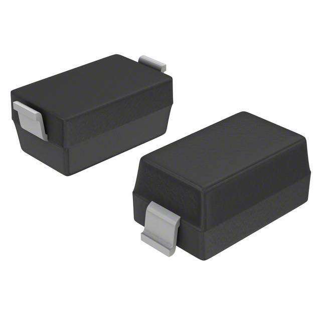
ICGOO电子元器件商城为您提供MSS1P6-M3/89A由Vishay设计生产,在icgoo商城现货销售,并且可以通过原厂、代理商等渠道进行代购。 MSS1P6-M3/89A价格参考。VishayMSS1P6-M3/89A封装/规格:二极管 - 整流器 - 单, Diode Schottky 60V 1A Surface Mount MicroSMP (DO-219AD)。您可以下载MSS1P6-M3/89A参考资料、Datasheet数据手册功能说明书,资料中有MSS1P6-M3/89A 详细功能的应用电路图电压和使用方法及教程。
MSS1P6-M3/89A是Vishay Semiconductor Diodes Division生产的一款表面贴装肖特基势垒二极管,属于单整流器二极管类别。该器件采用SOD-123FL封装,具有低正向压降和快速开关特性,适用于对效率和空间要求较高的电源应用。

其典型应用场景包括:便携式电子设备(如智能手机、平板电脑)中的电源管理电路,用于DC-DC转换器的续流与整流;消费类电子产品中的适配器和充电器电路;以及各类小型电源适配器、LED驱动电源和低压电源系统。由于其低功耗和高效率,也常用于电池供电设备中以延长续航时间。

此外,MSS1P6-M3/89A具备良好的热稳定性与可靠性,适合自动化贴片生产工艺,广泛应用于通信设备、家用电器和工业控制板等紧凑型电子模块中。其最大重复反向电压为60V,平均整流电流达1A,能在较高温度环境下稳定工作,满足多种通用整流需求。
| 参数 | 数值 |
| 产品目录 | |
| 描述 | DIODE SCHOTTKY 60V 1A MICROSMP肖特基二极管与整流器 1.0 Amp 60 Volt |
| 产品分类 | 单二极管/整流器分离式半导体 |
| 品牌 | Vishay SemiconductorsVishay Semiconductor Diodes Division |
| 产品手册 | |
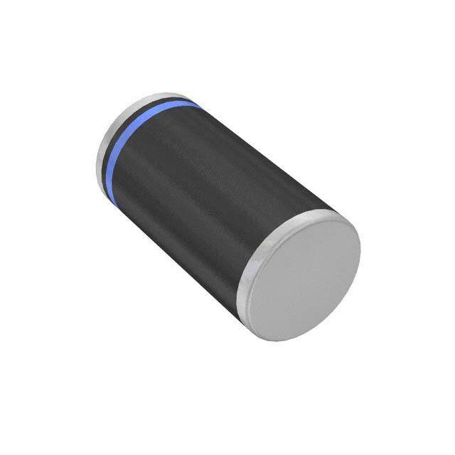
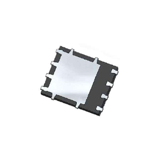
| 产品图片 |
|
| rohs | RoHS 合规性豁免无铅 / 符合限制有害物质指令(RoHS)规范要求 |
| 产品系列 | 二极管与整流器,肖特基二极管与整流器,Vishay Semiconductors MSS1P6-M3/89AeSMP™ |
| 数据手册 | |
| 产品型号 | MSS1P6-M3/89AMSS1P6-M3/89A |
| 不同If时的电压-正向(Vf) | 680mV @ 1A |
| 不同 Vr、F时的电容 | - |
| 不同 Vr时的电流-反向漏电流 | 150µA @ 60V |
| 二极管类型 | |
| 产品 | Schottky Rectifiers |
| 产品目录绘图 |
|
| 产品目录页面 | |
| 产品种类 | 肖特基二极管与整流器 |
| 供应商器件封装 | MicroSMP |
| 其它名称 | MSS1P6-M3/89AGIDKR |
| 包装 | Digi-Reel® |
| 反向恢复时间(trr) | - |
| 商标 | Vishay Semiconductors |
| 安装类型 | 表面贴装 |
| 安装风格 | SMD/SMT |
| 封装 | Reel |
| 封装/外壳 | MicroSMP |
| 封装/箱体 | Micro SMP |
| 峰值反向电压 | 60 V |
| 工作温度-结 | -55°C ~ 150°C |
| 工作温度范围 | - 55 C to + 150 C |
| 工厂包装数量 | 4500 |
| 技术 | Silicon |
| 最大反向漏泄电流 | 150 uA |
| 最大工作温度 | + 150 C |
| 最大浪涌电流 | 25 A |
| 最小工作温度 | - 55 C |
| 标准包装 | 1 |
| 正向电压下降 | 0.68 V |
| 正向连续电流 | 1 A |
| 电压-DC反向(Vr)(最大值) | 60V |
| 电流-平均整流(Io) | 1A |
| 系列 | MSSxPx |
| 速度 | 快速恢复 =< 500 ns,> 200mA(Io) |
| 配置 | Single |


- 商务部:美国ITC正式对集成电路等产品启动337调查
- 曝三星4nm工艺存在良率问题 高通将骁龙8 Gen1或转产台积电
- 太阳诱电将投资9.5亿元在常州建新厂生产MLCC 预计2023年完工
- 英特尔发布欧洲新工厂建设计划 深化IDM 2.0 战略
- 台积电先进制程称霸业界 有大客户加持明年业绩稳了
- 达到5530亿美元!SIA预计今年全球半导体销售额将创下新高
- 英特尔拟将自动驾驶子公司Mobileye上市 估值或超500亿美元
- 三星加码芯片和SET,合并消费电子和移动部门,撤换高东真等 CEO
- 三星电子宣布重大人事变动 还合并消费电子和移动部门
- 海关总署:前11个月进口集成电路产品价值2.52万亿元 增长14.8%


PDF Datasheet 数据手册内容提取
MSS1P5, MSS1P6 www.vishay.com Vishay General Semiconductor Surface Mount Schottky Barrier Rectifiers FEATURES eSMP® Series • Very low profile - typical height of 0.65 mm Available • Ideal for automated placement • Low forward voltage drop, low power losses • High efficiency • Meets MSL level 1, per J-STD-020, LF maximum peak of 260 °C Top View Bottom View • AEC-Q101 qualified available MicroSMP (DO-219AD) - Automotive ordering code: base P/NHM3 • Material categorization: for definitions of complianc e Anode Cathode please see www.vishay.com/doc?99912 ADDITIONAL RESOURCES TYPICAL APPLICATIONS 3DDD 333D For use in low voltage high frequency inverters, freewheeling, DC/DC converters, and polarity protectio n 3D Models applications. PRIMARY CHARACTERISTICS MECHANICAL DATA I 1.0 A Case: MicroSMP (DO-219AD) F(AV) Molding compound meets UL 94 V-0 flammability ratin g V 50 V, 60 V RRM Base P/N-M3 - halogen-free, RoHS-compliant, and IFSM 25 A commercial grade V at I = 1.0 A 0.52 V Base P/NHM3_X - halogen-free, RoHS-compliant, and F F AEC-Q101 qualified T max. 150 °C J (“_X” denotes revision code e.g. A, B,...) Package MicroSMP (DO-219AD) Terminals: matte tin plated leads, solderable per Circuit configuration Single J-STD-002 and JESD 22-B102 M3 suffix meets JESD 201 class 2 whisker test, HM3 suffix meets JESD 201 class 2 whisker test Polarity: color band denotes the cathode end MAXIMUM RATINGS (T = 25 °C unless otherwise noted) A PARAMETER SYMBOL MSS1P5 MSS1P6 UNIT Device marking code 15 16 Maximum repetitive peak reverse voltage V 50 60 V RRM Maximum average forward rectified current (fig. 1) I 1.0 A F(AV) Peak forward surge current 8.3 ms single half sine-wave I 25 A superimposed on rated load FSM Operating junction and storage temperature range T , T -55 to +150 °C J STG Revision: 17-Dec-2019 1 Document Number: 89018 For technical questions within your region: DiodesAmericas@vishay.com, DiodesAsia@vishay.com, DiodesEurope@vishay.com THIS DOCUMENT IS SUBJECT TO CHANGE WITHOUT NOTICE. THE PRODUCTS DESCRIBED HEREIN AND THIS DOCUMENT ARE SUBJECT TO SPECIFIC DISCLAIMERS, SET FORTH AT www.vishay.com/doc?91000
MSS1P5, MSS1P6 www.vishay.com Vishay General Semiconductor ELECTRICAL CHARACTERISTICS (T = 25 °C unless otherwise noted) A PARAMETER TEST CONDITIONS SYMBOL TYP. MAX. UNIT I = 0.5 A 0.45 - F T = 25 °C J Maximum instantaneous IF = 1.0 A V (1) 0.56 0.68 V forward voltage I = 0.5 A F 0.40 - F T = 125 °C J I = 1.0 A 0.52 0.60 F T = 25 °C 20 150 μA Maximum reverse current Rated V J I (2) R R T = 125 °C 7.0 12 mA J Typical junction capacitance 4.0 V, 1 MHz C 40 - pF J Notes (1) Pulse test: 300 μs pulse width, 1 % duty cycle (2) Pulse test: Pulse width 40 ms THERMAL CHARACTERISTICS (T = 25 °C unless otherwise noted) A PARAMETER SYMBOL MSS1P5 MSS1P6 UNIT R (1) 125 JA Typical thermal resistance R (1) 30 °C/W JL R (1) 40 JC Note (1) Thermal resistance from junction to ambient and junction to lead mounted on PCB with 6.0 mm x 6.0 mm copper pad areas R is measured JL at the terminal of cathode band. R is measured at the top center of the body JC ORDERING INFORMATION (Example) PREFERRED P/N UNIT WEIGHT (g) PREFERRED PACKAGE CODE BASE QUANTITY DELIVERY MODE MSS1P6-M3/89A 0.006 89A 4500 7" diameter plastic tape and reel MSS1P6HM3_A/H (1) 0.006 H 4500 7" diameter plastic tape and reel Note (1) AEC-Q101 qualified RATINGS AND CHARACTERISTICS CURVES (T = 25°C unless otherwise noted) A 1.2 0.7 A) Resistive or Inductive Load D = 0.3 D = 0.5 D = 0.8 nt ( 1.0 0.6 D = 0.2 urre W) d C 0.8 ss ( 0.5 D = 0.1 D = 1.0 e o d Rectifi 0.6 Power L 00..43 erage Forwar 00..24 aTtL tMhee aCsautrheodde Band Terminal Average 00..21 D = tp/T Ttp v A 0 0 0 25 50 75 100 125 150 0 0.2 0.4 0.6 0.8 1.0 1.2 Lead Temperature (°C) Average Forward Current (A) Fig. 1 - Maximum Forward Current Derating Curve Fig. 2 - Forward Power Loss Characteristics Revision: 17-Dec-2019 2 Document Number: 89018 For technical questions within your region: DiodesAmericas@vishay.com, DiodesAsia@vishay.com, DiodesEurope@vishay.com THIS DOCUMENT IS SUBJECT TO CHANGE WITHOUT NOTICE. THE PRODUCTS DESCRIBED HEREIN AND THIS DOCUMENT ARE SUBJECT TO SPECIFIC DISCLAIMERS, SET FORTH AT www.vishay.com/doc?91000
MSS1P5, MSS1P6 www.vishay.com Vishay General Semiconductor 10 1000 A) nt ( TJ= 150°C Curre 1 T = 125°C )Fp( e d J cn war atic or ap 100 F a us 0.1 C n ntaneo TJ= 25°C oitcnuJ a st TJ= -40°C n I 0.01 10 0 0.10.20.30.40.50.60.70.80.91.01.11.21.31.41.5 0.1 1 10 100 Reverse Voltage (V) Instantaneous Forward Voltage (V) Fig. 3 - Typical Instantaneous Forward Characteristics Fig. 5 - Typical Junction Capacitance Axis Title 1000 10000 1000 A) )W Junction to Ambient ent (m 10100 TJ= 150 °C /C°( e e Curr 1 TJ= 125 °C 1000 cnade 100 d lineRevers 0.00.11 TJ= 25 °C 1st line pmI lam 2nous 0.001 100 reh 10 e T an 0.0001 tn Instant0.00001 TJ= -40 °C eisnarT 0.000001 10 1 10 20 30 40 50 60 70 80 90 100 0.01 0.1 1 10 100 1000 Percent of Rated Peak Reverse Voltage (%) t - Pulse Duration (s) Fig. 4 - Typical Reverse Characteristics Fig. 6 - Typical Transient Thermal Impedance PACKAGE OUTLINE DIMENSIONS in inches (millimeters) MicroSMP (DO-219AD) 0.059 (1.50) 0.030 (0.75) Cathode Band 0.043 (1.10) 0.022 (0.55) 0.055 (1.40) 0.039 (0.98) 0.030 (0.75) 0.047 (1.20) 0.031 (0.78) 0.022 (0.55) 0.091 (2.30) 0.083 (2.10) 0.106 (2.70) 0.091 (2.30) Mounting Pad Layout 0.079 0.032 (2.00) (0.80) 0.029 (0.73) 0.043 0.032 0.025 (0.63) (1.10) (0.80) 0.011 (0.27) 0.005 (0.12) 0.020 (0.50) Revision: 17-Dec-2019 3 Document Number: 89018 For technical questions within your region: DiodesAmericas@vishay.com, DiodesAsia@vishay.com, DiodesEurope@vishay.com THIS DOCUMENT IS SUBJECT TO CHANGE WITHOUT NOTICE. THE PRODUCTS DESCRIBED HEREIN AND THIS DOCUMENT ARE SUBJECT TO SPECIFIC DISCLAIMERS, SET FORTH AT www.vishay.com/doc?91000
Legal Disclaimer Notice www.vishay.com Vishay Disclaimer ALL PRODUCT, PRODUCT SPECIFICATIONS AND DATA ARE SUBJECT TO CHANGE WITHOUT NOTICE TO IMPROV E RELIABILITY, FUNCTION OR DESIGN OR OTHERWISE. Vishay Intertechnology, Inc., its affiliates, agents, and employees, and all persons acting on its or their behalf (collectively, “Vishay”), disclaim any and all liability for any errors, inaccuracies or incompleteness contained in any datasheet or in any other disclosure relating to any product. Vishay makes no warranty, representation or guarantee regarding the suitability of the products for any particular purpose o r the continuing production of any product. To the maximum extent permitted by applicable law, Vishay disclaims (i) any and all liability arising out of the application or use of any product, (ii) any and all liability, including without limitation special, consequential or incidental damages, and (iii) any and all implied warranties, including warranties of fitness for particular purpose, non-infringement and merchantability. Statements regarding the suitability of products for certain types of applications are based on Vishay’s knowledge of typical requirements that are often placed on Vishay products in generic applications. Such statements are not binding statements about the suitability of products for a particular application. It is the customer’s responsibility to validate that a particular product with the properties described in the product specification is suitable for use in a particular application. Parameters provided in datasheets and / or specifications may vary in different applications and performance may vary over time. All operating parameters, including typical parameters, must be validated for each customer application by the customer’s technical experts. Product specifications do not expand or otherwise modify Vishay’s terms and conditions of purchase, including but not limited to the warranty expressed therein. Except as expressly indicated in writing, Vishay products are not designed for use in medical, life-saving, or life-sustainin g applications or for any other application in which the failure of the Vishay product could result in personal injury or death. Customers using or selling Vishay products not expressly indicated for use in such applications do so at their own risk . Please contact authorized Vishay personnel to obtain written terms and conditions regarding products designed for such applications. No license, express or implied, by estoppel or otherwise, to any intellectual property rights is granted by this documen t or by any conduct of Vishay. Product names and markings noted herein may be trademarks of their respective owners. © 2019 VISHAY INTERTECHNOLOGY, INC. ALL RIGHTS RESERVED Revision: 01-Jan-2019 1 Document Number: 91000
Mouser Electronics Authorized Distributor Click to View Pricing, Inventory, Delivery & Lifecycle Information: V ishay: MSS1P5-E3/89A MSS1P6-E3/89A MSS1P5-M3/89A MSS1P6-M3/89A MSS1P6HM3/89A MSS1P5HM3_A/H MSS1P6HM3J_A/H MSS1P6HM3_A/H MSS1P5HM3/89A MSS1P6HM3J/89A