ICGOO在线商城 > 集成电路(IC) > 嵌入式 - 微控制器 > MSP430FE4252IPMR

 Datasheet下载
- 型号: MSP430FE4252IPMR
- 制造商: Texas Instruments
- 库位|库存: xxxx|xxxx
- 要求:
| 数量阶梯 | 香港交货 | 国内含税 |
| +xxxx | $xxxx | ¥xxxx |
查看当月历史价格
查看今年历史价格
MSP430FE4252IPMR产品简介:
ICGOO电子元器件商城为您提供MSP430FE4252IPMR由Texas Instruments设计生产,在icgoo商城现货销售,并且可以通过原厂、代理商等渠道进行代购。 MSP430FE4252IPMR价格参考¥21.48-¥39.90。Texas InstrumentsMSP430FE4252IPMR封装/规格:嵌入式 - 微控制器, MSP430 微控制器 IC MSP430x4xx 16-位 8MHz 16KB(16K x 8 + 256B) 闪存 64-LQFP(10x10)。您可以下载MSP430FE4252IPMR参考资料、Datasheet数据手册功能说明书,资料中有MSP430FE4252IPMR 详细功能的应用电路图电压和使用方法及教程。
MSP430FE4252IPMR 是 Texas Instruments(德州仪器)推出的超低功耗微控制器,属于 MSP430 系列中的 FRAM(铁电随机存取存储器)产品线。它结合了高性能、低功耗和高可靠性,适用于多种嵌入式应用场景。以下是其主要应用场景:

1. 工业自动化
   - 用于传感器数据采集与处理,例如温度、湿度、压力等环境监测。
   - 在低功耗需求的工业设备中用作控制单元,如电机驱动、电源管理等。

2. 医疗设备
   - 应用于便携式医疗设备,如血糖仪、脉搏血氧仪等,利用其低功耗特性延长电池寿命。
   - 支持实时数据记录与分析,FRAM 的非易失性和快速写入能力非常适合存储关键健康数据。

3. 智能家居与物联网 (IoT)
   - 作为智能家电的核心控制芯片,例如智能灯泡、插座或温控器。
   - 在无线传感节点中使用,支持长时间待机模式以降低能耗。

4. 计量与能源管理
   - 用于水表、电表、气表等智能仪表中,提供精确的数据测量与存储功能。
   - FRAM 技术确保在断电情况下数据不丢失,适合需要高可靠性的应用。

5. 消费电子
   - 集成到可穿戴设备中,如健身追踪器或智能手表,满足小尺寸和低功耗要求。
   - 用作玩具或游戏设备的主控芯片,提供简单高效的控制逻辑。

6. 农业与环境监测
   - 部署于无线传感器网络中,监测土壤湿度、光照强度等农业参数。
   - 在野外长期运行的环境监测系统中,利用其低功耗特性减少维护成本。

7. 安全与访问控制
   - 用于门禁系统、RFID 阅读器或其他需要加密存储的应用中,FRAM 提供安全且快速的数据写入能力。

总结来说,MSP430FE4252IPMR 凭借其低功耗设计、FRAM 存储优势以及丰富的外设资源,广泛应用于对能效、可靠性和小型化有较高要求的领域。
| 参数 | 数值 |
| 产品目录 | 集成电路 (IC) |
| 描述 | IC MCU 16BIT 16KB FLASH 64LQFP |
| EEPROM容量 | - |
| 产品分类 | |
| I/O数 | 14 |
| 品牌 | Texas Instruments |
| 数据手册 | |
| 产品图片 |
|
| 产品型号 | MSP430FE4252IPMR |
| RAM容量 | 512 x 8 |
| rohs | 无铅 / 符合限制有害物质指令(RoHS)规范要求 |
| 产品系列 | MSP430x4xx |
| 产品培训模块 | http://www.digikey.cn/PTM/IndividualPTM.page?site=cn&lang=zhs&ptm=8361http://www.digikey.cn/PTM/IndividualPTM.page?site=cn&lang=zhs&ptm=8522http://www.digikey.cn/PTM/IndividualPTM.page?site=cn&lang=zhs&ptm=8576http://www.digikey.cn/PTM/IndividualPTM.page?site=cn&lang=zhs&ptm=8679http://www.digikey.cn/PTM/IndividualPTM.page?site=cn&lang=zhs&ptm=7557http://www.digikey.cn/PTM/IndividualPTM.page?site=cn&lang=zhs&ptm=25419http://www.digikey.cn/PTM/IndividualPTM.page?site=cn&lang=zhs&ptm=25427http://www.digikey.cn/PTM/IndividualPTM.page?site=cn&lang=zhs&ptm=25523http://www.digikey.cn/PTM/IndividualPTM.page?site=cn&lang=zhs&ptm=25524http://www.digikey.cn/PTM/IndividualPTM.page?site=cn&lang=zhs&ptm=25537http://www.digikey.cn/PTM/IndividualPTM.page?site=cn&lang=zhs&ptm=25788http://www.digikey.cn/PTM/IndividualPTM.page?site=cn&lang=zhs&ptm=25882http://www.digikey.cn/PTM/IndividualPTM.page?site=cn&lang=zhs&ptm=25885http://www.digikey.cn/PTM/IndividualPTM.page?site=cn&lang=zhs&ptm=26015http://www.digikey.cn/PTM/IndividualPTM.page?site=cn&lang=zhs&ptm=26006http://www.digikey.cn/PTM/IndividualPTM.page?site=cn&lang=zhs&ptm=30354 |
| 产品目录页面 | |
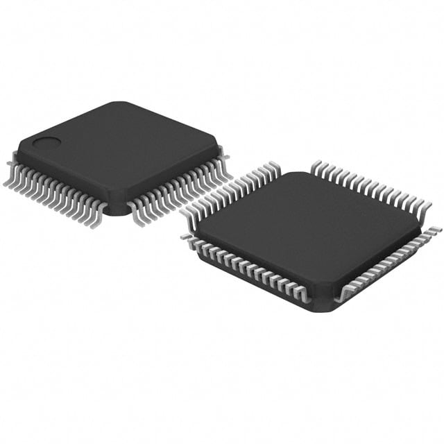
| 供应商器件封装 | 64-LQFP(10x10) |
| 其它名称 | 296-23732-6 |
| 制造商产品页 | http://www.ti.com/general/docs/suppproductinfo.tsp?distId=10&orderablePartNumber=MSP430FE4252IPMR |
| 包装 | Digi-Reel® |
| 外设 | 欠压检测/复位,LCD,POR,PWM,WDT |
| 封装/外壳 | 64-LQFP |
| 工作温度 | -40°C ~ 85°C |
| 振荡器类型 | 内部 |
| 数据转换器 | A/D 2x16b |
| 标准包装 | 1 |
| 核心处理器 | MSP430 |
| 核心尺寸 | 16-位 |
| 电压-电源(Vcc/Vdd) | 1.8 V ~ 3.6 V |
| 程序存储器类型 | 闪存 |
| 程序存储容量 | 16KB(16K x 8 + 256B) |
| 连接性 | SPI,UART/USART |
| 速度 | 8MHz |


- 商务部:美国ITC正式对集成电路等产品启动337调查
- 曝三星4nm工艺存在良率问题 高通将骁龙8 Gen1或转产台积电
- 太阳诱电将投资9.5亿元在常州建新厂生产MLCC 预计2023年完工
- 英特尔发布欧洲新工厂建设计划 深化IDM 2.0 战略
- 台积电先进制程称霸业界 有大客户加持明年业绩稳了
- 达到5530亿美元!SIA预计今年全球半导体销售额将创下新高
- 英特尔拟将自动驾驶子公司Mobileye上市 估值或超500亿美元
- 三星加码芯片和SET,合并消费电子和移动部门,撤换高东真等 CEO
- 三星电子宣布重大人事变动 还合并消费电子和移动部门
- 海关总署:前11个月进口集成电路产品价值2.52万亿元 增长14.8%


PDF Datasheet 数据手册内容提取
MSP430FE42x2 MIXED SIGNAL MICROCONTROLLER SLAS616 − JULY 2008 (cid:1) (cid:1) Low Supply-Voltage Range, 2.7 V to 3.6 V Supply Voltage Supervisor/Monitor With (cid:1) Ultra-Low-Power Consumption: Programmable Level Detection − Active Mode: 400 µA at 1 MHz, 3.0 V (cid:1) Serial Onboard Programming, − Standby Mode: 1.6 µA No External Programming Voltage Needed, − Off Mode (RAM Retention): 0.1 µA Programmable Code Protection by Security (cid:1) Five Power-Saving Modes Fuse (cid:1) (cid:1) Bootstrap Loader in Flash Devices Wake-Up From Standby Mode in Less Than 6 µs (cid:1) Family Members Include: (cid:1) Frequency-Locked Loop, FLL+ − MSP430FE4232 (cid:1) 8KB + 256B Flash Memory, 16-Bit RISC Architecture, 125-ns 256B RAM Instruction Cycle Time − MSP430FE4242 (cid:1) Embedded Signal Processing for 12KB + 256B Flash Memory, Single-Phase Energy Metering With 512B RAM Integrated Analog Front-End and − MSP430FE4252 Temperature Sensor (ESP430CE1B) 16KB + 256B Flash Memory, (cid:1) 16-Bit Timer_A With Three 512B RAM Capture/Compare Registers − MSP430FE4272 (cid:1) Integrated LCD Driver for 128 Segments 32KB + 256B Flash Memory, (cid:1) 1KB RAM Serial Communication Interface (USART), (cid:1) Asynchronous UART, or Synchronous SPI Available in 64-Pin Quad Flat Pack (QFP) (cid:1) Selectable by Software For Complete Module Descriptions, (cid:1) Brownout Detector See the MSP430x4xx Family User’s Guide, Literature Number SLAU056 description The Texas Instruments MSP430 family of ultra-low-power microcontrollers consists of several devices featuring different sets of peripherals targeted for various applications. The architecture, combined with five low-power modes is optimized to achieve extended battery life in portable measurement applications. The device features a powerful 16-bit RISC CPU, 16-bit registers, and constant generators that contribute to maximum code efficiency. The digitally controlled oscillator (DCO) allows wake-up from low-power modes to active mode in less than 6 µs. The MSP430FE42x2 devices are microcontroller configurations with two independent 16-bit sigma-delta analog-to-digital (A/D) converters and embedded signal processor core used to measure and calculate single-phase energy in both 2-wire and 3-wire configurations. Also included is a built-in 16-bit timer, 128 LCD segment drive capability, and 14 I/O pins. Typical applications include 2-wire and 3-wire single-phase metering. This integrated circuit can be damaged by ESD. Texas Instruments recommends that all integrated circuits be handled with appropriate precautions. Failure to observe proper handling and installation procedures can cause damage. ESD damage can range from subtle performance degradation to complete device failure. Precision integrated circuits may be more susceptible to damage because very small parametric changes could cause the device not to meet its published specifications. These devices have limited built-in ESD protection. Please be aware that an important notice concerning availability, standard warranty, and use in critical applications of TexasInstruments semiconductor products and disclaimers thereto appears at the end of this data sheet. PRODUCTION DATA information is current as of publication date. Copyright 2008 Texas Instruments Incorporated Products conform to specifications per the terms of Texas Instruments standard warranty. Production processing does not necessarily include testing of all parameters. POST OFFICE BOX 655303 • DALLAS, TEXAS 75265 1
MSP430FE42x2 MIXED SIGNAL MICROCONTROLLER SLAS616 − JULY 2008 AVAILABLE OPTIONS PACKAGED DEVICES TA PLASTIC 64-PIN QFP (PM) MSP430FE4232IPM MSP430FE4242IPM −40°C to 85°C MSP430FE4252IPM MSP430FE4272IPM pin designation 0 3 K S N D0 D0 MCL S31 OUT/ SVSI UTX URX NMI CLK TDI TA0 TA0/ TA1/ SVS S29 VCCVSSVSS2.3/ 2.4/ 2.5/ ST/ CK MS DI/T DO/ 1.0/ 1.1/ 1.2/ 1.3/ 1.4/ A D AP P P R T T T T P P P P P 6463 6261 60 59 58 57 56 55 54 53 52 51 5049 DV 1 48 P1.5/TACLK/ACLK/S28 CC I1+ 2 47 P1.6/SIMO0/S27 I1− 3 46 P1.7/SOMI0/S26 NC 4 45 P2.0/TA2/S25 NC 5 44 P2.1/UCLK0/S24 V1+ 6 43 R33 V1− 7 42 R23 XIN 8 41 R13 MSP430FE42x2 XOUT 9 40 R03 VREF 10 39 COM3 P2.2/STE0 11 38 COM2 S0 12 37 COM1 S1 13 36 COM0 S2 14 35 S23 S3 15 34 S22 S4 16 33 S21 17 18 19 20 21 22 23 24 25 26 27 28 29 30 31 32 5 6 7 8 9 0 1 2 3 4 5 6 7 8 9 0 S S S S S 1 1 1 1 1 1 1 1 1 1 2 S S S S S S S S S S S 2 POST OFFICE BOX 655303 • DALLAS, TEXAS 75265
MSP430FE42x2 MIXED SIGNAL MICROCONTROLLER SLAS616 − JULY 2008 functional block diagram XIN XOUT DVCC DVSS AVCC AVSS P1 P2 8 6 ACLK Oscillators Flash RAM Timer_A3 Port 1 Port 2 USART0 FLL+ SMCLK 32KB 1KB 3 CC Reg 8 I/O 6 I/O UART or MCLK 16KB 512B Interrupt Interrupt SPI 12KB 512B Capability Capability Function 8KB 256B MAB 8 MHz CPU incl. 16 Registers MDB Emulation Module PSOVSR// WWatDchTd+og ESEPm4b3e0dCdEed1B TBimaesirc 1 L1C2D8 Brownout Signal Segments 15/16-Bit Processing, 1 Interrupt 1,2,3,4 MUX JTAG Analog Vector Front-End Interface fLCD RST/NMI POST OFFICE BOX 655303 • DALLAS, TEXAS 75265 3
MSP430FE42x2 MIXED SIGNAL MICROCONTROLLER SLAS616 − JULY 2008 Terminal Functions TERMINAL II//OO DDEESSCCRRIIPPTTIIOONN NAME NO. DVCC 1 Digital supply voltage, positive terminal I1+ 2 I Current 1 positive analog input. Internal connection to SD16 Channel 0 A0+. (see Note 1) I1− 3 I Current 1 negative analog input. Internal connection to SD16 Channel 0 A0−. (see Note 1) NC 4 I Not connected. Connection to analog ground (AVSS) recommended. NC 5 I Not connected. Connection to analog ground (AVSS) recommended. V1+ 6 I Voltage 1 positive analog input. Internal connection to SD16 Channel 1 A0+. (see Note 1) V1− 7 I Voltage 1 negative analog input. Internal connection to SD16 Channel 1 A0−. (see Note 1) XIN 8 I Input port for crystal oscillator XT1. Standard or watch crystals can be connected. XOUT 9 O Output terminal of crystal oscillator XT1 VREF 10 I/O Input for an external reference voltage / Internal reference voltage output (can be used as mid-voltage) P2.2/STE0 11 I/O General-purpose digital I/O / Slave transmit enable—USART0/SPI mode S0 12 O LCD segment output 0 S1 13 O LCD segment output 1 S2 14 O LCD segment output 2 S3 15 O LCD segment output 3 S4 16 O LCD segment output 4 S5 17 O LCD segment output 5 S6 18 O LCD segment output 6 S7 19 O LCD segment output 7 S8 20 O LCD segment output 8 S9 21 O LCD segment output 9 S10 22 O LCD segment output 10 S11 23 O LCD segment output 11 S12 24 O LCD segment output 12 S13 25 O LCD segment output 13 S14 26 O LCD segment output 14 S15 27 O LCD segment output 15 S16 28 O LCD segment output 16 S17 29 O LCD segment output 17 S18 30 O LCD segment output 18 S19 31 O LCD segment output 19 S20 32 O LCD segment output 20 S21 33 O LCD segment output 21 S22 34 O LCD segment output 22 S23 35 O LCD segment output 23 COM0 36 O Common output, COM0−3 are used for LCD backplanes. COM1 37 O Common output, COM0−3 are used for LCD backplanes. COM2 38 O Common output, COM0−3 are used for LCD backplanes. COM3 39 O Common output, COM0−3 are used for LCD backplanes. R03 40 I Input port of fourth positive (lowest) analog LCD level (V5) NOTE 1: It is recommended to short unused analog input pairs and connect them to analog ground (AVSS). 4 POST OFFICE BOX 655303 • DALLAS, TEXAS 75265
MSP430FE42x2 MIXED SIGNAL MICROCONTROLLER SLAS616 − JULY 2008 Terminal Functions (Continued) TERMINAL II//OO DDEESSCCRRIIPPTTIIOONN NAME NO. R13 41 I Input port of third most positive analog LCD level (V4 or V3) R23 42 I Input port of second most positive analog LCD level (V2) R33 43 O Output port of most positive analog LCD level (V1) General-purpose digital I/O / External clock input-USART0/UART or SPI mode, clock output—USART0/SPI P2.1/UCLK0/S24 44 I/O mode / LCD segment output 24 (See Note 1) General-purpose digital I/O / Timer_A Capture: CCI2A input, Compare: Out2 output / LCD segment output P2.0/TA2/S25 45 I/O 25 (See Note 1) General-purpose digital I/O / Slave out/master in of USART0/SPI mode / LCD segment output 26 P1.7/SOMI0/S26 46 I/O (See Note 1) General-purpose digital I/O / Slave in/master out of USART0/SPI mode / LCD segment output 27 P1.6/SIMO0/S27 47 I/O (See Note 1) P1.5/TACLK/ General-purpose digital I/O / Timer_A and SD16 clock signal TACLK input / ACLK output 48 I/O ACLK/S28 (divided by 1, 2, 4, or 8) / LCD segment output 28 (See Note 1) P1.4/S29 49 I/O General-purpose digital I/O / LCD segment output 29 (See Note 1) P1.3/SVSOUT/ 50 I/O General-purpose digital I/O / SVS: output of SVS comparator / LCD segment output 30 (See Note 1) S30 General-purpose digital I/O / Timer_A, Capture: CCI1A, CCI1B input, Compare: Out1 output / LCD segment P1.2/TA1/S31 51 I/O output 31 (See Note 1) General-purpose digital I/O / Timer_A, Capture: CCI0B input / MCLK output. P1.1/TA0/MCLK 52 I/O Note: TA0 is only an input on this pin / BSL receive P1.0/TA0 53 I/O General-purpose digital I/O / Timer_A, Capture: CCI0A input, Compare: Out0 output / BSL transmit TDO/TDI 54 I/O Test data output port. TDO/TDI data output or programming data input terminal. TDI/TCLK 55 I Test data input or test clock input. The device protection fuse is connected to TDI. TMS 56 I Test mode select. TMS is used as an input port for device programming and test. TCK 57 I Test clock. TCK is the clock input port for device programming and test. RST/NMI 58 I Reset input or nonmaskable interrupt input port P2.5/URXD0 59 I/O General-purpose digital I/O / Receive data in—USART0/UART mode P2.4/UTXD0 60 I/O General-purpose digital I/O / Transmit data out—USART0/UART mode P2.3/SVSIN 61 I/O General-purpose digital I/O / Analog input to brownout, supply voltage supervisor Analog supply voltage, negative terminal. Supplies SD16, SVS, brownout, oscillator, and LCD resistive AVSS 62 divider circuitry. DVSS 63 Digital supply voltage, negative terminal. Analog supply voltage, positive terminal. Supplies SD16, SVS, brownout, oscillator, and LCD resistive AVCC 64 divider circuitry; must not power up prior to DVCC. NOTE 1: LCD function selected automatically when applicable LCD module control bits are set, not with PxSEL bits. POST OFFICE BOX 655303 • DALLAS, TEXAS 75265 5
MSP430FE42x2 MIXED SIGNAL MICROCONTROLLER SLAS616 − JULY 2008 short-form description CPU The MSP430 CPU has a 16-bit RISC architecture Program Counter PC/R0 that is highly transparent to the application. All operations, other than program-flow instructions, Stack Pointer SP/R1 are performed as register operations in Status Register SR/CG1/R2 conjunction with seven addressing modes for source operand and four addressing modes for Constant Generator CG2/R3 destination operand. General-Purpose Register R4 The CPU is integrated with 16 registers that provide reduced instruction execution time. The General-Purpose Register R5 register-to-register operation execution time is one cycle of the CPU clock. General-Purpose Register R6 Four of the registers, R0 to R3, are dedicated as General-Purpose Register R7 program counter, stack pointer, status register, and constant generator respectively. The General-Purpose Register R8 remaining registers are general-purpose registers. General-Purpose Register R9 Peripherals are connected to the CPU using data, General-Purpose Register R10 address, and control buses, and can be handled with all instructions. General-Purpose Register R11 instruction set General-Purpose Register R12 The instruction set consists of 51 instructions with three formats and seven address modes. Each General-Purpose Register R13 instruction can operate on word and byte data. Table 1 shows examples of the three types of General-Purpose Register R14 instruction formats; the address modes are listed General-Purpose Register R15 in Table 2. Table 1. Instruction Word Formats Dual operands, source-destination e.g., ADD R4,R5 R4 + R5 −−−> R5 Single operands, destination only e.g., CALL R8 PC −−>(TOS), R8−−> PC Relative jump, un/conditional e.g., JNE Jump-on-equal bit = 0 Table 2. Address Mode Descriptions ADDRESS MODE S D SYNTAX EXAMPLE OPERATION (cid:1) (cid:1) Register MOV Rs,Rd MOV R10,R11 R10 −−> R11 (cid:1) (cid:1) Indexed MOV X(Rn),Y(Rm) MOV 2(R5),6(R6) M(2+R5)−−> M(6+R6) (cid:1) (cid:1) Symbolic (PC relative) MOV EDE,TONI M(EDE) −−> M(TONI) (cid:1) (cid:1) Absolute MOV &MEM,&TCDAT M(MEM) −−> M(TCDAT) (cid:1) Indirect MOV @Rn,Y(Rm) MOV @R10,Tab(R6) M(R10) −−> M(Tab+R6) Indirect (cid:1) M(R10) −−> R11 MOV @Rn+,Rm MOV @R10+,R11 autoincrement R10 + 2−−> R10 (cid:1) Immediate MOV #X,TONI MOV #45,TONI #45 −−> M(TONI) NOTE: S = source, D = destination 6 POST OFFICE BOX 655303 • DALLAS, TEXAS 75265
MSP430FE42x2 MIXED SIGNAL MICROCONTROLLER SLAS616 − JULY 2008 operating modes The MSP430 has one active mode and five software-selectable low-power modes of operation. An interrupt event can wake up the device from any of the five low-power modes, service the request, and restore back to the low-power mode on return from the interrupt program. The following six operating modes can be configured by software: (cid:1) Active mode (AM) − All clocks are active. (cid:1) Low-power mode 0 (LPM0) − CPU is disabled. − ACLK and SMCLK remain active, MCLK is available to modules. − FLL+ loop control remains active. (cid:1) Low-power mode 1 (LPM1) − CPU is disabled. − ACLK and SMCLK remain active, MCLK is available to modules. − FLL+ loop control is disabled. (cid:1) Low-power mode 2 (LPM2) − CPU is disabled. − MCLK, FLL+ loop control, and DCOCLK are disabled. − DCO’s dc generator remains enabled. − ACLK remains active. (cid:1) Low-power mode 3 (LPM3) − CPU is disabled. − MCLK, FLL+ loop control, and DCOCLK are disabled. − DCO’s dc generator is disabled. − ACLK remains active. (cid:1) Low-power mode 4 (LPM4) − CPU is disabled. − ACLK is disabled. − MCLK, FLL+ loop control, and DCOCLK are disabled. − DCO’s dc generator is disabled. − Crystal oscillator is stopped. POST OFFICE BOX 655303 • DALLAS, TEXAS 75265 7
MSP430FE42x2 MIXED SIGNAL MICROCONTROLLER SLAS616 − JULY 2008 interrupt vector addresses The interrupt vectors and the power-up starting address are located in the address range of 0FFFFh to 0FFE0h. The vector contains the 16-bit address of the appropriate interrupt-handler instruction sequence. INTERRUPT SOURCE INTERRUPT FLAG SYSTEM INTERRUPT WORD ADDRESS PRIORITY Power-up WDTIFG Reset 0FFFEh 15, highest External reset KEYV Watchdog (see Note 1) Flash memory PC out-of-range (see Note 4) NMI NMIIFG (see Notes 1 and 3) (Non)maskable Oscillator fault OFIFG (see Notes 1 and 3) (Non)maskable 0FFFCh 14 Flash memory access violation ACCVIFG (see Notes 1 and 3) (Non)maskable MBCTL_OUTxIFG, ESP430 MBCTL_INxIFG Maskable 0FFFAh 13 (see Notes 1 and 2) SD16CCTLx SD16OVIFG, SD16 SD16CCTLx SD16IFG Maskable 0FFF8h 12 (see Notes 1 and 2) 0FFF6h 11 Watchdog timer WDTIFG Maskable 0FFF4h 10 USART0 receive URXIFG0 Maskable 0FFF2h 9 USART0 transmit UTXIFG0 Maskable 0FFF0h 8 0FFEEh 7 Timer_A3 TACCR0 CCIFG (see Note 2) Maskable 0FFECh 6 TACCR1 and TACCR2 Timer_A3 CCIFGs, and TACTL TAIFG Maskable 0FFEAh 5 (see Notes 1 and 2) P1IFG.0 to P1IFG.7 I/O port P1 (eight flags) Maskable 0FFE8h 4 (see Notes 1 and 2) 0FFE6h 3 0FFE4h 2 P2IFG.0 to P2IFG.7 I/O port P2 (eight flags) Maskable 0FFE2h 1 (see Notes 1 and 2) Basic timer1 BTIFG Maskable 0FFE0h 0, lowest NOTES: 1. Multiple source flags 2. Interrupt flags are located in the module. 3. (Non)maskable: the individual interrupt-enable bit can disable an interrupt event, but the general interrupt-enable cannot. 4. A reset is generated if the CPU tries to fetch instructions from within the module register memory address range (0h to 01FFh) or from within unused address ranges (from 0600h to 0BFFh). 8 POST OFFICE BOX 655303 • DALLAS, TEXAS 75265
MSP430FE42x2 MIXED SIGNAL MICROCONTROLLER SLAS616 − JULY 2008 special function registers Most interrupt and module enable bits are collected into the lowest address space. Special function register bits that are not allocated to a functional purpose are not physically present in the device. Simple software access is provided with this arrangement. interrupt enable 1 and 2 Address 7 6 5 4 3 2 1 0 0h UTXIE0 URXIE0 ACCVIE NMIIE OFIE WDTIE rw–0 rw–0 rw–0 rw–0 rw–0 rw–0 WDTIE: Watchdog timer interrupt enable. Inactive if watchdog mode is selected. Active if watchdog timer is configured in interval timer mode. OFIE: Oscillator-fault-interrupt enable NMIIE: Nonmaskable-interrupt enable ACCVIE: Flash access violation interrupt enable URXIE0: USART0: UART and SPI receive-interrupt enable UTXIE0: USART0: UART and SPI transmit-interrupt enable Address 7 6 5 4 3 2 1 0 1h BTIE rw-0 BTIE: Basic Timer1 interrupt enable interrupt flag register 1 and 2 Address 7 6 5 4 3 2 1 0 02h UTXIFG0 URXIFG0 NMIIFG OFIFG WDTIFG rw–1 rw–0 rw–0 rw–1 rw–(0) WDTIFG: Set on watchdog timer overflow (in watchdog mode) or security key violation. Reset on V CC power up or a reset condition at the RST/NMI pin in reset mode. OFIFG: Flag set on oscillator fault NMIIFG: Set via RST/NMI pin URXIFG0: USART0: UART and SPI receive flag UTXIFG0: USART0: UART and SPI transmit flag Address 7 6 5 4 3 2 1 0 3h BTIFG rw-0 BTIFG: Basic Timer1 interrupt flag POST OFFICE BOX 655303 • DALLAS, TEXAS 75265 9
MSP430FE42x2 MIXED SIGNAL MICROCONTROLLER SLAS616 − JULY 2008 module enable registers 1 and 2 Address 7 6 5 4 3 2 1 0 UTXE0 URXE0 04h USPIE0 rw–0 rw–0 URXE0: USART0: UART mode receive enable UTXE0: USART0: UART mode transmit enable USPIE0: USART0: SPI mode transmit and receive enable Address 7 6 5 4 3 2 1 0 05h Legend: rw−0,1: Bit Can Be Read and Written. It Is Reset or Set by PUC. rw−(0,1): Bit Can Be Read and Written. It Is Reset or Set by POR. SFR Bit Not Present in Device. 10 POST OFFICE BOX 655303 • DALLAS, TEXAS 75265
MSP430FE42x2 MIXED SIGNAL MICROCONTROLLER SLAS616 − JULY 2008 memory organization MSP430FE4232 MSP430FE4242 MSP430FE4252 MSP430FE4272 Memory Size 8KB 12KB 16KB 32KB Interrupt vector Flash 0FFFFh to 0FFE0h 0FFFFh to 0FFE0h 0FFFFh to 0FFE0h 0FFFFh to 0FFE0h Code memory Flash 0FFFFh to 0E000h 0FFFFh to 0D000h 0FFFFh to 0C000h 0FFFFh to 08000h Information memory Size 256 Byte 256 Byte 256 Byte 256 Byte 010FFh to 01000h 010FFh to 01000h 010FFh to 01000h 010FFh to 01000h Boot memory Size 1kB 1kB 1kB 1kB 0FFFh to 0C00h 0FFFh to 0C00h 0FFFh to 0C00h 0FFFh to 0C00h RAM Size 256 Byte 512 Byte 512 Byte 1KB 02FFh to 0200h 03FFh to 0200h 03FFh to 0200h 05FFh − 0200h Peripherals 16 bit 01FFh to 0100h 01FFh to 0100h 01FFh to 0100h 01FFh to 0100h 8 bit 0FFh to 010h 0FFh to 010h 0FFh to 010h 0FFh to 010h 8-bit SFR 0Fh to 00h 0Fh to 00h 0Fh to 00h 0Fh to 00h bootstrap loader (BSL) The MSP430 bootstrap loader (BSL) enables users to program the flash memory or RAM using a UART serial interface. Access to the MSP430 memory via the BSL is protected by user-defined password. For complete description of the features of the BSL and its implementation, see the application report Features of the MSP430 Bootstrap Loader, literature number SLAA089. BSL Function PM Package Pins Data Transmit 53 - P1.0 Data Receive 52 - P1.1 flash memory The flash memory can be programmed via the JTAG port, the bootstrap loader, or in system by the CPU. The CPU can perform single-byte and single-word writes to the flash memory. Features of the flash memory include: (cid:1) Flash memory has n segments of main memory and two segments of information memory (A and B) of 128 bytes each. Each segment in main memory is 512 bytes in size. (cid:1) Segments 0 to n may be erased in one step, or each segment may be individually erased. (cid:1) Segments A and B can be erased individually, or as a group with segments 0 to n. Segments A and B are also called information memory. (cid:1) New devices may have some bytes programmed in the information memory (needed for test during manufacturing). The user should perform an erase of the information memory prior to the first use. POST OFFICE BOX 655303 • DALLAS, TEXAS 75265 11
MSP430FE42x2 MIXED SIGNAL MICROCONTROLLER SLAS616 − JULY 2008 peripherals Peripherals are connected to the CPU through data, address, and control buses and can be handled using all instructions. For complete module descriptions, see the MSP430x4xx Family User’s Guide, literature number SLAU056. oscillator and system clock The clock system in the MSP430FE42x2 family of devices is supported by the FLL+ module, which includes support for a 32768-Hz watch crystal oscillator, an internal digitally-controlled oscillator (DCO), and a high-frequency crystal oscillator. The FLL+ clock module is designed to meet the requirements of both low system cost and low power consumption. The FLL+ features a digital frequency-locked loop (FLL) hardware that, in conjunction with a digital modulator, stabilizes the DCO frequency to a programmable multiple of the watch-crystal frequency. The internal DCO provides a fast turn-on clock source and stabilizes in less than 6 µs. The FLL+ module provides the following clock signals: (cid:1) Auxiliary clock (ACLK), sourced from a 32768-Hz watch crystal or a high-frequency crystal. (cid:1) Main clock (MCLK), the system clock used by the CPU. (cid:1) Sub-Main clock (SMCLK), the subsystem clock used by the peripheral modules. (cid:1) ACLK/n, the buffered output of ACLK, ACLK/2, ACLK/4, or ACLK/8. brownout, supply voltage supervisor (SVS) The brownout circuit is implemented to provide the proper internal reset signal to the device during power on and power off. The SVS circuitry detects if the supply voltage drops below a user-selectable level and supports both supply-voltage supervision (the device is automatically reset) and supply-voltage monitoring (SVM) (the device is not automatically reset). The CPU begins code execution after the brownout circuit releases the device reset. However, V may not CC have ramped to V at that time. The user must ensure that the default FLL+ settings are not changed until CC(min) V reaches V . If desired, the SVS circuit can be used to determine when V reaches V . CC CC(min) CC CC(min) digital I/O There are two 8-bit I/O ports implemented—ports P1 and P2 (only six P2 I/O signals are available on external pins). (cid:1) All individual I/O bits are independently programmable. (cid:1) Any combination of input, output, and interrupt conditions is possible. (cid:1) Edge-selectable interrupt input capability for all the eight bits of port P1 and six bits of P2. (cid:1) Read/write access to port-control registers is supported by all instructions. NOTE: Only six bits of port P2 (P2.0 to P2.5) are available on external pins, but all control and data bits for port P2 are implemented. Basic Timer1 The Basic Timer1 has two independent 8-bit timers that can be cascaded to form a 16-bit timer/counter. Both timers can be read and written by software. The Basic Timer1 can be used to generate periodic interrupts and clock for the LCD module. LCD drive The LCD driver generates the segment and common signals required to drive an LCD display. The LCD controller has dedicated data memory to hold segment drive information. Common and segment signals are generated as defined by the mode. Static, 2-MUX, 3-MUX, and 4-MUX LCDs are supported by this peripheral. 12 POST OFFICE BOX 655303 • DALLAS, TEXAS 75265
MSP430FE42x2 MIXED SIGNAL MICROCONTROLLER SLAS616 − JULY 2008 watchdog timer (WDT+) The primary function of the WDT+ module is to perform a controlled system restart after a software problem occurs. If the selected time interval expires, a system reset is generated. If the watchdog function is not needed in an application, the module can be configured as an interval timer and can generate interrupts at selected time intervals. Timer_A3 Timer_A3 is a 16-bit timer/counter with three capture/compare registers. Timer_A3 can support multiple capture/compares, PWM outputs, and interval timing. Timer_A3 also has extensive interrupt capabilities. Interrupts may be generated from the counter on overflow conditions and from each of the capture/compare registers. TIMER_A3 SIGNAL CONNECTIONS INPUT PIN DEVICE INPUT MODULE INPUT MODULE OUTPUT OUTPUT PIN MODULE BLOCK NUMBER SIGNAL NAME SIGNAL NUMBER 48 - P1.5 TACLK TACLK ACLK ACLK TTiimmeerr NNAA SMCLK SMCLK 48 - P1.5 TACLK INCLK 53 - P1.0 TA0 CCI0A 53 - P1.0 52 - P1.1 TA0 CCI0B CCCCRR00 TTAA00 DVSS GND DVCC VCC 51 - P1.2 TA1 CCI1A 51 - P1.2 51 - P1.2 TA1 CCI1B CCCCRR11 TTAA11 DVSS GND DVCC VCC 45 - P2.0 TA2 CCI2A 45 - P2.0 ACLK (internal) CCI2B CCCCRR22 TTAA22 DVSS GND DVCC VCC universal synchronous/asynchronous receive transmit (USART0) The MSP430FE42x2 devices have one hardware USART0 peripheral module that is used for serial data communication. The USART supports synchronous SPI (3-pin or 4-pin) and asynchronous UART communication protocols, using double-buffered transmit and receive channels. ESP430CE1B The ESP430CE1B module integrates a hardware multiplier, two independent 16-bit sigma-delta A/D converters (SD16) and an embedded signal processor (ESP430). The ESP430CE1B module measures 2 or 3-wire, single-phase energy and automatically calculates parameters which are made available to the MSP430 CPU. The module can be calibrated and initialized to accurately calculate energy, power factor, etc., for a wide range of metering sensor configurations. POST OFFICE BOX 655303 • DALLAS, TEXAS 75265 13
MSP430FE42x2 MIXED SIGNAL MICROCONTROLLER SLAS616 − JULY 2008 peripheral file map PERIPHERALS WITH WORD ACCESS Watchdog Watchdog timer control WDTCTL 0120h Timer__A3 Timer_A interrupt vector TAIV 012Eh Timer_A control TACTL 0160h Capture/compare control 0 TACCTL0 0162h Capture/compare control 1 TACCTL1 0164h Capture/compare control 2 TACCTL2 0166h Reserved 0168h Reserved 016Ah Reserved 016Ch Reserved 016Eh Timer_A register TAR 0170h Capture/compare register 0 TACCR0 0172h Capture/compare register 1 TACCR1 0174h Capture/compare register 2 TACCR2 0176h Reserved 0178h Reserved 017Ah Reserved 017Ch Reserved 017Eh Hardware Multipplier Sum extend SUMEXT 013Eh (see Note 1) Result high word RESHI 013Ch Result low word RESLO 013Ah Second operand OP2 0138h Multiply signed + accumulate/operand1 MACS 0136h Multiply + accumulate/operand1 MAC 0134h Multiply signed/operand1 MPYS 0132h Multiply unsigned/operand1 MPY 0130h Flash Flash control 3 FCTL3 012Ch Flash control 2 FCTL2 012Ah Flash control 1 FCTL1 0128h SD16 ((see Note 1)) General control SD16CTL 0100h (see also: Peripherals Channel 0 control SD16CCTL0 0102h wwiitthh BByyttee AAcccceessss)) Reserved 0104h Channel 2 control SD16CCTL2 0106h Reserved 0108h Reserved 010Ah Reserved 010Ch Reserved 010Eh Interrupt vector word register SD16IV 0110h Channel 0 conversion memory SD16MEM0 0112h NOTE 1: Module is contained within ESP430CE1B. Registers not accessible when ESP430 is active. ESP430 must be disabled or suspended to allow CPU access to these modules. 14 POST OFFICE BOX 655303 • DALLAS, TEXAS 75265
MSP430FE42x2 MIXED SIGNAL MICROCONTROLLER SLAS616 − JULY 2008 PERIPHERALS WITH WORD ACCESS SD16 Reserved 0114h (continued, see Note 1) Channel 2 conversion memory SD16MEM2 0116h Reserved 0118h Reserved 011Ah Reserved 011Ch Reserved 011Eh ESP430 ((ESP430CE1B)) ESP430 control ESPCTL 0150h Mailbox control MBCTL 0152h Mailbox in 0 MBIN0 0154h Mailbox in 1 MBIN1 0156h Mailbox out 0 MBOUT0 0158h Mailbox out 1 MBOUT1 015Ah ESP430 return value 0 RET0 01C0h : : : ESP430 return value 31 RET31 01FEh PERIPHERALS WITH BYTE ACCESS SD16 ((see Note 1)) Channel 0 input control SD16INCTL0 0B0h (see also, Peripherals Reserved 0B1h WWiitthh WWoorrdd AAcccceessss)) Channel 2 input control SD16INCTL2 0B2h Reserved 0B3h Reserved 0B4h Reserved 0B5h Reserved 0B6h Reserved 0B7h Channel 0 preload SD16PRE0 0B8h Reserved 0B9h Channel 2 preload SD16PRE2 0BAh Reserved 0BBh Reserved 0BCh Reserved 0BDh Reserved 0BEh Reserved 0BFh LCD LCD memory 20 LCDM20 0A4h : : : LCD memory 16 LCDM16 0A0h LCD memory 15 LCDM15 09Fh : : : LCD memory 1 LCDM1 091h LCD control and mode LCDCTL 090h NOTE 1: Module is contained within ESP430CE1B. Registers not accessible when ESP430 is active. ESP430 must be disabled or suspended to allow CPU access to these modules. POST OFFICE BOX 655303 • DALLAS, TEXAS 75265 15
MSP430FE42x2 MIXED SIGNAL MICROCONTROLLER SLAS616 − JULY 2008 peripheral file map (continued) PERIPHERALS WITH BYTE ACCESS (CONTINUED) USART0 Transmit buffer U0TXBUF 077h Receive buffer U0RXBUF 076h Baud rate U0BR1 075h Baud rate U0BR0 074h Modulation control U0MCTL 073h Receive control U0RCTL 072h Transmit control U0TCTL 071h USART control U0CTL 070h Brownout, SVS SVS control register SVSCTL 056h FLL+ Clock FLL+ control 1 FLL_CTL1 054h FLL+ control 0 FLL_CTL0 053h System clock frequency control SCFQCTL 052h System clock frequency integrator SCFI1 051h System clock frequency integrator SCFI0 050h Basic Timer1 BT counter 2 BTCNT2 047h BT counter 1 BTCNT1 046h BT control BTCTL 040h Port P2 Port P2 selection P2SEL 02Eh Port P2 interrupt enable P2IE 02Dh Port P2 interrupt-edge select P2IES 02Ch Port P2 interrupt flag P2IFG 02Bh Port P2 direction P2DIR 02Ah Port P2 output P2OUT 029h Port P2 input P2IN 028h Port P1 Port P1 selection P1SEL 026h Port P1 interrupt enable P1IE 025h Port P1 interrupt-edge select P1IES 024h Port P1 interrupt flag P1IFG 023h Port P1 direction P1DIR 022h Port P1 output P1OUT 021h Port P1 input P1IN 020h Sppecial Functions SFR module enable 2 ME2 005h SFR module enable 1 ME1 004h SFR interrupt flag 2 IFG2 003h SFR interrupt flag 1 IFG1 002h SFR interrupt enable 2 IE2 001h SFR interrupt enable 1 IE1 000h 16 POST OFFICE BOX 655303 • DALLAS, TEXAS 75265
MSP430FE42x2 MIXED SIGNAL MICROCONTROLLER SLAS616 − JULY 2008 absolute maximum ratings† Voltage applied at V to V . . . . . . . . . . . . . . . . . . . . . . . . . . . . . . . . . . . . . . . . . . . . . . . . . . . . −0.3 V to + 4.1 V CC SS Voltage applied to any pin (see Note 1) . . . . . . . . . . . . . . . . . . . . . . . . . . . . . . . . . . . . . . . . −0.3 V to VCC + 0.3 V Diode current at any device terminal . . . . . . . . . . . . . . . . . . . . . . . . . . . . . . . . . . . . . . . . . . . . . . . . . . . . . . . ±2 mA Storage temperature (unprogrammed device) . . . . . . . . . . . . . . . . . . . . . . . . . . . . . . . . . . . . . . . −55°C to 150°C Storage temperature (programmed device) . . . . . . . . . . . . . . . . . . . . . . . . . . . . . . . . . . . . . . . . . . −40°C to 85°C †Stresses beyond those listed under “absolute maximum ratings” may cause permanent damage to the device. These are stress ratings only, and functional operation of the device at these or any other conditions beyond those indicated under “recommended operating conditions” is not implied. Exposure to absolute-maximum-rated conditions for extended periods may affect device reliability. NOTE 1: All voltages referenced to VSS. The JTAG fuse-blow voltage, VFB, is allowed to exceed the absolute maximum rating. The voltage is applied to the TDI/TCLK pin when blowing the JTAG fuse. recommended operating conditions (see Note 1) PARAMETER MIN NOM MAX UNITS Supply voltage during program execution; ESP430 and SD16 disabled, 1.8 3.6 V VCC (AVCC = DVCC = VCC) (see Note 1) Supply voltage during program execution; SVS enabled, PORON = 1, ESP430 and SD16 disabled, 2.0 3.6 V VCC (AVCC = DVCC = VCC) (see Note 1 and Note 2) Supply voltage during program execution; ESP430 or SD16 enabled or during programming of 2.7 3.6 V flash memory, VCC (AVCC = DVCC = VCC) (see Note 1) Supply voltage (see Note 1), VSS (AVSS = DVSS = VSS) 0 0 V Operating free-air temperature range, TA −40 85 °C LF selected, XTS_FLL=0 Watch crystal 32768 Hz LLFFXXTT11 ccrryyssttaall ffrreeqquueennccyy,, ff((LLFFXXTT11)) ((sseeee NNoottee 33)) XT1 selected, XTS_FLL=1 Ceramic resonator 450 8000 kHz XT1 selected, XTS_FLL=1 Crystal 1000 8000 kHz VCC = 2.7 V dc 8.4 PPrroocceessssoorr ffrreeqquueennccyy ((ssiiggnnaall MMCCLLKK)), ff(System) ((sseeee NNoottee 44)) VCC = 3.6 V dc 8.4 MMHHzz NOTES: 1. It is recommended to power AVCC and DVCC from the same source. A maximum difference of 0.3 V between AVCC and DVCC can be tolerated during power up and operation. 2. The minimum operating supply voltage is defined according to the trip point where POR is going active by decreasing supply voltage. POR is going inactive when the supply voltage is raised above minimum supply voltage plus the hysteresis of the SVS circuitry. 3. The LFXT1 oscillator in LF-mode requires a watch crystal. 4. For frequencies above 8 MHz, MCLK is sourced by the built-in oscillator (DCO and FLL+). POST OFFICE BOX 655303 • DALLAS, TEXAS 75265 17
MSP430FE42x2 MIXED SIGNAL MICROCONTROLLER SLAS616 − JULY 2008 electrical characteristics over recommended operating free-air temperature (unless otherwise noted) supply current into AV + DV excluding external current (see Note 1) CC CC PARAMETER TEST CONDITIONS MIN TYP MAX UNIT Active mode, I(AM) ff((MACCLLKK)) == 3f(2S,M7C68LK H) =z, fX(DTCSO_) F=L 1L M= H0 z, TA = −40°C to 85°C VCC = 3 V 400 500 µA (program executes in flash) Low-power mode, (LPM0/LPM1) I(LPM0) ff((MACCLLKK)) == 3f(2S,M7C68LK H) =z, fX(DTCSO_) F=L 1L M= H0 z, TA = −40°C to 85°C VCC = 3 V 130 150 µA FN_8 = FN_4 = FN_3 = FN_2 = 0 (see Note 2) I(LPM2) Low-power mode, (LPM2) (see Note 2) TA = −40°C to 85°C VCC = 3 V 10 22 µA TA = −40°C 1.5 2.0 TA = 25°C 1.6 2.1 II(LPM3) LLooww-ppoowweerr mmooddee, ((LLPPMM33)) ((sseeee NNoottee 22)) TA = 60°C VVCC = 33 VV 1.7 2.2 µAA TA = 85°C 2.0 3.5 TA = −40°C 0.1 0.5 II((LLPPMM44)) LLooww-ppoowweerr mmooddee,, ((LLPPMM44)) ((sseeee NNoottee 22)) TA = 25°C VVCCCC = 33 VV 0.1 0.5 µµAA TA = 85°C 0.8 2.5 NOTES: 1. All inputs are tied to 0 V or VCC. Outputs do not source or sink any current. The current consumption in LPM2, LPM3, and LPM4 are measured with active Basic Timer1 and LCD (ACLK selected). The current consumption of the ESP430CE1B and the SVS module are specified in their respective sections. LPMx currents measured with WDT+ disabled. The currents are characterized with a KDS Daishinku DT−38 (6 pF) crystal. 2. Current for brownout included. current consumption of active mode versus system frequency I(AM) = I(AM) [1 MHz] × f(System) [MHz] current consumption of active mode versus supply voltage I(AM) = I(AM) [3 V] + 170 µA/V × (VCC – 3 V) f (MHz) Supply voltage range with z H ESP430 or SD16 enabled and during M y − 8.4 MHz programming of the ÎflashÎ meÎmorÎy ÎÎ c n Supply voltage rangeÎÎÎÎÎÎ e u during program q e execution ÎÎÎÎÎÎ r F r 6 MHz ÎÎÎÎÎÎ o s es ÎÎÎÎÎÎ c ro 4.15 MHz ÎÎÎÎÎÎ P m ÎÎÎÎÎÎ u m xi ÎÎÎÎÎÎ a M − ÎÎÎÎÎÎ m e ÎÎÎÎÎÎ st y S f 1.8 V 2.7 V 3 V 3.6 V VCC − Supply Voltage − V Figure 1. Frequency vs Supply Voltage 18 POST OFFICE BOX 655303 • DALLAS, TEXAS 75265
MSP430FE42x2 MIXED SIGNAL MICROCONTROLLER SLAS616 − JULY 2008 electrical characteristics over recommended operating free-air temperature (unless otherwise noted) (continued) Schmitt-trigger inputs − Ports P1 and P2, RST/NMI, JTAG: TCK, TMS, TDI/TCLK, TDO/TDI PARAMETER TEST CONDITIONS MIN MAX UNIT VIT+ Positive-going input threshold voltage VCC = 3 V 1.5 1.98 V VIT− Negative-going input threshold voltage VCC = 3 V 0.9 1.3 V Vhys Input voltage hysteresis (VIT+ − VIT−) VCC = 3 V 0.45 1 V inputs − Px.x, TAx PARAMETER TEST CONDITIONS VCC MIN MAX UNIT PPoorrtt PP11,, PP22:: PP11..xx ttoo PP22..xx,, EExxtteerrnnaall ttrriiggggeerr ssiiggnnaall 3 V 1.5 cycle tt(int) EExxtteerrnnaall iinntteerrrruupptt ttiimmiinngg for the interrupt flag (see Note 1) 3 V 50 ns t(cap) Timer_A, capture timing TAx 3 V 50 ns Timer_A clock frequency externally f(TAext) applied to pin TACLK, INCLK t(H) = t(L) 3 V 10 MHz f(TAint) Timer_A clock frequency SMCLK or ACLK signal selected 3 V 10 MHz NOTES: 1. The external signal sets the interrupt flag every time the minimum t(int) cycle and time parameters are met. It may be set even with trigger signals shorter than t(int). Both the cycle and timing specifications must be met to ensure the flag is set. t(int) is measured in MCLK cycles. leakage current (see Note 1) PARAMETER TEST CONDITIONS MIN MAX UNIT Ilkg(P1.x) Port P1 Port 1: V(P1.x) (see Note 2) VCC = 3 V ±50 nA LLeeaakkaaggee ccuurrrreenntt Ilkg(P2.x) Port P2 Port 2: V(P2.x) (see Note 2) VCC = 3 V ±50 nA NOTES: 1. The leakage current is measured with VSS or VCC applied to the corresponding pin(s), unless otherwise noted. 2. The port pin must be selected as an input. outputs − Ports P1 and P2 PARAMETER TEST CONDITIONS MIN MAX UNIT IOH(max) = −1.5 mA, VCC = 3 V, See Note 1 VCC−0.25 VCC VVOH HHiigghh-lleevveell oouuttppuutt vvoollttaaggee IOH(max) = −6 mA, VCC = 3 V, See Note 2 VCC−0.6 VCC VV IOL(max) = 1.5 mA, VCC = 3 V, See Note 1 VSS VSS+0.25 VVOL LLooww-lleevveell oouuttppuutt vvoollttaaggee VV IOL(max) = 6 mA, VCC = 3 V, See Note 2 VSS VSS+0.6 NOTES: 1. The maximum total current, IOH(max) and IOL(max), for all outputs combined, should not exceed ±12 mA to satisfy the maximum specified voltage drop. 2. The maximum total current, IOH(max) and IOL(max), for all outputs combined, should not exceed ±48 mA to satisfy the maximum specified voltage drop. output frequency PARAMETER TEST CONDITIONS MIN TYP MAX UNIT fPx.y (1 ≤ x ≤ 2, 0 ≤ y ≤ 7) CILL = = ± 2 10. 5pmF,A VCC = 3 V dc 12 MHz fACLK, P1.1/TA0/MCLK, fMCLK, P1.5/TACLK/ACLK/S28 CL = 20 pF VCC = 3 V 12 MHz fSMCLK PP11..55//TTAACCLLKK//AACCLLKK//SS2288,, fACLK = fLFXT1 = fXT1 40% 60% CCLL = 2200 ppFF fACLK = fLFXT1 = fLF 30% 70% ttXXddcc DDuuttyy ccyyccllee ooff oouuttppuutt ffrreeqquueennccyy VCC = 3 V fACLK = fLFXT1 50% P1.1/TA0/MCLK, 50% − 50% + CL = 20 pF, fMCLK = fDCOCLK 15 ns 50% 15 ns VCC = 3 V POST OFFICE BOX 655303 • DALLAS, TEXAS 75265 19
MSP430FE42x2 MIXED SIGNAL MICROCONTROLLER SLAS616 − JULY 2008 electrical characteristics over recommended operating free-air temperature (unless otherwise noted) (continued) outputs − Ports P1 and P2 (continued) TYPICAL LOW-LEVEL OUTPUT CURRENT TYPICAL LOW-LEVEL OUTPUT CURRENT vs vs LOW-LEVEL OUTPUT VOLTAGE LOW-LEVEL OUTPUT VOLTAGE 30 50 ent − mA 25 VPC2.C1 = 2.2 V TA = 25°C nt − mA 40 VPC2.C1 = 3 V TA = 25°C put Curr 20 TA = 85°C ut Curre 30 TA = 85°C Out utp vel 15 el O e v Low-l 10 ow-le 20 cal al L ypi pic 10 T 5 y − L − T O L O I 0 I 0 0.0 0.5 1.0 1.5 2.0 2.5 0.0 0.5 1.0 1.5 2.0 2.5 3.0 3.5 VOL − Low-Level Output Voltage − V VOL − Low-Level Output Voltage − V Figure 2 Figure 3 TYPICAL HIGH-LEVEL OUTPUT CURRENT TYPICAL HIGH-LEVEL OUTPUT CURRENT vs vs HIGH-LEVEL OUTPUT VOLTAGE HIGH-LEVEL OUTPUT VOLTAGE 0 0 A VPC2.C1 = 2.2 V VCC = 3 V m A P2.1 − −5 m rrent ent − −10 u r C −10 ur utput put C −20 O ut pical High-level −−2105 TA = 85°C cal High-level O −30 TA = 85°C − Ty −25 TA = 25°C Typi −40 L − IO −30 OL TA = 25°C I −50 0.0 0.5 1.0 1.5 2.0 2.5 0.0 0.5 1.0 1.5 2.0 2.5 3.0 3.5 VOH − High-Level Output Voltage − V VOH − High-Level Output Voltage − V Figure 4 Figure 5 NOTE: One output loaded at a time 20 POST OFFICE BOX 655303 • DALLAS, TEXAS 75265
MSP430FE42x2 MIXED SIGNAL MICROCONTROLLER SLAS616 − JULY 2008 electrical characteristics over recommended operating free-air temperature (unless otherwise noted) (continued) wake-up LPM3 PARAMETER TEST CONDITIONS MIN MAX UNIT f = 1 MHz 6 ttdd((LLPPMM33)) DDeellaayy ttiimmee f = 2 MHz VVCCCC = 33 VV 6 µµss f = 3 MHz 6 RAM (see Note 1) PARAMETER TEST CONDITIONS MIN MAX UNIT VRAMh CPU halted (see Note 1) 1.6 V NOTE 1: This parameter defines the minimum supply voltage when the data in the program memory RAM remain unchanged. No program execution should take place during this supply voltage condition. LCD PARAMETER TEST CONDITIONS MIN TYP MAX UNIT V(33) Voltage at R33 2.5 VCC + 0.2 V(23) Voltage at R23 (V 323/−3 V+0 3V)0 ×3 V(13) AAnnaalloogg vvoollttaaggee Voltage at R13 VVCC = 33 VV (V(3 13)/−3 V+( 0V3()0) 3×) VV V(33) − V(03) Voltage at R33/R03 2.5 VCC +0.2 I(R03) R03 = VSS ±20 NNo lloadd att allll segmentt andd I(R13) IInnppuutt lleeaakkaaggee R13 = VCC/3 ccoommmmoonn lliinneess, VVCCCC == 33 VV ±20 nnAA I(R23) R23 = 2 × VCC/3 ±20 V(Sxx0) V(03) V(03) − 0.1 V(Sxx1) SSeeggmmeenntt lliinnee V(13) V(13) − 0.1 V(Sxx2) voltage II(Sxx) = −33 µAA, VVCC = 33 VV V(23) V(23) − 0.1 VV V(Sxx3) V(33) V(33) + 0.1 USART0 (see Note 1) PARAMETER TEST CONDITIONS MIN TYP MAX UNIT t(τ) USART0: deglitch time VCC = 3 V, SYNC = 0, UART mode 150 280 500 ns NOTE 1: The signal applied to the USART0 receive signal/terminal (URXD0) should meet the timing requirements of t(τ) to ensure that the URXS flip-flop is set. The URXS flip-flop is set with negative pulses meeting the minimum-timing condition of t(τ). The operating conditions to set the flag must be met independently from this timing constraint. The deglitch circuitry is active only on negative transitions on the URXD0 line. POST OFFICE BOX 655303 • DALLAS, TEXAS 75265 21
MSP430FE42x2 MIXED SIGNAL MICROCONTROLLER SLAS616 − JULY 2008 POR brownout, reset (see Notes 1 and 2) PARAMETER TEST CONDITIONS MIN TYP MAX UNIT td(BOR) 2000 µs 0.7 × VCC(start) dVCC/dt ≤ 3 V/s (see Figure 6) V(B_IT−) V V(B_IT−) Brownout dVCC/dt ≤ 3 V/s (see Figure 6, Figure 7, Figure 8) 1.71 V Vhys(B_IT−) dVCC/dt ≤ 3 V/s (see Figure 6) 70 130 180 mV Pulse length needed at RST/NMI pin to accepted reset internally, t(reset) VCC = 3 V 2 µs NOTES: 1. The current consumption of the brownout module is already included in the ICC current consumption data. The voltage level V(B_IT−) + Vhys(B_IT−) is ≤ 1.8 V. 2. During power up, the CPU begins code execution following a period of td(BOR) after VCC = V(B_IT−) + Vhys(B_IT−). The default FLL+ settings must not be changed until VCC ≥ VCC(min), where VCC(min) is the minimum supply voltage for the desired operating frequency. See the MSP430x4xx Family User’s Guide (SLAU056) for more information on the brownout/SVS circuit. 22 POST OFFICE BOX 655303 • DALLAS, TEXAS 75265
MSP430FE42x2 MIXED SIGNAL MICROCONTROLLER SLAS616 − JULY 2008 electrical characteristics over recommended operating free-air temperature (unless otherwise noted) (continued) VCC Vhys(B_IT−) V(B_IT−) VCC(start) 1 0 td(BOR) Figure 6. POR/Brownout Reset (BOR) vs Supply Voltage 2 VCC tpw 3 V V = 3 V cc Typical Conditions 1.5 V − p) o 1 r d (CC VCC(drop) V 0.5 0 0.001 1 1000 1 ns 1 ns tpw − Pulse Width − µs tpw − Pulse Width − µs Figure 7. V Level With a Square Voltage Drop to Generate a POR/Brownout Signal CC(drop) VCC tpw 2 3 V V = 3 V cc 1.5 Typical Conditions V − op) 1 r d (C VCC(drop) C 0.5 V tf = tr 0 0.001 1 1000 tf tr tpw − Pulse Width − µs tpw − Pulse Width − µs Figure 8. V Level With a Triangle Voltage Drop to Generate a POR/Brownout Signal CC(drop) POST OFFICE BOX 655303 • DALLAS, TEXAS 75265 23
MSP430FE42x2 MIXED SIGNAL MICROCONTROLLER SLAS616 − JULY 2008 electrical characteristics over recommended operating free-air temperature (unless otherwise noted) (continued) SVS (supply voltage supervisor/monitor) (see Note 1) PARAMETER TEST CONDITIONS MIN TYP MAX UNIT tt(SVSR)4 ddVVCCCC//ddtt >≤ 3300 VV//mmss (see Figure 9) 5 2105000 µµss td(SVSon) SVSon, switch from VLD=0 to VLD ≠ 0, VCC = 3 V 20 150 µs tsettle VLD ≠ 0‡ 12 µs V(SVSstart) VLD ≠ 0, VCC/dt ≤ 3 V/s (see Figure 9) 1.55 1.7 V VLD = 1 70 120 155 mV VCC/dt ≤ 3 V/s (see Figure 9) VLD = 2 to 14 V(SVS_IT−) V(SVS_IT−) VVhhyyss((SSVVSS__IITT−−)) × 0.001 × 0.016 VCC/dt ≤ 3 V/s (see Figure 9), VLD = 15 1 20 mV External voltage applied onP2.3 VLD = 1 1.8 1.9 2.05 VLD = 2 1.94 2.1 2.25 VLD = 3 2.05 2.2 2.37 VLD = 4 2.14 2.3 2.48 VLD = 5 2.24 2.4 2.6 VLD = 6 2.33 2.5 2.71 VLD = 7 2.46 2.65 2.86 VVCCCC//ddtt ≤≤ 33 VV//ss ((sseeee FFiigguurree 99)) VLD = 8 2.58 2.8 3 VV((SSVVSS_IITT−)) VV VLD = 9 2.69 2.9 3.13 VLD = 10 2.83 3.05 3.29 VLD = 11 2.94 3.2 3.42 VLD = 12 3.11 3.35 3.61† VLD = 13 3.24 3.5 3.76† VLD = 14 3.43 3.7† 3.99† VCC/dt ≤ 3 V/s (see Figure 9), VLD = 15 1.1 1.2 1.3 External voltage applied onP2.3 I(CseCe(S NVSo)te 1) VLD ≠ 0, VCC = 2.2 V/3 V 10 15 µA †The recommended operating voltage range is limited to 3.6 V. ‡tsettle is the settling time that the comparator o/p needs to have a stable level after VLD is switched VLD ≠ 0 to a different VLD value somewhere between 2 and 15. The overdrive is assumed to be > 50 mV. NOTE 1: The current consumption of the SVS module is not included in the ICC current consumption data. 24 POST OFFICE BOX 655303 • DALLAS, TEXAS 75265
MSP430FE42x2 MIXED SIGNAL MICROCONTROLLER SLAS616 − JULY 2008 electrical characteristics over recommended operating free-air temperature (unless otherwise noted) (continued) Software Sets VLD>0: V SVS is Active CC Vhys(SVS_IT−) V (SVS_IT−) V (SVSstart) Vhys(B_IT−) V(B_IT−) V CC(start) Brownout Brownout Region Brownout Region 1 0 SVS out td(BOR) td(BOR) SVS Circuit is Active From VLD > to VCC < V(B_IT−) 1 0 td(SVSon) Set POR td(SVSR) 1 Undefined 0 Figure 9. SVS Reset (SVSR) vs Supply Voltage VCC tpw 3 V 2 Rectangular Drop 1.5 Triangular Drop VCC(drop) V − p) o 1 dr C( C V 1 ns 1 ns 0.5 VCC tpw 3 V 0 1 10 100 1000 tpw − Pulse Width − µs VCC(drop) tf = tr tf tr t − Pulse Width − µs Figure 10. V With a Square Voltage Drop and a Triangle Voltage Drop to Generate an SVS Signal CC(drop) POST OFFICE BOX 655303 • DALLAS, TEXAS 75265 25
MSP430FE42x2 MIXED SIGNAL MICROCONTROLLER SLAS616 − JULY 2008 electrical characteristics over recommended operating free-air temperature (unless otherwise noted) (continued) DCO PARAMETER TEST CONDITIONS VCC MIN TYP MAX UNIT f(DCOCLK) NDC(DOCOP)L =U 0S1=E 0h,, fFCNrys_t8al == F3N2._746 8= FkNH_z3 = FN_2 = 0, D = 2, 3 V 1 MHz f(DCO=2) FN_8 = FN_4 = FN_3 = FN_2 = 0, DCOPLUS = 1 3 V 0.3 0.7 1.3 MHz f(DCO=27) FN_8 = FN_4 = FN_3 = FN_2 = 0, DCOPLUS = 1 3 V 2.7 6.1 11.3 MHz f(DCO=2) FN_8 = FN_4 = FN_3 = 0, FN_2 = 1, DCOPLUS = 1 3 V 0.8 1.5 2.5 MHz f(DCO=27) FN_8 = FN_4 = FN_3 = 0, FN_2 = 1, DCOPLUS = 1 3 V 6.5 12.1 20 MHz f(DCO=2) FN_8 = FN_4 = 0, FN_3 = 1, FN_2 = x, DCOPLUS = 1 3 V 1.3 2.2 3.5 MHz f(DCO=27) FN_8 = FN_4 = 0, FN_3 = 1, FN_2 = x, DCOPLUS = 1 3 V 10.3 17.9 28.5 MHz f(DCO=2) FN_8 = 0, FN_4 = 1, FN_3 = FN_2 = x, DCOPLUS = 1 3 V 2.1 3.4 5.2 MHz f(DCO=27) FN_8 = 0, FN_4 = 1, FN_3 = FN_2 = x, DCOPLUS = 1 3 V 16 26.6 41 MHz f(DCO=2) FN_8 = 1, FN_4 = FN_3 = FN_2 = x, DCOPLUS = 1 3 V 4.2 6.3 9.2 MHz f(DCO=27) FN_8 = 1,FN_4 = FN_3 = FN_2 = x, DCOPLUS = 1 3 V 30 46 70 MHz SStteepp ssiizzee bbeettwweeeenn aaddjjaacceenntt DDCCOO ttaappss:: 1 < TAP ≤ 20 1.06 1.11 SSn Sn = fDCO(Tap n+1) / fDCO(Tap n), (see Figure 12 for taps 21 to 27) TAP = 27 1.07 1.17 Dt TDe =m 2p,e DraCtuOreP LdUrifSt, =N (0DCO) = 01Eh, FN_8 = FN_4 = FN_3 = FN_2 = 0, 3 V –0.2 –0.3 –0.4 %/(cid:2)C DV DFNrif_t 8w =it hF VNC_C4 v=a FriNat_io3n =, NF(ND_C2O )= = 0 0, 1DE =h ,2 , DCOPLUS = 0 0 5 15 %/V f f (DCO) (DCO) f(DCO3V) f(DCO20(cid:1)C) 1.0 1.0 0 1.8 2.4 3.0 3.6 −40 −20 0 20 40 60 85 VCC − V TA − °C Figure 11. DCO Frequency vs Supply Voltage V and vs Ambient Temperature CC 26 POST OFFICE BOX 655303 • DALLAS, TEXAS 75265
MSP430FE42x2 MIXED SIGNAL MICROCONTROLLER SLAS616 − JULY 2008 electrical characteristics over recommended operating free-air temperature (unless otherwise noted) (continued) s ÎÎÎÎÎÎÎÎÎÎÎÎÎ p a 1.17 O T ÎÎÎÎÎÎÎÎÎÎÎÎÎ C D ÎÎÎÎÎÎÎÎÎÎÎÎÎ n e ÎÎÎÎÎÎÎÎÎÎÎÎÎ e w et ÎÎÎÎÎÎÎÎÎÎÎÎÎ b atio 1.11 ÎÎÎÎÎÎÎÎMaÎx ÎÎÎÎ R e ÎÎÎÎÎÎÎÎÎÎÎÎÎ z si ÎÎÎÎÎÎÎÎÎÎÎÎÎ p e St ÎÎÎÎÎÎÎÎÎÎÎÎÎ S - n 11..0076 ÎÎÎÎÎÎÎÎÎÎÎÎÎ Min 1 20 27 DCO Tap Figure 12. DCO Tap Step Size Legend Tolerance at Tap 27 O) C D f( DCO Frequency Adjusted by Bits 29 to 25 in SCFI1 {N{DCO}} Tolerance at Tap 2 Overlapping DCO Ranges: Uninterrupted Frequency Range FN_2=0 FN_2=1 FN_2=x FN_2=x FN_2=x FN_3=0 FN_3=0 FN_3=1 FN_3=x FN_3=x FN_4=0 FN_4=0 FN_4=0 FN_4=1 FN_4=x FN_8=0 FN_8=0 FN_8=0 FN_8=0 FN_8=1 Figure 13. Five Overlapping DCO Ranges Controlled by FN_x Bits POST OFFICE BOX 655303 • DALLAS, TEXAS 75265 27
MSP430FE42x2 MIXED SIGNAL MICROCONTROLLER SLAS616 − JULY 2008 electrical characteristics over recommended operating free-air temperature (unless otherwise noted) (continued) crystal oscillator, LFXT1 oscillator (see Notes 1 and 2) PARAMETER TEST CONDITIONS VCC MIN TYP MAX UNIT OSCCAPx = 0h 3 V 0 IInntteeggrraatteedd iinnppuutt ccaappaacciittaannccee OSCCAPx = 1h 3 V 10 CCXIN ((see Note 4)) OSCCAPx = 2h 3 V 14 ppFF OSCCAPx = 3h 3 V 18 OSCCAPx = 0h 3 V 0 IInntteeggrraatteedd oouuttppuutt ccaappaacciittaannccee OSCCAPx = 1h 3 V 10 CCXOUT (see Note 4) OSCCAPx = 2h 3 V 14 ppFF OSCCAPx = 3h 3 V 18 VIL Low-level input voltage at XIN VSS 0.2×VCC V SSeeee NNoottee 33 22.22 VV//33 VV VIH High-level input voltage at XIN 0.8×VCC VCC V NOTES: 1. The parasitic capacitance from the package and board may be estimated to be 2pF. The effective load capacitor for the crystal is (CXIN x CXOUT) / (CXIN + CXOUT). It is independent of XTS_FLL . 2. To improve EMI on the low-power LFXT1 oscillator, particularly in the LF mode (32 kHz), the following guidelines must be observed: • Keep the trace between the MSP430FE42x2 and the crystal as short as possible. • Design a good ground plane around the oscillator pins. • Prevent crosstalk from other clock or data lines into oscillator pins XIN and XOUT. • Avoid running PCB traces underneath or adjacent to XIN an XOUT pins. • Use assembly materials and praxis to avoid any parasitic load on the oscillator XIN and XOUT pins. • If conformal coating is used, ensure that it does not induce capacitive/resistive leakage between the oscillator pins. • Do not route the XOUT line to the JTAG header to support the serial programming adapter as shown in other documentation. This signal is no longer required for the serial programming adapter. 3. Applies only when using an external logic-level clock source. XTS_FLL must be set. Not applicable when using a crystal or resonator. 4. External capacitance is recommended for precision real-time clock applications (OSCCAPx = 0h). 28 POST OFFICE BOX 655303 • DALLAS, TEXAS 75265
MSP430FE42x2 MIXED SIGNAL MICROCONTROLLER SLAS616 − JULY 2008 electrical characteristics over recommended operating free-air temperature (unless otherwise noted) (continued) ESP430CE1B, SD16 and ESP430 power supply and recommended operating conditions PARAMETER TEST CONDITIONS VCC MIN TYP MAX UNIT AVCC Avonlatalogge supply AAVVCSSC == DDVVSCSC = 0V 2.7 3.6 V SSDD1166LLPP = 00,, GAIN(V): 1, GAIN(I1): 1, I2: off 3 V 2.0 2.6 fMCLK = 4MHz, GAIN(V): 1, GAIN(I1): 32, I2: off 3 V 2.4 3.3 Total digital and ffSD16 = ffMCLK//44, GAIN(V): 1, GAIN(I1): 1, GAIN(I2): 1 3 V 2.7 3.6 aannaalloogg ssuuppppllyy SSDD1166RREEFFOONN == 11,, ccuurrrreenntt wwhheenn SD16VMIDON = 0 GAIN(V): 1, GAIN(I1): 32, GAIN(I2): 32 3 V 3.4 4.9 IIESP430 ESP430 and SD16 SSDD1166LLPP = 11,, GAIN(V): 1, GAIN(I1): 1, I2: off 3 V 1.5 2.1 mmAA actiive fMCLK = 2 MHz, GAIN(V): 1, GAIN(I1): 32, I2: off 3 V 1.6 2.1 ((IIAAVVCCCC ++ IIDDVVCCCC)) ffSD16 = ffMCLK//44, GAIN(V): 1, GAIN(I1): 1, GAIN(I2): 1 3 V 2.1 2.8 SSDD1166RREEFFOONN == 11,, SD16VMIDON = 0 GAIN(V): 1, GAIN(I1): 32, GAIN(I2): 32 3 V 2.2 3.0 GAIN: 1, 2 3 V 650 950 AAnnaalloogg ssuuppppllyy SSDD1166LLPP == 00,, ccuurrrreenntt:: oonnee aaccttiivvee ffSSDD1166 = 11 MMHHzz,, GAIN: 4, 8, 16 3 V 730 1100 SD16 channel SD16OSR = 256 GAIN: 32 3 V 1050 1550 IISSDD1166 including internal µµAA SD16LP = 1, GAIN: 1 3 V 620 930 rreeffeerreennccee ((EESSPP443300 disabled) ffSD16 = 00.55 MMHHzz, SD16OSR = 256 GAIN: 32 3 V 700 1060 Mains frequency fMAINS range 33 80 Hz Analog front-end SD16LP = 0 (low-power mode disabled) 3 V 1 ffSD16 iinnppuutt cclloocckk MMHHzz frequency SD16LP = 1 (low-power mode enabled) 3 V 0.5 ESP430CE1B, SD16 input range (see Note 1) PARAMETER TEST CONDITIONS VCC MIN TYP MAX UNIT SD16GAINx = 1, SD16REFON = 1 ±500 DDiiffffeerreennttiiaall iinnppuutt SD16GAINx = 2, SD16REFON = 1 ±250 voltage range for SD16GAINx = 4, SD16REFON = 1 ±125 VVID ssppeecciiffiieedd SD16GAINx = 8, SD16REFON = 1 ±62 mmVV ppeerrffoorrmmaannccee ((sseeee NNoottee 22)) SD16GAINx = 16, SD16REFON = 1 ±31 SD16GAINx = 32, SD16REFON = 1 ±15 Input impedance fSD16 = 1MHz, SD16GAINx = 1 3 V 200 ZZI ((oonnee iinnppuutt ppiinn ttoo kkΩΩ AVSS) fSD16 = 1MHz, SD16GAINx = 32 3 V 75 Differential input fSD16 = 1MHz, SD16GAINx = 1 3 V 300 400 ZZID iimmppeeddaannccee kkΩΩ (IN+ to IN−) fSD16 = 1MHz, SD16GAINx = 32 3 V 100 150 VI Avoblstaogluet era inngpeut AVS1S V− AVCC V VIC Cinopmutm voolnta-mgeo draenge AVS1S V− AVCC V NOTES: 1. All parameters pertain to each SD16 channel. 2. The analog input range depends on the reference voltage applied to VREF. If VREF is sourced externally, the full-scale range is defined by VFSR+ = +(VREF/2)/GAIN and VFSR− = −(VREF/2)/GAIN. The analog input range should not exceed 80% of VFSR+ or VFSR−. POST OFFICE BOX 655303 • DALLAS, TEXAS 75265 29
MSP430FE42x2 MIXED SIGNAL MICROCONTROLLER SLAS616 − JULY 2008 electrical characteristics over recommended operating free-air temperature (unless otherwise noted) (continued) ESP430CE1B, SD16 performance (f = 1MHz, SD16OSRx = 256, SD16REFON = 1) SD16 PARAMETER TEST CONDITIONS VCC MIN TYP MAX UNIT SD16GAINx = 1,Signal Amplitude = 500mV 3 V 83.5 85 SD16GAINx = 2,Signal Amplitude = 250mV 3 V 81.5 84 SSIINNAADD SSiiggnnaall-ttoo-nnooiissee ++ SD16GAINx = 4,Signal Amplitude = 125mV ffIINN == 5500 HHzz,, 3 V 76 79.5 ddBB distortion ratio SD16GAINx = 8,Signal Amplitude = 62mV 100 Hz 3 V 73 76.5 SD16GAINx = 16,Signal Amplitude = 31mV 3 V 69 73 SD16GAINx = 32,Signal Amplitude = 15mV 3 V 62 69 SD16GAINx = 1 3 V 0.97 1.00 1.02 SD16GAINx = 2 3 V 1.90 1.96 2.02 SD16GAINx = 4 3 V 3.76 3.86 3.96 GG Nominal gain SD16GAINx = 8 3 V 7.36 7.62 7.84 SD16GAINx = 16 3 V 14.56 15.04 15.52 SD16GAINx = 32 3 V 27.20 28.35 29.76 SD16GAINx = 1 3 V ±0.2 EEOS OOffffsseett eerrrroorr SD16GAINx = 32 3 V ±1.5 %%FFSSRR Offset error SD16GAINx = 1 3 V ±4 ±20 ppppmm ddEEOS//ddTT ttceeommefppfieecrrieaanttuutrree SD16GAINx = 32 3 V ±20 ±100 FSR/(cid:2)C SD16GAINx = 1, Common-mode input signal: 3 V >90 CCoommmmoonn-mmooddee VID = 500 mV, fIN = 50 Hz, 100 Hz CCMMRRRR ddBB rejection ratio SD16GAINx = 32, Common-mode input signal: 3 V >75 VID = 16 mV, fIN = 50 Hz, 100 Hz AC power supply AC PSRR rejection ratio SD16GAINx = 1, VCC = 3 V ± 100 mV, fVCC = 50 Hz 3 V >80 dB XT Crosstalk 3 V <−100 dB ESP430CE1B, SD16 temperature sensor PARAMETER TEST CONDITIONS VCC MIN TYP MAX UNIT Sensor temperature TCSensor coefficient 1.18 1.32 1.46 mV/K Sensor offset VOffset,sensor voltage −100 100 mV Temperature sensor voltage at TA = 85°C 3 V 435 475 515 SSensor outtputt VVSSeennssoorr vvoollttaaggee ((sseeee NNoottee 22)) Temperature sensor voltage at TA = 25°C 3 V 355 395 435 mmVV Temperature sensor voltage at TA = 0°C 3 V 320 360 400 NOTES: 1. The following formula can be used to calculate the temperature sensor output voltage: VSensor,typ = TCSensor ( 273 + T [°C] ) + VOffset,sensor [mV] 2. Results based on characterization and/or production test, no TCSensor or VOffset,sensor. 30 POST OFFICE BOX 655303 • DALLAS, TEXAS 75265
MSP430FE42x2 MIXED SIGNAL MICROCONTROLLER SLAS616 − JULY 2008 electrical characteristics over recommended operating free-air temperature (unless otherwise noted) (continued) ESP430CE1B, SD16 built-in voltage reference PARAMETER TEST CONDITIONS VCC MIN TYP MAX UNIT Internal reference VREF voltage SD16REFON = 1, SD16VMIDON = 0 3 V 1.14 1.20 1.26 V Reference supply IREF current SD16REFON = 1, SD16VMIDON = 0 3 V 175 260 µA Temperature TC SD16REFON = 1, SD16VMIDON = 0 (see Note 1) 3 V 20 50 ppm/K coefficient CREF cVaRpEaFc liotaandce SD16REFON = 1, SD16VMIDON = 0 (see Note 2) 100 nF ILOAD VloRaEdF c(Iu) rmreanxtimum SD16REFON = 0, SD16VMIDON = 0 3 V ±200 nA tON Turn-on time SD16REFON = 0 → 1, SD16VMIDON = 0, CREF = 100 nF 3 V 5 ms DC power supply DC PSR rejection, SD16REFON = 1, SD16VMIDON = 0, VCC = 2.5 V to 3.6 V 200 µV/V ∆VREF/∆VCC NOTES: 1. Calculated using the box method: (MAX(−40...85°C) − MIN(−40...85°C)) / MIN(−40...85°C) / (85 − (−40°C)) 2. There is no capacitance required on VREF. However, a capacitance of at least 100 nF is recommended to reduce any reference voltage noise. ESP430CE1B, SD16 reference output buffer PARAMETER TEST CONDITIONS VCC MIN TYP MAX UNIT Reference buffer VREF,BUF output voltage SD16REFON = 1, SD16VMIDON = 1 3 V 1.2 V Reference supply + reference output IREF,BUF buffer quiescent SD16REFON = 1, SD16VMIDON = 1 3 V 385 600 µA current Required load CREF(O) capacitance on SD16REFON = 1, SD16VMIDON = 1 470 nF VREF Maximum load ILOAD,Max current on VREF SD16REFON = 1, SD16VMIDON = 1 3 V ±1 mA Maximum voltage variation vs load |ILOAD| = 0 to 1mA 3 V −15 +15 mV current tON Turn-on time SD16REFON = 0 → 1, SD16VMIDON = 1, CREF = 470 nF 3 V 100 µs ESP430CE1B, SD16 external reference input PARAMETER TEST CONDITIONS VCC MIN TYP MAX UNIT VREF(I) Input voltage range SD16REFON = 0 3 V 1.0 1.25 1.5 V IREF(I) Input current SD16REFON = 0 3 V 50 nA POST OFFICE BOX 655303 • DALLAS, TEXAS 75265 31
MSP430FE42x2 MIXED SIGNAL MICROCONTROLLER SLAS616 − JULY 2008 electrical characteristics over recommended operating free-air temperature (unless otherwise noted) (continued) ESP430CE1B, active energy measurement test conditions and accuracy, T = 25°C (See Note 1) A (cid:1) f = 32,768 Hz (watch crystal) ACLK (cid:1) f = 8.39 MHz (FLL+) MCLK (cid:1) f = f /8 = 1.049 MHz SD16 MCLK (cid:1) Single point calibration at I = 10 A, PF = 0.5 lagging (cid:1) Measurements according to IEC1036 (cid:1) Input conditions (unless otherwise noted): I = 6 A, I = n × I = 60 A, n = 10, V = 230 V, f = 50 Hz B MAX B N MAINS PARAMETER TEST CONDITIONS VCC MIN TYP MAX UNIT I = 0.05*IB, V = VN, PF = 1.0 3 V ±0.17 I = 0.1*IB to IMAX, V = VN, PF = 1.0 VV11 SSDD1166GGAAIINNxx == 11 3 V ±0.18 I = 0.1*IB, V = VN, PF = 0.5 lagging II11 SSDD1166GGAAIINNxx == 11 3 V ±0.19 MMaaxxiimmuumm eerrrroorr I = 0.2*IB to IMAX, V = VN, PF = 0.5 lagging 3 V ±0.27 %% I = 0.1*IB, V = VN, PF = 0.8 leading See Figgure 14: 3 V ±0.15 I = 0.2*IB to IMAX, V = VN, PF = 0.8 leading R1 = 0Ω, RB = 12.4Ω 3 V ±0.24 I = 0.2*IB to IMAX, V = VN, PF = 0.25 lagging 3 V ±0.38 (cid:1) Input conditions (unless otherwise noted): I = 10 A, I = n × I = 60 A, n = 6, V = 230 V, f = 50 Hz B MAX B N MAINS PARAMETER TEST CONDITIONS VCC MIN TYP MAX UNIT I = 0.05*IB, V = VN, PF = 1.0 3 V ±0.11 I = 0.1*IB to IMAX, V = VN, PF = 1.0 3 V ±0.18 I = 0.1*IB, V = VN, PF = 0.5 lagging 3 V ±0.45 VV11 SSDD1166GGAAIINNxx = 11 MMaaxxiimmuumm eerrrroorr I = 0.2*IB to IMAX, V = VN, PF = 0.5 lagging 3 V ±0.33 %% II11 SSDD1166GGAAIINNxx == 3322 I = 0.1*IB, V = VN, PF = 0.8 leading 3 V ±0.10 I = 0.2*IB to IMAX, V = VN, PF = 0.8 leading 3 V ±0.18 I = 0.2*IB to IMAX, V = VN, PF = 0.25 lagging 3 V ±0.51 NOTES: 1. Measurements performed using complete hardware solution. Error shown contain temperature dependencies of all components including the MSP430FE42x2, crystal, and discrete components. 2. I1 SD16GAIN x = 1: CT part number = T60404−E4624−X101 ( Vacuumschmelze) I1 SD16GAINx = 32: shunt part number = BVO−M−R0002−5.0 (Isabellenhütte Heusler GmbH KG) I 1uH CT R1 1uH 1k I1+ 990k 1k 33nF R V1+ B 1k 33nF I1− 1.5k 1k 33nF 1uH V1− 33nF Figure 14. Energy Measurement Test Circuitry (SD16GAINx = 1) 32 POST OFFICE BOX 655303 • DALLAS, TEXAS 75265
MSP430FE42x2 MIXED SIGNAL MICROCONTROLLER SLAS616 − JULY 2008 ESP430CE1B (I1 SD16GAINx = 1) typical characteristics (see Note 1) MEASUREMENT ERROR AS % OF READING (T = 25°C) A 1.00 fMAINS = 50 Hz VLINE = 230 V 0.75 0.50 PF = 0.5 lag PF = 1 0.25 % − r 0.00 o r r E −0.25 PF = 0.8 lead −0.50 −0.75 −1.00 0.01 0.10 1.00 10.00 100.00 Line Current − A Figure 15 MEASUREMENT ERROR AS % OF READING MEASUREMENT ERROR AS % OF READING (T = −40°C) (T = 85°C) A A 1.00 1.00 fMAINS = 50 Hz fMAINS = 50 Hz VLINE = 230 V VLINE = 230 V 0.75 0.75 PF = 0.8 lead 0.50 0.50 PF = 0.5 lag 0.25 0.25 % % PF = 1 − − r 0.00 r 0.00 o o r r r r E E PF = 0.5 lag −0.25 −0.25 PF = 1 PF = 0.8 lead −0.50 −0.50 −0.75 −0.75 −1.00 −1.00 0.01 0.10 1.00 10.00 100.00 0.01 0.10 1.00 10.00 100.00 Line Current − A Line Current − A Figure 16 Figure 17 NOTE 1: Results corrected for typical phase error of CT used (−40°C to 25°C: −0.7°; 25°C to 85°C: +0.5°). See Figure 14 for test circuitry: CT part number = T60404−E4624−X101 ( Vacuumschmelze), R1 = 0 Ω, RB = 12.4 Ω. POST OFFICE BOX 655303 • DALLAS, TEXAS 75265 33
MSP430FE42x2 MIXED SIGNAL MICROCONTROLLER SLAS616 − JULY 2008 electrical characteristics over recommended operating free-air temperature (unless otherwise noted) (continued) flash memory TEST PARAMETER CONDITIONS VCC MIN TYP MAX UNIT VCC(PGM/ Program and erase supply voltage 2.7 3.6 V ERASE) fFTG Flash timing generator frequency 257 476 kHz IPGM Supply current from DVCC during program 2.7 V/ 3.6 V 3 5 mA IERASE Supply current from DVCC during erase 2.7 V/ 3.6 V 3 7 mA tCPT Cumulative program time See Note 1 2.7 V/ 3.6 V 10 ms tCMErase Cumulative mass erase time See Note 2 2.7 V/ 3.6 V 200 ms Program/erase endurance 104 105 cycles tRetention Data retention duration TJ = 25°C 100 years tWord Word or byte program time See Note 3 35 tFTG tBlock, 0 Block program time for first byte or word See Note 3 30 tFTG tBlock, 1-63 Block program time for each additional byte or word See Note 3 21 tFTG tBlock, End Block program end-sequence wait time See Note 3 6 tFTG tMass Erase Mass erase time See Note 3 5297 tFTG tSeg Erase Segment erase time See Note 3 4819 tFTG NOTES: 1. The cumulative programming time must not be exceeded when writing to a 64-byte flash block. This parameter applies to all programming methods: individual word/byte write and block write modes. 2. The mass erase duration generated by the flash timing generator is at least 11.1ms ( = 5297x1/fFTG,max = 5297x1/476kHz). To achieve the required cumulative mass erase time the Flash Controller’s mass erase operation can be repeated until this time is met. (A worst case minimum of 19 cycles are required). 3. These values are hardwired into the Flash Controller’s state machine (tFTG = 1/fFTG). JTAG interface TEST PARAMETER CONDITIONS VCC MIN TYP MAX UNIT 2.2 V 0 5 MHz ffTCK TTCCKK iinnppuutt ffrreeqquueennccyy sseeee NNoottee 11 3 V 0 10 MHz RInternal Internal pull-up resistance on TMS, TCK, TDI/TCLK see Note 2 2.2 V/ 3 V 25 60 90 kΩ NOTES: 1. fTCK may be restricted to meet the timing requirements of the module selected. 2. TMS, TDI/TCLK, and TCK pull-up resistors are implemented in all versions. JTAG fuse (see Note 1) TEST PARAMETER CONDITIONS VCC MIN MAX UNIT VCC(FB) Supply voltage during fuse-blow condition TA = 25°C 2.5 V VFB Voltage level on TDI/TCLK for fuse-blow 6 7 V IFB Supply current into TDI/TCLK during fuse-blow 100 mA tFB Time to blow fuse 1 ms NOTES: 1. Once the fuse is blown, no further access to the MSP430 JTAG/Test and emulation features is possible. The JTAG block is switched to bypass mode. 34 POST OFFICE BOX 655303 • DALLAS, TEXAS 75265
MSP430FE42x2 MIXED SIGNAL MICROCONTROLLER SLAS616 − JULY 2008 APPLICATION INFORMATION input/output schematic Port P1, P1.0 to P1.1, input/output with Schmitt trigger Pad Logic CAPD.x P1SEL.x 0: Input 0 P1DIR.x 1: Output Direction Control 1 From Module 0 P1OUT.x 1 Module X OUT Bus keeper P1.0/TA0 P1.1/TA0/MCLK P1IN.x EN Module X IN D P1IE.x P1IRQ.x EN Interrupt Q Edge P1IFG.x Set Select P1IES.x P1SEL.x NOTE: 0 ≤ x ≤ 1. Port Function is Active if CAPD.x = 0 Direction Module X PnSEL.x PnDIR.x Control PnOUT.x PnIN.x Module X IN PnIE.x PnIFG.x PnIES.x CAPD.x OUT From Module P1SEL.0 P1DIR.0 P1DIR.0 P1OUT.0 Out0 Sig.† P1IN.0 CCI0A† P1IE.0 P1IFG.0 P1IES.0 DVSS P1SEL.1 P1DIR.1 P1DIR.1 P1OUT.1 MCLK P1IN.1 CCI0B† P1IE.1 P1IFG.1 P1IES.1 DVSS †Timer_A3 POST OFFICE BOX 655303 • DALLAS, TEXAS 75265 35
MSP430FE42x2 MIXED SIGNAL MICROCONTROLLER SLAS616 − JULY 2008 APPLICATION INFORMATION Port P1, P1.2 to P1.7, input/output with Schmitt trigger Pad Logic Port/LCD Segment xx DVSS P1SEL.x 0: Input 0 P1DIR.x 1: Output Direction Control 1 From Module 0 P1OUT.x 1 Module X OUT Bus keeper P1.2/TA1/S31 P1.3/SVSOUT/S30 P1.4/S29 P1IN.x P1.5/TACLK/ACLK/S28 P1.6/SIMO0/S27 EN P1.7/SOMI0/S26 Module X IN D P1IE.x P1IRQ.x EN Interrupt Q Edge P1IFG.x Set Select P1IES.x P1SEL.x NOTE: 2 ≤ x ≤ 7. Port Function is Active if Port/LCD = 0 Direction Module X PnSEL.x PnDIR.x Control PnOUT.x PnIN.x Module X IN PnIE.x PnIFG.x PnIES.x Port/LCD Segment OUT From Module P1SEL.2 P1DIR.2 P1DIR.2 P1OUT.2 Out1 Sig.† P1IN.2 CCI1A† P1IE.2 P1IFG.2 P1IES.2 S31 P1SEL.3 P1DIR.3 P1DIR.3 P1OUT.3 SVSOUT P1IN.3 unused P1IE.3 P1IFG.3 P1IES.3 0: LCDM S30 < 0E0h 1: LCDM P1SEL.4 P1DIR.4 P1DIR.4 P1OUT.4 DVSS P1IN.4 unused P1IE.4 P1IFG.4 P1IES.4 ≥ 0E0h S29 P1SEL.5 P1DIR.5 P1DIR.5 P1OUT.5 ACLK P1IN.5 TACLK† P1IE.5 P1IFG.5 P1IES.5 S28 P1SEL.6 P1DIR.6 DCM_SIMO P1OUT.6 SIMO0(o)‡ P1IN.6 SIMO0(i)‡ P1IE.6 P1IFG.6 P1IES.6 0: LCDM S27 < 0C0h 1: LCDM P1SEL.7 P1DIR.7 DCM_SOMI P1OUT.7 SOMI0(o)‡ P1IN.7 SOMI0(i)‡ P1IE.7 P1IFG.7 P1IES.7 ≥ 0C0h S26 †Timer_A3 ‡USART0 Direction Control for SIMO0 Direction Control for SOMI0 SYNC SYNC MM DCM_SIMO MM DCM_SOMI STC STC STE STE 36 POST OFFICE BOX 655303 • DALLAS, TEXAS 75265
MSP430FE42x2 MIXED SIGNAL MICROCONTROLLER SLAS616 − JULY 2008 APPLICATION INFORMATION port P2, P2.0 to P2.1, input/output with Schmitt trigger 0: Port active 1: Segment xx function active Pad Logic Port/LCD Segment xx P2SEL.x 0: Input 0 P2DIR.x 1: Output Direction Control 1 From Module 0 P2OUT.x 1 Module X OUT Bus P2.0/TA2/S25 Keeper P2.1/UCLK0/S24 P2IN.x EN Module X IN D P2IE.x P2IRQ.x EN Interrupt Q P2IFG.x Edge Set Select P2IES.x P2SEL.x NOTE: 0 ≤ x ≤ 1. Port Function is Active if Port/LCD = 0 Dir. Control Module X PnSel.x PnDIR.x PnOUT.x PnIN.x Module X IN PnIE.x PnIFG.x PnIES.x Port/LCD Segment from module OUT P2Sel.0 P2DIR.0 P2DIR.0 P2OUT.0 Out2sig.† P2IN.0 CCI2A† P2IE.0 P2IFG.0 P2IES.0 0: LCDM S25 < 0E0h P2Sel.1 P2DIR.1 DCM_UCLK P2OUT.1 UCLK0(o)‡ P2IN.1 UCLK0(i)‡ P2IE.1 P2IFG.1 P2IES.1 1≥: L0CED0hM S24 † Timer_A3 ‡ USART0 Direction Control for UCLK0 SYNC MM DCM_UCLK STC STE POST OFFICE BOX 655303 • DALLAS, TEXAS 75265 37
MSP430FE42x2 MIXED SIGNAL MICROCONTROLLER SLAS616 − JULY 2008 APPLICATION INFORMATION port P2, P2.2 to P2.5, input/output with Schmitt trigger To BrownOut/SVS for P2.3/SVSIN Pad Logic DVSS DVSS CAPD.x P2SEL.x 0: Input 0 P2DIR.x 1: Output Direction Control 1 From Module 0 P2OUT.x 1 Module X OUT Bus keeper P2.2/STE0 P2.3/SVSIN P2.4/UTXD0 P2IN.x P2.5/URXD0 EN Module X IN D P2IE.x P2IRQ.x EN Interrupt Q Edge P2IFG.x Set Select P2IES.x P2SEL.x NOTE: 2 ≤ x ≤ 5 Port function is active if CAPD.x = 0 Direction Module X PnSEL.x PnDIR.x Control PnOUT.x PnIN.x Module X IN PnIE.x PnIFG.x PnIES.x CAPD.x OUT From Module P2SEL.2 P2DIR.2 DVSS P2OUT.2 DVSS P2IN.2 STE0† P2IE.2 P2IFG.2 P2IES.2 DVSS SVSCTL VLD P2SEL.3 P2DIR.3 P2DIR.3 P2OUT.3 DVSS P2IN.3 unused P2IE.3 P2IFG.3 P2IES.3 = 1111b P2SEL.4 P2DIR.4 DVCC P2OUT.4 UTXD0† P2IN.4 unused P2IE.4 P2IFG.4 P2IES.4 DVSS P2SEL.5 P2DIR.5 DVSS P2OUT.5 DVSS P2IN.5 URXD0† P2IE.5 P2IFG.5 P2IES.5 DVSS †USART0 38 POST OFFICE BOX 655303 • DALLAS, TEXAS 75265
MSP430FE42x2 MIXED SIGNAL MICROCONTROLLER SLAS616 − JULY 2008 APPLICATION INFORMATION Port P2, unbonded GPIOs P2.6 and P2.7 P2SEL.x 0 0: Input P2DIR.x 1: Output Direction Control 1 From Module 00 P2OUT.x 11 Module X OUT P2IN.x Node Is Reset With PUC EN Bus Keeper Module X IN D P2IRQ.x P2IE.x Interrupt PUC EN Q Edge P2IFG.x Select Set Interrupt P2IES.x Flag P2SEL.x NOTE: x = Bit/identifier, 6 to 7 for port P2 without external pins DIRECTION P2Sel.x P2DIR.x CONTROL P2OUT.x MODULE X OUT P2IN.x MODULE X IN P2IE.x P2IFG.x P2IES.x FROM MODULE P2Sel.6 P2DIR.6 P2DIR.6 P2OUT.6 DVSS P2IN.6 unused P2IE.6 P2IFG.6 P2IES.6 P2Sel.7 P2DIR.7 P2DIR.7 P2OUT.7 DVSS P2IN.7 unused P2IE.7 P2IFG.7 P2IES.7 NOTE: Unbonded GPIOs 6 and 7 of port P2 can be used as interrupt flags. Only software can affect the interrupt flags. They work as software interrupts. POST OFFICE BOX 655303 • DALLAS, TEXAS 75265 39
MSP430FE42x2 MIXED SIGNAL MICROCONTROLLER SLAS616 − JULY 2008 APPLICATION INFORMATION JTAG pins TMS, TCK, TDI/TCLK, TDO/TDI, input/output with Schmitt-trigger or output TDO Controlled by JTAG Controlled by JTAG TDO/TDI JTAG Controlled DV by JTAG CC TDI Burn and Test Fuse TDI/TCLK Test DV and CC Emulation TMS Module TMS DV CC TCK TCK RST/NMI Tau ~ 50 ns D Brownout G U S D TCK U G S 40 POST OFFICE BOX 655303 • DALLAS, TEXAS 75265
MSP430FE42x2 MIXED SIGNAL MICROCONTROLLER SLAS616 − JULY 2008 APPLICATION INFORMATION JTAG fuse check mode MSP430 devices that have the fuse on the TDI/TCLK terminal have a fuse-check mode that tests the continuity of the fuse the first time the JTAG port is accessed after a power-on reset (POR). When activated, a fuse check current, I , of 1.8 mA at 3 V can flow from the TDI/TCLK pin to ground if the fuse is not burned. Care must be TF taken to avoid accidentally activating the fuse-check mode and increasing overall system power consumption. Activation of the fuse check mode occurs with the first negative edge on the TMS pin after power up or if the TMS is being held low during power up. The second positive edge on the TMS pin deactivates the fuse check mode. After deactivation, the fuse check mode remains inactive until another POR occurs. After each POR, the fuse-check mode has the potential to be activated. The fuse-check current flows only when the fuse-check mode is active, and the TMS pin is in a low state (see Figure 18). Therefore, the additional current flow can be prevented by holding the TMS pin high (default condition). The JTAG pins are terminated internally and, therefore, do not require external termination. Time TMS Goes Low After POR TMS ITF ITDI/TCLK Figure 18. Fuse Check Mode Current, MSP430FE42x2 POST OFFICE BOX 655303 • DALLAS, TEXAS 75265 41
MSP430FE42x2 MIXED SIGNAL MICROCONTROLLER SLAS616 − JULY 2008 Data Sheet Revision History Literature Summary Number SLAS616 Production Data release NOTE: The referring page and figure numbers are referred to the respective document revision. 42 POST OFFICE BOX 655303 • DALLAS, TEXAS 75265
Manual Update Sheet SLAZ562–December2013 Corrections to MSP430FE42x2 Data Sheet (SLAS616) DocumentBeingUpdated: MSP430FE42x2MixedSignalMicrocontroller LiteratureNumberBeingUpdated:SLAS616 Page ChangeorAdd 36 Inthetablefor"PortP1,P1.2toP1.7,input/outputwithSchmitttrigger": Port/LCD (thecolumnheading)shouldbechangedtoPort/LCD. 0:LCDM< 0E0h,1:LCDM ≥ 0E0hshouldbechangedto0:LCDPx< 05h,1:LCDPx≥ 05h. 0:LCDM< 0C0h,1:LCDM≥ 0C0hshouldbechangedto0:LCDPx <04h,1:LCDPx ≥ 04h. 37 Inthetablefor"PortP2,P2.0toP2.1,input/outputwithSchmitttrigger": Port/LCD (thecolumnheading)shouldbechangedtoPort/LCD. 0:LCDM< 0E0h,1:LCDM ≥ 0E0hshouldbechangedto0:LCDPx< 04h,1:LCDPx≥ 04h. SLAZ562–December2013 CorrectionstoMSP430FE42x2DataSheet(SLAS616) 1 SubmitDocumentationFeedback Copyright©2013,TexasInstrumentsIncorporated
PACKAGE OPTION ADDENDUM www.ti.com 6-Feb-2020 PACKAGING INFORMATION Orderable Device Status Package Type Package Pins Package Eco Plan Lead/Ball Finish MSL Peak Temp Op Temp (°C) Device Marking Samples (1) Drawing Qty (2) (6) (3) (4/5) MSP430FE4232IPM ACTIVE LQFP PM 64 160 Green (RoHS NIPDAU Level-3-260C-168 HR -40 to 85 M430FE4232 & no Sb/Br) MSP430FE4232IPMR ACTIVE LQFP PM 64 1000 Green (RoHS NIPDAU Level-3-260C-168 HR -40 to 85 M430FE4232 & no Sb/Br) MSP430FE4242IPM ACTIVE LQFP PM 64 160 Green (RoHS NIPDAU Level-3-260C-168 HR -40 to 85 M430FE4242 & no Sb/Br) MSP430FE4242IPMR ACTIVE LQFP PM 64 1000 Green (RoHS NIPDAU Level-3-260C-168 HR -40 to 85 M430FE4242 & no Sb/Br) MSP430FE4252IPM ACTIVE LQFP PM 64 160 Green (RoHS NIPDAU Level-3-260C-168 HR -40 to 85 M430FE4252 & no Sb/Br) MSP430FE4252IPMR ACTIVE LQFP PM 64 1000 Green (RoHS NIPDAU Level-3-260C-168 HR -40 to 85 M430FE4252 & no Sb/Br) MSP430FE4272IPM ACTIVE LQFP PM 64 160 Green (RoHS NIPDAU Level-3-260C-168 HR -40 to 85 M430FE4272 & no Sb/Br) MSP430FE4272IPMR ACTIVE LQFP PM 64 1000 Green (RoHS NIPDAU Level-3-260C-168 HR -40 to 85 M430FE4272 & no Sb/Br) (1) The marketing status values are defined as follows: ACTIVE: Product device recommended for new designs. LIFEBUY: TI has announced that the device will be discontinued, and a lifetime-buy period is in effect. NRND: Not recommended for new designs. Device is in production to support existing customers, but TI does not recommend using this part in a new design. PREVIEW: Device has been announced but is not in production. Samples may or may not be available. OBSOLETE: TI has discontinued the production of the device. (2) RoHS: TI defines "RoHS" to mean semiconductor products that are compliant with the current EU RoHS requirements for all 10 RoHS substances, including the requirement that RoHS substance do not exceed 0.1% by weight in homogeneous materials. Where designed to be soldered at high temperatures, "RoHS" products are suitable for use in specified lead-free processes. TI may reference these types of products as "Pb-Free". RoHS Exempt: TI defines "RoHS Exempt" to mean products that contain lead but are compliant with EU RoHS pursuant to a specific EU RoHS exemption. Green: TI defines "Green" to mean the content of Chlorine (Cl) and Bromine (Br) based flame retardants meet JS709B low halogen requirements of <=1000ppm threshold. Antimony trioxide based flame retardants must also meet the <=1000ppm threshold requirement. (3) MSL, Peak Temp. - The Moisture Sensitivity Level rating according to the JEDEC industry standard classifications, and peak solder temperature. (4) There may be additional marking, which relates to the logo, the lot trace code information, or the environmental category on the device. Addendum-Page 1
PACKAGE OPTION ADDENDUM www.ti.com 6-Feb-2020 (5) Multiple Device Markings will be inside parentheses. Only one Device Marking contained in parentheses and separated by a "~" will appear on a device. If a line is indented then it is a continuation of the previous line and the two combined represent the entire Device Marking for that device. (6) Lead/Ball Finish - Orderable Devices may have multiple material finish options. Finish options are separated by a vertical ruled line. Lead/Ball Finish values may wrap to two lines if the finish value exceeds the maximum column width. Important Information and Disclaimer:The information provided on this page represents TI's knowledge and belief as of the date that it is provided. TI bases its knowledge and belief on information provided by third parties, and makes no representation or warranty as to the accuracy of such information. Efforts are underway to better integrate information from third parties. TI has taken and continues to take reasonable steps to provide representative and accurate information but may not have conducted destructive testing or chemical analysis on incoming materials and chemicals. TI and TI suppliers consider certain information to be proprietary, and thus CAS numbers and other limited information may not be available for release. In no event shall TI's liability arising out of such information exceed the total purchase price of the TI part(s) at issue in this document sold by TI to Customer on an annual basis. Addendum-Page 2
PACKAGE MATERIALS INFORMATION www.ti.com 26-Feb-2019 TAPE AND REEL INFORMATION *Alldimensionsarenominal Device Package Package Pins SPQ Reel Reel A0 B0 K0 P1 W Pin1 Type Drawing Diameter Width (mm) (mm) (mm) (mm) (mm) Quadrant (mm) W1(mm) MSP430FE4232IPMR LQFP PM 64 1000 330.0 24.4 13.0 13.0 2.1 16.0 24.0 Q2 MSP430FE4242IPMR LQFP PM 64 1000 330.0 24.4 13.0 13.0 2.1 16.0 24.0 Q2 MSP430FE4252IPMR LQFP PM 64 1000 330.0 24.4 13.0 13.0 2.1 16.0 24.0 Q2 MSP430FE4272IPMR LQFP PM 64 1000 330.0 24.4 13.0 13.0 2.1 16.0 24.0 Q2 PackMaterials-Page1
PACKAGE MATERIALS INFORMATION www.ti.com 26-Feb-2019 *Alldimensionsarenominal Device PackageType PackageDrawing Pins SPQ Length(mm) Width(mm) Height(mm) MSP430FE4232IPMR LQFP PM 64 1000 336.6 336.6 41.3 MSP430FE4242IPMR LQFP PM 64 1000 336.6 336.6 41.3 MSP430FE4252IPMR LQFP PM 64 1000 336.6 336.6 41.3 MSP430FE4272IPMR LQFP PM 64 1000 336.6 336.6 41.3 PackMaterials-Page2
PACKAGE OUTLINE PM0064A LQFP - 1.6 mm max height SCALE 1.400 PPLLAASSTTIICC QQUUAADD FFLLAATTPPAACCKK 10.2 B 9.8 NOTE 3 64 49 PIN 1 ID 1 48 10.2 12.2 TYP 9.8 11.8 NOTE 3 16 33 A 17 32 0.27 64X 60X 0.5 0.17 4X 7.5 0.08 C A B C (0.13) TYP SEATING PLANE 00..0088 SEE DETAIL A 0.25 (1.4) 1.6 MAX GAGE PLANE 0 -7 0.75 0.05 MIN 0.45 DETSDCEATLAEIL: 1A4AIL A TYPICAL 4215162/A 03/2017 NOTES: 1. All linear dimensions are in millimeters. Any dimensions in parenthesis are for reference only. Dimensioning and tolerancing per ASME Y14.5M. 2. This drawing is subject to change without notice. 3. This dimension does not include mold flash, protrusions, or gate burrs. Mold flash, protrusions, or gate burrs shall not exceed 0.15 mm per side. 4. Reference JEDEC registration MS-026. www.ti.com
EXAMPLE BOARD LAYOUT PM0064A LQFP - 1.6 mm max height PLASTIC QUAD FLATPACK SYMM 64 49 64X (1.5) 1 48 64X (0.3) SYMM 60X (0.5) (11.4) (R0.05) TYP 16 33 17 32 (11.4) LAND PATTERN EXAMPLE EXPOSED METAL SHOWN SCALE:8X 0.05 MAX EXPOSED METAL ALL AROUND EXPOSED METAL 0.05 MIN ALL AROUND METAL SOLDER MASK SOLDER MASK METAL UNDER OPENING SOLDER MASK NON SOLDER MASK SOLDER MASK DEFINED DEFINED SOLDER MASK DETAILS 4215162/A 03/2017 NOTES: (continued) 5. Publication IPC-7351 may have alternate designs. 6. Solder mask tolerances between and around signal pads can vary based on board fabrication site. 7. For more information, see Texas Instruments literature number SLMA004 (www.ti.com/lit/slma004). www.ti.com
EXAMPLE STENCIL DESIGN PM0064A LQFP - 1.6 mm max height PLASTIC QUAD FLATPACK SYMM 64 49 64X (1.5) 1 48 64X (0.3) SYMM 60X (0.5) (11.4) (R0.05) TYP 16 33 17 32 (11.4) SOLDER PASTE EXAMPLE BASED ON 0.125 mm THICK STENCIL SCALE:8X 4215162/A 03/2017 NOTES: (continued) 8. Laser cutting apertures with trapezoidal walls and rounded corners may offer better paste release. IPC-7525 may have alternate design recommendations. 9. Board assembly site may have different recommendations for stencil design. www.ti.com
IMPORTANTNOTICEANDDISCLAIMER TI PROVIDES TECHNICAL AND RELIABILITY DATA (INCLUDING DATASHEETS), DESIGN RESOURCES (INCLUDING REFERENCE DESIGNS), APPLICATION OR OTHER DESIGN ADVICE, WEB TOOLS, SAFETY INFORMATION, AND OTHER RESOURCES “AS IS” AND WITH ALL FAULTS, AND DISCLAIMS ALL WARRANTIES, EXPRESS AND IMPLIED, INCLUDING WITHOUT LIMITATION ANY IMPLIED WARRANTIES OF MERCHANTABILITY, FITNESS FOR A PARTICULAR PURPOSE OR NON-INFRINGEMENT OF THIRD PARTY INTELLECTUAL PROPERTY RIGHTS. These resources are intended for skilled developers designing with TI products. You are solely responsible for (1) selecting the appropriate TI products for your application, (2) designing, validating and testing your application, and (3) ensuring your application meets applicable standards, and any other safety, security, or other requirements. These resources are subject to change without notice. TI grants you permission to use these resources only for development of an application that uses the TI products described in the resource. Other reproduction and display of these resources is prohibited. No license is granted to any other TI intellectual property right or to any third party intellectual property right. TI disclaims responsibility for, and you will fully indemnify TI and its representatives against, any claims, damages, costs, losses, and liabilities arising out of your use of these resources. TI’s products are provided subject to TI’s Terms of Sale (www.ti.com/legal/termsofsale.html) or other applicable terms available either on ti.com or provided in conjunction with such TI products. TI’s provision of these resources does not expand or otherwise alter TI’s applicable warranties or warranty disclaimers for TI products. Mailing Address: Texas Instruments, Post Office Box 655303, Dallas, Texas 75265 Copyright © 2020, Texas Instruments Incorporated