ICGOO在线商城 > 集成电路(IC) > 嵌入式 - 微控制器 > MSP430F2619TPN

 Datasheet下载
- 型号: MSP430F2619TPN
- 制造商: Texas Instruments
- 库位|库存: xxxx|xxxx
- 要求:
| 数量阶梯 | 香港交货 | 国内含税 |
| +xxxx | $xxxx | ¥xxxx |
查看当月历史价格
查看今年历史价格
MSP430F2619TPN产品简介:
ICGOO电子元器件商城为您提供MSP430F2619TPN由Texas Instruments设计生产,在icgoo商城现货销售,并且可以通过原厂、代理商等渠道进行代购。 MSP430F2619TPN价格参考¥49.31-¥82.24。Texas InstrumentsMSP430F2619TPN封装/规格:嵌入式 - 微控制器, MSP430 微控制器 IC MSP430F2xx 16-位 16MHz 120KB(120K x 8 + 256B) 闪存 80-LQFP(12x12)。您可以下载MSP430F2619TPN参考资料、Datasheet数据手册功能说明书,资料中有MSP430F2619TPN 详细功能的应用电路图电压和使用方法及教程。
Texas Instruments(德州仪器)的MSP430F2619TPN是一款低功耗、高性能的16位微控制器,属于MSP430系列。它广泛应用于需要高效能和低功耗的嵌入式系统中,尤其适合那些对电池寿命有严格要求的应用场景。以下是该型号微控制器的主要应用场景:

 1. 工业自动化
MSP430F2619TPN在工业自动化领域有着广泛应用。它可以用于传感器数据采集、电机控制、温度监控等场景。其内置的ADC(模数转换器)能够精确地将模拟信号转换为数字信号,适用于各种工业传感器的数据处理。此外,其低功耗特性使得它可以在长时间运行的工业设备中保持高效工作,减少维护成本。

 2. 智能仪表
在智能电表、水表、气表等智能计量设备中,MSP430F2619TPN可以作为主控芯片,负责数据采集、处理和传输。它支持多种通信接口(如UART、SPI、I2C等),便于与外部设备或网络进行通信。由于其低功耗设计,特别适合那些依赖电池供电的智能仪表,延长了设备的工作时间。

 3. 便携式医疗设备
对于便携式医疗设备,如血糖仪、心率监测仪、血氧仪等,MSP430F2619TPN的低功耗和高精度特性非常适合。它能够实时采集生理信号,并通过内置的计算单元进行快速处理,确保数据的准确性和及时性。此外,其小尺寸封装也使得它能够在紧凑的便携式设备中轻松集成。

 4. 智能家居
在智能家居系统中,MSP430F2619TPN可以用于控制各种智能家电、照明系统和安防设备。它可以通过传感器检测环境变化(如温度、湿度、光照等),并根据预设条件自动调整设备状态。其低功耗特性使得它可以在待机状态下消耗极少的电量,延长电池寿命。

 5. 物联网(IoT)节点
MSP430F2619TPN还可以作为物联网节点的核心控制器,负责数据采集、处理和传输。它支持多种无线通信协议(如Zigbee、Bluetooth Low Energy等),能够与其他设备或云端服务器进行通信。其低功耗设计使得它可以在长时间无人值守的情况下稳定运行,特别适合远程监控和数据采集应用。

总之,MSP430F2619TPN凭借其低功耗、高性能和丰富的外设资源,成为了众多嵌入式系统中的理想选择,特别是在需要长时间稳定运行且对功耗敏感的应用场景中表现尤为突出。
| 参数 | 数值 |
| A/D位大小 | 12 bit |
| 产品目录 | 集成电路 (IC)半导体 |
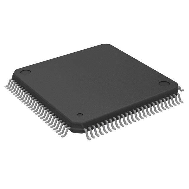
| 描述 | IC MCU 16BIT 120KB FLASH 80LQFP16位微控制器 - MCU 16B Ultra-Lo-Pwr MCU |
| EEPROM容量 | - |
| 产品分类 | |
| I/O数 | 64 |
| 品牌 | Texas Instruments |
| 产品手册 | |
| 产品图片 |
|
| rohs | 符合RoHS无铅 / 符合限制有害物质指令(RoHS)规范要求 |
| 产品系列 | 嵌入式处理器和控制器,微控制器 - MCU,16位微控制器 - MCU,Texas Instruments MSP430F2619TPNMSP430F2xx |
| 数据手册 | 点击此处下载产品Datasheethttp://www.ti.com/lit/pdf/slau144 |
| 产品型号 | MSP430F2619TPN |
| PCN设计/规格 | |
| RAM容量 | 4K x 8 |
| 产品培训模块 | http://www.digikey.cn/PTM/IndividualPTM.page?site=cn&lang=zhs&ptm=8361http://www.digikey.cn/PTM/IndividualPTM.page?site=cn&lang=zhs&ptm=8522http://www.digikey.cn/PTM/IndividualPTM.page?site=cn&lang=zhs&ptm=8576http://www.digikey.cn/PTM/IndividualPTM.page?site=cn&lang=zhs&ptm=8679http://www.digikey.cn/PTM/IndividualPTM.page?site=cn&lang=zhs&ptm=7557http://www.digikey.cn/PTM/IndividualPTM.page?site=cn&lang=zhs&ptm=25419http://www.digikey.cn/PTM/IndividualPTM.page?site=cn&lang=zhs&ptm=25427http://www.digikey.cn/PTM/IndividualPTM.page?site=cn&lang=zhs&ptm=25523http://www.digikey.cn/PTM/IndividualPTM.page?site=cn&lang=zhs&ptm=25524http://www.digikey.cn/PTM/IndividualPTM.page?site=cn&lang=zhs&ptm=25537http://www.digikey.cn/PTM/IndividualPTM.page?site=cn&lang=zhs&ptm=25788http://www.digikey.cn/PTM/IndividualPTM.page?site=cn&lang=zhs&ptm=25882http://www.digikey.cn/PTM/IndividualPTM.page?site=cn&lang=zhs&ptm=25885http://www.digikey.cn/PTM/IndividualPTM.page?site=cn&lang=zhs&ptm=26015http://www.digikey.cn/PTM/IndividualPTM.page?site=cn&lang=zhs&ptm=26006http://www.digikey.cn/PTM/IndividualPTM.page?site=cn&lang=zhs&ptm=30354 |
| 产品种类 | Microcontrollers - MSP430 Series |
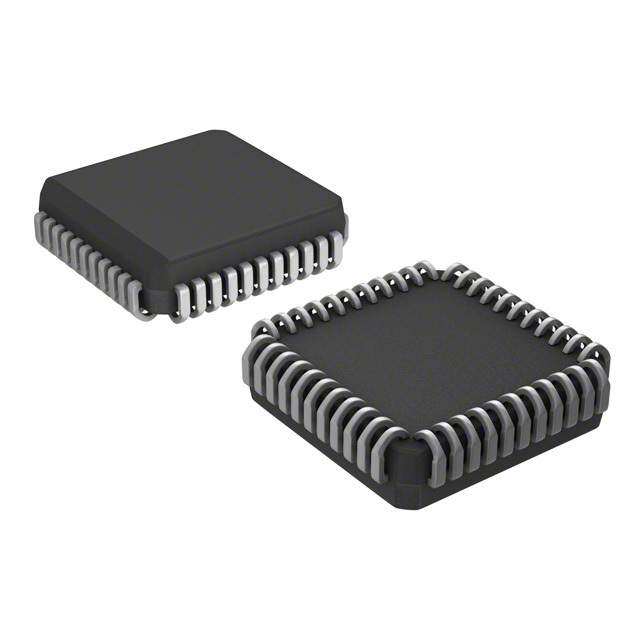
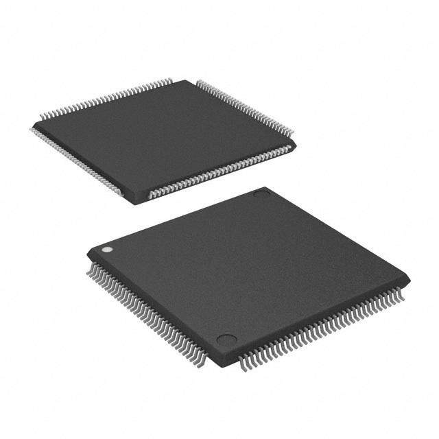
| 供应商器件封装 | 80-LQFP(12x12) |
| 其它名称 | 296-32656 |
| 制造商产品页 | http://www.ti.com/general/docs/suppproductinfo.tsp?distId=10&orderablePartNumber=MSP430F2619TPN |
| 包装 | 托盘 |
| 单位重量 | 465.700 mg |
| 可用A/D通道 | 8 |
| 可编程输入/输出端数量 | 48, 64 |
| 商标 | Texas Instruments |
| 商标名 | MSP430 |
| 处理器系列 | 2 Series |
| 外设 | 欠压检测/复位,DMA,POR,PWM,WDT |
| 安装风格 | SMD/SMT |
| 定时器数量 | 1 16-bit (3CCR), 1 16-bit (7CCR), 1 Watchdog/Interval |
| 封装 | Tube |
| 封装/外壳 | 80-LQFP |
| 封装/箱体 | LQFP-80 |
| 工作温度 | -40°C ~ 105°C |
| 工作电源电压 | 1.8 V to 3.6 V |
| 工厂包装数量 | 119 |
| 振荡器类型 | 内部 |
| 接口类型 | 2 USCI (UART, IrDA, LIN, SPI and I2C, SPI) |
| 数据RAM大小 | 4 kB |
| 数据总线宽度 | 16 bit |
| 数据转换器 | A/D 8x12b,D/A 2x12b |
| 最大工作温度 | + 105 C |
| 最大时钟频率 | 16 MHz |
| 最小工作温度 | - 40 C |
| 标准包装 | 119 |
| 核心 | MSP430 |
| 核心处理器 | MSP430 |
| 核心尺寸 | 16-位 |
| 片上ADC | Yes |
| 片上DAC | Yes |
| 电压-电源(Vcc/Vdd) | 1.8 V ~ 3.6 V |
| 程序存储器大小 | 120 kB |
| 程序存储器类型 | 闪存 |
| 程序存储容量 | 120KB(120K x 8 + 256B) |
| 系列 | MSP430F2619 |
| 输入/输出端数量 | 48 I/O |
| 连接性 | I²C, IrDA, LIN, SCI, SPI, UART/USART |
| 速度 | 16MHz |
| 配用 | /product-detail/zh/MSP-FET430U80/296-23005-ND/1571929 |


- 商务部:美国ITC正式对集成电路等产品启动337调查
- 曝三星4nm工艺存在良率问题 高通将骁龙8 Gen1或转产台积电
- 太阳诱电将投资9.5亿元在常州建新厂生产MLCC 预计2023年完工
- 英特尔发布欧洲新工厂建设计划 深化IDM 2.0 战略
- 台积电先进制程称霸业界 有大客户加持明年业绩稳了
- 达到5530亿美元!SIA预计今年全球半导体销售额将创下新高
- 英特尔拟将自动驾驶子公司Mobileye上市 估值或超500亿美元
- 三星加码芯片和SET,合并消费电子和移动部门,撤换高东真等 CEO
- 三星电子宣布重大人事变动 还合并消费电子和移动部门
- 海关总署:前11个月进口集成电路产品价值2.52万亿元 增长14.8%


PDF Datasheet 数据手册内容提取
MSP430F261x MSP430F241x www.ti.com SLAS541K–JUNE2007–REVISEDNOVEMBER2012 MIXED SIGNAL MICROCONTROLLER FEATURES 1 • LowSupplyVoltageRange1.8Vto3.6V • SerialOnboardProgramming,NoExternal • Ultra-LowPowerConsumption ProgrammingVoltageNeeded,Programmable CodeProtectionbySecurityFuse – ActiveMode:365µAat1MHz,2.2V • FamilyMembers: – StandbyMode(VLO):0.5µA – MSP430F2416 – OffMode(RAMRetention):0.1µA – 92KB+256BFlashMemory • Wake-UpFromStandbyModeinLessThan 1µs – 4KBRAM • 16-BitRISCArchitecture,62.5-nsInstruction – MSP430F2417 CycleTime – 92KB+256BFlashMemory • Three-ChannelInternalDMA – 8KBRAM • 12-BitAnalog-to-Digital(A/D)ConverterWith – MSP430F2418 InternalReference,Sample-and-Hold,and – 116KB+256BFlashMemory AutoscanFeature – 8KBRAM • Dual12-BitDigital-to-Analog(D/A)Converters – MSP430F2419 WithSynchronization – 120KB+256BFlashMemory • 16-BitTimer_AWithThreeCapture/Compare – 4KBRAM Registers – MSP430F2616 • 16-BitTimer_BWithSevenCapture/Compare- With-ShadowRegisters – 92KB+256BFlashMemory • On-ChipComparator – 4KBRAM • FourUniversalSerialCommunication – MSP430F2617 Interfaces(USCIs) – 92KB+256BFlashMemory – USCI_A0andUSCI_A1 – 8KBRAM – EnhancedUARTSupportingAuto- – MSP430F2618 BaudrateDetection – 116KB+256BFlashMemory – IrDAEncoderandDecoder – 8KBRAM – SynchronousSPI – MSP430F2619 – USCI_B0andUSCI_B1 – 120KB+256BFlashMemory – I2C™ – 4KBRAM – SynchronousSPI • Availablein80-PinQuadFlatPack(LQFP),64- • SupplyVoltageSupervisor/MonitorWith PinLQFP,and113-PinBallGridArray(BGA) ProgrammableLevelDetection (SeeTable1) • BrownoutDetector • ForCompleteModuleDescriptions,Seethe • BootstrapLoader MSP430x2xxFamilyUser'sGuide(SLAU144) 1 Pleasebeawarethatanimportantnoticeconcerningavailability,standardwarranty,anduseincriticalapplicationsof TexasInstrumentssemiconductorproductsanddisclaimerstheretoappearsattheendofthisdatasheet. PRODUCTIONDATAinformationiscurrentasofpublicationdate. Copyright©2007–2012,TexasInstrumentsIncorporated Products conform to specifications per the terms of the Texas Instruments standard warranty. Production processing does not necessarilyincludetestingofallparameters.
MSP430F261x MSP430F241x SLAS541K–JUNE2007–REVISEDNOVEMBER2012 www.ti.com This integrated circuit can be damaged by ESD. Texas Instruments recommends that all integrated circuits be handled with appropriateprecautions.Failuretoobserveproperhandlingandinstallationprocedurescancausedamage. ESDdamagecanrangefromsubtleperformancedegradationtocompletedevicefailure.Precisionintegratedcircuitsmaybemore susceptibletodamagebecauseverysmallparametricchangescouldcausethedevicenottomeetitspublishedspecifications. DESCRIPTION The Texas Instruments MSP430 family of ultralow-power microcontrollers consists of several devices featuring different sets of peripherals targeted for various applications. The architecture, combined with five low-power modes is optimized to achieve extended battery life in portable measurement applications. The device features a powerful 16-bit RISC CPU, 16-bit registers, and constant generators that contribute to maximum code efficiency. The calibrated digitally controlled oscillator (DCO) allows wake-up from low-power modes to active mode in less than1µs. The MSP430F261x and MSP430F241x series are microcontroller configurations with two built-in 16-bit timers, a fast 12-bit A/D converter, a comparator, dual 12-bit D/A converters, four universal serial communication interface (USCI) modules, DMA, and up to 64 I/O pins. The MSP430F241x devices are identical to the MSP430F261x devices,withtheexceptionthattheDAC12andtheDMAmodulesarenotimplemented. Typical applications include sensor systems, industrial control applications, and hand-held meters. The 12mmx12mmLQFP-64packageisalsoavailableasanon-magneticpackageformedicalimagingapplications. Table1.AvailableOptions(1) PACKAGEDDEVICES(2) T A PLASTIC113-PINBGA(ZQW) PLASTIC80-PINLQFP(PN) PLASTIC64-PINLQFP(PM) MSP430F2416TPM MSP430F2416TZQW MSP430F2416TPN MSP430F2417TPM MSP430F2417TZQW MSP430F2417TPN MSP430F2418TPM MSP430F2418TZQW MSP430F2418TPN MSP430F2419TPM MSP430F2419TZQW MSP430F2419TPN -40°Cto105°C MSP430F2616TPM MSP430F2616TZQW MSP430F2616TPN MSP430F2617TPM MSP430F2617TZQW MSP430F2617TPN MSP430F2618TPM MSP430F2618TZQW MSP430F2618TPN MSP430F2619TPM MSP430F2619TZQW MSP430F2619TPN MSP430F2618TPMR-NM (1) Forthemostcurrentpackageandorderinginformation,seethePackageOptionAddendumattheendofthisdocument,orseetheTI websiteatwww.ti.com. (2) Packagedrawings,thermaldata,andsymbolizationareavailableatwww.ti.com/packaging. Development Tool Support All MSP430 microcontrollers include an Embedded Emulation Module (EEM) allowing advanced debugging and programmingthrougheasy-to-usedevelopmenttools.Recommendedhardwareoptionsinclude: • DebuggingandProgrammingInterface – MSP-FET430UIF(USB) – MSP-FET430PIF(ParallelPort) • DebuggingandProgrammingInterfacewithTargetBoard – MSP-FET430U64(PMPackage) – MSP-FET430U80(PNPackage) • StandaloneTargetBoard – MSP-TS430PM64 • ProductionProgrammer – MSP-GANG430 2 SubmitDocumentationFeedback Copyright©2007–2012,TexasInstrumentsIncorporated
MSP430F261x MSP430F241x www.ti.com SLAS541K–JUNE2007–REVISEDNOVEMBER2012 Device Pinout, MSP430F241x, 80-Pin PN Package T U N O VCCVSS1VSS6.2/A2 6.1/A1 6.0/A0 ST/NMI CK MS DI/TCLK DO/TDI8.7/XT2I 8.6/XT2 8.5 8.4 8.3 8.2 8.1 8.0 7.7 A D A P P P R T T T TP P P P P P P P P 80 79 78 77 76 75 74 73 72 7170 69 68 67 66 65 64636261 DV 1 60 P7.6 CC1 P6.3/A3 2 59 P7.5 P6.4/A4 3 58 P7.4 P6.5/A5 4 57 P7.3 P6.6/A6 5 56 P7.2 P6.7/A7/SVSIN 6 55 P7.1 V 7 54 P7.0 REF+ XIN 8 53 DV SS2 XOUT 9 52 DV CC2 Ve 10 80-PIN 51 P5.7/TBOUTH/SVSOUT REF+ PN PACKAGE V /Ve 11 50 P5.6/ACLK REF- REF- (TOPVIEW) P1.0/TACLK/CAOUT 12 49 P5.5/SMCLK P1.1/TA0 13 48 P5.4/MCLK P1.2/TA1 14 47 P5.3/UCB1CLK/UCA1STE P1.3/TA2 15 46 P5.2/UCB1SOMI/UCB1SCL P1.4/SMCLK 16 45 P5.1/UCB1SIMO/UCB1SDA P1.5/TA0 17 44 P5.0/UCB1STE/UCA1CLK P1.6/TA1 18 43 P4.7/TBCLK P1.7/TA2 19 42 P4.6/TB6 P2.0/ACLK/CA2 20 41 P4.5/TB5 21 22 23 24 25 26 27 28 29 3031 32 33 34 35 36 37383940 P2.1/TAINCLK/CA3 P2.2/CAOUT/TA0/CA4 P2.3/CA0/TA1 P2.4/CA1/TA2 P2.5/R/CA5OSCP2.6/ADC12CLK/CA6 P2.7/TA0/CA7 P3.0/UCB0STE/UCA0CLK P3.1/UCB0SIMO/UCB0SDA P3.2/UCB0SOMI/UCB0SCL P3.3/UCB0CLK/UCA0STE P3.4/UCA0TXD/UCA0SIMO P3.5/UCA0RXD/UCA0SOMI P3.6/UCA1TXD/UCA1SIMO P3.7/UCA1RXD/UCA1SOMI P4.0/TB0 P4.1/TB1 P4.2/TB2 P4.3/TB3 P4.4/TB4 Copyright©2007–2012,TexasInstrumentsIncorporated SubmitDocumentationFeedback 3
MSP430F261x MSP430F241x SLAS541K–JUNE2007–REVISEDNOVEMBER2012 www.ti.com Device Pinout, MSP430F241x, 64-Pin PM Package T U O S V S H/ T K U K L VCCVSS1VSS6.2/A2 6.1/A1 6.0/A0 ST/NMI CK MS DI/TCLK DO/TDI T2IN T2OUT 5.7/TBO 5.6/ACL 5.5/SMC A D A P P P R T T T T X X P P P 64 636261605958575655545352515049 DV 1 48 P5.4/MCLK CC1 P6.3/A3 2 47 P5.3/UCB1CLK/UCA1STE P6.4/A4 3 46 P5.2/UCB1SOMI/UCB1SCL P6.5/A5 4 45 P5.1/UCB1SIMO/UCB1SDA P6.6/A6 5 44 P5.0/UCB1STE/UCA1CLK P6.7/A7/SVSIN 6 43 P4.7/TBCLK V 7 42 P4.6/TB6 REF+ XIN 8 64-PIN 41 P4.5/TB5 PM PACKAGE XOUT 9 40 P4.4/TB4 (TOPVIEW) Ve 10 39 P4.3/TB3 REF+ V /Ve 11 38 P4.2/TB2 REF- REF- P1.0/TACLK/CAOUT 12 37 P4.1/TB1 P1.1/TA0 13 36 P4.0/TB0 P1.2/TA1 14 35 P3.7/UCA1RXD/UCA1SOMI P1.3/TA2 15 34 P3.6/UCA1TXD/UCA1SIMO P1.4/SMCLK 16 33 P3.5/UCA0RXD/UCA0SOMI 17 181920212223242526272829303132 0 1 2 2 3 4 1 2 5 6 7 K A L E O TA TA TA CA CA CA TA TA CA CA CA CL SD SC ST M P1.5/ P1.6/ P1.7/ P2.0/ACLK/ P2.1/TAINCLK/ P2.2/CAOUT/TA0/ P2.3/CA0/ P2.4/CA1/ /P2.5/ROSCP2.6/ADC12CLK/ P2.7/TA0/ P3.0/UCB0STE/UCA0 3.1/UCB0SIMO/UCB0 3.2/UCB0SOMI/UCB0 P3.3/UCB0CLK/UCA0 3.4/UCA0TXD/UCA0SI P P P 4 SubmitDocumentationFeedback Copyright©2007–2012,TexasInstrumentsIncorporated
MSP430F261x MSP430F241x www.ti.com SLAS541K–JUNE2007–REVISEDNOVEMBER2012 Device Pinout, MSP430F261x, 80-Pin PN Package T U N O A2 A1 A0 NMI CLK TDIXT2I XT2 VCCVSS1VSS6.2/ 6.1/ 6.0/ ST/ CK MS DI/T DO/8.7/ 8.6/ 8.5 8.4 8.3 8.2 8.1 8.0 7.7 A D A P P P R T T T TP P P P P P P P P 80 79 78 77 76 75 74 73 72 7170 69 68 67 66 65 64636261 DV 1 60 P7.6 CC1 P6.3/A3 2 59 P7.5 P6.4/A4 3 58 P7.4 P6.5/A5/DAC1 4 57 P7.3 P6.6/A6/DAC0 5 56 P7.2 P6.7/A7/DAC1/SVSIN 6 55 P7.1 V 7 54 P7.0 REF+ XIN 8 53 DV SS2 XOUT 9 52 DV CC2 Ve /DAC0 10 80-PIN 51 P5.7/TBOUTH/SVSOUT REF+ PN PACKAGE V /Ve 11 50 P5.6/ACLK REF- REF- (TOPVIEW) P1.0/TACLK/CAOUT 12 49 P5.5/SMCLK P1.1/TA0 13 48 P5.4/MCLK P1.2/TA1 14 47 P5.3/UCB1CLK/UCA1STE P1.3/TA2 15 46 P5.2/UCB1SOMI/UCB1SCL P1.4/SMCLK 16 45 P5.1/UCB1SIMO/UCB1SDA P1.5/TA0 17 44 P5.0/UCB1STE/UCA1CLK P1.6/TA1 18 43 P4.7/TBCLK P1.7/TA2 19 42 P4.6/TB6 P2.0/ACLK/CA2 20 41 P4.5/TB5 21 22 23 24 25 26 27 28 29 3031 32 33 34 35 36 37383940 P2.1/TAINCLK/CA3 P2.2/CAOUT/TA0/CA4 P2.3/CA0/TA1 P2.4/CA1/TA2 P2.5/R/CA5OSC2.6/ADC12CLK/DMAE0/CA6 P2.7/TA0/CA7 P3.0/UCB0STE/UCA0CLK P3.1/UCB0SIMO/UCB0SDA P3.2/UCB0SOMI/UCB0SCL P3.3/UCB0CLK/UCA0STE P3.4/UCA0TXD/UCA0SIMO P3.5/UCA0RXD/UCA0SOMI P3.6/UCA1TXD/UCA1SIMO P3.7/UCA1RXD/UCA1SOMI P4.0/TB0 P4.1/TB1 P4.2/TB2 P4.3/TB3 P4.4/TB4 P Copyright©2007–2012,TexasInstrumentsIncorporated SubmitDocumentationFeedback 5
MSP430F261x MSP430F241x SLAS541K–JUNE2007–REVISEDNOVEMBER2012 www.ti.com Device Pinout, MSP430F261x, 64-Pin PM Package T U O S V S H/ T K U K L VCC VSS1 VSS 6.2/A2 6.1/A1 6.0/A0 ST/NMI CK MS DI/TCLK DO/TDI T2IN T2OUT 5.7/TBO 5.6/ACL 5.5/SMC A D A P P P R T T T T X X P P P 64 63 62 6160 59 58 57 56 55 54 53 52 5150 49 DV 1 48 P5.4/MCLK CC1 P6.3/A3 2 47 P5.3/UCB1CLK/UCA1STE P6.4/A4 3 46 P5.2/UCB1SOMI/UCB1SCL P6.5/A5/DAC1 4 45 P5.1/UCB1SIMO/UCB1SDA P6.6/A6/DAC0 5 44 P5.0/UCB1STE/UCA1CLK P6.7/A7/DAC1/SVSIN 6 43 P4.7/TBCLK V 7 42 P4.6/TB6 REF+ XIN 8 64-PIN 41 P4.5/TB5 PM PACKAGE XOUT 9 40 P4.4/TB4 (TOPVIEW) Ve /DAC0 10 39 P4.3/TB3 REF+ V /Ve 11 38 P4.2/TB2 REF- REF- P1.0/TACLK/CAOUT 12 37 P4.1/TB1 P1.1/TA0 13 36 P4.0/TB0 P1.2/TA1 14 35 P3.7/UCA1RXD/UCA1SOMI P1.3/TA2 15 34 P3.6/UCA1TXD/UCA1SIMO P1.4/SMCLK 16 33 P3.5/UCA0RXD/UCA0SOMI 17 18 19 20 2122 23 24 25 26 27 28 29 30 3132 A0 A1 A2 A2 A3 A4 A1 A2 A5 A6 A7 LK DA CL TE MO P1.5/T P1.6/T P1.7/T P2.0/ACLK/C P2.1/TAINCLK/C P2.2/CAOUT/TA0/C P2.3/CA0/T P2.4/CA1/T P2.5/R/COSC 2.6/ADC12CLK/DMAE0/C P2.7/TA0/C P3.0/UCB0STE/UCA0C P3.1/UCB0SIMO/UCB0S P3.2/UCB0SOMI/UCB0S P3.3/UCB0CLK/UCA0S P3.4/UCA0TXD/UCA0SI P 6 SubmitDocumentationFeedback Copyright©2007–2012,TexasInstrumentsIncorporated
MSP430F261x MSP430F241x www.ti.com SLAS541K–JUNE2007–REVISEDNOVEMBER2012 Device Pinout, 113-Pin ZQW Package NOTE Forterminalassignments,seeTable2. A1 A2 A3 A4 A5 A6 A7 A8 A9 A10 A11 A12 B1 B2 B3 B4 B5 B6 B7 B8 B9 B10 B11 B12 C1 C2 C3 C11 C12 D1 D2 D4 D5 D6 D7 D8 D9 D11 D12 E1 E2 E4 E5 E6 E7 E8 E9 E11 E12 F1 F2 F4 F5 F8 F9 F11 F12 G1 G2 G4 G5 G8 G9 G11 G12 H1 H2 H4 H5 H6 H7 H8 H9 H11 H12 J1 J2 J4 J5 J6 J7 J8 J9 J11 J12 K1 K2 K11 K12 L1 L2 L3 L4 L5 L6 L7 L8 L9 L10 L11 L12 M1 M2 M3 M4 M5 M6 M7 M8 M9 M10 M11 M12 Copyright©2007–2012,TexasInstrumentsIncorporated SubmitDocumentationFeedback 7
MSP430F261x MSP430F241x SLAS541K–JUNE2007–REVISEDNOVEMBER2012 www.ti.com FunctionalBlockDiagram,MSP430F241x,80-PinPNPackage XIN/ XOUT/ P3.x/P4.x DVCC1/2 DVSS1/2 AVCC AVSS P1.x/P2.x P7.x/P8.x XT2IN XT2OUT P5.x/P6.x 2x8/ 2 2 2x8 4x8 1x16 ACLK Oscillators Flash RAM Ports Ports Ports USCIA0 BasicClock SMCLK ADC12 P1/P2 P3/P4 P7/P8 UART/ System+ 120KB 4KB 12-Bit P5/P6 LIN, IrDA,SPI 116KB 8KB 2x8I/O 2x8/1x16 8 MCLK 92KB 8KB Channels Interrupt 4x8I/O I/O USCIB0 92KB 4KB capability SPI,I2C 16MHz MAB CPU 1MB incl.16 Registers MDB Hardware Timer_B7 USCIA1 Emulation Brownout Multiplier Watchdog Timer_A3 Comp_A+ UART/ Protection WDT+ 7CC LIN, MPY, IrDA,SPI JTAG SVS, MPYS, 3CC Registers, 8 Interface SVM MAC, 15-Bit Registers Shadow Channels USCIB1 Reg SPI,I2C MACS RST/NMI FunctionalBlockDiagram,MSP430F241x,64-PinPMPackage XIN/ XOUT/ P3.x/P4.x DVCC DVSS AVCC AVSS P1.x/P2.x XT2IN XT2OUT P5.x/P6.x 2 2 2x8 4x8 ACLK Oscillators Flash RAM Ports Ports USCIA0 BasicClock SMCLK ADC12 P1/P2 P3/P4 UART/ System+ 120KB 4KB 12-Bit P5/P6 LIN, IrDA,SPI 116KB 8KB 2x8I/O 8 MCLK 92KB 8KB Channels Interrupt 4x8I/O USCIB0 92KB 4KB capability SPI,I2C 16MHz MAB CPU 1MB incl.16 Registers MDB Hardware Timer_B7 USCIA1 Emulation Brownout Multiplier Watchdog Timer_A3 Comp_A+ UART/ Protection WDT+ 7CC LIN, MPY, IrDA,SPI JTAG SVS, MPYS, 3CC Registers, 8 Interface SVM MAC, 15-Bit Registers Shadow Channels USCIB1 Reg SPI,I2C MACS RST/NMI 8 SubmitDocumentationFeedback Copyright©2007–2012,TexasInstrumentsIncorporated
MSP430F261x MSP430F241x www.ti.com SLAS541K–JUNE2007–REVISEDNOVEMBER2012 FunctionalBlockDiagram,MSP430F261x,80-PinPNPackage XIN/ XOUT/ P3.x/P4.x DVCC1/2 DVSS1/2 AVCC AVSS P1.x/P2.x P7.x/P8.x XT2IN XT2OUT P5.x/P6.x 2x8/ 2 2 2x8 4x8 1x16 ACLK Oscillators Flash RAM DAC12 Ports Ports Ports USCIA0 BasicClock SMCLK ADC12 12-Bit P1/P2 P3/P4 P7/P8 UART/ System+ 120kB 4kB 12-Bit P5/P6 LIN, 116kB 8kB 2 IrDA,SPI 2x8I/O 2x8/1x16 92kB 8kB 8 Channels MCLK 92kB 4kB Channels Voltage Interrupt 4x8I/O I/O USCIB0 capability SPI,I2C 56kB 4kB Out 16MHz MAB CPU 1MB incl.16 Registers MDB Hardware Timer_B7 USCIA1 Emulation Brownout Multiplier DMA Watchdog Timer_A3 Comp_A+ UART/ Protection Controller WDT+ 7CC LIN, MPY, IrDA,SPI JTAG SVS, MPYS, 3 3CC Registers, 8 Interface SVM MAC, Channels 15-Bit Registers Shadow Channels USCIB1 Reg SPI,I2C MACS RST/NMI FunctionalBlockDiagram,MSP430F261x,64-PinPMPackage XIN/ XOUT/ P3.x/P4.x DVCC DVSS AVCC AVSS P1.x/P2.x XT2IN XT2OUT P5.x/P6.x 2 2 2x8 4x8 ACLK Oscillators Flash RAM DAC12 Ports Ports USCIA0 BasicClock SMCLK ADC12 12-Bit P1/P2 P3/P4 UART/ System+ 120kB 4kB 12-Bit P5/P6 LIN, 116kB 8kB 2 IrDA,SPI 2x8I/O 92kB 8kB 8 Channels MCLK 92kB 4kB Channels Voltage Interrupt 4x8I/O USCIB0 capability SPI,I2C 56kB 4kB Out 16MHz MAB CPU 1MB incl.16 Registers MDB Hardware Timer_B7 USCIA1 Emulation Brownout Multiplier DMA Watchdog Timer_A3 Comp_A+ UART/ Protection Controller WDT+ 7CC LIN, MPY, IrDA,SPI JTAG SVS, MPYS, 3 3CC Registers, 8 Interface SVM MAC, Channels 15-Bit Registers Shadow Channels USCIB1 Reg SPI,I2C MACS RST/NMI Copyright©2007–2012,TexasInstrumentsIncorporated SubmitDocumentationFeedback 9
MSP430F261x MSP430F241x SLAS541K–JUNE2007–REVISEDNOVEMBER2012 www.ti.com Table2.TerminalFunctions TERMINAL NO. I/O DESCRIPTION NAME 64 80 113 PIN PIN PIN Analogsupplyvoltage,positiveterminal.Suppliesonlytheanalogportionof AV 64 80 A2 CC ADC12andDAC12. Analogsupplyvoltage,negativeterminal.Suppliesonlytheanalogportionof AV 62 78 B2,B3 SS ADC12andDAC12. DV 1 1 A1 Digitalsupplyvoltage,positiveterminal.Suppliesalldigitalparts. CC1 DV 63 79 A3 Digitalsupplyvoltage,negativeterminal.Suppliesalldigitalparts. SS1 DV 52 F12 Digitalsupplyvoltage,positiveterminal.Suppliesalldigitalparts. CC2 DV 53 E12 Digitalsupplyvoltage,negativeterminal.Suppliesalldigitalparts. SS2 General-purposedigitalI/Opin P1.0/TACLK/CAOUT 12 12 G2 I/O Timer_A,clocksignalTACLKinput Comparator_Aoutput General-purposedigitalI/Opin P1.1/TA0 13 13 H1 I/O Timer_A,capture:CCI0Ainput,compare:Out0output BSLtransmit General-purposedigitalI/Opin P1.2/TA1 14 14 H2 I/O Timer_A,capture:CCI1Ainput,compare:Out1output General-purposedigitalI/Opin P1.3/TA2 15 15 J1 I/O Timer_A,capture:CCI2Ainput,compare:Out2output General-purposedigitalI/Opin P1.4/SMCLK 16 16 J2 I/O SMCLKsignaloutput General-purposedigitalI/Opin P1.5/TA0 17 17 K1 I/O Timer_A,compare:Out0output General-purposedigitalI/Opin P1.6/TA1 18 18 K2 I/O Timer_A,compare:Out1output General-purposedigitalI/Opin P1.7/TA2 19 19 L1 I/O Timer_A,compare:Out2output General-purposedigitalI/Opin P2.0/ACLK/CA2 20 20 M1 I/O ACLKoutput/Comparator_Ainput General-purposedigitalI/Opin P2.1/TAINCLK/CA3 21 21 M2 I/O Timer_A,clocksignalatINCLK General-purposedigitalI/Opin Timer_A,capture:CCI0Binput P2.2/CAOUT/TA0/CA4 22 22 M3 I/O Comparator_Aoutput BSLreceive Comparator_Ainput General-purposedigitalI/Opin P2.3/CA0/TA1 23 23 L3 I/O Timer_A,compare:Out1output Comparator_Ainput General-purposedigitalI/Opin P2.4/CA1/TA2 24 24 L4 I/O Timer_A,compare:Out2output Comparator_Ainput General-purposedigitalI/Opin P2.5/ROSC/CA5 25 25 M4 I/O InputforexternalresistordefiningtheDCOnominalfrequency Comparator_Ainput 10 SubmitDocumentationFeedback Copyright©2007–2012,TexasInstrumentsIncorporated
MSP430F261x MSP430F241x www.ti.com SLAS541K–JUNE2007–REVISEDNOVEMBER2012 Table2.TerminalFunctions(continued) TERMINAL NO. I/O DESCRIPTION NAME 64 80 113 PIN PIN PIN General-purposedigitalI/Opin P2.6/ADC12CLK/ Conversionclock-12-bitADC DMAE0(1)/CA6 26 26 J4 I/O DMAchannel0externaltrigger Comparator_Ainput General-purposedigitalI/Opin P2.7/TA0/CA7 27 27 L5 I/O Timer_A,compare:Out0output Comparator_Ainput P3.0/UCB0STE/ General-purposedigitalI/Opin 28 28 M5 I/O UCA0CLK USCI_B0slavetransmitenable/USCI_A0clockinput/output P3.1/UCB0SIMO/ General-purposedigitalI/Opin 29 29 L6 I/O UCB0SDA USCI_B0slave-inmaster-outinSPImode,SDAI2CdatainI2Cmode P3.2/UCB0SOMI/ General-purposedigitalI/Opin 30 30 M6 I/O UCB0SCL USCI_B0slave-outmaster-ininSPImode,SCLI2CclockinI2Cmode P3.3/UCB0CLK/ General-purposedigitalI/O 31 31 L7 I/O UCA0STE USCI_B0clockinput/output,USCI_A0slavetransmitenable General-purposedigitalI/Opin P3.4/UCA0TXD/ UCA0SIMO 32 32 M7 I/O USCI_A transmit data outputinUART mode,slavedata in/master outinSPI mode General-purposedigitalI/Opin P3.5/UCA0RXD/ UCA0SOMI 33 33 L8 I/O USCI_A0 receive data input in UART mode, slave data out/master in in SPI mode General-purposedigitalI/Opin P3.6/UCA1TXD/ UCA1SIMO 34 34 M8 I/O USCI_A1transmitdataoutputinUARTmode,slavedatain/masteroutinSPI mode General-purposedigitalI/Opin P3.7/UCA1RXD/ UCA1SOMI 35 35 L9 I/O USCI_A1 receive data input in UART mode, slave data out/master in in SPI mode General-purposedigitalI/Opin P4.0/TB0 36 36 M9 I/O Timer_B,capture:CCI0A/Binput,compare:Out0output General-purposedigitalI/Opin P4.1/TB1 37 37 J9 I/O Timer_B,capture:CCI1A/Binput,compare:Out1output General-purposedigitalI/Opin P4.2/TB2 38 38 M10 I/O Timer_B,capture:CCI2A/Binput,compare:Out2output General-purposedigitalI/Opin P4.3/TB3 39 39 L10 I/O Timer_B,capture:CCI3A/Binput,compare:Out3output General-purposedigitalI/Opin P4.4/TB4 40 40 M11 I/O Timer_B,capture:CCI4A/Binput,compare:Out4output General-purposedigitalI/Opin P4.5/TB5 41 41 M12 I/O Timer_B,capture:CCI5A/Binput,compare:Out5output General-purposedigitalI/Opin P4.6/TB6 42 42 L12 I/O Timer_B,capture:CCI6Ainput,compare:Out6output General-purposedigitalI/Opin P4.7/TBCLK 43 43 K11 I/O Timer_B,clocksignalTBCLKinput (1) MSP430F261xdevicesonly Copyright©2007–2012,TexasInstrumentsIncorporated SubmitDocumentationFeedback 11
MSP430F261x MSP430F241x SLAS541K–JUNE2007–REVISEDNOVEMBER2012 www.ti.com Table2.TerminalFunctions(continued) TERMINAL NO. I/O DESCRIPTION NAME 64 80 113 PIN PIN PIN P5.0/UCB1STE/ General-purposedigitalI/Opin 44 44 K12 I/O UCA1CLK USCI_B1slavetransmitenable/USCI_A1clockinput/output P5.1/UCB1SIMO/ General-purposedigitalI/Opin 45 45 J11 I/O UCB1SDA USCI_B1slave-inmaster-outinSPImode,SDAI2CdatainI2Cmode P5.2/UCB1SOMI/ General-purposedigitalI/Opin 46 46 J12 I/O UCB1SCL USCI_B1slave-outmaster-ininSPImode,SCLI2CclockinI2Cmode P5.3/UCB1CLK/ General-purposedigitalI/O 47 47 H11 I/O UCA1STE USCI_B1clockinput/output,USCI_A1slavetransmitenable General-purposedigitalI/Opin P5.4/MCLK 48 48 H12 I/O MainsystemclockMCLKoutput General-purposedigitalI/Opin P5.5/SMCLK 49 49 G11 I/O SubmainsystemclockSMCLKoutput General-purposedigitalI/Opin P5.6/ACLK 50 50 G12 I/O AuxiliaryclockACLKoutput General-purposedigitalI/Opin P5.7/TBOUTH/SVSOUT 51 51 F11 I/O SwitchallPWMdigitaloutputportstohighimpedance-Timer_BTB0toTB6 SVScomparatoroutput General-purposedigitalI/Opin P6.0/A0 59 75 D4 I/O AnaloginputA0-12-bitADC General-purposedigitalI/Opin P6.1/A1 60 76 A4 I/O AnaloginputA1-12-bitADC General-purposedigitalI/Opin P6.2/A2 61 77 B4 I/O AnaloginputA2-12-bitADC General-purposedigitalI/Opin P6.3/A3 2 2 B1 I/O AnaloginputA3-12-bitADC General-purposedigitalI/Opin P6.4/A4 3 3 C1 I/O AnaloginputA4-12-bitADC General-purposedigitalI/Opin P6.5/A5/DAC1(2) 4 4 CC23, I/O AnaloginputA5-12-bitADC DAC12.1output General-purposedigitalI/Opin P6.6/A6/DAC0(2) 5 5 D1 I/O AnaloginputA6-12-bitADC DAC12.0output General-purposedigitalI/Opin P6.7/A7/DAC1(2)/SVSIN 6 6 D2 I/O AnaloginputA7-12-bitADC DAC12.1output SVSinput P7.0 54 E11 I/O General-purposedigitalI/Opin P7.1 55 D12 I/O General-purposedigitalI/Opin P7.2 56 D11 I/O General-purposedigitalI/Opin P7.3 57 C12 I/O General-purposedigitalI/Opin P7.4 58 C11 I/O General-purposedigitalI/Opin (2) MSP430F261xdevicesonly 12 SubmitDocumentationFeedback Copyright©2007–2012,TexasInstrumentsIncorporated
MSP430F261x MSP430F241x www.ti.com SLAS541K–JUNE2007–REVISEDNOVEMBER2012 Table2.TerminalFunctions(continued) TERMINAL NO. I/O DESCRIPTION NAME 64 80 113 PIN PIN PIN P7.5 59 B12 I/O General-purposedigitalI/Opin P7.6 60 A12 I/O General-purposedigitalI/Opin P7.7 61 A11 I/O General-purposedigitalI/Opin P8.0 62 B10 I/O General-purposedigitalI/Opin P8.1 63 A10 I/O General-purposedigitalI/Opin P8.2 64 D9 I/O General-purposedigitalI/Opin P8.3 65 A9 I/O General-purposedigitalI/Opin P8.4 66 B9 I/O General-purposedigitalI/Opin P8.5 67 B8 I/O General-purposedigitalI/Opin General-purposedigitalI/Opin P8.6/XT2OUT 68 A8 I/O OutputterminalofcrystaloscillatorXT2 General-purposedigitalI/Opin P8.7/XT2IN 69 A7 I/O InputportforcrystaloscillatorXT2.Onlystandardcrystalscanbeconnected. XT2OUT 52 O OutputterminalofcrystaloscillatorXT2 XT2IN 53 I InputportforcrystaloscillatorXT2 Resetinput,nonmaskableinterruptinputport,orbootstraploaderstart(in RST/NMI 58 74 B5 I flashdevices) Testclock(JTAG).TCKistheclockinputportfordeviceprogrammingtest TCK 57 73 A5 I andbootstraploaderstart Testdatainputortestclockinput.Thedeviceprotectionfuseisconnectedto TDI/TCLK 55 71 A6 I TDI/TCLK. Testdataoutputport.TDO/TDIdataoutputorprogrammingdatainput TDO/TDI 54 70 B7 I/O terminal. Testmodeselect.TMSisusedasaninputportfordeviceprogrammingand TMS 56 72 B6 I test. VeREF+/DAC0(3) 10 10 F2 I Inputforanexternalreferencevoltage/DAC12.0output V 7 7 E2 O OutputofpositiveterminalofthereferencevoltageintheADC12 REF+ Negativeterminalforthereferencevoltageforbothsources,theinternal V /V 11 11 G1 I REF- eREF- referencevoltageoranexternalappliedreferencevoltage InputportforcrystaloscillatorXT1.Standardorwatchcrystalscanbe XIN 8 8 E1 I connected. OutputportforcrystaloscillatorXT1.Standardorwatchcrystalscanbe XOUT 9 9 F1 O connected. Reserved - - (4) NA Reservedpins.ConnectiontoDV ,AV recommended. SS SS (3) MSP430F261xdevicesonly (4) ReservedpinsareL2,E4,F4,G4,H4,D5,E5,F5,G5,H5,J5,D6,E6,H6,J6,D7,E7,H7,J7,D8,E8,F8,G8,H8,J8,E9,F9,G9,H9, B11,L11. Copyright©2007–2012,TexasInstrumentsIncorporated SubmitDocumentationFeedback 13
MSP430F261x MSP430F241x SLAS541K–JUNE2007–REVISEDNOVEMBER2012 www.ti.com SHORT-FORM DESCRIPTION CPU Program Counter PC/R0 The MSP430 CPU has a 16-bit RISC architecture Stack Pointer SP/R1 that is highly transparent to the application. All operations, other than program-flow instructions, are Status Register SR/CG1/R2 performed as register operations in conjunction with seven addressing modes for source operand and four Constant Generator CG2/R3 addressingmodesfordestinationoperand. General-Purpose Register R4 The CPU is integrated with 16 registers that provide reduced instruction execution time. The register-to- General-Purpose Register R5 register operation execution time is one cycle of the CPUclock. General-Purpose Register R6 Four of the registers, R0 to R3, are dedicated as program counter, stack pointer, status register, and General-Purpose Register R7 constant generator respectively. The remaining registersaregeneral-purposeregisters. General-Purpose Register R8 Peripherals are connected to the CPU using data, General-Purpose Register R9 address, and control buses, and can be handled with allinstructions. General-Purpose Register R10 Instruction Set General-Purpose Register R11 The instruction set consists of 51 instructions with General-Purpose Register R12 three formats and seven address modes. Each instruction can operate on word and byte data. General-Purpose Register R13 Table 3 shows examples of the three types of instruction formats; Table 4 shows the address General-Purpose Register R14 modes. General-Purpose Register R15 Table3.InstructionWordFormats INSTRUCTIONFORMAT EXAMPLE OPERATION Dualoperands,source-destination ADDR4,R5 R4+R5->R5 Singleoperands,destinationonly CALLR8 PC->(TOS),R8->PC Relativejump,un/conditional JNE Jump-on-equalbit=0 Table4.AddressModeDescriptions ADDRESSMODE S(1) D(1) SYNTAX EXAMPLE OPERATION Register ✓ ✓ MOVRs,Rd MOVR10,R11 R10->R11 Indexed ✓ ✓ MOVX(Rn),Y(Rm) MOV2(R5),6(R6) M(2+R5)->M(6+R6) Symbolic(PCrelative) ✓ ✓ MOVEDE,TONI M(EDE)->M(TONI) Absolute ✓ ✓ MOV&MEM,&TCDAT M(MEM)->M(TCDAT) Indirect ✓ MOV@Rn,Y(Rm) MOV@R10,Tab(R6) M(R10)->M(Tab+R6) M(R10)->R11 Indirectautoincrement ✓ MOV@Rn+,Rm MOV@R10+,R11 R10+2->R10 Immediate ✓ MOV#X,TONI MOV#45,TONI #45->M(TONI) (1) S=source,D=destination 14 SubmitDocumentationFeedback Copyright©2007–2012,TexasInstrumentsIncorporated
MSP430F261x MSP430F241x www.ti.com SLAS541K–JUNE2007–REVISEDNOVEMBER2012 Operating Modes The MSP430 has one active mode and five software-selectable low-power modes of operation. An interrupt event can wake the device from any of the five low-power modes, service the request, and restore back to the low-powermodeonreturnfromtheinterruptprogram. Thefollowingsixoperatingmodescanbeconfiguredbysoftware: • Activemode(AM) – Allclocksareactive • Low-powermode0(LPM0) – CPUisdisabled – ACLKandSMCLKremainactive – MCLKisdisabled • Low-powermode1(LPM1) – CPUisdisabled – ACLKandSMCLKremainactive.MCLKisdisabled – DCO'sdc-generatorisdisabledifDCOnotusedinactivemode • Low-powermode2(LPM2) – CPUisdisabled – MCLKandSMCLKaredisabled – DCO'sdc-generatorremainsenabled – ACLKremainsactive • Low-powermode3(LPM3) – CPUisdisabled – MCLKandSMCLKaredisabled – DCO'sdc-generatorisdisabled – ACLKremainsactive • Low-powermode4(LPM4) – CPUisdisabled – ACLKisdisabled – MCLKandSMCLKaredisabled – DCO'sdc-generatorisdisabled – Crystaloscillatorisstopped Copyright©2007–2012,TexasInstrumentsIncorporated SubmitDocumentationFeedback 15
MSP430F261x MSP430F241x SLAS541K–JUNE2007–REVISEDNOVEMBER2012 www.ti.com Interrupt Vector Addresses The interrupt vectors and the power-up starting address are located in the address range of 0FFFFh to 0FFC0h. Thevectorcontainsthe16-bitaddressoftheappropriateinterrupthandlerinstructionsequence. If the reset vector (located at address 0FFFEh) contains 0FFFFh (for example, flash is not programmed) the CPUentersLPM4immediatelyafterpower-up. Table5.InterruptSources SYSTEM INTERRUPTSOURCE INTERRUPTFLAG WORDADDRESS PRIORITY INTERRUPT Power-up PORIFG Externalreset RSTIFG WatchdogTimer+ WDTIFG Reset 0FFFEh 31,highest Flashkeyviolation KEYV PCout-of-range(1) See (2) NMI NMIIFG (Non)maskable, Oscillatorfault OFIFG (Non)maskable, 0FFFCh 30 Flashmemoryaccessviolation ACCVIFG(2)(3) (Non)maskable Timer_B7 TBCCR0CCIFG(4) Maskable 0FFFAh 29 TBCCR1toTBCCR6CCIFGs, Timer_B7 TBIFG(2)(4) Maskable 0FFF8h 28 Comparator_A+ CAIFG Maskable 0FFF6h 27 WatchdogTimer+ WDTIFG Maskable 0FFF4h 26 Timer_A3 TACCR0CCIFG(4) Maskable 0FFF2h 25 TACCR1CCIFG Timer_A3 TACCR2CCIFG(2)(4) Maskable 0FFF0h 24 USCI_A0/USCI_B0receive UCA0RXIFG,UCB0RXIFG(2)(5) Maskable 0FFEEh 23 USCI_B0I2Cstatus USCI_A0/USCI_B0transmit UCA0TXIFG,UCB0TXIFG(2)(6) Maskable 0FFECh 22 USCI_B0I2Creceiveortransmit ADC12 ADC12IFG(2)(4) Maskable 0FFEAh 21 0FFE8h 20 I/OportP2(eightflags) P2IFG.0toP2IFG.7(2)(4) Maskable 0FFE6h 19 I/OportP1(eightflags) P1IFG.0toP1IFG.7(2)(4) Maskable 0FFE4h 18 USCI_A1/USCI_B1receive UCA1RXIFG,UCB1RXIFG(2)(5) Maskable 0FFE2h 17 USCI_B1I2Cstatus USCI_A1/USCI_B1transmit UCA1TXIFG,UCB1TXIFG(2)(6) Maskable 0FFE0h 16 USCI_B1I2Creceiveortransmit DMA0IFG,DMA1IFG, DMA DMA2IFG(2)(4) Maskable 0FFDEh 15 DAC12 DAC12_0IFG,DAC12_1IFG(2)(4) Maskable 0FFDCh 14 See (7)(8) 0FFDAhto0FFC0h 15to0,lowest (1) AresetisgeneratediftheCPUtriestofetchinstructionsfromwithinthemoduleregistermemoryaddressrange(0hto01FFh)orfrom withinunusedaddressranges. (2) Multiplesourceflags (3) (Non)maskable:theindividualinterrupt-enablebitcandisableaninterruptevent,butthegeneralinterruptenablecannot. (4) Interruptflagsarelocatedinthemodule. (5) InSPImode:UCB0RXIFG.InI2Cmode:UCALIFG,UCNACKIFG,ICSTTIFG,UCSTPIFG. (6) InUART/SPImode:UCB0TXIFG.InI2Cmode:UCB0RXIFG,UCB0TXIFG. (7) Theaddress0FFBEhisusedasbootstraploadersecuritykey(BSLSKEY). A0AA55hatthislocationdisablestheBSLcompletely. Azerodisablestheerasureoftheflashifaninvalidpasswordissupplied. (8) Theinterruptvectorsataddresses0FFDAhto0FFC0harenotusedinthisdeviceandcanbeusedforregularprogramcodeif necessary. 16 SubmitDocumentationFeedback Copyright©2007–2012,TexasInstrumentsIncorporated
MSP430F261x MSP430F241x www.ti.com SLAS541K–JUNE2007–REVISEDNOVEMBER2012 Special Function Registers Most interrupt and module enable bits are collected into the lowest address space. Special function register bits not allocated to a functional purpose are not physically present in the device. Simple software access is provided withthisarrangement. Legend rw: Bitcanbereadandwritten. rw-0,1: Bitcanbereadandwritten.ItisresetorsetbyPUC. rw-(0,1): Bitcanbereadandwritten.ItisresetorsetbyPOR. SFRbitisnotpresentindevice. Table6.InterruptEnableRegister1and2 Address 7 6 5 4 3 2 1 0 00h ACCVIE NMIIE OFIE WDTIE rw-0 rw-0 rw-0 rw-0 WDTIE WatchdogTimerinterruptenable.Inactiveifwatchdogmodeisselected.ActiveifWatchdogTimerisconfiguredin intervaltimermode. OFIE Oscillatorfaultinterruptenable NMIIE (Non)maskableinterruptenable ACCVIE Flashaccessviolationinterruptenable Address 7 6 5 4 3 2 1 0 01h UCB0TXIE UCB0RXIE UCA0TXIE UCA0RXIE rw-0 rw-0 rw-0 rw-0 UCA0RXIE USCI_A0receiveinterruptenable UCA0TXIE USCI_A0transmitinterruptenable UCB0RXIE USCI_B0receiveinterruptenable UCB0TXIE USCI_B0transmitinterruptenable Table7.InterruptFlagRegister1and2 Address 7 6 5 4 3 2 1 0 02h NMIIFG RSTIFG PORIFG OFIFG WDTIFG rw-0 rw-(0) rw-(1) rw-1 rw-(0) WDTIFG Setonwatchdogtimeroverflow(inwatchdogmode)orsecuritykeyviolation. ResetonV power-onoraresetconditionattheRST/NMIpininresetmode. CC OFIFG Flagsetonoscillatorfault. PORIFG Power-OnResetinterruptflag.SetonV power-up. CC RSTIFG Externalresetinterruptflag.SetonaresetconditionatRST/NMIpininresetmode.ResetonV power-up. CC NMIIFG SetviaRST/NMIpin Address 7 6 5 4 3 2 1 0 03h UCB0TXIFG UCB0RXIFG UCA0TXIFG UCA0RXIFG rw-1 rw-0 rw-1 rw-0 UCA0RXIFG USCI_A0receiveinterruptflag UCA0TXIFG USCI_A0transmitinterruptflag UCB0RXIFG USCI_B0receiveinterruptflag UCB0TXIFG USCI_B0transmitinterruptflag Copyright©2007–2012,TexasInstrumentsIncorporated SubmitDocumentationFeedback 17
MSP430F261x MSP430F241x SLAS541K–JUNE2007–REVISEDNOVEMBER2012 www.ti.com Memory Organization Table8.MemoryOrganization MSP430F2416 MSP430F2417 MSP430F2418 MSP430F2419 MSP430F2616 MSP430F2617 MSP430F2618 MSP430F2619 Memory Size 92KB 92KB 116KB 120KB Main:interruptvector Flash 0x0FFFF-0x0FFC0 0x0FFFF-0x0FFC0 0x0FFFF-0x0FFC0 0x0FFFF-0x0FFC0 Main:codememory Flash 0x18FFF-0x02100 0x19FFF-0x03100 0x1FFFF-0x03100 0x1FFFF-0x02100 RAM(total) Size 4KB 8KB 8KB 4KB 0x020FF-0x01100 0x030FF-0x01100 0x030FF-0x01100 0x020FF-0x01100 Extended Size 2KB 6KB 6KB 2KB 0x020FF-0x01900 0x030FF-0x01900 0x030FF-0x01900 0x020FF-0x01900 Mirrored Size 2KB 2KB 2KB 2KB 0x018FF-0x01100 0x018FF-0x01100 0x018FF-0x01100 0x018FF-0x01100 Informationmemory Size 256Byte 256Byte 256Byte 256Byte Flash 0x010FF-0x01000 0x010FF-0x01000 0x010FF-0x01000 0x010FF-0x01000 Bootmemory Size 1KB 1KB 1KB 1KB ROM 0x00FFF-0x00C00 0x00FFF-0x00C00 0x00FFF-0x00C00 0x00FFF-0x00C00 RAM(mirroredat Size 2KB 2KB 2KB 2KB 0x18FFto0x01100) 0x009FF-0x00200 0x009FF-0x00200 0x009FF-0x00200 0x009FF-0x00200 Peripherals 16-bit 0x001FF-0x00100 0x001FF-0x00100 0x001FF-0x00100 0x001FF-0x00100 8-bit 0x000FF-0x00010 0x000FF-0x00010 0x000FF-0x00010 0x000FF-0x00010 8-bitSFR 0x0000F-0x00000 0x0000F-0x00000 0x0000F-0x00000 0x0000F-0x00000 Bootstrap Loader (BSL) The MSP430 BSL enables users to program the flash memory or RAM using a UART serial interface. Access to the MSP430 memory via the BSL is protected by a user-defined password. For complete description of the features of the BSL and its implementation, see the MSP430 Programming Via the Bootstrap Loader (BSL) User'sGuide(SLAU319). Table9.BSLPinFunctions PM,PNPACKAGE ZQWPACKAGE BSLFUNCTION PINS PINS DataTransmit 13-P1.1 H1-P1.1 DataReceive 22-P2.2 M3-P2.2 Flash Memory The flash memory can be programmed via the JTAG port, the bootstrap loader, or in-system by the CPU. The CPUcanperformsingle-byteandsingle-wordwritestotheflashmemory.Featuresoftheflashmemoryinclude: • Flash memory has n segments of main memory and four segments of information memory (A to D) of 64byteseach.Eachsegmentinmainmemoryis512bytesinsize. • Segments0tonmaybeerasedinonestep,oreachsegmentmaybeindividuallyerased. • Segments A to D can be erased individually, or as a group with segments 0 to n. Segments A to D are also calledinformationmemory. • Segment A contains calibration data. After reset segment A is protected against programming and erasing. It can be unlocked but care should be taken not to erase this segment if the device-specific calibration data is required. • Flashcontentintegritycheckwithmarginalreadmodes 18 SubmitDocumentationFeedback Copyright©2007–2012,TexasInstrumentsIncorporated
MSP430F261x MSP430F241x www.ti.com SLAS541K–JUNE2007–REVISEDNOVEMBER2012 Peripherals Peripherals are connected to the CPU through data, address, and control buses and can be handled using all instructions.Forcompletemoduledescriptions,seetheMSP430x2xxFamilyUser'sGuide(SLAU144). DMAController TheDMAcontrollerallowsmovementofdatafromonememoryaddresstoanotherwithoutCPUintervention.For example, the DMA controller can be used to move data from the ADC12 conversion memory to RAM. Using the DMA controller can increase the throughput of peripheral modules. The DMA controller reduces system power consumption by allowing the CPU to remain in sleep mode without having to awaken to move data to or from a peripheral. OscillatorandSystemClock The clock system in the MSP430F241x and MSP430F261x family of devices is supported by the basic clock module that includes support for a 32768-Hz watch crystal oscillator, an internal very low-power low-frequency oscillator, an internal digitally controlled oscillator (DCO), and a high-frequency crystal oscillator. The basic clock module is designed to meet the requirements of both low system cost and low power consumption. The internal DCO provides a fast turn-on clock source and stabilizes in less than 1 µs. The basic clock module provides the followingclocksignals: • Auxiliaryclock(ACLK),sourcedeitherfroma32768-HzwatchcrystalortheinternalLFoscillator. • Mainclock(MCLK),thesystemclockusedbytheCPU. • Sub-Mainclock(SMCLK),thesub-systemclockusedbytheperipheralmodules. TheDCOsettingstocalibratetheDCOoutputfrequencyarestoredintheinformationmemorysegmentA. CalibrationDataStoredinInformationMemorySegmentA CalibrationdataisstoredfortheDCOandfortheADC12.Itisorganizedinatag-length-value(TLV)structure. Table10.TagsUsedbytheTLVStructure NAME ADDRESS VALUE DESCRIPTION TAG_DCO_30 0x10F6 0x01 DCOfrequencycalibrationatV =3VandT =25°Catcalibration CC A TAG_ADC12_1 0x10DA 0x08 ADC12_1calibrationtag TAG_EMPTY - 0xFE Identifierforemptymemoryareas Table11.LabelsUsedbytheADCCalibrationStructure ADDRESS LABEL CONDITIONATCALIBRATION SIZE OFFSET CAL_ADC_25T85 INCHx=0x1010,REF2_5=1,T =85°C word 0x000E A CAL_ADC_25T30 INCHx=0x1010,REF2_5=1,T =30°C word 0x000C A CAL_ADC_25VREF_FACTOR REF2_5=1,T =30°C word 0x000A A CAL_ADC_15T85 INCHx=0x1010,REF2_5=0,T =85°C word 0x0008 A CAL_ADC_15T30 INCHx=0x1010,REF2_5=0,T =30°C word 0x0006 A CAL_ADC_15VREF_FACTOR REF2_5=0,T =30°C word 0x0004 A CAL_ADC_OFFSET ExternalV =1.5V,f =5MHz word 0x0002 REF ADC12CLK CAL_ADC_GAIN_FACTOR ExternalV =1.5V,f =5MHz word 0x0000 REF ADC12CLK CAL_BC1_1MHZ - byte 0x0007 CAL_DCO_1MHZ - byte 0x0006 CAL_BC1_8MHZ - byte 0x0005 CAL_DCO_8MHZ - byte 0x0004 CAL_BC1_12MHZ - byte 0x0003 CAL_DCO_12MHZ - byte 0x0002 CAL_BC1_16MHZ - byte 0x0001 CAL_DCO_16MHZ - byte 0x0000 Copyright©2007–2012,TexasInstrumentsIncorporated SubmitDocumentationFeedback 19
MSP430F261x MSP430F241x SLAS541K–JUNE2007–REVISEDNOVEMBER2012 www.ti.com Brownout,SupplyVoltageSupervisor(SVS) The brownout circuit is implemented to provide the proper internal reset signal to the device during power on and power off. The SVS circuitry detects if the supply voltage drops below a user selectable level and supports both supply voltage supervision (the device is automatically reset) and supply voltage monitoring (SVM) (the device is notautomaticallyreset). TheCPUbeginscodeexecutionafterthebrownoutcircuitreleasesthedevicereset.However,V maynothave CC ramped to V at that time. The user must ensure that the default DCO settings are not changed until V CC(min) CC reachesV .Ifdesired,theSVScircuitcanbeusedtodeterminewhenV reachesV . CC(min) CC CC(min) DigitalI/O Thereareuptoeight8-bitI/Oportsimplemented—portsP1throughP8: • AllindividualI/Obitsareindependentlyprogrammable. • Anycombinationofinput,output,andinterruptconditionispossible. • Edge-selectableinterruptinputcapabilityforalltheeightbitsofportP1andportP2. • Readandwriteaccesstoport-controlregistersissupportedbyallinstructions. • EachI/Ohasanindividuallyprogrammablepulluporpulldownresistor. • PortsP7andP8canbeaccessedword-wise. WatchdogTimer(WDT+) The primary function of the watchdog timer (WDT+) module is to perform a controlled system restart after a software problem occurs. If the selected time interval expires, a system reset is generated. If the watchdog function is not needed in an application, the module can be disabled or configured as an interval timer and can generateinterruptsatselectedtimeintervals. HardwareMultiplier The multiplication operation is supported by a dedicated peripheral module. The module performs 16x16, 16x8, 8x16, and 8x8 bit operations. The module is capable of supporting signed and unsigned multiplication as well as signed and unsigned multiply and accumulate operations. The result of an operation can be accessed immediately after the operands have been loaded into the peripheral registers. No additional clock cycles are required. UniversalSerialCommunicationInterface(USCI) The USCI modules are used for serial data communication. The USCI module supports synchronous communication protocols such as SPI (3 pin or 4 pin) or I2C, and asynchronous combination protocols such as UART,enhancedUARTwithautomaticbaudratedetection(LIN),andIrDA. TheUSCI_AmoduleprovidessupportforSPI(3pinor4pin),UART,enhancedUART,andIrDA. TheUSCI_BmoduleprovidessupportforSPI(3pinor4pin)andI2C 20 SubmitDocumentationFeedback Copyright©2007–2012,TexasInstrumentsIncorporated
MSP430F261x MSP430F241x www.ti.com SLAS541K–JUNE2007–REVISEDNOVEMBER2012 Timer_A3 Timer_A3 is a 16-bit timer/counter with three capture/compare registers. Timer_A3 can support multiple capture/compares, PWM outputs, and interval timing. Timer_A3 also has extensive interrupt capabilities. Interrupts may be generated from the counter on overflow conditions and from each of the capture/compare registers. Table12.Timer_A3SignalConnections INPUTPINNUMBER MODULE OUTPUTPINNUMBER DEVICEINPUT MODULE MODULE OUTPUT ZQW PM,PN SIGNAL INPUTNAME BLOCK SIGNAL PM,PN ZQW G2-P1.0 12-P1.0 TACLK TACLK Timer NA ACLK ACLK SMCLK SMCLK M2-P2.1 21-P2.1 TAINCLK INCLK H1-P1.1 13-P1.1 TA0 CCI0A CCR0 TA0 13-P1.1 H1-P1.1 M3-P2.2 22-P2.2 TA0 CCI0B 17-P1.5 K1-P1.5 DV GND 27-P2.7 L5-P2.7 SS DV V CC CC H2-P1.2 14-P1.2 TA1 CCI1A CCR1 TA1 14-P1.2 H2-P1.2 CAOUT CCI1B 18-P1.6 K2-P1.6 (internal) DV GND 23-P2.3 L3-P2.3 SS DV V ADC12(internal) CC CC DAC12_0(internal) DAC12_1(internal) J1-P1.3 15-P1.3 TA2 CCI2A CCR2 TA2 15-P1.3 J1-P1.3 ACLK(internal) CCI2B 19-P1.7 L1-P1.7 DV GND 24-P2.4 L4-P2.4 SS DV V CC CC Copyright©2007–2012,TexasInstrumentsIncorporated SubmitDocumentationFeedback 21
MSP430F261x MSP430F241x SLAS541K–JUNE2007–REVISEDNOVEMBER2012 www.ti.com Timer_B7 Timer_B7 is a 16-bit timer/counter with seven capture/compare registers. Timer_B7 can support multiple capture/compares, PWM outputs, and interval timing. Timer_B7 also has extensive interrupt capabilities. Interrupts may be generated from the counter on overflow conditions and from each of the capture/compare registers. Table13.Timer_B3,Timer_B7SignalConnections INPUTPINNUMBER MODULE OUTPUTPINNUMBER DEVICEINPUT MODULE MODULE OUTPUT ZQW PM,PN SIGNAL INPUTNAME BLOCK SIGNAL PM,PN ZQW K11-P4.7 43-P4.7 TBCLK TBCLK Timer NA ACLK ACLK SMCLK SMCLK K11-P4.7 43-P4.7 TBCLK INCLK M9-P4.0 36-P4.0 TB0 CCI0A CCR0 TB0 36-P4.0 M9-P4.0 M9-P4.0 36-P4.0 TB0 CCI0B ADC12 (internal) DV GND SS DV V CC CC J9-P4.1 37-P4.1 TB1 CCI1A CCR1 TB1 37-P4.1 J9-P4.1 J9-P4.1 37-P4.1 TB1 CCI1B ADC12 (internal) DV GND SS DV V CC CC M10-P4.2 38-P4.2 TB2 CCI2A CCR2 TB2 38-P4.2 M10-P4.2 M10-P4.2 38-P4.2 TB2 CCI2B DAC_0 (internal) DV GND DAC_1 SS (internal) DV V CC CC L10-P4.3 39-P4.3 TB3 CCI3A CCR3 TB3 39-P4.3 L10-P4.3 L10-P4.3 39-P4.3 TB3 CCI3B DV GND SS DV V CC CC M11-P4.4 40-P4.4 TB4 CCI4A CCR4 TB4 40-P4.4 M11-P4.4 M11-P4.4 40-P4.4 TB4 CCI4B DV GND SS DV V CC CC M12-P4.5 41-P4.5 TB5 CCI5A CCR5 TB5 41-P4.5 M12-P4.5 M12-P4.5 41-P4.5 TB5 CCI5B DV GND SS DV V CC CC L12-P4.6 42-P4.6 TB6 CCI6A CCR6 TB6 42-P4.6 L12-P4.6 ACLK(internal) CCI6B DV GND SS DV V CC CC 22 SubmitDocumentationFeedback Copyright©2007–2012,TexasInstrumentsIncorporated
MSP430F261x MSP430F241x www.ti.com SLAS541K–JUNE2007–REVISEDNOVEMBER2012 Comparator_A+ The primary function of the Comparator_A+ module is to support precision slope analog-to-digital conversions, battery-voltagesupervision,andmonitoringofexternalanalogsignals. ADC12 The ADC12 module supports fast 12-bit analog-to-digital conversions. The module implements a 12-bit SAR core, sample select control, reference generator, and a 16-word conversion-and-control buffer. The conversion- and-control buffer allows up to 16 independent ADC samples to be converted and stored without any CPU intervention. DAC12 The DAC12 module is a 12-bit R-ladder voltage-output digital-to-analog converter (DAC). The DAC12 may be used in 8-bit or 12-bit mode and may be used in conjunction with the DMA controller. When multiple DAC12 modulesarepresent,theymaybegroupedtogetherforsynchronousoperation. Copyright©2007–2012,TexasInstrumentsIncorporated SubmitDocumentationFeedback 23
MSP430F261x MSP430F241x SLAS541K–JUNE2007–REVISEDNOVEMBER2012 www.ti.com PeripheralFileMap Table14.PeripheralsFileMap MODULE REGISTER SHORTFORM ADDRESS DMA(1) DMAchannel2transfersize DMA2SZ 0x01F2 DMAchannel2destinationaddress DMA2DA 0x01EE DMAchannel2sourceaddress DMA2SA 0x01EA DMAchannel2control DMA2CTL 0x01E8 DMAchannel1transfersize DMA1SZ 0x01E6 DMAchannel1destinationaddress DMA1DA 0x01E2 DMAchannel1sourceaddress DMA1SA 0x01DE DMAchannel1control DMA1CTL 0x01DC DMAchannel0transfersize DMA0SZ 0x01DA DMAchannel0destinationaddress DMA0DA 0x01D6 DMAchannel0sourceaddress DMA0SA 0x01D2 DMAchannel0control DMA0CTL 0x01D0 DMAmoduleinterruptvectorword DMAIV 0x0126 DMAmodulecontrol1 DMACTL1 0x0124 DMAmodulecontrol0 DMACTL0 0x0122 DAC12(1) DAC12_1data DAC12_1DAT 0x01CA DAC12_1control DAC12_1CTL 0x01C2 DAC12_0data DAC12_0DAT 0x01C8 DAC12_0control DAC12_0CTL 0x01C0 (1) MSP430F261xdevicesonly 24 SubmitDocumentationFeedback Copyright©2007–2012,TexasInstrumentsIncorporated
MSP430F261x MSP430F241x www.ti.com SLAS541K–JUNE2007–REVISEDNOVEMBER2012 Table14.PeripheralsFileMap(continued) MODULE REGISTER SHORTFORM ADDRESS ADC12 Interruptvectorwordregister ADC12IV 0x01A8 Interruptenableregister ADC12IE 0x01A6 Interruptflagregister ADC12IFG 0x01A4 Controlregister1 ADC12CTL1 0x01A2 Controlregister0 ADC12CTL0 0x01A0 Conversionmemory15 ADC12MEM15 0x015E Conversionmemory14 ADC12MEM14 0x015C Conversionmemory13 ADC12MEM13 0x015A Conversionmemory12 ADC12MEM12 0x0158 Conversionmemory11 ADC12MEM11 0x0156 Conversionmemory10 ADC12MEM10 0x0154 Conversionmemory9 ADC12MEM9 0x0152 Conversionmemory8 ADC12MEM8 0x0150 Conversionmemory7 ADC12MEM7 0x014E Conversionmemory6 ADC12MEM6 0x014C Conversionmemory5 ADC12MEM5 0x014A Conversionmemory4 ADC12MEM4 0x0148 Conversionmemory3 ADC12MEM3 0x0146 Conversionmemory2 ADC12MEM2 0x0144 Conversionmemory1 ADC12MEM1 0x0142 Conversionmemory0 ADC12MEM0 0x0140 ADCmemory-controlregister15 ADC12MCTL15 0x008F ADCmemory-controlregister14 ADC12MCTL14 0x008E ADCmemory-controlregister13 ADC12MCTL13 0x008D ADCmemory-controlregister12 ADC12MCTL12 0x008C ADCmemory-controlregister11 ADC12MCTL11 0x008B ADCmemory-controlregister10 ADC12MCTL10 0x008A ADCmemory-controlregister9 ADC12MCTL9 0x0089 ADCmemory-controlregister8 ADC12MCTL8 0x0088 ADCmemory-controlregister7 ADC12MCTL7 0x0087 ADCmemory-controlregister6 ADC12MCTL6 0x0086 ADCmemory-controlregister5 ADC12MCTL5 0x0085 ADCmemory-controlregister4 ADC12MCTL4 0x0084 ADCmemory-controlregister3 ADC12MCTL3 0x0083 ADCmemory-controlregister2 ADC12MCTL2 0x0082 ADCmemory-controlregister1 ADC12MCTL1 0x0081 ADCmemory-controlregister0 ADC12MCTL0 0x0080 Copyright©2007–2012,TexasInstrumentsIncorporated SubmitDocumentationFeedback 25
MSP430F261x MSP430F241x SLAS541K–JUNE2007–REVISEDNOVEMBER2012 www.ti.com Table14.PeripheralsFileMap(continued) MODULE REGISTER SHORTFORM ADDRESS Timer_B7 Capture/compareregister6 TBCCR6 0x019E Capture/compareregister5 TBCCR5 0x019C Capture/compareregister4 TBCCR4 0x019A Capture/compareregister3 TBCCR3 0x0198 Capture/compareregister2 TBCCR2 0x0196 Capture/compareregister1 TBCCR1 0x0194 Capture/compareregister0 TBCCR0 0x0192 Timer_Bregister TBR 0x0190 Capture/comparecontrol6 TBCCTL6 0x018E Capture/comparecontrol5 TBCCTL5 0x018C Capture/comparecontrol4 TBCCTL4 0x018A Capture/comparecontrol3 TBCCTL3 0x0188 Capture/comparecontrol2 TBCCTL2 0x0186 Capture/comparecontrol1 TBCCTL1 0x0184 Capture/comparecontrol0 TBCCTL0 0x0182 Timer_Bcontrol TBCTL 0x0180 Timer_Binterruptvector TBIV 0x011E Timer_A3 Capture/compareregister2 TACCR2 0x0176 Capture/compareregister1 TACCR1 0x0174 Capture/compareregister0 TACCR0 0x0172 Timer_Aregister TAR 0x0170 Reserved 0x016E Reserved 0x016C Reserved 0x016A Reserved 0x0168 Capture/comparecontrol2 TACCTL2 0x0166 Capture/comparecontrol1 TACCTL1 0x0164 Capture/comparecontrol0 TACCTL0 0x0162 Timer_Acontrol TACTL 0x0160 Timer_Ainterruptvector TAIV 0x012E Hardware Sumextend SUMEXT 0x013E Multiplier Resulthighword RESHI 0x013C Resultlowword RESLO 0x013A Secondoperand OP2 0x0138 Multiplysigned+accumulate/operand1 MACS 0x0136 Multiply+accumulate/operand1 MAC 0x0134 Multiplysigned/operand1 MPYS 0x0132 Multiplyunsigned/operand1 MPY 0x0130 Flash Flashcontrol4 FCTL4 0x01BE Flashcontrol3 FCTL3 0x012C Flashcontrol2 FCTL2 0x012A Flashcontrol1 FCTL1 0x0128 Watchdog WatchdogTimercontrol WDTCTL 0x0120 26 SubmitDocumentationFeedback Copyright©2007–2012,TexasInstrumentsIncorporated
MSP430F261x MSP430F241x www.ti.com SLAS541K–JUNE2007–REVISEDNOVEMBER2012 Table14.PeripheralsFileMap(continued) MODULE REGISTER SHORTFORM ADDRESS USCI_A0/B0 USCI_A0autobaudratecontrol UCA0ABCTL 0x005D USCI_A0transmitbuffer UCA0TXBUF 0x0067 USCI_A0receivebuffer UCA0RXBUF 0x0066 USCI_A0status UCA0STAT 0x0065 USCI_A0modulationcontrol UCA0MCTL 0x0064 USCI_A0baudratecontrol1 UCA0BR1 0x0063 USCI_A0baudratecontrol0 UCA0BR0 0x0062 USCI_A0control1 UCA0CTL1 0x0061 USCI_A0control0 UCA0CTL0 0x0060 USCI_A0IrDAreceivecontrol UCA0IRRCTL 0x005F USCI_A0IrDAtransmitcontrol UCA0IRTCLT 0x005E USCI_B0transmitbuffer UCB0TXBUF 0x006F USCI_B0receivebuffer UCB0RXBUF 0x006E USCI_B0status UCB0STAT 0x006D USCI_B0I2CInterruptenable UCB0CIE 0x006C USCI_B0baudratecontrol1 UCB0BR1 0x006B USCI_B0baudratecontrol0 UCB0BR0 0x006A USCI_B0control1 UCB0CTL1 0x0069 USCI_B0control0 UCB0CTL0 0x0068 USCI_B0I2Cslaveaddress UCB0SA 0x011A USCI_B0I2Cownaddress UCB0OA 0x0118 USCI_A1/B1 USCI_A1autobaudratecontrol UCA1ABCTL 0x00CD USCI_A1transmitbuffer UCA1TXBUF 0x00D7 USCI_A1receivebuffer UCA1RXBUF 0x00D6 USCI_A1status UCA1STAT 0x00D5 USCI_A1modulationcontrol UCA1MCTL 0x00D4 USCI_A1baudratecontrol1 UCA1BR1 0x00D3 USCI_A1baudratecontrol0 UCA1BR0 0x00D2 USCI_A1control1 UCA1CTL1 0x00D1 USCI_A1control0 UCA1CTL0 0x00D0 USCI_A1IrDAreceivecontrol UCA1IRRCTL 0x00CF USCI_A1IrDAtransmitcontrol UCA1IRTCLT 0x00CE USCI_B1transmitbuffer UCB1TXBUF 0x00DF USCI_B1receivebuffer UCB1RXBUF 0x00DE USCI_B1status UCB1STAT 0x00DD USCI_B1I2CInterruptenable UCB1CIE 0x00DC USCI_B1baudratecontrol1 UCB1BR1 0x00DB USCI_B1baudratecontrol0 UCB1BR0 0x00DA USCI_B1control1 UCB1CTL1 0x00D9 USCI_B1control0 UCB1CTL0 0x00D8 USCI_B1I2Cslaveaddress UCB1SA 0x017E USCI_B1I2Cownaddress UCB1OA 0x017C USCI_A1/B1interruptenable UC1IE 0x0006 USCI_A1/B1interruptflag UC1IFG 0x0007 Comparator_A+ Comparator_Aportdisable CAPD 0x005B Comparator_Acontrol2 CACTL2 0x005A Comparator_Acontrol1 CACTL1 0x0059 Copyright©2007–2012,TexasInstrumentsIncorporated SubmitDocumentationFeedback 27
MSP430F261x MSP430F241x SLAS541K–JUNE2007–REVISEDNOVEMBER2012 www.ti.com Table14.PeripheralsFileMap(continued) MODULE REGISTER SHORTFORM ADDRESS BasicClock Basicclocksystemcontrol3 BCSCTL3 0x0053 Basicclocksystemcontrol2 BCSCTL2 0x0058 Basicclocksystemcontrol1 BCSCTL1 0x0057 DCOclockfrequencycontrol DCOCTL 0x0056 Brownout,SVS SVScontrolregister(resetbybrownoutsignal) SVSCTL 0x0055 PortPA(2) PortPAresistorenable PAREN 0x0014 PortPAselection PASEL 0x003E PortPAdirection PADIR 0x003C PortPAoutput PAOUT 0x003A PortPAinput PAIN 0x0038 PortP8(2) PortP8resistorenable P8REN 0x0015 PortP8selection P8SEL 0x003F PortP8direction P8DIR 0x003D PortP8output P8OUT 0x003B PortP8input P8IN 0x0039 PortP7(3) PortP7resistorenable P7REN 0x0014 PortP7selection P7SEL 0x003E PortP7direction P7DIR 0x003C PortP7output P7OUT 0x003A PortP7input P7IN 0x0038 PortP6 PortP6resistorenable P6REN 0x0013 PortP6selection P6SEL 0x0037 PortP6direction P6DIR 0x0036 PortP6output P6OUT 0x0035 PortP6input P6IN 0x0034 PortP5 PortP5resistorenable P5REN 0x0012 PortP5selection P5SEL 0x0033 PortP5direction P5DIR 0x0032 PortP5output P5OUT 0x0031 PortP5input P5IN 0x0030 PortP4 PortP4selection P4SEL 0x001F PortP4resistorenable P4REN 0x0011 PortP4direction P4DIR 0x001E PortP4output P4OUT 0x001D PortP4input P4IN 0x001C PortP3 PortP3resistorenable P3REN 0x0010 PortP3selection P3SEL 0x001B PortP3direction P3DIR 0x001A PortP3output P3OUT 0x0019 PortP3input P3IN 0x0018 (2) 80-pinPNand113-pinZQWdevicesonly (3) 80-pinPNand113-pinZQWdevicesonly 28 SubmitDocumentationFeedback Copyright©2007–2012,TexasInstrumentsIncorporated
MSP430F261x MSP430F241x www.ti.com SLAS541K–JUNE2007–REVISEDNOVEMBER2012 Table14.PeripheralsFileMap(continued) MODULE REGISTER SHORTFORM ADDRESS PortP2 PortP2resistorenable P2REN 0x002F PortP2selection P2SEL 0x002E PortP2interruptenable P2IE 0x002D PortP2interrupt-edgeselect P2IES 0x002C PortP2interruptflag P2IFG 0x002B PortP2direction P2DIR 0x002A PortP2output P2OUT 0x0029 PortP2input P2IN 0x0028 PortP1 PortP1resistorenable P1REN 0x0027 PortP1selection P1SEL 0x0026 PortP1interruptenable P1IE 0x0025 PortP1interrupt-edgeselect P1IES 0x0024 PortP1interruptflag P1IFG 0x0023 PortP1direction P1DIR 0x0022 PortP1output P1OUT 0x0021 PortP1input P1IN 0x0020 SpecialFunctions SFRinterruptflag2 IFG2 0x0003 SFRinterruptflag1 IFG1 0x0002 SFRinterruptenable2 IE2 0x0001 SFRinterruptenable1 IE1 0x0000 Copyright©2007–2012,TexasInstrumentsIncorporated SubmitDocumentationFeedback 29
MSP430F261x MSP430F241x SLAS541K–JUNE2007–REVISEDNOVEMBER2012 www.ti.com Absolute Maximum Ratings(1) VoltageappliedatV toV -0.3Vto4.1V CC SS Voltageappliedtoanypin(2) -0.3VtoV +0.3V CC Diodecurrentatanydeviceterminal ±2mA Unprogrammeddevice -55°Cto150°C T Storagetemperature(3) stg Programmeddevice -55°Cto150°C (1) Stressesbeyondthoselistedunder"absolutemaximumratings"maycausepermanentdamagetothedevice.Thesearestressratings only,andfunctionaloperationofthedeviceattheseoranyotherconditionsbeyondthoseindicatedunder"recommendedoperating conditions"isnotimplied.Exposuretoabsolute-maximum-ratedconditionsforextendedperiodsmayaffectdevicereliability. (2) AllvoltagesreferencedtoV .TheJTAGfuse-blowvoltage,V ,isallowedtoexceedtheabsolutemaximumrating.Thevoltageis SS FB appliedtotheTESTpinwhenblowingtheJTAGfuse. (3) HighertemperaturemaybeappliedduringboardsolderingaccordingtothecurrentJEDECJ-STD-020specificationwithpeakreflow temperaturesnothigherthanclassifiedonthedevicelabelontheshippingboxesorreels. Recommended Operating Conditions MIN MAX UNIT Duringprogramexecution 1.8 3.6 V Supplyvoltage(AV =DV =V (1)) V CC CC CC CC Duringflashprogram/erase 2.2 3.6 V Supplyvoltage(AV =DV =V ) 0 0 V SS SS SS SS Iversion -40 85 T Operatingfree-airtemperature °C A Tversion -40 105 V =1.8V, CC dc 4.15 Dutycycle=50%±10% f Processorfrequency(maximumMCLKfrequency)(2)(3) VCC=2.7V, dc 12 MHz SYSTEM Dutycycle=50%±10% V ≥3.3V, CC dc 16 Dutycycle=50%±10% (1) ItisrecommendedtopowerAV andDV fromthesamesource.Amaximumdifferenceof0.3VbetweenAV andDV canbe CC CC CC CC toleratedduringpower-up. (2) TheMSP430CPUisclockeddirectlywithMCLK.BoththehighandlowphasesofMCLKmustnotexceedthepulsedurationofthe specifiedmaximumfrequency. (3) Modulesmighthaveadifferentmaximuminputclockspecification.Seethespecificationoftherespectivemoduleinthisdatasheet. Legend: 16MHz Supply voltage range during flash memory Hz programming M − 12MHz y c n Supply voltage range e u during program execution q e Fr 7.5MHz m e st y S 4.15MHz 1.8V 2.2V 2.7V 3.3V 3.6V Supply Voltage−V Note: Minimumprocessorfrequencyisdefinedbysystemclock.FlashprogramoreraseoperationsrequireaminimumV CC of2.2V. Figure1. OperatingArea 30 SubmitDocumentationFeedback Copyright©2007–2012,TexasInstrumentsIncorporated
MSP430F261x MSP430F241x www.ti.com SLAS541K–JUNE2007–REVISEDNOVEMBER2012 Electrical Characteristics Active Mode Supply Current Into V Excluding External Current CC overrecommendedrangesofsupplyvoltageandoperatingfree-airtemperature(unlessotherwisenoted)(1)(2) PARAMETER TESTCONDITIONS T V MIN TYP MAX UNIT A CC f =f =f =1MHz, -40°Cto85°C 365 395 DCO MCLK SMCLK f =32768Hz, 2.2V ACLK 105°C 375 420 Programexecutesinflash, Activemode(AM) I BCSCTL1=CALBC1_1MHZ, -40°Cto85°C 515 560 µA AM,1MHz current(1MHz) DCOCTL=CALDCO_1MHZ, 3V CPUOFF=0,SCG0=0, 105°C 525 595 SCG1=0,OSCOFF=0 f =f =f =1MHz, -40°Cto85°C 330 370 DCO MCLK SMCLK f =32768Hz, 2.2V ACLK 105°C 340 390 ProgramexecutesinRAM, Activemode(AM) I BCSCTL1=CALBC1_1MHZ, -40°Cto85°C 460 495 µA AM,1MHz current(1MHz) DCOCTL=CALDCO_1MHZ, 3V CPUOFF=0,SCG0=0, 105°C 470 520 SCG1=0,OSCOFF=0 f =f =f =32768Hz/8 -40°Cto85°C 2.2V 2.1 9 MCLK SMCLK ACLK =4096Hz, 105°C 2.2V 15 31 f =0Hz, DCO Activemode(AM) Programexecutesinflash, -40°Cto85°C 3V 3 11 I µA AM,4kHz current(4kHz) SELMx=11,SELS=1, DIVMx=DIVSx=DIVAx=11, CPUOFF=0,SCG0=1, 105°C 3V 19 32 SCG1=0,OSCOFF=0 f =f =f ≈100kHz, -40°Cto85°C 2.2V 67 86 MCLK SMCLK DCO(0,0) f =0Hz, ACLK 105°C 2.2V 80 99 Activemode(AM) Programexecutesinflash, I µA AM,100kHz current(100kHz) RSELx=0,DCOx=0, -40°Cto85°C 3V 84 107 CPUOFF=0,SCG0=0, SCG1=0,OSCOFF=1 105°C 3V 99 128 (1) Allinputsaretiedto0VortoV .Outputsdonotsourceorsinkanycurrent. CC (2) ThecurrentsarecharacterizedwithaMicroCrystalCC4V-T1ASMDcrystalwithaloadcapacitanceof9pF.Theinternalandexternal loadcapacitanceischosentocloselymatchtherequired9pF. Copyright©2007–2012,TexasInstrumentsIncorporated SubmitDocumentationFeedback 31
MSP430F261x MSP430F241x SLAS541K–JUNE2007–REVISEDNOVEMBER2012 www.ti.com Typical Characteristics - Active Mode Supply Current (Into V ) CC ACTIVEMODECURRENT vs ACTIVEMODECURRENT SUPPLYVOLTAGE vs (T =25°C) DCOFREQUENCY A 7.0 10.0 fDCO= 16 MHz TA= 85°C 9.0 6.0 8.0 TA= 25°C mA fDCO= 12 MHz mA 5.0 VCC= 3 V − 7.0 − nt nt urre 6.0 urre 4.0 C C e 5.0 e TA= 85°C od fDCO= 8 MHz od 3.0 M 4.0 M e e Activ 3.0 Activ 2.0 TA= 25°C 2.0 fDCO= 1 MHz 1.0 VCC= 2.2 V 1.0 0.0 0.0 1.5 2.0 2.5 3.0 3.5 4.0 0.0 4.0 8.0 12.0 16.0 VCC−Supply Voltage−V fDCO−DCO Frequency−MHz Figure2. Figure3. 32 SubmitDocumentationFeedback Copyright©2007–2012,TexasInstrumentsIncorporated
MSP430F261x MSP430F241x www.ti.com SLAS541K–JUNE2007–REVISEDNOVEMBER2012 Low-Power Mode Supply Currents (Into V ) Excluding External Current CC overrecommendedrangesofsupplyvoltageandoperatingfree-airtemperature(unlessotherwisenoted)(1) (2) PARAMETER TESTCONDITIONS T V MIN TYP MAX UNIT A CC f =0MHz, -40°Cto85°C 68 63 MCLK f =f =1MHz, 2.2V SMCLK DCO 105°C 83 98 f =32,768Hz, Low-powermode0 ACLK ILPM0,1MHz (LPM0)current(3) BCSCTL1=CALBC1_1MHZ, -40°Cto85°C 87 105 µA DCOCTL=CALDCO_1MHZ, 3V CPUOFF=1,SCG0=0, 105°C 100 125 SCG1=0,OSCOFF=0 f =0MHz, -40°Cto85°C 37 49 MCLK f =f ≈100kHz, 2.2V SMCLK DCO(0,0) 105°C 50 62 Low-powermode0 f =0Hz, ILPM0,100kHz (LPM0)current(3) RASCLEKLx=0,DCOx=0, -40°Cto85°C 40 55 µA CPUOFF=1,SCG0=0, 3V SCG1=0,OSCOFF=1 105°C 57 73 f =f =0MHz,f =1 -40°Cto85°C 23 33 MCLK SMCLK DCO MHz, 2.2V 105°C 35 46 f =32,768Hz, Low-powermode2 ACLK ILPM2 (LPM2)current(4) BCSCTL1=CALBC1_1MHZ, -40°Cto85°C 25 36 µA DCOCTL=CALDCO_1MHZ, 3V CPUOFF=1,SCG0=0, 105°C 40 55 SCG1=1,OSCOFF=0 -40°C 0.8 1.2 25°C 1 1.3 2.2V 85°C 4.6 7 f =f =f =0MHz, DCO MCLK SMCLK Low-powermode3 f =32,768Hz, 105°C 14 24 ILPM3,LFXT1 (LPM3)current(3) CAPCLUKOFF=1,SCG0=1, -40°C 0.9 1.3 µA SCG1=1,OSCOFF=0 25°C 1.1 1.5 3V 85°C 5.5 8 105°C 17 30 -40°C 0.4 1 25°C 0.5 1 2.2V f =f =f =0MHz, 85°C 4.3 6.5 DCO MCLK SMCLK Low-powermode3 fACLKfrominternalLFoscillator 105°C 14 24 ILPM3,VLO (LPM3)current(4) (CVPLUOO),FF=1,SCG0=1, -40°C 0.6 1.2 µA SCG1=1,OSCOFF=0 25°C 0.6 1.2 3V 85°C 5 7.5 105°C 16.5 29.5 -40°C 0.1 0.5 25°C 0.1 0.5 2.2V 85°C 4 6 f =f =f =0MHz, DCO MCLK SMCLK Low-powermode4 f =0Hz, 105°C 13 23 ILPM4 (LPM4)current(5) CAPCLUKOFF=1,SCG0=1, -40°C 0.2 0.5 µA SCG1=1,OSCOFF=1 25°C 0.2 0.5 3V 85°C 4.7 7 105°C 14 24 (1) Allinputsaretiedto0VortoV .Outputsdonotsourceorsinkanycurrent. CC (2) ThecurrentsarecharacterizedwithaMicroCrystalCC4V-T1ASMDcrystalwithaloadcapacitanceof9pF. (3) CurrentforbrownoutandWDTclockedbySMCLKincluded. (4) CurrentforbrownoutandWDTclockedbyACLKincluded. (5) Currentforbrownoutincluded. Copyright©2007–2012,TexasInstrumentsIncorporated SubmitDocumentationFeedback 33
MSP430F261x MSP430F241x SLAS541K–JUNE2007–REVISEDNOVEMBER2012 www.ti.com Typical Characteristics - LPM4 Current LPM4CURRENT vs TEMPERATURE 16.0 15.0 14.0 A µ 13.0 − nt 12.0 e urr 11.0 e c 10.0 od 9.0 m er 8.0 Vcc = 3.6 V w 7.0 −po 6.0 Vcc = 3.0 V w Lo 5.0 Vcc = 2.2 V − 4.0 ILPM4 3.0 2.0 1.0 Vcc = 1.8 V 0.0 −40.0−20.0 0.0 20.0 40.0 60.0 80.0 100.0 120.0 TTAA−−TTeemmppeerraattuurree−−°C Figure4. 34 SubmitDocumentationFeedback Copyright©2007–2012,TexasInstrumentsIncorporated
MSP430F261x MSP430F241x www.ti.com SLAS541K–JUNE2007–REVISEDNOVEMBER2012 Schmitt-Trigger Inputs (Ports P1 Through P8, RST/NMI, JTAG, XIN, and XT2IN)(1) overrecommendedrangesofsupplyvoltageandoperatingfree-airtemperature(unlessotherwisenoted) PARAMETER TESTCONDITIONS V MIN TYP MAX UNIT CC 0.45V 0.75V CC CC V Positive-goinginputthresholdvoltage 2.2V 1.00 1.65 V IT+ 3V 1.35 2.25 0.25V 0.55V CC CC V Negative-goinginputthresholdvoltage 2.2V 0.55 1.20 V IT- 3V 0.75 1.65 2.2V 0.2 1 V Inputvoltagehysteresis(V -V ) V hys IT+ IT- 3V 0.3 1 Forpullup:V =V , R Pullup/pulldownresistor IN SS 20 35 50 kΩ Pull Forpulldown:V =V IN CC C Inputcapacitance V =V orV 5 pF I IN SS CC (1) XINandXT2INinbypassmodeonly Inputs (Ports P1 and P2) overrecommendedrangesofsupplyvoltageandoperatingfree-airtemperature(unlessotherwisenoted) PARAMETER TESTCONDITIONS V MIN MAX UNIT CC PortP1,P2:P1.xtoP2.x,Externaltriggerpulsewidthtoset t(int) Externalinterrupttiming interruptflag(1) 2.2V,3V 20 ns (1) Anexternalsignalsetstheinterruptflageverytimetheminimuminterruptpulsewidtht ismet.Itmaybesetevenwithtriggersignals (int) shorterthant . (int) Leakage Current (Ports P1 Through P8) overrecommendedrangesofsupplyvoltageandoperatingfree-airtemperature(unlessotherwisenoted) PARAMETER TESTCONDITIONS V MIN MAX UNIT CC I High-impedanceleakagecurrent (1) (2) 2.2V,3V ±50 nA lkg(Px.y) (1) TheleakagecurrentismeasuredwithV orV appliedtothecorrespondingpins,unlessotherwisenoted. SS CC (2) Theleakageofthedigitalportpinsismeasuredindividually.Theportpinisselectedforinputandthepulluporpulldownresistoris disabled. Standard Inputs (RST/NMI) overrecommendedrangesofsupplyvoltageandoperatingfree-airtemperature(unlessotherwisenoted) PARAMETER TESTCONDITIONS V MIN MAX UNIT CC V Low-levelinputvoltage 2.2V,3V V V +0.6 V IL SS SS V High-levelinputvoltage 2.2V,3V 0.8V V V IH CC CC Copyright©2007–2012,TexasInstrumentsIncorporated SubmitDocumentationFeedback 35
MSP430F261x MSP430F241x SLAS541K–JUNE2007–REVISEDNOVEMBER2012 www.ti.com Outputs (Ports P1 Through P8) overrecommendedrangesofsupplyvoltageandoperatingfree-airtemperature(unlessotherwisenoted) PARAMETER TESTCONDITIONS V MIN TYP MAX UNIT CC I =-1.5mA(1) 2.2V V -0.25 V (OHmax) CC CC I =-6mA (2) 2.2V V -0.6 V (OHmax) CC CC V High-leveloutputvoltage V OH I =-1.5mA(1) 3V V -0.25 V (OHmax) CC CC I =-6mA(2) 3V V -0.6 V (OHmax) CC CC I =1.5mA(1) 2.2V V V +0.25 (OLmax) SS SS I =6mA(2) 2.2V V V +0.6 (OLmax) SS SS V Low-leveloutputvoltage V OL I =1.5mA(1) 3V V V +0.25 (OLmax) SS SS I =6mA(2) 3V V V +0.6 (OLmax) SS SS (1) Themaximumtotalcurrent,I andI ,foralloutputscombinedshouldnotexceed±12mAtoholdthemaximumvoltagedrop (OHmax) (OLmax) specified. (2) Themaximumtotalcurrent,I andI ,foralloutputscombinedshouldnotexceed±48mAtoholdthemaximumvoltagedrop (OHmax) (OLmax) specified. Output Frequency (Ports P1 Through P8) overrecommendedrangesofsupplyvoltageandoperatingfree-airtemperature(unlessotherwisenoted) PARAMETER TESTCONDITIONS V MIN TYP MAX UNIT CC f Portoutputfrequency P1.4/SMCLK,C =20pF,R =1kΩ(1) (2) 2.2V dc 10 MHz Px.y (withload) L L 3V dc 12 2.2V dc 12 f Clockoutputfrequency P2.0/ACLK/CA2,P1.4/SMCLK,C =20pF(2) MHz Port°CLK L 3V dc 16 P5.6/ACLK,C =20pF,LFmode 30 50 70 L P5.6/ACLK,C =20pF,XT1mode 40 50 60 L P5.4/MCLK,C =20pF,XT1mode 40 60 L t(Xdc) Dfreuqtyuecnycclyeofoutput P5.4/MCLK,CL=20pF,DCO 5105%ns- 5105%n+s % P1.4/SMCLK,C =20pF,XT2mode 40 60 L 50%- 50%+ P1.4/SMCLK,C =20pF,DCO L 15ns 15ns (1) Aresistivedividerwithtwo0.5-kΩresistorsbetweenV andV isusedasload.Theoutputisconnectedtothecentertapofthe CC SS divider. (2) Theoutputvoltagereachesatleast10%and90%V atthespecifiedtogglefrequency. CC 36 SubmitDocumentationFeedback Copyright©2007–2012,TexasInstrumentsIncorporated
MSP430F261x MSP430F241x www.ti.com SLAS541K–JUNE2007–REVISEDNOVEMBER2012 Typical Characteristics - Outputs overrecommendedrangesofsupplyvoltageandoperatingfree-airtemperature(unlessotherwisenoted) LOW-LEVELOUTPUTCURRENT LOW-LEVELOUTPUTCURRENT vs vs LOW-LEVELOUTPUTVOLTAGE LOW-LEVELOUTPUTVOLTAGE 25.0 50.0 A VPC4.C5= 2.2 V TA= 25°C mA VPC4.C5= 3 V TA= 25°C m nt−20.0 TA= 85°C ent− 40.0 urre Curr TA= 85°C ut C15.0 put 30.0 utp Out el O vel v e w-Le10.0 ow-L 20.0 o L al L cal pic 5.0 ypi 10.0 y T T − − L L O O I I 0.0 0.0 0.0 0.5 1.0 1.5 2.0 2.5 0.0 0.5 1.0 1.5 2.0 2.5 3.0 3.5 VOL−Low-Level Output Voltage−V VOL−Low-Level Output Voltage−V Figure5. Figure6. HIGH-LEVELOUTPUTCURRENT HIGH-LEVELOUTPUTCURRENT vs vs HIGH-LEVELOUTPUTVOLTAGE HIGH-LEVELOUTPUTVOLTAGE 0.0 0.0 VCC= 2.2 V VCC= 3 V A P4.5 A P4.5 m m − − nt −5.0 nt −10.0 e e urr urr C C ut ut p −10.0 p −20.0 ut ut O O el el v v e e h-L −15.0 h-L −30.0 g g Hi Hi cal cal TA= 85°C Typi −20.0 TA= 85°C Typi −40.0 − − OH TA= 25°C OH I I TA= 25°C −25.0 −50.0 0.0 0.5 1.0 1.5 2.0 2.5 0.0 0.5 1.0 1.5 2.0 2.5 3.0 3.5 VOH−High-Level Output Voltage−V VOH−High-Level Output Voltage−V Figure7. Figure8. Copyright©2007–2012,TexasInstrumentsIncorporated SubmitDocumentationFeedback 37
MSP430F261x MSP430F241x SLAS541K–JUNE2007–REVISEDNOVEMBER2012 www.ti.com POR and Brownout Reset (BOR)(1) overrecommendedrangesofsupplyvoltageandoperatingfree-airtemperature(unlessotherwisenoted) PARAMETER TESTCONDITIONS V MIN TYP MAX UNIT CC 0.7× V SeeFigure9 dV /dt≤3V/s V CC(start) CC V (B_IT-) V SeeFigure9throughFigure11 dV /dt≤3V/s 1.71 V (B_IT-) CC V SeeFigure9 dV /dt≤3V/s 70 130 210 mV hys(B_IT-) CC t SeeFigure9 2000 µs d(BOR) PulselengthneededatRST/NMIpinto 2.2V, t 2 µs (reset) acceptedresetinternally 3V (1) ThecurrentconsumptionofthebrownoutmoduleisalreadyincludedintheI currentconsumptiondata.ThevoltagelevelV + CC (B_IT-) V is≤1.8V. hys(B_IT-) V CC V hys(B_IT−) V (B_IT−) VCC(start) 1 0 td(BOR) Figure9. PORandBORvsSupplyVoltage 38 SubmitDocumentationFeedback Copyright©2007–2012,TexasInstrumentsIncorporated
MSP430F261x MSP430F241x www.ti.com SLAS541K–JUNE2007–REVISEDNOVEMBER2012 Typical Characteristics - POR and BOR 2 VCC tpw 3 V VCC= 3 V Typical Conditions V 1.5 − p) dro 1 C( C VCC(drop) V 0.5 0 0.001 1 1000 1 ns 1 ns tpw−Pulse Width− µs tpw−Pulse Width− µs Figure10.V LevelWithaSquareVoltageDroptoGenerateaPORjorBORSignal CC(drop) VCC tpw 2 3 V VCC= 3 V V 1.5 Typical Conditions − p) o dr 1 C( C VCC(drop) V 0.5 tf= tr 0 0.001 1 1000 tf tr tpw−Pulse Width− µs tpw−Pulse Width− µs Figure11.V LevelWithaTriangleVoltageDroptoGenerateaPORorBORSignal CC(drop) Copyright©2007–2012,TexasInstrumentsIncorporated SubmitDocumentationFeedback 39
MSP430F261x MSP430F241x SLAS541K–JUNE2007–REVISEDNOVEMBER2012 www.ti.com Supply Voltage Supervisor (SVS), Supply Voltage Monitor (SVM) overrecommendedoperatingfree-airtemperaturerange(unlessotherwisenoted) PARAMETER TESTCONDITIONS MIN TYP MAX UNIT t dV /dt>30V/ms(seeFigure12) 5 150 (SVSR) CC µs dV /dt≤30V/ms 2000 CC t SVSon,switchfromVLD=0toVLD≠0,V =3V 150 300 µs d(SVSon) CC t VLD≠0(1) 12 µs settle V VLD≠0,V /dt≤3V/s(seeFigure12) 1.55 1.7 V (SVSstart) CC VLD=1 70 120 155 mV VCC/dt≤3V/s(seeFigure12) 0.004× 0.016× VLD=2to14 V V V V hys(SVS_IT-) (SVS_IT-) (SVS_IT-) V /dt≤3V/s(seeFigure12),externalvoltage CC VLD=15 4.4 20 mV appliedonA7 V VLD=1 1.8 1.9 2.05 (SVS_IT-) VLD=2 1.94 2.1 2.25 VLD=3 2.05 2.2 2.37 VLD=4 2.14 2.3 2.48 VLD=5 2.24 2.4 2.60 VLD=6 2.33 2.5 2.71 VLD=7 2.46 2.65 2.86 V /dt≤3V/s(seeFigure12andFigure13) CC VLD=8 2.58 2.8 3 V VLD=9 2.69 2.9 3.13 VLD=10 2.83 3.05 3.29 VLD=11 2.94 3.2 3.42 VLD=12 3.11 3.35 3.61(2) VLD=13 3.24 3.5 3.76(2) VLD=14 3.43 3.7(2) 3.99(2) V /dt≤3V/s(seeFigure12andFigure13), CC VLD=15 1.1 1.2 1.3 externalvoltageappliedonA7 I (3) VLD≠0,V =2.2V,3V 10 15 µA CC(SVS) CC (1) t isthesettlingtimethatthecomparatoroutputneedstohaveastablelevelafterVLDisswitchedfromVLD≠0toadifferentVLD settle valuesomewherebetween2and15.Theoverdriveisassumedtobe>50mV. (2) Therecommendedoperatingvoltagerangeislimitedto3.6V. (3) ThecurrentconsumptionoftheSVSmoduleisnotincludedintheI currentconsumptiondata. CC 40 SubmitDocumentationFeedback Copyright©2007–2012,TexasInstrumentsIncorporated
MSP430F261x MSP430F241x www.ti.com SLAS541K–JUNE2007–REVISEDNOVEMBER2012 Software sets VLD >0: SVS is active AVCC V hys(SVS_IT−) V (SVS_IT−) V (SVSstart) Vhys(B_IT−) V(B_IT−) V CC(start) Brown- Brownout out Region Brownout Region 1 0 SVS out td(BOR) td(BOR) SVS Circuit isActive From VLD > to VCC< V(B_IT−) 1 0 td(SVSon) td(SVSR) Set POR 1 undefined 0 Figure12. SVSReset(SVSR)vsSupplyVoltage V CC t pw 3 V 2 Rectangular Drop V CC(min) 1.5 V Triangular Drop − n) mi 1 C( C 1 ns 1 ns V 0.5 VCC tpw 3 V 0 1 10 100 1000 tpw−Pulse Width− µs V CC(min) tf= tr tf tr t−Pulse Width− µs Figure13. V :SquareVoltageDropandTriangleVoltageDroptoGenerateanSVSSignal(VLD=1) CC(min) Copyright©2007–2012,TexasInstrumentsIncorporated SubmitDocumentationFeedback 41
MSP430F261x MSP430F241x SLAS541K–JUNE2007–REVISEDNOVEMBER2012 www.ti.com Main DCO Characteristics • All ranges selected by RSELx overlap with RSELx + 1: RSELx = 0 overlaps RSELx = 1, ... RSELx = 14 overlapsRSELx=15. • DCOcontrolbitsDCOxhaveastepsizeasdefinedbyparameterS . DCO • Modulation control bits MODx select how often f is used within the period of 32 DCOCLK DCO(RSEL,DCO+1) cycles. The frequency f is used for the remaining cycles. The frequency is an average equal to: DCO(RSEL,DCO) 32×fDCO(RSEL,DCO) ×fDCO(RSEL,DCO+1) faverage = MOD×fDCO(RSEL,DCO) +(32–MOD)×fDCO(RSEL,DCO+1) DCO Frequency overrecommendedrangesofsupplyvoltageandoperatingfree-airtemperature(unlessotherwisenoted) PARAMETER TESTCONDITIONS V MIN TYP MAX UNIT CC RSELx<14 1.8 3.6 V Supplyvoltage RSELx=14 2.2 3.6 V CC RSELx=15 3.0 3.6 f DCOfrequency(0,0) RSELx=0,DCOx=0,MODx=0 2.2V,3V 0.06 0.14 MHz DCO(0,0) f DCOfrequency(0,3) RSELx=0,DCOx=3,MODx=0 2.2V,3V 0.07 0.17 MHz DCO(0,3) f DCOfrequency(1,3) RSELx=1,DCOx=3,MODx=0 2.2V,3V 0.10 0.20 MHz DCO(1,3) f DCOfrequency(2,3) RSELx=2,DCOx=3,MODx=0 2.2V,3V 0.14 0.28 MHz DCO(2,3) f DCOfrequency(3,3) RSELx=3,DCOx=3,MODx=0 2.2V,3V 0.20 0.40 MHz DCO(3,3) f DCOfrequency(4,3) RSELx=4,DCOx=3,MODx=0 2.2V,3V 0.28 0.54 MHz DCO(4,3) f DCOfrequency(5,3) RSELx=5,DCOx=3,MODx=0 2.2V,3V 0.39 0.77 MHz DCO(5,3) f DCOfrequency(6,3) RSELx=6,DCOx=3,MODx=0 2.2V,3V 0.54 1.06 MHz DCO(6,3) f DCOfrequency(7,3) RSELx=7,DCOx=3,MODx=0 2.2V,3V 0.80 1.50 MHz DCO(7,3) f DCOfrequency(8,3) RSELx=8,DCOx=3,MODx=0 2.2V,3V 1.10 2.10 MHz DCO(8,3) f DCOfrequency(9,3) RSELx=9,DCOx=3,MODx=0 2.2V,3V 1.60 3.00 MHz DCO(9,3) f DCOfrequency(10,3) RSELx=10,DCOx=3,MODx=0 2.2V,3V 2.50 4.30 MHz DCO(10,3) f DCOfrequency(11,3) RSELx=11,DCOx=3,MODx=0 2.2V,3V 3.00 5.50 MHz DCO(11,3) f DCOfrequency(12,3) RSELx=12,DCOx=3,MODx=0 2.2V,3V 4.30 7.30 MHz DCO(12,3) f DCOfrequency(13,3) RSELx=13,DCOx=3,MODx=0 2.2V,3V 6.00 9.60 MHz DCO(13,3) f DCOfrequency(14,3) RSELx=14,DCOx=3,MODx=0 2.2V,3V 8.60 13.9 MHz DCO(14,3) f DCOfrequency(15,3) RSELx=15,DCOx=3,MODx=0 3V 12.0 18.5 MHz DCO(15,3) f DCOfrequency(15,7) RSELx=15,DCOx=7,MODx=0 3V 16.0 26.0 MHz DCO(15,7) Frequencystepbetween S S =f /f 2.2V,3V 1.55 ratio RSEL rangeRSELandRSEL+1 RSEL DCO(RSEL+1,DCO) DCO(RSEL,DCO) Frequencystepbetweentap S S =f /f 2.2V,3V 1.05 1.08 1.12 ratio DCO DCOandDCO+1 DCO DCO(RSEL,DCO+1) DCO(RSEL,DCO) Dutycycle MeasuredatP1.4/SMCLK 2.2V,3V 40 50 60 % 42 SubmitDocumentationFeedback Copyright©2007–2012,TexasInstrumentsIncorporated
MSP430F261x MSP430F241x www.ti.com SLAS541K–JUNE2007–REVISEDNOVEMBER2012 Calibrated DCO Frequencies - Tolerance at Calibration overrecommendedrangesofsupplyvoltageandoperatingfree-airtemperature(unlessotherwisenoted) PARAMETER TESTCONDITIONS T V MIN TYP MAX UNIT A CC Frequencytoleranceatcalibration 25°C 3V -1 ±0.2 +1 % BCSCTL1=CALBC1_1MHZ, f 1-MHzcalibrationvalue DCOCTL=CALDCO_1MHZ, 25°C 3V 0.990 1 1.010 MHz CAL(1MHz) Gatingtime:5ms BCSCTL1=CALBC1_8MHZ, f 8-MHzcalibrationvalue DCOCTL=CALDCO_8MHZ, 25°C 3V 7.920 8 8.080 MHz CAL(8MHz) Gatingtime:5ms BCSCTL1=CALBC1_12MHZ, f 12-MHzcalibrationvalue DCOCTL=CALDCO_12MHZ, 25°C 3V 11.88 12 12.12 MHz CAL(12MHz) Gatingtime:5ms BCSCTL1=CALBC1_16MHZ, f 16-MHzcalibrationvalue DCOCTL=CALDCO_16MHZ, 25°C 3V 15.84 16 16.16 MHz CAL(16MHz) Gatingtime:2ms Calibrated DCO Frequencies - Tolerance Over Temperature 0°C to 85°C overrecommendedrangesofsupplyvoltageandoperatingfree-airtemperature(unlessotherwisenoted) PARAMETER TESTCONDITIONS T V MIN TYP MAX UNIT A CC 1-MHztoleranceover 0°Cto85°C 3V -2.5 ±0.5 +2.5 % temperature 8-MHztoleranceover 0°Cto85°C 3V -2.5 ±1.0 +2.5 % temperature 12-MHztoleranceover 0°Cto85°C 3V -2.5 ±1.0 +2.5 % temperature 16-MHztoleranceover 0°Cto85°C 3V -3 ±2.0 +3 % temperature 2.2V 0.970 1 1.030 BCSCTL1=CALBC1_1MHZ, f 1-MHzcalibrationvalue DCOCTL=CALDCO_1MHZ, 0°Cto85°C 3V 0.975 1 1.025 MHz CAL(1MHz) Gatingtime:5ms 3.6V 0.970 1 1.030 2.2V 7.760 8 8.40 BCSCTL1=CALBC1_8MHZ, f 8-MHzcalibrationvalue DCOCTL=CALDCO_8MHZ, 0°Cto85°C 3V 7.800 8 8.20 MHz CAL(8MHz) Gatingtime:5ms 3.6V 7.600 8 8.24 2.2V 11.64 12 12.36 BCSCTL1=CALBC1_12MHZ, f 12-MHzcalibrationvalue DCOCTL=CALDCO_12MHZ, 0°Cto85°C 3V 11.64 12 12.36 MHz CAL(12MHz) Gatingtime:5ms 3.6V 11.64 12 12.36 BCSCTL1=CALBC1_16MHZ, 3V 15.52 16 16.48 f 16-MHzcalibrationvalue DCOCTL=CALDCO_16MHZ, 0°Cto85°C MHz CAL(16MHz) Gatingtime:2ms 3.6V 15.00 16 16.48 Copyright©2007–2012,TexasInstrumentsIncorporated SubmitDocumentationFeedback 43
MSP430F261x MSP430F241x SLAS541K–JUNE2007–REVISEDNOVEMBER2012 www.ti.com Calibrated DCO Frequencies - Tolerance Over Supply Voltage V CC overrecommendedrangesofsupplyvoltageandoperatingfree-airtemperature(unlessotherwisenoted) PARAMETER TESTCONDITIONS T V MIN TYP MAX UNIT A CC 1-MHztoleranceoverV 25°C 1.8Vto3.6V -3 ±2 +3 % CC 8-MHztoleranceoverV 25°C 1.8Vto3.6V -3 ±2 +3 % CC 12-MHztoleranceoverV 25°C 2.2Vto3.6V -3 ±2 +3 % CC 16-MHztoleranceoverV 25°C 3Vto3.6V -6 ±2 +3 % CC BCSCTL1=CALBC1_1MHZ, f 1-MHzcalibrationvalue DCOCTL=CALDCO_1MHZ, 25°C 1.8Vto3.6V 0.97 1 1.03 MHz CAL(1MHz) Gatingtime:5ms BCSCTL1=CALBC1_8MHZ, f 8-MHzcalibrationvalue DCOCTL=CALDCO_8MHZ, 25°C 1.8Vto3.6V 7.76 8 8.24 MHz CAL(8MHz) Gatingtime:5ms BCSCTL1=CALBC1_12MHZ, f 12-MHzcalibrationvalue DCOCTL=CALDCO_12MHZ, 25°C 2.2Vto3.6V 11.64 12 12.36 MHz CAL(12MHz) Gatingtime:5ms BCSCTL1=CALBC1_16MHZ, f 16-MHzcalibrationvalue DCOCTL=CALDCO_16MHZ, 25°C 3Vto3.6V 15 16 16.48 MHz CAL(16MHz) Gatingtime:2ms Calibrated DCO Frequencies - Overall Tolerance overrecommendedrangesofsupplyvoltageandoperatingfree-airtemperature(unlessotherwisenoted) PARAMETER TESTCONDITIONS T V MIN TYP MAX UNIT A CC 1-MHztolerance -40°Cto105°C 1.8Vto3.6V -5 ±2 +5 % overall 8-MHztolerance -40°Cto105°C 1.8Vto3.6V -5 ±2 +5 % overall 12-MHztolerance -40°Cto105°C 2.2Vto3.6V -5 ±2 +5 % overall 16-MHztolerance -40°Cto105°C 3Vto3.6V -6 ±3 +6 % overall BCSCTL1=CALBC1_1MHZ, 1-MHzcalibration f DCOCTL=CALDCO_1MHZ, -40°Cto105°C 1.8Vto3.6V 0.95 1 1.05 MHz CAL(1MHz) value Gatingtime:5ms BCSCTL1=CALBC1_8MHZ, 8-MHzcalibration f DCOCTL=CALDCO_8MHZ, -40°Cto105°C 1.8Vto3.6V 7.6 8 8.4 MHz CAL(8MHz) value Gatingtime:5ms BCSCTL1=CALBC1_12MHZ, 12-MHzcalibration f DCOCTL=CALDCO_12MHZ, -40°Cto105°C 2.2Vto3.6V 11.4 12 12.6 MHz CAL(12MHz) value Gatingtime:5ms BCSCTL1=CALBC1_16MHZ, 16-MHzcalibration f DCOCTL=CALDCO_16MHZ, -40°Cto105°C 3Vto3.6V 15 16 17 MHz CAL(16MHz) value Gatingtime:2ms 44 SubmitDocumentationFeedback Copyright©2007–2012,TexasInstrumentsIncorporated
MSP430F261x MSP430F241x www.ti.com SLAS541K–JUNE2007–REVISEDNOVEMBER2012 Typical Characteristics - Calibrated DCO Frequency CALIBRATED1-MHzFREQUENCY CALIBRATED8-MHzFREQUENCY vs vs SUPPLYVOLTAGE SUPPLYVOLTAGE 1.02 8.20 TA= 105°C 8.15 1.01 8.10 Hz TA= 105°C Hz 8.05 M M TA= 85°C cy− 1.00 TA= 85°C cy− 8.00 TA= 25°C n n e e u u eq TA= 25°C eq 7.95 Fr Fr TA=−40°C 0.99 7.90 TA=−40°C 7.85 0.98 7.80 1.5 2.0 2.5 3.0 3.5 4.0 1.5 2.0 2.5 3.0 3.5 4.0 VCC−Supply Voltage−V VCC−Supply Voltage−V Figure14. Figure15. CALIBRATED12-MHzFREQUENCY CALIBRATED16-MHzFREQUENCY vs vs SUPPLYVOLTAGE SUPPLYVOLTAGE 12.2 16.1 12.1 16.0 TA=−40°C TA=−40°C z z MH 12.0 TA= 25°C MH 15.9 − − TA= 25°C cy TA= 85°C cy en en TA= 85°C u u q 11.9 q 15.8 e e Fr Fr TA= 105°C 11.8 TA= 105°C 15.7 11.7 15.6 1.5 2.0 2.5 3.0 3.5 4.0 1.5 2.0 2.5 3.0 3.5 4.0 VCC−Supply Voltage−V VCC−Supply Voltage−V Figure16. Figure17. Copyright©2007–2012,TexasInstrumentsIncorporated SubmitDocumentationFeedback 45
MSP430F261x MSP430F241x SLAS541K–JUNE2007–REVISEDNOVEMBER2012 www.ti.com Wake-Up From Lower-Power Modes (LPM3, LPM4) overrecommendedrangesofsupplyvoltageandoperatingfree-airtemperature(unlessotherwisenoted) PARAMETER TESTCONDITIONS V MIN TYP MAX UNIT CC BCSCTL1=CALBC1_1MHZ, 2 DCOCTL=CALDCO_1MHZ BCSCTL1=CALBC1_8MHZ, 2.2V,3V 1.5 DCOclockwake-uptime DCOCTL=CALDCO_8MHZ tDCO,LPM3/4 fromLPM3orLPM4(1) BCSCTL1=CALBC1_12MHZ, µs 1 DCOCTL=CALDCO_12MHZ BCSCTL1=CALBC1_16MHZ, 3V 1 DCOCTL=CALDCO_16MHZ CPUwake-uptimefrom 1/f + tCPU,LPM3/4 LPM3orLPM4(2) t MCLK Clock,LPM3/4 (1) TheDCOclockwake-uptimeismeasuredfromtheedgeofanexternalwake-upsignal(forexample,portinterrupt)tothefirstclock edgeobservableexternallyonaclockpin(MCLKorSMCLK). (2) ParameterapplicableonlyifDCOCLKisusedforMCLK. Typical Characteristics - DCO Clock Wake-Up Time From LPM3 or LPM4 DCOWAKE-UPTIMEFROMLPM3 vs DCOFREQUENCY 10.00 s µ − e m Ti e k Wa 1.00 RSELx = 12 to 15 O RSELx= 0 to 11 C D 0.10 0.10 1.00 10.00 DCO Frequency−MHz Figure18. 46 SubmitDocumentationFeedback Copyright©2007–2012,TexasInstrumentsIncorporated
MSP430F261x MSP430F241x www.ti.com SLAS541K–JUNE2007–REVISEDNOVEMBER2012 DCO With External Resistor R (1) OSC overrecommendedrangesofsupplyvoltageandoperatingfree-airtemperature(unlessotherwisenoted) PARAMETER TESTCONDITIONS V TYP UNIT CC DCOR=1, 2.2V 1.8 f DCOoutputfrequencywithR RSELx=4,DCOx=3,MODx=0, MHz DCO,ROSC OSC T =25°C 3V 1.95 A DCOR=1, D Temperaturedrift 2.2V,3V ±0.1 %/°C T RSELx=4,DCOx=3,MODx=0 DCOR=1, D DriftwithV 2.2V,3V 10 %/V V CC RSELx=4,DCOx=3,MODx=0 (1) R =100kΩ.Metalfilmresistor,type0257,0.6Wwith1%toleranceandT =±50ppm/°C. OSC K Typical Characteristics - DCO With External Resistor R OSC DCOFREQUENCY DCOFREQUENCY vs vs R R OSC OSC V =2.2V,T =25°C V =3V,T =25°C CC A CC A 10.00 10.00 z z H RSELx = 4 H RSELx = 4 M M − 1.00 − 1.00 y y c c n n e e u u q q e e Fr Fr O O C 0.10 C 0.10 D D 0.01 0.01 10.00 100.00 1000.00 10000.00 10.00 100.00 1000.00 10000.00 ROSC−External Resistor−kW ROSC−External Resistor−kW Figure19. Figure20. Copyright©2007–2012,TexasInstrumentsIncorporated SubmitDocumentationFeedback 47
MSP430F261x MSP430F241x SLAS541K–JUNE2007–REVISEDNOVEMBER2012 www.ti.com Typical Characteristics - DCO With External Resistor R (continued) OSC DCOFREQUENCY DCOFREQUENCY vs vs TEMPERATURE SUPPLYVOLTAGE V =3V T =25°C CC A 2.50 2.50 2.25 2.25 2.00 ROSC= 100k z 2.00 ROSC= 100k H MHz 1.75 −M 1.75 − y 1.50 c 1.50 y n CO Frequenc 011...702505 ROSC= 270k DCO Freque 011...702505 ROSC= 270k D 0.50 0.50 ROSC= 1M ROSC= 1M 0.25 0.25 0.00 0.00 −50.0 −25.0 0.0 25.0 50.0 75.0 100.0 1.5 2.0 2.5 3.0 3.5 4.0 TA−Temperature−°C VCC−Supply Voltage−V Figure21. Figure22. 48 SubmitDocumentationFeedback Copyright©2007–2012,TexasInstrumentsIncorporated
MSP430F261x MSP430F241x www.ti.com SLAS541K–JUNE2007–REVISEDNOVEMBER2012 Crystal Oscillator LFXT1, Low-Frequency Mode(1) overrecommendedrangesofsupplyvoltageandoperatingfree-airtemperature(unlessotherwisenoted) PARAMETER TESTCONDITIONS V MIN TYP MAX UNIT CC LFXT1oscillatorcrystal f XTS=0,LFXT1Sx=0or1 1.8Vto3.6V 32768 Hz LFXT1,LF frequency,LFmode0,1 LFXT1oscillatorlogiclevel f squarewaveinputfrequency, XTS=0,LFXT1Sx=3,XCAPx=0 1.8Vto3.6V 10000 32768 50000 Hz LFXT1,LF,logic LFmode XTS=0,LFXT1Sx=0, 500 Oscillationallowancefor fLFXT1,LF=32768Hz,CL,eff=6pF OA kΩ LF LFcrystals XTS=0,LFXT1Sx=0, 200 f =32768Hz,C =12pF LFXT1,LF L,eff XTS=0,XCAPx=0 1 Integratedeffectiveload XTS=0,XCAPx=1 5.5 CL,eff capacitance,LFmode(2) XTS=0,XCAPx=2 8.5 pF XTS=0,XCAPx=3 11 XTS=0,MeasuredatP2.0/ACLK, Dutycycle,LFmode 2.2V,3V 30 50 70 % f =32768Hz LFXT1,LF fFault,LF OLFscmilloadtoer(3f)aultfrequency, XTS=0,LFXT1Sx=3,XCAPx=0(4) 2.2V,3V 10 10000 Hz (1) ToimproveEMIontheXT1oscillator,thefollowingguidelinesshouldbeobserved. (a)Keepthetracebetweenthedeviceandthecrystalasshortaspossible. (b)Designagoodgroundplanearoundtheoscillatorpins. (c)PreventcrosstalkfromotherclockordatalinesintooscillatorpinsXINandXOUT. (d)AvoidrunningPCBtracesunderneathoradjacenttotheXINandXOUTpins. (e)UseassemblymaterialsandpraxistoavoidanyparasiticloadontheoscillatorXINandXOUTpins. (f)Ifconformalcoatingisused,ensurethatitdoesnotinducecapacitiveorresistiveleakagebetweentheoscillatorpins. (g)DonotroutetheXOUTlinetotheJTAGheadertosupporttheserialprogrammingadapterasshowninotherdocumentation.This signalisnolongerrequiredfortheserialprogrammingadapter. (2) Includesparasiticbondandpackagecapacitance(approximately2pFperpin). BecausethePCBaddsadditionalcapacitance,itisrecommendedtoverifythecorrectloadbymeasuringtheACLKfrequency.Fora correctsetup,theeffectiveloadcapacitanceshouldalwaysmatchthespecificationofthecrystalthatisused. (3) FrequenciesbelowtheMINspecificationsetthefaultflag.FrequenciesabovetheMAXspecificationdonotsetthefaultflag. Frequenciesinbetweenmightsettheflag. (4) Measuredwithlogic-levelinputfrequencybutalsoappliestooperationwithcrystals. Internal Very-Low-Power Low-Frequency Oscillator (VLO) overrecommendedrangesofsupplyvoltageandoperatingfree-airtemperature(unlessotherwisenoted) PARAMETER T V MIN TYP MAX UNIT A CC -40°Cto85°C 4 12 20 f VLOfrequency 2.2V,3V kHz VLO 105°C 22 df /dT VLOfrequencytemperaturedrift(1) 2.2V,3V 0.5 %/°C VLO df /dV VLOfrequencysupplyvoltagedrift(2) 25°C 1.8Vto3.6V 4 %/V VLO CC (1) Calculatedusingtheboxmethod: I:(MAX(-40to85°C)-MIN(-40to85°C))/MIN(-40to85°C)/(85°C-(-40°C)) T:(MAX(-40to105°C)-MIN(-40to105°C))/MIN(-40to105°C)/(105°C-(-40°C)) (2) Calculatedusingtheboxmethod:(MAX(1.8to3.6V)-MIN(1.8to3.6V))/MIN(1.8to3.6V)/(3.6V-1.8V) Copyright©2007–2012,TexasInstrumentsIncorporated SubmitDocumentationFeedback 49
MSP430F261x MSP430F241x SLAS541K–JUNE2007–REVISEDNOVEMBER2012 www.ti.com Crystal Oscillator LFXT1, High-Frequency Mode(1) PARAMETER TESTCONDITIONS V MIN TYP MAX UNIT CC LFXT1oscillatorcrystal f XTS=1,LFXT1Sx=0,XCAPx=0 1.8Vto3.6V 0.4 1 MHz LFXT1,HF0 frequency,HFmode0 LFXT1oscillatorcrystal f XTS=1,LFXT1Sx=1,XCAPx=0 1.8Vto3.6V 1 4 MHz LFXT1,HF1 frequency,HFmode1 1.8Vto3.6V 2 10 LFXT1oscillatorcrystal f XTS=1,LFXT1Sx=2,XCAPx=0 2.2Vto3.6V 2 12 MHz LFXT1,HF2 frequency,HFmode2 3Vto3.6V 2 16 1.8Vto3.6V 0.4 10 LFXT1oscillatorlogic-level f square-waveinput XTS=1,LFXT1Sx=3,XCAPx=0 2.2Vto3.6V 0.4 12 MHz LFXT1,HF,logic frequency,HFmode 3Vto3.6V 0.4 16 XTS=1,XCAPx=0,LFXT1Sx=0, 2700 f =1MHz,C =15pF LFXT1,HF L,eff OscillationallowanceforHF XTS=1,XCAPx=0,LFXT1Sx=1, OA crystals(seeFigure23and 800 Ω HF f =4MHz,C =15pF Figure24) LFXT1,HF L,eff XTS=1,XCAPx=0,LFXT1Sx=2, 300 f =16MHz,C =15pF LFXT1,HF L,eff CL,eff Icnatpeagcraittaendcee,ffHecFtivmeoldoea(d2) XTS=1,XCAPx=0(3) 1 pF XTS=1,XCAPx=0, MeasuredatP2.0/ACLK, 40 50 60 f =10MHz LFXT1,HF Dutycycle,HFmode 2.2V,3V % XTS=1,XCAPx=0, MeasuredatP2.0/ACLK, 40 50 60 f =16MHz LFXT1,HF f Oscillatorfaultfrequency(4) XTS=1,LFXT1Sx=3,XCAPx=0(5) 2.2V,3V 30 300 kHz Fault,HF (1) ToimproveEMIontheXT2oscillatorthefollowingguidelinesshouldbeobserved: (a)Keepthetracebetweenthedeviceandthecrystalasshortaspossible. (b)Designagoodgroundplanearoundtheoscillatorpins. (c)PreventcrosstalkfromotherclockordatalinesintooscillatorpinsXINandXOUT. (d)AvoidrunningPCBtracesunderneathoradjacenttotheXINandXOUTpins. (e)UseassemblymaterialsandpraxistoavoidanyparasiticloadontheoscillatorXINandXOUTpins. (f)Ifconformalcoatingisused,ensurethatitdoesnotinducecapacitiveorresistiveleakagebetweentheoscillatorpins. (g)DonotroutetheXOUTlinetotheJTAGheadertosupporttheserialprogrammingadapterasshowninotherdocumentation.This signalisnolongerrequiredfortheserialprogrammingadapter. (2) Includesparasiticbondandpackagecapacitance(approximately2pFperpin).BecausethePCBaddsadditionalcapacitance,itis recommendedtoverifythecorrectloadbymeasuringtheACLKfrequency.Foracorrectsetup,theeffectiveloadcapacitanceshould alwaysmatchthespecificationoftheusedcrystal. (3) Requiresexternalcapacitorsatbothterminals.Valuesarespecifiedbycrystalmanufacturers. (4) FrequenciesbelowtheMINspecificationsetthefaultflag,frequenciesabovetheMAXspecificationdonotsetthefaultflag,and frequenciesinbetweenmightsettheflag. (5) Measuredwithlogic-levelinputfrequency,butalsoappliestooperationwithcrystals. 50 SubmitDocumentationFeedback Copyright©2007–2012,TexasInstrumentsIncorporated
MSP430F261x MSP430F241x www.ti.com SLAS541K–JUNE2007–REVISEDNOVEMBER2012 Typical Characteristics - LFXT1 Oscillator in HF Mode (XTS = 1) OSCILLATIONALLOWANCE vs CRYSTALFREQUENCY C =15pF,T =25°C L,eff A 100000.00 10000.00 W − e c n a w Allo 1000.00 n o cillati LFXT1Sx = 2 s O 100.00 LFXT1Sx =0 LFXT1Sx = 1 10.00 0.10 1.00 10.00 100.00 Crystal Frequency−MHz Figure23. OSCILLATORSUPPLYCURRENT vs CRYSTALFREQUENCY C =15pF,T =25°C L,eff A 1500 1400 1300 LFXT1Sx = 2 A 1200 µ − 1100 nt e 1000 Curr 900 ply 800 p u 700 S or 600 at cill 500 Os 400 XT 300 LFXT1Sx = 1 200 100 LFXT1Sx = 0 0 0 4 8 12 16 20 Crystal Frequency−MHz Figure24. Copyright©2007–2012,TexasInstrumentsIncorporated SubmitDocumentationFeedback 51
MSP430F261x MSP430F241x SLAS541K–JUNE2007–REVISEDNOVEMBER2012 www.ti.com Crystal Oscillator XT2(1) PARAMETER TESTCONDITIONS V MIN TYP MAX UNIT CC XT2oscillatorcrystalfrequency, f XT2Sx=0 1.8Vto3.6V 0.4 1 MHz XT2 mode0 XT2oscillatorcrystalfrequency, f XT2Sx=1 1.8Vto3.6V 1 4 MHz XT2 mode1 1.8Vto2.2V 2 10 XT2oscillatorcrystalfrequency, f XT2Sx=2 2.2Vto3.6V 2 12 MHz XT2 mode2 3Vto3.6V 2 16 1.8Vto2.2V 0.4 10 XT2oscillatorlogic-levelsquare-wave f XT2Sx=3 2.2Vto3.6V 0.4 12 MHz XT2 inputfrequency 3Vto3.6V 0.4 16 XT2Sx=0,f =1MHz, XT2 2700 C =15pF L,eff Oscillationallowance(seeFigure25 XT2Sx=1,f =4MHz, OA XT2 800 Ω andFigure26) C =15pF L,eff XT2Sx=2,f =16MHz, XT2 300 C =15pF L,eff CL,eff IHnFtemgroadteed(2e)ffectiveloadcapacitance, See (3) 1 pF MeasuredatP1.4/SMCLK, 40 50 60 f =10MHz XT2 Dutycycle 2.2V,3V % MeasuredatP1.4/SMCLK, 40 50 60 f =16MHz XT2 f Oscillatorfaultfrequency,HFmode(4) XT2Sx=3(5) 2.2V,3V 30 300 kHz Fault (1) ToimproveEMIontheXT2oscillatorthefollowingguidelinesshouldbeobserved: (a)Keepthetracebetweenthedeviceandthecrystalasshortaspossible. (b)Designagoodgroundplanearoundtheoscillatorpins. (c)PreventcrosstalkfromotherclockordatalinesintooscillatorpinsXT2INandXT2OUT. (d)AvoidrunningPCBtracesunderneathoradjacenttotheXT2INandXT2OUTpins. (e)UseassemblymaterialsandpraxistoavoidanyparasiticloadontheoscillatorXT2INandXT2OUTpins. (f)Ifconformalcoatingisused,ensurethatitdoesnotinducecapacitiveorresistiveleakagebetweentheoscillatorpins. (2) Includesparasiticbondandpackagecapacitance(approximately2pFperpin).BecausethePCBaddsadditionalcapacitance,itis recommendedtoverifythecorrectloadbymeasuringtheACLKfrequency.Foracorrectsetup,theeffectiveloadcapacitanceshould alwaysmatchthespecificationoftheusedcrystal. (3) Requiresexternalcapacitorsatbothterminals.Valuesarespecifiedbycrystalmanufacturers. (4) FrequenciesbelowtheMINspecificationsetthefaultflag,frequenciesabovetheMAXspecificationdonotsetthefaultflag,and frequenciesinbetweenmightsettheflag. (5) Measuredwithlogic-levelinputfrequency,butalsoappliestooperationwithcrystals. 52 SubmitDocumentationFeedback Copyright©2007–2012,TexasInstrumentsIncorporated
MSP430F261x MSP430F241x www.ti.com SLAS541K–JUNE2007–REVISEDNOVEMBER2012 Typical Characteristics - XT2 Oscillator OSCILLATIONALLOWANCE vs CRYSTALFREQUENCY C =15pF,T =25°C L,eff A 100000.00 10000.00 W − e c n a w Allo 1000.00 n o ati XT2Sx = 2 cill s O 100.00 XT2Sx = 0 XT2Sx = 1 10.00 0.10 1.00 10.00 100.00 Crystal Frequency−MHz Figure25. OSCILLATORSUPPLYCURRENT vs CRYSTALFREQUENCY C =15pF,T =25°C L,eff A 1600 1500 1400 XT2Sx = 2 A 1300 µ − 1200 nt 1100 e urr 1000 C y 900 ppl 800 u S 700 ator 600 cill 500 s O 400 T X 300 XT2Sx = 1 200 100 XT2Sx = 0 0 0 4 8 12 16 20 Crystal Frequency−MHz Figure26. Copyright©2007–2012,TexasInstrumentsIncorporated SubmitDocumentationFeedback 53
MSP430F261x MSP430F241x SLAS541K–JUNE2007–REVISEDNOVEMBER2012 www.ti.com Timer_A overrecommendedrangesofsupplyvoltageandoperatingfree-airtemperature(unlessotherwisenoted) PARAMETER TESTCONDITIONS V MIN TYP MAX UNIT CC Internal:SMCLK,ACLK 2.2V 10 f Timer_Aclockfrequency External:TACLK,INCLK MHz TA Dutycycle=50%±10% 3V 16 t Timer_Acapturetiming TA0,TA1,TA2 2.2V,3V 20 ns TA,cap Timer_B overrecommendedrangesofsupplyvoltageandoperatingfree-airtemperature(unlessotherwisenoted) PARAMETER TESTCONDITIONS V MIN TYP MAX UNIT CC Internal:SMCLK,ACLK 2.2V 10 f Timer_Bclockfrequency External:TACLK,INCLK MHz TB Dutycycle=50%±10% 3V 16 t Timer_Bcapturetiming TB0,TB1,TB2 2.2V,3V 20 ns TB,cap 54 SubmitDocumentationFeedback Copyright©2007–2012,TexasInstrumentsIncorporated
MSP430F261x MSP430F241x www.ti.com SLAS541K–JUNE2007–REVISEDNOVEMBER2012 USCI (UART Mode) overrecommendedrangesofsupplyvoltageandoperatingfree-airtemperature(unlessotherwisenoted) PARAMETER CONDITIONS V MIN TYP MAX UNIT CC Internal:SMCLK,ACLK f USCIinputclockfrequency External:UCLK f MHz USCI SYSTEM Dutycycle=50%±10% BITCLKclockfrequency fBITCLK (equalsbaudrateinMBaud)(1) 2.2V,3V 1 MHz 2.2V 50 150 600 t UARTreceivedeglitchtime(2) ns τ 3V 50 100 600 (1) TheDCOwake-uptimemustbeconsideredinLPM3orLPM4forbaudratesabove1MHz. (2) PulsesontheUARTreceiveinput(UCxRX)shorterthantheUARTreceivedeglitchtimearesuppressed. USCI (SPI Master Mode)(1) overrecommendedrangesofsupplyvoltageandoperatingfree-airtemperature(unlessotherwisenoted) (seeFigure27andFigure28) PARAMETER TESTCONDITIONS V MIN MAX UNIT CC SMCLK,ACLK f USCIinputclockfrequency f MHz USCI Dutycycle=50%±10% SYSTEM 2.2V 110 t SOMIinputdatasetuptime ns SU,MI 3V 75 2.2V 0 t SOMIinputdataholdtime ns HD,MI 3V 0 2.2V 30 t SIMOoutputdatavalidtime UCLKedgetoSIMOvalid,C =20pF ns VALID,MO L 3V 20 (1) f =1/2t witht ≥max(t +t ,t +t ). UCxCLK LO/HI LO/HI VALID,MO(USCI) SU,SI(Slave) SU,MI(USCI) VALID,SO(Slave) Fortheslave'sparameterst andt ,seetheSPIparametersoftheattachedslave. SU,SI(Slave) VALID,SO(Slave) USCI (SPI Slave Mode)(1) overrecommendedrangesofsupplyvoltageandoperatingfree-airtemperature(unlessotherwisenoted) (seeFigure29andFigure30) PARAMETER TESTCONDITIONS V MIN TYP MAX UNIT CC t STEleadtime,STElowtoclock 2.2V,3V 50 ns STE,LEAD t STElagtime,LastclocktoSTEhigh 2.2V,3V 10 ns STE,LAG t STEaccesstime,STElowtoSOMIdataout 2.2V,3V 50 ns STE,ACC STEdisabletime,STEhightoSOMIhigh t 2.2V,3V 50 ns STE,DIS impedance 2.2V 20 t SIMOinputdatasetuptime ns SU,SI 3V 15 2.2V 10 t SIMOinputdataholdtime ns HD,SI 3V 10 UCLKedgetoSOMIvalid, 2.2V 75 110 t SOMIoutputdatavalidtime ns VALID,SO CL=20pF 3V 50 75 (1) f =1/2t witht ≥max(t +t ,t +t ). UCxCLK LO/HI LO/HI VALID,MO(Master) SU,SI(USCI) SU,MI(Master) VALID,SO(USCI) Forthemaster'sparameterst andt seetheSPIparametersoftheattachedslave. SU,MI(Master) VALID,MO(Master) Copyright©2007–2012,TexasInstrumentsIncorporated SubmitDocumentationFeedback 55
MSP430F261x MSP430F241x SLAS541K–JUNE2007–REVISEDNOVEMBER2012 www.ti.com 1/fUCxCLK CKPL=0 UCLK CKPL=1 tLO/HI tLO/HI tSU,MI tHD,MI SOMI tVALID,MO SIMO Figure27. SPIMasterMode,CKPH=0 1/fUCxCLK CKPL=0 UCLK CKPL=1 tLO/HI tLO/HI tHD,MI tSU,MI SOMI tVALID,MO SIMO Figure28. SPIMasterMode,CKPH=1 56 SubmitDocumentationFeedback Copyright©2007–2012,TexasInstrumentsIncorporated
MSP430F261x MSP430F241x www.ti.com SLAS541K–JUNE2007–REVISEDNOVEMBER2012 tSTE,LEAD tSTE,LAG STE 1/fUCxCLK CKPL=0 UCLK CKPL=1 tLO/HI tLO/HI tSU,SI tHD,SI SIMO tSTE,ACC tVALID,SO tSTE,DIS SOMI Figure29. SPISlaveMode,CKPH=0 tSTE,LEAD tSTE,LAG STE 1/fUCxCLK CKPL=0 UCLK CKPL=1 tLO/HI tLO/HI tHD,SI tSU,SI SIMO tSTE,ACC tVALID,SO tSTE,DIS SOMI Figure30. SPISlaveMode,CKPH=1 Copyright©2007–2012,TexasInstrumentsIncorporated SubmitDocumentationFeedback 57
MSP430F261x MSP430F241x SLAS541K–JUNE2007–REVISEDNOVEMBER2012 www.ti.com USCI (I2C Mode) overrecommendedrangesofsupplyvoltageandoperatingfree-airtemperature(unlessotherwisenoted)(seeFigure31) PARAMETER TESTCONDITIONS V MIN TYP MAX UNIT CC Internal:SMCLK,ACLK f USCIinputclockfrequency External:UCLK f MHz USCI SYSTEM Dutycycle=50%±10% f SCLclockfrequency 2.2V,3V 0 400 kHz SCL f ≤100kHz 4 SCL t Holdtime(repeated)START 2.2V,3V µs HD,STA f >100kHz 0.6 SCL f ≤100kHz 4.7 SCL t SetuptimeforarepeatedSTART 2.2V,3V µs SU,STA f >100kHz 0.6 SCL t Dataholdtime 2.2V,3V 0 ns HD,DAT t Datasetuptime 2.2V,3V 250 ns SU,DAT t SetuptimeforSTOP 2.2V,3V 4 µs SU,STO Pulsedurationofspikessuppressedbyinput 2.2V 50 150 600 t ns SP filter 3V 50 100 600 tHD,STA tSU,STA tHD,STA SDA 1/fSCL tSP SCL tSU,DAT tSU,STO tHD,DAT Figure31. I2CModeTiming 58 SubmitDocumentationFeedback Copyright©2007–2012,TexasInstrumentsIncorporated
MSP430F261x MSP430F241x www.ti.com SLAS541K–JUNE2007–REVISEDNOVEMBER2012 Comparator_A+(1) overrecommendedoperatingfree-airtemperaturerange(unlessotherwisenoted) PARAMETER TESTCONDITIONS V MIN TYP MAX UNIT CC 2.2V 25 40 I CAON=1,CARSEL=0,CAREF=0 µA (DD) 3V 45 60 CAON=1,CARSEL=0,CAREF=1/2/3, 2.2V 30 50 I µA (Refladder/RefDiode) NoloadatP23/CA0/TA1andP2.4/CA1/TA2 3V 45 71 Common-modeinput V CAON=1 2.2V,3V 0 V -1 V IC voltagerange CC (Voltageat0.25V PCA0=1,CARSEL=1,CAREF=1, V CC 2.2V,3V 0.23 0.24 0.25 (Ref025) node)÷V NoloadatP23/CA0/TA1andP2.4/CA1/TA2 CC (Voltageat0.5V node) PCA0=1,CARSEL=1,CAREF=2, V CC 2.2V,3V 0.47 0.48 0.5 (Ref050) ÷V NoloadatP23/CA0/TA1andP2.4/CA1/TA2 CC PCA0=1,CARSEL=1,CAREF=3, 2.2V 390 480 540 SeeFigure35and V NoloadatP23/CA0/TA1andP2.4/CA1/TA2, mV (RefVT) Figure36 T =85°C 3V 400 490 550 A V Offsetvoltage(2) 2.2V,3V -30 30 mV (offset) V Inputhysteresis CAON=1 2.2V,3V 0 0.7 1.4 mV hys T =25°C,Overdrive10mV, 2.2V 80 165 300 Responsetime,lowto A ns highandhightolow(3) Withoutfilter:CAF=0 3V 70 120 240 t (response) (seeFigure32and T =25°C,Overdrive10mV, 2.2V 1.4 1.9 2.8 Figure33) A µs Withfilter:CAF=1 3V 0.9 1.5 2.2 (1) TheleakagecurrentfortheComparator_A+terminalsisidenticaltoI specification. lkg(Px.y) (2) TheinputoffsetvoltagecanbecancelledbyusingtheCAEXbittoinverttheComparator_A+inputsonsuccessivemeasurements.The twosuccessivemeasurementsarethensummedtogether. (3) TheresponsetimeismeasuredatP2.2/CAOUT/TA0/CA4withaninputvoltagestepandwithComparator_A+alreadyenabled (CAON=1).IfCAONissetatthesametime,asettlingtimeofupto300nsisaddedtotheresponsetime. Copyright©2007–2012,TexasInstrumentsIncorporated SubmitDocumentationFeedback 59
MSP430F261x MSP430F241x SLAS541K–JUNE2007–REVISEDNOVEMBER2012 www.ti.com 0 V VCC 0 1 CAF CAON Low Pass Filter To Internal Modules 0 0 V+ + V− _ 1 1 CAOUT Set CAIFG Flag τ≈2.0µs Figure32. Comparator_A+ModuleBlockDiagram Overdrive VCAOUT V− 400 mV V+ t(response) Figure33. OverdriveDefinition CASHORT CA0 CA1 1 + VIN Comparator_A+ IOUT= 10µA − CASHORT=1 Figure34. Comparator_A+ShortResistanceTestCondition 60 SubmitDocumentationFeedback Copyright©2007–2012,TexasInstrumentsIncorporated
MSP430F261x MSP430F241x www.ti.com SLAS541K–JUNE2007–REVISEDNOVEMBER2012 Typical Characteristics, Comparator_A+ V V (RefVT) (RefVT) vs vs TEMPERATURE TEMPERATURE (V =3V) (V =2.2V) CC CC 650 650 VCC= 3 V VCC= 2.2 V V 600 V 600 m m − − Volts Typical Volts Typical Reference 550500 Reference 550500 − − T) T) V V F F E E V(R 450 V(R 450 400 400 −45 −25 −5 15 35 55 75 95 −45 −25 −5 15 35 55 75 95 TA−Free-AirTemperature− °C TA−Free-AirTemperature− °C Figure35. Figure36. SHORTRESISTANCE vs V /V IN CC 100.00 VCC= 1.8V W k VCC= 2.2V − e nc VCC= 3.0V a 10.00 st si e R ort h S VCC= 3.6V 1.00 0.0 0.2 0.4 0.6 0.8 1.0 VIN/VCC−Normalized Input Voltage−V/V Figure37. Copyright©2007–2012,TexasInstrumentsIncorporated SubmitDocumentationFeedback 61
MSP430F261x MSP430F241x SLAS541K–JUNE2007–REVISEDNOVEMBER2012 www.ti.com 12-Bit ADC Power Supply and Input Range Conditions (1) overrecommendedoperatingfree-airtemperaturerange(unlessotherwisenoted) PARAMETER TESTCONDITIONS V MIN TYP MAX UNIT CC AV andDV areconnectedtogether, CC CC AV Analogsupplyvoltage AV andDV areconnectedtogether, 2.2 3.6 V CC SS SS V =V =0V (AVSS) (DVSS) AllP6.0/A0toP6.7/A7terminals,Analoginputs Analoginputvoltage selectedinADC12MCTLxregister, V(P6.x/Ax) range(2) P6Sel.x=1,0≤×≤7, 0 VAVCC V V ≤V ≤V (AVSS) P6.x/Ax (AVCC) f =5MHz, 2.2V 0.65 0.8 Operatingsupplycurrent ADC12CLK IADC12 intoAVCCterminal(3) ASDHCT012=O0N,S=H1T,1R=EF0O,AND=C01,2DIV=0 3V 0.8 1 mA f =5MHz, ADC12CLK 3V 0.5 0.7 mA ADC12ON=0,REFON=1,REF2_5V=1 Operatingsupplycurrent IREF+ intoAVCCterminal(4) fADC12CLK=5MHz, 2.2V 0.5 0.7 mA ADC12ON=0,REFON=1,REF2_5V=0 3V 0.5 0.7 C Inputcapacitance(5) Onlyoneterminalcanbeselectedatonetime, 2.2V 40 pF I P6.x/Ax InputMUXON RI resistance(5) 0V≤VAx≤VAVCC 3V 2000 Ω (1) TheleakagecurrentisdefinedintheleakagecurrenttablewithP6.x/Axparameter. (2) TheanaloginputvoltagerangemustbewithintheselectedreferencevoltagerangeV toV forvalidconversionresults. R+ R- (3) TheinternalreferencesupplycurrentisnotincludedincurrentconsumptionparameterI . ADC12 (4) TheinternalreferencecurrentissuppliedviaterminalAV .ConsumptionisindependentoftheADC12ONcontrolbit,unlessa CC conversionisactive.TheREFONbitenablessettlingofthebuilt-inreferencebeforestartinganA/Dconversion. (5) Notproductiontested,limitsverifiedbydesign. 12-Bit ADC External Reference(1) overrecommendedoperatingfree-airtemperaturerange(unlessotherwisenoted) PARAMETER TESTCONDITIONS V MIN MAX UNIT CC V Positiveexternalreferencevoltageinput V >V /V (2) 1.4 V V eREF+ eREF+ REF- eREF- AVCC V /V Negativeexternalreferencevoltageinput V >V /V (3) 0 1.2 V REF- eREF- eREF+ REF- eREF- (VeREF+-VREF- Differentialexternalreferencevoltageinput V >V /V (4) 1.4 V V /V ) eREF+ REF- eREF- AVCC eREF- I Staticleakagecurrent 0V≤V ≤V 2.2V,3V ±1 µA VeREF+ eREF+ AVCC I Staticleakagecurrent 0V≤V ≤V 2.2V,3V ±1 µA VREF-/VeREF- eREF- AVCC (1) Theexternalreferenceisusedduringconversiontochargeanddischargethecapacitancearray.Theinputcapacitance,C,isalsothe I dynamicloadforanexternalreferenceduringconversion.Thedynamicimpedanceofthereferencesupplyshouldfollowthe recommendationsonanalog-sourceimpedancetoallowthechargetosettlefor12-bitaccuracy. (2) Theaccuracylimitstheminimumpositiveexternalreferencevoltage.Lowerreferencevoltagelevelsmaybeappliedwithreduced accuracyrequirements. (3) Theaccuracylimitsthemaximumnegativeexternalreferencevoltage.Higherreferencevoltagelevelsmaybeappliedwithreduced accuracyrequirements. (4) Theaccuracylimitsminimumexternaldifferentialreferencevoltage.Lowerdifferentialreferencevoltagelevelsmaybeappliedwith reducedaccuracyrequirements. 62 SubmitDocumentationFeedback Copyright©2007–2012,TexasInstrumentsIncorporated
MSP430F261x MSP430F241x www.ti.com SLAS541K–JUNE2007–REVISEDNOVEMBER2012 12-Bit ADC Built-In Reference overrecommendedoperatingfree-airtemperaturerange(unlessotherwisenoted) PARAMETER TESTCONDITIONS T V MIN NOM MAX UNIT A CC REF2_5V=1for2.5V, -40°Cto85°C 2.4 2.5 2.6 3V Positivebuilt-in IVREF+max≤IVREF+≤IVREF+min 105°C 2.37 2.5 2.64 V referencevoltage V REF+ output REF2_5V=0for1.5V, -40°Cto85°C 1.44 1.5 1.56 2.2V,3V IVREF+max≤IVREF+≤IVREF+min 105°C 1.42 1.5 1.57 REF2_5V=0, 2.2 I max≤I ≤I min AV minimum VREF+ VREF+ VREF+ CC voltage,positive REF2_5V=1, 2.8 AV V CC(min) built-inreference -0.5mA≤I ≤I min VREF+ VREF+ active REF2_5V=1, 2.9 -1mA≤I ≤I min VREF+ VREF+ Loadcurrentoutof 2.2V 0.01 -0.5 I mA VREF+ VREF+terminal 3V 0.01 -1 I =500µA±100µA, 2.2V ±2 VREF+ Analoginputvoltage≈0.75V, LSB Load-current REF2_5V=0 3V ±2 I regulation,V L(VREF)+ REF+ terminal (1) IVREF+=500µA±100µA, Analoginputvoltage≈1.25V, 3V ±2 LSB REF2_5V=1 Loadcurrent I =100µA→900µA, VREF+ I regulation,V C =5µF,ax≈0.5×V , 3V 20 ns DL(VREF)+ REF+ VREF+ REF+ terminal (2) Errorofconversionresult≤1LSB Capacitanceatpin REFON=1, CVREF+ V (3) 0mA≤I ≤I max 2.2V,3V 5 10 µF REF+ VREF+ VREF+ Temperature I isaconstantintherangeof T coefficientofbuilt-in VREF+ 2.2V,3V ±100 ppm/°C REF+ reference (2) 0mA≤IVREF+≤1mA Settletimeof internalreference I =0.5mA,C =10µF, t VREF+ VREF+ 2.2V 17 ms REFON voltage(see V =1.5V,V =2.2V REF+ AVCC Figure38) (4) (2) (1) Notproductiontested,limitscharacterized. (2) Notproductiontested,limitsverifiedbydesign. (3) Theinternalbufferoperationalamplifierandtheaccuracyspecificationsrequireanexternalcapacitor.AllINLandDNLtestsusestwo capacitorsbetweenpinsV andAV andV /V andAV :10µFtantalumand100nFceramic. REF+ SS REF- eREF- SS (4) Theconditionisthattheerrorinaconversionstartedaftert islessthan±0.5LSB.Thesettlingtimedependsontheexternal REFON capacitiveload. CVREF+ 100µF tREFON≈.66 x CVREF+[ms] with CVREF+inµF 10µF 1µF 0 1 ms 10 ms 100 ms tREFON Figure38. TypicalSettlingTimeofInternalReferencet vsExternalCapacitoronV REFON REF+ Copyright©2007–2012,TexasInstrumentsIncorporated SubmitDocumentationFeedback 63
MSP430F261x MSP430F241x SLAS541K–JUNE2007–REVISEDNOVEMBER2012 www.ti.com From DVCC Power + Supply − DVSS 10µF 100 nF + AVCC MSP430F261x − AVSS MSP430F241x 10µF 100 nF Apply External Reference [VeREF+] or Use Internal Reference [VREF+] + VREF+or VeREF+ − 10µF 100 nF Apply External + VREF−/VeREF− Reference − 10µF 100nF Figure39. SupplyVoltageandReferenceVoltageDesignV /V ExternalSupply REF- eREF- From DVCC Power + Supply − DVSS 10µF 100nF + AVCC MSP430F261x − AVSS MSP430F241x 10µF 100nF Apply External Reference [V eREF+] or Use Internal Reference [V REF+] + VREF+or VeREF+ − 10µF 100nF Reference Is Internally VREF−/VeREF− Switched toAVSS Figure40. SupplyVoltageandReferenceVoltageDesignV /V =AV ,InternallyConnected REF- eREF- SS 64 SubmitDocumentationFeedback Copyright©2007–2012,TexasInstrumentsIncorporated
MSP430F261x MSP430F241x www.ti.com SLAS541K–JUNE2007–REVISEDNOVEMBER2012 12-Bit ADC Timing Parameters overrecommendedoperatingfree-airtemperaturerange(unlessotherwisenoted) PARAMETER TESTCONDITIONS V MIN TYP MAX UNIT CC ForspecifiedperformanceofADC12 f 2.2V,3V 0.45 5 6.3 MHz ADC12CLK linearityparameters ADC12DIV=0, f InternalADC12oscillator 2.2V,3V 3.7 5 6.3 MHz ADC12OSC f =f ADC12CLK ADC12OSC C ≥5µF,Internaloscillator, VREF+ 2.2V,3V 2.06 3.51 µs f =3.7MHzto6.3MHz ADC12OSC tCONVERT Conversiontime 13× Externalf fromACLK,MCLK, ADC12CLK ADC12DIV× µs orSMCLK,ADC12SSEL≠0 1/f ADC12CLK tADC12ON TAuDrCn-o(1n) settlingtimeofthe See (2) 100 ns tSample Samplingtime (1) Rτ=S=[R4S0+0RΩI],R×IC=I1(30)00Ω,CI=30pF, 23.2VV 11242000 ns (1) Limitsverifiedbydesign (2) Theconditionisthattheerrorinaconversionstartedaftert islessthan±0.5LSB.Thereferenceandinputsignalarealready ADC12ON settled. (3) ApproximatelytenTau(τ)areneededtogetanerroroflessthan±0.5LSB: t =ln(2n+1)×(R +R)×C +800ns,wheren=ADCresolution=12,R =externalsourceresistance Sample S I I S 12-Bit ADC Linearity Parameters overrecommendedoperatingfree-airtemperaturerange(unlessotherwisenoted) PARAMETER TESTCONDITIONS V MIN TYP MAX UNIT CC Integrallinearity 1.4V≤(VeREF+-VREF-/VeREF-)min≤1.6V ±2 E 2.2V,3V LSB I error 1.6V<(V -V /V )min≤V ±1.7 eREF+ REF- eREF- AVCC Differentiallinearity (V -V /V )min≤(V -V /V ), E eREF+ REF- eREF- eREF+ REF- eREF- 2.2V,3V ±1 LSB D error C =10µF(tantalum)and100nF(ceramic) VREF+ (V -V /V )min≤(V -V /V ), eREF+ REF- eREF- eREF+ REF- eREF- E Offseterror InternalimpedanceofsourceRS<100Ω, 2.2V,3V ±2 ±4 LSB O C =10µF(tantalum)and100nF(ceramic) VREF+ (V -V /V )min≤(V -V /V ), E Gainerror eREF+ REF- eREF- eREF+ REF- eREF- 2.2V,3V ±1.1 ±2 LSB G C =10µF(tantalum)and100nF(ceramic) VREF+ Totalunadjusted (V -V /V )min≤(V -V /V ), E eREF+ REF- eREF- eREF+ REF- eREF- 2.2V,3V ±2 ±5 LSB T error C =10µF(tantalum)and100nF(ceramic) VREF+ Copyright©2007–2012,TexasInstrumentsIncorporated SubmitDocumentationFeedback 65
MSP430F261x MSP430F241x SLAS541K–JUNE2007–REVISEDNOVEMBER2012 www.ti.com 12-Bit ADC Temperature Sensor and Built-In V MID overrecommendedoperatingfree-airtemperaturerange(unlessotherwisenoted) PARAMETER TESTCONDITIONS V MIN TYP MAX UNIT CC Operatingsupply 2.2V 40 120 REFON=0,INCH=0Ah, I currentintoAV µA SENSOR terminal (1) CC ADC12ON=1,TA=25°C 3V 60 160 2.2V 986 V (2) (3) ADC12ON=1,INCH=0Ah,T =0°C mV SENSOR A 3V 986 2.2V 3.55 TC (3) ADC12ON=1,INCH=0Ah mV/°C SENSOR 3V 3.55 Sampletime 2.2V 30 t (3) requiredifchannel ADC12ON=1,INCH=0Ah, µs SENSOR(sample) 10isselected (4) Errorofconversionresult≤1LSB 3V 30 Currentintodivider 2.2V NA(5) IVMID atchannel11(5) ADC12ON=1,INCH=0Bh 3V NA(5) µA AV dividerat ADC12ON=1,INCH=0Bh, 2.2V 1.1 1.1±0.04 V CC V MID channel11 VMIDisapproximately0.5×VAVCC 3V 1.5 1.5±0.04 Sampletime 2.2V 1400 ADC12ON=1,INCH=0Bh, t requiredifchannel ns VMID(sample) 11isselected (6) Errorofconversionresult≤1LSB 3V 1220 (1) ThesensorcurrentI isconsumedif(ADC12ON=1andREFON=1),or(ADC12ON=1ANDINCH=0Ahandsamplesignalis SENSOR high).Thereforeitincludestheconstantcurrentthroughthesensorandthereference. (2) Thetemperaturesensoroffsetcanbeasmuchas±20°C.Asingle-pointcalibrationisrecommendedtominimizetheoffseterrorofthe built-intemperaturesensor. (3) Limitscharacterized (4) Thetypicalequivalentimpedanceofthesensoris51kΩ.Thesampletimerequiredincludesthesensor-ontimet SENSOR(on) (5) Noadditionalcurrentisneeded.TheV isusedduringsampling. MID (6) Theon-timet isincludedinthesamplingtimet ,noadditionalontimeisneeded. VMID(on) VMID(sample) 12-Bit DAC Supply Specifications overrecommendedrangesofsupplyvoltageandoperatingfree-airtemperature(unlessotherwisenoted) PARAMETER TESTCONDITIONS V T MIN TYP MAX UNIT CC A AV Analogsupplyvoltage AV =DV ,AV =DV =0V 2.2 3.6 V CC CC CC SS SS DAC12AMPx=2,DAC12IR=0, -40°Cto85°C 50 110 2.2V,3V DAC12_xDAT=0x0800 105°C 69 150 DAC12AMPx=2,DAC12IR=1, DAC12_xDAT=0x0800, 2.2V,3V 50 130 V =V =AV Supplycurrent,single eREF+ REF+ CC IDD DACchannel(1)(2) DAC12AMPx=5,DAC12IR=1, µA DAC12_xDAT=0x0800, 2.2V,3V 200 440 V =V =AV eREF+ REF+ CC DAC12AMPx=7,DAC12IR=1, DAC12_xDAT=0x0800, 2.2V,3V 700 1500 V =V =AV eREF+ REF+ CC DAC12_xDAT=800h,V =1.5V, REF 2.2V 70 ΔAV =100mV CC Power-supplyrejection PSRR ratio(3)(4) DAC12_xDAT=800h, dB V =1.5Vor2.5V, 3V 70 REF ΔAV =100mV CC (1) Noloadattheoutputpin,DAC12_0orDAC12_1,assumingthatthecontrolbitsforthesharedpinsaresetproperly. (2) Currentintoreferenceterminalsnotincluded.IfDAC12IR=1currentflowsthroughtheinputdivider;seeReferenceInputspecifications. (3) PSRR=20×log(ΔAV /ΔV ) CC DAC12_xOUT (4) V isappliedexternally.Theinternalreferenceisnotused. REF 66 SubmitDocumentationFeedback Copyright©2007–2012,TexasInstrumentsIncorporated
MSP430F261x MSP430F241x www.ti.com SLAS541K–JUNE2007–REVISEDNOVEMBER2012 12-Bit DAC Linearity Specifications overrecommendedrangesofsupplyvoltageandoperatingfree-airtemperature(unlessotherwisenoted) PARAMETER TESTCONDITIONS V MIN TYP MAX UNIT CC Resolution 12-bitmonotonic 12 bits V =1.5V, REF 2.2V ±2.0 ±8.0 DAC12AMPx=7,DAC12IR=1 INL Integralnonlinearity(1) LSB V =2.5V, REF 3V DAC12AMPx=7,DAC12IR=1 V =1.5V, REF 2.2V ±0.4 ±1.0 DAC12AMPx=7,DAC12IR=1 DNL Differentialnonlinearity(1) LSB V =2.5V, REF 3V DAC12AMPx=7,DAC12IR=1 V =1.5V, REF 2.2V ±21 Offsetvoltagewithout DAC12AMPx=7,DAC12IR=1 calibration(1)(2) V =2.5V, REF 3V DAC12AMPx=7,DAC12IR=1 E mV O V =1.5V, REF 2.2V ±2.5 Offsetvoltagewith DAC12AMPx=7,DAC12IR=1 calibration(1)(2) V =2.5V, REF 3V DAC12AMPx=7,DAC12IR=1 Offseterrortemperature dE(O)/dT coefficient(3) 2.2V,3V 30 µV/C V =1.5V 2.2V ±3.50 E Gainerror(3) REF %FSR G V =2.5V 3V REF d /d Gaintemperaturecoefficient(3) 2.2V,3V 10 ppmof E(G) T FSR/°C DAC12AMPx=2 100 t Timeforoffsetcalibration(4) DAC12AMPx=3,5 2.2V,3V 32 ms Offset_Cal DAC12AMPx=4,6,7 6 (1) Parameterscalculatedfromthebest-fitcurvefrom0x0Ato0xFFF.Thebest-fitcurvemethodisusedtodelivercoefficients"a"and"b"of thefirst-orderequation:y=a+b×x.VDAC12_xOUT=E +(1+E )×(V /4095)×DAC12_xDAT,DAC12IR=1. O G eREF+ (2) Theoffsetcalibrationworksontheoutputoperationalamplifier.OffsetcalibrationistriggeredsettingbitDAC12CALON. (3) Parameterscalculatedfromthebest-fitcurvefrom0x0Ato0xFFF.Thebest-fitcurvemethodisusedtodelivercoefficients"a"and"b"of thefirst-orderequation:y=a+b×x.VDAC12_xOUT=E +(1+E )×(V /4095)×DAC12_xDAT,DAC12IR=1. O G eREF+ (4) TheoffsetcalibrationcanbedoneifDAC12AMPx={2,3,4,5,6,7}.TheoutputoperationalamplifierisswitchedoffwithDAC12AMPx= {0,1}.TheDAC12moduleshouldbeconfiguredpriortoinitiatingcalibration.Portactivityduringcalibrationmayaffectaccuracyandis notrecommended. DAC VOUT DAC Output RLoad= VR+ Ideal transfer AVCC function 2 Offset Error Gain Error CLoad = 100pF Positive Negative DAC Code Figure41. LinearityTestLoadConditionsandGain/OffsetDefinition Copyright©2007–2012,TexasInstrumentsIncorporated SubmitDocumentationFeedback 67
MSP430F261x MSP430F241x SLAS541K–JUNE2007–REVISEDNOVEMBER2012 www.ti.com Typical Characteristics - 12-Bit DAC, Linearity Specifications overrecommendedrangesofsupplyvoltageandoperatingfree-airtemperature(unlessotherwisenoted) TYPICALINLERROR vs DIGITALINPUTDATA 4 VCC= 2.2 V, VREF= 1.5V 3 DAC12AMPx = 7 B DAC12IR = 1 S L − 2 or Err 1 y arit ne 0 nli o N al −1 gr e nt −2 I − L N I −3 −4 0 512 1024 1536 2048 2560 3072 3584 4095 DAC12_xDAT−Digital Code Figure42. TYPICALDNLERROR vs DIGITALINPUTDATA 2.0 VCC= 2.2 V, VREF= 1.5V B 1.5 DAC12AMPx = 7 S DAC12IR = 1 L − or 1.0 Err arity 0.5 e n nli 0.0 o N ntial −0.5 e er Diff −1.0 − L N −1.5 D −2.0 0 512 1024 1536 2048 2560 3072 3584 4095 DAC12_xDAT−Digital Code Figure43. 68 SubmitDocumentationFeedback Copyright©2007–2012,TexasInstrumentsIncorporated
MSP430F261x MSP430F241x www.ti.com SLAS541K–JUNE2007–REVISEDNOVEMBER2012 12-Bit DAC Output Specifications overrecommendedrangesofsupplyvoltageandoperatingfree-airtemperature(unlessotherwisenoted) PARAMETER TESTCONDITIONS V MIN TYP MAX UNIT CC NoLoad,V =AV , eREF+ CC DAC12_xDAT=0h,DAC12IR=1, 0 0.005 DAC12AMPx=7 NoLoad,V =AV , eREF+ CC AV - DAC12_xDAT=0FFFh,DAC12IR=1, CC AV 0.05 CC Outputvoltagerange(1)(see DAC12AMPx=7 V 2.2V,3V V O Figure44) R =3kΩ,V =AV , Load eREF+ CC DAC12_xDAT=0h,DAC12IR=1, 0 0.1 DAC12AMPx=7 R =3kΩ,V =AV , Load eREF+ CC AV - DAC12_xDAT=0FFFh,DAC12IR=1, CC AV 0.13 CC DAC12AMPx=7 MaximumDAC12load C 2.2V,3V 100 pF L(DAC12) capacitance 2.2V -0.5 0.5 I MaximumDAC12loadcurrent mA L(DAC12) 3V -1 1 R =3kΩ,V =0V, Load O/P(DAC12) 150 250 DAC12AMPx=7,DAC12_xDAT=0h R =3kΩ,V =AV , Load O/P(DAC12) CC Outputresistance(see DAC12AMPx=7, 150 250 R 2.2V,3V Ω O/P(DAC12) Figure44) DAC12_xDAT=0FFFh R =3kΩ, Load 0.3V<V <AV -0.3V, 1 4 O/P(DAC12) CC DAC12AMPx=7 (1) Dataisvalidaftertheoffsetcalibrationoftheoutputamplifier. RO/P(DAC12_x) Max ILoad RLoad AVCC DAC12 2 O/P(DAC12_x) CLoad= 100pF Min 0.3 AVCC−0.3V VOUT AVCC Figure44. DAC12_xOutputResistanceTests 12-Bit DAC Reference Input Specifications overrecommendedrangesofsupplyvoltageandoperatingfree-airtemperature(unlessotherwisenoted) PARAMETER TESTCONDITIONS V MIN TYP MAX UNIT CC Referenceinput DAC12IR=0(1)(2) AVCC/3 AVCC+0.2 V 2.2V,3V V eREF+ voltagerange DAC12IR=1(3)(4) AV AV +0.2 CC CC DAC12_0IR=DAC12_1IR=0 20 MΩ DAC12_0IR=1,DAC12_1IR=0 R , Referenceinput 40 48 56 Rii((VVReREEFF++)) resistance DAC12_0IR=0,DAC12_1IR=1 2.2V,3V kΩ DAC12_0IR=DAC12_1IR=1, DAC12_0SREFx=DAC12_1SREFx(5) 20 24 28 (1) Forafull-scaleoutput,thereferenceinputvoltagecanbeashighas1/3ofthemaximumoutputvoltageswing(AV ). CC (2) ThemaximumvoltageappliedatreferenceinputvoltageterminalV =[AV -VE(O)]/[3×(1+E )]. eREF+ CC G (3) Forafull-scaleoutput,thereferenceinputvoltagecanbeashighasthemaximumoutputvoltageswing(AV ). CC (4) ThemaximumvoltageappliedatreferenceinputvoltageterminalV =[AV -V ]/(1+E ). eREF+ CC E(O) G (5) WhenDAC12IR=1andDAC12SREFx=0or1forbothchannels,thereferenceinputresistivedividersforeachDACareinparallel reducingthereferenceinputresistance. Copyright©2007–2012,TexasInstrumentsIncorporated SubmitDocumentationFeedback 69
MSP430F261x MSP430F241x SLAS541K–JUNE2007–REVISEDNOVEMBER2012 www.ti.com 12-Bit DAC Dynamic Specifications V =V ,DAC12IR=1(seeFigure45andFigure46),overrecommendedrangesofsupplyvoltageandoperatingfree-air REF CC temperature(unlessotherwisenoted) PARAMETER TESTCONDITIONS V MIN TYP MAX UNIT CC DAC12AMPx=0→{2,3,4} 60 120 DAC12_xDAT=800h, t DAC12on-time Error <±0.5LSB(1)(see DAC12AMPx=0→{5,6} 2.2V,3V 15 30 µs ON V(O) Figure45) DAC12AMPx=0→7 6 12 DAC12AMPx=2 100 200 Settlingtime, DAC12_xDAT= t DAC12AMPx=3,5 2.2V,3V 40 80 µs S(FS) fullscale 80h→F7Fh→80h DAC12AMPx=4,6,7 15 30 DAC12AMPx=2 5 DAC12_xDAT= Settlingtime, t 3F8h→408h→3F8h DAC12AMPx=3,5 2.2V,3V 2 µs S(C-C) codetocode BF8h→C08h→BF8h DAC12AMPx=4,6,7 1 DAC12AMPx=2 0.05 0.12 SR Slewrate(2) DAC12_xDAT= DAC12AMPx=3,5 2.2V,3V 0.35 0.7 V/µs 80h→F7Fh→80h DAC12AMPx=4,6,7 1.5 2.7 DAC12AMPx=2 600 Glitchenergy,full DAC12_xDAT= DAC12AMPx=3,5 2.2V,3V 150 nV-s scale 80h→F7Fh→80h DAC12AMPx=4,6,7 30 DAC12AMPx={2,3,4},DAC12SREFx=2,DAC12IR=1, 40 DAC12_xDAT=800h 3-dBbandwidth, V =1.5V,V DAC12AMPx={5,6},DAC12SREFx=2,DAC12IR=1, BW DC AC 2.2V,3V 180 kHz -3dB =0.1V (see DAC12_xDAT=800h PP Figure47) DAC12AMPx=7,DAC12SREFx=2,DAC12IR=1, 550 DAC12_xDAT=800h DAC12_0DAT=800h,Noload, Channel-to- DAC12_1DAT=80h↔F7Fh,RLoad=3kΩ, -80 channel fDAC12_1OUT=10kHz,Dutycycle=50% crosstalk(1)(see DAC12_0DAT=80h↔F7Fh,R =3kΩ, 2.2V,3V dB Load Figure48) DAC12_1DAT=800h,Noload,f =10kHz, -80 DAC12_0OUT Dutycycle=50% (1) R andC areconnectedtoAV (notAV /2)inFigure45. Load Load SS CC (2) Slewrateappliestooutputvoltagesteps≥200mV. Conversion 1 Conversion 2 Conversion 3 DAC Output VOUT Glitch +/−1/2 LSB RLoad= 3 kΩ Energy ILoad AVCC 2 +/−1/2 LSB CLoad= 100pF RO/P(DAC12.x) tsettleLH tsettleHL Figure45. SettlingTimeandGlitchEnergyTesting 70 SubmitDocumentationFeedback Copyright©2007–2012,TexasInstrumentsIncorporated
MSP430F261x MSP430F241x www.ti.com SLAS541K–JUNE2007–REVISEDNOVEMBER2012 Conversion 1 Conversion 2 Conversion 3 VOUT 90% 90% 10% 10% tSRLH tSRHL Figure46. SlewRateTesting RLoad= 3 kΩ VeREF+ ILoad DAC12_x AVCC DACx 2 AC CLoad= 100pF DC Figure47. TestConditionsfor3-dBBandwidthSpecification RLoad ILoad DAC12_0 AVCC DAC12_xDAT 080h 7F7h 080h 7F7h 080h DAC0 2 VOUT CLoad= 100pF VREF+ VDAC12_yOUT RLoad ILoad Ve DAC12_1 AVCC VDAC12_xOUT DAC1 2 fToggle CLoad= 100pF Figure48. CrosstalkTestConditions Copyright©2007–2012,TexasInstrumentsIncorporated SubmitDocumentationFeedback 71
MSP430F261x MSP430F241x SLAS541K–JUNE2007–REVISEDNOVEMBER2012 www.ti.com Flash Memory overrecommendedrangesofsupplyvoltageandoperatingfree-airtemperature(unlessotherwisenoted) PARAMETER TESTCONDITIONS V MIN TYP MAX UNIT CC V Programanderasesupplyvoltage 2.2 3.6 V CC(PGM/ERASE) f Flashtiminggeneratorfrequency 257 476 kHz FTG I SupplycurrentfromV duringprogram 2.2V/3.6V 1 5 mA PGM CC I SupplycurrentfromV duringerase 2.2V/3.6V 1 7 mA ERASE CC t Cumulativeprogramtime (1) 2.2V/3.6V 10 ms CPT t Cumulativemasserasetime 2.2V/3.6V 20 ms CMErase Programanderaseendurance 104 105 cycles t Dataretentionduration T =25°C 100 years Retention J t Wordorbyteprogramtime (2) 30 t Word FTG t Blockprogramtimeforfirstbyteorword (2) 25 t Block,0 FTG t Blockprogramtimeforeachadditional (2) 18 t Block,1-63 byteorword FTG t Blockprogramend-sequencewaittime (2) 6 t Block,End FTG t Masserasetime (2) 10593 t MassErase FTG t Segmenterasetime (2) 4819 t SegErase FTG (1) Thecumulativeprogramtimemustnotbeexceededwhenwritingtoa64-byteflashblock.Thisparameterappliestoallprogramming methods:individualword/bytewriteandblockwritemodes. (2) ThesevaluesarehardwiredintotheFlashController'sstatemachine(t =1/f ). FTG FTG RAM overrecommendedrangesofsupplyvoltageandoperatingfree-airtemperature(unlessotherwisenoted) PARAMETER TESTCONDITIONS MIN MAX UNIT V RAMretentionsupplyvoltage (1) CPUhalted 1.6 V (RAMh) (1) ThisparameterdefinestheminimumsupplyvoltageV whenthedatainRAMremainsunchanged.Noprogramexecutionshould CC happenduringthissupplyvoltagecondition. JTAG Interface overrecommendedrangesofsupplyvoltageandoperatingfree-airtemperature(unlessotherwisenoted) PARAMETER V MIN TYP MAX UNIT CC 2.2V 0 5 f TCKinputfrequency(1) MHz TCK 3V 0 10 R InternalpullupresistanceonTMS,TCK,andTDI/TCLK(2) 2.2V,3V 25 60 90 kΩ Internal (1) f mayberestrictedtomeetthetimingrequirementsofthemoduleselected. TCK (2) TMS,TCK,andTDI/TCLKpullupresistorsareimplementedinallversions. JTAG Fuse(1) overrecommendedrangesofsupplyvoltageandoperatingfree-airtemperature(unlessotherwisenoted) PARAMETER TESTCONDITIONS MIN MAX UNIT V Supplyvoltageduringfuse-blowcondition T =25°C 2.5 V CC(FB) A V VoltagelevelonTESTforfuseblow 6 7 V FB I SupplycurrentintoTESTduringfuseblow 100 mA FB t Timetoblowfuse 1 ms FB (1) Oncethefuseisblown,nofurtheraccesstotheJTAG/Testandemulationfeatureispossible,andJTAGisswitchedtobypassmode. 72 SubmitDocumentationFeedback Copyright©2007–2012,TexasInstrumentsIncorporated
MSP430F261x MSP430F241x www.ti.com SLAS541K–JUNE2007–REVISEDNOVEMBER2012 APPLICATION INFORMATION Port P1 (P1.0 to P1.7), Input/Output With Schmitt Trigger Pad Logic P1REN.x DVSS 0 DVCC 1 1 P1DIR.x 0 Direction 0: Input 1 1: Output P1OUT.x 0 Module X OUT 1 P1.0/TACLK/CAOUT P1.1/TA0 P1SEL.x P1.2/TA1 P1.3/TA2 P1IN.x P1.4/SMCLK P1.5/TA0 EN P1.6/TA1 P1.7/TA2 Module X IN D P1IE.x EN P1IRQ.x Q Set P1IFG.x P1SEL.x Interrupt Edge Select P1IES.x Copyright©2007–2012,TexasInstrumentsIncorporated SubmitDocumentationFeedback 73
MSP430F261x MSP430F241x SLAS541K–JUNE2007–REVISEDNOVEMBER2012 www.ti.com Table15.PortP1(P1.0toP1.7)PinFunctions CONTROLBITS/SIGNALS PINNAME(P1.x) x FUNCTION P1DIR.x P1SEL.x P1.0(I/O) I:0;O:1 0 P1.0/TACLK/CAOUT 0 Timer_A3.TACLK 0 1 CAOUT 1 1 P1.1(I/O) I:0;O:1 0 P1.1/TA0 1 Timer_A3.CCI0A 0 1 Timer_A3.TA0 1 1 P1.2(I/O) I:0;O:1 0 P1.2/TA1 2 Timer_A3.CCI1A 0 1 Timer_A3.TA1 1 1 P1.3(I/O) I:0;O:1 0 P1.3/TA2 3 Timer_A3.CCI2A 0 1 Timer_A3.TA2 1 1 P1.4(I/O) I:0;O:1 0 P1.4/SMCLK 4 SMCLK 1 1 P1.5(I/O) I:0;O:1 0 P1.5/TA0 5 Timer_A3.TA0 1 1 P1.6(I/O) I:0;O:1 0 P1.6/TA1 6 Timer_A3.TA1 1 1 P1.7(I/O) I:0;O:1 0 P1.7/TA2 7 Timer_A3.TA2 1 1 74 SubmitDocumentationFeedback Copyright©2007–2012,TexasInstrumentsIncorporated
MSP430F261x MSP430F241x www.ti.com SLAS541K–JUNE2007–REVISEDNOVEMBER2012 Port P2 (P2.0 to P2.4, P2.6, and P2.7), Input/Output With Schmitt Trigger Pad Logic To Comparator_A From Comparator_A CAPD.x P2REN.x DVSS 0 DVCC 1 1 P2DIR.x 0 Direction 0: Input 1 1: Output P2OUT.x 0 Module X OUT 1 P2.0/ACLK/CA2 P2.1/TAINCLK/CA3 P2.2/CAOUT/TA0/CA4 Bus P2SEL.x P2.3/CA0/TA1 Keeper P2.4/CA1/TA2 EN P2IN.x P2.6/ADC12CLK/DMAE0/CA6 P2.7/TA0/CA7 EN Module X IN D P2IE.x EN P2IRQ.x Q Set P2IFG.x P2SEL.x Interrupt Edge Select P2IES.x Copyright©2007–2012,TexasInstrumentsIncorporated SubmitDocumentationFeedback 75
MSP430F261x MSP430F241x SLAS541K–JUNE2007–REVISEDNOVEMBER2012 www.ti.com Table16.PortP2(P2.0toP2.4,P2.6,andP2.7)PinFunctions CONTROLBITS/SIGNALS(1) PINNAME(P2.x) x FUNCTION CAPD.x P2DIR.x P2SEL.x P2.0(I/O) 0 I:0;O:1 0 P2.0/ACLK/CA2 0 ACLK 0 1 1 CA2 1 X X P2.1(I/O) 0 I:0;O:1 0 Timer_A3.INCLK 0 0 1 P2.1/TAINCLK/CA3 1 DV 0 1 1 SS CA3 1 X X P2.2(I/O) 0 I:0;O:1 0 CAOUT 0 1 1 P2.2/CAOUT/TA0/CA4 2 Timer_A3.CCI0B 0 0 1 CA4 1 X X P2.3(I/O) 0 I:0;O:1 0 P2.3/CA0/TA1 3 Timer_A3.TA1 0 1 1 CA0 1 X X P2.4(I/O) 0 I:0;O:1 0 P2.4/CA1/TA2 4 Timer_A3.TA2 0 1 X CA1 1 X 1 P2.6(I/O) 0 I:0;O:1 0 P2.6/ADC12CLK/ ADC12CLK 0 1 1 DMAE0(2)/CA6 6 DMAE0 0 0 1 CA6 1 X X P2.7(I/O) 0 I:0;O:1 0 P2.7/TA0/CA7 7 Timer_A3.TA0 0 1 1 CA7 1 X X (1) X=Don'tcare (2) MSP430F261xdevicesonly 76 SubmitDocumentationFeedback Copyright©2007–2012,TexasInstrumentsIncorporated
MSP430F261x MSP430F241x www.ti.com SLAS541K–JUNE2007–REVISEDNOVEMBER2012 Port P2 (P2.5), Input/Output With Schmitt Trigger Pad Logic To Comparator From Comparator CAPD.5 To DCO in DCO DCOR P2REN.5 DVSS 0 DVCC 1 1 P2DIR.5 0 Direction 0: Input 1 1: Output P2OUT.5 0 Module X OUT 1 P2.5/ROSC/CA5 Bus P2SEL.x Keeper EN P2IN.5 EN Module X IN D P2IE.5 EN P2IRQ.5 Q Set P2SEL.5 Interrupt Edge Select P2IES.5 Table17.PortP2(P2.5)PinFunctions CONTROLBITS/SIGNALS(1) PINNAME(P2.x) x FUNCTION CAPD DCOR P2DIR.5 P2SEL.5 P2.5(I/O) 0 0 I:0;O:1 0 R (2) 0 1 X X OSC P2.5/R /CA5 5 OSC DV 0 0 1 1 SS CA5 1orselected 0 X X (1) X=Don'tcare (2) IfR isused,itisconnectedtoanexternalresistor. OSC Copyright©2007–2012,TexasInstrumentsIncorporated SubmitDocumentationFeedback 77
MSP430F261x MSP430F241x SLAS541K–JUNE2007–REVISEDNOVEMBER2012 www.ti.com Port P3 (P3.0 to P3.7), Input/Output With Schmitt Trigger Pad Logic P3REN.x DVSS 0 DVCC 1 1 P3DIR.x 0 Direction 0: Input Module direction 1 1: Output P3OUT.x 0 Module X OUT 1 P3.0/UCB0STE/UCA0CLK P3.1/UCB0SIMO/UCB0SDA P3.2/UCB0SOMI/UCB0SCL P3SEL.x P3.3/UCB0CLK/UCA0STE P3.4/UCA0TXD/UCA0SIMO P3IN.x P3.5/UCA0RXD/UCA0SOMI P3.6/UCA1TXD/UCA1SIMO EN P3.7/UCA1RXD/UCA1SOMI Module X IN D Table18.PortP3(P3.0toP3.7)PinFunctions CONTROLBITS/SIGNALS(1) PINNAME(P3.x) x FUNCTION P3DIR.x P3SEL.x P3.0/UCB0STE/ P3.0(I/O) I:0;O:1 0 0 UCA0CLK UCB0STE/UCA0CLK(2)(3) X 1 P3.1/UCB0SIMO/ P3.1(I/O) I:0;O:1 0 1 UCB0SDA UCB0SIMO/UCB0SDA(4)(5) X 1 P3.2/UCB0SOMI/ P3.2(I/O) I:0;O:1 0 2 UCB0SCL UCB0SOMI/UCB0SCL(4)(5) X 1 P3.3/UCB0CLK/ P3.3(I/O) I:0;O:1 0 3 UCA0STE UCB0CLK/UCA0STE(4) X 1 P3.4/UCA0TXD/ P3.4(I/O) I:0;O:1 0 4 UCA0SIMO UCA0TXD/UCA0SIMO(4) X 1 P3.5/UCA0RXD/ P3.5(I/O) I:0;O:1 0 5 UCA0SOMI UCA0RXD/UCA0SOMI(4) X 1 P3.6/UCA1TXD/ P3.6(I/O) I:0;O:1 0 6 UCA1SIMO UCA1TXD/UCA1SIMO(4) X 1 P3.7/UCA1RXD/ P3.7(I/O) I:0;O:1 0 7 UCA1SOMI UCA1RXD/UCA1SOMI(4) X 1 (1) X=Don'tcare (2) ThepindirectioniscontrolledbytheUSCImodule. (3) UCA0CLKfunctiontakesprecedenceoverUCB0STEfunction.IfthepinisrequiredasUCA0CLKinputoroutput,USCI_A0/B0isforced to3-wireSPImodeif4-wireSPImodeisselected. (4) ThepindirectioniscontrolledbytheUSCImodule. (5) IftheI2Cfunctionalityisselected,theoutputdrivesonlythelogical0toV level. SS 78 SubmitDocumentationFeedback Copyright©2007–2012,TexasInstrumentsIncorporated
MSP430F261x MSP430F241x www.ti.com SLAS541K–JUNE2007–REVISEDNOVEMBER2012 Port P4 (P4.0 to P4.7), Input/Output With Schmitt Trigger Pad Logic P4REN.x DVSS 0 DVCC 1 1 P4DIR.x 0 Direction 0: Input 1 1: Output P4OUT.x 0 Module X OUT 1 P4.0/TB0 P4.1/TB1 P4SEL.x P4.2/TB2 P4.3/TB3 P4IN.x P4.4/TB4 P4.5/TB5 EN P4.6/TB6 P4.7/TBCLK Module X IN D Table19.PortP4(P4.0toP4.7)PinFunctions CONTROLBITS/SIGNALS(1) PINNAME(P4.x) x FUNCTION P4DIR.x P4SEL.x P4.0(I/O) I:0;O:1 0 P4.0/TB0 0 Timer_B7.CCI0AandTimer_B7.CCI0B 0 1 Timer_B7.TB0 1 1 P4.1(I/O) I:0;O:1 0 P4.1/TB1 1 Timer_B7.CCI1AandTimer_B7.CCI1B 0 1 Timer_B7.TB1 1 1 P4.2(I/O) I:0;O:1 0 P4.2/TB2 2 Timer_B7.CCI2AandTimer_B7.CCI2B 0 1 Timer_B7.TB2 1 1 P4.3(I/O) I:0;O:1 0 P4.3/TB3 3 Timer_B7.CCI3AandTimer_B7.CCI3B 0 1 Timer_B7.TB3 1 1 P4.4(I/O) I:0;O:1 0 P4.4/TB4 4 Timer_B7.CCI4AandTimer_B7.CCI4B 0 1 Timer_B7.TB4 1 1 P4.5(I/O) I:0;O:1 0 P4.5/TB5 5 Timer_B7.CCI5AandTimer_B7.CCI5B 0 1 Timer_B7.TB5 1 1 P4.6(I/O) I:0;O:1 0 P4.6/TB6 6 Timer_B7.CCI6AandTimer_B7.CCI6B 0 1 Timer_B7.TB6 1 1 P4.7(I/O) I:0;O:1 0 P4.7/TBCLK 7 Timer_B7.TBCLK 1 1 (1) X=Don'tcare Copyright©2007–2012,TexasInstrumentsIncorporated SubmitDocumentationFeedback 79
MSP430F261x MSP430F241x SLAS541K–JUNE2007–REVISEDNOVEMBER2012 www.ti.com Port P5 (P5.0 to P5.7), Input/Output With Schmitt Trigger Pad Logic P5REN.x DVSS 0 DVCC 1 1 P5DIR.x 0 Direction Module 0: Input Direction 1 1: Output P5OUT.x 0 Module X OUT 1 P5.0/UCB1STE/UCA1CLK P5.1/UCB1SIMO/UCB1SDA P5.2/UCB1SOMI/UCB1SCL P5SEL.x P5.3/UCB1CLK/UCA1STE P5.4/MCLK P5IN.x P5.5/SMCLK P5.6/ACLK EN P5.7/TBOUTH/SVSOUT Module X IN D Table20.PortP5(P5.0toP5.7)PinFunctions CONTROLBITS/SIGNALS(1) PINNAME(P5.x) x FUNCTION P5DIR.x P5SEL.x P5.0/UCB1STE/ P5.0(I/O) I:0;O:1 0 0 UCA1CLK UCB1STE/UCA1CLK(2)(3) X 1 P5.1/UCB1SIMO/ P5.1(I/O) I:0;O:1 0 1 UCB1SDA UCB1SIMO/UCB1SDA(2)(4) X 1 P5.2/UCB1SOMI/ P5.2(I/O) I:0;O:1 0 2 UCB1SCL UCB1SOMI/UCB1SCL(2)(4) X 1 P5.3/UCB1CLK/ P5.3(I/O) I:0;O:1 0 3 UCA1STE UCB1CLK/UCA1STE(2) X 1 P5.0(I/O) I:0;O:1 0 P5.4/MCLK 4 MCLK 1 1 P5.1(I/O) I:0;O:1 0 P5.5/SMCLK 5 SMCLK 1 1 P5.2(I/O) I:0;O:1 0 P5.6/ACLK 6 ACLK 1 1 P5.7(I/O) I:0;O:1 0 P5.7/TBOUTH/SVSOUT 7 TBOUTH 0 1 SVSOUT 1 1 (1) X=Don'tcare (2) ThepindirectioniscontrolledbytheUSCImodule. (3) UCA1CLKfunctiontakesprecedenceoverUCB1STEfunction.IfthepinisrequiredasUCA1CLKinputoroutputUSCI_A1/B1willbe forcedto3-wireSPImodeif4-wireSPImodeisselected. (4) IftheI2Cfunctionalityisselected,theoutputdrivesonlythelogical0toV level. SS 80 SubmitDocumentationFeedback Copyright©2007–2012,TexasInstrumentsIncorporated
MSP430F261x MSP430F241x www.ti.com SLAS541K–JUNE2007–REVISEDNOVEMBER2012 Port P6 (P6.0 to P6.4), Input/Output With Schmitt Trigger Pad Logic ADC12Ax P6REN.x DVSS 0 DVCC 1 1 P6DIR.x 0 Direction 0: Input 1 1: Output P6OUT.x 0 Module X OUT 1 P6.0/A0 P6.1/A1 P6SEL.x Bus P6.2/A2 Keeper P6.3/A3 EN P6.4/A4 P6IN.x EN Module X IN D Table21.PortP6(P6.0toP6.4)PinFunctions CONTROLBITS/SIGNALS(1) PINNAME(P6.x) x FUNCTION P6DIR.x P6SEL.x INCH.x P6.0(I/O) I:0;O:1 0 0 P6.0/A0 0 A0(2) X 1 1(y=0) P6.1(I/O) I:0;O:1 0 0 P6.1/A1 1 A1(2) X 1 1(y=1) P6.2(I/O) I:0;O:1 0 0 P6.2/A2 2 A2(2) X 1 1(y=2) P6.3(I/O) I:0;O:1 0 0 P6.3/A3 3 A3(2) X 1 1(y=3) P6.4(I/O) I:0;O:1 0 0 P6.4/A4 4 A4(2) X 1 1(y=4) (1) X=Don'tcare (2) TheADC12channelAxisconnectedtoAV internallyifnotselected. SS Copyright©2007–2012,TexasInstrumentsIncorporated SubmitDocumentationFeedback 81
MSP430F261x MSP430F241x SLAS541K–JUNE2007–REVISEDNOVEMBER2012 www.ti.com Port P6 (P6.5 and P6.6), Input/Output With Schmitt Trigger Pad Logic DAC12_0OUT DAC12AMP> 0 ADC12Ax ADC12Ax P6REN.x DVSS 0 DVCC 1 1 P6DIR.x 0 Direction 0: Input 1 1: Output P6OUT.x 0 Module X OUT 1 P6.5/A5/DAC1 P6.6/A6/DAC0 Bus P6SEL.x Keeper EN P6IN.x EN Module X IN D Table22.PortP6(P6.5andP6.6)PinFunctions CONTROLBITS/SIGNALS(1) PINNAME(P6.x) x FUNCTION P6DIR.x P6SEL.x DAC12AMP>0 INCH.y P6.5(I/O) I:0;O:1 0 0 0 DV 1 1 0 0 P6.5/A5/DAC1(2) 5 SS A5(3) X X 0 1(y=5) DAC1(DAC12OPS=1)(4) X X 1 0 P6.6(I/O) I:0;O:1 0 0 0 DV 1 1 0 0 P6.6/A6/DAC0(5) 6 SS A6(6) X X 0 1(y=6) DAC0(DAC12OPS=0)(7) X X 1 0 (1) X=Don'tcare (2) MSP430F261xdevicesonly (3) TheADC12channelAxisconnectedtoAV internallyifnotselected. SS (4) TheDACoutputsarefloatingifnotselected. (5) MSP430F261xdevicesonly (6) TheADC12channelAxisconnectedtoAV internallyifnotselected. SS (7) TheDACoutputsarefloatingifnotselected. 82 SubmitDocumentationFeedback Copyright©2007–2012,TexasInstrumentsIncorporated
MSP430F261x MSP430F241x www.ti.com SLAS541K–JUNE2007–REVISEDNOVEMBER2012 Port P6 (P6.7), Input/Output With Schmitt Trigger Pad Logic to SVS Mux VLD = 15 DAC12_0OUT DAC12AMP> 0 ADC12A7 fromADC12 P6REN.7 DVSS 0 DVCC 1 1 P6DIR.7 0 Direction 0: Input 1 1: Output P6OUT.7 0 Module X OUT 1 P6.7/A7/DAC1/SVSIN Bus P6SEL.7 Keeper EN P6IN.7 EN Module X IN D Table23.PortP6(P6.7)PinFunctions CONTROLBITS/SIGNALS(1) PINNAME(P6.x) x FUNCTION P6DIR.x P6SEL.x INCH.y DAC12AMP>0 P6.7(I/O) I:0;O:1 0 0 0 DV 1 1 0 0 SS PS6V.S7I/NA7(2/)DAC1(2)/ 7 A7(3) X 1 1(y=7) 0 DAC1(DAC12OPS=0)(4) X 1 0 1 SVSIN(VLD=15) X 1 0 0 (1) X=Don'tcare (2) MSP430F261xdevicesonly (3) TheADC12channelAxisconnectedtoAV internallyifnotselected. SS (4) TheDACoutputsarefloatingifnotselected. Copyright©2007–2012,TexasInstrumentsIncorporated SubmitDocumentationFeedback 83
MSP430F261x MSP430F241x SLAS541K–JUNE2007–REVISEDNOVEMBER2012 www.ti.com Port P7 (P7.0 to P7.7), Input/Output With Schmitt Trigger(5) Pad Logic P7REN.x DVSS 0 DVCC 1 1 P7DIR.x 0 Direction 0: Input 0 1 1: Output P7OUT.x 0 V 1 SS P7.0 P7.1 P7.2 P7SEL.x P7.3 P7.4 P7IN.x P7.5 P7.6 EN P7.7 Module X IN D Table24.PortP7(P7.0toP7.7)PinFunctions(1) CONTROLBITS/SIGNALS(2) PINNAME(P7.x) x FUNCTION P7DIR.x P7SEL.x P7.0(I/O) I:0;O:1 0 P7.0 0 Input X 1 P7.1(I/O) I:0;O:1 0 P7.1 1 Input X 1 P7.2(I/O) I:0;O:1 0 P7.2 2 Input X 1 P7.3(I/O) I:0;O:1 0 P7.3 3 Input X 1 P7.4(I/O) I:0;O:1 0 P7.4 4 Input X 1 P7.5(I/O) I:0;O:1 0 P7.5 5 Input X 1 P7.6(I/O) I:0;O:1 0 P7.6 6 Input X 1 P7.7(I/O) I:0;O:1 0 P7.7 7 Input X 1 (5) 80-pindevicesonly (1) 80-pindevicesonly (2) X=Don'tcare 84 SubmitDocumentationFeedback Copyright©2007–2012,TexasInstrumentsIncorporated
MSP430F261x MSP430F241x www.ti.com SLAS541K–JUNE2007–REVISEDNOVEMBER2012 Port P8 (P8.0 to P8.5), Input/Output With Schmitt Trigger(3) P8REN.x Pad Logic DVSS 0 DVCC 1 1 P8DIR.x 0 Direction 0: Input 0 1 1: Output P8OUT.x 0 V 1 SS P8.0 P8.1 P8SEL.x P8.2 P8.3 P8.4 P8IN.x P8.5 EN Module X IN D Table25.PortP8(P8.0toP8.5)PinFunctions(1) CONTROLBITS/SIGNALS(2) PINNAME(P8.x) x FUNCTION P8DIR.x P8SEL.x P8.0(I/O) I:0;O:1 0 P8.0 0 Input X 1 P8.1(I/O) I:0;O:1 0 P8.1 1 Input X 1 P8.2(I/O) I:0;O:1 0 P8.2 2 Input X 1 P8.3(I/O) I:0;O:1 0 P8.3 3 Input X 1 P8.4(I/O) I:0;O:1 0 P8.4 4 Input X 1 P8.5(I/O) I:0;O:1 0 P8.5 5 Input X 1 (3) 80-pindevicesonly (1) 80-pindevicesonly (2) X=Don'tcare Copyright©2007–2012,TexasInstrumentsIncorporated SubmitDocumentationFeedback 85
MSP430F261x MSP430F241x SLAS541K–JUNE2007–REVISEDNOVEMBER2012 www.ti.com Port P8 (P8.6), Input/Output With Schmitt Trigger(3) BCSCTL3.XT2Sx = 11 0 XT2CLK 1 FPr8o.m7/XIN P8.7/XT2IN XT2 off P8SEL.7 Pad Logic P8REN.6 DVSS 0 DVCC 1 1 P8DIR.6 0 Direction 0: Input 1 1: Output P8OUT.6 0 Module X OUT 1 P8.6/XT2OUT Bus P8SEL.6 Keeper EN P8IN.6 EN Module X IN D Table26.PortP8(P8.6)PinFunctions(1) CONTROLBITS/SIGNALS PINNAME(P8.x) x FUNCTION P8DIR.x P8SEL.x P8.6(I/O) I:0;O:1 0 P8.6/XT2OUT 6 XT2OUT(default) 0 1 DV 1 1 SS (3) 80-pindevicesonly (1) 80-pindevicesonly 86 SubmitDocumentationFeedback Copyright©2007–2012,TexasInstrumentsIncorporated
MSP430F261x MSP430F241x www.ti.com SLAS541K–JUNE2007–REVISEDNOVEMBER2012 Port P8 (P8.7), Input/Output With Schmitt Trigger(2) BCSCTL3.XT2Sx = 11 P8.6/XT2OUT XT2 off 0 XT2CLK 1 Pad Logic P8SEL.6 P8REN.7 0 DVSS 0 DVCC 1 1 P8DIR.7 0 Direction 0: Input 1 1: Output P8OUT.7 0 Module X OUT 1 P8.7/XT2IN P8SEL.7 Bus Keeper EN P8IN.7 EN Module X IN D Table27.PortP8(P8.7)PinFunctions(1) CONTROLBITS/SIGNALS PINNAME(P8.x) x FUNCTION P8DIR.x P8SEL.x P8.7(I/O) I:0;O:1 0 P8.7/XT2IN 7 XT2IN(default) 0 1 V 1 1 SS (2) 80-pindevicesonly (1) 80-pindevicesonly Copyright©2007–2012,TexasInstrumentsIncorporated SubmitDocumentationFeedback 87
MSP430F261x MSP430F241x SLAS541K–JUNE2007–REVISEDNOVEMBER2012 www.ti.com JTAG Pins: TMS, TCK, TDI/TCLK, TDO/TDI, Input/Output With Schmitt Trigger TDO Controlled by JT AG Controlled by JTAG JTAG TDO/TDI Controlled by JTAG DVCC DVCC TDI Fuse Burn andTest Fuse Test TDI/TCLK and Emulation DVCC Module TMS TMS DVCC During ProgrammingActivity and During Blowing of the Fuse, Pin TCK TDO/TDI Is Used toApply theTest Input Data for JTAG Circuitry TCK 88 SubmitDocumentationFeedback Copyright©2007–2012,TexasInstrumentsIncorporated
MSP430F261x MSP430F241x www.ti.com SLAS541K–JUNE2007–REVISEDNOVEMBER2012 JTAG Fuse Check Mode MSP430devicesthathavethefuseontheTESTterminalhaveafusecheckmodethatteststhecontinuityofthe fuse the first time the JTAG port is accessed after a power-on reset (POR). When activated, a fuse check current, I , of 1 mA at 3 V, 2.5 mA at 5 V can flow from the TEST pin to ground if the fuse is not burned. Care TF must be taken to avoid accidentally activating the fuse check mode and increasing overall system power consumption. When the TEST pin is again taken low after a test or programming session, the fuse check mode and sense currentsareterminated. Activation of the fuse check mode occurs with the first negative edge on the TMS pin after power up or if TMS is being held low during power up. The second positive edge on the TMS pin deactivates the fuse check mode. After deactivation, the fuse check mode remains inactive until another POR occurs. After each POR the fuse checkmodehasthepotentialtobeactivated. The fuse check current flows only when the fuse check mode is active and the TMS pin is in a low state (see Figure 49). Therefore, the additional current flow can be prevented by holding the TMS pin high (default condition). TimeTMS Goes LowAfter POR TMS I TF I TDI/TCLK Figure49. FuseCheckModeCurrent Copyright©2007–2012,TexasInstrumentsIncorporated SubmitDocumentationFeedback 89
MSP430F261x MSP430F241x SLAS541K–JUNE2007–REVISEDNOVEMBER2012 www.ti.com REVISION HISTORY LITERATURE DESCRIPTION NUMBER SLAS541 ProductPreviewrelease ProductionDatarelease Correctedtheformatandthecontentshownonthefirstpage. CorrectedpinnumberofP3.6andP3.7in64-pinpackageintheterminalfunctionlist. SLAS541A Correctedtheportschematics. Corrected"calibrationdata"section(page20).Typosandformattingcorrected. Addedthefigure"typicalcharacteristics-LPM4current"(Page33). SLAS541B AddedpreviewofMSP430F261xBGAdevices. SLAS541C ReleasetomarketofMSP430F261xBGAdevices AddedtheESDdisclaimer(page1). AddedreservedBGApinstotheterminalfunctionlist(pages10andfollowing). SLAS541D Correctedthereferencesintheoutputportparameters(page36). Correctedthecumulativeprogramtimeoftheflash(page75). CorrectedLFXT1SxvaluesinFigures23and24(page52). SLAS541E CorrectedXT2SxvaluesinFigures25and26(page54). Correctedt MINvaluefrom200msto20msandremovedtwonotesintheflashmemorytable(page75). CMErase RenamedTagsUsedbytheADCCalibrationTagstabletoTagsusedbytheTLVStructure(page20). ChangedvalueofTAG_ADC12_1from0x10to0x08inTagsusedbytheTLVStructure(page20). Added CAOUT to P1.0/TACLK, Changed Timer_A3.CCI0A to Timer_A3.CCI1A and Timer_A3.TA0 to Timer_A3.TA1 in SLAS541F P1.2/TA1 row, Changed Timer_A3.CCI0A to Timer_A3.CCI2A and Timer_A3.TA0 to Timer_A3.TA2 in P1.3/TA2 row in PortP1(P1.0toP1.7)pinfunctionstable(page78). Changed TA0 to Timer_A3.CCI0B in P2.2/CAOUT/TA0/CA4 row of Port P2.0, P2.3, P2.4, P2.6 and P2.7 pin functions table(page80). SLAS541G Changedlimitsont parameter(page40) d(SVSon) ChangedControlBits/SignalsinTable21,Table22,andTable23. SLAS541H ChangedcrystalsignalnamesinTable26andTable27. SLAS541I ChangedT ,Programmeddevice,to-55°Cto150°CinAbsoluteMaximumRatings. stg SLAS541J AddednonmagneticpackageoptiontoDescriptionandTable1. SLAS541K ChangedP8.6/XT2OUTandP8.7/XT2INtoI/OinTable2. 90 SubmitDocumentationFeedback Copyright©2007–2012,TexasInstrumentsIncorporated
PACKAGE OPTION ADDENDUM www.ti.com 20-Apr-2020 PACKAGING INFORMATION Orderable Device Status Package Type Package Pins Package Eco Plan Lead/Ball Finish MSL Peak Temp Op Temp (°C) Device Marking Samples (1) Drawing Qty (2) (6) (3) (4/5) MSP430F2416TPM ACTIVE LQFP PM 64 160 Green (RoHS NIPDAU Level-3-260C-168 HR -40 to 105 M430F2416T & no Sb/Br) MSP430F2416TPMR ACTIVE LQFP PM 64 1000 Green (RoHS NIPDAU Level-3-260C-168 HR -40 to 105 M430F2416T & no Sb/Br) MSP430F2416TPN ACTIVE LQFP PN 80 119 Green (RoHS NIPDAU Level-3-260C-168 HR -40 to 105 M430F2416T & no Sb/Br) MSP430F2416TPNR ACTIVE LQFP PN 80 1000 Green (RoHS NIPDAU Level-3-260C-168 HR -40 to 105 M430F2416T & no Sb/Br) MSP430F2416TZCA PREVIEW NFBGA ZCA 113 260 TBD Call TI Call TI -40 to 105 F2416T MSP430F2416TZCAR PREVIEW NFBGA ZCA 113 2500 TBD Call TI Call TI -40 to 105 F2416T MSP430F2416TZQW ACTIVE BGA ZQW 113 260 Green (RoHS SNAGCU Level-3-260C-168 HR -40 to 105 M430F2416T MICROSTAR & no Sb/Br) JUNIOR MSP430F2416TZQWR ACTIVE BGA ZQW 113 2500 Green (RoHS SNAGCU Level-3-260C-168 HR -40 to 105 M430F2416T MICROSTAR & no Sb/Br) JUNIOR MSP430F2417TPM ACTIVE LQFP PM 64 160 Green (RoHS NIPDAU Level-3-260C-168 HR -40 to 105 M430F2417T & no Sb/Br) MSP430F2417TPMR ACTIVE LQFP PM 64 1000 Green (RoHS NIPDAU Level-3-260C-168 HR -40 to 105 M430F2417T & no Sb/Br) MSP430F2417TPN ACTIVE LQFP PN 80 119 Green (RoHS NIPDAU Level-3-260C-168 HR -40 to 105 M430F2417T & no Sb/Br) MSP430F2417TPNR ACTIVE LQFP PN 80 1000 Green (RoHS NIPDAU Level-3-260C-168 HR -40 to 105 M430F2417T & no Sb/Br) MSP430F2417TZCAR PREVIEW NFBGA ZCA 113 2500 TBD Call TI Call TI -40 to 105 F2417T MSP430F2417TZQWR ACTIVE BGA ZQW 113 2500 Green (RoHS SNAGCU Level-3-260C-168 HR -40 to 105 M430F2417T MICROSTAR & no Sb/Br) JUNIOR MSP430F2418TPM ACTIVE LQFP PM 64 160 Green (RoHS NIPDAU Level-3-260C-168 HR -40 to 105 M430F2418T & no Sb/Br) MSP430F2418TPMR ACTIVE LQFP PM 64 1000 Green (RoHS NIPDAU Level-3-260C-168 HR -40 to 105 M430F2418T & no Sb/Br) MSP430F2418TPN ACTIVE LQFP PN 80 119 Green (RoHS NIPDAU Level-3-260C-168 HR -40 to 105 M430F2418T & no Sb/Br) Addendum-Page 1
PACKAGE OPTION ADDENDUM www.ti.com 20-Apr-2020 Orderable Device Status Package Type Package Pins Package Eco Plan Lead/Ball Finish MSL Peak Temp Op Temp (°C) Device Marking Samples (1) Drawing Qty (2) (6) (3) (4/5) MSP430F2418TPNR ACTIVE LQFP PN 80 1000 Green (RoHS NIPDAU Level-3-260C-168 HR -40 to 105 M430F2418T & no Sb/Br) MSP430F2418TZCA PREVIEW NFBGA ZCA 113 260 TBD Call TI Call TI -40 to 105 F2418T MSP430F2418TZCAR PREVIEW NFBGA ZCA 113 2500 TBD Call TI Call TI -40 to 105 F2418T MSP430F2418TZQW ACTIVE BGA ZQW 113 260 Green (RoHS SNAGCU Level-3-260C-168 HR -40 to 105 M430F2418T MICROSTAR & no Sb/Br) JUNIOR MSP430F2418TZQWR ACTIVE BGA ZQW 113 2500 Green (RoHS SNAGCU Level-3-260C-168 HR -40 to 105 M430F2418T MICROSTAR & no Sb/Br) JUNIOR MSP430F2419TPM ACTIVE LQFP PM 64 160 Green (RoHS NIPDAU Level-3-260C-168 HR -40 to 105 M430F2419T & no Sb/Br) MSP430F2419TPMR ACTIVE LQFP PM 64 1000 Green (RoHS NIPDAU Level-3-260C-168 HR -40 to 105 M430F2419T & no Sb/Br) MSP430F2419TPN ACTIVE LQFP PN 80 119 Green (RoHS NIPDAU Level-3-260C-168 HR -40 to 105 M430F2419T & no Sb/Br) MSP430F2419TPNR ACTIVE LQFP PN 80 1000 Green (RoHS NIPDAU Level-3-260C-168 HR -40 to 105 M430F2419T & no Sb/Br) MSP430F2419TZQW ACTIVE BGA ZQW 113 260 Green (RoHS SNAGCU Level-3-260C-168 HR -40 to 105 M430F2419T MICROSTAR & no Sb/Br) JUNIOR MSP430F2419TZQWR ACTIVE BGA ZQW 113 2500 Green (RoHS SNAGCU Level-3-260C-168 HR -40 to 105 M430F2419T MICROSTAR & no Sb/Br) JUNIOR MSP430F2616TPM ACTIVE LQFP PM 64 160 Green (RoHS NIPDAU Level-3-260C-168 HR -40 to 105 M430F2616T & no Sb/Br) MSP430F2616TPMR ACTIVE LQFP PM 64 1000 Green (RoHS NIPDAU Level-3-260C-168 HR -40 to 105 M430F2616T & no Sb/Br) MSP430F2616TPN ACTIVE LQFP PN 80 119 Green (RoHS NIPDAU Level-3-260C-168 HR -40 to 105 M430F2616T & no Sb/Br) MSP430F2616TPNR ACTIVE LQFP PN 80 1000 Green (RoHS NIPDAU Level-3-260C-168 HR -40 to 105 M430F2616T & no Sb/Br) MSP430F2616TZCA PREVIEW NFBGA ZCA 113 260 TBD Call TI Call TI -40 to 105 F2616T MSP430F2616TZCAR PREVIEW NFBGA ZCA 113 2500 TBD Call TI Call TI -40 to 105 F2616T Addendum-Page 2
PACKAGE OPTION ADDENDUM www.ti.com 20-Apr-2020 Orderable Device Status Package Type Package Pins Package Eco Plan Lead/Ball Finish MSL Peak Temp Op Temp (°C) Device Marking Samples (1) Drawing Qty (2) (6) (3) (4/5) MSP430F2616TZQW ACTIVE BGA ZQW 113 260 Green (RoHS SNAGCU Level-3-260C-168 HR -40 to 105 M430F2616T MICROSTAR & no Sb/Br) JUNIOR MSP430F2616TZQWR ACTIVE BGA ZQW 113 2500 Green (RoHS SNAGCU Level-3-260C-168 HR -40 to 105 M430F2616T MICROSTAR & no Sb/Br) JUNIOR MSP430F2617TPM ACTIVE LQFP PM 64 160 Green (RoHS NIPDAU Level-3-260C-168 HR -40 to 105 M430F2617T & no Sb/Br) MSP430F2617TPMR ACTIVE LQFP PM 64 1000 Green (RoHS NIPDAU Level-3-260C-168 HR -40 to 105 M430F2617T & no Sb/Br) MSP430F2617TPN ACTIVE LQFP PN 80 119 Green (RoHS NIPDAU Level-3-260C-168 HR -40 to 105 M430F2617T & no Sb/Br) MSP430F2617TPNR ACTIVE LQFP PN 80 1000 Green (RoHS NIPDAU Level-3-260C-168 HR -40 to 105 M430F2617T & no Sb/Br) MSP430F2617TZCA PREVIEW NFBGA ZCA 113 260 TBD Call TI Call TI -40 to 105 F2617T MSP430F2617TZCAR PREVIEW NFBGA ZCA 113 2500 TBD Call TI Call TI -40 to 105 F2617T MSP430F2617TZQW ACTIVE BGA ZQW 113 260 Green (RoHS SNAGCU Level-3-260C-168 HR -40 to 105 M430F2617T MICROSTAR & no Sb/Br) JUNIOR MSP430F2617TZQWR ACTIVE BGA ZQW 113 2500 Green (RoHS SNAGCU Level-3-260C-168 HR -40 to 105 M430F2617T MICROSTAR & no Sb/Br) JUNIOR MSP430F2618TPM ACTIVE LQFP PM 64 160 Green (RoHS NIPDAU Level-3-260C-168 HR -40 to 105 M430F2618T & no Sb/Br) MSP430F2618TPMR ACTIVE LQFP PM 64 1000 Green (RoHS NIPDAU Level-3-260C-168 HR -40 to 105 M430F2618T & no Sb/Br) MSP430F2618TPN ACTIVE LQFP PN 80 119 Green (RoHS NIPDAU Level-3-260C-168 HR -40 to 105 M430F2618T & no Sb/Br) MSP430F2618TPNR ACTIVE LQFP PN 80 1000 Green (RoHS NIPDAU Level-3-260C-168 HR -40 to 105 M430F2618T & no Sb/Br) MSP430F2618TZCA PREVIEW NFBGA ZCA 113 260 TBD Call TI Call TI -40 to 105 F2618T MSP430F2618TZCAR PREVIEW NFBGA ZCA 113 2500 TBD Call TI Call TI -40 to 105 F2618T MSP430F2618TZQW ACTIVE BGA ZQW 113 260 Green (RoHS SNAGCU Level-3-260C-168 HR -40 to 105 M430F2618T MICROSTAR & no Sb/Br) JUNIOR Addendum-Page 3
PACKAGE OPTION ADDENDUM www.ti.com 20-Apr-2020 Orderable Device Status Package Type Package Pins Package Eco Plan Lead/Ball Finish MSL Peak Temp Op Temp (°C) Device Marking Samples (1) Drawing Qty (2) (6) (3) (4/5) MSP430F2618TZQWR ACTIVE BGA ZQW 113 2500 Green (RoHS SNAGCU Level-3-260C-168 HR -40 to 105 M430F2618T MICROSTAR & no Sb/Br) JUNIOR MSP430F2619TPM ACTIVE LQFP PM 64 160 Green (RoHS NIPDAU Level-3-260C-168 HR -40 to 105 M430F2619T & no Sb/Br) REV # MSP430F2619TPMR ACTIVE LQFP PM 64 1000 Green (RoHS NIPDAU Level-3-260C-168 HR -40 to 105 M430F2619T & no Sb/Br) REV # MSP430F2619TPN ACTIVE LQFP PN 80 119 Green (RoHS NIPDAU Level-3-260C-168 HR -40 to 105 M430F2619T & no Sb/Br) MSP430F2619TPNR ACTIVE LQFP PN 80 1000 Green (RoHS NIPDAU Level-3-260C-168 HR -40 to 105 M430F2619T & no Sb/Br) MSP430F2619TZCA PREVIEW NFBGA ZCA 113 260 TBD Call TI Call TI -40 to 105 F2619T MSP430F2619TZCAR PREVIEW NFBGA ZCA 113 2500 TBD Call TI Call TI -40 to 105 F2619T MSP430F2619TZQW ACTIVE BGA ZQW 113 260 Green (RoHS SNAGCU Level-3-260C-168 HR -40 to 105 M430F2619T MICROSTAR & no Sb/Br) JUNIOR MSP430F2619TZQWR ACTIVE BGA ZQW 113 2500 Green (RoHS SNAGCU Level-3-260C-168 HR -40 to 105 M430F2619T MICROSTAR & no Sb/Br) JUNIOR (1) The marketing status values are defined as follows: ACTIVE: Product device recommended for new designs. LIFEBUY: TI has announced that the device will be discontinued, and a lifetime-buy period is in effect. NRND: Not recommended for new designs. Device is in production to support existing customers, but TI does not recommend using this part in a new design. PREVIEW: Device has been announced but is not in production. Samples may or may not be available. OBSOLETE: TI has discontinued the production of the device. (2) RoHS: TI defines "RoHS" to mean semiconductor products that are compliant with the current EU RoHS requirements for all 10 RoHS substances, including the requirement that RoHS substance do not exceed 0.1% by weight in homogeneous materials. Where designed to be soldered at high temperatures, "RoHS" products are suitable for use in specified lead-free processes. TI may reference these types of products as "Pb-Free". RoHS Exempt: TI defines "RoHS Exempt" to mean products that contain lead but are compliant with EU RoHS pursuant to a specific EU RoHS exemption. Green: TI defines "Green" to mean the content of Chlorine (Cl) and Bromine (Br) based flame retardants meet JS709B low halogen requirements of <=1000ppm threshold. Antimony trioxide based flame retardants must also meet the <=1000ppm threshold requirement. (3) MSL, Peak Temp. - The Moisture Sensitivity Level rating according to the JEDEC industry standard classifications, and peak solder temperature. (4) There may be additional marking, which relates to the logo, the lot trace code information, or the environmental category on the device. Addendum-Page 4
PACKAGE OPTION ADDENDUM www.ti.com 20-Apr-2020 (5) Multiple Device Markings will be inside parentheses. Only one Device Marking contained in parentheses and separated by a "~" will appear on a device. If a line is indented then it is a continuation of the previous line and the two combined represent the entire Device Marking for that device. (6) Lead/Ball Finish - Orderable Devices may have multiple material finish options. Finish options are separated by a vertical ruled line. Lead/Ball Finish values may wrap to two lines if the finish value exceeds the maximum column width. Important Information and Disclaimer:The information provided on this page represents TI's knowledge and belief as of the date that it is provided. TI bases its knowledge and belief on information provided by third parties, and makes no representation or warranty as to the accuracy of such information. Efforts are underway to better integrate information from third parties. TI has taken and continues to take reasonable steps to provide representative and accurate information but may not have conducted destructive testing or chemical analysis on incoming materials and chemicals. TI and TI suppliers consider certain information to be proprietary, and thus CAS numbers and other limited information may not be available for release. In no event shall TI's liability arising out of such information exceed the total purchase price of the TI part(s) at issue in this document sold by TI to Customer on an annual basis. OTHER QUALIFIED VERSIONS OF MSP430F2618 : •Enhanced Product: MSP430F2618-EP NOTE: Qualified Version Definitions: •Enhanced Product - Supports Defense, Aerospace and Medical Applications Addendum-Page 5
PACKAGE MATERIALS INFORMATION www.ti.com 20-Aug-2019 TAPE AND REEL INFORMATION *Alldimensionsarenominal Device Package Package Pins SPQ Reel Reel A0 B0 K0 P1 W Pin1 Type Drawing Diameter Width (mm) (mm) (mm) (mm) (mm) Quadrant (mm) W1(mm) MSP430F2416TPMR LQFP PM 64 1000 330.0 24.4 13.0 13.0 2.1 16.0 24.0 Q2 MSP430F2416TPMR LQFP PM 64 1000 330.0 24.4 13.0 13.0 2.1 16.0 24.0 Q2 MSP430F2416TPNR LQFP PN 80 1000 330.0 24.4 15.0 15.0 2.1 20.0 24.0 Q2 MSP430F2416TZQWR BGAMI ZQW 113 2500 330.0 16.4 7.3 7.3 1.5 12.0 16.0 Q1 CROSTA RJUNI OR MSP430F2417TPMR LQFP PM 64 1000 330.0 24.4 13.0 13.0 2.1 16.0 24.0 Q2 MSP430F2417TPMR LQFP PM 64 1000 330.0 24.4 13.0 13.0 2.1 16.0 24.0 Q2 MSP430F2417TPNR LQFP PN 80 1000 330.0 24.4 15.0 15.0 2.1 20.0 24.0 Q2 MSP430F2417TZQWR BGAMI ZQW 113 2500 330.0 16.4 7.3 7.3 1.5 12.0 16.0 Q1 CROSTA RJUNI OR MSP430F2418TPMR LQFP PM 64 1000 330.0 24.4 13.0 13.0 2.1 16.0 24.0 Q2 MSP430F2418TPMR LQFP PM 64 1000 330.0 24.4 13.0 13.0 2.1 16.0 24.0 Q2 MSP430F2418TPNR LQFP PN 80 1000 330.0 24.4 15.0 15.0 2.1 20.0 24.0 Q2 MSP430F2418TZQWR BGAMI ZQW 113 2500 330.0 16.4 7.3 7.3 1.5 12.0 16.0 Q1 CROSTA RJUNI OR PackMaterials-Page1
PACKAGE MATERIALS INFORMATION www.ti.com 20-Aug-2019 Device Package Package Pins SPQ Reel Reel A0 B0 K0 P1 W Pin1 Type Drawing Diameter Width (mm) (mm) (mm) (mm) (mm) Quadrant (mm) W1(mm) MSP430F2419TPMR LQFP PM 64 1000 330.0 24.4 13.0 13.0 2.1 16.0 24.0 Q2 MSP430F2419TPMR LQFP PM 64 1000 330.0 24.4 13.0 13.0 2.1 16.0 24.0 Q2 MSP430F2419TPNR LQFP PN 80 1000 330.0 24.4 15.0 15.0 2.1 20.0 24.0 Q2 MSP430F2419TZQWR BGAMI ZQW 113 2500 330.0 16.4 7.3 7.3 1.5 12.0 16.0 Q1 CROSTA RJUNI OR MSP430F2616TPMR LQFP PM 64 1000 330.0 24.4 13.0 13.0 2.1 16.0 24.0 Q2 MSP430F2616TPMR LQFP PM 64 1000 330.0 24.4 13.0 13.0 2.1 16.0 24.0 Q2 MSP430F2616TPNR LQFP PN 80 1000 330.0 24.4 15.0 15.0 2.1 20.0 24.0 Q2 MSP430F2616TZQWR BGAMI ZQW 113 2500 330.0 16.4 7.3 7.3 1.5 12.0 16.0 Q1 CROSTA RJUNI OR MSP430F2617TPMR LQFP PM 64 1000 330.0 24.4 13.0 13.0 2.1 16.0 24.0 Q2 MSP430F2617TPMR LQFP PM 64 1000 330.0 24.4 13.0 13.0 2.1 16.0 24.0 Q2 MSP430F2617TPNR LQFP PN 80 1000 330.0 24.4 15.0 15.0 2.1 20.0 24.0 Q2 MSP430F2617TZQWR BGAMI ZQW 113 2500 330.0 16.4 7.3 7.3 1.5 12.0 16.0 Q1 CROSTA RJUNI OR MSP430F2618TPMR LQFP PM 64 1000 330.0 24.4 13.0 13.0 2.1 16.0 24.0 Q2 MSP430F2618TPMR LQFP PM 64 1000 330.0 24.4 13.0 13.0 2.1 16.0 24.0 Q2 MSP430F2618TPNR LQFP PN 80 1000 330.0 24.4 15.0 15.0 2.1 20.0 24.0 Q2 MSP430F2618TZQWR BGAMI ZQW 113 2500 330.0 16.4 7.3 7.3 1.5 12.0 16.0 Q1 CROSTA RJUNI OR MSP430F2619TPMR LQFP PM 64 1000 330.0 24.4 13.0 13.0 2.1 16.0 24.0 Q2 MSP430F2619TPMR LQFP PM 64 1000 330.0 24.4 13.0 13.0 2.1 16.0 24.0 Q2 MSP430F2619TPNR LQFP PN 80 1000 330.0 24.4 15.0 15.0 2.1 20.0 24.0 Q2 MSP430F2619TZQWR BGAMI ZQW 113 2500 330.0 16.4 7.3 7.3 1.5 12.0 16.0 Q1 CROSTA RJUNI OR PackMaterials-Page2
PACKAGE MATERIALS INFORMATION www.ti.com 20-Aug-2019 *Alldimensionsarenominal Device PackageType PackageDrawing Pins SPQ Length(mm) Width(mm) Height(mm) MSP430F2416TPMR LQFP PM 64 1000 350.0 350.0 43.0 MSP430F2416TPMR LQFP PM 64 1000 336.6 336.6 41.3 MSP430F2416TPNR LQFP PN 80 1000 350.0 350.0 43.0 MSP430F2416TZQWR BGAMICROSTAR ZQW 113 2500 350.0 350.0 43.0 JUNIOR MSP430F2417TPMR LQFP PM 64 1000 336.6 336.6 41.3 MSP430F2417TPMR LQFP PM 64 1000 350.0 350.0 43.0 MSP430F2417TPNR LQFP PN 80 1000 350.0 350.0 43.0 MSP430F2417TZQWR BGAMICROSTAR ZQW 113 2500 350.0 350.0 43.0 JUNIOR MSP430F2418TPMR LQFP PM 64 1000 350.0 350.0 43.0 MSP430F2418TPMR LQFP PM 64 1000 336.6 336.6 41.3 MSP430F2418TPNR LQFP PN 80 1000 350.0 350.0 43.0 MSP430F2418TZQWR BGAMICROSTAR ZQW 113 2500 350.0 350.0 43.0 JUNIOR MSP430F2419TPMR LQFP PM 64 1000 336.6 336.6 41.3 MSP430F2419TPMR LQFP PM 64 1000 350.0 350.0 43.0 MSP430F2419TPNR LQFP PN 80 1000 350.0 350.0 43.0 MSP430F2419TZQWR BGAMICROSTAR ZQW 113 2500 350.0 350.0 43.0 JUNIOR MSP430F2616TPMR LQFP PM 64 1000 336.6 336.6 41.3 MSP430F2616TPMR LQFP PM 64 1000 350.0 350.0 43.0 PackMaterials-Page3
PACKAGE MATERIALS INFORMATION www.ti.com 20-Aug-2019 Device PackageType PackageDrawing Pins SPQ Length(mm) Width(mm) Height(mm) MSP430F2616TPNR LQFP PN 80 1000 350.0 350.0 43.0 MSP430F2616TZQWR BGAMICROSTAR ZQW 113 2500 350.0 350.0 43.0 JUNIOR MSP430F2617TPMR LQFP PM 64 1000 336.6 336.6 41.3 MSP430F2617TPMR LQFP PM 64 1000 350.0 350.0 43.0 MSP430F2617TPNR LQFP PN 80 1000 350.0 350.0 43.0 MSP430F2617TZQWR BGAMICROSTAR ZQW 113 2500 350.0 350.0 43.0 JUNIOR MSP430F2618TPMR LQFP PM 64 1000 350.0 350.0 43.0 MSP430F2618TPMR LQFP PM 64 1000 336.6 336.6 41.3 MSP430F2618TPNR LQFP PN 80 1000 350.0 350.0 43.0 MSP430F2618TZQWR BGAMICROSTAR ZQW 113 2500 350.0 350.0 43.0 JUNIOR MSP430F2619TPMR LQFP PM 64 1000 350.0 350.0 43.0 MSP430F2619TPMR LQFP PM 64 1000 336.6 336.6 41.3 MSP430F2619TPNR LQFP PN 80 1000 350.0 350.0 43.0 MSP430F2619TZQWR BGAMICROSTAR ZQW 113 2500 350.0 350.0 43.0 JUNIOR PackMaterials-Page4
MECHANICAL DATA MTQF010A – JANUARY 1995 – REVISED DECEMBER 1996 PN (S-PQFP-G80) PLASTIC QUAD FLATPACK 0,27 0,50 0,08 M 0,17 60 41 61 40 0,13 NOM 80 21 1 20 Gage Plane 9,50 TYP 12,20 0,25 SQ 11,80 0,05 MIN 0°–7° 14,20 SQ 13,80 0,75 1,45 0,45 1,35 Seating Plane 1,60 MAX 0,08 4040135/B 11/96 NOTES: A. All linear dimensions are in millimeters. B. This drawing is subject to change without notice. C. Falls within JEDEC MS-026 POST OFFICE BOX 655303 • DALLAS, TEXAS 75265 1
PACKAGE OUTLINE PM0064A LQFP - 1.6 mm max height SCALE 1.400 PPLLAASSTTIICC QQUUAADD FFLLAATTPPAACCKK 10.2 B 9.8 NOTE 3 64 49 PIN 1 ID 1 48 10.2 12.2 TYP 9.8 11.8 NOTE 3 16 33 A 17 32 0.27 64X 60X 0.5 0.17 4X 7.5 0.08 C A B C (0.13) TYP SEATING PLANE 00..0088 SEE DETAIL A 0.25 (1.4) 1.6 MAX GAGE PLANE 0 -7 0.75 0.05 MIN 0.45 DETSDCEATLAEIL: 1A4AIL A TYPICAL 4215162/A 03/2017 NOTES: 1. All linear dimensions are in millimeters. Any dimensions in parenthesis are for reference only. Dimensioning and tolerancing per ASME Y14.5M. 2. This drawing is subject to change without notice. 3. This dimension does not include mold flash, protrusions, or gate burrs. Mold flash, protrusions, or gate burrs shall not exceed 0.15 mm per side. 4. Reference JEDEC registration MS-026. www.ti.com
EXAMPLE BOARD LAYOUT PM0064A LQFP - 1.6 mm max height PLASTIC QUAD FLATPACK SYMM 64 49 64X (1.5) 1 48 64X (0.3) SYMM 60X (0.5) (11.4) (R0.05) TYP 16 33 17 32 (11.4) LAND PATTERN EXAMPLE EXPOSED METAL SHOWN SCALE:8X 0.05 MAX EXPOSED METAL ALL AROUND EXPOSED METAL 0.05 MIN ALL AROUND METAL SOLDER MASK SOLDER MASK METAL UNDER OPENING SOLDER MASK NON SOLDER MASK SOLDER MASK DEFINED DEFINED SOLDER MASK DETAILS 4215162/A 03/2017 NOTES: (continued) 5. Publication IPC-7351 may have alternate designs. 6. Solder mask tolerances between and around signal pads can vary based on board fabrication site. 7. For more information, see Texas Instruments literature number SLMA004 (www.ti.com/lit/slma004). www.ti.com
EXAMPLE STENCIL DESIGN PM0064A LQFP - 1.6 mm max height PLASTIC QUAD FLATPACK SYMM 64 49 64X (1.5) 1 48 64X (0.3) SYMM 60X (0.5) (11.4) (R0.05) TYP 16 33 17 32 (11.4) SOLDER PASTE EXAMPLE BASED ON 0.125 mm THICK STENCIL SCALE:8X 4215162/A 03/2017 NOTES: (continued) 8. Laser cutting apertures with trapezoidal walls and rounded corners may offer better paste release. IPC-7525 may have alternate design recommendations. 9. Board assembly site may have different recommendations for stencil design. www.ti.com
None
IMPORTANTNOTICEANDDISCLAIMER TI PROVIDES TECHNICAL AND RELIABILITY DATA (INCLUDING DATASHEETS), DESIGN RESOURCES (INCLUDING REFERENCE DESIGNS), APPLICATION OR OTHER DESIGN ADVICE, WEB TOOLS, SAFETY INFORMATION, AND OTHER RESOURCES “AS IS” AND WITH ALL FAULTS, AND DISCLAIMS ALL WARRANTIES, EXPRESS AND IMPLIED, INCLUDING WITHOUT LIMITATION ANY IMPLIED WARRANTIES OF MERCHANTABILITY, FITNESS FOR A PARTICULAR PURPOSE OR NON-INFRINGEMENT OF THIRD PARTY INTELLECTUAL PROPERTY RIGHTS. These resources are intended for skilled developers designing with TI products. You are solely responsible for (1) selecting the appropriate TI products for your application, (2) designing, validating and testing your application, and (3) ensuring your application meets applicable standards, and any other safety, security, or other requirements. These resources are subject to change without notice. TI grants you permission to use these resources only for development of an application that uses the TI products described in the resource. Other reproduction and display of these resources is prohibited. No license is granted to any other TI intellectual property right or to any third party intellectual property right. TI disclaims responsibility for, and you will fully indemnify TI and its representatives against, any claims, damages, costs, losses, and liabilities arising out of your use of these resources. TI’s products are provided subject to TI’s Terms of Sale (www.ti.com/legal/termsofsale.html) or other applicable terms available either on ti.com or provided in conjunction with such TI products. TI’s provision of these resources does not expand or otherwise alter TI’s applicable warranties or warranty disclaimers for TI products. Mailing Address: Texas Instruments, Post Office Box 655303, Dallas, Texas 75265 Copyright © 2020, Texas Instruments Incorporated