ICGOO在线商城 > 集成电路(IC) > 嵌入式 - 微控制器 > MSP430F2417TPMR
 Datasheet下载
- 型号: MSP430F2417TPMR
- 制造商: Texas Instruments
- 库位|库存: xxxx|xxxx
- 要求:
| 数量阶梯 | 香港交货 | 国内含税 |
| +xxxx | $xxxx | ¥xxxx |
查看当月历史价格
查看今年历史价格
MSP430F2417TPMR产品简介:
ICGOO电子元器件商城为您提供MSP430F2417TPMR由Texas Instruments设计生产,在icgoo商城现货销售,并且可以通过原厂、代理商等渠道进行代购。 MSP430F2417TPMR价格参考¥32.28-¥59.96。Texas InstrumentsMSP430F2417TPMR封装/规格:嵌入式 - 微控制器, MSP430 微控制器 IC MSP430F2xx 16-位 16MHz 92KB(92K x 8 + 256B) 闪存 64-LQFP(10x10)。您可以下载MSP430F2417TPMR参考资料、Datasheet数据手册功能说明书,资料中有MSP430F2417TPMR 详细功能的应用电路图电压和使用方法及教程。
MSP430F2417TPMR 是 Texas Instruments(德州仪器)推出的一款基于 MSP430 系列的低功耗 16 位微控制器,属于嵌入式微控制器类别。该型号集成了丰富的外设和高性能特性,适用于多种低功耗、高精度的应用场景。以下是其主要应用场景:

 1. 工业自动化与控制
   - 电机控制:MSP430F2417 内置定时器和 PWM 功能,适合用于简单电机驱动和控制。
   - 传感器数据采集:集成的 10 位 ADC 可以高效采集温度、压力、湿度等传感器信号,用于工业监控系统。
   - 远程监控:低功耗设计使其适合电池供电的远程设备,如环境监测节点或状态监控单元。

 2. 消费电子
   - 便携式设备:由于其低功耗特性,适用于便携式电子产品,例如手持测量工具、健康监测设备等。
   - 家电控制:可用于小型家电的控制模块,如智能风扇、加湿器等,提供简单的用户界面和功能控制。

 3. 医疗设备
   - 健康监测:支持低功耗运行,可应用于便携式健康监测设备,如血糖仪、脉搏血氧仪等。
   - 数据记录:通过其内置闪存存储健康数据,并通过串口或其他接口传输至外部设备。

 4. 智能家居
   - 环境监控:结合温湿度传感器、光照传感器等,实现对家居环境的实时监控。
   - 安防系统:可用于简单的入侵检测、门窗开关状态监测等应用。

 5. 农业与环境监测
   - 土壤湿度监测:通过 ADC 采集土壤湿度传感器数据,帮助优化灌溉系统。
   - 气象站:用于小型气象站的数据采集和初步处理,如温度、湿度、风速等。

 6. 教育与开发
   - 教学实验:因其简单易用和丰富的开发资源,适合用于大学或培训机构的教学实验。
   - 原型开发:开发者可以利用其低成本和多功能特性快速搭建原型系统。

 核心优势
- 低功耗:特别适合电池供电的应用场景。
- 集成度高:包含 ADC、定时器、UART 等外设,减少外围电路复杂性。
- 灵活性强:支持多种编程语言和开发工具,便于快速开发和调试。

总之,MSP430F2417TPMR 微控制器凭借其低功耗、高集成度和易用性,广泛适用于需要高效能和低能耗的各种嵌入式应用场景。
| 参数 | 数值 |
| 产品目录 | 集成电路 (IC) |
| 描述 | IC MCU 16BIT 92KB FLASH 64LQFP |
| EEPROM容量 | - |
| 产品分类 | |
| I/O数 | 48 |
| 品牌 | Texas Instruments |
| 数据手册 | 点击此处下载产品Datasheethttp://www.ti.com/lit/pdf/slau144 |
| 产品图片 |
|
| 产品型号 | MSP430F2417TPMR |
| RAM容量 | 8K x 8 |
| rohs | 无铅 / 符合限制有害物质指令(RoHS)规范要求 |
| 产品系列 | MSP430F2xx |
| 产品培训模块 | http://www.digikey.cn/PTM/IndividualPTM.page?site=cn&lang=zhs&ptm=8361http://www.digikey.cn/PTM/IndividualPTM.page?site=cn&lang=zhs&ptm=8522http://www.digikey.cn/PTM/IndividualPTM.page?site=cn&lang=zhs&ptm=8576http://www.digikey.cn/PTM/IndividualPTM.page?site=cn&lang=zhs&ptm=8679http://www.digikey.cn/PTM/IndividualPTM.page?site=cn&lang=zhs&ptm=7557http://www.digikey.cn/PTM/IndividualPTM.page?site=cn&lang=zhs&ptm=25419http://www.digikey.cn/PTM/IndividualPTM.page?site=cn&lang=zhs&ptm=25427http://www.digikey.cn/PTM/IndividualPTM.page?site=cn&lang=zhs&ptm=25523http://www.digikey.cn/PTM/IndividualPTM.page?site=cn&lang=zhs&ptm=25524http://www.digikey.cn/PTM/IndividualPTM.page?site=cn&lang=zhs&ptm=25537http://www.digikey.cn/PTM/IndividualPTM.page?site=cn&lang=zhs&ptm=25788http://www.digikey.cn/PTM/IndividualPTM.page?site=cn&lang=zhs&ptm=25882http://www.digikey.cn/PTM/IndividualPTM.page?site=cn&lang=zhs&ptm=25885http://www.digikey.cn/PTM/IndividualPTM.page?site=cn&lang=zhs&ptm=26015http://www.digikey.cn/PTM/IndividualPTM.page?site=cn&lang=zhs&ptm=26006http://www.digikey.cn/PTM/IndividualPTM.page?site=cn&lang=zhs&ptm=30354 |
| 产品目录页面 | |
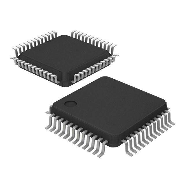
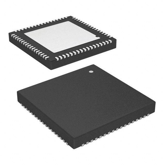
| 供应商器件封装 | 64-LQFP(10x10) |
| 其它名称 | 296-22687-6 |
| 制造商产品页 | http://www.ti.com/general/docs/suppproductinfo.tsp?distId=10&orderablePartNumber=MSP430F2417TPMR |
| 包装 | Digi-Reel® |
| 外设 | 欠压检测/复位,DMA,POR,PWM,WDT |
| 封装/外壳 | 64-LQFP |
| 工作温度 | -40°C ~ 105°C |
| 振荡器类型 | 内部 |
| 数据转换器 | A/D 8x12b |
| 标准包装 | 1 |
| 核心处理器 | MSP430 |
| 核心尺寸 | 16-位 |
| 电压-电源(Vcc/Vdd) | 1.8 V ~ 3.6 V |
| 程序存储器类型 | 闪存 |
| 程序存储容量 | 92KB(92K x 8 + 256B) |
| 连接性 | I²C, IrDA, LIN, SCI, SPI, UART/USART |
| 速度 | 16MHz |
| 配用 | /product-detail/zh/MSP-FET430U80/296-23005-ND/1571929 |


- 商务部:美国ITC正式对集成电路等产品启动337调查
- 曝三星4nm工艺存在良率问题 高通将骁龙8 Gen1或转产台积电
- 太阳诱电将投资9.5亿元在常州建新厂生产MLCC 预计2023年完工
- 英特尔发布欧洲新工厂建设计划 深化IDM 2.0 战略
- 台积电先进制程称霸业界 有大客户加持明年业绩稳了
- 达到5530亿美元!SIA预计今年全球半导体销售额将创下新高
- 英特尔拟将自动驾驶子公司Mobileye上市 估值或超500亿美元
- 三星加码芯片和SET,合并消费电子和移动部门,撤换高东真等 CEO
- 三星电子宣布重大人事变动 还合并消费电子和移动部门
- 海关总署:前11个月进口集成电路产品价值2.52万亿元 增长14.8%


PDF Datasheet 数据手册内容提取
Product Order Technical Tools & Support & Folder Now Documents Software Community MSP430F2619,MSP430F2618,MSP430F2617,MSP430F2616 MSP430F2419,MSP430F2418,MSP430F2417,MSP430F2416 SLAS541L–JUNE2007–REVISEDMAY2020 MSP430F261x, MSP430F241x Mixed-Signal Microcontrollers 1 Device Overview 1.1 Features 1 • Lowsupplyvoltagerange:1.8Vto3.6V • Bootloader(BSL) • Ultra-lowpowerconsumption • Serialonboardprogramming,noexternal – Activemode:365 µAat1MHz,2.2V programmingvoltageneeded,programmablecode protectionbysecurityfuse – Standbymode(VLO):0.5 µA • Familymembers(alsoseeDeviceComparison) – Offmode(RAMretention):0.1 µA – MSP430F2416 • Wakeupfromstandbymodeinlessthan1µs – 92KB+256bytesflashmemory • 16-bitRISCarchitecture,62.5-nsinstructioncycle time – 4KBRAM • Three-channelinternalDMA(MSP430F261xonly) – MSP430F2417 • 12-bitanalog-to-digitalconverter(ADC)with – 92KB+256bytesflashmemory internalreference,sample-and-hold,andautoscan – 8KBRAM feature – MSP430F2418 • Dual12-bitdigital-to-analogconverters(DACs) – 116KB+256bytesflashmemory withsynchronization(MSP430F261xonly) – 8KBRAM • 16-bitTimer_Awiththreecapture/compare – MSP430F2419 registers – 120KB+256bytesflashmemory • 16-bitTimer_Bwithsevencapture/compare – 4KBRAM registerswithshadowregisters – MSP430F2616 • On-chipcomparator – 92KB+256bytesflashmemory • Fouruniversalserialcommunicationinterfaces – 4KBRAM (USCIs) – MSP430F2617 – USCI_A0andUSCI_A1 – 92KB+256bytesflashmemory – EnhancedUARTsupportingautomaticbaud- ratedetection – 8KBRAM – IrDAencoderanddecoder – MSP430F2618 – SynchronousSPI – 116KB+256bytesflashmemory – USCI_B0andUSCI_B1 – 8KBRAM – I2C – MSP430F2619 – SynchronousSPI – 120KB+256bytesflashmemory • Supplyvoltagesupervisorandmonitorwith – 4KBRAM programmableleveldetection • Availablein80-pinquadflatpack(LQFP),64-pin • Brownoutdetector LQFP,and113-pinballgridarray(nFBGA) 1.2 Applications • Sensorsystems • Hand-heldmeters • Industrialcontrolapplications • Medicalimagingapplications 1.3 Description The Texas Instruments MSP430™ family of ultra-low-power microcontrollers consists of several devices featuring different sets of peripherals targeted for various applications. The architecture, combined with five low-power modes is optimized to achieve extended battery life in portable measurement applications. The device features a powerful 16-bit RISC CPU, 16-bit registers, and constant generators that contribute to maximum code efficiency. The calibrated digitally controlled oscillator (DCO) allows wake-up from low- powermodestoactivemodeinlessthan1µs. 1 An IMPORTANT NOTICE at the end of this data sheet addresses availability, warranty, changes, use in safety-critical applications, intellectualpropertymattersandotherimportantdisclaimers.PRODUCTIONDATA.
MSP430F2619,MSP430F2618,MSP430F2617,MSP430F2616 MSP430F2419,MSP430F2418,MSP430F2417,MSP430F2416 SLAS541L–JUNE2007–REVISEDMAY2020 www.ti.com The MSP430F261x and MSP430F241x series are microcontroller configurations with two built-in 16-bit timers, a fast 12-bit ADC, a comparator, two 12-bit DACs, four USCI modules, DMA, and up to 64 I/O pins. The MSP430F241x devices are identical to the MSP430F261x devices, with the exception that the DAC12andtheDMAmodulesarenotimplemented. TheLQFP-64packageisalsoavailableasanonmagneticpackageformedicalimagingapplications. Forcompletemoduledescriptions,seethe MSP430F2xx,MSP430G2xxFamilyUser'sGuide. DeviceInformation(1) PARTNUMBER PACKAGE BODYSIZE(2) MSP430F2619TPN LQFP(80) 12mm×12mm MSP430F2619TPM LQFP(64) 10mm×10mm MSP430F2619TZCA nFBGA(113) 7mm×7mm MSP430F2619TZQW(3) MicroStarJunior™BGA(113) 7mm×7mm (1) Forthemostcurrentpart,package,andorderinginformation,seethePackageOptionAddendumin Section8,orseetheTIwebsiteatwww.ti.com. (2) Thesizesshownhereareapproximations.Forthepackagedimensionswithtolerances,seethe MechanicalDatainSection8. (3) AllorderablepartnumbersintheZQW(MicroStarJuniorBGA)packagehavebeenchangedtoa statusofLastTimeBuy.VisittheProductlifecyclepagefordetailsonthisstatus. 2 DeviceOverview Copyright©2007–2020,TexasInstrumentsIncorporated SubmitDocumentationFeedback ProductFolderLinks:MSP430F2619 MSP430F2618 MSP430F2617 MSP430F2616MSP430F2419 MSP430F2418 MSP430F2417 MSP430F2416
MSP430F2619,MSP430F2618,MSP430F2617,MSP430F2616 MSP430F2419,MSP430F2418,MSP430F2417,MSP430F2416 www.ti.com SLAS541L–JUNE2007–REVISEDMAY2020 1.4 Functional Block Diagrams Figure1-1throughFigure1-4 showthefunctionalblockdiagrams. XIN, XOUT, DVCC1, DVSS1, P3.x, P4.x AVCC AVSS P1.x, P2.x P7.x, P8.x XT2IN XT2OUT DVCC2 DVSS2 P5.x, P6.x 2x8, 1x16 2 2 2x8 4x8 ACLK Oscillators Flash RAM Ports Ports Ports USCIA0 Basic Clock SMCLK ADC12 P1, P2 P3, P4 P7, P8 UART, System+ 120KB 4KB 12bit P5, P6 LIN, IrDA, SPI 116KB 8KB 2x8 I/O 2x8/1x16 8 MCLK 92KB 8KB channels Interrupt 4x8I/O I/O USCIB0 92KB 4KB capability SPI,I2C 16MHz MAB CPU 1MB incl. 16 Registers MDB Hardware Timer_B7 USCIA1 Emulation Brownout Multiplier Watchdog Timer_A3 Comp_A+ UART, Protection WDT+ 7 CC LIN, MPY, IrDA, SPI JTAG SVS, MPYS, 3CC Registers, 8 Interface SVM MAC, 15-Bit Registers Shadow Channels USCIB1 Reg SPI, I2C MACS RST/NMI Figure1-1.MSP430F241xFunctionalBlockDiagram,PNorZCAorZQWPackage XIN, XOUT, P3.x, P4.x DVCC DVSS AVCC AVSS P1.x, P2.x XT2IN XT2OUT P5.x, P6.x 2 2 2x8 4x8 ACLK Oscillators Flash RAM Ports Ports USCIA0 Basic Clock SMCLK ADC12 P1, P2 P3, P4 UART, System+ 120KB 4KB 12bit P5, P6 LIN, IrDA, SPI 116KB 8KB 2x8I/O 8 MCLK 92KB 8KB channels Interrupt 4x8I/O USCI B0 92KB 4KB capability SPI, I2C 16MHz MAB CPU 1MB incl. 16 Registers MDB Hardware Timer_B7 USCIA1 Emulation Brownout Multiplier Watchdog Timer_A3 Comp_A+ UART, Protection WDT+ 7 CC LIN, MPY, IrDA, SPI JTAG SVS, MPYS, 3 CC Registers, 8 Interface SVM MAC, 15-Bit Registers Shadow Channels USCI B1 Reg SPI, I2C MACS RST/NMI Figure1-2.MSP430F241xFunctionalBlockDiagram,PMPackage Copyright©2007–2020,TexasInstrumentsIncorporated DeviceOverview 3 SubmitDocumentationFeedback ProductFolderLinks:MSP430F2619 MSP430F2618 MSP430F2617 MSP430F2616MSP430F2419 MSP430F2418 MSP430F2417 MSP430F2416
MSP430F2619,MSP430F2618,MSP430F2617,MSP430F2616 MSP430F2419,MSP430F2418,MSP430F2417,MSP430F2416 SLAS541L–JUNE2007–REVISEDMAY2020 www.ti.com XIN, XOUT, DVCC1, DVSS1, P3.x, P4.x AVCC AVSS P1.x, P2.x P7.x, P8.x XT2IN XT2OUT DVCC2 DVSS2 P5.x, P6.x 2x8,1x16 2 2 2x8 4x8 ACLK Oscillators Flash RAM DAC12 Ports Ports Ports USCIA0 BasicClock SMCLK ADC12 12bit P1, P2 P3, P4 P7, P8 UART, System+ 120KB 4KB 12bit P5, P6 LIN, 116KB 8KB 2 IrDA,SPI 2x8I/O 2x8,1x16 92KB 8KB 8 channels, MCLK 92KB 4KB channels Voltage Interrupt 4x8I/O I/O USCIB0 56KB 4KB output capability SPI,I2C 16-MHz MAB CPU 1MB incl.16 Registers MDB Hardware Timer_B7 USCIA1 Emulation Brownout Multiplier DMA Watchdog Timer_A3 Comp_A+ UART, Protection Controller WDT+ 7CC LIN, MPY, IrDA,SPI JTAG SVS, MPYS, 3 3CC Registers, 8 Interface SVM MAC, Channels 15-Bit Registers Shadow Channels USCIB1 Reg SPI,I2C MACS RST/NMI Figure1-3.MSP430F261xFunctionalBlockDiagram,PNorZCAorZQWPackage XIN, XOUT, P3.x, P4.x DVCC DVSS AVCC AVSS P1.x, P2.x XT2IN XT2OUT P5.x, P6.x 2 2 2x8 4x8 ACLK Oscillators Flash RAM DAC12 Ports Ports USCIA0 Basic Clock SMCLK ADC12 12bit P1, P2 P3, P4 UART, System+ 120KB 4KB 12bit P5, P6 LIN, 116KB 8KB 2 IrDA, SPI 2x8 I/O 92KB 8KB 8 channels, MCLK 92KB 4KB channels Voltage Interrupt 4x8I/O USCIB0 56KB 4KB output capability SPI, I2C 16-MHz MAB CPU 1MB incl. 16 Registers MDB Hardware Timer_B7 USCIA1 Emulation Brownout Multiplier DMA Watchdog Timer_A3 Comp_A+ UART, Protection Controller WDT+ 7 CC LIN, MPY, IrDA, SPI JTAG SVS, MPYS, 3 3CC Registers, 8 Interface SVM MAC, Channels 15-Bit Registers Shadow Channels USCIB1 Reg SPI, I2C MACS RST/NMI Figure1-4.MSP430F261xFunctionalBlockDiagram,PMPackage 4 DeviceOverview Copyright©2007–2020,TexasInstrumentsIncorporated SubmitDocumentationFeedback ProductFolderLinks:MSP430F2619 MSP430F2618 MSP430F2617 MSP430F2616MSP430F2419 MSP430F2418 MSP430F2417 MSP430F2416
MSP430F2619,MSP430F2618,MSP430F2617,MSP430F2616 MSP430F2419,MSP430F2418,MSP430F2417,MSP430F2416 www.ti.com SLAS541L–JUNE2007–REVISEDMAY2020 Table of Contents 1 DeviceOverview......................................... 1 5.31 CrystalOscillatorLFXT1,High-FrequencyMode... 39 1.1 Features.............................................. 1 5.32 TypicalCharacteristics–LFXT1OscillatorinHF ..................................... ........................................... Mode(XTS=1) 40 1.2 Applications 1 ............................... ............................................ 5.33 CrystalOscillatorXT2 41 1.3 Description 1 ............ ........................... 5.34 TypicalCharacteristics–XT2Oscillator 42 1.4 FunctionalBlockDiagrams 3 ............................................. 2 Revision History......................................... 7 5.35 Timer_A 43 ............................................. 3 DeviceComparison ..................................... 9 5.36 Timer_B 43 ................................. ..................................... 5.37 USCI(UARTMode) 43 3.1 RelatedProducts 9 ............................ 4 TerminalConfigurationandFunctions............ 10 5.38 USCI(SPIMasterMode) 43 ............................. ........................................ 5.39 USCI(SPISlaveMode) 44 4.1 PinDiagrams 10 .................................. 5.40 USCI(I2CMode).................................... 46 4.2 SignalDescriptions 15 ..................................... 5 Specifications........................................... 20 5.41 Comparator_A+ 47 ............ ......................... 5.42 TypicalCharacteristics,Comparator_A+ 49 5.1 AbsoluteMaximumRatings 20 ........................................ 5.43 12-BitADCPowerSupplyandInputRange 5.2 ESDRatings 20 .......................................... Conditions 50 ............... 5.3 RecommendedOperatingConditions 20 ..................... 5.44 12-BitADCExternalReference 50 5.4 ActiveModeSupplyCurrentIntoV Excluding CC ...................... ..................................... 5.45 12-BitADCBuilt-InReference 51 External Current 22 ..................... 5.5 TypicalCharacteristics–ActiveModeSupply 5.46 12-BitADCTimingParameters 53 ................................... ................... Current(IntoV ) 22 5.47 12-BitADCLinearityParameters 53 CC 5.6 Low-PowerModeSupplyC.u.r.r.e.n.t.s..(.I.n.t.o..V.C.C..)....... 5.48 12-BitADCTemperatureSensorandBuilt-InVMID. 54 ExcludingExternalCurrent 23 ................... 5.49 12-BitDACSupplySpecifications 54 ............ 5.7 TypicalCharacteristics–LPM4Current 24 ................. 5.50 12-BitDACLinearitySpecifications 54 5.8 Schmitt-TriggerInputs(PortsP1toP8,RST/NMI, 5.51 TypicalCharacteristics,12-BitDACLinearity ............................. JTAG,XIN,andXT2IN) 25 ........................................ Specifications 56 ............................ 5.9 Inputs(PortsP1andP2) 25 ................... 5.52 12-BitDACOutputSpecifications 56 .................. 5.10 LeakageCurrent(PortsP1toP8) 25 ......... 5.53 12-BitDACReferenceInputSpecifications 57 ......................... 5.11 StandardInputs(RST/NMI) 25 ................. 5.54 12-BitDACDynamicSpecifications 57 ............................ 5.12 Outputs(PortsP1toP8) 26 ....................................... 5.55 FlashMemory 59 ................. 5.13 OutputFrequency(PortsP1toP8) 26 ................................................. 5.56 RAM 59 ................... 5.14 TypicalCharacteristics–Outputs 27 ...................................... 5.57 JTAGInterface 59 ................... 5.15 PORandBrownoutReset(BOR) 28 .......................................... 5.58 JTAGFuse 59 ........... 5.16 TypicalCharacteristics–PORandBOR 29 6 DetailedDescription................................... 60 5.17 SupplyVoltageSupervisor(SVS),SupplyVoltage ................................................. ....................................... 6.1 CPU 60 Monitor(SVM) 30 ....................................... .......................... 6.2 InstructionSet 61 5.18 MainDCOCharacteristics 32 .................................... ..................................... 6.3 OperatingModes 62 5.19 DCO Frequency 32 .......................... 6.4 InterruptVectorAddresses 63 5.20 CalibratedDCOFrequencies–Toleranceat Calibration........................................... 33 6.5 SpecialFunctionRegisters(SFRs)................. 64 ............................... 5.21 CalibratedDCOFrequencies–ToleranceOver 6.6 Memory Organization 66 Temperature0°Cto85°C........................... 33 6.7 Bootloader(BSL).................................... 66 5.22 CalibratedDCOFrequencies–ToleranceOver 6.8 FlashMemory....................................... 66 ................................. SupplyVoltageVCC 34 6.9 Peripherals.......................................... 68 .. 5.23 CalibratedDCOFrequencies–OverallTolerance 34 ....................................... 6.10 PortDiagrams 78 5.24 TypicalCha.r.a.c..te..ri.s.t.ic..s..–..C.a..li.b.r.a.t.e.d..D..C..O............ 7 DeviceandDocumentationSupport............... 95 Frequency 35 ...................................... 7.1 Getting Started 95 5.25 Wake-upTimesFromLower-PowerModes(LPM3, LPM4)............................................... 36 7.2 Device Nomenclature............................... 95 ................................. 5.26 TypicalCharacteristics–DCOClockWake-upTime 7.3 ToolsandSoftware 97 FromLPM3orLPM4................................ 36 7.4 DocumentationSupport............................. 98 5.27 DCOWithExternalResistorROSC.................. 37 7.5 RelatedLinks...................................... 101 5.28 TypicalCharacteristics–DCOWithExternal ............................. 7.6 CommunityResources 101 ....................................... Resistor ROSC 37 7.7 Trademarks........................................ 101 ... 5.29 CrystalOscillatorLFXT1,Low-FrequencyMode 38 ................... 7.8 ElectrostaticDischargeCaution 101 5.30 InternalVery-Low-PowerLow-FrequencyOscillator .............................. ................................................ 7.9 ExportControlNotice 101 (VLO) 38 Copyright©2007–2020,TexasInstrumentsIncorporated TableofContents 5 SubmitDocumentationFeedback ProductFolderLinks:MSP430F2619 MSP430F2618 MSP430F2617 MSP430F2616MSP430F2419 MSP430F2418 MSP430F2417 MSP430F2416
MSP430F2619,MSP430F2618,MSP430F2617,MSP430F2616 MSP430F2419,MSP430F2418,MSP430F2417,MSP430F2416 SLAS541L–JUNE2007–REVISEDMAY2020 www.ti.com 7.10 Glossary............................................ 102 8 Mechanical,Packaging,andOrderable Information............................................. 102 6 TableofContents Copyright©2007–2020,TexasInstrumentsIncorporated SubmitDocumentationFeedback ProductFolderLinks:MSP430F2619 MSP430F2618 MSP430F2617 MSP430F2616MSP430F2419 MSP430F2418 MSP430F2417 MSP430F2416
MSP430F2619,MSP430F2618,MSP430F2617,MSP430F2616 MSP430F2419,MSP430F2418,MSP430F2417,MSP430F2416 www.ti.com SLAS541L–JUNE2007–REVISEDMAY2020 2 Revision History NOTE:Pagenumbersforpreviousrevisionsmaydifferfrompagenumbersinthecurrentversion. ChangesfromrevisionKtorevisionL ChangesfromNovember9,2012toMay1,2020 Page • Formatchangesthroughoutdocument,includingadditionofsectionnumbering............................................ 1 • Throughoutthedocument,addedtheZCApackage............................................................................ 1 • AddedDeviceInformationtable .................................................................................................... 2 • ChangedthestatusofallorderablepartnumbersintheZQWpackage ..................................................... 2 • AddedSection1.4andmovedfunctionalblockdiagramstoit................................................................. 3 • AddedSection3,DeviceComparison............................................................................................. 9 • AddedSection5andmovedallelectricalspecificationstoit ................................................................. 20 • AddedSection5.2,ESDRatings.................................................................................................. 20 • Removed"Iversion"rowfromT rowinSection5.3(allavailabledevicesare"Tversion"temperaturerange)...... 20 A • AddedseparaterowsforInformationmemorysegmentstoTable6-8,MemoryOrganization........................... 66 • Changedallinstancesof"bootstraploader"to"bootloader".................................................................. 66 • Changedallinstancesof"INCHx=0x1010"to"INCHx=1010b",andcorrectedallvaluesintheADDRESS OFFSETcolumninTable6-11,LabelsUsedbytheADCCalibrationTags................................................ 69 • CorrectedP4DIR.xvalue(changedfrom1to0)forTimer_B7.TBCLKentryinTable6-19,PortP4(P4.0toP4.7) PinFunctions........................................................................................................................ 85 • AddedSection7andmovedTrademarksandElectrostaticDischargeCautionsectionstoit............................ 95 • AddedSection8,Mechanical,Packaging,andOrderableInformation..................................................... 102 ChangesfrominitialreleasetorevisionK REVISION COMMENTS SLAS541K ChangedP8.6/XT2OUTandP8.7/XT2INtoI/OinTable4-1 November2012 SLAS541J Addednonmagneticpackageoption December2011 SLAS541I ChangedT ,Programmeddevice,to-55°Cto150°CinSection5.1 July2011 stg SLAS541H ChangedControlBits/SignalsinTable6-21,Table6-22,andTable6-23 May2011 ChangedcrystalsignalnamesinTable6-26andTable6-27 SLAS541G Changedlimitsont parameter March2011 d(SVSon) RenamedTagsUsedbytheADCCalibrationTagstabletoTagsusedbytheTLVStructure ChangedvalueofTAG_ADC12_1from0x10to0x08inTagsusedbytheTLVStructure SLAS541F Added CAOUT to P1.0/TACLK, Changed Timer_A3.CCI0A to Timer_A3.CCI1A and Timer_A3.TA0 to December2009 Timer_A3.TA1 in P1.2/TA1 row, Changed Timer_A3.CCI0A to Timer_A3.CCI2A and Timer_A3.TA0 to Timer_A3.TA2inP1.3/TA2rowinPortP1(P1.0toP1.7)pinfunctionstable Changed TA0 to Timer_A3.CCI0B in P2.2/CAOUT/TA0/CA4 row of Port P2.0, P2.3, P2.4, P2.6 and P2.7 pin functionstable CorrectedLFXT1SxvaluesinFigures23and24 SLAS541E January2009 CorrectedXT2SxvaluesinFigures25and26 Correctedt MINvaluefrom200msto20msandremovedtwonotesintheflashmemorytable CMErase AddedtheESDdisclaimer SLAS541D AddedreservedBGApinstotheterminalfunctionlist November2008 Correctedthereferencesintheoutputportparameters Correctedthecumulativeprogramtimeoftheflash Copyright©2007–2020,TexasInstrumentsIncorporated RevisionHistory 7 SubmitDocumentationFeedback ProductFolderLinks:MSP430F2619 MSP430F2618 MSP430F2617 MSP430F2616MSP430F2419 MSP430F2418 MSP430F2417 MSP430F2416
MSP430F2619,MSP430F2618,MSP430F2617,MSP430F2616 MSP430F2419,MSP430F2418,MSP430F2417,MSP430F2416 SLAS541L–JUNE2007–REVISEDMAY2020 www.ti.com REVISION COMMENTS SLAS541C ReleasetomarketofMSP430F261xBGAdevices June2008 SLAS541B AddedpreviewofMSP430F261xBGAdevices May2008 PRODUCTIONDATArelease Correctedtheformatandthecontentshownonthefirstpage SLAS541A CorrectedpinnumberofP3.6andP3.7in64-pinpackageintheterminalfunctionlist October2007 Correctedtheportschematics Corrected"calibrationdata"section:typosandformattingcorrected Addedthefigure"typicalcharacteristics-LPM4current" SLAS541 PRODUCTPREVIEWrelease June2007 8 RevisionHistory Copyright©2007–2020,TexasInstrumentsIncorporated SubmitDocumentationFeedback ProductFolderLinks:MSP430F2619 MSP430F2618 MSP430F2617 MSP430F2616MSP430F2419 MSP430F2418 MSP430F2417 MSP430F2416
MSP430F2619,MSP430F2618,MSP430F2617,MSP430F2616 MSP430F2419,MSP430F2418,MSP430F2417,MSP430F2416 www.ti.com SLAS541L–JUNE2007–REVISEDMAY2020 3 Device Comparison Table3-1summarizestheavailablefamilymembers. Table3-1.DeviceComparison FLASH RAM DEVICE Timer_A Timer_B Comp_A+ ADC12 DAC12 DMA USCI_A USCI_B I/O PACKAGE (KB) (KB) PM64 48 PN80 MSP430F2619 120 4 1xTA3 1xTB7 Yes Yes Yes Yes 2 2 64 ZCA113 64 ZQW113 PM64 48 PN80 MSP430F2618 116 8 1xTA3 1xTB7 Yes Yes Yes Yes 2 2 64 ZCA113 64 ZQW113 PM64 48 PN80 MSP430F2617 92 8 1xTA3 1xTB7 Yes Yes Yes Yes 2 2 64 ZCA113 64 ZQW113 PM64 48 PN80 MSP430F2616 92 4 1xTA3 1xTB7 Yes Yes Yes Yes 2 2 64 ZCA113 64 ZQW113 PM64 48 PN80 MSP430F2419 120 4 1xTA3 1xTB7 Yes Yes No No 2 2 64 ZCA113 64 ZQW113 PM64 48 PN80 MSP430F2418 116 8 1xTA3 1xTB7 Yes Yes No No 2 2 64 ZCA113 64 ZQW113 PM64 48 PN80 MSP430F2417 92 8 1xTA3 1xTB7 Yes Yes No No 2 2 64 ZCA113 64 ZQW113 PM64 48 PN80 MSP430F2416 92 4 1xTA3 1xTB7 Yes Yes No No 2 2 64 ZCA113 64 ZQW113 3.1 Related Products Forinformationaboutotherdevicesinthisfamilyofproductsorrelatedproducts,seethefollowinglinks. 16-bitand32-bitmicrocontrollers High-performance,low-powersolutionstoenabletheautonomousfuture ProductsforMSP430ultra-low-powersensing& measurementMCUs Oneplatform.Oneecosystem.Endlesspossibilities. CompanionproductsforMSP430F2619 Reviewproductsthatarefrequentlypurchasedorusedwiththisproduct. Referencedesigns FindreferencedesignsleveragingthebestinTItechnologytosolveyoursystem-levelchallenges Copyright©2007–2020,TexasInstrumentsIncorporated DeviceComparison 9 SubmitDocumentationFeedback ProductFolderLinks:MSP430F2619 MSP430F2618 MSP430F2617 MSP430F2616MSP430F2419 MSP430F2418 MSP430F2417 MSP430F2416
MSP430F2619,MSP430F2618,MSP430F2617,MSP430F2616 MSP430F2419,MSP430F2418,MSP430F2417,MSP430F2416 SLAS541L–JUNE2007–REVISEDMAY2020 www.ti.com 4 Terminal Configuration and Functions 4.1 Pin Diagrams Figure4-1showsthepinoutofthe80-pinPNpackagefortheMSP430F241xdevices. T U N O VCCVSS1VSS6.2/A2 6.1/A1 6.0/A0 ST/NMI CK MS DI/TCLK DO/TDI8.7/XT2I 8.6/XT2 8.5 8.4 8.3 8.2 8.1 8.0 7.7 A D A P P P R T T T TP P P P P P P P P 80 79 78 77 76 75 74 73 72 7170 69 68 67 66 65 64636261 DV 1 60 P7.6 CC1 P6.3/A3 2 59 P7.5 P6.4/A4 3 58 P7.4 P6.5/A5 4 57 P7.3 P6.6/A6 5 56 P7.2 P6.7/A7/SVSIN 6 55 P7.1 V 7 54 P7.0 REF+ XIN 8 53 DV SS2 XOUT 9 52 DV CC2 Ve 10 51 P5.7/TBOUTH/SVSOUT REF+ V /Ve 11 50 P5.6/ACLK REF- REF- P1.0/TACLK/CAOUT 12 49 P5.5/SMCLK P1.1/TA0 13 48 P5.4/MCLK P1.2/TA1 14 47 P5.3/UCB1CLK/UCA1STE P1.3/TA2 15 46 P5.2/UCB1SOMI/UCB1SCL P1.4/SMCLK 16 45 P5.1/UCB1SIMO/UCB1SDA P1.5/TA0 17 44 P5.0/UCB1STE/UCA1CLK P1.6/TA1 18 43 P4.7/TBCLK P1.7/TA2 19 42 P4.6/TB6 P2.0/ACLK/CA2 20 41 P4.5/TB5 21 22 23 24 25 26 27 28 29 3031 32 33 34 35 36 37383940 P2.1/TAINCLK/CA3 P2.2/CAOUT/TA0/CA4 P2.3/CA0/TA1 P2.4/CA1/TA2 P2.5/R/CA5OSCP2.6/ADC12CLK/CA6 P2.7/TA0/CA7 P3.0/UCB0STE/UCA0CLK P3.1/UCB0SIMO/UCB0SDA P3.2/UCB0SOMI/UCB0SCL P3.3/UCB0CLK/UCA0STE P3.4/UCA0TXD/UCA0SIMO P3.5/UCA0RXD/UCA0SOMI P3.6/UCA1TXD/UCA1SIMO P3.7/UCA1RXD/UCA1SOMI P4.0/TB0 P4.1/TB1 P4.2/TB2 P4.3/TB3 P4.4/TB4 Figure4-1.80-PinPNPackage,MSP430F241x(TopView) 10 TerminalConfigurationandFunctions Copyright©2007–2020,TexasInstrumentsIncorporated SubmitDocumentationFeedback ProductFolderLinks:MSP430F2619 MSP430F2618 MSP430F2617 MSP430F2616MSP430F2419 MSP430F2418 MSP430F2417 MSP430F2416
MSP430F2619,MSP430F2618,MSP430F2617,MSP430F2616 MSP430F2419,MSP430F2418,MSP430F2417,MSP430F2416 www.ti.com SLAS541L–JUNE2007–REVISEDMAY2020 Figure4-2showsthepinoutofthe64-pinPMpackagefortheMSP430F241xdevices. T U O S V S H/ T K U K L VCCVSS1VSS6.2/A2 6.1/A1 6.0/A0 ST/NMI CK MS DI/TCLK DO/TDI T2IN T2OUT 5.7/TBO 5.6/ACL 5.5/SMC A D A P P P R T T T T X X P P P 64 636261605958575655545352515049 DV 1 48 P5.4/MCLK CC1 P6.3/A3 2 47 P5.3/UCB1CLK/UCA1STE P6.4/A4 3 46 P5.2/UCB1SOMI/UCB1SCL P6.5/A5 4 45 P5.1/UCB1SIMO/UCB1SDA P6.6/A6 5 44 P5.0/UCB1STE/UCA1CLK P6.7/A7/SVSIN 6 43 P4.7/TBCLK V 7 42 P4.6/TB6 REF+ XIN 8 41 P4.5/TB5 XOUT 9 40 P4.4/TB4 Ve 10 39 P4.3/TB3 REF+ V /Ve 11 38 P4.2/TB2 REF- REF- P1.0/TACLK/CAOUT 12 37 P4.1/TB1 P1.1/TA0 13 36 P4.0/TB0 P1.2/TA1 14 35 P3.7/UCA1RXD/UCA1SOMI P1.3/TA2 15 34 P3.6/UCA1TXD/UCA1SIMO P1.4/SMCLK 16 33 P3.5/UCA0RXD/UCA0SOMI 17 181920212223242526272829303132 0 1 2 2 3 4 1 2 5 6 7 K A L E O TA TA TA CA CA CA TA TA CA CA CA CL SD SC ST M P1.5/ P1.6/ P1.7/ P2.0/ACLK/ P2.1/TAINCLK/ P2.2/CAOUT/TA0/ P2.3/CA0/ P2.4/CA1/ /P2.5/ROSCP2.6/ADC12CLK/ P2.7/TA0/ P3.0/UCB0STE/UCA0 3.1/UCB0SIMO/UCB0 3.2/UCB0SOMI/UCB0 P3.3/UCB0CLK/UCA0 3.4/UCA0TXD/UCA0SI P P P Figure4-2.64-PinPMPackage,MSP430F241x(TopView) Copyright©2007–2020,TexasInstrumentsIncorporated TerminalConfigurationandFunctions 11 SubmitDocumentationFeedback ProductFolderLinks:MSP430F2619 MSP430F2618 MSP430F2617 MSP430F2616MSP430F2419 MSP430F2418 MSP430F2417 MSP430F2416
MSP430F2619,MSP430F2618,MSP430F2617,MSP430F2616 MSP430F2419,MSP430F2418,MSP430F2417,MSP430F2416 SLAS541L–JUNE2007–REVISEDMAY2020 www.ti.com Figure4-3showsthepinoutofthe80-pinPNpackagefortheMSP430F261xdevices. T U N O A2 A1 A0 NMI CLK TDIXT2I XT2 VCCVSS1VSS6.2/ 6.1/ 6.0/ ST/ CK MS DI/T DO/8.7/ 8.6/ 8.5 8.4 8.3 8.2 8.1 8.0 7.7 A D A P P P R T T T TP P P P P P P P P 80 79 78 77 76 75 74 73 72 7170 69 68 67 66 65 64636261 DV 1 60 P7.6 CC1 P6.3/A3 2 59 P7.5 P6.4/A4 3 58 P7.4 P6.5/A5/DAC1 4 57 P7.3 P6.6/A6/DAC0 5 56 P7.2 P6.7/A7/DAC1/SVSIN 6 55 P7.1 V 7 54 P7.0 REF+ XIN 8 53 DV SS2 XOUT 9 52 DV CC2 Ve /DAC0 10 51 P5.7/TBOUTH/SVSOUT REF+ V /Ve 11 50 P5.6/ACLK REF- REF- P1.0/TACLK/CAOUT 12 49 P5.5/SMCLK P1.1/TA0 13 48 P5.4/MCLK P1.2/TA1 14 47 P5.3/UCB1CLK/UCA1STE P1.3/TA2 15 46 P5.2/UCB1SOMI/UCB1SCL P1.4/SMCLK 16 45 P5.1/UCB1SIMO/UCB1SDA P1.5/TA0 17 44 P5.0/UCB1STE/UCA1CLK P1.6/TA1 18 43 P4.7/TBCLK P1.7/TA2 19 42 P4.6/TB6 P2.0/ACLK/CA2 20 41 P4.5/TB5 21 22 23 24 25 26 27 28 29 3031 32 33 34 35 36 37383940 P2.1/TAINCLK/CA3 P2.2/CAOUT/TA0/CA4 P2.3/CA0/TA1 P2.4/CA1/TA2 P2.5/R/CA5OSC2.6/ADC12CLK/DMAE0/CA6 P2.7/TA0/CA7 P3.0/UCB0STE/UCA0CLK P3.1/UCB0SIMO/UCB0SDA P3.2/UCB0SOMI/UCB0SCL P3.3/UCB0CLK/UCA0STE P3.4/UCA0TXD/UCA0SIMO P3.5/UCA0RXD/UCA0SOMI P3.6/UCA1TXD/UCA1SIMO P3.7/UCA1RXD/UCA1SOMI P4.0/TB0 P4.1/TB1 P4.2/TB2 P4.3/TB3 P4.4/TB4 P Figure4-3.80-PinPNPackage,MSP430F261x(TopView) 12 TerminalConfigurationandFunctions Copyright©2007–2020,TexasInstrumentsIncorporated SubmitDocumentationFeedback ProductFolderLinks:MSP430F2619 MSP430F2618 MSP430F2617 MSP430F2616MSP430F2419 MSP430F2418 MSP430F2417 MSP430F2416
MSP430F2619,MSP430F2618,MSP430F2617,MSP430F2616 MSP430F2419,MSP430F2418,MSP430F2417,MSP430F2416 www.ti.com SLAS541L–JUNE2007–REVISEDMAY2020 Figure4-4showsthepinoutofthe64-pinPMpackagefortheMSP430F261xdevices. T U O S V S H/ T K U K L VCC VSS1 VSS 6.2/A2 6.1/A1 6.0/A0 ST/NMI CK MS DI/TCLK DO/TDI T2IN T2OUT 5.7/TBO 5.6/ACL 5.5/SMC A D A P P P R T T T T X X P P P 64 63 62 6160 59 58 57 56 55 54 53 52 5150 49 DV 1 48 P5.4/MCLK CC1 P6.3/A3 2 47 P5.3/UCB1CLK/UCA1STE P6.4/A4 3 46 P5.2/UCB1SOMI/UCB1SCL P6.5/A5/DAC1 4 45 P5.1/UCB1SIMO/UCB1SDA P6.6/A6/DAC0 5 44 P5.0/UCB1STE/UCA1CLK P6.7/A7/DAC1/SVSIN 6 43 P4.7/TBCLK V 7 42 P4.6/TB6 REF+ XIN 8 41 P4.5/TB5 XOUT 9 40 P4.4/TB4 Ve /DAC0 10 39 P4.3/TB3 REF+ V /Ve 11 38 P4.2/TB2 REF- REF- P1.0/TACLK/CAOUT 12 37 P4.1/TB1 P1.1/TA0 13 36 P4.0/TB0 P1.2/TA1 14 35 P3.7/UCA1RXD/UCA1SOMI P1.3/TA2 15 34 P3.6/UCA1TXD/UCA1SIMO P1.4/SMCLK 16 33 P3.5/UCA0RXD/UCA0SOMI 17 18 19 20 2122 23 24 25 26 27 28 29 30 3132 A0 A1 A2 A2 A3 A4 A1 A2 A5 A6 A7 LK DA CL TE MO P1.5/T P1.6/T P1.7/T P2.0/ACLK/C P2.1/TAINCLK/C P2.2/CAOUT/TA0/C P2.3/CA0/T P2.4/CA1/T P2.5/R/COSC 2.6/ADC12CLK/DMAE0/C P2.7/TA0/C P3.0/UCB0STE/UCA0C P3.1/UCB0SIMO/UCB0S P3.2/UCB0SOMI/UCB0S P3.3/UCB0CLK/UCA0S P3.4/UCA0TXD/UCA0SI P Figure4-4.64-PinPMPackage,MSP430F261x(TopView) Copyright©2007–2020,TexasInstrumentsIncorporated TerminalConfigurationandFunctions 13 SubmitDocumentationFeedback ProductFolderLinks:MSP430F2619 MSP430F2618 MSP430F2617 MSP430F2616MSP430F2419 MSP430F2418 MSP430F2417 MSP430F2416
MSP430F2619,MSP430F2618,MSP430F2617,MSP430F2616 MSP430F2419,MSP430F2418,MSP430F2417,MSP430F2416 SLAS541L–JUNE2007–REVISEDMAY2020 www.ti.com Figure 4-5 shows the pinout of the 113-pin ZCA and ZQW packages. For the terminal assignments, see Table4-1. A1 A2 A3 A4 A5 A6 A7 A8 A9 A10 A11 A12 B1 B2 B3 B4 B5 B6 B7 B8 B9 B10 B11 B12 C1 C2 C3 C11 C12 D1 D2 D4 D5 D6 D7 D8 D9 D11 D12 E1 E2 E4 E5 E6 E7 E8 E9 E11 E12 F1 F2 F4 F5 F8 F9 F11 F12 G1 G2 G4 G5 G8 G9 G11 G12 H1 H2 H4 H5 H6 H7 H8 H9 H11 H12 J1 J2 J4 J5 J6 J7 J8 J9 J11 J12 K1 K2 K11 K12 L1 L2 L3 L4 L5 L6 L7 L8 L9 L10 L11 L12 M1 M2 M3 M4 M5 M6 M7 M8 M9 M10 M11 M12 Figure4-5.113-PinZCAandZQWPackages(TopView) 14 TerminalConfigurationandFunctions Copyright©2007–2020,TexasInstrumentsIncorporated SubmitDocumentationFeedback ProductFolderLinks:MSP430F2619 MSP430F2618 MSP430F2617 MSP430F2616MSP430F2419 MSP430F2418 MSP430F2417 MSP430F2416
MSP430F2619,MSP430F2618,MSP430F2617,MSP430F2616 MSP430F2419,MSP430F2418,MSP430F2417,MSP430F2416 www.ti.com SLAS541L–JUNE2007–REVISEDMAY2020 4.2 Signal Descriptions Table4-1describesthesignalsforalldevicevariantsandpackageoptions. Table4-1.SignalDescriptions TERMINAL NO. I/O DESCRIPTION NAME PM PN ZCAor ZQW 64‑‑PIN 80‑‑PIN 113‑‑PIN Analogsupplyvoltage,positiveterminal.Suppliesonlytheanalog AV 64 80 A2 CC portionofADC12andDAC12. Analogsupplyvoltage,negativeterminal.Suppliesonlytheanalog AV 62 78 B2,B3 SS portionofADC12andDAC12. DV 1 1 A1 Digitalsupplyvoltage,positiveterminal.Suppliesalldigitalparts. CC1 DV 63 79 A3 Digitalsupplyvoltage,negativeterminal.Suppliesalldigitalparts. SS1 DV 52 F12 Digitalsupplyvoltage,positiveterminal.Suppliesalldigitalparts. CC2 DV 53 E12 Digitalsupplyvoltage,negativeterminal.Suppliesalldigitalparts. SS2 General-purposedigitalI/Opin P1.0/TACLK/CAOUT 12 12 G2 I/O Timer_A,clocksignalTACLKinput Comparator_Aoutput General-purposedigitalI/Opin P1.1/TA0 13 13 H1 I/O Timer_A,capture:CCI0Ainput,compare:Out0output BSLtransmit General-purposedigitalI/Opin P1.2/TA1 14 14 H2 I/O Timer_A,capture:CCI1Ainput,compare:Out1output General-purposedigitalI/Opin P1.3/TA2 15 15 J1 I/O Timer_A,capture:CCI2Ainput,compare:Out2output General-purposedigitalI/Opin P1.4/SMCLK 16 16 J2 I/O SMCLKsignaloutput General-purposedigitalI/Opin P1.5/TA0 17 17 K1 I/O Timer_A,compare:Out0output General-purposedigitalI/Opin P1.6/TA1 18 18 K2 I/O Timer_A,compare:Out1output General-purposedigitalI/Opin P1.7/TA2 19 19 L1 I/O Timer_A,compare:Out2output General-purposedigitalI/Opin P2.0/ACLK/CA2 20 20 M1 I/O ACLKoutput Comparator_Ainput General-purposedigitalI/Opin P2.1/TAINCLK/CA3 21 21 M2 I/O Timer_A,clocksignalatINCLK General-purposedigitalI/Opin Timer_A,capture:CCI0Binput P2.2/CAOUT/TA0/CA4 22 22 M3 I/O Comparator_Aoutput BSLreceive Comparator_Ainput General-purposedigitalI/Opin P2.3/CA0/TA1 23 23 L3 I/O Timer_A,compare:Out1output Comparator_Ainput Copyright©2007–2020,TexasInstrumentsIncorporated TerminalConfigurationandFunctions 15 SubmitDocumentationFeedback ProductFolderLinks:MSP430F2619 MSP430F2618 MSP430F2617 MSP430F2616MSP430F2419 MSP430F2418 MSP430F2417 MSP430F2416
MSP430F2619,MSP430F2618,MSP430F2617,MSP430F2616 MSP430F2419,MSP430F2418,MSP430F2417,MSP430F2416 SLAS541L–JUNE2007–REVISEDMAY2020 www.ti.com Table4-1.SignalDescriptions(continued) TERMINAL NO. I/O DESCRIPTION NAME PM PN ZCAor ZQW 64‑‑PIN 80‑‑PIN 113‑‑PIN General-purposedigitalI/Opin P2.4/CA1/TA2 24 24 L4 I/O Timer_A,compare:Out2output Comparator_Ainput General-purposedigitalI/Opin P2.5/R /CA5 25 25 M4 I/O InputforexternalresistordefiningtheDCOnominalfrequency OSC Comparator_Ainput General-purposedigitalI/Opin P2.6/ADC12CLK/ Conversionclockfor12-bitADC DMAE0(1)/CA6 26 26 J4 I/O DMAchannel0externaltrigger Comparator_Ainput General-purposedigitalI/Opin P2.7/TA0/CA7 27 27 L5 I/O Timer_A,compare:Out0output Comparator_Ainput General-purposedigitalI/Opin P3.0/UCB0STE/ 28 28 M5 I/O USCI_B0slavetransmitenable UCA0CLK USCI_A0clockinput/output General-purposedigitalI/Opin P3.1/UCB0SIMO/ 29 29 L6 I/O USCI_B0slaveinmasteroutforSPImode UCB0SDA USCI_B0SDAI2CdatainI2Cmode General-purposedigitalI/Opin P3.2/UCB0SOMI/ 30 30 M6 I/O USCI_B0slaveoutmasterinforSPImode UCB0SCL USCI_B0SCLI2CclockinI2Cmode General-purposedigitalI/O P3.3/UCB0CLK/ 31 31 L7 I/O USCI_B0clockinput/output UCA0STE USCI_A0slavetransmitenable General-purposedigitalI/Opin P3.4/UCA0TXD/ 32 32 M7 I/O USCI_AtransmitdataoutputinUARTmode UCA0SIMO USCI_Aslavedatain/masteroutforSPImode General-purposedigitalI/Opin P3.5/UCA0RXD/ 33 33 L8 I/O USCI_A0receivedatainputinUARTmode UCA0SOMI USCI_A0slavedataout/masterinforSPImode General-purposedigitalI/Opin P3.6/UCA1TXD/ 34 34 M8 I/O USCI_A1transmitdataoutputinUARTmode UCA1SIMO USCI_A1slavedatain/masteroutforSPImode General-purposedigitalI/Opin P3.7/UCA1RXD/ 35 35 L9 I/O USCI_A1receivedatainputinUARTmode UCA1SOMI USCI_A1slavedataout/masterinforSPImode General-purposedigitalI/Opin P4.0/TB0 36 36 M9 I/O Timer_B,capture:CCI0A/Binput,compare:Out0output General-purposedigitalI/Opin P4.1/TB1 37 37 J9 I/O Timer_B,capture:CCI1A/Binput,compare:Out1output General-purposedigitalI/Opin P4.2/TB2 38 38 M10 I/O Timer_B,capture:CCI2A/Binput,compare:Out2output (1) MSP430F261xdevicesonly 16 TerminalConfigurationandFunctions Copyright©2007–2020,TexasInstrumentsIncorporated SubmitDocumentationFeedback ProductFolderLinks:MSP430F2619 MSP430F2618 MSP430F2617 MSP430F2616MSP430F2419 MSP430F2418 MSP430F2417 MSP430F2416
MSP430F2619,MSP430F2618,MSP430F2617,MSP430F2616 MSP430F2419,MSP430F2418,MSP430F2417,MSP430F2416 www.ti.com SLAS541L–JUNE2007–REVISEDMAY2020 Table4-1.SignalDescriptions(continued) TERMINAL NO. I/O DESCRIPTION NAME PM PN ZCAor ZQW 64‑‑PIN 80‑‑PIN 113‑‑PIN General-purposedigitalI/Opin P4.3/TB3 39 39 L10 I/O Timer_B,capture:CCI3A/Binput,compare:Out3output General-purposedigitalI/Opin P4.4/TB4 40 40 M11 I/O Timer_B,capture:CCI4A/Binput,compare:Out4output General-purposedigitalI/Opin P4.5/TB5 41 41 M12 I/O Timer_B,capture:CCI5A/Binput,compare:Out5output General-purposedigitalI/Opin P4.6/TB6 42 42 L12 I/O Timer_B,capture:CCI6Ainput,compare:Out6output General-purposedigitalI/Opin P4.7/TBCLK 43 43 K11 I/O Timer_B,clocksignalTBCLKinput General-purposedigitalI/Opin P5.0/UCB1STE/ 44 44 K12 I/O USCI_B1slavetransmitenable UCA1CLK USCI_A1clockinput/output General-purposedigitalI/Opin P5.1/UCB1SIMO/ 45 45 J11 I/O USCI_B1slaveinmasteroutforSPImode UCB1SDA USCI_B1SDAI2CdatainI2Cmode General-purposedigitalI/Opin P5.2/UCB1SOMI/ 46 46 J12 I/O USCI_B1slaveoutmasterinforSPImode UCB1SCL USCI_B1SCLI2CclockinI2Cmode General-purposedigitalI/O P5.3/UCB1CLK/ 47 47 H11 I/O USCI_B1clockinput/output UCA1STE USCI_A1slavetransmitenable General-purposedigitalI/Opin P5.4/MCLK 48 48 H12 I/O MainsystemclockMCLKoutput General-purposedigitalI/Opin P5.5/SMCLK 49 49 G11 I/O SubmainsystemclockSMCLKoutput General-purposedigitalI/Opin P5.6/ACLK 50 50 G12 I/O AuxiliaryclockACLKoutput General-purposedigitalI/Opin SwitchallPWMdigitaloutputportstohighimpedance–Timer_BTB0to P5.7/TBOUTH/SVSOUT 51 51 F11 I/O TB6 SVScomparatoroutput General-purposedigitalI/Opin P6.0/A0 59 75 D4 I/O AnaloginputA0for12-bitADC General-purposedigitalI/Opin P6.1/A1 60 76 A4 I/O AnaloginputA1for12-bitADC General-purposedigitalI/Opin P6.2/A2 61 77 B4 I/O AnaloginputA2for12-bitADC General-purposedigitalI/Opin P6.3/A3 2 2 B1 I/O AnaloginputA3for12-bitADC General-purposedigitalI/Opin P6.4/A4 3 3 C1 I/O AnaloginputA4for12-bitADC Copyright©2007–2020,TexasInstrumentsIncorporated TerminalConfigurationandFunctions 17 SubmitDocumentationFeedback ProductFolderLinks:MSP430F2619 MSP430F2618 MSP430F2617 MSP430F2616MSP430F2419 MSP430F2418 MSP430F2417 MSP430F2416
MSP430F2619,MSP430F2618,MSP430F2617,MSP430F2616 MSP430F2419,MSP430F2418,MSP430F2417,MSP430F2416 SLAS541L–JUNE2007–REVISEDMAY2020 www.ti.com Table4-1.SignalDescriptions(continued) TERMINAL NO. I/O DESCRIPTION NAME PM PN ZCAor ZQW 64‑‑PIN 80‑‑PIN 113‑‑PIN General-purposedigitalI/Opin P6.5/A5/DAC1(1) 4 4 C2, I/O AnaloginputA5for12-bitADC C3 DAC12.1output General-purposedigitalI/Opin P6.6/A6/DAC0(1) 5 5 D1 I/O AnaloginputA6for12-bitADC DAC12.0output General-purposedigitalI/Opin AnaloginputA7for12-bitADC P6.7/A7/DAC1(1)/SVSIN 6 6 D2 I/O DAC12.1output SVSinput P7.0 54 E11 I/O General-purposedigitalI/Opin P7.1 55 D12 I/O General-purposedigitalI/Opin P7.2 56 D11 I/O General-purposedigitalI/Opin P7.3 57 C12 I/O General-purposedigitalI/Opin P7.4 58 C11 I/O General-purposedigitalI/Opin P7.5 59 B12 I/O General-purposedigitalI/Opin P7.6 60 A12 I/O General-purposedigitalI/Opin P7.7 61 A11 I/O General-purposedigitalI/Opin P8.0 62 B10 I/O General-purposedigitalI/Opin P8.1 63 A10 I/O General-purposedigitalI/Opin P8.2 64 D9 I/O General-purposedigitalI/Opin P8.3 65 A9 I/O General-purposedigitalI/Opin P8.4 66 B9 I/O General-purposedigitalI/Opin P8.5 67 B8 I/O General-purposedigitalI/Opin General-purposedigitalI/Opin P8.6/XT2OUT 68 A8 I/O OutputterminalofcrystaloscillatorXT2 General-purposedigitalI/Opin P8.7/XT2IN 69 A7 I/O InputportforcrystaloscillatorXT2.Onlystandardcrystalscanbe connected. XT2OUT 52 O OutputterminalofcrystaloscillatorXT2 XT2IN 53 I InputportforcrystaloscillatorXT2 Resetinput,nonmaskableinterruptinputport,orbootloaderstart(in RST/NMI 58 74 B5 I flashdevices) Testclock(JTAG).TCKistheclockinputportfordeviceprogramming TCK 57 73 A5 I testandbootloaderstart Testdatainputortestclockinput.Thedeviceprotectionfuseis TDI/TCLK 55 71 A6 I connectedtoTDI/TCLK. Testdataoutputport.TDO/TDIdataoutputorprogrammingdatainput TDO/TDI 54 70 B7 I/O terminal. Testmodeselect.TMSisusedasaninputportfordeviceprogramming TMS 56 72 B6 I andtest. Inputforanexternalreferencevoltage V /DAC0(1) 10 10 F2 I eREF+ DAC12.0output V 7 7 E2 O OutputofpositiveterminalofthereferencevoltageintheADC12 REF+ Negativeterminalforthereferencevoltageforbothsources,theinternal V /V 11 11 G1 I REF- eREF- referencevoltageoranexternalappliedreferencevoltage 18 TerminalConfigurationandFunctions Copyright©2007–2020,TexasInstrumentsIncorporated SubmitDocumentationFeedback ProductFolderLinks:MSP430F2619 MSP430F2618 MSP430F2617 MSP430F2616MSP430F2419 MSP430F2418 MSP430F2417 MSP430F2416
MSP430F2619,MSP430F2618,MSP430F2617,MSP430F2616 MSP430F2419,MSP430F2418,MSP430F2417,MSP430F2416 www.ti.com SLAS541L–JUNE2007–REVISEDMAY2020 Table4-1.SignalDescriptions(continued) TERMINAL NO. I/O DESCRIPTION NAME PM PN ZCAor ZQW 64‑‑PIN 80‑‑PIN 113‑‑PIN InputportforcrystaloscillatorXT1.Standardorwatchcrystalscanbe XIN 8 8 E1 I connected. OutputportforcrystaloscillatorXT1.Standardorwatchcrystalscanbe XOUT 9 9 F1 O connected. Reserved – – (2) NA Reservedpins.TIrecommendsconnectingtoDV andAV . SS SS (2) ReservedpinsareL2,E4,F4,G4,H4,D5,E5,F5,G5,H5,J5,D6,E6,H6,J6,D7,E7,H7,J7,D8,E8,F8,G8,H8,J8,E9,F9,G9,H9, B11,L11. Copyright©2007–2020,TexasInstrumentsIncorporated TerminalConfigurationandFunctions 19 SubmitDocumentationFeedback ProductFolderLinks:MSP430F2619 MSP430F2618 MSP430F2617 MSP430F2616MSP430F2419 MSP430F2418 MSP430F2417 MSP430F2416
MSP430F2619,MSP430F2618,MSP430F2617,MSP430F2616 MSP430F2419,MSP430F2418,MSP430F2417,MSP430F2416 SLAS541L–JUNE2007–REVISEDMAY2020 www.ti.com 5 Specifications 5.1 Absolute Maximum Ratings(1) overoperatingfree-airtemperaturerange(unlessotherwisenoted) MIN MAX UNIT VoltageappliedatV toV –0.3 4.1 V CC SS Voltageappliedtoanypin(2) –0.3 V +0.3 V CC Diodecurrentatanydeviceterminal –2 2 mA Unprogrammeddevice –55 150 Storagetemperature,T (3) °C stg Programmeddevice –55 150 (1) StressesbeyondthoselistedunderAbsoluteMaximumRatingsmaycausepermanentdamagetothedevice.Thesearestressratings only,andfunctionaloperationofthedeviceattheseoranyotherconditionsbeyondthoseindicatedunderRecommendedOperating Conditionsisnotimplied.Exposuretoabsolute-maximum-ratedconditionsforextendedperiodsmayaffectdevicereliability. (2) AllvoltagesreferencedtoV .TheJTAGfuse-blowvoltage,V ,isallowedtoexceedtheabsolutemaximumrating.Thevoltageis SS FB appliedtotheTESTpinwhenblowingtheJTAGfuse. (3) HighertemperaturemaybeappliedduringboardsolderingaccordingtothecurrentJEDECJ-STD-020specificationwithpeakreflow temperaturesnothigherthanclassifiedonthedevicelabelontheshippingboxesorreels. 5.2 ESD Ratings VALUE UNIT Human-bodymodel(HBM),perANSI/ESDA/JEDECJS-001(1) ±1000 V Electrostaticdischarge V (ESD) Charged-devicemodel(CDM),perJEDECspecificationJESD22-C101(2) ±250 (1) JEDECdocumentJEP155statesthat500-VHBMallowssafemanufacturingwithastandardESDcontrolprocess.Pinslistedas ±1000Vmayactuallyhavehigherperformance. (2) JEDECdocumentJEP157statesthat250-VCDMallowssafemanufacturingwithastandardESDcontrolprocess.Pinslistedas±250V mayactuallyhavehigherperformance. 5.3 Recommended Operating Conditions TypicalvaluesarespecifiedatV =3.3VandT =25°C(unlessotherwisenoted) CC A MIN MAX UNIT Duringprogramexecution 1.8 3.6 V Supplyvoltage(AV =DV =V (1)) V CC CC CC CC Duringflashprogramorerase 2.2 3.6 V Supplyvoltage(AV =DV =V ) 0 0 V SS SS SS SS T Operatingfree-airtemperature Tversion –40 105 °C A V =1.8V, CC DC 4.15 Dutycycle=50%±10% Processorfrequency(maximumMCLKfrequency)(2)(3)(see V =2.7V, f CC DC 12 MHz SYSTEM Figure5-1) Dutycycle=50%±10% V ≥3.3V, CC DC 16 Dutycycle=50%±10% (1) TIrecommendspoweringAV andDV fromthesamesource.Amaximumdifferenceof0.3VbetweenAV andDV canbe CC CC CC CC toleratedduringpowerup. (2) TheMSP430CPUisclockeddirectlywithMCLK.BoththehighandlowphasesofMCLKmustnotexceedthepulsedurationofthe specifiedmaximumfrequency. (3) Modulesmighthaveadifferentmaximuminputclockspecification.Seethespecificationoftherespectivemoduleinthisdatasheet. 20 Specifications Copyright©2007–2020,TexasInstrumentsIncorporated SubmitDocumentationFeedback ProductFolderLinks:MSP430F2619 MSP430F2618 MSP430F2617 MSP430F2616MSP430F2419 MSP430F2418 MSP430F2417 MSP430F2416
MSP430F2619,MSP430F2618,MSP430F2617,MSP430F2616 MSP430F2419,MSP430F2418,MSP430F2417,MSP430F2416 www.ti.com SLAS541L–JUNE2007–REVISEDMAY2020 Legend: 16MHz Supply voltage range during flash memory programming y 12MHz c n e qu Supply voltage range Fre during program execution m 7.5MHz e st y S 4.15MHz 1.8V 2.2V 2.7V 3.3V 3.6V Supply Voltage Note: Minimumprocessorfrequencyisdefinedbysystemclock.FlashprogramoreraseoperationsrequireaminimumV CC of2.2V. Figure5-1.OperatingArea Copyright©2007–2020,TexasInstrumentsIncorporated Specifications 21 SubmitDocumentationFeedback ProductFolderLinks:MSP430F2619 MSP430F2618 MSP430F2617 MSP430F2616MSP430F2419 MSP430F2418 MSP430F2417 MSP430F2416
MSP430F2619,MSP430F2618,MSP430F2617,MSP430F2616 MSP430F2419,MSP430F2418,MSP430F2417,MSP430F2416 SLAS541L–JUNE2007–REVISEDMAY2020 www.ti.com 5.4 Active Mode Supply Current Into V Excluding External Current CC overrecommendedrangesofsupplyvoltageandoperatingfree-airtemperature(unlessotherwisenoted)(1)(2)(seeFigure5-2 andFigure5-3) PARAMETER TESTCONDITIONS T V MIN TYP MAX UNIT A CC f =f =f =1MHz, –40°Cto85°C 365 395 DCO MCLK SMCLK f =32768Hz, 2.2V ACLK 105°C 375 420 Programexecutesinflash, Activemode(AM) I BCSCTL1=CALBC1_1MHZ, –40°Cto85°C 515 560 µA AM,1MHz current(1MHz) DCOCTL=CALDCO_1MHZ, 3V CPUOFF=0,SCG0=0, 105°C 525 595 SCG1=0,OSCOFF=0 f =f =f =1MHz, –40°Cto85°C 330 370 DCO MCLK SMCLK f =32768Hz, 2.2V ACLK 105°C 340 390 ProgramexecutesinRAM, Activemode(AM) I BCSCTL1=CALBC1_1MHZ, –40°Cto85°C 460 495 µA AM,1MHz current(1MHz) DCOCTL=CALDCO_1MHZ, 3V CPUOFF=0,SCG0=0, 105°C 470 520 SCG1=0,OSCOFF=0 f =f =f =32768Hz/8 –40°Cto85°C 2.2V 2.1 9 MCLK SMCLK ACLK =4096Hz, 105°C 2.2V 15 31 f =0Hz, DCO Activemode(AM) Programexecutesinflash, –40°Cto85°C 3V 3 11 I µA AM,4kHz current(4kHz) SELMx=11,SELS=1, DIVMx=DIVSx=DIVAx=11, CPUOFF=0,SCG0=1, 105°C 3V 19 32 SCG1=0,OSCOFF=0 f =f =f ≈100kHz, –40°Cto85°C 2.2V 67 86 MCLK SMCLK DCO(0,0) f =0Hz, ACLK 105°C 2.2V 80 99 Activemode(AM) Programexecutesinflash, I µA AM,100kHz current(100kHz) RSELx=0,DCOx=0, –40°Cto85°C 3V 84 107 CPUOFF=0,SCG0=0, SCG1=0,OSCOFF=1 105°C 3V 99 128 (1) Allinputsaretiedto0VortoV .Outputsdonotsourceorsinkanycurrent. CC (2) ThecurrentsarecharacterizedwithaMicroCrystalCC4V-T1ASMDcrystalwithaloadcapacitanceof9pF.Theinternalandexternal loadcapacitanceischosentocloselymatchtherequired9pF. 5.5 Typical Characteristics – Active Mode Supply Current (Into V ) CC 7.0 10.0 fDCO= 16 MHz TA= 85°C 9.0 6.0 8.0 TA= 25°C A A m fDCO= 12 MHz m 5.0 VCC= 3 V −7.0 − nt nt urre6.0 urre 4.0 C C e 5.0 e TA= 85°C od fDCO= 8 MHz od 3.0 M4.0 M e e Activ3.0 Activ 2.0 TA= 25°C 2.0 fDCO= 1 MHz 1.0 VCC= 2.2 V 1.0 0.0 0.0 1.5 2.0 2.5 3.0 3.5 4.0 0.0 4.0 8.0 12.0 16.0 VCC−Supply Voltage−V fDCO−DCO Frequency−MHz Figure5-2. ActiveModeCurrentvsSupplyVoltage(TA=25°C) Figure5-3.ActiveModeCurrentvsDCOFrequency 22 Specifications Copyright©2007–2020,TexasInstrumentsIncorporated SubmitDocumentationFeedback ProductFolderLinks:MSP430F2619 MSP430F2618 MSP430F2617 MSP430F2616MSP430F2419 MSP430F2418 MSP430F2417 MSP430F2416
MSP430F2619,MSP430F2618,MSP430F2617,MSP430F2616 MSP430F2419,MSP430F2418,MSP430F2417,MSP430F2416 www.ti.com SLAS541L–JUNE2007–REVISEDMAY2020 5.6 Low-Power Mode Supply Currents (Into V ) Excluding External Current CC overrecommendedrangesofsupplyvoltageandoperatingfree-airtemperature(unlessotherwisenoted)(1) (2) PARAMETER TESTCONDITIONS T V MIN TYP MAX UNIT A CC f =0MHz, –40°Cto85°C 68 63 MCLK f =f =1MHz, 2.2V SMCLK DCO 105°C 83 98 f =32,768Hz, Low-powermode0 ACLK ILPM0,1MHz (LPM0)current(3) BCSCTL1=CALBC1_1MHZ, –40°Cto85°C 87 105 µA DCOCTL=CALDCO_1MHZ, 3V CPUOFF=1,SCG0=0, 105°C 100 125 SCG1=0,OSCOFF=0 f =0MHz, –40°Cto85°C 37 49 MCLK f =f ≈100kHz, 2.2V SMCLK DCO(0,0) 105°C 50 62 Low-powermode0 f =0Hz, ILPM0,100kHz (LPM0)current(3) RASCLEKLx=0,DCOx=0, –40°Cto85°C 40 55 µA CPUOFF=1,SCG0=0, 3V SCG1=0,OSCOFF=1 105°C 57 73 f =f =0MHz,f =1 –40°Cto85°C 23 33 MCLK SMCLK DCO MHz, 2.2V 105°C 35 46 f =32,768Hz, Low-powermode2 ACLK ILPM2 (LPM2)current(4) BCSCTL1=CALBC1_1MHZ, –40°Cto85°C 25 36 µA DCOCTL=CALDCO_1MHZ, 3V CPUOFF=1,SCG0=0, 105°C 40 55 SCG1=1,OSCOFF=0 –40°C 0.8 1.2 25°C 1 1.3 2.2V 85°C 4.6 7 f =f =f =0MHz, DCO MCLK SMCLK Low-powermode3 f =32,768Hz, 105°C 14 24 ILPM3,LFXT1 (LPM3)current(3) CAPCLUKOFF=1,SCG0=1, –40°C 0.9 1.3 µA SCG1=1,OSCOFF=0 25°C 1.1 1.5 3V 85°C 5.5 8 105°C 17 30 –40°C 0.4 1 25°C 0.5 1 2.2V f =f =f =0MHz, 85°C 4.3 6.5 DCO MCLK SMCLK Low-powermode3 fACLKfrominternalLFoscillator 105°C 14 24 ILPM3,VLO (LPM3)current(4) (CVPLUOO),FF=1,SCG0=1, –40°C 0.6 1.2 µA SCG1=1,OSCOFF=0 25°C 0.6 1.2 3V 85°C 5 7.5 105°C 16.5 29.5 –40°C 0.1 0.5 25°C 0.1 0.5 2.2V 85°C 4 6 f =f =f =0MHz, I L(LoPwM-p4o)wceurrrmenotd(5e)4 fDACCLOK=M0CHLKz, SMCLK 105°C 13 23 µA LPM4 (seeFigure5-4) CPUOFF=1,SCG0=1, –40°C 0.2 0.5 SCG1=1,OSCOFF=1 25°C 0.2 0.5 3V 85°C 4.7 7 105°C 14 24 (1) Allinputsaretiedto0VortoV .Outputsdonotsourceorsinkanycurrent. CC (2) ThecurrentsarecharacterizedwithaMicroCrystalCC4V-T1ASMDcrystalwithaloadcapacitanceof9pF. (3) CurrentforbrownoutandWDTclockedbySMCLKincluded. (4) CurrentforbrownoutandWDTclockedbyACLKincluded. (5) Currentforbrownoutincluded. Copyright©2007–2020,TexasInstrumentsIncorporated Specifications 23 SubmitDocumentationFeedback ProductFolderLinks:MSP430F2619 MSP430F2618 MSP430F2617 MSP430F2616MSP430F2419 MSP430F2418 MSP430F2417 MSP430F2416
MSP430F2619,MSP430F2618,MSP430F2617,MSP430F2616 MSP430F2419,MSP430F2418,MSP430F2417,MSP430F2416 SLAS541L–JUNE2007–REVISEDMAY2020 www.ti.com 5.7 Typical Characteristics – LPM4 Current 16.0 15.0 14.0 A µ 13.0 − nt 12.0 e urr 11.0 e c 10.0 od 9.0 m er 8.0 VCC= 3.6 V w 7.0 −po 6.0 VCC= 3.0 V w −Lo 45..00 VCC= 2.2 V ILPM4 3.0 2.0 1.0 V = 1.8 V 0.0 CC −40.0−20.0 0.0 20.0 40.0 60.0 80.0 100.0120.0 T −Temperature−°C A Figure5-4. LPM4CurrentvsTemperature 24 Specifications Copyright©2007–2020,TexasInstrumentsIncorporated SubmitDocumentationFeedback ProductFolderLinks:MSP430F2619 MSP430F2618 MSP430F2617 MSP430F2616MSP430F2419 MSP430F2418 MSP430F2417 MSP430F2416
MSP430F2619,MSP430F2618,MSP430F2617,MSP430F2616 MSP430F2419,MSP430F2418,MSP430F2417,MSP430F2416 www.ti.com SLAS541L–JUNE2007–REVISEDMAY2020 5.8 Schmitt-Trigger Inputs (Ports P1 to P8, RST/NMI, JTAG, XIN, and XT2IN)(1) overrecommendedrangesofsupplyvoltageandoperatingfree-airtemperature(unlessotherwisenoted) PARAMETER TESTCONDITIONS V MIN TYP MAX UNIT CC 0.45V 0.75V CC CC V Positive-goinginputthresholdvoltage 2.2V 1.00 1.65 V IT+ 3V 1.35 2.25 0.25V 0.55V CC CC V Negative-goinginputthresholdvoltage 2.2V 0.55 1.20 V IT– 3V 0.75 1.65 2.2V 0.2 1 V Inputvoltagehysteresis(V –V ) V hys IT+ IT– 3V 0.3 1 Forpullup:V =V , R Pullup/pulldownresistor IN SS 20 35 50 kΩ Pull Forpulldown:V =V IN CC C Inputcapacitance V =V orV 5 pF I IN SS CC (1) XINandXT2INinbypassmodeonly 5.9 Inputs (Ports P1 and P2) overrecommendedrangesofsupplyvoltageandoperatingfree-airtemperature(unlessotherwisenoted) PARAMETER TESTCONDITIONS V MIN MAX UNIT CC PortP1,P2:P1.xtoP2.x,Externaltriggerpulsedurationto t(int) Externalinterrupttiming setinterruptflag(1) 2.2V,3V 20 ns (1) Anexternalsignalsetstheinterruptflageverytimetheminimuminterruptpulsedurationt ismet.Itmaybesetevenwithtrigger (int) signalsshorterthant . (int) 5.10 Leakage Current (Ports P1 to P8) overrecommendedrangesofsupplyvoltageandoperatingfree-airtemperature(unlessotherwisenoted) PARAMETER V MIN MAX UNIT CC I High-impedanceleakagecurrent(1) (2) 2.2V,3V ±50 nA lkg(Px.y) (1) TheleakagecurrentismeasuredwithV orV appliedtothecorrespondingpins,unlessotherwisenoted. SS CC (2) Theleakageofthedigitalportpinsismeasuredindividually.Theportpinisselectedforinputandthepulluporpulldownresistoris disabled. 5.11 Standard Inputs (RST/NMI) overrecommendedrangesofsupplyvoltageandoperatingfree-airtemperature(unlessotherwisenoted) PARAMETER V MIN MAX UNIT CC V Low-levelinputvoltage 2.2V,3V V V +0.6 V IL SS SS V High-levelinputvoltage 2.2V,3V 0.8V V V IH CC CC Copyright©2007–2020,TexasInstrumentsIncorporated Specifications 25 SubmitDocumentationFeedback ProductFolderLinks:MSP430F2619 MSP430F2618 MSP430F2617 MSP430F2616MSP430F2419 MSP430F2418 MSP430F2417 MSP430F2416
MSP430F2619,MSP430F2618,MSP430F2617,MSP430F2616 MSP430F2419,MSP430F2418,MSP430F2417,MSP430F2416 SLAS541L–JUNE2007–REVISEDMAY2020 www.ti.com 5.12 Outputs (Ports P1 to P8) overrecommendedrangesofsupplyvoltageandoperatingfree-airtemperature(unlessotherwisenoted) (alsoseeFigure5-5,Figure5-6,Figure5-7,andFigure5-8) PARAMETER TESTCONDITIONS V MIN TYP MAX UNIT CC I =–1.5mA(1) 2.2V V –0.25 V (OHmax) CC CC I =–6mA (2) 2.2V V –0.6 V (OHmax) CC CC V High-leveloutputvoltage V OH I =–1.5mA(1) 3V V –0.25 V (OHmax) CC CC I =–6mA(2) 3V V –0.6 V (OHmax) CC CC I =1.5mA(1) 2.2V V V +0.25 (OLmax) SS SS I =6mA(2) 2.2V V V +0.6 (OLmax) SS SS V Low-leveloutputvoltage V OL I =1.5mA(1) 3V V V +0.25 (OLmax) SS SS I =6mA(2) 3V V V +0.6 (OLmax) SS SS (1) Themaximumtotalcurrent,I andI ,foralloutputscombinedshouldnotexceed±12mAtoholdthemaximumvoltagedrop (OHmax) (OLmax) specified. (2) Themaximumtotalcurrent,I andI ,foralloutputscombinedshouldnotexceed±48mAtoholdthemaximumvoltagedrop (OHmax) (OLmax) specified. 5.13 Output Frequency (Ports P1 to P8) overrecommendedrangesofsupplyvoltageandoperatingfree-airtemperature(unlessotherwisenoted) PARAMETER TESTCONDITIONS V MIN TYP MAX UNIT CC f Portoutputfrequency P1.4/SMCLK,C =20pF,R =1kΩ(1) (2) 2.2V DC 10 MHz Px.y (withload) L L 3V DC 12 2.2V DC 12 f Clockoutputfrequency P2.0/ACLK/CA2,P1.4/SMCLK,C =20pF(2) MHz Port°CLK L 3V DC 16 P5.6/ACLK,C =20pF,LFmode 30% 50% 70% L P5.6/ACLK,C =20pF,XT1mode 40% 50% 60% L P5.4/MCLK,C =20pF,XT1mode 40% 60% L t(Xdc) Dfreuqtyuecnycclyeofoutput P5.4/MCLK,CL=20pF,DCO 5105%n–s 5105%n+s P1.4/SMCLK,C =20pF,XT2mode 40% 60% L 50%– 50%+ P1.4/SMCLK,C =20pF,DCO L 15ns 15ns (1) Aresistivedividerwithtwo0.5-kΩresistorsbetweenV andV isusedasload.Theoutputisconnectedtothecentertapofthe CC SS divider. (2) Theoutputvoltagereachesatleast10%and90%V atthespecifiedtogglefrequency. CC 26 Specifications Copyright©2007–2020,TexasInstrumentsIncorporated SubmitDocumentationFeedback ProductFolderLinks:MSP430F2619 MSP430F2618 MSP430F2617 MSP430F2616MSP430F2419 MSP430F2418 MSP430F2417 MSP430F2416
MSP430F2619,MSP430F2618,MSP430F2617,MSP430F2616 MSP430F2419,MSP430F2418,MSP430F2417,MSP430F2416 www.ti.com SLAS541L–JUNE2007–REVISEDMAY2020 5.14 Typical Characteristics – Outputs overrecommendedrangesofsupplyvoltageandoperatingfree-airtemperature(unlessotherwisenoted) 25.0 50.0 mA VPC4.C5= 2.2 V TA= 25°C mA VPC4.C5= 3 V TA= 25°C Typical Low-Level Output Current−1125050....0000 TA= 85°C −Typical Low-Level Output Current− 12340000....0000 TA= 85°C − L L O O I I 0.0 0.0 0.0 0.5 1.0 1.5 2.0 2.5 0.0 0.5 1.0 1.5 2.0 2.5 3.0 3.5 VOL−Low-Level Output Voltage−V VOL−Low-Level Output Voltage−V Figure5-5.Low-LevelOutputCurrentvsLow-LevelOutput Figure5-6.Low-LevelOutputCurrentvsLow-LevelOutput Voltage Voltage 0.0 0.0 VCC= 2.2 V VCC= 3 V A P4.5 A P4.5 m m − − nt −5.0 nt −10.0 e e urr urr C C ut ut p −10.0 p −20.0 ut ut O O el el v v e e h-L −15.0 h-L −30.0 g g Hi Hi cal cal TA= 85°C Typi −20.0 TA= 85°C Typi −40.0 − − OH TA= 25°C OH I I TA= 25°C −25.0 −50.0 0.0 0.5 1.0 1.5 2.0 2.5 0.0 0.5 1.0 1.5 2.0 2.5 3.0 3.5 VOH−High-Level Output Voltage−V VOH−High-Level Output Voltage−V Figure5-7.High-LevelOutputCurrentvsHigh-LevelOutput Figure5-8.High-LevelOutputCurrentvsHigh-LevelOutput Voltage Voltage Copyright©2007–2020,TexasInstrumentsIncorporated Specifications 27 SubmitDocumentationFeedback ProductFolderLinks:MSP430F2619 MSP430F2618 MSP430F2617 MSP430F2616MSP430F2419 MSP430F2418 MSP430F2417 MSP430F2416
MSP430F2619,MSP430F2618,MSP430F2617,MSP430F2616 MSP430F2419,MSP430F2418,MSP430F2417,MSP430F2416 SLAS541L–JUNE2007–REVISEDMAY2020 www.ti.com 5.15 POR and Brownout Reset (BOR)(1) overrecommendedrangesofsupplyvoltageandoperatingfree-airtemperature(unlessotherwisenoted) PARAMETER TESTCONDITIONS V MIN TYP MAX UNIT CC 0.7× V SeeFigure5-9 dV /dt≤3V/s V CC(start) CC V (B_IT–) V SeeFigure5-9,Figure5-10,andFigure5-11 dV /dt≤3V/s 1.71 V (B_IT–) CC V SeeFigure5-9 dV /dt≤3V/s 70 130 210 mV hys(B_IT–) CC t SeeFigure5-9 2000 µs d(BOR) PulsedurationneededatRST/NMIpinto 2.2V, t 2 µs (reset) acceptresetinternally 3V (1) ThecurrentconsumptionofthebrownoutmoduleisalreadyincludedintheI currentconsumptiondata.ThevoltagelevelV + CC (B_IT–) V is≤1.8V. hys(B_IT–) V CC V hys(B_IT−) V (B_IT−) V CC(start) 1 0 td(BOR) Figure5-9.PORandBORvsSupplyVoltage 28 Specifications Copyright©2007–2020,TexasInstrumentsIncorporated SubmitDocumentationFeedback ProductFolderLinks:MSP430F2619 MSP430F2618 MSP430F2617 MSP430F2616MSP430F2419 MSP430F2418 MSP430F2417 MSP430F2416
MSP430F2619,MSP430F2618,MSP430F2617,MSP430F2616 MSP430F2419,MSP430F2418,MSP430F2417,MSP430F2416 www.ti.com SLAS541L–JUNE2007–REVISEDMAY2020 5.16 Typical Characteristics – POR and BOR 2 VCC tpw 3 V VCC= 3 V Typical Conditions 1.5 V − p) 1 o dr C( C V V CC(drop) 0.5 0 0.001 1 1000 1 ns 1 ns tpw−Pulse Width− µs tpw−Pulse Width− µs Figure5-10.V LevelWithaRectangularVoltageDroptoGenerateaPORorBORSignal CC(drop) VCC tpw 2 3 V V = 3 V CC V 1.5 Typical Conditions − p) o dr 1 C( VC VCC(drop) 0.5 t = t f r 0 0.001 1 1000 tf tr tpw−Pulse Width− µs tpw−Pulse Width− µs Figure5-11.V LevelWithaTriangularVoltageDroptoGenerateaPORorBORSignal CC(drop) Copyright©2007–2020,TexasInstrumentsIncorporated Specifications 29 SubmitDocumentationFeedback ProductFolderLinks:MSP430F2619 MSP430F2618 MSP430F2617 MSP430F2616MSP430F2419 MSP430F2418 MSP430F2417 MSP430F2416
MSP430F2619,MSP430F2618,MSP430F2617,MSP430F2616 MSP430F2419,MSP430F2418,MSP430F2417,MSP430F2416 SLAS541L–JUNE2007–REVISEDMAY2020 www.ti.com 5.17 Supply Voltage Supervisor (SVS), Supply Voltage Monitor (SVM) overrecommendedoperatingfree-airtemperaturerange(unlessotherwisenoted) PARAMETER TESTCONDITIONS MIN TYP MAX UNIT dV /dt>30V/ms(seeFigure5-12) 5 150 CC t µs (SVSR) dV /dt≤30V/ms 2000 CC t SVSon,switchfromVLD=0toVLD≠0,V =3V 150 300 µs d(SVSon) CC t VLD≠0(1) 12 µs settle V VLD≠0,V /dt≤3V/s(seeFigure5-12) 1.55 1.7 V (SVSstart) CC VLD=1 70 120 155 mV VCC/dt≤3V/s(seeFigure5-12) 0.004× 0.016× VLD=2to14 V V V V hys(SVS_IT–) (SVS_IT–) (SVS_IT–) V /dt≤3V/s(seeFigure5-12),externalvoltage CC VLD=15 4.4 20 mV appliedonA7 VLD=1 1.8 1.9 2.05 VLD=2 1.94 2.1 2.25 VLD=3 2.05 2.2 2.37 VLD=4 2.14 2.3 2.48 VLD=5 2.24 2.4 2.60 VLD=6 2.33 2.5 2.71 VLD=7 2.46 2.65 2.86 V /dt≤3V/s(seeFigure5-12andFigure5-13) CC VLD=8 2.58 2.8 3 V V (SVS_IT–) VLD=9 2.69 2.9 3.13 VLD=10 2.83 3.05 3.29 VLD=11 2.94 3.2 3.42 VLD=12 3.11 3.35 3.61(2) VLD=13 3.24 3.5 3.76(2) VLD=14 3.43 3.7(2) 3.99(2) V /dt≤3V/s(seeFigure5-12andFigure5-13), CC VLD=15 1.1 1.2 1.3 externalvoltageappliedonA7 I (3) VLD≠0,V =2.2V,3V 10 15 µA CC(SVS) CC (1) t isthesettlingtimethatthecomparatoroutputrequirestohaveastablelevelafterVLDisswitchedfromVLD≠0toadifferentVLD settle valuesomewherebetween2and15.Theoverdriveisassumedtobe>50mV. (2) Therecommendedoperatingvoltagerangeislimitedto3.6V. (3) ThecurrentconsumptionoftheSVSmoduleisnotincludedintheI currentconsumptiondata. CC 30 Specifications Copyright©2007–2020,TexasInstrumentsIncorporated SubmitDocumentationFeedback ProductFolderLinks:MSP430F2619 MSP430F2618 MSP430F2617 MSP430F2616MSP430F2419 MSP430F2418 MSP430F2417 MSP430F2416
MSP430F2619,MSP430F2618,MSP430F2617,MSP430F2616 MSP430F2419,MSP430F2418,MSP430F2417,MSP430F2416 www.ti.com SLAS541L–JUNE2007–REVISEDMAY2020 Software sets VLD >0: SVS is active AVCC V hys(SVS_IT−) V (SVS_IT−) V (SVSstart) Vhys(B_IT−) V(B_IT−) V CC(start) Brown- Brownout out Region Brownout Region 1 0 SVS out td(BOR) td(BOR) SVS Circuit isActive From VLD > to VCC< V(B_IT−) 1 0 td(SVSon) td(SVSR) Set POR 1 undefined 0 Figure5-12.SVSReset(SVSR)vsSupplyVoltage V CC t pw 3 V 2 Rectangular Drop V CC(min) 1.5 V Triangular Drop − n) mi 1 C( C 1 ns 1 ns V 0.5 VCC tpw 3 V 0 1 10 100 1000 tpw−Pulse Width− µs V CC(min) tf= tr tf tr t−Pulse Width− µs Figure5-13.V :RectangularVoltageDropandTriangularVoltageDroptoGenerateanSVSSignal CC(min) (VLD=1) Copyright©2007–2020,TexasInstrumentsIncorporated Specifications 31 SubmitDocumentationFeedback ProductFolderLinks:MSP430F2619 MSP430F2618 MSP430F2617 MSP430F2616MSP430F2419 MSP430F2418 MSP430F2417 MSP430F2416
MSP430F2619,MSP430F2618,MSP430F2617,MSP430F2616 MSP430F2419,MSP430F2418,MSP430F2417,MSP430F2416 SLAS541L–JUNE2007–REVISEDMAY2020 www.ti.com 5.18 Main DCO Characteristics • AllrangesselectedbyRSELxoverlapwithRSELx+1:RSELx=0overlapsRSELx=1,...RSELx=14overlapsRSELx=15. • DCOcontrolbitsDCOxhaveastepsizeasdefinedbyparameterS . DCO • ModulationcontrolbitsMODxselecthowoftenf isusedwithintheperiodof32DCOCLKcycles.Thefrequency DCO(RSEL,DCO+1) f isusedfortheremainingcycles.Thefrequencyisanaverageequalto: DCO(RSEL,DCO) 32×fDCO(RSEL,DCO) ×fDCO(RSEL,DCO+1) faverage = MOD×fDCO(RSEL,DCO) +(32–MOD)×fDCO(RSEL,DCO+1) 5.19 DCO Frequency overrecommendedrangesofsupplyvoltageandoperatingfree-airtemperature(unlessotherwisenoted) PARAMETER TESTCONDITIONS V MIN TYP MAX UNIT CC RSELx<14 1.8 3.6 V Supplyvoltage RSELx=14 2.2 3.6 V CC RSELx=15 3.0 3.6 f DCOfrequency(0,0) RSELx=0,DCOx=0,MODx=0 2.2V,3V 0.06 0.14 MHz DCO(0,0) f DCOfrequency(0,3) RSELx=0,DCOx=3,MODx=0 2.2V,3V 0.07 0.17 MHz DCO(0,3) f DCOfrequency(1,3) RSELx=1,DCOx=3,MODx=0 2.2V,3V 0.10 0.20 MHz DCO(1,3) f DCOfrequency(2,3) RSELx=2,DCOx=3,MODx=0 2.2V,3V 0.14 0.28 MHz DCO(2,3) f DCOfrequency(3,3) RSELx=3,DCOx=3,MODx=0 2.2V,3V 0.20 0.40 MHz DCO(3,3) f DCOfrequency(4,3) RSELx=4,DCOx=3,MODx=0 2.2V,3V 0.28 0.54 MHz DCO(4,3) f DCOfrequency(5,3) RSELx=5,DCOx=3,MODx=0 2.2V,3V 0.39 0.77 MHz DCO(5,3) f DCOfrequency(6,3) RSELx=6,DCOx=3,MODx=0 2.2V,3V 0.54 1.06 MHz DCO(6,3) f DCOfrequency(7,3) RSELx=7,DCOx=3,MODx=0 2.2V,3V 0.80 1.50 MHz DCO(7,3) f DCOfrequency(8,3) RSELx=8,DCOx=3,MODx=0 2.2V,3V 1.10 2.10 MHz DCO(8,3) f DCOfrequency(9,3) RSELx=9,DCOx=3,MODx=0 2.2V,3V 1.60 3.00 MHz DCO(9,3) f DCOfrequency(10,3) RSELx=10,DCOx=3,MODx=0 2.2V,3V 2.50 4.30 MHz DCO(10,3) f DCOfrequency(11,3) RSELx=11,DCOx=3,MODx=0 2.2V,3V 3.00 5.50 MHz DCO(11,3) f DCOfrequency(12,3) RSELx=12,DCOx=3,MODx=0 2.2V,3V 4.30 7.30 MHz DCO(12,3) f DCOfrequency(13,3) RSELx=13,DCOx=3,MODx=0 2.2V,3V 6.00 9.60 MHz DCO(13,3) f DCOfrequency(14,3) RSELx=14,DCOx=3,MODx=0 2.2V,3V 8.60 13.9 MHz DCO(14,3) f DCOfrequency(15,3) RSELx=15,DCOx=3,MODx=0 3V 12.0 18.5 MHz DCO(15,3) f DCOfrequency(15,7) RSELx=15,DCOx=7,MODx=0 3V 16.0 26.0 MHz DCO(15,7) Frequencystepbetween S S =f /f 2.2V,3V 1.55 ratio RSEL rangeRSELandRSEL+1 RSEL DCO(RSEL+1,DCO) DCO(RSEL,DCO) Frequencystepbetweentap S S =f /f 2.2V,3V 1.05 1.08 1.12 ratio DCO DCOandDCO+1 DCO DCO(RSEL,DCO+1) DCO(RSEL,DCO) Dutycycle MeasuredatP1.4/SMCLK 2.2V,3V 40% 50% 60% 32 Specifications Copyright©2007–2020,TexasInstrumentsIncorporated SubmitDocumentationFeedback ProductFolderLinks:MSP430F2619 MSP430F2618 MSP430F2617 MSP430F2616MSP430F2419 MSP430F2418 MSP430F2417 MSP430F2416
MSP430F2619,MSP430F2618,MSP430F2617,MSP430F2616 MSP430F2419,MSP430F2418,MSP430F2417,MSP430F2416 www.ti.com SLAS541L–JUNE2007–REVISEDMAY2020 5.20 Calibrated DCO Frequencies – Tolerance at Calibration overrecommendedrangesofsupplyvoltageandoperatingfree-airtemperature(unlessotherwisenoted) PARAMETER TESTCONDITIONS T V MIN TYP MAX UNIT A CC Frequencytoleranceatcalibration 25°C 3V –1% ±0.2% +1% BCSCTL1=CALBC1_1MHZ, f 1-MHzcalibrationvalue DCOCTL=CALDCO_1MHZ, 25°C 3V 0.990 1 1.010 MHz CAL(1MHz) Gatingtime:5ms BCSCTL1=CALBC1_8MHZ, f 8-MHzcalibrationvalue DCOCTL=CALDCO_8MHZ, 25°C 3V 7.920 8 8.080 MHz CAL(8MHz) Gatingtime:5ms BCSCTL1=CALBC1_12MHZ, f 12-MHzcalibrationvalue DCOCTL=CALDCO_12MHZ, 25°C 3V 11.88 12 12.12 MHz CAL(12MHz) Gatingtime:5ms BCSCTL1=CALBC1_16MHZ, f 16-MHzcalibrationvalue DCOCTL=CALDCO_16MHZ, 25°C 3V 15.84 16 16.16 MHz CAL(16MHz) Gatingtime:2ms 5.21 Calibrated DCO Frequencies – Tolerance Over Temperature 0°C to 85°C overrecommendedrangesofsupplyvoltageandoperatingfree-airtemperature(unlessotherwisenoted) PARAMETER TESTCONDITIONS T V MIN TYP MAX UNIT A CC 1-MHztoleranceover 0°Cto85°C 3V –2.5% ±0.5% +2.5% temperature 8-MHztoleranceover 0°Cto85°C 3V –2.5% ±1.0% +2.5% temperature 12-MHztoleranceover 0°Cto85°C 3V –2.5% ±1.0% +2.5% temperature 16-MHztoleranceover 0°Cto85°C 3V –3% ±2.0% +3% temperature 2.2V 0.970 1 1.030 BCSCTL1=CALBC1_1MHZ, f 1-MHzcalibrationvalue DCOCTL=CALDCO_1MHZ, 0°Cto85°C 3V 0.975 1 1.025 MHz CAL(1MHz) Gatingtime:5ms 3.6V 0.970 1 1.030 2.2V 7.760 8 8.40 BCSCTL1=CALBC1_8MHZ, f 8-MHzcalibrationvalue DCOCTL=CALDCO_8MHZ, 0°Cto85°C 3V 7.800 8 8.20 MHz CAL(8MHz) Gatingtime:5ms 3.6V 7.600 8 8.24 2.2V 11.64 12 12.36 BCSCTL1=CALBC1_12MHZ, f 12-MHzcalibrationvalue DCOCTL=CALDCO_12MHZ, 0°Cto85°C 3V 11.64 12 12.36 MHz CAL(12MHz) Gatingtime:5ms 3.6V 11.64 12 12.36 BCSCTL1=CALBC1_16MHZ, 3V 15.52 16 16.48 f 16-MHzcalibrationvalue DCOCTL=CALDCO_16MHZ, 0°Cto85°C MHz CAL(16MHz) Gatingtime:2ms 3.6V 15.00 16 16.48 Copyright©2007–2020,TexasInstrumentsIncorporated Specifications 33 SubmitDocumentationFeedback ProductFolderLinks:MSP430F2619 MSP430F2618 MSP430F2617 MSP430F2616MSP430F2419 MSP430F2418 MSP430F2417 MSP430F2416
MSP430F2619,MSP430F2618,MSP430F2617,MSP430F2616 MSP430F2419,MSP430F2418,MSP430F2417,MSP430F2416 SLAS541L–JUNE2007–REVISEDMAY2020 www.ti.com 5.22 Calibrated DCO Frequencies – Tolerance Over Supply Voltage V CC overrecommendedrangesofsupplyvoltageandoperatingfree-airtemperature(unlessotherwisenoted) PARAMETER TESTCONDITIONS T V MIN TYP MAX UNIT A CC 1-MHztoleranceoverV 25°C 1.8Vto3.6V –3% ±2% +3% CC 8-MHztoleranceoverV 25°C 1.8Vto3.6V –3% ±2% +3% CC 12-MHztoleranceoverV 25°C 2.2Vto3.6V –3% ±2% +3% CC 16-MHztoleranceoverV 25°C 3Vto3.6V –6% ±2% +3% CC BCSCTL1=CALBC1_1MHZ, f 1-MHzcalibrationvalue DCOCTL=CALDCO_1MHZ, 25°C 1.8Vto3.6V 0.97 1 1.03 MHz CAL(1MHz) Gatingtime:5ms BCSCTL1=CALBC1_8MHZ, f 8-MHzcalibrationvalue DCOCTL=CALDCO_8MHZ, 25°C 1.8Vto3.6V 7.76 8 8.24 MHz CAL(8MHz) Gatingtime:5ms BCSCTL1=CALBC1_12MHZ, f 12-MHzcalibrationvalue DCOCTL=CALDCO_12MHZ, 25°C 2.2Vto3.6V 11.64 12 12.36 MHz CAL(12MHz) Gatingtime:5ms BCSCTL1=CALBC1_16MHZ, f 16-MHzcalibrationvalue DCOCTL=CALDCO_16MHZ, 25°C 3Vto3.6V 15 16 16.48 MHz CAL(16MHz) Gatingtime:2ms 5.23 Calibrated DCO Frequencies – Overall Tolerance overrecommendedrangesofsupplyvoltageandoperatingfree-airtemperature(unlessotherwisenoted) PARAMETER TESTCONDITIONS T V MIN TYP MAX UNIT A CC 1-MHztolerance –40°Cto105°C 1.8Vto3.6V –5% ±2% +5% overall 8-MHztolerance –40°Cto105°C 1.8Vto3.6V –5% ±2% +5% overall 12-MHztolerance –40°Cto105°C 2.2Vto3.6V –5% ±2% +5% overall 16-MHztolerance –40°Cto105°C 3Vto3.6V –6% ±3% +6% overall BCSCTL1=CALBC1_1MHZ, 1-MHzcalibration f DCOCTL=CALDCO_1MHZ, –40°Cto105°C 1.8Vto3.6V 0.95 1 1.05 MHz CAL(1MHz) value(seeFigure5-14) Gatingtime:5ms BCSCTL1=CALBC1_8MHZ, 8-MHzcalibration f DCOCTL=CALDCO_8MHZ, –40°Cto105°C 1.8Vto3.6V 7.6 8 8.4 MHz CAL(8MHz) value(seeFigure5-15) Gatingtime:5ms BCSCTL1=CALBC1_12MHZ, 12-MHzcalibration f DCOCTL=CALDCO_12MHZ, –40°Cto105°C 2.2Vto3.6V 11.4 12 12.6 MHz CAL(12MHz) value(seeFigure5-16) Gatingtime:5ms BCSCTL1=CALBC1_16MHZ, 16-MHzcalibration f DCOCTL=CALDCO_16MHZ, –40°Cto105°C 3Vto3.6V 15 16 17 MHz CAL(16MHz) value(seeFigure5-17) Gatingtime:2ms 34 Specifications Copyright©2007–2020,TexasInstrumentsIncorporated SubmitDocumentationFeedback ProductFolderLinks:MSP430F2619 MSP430F2618 MSP430F2617 MSP430F2616MSP430F2419 MSP430F2418 MSP430F2417 MSP430F2416
MSP430F2619,MSP430F2618,MSP430F2617,MSP430F2616 MSP430F2419,MSP430F2418,MSP430F2417,MSP430F2416 www.ti.com SLAS541L–JUNE2007–REVISEDMAY2020 5.24 Typical Characteristics – Calibrated DCO Frequency 1.02 8.20 TA= 105°C 8.15 1.01 8.10 Hz TA= 105°C Hz 8.05 M M TA= 85°C ncy− 1.00 TA= 85°C ncy− 8.00 TA= 25°C e e u u eq TA= 25°C eq 7.95 Fr Fr TA=−40°C 0.99 7.90 TA=−40°C 7.85 0.98 7.80 1.5 2.0 2.5 3.0 3.5 4.0 1.5 2.0 2.5 3.0 3.5 4.0 VCC−Supply Voltage−V VCC−Supply Voltage−V Figure5-14.Calibrated1-MHzFrequencyvsSupplyVoltage Figure5-15. Calibrated8-MHzFrequencyvsSupplyVoltage 12.2 16.1 12.1 16.0 TA=−40°C TA=−40°C z z MH 12.0 TA= 25°C MH 15.9 − − TA= 25°C cy TA= 85°C cy en en TA= 85°C u u q 11.9 q 15.8 e e Fr Fr TA= 105°C 11.8 TA= 105°C 15.7 11.7 15.6 1.5 2.0 2.5 3.0 3.5 4.0 1.5 2.0 2.5 3.0 3.5 4.0 VCC−Supply Voltage−V VCC−Supply Voltage−V Figure5-16. Calibrated12-MHzFrequencyvsSupplyVoltage Figure5-17. Calibrated16-MHzFrequencyvsSupplyVoltage Copyright©2007–2020,TexasInstrumentsIncorporated Specifications 35 SubmitDocumentationFeedback ProductFolderLinks:MSP430F2619 MSP430F2618 MSP430F2617 MSP430F2616MSP430F2419 MSP430F2418 MSP430F2417 MSP430F2416
MSP430F2619,MSP430F2618,MSP430F2617,MSP430F2616 MSP430F2419,MSP430F2418,MSP430F2417,MSP430F2416 SLAS541L–JUNE2007–REVISEDMAY2020 www.ti.com 5.25 Wake-up Times From Lower-Power Modes (LPM3, LPM4) overrecommendedrangesofsupplyvoltageandoperatingfree-airtemperature(unlessotherwisenoted) PARAMETER TESTCONDITIONS V MIN TYP MAX UNIT CC BCSCTL1=CALBC1_1MHZ, 2 DCOCTL=CALDCO_1MHZ BCSCTL1=CALBC1_8MHZ, DCOclockwake-uptimefrom DCOCTL=CALDCO_8MHZ 2.2V,3V 1.5 t LPM3orLPM4(1)(see µs DCO,LPM3/4 Figure5-18) BCSCTL1=CALBC1_12MHZ, 1 DCOCTL=CALDCO_12MHZ BCSCTL1=CALBC1_16MHZ, 3V 1 DCOCTL=CALDCO_16MHZ CPUwake-uptimefromLPM3 1/f + tCPU,LPM3/4 orLPM4(2) t MCLK Clock,LPM3/4 (1) TheDCOclockwake-uptimeismeasuredfromtheedgeofanexternalwake-upsignal(forexample,portinterrupt)tothefirstclock edgeobservableexternallyonaclockpin(MCLKorSMCLK). (2) ParameterapplicableonlyifDCOCLKisusedforMCLK. 5.26 Typical Characteristics – DCO Clock Wake-up Time From LPM3 or LPM4 10.00 s µ − e m Ti e k Wa 1.00 RSELx = 12 to 15 O RSELx= 0 to 11 C D 0.10 0.10 1.00 10.00 DCO Frequency−MHz Figure5-18.DCOWake-upTimeFromLPM3vsDCOFrequency 36 Specifications Copyright©2007–2020,TexasInstrumentsIncorporated SubmitDocumentationFeedback ProductFolderLinks:MSP430F2619 MSP430F2618 MSP430F2617 MSP430F2616MSP430F2419 MSP430F2418 MSP430F2417 MSP430F2416
MSP430F2619,MSP430F2618,MSP430F2617,MSP430F2616 MSP430F2419,MSP430F2418,MSP430F2417,MSP430F2416 www.ti.com SLAS541L–JUNE2007–REVISEDMAY2020 5.27 DCO With External Resistor R (1) OSC overrecommendedrangesofsupplyvoltageandoperatingfree-airtemperature(unlessotherwisenoted) (seeFigure5-19,Figure5-20,Figure5-21,andFigure5-22) PARAMETER TESTCONDITIONS V TYP UNIT CC DCOR=1, 2.2V 1.8 f DCOoutputfrequencywithR RSELx=4,DCOx=3,MODx=0, MHz DCO,ROSC OSC T =25°C 3V 1.95 A DCOR=1, D Temperaturedrift 2.2V,3V ±0.1 %/°C T RSELx=4,DCOx=3,MODx=0 DCOR=1, D DriftwithV 2.2V,3V 10 %/V V CC RSELx=4,DCOx=3,MODx=0 (1) R =100kΩ.Metalfilmresistor,type0257,0.6Wwith1%toleranceandT =±50ppm/°C. OSC K 5.28 Typical Characteristics – DCO With External Resistor R OSC 10.00 10.00 z z H RSELx = 4 H RSELx = 4 M M − 1.00 − 1.00 y y c c n n e e u u q q e e Fr Fr O O C 0.10 C 0.10 D D 0.01 0.01 10.00 100.00 1000.00 10000.00 10.00 100.00 1000.00 10000.00 ROSC−External Resistor−kW ROSC−External Resistor−kW Figure5-19. DCOFrequencyvsR Figure5-20. DCOFrequencyvsR OSC OSC (V =2.2V,T =25°C) (V =3V,T =25°C) CC A CC A 2.50 2.50 2.25 2.25 2.00 ROSC= 100k z 2.00 ROSC= 100k MHz 1.75 −MH 1.75 CO Frequency− 0111....70255050 ROSC= 270k DCO Frequency 0111....70255050 ROSC= 270k D 0.50 0.50 ROSC= 1M ROSC= 1M 0.25 0.25 0.00 0.00 −50.0 −25.0 0.0 25.0 50.0 75.0 100.0 1.5 2.0 2.5 3.0 3.5 4.0 TA−Temperature−°C VCC−Supply Voltage−V Figure5-21. DCOFrequencyvsTemperature Figure5-22. DCOFrequencyvsSupplyVoltage (V =3V) (T =25°C) CC A Copyright©2007–2020,TexasInstrumentsIncorporated Specifications 37 SubmitDocumentationFeedback ProductFolderLinks:MSP430F2619 MSP430F2618 MSP430F2617 MSP430F2616MSP430F2419 MSP430F2418 MSP430F2417 MSP430F2416
MSP430F2619,MSP430F2618,MSP430F2617,MSP430F2616 MSP430F2419,MSP430F2418,MSP430F2417,MSP430F2416 SLAS541L–JUNE2007–REVISEDMAY2020 www.ti.com 5.29 Crystal Oscillator LFXT1, Low-Frequency Mode(1) overrecommendedrangesofsupplyvoltageandoperatingfree-airtemperature(unlessotherwisenoted) PARAMETER TESTCONDITIONS V MIN TYP MAX UNIT CC LFXT1oscillatorcrystal f XTS=0,LFXT1Sx=0or1 1.8Vto3.6V 32768 Hz LFXT1,LF frequency,LFmode0,1 LFXT1oscillatorlogiclevel f squarewaveinputfrequency, XTS=0,LFXT1Sx=3,XCAPx=0 1.8Vto3.6V 10000 32768 50000 Hz LFXT1,LF,logic LFmode XTS=0,LFXT1Sx=0, 500 Oscillationallowancefor fLFXT1,LF=32768Hz,CL,eff=6pF OA kΩ LF LFcrystals XTS=0,LFXT1Sx=0, 200 f =32768Hz,C =12pF LFXT1,LF L,eff XTS=0,XCAPx=0 1 Integratedeffectiveload XTS=0,XCAPx=1 5.5 CL,eff capacitance,LFmode(2) XTS=0,XCAPx=2 8.5 pF XTS=0,XCAPx=3 11 XTS=0,MeasuredatP2.0/ACLK, Dutycycle,LFmode 2.2V,3V 30% 50% 70% f =32768Hz LFXT1,LF fFault,LF OLFscmilloadtoer(3f)aultfrequency, XTS=0,LFXT1Sx=3,XCAPx=0(4) 2.2V,3V 10 10000 Hz (1) ToimproveEMIontheXT1oscillator,thefollowingguidelinesshouldbeobserved. • Keepthetracebetweenthedeviceandthecrystalasshortaspossible. • Designagoodgroundplanearoundtheoscillatorpins. • PreventcrosstalkfromotherclockordatalinesintooscillatorpinsXINandXOUT. • AvoidrunningPCBtracesunderneathoradjacenttotheXINandXOUTpins. • UseassemblymaterialsandprocessesthatavoidanyparasiticloadontheoscillatorXINandXOUTpins. • Ifconformalcoatingisused,makesurethatitdoesnotinducecapacitiveorresistiveleakagebetweentheoscillatorpins. • DonotroutetheXOUTlinetotheJTAGheadertosupporttheserialprogrammingadapterasshowninotherdocumentation.This signalisnolongerrequiredfortheserialprogrammingadapter. (2) Includesparasiticbondandpackagecapacitance(approximately2pFperpin). BecausethePCBaddsadditionalcapacitance,verifythecorrectloadbymeasuringtheACLKfrequency.Foracorrectsetup,the effectiveloadcapacitanceshouldalwaysmatchthespecificationofthecrystalthatisused. (3) FrequenciesbelowtheMINspecificationsetthefaultflag.FrequenciesabovetheMAXspecificationdonotsetthefaultflag. Frequenciesinbetweenmightsettheflag. (4) Measuredwithlogic-levelinputfrequencybutalsoappliestooperationwithcrystals. 5.30 Internal Very-Low-Power Low-Frequency Oscillator (VLO) overrecommendedrangesofsupplyvoltageandoperatingfree-airtemperature(unlessotherwisenoted) PARAMETER T V MIN TYP MAX UNIT A CC –40°Cto85°C 4 12 20 f VLOfrequency 2.2V,3V kHz VLO 105°C 22 df /dT VLOfrequencytemperaturedrift(1) 2.2V,3V 0.5 %/°C VLO df /dV VLOfrequencysupplyvoltagedrift(2) 25°C 1.8Vto3.6V 4 %/V VLO CC (1) Calculatedusingtheboxmethod: I:(MAX(–40°Cto85°C)–MIN(–40°Cto85°C))/MIN(–40°Cto85°C)/(85°C–(-40°C)) T:(MAX(–40°Cto105°C)–MIN(–40°Cto105°C))/MIN(–40°Cto105°C)/(105°C–(-40°C)) (2) Calculatedusingtheboxmethod:(MAX(1.8Vto3.6V)–MIN(1.8Vto3.6V))/MIN(1.8Vto3.6V)/(3.6V–1.8V) 38 Specifications Copyright©2007–2020,TexasInstrumentsIncorporated SubmitDocumentationFeedback ProductFolderLinks:MSP430F2619 MSP430F2618 MSP430F2617 MSP430F2616MSP430F2419 MSP430F2418 MSP430F2417 MSP430F2416
MSP430F2619,MSP430F2618,MSP430F2617,MSP430F2616 MSP430F2419,MSP430F2418,MSP430F2417,MSP430F2416 www.ti.com SLAS541L–JUNE2007–REVISEDMAY2020 5.31 Crystal Oscillator LFXT1, High-Frequency Mode(1) PARAMETER TESTCONDITIONS V MIN TYP MAX UNIT CC LFXT1oscillatorcrystal f XTS=1,LFXT1Sx=0,XCAPx=0 1.8Vto3.6V 0.4 1 MHz LFXT1,HF0 frequency,HFmode0 LFXT1oscillatorcrystal f XTS=1,LFXT1Sx=1,XCAPx=0 1.8Vto3.6V 1 4 MHz LFXT1,HF1 frequency,HFmode1 1.8Vto3.6V 2 10 LFXT1oscillatorcrystal f XTS=1,LFXT1Sx=2,XCAPx=0 2.2Vto3.6V 2 12 MHz LFXT1,HF2 frequency,HFmode2 3Vto3.6V 2 16 1.8Vto3.6V 0.4 10 LFXT1oscillatorlogic-level f square-waveinput XTS=1,LFXT1Sx=3,XCAPx=0 2.2Vto3.6V 0.4 12 MHz LFXT1,HF,logic frequency,HFmode 3Vto3.6V 0.4 16 XTS=1,XCAPx=0,LFXT1Sx=0, 2700 f =1MHz,C =15pF LFXT1,HF L,eff OscillationallowanceforHF XTS=1,XCAPx=0,LFXT1Sx=1, OA crystals(seeFigure5-23and 800 Ω HF f =4MHz,C =15pF Figure5-24) LFXT1,HF L,eff XTS=1,XCAPx=0,LFXT1Sx=2, 300 f =16MHz,C =15pF LFXT1,HF L,eff CL,eff Icnatpeagcraittaendcee,ffeHcFtivmeoldoea(d2) XTS=1,XCAPx=0(3) 1 pF XTS=1,XCAPx=0, MeasuredatP2.0/ACLK, 40% 50% 60% f =10MHz LFXT1,HF Dutycycle,HFmode 2.2V,3V XTS=1,XCAPx=0, MeasuredatP2.0/ACLK, 40% 50% 60% f =16MHz LFXT1,HF f Oscillatorfaultfrequency(4) XTS=1,LFXT1Sx=3,XCAPx=0(5) 2.2V,3V 30 300 kHz Fault,HF (1) ToimproveEMIontheXT2oscillatorthefollowingguidelinesshouldbeobserved: • Keepthetracebetweenthedeviceandthecrystalasshortaspossible. • Designagoodgroundplanearoundtheoscillatorpins. • PreventcrosstalkfromotherclockordatalinesintooscillatorpinsXINandXOUT. • AvoidrunningPCBtracesunderneathoradjacenttotheXINandXOUTpins. • UseassemblymaterialsandprocessesthatavoidanyparasiticloadontheoscillatorXINandXOUTpins. • Ifconformalcoatingisused,makesurethatitdoesnotinducecapacitiveorresistiveleakagebetweentheoscillatorpins. • DonotroutetheXOUTlinetotheJTAGheadertosupporttheserialprogrammingadapterasshowninotherdocumentation.This signalisnolongerrequiredfortheserialprogrammingadapter. (2) Includesparasiticbondandpackagecapacitance(approximately2pFperpin).BecausethePCBaddsadditionalcapacitance,verifythe correctloadbymeasuringtheACLKfrequency.Foracorrectsetup,theeffectiveloadcapacitanceshouldalwaysmatchthe specificationoftheusedcrystal. (3) Requiresexternalcapacitorsatbothterminals.Valuesarespecifiedbycrystalmanufacturers. (4) FrequenciesbelowtheMINspecificationsetthefaultflag,frequenciesabovetheMAXspecificationdonotsetthefaultflag,and frequenciesinbetweenmightsettheflag. (5) Measuredwithlogic-levelinputfrequency,butalsoappliestooperationwithcrystals. Copyright©2007–2020,TexasInstrumentsIncorporated Specifications 39 SubmitDocumentationFeedback ProductFolderLinks:MSP430F2619 MSP430F2618 MSP430F2617 MSP430F2616MSP430F2419 MSP430F2418 MSP430F2417 MSP430F2416
MSP430F2619,MSP430F2618,MSP430F2617,MSP430F2616 MSP430F2419,MSP430F2418,MSP430F2417,MSP430F2416 SLAS541L–JUNE2007–REVISEDMAY2020 www.ti.com 5.32 Typical Characteristics – LFXT1 Oscillator in HF Mode (XTS = 1) 100000 1500 1400 1300 LFXT1Sx = 2 µA 1200 W 10000 − 1100 − ent 1000 Allowance 1000 upply Curr 789000000 n S Oscillatio 100 LFXT1Sx = 2 Oscillator 456000000 LFXT1Sx =0 LFXT1Sx = 1 XT 300 LFXT1Sx = 1 200 100 LFXT1Sx = 0 10 0 0.10 1.00 10.00 100.00 0 4 8 12 16 20 Crystal Frequency−MHz Crystal Frequency−MHz Figure5-23.OscillationAllowancevsCrystalFrequency Figure5-24.OscillatorSupplyCurrentvsCrystalFrequency CL,eff=15pF,TA=25°C CL,eff=15pF,TA=25°C 40 Specifications Copyright©2007–2020,TexasInstrumentsIncorporated SubmitDocumentationFeedback ProductFolderLinks:MSP430F2619 MSP430F2618 MSP430F2617 MSP430F2616MSP430F2419 MSP430F2418 MSP430F2417 MSP430F2416
MSP430F2619,MSP430F2618,MSP430F2617,MSP430F2616 MSP430F2419,MSP430F2418,MSP430F2417,MSP430F2416 www.ti.com SLAS541L–JUNE2007–REVISEDMAY2020 5.33 Crystal Oscillator XT2(1) PARAMETER TESTCONDITIONS V MIN TYP MAX UNIT CC f XT2oscillatorcrystalfrequency,mode0 XT2Sx=0 1.8Vto3.6V 0.4 1 MHz XT2 f XT2oscillatorcrystalfrequency,mode1 XT2Sx=1 1.8Vto3.6V 1 4 MHz XT2 1.8Vto2.2V 2 10 f XT2oscillatorcrystalfrequency,mode2 XT2Sx=2 2.2Vto3.6V 2 12 MHz XT2 3Vto3.6V 2 16 1.8Vto2.2V 0.4 10 XT2oscillatorlogic-levelsquare-waveinput f XT2Sx=3 2.2Vto3.6V 0.4 12 MHz XT2 frequency 3Vto3.6V 0.4 16 XT2Sx=0,f =1MHz, XT2 2700 C =15pF L,eff Oscillationallowance(seeFigure5-25and XT2Sx=1,f =4MHz, OA XT2 800 Ω Figure5-26) C =15pF L,eff XT2Sx=2,f =16MHz, XT2 300 C =15pF L,eff CL,eff IHnFtemgroadteed(2e)ffectiveloadcapacitance, See (3) 1 pF MeasuredatP1.4/SMCLK, 40% 50% 60% f =10MHz XT2 Dutycycle 2.2V,3V MeasuredatP1.4/SMCLK, 40% 50% 60% f =16MHz XT2 f Oscillatorfaultfrequency,HFmode(4) XT2Sx=3(5) 2.2V,3V 30 300 kHz Fault (1) ToimproveEMIontheXT2oscillatorthefollowingguidelinesshouldbeobserved: • Keepthetracebetweenthedeviceandthecrystalasshortaspossible. • Designagoodgroundplanearoundtheoscillatorpins. • PreventcrosstalkfromotherclockordatalinesintooscillatorpinsXT2INandXT2OUT. • AvoidrunningPCBtracesunderneathoradjacenttotheXT2INandXT2OUTpins. • UseassemblymaterialsandprocessesthatavoidanyparasiticloadontheoscillatorXT2INandXT2OUTpins. • Ifconformalcoatingisused,makesurethatitdoesnotinducecapacitiveorresistiveleakagebetweentheoscillatorpins. (2) Includesparasiticbondandpackagecapacitance(approximately2pFperpin).BecausethePCBaddsadditionalcapacitance,verifythe correctloadbymeasuringtheACLKfrequency.Foracorrectsetup,theeffectiveloadcapacitanceshouldalwaysmatchthe specificationoftheusedcrystal. (3) Requiresexternalcapacitorsatbothterminals.Valuesarespecifiedbycrystalmanufacturers. (4) FrequenciesbelowtheMINspecificationsetthefaultflag,frequenciesabovetheMAXspecificationdonotsetthefaultflag,and frequenciesinbetweenmightsettheflag. (5) Measuredwithlogic-levelinputfrequency,butalsoappliestooperationwithcrystals. Copyright©2007–2020,TexasInstrumentsIncorporated Specifications 41 SubmitDocumentationFeedback ProductFolderLinks:MSP430F2619 MSP430F2618 MSP430F2617 MSP430F2616MSP430F2419 MSP430F2418 MSP430F2417 MSP430F2416
MSP430F2619,MSP430F2618,MSP430F2617,MSP430F2616 MSP430F2419,MSP430F2418,MSP430F2417,MSP430F2416 SLAS541L–JUNE2007–REVISEDMAY2020 www.ti.com 5.34 Typical Characteristics – XT2 Oscillator 100000 1600 1500 1400 XT2Sx = 2 A 1300 µ 10000 − 1200 W − ent 1100 wance y Curr 1900000 Allo 1000 uppl 800 n S 700 Oscillatio 100 XT2Sx = 2 Oscillator 456000000 T XT2Sx = 0 XT2Sx = 1 X 300 XT2Sx = 1 200 100 XT2Sx = 0 10 0 0.10 1.00 10.00 100.00 0 4 8 12 16 20 Crystal Frequency−MHz Crystal Frequency−MHz Figure5-25.OscillationAllowancevsCrystalFrequency Figure5-26.OscillatorSupplyCurrentvsCrystalFrequency CL,eff=15pF,TA=25°C CL,eff=15pF,TA=25°C 42 Specifications Copyright©2007–2020,TexasInstrumentsIncorporated SubmitDocumentationFeedback ProductFolderLinks:MSP430F2619 MSP430F2618 MSP430F2617 MSP430F2616MSP430F2419 MSP430F2418 MSP430F2417 MSP430F2416
MSP430F2619,MSP430F2618,MSP430F2617,MSP430F2616 MSP430F2419,MSP430F2418,MSP430F2417,MSP430F2416 www.ti.com SLAS541L–JUNE2007–REVISEDMAY2020 5.35 Timer_A overrecommendedrangesofsupplyvoltageandoperatingfree-airtemperature(unlessotherwisenoted) PARAMETER TESTCONDITIONS V MIN TYP MAX UNIT CC Internal:SMCLKorACLK, 2.2V 10 f Timer_Aclockfrequency External:TACLKorINCLK, MHz TA Dutycycle=50%±10% 3V 16 t Timer_Acapturetiming TA0,TA1,TA2 2.2V,3V 20 ns TA,cap 5.36 Timer_B overrecommendedrangesofsupplyvoltageandoperatingfree-airtemperature(unlessotherwisenoted) PARAMETER TESTCONDITIONS V MIN TYP MAX UNIT CC Internal:SMCLKorACLK, 2.2V 10 f Timer_Bclockfrequency External:TBCLKorINCLK, MHz TB Dutycycle=50%±10% 3V 16 t Timer_Bcapturetiming TB0,TB1,TB2 2.2V,3V 20 ns TB,cap 5.37 USCI (UART Mode) overrecommendedrangesofsupplyvoltageandoperatingfree-airtemperature(unlessotherwisenoted) PARAMETER TESTCONDITIONS V MIN TYP MAX UNIT CC Internal:SMCLKorACLK, f USCIinputclockfrequency External:UCLK, f MHz USCI SYSTEM Dutycycle=50%±10% BITCLKclockfrequency fBITCLK (equalsbaudrateinMBaud)(1) 2.2V,3V 1 MHz 2.2V 50 150 600 t UARTreceivedeglitchtime(2) ns τ 3V 50 100 600 (1) TheDCOwake-uptimemustbeconsideredinLPM3orLPM4forbaudratesabove1MHz. (2) PulsesontheUARTreceiveinput(UCxRX)shorterthantheUARTreceivedeglitchtimearesuppressed. 5.38 USCI (SPI Master Mode)(1) overrecommendedrangesofsupplyvoltageandoperatingfree-airtemperature(unlessotherwisenoted) (seeFigure5-27andFigure5-28) PARAMETER TESTCONDITIONS V MIN MAX UNIT CC SMCLK,ACLK f USCIinputclockfrequency f MHz USCI Dutycycle=50%±10% SYSTEM 2.2V 110 t SOMIinputdatasetuptime ns SU,MI 3V 75 2.2V 0 t SOMIinputdataholdtime ns HD,MI 3V 0 2.2V 30 t SIMOoutputdatavalidtime UCLKedgetoSIMOvalid,C =20pF ns VALID,MO L 3V 20 (1) f =1/2t witht ≥max(t +t ,t +t ) UCxCLK LO/HI LO/HI VALID,MO(USCI) SU,SI(Slave) SU,MI(USCI) VALID,SO(Slave) Fortheslaveparameterst andt ,seetheSPIparametersoftheattachedslave. SU,SI(Slave) VALID,SO(Slave) Copyright©2007–2020,TexasInstrumentsIncorporated Specifications 43 SubmitDocumentationFeedback ProductFolderLinks:MSP430F2619 MSP430F2618 MSP430F2617 MSP430F2616MSP430F2419 MSP430F2418 MSP430F2417 MSP430F2416
MSP430F2619,MSP430F2618,MSP430F2617,MSP430F2616 MSP430F2419,MSP430F2418,MSP430F2417,MSP430F2416 SLAS541L–JUNE2007–REVISEDMAY2020 www.ti.com 5.39 USCI (SPI Slave Mode)(1) overrecommendedrangesofsupplyvoltageandoperatingfree-airtemperature(unlessotherwisenoted) (seeFigure5-29andFigure5-30) PARAMETER TESTCONDITIONS V MIN TYP MAX UNIT CC t STEleadtime,STElowtoclock 2.2V,3V 50 ns STE,LEAD t STElagtime,lastclocktoSTEhigh 2.2V,3V 10 ns STE,LAG t STEaccesstime,STElowtoSOMIdataout 2.2V,3V 50 ns STE,ACC STEdisabletime,STEhightoSOMIhigh t 2.2V,3V 50 ns STE,DIS impedance 2.2V 20 t SIMOinputdatasetuptime ns SU,SI 3V 15 2.2V 10 t SIMOinputdataholdtime ns HD,SI 3V 10 UCLKedgetoSOMIvalid, 2.2V 75 110 t SOMIoutputdatavalidtime ns VALID,SO CL=20pF 3V 50 75 (1) f =1/2t witht ≥max(t +t ,t +t ) UCxCLK LO/HI LO/HI VALID,MO(Master) SU,SI(USCI) SU,MI(Master) VALID,SO(USCI) Forthemasterparameterst andt ,seetheSPIparametersoftheattachedmaster. SU,MI(Master) VALID,MO(Master) 1/f UCxCLK CKPL= 0 UCLK CKPL= 1 t t t LO/HI LO/HI SU,MI t HD,MI SOMI t VALID,MO SIMO Figure5-27.SPIMasterMode,CKPH=0 1/f UCxCLK CKPL= 0 UCLK CKPL= 1 t t LO/HI LO/HI t HD,MI t SU,MI SOMI t VALID,MO SIMO Figure5-28.SPIMasterMode,CKPH=1 44 Specifications Copyright©2007–2020,TexasInstrumentsIncorporated SubmitDocumentationFeedback ProductFolderLinks:MSP430F2619 MSP430F2618 MSP430F2617 MSP430F2616MSP430F2419 MSP430F2418 MSP430F2417 MSP430F2416
MSP430F2619,MSP430F2618,MSP430F2617,MSP430F2616 MSP430F2419,MSP430F2418,MSP430F2417,MSP430F2416 www.ti.com SLAS541L–JUNE2007–REVISEDMAY2020 t t STE,LEAD STE,LAG STE 1/f UCxCLK CKPL= 0 UCLK CKPL= 1 t t t LO/HI LO/HI SU,SI t HD,SI SIMO tSTE,ACC tVALID,SO tSTE,DIS SOMI Figure5-29.SPISlaveMode,CKPH=0 t t STE,LEAD STE,LAG STE 1/f UCxCLK CKPL= 0 UCLK CKPL= 1 t t LO/HI LO/HI t t HD,SI SU,SI SIMO t STE,ACC t t VALID,SO STE,DIS SOMI Figure5-30.SPISlaveMode,CKPH=1 Copyright©2007–2020,TexasInstrumentsIncorporated Specifications 45 SubmitDocumentationFeedback ProductFolderLinks:MSP430F2619 MSP430F2618 MSP430F2617 MSP430F2616MSP430F2419 MSP430F2418 MSP430F2417 MSP430F2416
MSP430F2619,MSP430F2618,MSP430F2617,MSP430F2616 MSP430F2419,MSP430F2418,MSP430F2417,MSP430F2416 SLAS541L–JUNE2007–REVISEDMAY2020 www.ti.com 5.40 USCI (I2C Mode) overrecommendedrangesofsupplyvoltageandoperatingfree-airtemperature(unlessotherwisenoted)(seeFigure5-31) PARAMETER TESTCONDITIONS V MIN TYP MAX UNIT CC Internal:SMCLKorACLK, f USCIinputclockfrequency External:UCLK, f MHz USCI SYSTEM Dutycycle=50%±10% f SCLclockfrequency 2.2V,3V 0 400 kHz SCL f ≤100kHz 4 SCL t Holdtime(repeated)START 2.2V,3V µs HD,STA f >100kHz 0.6 SCL f ≤100kHz 4.7 SCL t SetuptimeforarepeatedSTART 2.2V,3V µs SU,STA f >100kHz 0.6 SCL t Dataholdtime 2.2V,3V 0 ns HD,DAT t Datasetuptime 2.2V,3V 250 ns SU,DAT t SetuptimeforSTOP 2.2V,3V 4 µs SU,STO Pulsedurationofspikessuppressedby 2.2V 50 150 600 t ns SP inputfilter 3V 50 100 600 t t t HD,STA SU,STA HD,STA SDA 1/f t SCL SP SCL t SU,DAT t t HD,DAT SU,STO Figure5-31.I2CModeTiming 46 Specifications Copyright©2007–2020,TexasInstrumentsIncorporated SubmitDocumentationFeedback ProductFolderLinks:MSP430F2619 MSP430F2618 MSP430F2617 MSP430F2616MSP430F2419 MSP430F2418 MSP430F2417 MSP430F2416
MSP430F2619,MSP430F2618,MSP430F2617,MSP430F2616 MSP430F2419,MSP430F2418,MSP430F2417,MSP430F2416 www.ti.com SLAS541L–JUNE2007–REVISEDMAY2020 5.41 Comparator_A+(1)(2) overrecommendedoperatingfree-airtemperaturerange(unlessotherwisenoted) PARAMETER TESTCONDITIONS V MIN TYP MAX UNIT CC 2.2V 25 40 I CAON=1,CARSEL=0,CAREF=0 µA (DD) 3V 45 60 CAON=1,CARSEL=0,CAREF=1/2/3, 2.2V 30 50 I µA (Refladder/RefDiode) NoloadatP2.3/CA0/TA1andP2.4/CA1/TA2 3V 45 71 Common-modeinput V CAON=1 2.2V,3V 0 V –1 V IC voltagerange CC (Voltageat0.25V PCA0=1,CARSEL=1,CAREF=1, V CC 2.2V,3V 0.23 0.24 0.25 (Ref025) node)÷V NoloadatP2.3/CA0/TA1andP2.4/CA1/TA2 CC (Voltageat0.5V node) PCA0=1,CARSEL=1,CAREF=2, V CC 2.2V,3V 0.47 0.48 0.5 (Ref050) ÷V NoloadatP2.3/CA0/TA1andP2.4/CA1/TA2 CC PCA0=1,CARSEL=1,CAREF=3, 2.2V 390 480 540 SeeFigure5-35and V NoloadatP2.3/CA0/TA1andP2.4/CA1/TA2, mV (RefVT) Figure5-36 T =85°C 3V 400 490 550 A V Offsetvoltage(3) 2.2V,3V –30 30 mV (offset) V Inputhysteresis CAON=1 2.2V,3V 0 0.7 1.4 mV hys T =25°C,Overdrive10mV, 2.2V 80 165 300 Responsetime,lowto A ns highandhightolow(4) Withoutfilter:CAF=0 3V 70 120 240 t (response) (seeFigure5-32and T =25°C,Overdrive10mV, 2.2V 1.4 1.9 2.8 Figure5-33) A µs Withfilter:CAF=1 3V 0.9 1.5 2.2 (1) TheleakagecurrentfortheComparator_A+terminalsisidenticaltoI specification. lkg(Px.y) (2) AlsoseeFigure5-34andFigure5-37. (3) TheinputoffsetvoltagecanbecancelledbyusingtheCAEXbittoinverttheComparator_A+inputsonsuccessivemeasurements.The twosuccessivemeasurementsarethensummedtogether. (4) TheresponsetimeismeasuredatP2.2/CAOUT/TA0/CA4withaninputvoltagestepandwithComparator_A+alreadyenabled (CAON=1).IfCAONissetatthesametime,asettlingtimeofupto300nsisaddedtotheresponsetime. Copyright©2007–2020,TexasInstrumentsIncorporated Specifications 47 SubmitDocumentationFeedback ProductFolderLinks:MSP430F2619 MSP430F2618 MSP430F2617 MSP430F2616MSP430F2419 MSP430F2418 MSP430F2417 MSP430F2416
MSP430F2619,MSP430F2618,MSP430F2617,MSP430F2616 MSP430F2419,MSP430F2418,MSP430F2417,MSP430F2416 SLAS541L–JUNE2007–REVISEDMAY2020 www.ti.com 0 V VCC 0 1 CAF CAON Low-Pass Filter To Internal Modules 0 0 V+ + V− _ 1 1 CAOUT Set CAIFG Flag τ≈2.0µs Figure5-32.Comparator_A+ModuleBlockDiagram Overdrive VCAOUT V− 400 mV V+ t (response) Figure5-33.OverdriveDefinition CASHORT CA0 CA1 1 + VIN Comparator_A+ IOUT= 10 µA − CASHORT=1 Figure5-34.Comparator_A+ShortResistanceTestCondition 48 Specifications Copyright©2007–2020,TexasInstrumentsIncorporated SubmitDocumentationFeedback ProductFolderLinks:MSP430F2619 MSP430F2618 MSP430F2617 MSP430F2616MSP430F2419 MSP430F2418 MSP430F2417 MSP430F2416
MSP430F2619,MSP430F2618,MSP430F2617,MSP430F2616 MSP430F2419,MSP430F2418,MSP430F2417,MSP430F2416 www.ti.com SLAS541L–JUNE2007–REVISEDMAY2020 5.42 Typical Characteristics, Comparator_A+ 650 650 VCC= 3 V VCC= 2.2 V V 600 V 600 m m − − Reference Volts 550500 Typical Reference Volts 550500 Typical − − VT) VT) EF EF V(R 450 V(R 450 400 400 −45 −25 −5 15 35 55 75 95 −45 −25 −5 15 35 55 75 95 TA−Free-AirTemperature− °C TA−Free-AirTemperature− °C Figure5-35. V vsTemperature Figure5-36. V vsTemperature (RefVT) (RefVT) (V =3V) (V =2.2V) CC CC 100.00 VCC= 1.8 V W k VCC= 2.2 V − e nc VCC= 3.0 V a 10.00 st si e R ort h S VCC= 3.6 V 1.00 0.0 0.2 0.4 0.6 0.8 1.0 VIN/VCC−Normalized Input Voltage−V/V Figure5-37. ShortResistancevsV /V IN CC Copyright©2007–2020,TexasInstrumentsIncorporated Specifications 49 SubmitDocumentationFeedback ProductFolderLinks:MSP430F2619 MSP430F2618 MSP430F2617 MSP430F2616MSP430F2419 MSP430F2418 MSP430F2417 MSP430F2416
MSP430F2619,MSP430F2618,MSP430F2617,MSP430F2616 MSP430F2419,MSP430F2418,MSP430F2417,MSP430F2416 SLAS541L–JUNE2007–REVISEDMAY2020 www.ti.com 5.43 12-Bit ADC Power Supply and Input Range Conditions (1) overrecommendedoperatingfree-airtemperaturerange(unlessotherwisenoted) PARAMETER TESTCONDITIONS V MIN TYP MAX UNIT CC AV andDV areconnectedtogether, CC CC AV Analogsupplyvoltage AV andDV areconnectedtogether, 2.2 3.6 V CC SS SS V =V =0V (AVSS) (DVSS) AllP6.0/A0toP6.7/A7terminals,Analoginputs Analoginputvoltage selectedinADC12MCTLxregister, V(P6.x/Ax) range(2) P6Sel.x=1,0≤×≤7, 0 VAVCC V V ≤V ≤V (AVSS) P6.x/Ax (AVCC) f =5MHz, 2.2V 0.65 0.8 Operatingsupplycurrent ADC12CLK IADC12 intoAVCCterminal(3) ASDHCT012=O0N,S=H1T,1R=EF0O,AND=C01,2DIV=0 3V 0.8 1 mA f =5MHz, ADC12CLK 3V 0.5 0.7 ADC12ON=0,REFON=1,REF2_5V=1 Operatingsupplycurrent IREF+ intoAVCCterminal(4) fADC12CLK=5MHz, 2.2V 0.5 0.7 mA ADC12ON=0,REFON=1,REF2_5V=0 3V 0.5 0.7 C Inputcapacitance(5) Onlyoneterminalcanbeselectedatonetime, 2.2V 40 pF I P6.x/Ax InputMUXON RI resistance(5) 0V≤VAx≤VAVCC 3V 2000 Ω (1) TheleakagecurrentisdefinedintheleakagecurrenttablewithP6.x/Axparameter. (2) TheanaloginputvoltagerangemustbewithintheselectedreferencevoltagerangeV toV forvalidconversionresults. R+ R- (3) TheinternalreferencesupplycurrentisnotincludedincurrentconsumptionparameterI . ADC12 (4) TheinternalreferencecurrentissuppliedviaterminalAV .ConsumptionisindependentoftheADC12ONcontrolbit,unlessa CC conversionisactive.TheREFONbitenablessettlingofthebuilt-inreferencebeforestartinganA/Dconversion. (5) Notproductiontested,limitsverifiedbydesign. 5.44 12-Bit ADC External Reference(1) overrecommendedoperatingfree-airtemperaturerange(unlessotherwisenoted) PARAMETER TESTCONDITIONS V MIN MAX UNIT CC V Positiveexternalreferencevoltageinput V >V /V (2) 1.4 V V eREF+ eREF+ REF- eREF- AVCC V /V Negativeexternalreferencevoltageinput V >V /V (3) 0 1.2 V REF- eREF- eREF+ REF- eREF- (VeREF+–VREF- Differentialexternalreferencevoltageinput V >V /V (4) 1.4 V V /V ) eREF+ REF- eREF- AVCC eREF- I Staticleakagecurrent 0V≤V ≤V 2.2V,3V ±1 µA VeREF+ eREF+ AVCC I Staticleakagecurrent 0V≤V ≤V 2.2V,3V ±1 µA VREF-/VeREF- eREF- AVCC (1) Theexternalreferenceisusedduringconversiontochargeanddischargethecapacitancearray.Theinputcapacitance,C,isalsothe I dynamicloadforanexternalreferenceduringconversion.Thedynamicimpedanceofthereferencesupplyshouldfollowthe recommendationsonanalog-sourceimpedancetoallowthechargetosettlefor12-bitaccuracy. (2) Theaccuracylimitstheminimumpositiveexternalreferencevoltage.Lowerreferencevoltagelevelsmaybeappliedwithreduced accuracyrequirements. (3) Theaccuracylimitsthemaximumnegativeexternalreferencevoltage.Higherreferencevoltagelevelsmaybeappliedwithreduced accuracyrequirements. (4) Theaccuracylimitsminimumexternaldifferentialreferencevoltage.Lowerdifferentialreferencevoltagelevelsmaybeappliedwith reducedaccuracyrequirements. 50 Specifications Copyright©2007–2020,TexasInstrumentsIncorporated SubmitDocumentationFeedback ProductFolderLinks:MSP430F2619 MSP430F2618 MSP430F2617 MSP430F2616MSP430F2419 MSP430F2418 MSP430F2417 MSP430F2416
MSP430F2619,MSP430F2618,MSP430F2617,MSP430F2616 MSP430F2419,MSP430F2418,MSP430F2417,MSP430F2416 www.ti.com SLAS541L–JUNE2007–REVISEDMAY2020 5.45 12-Bit ADC Built-In Reference overrecommendedoperatingfree-airtemperaturerange(unlessotherwisenoted)(seeFigure5-39andFigure5-40) PARAMETER TESTCONDITIONS T V MIN TYP MAX UNIT A CC REF2_5V=1for2.5V, –40°Cto85°C 2.4 2.5 2.6 3V Positivebuilt-in IVREF+max≤IVREF+≤IVREF+min 105°C 2.37 2.5 2.64 V referencevoltage V REF+ output REF2_5V=0for1.5V, –40°Cto85°C 1.44 1.5 1.56 2.2V,3V IVREF+max≤IVREF+≤IVREF+min 105°C 1.42 1.5 1.57 REF2_5V=0, 2.2 I max≤I ≤I min AV minimum VREF+ VREF+ VREF+ CC voltage,positive REF2_5V=1, 2.8 AV V CC(min) built-inreference –0.5mA≤I ≤I min VREF+ VREF+ active REF2_5V=1, 2.9 –1mA≤I ≤I min VREF+ VREF+ Loadcurrentoutof 2.2V 0.01 –0.5 I mA VREF+ VREF+terminal 3V 0.01 –1 I =500µA±100µA, 2.2V ±2 VREF+ Analoginputvoltage≈0.75V, Load-current REF2_5V=0 3V ±2 I regulation,V LSB L(VREF)+ REF+ terminal (1) IVREF+=500µA±100µA, Analoginputvoltage≈1.25V, 3V ±2 REF2_5V=1 Loadcurrent I =100µA→900µA, VREF+ I regulation,V C =5µF,Ax≈0.5×V , 3V 20 ns DL(VREF)+ REF+ VREF+ REF+ terminal (2) Errorofconversionresult≤1LSB Capacitanceatpin REFON=1, CVREF+ V (3) 0mA≤I ≤I max 2.2V,3V 5 10 µF REF+ VREF+ VREF+ Temperature I isaconstantintherangeof T coefficientofbuilt-in VREF+ 2.2V,3V ±100 ppm/°C REF+ reference (2) 0mA≤IVREF+≤1mA Settlingtimeof internalreference I =0.5mA,C =10µF, t VREF+ VREF+ 2.2V 17 ms REFON voltage(see V =1.5V,V =2.2V REF+ AVCC Figure5-38)(2)(4) (1) Notproductiontested,limitscharacterized (2) Notproductiontested,limitsverifiedbydesign (3) Theinternalbufferoperationalamplifierandtheaccuracyspecificationsrequireanexternalcapacitor.AllINLandDNLtestsusetwo capacitorsbetweenpinsV andAV andbetweenV /V andAV :10-µFtantalumand100-nFceramic. REF+ SS REF- eREF- SS (4) Theconditionisthattheerrorinaconversionstartedaftert islessthan±0.5LSB.Thesettlingtimedependsontheexternal REFON capacitiveload. CVREF+ 100µF tREFON≈.66 x CVREF+[ms] with CVREF+inµF 10µF 1µF 0 1 ms 10 ms 100 ms tREFON Figure5-38.TypicalSettlingTimeofInternalReferencet vsExternalCapacitoronV REFON REF+ Copyright©2007–2020,TexasInstrumentsIncorporated Specifications 51 SubmitDocumentationFeedback ProductFolderLinks:MSP430F2619 MSP430F2618 MSP430F2617 MSP430F2616MSP430F2419 MSP430F2418 MSP430F2417 MSP430F2416
MSP430F2619,MSP430F2618,MSP430F2617,MSP430F2616 MSP430F2419,MSP430F2418,MSP430F2417,MSP430F2416 SLAS541L–JUNE2007–REVISEDMAY2020 www.ti.com DV CC From power supply + − DV SS 10 µF 100 nF AV + CC MSP430F261x − MSP430F241x AV SS 10 µF 100 nF Apply external reference [V ] eREF+ or use internal reference [V ] V or V REF+ + REF+ eREF+ − 10 µF 100 nF Apply external reference V /V + REF− eREF− − 10µF 100nF Figure5-39.SupplyVoltageandReferenceVoltageDesignV /V ExternalSupply REF- eREF- DV CC From power supply + − DV SS 10 µF 100 nF AV + CC MSP430F261x − MSP430F241x AV SS 10 µF 100 nF Apply external reference [V ] eREF+ or use internal reference [V ] V or V REF+ + REF+ eREF+ − 10 µF 100 nF Reference is internally V /V switched toAV REF− eREF− SS Figure5-40.SupplyVoltageandReferenceVoltageDesignV /V =AV ,InternallyConnected REF- eREF- SS 52 Specifications Copyright©2007–2020,TexasInstrumentsIncorporated SubmitDocumentationFeedback ProductFolderLinks:MSP430F2619 MSP430F2618 MSP430F2617 MSP430F2616MSP430F2419 MSP430F2418 MSP430F2417 MSP430F2416
MSP430F2619,MSP430F2618,MSP430F2617,MSP430F2616 MSP430F2419,MSP430F2418,MSP430F2417,MSP430F2416 www.ti.com SLAS541L–JUNE2007–REVISEDMAY2020 5.46 12-Bit ADC Timing Parameters overrecommendedoperatingfree-airtemperaturerange(unlessotherwisenoted) PARAMETER TESTCONDITIONS V MIN TYP MAX UNIT CC ForspecifiedperformanceofADC12 f 2.2V,3V 0.45 5 6.3 MHz ADC12CLK linearityparameters ADC12DIV=0, f InternalADC12oscillator 2.2V,3V 3.7 5 6.3 MHz ADC12OSC f =f ADC12CLK ADC12OSC C ≥5µF,Internaloscillator, VREF+ 2.2V,3V 2.06 3.51 f =3.7MHzto6.3MHz ADC12OSC tCONVERT Conversiontime 13× µs Externalf fromACLK,MCLK, ADC12CLK ADC12DIV× orSMCLK,ADC12SSEL≠0 1/f ADC12CLK tADC12ON TAuDrCn-o(1n) settlingtimeofthe See (2) 100 ns tSample Samplingtime (1) Rτ=S=[R4S0+0RΩI],R×IC=I1(30)00Ω,CI=30pF, 23.2VV 11242000 ns (1) Limitsverifiedbydesign (2) Theconditionisthattheerrorinaconversionstartedaftert islessthan±0.5LSB.Thereferenceandinputsignalarealready ADC12ON settled. (3) Approximately10Tau(τ)areneededtogetanerroroflessthan±0.5LSB: t =ln(2n+1)×(R +R)×C +800ns,wheren=ADCresolution=12,R =externalsourceresistance Sample S I I S 5.47 12-Bit ADC Linearity Parameters overrecommendedoperatingfree-airtemperaturerange(unlessotherwisenoted) PARAMETER TESTCONDITIONS V MIN TYP MAX UNIT CC Integrallinearity 1.4V≤(VeREF+–VREF-/VeREF-)min≤1.6V ±2 E 2.2V,3V LSB I error 1.6V<(V –V /V )min≤V ±1.7 eREF+ REF- eREF- AVCC Differentiallinearity (V –V /V )min≤(V –V /V ), E eREF+ REF- eREF- eREF+ REF- eREF- 2.2V,3V ±1 LSB D error C =10µF(tantalum)and100nF(ceramic) VREF+ (V –V /V )min≤(V –V /V ), eREF+ REF- eREF- eREF+ REF- eREF- E Offseterror InternalimpedanceofsourceRS<100Ω, 2.2V,3V ±2 ±4 LSB O C =10µF(tantalum)and100nF(ceramic) VREF+ (V –V /V )min≤(V –V /V ), E Gainerror eREF+ REF- eREF- eREF+ REF- eREF- 2.2V,3V ±1.1 ±2 LSB G C =10µF(tantalum)and100nF(ceramic) VREF+ Totalunadjusted (V –V /V )min≤(V -V /V ), E eREF+ REF- eREF- eREF+ REF- eREF- 2.2V,3V ±2 ±5 LSB T error C =10µF(tantalum)and100nF(ceramic) VREF+ Copyright©2007–2020,TexasInstrumentsIncorporated Specifications 53 SubmitDocumentationFeedback ProductFolderLinks:MSP430F2619 MSP430F2618 MSP430F2617 MSP430F2616MSP430F2419 MSP430F2418 MSP430F2417 MSP430F2416
MSP430F2619,MSP430F2618,MSP430F2617,MSP430F2616 MSP430F2419,MSP430F2418,MSP430F2417,MSP430F2416 SLAS541L–JUNE2007–REVISEDMAY2020 www.ti.com 5.48 12-Bit ADC Temperature Sensor and Built-In V MID overrecommendedoperatingfree-airtemperaturerange(unlessotherwisenoted) PARAMETER TESTCONDITIONS V MIN TYP MAX UNIT CC Operatingsupplycurrentinto REFON=0,INCH=0Ah, 2.2V 40 120 ISENSOR AVCCterminal (1) ADC12ON=1,TA=25°C 3V 60 160 µA Temperaturesensorvoltage(2) 2.2V 986 VSENSOR (3) ADC12ON=1,INCH=0Ah,TA=0°C mV 3V 986 2.2V 3.55 TC Temperaturecoefficient(3) ADC12ON=1,INCH=0Ah mV/°C SENSOR 3V 3.55 Sampletimerequiredif ADC12ON=1,INCH=0Ah, 2.2V 30 tSENSOR(sample) channel10isselected (4)(3) Errorofconversionresult≤1LSB 3V 30 µs Currentintodivideratchannel 2.2V N/A(5) IVMID 11(5) ADC12ON=1,INCH=0Bh 3V N/A(5) µA ADC12ON=1,INCH=0Bh, 2.2V 1.1 1.1±0.04 V AV divideratchannel11 V MID CC VMID≈0.5×VAVCC 3V 1.5 1.5±0.04 Sampletimerequiredif ADC12ON=1,INCH=0Bh, 2.2V 1400 tVMID(sample) channel11isselected (6) Errorofconversionresult≤1LSB 3V 1220 ns (1) ThesensorcurrentI isconsumedif(ADC12ON=1andREFON=1),or(ADC12ON=1ANDINCH=0Ahandsamplesignalis SENSOR high).Thereforeitincludestheconstantcurrentthroughthesensorandthereference. (2) Thetemperaturesensoroffsetcanbeasmuchas±20°C.TIrecommendsasingle-pointcalibrationtominimizetheoffseterrorofthe built-intemperaturesensor. (3) Limitscharacterized (4) Thetypicalequivalentimpedanceofthesensoris51kΩ.Thesampletimerequiredincludesthesensor-ontimet SENSOR(on) (5) Noadditionalcurrentisneeded.TheV isusedduringsampling. MID (6) Theon-timet isincludedinthesamplingtimet ,noadditionalontimeisneeded. VMID(on) VMID(sample) 5.49 12-Bit DAC Supply Specifications overrecommendedrangesofsupplyvoltageandoperatingfree-airtemperature(unlessotherwisenoted) PARAMETER TESTCONDITIONS V T MIN TYP MAX UNIT CC A AV Analogsupplyvoltage AV =DV ,AV =DV =0V 2.2 3.6 V CC CC CC SS SS DAC12AMPx=2,DAC12IR=0, –40°Cto85°C 50 110 2.2V,3V DAC12_xDAT=0x0800 105°C 69 150 DAC12AMPx=2,DAC12IR=1, DAC12_xDAT=0x0800, 2.2V,3V 50 130 V =V =AV Supplycurrent,single eREF+ REF+ CC IDD DACchannel(1)(2) DAC12AMPx=5,DAC12IR=1, µA DAC12_xDAT=0x0800, 2.2V,3V 200 440 V =V =AV eREF+ REF+ CC DAC12AMPx=7,DAC12IR=1, DAC12_xDAT=0x0800, 2.2V,3V 700 1500 V =V =AV eREF+ REF+ CC DAC12_xDAT=800h,V =1.5V, REF 2.2V 70 ΔAV =100mV CC Power-supplyrejection PSRR ratio(3)(4) DAC12_xDAT=800h, dB V =1.5Vor2.5V, 3V 70 REF ΔAV =100mV CC (1) Noloadattheoutputpin,DAC12_0orDAC12_1,assumingthatthecontrolbitsforthesharedpinsaresetproperly. (2) Currentintoreferenceterminalsnotincluded.IfDAC12IR=1currentflowsthroughtheinputdivider;seeReferenceInputspecifications. (3) PSRR=20×log(ΔAV /ΔV ) CC DAC12_xOUT (4) V isappliedexternally.Theinternalreferenceisnotused. REF 5.50 12-Bit DAC Linearity Specifications overrecommendedrangesofsupplyvoltageandoperatingfree-airtemperature(unlessotherwisenoted)(seeFigure5-41) PARAMETER TESTCONDITIONS V MIN TYP MAX UNIT CC Resolution 12-bitmonotonic 12 bits 54 Specifications Copyright©2007–2020,TexasInstrumentsIncorporated SubmitDocumentationFeedback ProductFolderLinks:MSP430F2619 MSP430F2618 MSP430F2617 MSP430F2616MSP430F2419 MSP430F2418 MSP430F2417 MSP430F2416
MSP430F2619,MSP430F2618,MSP430F2617,MSP430F2616 MSP430F2419,MSP430F2418,MSP430F2417,MSP430F2416 www.ti.com SLAS541L–JUNE2007–REVISEDMAY2020 12-Bit DAC Linearity Specifications (continued) overrecommendedrangesofsupplyvoltageandoperatingfree-airtemperature(unlessotherwisenoted)(seeFigure5-41) PARAMETER TESTCONDITIONS V MIN TYP MAX UNIT CC V =1.5V, REF 2.2V ±2.0 ±8.0 Integralnonlinearity(1)(seeFigure5- DAC12AMPx=7,DAC12IR=1 INL LSB 42) V =2.5V, REF 3V ±2.0 ±8.0 DAC12AMPx=7,DAC12IR=1 V =1.5V, REF 2.2V ±0.4 ±1.0 Differentialnonlinearity(1)(see DAC12AMPx=7,DAC12IR=1 DNL LSB Figure5-43) V =2.5V, REF 3V ±0.4 ±1.0 DAC12AMPx=7,DAC12IR=1 V =1.5V, REF 2.2V ±21 DAC12AMPx=7,DAC12IR=1 Offsetvoltagewithoutcalibration(1)(2) V =2.5V, REF 3V ±21 DAC12AMPx=7,DAC12IR=1 E mV O V =1.5V, REF 2.2V ±2.5 DAC12AMPx=7,DAC12IR=1 Offsetvoltagewithcalibration(1)(2) V =2.5V, REF 3V ±2.5 DAC12AMPx=7,DAC12IR=1 d /d Offseterrortemperaturecoefficient(1) 2.2V,3V 30 µV/C E(O) T V =1.5V 2.2V ±3.50 E Gainerror(1) REF %FSR G V =2.5V 3V ±3.50 REF d /d Gaintemperaturecoefficient(1) 2.2V,3V 10 ppmof E(G) T FSR/°C DAC12AMPx=2 100 t Timeforoffsetcalibration(3) DAC12AMPx=3,5 2.2V,3V 32 ms Offset_Cal DAC12AMPx=4,6,7 6 (1) Parameterscalculatedfromthebest-fitcurvefrom0x0Ato0xFFF.Thebest-fitcurvemethodisusedtodelivercoefficients"a"and"b"of thefirst-orderequation:y=a+b×x.VDAC12_xOUT=E +(1+E )×(V /4095)×DAC12_xDAT,DAC12IR=1. O G eREF+ (2) Theoffsetcalibrationworksontheoutputoperationalamplifier.OffsetcalibrationistriggeredsettingbitDAC12CALON. (3) TheoffsetcalibrationcanbedoneifDAC12AMPx={2,3,4,5,6,7}.TheoutputoperationalamplifierisswitchedoffwithDAC12AMPx= {0,1}.TheDAC12moduleshouldbeconfiguredbeforeinitiatingcalibration.Portactivityduringcalibrationmayaffectaccuracyandis notrecommended. DAC V OUT DAC Output R =¥ VR+ Load Ideal transfer AV function CC 2 Offset Error Gain Error C = 100 pF Load Positive Negative DAC Code Figure5-41.LinearityTestLoadConditions,GainandOffsetDefinition Copyright©2007–2020,TexasInstrumentsIncorporated Specifications 55 SubmitDocumentationFeedback ProductFolderLinks:MSP430F2619 MSP430F2618 MSP430F2617 MSP430F2616MSP430F2419 MSP430F2418 MSP430F2417 MSP430F2416
MSP430F2619,MSP430F2618,MSP430F2617,MSP430F2616 MSP430F2419,MSP430F2418,MSP430F2417,MSP430F2416 SLAS541L–JUNE2007–REVISEDMAY2020 www.ti.com 5.51 Typical Characteristics, 12-Bit DAC Linearity Specifications overrecommendedrangesofsupplyvoltageandoperatingfree-airtemperature(unlessotherwisenoted) 4 2.0 VCC= 2.2 V, VREF= 1.5V VCC= 2.2 V, VREF= 1.5V INL−Integral Nonlinearity Error−LSB −−−0123321 DDAACC1122AIRM =P 1x = 7 DNL−Differential Nonlinearity Error−LSB −−−0011110.......0505505 DDAACC1122AIRM =P 1x = 7 −4 −2.0 0 512 1024 1536 2048 2560 3072 3584 4095 0 512 1024 1536 2048 2560 3072 3584 4095 DAC12_xDAT−Digital Code DAC12_xDAT−Digital Code Figure5-42.TypicalINLErrorvsDigitalInputData Figure5-43.TypicalDNLErrorvsDigitalInputData 5.52 12-Bit DAC Output Specifications overrecommendedrangesofsupplyvoltageandoperatingfree-airtemperature(unlessotherwisenoted) PARAMETER TESTCONDITIONS V MIN TYP MAX UNIT CC NoLoad,V =AV , eREF+ CC DAC12_xDAT=0h,DAC12IR=1, 0 0.005 DAC12AMPx=7 NoLoad,V =AV , eREF+ CC AV – DAC12_xDAT=0FFFh,DAC12IR=1, CC AV 0.05 CC Outputvoltagerange(1)(see DAC12AMPx=7 V 2.2V,3V V O Figure5-44) R =3kΩ,V =AV , Load eREF+ CC DAC12_xDAT=0h,DAC12IR=1, 0 0.1 DAC12AMPx=7 R =3kΩ,V =AV , Load eREF+ CC AV – DAC12_xDAT=0FFFh,DAC12IR=1, CC AV 0.13 CC DAC12AMPx=7 MaximumDAC12load C 2.2V,3V 100 pF L(DAC12) capacitance 2.2V –0.5 0.5 I MaximumDAC12loadcurrent mA L(DAC12) 3V –1 1 R =3kΩ,V =0V, Load O/P(DAC12) 150 250 DAC12AMPx=7,DAC12_xDAT=0h R =3kΩ,V =AV , Load O/P(DAC12) CC Outputresistance(see DAC12AMPx=7, 150 250 R 2.2V,3V Ω O/P(DAC12) Figure5-44) DAC12_xDAT=0FFFh R =3kΩ, Load 0.3V<V <AV –0.3V, 1 4 O/P(DAC12) CC DAC12AMPx=7 (1) Dataisvalidaftertheoffsetcalibrationoftheoutputamplifier. R O/P(DAC12_x) Max R I Load Load AV DAC12 CC 2 O/P(DAC12_x) CLoad= 100 pF Min 0.3 AVCC−0.3 V VOUT AV CC Figure5-44.DAC12_xOutputResistanceTests 56 Specifications Copyright©2007–2020,TexasInstrumentsIncorporated SubmitDocumentationFeedback ProductFolderLinks:MSP430F2619 MSP430F2618 MSP430F2617 MSP430F2616MSP430F2419 MSP430F2418 MSP430F2417 MSP430F2416
MSP430F2619,MSP430F2618,MSP430F2617,MSP430F2616 MSP430F2419,MSP430F2418,MSP430F2417,MSP430F2416 www.ti.com SLAS541L–JUNE2007–REVISEDMAY2020 5.53 12-Bit DAC Reference Input Specifications overrecommendedrangesofsupplyvoltageandoperatingfree-airtemperature(unlessotherwisenoted) PARAMETER TESTCONDITIONS V MIN TYP MAX UNIT CC Referenceinput DAC12IR=0(1)(2) AVCC/3 AVCC+0.2 V 2.2V,3V V eREF+ voltagerange DAC12IR=1(3)(4) AV AV +0.2 CC CC DAC12_0IR=DAC12_1IR=0 20 MΩ DAC12_0IR=1,DAC12_1IR=0 R , Referenceinput 40 48 56 Rii((VVReREEFF++)) resistance DAC12_0IR=0,DAC12_1IR=1 2.2V,3V kΩ DAC12_0IR=DAC12_1IR=1, DAC12_0SREFx=DAC12_1SREFx(5) 20 24 28 (1) Forafull-scaleoutput,thereferenceinputvoltagecanbeashighas1/3ofthemaximumoutputvoltageswing(AV ). CC (2) ThemaximumvoltageappliedatreferenceinputvoltageterminalV =[AV –VE(O)]/[3×(1+E )]. eREF+ CC G (3) Forafull-scaleoutput,thereferenceinputvoltagecanbeashighasthemaximumoutputvoltageswing(AV ). CC (4) ThemaximumvoltageappliedatreferenceinputvoltageterminalV =[AV –V ]/(1+E ). eREF+ CC E(O) G (5) WhenDAC12IR=1andDAC12SREFx=0or1forbothchannels,thereferenceinputresistivedividersforeachDACareinparallel reducingthereferenceinputresistance. 5.54 12-Bit DAC Dynamic Specifications V =V ,DAC12IR=1,overrecommendedrangesofsupplyvoltageandoperatingfree-airtemperature(unlessotherwise REF CC noted) PARAMETER TESTCONDITIONS V MIN TYP MAX UNIT CC DAC12AMPx=0→{2,3,4} 60 120 DAC12_xDAT=800h, t DAC12on-time Error <±0.5LSB(1)(see DAC12AMPx=0→{5,6} 2.2V,3V 15 30 µs ON V(O) Figure5-45) DAC12AMPx=0→7 6 12 DAC12AMPx=2 100 200 Settlingtime, DAC12_xDAT= t DAC12AMPx=3,5 2.2V,3V 40 80 µs S(FS) fullscale 80h→F7Fh→80h DAC12AMPx=4,6,7 15 30 DAC12AMPx=2 5 DAC12_xDAT= Settlingtime, t 3F8h→408h→3F8h DAC12AMPx=3,5 2.2V,3V 2 µs S(C-C) codetocode BF8h→C08h→BF8h DAC12AMPx=4,6,7 1 DAC12AMPx=2 0.05 0.12 Slewrate(2)(see DAC12_xDAT= SR DAC12AMPx=3,5 2.2V,3V 0.35 0.7 V/µs Figure5-46) 80h→F7Fh→80h DAC12AMPx=4,6,7 1.5 2.7 DAC12AMPx=2 600 Glitchenergy,full DAC12_xDAT= DAC12AMPx=3,5 2.2V,3V 150 nV-s scale 80h→F7Fh→80h DAC12AMPx=4,6,7 30 DAC12AMPx={2,3,4},DAC12SREFx=2,DAC12IR=1, 40 DAC12_xDAT=800h 3-dBbandwidth, V =1.5V,V DAC12AMPx={5,6},DAC12SREFx=2,DAC12IR=1, BW DC AC 2.2V,3V 180 kHz –3dB =0.1V (see DAC12_xDAT=800h PP Figure5-47) DAC12AMPx=7,DAC12SREFx=2,DAC12IR=1, 550 DAC12_xDAT=800h DAC12_0DAT=800h,Noload, Channel-to- DAC12_1DAT=80h↔F7Fh,RLoad=3kΩ, –80 channel fDAC12_1OUT=10kHz,Dutycycle=50% crosstalk(1)(see DAC12_0DAT=80h↔F7Fh,R =3kΩ, 2.2V,3V dB Load Figure5-48) DAC12_1DAT=800h,Noload,f =10kHz, –80 DAC12_0OUT Dutycycle=50% (1) R andC areconnectedtoAV (notAV /2)inFigure5-45. Load Load SS CC (2) Slewrateappliestooutputvoltagesteps≥200mV. Copyright©2007–2020,TexasInstrumentsIncorporated Specifications 57 SubmitDocumentationFeedback ProductFolderLinks:MSP430F2619 MSP430F2618 MSP430F2617 MSP430F2616MSP430F2419 MSP430F2418 MSP430F2417 MSP430F2416
MSP430F2619,MSP430F2618,MSP430F2617,MSP430F2616 MSP430F2419,MSP430F2418,MSP430F2417,MSP430F2416 SLAS541L–JUNE2007–REVISEDMAY2020 www.ti.com Conversion 1 Conversion 2 Conversion 3 DAC Output VOUT Glitch ±1/2 LSB R = 3 kΩ Load Energy I Load AV CC 2 ±1/2 LSB C = 100 pF Load R O/P(DAC12.x) t t settleLH settleHL Figure5-45.SettlingTimeandGlitchEnergyTesting Conversion 1 Conversion 2 Conversion 3 V OUT 90% 90% 10% 10% t t SRLH SRHL Figure5-46.SlewRateTesting R = 3 kΩ Load VeREF+ ILoad AV DAC12_x CC DACx 2 AC C = 100 pF Load DC Figure5-47.TestConditionsfor3-dBBandwidthSpecification R Load I Load DAC12_0 AVCC DAC12_xDAT 080h 7F7h 080h 7F7h 080h DAC0 2 V OUT C = 100 pF Load V V REF+ R DAC12_yOUT Load I Load AV V DAC12_1 CC DAC12_xOUT DAC1 2 fToggle C = 100 pF Load Figure5-48.CrosstalkTestConditions 58 Specifications Copyright©2007–2020,TexasInstrumentsIncorporated SubmitDocumentationFeedback ProductFolderLinks:MSP430F2619 MSP430F2618 MSP430F2617 MSP430F2616MSP430F2419 MSP430F2418 MSP430F2417 MSP430F2416
MSP430F2619,MSP430F2618,MSP430F2617,MSP430F2616 MSP430F2419,MSP430F2418,MSP430F2417,MSP430F2416 www.ti.com SLAS541L–JUNE2007–REVISEDMAY2020 5.55 Flash Memory overrecommendedrangesofsupplyvoltageandoperatingfree-airtemperature(unlessotherwisenoted) PARAMETER TESTCONDITIONS V MIN TYP MAX UNIT CC V Programanderasesupplyvoltage 2.2 3.6 V CC(PGM/ERASE) f Flashtiminggeneratorfrequency 257 476 kHz FTG I SupplycurrentfromV duringprogram 2.2V/3.6V 1 5 mA PGM CC I SupplycurrentfromV duringerase 2.2V/3.6V 1 7 mA ERASE CC t Cumulativeprogramtime (1) 2.2V/3.6V 10 ms CPT t Cumulativemasserasetime 2.2V/3.6V 20 ms CMErase Programanderaseendurance 104 105 cycles t Dataretentionduration T =25°C 100 years Retention J t Wordorbyteprogramtime (2) 30 t Word FTG t Blockprogramtimeforfirstbyteorword (2) 25 t Block,0 FTG t Blockprogramtimeforeachadditional (2) 18 t Block,1-63 byteorword FTG t Blockprogramend-sequencewaittime (2) 6 t Block,End FTG t Masserasetime (2) 10593 t MassErase FTG t Segmenterasetime (2) 4819 t SegErase FTG (1) Thecumulativeprogramtimemustnotbeexceededwhenwritingtoa64-byteflashblock.Thisparameterappliestoallprogramming methods:individualword/bytewriteandblockwritemodes. (2) Thesevaluesarehardwiredintothestatemachineoftheflashcontroller(t =1/f ). FTG FTG 5.56 RAM overrecommendedrangesofsupplyvoltageandoperatingfree-airtemperature(unlessotherwisenoted) PARAMETER TESTCONDITIONS MIN MAX UNIT V RAMretentionsupplyvoltage (1) CPUhalted 1.6 V (RAMh) (1) ThisparameterdefinestheminimumsupplyvoltageV whenthedatainRAMremainsunchanged.Noprogramexecutionshould CC happenduringthissupplyvoltagecondition. 5.57 JTAG Interface overrecommendedrangesofsupplyvoltageandoperatingfree-airtemperature(unlessotherwisenoted) PARAMETER V MIN TYP MAX UNIT CC 2.2V 0 5 f TCKinputfrequency(1) MHz TCK 3V 0 10 R InternalpullupresistanceonTMS,TCK,andTDI/TCLK(2) 2.2V,3V 25 60 90 kΩ Internal (1) f mayberestrictedtomeetthetimingrequirementsofthemoduleselected. TCK (2) TMS,TCK,andTDI/TCLKpullupresistorsareimplementedinallversions. 5.58 JTAG Fuse(1) overrecommendedrangesofsupplyvoltageandoperatingfree-airtemperature(unlessotherwisenoted) PARAMETER T MIN MAX UNIT A V Supplyvoltageduringfuse-blowcondition 25°C 2.5 V CC(FB) V VoltagelevelonTESTforfuseblow 6 7 V FB I SupplycurrentintoTESTduringfuseblow 100 mA FB t Timetoblowfuse 1 ms FB (1) Whenthefuseisblown,nofurtheraccesstotheJTAG/Testandemulationfeatureispossible,andJTAGisswitchedtobypassmode. Copyright©2007–2020,TexasInstrumentsIncorporated Specifications 59 SubmitDocumentationFeedback ProductFolderLinks:MSP430F2619 MSP430F2618 MSP430F2617 MSP430F2616MSP430F2419 MSP430F2418 MSP430F2417 MSP430F2416
MSP430F2619,MSP430F2618,MSP430F2617,MSP430F2616 MSP430F2419,MSP430F2418,MSP430F2417,MSP430F2416 SLAS541L–JUNE2007–REVISEDMAY2020 www.ti.com 6 Detailed Description 6.1 CPU The MSP430 CPU has a 16-bit RISC architecture that is highly transparent to the application. All operations, other than program-flow instructions, are performed as register operations in conjunction with sevenaddressingmodesforsourceoperandandfouraddressingmodesfordestinationoperand. The CPU is integrated with 16 registers that provide reduced instruction execution time. The register-to- registeroperationexecutiontimeisonecycleoftheCPUclock. Four of the registers, R0 to R3, are dedicated as program counter, stack pointer, status register, and constantgeneratorrespectively.Theremainingregistersaregeneral-purposeregisters(seeFigure6-1). Peripherals are connected to the CPU using data, address, and control buses. Peripherals can be mangedwithallinstructions. Program Counter PC/R0 Stack Pointer SP/R1 Status Register SR/CG1/R2 Constant Generator CG2/R3 General-Purpose Register R4 General-Purpose Register R5 General-Purpose Register R6 General-Purpose Register R7 General-Purpose Register R8 General-Purpose Register R9 General-Purpose Register R10 General-Purpose Register R11 General-Purpose Register R12 General-Purpose Register R13 General-Purpose Register R14 General-Purpose Register R15 Figure6-1.CPURegisters 60 DetailedDescription Copyright©2007–2020,TexasInstrumentsIncorporated SubmitDocumentationFeedback ProductFolderLinks:MSP430F2619 MSP430F2618 MSP430F2617 MSP430F2616MSP430F2419 MSP430F2418 MSP430F2417 MSP430F2416
MSP430F2619,MSP430F2618,MSP430F2617,MSP430F2616 MSP430F2419,MSP430F2418,MSP430F2417,MSP430F2416 www.ti.com SLAS541L–JUNE2007–REVISEDMAY2020 6.2 Instruction Set The instruction set consists of 51 instructions with three formats and seven address modes. Each instruction can operate on word and byte data. Table 6-1 lists examples of the three types of instruction formats;Table6-2liststheaddressmodes. Table6-1.InstructionWordFormats INSTRUCTIONFORMAT EXAMPLE OPERATION Dualoperands,sourceanddestination ADDR4,R5 R4+R5→R5 Singleoperands,destinationonly CALLR8 PC→(TOS),R8→PC Relativejump,unconditionalorconditional JNE Jump-on-equalbit=0 Table6-2.AddressModeDescriptions ADDRESSMODE S(1) D(1) SYNTAX EXAMPLE OPERATION Register ✓ ✓ MOVRs,Rd MOVR10,R11 R10→R11 Indexed ✓ ✓ MOVX(Rn),Y(Rm) MOV2(R5),6(R6) M(2+R5)→M(6+R6) Symbolic(PCrelative) ✓ ✓ MOVEDE,TONI M(EDE)→M(TONI) Absolute ✓ ✓ MOV&MEM,&TCDAT M(MEM)→M(TCDAT) Indirect ✓ MOV@Rn,Y(Rm) MOV@R10,Tab(R6) M(R10)→M(Tab+R6) M(R10)→R11 Indirectautoincrement ✓ MOV@Rn+,Rm MOV@R10+,R11 R10+2→R10 Immediate ✓ MOV#X,TONI MOV#45,TONI #45→M(TONI) (1) S=source,D=destination Copyright©2007–2020,TexasInstrumentsIncorporated DetailedDescription 61 SubmitDocumentationFeedback ProductFolderLinks:MSP430F2619 MSP430F2618 MSP430F2617 MSP430F2616MSP430F2419 MSP430F2418 MSP430F2417 MSP430F2416
MSP430F2619,MSP430F2618,MSP430F2617,MSP430F2616 MSP430F2419,MSP430F2418,MSP430F2417,MSP430F2416 SLAS541L–JUNE2007–REVISEDMAY2020 www.ti.com 6.3 Operating Modes The MSP430 has one active mode and five software-selectable low-power modes of operation. An interrupt event can wake the device from any of the five low-power modes, service the request, and restorebacktothelow-powermodeonreturnfromtheinterruptprogram. Thefollowingsixoperatingmodescanbeconfiguredbysoftware: • Activemode(AM) – Allclocksareactive • Low-powermode0(LPM0) – CPUisdisabled – ACLKandSMCLKremainactive – MCLKisdisabled • Low-powermode1(LPM1) – CPUisdisabled – ACLKandSMCLKremainactive.MCLKisdisabled – DCgeneratoroftheDCOisdisabledifDCOnotusedinactivemode • Low-powermode2(LPM2) – CPUisdisabled – MCLKandSMCLKaredisabled – DCgeneratoroftheDCOremainsenabled – ACLKremainsactive • Low-powermode3(LPM3) – CPUisdisabled – MCLKandSMCLKaredisabled – DCgeneratoroftheDCOisdisabled – ACLKremainsactive • Low-powermode4(LPM4) – CPUisdisabled – ACLKisdisabled – MCLKandSMCLKaredisabled – DCgeneratoroftheDCOisdisabled – Crystaloscillatorisstopped 62 DetailedDescription Copyright©2007–2020,TexasInstrumentsIncorporated SubmitDocumentationFeedback ProductFolderLinks:MSP430F2619 MSP430F2618 MSP430F2617 MSP430F2616MSP430F2419 MSP430F2418 MSP430F2417 MSP430F2416
MSP430F2619,MSP430F2618,MSP430F2617,MSP430F2616 MSP430F2419,MSP430F2418,MSP430F2417,MSP430F2416 www.ti.com SLAS541L–JUNE2007–REVISEDMAY2020 6.4 Interrupt Vector Addresses The interrupt vectors and the power up starting address are in the address range of 0FFFFh to 0FFC0h. Thevectorcontainsthe16-bitaddressoftheappropriateinterrupthandlerinstructionsequence. If the reset vector (at address 0FFFEh) contains 0FFFFh (for example, flash is not programmed) the CPU entersLPM4immediatelyafterpowerup. Table6-3.InterruptSources SYSTEM INTERRUPTSOURCE INTERRUPTFLAG WORDADDRESS PRIORITY INTERRUPT Powerup PORIFG Externalreset RSTIFG WatchdogTimer+ WDTIFG Reset 0FFFEh 31,highest Flashkeyviolation KEYV PCoutofrange(1) See (2) NMI NMIIFG (Non)maskable, Oscillatorfault OFIFG (Non)maskable, 0FFFCh 30 Flashmemoryaccessviolation ACCVIFG(2)(3) (Non)maskable Timer_B7 TBCCR0CCIFG(4) Maskable 0FFFAh 29 TBCCR1toTBCCR6CCIFGs, Timer_B7 TBIFG(2)(4) Maskable 0FFF8h 28 Comparator_A+ CAIFG Maskable 0FFF6h 27 WatchdogTimer+ WDTIFG Maskable 0FFF4h 26 Timer_A3 TACCR0CCIFG(4) Maskable 0FFF2h 25 TACCR1CCIFG Timer_A3 TACCR2CCIFG(2)(4) Maskable 0FFF0h 24 USCIU_AS0CIo_rBU0SI2CCI_sBta0turesceive UCA0RXIFG,UCB0RXIFG(2)(5) Maskable 0FFEEh 23 UUSSCCI_I_BA00I2oCrUreScCeiIv_eB0ortrtarannssmmitit UCA0TXIFG,UCB0TXIFG(2)(6) Maskable 0FFECh 22 ADC12 ADC12IFG(2)(4) Maskable 0FFEAh 21 0FFE8h 20 I/OportP2(eightflags) P2IFG.0toP2IFG.7(2)(4) Maskable 0FFE6h 19 I/OportP1(eightflags) P1IFG.0toP1IFG.7(2)(4) Maskable 0FFE4h 18 USCIU_AS1CIo_rBU1SI2CCI_sBta1turesceive UCA1RXIFG,UCB1RXIFG(2)(5) Maskable 0FFE2h 17 UUSSCCI_I_BA11I2oCrUreScCeiIv_eB1ortrtarannssmmitit UCA1TXIFG,UCB1TXIFG(2)(6) Maskable 0FFE0h 16 DMA0IFG,DMA1IFG, DMA DMA2IFG(2)(4) Maskable 0FFDEh 15 DAC12 DAC12_0IFG,DAC12_1IFG(2)(4) Maskable 0FFDCh 14 See (7)(8) 0FFDAhto0FFC0h 15to0,lowest (1) AresetisgeneratediftheCPUtriestofetchinstructionsfromwithinthemoduleregistermemoryaddressrange(0hto01FFh)orfrom withinunusedaddressranges. (2) Multiplesourceflags (3) (Non)maskable:theindividualinterrupt-enablebitcandisableaninterruptevent,butthegeneralinterruptenablecannot. (4) Interruptflagsareinthemodule. (5) InSPImode:UCB0RXIFG.InI2Cmode:UCALIFG,UCNACKIFG,ICSTTIFG,UCSTPIFG. (6) InUARTorSPImode:UCB0TXIFG.InI2Cmode:UCB0RXIFG,UCB0TXIFG. (7) Theaddress0FFBEhisusedasbootloadersecuritykey(BSLSKEY). A0AA55hatthislocationdisablestheBSLcompletely. Azerodisablestheerasureoftheflashifaninvalidpasswordissupplied. (8) Theinterruptvectorsataddresses0FFDAhto0FFC0harenotusedinthisdeviceandcanbeusedforregularprogramcodeif necessary. Copyright©2007–2020,TexasInstrumentsIncorporated DetailedDescription 63 SubmitDocumentationFeedback ProductFolderLinks:MSP430F2619 MSP430F2618 MSP430F2617 MSP430F2616MSP430F2419 MSP430F2418 MSP430F2417 MSP430F2416
MSP430F2619,MSP430F2618,MSP430F2617,MSP430F2616 MSP430F2419,MSP430F2418,MSP430F2417,MSP430F2416 SLAS541L–JUNE2007–REVISEDMAY2020 www.ti.com 6.5 Special Function Registers (SFRs) Most interrupt and module enable bits are collected into the lowest address space. Special function register bits not allocated to a functional purpose are not physically present in the device. Simple software accessisprovidedwiththisarrangement. Legend rw Bitcanbereadandwritten. rw-0,rw-1 Bitcanbereadandwritten.ItisResetorSetbyPUC. rw-(0),rw-(1) Bitcanbereadandwritten.ItisResetorSetbyPOR. SFRbitisnotpresentindevice. Figure6-2.InterruptEnableRegister1(Address=00h) 7 6 5 4 3 2 1 0 ACCVIE NMIIE OFIE WDTIE rw-0 rw-0 rw-0 rw-0 Table6-4.InterruptEnableRegister1Description BIT FIELD TYPE RESET DESCRIPTION 5 ACCVIE RW 0h Flashaccessviolationinterruptenable 4 NMIIE RW 0h (Non)maskableinterruptenable 1 OFIE RW 0h Oscillatorfaultinterruptenable Watchdogtimerinterruptenable.Inactiveifwatchdogmodeisselected.Activeif 0 WDTIE RW 0h thewatchdogtimerisconfiguredinintervaltimermode. Figure6-3.InterruptEnableRegister2(Address=01h) 7 6 5 4 3 2 1 0 UCB0TXIE UCB0RXIE UCA0TXIE UCA0RXIE rw-0 rw-0 rw-0 rw-0 Table6-5.InterruptEnableRegister2Description BIT FIELD TYPE RESET DESCRIPTION 3 UCB0TXIE RW 0h USCI_B0transmitinterruptenable 2 UCB0RXIE RW 0h USCI_B0receiveinterruptenable 1 UCA0TXIE RW 0h USCI_A0transmitinterruptenable 0 UCA0RXIE RW 0h USCI_A0receiveinterruptenable Figure6-4.InterruptFlagRegister1(Address=02h) 7 6 5 4 3 2 1 0 NMIIFG RSTIFG PORIFG OFIFG WDTIFG rw-0 rw-(0) rw-(1) rw-1 rw-(0) Table6-6.InterruptFlagRegister1Description BIT FIELD TYPE RESET DESCRIPTION 4 NMIIFG RW 0h SetbytheRST/NMIpin Externalresetinterruptflag.SetonaresetconditionatRST/NMIpininreset 3 RSTIFG RW 0h mode.ResetonV powerup. CC 2 PORIFG RW 1h Power-onresetinterruptflag.SetonV powerup. CC 1 OFIFG RW 1h Flagsetonoscillatorfault. Setonwatchdogtimeroverflow(inwatchdogmode)orsecuritykeyviolation. 0 WDTIFG RW 0h ResetonV poweronoraresetconditionattheRST/NMIpininresetmode. CC 64 DetailedDescription Copyright©2007–2020,TexasInstrumentsIncorporated SubmitDocumentationFeedback ProductFolderLinks:MSP430F2619 MSP430F2618 MSP430F2617 MSP430F2616MSP430F2419 MSP430F2418 MSP430F2417 MSP430F2416
MSP430F2619,MSP430F2618,MSP430F2617,MSP430F2616 MSP430F2419,MSP430F2418,MSP430F2417,MSP430F2416 www.ti.com SLAS541L–JUNE2007–REVISEDMAY2020 Figure6-5.InterruptFlagRegister2(Address=03h) 7 6 5 4 3 2 1 0 UCB0TXIFG UCB0RXIFG UCA0TXIFG UCA0RXIFG rw-1 rw-0 rw-1 rw-0 Table6-7.InterruptFlagRegister2Description BIT FIELD TYPE RESET DESCRIPTION 3 UCB0TXIFG RW 0h USCI_B0transmitinterruptflag 2 UCB0RXIFG RW 1h USCI_B0receiveinterruptflag 1 UCA0TXIFG RW 1h USCI_A0transmitinterruptflag 0 UCA0RXIFG RW 0h USCI_A0receiveinterruptflag Copyright©2007–2020,TexasInstrumentsIncorporated DetailedDescription 65 SubmitDocumentationFeedback ProductFolderLinks:MSP430F2619 MSP430F2618 MSP430F2617 MSP430F2616MSP430F2419 MSP430F2418 MSP430F2417 MSP430F2416
MSP430F2619,MSP430F2618,MSP430F2617,MSP430F2616 MSP430F2419,MSP430F2418,MSP430F2417,MSP430F2416 SLAS541L–JUNE2007–REVISEDMAY2020 www.ti.com 6.6 Memory Organization Table6-8summarizesthememorymapofeachdevicevariant. Table6-8.MemoryOrganization MSP430F2416 MSP430F2417 MSP430F2418 MSP430F2419 MSP430F2616 MSP430F2617 MSP430F2618 MSP430F2619 Memory Size 92KB 92KB 116KB 120KB Main:interruptvector Flash 0x0FFFFto0x0FFC0 0x0FFFFto0x0FFC0 0x0FFFFto0x0FFC0 0x0FFFFto0x0FFC0 Main:codememory Flash 0x18FFFto0x02100 0x19FFFto0x03100 0x1FFFFto0x03100 0x1FFFFto0x02100 4KB 8KB 8KB 4KB RAM(total) Size 0x020FFto0x01100 0x030FFto0x01100 0x030FFto0x01100 0x020FFto0x01100 2KB 6KB 6KB 2KB Extended Size 0x020FFto0x01900 0x030FFto0x01900 0x030FFto0x01900 0x020FFto0x01900 2KB 2KB 2KB 2KB Mirrored Size 0x018FFto0x01100 0x018FFto0x01100 0x018FFto0x01100 0x018FFto0x01100 Size 256bytes 256bytes 256bytes 256bytes InfoA 0x010FFto0x010C0 0x010FFto0x010C0 0x010FFto0x010C0 0x010FFto0x010C0 Informationmemory InfoB 0x010BFto0x01080 0x010BFto0x01080 0x010BFto0x01080 0x010BFto0x01080 InfoC 0x0107Fto0x01040 0x0107Fto0x01040 0x0107Fto0x01040 0x0107Fto0x01040 InfoD 0x0103Fto0x01000 0x0103Fto0x01000 0x0103Fto0x01000 0x0103Fto0x01000 Size 1KB 1KB 1KB 1KB Bootmemory ROM 0x00FFFto0x00C00 0x00FFFto0x00C00 0x00FFFto0x00C00 0x00FFFto0x00C00 RAM(mirroredat 2KB 2KB 2KB 2KB Size 0x18FFto0x01100) 0x009FFto0x00200 0x009FFto0x00200 0x009FFto0x00200 0x009FFto0x00200 16-bit 0x001FFto0x00100 0x001FFto0x00100 0x001FFto0x00100 0x001FFto0x00100 Peripherals 8-bit 0x000FFto0x00010 0x000FFto0x00010 0x000FFto0x00010 0x000FFto0x00010 8-bitSFR 0x0000Fto0x00000 0x0000Fto0x00000 0x0000Fto0x00000 0x0000Fto0x00000 6.7 Bootloader (BSL) The MSP430 BSL lets users program the flash memory or RAM using a UART serial interface. Table 6-9 lists the BSL pin requirements. Access to the MSP430 memory through the BSL is protected by a user- defined password. For complete description of the features of the BSL and its implementation, see the MSP430™FlashDevicesBootloader(BSL)User'sGuide. Table6-9.BSLPinFunctions PM,PNPACKAGE ZCA,ZQW BSLFUNCTION PINS PACKAGEPINS DataTransmit 13-P1.1 H1-P1.1 DataReceive 22-P2.2 M3-P2.2 6.8 Flash Memory The flash memory can be programmed via the JTAG port, the bootloader, or in-system by the CPU. The CPU can perform single-byte and single-word writes to the flash memory. Features of the flash memory include: • Flash memory has n segments of main memory and four segments of information memory (A to D) of 64byteseach.Eachsegmentinmainmemoryis512bytesinsize. • Segments0tonmaybeerasedinonestep,oreachsegmentmaybeindividuallyerased. • Segments A to D can be erased individually, or as a group with segments 0 to n. Segments A to D are alsocalledinformationmemory. 66 DetailedDescription Copyright©2007–2020,TexasInstrumentsIncorporated SubmitDocumentationFeedback ProductFolderLinks:MSP430F2619 MSP430F2618 MSP430F2617 MSP430F2616MSP430F2419 MSP430F2418 MSP430F2417 MSP430F2416
MSP430F2619,MSP430F2618,MSP430F2617,MSP430F2616 MSP430F2419,MSP430F2418,MSP430F2417,MSP430F2416 www.ti.com SLAS541L–JUNE2007–REVISEDMAY2020 • Segment A contains calibration data. After reset segment A is protected against programming and erasing. It can be unlocked but care should be taken not to erase this segment if the device-specific calibrationdataisrequired. • Flashcontentintegritycheckwithmarginalreadmodes Copyright©2007–2020,TexasInstrumentsIncorporated DetailedDescription 67 SubmitDocumentationFeedback ProductFolderLinks:MSP430F2619 MSP430F2618 MSP430F2617 MSP430F2616MSP430F2419 MSP430F2418 MSP430F2417 MSP430F2416
MSP430F2619,MSP430F2618,MSP430F2617,MSP430F2616 MSP430F2419,MSP430F2418,MSP430F2417,MSP430F2416 SLAS541L–JUNE2007–REVISEDMAY2020 www.ti.com 6.9 Peripherals PeripheralsareconnectedtotheCPUthroughdata,address,andcontrolbusesandcanbe handled using all instructions. For complete module descriptions, see the MSP430F2xx, MSP430G2xx Family User's Guide. 6.9.1 DMA Controller (MSP430F261x Only) The DMA controller allows movement of data from one memory address to another without CPU intervention. For example, the DMA controller can be used to move data from the ADC12 conversion memory to RAM. Using the DMA controller can increase the throughput of peripheral modules. The DMA controller reduces system power consumption by allowing the CPU to remain in sleep mode without havingtoawakentomovedatatoorfromaperipheral. 6.9.2 Oscillator and System Clock The clock system in the MSP430F241x and MSP430F261x family of devices is supported by the basic clock module that includes support for a 32768-Hz watch crystal oscillator, an internal very low-power low- frequencyoscillator,aninternaldigitallycontrolledoscillator (DCO), and a high-frequency crystal oscillator. The basic clock module is designed to meet the requirements of both low system cost and low power consumption. The internal DCO provides a fast turnon clock source and stabilizes in less than 1 µs. The basicclockmoduleprovidesthefollowingclocksignals: • Auxiliaryclock(ACLK),sourcedeitherfroma32768-HzwatchcrystalortheinternalLFoscillator. • Mainclock(MCLK),thesystemclockusedbytheCPU. • Sub-Mainclock(SMCLK),thesubsystemclockusedbytheperipheralmodules. TheDCOsettingstocalibratetheDCOoutputfrequencyarestoredintheinformationmemorysegmentA. 6.9.3 Calibration Data Stored in Information Memory Segment A Calibration data is stored for the DCO and for the ADC12. It is organized in a tag-length-value (TLV) structure(seeTable6-10andTable6-11). Table6-10.TagsUsedbytheTLVStructure NAME ADDRESS VALUE DESCRIPTION TAG_DCO_30 0x10F6 0x01 DCOfrequencycalibrationatV =3VandT =25°C CC A TAG_ADC12_1 0x10DA 0x08 ADC12_1calibrationtag TAG_EMPTY – 0xFE Identifierforemptymemoryareas 68 DetailedDescription Copyright©2007–2020,TexasInstrumentsIncorporated SubmitDocumentationFeedback ProductFolderLinks:MSP430F2619 MSP430F2618 MSP430F2617 MSP430F2616MSP430F2419 MSP430F2418 MSP430F2417 MSP430F2416
MSP430F2619,MSP430F2618,MSP430F2617,MSP430F2616 MSP430F2419,MSP430F2418,MSP430F2417,MSP430F2416 www.ti.com SLAS541L–JUNE2007–REVISEDMAY2020 Table6-11.LabelsUsedbytheADCCalibrationStructure ADDRESS LABEL SIZE CONDITIONATCALIBRATION OFFSET CAL_ADC_25T85 0x0010 Word INCHx=1010b,REF2_5=1,T =85°C A CAL_ADC_25T30 0x000E Word INCHx=1010b,REF2_5=1,T =30°C A CAL_ADC_25VREF_FACTOR 0x000C Word REF2_5=1,T =30°C A CAL_ADC_15T85 0x000A Word INCHx=1010b,REF2_5=0,T =85°C A CAL_ADC_15T30 0x0008 Word INCHx=1010b,REF2_5=0,T =30°C A CAL_ADC_15VREF_FACTOR 0x0006 Word REF2_5=0,T =30°C A CAL_ADC_OFFSET 0x0004 Word ExternalV =1.5V,f =5MHz REF ADC12CLK CAL_ADC_GAIN_FACTOR 0x0002 Word ExternalV =1.5V,f =5MHz REF ADC12CLK CAL_BC1_1MHZ 0x0009 Byte – CAL_DCO_1MHZ 0x0008 Byte – CAL_BC1_8MHZ 0x0007 Byte – CAL_DCO_8MHZ 0x0006 Byte – CAL_BC1_12MHZ 0x0005 Byte – CAL_DCO_12MHZ 0x0004 Byte – CAL_BC1_16MHZ 0x0003 Byte – CAL_DCO_16MHZ 0x0002 Byte – 6.9.4 Brownout, Supply Voltage Supervisor (SVS) The brownout circuit is implemented to provide the proper internal reset signal to the device during power on and power off. The SVS circuitry detects if the supply voltage drops below a user selectable level and supports both supply voltage supervision (the device is automatically reset) and supply voltage monitoring (SVM)(thedeviceisnotautomaticallyreset). The CPU begins code execution after the brownout circuit releases the device reset. However, V may CC not have ramped to V at that time. The user must ensure that the default DCO settings are not CC(min) changed until V reaches V . If desired, the SVS circuit can be used to determine when V CC CC(min) CC reachesV . CC(min) 6.9.5 Digital I/O Uptoeight8-bitI/Oportsareimplemented—portsP1toP8: • AllindividualI/Obitsareindependentlyprogrammable. • Anycombinationofinput,output,andinterruptconditionispossible. • Edge-selectableinterruptinputcapabilityforall8bitsofbothportP1andportP2. • Readandwriteaccesstoport-controlregistersissupportedbyallinstructions. • EachI/Ohasanindividuallyprogrammablepulluporpulldownresistor. • PortsP7andP8canbeaccessedword-wise. 6.9.6 Watchdog Timer (WDT+) The primary function of the WDT+ module is to perform a controlled system restart after a software problem occurs. If the selected time interval expires, a system reset is generated. If the watchdog function is not needed in an application, the module can be disabled or configured as an interval timer and can generateinterruptsatselectedtimeintervals. Copyright©2007–2020,TexasInstrumentsIncorporated DetailedDescription 69 SubmitDocumentationFeedback ProductFolderLinks:MSP430F2619 MSP430F2618 MSP430F2617 MSP430F2616MSP430F2419 MSP430F2418 MSP430F2417 MSP430F2416
MSP430F2619,MSP430F2618,MSP430F2617,MSP430F2616 MSP430F2419,MSP430F2418,MSP430F2417,MSP430F2416 SLAS541L–JUNE2007–REVISEDMAY2020 www.ti.com 6.9.7 Hardware Multiplier The multiplication operation is supported by a dedicated peripheral module. The module performs 16- × 16-bit, 16- × 8-bit, 8- × 16-bit, and 8- × 8-bit operations. The module supports signed and unsigned multiplication as well as signed and unsigned multiply-and-accumulate operations. The result of an operation can be accessed immediately after the operands have been loaded into the peripheral registers. Noadditionalclockcyclesarerequired. 6.9.8 Universal Serial Communication Interface (USCI) The USCI modules are used for serial data communication. The USCI module supports synchronous communication protocols such as SPI (3-pin or 4-pin) or I2C, and asynchronous combination protocols suchasUART,enhancedUARTwithautomaticbaudratedetection(LIN),andIrDA. TheUSCI_AmoduleprovidessupportforSPI(3-pinor4-pin),UART,enhancedUART,andIrDA. TheUSCI_BmoduleprovidessupportforSPI(3-pinor4-pin)andI2C 6.9.9 Timer_A3 Timer_A3 is a 16-bit timer/counter with three capture/compare registers. Timer_A3 supports multiple capture/compares, PWM outputs, and interval timing (see Table 6-12). Timer_A3 also has extensive interrupt capabilities. Interrupts may be generated from the counter on overflow conditions and from each ofthecapture/compareregisters. Table6-12.Timer_A3SignalConnections INPUTPINNUMBER MODULE OUTPUTPINNUMBER DEVICEINPUT MODULE MODULE OUTPUT ZCA,ZQW PM,PN SIGNAL INPUTNAME BLOCK SIGNAL PM,PN ZCA,ZQW G2-P1.0 12-P1.0 TACLK TACLK ACLK ACLK Timer NA SMCLK SMCLK M2-P2.1 21-P2.1 TAINCLK INCLK H1-P1.1 13-P1.1 TA0 CCI0A 13-P1.1 H1-P1.1 M3-P2.2 22-P2.2 TA0 CCI0B 17-P1.5 K1-P1.5 CCR0 TA0 DV GND 27-P2.7 L5-P2.7 SS DV V CC CC H2-P1.2 14-P1.2 TA1 CCI1A 14-P1.2 H2-P1.2 CAOUT 18-P1.6 CCI1B K2-P1.6 (internal) DVSS GND CCR1 TA1 23-P2.3 L3-P2.3 DV V ADC12(internal) CC CC DAC12_0(internal) DAC12_1(internal) J1-P1.3 15-P1.3 TA2 CCI2A 15-P1.3 J1-P1.3 ACLK(internal) CCI2B 19-P1.7 L1-P1.7 CCR2 TA2 DV GND 24-P2.4 L4-P2.4 SS DV V CC CC 70 DetailedDescription Copyright©2007–2020,TexasInstrumentsIncorporated SubmitDocumentationFeedback ProductFolderLinks:MSP430F2619 MSP430F2618 MSP430F2617 MSP430F2616MSP430F2419 MSP430F2418 MSP430F2417 MSP430F2416
MSP430F2619,MSP430F2618,MSP430F2617,MSP430F2616 MSP430F2419,MSP430F2418,MSP430F2417,MSP430F2416 www.ti.com SLAS541L–JUNE2007–REVISEDMAY2020 6.9.10 Timer_B7 Timer_B7 is a 16-bit timer/counter with seven capture/compare registers. Timer_B7 supports multiple capture/compares, PWM outputs, and interval timing (see Table 6-13). Timer_B7 also has extensive interrupt capabilities. Interrupts may be generated from the counter on overflow conditions and from each ofthecapture/compareregisters. Table6-13.Timer_B3,Timer_B7SignalConnections INPUTPINNUMBER MODULE OUTPUTPINNUMBER DEVICEINPUT MODULE MODULE OUTPUT ZCA,ZQW PM,PN SIGNAL INPUTNAME BLOCK SIGNAL PM,PN ZCA,ZQW K11-P4.7 43-P4.7 TBCLK TBCLK ACLK ACLK Timer NA SMCLK SMCLK K11-P4.7 43-P4.7 TBCLK INCLK M9-P4.0 36-P4.0 TB0 CCI0A 36-P4.0 M9-P4.0 ADC12 M9-P4.0 36-P4.0 TB0 CCI0B CCR0 TB0 (internal) DV GND SS DV V CC CC J9-P4.1 37-P4.1 TB1 CCI1A 37-P4.1 J9-P4.1 ADC12 J9-P4.1 37-P4.1 TB1 CCI1B CCR1 TB1 (internal) DV GND SS DV V CC CC M10-P4.2 38-P4.2 TB2 CCI2A 38-P4.2 M10-P4.2 DAC_0 M10-P4.2 38-P4.2 TB2 CCI2B (internal) CCR2 TB2 DAC_1 DV GND SS (internal) DV V CC CC L10-P4.3 39-P4.3 TB3 CCI3A 39-P4.3 L10-P4.3 L10-P4.3 39-P4.3 TB3 CCI3B CCR3 TB3 DV GND SS DV V CC CC M11-P4.4 40-P4.4 TB4 CCI4A 40-P4.4 M11-P4.4 M11-P4.4 40-P4.4 TB4 CCI4B CCR4 TB4 DV GND SS DV V CC CC M12-P4.5 41-P4.5 TB5 CCI5A 41-P4.5 M12-P4.5 M12-P4.5 41-P4.5 TB5 CCI5B CCR5 TB5 DV GND SS DV V CC CC L12-P4.6 42-P4.6 TB6 CCI6A 42-P4.6 L12-P4.6 ACLK(internal) CCI6B CCR6 TB6 DV GND SS DV V CC CC Copyright©2007–2020,TexasInstrumentsIncorporated DetailedDescription 71 SubmitDocumentationFeedback ProductFolderLinks:MSP430F2619 MSP430F2618 MSP430F2617 MSP430F2616MSP430F2419 MSP430F2418 MSP430F2417 MSP430F2416
MSP430F2619,MSP430F2618,MSP430F2617,MSP430F2616 MSP430F2419,MSP430F2418,MSP430F2417,MSP430F2416 SLAS541L–JUNE2007–REVISEDMAY2020 www.ti.com 6.9.11 Comparator_A+ The primary function of the Comparator_A+ module is to support precision slope analog-to-digital conversions,battery-voltagesupervision,andmonitoringofexternalanalogsignals. 6.9.12 ADC12 The ADC12 module supports fast 12-bit analog-to-digital conversions. The module implements a 12-bit SAR core, sample select control, reference generator, and a 16-word conversion-and-control buffer. The conversion-and-control buffer allows the conversion and storage of up to 16 independent ADC samples withoutanyCPUintervention. 6.9.13 DAC12 (MSP430F261x Only) The DAC12 module is a 12-bit R-ladder voltage-output digital-to-analog converter (DAC). The DAC12 may be used in 8-bit or 12-bit mode and may be used with the DMA controller. When multiple DAC12 modules arepresent,theymaybegroupedtogetherforsynchronousoperation. 6.9.14 Peripheral File Map Table6-14liststhesupportedregistersforeachperipheralmodule. Table6-14.PeripheralsFileMap MODULE REGISTER ACRONYM ADDRESS DMAchannel2transfersize DMA2SZ 0x01F2 DMAchannel2destinationaddress DMA2DA 0x01EE DMAchannel2sourceaddress DMA2SA 0x01EA DMAchannel2control DMA2CTL 0x01E8 DMAchannel1transfersize DMA1SZ 0x01E6 DMAchannel1destinationaddress DMA1DA 0x01E2 DMAchannel1sourceaddress DMA1SA 0x01DE DMA(1) DMAchannel1control DMA1CTL 0x01DC DMAchannel0transfersize DMA0SZ 0x01DA DMAchannel0destinationaddress DMA0DA 0x01D6 DMAchannel0sourceaddress DMA0SA 0x01D2 DMAchannel0control DMA0CTL 0x01D0 DMAmoduleinterruptvectorword DMAIV 0x0126 DMAmodulecontrol1 DMACTL1 0x0124 DMAmodulecontrol0 DMACTL0 0x0122 DAC12_1data DAC12_1DAT 0x01CA DAC12_1control DAC12_1CTL 0x01C2 DAC12(1) DAC12_0data DAC12_0DAT 0x01C8 DAC12_0control DAC12_0CTL 0x01C0 (1) MSP430F261xdevicesonly 72 DetailedDescription Copyright©2007–2020,TexasInstrumentsIncorporated SubmitDocumentationFeedback ProductFolderLinks:MSP430F2619 MSP430F2618 MSP430F2617 MSP430F2616MSP430F2419 MSP430F2418 MSP430F2417 MSP430F2416
MSP430F2619,MSP430F2618,MSP430F2617,MSP430F2616 MSP430F2419,MSP430F2418,MSP430F2417,MSP430F2416 www.ti.com SLAS541L–JUNE2007–REVISEDMAY2020 Table6-14.PeripheralsFileMap(continued) MODULE REGISTER ACRONYM ADDRESS Interruptvectorword ADC12IV 0x01A8 Interruptenable ADC12IE 0x01A6 Interruptflag ADC12IFG 0x01A4 Control1 ADC12CTL1 0x01A2 Control0 ADC12CTL0 0x01A0 Conversionmemory15 ADC12MEM15 0x015E Conversionmemory14 ADC12MEM14 0x015C Conversionmemory13 ADC12MEM13 0x015A Conversionmemory12 ADC12MEM12 0x0158 Conversionmemory11 ADC12MEM11 0x0156 Conversionmemory10 ADC12MEM10 0x0154 Conversionmemory9 ADC12MEM9 0x0152 Conversionmemory8 ADC12MEM8 0x0150 Conversionmemory7 ADC12MEM7 0x014E Conversionmemory6 ADC12MEM6 0x014C Conversionmemory5 ADC12MEM5 0x014A Conversionmemory4 ADC12MEM4 0x0148 Conversionmemory3 ADC12MEM3 0x0146 ADC12 Conversionmemory2 ADC12MEM2 0x0144 Conversionmemory1 ADC12MEM1 0x0142 Conversionmemory0 ADC12MEM0 0x0140 ADCmemorycontrol15 ADC12MCTL15 0x008F ADCmemorycontrol14 ADC12MCTL14 0x008E ADCmemorycontrol13 ADC12MCTL13 0x008D ADCmemorycontrol12 ADC12MCTL12 0x008C ADCmemorycontrol11 ADC12MCTL11 0x008B ADCmemorycontrol10 ADC12MCTL10 0x008A ADCmemorycontrol9 ADC12MCTL9 0x0089 ADCmemorycontrol8 ADC12MCTL8 0x0088 ADCmemorycontrol7 ADC12MCTL7 0x0087 ADCmemorycontrol6 ADC12MCTL6 0x0086 ADCmemorycontrol5 ADC12MCTL5 0x0085 ADCmemorycontrol4 ADC12MCTL4 0x0084 ADCmemorycontrol3 ADC12MCTL3 0x0083 ADCmemorycontrol2 ADC12MCTL2 0x0082 ADCmemorycontrol1 ADC12MCTL1 0x0081 ADCmemorycontrol0 ADC12MCTL0 0x0080 Copyright©2007–2020,TexasInstrumentsIncorporated DetailedDescription 73 SubmitDocumentationFeedback ProductFolderLinks:MSP430F2619 MSP430F2618 MSP430F2617 MSP430F2616MSP430F2419 MSP430F2418 MSP430F2417 MSP430F2416
MSP430F2619,MSP430F2618,MSP430F2617,MSP430F2616 MSP430F2419,MSP430F2418,MSP430F2417,MSP430F2416 SLAS541L–JUNE2007–REVISEDMAY2020 www.ti.com Table6-14.PeripheralsFileMap(continued) MODULE REGISTER ACRONYM ADDRESS Capture/compare6 TBCCR6 0x019E Capture/compare5 TBCCR5 0x019C Capture/compare4 TBCCR4 0x019A Capture/compare3 TBCCR3 0x0198 Capture/compare2 TBCCR2 0x0196 Capture/compare1 TBCCR1 0x0194 Capture/compare0 TBCCR0 0x0192 Timer_Bcounter TBR 0x0190 Timer_B7 Capture/comparecontrol6 TBCCTL6 0x018E Capture/comparecontrol5 TBCCTL5 0x018C Capture/comparecontrol4 TBCCTL4 0x018A Capture/comparecontrol3 TBCCTL3 0x0188 Capture/comparecontrol2 TBCCTL2 0x0186 Capture/comparecontrol1 TBCCTL1 0x0184 Capture/comparecontrol0 TBCCTL0 0x0182 Timer_Bcontrol TBCTL 0x0180 Timer_Binterruptvector TBIV 0x011E Capture/compare2 TACCR2 0x0176 Capture/compare1 TACCR1 0x0174 Capture/compare0 TACCR0 0x0172 Timer_Acounter TAR 0x0170 Reserved 0x016E Reserved 0x016C Timer_A3 Reserved 0x016A Reserved 0x0168 Capture/comparecontrol2 TACCTL2 0x0166 Capture/comparecontrol1 TACCTL1 0x0164 Capture/comparecontrol0 TACCTL0 0x0162 Timer_Acontrol TACTL 0x0160 Timer_Ainterruptvector TAIV 0x012E Sumextend SUMEXT 0x013E Resulthighword RESHI 0x013C Resultlowword RESLO 0x013A Hardware Secondoperand OP2 0x0138 multiplier Multiplysigned+accumulate/operand1 MACS 0x0136 Multiply+accumulate/operand1 MAC 0x0134 Multiplysigned/operand1 MPYS 0x0132 Multiplyunsigned/operand1 MPY 0x0130 Flashcontrol4 FCTL4 0x01BE Flashcontrol3 FCTL3 0x012C Flash Flashcontrol2 FCTL2 0x012A Flashcontrol1 FCTL1 0x0128 Watchdog WatchdogTimercontrol WDTCTL 0x0120 74 DetailedDescription Copyright©2007–2020,TexasInstrumentsIncorporated SubmitDocumentationFeedback ProductFolderLinks:MSP430F2619 MSP430F2618 MSP430F2617 MSP430F2616MSP430F2419 MSP430F2418 MSP430F2417 MSP430F2416
MSP430F2619,MSP430F2618,MSP430F2617,MSP430F2616 MSP430F2419,MSP430F2418,MSP430F2417,MSP430F2416 www.ti.com SLAS541L–JUNE2007–REVISEDMAY2020 Table6-14.PeripheralsFileMap(continued) MODULE REGISTER ACRONYM ADDRESS USCI_A0autobaudratecontrol UCA0ABCTL 0x005D USCI_A0transmitbuffer UCA0TXBUF 0x0067 USCI_A0receivebuffer UCA0RXBUF 0x0066 USCI_A0status UCA0STAT 0x0065 USCI_A0modulationcontrol UCA0MCTL 0x0064 USCI_A0baudratecontrol1 UCA0BR1 0x0063 USCI_A0baudratecontrol0 UCA0BR0 0x0062 USCI_A0control1 UCA0CTL1 0x0061 USCI_A0control0 UCA0CTL0 0x0060 USCI_A0IrDAreceivecontrol UCA0IRRCTL 0x005F USCI_A0, USCI_A0IrDAtransmitcontrol UCA0IRTCLT 0x005E USCI_B0 USCI_B0transmitbuffer UCB0TXBUF 0x006F USCI_B0receivebuffer UCB0RXBUF 0x006E USCI_B0status UCB0STAT 0x006D USCI_B0I2CInterruptenable UCB0CIE 0x006C USCI_B0baudratecontrol1 UCB0BR1 0x006B USCI_B0baudratecontrol0 UCB0BR0 0x006A USCI_B0control1 UCB0CTL1 0x0069 USCI_B0control0 UCB0CTL0 0x0068 USCI_B0I2Cslaveaddress UCB0SA 0x011A USCI_B0I2Cownaddress UCB0OA 0x0118 USCI_A1autobaudratecontrol UCA1ABCTL 0x00CD USCI_A1transmitbuffer UCA1TXBUF 0x00D7 USCI_A1receivebuffer UCA1RXBUF 0x00D6 USCI_A1status UCA1STAT 0x00D5 USCI_A1modulationcontrol UCA1MCTL 0x00D4 USCI_A1baudratecontrol1 UCA1BR1 0x00D3 USCI_A1baudratecontrol0 UCA1BR0 0x00D2 USCI_A1control1 UCA1CTL1 0x00D1 USCI_A1control0 UCA1CTL0 0x00D0 USCI_A1IrDAreceivecontrol UCA1IRRCTL 0x00CF USCI_A1IrDAtransmitcontrol UCA1IRTCLT 0x00CE USCI_A1, USCI_B1transmitbuffer UCB1TXBUF 0x00DF USCI_B1 USCI_B1receivebuffer UCB1RXBUF 0x00DE USCI_B1status UCB1STAT 0x00DD USCI_B1I2CInterruptenable UCB1CIE 0x00DC USCI_B1baudratecontrol1 UCB1BR1 0x00DB USCI_B1baudratecontrol0 UCB1BR0 0x00DA USCI_B1control1 UCB1CTL1 0x00D9 USCI_B1control0 UCB1CTL0 0x00D8 USCI_B1I2Cslaveaddress UCB1SA 0x017E USCI_B1I2Cownaddress UCB1OA 0x017C USCI_A1/B1interruptenable UC1IE 0x0006 USCI_A1/B1interruptflag UC1IFG 0x0007 Comparator_Aportdisable CAPD 0x005B Comparator_A+ Comparator_Acontrol2 CACTL2 0x005A Comparator_Acontrol1 CACTL1 0x0059 Copyright©2007–2020,TexasInstrumentsIncorporated DetailedDescription 75 SubmitDocumentationFeedback ProductFolderLinks:MSP430F2619 MSP430F2618 MSP430F2617 MSP430F2616MSP430F2419 MSP430F2418 MSP430F2417 MSP430F2416
MSP430F2619,MSP430F2618,MSP430F2617,MSP430F2616 MSP430F2419,MSP430F2418,MSP430F2417,MSP430F2416 SLAS541L–JUNE2007–REVISEDMAY2020 www.ti.com Table6-14.PeripheralsFileMap(continued) MODULE REGISTER ACRONYM ADDRESS Basicclocksystemcontrol3 BCSCTL3 0x0053 Basicclocksystemcontrol2 BCSCTL2 0x0058 Basicclock Basicclocksystemcontrol1 BCSCTL1 0x0057 DCOclockfrequencycontrol DCOCTL 0x0056 Brownout,SVS SVScontrol(resetbybrownoutsignal) SVSCTL 0x0055 PortPAresistorenable PAREN 0x0014 PortPAselection PASEL 0x003E PortPA(2) PortPAdirection PADIR 0x003C PortPAoutput PAOUT 0x003A PortPAinput PAIN 0x0038 PortP8resistorenable P8REN 0x0015 PortP8selection P8SEL 0x003F PortP8(2) PortP8direction P8DIR 0x003D PortP8output P8OUT 0x003B PortP8input P8IN 0x0039 PortP7resistorenable P7REN 0x0014 PortP7selection P7SEL 0x003E PortP7(2) PortP7direction P7DIR 0x003C PortP7output P7OUT 0x003A PortP7input P7IN 0x0038 PortP6resistorenable P6REN 0x0013 PortP6selection P6SEL 0x0037 PortP6 PortP6direction P6DIR 0x0036 PortP6output P6OUT 0x0035 PortP6input P6IN 0x0034 PortP5resistorenable P5REN 0x0012 PortP5selection P5SEL 0x0033 PortP5 PortP5direction P5DIR 0x0032 PortP5output P5OUT 0x0031 PortP5input P5IN 0x0030 PortP4selection P4SEL 0x001F PortP4resistorenable P4REN 0x0011 PortP4 PortP4direction P4DIR 0x001E PortP4output P4OUT 0x001D PortP4input P4IN 0x001C PortP3resistorenable P3REN 0x0010 PortP3selection P3SEL 0x001B PortP3 PortP3direction P3DIR 0x001A PortP3output P3OUT 0x0019 PortP3input P3IN 0x0018 (2) 80-pinPNand113-pinZCAorZQWdevicesonly 76 DetailedDescription Copyright©2007–2020,TexasInstrumentsIncorporated SubmitDocumentationFeedback ProductFolderLinks:MSP430F2619 MSP430F2618 MSP430F2617 MSP430F2616MSP430F2419 MSP430F2418 MSP430F2417 MSP430F2416
MSP430F2619,MSP430F2618,MSP430F2617,MSP430F2616 MSP430F2419,MSP430F2418,MSP430F2417,MSP430F2416 www.ti.com SLAS541L–JUNE2007–REVISEDMAY2020 Table6-14.PeripheralsFileMap(continued) MODULE REGISTER ACRONYM ADDRESS PortP2resistorenable P2REN 0x002F PortP2selection P2SEL 0x002E PortP2interruptenable P2IE 0x002D PortP2interrupt-edgeselect P2IES 0x002C PortP2 PortP2interruptflag P2IFG 0x002B PortP2direction P2DIR 0x002A PortP2output P2OUT 0x0029 PortP2input P2IN 0x0028 PortP1resistorenable P1REN 0x0027 PortP1selection P1SEL 0x0026 PortP1interruptenable P1IE 0x0025 PortP1interrupt-edgeselect P1IES 0x0024 PortP1 PortP1interruptflag P1IFG 0x0023 PortP1direction P1DIR 0x0022 PortP1output P1OUT 0x0021 PortP1input P1IN 0x0020 SFRinterruptflag2 IFG2 0x0003 SFRinterruptflag1 IFG1 0x0002 Specialfunctions SFRinterruptenable2 IE2 0x0001 SFRinterruptenable1 IE1 0x0000 Copyright©2007–2020,TexasInstrumentsIncorporated DetailedDescription 77 SubmitDocumentationFeedback ProductFolderLinks:MSP430F2619 MSP430F2618 MSP430F2617 MSP430F2616MSP430F2419 MSP430F2418 MSP430F2417 MSP430F2416
MSP430F2619,MSP430F2618,MSP430F2617,MSP430F2616 MSP430F2419,MSP430F2418,MSP430F2417,MSP430F2416 SLAS541L–JUNE2007–REVISEDMAY2020 www.ti.com 6.10 Port Diagrams 6.10.1 Port P1 (P1.0 to P1.7), Input/Output With Schmitt Trigger Figure6-6showstheportdiagram.Table6-15 summarizestheselectionofthepinfunction. Pad Logic P1REN.x DVSS 0 DVCC 1 1 P1DIR.x 0 Direction 0: Input 1 1: Output P1OUT.x 0 Module X OUT 1 P1.0/TACLK/CAOUT P1.1/TA0 P1SEL.x P1.2/TA1 P1.3/TA2 P1IN.x P1.4/SMCLK P1.5/TA0 EN P1.6/TA1 P1.7/TA2 Module X IN D P1IE.x EN P1IRQ.x Q Set P1IFG.x P1SEL.x Interrupt Edge Select P1IES.x Figure6-6.PortP1(P1.0toP1.7)Diagram 78 DetailedDescription Copyright©2007–2020,TexasInstrumentsIncorporated SubmitDocumentationFeedback ProductFolderLinks:MSP430F2619 MSP430F2618 MSP430F2617 MSP430F2616MSP430F2419 MSP430F2418 MSP430F2417 MSP430F2416
MSP430F2619,MSP430F2618,MSP430F2617,MSP430F2616 MSP430F2419,MSP430F2418,MSP430F2417,MSP430F2416 www.ti.com SLAS541L–JUNE2007–REVISEDMAY2020 Table6-15.PortP1(P1.0toP1.7)PinFunctions CONTROLBITSORSIGNALS PINNAME(P1.x) x FUNCTION P1DIR.x P1SEL.x 0=Input P1.0(I/O) 0 1=Output P1.0/TACLK/CAOUT 0 Timer_A3.TACLK 0 1 CAOUT 1 1 0=Input P1.1(I/O) 0 1=Output P1.1/TA0 1 Timer_A3.CCI0A 0 1 Timer_A3.TA0 1 1 0=Input P1.2(I/O) 0 1=Output P1.2/TA1 2 Timer_A3.CCI1A 0 1 Timer_A3.TA1 1 1 0=Input P1.3(I/O) 0 1=Output P1.3/TA2 3 Timer_A3.CCI2A 0 1 Timer_A3.TA2 1 1 0=Input P1.4(I/O) 0 P1.4/SMCLK 4 1=Output SMCLK 1 1 0=Input P1.5(I/O) 0 P1.5/TA0 5 1=Output Timer_A3.TA0 1 1 0=Input P1.6(I/O) 0 P1.6/TA1 6 1=Output Timer_A3.TA1 1 1 0=Input P1.7(I/O) 0 P1.7/TA2 7 1=Output Timer_A3.TA2 1 1 Copyright©2007–2020,TexasInstrumentsIncorporated DetailedDescription 79 SubmitDocumentationFeedback ProductFolderLinks:MSP430F2619 MSP430F2618 MSP430F2617 MSP430F2616MSP430F2419 MSP430F2418 MSP430F2417 MSP430F2416
MSP430F2619,MSP430F2618,MSP430F2617,MSP430F2616 MSP430F2419,MSP430F2418,MSP430F2417,MSP430F2416 SLAS541L–JUNE2007–REVISEDMAY2020 www.ti.com 6.10.2 Port P2 (P2.0 to P2.4, P2.6, and P2.7), Input/Output With Schmitt Trigger Figure6-7showstheportdiagram.Table6-16 summarizestheselectionofthepinfunction. Pad Logic To Comparator_A From Comparator_A CAPD.x P2REN.x DVSS 0 DVCC 1 1 P2DIR.x 0 Direction 0: Input 1 1: Output P2OUT.x 0 Module X OUT 1 P2.0/ACLK/CA2 P2.1/TAINCLK/CA3 P2.2/CAOUT/TA0/CA4 Bus P2SEL.x P2.3/CA0/TA1 Keeper P2.4/CA1/TA2 EN P2IN.x P2.6/ADC12CLK/DMAE0/CA6 P2.7/TA0/CA7 EN Module X IN D P2IE.x EN P2IRQ.x Q Set P2IFG.x P2SEL.x Interrupt Edge Select P2IES.x Figure6-7.PortP2(P2.0toP2.4,P2.6,andP2.7)Diagram 80 DetailedDescription Copyright©2007–2020,TexasInstrumentsIncorporated SubmitDocumentationFeedback ProductFolderLinks:MSP430F2619 MSP430F2618 MSP430F2617 MSP430F2616MSP430F2419 MSP430F2418 MSP430F2417 MSP430F2416
MSP430F2619,MSP430F2618,MSP430F2617,MSP430F2616 MSP430F2419,MSP430F2418,MSP430F2417,MSP430F2416 www.ti.com SLAS541L–JUNE2007–REVISEDMAY2020 Table6-16.PortP2(P2.0toP2.4,P2.6,andP2.7)PinFunctions CONTROLBITSORSIGNALS(1) PINNAME(P2.x) x FUNCTION CAPD.x P2DIR.x P2SEL.x 0=Input P2.0(I/O) 0 0 1=Output P2.0/ACLK/CA2 0 ACLK 0 1 1 CA2 1 X X 0=Input P2.1(I/O) 0 0 1=Output P2.1/TAINCLK/CA3 1 Timer_A3.INCLK 0 0 1 DV 0 1 1 SS CA3 1 X X 0=Input P2.2(I/O) 0 0 1=Output P2.2/CAOUT/TA0/CA4 2 CAOUT 0 1 1 Timer_A3.CCI0B 0 0 1 CA4 1 X X 0=Input P2.3(I/O) 0 0 1=Output P2.3/CA0/TA1 3 Timer_A3.TA1 0 1 1 CA0 1 X X 0=Input P2.4(I/O) 0 0 1=Output P2.4/CA1/TA2 4 Timer_A3.TA2 0 1 X CA1 1 X 1 0=Input P2.6(I/O) 0 0 1=Output PD2M.6A/EA0D(C2)1/C2AC6LK/ 6 ADC12CLK 0 1 1 DMAE0 0 0 1 CA6 1 X X 0=Input P2.7(I/O) 0 0 1=Output P2.7/TA0/CA7 7 Timer_A3.TA0 0 1 1 CA7 1 X X (1) X=Don'tcare (2) MSP430F261xdevicesonly Copyright©2007–2020,TexasInstrumentsIncorporated DetailedDescription 81 SubmitDocumentationFeedback ProductFolderLinks:MSP430F2619 MSP430F2618 MSP430F2617 MSP430F2616MSP430F2419 MSP430F2418 MSP430F2417 MSP430F2416
MSP430F2619,MSP430F2618,MSP430F2617,MSP430F2616 MSP430F2419,MSP430F2418,MSP430F2417,MSP430F2416 SLAS541L–JUNE2007–REVISEDMAY2020 www.ti.com 6.10.3 Port P2 (P2.5), Input/Output With Schmitt Trigger Figure6-8showstheportdiagram.Table6-17 summarizestheselectionofthepinfunction. Pad Logic To Comparator From Comparator CAPD.5 To DCO in DCO DCOR P2REN.5 DVSS 0 DVCC 1 1 P2DIR.5 0 Direction 0: Input 1 1: Output P2OUT.5 0 Module X OUT 1 P2.5/ROSC/CA5 Bus P2SEL.x Keeper EN P2IN.5 EN Module X IN D P2IE.5 EN P2IRQ.5 Q Set P2SEL.5 Interrupt Edge Select P2IES.5 Figure6-8.PortP2(P2.5)Diagram Table6-17.PortP2(P2.5)PinFunctions CONTROLBITSORSIGNALS(1) PINNAME(P2.x) x FUNCTION CAPD DCOR P2DIR.5 P2SEL.5 0=Input P2.5(I/O) 0 0 0 1=Output P2.5/ROSC/CA5 5 ROSC(2) 0 1 X X DV 0 0 1 1 SS CA5 1orselected 0 X X (1) X=Don'tcare (2) IfR isused,itisconnectedtoanexternalresistor. OSC 82 DetailedDescription Copyright©2007–2020,TexasInstrumentsIncorporated SubmitDocumentationFeedback ProductFolderLinks:MSP430F2619 MSP430F2618 MSP430F2617 MSP430F2616MSP430F2419 MSP430F2418 MSP430F2417 MSP430F2416
MSP430F2619,MSP430F2618,MSP430F2617,MSP430F2616 MSP430F2419,MSP430F2418,MSP430F2417,MSP430F2416 www.ti.com SLAS541L–JUNE2007–REVISEDMAY2020 6.10.4 Port P3 (P3.0 to P3.7), Input/Output With Schmitt Trigger Figure6-9showstheportdiagram.Table6-18 summarizestheselectionofthepinfunction. Pad Logic P3REN.x DVSS 0 DVCC 1 1 P3DIR.x 0 Direction 0: Input Module direction 1 1: Output P3OUT.x 0 Module X OUT 1 P3.0/UCB0STE/UCA0CLK P3.1/UCB0SIMO/UCB0SDA P3.2/UCB0SOMI/UCB0SCL P3SEL.x P3.3/UCB0CLK/UCA0STE P3.4/UCA0TXD/UCA0SIMO P3IN.x P3.5/UCA0RXD/UCA0SOMI P3.6/UCA1TXD/UCA1SIMO EN P3.7/UCA1RXD/UCA1SOMI Module X IN D Figure6-9.PortP3(P3.0toP3.7)Diagram Table6-18.PortP3(P3.0toP3.7)PinFunctions CONTROLBITSORSIGNALS(1) PINNAME(P3.x) x FUNCTION P3DIR.x P3SEL.x 0=Input P3.0/UCB0STE/ 0 P3.0(I/O) 1=Output 0 UCA0CLK UCB0STE/UCA0CLK(2)(3) X 1 0=Input P3.1/UCB0SIMO/ 1 P3.1(I/O) 1=Output 0 UCB0SDA UCB0SIMO/UCB0SDA(2)(4) X 1 0=Input P3.2/UCB0SOMI/ 2 P3.2(I/O) 1=Output 0 UCB0SCL UCB0SOMI/UCB0SCL(2)(4) X 1 0=Input P3.3/UCB0CLK/ 3 P3.3(I/O) 1=Output 0 UCA0STE UCB0CLK/UCA0STE(2)(5) X 1 0=Input P3.4/UCA0TXD/ 4 P3.4(I/O) 1=Output 0 UCA0SIMO UCA0TXD/UCA0SIMO(2) X 1 0=Input P3.5/UCA0RXD/ 5 P3.5(I/O) 1=Output 0 UCA0SOMI UCA0RXD/UCA0SOMI(2) X 1 0=Input P3.6/UCA1TXD/ 6 P3.6(I/O) 1=Output 0 UCA1SIMO UCA1TXD/UCA1SIMO(2) X 1 (1) X=Don'tcare (2) ThepindirectioniscontrolledbytheUSCImodule. (3) UCA0CLKfunctiontakesprecedenceoverUCB0STEfunction.IfthepinisrequiredasUCA0CLKinputoroutput,USCI_B0isforcedto 3-wireSPImodeif4-wireSPImodeisselected. (4) IftheI2Cfunctionalityisselected,theoutputdrivesonlythelogical0toV level. SS (5) UCB0CLKfunctiontakesprecedenceoverUCA0STEfunction.IfthepinisrequiredasUCB0CLKinputoroutput,USCI_A0isforcedto 3-wireSPImodeif4-wireSPImodeisselected. Copyright©2007–2020,TexasInstrumentsIncorporated DetailedDescription 83 SubmitDocumentationFeedback ProductFolderLinks:MSP430F2619 MSP430F2618 MSP430F2617 MSP430F2616MSP430F2419 MSP430F2418 MSP430F2417 MSP430F2416
MSP430F2619,MSP430F2618,MSP430F2617,MSP430F2616 MSP430F2419,MSP430F2418,MSP430F2417,MSP430F2416 SLAS541L–JUNE2007–REVISEDMAY2020 www.ti.com Table6-18.PortP3(P3.0toP3.7)PinFunctions(continued) CONTROLBITSORSIGNALS(1) PINNAME(P3.x) x FUNCTION P3DIR.x P3SEL.x 0=Input P3.7/UCA1RXD/ 7 P3.7(I/O) 1=Output 0 UCA1SOMI UCA1RXD/UCA1SOMI(2) X 1 6.10.5 Port P4 (P4.0 to P4.7), Input/Output With Schmitt Trigger Figure6-10showstheportdiagram.Table6-19summarizestheselectionofthepinfunction. Pad Logic P4REN.x DVSS 0 DVCC 1 1 P4DIR.x 0 Direction 0: Input 1 1: Output P4OUT.x 0 Module X OUT 1 P4.0/TB0 P4.1/TB1 P4SEL.x P4.2/TB2 P4.3/TB3 P4IN.x P4.4/TB4 P4.5/TB5 EN P4.6/TB6 P4.7/TBCLK Module X IN D Figure6-10.PortP4(P4.0toP4.7)Diagram Table6-19.PortP4(P4.0toP4.7)PinFunctions CONTROLBITSORSIGNALS(1) PINNAME(P4.x) x FUNCTION P4DIR.x P4SEL.x 0=Input P4.0(I/O) 0 1=Output P4.0/TB0 0 Timer_B7.CCI0AandTimer_B7.CCI0B 0 1 Timer_B7.TB0 1 1 0=Input P4.1(I/O) 0 1=Output P4.1/TB1 1 Timer_B7.CCI1AandTimer_B7.CCI1B 0 1 Timer_B7.TB1 1 1 0=Input P4.2(I/O) 0 1=Output P4.2/TB2 2 Timer_B7.CCI2AandTimer_B7.CCI2B 0 1 Timer_B7.TB2 1 1 0=Input P4.3(I/O) 0 1=Output P4.3/TB3 3 Timer_B7.CCI3AandTimer_B7.CCI3B 0 1 Timer_B7.TB3 1 1 (1) X=Don'tcare 84 DetailedDescription Copyright©2007–2020,TexasInstrumentsIncorporated SubmitDocumentationFeedback ProductFolderLinks:MSP430F2619 MSP430F2618 MSP430F2617 MSP430F2616MSP430F2419 MSP430F2418 MSP430F2417 MSP430F2416
MSP430F2619,MSP430F2618,MSP430F2617,MSP430F2616 MSP430F2419,MSP430F2418,MSP430F2417,MSP430F2416 www.ti.com SLAS541L–JUNE2007–REVISEDMAY2020 Table6-19.PortP4(P4.0toP4.7)PinFunctions(continued) CONTROLBITSORSIGNALS(1) PINNAME(P4.x) x FUNCTION P4DIR.x P4SEL.x 0=Input P4.4(I/O) 0 1=Output P4.4/TB4 4 Timer_B7.CCI4AandTimer_B7.CCI4B 0 1 Timer_B7.TB4 1 1 0=Input P4.5(I/O) 0 1=Output P4.5/TB5 5 Timer_B7.CCI5AandTimer_B7.CCI5B 0 1 Timer_B7.TB5 1 1 0=Input P4.6(I/O) 0 1=Output P4.6/TB6 6 Timer_B7.CCI6AandTimer_B7.CCI6B 0 1 Timer_B7.TB6 1 1 0=Input P4.7(I/O) 0 P4.7/TBCLK 7 1=Output Timer_B7.TBCLK 0 1 6.10.6 Port P5 (P5.0 to P5.7), Input/Output With Schmitt Trigger Figure6-11showstheportdiagram.Table6-20summarizestheselectionofthepinfunction. Pad Logic P5REN.x DVSS 0 DVCC 1 1 P5DIR.x 0 Direction Module 0: Input Direction 1 1: Output P5OUT.x 0 Module X OUT 1 P5.0/UCB1STE/UCA1CLK P5.1/UCB1SIMO/UCB1SDA P5.2/UCB1SOMI/UCB1SCL P5SEL.x P5.3/UCB1CLK/UCA1STE P5.4/MCLK P5IN.x P5.5/SMCLK P5.6/ACLK EN P5.7/TBOUTH/SVSOUT Module X IN D Figure6-11.PortP5(P5.0toP5.7)Diagram Table6-20.PortP5(P5.0toP5.7)PinFunctions CONTROLBITSORSIGNALS(1) PINNAME(P5.x) x FUNCTION P5DIR.x P5SEL.x 0=Input P5.0/UCB1STE/ 0 P5.0(I/O) 1=Output 0 UCA1CLK UCB1STE/UCA1CLK(2)(3) X 1 (1) X=Don'tcare (2) ThepindirectioniscontrolledbytheUSCImodule. (3) UCA1CLKfunctiontakesprecedenceoverUCB1STEfunction.IfthepinisrequiredasUCA1CLKinputoroutput,USCI_B1isforcedto 3-wireSPImodeif4-wireSPImodeisselected. Copyright©2007–2020,TexasInstrumentsIncorporated DetailedDescription 85 SubmitDocumentationFeedback ProductFolderLinks:MSP430F2619 MSP430F2618 MSP430F2617 MSP430F2616MSP430F2419 MSP430F2418 MSP430F2417 MSP430F2416
MSP430F2619,MSP430F2618,MSP430F2617,MSP430F2616 MSP430F2419,MSP430F2418,MSP430F2417,MSP430F2416 SLAS541L–JUNE2007–REVISEDMAY2020 www.ti.com Table6-20.PortP5(P5.0toP5.7)PinFunctions(continued) CONTROLBITSORSIGNALS(1) PINNAME(P5.x) x FUNCTION P5DIR.x P5SEL.x 0=Input P5.1/UCB1SIMO/ 1 P5.1(I/O) 1=Output 0 UCB1SDA UCB1SIMO/UCB1SDA(2)(4) X 1 0=Input P5.2/UCB1SOMI/ 2 P5.2(I/O) 1=Output 0 UCB1SCL UCB1SOMI/UCB1SCL(2)(4) X 1 0=Input P5.3/UCB1CLK/ 3 P5.3(I/O) 1=Output 0 UCA1STE UCB1CLK/UCA1STE(2) X 1 0=Input P5.0(I/O) 0 P5.4/MCLK 4 1=Output MCLK 1 1 0=Input P5.1(I/O) 0 P5.5/SMCLK 5 1=Output SMCLK 1 1 0=Input P5.2(I/O) 0 P5.6/ACLK 6 1=Output ACLK 1 1 0=Input P5.7(I/O) 0 1=Output P5.7/TBOUTH/SVSOUT 7 TBOUTH 0 1 SVSOUT 1 1 (4) IftheI2Cfunctionalityisselected,theoutputdrivesonlythelogical0toV level. SS 6.10.7 Port P6 (P6.0 to P6.4), Input/Output With Schmitt Trigger Figure6-12showstheportdiagram.Table6-21summarizestheselectionofthepinfunction. Pad Logic ADC12Ax P6REN.x DVSS 0 DVCC 1 1 P6DIR.x 0 Direction 0: Input 1 1: Output P6OUT.x 0 Module X OUT 1 P6.0/A0 P6.1/A1 P6SEL.x Bus P6.2/A2 Keeper P6.3/A3 EN P6.4/A4 P6IN.x EN Module X IN D Figure6-12.PortP6(P6.0toP6.4)Diagram 86 DetailedDescription Copyright©2007–2020,TexasInstrumentsIncorporated SubmitDocumentationFeedback ProductFolderLinks:MSP430F2619 MSP430F2618 MSP430F2617 MSP430F2616MSP430F2419 MSP430F2418 MSP430F2417 MSP430F2416
MSP430F2619,MSP430F2618,MSP430F2617,MSP430F2616 MSP430F2419,MSP430F2418,MSP430F2417,MSP430F2416 www.ti.com SLAS541L–JUNE2007–REVISEDMAY2020 Table6-21.PortP6(P6.0toP6.4)PinFunctions CONTROLBITSORSIGNALS(1) PINNAME(P6.x) x FUNCTION P6DIR.x P6SEL.x INCH.x 0=Input P6.0(I/O) 0 0 P6.0/A0 0 1=Output A0(2) X 1 1(y=0) 0=Input P6.1(I/O) 0 0 P6.1/A1 1 1=Output A1(2) X 1 1(y=1) 0=Input P6.2(I/O) 0 0 P6.2/A2 2 1=Output A2(2) X 1 1(y=2) 0=Input P6.3(I/O) 0 0 P6.3/A3 3 1=Output A3(2) X 1 1(y=3) 0=Input P6.4(I/O) 0 0 P6.4/A4 4 1=Output A4(2) X 1 1(y=4) (1) X=Don'tcare (2) TheADC12channelAxisconnectedtoAV internallyifnotselected. SS 6.10.8 Port P6 (P6.5 and P6.6), Input/Output With Schmitt Trigger Figure6-13showstheportdiagram.Table6-22summarizestheselectionofthepinfunction. Pad Logic DAC12_0OUT DAC12AMP> 0 ADC12Ax ADC12Ax P6REN.x DVSS 0 DVCC 1 1 P6DIR.x 0 Direction 0: Input 1 1: Output P6OUT.x 0 Module X OUT 1 P6.5/A5/DAC1 P6.6/A6/DAC0 Bus P6SEL.x Keeper EN P6IN.x EN Module X IN D Figure6-13.PortP6(P6.5andP6.6)Diagram Copyright©2007–2020,TexasInstrumentsIncorporated DetailedDescription 87 SubmitDocumentationFeedback ProductFolderLinks:MSP430F2619 MSP430F2618 MSP430F2617 MSP430F2616MSP430F2419 MSP430F2418 MSP430F2417 MSP430F2416
MSP430F2619,MSP430F2618,MSP430F2617,MSP430F2616 MSP430F2419,MSP430F2418,MSP430F2417,MSP430F2416 SLAS541L–JUNE2007–REVISEDMAY2020 www.ti.com Table6-22.PortP6(P6.5andP6.6)PinFunctions CONTROLBITSORSIGNALS(1) PINNAME(P6.x) x FUNCTION P6DIR.x P6SEL.x DAC12AMP>0 INCH.y 0=Input P6.5(I/O) 0 0 0 1=Output P6.5/A5/DAC1(2) 5 DVSS 1 1 0 0 A5(3) X X 0 1(y=5) DAC1(DAC12OPS=1)(4) X X 1 0 0=Input P6.6(I/O) 0 0 0 1=Output P6.6/A6/DAC0(2) 6 DVSS 1 1 0 0 A6(3) X X 0 1(y=6) DAC0(DAC12OPS=0)(4) X X 1 0 (1) X=Don'tcare (2) MSP430F261xdevicesonly (3) TheADC12channelAxisconnectedtoAV internallyifnotselected. SS (4) TheDACoutputsarefloatingifnotselected. 6.10.9 Port P6 (P6.7), Input/Output With Schmitt Trigger Figure6-14showstheportdiagram.Table6-23summarizestheselectionofthepinfunction. Pad Logic to SVS Mux VLD = 15 DAC12_0OUT DAC12AMP> 0 ADC12A7 fromADC12 P6REN.7 DVSS 0 DVCC 1 1 P6DIR.7 0 Direction 0: Input 1 1: Output P6OUT.7 0 Module X OUT 1 P6.7/A7/DAC1/SVSIN Bus P6SEL.7 Keeper EN P6IN.7 EN Module X IN D Figure6-14.PortP6(P6.7)Diagram 88 DetailedDescription Copyright©2007–2020,TexasInstrumentsIncorporated SubmitDocumentationFeedback ProductFolderLinks:MSP430F2619 MSP430F2618 MSP430F2617 MSP430F2616MSP430F2419 MSP430F2418 MSP430F2417 MSP430F2416
MSP430F2619,MSP430F2618,MSP430F2617,MSP430F2616 MSP430F2419,MSP430F2418,MSP430F2417,MSP430F2416 www.ti.com SLAS541L–JUNE2007–REVISEDMAY2020 Table6-23.PortP6(P6.7)PinFunctions CONTROLBITSORSIGNALS(1) PINNAME(P6.x) x FUNCTION P6DIR.x P6SEL.x INCH.y DAC12AMP>0 0=Input P6.7(I/O) 0 0 0 1=Output P6.7/A7/DAC1(2)/ DVSS 1 1 0 0 SVSIN(2) 7 A7(3) X 1 1(y=7) 0 DAC1(DAC12OPS=0)(4) X 1 0 1 SVSIN(VLD=15) X 1 0 0 (1) X=Don'tcare (2) MSP430F261xdevicesonly (3) TheADC12channelAxisconnectedtoAV internallyifnotselected. SS (4) TheDACoutputsarefloatingifnotselected. 6.10.10 Port P7 (P7.0 to P7.7), Input/Output With Schmitt Trigger PortP7isavailableon80-pinPNand113-pinZCAorZQWdevicesonly. Figure6-15showstheportdiagram.Table6-24summarizestheselectionofthepinfunction. Pad Logic P7REN.x DVSS 0 DVCC 1 1 P7DIR.x 0 Direction 0: Input 0 1 1: Output P7OUT.x 0 V 1 SS P7.0 P7.1 P7.2 P7SEL.x P7.3 P7.4 P7IN.x P7.5 P7.6 EN P7.7 Module X IN D Figure6-15.PortP7(P7.0toP7.7)Diagram Table6-24.PortP7(P7.0toP7.7)PinFunctions CONTROLBITSORSIGNALS(1) PINNAME(P7.x) x FUNCTION P7DIR.x P7SEL.x 0=Input P7.0(I/O) 0 P7.0 0 1=Output Input X 1 0=Input P7.1(I/O) 0 P7.1 1 1=Output Input X 1 0=Input P7.2(I/O) 0 P7.2 2 1=Output Input X 1 0=Input P7.3(I/O) 0 P7.3 3 1=Output Input X 1 (1) X=Don'tcare Copyright©2007–2020,TexasInstrumentsIncorporated DetailedDescription 89 SubmitDocumentationFeedback ProductFolderLinks:MSP430F2619 MSP430F2618 MSP430F2617 MSP430F2616MSP430F2419 MSP430F2418 MSP430F2417 MSP430F2416
MSP430F2619,MSP430F2618,MSP430F2617,MSP430F2616 MSP430F2419,MSP430F2418,MSP430F2417,MSP430F2416 SLAS541L–JUNE2007–REVISEDMAY2020 www.ti.com Table6-24.PortP7(P7.0toP7.7)PinFunctions(continued) CONTROLBITSORSIGNALS(1) PINNAME(P7.x) x FUNCTION P7DIR.x P7SEL.x 0=Input P7.4(I/O) 0 P7.4 4 1=Output Input X 1 0=Input P7.5(I/O) 0 P7.5 5 1=Output Input X 1 0=Input P7.6(I/O) 0 P7.6 6 1=Output Input X 1 0=Input P7.7(I/O) 0 P7.7 7 1=Output Input X 1 6.10.11 Port P8 (P8.0 to P8.5), Input/Output With Schmitt Trigger PortP8isavailableon80-pinPNand113-pinZCAorZQWdevicesonly. Figure6-16showstheportdiagram.Table6-25summarizestheselectionofthepinfunction. P8REN.x Pad Logic DVSS 0 DVCC 1 1 P8DIR.x 0 Direction 0: Input 0 1 1: Output P8OUT.x 0 V 1 SS P8.0 P8.1 P8SEL.x P8.2 P8.3 P8.4 P8IN.x P8.5 EN Module X IN D Figure6-16.PortP8(P8.0toP8.5)Diagram Table6-25.PortP8(P8.0toP8.5)PinFunctions CONTROLBITSORSIGNALS(1) PINNAME(P8.x) x FUNCTION P8DIR.x P8SEL.x 0=Input P8.0(I/O) 0 P8.0 0 1=Output Input X 1 0=Input P8.1(I/O) 0 P8.1 1 1=Output Input X 1 0=Input P8.2(I/O) 0 P8.2 2 1=Output Input X 1 (1) X=Don'tcare 90 DetailedDescription Copyright©2007–2020,TexasInstrumentsIncorporated SubmitDocumentationFeedback ProductFolderLinks:MSP430F2619 MSP430F2618 MSP430F2617 MSP430F2616MSP430F2419 MSP430F2418 MSP430F2417 MSP430F2416
MSP430F2619,MSP430F2618,MSP430F2617,MSP430F2616 MSP430F2419,MSP430F2418,MSP430F2417,MSP430F2416 www.ti.com SLAS541L–JUNE2007–REVISEDMAY2020 Table6-25.PortP8(P8.0toP8.5)PinFunctions(continued) CONTROLBITSORSIGNALS(1) PINNAME(P8.x) x FUNCTION P8DIR.x P8SEL.x 0=Input P8.3(I/O) 0 P8.3 3 1=Output Input X 1 0=Input P8.4(I/O) 0 P8.4 4 1=Output Input X 1 0=Input P8.5(I/O) 0 P8.5 5 1=Output Input X 1 6.10.12 Port P8 (P8.6), Input/Output With Schmitt Trigger PortP8isavailableon80-pinPNand113-pinZCAorZQWdevicesonly. Figure6-17showstheportdiagram.Table6-26summarizestheselectionofthepinfunction. BCSCTL3.XT2Sx = 11 0 XT2CLK 1 FPr8o.m7/XIN P8.7/XT2IN XT2 off P8SEL.7 Pad Logic P8REN.6 DVSS 0 DVCC 1 1 P8DIR.6 0 Direction 0: Input 1 1: Output P8OUT.6 0 Module X OUT 1 P8.6/XT2OUT Bus P8SEL.6 Keeper EN P8IN.6 EN Module X IN D Figure6-17.PortP8(P8.6)Diagram Copyright©2007–2020,TexasInstrumentsIncorporated DetailedDescription 91 SubmitDocumentationFeedback ProductFolderLinks:MSP430F2619 MSP430F2618 MSP430F2617 MSP430F2616MSP430F2419 MSP430F2418 MSP430F2417 MSP430F2416
MSP430F2619,MSP430F2618,MSP430F2617,MSP430F2616 MSP430F2419,MSP430F2418,MSP430F2417,MSP430F2416 SLAS541L–JUNE2007–REVISEDMAY2020 www.ti.com Table6-26.PortP8(P8.6)PinFunctions CONTROLBITSORSIGNALS PINNAME(P8.x) x FUNCTION P8DIR.x P8SEL.x 0=Input P8.6(I/O) 0 1=Output P8.6/XT2OUT 6 XT2OUT(default) 0 1 DV 1 1 SS 6.10.13 Port P8 (P8.7), Input/Output With Schmitt Trigger PortP8isavailableon80-pinPNand113-pinZCAorZQWdevicesonly. Figure6-18showstheportdiagram.Table6-27summarizestheselectionofthepinfunction. BCSCTL3.XT2Sx = 11 P8.6/XT2OUT XT2 off 0 XT2CLK 1 Pad Logic P8SEL.6 P8REN.7 0 DVSS 0 DVCC 1 1 P8DIR.7 0 Direction 0: Input 1 1: Output P8OUT.7 0 Module X OUT 1 P8.7/XT2IN P8SEL.7 Bus Keeper EN P8IN.7 EN Module X IN D Figure6-18.PortP8(P8.7)Diagram Table6-27.PortP8(P8.7)PinFunctions CONTROLBITSORSIGNALS PINNAME(P8.x) x FUNCTION P8DIR.x P8SEL.x 0=Input P8.7(I/O) 0 1=Output P8.7/XT2IN 7 XT2IN(default) 0 1 V 1 1 SS 92 DetailedDescription Copyright©2007–2020,TexasInstrumentsIncorporated SubmitDocumentationFeedback ProductFolderLinks:MSP430F2619 MSP430F2618 MSP430F2617 MSP430F2616MSP430F2419 MSP430F2418 MSP430F2417 MSP430F2416
MSP430F2619,MSP430F2618,MSP430F2617,MSP430F2616 MSP430F2419,MSP430F2418,MSP430F2417,MSP430F2416 www.ti.com SLAS541L–JUNE2007–REVISEDMAY2020 6.10.14 JTAG Pins (TMS, TCK, TDI/TCLK, TDO/TDI) Input/Output With Schmitt Trigger Figure6-19showstheportdiagram. TDO Controlled by JTAG Controlled by JTAG JTAG TDO/TDI Controlled by JTAG DV DV CC CC TDI Fuse Burn andTest Fuse Test TDI/TCLK and Emulation DV Module CC TMS TMS DV CC TCK TCK During programming activity and during blowing of the fuse, pinTDO/TDI is used to apply the test input data for JTAG circuitry. Figure6-19.JTAGPins(TMS,TCK,TDI/TCLK,TDO/TDI)Diagram Copyright©2007–2020,TexasInstrumentsIncorporated DetailedDescription 93 SubmitDocumentationFeedback ProductFolderLinks:MSP430F2619 MSP430F2618 MSP430F2617 MSP430F2616MSP430F2419 MSP430F2418 MSP430F2417 MSP430F2416
MSP430F2619,MSP430F2618,MSP430F2617,MSP430F2616 MSP430F2419,MSP430F2418,MSP430F2417,MSP430F2416 SLAS541L–JUNE2007–REVISEDMAY2020 www.ti.com 6.10.15 JTAG Fuse Check Mode MSP430 devices that have the fuse on the TEST terminal have a fuse check mode that tests the continuity of the fuse the first time the JTAG port is accessed after a power-on reset (POR). When activated, a fuse check current (I ) of 1 mA at 3 V or 2.5 mA at 5 V can flow from the TEST pin to ground TF if the fuse is not burned. Take care to avoid accidentally activating the fuse check mode and increasing overallsystempowerconsumption. When the TEST pin is again taken low after a test or programming session, the fuse check mode and sensecurrentsareterminated. Activation of the fuse check mode occurs with the first negative edge on the TMS pin after power up or if TMS is being held low during power up. The second positive edge on the TMS pin deactivates the fuse check mode. After deactivation, the fuse check mode remains inactive until another POR occurs. After eachPOR,thefusecheckmodehasthepotentialtobeactivated. The fuse check current flows only when the fuse check mode is active and the TMS pin is in a low state (see Figure 6-20). Therefore, the additional current flow can be prevented by holding the TMS pin high (defaultcondition). TimeTMS Goes LowAfter POR TMS I TF I TDI/TCLK Figure6-20.FuseCheckModeCurrent 94 DetailedDescription Copyright©2007–2020,TexasInstrumentsIncorporated SubmitDocumentationFeedback ProductFolderLinks:MSP430F2619 MSP430F2618 MSP430F2617 MSP430F2616MSP430F2419 MSP430F2418 MSP430F2417 MSP430F2416
MSP430F2619,MSP430F2618,MSP430F2617,MSP430F2616 MSP430F2419,MSP430F2418,MSP430F2417,MSP430F2416 www.ti.com SLAS541L–JUNE2007–REVISEDMAY2020 7 Device and Documentation Support 7.1 Getting Started For more information on the MSP430 family of devices and the tools and libraries that are available to helpwithyourdevelopment,visittheMSP430™ultra-low-powersensing & measurementMCUsoverview. 7.2 Device Nomenclature To designate the stages in the product development cycle, TI assigns prefixes to the part numbers of all MSP MCU devices. Each MSP MCU commercial family member has one of two prefixes: MSP or XMS. These prefixes represent evolutionary stages of product development from engineering prototypes (XMS) throughfullyqualifiedproductiondevices(MSP). XMS – Experimental device that is not necessarily representative of the final device's electrical specifications MSP–Fullyqualifiedproductiondevice XMSdevicesareshippedagainstthefollowingdisclaimer: "Developmentalproductisintendedforinternalevaluationpurposes." MSP devices have been characterized fully, and the quality and reliability of the device have been demonstratedfully.TI'sstandardwarrantyapplies. Predictions show that prototype devices (XMS) have a greater failure rate than the standard production devices. TI recommends that these devices not be used in any production system because their expected end-usefailureratestillisundefined.Onlyqualifiedproductiondevicesaretobeused. TI device nomenclature also includes a suffix with the device family name. This suffix indicates the temperature range, package type, and distribution format. Figure 7-1 provides a legend for reading the completedevicename. Copyright©2007–2020,TexasInstrumentsIncorporated DeviceandDocumentationSupport 95 SubmitDocumentationFeedback ProductFolderLinks:MSP430F2619 MSP430F2618 MSP430F2617 MSP430F2616MSP430F2419 MSP430F2418 MSP430F2417 MSP430F2416
MSP430F2619,MSP430F2618,MSP430F2617,MSP430F2616 MSP430F2419,MSP430F2418,MSP430F2417,MSP430F2416 SLAS541L–JUNE2007–REVISEDMAY2020 www.ti.com MSP 430 F 5 438 A I PM T -EP Processor Family Optional:Additional Features MCU Platform Optional:Tape and Reel DeviceType Packaging Series Optional:Temperature Range Feature Set Optional: Revision Processor Family CC = Embedded RF Radio MSP= Mixed-Signal Processor XMS = Experimental Silicon PMS = Prototype Device MCU Platform 430 = MSP430 low-power microcontroller platform Device Type Memory Type SpecializedApplication C = ROM AFE =Analog front end F = Flash BQ = Contactless power FR = FRAM CG = ROM medical G = Flash FE = Flash energy meter L= No nonvolatile memory FG = Flash medical FW = Flash electronic flow meter Series 1 = Up to 8 MHz 5 = Up to 25 MHz 2 = Up to 16 MHz 6 = Up to 25 MHz with LCD driver 3 = Legacy 0 = Low-voltage series 4 = Up to 16 MHz with LCD driver Feature Set Various levels of integration within a series Optional: Revision Updated version of the base part number Optional: Temperature Range S = 0°C to 50°C C = 0°C to 70°C I =–40°C to 85°C T=–40°C to 105°C Packaging http://www.ti.com/packaging Optional: Tape and Reel T= Small reel R = Large reel No markings =Tube or tray Optional:Additional Features -EP= Enhanced product (–40°C to 105°C) -HT= Extreme temperature parts (–55°C to 150°C) -Q1 =Automotive Q100 qualified Figure7-1.DeviceNomenclature 96 DeviceandDocumentationSupport Copyright©2007–2020,TexasInstrumentsIncorporated SubmitDocumentationFeedback ProductFolderLinks:MSP430F2619 MSP430F2618 MSP430F2617 MSP430F2616MSP430F2419 MSP430F2418 MSP430F2417 MSP430F2416
MSP430F2619,MSP430F2618,MSP430F2617,MSP430F2616 MSP430F2419,MSP430F2418,MSP430F2417,MSP430F2416 www.ti.com SLAS541L–JUNE2007–REVISEDMAY2020 7.3 Tools and Software Table 7-1 lists the debug features supported by the MSP430F261x and MSP430F241x microcontrollers. SeetheCodeComposerStudioIDEforMSP430MCUsUser'sGuidefordetailsontheavailablefeatures. Table7-1.HardwareFeatures BREAK- RANGE MSP430 4-WIRE 2-WIRE CLOCK STATE TRACE POINTS BREAK- ARCHITECTURE JTAG JTAG CONTROL SEQUENCER BUFFER (N) POINTS MSP430X Yes No 8 Yes Yes Yes Yes DesignKitsandEvaluationModules 64-pin Target Development Board and MSP-FET Programmer Bundle - MSP430F1x, MSP430F2x, MSP430F4xMCUs The MSP-FET430U64 is a powerful flash emulation tool that includes the hardware and software required to quickly begin application development on the MSP430 MCU. It includes a ZIF socket target board (MSP-TS430PM64) and a USB debugging interface (MSP-FET) used to program and debug the MSP430 in-system through the JTAG interface or the pin-saving Spy-Bi-Wire (2-wire JTAG) protocol. The flash memory can be erased and programmed in seconds with only a few keystrokes, and becausetheMSP430flashisultra-lowpower,noexternalpowersupplyisrequired. 80-pin Target Development Board and MSP-FET Programmer Bundle for MSP430F2x and MSP430F4x MCUs The MSP-FET430U80 is a powerful flash emulation tool that includes the hardware and software required to quickly begin application development on the MSP430 MCU. It includes a ZIF socket target board and a USB debugging interface (MSP-FET) used to program and debug the MSP430 in-system through the JTAG interface or the pin-saving Spy-Bi-Wire (2-wire JTAG) protocol. The flash memory can be erased and programmed in seconds with only a few keystrokes, and because the MSP430 flashisultra-lowpower,noexternalpowersupplyisrequired. Software MSP430F241x,MSP430F261xCodeExamples Ccodeexamplesareavailablefor every MSP device that configures each of the integrated peripherals forvariousapplicationneeds. MSPWareSoftware MSPWare software is a collection of code examples, data sheets, and other design resources for all MSP devices delivered in a convenient package. In addition to providing a complete collection of existing MSP design resources, MSPWare software also includes a high-level API called MSP Driver Library. This library makes it easy to program MSP hardware. MSPWare software is available as a componentofCCSorasastand-alonepackage. MSPDriverLibrary The abstracted API of MSP Driver Library provides easy-to-use function calls that free you from directlymanipulatingthebitsandbytesoftheMSP430hardware.Thorough documentation is delivered through a helpful API Guide, which includes details on each function call and the recognized parameters. Developers can use Driver Library functions to write complete projects with minimal overhead. MSPEnergyTraceTechnology EnergyTrace technology for MSP430 microcontrollers is an energy-based code analysis tool that measures and displays the energy profile of the application and helps to optimize it for ultra-low power consumption. ULP(Ultra-LowPower)Advisor Copyright©2007–2020,TexasInstrumentsIncorporated DeviceandDocumentationSupport 97 SubmitDocumentationFeedback ProductFolderLinks:MSP430F2619 MSP430F2618 MSP430F2617 MSP430F2616MSP430F2419 MSP430F2418 MSP430F2417 MSP430F2416
MSP430F2619,MSP430F2618,MSP430F2617,MSP430F2616 MSP430F2419,MSP430F2418,MSP430F2417,MSP430F2416 SLAS541L–JUNE2007–REVISEDMAY2020 www.ti.com ULP Advisor™ software is a tool for guiding developers to write more efficient code to fully use the unique ultra-low-power features of MSP and MSP432 microcontrollers. Aimed at both experienced and new microcontroller developers, ULP Advisor checks your code against a thorough ULP checklist to help minimize the energy consumption of your application. At build time, ULP Advisor provides notificationsandremarkstohighlightareasofyourcodethatcanbefurtheroptimizedforlowerpower. FixedPointMathLibraryforMSP The MSP IQmath and Qmath Libraries are a collection of highly optimized and high-precision mathematical functions for C programmers to seamlessly port a floating-point algorithm into fixed-point code on MSP430 and MSP432 devices. These routines are typically used in computationally intensive real-time applications where optimal execution speed, high accuracy, and ultra-low energy are critical. By using the IQmath and Qmath libraries, it is possible to achieve execution speeds considerably faster and energy consumption considerably lower than equivalent code written using floating-point math. DevelopmentTools CodeComposerStudio™IntegratedDevelopmentEnvironmentforMSPMicrocontrollers Code Composer Studio (CCS) integrated development environment (IDE) supports all MSP microcontroller devices. CCS comprises a suite of embedded software utilities used to develop and debug embedded applications. CCS includes an optimizing C/C++ compiler, source code editor, projectbuildenvironment,debugger,profiler,andmanyotherfeatures. MSPWareSoftware MSPWare software is a collection of code examples, data sheets, and other design resources for all MSP devices delivered in a convenient package. In addition to providing a complete collection of existing MSP design resources, MSPWare software also includes a high-level API called MSP Driver Library. This library makes it easy to program MSP hardware. MSPWare software is available as a componentofCCSorasastand-alonepackage. Command-LineProgrammer MSP Flasher is an open-source shell-based interface for programming MSP microcontrollers through a FET programmer or eZ430 using JTAG or Spy-Bi-Wire (SBW) communication. MSP Flasher can downloadbinaryfiles(.txtor.hex)directlytotheMSPmicrocontrollerwithoutanIDE. MSPMCUProgrammerandDebugger The MSP-FET is a powerful emulation development tool – often called a debug probe – which lets usersquicklybeginapplicationdevelopmentonMSPlow-powerMCUs.CreatingMCUsoftware usually requiresdownloadingtheresultingbinaryprogramtotheMSPdeviceforvalidationanddebugging. MSP-GANGProductionProgrammer The MSP Gang Programmer is an MSP430 or MSP432 device programmer that can program up to eight identical MSP430 or MSP432 flash or FRAM devices at the same time. The MSP Gang Programmer connects to a host PC using a standard RS-232 or USB connection and provides flexible programmingoptionsthatlettheuserfullycustomizetheprocess. 7.4 Documentation Support The following documents describe the MSP430F261x and MSP430F241x MCUs. Copies of these documentsareavailableontheInternetatwww.ti.com. ReceivingNotificationofDocumentUpdates To receive notification of documentation updates—including silicon errata—go to the product folder for your device on ti.com (see Section 7.5 for links to product folders). In the upper right corner, click the "Alert me" button. This registers you to receive a weekly digest of product information that has changed (if any).Forchangedetails,checktherevisionhistoryofanyreviseddocument. Errata 98 DeviceandDocumentationSupport Copyright©2007–2020,TexasInstrumentsIncorporated SubmitDocumentationFeedback ProductFolderLinks:MSP430F2619 MSP430F2618 MSP430F2617 MSP430F2616MSP430F2419 MSP430F2418 MSP430F2417 MSP430F2416
MSP430F2619,MSP430F2618,MSP430F2617,MSP430F2616 MSP430F2419,MSP430F2418,MSP430F2417,MSP430F2416 www.ti.com SLAS541L–JUNE2007–REVISEDMAY2020 MSP430F2619DeviceErratasheet Describestheknownexceptionstothefunctionalspecifications. MSP430F2618DeviceErratasheet Describestheknownexceptionstothefunctionalspecifications. MSP430F2617DeviceErratasheet Describestheknownexceptionstothefunctionalspecifications. MSP430F2616DeviceErratasheet Describestheknownexceptionstothefunctionalspecifications. MSP430F2419DeviceErratasheet Describestheknownexceptionstothefunctionalspecifications. MSP430F2418DeviceErratasheet Describestheknownexceptionstothefunctionalspecifications. MSP430F2417DeviceErratasheet Describestheknownexceptionstothefunctionalspecifications. MSP430F2416DeviceErratasheet Describestheknownexceptionstothefunctionalspecifications. Copyright©2007–2020,TexasInstrumentsIncorporated DeviceandDocumentationSupport 99 SubmitDocumentationFeedback ProductFolderLinks:MSP430F2619 MSP430F2618 MSP430F2617 MSP430F2616MSP430F2419 MSP430F2418 MSP430F2417 MSP430F2416
MSP430F2619,MSP430F2618,MSP430F2617,MSP430F2616 MSP430F2419,MSP430F2418,MSP430F2417,MSP430F2416 SLAS541L–JUNE2007–REVISEDMAY2020 www.ti.com User'sGuides MSP430F2xx,MSP430G2xxFamilyUser'sGuide Detaileddescriptionofallmodulesandperipheralsavailableinthisdevicefamily. MSP430ProgrammingWiththeJTAGInterface This document describes the functions that are required to erase, program, and verify the memory module of the MSP430 flash-based and FRAM-based microcontroller families using the JTAG communication port. In addition, it describes how to program the JTAG access security fuse that is available on all MSP430 devices. This document describes device access using both the standard 4- wireJTAGinterfaceandthe2-wireJTAGinterface,whichisalsoreferredtoasSpy-Bi-Wire(SBW). MSP430FlashDeviceBootloader(BSL)User'sGuide The MSP430 BSL lets users communicate with embedded memory in the MSP430 MCU during the prototyping phase, final production, and in service. Both the programmable memory (flash memory) andthedatamemory(RAM)canbemodifiedasrequired. MSP430HardwareToolsUser'sGuide This manual describes the hardware of the TI MSP-FET430 Flash Emulation Tool (FET). The FET is the program development tool for the MSP430 ultra-low-power microcontroller. Both available interface types,theparallelportinterfaceandtheUSBinterface,aredescribed. ApplicationReports MSP43032-kHzCrystalOscillators Selection of the right crystal, correct load circuit, and proper board layout are important for a stable crystal oscillator. This application report summarizes crystal oscillator function and explains the parameters to select the correct crystal for MSP430 ultra-low-power operation. In addition, hints and examples for correct board layout are given. The document also contains detailed information on the possibleoscillatorteststoensurestableoscillatoroperationinmassproduction. MSP430System-LevelESDConsiderations System-level ESD has become increasingly demanding with silicon technology scaling towards lower voltages and the need for designing cost-effective and ultra-low-power components. This application report addresses three different ESD topics to help board designers and OEMs understand and design robustsystem-leveldesigns. UnderstandingMSP430FlashDataRetention The MSP430 family of microcontrollers, as part of its broad portfolio, offers both read-only memory (ROM)-based and flash-based devices. Understanding the MSP430 flash is extremely important for efficient, robust, and reliable system design. Data retention is one of the key aspects to flash reliability. In this application report, data retention for the MSP430 flash is discussed in detail and the effect of temperatureisgivenprimaryimportance. Interfacingthe3-VMSP430to5-VCircuits The interfacing of the 3-V MSP430x1xx and MSP430x4xx microcontroller families to circuits with a supply of 5 V or higher is shown. Input, output and I/O interfaces are given and explained. Worse-case design equations are provided, where necessary. Some simple power supplies generating both voltagesareshown,too. EfficientMultiplicationandDivisionUsingMSP430 Multiplication and division in the absence of a hardware multiplier require many instruction cycles, especially in C. This report discusses a method that does not need a hardware multiplier and can perform multiplication and division with only shift and add instructions. The method described in this applicationreportisbasedonHorner'smethod. 100 DeviceandDocumentationSupport Copyright©2007–2020,TexasInstrumentsIncorporated SubmitDocumentationFeedback ProductFolderLinks:MSP430F2619 MSP430F2618 MSP430F2617 MSP430F2616MSP430F2419 MSP430F2418 MSP430F2417 MSP430F2416
MSP430F2619,MSP430F2618,MSP430F2617,MSP430F2616 MSP430F2419,MSP430F2418,MSP430F2417,MSP430F2416 www.ti.com SLAS541L–JUNE2007–REVISEDMAY2020 7.5 Related Links Table 7-2 lists quick access links. Categories include technical documents, support and community resources,toolsandsoftware,andquickaccesstosampleorbuy. Table7-2.RelatedLinks TECHNICAL TOOLS& SUPPORT& PARTS PRODUCTFOLDER ORDERNOW DOCUMENTS SOFTWARE COMMUNITY MSP430F2619 Clickhere Clickhere Clickhere Clickhere Clickhere MSP430F2618 Clickhere Clickhere Clickhere Clickhere Clickhere MSP430F2617 Clickhere Clickhere Clickhere Clickhere Clickhere MSP430F2616 Clickhere Clickhere Clickhere Clickhere Clickhere MSP430F2419 Clickhere Clickhere Clickhere Clickhere Clickhere MSP430F2418 Clickhere Clickhere Clickhere Clickhere Clickhere MSP430F2417 Clickhere Clickhere Clickhere Clickhere Clickhere MSP430F2416 Clickhere Clickhere Clickhere Clickhere Clickhere 7.6 Community Resources The following links connect to TI community resources. Linked contents are provided "AS IS" by the respective contributors. They do not constitute TI specifications and do not necessarily reflect TI's views; seeTI's TermsofUse. TIE2E™Community TI's Engineer-to-Engineer (E2E) Community. Created to foster collaboration among engineers. At e2e.ti.com, you can ask questions, share knowledge, explore ideas, and help solve problems with fellow engineers. TIEmbeddedProcessorsWiki TexasInstruments Embedded Processors Wiki. Established to help developers get started with embedded processors from Texas Instruments and to foster innovation and growth of general knowledge about the hardwareandsoftwaresurroundingthesedevices. 7.7 Trademarks MSP430,MicroStarJunior,ULPAdvisor,CodeComposerStudio,E2EaretrademarksofTexas Instruments. 7.8 Electrostatic Discharge Caution This integrated circuit can be damaged by ESD. Texas Instruments recommends that all integrated circuits be handled with appropriateprecautions.Failuretoobserveproperhandlingandinstallationprocedurescancausedamage. ESDdamagecanrangefromsubtleperformancedegradationtocompletedevicefailure.Precisionintegratedcircuitsmaybemore susceptibletodamagebecauseverysmallparametricchangescouldcausethedevicenottomeetitspublishedspecifications. 7.9 Export Control Notice Recipient agrees to not knowingly export or re-export, directly or indirectly, any product or technical data (as defined by the U.S., EU, and other Export Administration Regulations) including software, or any controlled product restricted by other applicable national regulations, received from disclosing party under nondisclosure obligations (if any), or any direct product of such technology, to any destination to which such export or re-export is restricted or prohibited by U.S. or other applicable laws, without obtaining prior authorization from U.S. Department of Commerce and other competent Government authorities to the extentrequiredbythoselaws. Copyright©2007–2020,TexasInstrumentsIncorporated DeviceandDocumentationSupport 101 SubmitDocumentationFeedback ProductFolderLinks:MSP430F2619 MSP430F2618 MSP430F2617 MSP430F2616MSP430F2419 MSP430F2418 MSP430F2417 MSP430F2416
MSP430F2619,MSP430F2618,MSP430F2617,MSP430F2616 MSP430F2419,MSP430F2418,MSP430F2417,MSP430F2416 SLAS541L–JUNE2007–REVISEDMAY2020 www.ti.com 7.10 Glossary TIGlossary Thisglossarylistsandexplainsterms,acronyms,anddefinitions. 8 Mechanical, Packaging, and Orderable Information The following pages include mechanical, packaging, and orderable information. This information is the most current data available for the designated devices. This data is subject to change without notice and revisionofthisdocument.Forbrowser-basedversionsofthisdatasheet,refertotheleft-handnavigation. 102 Mechanical,Packaging,andOrderableInformation Copyright©2007–2020,TexasInstrumentsIncorporated SubmitDocumentationFeedback ProductFolderLinks:MSP430F2619 MSP430F2618 MSP430F2617 MSP430F2616MSP430F2419 MSP430F2418 MSP430F2417 MSP430F2416
PACKAGE OPTION ADDENDUM www.ti.com 11-Jul-2020 PACKAGING INFORMATION Orderable Device Status Package Type Package Pins Package Eco Plan Lead finish/ MSL Peak Temp Op Temp (°C) Device Marking Samples (1) Drawing Qty (2) Ball material (3) (4/5) (6) MSP430F2416TPM ACTIVE LQFP PM 64 160 Green (RoHS NIPDAU Level-3-260C-168 HR -40 to 105 M430F2416T & no Sb/Br) MSP430F2416TPMR ACTIVE LQFP PM 64 1000 Green (RoHS NIPDAU Level-3-260C-168 HR -40 to 105 M430F2416T & no Sb/Br) MSP430F2416TPN ACTIVE LQFP PN 80 119 Green (RoHS NIPDAU Level-3-260C-168 HR -40 to 105 M430F2416T & no Sb/Br) MSP430F2416TPNR ACTIVE LQFP PN 80 1000 Green (RoHS NIPDAU Level-3-260C-168 HR -40 to 105 M430F2416T & no Sb/Br) MSP430F2416TZCA ACTIVE NFBGA ZCA 113 260 Green (RoHS SNAGCU Level-3-260C-168 HR -40 to 105 F2416T & no Sb/Br) MSP430F2416TZCAR ACTIVE NFBGA ZCA 113 2500 TBD Call TI Call TI -40 to 105 F2416T MSP430F2416TZQW LIFEBUY BGA ZQW 113 260 Green (RoHS SNAGCU Level-3-260C-168 HR 0 to 0 M430F2416T MICROSTAR & no Sb/Br) JUNIOR MSP430F2416TZQWR LIFEBUY BGA ZQW 113 2500 Green (RoHS SNAGCU Level-3-260C-168 HR 0 to 0 M430F2416T MICROSTAR & no Sb/Br) JUNIOR MSP430F2417TPM ACTIVE LQFP PM 64 160 Green (RoHS NIPDAU Level-3-260C-168 HR -40 to 105 M430F2417T & no Sb/Br) MSP430F2417TPMR ACTIVE LQFP PM 64 1000 Green (RoHS NIPDAU Level-3-260C-168 HR -40 to 105 M430F2417T & no Sb/Br) MSP430F2417TPN ACTIVE LQFP PN 80 119 Green (RoHS NIPDAU Level-3-260C-168 HR -40 to 105 M430F2417T & no Sb/Br) MSP430F2417TPNR ACTIVE LQFP PN 80 1000 Green (RoHS NIPDAU Level-3-260C-168 HR -40 to 105 M430F2417T & no Sb/Br) MSP430F2417TZCAR ACTIVE NFBGA ZCA 113 2500 Green (RoHS SNAGCU Level-3-260C-168 HR -40 to 105 F2417T & no Sb/Br) MSP430F2417TZQWR LIFEBUY BGA ZQW 113 2500 Green (RoHS SNAGCU Level-3-260C-168 HR 0 to 0 M430F2417T MICROSTAR & no Sb/Br) JUNIOR MSP430F2418TPM ACTIVE LQFP PM 64 160 Green (RoHS NIPDAU Level-3-260C-168 HR -40 to 105 M430F2418T & no Sb/Br) Addendum-Page 1
PACKAGE OPTION ADDENDUM www.ti.com 11-Jul-2020 Orderable Device Status Package Type Package Pins Package Eco Plan Lead finish/ MSL Peak Temp Op Temp (°C) Device Marking Samples (1) Drawing Qty (2) Ball material (3) (4/5) (6) MSP430F2418TPMR ACTIVE LQFP PM 64 1000 Green (RoHS NIPDAU Level-3-260C-168 HR -40 to 105 M430F2418T & no Sb/Br) MSP430F2418TPN ACTIVE LQFP PN 80 119 Green (RoHS NIPDAU Level-3-260C-168 HR -40 to 105 M430F2418T & no Sb/Br) MSP430F2418TPNR ACTIVE LQFP PN 80 1000 Green (RoHS NIPDAU Level-3-260C-168 HR -40 to 105 M430F2418T & no Sb/Br) MSP430F2418TZCA ACTIVE NFBGA ZCA 113 260 Green (RoHS SNAGCU Level-3-260C-168 HR -40 to 105 F2418T & no Sb/Br) MSP430F2418TZCAR ACTIVE NFBGA ZCA 113 2500 Green (RoHS SNAGCU Level-3-260C-168 HR -40 to 105 F2418T & no Sb/Br) MSP430F2418TZQW LIFEBUY BGA ZQW 113 260 Green (RoHS SNAGCU Level-3-260C-168 HR 0 to 0 M430F2418T MICROSTAR & no Sb/Br) JUNIOR MSP430F2418TZQWR LIFEBUY BGA ZQW 113 2500 Green (RoHS SNAGCU Level-3-260C-168 HR 0 to 0 M430F2418T MICROSTAR & no Sb/Br) JUNIOR MSP430F2419TPM ACTIVE LQFP PM 64 160 Green (RoHS NIPDAU Level-3-260C-168 HR -40 to 105 M430F2419T & no Sb/Br) MSP430F2419TPMR ACTIVE LQFP PM 64 1000 Green (RoHS NIPDAU Level-3-260C-168 HR -40 to 105 M430F2419T & no Sb/Br) MSP430F2419TPN ACTIVE LQFP PN 80 119 Green (RoHS NIPDAU Level-3-260C-168 HR -40 to 105 M430F2419T & no Sb/Br) MSP430F2419TPNR ACTIVE LQFP PN 80 1000 Green (RoHS NIPDAU Level-3-260C-168 HR -40 to 105 M430F2419T & no Sb/Br) MSP430F2419TZQW LIFEBUY BGA ZQW 113 260 Green (RoHS SNAGCU Level-3-260C-168 HR 0 to 0 M430F2419T MICROSTAR & no Sb/Br) JUNIOR MSP430F2419TZQWR LIFEBUY BGA ZQW 113 2500 Green (RoHS SNAGCU Level-3-260C-168 HR 0 to 0 M430F2419T MICROSTAR & no Sb/Br) JUNIOR MSP430F2616TPM ACTIVE LQFP PM 64 160 Green (RoHS NIPDAU Level-3-260C-168 HR -40 to 105 M430F2616T & no Sb/Br) MSP430F2616TPMR ACTIVE LQFP PM 64 1000 Green (RoHS NIPDAU Level-3-260C-168 HR -40 to 105 M430F2616T & no Sb/Br) MSP430F2616TPN ACTIVE LQFP PN 80 119 Green (RoHS NIPDAU Level-3-260C-168 HR -40 to 105 M430F2616T & no Sb/Br) Addendum-Page 2
PACKAGE OPTION ADDENDUM www.ti.com 11-Jul-2020 Orderable Device Status Package Type Package Pins Package Eco Plan Lead finish/ MSL Peak Temp Op Temp (°C) Device Marking Samples (1) Drawing Qty (2) Ball material (3) (4/5) (6) MSP430F2616TPNR ACTIVE LQFP PN 80 1000 Green (RoHS NIPDAU Level-3-260C-168 HR -40 to 105 M430F2616T & no Sb/Br) MSP430F2616TZCA ACTIVE NFBGA ZCA 113 260 Green (RoHS SNAGCU Level-3-260C-168 HR -40 to 105 F2616T & no Sb/Br) MSP430F2616TZCAR ACTIVE NFBGA ZCA 113 2500 Green (RoHS SNAGCU Level-3-260C-168 HR -40 to 105 F2616T & no Sb/Br) MSP430F2616TZQW LIFEBUY BGA ZQW 113 260 Green (RoHS SNAGCU Level-3-260C-168 HR 0 to 0 M430F2616T MICROSTAR & no Sb/Br) JUNIOR MSP430F2616TZQWR LIFEBUY BGA ZQW 113 2500 Green (RoHS SNAGCU Level-3-260C-168 HR 0 to 0 M430F2616T MICROSTAR & no Sb/Br) JUNIOR MSP430F2617TPM ACTIVE LQFP PM 64 160 Green (RoHS NIPDAU Level-3-260C-168 HR -40 to 105 M430F2617T & no Sb/Br) MSP430F2617TPMR ACTIVE LQFP PM 64 1000 Green (RoHS NIPDAU Level-3-260C-168 HR -40 to 105 M430F2617T & no Sb/Br) MSP430F2617TPN ACTIVE LQFP PN 80 119 Green (RoHS NIPDAU Level-3-260C-168 HR -40 to 105 M430F2617T & no Sb/Br) MSP430F2617TPNR ACTIVE LQFP PN 80 1000 Green (RoHS NIPDAU Level-3-260C-168 HR -40 to 105 M430F2617T & no Sb/Br) MSP430F2617TZCA ACTIVE NFBGA ZCA 113 260 Green (RoHS SNAGCU Level-3-260C-168 HR -40 to 105 F2617T & no Sb/Br) MSP430F2617TZCAR ACTIVE NFBGA ZCA 113 2500 Green (RoHS SNAGCU Level-3-260C-168 HR -40 to 105 F2617T & no Sb/Br) MSP430F2617TZQW LIFEBUY BGA ZQW 113 260 Green (RoHS SNAGCU Level-3-260C-168 HR 0 to 0 M430F2617T MICROSTAR & no Sb/Br) JUNIOR MSP430F2617TZQWR LIFEBUY BGA ZQW 113 2500 Green (RoHS SNAGCU Level-3-260C-168 HR 0 to 0 M430F2617T MICROSTAR & no Sb/Br) JUNIOR MSP430F2618TPM ACTIVE LQFP PM 64 160 Green (RoHS NIPDAU Level-3-260C-168 HR -40 to 105 M430F2618T & no Sb/Br) MSP430F2618TPMR ACTIVE LQFP PM 64 1000 Green (RoHS NIPDAU Level-3-260C-168 HR -40 to 105 M430F2618T & no Sb/Br) MSP430F2618TPN ACTIVE LQFP PN 80 119 Green (RoHS NIPDAU Level-3-260C-168 HR -40 to 105 M430F2618T & no Sb/Br) Addendum-Page 3
PACKAGE OPTION ADDENDUM www.ti.com 11-Jul-2020 Orderable Device Status Package Type Package Pins Package Eco Plan Lead finish/ MSL Peak Temp Op Temp (°C) Device Marking Samples (1) Drawing Qty (2) Ball material (3) (4/5) (6) MSP430F2618TPNR ACTIVE LQFP PN 80 1000 Green (RoHS NIPDAU Level-3-260C-168 HR -40 to 105 M430F2618T & no Sb/Br) MSP430F2618TZCA ACTIVE NFBGA ZCA 113 260 Green (RoHS SNAGCU Level-3-260C-168 HR -40 to 105 F2618T & no Sb/Br) MSP430F2618TZCAR ACTIVE NFBGA ZCA 113 2500 Green (RoHS SNAGCU Level-3-260C-168 HR -40 to 105 F2618T & no Sb/Br) MSP430F2618TZQW LIFEBUY BGA ZQW 113 260 Green (RoHS SNAGCU Level-3-260C-168 HR 0 to 0 M430F2618T MICROSTAR & no Sb/Br) JUNIOR MSP430F2618TZQWR LIFEBUY BGA ZQW 113 2500 Green (RoHS SNAGCU Level-3-260C-168 HR 0 to 0 M430F2618T MICROSTAR & no Sb/Br) JUNIOR MSP430F2619TPM ACTIVE LQFP PM 64 160 Green (RoHS NIPDAU Level-3-260C-168 HR -40 to 105 M430F2619T & no Sb/Br) REV # MSP430F2619TPMR ACTIVE LQFP PM 64 1000 Green (RoHS NIPDAU Level-3-260C-168 HR -40 to 105 M430F2619T & no Sb/Br) REV # MSP430F2619TPN ACTIVE LQFP PN 80 119 Green (RoHS NIPDAU Level-3-260C-168 HR -40 to 105 M430F2619T & no Sb/Br) MSP430F2619TPNR ACTIVE LQFP PN 80 1000 Green (RoHS NIPDAU Level-3-260C-168 HR -40 to 105 M430F2619T & no Sb/Br) MSP430F2619TZCA ACTIVE NFBGA ZCA 113 260 Green (RoHS SNAGCU Level-3-260C-168 HR -40 to 105 F2619T & no Sb/Br) MSP430F2619TZCAR ACTIVE NFBGA ZCA 113 2500 Green (RoHS SNAGCU Level-3-260C-168 HR -40 to 105 F2619T & no Sb/Br) MSP430F2619TZQW LIFEBUY BGA ZQW 113 260 Green (RoHS SNAGCU Level-3-260C-168 HR 0 to 0 M430F2619T MICROSTAR & no Sb/Br) JUNIOR MSP430F2619TZQWR LIFEBUY BGA ZQW 113 2500 Green (RoHS SNAGCU Level-3-260C-168 HR 0 to 0 M430F2619T MICROSTAR & no Sb/Br) JUNIOR (1) The marketing status values are defined as follows: ACTIVE: Product device recommended for new designs. LIFEBUY: TI has announced that the device will be discontinued, and a lifetime-buy period is in effect. NRND: Not recommended for new designs. Device is in production to support existing customers, but TI does not recommend using this part in a new design. PREVIEW: Device has been announced but is not in production. Samples may or may not be available. OBSOLETE: TI has discontinued the production of the device. Addendum-Page 4
PACKAGE OPTION ADDENDUM www.ti.com 11-Jul-2020 (2) RoHS: TI defines "RoHS" to mean semiconductor products that are compliant with the current EU RoHS requirements for all 10 RoHS substances, including the requirement that RoHS substance do not exceed 0.1% by weight in homogeneous materials. Where designed to be soldered at high temperatures, "RoHS" products are suitable for use in specified lead-free processes. TI may reference these types of products as "Pb-Free". RoHS Exempt: TI defines "RoHS Exempt" to mean products that contain lead but are compliant with EU RoHS pursuant to a specific EU RoHS exemption. Green: TI defines "Green" to mean the content of Chlorine (Cl) and Bromine (Br) based flame retardants meet JS709B low halogen requirements of <=1000ppm threshold. Antimony trioxide based flame retardants must also meet the <=1000ppm threshold requirement. (3) MSL, Peak Temp. - The Moisture Sensitivity Level rating according to the JEDEC industry standard classifications, and peak solder temperature. (4) There may be additional marking, which relates to the logo, the lot trace code information, or the environmental category on the device. (5) Multiple Device Markings will be inside parentheses. Only one Device Marking contained in parentheses and separated by a "~" will appear on a device. If a line is indented then it is a continuation of the previous line and the two combined represent the entire Device Marking for that device. (6) Lead finish/Ball material - Orderable Devices may have multiple material finish options. Finish options are separated by a vertical ruled line. Lead finish/Ball material values may wrap to two lines if the finish value exceeds the maximum column width. Important Information and Disclaimer:The information provided on this page represents TI's knowledge and belief as of the date that it is provided. TI bases its knowledge and belief on information provided by third parties, and makes no representation or warranty as to the accuracy of such information. Efforts are underway to better integrate information from third parties. TI has taken and continues to take reasonable steps to provide representative and accurate information but may not have conducted destructive testing or chemical analysis on incoming materials and chemicals. TI and TI suppliers consider certain information to be proprietary, and thus CAS numbers and other limited information may not be available for release. In no event shall TI's liability arising out of such information exceed the total purchase price of the TI part(s) at issue in this document sold by TI to Customer on an annual basis. OTHER QUALIFIED VERSIONS OF MSP430F2618 : •Enhanced Product: MSP430F2618-EP NOTE: Qualified Version Definitions: •Enhanced Product - Supports Defense, Aerospace and Medical Applications Addendum-Page 5
PACKAGE MATERIALS INFORMATION www.ti.com 11-Jul-2020 TAPE AND REEL INFORMATION *Alldimensionsarenominal Device Package Package Pins SPQ Reel Reel A0 B0 K0 P1 W Pin1 Type Drawing Diameter Width (mm) (mm) (mm) (mm) (mm) Quadrant (mm) W1(mm) MSP430F2416TPMR LQFP PM 64 1000 330.0 24.4 13.0 13.0 2.1 16.0 24.0 Q2 MSP430F2416TPMR LQFP PM 64 1000 330.0 24.4 13.0 13.0 2.1 16.0 24.0 Q2 MSP430F2416TPNR LQFP PN 80 1000 330.0 24.4 15.0 15.0 2.1 20.0 24.0 Q2 MSP430F2416TZQWR BGAMI ZQW 113 2500 330.0 16.4 7.3 7.3 1.5 12.0 16.0 Q1 CROSTA RJUNI OR MSP430F2417TPMR LQFP PM 64 1000 330.0 24.4 13.0 13.0 2.1 16.0 24.0 Q2 MSP430F2417TPMR LQFP PM 64 1000 330.0 24.4 13.0 13.0 2.1 16.0 24.0 Q2 MSP430F2417TPNR LQFP PN 80 1000 330.0 24.4 15.0 15.0 2.1 20.0 24.0 Q2 MSP430F2417TZCAR NFBGA ZCA 113 2500 330.0 16.4 7.3 7.3 1.5 12.0 16.0 Q1 MSP430F2417TZQWR BGAMI ZQW 113 2500 330.0 16.4 7.3 7.3 1.5 12.0 16.0 Q1 CROSTA RJUNI OR MSP430F2418TPMR LQFP PM 64 1000 330.0 24.4 13.0 13.0 2.1 16.0 24.0 Q2 MSP430F2418TPMR LQFP PM 64 1000 330.0 24.4 13.0 13.0 2.1 16.0 24.0 Q2 MSP430F2418TPNR LQFP PN 80 1000 330.0 24.4 15.0 15.0 2.1 20.0 24.0 Q2 MSP430F2418TZCAR NFBGA ZCA 113 2500 330.0 16.4 7.3 7.3 1.5 12.0 16.0 Q1 MSP430F2418TZQWR BGAMI ZQW 113 2500 330.0 16.4 7.3 7.3 1.5 12.0 16.0 Q1 PackMaterials-Page1
PACKAGE MATERIALS INFORMATION www.ti.com 11-Jul-2020 Device Package Package Pins SPQ Reel Reel A0 B0 K0 P1 W Pin1 Type Drawing Diameter Width (mm) (mm) (mm) (mm) (mm) Quadrant (mm) W1(mm) CROSTA RJUNI OR MSP430F2419TPMR LQFP PM 64 1000 330.0 24.4 13.0 13.0 2.1 16.0 24.0 Q2 MSP430F2419TPMR LQFP PM 64 1000 330.0 24.4 13.0 13.0 2.1 16.0 24.0 Q2 MSP430F2419TPNR LQFP PN 80 1000 330.0 24.4 15.0 15.0 2.1 20.0 24.0 Q2 MSP430F2419TZQWR BGAMI ZQW 113 2500 330.0 16.4 7.3 7.3 1.5 12.0 16.0 Q1 CROSTA RJUNI OR MSP430F2616TPMR LQFP PM 64 1000 330.0 24.4 13.0 13.0 2.1 16.0 24.0 Q2 MSP430F2616TPMR LQFP PM 64 1000 330.0 24.4 13.0 13.0 2.1 16.0 24.0 Q2 MSP430F2616TPNR LQFP PN 80 1000 330.0 24.4 15.0 15.0 2.1 20.0 24.0 Q2 MSP430F2616TZCAR NFBGA ZCA 113 2500 330.0 16.4 7.3 7.3 1.5 12.0 16.0 Q1 MSP430F2616TZQWR BGAMI ZQW 113 2500 330.0 16.4 7.3 7.3 1.5 12.0 16.0 Q1 CROSTA RJUNI OR MSP430F2617TPMR LQFP PM 64 1000 330.0 24.4 13.0 13.0 2.1 16.0 24.0 Q2 MSP430F2617TPMR LQFP PM 64 1000 330.0 24.4 13.0 13.0 2.1 16.0 24.0 Q2 MSP430F2617TPNR LQFP PN 80 1000 330.0 24.4 15.0 15.0 2.1 20.0 24.0 Q2 MSP430F2617TZCAR NFBGA ZCA 113 2500 330.0 16.4 7.3 7.3 1.5 12.0 16.0 Q1 MSP430F2617TZQWR BGAMI ZQW 113 2500 330.0 16.4 7.3 7.3 1.5 12.0 16.0 Q1 CROSTA RJUNI OR MSP430F2618TPMR LQFP PM 64 1000 330.0 24.4 13.0 13.0 2.1 16.0 24.0 Q2 MSP430F2618TPMR LQFP PM 64 1000 330.0 24.4 13.0 13.0 2.1 16.0 24.0 Q2 MSP430F2618TPNR LQFP PN 80 1000 330.0 24.4 15.0 15.0 2.1 20.0 24.0 Q2 MSP430F2618TZCAR NFBGA ZCA 113 2500 330.0 16.4 7.3 7.3 1.5 12.0 16.0 Q1 MSP430F2618TZQWR BGAMI ZQW 113 2500 330.0 16.4 7.3 7.3 1.5 12.0 16.0 Q1 CROSTA RJUNI OR MSP430F2619TPMR LQFP PM 64 1000 330.0 24.4 13.0 13.0 2.1 16.0 24.0 Q2 MSP430F2619TPMR LQFP PM 64 1000 330.0 24.4 13.0 13.0 2.1 16.0 24.0 Q2 MSP430F2619TPNR LQFP PN 80 1000 330.0 24.4 15.0 15.0 2.1 20.0 24.0 Q2 MSP430F2619TZQWR BGAMI ZQW 113 2500 330.0 16.4 7.3 7.3 1.5 12.0 16.0 Q1 CROSTA RJUNI OR PackMaterials-Page2
PACKAGE MATERIALS INFORMATION www.ti.com 11-Jul-2020 *Alldimensionsarenominal Device PackageType PackageDrawing Pins SPQ Length(mm) Width(mm) Height(mm) MSP430F2416TPMR LQFP PM 64 1000 350.0 350.0 43.0 MSP430F2416TPMR LQFP PM 64 1000 336.6 336.6 41.3 MSP430F2416TPNR LQFP PN 80 1000 350.0 350.0 43.0 MSP430F2416TZQWR BGAMICROSTAR ZQW 113 2500 350.0 350.0 43.0 JUNIOR MSP430F2417TPMR LQFP PM 64 1000 336.6 336.6 41.3 MSP430F2417TPMR LQFP PM 64 1000 350.0 350.0 43.0 MSP430F2417TPNR LQFP PN 80 1000 350.0 350.0 43.0 MSP430F2417TZCAR NFBGA ZCA 113 2500 350.0 350.0 43.0 MSP430F2417TZQWR BGAMICROSTAR ZQW 113 2500 350.0 350.0 43.0 JUNIOR MSP430F2418TPMR LQFP PM 64 1000 350.0 350.0 43.0 MSP430F2418TPMR LQFP PM 64 1000 336.6 336.6 41.3 MSP430F2418TPNR LQFP PN 80 1000 350.0 350.0 43.0 MSP430F2418TZCAR NFBGA ZCA 113 2500 350.0 350.0 43.0 MSP430F2418TZQWR BGAMICROSTAR ZQW 113 2500 350.0 350.0 43.0 JUNIOR MSP430F2419TPMR LQFP PM 64 1000 336.6 336.6 41.3 MSP430F2419TPMR LQFP PM 64 1000 350.0 350.0 43.0 MSP430F2419TPNR LQFP PN 80 1000 350.0 350.0 43.0 MSP430F2419TZQWR BGAMICROSTAR ZQW 113 2500 350.0 350.0 43.0 JUNIOR PackMaterials-Page3
PACKAGE MATERIALS INFORMATION www.ti.com 11-Jul-2020 Device PackageType PackageDrawing Pins SPQ Length(mm) Width(mm) Height(mm) MSP430F2616TPMR LQFP PM 64 1000 336.6 336.6 41.3 MSP430F2616TPMR LQFP PM 64 1000 350.0 350.0 43.0 MSP430F2616TPNR LQFP PN 80 1000 350.0 350.0 43.0 MSP430F2616TZCAR NFBGA ZCA 113 2500 350.0 350.0 43.0 MSP430F2616TZQWR BGAMICROSTAR ZQW 113 2500 350.0 350.0 43.0 JUNIOR MSP430F2617TPMR LQFP PM 64 1000 350.0 350.0 43.0 MSP430F2617TPMR LQFP PM 64 1000 336.6 336.6 41.3 MSP430F2617TPNR LQFP PN 80 1000 350.0 350.0 43.0 MSP430F2617TZCAR NFBGA ZCA 113 2500 350.0 350.0 43.0 MSP430F2617TZQWR BGAMICROSTAR ZQW 113 2500 350.0 350.0 43.0 JUNIOR MSP430F2618TPMR LQFP PM 64 1000 336.6 336.6 41.3 MSP430F2618TPMR LQFP PM 64 1000 350.0 350.0 43.0 MSP430F2618TPNR LQFP PN 80 1000 350.0 350.0 43.0 MSP430F2618TZCAR NFBGA ZCA 113 2500 350.0 350.0 43.0 MSP430F2618TZQWR BGAMICROSTAR ZQW 113 2500 350.0 350.0 43.0 JUNIOR MSP430F2619TPMR LQFP PM 64 1000 350.0 350.0 43.0 MSP430F2619TPMR LQFP PM 64 1000 336.6 336.6 41.3 MSP430F2619TPNR LQFP PN 80 1000 350.0 350.0 43.0 MSP430F2619TZQWR BGAMICROSTAR ZQW 113 2500 350.0 350.0 43.0 JUNIOR PackMaterials-Page4
PACKAGE OUTLINE PM0064A LQFP - 1.6 mm max height SCALE 1.400 PPLLAASSTTIICC QQUUAADD FFLLAATTPPAACCKK 10.2 B 9.8 NOTE 3 64 49 PIN 1 ID 1 48 10.2 12.2 TYP 9.8 11.8 NOTE 3 16 33 A 17 32 0.27 64X 60X 0.5 0.17 4X 7.5 0.08 C A B C (0.13) TYP SEATING PLANE 00..0088 SEE DETAIL A 0.25 (1.4) 1.6 MAX GAGE PLANE 0 -7 0.75 0.05 MIN 0.45 DETSDCEATLAEIL: 1A4AIL A TYPICAL 4215162/A 03/2017 NOTES: 1. All linear dimensions are in millimeters. Any dimensions in parenthesis are for reference only. Dimensioning and tolerancing per ASME Y14.5M. 2. This drawing is subject to change without notice. 3. This dimension does not include mold flash, protrusions, or gate burrs. Mold flash, protrusions, or gate burrs shall not exceed 0.15 mm per side. 4. Reference JEDEC registration MS-026. www.ti.com
EXAMPLE BOARD LAYOUT PM0064A LQFP - 1.6 mm max height PLASTIC QUAD FLATPACK SYMM 64 49 64X (1.5) 1 48 64X (0.3) SYMM 60X (0.5) (11.4) (R0.05) TYP 16 33 17 32 (11.4) LAND PATTERN EXAMPLE EXPOSED METAL SHOWN SCALE:8X 0.05 MAX EXPOSED METAL ALL AROUND EXPOSED METAL 0.05 MIN ALL AROUND METAL SOLDER MASK SOLDER MASK METAL UNDER OPENING SOLDER MASK NON SOLDER MASK SOLDER MASK DEFINED DEFINED SOLDER MASK DETAILS 4215162/A 03/2017 NOTES: (continued) 5. Publication IPC-7351 may have alternate designs. 6. Solder mask tolerances between and around signal pads can vary based on board fabrication site. 7. For more information, see Texas Instruments literature number SLMA004 (www.ti.com/lit/slma004). www.ti.com
EXAMPLE STENCIL DESIGN PM0064A LQFP - 1.6 mm max height PLASTIC QUAD FLATPACK SYMM 64 49 64X (1.5) 1 48 64X (0.3) SYMM 60X (0.5) (11.4) (R0.05) TYP 16 33 17 32 (11.4) SOLDER PASTE EXAMPLE BASED ON 0.125 mm THICK STENCIL SCALE:8X 4215162/A 03/2017 NOTES: (continued) 8. Laser cutting apertures with trapezoidal walls and rounded corners may offer better paste release. IPC-7525 may have alternate design recommendations. 9. Board assembly site may have different recommendations for stencil design. www.ti.com
None
PACKAGE OUTLINE ZCA0113A NFBGA - 1 mm max height PLASTIC BALL GRID ARRAY A 7.1 B 6.9 BALL A1 CORNER 7.1 6.9 1 MAX C SEATING PLANE 0.25 0.08 C 0.15 BALL TYP 5.5 (0.75) TYP TYP SYMM M L (0.75) TYP K J H SYMM 5.5 G TYP F E D C 113X Ø0.35 0.25 B 0.15 C A B A 0.05 C 0.5 TYP 1 2 3 4 5 6 7 8 9 10 1112 0.5 TYP 4225149/A 08/2019 NOTES: NanoFree is a trademark of Texas Instruments. 1. All linear dimensions are in millimeters. Any dimensions in parenthesis are for reference only. Dimensioning and tolerancing per ASME Y14.5M. 2. This drawing is subject to change without notice. www.ti.com
EXAMPLE BOARD LAYOUT ZCA0113A NFBGA - 1 mm max height PLASTIC BALL GRID ARRAY (0.5) TYP (0.5) TYP 1 2 3 4 5 6 7 8 9 10 11 12 A B C D E 113X (Ø0.25) F SYMM G H J K L M SYMM LAND PATTERN EXAMPLE SCALE: 10X 0.05 MAX 0.05 MIN METAL UNDER ALL AROUND EXPOSED ALL AROUND SOLDER MASK METAL (Ø 0.25) METAL EXPOSED (Ø 0.25) SOLDER MASK METAL SOLDER MASK OPENING OPENING NON- SOLDER MASK SOLDER MASK DEFINED DEFINED (PREFERRED) SOLDER MASK DETAILS NOT TO SCALE 4225149/A 08/2019 NOTES: (continued) 3. Final dimensions may vary due to manufacturing tolerance considerations and also routing constraints. Refer to Texas Instruments Literature number SNVA009 (www.ti.com/lit/snva009). www.ti.com
EXAMPLE STENCIL DESIGN ZCA0113A NFBGA - 1 mm max height PLASTIC BALL GRID ARRAY (0.5) TYP (0.5) TYP 1 2 3 4 5 6 7 8 9 10 11 12 A B C D (R0.05) E F SYMM G H J METAL TYP K L M 113X ( 0.25) SYMM SOLDER PASTE EXAMPLE BASED ON 0.100 mm THICK STENCIL SCALE: 10X 4225149/A 08/2019 NOTES: (continued) 4. Laser cutting apertures with trapezoidal walls and rounded corners may offer better paste release. www.ti.com
MECHANICAL DATA MTQF010A – JANUARY 1995 – REVISED DECEMBER 1996 PN (S-PQFP-G80) PLASTIC QUAD FLATPACK 0,27 0,50 0,08 M 0,17 60 41 61 40 0,13 NOM 80 21 1 20 Gage Plane 9,50 TYP 12,20 0,25 SQ 11,80 0,05 MIN 0°–7° 14,20 SQ 13,80 0,75 1,45 0,45 1,35 Seating Plane 1,60 MAX 0,08 4040135/B 11/96 NOTES: A. All linear dimensions are in millimeters. B. This drawing is subject to change without notice. C. Falls within JEDEC MS-026 POST OFFICE BOX 655303 • DALLAS, TEXAS 75265 1
IMPORTANTNOTICEANDDISCLAIMER TI PROVIDES TECHNICAL AND RELIABILITY DATA (INCLUDING DATASHEETS), DESIGN RESOURCES (INCLUDING REFERENCE DESIGNS), APPLICATION OR OTHER DESIGN ADVICE, WEB TOOLS, SAFETY INFORMATION, AND OTHER RESOURCES “AS IS” AND WITH ALL FAULTS, AND DISCLAIMS ALL WARRANTIES, EXPRESS AND IMPLIED, INCLUDING WITHOUT LIMITATION ANY IMPLIED WARRANTIES OF MERCHANTABILITY, FITNESS FOR A PARTICULAR PURPOSE OR NON-INFRINGEMENT OF THIRD PARTY INTELLECTUAL PROPERTY RIGHTS. These resources are intended for skilled developers designing with TI products. You are solely responsible for (1) selecting the appropriate TI products for your application, (2) designing, validating and testing your application, and (3) ensuring your application meets applicable standards, and any other safety, security, or other requirements. These resources are subject to change without notice. TI grants you permission to use these resources only for development of an application that uses the TI products described in the resource. Other reproduction and display of these resources is prohibited. No license is granted to any other TI intellectual property right or to any third party intellectual property right. TI disclaims responsibility for, and you will fully indemnify TI and its representatives against, any claims, damages, costs, losses, and liabilities arising out of your use of these resources. TI’s products are provided subject to TI’s Terms of Sale (www.ti.com/legal/termsofsale.html) or other applicable terms available either on ti.com or provided in conjunction with such TI products. TI’s provision of these resources does not expand or otherwise alter TI’s applicable warranties or warranty disclaimers for TI products. Mailing Address: Texas Instruments, Post Office Box 655303, Dallas, Texas 75265 Copyright © 2020, Texas Instruments Incorporated