ICGOO在线商城 > 集成电路(IC) > 嵌入式 - 微控制器 > MSP430F235TPM
 Datasheet下载
- 型号: MSP430F235TPM
- 制造商: Texas Instruments
- 库位|库存: xxxx|xxxx
- 要求:
| 数量阶梯 | 香港交货 | 国内含税 |
| +xxxx | $xxxx | ¥xxxx |
查看当月历史价格
查看今年历史价格
MSP430F235TPM产品简介:
ICGOO电子元器件商城为您提供MSP430F235TPM由Texas Instruments设计生产,在icgoo商城现货销售,并且可以通过原厂、代理商等渠道进行代购。 MSP430F235TPM价格参考¥25.78-¥47.89。Texas InstrumentsMSP430F235TPM封装/规格:嵌入式 - 微控制器, MSP430 微控制器 IC MSP430F2xx 16-位 16MHz 16KB(16K x 8 + 256B) 闪存 64-LQFP(10x10)。您可以下载MSP430F235TPM参考资料、Datasheet数据手册功能说明书,资料中有MSP430F235TPM 详细功能的应用电路图电压和使用方法及教程。
Texas Instruments(德州仪器)的MSP430F235TPM是一款低功耗、16位RISC架构的微控制器,属于MSP430系列。它专为需要高效能和低功耗的应用场景设计,特别适合用于电池供电的设备或对能耗敏感的系统。以下是该型号的一些主要应用场景:

 1. 智能计量
MSP430F235TPM广泛应用于智能电表、水表、气表等计量设备中。其低功耗特性使得它能够在长时间运行的情况下保持较低的能耗,确保电池寿命长。同时,它内置了丰富的外设,如ADC(模数转换器),可以精确地采集电压、电流等数据,并通过串行通信接口将数据传输给上位机或云端。

 2. 便携式医疗设备
在便携式医疗设备中,如血糖仪、心率监测仪等,MSP430F235TPM的低功耗和高精度特性非常关键。它可以实时采集生理信号,进行简单的数据处理,并通过LCD显示结果或通过无线模块发送给医生端。此外,它还可以与外部传感器(如温度传感器、加速度计等)配合使用,提供更多的健康监测功能。

 3. 工业自动化
MSP430F235TPM在工业自动化领域也有广泛应用,特别是在远程监控和控制方面。它可以作为节点控制器,负责采集现场的各种传感器数据(如温度、湿度、压力等),并通过有线或无线通信方式将数据上传到主控系统。它的低功耗特性使其非常适合在无人值守的环境中长期稳定工作。

 4. 环境监测
在环境监测系统中,MSP430F235TPM可以用于空气质量监测、水质检测等应用。它能够与各种传感器(如气体传感器、pH值传感器等)连接,实时采集环境数据,并通过无线通信模块将数据发送到中央服务器。由于其低功耗特性,可以在太阳能供电或电池供电的情况下长期运行。

 5. 智能家居
在智能家居系统中,MSP430F235TPM可以作为智能插座、智能灯控等设备的核心控制器。它可以通过Zigbee、蓝牙等无线通信协议与其他智能家居设备互联,实现远程控制和自动化操作。同时,它还可以集成温湿度传感器、光线传感器等,根据环境变化自动调整家居设备的工作状态。

总之,MSP430F235TPM凭借其低功耗、高性能和丰富的外设资源,适用于多种嵌入式应用场景,尤其在对功耗要求严格的场合表现出色。
| 参数 | 数值 |
| A/D位大小 | 12 bit |
| 产品目录 | 集成电路 (IC)半导体 |
| 描述 | IC MCU 16BIT 16KB FLASH 64LQFP16位微控制器 - MCU 16B Ultra-Lo-Pwr MCU |
| EEPROM容量 | - |
| 产品分类 | |
| I/O数 | 48 |
| 品牌 | Texas Instruments |
| 产品手册 | |
| 产品图片 |
|
| rohs | 符合RoHS无铅 / 符合限制有害物质指令(RoHS)规范要求 |
| 产品系列 | 嵌入式处理器和控制器,微控制器 - MCU,16位微控制器 - MCU,Texas Instruments MSP430F235TPMMSP430F2xx |
| 数据手册 | 点击此处下载产品Datasheet点击此处下载产品Datasheethttp://www.ti.com/lit/pdf/slau144http://www.ti.com/lit/pdf/slaz172 |
| 产品型号 | MSP430F235TPM |
| RAM容量 | 2K x 8 |
| 产品培训模块 | http://www.digikey.cn/PTM/IndividualPTM.page?site=cn&lang=zhs&ptm=8361http://www.digikey.cn/PTM/IndividualPTM.page?site=cn&lang=zhs&ptm=8522http://www.digikey.cn/PTM/IndividualPTM.page?site=cn&lang=zhs&ptm=8576http://www.digikey.cn/PTM/IndividualPTM.page?site=cn&lang=zhs&ptm=8679http://www.digikey.cn/PTM/IndividualPTM.page?site=cn&lang=zhs&ptm=7557http://www.digikey.cn/PTM/IndividualPTM.page?site=cn&lang=zhs&ptm=25419http://www.digikey.cn/PTM/IndividualPTM.page?site=cn&lang=zhs&ptm=25427http://www.digikey.cn/PTM/IndividualPTM.page?site=cn&lang=zhs&ptm=25523http://www.digikey.cn/PTM/IndividualPTM.page?site=cn&lang=zhs&ptm=25524http://www.digikey.cn/PTM/IndividualPTM.page?site=cn&lang=zhs&ptm=25537http://www.digikey.cn/PTM/IndividualPTM.page?site=cn&lang=zhs&ptm=25788http://www.digikey.cn/PTM/IndividualPTM.page?site=cn&lang=zhs&ptm=25882http://www.digikey.cn/PTM/IndividualPTM.page?site=cn&lang=zhs&ptm=25885http://www.digikey.cn/PTM/IndividualPTM.page?site=cn&lang=zhs&ptm=26015http://www.digikey.cn/PTM/IndividualPTM.page?site=cn&lang=zhs&ptm=26006http://www.digikey.cn/PTM/IndividualPTM.page?site=cn&lang=zhs&ptm=30354 |
| 产品种类 | 16位微控制器 - MCU |
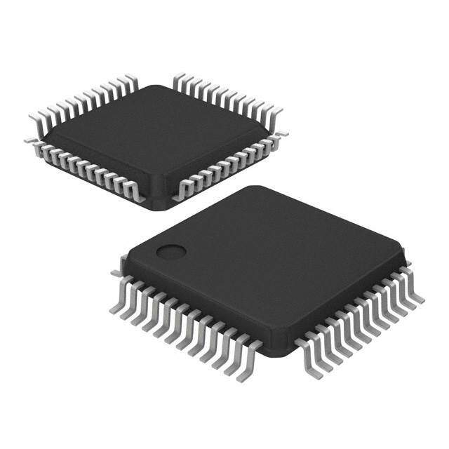
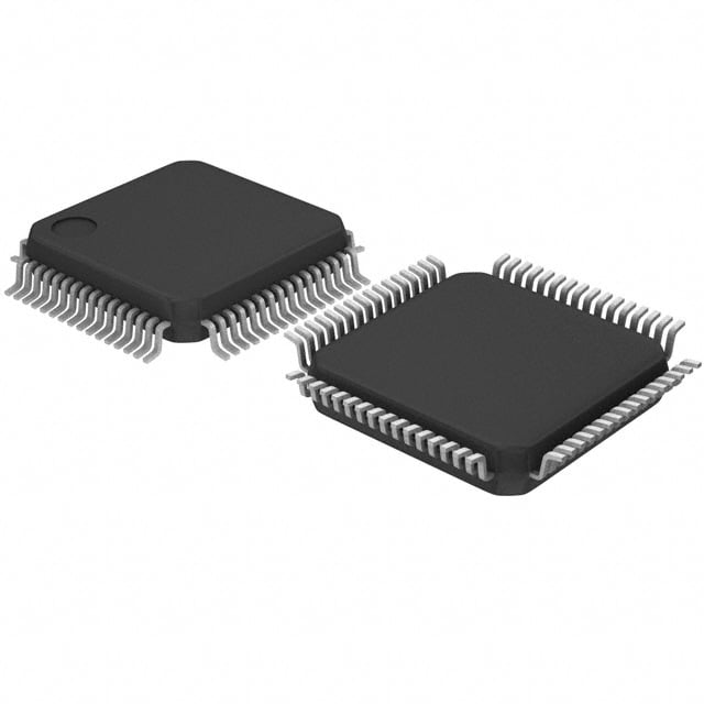
| 供应商器件封装 | 64-LQFP(10x10) |
| 其它名称 | 296-26213 |
| 制造商产品页 | http://www.ti.com/general/docs/suppproductinfo.tsp?distId=10&orderablePartNumber=MSP430F235TPM |
| 包装 | 托盘 |
| 单位重量 | 342.700 mg |
| 可用A/D通道 | 8 |
| 可编程输入/输出端数量 | 48 |
| 商标 | Texas Instruments |
| 商标名 | MSP430 |
| 处理器系列 | 2 Series |
| 外设 | 欠压检测/复位,POR,PWM,WDT |
| 安装风格 | SMD/SMT |
| 定时器数量 | 3 Timer |
| 封装 | Tube |
| 封装/外壳 | 64-LQFP |
| 封装/箱体 | LQFP-64 |
| 工作温度 | -40°C ~ 105°C |
| 工作电源电压 | 1.8 V to 3.6 V |
| 工厂包装数量 | 160 |
| 振荡器类型 | 内部 |
| 接口类型 | USCI (UART, IrDA, LIN, SPI and I2C, SPI) |
| 数据RAM大小 | 2 kB |
| 数据总线宽度 | 16 bit |
| 数据转换器 | A/D 8x12b |
| 最大工作温度 | + 105 C |
| 最大时钟频率 | 16 MHz |
| 最小工作温度 | - 40 C |
| 标准包装 | 160 |
| 核心 | MSP430 |
| 核心处理器 | MSP430 |
| 核心尺寸 | 16-位 |
| 片上ADC | Yes |
| 电压-电源(Vcc/Vdd) | 1.8 V ~ 3.6 V |
| 程序存储器大小 | 16 kB |
| 程序存储器类型 | 闪存 |
| 程序存储容量 | 16KB(16K x 8 + 256B) |
| 系列 | MSP430F235 |
| 输入/输出端数量 | 48 I/O |
| 连接性 | I²C, IrDA, LIN, SCI, SPI, UART/USART |
| 速度 | 16MHz |


- 商务部:美国ITC正式对集成电路等产品启动337调查
- 曝三星4nm工艺存在良率问题 高通将骁龙8 Gen1或转产台积电
- 太阳诱电将投资9.5亿元在常州建新厂生产MLCC 预计2023年完工
- 英特尔发布欧洲新工厂建设计划 深化IDM 2.0 战略
- 台积电先进制程称霸业界 有大客户加持明年业绩稳了
- 达到5530亿美元!SIA预计今年全球半导体销售额将创下新高
- 英特尔拟将自动驾驶子公司Mobileye上市 估值或超500亿美元
- 三星加码芯片和SET,合并消费电子和移动部门,撤换高东真等 CEO
- 三星电子宣布重大人事变动 还合并消费电子和移动部门
- 海关总署:前11个月进口集成电路产品价值2.52万亿元 增长14.8%


PDF Datasheet 数据手册内容提取
MSP430F23x MSP430F24x(1) MSP430F2410 www.ti.com SLAS547I–JUNE2007–REVISEDDECEMBER2012 MIXED SIGNAL MICROCONTROLLER FEATURES 1 • LowSupply-VoltageRange,1.8Vto3.6V • On-ChipComparator 23 • Ultra-LowPowerConsumption • SupplyVoltageSupervisor/MonitorWith – ActiveMode:270µAat1MHz,2.2V ProgrammableLevelDetection – StandbyMode(VLO):0.3µA • BrownoutDetector – OffMode(RAMRetention):0.1µA • BootstrapLoader • Ultra-FastWake-UpFromStandbyModein • SerialOnboardProgramming,NoExternal LessThan1µs ProgrammingVoltageNeeded,Programmable CodeProtectionbySecurityFuse • 16-BitRISCArchitecture,62.5-nsInstruction CycleTime • FamilyMembersInclude: • BasicClockModuleConfigurations: – MSP430F233 – InternalFrequenciesupto16MHz – 8KB+256BFlashMemory, – InternalVeryLow-PowerLFOscillator – 1KBRAM – 32-kHzCrystal – MSP430F235 – InternalFrequenciesupto16MHzWith – 16KB+256BFlashMemory FourCalibratedFrequenciesto±1% – 2KBRAM – Resonator – MSP430F247,MSP430F2471 (1) – ExternalDigitalClockSource – 32KB+256BFlashMemory – ExternalResistor – 4KBRAM • 12-BitAnalog-to-Digital(A/D)ConverterWith – MSP430F248,MSP430F2481 InternalReference,Sample-and-Hold,and – 48KB+256BFlashMemory AutoscanFeature – 4KBRAM • 16-BitTimer_AWithThreeCapture/Compare – MSP430F249,MSP430F2491 Registers – 60KB+256BFlashMemory • 16-BitTimer_BWithSevenCapture/Compare – 2KBRAM WithShadowRegisters – MSP430F2410 • FourUniversalSerialCommunication Interfaces(USCI) – 56KB+256BFlashMemory – USCI_A0andUSCI_A1 – 4KBRAM – EnhancedUARTSupportingAuto-Baudrate • Availablein64-PinQFPand64-PinQFN Detection Packages(SeeAvailableOptions) – IrDAEncoderandDecoder • ForCompleteModuleDescriptions,See MSP430x2xxFamilyUser’sGuide(SLAU144) – SynchronousSPI – USCI_B0andUSCI_B1 – I2C™ (1) TheMSP430F24x1devicesareidenticaltotheMSP430F24x devices,withtheexceptionthattheADC12moduleisnot – SynchronousSPI implementedontheMSP430F24x1. 1 Pleasebeawarethatanimportantnoticeconcerningavailability,standardwarranty,anduseincriticalapplicationsof TexasInstrumentssemiconductorproductsanddisclaimerstheretoappearsattheendofthisdatasheet. MSP430isatrademarkofTexasInstruments. 2 Allothertrademarksarethepropertyoftheirrespectiveowners. 3 PRODUCTIONDATAinformationiscurrentasofpublicationdate. Copyright©2007–2012,TexasInstrumentsIncorporated Products conform to specifications per the terms of the Texas Instruments standard warranty. Production processing does not necessarilyincludetestingofallparameters.
MSP430F23x MSP430F24x(1) MSP430F2410 SLAS547I–JUNE2007–REVISEDDECEMBER2012 www.ti.com This integrated circuit can be damaged by ESD. Texas Instruments recommends that all integrated circuits be handled with appropriateprecautions.Failuretoobserveproperhandlingandinstallationprocedurescancausedamage. ESDdamagecanrangefromsubtleperformancedegradationtocompletedevicefailure.Precisionintegratedcircuitsmaybemore susceptibletodamagebecauseverysmallparametricchangescouldcausethedevicenottomeetitspublishedspecifications. DESCRIPTION TheTexasInstrumentsMSP430™familyofultra-lowpowermicrocontrollersconsistsofseveraldevicesfeaturing different sets of peripherals targeted for various applications. The architecture, combined with five low-power modes,isoptimizedtoachieveextendedbatterylifeinportablemeasurementapplications.Thedevicefeaturesa powerful 16-bit RISC CPU, 16-bit registers, and constant generators that contribute to maximum code efficiency. The calibrated digitally controlled oscillator (DCO) allows wake-up from low-power modes to active mode in less than1µs. The MSP430F23x, MSP430F24x(1), and MSP430F2410 series are microcontroller configurations with two built- in 16-bit timers, a fast 12-bit A/D converter (not MSP430F24x1), a comparator, four (two in MSP430F23x) universal serial communication interface (USCI) modules, and up to 48 I/O pins. The MSP430F24x1 devices are identical to the MSP430F24x devices, with the exception that the ADC12 module is not implemented. The MSP430F23x devices are identical to the MSP430F24x devices, with the exception that a reduced Timer_B, one USCImodule,andlessRAMareintegrated. Typicalapplicationsincludesensorsystems,industrialcontrolapplications,andhand-heldmeters. Table1.AvailableOptions PACKAGEDDEVICES(1)(2) T A PLASTIC64-PINQFP(PM) PLASTIC64-PINQFN(RGC) MSP430F233TPM MSP430F233TRGC MSP430F235TPM MSP430F235TRGC MSP430F247TPM MSP430F247TRGC MSP430F2471TPM MSP430F2471TRGC -40°Cto105°C MSP430F248TPM MSP430F248TRGC MSP430F2481TPM MSP430F2481TRGC MSP430F249TPM MSP430F249TRGC MSP430F2491TPM MSP430F2491TRGC MSP430F2410TPM MSP430F2410TRGC (1) Forthemostcurrentpackageandorderinginformation,seethePackageOptionAddendumattheend ofthisdocument,orseetheTIwebsiteatwww.ti.com. (2) Packagedrawings,thermaldata,andsymbolizationareavailableatwww.ti.com/packaging. Development Tool Support All MSP430 microcontrollers include an Embedded Emulation Module (EEM) allowing advanced debugging and programmingthrougheasytousedevelopmenttools.Recommendedhardwareoptionsincludethefollowing: • DebuggingandProgrammingInterface – MSP-FET430UIF(USB) – MSP-FET430PIF(ParallelPort) • DebuggingandProgrammingInterfacewithTargetBoard – MSP-FET430U64(PMpackage) • StandaloneTargetBoard – MSP-TS430PM64(PMpackage) • ProductionProgrammer – MSP-GANG430 2 SubmitDocumentationFeedback Copyright©2007–2012,TexasInstrumentsIncorporated
MSP430F23x MSP430F24x(1) MSP430F2410 www.ti.com SLAS547I–JUNE2007–REVISEDDECEMBER2012 Device Pinout, MSP430F23x PM OR RGC PACKAGE T U (TOPVIEW) O S V S H/ T K U K L VCCVSSVSS6.2/A2 6.1/A1 6.0/A0 ST/NMICK MS DI/TCLK DO/TDI T2IN T2OUT 5.7/TBO 5.6/ACL 5.5/SMC A D A P P P RT T T T X X P P P 64 63 62 6160 59 58 57 56 55 54 53 52 5150 49 DV 1 48 P5.4/MCLK CC P6.3/A3 2 47 P5.3 P6.4/A4 3 46 P5.2 P6.5/A5 4 45 P5.1 P6.6/A6 5 44 P5.0 P6.7/A7/SVSIN 6 43 P4.7/TBCLK V 7 42 P4.6 REF+ XIN 8 41 P4.5 MSP430F23x XOUT 9 40 P4.4 Ve 10 39 P4.3 REF+ V /Ve 11 38 P4.2/TB2 REF- REF- P1.0/TACLK/CAOUT 12 37 P4.1/TB1 P1.1/TA0 13 36 P4.0/TB0 P1.2/TA1 14 35 P3.7 P1.3/TA2 15 34 P3.6 P1.4/SMCLK 16 33 P3.5/UCA0RXD/UCA0SOMI 17 18 19 20 2122 23 24 25 26 27 28 29 30 3132 0 1 2 2 3 4 1 2 5 6 7 KA L E O P1.5/TA P1.6/TA P1.7/TA P2.0/ACLK/CA P2.1/TAINCLK/CA P2.2/CAOUT/TA0/CA P2.3/CA0/TA P2.4/CA1/TA P2.5/R/CAOSCP2.6/ADC12CLK/CA P2.7/TA0/CA P3.0/UCB0STE/UCA0CL3.1/UCB0SIMO/UCB0SD 3.2/UCB0SOMI/UCB0SC P3.3/UCB0CLK/UCA0ST 3.4/UCA0TXD/UCA0SIM P P P Copyright©2007–2012,TexasInstrumentsIncorporated SubmitDocumentationFeedback 3
MSP430F23x MSP430F24x(1) MSP430F2410 SLAS547I–JUNE2007–REVISEDDECEMBER2012 www.ti.com Device Pinout, MSP430F24x, MSP430F2410 PM OR RGC PACKAGE T U (TOPVIEW) O S V S H/ T K U K L VCCVSSVSS6.2/A2 6.1/A1 6.0/A0 ST/NMICK MS DI/TCLK DO/TDI T2IN T2OUT 5.7/TBO 5.6/ACL 5.5/SMC A D A P P P RT T T T X X P P P 64 63 62 6160 59 58 57 56 55 54 53 52 5150 49 DV 1 48 P5.4/MCLK CC P6.3/A3 2 47 P5.3/UCB1CLK/UCA1STE P6.4/A4 3 46 P5.2/UCB1SOMI/UCB1SCL P6.5/A5 4 45 P5.1/UCB1SIMO/UCB1SDA P6.6/A6 5 44 P5.0/UCB1STE/UCA1CLK P6.7/A7/SVSIN 6 43 P4.7/TBCLK V 7 42 P4.6/TB6 REF+ XIN 8 41 P4.5/TB5 MSP430F2410, XOUT 9 MSP430F24x 40 P4.4/TB4 Ve 10 39 P4.3/TB3 REF+ V /Ve 11 38 P4.2/TB2 REF- REF- P1.0/TACLK/CAOUT 12 37 P4.1/TB1 P1.1/TA0 13 36 P4.0/TB0 P1.2/TA1 14 35 P3.7/UCA1RXD/UCA1SOMI P1.3/TA2 15 34 P3.6/UCA1TXD/UCA1SIMO P1.4/SMCLK 16 33 P3.5/UCA0RXD/UCA0SOMI 17 18 19 20 2122 23 24 25 26 27 28 29 30 3132 0 1 2 2 3 4 1 2 5 6 7 KA L E O P1.5/TA P1.6/TA P1.7/TA P2.0/ACLK/CA P2.1/TAINCLK/CA P2.2/CAOUT/TA0/CA P2.3/CA0/TA P2.4/CA1/TA P2.5/R/CAOSCP2.6/ADC12CLK/CA P2.7/TA0/CA P3.0/UCB0STE/UCA0CL3.1/UCB0SIMO/UCB0SD 3.2/UCB0SOMI/UCB0SC P3.3/UCB0CLK/UCA0ST 3.4/UCA0TXD/UCA0SIM P P P 4 SubmitDocumentationFeedback Copyright©2007–2012,TexasInstrumentsIncorporated
MSP430F23x MSP430F24x(1) MSP430F2410 www.ti.com SLAS547I–JUNE2007–REVISEDDECEMBER2012 Device Pinout, MSP430F24x1 PM OR RGC PACKAGE T U (TOPVIEW) O S V S H/ T K U K L VCCVSSVSS6.2 6.16.0 ST/NMICK MS DI/TCLK DO/TDI T2IN T2OUT 5.7/TBO 5.6/ACL 5.5/SMC A D A P PP RT T T T X X P P P 64 63 62 6160 59 58 57 56 55 54 53 52 5150 49 DV 1 48 P5.4/MCLK CC P6.3 2 47 P5.3/UCB1CLK/UCA1STE P6.4 3 46 P5.2/UCB1SOMI/UCB1SCL P6.5 4 45 P5.1/UCB1SIMO/UCB1SDA P6.6 5 44 P5.0/UCB1STE/UCA1CLK P6.7/A7/SVSIN 6 43 P4.7/TBCLK V 7 42 P4.6/TB6 REF+ XIN 8 41 P4.5/TB5 MSP430F24x1 XOUT 9 40 P4.4/TB4 DV 10 39 P4.3/TB3 SS DV 11 38 P4.2/TB2 SS P1.0/TACLK/CAOUT 12 37 P4.1/TB1 P1.1/TA0 13 36 P4.0/TB0 P1.2/TA1 14 35 P3.7/UCA1RXD/UCA1SOMI P1.3/TA2 15 34 P3.6/UCA1TXD/UCA1SIMO P1.4/SMCLK 16 33 P3.5/UCA0RXD/UCA0SOMI 17 18 19 20 2122 23 24 25 26 27 28 29 30 3132 0 1 2 2 3 4 1 2 5 6 7 KA L E O P1.5/TA P1.6/TA P1.7/TA P2.0/ACLK/CA P2.1/TAINCLK/CA P2.2/CAOUT/TA0/CA P2.3/CA0/TA P2.4/CA1/TA P2.5/R/CAOSCP2.6/ADC12CLK/CA P2.7/TA0/CA P3.0/UCB0STE/UCA0CL3.1/UCB0SIMO/UCB0SD 3.2/UCB0SOMI/UCB0SC P3.3/UCB0CLK/UCA0ST 3.4/UCA0TXD/UCA0SIM P P P Copyright©2007–2012,TexasInstrumentsIncorporated SubmitDocumentationFeedback 5
MSP430F23x MSP430F24x(1) MSP430F2410 SLAS547I–JUNE2007–REVISEDDECEMBER2012 www.ti.com Functional Block Diagram, MSP430F23x XIN/ XOUT/ P3.x/P4.x XT2IN XT2OUT DVCC DVSS AVCC AVSS P1.x/P2.x P5.x/P6.x 2 2 2x8 4x8 ACLK Oscillators Ports Ports BSasyisct eCmlo+ck SMCLK Flash RAM A1D2C-B1it2 P1/P2 PP35//PP46 16kB 2kB 2x8 I/O 8kB 1kB 8 Interrupt 4x8 I/O MCLK Channels capability MAB 16MHz CPU incl. 16 MDB Registers Emulation Hardware Timer_B3 USCIA0 Multiplier Watchdog Timer_A3 UART/LIN, JTAG BOR MPY, WDT+ 3 CC IrDA, SPI Interface SVS/SVM MPYS, 3 CC Registers, Comp_A+ MAC, 15/16-Bit Registers Shadow USCI B0 Reg SPI, I2C MACS RST/NMI 6 SubmitDocumentationFeedback Copyright©2007–2012,TexasInstrumentsIncorporated
MSP430F23x MSP430F24x(1) MSP430F2410 www.ti.com SLAS547I–JUNE2007–REVISEDDECEMBER2012 Functional Block Diagram, MSP430F24x, MSP430F2410 XIN/ XOUT/ P3.x/P4.x XT2IN XT2OUT DVCC DVSS AVCC AVSS P1.x/P2.x P5.x/P6.x 2 2 2x8 4x8 ACLK BOasscicil laCtloorcsk SMCLK F6l0aksBh R2AkBM A1D2C-B1it2 PP1o/rPts2 PP3o/rPts4 System+ 56kB 4kB 2x8 I/O P5/P6 MCLK 4382kkBB 44kkBB Chan8nels cIanptearbruilpityt 4x8 I/O MAB 16MHz CPU incl. 16 MDB Registers Emulation Hardware Timer_B7 USCIA0 USCIA1 Multiplier Watchdog Timer_A3 UART/LIN, UART/LIN, JTAG BOR MPY, WDT+ 7 CC IrDA, SPI IrDA, SPI Interface SVS/SVM MPYS, 3 CC Registers, Comp_A+ MAC, 15/16-Bit Registers Shadow USCI B0 USCI B1 Reg SPI, I2C SPI, I2C MACS RST/NMI Copyright©2007–2012,TexasInstrumentsIncorporated SubmitDocumentationFeedback 7
MSP430F23x MSP430F24x(1) MSP430F2410 SLAS547I–JUNE2007–REVISEDDECEMBER2012 www.ti.com Functional Block Diagram, MSP430F24x1 XIN/ XOUT/ P3.x/P4.x XT2IN XT2OUT DVCC DVSS AVCC AVSS P1.x/P2.x P5.x/P6.x 2 2 2x8 4x8 ACLK Oscillators Flash RAM Ports Ports Basic Clock SMCLK P1/P2 P3/P4 System+ 60kB 2kB P5/P6 48kB 4kB 2x8 I/O 32kB 4kB Interrupt 4x8 I/O MCLK capability MAB 16MHz CPU incl. 16 MDB Registers Emulation Hardware Timer_B7 USCIA0 USCIA1 Multiplier Watchdog Timer_A3 UART/LIN, UART/LIN, JTAG BOR MPY, WDT+ 7 CC IrDA, SPI IrDA, SPI Interface SVS/SVM MPYS, 3 CC Registers, Comp_A+ MAC, 15/16-Bit Registers Shadow USCI B0 USCI B1 Reg SPI, I2C SPI, I2C MACS RST/NMI 8 SubmitDocumentationFeedback Copyright©2007–2012,TexasInstrumentsIncorporated
MSP430F23x MSP430F24x(1) MSP430F2410 www.ti.com SLAS547I–JUNE2007–REVISEDDECEMBER2012 Table2.TerminalFunctions,MSP430F23x TERMINAL I/O DESCRIPTION NAME NO. AVCC 64 Analogsupplyvoltage,positive.SuppliesonlytheanalogportionofADC12. AVSS 62 Analogsupplyvoltage,negative.SuppliesonlytheanalogportionofADC12. DVCC 1 Digitalsupplyvoltage,positive.Suppliesalldigitalparts. DVSS 63 Digitalsupplyvoltage,negative.Suppliesalldigitalparts. P1.0/TACLK/CAOUT 12 I/O General-purposedigitalI/O/Timer_A,clocksignalTACLKinput/Comparator_Aoutput P1.1/TA0 13 I/O General-purposedigitalI/O/Timer_A,capture:CCI0Ainput,compare:Out0output/BSLtransmit P1.2/TA1 14 I/O General-purposedigitalI/O/Timer_A,capture:CCI1Ainput,compare:Out1output P1.3/TA2 15 I/O General-purposedigitalI/O/Timer_A,capture:CCI2Ainput,compare:Out2output P1.4/SMCLK 16 I/O General-purposedigitalI/O/SMCLKsignaloutput P1.5/TA0 17 I/O General-purposedigitalI/O/Timer_A,compare:Out0output P1.6/TA1 18 I/O General-purposedigitalI/O/Timer_A,compare:Out1output P1.7/TA2 19 I/O General-purposedigitalI/O/Timer_A,compare:Out2output P2.0/ACLK/CA2 20 I/O General-purposedigitalI/O/ACLKoutput/Comparator_Ainput P2.1/TAINCLK/CA3 21 I/O General-purposedigitalI/O/Timer_A,clocksignalatINCLK General-purposedigitalI/O/Timer_A,capture:CCI0Binput/Comparator_Aoutput/BSL P2.2/CAOUT/TA0/CA4 22 I/O receive/Comparator_Ainput P2.3/CA0/TA1 23 I/O General-purposedigitalI/O/Timer_A,compare:Out1output/Comparator_Ainput P2.4/CA1/TA2 24 I/O General-purposedigitalI/O/Timer_A,compare:Out2output/Comparator_Ainput General-purposedigitalI/O/inputforexternalresistordefiningtheDCOnominalfrequency/Comparator_A P2.5/ROSC/CA5 25 I/O input P2.6/ADC12CLK/CA6 26 I/O General-purposedigitalI/O/conversionclock-12-bitADC/Comparator_Ainput P2.7/TA0/CA7 27 I/O General-purposedigitalI/O/Timer_A,compare:Out0output/Comparator_Ainput P3.0/UCB0STE/UCA0CLK 28 I/O General-purposedigitalI/O/USCI_B0slavetransmitenable/USCIA0clockinput/output P3.1/UCB0SIMO/UCB0SDA 29 I/O General-purposedigitalI/O/USCI_B0slavein/masteroutinSPImode,SDAI2CdatainI2Cmode P3.2/UCB0SOMI/UCB0SCL 30 I/O General-purposedigitalI/O/USCI_B0slaveout/masterininSPImode,SCLI2CclockinI2Cmode P3.3/UCB0CLK/UCA0STE 31 I/O General-purposedigitalI/O/USCI_B0clockinput/output,USCIA0slavetransmitenable General-purposedigitalI/O/USCI_A0transmitdataoutputinUARTmode,slavedatain/masteroutinSPI P3.4/UCA0TXD/UCA0SIMO 32 I/O mode P3.5/UCA0RXD/ General-purposedigitalI/O/USCI_A0receivedatainputinUARTmode,slavedataout/masterininSPI 33 I/O UCA0SOMI mode P3.6 34 I/O General-purposedigitalI/O P3.7 35 I/O General-purposedigitalI/O P4.0/TB0 36 I/O General-purposedigitalI/O/Timer_B,capture:CCI0A/Binput,compare:Out0output P4.1/TB1 37 I/O General-purposedigitalI/O/Timer_B,capture:CCI1A/Binput,compare:Out1output P4.2/TB2 38 I/O General-purposedigitalI/O/Timer_B,capture:CCI2A/Binput,compare:Out2output P4.3 39 I/O General-purposedigitalI/O P4.4 40 I/O General-purposedigitalI/O P4.5 41 I/O General-purposedigitalI/O P4.6 42 I/O General-purposedigitalI/O P4.7/TBCLK 43 I/O General-purposedigitalI/O/Timer_B,clocksignalTBCLKinput P5.0 44 I/O General-purposedigitalI/O P5.1 45 I/O General-purposedigitalI/O P5.2 46 I/O General-purposedigitalI/O P5.3 47 I/O General-purposedigitalI/O P5.4/MCLK 48 I/O General-purposedigitalI/O/mainsystemclockMCLKoutput P5.5/SMCLK 49 I/O General-purposedigitalI/O/submainsystemclockSMCLKoutput P5.6/ACLK 50 I/O General-purposedigitalI/O/auxiliaryclockACLKoutput General-purposedigitalI/O/switchallPWMdigitaloutputportstohighimpedance-Timer_BTB0to P5.7/TBOUTH/SVSOUT 51 I/O TB6/SVScomparatoroutput P6.0/A0 59 I/O General-purposedigitalI/O/analoginputA0-12-bitADC P6.1/A1 60 I/O General-purposedigitalI/O/analoginputA1-12-bitADC P6.2/A2 61 I/O General-purposedigitalI/O/analoginputA2-12-bitADC Copyright©2007–2012,TexasInstrumentsIncorporated SubmitDocumentationFeedback 9
MSP430F23x MSP430F24x(1) MSP430F2410 SLAS547I–JUNE2007–REVISEDDECEMBER2012 www.ti.com Table2.TerminalFunctions,MSP430F23x(continued) TERMINAL I/O DESCRIPTION NAME NO. P6.3/A3 2 I/O General-purposedigitalI/O/analoginputA3-12-bitADC P6.4/A4 3 I/O General-purposedigitalI/O/analoginputA4-12-bitADC P6.5/A5 4 I/O General-purposedigitalI/O/analoginputA5-12-bitADC P6.6/A6 5 I/O General-purposedigitalI/O/analoginputA6-12-bitADC P6.7/A7/SVSIN 6 I/O General-purposedigitalI/O/analoginputA7-12-bitADC/SVSinput XT2OUT 52 O OutputterminalofcrystaloscillatorXT2 XT2IN 53 I InputportforcrystaloscillatorXT2 RST/NMI 58 I Resetinput,nonmaskableinterruptinput,orbootstraploaderstart(inflashdevices) TCK 57 I Testclock(JTAG).TCKistheclockinputportfordeviceprogrammingtestandbootstraploaderstart. TDI/TCLK 55 I Testdatainputortestclockinput.ThedeviceprotectionfuseisconnectedtoTDI/TCLK. TDO/TDI 54 I/O Testdataoutput.TDO/TDIdataoutputorprogrammingdatainputterminal. TMS 56 I Testmodeselect.TMSisusedasaninputportfordeviceprogrammingandtest. VeREF+ 10 I Inputforanexternalreferencevoltage VREF+ 7 O OutputofpositiveterminalofthereferencevoltageintheADC12 Negativeterminalforthereferencevoltageforbothsources,theinternalreferencevoltage,oranexternal VREF-/VeREF- 11 I appliedreferencevoltage XIN 8 I InputforcrystaloscillatorXT1.Standardorwatchcrystalscanbeconnected. XOUT 9 O OutputforcrystaloscillatorXT1.Standardorwatchcrystalscanbeconnected. QFNPad NA NA QFNpackagepadconnectiontoDVSSrecommended 10 SubmitDocumentationFeedback Copyright©2007–2012,TexasInstrumentsIncorporated
MSP430F23x MSP430F24x(1) MSP430F2410 www.ti.com SLAS547I–JUNE2007–REVISEDDECEMBER2012 Table3.TerminalFunctions,MSP430F24x,MSP430F2410 TERMINAL I/O DESCRIPTION NAME NO. AVCC 64 Analogsupplyvoltage,positiveterminal.SuppliesonlytheanalogportionofADC12. AVSS 62 Analogsupplyvoltage,negativeterminal.SuppliesonlytheanalogportionofADC12. DVCC 1 Digitalsupplyvoltage,positiveterminal.Suppliesalldigitalparts. DVSS 63 Digitalsupplyvoltage,negativeterminal.Suppliesalldigitalparts. P1.0/TACLK/CAOUT 12 I/O General-purposedigitalI/O/Timer_A,clocksignalTACLKinput/Comparator_Aoutput P1.1/TA0 13 I/O General-purposedigitalI/O/Timer_A,capture:CCI0Ainput,compare:Out0output/BSLtransmit P1.2/TA1 14 I/O General-purposedigitalI/O/Timer_A,capture:CCI1Ainput,compare:Out1output P1.3/TA2 15 I/O General-purposedigitalI/O/Timer_A,capture:CCI2Ainput,compare:Out2output P1.4/SMCLK 16 I/O General-purposedigitalI/O/SMCLKsignaloutput P1.5/TA0 17 I/O General-purposedigitalI/O/Timer_A,compare:Out0output P1.6/TA1 18 I/O General-purposedigitalI/O/Timer_A,compare:Out1output P1.7/TA2 19 I/O General-purposedigitalI/O/Timer_A,compare:Out2output P2.0/ACLK/CA2 20 I/O General-purposedigitalI/O/ACLKoutput/Comparator_Ainput P2.1/TAINCLK/CA3 21 I/O General-purposedigitalI/O/Timer_A,clocksignalatINCLK General-purposedigitalI/O/Timer_A,capture:CCI0Binput/Comparator_Aoutput/BSL P2.2/CAOUT/TA0/CA4 22 I/O receive/Comparator_Ainput P2.3/CA0/TA1 23 I/O General-purposedigitalI/O/Timer_A,compare:Out1output/Comparator_Ainput P2.4/CA1/TA2 24 I/O General-purposedigitalI/O/Timer_A,compare:Out2output/Comparator_Ainput General-purposedigitalI/O/InputforexternalresistordefiningtheDCOnominalfrequency/Comparator_A P2.5/ROSC/CA5 25 I/O input P2.6/ADC12CLK/CA6 26 I/O General-purposedigitalI/O/Conversionclock-12-bitADC/Comparator_Ainput P2.7/TA0/CA7 27 I/O General-purposedigitalI/O/Timer_A,compare:Out0output/Comparator_Ainput P3.0/UCB0STE/UCA0CLK 28 I/O General-purposedigitalI/O/USCI_B0slavetransmitenable/USCIA0clockinput/output P3.1/UCB0SIMO/UCB0SDA 29 I/O General-purposedigitalI/O/USCI_B0slavein/masteroutinSPImode,SDAI2CdatainI2Cmode P3.2/UCB0SOMI/UCB0SCL 30 I/O General-purposedigitalI/O/USCI_B0slaveout/masterininSPImode,SCLI2CclockinI2Cmode P3.3/UCB0CLK/UCA0STE 31 I/O General-purposedigitalI/O/USCI_B0clockinput/output,USCIA0slavetransmitenable General-purposedigitalI/O/USCI_A-transmitdataoutputinUARTmode,slavedatain/masteroutinSPI P3.4/UCA0TXD/UCA0SIMO 32 I/O mode P3.5/UCA0RXD/ General-purposedigitalI/O/USCI_A0receivedatainputinUARTmode,slavedataout/masterininSPI 33 I/O UCA0SOMI mode General-purposedigitalI/O/USCI_A1transmitdataoutputinUARTmode,slavedatain/masteroutinSPI P3.6/UCA1TXD/UCA1SIMO 34 I/O mode P3.7/UCA1RXD/ General-purposedigitalI/O/USCI_A1receivedatainputinUARTmode,slavedataout/masterininSPI 35 I/O UCA1SOMI mode P4.0/TB0 36 I/O General-purposedigitalI/O/Timer_B,capture:CCI0A/Binput,compare:Out0output P4.1/TB1 37 I/O General-purposedigitalI/O/Timer_B,capture:CCI1A/Binput,compare:Out1output P4.2/TB2 38 I/O General-purposedigitalI/O/Timer_B,capture:CCI2A/Binput,compare:Out2output P4.3/TB3 39 I/O General-purposedigitalI/O/Timer_B,capture:CCI3A/Binput,compare:Out3output P4.4/TB4 40 I/O General-purposedigitalI/O/Timer_B,capture:CCI4A/Binput,compare:Out4output P4.5/TB5 41 I/O General-purposedigitalI/O/Timer_B,capture:CCI5A/Binput,compare:Out5output P4.6/TB6 42 I/O General-purposedigitalI/O/Timer_B,capture:CCI6Ainput,compare:Out6output P4.7/TBCLK 43 I/O General-purposedigitalI/O/Timer_B,clocksignalTBCLKinput P5.0/UCB1STE/UCA1CLK 44 I/O General-purposedigitalI/O/USCI_B1slavetransmitenable/USCI_A1clockinput/output P5.1/UCB1SIMO/UCB1SDA 45 I/O General-purposedigitalI/O/USCI_B1slavein/masteroutinSPImode,SDAI2CdatainI2Cmode P5.2/UCB1SOMI/UCB1SCL 46 I/O General-purposedigitalI/O/USCI_B1slaveout/masterininSPImode,SCLI2CclockinI2Cmode P5.3/UCB1CLK/UCA1STE 47 I/O General-purposedigitalI/O/USCI_B1clockinput/output,USCI_A1slavetransmitenable P5.4/MCLK 48 I/O General-purposedigitalI/O/mainsystemclockMCLKoutput P5.5/SMCLK 49 I/O General-purposedigitalI/O/submainsystemclockSMCLKoutput P5.6/ACLK 50 I/O General-purposedigitalI/O/auxiliaryclockACLKoutput General-purposedigitalI/O/switchallPWMdigitaloutputportstohighimpedance-Timer_BTB0to P5.7/TBOUTH/SVSOUT 51 I/O TB6/SVScomparatoroutput P6.0/A0 59 I/O General-purposedigitalI/O/analoginputA0-12-bitADC Copyright©2007–2012,TexasInstrumentsIncorporated SubmitDocumentationFeedback 11
MSP430F23x MSP430F24x(1) MSP430F2410 SLAS547I–JUNE2007–REVISEDDECEMBER2012 www.ti.com Table3.TerminalFunctions,MSP430F24x,MSP430F2410(continued) TERMINAL I/O DESCRIPTION NAME NO. P6.1/A1 60 I/O General-purposedigitalI/O/analoginputA1-12-bitADC P6.2/A2 61 I/O General-purposedigitalI/O/analoginputA2-12-bitADC P6.3/A3 2 I/O General-purposedigitalI/O/analoginputA3-12-bitADC P6.4/A4 3 I/O General-purposedigitalI/O/analoginputA4-12-bitADC P6.5/A5 4 I/O General-purposedigitalI/O/analoginputA5-12-bitADC P6.6/A6 5 I/O General-purposedigitalI/O/analoginputA6-12-bitADC P6.7/A7/SVSIN 6 I/O General-purposedigitalI/O/analoginputA7-12-bitADC/SVSinput XT2OUT 52 O OutputofcrystaloscillatorXT2 XT2IN 53 I InputforcrystaloscillatorXT2 RST/NMI 58 I Resetinput,nonmaskableinterruptinput,orbootstraploaderstart(inflashdevices) TCK 57 I Testclock(JTAG).TCKistheclockinputportfordeviceprogrammingtestandbootstraploaderstart. TDI/TCLK 55 I Testdatainputortestclockinput.ThedeviceprotectionfuseisconnectedtoTDI/TCLK. TDO/TDI 54 I/O Testdataoutput.TDO/TDIdataoutputorprogrammingdatainputterminal. TMS 56 I Testmodeselect.TMSisusedasaninputportfordeviceprogrammingandtest. VeREF+ 10 I Inputforanexternalreferencevoltage VREF+ 7 O PositiveoutputofthereferencevoltageintheADC12 Negativeinputforthereferencevoltageforbothsources,theinternalreferencevoltage,oranexternal VREF-/VeREF- 11 I appliedreferencevoltage XIN 8 I InputforcrystaloscillatorXT1.Standardorwatchcrystalscanbeconnected. XOUT 9 O OutputforcrystaloscillatorXT1.Standardorwatchcrystalscanbeconnected. QFNPad NA NA QFNpackagepadconnectiontoDVSSrecommended(RGCpackageonly) 12 SubmitDocumentationFeedback Copyright©2007–2012,TexasInstrumentsIncorporated
MSP430F23x MSP430F24x(1) MSP430F2410 www.ti.com SLAS547I–JUNE2007–REVISEDDECEMBER2012 Table4.TerminalFunctions,MSP430F24x1 TERMINAL I/O DESCRIPTION NAME NO. AVCC 64 Analogsupplyvoltage,positive.SuppliesonlytheanalogportionofADC12. AVSS 62 Analogsupplyvoltage,negative.SuppliesonlytheanalogportionofADC12. DVCC 1 Digitalsupplyvoltage,positive.Suppliesalldigitalparts. DVSS 63 Digitalsupplyvoltage,negative.Suppliesalldigitalparts. P1.0/TACLK/CAOUT 12 I/O General-purposedigitalI/O/Timer_A,clocksignalTACLKinput/Comparator_Aoutput P1.1/TA0 13 I/O General-purposedigitalI/O/Timer_A,capture:CCI0Ainput,compare:Out0output/BSLtransmit P1.2/TA1 14 I/O General-purposedigitalI/O/Timer_A,capture:CCI1Ainput,compare:Out1output P1.3/TA2 15 I/O General-purposedigitalI/O/Timer_A,capture:CCI2Ainput,compare:Out2output P1.4/SMCLK 16 I/O General-purposedigitalI/O/SMCLKsignaloutput P1.5/TA0 17 I/O General-purposedigitalI/O/Timer_A,compare:Out0output P1.6/TA1 18 I/O General-purposedigitalI/O/Timer_A,compare:Out1output P1.7/TA2 19 I/O General-purposedigitalI/O/Timer_A,compare:Out2output P2.0/ACLK/CA2 20 I/O General-purposedigitalI/O/ACLKoutput/Comparator_Ainput P2.1/TAINCLK/CA3 21 I/O General-purposedigitalI/O/Timer_A,clocksignalatINCLK General-purposedigitalI/O/Timer_A,capture:CCI0Binput/Comparator_Aoutput/BSL P2.2/CAOUT/TA0/CA4 22 I/O receive/Comparator_Ainput P2.3/CA0/TA1 23 I/O General-purposedigitalI/O/Timer_A,compare:Out1output/Comparator_Ainput P2.4/CA1/TA2 24 I/O General-purposedigitalI/O/Timer_A,compare:Out2output/Comparator_Ainput General-purposedigitalI/O/inputforexternalresistordefiningtheDCOnominalfrequency/Comparator_A P2.5/ROSC/CA5 25 I/O input P2.6/ADC12CLK/CA6 26 I/O General-purposedigitalI/O/conversionclock-12-bitADC/Comparator_Ainput P2.7/TA0/CA7 27 I/O General-purposedigitalI/O/Timer_A,compare:Out0output/Comparator_Ainput P3.0/UCB0STE/UCA0CLK 28 I/O General-purposedigitalI/O/USCI_B0slavetransmitenable/USCIA0clockinput/output P3.1/UCB0SIMO/UCB0SDA 29 I/O General-purposedigitalI/O/USCI_B0slavein/masteroutinSPImode,SDAI2CdatainI2Cmode P3.2/UCB0SOMI/UCB0SCL 30 I/O General-purposedigitalI/O/USCI_B0slaveout/masterininSPImode,SCLI2CclockinI2Cmode P3.3/UCB0CLK/UCA0STE 31 I/O General-purposedigitalI/O/USCI_B0clockinput/output,USCIA0slavetransmitenable General-purposedigitalI/O/USCI_A0transmitdataoutputinUARTmode,slavedatain/masteroutinSPI P3.4/UCA0TXD/UCA0SIMO 32 I/O mode P3.5/UCA0RXD/ General-purposedigitalI/O/USCI_A0receivedatainputinUARTmode,slavedataout/masterininSPI 33 I/O UCA0SOMI mode General-purposedigitalI/O/USCI_A1transmitdataoutputinUARTmode,slavedatain/masteroutinSPI P3.6/UCA1TXD/UCA1SIMO 34 I/O mode P3.7/UCA1RXD/ General-purposedigitalI/O/USCI_A1receivedatainputinUARTmode,slavedataout/masterininSPI 35 I/O UCA1SOMI mode P4.0/TB0 36 I/O General-purposedigitalI/O/Timer_B,capture:CCI0A/Binput,compare:Out0output P4.1/TB1 37 I/O General-purposedigitalI/O/Timer_B,capture:CCI1A/Binput,compare:Out1output P4.2/TB2 38 I/O General-purposedigitalI/O/Timer_B,capture:CCI2A/Binput,compare:Out2output P4.3/TB3 39 I/O General-purposedigitalI/O/Timer_B,capture:CCI3A/Binput,compare:Out3output P4.4/TB4 40 I/O General-purposedigitalI/O/Timer_B,capture:CCI4A/Binput,compare:Out4output P4.5/TB5 41 I/O General-purposedigitalI/O/Timer_B,capture:CCI5A/Binput,compare:Out5output P4.6/TB6 42 I/O General-purposedigitalI/O/Timer_B,capture:CCI6Ainput,compare:Out6output P4.7/TBCLK 43 I/O General-purposedigitalI/O/Timer_B,clocksignalTBCLKinput P5.0/UCB1STE/UCA1CLK 44 I/O General-purposedigitalI/O/USCI_B1slavetransmitenable/USCI_A1clockinput/output P5.1/UCB1SIMO/UCB1SDA 45 I/O General-purposedigitalI/O/USCI_B1slavein/masteroutinSPImode,SDAI2CdatainI2Cmode P5.2/UCB1SOMI/UCB1SCL 46 I/O General-purposedigitalI/O/USCI_B1slaveout/masterininSPImode,SCLI2CclockinI2Cmode P5.3/UCB1CLK/UCA1STE 47 I/O General-purposedigitalI/O/USCI_B1clockinput/output,USCI_A1slavetransmitenable P5.4/MCLK 48 I/O General-purposedigitalI/O/mainsystemclockMCLKoutput P5.5/SMCLK 49 I/O General-purposedigitalI/O/submainsystemclockSMCLKoutput P5.6/ACLK 50 I/O General-purposedigitalI/O/auxiliaryclockACLKoutput General-purposedigitalI/O/switchallPWMdigitaloutputportstohighimpedance-Timer_BTB0to P5.7/TBOUTH/SVSOUT 51 I/O TB6/SVScomparatoroutput P6.0 59 I/O General-purposedigitalI/O Copyright©2007–2012,TexasInstrumentsIncorporated SubmitDocumentationFeedback 13
MSP430F23x MSP430F24x(1) MSP430F2410 SLAS547I–JUNE2007–REVISEDDECEMBER2012 www.ti.com Table4.TerminalFunctions,MSP430F24x1(continued) TERMINAL I/O DESCRIPTION NAME NO. P6.1 60 I/O General-purposedigitalI/O P6.2 61 I/O General-purposedigitalI/O P6.3 2 I/O General-purposedigitalI/O P6.4 3 I/O General-purposedigitalI/O P6.5 4 I/O General-purposedigitalI/O P6.6 5 I/O General-purposedigitalI/O P6.7/SVSIN 6 I/O General-purposedigitalI/O/SVSinput XT2OUT 52 O OutputterminalofcrystaloscillatorXT2 XT2IN 53 I InputportforcrystaloscillatorXT2 RST/NMI 58 I Resetinput,nonmaskableinterruptinput,orbootstraploaderstart(inflashdevices). TCK 57 I Testclock(JTAG).TCKistheclockinputfordeviceprogrammingtestandbootstraploaderstart. TDI/TCLK 55 I Testdatainputortestclockinput.ThedeviceprotectionfuseisconnectedtoTDI/TCLK. TDO/TDI 54 I/O Testdataoutput.TDO/TDIdataoutputorprogrammingdatainputterminal. TMS 56 I Testmodeselect.TMSisusedasaninputportfordeviceprogrammingandtest. DVSS 10 I ConnectedtoDVSS Reserved 7 O Reserved,donotconnectexternally DVSS 11 I ConnectedtoDVSS XIN 8 I InputforcrystaloscillatorXT1.Standardorwatchcrystalscanbeconnected. XOUT 9 O OutputforcrystaloscillatorXT1.Standardorwatchcrystalscanbeconnected. QFNPad NA NA QFNpackagepadconnectiontoDVSSrecommended(RGCpackageonly) 14 SubmitDocumentationFeedback Copyright©2007–2012,TexasInstrumentsIncorporated
MSP430F23x MSP430F24x(1) MSP430F2410 www.ti.com SLAS547I–JUNE2007–REVISEDDECEMBER2012 SHORT-FORM DESCRIPTION CPU Program Counter PC/R0 The MSP430 CPU has a 16-bit RISC architecture Stack Pointer SP/R1 that is highly transparent to the application. All operations, other than program-flow instructions, are Status Register SR/CG1/R2 performed as register operations in conjunction with seven addressing modes for source operand and four Constant Generator CG2/R3 addressingmodesfordestinationoperand. General-Purpose Register R4 The CPU is integrated with 16 registers that provide reduced instruction execution time. The register-to- General-Purpose Register R5 register operation execution time is one cycle of the CPUclock. General-Purpose Register R6 Four of the registers, R0 to R3, are dedicated as program counter, stack pointer, status register, and General-Purpose Register R7 constant generator, respectively. The remaining registersaregeneral-purposeregisters. General-Purpose Register R8 Peripherals are connected to the CPU using data, General-Purpose Register R9 address, and control buses, and can be handled with allinstructions. General-Purpose Register R10 Instruction Set General-Purpose Register R11 The instruction set consists of 51 instructions with General-Purpose Register R12 three formats and seven address modes. Each instruction can operate on word and byte data. General-Purpose Register R13 Table 5 shows examples of the three types of instruction formats; Table 6 shows the address General-Purpose Register R14 modes. General-Purpose Register R15 Table5.InstructionWordFormats INSTRUCTIONFORMAT EXAMPLE OPERATION Dualoperands,source-destination ADDR4,R5 R4+R5→R5 Singleoperands,destinationonly CALLR8 PC→(TOS),R8→PC Relativejump,unconditional/conditional JNE Jump-on-equalbit=0 Table6.AddressModeDescriptions ADDRESSMODE S (1) D (2) SYNTAX EXAMPLE OPERATION Register ✓ ✓ MOVRs,Rd MOVR10,R11 R10→R11 Indexed ✓ ✓ MOVX(Rn),Y(Rm) MOV2(R5),6(R6) M(2+R5)→M(6+R6) Symbolic(PCrelative) ✓ ✓ MOVEDE,TONI M(EDE)→M(TONI) Absolute ✓ ✓ MOV&MEM,&TCDAT M(MEM)→M(TCDAT) Indirect ✓ MOV@Rn,Y(Rm) MOV@R10,Tab(R6) M(R10)→M(Tab+R6) M(R10)→R11 Indirectautoincrement ✓ MOV@Rn+,Rm MOV@R10+,R11 R10+2→R10 Immediate ✓ MOV#X,TONI MOV#45,TONI #45→M(TONI) (1) S=source (2) D=destination Copyright©2007–2012,TexasInstrumentsIncorporated SubmitDocumentationFeedback 15
MSP430F23x MSP430F24x(1) MSP430F2410 SLAS547I–JUNE2007–REVISEDDECEMBER2012 www.ti.com Operating Modes The MSP430 has one active mode and five software-selectable low-power modes of operation. An interrupt eventcanwakeupthedevicefromanyofthefivelow-powermodes,servicetherequest,andrestorebacktothe low-powermodeonreturnfromtheinterruptprogram. Thefollowingsixoperatingmodescanbeconfiguredbysoftware: • Activemode(AM) – Allclocksareactive. • Low-powermode0(LPM0) – CPUisdisabled. – ACLKandSMCLKremainactive.MCLKisdisabled. • Low-powermode1(LPM1) – CPUisdisabledACLKandSMCLKremainactive.MCLKisdisabled. – DCOdc-generatorisdisabledifDCOnotusedinactivemode. • Low-powermode2(LPM2) – CPUisdisabled. – MCLKandSMCLKaredisabled. – DCOdc-generatorremainsenabled. – ACLKremainsactive. • Low-powermode3(LPM3) – CPUisdisabled. – MCLKandSMCLKaredisabled. – DCOdc-generatorisdisabled. – ACLKremainsactive. • Low-powermode4(LPM4) – CPUisdisabled. – ACLKisdisabled. – MCLKandSMCLKaredisabled. – DCOdc-generatorisdisabled. – Crystaloscillatorisstopped. 16 SubmitDocumentationFeedback Copyright©2007–2012,TexasInstrumentsIncorporated
MSP430F23x MSP430F24x(1) MSP430F2410 www.ti.com SLAS547I–JUNE2007–REVISEDDECEMBER2012 Interrupt Vector Addresses The interrupt vectors and the power-up starting address are located in the address range 0xFFFF to 0xFFC0. The vector contains the 16-bit address of the appropriate interrupt-handler instruction sequence. If the reset vector (0xFFFE) contains 0xFFFF (for example, if flash is not programmed) the CPU enters LPM4 after power- up. Table7.InterruptVectorAddresses INTERRUPTSOURCE INTERRUPTFLAG SYSTEMINTERRUPT WORDADDRESS PRIORITY Power-up PORIFG Externalreset WDTIFG Watchdog RSTIFG Reset 0xFFFE 31,highest Flashkeyviolation KEYV PCoutofrange(1) (see (2)) NMI NMIIFG (Non)maskable Oscillatorfault OFIFG (Non)maskable 0xFFFC 30 Flashmemoryaccessviolation ACCVIFG(2)(3) (Non)maskable Timer_B7(4) TBCCR0CCIFG(5) Maskable 0xFFFA 29 Timer_B7(4) TBCCR1tToBTIFBGC(C2)R(56) CCIFGs, Maskable 0xFFF8 28 Comparator_A+ CAIFG Maskable 0xFFF6 27 Watchdogtimer+ WDTIFG Maskable 0xFFF4 26 Timer_A3 TACCR0CCIFG(5) Maskable 0xFFF2 25 TACCR1CCIFG Timer_A3 TACCR2CCIFGTAIFG(2)(5) Maskable 0xFFF0 24 USCI_A0/USCI_B0receive UCA0RXIFG,UCB0RXIFG(2)(6) Maskable 0xFFEE 23 USCI_B0I2Cstatus USCI_A0/USCI_B0transmit UCA0TXIFG,UCB0TXIFG(2)(7) Maskable 0xFFEC 22 USCI_B0I2Creceive/transmit ADC12(8) ADC12IFG(2)(5) Maskable 0xFFEA 21 0xFFE8 20 I/OportP2(eightflags) P2IFG.0toP2IFG.7(2)(5) Maskable 0xFFE6 19 I/OportP1(eightflags) P1IFG.0toP1IFG.7(2)(5) Maskable 0xFFE4 18 USCI_A1/USCI_B1receive UCA1RXIFG,UCB1RXIFG(2)(6) Maskable 0xFFE2 17 USCI_B1I2Cstatus USCI_A1/USCI_B1transmit UCA1TXIFG,UCB1TXIFG(2)(7) Maskable 0xFFE0 16 USCI_B1I2Creceive/transmit Reserved(9)(10) Reserved 0xFFDEto0xFFC0 15to0,lowest (1) AresetisgeneratediftheCPUtriestofetchinstructionsfromwithinthemoduleregistermemoryaddressrange(0x0000to0x01FF)or fromwithinunusedaddressrange. (2) Multiplesourceflags (3) (Non)maskable:Theindividualinterrupt-enablebitcandisableaninterruptevent,butthegeneral-interruptenablecannot. (4) Timer_B7inMSP430F24x(1)/MSP430F2410familyhassevenCCRs,Timer_B3inMSP430F23xfamilyhasthreeCCRs.InTimer_B3, thereareonlyinterruptflagsTBCCR0CCIFG,TBCCR1CCIFG,andTBCCR2CCIFG,andtheinterruptenablebitsTBCCTL0CCIE, TBCCTL1CCIE,andTBCCTL2CCIE. (5) Interruptflagsarelocatedinthemodule. (6) InSPImode:UCB0RXIFG.InI2Cmode:UCALIFG,UCNACKIFG,ICSTTIFG,UCSTPIFG. (7) InUART/SPImode:UCB0TXIFG.InI2Cmode:UCB0RXIFG,UCB0TXIFG. (8) ADC12isnotimplementedintheMSP430F24x1family. (9) Theaddress0xFFDEisusedasbootstraploadersecuritykey(BSLSKEY).A0xAA55atthislocationdisablestheBSLcompletely.A zerodisablestheerasureoftheflashifaninvalidpasswordissupplied. (10) Theinterruptvectorsataddresses0xFFDEto0xFFC0arenotusedinthisdeviceandcanbeusedforregularprogramcodeif necessary. Copyright©2007–2012,TexasInstrumentsIncorporated SubmitDocumentationFeedback 17
MSP430F23x MSP430F24x(1) MSP430F2410 SLAS547I–JUNE2007–REVISEDDECEMBER2012 www.ti.com Special Function Registers Mostinterruptenablebitsarecollectedinthelowestaddressspace.Special-functionregisterbitsnotallocatedto afunctionalpurposearenotphysicallypresentinthedevice.Thisarrangementprovidessimplesoftwareaccess. Legend rw Bitcanbereadandwritten. rw-0,1 Bitcanbereadandwritten.ItisResetorSetbyPUC. rw-(0),(1) Bitcanbereadandwritten.ItisResetorSetbyPOR. SFRbitisnotpresentindevice. Table8.InterruptEnable1 Address 7 6 5 4 3 2 1 0 00h ACCVIE NMIIE OFIE WDTIE rw-0 rw-0 rw-0 rw-0 WDTIE Watchdogtimerinterruptenable.Inactiveifwatchdogmodeisselected.Activeifwatchdogtimerisconfiguredininterval timermode. OFIE Oscillatorfaultinterruptenable NMIIE (Non)maskableinterruptenable ACCVIE Flashaccessviolationinterruptenable Table9.InterruptEnable2 Address 7 6 5 4 3 2 1 0 01h UCB0TXIE UCB0RXIE UCA0TXIE UCA0RXIE rw-0 rw-0 rw-0 rw-0 UCA0RXIE USCI_A0receive-interruptenable UCA0TXIE USCI_A0transmit-interruptenable UCB0RXIE USCI_B0receive-interruptenable UCB0TXIE USCI_B0transmit-interruptenable Table10.InterruptFlagRegister1 Address 7 6 5 4 3 2 1 0 02h NMIIFG RSTIFG PORIFG OFIFG WDTIFG rw-0 rw-(0) rw-(1) rw-1 rw-(0) WDTIFG Setonwatchdogtimeroverflow(inwatchdogmode)orsecuritykeyviolation. ResetonV power-uporaresetconditionatRST/NMIpininresetmode. CC OFIFG Flagsetonoscillatorfault RSTIFG Externalresetinterruptflag.SetonaresetconditionatRST/NMIpininresetmode.ResetonV powerup. CC PORIFG Power-onresetinterruptflag.SetonV powerup. CC NMIIFG SetviaRST/NMIpin Table11.InterruptFlagRegister2 Address 7 6 5 4 3 2 1 0 03h UCB0TXIFG UCB0RXIFG UCA0TXIFG UCA0RXIFG rw-1 rw-0 rw-1 rw-0 UCA0RXIFG USCI_A0receive-interruptflag UCA0TXIFG USCI_A0transmit-interruptflag UCB0RXIFG USCI_B0receive-interruptflag UCB0TXIFG USCI_B0transmit-interruptflag 18 SubmitDocumentationFeedback Copyright©2007–2012,TexasInstrumentsIncorporated
MSP430F23x MSP430F24x(1) MSP430F2410 www.ti.com SLAS547I–JUNE2007–REVISEDDECEMBER2012 Memory Organization Table12.MemoryOrganization MSP430F249 MSP430F233 MSP430F235 MSP430F2491 Memory Size 8KB 16KB 60KB Main:interruptvector Flash 0xFFFFto0xFFC0 0xFFFFto0xFFC0 0xFFFFto0xFFC0 Main:codememory Flash 0xFFFFto0xE000 0xFFFFto0xC000 0xFFFFto0x1100 RAM(Total) Size 1KB 2KB 2KB 0x05FFto0x0200 0x09FFto0x0200 0x09FFto0x0200 Informationmemory Size 256Byte 256Byte 256Byte Flash 0x10FFto0x1000 0x10FFto0x1000 0x10FFto0x1000 Bootmemory Size 1KB 1KB 1KB ROM 0x0FFFto0x0C00 0x0FFFto0x0C00 0x0FFFto0x0C00 RAM Size 1KB 2KB 2KB 0x05FFto0x0200 0x09FFto0x0200 0x09FFto0x0200 Peripherals 16bit 0x01FFto0x0100 0x01FFto0x0100 0x01FFto0x0100 8bit 0x00FFto0x0010 0x00FFto0x0010 0x00FFto0x0010 SFR 0x000Fto0x0000 0x000Fto0x0000 0x000Fto0x0000 MSP430F247 MSP430F248 MSP430F2410 MSP430F2471 MSP430F2481 Memory Size 32KB 48KB 56KB Main:interruptvector Flash 0xFFFFto0xFFC0 0xFFFFto0xFFC0 0xFFFFto0xFFC0 Main:codememory Flash 0xFFFFto0x8000 0xFFFFto0x4000 0xFFFFto0x2100 RAM(total) Size 4KB 4KB 4KB 0x20FFto0x1100 0x20FFto0x1100 0x20FFto0x1100 Extended Size 2KB 2KB 2KB 0x20FFto0x1900 0x20FFto0x1900 0x20FFto0x1900 Mirrored Size 2KB 2KB 2KB 0x18FFto0x1100 0x18FFto0x1100 0x18FFto0x1100 Informationmemory Size 256Byte 256Byte 256Byte Flash 0x10FFto0x1000 0x10FFto0x1000 0x10FFto0x1000 Bootmemory Size 1KB 1KB 1KB ROM 0x0FFFto0x0C00 0x0FFFto0x0C00 0x0FFFto0x0C00 RAM(mirroredat Size 2KB 2KB 2KB 0x18FFto0x1100) 0x09FFto0x0200 0x09FFto0x0200 0x09FFto0x0200 Peripherals 16bit 0x01FFto0x0100 0x01FFto0x0100 0x01FFto0x0100 8bit 0x00FFto0x0010 0x00FFto0x0010 0x00FFto0x0010 SFR 0x000Fto0x0000 0x000Fto0x0000 0x000Fto0x0000 Bootstrap Loader (BSL) The MSP430 bootstrap loader (BSL) enables users to program the flash memory or RAM using a UART serial interface. Access to the MSP430 memory via the BSL is protected by user-defined password. For complete description of the features of the BSL and its implementation, see the MSP430 Programming Via the Bootstrap LoaderUser’sGuide(SLAU319). Table13.BSLFunctionPins BSLFUNCTION PM,RGCPACKAGEPINS Datatransmit 13-P1.1 Datareceive 22-P2.2 Flash Memory The flash memory can be programmed via the JTAG port, the bootstrap loader, or in-system by the CPU. The CPUcanperformsingle-byteandsingle-wordwritestotheflashmemory.Featuresoftheflashmemoryinclude: • Flash memory has n segments of main memory and four segments of information memory (A to D) of Copyright©2007–2012,TexasInstrumentsIncorporated SubmitDocumentationFeedback 19
MSP430F23x MSP430F24x(1) MSP430F2410 SLAS547I–JUNE2007–REVISEDDECEMBER2012 www.ti.com 64byteseach.Eachsegmentinmainmemoryis512bytesinsize. • Segments0tonmaybeerasedinonestep,oreachsegmentmaybeindividuallyerased. • SegmentsAtoDcanbeerasedindividually,orasagroupwithsegments0ton. SegmentsAtoDarealsocalledinformationmemory. • Segment A contains calibration data. After reset, segment A is protected against programming and erasing. It can be unlocked, but care should be taken not to erase this segment if the device-specific calibration data is required. 20 SubmitDocumentationFeedback Copyright©2007–2012,TexasInstrumentsIncorporated
MSP430F23x MSP430F24x(1) MSP430F2410 www.ti.com SLAS547I–JUNE2007–REVISEDDECEMBER2012 Peripherals Peripherals are connected to the CPU through data, address, and control buses and can be handled using all instructions.Forcompletemoduledescriptions,seetheMSP430x2xxFamilyUser'sGuide(SLAU144). Oscillator and System Clock The clock system is supported by the basic clock module that includes support for a 32768-Hz watch crystal oscillator,aninternalvery-low-powerlow-frequencyoscillator,aninternaldigitally-controlledoscillator(DCO),and a high-frequency crystal oscillator. The basic clock module is designed to meet the requirements of both low system cost and low power consumption. The internal DCO provides a fast turn-on clock source and stabilizes in lessthan1µs.Thebasicclockmoduleprovidesthefollowingclocksignals: • Auxiliary clock (ACLK), sourced from a 32768-Hz watch crystal, a high-frequency crystal, or the internal very- low-powerLFoscillator. • Mainclock(MCLK),thesystemclockusedbytheCPU. • Sub-Mainclock(SMCLK),thesub-systemclockusedbytheperipheralmodules. Calibration Data Stored in Information Memory Segment A CalibrationdataisstoredfortheDCOandfortheADC12.Itisorganizedinatag-length-value(TLV)structure. Table14.TagsUsedbytheADCCalibrationTags NAME ADDRESS VALUE DESCRIPTION TAG_DCO_30 0x10F6 0x01 DCOfrequencycalibrationatV =3VandT =25°Catcalibration CC A TAG_ADC12_1 0x10DA 0x10 ADC12_1calibrationtag TAG_EMPTY - 0xFE Identifierforemptymemoryareas Table15.LabelsUsedbytheADCCalibrationTags LABEL CONDITIONATCALIBRATION/DESCRIPTION SIZE ADDRESSOFFSET CAL_ADC_25T85 INCHx=0x1010,REF2_5=1,T =85°C word 0x000E A CAL_ADC_25T30 INCHx=0x1010,REF2_5=1,T =30°C word 0x000C A CAL_ADC_25VREF_FACTOR REF2_5=1,T =30°C,I =1.0mA word 0x000A A VREF+ CAL_ADC_15T85 INCHx=0x1010,REF2_5=0,T =85°C word 0x0008 A CAL_ADC_15T30 INCHx=0x1010,REF2_5=0,T =30°C word 0x0006 A CAL_ADC_15VREF_FACTOR REF2_5=0,T =30°C,I =0.5mA word 0x0004 A VREF+ CAL_ADC_OFFSET ExternalVref=1.5V,f =5MHz word 0x0002 ADC12CLK CAL_ADC_GAIN_FACTOR ExternalVref=1.5V,f =5MHz word 0x0000 ADC12CLK CAL_BC1_1MHZ - byte 0x0007 CAL_DCO_1MHZ - byte 0x0006 CAL_BC1_8MHZ - byte 0x0005 CAL_DCO_8MHZ - byte 0x0004 CAL_BC1_12MHZ - byte 0x0003 CAL_DCO_12MHZ - byte 0x0002 CAL_BC1_16MHZ - byte 0x0001 CAL_DCO_16MHZ - byte 0x0000 Brownout, Supply Voltage Supervisor (SVS) The brownout circuit is implemented to provide the proper internal reset signal to the device during power on and power off. The SVS circuitry detects if the supply voltage drops below a user-selectable level and supports both supply voltage supervision (the device is automatically reset) and supply voltage monitoring (SVM, the device is notautomaticallyreset). TheCPUbeginscodeexecutionafterthebrownoutcircuitreleasesthedevicereset.However,V maynothave CC ramped to V at that time. The user must ensure that the default DCO settings are not changed until V CC(min) CC reachesV .Ifdesired,theSVScircuitcanbeusedtodeterminewhenV reachesV . CC(min) CC CC(min) Copyright©2007–2012,TexasInstrumentsIncorporated SubmitDocumentationFeedback 21
MSP430F23x MSP430F24x(1) MSP430F2410 SLAS547I–JUNE2007–REVISEDDECEMBER2012 www.ti.com Digital I/O Thereareuptosix8-bitI/Oportsimplemented—portsP1throughP6: • AllindividualI/Obitsareindependentlyprogrammable. • Anycombinationofinput,output,andinterruptconditionispossible. • Edge-selectableinterruptinputcapabilityforalleightbitsofportP1andP2. • Read/writeaccesstoport-controlregistersissupportedbyallinstructions. • EachI/Ohasanindividuallyprogrammablepullup/pulldownresistor. Watchdog Timer (WDT+) The primary function of the WDT+ module is to perform a controlled system restart after a software problem occurs. If the selected time interval expires, a system reset is generated. If the watchdog function is not needed in an application, the module can be disabled or configured as an interval timer and can generate interrupts at selectedtimeintervals. Hardware Multiplier The multiplication operation is supported by a dedicated peripheral module. The module performs 16x16, 16x8, 8x16, and 8x8 bit operations. The module is capable of supporting signed and unsigned multiplication as well as signed and unsigned multiply and accumulate operations. The result of an operation can be accessed immediately after the operands have been loaded into the peripheral registers. No additional clock cycles are required. Timer_A3 Timer_A3 is a 16-bit timer/counter with three capture/compare registers. Timer_A3 can support multiple capture/compares, PWM outputs, and interval timing. Timer_A3 also has extensive interrupt capabilities. Interrupts may be generated from the counter on overflow conditions and from each of the capture/compare registers. Table16.Timer_A3SignalConnections DEVICEINPUT MODULEINPUT MODULEOUTPUT OUTPUTPIN INPUTPINNUMBER MODULEBLOCK SIGNAL NAME SIGNAL NUMBER 12-P1.0 TACLK TACLK ACLK ACLK Timer NA SMCLK SMCLK 21-P2.1 TAINCLK INCLK 13-P1.1 TA0 CCI0A 13-P1.1 22-P2.2 TA0 CCI0B 17-P1.5 CCR0 TA0 DV GND 27-P2.7 SS DV V CC CC 14-P1.2 TA1 CCI1A 14-P1.2 CAOUT(internal) CCI1B 18-P1.6 CCR1 TA1 DV GND 23-P2.3 SS DV V ADC12(1)(internal) CC CC 15-P1.3 TA2 CCI2A 15-P1.3 ACLK(internal) CCI2B 19-P1.7 CCR2 TA2 DV GND 24-P2.4 SS DV V CC CC (1) NotavailableintheMSP430F24x1devices. 22 SubmitDocumentationFeedback Copyright©2007–2012,TexasInstrumentsIncorporated
MSP430F23x MSP430F24x(1) MSP430F2410 www.ti.com SLAS547I–JUNE2007–REVISEDDECEMBER2012 Timer_B7 (MSP430F24x(1) and MSP430F2410 Devices) Timer_B7 is a 16-bit timer/counter with seven capture/compare registers. Timer_B7 can support multiple capture/compares, PWM outputs, and interval timing. Timer_B7 also has extensive interrupt capabilities. Interrupts may be generated from the counter on overflow conditions and from each of the capture/compare registers. Table17.Timer_B7SignalConnections DEVICEINPUT MODULEINPUT MODULEOUTPUT OUTPUTPIN INPUTPINNUMBER MODULEBLOCK SIGNAL NAME SIGNAL NUMBER 43-P4.7 TBCLK TBCLK ACLK ACLK Timer NA SMCLK SMCLK 43-P4.7 TBCLK INCLK 36-P4.0 TB0 CCI0A 36-P4.0 36-P4.0 TB0 CCI0B ADC12(1)(internal) CCR0 TB0 DV GND SS DV V CC CC 37-P4.1 TB1 CCI1A 37-P4.1 37-P4.1 TB1 CCI1B ADC12(2)(internal) CCR1 TB1 DV GND SS DV V CC CC 38-P4.2 TB2 CCI2A 38-P4.2 38-P4.2 TB2 CCI2B CCR2 TB2 DV GND SS DV V CC CC 39-P4.3 TB3 CCI3A 39-P4.3 39-P4.3 TB3 CCI3B CCR3 TB3 DV GND SS DV V CC CC 40-P4.4 TB4 CCI4A 40-P4.4 40-P4.4 TB4 CCI4B CCR4 TB4 DV GND SS DV V CC CC 41-P4.5 TB5 CCI5A 41-P4.5 41-P4.5 TB5 CCI5B CCR5 TB5 DV GND SS DV V CC CC 42-P4.6 TB6 CCI6A 42-P4.6 ACLK(internal) CCI6B CCR6 TB6 DV GND SS DV V CC CC (1) NotavailableintheMSP430F24x1devices. (2) NotavailableintheMSP430F24x1devices. Copyright©2007–2012,TexasInstrumentsIncorporated SubmitDocumentationFeedback 23
MSP430F23x MSP430F24x(1) MSP430F2410 SLAS547I–JUNE2007–REVISEDDECEMBER2012 www.ti.com Timer_B3 (MSP430F23x Devices) Timer_B3 is a 16-bit timer/counter with three capture/compare registers. Timer_B3 can support multiple capture/compares, PWM outputs, and interval timing. Timer_B3 also has extensive interrupt capabilities. Interrupts may be generated from the counter on overflow conditions and from each of the capture/compare registers. Table18.Timer_B3SignalConnections DEVICEINPUT MODULEINPUT MODULEOUTPUT OUTPUTPIN INPUTPINNUMBER MODULEBLOCK SIGNAL NAME SIGNAL NUMBER 43-P4.7 TBCLK TBCLK ACLK ACLK Timer NA SMCLK SMCLK 43-P4.7 TBCLK INCLK 36-P4.0 TB0 CCI0A 36-P4.0 36-P4.0 TB0 CCI0B ADC12(internal) CCR0 TB0 DV GND SS DV V CC CC 37-P4.1 TB1 CCI1A 37-P4.1 37-P4.1 TB1 CCI1B ADC12(internal) CCR1 TB1 DV GND SS DV V CC CC 38-P4.2 TB2 CCI2A 38-P4.2 38-P4.2 TB2 CCI2B CCR2 TB2 DV GND SS DV V CC CC Universal Serial Communications Interface (USCI) The USCI modules are used for serial data communication. The USCI module supports synchronous communication protocols, such as SPI (3 or 4 pin) or I2C, and asynchronous combination protocols, such as UART,enhancedUARTwithautomaticbaudratedetection(LIN),andIrDA. TheUSCIAmoduleprovidessupportforSPI(3or4pin),UART,enhancedUART,andIrDA. TheUSCIBmoduleprovidessupportforSPI(3or4pin)andI2C. Comparator_A+ The primary function of the comparator_A+ module is to support precision slope analog-to-digital conversions, battery-voltagesupervision,andmonitoringofexternalanalogsignals. ADC12 (MSP430F23x, MSP430F24x, and MSP430F2410 Devices) The ADC12 module supports fast, 12-bit analog-to-digital conversions. The module implements a 12-bit SAR core, sample select control, reference generator, and a 16-word conversion-and-control buffer. The conversion- and-control buffer allows up to 16 independent ADC samples to be converted and stored without any CPU intervention. 24 SubmitDocumentationFeedback Copyright©2007–2012,TexasInstrumentsIncorporated
MSP430F23x MSP430F24x(1) MSP430F2410 www.ti.com SLAS547I–JUNE2007–REVISEDDECEMBER2012 Peripheral File Map Table19.PeripheralFileMap MODULE REGISTERNAME SHORTFORM ADDRESS ADC12 Interrupt-vector-wordregister ADC12IV 0x01A8 (MSP430F24x, Interrupt-enableregister ADC12IE 0x01A6 MSP430F2410,and MSP430F23x) Interrupt-flagregister ADC12IFG 0x01A4 Controlregister1 ADC12CTL1 0x01A2 Controlregister0 ADC12CTL0 0x01A0 Conversionmemory15 ADC12MEM15 0x015E Conversionmemory14 ADC12MEM14 0x015C Conversionmemory13 ADC12MEM13 0x015A Conversionmemory12 ADC12MEM12 0x0158 Conversionmemory11 ADC12MEM11 0x0156 Conversionmemory10 ADC12MEM10 0x0154 Conversionmemory9 ADC12MEM9 0x0152 Conversionmemory8 ADC12MEM8 0x0150 Conversionmemory7 ADC12MEM7 0x014E Conversionmemory6 ADC12MEM6 0x014C Conversionmemory5 ADC12MEM5 0x014A Conversionmemory4 ADC12MEM4 0x0148 Conversionmemory3 ADC12MEM3 0x0146 Conversionmemory2 ADC12MEM2 0x0144 Conversionmemory1 ADC12MEM1 0x0142 Conversionmemory0 ADC12MEM0 0x0140 ADCmemory-controlregister15 ADC12MCTL15 0x008F ADCmemory-controlregister14 ADC12MCTL14 0x008E ADCmemory-controlregister13 ADC12MCTL13 0x008D ADCmemory-controlregister12 ADC12MCTL12 0x008C ADCmemory-controlregister11 ADC12MCTL11 0x008B ADCmemory-controlregister10 ADC12MCTL10 0x008A ADCmemory-controlregister9 ADC12MCTL9 0x0089 ADCmemory-controlregister8 ADC12MCTL8 0x0088 ADCmemory-controlregister7 ADC12MCTL7 0x0087 ADCmemory-controlregister6 ADC12MCTL6 0x0086 ADCmemory-controlregister5 ADC12MCTL5 0x0085 ADCmemory-controlregister4 ADC12MCTL4 0x0084 ADCmemory-controlregister3 ADC12MCTL3 0x0083 ADCmemory-controlregister2 ADC12MCTL2 0x0082 ADCmemory-controlregister1 ADC12MCTL1 0x0081 ADCmemory-controlregister0 ADC12MCTL0 0x0080 Copyright©2007–2012,TexasInstrumentsIncorporated SubmitDocumentationFeedback 25
MSP430F23x MSP430F24x(1) MSP430F2410 SLAS547I–JUNE2007–REVISEDDECEMBER2012 www.ti.com Table19.PeripheralFileMap(continued) MODULE REGISTERNAME SHORTFORM ADDRESS Timer_B7 Capture/compareregister6 TBCCR6 0x019E (MSP430F24x(1)and Capture/compareregister5 TBCCR5 0x019C MSP430F2410) Capture/compareregister4 TBCCR4 0x019A Capture/compareregister3 TBCCR3 0x0198 Capture/compareregister2 TBCCR2 0x0196 Capture/compareregister1 TBCCR1 0x0194 Capture/compareregister0 TBCCR0 0x0192 Timer_Bregister TBR 0x0190 Capture/comparecontrol6 TBCCTL6 0x018E Capture/comparecontrol5 TBCCTL5 0x018C Capture/comparecontrol4 TBCCTL4 0x018A Capture/comparecontrol3 TBCCTL3 0x0188 Capture/comparecontrol2 TBCCTL2 0x0186 Capture/comparecontrol1 TBCCTL1 0x0184 Capture/comparecontrol0 TBCCTL0 0x0182 Timer_Bcontrol TBCTL 0x0180 Timer_Binterruptvector TBIV 0x011E Timer_B3 Capture/compareregister2 TBCCR2 0x0196 (MSP430F23x) Capture/compareregister1 TBCCR1 0x0194 Capture/compareregister0 TBCCR0 0x0192 Timer_Bregister TBR 0x0190 Capture/comparecontrol2 TBCCTL2 0x0186 Capture/comparecontrol1 TBCCTL1 0x0184 Capture/comparecontrol0 TBCCTL0 0x0182 Timer_Bcontrol TBCTL 0x0180 Timer_Binterruptvector TBIV 0x011E Timer_A3 Capture/compareregister2 TACCR2 0x0176 Capture/compareregister1 TACCR1 0x0174 Capture/compareregister0 TACCR0 0x0172 Timer_Aregister TAR 0x0170 Reserved 0x016E Reserved 0x016C Reserved 0x016A Reserved 0x0168 Capture/comparecontrol2 TACCTL2 0x0166 Capture/comparecontrol1 TACCTL1 0x0164 Capture/comparecontrol0 TACCTL0 0x0162 Timer_Acontrol TACTL 0x0160 Timer_Ainterruptvector TAIV 0x012E HardwareMultiplier Sumextend SUMEXT 0x013E Resulthighword RESHI 0x013C Resultlowword RESLO 0x013A Secondoperand OP2 0x0138 Multiplysigned+accumulate/operand1 MACS 0x0136 Multiply+accumulate/operand1 MAC 0x0134 Multiplysigned/operand1 MPYS 0x0132 Multiplyunsigned/operand1 MPY 0x0130 26 SubmitDocumentationFeedback Copyright©2007–2012,TexasInstrumentsIncorporated
MSP430F23x MSP430F24x(1) MSP430F2410 www.ti.com SLAS547I–JUNE2007–REVISEDDECEMBER2012 Table19.PeripheralFileMap(continued) MODULE REGISTERNAME SHORTFORM ADDRESS Flash Flashcontrol4 FCTL4 0x01BE Flashcontrol3 FCTL3 0x012C Flashcontrol2 FCTL2 0x012A Flashcontrol1 FCTL1 0x0128 Watchdog WatchdogTimercontrol WDTCTL 0x0120 USCIA0/B0 USCIA0autobaudratecontrol UCA0ABCTL 0x005D USCIA0transmitbuffer UCA0TXBUF 0x0067 USCIA0receivebuffer UCA0RXBUF 0x0066 USCIA0status UCA0STAT 0x0065 USCIA0modulationcontrol UCA0MCTL 0x0064 USCIA0baudratecontrol1 UCA0BR1 0x0063 USCIA0baudratecontrol0 UCA0BR0 0x0062 USCIA0control1 UCA0CTL1 0x0061 USCIA0control0 UCA0CTL0 0x0060 USCIA0IrDAreceivecontrol UCA0IRRCTL 0x005F USCIA0IrDAtransmitcontrol UCA0IRTCLT 0x005E USCIB0transmitbuffer UCB0TXBUF 0x006F USCIB0receivebuffer UCB0RXBUF 0x006E USCIB0status UCB0STAT 0x006D USCIB0I2CInterruptenable UCB0CIE 0x006C USCIB0baudratecontrol1 UCB0BR1 0x006B USCIB0baudratecontrol0 UCB0BR0 0x006A USCIB0control1 UCB0CTL1 0x0069 USCIB0control0 UCB0CTL0 0x0068 USCIB0I2Cslaveaddress UCB0SA 0x011A USCIB0I2Cownaddress UCB0OA 0x0118 Copyright©2007–2012,TexasInstrumentsIncorporated SubmitDocumentationFeedback 27
MSP430F23x MSP430F24x(1) MSP430F2410 SLAS547I–JUNE2007–REVISEDDECEMBER2012 www.ti.com Table19.PeripheralFileMap(continued) MODULE REGISTERNAME SHORTFORM ADDRESS USCIA1/B1 USCIA1autobaudratecontrol UCA1ABCTL 0x00CD (MSP430F24x(1)and USCIA1transmitbuffer UCA1TXBUF 0x00D7 MSP430F2410) USCIA1receivebuffer UCA1RXBUF 0x00D6 USCIA1status UCA1STAT 0x00D5 USCIA1modulationcontrol UCA1MCTL 0x00D4 USCIA1baudratecontrol1 UCA1BR1 0x00D3 USCIA1baudratecontrol0 UCA1BR0 0x00D2 USCIA1control1 UCA1CTL1 0x00D1 USCIA1control0 UCA1CTL0 0x00D0 USCIA1IrDAreceivecontrol UCA1IRRCTL 0x00CF USCIA1IrDAtransmitcontrol UCA1IRTCLT 0x00CE USCIB1transmitbuffer UCB1TXBUF 0x00DF USCIB1receivebuffer UCB1RXBUF 0x00DE USCIB1status UCB1STAT 0x00DD USCIB1I2CInterruptenable UCB1CIE 0x00DC USCIB1baudratecontrol1 UCB1BR1 0x00DB USCIB1baudratecontrol0 UCB1BR0 0x00DA USCIB1control1 UCB1CTL1 0x00D9 USCIB1control0 UCB1CTL0 0x00D8 USCIB1I2Cslaveaddress UCB1SA 0x017E USCIB1I2Cownaddress UCB1OA 0x017C USCIA1/B1interruptenable UC1IE 0x0006 USCIA1/B1interruptflag UC1IFG 0x0007 Comparator_A+ Comparator_Aportdisable CAPD 0x005B Comparator_Acontrol2 CACTL2 0x005A Comparator_Acontrol1 CACTL1 0x0059 BasicClock Basicclocksystemcontrol3 BCSCTL3 0x0053 Basicclocksystemcontrol2 BCSCTL2 0x0058 Basicclocksystemcontrol1 BCSCTL1 0x0057 DCOclockfrequencycontrol DCOCTL 0x0056 Brownout,SVS SVScontrolregister(resetbybrownoutsignal) SVSCTL 0x0055 PortP6 PortP6resistorenable P6REN 0x0013 PortP6selection P6SEL 0x0037 PortP6direction P6DIR 0x0036 PortP6output P6OUT 0x0035 PortP6input P6IN 0x0034 PortP5 PortP5resistorenable P5REN 0x0012 PortP5selection P5SEL 0x0033 PortP5direction P5DIR 0x0032 PortP5output P5OUT 0x0031 PortP5input P5IN 0x0030 PortP4 PortP4resistorenable P4REN 0x0011 PortP4selection P4SEL 0x001F PortP4direction P4DIR 0x001E PortP4output P4OUT 0x001D PortP4input P4IN 0x001C 28 SubmitDocumentationFeedback Copyright©2007–2012,TexasInstrumentsIncorporated
MSP430F23x MSP430F24x(1) MSP430F2410 www.ti.com SLAS547I–JUNE2007–REVISEDDECEMBER2012 Table19.PeripheralFileMap(continued) MODULE REGISTERNAME SHORTFORM ADDRESS PortP3 PortP3resistorenable P3REN 0x0010 PortP3selection P3SEL 0x001B PortP3direction P3DIR 0x001A PortP3output P3OUT 0x0019 PortP3input P3IN 0x0018 PortP2 PortP2resistorenable P2REN 0x002F PortP2selection P2SEL 0x002E PortP2interruptenable P2IE 0x002D PortP2interrupt-edgeselect P2IES 0x002C PortP2interruptflag P2IFG 0x002B PortP2direction P2DIR 0x002A PortP2output P2OUT 0x0029 PortP2input P2IN 0x0028 PortP1 PortP1resistorenable P1REN 0x0027 PortP1selection P1SEL 0x0026 PortP1interruptenable P1IE 0x0025 PortP1interrupt-edgeselect P1IES 0x0024 PortP1interruptflag P1IFG 0x0023 PortP1direction P1DIR 0x0022 PortP1output P1OUT 0x0021 PortP1input P1IN 0x0020 SpecialFunctions SFRinterruptflag2 IFG2 0x0003 SFRinterruptflag1 IFG1 0x0002 SFRinterruptenable2 IE2 0x0001 SFRinterruptenable1 IE1 0x0000 Copyright©2007–2012,TexasInstrumentsIncorporated SubmitDocumentationFeedback 29
MSP430F23x MSP430F24x(1) MSP430F2410 SLAS547I–JUNE2007–REVISEDDECEMBER2012 www.ti.com Absolute Maximum Ratings(1) VoltageappliedatV toV -0.3Vto4.1V CC SS Voltageappliedtoanypin (2) -0.3VtoV +0.3V CC Diodecurrentatanydeviceterminal ±2mA Unprogrammeddevice -55°Cto150°C Storagetemperature,T (3) stg Programmeddevice -55°Cto150°C (1) Stressesbeyondthoselistedunderabsolutemaximumratingsmaycausepermanentdamagetothedevice.Thesearestressratings only,andfunctionaloperationofthedeviceattheseoranyotherconditionsbeyondthoseindicatedunderrecommendedoperating conditionsisnotimplied.Exposuretoabsolute-maximum-ratedconditionsforextendedperiodsmayaffectdevicereliability. (2) AllvoltagesreferencedtoV .TheJTAGfuse-blowvoltage,V ,isallowedtoexceedtheabsolutemaximumrating.Thevoltageis SS FB appliedtotheTESTpinwhenblowingtheJTAGfuse. (3) HighertemperaturemaybeappliedduringboardsolderingprocessaccordingtothecurrentJEDECJ-STD-020specificationwithpeak reflowtemperaturesnothigherthanclassifiedonthedevicelabelontheshippingboxesorreels. Recommended Operating Conditions(1)(2) TypicalvaluesarespecifiedatV =3.3VandT =25°C(unlessotherwisenoted) CC A MIN NOM MAX UNIT Duringprogram 1.8 3.6 V execution V Supplyvoltage(3) AV =DV =V CC CC CC CC Duringprogramorerase 2.2 3.6 V flashmemory V Supplyvoltage AV =DV =V 0 V SS SS SS SS Iversion -40 85 T Operatingfree-airtemperature °C A Tversion -40 105 V =1.8V,Dutycycle=50%±10% dc 4.15 Processorfrequency CC f (maximumMCLKfrequency)(1)(2) V =2.7V,Dutycycle=50%±10% dc 12 MHz SYSTEM CC (seeFigure1) V ≥3.3V,Dutycycle=50%±10% dc 16 CC (1) TheMSP430CPUisclockeddirectlywithMCLK.BoththehighandlowphaseofMCLKmustnotexceedthepulsedurationofthe specifiedmaximumfrequency. (2) Modulesmighthaveadifferentmaximuminputclockspecification.Seethespecificationoftherespectivemoduleinthisdatasheet. (3) ItisrecommendedtopowerAV andDV fromthesamesource.Amaximumdifferenceof0.3VbetweenAV andDV canbe CC CC CC CC toleratedduringpower-up. Legend: 16MHz Supply voltage range during flash memory Hz programming M − 12MHz y c n Supply voltage range e u during program execution q e Fr 7.5MHz m e st y S 4.15MHz 1.8V 2.2V 2.7V 3.3V 3.6V Supply Voltage−V NOTE: Minimumprocessorfrequencyisdefinedbysystemclock.FlashprogramoreraseoperationsrequireaminimumV CC of2.2V. Figure1. OperatingArea 30 SubmitDocumentationFeedback Copyright©2007–2012,TexasInstrumentsIncorporated
MSP430F23x MSP430F24x(1) MSP430F2410 www.ti.com SLAS547I–JUNE2007–REVISEDDECEMBER2012 Active Mode Supply Current (Into DV and AV ) Excluding External Current(1)(2) CC CC overrecommendedrangesofsupplyvoltageandoperatingfree-airtemperature(unlessotherwisenoted) PARAMETER TESTCONDITIONS T V MIN TYP MAX UNIT A CC f =f =f =1MHz, -40°Cto85°C 275 312 DCO MCLK SMCLK f =32768Hz, 2.2V ACLK 105°C 295 318 Programexecutesinflash, Activemode(AM) I BCSCTL1=CALBC1_1MHZ, -40°Cto85°C 386 445 µA AM,1MHz current(1MHz) DCOCTL=CALDCO_1MHZ, 3V CPUOFF=0,SCG0=0,SCG1=0, 105°C 417 449 OSCOFF=0 f =f =f =1MHz, -40°Cto85°C 230 261 DCO MCLK SMCLK f =32768Hz, 2.2V ACLK 105°C 248 267 ProgramexecutesinRAM, Activemode(AM) I BCSCTL1=CALBC1_1MHZ, -40°Cto85°C 321 366 µA AM,1MHz current(1MHz) DCOCTL=CALDCO_1MHZ, 3.3V CPUOFF=0,SCG0=0,SCG1=0, 105°C 344 370 OSCOFF=0 f =f =f = -40°Cto85°C 1.5 3.8 MCLK SMCLK ACLK 32768Hz/8=4096Hz, 2.2V 105°C 6 10.5 f =0Hz, DCO Activemode(AM) Programexecutesinflash, -40°Cto85°C 2 4.7 I µA AM,4kHz current(4kHz) SELMx=11,SELS=1, DIVMx=DIVSx=DIVAx=11, 3V CPUOFF=0,SCG0=1,SCG1=0, 105°C 7 12.2 OSCOFF=0 f =f =f ≈100kHz, -40°Cto85°C 55 72 MCLK SMCLK DCO(0,0) 2.2V Activemode(AM) fACLK=0Hz, 105°C 70 81 I Programexecutesinflash, µA AM,100kHz current(100kHz) RSELx=0,DCOx=0,CPUOFF=0, -40°Cto85°C 67 89 3V SCG0=0,SCG1=0,OSCOFF=1 105°C 84 100 (1) Allinputsaretiedto0VorV .Outputsdonotsourceorsinkanycurrent. CC (2) ThecurrentsarecharacterizedwithaMicroCrystalCC4V-T1ASMDcrystalwithaloadcapacitanceof9pF.Theinternalandexternal loadcapacitanceischosentocloselymatchtherequired9pF. Copyright©2007–2012,TexasInstrumentsIncorporated SubmitDocumentationFeedback 31
MSP430F23x MSP430F24x(1) MSP430F2410 SLAS547I–JUNE2007–REVISEDDECEMBER2012 www.ti.com Typical Characteristics - Active-Mode Supply Current (Into DV and AV ) CC CC ACTIVE-MODECURRENT vs ACTIVE-MODECURRENT SUPPLYVOLTAGE vs T =25°C DCOFREQUENCY A 8.0 5.0 7.0 fDCO= 16 MHz TA= 85°C 4.0 A 6.0 A TA= 25°C m m − fDCO= 12 MHz − Mode Current 45..00 fDCO= 8 MHz Mode Current 23..00 VCC= 3 V TA= 85°C Active 23..00 Active TA= 25°C 1.0 1.0 fDCO= 1 MHz VCC= 2.2 V 0.0 0.0 1.5 2.0 2.5 3.0 3.5 4.0 0.0 4.0 8.0 12.0 16.0 VCC−Supply Voltage−V fDCO−DCO Frequency−MHz Figure2. Figure3. 32 SubmitDocumentationFeedback Copyright©2007–2012,TexasInstrumentsIncorporated
MSP430F23x MSP430F24x(1) MSP430F2410 www.ti.com SLAS547I–JUNE2007–REVISEDDECEMBER2012 Low-Power-Mode Supply Currents (Into V ) Excluding External Current(1)(2) CC overrecommendedrangesofsupplyvoltageandoperatingfree-airtemperature(unlessotherwisenoted) PARAMETER TESTCONDITIONS T V MIN TYP MAX UNIT A CC f =0MHz, -40°Cto85°C 60 65 MCLK f =f =1MHz, 2.2V SMCLK DCO 105°C 63 72 f =32768Hz, Low-powermode0 ACLK ILPM0,1MHz (LPM0)current(3) BCSCTL1=CALBC1_1MHZ, -40°Cto85°C 75 90 µA DCOCTL=CALDCO_1MHZ, 3V CPUOFF=1,SCG0=0,SCG1=0, 105°C 80 95 OSCOFF=0 f =0MHz, -40°Cto85°C 33 38 MCLK f =f ≈100kHz, 2.2V SMCLK DCO(0,0) 105°C 36 43 Low-powermode0 f =0Hz, ILPM0,100kHz (LPM0)current(3) RASCLEKLx=0,DCOx=0, -40°Cto85°C 36 42 µA CPUOFF=1,SCG0=0,SCG1=0, 3V OSCOFF=1 105°C 40 47 f =f =0MHz, -40°Cto85°C 20 25 MCLK SMCLK f =1MHz, 2.2V DCO 105°C 25 30 f =32768Hz, Low-powermode2 ACLK ILPM2 (LPM2)current(4) BCSCTL1=CALBC1_1MHZ, -40°Cto85°C 23 30 µA DCOCTL=CALDCO_1MHZ, 3V CPUOFF=1,SCG0=0,SCG1=1, 105°C 28 35 OSCOFF=0 -40°C 0.8 1.2 25°C 0.9 1.3 2.2V 85°C 2.4 3 f =f =f =0MHz, DCO MCLK SMCLK Low-powermode3 f =32768Hz, 105°C 6 13 ILPM3,LFXT1 (LPM3)current(4) CAPCLUKOFF=1,SCG0=1,SCG1=1, -40°C 0.9 1.3 µA OSCOFF=0 25°C 1 1.4 3V 85°C 3.9 4.3 105°C 10 15 -40°C 0.3 0.9 25°C 0.3 0.9 2.2V f =f =f =0MHz, 85°C 1.8 2.4 DCO MCLK SMCLK Low-powermode3 fACLKfrominternalLFoscillator 105°C 5.5 13 ILPM3,VLO current,(LPM3)(4) (CVPLUOO),FF=1,SCG0=1,SCG1=1, -40°C 0.4 1 µA OSCOFF=0 25°C 0.4 1 3V 85°C 2 3 105°C 9 15 -40°C 0.1 0.5 f =f =f =0MHz, DCO MCLK SMCLK Low-powermode4 f =0Hz, 25°C 0.1 0.5 ILPM4 (LPM4)current(5) CAPCLUKOFF=1,SCG0=1,SCG1=1, 85°C 2.2V,3V 1.6 2.5 µA OSCOFF=1 105°C 6.5 13 (1) Allinputsaretiedto0VorV .Outputsdonotsourceorsinkanycurrent. CC (2) ThecurrentsarecharacterizedwithaMicroCrystalCC4V-T1ASMDcrystalwithaloadcapacitanceof9pF.Theinternalandexternal loadcapacitanceischosentocloselymatchtherequired9pF. (3) CurrentforBrownoutandWDT+isincluded.TheWDT+isclockedbySMCLK. (4) CurrentforBrownoutandWDT+isincluded.TheWDT+isclockedbyACLK. (5) CurrentforBrownoutisincluded. Copyright©2007–2012,TexasInstrumentsIncorporated SubmitDocumentationFeedback 33
MSP430F23x MSP430F24x(1) MSP430F2410 SLAS547I–JUNE2007–REVISEDDECEMBER2012 www.ti.com Typical Characteristics - LPM4 Current LPM4CURRENT vs TEMPERATURE 10.0 A 9.0 µ − nt 8.0 e urr 7.0 c e d o 6.0 m er ow 5.0 VCC= 3.6 V p ow− 4.0 VCC= 3 V L − 3.0 4 Vcc = 2.2V M LP 2.0 I 1.0 Vcc = 1.8 V 0.0 −40.0−20.0 0.0 20.0 40.0 60.0 80.0 100.0 120.0 TA−Temperature−°C Figure4. 34 SubmitDocumentationFeedback Copyright©2007–2012,TexasInstrumentsIncorporated
MSP430F23x MSP430F24x(1) MSP430F2410 www.ti.com SLAS547I–JUNE2007–REVISEDDECEMBER2012 Schmitt-Trigger Inputs (Ports P1, P2, P3, P4, P5, P6, RST/NMI, JTAG, XIN, XT2IN) overrecommendedrangesofsupplyvoltageandoperatingfree-airtemperature(unlessotherwisenoted) PARAMETER TESTCONDITIONS V MIN TYP MAX UNIT CC 0.45V 0.75V CC CC V Positive-goinginputthresholdvoltage 2.2V 1 1.65 V IT+ 3V 1.35 2.25 0.25V 0.55V CC CC V Negative-goinginputthresholdvoltage 2.2V 0.55 1.20 V IT- 3V 0.75 1.65 2.2V 0.2 1 V Inputvoltagehysteresis(V -V ) V hys IT+ IT- 3V 0.3 1 Forpullup:V =V , R Pullup/pulldownresistor IN SS 3V 20 35 50 kΩ Pull Forpulldown:V =V IN CC C Inputcapacitance V =V orV 5 pF I IN SS CC Inputs (Ports P1, P2) overrecommendedrangesofsupplyvoltageandoperatingfree-airtemperature(unlessotherwisenoted) PARAMETER TESTCONDITIONS V MIN MAX UNIT CC PortP1,P2:P1.xtoP2.x,Externaltrigger t(int) Externalinterrupttiming pulsewidthtosetinterruptflag(1) 2.2V,3V 20 ns TA0,TA1,TA2 2.2V 62 t Timer_ATimer_Bcapturetiming ns cap TB0,TB1,TB2,TB3,TB4,TB5,TB6 3V 50 f , Timer_A,Timer_Bclockfrequency 2.2V 8 TAext TACLK,TBCLK,INCLK:t =t MHz fTBext externallyappliedtopin (H) (L) 3V 10 f , 2.2V 8 TAint Timer_A,Timer_Bclockfrequency SMCLKorACLKsignalselected MHz fTBint 3V 10 (1) Anexternalsignalsetstheinterruptflageverytimetheminimuminterruptpulsewidtht ismet.Itmaybesetevenwithtriggersignals (int) shorterthant . (int) Leakage Current (Ports P1, P2, P3, P4, P5, P6) overrecommendedrangesofsupplyvoltageandoperatingfree-airtemperature(unlessotherwisenoted) PARAMETER TESTCONDITIONS V MIN MAX UNIT CC I High-impedanceleakagecurrent See (1) (2) 2.2V,3V ±50 nA lkg(Px.y) (1) TheleakagecurrentismeasuredwithV orV appliedtothecorrespondingpins,unlessotherwisenoted. SS CC (2) Theleakageofthedigitalportpinsismeasuredindividually.Theportpinisselectedforinputandthepullup/pulldownresistoris disabled. Standard Inputs (RST/NMI) overrecommendedrangesofsupplyvoltageandoperatingfree-airtemperature(unlessotherwisenoted) PARAMETER TESTCONDITIONS V MIN MAX UNIT CC V Low-levelinputvoltage 2.2V,3V V V +0.6 V IL SS SS V High-levelinputvoltage 2.2V,3V 0.8V V V IH CC CC Copyright©2007–2012,TexasInstrumentsIncorporated SubmitDocumentationFeedback 35
MSP430F23x MSP430F24x(1) MSP430F2410 SLAS547I–JUNE2007–REVISEDDECEMBER2012 www.ti.com Outputs (Ports P1, P2, P3, P4, P5, P6) overrecommendedrangesofsupplyvoltageandoperatingfree-airtemperature(unlessotherwisenoted) PARAMETER TESTCONDITIONS V MIN MAX UNIT CC I =-1.5mA (1) V -0.25 V OH(max) CC CC 2.2V I =-6mA (2) V -0.6 V OH(max) CC CC V High-leveloutputvoltage V OH I =-1.5mA(1) V -0.25 V OH(max) CC CC 3V I =-6mA(2) V -0.6 V OH(max) CC CC I =1.5mA(1) V V +0.25 OL(max) SS SS 2.2V I =6mA(2) V V +0.6 OL(max) SS SS V Low-leveloutputvoltage V OL I =1.5mA(1) V V +0.25 OL(max) SS SS 3V I =6mA(2) V V +0.6 OL(max) SS SS (1) Themaximumtotalcurrent,I andI ,foralloutputscombined,shouldnotexceed±12mAtoholdthemaximumvoltagedrop OH(max) OL(max) specified. (2) Themaximumtotalcurrent,I andI ,foralloutputscombined,shouldnotexceed±48mAtoholdthemaximumvoltagedrop OH(max) OL(max) specified. Output Frequency (Ports P1, P2, P3, P4, P5, P6) overrecommendedrangesofsupplyvoltageandoperatingfree-airtemperature(unlessotherwisenoted) PARAMETER TESTCONDITIONS V MIN TYP MAX UNIT CC Portoutput 2.2V DC 10 f frequencywith P1.4/SMCLK,C =20pF,R =1kΩ(1)(2) MHz Px.y L L load 3V DC 12 f Clockoutput P2.0/ACLK/CA2,P1.4/SMCLK,C =20pF(2) 2.2V DC 12 MHz Port°CLK frequency L 3V DC 16 P1.0/TACLK/CAOUT,C =20pF,LFmode 30% 50% 70% L P1.0/TACLK/CAOUT,C =20pF,XT1mode 40% 50% 60% L Dutycycleof P1.1/TA0,CL=20pF,XT1mode 40% 60% t (Xdc) outputfrequency P1.1/TA0,C =20pF,DCO 50%–15ns 50% 50%+15ns L P1.4/SMCLK,C =20pF,XT2mode 40% 60% L P1.4/SMCLK,C =20pF,DCO 50%–15ns 50%+15ns L (1) Aresistivedividerwithtwo0.5-kΩresistorsbetweenV andV isusedasload.Theoutputisconnectedtothecentertapofthe CC SS divider. (2) Theoutputvoltagereachesatleast10%and90%V atthespecifiedtogglefrequency. CC 36 SubmitDocumentationFeedback Copyright©2007–2012,TexasInstrumentsIncorporated
MSP430F23x MSP430F24x(1) MSP430F2410 www.ti.com SLAS547I–JUNE2007–REVISEDDECEMBER2012 Typical Characteristics - Outputs Oneoutputloadedatatime. TYPICALLOW-LEVELOUTPUTCURRENT TYPICALLOW-LEVELOUTPUTCURRENT vs vs LOW-LEVELOUTPUTVOLTAGE LOW-LEVELOUTPUTVOLTAGE 25.0 50.0 A VPC4.C5= 2.2 V TA= 25°C mA VPC4.C5= 3 V TA= 25°C m nt−20.0 TA= 85°C ent− 40.0 urre Curr TA= 85°C ut C15.0 put 30.0 utp Out el O vel v e w-Le10.0 ow-L 20.0 o L al L cal pic 5.0 ypi 10.0 y T T − − L L O O I I 0.0 0.0 0.0 0.5 1.0 1.5 2.0 2.5 0.0 0.5 1.0 1.5 2.0 2.5 3.0 3.5 VOL−Low-Level Output Voltage−V VOL−Low-Level Output Voltage−V Figure5. Figure6. TYPICALHIGH-LEVELOUTPUTCURRENT TYPICALHIGH-LEVELOUTPUTCURRENT vs vs HIGH-LEVELOUTPUTVOLTAGE HIGH-LEVELOUTPUTVOLTAGE 0.0 0.0 VCC= 2.2 V VCC= 3 V A P4.5 A P4.5 m m − − nt −5.0 nt −10.0 e e urr urr C C ut ut p −10.0 p −20.0 ut ut O O el el v v e e h-L −15.0 h-L −30.0 g g Hi Hi ypical −20.0 TA= 85°C ypical −40.0 TA= 85°C T T − − H H O O I −25.0 TA= 25°C I −50.0 TA= 25°C 0.0 0.5 1.0 1.5 2.0 2.5 0.0 0.5 1.0 1.5 2.0 2.5 3.0 3.5 VOH−High-Level Output Voltage−V VOH−High-Level Output Voltage−V Figure7. Figure8. Copyright©2007–2012,TexasInstrumentsIncorporated SubmitDocumentationFeedback 37
MSP430F23x MSP430F24x(1) MSP430F2410 SLAS547I–JUNE2007–REVISEDDECEMBER2012 www.ti.com POR and Brownout Reset (BOR)(1)(2) overrecommendedrangesofsupplyvoltageandoperatingfree-airtemperature(unlessotherwisenoted) PARAMETER TESTCONDITIONS V MIN TYP MAX UNIT CC V Operatingvoltage dV /dt≤3V/s 0.7×V V CC(start) CC (B_IT-) V NegativegoingV resetthresholdvoltage dV /dt≤3V/s 1.71 V (B_IT-) CC CC V V resetthresholdhysteresis dV /dt≤3V/s 70 130 210 mV hys(B_IT-) CC CC t BORresetreleasedelaytime 2000 µs d(BOR) PulsedurationneededatRST/NMIpinto t 2.2V,3V 2 µs (reset) acceptedresetinternally (1) ThecurrentconsumptionofthebrownoutmoduleisalreadyincludedintheI currentconsumptiondata. CC ThevoltagelevelV +V is≤1.8V. (B_IT-) hys(B_IT-) (2) Duringpowerup,theCPUbeginscodeexecutionfollowingaperiodoft afterV =V +V .ThedefaultDCOsettings d(BOR) CC (B_IT-) hys(B_IT-) mustnotbechangeduntilV ≥V ,whereV istheminimumsupplyvoltageforthedesiredoperatingfrequency. CC CC(min) CC(min) V CC V hys(B_IT−) V (B_IT−) VCC(start) 1 0 td(BOR) Figure9. POR/BrownoutReset(BOR)vsSupplyVoltage 38 SubmitDocumentationFeedback Copyright©2007–2012,TexasInstrumentsIncorporated
MSP430F23x MSP430F24x(1) MSP430F2410 www.ti.com SLAS547I–JUNE2007–REVISEDDECEMBER2012 Typical Characteristics - POR/Brownout Reset (BOR) 2 VCC tpw 3 V VCC= 3 V Typical Conditions V 1.5 − p) dro 1 C( C VCC(drop) V 0.5 0 0.001 1 1000 1 ns 1 ns tpw−Pulse Width− µs tpw−Pulse Width− µs Figure10.V LevelWithaSquareVoltageDroptoGenerateaPOR/BrownoutSignal CC(drop) VCC tpw 2 3 V VCC= 3 V V 1.5 Typical Conditions − p) o dr 1 C( C VCC(drop) V 0.5 tf= tr 0 0.001 1 1000 tf tr tpw−Pulse Width− µs tpw−Pulse Width− µs Figure11.V LevelWithaTriangleVoltageDroptoGenerateaPOR/BrownoutSignal CC(drop) Copyright©2007–2012,TexasInstrumentsIncorporated SubmitDocumentationFeedback 39
MSP430F23x MSP430F24x(1) MSP430F2410 SLAS547I–JUNE2007–REVISEDDECEMBER2012 www.ti.com SVS (Supply Voltage Supervisor and Supply Voltage Monitor) overrecommendedoperatingfree-airtemperaturerange(unlessotherwisenoted) PARAMETER TESTCONDITIONS MIN TYP MAX UNIT t dV /dt>30V/ms(seeFigure12) 1 150 (SVSR) CC µs dV /dt≤30V/ms 2000 CC t SVSon,switchfromVLD=0toVLD≠0,V =3V 150 300 µs d(SVSon) CC t VLD≠0(1) 12 µs settle V VLD≠0,V /dt≤3V/s(seeFigure12) 1.55 1.7 V (SVSstart) CC VLD=1 70 120 155 mV VCC/dt≤3V/s(seeFigure12) 0.001× 0.016× VLD=2to14 V V V hys(SVS_IT-) (SVS_IT-) (SVS_IT-) V /dt≤3V/s(seeFigure12),externalvoltage CC VLD=15 4.4 20 mV appliedonA7 V VLD=1 1.8 1.9 2.05 (SVS_IT-) VLD=2 1.94 2.1 2.25 VLD=3 2.05 2.2 2.37 VLD=4 2.14 2.3 2.48 VLD=5 2.24 2.4 2.6 VLD=6 2.33 2.5 2.71 VLD=7 2.46 2.65 2.86 V /dt≤3V/s(seeFigure12andFigure13) CC VLD=8 2.58 2.8 3 V VLD=9 2.69 2.9 3.13 VLD=10 2.83 3.05 3.29 VLD=11 2.94 3.2 3.42 VLD=12 3.11 3.35 3.61(2) VLD=13 3.24 3.5 3.76(2) VLD=14 3.43 3.7(2) 3.99(2) V /dt≤3V/s(seeFigure12andFigure13), CC VLD=15 1.1 1.2 1.3 externalvoltageappliedonA7 I (3) VLD≠0,V =2.2V,3V 10 15 µA CC(SVS) CC (1) t isthesettlingtimethatthecomparatoroutputneedstohaveastablelevelafterVLDisswitchedfromVLD≠0toadifferentVLD settle valuesomewherebetween2and15.Theoverdriveisassumedtobe>50mV. (2) Therecommendedoperatingvoltagerangeislimitedto3.6V. (3) ThecurrentconsumptionoftheSVSmoduleisnotincludedintheI currentconsumptiondata. CC 40 SubmitDocumentationFeedback Copyright©2007–2012,TexasInstrumentsIncorporated
MSP430F23x MSP430F24x(1) MSP430F2410 www.ti.com SLAS547I–JUNE2007–REVISEDDECEMBER2012 Software sets VLD >0: SVS is active AVCC V hys(SVS_IT−) V (SVS_IT−) V (SVSstart) Vhys(B_IT−) V(B_IT−) V CC(start) Brown- Brownout out Region Brownout Region 1 0 SVS out td(BOR) td(BOR) SVS Circuit isActive From VLD > to VCC< V(B_IT−) 1 0 td(SVSon) td(SVSR) Set POR 1 undefined 0 Figure12. SVSReset(SVSR)vsSupplyVoltage V CC t pw 3 V 2 Rectangular Drop V CC(min) 1.5 V Triangular Drop − n) mi 1 C( C 1 ns 1 ns V 0.5 VCC tpw 3 V 0 1 10 100 1000 tpw−Pulse Width− µs V CC(min) tf= tr tf tr t−Pulse Width− µs Figure13. V :SquareVoltageDropandTriangleVoltageDroptoGenerateanSVSSignal(VLD=1) CC(min) Copyright©2007–2012,TexasInstrumentsIncorporated SubmitDocumentationFeedback 41
MSP430F23x MSP430F24x(1) MSP430F2410 SLAS547I–JUNE2007–REVISEDDECEMBER2012 www.ti.com Main DCO Characteristics • All ranges selected by RSELx overlap with RSELx + 1: RSELx = 0 overlaps RSELx = 1, ... RSELx = 14 overlapsRSELx=15. • DCOcontrolbitsDCOxhaveastepsizeasdefinedbyparameterS . DCO • Modulation control bits MODx select how often f is used within the period of 32 DCOCLK DCO(RSEL,DCO+1) cycles.Thefrequencyf isusedfortheremainingcycles.Thefrequencyisanaverageequalto: DCO(RSEL,DCO) 32×fDCO(RSEL,DCO) ×fDCO(RSEL,DCO+1) faverage = MOD×fDCO(RSEL,DCO) +(32–MOD)×fDCO(RSEL,DCO+1) DCO Frequency overrecommendedrangesofsupplyvoltageandoperatingfree-airtemperature(unlessotherwisenoted) PARAMETER TESTCONDITIONS V MIN TYP MAX UNIT CC RSELx<14 1.8 3.6 V Supplyvoltagerange RSELx=14 2.2 3.6 V CC RSELx=15 3.0 3.6 f DCOfrequency(0,0) RSELx=0,DCOx=0,MODx=0 2.2V,3V 0.06 0.14 MHz DCO(0,0) f DCOfrequency(0,3) RSELx=0,DCOx=3,MODx=0 2.2V,3V 0.07 0.17 MHz DCO(0,3) f DCOfrequency(1,3) RSELx=1,DCOx=3,MODx=0 2.2V,3V 0.10 0.20 MHz DCO(1,3) f DCOfrequency(2,3) RSELx=2,DCOx=3,MODx=0 2.2V,3V 0.14 0.28 MHz DCO(2,3) f DCOfrequency(3,3) RSELx=3,DCOx=3,MODx=0 2.2V,3V 0.20 0.40 MHz DCO(3,3) f DCOfrequency(4,3) RSELx=4,DCOx=3,MODx=0 2.2V,3V 0.28 0.54 MHz DCO(4,3) f DCOfrequency(5,3) RSELx=5,DCOx=3,MODx=0 2.2V,3V 0.39 0.77 MHz DCO(5,3) f DCOfrequency(6,3) RSELx=6,DCOx=3,MODx=0 2.2V,3V 0.54 1.06 MHz DCO(6,3) f DCOfrequency(7,3) RSELx=7,DCOx=3,MODx=0 2.2V,3V 0.80 1.50 MHz DCO(7,3) f DCOfrequency(8,3) RSELx=8,DCOx=3,MODx=0 2.2V,3V 1.10 2.10 MHz DCO(8,3) f DCOfrequency(9,3) RSELx=9,DCOx=3,MODx=0 2.2V,3V 1.60 3.00 MHz DCO(9,3) f DCOfrequency(10,3) RSELx=10,DCOx=3,MODx=0 2.2V,3V 2.50 4.30 MHz DCO(10,3) f DCOfrequency(11,3) RSELx=11,DCOx=3,MODx=0 2.2V,3V 3.00 5.50 MHz DCO(11,3) f DCOfrequency(12,3) RSELx=12,DCOx=3,MODx=0 2.2V,3V 4.30 7.30 MHz DCO(12,3) f DCOfrequency(13,3) RSELx=13,DCOx=3,MODx=0 2.2V,3V 6.00 9.60 MHz DCO(13,3) f DCOfrequency(14,3) RSELx=14,DCOx=3,MODx=0 2.2V,3V 8.60 13.9 MHz DCO(14,3) f DCOfrequency(15,3) RSELx=15,DCOx=3,MODx=0 3V 12.0 18.5 MHz DCO(15,3) f DCOfrequency(15,7) RSELx=15,DCOx=7,MODx=0 3V 16.0 26.0 MHz DCO(15,7) Frequencystepbetweenrange S S =f /f 2.2V,3V 1.55 ratio RSEL RSELandRSEL+1 RSEL DCO(RSEL+1,DCO) DCO(RSEL,DCO) FrequencystepbetweentapDCO S S =f /f 2.2V,3V 1.05 1.08 1.12 ratio DCO andDCO+1 DCO DCO(RSEL,DCO+1) DCO(RSEL,DCO) Dutycycle MeasuredatP1.4/SMCLK 2.2V,3V 40 50 60 % 42 SubmitDocumentationFeedback Copyright©2007–2012,TexasInstrumentsIncorporated
MSP430F23x MSP430F24x(1) MSP430F2410 www.ti.com SLAS547I–JUNE2007–REVISEDDECEMBER2012 Calibrated DCO Frequencies - Tolerance at Calibration overrecommendedrangesofsupplyvoltageandoperatingfree-airtemperature(unlessotherwisenoted) PARAMETER TESTCONDITIONS T V MIN TYP MAX UNIT A CC Frequencytoleranceatcalibration 25°C 3V -1 ±0.2 +1 % BCSCTL1=CALBC1_1MHZ, f 1-MHzcalibrationvalue DCOCTL=CALDCO_1MHZ, 25°C 3V 0.990 1 1.010 MHz CAL(1MHz) Gatingtime:5ms BCSCTL1=CALBC1_8MHZ, f 8-MHzcalibrationvalue DCOCTL=CALDCO_8MHZ, 25°C 3V 7.920 8 8.080 MHz CAL(8MHz) Gatingtime:5ms BCSCTL1=CALBC1_12MHZ, f 12-MHzcalibrationvalue DCOCTL=CALDCO_12MHZ, 25°C 3V 11.88 12 12.12 MHz CAL(12MHz) Gatingtime:5ms BCSCTL1=CALBC1_16MHZ, f 16-MHzcalibrationvalue DCOCTL=CALDCO_16MHZ, 25°C 3V 15.84 16 16.16 MHz CAL(16MHz) Gatingtime:2ms Calibrated DCO Frequencies - Tolerance Over Temperature 0°C to 85°C overrecommendedrangesofsupplyvoltageandoperatingfree-airtemperature(unlessotherwisenoted) PARAMETER TESTCONDITIONS T V MIN TYP MAX UNIT A CC 1-MHztoleranceover 0°Cto85°C 3V -2.5 ±0.5 2.5 % temperature 8-MHztoleranceover 0°Cto85°C 3V -2.5 ±1.0 2.5 % temperature 12-MHztoleranceover 0°Cto85°C 3V -2.5 ±1.0 2.5 % temperature 16-MHztoleranceover 0°Cto85°C 3V -3 ±2.0 3 % temperature 2.2V 0.97 1 1.03 BCSCTL1=CALBC1_1MHZ, f 1-MHzcalibrationvalue DCOCTL=CALDCO_1MHZ, 0°Cto85°C 3V 0.975 1 1.025 MHz CAL(1MHz) Gatingtime:5ms 3.6V 0.97 1 1.03 2.2V 7.76 8 8.4 BCSCTL1=CALBC1_8MHZ, f 8-MHzcalibrationvalue DCOCTL=CALDCO_8MHZ, 0°Cto85°C 3V 7.8 8 8.2 MHz CAL(8MHz) Gatingtime:5ms 3.6V 7.6 8 8.24 2.2V 11.64 12 12.36 BCSCTL1=CALBC1_12MHZ, f 12-MHzcalibrationvalue DCOCTL=CALDCO_12MHZ, 0°Cto85°C 3V 11.64 12 12.36 MHz CAL(12MHz) Gatingtime:5ms 3.6V 11.64 12 12.36 BCSCTL1=CALBC1_16MHZ, 3V 15.52 16 16.48 f 16-MHzcalibrationvalue DCOCTL=CALDCO_16MHZ, 0°Cto85°C MHz CAL(16MHz) Gatingtime:2ms 3.6V 15 16 16.48 Copyright©2007–2012,TexasInstrumentsIncorporated SubmitDocumentationFeedback 43
MSP430F23x MSP430F24x(1) MSP430F2410 SLAS547I–JUNE2007–REVISEDDECEMBER2012 www.ti.com Calibrated DCO Frequencies - Tolerance Over Supply Voltage V CC overrecommendedrangesofsupplyvoltageandoperatingfree-airtemperature(unlessotherwisenoted) PARAMETER TESTCONDITIONS T V MIN TYP MAX UNIT A CC 1-MHztoleranceoverV 25°C 1.8Vto3.6V -3 ±2 +3 % CC 8-MHztoleranceoverV 25°C 1.8Vto3.6V -3 ±2 +3 % CC 12-MHztoleranceoverV 25°C 2.2Vto3.6V -3 ±2 +3 % CC 16-MHztoleranceoverV 25°C 3Vto3.6V -6 ±2 +3 % CC BCSCTL1=CALBC1_1MHZ, f 1-MHzcalibrationvalue DCOCTL=CALDCO_1MHZ, 25°C 1.8Vto3.6V 0.97 1 1.03 MHz CAL(1MHz) Gatingtime:5ms BCSCTL1=CALBC1_8MHZ, f 8-MHzcalibrationvalue DCOCTL=CALDCO_8MHZ, 25°C 1.8Vto3.6V 7.76 8 8.24 MHz CAL(8MHz) Gatingtime:5ms BCSCTL1=CALBC1_12MHZ, f 12-MHzcalibrationvalue DCOCTL=CALDCO_12MHZ, 25°C 2.2Vto3.6V 11.64 12 12.36 MHz CAL(12MHz) Gatingtime:5ms BCSCTL1=CALBC1_16MHZ, f 16-MHzcalibrationvalue DCOCTL=CALDCO_16MHZ, 25°C 3Vto3.6V 15 16 16.48 MHz CAL(16MHz) Gatingtime:2ms Calibrated DCO Frequencies - Overall Tolerance overrecommendedrangesofsupplyvoltageandoperatingfree-airtemperature(unlessotherwisenoted) PARAMETER TESTCONDITIONS T V MIN TYP MAX UNIT A CC 1-MHztolerance -40°Cto105°C 1.8Vto3.6V -5 ±2 +5 % overall 8-MHztolerance -40°Cto105°C 1.8Vto3.6V -5 ±2 +5 % overall 12-MHz -40°Cto105°C 2.2Vto3.6V -5 ±2 +5 % toleranceoverall 16-MHz -40°Cto105°C 3Vto3.6V -6 ±3 +6 % toleranceoverall BCSCTL1=CALBC1_1MHZ, 1-MHz f DCOCTL=CALDCO_1MHZ, -40°Cto105°C 1.8Vto3.6V 0.95 1 1.05 MHz CAL(1MHz) calibrationvalue Gatingtime:5ms BCSCTL1=CALBC1_8MHZ, 8-MHz f DCOCTL=CALDCO_8MHZ, -40°Cto105°C 1.8Vto3.6V 7.6 8 8.4 MHz CAL(8MHz) calibrationvalue Gatingtime:5ms BCSCTL1=CALBC1_12MHZ, 12-MHz f DCOCTL=CALDCO_12MHZ, -40°Cto105°C 2.2Vto3.6V 11.4 12 12.6 MHz CAL(12MHz) calibrationvalue Gatingtime:5ms BCSCTL1=CALBC1_16MHZ, 16-MHz f DCOCTL=CALDCO_16MHZ, -40°Cto105°C 3Vto3.6V 15 16 17 MHz CAL(16MHz) calibrationvalue Gatingtime:2ms 44 SubmitDocumentationFeedback Copyright©2007–2012,TexasInstrumentsIncorporated
MSP430F23x MSP430F24x(1) MSP430F2410 www.ti.com SLAS547I–JUNE2007–REVISEDDECEMBER2012 Typical Characteristics - Calibrated DCO Frequency CALIBRATED1-MHzFREQUENCY CALIBRATED8-MHzFREQUENCY vs vs SUPPLYVOLTAGE SUPPLYVOLTAGE 1.04 8.20 8.15 TA=−40°C 1.03 8.10 TA= 85°C z z H H 8.05 M 1.02 M − − cy cy 8.00 uen TA=−40°C uen TA= 25°C q 1.01 q e e 7.95 Fr TA= 25°C Fr 7.90 1.00 TA= 85°C TA= 105°C 7.85 TA= 105°C 0.99 7.80 1.5 2.0 2.5 3.0 3.5 4.0 1.5 2.0 2.5 3.0 3.5 4.0 VCC−Supply Voltage−V VCC−Supply Voltage−V Figure14. Figure15. CALIBRATED12-MHzFREQUENCY CALIBRATED16-MHzFREQUENCY vs vs SUPPLYVOLTAGE SUPPLYVOLTAGE 12.5 16.1 16.0 12.3 TA=−40°C TA= 25°C z TA=−40°C z 15.9 H H M 12.1 M − TA= 25°C − cy cy 15.8 n n ue TA= 85°C ue Freq 11.9 TA= 105°C Freq 15.7 TA= 85°C 11.7 TA= 105°C 15.6 11.5 15.5 1.5 2.0 2.5 3.0 3.5 4.0 1.5 2.0 2.5 3.0 3.5 4.0 VCC−Supply Voltage−V VCC−Supply Voltage−V Figure16. Figure17. Copyright©2007–2012,TexasInstrumentsIncorporated SubmitDocumentationFeedback 45
MSP430F23x MSP430F24x(1) MSP430F2410 SLAS547I–JUNE2007–REVISEDDECEMBER2012 www.ti.com Wake-Up From Lower-Power Modes (LPM3/4) overrecommendedrangesofsupplyvoltageandoperatingfree-airtemperature(unlessotherwisenoted) PARAMETER TESTCONDITIONS V MIN TYP MAX UNIT CC BCSCTL1=CALBC1_1MHZ, 2 DCOCTL=CALDCO_1MHZ BCSCTL1=CALBC1_8MHZ, 2.2V,3V 1.5 DCOclockwake-uptime DCOCTL=CALDCO_8MHZ tDCO,LPM3/4 fromLPM3/4 (1) BCSCTL1=CALBC1_12MHZ, µs 1 DCOCTL=CALDCO_12MHZ BCSCTL1=CALBC1_16MHZ, 3V 1 DCOCTL=CALDCO_16MHZ CPUwake-uptimefrom 1/f + tCPU,LPM3/4 LPM3/4 (2) t MCLK Clock,LPM3/4 (1) TheDCOclockwake-uptimeismeasuredfromtheedgeofanexternalwake-upsignal(forexample,aportinterrupt)tothefirstclock edgeobservableexternallyonaclockpin(MCLKorSMCLK). (2) ParameterapplicableonlyifDCOCLKisusedforMCLK. Typical Characteristics - DCO Clock Wake-Up Time From LPM3/4 CLOCKWAKE-UPTIMEFROMLPM3 vs DCOFREQUENCY 10.00 s µ − e m Ti e ak RSELx = 0 to 11 W 1.00 RSELx = 12 to 15 O C D 0.10 0.10 1.00 10.00 DCO Frequency−MHz Figure18. 46 SubmitDocumentationFeedback Copyright©2007–2012,TexasInstrumentsIncorporated
MSP430F23x MSP430F24x(1) MSP430F2410 www.ti.com SLAS547I–JUNE2007–REVISEDDECEMBER2012 DCO With External Resistor R (1) OSC overrecommendedrangesofsupplyvoltageandoperatingfree-airtemperature(unlessotherwisenoted) PARAMETER TESTCONDITIONS V TYP UNIT CC DCOR=1, 2.2V 1.8 f DCOoutputfrequencywithR RSELx=4,DCOx=3,MODx=0, MHz DCO,ROSC OSC T =25°C 3V 1.95 A DCOR=1, D Temperaturedrift 2.2V,3V ±0.1 %/°C T RSELx=4,DCOx=3,MODx=0 DCOR=1, D DriftwithV 2.2V,3V 10 %/V V CC RSELx=4,DCOx=3,MODx=0 (1) R =100kΩ.Metalfilmresistor,type0257,0.6Wwith1%toleranceandT =±50ppm/°C. OSC K Typical Characteristics - DCO With External Resistor R OSC DCOFREQUENCY DCOFREQUENCY vs vs R R OSC OSC V =2.2V,T =25°C V =3V,T =25°C CC A CC A 10.00 10.00 z z H H M M − 1.00 − 1.00 y y c c n n e e u RSELx = 4 u q q RSELx = 4 e e Fr Fr O O C 0.10 C 0.10 D D 0.01 0.01 10.00 100.00 1000.00 10000.00 10.00 100.00 1000.00 10000.00 ROSC−External Resistor−kW ROSC−External Resistor−kW Figure19. Figure20. DCOFREQUENCY DCOFREQUENCY vs vs TEMPERATURE SUPPLYVOLTAGE V =3V T =25°C CC A 2.50 2.50 2.25 2.25 2.00 ROSC= 100k z 2.00 ROSC= 100k H MHz 1.75 −M 1.75 − y 1.50 c 1.50 y n CO Frequenc 011...702505 ROSC= 270k DCO Freque 011...702505 ROSC= 270k D 0.50 0.50 ROSC= 1M ROSC= 1M 0.25 0.25 0.00 0.00 −50.0 −25.0 0.0 25.0 50.0 75.0 100.0 2.0 2.5 3.0 3.5 4.0 TA−Temperature− C VCC−Supply Voltage−V Figure21. Figure22. Copyright©2007–2012,TexasInstrumentsIncorporated SubmitDocumentationFeedback 47
MSP430F23x MSP430F24x(1) MSP430F2410 SLAS547I–JUNE2007–REVISEDDECEMBER2012 www.ti.com Crystal Oscillator LFXT1, Low-Frequency Mode(1) overrecommendedrangesofsupplyvoltageandoperatingfree-airtemperature(unlessotherwisenoted) PARAMETER TESTCONDITIONS V MIN TYP MAX UNIT CC LFXT1oscillatorcrystal f XTS=0,LFXT1Sx=0or1 1.8Vto3.6V 32768 Hz LFXT1,LF frequency,LFmode0,1 LFXT1oscillatorlogiclevel f squarewaveinputfrequency, XTS=0,LFXT1Sx=3,XCAPx=0 1.8Vto3.6V 10000 32768 50000 Hz LFXT1,LF,logic LFmode XTS=0,LFXT1Sx=0, 500 Oscillationallowancefor fLFXT1,LF=32768Hz,CL,eff=6pF OA kΩ LF LFcrystals XTS=0,LFXT1Sx=0, 200 f =32768Hz,C =12pF LFXT1,LF L,eff XTS=0,XCAPx=0 1 Integratedeffectiveload XTS=0,XCAPx=1 5.5 CL,eff capacitance,LFmode(2) XTS=0,XCAPx=2 8.5 pF XTS=0,XCAPx=3 11 XTS=0,MeasuredatP2.0/ACLK, Dutycycle,LFmode 2.2V,3V 30 50 70 % f =32768Hz LFXT1,LF fFault,LF OLFscmilloadtoer(3f)aultfrequency, XTS=0,LFXT1Sx=3,XCAPx=0(4) 2.2V,3V 10 10000 Hz (1) ToimproveEMIontheXT1oscillator,thefollowingguidelinesshouldbeobserved. (a)Keepthetracebetweenthedeviceandthecrystalasshortaspossible. (b)Designagoodgroundplanearoundtheoscillatorpins. (c)PreventcrosstalkfromotherclockordatalinesintooscillatorpinsXINandXOUT. (d)AvoidrunningPCBtracesunderneathoradjacenttotheXINandXOUTpins. (e)UseassemblymaterialsandpraxistoavoidanyparasiticloadontheoscillatorXINandXOUTpins. (f)Ifconformalcoatingisused,ensurethatitdoesnotinducecapacitiveorresistiveleakagebetweentheoscillatorpins. (g)DonotroutetheXOUTlinetotheJTAGheadertosupporttheserialprogrammingadapterasshowninotherdocumentation.This signalisnolongerrequiredfortheserialprogrammingadapter. (2) Includesparasiticbondandpackagecapacitance(approximately2pFperpin). BecausethePCBaddsadditionalcapacitance,itisrecommendedtoverifythecorrectloadbymeasuringtheACLKfrequency.Fora correctsetup,theeffectiveloadcapacitanceshouldalwaysmatchthespecificationofthecrystalthatisused. (3) FrequenciesbelowtheMINspecificationsetthefaultflag.FrequenciesabovetheMAXspecificationdonotsetthefaultflag. Frequenciesinbetweenmightsettheflag. (4) Measuredwithlogic-levelinputfrequencybutalsoappliestooperationwithcrystals. Internal Very-Low-Power Low-Frequency Oscillator (VLO) overrecommendedrangesofsupplyvoltageandoperatingfree-airtemperature(unlessotherwisenoted) PARAMETER V MIN TYP MAX UNIT CC f VLOfrequency 2.2V,3V 4 12 20 kHz VLO df /dT VLOfrequencytemperaturedrift (1) 2.2V,3V 0.5 %/°C VLO df /dV VLOfrequencysupplyvoltagedrift (2) 1.8Vto3.6V 4 %/V VLO CC (1) Calculatedusingtheboxmethod: Iversion:(MAX(-40to85°C)-MIN(-40to85°C))/MIN(-40to85°C)/(85°C-(-40°C)) Tversion:(MAX(-40to105°C)-MIN(-40to105°C))/MIN(-40to105°C)/(105°C-(-40°C)) (2) Calculatedusingtheboxmethod:(MAX(1.8to3.6V)-MIN(1.8to3.6V))/MIN(1.8to3.6V)/(3.6V-1.8V) 48 SubmitDocumentationFeedback Copyright©2007–2012,TexasInstrumentsIncorporated
MSP430F23x MSP430F24x(1) MSP430F2410 www.ti.com SLAS547I–JUNE2007–REVISEDDECEMBER2012 Crystal Oscillator LFXT1, High-Frequency Mode(1) PARAMETER TESTCONDITIONS V MIN TYP MAX UNIT CC LFXT1oscillatorcrystal f XTS=1,LFXT1Sx=0,XCAPx=0 1.8Vto3.6V 0.4 1 MHz LFXT1,HF0 frequency,HFmode0 LFXT1oscillatorcrystal f XTS=1,LFXT1Sx=1,XCAPx=0 1.8Vto3.6V 1 4 MHz LFXT1,HF1 frequency,HFmode1 1.8Vto3.6V 2 10 LFXT1oscillatorcrystal f XTS=1,LFXT1Sx=2,XCAPx=0 2.2Vto3.6V 2 12 MHz LFXT1,HF2 frequency,HFmode2 3Vto3.6V 2 16 1.8Vto3.6V 0.4 10 LFXT1oscillatorlogic-level f square-waveinput XTS=1,LFXT1Sx=3,XCAPx=0 2.2Vto3.6V 0.4 12 MHz LFXT1,HF,logic frequency,HFmode 3Vto3.6V 0.4 16 XTS=1,XCAPx=0,LFXT1Sx=0, 2700 f =1MHz,C =15pF LFXT1,HF L,eff OscillationallowanceforHF XTS=1,XCAPx=0,LFXT1Sx=1, OA crystals(seeFigure23and 800 Ω HF f =4MHz,C =15pF Figure24) LFXT1,HF L,eff XTS=1,XCAPx=0,LFXT1Sx=2, 300 f =16MHz,C =15pF LFXT1,HF L,eff CL,eff Icnatpeagcraittaendcee,ffHecFtivmeoldoea(d2) XTS=1,XCAPx=0(3) 1 pF XTS=1,XCAPx=0, MeasuredatP1.4/SMCLK, 40 50 60 f =10MHz LFXT1,HF Dutycycle,HFmode 2.2V,3V % XTS=1,XCAPx=0, MeasuredatP1.4/SMCLK, 40 50 60 f =16MHz LFXT1,HF f Oscillatorfaultfrequency (4) XTS=1,LFXT1Sx=3,XCAPx=0(5) 2.2V,3V 30 300 kHz Fault,HF (1) ToimproveEMIontheXT2oscillatorthefollowingguidelinesshouldbeobserved: (a)Keepthetracebetweenthedeviceandthecrystalasshortaspossible. (b)Designagoodgroundplanearoundtheoscillatorpins. (c)PreventcrosstalkfromotherclockordatalinesintooscillatorpinsXINandXOUT. (d)AvoidrunningPCBtracesunderneathoradjacenttotheXINandXOUTpins. (e)UseassemblymaterialsandpraxistoavoidanyparasiticloadontheoscillatorXINandXOUTpins. (f)Ifconformalcoatingisused,ensurethatitdoesnotinducecapacitiveorresistiveleakagebetweentheoscillatorpins. (g)DonotroutetheXOUTlinetotheJTAGheadertosupporttheserialprogrammingadapterasshowninotherdocumentation.This signalisnolongerrequiredfortheserialprogrammingadapter. (2) Includesparasiticbondandpackagecapacitance(approximately2pFperpin).BecausethePCBaddsadditionalcapacitance,itis recommendedtoverifythecorrectloadbymeasuringtheACLKfrequency.Foracorrectsetup,theeffectiveloadcapacitanceshould alwaysmatchthespecificationoftheusedcrystal. (3) Requiresexternalcapacitorsatbothterminals.Valuesarespecifiedbycrystalmanufacturers. (4) FrequenciesbelowtheMINspecificationsetthefaultflag,frequenciesabovetheMAXspecificationdonotsetthefaultflag,and frequenciesinbetweenmightsettheflag. (5) Measuredwithlogic-levelinputfrequency,butalsoappliestooperationwithcrystals. Copyright©2007–2012,TexasInstrumentsIncorporated SubmitDocumentationFeedback 49
MSP430F23x MSP430F24x(1) MSP430F2410 SLAS547I–JUNE2007–REVISEDDECEMBER2012 www.ti.com Typical Characteristics - LFXT1 Oscillator in HF Mode (XTS = 1) OSCILLATIONALLOWANCE vs CRYSTALFREQUENCY C =15pF,T =25°C L,eff A 100000.00 10000.00 W − e c n a w Allo 1000.00 n o ati LFXT1Sx = 2 cill s O 100.00 LFXT1Sx = 0 LFXT1Sx = 1 10.00 0.10 1.00 10.00 100.00 Crystal Frequency−MHz Figure23. OSCILLATORSUPPLYCURRENT vs CRYSTALFREQUENCY C =15pF,T =25°C L,eff A 1600.0 1500.0 1400.0 LFXT1Sx = 2 A 1300.0 µ − 1200.0 nt 1100.0 e urr 1000.0 C y 900.0 ppl 800.0 u S 700.0 ator 600.0 cill 500.0 s O 400.0 T X 300.0 LFXT1Sx = 1 200.0 100.0 LFXT1Sx = 0 0.0 0.0 4.0 8.0 12.0 16.0 20.0 Crystal Frequency−MHz Figure24. 50 SubmitDocumentationFeedback Copyright©2007–2012,TexasInstrumentsIncorporated
MSP430F23x MSP430F24x(1) MSP430F2410 www.ti.com SLAS547I–JUNE2007–REVISEDDECEMBER2012 Crystal Oscillator XT2(1) PARAMETER TESTCONDITIONS V MIN TYP MAX UNIT CC XT2oscillatorcrystalfrequency, f XT2Sx=0 1.8Vto3.6V 0.4 1 MHz XT2 mode0 XT2oscillatorcrystalfrequency, f XT2Sx=1 1.8Vto3.6V 1 4 MHz XT2 mode1 1.8Vto2.2V 2 10 XT2oscillatorcrystalfrequency, f XT2Sx=2 2.2Vto3.0V 2 12 MHz XT2 mode2 3.0Vto3.6V 2 16 1.8Vto2.2V 0.4 10 XT2oscillatorlogic-levelsquare-wave f XT2Sx=3 2.2Vto3.0V 0.4 12 MHz XT2 inputfrequency 3.0Vto3.6V 0.4 16 XT2Sx=0,f =1MHz, XT2 2700 C =15pF L,eff Oscillationallowance(seeFigure25 XT2Sx=1,f =4MHz, OA XT2 800 Ω andFigure26) C =15pF L,eff XT2Sx=2,f =16MHz, XT2 300 C =15pF L,eff CL,eff IHnFtemgroadteed(2e)ffectiveloadcapacitance, See (3) 1 pF MeasuredatP1.4/SMCLK, 40 50 60 f =10MHz XT2 Dutycycle 2.2V,3V % MeasuredatP1.4/SMCLK, 40 50 60 f =16MHz XT2 f Oscillatorfaultfrequency,HFmode(4) XT2Sx=3(5) 2.2V,3V 30 300 kHz Fault (1) ToimproveEMIontheXT2oscillatorthefollowingguidelinesshouldbeobserved: (a)Keepthetracebetweenthedeviceandthecrystalasshortaspossible. (b)Designagoodgroundplanearoundtheoscillatorpins. (c)PreventcrosstalkfromotherclockordatalinesintooscillatorpinsXT2INandXT2OUT. (d)AvoidrunningPCBtracesunderneathoradjacenttotheXT2INandXT2OUTpins. (e)UseassemblymaterialsandpraxistoavoidanyparasiticloadontheoscillatorXT2INandXT2OUTpins. (f)Ifconformalcoatingisused,ensurethatitdoesnotinducecapacitiveorresistiveleakagebetweentheoscillatorpins. (2) Includesparasiticbondandpackagecapacitance(approximately2pFperpin).BecausethePCBaddsadditionalcapacitance,itis recommendedtoverifythecorrectloadbymeasuringtheACLKfrequency.Foracorrectsetup,theeffectiveloadcapacitanceshould alwaysmatchthespecificationoftheusedcrystal. (3) Requiresexternalcapacitorsatbothterminals.Valuesarespecifiedbycrystalmanufacturers. (4) FrequenciesbelowtheMINspecificationsetthefaultflag,frequenciesabovetheMAXspecificationdonotsetthefaultflag,and frequenciesinbetweenmightsettheflag. (5) Measuredwithlogic-levelinputfrequency,butalsoappliestooperationwithcrystals. Copyright©2007–2012,TexasInstrumentsIncorporated SubmitDocumentationFeedback 51
MSP430F23x MSP430F24x(1) MSP430F2410 SLAS547I–JUNE2007–REVISEDDECEMBER2012 www.ti.com Typical Characteristics - XT2 Oscillator OSCILLATIONALLOWANCE vs CRYSTALFREQUENCY C =15pF,T =25°C L,eff A 100000.00 10000.00 W − e c n a w Allo 1000.00 n o ati XT2Sx = 2 cill s O 100.00 XT2Sx = 0 XT2Sx = 1 10.00 0.10 1.00 10.00 100.00 Crystal Frequency−MHz Figure25. OSCILLATORSUPPLYCURRENT vs CRYSTALFREQUENCY C =15pF,T =25°C L,eff A 1600.0 1500.0 1400.0 XT2Sx = 2 A 1300.0 µ − 1200.0 nt 1100.0 e urr 1000.0 C y 900.0 ppl 800.0 u S 700.0 ator 600.0 cill 500.0 s O 400.0 T X 300.0 XT2Sx = 1 200.0 100.0 XT2Sx = 0 0.0 0.0 4.0 8.0 12.0 16.0 20.0 Crystal Frequency−MHz Figure26. 52 SubmitDocumentationFeedback Copyright©2007–2012,TexasInstrumentsIncorporated
MSP430F23x MSP430F24x(1) MSP430F2410 www.ti.com SLAS547I–JUNE2007–REVISEDDECEMBER2012 Timer_A overrecommendedrangesofsupplyvoltageandoperatingfree-airtemperature(unlessotherwisenoted) PARAMETER TESTCONDITIONS V MIN TYP MAX UNIT CC Internal:SMCLK,ACLK 2.2V 10 f Timer_Aclockfrequency External:TACLK,INCLK MHz TA Dutycycle=50%±10% 3V 16 t Timer_Acapturetiming TA0,TA1,TA2 2.2V,3V 20 ns TA,cap Timer_B overrecommendedrangesofsupplyvoltageandoperatingfree-airtemperature(unlessotherwisenoted) PARAMETER TESTCONDITIONS V MIN TYP MAX UNIT CC Internal:SMCLK,ACLK 2.2V 10 f Timer_Bclockfrequency External:TACLK,INCLK MHz TB Dutycycle=50%±10% 3V 16 t Timer_Bcapturetiming TB0,TB1,TB2 2.2V,3V 20 ns TB,cap Copyright©2007–2012,TexasInstrumentsIncorporated SubmitDocumentationFeedback 53
MSP430F23x MSP430F24x(1) MSP430F2410 SLAS547I–JUNE2007–REVISEDDECEMBER2012 www.ti.com USCI (UART Mode) overrecommendedrangesofsupplyvoltageandoperatingfree-airtemperature(unlessotherwisenoted) PARAMETER CONDITIONS V MIN TYP MAX UNIT CC Internal:SMCLK,ACLK f USCIinputclockfrequency External:UCLK f MHz USCI SYSTEM Dutycycle=50%±10% BITCLKclockfrequency fBITCLK (equalsbaudrateinMBaud)(1) 2.2V,3V 1 MHz 2.2V 50 150 t UARTreceivedeglitchtime(2) ns τ 3V 50 100 (1) TheDCOwake-uptimemustbeconsideredinLPM3/4forbaudratesabove1MHz. (2) PulsesontheUARTreceiveinput(UCxRX)shorterthantheUARTreceivedeglitchtimearesuppressed. USCI (SPI Master Mode)(1) overrecommendedrangesofsupplyvoltageandoperatingfree-airtemperature(unlessotherwisenoted) (seeFigure27andFigure28) PARAMETER TESTCONDITIONS V MIN TYP MAX UNIT CC SMCLK,ACLK f USCIinputclockfrequency f MHz USCI Dutycycle=50%±10% SYSTEM 2.2V 110 t SOMIinputdatasetuptime ns SU,MI 3V 75 2.2V 0 t SOMIinputdataholdtime ns HD,MI 3V 0 UCLKedgetoSIMOvalid, 2.2V 30 t SIMOoutputdatavalidtime ns VALID,MO CL=20pF 3V 20 (1) f =1/2t witht ≥max(t +t ,t +t ). UCxCLK LO/HI LO/HI VALID,MO(USCI) SU,SI(Slave) SU,MI(USCI) VALID,SO(Slave) Fortheslave'sparameterst andt ,seetheSPIparametersoftheattachedslave. SU,SI(Slave) VALID,SO(Slave) USCI (SPI Slave Mode)(1) overrecommendedrangesofsupplyvoltageandoperatingfree-airtemperature(unlessotherwisenoted) (seeFigure29andFigure30) PARAMETER TESTCONDITIONS V MIN TYP MAX UNIT CC t STEleadtime,STElowtoclock 2.2V,3V 50 ns STE,LEAD t STElagtime,LastclocktoSTEhigh 2.2V,3V 10 ns STE,LAG t STEaccesstime,STElowtoSOMIdataout 2.2V,3V 50 ns STE,ACC STEdisabletime,STEhightoSOMIhigh t 2.2V,3V 50 ns STE,DIS impedance 2.2V 20 t SIMOinputdatasetuptime ns SU,SI 3V 15 2.2V 10 t SIMOinputdataholdtime ns HD,SI 3V 10 UCLKedgetoSOMIvalid, 2.2V 75 110 t SOMIoutputdatavalidtime ns VALID,SO CL=20pF 3V 50 75 (1) f =1/2t witht ≥max(t +t ,t +t ). UCxCLK LO/HI LO/HI VALID,MO(Master) SU,SI(USCI) SU,MI(Master) VALID,SO(USCI) Forthemaster'sparameterst andt seetheSPIparametersoftheattachedslave. SU,MI(Master) VALID,MO(Master) 54 SubmitDocumentationFeedback Copyright©2007–2012,TexasInstrumentsIncorporated
MSP430F23x MSP430F24x(1) MSP430F2410 www.ti.com SLAS547I–JUNE2007–REVISEDDECEMBER2012 1/fUCxCLK CKPL=0 UCLK CKPL=1 tLO/HI tLO/HI tSU,MI tHD,MI SOMI tVALID,MO SIMO Figure27. SPIMasterMode,CKPH=0 1/fUCxCLK CKPL=0 UCLK CKPL=1 tLO/HI tLO/HI tHD,MI tSU,MI SOMI tVALID,MO SIMO Figure28. SPIMasterMode,CKPH=1 Copyright©2007–2012,TexasInstrumentsIncorporated SubmitDocumentationFeedback 55
MSP430F23x MSP430F24x(1) MSP430F2410 SLAS547I–JUNE2007–REVISEDDECEMBER2012 www.ti.com tSTE,LEAD tSTE,LAG STE 1/fUCxCLK CKPL=0 UCLK CKPL=1 tLO/HI tLO/HI tSU,SI tHD,SI SIMO tSTE,ACC tVALID,SO tSTE,DIS SOMI Figure29. SPISlaveMode,CKPH=0 tSTE,LEAD tSTE,LAG STE 1/fUCxCLK CKPL=0 UCLK CKPL=1 tLO/HI tLO/HI tHD,SI tSU,SI SIMO tSTE,ACC tVALID,SO tSTE,DIS SOMI Figure30. SPISlaveMode,CKPH=1 56 SubmitDocumentationFeedback Copyright©2007–2012,TexasInstrumentsIncorporated
MSP430F23x MSP430F24x(1) MSP430F2410 www.ti.com SLAS547I–JUNE2007–REVISEDDECEMBER2012 USCI (I2C Mode) overrecommendedrangesofsupplyvoltageandoperatingfree-airtemperature(unlessotherwisenoted)(seeFigure31) PARAMETER TESTCONDITIONS V MIN TYP MAX UNIT CC Internal:SMCLK,ACLK f USCIinputclockfrequency External:UCLK f MHz USCI SYSTEM Dutycycle=50%±10% f SCLclockfrequency 2.2V,3V 0 400 kHz SCL f ≤100kHz 4 SCL t Holdtime(repeated)START 2.2V,3V µs HD,STA f >100kHz 0.6 SCL f ≤100kHz 4.7 SCL t SetuptimeforarepeatedSTART 2.2V,3V µs SU,STA f >100kHz 0.6 SCL t Dataholdtime 2.2V,3V 0 ns HD,DAT t Datasetuptime 2.2V,3V 250 ns SU,DAT t SetuptimeforSTOP 2.2V,3V 4 µs SU,STO 2.2V 50 150 600 t Pulsewidthofspikessuppressedbyinputfilter ns SP 3V 50 100 600 tHD,STA tSU,STA tHD,STA SDA 1/fSCL tSP SCL tSU,DAT tSU,STO tHD,DAT Figure31. I2CModeTiming Copyright©2007–2012,TexasInstrumentsIncorporated SubmitDocumentationFeedback 57
MSP430F23x MSP430F24x(1) MSP430F2410 SLAS547I–JUNE2007–REVISEDDECEMBER2012 www.ti.com Comparator_A+(1) overrecommendedoperatingfree-airtemperaturerange(unlessotherwisenoted) PARAMETER TESTCONDITIONS V MIN TYP MAX UNIT CC 2.2V 25 40 I CAON=1,CARSEL=0,CAREF=0 µA (DD) 3V 45 60 CAON=1,CARSEL=0,CAREF=1/2/3, 2.2V 30 50 I µA (Refladder/RefDiode) NoloadatP2.3/CA0/TA1andP2.4/CA1/TA2 3V 45 71 Common-modeinput V CAON=1 2.2V,3V 0 V -1 V IC voltagerange CC Voltageat0.25V PCA0=1,CARSEL=1,CAREF=1, V CC 2.2V,3V 0.23 0.24 0.25 (Ref025) node/V NoloadatP2.3/CA0/TA1andP2.4/CA1/TA2 CC Voltageat0.5V node/ PCA0=1,CARSEL=1,CAREF=2, V CC 2.2V,3V 0.47 0.48 0.5 (Ref050) V NoloadatP2.3/CA0/TA1andP2.4/CA1/TA2 CC PCA0=1,CARSEL=1,CAREF=3, 2.2V 390 480 540 SeeFigure36and V NoloadatP2.3/CA0/TA1andP2.4/CA1/TA2, mV (RefVT) Figure37 T =85°C 3V 400 490 550 A V Offsetvoltage(2) 2.2V,3V -30 30 mV (offset) V Inputhysteresis CAON=1 2.2V,3V 0 0.7 1.4 mV hys T =25°C,Overdrive10mV, 2.2V 80 165 300 A Withoutfilter:CAF=0(3) ns Responsetime (seeFigure32andFigure33) 3V 70 120 240 t (low-to-highandhigh-to- (response) low) TA=25°C,Overdrive10mV, 2.2V 1.4 1.9 2.8 Withoutfilter:CAF=1(3) µs (seeFigure32andFigure33) 3V 0.9 1.5 2.2 (1) TheleakagecurrentfortheComparator_A+terminalsisidenticaltoI specification. lkg(Px.y) (2) TheinputoffsetvoltagecanbecancelledbyusingtheCAEXbittoinverttheComparator_A+inputsonsuccessivemeasurements.The twosuccessivemeasurementsarethensummedtogether. (3) TheresponsetimeismeasuredatP2.2/CAOUT/TA0/CA4withaninputvoltagestep,withComparator_A+alreadyenabled(CAON=1). IfCAONissetatthesametime,asettlingtimeofupto300nsisaddedtotheresponsetime. 58 SubmitDocumentationFeedback Copyright©2007–2012,TexasInstrumentsIncorporated
MSP430F23x MSP430F24x(1) MSP430F2410 www.ti.com SLAS547I–JUNE2007–REVISEDDECEMBER2012 0 V VCC 0 1 CAF CAON Low Pass Filter To Internal Modules 0 0 V+ + V− _ 1 1 CAOUT Set CAIFG Flag τ≈2.0µs Figure32. Comparator_A+BlockDiagram Overdrive VCAOUT V− 400 mV V+ t(response) Figure33. Comparator_A+OverdriveDefinition Figure34. Comparator_A+ShortResistanceTestCondition CASHORT CA0 CA1 1 + VIN Comparator_A+ IOUT= 10µA − CASHORT=1 Figure35. Comparator_A+ShortResistanceTestCondition Copyright©2007–2012,TexasInstrumentsIncorporated SubmitDocumentationFeedback 59
MSP430F23x MSP430F24x(1) MSP430F2410 SLAS547I–JUNE2007–REVISEDDECEMBER2012 www.ti.com Typical Characteristics, Comparator_A+ V V (RefVT) (RefVT) vs vs TEMPERATURE TEMPERATURE (V =3V) (V =2.2V) CC CC 650 650 VCC= 3 V VCC= 2.2 V V 600 V 600 m m − − Reference Volts 550500 Typical Reference Volts 550500 Typical − − VT) VT) EF EF V(R 450 V(R 450 400 400 −45 −25 −5 15 35 55 75 95 −45 −25 −5 15 35 55 75 95 TA−Free-AirTemperature− °C TA−Free-AirTemperature− °C Figure 1. V vsTemperature, V = 3 V (RefVT) CC Figure36. Figure37. SHORTRESISTANCE vs V /V IN CC 100.00 W VCC= 1.8 V −k VCC= 2.2V e nc VCC= 3 V sta 10.00 si e R ort h S VCC= 3.6 V 1.00 0.0 0.2 0.4 0.6 0.8 1.0 VIN/VCC−Normalized Input Voltage−V/V Figure38. 60 SubmitDocumentationFeedback Copyright©2007–2012,TexasInstrumentsIncorporated
MSP430F23x MSP430F24x(1) MSP430F2410 www.ti.com SLAS547I–JUNE2007–REVISEDDECEMBER2012 12-bit ADC, Power Supply and Input Range Conditions(1) overrecommendedoperatingfree-airtemperaturerange(unlessotherwisenoted) PARAMETER TESTCONDITIONS V MIN TYP MAX UNIT CC AV andDV areconnectedtogether CC CC AV Analogsupplyvoltage AV andDV areconnectedtogether 2.2 3.6 V CC SS SS V =V =0V (AVSS) (DVSS) AllP6.0/A0toP6.7/A7terminals,Analoginputs Analoginputvoltage selectedinADC12MCTLxregister, V(P6.x/Ax) range(2) P6Sel.x=1,0≤×≤7, 0 VAVCC V V ≤V ≤V (AVSS) P6.x/Ax (AVCC) f =5MHz, 2.2V 0.65 0.8 Operatingsupplycurrent ADC12CLK IADC12 intoAVCCterminal(3) ASDHCT012=O0N,S=H1T,1R=EF0O,AND=C01,2DIV=0 3V 0.8 1 mA f =5MHz, ADC12CLK 3V 0.5 0.7 mA ADC12ON=0,REFON=1,REF2_5V=1 Operatingsupplycurrent IREF+ intoAVCCterminal(4) fADC12CLK=5MHz, 2.2V 0.5 0.7 mA ADC12ON=0,REFON=1,REF2_5V=0 3V 0.5 0.7 C Inputcapacitance(5) Onlyoneterminalcanbeselectedatonetime, 2.2V 40 pF I P6.x/Ax InputMUXON RI resistance(5) 0V≤VAx≤VAVCC 3V 2000 Ω (1) TheleakagecurrentisdefinedintheleakagecurrenttablewithP6.x/Axparameter. (2) TheanaloginputvoltagerangemustbewithintheselectedreferencevoltagerangeV toV forvalidconversionresults. R+ R– (3) TheinternalreferencesupplycurrentisnotincludedincurrentconsumptionparameterI . ADC12 (4) TheinternalreferencecurrentissuppliedviaterminalAV .ConsumptionisindependentoftheADC12ONcontrolbit,unlessa CC conversionisactive.TheREFONbitenablessettlingofthebuilt-inreferencebeforestartinganA/Dconversion. (5) Notproductiontested,limitsverifiedbydesign. 12-Bit ADC, External Reference(1) overrecommendedoperatingfree-airtemperaturerange(unlessotherwisenoted) PARAMETER TESTCONDITIONS V MIN MAX UNIT CC V Positiveexternalreferencevoltageinput V >V /V (2) 1.4 V V eREF+ eREF+ REF– eREF– AVCC V /V Negativeexternalreferencevoltageinput V >V /V (3) 0 1.2 V REF– eREF– eREF+ REF– eREF– (VeREF+– Differentialexternalreferencevoltageinput V >V /V (4) 1.4 V V V /V ) eREF+ REF– eREF– AVCC REF– eREF– I Staticleakagecurrent 0V≤V ≤V 2.2V,3V ±1 µA VeREF+ eREF+ AVCC I Staticleakagecurrent 0V≤V ≤V 2.2V,3V ±1 µA VREF–/VeREF– eREF– AVCC (1) Theexternalreferenceisusedduringconversiontochargeanddischargethecapacitancearray.Theinputcapacitance,C,isalsothe I dynamicloadforanexternalreferenceduringconversion.Thedynamicimpedanceofthereferencesupplyshouldfollowthe recommendationsonanalog-sourceimpedancetoallowthechargetosettlefor12-bitaccuracy. (2) Theaccuracylimitstheminimumpositiveexternalreferencevoltage.Lowerreferencevoltagelevelsmaybeappliedwithreduced accuracyrequirements. (3) Theaccuracylimitsthemaximumnegativeexternalreferencevoltage.Higherreferencevoltagelevelsmaybeappliedwithreduced accuracyrequirements. (4) Theaccuracylimitsminimumexternaldifferentialreferencevoltage.Lowerdifferentialreferencevoltagelevelsmaybeappliedwith reducedaccuracyrequirements. Copyright©2007–2012,TexasInstrumentsIncorporated SubmitDocumentationFeedback 61
MSP430F23x MSP430F24x(1) MSP430F2410 SLAS547I–JUNE2007–REVISEDDECEMBER2012 www.ti.com 12-Bit ADC, Built-In Reference overrecommendedoperatingfree-airtemperaturerange(unlessotherwisenoted) PARAMETER TESTCONDITIONS T V MIN NOM MAX UNIT A CC REF2_5V=1for2.5V, -40°Cto85°C 2.4 2.5 2.6 3V Positivebuilt-in IVREF+max≤IVREF+≤IVREF+min 105°C 2.37 2.5 2.64 V referencevoltage V REF+ output REF2_5V=0for1.5V, -40°Cto85°C 1.44 1.5 1.56 2.2V,3V IVREF+max≤IVREF+≤IVREF+min 105°C 1.42 1.5 1.57 REF2_5V=0, 2.2 I max≤I ≤I min AV minimum VREF+ VREF+ VREF+ CC voltage,positive REF2_5V=1, 2.8 AV V CC(min) built-inreference -0.5mA≤I ≤I min VREF+ VREF+ active REF2_5V=1, 2.9 -1mA≤I ≤I min VREF+ VREF+ Loadcurrentoutof 2.2V 0.01 -0.5 I mA VREF+ VREF+terminal 3V 0.01 -1 I =500µA±100µA, 2.2V ±2 VREF+ Analoginputvoltage≈0.75V, LSB Load-current REF2_5V=0 3V ±2 I regulation,V L(VREF)+ REF+ terminal (1) IVREF+=500µA±100µA, Analoginputvoltage≈1.25V, 3V ±2 LSB REF2_5V=1 Loadcurrent I =100µA→900µA, VREF+ I regulation,V C =5µF,ax≈0.5×V , 3V 20 ns DL(VREF)+ REF+ VREF+ REF+ terminal (2) Errorofconversionresult≤1LSB Capacitanceatpin REFON=1, CVREF+ V (3) 0mA≤I ≤I max 2.2V,3V 5 10 µF REF+ VREF+ VREF+ Temperature I isaconstantintherangeof T coefficientofbuilt-in VREF+ 2.2V,3V ±100 ppm/°C REF+ reference (2) 0mA≤IVREF+≤1mA Settletimeof internalreference I =0.5mA,C =10µF, t VREF+ VREF+ 2.2V 17 ms REFON voltage(see V =1.5V,V =2.2V REF+ AVCC Figure39) (4) (2) (1) Notproductiontested,limitscharacterized. (2) Notproductiontested,limitsverifiedbydesign. (3) Theinternalbufferoperationalamplifierandtheaccuracyspecificationsrequireanexternalcapacitor.AllINLandDNLtestsusestwo capacitorsbetweenpinsV andAV andV /V andAV :10µFtantalumand100nFceramic. REF+ SS REF-– eREF– SS (4) Theconditionisthattheerrorinaconversionstartedaftert islessthan±0.5LSB.Thesettlingtimedependsontheexternal REFON capacitiveload. CVREF+ 100µF tREFON≈.66 x CVREF+[ms] with CVREF+inµF 10µF 1µF 0 1 ms 10 ms 100 ms tREFON Figure39. TypicalSettlingTimeofInternalReferencet vsExternalCapacitoronV REFON REF+ 62 SubmitDocumentationFeedback Copyright©2007–2012,TexasInstrumentsIncorporated
MSP430F23x MSP430F24x(1) MSP430F2410 www.ti.com SLAS547I–JUNE2007–REVISEDDECEMBER2012 From Power Supply DVCC + − DVSS 10µF 100 nF + AVCC − AVSS 10µF 100 nF Apply External Reference [VeREF+] or Use Internal Reference [VREF+] VREF+or VeREF+ + − 10µF 100 nF Apply External Reference + VREF−/VeREF− − 10µF 100nF Figure40. SupplyVoltageandReferenceVoltageDesignV /V ExternalSupply REF– eREF– From Power Supply DVCC + − DVSS 10µF 100nF + AVCC − AVSS 10µF 100nF Apply External Reference [VeREF+] or Use Internal Reference [VREF+] VREF+or VeREF+ + − 10µF 100nF Reference Is Internally VREF−/VeREF− Switched toAVSS Figure41. SupplyVoltageandReferenceVoltageDesignV /V =AV ,InternallyConnected REF– eREF– SS Copyright©2007–2012,TexasInstrumentsIncorporated SubmitDocumentationFeedback 63
MSP430F23x MSP430F24x(1) MSP430F2410 SLAS547I–JUNE2007–REVISEDDECEMBER2012 www.ti.com 12-Bit ADC, Timing Parameters overrecommendedoperatingfree-airtemperaturerange(unlessotherwisenoted) PARAMETER TESTCONDITIONS V MIN NOM MAX UNIT CC ForspecifiedperformanceofADC12 f 2.2V,3V 0.45 5 6.3 MHz ADC12CLK linearityparameters ADC12DIV=0, f InternalADC12oscillator 2.2V,3V 3.7 5 6.3 MHz ADC12OSC f =f ADC12CLK ADC12OSC C ≥5µF,Internaloscillator, VREF+ 2.2V,3V 2.06 3.51 µs f =3.7MHzto6.3MHz ADC12OSC tCONVERT Conversiontime ExternalfADC12CLKfromACLK,MCLK, 13× orSMCLK, ADC12DIV× µs ADC12SSEL≉0 1/f ADC12CLK tADC12ON TAuDrCn-o(1n) settlingtimeofthe See (2) 100 ns tSample Samplingtime(1) Rτ=S=[R4S0+0RΩI],R×IC=I1(30)00Ω,CI=30pF, 23.2VV 11242000 ns (1) Limitsverifiedbydesign (2) Theconditionisthattheerrorinaconversionstartedaftert islessthan±0.5LSB.Thereferenceandinputsignalarealready ADC12ON settled. (3) ApproximatelytenTau(τ)areneededtogetanerroroflessthan±0.5LSB: t =ln(2n+1)×(R +R)×C +800ns,wheren=ADCresolution=12,R =externalsourceresistance Sample S I I S 12-Bit ADC, Linearity Parameters overrecommendedoperatingfree-airtemperaturerange(unlessotherwisenoted) PARAMETER TESTCONDITIONS V MIN NOM MAX UNIT CC Integrallinearity 1.4V≤(VeREF+–VREF–/VeREF–)min≤1.6V ±2 E 2.2V,3V LSB I error 1.6V<(V –V /V )min≤V ±1.7 eREF+ REF– eREF– AVCC Differentiallinearity (V –V /V )min≤(V –V /V ), E eREF+ REF– eREF– eREF+ REF– eREF– 2.2V,3V ±1 LSB D error C =10µF(tantalum)and100nF(ceramic) VREF+ (V –V /V )min≤(V –V /V ), eREF+ REF– eREF– eREF+ REF– eREF– E Offseterror InternalimpedanceofsourceRS<100Ω, 2.2V,3V ±2 ±4 LSB O C =10µF(tantalum)and100nF(ceramic) VREF+ (V –V /V )min≤(V –V /V ), E Gainerror eREF+ REF– eREF– eREF+ REF– eREF– 2.2V,3V ±1.1 ±2 LSB G C =10µF(tantalum)and100nF(ceramic) VREF+ Totalunadjusted (V -–V /V )min≤(V –V /V ), E eREF+ REF– eREF– eREF+ REF– eREF– 2.2V,3V ±2 ±5 LSB T error C =10µF(tantalum)and100nF(ceramic) VREF+ 64 SubmitDocumentationFeedback Copyright©2007–2012,TexasInstrumentsIncorporated
MSP430F23x MSP430F24x(1) MSP430F2410 www.ti.com SLAS547I–JUNE2007–REVISEDDECEMBER2012 12-Bit ADC, Temperature Sensor and Built-In V MID overrecommendedoperatingfree-airtemperaturerange(unlessotherwisenoted) PARAMETER TESTCONDITIONS V MIN TYP MAX UNIT CC Operatingsupply 2.2V 40 120 REFON=0,INCH=0Ah, I currentintoAV µA SENSOR terminal(1) CC ADC12ON=1,TA=25°C 3V 60 160 2.2V 986 V (2)(3) ADC12ON=1,INCH=0Ah,T =0°C mV SENSOR A 3V 986 2.2V 3.55 3.55±3% TC (3) ADC12ON=1,INCH=0Ah mV/°C SENSOR 3V 3.55 3.55±3% Sampletime 2.2V 30 t (3) requiredifchannel ADC12ON=1,INCH=0Ah, µs SENSOR(sample) 10isselected(4) Errorofconversionresult≤1LSB 3V 30 Currentintodivider 2.2V NA IVMID atchannel11(5) ADC12ON=1,INCH=0Bh 3V NA µA AV dividerat ADC12ON=1,INCH=0Bh, 2.2V 1.1 1.1±0.04 V CC V MID channel11 VMIDis~0.5×VAVCC 3V 1.5 1.5±0.04 Sampletime 2.2V 1400 ADC12ON=1,INCH=0Bh, t requiredifchannel ns VMID(sample) 11isselected(6) Errorofconversionresult≤1LSB 3V 1220 (1) ThesensorcurrentI isconsumedif(ADC12ON=1andREFON=1),or(ADC12ON=1ANDINCH=0Ahandsamplesignalis SENSOR high).Thereforeitincludestheconstantcurrentthroughthesensorandthereference. (2) Thetemperaturesensoroffsetcanbeasmuchas±20°C.Asingle-pointcalibrationisrecommendedtominimizetheoffseterrorofthe built-intemperaturesensor. (3) Limitscharacterized (4) Thetypicalequivalentimpedanceofthesensoris51kΩ.Thesampletimerequiredincludesthesensor-ontimet SENSOR(on) (5) Noadditionalcurrentisneeded.TheV isusedduringsampling. MID (6) Theon-timet isincludedinthesamplingtimet ,noadditionalontimeisneeded. VMID(on) VMID(sample) Copyright©2007–2012,TexasInstrumentsIncorporated SubmitDocumentationFeedback 65
MSP430F23x MSP430F24x(1) MSP430F2410 SLAS547I–JUNE2007–REVISEDDECEMBER2012 www.ti.com Flash Memory overrecommendedrangesofsupplyvoltageandoperatingfree-airtemperature(unlessotherwisenoted) PARAMETER TESTCONDITIONS V MIN TYP MAX UNIT CC V Programanderasesupplyvoltage 2.2 3.6 V CC(PGM/ERASE) f Flashtiminggeneratorfrequency 257 476 kHz FTG I SupplycurrentfromV duringprogram 2.2V/3.6V 1 5 mA PGM CC I SupplycurrentfromV duringerase 2.2V/3.6V 1 7 mA ERASE CC t Cumulativeprogramtime(1) 2.2V/3.6V 10 ms CPT t Cumulativemasserasetime 2.2V/3.6V 20 ms CMErase Program/Eraseendurance 104 105 cycles t Dataretentionduration T =25°C 100 years Retention J t Wordorbyteprogramtime (2) 30 t Word FTG t Blockprogramtimeforfirstbyteorword (2) 25 t Block,0 FTG t Blockprogramtimeforeachadditional (2) 18 t Block,1-63 byteorword FTG t Blockprogramend-sequencewaittime (2) 6 t Block,End FTG t Masserasetime (2) 10593 t MassErase FTG t Segmenterasetime (2) 4819 t SegErase FTG (1) Thecumulativeprogramtimemustnotbeexceededwhenwritingtoa64-byteflashblock.Thisparameterappliestoallprogramming methods:individualword/bytewriteandblockwritemodes. (2) Thesevaluesarehardwiredintotheflashcontroller'sstatemachine(t =1/f ). FTG FTG RAM overrecommendedrangesofsupplyvoltageandoperatingfree-airtemperature(unlessotherwisenoted) PARAMETER TESTCONDITIONS MIN MAX UNIT V RAMretentionsupplyvoltage (1) CPUhalted 1.6 V (RAMh) (1) ThisparameterdefinestheminimumsupplyvoltageV whenthedatainRAMremainsunchanged.Noprogramexecutionshould CC happenduringthissupplyvoltagecondition. JTAG Interface overrecommendedrangesofsupplyvoltageandoperatingfree-airtemperature(unlessotherwisenoted) PARAMETER TESTCONDITIONS V MIN TYP MAX UNIT CC 2.2V 0 5 f TCKinputfrequency See (1) MHz TCK 3V 0 10 R InternalpulldownresistanceonTEST See (2) 2.2V,3V 25 60 90 kΩ Internal (1) f mayberestrictedtomeetthetimingrequirementsofthemoduleselected. TCK (2) TMS,TDI/TCLK,andTCKpullupresistorsareimplementedinallversions. JTAG Fuse(1) overrecommendedrangesofsupplyvoltageandoperatingfree-airtemperature(unlessotherwisenoted) PARAMETER TESTCONDITIONS MIN MAX UNIT V Supplyvoltageduringfuse-blowcondition T =25°C 2.5 V CC(FB) A V VoltagelevelonTESTforfuseblow 6 7 V FB I SupplycurrentintoTESTduringfuseblow 100 mA FB t Timetoblowfuse 1 ms FB (1) Oncethefuseisblown,nofurtheraccesstotheJTAG/Test,Spy-Bi-Wire,andemulationfeatureispossible,andJTAGisswitchedto bypassmode. 66 SubmitDocumentationFeedback Copyright©2007–2012,TexasInstrumentsIncorporated
MSP430F23x MSP430F24x(1) MSP430F2410 www.ti.com SLAS547I–JUNE2007–REVISEDDECEMBER2012 APPLICATION INFORMATION Port P1 Pin Schematic: P1.0 to P1.7, Input/Output With Schmitt Trigger P1REN.x Pad Logic DVSS 0 DVCC 1 1 P1DIR.x 0 Direction 0: Input 1 1: Output P1OUT.x 0 Module X OUT 1 P1.0/TACLK P1.1/TA0 P1SEL.x P1.2/TA1 P1.3/TA2 P1.4/SMCLK P1IN.x P1.5/TA0 P1.6/TA1 EN P1.7/TA2 Module X IN D P1IE.x EN P1IRQ.x Q Set P1IFG.x P1SEL.x Interrupt Edge P1IES.x Select Copyright©2007–2012,TexasInstrumentsIncorporated SubmitDocumentationFeedback 67
MSP430F23x MSP430F24x(1) MSP430F2410 SLAS547I–JUNE2007–REVISEDDECEMBER2012 www.ti.com Table20.PortP1.0toP1.7PinFunctions CONTROLBITS/SIGNALS PINNAME(P1.x) x FUNCTION P1DIR.x P1SEL.x P1.0(I/O) I:0;O:1 0 P1.0/TACLK 0 Timer_A3.TACLK 0 1 CAOUT 1 1 P1.1(I/O) I:0;O:1 0 P1.1/TA0 1 Timer_A3.CCI0A 0 1 Timer_A3.TA0 1 1 P1.2(I/O) I:0;O:1 0 P1.2/TA1 2 Timer_A3.CCI1A 0 1 Timer_A3.TA1 1 1 P1.3(I/O) I:0;O:1 0 P1.3/TA2 3 Timer_A3.CCI2A 0 1 Timer_A3.TA2 1 1 P1.4(I/O) I:0;O:1 0 P1.4/SMCLK 4 SMCLK 1 1 P1.5(I/O) I:0;O:1 0 P1.5/TA0 5 Timer_A3.TA0 1 1 P1.6(I/O) I:0;O:1 0 P1.6/TA1 6 Timer_A3.TA1 1 1 P1.7(I/O) I:0;O:1 0 P1.7/TA2 7 Timer_A3.TA2 1 1 68 SubmitDocumentationFeedback Copyright©2007–2012,TexasInstrumentsIncorporated
MSP430F23x MSP430F24x(1) MSP430F2410 www.ti.com SLAS547I–JUNE2007–REVISEDDECEMBER2012 Port P2 Pin Schematic: P2.0 to P2.4, P2.6, and P2.7, Input/Output With Schmitt Trigger Pad Logic To Comparator_A From Comparator_A CAPD.x P2REN.x DVSS 0 DVCC 1 1 P2DIR.x 0 Direction 0: Input 1 1: Output P2OUT.x 0 Module X OUT 1 P2.0/ACLK/CA2 P2.1/TAINCLK/CA3 P2SEL.x Bus P2.2/CAOUT/TA0/CA4 Keeper P2.3/CA0/TA1 EN P2.4/CA1/TA2 P2IN.x P2.6/ADC12CLK/CA6 P2.7/TA0/CA7 EN Module X IN D P2IE.x EN P2IRQ.x Q Set P2IFG.x P2SEL.x Interrupt Edge P2IES.x Select Copyright©2007–2012,TexasInstrumentsIncorporated SubmitDocumentationFeedback 69
MSP430F23x MSP430F24x(1) MSP430F2410 SLAS547I–JUNE2007–REVISEDDECEMBER2012 www.ti.com Table21.PortP2.0toP2.4,P2.6,andP2.7PinFunctions CONTROLBITS/SIGNALS(1) PINNAME(P2.x) x FUNCTION CAPD.x P2DIR.x P2SEL.x 0 P2.0(I/O) 0 I:0;O:1 0 P2.0/ACLK/CA2 ACLK 0 1 1 CA2 1 X X 1 P2.1(I/O) 0 I:0;O:1 0 Timer_A3.INCLK 0 0 1 P2.1/TAINCLK/CA3 DV 0 1 1 SS CA3 1 X X 2 P2.2(I/O) 0 I:0;O:1 0 CAOUT 0 1 1 P2.2/CAOUT/TA0/CA4 TA0 0 0 1 CA4 1 X X 3 P2.3(I/O) 0 I:0;O:1 0 P2.3/CA0/TA1 Timer_A3.TA1 0 1 1 CA0 1 X X 4 P2.4(I/O) 0 I:0;O:1 0 P2.4/CA1/TA2 Timer_A3.TA2 0 1 X CA1 1 X 1 6 P2.6(I/O) 0 I:0;O:1 0 P2.6/ADC12CLK(2)/CA6 ADC12CLK(2) 0 1 1 CA6 1 X X 7 P2.7(I/O) 0 I:0;O:1 0 P2.7/TA0/CA7 Timer_A3.TA0 0 1 1 CA7 1 X X (1) X=Don'tcare (2) MSP430F24xandMSP430F23xdevicesonly 70 SubmitDocumentationFeedback Copyright©2007–2012,TexasInstrumentsIncorporated
MSP430F23x MSP430F24x(1) MSP430F2410 www.ti.com SLAS547I–JUNE2007–REVISEDDECEMBER2012 Port P2 Pin Schematic: P2.5, Input/Output With Schmitt Trigger Pad Logic To Comparator From Comparator CAPD.5 To DCO in DCO DCOR P2REN.5 DVSS 0 DVCC 1 1 P2DIR.5 0 Direction 0: Input 1 1: Output P2OUT.5 0 Module X OUT 1 P2.5/ROSC/CA5 P2SEL.5 Bus Keeper EN P2IN.5 EN Module X IN D P2IE.5 EN P2IRQ.5 Q Set P2IFG.5 P2SEL.5 Interrupt Edge Select P2IES.5 Table22.PortP2.5PinFunctions CONTROLBITS/SIGNALS(1) PINNAME(P2.x) x FUNCTION CAPD DCOR P2DIR.5 P2SEL.5 P2.5(I/O) 0 0 I:0;O:1 0 R 0 1 X X OSC P2.5/R /CA5 5 OSC DV 0 0 1 1 SS CA5 1orselected 0 X X (1) X=Don'tcare Copyright©2007–2012,TexasInstrumentsIncorporated SubmitDocumentationFeedback 71
MSP430F23x MSP430F24x(1) MSP430F2410 SLAS547I–JUNE2007–REVISEDDECEMBER2012 www.ti.com Port P3 Pin Schematic: P3.0 to P3.7, Input/Output With Schmitt Trigger Pad Logic P3REN.x DVSS 0 DVCC 1 1 P3DIR.x 0 Direction Module direction 1 0: Input 1: Output P3OUT.x 0 Module X OUT 1 P3.0/UCB0STE/UCA0CLK P3.1/UCB0SIMO/UCB0SDA P3SEL.x P3.2/UCB0SOMI/UCB0SCL P3.3/UCB0CLK/UCA0STE P3IN.x P3.4/UCA0TXD/UCA0SIMO P3.5/UCA0RXD/UCA0SOMI EN P3.6/UCA1TXD/UCA1SIMO P3.7/UCA1RXD/UCA1SOMI Module X IN D Table23.PortP3.0toP3.7PinFunctions CONTROLBITS/ PINNAME(P3.x) x FUNCTION SIGNALS(1) P3DIR.x P3SEL.x P3.0(I/O) I:0;O:1 0 P3.0/UCB0STE/UCA0CLK 0 UCB0STE/UCA0CLK(2)(3) X 1 P3.1(I/O) I:0;O:1 0 P3.1/UCB0SIMO/UCB0SDA 1 UCB0SIMO/UCB0SDA(2)(4) X 1 P3.2(I/O) I:0;O:1 0 P3.2/UCB0SOMI/UCB0SCL 2 UCB0SOMI/UCB0SCL(2)(4) X 1 P3.3(I/O) I:0;O:1 0 P3.3/UCB0CLK/UCA0STE 3 UCB0CLK/UCA0STE(2) X 1 P3.4(I/O) I:0;O:1 0 P3.4/UCA0TXD/UCA0SIMO 4 UCA0TXD/UCA0SIMO(2) X 1 P3.5(I/O) I:0;O:1 0 P3.5/UCA0RXD/UCA0SOMI 5 UCA0RXD/UCA0SOMI(2) X 1 P3.6(I/O) I:0;O:1 0 P3.6/UCA1TXD(5)/UCA1SIMO(5) 6 UCA1TXD(5)/UCA1SIMO(5)(2) X 1 P3.7(I/O) I:0;O:1 0 P3.7/UCA1RXD(5)/UCA1SOMI(5) 7 UCA1RXD(5)/UCA1SOMI(5)(2) X 1 (1) X=Don'tcare (2) ThepindirectioniscontrolledbytheUSCImodule. (3) UCA0CLKfunctiontakesprecedenceoverUCB0STEfunction.IfthepinisrequiredasUCA0CLKinputoroutput,USCIA/B0isforcedto 3-wireSPImodeif4-wireSPImodeisselected. (4) IfI2Cfunctionalityisselected,theoutputdrivesonlythelogical0toV level. SS (5) MSP430F24xandMSP430F24x1devicesonly 72 SubmitDocumentationFeedback Copyright©2007–2012,TexasInstrumentsIncorporated
MSP430F23x MSP430F24x(1) MSP430F2410 www.ti.com SLAS547I–JUNE2007–REVISEDDECEMBER2012 Port P4 Pin Schematic: P4.0 to P4.7, Input/Output With Schmitt Trigger Pad Logic P4REN.x DVSS 0 DVCC 1 1 P4DIR.x 0 Direction 0: Input 1 1: Output P4OUT.x 0 Module X OUT 1 P4.0/TB0 P4.1/TB1 P4SEL.x P4.2/TB2 P4.3/TB3 P4.4/TB4 P4IN.x P4.5/TB5 P4.6/TB6 EN P4.7/TBCLK Module X IN D Table24.PortP4.0toP4.7PinFunctions CONTROLBITS/SIGNALS PINNAME(P4.x) x FUNCTION P4DIR.x P4SEL.x P4.0(I/O) I:0;O:1 0 P4.0/TB0 0 Timer_B7.CCI0AandTimer_B7.CCI0B 0 1 Timer_B7.TB0 1 1 P4.1(I/O) I:0;O:1 0 P4.1/TB1 1 Timer_B7.CCI1AandTimer_B7.CCI1B 0 1 Timer_B7.TB1 1 1 P4.2(I/O) I:0;O:1 0 P4.2/TB2 2 Timer_B7.CCI2AandTimer_B7.CCI2B 0 1 Timer_B7.TB2 1 1 P4.3(I/O) I:0;O:1 0 P4.3/TB3(1) 3 Timer_B7.CCI3AandTimer_B7.CCI3B(1) 0 1 Timer_B7.TB3(1) 1 1 P4.4(I/O) I:0;O:1 0 P4.4/TB4(1) 4 Timer_B7.CCI4AandTimer_B7.CCI4B(1) 0 1 Timer_B7.TB4(1) 1 1 P4.5(I/O) I:0;O:1 0 P4.5/TB5(1) 5 Timer_B7.CCI5AandTimer_B7.CCI5B(1) 0 1 Timer_B7.TB5(1) 1 1 P4.6(I/O) I:0;O:1 0 P4.6/TB6(1) 6 Timer_B7.CCI6AandTimer_B7.CCI6B(1) 0 1 Timer_B7.TB6(1) 1 1 P4.7(I/O) I:0;O:1 0 P4.7/TBCLK 7 Timer_B7.TBCLK 0 1 (1) MSP430F24xandMSP430F24x1devicesonly Copyright©2007–2012,TexasInstrumentsIncorporated SubmitDocumentationFeedback 73
MSP430F23x MSP430F24x(1) MSP430F2410 SLAS547I–JUNE2007–REVISEDDECEMBER2012 www.ti.com Port P5 Pin Schematic: P5.0 to P5.3, Input/Output With Schmitt Trigger Pad Logic P5REN.x DVSS 0 DVCC 1 1 P5DIR.x 0 Direction 0: Input Module Direction 1 1: Output P5OUT.x 0 Module X OUT 1 P5.0/UCB1STE/UCA1CLK P5.1/UCB1SIMO/UCB1SDA P5SEL.x P5.2/UCB1SOMI/UCB1SCL P5.3/UCB1CLK/UCA1STE P5IN.x EN Module X IN D Table25.PortP5.0toP5.3PinFunctions CONTROLBITS/ PINNAME(P5.x) x FUNCTION SIGNALS(1) P5DIR.x P5SEL.x 0 P5.0(I/O) I:0;O:1 0 P5.0/UCB1STE(2)/UCA1CLK(2) UCB1STE(2)/UCA1CLK(2)(3)(4) X 1 1 P5.1(I/O) I:0;O:1 0 P5.1/UCB1SIMO(2)/UCB1SDA(2) UCB1SIMO(2)/UCB1SDA(2)(3)(5) X 1 2 P5.2(I/O) I:0;O:1 0 P5.2/UCB1SOMI(2)/UCB1SCL(2) UCB1SOMI(2)/UCB1SCL(2)(3)(5) X 1 3 P5.3(I/O) I:0;O:1 0 P5.3/UCB1CLK(2)/UCA1STE(2) UCB1CLK(2)/UCA1STE(2)(3) X 1 (1) X=Don'tcare (2) MSP430F24xandMSP430F24x1devicesonly (3) ThepindirectioniscontrolledbytheUSCImodule. (4) UCA0CLKfunctiontakesprecedenceoverUCB0STEfunction.IfthepinisrequiredasUCA0CLKinputoroutput,USCIA/B0isforcedto 3-wireSPImodeif4-wireSPImodeisselected. (5) IfI2Cfunctionalityisselected,theoutputdrivesonlythelogical0toV level. SS 74 SubmitDocumentationFeedback Copyright©2007–2012,TexasInstrumentsIncorporated
MSP430F23x MSP430F24x(1) MSP430F2410 www.ti.com SLAS547I–JUNE2007–REVISEDDECEMBER2012 Port P5 Pin Schematic: P5.4 to P5.7, Input/Output With Schmitt Trigger Pad Logic P5REN.x DVSS 0 DVCC 1 1 P5DIR.x 0 Direction 0: Input 1 1: Output P5OUT.x 0 Module X OUT 1 P5.4/MCLK P5.5/SMCLK P5SEL.x P5.6/ACLK P5.7/TBOUTH/SVSOUT P5IN.x EN Module X IN D Table26.PortP5.4toP5.7PinFunctions CONTROLBITS/SIGNALS PINNAME(P5.x) x FUNCTION P5DIR.x P5SEL.x P5.4(I/O) I:0;O:1 0 P5.4/MCLK 4 MCLK 1 1 P5.5(I/O) I:0;O:1 0 P5.5/SMCLK 5 SMCLK 1 1 P5.6(I/O) I:0;O:1 0 P5.6/ACLK 6 ACLK 1 1 P5.7(I/O) I:0;O:1 0 P5.7/TBOUTH/SVSOUT 7 Timer_B7.TBOUTH 0 1 SVSOUT 1 1 Copyright©2007–2012,TexasInstrumentsIncorporated SubmitDocumentationFeedback 75
MSP430F23x MSP430F24x(1) MSP430F2410 SLAS547I–JUNE2007–REVISEDDECEMBER2012 www.ti.com Port P6 Pin Schematic: P6.0 to P6.6, Input/Output With Schmitt Trigger Pad Logic ADC12Ax FromADC12 P6REN.x DVSS 0 DVCC 1 1 P6DIR.x 0 Direction 0: Input 1 1: Output P6OUT.x 0 Module X OUT 1 P6.0/A0 P6.1/A1 P6SEL.x Bus P6.2/A2 Keeper P6.3/A3 P6IN.x EN P6.4/A4 P6.5/A5 P6.6/A6 EN Module X IN D Table27.PortP6.0toP6.6PinFunctions CONTROLBITS/ PINNAME(P6.x) x FUNCTION SIGNALS(1) P6DIR.x P6SEL.x P5.0(I/O) I:0;O:1 0 P6.0/A0(2) 0 A0(2) X 1 P5.1(I/O) I:0;O:1 0 P6.1/A1(2) 1 A1(2) X 1 P5.2(I/O) I:0;O:1 0 P6.2/A2(2) 2 A2(2) X 1 P5.3(I/O) I:0;O:1 0 P6.3/A3(2) 3 A3(2) X 1 P5.4(I/O) I:0;O:1 0 P6.4/A4(2) 4 A4(2) X 1 P5.5(I/O) I:0;O:1 0 P6.5/A5(2) 5 A5(2) X 1 P6.6(I/O) I:0;O:1 0 P6.6/A6(2) 6 A6(2) X 1 (1) X=Don'tcare (2) MSP430F24xandMSP430F23xdevicesonly 76 SubmitDocumentationFeedback Copyright©2007–2012,TexasInstrumentsIncorporated
MSP430F23x MSP430F24x(1) MSP430F2410 www.ti.com SLAS547I–JUNE2007–REVISEDDECEMBER2012 Port P6 Pin Schematic: P6.7, Input/Output With Schmitt Trigger Pad Logic To SVS Mux VLD = 15 ADC12A7 FromADC12 P6REN.7 DVSS 0 DVCC 1 1 P6DIR.7 0 Direction 0: Input 1 1: Output P6OUT.7 0 Module X OUT 1 P6.7/A7/SVSIN P6SEL.7 Bus Keeper EN P6IN.7 EN Module X IN D Table28.PortP6.7PinFunctions CONTROLBITS/SIGNALS(1) PINNAME(P6.x) x FUNCTION P6DIR.x P6SEL.x INCHy P6.7(I/O) I:0;O:1 0 0 DV 1 1 0 SS P6.7/A7/SVSIN 7 A7(2) X X 1(y=7) SVSIN(VLD=15) X X 1 (1) X=Don'tcare (2) MSP430F24xandMSP430F23xdevicesonly Copyright©2007–2012,TexasInstrumentsIncorporated SubmitDocumentationFeedback 77
MSP430F23x MSP430F24x(1) MSP430F2410 SLAS547I–JUNE2007–REVISEDDECEMBER2012 www.ti.com JTAG Pins (TMS, TCK, TDI/TCLK, TDO/TDI), Input/Output With Schmitt Trigger TDO Controlled by JTAG Controlled by JTAG JTAG TDO/TDI Controlled by JTAG DVCC DVCC TDI Fuse Burn &Test Fuse Test TDI/TCLK and Emulation DVCC Module TMS TMS DVCC During ProgrammingActivity and During Blowing of the Fuse, Pin TCK TDO/TDI Is Used toApply theTest Input Data for JTAG Circuitry TCK 78 SubmitDocumentationFeedback Copyright©2007–2012,TexasInstrumentsIncorporated
MSP430F23x MSP430F24x(1) MSP430F2410 www.ti.com SLAS547I–JUNE2007–REVISEDDECEMBER2012 JTAG Fuse Check Mode MSP430devicesthathavethefuseontheTESTterminalhaveafusecheckmodethatteststhecontinuityofthe fuse the first time the JTAG port is accessed after a power-on reset (POR). When activated, a fuse check current, I , of 1 mA at 3 V, 2.5 mA at 5 V can flow from the TEST pin to ground if the fuse is not burned. Care TF must be taken to avoid accidentally activating the fuse check mode and increasing overall system power consumption. When the TEST pin is again taken low after a test or programming session, the fuse check mode and sense currentsareterminated. Activation of the fuse check mode occurs with the first negative edge on the TMS pin after power up or if TMS is being held low during power up. The second positive edge on the TMS pin deactivates the fuse check mode. After deactivation, the fuse check mode remains inactive until another POR occurs. After each POR the fuse checkmodehasthepotentialtobeactivated. The fuse check current flows only when the fuse check mode is active and the TMS pin is in a low state (see Figure 42). Therefore, the additional current flow can be prevented by holding the TMS pin high (default condition). TimeTMS Goes LowAfter POR TMS I TF I TDI/TCLK Figure42. FuseCheckModeCurrent NOTE The CODE and RAM data protection is ensured if the JTAG fuse is blown and the 256-bit bootloader access key is used. Also, see the Bootstrap Loader section for more information. Copyright©2007–2012,TexasInstrumentsIncorporated SubmitDocumentationFeedback 79
MSP430F23x MSP430F24x(1) MSP430F2410 SLAS547I–JUNE2007–REVISEDDECEMBER2012 www.ti.com REVISION HISTORY LITERATURE SUMMARY NUMBER SLAS547 ProductPreviewrelease SLAS547A ProductionDatarelease Correctedterminalnamesanddescriptionsforpins34and35in"TerminalFunctions-MSP430F23x"(page9) Correctedterminalnamesforpins13,14,and15in"TerminalFunctions-MSP430F24x1"(page13) CorrectedinterruptsourceandflagentriesforUSCI_A1/USCI_B1in"interruptvectoraddresses"table(page17) SLAS547B Changedindexvaluesfrom1-3to0-2inFigures23to26(pages52and54) Changedf andt parametersin"USCI(UARTmode)"table(page56) max,BITCLK τ Corrected"PortP1.0toP1.7pinfunctions"table(page72) RemovedincorrectCAPD.xcolumnin"PortP6.0toP6.6pinfunctions"table(page80) AddedDevelopmentToolSupportsection(page2) SLAS547C Updatedparametricvaluesin"low-powermodesupplycurrentintoV excludingexternalcurrent"table(page34) CC SLAS547D Updatednotesandt MINvalue"flashmemory"table(page34) CMErase SLAS547E Changedlimitsont parameter(page41) d(SVSon) Changed"Port6.0to6.6PinFunctions"table(page77) SLAS547F Changed"Port6.7PinFunctions"table(page78) SLAS547G ChangedT ,Programmeddevice,to-55°Cto150°CinAbsoluteMaximumRatings stg CorrectedformattingerrorofT columninActiveModeSupplyCurrent(bothI parameters)andinLow-Power- SLAS547H A AM,1MHz ModeSupplyCurrents(I andI parameters) LPM0,1MHz LPM0,100kHz Correctednumberofcapture/compareregistersindescriptioninTimer_B3(MSP430F23xDevices). SLAS547I AddedtypicaltestconditionsinRecommendedOperatingConditions. Removed"Timer_A3.CCIxA"entriesfromP1.5throughP1.7inTable20. 80 SubmitDocumentationFeedback Copyright©2007–2012,TexasInstrumentsIncorporated
PACKAGE OPTION ADDENDUM www.ti.com 6-Feb-2020 PACKAGING INFORMATION Orderable Device Status Package Type Package Pins Package Eco Plan Lead/Ball Finish MSL Peak Temp Op Temp (°C) Device Marking Samples (1) Drawing Qty (2) (6) (3) (4/5) MSP430F233TPM ACTIVE LQFP PM 64 160 Green (RoHS NIPDAU Level-3-260C-168 HR -40 to 105 M430F233T & no Sb/Br) REV # MSP430F233TPMR ACTIVE LQFP PM 64 1000 Green (RoHS NIPDAU Level-3-260C-168 HR -40 to 105 M430F233T & no Sb/Br) REV # MSP430F233TRGCR ACTIVE VQFN RGC 64 2500 Green (RoHS NIPDAU Level-3-260C-168 HR -40 to 105 M430F233T & no Sb/Br) MSP430F233TRGCT ACTIVE VQFN RGC 64 250 Green (RoHS NIPDAU Level-3-260C-168 HR -40 to 105 M430F233T & no Sb/Br) MSP430F235TPM ACTIVE LQFP PM 64 160 Green (RoHS NIPDAU Level-3-260C-168 HR -40 to 105 M430F235T & no Sb/Br) REV # MSP430F235TPMR ACTIVE LQFP PM 64 1000 Green (RoHS NIPDAU Level-3-260C-168 HR -40 to 105 M430F235T & no Sb/Br) REV # MSP430F235TRGCR ACTIVE VQFN RGC 64 2500 Green (RoHS NIPDAU Level-3-260C-168 HR -40 to 105 M430F235T & no Sb/Br) MSP430F235TRGCT ACTIVE VQFN RGC 64 250 Green (RoHS NIPDAU Level-3-260C-168 HR -40 to 105 M430F235T & no Sb/Br) MSP430F2410TPM ACTIVE LQFP PM 64 160 Green (RoHS NIPDAU Level-3-260C-168 HR -40 to 105 M430F2410T & no Sb/Br) REV # MSP430F2410TPMR ACTIVE LQFP PM 64 1000 Green (RoHS NIPDAU Level-3-260C-168 HR -40 to 105 M430F2410T & no Sb/Br) REV # MSP430F2410TRGCR ACTIVE VQFN RGC 64 2500 Green (RoHS NIPDAU Level-3-260C-168 HR -40 to 105 M430F2410T & no Sb/Br) MSP430F2410TRGCT ACTIVE VQFN RGC 64 250 Green (RoHS NIPDAU Level-3-260C-168 HR -40 to 105 M430F2410T & no Sb/Br) MSP430F2471TPM ACTIVE LQFP PM 64 160 Green (RoHS NIPDAU Level-3-260C-168 HR -40 to 105 M430F2471T & no Sb/Br) REV # MSP430F2471TPMR ACTIVE LQFP PM 64 1000 Green (RoHS NIPDAU Level-3-260C-168 HR -40 to 105 M430F2471T & no Sb/Br) REV # MSP430F2471TRGCR ACTIVE VQFN RGC 64 2500 Green (RoHS NIPDAU Level-3-260C-168 HR -40 to 105 M430F2471T & no Sb/Br) MSP430F2471TRGCT ACTIVE VQFN RGC 64 250 Green (RoHS NIPDAU Level-3-260C-168 HR -40 to 105 M430F2471T & no Sb/Br) MSP430F247TPM ACTIVE LQFP PM 64 160 Green (RoHS NIPDAU Level-3-260C-168 HR -40 to 105 M430F247T & no Sb/Br) REV # Addendum-Page 1
PACKAGE OPTION ADDENDUM www.ti.com 6-Feb-2020 Orderable Device Status Package Type Package Pins Package Eco Plan Lead/Ball Finish MSL Peak Temp Op Temp (°C) Device Marking Samples (1) Drawing Qty (2) (6) (3) (4/5) MSP430F247TPMR ACTIVE LQFP PM 64 1000 Green (RoHS NIPDAU Level-3-260C-168 HR -40 to 105 M430F247T & no Sb/Br) REV # MSP430F247TRGCR ACTIVE VQFN RGC 64 2500 Green (RoHS NIPDAU Level-3-260C-168 HR -40 to 105 M430F247T & no Sb/Br) MSP430F247TRGCT ACTIVE VQFN RGC 64 250 Green (RoHS NIPDAU Level-3-260C-168 HR -40 to 105 M430F247T & no Sb/Br) MSP430F2481TPM ACTIVE LQFP PM 64 160 Green (RoHS NIPDAU Level-3-260C-168 HR -40 to 105 M430F2481T & no Sb/Br) REV # MSP430F2481TPMR ACTIVE LQFP PM 64 1000 Green (RoHS NIPDAU Level-3-260C-168 HR -40 to 105 M430F2481T & no Sb/Br) REV # MSP430F2481TRGCR ACTIVE VQFN RGC 64 2500 Green (RoHS NIPDAU Level-3-260C-168 HR -40 to 105 M430F2481T & no Sb/Br) MSP430F2481TRGCT ACTIVE VQFN RGC 64 250 Green (RoHS NIPDAU Level-3-260C-168 HR -40 to 105 M430F2481T & no Sb/Br) MSP430F248TPM ACTIVE LQFP PM 64 160 Green (RoHS NIPDAU Level-3-260C-168 HR -40 to 105 M430F248T & no Sb/Br) REV # MSP430F248TPMR ACTIVE LQFP PM 64 1000 Green (RoHS NIPDAU Level-3-260C-168 HR -40 to 105 M430F248T & no Sb/Br) REV # MSP430F248TRGCR ACTIVE VQFN RGC 64 2500 Green (RoHS NIPDAU Level-3-260C-168 HR -40 to 105 M430F248T & no Sb/Br) MSP430F248TRGCT ACTIVE VQFN RGC 64 250 Green (RoHS NIPDAU Level-3-260C-168 HR -40 to 105 M430F248T & no Sb/Br) MSP430F2491TPM ACTIVE LQFP PM 64 160 Green (RoHS NIPDAU Level-3-260C-168 HR -40 to 105 M430F2491T & no Sb/Br) REV # MSP430F2491TPMR ACTIVE LQFP PM 64 1000 Green (RoHS NIPDAU Level-3-260C-168 HR -40 to 105 M430F2491T & no Sb/Br) REV # MSP430F2491TRGCR ACTIVE VQFN RGC 64 2500 Green (RoHS NIPDAU Level-3-260C-168 HR -40 to 105 M430F2491T & no Sb/Br) MSP430F2491TRGCT ACTIVE VQFN RGC 64 250 Green (RoHS NIPDAU Level-3-260C-168 HR -40 to 105 M430F2491T & no Sb/Br) MSP430F249TPM ACTIVE LQFP PM 64 160 Green (RoHS NIPDAU Level-3-260C-168 HR -40 to 105 M430F249T & no Sb/Br) REV # MSP430F249TPMR ACTIVE LQFP PM 64 1000 Green (RoHS NIPDAU Level-3-260C-168 HR -40 to 105 M430F249T & no Sb/Br) REV # MSP430F249TRGCR ACTIVE VQFN RGC 64 2500 Green (RoHS NIPDAU Level-3-260C-168 HR -40 to 105 M430F249T & no Sb/Br) Addendum-Page 2
PACKAGE OPTION ADDENDUM www.ti.com 6-Feb-2020 Orderable Device Status Package Type Package Pins Package Eco Plan Lead/Ball Finish MSL Peak Temp Op Temp (°C) Device Marking Samples (1) Drawing Qty (2) (6) (3) (4/5) MSP430F249TRGCT ACTIVE VQFN RGC 64 250 Green (RoHS NIPDAU Level-3-260C-168 HR -40 to 105 M430F249T & no Sb/Br) (1) The marketing status values are defined as follows: ACTIVE: Product device recommended for new designs. LIFEBUY: TI has announced that the device will be discontinued, and a lifetime-buy period is in effect. NRND: Not recommended for new designs. Device is in production to support existing customers, but TI does not recommend using this part in a new design. PREVIEW: Device has been announced but is not in production. Samples may or may not be available. OBSOLETE: TI has discontinued the production of the device. (2) RoHS: TI defines "RoHS" to mean semiconductor products that are compliant with the current EU RoHS requirements for all 10 RoHS substances, including the requirement that RoHS substance do not exceed 0.1% by weight in homogeneous materials. Where designed to be soldered at high temperatures, "RoHS" products are suitable for use in specified lead-free processes. TI may reference these types of products as "Pb-Free". RoHS Exempt: TI defines "RoHS Exempt" to mean products that contain lead but are compliant with EU RoHS pursuant to a specific EU RoHS exemption. Green: TI defines "Green" to mean the content of Chlorine (Cl) and Bromine (Br) based flame retardants meet JS709B low halogen requirements of <=1000ppm threshold. Antimony trioxide based flame retardants must also meet the <=1000ppm threshold requirement. (3) MSL, Peak Temp. - The Moisture Sensitivity Level rating according to the JEDEC industry standard classifications, and peak solder temperature. (4) There may be additional marking, which relates to the logo, the lot trace code information, or the environmental category on the device. (5) Multiple Device Markings will be inside parentheses. Only one Device Marking contained in parentheses and separated by a "~" will appear on a device. If a line is indented then it is a continuation of the previous line and the two combined represent the entire Device Marking for that device. (6) Lead/Ball Finish - Orderable Devices may have multiple material finish options. Finish options are separated by a vertical ruled line. Lead/Ball Finish values may wrap to two lines if the finish value exceeds the maximum column width. Important Information and Disclaimer:The information provided on this page represents TI's knowledge and belief as of the date that it is provided. TI bases its knowledge and belief on information provided by third parties, and makes no representation or warranty as to the accuracy of such information. Efforts are underway to better integrate information from third parties. TI has taken and continues to take reasonable steps to provide representative and accurate information but may not have conducted destructive testing or chemical analysis on incoming materials and chemicals. TI and TI suppliers consider certain information to be proprietary, and thus CAS numbers and other limited information may not be available for release. In no event shall TI's liability arising out of such information exceed the total purchase price of the TI part(s) at issue in this document sold by TI to Customer on an annual basis. OTHER QUALIFIED VERSIONS OF MSP430F249 : •Enhanced Product: MSP430F249-EP Addendum-Page 3
PACKAGE OPTION ADDENDUM www.ti.com 6-Feb-2020 NOTE: Qualified Version Definitions: •Enhanced Product - Supports Defense, Aerospace and Medical Applications Addendum-Page 4
PACKAGE MATERIALS INFORMATION www.ti.com 24-Mar-2015 TAPE AND REEL INFORMATION *Alldimensionsarenominal Device Package Package Pins SPQ Reel Reel A0 B0 K0 P1 W Pin1 Type Drawing Diameter Width (mm) (mm) (mm) (mm) (mm) Quadrant (mm) W1(mm) MSP430F233TPMR LQFP PM 64 1000 330.0 24.4 13.0 13.0 2.1 16.0 24.0 Q2 MSP430F233TRGCT VQFN RGC 64 250 180.0 16.4 9.3 9.3 1.5 12.0 16.0 Q2 MSP430F235TPMR LQFP PM 64 1000 330.0 24.4 13.0 13.0 2.1 16.0 24.0 Q2 MSP430F235TRGCT VQFN RGC 64 250 180.0 16.4 9.3 9.3 1.5 12.0 16.0 Q2 MSP430F2410TPMR LQFP PM 64 1000 330.0 24.4 13.0 13.0 2.1 16.0 24.0 Q2 MSP430F2410TRGCT VQFN RGC 64 250 180.0 16.4 9.3 9.3 1.5 12.0 16.0 Q2 MSP430F2471TPMR LQFP PM 64 1000 330.0 24.4 13.0 13.0 2.1 16.0 24.0 Q2 MSP430F2471TRGCT VQFN RGC 64 250 180.0 16.4 9.3 9.3 1.5 12.0 16.0 Q2 MSP430F247TPMR LQFP PM 64 1000 330.0 24.4 13.0 13.0 2.1 16.0 24.0 Q2 MSP430F247TRGCT VQFN RGC 64 250 180.0 16.4 9.3 9.3 1.5 12.0 16.0 Q2 MSP430F2481TPMR LQFP PM 64 1000 330.0 24.4 13.0 13.0 2.1 16.0 24.0 Q2 MSP430F2481TRGCT VQFN RGC 64 250 180.0 16.4 9.3 9.3 1.5 12.0 16.0 Q2 MSP430F248TPMR LQFP PM 64 1000 330.0 24.4 13.0 13.0 2.1 16.0 24.0 Q2 MSP430F248TRGCT VQFN RGC 64 250 180.0 16.4 9.3 9.3 1.5 12.0 16.0 Q2 MSP430F2491TPMR LQFP PM 64 1000 330.0 24.4 13.0 13.0 2.1 16.0 24.0 Q2 MSP430F2491TRGCR VQFN RGC 64 2500 330.0 16.4 9.3 9.3 1.5 12.0 16.0 Q2 MSP430F2491TRGCT VQFN RGC 64 250 180.0 16.4 9.3 9.3 1.5 12.0 16.0 Q2 MSP430F249TPMR LQFP PM 64 1000 330.0 24.4 13.0 13.0 2.1 16.0 24.0 Q2 PackMaterials-Page1
PACKAGE MATERIALS INFORMATION www.ti.com 24-Mar-2015 Device Package Package Pins SPQ Reel Reel A0 B0 K0 P1 W Pin1 Type Drawing Diameter Width (mm) (mm) (mm) (mm) (mm) Quadrant (mm) W1(mm) MSP430F249TRGCT VQFN RGC 64 250 180.0 16.4 9.3 9.3 1.5 12.0 16.0 Q2 *Alldimensionsarenominal Device PackageType PackageDrawing Pins SPQ Length(mm) Width(mm) Height(mm) MSP430F233TPMR LQFP PM 64 1000 336.6 336.6 41.3 MSP430F233TRGCT VQFN RGC 64 250 210.0 185.0 35.0 MSP430F235TPMR LQFP PM 64 1000 336.6 336.6 41.3 MSP430F235TRGCT VQFN RGC 64 250 210.0 185.0 35.0 MSP430F2410TPMR LQFP PM 64 1000 336.6 336.6 41.3 MSP430F2410TRGCT VQFN RGC 64 250 210.0 185.0 35.0 MSP430F2471TPMR LQFP PM 64 1000 336.6 336.6 41.3 MSP430F2471TRGCT VQFN RGC 64 250 210.0 185.0 35.0 MSP430F247TPMR LQFP PM 64 1000 336.6 336.6 41.3 MSP430F247TRGCT VQFN RGC 64 250 210.0 185.0 35.0 MSP430F2481TPMR LQFP PM 64 1000 336.6 336.6 41.3 MSP430F2481TRGCT VQFN RGC 64 250 210.0 185.0 35.0 MSP430F248TPMR LQFP PM 64 1000 336.6 336.6 41.3 MSP430F248TRGCT VQFN RGC 64 250 210.0 185.0 35.0 MSP430F2491TPMR LQFP PM 64 1000 336.6 336.6 41.3 MSP430F2491TRGCR VQFN RGC 64 2500 367.0 367.0 38.0 PackMaterials-Page2
PACKAGE MATERIALS INFORMATION www.ti.com 24-Mar-2015 Device PackageType PackageDrawing Pins SPQ Length(mm) Width(mm) Height(mm) MSP430F2491TRGCT VQFN RGC 64 250 210.0 185.0 35.0 MSP430F249TPMR LQFP PM 64 1000 336.6 336.6 41.3 MSP430F249TRGCT VQFN RGC 64 250 210.0 185.0 35.0 PackMaterials-Page3
GENERIC PACKAGE VIEW RGC 64 VQFN - 1 mm max height 9 x 9, 0.5 mm pitch PLASTIC QUAD FLATPACK - NO LEAD Images above are just a representation of the package family, actual package may vary. Refer to the product data sheet for package details. 4224597/A www.ti.com
PACKAGE OUTLINE RGC0064B VQFN - 1 mm max height SCALE 1.500 PLASTIC QUAD FLATPACK - NO LEAD 9.15 A B 8.85 PIN 1 INDEX AREA 9.15 8.85 1.0 0.8 C SEATING PLANE 0.05 0.08 C 0.00 2X 7.5 EXPOSED SYMM (0.2) TYP THERMAL PAD 17 32 16 33 SYMM 65 2X 7.5 4.25 0.1 60X 0.5 1 48 0.30 64X PIN 1 ID 64 49 0.18 0.1 C A B 0.5 64X 0.3 0.05 4219010/A 10/2018 NOTES: 1. All linear dimensions are in millimeters. Any dimensions in parenthesis are for reference only. Dimensioning and tolerancing per ASME Y14.5M. 2. This drawing is subject to change without notice. 3. The package thermal pad must be soldered to the printed circuit board for thermal and mechanical performance. www.ti.com
EXAMPLE BOARD LAYOUT RGC0064B VQFN - 1 mm max height PLASTIC QUAD FLATPACK - NO LEAD ( 4.25) SEE SOLDER MASK SYMM 64X (0.6) DETAIL 64 49 64X (0.24) 1 48 60X (0.5) (R0.05) TYP (1.18) TYP (8.8) 65 SYMM (0.695) TYP ( 0.2) TYP VIA 16 33 17 32 (0.695) TYP (1.18) TYP (8.8) LAND PATTERN EXAMPLE EXPOSED METAL SHOWN SCALE: 10X 0.07 MIN 0.07 MAX ALL AROUND ALL AROUND METAL UNDER METAL EDGE SOLDER MASK EXPOSED METAL SOLDER MASK EXPOSED SOLDER MASK OPENING METAL OPENING NON SOLDER MASK DEFINED SOLDER MASK DEFINED (PREFERRED) SOLDER MASK DETAILS 4219010/A 10/2018 NOTES: (continued) 4. This package is designed to be soldered to a thermal pad on the board. For more information, see Texas Instruments literature number SLUA271 (www.ti.com/lit/slua271). 5. Vias are optional depending on application, refer to device data sheet. If any vias are implemented, refer to their locations shown on this view. It is recommended that vias under paste be filled, plugged or tented. www.ti.com
EXAMPLE STENCIL DESIGN RGC0064B VQFN - 1 mm max height PLASTIC QUAD FLATPACK - NO LEAD SYMM 64X (0.6) 64 49 64X (0.24) 1 48 60X (0.5) (R0.05) TYP 9X ( 1.19) 65 SYMM (8.8) (1.39) 16 33 17 32 (1.39) (8.8) SOLDER PASTE EXAMPLE BASED ON 0.125 MM THICK STENCIL SCALE: 10X EXPOSED PAD 65 71% PRINTED SOLDER COVERAGE BY AREA UNDER PACKAGE 4219010/A 10/2018 NOTES: (continued) 6. Laser cutting apertures with trapezoidal walls and rounded corners may offer better paste release. IPC-7525 may have alternate design recommendations. www.ti.com
PACKAGE OUTLINE PM0064A LQFP - 1.6 mm max height SCALE 1.400 PPLLAASSTTIICC QQUUAADD FFLLAATTPPAACCKK 10.2 B 9.8 NOTE 3 64 49 PIN 1 ID 1 48 10.2 12.2 TYP 9.8 11.8 NOTE 3 16 33 A 17 32 0.27 64X 60X 0.5 0.17 4X 7.5 0.08 C A B C (0.13) TYP SEATING PLANE 00..0088 SEE DETAIL A 0.25 (1.4) 1.6 MAX GAGE PLANE 0 -7 0.75 0.05 MIN 0.45 DETSDCEATLAEIL: 1A4AIL A TYPICAL 4215162/A 03/2017 NOTES: 1. All linear dimensions are in millimeters. Any dimensions in parenthesis are for reference only. Dimensioning and tolerancing per ASME Y14.5M. 2. This drawing is subject to change without notice. 3. This dimension does not include mold flash, protrusions, or gate burrs. Mold flash, protrusions, or gate burrs shall not exceed 0.15 mm per side. 4. Reference JEDEC registration MS-026. www.ti.com
EXAMPLE BOARD LAYOUT PM0064A LQFP - 1.6 mm max height PLASTIC QUAD FLATPACK SYMM 64 49 64X (1.5) 1 48 64X (0.3) SYMM 60X (0.5) (11.4) (R0.05) TYP 16 33 17 32 (11.4) LAND PATTERN EXAMPLE EXPOSED METAL SHOWN SCALE:8X 0.05 MAX EXPOSED METAL ALL AROUND EXPOSED METAL 0.05 MIN ALL AROUND METAL SOLDER MASK SOLDER MASK METAL UNDER OPENING SOLDER MASK NON SOLDER MASK SOLDER MASK DEFINED DEFINED SOLDER MASK DETAILS 4215162/A 03/2017 NOTES: (continued) 5. Publication IPC-7351 may have alternate designs. 6. Solder mask tolerances between and around signal pads can vary based on board fabrication site. 7. For more information, see Texas Instruments literature number SLMA004 (www.ti.com/lit/slma004). www.ti.com
EXAMPLE STENCIL DESIGN PM0064A LQFP - 1.6 mm max height PLASTIC QUAD FLATPACK SYMM 64 49 64X (1.5) 1 48 64X (0.3) SYMM 60X (0.5) (11.4) (R0.05) TYP 16 33 17 32 (11.4) SOLDER PASTE EXAMPLE BASED ON 0.125 mm THICK STENCIL SCALE:8X 4215162/A 03/2017 NOTES: (continued) 8. Laser cutting apertures with trapezoidal walls and rounded corners may offer better paste release. IPC-7525 may have alternate design recommendations. 9. Board assembly site may have different recommendations for stencil design. www.ti.com
IMPORTANTNOTICEANDDISCLAIMER TI PROVIDES TECHNICAL AND RELIABILITY DATA (INCLUDING DATASHEETS), DESIGN RESOURCES (INCLUDING REFERENCE DESIGNS), APPLICATION OR OTHER DESIGN ADVICE, WEB TOOLS, SAFETY INFORMATION, AND OTHER RESOURCES “AS IS” AND WITH ALL FAULTS, AND DISCLAIMS ALL WARRANTIES, EXPRESS AND IMPLIED, INCLUDING WITHOUT LIMITATION ANY IMPLIED WARRANTIES OF MERCHANTABILITY, FITNESS FOR A PARTICULAR PURPOSE OR NON-INFRINGEMENT OF THIRD PARTY INTELLECTUAL PROPERTY RIGHTS. These resources are intended for skilled developers designing with TI products. You are solely responsible for (1) selecting the appropriate TI products for your application, (2) designing, validating and testing your application, and (3) ensuring your application meets applicable standards, and any other safety, security, or other requirements. These resources are subject to change without notice. TI grants you permission to use these resources only for development of an application that uses the TI products described in the resource. Other reproduction and display of these resources is prohibited. No license is granted to any other TI intellectual property right or to any third party intellectual property right. TI disclaims responsibility for, and you will fully indemnify TI and its representatives against, any claims, damages, costs, losses, and liabilities arising out of your use of these resources. TI’s products are provided subject to TI’s Terms of Sale (www.ti.com/legal/termsofsale.html) or other applicable terms available either on ti.com or provided in conjunction with such TI products. TI’s provision of these resources does not expand or otherwise alter TI’s applicable warranties or warranty disclaimers for TI products. Mailing Address: Texas Instruments, Post Office Box 655303, Dallas, Texas 75265 Copyright © 2020, Texas Instruments Incorporated