ICGOO在线商城 > 集成电路(IC) > 嵌入式 - 微控制器 > MSP430F2254IDA
 Datasheet下载
- 型号: MSP430F2254IDA
- 制造商: Texas Instruments
- 库位|库存: xxxx|xxxx
- 要求:
| 数量阶梯 | 香港交货 | 国内含税 |
| +xxxx | $xxxx | ¥xxxx |
查看当月历史价格
查看今年历史价格
MSP430F2254IDA产品简介:
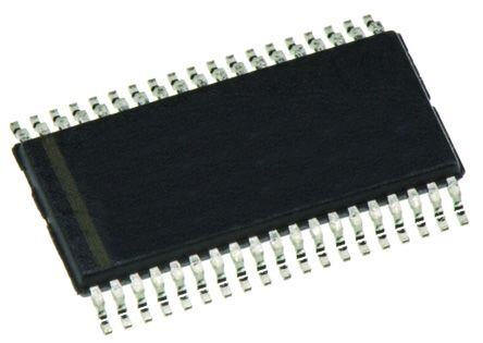
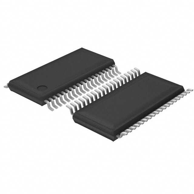
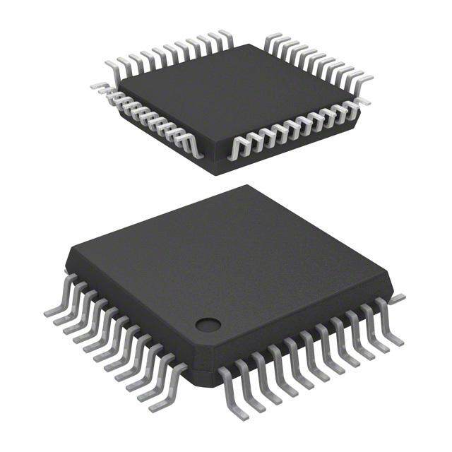
ICGOO电子元器件商城为您提供MSP430F2254IDA由Texas Instruments设计生产,在icgoo商城现货销售,并且可以通过原厂、代理商等渠道进行代购。 MSP430F2254IDA价格参考。Texas InstrumentsMSP430F2254IDA封装/规格:嵌入式 - 微控制器, MSP430 微控制器 IC MSP430F2xx 16-位 16MHz 16KB(16K x 8 + 256B) 闪存 38-TSSOP。您可以下载MSP430F2254IDA参考资料、Datasheet数据手册功能说明书,资料中有MSP430F2254IDA 详细功能的应用电路图电压和使用方法及教程。
Texas Instruments(TI)的MSP430F2254IDA是一款16位超低功耗微控制器,属于MSP430系列。该芯片广泛应用于对功耗敏感、电池供电或需要长时间运行的嵌入式系统中。

其主要应用场景包括:

1. 便携式医疗设备:如血糖仪、心率监测器等,得益于其低功耗特性,适合长时间使用且依赖电池供电的设备。

2. 智能传感器节点:用于工业自动化、环境监测等领域,能够实现温度、湿度、压力等信号的采集与处理。

3. 电表与能源管理系统:如智能水表、气表、电表等“三表”应用,支持低功耗待机与定时数据采集功能。

4. 安防与物联网终端:例如无线门禁控制、远程监控设备、智能家居控制器等,适用于需长时间运行并具备一定处理能力的IoT边缘设备。

5. 消费类电子产品:如电子秤、计时器、手持测量工具等,具有成本低、集成度高、功耗小的优势。

MSP430F2254IDA内置16KB闪存和512B RAM,提供丰富的外设接口(如ADC、UART、SPI),结合TI完善的开发工具链,便于快速开发和部署各类低功耗嵌入式应用。
| 参数 | 数值 |
| A/D位大小 | 10 bit |
| 产品目录 | 集成电路 (IC)半导体 |
| 描述 | IC MCU 16BIT 16KB FLASH 38TSSOP16位微控制器 - MCU 16-bit Ultra-Lo-Pwr Microcontroller |
| EEPROM容量 | - |
| 产品分类 | |
| I/O数 | 32 |
| 品牌 | Texas Instruments |
| 产品手册 | http://www.ti.com/lit/gpn/msp430f2254 |
| 产品图片 |
|
| rohs | 符合RoHS无铅 / 符合限制有害物质指令(RoHS)规范要求 |
| 产品系列 | 嵌入式处理器和控制器,微控制器 - MCU,16位微控制器 - MCU,Texas Instruments MSP430F2254IDAMSP430F2xx |
| 数据手册 | 点击此处下载产品Datasheethttp://www.ti.com/lit/pdf/slau144 |
| 产品型号 | MSP430F2254IDA |
| RAM容量 | 512 x 8 |
| 产品培训模块 | http://www.digikey.cn/PTM/IndividualPTM.page?site=cn&lang=zhs&ptm=8361http://www.digikey.cn/PTM/IndividualPTM.page?site=cn&lang=zhs&ptm=8522http://www.digikey.cn/PTM/IndividualPTM.page?site=cn&lang=zhs&ptm=8576http://www.digikey.cn/PTM/IndividualPTM.page?site=cn&lang=zhs&ptm=8679http://www.digikey.cn/PTM/IndividualPTM.page?site=cn&lang=zhs&ptm=7557http://www.digikey.cn/PTM/IndividualPTM.page?site=cn&lang=zhs&ptm=25419http://www.digikey.cn/PTM/IndividualPTM.page?site=cn&lang=zhs&ptm=25427http://www.digikey.cn/PTM/IndividualPTM.page?site=cn&lang=zhs&ptm=25523http://www.digikey.cn/PTM/IndividualPTM.page?site=cn&lang=zhs&ptm=25524http://www.digikey.cn/PTM/IndividualPTM.page?site=cn&lang=zhs&ptm=25537http://www.digikey.cn/PTM/IndividualPTM.page?site=cn&lang=zhs&ptm=25788http://www.digikey.cn/PTM/IndividualPTM.page?site=cn&lang=zhs&ptm=25882http://www.digikey.cn/PTM/IndividualPTM.page?site=cn&lang=zhs&ptm=25885http://www.digikey.cn/PTM/IndividualPTM.page?site=cn&lang=zhs&ptm=26015http://www.digikey.cn/PTM/IndividualPTM.page?site=cn&lang=zhs&ptm=26006http://www.digikey.cn/PTM/IndividualPTM.page?site=cn&lang=zhs&ptm=30354 |
| 产品目录页面 | |
| 产品种类 | 16位微控制器 - MCU |
| 供应商器件封装 | 38-TSSOP |
| 其它名称 | 296-26207-5 |
| 制造商产品页 | http://www.ti.com/general/docs/suppproductinfo.tsp?distId=10&orderablePartNumber=MSP430F2254IDA |
| 包装 | 管件 |
| 单位重量 | 203.800 mg |
| 可用A/D通道 | 12 |
| 可编程输入/输出端数量 | 32 |
| 商标 | Texas Instruments |
| 商标名 | MSP430 |
| 处理器系列 | 2 Series |
| 外设 | 欠压检测/复位,POR,PWM,WDT |
| 安装风格 | SMD/SMT |
| 定时器数量 | 3 Timer |
| 封装 | Tube |
| 封装/外壳 | 38-TSSOP(0.240",6.10mm 宽) |
| 封装/箱体 | TSSOP-38 |
| 工作温度 | -40°C ~ 85°C |
| 工作电源电压 | 1.8 V to 3.6 V |
| 工厂包装数量 | 40 |
| 振荡器类型 | 内部 |
| 接口类型 | USCI (UART, IrDA, LIN, SPI and I2C, SPI) |
| 数据RAM大小 | 512 B |
| 数据总线宽度 | 16 bit |
| 数据转换器 | A/D 12x10b |
| 最大工作温度 | + 85 C |
| 最大时钟频率 | 16 MHz |
| 最小工作温度 | - 40 C |
| 标准包装 | 40 |
| 核心 | MSP430 |
| 核心处理器 | - |
| 核心尺寸 | 16-位 |
| 片上ADC | Yes |
| 电压-电源(Vcc/Vdd) | 1.8 V ~ 3.6 V |
| 程序存储器大小 | 16 kB |
| 程序存储器类型 | Flash |
| 程序存储容量 | 16KB(16K x 8 + 256B) |
| 系列 | MSP430F2254 |
| 输入/输出端数量 | 32 I/O |
| 连接性 | I²C, IrDA, LIN, SCI, SPI, UART/USART |
| 速度 | 16MHz |
| 配用 | /product-detail/zh/EZ430-RF2500-SEH/296-24121-ND/1998176/product-detail/zh/MSP-FET430U38/296-22904-ND/1571927 |


- 商务部:美国ITC正式对集成电路等产品启动337调查
- 曝三星4nm工艺存在良率问题 高通将骁龙8 Gen1或转产台积电
- 太阳诱电将投资9.5亿元在常州建新厂生产MLCC 预计2023年完工
- 英特尔发布欧洲新工厂建设计划 深化IDM 2.0 战略
- 台积电先进制程称霸业界 有大客户加持明年业绩稳了
- 达到5530亿美元!SIA预计今年全球半导体销售额将创下新高
- 英特尔拟将自动驾驶子公司Mobileye上市 估值或超500亿美元
- 三星加码芯片和SET,合并消费电子和移动部门,撤换高东真等 CEO
- 三星电子宣布重大人事变动 还合并消费电子和移动部门
- 海关总署:前11个月进口集成电路产品价值2.52万亿元 增长14.8%


PDF Datasheet 数据手册内容提取
MSP430F22x2 MSP430F22x4 www.ti.com SLAS504G–JULY2006–REVISEDAUGUST2012 MIXED SIGNAL MICROCONTROLLER FEATURES 1 • LowSupplyVoltageRange:1.8Vto3.6V • TwoConfigurableOperationalAmplifiers 23 • Ultra-LowPowerConsumption (MSP430F22x4Only) – ActiveMode:270µAat1MHz,2.2V • BrownoutDetector – StandbyMode:0.7 µA • SerialOnboardProgramming,NoExternal ProgrammingVoltageNeeded,Programmable – OffMode(RAMRetention):0.1µA CodeProtectionbySecurityFuse • Ultra-FastWake-UpFromStandbyModein • BootstrapLoader LessThan1µs • On-ChipEmulationModule • 16-BitRISCArchitecture,62.5-nsInstruction CycleTime • FamilyMembersInclude: • BasicClockModuleConfigurations – MSP430F2232 – InternalFrequenciesupto16MHzWith – 8KB+256BFlashMemory FourCalibratedFrequenciesto±1% – 512BRAM – InternalVery-Low-PowerLow-Frequency – MSP430F2252 Oscillator – 16KB+256BFlashMemory – 32-kHzCrystal – 512BRAM – High-Frequency(HF)Crystalupto16MHz – MSP430F2272 – Resonator – 32KB+256BFlashMemory – ExternalDigitalClockSource – 1KBRAM – ExternalResistor – MSP430F2234 • 16-BitTimer_AWithThreeCapture/Compare – 8KB+256BFlashMemory Registers – 512BRAM • 16-BitTimer_BWithThreeCapture/Compare – MSP430F2254 Registers – 16KB+256BFlashMemory • UniversalSerialCommunicationInterface – 512BRAM – EnhancedUARTSupportingAuto-Baudrate – MSP430F2274 Detection(LIN) – 32KB+256BFlashMemory – IrDAEncoderandDecoder – 1KBRAM – SynchronousSPI • Availableina38-PinThinShrinkSmall-Outline – I2C™ Package(TSSOP)(DA),40-PinQFNPackage • 10-Bit200-kspsAnalog-to-Digital(A/D) (RHA),and49-PinBallGridArrayPackage ConverterWithInternalReference,Sample- (YFF)(SeeTable1) and-Hold,Autoscan,andDataTransfer • ForCompleteModuleDescriptions,Seethe Controller MSP430x2xxFamilyUser'sGuide(SLAU144) 1 Pleasebeawarethatanimportantnoticeconcerningavailability,standardwarranty,anduseincriticalapplicationsof TexasInstrumentssemiconductorproductsanddisclaimerstheretoappearsattheendofthisdatasheet. MSP430isatrademarkofTexasInstruments. 2 Allothertrademarksarethepropertyoftheirrespectiveowners. 3 PRODUCTIONDATAinformationiscurrentasofpublicationdate. Copyright©2006–2012,TexasInstrumentsIncorporated Products conform to specifications per the terms of the Texas Instruments standard warranty. Production processing does not necessarilyincludetestingofallparameters.
MSP430F22x2 MSP430F22x4 SLAS504G–JULY2006–REVISEDAUGUST2012 www.ti.com This integrated circuit can be damaged by ESD. Texas Instruments recommends that all integrated circuits be handled with appropriateprecautions.Failuretoobserveproperhandlingandinstallationprocedurescancausedamage. ESDdamagecanrangefromsubtleperformancedegradationtocompletedevicefailure.Precisionintegratedcircuitsmaybemore susceptibletodamagebecauseverysmallparametricchangescouldcausethedevicenottomeetitspublishedspecifications. DESCRIPTION The Texas Instruments MSP430™ family of ultra-low-power microcontrollers consist of several devices featuring different sets of peripherals targeted for various applications. The architecture, combined with five low-power modes is optimized to achieve extended battery life in portable measurement applications. The device features a powerful 16-bit RISC CPU, 16-bit registers, and constant generators that contribute to maximum code efficiency. Thedigitallycontrolledoscillator(DCO)allowswake-upfromlow-powermodestoactivemodeinlessthan1µs. The MSP430F22x4/MSP430F22x2 series is an ultra-low-power mixed signal microcontroller with two built-in 16- bit timers, a universal serial communication interface, 10-bit A/D converter with integrated reference and data transfer controller (DTC), two general-purpose operational amplifiers in the MSP430F22x4 devices, and 32 I/O pins. Typical applications include sensor systems that capture analog signals, convert them to digital values, and then process the data for display or for transmission to a host system. Stand-alone radio-frequency (RF) sensor front endsareanotherareaofapplication. Table1.AvailableOptions PACKAGEDDEVICES(1)(2) TA PLASTIC49-PINBGA PLASTIC38-PINTSSOP PLASTIC40-PINQFN (YFF) (DA) (RHA) MSP430F2232IYFF MSP430F2232IDA MSP430F2232IRHA MSP430F2252IYFF MSP430F2252IDA MSP430F2252IRHA MSP430F2272IYFF MSP430F2272IDA MSP430F2272IRHA -40°Cto85°C MSP430F2234IYFF MSP430F2234IDA MSP430F2234IRHA MSP430F2254IYFF MSP430F2254IDA MSP430F2254IRHA MSP430F2274IYFF MSP430F2274IDA MSP430F2274IRHA MSP430F2232TDA MSP430F2232TRHA MSP430F2252TDA MSP430F2252TRHA MSP430F2272TDA MSP430F2272TRHA -40°Cto105°C MSP430F2234TDA MSP430F2234TRHA MSP430F2254TDA MSP430F2254TRHA MSP430F2274TDA MSP430F2274TRHA (1) Forthemostcurrentpackageandorderinginformation,seethePackageOptionAddendumattheendofthisdocument,orseetheTI websiteatwww.ti.com. (2) Packagedrawings,thermaldata,andsymbolizationareavailableatwww.ti.com/packaging. Development Tool Support All MSP430™ microcontrollers include an Embedded Emulation Module (EEM) that allows advanced debugging andprogrammingthrougheasy-to-usedevelopmenttools.Recommendedhardwareoptionsinclude: • DebuggingandProgrammingInterface – MSP-FET430UIF(USB) – MSP-FET430PIF(ParallelPort) • DebuggingandProgrammingInterfacewithTargetBoard – MSP-FET430U38(DApackage) • ProductionProgrammer – MSP-GANG430 2 Copyright©2006–2012,TexasInstrumentsIncorporated
MSP430F22x2 MSP430F22x4 www.ti.com SLAS504G–JULY2006–REVISEDAUGUST2012 MSP430F22x2 Device Pinout, DA Package TEST/SBWTCK 1 38 P1.7/TA2/TDO/TDI DVCC 2 37 P1.6/TA1/TDI P2.5/R 3 36 P1.5/TA0/TMS OSC DVSS 4 35 P1.4/SMCLK/TCK XOUT/P2.7 5 34 P1.3/TA2 XIN/P2.6 6 33 P1.2/TA1 RST/NMI/SBWTDIO 7 32 P1.1/TA0 P2.0/ACLK/A0 8 31 P1.0/TACLK/ADC10CLK P2.1/TAINCLK/SMCLK/A1 9 30 P2.4/TA2/A4/VREF+/VeREF+ P2.2/TA0/A2 10 29 P2.3/TA1/A3/VREF−/VeREF− P3.0/UCB0STE/UCA0CLK/A5 11 28 P3.7/A7 P3.1/UCB0SIMO/UCB0SDA 12 27 P3.6/A6 P3.2/UCB0SOMI/UCB0SCL 13 26 P3.5/UCA0RXD/UCA0SOMI P3.3/UCB0CLK/UCA0STE 14 25 P3.4/UCA0TXD/UCA0SIMO AVSS 15 24 P4.7/TBCLK AVCC 16 23 P4.6/TBOUTH/A15 P4.0/TB0 17 22 P4.5/TB2/A14 P4.1/TB1 18 21 P4.4/TB1/A13 P4.2/TB2 19 20 P4.3/TB0/A12 MSP430F22x4 Device Pinout, DA Package TEST/SBWTCK 1 38 P1.7/TA2/TDO/TDI DVCC 2 37 P1.6/TA1/TDI P2.5/R 3 36 P1.5/TA0/TMS OSC DVSS 4 35 P1.4/SMCLK/TCK XOUT/P2.7 5 34 P1.3/TA2 XIN/P2.6 6 33 P1.2/TA1 RST/NMI/SBWTDIO 7 32 P1.1/TA0 P2.0/ACLK/A0/OA0I0 8 31 P1.0/TACLK/ADC10CLK P2.1/TAINCLK/SMCLK/A1/OA0O 9 30 P2.4/TA2/A4/VREF+/VeREF+/OA1I0 P2.2/TA0/A2/OA0I1 10 29 P2.3/TA1/A3/VREF−/VeREF−/OA1I1/OA1O P3.0/UCB0STE/UCA0CLK/A5 11 28 P3.7/A7/OA1I2 P3.1/UCB0SIMO/UCB0SDA 12 27 P3.6/A6/OA0I2 P3.2/UCB0SOMI/UCB0SCL 13 26 P3.5/UCA0RXD/UCA0SOMI P3.3/UCB0CLK/UCA0STE 14 25 P3.4/UCA0TXD/UCA0SIMO AVSS 15 24 P4.7/TBCLK AVCC 16 23 P4.6/TBOUTH/A15/OA1I3 P4.0/TB0 17 22 P4.5/TB2/A14/OA0I3 P4.1/TB1 18 21 P4.4/TB1/A13/OA1O P4.2/TB2 19 20 P4.3/TB0/A12/OA0O Copyright©2006–2012,TexasInstrumentsIncorporated 3
MSP430F22x2 MSP430F22x4 SLAS504G–JULY2006–REVISEDAUGUST2012 www.ti.com MSP430F22x2 Device Pinout, RHA Package K DI L K TCK DO/T DI/TC MS K/TC W T T T L OSC SB A2/ A1/ A0/ MC A2 A1 5/R CC CC ST/ 7/T 6/T 5/T 4/S 3/T 2/T 2. V V E 1. 1. 1. 1. 1. 1. P D D T P P P P P P 39 38 37 36 35 34 33 32 DVSS 1 30 P1.1/TA0 XOUT/P2.7 2 29 P1.0/TACLK/ADC10CLK XIN/P2.6 3 28 P2.4/TA2/A4/VREF+/VeREF+ DVSS 4 27 P2.3/TA1/A3/VREF−/VeREF− RST/NMI/SBWTDIO 5 26 P3.7/A7 P2.0/ACLK/A0 6 25 P3.6/A6 P2.1/TAINCLK/SMCLK/A1 7 24 P3.5/UCA0RXD/UCA0SOMI P2.2/TA0/A2 8 23 P3.4/UCA0TXD/UCA0SIMO P3.0/UCB0STE/UCA0CLK/A5 9 22 P4.7/TBCLK P3.1/UCB0SIMO/UCB0SDA 10 21 P4.6/TBOUTH/A15 12 13 14 15 16 17 18 19 L E S C 0 1 2 2 3 4 0SC 0ST AVS AVC 0/TB 1/TB 2/TB 0/A1 1/A1 2/A1 CB CA P4. P4. P4. TB TB TB U U 3/ 4/ 5/ MI/ LK/ P4. P4. P4. O C S 0 0 B B C C U 3.2/U P3.3/ P 4 Copyright©2006–2012,TexasInstrumentsIncorporated
MSP430F22x2 MSP430F22x4 www.ti.com SLAS504G–JULY2006–REVISEDAUGUST2012 MSP430F22x4 Device Pinout, RHA Package K DI L K TCK DO/T DI/TC MS K/TC W T T T L OSC SB A2/ A1/ A0/ MC A2 A1 5/R CC CC ST/ 7/T 6/T 5/T 4/S 3/T 2/T 2. V V E 1. 1. 1. 1. 1. 1. P D D T P P P P P P 39 38 37 36 35 34 33 32 DVSS 1 30 P1.1/TA0 XOUT/P2.7 2 29 P1.0/TACLK/ADC10CLK XIN/P2.6 3 28 P2.4/TA2/A4/VREF+/VeREF+/OA1I0 DVSS 4 27 P2.3/TA1/A3/VREF−/VeREF−/OA1I1/OA1O RST/NMI/SBWTDIO 5 26 P3.7/A7/OA1I2 P2.0/ACLK/A0/OA0I0 6 25 P3.6/A6/OA0I2 P2.1/TAINCLK/SMCLK/A1/OA0O 7 24 P3.5/UCA0RXD/UCA0SOMI P2.2/TA0/A2/OA0I1 8 23 P3.4/UCA0TXD/UCA0SIMO P3.0/UCB0STE/UCA0CLK/A5 9 22 P4.7/TBCLK P3.1/UCB0SIMO/UCB0SDA 10 21 P4.6/TBOUTH/A15/OA1I3 12 13 14 15 16 17 18 19 L E S C 0 1 2 O O 3 0SC 0ST AVS AVC 0/TB 1/TB 2/TB OA0 OA1 OA0I UCB UCA P4. P4. P4. A12/ A13/ A14/ OMI/ CLK/ TB0/ TB1/ TB2/ B0S CB0 4.3/ 4.4/ 4.5/ C U P P P 3.2/U P3.3/ P Copyright©2006–2012,TexasInstrumentsIncorporated 5
MSP430F22x2 MSP430F22x4 SLAS504G–JULY2006–REVISEDAUGUST2012 www.ti.com MSP430F22x4, MSP430F22x2 Device Pinout, YFF Package A1 A2 A3 A4 A5 A6 A7 B1 B2 B3 B4 B5 B6 B7 C1 C2 C3 C4 C5 C6 C7 TOPVIEW D1 D2 D3 D4 D5 D6 D7 E1 E2 E3 E4 E5 E6 E7 F1 F2 F3 F4 F5 F6 F7 G1 G2 G3 G4 G5 G6 G7 PackageDimensions The package dimensions for this YFF package are shown in Table 2. See the package drawing at the end of this datasheetformoredetails. Table2.YFFPackageDimensions PACKAGEDDEVICES D E MSP430F22x2 3.33±0.03mm 3.49±0.03mm MSP430F22x4 6 Copyright©2006–2012,TexasInstrumentsIncorporated
MSP430F22x2 MSP430F22x4 www.ti.com SLAS504G–JULY2006–REVISEDAUGUST2012 MSP430F22x2 Functional Block Diagram VCC VSS P1.x/P2.x P3.x/P4.x 2x8 2x8 XIN XOUT ADC10 Ports P1/P2 ACLK Basic Clock Flash RAM 10−Bit Ports P3/P4 System+ 2x8I/O SMCLK 32kB 1kB 12 Interrupt 2x8I/O 16kB 512B Channels, capability, pull−up/down MCLK 8kB 512B Autoscan, pull−up/down resistors DTC resistors 16MHz MAB CPU incl.16 Registers MDB Emulation (2BP) Timer_B3 USCI_A0: Watchdog Timer_A3 UART/LIN, JTAG Brownout WDT+ 3CC IrDA,SPI Interface Protection 3CC Registers, 15/16−Bit Registers Shadow USCI_B0: Reg SPI,I2C Spy−Bi Wire RST/NMI MSP430F22x4 Functional Block Diagram VCC VSS P1.x/P2.x P3.x/P4.x 2x8 2x8 XIN XOUT ADC10 Ports P1/P2 ACLK Basic Clock Flash RAM 10−Bit Ports P3/P4 System+ OA0,OA1 2x8I/O SMCLK 32kB 1kB 12 Interrupt 2x8I/O 16kB 512B Channels, 2OpAmps capability, pull−up/down MCLK 8kB 512B Autoscan, pull−up/down resistors DTC resistors 16MHz MAB CPU incl.16 Registers MDB Emulation (2BP) Timer_B3 USCI_A0: Watchdog Timer_A3 UART/LIN, JTAG Brownout WDT+ 3CC IrDA,SPI Interface Protection 3CC Registers, 15/16−Bit Registers Shadow USCI_B0: Reg SPI,I2C Spy−Bi Wire RST/NMI Copyright©2006–2012,TexasInstrumentsIncorporated 7
MSP430F22x2 MSP430F22x4 SLAS504G–JULY2006–REVISEDAUGUST2012 www.ti.com Table3.TerminalFunctions,MSP430F22x2 TERMINAL NO. I/O DESCRIPTION NAME YFF DA RHA General-purposedigitalI/Opin P1.0/TACLK/ADC10CLK F2 31 29 I/O Timer_A,clocksignalTACLKinput ADC10,conversionclock General-purposedigitalI/Opin P1.1/TA0 G2 32 30 I/O Timer_A,capture:CCI0Ainput,compare:OUT0output BSLtransmit General-purposedigitalI/Opin P1.2/TA1 E2 33 31 I/O Timer_A,capture:CCI1Ainput,compare:OUT1output General-purposedigitalI/Opin P1.3/TA2 G1 34 32 I/O Timer_A,capture:CCI2Ainput,compare:OUT2output General-purposedigitalI/Opin P1.4/SMCLK/TCK F1 35 33 I/O SMCLKsignaloutput TestClockinputfordeviceprogrammingandtest General-purposedigitalI/Opin P1.5/TA0/TMS E1 36 34 I/O Timer_A,compare:OUT0output TestModeSelectinputfordeviceprogrammingandtest General-purposedigitalI/Opin P1.6/TA1/TDI/TCLK E3 37 35 I/O Timer_A,compare:OUT1output TestDataInputorTestClockInputforprogrammingandtest General-purposedigitalI/Opin P1.7/TA2/TDO/TDI(1) D2 38 36 I/O Timer_A,compare:OUT2output TestDataOutputorTestDataInputforprogrammingandtest General-purposedigitalI/Opin P2.0/ACLK/A0 A4 8 6 I/O ACLKoutput ADC10,analoginputA0 General-purposedigitalI/Opin Timer_A,clocksignalatINCLK P2.1/TAINCLK/SMCLK/A1 B4 9 7 I/O SMCLKsignaloutput ADC10,analoginputA1 General-purposedigitalI/Opin P2.2/TA0/A2 A5 10 8 I/O Timer_A,capture:CCI0Binput/BSLreceive,compare:OUT0output ADC10,analoginputA2 General-purposedigitalI/Opin Timer_A,captureCCI1Binput,compare:OUT1output P2.3/TA1/A3/V /V F3 29 27 I/O REF- eREF- ADC10,analoginputA3 Negativereferencevoltageinput General-purposedigitalI/Opin Timer_A,compare:OUT2output P2.4/TA2/A4/V /V G3 30 28 I/O REF+ eREF+ ADC10,analoginputA4 Positivereferencevoltageoutputorinput General-purposedigitalI/Opin P2.5/R C2 3 40 I/O OSC InputforexternalDCOresistortodefineDCOfrequency Inputterminalofcrystaloscillator XIN/P2.6 A2 6 3 I/O General-purposedigitalI/Opin (1) TDOorTDIisselectedviaJTAGinstruction. 8 Copyright©2006–2012,TexasInstrumentsIncorporated
MSP430F22x2 MSP430F22x4 www.ti.com SLAS504G–JULY2006–REVISEDAUGUST2012 Table3.TerminalFunctions,MSP430F22x2(continued) TERMINAL NO. I/O DESCRIPTION NAME YFF DA RHA Outputterminalofcrystaloscillator XOUT/P2.7 A1 5 2 I/O General-purposedigitalI/Opin(2) General-purposedigitalI/Opin P3.0/UCB0STE/UCA0CLK/ USCI_B0slavetransmitenable B5 11 9 I/O A5 USCI_A0clockinput/output ADC10,analoginputA5 General-purposedigitalI/Opin P3.1/UCB0SIMO/ A6 12 10 I/O USCI_B0SPImode:slavein/masterout UCB0SDA USCI_B0I2Cmode:SDAI2Cdata General-purposedigitalI/Opin P3.2/UCB0SOMI/UCB0SCL A7 13 11 I/O USCI_B0SPImode:slaveout/masterin USCI_B0I2Cmode:SCLI2Cclock General-purposedigitalI/Opin P3.3/UCB0CLK/UCA0STE B6 14 12 I/O USCI_B0clockinput/output USCI_A0slavetransmitenable General-purposedigitalI/Opin P3.4/UCA0TXD/ G6 25 23 I/O USCI_A0UARTmode:transmitdataoutput UCA0SIMO USCI_A0SPImode:slavein/masterout General-purposedigitalI/Opin P3.5/UCA0RXD/ G5 26 24 I/O USCI_A0UARTmode:receivedatainput UCA0SOMI USCI_A0SPImode:slaveout/masterin General-purposedigitalI/Opin P3.6/A6 F4 27 25 I/O ADC10analoginputA6 General-purposedigitalI/Opin P3.7/A7 G4 28 26 I/O ADC10analoginputA7 General-purposedigitalI/Opin P4.0/TB0 D6 17 15 I/O Timer_B,capture:CCI0Ainput,compare:OUT0output General-purposedigitalI/Opin P4.1/TB1 D7 18 16 I/O Timer_B,capture:CCI1Ainput,compare:OUT1output General-purposedigitalI/Opin P4.2/TB2 E6 19 17 I/O Timer_B,capture:CCI2Ainput,compare:OUT2output General-purposedigitalI/Opin P4.3/TB0/A12 E7 20 18 I/O Timer_B,capture:CCI0Binput,compare:OUT0output ADC10analoginputA12 General-purposedigitalI/Opin P4.4/TB1/A13 F7 21 19 I/O Timer_B,capture:CCI1Binput,compare:OUT1output ADC10analoginputA13 General-purposedigitalI/Opin P4.5/TB2/A14 F6 22 20 I/O Timer_B,compare:OUT2output ADC10analoginputA14 General-purposedigitalI/Opin P4.6/TBOUTH/A15 G7 23 21 I/O Timer_B,switchallTB0toTB3outputstohighimpedance ADC10analoginputA15 (2) IfXOUT/P2.7isusedasaninput,excesscurrentflowsuntilP2SEL.7iscleared.Thisisduetotheoscillatoroutputdriverconnectionto thispadafterreset. Copyright©2006–2012,TexasInstrumentsIncorporated 9
MSP430F22x2 MSP430F22x4 SLAS504G–JULY2006–REVISEDAUGUST2012 www.ti.com Table3.TerminalFunctions,MSP430F22x2(continued) TERMINAL NO. I/O DESCRIPTION NAME YFF DA RHA General-purposedigitalI/Opin P4.7/TBCLK F5 24 22 I/O Timer_B,clocksignalTBCLKinput Resetornonmaskableinterruptinput RST/NMI/SBWTDIO B3 7 5 I Spy-Bi-Wiretestdatainput/outputduringprogrammingandtest SelectstestmodeforJTAGpinsonPort1.Thedeviceprotectionfuseis TEST/SBWTCK D1 1 37 I connectedtoTEST. Spy-Bi-Wiretestclockinputduringprogrammingandtest C1, D3, DV 2 38,39 Digitalsupplyvoltage CC D4, E4,E5 C6, AV C7, 16 14 Analogsupplyvoltage CC D5 A3, B1, DV B2, 4 1,4 Digitalgroundreference SS C3, C4 B7, AV 15 13 Analoggroundreference SS C5 QFNPad NA NA Pad NA QFNpackagepad;connectiontoDV recommended. SS 10 Copyright©2006–2012,TexasInstrumentsIncorporated
MSP430F22x2 MSP430F22x4 www.ti.com SLAS504G–JULY2006–REVISEDAUGUST2012 Table4.TerminalFunctions,MSP430F22x4 TERMINAL NO. I/O DESCRIPTION NAME YFF DA RHA General-purposedigitalI/Opin P1.0/TACLK/ADC10CLK F2 31 29 I/O Timer_A,clocksignalTACLKinput ADC10,conversionclock General-purposedigitalI/Opin P1.1/TA0 G2 32 30 I/O Timer_A,capture:CCI0Ainput,compare:OUT0output BSLtransmit General-purposedigitalI/Opin P1.2/TA1 E2 33 31 I/O Timer_A,capture:CCI1Ainput,compare:OUT1output General-purposedigitalI/Opin P1.3/TA2 G1 34 32 I/O Timer_A,capture:CCI2Ainput,compare:OUT2output General-purposedigitalI/Opin P1.4/SMCLK/TCK F1 35 33 I/O SMCLKsignaloutput TestClockinputfordeviceprogrammingandtest General-purposedigitalI/Opin P1.5/TA0/TMS E1 36 34 I/O Timer_A,compare:OUT0output TestModeSelectinputfordeviceprogrammingandtest General-purposedigitalI/Opin P1.6/TA1/TDI/TCLK E3 37 35 I/O Timer_A,compare:OUT1output TestDataInputorTestClockInputforprogrammingandtest General-purposedigitalI/Opin P1.7/TA2/TDO/TDI(1) D2 38 36 I/O Timer_A,compare:OUT2output TestDataOutputorTestDataInputforprogrammingandtest General-purposedigitalI/Opin ACLKoutput P2.0/ACLK/A0/OA0I0 A4 8 6 I/O ADC10,analoginputA0 OA0,analoginputIO General-purposedigitalI/Opin Timer_A,clocksignalatINCLK P2.1/TAINCLK/SMCLK/ B4 9 7 I/O SMCLKsignaloutput A1/OA0O ADC10,analoginputA1 OA0,analogoutput General-purposedigitalI/Opin Timer_A,capture:CCI0Binput/BSLreceive,compare:OUT0output P2.2/TA0/A2/OA0I1 A5 10 8 I/O ADC10,analoginputA2 OA0,analoginputI1 General-purposedigitalI/Opin Timer_A,captureCCI1Binput,compare:OUT1output P2.3/TA1/A3/V /V / ADC10,analoginputA3 REF- eREF- F3 29 27 I/O OA1I1/OA1O Negativereferencevoltageinput OA1,analoginputI1 OA1,analogoutput (1) TDOorTDIisselectedviaJTAGinstruction. Copyright©2006–2012,TexasInstrumentsIncorporated 11
MSP430F22x2 MSP430F22x4 SLAS504G–JULY2006–REVISEDAUGUST2012 www.ti.com Table4.TerminalFunctions,MSP430F22x4(continued) TERMINAL NO. I/O DESCRIPTION NAME YFF DA RHA General-purposedigitalI/Opin Timer_A,compare:OUT2output P2.4/TA2/A4/ G3 30 28 I/O ADC10,analoginputA4 V /V /OA1I0 REF+ eREF+ Positivereferencevoltageoutputorinput OA1,analoginputI/O General-purposedigitalI/Opin P2.5/R C2 3 40 I/O OSC InputforexternalDCOresistortodefineDCOfrequency Inputterminalofcrystaloscillator XIN/P2.6 A2 6 3 I/O General-purposedigitalI/Opin Outputterminalofcrystaloscillator XOUT/P2.7 A1 5 2 I/O General-purposedigitalI/Opin(2) General-purposedigitalI/Opin P3.0/UCB0STE/UCA0CLK/ USCI_B0slavetransmitenable B5 11 9 I/O A5 USCI_A0clockinput/output ADC10,analoginputA5 General-purposedigitalI/Opin P3.1/UCB0SIMO/ A6 12 10 I/O USCI_B0SPImode:slavein/masterout UCB0SDA USCI_B0I2Cmode:SDAI2Cdata General-purposedigitalI/Opin P3.2/UCB0SOMI/UCB0SCL A7 13 11 I/O USCI_B0SPImode:slaveout/masterin USCI_B0I2Cmode:SCLI2Cclock General-purposedigitalI/Opin P3.3/UCB0CLK/UCA0STE B6 14 12 I/O USCI_B0clockinput/output USCI_A0slavetransmitenable General-purposedigitalI/Opin P3.4/UCA0TXD/ G6 25 23 I/O USCI_A0UARTmode:transmitdataoutput UCA0SIMO USCI_A0SPImode:slavein/masterout General-purposedigitalI/Opin P3.5/UCA0RXD/ G5 26 24 I/O USCI_A0UARTmode:receivedatainput UCA0SOMI USCI_A0SPImode:slaveout/masterin General-purposedigitalI/Opin P3.6/A6/OA0I2 F4 27 25 I/O ADC10analoginputA6 OA0analoginputI2 General-purposedigitalI/Opin P3.7/A7/OA1I2 G4 28 26 I/O ADC10analoginputA7 OA1analoginputI2 General-purposedigitalI/Opin P4.0/TB0 D6 17 15 I/O Timer_B,capture:CCI0Ainput,compare:OUT0output General-purposedigitalI/Opin P4.1/TB1 D7 18 16 I/O Timer_B,capture:CCI1Ainput,compare:OUT1output General-purposedigitalI/Opin P4.2/TB2 E6 19 17 I/O Timer_B,capture:CCI2Ainput,compare:OUT2output (2) IfXOUT/P2.7isusedasaninput,excesscurrentflowsuntilP2SEL.7iscleared.Thisisduetotheoscillatoroutputdriverconnectionto thispadafterreset. 12 Copyright©2006–2012,TexasInstrumentsIncorporated
MSP430F22x2 MSP430F22x4 www.ti.com SLAS504G–JULY2006–REVISEDAUGUST2012 Table4.TerminalFunctions,MSP430F22x4(continued) TERMINAL NO. I/O DESCRIPTION NAME YFF DA RHA General-purposedigitalI/Opin Timer_B,capture:CCI0Binput,compare:OUT0output P4.3/TB0/A12/OA0O E7 20 18 I/O ADC10analoginputA12 OA0analogoutput General-purposedigitalI/Opin Timer_B,capture:CCI1Binput,compare:OUT1output P4.4/TB1/A13/OA1O F7 21 19 I/O ADC10analoginputA13 OA1analogoutput General-purposedigitalI/Opin Timer_B,compare:OUT2output P4.5/TB2/A14/OA0I3 F6 22 20 I/O ADC10analoginputA14 OA0analoginputI3 General-purposedigitalI/Opin Timer_B,switchallTB0toTB3outputstohighimpedance P4.6/TBOUTH/A15/OA1I3 G7 23 21 I/O ADC10analoginputA15 OA1analoginputI3 General-purposedigitalI/Opin P4.7/TBCLK F5 24 22 I/O Timer_B,clocksignalTBCLKinput Resetornonmaskableinterruptinput RST/NMI/SBWTDIO B3 7 5 I Spy-Bi-Wiretestdatainput/outputduringprogrammingandtest SelectstestmodeforJTAGpinsonPort1.Thedeviceprotectionfuseis TEST/SBWTCK D1 1 37 I connectedtoTEST. Spy-Bi-Wiretestclockinputduringprogrammingandtest C1, D3, DV 2 38,39 Digitalsupplyvoltage CC D4, E4,E5 C6, AV C7, 16 14 Analogsupplyvoltage CC D5 A3, B1, DV B2, 4 1,4 Digitalgroundreference SS C3, C4 B7, AV 15 13 Analoggroundreference SS C5 QFNPad NA NA Pad NA QFNpackagepad;connectiontoDV recommended. SS Copyright©2006–2012,TexasInstrumentsIncorporated 13
MSP430F22x2 MSP430F22x4 SLAS504G–JULY2006–REVISEDAUGUST2012 www.ti.com SHORT-FORM DESCRIPTION CPU Program Counter PC/R0 The MSP430™ CPU has a 16-bit RISC architecture Stack Pointer SP/R1 that is highly transparent to the application. All operations, other than program-flow instructions, are Status Register SR/CG1/R2 performed as register operations in conjunction with seven addressing modes for source operand and four Constant Generator CG2/R3 addressingmodesfordestinationoperand. The CPU is integrated with 16 registers that provide General-Purpose Register R4 reduced instruction execution time. The register-to- General-Purpose Register R5 register operation execution time is one cycle of the CPUclock. General-Purpose Register R6 Four of the registers, R0 to R3, are dedicated as program counter, stack pointer, status register, and General-Purpose Register R7 constant generator respectively. The remaining registersaregeneral-purposeregisters. General-Purpose Register R8 Peripherals are connected to the CPU using data, General-Purpose Register R9 address, and control buses and can be handled with allinstructions. General-Purpose Register R10 Instruction Set General-Purpose Register R11 The instruction set consists of 51 instructions with General-Purpose Register R12 three formats and seven address modes. Each instruction can operate on word and byte data. General-Purpose Register R13 Table 5 shows examples of the three types of instruction formats; Table 6 shows the address General-Purpose Register R14 modes. General-Purpose Register R15 Table5.InstructionWordFormats INSTRUCTIONFORMAT EXAMPLE OPERATION Dualoperands,source-destination ADDR4,R5 R4+R5→R5 Singleoperands,destinationonly CALLR8 PC→(TOS),R8→PC Relativejump,unconditional/conditional JNE Jump-on-equalbit=0 Table6.AddressModeDescriptions ADDRESSMODE S (1) D (2) SYNTAX EXAMPLE OPERATION Register ✓ ✓ MOVRs,Rd MOVR10,R11 R10→R11 Indexed ✓ ✓ MOVX(Rn),Y(Rm) MOV2(R5),6(R6) M(2+R5)→M(6+R6) Symbolic(PCrelative) ✓ ✓ MOVEDE,TONI M(EDE)→M(TONI) Absolute ✓ ✓ MOV&MEM,&TCDAT M(MEM)→M(TCDAT) Indirect ✓ MOV@Rn,Y(Rm) MOV@R10,Tab(R6) M(R10)→M(Tab+R6) M(R10)→R11 Indirectautoincrement ✓ MOV@Rn+,Rm MOV@R10+,R11 R10+2→R10 Immediate ✓ MOV#X,TONI MOV#45,TONI #45→M(TONI) (1) S=source (2) D=destination 14 Copyright©2006–2012,TexasInstrumentsIncorporated
MSP430F22x2 MSP430F22x4 www.ti.com SLAS504G–JULY2006–REVISEDAUGUST2012 Operating Modes The MSP430 microcontrollers have one active mode and five software-selectable low-power modes of operation. An interrupt event can wake up the device from any of the five low-power modes, service the request, and restorebacktothelow-powermodeonreturnfromtheinterruptprogram. Thefollowingsixoperatingmodescanbeconfiguredbysoftware: • Activemode(AM) – Allclocksareactive. • Low-powermode0(LPM0) – CPUisdisabled. – ACLKandSMCLKremainactive.MCLKisdisabled. • Low-powermode1(LPM1) – CPUisdisabledACLKandSMCLKremainactive.MCLKisdisabled. – DCOdc-generatorisdisabledifDCOnotusedinactivemode. • Low-powermode2(LPM2) – CPUisdisabled. – MCLKandSMCLKaredisabled. – DCOdc-generatorremainsenabled. – ACLKremainsactive. • Low-powermode3(LPM3) – CPUisdisabled. – MCLKandSMCLKaredisabled. – DCOdc-generatorisdisabled. – ACLKremainsactive. • Low-powermode4(LPM4) – CPUisdisabled. – ACLKisdisabled. – MCLKandSMCLKaredisabled. – DCOdc-generatorisdisabled. – Crystaloscillatorisstopped. Copyright©2006–2012,TexasInstrumentsIncorporated 15
MSP430F22x2 MSP430F22x4 SLAS504G–JULY2006–REVISEDAUGUST2012 www.ti.com Interrupt Vector Addresses The interrupt vectors and the power-up starting address are located in the address range of 0FFFFh to 0FFC0h. Thevectorcontainsthe16-bitaddressoftheappropriateinterrupthandlerinstructionsequence. If the reset vector (located at address 0FFFEh) contains 0FFFFh (for example, if flash is not programmed), the CPUgoesintoLPM4immediatelyafterpowerup. Table7.InterruptVectorAddresses SYSTEM INTERRUPTSOURCE INTERRUPTFLAG WORDADDRESS PRIORITY INTERRUPT Power-up PORIFG Externalreset RSTIFG Watchdog Reset 0FFFEh 31,highest WDTIFG FPlCasohukt-eoyf-vraionlgaetio(1n) KEYV(2) NMI NMIIFG (non)-maskable, Oscillatorfault OFIFG (non)-maskable, 0FFFCh 30 Flashmemoryaccessviolation ACCVIFG(2)(3) (non)-maskable Timer_B3 TBCCR0CCIFG(4) maskable 0FFFAh 29 TBCCR1andTBCCR2CCIFGs, Timer_B3 TBIFG(2)(4) maskable 0FFF8h 28 0FFF6h 27 WatchdogTimer WDTIFG maskable 0FFF4h 26 Timer_A3 TACCR0CCIFG(seeNote3) maskable 0FFF2h 25 TACCR1CCIFG Timer_A3 TACCR2CCIFG maskable 0FFF0h 24 TAIFG(2)(4) USCI_A0/USCI_B0Receive UCA0RXIFG,UCB0RXIFG(2) maskable 0FFEEh 23 USCI_A0/USCI_B0Transmit UCA0TXIFG,UCB0TXIFG(2) maskable 0FFECh 22 ADC10 ADC10IFG(4) maskable 0FFEAh 21 0FFE8h 20 I/OPortP2 P2IFG.0toP2IFG.7(2)(4) maskable 0FFE6h 19 (eightflags) I/OPortP1 P1IFG.0toP1IFG.7(2)(4) maskable 0FFE4h 18 (eightflags) 0FFE2h 17 0FFE0h 16 (5) 0FFDEh 15 (6) 0FFDChto0FFC0h 14to0,lowest (1) AresetisgeneratediftheCPUtriestofetchinstructionsfromwithinthemoduleregistermemoryaddressrange(0hto01FFh)orfrom withinunusedaddressrange. (2) Multiplesourceflags (3) (non)-maskable:theindividualinterrupt-enablebitcandisableaninterruptevent,butthegeneralinterruptenablecannot. Nonmaskable:neithertheindividualnorthegeneralinterrupt-enablebitwilldisableaninterruptevent. (4) Interruptflagsarelocatedinthemodule. (5) Thislocationisusedasbootstraploadersecuritykey(BSLSKEY). A0AA55hatthislocationdisablestheBSLcompletely. Azero(0h)disablestheerasureoftheflashifaninvalidpasswordissupplied. (6) Theinterruptvectorsataddresses0FFDChto0FFC0harenotusedinthisdeviceandcanbeusedforregularprogramcodeif necessary. 16 Copyright©2006–2012,TexasInstrumentsIncorporated
MSP430F22x2 MSP430F22x4 www.ti.com SLAS504G–JULY2006–REVISEDAUGUST2012 Special Function Registers Most interrupt and module enable bits are collected into the lowest address space. Special function register bits not allocated to a functional purpose are not physically present in the device. Simple software access is provided withthisarrangement. Legend rw Bitcanbereadandwritten. rw-0,1 Bitcanbereadandwritten.ItisResetorSetbyPUC. rw-(0),(1) Bitcanbereadandwritten.ItisResetorSetbyPOR. SFRbitisnotpresentindevice. Table8.InterruptEnable1 Address 7 6 5 4 3 2 1 0 00h ACCVIE NMIIE OFIE WDTIE rw-0 rw-0 rw-0 rw-0 WDTIE Watchdogtimerinterruptenable.Inactiveifwatchdogmodeisselected.Activeifwatchdogtimerisconfiguredininterval timermode. OFIE Oscillatorfaultinterruptenable NMIIE (Non)maskableinterruptenable ACCVIE Flashaccessviolationinterruptenable Table9.InterruptEnable2 Address 7 6 5 4 3 2 1 0 01h UCB0TXIE UCB0RXIE UCA0TXIE UCA0RXIE rw-0 rw-0 rw-0 rw-0 UCA0RXIE USCI_A0receive-interruptenable UCA0TXIE USCI_A0transmit-interruptenable UCB0RXIE USCI_B0receive-interruptenable UCB0TXIE USCI_B0transmit-interruptenable Table10.InterruptFlagRegister1 Address 7 6 5 4 3 2 1 0 02h NMIIFG RSTIFG PORIFG OFIFG WDTIFG rw-0 rw-(0) rw-(1) rw-1 rw-(0) WDTIFG Setonwatchdogtimeroverflow(inwatchdogmode)orsecuritykeyviolation. ResetonV power-uporaresetconditionatRST/NMIpininresetmode. CC OFIFG Flagsetonoscillatorfault RSTIFG Externalresetinterruptflag.SetonaresetconditionatRST/NMIpininresetmode.ResetonV powerup. CC PORIFG Power-onresetinterruptflag.SetonV powerup. CC NMIIFG SetviaRST/NMIpin Table11.InterruptFlagRegister2 Address 7 6 5 4 3 2 1 0 03h UCB0TXIFG UCB0RXIFG UCA0TXIFG UCA0RXIFG rw-1 rw-0 rw-1 rw-0 UCA0RXIFG USCI_A0receive-interruptflag UCA0TXIFG USCI_A0transmit-interruptflag UCB0RXIFG USCI_B0receive-interruptflag UCB0TXIFG USCI_B0transmit-interruptflag Copyright©2006–2012,TexasInstrumentsIncorporated 17
MSP430F22x2 MSP430F22x4 SLAS504G–JULY2006–REVISEDAUGUST2012 www.ti.com Memory Organization Table12.MemoryOrganization MSP430F223x MSP430F225x MSP430F227x Memory Size 8KBFlash 16KBFlash 32KBFlash Main:interruptvector Flash 0FFFFh-0FFC0h 0FFFFh-0FFC0h 0FFFFh-0FFC0h Main:codememory Flash 0FFFFh-0E000h 0FFFFh-0C000h 0FFFFh-08000h Size 256Byte 256Byte 256Byte Informationmemory Flash 010FFh-01000h 010FFh-01000h 010FFh-01000h Size 1KB 1KB 1KB Bootmemory ROM 0FFFh-0C00h 0FFFh-0C00h 0FFFh-0C00h 512Byte 512Byte 1KB RAM Size 03FFh-0200h 03FFh-0200h 05FFh-0200h 16-bit 01FFh-0100h 01FFh-0100h 01FFh-0100h Peripherals 8-bit 0FFh-010h 0FFh-010h 0FFh-010h 8-bitSFR 0Fh-00h 0Fh-00h 0Fh-00h Bootstrap Loader (BSL) The MSP430 bootstrap loader (BSL) enables users to program the flash memory or RAM using a UART serial interface. Access to the MSP430 memory via the BSL is protected by user-defined password. For complete description of the features of the BSL and its implementation, see the MSP430 Programming Via the Bootstrap LoaderUser’sGuide(SLAU319). Table13.BSLFunctionPins BSLFUNCTION DAPACKAGEPINS RHAPACKAGEPINS YFFPACKAGEPINS Datatransmit 32-P1.1 30-P1.1 G3-P1.1 Datareceive 10-P2.2 8-P2.2 A5-P2.2 Flash Memory The flash memory can be programmed via the JTAG port, the bootstrap loader, or in-system by the CPU. The CPUcanperformsingle-byteandsingle-wordwritestotheflashmemory.Featuresoftheflashmemoryinclude: • Flash memory has n segments of main memory and four segments of information memory (A to D) of 64byteseach.Eachsegmentinmainmemoryis512bytesinsize. • Segments0tonmaybeerasedinonestep,oreachsegmentmaybeindividuallyerased. • SegmentsAtoDcanbeerasedindividually,orasagroupwithsegments0ton. SegmentsAtoDarealsocalledinformationmemory. • Segment A contains calibration data. After reset, segment A is protected against programming and erasing. It can be unlocked, but care should be taken not to erase this segment if the device-specific calibration data is required. 18 Copyright©2006–2012,TexasInstrumentsIncorporated
MSP430F22x2 MSP430F22x4 www.ti.com SLAS504G–JULY2006–REVISEDAUGUST2012 Peripherals Peripherals are connected to the CPU through data, address, and control buses and can be handled using all instructions.Forcompletemoduledescriptions,seetheMSP430x2xxFamilyUser'sGuide(SLAU144). Oscillator and System Clock The clock system is supported by the basic clock module that includes support for a 32768-Hz watch crystal oscillator,aninternalvery-low-powerlow-frequencyoscillator,aninternaldigitally-controlledoscillator(DCO),and a high-frequency crystal oscillator. The basic clock module is designed to meet the requirements of both low system cost and low power consumption. The internal DCO provides a fast turn-on clock source and stabilizes in lessthan1µs.Thebasicclockmoduleprovidesthefollowingclocksignals: • Auxiliary clock (ACLK), sourced from a 32768-Hz watch crystal, a high-frequency crystal, or the internal very- low-powerLFoscillator. • Mainclock(MCLK),thesystemclockusedbytheCPU. • Sub-Mainclock(SMCLK),thesub-systemclockusedbytheperipheralmodules. Table14.DCOCalibrationData (ProvidedFromFactoryinFlashInformationMemorySegmentA) DCOFREQUENCY CALIBRATIONREGISTER SIZE ADDRESS CALBC1_1MHZ byte 010FFh 1MHz CALDCO_1MHZ byte 010FEh CALBC1_8MHZ byte 010FDh 8MHz CALDCO_8MHZ byte 010FCh CALBC1_12MHZ byte 010FBh 12MHz CALDCO_12MHZ byte 010FAh CALBC1_16MHZ byte 010F9h 16MHz CALDCO_16MHZ byte 010F8h Brownout The brownout circuit is implemented to provide the proper internal reset signal to the device during power on and poweroff. Digital I/O Therearefour8-bitI/Oportsimplemented—portsP1,P2,P3,andP4: • AllindividualI/Obitsareindependentlyprogrammable. • Anycombinationofinput,output,andinterruptconditionispossible. • Edge-selectableinterruptinputcapabilityforalleightbitsofportP1andP2. • Read/writeaccesstoport-controlregistersissupportedbyallinstructions. • EachI/Ohasanindividuallyprogrammablepullup/pulldownresistor. Because there are only three I/O pins implemented from port P2, bits [5:1] of all port P2 registers read as 0, and writedataisignored. Watchdog Timer (WDT+) The primary function of the WDT+ module is to perform a controlled system restart after a software problem occurs. If the selected time interval expires, a system reset is generated. If the watchdog function is not needed in an application, the module can be disabled or configured as an interval timer and can generate interrupts at selectedtimeintervals. Copyright©2006–2012,TexasInstrumentsIncorporated 19
MSP430F22x2 MSP430F22x4 SLAS504G–JULY2006–REVISEDAUGUST2012 www.ti.com Timer_A3 Timer_A3 is a 16-bit timer/counter with three capture/compare registers. Timer_A3 can support multiple capture/compares, PWM outputs, and interval timing. Timer_A3 also has extensive interrupt capabilities. Interrupts may be generated from the counter on overflow conditions and from each of the capture/compare registers. Table15.Timer_A3SignalConnections INPUTPINNUMBER DEVICE MODULE MODULE OUTPUTPINNUMBER MODULE INPUT INPUT OUTPUT DA RHA YFF SIGNAL NAME BLOCK SIGNAL DA RHA YFF 31-P1.0 29-P1.0 F2-P1.0 TACLK TACLK Timer NA ACLK ACLK SMCLK SMCLK 9-P2.1 7-P2.1 B4-P2.1 TAINCLK INCLK 32-P1.1 30-P1.1 G2-P1.1 TA0 CCI0A CCR0 TA0 32-P1.1 30-P1.1 G2-P1.1 10-P2.2 8-P2.2 A5-P2.2 TA0 CCI0B 10-P2.2 8-P2.2 A5-P2.2 V GND 36-P1.5 34-P1.5 E1-P1.5 SS V V CC CC 33-P1.2 31-P1.2 E2-P1.2 TA1 CCI1A CCR1 TA1 33-P1.2 31-P1.2 E2-P1.2 29-P2.3 27-P2.3 F3-P2.3 TA1 CCI1B 29-P2.3 27-P2.3 F3-P2.3 V GND 37-P1.6 35-P1.6 E3-P1.6 SS V V CC CC 34-P1.3 32-P1.3 G1-P1.3 TA2 CCI2A CCR2 TA2 34-P1.3 32-P1.3 G1-P1.3 ACLK CCI2B 30-P2.4 28-P2.4 G3-P2.4 (internal) V GND 38-P1.7 36-P1.7 D2-P1.7 SS V V CC CC 20 Copyright©2006–2012,TexasInstrumentsIncorporated
MSP430F22x2 MSP430F22x4 www.ti.com SLAS504G–JULY2006–REVISEDAUGUST2012 Timer_B3 Timer_B3 is a 16-bit timer/counter with three capture/compare registers. Timer_B3 can support multiple capture/compares, PWM outputs, and interval timing. Timer_B3 also has extensive interrupt capabilities. Interrupts may be generated from the counter on overflow conditions and from each of the capture/compare registers. Table16.Timer_B3SignalConnections INPUTPINNUMBER DEVICE MODULE MODULE OUTPUTPINNUMBER MODULE INPUT INPUT OUTPUT DA RHA YFF SIGNAL NAME BLOCK SIGNAL DA RHA YFF 24-P4.7 22-P4.7 F5-P4.7 TBCLK TBCLK Timer NA ACLK ACLK SMCLK SMCLK 24-P4.7 22-P4.7 F5-P4.7 TBCLK INCLK 17-P4.0 15-P4.0 D6-P4.0 TB0 CCI0A CCR0 TB0 17-P4.0 15-P4.0 D6-P4.0 20-P4.3 18-P4.3 E7-P4.3 TB0 CCI0B 20-P4.3 18-P4.3 E7-P4.3 V GND SS V V CC CC 18-P4.1 16-P4.1 D7-P4.1 TB1 CCI1A CCR1 TB1 18-P4.1 16-P4.1 D7-P4.1 21-P4.4 19-P4.4 F7-P4.4 TB1 CCI1B 21-P4.4 19-P4.4 F7-P4.4 V GND SS V V CC CC 19-P4.2 17-P4.2 E6-P4.2 TB2 CCI2A CCR2 TB2 19-P4.2 17-P4.2 E6-P4.2 ACLK CCI2B 22-P4.5 20-P4.5 F6-P4.5 (internal) V GND SS V V CC CC Universal Serial Communications Interface (USCI) The USCI module is used for serial data communication. The USCI module supports synchronous communication protocols like SPI (3 or 4 pin), I2C and asynchronous communication protocols such as UART, enhancedUARTwithautomaticbaudratedetection(LIN),andIrDA. USCI_A0providessupportforSPI(3or4pin),UART,enhancedUART,andIrDA. USCI_B0providessupportforSPI(3or4pin)andI2C. ADC10 The ADC10 module supports fast, 10-bit analog-to-digital conversions. The module implements a 10-bit SAR core, sample select control, reference generator and data transfer controller, or DTC, for automatic conversion resulthandlingallowingADCsamplestobeconvertedandstoredwithoutanyCPUintervention. Copyright©2006–2012,TexasInstrumentsIncorporated 21
MSP430F22x2 MSP430F22x4 SLAS504G–JULY2006–REVISEDAUGUST2012 www.ti.com Operational Amplifier (OA) (MSP430F22x4 only) The MSP430F22x4 has two configurable low-current general-purpose operational amplifiers. Each OA input and output terminal is software-selectable and offer a flexible choice of connections for various applications. The OA opampsprimarilysupportfront-endanalogsignalconditioningpriortoanalog-to-digitalconversion. Table17.OA0SignalConnections ANALOGINPUTPINNUMBER DEVICEINPUTSIGNAL MODULEINPUTNAME DA RHA YFF 8-A0 6-A0 B4-A0 OA0I0 OAxI0 10-A2 8-A2 B5-A2 OA0I1 OA0I1 10-A2 8-A2 B5-A2 OA0I1 OAxI1 27-A6 25-A6 F4-A6 OA0I2 OAxIA 22-A14 20-A14 F6-A14 OA0I3 OAxIB Table18.OA1SignalConnections ANALOGINPUTPINNUMBER DEVICEINPUTSIGNAL MODULEINPUTNAME DA RHA YFF 30-A4 28-A4 G3-A4 OA1I0 OAxI0 10-A2 8-A2 B5-A2 OA0I1 OA0I1 29-A3 27-A3 F3-A3 OA1I1 OAxI1 28-A7 26-A7 G4-A7 OA1I2 OAxIA 23-A15 21-A15 G7-A15 OA1I3 OAxIB 22 Copyright©2006–2012,TexasInstrumentsIncorporated
MSP430F22x2 MSP430F22x4 www.ti.com SLAS504G–JULY2006–REVISEDAUGUST2012 Peripheral File Map Table19.PeripheralsWithWordAccess MODULE REGISTERNAME SHORTNAME ADDRESS OFFSET ADC10 ADCdatatransferstartaddress ADC10SA 1BCh ADCmemory ADC10MEM 1B4h ADCcontrolregister1 ADC10CTL1 1B2h ADCcontrolregister0 ADC10CTL0 1B0h ADCanalogenable0 ADC10AE0 04Ah ADCanalogenable1 ADC10AE1 04Bh ADCdatatransfercontrolregister1 ADC10DTC1 049h ADCdatatransfercontrolregister0 ADC10DTC0 048h Timer_B Capture/compareregister TBCCR2 0196h Capture/compareregister TBCCR1 0194h Capture/compareregister TBCCR0 0192h Timer_Bregister TBR 0190h Capture/comparecontrol TBCCTL2 0186h Capture/comparecontrol TBCCTL1 0184h Capture/comparecontrol TBCCTL0 0182h Timer_Bcontrol TBCTL 0180h Timer_Binterruptvector TBIV 011Eh Timer_A Capture/compareregister TACCR2 0176h Capture/compareregister TACCR1 0174h Capture/compareregister TACCR0 0172h Timer_Aregister TAR 0170h Capture/comparecontrol TACCTL2 0166h Capture/comparecontrol TACCTL1 0164h Capture/comparecontrol TACCTL0 0162h Timer_Acontrol TACTL 0160h Timer_Ainterruptvector TAIV 012Eh FlashMemory Flashcontrol3 FCTL3 012Ch Flashcontrol2 FCTL2 012Ah Flashcontrol1 FCTL1 0128h WatchdogTimer+ Watchdog/timercontrol WDTCTL 0120h Copyright©2006–2012,TexasInstrumentsIncorporated 23
MSP430F22x2 MSP430F22x4 SLAS504G–JULY2006–REVISEDAUGUST2012 www.ti.com Table20.PeripheralsWithByteAccess MODULE REGISTERNAME SHORTNAME ADDRESS OFFSET OA1(MSP430F22x4only) OperationalAmplifier1controlregister1 OA1CTL1 0C3h OperationalAmplifier1controlregister1 OA1CTL0 0C2h OA0(MSP430F22x4only) OperationalAmplifier0controlregister1 OA0CTL1 0C1h OperationalAmplifier0controlregister1 OA0CTL0 0C0h USCI_B0 USCI_B0transmitbuffer UCB0TXBUF 06Fh USCI_B0receivebuffer UCB0RXBUF 06Eh USCI_B0status UCB0STAT 06Dh USCI_B0bitratecontrol1 UCB0BR1 06Bh USCI_B0bitratecontrol0 UCB0BR0 06Ah USCI_B0control1 UCB0CTL1 069h USCI_B0control0 UCB0CTL0 068h USCI_B0I2Cslaveaddress UCB0SA 011Ah USCI_B0I2Cownaddress UCB0OA 0118h USCI_A0 USCI_A0transmitbuffer UCA0TXBUF 067h USCI_A0receivebuffer UCA0RXBUF 066h USCI_A0status UCA0STAT 065h USCI_A0modulationcontrol UCA0MCTL 064h USCI_A0baudratecontrol1 UCA0BR1 063h USCI_A0baudratecontrol0 UCA0BR0 062h USCI_A0control1 UCA0CTL1 061h USCI_A0control0 UCA0CTL0 060h USCI_A0IrDAreceivecontrol UCA0IRRCTL 05Fh USCI_A0IrDAtransmitcontrol UCA0IRTCTL 05Eh USCI_A0autobaudratecontrol UCA0ABCTL 05Dh BasicClockSystem+ Basicclocksystemcontrol3 BCSCTL3 053h Basicclocksystemcontrol2 BCSCTL2 058h Basicclocksystemcontrol1 BCSCTL1 057h DCOclockfrequencycontrol DCOCTL 056h PortP4 PortP4resistorenable P4REN 011h PortP4selection P4SEL 01Fh PortP4direction P4DIR 01Eh PortP4output P4OUT 01Dh PortP4input P4IN 01Ch PortP3 PortP3resistorenable P3REN 010h PortP3selection P3SEL 01Bh PortP3direction P3DIR 01Ah PortP3output P3OUT 019h PortP3input P3IN 018h PortP2 PortP2resistorenable P2REN 02Fh PortP2selection P2SEL 02Eh PortP2interruptenable P2IE 02Dh PortP2interruptedgeselect P2IES 02Ch PortP2interruptflag P2IFG 02Bh PortP2direction P2DIR 02Ah PortP2output P2OUT 029h PortP2input P2IN 028h 24 Copyright©2006–2012,TexasInstrumentsIncorporated
MSP430F22x2 MSP430F22x4 www.ti.com SLAS504G–JULY2006–REVISEDAUGUST2012 Table20.PeripheralsWithByteAccess(continued) MODULE REGISTERNAME SHORTNAME ADDRESS OFFSET PortP1 PortP1resistorenable P1REN 027h PortP1selection P1SEL 026h PortP1interruptenable P1IE 025h PortP1interruptedgeselect P1IES 024h PortP1interruptflag P1IFG 023h PortP1direction P1DIR 022h PortP1output P1OUT 021h PortP1input P1IN 020h SpecialFunction SFRinterruptflag2 IFG2 003h SFRinterruptflag1 IFG1 002h SFRinterruptenable2 IE2 001h SFRinterruptenable1 IE1 000h Copyright©2006–2012,TexasInstrumentsIncorporated 25
MSP430F22x2 MSP430F22x4 SLAS504G–JULY2006–REVISEDAUGUST2012 www.ti.com Absolute Maximum Ratings(1) VoltageappliedatV toV -0.3Vto4.1V CC SS Voltageappliedtoanypin (2) -0.3VtoV +0.3V CC Diodecurrentatanydeviceterminal ±2mA Unprogrammeddevice -55°Cto150°C Storagetemperature,T (3) stg Programmeddevice -55°Cto150°C (1) Stressesbeyondthoselistedunderabsolutemaximumratingsmaycausepermanentdamagetothedevice.Thesearestressratings only,andfunctionaloperationofthedeviceattheseoranyotherconditionsbeyondthoseindicatedunderrecommendedoperating conditionsisnotimplied.Exposuretoabsolute-maximum-ratedconditionsforextendedperiodsmayaffectdevicereliability. (2) AllvoltagesreferencedtoV .TheJTAGfuse-blowvoltage,V ,isallowedtoexceedtheabsolutemaximumrating.Thevoltageis SS FB appliedtotheTESTpinwhenblowingtheJTAGfuse. (3) HighertemperaturemaybeappliedduringboardsolderingprocessaccordingtothecurrentJEDECJ-STD-020specificationwithpeak reflowtemperaturesnothigherthanclassifiedonthedevicelabelontheshippingboxesorreels. Recommended Operating Conditions(1)(2) MIN NOM MAX UNIT Duringprogram 1.8 3.6 V execution V Supplyvoltage AV =DV =V CC CC CC CC Duringprogram/erase 2.2 3.6 V flashmemory V Supplyvoltage AV =DV =V 0 V SS SS SS SS Iversion -40 85 T Operatingfree-airtemperature °C A Tversion -40 105 V =1.8V,Dutycycle=50%±10% dc 4.15 Processorfrequency CC f (maximumMCLKfrequency)(1)(2) V =2.7V,Dutycycle=50%±10% dc 12 MHz SYSTEM CC (seeFigure1) V ≥3.3V,Dutycycle=50%±10% dc 16 CC (1) TheMSP430CPUisclockeddirectlywithMCLK.BoththehighandlowphaseofMCLKmustnotexceedthepulsewidthofthe specifiedmaximumfrequency. (2) Modulesmighthaveadifferentmaximuminputclockspecification.Seethespecificationoftherespectivemoduleinthisdatasheet. Legend: 16MHz Supply voltage range, during flash memory z H programming M − 12MHz y c n e Supply voltage range, u q during program execution e Fr 7.5MHz m e st y S 4.15MHz 1.8V 2.2V 2.7V 3.3V 3.6V Supply Voltage−V NOTE: Minimumprocessorfrequencyisdefinedbysystemclock.FlashprogramoreraseoperationsrequireaminimumV CC of2.2V. Figure1. OperatingArea 26 Copyright©2006–2012,TexasInstrumentsIncorporated
MSP430F22x2 MSP430F22x4 www.ti.com SLAS504G–JULY2006–REVISEDAUGUST2012 Active Mode Supply Current (into DV + AV ) Excluding External Current (1)(2) CC CC overrecommendedrangesofsupplyvoltageandoperatingfree-airtemperature(unlessotherwisenoted) PARAMETER TESTCONDITIONS T V MIN TYP MAX UNIT A CC f =f =f =1MHz, 2.2V 270 390 DCO MCLK SMCLK f =32768Hz, ACLK Programexecutesinflash, Activemode(AM) I BCSCTL1=CALBC1_1MHZ, µA AM,1MHz current(1MHz) DCOCTL=CALDCO_1MHZ, 3V 390 550 CPUOFF=0,SCG0=0,SCG1=0, OSCOFF=0 f =f =f =1MHz, 2.2V 240 DCO MCLK SMCLK f =32768Hz, ACLK ProgramexecutesinRAM, Activemode(AM) I BCSCTL1=CALBC1_1MHZ, µA AM,1MHz current(1MHz) DCOCTL=CALDCO_1MHZ, 3.3V 340 CPUOFF=0,SCG0=0,SCG1=0, OSCOFF=0 f =f =f =32768Hz/8= -40°Cto MCLK SMCLK ACLK 5 9 4096Hz, 85°C 2.2V f =0Hz, DCO 105°C 18 Activemode(AM) Programexecutesinflash, I µA AM,4kHz current(4kHz) SELMx=11,SELS=1, -40°Cto 6 10 DIVMx=DIVSx=DIVAx=11, 85°C 3V CPUOFF=0,SCG0=1,SCG1=0, OSCOFF=0 105°C 20 -40°Cto 60 85 fMCLK=fSMCLK=fDCO(0,0)≈100kHz, 85°C 2.2V Activemode(AM) fACLK=0Hz, 105°C 95 I Programexecutesinflash, µA AM,100kHz current(100kHz) RSELx=0,DCOx=0,CPUOFF=0, -40°Cto 72 95 SCG0=0,SCG1=0,OSCOFF=1 85°C 3V 105°C 105 (1) Allinputsaretiedto0VorV .Outputsdonotsourceorsinkanycurrent. CC (2) ThecurrentsarecharacterizedwithaMicroCrystalCC4V-T1ASMDcrystalwithaloadcapacitanceof9pF.Theinternalandexternal loadcapacitanceischosentocloselymatchtherequired9pF. Copyright©2006–2012,TexasInstrumentsIncorporated 27
MSP430F22x2 MSP430F22x4 SLAS504G–JULY2006–REVISEDAUGUST2012 www.ti.com Typical Characteristics - Active-Mode Supply Current (Into DV + AV ) CC CC ACTIVE-MODECURRENT vs ACTIVE-MODECURRENT SUPPLYVOLTAGE vs T =25°C DCOFREQUENCY A 8.0 5.0 7.0 fDCO= 16 MHz TA= 85°C 4.0 A 6.0 A TA= 25°C m m − fDCO= 12 MHz − Mode Current 45..00 fDCO= 8 MHz Mode Current 23..00 VCC= 3 V TA= 85°C Active 23..00 Active TA= 25°C 1.0 1.0 fDCO= 1 MHz VCC= 2.2 V 0.0 0.0 1.5 2.0 2.5 3.0 3.5 4.0 0.0 4.0 8.0 12.0 16.0 VCC−Supply Voltage−V fDCO−DCO Frequency−MHz Figure2. Figure3. 28 Copyright©2006–2012,TexasInstrumentsIncorporated
MSP430F22x2 MSP430F22x4 www.ti.com SLAS504G–JULY2006–REVISEDAUGUST2012 Low-Power-Mode Supply Currents (Into V ) Excluding External Current (1)(2) CC overrecommendedrangesofsupplyvoltageandoperatingfree-airtemperature(unlessotherwisenoted) PARAMETER TESTCONDITIONS T V MIN TYP MAX UNIT A CC f =0MHz, 2.2V 75 90 MCLK f =f =1MHz, SMCLK DCO f =32768Hz, Low-powermode0 ACLK ILPM0,1MHz (LPM0)current(3) BDCCSOCCTTLL1==CCAALLDBCCO1__11MMHHZZ,, 3V 90 120 µA CPUOFF=1,SCG0=0, SCG1=0,OSCOFF=0 f =0MHz, 2.2V 37 48 MCLK f =f ≈100kHz, SMCLK DCO(0,0) Low-powermode0 f =0Hz, ILPM0,100kHz (LPM0)current(3) RASCLEKLx=0,DCOx=0, 3V 41 65 µA CPUOFF=1,SCG0=0, SCG1=0,OSCOFF=1 fMCLK=fSMCLK=0MHz, -40°Cto 22 29 fDCO=1MHz, 85°C 2.2V Low-powermode2 fACLK=32768Hz, 105°C 31 ILPM2 (LPM2)current(4) BDCCSOCCTTLL1==CCAALLDBCCO1__11MMHHZZ,, -40°Cto 25 32 µA CPUOFF=1,SCG0=0, 85°C 3V SCG1=1,OSCOFF=0 105°C 34 -40°C 0.7 1.4 25°C 0.7 1.4 2.2V 85°C 2.4 3.3 f =f =f =0MHz, DCO MCLK SMCLK Low-powermode3 f =32768Hz, 105°C 5 10 ILPM3,LFXT1 (LPM3)current(4) CAPCLUKOFF=1,SCG0=1, -40°C 0.9 1.5 µA SCG1=1,OSCOFF=0 25°C 0.9 1.5 3V 85°C 2.6 3.8 105°C 6 12 -40°C 0.4 1 25°C 0.5 1 2.2V f =f =f =0MHz, 85°C 1.8 2.9 DCO MCLK SMCLK Low-powermode3 fACLKfrominternalLFoscillator 105°C 4.5 9 ILPM3,VLO current,(LPM3)(4) (CVPLUOO),FF=1,SCG0=1, -40°C 0.5 1.2 µA SCG1=1,OSCOFF=0 25°C 0.6 1.2 3V 85°C 2.1 3.3 105°C 5.5 11 -40°C 0.1 0.5 f =f =f =0MHz, DCO MCLK SMCLK Low-powermode4 f =0Hz, 25°C 2.2V/ 0.1 0.5 ILPM4 (LPM4)current(5) CAPCLUKOFF=1,SCG0=1, 85°C 3V 1.5 3 µA SCG1=1,OSCOFF=1 105°C 4.5 9 (1) Allinputsaretiedto0VorV .Outputsdonotsourceorsinkanycurrent. CC (2) ThecurrentsarecharacterizedwithaMicroCrystalCC4V-T1ASMDcrystalwithaloadcapacitanceof9pF.Theinternalandexternal loadcapacitanceischosentocloselymatchtherequired9pF. (3) CurrentforbrownoutandWDTclockedbySMCLKincluded. (4) CurrentforbrownoutandWDTclockedbyACLKincluded. (5) Currentforbrownoutincluded. Copyright©2006–2012,TexasInstrumentsIncorporated 29
MSP430F22x2 MSP430F22x4 SLAS504G–JULY2006–REVISEDAUGUST2012 www.ti.com Schmitt-Trigger Inputs (Ports P1, P2, P3, P4, and RST/NMI) overrecommendedrangesofsupplyvoltageandoperatingfree-airtemperature(unlessotherwisenoted) PARAMETER TESTCONDITIONS V MIN TYP MAX UNIT CC 0.45V 0.75V CC CC V Positive-goinginputthresholdvoltage 2.2V 1 1.65 V IT+ 3V 1.35 2.25 0.25V 0.55V CC CC V Negative-goinginputthresholdvoltage 2.2V 0.55 1.20 V IT- 3V 0.75 1.65 2.2V 0.1 1 V Inputvoltagehysteresis(V -V ) V hys IT+ IT- 3V 0.3 1 Forpullup:V =V , R Pullup/pulldownresistor IN SS 3V 20 35 50 kΩ Pull Forpulldown:V =V IN CC C Inputcapacitance V =V orV 5 pF I IN SS CC Inputs (Ports P1, P2) overrecommendedrangesofsupplyvoltageandoperatingfree-airtemperature(unlessotherwisenoted) PARAMETER TESTCONDITIONS V MIN TYP MAX UNIT CC PortP1,P2:P1.xtoP2.x,Externaltrigger t(int) Externalinterrupttiming pulsewidthtosetinterruptflag(1) 2.2V,3V 20 ns (1) Anexternalsignalsetstheinterruptflageverytimetheminimuminterruptpulsewidtht ismet.Itmaybesetevenwithtriggersignals (int) shorterthant . (int) Leakage Current (Ports P1, P2, P3, and P4) overrecommendedrangesofsupplyvoltageandoperatingfree-airtemperature(unlessotherwisenoted) PARAMETER TESTCONDITIONS V MIN TYP MAX UNIT CC I High-impedanceleakagecurrent (1) (2) 2.2V,3V ±50 nA lkg(Px.y) (1) TheleakagecurrentismeasuredwithV orV appliedtothecorrespondingpin(s),unlessotherwisenoted. SS CC (2) Theleakageofthedigitalportpinsismeasuredindividually.Theportpinisselectedforinputandthepullup/pulldownresistoris disabled. 30 Copyright©2006–2012,TexasInstrumentsIncorporated
MSP430F22x2 MSP430F22x4 www.ti.com SLAS504G–JULY2006–REVISEDAUGUST2012 Outputs (Ports P1, P2, P3, and P4) overrecommendedrangesofsupplyvoltageandoperatingfree-airtemperature(unlessotherwisenoted) PARAMETER TESTCONDITIONS V MIN MAX UNIT CC I =-1.5mA (1) V -0.25 V OH(max) CC CC 2.2V I =-6mA (2) V -0.6 V OH(max) CC CC V High-leveloutputvoltage V OH I =-1.5mA(1) V -0.25 V OH(max) CC CC 3V I =-6mA(2) V -0.6 V OH(max) CC CC I =1.5mA(1) V V +0.25 OL(max) SS SS 2.2V I =6mA(2) V V +0.6 OL(max) SS SS V Low-leveloutputvoltage V OL I =1.5mA(1) V V +0.25 OL(max) SS SS 3V I =6mA(2) V V +0.6 OL(max) SS SS (1) Themaximumtotalcurrent,I andI ,foralloutputscombined,shouldnotexceed±12mAtoholdthemaximumvoltagedrop OH(max) OL(max) specified. (2) Themaximumtotalcurrent,I andI ,foralloutputscombined,shouldnotexceed±48mAtoholdthemaximumvoltagedrop OH(max) OL(max) specified. Output Frequency (Ports P1, P2, P3, and P4) overrecommendedrangesofsupplyvoltageandoperatingfree-airtemperature(unlessotherwisenoted) PARAMETER TESTCONDITIONS V MIN TYP MAX UNIT CC P1.4/SMCLK,C =20pF, 2.2V 10 fPx.y Portoutputfrequency(withload) RL=1kΩagainLstVCC/2(1)(2) 3V 12 MHz 2.2V 12 f Clockoutputfrequency P2.0/ACLK,P1.4/SMCLK,C =20pF(2) MHz Port_CLK L 3V 16 (1) Alternatively,aresistivedividerwithtwo2-kΩresistorsbetweenV andV isusedasload.Theoutputisconnectedtothecentertap CC SS ofthedivider. (2) Theoutputvoltagereachesatleast10%and90%V atthespecifiedtogglefrequency. CC Copyright©2006–2012,TexasInstrumentsIncorporated 31
MSP430F22x2 MSP430F22x4 SLAS504G–JULY2006–REVISEDAUGUST2012 www.ti.com Typical Characteristics - Outputs Oneoutputloadedatatime. TYPICALLOW-LEVELOUTPUTCURRENT TYPICALLOW-LEVELOUTPUTCURRENT vs vs LOW-LEVELOUTPUTVOLTAGE LOW-LEVELOUTPUTVOLTAGE 25.0 50.0 VCC= 2.2 V TA= 25°C VCC= 3 V mA P4.5 mA P4.5 TA= 25°C nt− 20.0 TA= 85°C nt− 40.0 e e Curr Curr TA= 85°C put 15.0 put 30.0 ut ut O O el el v v e e w-L 10.0 w-L 20.0 o o L L al al c c Typi 5.0 Typi 10.0 − − OL OL I I 0.0 0.0 0.0 0.5 1.0 1.5 2.0 2.5 0.0 0.5 1.0 1.5 2.0 2.5 3.0 3.5 VOL−Low-Level Output Voltage−V VOL−Low-Level Output Voltage−V Figure4. Figure5. TYPICALHIGH-LEVELOUTPUTCURRENT TYPICALHIGH-LEVELOUTPUTCURRENT vs vs HIGH-LEVELOUTPUTVOLTAGE HIGH-LEVELOUTPUTVOLTAGE 0.0 0.0 VCC= 2.2 V VCC= 3 V A P4.5 A P4.5 m m − − nt −5.0 nt −10.0 e e urr urr C C ut ut p −10.0 p −20.0 ut ut O O el el v v e e h-L −15.0 h-L −30.0 g g Hi Hi al al ypic −20.0 ypic −40.0 TA= 85°C −T TA= 85°C −T H H O O I −25.0 TA= 25°C I −50.0 TA= 25°C 0.0 0.5 1.0 1.5 2.0 2.5 0.0 0.5 1.0 1.5 2.0 2.5 3.0 3.5 VOH−High-Level Output Voltage−V VOH−High-Level Output Voltage−V Figure6. Figure7. 32 Copyright©2006–2012,TexasInstrumentsIncorporated
MSP430F22x2 MSP430F22x4 www.ti.com SLAS504G–JULY2006–REVISEDAUGUST2012 POR/Brownout Reset (BOR) (1) (2) overrecommendedrangesofsupplyvoltageandoperatingfree-airtemperature(unlessotherwisenoted) PARAMETER TESTCONDITIONS V MIN TYP MAX UNIT CC 0.7× V SeeFigure8 dV /dt≤3V/s V CC(start) CC V (B_IT-) V SeeFigure8throughFigure10 dV /dt≤3V/s 1.71 V (B_IT-) CC V SeeFigure8 dV /dt≤3V/s 70 130 210 mV hys(B_IT-) CC t SeeFigure8 2000 µs d(BOR) PulselengthneededatRST/NMIpin t 3V 2 µs (reset) toacceptedresetinternally (1) ThecurrentconsumptionofthebrownoutmoduleisalreadyincludedintheI currentconsumptiondata.ThevoltagelevelV + CC (B_IT-) V is≤1.8V. hys(B_IT-) (2) Duringpowerup,theCPUbeginscodeexecutionfollowingaperiodoft afterV =V +V .ThedefaultDCOsettings d(BOR) CC (B_IT-) hys(B_IT-) mustnotbechangeduntilV ≥V ,whereV istheminimumsupplyvoltageforthedesiredoperatingfrequency. CC CC(min) CC(min) V CC V hys(B_IT−) V (B_IT−) VCC(start) 1 0 td(BOR) Figure8. POR/BrownoutReset(BOR)vsSupplyVoltage Copyright©2006–2012,TexasInstrumentsIncorporated 33
MSP430F22x2 MSP430F22x4 SLAS504G–JULY2006–REVISEDAUGUST2012 www.ti.com Typical Characteristics - POR/Brownout Reset (BOR) 2 VCC tpw 3 V VCC= 3 V Typical Conditions V 1.5 − p) dro 1 C( C VCC(drop) V 0.5 0 0.001 1 1000 1 ns 1 ns tpw−Pulse Width− µs tpw−Pulse Width− µs Figure9.V LevelWithaSquareVoltageDroptoGenerateaPOR/BrownoutSignal CC(drop) VCC tpw 2 3 V VCC= 3 V V 1.5 Typical Conditions − p) o dr 1 C( C VCC(drop) V 0.5 tf= tr 0 0.001 1 1000 tf tr tpw−Pulse Width− µs tpw−Pulse Width− µs Figure10.V LevelWithaTriangleVoltageDroptoGenerateaPOR/BrownoutSignal CC(drop) 34 Copyright©2006–2012,TexasInstrumentsIncorporated
MSP430F22x2 MSP430F22x4 www.ti.com SLAS504G–JULY2006–REVISEDAUGUST2012 Main DCO Characteristics • All ranges selected by RSELx overlap with RSELx + 1: RSELx = 0 overlaps RSELx = 1, ... RSELx = 14 overlapsRSELx=15. • DCOcontrolbitsDCOxhaveastepsizeasdefinedbyparameterS . DCO • Modulation control bits MODx select how often f is used within the period of 32 DCOCLK DCO(RSEL,DCO+1) cycles.Thefrequencyf isusedfortheremainingcycles.Thefrequencyisanaverageequalto: DCO(RSEL,DCO) 32×fDCO(RSEL,DCO) ×fDCO(RSEL,DCO+1) faverage = MOD×fDCO(RSEL,DCO) +(32–MOD)×fDCO(RSEL,DCO+1) DCO Frequency overrecommendedrangesofsupplyvoltageandoperatingfree-airtemperature(unlessotherwisenoted) PARAMETER TESTCONDITIONS V MIN TYP MAX UNIT CC RSELx<14 1.8 3.6 V Supplyvoltagerange RSELx=14 2.2 3.6 V CC RSELx=15 3.0 3.6 f DCOfrequency(0,0) RSELx=0,DCOx=0,MODx=0 2.2V,3V 0.06 0.14 MHz DCO(0,0) f DCOfrequency(0,3) RSELx=0,DCOx=3,MODx=0 2.2V,3V 0.07 0.17 MHz DCO(0,3) f DCOfrequency(1,3) RSELx=1,DCOx=3,MODx=0 2.2V,3V 0.10 0.20 MHz DCO(1,3) f DCOfrequency(2,3) RSELx=2,DCOx=3,MODx=0 2.2V,3V 0.14 0.28 MHz DCO(2,3) f DCOfrequency(3,3) RSELx=3,DCOx=3,MODx=0 2.2V,3V 0.20 0.40 MHz DCO(3,3) f DCOfrequency(4,3) RSELx=4,DCOx=3,MODx=0 2.2V,3V 0.28 0.54 MHz DCO(4,3) f DCOfrequency(5,3) RSELx=5,DCOx=3,MODx=0 2.2V,3V 0.39 0.77 MHz DCO(5,3) f DCOfrequency(6,3) RSELx=6,DCOx=3,MODx=0 2.2V,3V 0.54 1.06 MHz DCO(6,3) f DCOfrequency(7,3) RSELx=7,DCOx=3,MODx=0 2.2V,3V 0.80 1.50 MHz DCO(7,3) f DCOfrequency(8,3) RSELx=8,DCOx=3,MODx=0 2.2V,3V 1.10 2.10 MHz DCO(8,3) f DCOfrequency(9,3) RSELx=9,DCOx=3,MODx=0 2.2V,3V 1.60 3.00 MHz DCO(9,3) f DCOfrequency(10,3) RSELx=10,DCOx=3,MODx=0 2.2V,3V 2.50 4.30 MHz DCO(10,3) f DCOfrequency(11,3) RSELx=11,DCOx=3,MODx=0 2.2V,3V 3.00 5.50 MHz DCO(11,3) f DCOfrequency(12,3) RSELx=12,DCOx=3,MODx=0 2.2V,3V 4.30 7.30 MHz DCO(12,3) f DCOfrequency(13,3) RSELx=13,DCOx=3,MODx=0 2.2V,3V 6.00 9.60 MHz DCO(13,3) f DCOfrequency(14,3) RSELx=14,DCOx=3,MODx=0 2.2V,3V 8.60 13.9 MHz DCO(14,3) f DCOfrequency(15,3) RSELx=15,DCOx=3,MODx=0 3V 12.0 18.5 MHz DCO(15,3) f DCOfrequency(15,7) RSELx=15,DCOx=7,MODx=0 3V 16.0 26.0 MHz DCO(15,7) Frequencystepbetween S S =f /f 2.2V,3V 1.55 ratio RSEL rangeRSELandRSEL+1 RSEL DCO(RSEL+1,DCO) DCO(RSEL,DCO) Frequencystepbetweentap S S =f /f 2.2V,3V 1.05 1.08 1.12 ratio DCO DCOandDCO+1 DCO DCO(RSEL,DCO+1) DCO(RSEL,DCO) Dutycycle MeasuredatP1.4/SMCLK 2.2V,3V 40 50 60 % Copyright©2006–2012,TexasInstrumentsIncorporated 35
MSP430F22x2 MSP430F22x4 SLAS504G–JULY2006–REVISEDAUGUST2012 www.ti.com Calibrated DCO Frequencies - Tolerance at Calibration overrecommendedrangesofsupplyvoltageandoperatingfree-airtemperature(unlessotherwisenoted) PARAMETER TESTCONDITIONS T V MIN TYP MAX UNIT A CC Frequencytoleranceatcalibration 25°C 3V -1 ±0.2 +1 % BCSCTL1=CALBC1_1MHZ, f 1-MHzcalibrationvalue DCOCTL=CALDCO_1MHZ, 25°C 3V 0.990 1 1.010 MHz CAL(1MHz) Gatingtime:5ms BCSCTL1=CALBC1_8MHZ, f 8-MHzcalibrationvalue DCOCTL=CALDCO_8MHZ, 25°C 3V 7.920 8 8.080 MHz CAL(8MHz) Gatingtime:5ms BCSCTL1=CALBC1_12MHZ, f 12-MHzcalibrationvalue DCOCTL=CALDCO_12MHZ, 25°C 3V 11.88 12 12.12 MHz CAL(12MHz) Gatingtime:5ms BCSCTL1=CALBC1_16MHZ, f 16-MHzcalibrationvalue DCOCTL=CALDCO_16MHZ, 25°C 3V 15.84 16 16.16 MHz CAL(16MHz) Gatingtime:2ms Calibrated DCO Frequencies - Tolerance Over Temperature 0°C to 85°C overrecommendedrangesofsupplyvoltageandoperatingfree-airtemperature(unlessotherwisenoted) PARAMETER TESTCONDITIONS T V MIN TYP MAX UNIT A CC 1-MHztoleranceover 0°Cto85°C 3V -2.5 ±0.5 +2.5 % temperature 8-MHztoleranceover 0°Cto85°C 3V -2.5 ±1.0 +2.5 % temperature 12-MHztoleranceover 0°Cto85°C 3V -2.5 ±1.0 +2.5 % temperature 16-MHztoleranceover 0°Cto85°C 3V -3 ±2.0 +3 % temperature 2.2V 0.97 1 1.03 BCSCTL1=CALBC1_1MHZ, f 1-MHzcalibrationvalue DCOCTL=CALDCO_1MHZ, 0°Cto85°C 3V 0.975 1 1.025 MHz CAL(1MHz) Gatingtime:5ms 3.6V 0.97 1 1.03 2.2V 7.76 8 8.4 BCSCTL1=CALBC1_8MHZ, f 8-MHzcalibrationvalue DCOCTL=CALDCO_8MHZ, 0°Cto85°C 3V 7.8 8 8.2 MHz CAL(8MHz) Gatingtime:5ms 3.6V 7.6 8 8.24 2.2V 11.7 12 12.3 BCSCTL1=CALBC1_12MHZ, f 12-MHzcalibrationvalue DCOCTL=CALDCO_12MHZ, 0°Cto85°C 3V 11.7 12 12.3 MHz CAL(12MHz) Gatingtime:5ms 3.6V 11.7 12 12.3 BCSCTL1=CALBC1_16MHZ, 3V 15.52 16 16.48 f 16-MHzcalibrationvalue DCOCTL=CALDCO_16MHZ, 0°Cto85°C MHz CAL(16MHz) Gatingtime:2ms 3.6V 15 16 16.48 36 Copyright©2006–2012,TexasInstrumentsIncorporated
MSP430F22x2 MSP430F22x4 www.ti.com SLAS504G–JULY2006–REVISEDAUGUST2012 Calibrated DCO Frequencies - Tolerance Over Supply Voltage V CC overrecommendedrangesofsupplyvoltageandoperatingfree-airtemperature(unlessotherwisenoted) PARAMETER TESTCONDITIONS T V MIN TYP MAX UNIT A CC 1-MHztoleranceoverV 25°C 1.8Vto3.6V -3 ±2 +3 % CC 8-MHztoleranceoverV 25°C 1.8Vto3.6V -3 ±2 +3 % CC 12-MHztoleranceoverV 25°C 2.2Vto3.6V -3 ±2 +3 % CC 16-MHztoleranceoverV 25°C 3Vto3.6V -6 ±2 +3 % CC BCSCTL1=CALBC1_1MHZ, f 1-MHzcalibrationvalue DCOCTL=CALDCO_1MHZ, 25°C 1.8Vto3.6V 0.97 1 1.03 MHz CAL(1MHz) Gatingtime:5ms BCSCTL1=CALBC1_8MHZ, f 8-MHzcalibrationvalue DCOCTL=CALDCO_8MHZ, 25°C 1.8Vto3.6V 7.76 8 8.24 MHz CAL(8MHz) Gatingtime:5ms BCSCTL1=CALBC1_12MHZ, f 12-MHzcalibrationvalue DCOCTL=CALDCO_12MHZ, 25°C 2.2Vto3.6V 11.64 12 12.36 MHz CAL(12MHz) Gatingtime:5ms BCSCTL1=CALBC1_16MHZ, f 16-MHzcalibrationvalue DCOCTL=CALDCO_16MHZ, 25°C 3Vto3.6V 15 16 16.48 MHz CAL(16MHz) Gatingtime:2ms Calibrated DCO Frequencies - Overall Tolerance overrecommendedrangesofsupplyvoltageandoperatingfree-airtemperature(unlessotherwisenoted) PARAMETER TESTCONDITIONS T V MIN TYP MAX UNIT A CC 1-MHztolerance I:-40°Cto85°C 1.8Vto3.6V -5 ±2 +5 % overall T:-40°Cto105°C 8-MHztolerance I:-40°Cto85°C 1.8Vto3.6V -5 ±2 +5 % overall T:-40°Cto105°C 12-MHz I:-40°Cto85°C 2.2Vto3.6V -5 ±2 +5 % toleranceoverall T:-40°Cto105°C 16-MHz I:-40°Cto85°C 3Vto3.6V -6 ±3 +6 % toleranceoverall T:-40°Cto105°C BCSCTL1=CALBC1_1MHZ, 1-MHz I:-40°Cto85°C f DCOCTL=CALDCO_1MHZ, 1.8Vto3.6V 0.95 1 1.05 MHz CAL(1MHz) calibrationvalue T:-40°Cto105°C Gatingtime:5ms BCSCTL1=CALBC1_8MHZ, 8-MHz I:-40°Cto85°C f DCOCTL=CALDCO_8MHZ, 1.8Vto3.6V 7.6 8 8.4 MHz CAL(8MHz) calibrationvalue T:-40°Cto105°C Gatingtime:5ms BCSCTL1=CALBC1_12MHZ, 12-MHz I:-40°Cto85°C f DCOCTL=CALDCO_12MHZ, 2.2Vto3.6V 11.4 12 12.6 MHz CAL(12MHz) calibrationvalue T:-40°Cto105°C Gatingtime:5ms BCSCTL1=CALBC1_16MHZ, 16-MHz I:-40°Cto85°C f DCOCTL=CALDCO_16MHZ, 3Vto3.6V 15 16 17 MHz CAL(16MHz) calibrationvalue T:-40°Cto105°C Gatingtime:2ms Copyright©2006–2012,TexasInstrumentsIncorporated 37
MSP430F22x2 MSP430F22x4 SLAS504G–JULY2006–REVISEDAUGUST2012 www.ti.com Typical Characteristics - Calibrated 1-MHz DCO Frequency CALIBRATED1-MHzFREQUENCY CALIBRATED1-MHzFREQUENCY vs vs TEMPERATURE SUPPLYVOLTAGE 1.03 1.03 1.02 1.02 VCC= 1.8 V 1.01 z 1.01 TA= 105°C H Hz M −M 1.00 VCC= 2.2 V cy− 1.00 TA= 85°C cy VCC= 3.0 V en en qu TA= 25°C u e eq 0.99 Fr 0.99 Fr VCC= 3.6 V TA=−40°C 0.98 0.98 0.97 0.97 −50.0 −25.0 0.0 25.0 50.0 75.0 100.0 1.5 2.0 2.5 3.0 3.5 4.0 TA−Temperature− °C VCC−Supply Voltage−V Figure11. Figure12. 38 Copyright©2006–2012,TexasInstrumentsIncorporated
MSP430F22x2 MSP430F22x4 www.ti.com SLAS504G–JULY2006–REVISEDAUGUST2012 Wake-Up From Lower-Power Modes (LPM3/4) overrecommendedrangesofsupplyvoltageandoperatingfree-airtemperature(unlessotherwisenoted) PARAMETER TESTCONDITIONS V MIN TYP MAX UNIT CC BCSCTL1=CALBC1_1MHZ, 2 DCOCTL=CALDCO_1MHZ BCSCTL1=CALBC1_8MHZ, 2.2V,3V 1.5 DCOclockwake-uptime DCOCTL=CALDCO_8MHZ tDCO,LPM3/4 fromLPM3/4 (1) BCSCTL1=CALBC1_12MHZ, µs 1 DCOCTL=CALDCO_12MHZ BCSCTL1=CALBC1_16MHZ, 3V 1 DCOCTL=CALDCO_16MHZ CPUwake-uptimefrom 1/f + tCPU,LPM3/4 LPM3/4 (2) t MCLK Clock,LPM3/4 (1) TheDCOclockwake-uptimeismeasuredfromtheedgeofanexternalwake-upsignal(forexample,aportinterrupt)tothefirstclock edgeobservableexternallyonaclockpin(MCLKorSMCLK). (2) ParameterapplicableonlyifDCOCLKisusedforMCLK. Typical Characteristics - DCO Clock Wake-Up Time From LPM3/4 CLOCKWAKE-UPTIMEFROMLPM3 vs DCOFREQUENCY 10.00 s µ − e m Ti p U e- RSELx = 0...11 k Wa 1.00 RSELx = 12...15 O C D 0.10 0.10 1.00 10.00 DCO Frequency−MHz Figure13. Copyright©2006–2012,TexasInstrumentsIncorporated 39
MSP430F22x2 MSP430F22x4 SLAS504G–JULY2006–REVISEDAUGUST2012 www.ti.com DCO With External Resistor R (1) OSC overrecommendedrangesofsupplyvoltageandoperatingfree-airtemperature(unlessotherwisenoted) PARAMETER TESTCONDITIONS V MIN TYP MAX UNIT CC DCOR=1, 2.2V 1.8 f DCOoutputfrequencywithR RSELx=4,DCOx=3,MODx=0, MHz DCO,ROSC OSC T =25°C 3V 1.95 A DCOR=1, D Temperaturedrift 2.2V,3V ±0.1 %/°C T RSELx=4,DCOx=3,MODx=0 DCOR=1, D DriftwithV 2.2V,3V 10 %/V V CC RSELx=4,DCOx=3,MODx=0 (1) R =100kΩ.Metalfilmresistor,type0257,0.6Wwith1%toleranceandT =±50ppm/°C. OSC K Typical Characteristics - DCO With External Resistor R OSC DCOFREQUENCY DCOFREQUENCY vs vs R R OSC OSC V =2.2V,T =25°C V =3V,T =25°C CC A CC A 10.00 10.00 z z H H M M − 1.00 − 1.00 y y c c n n e e u u q q e e Fr Fr O O C 0.10 C 0.10 D RSELx = 4 D RSELx = 4 0.01 0.01 10.00 100.00 1000.00 10000.00 10.00 100.00 1000.00 10000.00 ROSC−External Resistor−kW ROSC−External Resistor−kW Figure14. Figure15. DCOFREQUENCY DCOFREQUENCY vs vs TEMPERATURE SUPPLYVOLTAGE V =3V T =25°C CC A 2.50 2.50 2.25 2.25 2.00 ROSC= 100k z 2.00 ROSC= 100k H M 1.75 1.75 − y z 1.50 c 1.50 H n M e − 1.25 qu 1.25 e uency 1.00 ROSC= 270k CO Fr 1.00 ROSC= 270k q 0.75 D 0.75 e Fr O 0.50 0.50 C ROSC= 1M ROSC= 1M D 0.25 0.25 0.00 0.00 −50.0 −25.0 0.0 25.0 50.0 75.0 100.0 2.0 2.5 3.0 3.5 4.0 TA−Temperature− C VCC−Supply Voltage−V Figure16. Figure17. 40 Copyright©2006–2012,TexasInstrumentsIncorporated
MSP430F22x2 MSP430F22x4 www.ti.com SLAS504G–JULY2006–REVISEDAUGUST2012 Crystal Oscillator LFXT1, Low-Frequency Mode(1) overrecommendedrangesofsupplyvoltageandoperatingfree-airtemperature(unlessotherwisenoted) PARAMETER TESTCONDITIONS V MIN TYP MAX UNIT CC LFXT1oscillatorcrystal f XTS=0,LFXT1Sx=0or1 1.8Vto3.6V 32768 Hz LFXT1,LF frequency,LFmode0,1 LFXT1oscillatorlogiclevel f squarewaveinputfrequency, XTS=0,LFXT1Sx=3 1.8Vto3.6V 10000 32768 50000 Hz LFXT1,LF,logic LFmode XTS=0,LFXT1Sx=0, 500 Oscillationallowancefor fLFXT1,LF=32768Hz,CL,eff=6pF OA kΩ LF LFcrystals XTS=0,LFXT1Sx=0, 200 f =32768Hz,C =12pF LFXT1,LF L,eff XTS=0,XCAPx=0 1 Integratedeffectiveload XTS=0,XCAPx=1 5.5 CL,eff capacitance,LFmode(2) XTS=0,XCAPx=2 8.5 pF XTS=0,XCAPx=3 11 XTS=0,MeasuredatP2.0/ACLK, Dutycycle,LFmode 2.2V,3V 30 50 70 % f =32768Hz LFXT1,LF fFault,LF OLFscmilloadtoer(3f)aultfrequency, XTS=0,LFXT1Sx=3(4) 2.2V,3V 10 10000 Hz (1) ToimproveEMIontheXT1oscillator,thefollowingguidelinesshouldbeobserved. (a)Keepthetracebetweenthedeviceandthecrystalasshortaspossible. (b)Designagoodgroundplanearoundtheoscillatorpins. (c)PreventcrosstalkfromotherclockordatalinesintooscillatorpinsXINandXOUT. (d)AvoidrunningPCBtracesunderneathoradjacenttotheXINandXOUTpins. (e)UseassemblymaterialsandpraxistoavoidanyparasiticloadontheoscillatorXINandXOUTpins. (f)Ifconformalcoatingisused,ensurethatitdoesnotinducecapacitiveorresistiveleakagebetweentheoscillatorpins. (g)DonotroutetheXOUTlinetotheJTAGheadertosupporttheserialprogrammingadapterasshowninotherdocumentation.This signalisnolongerrequiredfortheserialprogrammingadapter. (2) Includesparasiticbondandpackagecapacitance(approximately2pFperpin). BecausethePCBaddsadditionalcapacitance,itisrecommendedtoverifythecorrectloadbymeasuringtheACLKfrequency.Fora correctsetup,theeffectiveloadcapacitanceshouldalwaysmatchthespecificationofthecrystalthatisused. (3) FrequenciesbelowtheMINspecificationsetthefaultflag.FrequenciesabovetheMAXspecificationdonotsetthefaultflag. Frequenciesinbetweenmightsettheflag. (4) Measuredwithlogic-levelinputfrequencybutalsoappliestooperationwithcrystals. Internal Very-Low-Power Low-Frequency Oscillator (VLO) overrecommendedrangesofsupplyvoltageandoperatingfree-airtemperature(unlessotherwisenoted) PARAMETER T V MIN TYP MAX UNIT A CC -40°Cto85°C 4 12 20 f VLOfrequency 2.2V,3V kHz VLO 105°C 22 df /dT VLOfrequencytemperaturedrift (1) I:-40°Cto85°C 2.2V,3V 0.5 %/°C VLO T:-40°Cto105°C df /dV VLOfrequencysupplyvoltagedrift (2) 25°C 1.8Vto3.6V 4 %/V VLO CC (1) Calculatedusingtheboxmethod: Iversion:[MAX(-40...85°C)-MIN(-40...85°C)]/MIN(-40...85°C)/[85°C-(-40°C)] Tversion:[MAX(-40...105°C)-MIN(-40...105°C)]/MIN(-40...105°C)/[105°C-(-40°C)] (2) Calculatedusingtheboxmethod:[MAX(1.8...3.6V)-MIN(1.8...3.6V)]/MIN(1.8...3.6V)/(3.6V-1.8V) Copyright©2006–2012,TexasInstrumentsIncorporated 41
MSP430F22x2 MSP430F22x4 SLAS504G–JULY2006–REVISEDAUGUST2012 www.ti.com Crystal Oscillator LFXT1, High-Frequency Mode(1) PARAMETER TESTCONDITIONS V MIN TYP MAX UNIT CC LFXT1oscillatorcrystal f XTS=1,LFXT1Sx=0 1.8Vto3.6V 0.4 1 MHz LFXT1,HF0 frequency,HFmode0 LFXT1oscillatorcrystal f XTS=1,LFXT1Sx=1 1.8Vto3.6V 1 4 MHz LFXT1,HF1 frequency,HFmode1 1.8Vto3.6V 2 10 LFXT1oscillatorcrystal f XTS=1,LFXT1Sx=2 2.2Vto3.6V 2 12 MHz LFXT1,HF2 frequency,HFmode2 3Vto3.6V 2 16 1.8Vto3.6V 0.4 10 LFXT1oscillatorlogic-level f square-waveinputfrequency,HF XTS=1,LFXT1Sx=3 2.2Vto3.6V 0.4 12 MHz LFXT1,HF,logic mode 3Vto3.6V 0.4 16 XTS=1,LFXT1Sx=0, f =1MHz, 2700 LFXT1,HF C =15pF L,eff OscillationallowanceforHF XTS=1,LFXT1Sx=1, OA crystals(seeFigure18and f =4MHz, 800 Ω HF LFXT1,HF Figure19) C =15pF L,eff XTS=1,LFXT1Sx=2, f =16MHz, 300 LFXT1,HF C =15pF L,eff CL,eff Icnatpeagcraittaendcee,ffHecFtivmeoldoea(d2) XTS=1(3) 1 pF XTS=1, MeasuredatP2.0/ACLK, 40 50 60 f =10MHz LFXT1,HF Dutycycle,HFmode 2.2V,3V % XTS=1, MeasuredatP2.0/ACLK, 40 50 60 f =16MHz LFXT1,HF f Oscillatorfaultfrequency(4) XTS=1,LFXT1Sx=3(5) 2.2V,3V 30 300 kHz Fault,HF (1) ToimproveEMIontheXT1oscillatorthefollowingguidelinesshouldbeobserved: (a)Keepthetracebetweenthedeviceandthecrystalasshortaspossible. (b)Designagoodgroundplanearoundtheoscillatorpins. (c)PreventcrosstalkfromotherclockordatalinesintooscillatorpinsXINandXOUT. (d)AvoidrunningPCBtracesunderneathoradjacenttotheXINandXOUTpins. (e)UseassemblymaterialsandpraxistoavoidanyparasiticloadontheoscillatorXINandXOUTpins. (f)Ifconformalcoatingisused,ensurethatitdoesnotinducecapacitiveorresistiveleakagebetweentheoscillatorpins. (g)DonotroutetheXOUTlinetotheJTAGheadertosupporttheserialprogrammingadapterasshowninotherdocumentation.This signalisnolongerrequiredfortheserialprogrammingadapter. (2) Includesparasiticbondandpackagecapacitance(approximately2pFperpin).BecausethePCBaddsadditionalcapacitance,itis recommendedtoverifythecorrectloadbymeasuringtheACLKfrequency.Foracorrectsetup,theeffectiveloadcapacitanceshould alwaysmatchthespecificationoftheusedcrystal. (3) Requiresexternalcapacitorsatbothterminals.Valuesarespecifiedbycrystalmanufacturers. (4) FrequenciesbelowtheMINspecificationsetthefaultflag,frequenciesabovetheMAXspecificationdonotsetthefaultflag,and frequenciesinbetweenmightsettheflag. (5) Measuredwithlogic-levelinputfrequency,butalsoappliestooperationwithcrystals. 42 Copyright©2006–2012,TexasInstrumentsIncorporated
MSP430F22x2 MSP430F22x4 www.ti.com SLAS504G–JULY2006–REVISEDAUGUST2012 Typical Characteristics - LFXT1 Oscillator in HF Mode (XTS = 1) OSCILLATIONALLOWANCE OSCILLATORSUPPLYCURRENT vs vs CRYSTALFREQUENCY CRYSTALFREQUENCY C =15pF,T =25°C C =15pF,T =25°C L,eff A L,eff A 100000.00 800.0 LFXT1Sx = 3 700.0 A s u m 10000.00 − 600.0 h O nt e− urre 500.0 c C an y ow 1000.00 ppl 400.0 All Su scillation 100.00 LFXT1Sx = 3 Oscillator 230000..00 LFXT1Sx = 2 O T LFXT1Sx = 1 LFXT1Sx = 2 X 100.0 LFXT1Sx = 1 10.00 0.0 0.10 1.00 10.00 100.00 0.0 4.0 8.0 12.0 16.0 20.0 Crystal Frequency−MHz Crystal Frequency−MHz Figure18. Figure19. Timer_A overrecommendedrangesofsupplyvoltageandoperatingfree-airtemperature(unlessotherwisenoted) PARAMETER TESTCONDITIONS V MIN TYP MAX UNIT CC Internal:SMCLK,ACLK 2.2V 10 f Timer_Aclockfrequency External:TACLK,INCLK MHz TA Dutycycle=50%±10% 3V 16 t Timer_Acapturetiming TA0,TA1,TA2 2.2V,3V 20 ns TA,cap Timer_B overrecommendedrangesofsupplyvoltageandoperatingfree-airtemperature(unlessotherwisenoted) PARAMETER TESTCONDITIONS V MIN TYP MAX UNIT CC Internal:SMCLK,ACLK 2.2V 10 f Timer_Bclockfrequency External:TACLK,INCLK MHz TB Dutycycle=50%±10% 3V 16 t Timer_Bcapturetiming TB0,TB1,TB2 2.2V,3V 20 ns TB,cap Copyright©2006–2012,TexasInstrumentsIncorporated 43
MSP430F22x2 MSP430F22x4 SLAS504G–JULY2006–REVISEDAUGUST2012 www.ti.com USCI (UART Mode) overrecommendedrangesofsupplyvoltageandoperatingfree-airtemperature(unlessotherwisenoted) PARAMETER CONDITIONS V MIN TYP MAX UNIT CC Internal:SMCLK,ACLK f USCIinputclockfrequency External:UCLK f MHz USCI SYSTEM Dutycycle=50%±10% BITCLKclockfrequency f 2.2V,3V 1 MHz BITCLK (equalsbaudrateinMBaud) 2.2V 50 150 600 t UARTreceivedeglitchtime(1) ns τ 3V 50 100 600 (1) PulsesontheUARTreceiveinput(UCxRX)shorterthantheUARTreceivedeglitchtimearesuppressed.Toensurethatpulsesare correctlyrecognizedtheirwidthshouldexceedthemaximumspecificationofthedeglitchtime. USCI (SPI Master Mode)(1) overrecommendedrangesofsupplyvoltageandoperatingfree-airtemperature(unlessotherwisenoted) (seeFigure20andFigure21) PARAMETER TESTCONDITIONS V MIN TYP MAX UNIT CC SMCLK,ACLK f USCIinputclockfrequency f MHz USCI Dutycycle=50%±10% SYSTEM 2.2V 110 t SOMIinputdatasetuptime ns SU,MI 3V 75 2.2V 0 t SOMIinputdataholdtime ns HD,MI 3V 0 UCLKedgetoSIMOvalid, 2.2V 30 t SIMOoutputdatavalidtime ns VALID,MO CL=20pF 3V 20 (1) f =1/2t witht ≥max(t +t ,t +t ). UCxCLK LO/HI LO/HI VALID,MO(USCI) SU,SI(Slave) SU,MI(USCI) VALID,SO(Slave) Fortheslave'sparameterst andt ,seetheSPIparametersoftheattachedslave. SU,SI(Slave) VALID,SO(Slave) USCI (SPI Slave Mode)(1) overrecommendedrangesofsupplyvoltageandoperatingfree-airtemperature(unlessotherwisenoted) (seeFigure22andFigure23) PARAMETER TESTCONDITIONS V MIN TYP MAX UNIT CC t STEleadtime,STElowtoclock 2.2V,3V 50 ns STE,LEAD t STElagtime,LastclocktoSTEhigh 2.2V,3V 10 ns STE,LAG t STEaccesstime,STElowtoSOMIdataout 2.2V,3V 50 ns STE,ACC STEdisabletime,STEhightoSOMIhigh t 2.2V,3V 50 ns STE,DIS impedance 2.2V 20 t SIMOinputdatasetuptime ns SU,SI 3V 15 2.2V 10 t SIMOinputdataholdtime ns HD,SI 3V 10 UCLKedgetoSOMIvalid, 2.2V 75 110 t SOMIoutputdatavalidtime ns VALID,SO CL=20pF 3V 50 75 (1) f =1/2t witht ≥max(t +t ,t +t ). UCxCLK LO/HI LO/HI VALID,MO(Master) SU,SI(USCI) SU,MI(Master) VALID,SO(USCI) Forthemaster'sparameterst andt refertotheSPIparametersoftheattachedslave. SU,MI(Master) VALID,MO(Master) 44 Copyright©2006–2012,TexasInstrumentsIncorporated
MSP430F22x2 MSP430F22x4 www.ti.com SLAS504G–JULY2006–REVISEDAUGUST2012 1/fUCxCLK CKPL=0 UCLK CKPL=1 tLO/HI tLO/HI tSU,MI tHD,MI SOMI tVALID,MO SIMO Figure20. SPIMasterMode,CKPH=0 1/fUCxCLK CKPL=0 UCLK CKPL=1 tLO/HI tLO/HI tHD,MI tSU,MI SOMI tVALID,MO SIMO Figure21. SPIMasterMode,CKPH=1 Copyright©2006–2012,TexasInstrumentsIncorporated 45
MSP430F22x2 MSP430F22x4 SLAS504G–JULY2006–REVISEDAUGUST2012 www.ti.com tSTE,LEAD tSTE,LAG STE 1/fUCxCLK CKPL=0 UCLK CKPL=1 tLO/HI tLO/HI tSU,SI tHD,SI SIMO tSTE,ACC tVALID,SO tSTE,DIS SOMI Figure22. SPISlaveMode,CKPH=0 tSTE,LEAD tSTE,LAG STE 1/fUCxCLK CKPL=0 UCLK CKPL=1 tLO/HI tLO/HI tHD,SI tSU,SI SIMO tSTE,ACC tVALID,SO tSTE,DIS SOMI Figure23. SPISlaveMode,CKPH=1 46 Copyright©2006–2012,TexasInstrumentsIncorporated
MSP430F22x2 MSP430F22x4 www.ti.com SLAS504G–JULY2006–REVISEDAUGUST2012 USCI (I2C Mode) overrecommendedrangesofsupplyvoltageandoperatingfree-airtemperature(unlessotherwisenoted)(seeFigure24) PARAMETER TESTCONDITIONS V MIN TYP MAX UNIT CC Internal:SMCLK,ACLK f USCIinputclockfrequency External:UCLK f MHz USCI SYSTEM Dutycycle=50%±10% f SCLclockfrequency 2.2V,3V 0 400 kHz SCL f ≤100kHz 4 SCL t Holdtime(repeated)START 2.2V,3V µs HD,STA f >100kHz 0.6 SCL f ≤100kHz 4.7 SCL t SetuptimeforarepeatedSTART 2.2V,3V µs SU,STA f >100kHz 0.6 SCL t Dataholdtime 2.2V,3V 0 ns HD,DAT t Datasetuptime 2.2V,3V 250 ns SU,DAT t SetuptimeforSTOP 2.2V,3V 4 µs SU,STO 2.2V 50 150 600 t Pulsewidthofspikessuppressedbyinputfilter ns SP 3V 50 100 600 tHD,STA tSU,STA tHD,STA SDA 1/fSCL tSP SCL tSU,DAT tSU,STO tHD,DAT Figure24. I2CModeTiming Copyright©2006–2012,TexasInstrumentsIncorporated 47
MSP430F22x2 MSP430F22x4 SLAS504G–JULY2006–REVISEDAUGUST2012 www.ti.com 10-Bit ADC, Power Supply and Input Range Conditions(1) overrecommendedrangesofsupplyvoltageandoperatingfree-airtemperature(unlessotherwisenoted)(1) PARAMETER TESTCONDITIONS T V MIN TYP MAX UNIT A CC Analogsupplyvoltage V V =0V 2.2 3.6 V CC range SS AllAxterminals, Analoginputvoltage VAx range(2) Analoginputsselectedin 0 VCC V ADC10AEregister f =5MHz, 2.2V 0.52 1.05 ADC10CLK ADC10ON=1,REFON=0, I ADC10supplycurrent(3) ADC10SHT0=1, I:-40°Cto85°C mA ADC10 ADC10SHT1=0, T:-40°Cto105°C 3V 0.6 1.2 ADC10DIV=0 f =5MHz, ADC10CLK ADC10ON=0,REF2_5V=0, 2.2V,3V 0.25 0.4 Referencesupply REFON=1,REFOUT=0 I:-40°Cto85°C I current,referencebuffer mA REF+ disabled(4) fADC10CLK=5MHz, T:-40°Cto105°C ADC10ON=0,REF2_5V=1, 3V 0.25 0.4 REFON=1,REFOUT=0 f =5MHz -40°Cto85°C 2.2V,3V 1.1 1.4 Referencebuffersupply ADC10CLK ADC10ON=0,REFON=1, I currentwith mA REFB,0 ADC10SR=0(4) REF2_5V=0,REFOUT=1, 105°C 2.2V,3V 1.8 ADC10SR=0 f =5MHz, -40°Cto85°C 2.2V,3V 0.5 0.7 Referencebuffersupply ADC10CLK ADC10ON=0,REFON=1, I currentwith mA REFB,1 ADC10SR=1(4) REF2_5V=0,REFOUT=1, 105°C 2.2V,3V 0.8 ADC10SR=1 OnlyoneterminalAxselectedat I:-40°Cto85°C C Inputcapacitance 27 pF I atime T:-40°Cto105°C InputMUXON I:-40°Cto85°C R 0V≤V ≤V 2.2V,3V 2000 Ω I resistance Ax CC T:-40°Cto105°C (1) TheleakagecurrentisdefinedintheleakagecurrenttablewithPx.x/Axparameter. (2) TheanaloginputvoltagerangemustbewithintheselectedreferencevoltagerangeV toV forvalidconversionresults. R+ R- (3) TheinternalreferencesupplycurrentisnotincludedincurrentconsumptionparameterI . ADC10 (4) TheinternalreferencecurrentissuppliedviaterminalV .ConsumptionisindependentoftheADC10ONcontrolbit,unlessa CC conversionisactive.TheREFONbitenablesthebuilt-inreferencetosettlebeforestartinganA/Dconversion. 48 Copyright©2006–2012,TexasInstrumentsIncorporated
MSP430F22x2 MSP430F22x4 www.ti.com SLAS504G–JULY2006–REVISEDAUGUST2012 10-Bit ADC, Built-In Voltage Reference overrecommendedrangesofsupplyvoltageandoperatingfree-airtemperature(unlessotherwisenoted) PARAMETER TESTCONDITIONS V MIN TYP MAX UNIT CC I ≤1mA,REF2_5V=0 2.2 Positivebuilt-in VREF+ V referenceanalog I ≤0.5mA,REF2_5V=1 2.8 V CC,REF+ VREF+ supplyvoltagerange I ≤1mA,REF2_5V=1 2.9 VREF+ Positivebuilt-in IVREF+≤IVREF+max,REF2_5V=0 2.2V,3V 1.41 1.5 1.59 V V REF+ referencevoltage I ≤I max,REF2_5V=1 3V 2.35 2.5 2.65 VREF+ VREF+ MaximumV 2.2V ±0.5 I REF+ mA LD,VREF+ loadcurrent 3V ±1 I =500µA±100µA, VREF+ AnaloginputvoltageV ≈0.75V, 2.2V,3V ±2 Ax V load REF2_5V=0 REF+ LSB regulation I =500µA±100µA, VREF+ AnaloginputvoltageV ≈1.25V, 3V ±2 Ax REF2_5V=1 I =100µAto900µA, ADC10SR=0 400 V load VREF+ REF+ V ≈0.5xV , regulationresponse Ax REF+ 3V ns time Errorofconversionresult ADC10SR=1 2000 ≤1LSB Maximum I ≤±1mA, C capacitanceatpin VREF+ 2.2V,3V 100 pF VREF+ V (1) REFON=1,REFOUT=1 REF+ Temperature I =constantwith TCREF+ coefficient(2) 0VRmEAF+≤I ≤1mA 2.2V,3V ±100 ppm/°C VREF+ Settlingtimeof I =0.5mA,REF2_5V=0, t internalreference VREF+ 3.6V 30 µs REFON voltage(3) REFON=0to1 I =0.5mA, ADC10SR=0 1 VREF+ REF2_5V=0, 2.2V REFON=1, ADC10SR=1 2.5 Settlingtimeof REFBURST=1 tREFBURST referencebuffer(3) I =0.5mA, ADC10SR=0 2 µs VREF+ REF2_5V=1, 3V REFON=1, ADC10SR=1 4.5 REFBURST=1 (1) Thecapacitanceappliedtotheinternalbufferoperationalamplifier,ifswitchedtoterminalP2.4/TA2/A4/V /V (REFOUT=1), REF+ eREF+ mustbelimited;thereferencebuffermaybecomeunstableotherwise. (2) Calculatedusingtheboxmethod: Itemperature:(MAX(-40to85°C)–MIN(-40to85°C))/MIN(-40to85°C)/(85°C–(–40°C)) Ttemperature:(MAX(-40to105°C)–MIN(-40to105°C))/MIN(-40to105°C)/(105°C–(–40°C)) (3) Theconditionisthattheerrorinaconversionstartedaftert ort islessthan±0.5LSB. REFON RefBuf Copyright©2006–2012,TexasInstrumentsIncorporated 49
MSP430F22x2 MSP430F22x4 SLAS504G–JULY2006–REVISEDAUGUST2012 www.ti.com 10-Bit ADC, External Reference(1) overrecommendedrangesofsupplyvoltageandoperatingfree-airtemperature(unlessotherwisenoted) PARAMETER TESTCONDITIONS V MIN MAX UNIT CC V >V , eREF+ eREF- 1.4 V Positiveexternalreferenceinput SREF1=1,SREF0=0 CC VeREF+ voltagerange(2) V ≤V ≤V -0.15V, V SeRREEFF-1=e1R,ESFR+EF0CC=1(3) 1.4 3 Negativeexternalreferenceinput VeREF- voltagerange(4) VeREF+>VeREF- 0 1.2 V Differentialexternalreference ΔV inputvoltagerange V >V (5) 1.4 V V eREF eREF+ eREF- CC ΔV =V -V eREF eREF+ eREF- 0V≤V ≤V , eREF+ CC ±1 SREF1=1,SREF0=0 I StaticinputcurrentintoV 2.2V,3V µA VeREF+ eREF+ 0V≤V ≤V -0.15V≤3V, SREF1e=RE1F,+SRECFC0=1(3) 0 I StaticinputcurrentintoV 0V≤V ≤V 2.2V,3V ±1 µA VeREF- eREF- eREF- CC (1) Theexternalreferenceisusedduringconversiontochargeanddischargethecapacitancearray.Theinputcapacitance,CI,isalsothe dynamicloadforanexternalreferenceduringconversion.Thedynamicimpedanceofthereferencesupplyshouldfollowthe recommendationsonanalog-sourceimpedancetoallowthechargetosettlefor10-bitaccuracy. (2) Theaccuracylimitstheminimumpositiveexternalreferencevoltage.Lowerreferencevoltagelevelsmaybeappliedwithreduced accuracyrequirements. (3) Underthiscondition,theexternalreferenceisinternallybuffered.Thereferencebufferisactiveandrequiresthereferencebuffersupply currentI .ThecurrentconsumptioncanbelimitedtothesampleandconversionperiodwithREBURST=1. REFB (4) Theaccuracylimitsthemaximumnegativeexternalreferencevoltage.Higherreferencevoltagelevelsmaybeappliedwithreduced accuracyrequirements. (5) Theaccuracylimitstheminimumexternaldifferentialreferencevoltage.Lowerdifferentialreferencevoltagelevelsmaybeappliedwith reducedaccuracyrequirements. 10-Bit ADC, Timing Parameters overrecommendedrangesofsupplyvoltageandoperatingfree-airtemperature(unlessotherwisenoted) PARAMETER TESTCONDITIONS V MIN TYP MAX UNIT CC ADC10inputclock Forspecifiedperformanceof ADC10SR=0 0.45 6.3 f 2.2V,3V MHz ADC10CLK frequency ADC10linearityparameters ADC10SR=1 0.45 1.5 ADC10built-inoscillator ADC10DIVx=0,ADC10SSELx=0, f 2.2V,3V 3.7 6.3 MHz ADC10OSC frequency f =f ADC10CLK ADC10OSC ADC10built-inoscillator,ADC10SSELx=0, 2.2V,3V 2.06 3.51 f =f ADC10CLK ADC10OSC t Conversiontime µs CONVERT f fromACLK,MCLKorSMCLK, 13×ADC10DIVx× ADC10CLK ADC10SSELx≠0 1/f ADC10CLK Turnonsettlingtimeof tADC10ON theADC(1) 100 ns (1) Theconditionisthattheerrorinaconversionstartedaftert islessthan±0.5LSB.Thereferenceandinputsignalarealready ADC10ON settled. 50 Copyright©2006–2012,TexasInstrumentsIncorporated
MSP430F22x2 MSP430F22x4 www.ti.com SLAS504G–JULY2006–REVISEDAUGUST2012 10-Bit ADC, Linearity Parameters overrecommendedrangesofsupplyvoltageandoperatingfree-airtemperature(unlessotherwisenoted) PARAMETER TESTCONDITIONS V MIN TYP MAX UNIT CC E Integrallinearityerror 2.2V,3V ±1 LSB I E Differentiallinearityerror 2.2V,3V ±1 LSB D E Offseterror SourceimpedanceR <100Ω 2.2V,3V ±1 LSB O S SREFx=010,unbufferedexternalreference, 2.2V ±1.1 ±2 V =1.5V eREF+ SREFx=010,unbufferedexternalreference, 3V ±1.1 ±2 V =2.5V eREF+ E Gainerror LSB G SREFx=011,bufferedexternalreference(1), 2.2V ±1.1 ±4 V =1.5V eREF+ SREFx=011,bufferedexternalreference(1), 3V ±1.1 ±3 V =2.5V eREF+ SREFx=010,unbufferedexternalreference, 2.2V ±2 ±5 V =1.5V eREF+ SREFx=010,unbufferedexternalreference, 3V ±2 ±5 V =2.5V eREF+ E Totalunadjustederror LSB T SREFx=011,bufferedexternalreference(1), 2.2V ±2 ±7 V =1.5V eREF+ SREFx=011,bufferedexternalreference(1), 3V ±2 ±6 V =2.5V eREF+ (1) Thereferencebufferoffsetaddstothegainandtotalunadjustederror. 10-Bit ADC, Temperature Sensor and Built-In V (1) MID overrecommendedrangesofsupplyvoltageandoperatingfree-airtemperature(unlessotherwisenoted) PARAMETER TESTCONDITIONS V MIN TYP MAX UNIT CC Temperaturesensorsupply REFON=0,INCHx=0Ah, 2.2V 40 120 ISENSOR current(1) TA=25°C 3V 60 160 µA TC ADC10ON=1,INCHx=0Ah(2) 2.2V,3V 3.44 3.55 3.66 mV/°C SENSOR V Sensoroffsetvoltage ADC10ON=1,INCHx=0Ah(2) -100 100 mV Offset,Sensor Temperaturesensorvoltageat 1265 1365 1465 T =105°C(Tversiononly) A VSENSOR Sensoroutputvoltage(3) TemperaturesensorvoltageatTA=85°C 2.2V,3V 1195 1295 1395 mV TemperaturesensorvoltageatT =25°C 985 1085 1185 A TemperaturesensorvoltageatT =0°C 895 995 1095 A Sampletimerequiredif ADC10ON=1,INCHx=0Ah, tSENSOR(sample) channel10isselected(4) Errorofconversionresult≤1LSB 2.2V,3V 30 µs Currentintodividerat 2.2V N/A IVMID channel11(4) ADC10ON=1,INCHx=0Bh 3V N/A µA ADC10ON=1,INCHx=0Bh, 2.2V 1.06 1.1 1.14 V V divideratchannel11 V MID CC VMID≈0.5×VCC 3V 1.46 1.5 1.54 Sampletimerequiredif ADC10ON=1,INCHx=0Bh, 2.2V 1400 tVMID(sample) channel11isselected(5) Errorofconversionresult≤1LSB 3V 1220 ns (1) ThesensorcurrentI isconsumedif(ADC10ON=1andREFON=1),or(ADC10ON=1andINCH=0Ahandsamplesignalis SENSOR high).WhenREFON=1,I isincludedinI .WhenREFON=0,I appliesduringconversionofthetemperaturesensor SENSOR REF+ SENSOR input(INCH=0Ah). (2) Thefollowingformulacanbeusedtocalculatethetemperaturesensoroutputvoltage: V =TC (273+T[°C])+V [mV]or Sensor,typ Sensor Offset,sensor V =TC T[°C]+V (T =0°C)[mV] Sensor,typ Sensor Sensor A (3) Resultsbasedoncharacterizationand/orproductiontest,notTC orV . Sensor Offset,sensor (4) Noadditionalcurrentisneeded.TheV isusedduringsampling. MID (5) Theontime,t ,isincludedinthesamplingtime,t ;noadditionalontimeisneeded. VMID(on) VMID(sample) Copyright©2006–2012,TexasInstrumentsIncorporated 51
MSP430F22x2 MSP430F22x4 SLAS504G–JULY2006–REVISEDAUGUST2012 www.ti.com Operational Amplifier (OA) Supply Specifications (MSP430F22x4 Only) overrecommendedrangesofsupplyvoltageandoperatingfree-airtemperature(unlessotherwisenoted) PARAMETER TESTCONDITIONS V MIN TYP MAX UNIT CC V Supplyvoltagerange 2.2 3.6 V CC FastMode 180 290 I Supplycurrent(1) MediumMode 2.2V,3V 110 190 µA CC SlowMode 50 80 PSRR Power-supplyrejectionratio Noninverting 2.2V,3V 70 dB (1) CorrespondingpinsconfiguredasOAinputsandoutputs,respectively. Operational Amplifier (OA) Input/Output Specifications (MSP430F22x4 Only) overrecommendedrangesofsupplyvoltageandoperatingfree-airtemperature(unlessotherwisenoted) PARAMETER TESTCONDITIONS V MIN TYP MAX UNIT CC V Inputvoltagerange -0.1 V -1.2 V I/P CC T =-40to+55°C -5 ±0.5 5 A Inputleakage Ilkg current(1)(2) TA=+55to+85°C 2.2V,3V -20 ±5 20 nA T =+85to+105°C -50 50 A FastMode 50 MediumMode f =1kHz 80 V(I/P) Voltagenoise SlowMode 140 V nV/√Hz n density,I/P FastMode 30 MediumMode f =10kHz 50 V(I/P) SlowMode 65 V Offsetvoltage,I/P 2.2V,3V ±10 mV IO Offsettemperature drift,I/P(3) 2.2V,3V ±10 µV/°C Offsetvoltagedrift 0.3V≤V ≤V -1.0V IN CC 2.2V,3V ±1.5 mV/V withsupply,I/P ΔV ≤±10%,T =25°C CC A High-leveloutput FastMode,ISOURCE≤-500µA VCC-0.2 VCC V 2.2V,3V V OH voltage,O/P SlowMode,I ≤-150µA V -0.1 V SOURCE CC CC Low-leveloutput FastMode,ISOURCE≤500µA VSS 0.2 V 2.2V,3V V OL voltage,O/P SlowMode,I ≤150µA V 0.1 SOURCE SS R =3kΩ,C =50pF, Load Load 150 250 V <0.2V O/P(OAx) Outputresistance(4) R =3kΩ,C =50pF, R Load Load 2.2V,3V 150 250 Ω O/P(OAx) (seeFigure25) V >V -1.2V O/P(OAx) CC R =3kΩ,C =50pF, Load Load 0.1 4 0.2V≤V ≤V -0.2V O/P(OAx) CC Common-mode CMRR Noninverting 2.2V,3V 70 dB rejectionratio (1) ESDdamagecandegradeinputcurrentleakage. (2) Theinputbiascurrentisoverriddenbytheinputleakagecurrent. (3) Calculatedusingtheboxmethod (4) Specificationvalidforvoltage-followerOAxconfiguration 52 Copyright©2006–2012,TexasInstrumentsIncorporated
MSP430F22x2 MSP430F22x4 www.ti.com SLAS504G–JULY2006–REVISEDAUGUST2012 RO/P(OAx) Max ILoad RLoad AVCC OAx 2 O/P(OAx) CLoad Min 0.2V AVCC−0.2VAVCCVOUT Figure25. OAxOutputResistanceTests Operational Amplifier (OA) Dynamic Specifications (MSP430F22x4 Only) overrecommendedrangesofsupplyvoltageandoperatingfree-airtemperature(unlessotherwisenoted) PARAMETER TESTCONDITIONS V MIN TYP MAX UNIT CC FastMode 1.2 SR Slewrate MediumMode 0.8 V/µs SlowMode 0.3 Open-loopvoltagegain 100 dB φm Phasemargin C =50pF 60 deg L Gainmargin C =50pF 20 dB L Noninverting,FastMode, 2.2 R =47kΩ,C =50pF L L Gain-bandwidthproduct Noninverting,MediumMode, GBW 2.2V,3V 1.4 MHz (seeFigure26andFigure27) R =300kΩ,C =50pF L L Noninverting,SlowMode, 0.5 R =300kΩ,C =50pF L L t Enabletimeon t ,noninverting,Gain=1 2.2V,3V 10 20 µs en(on) on t Enabletimeoff 2.2V,3V 1 µs en(off) TYPICALOPEN-LOOPGAIN TYPICALPHASE vs vs FREQUENCY FREQUENCY 140 0 120 100 −50 80 Fast Mode Fast Mode 60 s n−dB 40 Medium Mode degree −100 ai 20 − G e Medium Mode 0 as −150 h Slow Mode P −20 Slow Mode −40 −200 −60 −80 1 10 100 1000 10000 100000 −250 1 10 100 1000 10000 100000 Input Frequency−kHz Input Frequency−kHz Figure26. Figure27. Copyright©2006–2012,TexasInstrumentsIncorporated 53
MSP430F22x2 MSP430F22x4 SLAS504G–JULY2006–REVISEDAUGUST2012 www.ti.com Operational Amplifier OA Feedback Network, Resistor Network (MSP430F22x4 Only)(1) overrecommendedrangesofsupplyvoltageandoperatingfree-airtemperature(unlessotherwisenoted) PARAMETER TESTCONDITIONS V MIN TYP MAX UNIT CC R Totalresistanceofresistorstring 76 96 128 kΩ total R Unitresistorofresistorstring(2) 4.8 6 8 kΩ unit (1) Asingleresistorstringiscomposedof4R +4R +2R +2R +1R +1R +1R +1R =16R =R . unit unit unit unit unit unit unit unit unit total (2) Forthematching(thatis,therelativeaccuracy)oftheunitresistorsonadevice,seethegainandlevelspecificationsoftherespective configurations. Operational Amplifier (OA) Feedback Network, Comparator Mode (OAFCx = 3) (MSP430F22x4 Only) overrecommendedrangesofsupplyvoltageandoperatingfree-airtemperature(unlessotherwisenoted) PARAMETER TESTCONDITIONS V MIN TYP MAX UNIT CC OAFBRx=1,OARRIP=0 0.245 0.25 0.255 OAFBRx=2,OARRIP=0 0.495 0.5 0.505 OAFBRx=3,OARRIP=0 0.619 0.625 0.631 OAFBRx=4,OARRIP=0 N/A(1) OAFBRx=5,OARRIP=0 N/A(1) OAFBRx=6,OARRIP=0 N/A(1) OAFBRx=7,OARRIP=0 N/A(1) V Comparatorlevel 2.2V,3V V Level CC OAFBRx=1,OARRIP=1 0.061 0.0625 0.065 OAFBRx=2,OARRIP=1 0.122 0.125 0.128 OAFBRx=3,OARRIP=1 0.184 0.1875 0.192 OAFBRx=4,OARRIP=1 0.245 0.25 0.255 OAFBRx=5,OARRIP=1 0.367 0.375 0.383 OAFBRx=6,OARRIP=1 0.495 0.5 0.505 OAFBRx=7,OARRIP=1 N/A(1) FastMode,Overdrive10mV 40 FastMode,Overdrive100mV 4 FastMode,Overdrive500mV 3 MediumMode,Overdrive10mV 60 t , Propagationdelay PLH MediumMode,Overdrive100mV 2.2V,3V 6 µs t (low-highandhigh-low) PHL MediumMode,Overdrive500mV 5 SlowMode,Overdrive10mV 160 SlowMode,Overdrive100mV 20 SlowMode,Overdrive500mV 15 (1) Thelevelisnotavailableduetotheanaloginputvoltagerangeoftheoperationalamplifier. 54 Copyright©2006–2012,TexasInstrumentsIncorporated
MSP430F22x2 MSP430F22x4 www.ti.com SLAS504G–JULY2006–REVISEDAUGUST2012 Operational Amplifier (OA) Feedback Network, Noninverting Amplifier Mode (OAFCx = 4) (MSP430F22x4 Only) overrecommendedrangesofsupplyvoltageandoperatingfree-airtemperature(unlessotherwisenoted) PARAMETER TESTCONDITIONS V MIN TYP MAX UNIT CC OAFBRx=0 0.998 1 1.002 OAFBRx=1 1.328 1.334 1.340 OAFBRx=2 1.985 2.001 2.017 OAFBRx=3 2.638 2.667 2.696 G Gain 2.2V,3V OAFBRx=4 3.94 4 4.06 OAFBRx=5 5.22 5.33 5.44 OAFBRx=6 7.76 7.97 8.18 OAFBRx=7 15 15.8 16.6 2.2V -60 THD Totalharmonicdistortion/nonlinearity Allgains dB 3V -70 t Settlingtime(1) Allpowermodes 2.2V,3V 7 12 µs Settle (1) ThesettlingtimespecifiesthetimeuntilanADCresultisstable.ThisincludestheminimumrequiredsamplingtimeoftheADC.The settlingtimeoftheamplifieritselfmightbefaster. Operational Amplifier (OA) Feedback Network, Inverting Amplifier Mode (OAFCx = 6) (MSP430F22x4 Only)(1) overrecommendedrangesofsupplyvoltageandoperatingfree-airtemperature(unlessotherwisenoted) PARAMETER TESTCONDITIONS V MIN TYP MAX UNIT CC OAFBRx=1 -0.345 -0.335 -0.325 OAFBRx=2 -1.023 -1.002 -0.979 OAFBRx=3 -1.712 -1.668 -1.624 G Gain OAFBRx=4 2.2V,3V -3.1 -3 -2.9 OAFBRx=5 -4.51 -4.33 -4.15 OAFBRx=6 -7.37 -6.97 -6.57 OAFBRx=7 -16.3 -14.8 -13.1 2.2V -60 THD Totalharmonicdistortion/nonlinearity Allgains dB 3V -70 t Settlingtime(2) Allpowermodes 2.2V,3V 7 12 µs Settle (1) Thisincludesthe2OAconfiguration"invertingamplifierwithinputbuffer".BothOAneedstobesettothesamepowermodeOAPMx. (2) ThesettlingtimespecifiesthetimeuntilanADCresultisstable.ThisincludestheminimumrequiredsamplingtimeoftheADC.The settlingtimeoftheamplifieritselfmightbefaster. Copyright©2006–2012,TexasInstrumentsIncorporated 55
MSP430F22x2 MSP430F22x4 SLAS504G–JULY2006–REVISEDAUGUST2012 www.ti.com Flash Memory overrecommendedrangesofsupplyvoltageandoperatingfree-airtemperature(unlessotherwisenoted) PARAMETER TESTCONDITIONS V MIN TYP MAX UNIT CC V Programanderasesupplyvoltage 2.2 3.6 V CC(PGM/ERASE) f Flashtiminggeneratorfrequency 257 476 kHz FTG I SupplycurrentfromV duringprogram 2.2V,3.6V 1 5 mA PGM CC I SupplycurrentfromV duringerase 2.2V,3.6V 1 7 mA ERASE CC t Cumulativeprogramtime(1) 2.2V,3.6V 10 ms CPT t Cumulativemasserasetime 2.2V,3.6V 20 ms CMErase Program/Eraseendurance 104 105 cycles t Dataretentionduration T =25°C 100 years Retention J t Wordorbyteprogramtime (2) 30 t Word FTG t Blockprogramtimeforfirstbyteorword (2) 25 t Block,0 FTG t Blockprogramtimeforeachadditional (2) 18 t Block,1-63 byteorword FTG t Blockprogramend-sequencewaittime (2) 6 t Block,End FTG t Masserasetime (2) 10593 t MassErase FTG t Segmenterasetime (2) 4819 t SegErase FTG (1) Thecumulativeprogramtimemustnotbeexceededwhenwritingtoa64-byteflashblock.Thisparameterappliestoallprogramming methods:individualword/bytewriteandblockwritemodes. (2) Thesevaluesarehardwiredintotheflashcontroller'sstatemachine(t =1/f ). FTG FTG RAM overrecommendedrangesofsupplyvoltageandoperatingfree-airtemperature(unlessotherwisenoted) PARAMETER TESTCONDITIONS MIN MAX UNIT V RAMretentionsupplyvoltage (1) CPUhalted 1.6 V (RAMh) (1) ThisparameterdefinestheminimumsupplyvoltageV whenthedatainRAMremainsunchanged.Noprogramexecutionshould CC happenduringthissupplyvoltagecondition. 56 Copyright©2006–2012,TexasInstrumentsIncorporated
MSP430F22x2 MSP430F22x4 www.ti.com SLAS504G–JULY2006–REVISEDAUGUST2012 JTAG and Spy-Bi-Wire Interface overrecommendedrangesofsupplyvoltageandoperatingfree-airtemperature(unlessotherwisenoted) PARAMETER TESTCONDITIONS V MIN TYP MAX UNIT CC f Spy-Bi-Wireinputfrequency 2.2V,3V 0 20 MHz SBW t Spy-Bi-Wirelowclockpulselength 2.2V,3V 0.025 15 µs SBW,Low Spy-Bi-Wireenabletime tSBW,En (TESThightoacceptanceoffirstclockedge(1)) 2.2V,3V 1 µs t Spy-Bi-Wirereturntonormaloperationtime 2.2V,3V 15 100 µs SBW,Ret 2.2V 0 5 MHz f TCKinputfrequency(2) TCK 3V 0 10 MHz R InternalpulldownresistanceonTEST 2.2V,3V 25 60 90 kΩ Internal (1) ToolsaccessingtheSpy-Bi-Wireinterfaceneedtowaitforthemaximumt timeafterpullingtheTEST/SBWCLKpinhighbefore SBW,En applyingthefirstSBWCLKclockedge. (2) f mayberestrictedtomeetthetimingrequirementsofthemoduleselected. TCK JTAG Fuse(1) overrecommendedrangesofsupplyvoltageandoperatingfree-airtemperature(unlessotherwisenoted) PARAMETER TESTCONDITIONS MIN MAX UNIT V Supplyvoltageduringfuse-blowcondition T =25°C 2.5 V CC(FB) A V VoltagelevelonTESTforfuseblow 6 7 V FB I SupplycurrentintoTESTduringfuseblow 100 mA FB t Timetoblowfuse 1 ms FB (1) Oncethefuseisblown,nofurtheraccesstotheJTAG/Test,Spy-Bi-Wire,andemulationfeatureispossible,andJTAGisswitchedto bypassmode. Copyright©2006–2012,TexasInstrumentsIncorporated 57
MSP430F22x2 MSP430F22x4 SLAS504G–JULY2006–REVISEDAUGUST2012 www.ti.com APPLICATION INFORMATION Port P1 Pin Schematic: P1.0 to P1.3, Input/Output With Schmitt Trigger Pad Logic P1REN.x DVSS 0 DVCC 1 1 P1DIR.x 0 Direction 1 0:Input 1:Output P1OUT.x 0 Module X OUT 1 P1.0/TACLK/ADC10CLK P1.1/TA0 P1SEL.x P1.2/TA1 P1.3/TA2 P1IN.x EN Module X IN D P1IE.x EN P1IRQ.x Q Set P1IFG.x P1SEL.x Interrupt Edge P1IES.x Select Table21.PortP1(P1.0toP1.3)PinFunctions CONTROLBITS/SIGNALS PINNAME(P1.x) x FUNCTION P1DIR.x P1SEL.x P1.0(1) I:0;O:1 0 P1.0/TACLK/ADC10CLK 0 Timer_A3.TACLK 0 1 ADC10CLK 1 1 P1.1(1)(I/O) I:0;O:1 0 P1.1/TA0 1 Timer_A3.CCI0A 0 1 Timer_A3.TA0 1 1 P1.2(1)(I/O) I:0;O:1 0 P1.2/TA1 2 Timer_A3.CCI1A 0 1 Timer_A3.TA1 1 1 P1.3(1)(I/O) I:0;O:1 0 P1.3/TA2 3 Timer_A3.CCI2A 0 1 Timer_A3.TA2 1 1 (1) Defaultafterreset(PUC/POR) 58 Copyright©2006–2012,TexasInstrumentsIncorporated
MSP430F22x2 MSP430F22x4 www.ti.com SLAS504G–JULY2006–REVISEDAUGUST2012 Port P1 Pin Schematic: P1.4 to P1.6, Input/Output With Schmitt Trigger and In-System Access Features Pad Logic P1REN.x DVSS 0 DVCC 1 1 P1DIR.x 0 Direction 1 0:Input 1:Output P1OUT.x 0 Module X OUT 1 P1.4/SMCLK/TCK P1.5/TA0/TMS P1SEL.x Bus P1.6/TA1/TDI Keeper P1IN.x EN EN Module X IN D P1IE.x EN P1IRQ.x Q Set P1IFG.x P1SEL.x Interrupt Edge P1IES.x Select To JTAG From JTAG Table22.PortP1(P1.4toP1.6)PinFunctions CONTROLBITS/SIGNALS(1) PINNAME(P1.x) x FUNCTION P1DIR.x P1SEL.x 4-WireJTAG P1.4(2)(I/O) I:0;O:1 0 0 P1.4/SMCLK/TCK 4 SMCLK 1 1 0 TCK X X 1 P1.5(2)(I/O) I:0;O:1 0 0 P1.5/TA0/TMS 5 Timer_A3.TA0 1 1 0 TMS X X 1 P1.6(2)(I/O) I:0;O:1 0 0 P1.6/TA1/TDI/TCLK 6 Timer_A3.TA1 1 1 0 TDI/TCLK(3) X X 1 (1) X=Don'tcare (2) Defaultafterreset(PUC/POR) (3) FunctioncontrolledbyJTAG Copyright©2006–2012,TexasInstrumentsIncorporated 59
MSP430F22x2 MSP430F22x4 SLAS504G–JULY2006–REVISEDAUGUST2012 www.ti.com Port P1 Pin Schematic: P1.7, Input/Output With Schmitt Trigger and In-System Access Features Pad Logic P1REN.7 DVSS 0 DVCC 1 1 P1DIR.7 0 Direction 1 0:Input 1:Output P1OUT.7 0 Module X OUT 1 P1.7/TA2/TDO/TDI P1SEL.7 Bus Keeper P1IN.7 EN EN Module X IN D P1IE.7 EN P1IRQ.7 Q Set P1IFG.7 P1SEL.7 Interrupt Edge P1IES.7 Select To JTAG From JTAG From JTAG From JTAG(TDO) Table23.PortP1(P1.7)PinFunctions CONTROLBITS/SIGNALS(1) PINNAME(P1.x) x FUNCTION P1DIR.x P1SEL.x 4-WireJTAG P1.7(2)(I/O) I:0;O:1 0 0 P1.7/TA2/TDO/TDI 7 Timer_A3.TA2 1 1 0 TDO/TDI(3) X X 1 (1) X=Don'tcare (2) Defaultafterreset(PUC/POR) (3) FunctioncontrolledbyJTAG 60 Copyright©2006–2012,TexasInstrumentsIncorporated
MSP430F22x2 MSP430F22x4 www.ti.com SLAS504G–JULY2006–REVISEDAUGUST2012 Port P2 Pin Schematic: P2.0, P2.2, Input/Output With Schmitt Trigger Pad Logic ToADC10 INCHx=y ADC10AE0.y P2REN.x DVSS 0 DVCC 1 1 P2DIR.x 0 Direction 1 0:Input 1:Output P2OUT.x 0 Module X OUT 1 P2.0/ACLK/A0/OA0I0 P2.2/TA0/A2/OA0I1 P2SEL.x Bus Keeper P2IN.x EN EN Module X IN D P2IE.x EN P2IRQ.x Q Set P2IFG.x P2SEL.x Interrupt Edge + P2IES.x Select OA0 − Table24.PortP2(P2.0,P2.2)PinFunctions CONTROLBITS/SIGNALS(1) PinName(P2.x) x y FUNCTION P2DIR.x P2SEL.x ADC10AE0.y P2.0(2)(I/O) I:0;O:1 0 0 P2.0/ACLK/A0/OA0I0 0 0 ACLK 1 1 0 A0/OA0I0(3) X X 1 P2.2(2)(I/O) I:0;O:1 0 0 Timer_A3.CCI0B 0 1 0 P2.2/TA0/A2/OA0I1 2 2 Timer_A3.TA0 1 1 0 A2/OA0I1(3) X X 1 (1) X=Don'tcare (2) Defaultafterreset(PUC/POR) (3) SettingtheADC10AE0.ybitdisablestheoutputdriveraswellastheinputSchmitttriggertopreventparasiticcrosscurrentswhen applyinganalogsignals. Copyright©2006–2012,TexasInstrumentsIncorporated 61
MSP430F22x2 MSP430F22x4 SLAS504G–JULY2006–REVISEDAUGUST2012 www.ti.com Port P2 Pin Schematic: P2.1, Input/Output With Schmitt Trigger Pad Logic ToADC10 INCHx=1 ADC10AE0.1 P2REN.1 DVSS 0 DVCC 1 1 P2DIR.1 0 Direction 1 0:Input 1:Output P2OUT.1 0 Module X OUT 1 P2.1/TAINCLK/SMCLK/ A1/OA0O P2SEL.1 Bus Keeper P2IN.1 EN EN Module X IN D P2IE.1 EN P2IRQ.1 Q Set P2IFG.1 + 11 OA0 P2SEL.1 Interrupt − Edge P2IES.1 Select OAADCx OAFCx (OAADCx=10or OAFCx=000)and OAPMx>00 OAPMx To OA0Feedback Network 1 Table25.PortP2(P2.1)PinFunctions CONTROLBITS/SIGNALS(1) PINNAME(P2.x) x y FUNCTION P2DIR.x P2SEL.x ADC10AE0.y P2.1(2)(I/O) I:0;O:1 0 0 P2.1/TAINCLK/SMCLK/ Timer_A3.INCLK 0 1 0 1 1 A1/OA0O SMCLK 1 1 0 A1/OA0O(3) X X 1 (1) X=Don'tcare (2) Defaultafterreset(PUC/POR) (3) SettingtheADC10AE0.ybitdisablestheoutputdriveraswellastheinputSchmitttriggertopreventparasiticcrosscurrentswhen applyinganalogsignals. 62 Copyright©2006–2012,TexasInstrumentsIncorporated
MSP430F22x2 MSP430F22x4 www.ti.com SLAS504G–JULY2006–REVISEDAUGUST2012 Port P2 Pin Schematic: P2.3, Input/Output With Schmitt Trigger SREF2 0 VSS Pad Logic ToADC10V R− 1 ToADC10 INCHx=3 ADC10AE0.3 P2REN.3 DVSS 0 DVCC 1 1 P2DIR.3 0 Direction 1 0:Input 1:Output P2OUT.3 0 Module X OUT 1 P2.3/TA1/ A3/VREF−/VeREF−/ P2SEL.3 Bus OA1I1/OA1O Keeper P2IN.3 EN EN Module X IN D P2IE.3 EN P2IRQ.3 Q Set P2IFG.3 P2SEL.3 Interrupt + Edge 1 OA1 P2IES.3 Select − OAADCx OAFCx (OAADCx=10or OAFCx=000)and OAPMx>00 OAPMx To OA1Feedback Network 1 Copyright©2006–2012,TexasInstrumentsIncorporated 63
MSP430F22x2 MSP430F22x4 SLAS504G–JULY2006–REVISEDAUGUST2012 www.ti.com Table26.PortP2(P2.3)PinFunctions CONTROLBITS/SIGNALS(1) PINNAME(P2.x) x y FUNCTION P2DIR.x P2SEL.x ADC10AE0.y P2.3(2)(I/O) I:0;O:1 0 0 P2.3/TA1/A3/V Timer_A3.CCI1B 0 1 0 REF- 3 3 /VeREF-/OA1I1/OA1O Timer_A3.TA1 1 1 0 A3/V /V /OA1I1/OA1O(3) X X 1 REF- eREF- (1) X=Don'tcare (2) Defaultafterreset(PUC/POR) (3) SettingtheADC10AE0.ybitdisablestheoutputdriveraswellastheinputSchmitttriggertopreventparasiticcrosscurrentswhen applyinganalogsignals. 64 Copyright©2006–2012,TexasInstrumentsIncorporated
MSP430F22x2 MSP430F22x4 www.ti.com SLAS504G–JULY2006–REVISEDAUGUST2012 Port P2 Pin Schematic: P2.4, Input/Output With Schmitt Trigger Pad Logic To/fromADC10 positive reference ToADC10 INCHx=4 ADC10AE0.4 P2REN.4 DVSS 0 DVCC 1 1 P2DIR.4 0 Direction 1 0:Input 1:Output P2OUT.4 0 Module X OUT 1 P2.4/TA2/ A4/VREF+/VeREF+/ P2SEL.4 Bus OA1I0 Keeper P2IN.4 EN EN Module X IN D P2IE.4 EN P2IRQ.4 Q Set P2IFG.4 P2SEL.4 Interrupt Edge + P2IES.4 Select OA1 − Table27.PortP2(P2.4)PinFunctions CONTROLBITS/SIGNALS(1) PINNAME(P2.x) x y FUNCTION P2DIR.x P2SEL.x ADC10AE0.y P2.4(2)(I/O) I:0;O:1 0 0 P2.4/TA2/A4/V / REF+ 4 4 Timer_A3.TA2 1 1 0 V /OA1I0 eREF+ A4/V /V /OA1I0(3) X X 1 REF+ eREF+ (1) X=Don'tcare (2) Defaultafterreset(PUC/POR) (3) SettingtheADC10AE0.ybitdisablestheoutputdriveraswellastheinputSchmitttriggertopreventparasiticcrosscurrentswhen applyinganalogsignals. Copyright©2006–2012,TexasInstrumentsIncorporated 65
MSP430F22x2 MSP430F22x4 SLAS504G–JULY2006–REVISEDAUGUST2012 www.ti.com Port P2 Pin Schematic: P2.5, Input/Output With Schmitt Trigger and External R for DCO OSC Pad Logic To DCO DCOR P2REN.x DVSS 0 DVCC 1 1 P2DIR.x 0 Direction 1 0:Input 1:Output P2OUT.x 0 Module X OUT 1 P2.5/ROSC P2SEL.x Bus Keeper P2IN.x EN EN Module X IN D P2IE.x EN P2IRQ.x Q Set P2IFG.x P2SEL.x Interrupt Edge P2IES.x Select Table28.PortP2(P2.5)PinFunctions CONTROLBITS/SIGNALS(1) PINNAME(P2.x) x FUNCTION P2DIR.x P2SEL.x DCOR P2.5(2)(I/O) I:0;O:1 0 0 N/A(3) 0 1 0 P2.5/R 5 OSC DV 1 1 0 SS R X X 1 OSC (1) X=Don'tcare (2) Defaultafterreset(PUC/POR) (3) N/A=Notavailableornotapplicable 66 Copyright©2006–2012,TexasInstrumentsIncorporated
MSP430F22x2 MSP430F22x4 www.ti.com SLAS504G–JULY2006–REVISEDAUGUST2012 Port P2 Pin Schematic: P2.6, Input/Output With Schmitt Trigger and Crystal Oscillator Input BCSCTL3.LFXT1Sx=11 LFXT1Oscillator P2.7/XOUT LFXT1off 0 LFXT1CLK 1 P2SEL.7 Pad Logic P2REN.6 DVSS 0 DVCC 1 1 P2DIR.6 0 Direction 1 0:Input 1:Output P2OUT.6 0 Module X OUT 1 P2.6/XIN P2SEL.6 Bus Keeper EN P2IN.6 EN Module X IN D P2IE.6 EN P2IRQ.6 Q Set P2IFG.6 P2SEL.6 Interrupt Edge P2IES.6 Select Table29.PortP2(P2.6)PinFunctions CONTROLBITS/SIGNALS(1) PINNAME(P2.x) x FUNCTION P2DIR.x P2SEL.x P2.6(I/O) I:0;O:1 0 P2.6/XIN 6 XIN(2) X 1 (1) X=Don'tcare (2) Defaultafterreset(PUC/POR) Copyright©2006–2012,TexasInstrumentsIncorporated 67
MSP430F22x2 MSP430F22x4 SLAS504G–JULY2006–REVISEDAUGUST2012 www.ti.com Port P2 Pin Schematic: P2.7, Input/Output With Schmitt Trigger and Crystal Oscillator Output BCSCTL3.LFXT1Sx=11 LFXT1Oscillator LFXT1off 0 LFXT1CLK From P2.6/XIN P2.6/XIN 1 P2SEL.6 Pad Logic P2REN.7 DVSS 0 DVCC 1 1 P2DIR.7 0 Direction 1 0:Input 1:Output P2OUT.7 0 Module X OUT 1 P2.7/XOUT P2SEL.7 Bus Keeper EN P2IN.7 EN Module X IN D P2IE.7 EN P2IRQ.7 Q Set P2IFG.7 P2SEL.7 Interrupt Edge P2IES.7 Select Table30.PortP2(P2.7)PinFunctions CONTROLBITS/SIGNALS(1) PINNAME(P2.x) x FUNCTION P2DIR.x P2SEL.x P2.7(I/O) I:0;O:1 0 XOUT/P2.7 7 XOUT(2) (3) X 1 (1) X=Don'tcare (2) Defaultafterreset(PUC/POR) (3) IfthepinXOUT/P2.7isusedasaninputacurrentcanflowuntilP2SEL.7isclearedduetotheoscillatoroutputdriverconnectiontothis pinafterreset. 68 Copyright©2006–2012,TexasInstrumentsIncorporated
MSP430F22x2 MSP430F22x4 www.ti.com SLAS504G–JULY2006–REVISEDAUGUST2012 Port P3 Pin Schematic: P3.0, Input/Output With Schmitt Trigger Pad Logic ToADC10 INCHx=5 ADC10AE0.5 P3REN.0 DVSS 0 DVCC 1 1 P3DIR.0 0 Direction USCI Direction 1 0:Input Control 1:Output P3OUT.0 0 Module X OUT 1 P3.0/UCB0STE/UCA0CLK/A5 P3SEL.0 Bus Keeper P3IN.0 EN EN Module X IN D Table31.PortP3(P3.0)PinFunctions CONTROLBITS/SIGNALS(1) PINNAME(P1.x) x y FUNCTION P3DIR.x P3SEL.x ADC10AE0.y P3.0(2)(I/O) I:0;O:1 0 0 P3.0/UCB0STE/ 0 5 UCB0STE/UCA0CLK(3) (4) X 1 0 UCA0CLK/A5 A5(5) X X 1 (1) X=Don'tcare (2) Defaultafterreset(PUC/POR) (3) ThepindirectioniscontrolledbytheUSCImodule. (4) UCA0CLKfunctiontakesprecedenceoverUCB0STEfunction.IfthepinisrequiredasUCA0CLKinputoroutput,USCI_B0isforcedto 3-wireSPImodeif4-wireSPImodeisselected. (5) SettingtheADC10AE0.ybitdisablestheoutputdriveraswellastheinputSchmitttriggertopreventparasiticcrosscurrentswhen applyinganalogsignals. Copyright©2006–2012,TexasInstrumentsIncorporated 69
MSP430F22x2 MSP430F22x4 SLAS504G–JULY2006–REVISEDAUGUST2012 www.ti.com Port P3 Pin Schematic: P3.1 to P3.5, Input/Output With Schmitt Trigger DVSS Pad Logic P3REN.x DVSS 0 DVCC 1 1 P3DIR.x 0 Direction USCI Direction 1 0:Input Control 1:Output P3OUT.x 0 Module X OUT 1 P3.1/UCB0SIMO/UCB0SDA P3.2/UCB0SOMI/UCB0SCL P3SEL.x Bus P3.3/UCB0CLK/UCA0STE Keeper P3.4/UCA0TXD/UCA0SIMO P3IN.x EN P3.5/UCA0RXD/UCA0SOMI EN Module X IN D Table32.PortP3(P3.1toP3.5)PinFunctions CONTROLBITS/SIGNALS(1) PINNAME(P3.x) x FUNCTION P3DIR.x P3SEL.x P3.1(2)(I/O) I:0;O:1 0 P3.1/UCB0SIMO/UCB0SDA 1 UCB0SIMO/UCB0SDA(3) X 1 P3.2(2)(I/O) I:0;O:1 0 P3.2/UCB0SOMI/UCB0SCL 2 UCB0SOMI/UCB0SCL(3) X 1 P3.3(2)(I/O) I:0;O:1 0 P3.3/UCB0CLK/UCA0STE 3 UCB0CLK/UCA0STE(3) (4) X 1 P3.4(2)(I/O) I:0;O:1 0 P3.4/UCA0TXD/UCA0SIMO 4 UCA0TXD/UCA0SIMO(3) X 1 P3.5(2)(I/O) I:0;O:1 0 P3.5/UCA0RXD/UCA0SOMI 5 UCA0RXD/UCA0SOMI(3) X 1 (1) X=Don'tcare (2) Defaultafterreset(PUC/POR) (3) ThepindirectioniscontrolledbytheUSCImodule. (4) UCB0CLKfunctiontakesprecedenceoverUCA0STEfunction.IfthepinisrequiredasUCB0CLKinputoroutput,USCI_A0isforcedto 3-wireSPImodeevenif4-wireSPImodeisselected. 70 Copyright©2006–2012,TexasInstrumentsIncorporated
MSP430F22x2 MSP430F22x4 www.ti.com SLAS504G–JULY2006–REVISEDAUGUST2012 Port P3 Pin Schematic: P3.6 to P3.7, Input/Output With Schmitt Trigger Pad Logic ToADC10 INCHx=y ADC10AE0.y P3REN.x DVSS 0 DVCC 1 1 P3DIR.x 0 Direction DVSS 1 0:Input 1:Output P3OUT.x 0 Module X OUT 1 P3.6/A6/OA0I2 P3.7/A7/OA1I2 P3SEL.x Bus Keeper P3IN.x EN EN Module X IN D + OA0/1 − Table33.PortP3(P3.6,P3.7)PinFunctions CONTROLBITS/SIGNALS(1) PINNAME(P3.x) x y FUNCTION P3DIR.x P3SEL.x ADC10AE0.y P3.6(2)(I/O) I:0;O:1 0 0 P3.6/A6/OA0I2 6 6 A6/OA0I2(3) X X 1 P3.7(2)(I/O) I:0;O:1 0 0 P3.7/A7/OA1I2 7 7 A7/OA1I2(3) X X 1 (1) X=Don'tcare (2) Defaultafterreset(PUC/POR) (3) SettingtheADC10AE0.ybitdisablestheoutputdriveraswellastheinputSchmitttriggertopreventparasiticcrosscurrentswhen applyinganalogsignals. Copyright©2006–2012,TexasInstrumentsIncorporated 71
MSP430F22x2 MSP430F22x4 SLAS504G–JULY2006–REVISEDAUGUST2012 www.ti.com Port P4 Pin Schematic: P4.0 to P4.2, Input/Output With Schmitt Trigger Timer_B OutputTristate Logic P4.6/TBOUTH/A15/OA1I3 P4SEL.6 Pad Logic P4DIR.6 ADC10AE1.7 P4REN.x DVSS 0 DVCC 1 1 P4DIR.x 0 Direction 1 0:Input 1:Output P4OUT.x 0 Module X OUT 1 P4.0/TB0 P4.1/TB1 P4SEL.x Bus P4.2/TB2 Keeper P4IN.x EN EN Module X IN D Table34.PortP4(P4.0toP4.2)PinFunctions CONTROLBITS/SIGNALS PINNAME(P4.x) x FUNCTION P4DIR.x P4SEL.x P4.0(1)(I/O) I:0;O:1 0 P4.0/TB0 0 Timer_B3.CCI0A 0 1 Timer_B3.TB0 1 1 P4.1(1)(I/O) I:0;O:1 0 P4.1/TB1 1 Timer_B3.CCI1A 0 1 Timer_B3.TB1 1 1 P4.2(1)(I/O) I:0;O:1 0 P4.2/TB2 2 Timer_B3.CCI2A 0 1 Timer_B3.TB2 1 1 (1) Defaultafterreset(PUC/POR) 72 Copyright©2006–2012,TexasInstrumentsIncorporated
MSP430F22x2 MSP430F22x4 www.ti.com SLAS504G–JULY2006–REVISEDAUGUST2012 Port P4 Pin Schematic: P4.3 to P4.4, Input/Output With Schmitt Trigger Timer_B OutputTristate Logic P4.6/TBOUTH/A15/OA1I3 P4SEL.6 P4DIR.6 ADC10AE1.7 Pad Logic ToADC10 † INCHx=8+y ADC10AE1.y P4REN.x DVSS 0 DVCC 1 1 P4DIR.x 0 Direction 1 0:Input 1:Output P4OUT.x 0 Module X OUT 1 P4.3/TB0/A12/OA0O P4.4/TB1/A13/OA1O P4SEL.x Bus Keeper P4IN.x EN EN Module X IN D + 1 OA0/1 − OAADCx OAADCx=01and OAPMx>00 OAPMx To OA0/1Feedback Network 1 †IfOAADCx=11andnotOAFCx=000,theADCinputA12orA13isinternallyconnectedtotheOA0orOA1output, respectively,andtheconnectionsfromtheADCandtheoperationalamplifierstothepadaredisabled. Copyright©2006–2012,TexasInstrumentsIncorporated 73
MSP430F22x2 MSP430F22x4 SLAS504G–JULY2006–REVISEDAUGUST2012 www.ti.com Table35.PortP4(P4.3toP4.4)PinFunctions CONTROLBITS/SIGNALS(1) PINNAME(P4.x) x y FUNCTION P4DIR.x P4SEL.x ADC10AE1.y P4.3(2)(I/O) I:0;O:1 0 0 Timer_B3.CCI0B 0 1 0 P4.3/TB0/A12/OA0O 3 4 Timer_B3.TB0 1 1 0 A12/OA0O(3) X X 1 P4.4(2)(I/O) I:0;O:1 0 0 Timer_B3.CCI1B 0 1 0 P4.4/TB1/A13/OA1O 4 5 Timer_B3.TB1 1 1 0 A13/OA1O(3) X X 1 (1) X=Don'tcare (2) Defaultafterreset(PUC/POR) (3) SettingtheADC10AE1.ybitdisablestheoutputdriveraswellastheinputSchmitttriggertopreventparasiticcrosscurrentswhen applyinganalogsignals. 74 Copyright©2006–2012,TexasInstrumentsIncorporated
MSP430F22x2 MSP430F22x4 www.ti.com SLAS504G–JULY2006–REVISEDAUGUST2012 Port P4 Pin Schematic: P4.5, Input/Output With Schmitt Trigger Timer_B OutputTristate Logic P4.6/TBOUTH/A15/OA1I3 P4SEL.6 P4DIR.6 ADC10AE1.7 Pad Logic ToADC10 INCHx=14 ADC10AE1.6 P4REN.5 DVSS 0 DVCC 1 1 P4DIR.5 0 Direction 1 0:Input 1:Output P4OUT.5 0 Module X OUT 1 P4.5/TB3/A14/OA0I3 P4SEL.5 Bus Keeper P4IN.5 EN EN Module X IN D + OA0 − Table36.PortP4(P4.5)PinFunctions CONTROLBITS/SIGNALS(1) PINNAME(P4.x) x y FUNCTION P4DIR.x P4SEL.x ADC10AE1.y P4.5(2)(I/O) I:0;O:1 0 0 P4.5/TB3/A14/OA0I3 5 6 Timer_B3.TB2 1 1 0 A14/OA0I3(3) X X 1 (1) X=Don'tcare (2) Defaultafterreset(PUC/POR) (3) SettingtheADC10AE1.ybitdisablestheoutputdriveraswellastheinputSchmitttriggertopreventparasiticcrosscurrentswhen applyinganalogsignals. Copyright©2006–2012,TexasInstrumentsIncorporated 75
MSP430F22x2 MSP430F22x4 SLAS504G–JULY2006–REVISEDAUGUST2012 www.ti.com Port P4 Pin Schematic: P4.6, Input/Output With Schmitt Trigger Pad Logic ToADC10 INCHx=15 ADC10AE1.7 P4REN.6 DVSS 0 DVCC 1 1 P4DIR.6 0 Direction 1 0:Input 1:Output P4OUT.6 0 Module X OUT 1 P4.6/TBOUTH/ A15/OA1I3 P4SEL.6 Bus Keeper P4IN.6 EN EN Module X IN D + OA1 − Table37.PortP4(P4.6)PinFunctions CONTROLBITS/SIGNALS(1) PINNAME(P4.x) x y FUNCTION P4DIR.x P4SEL.x ADC10AE1.y P4.6(2)(I/O) I:0;O:1 0 0 TBOUTH 0 1 0 P4.6/TBOUTH/A15/OA1I3 6 7 DV 1 1 0 SS A15/OA1I3(3) X X 1 (1) X=Don'tcare (2) Defaultafterreset(PUC/POR) (3) SettingtheADC10AE1.ybitdisablestheoutputdriveraswellastheinputSchmitttriggertopreventparasiticcrosscurrentswhen applyinganalogsignals. 76 Copyright©2006–2012,TexasInstrumentsIncorporated
MSP430F22x2 MSP430F22x4 www.ti.com SLAS504G–JULY2006–REVISEDAUGUST2012 Port P4 Pin Schematic: P4.7, Input/Output With Schmitt Trigger DVSS Pad Logic P4REN.x DVSS 0 DVCC 1 1 P4DIR.x 0 Direction 1 0:Input 1:Output P4OUT.x 0 Module X OUT 1 P4.7/TBCLK P4SEL.x Bus Keeper P4IN.x EN EN Module X IN D Table38.PortP4(Pr.7)PinFunctions CONTROLBITS/SIGNALS PINNAME(P4.x) x FUNCTION P4DIR.x P4SEL.x P4.7(1)(I/O) I:0;O:1 0 P4.7/TBCLK 7 Timer_B3.TBCLK 0 1 DV 1 1 SS (1) Defaultafterreset(PUC/POR) Copyright©2006–2012,TexasInstrumentsIncorporated 77
MSP430F22x2 MSP430F22x4 SLAS504G–JULY2006–REVISEDAUGUST2012 www.ti.com JTAG Fuse Check Mode MSP430devicesthathavethefuseontheTESTterminalhaveafusecheckmodethatteststhecontinuityofthe fuse the first time the JTAG port is accessed after a power-on reset (POR). When activated, a fuse check current, I , of 1 mA at 3 V, 2.5 mA at 5 V can flow from the TEST pin to ground if the fuse is not burned. Care TF must be taken to avoid accidentally activating the fuse check mode and increasing overall system power consumption. When the TEST pin is again taken low after a test or programming session, the fuse check mode and sense currentsareterminated. Activation of the fuse check mode occurs with the first negative edge on the TMS pin after power up or if TMS is being held low during power up. The second positive edge on the TMS pin deactivates the fuse check mode. After deactivation, the fuse check mode remains inactive until another POR occurs. After each POR the fuse checkmodehasthepotentialtobeactivated. The fuse check current flows only when the fuse check mode is active and the TMS pin is in a low state (see Figure 28). Therefore, the additional current flow can be prevented by holding the TMS pin high (default condition). TimeTMS Goes LowAfter POR TMS I TF I TEST Figure28. FuseCheckModeCurrent NOTE The CODE and RAM data protection is ensured if the JTAG fuse is blown and the 256-bit bootloader access key is used. Also, see the Bootstrap Loader section for more information. 78 Copyright©2006–2012,TexasInstrumentsIncorporated
MSP430F22x2 MSP430F22x4 www.ti.com SLAS504G–JULY2006–REVISEDAUGUST2012 REVISION HISTORY Literature Summary Number SLAS504 Preliminarydatasheetrelease SLAS504A Productiondatasheetrelease Updatedspecificationandaddedcharacterizationgraphs Updated/correctedportpinschematics SLAS504B Maximumlow-powermodesupplycurrentlimitsdecreased Addednoteconcerningf toUSCISPIparameters UCxCLK SLAS504C AddedDevelopmentToolSupportsection(page2) ChangedT forprogrammeddevicesfrom"-40°Cto105°C"to"-55°Cto105°C"(page23) stg SLAS504D Correctedpinnamesin"PortP3pinschematic:P3.0"and"PortP3(P3.0)pinfunctions"(page68) Correctedpinnamesin"PortP3pinschematic:P3.1toP3.5"and"PortP3(P3.1toP3.5)pinfunctions"(page69) Correctedsignalnamesin"PortP2pinschematic:P2.5,input/output"(page65)(D1) Correctedvaluesin"x"columnin"PortP3(P3.1toP3.5)pinfunctions"(page69)(D2) SLAS504E AddedinformationforYFFpackage SLAS504F CorrectsignalnamesforP3.6andP3.7inMSP430F22x2pinouts–DApackage,RHApackage ChangedStoragetemperaturerangelimitinAbsoluteMaximumRatings CorrectedTestConditionsinCrystalOscillatorLFXT1,High-FrequencyMode CorrectedsignalnamesinPortP1(P1.0toP1.3)PinFunctions Correctedtypoinnote1onCrystalOscillatorLFXT1,High-FrequencyModetable SLAS504G TerminalFunctionstables,CorrecteddescriptionofV /V pins. REF- eREF- AddednoteonTC in10-BitADC,Built-InVoltageReference. REF+ Copyright©2006–2012,TexasInstrumentsIncorporated 79
PACKAGE OPTION ADDENDUM www.ti.com 6-Feb-2020 PACKAGING INFORMATION Orderable Device Status Package Type Package Pins Package Eco Plan Lead/Ball Finish MSL Peak Temp Op Temp (°C) Device Marking Samples (1) Drawing Qty (2) (6) (3) (4/5) MSP430F2232IDA ACTIVE TSSOP DA 38 40 Green (RoHS NIPDAU Level-2-260C-1 YEAR -40 to 85 M430F2232 & no Sb/Br) MSP430F2232IDAR ACTIVE TSSOP DA 38 2000 Green (RoHS NIPDAU Level-2-260C-1 YEAR -40 to 85 M430F2232 & no Sb/Br) MSP430F2232IRHAR ACTIVE VQFN RHA 40 2500 Green (RoHS NIPDAU Level-3-260C-168 HR -40 to 85 M430 & no Sb/Br) F2232 MSP430F2232IRHAT ACTIVE VQFN RHA 40 250 Green (RoHS NIPDAU Level-3-260C-168 HR -40 to 85 M430 & no Sb/Br) F2232 MSP430F2232TDA ACTIVE TSSOP DA 38 40 Green (RoHS NIPDAU Level-2-260C-1 YEAR -40 to 105 M430F2232T & no Sb/Br) MSP430F2232TDAR ACTIVE TSSOP DA 38 2000 Green (RoHS NIPDAU Level-2-260C-1 YEAR -40 to 105 M430F2232T & no Sb/Br) MSP430F2232TRHAR ACTIVE VQFN RHA 40 2500 Green (RoHS NIPDAU Level-3-260C-168 HR -40 to 105 M430 & no Sb/Br) F2232T MSP430F2232TRHAT ACTIVE VQFN RHA 40 250 Green (RoHS NIPDAU Level-3-260C-168 HR -40 to 105 M430 & no Sb/Br) F2232T MSP430F2234IDA ACTIVE TSSOP DA 38 40 Green (RoHS NIPDAU Level-2-260C-1 YEAR -40 to 85 M430F2234 & no Sb/Br) MSP430F2234IDAR ACTIVE TSSOP DA 38 2000 Green (RoHS NIPDAU Level-2-260C-1 YEAR -40 to 85 M430F2234 & no Sb/Br) MSP430F2234IRHAR ACTIVE VQFN RHA 40 2500 Green (RoHS NIPDAU Level-3-260C-168 HR -40 to 85 M430 & no Sb/Br) F2234 MSP430F2234IRHAT ACTIVE VQFN RHA 40 250 Green (RoHS NIPDAU Level-3-260C-168 HR -40 to 85 M430 & no Sb/Br) F2234 MSP430F2234TDA ACTIVE TSSOP DA 38 40 Green (RoHS NIPDAU Level-2-260C-1 YEAR -40 to 105 M430F2234T & no Sb/Br) MSP430F2234TDAR ACTIVE TSSOP DA 38 2000 Green (RoHS NIPDAU Level-2-260C-1 YEAR -40 to 105 M430F2234T & no Sb/Br) MSP430F2234TRHAT ACTIVE VQFN RHA 40 250 Green (RoHS NIPDAU Level-3-260C-168 HR -40 to 105 M430 & no Sb/Br) F2234T MSP430F2252IDA ACTIVE TSSOP DA 38 40 Green (RoHS NIPDAU Level-2-260C-1 YEAR -40 to 85 M430F2252 & no Sb/Br) MSP430F2252IDAR ACTIVE TSSOP DA 38 2000 Green (RoHS NIPDAU Level-2-260C-1 YEAR -40 to 85 M430F2252 & no Sb/Br) Addendum-Page 1
PACKAGE OPTION ADDENDUM www.ti.com 6-Feb-2020 Orderable Device Status Package Type Package Pins Package Eco Plan Lead/Ball Finish MSL Peak Temp Op Temp (°C) Device Marking Samples (1) Drawing Qty (2) (6) (3) (4/5) MSP430F2252IRHAR ACTIVE VQFN RHA 40 2500 Green (RoHS NIPDAU Level-3-260C-168 HR -40 to 85 M430 & no Sb/Br) F2252 MSP430F2252IRHAT ACTIVE VQFN RHA 40 250 Green (RoHS NIPDAU Level-3-260C-168 HR -40 to 85 M430 & no Sb/Br) F2252 MSP430F2252IYFFR ACTIVE DSBGA YFF 49 2500 Green (RoHS SNAGCU Level-1-260C-UNLIM -40 to 85 M430F2252 & no Sb/Br) MSP430F2252TDA ACTIVE TSSOP DA 38 40 Green (RoHS NIPDAU Level-2-260C-1 YEAR -40 to 105 M430F2252T & no Sb/Br) MSP430F2252TDAR ACTIVE TSSOP DA 38 2000 Green (RoHS NIPDAU Level-2-260C-1 YEAR -40 to 105 M430F2252T & no Sb/Br) MSP430F2252TRHAR ACTIVE VQFN RHA 40 2500 Green (RoHS NIPDAU Level-3-260C-168 HR -40 to 105 M430 & no Sb/Br) F2252T MSP430F2252TRHAT ACTIVE VQFN RHA 40 250 Green (RoHS NIPDAU Level-3-260C-168 HR -40 to 105 M430 & no Sb/Br) F2252T MSP430F2254IDA ACTIVE TSSOP DA 38 40 Green (RoHS NIPDAU Level-2-260C-1 YEAR -40 to 85 M430F2254 & no Sb/Br) MSP430F2254IDAR ACTIVE TSSOP DA 38 2000 Green (RoHS NIPDAU Level-2-260C-1 YEAR -40 to 85 M430F2254 & no Sb/Br) MSP430F2254IRHAR ACTIVE VQFN RHA 40 2500 Green (RoHS NIPDAU Level-3-260C-168 HR -40 to 85 M430 & no Sb/Br) F2254 MSP430F2254IRHAT ACTIVE VQFN RHA 40 250 Green (RoHS NIPDAU Level-3-260C-168 HR -40 to 85 M430 & no Sb/Br) F2254 MSP430F2254TDA ACTIVE TSSOP DA 38 40 Green (RoHS NIPDAU Level-2-260C-1 YEAR -40 to 105 M430F2254T & no Sb/Br) MSP430F2254TDAR ACTIVE TSSOP DA 38 2000 Green (RoHS NIPDAU Level-2-260C-1 YEAR -40 to 105 M430F2254T & no Sb/Br) MSP430F2254TRHAR ACTIVE VQFN RHA 40 2500 Green (RoHS NIPDAU Level-3-260C-168 HR -40 to 105 M430 & no Sb/Br) F2254T MSP430F2254TRHAT ACTIVE VQFN RHA 40 250 Green (RoHS NIPDAU Level-3-260C-168 HR -40 to 105 M430 & no Sb/Br) F2254T MSP430F2272IDA ACTIVE TSSOP DA 38 40 Green (RoHS NIPDAU Level-2-260C-1 YEAR -40 to 85 M430F2272 & no Sb/Br) MSP430F2272IDAR ACTIVE TSSOP DA 38 2000 Green (RoHS NIPDAU Level-2-260C-1 YEAR -40 to 85 M430F2272 & no Sb/Br) MSP430F2272IRHAR ACTIVE VQFN RHA 40 2500 Green (RoHS NIPDAU Level-3-260C-168 HR -40 to 85 M430 & no Sb/Br) F2272 Addendum-Page 2
PACKAGE OPTION ADDENDUM www.ti.com 6-Feb-2020 Orderable Device Status Package Type Package Pins Package Eco Plan Lead/Ball Finish MSL Peak Temp Op Temp (°C) Device Marking Samples (1) Drawing Qty (2) (6) (3) (4/5) MSP430F2272IRHAT ACTIVE VQFN RHA 40 250 Green (RoHS NIPDAU Level-3-260C-168 HR -40 to 85 M430 & no Sb/Br) F2272 MSP430F2272IYFFR ACTIVE DSBGA YFF 49 2500 Green (RoHS SNAGCU Level-1-260C-UNLIM -40 to 85 M430F2272 & no Sb/Br) MSP430F2272IYFFT ACTIVE DSBGA YFF 49 250 Green (RoHS SNAGCU Level-1-260C-UNLIM -40 to 85 M430F2272 & no Sb/Br) MSP430F2272TDA ACTIVE TSSOP DA 38 40 Green (RoHS NIPDAU Level-2-260C-1 YEAR -40 to 105 M430F2272T & no Sb/Br) MSP430F2272TDAR ACTIVE TSSOP DA 38 2000 Green (RoHS NIPDAU Level-2-260C-1 YEAR -40 to 105 M430F2272T & no Sb/Br) MSP430F2272TRHAR ACTIVE VQFN RHA 40 2500 Green (RoHS NIPDAU Level-3-260C-168 HR -40 to 105 M430 & no Sb/Br) F2272T MSP430F2272TRHAT ACTIVE VQFN RHA 40 250 Green (RoHS NIPDAU Level-3-260C-168 HR -40 to 105 M430 & no Sb/Br) F2272T MSP430F2274IDA ACTIVE TSSOP DA 38 40 Green (RoHS NIPDAU Level-2-260C-1 YEAR -40 to 85 M430F2274 & no Sb/Br) MSP430F2274IDAR ACTIVE TSSOP DA 38 2000 Green (RoHS NIPDAU Level-2-260C-1 YEAR -40 to 85 M430F2274 & no Sb/Br) MSP430F2274IRHAR ACTIVE VQFN RHA 40 2500 Green (RoHS NIPDAU Level-3-260C-168 HR -40 to 85 M430 & no Sb/Br) F2274 MSP430F2274IRHAT ACTIVE VQFN RHA 40 250 Green (RoHS NIPDAU Level-3-260C-168 HR -40 to 85 M430 & no Sb/Br) F2274 MSP430F2274IYFFR ACTIVE DSBGA YFF 49 2500 Green (RoHS SNAGCU Level-1-260C-UNLIM -40 to 85 M430F2274 & no Sb/Br) MSP430F2274IYFFT ACTIVE DSBGA YFF 49 250 Green (RoHS SNAGCU Level-1-260C-UNLIM -40 to 85 M430F2274 & no Sb/Br) MSP430F2274TDA ACTIVE TSSOP DA 38 40 Green (RoHS NIPDAU Level-2-260C-1 YEAR -40 to 105 M430F2274T & no Sb/Br) MSP430F2274TDAR ACTIVE TSSOP DA 38 2000 Green (RoHS NIPDAU Level-2-260C-1 YEAR -40 to 105 M430F2274T & no Sb/Br) MSP430F2274TRHAR ACTIVE VQFN RHA 40 2500 Green (RoHS NIPDAU Level-3-260C-168 HR -40 to 105 M430 & no Sb/Br) F2274T MSP430F2274TRHAT ACTIVE VQFN RHA 40 250 Green (RoHS NIPDAU Level-3-260C-168 HR -40 to 105 M430 & no Sb/Br) F2274T (1) The marketing status values are defined as follows: Addendum-Page 3
PACKAGE OPTION ADDENDUM www.ti.com 6-Feb-2020 ACTIVE: Product device recommended for new designs. LIFEBUY: TI has announced that the device will be discontinued, and a lifetime-buy period is in effect. NRND: Not recommended for new designs. Device is in production to support existing customers, but TI does not recommend using this part in a new design. PREVIEW: Device has been announced but is not in production. Samples may or may not be available. OBSOLETE: TI has discontinued the production of the device. (2) RoHS: TI defines "RoHS" to mean semiconductor products that are compliant with the current EU RoHS requirements for all 10 RoHS substances, including the requirement that RoHS substance do not exceed 0.1% by weight in homogeneous materials. Where designed to be soldered at high temperatures, "RoHS" products are suitable for use in specified lead-free processes. TI may reference these types of products as "Pb-Free". RoHS Exempt: TI defines "RoHS Exempt" to mean products that contain lead but are compliant with EU RoHS pursuant to a specific EU RoHS exemption. Green: TI defines "Green" to mean the content of Chlorine (Cl) and Bromine (Br) based flame retardants meet JS709B low halogen requirements of <=1000ppm threshold. Antimony trioxide based flame retardants must also meet the <=1000ppm threshold requirement. (3) MSL, Peak Temp. - The Moisture Sensitivity Level rating according to the JEDEC industry standard classifications, and peak solder temperature. (4) There may be additional marking, which relates to the logo, the lot trace code information, or the environmental category on the device. (5) Multiple Device Markings will be inside parentheses. Only one Device Marking contained in parentheses and separated by a "~" will appear on a device. If a line is indented then it is a continuation of the previous line and the two combined represent the entire Device Marking for that device. (6) Lead/Ball Finish - Orderable Devices may have multiple material finish options. Finish options are separated by a vertical ruled line. Lead/Ball Finish values may wrap to two lines if the finish value exceeds the maximum column width. Important Information and Disclaimer:The information provided on this page represents TI's knowledge and belief as of the date that it is provided. TI bases its knowledge and belief on information provided by third parties, and makes no representation or warranty as to the accuracy of such information. Efforts are underway to better integrate information from third parties. TI has taken and continues to take reasonable steps to provide representative and accurate information but may not have conducted destructive testing or chemical analysis on incoming materials and chemicals. TI and TI suppliers consider certain information to be proprietary, and thus CAS numbers and other limited information may not be available for release. In no event shall TI's liability arising out of such information exceed the total purchase price of the TI part(s) at issue in this document sold by TI to Customer on an annual basis. OTHER QUALIFIED VERSIONS OF MSP430F2252, MSP430F2272, MSP430F2274 : •Automotive: MSP430F2252-Q1, MSP430F2272-Q1 •Enhanced Product: MSP430F2274-EP NOTE: Qualified Version Definitions: •Automotive - Q100 devices qualified for high-reliability automotive applications targeting zero defects Addendum-Page 4
PACKAGE OPTION ADDENDUM www.ti.com 6-Feb-2020 •Enhanced Product - Supports Defense, Aerospace and Medical Applications Addendum-Page 5
PACKAGE MATERIALS INFORMATION www.ti.com 18-Jun-2020 TAPE AND REEL INFORMATION *Alldimensionsarenominal Device Package Package Pins SPQ Reel Reel A0 B0 K0 P1 W Pin1 Type Drawing Diameter Width (mm) (mm) (mm) (mm) (mm) Quadrant (mm) W1(mm) MSP430F2232IDAR TSSOP DA 38 2000 330.0 24.4 8.6 13.0 1.8 12.0 24.0 Q1 MSP430F2232IRHAR VQFN RHA 40 2500 330.0 16.4 6.3 6.3 1.1 12.0 16.0 Q2 MSP430F2232IRHAT VQFN RHA 40 250 180.0 16.4 6.3 6.3 1.1 12.0 16.0 Q2 MSP430F2232TRHAR VQFN RHA 40 2500 330.0 16.4 6.3 6.3 1.1 12.0 16.0 Q2 MSP430F2232TRHAT VQFN RHA 40 250 180.0 16.4 6.3 6.3 1.1 12.0 16.0 Q2 MSP430F2234IDAR TSSOP DA 38 2000 330.0 24.4 8.6 13.0 1.8 12.0 24.0 Q1 MSP430F2234IRHAR VQFN RHA 40 2500 330.0 16.4 6.3 6.3 1.1 12.0 16.0 Q2 MSP430F2234IRHAT VQFN RHA 40 250 180.0 16.4 6.3 6.3 1.1 12.0 16.0 Q2 MSP430F2234TRHAT VQFN RHA 40 250 180.0 16.4 6.3 6.3 1.1 12.0 16.0 Q2 MSP430F2252IDAR TSSOP DA 38 2000 330.0 24.4 8.6 13.0 1.8 12.0 24.0 Q1 MSP430F2252IRHAR VQFN RHA 40 2500 330.0 16.4 6.3 6.3 1.1 12.0 16.0 Q2 MSP430F2252IRHAT VQFN RHA 40 250 180.0 16.4 6.3 6.3 1.1 12.0 16.0 Q2 MSP430F2252TRHAR VQFN RHA 40 2500 330.0 16.4 6.3 6.3 1.1 12.0 16.0 Q2 MSP430F2252TRHAT VQFN RHA 40 250 180.0 16.4 6.3 6.3 1.1 12.0 16.0 Q2 MSP430F2254IDAR TSSOP DA 38 2000 330.0 24.4 8.6 13.0 1.8 12.0 24.0 Q1 MSP430F2254IRHAR VQFN RHA 40 2500 330.0 16.4 6.3 6.3 1.1 12.0 16.0 Q2 MSP430F2254IRHAT VQFN RHA 40 250 180.0 16.4 6.3 6.3 1.1 12.0 16.0 Q2 MSP430F2254TRHAR VQFN RHA 40 2500 330.0 16.4 6.3 6.3 1.1 12.0 16.0 Q2 PackMaterials-Page1
PACKAGE MATERIALS INFORMATION www.ti.com 18-Jun-2020 Device Package Package Pins SPQ Reel Reel A0 B0 K0 P1 W Pin1 Type Drawing Diameter Width (mm) (mm) (mm) (mm) (mm) Quadrant (mm) W1(mm) MSP430F2254TRHAR VQFN RHA 40 2500 330.0 16.4 6.3 6.3 1.1 12.0 16.0 Q2 MSP430F2254TRHAT VQFN RHA 40 250 180.0 16.4 6.3 6.3 1.1 12.0 16.0 Q2 MSP430F2254TRHAT VQFN RHA 40 250 180.0 16.4 6.3 6.3 1.1 12.0 16.0 Q2 MSP430F2272IDAR TSSOP DA 38 2000 330.0 24.4 8.6 13.0 1.8 12.0 24.0 Q1 MSP430F2272IRHAR VQFN RHA 40 2500 330.0 16.4 6.3 6.3 1.1 12.0 16.0 Q2 MSP430F2272IRHAT VQFN RHA 40 250 180.0 16.4 6.3 6.3 1.1 12.0 16.0 Q2 MSP430F2272TDAR TSSOP DA 38 2000 330.0 24.4 8.6 13.0 1.8 12.0 24.0 Q1 MSP430F2272TRHAR VQFN RHA 40 2500 330.0 16.4 6.3 6.3 1.1 12.0 16.0 Q2 MSP430F2272TRHAT VQFN RHA 40 250 180.0 16.4 6.3 6.3 1.1 12.0 16.0 Q2 MSP430F2274IDAR TSSOP DA 38 2000 330.0 24.4 8.6 13.0 1.8 12.0 24.0 Q1 MSP430F2274IRHAR VQFN RHA 40 2500 330.0 16.4 6.3 6.3 1.1 12.0 16.0 Q2 MSP430F2274IRHAT VQFN RHA 40 250 180.0 16.4 6.3 6.3 1.1 12.0 16.0 Q2 MSP430F2274IYFFR DSBGA YFF 49 2500 330.0 12.4 3.5 3.7 0.81 8.0 12.0 Q2 MSP430F2274IYFFT DSBGA YFF 49 250 180.0 12.4 3.5 3.7 0.81 8.0 12.0 Q2 MSP430F2274TRHAR VQFN RHA 40 2500 330.0 16.4 6.3 6.3 1.1 12.0 16.0 Q2 MSP430F2274TRHAT VQFN RHA 40 250 180.0 16.4 6.3 6.3 1.1 12.0 16.0 Q2 *Alldimensionsarenominal Device PackageType PackageDrawing Pins SPQ Length(mm) Width(mm) Height(mm) MSP430F2232IDAR TSSOP DA 38 2000 350.0 350.0 43.0 PackMaterials-Page2
PACKAGE MATERIALS INFORMATION www.ti.com 18-Jun-2020 Device PackageType PackageDrawing Pins SPQ Length(mm) Width(mm) Height(mm) MSP430F2232IRHAR VQFN RHA 40 2500 367.0 367.0 35.0 MSP430F2232IRHAT VQFN RHA 40 250 210.0 185.0 35.0 MSP430F2232TRHAR VQFN RHA 40 2500 367.0 367.0 35.0 MSP430F2232TRHAT VQFN RHA 40 250 210.0 185.0 35.0 MSP430F2234IDAR TSSOP DA 38 2000 350.0 350.0 43.0 MSP430F2234IRHAR VQFN RHA 40 2500 367.0 367.0 35.0 MSP430F2234IRHAT VQFN RHA 40 250 210.0 185.0 35.0 MSP430F2234TRHAT VQFN RHA 40 250 210.0 185.0 35.0 MSP430F2252IDAR TSSOP DA 38 2000 350.0 350.0 43.0 MSP430F2252IRHAR VQFN RHA 40 2500 367.0 367.0 35.0 MSP430F2252IRHAT VQFN RHA 40 250 210.0 185.0 35.0 MSP430F2252TRHAR VQFN RHA 40 2500 367.0 367.0 35.0 MSP430F2252TRHAT VQFN RHA 40 250 210.0 185.0 35.0 MSP430F2254IDAR TSSOP DA 38 2000 350.0 350.0 43.0 MSP430F2254IRHAR VQFN RHA 40 2500 367.0 367.0 35.0 MSP430F2254IRHAT VQFN RHA 40 250 210.0 185.0 35.0 MSP430F2254TRHAR VQFN RHA 40 2500 367.0 367.0 38.0 MSP430F2254TRHAR VQFN RHA 40 2500 367.0 367.0 35.0 MSP430F2254TRHAT VQFN RHA 40 250 210.0 185.0 35.0 MSP430F2254TRHAT VQFN RHA 40 250 210.0 185.0 35.0 MSP430F2272IDAR TSSOP DA 38 2000 350.0 350.0 43.0 MSP430F2272IRHAR VQFN RHA 40 2500 367.0 367.0 35.0 MSP430F2272IRHAT VQFN RHA 40 250 210.0 185.0 35.0 MSP430F2272TDAR TSSOP DA 38 2000 350.0 350.0 43.0 MSP430F2272TRHAR VQFN RHA 40 2500 367.0 367.0 35.0 MSP430F2272TRHAT VQFN RHA 40 250 210.0 185.0 35.0 MSP430F2274IDAR TSSOP DA 38 2000 350.0 350.0 43.0 MSP430F2274IRHAR VQFN RHA 40 2500 367.0 367.0 35.0 MSP430F2274IRHAT VQFN RHA 40 250 210.0 185.0 35.0 MSP430F2274IYFFR DSBGA YFF 49 2500 335.0 335.0 25.0 MSP430F2274IYFFT DSBGA YFF 49 250 182.0 182.0 20.0 MSP430F2274TRHAR VQFN RHA 40 2500 367.0 367.0 35.0 MSP430F2274TRHAT VQFN RHA 40 250 210.0 185.0 35.0 PackMaterials-Page3
None
None
D: Max = 3.518 mm, Min =3 .458 mm E: Max = 3.36 mm, Min = 3.3 mm
None
None
None
IMPORTANTNOTICEANDDISCLAIMER TI PROVIDES TECHNICAL AND RELIABILITY DATA (INCLUDING DATASHEETS), DESIGN RESOURCES (INCLUDING REFERENCE DESIGNS), APPLICATION OR OTHER DESIGN ADVICE, WEB TOOLS, SAFETY INFORMATION, AND OTHER RESOURCES “AS IS” AND WITH ALL FAULTS, AND DISCLAIMS ALL WARRANTIES, EXPRESS AND IMPLIED, INCLUDING WITHOUT LIMITATION ANY IMPLIED WARRANTIES OF MERCHANTABILITY, FITNESS FOR A PARTICULAR PURPOSE OR NON-INFRINGEMENT OF THIRD PARTY INTELLECTUAL PROPERTY RIGHTS. These resources are intended for skilled developers designing with TI products. You are solely responsible for (1) selecting the appropriate TI products for your application, (2) designing, validating and testing your application, and (3) ensuring your application meets applicable standards, and any other safety, security, or other requirements. These resources are subject to change without notice. TI grants you permission to use these resources only for development of an application that uses the TI products described in the resource. Other reproduction and display of these resources is prohibited. No license is granted to any other TI intellectual property right or to any third party intellectual property right. TI disclaims responsibility for, and you will fully indemnify TI and its representatives against, any claims, damages, costs, losses, and liabilities arising out of your use of these resources. TI’s products are provided subject to TI’s Terms of Sale (www.ti.com/legal/termsofsale.html) or other applicable terms available either on ti.com or provided in conjunction with such TI products. TI’s provision of these resources does not expand or otherwise alter TI’s applicable warranties or warranty disclaimers for TI products. Mailing Address: Texas Instruments, Post Office Box 655303, Dallas, Texas 75265 Copyright © 2020, Texas Instruments Incorporated