ICGOO在线商城 > 集成电路(IC) > 嵌入式 - 微控制器 > MSP430F1232IRHBT
 Datasheet下载
- 型号: MSP430F1232IRHBT
- 制造商: Texas Instruments
- 库位|库存: xxxx|xxxx
- 要求:
| 数量阶梯 | 香港交货 | 国内含税 |
| +xxxx | $xxxx | ¥xxxx |
查看当月历史价格
查看今年历史价格
MSP430F1232IRHBT产品简介:
ICGOO电子元器件商城为您提供MSP430F1232IRHBT由Texas Instruments设计生产,在icgoo商城现货销售,并且可以通过原厂、代理商等渠道进行代购。 MSP430F1232IRHBT价格参考¥19.52-¥36.26。Texas InstrumentsMSP430F1232IRHBT封装/规格:嵌入式 - 微控制器, MSP430 微控制器 IC MSP430x1xx 16-位 8MHz 8KB(8K x 8 + 256B) 闪存 32-VQFN(5x5)。您可以下载MSP430F1232IRHBT参考资料、Datasheet数据手册功能说明书,资料中有MSP430F1232IRHBT 详细功能的应用电路图电压和使用方法及教程。
MSP430F1232IRHBT是德州仪器(Texas Instruments)生产的嵌入式微控制器,属于MSP430系列。该型号的微控制器以其低功耗和高效能著称,适用于多种应用场景,尤其是在需要长时间运行且对功耗要求严格的环境中表现优异。

 1. 电池供电设备
MSP430F1232IRHBT的低功耗特性使其非常适合用于电池供电的设备。例如,在智能仪表、无线传感器节点、便携式医疗设备等场景中,该微控制器可以显著延长电池寿命。它能够在待机模式下保持极低的电流消耗,同时快速响应外部中断,确保系统在需要时迅速进入工作状态。

 2. 工业控制与自动化
在工业控制领域,MSP430F1232IRHBT可用于监控和控制系统中的各种参数,如温度、湿度、压力等。其丰富的外设接口(如UART、SPI、I2C等)使得它可以方便地与其他传感器或执行器进行通信。此外,该微控制器还支持实时操作系统(RTOS),能够处理复杂的任务调度和多任务处理,确保工业系统的稳定性和可靠性。

 3. 智能家居
MSP430F1232IRHBT也可应用于智能家居设备中,如智能门锁、智能插座、环境监测设备等。它可以通过内置的ADC(模数转换器)采集环境数据,并通过无线通信模块将数据发送到云端或本地网关。其低功耗特性有助于减少设备的能耗,延长设备的使用寿命。

 4. 医疗健康设备
在便携式医疗设备中,MSP430F1232IRHBT可以用于心率监测仪、血糖仪、血压计等设备。这些设备通常需要长时间工作且对功耗有严格要求,而该微控制器的低功耗设计正好满足了这一需求。同时,其高精度的ADC可以帮助提高测量的准确性,确保数据的可靠性和安全性。

 5. 农业物联网
在农业物联网领域,MSP430F1232IRHBT可以用于土壤湿度传感器、气象站等设备。它能够实时采集环境数据,并通过无线通信模块将数据传输给农民或农业管理系统,帮助优化灌溉、施肥等操作,提高农业生产效率。

总之,MSP430F1232IRHBT凭借其低功耗、高性能和丰富的外设接口,广泛应用于电池供电设备、工业控制、智能家居、医疗健康和农业物联网等多个领域。
| 参数 | 数值 |
| A/D位大小 | 10 bit SAR |
| 产品目录 | 集成电路 (IC)半导体 |
| 描述 | IC MCU 16BIT 8KB FLASH 32VQFN16位微控制器 - MCU 8kB Flash 256B RAM 10bit ADC + 1 USART |
| EEPROM容量 | - |
| 产品分类 | |
| I/O数 | 22 |
| 品牌 | Texas Instruments |
| 产品手册 | |
| 产品图片 |
|
| rohs | 符合RoHS无铅 / 符合限制有害物质指令(RoHS)规范要求 |
| 产品系列 | 嵌入式处理器和控制器,微控制器 - MCU,16位微控制器 - MCU,Texas Instruments MSP430F1232IRHBTMSP430x1xx |
| 数据手册 | |
| 产品型号 | MSP430F1232IRHBT |
| RAM容量 | 256 x 8 |
| 产品培训模块 | http://www.digikey.cn/PTM/IndividualPTM.page?site=cn&lang=zhs&ptm=8361http://www.digikey.cn/PTM/IndividualPTM.page?site=cn&lang=zhs&ptm=8522http://www.digikey.cn/PTM/IndividualPTM.page?site=cn&lang=zhs&ptm=8576http://www.digikey.cn/PTM/IndividualPTM.page?site=cn&lang=zhs&ptm=8679http://www.digikey.cn/PTM/IndividualPTM.page?site=cn&lang=zhs&ptm=7557http://www.digikey.cn/PTM/IndividualPTM.page?site=cn&lang=zhs&ptm=25419http://www.digikey.cn/PTM/IndividualPTM.page?site=cn&lang=zhs&ptm=25427http://www.digikey.cn/PTM/IndividualPTM.page?site=cn&lang=zhs&ptm=25523http://www.digikey.cn/PTM/IndividualPTM.page?site=cn&lang=zhs&ptm=25524http://www.digikey.cn/PTM/IndividualPTM.page?site=cn&lang=zhs&ptm=25537http://www.digikey.cn/PTM/IndividualPTM.page?site=cn&lang=zhs&ptm=25788http://www.digikey.cn/PTM/IndividualPTM.page?site=cn&lang=zhs&ptm=25882http://www.digikey.cn/PTM/IndividualPTM.page?site=cn&lang=zhs&ptm=25885http://www.digikey.cn/PTM/IndividualPTM.page?site=cn&lang=zhs&ptm=26015http://www.digikey.cn/PTM/IndividualPTM.page?site=cn&lang=zhs&ptm=26006http://www.digikey.cn/PTM/IndividualPTM.page?site=cn&lang=zhs&ptm=30354 |
| 产品种类 | 16位微控制器 - MCU |
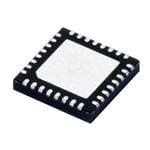
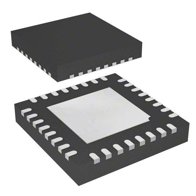
| 供应商器件封装 | 32-VQFN(5x5) |
| 其它名称 | 296-26178-6 |
| 制造商产品页 | http://www.ti.com/general/docs/suppproductinfo.tsp?distId=10&orderablePartNumber=MSP430F1232IRHBT |
| 包装 | Digi-Reel® |
| 单位重量 | 72.200 mg |
| 可用A/D通道 | 8 Channel |
| 可编程输入/输出端数量 | 22 |
| 商标 | Texas Instruments |
| 商标名 | MSP430 |
| 处理器系列 | MSP430F1232 |
| 外设 | 欠压检测/复位,POR,PWM,WDT |
| 安装风格 | SMD/SMT |
| 定时器数量 | 1 Timer |
| 封装 | Reel |
| 封装/外壳 | 32-VFQFN 裸露焊盘 |
| 封装/箱体 | VQFN-32 |
| 工作温度 | -40°C ~ 85°C |
| 工作电源电压 | 1.8 V to 3.6 V |
| 工厂包装数量 | 250 |
| 振荡器类型 | 内部 |
| 接口类型 | SPI, UART, USART |
| 数据RAM大小 | 256 B |
| 数据Ram类型 | SRAM |
| 数据ROM大小 | 256 B |
| 数据Rom类型 | Flash |
| 数据总线宽度 | 16 bit |
| 数据转换器 | A/D 8x10b |
| 最大工作温度 | + 85 C |
| 最大时钟频率 | 8 MHz |
| 最小工作温度 | - 40 C |
| 标准包装 | 1 |
| 核心 | RISC |
| 核心处理器 | MSP430 |
| 核心尺寸 | 16-位 |
| 片上ADC | Yes |
| 电压-电源(Vcc/Vdd) | 1.8 V ~ 3.6 V |
| 程序存储器大小 | 8 kB |
| 程序存储器类型 | 闪存 |
| 程序存储容量 | 8KB(8K x 8 + 256B) |
| 系列 | MSP430F1232 |
| 输入/输出端数量 | 22 I/O |
| 连接性 | SPI,UART/USART |
| 速度 | 8MHz |


- 商务部:美国ITC正式对集成电路等产品启动337调查
- 曝三星4nm工艺存在良率问题 高通将骁龙8 Gen1或转产台积电
- 太阳诱电将投资9.5亿元在常州建新厂生产MLCC 预计2023年完工
- 英特尔发布欧洲新工厂建设计划 深化IDM 2.0 战略
- 台积电先进制程称霸业界 有大客户加持明年业绩稳了
- 达到5530亿美元!SIA预计今年全球半导体销售额将创下新高
- 英特尔拟将自动驾驶子公司Mobileye上市 估值或超500亿美元
- 三星加码芯片和SET,合并消费电子和移动部门,撤换高东真等 CEO
- 三星电子宣布重大人事变动 还合并消费电子和移动部门
- 海关总署:前11个月进口集成电路产品价值2.52万亿元 增长14.8%


PDF Datasheet 数据手册内容提取
(cid:1)(cid:2)(cid:3)(cid:4)(cid:5)(cid:6)(cid:7)(cid:8)(cid:8)(cid:7)(cid:9)(cid:10) (cid:1)(cid:2)(cid:3)(cid:4)(cid:5)(cid:6)(cid:7)(cid:8)(cid:9)(cid:7)(cid:9) (cid:1)(cid:12)(cid:13)(cid:14)(cid:15) (cid:2)(cid:12)(cid:16)(cid:17)(cid:18)(cid:19) (cid:1)(cid:12)(cid:20)(cid:21)(cid:22)(cid:20)(cid:22)(cid:17)(cid:23)(cid:21)(cid:22)(cid:19)(cid:19)(cid:14)(cid:21) SLAS361D − JANUARY 2002 − REVISED AUGUST 2004 (cid:1) (cid:1) Low Supply Voltage Range 1.8 V to 3.6 V Serial Onboard Programming, (cid:1) Ultralow-Power Consumption: No External Programming Voltage Needed − Active Mode: 200 µA at 1 MHz, 2.2 V Programmable Code Protection by − Standby Mode: 0.7 µA Security Fuse − Off Mode (RAM Retention): 0.1 µA (cid:1) Supply Voltage Brownout Protection (cid:1) (cid:1) Five Power Saving Modes MSP430x11x2 Family Members Include: (cid:1) MSP430F1122: 4KB + 256B Flash Memory Wake-Up From Standby Mode in less than 6 µs 256B RAM (cid:1) MSP430F1132: 8KB + 256B Flash Memory 16-Bit RISC Architecture, 125 ns 256B RAM Instruction Cycle Time Available in 20-Pin Plastic SOWB, 20-Pin (cid:1) Basic Clock Module Configurations: Plastic TSSOP and 32-Pin QFN Packages − Various Internal Resistors (cid:1) MSP430x12x2 Family Members Include: − Single External Resistor MSP430F1222: 4KB + 256B Flash Memory − 32-kHz Crystal 256B RAM − High Frequency Crystal MSP430F1232: 8KB + 256B Flash Memory − Resonator 256B RAM − External Clock Source Available in 28-Pin Plastic SOWB, 28-Pin (cid:1) 16-Bit Timer_A With Three Plastic TSSOP, and 32-Pin QFN Packages Capture/Compare Registers (cid:1) For Complete Module Descriptions, See the (cid:1) 10-Bit, 200-ksps A/D Converter With MSP430x1xx Family User’s Guide, Internal Reference, Sample-and-Hold, Literature Number SLAU049 Autoscan, and Data Transfer Controller (cid:1) Serial Communication Interface (USART0) With Software-Selectable Asynchronous UART or Synchronous SPI (MSP430x12x2 Only) description The Texas Instruments MSP430 family of ultralow-power microcontrollers consist of several devices featuring different sets of peripherals targeted for various applications. The architecture, combined with five low power modes is optimized to achieve extended battery life in portable measurement applications. The device features a powerful 16-bit RISC CPU, 16-bit registers, and constant generators that attribute to maximum code efficiency. The digitally controlled oscillator (DCO) allows wake-up from low-power modes to active mode in less than 6µs. The MSP430x11x2 and MSP430x12x2 series are ultralow-power mixed signal microcontrollers with a built-in 16-bit timer, 10-bit A/D converter with integrated reference and data transfer controller (DTC) and fourteen or twenty-two I/O pins. In addition, the MSP430x12x2 series microcontrollers have built-in communication capability using asynchronous (UART) and synchronous (SPI) protocols. Digital signal processing with the 16-bit RISC performance enables effective system solutions such as glass breakage detection with signal analysis (including wave digital filter algorithm). Another area of application is in stand-alone RF sensors. Please be aware that an important notice concerning availability, standard warranty, and use in critical applications of TexasInstruments semiconductor products and disclaimers thereto appears at the end of this data sheet. (cid:3)(cid:21)(cid:22)(cid:15)(cid:24)(cid:20)(cid:23)(cid:12)(cid:22)(cid:17) (cid:15)(cid:18)(cid:23)(cid:18) (cid:25)(cid:26)(cid:27)(cid:28)(cid:29)(cid:30)(cid:31) (cid:25)(cid:28)(cid:26) (cid:25)! "#(cid:29)(cid:29)$(cid:26) (cid:31)! (cid:28)(cid:27) %#&’(cid:25)"(cid:31) (cid:25)(cid:28)(cid:26) ((cid:31) $) Copyright 2002 − 2004, Texas Instruments Incorporated (cid:3)(cid:29)(cid:28)(#" ! "(cid:28)(cid:26)(cid:27)(cid:28)(cid:29)(cid:30) (cid:28) !%$"(cid:25)(cid:27)(cid:25)"(cid:31) (cid:25)(cid:28)(cid:26)! %$(cid:29) *$ $(cid:29)(cid:30)! (cid:28)(cid:27) (cid:23)$(cid:7)(cid:31)! (cid:12)(cid:26)! (cid:29)#(cid:30)$(cid:26) ! ! (cid:31)(cid:26)((cid:31)(cid:29)( +(cid:31)(cid:29)(cid:29)(cid:31)(cid:26) ,) (cid:3)(cid:29)(cid:28)(#" (cid:25)(cid:28)(cid:26) %(cid:29)(cid:28)"$!!(cid:25)(cid:26)- ((cid:28)$! (cid:26)(cid:28) (cid:26)$"$!!(cid:31)(cid:29)(cid:25)’, (cid:25)(cid:26)"’#($ $! (cid:25)(cid:26)- (cid:28)(cid:27) (cid:31)’’ %(cid:31)(cid:29)(cid:31)(cid:30)$ $(cid:29)!) POST OFFICE BOX 655303 • DALLAS, TEXAS 75265 1
(cid:1)(cid:2)(cid:3)(cid:4)(cid:5)(cid:6)(cid:7)(cid:8)(cid:8)(cid:7)(cid:9)(cid:10) (cid:1)(cid:2)(cid:3)(cid:4)(cid:5)(cid:6)(cid:7)(cid:8)(cid:9)(cid:7)(cid:9) (cid:1)(cid:12)(cid:13)(cid:14)(cid:15) (cid:2)(cid:12)(cid:16)(cid:17)(cid:18)(cid:19) (cid:1)(cid:12)(cid:20)(cid:21)(cid:22)(cid:20)(cid:22)(cid:17)(cid:23)(cid:21)(cid:22)(cid:19)(cid:19)(cid:14)(cid:21) SLAS361D − JANUARY 2002 − REVISED AUGUST 2004 AVAILABLE OPTIONS PACKAGED DEVICES TA PLASTIC 20-PIN PLASTIC 20-PIN PLASTIC 28-PIN PLASTIC 28-PIN PLASTIC 32-PIN SOWB (DW) TSSOP (PW) SOWB (DW) TSSOP (PW) QFN (RHB) MSP430F1122IRHB MMSSPP443300FF11112222IIDDWW MMSSPP443300FF11112222IIPPWW MMSSPP443300FF11222222IIDDWW MMSSPP443300FF11222222IIPPWW MMSSPP443300FF11113322IIRRHHBB −40°°C to 85°°C MSP430F1132IDW MSP430F1132IPW MSP430F1232IDW MSP430F1232IPW MSP430F1222IRHB MSP430F1232IRHB pin designation, MSP430x11x2 (see Notes 1, 2 and 3) DW or PW PACKAGE (TOP VIEW) TEST 1 20 P1.7/TA2/TDO/TDI VCC 2 19 P1.6/TA1/TDI/TCLK P2.5/ROSC 3 18 P1.5/TA0/TMS VSS 4 17 P1.4/SMCLK/TCK XOUT 5 16 P1.3/TA2 XIN 6 15 P1.2/TA1 RST/NMI 7 14 P1.1/TA0 P2.0/ACLK/A0 8 13 P1.0/TACLK/ADC10CLK P2.1/INCLK/A1 9 12 P2.4/TA2/A4/V /V REF+ eREF+ P2.2/TA0/A2 10 11 P2.3/TA1/A3/V /V REF− eREF− RHB PACKAGE (TOP VIEW) K DIL K TC C DO/DI/TMSK/T OSC A2/TA1/TA0/TMCL R TTTS 2.5/C CCEST1.7/1.6/1.5/1.4/ PNVTPPPP VSS 1 313029 28 272624 P1.3/TA2 XOUT 2 23 P1.2/TA1 XIN 3 22 P1.1/TA0 NC 4 21 P1.0/TACLK/ADC10CLK RST/NMI 5 20 NC P2.0/ACLK/A0 6 19 P2.4/TA2/A4/VREF+/VeREF+ P2.1/INCLK/A1 7 18 P2.3/TA1/A3/VREF−/VeREF− P2.2/TA0/A2 8 10111213 1415 17 NC d dddd ddd e eeee eee v vvvv vvv er erererer ererer s ssss sss e eeee eee R RRRR RRR NOTES: 1. NC pins are not internally connected. Recommended connection to VSS. 2. Recommended connection to VSS for all pins labeled “Reserved” to avoid floating nodes, otherwise increased current consumption may occur. 3. Power pad connection to VSS recommended. 2 POST OFFICE BOX 655303 • DALLAS, TEXAS 75265
(cid:1)(cid:2)(cid:3)(cid:4)(cid:5)(cid:6)(cid:7)(cid:8)(cid:8)(cid:7)(cid:9)(cid:10) (cid:1)(cid:2)(cid:3)(cid:4)(cid:5)(cid:6)(cid:7)(cid:8)(cid:9)(cid:7)(cid:9) (cid:1)(cid:12)(cid:13)(cid:14)(cid:15) (cid:2)(cid:12)(cid:16)(cid:17)(cid:18)(cid:19) (cid:1)(cid:12)(cid:20)(cid:21)(cid:22)(cid:20)(cid:22)(cid:17)(cid:23)(cid:21)(cid:22)(cid:19)(cid:19)(cid:14)(cid:21) SLAS361D − JANUARY 2002 − REVISED AUGUST 2004 pin designation, MSP430x12x2 (see Notes 1 and 2) DW or PW PACKAGE (TOP VIEW) TEST 1 28 P1.7/TA2/TDO/TDI V 2 27 P1.6/TA1/TDI/TCLK CC P2.5/R 3 26 P1.5/TA0/TMS OSC V 4 25 P1.4/SMCLK/TCK SS XOUT 5 24 P1.3/TA2 XIN 6 23 P1.2/TA1 RST/NMI 7 22 P1.1/TA0 P2.0/ACLK/A0 8 21 P1.0/TACLK/ADC10CLK P2.1/INCLK/A1 9 20 P2.4/TA2/A4/V /V REF+ eREF+ P2.2/TA0/A2 10 19 P2.3/TA1/A3/V /V REF− eREF− P3.0/STE0/A5 11 18 P3.7/A7 P3.1/SIMO0 12 17 P3.6/A6 P3.2/SOMI0 13 16 P3.5/URXD0 P3.3/UCLK0 14 15 P3.4/UTXD0 RHB PACKAGE (TOP VIEW) K DIL K TC C DO/DI/TMSK/T OSC A2/TA1/TA0/TMCL R TTTS 2.5/C CCEST1.7/1.6/1.5/1.4/ PNVTPPPP VSS 1 313029 28 272624 P1.3/TA2 XOUT 2 23 P1.2/TA1 XIN 3 22 P1.1/TA0 NC 4 21 P1.0/TACLK/ADC10CLK RST/NMI 5 20 NC P2.0/ACLK/A0 6 19 P2.4/TA2/A4/VREF+/VeREF+ P2.1/INCLK/A1 7 18 P2.3/TA1/A3/VREF−/VeREF− P2.2/TA0/A2 8 10111213 1415 17 NC 50000 06 7 AOMIKD DA A 3.0/STE0/P3.1/SIMP3.2/SOP3.3/UCLP3.4/UTX P3.5/URXP3.6/ P3.7/ P NOTES: 1. NC pins are not internally connected. Recommended connection to VSS. 2. Power pad connection to VSS recommended. POST OFFICE BOX 655303 • DALLAS, TEXAS 75265 3
(cid:1)(cid:2)(cid:3)(cid:4)(cid:5)(cid:6)(cid:7)(cid:8)(cid:8)(cid:7)(cid:9)(cid:10) (cid:1)(cid:2)(cid:3)(cid:4)(cid:5)(cid:6)(cid:7)(cid:8)(cid:9)(cid:7)(cid:9) (cid:1)(cid:12)(cid:13)(cid:14)(cid:15) (cid:2)(cid:12)(cid:16)(cid:17)(cid:18)(cid:19) (cid:1)(cid:12)(cid:20)(cid:21)(cid:22)(cid:20)(cid:22)(cid:17)(cid:23)(cid:21)(cid:22)(cid:19)(cid:19)(cid:14)(cid:21) SLAS361D − JANUARY 2002 − REVISED AUGUST 2004 functional block diagram, MSP430x11x2 XIN XOUT VCC VSS RST/NMI P1/JTAG P2 8 6 ROSC Oscillator ACLK 8KB Flash 256B RAM ADC10 I/O Port 1 I/O Port 2 8 I/Os, with 6 I/Os, with System SMCLK 4KB Flash 256B RAM 10-Bit Interrupt Interrupt Clock Autoscan Capability Capability DTC MCLK MAB, Test MAB,M 1A6B B, it16-Bit 4 Bit JTAG CPU MCB Incl. 16 Reg. n oe mulatiModul MDBM, D1B6 ,B 1it6-Bit Bus MDB, 8 Bit E Conv TEST Watchdog Timer_A3 POR/ Timer Brownout 3 CC Reg 15/16-Bit functional block diagram, MSP430x12x2 XIN XOUT VCC VSS RST/NMI P1/JTAG P2 P3 8 6 8 ROSC Oscillator ACLK 8KB Flash 256B RAM ADC10 I/O Port 1 I/O Port 2 I/O Port 3 8 I/Os, with 6 I/Os, with 8 I/Os System SMCLK 4KB Flash 256B RAM 10-Bit Interrupt Interrupt Clock Autoscan Capability Capability DTC MCLK MAB, Test MAB,M 1A6B B, it16-Bit 4 Bit JTAG CPU MCB Incl. 16 Reg. n oe mulatiModul MDBM, D1B6 ,B 1it6-Bit Bus MDB, 8 Bit E Conv TEST Watchdog Timer_A3 POR/ USART0 Timer Brownout 3 CC Reg UART Mode 15/16-Bit SPI Mode 4 POST OFFICE BOX 655303 • DALLAS, TEXAS 75265
(cid:1)(cid:2)(cid:3)(cid:4)(cid:5)(cid:6)(cid:7)(cid:8)(cid:8)(cid:7)(cid:9)(cid:10) (cid:1)(cid:2)(cid:3)(cid:4)(cid:5)(cid:6)(cid:7)(cid:8)(cid:9)(cid:7)(cid:9) (cid:1)(cid:12)(cid:13)(cid:14)(cid:15) (cid:2)(cid:12)(cid:16)(cid:17)(cid:18)(cid:19) (cid:1)(cid:12)(cid:20)(cid:21)(cid:22)(cid:20)(cid:22)(cid:17)(cid:23)(cid:21)(cid:22)(cid:19)(cid:19)(cid:14)(cid:21) SLAS361D − JANUARY 2002 − REVISED AUGUST 2004 Terminal Functions, MSP430x11x2 TERMINAL II//OO DDEESSCCRRIIPPTTIIOONN NAME DW & PW RHB P1.0/TACLK/ 13 21 I/O General-purpose digital I/O pin/Timer_A, clock signal TACLK input/conversion ADC10CLK clock—10-bit ADC P1.1/TA0 14 22 I/O General-purpose digital I/O pin/Timer_A, capture: CCI0A input, compare: Out0 output/BSL transmit P1.2/TA1 15 23 I/O General-purpose digital I/O pin/Timer_A, capture: CCI1A input, compare: Out1 output P1.3/TA2 16 24 I/O General-purpose digital I/O pin/Timer_A, capture: CCI2A input, compare: Out2 output P1.4/SMCLK/TCK 17 25 I/O General-purpose digital I/O pin/SMCLK signal output/test clock, input terminal for device programming and test P1.5/TA0/TMS 18 26 I/O General-purpose digital I/O pin/Timer_A, compare: Out0 output/test mode select, input terminal for device programming and test P1.6/TA1/TDI/TCLK 19 27 I/O General-purpose digital I/O pin/Timer_A, compare: Out1 output/test data input terminal or test clock input P1.7/TA2/TDO/TDI† 20 28 I/O General-purpose digital I/O pin/Timer_A, compare: Out2 output/test data output terminal or data input during programming P2.0/ACLK/A0 8 6 I/O General-purpose digital I/O pin/ACLK output/analog input to 10-bit ADC input A0 P2.1/INCLK/A1 9 7 I/O General-purpose digital I/O pin/Timer_A, clock signal at INCLK/analog input to 10-bit ADC input A1 P2.2/TA0/A2 10 8 I/O General-purpose digital I/O pin/Timer_A, capture: CCI0B input, compare: Out0 output/analog input to 10-bit ADC input A2/BSL receive P2.3/TA1/A3/VREF−/ 11 18 I/O General-purpose digital I/O pin/Timer_A, capture: CCI1B input, compare: Out1 VeREF− output/analog input to 10-bit ADC input A3/negative reference voltage terminal. P2.4/TA2/A4/VREF+/ 12 19 I/O General-purpose digital I/O pin/Timer_A, compare: Out2 output/analog input to 10-bit VeREF+ ADC input A4/I/O of positive reference voltage terminal P2.5/ROSC 3 32 I/O General-purpose digital I/O pin/Input for external resistor that defines the DCO nominal frequency RST/NMI 7 5 I Reset or nonmaskable interrupt input TEST 1 29 I Selects test mode for JTAG pins on P1.x VCC 2 30 Supply voltage VSS 4 1 Ground reference XIN 6 3 I Input terminal of crystal oscillator XOUT 5 2 O Output terminal of crystal oscillator NC NA 4,17,20,31 Not connected internally. Recommended connection to VSS. Reserved NA 9 - 16 Reserved pins. Recommended connection to VSS to avoid floating nodes, otherwise increased current consumption may occur. QFN Pad NA Package QFN package pad connection to VSS recommended. Pad †TDO or TDI is selected via JTAG instruction. POST OFFICE BOX 655303 • DALLAS, TEXAS 75265 5
(cid:1)(cid:2)(cid:3)(cid:4)(cid:5)(cid:6)(cid:7)(cid:8)(cid:8)(cid:7)(cid:9)(cid:10) (cid:1)(cid:2)(cid:3)(cid:4)(cid:5)(cid:6)(cid:7)(cid:8)(cid:9)(cid:7)(cid:9) (cid:1)(cid:12)(cid:13)(cid:14)(cid:15) (cid:2)(cid:12)(cid:16)(cid:17)(cid:18)(cid:19) (cid:1)(cid:12)(cid:20)(cid:21)(cid:22)(cid:20)(cid:22)(cid:17)(cid:23)(cid:21)(cid:22)(cid:19)(cid:19)(cid:14)(cid:21) SLAS361D − JANUARY 2002 − REVISED AUGUST 2004 Terminal Functions, MSP430x12x2 TERMINAL II//OO DDEESSCCRRIIPPTTIIOONN NAME DW & PW RHB P1.0/TACLK/ 21 21 I/O General-purpose digital I/O pin/Timer_A, clock signal TACLK input/conversion ADC10CLK clock—10-bit ADC P1.1/TA0 22 22 I/O General-purpose digital I/O pin/Timer_A, capture: CCI0A input, compare: Out0 output/BSL transmit P1.2/TA1 23 23 I/O General-purpose digital I/O pin/Timer_A, capture: CCI1A input, compare: Out1 output P1.3/TA2 24 24 I/O General-purpose digital I/O pin/Timer_A, capture: CCI2A input, compare: Out2 output P1.4/SMCLK/TCK 25 25 I/O General-purpose digital I/O pin/SMCLK signal output/test clock, input terminal for device programming and test P1.5/TA0/TMS 26 26 I/O General-purpose digital I/O pin/Timer_A, compare: Out0 output/test mode select, input terminal for device programming and test P1.6/TA1/TDI/TCLK 27 27 I/O General-purpose digital I/O pin/Timer_A, compare: Out1 output/test data input terminal or test clock input P1.7/TA2/TDO/TDI† 28 28 I/O General-purpose digital I/O pin/Timer_A, compare: Out2 output/test data output terminal or data input during programming P2.0/ACLK/A0 8 6 I/O General-purpose digital I/O pin/ACLK output/analog input to 10-bit ADC input A0 P2.1/INCLK/A1 9 7 I/O General-purpose digital I/O pin/Timer_A, clock signal at INCLK/analog input to 10-bit ADC input A1 P2.2/TA0/A2 10 8 I/O General-purpose digital I/O pin/Timer_A, capture: CCI0B input, compare: Out0 output/analog input to 10-bit ADC input A2/BSL receive P2.3/TA1/A3/VREF−/ 19 18 I/O General-purpose digital I/O pin/Timer_A, capture: CCI1B input, compare: Out1 VeREF− output/analog input to 10-bit ADC input A3/negative reference voltage terminal. P2.4/TA2/A4/VREF+/ 20 19 I/O General-purpose digital I/O pin/Timer_A, compare: Out2 output/analog input to 10-bit VeREF+ ADC input A4/I/O of positive reference voltage terminal P2.5/ROSC 3 32 I/O General-purpose digital I/O pin/Input for external resistor that defines the DCO nominal frequency P3.0/STE0/A5 11 9 I/O General-purpose digital I/O pin/slave transmit enable—USART0/SPI mode/analog input to 10-bit ADC input A5 P3.1/SIMO0 12 10 I/O General-purpose digital I/O pin/slave in/master out of USART0/SPI mode P3.2/SOMI0 13 11 I/O General-purpose digital I/O pin/slave out/master in of USART0/SPI mode P3.3/UCLK0 14 12 I/O General-purpose digital I/O pin/external clock input—USART0/UART or SPI mode, clock output—USART0/SPI mode clock input P3.4/UTXD0 15 13 I/O General-purpose digital I/O pin/transmit data out—USART0/UART mode P3.5/URXD0 16 14 I/O General-purpose digital I/O pin/receive data in—USART0/UART mode P3.6/A6 17 15 I/O General-purpose digital I/O pin/analog input to 10-bit ADC input A6 P3.7/A7 18 16 I/O General-purpose digital I/O pin/analog input to 10-bit ADC input A7 RST/NMI 7 5 I Reset or nonmaskable interrupt input TEST 1 29 I Selects test mode for JTAG pins on P1.x VCC 2 30 Supply voltage VSS 4 1 Ground reference XIN 6 3 I Input terminal of crystal oscillator XOUT 5 2 O Output terminal of crystal oscillator NC NA 4,17,20,31 Not connected internally. Recommended connection to VSS. QFN Pad NA QFN package pad connection to VSS recommended. †TDO or TDI is selected via JTAG instruction. 6 POST OFFICE BOX 655303 • DALLAS, TEXAS 75265
(cid:1)(cid:2)(cid:3)(cid:4)(cid:5)(cid:6)(cid:7)(cid:8)(cid:8)(cid:7)(cid:9)(cid:10) (cid:1)(cid:2)(cid:3)(cid:4)(cid:5)(cid:6)(cid:7)(cid:8)(cid:9)(cid:7)(cid:9) (cid:1)(cid:12)(cid:13)(cid:14)(cid:15) (cid:2)(cid:12)(cid:16)(cid:17)(cid:18)(cid:19) (cid:1)(cid:12)(cid:20)(cid:21)(cid:22)(cid:20)(cid:22)(cid:17)(cid:23)(cid:21)(cid:22)(cid:19)(cid:19)(cid:14)(cid:21) SLAS361D − JANUARY 2002 − REVISED AUGUST 2004 short-form description CPU The MSP430 CPU has a 16-bit RISC architecture Program Counter PC/R0 that is highly transparent to the application. All operations, other than program-flow instructions, Stack Pointer SP/R1 are performed as register operations in Status Register SR/CG1/R2 conjunction with seven addressing modes for source operand and four addressing modes for Constant Generator CG2/R3 destination operand. General-Purpose Register R4 The CPU is integrated with 16 registers that provide reduced instruction execution time. The General-Purpose Register R5 register-to-register operation execution time is one cycle of the CPU clock. General-Purpose Register R6 Four of the registers, R0 to R3, are dedicated as General-Purpose Register R7 program counter, stack pointer, status register, and constant generator respectively. The General-Purpose Register R8 remaining registers are general-purpose registers. General-Purpose Register R9 Peripherals are connected to the CPU using data, General-Purpose Register R10 address, and control buses, and can be handled with all instructions. General-Purpose Register R11 instruction set General-Purpose Register R12 The instruction set consists of 51 instructions with three formats and seven address modes. Each General-Purpose Register R13 instruction can operate on word and byte data. Table1 shows examples of the three types of General-Purpose Register R14 instruction formats; the address modes are listed General-Purpose Register R15 in Table2. Table 1. Instruction Word Formats Dual operands, source-destination e.g. ADD R4,R5 R4 + R5 −−−> R5 Single operands, destination only e.g. CALL R8 PC −−>(TOS), R8−−> PC Relative jump, un/conditional e.g. JNE Jump-on-equal bit = 0 Table 2. Address Mode Descriptions ADDRESS MODE S D SYNTAX EXAMPLE OPERATION (cid:1) (cid:1) Register MOV Rs,Rd MOV R10,R11 R10 −−> R11 (cid:1) (cid:1) Indexed MOV X(Rn),Y(Rm) MOV 2(R5),6(R6) M(2+R5)−−> M(6+R6) (cid:1) (cid:1) Symbolic (PC relative) MOV EDE,TONI M(EDE) −−> M(TONI) (cid:1) (cid:1) Absolute MOV &MEM,&TCDAT M(MEM) −−> M(TCDAT) (cid:1) Indirect MOV @Rn,Y(Rm) MOV @R10,Tab(R6) M(R10) −−> M(Tab+R6) Indirect (cid:1) M(R10) −−> R11 MOV @Rn+,Rm MOV @R10+,R11 autoincrement R10 + 2−−> R10 (cid:1) Immediate MOV #X,TONI MOV #45,TONI #45 −−> M(TONI) NOTE: S = source D = destination POST OFFICE BOX 655303 • DALLAS, TEXAS 75265 7
(cid:1)(cid:2)(cid:3)(cid:4)(cid:5)(cid:6)(cid:7)(cid:8)(cid:8)(cid:7)(cid:9)(cid:10) (cid:1)(cid:2)(cid:3)(cid:4)(cid:5)(cid:6)(cid:7)(cid:8)(cid:9)(cid:7)(cid:9) (cid:1)(cid:12)(cid:13)(cid:14)(cid:15) (cid:2)(cid:12)(cid:16)(cid:17)(cid:18)(cid:19) (cid:1)(cid:12)(cid:20)(cid:21)(cid:22)(cid:20)(cid:22)(cid:17)(cid:23)(cid:21)(cid:22)(cid:19)(cid:19)(cid:14)(cid:21) SLAS361D − JANUARY 2002 − REVISED AUGUST 2004 operating modes The MSP430 has one active mode and five software selectable low-power modes of operation. An interrupt event can wake up the device from any of the five low-power modes, service the request and restore back to the low-power mode on return from the interrupt program. The following six operating modes can be configured by software: (cid:1) Active mode AM; − All clocks are active (cid:1) Low-power mode 0 (LPM0); − CPU is disabled ACLK and SMCLK remain active. MCLK is disabled (cid:1) Low-power mode 1 (LPM1); − CPU is disabled ACLK and SMCLK remain active. MCLK is disabled DCO’s dc-generator is disabled if DCO not used in active mode (cid:1) Low-power mode 2 (LPM2); − CPU is disabled MCLK and SMCLK are disabled DCO’s dc-generator remains enabled ACLK remains active (cid:1) Low-power mode 3 (LPM3); − CPU is disabled MCLK and SMCLK are disabled DCO’s dc-generator is disabled ACLK remains active (cid:1) Low-power mode 4 (LPM4); − CPU is disabled ACLK is disabled MCLK and SMCLK are disabled DCO’s dc-generator is disabled Crystal oscillator is stopped 8 POST OFFICE BOX 655303 • DALLAS, TEXAS 75265
(cid:1)(cid:2)(cid:3)(cid:4)(cid:5)(cid:6)(cid:7)(cid:8)(cid:8)(cid:7)(cid:9)(cid:10) (cid:1)(cid:2)(cid:3)(cid:4)(cid:5)(cid:6)(cid:7)(cid:8)(cid:9)(cid:7)(cid:9) (cid:1)(cid:12)(cid:13)(cid:14)(cid:15) (cid:2)(cid:12)(cid:16)(cid:17)(cid:18)(cid:19) (cid:1)(cid:12)(cid:20)(cid:21)(cid:22)(cid:20)(cid:22)(cid:17)(cid:23)(cid:21)(cid:22)(cid:19)(cid:19)(cid:14)(cid:21) SLAS361D − JANUARY 2002 − REVISED AUGUST 2004 interrupt vector addresses The interrupt vectors and the power-up starting address are located in the address range of 0FFFFh-0FFE0h. The vector contains the 16-bit address of the appropriate interrupt handler instruction sequence. INTERRUPT SOURCE INTERRUPT FLAG SYSTEM INTERRUPT WORD ADDRESS PRIORITY Power-up External reset WDTIFG (see Note1) Reset 0FFFEh 15, highest Watchdog KEYV (see Note 1) Flash memory NMI NMIIFG (see Notes 1 and 4) (Non)-maskable Oscillator fault OFIFG (see Notes 1 and 4) (Non)-maskable 0FFFCh 14 Flash memory access violation ACCVIFG (see Notes 1 and 4) (Non)-maskable 0FFFAh 13 0FFF8h 12 0FFF6h 11 Watchdog timer WDTIFG Maskable 0FFF4h 10 Timer_A3 TACCR0 CCIFG (see Note 2) Maskable 0FFF2h 9 TACCR1 and TACCR2 Timer_A3 CCIFGs, TAIFG Maskable 0FFF0h 8 (see Notes 1 and 2) USART0 receive (see Note 5) URXIFG0 Maskable 0FFEEh 7 USART0 transmit (see Note 5) UTXIFG0 Maskable 0FFECh 6 ADC10 ADC10IFG Maskable 0FFEAh 5 0FFE8h 4 I/O Port P2 P2IFG.0 to P2IFG.7 Maskable 0FFE6h 3 (eight flags − see Note 3) (see Notes 1 and 2) I/O Port P1 P1IFG.0 to P1IFG.7 Maskable 0FFE4h 2 (eight flags) (see Notes 1 and 2) 0FFE2h 1 0FFE0h 0, lowest NOTES: 1. Multiple source flags 2. Interrupt flags are located in the module 3. There are eight Port P2 interrupt flags, but only six Port P2 I/O pins (P2.0−5) are implemented on the ’11x2 and ’12x2 devices. 4. (Non)-maskable: the individual interrupt enable bit can disable an interrupt event, but the general interrupt enable cannot. 5. USART0 is implemented in MSP430x12x2 devices only. POST OFFICE BOX 655303 • DALLAS, TEXAS 75265 9
(cid:1)(cid:2)(cid:3)(cid:4)(cid:5)(cid:6)(cid:7)(cid:8)(cid:8)(cid:7)(cid:9)(cid:10) (cid:1)(cid:2)(cid:3)(cid:4)(cid:5)(cid:6)(cid:7)(cid:8)(cid:9)(cid:7)(cid:9) (cid:1)(cid:12)(cid:13)(cid:14)(cid:15) (cid:2)(cid:12)(cid:16)(cid:17)(cid:18)(cid:19) (cid:1)(cid:12)(cid:20)(cid:21)(cid:22)(cid:20)(cid:22)(cid:17)(cid:23)(cid:21)(cid:22)(cid:19)(cid:19)(cid:14)(cid:21) SLAS361D − JANUARY 2002 − REVISED AUGUST 2004 special function registers Most interrupt and module enable bits are collected into the lowest address space. Special function register bits that are not allocated to a functional purpose are not physically present in the device. Simple software access is provided with this arrangement. interrupt enable 1 and 2 Address 7 6 5 4 3 2 1 0 0h ACCVIE NMIIE OFIE WDTIE rw-0 rw-0 rw-0 rw-0 WDTIE: Watchdog Timer interrupt enable. Inactive if watchdog mode is selected. Active if Watchdog Timer is configured in interval timer mode. OFIE: Oscillator fault enable NMIIE: (Non)maskable interrupt enable ACCVIE: Flash access violation interrupt enable Address 7 6 5 4 3 2 1 0 01h UTXIE0 URXIE0 rw-0 rw-0 URXIE0: USART0: UART and SPI receive-interrupt enable (MSP430x12x2 devices only) UTXIE0: USART0: UART and SPI transmit-interrupt enable (MSP430x12x2 devices only) interrupt flag register 1 and 2 Address 7 6 5 4 3 2 1 0 02h NMIIFG OFIFG WDTIFG rw-0 rw-1 rw-(0) WDTIFG: Set on Watchdog Timer overflow (in watchdog mode) or security key violation. Reset on V power-up or a reset condition at RST/NMI pin in reset mode. CC OFIFG: Flag set on oscillator fault NMIIFG: Set via RST/NMI-pin Address 7 6 5 4 3 2 1 0 03h UTXIFG0 URXIFG0 rw-1 rw-0 URXIFG0: USART0: UART and SPI receive flag (MSP430x12x2 devices only) UTXIFG0: USART0: UART and SPI transmit flag (MSP430x12x2 devices only) 10 POST OFFICE BOX 655303 • DALLAS, TEXAS 75265
(cid:1)(cid:2)(cid:3)(cid:4)(cid:5)(cid:6)(cid:7)(cid:8)(cid:8)(cid:7)(cid:9)(cid:10) (cid:1)(cid:2)(cid:3)(cid:4)(cid:5)(cid:6)(cid:7)(cid:8)(cid:9)(cid:7)(cid:9) (cid:1)(cid:12)(cid:13)(cid:14)(cid:15) (cid:2)(cid:12)(cid:16)(cid:17)(cid:18)(cid:19) (cid:1)(cid:12)(cid:20)(cid:21)(cid:22)(cid:20)(cid:22)(cid:17)(cid:23)(cid:21)(cid:22)(cid:19)(cid:19)(cid:14)(cid:21) SLAS361D − JANUARY 2002 − REVISED AUGUST 2004 module enable registers 1 and 2 Address 7 6 5 4 3 2 1 0 04h Address 7 6 5 4 3 2 1 0 URXE0 05h UTXE0 USPIE0 rw-0 rw-0 URXE0: USART0: UART mode receive enable (MSP430x12x2 devices only) UTXE0: USART0: UART mode transmit enable (MSP430x12x2 devices only) USPIE0: USART0: SPI mode transmit and receive enable (MSP430x12x2 devices only) Legend rw: Bit can be read and written. rw-0,1: Bit can be read and written. It is Reset or Set by PUC rw-(0,1): Bit can be read and written. It is Reset or Set by POR SFR bit is not present in device. memory organization MSP430F1122 MSP430F1132 MSP430F1222 MSP430F1232 Memory Size 4KB Flash 8KB Flash 4KB Flash 8KB Flash Main: interrupt vector Flash 0FFFFh−0FFE0h 0FFFFh−0FFE0h 0FFFFh−0FFE0h 0FFFFh−0FFE0h Main: code memory Flash 0FFFFh−0F000h 0FFFFh−0E000h 0FFFFh−0F000h 0FFFFh−0E000h Information memory Size 256 Byte 256 Byte 256 Byte 256 Byte Flash 010FFh − 01000h 010FFh − 01000h 010FFh − 01000h 010FFh − 01000h Boot memory Size 1KB 1KB 1KB 1KB ROM 0FFFh − 0C00h 0FFFh − 0C00h 0FFFh − 0C00h 0FFFh − 0C00h RAM Size 256 Byte 256 Byte 256 Byte 256 Byte 02FFh − 0200h 02FFh − 0200h 02FFh − 0200h 02FFh − 0200h Peripherals 16-bit 01FFh − 0100h 01FFh − 0100h 01FFh − 0100h 01FFh − 0100h 8-bit 0FFh − 010h 0FFh − 010h 0FFh − 010h 0FFh − 010h 8-bit SFR 0Fh − 00h 0Fh − 00h 0Fh − 00h 0Fh − 00h bootstrap loader (BSL) The MSP430 bootstrap loader (BSL) enables users to program the flash memory or RAM using a UART serial interface. Access to the MSP430 memory via the BSL is protected by user-defined password. For complete description of the features of the BSL and its implementation, see the Application report Features of the MSP430 Bootstrap Loader, Literature Number SLAA089. MSP430x11x2 MSP430x12x2 MSP430x11x2/12x2 BSL Function DW & PW Package DW & PW Package RHB Package (20 Pins) (28 Pins) (32 Pins) Data Transmit 14 - P1.1 22 - P1.1 22 - P1.1 Data Receive 10 - P2.2 10 - P2.2 8 - P2.2 POST OFFICE BOX 655303 • DALLAS, TEXAS 75265 11
(cid:1)(cid:2)(cid:3)(cid:4)(cid:5)(cid:6)(cid:7)(cid:8)(cid:8)(cid:7)(cid:9)(cid:10) (cid:1)(cid:2)(cid:3)(cid:4)(cid:5)(cid:6)(cid:7)(cid:8)(cid:9)(cid:7)(cid:9) (cid:1)(cid:12)(cid:13)(cid:14)(cid:15) (cid:2)(cid:12)(cid:16)(cid:17)(cid:18)(cid:19) (cid:1)(cid:12)(cid:20)(cid:21)(cid:22)(cid:20)(cid:22)(cid:17)(cid:23)(cid:21)(cid:22)(cid:19)(cid:19)(cid:14)(cid:21) SLAS361D − JANUARY 2002 − REVISED AUGUST 2004 flash memory The flash memory can be programmed via the JTAG port, the bootstrap loader, or in-system by the CPU. The CPU can perform single-byte and single-word writes to the flash memory. Features of the flash memory include: (cid:1) Flash memory has n segments of main memory and two segments of information memory (A and B) of 128 bytes each. Each segment in main memory is 512 bytes in size. (cid:1) Segments 0 to n may be erased in one step, or each segment may be individually erased. (cid:1) Segments A and B can be erased individually, or as a group with segments 0−n. Segments A and B are also called information memory. (cid:1) New devices may have some bytes programmed in the information memory (needed for test during manufacturing). The user should perform an erase of the information memory prior to the first use. 0FFFFh Segment0 w/ 0FE00h Interrupt Vectors 0FDFFh Segment1 0FC00h 0FBFFh Segment2 0FA00h 0F9FFh Segment3 0F800h Flash Main Memory 0F7FFh Segment4 0F600h 0E3FFh Segment14 0E200h 0E1FFh Segment15 0E000h 010FFh SegmentA 01080h Information Memory 0107Fh SegmentB 01000h NOTE: All segments not implemented on all devices. 12 POST OFFICE BOX 655303 • DALLAS, TEXAS 75265
(cid:1)(cid:2)(cid:3)(cid:4)(cid:5)(cid:6)(cid:7)(cid:8)(cid:8)(cid:7)(cid:9)(cid:10) (cid:1)(cid:2)(cid:3)(cid:4)(cid:5)(cid:6)(cid:7)(cid:8)(cid:9)(cid:7)(cid:9) (cid:1)(cid:12)(cid:13)(cid:14)(cid:15) (cid:2)(cid:12)(cid:16)(cid:17)(cid:18)(cid:19) (cid:1)(cid:12)(cid:20)(cid:21)(cid:22)(cid:20)(cid:22)(cid:17)(cid:23)(cid:21)(cid:22)(cid:19)(cid:19)(cid:14)(cid:21) SLAS361D − JANUARY 2002 − REVISED AUGUST 2004 peripherals Peripherals are connected to the CPU through data, address, and control busses and can be handled using all instructions. For complete module descriptions, see the MSP430x1xx Family User’s Guide, literature number SLAU049. oscillator and system clock The clock system in the MSP430x11x2 and MSP430x12x2 devices is supported by the basic clock module that includes support for a 32768-Hz watch crystal oscillator, an internal digitally-controlled oscillator (DCO) and a high frequency crystal oscillator. The basic clock module is designed to meet the requirements of both low system cost and low-power consumption. The internal DCO provides a fast turn-on clock source and stabilizes in less than 6 µs. The basic clock module provides the following clock signals: (cid:1) Auxiliary clock (ACLK), sourced from a 32768-Hz watch crystal or a high frequency crystal. (cid:1) Main clock (MCLK), the system clock used by the CPU. (cid:1) Sub-Main clock (SMCLK), the sub-system clock used by the peripheral modules. digital I/O There are 3 8-bit I/O ports implemented—ports P1, P2, and P3 (only six port P2 I/O signals are available on external pins; port P3 is implemented only on ’x12x2 devices): (cid:1) All individual I/O bits are independently programmable. (cid:1) Any combination of input, output, and interrupt conditions is possible. (cid:1) Edge-selectable interrupt input capability for all the eight bits of ports P1 and six bits of port P2. (cid:1) Read/write access to port-control registers is supported by all instructions. NOTE: Six bits of port P2, P2.0 to P2.5, are available on external pins, but all control and data bits for port P2 are implemented. Port P3 has no interrupt capability. Port P3 is implemented in MSP430x12x2 only. brownout The brownout circuit is implemented to provide the proper internal reset signal to the device during power on and power off. watchdog timer The primary function of the watchdog timer (WDT) module is to perform a controlled system restart after a software problem occurs. If the selected time interval expires, a system reset is generated. If the watchdog function is not needed in an application, the module can be configured as an interval timer and can generate interrupts at selected time intervals. USART0 (MSP430x12x2 Only) The MSP430x12x2 devices have one hardware universal synchronous/asynchronous receive transmit (USART0) peripheral module that is used for serial data communication. The USART supports synchronous SPI (3 or 4 pin) and asynchronous UART communication protocols, using double-buffered transmit and receive channels. ADC10 The ADC10 module supports fast, 10-bit analog-to-digital conversions. The module implements a 10-bit SAR core, sample select control, reference generator and data transfer controller, or DTC, for automatic conversion result handling allowing ADC samples to be converted and stored without any CPU intervention. POST OFFICE BOX 655303 • DALLAS, TEXAS 75265 13
(cid:1)(cid:2)(cid:3)(cid:4)(cid:5)(cid:6)(cid:7)(cid:8)(cid:8)(cid:7)(cid:9)(cid:10) (cid:1)(cid:2)(cid:3)(cid:4)(cid:5)(cid:6)(cid:7)(cid:8)(cid:9)(cid:7)(cid:9) (cid:1)(cid:12)(cid:13)(cid:14)(cid:15) (cid:2)(cid:12)(cid:16)(cid:17)(cid:18)(cid:19) (cid:1)(cid:12)(cid:20)(cid:21)(cid:22)(cid:20)(cid:22)(cid:17)(cid:23)(cid:21)(cid:22)(cid:19)(cid:19)(cid:14)(cid:21) SLAS361D − JANUARY 2002 − REVISED AUGUST 2004 timer_A3 Timer_A3 is a 16-bit timer/counter with three capture/compare registers. Timer_A3 can support multiple capture/compares, PWM outputs, and interval timing. Timer_A3 also has extensive interrupt capabilities. Interrupts may be generated from the counter on overflow conditions and from each of the capture/compare registers. Timer_A3 Signal Connections Input Pin Number Output Pin Number DW and PW RHB DDeevviiccee IInnppuutt MMoodduullee MMoodduullee MMoodduullee OOuuttppuutt DW and PW RHB ’11x2 ’12x2 ’11x2/12x2 Signal Input Name Block Signal ’11x2 ’12x2 ’11x2/12x2 20-Pin 28-Pin 32-Pin 20-Pin 28-Pin 32-Pin 13 - P1.0 21 - P1.0 21 - P1.0 TACLK TACLK ACLK ACLK Timer NA SMCLK SMCLK 9 - P2.1 9 - P2.1 7 - P2.1 INCLK INCLK 14 - P1.1 22 - P1.1 22 - P1.1 TA0 CCI0A 14 - P1.1 22 - P1.1 22 - P1.1 10 - P2.2 10 - P2.2 8 - P2.2 TA0 CCI0B 18 - P1.5 26 - P1.5 26 - P1.5 CCR0 TA0 DVSS GND 10 - P2.2 10 - P2.2 8 - P2.2 DVCC VCC ADC10 Internal 15 - P1.2 23 - P1.2 23 - P1.2 TA1 CCI1A 15 - P1.2 23 - P1.2 23 - P1.2 11 - P2.3 19 - P2.3 18 - P2.3 TA1 CCI1B 19 - P1.6 27 - P1.6 27 - P1.6 CCR1 TA1 DVSS GND 11 - P2.3 19 - P2.3 18 - P2.3 DVCC VCC ADC10 Internal 16 - P1.3 24 - P1.3 24 - P1.3 TA2 CCI2A 16 - P1.3 24 - P1.3 24 - P1.3 ACLK (internal) CCI2B 20 - P1.7 28 - P1.7 28 - P1.7 CCR2 TA2 DVSS GND 12 - P2.4 20 - P2.4 19 - P2.4 DVCC VCC ADC10 Internal 14 POST OFFICE BOX 655303 • DALLAS, TEXAS 75265
(cid:1)(cid:2)(cid:3)(cid:4)(cid:5)(cid:6)(cid:7)(cid:8)(cid:8)(cid:7)(cid:9)(cid:10) (cid:1)(cid:2)(cid:3)(cid:4)(cid:5)(cid:6)(cid:7)(cid:8)(cid:9)(cid:7)(cid:9) (cid:1)(cid:12)(cid:13)(cid:14)(cid:15) (cid:2)(cid:12)(cid:16)(cid:17)(cid:18)(cid:19) (cid:1)(cid:12)(cid:20)(cid:21)(cid:22)(cid:20)(cid:22)(cid:17)(cid:23)(cid:21)(cid:22)(cid:19)(cid:19)(cid:14)(cid:21) SLAS361D − JANUARY 2002 − REVISED AUGUST 2004 peripheral file map PERIPHERALS WITH WORD ACCESS ADC10 ADC data transfer start address ADC10SA 1BCh ADC memory ADC10MEM 1B4h ADC control register 1 ADC10CTL1 1B2h ADC control register 0 ADC10CTL0 1B0h ADC analog enable ADC10AE 04Ah ADC data transfer control register 1 ADC10DTC1 049h ADC data transfer control register 0 ADC10DTC0 048h Timer_A Reserved 017Eh Reserved 017Ch Reserved 017Ah Reserved 0178h Capture/compare register TACCR2 0176h Capture/compare register TACCR1 0174h Capture/compare register TACCR0 0172h Timer_A register TAR 0170h Reserved 016Eh Reserved 016Ch Reserved 016Ah Reserved 0168h Capture/compare control TACCTL2 0166h Capture/compare control TACCTL1 0164h Capture/compare control TACCTL0 0162h Timer_A control TACTL 0160h Timer_A interrupt vector TAIV 012Eh Flash Memory Flash control 3 FCTL3 012Ch Flash control 2 FCTL2 012Ah Flash control 1 FCTL1 0128h Watchdog Watchdog/timer control WDTCTL 0120h PERIPHERALS WITH BYTE ACCESS USART0 Transmit buffer U0TXBUF 077h (in MSP430x12x2 only) Receive buffer U0RXBUF 076h Baud rate U0BR1 075h Baud rate U0BR0 074h Modulation control U0MCTL 073h Receive control U0RCTL 072h Transmit control U0TCTL 071h USART control U0CTL 070h Basic Clock Basic clock sys. control2 BCSCTL2 058h Basic clock sys. control1 BCSCTL1 057h DCO clock freq. control DCOCTL 056h Port P2 Port P2 selection P2SEL 02Eh Port P2 interrupt enable P2IE 02Dh Port P2 interrupt edge select P2IES 02Ch Port P2 interrupt flag P2IFG 02Bh Port P2 direction P2DIR 02Ah Port P2 output P2OUT 029h Port P2 input P2IN 028h Port P1 Port P1 selection P1SEL 026h Port P1 interrupt enable P1IE 025h Port P1 interrupt edge select P1IES 024h Port P1 interrupt flag P1IFG 023h Port P1 direction P1DIR 022h Port P1 output P1OUT 021h Port P1 input P1IN 020h POST OFFICE BOX 655303 • DALLAS, TEXAS 75265 15
(cid:1)(cid:2)(cid:3)(cid:4)(cid:5)(cid:6)(cid:7)(cid:8)(cid:8)(cid:7)(cid:9)(cid:10) (cid:1)(cid:2)(cid:3)(cid:4)(cid:5)(cid:6)(cid:7)(cid:8)(cid:9)(cid:7)(cid:9) (cid:1)(cid:12)(cid:13)(cid:14)(cid:15) (cid:2)(cid:12)(cid:16)(cid:17)(cid:18)(cid:19) (cid:1)(cid:12)(cid:20)(cid:21)(cid:22)(cid:20)(cid:22)(cid:17)(cid:23)(cid:21)(cid:22)(cid:19)(cid:19)(cid:14)(cid:21) SLAS361D − JANUARY 2002 − REVISED AUGUST 2004 peripheral file map (continued) PERIPHERALS WITH BYTE ACCESS (CONTINUED) Port P3 Port P3 selection P3SEL 01Bh (in MSP430x12x2 only) Port P3 direction P3DIR 01Ah Port P3 output P3OUT 019h Port P3 input P3IN 018h Special Function Module enable2 ME2 005h Module enable1 ME1 004h SFR interrupt flag2 IFG2 003h SFR interrupt flag1 IFG1 002h SFR interrupt enable2 IE2 001h SFR interrupt enable1 IE1 000h absolute maximum ratings† Voltage applied at V to V . . . . . . . . . . . . . . . . . . . . . . . . . . . . . . . . . . . . . . . . . . . . . . . . . . . . . . −0.3 V to 4.1 V CC SS Voltage applied to any pin (see Note) . . . . . . . . . . . . . . . . . . . . . . . . . . . . . . . . . . . . . . . . . . −0.3 V to VCC + 0.3 V Diode current at any device terminal . . . . . . . . . . . . . . . . . . . . . . . . . . . . . . . . . . . . . . . . . . . . . . . . . . . . . . . . ±2 mA Storage temperature, T (unprogrammed device) . . . . . . . . . . . . . . . . . . . . . . . . . . . . . . . . . . . −55°C to 150°C stg Storage temperature, T (programmed device) . . . . . . . . . . . . . . . . . . . . . . . . . . . . . . . . . . . . . . −40°C to 85°C stg †Stresses beyond those listed under “absolute maximum ratings” may cause permanent damage to the device. These are stress ratings only, and functional operation of the device at these or any other conditions beyond those indicated under “recommended operating conditions” is not implied. Exposure to absolute-maximum-rated conditions for extended periods may affect device reliability. NOTE: All voltages referenced to VSS. The JTAG fuse-blow voltage, VFB, is allowed to exceed the absolute maximum rating. The voltage is applied to the TEST pin when blowing the JTAG fuse. recommended operating conditions MIN NOM MAX UNITS Supply voltage during program execution, VCC (see Note 1) MMSSPP443300FF1111xx22 1.8 3.6 V Supply voltage during program/erase flash memory, VCC MSP430F12x2 2.7 3.6 V Supply voltage, VSS 0 V MSP430F11x2 Operating free-air temperature range, TA MSP430F12x2 −40 85 °C LF mode selected, XTS=0 Watch crystal 32768 Hz LFXT1 crystal frequency, f(LFXT1) Ceramic resonator 450 8000 (see Note 1 & Note 2) XT1 selected mode, XTS=1 kHz Crystal 1000 8000 VCC = 1.8 V, MSP430F11x2 dc 4.15 MSP430F12x2 Processor frequency f(system) (MCLK signal) VCC = 3.6 V, MHz MSP430F11x2 dc 8 MSP430F12x2 NOTES: 1. The LFXT1 oscillator in LF-mode requires a resistor of 5.1 MΩ from XOUT to VSS when VCC <2.5 V. The LFXT1 oscillator in XT1-mode accepts a ceramic resonator or a crystal frequency of 4 MHz at VCC ≥ 2.2 V. The LFXT1 oscillator in XT1-mode accepts a ceramic resonator or a crystal frequency of 8 MHz at VCC ≥ 2.8 V. 2. The LFXT1 oscillator in LF-mode requires a watch crystal. The LFXT1 oscillator in XT1-mode accepts a ceramic resonator or a crystal. 16 POST OFFICE BOX 655303 • DALLAS, TEXAS 75265
(cid:1)(cid:2)(cid:3)(cid:4)(cid:5)(cid:6)(cid:7)(cid:8)(cid:8)(cid:7)(cid:9)(cid:10) (cid:1)(cid:2)(cid:3)(cid:4)(cid:5)(cid:6)(cid:7)(cid:8)(cid:9)(cid:7)(cid:9) (cid:1)(cid:12)(cid:13)(cid:14)(cid:15) (cid:2)(cid:12)(cid:16)(cid:17)(cid:18)(cid:19) (cid:1)(cid:12)(cid:20)(cid:21)(cid:22)(cid:20)(cid:22)(cid:17)(cid:23)(cid:21)(cid:22)(cid:19)(cid:19)(cid:14)(cid:21) SLAS361D − JANUARY 2002 − REVISED AUGUST 2004 electrical characteristics over recommended ranges of supply voltage and operating free-air temperature (unless otherwise noted) f(system) (MHz) 8.0 MHz ÎÎÎÎÎ Supply voltage range, Supply voltage range, ’F11x2/12x2, ’F11x2/12x2, durinÎg ÎÎÎÎduring flash memory programming program execution ÎÎÎÎÎ ÎÎÎÎÎ 4.15 MHz ÎÎÎÎÎ ÎÎÎÎÎ ÎÎÎÎÎ ÎÎÎÎÎ 1.8 V 2.7 V 3 V 3.6 V Supply Voltage − V NOTE: Minimum processor frequency is defined by system clock. Flash program or erase operations require a minimum VCC of 2.7 V. Figure 1. Frequency vs Supply Voltage supply current (into V ) excluding external current CC PARAMETER TEST CONDITIONS MIN TYP MAX UNIT TA = −40°C +85°C, VCC = 2.2 V 200 250 ffMCLK == ff(SMCLK) == 11 MMHHzz,, µµA II((AAMM)) AAccttiivvee mmooddee fP(AroCgLKra) m= 3e2x,e7c6u8t eHsz i,n Flash VCC = 3 V 300 350 TA = −40°C +85°C, VCC = 2.2 V 3 5 f(MCLK) = f(SMCLK) = f(ACLK) = 4096 Hz, µµA Program executes in Flash VCC = 3 V 11 18 TA = −40°C +85°C, VCC = 2.2 V 32 45 I(CPUOff) Low-power mode, (LPM0) f(MCLK) = 0, f(SMCLK) = 1 MHz, µµA f(ACLK) = 32,768 Hz VCC = 3 V 55 70 TA = −40°C +85°C, VCC = 2.2 V 11 14 I(LPM2) Low-power mode, (LPM2) f(MCLK) = f(SMCLK) = 0 MHz, µµA f(ACLK) = 32,768 Hz, SCG0 = 0 VCC = 3 V 17 22 TA = −40°C 0.8 1.2 TA = 25°C VCCCC = 2.2 V 0.7 1 µµA TA = 85°C 1.6 2.3 I(LPM3) Low-power mode, (LPM3) TA = −40°C 1.8 2.2 TA = 25°C VCCCC = 3 V 1.6 1.9 µµA TA = 85°C 2.3 3.4 TA = −40°C 0.1 0.5 I((LLPPMM44)) Low-power mode, (LPM4) TA = 25°C VCCCC = 2.2 V/3 V 0.1 0.5 µµA TA = 85°C 0.8 1.9 NOTES: 1. All inputs are tied to 0 V or VCC. Outputs do not source or sink any current. current consumption of active mode versus system frequency IAM = IAM[1 MHz] × fsystem [MHz] current consumption of active mode versus supply voltage IAM = IAM[3 V] + 120 µA/V × (VCC−3 V) POST OFFICE BOX 655303 • DALLAS, TEXAS 75265 17
(cid:1)(cid:2)(cid:3)(cid:4)(cid:5)(cid:6)(cid:7)(cid:8)(cid:8)(cid:7)(cid:9)(cid:10) (cid:1)(cid:2)(cid:3)(cid:4)(cid:5)(cid:6)(cid:7)(cid:8)(cid:9)(cid:7)(cid:9) (cid:1)(cid:12)(cid:13)(cid:14)(cid:15) (cid:2)(cid:12)(cid:16)(cid:17)(cid:18)(cid:19) (cid:1)(cid:12)(cid:20)(cid:21)(cid:22)(cid:20)(cid:22)(cid:17)(cid:23)(cid:21)(cid:22)(cid:19)(cid:19)(cid:14)(cid:21) SLAS361D − JANUARY 2002 − REVISED AUGUST 2004 electrical characteristics over recommended ranges of supply voltage and operating free-air temperature (unless otherwise noted) (continued) Schmitt-trigger inputs Port P1 to Port P3; P1.0 to P1.7, P2.0 to P2.5, P3.0 to P3.7 PARAMETER TEST CONDITIONS MIN TYP MAX UNIT VCC = 2.2 V 1.1 1.5 VIT+ Positive-going input threshold voltage VCC = 3 V 1.5 1.9 V VCC = 2.2 V 0.4 0.9 VIT− Negative-going input threshold voltage VCC = 3 V 0.9 1.3 V VCC = 2.2 V 0.3 1.1 Vhys Input voltage hysteresis, (VIT+ − VIT−) V VCC = 3 V 0.5 1 standard inputs − RST/NMI, TEST; JTAG: TCK, TMS, TDI/TCLK PARAMETER TEST CONDITIONS MIN TYP MAX UNIT VIL Low-level input voltage VSS VSS+0.6 V VIH High-level input voltage VCC = 2.2 V / 3 V 0.8×VCC VCC V inputs Px.x, TAx PARAMETER TEST CONDITIONS VCC MIN TYP MAX UNIT 2.2 V/3 V 1.5 cycle Port P1, P2: P1.x to P2.x, External trigger signal t((iinntt)) External interrupt timing for the interrupt flag, (see Note 1) 2.2 V 62 ns 3 V 50 2.2 V 62 t(cap) Timer_A, capture timing TA0, TA1, TA2 ns 3 V 50 TTiimmeerr__AA cclloocckk ffrreeqquueennccyy 2.2 V 8 f(TAext) externally applied to pin TACLK, INCLK t(H) = t(L) 3 V 10 MHz 2.2 V 8 f(TAint) Timer_A clock frequency SMCLK or ACLK signal selected MHz 3 V 10 NOTES: 1. The external signal sets the interrupt flag every time the minimum t(int) cycle and time parameters are met. It may be set even with trigger signals shorter than t(int). Both the cycle and timing specifications must be met to ensure the flag is set. t(int) is measured in MCLK cycles. leakage current PARAMETER TEST CONDITIONS VCC MIN TYP MAX UNIT Port P1: P1.x, 0 ≤ ×≤ 7 2.2 V/3 V ±50 (see Notes 1 and 2) Ilkg(Px.x) High-impedance leakage current Port P2: P2.x, 0 ≤ ×≤ 5 nA 2.2 V/3 V ±50 (see Notes 1 and 2) NOTES: 1. The leakage current is measured with VSS or VCC applied to the corresponding pin(s), unless otherwise noted. 2. The leakage of the digital port pins is measured individually. The port pin must be selected for input and there must be no optional pullup or pulldown resistor. 18 POST OFFICE BOX 655303 • DALLAS, TEXAS 75265
(cid:1)(cid:2)(cid:3)(cid:4)(cid:5)(cid:6)(cid:7)(cid:8)(cid:8)(cid:7)(cid:9)(cid:10) (cid:1)(cid:2)(cid:3)(cid:4)(cid:5)(cid:6)(cid:7)(cid:8)(cid:9)(cid:7)(cid:9) (cid:1)(cid:12)(cid:13)(cid:14)(cid:15) (cid:2)(cid:12)(cid:16)(cid:17)(cid:18)(cid:19) (cid:1)(cid:12)(cid:20)(cid:21)(cid:22)(cid:20)(cid:22)(cid:17)(cid:23)(cid:21)(cid:22)(cid:19)(cid:19)(cid:14)(cid:21) SLAS361D − JANUARY 2002 − REVISED AUGUST 2004 electrical characteristics over recommended ranges of supply voltage and operating free-air temperature (unless otherwise noted) (continued) outputs Port 1 to Port 3; P1.0 to P1.7, P2.0 to P2.5, P3.0 to P3.7 PARAMETER TEST CONDITIONS MIN TYP MAX UNIT I(OHmax) = −1.5 mA See Note 1 VCC−0.25 VCC I(OHmax) = −6 mA VCC = 2.2 V See Note 2 VCC−0.6 VCC VOH High-level output voltage I(OHmax) = −1.5 mA See Note 1 VCC−0.25 VCC V I(OHmax) = −6 mA VCC = 3 V See Note 2 VCC−0.6 VCC I(OLmax) = 1.5 mA See Note 1 VSS VSS+0.25 I(OLmax) = 6 mA VCC = 2.2 V See Note 2 VSS VSS+0.6 VOL Low-level output voltage I(OLmax) = 1.5 mA See Note 1 VSS VSS+0.25 V VCC = 3 V I(OLmax) = 6 mA See Note 2 VSS VSS+0.6 NOTES: 1. The maximum total current, IOHmax and IOLmax, for all outputs combined, should not exceed ±12 mA to hold the maximum voltage drop specified. 2. The maximum total current, IOHmax and IOLmax, for all outputs combined, should not exceed ±48 mA to hold the maximum voltage drop specified. outputs P1.x, P2.x, P3.x, TAx PARAMETER TEST CONDITIONS VCC MIN TYP MAX UNIT f(P20) P2.0/ACLK, CL = 20 pF 2.2 V/3 V fSystem f(TAx) Output frequency TInAte0r,n TaAl 1c,lo TcAk2 s,o CuLrc =e ,2 S0 MpFC,LK signal applied (see Note 1) 2.2 V/3 V dc fSystem MHz fSMCLK = fLFXT1 = fXT1 40% 60% P1.4/SMCLK, fSMCLK = fLFXT1 = fLF 2.2 V/3 V 35% 65% 50%− 50%+ CL = 20 pF fSMCLK = fLFXT1/n 15 ns 50% 15 ns t(Xdc) Dffrreeuqqtyuu eecynnccclyye of O/P fSMCLK = fDCOCLK 2.2 V/3 V 5105% n−s 50% 5105% n+s fP20 = fLFXT1 = fXT1 40% 60% P2.0/ACLK, CL = 20 pF fP20 = fLFXT1 = fLF 2.2 V/3 V 30% 70% fP20 = fLFXT1/n 50% t(TAdc) TA0, TA1, TA2, CL = 20 pF, Duty cycle = 50% 2.2 V/3 V 0 ±50 ns NOTES: 1. The limits of the system clock MCLK has to be met. MCLK and SMCLK can have different frequencies. POST OFFICE BOX 655303 • DALLAS, TEXAS 75265 19
(cid:1)(cid:2)(cid:3)(cid:4)(cid:5)(cid:6)(cid:7)(cid:8)(cid:8)(cid:7)(cid:9)(cid:10) (cid:1)(cid:2)(cid:3)(cid:4)(cid:5)(cid:6)(cid:7)(cid:8)(cid:9)(cid:7)(cid:9) (cid:1)(cid:12)(cid:13)(cid:14)(cid:15) (cid:2)(cid:12)(cid:16)(cid:17)(cid:18)(cid:19) (cid:1)(cid:12)(cid:20)(cid:21)(cid:22)(cid:20)(cid:22)(cid:17)(cid:23)(cid:21)(cid:22)(cid:19)(cid:19)(cid:14)(cid:21) SLAS361D − JANUARY 2002 − REVISED AUGUST 2004 electrical characteristics over recommended ranges of supply voltage and operating free-air temperature (unless otherwise noted) (continued) outputs − Ports P1, P2, and P3 (see Note) TYPICAL LOW-LEVEL OUTPUT CURRENT TYPICAL LOW-LEVEL OUTPUT CURRENT vs vs LOW-LEVEL OUTPUT VOLTAGE LOW-LEVEL OUTPUT VOLTAGE A 32 A 50 m m ent − 28 VPC1.C0 = 2.2 V TA = 25°C ent − VPC1.C0 = 3 V TA = 25°C put Curr 24 TA = 85°C put Curr 40 TA = 85°C ut ut el O 20 el O 30 v v e e L 16 L w- w- Lo Lo 20 al 12 al c c pi pi y y T 8 T − − 10 L L O O I 4 I 0 0 0.0 0.5 1.0 1.5 2.0 2.5 0.0 0.5 1.0 1.5 2.0 2.5 3.0 3.5 VOL − Low-Level Output Voltage − V VOL − Low-Level Output Voltage − V Figure 2 Figure 3 TYPICAL HIGH-LEVEL OUTPUT CURRENT TYPICAL HIGH-LEVEL OUTPUT CURRENT vs vs HIGH-LEVEL OUTPUT VOLTAGE HIGH-LEVEL OUTPUT VOLTAGE mA 0 mA 0 − VCC = 2.2 V − VCC = 3 V nt P1.0 nt P1.0 e −4 e urr urr −10 C C put −8 put ut ut −20 O O el −12 el v v e e L L −30 h- h- Hig −16 Hig pical −20 pical −40 TA = 85°C y y − T TA = 85°C − T H H −50 IO −24 IO TA = 25°C TA = 25°C −28 −60 0.0 0.5 1.0 1.5 2.0 2.5 0.0 0.5 1.0 1.5 2.0 2.5 3.0 3.5 VOH − High-Level Output Voltage − V VOH − High-Level Output Voltage − V Figure 4 Figure 5 NOTE: Only one output is loaded at a time. 20 POST OFFICE BOX 655303 • DALLAS, TEXAS 75265
(cid:1)(cid:2)(cid:3)(cid:4)(cid:5)(cid:6)(cid:7)(cid:8)(cid:8)(cid:7)(cid:9)(cid:10) (cid:1)(cid:2)(cid:3)(cid:4)(cid:5)(cid:6)(cid:7)(cid:8)(cid:9)(cid:7)(cid:9) (cid:1)(cid:12)(cid:13)(cid:14)(cid:15) (cid:2)(cid:12)(cid:16)(cid:17)(cid:18)(cid:19) (cid:1)(cid:12)(cid:20)(cid:21)(cid:22)(cid:20)(cid:22)(cid:17)(cid:23)(cid:21)(cid:22)(cid:19)(cid:19)(cid:14)(cid:21) SLAS361D − JANUARY 2002 − REVISED AUGUST 2004 electrical characteristics over recommended ranges of supply voltage and operating free-air temperature (unless otherwise noted) (continued) wake-up from lower power modes (LPMx) PARAMETER TEST CONDITIONS MIN TYP MAX UNIT t(LPM0) VCC = 2.2 V/3 V 100 ns t(LPM2) VCC = 2.2 V/3 V 100 f(MCLK) = 1 MHz, VCC = 2.2 V/3 V 6 t((LLPPMM33)) f(MCLK) = 2 MHz, VCC = 2.2 V/3 V 6 µµs Delay time (see Note 1) f(MCLK) = 3 MHz, VCC = 2.2 V/3 V 6 f(MCLK) = 1 MHz, VCC = 2.2 V/3 V 6 t((LLPPMM44)) f(MCLK) = 2 MHz, VCC = 2.2 V/3 V 6 µµs f(MCLK) = 3 MHz, VCC = 2.2 V/3 V 6 NOTES: 1. Parameter applicable only if DCOCLK is used for MCLK. USART (see Note 1) PARAMETER TEST CONDITIONS MIN TYP MAX UNIT VCC = 2.2 V 200 430 800 t(τ) USART: deglitch time ns VCC = 3 V 150 280 500 NOTES: 1. The signal applied to the USART receive signal/terminal (URXD) should meet the timing requirements of t(τ) to ensure that the URXS flip-flop is set. The URXS flip-flop is set with negative pulses meeting the minimum-timing condition of t(τ). The operating conditions to set the flag must be met independently from this timing constraint. The deglitch circuitry is active only on negative transitions on the URXD line. RAM PARAMETER MIN NOM MAX UNIT V(RAMh) CPU halted (see Note 1) 1.6 V NOTES: 1. This parameter defines the minimum supply voltage VCC when the data in the program memory RAM remains unchanged. No program execution should happen during this supply voltage condition. POR brownout, reset (see Notes 1 and 2) PARAMETER TEST CONDITIONS MIN TYP MAX UNIT td(BOR) 2000 µs VCC(start) dVCC/dt ≤ 3 V/s 0.7 × V(B_IT−) V V(B_IT−) Brownout dVCC/dt ≤ 3 V/s 1.71 V Vhys(B_IT−) dVCC/dt ≤ 3 V/s 70 130 180 mV Pulse length needed at RST/NMI pin to accepted reset internally, t(reset) VCC = 2.2 V/3 V 2 µs NOTES: 1. The current consumption of the brown-out module is already included in the ICC current consumption data. 2. During power up, the CPU begins code execution following a period of td(BOR) after VCC = V(B_IT−) + Vhys(B_IT−). The default DCO settings must not be changed until VCC ≥ VCC(min), where VCC(min) is the minimum supply voltage for the desired operating frequency. See the MSP430x1xx Family User’s Guide for more information on the brownout circuit. POST OFFICE BOX 655303 • DALLAS, TEXAS 75265 21
(cid:1)(cid:2)(cid:3)(cid:4)(cid:5)(cid:6)(cid:7)(cid:8)(cid:8)(cid:7)(cid:9)(cid:10) (cid:1)(cid:2)(cid:3)(cid:4)(cid:5)(cid:6)(cid:7)(cid:8)(cid:9)(cid:7)(cid:9) (cid:1)(cid:12)(cid:13)(cid:14)(cid:15) (cid:2)(cid:12)(cid:16)(cid:17)(cid:18)(cid:19) (cid:1)(cid:12)(cid:20)(cid:21)(cid:22)(cid:20)(cid:22)(cid:17)(cid:23)(cid:21)(cid:22)(cid:19)(cid:19)(cid:14)(cid:21) SLAS361D − JANUARY 2002 − REVISED AUGUST 2004 electrical characteristics over recommended ranges of supply voltage and operating free-air temperature (unless otherwise noted) (continued) V CC V hys(B_IT−) V (B_IT−) VCC(start) 1 Set signal for POR circuitry 0 t d(BOR) Figure 6. POR/Brownout Reset (BOR) vs Supply Voltage 2 VCC tpw 3 V V = 3.0 V cc Typical Conditions 1.50 V − n) mi 1 C( C VCC(min) V 0.50 0 0.001 1 1000 1ns 1ns tpw − Pulse Width − µs tpw − Pulse Width − µs Figure 7. V Level With a Square Voltage Drop to Generate a POR/Brownout Signal CC(min) VCC tpw 2 3 V V = 3.0 V cc V 1.50 Typical Conditions − n) mi 1 C( C VCC(min) V 0.50 tfall = trise 0 0.001 1 1000 tfall trise tpw − Pulse Width − µs tpw − Pulse Width − µs Figure 8. V Level With a Triangle Voltage Drop to Generate a POR/Brownout Signal CC(min) 22 POST OFFICE BOX 655303 • DALLAS, TEXAS 75265
(cid:1)(cid:2)(cid:3)(cid:4)(cid:5)(cid:6)(cid:7)(cid:8)(cid:8)(cid:7)(cid:9)(cid:10) (cid:1)(cid:2)(cid:3)(cid:4)(cid:5)(cid:6)(cid:7)(cid:8)(cid:9)(cid:7)(cid:9) (cid:1)(cid:12)(cid:13)(cid:14)(cid:15) (cid:2)(cid:12)(cid:16)(cid:17)(cid:18)(cid:19) (cid:1)(cid:12)(cid:20)(cid:21)(cid:22)(cid:20)(cid:22)(cid:17)(cid:23)(cid:21)(cid:22)(cid:19)(cid:19)(cid:14)(cid:21) SLAS361D − JANUARY 2002 − REVISED AUGUST 2004 electrical characteristics over recommended ranges of supply voltage and operating free-air temperature (unless otherwise noted) (continued) DCO PARAMETER TEST CONDITIONS VCC MIN TYP MAX UNIT 2.2 V 0.08 0.12 0.15 f(DCO03) Rsel = 0, DCO = 3, MOD = 0, DCOR = 0, TA = 25°°C 3 V 0.08 0.13 0.16 MHz 2.2 V 0.14 0.19 0.23 f(DCO13) Rsel = 1, DCO = 3, MOD = 0, DCOR = 0, TA = 25°°C 3 V 0.14 0.18 0.22 MHz 2.2 V 0.22 0.3 0.36 f(DCO23) Rsel = 2, DCO = 3, MOD = 0, DCOR = 0, TA = 25°°C MHz 3 V 0.22 0.28 0.34 2.2 V 0.37 0.49 0.59 f(DCO33) Rsel = 3, DCO = 3, MOD = 0, DCOR = 0, TA = 25°°C MHz 3 V 0.37 0.47 0.56 2.2 V 0.61 0.77 0.93 f(DCO43) Rsel = 4, DCO = 3, MOD = 0, DCOR = 0, TA = 25°°C MHz 3 V 0.61 0.75 0.9 2.2 V 1 1.2 1.5 f(DCO53) Rsel = 5, DCO = 3, MOD = 0, DCOR = 0, TA = 25°°C MHz 3 V 1 1.3 1.5 2.2 V 1.6 1.9 2.2 f(DCO63) Rsel = 6, DCO = 3, MOD = 0, DCOR = 0, TA = 25°°C MHz 3 V 1.69 2 2.29 2.2 V 2.4 2.9 3.4 f(DCO73) Rsel = 7, DCO = 3, MOD = 0, DCOR = 0, TA = 25°°C MHz 3 V 2.7 3.2 3.65 2.2 V 4 4.5 4.9 f(DCO77) Rsel = 7, DCO = 7, MOD = 0, DCOR = 0, TA = 25°°C MHz 3 V 4.4 4.9 5.4 f(DCO47) Rsel = 4, DCO = 7, MOD = 0, DCOR = 0, TA = 25°°C 2.2 V/3 V ffDDCCxOO144.700 ffDDCCxOO244.100 ffDDCCxOO244.500 MHz S(Rsel) SR = fRsel+1/fRsel 2.2 V/3 V 1.35 1.65 2 ratio S(DCO) SDCO = fDCO+1/fDCO 2.2 V/3 V 1.07 1.12 1.16 2.2 V −0.31 −0.36 −0.4 Dt Temperature drift, Rsel = 4, DCO = 3, MOD = 0 (see Note 1) %/°°C 3 V −0.33 −0.38 −0.43 DV D(sreifet wNiothte V 1C)C variation, Rsel = 4, DCO = 3, MOD = 0 2.2 V/3 V ±5 %/V NOTES: 1. These parameters are not production tested. ÎÎÎÎÎ e Max nc f(DCOx7) ÎÎÎÎÎ a Min ari K V L y C nc 1 CO ue ÎÎÎÎÎ D q Max f re f(DCOx0) ÎÎÎÎÎ F Min 0 1 2 3 4 5 6 7 2.2 V 3 V VCC DCO Steps Figure 9. DCO Characteristics POST OFFICE BOX 655303 • DALLAS, TEXAS 75265 23
(cid:1)(cid:2)(cid:3)(cid:4)(cid:5)(cid:6)(cid:7)(cid:8)(cid:8)(cid:7)(cid:9)(cid:10) (cid:1)(cid:2)(cid:3)(cid:4)(cid:5)(cid:6)(cid:7)(cid:8)(cid:9)(cid:7)(cid:9) (cid:1)(cid:12)(cid:13)(cid:14)(cid:15) (cid:2)(cid:12)(cid:16)(cid:17)(cid:18)(cid:19) (cid:1)(cid:12)(cid:20)(cid:21)(cid:22)(cid:20)(cid:22)(cid:17)(cid:23)(cid:21)(cid:22)(cid:19)(cid:19)(cid:14)(cid:21) SLAS361D − JANUARY 2002 − REVISED AUGUST 2004 electrical characteristics over recommended ranges of supply voltage and operating free-air temperature (unless otherwise noted) (continued) main DCO characteristics (cid:1) Individual devices have a minimum and maximum operation frequency. The specified parameters for f(DCOx0) to f(DCOx7) are valid for all devices. (cid:1) All ranges selected by Rsel(n) overlap with Rsel(n+1): Rsel0 overlaps Rsel1, ... Rsel6 overlaps Rsel7. (cid:1) DCO control bits DCO0, DCO1, and DCO2 have a step size as defined by parameter S . DCO (cid:1) Modulation control bits MOD0 to MOD4 select how often f(DCO+1) is used within the period of 32 DCOCLK cycles. The frequency f is used for the remaining cycles. The frequency is an average equal to: (DCO) (cid:1)(cid:2)(cid:2)(cid:1) (cid:2)(cid:1) (cid:1) (cid:1) (cid:3)(cid:7)(cid:8)(cid:9)(cid:4) (cid:3)(cid:7)(cid:8)(cid:9)(cid:3)(cid:5)(cid:4) (cid:2)(cid:3)(cid:4)(cid:5)(cid:2)(cid:6)(cid:4) (cid:10)(cid:9)(cid:7)(cid:2)(cid:1) (cid:3)(cid:3)(cid:1)(cid:2)(cid:4)(cid:10)(cid:9)(cid:7)(cid:4)(cid:2)(cid:1) (cid:3)(cid:7)(cid:8)(cid:9)(cid:4) (cid:3)(cid:7)(cid:8)(cid:9)(cid:3)(cid:5)(cid:4) DCO when using ROSC (see Note 1) PARAMETER TEST CONDITIONS VCC MIN NOM MAX UNIT fDCO, DCO output frequency RRTAss ee=ll ==2 544°,,C DDCCOO == 33,, MMOODD == 00,, DDCCOORR == 11,, 23. 2V V 11.9.85±±1155%% MMHHzz Dt, Temperature drift Rsel = 4, DCO = 3, MOD = 0, DCOR = 1 2.2 V/3 V ±0.1 %/°C Dv, Drift with VCC variation Rsel = 4, DCO = 3, MOD = 0, DCOR = 1 2.2 V/3 V 10 %/V NOTES: 1. ROSC = 100kΩ. Metal film resistor, type 0257. 0.6 watt with 1% tolerance and TK = ±50ppm/°C. crystal oscillator,LFXT1 PARAMETER TEST CONDITIONS VCC MIN TYP MAX UNIT XTS=0; LF mode selected 12 PPiinn llooaadd 2.2 V / 3 V CXIN capacitance pF XTS=1; XT1 mode selected (see Note 1) 2 2.2 V / 3 V PPiinn llooaadd XTS=0; LF mode selected 2.2 V / 3 V 12 CXOUT capacitance XTS=1; XT1 mode selected (see Note 1) 2.2 V / 3 V 2 pF VIL VSS 0.2 × VCC V Input levels at XIN see Note 2 2.2 V / 3 V VIH 0.8 × VCC VCC V NOTES: 1. Requires external capacitors at both terminals. Values are specified by crystal manufacturers. 2. Applies only when using an external logic-level clock source. Not applicable when using a crystal or resonator. 24 POST OFFICE BOX 655303 • DALLAS, TEXAS 75265
(cid:1)(cid:2)(cid:3)(cid:4)(cid:5)(cid:6)(cid:7)(cid:8)(cid:8)(cid:7)(cid:9)(cid:10) (cid:1)(cid:2)(cid:3)(cid:4)(cid:5)(cid:6)(cid:7)(cid:8)(cid:9)(cid:7)(cid:9) (cid:1)(cid:12)(cid:13)(cid:14)(cid:15) (cid:2)(cid:12)(cid:16)(cid:17)(cid:18)(cid:19) (cid:1)(cid:12)(cid:20)(cid:21)(cid:22)(cid:20)(cid:22)(cid:17)(cid:23)(cid:21)(cid:22)(cid:19)(cid:19)(cid:14)(cid:21) SLAS361D − JANUARY 2002 − REVISED AUGUST 2004 electrical characteristics over recommended operating free-air temperature (unless otherwise noted) (continued) 10-bit ADC, power supply and input range conditions (see Note 1) PARAMETER TEST CONDITIONS MIN NOM MAX UNIT VCC Analog supply voltage VSS = 0 V 2.2 3.6 V All Ax terminals. Analog inputs Analog input voltage V(P6.x/Ax) range (see Note 2) selected in ADC10AE register and PxSel.x=1 0 VCC V VSS ≤ VPx.x/Ax ≤ VCC Operating supply current fADC10CLK = 5.0 MHz VCC = 2.2 V 0.52 1.05 AADDCC1100OONN == 11,, RREEFFOONN == 00 IADC10 into VCC terminal ADC10SHT0=1, ADC10SHT1=0, mA (see Note 3) ADC10DIV=0 VCC = 3 V 0.6 1.2 Reference operating fADC10CLK = 5.0 MHz IREF+ sreufpeprelyn cceu rbreunffte,r disabled ARDECFO10NO =N 1 =, R0,E F2_5V = x; V2.C2CV /=3 V 0.25 0.4 mA (see Note 4) REFOUT = 0 Reference buffer fADC10CLK = 5.0 MHz ADC10SR = 0 1.1 1.4 AADDCC1100OONN == 00,, IREFB operating supply current REFON = 1, REF2_5V = 0 mA (see Note 4) ADC10SR = 1 0.46 0.55 REFOUT = 1 Only one terminal can be selected CI † Input capacitance at one time, Px.x/Ax VCC = 2.2 V 27 pF RI† Input MUX ON resistance 0V ≤ VAx ≤ VCC VCC = 3 V 2000 Ω †Not production tested, limits verified by design NOTES: 1. The leakage current is defined in the leakage current table with Px.x/Ax parameter. 2. The analog input voltage range must be within the selected reference voltage range VR+ to VR− for valid conversion results. 3. The internal reference supply current is not included in current consumption parameter IADC10. 4. The internal reference current is supplied via terminal VCC. Consumption is independent of the ADC10ON control bit, unless a conversion is active. The REFON bit enables the built-in reference to settle before starting an A/D conversion. 10-bit ADC, external reference (see Note 1) PARAMETER TEST CONDITIONS VCC MIN NOM MAX UNIT Positive external VeREF+ reference voltage input VeREF+ > VREF−/VeREF− (see Note 2) 1.4 VCC V Negative external VREF−/VeREF− reference voltage input VeREF+ > VREF−/VeREF− (see Note 3) 0 1.2 V (VVReERFE−F/V+e−REF−) Dreiffeferreenncteia vl oelxtategren ainlput VeREF+ > VREF−/VeREF− (see Note 4) 1.4 VCC V IVeREF+ Static input current 0V ≤VeREF+ ≤ VCC 2.2 V/3 V ±1 µA IVREF−/VeREF− Static input current 0V ≤ VeREF− ≤ VCC 2.2 V/3 V ±1 µA NOTES: 1. The external reference is used during conversion to charge and discharge the capacitance array. The input capacitance, CI, is also the dynamic load for an external reference during conversion. The dynamic impedance of the reference supply should follow the recommendations on analog-source impedance to allow the charge to settle for 10-bit accuracy. 2. The accuracy limits the minimum positive external reference voltage. Lower reference voltage levels may be applied with reduced accuracy requirements. 3. The accuracy limits the maximum negative external reference voltage. Higher reference voltage levels may be applied with reduced accuracy requirements. 4. The accuracy limits minimum external differential reference voltage. Lower differential reference voltage levels may be applied with reduced accuracy requirements. POST OFFICE BOX 655303 • DALLAS, TEXAS 75265 25
(cid:1)(cid:2)(cid:3)(cid:4)(cid:5)(cid:6)(cid:7)(cid:8)(cid:8)(cid:7)(cid:9)(cid:10) (cid:1)(cid:2)(cid:3)(cid:4)(cid:5)(cid:6)(cid:7)(cid:8)(cid:9)(cid:7)(cid:9) (cid:1)(cid:12)(cid:13)(cid:14)(cid:15) (cid:2)(cid:12)(cid:16)(cid:17)(cid:18)(cid:19) (cid:1)(cid:12)(cid:20)(cid:21)(cid:22)(cid:20)(cid:22)(cid:17)(cid:23)(cid:21)(cid:22)(cid:19)(cid:19)(cid:14)(cid:21) SLAS361D − JANUARY 2002 − REVISED AUGUST 2004 electrical characteristics over recommended operating free-air temperature (unless otherwise noted) (continued) 10-bit ADC, built-in reference PARAMETER TEST CONDITIONS MIN NOM MAX UNIT REF2_5V = 1 for 2.5 V PPoossiittiivvee bbuuiilltt--iinn rreeffeerreennccee IVREF+≤ IVREF+max VCC = 3 V 2.35 2.5 2.65 VREF+ voltage output REF2_5V = 0 for 1.5 V VCC = 1.41 1.5 1.59 V IVREF+≤ IVREF+max 2.2 V/3 V VCC minimum voltage, REF2_5V = 0, IVREF+ ≤ 1mA 2.2 VVCCCC((mmiinn)) PPoossiittiivvee bbuuiilltt--iinn rreeffeerreennccee REF2_5V = 1, IVREF+ ≤ 0.5mA VREF+ + 0.15 VV active REF2_5V = 1, IVREF+ ≤ 1mA VREF+ + 0.15 IVREF+ LLteooraamddi nccauulrrrreenntt oouutt ooff VVRREEFF++ VVCCCC == 23. 2V V ±0±.15 mA IVREF+ = 500 µA +/− 100 µA VCC = 2.2 V ±2 Analog input voltage ~0.75 V; LSB LLooaadd--ccuurrrreenntt rreegguullaattiioonn REF2_5V = 0 VCC = 3 V ±2 IL(VREF)+ † VREF+ terminal IVREF+ = 500 µA ± 100 µA Analog input voltage ~1.25 V; VCC = 3 V ±2 LSB REF2_5V = 1 LLooaadd ccuurrrreenntt rreegguullaattiioonn IVREF+ =100 µA → 900 µA, ADC10SR = 0 400 tDL(VREF) +‡ VREF+ terminal EVrCrCo=r 3o fV c,o Anxv e~r0s.i5o nx rVeRsuEFlt+ ≤ 1 LSB ADC10SR = 1 2000 ns CVREF+ C(saepea Nciotaten c1e) at pin VREF+ REFON =1, IVREF+≤±1 mA V2.C2C V =/3 V 100 pF TREF+† Tbeumilt-pine rraetfuerree nccoeefficient of I0V RmEAF +≤ isIV aR EcFo+n s≤t a1n mt iAn the range of V2.C2C V =/3 V ±100 ppm/°C Settle time of internal IVREF+ = 0.5 mA,VREF+ = 1.5 V, VCC = 3.6 V, 30 REFON = 0 →1 tREFON† rVVeRRfeEErFFe++nce voltage and IIVVRREEFF++ == 00..55 mmAA,, VVRREEFF++ == 11..55 VV,, ADC10SR = 0 0.8 µs (see Note 2) VCC = 2.2 V, REFON = 1 ADC10SR = 1 2.5 †Not production tested, limits characterized ‡Not production tested, limits verified by design NOTES: 1. The capacitance applied to the internal buffer operational amplifier, if switched to terminal P2.4/TA2/A4/VREF+/VeREF+ (REFOUT=1), must be limited; the reference buffer may become unstable otherwise. 2. The condition is that the error in a conversion started after tREFON is less than ±0.5 LSB. 26 POST OFFICE BOX 655303 • DALLAS, TEXAS 75265
(cid:1)(cid:2)(cid:3)(cid:4)(cid:5)(cid:6)(cid:7)(cid:8)(cid:8)(cid:7)(cid:9)(cid:10) (cid:1)(cid:2)(cid:3)(cid:4)(cid:5)(cid:6)(cid:7)(cid:8)(cid:9)(cid:7)(cid:9) (cid:1)(cid:12)(cid:13)(cid:14)(cid:15) (cid:2)(cid:12)(cid:16)(cid:17)(cid:18)(cid:19) (cid:1)(cid:12)(cid:20)(cid:21)(cid:22)(cid:20)(cid:22)(cid:17)(cid:23)(cid:21)(cid:22)(cid:19)(cid:19)(cid:14)(cid:21) SLAS361D − JANUARY 2002 − REVISED AUGUST 2004 electrical characteristics over recommended operating free-air temperature (unless otherwise noted) (continued) 10-bit ADC, timing parameters PARAMETER TEST CONDITIONS MIN NOM MAX UNIT FFoorr ssppeecciiffiieedd ppeerrffoorrmmaannccee ooff ADC10SR = 0 0.450 6.3 fADC10CLK ADC10 linearity parameters ADC10SR = 1 0.450 1.5 MHz fADC10OSC AfADDCC1100CDLIKV==fA0D,C10OSC V2.C2C V =/ 3V 3.7 6.3 MHz Internal oscillator, fADC10OSC = 3.7 MHz to V2.C2C V =/ 3 V 2.06 3.51 µs 6.3 MHz ttCONVERT CCoonnvveerrssiioonn ttiimmee External fADC10CLK from ACLK, MCLK or SMCLK: 13×ADC10DIV× µs ADC10SSEL ≠ 0 1/fADC10CLK Turn on settling time of tADC10ON‡ the ADC (see Note 1) 100 ns tSample‡ Sampling time RRCSSI = == 2 44000 p00F ΩΩ (,,s RReeII == N 22o00te00 002 )ΩΩ,, VVCCCC == 23. 2V V 11440000 ns †Not production tested, limits characterized ‡Not production tested, limits verified by design NOTES: 1. The condition is that the error in a conversion started after tADC10ON is less than ±0.5 LSB. The reference and input signal are already settled. 2. Approximately eight Tau (τ) are needed to get an error of less than ±0.5 LSB. tSample = ln(2n+1) x (RS + RI) x CI+ 800 ns. (ADC10SR = 0, n = ADC resolution = 10, RS = external source resistance) tSample = ln(2n+1) x (RS + RI) x CI+ 2.5 µs. (ADC10SR = 1, n = ADC resolution = 10, RS = external source resistance) 10-bit ADC, linearity parameters PARAMETER TEST CONDITIONS VCC MIN NOM MAX UNIT 1.4 V ≤ (VeREF+ − VREF−/VeREF−) min ≤ 1.6 V ±1 EI Integral linearity error 1.6 V < (VeREF+ − VREF−/VeREF−) min ≤ [VCC] 2.2 V/3 V ±1 LSB Differential linearity ED error (VeREF+ − VREF−/VeREF−)min ≤ (VeREF+ − VREF−/VeREF−) 2.2 V/3 V ±1 LSB EO Offset error (InVteeRrnEFa+l i−m VpeRdEaFn−/cVee RofE sFo−)umrcine ≤ R (SV e<R 1E0F+0 −Ω ,VREF−/VeREF−), 2.2 V/3 V ±2 ±4 LSB EG Gain error (VeREF+ − VREF−/VeREF−)min ≤ (VeREF+ − VREF−/VeREF−), 2.2 V/3 V ±1.1 ±2 LSB ET Teorrtoarl unadjusted (VeREF+ − VREF−/VeREF−)min ≤ (VeREF+ − VREF−/VeREF−), 2.2 V/3 V ±2 ±5 LSB POST OFFICE BOX 655303 • DALLAS, TEXAS 75265 27
(cid:1)(cid:2)(cid:3)(cid:4)(cid:5)(cid:6)(cid:7)(cid:8)(cid:8)(cid:7)(cid:9)(cid:10) (cid:1)(cid:2)(cid:3)(cid:4)(cid:5)(cid:6)(cid:7)(cid:8)(cid:9)(cid:7)(cid:9) (cid:1)(cid:12)(cid:13)(cid:14)(cid:15) (cid:2)(cid:12)(cid:16)(cid:17)(cid:18)(cid:19) (cid:1)(cid:12)(cid:20)(cid:21)(cid:22)(cid:20)(cid:22)(cid:17)(cid:23)(cid:21)(cid:22)(cid:19)(cid:19)(cid:14)(cid:21) SLAS361D − JANUARY 2002 − REVISED AUGUST 2004 electrical characteristics over recommended operating free-air temperature (unless otherwise noted) (continued) 10-bit ADC, temperature sensor and built-in V MID PARAMETER TEST CONDITIONS VCC MIN NOM MAX UNIT OOppeerraattiinngg ssuuppppllyy ccuurrrreenntt iinnttoo RREEFFOONN == 00,, IINNCCHH == 00AAhh,, 2.2 V 40 120 ISENSOR VCC terminal (see Note 1) ADC10ON=NA, TA = 25(cid:2)C 3 V 60 160 µA AADDCC1100OONN == 11,, IINNCCHH == 00AAhh,, 2.2 V 986 986±5% VSENSOR† TA = 0°C 3 V 986 986±5% mV 2.2 V 3.55 3.55±3% TCSENSOR† ADC10ON = 1, INCH = 0Ah 3 V 3.55 3.55±3% mV/°°C SSaammppllee ttiimmee rreeqquuiirreedd iiff cchhaannnneell AADDCC1100OONN == 11,, IINNCCHH == 00AAhh,, 2.2 V 30 tSENSOR(sample)† 10 is selected (see Note 2) Error of conversion result ≤1 LSB 3 V 30 µs CCuurrrreenntt iinnttoo ddiivviiddeerr aatt cchhaannnneell 1111 2.2 V NA IVMID (see Note 3) ADC10ON = 1, INCH = 0Bh, 3 V NA µA AADDCC1100OONN == 11,, IINNCCHH == 00BBhh,, 2.2 V 1.1 1.1±0.04 VMID VCC divider at channel 11 VMID is ~0.5 x VCC 3 V 1.5 1.50±0.04 V SSaammppllee ttiimmee rreeqquuiirreedd iiff cchhaannnneell AADDCC1100OONN == 11,, IINNCCHH == 00BBhh,, 2.2 V 1400 tVMID(sample) 11 is selected (see Note 4) Error of conversion result ≤ 1 LSB 3 V 1220 ns †Not production tested, limits characterized NOTES: 1. The sensor current ISENSOR is consumed if (ADC10ON = 1 and REFON = 1), or (ADC10ON=1 and INCH=0Ah and sample signal is high). When REFON = 1, ISENSOR is included in IREF+. When REFON = 0, ISENSOR applies during conversion of the temperature sensor input (INCH = 0Ah). 2. The typical equivalent impedance of the sensor is 51 kΩ. The sample time required includes the sensor-on time tSENSOR(on). 3. No additional current is needed. The VMID is used during sampling. 4. The on-time tVMID(on) is included in the sampling time tVMID(sample); no additional on time is needed. 28 POST OFFICE BOX 655303 • DALLAS, TEXAS 75265
(cid:1)(cid:2)(cid:3)(cid:4)(cid:5)(cid:6)(cid:7)(cid:8)(cid:8)(cid:7)(cid:9)(cid:10) (cid:1)(cid:2)(cid:3)(cid:4)(cid:5)(cid:6)(cid:7)(cid:8)(cid:9)(cid:7)(cid:9) (cid:1)(cid:12)(cid:13)(cid:14)(cid:15) (cid:2)(cid:12)(cid:16)(cid:17)(cid:18)(cid:19) (cid:1)(cid:12)(cid:20)(cid:21)(cid:22)(cid:20)(cid:22)(cid:17)(cid:23)(cid:21)(cid:22)(cid:19)(cid:19)(cid:14)(cid:21) SLAS361D − JANUARY 2002 − REVISED AUGUST 2004 electrical characteristics over recommended operating free-air temperature (unless otherwise noted) (continued) Flash Memory TEST PARAMETER CONDITIONS VCC MIN NOM MAX UNIT VCC(PGM/ ERASE) Program and Erase supply voltage 2.7 3.6 V fFTG Flash Timing Generator frequency 257 476 kHz IPGM Supply current from VCC during program 2.7 V/ 3.6 V 3 5 mA IERASE Supply current from VCC during erase 2.7 V/ 3.6 V 3 7 mA tCPT Cumulative program time see Note 1 2.7 V/ 3.6 V 4 ms tCMErase Cumulative mass erase time see Note 2 2.7 V/ 3.6 V 200 ms Program/Erase endurance 104 105 cycles tRetention Data retention duration TJ = 25°C 100 years tWord Word or byte program time 35 tBlock, 0 Block program time for 1st byte or word 30 tBlock, 1-63 Block program time for each additional byte or word 21 tBlock, End Block program end-sequence wait time see Note 3 6 tFTG tMass Erase Mass erase time 5297 tSeg Erase Segment erase time 4819 NOTES: 1. The cumulative program time must not be exceeded when writing to a 64-byte flash block. This parameter applies to all programming methods: individual word/byte write and block write modes. 2. The mass erase duration generated by the flash timing generator is at least 11.1ms ( = 5297x1/fFTG,max = 5297x1/476kHz). To achieve the required cumulative mass erase time the Flash Controller’s mass erase operation can be repeated until this time is met. (A worst case minimum of 19 cycles are required). 3. These values are hardwired into the Flash Controller’s state machine; tFTG = 1/fFTG. JTAG Interface TEST PARAMETER CONDITIONS VCC MIN NOM MAX UNIT 2.2 V 0 5 MHz fTCK TCK input frequency see Note 1 3 V 0 10 MHz RInternal Internal pull-down resistance on TEST see Note 2 2.2 V/ 3 V 25 60 90 kΩ NOTES: 1. fTCK may be restricted to meet the timing requirements of the module selected. 2. TEST pull-down resistor implemented in all Flash versions. JTAG Fuse (see Note 1) TEST PARAMETER CONDITIONS VCC MIN NOM MAX UNIT VCC(FB) Supply voltage during fuse-blow condition TA = 25°C 2.5 V VFB Voltage level on TEST for fuse-blow 6 7 V IFB Supply current into TEST during fuse blow 100 mA tFB Time to blow fuse 1 ms NOTES: 1. Once the fuse is blown, no further access to the MSP430 JTAG/Test and emulation features is possible. The JTAG block is switched to bypass mode. POST OFFICE BOX 655303 • DALLAS, TEXAS 75265 29
(cid:1)(cid:2)(cid:3)(cid:4)(cid:5)(cid:6)(cid:7)(cid:8)(cid:8)(cid:7)(cid:9)(cid:10) (cid:1)(cid:2)(cid:3)(cid:4)(cid:5)(cid:6)(cid:7)(cid:8)(cid:9)(cid:7)(cid:9) (cid:1)(cid:12)(cid:13)(cid:14)(cid:15) (cid:2)(cid:12)(cid:16)(cid:17)(cid:18)(cid:19) (cid:1)(cid:12)(cid:20)(cid:21)(cid:22)(cid:20)(cid:22)(cid:17)(cid:23)(cid:21)(cid:22)(cid:19)(cid:19)(cid:14)(cid:21) SLAS361D − JANUARY 2002 − REVISED AUGUST 2004 APPLICATION INFORMATION input/output schematic Port P1, P1.0 to P1.3, input/output with Schmitt-trigger P1SEL.x 0 P1DIR.x Direction Control 1 From Module 0 Pad Logic P1OUT.x 1 Module X OUT P1.0/TACLK/ADC10CLK P1.1/TA0 P1.2/TA1 P1.3/TA2 P1IN.x EN Module X IN D P1IRQ.x P1IE.x Interrupt EN Q Edge P1IFG.x Set Select Interrupt Flag P1IES.x P1SEL.x NOTE: x = Bit/identifier, 0 to 3 for port P1 DIRECTION PnSel.x PnDIR.x CONTROL FROM PnOUT.x MODULE X OUT PnIN.x MODULE X IN PnIE.x PnIFG.x PnIES.x MODULE P1Sel.0 P1DIR.0 P1DIR.0 P1OUT.0 ADC10CLK P1IN.0 TACLK† P1IE.0 P1IFG.0 P1IES.0 P1Sel.1 P1DIR.1 P1DIR.1 P1OUT.1 Out0 signal† P1IN.1 CCI0A† P1IE.1 P1IFG.1 P1IES.1 P1Sel.2 P1DIR.2 P1DIR.2 P1OUT.2 Out1 signal† P1IN.2 CCI1A† P1IE.2 P1IFG.2 P1IES.2 P1Sel.3 P1DIR.3 P1DIR.3 P1OUT.3 Out2 signal† P1IN.3 CCI2A† P1IE.3 P1IFG.3 P1IES.3 †Signal from or to Timer_A 30 POST OFFICE BOX 655303 • DALLAS, TEXAS 75265
(cid:1)(cid:2)(cid:3)(cid:4)(cid:5)(cid:6)(cid:7)(cid:8)(cid:8)(cid:7)(cid:9)(cid:10) (cid:1)(cid:2)(cid:3)(cid:4)(cid:5)(cid:6)(cid:7)(cid:8)(cid:9)(cid:7)(cid:9) (cid:1)(cid:12)(cid:13)(cid:14)(cid:15) (cid:2)(cid:12)(cid:16)(cid:17)(cid:18)(cid:19) (cid:1)(cid:12)(cid:20)(cid:21)(cid:22)(cid:20)(cid:22)(cid:17)(cid:23)(cid:21)(cid:22)(cid:19)(cid:19)(cid:14)(cid:21) SLAS361D − JANUARY 2002 − REVISED AUGUST 2004 APPLICATION INFORMATION input/output schematic (continued) Port P1, P1.4 to P1.7, input/output with Schmitt-trigger and in-system access features P1SEL.x 0 P1DIR.x Direction Control 1 From Module 00 P1OUT.x Pad Logic 11 P1.4−P1.7 Module X OUT TST Bus Keeper P1IN.x EN DVCC Module X IN D TEST P1IRQ.x P1IE.x Interrupt 60 kΩ Q EN Edge Typical P1IFG.x Set Select Bum Interrupt Control by Flag P1IES.x JTAG and Test Fuse P1SEL.x P1.x TDO Controlled By JTAG P1.7/TA2/TDO/TDI Controlled by JTAG TDI TST P1.x P1.6/TA1/TDI/TCLK NOTE: The test pin should be protected from potential EMI and ESD voltage spikes. This may require a smaller TST P1.x TMS external pulldown resistor in some applications. P1.5/TA0/TMS x = Bit identifier, 4 to 7 for port P1 During programming activity and during blowing TST P1.x the fuse, the pin TDO/TDI is used to apply the test TCK input for JTAG circuitry. P1.4/SMCLK/TCK DIRECTION PnSel.x PnDIR.x CONTROL PnOUT.x MODULE X OUT PnIN.x MODULE X IN PnIE.x PnIFG.x PnIES.x FROM MODULE P1Sel.4 P1DIR.4 P1DIR.4 P1OUT.4 SMCLK P1IN.4 unused P1IE.4 P1IFG.4 P1IES.4 P1Sel.5 P1DIR.5 P1DIR.5 P1OUT.5 Out0 signal† P1IN.5 unused P1IE.5 P1IFG.5 P1IES.5 P1Sel.6 P1DIR.6 P1DIR.6 P1OUT.6 Out1 signal† P1IN.6 unused P1IE.6 P1IFG.6 P1IES.6 P1Sel.7 P1DIR.7 P1DIR.7 P1OUT.7 Out2 signal† P1IN.7 unused P1IE.7 P1IFG.7 P1IES.7 †Signal from or to Timer_A POST OFFICE BOX 655303 • DALLAS, TEXAS 75265 31
(cid:1)(cid:2)(cid:3)(cid:4)(cid:5)(cid:6)(cid:7)(cid:8)(cid:8)(cid:7)(cid:9)(cid:10) (cid:1)(cid:2)(cid:3)(cid:4)(cid:5)(cid:6)(cid:7)(cid:8)(cid:9)(cid:7)(cid:9) (cid:1)(cid:12)(cid:13)(cid:14)(cid:15) (cid:2)(cid:12)(cid:16)(cid:17)(cid:18)(cid:19) (cid:1)(cid:12)(cid:20)(cid:21)(cid:22)(cid:20)(cid:22)(cid:17)(cid:23)(cid:21)(cid:22)(cid:19)(cid:19)(cid:14)(cid:21) SLAS361D − JANUARY 2002 − REVISED AUGUST 2004 APPLICATION INFORMATION input/output schematic (continued) Port P2, P2.0 to P2.2, input/output with Schmitt-trigger a0, or a1, or a2 selected in ADC10 a0, or a1, or a2 to ADC10, ADC10AE.x P2SEL.x Pad Logic 0 0: input P2DIR.x 1: output Direction Control 1 From Module 0 P2OUT.x 1 Module X Out Bus Keeper P2.0/ACLK/A0 P2.1/INCLK/A1 P2IN.x P2.2/TA0/A2 EN Module X In D P2IE.x P2IRQ.x EN Q Interrupt P2IFG.x Edge Select Set P2IES.x P2SEL.x NOTE: 0≤ x ≤ 2 DIRECTION PnSel.x PnDIR.x CONTROL PnOUT.x MODULE X OUT PnIN.x MODULE X IN PnIE.x PnIFG.x PnIES.x FROM MODULE P2Sel.0 P2DIR.0 P2DIR.0 P2OUT.0 ACLK† P2IN.0 unused P2IE.0 P2IFG.0 P1IES.0 P2Sel.1 P2DIR.1 P2DIR.1 P2OUT.1 VSS P2IN.1 INCLK† P2IE.1 P2IFG.1 P1IES.1 P2Sel.2 P2DIR.2 P2DIR.2 P2OUT.2 OUT0 signal† P2IN.2 CCI0B† P2IE.2 P2IFG.2 P1IES.2 †Timer_A 32 POST OFFICE BOX 655303 • DALLAS, TEXAS 75265
(cid:1)(cid:2)(cid:3)(cid:4)(cid:5)(cid:6)(cid:7)(cid:8)(cid:8)(cid:7)(cid:9)(cid:10) (cid:1)(cid:2)(cid:3)(cid:4)(cid:5)(cid:6)(cid:7)(cid:8)(cid:9)(cid:7)(cid:9) (cid:1)(cid:12)(cid:13)(cid:14)(cid:15) (cid:2)(cid:12)(cid:16)(cid:17)(cid:18)(cid:19) (cid:1)(cid:12)(cid:20)(cid:21)(cid:22)(cid:20)(cid:22)(cid:17)(cid:23)(cid:21)(cid:22)(cid:19)(cid:19)(cid:14)(cid:21) SLAS361D − JANUARY 2002 − REVISED AUGUST 2004 APPLICATION INFORMATION input/output schematic (continued) Port P2, P2.3 to P2.4, input/output with Schmitt-trigger Pad Logic a3 Selected to ADC10, a3 ADC10AE.3 P2SEL.3 0 0: input P2DIR.3 1: output 1 P2DIR.3 0 P2OUT.3 1 Module X Out Bus Keeper P2.3/ P2IN.4 TA1/ A3/ EN VREF−/VeREF− Module X In D P2IE.4 Interrupt P2IRQ.07 EN Q Edge P2IFG.4 Select Set Reference Circuit AVCC AVCC AVSS in ADC10 Module REF+ P2IES.x P2SEL.x a10 on REFON OUT ON ON REF_x + 0 Typ. 0,4 0 1 1.25 V _ 1,5 SREF SREF.2 2_5 V ADC10 ADC10 CTL0.12..14) CTL0.14) V + V − R R Pad Logic a4 Selected to ADC10, a4 ADC10AE.4 P2SEL.4 0 0: input P2DIR.4 1: output 1 P2DIR.4 0 P2OUT.4 1 Module X Out BKueesper P2.4/ P2IN.4 TA2/ A4/ EN VREF+/ VeREF+ Unused D P2IE.4 Interrupt P2IRQ.07 EN Q Edge P2IFG.4 Select Set P2IES.4 P2SEL.4 POST OFFICE BOX 655303 • DALLAS, TEXAS 75265 33
(cid:1)(cid:2)(cid:3)(cid:4)(cid:5)(cid:6)(cid:7)(cid:8)(cid:8)(cid:7)(cid:9)(cid:10) (cid:1)(cid:2)(cid:3)(cid:4)(cid:5)(cid:6)(cid:7)(cid:8)(cid:9)(cid:7)(cid:9) (cid:1)(cid:12)(cid:13)(cid:14)(cid:15) (cid:2)(cid:12)(cid:16)(cid:17)(cid:18)(cid:19) (cid:1)(cid:12)(cid:20)(cid:21)(cid:22)(cid:20)(cid:22)(cid:17)(cid:23)(cid:21)(cid:22)(cid:19)(cid:19)(cid:14)(cid:21) SLAS361D − JANUARY 2002 − REVISED AUGUST 2004 APPLICATION INFORMATION Port P2, P2.3 to P2.4, input/output with Schmitt-trigger (continued) DIRECTION PnSel.x PnDIR.x CONTROL PnOUT.x MODULE X OUT PnIN.x MODULE X IN PnIE.x PnIFG.x PnIES.x FROM MODULE P2Sel.3 P2DIR.3 P2DIR.3 P2OUT.3 Out1 signal† P2IN.3 CCI1B† P2IE.3 P2IFG.3 P1IES.3 P2Sel.4 P2DIR.4 P2DIR.4 P2OUT.4 Out2 signal† P2IN.4 Unused P2IE.4 P2IFG.4 P1IES.4 †Timer_A input/output schematic (continued) Port P2, P2.5, input/output with Schmitt-trigger and R function for the Basic Clock Module OSC P2SEL.5 0 0: Input Pad Logic P2DIR.5 1: Output Direction Control 1 From Module 00 P2OUT.5 P2.5/ROSC 11 Module X OUT P2IN.5 Bus Keeper EN Module X IN D Internal to Basic Clock P2IRQ.5 P2IE.5 Module EN Interrupt VCC 0 1 Q Edge P2IFG.5 Select Set Interrupt Flag P2IES.5 DCOR DC Generator P2SEL.5 NOTE: DCOR: Control bit from Basic Clock Module: if it is set P2.5 is disconnected from P2.5 pad. DIRECTION PnSel.x PnDIR.x CONTROL PnOUT.x MODULE X OUT PnIN.x MODULE X IN PnIE.x PnIFG.x PnIES.x FROM MODULE P2Sel.5 P2DIR.5 P2DIR.5 P2OUT.5 VSS P2IN.5 unused P2IE.5 P2IFG.5 P2IES.5 34 POST OFFICE BOX 655303 • DALLAS, TEXAS 75265
(cid:1)(cid:2)(cid:3)(cid:4)(cid:5)(cid:6)(cid:7)(cid:8)(cid:8)(cid:7)(cid:9)(cid:10) (cid:1)(cid:2)(cid:3)(cid:4)(cid:5)(cid:6)(cid:7)(cid:8)(cid:9)(cid:7)(cid:9) (cid:1)(cid:12)(cid:13)(cid:14)(cid:15) (cid:2)(cid:12)(cid:16)(cid:17)(cid:18)(cid:19) (cid:1)(cid:12)(cid:20)(cid:21)(cid:22)(cid:20)(cid:22)(cid:17)(cid:23)(cid:21)(cid:22)(cid:19)(cid:19)(cid:14)(cid:21) SLAS361D − JANUARY 2002 − REVISED AUGUST 2004 APPLICATION INFORMATION input/output schematic (continued) Port P2, unbonded bits P2.6 and P2.7 P2SEL.x 0 0: Input P2DIR.x 1: Output Direction Control 1 From Module 00 P2OUT.x 11 Module X OUT P2IN.x Node Is Reset With PUC EN Bus Keeper Module X IN D P2IRQ.x P2IE.x Interrupt PUC EN Q Edge P2IFG.x Select Set Interrupt P2IES.x Flag P2SEL.x NOTE: x = Bit/identifier, 6 to 7 for port P2 without external pins DIRECTION P2Sel.x P2DIR.x CONTROL P2OUT.x MODULE X OUT P2IN.x MODULE X IN P2IE.x P2IFG.x P2IES.x FROM MODULE P2Sel.6 P2DIR.6 P2DIR.6 P2OUT.6 VSS P2IN.6 unused P2IE.6 P2IFG.6 P2IES.6 P2Sel.7 P2DIR.7 P2DIR.7 P2OUT.7 VSS P2IN.7 unused P2IE.7 P2IFG.7 P2IES.7 NOTE: Unbonded bits 6 and 7 of port P2 can be used as interrupt flags. Only software can affect the interrupt flags. They work as software interrupts. POST OFFICE BOX 655303 • DALLAS, TEXAS 75265 35
(cid:1)(cid:2)(cid:3)(cid:4)(cid:5)(cid:6)(cid:7)(cid:8)(cid:8)(cid:7)(cid:9)(cid:10) (cid:1)(cid:2)(cid:3)(cid:4)(cid:5)(cid:6)(cid:7)(cid:8)(cid:9)(cid:7)(cid:9) (cid:1)(cid:12)(cid:13)(cid:14)(cid:15) (cid:2)(cid:12)(cid:16)(cid:17)(cid:18)(cid:19) (cid:1)(cid:12)(cid:20)(cid:21)(cid:22)(cid:20)(cid:22)(cid:17)(cid:23)(cid:21)(cid:22)(cid:19)(cid:19)(cid:14)(cid:21) SLAS361D − JANUARY 2002 − REVISED AUGUST 2004 APPLICATION INFORMATION input/output schematic (continued) port P3, P3.0, P3.6 and P3.7 input/output with Schmitt-trigger a5, or a6, or a7 selected in ADC10 To ADC10 a5, or a6, or a7 ADC10AE.x P3SEL.x Pad Logic 0 0: input P3DIR.x 1: output Direction Control 1 From Module 0 P3OUT.x 1 Module X Out Bus Keeper P3.0/STE0/A5 P3.6/A6 P3IN.x P3.7/A7 EN Module X In D NOTE: x (0,6,7) Direction Control PnSel.x PnDIR.x PnOUT.x Module X OUT PnIN.x Module X IN From Module P3Sel.0 P3DIR.0 VSS P3OUT.0 VSS P3IN.0 STE0† P3Sel.6 P3DIR.1 P3DIR.6 P3OUT.6 VSS P3IN.6 Unused P3Sel.7 P3DIR.2 P3DIR.7 P3OUT.7 VSS P3IN.7 Unused †USART0 36 POST OFFICE BOX 655303 • DALLAS, TEXAS 75265
(cid:1)(cid:2)(cid:3)(cid:4)(cid:5)(cid:6)(cid:7)(cid:8)(cid:8)(cid:7)(cid:9)(cid:10) (cid:1)(cid:2)(cid:3)(cid:4)(cid:5)(cid:6)(cid:7)(cid:8)(cid:9)(cid:7)(cid:9) (cid:1)(cid:12)(cid:13)(cid:14)(cid:15) (cid:2)(cid:12)(cid:16)(cid:17)(cid:18)(cid:19) (cid:1)(cid:12)(cid:20)(cid:21)(cid:22)(cid:20)(cid:22)(cid:17)(cid:23)(cid:21)(cid:22)(cid:19)(cid:19)(cid:14)(cid:21) SLAS361D − JANUARY 2002 − REVISED AUGUST 2004 APPLICATION INFORMATION input/output schematic (continued) port P3, P3.1 input/output with Schmitt-trigger P3SEL.1 0: Input 0 1: Output SYNC P3DIR.1 MM DCM_SIMO 1 STC Pad Logic STE 0 P3.1/SIMO0 P3OUT1 (SI)MO0 1 From USART0 P3IN.1 EN SI(MO)0 D To USART0 port P3, P3.2, input/output with Schmitt-trigger P3SEL.2 0: Input 0 1: Output SYNC P3DIR.2 MM DCM_SOMI 1 STC Pad Logic STE 0 P3.2/SOMI0 P3OUT.2 SO(MI)0 1 From USART0 P3IN.2 EN (SO)MI0 D To USART0 POST OFFICE BOX 655303 • DALLAS, TEXAS 75265 37
(cid:1)(cid:2)(cid:3)(cid:4)(cid:5)(cid:6)(cid:7)(cid:8)(cid:8)(cid:7)(cid:9)(cid:10) (cid:1)(cid:2)(cid:3)(cid:4)(cid:5)(cid:6)(cid:7)(cid:8)(cid:9)(cid:7)(cid:9) (cid:1)(cid:12)(cid:13)(cid:14)(cid:15) (cid:2)(cid:12)(cid:16)(cid:17)(cid:18)(cid:19) (cid:1)(cid:12)(cid:20)(cid:21)(cid:22)(cid:20)(cid:22)(cid:17)(cid:23)(cid:21)(cid:22)(cid:19)(cid:19)(cid:14)(cid:21) SLAS361D − JANUARY 2002 − REVISED AUGUST 2004 APPLICATION INFORMATION input/output schematic (continued) port P3, P3.3, input/output with Schmitt-trigger P3SEL.3 0: Input 0 1: Output SYNC P3DIR.3 MM DCM_UCLK 1 STC Pad Logic STE 0 P3.3/UCLK0 P3OUT.3 UCLK.0 1 From USART0 P3IN.3 EN UCLK0 D To USART0 NOTE: UART mode: The UART clock can only be an input. If UART mode and UART function are selected, the P3.3/UCLK0 is always an input. SPI, slave mode: The clock applied to UCLK0 is used to shift data in and out. SPI, master mode: The clock to shift data in and out is supplied to connected devices on pin P3.3/UCLK0 (in slave mode). port P3, P3.4, and P3.5 input/output with Schmitt-trigger P3SEL.x 0: Input P3DIR.x 0 1: Output Direction Control From Module 1 Pad Logic 0 P3OUT.x Module X OUT 1 P3.4/UTXD0 P3.5/URXD0 P3IN.x EN Module X IN D x {4,5} DIRECTION PnSel.x PnDIR.x CONTROL PnOUT.x MODULE X OUT PnIN.x MODULE X IN FROM MODULE P3Sel.4 P3DIR.4 VCC P3OUT.4 UTXD0† P3IN.4 Unused P3Sel.5 P3DIR.5 VSS P3OUT.5 VSS P3IN.5 URXD0‡ †Output from USART0 module ‡Input to USART0 module 38 POST OFFICE BOX 655303 • DALLAS, TEXAS 75265
(cid:1)(cid:2)(cid:3)(cid:4)(cid:5)(cid:6)(cid:7)(cid:8)(cid:8)(cid:7)(cid:9)(cid:10) (cid:1)(cid:2)(cid:3)(cid:4)(cid:5)(cid:6)(cid:7)(cid:8)(cid:9)(cid:7)(cid:9) (cid:1)(cid:12)(cid:13)(cid:14)(cid:15) (cid:2)(cid:12)(cid:16)(cid:17)(cid:18)(cid:19) (cid:1)(cid:12)(cid:20)(cid:21)(cid:22)(cid:20)(cid:22)(cid:17)(cid:23)(cid:21)(cid:22)(cid:19)(cid:19)(cid:14)(cid:21) SLAS361D − JANUARY 2002 − REVISED AUGUST 2004 APPLICATION INFORMATION JTAG fuse check mode MSP430 devices that have the fuse on the TEST terminal have a fuse check mode that tests the continuity of the fuse the first time the JTAG port is accessed after a power-on reset (POR). When activated, a fuse check current, I , of 1 mA at 3 V, 2.5 mA at 5 V can flow from the TEST pin to ground if the fuse is not burned. Care TF must be taken to avoid accidentally activating the fuse check mode and increasing overall system power consumption. When the TEST pin is taken back low after a test or programming session, the fuse check mode and sense currents are terminated. Activation of the fuse check mode occurs with the first negative edge on the TMS pin after power up or if TMS is being held low during power up. The second positive edge on the TMS pin deactivates the fuse check mode. After deactivation, the fuse check mode remains inactive until another POR occurs. After each POR the fuse check mode has the potential to be activated. The fuse check current will only flow when the fuse check mode is active and the TMS pin is in a low state (see Figure 10). Therefore, the additional current flow can be prevented by holding the TMS pin high (default condition). Time TMS Goes Low After POR TMS ITF ITEST Figure 10. Fuse Check Mode Current, MSP430F11x2, MSP430F12x2 NOTE: The CODE and RAM data protection is ensured if the JTAG fuse is blown and the 256-bit bootloader access key is used. Also, see the bootstrap loader section for more information. POST OFFICE BOX 655303 • DALLAS, TEXAS 75265 39
PACKAGE OPTION ADDENDUM www.ti.com 6-Feb-2020 PACKAGING INFORMATION Orderable Device Status Package Type Package Pins Package Eco Plan Lead/Ball Finish MSL Peak Temp Op Temp (°C) Device Marking Samples (1) Drawing Qty (2) (6) (3) (4/5) MSP430F1122IDW ACTIVE SOIC DW 20 25 Green (RoHS NIPDAU Level-1-260C-UNLIM -40 to 85 M430F1122 & no Sb/Br) MSP430F1122IDWR ACTIVE SOIC DW 20 2000 Green (RoHS NIPDAU Level-1-260C-UNLIM -40 to 85 M430F1122 & no Sb/Br) MSP430F1122IPW ACTIVE TSSOP PW 20 70 Green (RoHS NIPDAU Level-1-260C-UNLIM -40 to 85 430F1122 & no Sb/Br) MSP430F1122IPWR ACTIVE TSSOP PW 20 2000 Green (RoHS NIPDAU Level-1-260C-UNLIM -40 to 85 430F1122 & no Sb/Br) MSP430F1122IRHBT ACTIVE VQFN RHB 32 250 Green (RoHS NIPDAU Level-2-260C-1 YEAR -40 to 85 MSP430 & no Sb/Br) F1122 MSP430F1132IDW ACTIVE SOIC DW 20 25 Green (RoHS NIPDAU Level-1-260C-UNLIM -40 to 85 M430F1132 & no Sb/Br) MSP430F1132IDWR ACTIVE SOIC DW 20 2000 Green (RoHS NIPDAU Level-1-260C-UNLIM -40 to 85 M430F1132 & no Sb/Br) MSP430F1132IPW ACTIVE TSSOP PW 20 70 Green (RoHS NIPDAU Level-1-260C-UNLIM -40 to 85 430F1132 & no Sb/Br) MSP430F1132IPWR ACTIVE TSSOP PW 20 2000 Green (RoHS NIPDAU Level-1-260C-UNLIM -40 to 85 430F1132 & no Sb/Br) MSP430F1132IRHBR ACTIVE VQFN RHB 32 3000 Green (RoHS NIPDAU Level-2-260C-1 YEAR -40 to 85 MSP430 & no Sb/Br) F1132 MSP430F1132IRHBT ACTIVE VQFN RHB 32 250 Green (RoHS NIPDAU Level-2-260C-1 YEAR -40 to 85 MSP430 & no Sb/Br) F1132 MSP430F1222IDW ACTIVE SOIC DW 28 20 Green (RoHS NIPDAU Level-1-260C-UNLIM -40 to 85 M430F1222 & no Sb/Br) MSP430F1222IDWR ACTIVE SOIC DW 28 1000 Green (RoHS NIPDAU Level-1-260C-UNLIM -40 to 85 M430F1222 & no Sb/Br) MSP430F1222IPW ACTIVE TSSOP PW 28 50 Green (RoHS NIPDAU Level-1-260C-UNLIM -40 to 85 M430F1222 & no Sb/Br) MSP430F1222IPWR ACTIVE TSSOP PW 28 2000 Green (RoHS NIPDAU Level-1-260C-UNLIM -40 to 85 M430F1222 & no Sb/Br) MSP430F1222IRHBR ACTIVE VQFN RHB 32 3000 Green (RoHS NIPDAU Level-2-260C-1 YEAR -40 to 85 MSP430 & no Sb/Br) F1222 MSP430F1222IRHBT ACTIVE VQFN RHB 32 250 Green (RoHS NIPDAU Level-2-260C-1 YEAR -40 to 85 MSP430 & no Sb/Br) F1222 Addendum-Page 1
PACKAGE OPTION ADDENDUM www.ti.com 6-Feb-2020 Orderable Device Status Package Type Package Pins Package Eco Plan Lead/Ball Finish MSL Peak Temp Op Temp (°C) Device Marking Samples (1) Drawing Qty (2) (6) (3) (4/5) MSP430F1232IDW ACTIVE SOIC DW 28 20 Green (RoHS NIPDAU Level-1-260C-UNLIM -40 to 85 M430F1232 & no Sb/Br) MSP430F1232IDWR ACTIVE SOIC DW 28 1000 Green (RoHS NIPDAU Level-1-260C-UNLIM -40 to 85 M430F1232 & no Sb/Br) MSP430F1232IPW ACTIVE TSSOP PW 28 50 Green (RoHS NIPDAU Level-1-260C-UNLIM -40 to 85 M430F1232 & no Sb/Br) MSP430F1232IPWR ACTIVE TSSOP PW 28 2000 Green (RoHS NIPDAU Level-1-260C-UNLIM -40 to 85 M430F1232 & no Sb/Br) MSP430F1232IRHBR ACTIVE VQFN RHB 32 3000 Green (RoHS NIPDAU Level-2-260C-1 YEAR -40 to 85 MSP430 & no Sb/Br) F1232 MSP430F1232IRHBT ACTIVE VQFN RHB 32 250 Green (RoHS NIPDAU Level-2-260C-1 YEAR -40 to 85 MSP430 & no Sb/Br) F1232 (1) The marketing status values are defined as follows: ACTIVE: Product device recommended for new designs. LIFEBUY: TI has announced that the device will be discontinued, and a lifetime-buy period is in effect. NRND: Not recommended for new designs. Device is in production to support existing customers, but TI does not recommend using this part in a new design. PREVIEW: Device has been announced but is not in production. Samples may or may not be available. OBSOLETE: TI has discontinued the production of the device. (2) RoHS: TI defines "RoHS" to mean semiconductor products that are compliant with the current EU RoHS requirements for all 10 RoHS substances, including the requirement that RoHS substance do not exceed 0.1% by weight in homogeneous materials. Where designed to be soldered at high temperatures, "RoHS" products are suitable for use in specified lead-free processes. TI may reference these types of products as "Pb-Free". RoHS Exempt: TI defines "RoHS Exempt" to mean products that contain lead but are compliant with EU RoHS pursuant to a specific EU RoHS exemption. Green: TI defines "Green" to mean the content of Chlorine (Cl) and Bromine (Br) based flame retardants meet JS709B low halogen requirements of <=1000ppm threshold. Antimony trioxide based flame retardants must also meet the <=1000ppm threshold requirement. (3) MSL, Peak Temp. - The Moisture Sensitivity Level rating according to the JEDEC industry standard classifications, and peak solder temperature. (4) There may be additional marking, which relates to the logo, the lot trace code information, or the environmental category on the device. (5) Multiple Device Markings will be inside parentheses. Only one Device Marking contained in parentheses and separated by a "~" will appear on a device. If a line is indented then it is a continuation of the previous line and the two combined represent the entire Device Marking for that device. (6) Lead/Ball Finish - Orderable Devices may have multiple material finish options. Finish options are separated by a vertical ruled line. Lead/Ball Finish values may wrap to two lines if the finish value exceeds the maximum column width. Addendum-Page 2
PACKAGE OPTION ADDENDUM www.ti.com 6-Feb-2020 Important Information and Disclaimer:The information provided on this page represents TI's knowledge and belief as of the date that it is provided. TI bases its knowledge and belief on information provided by third parties, and makes no representation or warranty as to the accuracy of such information. Efforts are underway to better integrate information from third parties. TI has taken and continues to take reasonable steps to provide representative and accurate information but may not have conducted destructive testing or chemical analysis on incoming materials and chemicals. TI and TI suppliers consider certain information to be proprietary, and thus CAS numbers and other limited information may not be available for release. In no event shall TI's liability arising out of such information exceed the total purchase price of the TI part(s) at issue in this document sold by TI to Customer on an annual basis. Addendum-Page 3
PACKAGE MATERIALS INFORMATION www.ti.com 26-Feb-2019 TAPE AND REEL INFORMATION *Alldimensionsarenominal Device Package Package Pins SPQ Reel Reel A0 B0 K0 P1 W Pin1 Type Drawing Diameter Width (mm) (mm) (mm) (mm) (mm) Quadrant (mm) W1(mm) MSP430F1122IRHBT VQFN RHB 32 250 180.0 12.4 5.3 5.3 1.5 8.0 12.0 Q2 MSP430F1132IRHBR VQFN RHB 32 3000 330.0 12.4 5.3 5.3 1.5 8.0 12.0 Q2 MSP430F1132IRHBT VQFN RHB 32 250 180.0 12.4 5.3 5.3 1.5 8.0 12.0 Q2 MSP430F1222IDWR SOIC DW 28 1000 330.0 32.4 11.35 18.67 3.1 16.0 32.0 Q1 MSP430F1222IPWR TSSOP PW 28 2000 330.0 16.4 6.9 10.2 1.8 12.0 16.0 Q1 MSP430F1222IRHBR VQFN RHB 32 3000 330.0 12.4 5.3 5.3 1.5 8.0 12.0 Q2 MSP430F1222IRHBT VQFN RHB 32 250 180.0 12.4 5.3 5.3 1.5 8.0 12.0 Q2 MSP430F1232IDWR SOIC DW 28 1000 330.0 32.4 11.35 18.67 3.1 16.0 32.0 Q1 MSP430F1232IPWR TSSOP PW 28 2000 330.0 16.4 6.9 10.2 1.8 12.0 16.0 Q1 MSP430F1232IRHBR VQFN RHB 32 3000 330.0 12.4 5.3 5.3 1.5 8.0 12.0 Q2 MSP430F1232IRHBT VQFN RHB 32 250 180.0 12.4 5.3 5.3 1.5 8.0 12.0 Q2 PackMaterials-Page1
PACKAGE MATERIALS INFORMATION www.ti.com 26-Feb-2019 *Alldimensionsarenominal Device PackageType PackageDrawing Pins SPQ Length(mm) Width(mm) Height(mm) MSP430F1122IRHBT VQFN RHB 32 250 210.0 185.0 35.0 MSP430F1132IRHBR VQFN RHB 32 3000 367.0 367.0 35.0 MSP430F1132IRHBT VQFN RHB 32 250 210.0 185.0 35.0 MSP430F1222IDWR SOIC DW 28 1000 350.0 350.0 66.0 MSP430F1222IPWR TSSOP PW 28 2000 350.0 350.0 43.0 MSP430F1222IRHBR VQFN RHB 32 3000 367.0 367.0 35.0 MSP430F1222IRHBT VQFN RHB 32 250 210.0 185.0 35.0 MSP430F1232IDWR SOIC DW 28 1000 350.0 350.0 66.0 MSP430F1232IPWR TSSOP PW 28 2000 350.0 350.0 43.0 MSP430F1232IRHBR VQFN RHB 32 3000 367.0 367.0 35.0 MSP430F1232IRHBT VQFN RHB 32 250 210.0 185.0 35.0 PackMaterials-Page2
None
None
None
None
PACKAGE OUTLINE DW0020A SOIC - 2.65 mm max height SCALE 1.200 SOIC C 10.63 SEATING PLANE TYP 9.97 A PIN 1 ID 0.1 C AREA 18X 1.27 20 1 13.0 2X 12.6 11.43 NOTE 3 10 11 0.51 20X 7.6 0.31 2.65 MAX B 7.4 0.25 C A B NOTE 4 0.33 TYP 0.10 0.25 SEE DETAIL A GAGE PLANE 0.3 1.27 0 - 8 0.1 0.40 DETAIL A TYPICAL 4220724/A 05/2016 NOTES: 1. All linear dimensions are in millimeters. Dimensions in parenthesis are for reference only. Dimensioning and tolerancing per ASME Y14.5M. 2. This drawing is subject to change without notice. 3. This dimension does not include mold flash, protrusions, or gate burrs. Mold flash, protrusions, or gate burrs shall not exceed 0.15 mm per side. 4. This dimension does not include interlead flash. Interlead flash shall not exceed 0.43 mm per side. 5. Reference JEDEC registration MS-013. www.ti.com
EXAMPLE BOARD LAYOUT DW0020A SOIC - 2.65 mm max height SOIC 20X (2) SYMM 1 20 20X (0.6) 18X (1.27) SYMM (R0.05) TYP 10 11 (9.3) LAND PATTERN EXAMPLE SCALE:6X SOOPLEDNEINRG MASK METAL MSOELTDAEL RU NMDAESRK SOOPLEDNEINRG MASK 0.07 MAX 0.07 MIN ALL AROUND ALL AROUND NON SOLDER MASK SOLDER MASK DEFINED DEFINED SOLDER MASK DETAILS 4220724/A 05/2016 NOTES: (continued) 6. Publication IPC-7351 may have alternate designs. 7. Solder mask tolerances between and around signal pads can vary based on board fabrication site. www.ti.com
EXAMPLE STENCIL DESIGN DW0020A SOIC - 2.65 mm max height SOIC 20X (2) SYMM 1 20 20X (0.6) 18X (1.27) SYMM 10 11 (9.3) SOLDER PASTE EXAMPLE BASED ON 0.125 mm THICK STENCIL SCALE:6X 4220724/A 05/2016 NOTES: (continued) 8. Laser cutting apertures with trapezoidal walls and rounded corners may offer better paste release. IPC-7525 may have alternate design recommendations. 9. Board assembly site may have different recommendations for stencil design. www.ti.com
None
None
GENERIC PACKAGE VIEW RHB 32 VQFN - 1 mm max height 5 x 5, 0.5 mm pitch PLASTIC QUAD FLATPACK - NO LEAD Images above are just a representation of the package family, actual package may vary. Refer to the product data sheet for package details. 4224745/A www.ti.com
PACKAGE OUTLINE RHB0032E VQFN - 1 mm max height SCALE 3.000 PLASTIC QUAD FLATPACK - NO LEAD A 5.1 B 4.9 PIN 1 INDEX AREA 5.1 (0.1) 4.9 SIDE WALL DETAIL OPTIONAL ME20.000TAL THICKNESS C 1 MAX SEATING PLANE 0.05 0.00 0.08 C 2X 3.5 3.45 0.1 (0.2) TYP 9 16 EXPOSED THERMAL PAD 28X 0.5 8 17 SEE SIDE WALL DETAIL 2X 33 SYMM 3.5 0.3 32X 0.2 24 0.1 C A B 1 0.05 C 32 25 PIN 1 ID SYMM (OPTIONAL) 0.5 32X 0.3 4223442/B 08/2019 NOTES: 1. All linear dimensions are in millimeters. Any dimensions in parenthesis are for reference only. Dimensioning and tolerancing per ASME Y14.5M. 2. This drawing is subject to change without notice. 3. The package thermal pad must be soldered to the printed circuit board for thermal and mechanical performance. www.ti.com
EXAMPLE BOARD LAYOUT RHB0032E VQFN - 1 mm max height PLASTIC QUAD FLATPACK - NO LEAD ( 3.45) SYMM 32 25 32X (0.6) 1 24 32X (0.25) (1.475) 28X (0.5) 33 SYMM (4.8) ( 0.2) TYP VIA 8 17 (R0.05) TYP 9 16 (1.475) (4.8) LAND PATTERN EXAMPLE SCALE:18X 0.07 MAX 0.07 MIN ALL AROUND ALL AROUND SOLDER MASK METAL OPENING SOLDER MASK METAL UNDER OPENING SOLDER MASK NON SOLDER MASK SOLDER MASK DEFINED DEFINED (PREFERRED) SOLDER MASK DETAILS 4223442/B 08/2019 NOTES: (continued) 4. This package is designed to be soldered to a thermal pad on the board. For more information, see Texas Instruments literature number SLUA271 (www.ti.com/lit/slua271). 5. Vias are optional depending on application, refer to device data sheet. If any vias are implemented, refer to their locations shown on this view. It is recommended that vias under paste be filled, plugged or tented. www.ti.com
EXAMPLE STENCIL DESIGN RHB0032E VQFN - 1 mm max height PLASTIC QUAD FLATPACK - NO LEAD 4X ( 1.49) (R0.05) TYP (0.845) 32 25 32X (0.6) 1 24 32X (0.25) 28X (0.5) (0.845) SYMM 33 (4.8) 8 17 METAL TYP 9 16 SYMM (4.8) SOLDER PASTE EXAMPLE BASED ON 0.125 mm THICK STENCIL EXPOSED PAD 33: 75% PRINTED SOLDER COVERAGE BY AREA UNDER PACKAGE SCALE:20X 4223442/B 08/2019 NOTES: (continued) 6. Laser cutting apertures with trapezoidal walls and rounded corners may offer better paste release. IPC-7525 may have alternate design recommendations. www.ti.com
IMPORTANTNOTICEANDDISCLAIMER TI PROVIDES TECHNICAL AND RELIABILITY DATA (INCLUDING DATASHEETS), DESIGN RESOURCES (INCLUDING REFERENCE DESIGNS), APPLICATION OR OTHER DESIGN ADVICE, WEB TOOLS, SAFETY INFORMATION, AND OTHER RESOURCES “AS IS” AND WITH ALL FAULTS, AND DISCLAIMS ALL WARRANTIES, EXPRESS AND IMPLIED, INCLUDING WITHOUT LIMITATION ANY IMPLIED WARRANTIES OF MERCHANTABILITY, FITNESS FOR A PARTICULAR PURPOSE OR NON-INFRINGEMENT OF THIRD PARTY INTELLECTUAL PROPERTY RIGHTS. These resources are intended for skilled developers designing with TI products. You are solely responsible for (1) selecting the appropriate TI products for your application, (2) designing, validating and testing your application, and (3) ensuring your application meets applicable standards, and any other safety, security, or other requirements. These resources are subject to change without notice. TI grants you permission to use these resources only for development of an application that uses the TI products described in the resource. Other reproduction and display of these resources is prohibited. No license is granted to any other TI intellectual property right or to any third party intellectual property right. TI disclaims responsibility for, and you will fully indemnify TI and its representatives against, any claims, damages, costs, losses, and liabilities arising out of your use of these resources. TI’s products are provided subject to TI’s Terms of Sale (www.ti.com/legal/termsofsale.html) or other applicable terms available either on ti.com or provided in conjunction with such TI products. TI’s provision of these resources does not expand or otherwise alter TI’s applicable warranties or warranty disclaimers for TI products. Mailing Address: Texas Instruments, Post Office Box 655303, Dallas, Texas 75265 Copyright © 2020, Texas Instruments Incorporated