 Datasheet下载
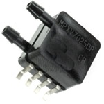
- 型号: MPXV7025DP
- 制造商: Freescale Semiconductor
- 库位|库存: xxxx|xxxx
- 要求:
| 数量阶梯 | 香港交货 | 国内含税 |
| +xxxx | $xxxx | ¥xxxx |
查看当月历史价格
查看今年历史价格
MPXV7025DP产品简介:
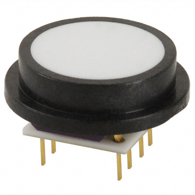
ICGOO电子元器件商城为您提供MPXV7025DP由Freescale Semiconductor设计生产,在icgoo商城现货销售,并且可以通过原厂、代理商等渠道进行代购。 MPXV7025DP价格参考¥147.45-¥176.93。Freescale SemiconductorMPXV7025DP封装/规格:压力传感器,变送器, 差分 压力 传感器 ±3.63 PSI(±25 kPa) 公型 - 0.13"(3.3mm) 双管 0.2 V ~ 4.7 V 8-SMD 模块。您可以下载MPXV7025DP参考资料、Datasheet数据手册功能说明书,资料中有MPXV7025DP 详细功能的应用电路图电压和使用方法及教程。
NXP USA Inc.生产的MPXV7025DP是一款差压传感器,属于压力传感器和变送器类别。它广泛应用于需要精确测量气体或液体差压的场景,以下是其主要应用场景:

1. 医疗设备:用于呼吸机、氧气浓缩器和其他医疗仪器中,监测气流和压力变化,确保患者获得稳定的氧气供应。

2. 暖通空调(HVAC)系统:在通风和空调系统中,用于检测过滤器堵塞情况、监控空气流量以及调节风机速度,以优化能源效率和空气质量。

3. 工业自动化:适用于各种工业过程控制,例如液体流量监测、液位测量以及泵的压力反馈控制,确保生产流程稳定运行。

4. 汽车领域:可用于发动机进气歧管压力监测、燃油喷射系统控制及涡轮增压压力管理,从而提高燃油效率并减少排放。

5. 环境监测:用于气象站等设备中,测量风速、风向及大气压力变化,支持精准的天气预报与分析。

6. 家用电器:如洗碗机、洗衣机等产品中,可用来检测水位高度或水流速度,实现智能化操作与节能效果。

MPXV7025DP凭借其高灵敏度、低功耗特性和宽工作温度范围,在上述领域表现出色,能够满足多种复杂工况下的使用需求。
| 参数 | 数值 |
| 产品目录 | |
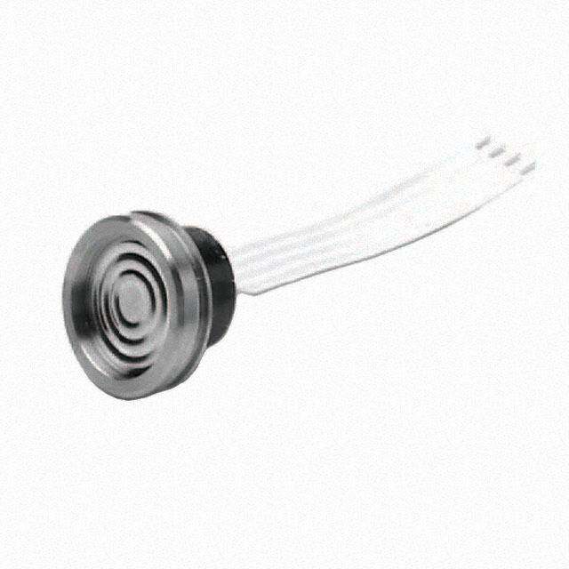
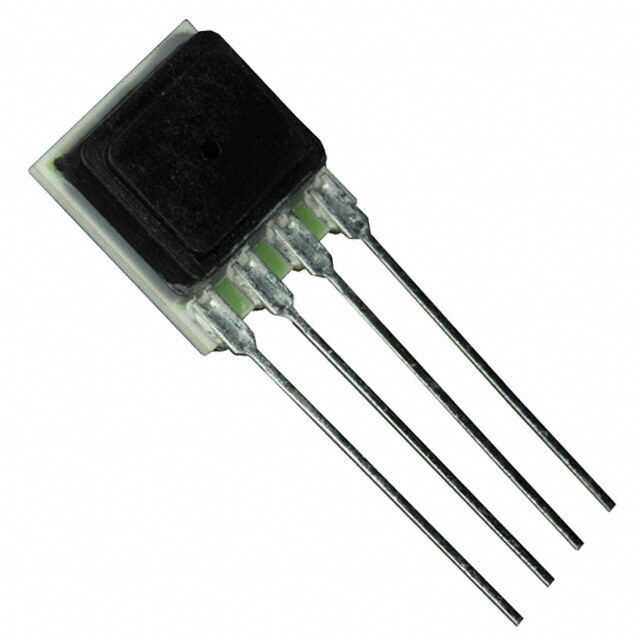
| 描述 | PRESSURE SENSOR DUAL PORT 8-SOP板机接口压力传感器 SOP DUAL PORT |
| 产品分类 | |
| 品牌 | Freescale Semiconductor |
| 产品手册 | |
| 产品图片 |
|
| rohs | 符合RoHS无铅 / 符合限制有害物质指令(RoHS)规范要求 |
| 产品系列 | 板机接口压力传感器,Freescale Semiconductor MPXV7025DPMPXV7025 |
| 数据手册 | |
| 产品型号 | MPXV7025DP |
| 产品目录绘图 |
|
| 产品目录页面 | |
| 产品种类 | 板机接口压力传感器 |
| 出厂设置 | - |
| 单位重量 | 2.223 g |
| 压力类型 | 差分 |
| 商标 | Freescale Semiconductor |
| 安装风格 | SMD/SMT |
| 封装 | Tray |
| 封装/外壳 | 8-SMD 模块 |
| 封装/箱体 | SO-8 |
| 工作压力 | ±3.6 PSI |
| 工作温度 | -40°C ~ 125°C |
| 工作电源电压 | 5 V |
| 工厂包装数量 | 125 |
| 最大工作温度 | + 125 C |
| 最小工作温度 | - 40 C |
| 标准包装 | 375 |
| 电压-电源 | 4.75 V ~ 5.25 V |
| 电源电流 | 7 mA |
| 端口大小 | 3.3 mm |
| 端口尺寸 | 公型,0.13"(3.302mm)双管 |
| 端口类型 | Dual Radial Barbed |
| 端子类型 | PCB |
| 精度 | ±5%FSS |
| 系列 | MPXV7025DP |
| 输出 | 0.2 V ~ 4.7 V |
| 输出电压 | 4.61 V to 4.89 V |


- 商务部:美国ITC正式对集成电路等产品启动337调查
- 曝三星4nm工艺存在良率问题 高通将骁龙8 Gen1或转产台积电
- 太阳诱电将投资9.5亿元在常州建新厂生产MLCC 预计2023年完工
- 英特尔发布欧洲新工厂建设计划 深化IDM 2.0 战略
- 台积电先进制程称霸业界 有大客户加持明年业绩稳了
- 达到5530亿美元!SIA预计今年全球半导体销售额将创下新高
- 英特尔拟将自动驾驶子公司Mobileye上市 估值或超500亿美元
- 三星加码芯片和SET,合并消费电子和移动部门,撤换高东真等 CEO
- 三星电子宣布重大人事变动 还合并消费电子和移动部门
- 海关总署:前11个月进口集成电路产品价值2.52万亿元 增长14.8%
PDF Datasheet 数据手册内容提取
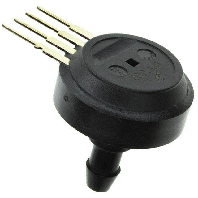
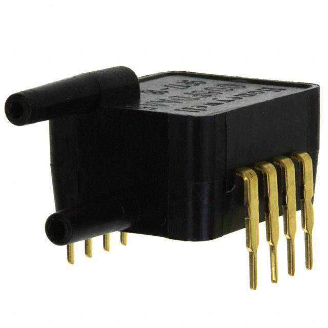
Pressure Freescale Semiconductor MPXV7025 Rev 6, 10/2012 Data Sheet: Technical Data Integrated Silicon Pressure Sensor MPXV7025 On-Chip Signal Conditioned, Series Temperature Compensated and Calibrated -25 to 25 kPa (-3.6 to 3.6 psi) 0.2 to 4.7 V Output The MPXV7025 series piezoresistive transducer is a state-of-the-art monolithic silicon pressure sensor designed for a wide range of applications, but particularly those employing a microcontroller or microprocessor with A/D Application Examples inputs. This patented, single element transducer combines advanced micromachining techniques, thin-film metallization, and bipolar processing to • Respiratory Systems provide an accurate, high level analog output signal that is proportional to the • Process Control applied pressure. • Patient Monitoring Features • Remote Monitoring Devices • 5.0% Maximum Error Over 0 to 85C • Ideally Suited for Microprocessor or Microcontroller-Based Systems • Temperature Compensated Over –40 to +125C • Thermoplastic (PPS) Surface Mount Package • Patented Silicon Shear Stress Strain Gauge • Available in Differential and Gauge Configurations ORDERING INFORMATION Package Case # of Ports Pressure Type Device Device Name Options No. None Single Dual Gauge Differential Absolute Marking Small Outline Package (MPXV7025 Series) MPXV7025GC6U Rails 482A • • MPXV7025G MPXV7025GC6T1 Tape & Reel 482A • • MPXV7025G MPXV7025GP Trays 1369 • • MPXV7025GP MPXV7025DP Trays 1351 • • MPXV7025DP Small Outline Package (Media Resistant Gel) (MPVZ7025 Series) MPVZ7025GC6U Rails 482A • • MPVZ7025G MPVZ7025GP Trays 1369 • • MPVZ7025GP MPVZ7025G6U Rails 482 • • MPVZ7025G MPVZ7025DP Trays 1351 • • MPVZ7025DP SMALL OUTLINE PACKAGE MPXV7025GC6U/T1 MPVZ7025G6U MPXV7025GP MPXV7025DP MPVZ7025GC6U CASE 482-01 MPVZ7025GP MPVZ7025DP CASE 482A-01 CASE 1369-01 CASE 1351-01 © 2007-2009, 2012 Freescale Semiconductor, Inc. All rights reserved.
Pressure Operating Characteristics Table1. Operating Characteristics (VS = 5.0 Vdc, TA = 25°C unless otherwise noted, P1 > P2. Decoupling circuit shown in Figure3 required to meet electrical specifications.) Characteristic Symbol Min Typ Max Unit Pressure Range(1) POP -25 — 25 kPa Supply Voltage(2) VS 4.75 5.0 5.25 Vdc Supply Current I — 7.0 10 mAdc o Minimum Pressure Offset(3) (0 to 85C) Voff 0.116 0.25 0.384 Vdc @ V = 5.0 Volts S Full Scale Output(4) (0 to 85C) VFSO 4.610 4.75 4.890 Vdc @ V = 5.0 Volts S Full Scale Span(5) (0 to 85C) VFSS — 4.5 — Vdc @ V = 5.0 Volts S Accuracy (0 to 85C) — — — 5.0 %V FSS Sensitivity V/P — 90 —- mV/kPa Response Time(6) tR — 1.0 —- ms Output Source Current at Full Scale Output I — 0.1 —- mAdc o+ Warm-Up Time(7) — — 20 —- ms Offset Stability(8) — — 0.5 —- %VFSS 1. 1.0 kPa (kiloPascal) equals 0.145 psi. 2. Device is ratiometric within this specified excitation range. 3. Offset (V ) is defined as the output voltage at the minimum rated pressure. off 4. Full Scale Output (V ) is defined as the output voltage at the maximum or full rated pressure. FSO 5. Full Scale Span (V ) is defined as the algebraic difference between the output voltage at full rated pressure and the output voltage at the FSS minimum rated pressure. 6. Response Time is defined as the time for the incremental change in the output to go from 10% to 90% of its final value when subjected to a specified step change in pressure. 7. Warm-up Time is defined as the time required for the product to meet the specified output voltage after the Pressure has been stabilized. 8. Offset Stability is the product's output deviation when subjected to 1000 hours of Pulsed Pressure, Temperature Cycling with Bias Test. MPXV7025 Sensors 2 Freescale Semiconductor, Inc.
Pressure Maximum Ratings Table2. Maximum Ratings(1) Rating Symbol Value Unit Maximum Pressure (P1 > P2) P 200 kPa max Storage Temperature T –40 to +125 C stg Operating Temperature T –40 to +125 C A 1. Exposure beyond the specified limits may cause permanent damage or degradation to the device. Figure1 shows a block diagram of the internal circuitry integrated on a pressure sensor chip. 2 V S Thin Film Gain Stage #2 Temperature and Sensing Compensation Ground Vout 4 Element and Reference Gain Stage #1 Shift Circuitry Pins 1, 5, 6, 7, and 8 are NO CONNECTS for Small Outline Package Device GND 3 Figure1. Integrated Pressure Sensor Schematic MPXV7025 Sensors Freescale Semiconductor, Inc. 3
Pressure On-chip Temperature Compensation and Calibration The MPXV7025 series pressure sensor operating curves are shown for operation over a temperature range of characteristics, and internal reliability and qualification tests 0 to 85C using the decoupling circuit shown in Figure3. The are based on use of dry air as the pressure media. Media, output will saturate outside of the specified pressure range. other than dry air, may have adverse effects on sensor Figure3 shows the recommended decoupling circuit for performance and long-term reliability. Contact the factory for interfacing the output of the integrated sensor to the A/D input information regarding media compatibility in your application. of a microprocessor or microcontroller. Proper decoupling of Figure2 shows the sensor output signal relative to the power supply is recommended. pressure input. Typical, minimum, and maximum output 5.0 Transfer Function: 4.5 V = V *(0.018*P+0.5) ± ERROR out S 4.0 V = 5.0 Vdc S 3.5 TEMP = 0 to 85°C TYPICAL 3.0 V) ut ( 2.5 MAX p ut 2.0 O MIN 1.5 1.0 0.5 0 -25 0 25 Differential Pressure (kPa) Figure2. Output versus Pressure Differential +5 V OUTPUT V out V s IPS 1.0 F 0.01 F GND 470 pF Figure3. Recommended Power Supply Decoupling and Output Filtering (For additional output filtering, please refer to Application Note AN1646.) MPXV7025 Sensors 4 Freescale Semiconductor, Inc.
Pressure Transfer Function Nominal Transfer Value: V = V (P x 0.018 + 0.5) out S ± (Pressure Error x Temp. Factor x 0.018 x V ) S V = 5.0 V 0.25 Vdc S Temperature Error Band MPXV7025 SERIES 4.0 Temp Multiplier 3.0 –40 3 Temperature 0 to 85 1 Error 2.0 +125 3 Factor 1.0 0.0 –40 –20 0 20 40 60 80 100 120 140 Temperature in (cid:31)C NOTE: The Temperature Multiplier is a linear response from 0° to –40°C and from 85° to 125°C. Pressure Error Band Error Limits for Pressure 3.0 2.0 a) kP 1.0 or ( e Err 0.0 -25 0 25 Pressure (in kPa) ur s –1.0 s e Pr –2.0 –3.0 Pressure Error (Max) -25 to 25 (kPa) ±1.25 (kPa) MPXV7025 Sensors Freescale Semiconductor, Inc. 5
Pressure PRESSURE (P1)/VACUUM (P2) SIDE IDENTIFICATION TABLE Freescale designates the two sides of the pressure sensor sensor is designed to operate with positive differential as the Pressure (P1) side and the Vacuum (P2) side. The pressure applied, P1 > P2. Pressure (P1) side is the side containing fluorosilicone gel The Pressure (P1) side may be identified by using the which protects the die from harsh media. The pressure following table: Pressure (P1) Part Number Case Type Side Identifier MPXV7025GC6U/C6T1, MPVZ7025GC6U 482A Side with Port Attached MPXV7025GP, MPVZ7025GP 1369 Side with Port Attached MPXV7025DP, MPVZ7025DP 1351 Side with Part Marking MPVZ7025G6U 482 Side with Part Marking MINIMUM RECOMMENDED FOOTPRINT FOR SURFACE MOUNTED APPLICATIONS Surface mount board layout is a critical portion of the total footprint, the packages will self align when subjected to a design. The footprint for the surface mount packages must be solder reflow process. It is always recommended to design the correct size to ensure proper solder connection interface boards with a solder mask layer to avoid bridging and between the board and the package. With the correct shorting between solder pads. 0.100 TYP 8X 0.660 2.54 16.76 0.060 TYP 8X 0.300 1.52 7.62 0.100 TYP 8X inch 2.54 mm SCALE 2:1 Figure4. Small Outline Package Footprint MPXV7025 Sensors 6 Freescale Semiconductor, Inc.
Pressure PACKAGE DIMENSIONS -A- D 8 PL 4 0.25 (0.010) M T B S A S NOTES: 5 1. DIMENSIONING AND TOLERANCING PER ANSI Y14.5M, 1982. 2. CONTROLLING DIMENSION: INCH. N -B- 3. DIMENSION A AND B DO NOT INCLUDE MOLD PROTRUSION. 4. MAXIMUM MOLD PROTRUSION 0.15 (0.006). G 5. ALL VERTICAL SURFACES 5˚ TYPICAL DRAFT. 8 1 INCHES MILLIMETERS DIM MIN MAX MIN MAX S A 0.415 0.425 10.54 10.79 W B 0.415 0.425 10.54 10.79 C 0.500 0.520 12.70 13.21 D 0.038 0.042 0.96 1.07 G 0.100 BSC 2.54 BSC V H 0.002 0.010 0.05 0.25 J 0.009 0.011 0.23 0.28 K 0.061 0.071 1.55 1.80 C M 0˚ 7˚ 0˚ 7˚ N 0.444 0.448 11.28 11.38 S 0.709 0.725 18.01 18.41 H V 0.245 0.255 6.22 6.48 J -T- W 0.115 0.125 2.92 3.17 PIN 1 IDENTIFIER SEATING K M PLANE CASE 482A-01 ISSUE A SMALL OUTLINE PACKAGE -A- D8 PL 4 0.25 (0.010) M T B S A S 5 NOTES: 1. DIMENSIONING AND TOLERANCING PER ANSI Y14.5M, 1982. -B- 2. CONTROLLING DIMENSION: INCH. 3. DIMENSION A AND B DO NOT INCLUDE MOLD PROTRUSION. G 4. MAXIMUM MOLD PROTRUSION 0.15 (0.006). 8 5. ALL VERTICAL SURFACES 5˚ TYPICAL DRAFT. 1 INCHES MILLIMETERS S DIM MIN MAX MIN MAX A 0.415 0.425 10.54 10.79 B 0.415 0.425 10.54 10.79 C 0.212 0.230 5.38 5.84 N D 0.038 0.042 0.96 1.07 G 0.100 BSC 2.54 BSC H 0.002 0.010 0.05 0.25 C H J 0.009 0.011 0.23 0.28 J K 0.061 0.071 1.55 1.80 -T- M 0˚ 7˚ 0˚ 7˚ N 0.405 0.415 10.29 10.54 PIN 1 IDENTIFIER SEATING S 0.709 0.725 18.01 18.41 K M PLANE CASE 482-01 ISSUE O SMALL OUTLINE PACKAGE MPXV7025 Sensors Freescale Semiconductor, Inc. 7
Pressure PACKAGE DIMENSIONS 2 PLACES 4 TIPS 0.006 (0.15) C A B A E GAGE e PLANE 5 4 e/2 .014 (0.35) θ L A1 D DETAIL G 8 1 NOTES: 8X b 1. CONTROLLING DIMENSION: INCH. F 0.004 (0.1) M C A B STYPLINE 11.: GND STYPLINE 12.: N/C 2. IANSTMEER PYR14E.T5 MD,I M19E9N4S.IONS AND TOLERANCES PER 2. +Vout 2. Vs 3. Vs 3. GND 3. DIMENSIONS "D" AND "E1" DO NOT INCLUDE 4. -Vout 4. Vout MOLD FLASH OR PROTRUSIONS. MOLD FLASH OR B E1 56.. NN//CC 56.. NN//CC PPRERO TSRIDUES.IONS SHALL NOT EXCEED 0.006 (0.152) 7. N/C 7. N/C 4. DIMENSION "b" DOES NOT INCLUDE DAMBAR 8. N/C 8. N/C PROTRUSION. ALLOWABLE DAMBAR PROTRUSION SHALL BE 0.008 (0.203) MAXIMUM. INCHES MILLIMETERS N ∅T DIM MIN MAX MIN MAX A 0.370 0.390 9.39 9.91 A1 0.002 0.010 0.05 0.25 b 0.038 0.042 0.96 1.07 D 0.465 0.485 11.81 12.32 E 0.680 0.700 17.27 17.78 A M E1 0.465 0.485 11.81 12.32 e 0.100 BSC 2.54 BSC F 0.240 0.260 6.10 6.60 K 0.115 0.135 2.92 3.43 L 0.040 0.060 1.02 1.52 8X 0.004 (0.1) M 0.270 0.290 6.86 7.37 P K N 0.160 0.180 4.06 4.57 DETAIL G P 0.009 0.011 0.23 0.28 C SPELAATNIENG Tθ 0.101˚0 0.173˚0 2.07˚9 3.73˚0 CASE 1351-01 ISSUE O SMALL OUTLINE PACKAGE MPXV7025 Sensors 8 Freescale Semiconductor, Inc.
Pressure PACKAGE DIMENSIONS 2 PLACES 4 TIPS 0.008 (0.20) C A B A E e GAGE PLANE 5 4 e/2 .014 (0.35) θ L A1 D DETAIL G 8 1 NOTES: 1. CONTROLLING DIMENSION: INCH. 8X b 2. INTERPRET DIMENSIONS AND TOLERANCES PER F 0.004 (0.1) M C A B ASME Y14.5M, 1994. 3. DIMENSIONS "D" AND "E1" DO NOT INCLUDE MOLD FLASH OR PROTRUSIONS. MOLD FLASH OR PROTRUSIONS SHALL NOT EXCEED 0.006 (0.152) B E1 PER SIDE. 4. DIMENSION "b" DOES NOT INCLUDE DAMBAR PROTRUSION. ALLOWABLE DAMBAR PROTRUSION SHALL BE 0.008 (0.203) MAXIMUM. INCHES MILLIMETERS ∅T N K DAIM 0M.3I0N0 M0.3A3X0 M7.1IN1 M7.A62X A1 0.002 0.010 0.05 0.25 b 0.038 0.042 0.96 1.07 D 0.465 0.485 11.81 12.32 E 0.717 BSC 18.21 BSC A M Ee1 0.406.1500 B0S.C485 11.821.54 BS1C2.32 F 0.245 0.255 6.22 6.47 K 0.120 0.130 3.05 3.30 8X 0.004 (0.1) L 0.061 0.071 1.55 1.80 P M 0.270 0.290 6.86 7.36 DETAIL G N 0.080 0.090 2.03 2.28 P 0.009 0.011 0.23 0.28 C SEATING T 0.115 0.125 2.92 3.17 PLANE θ 0˚ 7˚ 0˚ 7˚ CASE 1369-01 ISSUE O SMALL OUTLINE PACKAGE MPXV7025 Sensors Freescale Semiconductor, Inc. 9
Pressure Table3. Revision History Revision Revision Description of changes number date 6 10/2012 • Deleted references to device number MPVZ7025GC6T1 and MPVZ7025G6T1 throughout the document MPXV7025 Sensors 10 Freescale Semiconductor, Inc.
How to Reach Us: Information in this document is provided solely to enable system and software implementers to use Freescale products. There are no express or implied copyright Home Page: licenses granted hereunder to design or fabricate any integrated circuits based on the freescale.com information in this document. Web Support: freescale.com/support Freescale reserves the right to make changes without further notice to any products herein. Freescale makes no warranty, representation, or guarantee regarding the suitability of its products for any particular purpose, nor does Freescale assume any liability arising out of the application or use of any product or circuit, and specifically disclaims any and all liability, including without limitation consequential or incidental damages. “Typical” parameters that may be provided in Freescale data sheets and/or specifications can and do vary in different applications, and actual performance may vary over time. All operating parameters, including “typicals,” must be validated for each customer application by customer’s technical experts. Freescale does not convey any license under its patent rights nor the rights of others. Freescale sells products pursuant to standard terms and conditions of sale, which can be found at the following address: freescale.com/salestermsandconditions. Freescale, the Freescale logo, Energy Efficient Solutions logo, are trademarks of Freescale Semiconductor, Inc., Reg. U.S. Pat. & Tm. Off. Xtrinsic is a trademark of Freescale Semiconductor, Inc. All other product or service names are the property of their respective owners. © 2012 Freescale Semiconductor, Inc. MPXV7025 Rev. 6 10/2012
Mouser Electronics Authorized Distributor Click to View Pricing, Inventory, Delivery & Lifecycle Information: N XP: MPXV7025GC6U MPXV7025DP