 Datasheet下载
- 型号: MPXV5050VC6T1
- 制造商: Freescale Semiconductor
- 库位|库存: xxxx|xxxx
- 要求:
| 数量阶梯 | 香港交货 | 国内含税 |
| +xxxx | $xxxx | ¥xxxx |
查看当月历史价格
查看今年历史价格
MPXV5050VC6T1产品简介:
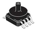
ICGOO电子元器件商城为您提供MPXV5050VC6T1由Freescale Semiconductor设计生产,在icgoo商城现货销售,并且可以通过原厂、代理商等渠道进行代购。 MPXV5050VC6T1价格参考。Freescale SemiconductorMPXV5050VC6T1封装/规格:压力传感器,变送器, 真空 压力 传感器 -7.25 PSI(-50 kPa) 公型 - 0.13"(3.17mm) 管 0.1 V ~ 4.6 V 8-SMD,鸥翼,顶部端口。您可以下载MPXV5050VC6T1参考资料、Datasheet数据手册功能说明书,资料中有MPXV5050VC6T1 详细功能的应用电路图电压和使用方法及教程。
NXP USA Inc. 的 MPXV5050VC6T1 是一款压力传感器,其应用场景广泛,主要适用于需要精确测量低压范围的工业和消费类设备。以下是该型号的一些典型应用场景:

1. 家用电器
   - 用于洗衣机、洗碗机等家电中监测水压,确保水流稳定并防止过压或泄漏。
   - 在空调和制冷系统中检测制冷剂压力,优化能效和运行性能。

2. 医疗设备
   - 应用于血压监测仪、呼吸机等医疗设备中,提供高精度的压力检测。
   - 用于输液泵中监控液体流动压力,保障患者安全。

3. 汽车电子
   - 用于刹车系统(如ABS)中的压力监测,确保制动性能可靠。
   - 在燃油喷射系统中测量燃油压力,提升发动机效率。
   - 检测轮胎气压(TPMS辅助功能),提高行车安全性。

4. 工业自动化
   - 在液压和气动系统中监测压力变化,实现精确控制。
   - 用于气体流量计或液体流量计中,配合其他传感器完成多参数测量。

5. 环境与气象监测
   - 测量大气压力,用于天气预报设备或高度计。
   - 监控管道或容器内的压力状态,预防泄漏或爆裂风险。

6. 消费电子产品
   - 集成到智能健身设备中,监测用户运动时的环境压力变化。
   - 用于无人机或飞行器的高度感应模块,辅助导航和稳定控制。

MPXV5050VC6T1 的工作压力范围为 0 至 50 kPa,具有小型化设计、低功耗和高可靠性特点,非常适合上述领域的应用需求。同时,它支持表面贴装技术(SMT),便于大规模生产和集成到各种电子系统中。
| 参数 | 数值 |
| 产品目录 | |
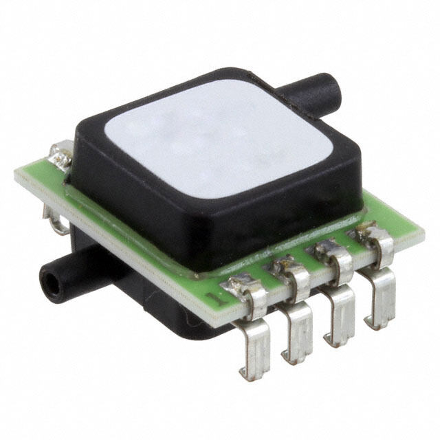
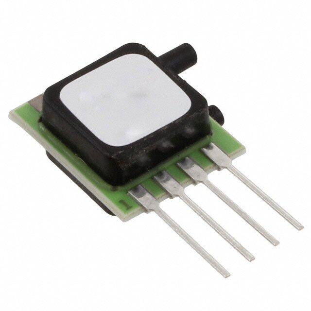
| 描述 | SENSOR DIFF PRESS -7.25-0PSI MAX板机接口压力传感器 SOP SURFACE MOUNT |
| 产品分类 | |
| 品牌 | Freescale Semiconductor |
| 产品手册 | |
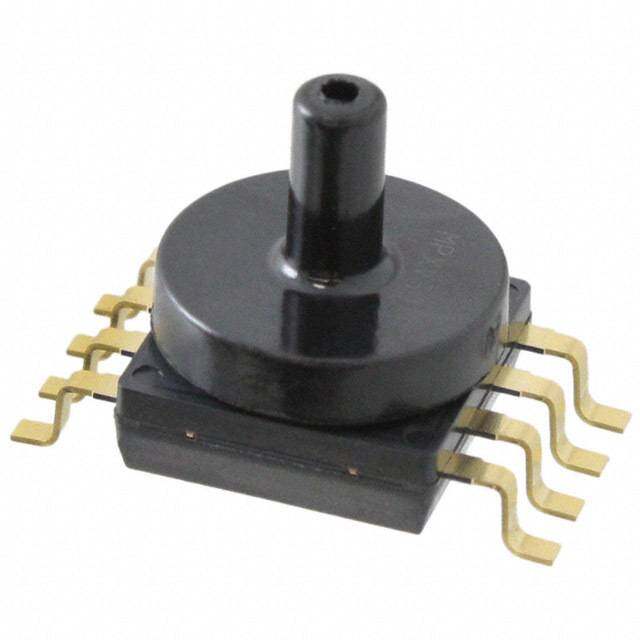
| 产品图片 |
|
| rohs | 符合RoHS无铅 / 符合限制有害物质指令(RoHS)规范要求 |
| 产品系列 | 板机接口压力传感器,Freescale Semiconductor MPXV5050VC6T1MPXV5050 |
| 数据手册 | |
| 产品型号 | MPXV5050VC6T1 |
| 产品目录绘图 |
|
| 产品目录页面 | |
| 产品种类 | 板机接口压力传感器 |
| 其它名称 | MPXV5050VC6T1CT |
| 出厂设置 | - |
| 单位重量 | 1.306 g |
| 压力类型 | Vacuum, Gauge |
| 商标 | Freescale Semiconductor |
| 安装风格 | SMD/SMT |
| 封装 | Reel |
| 封装/外壳 | 8-SMD, 鸥形翼, 顶部端口 |
| 封装/箱体 | SO-8 |
| 工作压力 | - 50 kPa to 0 kPa |
| 工作温度 | -40°C ~ 125°C |
| 工作电源电压 | 5 V |
| 工厂包装数量 | 100 |
| 最大工作温度 | + 125 C |
| 最小工作温度 | - 40 C |
| 标准包装 | 1 |
| 电压-电源 | 4.75 V ~ 5.25 V |
| 电源电流 | 7 mA |
| 端口大小 | 3.17 mm |
| 端口尺寸 | - |
| 端口类型 | Single Axial Barbless |
| 端子类型 | PCB |
| 精度 | ±2.5%FSS |
| 系列 | MPXx5050 |
| 输出 | 0.2 V ~ 4.7 V |
| 输出电压 | 0.1 V to 4.6 V |


- 商务部:美国ITC正式对集成电路等产品启动337调查
- 曝三星4nm工艺存在良率问题 高通将骁龙8 Gen1或转产台积电
- 太阳诱电将投资9.5亿元在常州建新厂生产MLCC 预计2023年完工
- 英特尔发布欧洲新工厂建设计划 深化IDM 2.0 战略
- 台积电先进制程称霸业界 有大客户加持明年业绩稳了
- 达到5530亿美元!SIA预计今年全球半导体销售额将创下新高
- 英特尔拟将自动驾驶子公司Mobileye上市 估值或超500亿美元
- 三星加码芯片和SET,合并消费电子和移动部门,撤换高东真等 CEO
- 三星电子宣布重大人事变动 还合并消费电子和移动部门
- 海关总署:前11个月进口集成电路产品价值2.52万亿元 增长14.8%
PDF Datasheet 数据手册内容提取
Pressure Freescale Semiconductor MPXV5050VC6T1 Rev 2, 11/2009 High Temperature Accuracy MPXV5050V Integrated Silicon Pressure Sensor Series for Measuring Absolute Pressure, On-Chip Signal Conditioned, -50 to 0 kPa (-7.25 to 0 psi) 0.1 to 4.6 V Output Temperature Compensated and Calibrated The MPXV5050V series sensor integrates on-chip, bipolar op amp circuitry and Application Examples thin film resistor networks to provide a high output signal and temperature • Vacuum Pump Monitoring compensation. The small form factor and high reliability of on-chip integration make the Freescale Semiconductor, Inc. pressure sensor a logical and economical choice for the system designer. The MPXV5050V series piezoresistive transducer is a state-of-the-art, monolithic, signal conditioned, silicon pressure sensor. This sensor combines advanced micromachining techniques, thin film metallization, and bipolar semiconductor processing to provide an accurate, high level analog output signal that is proportional to applied pressure. Features • 2.5% Maximum Error over 0° to 85°C • Ideally suited for Microprocessor or Microcontroller-Based Systems • Temperature Compensated from Over -40° to +125°C • Patented Silicon Shear Stress Strain Gauge • Durable Thermoplastic (PPS) Surface Mount Package • Easy-to-Use Chip Carrier Option • Ideal for Automotive and Non-Automotive Applications ORDERING INFORMATION Case # of Ports Pressure Type Device Device Name No. None Single Dual Gauge Differential Absolute Marking Small Outline Package MPXV5050VC6T1 482A • • Vacuum/Gauge MPXV5050V SMALL OUTLINE PACKAGE MPXV5050VC6T1 CASE 482A-01 © Freescale Semiconductor, Inc., 2005, 2009. All rights reserved.
Pressure Operating Characteristics Table1. Operating Characteristics (VS = 5.0 Vdc, TA = 25°C unless otherwise noted, P1 > P2) Characteristic Symbol Min Typ Max Unit Pressure Range P -50 — 0 kPa OP Supply Voltage(1) VS 4.75 5.0 5.25 Vdc Supply Current I — 7.0 10 mAdc o Full Scale Output(2) (0 to 85°C) VFSO 4.488 4.6 4.713 Vdc @ V = 5.0 Volts S Full Scale Span(3) (0 to 85°C) VFSS — 4.5 — Vdc @ V = 5.0 Volts S Accuracy(4) (0 to 85°C) — — — ±2.5 %VFSS Sensitivity V/P — 90 — mV/kPa Response Time(5) tR — 1.0 — ms Warm-Up Time(6) — — 20 — ms Offset Stability(7) — — ±0.5 — %VFSS Pressure Offset(8) (0 to 85°C) Voff 0 0.100 0.213 Vdc 1. Device is ratiometric within this specified excitation range. 2. Full Scale Output (V ) is defined as the output voltage at the maximum or full rated pressure. FSO 3. Full Scale Span (V ) is defined as the algebraic difference between the output voltage at full rated pressure and the output voltage at the FSS minimum rated pressure. 4. Accuracy is the deviation in actual output from nominal output over the entire pressure range and temperature range as a percent of span at 25°C due to all sources of error including the following: Linearity: Output deviation from a straight line relationship with pressure over the specified pressure range. Temperature Hysteresis: Output deviation at any temperature within the operating temperature range, after the temperature is cycled to and from the minimum or maximum operating temperature points, with zero differential pressure applied. Pressure Hysteresis: Output deviation at any pressure within the specified range, when this pressure is cycled to and from minimum or maximum rated pressure at 25°C. TcSpan: Output deviation over the temperature range of 0° to 85°C, relative to 25°C. TcOffset: Output deviation with minimum pressure applied, over the temperature range of 0° to 85°C, relative to 25°C. 5. Response Time is defined as the time for the incremental change in the output to go from 10% to 90% of its final value when subjected to a specified step change in pressure. 6. Warm-up Time is defined as the time required for the product to meet the specified output voltage after the pressure has been stabilized. 7. Offset Stability is the product's output deviation when subjected to 1000 cycles of Pulsed Pressure, Temperature Cycling with Bias Test. 8. Offset (V ) is defined as the output voltage at the minimum rated pressure. off MPXV5050VC6T1 Sensors 2 Freescale Semiconductor
Pressure Maximum Ratings Table2. Maximum Ratings(1) Rating Symbol Value Units Maximum Pressure (P1 > P2) P 200 kPa max Storage Temperature Tstg -40 to +125 °C Operating Temperature TA -40 to +125 °C 1. Exposure beyond the specified limits may cause permanent damage or degradation to the device. Figure1 shows a block diagram of the internal circuitry integrated on a pressure sensor chip. V S 2 Thin Film Gain Stage #2 Temperature And 4 Sensing Compensation Ground Vout Element And Reference Gain Stage #1 Shift Circuitry Pins 1, 5, 6, 7, and 8 are no connects 3 GND Figure1. Fully Integrated Pressure Sensor Schematic MPXV5050VC6T1 Sensors Freescale Semiconductor 3
Pressure On-chip Temperature Compensation and Calibration Figure2 illustrates the absolute sensing chip in the basic A fluorosilicone gel isolates the die surface and wire bonds Super Small Outline chip carrier (Case 482A). from the environment, while allowing the pressure signal to Figure3 shows a typical application circuit (output source be transmitted to the silicon diaphragm. The MPXV5050 current operation). series pressure sensor operating characteristics, internal Figure4 shows the sensor output signal relative to reliability and qualification tests are based on use of dry air as pressure input. Typical minimum and maximum output the pressure media. Media other than dry air may have curves are shown for operation over 0° to 85°C temperature adverse effects on sensor performance and long-term range. The output will saturate outside of the rated pressure reliability. Contact the factory for information regarding media range. compatibility in your application. Fluorosilicone Gel Die Coat Die Stainless +5 V Steel Cap P1 OUTPUT V Wire out Bond Thermoplastic Vs Case IPS Lead Frame 1.0 μF 0.01 μF GND 470 pF P2 Die Bond Differential Sensing Element Figure2. Cross Sectional Diagram SSOP (not to scale) Figure3. Typical Application Circuit (Output Source Current Operation) Transfer Function MPXV5050VC Series 5 Transfer Function: V = V x (0.018 x P + 0.92) ± (PE x TM x 0.018 x V) out S s V = 5.0 ± 0.25 vdc 4 s PE = 1.25 TM = 1 Temperature = 0 to 85°C Output Voltage (V) 23 MAX TYPICAL Span Range (Typ) Output Range (Typ) MIN 1 0 –50 –40 –30 –20 –10 0 Offset Pressure (kPa) (Typ) Figure4. Output vs. Absolute Pressure MPXV5050VC6T1 Sensors 4 Freescale Semiconductor
Pressure Transfer Function (MPXV5050V) Nominal Transfer Value: V = V x (0.018 x P + 0.92) OUT S ± (Pressure Error x Temp Multi x 0.018 x V ) S VS = 5.0 ± 0.25 V Temperature Error Band MPXV5050V 4.0 Break Points Temp Multiplier 3.0 –40 3 Temperature 0 to 85 1 Error 2.0 +125 3 Factor 1.0 0.0 –40 –20 0 20 40 60 80 100 120 140 Temperature in °C NOTE: The Temperature Multiplier is a linear response from 0°C to –40°C and from 85°C to 125°C. Pressure Error Band MMPPXXVV55005500VV Error Limits for Pressure 1.25 1.00 a) P k or ( 0.75 e Err 0 Pressure (in kPa) ur –50 –40 –30 –20 –10 0 s es –0.75 Pr –1.00 –1.25 Pressure Error (Max) –50 to 0 kPa ±1.25 kPa MPXV5050VC6T1 Sensors Freescale Semiconductor 5
Pressure SURFACE MOUNTING INFORMATION MINIMUM RECOMMENDED FOOTPRINT FOR SMALL OUTLINE PACKAGE Surface mount board layout is a critical portion of the total solder reflow process. It is always recommended to fabricate design. The footprint for the semiconductor package must be boards with a solder mask layer to avoid bridging and/or the correct size to ensure proper solder connection interface shorting between solder pads, especially on tight tolerances between the board and the package. With the correct pad and/or tight layouts. geometry, the packages will self-align when subjected to a 0.100 TYP 0.660 2.54 16.76 0.060 TYP 8X 1.52 0.300 7.62 0.100 TYP 8X inch 2.54 mm Figure5. SOP Footprint (Case 482A) MPXV5050VC6T1 Sensors 6 Freescale Semiconductor
Pressure PACKAGE DIMENSIONS -A- D 8 PL 4 0.25 (0.010) M T B S A S NOTES: 5 1. DIMENSIONING AND TOLERANCING PER ANSI Y14.5M, 1982. 2. CONTROLLING DIMENSION: INCH. N -B- 3. DIMENSION A AND B DO NOT INCLUDE MOLD PROTRUSION. 4. MAXIMUM MOLD PROTRUSION 0.15 (0.006). G 5. ALL VERTICAL SURFACES 5˚ TYPICAL DRAFT. 8 1 INCHES MILLIMETERS DIM MIN MAX MIN MAX S A 0.415 0.425 10.54 10.79 W B 0.415 0.425 10.54 10.79 C 0.500 0.520 12.70 13.21 D 0.038 0.042 0.96 1.07 G 0.100 BSC 2.54 BSC V H 0.002 0.010 0.05 0.25 J 0.009 0.011 0.23 0.28 K 0.061 0.071 1.55 1.80 C M 0˚ 7˚ 0˚ 7˚ N 0.444 0.448 11.28 11.38 S 0.709 0.725 18.01 18.41 H V 0.245 0.255 6.22 6.48 J -T- W 0.115 0.125 2.92 3.17 PIN 1 IDENTIFIER SEATING K M PLANE CASE 482A-01 ISSUE A SMALL OUTLINE PACKAGE MPXV5050VC6T1 Sensors Freescale Semiconductor 7
How to Reach Us: Home Page: www.freescale.com Web Support: http://www.freescale.com/support USA/Europe or Locations Not Listed: Freescale Semiconductor, Inc. Technical Information Center, EL516 2100 East Elliot Road Tempe, Arizona 85284 1-800-521-6274 or +1-480-768-2130 www.freescale.com/support Europe, Middle East, and Africa: Information in this document is provided solely to enable system and software Freescale Halbleiter Deutschland GmbH Technical Information Center implementers to use Freescale Semiconductor products. There are no express or Schatzbogen 7 implied copyright licenses granted hereunder to design or fabricate any integrated 81829 Muenchen, Germany circuits or integrated circuits based on the information in this document. +44 1296 380 456 (English) +46 8 52200080 (English) +49 89 92103 559 (German) Freescale Semiconductor reserves the right to make changes without further notice to +33 1 69 35 48 48 (French) any products herein. Freescale Semiconductor makes no warranty, representation or www.freescale.com/support guarantee regarding the suitability of its products for any particular purpose, nor does Freescale Semiconductor assume any liability arising out of the application or use of any Japan: product or circuit, and specifically disclaims any and all liability, including without Freescale Semiconductor Japan Ltd. limitation consequential or incidental damages. “Typical” parameters that may be Headquarters provided in Freescale Semiconductor data sheets and/or specifications can and do vary ARCO Tower 15F in different applications and actual performance may vary over time. All operating 1-8-1, Shimo-Meguro, Meguro-ku, parameters, including “Typicals”, must be validated for each customer application by Tokyo 153-0064 Japan customer’s technical experts. Freescale Semiconductor does not convey any license 0120 191014 or +81 3 5437 9125 under its patent rights nor the rights of others. Freescale Semiconductor products are support.japan@freescale.com not designed, intended, or authorized for use as components in systems intended for surgical implant into the body, or other applications intended to support or sustain life, Asia/Pacific: or for any other application in which the failure of the Freescale Semiconductor product Freescale Semiconductor China Ltd. could create a situation where personal injury or death may occur. Should Buyer Exchange Building 23F purchase or use Freescale Semiconductor products for any such unintended or No. 118 Jianguo Road unauthorized application, Buyer shall indemnify and hold Freescale Semiconductor and Chaoyang District its officers, employees, subsidiaries, affiliates, and distributors harmless against all Beijing 100022 China claims, costs, damages, and expenses, and reasonable attorney fees arising out of, +86 010 5879 8000 directly or indirectly, any claim of personal injury or death associated with such support.asia@freescale.com unintended or unauthorized use, even if such claim alleges that Freescale Semiconductor was negligent regarding the design or manufacture of the part. For Literature Requests Only: Freescale Semiconductor Literature Distribution Center 1-800-441-2447 or +1-303-675-2140 Freescale™ and the Freescale logo are trademarks of Freescale Semiconductor, Inc. Fax: +1-303-675-2150 All other product or service names are the property of their respective owners. LDCForFreescaleSemiconductor@hibbertgroup.com © Freescale Semiconductor, Inc. 2009. All rights reserved. MPXV5050VC6T1 Rev. 2 11/2009
Mouser Electronics Authorized Distributor Click to View Pricing, Inventory, Delivery & Lifecycle Information: N XP: MPXV5050VC6T1