
 Datasheet下载
- 型号: MPL115A1T1
- 制造商: Freescale Semiconductor
- 库位|库存: xxxx|xxxx
- 要求:
| 数量阶梯 | 香港交货 | 国内含税 |
| +xxxx | $xxxx | ¥xxxx |
查看当月历史价格
查看今年历史价格
MPL115A1T1产品简介:
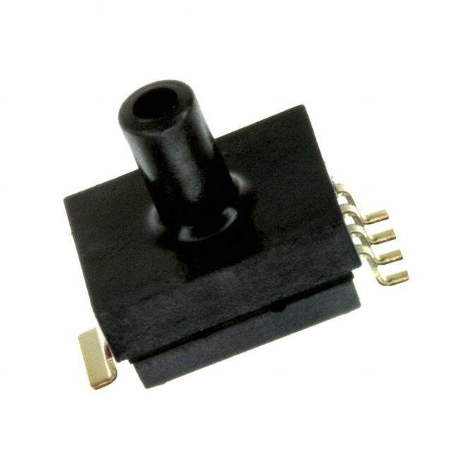
ICGOO电子元器件商城为您提供MPL115A1T1由Freescale Semiconductor设计生产,在icgoo商城现货销售,并且可以通过原厂、代理商等渠道进行代购。 MPL115A1T1价格参考。Freescale SemiconductorMPL115A1T1封装/规格:压力传感器,变送器, 绝对 压力 传感器 7.25 PSI ~ 16.68 PSI(50 kPa ~ 115 kPa) 10 b 8-TLGA。您可以下载MPL115A1T1参考资料、Datasheet数据手册功能说明书,资料中有MPL115A1T1 详细功能的应用电路图电压和使用方法及教程。
NXP USA Inc. 生产的 MPL115A1T1 是一款压力传感器,属于变送器类别。该型号的应用场景主要包括以下几个方面:

1. 天气监测:MPL115A1T1 可用于气象站中测量大气压力,从而帮助预测天气变化。其高精度和低功耗特性使其非常适合长时间运行的环境监测设备。

2. 消费电子设备:该传感器常用于智能手机、平板电脑和其他便携式设备中,提供海拔高度测量功能,支持导航应用和健康追踪设备(如计步器)中的气压数据采集。

3. 无人机与飞行器:在无人机和小型飞行器中,MPL115A1T1 能够提供精确的高度信息,协助实现稳定悬停和自动飞行控制。

4. 智能家居系统:集成到智能温控器或环境控制系统中,用于检测室内气压变化,优化能源使用并提升居住舒适度。

5. 医疗设备:适用于呼吸机、制氧机等需要精确压力监控的医疗器械,确保患者治疗过程中的安全性与有效性。

6. 工业自动化:可用于工业流程中的压力监控,例如液体水平监测、管道压力检测等,以保障生产安全和效率。

MPL115A1T1 的主要优势在于其紧凑的设计、较低的功耗以及良好的温度补偿性能,这使得它能够适应多种复杂的工作环境,并为不同领域的应用提供可靠的解决方案。
| 参数 | 数值 |
| 产品目录 | |
| 描述 | IC BAROMETER SPI DGTL MINI 8-LGA板机接口压力传感器 Miniature SPI Digital Barometer |
| 产品分类 | |
| 品牌 | Freescale Semiconductor |
| 产品手册 | |
| 产品图片 |
|
| rohs | 符合RoHS无铅 / 符合限制有害物质指令(RoHS)规范要求 |
| 产品系列 | 板机接口压力传感器,Freescale Semiconductor MPL115A1T1- |
| 数据手册 | |
| 产品型号 | MPL115A1T1 |
| PCN组件/产地 | http://cache.freescale.com/files/shared/doc/pcn/PCN16332.htm |
| 产品目录绘图 |
|
| 产品目录页面 | |
| 产品种类 | 板机接口压力传感器 |
| 其它名称 | MPL115A1T1DKR |
| 出厂设置 | - |
| 单位重量 | 31.300 mg |
| 压力类型 | Absolute |
| 商标 | Freescale Semiconductor |
| 安装风格 | SMD/SMT |
| 封装 | Reel |
| 封装/外壳 | 8-TLGA |
| 封装/箱体 | LGA |
| 工作压力 | 50 kPa to 115 kPa |
| 工作温度 | -40°C ~ 105°C |
| 工作电源电压 | 2.375 V to 5.5 V |
| 工厂包装数量 | 1000 |
| 最大工作温度 | + 105 C |
| 最小工作温度 | - 40 C |
| 标准包装 | 1 |
| 电压-电源 | 2.375 V ~ 5.5 V |
| 端口尺寸 | - |
| 端子类型 | PCB |
| 精度 | ±1kPa |
| 输出 | SPI |


- 商务部:美国ITC正式对集成电路等产品启动337调查
- 曝三星4nm工艺存在良率问题 高通将骁龙8 Gen1或转产台积电
- 太阳诱电将投资9.5亿元在常州建新厂生产MLCC 预计2023年完工
- 英特尔发布欧洲新工厂建设计划 深化IDM 2.0 战略
- 台积电先进制程称霸业界 有大客户加持明年业绩稳了
- 达到5530亿美元!SIA预计今年全球半导体销售额将创下新高
- 英特尔拟将自动驾驶子公司Mobileye上市 估值或超500亿美元
- 三星加码芯片和SET,合并消费电子和移动部门,撤换高东真等 CEO
- 三星电子宣布重大人事变动 还合并消费电子和移动部门
- 海关总署:前11个月进口集成电路产品价值2.52万亿元 增长14.8%

PDF Datasheet 数据手册内容提取
MPL115A1 Miniature SPI digital barometer, 50 to 115 kPa Rev. 8 — 10 October 2017 Data sheet: technical data 1 General description The MPL115A1 is an absolute pressure sensor with a digital SPI output targeting low cost applications. A miniature 5 x 3 x 1.2 mm LGA package is ideally suited for the space constrained requirements of portable electronic devices. Low current consumptions of 5 μA during Active mode and 1 μA during Shutdown (Sleep) mode are essential when focusing on low-power applications. The wide operating temperature range spans from – 40 °C to +105 °C to fit demanding environment conditions. The MPL115A1 employs a MEMS pressure sensor with a conditioning IC to provide accurate pressure measurements from 50 to 115 kPa. An integrated ADC converts pressure and temperature sensor readings to digitized outputs via a SPI port. Factory calibration data is stored internally in an on-board ROM. Utilizing the raw sensor output and calibration data, the host microcontroller executes a compensation algorithm to render Compensated Absolute Pressure with ±1 kPa accuracy. The MPL115A1 pressure sensor’s small form factor, low power capability, precision, and digital output optimize it for barometric measurement applications. 2 Features • Digitized pressure and temperature information together with programmed calibration coefficients for host micro use. • Factory calibrated • 50 kPa to 115 kPa absolute pressure • ±1 kPa accuracy • 2.375 V to 5.5 V supply • Integrated ADC • SPI Interface • Monotonic pressure and temperature data outputs • Surface mount RoHS compliant package 3 Applications • Barometry (portable and desktop) • Altimeters • Weather stations • Hard-disk drives (HDD) • Industrial equipment • Health monitoring • Air control systems
NXP Semiconductors MPL115A1 Miniature SPI digital barometer, 50 to 115 kPa 4 Ordering information Table 1. Ordering information Type number Package Name Description Version MPL115A1 TSON8 LGA 8 I/O, 3 X 5 X 1.25 PITCH, SENSOR 1.2MAX MM PKG SOT1769-1 4.1 Ordering options Table 2. Ordering options Device Name Package Options # of Ports Pressure Type Digital Interface None Single Dual Gauge Differential Absolute MPL115A1 Tray • • SPI MPL115A1T1 Tape & Reel (1000) • • SPI 5 Block diagram Figure 1. Block diagram of MPL115A1 MPL115A1 All information provided in this document is subject to legal disclaimers. © NXP B.V. 2017. All rights reserved. Data sheet: technical data Rev. 8 — 10 October 2017 2 / 23
NXP Semiconductors MPL115A1 Miniature SPI digital barometer, 50 to 115 kPa 6 Pinning information 6.1 Pinning MPL115A1 VDD 1 8 SCLK CAP 2 7 DIN GND 3 6 DOUT SHDN 4 5 CS transparent top view Figure 2. Pin configuration 6.2 Pin description Table 3. Pin description Pin Name Function 1 VDD Power Supply Connection. VDD range is 2.375 V to 5.5 V. External Capacitor: Output decoupling capacitor for main internal 2 CAP regulator. Connect a 1 μF ceramic capacitor to ground. 3 GND Ground Shutdown: Connect to GND to disable the device. When in shut down the part draws no more than 1 μA supply current and all 4 SHDN communications pins (CS, SCLK, DOUT, DIN) are high impedance. Connect to VDD for normal operation. 5 CS Chip Select line. 6 DOUT Serial data output 7 DIN Serial data input 8 SCLK Serial clock input. 7 Handling and Board Mount Recommendations The sensor die is sensitive to light exposure. Direct light exposure through the port hole can lead to varied accuracy of pressure measurement. Avoid such exposure to the port during normal operation. 7.1 Methods of Handling Components can be picked from the carrier tape using either the vacuum assist or the mechanical type pickup heads. A vacuum assist nozzle type is most common due to its lower cost of maintenance and ease of operation. The recommended vacuum nozzle configuration should be designed to make contact with the device directly on the metal cover and avoid vacuum port location directly over the vent hole in the metal cover of the MPL115A1 All information provided in this document is subject to legal disclaimers. © NXP B.V. 2017. All rights reserved. Data sheet: technical data Rev. 8 — 10 October 2017 3 / 23
NXP Semiconductors MPL115A1 Miniature SPI digital barometer, 50 to 115 kPa device. Multiple vacuum ports within the nozzle may be required to effectively handle the device and prevent shifting during movement to placement position. Vacuum pressure required to adequately support the component should be approximately 25 inches Hg (85 kPa). This level is typical of in-house vacuum supply. Pickup nozzles are available in various sizes and configurations to suit a variety of component geometries. To select the nozzle best suited for the specific application, it is recommended that the customer consult their pick and place equipment supplier to determine the correct nozzle. In some cases it may be necessary to fabricate a special nozzle depending on the equipment and speed of operation. Tweezers or other mechanical forms of handling that have a sharp point are not recommended since they can inadvertently be inserted into the vent hole of the device. This can lead to a puncture of the MEMS element that will render the device inoperable. 7.2 Board Mount Recommendations Components can be mounted using solder paste stencil, screen printed or dispensed onto the PCB pads prior to placement of the component. The volume of solder paste applied to the PCB is normally sufficient to secure the component during transport to the subsequent reflow soldering process. Use of adhesives to secure the component is not recommended, but where necessary can be applied to the underside of the device. Solder pastes are available in variety of metal compositions, particle size and flux types. The solder paste consists of metals and flux required for a reliable connection between the component lead and the PCB pad. Flux aids the removal of oxides that may be present on PCB pads and prevents further oxidation from occurring during the solder process. The use of a No-Clean (NC) flux is recommended for exposed cavity components. Using pressure spray, wire brush, or other methods of cleaning is not recommended since it can puncture the MEMS device and render it unusable. If cleaning of the pcb is performed, Water Soluble (WS) flux can be used. However, it is recommended the component cavity is protected by adhesive Kapton tape, vinyl cap or other means prior to the cleaning process. This covering will prevent damage to the MEMS device, contamination, and foreign materials from being introduced into device cavity as result of cleaning processes. Ultrasonic cleaning is not recommended as the frequencies can damage wire bond interconnections and the MEMS device. MPL115A1 All information provided in this document is subject to legal disclaimers. © NXP B.V. 2017. All rights reserved. Data sheet: technical data Rev. 8 — 10 October 2017 4 / 23
NXP Semiconductors MPL115A1 Miniature SPI digital barometer, 50 to 115 kPa 8 Functional description Initial powerup Reading coefficient data Data conversion Compensated pressure reading Shutdown Figure 3. Sequence flow chart The MPL115A interfaces to a host (or system) microcontroller in the user’s application. All communications are via SPI. A typical usage sequence is as follows: Initial power-up All circuit elements are active. SPI port pins are high impedance and associated registers are cleared. The device then enters standby mode. Reading coefficient data The user then typically accesses the part and reads the coefficient data. The main circuits within the slave device are disabled during read activity. The coefficients are usually stored in the host microcontoller local memory but can be re-read at any time. Reading of the coefficients may be executed only once and the values stored in the host microcontroller. It is not necessary to read this multiple times because the coefficients within a device are constant and do not change. However, note that the coefficients will be different from device to device, and cannot be used for another part. Data conversion This is the first step that is performed each time a new pressure reading is required which is initiated by the host sending the CONVERT command. The main system circuits are activated (wake) in response to the command and after the conversion completes, the result is placed into the Pressure and Temperature ADC output registers. The conversion completes within the maximum conversion time, tc (see row 6, in Table 11). The device then enters standby mode. MPL115A1 All information provided in this document is subject to legal disclaimers. © NXP B.V. 2017. All rights reserved. Data sheet: technical data Rev. 8 — 10 October 2017 5 / 23
NXP Semiconductors MPL115A1 Miniature SPI digital barometer, 50 to 115 kPa Compensated pressure reading After the conversion has been given sufficient time to complete, the host microcontroller reads the result from the ADC output registers and calculates the Compensated Pressure, a barometric/atmospheric pressure value which is compensated for changes in temperature and pressure sensor linearity. This is done using the coefficient data from the MPL115A and the raw sampled pressure and temperature ADC output values, in a compensation equation (detailed later). Note that this is an absolute pressure measurement with a vacuum as a reference. From this step the host controller may either wait and then return to the Data Conversion step to obtain the next pressure reading or it may go to the Shutdown step. Shutdown For longer periods of inactivity the user may assert the SHDN input by driving this pin low to reduce system power consumption. This removes power from all internal circuits, including any registers. In the shutdown state, the Pressure and Temperature registers will be reset, losing any previous ADC output values. This step is exited by taking the SHDN pin high. Wait for the maximum wakeup time, tw (see row 7, in Table 11), after which another pressure reading can be taken by transitioning to the data Conversion step. Table 4. Device memory map Address Name Description 00h Padc_MSB 10-bit Pressure ADC output value MSB 01h Padc_LSB 10-bit Pressure ADC output value LSB 02h Tadc_MSB 10-bit Temperature ADC output value MSB 03h Tacd_LSB 10-bit Temperature ADC output value LSB 04h a0_MSB a0 coefficient MSB 05h a0_LSB a0 coefficient LSB 06h b1_MSB b1 coefficient MSB 07h b1_LSB b1 coefficient LSB 08h b2_MSB b2 coefficient MSB 09h b2_LSB b2 coefficient LSB 0Ah c12_MSB c12 coefficient MSB 0Bh c12_LSB c12 coefficient LSB [1] 0Ch reserved — [1] 0Dh reserved — [1] 0Eh reserved — [1] 0Fh reserved — MPL115A1 All information provided in this document is subject to legal disclaimers. © NXP B.V. 2017. All rights reserved. Data sheet: technical data Rev. 8 — 10 October 2017 6 / 23
NXP Semiconductors MPL115A1 Miniature SPI digital barometer, 50 to 115 kPa Address Name Description 10h reserved — 11h reserved — 12h CONVERT Start Pressure and Temperature Conversion [1] This register is set to 00h. It is reserved, and was previously utilized as Coefficient values, c11 and c22, which were always 00h. For values with less than 16 bits, the lower LSBs are zero. For example, c12 is 14 bits and is stored into 2 bytes as follows: c12 MS byte = c12[13:6] = [c12 , c12 , c12 , c12 , c12 , c12 , c12 , c12 ] b13 b12 b11 b10 b9 b8 b7 b6 c12 LS byte = c12[5:0] & "00" = [c12 , c12 , c12 , c12 , c12 , c12 , 0 , 0] b5 b4 b3 b2 b1 b0 8.1 Pressure, temperature and coefficient bit-width specifications The table below specifies the initial coefficient bit-width specifications for the compensation algorithm and the specifications for Pressure and Temperature ADC values. Table 5. Pressure, temperature and compensation coefficient specifications a0 b1 b2 c12 Padc Tadc Total Bits 16 16 16 14 10 10 Sign Bits 1 1 1 1 0 0 Integer Bits 12 2 1 0 10 10 Fractional Bits 3 13 14 13 0 0 dec pt zero pad 0 0 0 9 0 0 Example Binary Format Definitions: a0 Signed, Integer Bits = 12, Fractional Bits = 3 : Coeff a0 = S I11 I10 I9 I8 I7 I6 I5 I4 I3 I2 I1 I0 . F2 F1 F0 b1 Signed, Integer Bits = 2, Fractional Bits = 13 : Coeff b1 = S I1 I0 . F12 F11 F10 F9 F8 F7 F6 F5 F4 F3 F2 F1 F0 b2 Signed, Integer Bits = 1, Fractional Bits = 14 : Coeff b2 = S I0 . F13 F12 F11 F10 F9 F8 F7 F6 F5 F4 F3 F2 F1 F0 c12 Signed, Integer Bits = 0, Fractional Bits = 13, dec pt zero pad = 9 : Coeff c12 = S 0 . 000 000 000 F12 F11 F10 F9 F8 F7 F6 F5 F4 F3 F2 F1 F0 Padc Unsigned, Integer Bits = 10 : Padc U = I9 I8 I7 I6 I5 I4 I3 I2 I1 I0 Tadc Unsigned, Integer Bits =10 : Tadc U = I9 I8 I7 I6 I5 I4 I3 I2 I1 I0 Note: Negative coefficients are coded in 2’s complement notation. 8.2 Compensation The 10-bit compensated pressure output, Pcomp, is calculated as follows: MPL115A1 All information provided in this document is subject to legal disclaimers. © NXP B.V. 2017. All rights reserved. Data sheet: technical data Rev. 8 — 10 October 2017 7 / 23
NXP Semiconductors MPL115A1 Miniature SPI digital barometer, 50 to 115 kPa (1) Where: Padc is the 10-bit pressure ADC output of the MPL115A Tadc is the 10-bit temperature ADC output of the MPL115A a0 is the pressure offset coefficient b1 is the pressure sensitivity coefficient b2 is the temperature coefficient of offset (TCO) c12 is the temperature coefficient of sensitivity (TCS) Pcomp will produce a value of 0 with an input pressure of 50 kPa and will produce a full- scale value of 1023 with an input pressure of 115 kPa. (2) 8.3 Evaluation sequence, arithmetic circuits The following is an example of the calculation for Pcomp, the compensated pressure output. Input values are in bold. c12x2 = c12 * Tadc a1 = b1 + c12x2 a1x1 = a1 * Padc y1 = a0 + a1x1 a2x2 = b2 * Tadc Pcomp = y1 + a2x2 This can be calculated as a succession of Multiply Accumulates (MACs) operations of the form y = a + b * x: a + y b X x The polynomial can be evaluated (Equation 1) as a sequence of 3 MACs: MPL115A1 All information provided in this document is subject to legal disclaimers. © NXP B.V. 2017. All rights reserved. Data sheet: technical data Rev. 8 — 10 October 2017 8 / 23
NXP Semiconductors MPL115A1 Miniature SPI digital barometer, 50 to 115 kPa b1 c12 a1 Tadc a0 y1 Padc b2 y PComp Tadc Please refer to NXP application note AN3785 for more detailed notes on implementation. 8.4 SPI device read/write operations All device read/write operations are memory mapped. Device actions e.g. "Start Conversions" are controlled by writing to the appropriate memory address location. All memory address locations are 6-bit (see Table 2). The 8-bit command word comprises: • the most significant bit which is the Read/Write identifier which is '1' for read operations and '0' for write operations. • the 6-bit address (from Table 4); • the least significant bit which is not used and is don't care (X). The device write commands are shown in Table 6. Table 6. SPI write command Legend: X = don't care [1] Command Binary HEX Start Conversions 0010010X 24h [1] The command byte needs to be paired with a 00h as part of the SPI exchange to complete the passing of Start Conversions. The actions taken by the part in response to each command are as follows: Table 7. SPI Write command description Command Action taken Wake main circuits. Start clock. Allow supply stabilization time. Select pressure sensor input. Apply positive sensor excitation and perform A to D conversion. Select temperature Start Conversions input. Perform A to D conversion. Load the Pressure and Temperature registers with the result. Shut down main circuits and clock. MPL115A1 All information provided in this document is subject to legal disclaimers. © NXP B.V. 2017. All rights reserved. Data sheet: technical data Rev. 8 — 10 October 2017 9 / 23
NXP Semiconductors MPL115A1 Miniature SPI digital barometer, 50 to 115 kPa SPI Read operations are performed by sending the required address with a leading Read bit set to ‘1’. SPI operations require that each byte be addressed individually. All data is transmitted most significant bit first. Table 8. Example SPI Read Commands Legend: X = don't care [1] Command Binary HEX Read Pressure MSB 1000000X 80h Read Pressure LSB 1000001X 82h Read Temperature MSB 1000010X 84h Read Temperature LSB 1000011X 86h Read Coefficient data byte 1 1000100X 88h [1] The command byte needs to be paired with a 00h as part of the SPI exchange to complete the passing of stated command. 8.5 SPI timing Table 9 and Figure 4 describe the timing requirements for the SPI system. Table 9. SPI timing Ref Symbol Function Min Max Unit 1 Of Operating Frequency — 8 MHz 2 tSCLK SCLK Period 125 — ns 3 tCLKH SCLK High time 62.5 — ns 4 tCLKL SCLK Low time 62.5 — ns 5 tSCS Enable lead time 125 — ns 6 tHCS Enable lag time 125 — ns 7 tSET Data setup time 30 — ns 8 tHOLD Data hold time 30 — ns 9 tDDLY Data valid (after SCLK low edge) — 32 ns 10 tWCS Width CS High 30 — ns Figure 4. SPI timing diagram MPL115A1 All information provided in this document is subject to legal disclaimers. © NXP B.V. 2017. All rights reserved. Data sheet: technical data Rev. 8 — 10 October 2017 10 / 23
NXP Semiconductors MPL115A1 Miniature SPI digital barometer, 50 to 115 kPa 8.6 Example of SPI reading of coefficients These are MPL115A1 SPI commands to read coefficients, execute Pressure and Temperature conversions, and to read Pressure and Temperature data. The sequence of the commands for the interaction is given as an example to operate the MPL115A1. Utilizing this gathered data, an example of the calculating the Compensated Pressure reading is given in floating point notation. SPI Commands (simplified for communication) Command to Write "Convert Pressure and Temperature" = 24h Command to Read "Pressure ADC High byte" = 80h Command to Read "Pressure ADC Low byte" = 82h Command to Read "Temperature ADC High byte" = 84h Command to Read "Temperature ADC Low byte" = 86h Command to Read "Coefficient data byte 1 High byte" = 88h Read coefficients: [CS=0], [88h], [00h], [8Ah], [00h], [8Ch], [00h], [8Eh], [00h], [90h], [00h], [92h], [00h], [94h], [00h], [96h], [00h], [00h], [CS=1] Start pressure and temperature conversion, read raw pressure: [CS=0], [24h], [00h], [CS=1], [3 ms Delay] [CS=0], [80h], [00h], [82h], [00h], [84h], [00h], [86h], [00h], [00h], [CS=1] Note: Extra [00h] at the end of each sequence to output the last data byte on the slave side of the SPI. Figure 5. SPI read coefficient datagram MPL115A1 All information provided in this document is subject to legal disclaimers. © NXP B.V. 2017. All rights reserved. Data sheet: technical data Rev. 8 — 10 October 2017 11 / 23
NXP Semiconductors MPL115A1 Miniature SPI digital barometer, 50 to 115 kPa a0 coefficient MSB = 41h a0 coefficient LSB = DFh a0 coefficient = 41DFh = 2107.875 b1 coefficient MSB = B0h b1 coefficient LSB = 28h b1 coefficient = B028h = –2.49512 b2 coefficient MSB = BEh b2 coefficient LSB = ADh b2 coefficient = BEADh = –1.02069 c12 coefficient MSB = 38h c12 coefficient LSB = CCh c12 coefficient = 38CCh = 0.00086665 Figure 6. SPI start conversion datagram Command to start pressure and temperature conversion, 24h Figure 7. SPI read results datagram Pressure MSB = 67h Pressure LSB = C0h Pressure = 67C0h = 0110 0111 11 00 0000 = 415 ADC counts Temperature MSB = 80h Temperature LSB = 40h Temperature = 8040h = 1000 0000 01 00 0000 = 513 ADC counts MPL115A1 All information provided in this document is subject to legal disclaimers. © NXP B.V. 2017. All rights reserved. Data sheet: technical data Rev. 8 — 10 October 2017 12 / 23
NXP Semiconductors MPL115A1 Miniature SPI digital barometer, 50 to 115 kPa 8.7 Example of pressure compensated calculation in floating-point notation a0 coefficient = 2107.875 b1 coefficient = –2.49512 b2 coefficient = –1.02069 c12 coefficient = 0.00086665 Pressure = 415 ADC counts Temperature = 513 ADC counts Pressure compensation Using the evaluation sequence The evaluation sequence is located in Section 8.3. c12x2 = c12 * Tadc = 0.00086665 * 513 = 0.44459 a1 = b1 + c12x2 = –2.49512 + 0.44459 = –2.05052 a1x1 = a1 * Padc = –2.05052 * 415 = –850.96785 y1 = a0 + a1x1 = 2107.875 + (–850.96785) = 1256.90715 a2x2 = b2 * Tadc = –1.02069 * 513 = –523.61444 PComp = y1 + a2x2 = 1256.90715 + (– = 733.29270 523.61444) MPL115A1 All information provided in this document is subject to legal disclaimers. © NXP B.V. 2017. All rights reserved. Data sheet: technical data Rev. 8 — 10 October 2017 13 / 23
NXP Semiconductors MPL115A1 Miniature SPI digital barometer, 50 to 115 kPa 9 Maximum ratings Table 10. Maximum ratings Voltage (with respect to GND unless otherwise noted) Symbol Value Units V –0.3 to +5.5 V DD SHDN, SCLK, CS, D , D –0.3 to V + 0.3 V IN OUT DD Operating Temperature Range –40 to +105 °C Storage Temperature Range –40 to +125 °C Overpressure 1000 kPa 10 Mechanical and electrical characteristics Table 11. Mechanical and electrical characteristics V = 2.375 V to 5.5 V, T = –40 °C to +105 °C, unless otherwise noted. Typical values are at V = 3.3 V, T = +25 °C. DD A DD A Ref Parameters Symbol Conditions Min Typ Max Units 1 Operating Supply Voltage V 2.375 3.3 5.5 V DD 2 Supply Current I Shutdown (SHDN = GND) — — 1 μA DD Standby — 3.5 10 μA Average – at one measurement per — 5 — μA second Pressure Sensor 3 Range 50 — 115 kPa 4 Resolution — 0.15 — kPa 5 Accuracy –20 ºC to 85 ºC — — ±1 kPa 6 Conversion Time tc Time between start convert command — 1.6 3 ms (Start Pressure and and data available in the Pressure and Temperature Conversion) Temperature registers 7 Wakeup Time tw Time between leaving Shutdown — 3 5 ms mode (SHDN goes high) and communicating with the device to issue a command or read data. SPI Inputs: SCLK, CS, D IN [1] 8 SCLK Clock Frequency f — — 8 MHz SCLK 9 Low Level Input Voltage VIL — — 0.3V V DD 10 High Level Input Voltage VIH 0.7V — — V DD SPI Outputs: D OUT 11 Low Level Output Voltage VOL1 At 3 mA sink current 0 — 0.4 V VOL2 At 6 mA sink current 0 — 0.6 12 High Level Output Voltage VOH1 At 3 mA source current V — — DD – 0.4 MPL115A1 All information provided in this document is subject to legal disclaimers. © NXP B.V. 2017. All rights reserved. Data sheet: technical data Rev. 8 — 10 October 2017 14 / 23
NXP Semiconductors MPL115A1 Miniature SPI digital barometer, 50 to 115 kPa [1] Nominal maximum SPI clock frequency. 11 Package outline MPL115A1 All information provided in this document is subject to legal disclaimers. © NXP B.V. 2017. All rights reserved. Data sheet: technical data Rev. 8 — 10 October 2017 15 / 23
NXP Semiconductors MPL115A1 Miniature SPI digital barometer, 50 to 115 kPa Figure 8. Package outline SOT1769-1 (TSON8) MPL115A1 All information provided in this document is subject to legal disclaimers. © NXP B.V. 2017. All rights reserved. Data sheet: technical data Rev. 8 — 10 October 2017 16 / 23
NXP Semiconductors MPL115A1 Miniature SPI digital barometer, 50 to 115 kPa 12 Packing information Figure 9. LGA (3 x 5) embossed carrier tape dimensions Figure 10. Device orientation in chip carrier MPL115A1 All information provided in this document is subject to legal disclaimers. © NXP B.V. 2017. All rights reserved. Data sheet: technical data Rev. 8 — 10 October 2017 17 / 23
NXP Semiconductors MPL115A1 Miniature SPI digital barometer, 50 to 115 kPa 13 Soldering 1. Use SAC solder alloy, i.e., Sn-Ag-Cu, with a melting point of about 217 °C. It is recommended to use SAC305, i.e., Sn-3.0 wt.% Ag-0.5 wt.% Cu. 2. Reflow • Ramp up rate: 2 to 3 °C/s. • Preheat flat (soak): 110 to 130 s. • Reflow peak temperature: 250 °C to 260 °C (depends on exact SAC alloy composition). • Time above 217°C: 40 to 90s (depends on board type, thermal mass of the board/ quantities in the reflow). • Ramp down: 5 to 6 °C/s. • Using an inert reflow environment (with O level about 5 to 15 ppm). 2 Note: The stress level and signal offset of the device also depends on the board type, board core material, board thickness and metal finishing of the board. 14 Soldering/landing pad information The LGA package is compliant with the RoHS standard. It is recommended to use a no- clean solder paste to reduce cleaning exposure to high pressure and chemical agents that can damage or reduce life span of the Pressure sensing element. Figure 11. Recommended PCB landing pattern MPL115A1 All information provided in this document is subject to legal disclaimers. © NXP B.V. 2017. All rights reserved. Data sheet: technical data Rev. 8 — 10 October 2017 18 / 23
NXP Semiconductors MPL115A1 Miniature SPI digital barometer, 50 to 115 kPa 15 Revision history Table 12. Revision history Document ID Release date Data sheet status Change notice Supersedes MPL115A1 v.8 20171010 Technical data — MPL115A1 v.7 Modifications: • The format of this data sheet has been redesigned to comply with the new identity guidelines of NXP Semiconductors. • Legal texts have been adapted to the new company name where appropriate. • Removed the first paragraph of Section 7. • Added Section 7.1 and Section 7.2 in Section 7 "Handling and Board Mount Recommendations" • Updated Figure 8. No technical changes. MPL115A1 v.7 02/2013 Technical data — — MPL115A1 All information provided in this document is subject to legal disclaimers. © NXP B.V. 2017. All rights reserved. Data sheet: technical data Rev. 8 — 10 October 2017 19 / 23
NXP Semiconductors MPL115A1 Miniature SPI digital barometer, 50 to 115 kPa 16 Legal information 16.1 Data sheet status Document status[1][2] Product status[3] Definition [short] Data sheet: product preview Development This document contains certain information on a product under development. NXP reserves the right to change or discontinue this product without notice. [short] Data sheet: advance information Qualification This document contains information on a new product. Specifications and information herein are subject to change without notice. [short] Data sheet: technical data Production This document contains the product specification. NXP Semiconductors reserves the right to change the detail specifications as may be required to permit improvements in the design of its products. [1] Please consult the most recently issued document before initiating or completing a design. [2] The term 'short data sheet' is explained in section "Definitions". [3] The product status of device(s) described in this document may have changed since this document was published and may differ in case of multiple devices. The latest product status information is available on the Internet at URL http://www.nxp.com. limitation specifications and product descriptions, at any time and without notice. This document supersedes and replaces all information supplied prior 16.2 Definitions to the publication hereof. Draft — The document is a draft version only. The content is still under Suitability for use — NXP Semiconductors products are not designed, internal review and subject to formal approval, which may result in authorized or warranted to be suitable for use in life support, life-critical or modifications or additions. NXP Semiconductors does not give any safety-critical systems or equipment, nor in applications where failure or representations or warranties as to the accuracy or completeness of malfunction of an NXP Semiconductors product can reasonably be expected information included herein and shall have no liability for the consequences to result in personal injury, death or severe property or environmental of use of such information. damage. NXP Semiconductors and its suppliers accept no liability for inclusion and/or use of NXP Semiconductors products in such equipment or Short data sheet — A short data sheet is an extract from a full data sheet applications and therefore such inclusion and/or use is at the customer’s own with the same product type number(s) and title. A short data sheet is risk. intended for quick reference only and should not be relied upon to contain detailed and full information. For detailed and full information see the Applications — Applications that are described herein for any of these relevant full data sheet, which is available on request via the local NXP products are for illustrative purposes only. NXP Semiconductors makes Semiconductors sales office. In case of any inconsistency or conflict with the no representation or warranty that such applications will be suitable short data sheet, the full data sheet shall prevail. for the specified use without further testing or modification. Customers are responsible for the design and operation of their applications and Product specification — The information and data provided in a products using NXP Semiconductors products, and NXP Semiconductors technical data data sheet shall define the specification of the product as accepts no liability for any assistance with applications or customer product agreed between NXP Semiconductors and its customer, unless NXP design. It is customer’s sole responsibility to determine whether the NXP Semiconductors and customer have explicitly agreed otherwise in writing. Semiconductors product is suitable and fit for the customer’s applications In no event however, shall an agreement be valid in which the NXP and products planned, as well as for the planned application and use of Semiconductors product is deemed to offer functions and qualities beyond customer’s third party customer(s). Customers should provide appropriate those described in the technical data data sheet. design and operating safeguards to minimize the risks associated with their applications and products. NXP Semiconductors does not accept any liability related to any default, damage, costs or problem which is based on any weakness or default in the customer’s applications or products, or 16.3 Disclaimers the application or use by customer’s third party customer(s). Customer is responsible for doing all necessary testing for the customer’s applications Limited warranty and liability — Information in this document is believed and products using NXP Semiconductors products in order to avoid a to be accurate and reliable. However, NXP Semiconductors does not default of the applications and the products or of the application or use by give any representations or warranties, expressed or implied, as to the customer’s third party customer(s). NXP does not accept any liability in this accuracy or completeness of such information and shall have no liability respect. for the consequences of use of such information. NXP Semiconductors takes no responsibility for the content in this document if provided by an information source outside of NXP Semiconductors. In no event shall NXP Limiting values — Stress above one or more limiting values (as defined in Semiconductors be liable for any indirect, incidental, punitive, special or the Absolute Maximum Ratings System of IEC 60134) will cause permanent consequential damages (including - without limitation - lost profits, lost damage to the device. Limiting values are stress ratings only and (proper) savings, business interruption, costs related to the removal or replacement operation of the device at these or any other conditions above those of any products or rework charges) whether or not such damages are based given in the Recommended operating conditions section (if present) or the on tort (including negligence), warranty, breach of contract or any other Characteristics sections of this document is not warranted. Constant or legal theory. Notwithstanding any damages that customer might incur for repeated exposure to limiting values will permanently and irreversibly affect any reason whatsoever, NXP Semiconductors’ aggregate and cumulative the quality and reliability of the device. liability towards customer for the products described herein shall be limited in accordance with the Terms and conditions of commercial sale of NXP Terms and conditions of commercial sale — NXP Semiconductors Semiconductors. products are sold subject to the general terms and conditions of commercial sale, as published at http://www.nxp.com/profile/terms, unless otherwise Right to make changes — NXP Semiconductors reserves the right to agreed in a valid written individual agreement. In case an individual make changes to information published in this document, including without agreement is concluded only the terms and conditions of the respective agreement shall apply. NXP Semiconductors hereby expressly objects to MPL115A1 All information provided in this document is subject to legal disclaimers. © NXP B.V. 2017. All rights reserved. Data sheet: technical data Rev. 8 — 10 October 2017 20 / 23
NXP Semiconductors MPL115A1 Miniature SPI digital barometer, 50 to 115 kPa applying the customer’s general terms and conditions with regard to the use the product without NXP Semiconductors’ warranty of the product for purchase of NXP Semiconductors products by customer. such automotive applications, use and specifications, and (b) whenever customer uses the product for automotive applications beyond NXP No offer to sell or license — Nothing in this document may be interpreted Semiconductors’ specifications such use shall be solely at customer’s own or construed as an offer to sell products that is open for acceptance or risk, and (c) customer fully indemnifies NXP Semiconductors for any liability, the grant, conveyance or implication of any license under any copyrights, damages or failed product claims resulting from customer design and use patents or other industrial or intellectual property rights. of the product for automotive applications beyond NXP Semiconductors’ standard warranty and NXP Semiconductors’ product specifications. Export control — This document as well as the item(s) described herein may be subject to export control regulations. Export might require a prior Translations — A non-English (translated) version of a document is for authorization from competent authorities. reference only. The English version shall prevail in case of any discrepancy between the translated and English versions. Non-automotive qualified products — Unless this data sheet expressly states that this specific NXP Semiconductors product is automotive qualified, the product is not suitable for automotive use. It is neither qualified nor tested in accordance with automotive testing or application requirements. 16.4 Trademarks NXP Semiconductors accepts no liability for inclusion and/or use of non- automotive qualified products in automotive equipment or applications. In Notice: All referenced brands, product names, service names and the event that customer uses the product for design-in and use in automotive trademarks are the property of their respective owners. applications to automotive specifications and standards, customer (a) shall NXP — is a trademark of NXP B.V. MPL115A1 All information provided in this document is subject to legal disclaimers. © NXP B.V. 2017. All rights reserved. Data sheet: technical data Rev. 8 — 10 October 2017 21 / 23
NXP Semiconductors MPL115A1 Miniature SPI digital barometer, 50 to 115 kPa Tables Tab. 1. Ordering information ..........................................2 Tab. 7. SPI Write command description ........................9 Tab. 2. Ordering options ................................................2 Tab. 8. Example SPI Read Commands ......................10 Tab. 3. Pin description ...................................................3 Tab. 9. SPI timing ........................................................10 Tab. 4. Device memory map .........................................6 Tab. 10. Maximum ratings .............................................14 Tab. 5. Pressure, temperature and compensation Tab. 11. Mechanical and electrical characteristics ........14 coefficient specifications ....................................7 Tab. 12. Revision history ...............................................19 Tab. 6. SPI write command ...........................................9 Figures Fig. 1. Block diagram of MPL115A1 .............................2 Fig. 7. SPI read results datagram ..............................12 Fig. 2. Pin configuration ...............................................3 Fig. 8. Package outline SOT1769-1 (TSON8) ............15 Fig. 3. Sequence flow chart .........................................5 Fig. 9. LGA (3 x 5) embossed carrier tape Fig. 4. SPI timing diagram ..........................................10 dimensions ......................................................17 Fig. 5. SPI read coefficient datagram .........................11 Fig. 10. Device orientation in chip carrier .....................17 Fig. 6. SPI start conversion datagram ........................12 Fig. 11. Recommended PCB landing pattern ...............18 MPL115A1 All information provided in this document is subject to legal disclaimers. © NXP B.V. 2017. All rights reserved. Data sheet: technical data Rev. 8 — 10 October 2017 22 / 23
NXP Semiconductors MPL115A1 Miniature SPI digital barometer, 50 to 115 kPa Contents 1 General description ............................................1 2 Features ...............................................................1 3 Applications .........................................................1 4 Ordering information ..........................................2 4.1 Ordering options ................................................2 5 Block diagram .....................................................2 6 Pinning information ............................................3 6.1 Pinning ...............................................................3 6.2 Pin description ...................................................3 7 Handling and Board Mount Recommendations ..............................................3 7.1 Methods of Handling .........................................3 7.2 Board Mount Recommendations .......................4 8 Functional description ........................................5 8.1 Pressure, temperature and coefficient bit- width specifications ............................................7 8.2 Compensation ....................................................7 8.3 Evaluation sequence, arithmetic circuits ............8 8.4 SPI device read/write operations .......................9 8.5 SPI timing ........................................................10 8.6 Example of SPI reading of coefficients ............11 8.7 Example of pressure compensated calculation in floating-point notation .................13 9 Maximum ratings ...............................................14 10 Mechanical and electrical characteristics .......14 11 Package outline .................................................15 12 Packing information ..........................................17 13 Soldering ............................................................18 14 Soldering/landing pad information ..................18 15 Revision history ................................................19 16 Legal information ..............................................20 Please be aware that important notices concerning this document and the product(s) described herein, have been included in section 'Legal information'. © NXP B.V. 2017. All rights reserved. For more information, please visit: http://www.nxp.com For sales office addresses, please send an email to: salesaddresses@nxp.com Date of release: 10 October 2017 Document identifier: MPL115A1
Mouser Electronics Authorized Distributor Click to View Pricing, Inventory, Delivery & Lifecycle Information: N XP: MPL115A1T1 MPL115A1