 Datasheet下载
- 型号: MP45DT02TR
- 制造商: STMicroelectronics
- 库位|库存: xxxx|xxxx
- 要求:
| 数量阶梯 | 香港交货 | 国内含税 |
| +xxxx | $xxxx | ¥xxxx |
查看当月历史价格
查看今年历史价格
MP45DT02TR产品简介:
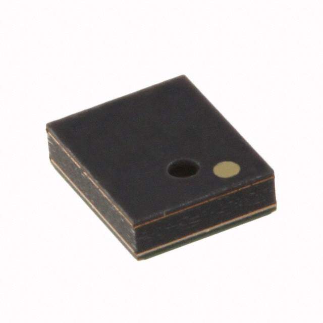
ICGOO电子元器件商城为您提供MP45DT02TR由STMicroelectronics设计生产,在icgoo商城现货销售,并且可以通过原厂、代理商等渠道进行代购。 MP45DT02TR价格参考。STMicroelectronicsMP45DT02TR封装/规格:麦克风, 100Hz ~ 10kHz Digital, PDM Microphone MEMS (Silicon) 1.64V ~ 3.6V Omnidirectional (-26dB ±3dB @ 94dB SPL) Solder Pads。您可以下载MP45DT02TR参考资料、Datasheet数据手册功能说明书,资料中有MP45DT02TR 详细功能的应用电路图电压和使用方法及教程。
STMicroelectronics(意法半导体)的MP45DT02TR是一款数字MEMS麦克风,具有高信噪比、低功耗和小型化的特点,适用于多种对音频采集质量要求较高的应用场景。该型号采用底部收音结构和I²S数字输出接口,抗干扰能力强,适合紧凑型设计。

主要应用场景包括:智能手机、平板电脑和笔记本电脑等移动设备,用于提升通话和录音的音频质量;智能音箱、语音助手和家庭自动化设备,支持远场语音识别和唤醒功能;无人机、可穿戴设备(如智能手表和无线耳机)也广泛采用该麦克风,以实现清晰的语音交互和环境噪声抑制。此外,MP45DT02TR还可用于安防监控摄像头、会议系统和车载信息系统中,提供可靠的语音采集能力。

其坚固的封装和良好的温度稳定性,使其在复杂电磁环境和多变工作条件下仍能保持稳定性能。总之,MP45DT02TR凭借其高性能和高可靠性,广泛应用于消费电子、智能家居和工业控制等领域,是现代智能设备中理想的音频输入解决方案。
| 参数 | 数值 |
| 产品目录 | |
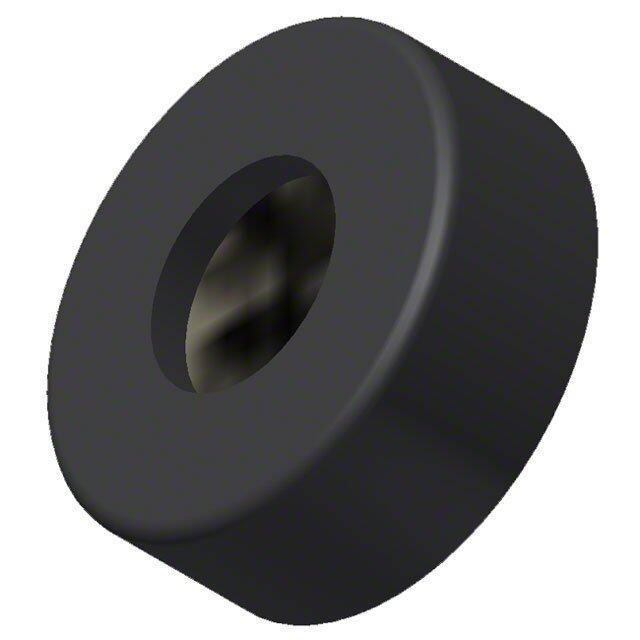
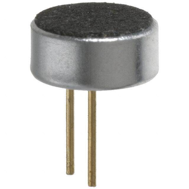
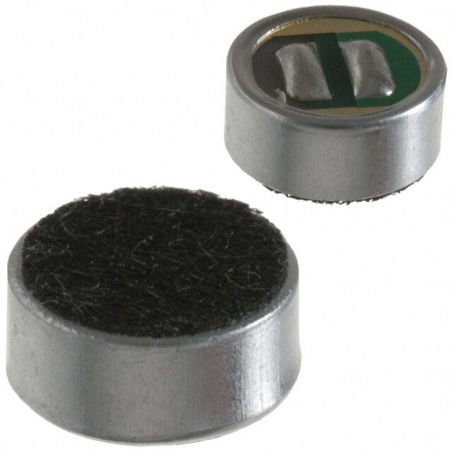
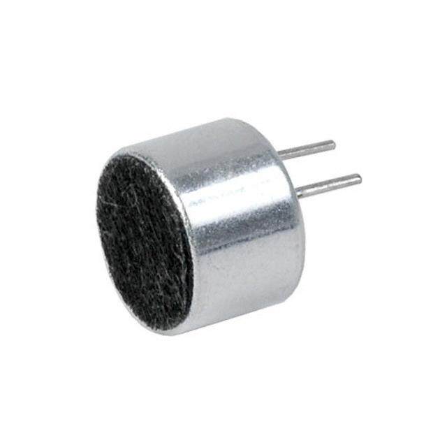
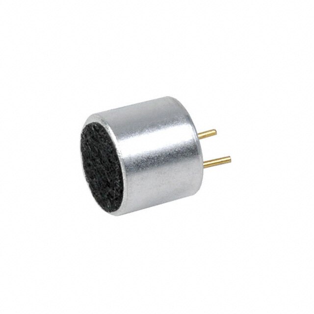
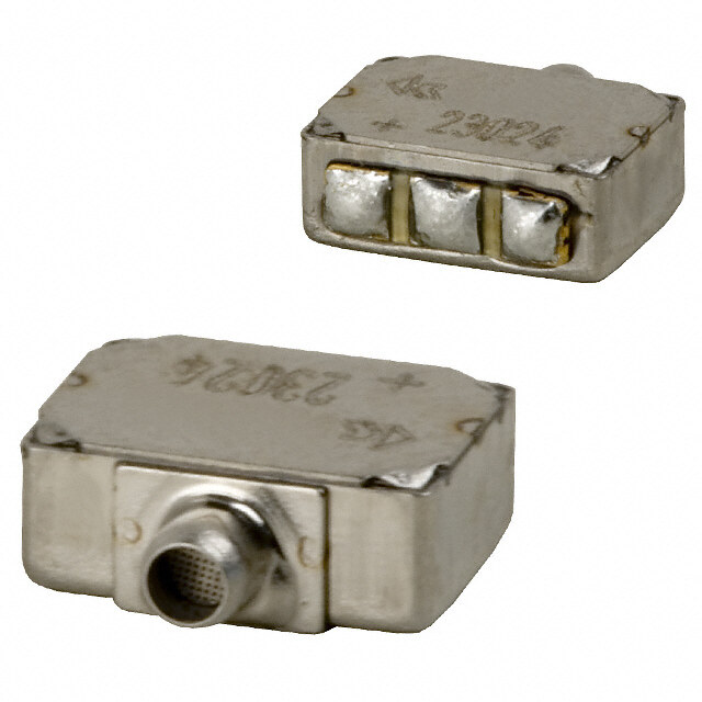
| 描述 | MIC MEMS DIGITAL PDM OMNI -26DBMEMS麦克风 MEMS Audio Sensor Omni MIC 120dBSPL |
| 产品分类 | |
| 品牌 | STMicroelectronics |
| 产品手册 | |
| 产品图片 |
|
| rohs | 符合RoHS无铅 / 符合限制有害物质指令(RoHS)规范要求 |
| 产品系列 | MEMS麦克风,STMicroelectronics MP45DT02TR- |
| 数据手册 | |
| 产品型号 | MP45DT02TR |
| 产品培训模块 | http://www.digikey.cn/PTM/IndividualPTM.page?site=cn&lang=zhs&ptm=30230 |
| 产品种类 | MEMS麦克风 |
| 信噪比 | 61dB |
| 其它名称 | 497-11921-2 |
| 其它有关文件 | http://www.st.com/web/catalog/sense_power/FM125/SC1564/PF251680?referrer=70071840 |
| 包装 | 带卷 (TR) |
| 商标 | STMicroelectronics |
| 大小/尺寸 | 4.72mm 长 x 3.76mm 宽 |
| 宽度 | 3.81 mm |
| 密封等级 | 无 |
| 封装 | Reel |
| 工作电压 | 1.64 V to 3.6 V |
| 工厂包装数量 | 4000 |
| 形状 | 矩形 |
| 方向 | 全向 |
| 方向性 | Omnidirectional |
| 标准包装 | 4,000 |
| 深度 | 1.375 mm |
| 灵敏度 | -26dB ±3dB @ 94dB SPL |
| 电压-额定 | 1.64 ~ 3.6V |
| 电流-电源 | 650µA |
| 端口位置 | 顶部 |
| 端接 | 焊盘 |
| 端接类型 | SMD/SMT |
| 类型 | MEMS(硅) |
| 系列 | MP45DT |
| 输出类型 | 数字,PDM |
| 配用 | /product-detail/zh/STEVAL-MKI138V3/497-14895-ND/4901477 |
| 长度 | 4.77 mm |
| 阻抗 | - |
| 频率范围 | 100Hz ~ 10kHz |
| 高度(最大值) | 1.38mm |


- 商务部:美国ITC正式对集成电路等产品启动337调查
- 曝三星4nm工艺存在良率问题 高通将骁龙8 Gen1或转产台积电
- 太阳诱电将投资9.5亿元在常州建新厂生产MLCC 预计2023年完工
- 英特尔发布欧洲新工厂建设计划 深化IDM 2.0 战略
- 台积电先进制程称霸业界 有大客户加持明年业绩稳了
- 达到5530亿美元!SIA预计今年全球半导体销售额将创下新高
- 英特尔拟将自动驾驶子公司Mobileye上市 估值或超500亿美元
- 三星加码芯片和SET,合并消费电子和移动部门,撤换高东真等 CEO
- 三星电子宣布重大人事变动 还合并消费电子和移动部门
- 海关总署:前11个月进口集成电路产品价值2.52万亿元 增长14.8%

PDF Datasheet 数据手册内容提取
MP45DT02 MEMS audio sensor omnidirectional digital microphone Datasheet - production data Description The MP45DT02 is a compact, low-power, to)p- s port, omnidirectional, digital MEMS microphone. ( The MP45DT02 is built with a sensicngt element and an IC interface with stereo cuapability. d The sensing element, capaoble of detecting acoustic waves, is manrufactured using a P specialized silicon micromachining process to produce audio seensors. t e The IC interface is manufactured using a CMOS l o process that allows designing a dedicated circuit s able to provide a digital signal externally in PDM b O format. HLGA (4.72 x 3.76 mm) 6LD - The MP45DT02 has an acoustic overload point of ) 120 dBSPL with a best on the market 61 dB Features s signal-to-noise ratio and -26 dB sensitivity. ( t • Single supply voltage c The MP45DT02 is available in an SMD-compliant • Low power consumption u metal (M) or plastic package and is guaranteed to d • 120 dBSPL acoustic ooverload point operate over an extended temperature range • Omnidirectional sernsitivity from -30 °C to +85 °C. P • PDM single-bit output with option for stereo The MP45DT02’s digital output and package size configuratioen • HLGA epatckage (SMD-compliant) plastic or (1.25 mm thick) make this device the best solution for laptop and portable computing metlal • sECoOPACK®, RoHS, and “Green” compliant applications. b Table 1: Device summary O Applications Order code Temp. range [°C] Package Packing • Mobile terminals HLGA • Laptop and notebook computers MP45DT02 -30 to +85 4.72x3.76 6LD Tray • Portable media players HLGA • VoIP MP45DT02TR -30 to +85 Tape and reel 4.72x3.76 6LD • Speech recognition • A/V eLearning devices HLGA MP45DT02TR-M -30 to +85 Tape and reel • Gaming and virtual reality input devices 4.72x3.76 6LD • Digital still and video cameras • Antitheft systems January 2016 DocID018658 Rev 8 1/15 This is information on a product in full production. www.st.com
Contents MP45DT02 Contents 1 Pin description ................................................................................ 3 2 Acoustic and electrical specifications ........................................... 4 2.1 Acoustic and electrical characteristics ............................................... 4 2.2 Timing characteristics ....................................................................... 5 2.3 Frequency response ......................................................................... 6 3 Sensing element .............................................................................. 7 4 Absolute maximum ratings ............................................................. 8 ) s 5 Functionality .........................................................................(........... 9 t c 5.1 L/R channel selection ...................................................u..................... 9 d 6 Application recommendations ...............................o...................... 10 r P 7 Package information ..................................................................... 11 e 7.1 Soldering information .........................t............................................. 11 e 7.2 HLGA (4.72 x 3.76 mm) 6L (plasotilc) package information ............... 12 s 7.3 HLGA (4.72 x 3.76 mm) 6L b(metal) package information ................ 13 O 8 Revision history ................. ........................................................... 14 - ) s ( t c u d o r P e t e l o s b O 2/15 DocID018658 Rev 8
MP45DT02 Pin description 1 Pin description Figure 1: Pin connections Vdd 6 11 GND DOUT 55 2 LR ) s CLK 44 33 GND t( c u d o r P (BOTTOM VIEW) e t e Table 2: Pin description l o Pin Pin n° s Function name b O 1 GND 0 V supply Left/right channel s-election; ) 2 LR MIC1 LR is cosnnected to GND or Vdd and MIC2 LR is connected to Vdd or GND (see Figur(e 5: "MP45DT02 electrical connections for stereo configuration") t c 3 GND 0 Vu supply d 4 CLK Synchronization input clock o 5 DOrUT Left/right PDM data output P 6 Vdd Power supply e t e l o s b O DocID018658 Rev 8 3/15
Acoustic and electrical specifications MP45DT02 2 Acoustic and electrical specifications 2.1 Acoustic and electrical characteristics The values listed in the table below are specified for Vdd = 1.8 V, Clock = 2.4 MHz, T = 25 °C, unless otherwise noted. Table 3: Acoustic and electrical characteristics Symbol Parameter Test Min. Typ. (1) Max. Unit condition Vdd Supply voltage 1.64 1.8 3.6 V Current consumption in No load on ) Idd 0.65 s mA normal mode data line ( t c Current consumption in IddPdn power-down mode (2) 20 d u µA Scc Short-circuit current 1 o 10 mA r AOP Acoustic overload point P 120 dBSPL So Sensitivity -29 e -26 -23 dBFS t A-weighted e SNR Signal-to-noise ratio l 61 dB @1 kHz, 1 Pa o s Guaranteebd by PSR Power supply rejection designO (3) -70 dBFS Clock Input clock frequency (4) 1 2.4 3.25 MHz - TWK Wake-up time (5) s ) Guaranteed by 10 ms ( design t c Operating temperature Top u -30 +85 °C range d Low olevel logic VIOL P inrput/output voltage Iout = 1 mA -0.3 0.35xVdd V tVIeOH Hinipguht /loeuvtepl ulot gviocl tage Iout = 1 mA 0.65xVdd Vdd+0.3 V e l o Notes: s b (1)Typical specifications are not guaranteed. O (2)Input clock in static mode. (3)Test signal: 217 Hz square wave, 100 mVpp on Vdd pin. (4)Duty cycle: min = 40% max = 60%. (5)Time from the first clock edge to valid output data. Table 4: Distortion specifications Parameter Test condition Value Distortion 100 dBSPL (50 Hz - 4 kHz) < 1% THD + N Distortion 115 dBSPL (1 kHz) < 5% THD + N 4/15 DocID018658 Rev 8
MP45DT02 Acoustic and electrical specifications 2.2 Timing characteristics Table 5: Timing characteristics Parameter Description Min Max Unit fCLK Clock frequency for normal mode 1 3.25 MHz fPD Clock frequency for power-down mode 0.23 MHz TCLK Clock period for normal mode 308 1000 ns TR,EN Data enabled on DATA line, L/R pin = 1 30 (1) ns TR,DIS Data disabled on DATA line, L/R pin = 1 16(1)(2) ns TL,EN Data enabled on DATA line, L/R pin = 0 30(1) ns TL,DIS Data disabled on DATA line, L/R pin = 0 16(1)(2) ns ) s Notes: ( t (1)From design simulations c u (2)In order to measure the disable time, a 1 kΩ pull-down resistor must be added to the DOdUT pin. o r P Figure 2: Timing waveforms e t e l o s b O - ) s ( t c u d o r P e t e l o s b O DocID018658 Rev 8 5/15
Acoustic and electrical specifications MP45DT02 2.3 Frequency response Figure 3: Typical frequency response normalized at 1 kHz ) s ( t c u d o r P e t e l o s b O - ) s ( t c u d o r P e t e l o s b O 6/15 DocID018658 Rev 8
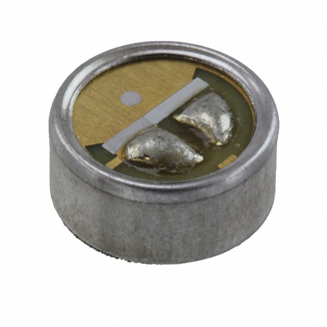
MP45DT02 Sensing element 3 Sensing element The sensing element shall mean the acoustic sensor consisting of a conductive movable plate and a fixed plate placed in a tiny silicon chip. This sensor transduces the sound pressure into the changes of coupled capacity between those two plates. Omron Corporation supplies this element for STMicroelectronics. ) s ( t c u d o r P e t e l o s b O - ) s ( t c u d o r P e t e l o s b O DocID018658 Rev 8 7/15
Absolute maximum ratings MP45DT02 4 Absolute maximum ratings Stresses above those listed as “absolute maximum ratings” may cause permanent damage to the device. This is a stress rating only and functional operation of the device under these conditions is not implied. Exposure to maximum rating conditions for extended periods may affect device reliability. Table 6: Absolute maximum ratings Symbol Ratings Maximum value Unit Vdd Supply voltage -0.3 to 6 V Vin Input voltage on any control pin -0.3 to Vdd +0.3 V TSTG Storage temperature range -40 to +125 s )°C ESD Electrostatic discharge protection 2 (HBM) ( kV t c u d o r P e t e l o s b O - ) s ( t c u d o r P e t e l o s b O 8/15 DocID018658 Rev 8
MP45DT02 Functionality 5 Functionality 5.1 L/R channel selection The L/R digital pad lets the user select the DOUT signal pattern as explained in Table 7: "L/R channel selection". The L/R pin must be connected to Vdd or GND. Table 7: L/R channel selection L/R CLK low CLK high GND Data valid High impedence Vdd High impedence Data valid ) s ( t c u d o r P e t e l o s b O - ) s ( t c u d o r P e t e l o s b O DocID018658 Rev 8 9/15
Application recommendations MP45DT02 6 Application recommendations Figure 4: MP45DT02 electrical connections Vdd 10 µF 100nF 1 6 ) s C ( L/R 2 PVIEW 5 Dout ODE u ct TO C d o CLK 3 4 r P e t e l o Figure 5: MP45DT02 electrical connections for stereo configuration s b O Vdd - 10 µ F ) s 100nF ( t c MICu1 MIC2 d o 1 6 1 6 r P W e t e 2 TOPVIE 5 Dout Vdd 2 TOPVIEW 5 Dout l o 3 4 3 4 s b O CLK CODEC Power supply decoupling capacitors (100 nF ceramic, 10 µF ceramic) should be placed as near as possible to pin 6 of the device (common design practice). The L/R pin must be connected to Vdd or GND (refer to Table 7: "L/R channel selection"). 10/15 DocID018658 Rev 8
MP45DT02 Package information 7 Package information In order to meet environmental requirements, ST offers these devices in different grades of ECOPACK® packages, depending on their level of environmental compliance. ECOPACK® specifications, grade definitions and product status are available at: www.st.com. ECOPACK® is an ST trademark. 7.1 Soldering information The HLGA (4.72 x 3.76 x 1.25) mm package is also compliant with the RoHS and “Green” standards and is qualified for soldering heat resistance according to JEDEC J-STD-020. Landing pattern and soldering recommendations are available at www.st.com. ) s Figure 6: Recommended soldering profile limits ( t c u d o r P e t e l o s b O - ) s ( t c u d o r P Table 8: Recommended soldering profile limits e Description Parameter Pb free t e ol Average ramp rate TL to TP 3 °C/sec max s Preheat b TSMIN 150 °C Minimum temperature O TSMAX 200 °C Maximum temperature tS 60 sec to 120 sec Time (TSMIN to TSMAX) Ramp-up rate TSMAX to TL Time maintained above liquidus temperature tL 60 sec to 150 sec Liquidus temperature TL 217 °C Peak temperature TP 260 °C max Time within 5 °C of actual peak temperature 20 sec to 40 sec Ramp-down rate 6 °C/sec max Time 25 °C (t25 °C) to peak temperature 8 minutes max DocID018658 Rev 8 11/15
Package information MP45DT02 7.2 HLGA (4.72 x 3.76 mm) 6L (plastic) package information Figure 7: HLGA (4.72 x 3.76 mm) 6-lead package outline Pin1indicator A1 N4 E1 //KC K C 2 R1 D 3 1 D N N 1D 1L ) KE s ( t c K E2 E KD 1 N2 u G d * 7 o L2 r P e 8287552_A t e Table 9: HLGA (4.72 x 3.76 mm) 6-leald package mechanical data o s mm. Symbol b Min. O Typ. Max. A1 1.125 - 1.250 1.375 D1 4.67)0 4.720 4.770 s ( D2 t 1.320 c R1 u 0.750 0.840 0.930 d E1 3.710 3.760 3.810 o Er2 1.880 P L1 3.200 3.300 3.400 e t L2 2.250 2.350 2.450 e ol N1 1.550 1.650 1.750 s N2 1.075 1.175 1.275 b O N3 1.350 1.450 1.550 N4 0.865 0.965 1.065 G1 0.810 0.910 1.010 K 0.050 12/15 DocID018658 Rev 8
MP45DT02 Package information 7.3 HLGA (4.72 x 3.76 mm) 6L (metal) package information Figure 8: HLGA (4.72 x 3.76 mm) 6-lead package outline and mechanical data ) s ( t c u d o r P e t e Dimensionsareinmillimeterunlesslotherwisespecified GeneralToleranceis+/-0.15mmunolessotherwisespecified s b OUTERDIMENSIONS O ITEM DIMENSION[mm] TOLERANCE[mm] Length[L] - 4.72 ±0.1 Width[W] ) 3.76 ±0.1 Height[H] s 1.25 ±0.1 ( t c u 8499123_A d o Note: The MEMS microphone metal cap can exhibit some level of variation in color when r the devicPe is subjected to a thermal process. e t e l o s b O DocID018658 Rev 8 13/15
Revision history MP45DT02 8 Revision history Table 10: Document revision history Date Revision Changes 28-Mar-2011 1 Initial release Added max. peak temperature TP to 21-Oct-2011 2 Added min. and max. sensitivity So to Table 3: "Acoustic and electrical characteristics" Document status promoted from preliminary to production data 01-Mar-2012 3 Updated SNR to 61 dB ("Description" and Table 3: "Acoustic and electrical characteristics") ) s 07-May-2012 4 Added VIOL, VIOH to Table 3: "Acoustic and electrical chara(cteristics" t c 05-Jul-2012 5 Added Section 4: "Sensing element" u Added new package "Figure 8: "HLGA (4.72 x 3d.76 mm) 6-lead 21-Mar-2014 6 package outline and mechanical data" o r Updated "Figure 3: Typical frequency rPesponse normalized at 1 17-Jun-2014 7 kHz" e t Added footnote concerning edisable time to Table 5: "Timing 26-Jan-2016 8 characteristics" l o s b O - ) s ( t c u d o r P e t e l o s b O 14/15 DocID018658 Rev 8
MP45DT02 IMPORTANT NOTICE – PLEASE READ CAREFULLY STMicroelectronics NV and its subsidiaries (“ST”) reserve the right to make changes, corrections, enhancements, modifications, and improvements to ST products and/or to this document at any time without notice. Purchasers should obtain the latest relevant information on ST products before placing orders. ST products are sold pursuant to ST’s terms and conditions of sale in place at the time of order acknowledgement. Purchasers are solely responsible for the choice, selection, and use of ST products and ST assumes no liability for application assistance or the design of Purchasers’ products. ) No license, express or implied, to any intellectual property right is granted by ST herein. s ( ct u Resale of ST products with provisions different from the information set forth herein shall void any warranty granted by ST for such product. d o r P ST and the ST logo are trademarks of ST. All other product or service names are the property of their respective owners. e t e Information in this document supersedes and replaces information previously supplied inl any prior versions of this document. o s b © 2016 STMicroelectronOics – All rights reserved - ) s ( t c u d o r P e t e l o s b O DocID018658 Rev 8 15/15