 Datasheet下载
- 型号: MP34DT01TR
- 制造商: STMicroelectronics
- 库位|库存: xxxx|xxxx
- 要求:
| 数量阶梯 | 香港交货 | 国内含税 |
| +xxxx | $xxxx | ¥xxxx |
查看当月历史价格
查看今年历史价格
MP34DT01TR产品简介:
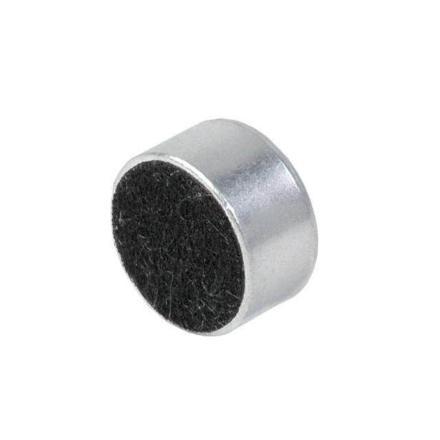
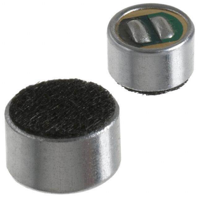
ICGOO电子元器件商城为您提供MP34DT01TR由STMicroelectronics设计生产,在icgoo商城现货销售,并且可以通过原厂、代理商等渠道进行代购。 MP34DT01TR价格参考。STMicroelectronicsMP34DT01TR封装/规格:麦克风, 100Hz ~ 10kHz Digital, PDM Microphone MEMS (Silicon) 1.64V ~ 3.6V Omnidirectional (-26dB ±3dB @ 94dB SPL) Solder Pads。您可以下载MP34DT01TR参考资料、Datasheet数据手册功能说明书,资料中有MP34DT01TR 详细功能的应用电路图电压和使用方法及教程。
STMicroelectronics的MP34DT01TR是一款数字MEMS(微机电系统)麦克风,广泛应用于各种消费电子和工业设备中。它具有高信噪比、低功耗和小型化的特点,适用于需要高质量音频采集的场景。

 主要应用场景:

1. 智能手机和平板电脑:
   MP34DT01TR常用于智能手机和平板电脑中,作为主麦克风或辅助麦克风,用于语音通话、录音、语音助手等功能。其高灵敏度和低噪声特性确保了清晰的语音传输,提升了用户体验。

2. 智能音箱和语音助手设备:
   该麦克风广泛应用于智能音箱、语音助手等设备中,支持远场语音识别功能。其数字输出接口和低功耗设计使得它在长时间待机状态下也能保持高效工作,确保用户能够随时唤醒语音助手。

3. 可穿戴设备:
   在智能手表、TWS(真无线立体声)耳机等可穿戴设备中,MP34DT01TR的小尺寸和低功耗特性使其成为理想选择。它可以用于语音控制、环境音监听等功能,帮助用户实现更便捷的操作体验。

4. 智能家居设备:
   智能门铃、摄像头、安防设备等智能家居产品也常用到这款麦克风。它可以帮助设备捕捉周围的声音信息,结合视频监控实现更加全面的安全防护功能。

5. 医疗设备:
   在一些便携式医疗设备如助听器、远程医疗设备中,MP34DT01TR可以提供高质量的音频输入,帮助医生更准确地获取患者的语音信息,提升诊断效率。

6. 汽车电子:
   汽车内部的语音控制系统、行车记录仪等设备也会使用这款麦克风,以确保车内人员的语音指令能够被准确识别,提升驾驶安全性和便利性。

总之,MP34DT01TR凭借其出色的性能和灵活性,成为了众多音频采集应用的理想选择,尤其是在对音频质量要求较高的场景中表现尤为突出。
| 参数 | 数值 |
| 产品目录 | |
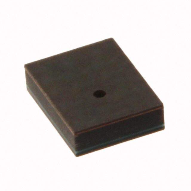
| 描述 | MIC MEMS DIGITAL PDM OMNI -26DBMEMS麦克风 MEMS Audio 120 dBSPL 63dB -26 dBFS Sensor |
| 产品分类 | |
| 品牌 | STMicroelectronics |
| 产品手册 | |
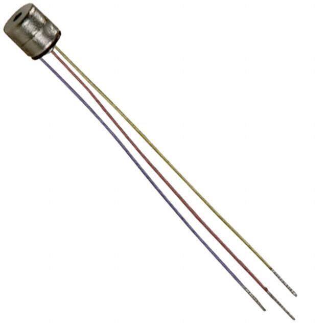
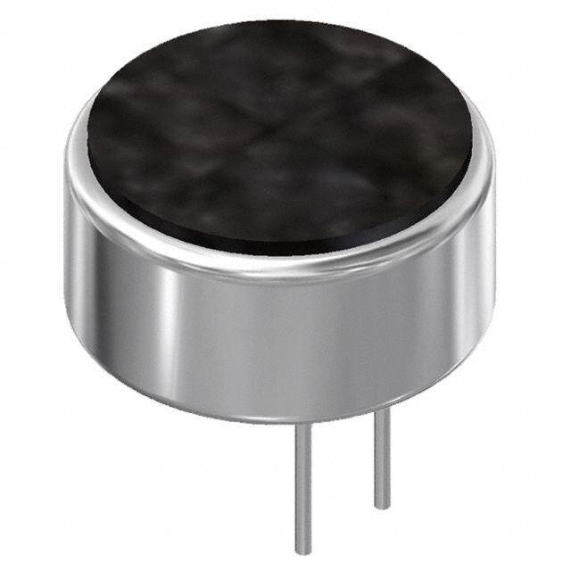
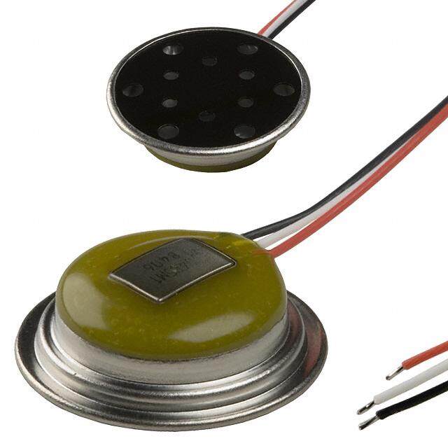
| 产品图片 |
|
| rohs | 符合RoHS无铅 / 符合限制有害物质指令(RoHS)规范要求 |
| 产品系列 | MEMS麦克风,STMicroelectronics MP34DT01TR- |
| 数据手册 | |
| 产品型号 | MP34DT01TR |
| 产品培训模块 | http://www.digikey.cn/PTM/IndividualPTM.page?site=cn&lang=zhs&ptm=30230 |
| 产品种类 | MEMS麦克风 |
| 信噪比 | 63dB |
| 其它名称 | 497-12016-2 |
| 其它有关文件 | http://www.st.com/web/catalog/sense_power/FM125/SC1564/PF250940?referrer=70071840 |
| 包装 | 带卷 (TR) |
| 商标 | STMicroelectronics |
| 商标名 | ECOPACK |
| 大小/尺寸 | 4.00mm 长 x 3.00mm 宽 |
| 安装风格 | SMD/SMT |
| 宽度 | 3 mm |
| 密封等级 | 无 |
| 封装 | Reel |
| 封装/箱体 | HCLGA |
| 工作电压 | 1.8 V |
| 工厂包装数量 | 4000 |
| 形状 | 矩形 |
| 方向 | 全向 |
| 方向性 | Omnidirectional |
| 最大工作温度 | + 85 C |
| 最小工作温度 | - 40 C |
| 标准包装 | 4,000 |
| 深度 | 1 mm |
| 灵敏度 | -26dB ±3dB @ 94dB SPL |
| 电压-额定 | 1.64 ~ 3.6V |
| 电流-电源 | 600µA |
| 电流额定值 | 0.6 mA |
| 端口位置 | 顶部 |
| 端接 | 表面贴装型 |
| 端接类型 | SMD/SMT |
| 类型 | MEMS(硅) |
| 系列 | MP33AB01 |
| 输出类型 | 数字,PDM |
| 长度 | 4 mm |
| 阻抗 | - |
| 频率范围 | 100Hz ~ 10kHz |
| 高度(最大值) | 1.10mm |


- 商务部:美国ITC正式对集成电路等产品启动337调查
- 曝三星4nm工艺存在良率问题 高通将骁龙8 Gen1或转产台积电
- 太阳诱电将投资9.5亿元在常州建新厂生产MLCC 预计2023年完工
- 英特尔发布欧洲新工厂建设计划 深化IDM 2.0 战略
- 台积电先进制程称霸业界 有大客户加持明年业绩稳了
- 达到5530亿美元!SIA预计今年全球半导体销售额将创下新高
- 英特尔拟将自动驾驶子公司Mobileye上市 估值或超500亿美元
- 三星加码芯片和SET,合并消费电子和移动部门,撤换高东真等 CEO
- 三星电子宣布重大人事变动 还合并消费电子和移动部门
- 海关总署:前11个月进口集成电路产品价值2.52万亿元 增长14.8%
PDF Datasheet 数据手册内容提取
MP34DT01 MEMS audio sensor omnidirectional digital microphone Datasheet - production data Description The MP34DT01 is an ultra-compact, low-power, omnidirectional, digital MEMS microphone built with a capacitive sensing element and an IC interface. The sensing element, capable of detecting acoustic waves, is manufactured using a specialized silicon micromachining process dedicated to produce audio sensors. The IC interface is manufactured using a CMOS Features process that allows designing a dedicated circuit • Single supply voltage able to provide a digital signal externally in PDM • Low power consumption format. • 120 dBSPL acoustic overload point The MP34DT01 has an acoustic overload point of • 63 dB signal-to-noise ratio 120 dBSPL with a 63 dB signal-to-noise ratio and • Omnidirectional sensitivity –26 dBFS sensitivity. • –26 dBFS sensitivity • PDM output The MP34DT01 is available in a top-port, SMD- • HCLGA package compliant, EMI-shielded package and is guaranteed to operate over an extended − Top-port design temperature range from -40 °C to +85 °C. − SMD-compliant − EMI-shielded Table 1: Device summary − ECOPACK®, RoHS, and “Green” Temp. compliant Order codes Package Packing range [°C] HCLGA Applications MP34DT01 -40 to +85 (3x4 x1 mm) Tray • Mobile terminals 4LD • Laptop and notebook computers HCLGA • Portable media players Tape MP34DT01TR -40 to +85 (3x4x1 mm) • VoIP and reel 4LD • Speech recognition • A/V eLearning devices • Gaming and virtual reality input devices • Digital still and video cameras • Antitheft systems February 2015 DocID022331 Rev 12 1/20 This is information on a product in full production. www.st.com
Contents MP34DT01 Contents 1 Pin description ................................................................................ 5 2 Acoustic and electrical specifications ........................................... 6 2.1 Acoustic and electrical characteristics ............................................... 6 2.2 Timing characteristics ....................................................................... 7 2.3 Frequency response ......................................................................... 8 3 Carrier tape mechanical specifications ......................................... 9 4 Process recommendations ........................................................... 10 5 Sensing element ............................................................................ 12 6 Absolute maximum ratings ........................................................... 13 7 Functionality .................................................................................. 14 7.1 L/R channel selection ...................................................................... 14 8 Package information ..................................................................... 15 8.1 Soldering information ...................................................................... 15 8.2 HCLGA package information........................................................... 16 9 Revision history ............................................................................ 19 2/20 DocID022331 Rev 12
MP34DT01 List of tables List of tables Table 1: Device summary ........................................................................................................................... 1 Table 2: Pin description .............................................................................................................................. 5 Table 3: Acoustic and electrical characteristics .......................................................................................... 6 Table 4: Distortion specifications ................................................................................................................ 6 Table 5: Timing characteristics ................................................................................................................... 7 Table 6: Frequency response mask for digital microphones ...................................................................... 8 Table 7: Absolute maximum ratings ......................................................................................................... 13 Table 8: L/R channel selection ................................................................................................................. 14 Table 9: Recommended soldering profile limits ........................................................................................ 15 Table 10: HCLGA (3 x 4 x 1 mm) 4-lead package dimensions ................................................................ 17 Table 11: Document revision history ........................................................................................................ 19 DocID022331 Rev 12 3/20
List of figures MP34DT01 List of figures Figure 1: Pin connections ........................................................................................................................... 5 Figure 2: Timing waveforms ....................................................................................................................... 7 Figure 3: Frequency response and mask ................................................................................................... 8 Figure 4: Carrier tape without microphone (top view) ................................................................................. 9 Figure 5: Carrier tape with microphone (top view) ...................................................................................... 9 Figure 6: Recommended picking area ...................................................................................................... 10 Figure 7: Recommended picker design .................................................................................................... 11 Figure 8: Recommended soldering profile limits ...................................................................................... 15 Figure 9: HCLGA (3 x 4 x 1 mm) 4-lead package outline ......................................................................... 16 Figure 10: Land pattern............................................................................................................................. 18 4/20 DocID022331 Rev 12
MP34DT01 Pin description 1 Pin description Figure 1: Pin connections Table 2: Pin description Pin # Pin name Function 1 Vdd Power supply 2 LR Left/Right channel selection 3 CLK Synchronization input clock 4 DOUT Left/Right PDM data output 5 (ground ring) GND 0 V supply DocID022331 Rev 12 5/20
Acoustic and electrical specifications MP34DT01 2 Acoustic and electrical specifications 2.1 Acoustic and electrical characteristics The values listed in the table below are specified for Vdd = 1.8 V, Clock = 2.4 MHz, T = 25 °C, unless otherwise noted. Table 3: Acoustic and electrical characteristics Symbol Parameter Test condition Min. Typ. (1) Max. Unit Vdd Supply voltage 1.64 1.8 3.6 V Current consumption in normal Idd Mean value 0.6 mA mode Current consumption in power- IddPdn down mode (2) 20 µA Scc Short-circuit current 1 10 mA AOP Acoustic overload point 120 dBSPL So Sensitivity -29 -26 -23 dBFS A-weighted at 1 kHz, SNR Signal-to-noise ratio 63 dB 1 Pa PSR Power supply rejection Guaranteed by design -70 dBFS Clock Input clock frequency (3) 1 2.4 3.25 MHz Ton Turn-on time (4) Guaranteed by design 10 ms Top Operating temperature range -40 +85 °C Low-level logic input/output VIOL voltage Iout = 1 mA -0.3 0.35xVdd V High-level logic input/output VIOH voltage Iout = 1 mA 0.65xVdd Vdd+0.3 V Notes: (1)Typical specifications are not guaranteed. (2)Input clock in static mode. (3)Duty cycle: min = 40% max = 60%. (4)Time from the first clock edge to valid output data. Table 4: Distortion specifications Parameter Test condition Value Distortion 100 dBSPL (50 Hz - 4 kHz) < 1% THD + N Distortion 115 dBSPL (1 kHz) < 5% THD + N 6/20 DocID022331 Rev 12
MP34DT01 Acoustic and electrical specifications 2.2 Timing characteristics Table 5: Timing characteristics Parameter Description Min. Max. Unit fCLK Clock frequency for normal mode 1 3.25 MHz fPD Clock frequency for power-down mode 0.23 MHz TCLK Clock period for normal mode 308 1000 ns TR,EN Data enabled on DATA line, L/R pin = 1 18 (1) ns TR,DIS Data disabled on DATA line, L/R pin = 1 16(1) ns TL,EN Data enabled on DATA line, L/R pin = 0 18(1) ns TL,DIS Data disabled on DATA line, L/R pin = 0 16(1) ns Notes: (1)From design simulations Figure 2: Timing waveforms DocID022331 Rev 12 7/20
Acoustic and electrical specifications MP34DT01 2.3 Frequency response Figure 3: Frequency response and mask Table 6: Frequency response mask for digital microphones Frequency / Hz (1) Lower limit Upper limit Unit 100...4000 -2 +2 dBr 1 kHz 4000...10000 -2 +4 dBr 1 kHz Notes: (1)At T = 20 °C and acoustic stimulus = 1 Pa (94 dB SPL) 8/20 DocID022331 Rev 12
MP34DT01 Carrier tape mechanical specifications 3 Carrier tape mechanical specifications Figure 4: Carrier tape without microphone (top view) Figure 5: Carrier tape with microphone (top view) DocID022331 Rev 12 9/20
Process recommendations MP34DT01 4 Process recommendations To ensure a consistent manufacturing process it is strongly advised to comply with the following recommendations: • The recommended pick-up area for the MP34DT01 package must be defined using the worst case (ie. no device alignment during the picking process). This area has been defined considering all the tolerances of the components involved (reel, package, sound inlet). The picker tolerance shall be considered as well. • To prevent damage to the MEMS membrane or incorrect pick-up and placement, do not pick up the component on the inlet area • For the package outline please refer to Figure 5: "Carrier tape with microphone (top view)". Nozzle shape, size, and placement accuracy are the other key factors to consider when deciding on the coordinates for picking. • Device alignment before picking is highly recommended. • A vacuum force greater than 7 psi must be avoided • 1 kPa = 0.145 psi (lb/in2) = 0.0102 kgf/cm² = 0.0098 atm • All recommended dimensions (device safe-picking area) do not include the pick-and- place equipment tolerances Figure 6: Recommended picking area To have a safe pick-up "by design", ST strongly advises an ad hoc nozzle. The following picker ensures that the holes for the vacuum and the air stream are ALWAYS away from the porthole of the device (4 vacuum ports located at each corner of the device). The recommended nozzle also has a recess, in the form of a cross, which guarantees that the porthole is always left at atmospheric pressure. By using the recommended nozzle, the membrane will not suffer any sudden air disturbances during the picking or placing of the devices in the tape and reel. 10/20 DocID022331 Rev 12
MP34DT01 Process recommendations Figure 7: Recommended picker design DocID022331 Rev 12 11/20
Sensing element MP34DT01 5 Sensing element The sensing element shall mean the acoustic sensor consisting of a conductive movable plate and a fixed plate placed in a tiny silicon chip. This sensor transduces the sound pressure into the changes of coupled capacity between those two plates. Omron Corporation supplies this element for STMicroelectronics. 12/20 DocID022331 Rev 12
MP34DT01 Absolute maximum ratings 6 Absolute maximum ratings Stresses above those listed as “absolute maximum ratings” may cause permanent damage to the device. This is a stress rating only and functional operation of the device under these conditions is not implied. Exposure to maximum rating conditions for extended periods may affect device reliability. Table 7: Absolute maximum ratings Symbol Ratings Maximum value Unit Vdd Supply voltage -0.3 to 6 V Vin Input voltage on any control pin -0.3 to Vdd +0.3 V TSTG Storage temperature range -40 to +125 °C ESD Electrostatic discharge protection 2 (HBM) kV DocID022331 Rev 12 13/20
Functionality MP34DT01 7 Functionality 7.1 L/R channel selection The L/R digital pad lets the user select the DOUT signal pattern as shown in Table 8: "L/R channel selection". The L/R pin must be connected to Vdd or GND. Table 8: L/R channel selection L/R CLK low CLK high GND Data valid High impedance Vdd High impedance Data valid 14/20 DocID022331 Rev 12
MP34DT01 Package information 8 Package information In order to meet environmental requirements, ST offers these devices in different grades of ECOPACK® packages, depending on their level of environmental compliance. ECOPACK® specifications, grade definitions and product status are available at: www.st.com. ECOPACK® is an ST trademark. 8.1 Soldering information The HCLGA (3 x 4) 4LD package is also compliant with the RoHS and “Green” standards and is qualified for soldering heat resistance according to JEDEC J-STD-020. Land pattern and soldering recommendations are available at www.st.com. Figure 8: Recommended soldering profile limits Table 9: Recommended soldering profile limits Description Parameter Pb free Average ramp rate TL to TP 3 °C/sec max Preheat TSMIN 150 °C Minimum temperature TSMAX 200 °C Maximum temperature tS 60 sec to 120 sec Time (TSMIN to TSMAX) Ramp-up rate TSMAX to TL Time maintained above liquids temperature tL 60 sec to 150 sec Liquids temperature TL 217 °C Peak temperature TP 260 °C max Time within 5 °C of actual peak temperature 20 sec to 40 sec Ramp-down rate 6 °C/sec max Time 25 °C (t25 °C) to peak temperature 8 minutes max DocID022331 Rev 12 15/20
Package information MP34DT01 8.2 HCLGA package information Figure 9: HCLGA (3 x 4 x 1 mm) 4-lead package outline Note: The MEMS microphone plastic cap can exhibit some level of variation in color when the device is subjected to thermal processes. 16/20 DocID022331 Rev 12
MP34DT01 Package information Table 10: HCLGA (3 x 4 x 1 mm) 4-lead package dimensions mm Symbol Min. Typ. Max. A 0.90 1.00 1.10 A1 0.00 - 0.05 b 0.35 0.45 0.50 D 3.90 4.00 4.10 D1 3.05 3.10 3.15 D2 3.75 3.80 3.85 D3 0.30 0.50 0.70 E 2.90 3.00 3.10 E1 2.05 2.10 2.15 E2 2.75 2.80 2.85 E3 -0.20 0.00 0.20 e1 1.30 1.35 1.40 e2 0.80 0.85 0.90 h 0.25 0.30 0.35 L 0.90 0.95 1.00 L1 - 0.10 - N 4 R1 0.30 0.40 0.50 R2 - 0.40 - aaa 0.15 ccc 0.10 eee 0.08 DocID022331 Rev 12 17/20
Package information MP34DT01 Figure 10: Land pattern 0.85 1.30 5 GND 3 0. 85 0. 0.40 K R 5 CL L 0.9 D D 0 N N 3 G G 2. T U d O d V D 0.35 GND Pad + solder paste 18/20 DocID022331 Rev 12
MP34DT01 Revision history 9 Revision history Table 11: Document revision history Date Revision Changes 06-Oct-2011 1 Initial release 18-Nov-2011 2 Removed “stereo” from title, Section "Features", and Section "Description" 29-Nov-2011 3 Updated Section "Features" and Section "Description" Updated 04-Jan-2012 4 Added So limits to Table 3: "Acoustic and electrical characteristics" Minor textual updates Updated Figure 9: "HCLGA (3 x 4 x 1 mm) 4-lead package outline" Pin 1 indicator removed from top view of package on page 1 and Figure 1: "Pin 23-Mar-2012 5 connections" Updated Table 10: "HCLGA (3 x 4 x 1 mm) 4-lead package dimensions" Updated maximum supply voltage in Table 3: "Acoustic and electrical 06-Apr-2012 6 characteristics" 07-May-2012 7 Added VIOL, VIOH to Table 3: "Acoustic and electrical characteristics" 18-May-2012 8 Updated Table 5: "Timing characteristics" Added Section 5: "Sensing element" 05-Jul-2012 9 Added Figure 10: "Land pattern" Updated temperature range to -40 to +85 °C throughout datasheet Updated dimension T2 in Table 10: "HCLGA (3 x 4 x 1 mm) 4-lead package 21-Feb-2013 10 dimensions" Updated - Figure 3: "Frequency response and mask" - Table 6: "Frequency response mask for digital microphones" - HCLGA mechanical data Figure 9: "HCLGA (3 x 4 x 1 mm) 4-lead package 07-Jun-2013 11 outline" and Table 10: "HCLGA (3 x 4 x 1 mm) 4-lead package dimensions" Added - Section 3: "Carrier tape mechanical specifications" - Section 4: "Process recommendations" Minor textual updates 27-Feb-2015 12 Added note below Figure 9: "HCLGA (3 x 4 x 1 mm) 4-lead package outline" DocID022331 Rev 12 19/20
MP34DT01 IMPORTANT NOTICE – PLEASE READ CAREFULLY STMicroelectronics NV and its subsidiaries (“ST”) reserve the right to make changes, corrections, enhancements, modifications, and improvements to ST products and/or to this document at any time without notice. Purchasers should obtain the latest relevant information on ST products before placing orders. ST products are sold pursuant to ST’s terms and conditions of sale in place at the time of order acknowledgement. Purchasers are solely responsible for the choice, selection, and use of ST products and ST assumes no liability for application assistance or the design of Purchasers’ products. No license, express or implied, to any intellectual property right is granted by ST herein. Resale of ST products with provisions different from the information set forth herein shall void any warranty granted by ST for such product. ST and the ST logo are trademarks of ST. All other product or service names are the property of their respective owners. Information in this document supersedes and replaces information previously supplied in any prior versions of this document. © 2015 STMicroelectronics – All rights reserved 20/20 DocID022331 Rev 12