ICGOO在线商城 > 集成电路(IC) > 逻辑 - 缓冲器,驱动器,接收器,收发器 > MM74HC240MTCX
 Datasheet下载
- 型号: MM74HC240MTCX
- 制造商: Fairchild Semiconductor
- 库位|库存: xxxx|xxxx
- 要求:
| 数量阶梯 | 香港交货 | 国内含税 |
| +xxxx | $xxxx | ¥xxxx |
查看当月历史价格
查看今年历史价格
MM74HC240MTCX产品简介:
ICGOO电子元器件商城为您提供MM74HC240MTCX由Fairchild Semiconductor设计生产,在icgoo商城现货销售,并且可以通过原厂、代理商等渠道进行代购。 MM74HC240MTCX价格参考。Fairchild SemiconductorMM74HC240MTCX封装/规格:逻辑 - 缓冲器,驱动器,接收器,收发器, 缓冲器,反向 2 Element 4 Bit per Element 三态 Output 20-TSSOP。您可以下载MM74HC240MTCX参考资料、Datasheet数据手册功能说明书,资料中有MM74HC240MTCX 详细功能的应用电路图电压和使用方法及教程。
ON Semiconductor的MM74HC240MTCX是一款高速CMOS逻辑器件,属于八路反相缓冲器/驱动器,具备三态输出功能。其主要应用场景包括数字系统中的信号缓冲、电平转换和总线驱动。

该芯片内含两组独立的四路反相缓冲器,每组由一个使能端控制,适用于需要隔离、驱动或增强信号强度的场合。典型应用包括微处理器系统中的地址/数据总线驱动,用于提升信号驱动能力,减少信号衰减;也可用于存储器接口电路中,作为线路接收器或驱动器,提高系统的稳定性和抗干扰能力。

此外,MM74HC240MTCX广泛应用于工业控制设备、通信系统、消费类电子产品(如电视、音响设备)以及各类嵌入式系统中,适合需要低功耗、高噪声抑制和高速传输的环境。其TSSOP封装形式(MTCX)有助于节省PCB空间,适用于高密度布局设计。

由于采用HC系列CMOS工艺,该器件兼容TTL电平,工作电压范围为2V至6V,兼具高速性能与低功耗优势,是数字逻辑设计中常用的缓冲与驱动解决方案之一。
| 参数 | 数值 |
| 产品目录 | 集成电路 (IC)半导体 |
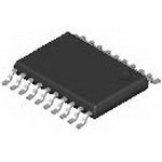
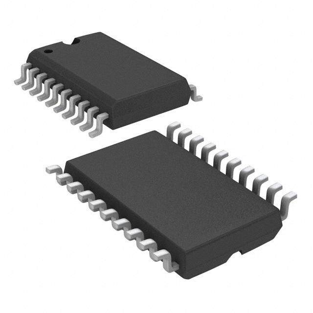
| 描述 | IC INVERTER DUAL 4-INPUT 20TSSOP缓冲器和线路驱动器 Inv Oct 3-STATE Buf |
| 产品分类 | |
| 品牌 | Fairchild Semiconductor |
| 产品手册 | |
| 产品图片 |
|
| rohs | 符合RoHS无铅 / 符合限制有害物质指令(RoHS)规范要求 |
| 产品系列 | 逻辑集成电路,缓冲器和线路驱动器,Fairchild Semiconductor MM74HC240MTCX74HC |
| 数据手册 | |
| 产品型号 | MM74HC240MTCX |
| 产品目录页面 | |
| 产品种类 | 缓冲器和线路驱动器 |
| 传播延迟时间 | 150 ns at 2 V, 30 ns at 4.5 V, 26 ns at 6 V |
| 低电平输出电流 | 7.8 mA |
| 供应商器件封装 | 20-TSSOP |
| 元件数 | 2 |
| 其它名称 | MM74HC240MTCXDKR |
| 包装 | Digi-Reel® |
| 单位重量 | 191 mg |
| 商标 | Fairchild Semiconductor |
| 安装类型 | 表面贴装 |
| 安装风格 | SMD/SMT |
| 封装 | Reel |
| 封装/外壳 | 20-TSSOP(0.173",4.40mm 宽) |
| 封装/箱体 | TSSOP-20 |
| 工作温度 | -40°C ~ 85°C |
| 工厂包装数量 | 2500 |
| 最大功率耗散 | 500 mW |
| 最大工作温度 | + 85 C |
| 最小工作温度 | - 40 C |
| 极性 | Inverting |
| 标准包装 | 1 |
| 每元件位数 | 4 |
| 每芯片的通道数量 | 8 |
| 电压-电源 | 2 V ~ 6 V |
| 电流-输出高,低 | 7.8mA,7.8mA |
| 电源电压-最大 | 6 V |
| 电源电压-最小 | 2 V |
| 系列 | MM74HC240 |
| 输入线路数量 | 8 |
| 输出类型 | 3-State |
| 输出线路数量 | 8 |
| 逻辑类型 | 缓冲器/线路驱动器, 反相 |
| 逻辑系列 | HC |
| 零件号别名 | MM74HC240MTCX_NL |
| 高电平输出电流 | - 7.8 mA |


PDF Datasheet 数据手册内容提取
Is Now Part of To learn more about ON Semiconductor, please visit our website at www.onsemi.com Please note: As part of the Fairchild Semiconductor integration, some of the Fairchild orderable part numbers will need to change in order to meet ON Semiconductor’s system requirements. Since the ON Semiconductor product management systems do not have the ability to manage part nomenclature that utilizes an underscore (_), the underscore (_) in the Fairchild part numbers will be changed to a dash (-). This document may contain device numbers with an underscore (_). Please check the ON Semiconductor website to verify the updated device numbers. The most current and up-to-date ordering information can be found at www.onsemi.com. Please email any questions regarding the system integration to Fairchild_questions@onsemi.com. ON Semiconductor and the ON Semiconductor logo are trademarks of Semiconductor Components Industries, LLC dba ON Semiconductor or its subsidiaries in the United States and/or other countries. ON Semiconductor owns the rights to a number of patents, trademarks, copyrights, trade secrets, and other intellectual property. A listing of ON Semiconductor’s product/patent coverage may be accessed at www.onsemi.com/site/pdf/Patent-Marking.pdf. ON Semiconductor reserves the right to make changes without further notice to any products herein. ON Semiconductor makes no warranty, representation or guarantee regarding the suitability of its products for any particular purpose, nor does ON Semiconductor assume any liability arising out of the application or use of any product or circuit, and specifically disclaims any and all liability, including without limitation special, consequential or incidental damages. Buyer is responsible for its products and applications using ON Semiconductor products, including compliance with all laws, regulations and safety requirements or standards, regardless of any support or applications information provided by ON Semiconductor. “Typical” parameters which may be provided in ON Semiconductor data sheets and/or specifications can and do vary in different applications and actual performance may vary over time. All operating parameters, including “Typicals” must be validated for each customer application by customer’s technical experts. ON Semiconductor does not convey any license under its patent rights nor the rights of others. ON Semiconductor products are not designed, intended, or authorized for use as a critical component in life support systems or any FDA Class 3 medical devices or medical devices with a same or similar classification in a foreign jurisdiction or any devices intended for implantation in the human body. Should Buyer purchase or use ON Semiconductor products for any such unintended or unauthorized application, Buyer shall indemnify and hold ON Semiconductor and its officers, employees, subsidiaries, affiliates, and distributors harmless against all claims, costs, damages, and expenses, and reasonable attorney fees arising out of, directly or indirectly, any claim of personal injury or death associated with such unintended or unauthorized use, even if such claim alleges that ON Semiconductor was negligent regarding the design or manufacture of the part. ON Semiconductor is an Equal Opportunity/Affirmative Action Employer. This literature is subject to all applicable copyright laws and is not for resale in any manner.
M September 1983 M Revised May 2005 7 4 H C 2 MM74HC240 4 0 Inverting Octal 3-STATE Buffer In v e r General Description Features t in The MM74HC240 3-STATE buffer utilizes advanced sili- (cid:1) Typical propagation delay: 12 ns g con-gate CMOS technology. It possesses high drive cur- (cid:1) 3-STATE outputs for connection to system buses O rent outputs which enable high speed operation even when (cid:1) Wide power supply range: 2–6V ct driving large bus capacitances. These circuits achieve a srepteaeindins gc othmep aadravbalnet atgoe l oowf CpMowOeSr cSicrchuoitttrkyy, i.dee.,v ihciegsh, nwohisilee (cid:1)(cid:1) LOouwtp quut iceusrcreenntt: s6u pmpAly current: 80 PA (74 Series) l 3- S immunity and low power consumption. It has a fanout of 15 T LS-TTL equivalent inputs. A The MM74HC240 is an inverting buffer and has two active T E LOW enables (1G and 2G). Each enable independently controls 4 buffers. B u All inputs are protected from damage due to static dis- f charge by diodes to VCC and ground. fe r Ordering Code: Order Number Package Number Package Description MM74HC240WM M20B 20-Lead Small Outline Integrated Circuit (SOIC), JEDEC MS-013, 0.300" Wide MM74HC240SJ M20D 20-Lead Small Outline Package (SOP), EIAJ TYPE II, 5.3mm Wide MM74HC240MTC MTC20 20-Lead Thin Shrink Small Outline Package (TSSOP), JEDEC MO-153, 4.4mm Wide MM74HC240N N20A 20-Lead Plastic Dual-In-Line Package (PDIP), JEDEC MS-001, 0.300" Wide Devices also available in Tape and Reel. Specify by appending the suffix letter “X” to the ordering code. Connection Diagram Truth Table 1G 1A 1Y 2G 2A 2Y L L H L L H L H L L H L H L Z H L Z H H Z H H Z H HIGH Level L LOW Level Z HIGH Impedance Top View © 2005 Fairchild Semiconductor Corporation DS005020 www.fairchildsemi.com
0 4 Logic Diagram 2 C H 4 7 M M www.fairchildsemi.com 2
M Absolute Maximum Ratings(Note 1) Recommended Operating M (Note 2) Conditions 74 H Supply Voltage (VCC) (cid:16)0.5 to (cid:14)7.0V Min Max Units C DC Input Voltage (VIN) (cid:16)1.5 to VCC (cid:14)1.5V Supply Voltage (VCC) 2 6 V 24 DC Output Voltage (VOUT) (cid:16)0.5 to VCC (cid:14)0.5V DC Input or Output Voltage 0 VCC V 0 Clamp Diode Current (IIK, IOK) r20 mA (VIN, VOUT) DC Output Current, per pin (IOUT) r35 mA Operating Temperature Range (TA) (cid:16)40 (cid:14)85 qC DC VCC or GND Current, per pin (ICC) r70 mA Input Rise or Fall Times Storage Temperature Range (TSTG) (cid:16)65qC to (cid:14)150qC (tr, tf) VCC 2.0V 1000 ns Power Dissipation (PD) VCC 4.5V 500 ns (Note 3) 600 mW VCC 6.0V 400 ns S.O. Package only 500 mW Note 1: Absolute Maximum Ratings are those values beyond which dam- Lead Temperature (TL) age to the device may occur. Note 2: unless otherwise specified all voltages are referenced to ground. (Soldering 10 seconds) 260qC Note 3: Power Dissipation temperature derating — plastic “N” package: (cid:16) 12 mW/qC from 65qC to 85qC. DC Electrical Characteristics (Note 4) Symbol Parameter Conditions VCC TA 25qC TA (cid:16)40 to 85qC TA (cid:16)55 to 125qC Units Typ Guaranteed Limits VIH Minimum HIGH Level 2.0V 1.5 1.5 1.5 V Input Voltage 4.5V 3.15 3.15 3.15 V 6.0V 4.2 4.2 4.2 V VIL Maximum LOW Level 2.0V 0.5 0.5 0.5 V Input Voltage 4.5V 1.35 1.35 1.35 V 6.0V 1.8 1.8 1.8 V VOH Minimum HIGH Level VI N VIH or VIL Output Voltage |IOUT| d 20 PA 2.0V 2.0 1.9 1.9 1.9 V 4.5V 4.5 4.4 4.4 4.4 V 6.0V 6.0 5.9 5.9 5.9 V VIN VIH or VIL |IOUT| d 6.0 mA 4.5V 4.2 3.98 3.84 3.7 V |IOUT| d 7.8 mA 6.0V 5.7 5.48 5.34 5.2 V VOL Maximum LOW Level VIN VIH or VIL Output Voltage |IOUT| d 20 PA 2.0V 0 0.1 0.1 0.1 V 4.5V 0 0.1 0.1 0.1 V 6.0V 0 0.1 0.1 0.1 V VIN VIH or VIL |IOUT| d 6.0 mA 4.5V 0.2 0.26 0.33 0.4 V |IOUT| d 7.8 mA 6.0V 0.2 0.26 0.33 0.4 V IIN Maximum Input Current VIN VCC or GND 6.0V r0.1 r1.0 r1.0 PA IOZ Maximum 3-STATE VIN VIH or VIL Output Leakage VOUT VCC or GND 6.0V r0.5 r5 r10 PA Current G VIH, G VIL ICC Maximum Quiescent VIN VCC or GND 6.0V 8.0 80 160 PA Supply Current IOUT 0 PA Note 4: For a power supply of 5V r10% the worst case output voltages (VOH, and VOL) occur for HC at 4.5V. Thus the 4.5V values should be used when designing with this supply. Worst case VIH and VIL occur at VCC 5.5V and 4.5V respectively. (The VIH value at 5.5V is 3.85V.) The worst case leakage cur- rent (IIN, ICC, and IOZ) occur for CMOS at the higher voltage and so the 6.0V values should be used. 3 www.fairchildsemi.com
0 4 AC Electrical Characteristics 2 C H 4 VCC 5V, TA 25qC, tr tf 6 ns 7 Symbol Parameter Conditions Typ Guaranteed Limit Units M tPHL, tPLH Maximum Propagation Delay CL 45 pF 12 18 ns M tPZH, tPZL Maximum Enable Delay RL 1 k: 14 28 ns to Active Output CL 45 pF tPHZ, tPLZ Maximum Disable Delay RL 1 k: 13 25 ns from Active Output CL 5 pF AC Electrical Characteristics VCC 2.0V to 6.0V, CL 50 pF, tr tf 6 ns (unless otherwise specified) Symbol Parameter Conditions VCC TA 25qC TA (cid:16)40 to 85qC TA (cid:16)55 to 125qC Units Typ Guaranteed Limits tPHL, tPLH Maximum Propagation CL 50 pF 2.0V 55 100 126 149 ns Delay CL 150 pF 2.0V 80 150 190 224 ns CL 50 pF 4.5V 12 20 25 30 ns CL 150 pF 4.5V 22 30 38 45 ns CL 50 pF 6.0V 11 17 21 25 ns CL 150 pF 6.0V 28 26 32 38 ns tPZH, tPZL Maximum Output Enable RL 1 k: TIme CL 50 pF 2.0V 75 150 189 224 ns CL 150 pF 2.0V 100 200 252 298 ns CL 50 pF 4.5V 15 30 38 45 ns CL 150 pF 4.5V 20 40 50 60 ns CL 50 pF 6.0V 13 26 32 38 ns CL 150 pF 6.0V 17 34 43 51 ns tPHZ, tPLZ Maximum Output Disable RL 1 k: 2.0V 75 150 189 224 ns Time CL 50 pF 4.5V 15 30 38 45 ns 6.0V 13 26 32 38 ns tTLH, tTHL Maximum Output 2.0V 60 75 90 ns Rise and Fall Time 4.5V 12 15 18 ns 6.0V 10 13 15 ns CPD Power Dissipation (per buffer) Capacitance (Note 5) G VIH 12 pF G VIL 50 pF CIN Maximum Input Capacitance 5 10 10 10 pF COUT Maximum Output Capacitance 10 20 20 20 pF Note 5: CPD determines the no load dynamic power consumption, PD CPD VCC2 f (cid:14) ICC VCC, and the no load dynamic current consumption, IS CPDVCCf (cid:14) ICC. www.fairchildsemi.com 4
M Physical Dimensions inches (millimeters) unless otherwise noted M 7 4 H C 2 4 0 20-Lead Small Outline Integrated Circuit (SOIC), JEDEC MS-013, 0.300" Wide Package Number M20B 5 www.fairchildsemi.com
0 4 Physical Dimensions 2 inches (millimeters) unless otherwise noted (Continued) C H 4 7 M M 20-Lead Small Outline Package (SOP), EIAJ TYPE II, 5.3mm Wide Package Number M20D www.fairchildsemi.com 6
M Physical Dimensions inches (millimeters) unless otherwise noted (Continued) M 7 4 H C 2 4 0 20-Lead Thin Shrink Small Outline Package (TSSOP), JEDEC MO-153, 4.4mm Wide Package Number MTC20 7 www.fairchildsemi.com
r e Physical Dimensions f inches (millimeters) unless otherwise noted (Continued) f u B E T A T S - 3 l a t c O g n i t r e v n I 0 4 2 C H 4 7 M M 20-Lead Plastic Dual-In-Line Package (PDIP), JEDEC MS-001, 0.300" Wide Package Number N20A Fairchild does not assume any responsibility for use of any circuitry described, no circuit patent licenses are implied and Fairchild reserves the right at any time without notice to change said circuitry and specifications. LIFE SUPPORT POLICY FAIRCHILD’S PRODUCTS ARE NOT AUTHORIZED FOR USE AS CRITICAL COMPONENTS IN LIFE SUPPORT DEVICES OR SYSTEMS WITHOUT THE EXPRESS WRITTEN APPROVAL OF THE PRESIDENT OF FAIRCHILD SEMICONDUCTOR CORPORATION. As used herein: 1. Life support devices or systems are devices or systems 2. A critical component in any component of a life support which, (a) are intended for surgical implant into the device or system whose failure to perform can be rea- body, or (b) support or sustain life, and (c) whose failure sonably expected to cause the failure of the life support to perform when properly used in accordance with device or system, or to affect its safety or effectiveness. instructions for use provided in the labeling, can be rea- sonably expected to result in a significant injury to the www.fairchildsemi.com user. www.fairchildsemi.com 8
ON Semiconductor and are trademarks of Semiconductor Components Industries, LLC dba ON Semiconductor or its subsidiaries in the United States and/or other countries. ON Semiconductor owns the rights to a number of patents, trademarks, copyrights, trade secrets, and other intellectual property. A listing of ON Semiconductor’s product/patent coverage may be accessed at www.onsemi.com/site/pdf/Patent−Marking.pdf. ON Semiconductor reserves the right to make changes without further notice to any products herein. ON Semiconductor makes no warranty, representation or guarantee regarding the suitability of its products for any particular purpose, nor does ON Semiconductor assume any liability arising out of the application or use of any product or circuit, and specifically disclaims any and all liability, including without limitation special, consequential or incidental damages. Buyer is responsible for its products and applications using ON Semiconductor products, including compliance with all laws, regulations and safety requirements or standards, regardless of any support or applications information provided by ON Semiconductor. “Typical” parameters which may be provided in ON Semiconductor data sheets and/or specifications can and do vary in different applications and actual performance may vary over time. All operating parameters, including “Typicals” must be validated for each customer application by customer’s technical experts. ON Semiconductor does not convey any license under its patent rights nor the rights of others. ON Semiconductor products are not designed, intended, or authorized for use as a critical component in life support systems or any FDA Class 3 medical devices or medical devices with a same or similar classification in a foreign jurisdiction or any devices intended for implantation in the human body. Should Buyer purchase or use ON Semiconductor products for any such unintended or unauthorized application, Buyer shall indemnify and hold ON Semiconductor and its officers, employees, subsidiaries, affiliates, and distributors harmless against all claims, costs, damages, and expenses, and reasonable attorney fees arising out of, directly or indirectly, any claim of personal injury or death associated with such unintended or unauthorized use, even if such claim alleges that ON Semiconductor was negligent regarding the design or manufacture of the part. ON Semiconductor is an Equal Opportunity/Affirmative Action Employer. This literature is subject to all applicable copyright laws and is not for resale in any manner. PUBLICATION ORDERING INFORMATION LITERATURE FULFILLMENT: N. American Technical Support: 800−282−9855 Toll Free ON Semiconductor Website: www.onsemi.com Literature Distribution Center for ON Semiconductor USA/Canada 19521 E. 32nd Pkwy, Aurora, Colorado 80011 USA Europe, Middle East and Africa Technical Support: Order Literature: http://www.onsemi.com/orderlit Phone: 303−675−2175 or 800−344−3860 Toll Free USA/Canada Phone: 421 33 790 2910 Fax: 303−675−2176 or 800−344−3867 Toll Free USA/Canada Japan Customer Focus Center For additional information, please contact your local Email: orderlit@onsemi.com Phone: 81−3−5817−1050 Sales Representative © Semiconductor Components Industries, LLC www.onsemi.com www.onsemi.com 1
Mouser Electronics Authorized Distributor Click to View Pricing, Inventory, Delivery & Lifecycle Information: O N Semiconductor: MM74HC240WM MM74HC240SJ MM74HC240MTCX MM74HC240SJX MM74HC240MTC MM74HC240WMX MM74HC240N