ICGOO在线商城 > 集成电路(IC) > 嵌入式 - 微控制器 > MKL36Z256VLL4
 Datasheet下载
- 型号: MKL36Z256VLL4
- 制造商: Freescale Semiconductor
- 库位|库存: xxxx|xxxx
- 要求:
| 数量阶梯 | 香港交货 | 国内含税 |
| +xxxx | $xxxx | ¥xxxx |
查看当月历史价格
查看今年历史价格
MKL36Z256VLL4产品简介:
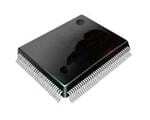
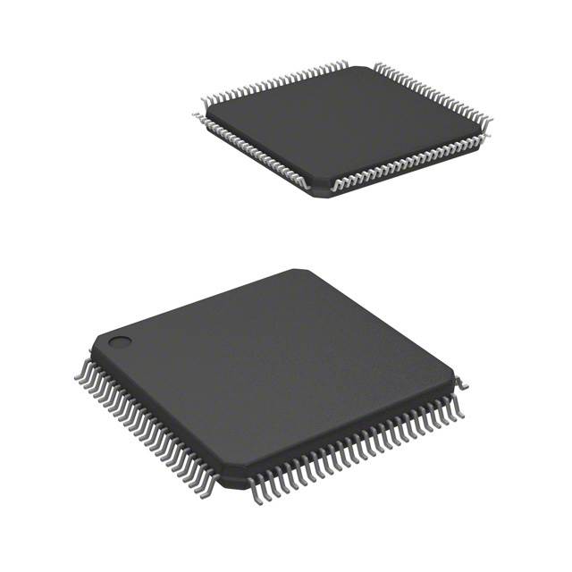
ICGOO电子元器件商城为您提供MKL36Z256VLL4由Freescale Semiconductor设计生产,在icgoo商城现货销售,并且可以通过原厂、代理商等渠道进行代购。 MKL36Z256VLL4价格参考。Freescale SemiconductorMKL36Z256VLL4封装/规格:嵌入式 - 微控制器, ARM® Cortex®-M0+ 微控制器 IC Kinetis KL3 32-位 48MHz 256KB(256K x 8) 闪存 100-LQFP(14x14)。您可以下载MKL36Z256VLL4参考资料、Datasheet数据手册功能说明书,资料中有MKL36Z256VLL4 详细功能的应用电路图电压和使用方法及教程。
NXP USA Inc.的型号为MKL36Z256VLL4的微控制器属于Kinetis L系列,基于ARM Cortex-M0+内核,适用于低功耗、高性能的嵌入式应用。其主要应用场景包括:

1. 消费电子:如智能手环、健康监测设备等可穿戴产品,得益于其低功耗特性,适合用于需要长时间运行的便携设备。

2. 工业控制:可用于传感器节点、电机控制、工业自动化设备等,支持多种通信接口(如SPI、I2C、UART),便于与各类工业设备连接。

3. 家电控制:如洗衣机、冰箱、空调等家用电器的主控单元,具备较强的抗干扰能力与稳定性,适合复杂电磁环境下的运行。

4. 物联网终端:作为边缘设备的主控芯片,支持低功耗数据采集与传输,适用于智能家居、环境监测等IoT应用场景。

5. 医疗设备:用于便携式医疗仪器,如血糖仪、心率监测仪等,满足对功耗、精度和安全性的多重需求。

该芯片具备256KB Flash、32KB RAM,工作温度范围宽,适用于多种恶劣环境,是一款高性价比的多功能微控制器。
| 参数 | 数值 |
| A/D位大小 | 16 bit |
| 产品目录 | 集成电路 (IC)半导体 |
| 描述 | IC MCU ARM 256KB FLASH 100LQFPARM微控制器 - MCU Cortex M0+ Core,Flex USB |
| EEPROM容量 | - |
| 产品分类 | |
| I/O数 | 84 |
| 品牌 | Freescale Semiconductor |
| 产品手册 | |
| 产品图片 |
|
| rohs | 符合RoHS无铅 / 符合限制有害物质指令(RoHS)规范要求 |
| 产品系列 | 嵌入式处理器和控制器,微控制器 - MCU,ARM微控制器 - MCU,Freescale Semiconductor MKL36Z256VLL4Kinetis KL3 |
| 数据手册 | |
| 产品型号 | MKL36Z256VLL4 |
| PCN设计/规格 | http://cache.freescale.com/files/shared/doc/pcn/PCN15823.htmhttp://cache.freescale.com/files/shared/doc/pcn/PCN15993.htmhttp://cache.freescale.com/files/shared/doc/pcn/PCN16203.htm |
| RAM容量 | 32K x 8 |
| 产品种类 | ARM微控制器 - MCU |
| 供应商器件封装 | 100-LQFP(14x14) |
| 包装 | 托盘 |
| 单位重量 | 685.200 mg |
| 可用A/D通道 | 1 |
| 商标 | Freescale Semiconductor |
| 商标名 | Kinetis |
| 处理器系列 | MKL36Z256 |
| 外设 | 断电检测/复位, DMA, I²S, LCD, LVD, POR, PWM, WDT |
| 安装风格 | SMD/SMT |
| 定时器数量 | 3 Timer |
| 封装 | Tray |
| 封装/外壳 | 100-LQFP |
| 封装/箱体 | LQFP-100 |
| 工作温度 | -40°C ~ 85°C |
| 工厂包装数量 | 90 |
| 振荡器类型 | 内部 |
| 接口类型 | I2C, I2S, SPI, UART |
| 数据RAM大小 | 32 kB |
| 数据Ram类型 | SRAM |
| 数据总线宽度 | 32 bit |
| 数据转换器 | A/D - 16-位, D/A - 12-位 |
| 最大工作温度 | + 105 C |
| 最大时钟频率 | 48 MHz |
| 最小工作温度 | - 40 C |
| 标准包装 | 90 |
| 核心 | ARM Cortex M4 |
| 核心处理器 | ARM® Cortex™-M0+ |
| 核心尺寸 | 32-位 |
| 片上ADC | Yes |
| 片上DAC | With DAC |
| 电压-电源(Vcc/Vdd) | 1.71 V ~ 3.6 V |
| 程序存储器大小 | 256 kB |
| 程序存储器类型 | Flash |
| 程序存储容量 | 256KB(256K x 8) |
| 系列 | Kinetis L3 |
| 连接性 | I²C, LIN, SPI, UART/USART |
| 速度 | 48MHz |


- 商务部:美国ITC正式对集成电路等产品启动337调查
- 曝三星4nm工艺存在良率问题 高通将骁龙8 Gen1或转产台积电
- 太阳诱电将投资9.5亿元在常州建新厂生产MLCC 预计2023年完工
- 英特尔发布欧洲新工厂建设计划 深化IDM 2.0 战略
- 台积电先进制程称霸业界 有大客户加持明年业绩稳了
- 达到5530亿美元!SIA预计今年全球半导体销售额将创下新高
- 英特尔拟将自动驾驶子公司Mobileye上市 估值或超500亿美元
- 三星加码芯片和SET,合并消费电子和移动部门,撤换高东真等 CEO
- 三星电子宣布重大人事变动 还合并消费电子和移动部门
- 海关总署:前11个月进口集成电路产品价值2.52万亿元 增长14.8%


PDF Datasheet 数据手册内容提取
Freescale Semiconductor, Inc. Document Number: KL36P121M48SF4 Data Sheet: Technical Data Rev 5 08/2014 Kinetis KL36 Sub-Family MKL36ZxxxVLH4 48 MHz Cortex-M0+ Based Microcontroller MKL36Z256VMP4, MKL36ZxxxVLL4 Designed with efficiency in mind. Compatible with all other MKL36ZxxxVMC4 Kinetis L families as well as Kinetis K3x family. General purpose MCU with segment LCD, featuring market leading ultra low- power to provide developers an appropriate entry-level 32-bit solution. This product offers: 64-pin LQFP (LH) 64-pin MAPBGA (MP) • Run power consumption down to 50 μA/MHz in very low 10 x 10 x 1.4 Pitch 0.5 5 x 5 x 1.23 Pitch 0.5 mm mm power run mode • Static power consumption down to 2 μA with full state retention and 4.5 μs wakeup • Ultra-efficient Cortex-M0+ processor running up to 48 MHz with industry leading throughput 100-pin LQFP (LL) 121-pin MAPBGA (MP) • Memory option is up to 256 KB Flash and 32 KB RAM 14 x 14 x 1.4 Pitch 0.5 8 x 8 x 0.8 Pitch 0.65 • Energy-saving architecture is optimized for low power with mm mm 90 nm TFS technology, clock and power gating techniques, and zero wait state flash memory controller Performance Human-machine interface • 48 MHz ARM® Cortex®-M0+ core • Segment LCD controller supporting up to 47 frontplanes and 8 backplanes, or 51 frontplanes and Memories and memory interfaces 4 backplanes • Up to 256 KB program flash memory • Low-power hardware touch sensor interface (TSI) • Up to 32 KB SRAM • Up to 84 general-purpose input/output (GPIO) System peripherals Communication interfaces • Nine low-power modes to provide power optimization • Two 16-bit SPI modules based on application requirements • I2S (SAI) module • COP Software watchdog • One low power UART module • 4-channel DMA controller, supporting up to 63 request • Two UART modules sources • Two I2C module • Low-leakage wakeup unit • SWD debug interface and Micro Trace Buffer Analog Modules • Bit Manipulation Engine • 16-bit SAR ADC • 12-bit DAC Clocks • Analog comparator (CMP) containing a 6-bit DAC • 32 kHz to 40 kHz or 3 MHz to 32 MHz crystal oscillator and programmable reference input • Multi-purpose clock source Timers Operating Characteristics • Six channel Timer/PWM (TPM) • Voltage range: 1.71 to 3.6 V • Two 2-channel Timer/PWM modules • Flash write voltage range: 1.71 to 3.6 V • Periodic interrupt timers • Temperature range (ambient): -40 to 105°C Freescale reserves the right to change the detail specifications as may be required to permit improvements in the design of its products. © 2012–2014 Freescale Semiconductor, Inc. All rights reserved.
• 16-bit low-power timer (LPTMR) • Real time clock Security and integrity modules • 80-bit unique identification number per chip Ordering Information 1 Part Number Memory Maximum number of I\O's Flash (KB) SRAM (KB) MKL36Z64VLH4 64 8 54 MKL36Z128VLH4 128 16 54 MKL36Z256VLH4 256 32 54 MKL36Z256VMP4 256 32 54 MKL36Z64VLL4 64 8 84 MKL36Z128VLL4 128 16 84 MKL36Z256VLL4 256 32 84 MKL36Z128VMC4 128 16 84 MKL36Z256VMC4 256 32 84 1. To confirm current availability of ordererable part numbers, go to http://www.freescale.com and perform a part number search. Related Resources Type Description Resource Selector Guide The Freescale Solution Advisor is a web-based tool that features Solution Advisor interactive application wizards and a dynamic product selector. Reference The Reference Manual contains a comprehensive description of KL36P121M48SF4RM1 Manual the structure and function (operation) of a device. Data Sheet The Data Sheet includes electrical characteristics and signal KL36P121M48SF41 connections. Chip Errata The chip mask set Errata provides additional or corrective KINETIS_L_xN40H2 information for a particular device mask set. Package Package dimensions are provided in package drawings. LQFP 64-pin: 98ASS23234W1 drawing MAPBGA 64-pin: 98ASA00420D1 LQFP 100-pin: 98ASS23308W1 MAPBGA 121-pin: 98ASA00344D1 1. To find the associated resource, go to http://www.freescale.com and perform a search using this term. 2. To find the associated resource, go to http://www.freescale.com and perform a search using this term with the “x” replaced by the revision of the device you are using. 2 Kinetis KL36 Sub-Family, Rev5 08/2014. Freescale Semiconductor, Inc.
Table of Contents 1 Ratings..................................................................................4 3.6.3 12-bit DAC electrical characteristics..................33 1.1 Thermal handling ratings...............................................4 3.7 Timers............................................................................36 1.2 Moisture handling ratings...............................................4 3.8 Communication interfaces.............................................36 1.3 ESD handling ratings.....................................................4 3.8.1 SPI switching specifications...............................36 1.4 Voltage and current operating ratings............................4 3.8.2 Inter-Integrated Circuit Interface (I2C) timing.....41 2 General.................................................................................5 3.8.3 UART.................................................................42 2.1 AC electrical characteristics...........................................5 3.8.4 I2S/SAI switching specifications........................42 2.2 Nonswitching electrical specifications............................5 3.9 Human-machine interfaces (HMI)..................................46 2.2.1 Voltage and current operating requirements......6 3.9.1 TSI electrical specifications................................46 2.2.2 LVD and POR operating requirements..............6 3.9.2 LCD electrical characteristics.............................47 2.2.3 Voltage and current operating behaviors...........7 4 Dimensions...........................................................................48 2.2.4 Power mode transition operating behaviors.......8 4.1 Obtaining package dimensions......................................48 2.2.5 Power consumption operating behaviors...........9 5 Pinout....................................................................................49 2.2.6 EMC radiated emissions operating behaviors...15 5.1 KL36 Signal Multiplexing and Pin Assignments.............49 2.2.7 Designing with radiated emissions in mind........16 5.2 KL36 pinouts..................................................................53 2.2.8 Capacitance attributes.......................................16 6 Ordering parts.......................................................................57 2.3 Switching specifications.................................................16 6.1 Determining valid orderable parts..................................57 2.3.1 Device clock specifications................................16 7 Part identification...................................................................58 2.3.2 General switching specifications........................17 7.1 Description.....................................................................58 2.4 Thermal specifications...................................................17 7.2 Format...........................................................................58 2.4.1 Thermal operating requirements........................17 7.3 Fields.............................................................................58 2.4.2 Thermal attributes..............................................17 7.4 Example.........................................................................59 3 Peripheral operating requirements and behaviors................18 8 Terminology and guidelines..................................................59 3.1 Core modules................................................................18 8.1 Definition: Operating requirement..................................59 3.1.1 SWD electricals .................................................18 8.2 Definition: Operating behavior.......................................59 3.2 System modules............................................................20 8.3 Definition: Attribute........................................................59 3.3 Clock modules...............................................................20 8.4 Definition: Rating...........................................................60 3.3.1 MCG specifications............................................20 8.5 Result of exceeding a rating..........................................60 3.3.2 Oscillator electrical specifications......................22 8.6 Relationship between ratings and operating 3.4 Memories and memory interfaces.................................24 requirements..................................................................61 3.4.1 Flash electrical specifications............................24 8.7 Guidelines for ratings and operating requirements........61 3.5 Security and integrity modules.......................................26 8.8 Definition: Typical value.................................................61 3.6 Analog............................................................................26 8.9 Typical value conditions.................................................62 3.6.1 ADC electrical specifications..............................26 9 Revision history.....................................................................63 3.6.2 CMP and 6-bit DAC electrical specifications......31 Kinetis KL36 Sub-Family, Rev5 08/2014. 3 Freescale Semiconductor, Inc.
Ratings 1 Ratings 1.1 Thermal handling ratings Table 1. Thermal handling ratings Symbol Description Min. Max. Unit Notes T Storage temperature –55 150 °C 1 STG T Solder temperature, lead-free — 260 °C 2 SDR 1. Determined according to JEDEC Standard JESD22-A103, High Temperature Storage Life. 2. Determined according to IPC/JEDEC Standard J-STD-020, Moisture/Reflow Sensitivity Classification for Nonhermetic Solid State Surface Mount Devices. 1.2 Moisture handling ratings Table 2. Moisture handling ratings Symbol Description Min. Max. Unit Notes MSL Moisture sensitivity level — 3 — 1 1. Determined according to IPC/JEDEC Standard J-STD-020, Moisture/Reflow Sensitivity Classification for Nonhermetic Solid State Surface Mount Devices. 1.3 ESD handling ratings Table 3. ESD handling ratings Symbol Description Min. Max. Unit Notes V Electrostatic discharge voltage, human body model –2000 +2000 V 1 HBM V Electrostatic discharge voltage, charged-device –500 +500 V 2 CDM model I Latch-up current at ambient temperature of 105 °C –100 +100 mA 3 LAT 1. Determined according to JEDEC Standard JESD22-A114, Electrostatic Discharge (ESD) Sensitivity Testing Human Body Model (HBM). 2. Determined according to JEDEC Standard JESD22-C101, Field-Induced Charged-Device Model Test Method for Electrostatic-Discharge-Withstand Thresholds of Microelectronic Components. 3. Determined according to JEDEC Standard JESD78, IC Latch-Up Test. 4 Kinetis KL36 Sub-Family, Rev5 08/2014. Freescale Semiconductor, Inc.
General 1.4 Voltage and current operating ratings Table 4. Voltage and current operating ratings Symbol Description Min. Max. Unit V Digital supply voltage –0.3 3.8 V DD I Digital supply current — 120 mA DD V IO pin input voltage –0.3 V + 0.3 V IO DD I Instantaneous maximum current single pin limit (applies to –25 25 mA D all port pins) V Analog supply voltage V – 0.3 V + 0.3 V DDA DD DD 2 General 2.1 AC electrical characteristics Unless otherwise specified, propagation delays are measured from the 50% to the 50% point, and rise and fall times are measured at the 20% and 80% points, as shown in the following figure. Low High V IH 80% Input Signal Midpoint1 50% 20% V IL Fall Time Rise Time The midpoint is V + (V - V ) / 2 IL IH IL Figure 2. Input signal measurement reference All digital I/O switching characteristics, unless otherwise specified, assume the output pins have the following characteristics. • C =30 pF loads L • Slew rate disabled • Normal drive strength 2.2 Nonswitching electrical specifications Kinetis KL36 Sub-Family, Rev5 08/2014. 5 Freescale Semiconductor, Inc.
General 2.2.1 Voltage and current operating requirements Table 5. Voltage and current operating requirements Symbol Description Min. Max. Unit Notes V Supply voltage 1.71 3.6 V DD V Analog supply voltage 1.71 3.6 V DDA V – V V -to-V differential voltage –0.1 0.1 V DD DDA DD DDA V – V V -to-V differential voltage –0.1 0.1 V SS SSA SS SSA V Input high voltage IH • 2.7 V ≤ V ≤ 3.6 V 0.7 × V — V DD DD • 1.7 V ≤ V ≤ 2.7 V 0.75 × V — V DD DD V Input low voltage IL • 2.7 V ≤ V ≤ 3.6 V — 0.35 × V V DD DD • 1.7 V ≤ V ≤ 2.7 V — 0.3 × V V DD DD V Input hysteresis 0.06 × V — V HYS DD I IO pin negative DC injection current — single pin 1 ICIO -3 — mA • V < V -0.3V IN SS I Contiguous pin DC injection current —regional limit, ICcont includes sum of negative injection currents of 16 contiguous pins -25 — mA • Negative current injection V Open drain pullup voltage level V V V 2 ODPU DD DD V V voltage required to retain RAM 1.2 — V RAM DD 1. All I/O pins are internally clamped to V through a ESD protection diode. There is no diode connection to V . If V SS DD IN greater than V (= V -0.3 V) is observed, then there is no need to provide current limiting resistors at the pads. If IO_MIN SS this limit cannot be observed then a current limiting resistor is required. The negative DC injection current limiting resistor is calculated as R = (V - V )/|I |. IO_MIN IN ICIO 2. Open drain outputs must be pulled to V . DD 2.2.2 LVD and POR operating requirements Table 6. V supply LVD and POR operating requirements DD Symbol Description Min. Typ. Max. Unit Notes V Falling V POR detect voltage 0.8 1.1 1.5 V — POR DD V Falling low-voltage detect threshold — high 2.48 2.56 2.64 V — LVDH range (LVDV = 01) Low-voltage warning thresholds — high range 1 Table continues on the next page... 6 Kinetis KL36 Sub-Family, Rev5 08/2014. Freescale Semiconductor, Inc.
General Table 6. V supply LVD and POR operating requirements (continued) DD Symbol Description Min. Typ. Max. Unit Notes V • Level 1 falling (LVWV = 00) 2.62 2.70 2.78 V LVW1H V • Level 2 falling (LVWV = 01) 2.72 2.80 2.88 V LVW2H V • Level 3 falling (LVWV = 10) 2.82 2.90 2.98 V LVW3H V • Level 4 falling (LVWV = 11) 2.92 3.00 3.08 V LVW4H V Low-voltage inhibit reset/recover hysteresis — — ±60 — mV — HYSH high range V Falling low-voltage detect threshold — low 1.54 1.60 1.66 V — LVDL range (LVDV=00) Low-voltage warning thresholds — low range 1 V • Level 1 falling (LVWV = 00) LVW1L 1.74 1.80 1.86 V V • Level 2 falling (LVWV = 01) LVW2L 1.84 1.90 1.96 V V • Level 3 falling (LVWV = 10) LVW3L 1.94 2.00 2.06 V V • Level 4 falling (LVWV = 11) LVW4L 2.04 2.10 2.16 V V Low-voltage inhibit reset/recover hysteresis — — ±40 — mV — HYSL low range V Bandgap voltage reference 0.97 1.00 1.03 V — BG t Internal low power oscillator period — factory 900 1000 1100 μs — LPO trimmed 1. Rising thresholds are falling threshold + hysteresis voltage 2.2.3 Voltage and current operating behaviors Table 7. Voltage and current operating behaviors Symbol Description Min. Max. Unit Notes V Output high voltage — Normal drive pad (except 1, 2 OH RESET_b) V – 0.5 — V DD • 2.7 V ≤ V ≤ 3.6 V, I = -5 mA DD OH V – 0.5 — V DD • 1.71 V ≤ V ≤ 2.7 V, I = -2.5 mA DD OH V Output high voltage — High drive pad (except 1, 2 OH RESET_b) V – 0.5 — V DD • 2.7 V ≤ V ≤ 3.6 V, I = -20 mA DD OH V – 0.5 — V DD • 1.71 V ≤ V ≤ 2.7 V, I = -10 mA DD OH I Output high current total for all ports — 100 mA OHT V Output low voltage — Normal drive pad 1 OL • 2.7 V ≤ V ≤ 3.6 V, I = 5 mA — 0.5 V DD OL • 1.71 V ≤ V ≤ 2.7 V, I = 2.5 mA — 0.5 V DD OL Table continues on the next page... Kinetis KL36 Sub-Family, Rev5 08/2014. 7 Freescale Semiconductor, Inc.
General Table 7. Voltage and current operating behaviors (continued) Symbol Description Min. Max. Unit Notes V Output low voltage — High drive pad 1 OL • 2.7 V ≤ V ≤ 3.6 V, I = 20 mA — 0.5 V DD OL • 1.71 V ≤ V ≤ 2.7 V, I = 10 mA — 0.5 V DD OL I Output low current total for all ports — 100 mA OLT I Input leakage current (per pin) for full temperature — 1 μA 3 IN range I Input leakage current (per pin) at 25 °C — 0.025 μA 3 IN I Input leakage current (total all pins) for full — μA 3 IN temperature range I Hi-Z (off-state) leakage current (per pin) — 1 μA OZ R Internal pullup resistors 20 50 kΩ 4 PU 1. PTB0, PTB1, PTD6, and PTD7 I/O have both high drive and normal drive capability selected by the associated PTx_PCRn[DSE] control bit. All other GPIOs are normal drive only. 2. The reset pin only contains an active pull down device when configured as the RESET signal or as a GPIO. When configured as a GPIO output, it acts as a pseudo open drain output. 3. Measured at V = 3.6 V DD 4. Measured at V supply voltage = V min and Vinput = V DD DD SS 2.2.4 Power mode transition operating behaviors All specifications except t and VLLSx→RUN recovery times in the following table POR assume this clock configuration: • CPU and system clocks = 48 MHz • Bus and flash clock = 24 MHz • FEI clock mode POR and VLLSx→RUN recovery use FEI clock mode at the default CPU and system frequency of 21 MHz, and a bus and flash clock frequency of 10.5 MHz. Table 8. Power mode transition operating behaviors Symbol Description Min. Typ. Max. Unit Notes t After a POR event, amount of time from the — — 300 μs 1 POR point V reaches 1.8 V to execution of the first DD instruction across the operating temperature range of the chip. • VLLS0 → RUN — 113 124 μs Table continues on the next page... 8 Kinetis KL36 Sub-Family, Rev5 08/2014. Freescale Semiconductor, Inc.
General Table 8. Power mode transition operating behaviors (continued) Symbol Description Min. Typ. Max. Unit Notes • VLLS1 → RUN — 112 124 μs • VLLS3 → RUN — 53 60 μs • LLS → RUN — 4.5 5.0 μs • VLPS → RUN — 4.5 5.0 μs • STOP → RUN — 4.5 5.0 μs 1. Normal boot (FTFA_FOPT[LPBOOT]=11). 2.2.5 Power consumption operating behaviors The maximum values stated in the following table represent characterized results equivalent to the mean plus three times the standard deviation (mean + 3 sigma). Table 9. Power consumption operating behaviors Symbol Description Typ. Max Unit Note I Analog supply current — — See note mA 1 DDA I Run mode current in compute operation — 6.7 — mA 2 DD_RUNCO_ CM - 48 MHz core / 24 MHz flash/ bus disabled, LPTMR running using 4 MHz internal reference clock, CoreMark® benchmark code executing from flash, at 3.0 V I Run mode current in compute operation — 4.5 5.1 mA 3 DD_RUNCO - 48 MHz core / 24 MHz flash / bus clock disabled, code of while(1) loop executing from flash, at 3.0 V I Run mode current - 48 MHz core / 24 at 1.8 V 5.6 6.3 mA 3 DD_RUN MHz bus and flash, all peripheral clocks at 3.0 V 5.4 6.0 mA disabled, code executing from flash I Run mode current - 48 MHz core / 24 — 6.9 7.3 mA 3, 4 DD_RUN MHz bus and flash, all peripheral clocks enabled, code executing from flash, at 1.8 V Run mode current - 48 MHz core / 24 at 25 °C 6.9 7.1 mA MHz bus and flash, all peripheral clocks at 125 °C 7.3 7.6 mA enabled, code executing from flash, at 3.0 V Table continues on the next page... Kinetis KL36 Sub-Family, Rev5 08/2014. 9 Freescale Semiconductor, Inc.
General Table 9. Power consumption operating behaviors (continued) Symbol Description Typ. Max Unit Note I Wait mode current - core disabled / 48 — 2.9 3.5 mA 3 DD_WAIT MHz system / 24 MHz bus / flash disabled (flash doze enabled), all peripheral clocks disabled, at 3.0 V I Wait mode current - core disabled / 24 — 2.2 2.8 mA 3 DD_WAIT MHz system / 24 MHz bus / flash disabled (flash doze enabled), wait mode reduced frequency current at 3.0 V — all peripheral clocks disabled I Stop mode current with partial stop 2 — 1.6 2.1 mA 3 DD_PSTOP2 clocking option - core and system disabled / 10.5 MHz bus, at 3.0 V I Very-low-power run mode current in — 798 — µA 5 DD_VLPRCO _CM compute operation - 4 MHz core / 0.8 MHz flash / bus clock disabled, LPTMR running with 4 MHz internal reference clock, CoreMark benchmark code executing from flash, at 3.0 V I Very low power run mode current in — 167 336 µA 6 DD_VLPRCO compute operation - 4 MHz core / 0.8 MHz flash / bus clock disabled, code executing from flash, at 3.0 V I Very low power run mode current - 4 — 192 354 µA 6 DD_VLPR MHz core / 0.8 MHz bus and flash, all peripheral clocks disabled, code executing from flash, at 3.0 V I Very low power run mode current - 4 — 257 431 µA 4, 6 DD_VLPR MHz core / 0.8 MHz bus and flash, all peripheral clocks enabled, code executing from flash, at 3.0 V I Very low power wait mode current - — 112 286 µA 6 DD_VLPW core disabled / 4 MHz system / 0.8 MHz bus / flash disabled (flash doze enabled), all peripheral clocks disabled, at 3.0 V I Stop mode current at 3.0 V at 25 °C 306 328 µA — DD_STOP at 50 °C 322 349 µA at 70 °C 348 382 µA at 85 °C 384 433 µA at 105 °C 481 578 µA I Very-low-power stop mode current at at 25 °C 2.71 5.03 µA — DD_VLPS 3.0 V at 50 °C 7.05 11.94 µA at 70 °C 15.80 26.87 µA at 85 °C 29.60 47.30 µA at 105 °C 69.13 106.04 µA Table continues on the next page... 10 Kinetis KL36 Sub-Family, Rev5 08/2014. Freescale Semiconductor, Inc.
General Table 9. Power consumption operating behaviors (continued) Symbol Description Typ. Max Unit Note I Low leakage stop mode current at 3.0 at 25 °C 2.00 2.7 µA — DD_LLS V at 50 °C 3.96 5.14 µA at 70 °C 7.77 10.71 µA at 85 °C 14.15 18.79 µA at 105 °C 33.20 43.67 µA I Very low-leakage stop mode 3 current at 25 °C 1.5 2.2 µA — DD_VLLS3 at 3.0 V at 50 °C 2.83 3.55 µA at 70 °C 5.53 7.26 µA at 85 °C 9.92 12.71 µA at 105 °C 22.90 29.23 µA I Very low-leakage stop mode 1 current at 25 °C 0.71 1.2 µA — DD_VLLS1 at 3.0V at 50 °C 1.27 1.9 µA at 70 °C 2.48 3.51 µA at 85 °C 4.65 6.29 µA at 105 °C 11.55 14.34 µA I Very low-leakage stop mode 0 current at 25 °C 0.41 0.9 µA — DD_VLLS0 (SMC_STOPCTRL[PORPO] = 0) at 3.0 at 50 °C 0.96 1.56 µA V at 70 °C 2.17 3.1 µA at 85 °C 4.35 5.32 µA at 105 °C 11.24 14.00 µA I Very low-leakage stop mode 0 current at 25 °C 0.23 0.69 µA 7 DD_VLLS0 (SMC_STOPCTRL[PORPO] = 1) at 3.0 at 50 °C 0.77 1.35 µA V at 70 °C 1.98 2.52 µA at 85 °C 4.16 5.14 µA at 105 °C 11.05 13.80 µA 1. The analog supply current is the sum of the active or disabled current for each of the analog modules on the device. See each module's specification for its supply current. 2. MCG configured for PEE mode. CoreMark benchmark compiled using IAR 6.40 with optimization level high, optimized for balanced. 3. MCG configured for FEI mode. 4. Incremental current consumption from peripheral activity is not included. 5. MCG configured for BLPI mode. CoreMark benchmark compiled using IAR 6.40 with optimization level high, optimized for balanced. 6. MCG configured for BLPI mode. 7. No brownout. Kinetis KL36 Sub-Family, Rev5 08/2014. 11 Freescale Semiconductor, Inc.
General Table 10. Low power mode peripheral adders — typical value Symbol Description Temperature (°C) Unit -40 25 50 70 85 105 I 4 MHz internal reference clock (IRC) adder. 56 56 56 56 56 56 µA IREFSTEN4MHz Measured by entering STOP or VLPS mode with 4 MHz IRC enabled. I 32 kHz internal reference clock (IRC) adder. 52 52 52 52 52 52 µA IREFSTEN32KHz Measured by entering STOP mode with the 32 kHz IRC enabled. I External 4 MHz crystal clock adder. 206 228 237 245 251 258 µA EREFSTEN4MHz Measured by entering STOP or VLPS mode with the crystal enabled. I External 32 kHz crystal clock VLLS1 440 490 540 560 570 580 nA EREFSTEN32KHz adder by means of the VLLS3 440 490 540 560 570 580 OSC0_CR[EREFSTEN and EREFSTEN] bits. Measured LLS 490 490 540 560 570 680 by entering all modes with the VLPS 510 560 560 560 610 680 crystal enabled. STOP 510 560 560 560 610 680 I CMP peripheral adder measured by placing 22 22 22 22 22 22 µA CMP the device in VLLS1 mode with CMP enabled using the 6-bit DAC and a single external input for compare. Includes 6-bit DAC power consumption. I RTC peripheral adder measured by placing 432 357 388 475 532 810 nA RTC the device in VLLS1 mode with external 32 kHz crystal enabled by means of the RTC_CR[OSCE] bit and the RTC ALARM set for 1 minute. Includes ERCLK32K (32 kHz external crystal) power consumption. I UART peripheral adder MCGIRCLK 66 66 66 66 66 66 µA UART measured by placing the (4 MHz device in STOP or VLPS internal mode with selected clock reference source waiting for RX data at clock) 115200 baud rate. Includes OSCERCLK 214 237 246 254 260 268 selected clock source power (4 MHz consumption. external crystal) I TPM peripheral adder MCGIRCLK 86 86 86 86 86 86 µA TPM measured by placing the (4 MHz device in STOP or VLPS internal mode with selected clock reference source configured for output clock) compare generating 100 Hz OSCERCLK 235 256 265 274 280 287 clock signal. No load is (4 MHz placed on the I/O generating external the clock signal. Includes crystal) selected clock source and I/O switching currents. Table continues on the next page... 12 Kinetis KL36 Sub-Family, Rev5 08/2014. Freescale Semiconductor, Inc.
General Table 10. Low power mode peripheral adders — typical value (continued) Symbol Description Temperature (°C) Unit -40 25 50 70 85 105 I Bandgap adder when BGEN bit is set and 45 45 45 45 45 45 µA BG device is placed in VLPx, LLS, or VLLSx mode. I ADC peripheral adder combining the 366 366 366 366 366 366 µA ADC measured values at V and V by placing DD DDA the device in STOP or VLPS mode. ADC is configured for low power mode using the internal clock and continuous conversions. I LCD peripheral adder measured by placing 5 5 5 5 5 5 µA LCD the device in VLLS1 mode with external 32 kHz crystal enabled by means of the OSC0_CR[EREFSTEN, EREFSTEN] bits. VIREG disabled, resistor bias network enabled, 1/8 duty cycle, 8 x 36 configuration for driving 288 Segments, 32 Hz frame rate, no LCD glass connected. Includes ERCLK32K (32 kHz external crystal) power consumption. 2.2.5.1 Diagram: Typical IDD_RUN operating behavior The following data was measured under these conditions: • MCG in FBE for run mode, and BLPE for VLPR mode • No GPIOs toggled • Code execution from flash with cache enabled • For the ALLOFF curve, all peripheral clocks are disabled except FTFA Kinetis KL36 Sub-Family, Rev5 08/2014. 13 Freescale Semiconductor, Inc.
General Run Mode Current Vs Core Frequency Temperature = 25, V = 3, CACHE = Enable, Code Residence = Flash, Clocking Mode = FBE DD 8.00E-03 7.00E-03 6.00E-03 A) (D n VD 5.00E-03 o n o All Peripheral CLK Gates pti m 4.00E-03 All Off u s on All On C nt 3.00E-03 e urr C 2.00E-03 1.00E-03 000.00E+00 CLK Ratio '1-1 '1-1 '1-1 '1-1 '1-1 '1-1 '1-1 '1-2 Flash-Core 1 2 3 4 6 12 24 48 Core Freq (MHz) Figure 3. Run mode supply current vs. core frequency 14 Kinetis KL36 Sub-Family, Rev5 08/2014. Freescale Semiconductor, Inc.
General VLPR Mode Current Vs Core Frequency Temperature = 25, VDD = 3, CACHE = Enable, Code Residence = Flash, Clocking Mode = BLPE 350.00E-06 300.00E-06 A) 250.00E-06 (D VD All Peripheral CLK Gates n on 200.00E-06 All Off o pti All On m u s 150.00E-06 n o C nt e urr 100.00E-06 C 50.00E-06 000.00E+00 CLK Ratio '1-1 '1-2 '1-2 '1-4 Flash-Core 1 2 4 Core Freq (MHz) Figure 4. VLPR mode current vs. core frequency 2.2.6 EMC radiated emissions operating behaviors Table 11. EMC radiated emissions operating behaviors Symbol Description Frequency Typ. Unit Notes band (MHz) V Radiated emissions voltage, band 1 0.15–50 12 dBμV 1,2 RE1 V Radiated emissions voltage, band 2 50–150 8 dBμV RE2 V Radiated emissions voltage, band 3 150–500 7 dBμV RE3 V Radiated emissions voltage, band 4 500–1000 4 dBμV RE4 V IEC level 0.15–1000 M — 2,3 RE_IEC 1. Determined according to IEC Standard 61967-1, Integrated Circuits - Measurement of Electromagnetic Emissions, 150 kHz to 1 GHz Part 1: General Conditions and Definitions and IEC Standard 61967-2, Integrated Circuits - Measurement of Electromagnetic Emissions, 150 kHz to 1 GHz Part 2: Measurement of Radiated Emissions—TEM Cell and Wideband TEM Cell Method. Measurements were made while the microcontroller was running basic application code. The reported emission level is the value of the maximum measured emission, rounded up to the next whole number, from among the measured orientations in each frequency range. 2. V = 3.3 V, T = 25 °C, f = 8 MHz (crystal), f = 48 MHz, f = 24 MHz DD A OSC SYS BUS 3. Specified according to Annex D of IEC Standard 61967-2, Measurement of Radiated Emissions—TEM Cell and Wideband TEM Cell Method Kinetis KL36 Sub-Family, Rev5 08/2014. 15 Freescale Semiconductor, Inc.
General 2.2.7 Designing with radiated emissions in mind To find application notes that provide guidance on designing your system to minimize interference from radiated emissions: 1. Go to www.freescale.com. 2. Perform a keyword search for “EMC design.” 2.2.8 Capacitance attributes Table 12. Capacitance attributes Symbol Description Min. Max. Unit C Input capacitance — 7 pF IN 2.3 Switching specifications 2.3.1 Device clock specifications Table 13. Device clock specifications Symbol Description Min. Max. Unit Normal run mode f System and core clock — 48 MHz SYS f Bus clock — 24 MHz BUS f Flash clock — 24 MHz FLASH f LPTMR clock — 24 MHz LPTMR VLPR and VLPS modes1 f System and core clock — 4 MHz SYS f Bus clock — 1 MHz BUS f Flash clock — 1 MHz FLASH f LPTMR clock2 — 24 MHz LPTMR f External reference clock — 16 MHz ERCLK f LPTMR external reference clock — 16 MHz LPTMR_ERCLK f Oscillator crystal or resonator frequency — high frequency — 16 MHz osc_hi_2 mode (high range) (MCG_C2[RANGE]=1x) f TPM asynchronous clock — 8 MHz TPM f UART0 asynchronous clock — 8 MHz UART0 16 Kinetis KL36 Sub-Family, Rev5 08/2014. Freescale Semiconductor, Inc.
General 1. The frequency limitations in VLPR and VLPS modes here override any frequency specification listed in the timing specification for any other module. These same frequency limits apply to VLPS, whether VLPS was entered from RUN or from VLPR. 2. The LPTMR can be clocked at this speed in VLPR or VLPS only when the source is an external pin. 2.3.2 General switching specifications These general-purpose specifications apply to all signals configured for GPIO and UART signals. Table 14. General switching specifications Description Min. Max. Unit Notes GPIO pin interrupt pulse width (digital glitch filter disabled) 1.5 — Bus clock 1 — Synchronous path cycles External RESET and NMI pin interrupt pulse width — 100 — ns 2 Asynchronous path GPIO pin interrupt pulse width — Asynchronous path 16 — ns 2 Port rise and fall time — 36 ns 3 1. The greater synchronous and asynchronous timing must be met. 2. This is the shortest pulse that is guaranteed to be recognized. 3. 75 pF load 2.4 Thermal specifications 2.4.1 Thermal operating requirements Table 15. Thermal operating requirements Symbol Description Min. Max. Unit T Die junction temperature –40 125 °C J T Ambient temperature –40 105 °C A Kinetis KL36 Sub-Family, Rev5 08/2014. 17 Freescale Semiconductor, Inc.
Peripheral operating requirements and behaviors 2.4.2 Thermal attributes Table 16. Thermal attributes Board type Symbol Description 121 100 64 64 Unit Notes MAPBG LQFP LQFP MAPBG A A Single-layer (1S) R Thermal resistance, junction 94 64 69 49.8 °C/W 1 θJA to ambient (natural convection) Four-layer (2s2p) R Thermal resistance, junction 57 51 51 42.3 °C/W θJA to ambient (natural convection) Single-layer (1S) R Thermal resistance, junction 81 54 58 40.9 °C/W θJMA to ambient (200 ft./min. air speed) Four-layer (2s2p) R Thermal resistance, junction 53 45 44 37.7 °C/W θJMA to ambient (200 ft./min. air speed) — R Thermal resistance, junction 40 37 33 39.2 °C/W 2 θJB to board — R Thermal resistance, junction 30 19 19 50.3 °C/W 3 θJC to case — Ψ Thermal characterization 8 4 4 2.2 °C/W 4 JT parameter, junction to package top outside center (natural convection) 1. Determined according to JEDEC Standard JESD51-2, Integrated Circuits Thermal Test Method Environmental Conditions—Natural Convection (Still Air), or EIA/JEDEC Standard JESD51-6, Integrated Circuit Thermal Test Method Environmental Conditions—Forced Convection (Moving Air). 2. Determined according to JEDEC Standard JESD51-8, Integrated Circuit Thermal Test Method Environmental Conditions—Junction-to-Board. 3. Determined according to Method 1012.1 of MIL-STD 883, Test Method Standard, Microcircuits, with the cold plate temperature used for the case temperature. The value includes the thermal resistance of the interface material between the top of the package and the cold plate. 4. Determined according to JEDEC Standard JESD51-2, Integrated Circuits Thermal Test Method Environmental Conditions—Natural Convection (Still Air). 3 Peripheral operating requirements and behaviors 3.1 Core modules 18 Kinetis KL36 Sub-Family, Rev5 08/2014. Freescale Semiconductor, Inc.
Peripheral operating requirements and behaviors 3.1.1 SWD electricals Table 17. SWD full voltage range electricals Symbol Description Min. Max. Unit Operating voltage 1.71 3.6 V J1 SWD_CLK frequency of operation • Serial wire debug 0 25 MHz J2 SWD_CLK cycle period 1/J1 — ns J3 SWD_CLK clock pulse width • Serial wire debug 20 — ns J4 SWD_CLK rise and fall times — 3 ns J9 SWD_DIO input data setup time to SWD_CLK rise 10 — ns J10 SWD_DIO input data hold time after SWD_CLK rise 0 — ns J11 SWD_CLK high to SWD_DIO data valid — 32 ns J12 SWD_CLK high to SWD_DIO high-Z 5 — ns J2 J3 J3 SWD_CLK (input) J4 J4 Figure 5. Serial wire clock input timing Kinetis KL36 Sub-Family, Rev5 08/2014. 19 Freescale Semiconductor, Inc.
Peripheral operating requirements and behaviors SWD_CLK J9 J10 SWD_DIO Input data valid J11 SWD_DIO Output data valid J12 SWD_DIO J11 SWD_DIO Output data valid Figure 6. Serial wire data timing 3.2 System modules There are no specifications necessary for the device's system modules. 3.3 Clock modules 3.3.1 MCG specifications Table 18. MCG specifications Symbol Description Min. Typ. Max. Unit Notes f Internal reference frequency (slow clock) — — 32.768 — kHz ints_ft factory trimmed at nominal V and 25 °C DD f Internal reference frequency (slow clock) — 31.25 — 39.0625 kHz ints_t user trimmed Δ Resolution of trimmed average DCO output — ± 0.3 ± 0.6 %f 1 fdco_res_t dco frequency at fixed voltage and temperature — using C3[SCTRIM] and C4[SCFTRIM] Table continues on the next page... 20 Kinetis KL36 Sub-Family, Rev5 08/2014. Freescale Semiconductor, Inc.
Peripheral operating requirements and behaviors Table 18. MCG specifications (continued) Symbol Description Min. Typ. Max. Unit Notes Δf Total deviation of trimmed average DCO output — +0.5/-0.7 ± 3 %f 1, 2 dco_t dco frequency over voltage and temperature Δf Total deviation of trimmed average DCO output — ± 0.4 ± 1.5 %f 1, 2 dco_t dco frequency over fixed voltage and temperature range of 0–70 °C f Internal reference frequency (fast clock) — — 4 — MHz intf_ft factory trimmed at nominal V and 25 °C DD Δf Frequency deviation of internal reference clock — +1/-2 ± 3 %f 2 intf_ft intf_ft (fast clock) over temperature and voltage — factory trimmed at nominal V and 25 °C DD f Internal reference frequency (fast clock) — user 3 — 5 MHz intf_t trimmed at nominal V and 25 °C DD f Loss of external clock minimum frequency — (3/5) x — — kHz loc_low RANGE = 00 f ints_t f Loss of external clock minimum frequency — (16/5) x — — kHz loc_high f ints_t FLL f FLL reference frequency range 31.25 — 39.0625 kHz fll_ref f DCO output Low range (DRS = 00) 20 20.97 25 MHz 3, 4 dco frequency range 640 × f fll_ref Mid range (DRS = 01) 40 41.94 48 MHz 1280 × f fll_ref f DCO output Low range (DRS = 00) — 23.99 — MHz 5, 6 dco_t_DMX3 frequency 2 732 × f fll_ref Mid range (DRS = 01) — 47.97 — MHz 1464 × f fll_ref J FLL period jitter — 180 — ps 7 cyc_fll • f = 48 MHz VCO t FLL target frequency acquisition time — — 1 ms 8 fll_acquire PLL f VCO operating frequency 48.0 — 100 MHz vco I PLL operating current 9 pll — 1060 — µA • PLL at 96 MHz (f = 8 MHz, f = osc_hi_1 pll_ref 2 MHz, VDIV multiplier = 48) I PLL operating current 9 pll — 600 — µA • PLL at 48 MHz (f = 8 MHz, f = osc_hi_1 pll_ref 2 MHz, VDIV multiplier = 24) f PLL reference frequency range 2.0 — 4.0 MHz pll_ref J PLL period jitter (RMS) 10 cyc_pll • f = 48 MHz — 120 — ps vco • f = 100 MHz — — ps vco Table continues on the next page... Kinetis KL36 Sub-Family, Rev5 08/2014. 21 Freescale Semiconductor, Inc.
Peripheral operating requirements and behaviors Table 18. MCG specifications (continued) Symbol Description Min. Typ. Max. Unit Notes J PLL accumulated jitter over 1µs (RMS) 10 acc_pll • f = 48 MHz — 1350 — ps vco • f = 100 MHz — 600 — ps vco D Lock entry frequency tolerance ± 1.49 — ± 2.98 % lock D Lock exit frequency tolerance ± 4.47 — ± 5.97 % unl t Lock detector detection time — — 150 × 10-6 s 11 pll_lock + 1075(1/ f ) pll_ref 1. This parameter is measured with the internal reference (slow clock) being used as a reference to the FLL (FEI clock mode). 2. The deviation is relative to the factory trimmed frequency at nominal V and 25 °C, f . DD ints_ft 3. These typical values listed are with the slow internal reference clock (FEI) using factory trim and DMX32 = 0. 4. The resulting system clock frequencies must not exceed their maximum specified values. The DCO frequency deviation (Δf ) over voltage and temperature must be considered. dco_t 5. These typical values listed are with the slow internal reference clock (FEI) using factory trim and DMX32 = 1. 6. The resulting clock frequency must not exceed the maximum specified clock frequency of the device. 7. This specification is based on standard deviation (RMS) of period or frequency. 8. This specification applies to any time the FLL reference source or reference divider is changed, trim value is changed, DMX32 bit is changed, DRS bits are changed, or changing from FLL disabled (BLPE, BLPI) to FLL enabled (FEI, FEE, FBE, FBI). If a crystal/resonator is being used as the reference, this specification assumes it is already running. 9. Excludes any oscillator currents that are also consuming power while PLL is in operation. 10. This specification was obtained using a Freescale developed PCB. PLL jitter is dependent on the noise characteristics of each PCB and results will vary. 11. This specification applies to any time the PLL VCO divider or reference divider is changed, or changing from PLL disabled (BLPE, BLPI) to PLL enabled (PBE, PEE). If a crystal/resonator is being used as the reference, this specification assumes it is already running. 3.3.2 Oscillator electrical specifications 3.3.2.1 Oscillator DC electrical specifications Table 19. Oscillator DC electrical specifications Symbol Description Min. Typ. Max. Unit Notes V Supply voltage 1.71 — 3.6 V DD I Supply current — low-power mode (HGO=0) 1 DDOSC • 32 kHz — 500 — nA • 4 MHz — 200 — μA • 8 MHz (RANGE=01) — 300 — μA • 16 MHz — 950 — μA — 1.2 — mA Table continues on the next page... 22 Kinetis KL36 Sub-Family, Rev5 08/2014. Freescale Semiconductor, Inc.
Peripheral operating requirements and behaviors Table 19. Oscillator DC electrical specifications (continued) Symbol Description Min. Typ. Max. Unit Notes • 24 MHz — 1.5 — mA • 32 MHz I Supply current — high gain mode (HGO=1) 1 DDOSC • 32 kHz — 25 — μA • 4 MHz — 400 — μA • 8 MHz (RANGE=01) — 500 — μA • 16 MHz — 2.5 — mA • 24 MHz — 3 — mA • 32 MHz — 4 — mA C EXTAL load capacitance — — — 2, 3 x C XTAL load capacitance — — — 2, 3 y R Feedback resistor — low-frequency, low-power — — — MΩ 2, 4 F mode (HGO=0) Feedback resistor — low-frequency, high-gain — 10 — MΩ mode (HGO=1) Feedback resistor — high-frequency, low-power — — — MΩ mode (HGO=0) Feedback resistor — high-frequency, high-gain — 1 — MΩ mode (HGO=1) R Series resistor — low-frequency, low-power — — — kΩ S mode (HGO=0) Series resistor — low-frequency, high-gain — 200 — kΩ mode (HGO=1) Series resistor — high-frequency, low-power — — — kΩ mode (HGO=0) Series resistor — high-frequency, high-gain mode (HGO=1) — 0 — kΩ V 5 Peak-to-peak amplitude of oscillation (oscillator — 0.6 — V pp mode) — low-frequency, low-power mode (HGO=0) Peak-to-peak amplitude of oscillation (oscillator — V — V DD mode) — low-frequency, high-gain mode (HGO=1) Peak-to-peak amplitude of oscillation (oscillator — 0.6 — V mode) — high-frequency, low-power mode (HGO=0) Peak-to-peak amplitude of oscillation (oscillator — V — V DD mode) — high-frequency, high-gain mode (HGO=1) 1. V =3.3 V, Temperature =25 °C DD 2. See crystal or resonator manufacturer's recommendation Kinetis KL36 Sub-Family, Rev5 08/2014. 23 Freescale Semiconductor, Inc.
Peripheral operating requirements and behaviors 3. C ,C can be provided by using the integrated capacitors when the low frequency oscillator (RANGE = 00) is used. For x y all other cases external capacitors must be used. 4. When low power mode is selected, R is integrated and must not be attached externally. F 5. The EXTAL and XTAL pins should only be connected to required oscillator components and must not be connected to any other devices. 3.3.2.2 Oscillator frequency specifications Table 20. Oscillator frequency specifications Symbol Description Min. Typ. Max. Unit Notes f Oscillator crystal or resonator frequency — low- 32 — 40 kHz osc_lo frequency mode (MCG_C2[RANGE]=00) f Oscillator crystal or resonator frequency — high- 3 — 8 MHz osc_hi_1 frequency mode (low range) (MCG_C2[RANGE]=01) f Oscillator crystal or resonator frequency — high 8 — 32 MHz osc_hi_2 frequency mode (high range) (MCG_C2[RANGE]=1x) f Input clock frequency (external clock mode) — — 48 MHz 1, 2 ec_extal t Input clock duty cycle (external clock mode) 40 50 60 % dc_extal t Crystal startup time — 32 kHz low-frequency, — 750 — ms 3, 4 cst low-power mode (HGO=0) Crystal startup time — 32 kHz low-frequency, — 250 — ms high-gain mode (HGO=1) Crystal startup time — 8 MHz high-frequency — 0.6 — ms (MCG_C2[RANGE]=01), low-power mode (HGO=0) Crystal startup time — 8 MHz high-frequency — 1 — ms (MCG_C2[RANGE]=01), high-gain mode (HGO=1) 1. Other frequency limits may apply when external clock is being used as a reference for the FLL or PLL. 2. When transitioning from FEI or FBI to FBE mode, restrict the frequency of the input clock so that, when it is divided by FRDIV, it remains within the limits of the DCO input clock frequency. 3. Proper PC board layout procedures must be followed to achieve specifications. 4. Crystal startup time is defined as the time between the oscillator being enabled and the OSCINIT bit in the MCG_S register being set. 3.4 Memories and memory interfaces 3.4.1 Flash electrical specifications This section describes the electrical characteristics of the flash memory module. 24 Kinetis KL36 Sub-Family, Rev5 08/2014. Freescale Semiconductor, Inc.
Peripheral operating requirements and behaviors 3.4.1.1 Flash timing specifications — program and erase The following specifications represent the amount of time the internal charge pumps are active and do not include command overhead. Table 21. NVM program/erase timing specifications Symbol Description Min. Typ. Max. Unit Notes t Longword Program high-voltage time — 7.5 18 μs — hvpgm4 t Sector Erase high-voltage time — 13 113 ms 1 hversscr t Erase Block high-voltage time for 128 KB — 52 452 ms 1 hversblk128k t Erase All high-voltage time — 52 452 ms 1 hversall 1. Maximum time based on expectations at cycling end-of-life. 3.4.1.2 Flash timing specifications — commands Table 22. Flash command timing specifications Symbol Description Min. Typ. Max. Unit Notes Read 1s Block execution time — t • 128 KB program flash — — 1.7 ms rd1blk128k t Read 1s Section execution time (flash sector) — — 60 μs 1 rd1sec1k t Program Check execution time — — 45 μs 1 pgmchk t Read Resource execution time — — 30 μs 1 rdrsrc t Program Longword execution time — 65 145 μs — pgm4 Erase Flash Block execution time 2 t • 128 KB program flash — 88 600 ms ersblk128k t Erase Flash Sector execution time — 14 114 ms 2 ersscr t Read 1s All Blocks execution time — — 1.8 ms — rd1all t Read Once execution time — — 25 μs 1 rdonce t Program Once execution time — 65 — μs — pgmonce t Erase All Blocks execution time — 175 1300 ms 2 ersall t Verify Backdoor Access Key execution time — — 30 μs 1 vfykey 1. Assumes 25 MHz flash clock frequency. 2. Maximum times for erase parameters based on expectations at cycling end-of-life. Kinetis KL36 Sub-Family, Rev5 08/2014. 25 Freescale Semiconductor, Inc.
Peripheral operating requirements and behaviors 3.4.1.3 Flash high voltage current behaviors Table 23. Flash high voltage current behaviors Symbol Description Min. Typ. Max. Unit I Average current adder during high voltage — 2.5 6.0 mA DD_PGM flash programming operation I Average current adder during high voltage — 1.5 4.0 mA DD_ERS flash erase operation 3.4.1.4 Reliability specifications Table 24. NVM reliability specifications Symbol Description Min. Typ.1 Max. Unit Notes Program Flash t Data retention after up to 10 K cycles 5 50 — years — nvmretp10k t Data retention after up to 1 K cycles 20 100 — years — nvmretp1k n Cycling endurance 10 K 50 K — cycles 2 nvmcycp 1. Typical data retention values are based on measured response accelerated at high temperature and derated to a constant 25 °C use profile. Engineering Bulletin EB618 does not apply to this technology. Typical endurance defined in Engineering Bulletin EB619. 2. Cycling endurance represents number of program/erase cycles at -40 °C ≤ T ≤ 125 °C. j 3.5 Security and integrity modules There are no specifications necessary for the device's security and integrity modules. 3.6 Analog 3.6.1 ADC electrical specifications The 16-bit accuracy specifications listed in Table 25 and Table 26 are achievable on the differential pins ADCx_DP0, ADCx_DM0. All other ADC channels meet the 13-bit differential/12-bit single-ended accuracy specifications. 26 Kinetis KL36 Sub-Family, Rev5 08/2014. Freescale Semiconductor, Inc.
Peripheral operating requirements and behaviors 3.6.1.1 16-bit ADC operating conditions Table 25. 16-bit ADC operating conditions Symbol Description Conditions Min. Typ.1 Max. Unit Notes V Supply voltage Absolute 1.71 — 3.6 V — DDA ΔV Supply voltage Delta to V (V – V ) -100 0 +100 mV 2 DDA DD DD DDA ΔV Ground voltage Delta to V (V – V ) -100 0 +100 mV 2 SSA SS SS SSA V ADC reference 1.13 V V V REFH DDA DDA voltage high V ADC reference V V V V REFL SSA SSA SSA voltage low V Input voltage • 16-bit differential mode VREFL — 31/32 * V — ADIN VREFH • All other modes VREFL — VREFH C Input • 16-bit mode — 8 10 pF — ADIN capacitance • 8-bit / 10-bit / 12-bit — 4 5 modes R Input series — 2 5 kΩ — ADIN resistance R Analog source 13-bit / 12-bit modes 3 AS resistance f < 4 MHz — — 5 kΩ (external) ADCK f ADC conversion ≤ 13-bit mode 1.0 — 18.0 MHz 4 ADCK clock frequency f ADC conversion 16-bit mode 2.0 — 12.0 MHz 4 ADCK clock frequency C ADC conversion ≤ 13-bit modes 5 rate rate No ADC hardware averaging 20.000 — 818.330 Ksps Continuous conversions enabled, subsequent conversion time C ADC conversion 16-bit mode 5 rate rate No ADC hardware averaging 37.037 — 461.467 Ksps Continuous conversions enabled, subsequent conversion time 1. Typical values assume V = 3.0 V, Temp = 25 °C, f = 1.0 MHz, unless otherwise stated. Typical values are for DDA ADCK reference only, and are not tested in production. 2. DC potential difference. 3. This resistance is external to MCU. To achieve the best results, the analog source resistance must be kept as low as possible. The results in this data sheet were derived from a system that had < 8 Ω analog source resistance. The R /C time constant should be kept to < 1 ns. AS AS 4. To use the maximum ADC conversion clock frequency, CFG2[ADHSC] must be set and CFG1[ADLPC] must be clear. 5. For guidelines and examples of conversion rate calculation, download the ADC calculator tool. Kinetis KL36 Sub-Family, Rev5 08/2014. 27 Freescale Semiconductor, Inc.
Peripheral operating requirements and behaviors SIMPLIFIED INPUT PIN EQUIVALENT CIRCUIT ZADIN SIMPLIFIED Pad ZAS leakage CHANNEL SELECT due to CIRCUIT ADC SAR RAS input RADIN ENGINE protection VADIN VAS CAS RADIN INPUT PIN RADIN INPUT PIN RADIN INPUT PIN CADIN Figure 7. ADC input impedance equivalency diagram 3.6.1.2 16-bit ADC electrical characteristics Table 26. 16-bit ADC characteristics (V = V , V = V ) REFH DDA REFL SSA Symbol Description Conditions1 Min. Typ.2 Max. Unit Notes I Supply current 0.215 — 1.7 mA 3 DDA_ADC ADC • ADLPC = 1, ADHSC = 1.2 2.4 3.9 MHz t = ADACK asynchronous 0 1/f 2.4 4.0 6.1 MHz ADACK clock source • ADLPC = 1, ADHSC = 3.0 5.2 7.3 MHz 1 f 4.4 6.2 9.5 MHz ADACK • ADLPC = 0, ADHSC = 0 • ADLPC = 0, ADHSC = 1 Sample Time See Reference Manual chapter for sample times TUE Total unadjusted • 12-bit modes — ±4 ±6.8 LSB4 5 error • <12-bit modes — ±1.4 ±2.1 DNL Differential non- • 12-bit modes — ±0.7 –1.1 to LSB4 5 linearity +1.9 • <12-bit modes — ±0.2 –0.3 to 0.5 Table continues on the next page... 28 Kinetis KL36 Sub-Family, Rev5 08/2014. Freescale Semiconductor, Inc.
Peripheral operating requirements and behaviors Table 26. 16-bit ADC characteristics (V = V , V = V ) (continued) REFH DDA REFL SSA Symbol Description Conditions1 Min. Typ.2 Max. Unit Notes INL Integral non- • 12-bit modes — ±1.0 –2.7 to LSB4 5 linearity +1.9 • <12-bit modes — ±0.5 –0.7 to +0.5 E Full-scale error • 12-bit modes — –4 –5.4 LSB4 V = FS ADIN V 5 • <12-bit modes — –1.4 –1.8 DDA E Quantization • 16-bit modes — –1 to 0 — LSB4 Q error • ≤13-bit modes — — ±0.5 ENOB Effective number 16-bit differential mode 6 12.8 14.5 — bits of bits • Avg = 32 11.9 13.8 — bits • Avg = 4 12.2 13.9 — bits 16-bit single-ended mode 11.4 13.1 — bits • Avg = 32 • Avg = 4 Signal-to-noise See ENOB SINAD 6.02 × ENOB + 1.76 dB plus distortion THD Total harmonic 16-bit differential mode 7 — -94 — dB distortion • Avg = 32 — -85 — dB 16-bit single-ended mode • Avg = 32 SFDR Spurious free 16-bit differential mode 7 82 95 — dB dynamic range • Avg = 32 78 90 — dB 16-bit single-ended mode • Avg = 32 E Input leakage I × R mV I = IL In AS In error leakage current (refer to the MCU's voltage and current operating ratings) Temp sensor Across the full temperature 1.55 1.62 1.69 mV/°C 8 slope range of the device V Temp sensor 25 °C 706 716 726 mV 8 TEMP25 voltage Kinetis KL36 Sub-Family, Rev5 08/2014. 29 Freescale Semiconductor, Inc.
Peripheral operating requirements and behaviors 1. All accuracy numbers assume the ADC is calibrated with V = V REFH DDA 2. Typical values assume V = 3.0 V, Temp = 25 °C, f = 2.0 MHz unless otherwise stated. Typical values are for DDA ADCK reference only and are not tested in production. 3. The ADC supply current depends on the ADC conversion clock speed, conversion rate and ADC_CFG1[ADLPC] (low power). For lowest power operation, ADC_CFG1[ADLPC] must be set, the ADC_CFG2[ADHSC] bit must be clear with 1 MHz ADC conversion clock speed. 4. 1 LSB = (V - V )/2N REFH REFL 5. ADC conversion clock < 16 MHz, Max hardware averaging (AVGE = %1, AVGS = %11) 6. Input data is 100 Hz sine wave. ADC conversion clock < 12 MHz. 7. Input data is 1 kHz sine wave. ADC conversion clock < 12 MHz. 8. ADC conversion clock < 3 MHz Typical ADC 16-bit Differential ENOB vs ADC Clock 100Hz, 90% FS Sine Input 15.00 14.70 14.40 14.10 13.80 B O 13.50 N E 13.20 12.90 12.60 Hardware Averaging Disabled 12.30 Averaging of 4 samples Averaging of 8 samples Averaging of 32 samples 12.00 1 2 3 4 5 6 7 8 9 10 11 12 ADC Clock Frequency (MHz) Figure 8. Typical ENOB vs. ADC_CLK for 16-bit differential mode Typical ADC 16-bit Single-Ended ENOB vs ADC Clock 100Hz, 90% FS Sine Input 14.00 13.75 13.50 13.25 13.00 12.75 B O 12.50 N E 12.25 12.00 11.75 11.50 11.25 Averaging of 4 samples Averaging of 32 samples 11.00 1 2 3 4 5 6 7 8 9 10 11 12 ADC Clock Frequency (MHz) Figure 9. Typical ENOB vs. ADC_CLK for 16-bit single-ended mode 30 Kinetis KL36 Sub-Family, Rev5 08/2014. Freescale Semiconductor, Inc.
Peripheral operating requirements and behaviors 3.6.2 CMP and 6-bit DAC electrical specifications Table 27. Comparator and 6-bit DAC electrical specifications Symbol Description Min. Typ. Max. Unit V Supply voltage 1.71 — 3.6 V DD I Supply current, High-speed mode (EN=1, — — 200 μA DDHS PMODE=1) I Supply current, low-speed mode (EN=1, PMODE=0) — — 20 μA DDLS V Analog input voltage V – 0.3 — V V AIN SS DD V Analog input offset voltage — — 20 mV AIO V Analog comparator hysteresis1 H • CR0[HYSTCTR] = 00 — 5 — mV • CR0[HYSTCTR] = 01 — 10 — mV • CR0[HYSTCTR] = 10 — 20 — mV • CR0[HYSTCTR] = 11 — 30 — mV V Output high V – 0.5 — — V CMPOh DD V Output low — — 0.5 V CMPOl t Propagation delay, high-speed mode (EN=1, 20 50 200 ns DHS PMODE=1) t Propagation delay, low-speed mode (EN=1, 80 250 600 ns DLS PMODE=0) Analog comparator initialization delay2 — — 40 μs I 6-bit DAC current adder (enabled) — 7 — μA DAC6b INL 6-bit DAC integral non-linearity –0.5 — 0.5 LSB3 DNL 6-bit DAC differential non-linearity –0.3 — 0.3 LSB 1. Typical hysteresis is measured with input voltage range limited to 0.6 to V –0.6 V. DD 2. Comparator initialization delay is defined as the time between software writes to change control inputs (Writes to CMP_DACCR[DACEN], CMP_DACCR[VRSEL], CMP_DACCR[VOSEL], CMP_MUXCR[PSEL], and CMP_MUXCR[MSEL]) and the comparator output settling to a stable level. 3. 1 LSB = V /64 reference Kinetis KL36 Sub-Family, Rev5 08/2014. 31 Freescale Semiconductor, Inc.
Peripheral operating requirements and behaviors 0.08 0.07 0.06 ) 0.05 HYSTCT R V Setting ( s eri 00 r 0.04 e 01 st y 1100 H P 0.03 11 M C 0.02 0.01 0 0.1 0.4 0.7 1 1.3 1.6 1.9 2.2 2.5 2.8 3.1 Vin level (V) Figure 10. Typical hysteresis vs. Vin level (VDD = 3.3 V, PMODE = 0) 32 Kinetis KL36 Sub-Family, Rev5 08/2014. Freescale Semiconductor, Inc.
Peripheral operating requirements and behaviors 0.18 0.16 0.14 0.12 HYSTC TR ) V Setting ( s esi 0.1 00 r e 01 st y 0.08 1100 H P 11 M C 0.06 0.04 0.02 0 0.1 0.4 0.7 1 1.3 1.6 1.9 2.2 2.5 2.8 3.1 Vin le vel (V) Figure 11. Typical hysteresis vs. Vin level (VDD = 3.3 V, PMODE = 1) 3.6.3 12-bit DAC electrical characteristics 3.6.3.1 12-bit DAC operating requirements Table 28. 12-bit DAC operating requirements Symbol Desciption Min. Max. Unit Notes V Supply voltage 1.71 3.6 V DDA V Reference voltage 1.13 3.6 V 1 DACR C Output load capacitance — 100 pF 2 L I Output load current — 1 mA L 1. The DAC reference can be selected to be V or V . DDA REFH 2. A small load capacitance (47 pF) can improve the bandwidth performance of the DAC. Kinetis KL36 Sub-Family, Rev5 08/2014. 33 Freescale Semiconductor, Inc.
Peripheral operating requirements and behaviors 3.6.3.2 12-bit DAC operating behaviors Table 29. 12-bit DAC operating behaviors Symbol Description Min. Typ. Max. Unit Notes I Supply current — low-power mode — — 250 μA DDA_DACL P I Supply current — high-speed mode — — 900 μA DDA_DACH P t Full-scale settling time (0x080 to 0xF7F) — — 100 200 μs 1 DACLP low-power mode t Full-scale settling time (0x080 to 0xF7F) — — 15 30 μs 1 DACHP high-power mode t Code-to-code settling time (0xBF8 to — 0.7 1 μs 1 CCDACLP 0xC08) — low-power mode and high-speed mode V DAC output voltage range low — high- — — 100 mV dacoutl speed mode, no load, DAC set to 0x000 V DAC output voltage range high — high- V — V mV dacouth DACR DACR speed mode, no load, DAC set to 0xFFF −100 INL Integral non-linearity error — high speed — — ±8 LSB 2 mode DNL Differential non-linearity error — V > 2 — — ±1 LSB 3 DACR V DNL Differential non-linearity error — V = — — ±1 LSB 4 DACR VREF_OUT V Offset error — ±0.4 ±0.8 %FSR 5 OFFSET E Gain error — ±0.1 ±0.6 %FSR 5 G PSRR Power supply rejection ratio, V ≥ 2.4 V 60 — 90 dB DDA T Temperature coefficient offset voltage — 3.7 — μV/C 6 CO T Temperature coefficient gain error — 0.000421 — %FSR/C GE Rop Output resistance (load = 3 kΩ) — — 250 Ω SR Slew rate -80h→ F7Fh→ 80h V/μs • High power (SP ) 1.2 1.7 — HP • Low power (SP ) 0.05 0.12 — LP BW 3dB bandwidth kHz • High power (SP ) 550 — — HP • Low power (SP ) 40 — — LP 1. Settling within ±1 LSB 2. The INL is measured for 0 + 100 mV to V −100 mV DACR 3. The DNL is measured for 0 + 100 mV to V −100 mV DACR 4. The DNL is measured for 0 + 100 mV to V −100 mV with V > 2.4 V DACR DDA 5. Calculated by a best fit curve from V + 100 mV to V − 100 mV SS DACR 6. V = 3.0 V, reference select set for V (DACx_CO:DACRFS = 1), high power mode (DACx_C0:LPEN = 0), DAC set DDA DDA to 0x800, temperature range is across the full range of the device 34 Kinetis KL36 Sub-Family, Rev5 08/2014. Freescale Semiconductor, Inc.
Peripheral operating requirements and behaviors 8 6 4 2 B) S L L ( N 0 2 I 1 C A D -2 -4 -6 -8 0 500 1000 1500 2000 2500 3000 3500 4000 Digital Code Figure 12. Typical INL error vs. digital code Kinetis KL36 Sub-Family, Rev5 08/2014. 35 Freescale Semiconductor, Inc.
Peripheral operating requirements and behaviors 1.499 1.4985 ge 1.498 a olt V e d o C vel 1.4975 e L d Mi 2 1 C A D 1.497 1.4965 1.496 -40 25 55 85 105 125 Temperature °C Figure 13. Offset at half scale vs. temperature 3.7 Timers See General switching specifications. 3.8 Communication interfaces 36 Kinetis KL36 Sub-Family, Rev5 08/2014. Freescale Semiconductor, Inc.
Peripheral operating requirements and behaviors 3.8.1 SPI switching specifications The Serial Peripheral Interface (SPI) provides a synchronous serial bus with master and slave operations. Many of the transfer attributes are programmable. The following tables provide timing characteristics for classic SPI timing modes. See the SPI chapter of the chip's Reference Manual for information about the modified transfer formats used for communicating with slower peripheral devices. All timing is shown with respect to 20% V and 80% V thresholds, unless noted, DD DD as well as input signal transitions of 3 ns and a 30 pF maximum load on all SPI pins. Table 30. SPI master mode timing on slew rate disabled pads Num. Symbol Description Min. Max. Unit Note 1 f Frequency of operation f /2048 f /2 Hz 1 op periph periph 2 t SPSCK period 2 x t 2048 x ns 2 SPSCK periph t periph 3 t Enable lead time 1/2 — t — Lead SPSCK 4 t Enable lag time 1/2 — t — Lag SPSCK 5 t Clock (SPSCK) high or low time t - 30 1024 x ns — WSPSCK periph t periph 6 t Data setup time (inputs) 18 — ns — SU 7 t Data hold time (inputs) 0 — ns — HI 8 t Data valid (after SPSCK edge) — 15 ns — v 9 t Data hold time (outputs) 0 — ns — HO 10 t Rise time input — t - 25 ns — RI periph t Fall time input FI 11 t Rise time output — 25 ns — RO t Fall time output FO 1. For SPI0 f is the bus clock (f ). For SPI1 f is the system clock (f ). periph BUS periph SYS 2. t = 1/f periph periph Table 31. SPI master mode timing on slew rate enabled pads Num. Symbol Description Min. Max. Unit Note 1 f Frequency of operation f /2048 f /2 Hz 1 op periph periph 2 t SPSCK period 2 x t 2048 x ns 2 SPSCK periph t periph 3 t Enable lead time 1/2 — t — Lead SPSCK 4 t Enable lag time 1/2 — t — Lag SPSCK 5 t Clock (SPSCK) high or low time t - 30 1024 x ns — WSPSCK periph t periph 6 t Data setup time (inputs) 96 — ns — SU 7 t Data hold time (inputs) 0 — ns — HI Table continues on the next page... Kinetis KL36 Sub-Family, Rev5 08/2014. 37 Freescale Semiconductor, Inc.
Peripheral operating requirements and behaviors Table 31. SPI master mode timing on slew rate enabled pads (continued) Num. Symbol Description Min. Max. Unit Note 8 t Data valid (after SPSCK edge) — 52 ns — v 9 t Data hold time (outputs) 0 — ns — HO 10 t Rise time input — t - 25 ns — RI periph t Fall time input FI 11 t Rise time output — 36 ns — RO t Fall time output FO 1. For SPI0 f is the bus clock (f ). For SPI1 f is the system clock (f ). periph BUS periph SYS 2. t = 1/f periph periph SS1 (OUTPUT) 3 2 10 11 4 SPSCK 5 (CPOL=0) (OUTPUT) 5 10 11 SPSCK (CPOL=1) (OUTPUT) 6 7 MISO MSB IN2 BIT 6 . . . 1 LSB IN (INPUT) 8 9 MOSI (OUTPUT) MSB OUT2 BIT 6 . . . 1 LSB OUT 1. If configured as an output. 2. LSBF = 0. For LSBF = 1, bit order is LSB, bit 1, ..., bit 6, MSB. Figure 14. SPI master mode timing (CPHA = 0) 38 Kinetis KL36 Sub-Family, Rev5 08/2014. Freescale Semiconductor, Inc.
Peripheral operating requirements and behaviors SS1 (OUTPUT) 2 3 10 11 4 SPSCK (CPOL=0) (OUTPUT) 5 5 10 11 SPSCK (CPOL=1) (OUTPUT) 6 7 MISO (INPUT) MSB IN2 BIT 6 . . . 1 LSB IN 8 9 MOSI (OUTPUT) PORT DATA MASTER MSB OUT2 BIT 6 . . . 1 MASTER LSB OUT PORT DATA 1.If configured as output 2. LSBF = 0. For LSBF = 1, bit order is LSB, bit 1, ..., bit 6, MSB. Figure 15. SPI master mode timing (CPHA = 1) Table 32. SPI slave mode timing on slew rate disabled pads Num. Symbol Description Min. Max. Unit Note 1 f Frequency of operation 0 f /4 Hz 1 op periph 2 t SPSCK period 4 x t — ns 2 SPSCK periph 3 t Enable lead time 1 — t — Lead periph 4 t Enable lag time 1 — t — Lag periph 5 t Clock (SPSCK) high or low time t - 30 — ns — WSPSCK periph 6 t Data setup time (inputs) 2.5 — ns — SU 7 t Data hold time (inputs) 3.5 — ns — HI 8 t Slave access time — t ns 3 a periph 9 t Slave MISO disable time — t ns 4 dis periph 10 t Data valid (after SPSCK edge) — 31 ns — v 11 t Data hold time (outputs) 0 — ns — HO 12 t Rise time input — t - 25 ns — RI periph t Fall time input FI 13 t Rise time output — 25 ns — RO t Fall time output FO 1. For SPI0 f is the bus clock (f ). For SPI1 f is the system clock (f ). periph BUS periph SYS 2. t = 1/f periph periph 3. Time to data active from high-impedance state 4. Hold time to high-impedance state 38 <<CLASSIFICATION>> Kinetis KL36 Sub-Family, Rev5 08/2014. 39 <<NDA MESSAGE>> Freescale Semiconductor, Inc.
Peripheral operating requirements and behaviors Table 33. SPI slave mode timing on slew rate enabled pads Num. Symbol Description Min. Max. Unit Note 1 f Frequency of operation 0 f /4 Hz 1 op periph 2 t SPSCK period 4 x t — ns 2 SPSCK periph 3 t Enable lead time 1 — t — Lead periph 4 t Enable lag time 1 — t — Lag periph 5 t Clock (SPSCK) high or low time t - 30 — ns — WSPSCK periph 6 t Data setup time (inputs) 2 — ns — SU 7 t Data hold time (inputs) 7 — ns — HI 8 t Slave access time — t ns 3 a periph 9 t Slave MISO disable time — t ns 4 dis periph 10 t Data valid (after SPSCK edge) — 122 ns — v 11 t Data hold time (outputs) 0 — ns — HO 12 t Rise time input — t - 25 ns — RI periph t Fall time input FI 13 t Rise time output — 36 ns — RO t Fall time output FO 1. For SPI0 f is the bus clock (f ). For SPI1 f is the system clock (f ). periph BUS periph SYS 2. t = 1/f periph periph 3. Time to data active from high-impedance state 4. Hold time to high-impedance state SS (INPUT) 2 12 13 4 SPSCK (CPOL=0) (INPUT) 3 5 5 SPSCK 12 13 (CPOL=1) (INPUT) 9 8 10 11 11 MISO see SEE (OUTPUT) note SLAVE MSB BIT 6 . . . 1 SLAVE LSB OUT NOTE 6 7 MOSI (INPUT) MSB IN BIT 6 . . . 1 LSB IN NOTE: Not defined Figure 16. SPI slave mode timing (CPHA = 0) 40 Kinetis KL36 Sub-Family, Rev5 08/2014. Freescale Semiconductor, Inc.
Peripheral operating requirements and behaviors SS (INPUT) 2 4 3 12 13 SPSCK (CPOL=0) (INPUT) 5 5 12 13 SPSCK (CPOL=1) (INPUT) 10 11 9 MISO see SLAVE MSB OUT BIT 6 . . . 1 SLAVE LSB OUT (OUTPUT) note 8 6 7 MOSI (INPUT) MSB IN BIT 6 . . . 1 LSB IN NOTE: Not defined Figure 17. SPI slave mode timing (CPHA = 1) 3.8.2 Inter-Integrated Circuit Interface (I2C) timing Table 34. I2C timing Characteristic Symbol Standard Mode Fast Mode Unit Minimum Maximum Minimum Maximum SCL Clock Frequency f 0 100 0 4001 kHz SCL Hold time (repeated) START condition. t ; STA 4 — 0.6 — µs HD After this period, the first clock pulse is generated. LOW period of the SCL clock t 4.7 — 1.3 — µs LOW HIGH period of the SCL clock t 4 — 0.6 — µs HIGH Set-up time for a repeated START t ; STA 4.7 — 0.6 — µs SU condition Data hold time for I2C bus devices t ; DAT 02 3.453 04 0.92 µs HD Data set-up time t ; DAT 2505 — 1003, 6 — ns SU Rise time of SDA and SCL signals t — 1000 20 +0.1C 7 300 ns r b Fall time of SDA and SCL signals t — 300 20 +0.1C 6 300 ns f b Set-up time for STOP condition t ; STO 4 — 0.6 — µs SU Bus free time between STOP and t 4.7 — 1.3 — µs BUF START condition Pulse width of spikes that must be t N/A N/A 0 50 ns SP suppressed by the input filter 1. The maximum SCL Clock Frequency in Fast mode with maximum bus loading can only achieved when using the High drive pins (see Voltage and current operating behaviors) or when using the Normal drive pins and VDD ≥ 2.7 V Kinetis KL36 Sub-Family, Rev5 08/2014. 41 Freescale Semiconductor, Inc.
Peripheral operating requirements and behaviors 2. The master mode I2C deasserts ACK of an address byte simultaneously with the falling edge of SCL. If no slaves acknowledge this address byte, then a negative hold time can result, depending on the edge rates of the SDA and SCL lines. 3. The maximum tHD; DAT must be met only if the device does not stretch the LOW period (tLOW) of the SCL signal. 4. Input signal Slew = 10 ns and Output Load = 50 pF 5. Set-up time in slave-transmitter mode is 1 IPBus clock period, if the TX FIFO is empty. 6. A Fast mode I2C bus device can be used in a Standard mode I2C bus system, but the requirement t ≥ 250 ns SU; DAT must then be met. This is automatically the case if the device does not stretch the LOW period of the SCL signal. If such a device does stretch the LOW period of the SCL signal, then it must output the next data bit to the SDA line t + t rmax SU; = 1000 + 250 = 1250 ns (according to the Standard mode I2C bus specification) before the SCL line is released. DAT 7. C = total capacitance of the one bus line in pF. b SDA tSU; DAT tf tf tLOW tr tHD; STA tSP tr tBUF SCL HD; STA tSU; STA tSU; STO S t t SR P S HD; DAT HIGH Figure 18. Timing definition for fast and standard mode devices on the I2C bus 3.8.3 UART See General switching specifications. 3.8.4 I2S/SAI switching specifications This section provides the AC timing for the I2S/SAI module in master mode (clocks are driven) and slave mode (clocks are input). All timing is given for noninverted serial clock polarity (TCR2[BCP] is 0, RCR2[BCP] is 0) and a noninverted frame sync (TCR4[FSP] is 0, RCR4[FSP] is 0). If the polarity of the clock and/or the frame sync have been inverted, all the timing remains valid by inverting the bit clock signal (BCLK) and/or the frame sync (FS) signal shown in the following figures. 42 Kinetis KL36 Sub-Family, Rev5 08/2014. Freescale Semiconductor, Inc.
Peripheral operating requirements and behaviors 3.8.4.1 Normal Run, Wait and Stop mode performance over the full operating voltage range This section provides the operating performance over the full operating voltage for the device in Normal Run, Wait and Stop modes. Table 35. I2S/SAI master mode timing Num. Characteristic Min. Max. Unit Operating voltage 1.71 3.6 V S1 I2S_MCLK cycle time 40 — ns S2 I2S_MCLK (as an input) pulse width high/low 45% 55% MCLK period S3 I2S_TX_BCLK/I2S_RX_BCLK cycle time (output) 80 — ns S4 I2S_TX_BCLK/I2S_RX_BCLK pulse width high/low 45% 55% BCLK period S5 I2S_TX_BCLK/I2S_RX_BCLK to I2S_TX_FS/ — 15.5 ns I2S_RX_FS output valid S6 I2S_TX_BCLK/I2S_RX_BCLK to I2S_TX_FS/ 0 — ns I2S_RX_FS output invalid S7 I2S_TX_BCLK to I2S_TXD valid — 19 ns S8 I2S_TX_BCLK to I2S_TXD invalid 0 — ns S9 I2S_RXD/I2S_RX_FS input setup before 26 — ns I2S_RX_BCLK S10 I2S_RXD/I2S_RX_FS input hold after 0 — ns I2S_RX_BCLK S1 S2 S2 I2S_MCLK (output) S3 I2S_TX_BCLK/ S4 I2S_RX_BCLK (output) S4 S5 S6 I2S_TX_FS/ I2S_RX_FS (output) S9 S10 I2S_TX_FS/ I2S_RX_FS (input) S7 S7 S8 S8 I2S_TXD S9 S10 I2S_RXD Figure 19. I2S/SAI timing — master modes Kinetis KL36 Sub-Family, Rev5 08/2014. 43 Freescale Semiconductor, Inc.
Peripheral operating requirements and behaviors Table 36. I2S/SAI slave mode timing Num. Characteristic Min. Max. Unit Operating voltage 1.71 3.6 V S11 I2S_TX_BCLK/I2S_RX_BCLK cycle time (input) 80 — ns S12 I2S_TX_BCLK/I2S_RX_BCLK pulse width high/low 45% 55% MCLK period (input) S13 I2S_TX_FS/I2S_RX_FS input setup before 10 — ns I2S_TX_BCLK/I2S_RX_BCLK S14 I2S_TX_FS/I2S_RX_FS input hold after 2 — ns I2S_TX_BCLK/I2S_RX_BCLK S15 I2S_TX_BCLK to I2S_TXD/I2S_TX_FS output valid — 33 ns S16 I2S_TX_BCLK to I2S_TXD/I2S_TX_FS output invalid 0 — ns S17 I2S_RXD setup before I2S_RX_BCLK 10 — ns S18 I2S_RXD hold after I2S_RX_BCLK 2 — ns S19 I2S_TX_FS input assertion to I2S_TXD output valid1 — 28 ns 1. Applies to first bit in each frame and only if the TCR4[FSE] bit is clear S11 S12 I2S_TX_BCLK/ S12 I2S_RX_BCLK (input) S15 S16 I2S_TX_FS/ I2S_RX_FS (output) S13 S14 I2S_TX_FS/ I2S_RX_FS (input) S15 S19 S15 S16 S16 I2S_TXD S17 S18 I2S_RXD Figure 20. I2S/SAI timing — slave modes 3.8.4.2 VLPR, VLPW, and VLPS mode performance over the full operating voltage range This section provides the operating performance over the full operating voltage for the device in VLPR, VLPW, and VLPS modes. 44 Kinetis KL36 Sub-Family, Rev5 08/2014. Freescale Semiconductor, Inc.
Peripheral operating requirements and behaviors Table 37. I2S/SAI master mode timing in VLPR, VLPW, and VLPS modes (full voltage range) Num. Characteristic Min. Max. Unit Operating voltage 1.71 3.6 V S1 I2S_MCLK cycle time 62.5 — ns S2 I2S_MCLK pulse width high/low 45% 55% MCLK period S3 I2S_TX_BCLK/I2S_RX_BCLK cycle time (output) 250 — ns S4 I2S_TX_BCLK/I2S_RX_BCLK pulse width high/low 45% 55% BCLK period S5 I2S_TX_BCLK/I2S_RX_BCLK to I2S_TX_FS/ — 45 ns I2S_RX_FS output valid S6 I2S_TX_BCLK/I2S_RX_BCLK to I2S_TX_FS/ 0 — ns I2S_RX_FS output invalid S7 I2S_TX_BCLK to I2S_TXD valid — 45 ns S8 I2S_TX_BCLK to I2S_TXD invalid 0 — ns S9 I2S_RXD/I2S_RX_FS input setup before 75 — ns I2S_RX_BCLK S10 I2S_RXD/I2S_RX_FS input hold after 0 — ns I2S_RX_BCLK S1 S2 S2 I2S_MCLK (output) S3 I2S_TX_BCLK/ S4 I2S_RX_BCLK (output) S4 S5 S6 I2S_TX_FS/ I2S_RX_FS (output) S9 S10 I2S_TX_FS/ I2S_RX_FS (input) S7 S7 S8 S8 I2S_TXD S9 S10 I2S_RXD Figure 21. I2S/SAI timing — master modes Table 38. I2S/SAI slave mode timing in VLPR, VLPW, and VLPS modes (full voltage range) Num. Characteristic Min. Max. Unit Operating voltage 1.71 3.6 V S11 I2S_TX_BCLK/I2S_RX_BCLK cycle time (input) 250 — ns Table continues on the next page... Kinetis KL36 Sub-Family, Rev5 08/2014. 45 Freescale Semiconductor, Inc.
Peripheral operating requirements and behaviors Table 38. I2S/SAI slave mode timing in VLPR, VLPW, and VLPS modes (full voltage range) (continued) Num. Characteristic Min. Max. Unit S12 I2S_TX_BCLK/I2S_RX_BCLK pulse width high/low 45% 55% MCLK period (input) S13 I2S_TX_FS/I2S_RX_FS input setup before 30 — ns I2S_TX_BCLK/I2S_RX_BCLK S14 I2S_TX_FS/I2S_RX_FS input hold after 2 — ns I2S_TX_BCLK/I2S_RX_BCLK S15 I2S_TX_BCLK to I2S_TXD/I2S_TX_FS output valid — 87 ns S16 I2S_TX_BCLK to I2S_TXD/I2S_TX_FS output 0 — ns invalid S17 I2S_RXD setup before I2S_RX_BCLK 30 — ns S18 I2S_RXD hold after I2S_RX_BCLK 2 — ns S19 I2S_TX_FS input assertion to I2S_TXD output valid1 — 72 ns 1. Applies to first bit in each frame and only if the TCR4[FSE] bit is clear S11 S12 I2S_TX_BCLK/ S12 I2S_RX_BCLK (input) S15 S16 I2S_TX_FS/ I2S_RX_FS (output) S13 S14 I2S_TX_FS/ I2S_RX_FS (input) S15 S19 S15 S16 S16 I2S_TXD S17 S18 I2S_RXD Figure 22. I2S/SAI timing — slave modes 3.9 Human-machine interfaces (HMI) 3.9.1 TSI electrical specifications Table 39. TSI electrical specifications Symbol Description Min. Typ. Max. Unit TSI_RUNF Fixed power consumption in run mode — 100 — µA Table continues on the next page... 46 Kinetis KL36 Sub-Family, Rev5 08/2014. Freescale Semiconductor, Inc.
Peripheral operating requirements and behaviors Table 39. TSI electrical specifications (continued) Symbol Description Min. Typ. Max. Unit TSI_RUNV Variable power consumption in run mode 1.0 — 128 µA (depends on oscillator's current selection) TSI_EN Power consumption in enable mode — 100 — µA TSI_DIS Power consumption in disable mode — 1.2 — µA TSI_TEN TSI analog enable time — 66 — µs TSI_CREF TSI reference capacitor — 1.0 — pF TSI_DVOLT Voltage variation of VP & VM around nominal 0.19 — 1.03 V values 3.9.2 LCD electrical characteristics Table 40. LCD electricals Symbol Description Min. Typ. Max. Unit Notes f LCD frame frequency Frame • GCR[FFR]=0 23.3 — 73.1 Hz • GCR[FFR]=1 46.6 — 146.2 Hz C LCD charge pump capacitance — nominal — 100 — nF 1 LCD value C LCD bypass capacitance — nominal value — 100 — nF 1 BYLCD C LCD glass capacitance — 2000 8000 pF 2 Glass V V V 3 IREG IREG • RVTRIM=0000 — 0.91 — • RVTRIM=1000 — 0.92 — • RVTRIM=0100 — 0.93 — • RVTRIM=1100 — 0.94 — • RVTRIM=0010 — 0.96 — • RVTRIM=1010 — 0.97 — • RVTRIM=0110 — 0.98 — • RVTRIM=1110 — 0.99 — • RVTRIM=0001 — 1.01 — • RVTRIM=1001 — 1.02 — • RVTRIM=0101 — 1.03 — • RVTRIM=1101 — 1.05 — • RVTRIM=0011 — 1.06 — • RVTRIM=1011 — 1.07 — Table continues on the next page... Kinetis KL36 Sub-Family, Rev5 08/2014. 47 Freescale Semiconductor, Inc.
Dimensions Table 40. LCD electricals (continued) Symbol Description Min. Typ. Max. Unit Notes • RVTRIM=0111 — 1.08 — • RVTRIM=1111 — 1.09 — Δ V TRIM resolution — — 3.0 % V RTRIM IREG IREG I V current adder — RVEN = 1 — 1 — µA 4 VIREG IREG I RBIAS current adder RBIAS • LADJ = 10 or 11 — High load (LCD glass — 10 — µA capacitance ≤ 8000 pF) • LADJ = 00 or 01 — Low load (LCD glass — 1 — µA capacitance ≤ 2000 pF) R RBIAS resistor values RBIAS • LADJ = 10 or 11 — High load (LCD glass — 0.28 — MΩ capacitance ≤ 8000 pF) • LADJ = 00 or 01 — Low load (LCD glass — 2.98 — MΩ capacitance ≤ 2000 pF) VLL1 VLL1 voltage — — V V 5 IREG VLL2 VLL2 voltage — — 2 x V V 5 IREG VLL3 VLL3 voltage — — 3 x V V 5 IREG VLL1 VLL1 voltage — — V / 3 V 6 DDA VLL2 VLL2 voltage — — V / 1.5 V 6 DDA VLL3 VLL3 voltage — — V V 6 DDA 1. The actual value used could vary with tolerance. 2. For highest glass capacitance values, LCD_GCR[LADJ] should be configured as specified in the LCD Controller chapter within the device's reference manual. 3. V maximum should never be externally driven to any level other than V - 0.15 V IREG DD 4. 2000 pF load LCD, 32 Hz frame frequency 5. VLL1, VLL2 and VLL3 are a function of V only when the regulator is enabled (GCR[RVEN]=1) and the charge pump IREG is enabled (GCR[CPSEL]=1). 6. VLL1, VLL2 and VLL3 are a function of V only under either of the following conditions: DDA • The charge pump is enabled (GCR[CPSEL]=1), the regulator is disabled (GCR[RVEN]=0), and VLL3 = V DDA through the internal power switch (GCR[VSUPPLY]=0). • The resistor bias string is enabled (GCR[CPSEL]=0), the regulator is disabled (GCR[RVEN]=0), and VLL3 is connected to V externally (GCR[VSUPPLY]=1). DDA 4 Dimensions 4.1 Obtaining package dimensions Package dimensions are provided in package drawings. 48 Kinetis KL36 Sub-Family, Rev5 08/2014. Freescale Semiconductor, Inc.
Pinout To find a package drawing, go to freescale.com and perform a keyword search for the drawing’s document number: If you want the drawing for this package Then use this document number 64-pin LQFP 98ASS23234W 64-pin MAPBGA 98ASA00420D 100-pin LQFP 98ASS23308W 121-pin MAPBGA 98ASA00344D 5 Pinout 5.1 KL36 Signal Multiplexing and Pin Assignments The following table shows the signals available on each pin and the locations of these pins on the devices supported by this document. The Port Control Module is responsible for selecting which ALT functionality is available on each pin. 121 100 64 64 Pin Name Default ALT0 ALT1 ALT2 ALT3 ALT4 ALT5 ALT6 ALT7 BGA LQFP BGA LQFP E4 1 A1 1 PTE0 DISABLED LCD_P48 PTE0 SPI1_MISO UART1_TX RTC_ CMP0_OUT I2C1_SDA LCD_P48 CLKOUT E3 2 B1 2 PTE1 DISABLED LCD_P49 PTE1 SPI1_MOSI UART1_RX SPI1_MISO I2C1_SCL LCD_P49 E2 3 — — PTE2 DISABLED LCD_P50 PTE2 SPI1_SCK LCD_P50 F4 4 — — PTE3 DISABLED LCD_P51 PTE3 SPI1_MISO SPI1_MOSI LCD_P51 H7 5 — — PTE4 DISABLED LCD_P52 PTE4 SPI1_PCS0 LCD_P52 G4 6 — — PTE5 DISABLED LCD_P53 PTE5 LCD_P53 F3 7 — — PTE6 DISABLED LCD_P54 PTE6 I2S0_MCLK audioUSB_ LCD_P54 SOF_OUT E6 8 — 3 VDD VDD VDD G7 9 C4 4 VSS VSS VSS L6 — — — VSS VSS VSS H1 14 E1 5 PTE16 ADC0_DP1/ LCD_P55/ PTE16 SPI0_PCS0 UART2_TX TPM_ LCD_P55 ADC0_SE1 ADC0_DP1/ CLKIN0 ADC0_SE1 H2 15 D1 6 PTE17 ADC0_DM1/ LCD_P56/ PTE17 SPI0_SCK UART2_RX TPM_ LPTMR0_ LCD_P56 ADC0_SE5a ADC0_DM1/ CLKIN1 ALT3 ADC0_SE5a J1 16 E2 7 PTE18 ADC0_DP2/ LCD_P57/ PTE18 SPI0_MOSI I2C0_SDA SPI0_MISO LCD_P57 ADC0_SE2 ADC0_DP2/ ADC0_SE2 Kinetis KL36 Sub-Family, Rev5 08/2014. 49 Freescale Semiconductor, Inc.
Pinout 121 100 64 64 Pin Name Default ALT0 ALT1 ALT2 ALT3 ALT4 ALT5 ALT6 ALT7 BGA LQFP BGA LQFP J2 17 D2 8 PTE19 ADC0_DM2/ LCD_P58/ PTE19 SPI0_MISO I2C0_SCL SPI0_MOSI LCD_P58 ADC0_SE6a ADC0_DM2/ ADC0_SE6a K1 18 G1 9 PTE20 ADC0_DP0/ LCD_P59/ PTE20 TPM1_CH0 UART0_TX LCD_P59 ADC0_SE0 ADC0_DP0/ ADC0_SE0 K2 19 F1 10 PTE21 ADC0_DM0/ LCD_P60/ PTE21 TPM1_CH1 UART0_RX LCD_P60 ADC0_SE4a ADC0_DM0/ ADC0_SE4a L1 20 G2 11 PTE22 ADC0_DP3/ ADC0_DP3/ PTE22 TPM2_CH0 UART2_TX ADC0_SE3 ADC0_SE3 L2 21 F2 12 PTE23 ADC0_DM3/ ADC0_DM3/ PTE23 TPM2_CH1 UART2_RX ADC0_SE7a ADC0_SE7a F5 22 F4 13 VDDA VDDA VDDA G5 23 G4 14 VREFH VREFH VREFH G6 24 G3 15 VREFL VREFL VREFL F6 25 F3 16 VSSA VSSA VSSA L3 26 H1 17 PTE29 CMP0_IN5/ CMP0_IN5/ PTE29 TPM0_CH2 TPM_ ADC0_SE4b ADC0_SE4b CLKIN0 K5 27 H2 18 PTE30 DAC0_OUT/ DAC0_OUT/ PTE30 TPM0_CH3 TPM_ ADC0_SE23/ ADC0_SE23/ CLKIN1 CMP0_IN4 CMP0_IN4 L4 28 H3 19 PTE31 DISABLED PTE31 TPM0_CH4 L5 29 — — VSS VSS VSS K6 30 — — VDD VDD VDD H5 31 H4 20 PTE24 DISABLED PTE24 TPM0_CH0 I2C0_SCL J5 32 H5 21 PTE25 DISABLED PTE25 TPM0_CH1 I2C0_SDA H6 33 — — PTE26 DISABLED PTE26 TPM0_CH5 RTC_ CLKOUT J6 34 D3 22 PTA0 SWD_CLK TSI0_CH1 PTA0 TPM0_CH5 SWD_CLK H8 35 D4 23 PTA1 DISABLED TSI0_CH2 PTA1 UART0_RX TPM2_CH0 J7 36 E5 24 PTA2 DISABLED TSI0_CH3 PTA2 UART0_TX TPM2_CH1 H9 37 D5 25 PTA3 SWD_DIO TSI0_CH4 PTA3 I2C1_SCL TPM0_CH0 SWD_DIO J8 38 G5 26 PTA4 NMI_b TSI0_CH5 PTA4 I2C1_SDA TPM0_CH1 NMI_b K7 39 F5 27 PTA5 DISABLED PTA5 TPM0_CH2 I2S0_TX_ BCLK E5 — — — VDD VDD VDD G3 — — — VSS VSS VSS K3 40 — — PTA6 DISABLED PTA6 TPM0_CH3 H4 41 — — PTA7 DISABLED PTA7 TPM0_CH4 K8 42 H6 28 PTA12 DISABLED PTA12 TPM1_CH0 I2S0_TXD0 L8 43 G6 29 PTA13 DISABLED PTA13 TPM1_CH1 I2S0_TX_FS K9 44 — — PTA14 DISABLED PTA14 SPI0_PCS0 UART0_TX I2S0_RX_ I2S0_TXD0 BCLK 50 Kinetis KL36 Sub-Family, Rev5 08/2014. Freescale Semiconductor, Inc.
Pinout 121 100 64 64 Pin Name Default ALT0 ALT1 ALT2 ALT3 ALT4 ALT5 ALT6 ALT7 BGA LQFP BGA LQFP L9 45 — — PTA15 DISABLED PTA15 SPI0_SCK UART0_RX I2S0_RXD0 J10 46 — — PTA16 DISABLED PTA16 SPI0_MOSI SPI0_MISO I2S0_RX_FS I2S0_RXD0 H10 47 — — PTA17 DISABLED PTA17 SPI0_MISO SPI0_MOSI I2S0_MCLK L10 48 G7 30 VDD VDD VDD K10 49 H7 31 VSS VSS VSS L11 50 H8 32 PTA18 EXTAL0 EXTAL0 PTA18 UART1_RX TPM_ CLKIN0 K11 51 G8 33 PTA19 XTAL0 XTAL0 PTA19 UART1_TX TPM_ LPTMR0_ CLKIN1 ALT1 J11 52 F8 34 PTA20 RESET_b PTA20 RESET_b G11 53 F7 35 PTB0/ LCD_P0/ LCD_P0/ PTB0/ I2C0_SCL TPM1_CH0 LCD_P0 LLWU_P5 ADC0_SE8/ ADC0_SE8/ LLWU_P5 TSI0_CH0 TSI0_CH0 G10 54 F6 36 PTB1 LCD_P1/ LCD_P1/ PTB1 I2C0_SDA TPM1_CH1 LCD_P1 ADC0_SE9/ ADC0_SE9/ TSI0_CH6 TSI0_CH6 G9 55 E7 37 PTB2 LCD_P2/ LCD_P2/ PTB2 I2C0_SCL TPM2_CH0 LCD_P2 ADC0_SE12/ ADC0_SE12/ TSI0_CH7 TSI0_CH7 G8 56 E8 38 PTB3 LCD_P3/ LCD_P3/ PTB3 I2C0_SDA TPM2_CH1 LCD_P3 ADC0_SE13/ ADC0_SE13/ TSI0_CH8 TSI0_CH8 E11 57 — — PTB7 LCD_P7 LCD_P7 PTB7 LCD_P7 D11 58 — — PTB8 LCD_P8 LCD_P8 PTB8 SPI1_PCS0 EXTRG_IN LCD_P8 E10 59 — — PTB9 LCD_P9 LCD_P9 PTB9 SPI1_SCK LCD_P9 D10 60 — — PTB10 LCD_P10 LCD_P10 PTB10 SPI1_PCS0 LCD_P10 C10 61 — — PTB11 LCD_P11 LCD_P11 PTB11 SPI1_SCK LCD_P11 B10 62 E6 39 PTB16 LCD_P12/ LCD_P12/ PTB16 SPI1_MOSI UART0_RX TPM_ SPI1_MISO LCD_P12 TSI0_CH9 TSI0_CH9 CLKIN0 E9 63 D7 40 PTB17 LCD_P13/ LCD_P13/ PTB17 SPI1_MISO UART0_TX TPM_ SPI1_MOSI LCD_P13 TSI0_CH10 TSI0_CH10 CLKIN1 D9 64 D6 41 PTB18 LCD_P14/ LCD_P14/ PTB18 TPM2_CH0 I2S0_TX_ LCD_P14 TSI0_CH11 TSI0_CH11 BCLK C9 65 C7 42 PTB19 LCD_P15/ LCD_P15/ PTB19 TPM2_CH1 I2S0_TX_FS LCD_P15 TSI0_CH12 TSI0_CH12 F10 66 — — PTB20 LCD_P16 LCD_P16 PTB20 CMP0_OUT LCD_P16 F9 67 — — PTB21 LCD_P17 LCD_P17 PTB21 LCD_P17 F8 68 — — PTB22 LCD_P18 LCD_P18 PTB22 LCD_P18 E8 69 — — PTB23 LCD_P19 LCD_P19 PTB23 LCD_P19 B9 70 D8 43 PTC0 LCD_P20/ LCD_P20/ PTC0 EXTRG_IN audioUSB_ CMP0_OUT I2S0_TXD0 LCD_P20 ADC0_SE14/ ADC0_SE14/ SOF_OUT TSI0_CH13 TSI0_CH13 D8 71 C6 44 PTC1/ LCD_P21/ LCD_P21/ PTC1/ I2C1_SCL TPM0_CH0 I2S0_TXD0 LCD_P21 LLWU_P6/ ADC0_SE15/ ADC0_SE15/ LLWU_P6/ RTC_CLKIN TSI0_CH14 TSI0_CH14 RTC_CLKIN Kinetis KL36 Sub-Family, Rev5 08/2014. 51 Freescale Semiconductor, Inc.
Pinout 121 100 64 64 Pin Name Default ALT0 ALT1 ALT2 ALT3 ALT4 ALT5 ALT6 ALT7 BGA LQFP BGA LQFP C8 72 B7 45 PTC2 LCD_P22/ LCD_P22/ PTC2 I2C1_SDA TPM0_CH1 I2S0_TX_FS LCD_P22 ADC0_SE11/ ADC0_SE11/ TSI0_CH15 TSI0_CH15 B8 73 C8 46 PTC3/ LCD_P23 LCD_P23 PTC3/ UART1_RX TPM0_CH2 CLKOUT I2S0_TX_ LCD_P23 LLWU_P7 LLWU_P7 BCLK F7 74 E3 47 VSS VSS VSS E7 — E4 — VDD VDD VDD A11 75 C5 48 VLL3 VLL3 VLL3 A10 76 A6 49 VLL2 VLL2 VLL2/ PTC20 LCD_P4 LCD_P4 A9 77 B5 50 VLL1 VLL1 VLL1/ PTC21 LCD_P5 LCD_P5 B11 78 B4 51 VCAP2 VCAP2 VCAP2/ PTC22 LCD_P6 LCD_P6 C11 79 A5 52 VCAP1 VCAP1 VCAP1/ PTC23 LCD_P39 LCD_P39 A8 80 B8 53 PTC4/ LCD_P24 LCD_P24 PTC4/ SPI0_PCS0 UART1_TX TPM0_CH3 I2S0_MCLK LCD_P24 LLWU_P8 LLWU_P8 D7 81 A8 54 PTC5/ LCD_P25 LCD_P25 PTC5/ SPI0_SCK LPTMR0_ I2S0_RXD0 CMP0_OUT LCD_P25 LLWU_P9 LLWU_P9 ALT2 C7 82 A7 55 PTC6/ LCD_P26/ LCD_P26/ PTC6/ SPI0_MOSI EXTRG_IN I2S0_RX_ SPI0_MISO I2S0_MCLK LCD_P26 LLWU_P10 CMP0_IN0 CMP0_IN0 LLWU_P10 BCLK B7 83 B6 56 PTC7 LCD_P27/ LCD_P27/ PTC7 SPI0_MISO audioUSB_ I2S0_RX_FS SPI0_MOSI LCD_P27 CMP0_IN1 CMP0_IN1 SOF_OUT A7 84 — — PTC8 LCD_P28/ LCD_P28/ PTC8 I2C0_SCL TPM0_CH4 I2S0_MCLK LCD_P28 CMP0_IN2 CMP0_IN2 D6 85 — — PTC9 LCD_P29/ LCD_P29/ PTC9 I2C0_SDA TPM0_CH5 I2S0_RX_ LCD_P29 CMP0_IN3 CMP0_IN3 BCLK C6 86 — — PTC10 LCD_P30 LCD_P30 PTC10 I2C1_SCL I2S0_RX_FS LCD_P30 C5 87 — — PTC11 LCD_P31 LCD_P31 PTC11 I2C1_SDA I2S0_RXD0 LCD_P31 B6 88 — — PTC12 LCD_P32 LCD_P32 PTC12 TPM_ LCD_P32 CLKIN0 A6 89 — — PTC13 LCD_P33 LCD_P33 PTC13 TPM_ LCD_P33 CLKIN1 D5 90 — — PTC16 LCD_P36 LCD_P36 PTC16 LCD_P36 C4 91 — — PTC17 LCD_P37 LCD_P37 PTC17 LCD_P37 B4 92 — — PTC18 LCD_P38 LCD_P38 PTC18 LCD_P38 D4 93 C3 57 PTD0 LCD_P40 LCD_P40 PTD0 SPI0_PCS0 TPM0_CH0 LCD_P40 D3 94 A4 58 PTD1 LCD_P41/ LCD_P41/ PTD1 SPI0_SCK TPM0_CH1 LCD_P41 ADC0_SE5b ADC0_SE5b C3 95 C2 59 PTD2 LCD_P42 LCD_P42 PTD2 SPI0_MOSI UART2_RX TPM0_CH2 SPI0_MISO LCD_P42 B3 96 B3 60 PTD3 LCD_P43 LCD_P43 PTD3 SPI0_MISO UART2_TX TPM0_CH3 SPI0_MOSI LCD_P43 A3 97 A3 61 PTD4/ LCD_P44 LCD_P44 PTD4/ SPI1_PCS0 UART2_RX TPM0_CH4 LCD_P44 LLWU_P14 LLWU_P14 52 Kinetis KL36 Sub-Family, Rev5 08/2014. Freescale Semiconductor, Inc.
Pinout 121 100 64 64 Pin Name Default ALT0 ALT1 ALT2 ALT3 ALT4 ALT5 ALT6 ALT7 BGA LQFP BGA LQFP A2 98 C1 62 PTD5 LCD_P45/ LCD_P45/ PTD5 SPI1_SCK UART2_TX TPM0_CH5 LCD_P45 ADC0_SE6b ADC0_SE6b B2 99 B2 63 PTD6/ LCD_P46/ LCD_P46/ PTD6/ SPI1_MOSI UART0_RX SPI1_MISO LCD_P46 LLWU_P15 ADC0_SE7b ADC0_SE7b LLWU_P15 A1 100 A2 64 PTD7 LCD_P47 LCD_P47 PTD7 SPI1_MISO UART0_TX SPI1_MOSI LCD_P47 F1 10 — — NC NC NC F2 11 — — NC NC NC G1 12 — — NC NC NC G2 13 — — NC NC NC J3 — — — NC NC NC H3 — — — NC NC NC K4 — — — NC NC NC L7 — — — NC NC NC J9 — — — NC NC NC J4 — — — NC NC NC H11 — — — NC NC NC F11 — — — NC NC NC A5 — — — NC NC NC B5 — — — NC NC NC A4 — — — NC NC NC B1 — — — NC NC NC C2 — — — NC NC NC C1 — — — NC NC NC D2 — — — NC NC NC D1 — — — NC NC NC E1 — — — NC NC NC 5.2 KL36 pinouts The following figures show the pinout diagrams for the devices supported by this document. Many signals may be multiplexed onto a single pin. To determine what signals can be used on which pin, ssee KL36 Signal Multiplexing and Pin Assignments. Kinetis KL36 Sub-Family, Rev5 08/2014. 53 Freescale Semiconductor, Inc.
Pinout 1 2 3 4 5 6 7 8 9 10 11 PTD4/ PTC4/ A PTD7 PTD5 NC NC PTC13 PTC8 VLL1 VLL2 VLL3 A LLWU_P14 LLWU_P8 PTD6/ PTC3/ B NC PTD3 PTC18 NC PTC12 PTC7 PTC0 PTB16 VCAP2 B LLWU_P15 LLWU_P7 PTC6/ C NC NC PTD2 PTC17 PTC11 PTC10 PTC2 PTB19 PTB11 VCAP1 C LLWU_P10 PTC1/ PTC5/ D NC NC PTD1 PTD0 PTC16 PTC9 LLWU_P6/ PTB18 PTB10 PTB8 D LLWU_P9 RTC_CLKIN E NC PTE2 PTE1 PTE0 VDD VDD VDD PTB23 PTB17 PTB9 PTB7 E F NC NC PTE6 PTE3 VDDA VSSA VSS PTB22 PTB21 PTB20 NC F PTB0/ G NC NC VSS PTE5 VREFH VREFL VSS PTB3 PTB2 PTB1 G LLWU_P5 H PTE16 PTE17 NC PTA7 PTE24 PTE26 PTE4 PTA1 PTA3 PTA17 NC H J PTE18 PTE19 NC NC PTE25 PTA0 PTA2 PTA4 NC PTA16 PTA20 J K PTE20 PTE21 PTA6 NC PTE30 VDD PTA5 PTA12 PTA14 VSS PTA19 K L PTE22 PTE23 PTE29 PTE31 VSS VSS NC PTA13 PTA15 VDD PTA18 L 1 2 3 4 5 6 7 8 9 10 11 Figure 23. KL36 121-pin BGA pinout diagram 54 Kinetis KL36 Sub-Family, Rev5 08/2014. Freescale Semiconductor, Inc.
Pinout 5 4 0 1 1 1 9 8 P P P P P _ _ _ _ _ U U U U U W W W W W L L L L L TD7 TD6/L TD5 TD4/L TD3 TD2 TD1 TD0 TC18 TC17 TC16 TC13 TC12 TC11 TC10 TC9 TC8 TC7 TC6/L TC5/L TC4/L CAP1 CAP2 LL1 LL2 P P P P P P P P P P P P P P P P P P P P P V V V V 100 99 98 97 96 95 94 93 92 91 90 89 88 87 86 85 84 83 82 81 80 79 78 77 76 PTE0 1 75 VLL3 PTE1 2 74 VSS PTE2 3 73 PTC3/LLWU_P7 PTE3 4 72 PTC2 PTE4 5 71 PTC1/LLWU_P6/RTC_CLKIN PTE5 6 70 PTC0 PTE6 7 69 PTB23 VDD 8 68 PTB22 VSS 9 67 PTB21 NC 10 66 PTB20 NC 11 65 PTB19 NC 12 64 PTB18 NC 13 63 PTB17 PTE16 14 62 PTB16 PTE17 15 61 PTB11 PTE18 16 60 PTB10 PTE19 17 59 PTB9 PTE20 18 58 PTB8 PTE21 19 57 PTB7 PTE22 20 56 PTB3 PTE23 21 55 PTB2 VDDA 22 54 PTB1 VREFH 23 53 PTB0/LLWU_P5 VREFL 24 52 PTA20 VSSA 25 51 PTA19 26 27 28 29 30 31 32 33 34 35 36 37 38 39 40 41 42 43 44 45 46 47 48 49 50 9 0 1 S D 4 5 6 0 1 2 3 4 5 6 7 2 3 4 5 6 7 D S 8 PTE2 PTE3 PTE3 VS VD PTE2 PTE2 PTE2 PTA PTA PTA PTA PTA PTA PTA PTA PTA1 PTA1 PTA1 PTA1 PTA1 PTA1 VD VS PTA1 Figure 24. KL36 100-pin LQFP pinout diagram Kinetis KL36 Sub-Family, Rev5 08/2014. 55 Freescale Semiconductor, Inc.
Pinout 1 2 3 4 5 6 7 8 PTD4/ PTC6/ PTC5/ A PTE0 PTD7 PTD1 VCAP1 VLL2 A LLWU_P14 LLWU_P10 LLWU_P9 PTD6/ PTC4/ B PTE1 PTD3 VCAP2 VLL1 PTC7 PTC2 B LLWU_P15 LLWU_P8 PTC1/ PTC3/ C PTD5 PTD2 PTD0 VSS VLL3 LLWU_P6/ PTB19 C LLWU_P7 RTC_CLKIN D PTE17 PTE19 PTA0 PTA1 PTA3 PTB18 PTB17 PTC0 D E PTE16 PTE18 VSS VDD PTA2 PTB16 PTB2 PTB3 E PTB0/ F PTE21 PTE23 VSSA VDDA PTA5 PTB1 PTA20 F LLWU_P5 G PTE20 PTE22 VREFL VREFH PTA4 PTA13 VDD PTA19 G H PTE29 PTE30 PTE31 PTE24 PTE25 PTA12 VSS PTA18 H 1 2 3 4 5 6 7 8 Figure 25. KL36 64-pin BGA pinout diagram 56 Kinetis KL36 Sub-Family, Rev5 08/2014. Freescale Semiconductor, Inc.
Ordering parts 15 14 10 9 8 P P P P P _ _ _ _ _ U U U U U W W W W W L L L L L TD7 TD6/L TD5 TD4/L TD3 TD2 TD1 TD0 TC7 TC6/L TC5/L TC4/L CAP1 CAP2 LL1 LL2 P P P P P P P P P P P P V V V V 64 63 62 61 60 59 58 57 56 55 54 53 52 51 50 49 PTE0 1 48 VLL3 PTE1 2 47 VSS VDD 3 46 PTC3/LLWU_P7 VSS 4 45 PTC2 PTE16 5 44 PTC1/LLWU_P6/RTC_CLKIN PTE17 6 43 PTC0 PTE18 7 42 PTB19 PTE19 8 41 PTB18 PTE20 9 40 PTB17 PTE21 10 39 PTB16 PTE22 11 38 PTB3 PTE23 12 37 PTB2 VDDA 13 36 PTB1 VREFH 14 35 PTB0/LLWU_P5 VREFL 15 34 PTA20 VSSA 16 33 PTA19 17 18 19 20 21 22 23 24 25 26 27 28 29 30 31 32 TE29 TE30 TE31 TE24 TE25 PTA0 PTA1 PTA2 PTA3 PTA4 PTA5 TA12 TA13 VDD VSS TA18 P P P P P P P P Figure 26. KL36 64-pin LQFP pinout diagram 6 Ordering parts 6.1 Determining valid orderable parts Valid orderable part numbers are provided on the web. To determine the orderable part numbers for this device, go to freescale.com and perform a part number search for the following device numbers: PKL36 and MKL36 Kinetis KL36 Sub-Family, Rev5 08/2014. 57 Freescale Semiconductor, Inc.
Part identification 7 Part identification 7.1 Description Part numbers for the chip have fields that identify the specific part. You can use the values of these fields to determine the specific part you have received. 7.2 Format Part numbers for this device have the following format: Q KL## A FFF R T PP CC N 7.3 Fields This table lists the possible values for each field in the part number (not all combinations are valid): Table 41. Part number fields descriptions Field Description Values Q Qualification status • M = Fully qualified, general market flow • P = Prequalification KL## Kinetis family • KL36 A Key attribute • Z = Cortex-M0+ FFF Program flash memory size • 64 = 64 KB • 128 = 128 KB • 256 = 256 KB R Silicon revision • (Blank) = Main • A = Revision after main T Temperature range (°C) • V = –40 to 105 PP Package identifier • LH = 64 LQFP (10 mm x 10 mm) • MP = 64 MAPBGA (5 mm x 5 mm) • LL = 100 LQFP (14 mm x 14 mm) • MC = 121 MAPBGA (8 mm x 8 mm) CC Maximum CPU frequency (MHz) • 4 = 48 MHz N Packaging type • R = Tape and reel 58 Kinetis KL36 Sub-Family, Rev5 08/2014. Freescale Semiconductor, Inc.
Terminology and guidelines 7.4 Example This is an example part number: MKL36Z256VMC4 8 Terminology and guidelines 8.1 Definition: Operating requirement An operating requirement is a specified value or range of values for a technical characteristic that you must guarantee during operation to avoid incorrect operation and possibly decreasing the useful life of the chip. 8.1.1 Example This is an example of an operating requirement: Symbol Description Min. Max. Unit V 1.0 V core supply 0.9 1.1 V DD voltage 8.2 Definition: Operating behavior Unless otherwise specified, an operating behavior is a specified value or range of values for a technical characteristic that are guaranteed during operation if you meet the operating requirements and any other specified conditions. 8.3 Definition: Attribute An attribute is a specified value or range of values for a technical characteristic that are guaranteed, regardless of whether you meet the operating requirements. Kinetis KL36 Sub-Family, Rev5 08/2014. 59 Freescale Semiconductor, Inc.
Terminology and guidelines 8.3.1 Example This is an example of an attribute: Symbol Description Min. Max. Unit CIN_D Input capacitance: — 7 pF digital pins 8.4 Definition: Rating A rating is a minimum or maximum value of a technical characteristic that, if exceeded, may cause permanent chip failure: • Operating ratings apply during operation of the chip. • Handling ratings apply when the chip is not powered. 8.4.1 Example This is an example of an operating rating: Symbol Description Min. Max. Unit V 1.0 V core supply –0.3 1.2 V DD voltage 8.5 Result of exceeding a rating 40 m) 30 p p e ( m s in ti 20 Tsohoen l ikaesl iah ocohda roafc pteerrimstiacn beengt icnhsi pto f aeixlucreee idn corneea soef sit sra oppidelrya atins g ratings. e ur Fail 10 0 Operating rating Measured characteristic 60 Kinetis KL36 Sub-Family, Rev5 08/2014. Freescale Semiconductor, Inc.
Terminology and guidelines 8.6 Relationship between ratings and operating requirements Operating rating (min.) Operating requirement (min.) Operating requirement (max.) Operating rating (max.) Fatal range Degraded operating range Normal operating range Degraded operating range Fatal range Expected permanent failure - No permanent failure - No permanent failure - No permanent failure Expected permanent failure - Possible decreased life - Correct operation - Possible decreased life - Possible incorrect operation - Possible incorrect operation –∞ ∞ Operating (power on) Handling rating (min.) Handling rating (max.) Fatal range Handling range Fatal range Expected permanent failure No permanent failure Expected permanent failure –∞ ∞ Handling (power off) 8.7 Guidelines for ratings and operating requirements Follow these guidelines for ratings and operating requirements: • Never exceed any of the chip’s ratings. • During normal operation, don’t exceed any of the chip’s operating requirements. • If you must exceed an operating requirement at times other than during normal operation (for example, during power sequencing), limit the duration as much as possible. 8.8 Definition: Typical value A typical value is a specified value for a technical characteristic that: • Lies within the range of values specified by the operating behavior • Given the typical manufacturing process, is representative of that characteristic during operation when you meet the typical-value conditions or other specified conditions Typical values are provided as design guidelines and are neither tested nor guaranteed. Kinetis KL36 Sub-Family, Rev5 08/2014. 61 Freescale Semiconductor, Inc.
Terminology and guidelines 8.8.1 Example 1 This is an example of an operating behavior that includes a typical value: Symbol Description Min. Typ. Max. Unit I Digital I/O weak 10 70 130 µA WP pullup/pulldown current 8.8.2 Example 2 This is an example of a chart that shows typical values for various voltage and temperature conditions: 5000 4500 4000 T 3500 J 150 °C A) 3000 μ ( 105 °C P O 2500 T D_S 25 °C ID 2000 –40 °C 1500 1000 500 0 0.90 0.95 1.00 1.05 1.10 V (V) DD 8.9 Typical value conditions Typical values assume you meet the following conditions (or other conditions as specified): 62 Kinetis KL36 Sub-Family, Rev5 08/2014. Freescale Semiconductor, Inc.
Revision history Table 42. Typical value conditions Symbol Description Value Unit T Ambient temperature 25 °C A V 3.3 V supply voltage 3.3 V DD 9 Revision history The following table provides a revision history for this document. Table 43. Revision history Rev. No. Date Substantial Changes 3 3/2014 • Updated the front page and restructured the chapters • Updated Voltage and current operating behaviors • Updated EMC radiated emissions operating behaviors • Updated Power mode transition operating behaviors • Updated Capacitance attributes • Updated footnote in the Device clock specifications • Added thermal attributes of 64-pin MAPBGA in the Thermal attributes • Added V and V in the 16-bit ADC electrical REFH REFL characteristics • Updated footnote to the V in the 12-bit DAC operating DACR requirements • Added Inter-Integrated Circuit Interface (I2C) timing 4 5/2014 • Updated Power consumption operating behaviors • Updated Definition: Operating behavior 5 08/2014 • Updated related source in the front page • Updated Power consumption operating behaviors Kinetis KL36 Sub-Family, Rev5 08/2014. 63 Freescale Semiconductor, Inc.
How to Reach Us: Information in this document is provided solely to enable system and software implementers to use Freescale products. There are no express Home Page: or implied copyright licenses granted hereunder to design or fabricate freescale.com any integrated circuits based on the information in this document. Web Support: Freescale reserves the right to make changes without further notice to freescale.com/support any products herein. Freescale makes no warranty, representation, or guarantee regarding the suitability of its products for any particular purpose, nor does Freescale assume any liability arising out of the application or use of any product or circuit, and specifically disclaims any and all liability, including without limitation consequential or incidental damages. “Typical” parameters that may be provided in Freescale data sheets and/or specifications can and do vary in different applications, and actual performance may vary over time. All operating parameters, including “typicals,” must be validated for each customer application by customer's technical experts. Freescale does not convey any license under its patent rights nor the rights of others. Freescale sells products pursuant to standard terms and conditions of sale, which can be found at the following address: freescale.com/SalesTermsandConditions. Freescale, Freescale logo, Energy Efficient Solutions logo, and Kinetis are trademarks of Freescale Semiconductor, Inc., Reg. U.S. Pat. & Tm. Off. All other product or service names are the property of their respective owners. ARM and Cortex are registered trademarks of ARM Limited (or its subsidiaries) in the EU and/or elsewhere. All rights reserved. © 2012-2014 Freescale Semiconductor, Inc. Document Number KL36P121M48SF4 Revision 5 08/2014
Mouser Electronics Authorized Distributor Click to View Pricing, Inventory, Delivery & Lifecycle Information: N XP: MKL36Z128VLH4 MKL36Z256VLH4 MKL36Z256VLL4 MKL36Z64VLL4 MKL36Z64VLH4 MKL36Z256VMC4 MKL36Z128VLL4 MKL36Z128VMC4 MKL36Z256VLL4R MKL36Z256VMP4 MKL33Z64VLK4 MKL33Z64VLH4 MKL33Z32VLK4