ICGOO在线商城 > 集成电路(IC) > PMIC - 配电开关,负载驱动器 > MIC59P50BN
 Datasheet下载
- 型号: MIC59P50BN
- 制造商: Micrel
- 库位|库存: xxxx|xxxx
- 要求:
| 数量阶梯 | 香港交货 | 国内含税 |
| +xxxx | $xxxx | ¥xxxx |
查看当月历史价格
查看今年历史价格
MIC59P50BN产品简介:
ICGOO电子元器件商城为您提供MIC59P50BN由Micrel设计生产,在icgoo商城现货销售,并且可以通过原厂、代理商等渠道进行代购。 MIC59P50BN价格参考。MicrelMIC59P50BN封装/规格:PMIC - 配电开关,负载驱动器, 。您可以下载MIC59P50BN参考资料、Datasheet数据手册功能说明书,资料中有MIC59P50BN 详细功能的应用电路图电压和使用方法及教程。
Microchip Technology的PMIC(电源管理集成电路)——配电开关、负载驱动器型号MIC59P50BN,是一款高性能、低功耗的电源管理器件,广泛应用于需要精确控制电流和电压分配的场景。以下是其主要应用场景:

 1. 消费电子设备
   - 便携式设备:如智能手机、平板电脑、可穿戴设备等,MIC59P50BN可用于管理电池供电下的负载分配,确保每个模块(如显示屏、处理器、传感器)获得合适的电流。
   - 音频设备:例如耳机放大器、蓝牙音箱,该器件可以为音频功率放大器提供稳定的电流输出,同时保护电路免受过载或短路的影响。

 2. 工业自动化
   - 传感器驱动:在工业物联网(IIoT)中,MIC59P50BN可用于驱动各种传感器(如温度、压力、湿度传感器),并确保其工作在安全的电流范围内。
   - 电机控制:小型直流电机或步进电机的驱动中,该器件可以实现精准的电流控制,提高效率并减少能耗。

 3. 通信设备
   - 基站模块:在无线通信基站中,MIC59P50BN可用于管理射频模块、滤波器和其他组件的电源分配。
   - 网络交换机/路由器:为不同的端口和模块提供独立的电流控制,增强系统的稳定性和可靠性。

 4. 汽车电子
   - 车载信息娱乐系统:为触摸屏、音响系统等提供稳定的电源支持。
   - ADAS(高级驾驶辅助系统):用于摄像头、雷达传感器等关键组件的电源管理,确保实时数据处理的准确性。

 5. 医疗设备
   - 便携式医疗仪器:如血糖仪、脉搏血氧仪,MIC59P50BN能够高效管理电池能量,延长设备使用时间。
   - 诊断设备:为超声波探头、心电图仪等高精度设备提供稳定的电流输出。

 6. 嵌入式系统
   - 微控制器供电:为MCU及其外围设备提供精确的电流分配,确保系统运行的稳定性。
   - FPGA/ASIC供电:在复杂计算环境中,该器件可为高性能芯片提供可靠的电源支持。

 特点总结:
- 高精度电流控制:适用于对电流要求严格的场景。
- 低功耗设计:适合电池供电设备,延长续航时间。
- 多重保护功能:包括过流保护、短路保护和热关断功能,提升系统安全性。
- 小型化封装:便于集成到空间受限的应用中。

综上所述,MIC59P50BN凭借其卓越的性能和可靠性,成为各类电子设备中电源管理的理想选择。
| 参数 | 数值 |
| 产品目录 | 集成电路 (IC)半导体 |
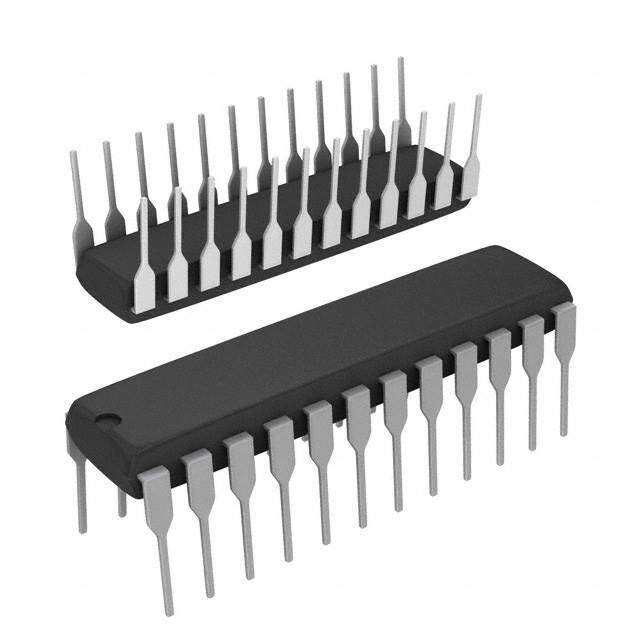
| 描述 | IC DRVR LATCH 8BIT PAR IN 24DIP闭锁 8-Bit Parallel Input Protected Latched Driver |
| 产品分类 | PMIC - MOSFET,电桥驱动器 - 内部开关集成电路 - IC |
| 品牌 | Micrel |
| 产品手册 | |
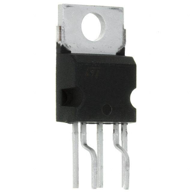
| 产品图片 |
|
| rohs | 否含铅 / 不符合限制有害物质指令(RoHS)规范要求 |
| 产品系列 | 逻辑集成电路,闭锁,Micrel MIC59P50BN- |
| 数据手册 | |
| 产品型号 | MIC59P50BN |
| 产品种类 | 闭锁 |
| 低电平输出电流 | 15 mA |
| 供应商器件封装 | 24-PDIP |
| 包装 | 管件 |
| 商标 | Micrel |
| 安装类型 | 通孔 |
| 安装风格 | Through Hole |
| 导通电阻 | - |
| 封装 | Tube |
| 封装/外壳 | 24-DIP(0.300",7.62mm) |
| 封装/箱体 | PDIP-24 |
| 工作温度 | -40°C ~ 85°C |
| 工厂包装数量 | 15 |
| 最大工作温度 | + 85 C |
| 最小工作温度 | - 40 C |
| 极性 | Non-Inverting |
| 标准包装 | 15 |
| 电压-电源 | 5 V ~ 12 V |
| 电流-峰值输出 | - |
| 电流-输出/通道 | 500mA |
| 电源电压-最大 | 12 V |
| 电源电压-最小 | 5 V |
| 电源电流 | 6.4 mA |
| 电路数量 | 1 Circuit |
| 类型 | 锁存驱动器 |
| 系列 | MIC59P50 |
| 输入类型 | 非反相 |
| 输入线路数量 | 8 Line |
| 输出数 | 8 |
| 输出线路数量 | 8 Line |
| 逻辑类型 | Latch |
| 逻辑系列 | TTL |
| 高电平输出电流 | 50 nA |


- 商务部:美国ITC正式对集成电路等产品启动337调查
- 曝三星4nm工艺存在良率问题 高通将骁龙8 Gen1或转产台积电
- 太阳诱电将投资9.5亿元在常州建新厂生产MLCC 预计2023年完工
- 英特尔发布欧洲新工厂建设计划 深化IDM 2.0 战略
- 台积电先进制程称霸业界 有大客户加持明年业绩稳了
- 达到5530亿美元!SIA预计今年全球半导体销售额将创下新高
- 英特尔拟将自动驾驶子公司Mobileye上市 估值或超500亿美元
- 三星加码芯片和SET,合并消费电子和移动部门,撤换高东真等 CEO
- 三星电子宣布重大人事变动 还合并消费电子和移动部门
- 海关总署:前11个月进口集成电路产品价值2.52万亿元 增长14.8%


PDF Datasheet 数据手册内容提取
MIC59P50 8-Bit Parallel-Input Protected Latched Driver General Description Features The MIC59P50 parallel-input latched driver is a high- • 4.4MHz minimum data input rate voltage (80V), high-current (500mA) integrated circuit • High-voltage, high-current outputs comprised of eight CMOS data latches, a bipolar • Per-output overcurrent shutdown (500mA typical) Darlington transistor driver for each latch, and CMOS control circuitry for the common CLEAR, STROBE, and • Undervoltage lockout OUTPUT ENABLE functions. Similar to the MIC5801, • Output fault flag additional protection circuitry supplied on this device • Output transient protection diodes includes thermal shutdown, undervoltage lockout (UVLO), • CMOS, PMOS, NMOS, and TTL-compatible inputs and overcurrent shutdown. • Internal pull-down resistors The bipolar/MOS combination provides an extremely low- • Low-power CMOS latches power latch with maximum interface flexibility. The • Single or split supply operation MIC59P50 has open-collector outputs capable of sinking 500mA and integral diodes for inductive load transient suppression with a minimum output breakdown voltage rating of 80V above V (50V sustaining). The drivers can EE be operated with a split supply, where the negative supply is down to –20V and may be paralleled for higher load current capability. With a 5V logic supply, the MIC59P50 will typically operate at better than 5MHz. With a 12V logic supply, significantly higher speeds are obtained. The CMOS inputs are compatible with standard CMOS, PMOS, and NMOS circuits. TTL circuits may require pull-up resistors. Each of these eight outputs has an independent overcurrent shutdown at 500mA. Upon current shutdown, the affected channel will turn OFF and the flag will go low until V is cycled or the /ENABLE/RESET pin is pulsed DD high. Current pulses less than 2µs will not activate overcurrent shutdown. Temperatures above +165°C will shut down the device and activate the open-collector FLAG output at pin 1. The UVLO circuit disables the outputs at low V ; hysteresis of 0.5V is provided. DD Datasheets and support documentation are available on Micrel’s website at: www.micrel.com. Micrel Inc. • 2180 Fortune Drive • San Jose, CA 95131 • USA • tel +1 (408) 944-0800 • fax + 1 (408) 474-1000 • http://www.micrel.com July 29, 2015 Revision 2.0
Micrel, Inc. MIC59P50 Functional Diagram July 29, 2015 2 Revision 2.0
Micrel, Inc. MIC59P50 Ordering Information Part Number Temperature Range Package Pb-Free MIC59P50YN –40°C to +85°C 24-Pin Plastic DIP(1) √ MIC59P50YV –40°C to +85°C 28-Pin PLCC √ MIC59P50YWM –40°C to +85°C 24-Pin Wide SOIC √ Note: 1. 300mm “Skinny DIP” Pin Configuration 24-Pin PDIP (N) 28-Pin PLCC (V) 24-Pin Wide SOIC (WM) (Top View) (Top View) Pin Description Pin Number Pin Number Pin Name Pin Name PDIP & SOIC PLCC Error flag. Open-collector output is low upon overcurrent fault or 1 2 /FLAG overtemperature fault. /OE/RESET must be pulled high to reset the flag and fault condition. 2 3 CLEAR Sets all latches to OFF (open). 3 4 STROBE Input strobe pin. Loads output latches when high. 4-11 5-12 INn Parallel inputs, 1 through 8. 12 15 VEE Output ground (substrate). Most negative voltage in the system connects here. 13 17 COMMON Transient suppression diodes cathode common pin. 14-21 18-25 OUTn Parallel outputs, 8 through 1. 22 26 VDD Logic positive supply voltage. Output enable reset. When low, outputs are active. When high, outputs are 23 27 /OE/RESET inactive and the flag and outputs are reset from a fault condition. An undervoltage condition emulates a high /OE input. 24 28 VSS Logic reference (ground) pin. July 29, 2015 3 Revision 2.0
Micrel, Inc. MIC59P50 Absolute Maximum Ratings(2) Operating Ratings(3) Input Voltage (VCE) ....................................................... +80V Input Voltage (VIN) .................................. –0.3V to VDD+0.3V Supply Voltage Operating Temperature (TA)........................ –40°C to +85°C (VDD) ......................................................................... 15V Junction Temperature (TJ) ....................................... +150°C (VDD – VEE) ............................................................... 25V Power Dissipation (PD) Continuous Collector Current (I ) .............................. 500mA Plastic DIP (N) ....................................................... 2.4W C Protected Current(4) ....................................................... 1.5A Derate above TA = +25°C ............................ 24mW/°C Lead Temperature (soldering, 10s) ............................ 260°C PLCC (V) ............................................................... 1.6W Storage Temperature (Ts) ......................... –65°C to +150°C Derate above TA = +25°C ............................ 16mW/°C ESD Rating(5) ................................................. ESD Sensitive Wide SOIC (WM) ................................................... 1.4W Derate above T = +25°C ............................ 14mW/°C A (6) Electrical Characteristics VDD = 5V; TA = 25°C, unless noted. Symbol Parameter Condition Min. Typ. Max. Units VCE = 80V, TA = +25°C 50 µA ICEX Output Leakage Current VCE = 80V, TA = +70°C 100 µA VCE(SAT) Collector-Emitter IC = 100mA 0.9 1.1 V IC = 200mA 1.1 1.3 V Saturation Voltage IC = 350mA 1.3 1.6 V VIN(0) 1.0 V VDD = 12V 10.5 V Input Voltage VIN(1) VDD = 10V 8.5 V VDD = 5V, Note 7 3.5 V VDD = 12V 50 200 kΩ RIN Input Resistance VDD = 10V 50 300 kΩ VDD = 5V 50 600 kΩ IOL /Flag Output Current VOL = 0.4V 15 mA IOH /Flag Output Leakage VOH = 12V 50 nA Notes: 2. Exceeding the absolute maximum ratings may damage the device. 3. The device is not guaranteed to function outside its operating ratings. 4. Each channel VEE connection must be designed to minimize inductance and resistance. 5. Devices are ESD sensitive. Handling precautions are recommended. Human body model, 1.5kΩ in series with 100pF. 6. Specification for packaged product only. 7. Operation of these devices with standard TTL or DTL may require the use of appropriate pull-up resistors to ensure a minimum logic “1”. July 29, 2015 4 Revision 2.0
Micrel, Inc. MIC59P50 (6) Electrical Characteristics (Continued) VDD = 5V; TA = 25°C, unless noted. Symbol Parameter Condition Min. Typ. Max. Units VDD = 12V, outputs open 3.3 4.5 mA IDD(ON)1 Supply Current VDD = 10V, outputs open 3.1 4.5 mA One Output Active VDD = 5V, outputs open 2.4 3.6 mA VDD = 12V, outputs open 6.4 10.0 mA IDD(ON) All Supply Current VDD = 10V, outputs open 6.0 9.0 mA All Outputs Active VDD = 5V, outputs open 4.7 7.5 mA VDD = 12V, outputs open, inputs = 0V 3.0 4.5 mA IDD(OFF) Supply Current OFF VDD = 5V, outputs open, inputs = 0V 2.2 3.6 mA VR = 80V, TA = +25°C 50 µA IR Clamp Diode Leakage Current VR = 80V, TA = +70°C 100 µA ILIM Overcurrent Threshold Each output 500 mA VSU Start-up Voltage Note 8 3.5 4.0 4.5 V VDD MIN Minimum Operating VDD 3.0 3.5 4.0 V VF Clamp Diode Forward Voltage IF = 350mA 1.7 2.0 V Thermal Shutdown 165 °C Thermal Shutdown Hysteresis 10 Notes: 8. Undervoltage lockout is guaranteed to release device at no more than 4.5V and disable the device at no less than 3.0V input logic voltage. Truth Table OUTn INn Strobe Clear Output Enable t-1 t 0 1 0 0 X OFF 1 1 0 0 X ON X X 1 X X OFF X X X 1 X OFF X 0 0 0 ON ON X 0 0 0 OFF OFF Note: X = Irrelevant t-1 = Previous output state t = Present output state Information present at an input is transferred to its latch when the STROBE is high. A high CLEAR input will set all latches to the output OFF condition regardless of the data or STROBE input levels. A high OUTPUT ENABLE will set all outputs to the OFF condition, regardless of any other input conditions. When the OUTPUT ENABLE is low, the outputs depend on the state of their respective latches. If current shutdown is activated, the OUTPUT ENABLE must be pulsed high to restore operation and reset the FLAG. Overtemperature faults are not latched and require no reset pulse. July 29, 2015 5 Revision 2.0
Micrel, Inc. MIC59P50 Timing Diagram Timing Conditions T = +25°C; Logic levels are V and V ; V = 5V. A DD SS DD A. Minimum data active time before strobe enabled (data set-up time) 50ns B. Minimum data active time after strobe disabled (data hold time) 50ns C. Minimum strobe pulse width 125ns D. Typical time between strobe activation and output on-to-off transition 500ns E. Typical time between strobe activation and output off-to-on transition 500ns F. Minimum clear pulse width 300ns G. Minimum data pulse width 225ns July 29, 2015 6 Revision 2.0
Micrel, Inc. MIC59P50 Typical Characteristics July 29, 2015 7 Revision 2.0
Micrel, Inc. MIC59P50 Typical Application MIC59P50 Protected Relay Driver July 29, 2015 8 Revision 2.0
Micrel, Inc. MIC59P50 (9) Package Information and Recommended Land Pattern 24-Pin PDIP (N) Note: 9. Package information is correct as of the publication date. For updates and most current information, go to www.micrel.com. July 29, 2015 9 Revision 2.0
Micrel, Inc. MIC59P50 (9) Package Information and Recommended Land Pattern 28-Pin PLCC (V) July 29, 2015 10 Revision 2.0
Micrel, Inc. MIC59P50 (9) Package Information and Recommended Land Pattern 24-Pin Wide SOIC (WM) July 29, 2015 11 Revision 2.0
Micrel, Inc. MIC59P50 MICREL, INC. 2180 FORTUNE DRIVE SAN JOSE, CA 95131 USA TEL +1 (408) 944-0800 FAX +1 (408) 474-1000 WEB http://www.micrel.com Micrel, Inc. is a leading global manufacturer of IC solutions for the worldwide high performance linear and power, LAN, and timing & communications markets. The Company’s products include advanced mixed-signal, analog & power semiconductors; high-performance communication, clock management, MEMs-based clock oscillators & crystal-less clock generators, Ethernet switches, and physical layer transceiver ICs. Company customers include leading manufacturers of enterprise, consumer, industrial, mobile, telecommunications, automotive, and computer products. Corporation headquarters and state-of-the-art wafer fabrication facilities are located in San Jose, CA, with regional sales and support offices and advanced technology design centers situated throughout the Americas, Europe, and Asia. Additionally, the Company maintains an extensive network of distributors and reps worldwide. Micrel makes no representations or warranties with respect to the accuracy or completeness of the information furnished in this datasheet. This information is not intended as a warranty and Micrel does not assume responsibility for its use. Micrel reserves the right to change circuitry, specifications and descriptions at any time without notice. No license, whether express, implied, arising by estoppel or otherwise, to any intellectual property rights is granted by this document. Except as provided in Micrel’s terms and conditions of sale for such products, Micrel assumes no liability whatsoever, and Micrel disclaims any express or implied warranty relating to the sale and/or use of Micrel products including liability or warranties relating to fitness for a particular purpose, merchantability, or infringement of any patent, copyright, or other intellectual property right. Micrel Products are not designed or authorized for use as components in life support appliances, devices or systems where malfunction of a product can reasonably be expected to result in personal injury. Life support devices or systems are devices or systems that (a) are intended for surgical implant into the body or (b) support or sustain life, and whose failure to perform can be reasonably expected to result in a significant injury to the user. A Purchaser’s use or sale of Micrel Products for use in life support appliances, devices or systems is a Purchaser’s own risk and Purchaser agrees to fully indemnify Micrel for any damages resulting from such use or sale. © 1998 Micrel, Incorporated. July 29, 2015 12 Revision 2.0