ICGOO在线商城 > 集成电路(IC) > PMIC - 稳压器 - 线性稳压器控制器 > MIC5156-3.3YM
 Datasheet下载
- 型号: MIC5156-3.3YM
- 制造商: Micrel
- 库位|库存: xxxx|xxxx
- 要求:
| 数量阶梯 | 香港交货 | 国内含税 |
| +xxxx | $xxxx | ¥xxxx |
查看当月历史价格
查看今年历史价格
MIC5156-3.3YM产品简介:
ICGOO电子元器件商城为您提供MIC5156-3.3YM由Micrel设计生产,在icgoo商城现货销售,并且可以通过原厂、代理商等渠道进行代购。 MIC5156-3.3YM价格参考。MicrelMIC5156-3.3YM封装/规格:PMIC - 稳压器 - 线性稳压器控制器, Linear Regulator Controller IC Positive Fixed 1 Output 8-SOIC。您可以下载MIC5156-3.3YM参考资料、Datasheet数据手册功能说明书,资料中有MIC5156-3.3YM 详细功能的应用电路图电压和使用方法及教程。
Microchip Technology的MIC5156-3.3YM是一款PMIC(电源管理集成电路)中的线性稳压器控制器,主要应用于需要高效、低功耗和稳定电压输出的场景。以下是其典型应用场景:

1. 便携式电子设备:
   MIC5156-3.3YM适合用于便携式设备,如智能手机、平板电脑、可穿戴设备等。这些设备对电源效率和体积要求较高,而该芯片能够提供稳定的3.3V输出电压,同时支持低功耗模式,延长电池寿命。

2. 嵌入式系统:
   在工业控制、物联网(IoT)设备和嵌入式计算模块中,MIC5156-3.3YM可以为微控制器、传感器和其他外围设备提供稳定的电源供应。其高精度输出电压确保系统运行可靠。

3. 通信设备:
   适用于路由器、调制解调器和其他网络设备。这些设备通常需要多个电压轨,MIC5156-3.3YM可以作为其中的一部分,为特定组件提供恒定的3.3V电源。

4. 消费类电子产品:
   包括数码相机、游戏机和音频设备等。这些产品需要高质量的电源供应以保证性能和用户体验,MIC5156-3.3YM的低噪声特性非常适合此类应用。

5. 汽车电子:
   虽然主要用于消费级市场,但在某些非核心汽车应用中(如信息娱乐系统或传感器模块),MIC5156-3.3YM也能发挥作用,提供稳定的电源支持。

6. 医疗设备:
   对于便携式医疗设备(如血糖仪、脉搏血氧仪等),该芯片的低功耗特性和稳定性使其成为理想选择,确保设备在电池供电下长时间运行。

总结来说,MIC5156-3.3YM凭借其高效能、小尺寸和稳定性,广泛应用于需要精确电压输出和节能特性的各种电子设备中。
| 参数 | 数值 |
| 产品目录 | 集成电路 (IC) |
| 描述 | IC REG CTRLR SGL 3.3V 8-SOIC |
| 产品分类 | PMIC - 稳压器 - 线性晶体管驱动器 |
| 品牌 | Micrel Inc |
| 数据手册 | |
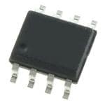
| 产品图片 |
|
| 产品型号 | MIC5156-3.3YM |
| rohs | 无铅 / 符合限制有害物质指令(RoHS)规范要求 |
| 产品系列 | - |
| 产品目录页面 | |
| 供应商器件封装 | 8-SOIC |
| 其它名称 | 576-2355 |
| 包装 | 管件 |
| 封装/外壳 | 8-SOIC(0.154",3.90mm 宽) |
| 工作温度 | -40°C ~ 85°C |
| 标准包装 | 95 |
| 电压-输入 | 3 V ~ 36 V |
| 电压-输出 | 3.3V |
| 电流-电源 | 2.7mA |
| 类型 | 正,固定式 |
| 输出数 | 1 |


- 商务部:美国ITC正式对集成电路等产品启动337调查
- 曝三星4nm工艺存在良率问题 高通将骁龙8 Gen1或转产台积电
- 太阳诱电将投资9.5亿元在常州建新厂生产MLCC 预计2023年完工
- 英特尔发布欧洲新工厂建设计划 深化IDM 2.0 战略
- 台积电先进制程称霸业界 有大客户加持明年业绩稳了
- 达到5530亿美元!SIA预计今年全球半导体销售额将创下新高
- 英特尔拟将自动驾驶子公司Mobileye上市 估值或超500亿美元
- 三星加码芯片和SET,合并消费电子和移动部门,撤换高东真等 CEO
- 三星电子宣布重大人事变动 还合并消费电子和移动部门
- 海关总署:前11个月进口集成电路产品价值2.52万亿元 增长14.8%


PDF Datasheet 数据手册内容提取
MIC5156/5157/5158 Micrel, Inc. MIC5156/5157/5158 Super LDO™ Regulator Controller General Description either 3.3V, 5.0V, or 12V. The MIC5158 can be configured as a fixed 5V controller or programmed to any voltage from The MIC5156, MIC5157, and MIC5158 Super Low-Dropout 1.3V to 36V using two external resistors. (LDO) Regulator Controllers are single IC solutions for high- current low-dropout linear voltage regulation. Super LDO™ The MIC5156 is available in an 8-pin DIP or SOIC. The Regulators have the advantages of an external N-channel MIC5157 and MIC5158 are available in a 14-pin DIP or SOIC power MOSFET as the linear pass element. which operate from –40°C to +85°C. The MIC5156/7/8 family features a dropout voltage as low as the R of the external power MOSFET multiplied by DS(ON) Features the output current. The output current can be as high as the largest MOSFETs can provide. • 4.5mA typical operating current • <1µA typical standby current The MIC5156/7/8 family operates from 3V to 36V. The • Low external parts count MIC5156 requires an external gate drive supply to provide • Optional current limit (35mV typical threshold) the higher voltage needed to drive the gate of the external • 1% initial output voltage tolerance in most configurations MOSFET. The MIC5157 and MIC5158 each have an inter- • 2% output voltage tolerance over temperature nal charge pump tripler to produce the gate drive voltage. • Fixed output voltages of 3.3V, 5.0V (MIC5156) The tripler is capable of providing enough voltage to drive a • Fixed output voltages of 3.3V, 5.0V, 12V (MIC5157) logic-level MOSFET to 3.3V output from a 3.5V supply and • Programmable (1.3 to 36V) with 2 resistors (MIC5156/8) is clamped to 17.5V above the supply voltage. The tripler • Internal charge pump voltage tripler (MIC5157/8) requires three external capacitors. • Enable pin to activate or shutdown the regulator The regulator output is constant-current limited when the • Internal gate-to-source protective clamp controller detects 35mV across an optional external sense • All versions available in DIP and SOIC resistor. An active-low open-collector flag indicates a low voltage of 8% or more below nominal output. A shutdown Applications (low) signal to the TTL-compatible enable control reduces • Ultrahigh current ultralow dropout voltage regulator controller supply current to less than 1µA while forcing the • Constant high-current source output voltage to ground. • Low parts count 5.0V to 3.3V computer supply The MIC5156-3.3 and MIC5156-5.0 controllers have inter- • Low noise/low-dropout SMPS post regulator nally fixed output voltages. The MIC5156 [adjustable] output • High-current, current-limited switch is configured using two external resistors. The MIC5157 is a fixed output controller which is externally configured to select Typical Applications +12V 1.0µF 0.1µF Enable 0.1µF Shutdown 4 3 2 1 7 6 5 4 3 2 1 NDLAGN 2+2–NDLAG.3VVP VP G E C C VC G 3 5 F F MIC5156-3.3 MIC5157 D 1+1ND VD G D S C C– VD G D S E 5 6 7 8 8 9 10 11 12 13 14 0.1µF Enable V5IVN 47µF 3RmSΩ CL* V3.O3UVT, 10A (3.61VVINmin.) 47µF 3RmSΩ ShuCtdLo*wn V3.O3UVT, 10A 47µF 47µF R = 0.035V /I R = 0.035V /I S LIMIT *Improves transient S LIMIT *Improves transient SMP60N03-10L response to load changes IRLZ44 (Logic Level MOSFET) response to load changes 10A 5V to 3.3V Desktop Computer Regulator 10A Low-Dropout Voltage Regulator Super LDO is a trademark of Micrel, Inc. Micrel, Inc. • 2180 Fortune Drive • San Jose, CA 95131 • USA • tel + 1 (408) 944-0800 • fax + 1 (408) 474-1000 • http://www.micrel.com August 2005 1 MIC5156/5157/5158
MIC5156/5157/5158 Micrel, Inc. Ordering Information MIC5156 Part Number Temperature Standard Pb-Free Voltage Range Package MIC5156-3.3BN MIC5156-3.3YN 3.3V –40°C to +85°C 8-pin DIP MIC5156-5.0BN MIC5156-5.0YN 5.0V –40°C to +85°C 8-pin DIP MIC5156BN MIC5156YN Adj –40°C to +85°C 8-pin DIP MIC5156-3.3BM MIC5156-3.3YM 3.3V –40°C to +85°C 8-pin SOIC MIC5156-5.0BM MIC5156-5.0YM 5.0V –40°C to +85°C 8-pin SOIC MIC5156BM MIC5156YM Adj –40°C to +85°C 8-pin SOIC Ordering Information MIC5157 Part Number Temperature Standard Pb-Free Voltage Range Package MIC5157BN MIC5157YN Selectable –40°C to +85°C 14-pin DIP MIC5157BM MIC5157YM Selectable –40°C to +85°C 14-pin SOIC Ordering Information MIC5158 Part Number Temperature Standard Pb-Free Voltage Range Package MIC5158BN MIC5158YN 5.0V/Adj –40°C to +85°C 14-pin DIP MIC5158BM MIC5158YM 5.0V/Adj –40°C to +85°C 14-pin SOIC Pin Configuration MIC5156-x.x MIC5156 EN 1 8 S (Source) EN 1 8 EA FLAG 2 7 D (Drain) FLAG 2 7 D (Drain) GND 3 6 G (Gate) GND 3 6 G (Gate) VP 4 5 VDD VP 4 5 VDD MIC5157 MIC5158 5V 1 14 EN EA 1 14 EN 3.3V 2 13 S (Source) 5V FB 2 13 S (Source) FLAG 3 12 D (Drain) FLAG 3 12 D (Drain) GND 4 11 G (Gate) GND 4 11 G (Gate) V 5 10 V V 5 10 V CP DD CP DD C2– 6 9 C1– C2– 6 9 C1– C2+ 7 8 C1+ C2+ 7 8 C1+ MIC5156/5157/5158 2 August 2005
MIC5156/5157/5158 Micrel, Inc. Pin Description MIC5156 Pin Number Pin Name Pin Function 1 EN Enable (Input): TTL high enables regulator; TTL low shuts down regulator. 2 FLAG Output Flag (Output): Open collector output is active (low) when V is more OUT than 8% below nominal output. Circuit has 3% hysteresis. 3 GND Circuit ground. 4 V N-channel Gate Drive Supply Voltage: User supplied voltage for driving the P gate of the external MOSFET. 5 V Supply Voltage (Input): Supply voltage connection. Connect sense resis- DD tor (R ) to V if current limiting used. Connect supply bypass capacitor to S DD ground near device. 6 G Gate (Output): Drives the gate of the external MOSFET. 7 D Drain and Current Limit (Input): Connect to external MOSFET drain and ex- ternal sense resistor (current limit), or connect to V and external MOSFET DD drain (no current limit). 8 (3.3V, 5V) S Source (Input): Top of internal resistive divider chain. Connect directly to the load for best load regulation. 8 (adjustable) EA Error Amplifier (Input): Connect to external resistive divider. Pin Description MIC5157, MIC5158 Pin Number Pin Name Pin Function 1 (MIC5157) 5V 5V Configuration (Input): Connect to S (source) pin for 5V output. 1 (MIC5158) EA Error Amplifier (Input): Connect to external resistive divider to obtain adjust- able output. 2 (MIC5157) 3.3V 3.3V Configuration (Input): Connect to S (source) pin for 3.3V output. 2 (MIC5158) 5V FB 5V Feedback (Input): Connect to EA for fixed 5V output. 3 FLAG Output Voltage Flag (Output): Open collector is active (low) when V is 8% OUT or more below its nominal value. 4 GND Circuit ground. 5 V Voltage Tripler Output [Filter Capacitor]. Connect a 1 to 10µF capacitor to ground. CP 6 C2– Charge Pump Capacitor 2: Second stage of internal voltage tripler. Connect a 0.1µF capacitor from C2+ to C2–. 7 C2+ Charge Pump Capacitor 2: See C2– pin 6. 8 C1+ Charge Pump Capacitor 1: First stage of internal voltage tripler. Connect a 0.1µF capacitor from C1+ to C1–. 9 C1– Charge Pump Capacitor 1: See C1+ pin 8. 10 V Supply Voltage (Input): Supply voltage connection. Connect sense resis- DD tor (R ) to V if current limiting used. Connect supply bypass capacitor to S DD ground near device. 11 G Gate (Output): Connect to External MOSFET gate. 12 D Drain and Current Limit (Input): Connect to external MOSFET drain and ex- ternal sense resistor (current limit), or connect to V and external MOSFET DD drain (no current limit). 13 (MIC5157) S Source and 3.3V/5V Configuration: Top of internal resistor chain. Connect to source of external MOSFET for 3.3V, 5V, and 12V operation. Also see 3.3V and 5V pin descriptions. 13 (MIC5158) S Source (Input): Top of internal resistor chain. Connect to top of external resis- tive divider and source of external MOSFET. 14 EN Enable (Input): TTL high enables regulator; TTL low shuts down regulator. August 2005 3 MIC5156/5157/5158
MIC5156/5157/5158 Micrel, Inc. Absolute Maximum Ratings (Note 1) Operating Ratings (Note 2) Supply Input (V ) .......................................................+38V Ambient Temperature Range (T ) DD A Enable Input (V ) ..........................................–0.3V to 36V MIC515xBM/BN ......................................–40°C to +85°C EN Gate Output (VG) MIC5156 .........................................+55V Junction Temperature (TJ) .......................................+150°C Charge Pump Node (VCP) MIC5157/8 ........................+55V Thermal Resistance (θJA) Package MIC5156 MIC5157/8 Source Connection (V ) ...................................1.3 to +36V S DIP ................................100°C/W .....................90°C/W Flag (V ) ....................................................–0.3 to +40V FLAG SOIC .............................160°C/W ...................120°C/W Storage Temperature (T ) ........................–65°C to +150°C S Lead Temperature (soldering 10 sec.) .......................300°C Electrical Characteristics(Note 5) V = 5V, V = 5V; T = 25°C; unless noted. DD EN A Symbol Parameter Condition Min Typ Max Units V Supply Voltage 3 36 V DD I Supply Current MIC5156 Operating, V = 5V 2.7 10 mA DD(ON) EN I Shutdown, V = 0V 0.1 5 µA DD(OFF) EN I Supply Current MIC5157/8 Operating, V = 5V 4.5 10 mA DD(ON) EN I Shutdown, V = 0V 0.1 5 µA DD(OFF) EN V Enable Input Threshold High 2.4 1.3 V IH V Low 1.3 0.8 V IL EN I Enable Input Bias Current V = 2.4V 20 25 µA B EN V Max. Charge Pump Voltage V – V , V > 10V 17.5 18.5 V CP CP DD DD f Charge Pump Frequency 160 kHz CP V Maximum Gate Drive Voltage V = 0V OUT MAX SOURCE (MIC5157/8) V = 3.5V 5 7.0 9 V DD V = 5V 9 11.3 15 V DD V = 12V 24 28 30 V DD V Minimum Gate Drive Voltage V > V 1.0 V OUT MIN SOURCE OUT(NOM) V Current Limit Threshold V – V @ I 28 35 42 mV LIM DD D LIM V Source Voltage Short G (gate) to (S) source, Note 4 S MIC5156-3.3 3.267 3.3 3.333 V MIC5156-5.0 4.950 5.0 5.050 V MIC5157, 3.3V pin to S pin (3.3V config.) 3.250 3.3 3.350 V MIC5157, 5V pin to S pin (5V config.) 4.950 5.0 5.050 V MIC5157, V = 7V, (12V config.) 11.70 12 12.30 V DD MIC5158, 5V FB pin to EA pin (5V config.) 4.925 5.0 5.075 V V Bandgap Reference Voltage MIC5156 [adjustable] and MIC5158 1.222 1.235 1.248 V BG V Output Voltage Line Regulation 5V < V < 15V, V = 3.3V 2 7 mV LR DD OUT V Gate to Source Clamp 14 16.6 20 V GS MAX V Flag Comparator Threshold % of nominal V 92 % FT SOURCE V Flag Comparator Hysteresis % of nominal V 3 % FH SOURCE V Flag Comparator Sat. Voltage I = 1mA 0.09 0.2 V SAT FLAG Note 1. Exceeding the absolute maximum rating may damage the device. Note 2. The device is not guaranteed to function outside its operating rating. Note 3. Devices are ESD sensitive. Handling precautions recommended. Note 4. Test configuration. External MOSFET not used. Note 5. Specification for packaged product only. MIC5156/5157/5158 4 August 2005
MIC5156/5157/5158 Micrel, Inc. Typical Characteristics 3.3V Regulator Output 5.0V Regulator Output MIC5157/8 Turn-On Voltage vs. Temperature Voltage vs. Temperature Response Time for 3.3V 3.34 5.04 12 MOSFET = IRF540 V)3.33 V)5.03 10 VIN=5V,IL=0.5A GE (3.32 GE (5.02 V) 8 CCC1==C1µCF2=0.1µF UT VOLTA333...233901 UT VOLTA455...900901 OLTAGE ( 46 CCLP=50µLFINOPGUICT TP3.28 TP4.98 V 2 U U 3.3V O3.27 O4.97 0 OUTPUT 3.26 4.96 -2 -60 -30 0 30 60 90 120 150 -60 -30 0 30 60 90 120 150 -0.2 0.0 0.2 0.4 0.6 TEMPERATURE (°C) TEMPERATURE (°C) TIME (ms) MIC5157/8 On-State Supply MIC5157/8 On-State Supply Off-State Supply Current mA)10.0Current vs. Supply Voltage mA)5.0 Current vs. Temperature µA)5.0 vs. Temperature NT ( 9.0 NT (4.5 NT (4.5 VDD=5V RE 8.0 RE4.0 RE4.0 R R3.5 R3.5 CU 7.0 CU3.0 CU3.0 UPPLY 56..00 UPPLY 22..05 VDD=5V UPPLY 22..05 ON-STATE S 234...0000 5 10 15 20 25 30 ON-STATE S0011....0505-60 -30 0 30 60 90 120 150 OFF-STATE S0011....0505-60 -30 0 30 60 90 120 150 SUPPLY VOLTAGE (V) TEMPERATURE (°C) TEMPERATURE (°C) Charge-Pump Output Voltage Flag Output Voltage Flag Output Voltage vs. Supply Voltage vs. Temperature vs. Flag Current 60 200 1.0 HARGE PUMP VOLTAGE (V)1234500000 FLAG VOLTAGE (mV)111102572570505505 VIFDLADG==51VmA FLAG VOLTAGE (V)000000000.........123456789 VDD=5V C 0 0 0.0 0 5 10 15 20 25 30 -60 -30 0 30 60 90 120 150 0 2 4 6 8 10 SUPPLY VOLTAGE (V) TEMPERATURE (°C) FLAG SINK CURRENT (mA) Enable Threshold Voltage Enable Input Bias Current Current Limit Threshold NABLE THRESHOLD VOLTAGE (V)0000011111..........0246802468 vs. Temperature ENABLE BIAS CURRENT (µA)110224680000000 vs. Enable Voltage URRENT LIMIT THRESHOLD (mV)123456700000000 vs. Temperature E -60 -30 0 30 60 90 120 150 0 2 4 6 8 10 12 14 16 C -60 -30 0 30 60 90 120 150 TEMPERATURE (°C) ENABLE VOLTAGE (V) TEMPERATURE (°C) August 2005 5 MIC5156/5157/5158
MIC5156/5157/5158 Micrel, Inc. Block Diagram MIC5156 +12V Input +5V Input 0.1µF VP VDD IBnitaesrnal ENEShnuatbdleown R3mSΩ 12k to all 1.235V internal blocks Bandgap I Reference CLIoMmITparator D (Drain) +5V Input [ I ] 35mV LIMIT Q2 VOUT Error G (Gate) Q1 Comparator Amp SMP60N03-10L FLAG Switched 16.6V S* (Source) 5V Load Regulated 75mV +3.3V Output 17k† *fixed version only †3.3V = 17k, 5V = 32k C 10k GND L ‡ adjustable version only EA‡ Block Diagram with External Components Fixed 3.3V Power Supply with 5.0V Load Switch Block Diagram MIC5157 +5V Input C3 0.1µF C1 0.1µF C2 1µF C1+ C1– C2+ C2– VCP VDD Oscillator ChaTrrgiep lePrump CVlaCmPp IBnitaesrnal ENEShnuatbdleown R3mSΩ to all 1.235V niternal blocks Bandgap I Reference CLIoMmITparator D (Drain) [ I ] 35mV LIMIT VOUT Error G (Gate) Q1 Comparator Amp IRFZ44 FLAG 16.6V S (Source)* Regulated 75mV +3.3V Output 58k 5V C L 15k 3.3V 17k 10k GND Block Diagram with External Components Fixed 3.3V 10A Power Supply MIC5156/5157/5158 6 August 2005
MIC5156/5157/5158 Micrel, Inc. Block Diagram MIC5158 +5V Input C3 0.1µF C1 0.1µF C2 1µF C1+ C1– C2+ C2– VCP VDD Oscillator ChaTrrgiep lePrump CVlaCmPp IBnitaesrnal ENEShnuatbdleown R3mSΩ to all 1.235V internal blocks Bandgap I Reference CLIoMmITparator D (Drain) [ I ] 35mV LIMIT VOUT Error G (Gate) Q1 Comparator Amp IRFZ44 FLAG 16.6V S (Source) Regulated 75mV +3.6V Output 32k 5V FB C 10k L GND EA 19.1k 10.0k Block Diagram with External Components Adjustable Power Supply, 3.6V Configuration Functional Description to-source enhancement voltage for an external N-channel MOSFET (regulator pass element) placed between the supply A Super LDO Regulator is a complete regulator built around and the load. The gate-to-source voltage may vary from 1V Micrel’s Super LDO Regulator Controller. to 16V depending upon the supply and load conditions. Refer to Block Diagrams MIC5156, MIC5157, and Because the source voltage (output) approaches the drain MIC5158. voltage (input) when the regulator is in dropout and the Version Differences MOSFET is fully enhanced, an additional higher supply The MIC5156 requires an external voltage for MOSFET gate voltage is required to produce the necessary gate-to-source drive and is available in 3.3V fixed output, 5V fixed output, or enhancement. This higher gate drive voltage is provided by adjustable output versions. With 8-pins, the MIC5156 is the an external gate drive supply (MIC5156) or by an internal smallest of the Super LDO Regulator Controllers. charge pump (MIC5157 and MIC5158). The MIC5157 and MIC5158 each have an internal charge Gate Drive Supply Voltage (MIC5156 only) pump which provides MOSFET gate drive voltage. The The gate drive supply voltage must not be more than 14V MIC5157 has a selectable fixed output of 3.3V, 5V, or 12V. above the supply voltage (V – V < 14V). The minimum P DD The MIC5158 may be configured for a fixed 5V or adjustable necessary gate drive supply voltage is: output. V = V + V + 1 P OUT GS Enable (EN) where: With at least 3.0V on V , applying a TTL low to EN places DD V = gate drive supply voltage the controller in shutdown mode. A TTL high on EN enables P the internal bias circuit which powers all internal circuitry. EN VOUT = regulator output voltage must be pulled high if unused. The voltage applied to EN may V = gate-to-source voltage for full GS be as high as 36V. MOSFET gate enhancement The controller draws less than 1µA in shutdown mode. The error amplifier uses the gate drive supply voltage to drive Gate Enhancement the gate of the external MOSFET. The error amplifier output can swing to within 1V of V . The Super LDO Regulator Controller manages the gate- P August 2005 7 MIC5156/5157/5158
MIC5156/5157/5158 Micrel, Inc. Charge Pump (MIC5157/5158 only) Note that the recovery time to repetitive load transients may be affected with small pump capacitors. The charge pump tripler creates a dc voltage across reservoir capacitor C3. External capacitors C1 and C2 provide the nec- Gate-to-Source Clamp essary storage for the stages of the charge pump tripler. A gate-to-source protective voltage clamp of 16.6V protects The tripler’s approximate dc output voltage is: the MOSFET in the event that the output voltage is suddenly forced to zero volts. This prevents damage to the external V ≈ 3 (V – 1) CP DD MOSFET during shorted load conditions. Refer to “Charge where: Pump” for normal clamp circuit operation. V = charge pump output voltage CP The source connection required by the gate-to-source clamp VDD = supply voltage is not available on the adjustable version of the MIC5156. The V clamp circuit limits the charge pump voltage to 16V CP Output Regulation above V by gating the charge pump oscillator ON or OFF as DD At start-up, the error amplifier feedback voltage (EA), or required. The charge pump oscillator operates at 160kHz. internal feedback on fixed versions, is below nominal when The error amplifier uses the charge pump voltage to drive compared to the internal 1.235V bandgap reference. This the gate of the external MOSFET. It provides a constant load forces the error amplifier output high which turns on exter- of about 1mA to the charge pump. The error amplifier output nal MOSFET Q1. Once the output reaches regulation, the can swing to within 1V of VCP. controller maintains constant output voltage under changing Although the MIC5157/8 is designed to provide gate drive input and load conditions by adjusting the error amplifier using its internal charge pump, an external gate drive sup- output voltage (gate enhancement voltage) according to the ply voltage can be applied to V . When using an external feedback voltage. CP gate drive supply, V must not be forced more than 14V CP Out-of-Regulation Detection higher than V . DD When the output voltage is 8% or more below nominal, the When constant loads are driven, the ON/OFF switching of open-collector FLAG output (normally high) is forced low to the charge pump may be evident on the output waveform. signal a fault condition. The FLAG output can be used to This is caused by the charge pump switching ON and rapidly signal or control external circuitry. The FLAG output can also increasing the supply voltage to the error amplifier. The period be used to shut down the regulator using the EN control. of this small charge pump excitation is determined by a number Current Limiting of factors: the input voltage, the 1mA op-amp load, any dc Super LDO Regulators perform constant-current limiting (not leakage associated with the MOSFET gate circuit, the size foldback). To implement current limiting, a sense resistor of the charge pump capacitors, the size of the charge pump (R ) must be placed in the “power” path between V and reservoir capacitor, and the characteristics of the input voltage S DD D (drain). and load. The period is lengthened by increasing the charge pump reservoir capacitor (C3). The amplitude is reduced by If the voltage drop across the sense resistor reaches 35mV, weakening the charge pump—this is accomplished by reduc- the current limit comparator reduces the error amplifier out- ing the size of the pump capacitors (C1 and C2). If this small put. The error amplifier output is decreased only enough to burst is a problem in the application, use a 10µF reservoir reduce the output current, keeping the voltage across the capacitor at C3 and 0.01µF pump capacitors at C1 and C2. sense resistor from exceeding 35mV. Application Information V MOSFET Selection IN Standard N-channel enhancement-mode MOSFETs are ac- G ceptable for most Super LDO regulator applications. S Logic-level N-channel enhancement-mode MOSFETs may MIC515x be necessary if the external gate drive voltage is too low (MIC5156), or the input voltage is too low, to provide adequate GND charge pump voltage (MIC5157/8) to enhance a standard MOSFET. Circuit Layout Figure 1a. Connections for Fixed Output For the best voltage regulation, place the source, ground, and error amplifier connections as close as possible to the load. See figures (1a) and (1b). MIC5156/5157/5158 8 August 2005
MIC5156/5157/5158 Micrel, Inc. V Adjustable Configurations IN Micrel’s MIC5156 [adjustable] and MIC5158 require an ex- G ternal resistive divider to set the output voltage from 1.235V MIC5157 S to 36V. For best results, use a 10kΩ resistor for R2. See or MIC5158 equation (1) and figure (2). EA V GND 1) R1 = 1 × 10⁴ ( O U T - 1) 1.235 Figure 1b. Connections for Adjustable Output G S VOUT MIC5157/8 R1 VIN EA* GND R2 10k G * MIC5156 Figure 2. Typical Resistive Divider EA GND Input Filter Capacitor The Super LDO requires an input bypass capacitor for accom- modating wide changes in load current and for decoupling *Optional 16V zener diode the error amplifier and charge pump. A medium to large value recommended in applications whereVG is greater than 18V low-ESR (equivalent series resistance) capacitor is best, mounted close to the device. Figure 1c. MIC5156 Connections for Adjustable Output Output Filter Capacitor An output filter capacitor may be used to reduce ripple and MOSFET Gate-to-Source Protection improve load regulation. Stable operation does not require When using the adjustable version of the MIC5156, an external a large capacitor, but for transient load regulation the size of 16V zener diode placed from gate-to-source is recommended the output capacitor may become a consideration. Common for MOSFET protection. All other versions of the Super LDO aluminum electrolytic capacitors perform nicely; very low-ESR regulator controller use the internal gate-to-source clamp. capacitors are not necessary. Increased capacitance (rather than reduced ESR) is preferred. The capacitor value should Output Voltage Configuration be large enough to provide sufficient I = C × dV/dt current consistent with the required transient load regulation quality. Fixed Configurations For a given step increase in load current, the output voltage will The MIC5156-3.3 and MIC5156-5.0 are preset for 3.3V and drop by about dV = I × dt/C, where I represents the increase 5.0V respectively. in load current over time t. This relationship assumes that The MIC5157 operates at 3.3V when the 3.3V pin is connected all output current was being supplied via the MOSFET pass to the S (source) pin; 5.0V when the 5.0V pin is connected to device prior to the load increase. Small (0.01µF to 10µF) film the S pin; or 12V if the 3.3V and 5.0V pins are open. capacitors parallel to the load will further improve response The MIC5158 operates at a fixed 5V (without an external to transient loads. resistive divider) if the 5V FB pin is connected to EA. Some linear regulators specify a minimum required output filter capacitance because the capacitor determines the dominant pole of the system, and thereby stabilizes the system. This is not the situation for the MIC5156/7/8; its dominant pole is determined within its error amplifier. August 2005 9 MIC5156/5157/5158
MIC5156/5157/5158 Micrel, Inc. Current Limiting Gate Supply V IN Current sensing requires a low-value series resistance (R ) s between V and D (drain). Refer to the typical applications. DD V V RS The internal current-limiting circuit limits the voltage drop G DD ShuEtndaobwlen EN D across the sense resistor to 35mV. Equation (2) provides the MIC5156-x.xG sense resistor value required for a given maximum current. 35mV S 2) R = GND S I LIM where: R = sense resistor value S I = maximum output current LIM Figure 4a. High-Side Switch Most current-limited applications require low-value resistors. If a MIC5157 or MIC5158 is used and is shutdown for a See Application Hints 21 and 25 for construction hints. given time, the charge pump reservoir V will bleed off. If CP Non-Current-Limited Applications recharging the reservoir causes an unacceptable delay in the load reaching its operating voltage, do not use the EN pin For circuits not requiring current limiting, do not use a sense for on/off control. Instead, use the MIC5158, hold EN high to resistor between V and D (drain). See figure (3). The con- DD keep the charge pump in continuous operation, and switch troller will not limit current when it does not detect a 35mV the MOSFET on or off by overriding the error amplifier input drop from V to D. DD as shown in figure (4b). V IN V IN V DD V DD EN G D S MIC5156 G MIC5158 S EA GND Figure 3. No Current Limit Output Off 1N4148 Output On 3.3V Microprocessor Applications For computer designs that use 3.3V microprocessors with 5V Figure 4b. Fast High-Side Switch logic, the FLAG output can be used to suppress the 5V sup- ply until the 3.3V output is in regulation. Refer to the external Battery Charger Application components shown with the MIC5156 Block Diagram. The MIC5158 may be used in constant-current applications SMPS Post Regulator Application such as battery chargers. See figure (5). The regulator supplies A Super LDO regulator can be used as a post regulator for a a constant-current (35mV ÷ R3) until the battery approaches switch-mode power supply. The Super LDO regulator can pro- the float voltage: vide a significant reduction in peak-to-peak ripple voltage. ( R1 ) V = 1.235 1 + High-Current Switch Application FL R2 All versions of the MIC5156/7/8 may be used for current-lim- where: ited, high-current, high-side switching with or without voltage V = float voltage regulation. See figure (4a). Simply leave the “S” terminal FL open. A 16V zener diode from the gate to the source of the At float voltage, the MOSFET is shut off. A trickle charge is MOSFET protects the MOSFET from overdrive during fault supplied by R4. conditions. MIC5156/5157/5158 10 August 2005
MIC5156/5157/5158 Micrel, Inc. V Uninterruptible Power Supply IN The MIC5157 and two N-channel MOSFETs provide battery switching for uninterruptible power as shown in figure (6). V R3 R4 DD Two MOSFETs are placed source-to-source to prevent cur- D rent flow through their body diodes when switched off. The EN G Super LDO regulator is continuously enabled to achieve MIC5158 S fast battery switch-in. Careful attention must be paid to the R1 ac-line monitoring circuitry to ensure that the output voltage EA does not fall below design limits while the battery is being GND R2 switched in. V DD EN D Q1 D Figure 5. Battery Charger Concept G G MIC5158 S S MshOowSFn EfoTr bcloadriyty diodes S G Q2 EA D GND 40V max. Line 1N4148 Battery AC Off-line Uninterruptable Line Power Supply DC Figure 6. UPS Power Supply Concept August 2005 11 MIC5156/5157/5158
MIC5156/5157/5158 Micrel, Inc. Package Information PIN 1 DIMENSIONS: INCH (MM) 0.380 (9.65) 0.255 (6.48) 0.370 (9.40) 0.135 (3.43) 0.245 (6.22) 0.125 (3.18) 0.300 (7.62) 0.013 (0.330) 0.010 (0.254) 0.018 (0.57) 0.130 (3.30) 0.380 (9.65) 0.320 (8.13) 0.100 (2.54) 0.0375 (0.952) 8-Pin DIP (N) 8-Pin SOIC (M) MIC5156/5157/5158 12 August 2005
MIC5156/5157/5158 Micrel, Inc. .770 (19.558) MAX PIN 1 .235 (5.969) .215 (5.461) .060 (1.524) .045 (1.143) .310 (7.874) .280 (7.112) .160 MAX (4.064) .080 (1.524) .015 (0.381) .015 (0.381) .008 (0.2032) .160 (4.064) .100 (2.540) .110 (2.794) .023 (.5842) .090 (2.296) .015 (.3810) .400 (10.180) .060 (1.524) .330 (8.362) .045 (1.143) 14-Pin DIP (N) PIN 1 0.154 (3.90) DIMENSIONS: INCHES (MM) 0.026 (0.65) MAX) 0.193 (4.90) 0.050 (1.27) 0.016 (0.40) TYP TYP 45 0.006 (0.15) 3–6 0.344 (8.75) 0.244 (6.20) 0.057 (1.45) 0.337 (8.55) SEATING 0.228 (5.80) 0.049 (1.25) PLANE 14-Pin SOIC (M) MICREL INC. 2180 FORTUNE DRIVE SAN JOSE, CA 95131 USA TEL + 1 (408) 944-0800 FAX + 1 (408) 474-1000 WEB http://www.micrel.com This information furnished by Micrel in this data sheet is believed to be accurate and reliable. However no responsibility is assumed by Micrel for its use. Micrel reserves the right to change circuitry and specifications at any time without notification to the customer. Micrel Products are not designed or authorized for use as components in life support appliances, devices or systems where malfunction of a product can reasonably be expected to result in personal injury. Life support devices or systems are devices or systems that (a) are intended for surgical implant into the body or (b) support or sustain life, and whose failure to perform can be reasonably expected to result in a significant injury to the user. A Purchaser's use or sale of Micrel Products for use in life support appliances, devices or systems is a Purchaser's own risk and Purchaser agrees to fully indemnify Micrel for any damages resulting from such use or sale. © 1999 Micrel, Inc. August 2005 13 MIC5156/5157/5158
Mouser Electronics Authorized Distributor Click to View Pricing, Inventory, Delivery & Lifecycle Information: M icrel: MIC5156YM TR MIC5156-5.0YM TR M icrochip: MIC5156-5.0YM MIC5156-5.0YN MIC5158YN MIC5156-3.3YN MIC5157YM MIC5156-3.3YM MIC5158YM MIC5156YN MIC5156YM MIC5157YN MIC5156YM-TR MIC5156-5.0YM-TR MIC5158YM-TR MIC5156-3.3YM-TR MIC5157YM-TR