ICGOO在线商城 > 集成电路(IC) > PMIC - 稳压器 - 线性 > MIC37152WR
 Datasheet下载
- 型号: MIC37152WR
- 制造商: Micrel
- 库位|库存: xxxx|xxxx
- 要求:
| 数量阶梯 | 香港交货 | 国内含税 |
| +xxxx | $xxxx | ¥xxxx |
查看当月历史价格
查看今年历史价格
MIC37152WR产品简介:
ICGOO电子元器件商城为您提供MIC37152WR由Micrel设计生产,在icgoo商城现货销售,并且可以通过原厂、代理商等渠道进行代购。 MIC37152WR价格参考。MicrelMIC37152WR封装/规格:PMIC - 稳压器 - 线性, Linear Voltage Regulator IC Positive Adjustable 1 Output 1.25 V ~ 5.5 V 1.5A S-PAK-5。您可以下载MIC37152WR参考资料、Datasheet数据手册功能说明书,资料中有MIC37152WR 详细功能的应用电路图电压和使用方法及教程。
MIC37152WR 是 Microchip Technology 推出的一款低压差线性稳压器(LDO),具有高输出电流能力(可达 2A)和良好的负载/线路调整率,适用于对电源稳定性要求较高的应用场景。

该器件主要应用于以下领域:

1. 嵌入式系统与工业控制:为微处理器、FPGA、DSP 等提供稳定电源,确保在复杂工业环境中稳定运行。

2. 通信设备:用于基站、路由器、交换机等设备中的电源管理模块,提供低噪声、高稳定性的电压源。

3. 汽车电子:如车载信息娱乐系统、ADAS(高级驾驶辅助系统)等,满足汽车环境对可靠性和温度范围的要求。

4. 测试与测量仪器:为高精度 ADC、DAC 和传感器供电,确保测量精度和信号完整性。

5. 消费类电子产品:如高性能音频设备、平板电脑等,提供干净电源以降低噪声干扰。

其封装为 8 引脚 SOIC(宽体),具备热关断与过流保护功能,适用于空间有限但需要高可靠性的设计。
| 参数 | 数值 |
| 产品目录 | 集成电路 (IC)半导体 |
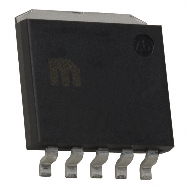
| 描述 | IC REG LDO ADJ 1.5A SPAK-5低压差稳压器 LV, 2.5A Cap LDO in Spak (ROHS Compliant) |
| 产品分类 | |
| 品牌 | Micrel |
| 产品手册 | |
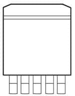
| 产品图片 |
|
| rohs | 符合RoHS无铅 / 符合限制有害物质指令(RoHS)规范要求 |
| 产品系列 | 电源管理 IC,低压差稳压器,Micrel MIC37152WR- |
| 数据手册 | |
| 产品型号 | MIC37152WR |
| PCN组件/产地 | |
| 产品目录页面 | |
| 产品种类 | 低压差稳压器 |
| 供应商器件封装 | S-PAK-5 |
| 其它名称 | 576-1165 |
| 包装 | 管件 |
| 商标 | Micrel |
| 回动电压—最大值 | 500 mV |
| 安装类型 | 表面贴装 |
| 安装风格 | SMD/SMT |
| 封装 | Tube |
| 封装/外壳 | SPak-5 (5 引线 + 接片) |
| 封装/箱体 | SPAK-5 |
| 工作温度 | -40°C ~ 125°C |
| 工厂包装数量 | 48 |
| 最大工作温度 | + 125 C |
| 最大输入电压 | 6 V |
| 最小工作温度 | - 40 C |
| 最小输入电压 | 2.25 V |
| 标准包装 | 48 |
| 电压-跌落(典型值) | - |
| 电压-输入 | 2.25 V ~ 6 V |
| 电压-输出 | 1.25 V ~ 5.5 V |
| 电流-输出 | 1.5A |
| 电流-限制(最小值) | - |
| 稳压器拓扑 | 正,可调式 |
| 稳压器数 | 1 |
| 系列 | MIC37152 |
| 线路调整率 | 0.06 % |
| 负载调节 | 0.2 % |
| 输出电压容差 | 1 % |
| 输出电流 | 1.5 A |
| 输出端数量 | 1 Output |
| 输出类型 | Adjustable |


PDF Datasheet 数据手册内容提取
MIC37150/51/52/53 1.5A, Low Voltage µCap LDO Regulator General Description Features The Micrel MIC37150/51/52/53 is a 1.5A low-dropout • 1.5A minimum guaranteed output current linear voltage regulator that provides a low voltage, high • 500mV maximum dropout voltage over temperature current output with a minimum of external components. It – Ideal for 3.0V to 2.5V conversion offers high precision, ultra-low dropout (500mV over – Ideal for 2.5V to 1.8V, 1.65V, or 1.5V conversion temperature), and low ground current. • Stable with ceramic or tantalum capacitor The MIC37150/51/52/53 operates from an input of 2.25V • Wide input voltage range to 6.0V. It is designed to drive digital circuits requiring low – VIN: 2.25V to 6.0V voltage at high currents (i.e., PLDs, DSPs, micro- • ±1.0% initial output tolerance controllers, etc.). It is available in fixed and adjustable • Fixed and adjustable output voltages output voltages. Fixed voltages include 1.5V, 1.65V, 1.8V, – MIC37150—3-pin fixed voltages 2.5V and 3.3V. The adjustable version is capable of – MIC37151—5-pin S-Pak or 8-pin e-Pad SOIC supplying output voltages from 1.24V to 5.5V. fixed voltages with flag Features of the MIC37150/51/52/53 LDO include thermal – MIC37152—5-pin adjustable voltage and current limit protection, and reverse current and – MIC37153—8-pin adjustable voltage with flag reverse battery protection. Logic enable and error flag pins • Excellent line and load regulation specifications are available. • Logic controlled shutdown Junction temperature range of the MIC37150/51/52/53 is • Thermal shutdown and current limit protection from –40°C to +125°C. • Reverse-leakage protection For applications requiring input voltage greater than 6.0V, • Low profile 3 or 5-pin S-Pak packages or 8-pin e-Pad see MIC3910x, MIC3915x, MIC3930x, and MIC3950x SOIC LDOs. Data sheets and support documentation can be found on Applications Micrel’s web site at www.micrel.com. • LDO linear regulator for low-voltage digital IC • PC add-in cards • High efficiency linear power supplies • SMPS post regulator • Battery charger Typical Application MIC37151 MIC37152 V = 3.0V V = 2.5V V 1.3V IN OUT IN VIN VOUT VIN VOUT C 100k C R1 IN 47OµUFT, Ceramic CIN COUT VEN FLG VEN ADJ 47µF, Ceramic GND GND R2 Fixed 2.5V Regulator with Error Flag Adjustable Regulator Super ßeta PNP is a trademark of Micrel, Inc. Micrel Inc. • 2180 Fortune Drive • San Jose, CA 95131 • USA • tel +1 (408) 944-0800 • fax + 1 (408) 474-1000 • http://www.micrel.com October 2007 M9999-101907
Micrel, Inc. MIC37150/51/52/53 Ordering Information Part Number Output Standard RoHS Compliant* / Current Voltage Junction Temp. Range Package Pb-free MIC37150-1.5BR MIC37150-1.5WR* 1.5A 1.5V –40° to +125°C S-PAK-3 MIC37150-1.65BR MIC37150-1.65WR* 1.5A 1.65V –40° to +125°C S-PAK-3 MIC37150-1.8BR MIC37150-1.8WR* 1.5A 1.8V –40° to +125°C S-PAK-3 MIC37150-2.5BR MIC37150-2.5WR* 1.5A 2.5V –40° to +125°C S-PAK-3 MIC37150-3.3BR MIC37150-3.3WR* 1.5A 3.3V –40° to +125°C S-PAK-3 MIC37151-1.5BR MIC37151-1.5WR* 1.5A 1.5V –40° to +125°C S-PAK-5 MIC37151-1.5YME* 1.5A 1.5V –40° to +125°C e-Pad SOIC-8 MIC37151-1.65BR MIC37151-1.65WR* 1.5A 1.65V –40° to +125°C S-PAK-5 MIC37151-1.8YME* 1.5A 1.8V –40° to +125°C e- Pad SOIC-8 MIC37151-1.8BR MIC37151-1.8WR* 1.5A 1.8V –40° to +125°C S-PAK-5 MIC37151-2.5YME** 1.5A 2.5V –40° to +125°C e-Pad SOIC-8 MIC37151-2.5BR MIC37151-2.5WR* 1.5A 2.5V –40° to +125°C S-PAK-5 MIC37151-3.3BR MIC37151-3.3WR* 1.5A 3.3V –40° to +125°C S-PAK-5 MIC37152BR MIC37152WR* 1.5A ADJ –40° to +125°C S-PAK-5 MIC37152YM 1.5A ADJ –40° to +125°C SOIC-8 MIC37153YME** 1.5A ADJ –40° to +125°C e-Pad SOIC-8 * RoHS compliant with ‘high-melting solder’ exemption. ** Contact factory for availablity. October 2007 2 M9999-101907
Micrel, Inc. MIC37150/51/52/53 Pin Configuration 5 FLG/ADJ 3 VOUT 4 VOUT TAB 2 GND TAB 3 GND 2 VIN 1 VIN 1 EN S-PAK-3 (R) S-PAK-5 (R) EN 1 8 GND GND 1 8 FLG VIN 2 7 GND EN 2 7 VOUT/ADJ VOUT 3 6 GND VIN 3 6 VOUT ADJ 4 5 GND NC 4 5 NC SOIC-8 (M) e-Pad SOIC-8 (ME) Pin Description Pin Number Pin Number Pin Number Pin Number Pin Name Pin Name S-PAK-3 S-PAK-5 SOIC-8 e-Pad SOIC-8 – 1 1 2 EN Enable (Input): CMOS compatible input. Logic high = enable, logic low = shutdown. 1 2 2 3 VIN Input voltage which supplies current to the output power device. 2 3 5, 6, 7, 8 1 GND Ground (TAB is connected to ground on S-Pak) 6, 7 (Fixed) 3 4 3 VOUT Regulator Output 6 (Adj) – 5 – 8 FLG Error Flag (Output): Open collector output. Active low indicates an output fault condition. 4 7 ADJ Adjustable regulator feedback input. Connect to resistor voltage divider. – – – 4, 5 NC Not internally connected. October 2007 3 M9999-101907
Micrel, Inc. MIC37150/51/52/53 Absolute Maximum Ratings(1) Operating Ratings(2) Supply Voltage (V )......................................................6.5V Supply voltage (V ).......................................2.25V to 6.0V IN IN Enable Input Voltage (V )............................................6.5V Enable Input Voltage (V )..................................0V to 6.0V EN EN Power Dissipation.....................................Internally Limited Junction Temperature Range.............–40°C ≤ T ≤ +125°C J Junction Temperature.........................–40°C ≤ T ≤ +125°C Maximum Power Dissipation.....................................Note 4 J Storage Temperature (T )...................–65°C ≤ T ≤ +150°C Package Thermal Resistance s J Lead Temperature (soldering, 5sec.).........................260°C S-Pak (θ )..........................................................2°C/W JC EDS Rating................................................................Note 3 Power SOIC-8 (θ )...........................................63°C/W JA e-Pad SOIC-8 (θ )............................................10°C/W JC Electrical Characteristics(5) T = 25°C with V = V + 1V; V = V ; bold values indicate –40°C < T < +125°C, unless otherwise noted. A IN OUT EN IN J Parameter Condition Min Typ Max Units Output Voltage Accuracy I = 10mA –1 +1 % L 10mA < I < I , V + 1 ≤ V ≤ 6V –2 +2 % OUT L(max) OUT IN Output Voltage Line Regulation V = V +1.0V to 6.0V 0.06 0.5 % IN OUT Output Voltage Load Regulation I = 10mA to 1.5A 0.2 1 % L V – V ; Dropout Voltage, I = 750mA 350 mV IN OUT L Note 6 I = 1.5A 500 mV L Ground Pin Current, Note 7 I = 1.5A 17 30 mA L Ground Pin Current in Shutdown V ≤ 0.5V, V = V + 1V 1.0 µA IL IN OUT Current Limit V = 0 2.25 4.0 A OUT Start-up Time V = V , I = 10mA, C = 22µF 170 500 µs EN IN OUT OUT Enable Input Enable Input Threshold Regulator enable 2.25 V Regulator shutdown 0.8 V Enable Pin Input Current V ≤ 0.8V (regulator shutdown) 2 µA IL 4 µA V ≥ 2.25V (regulator enabled) 1 15 30 µA IH 75 µA Flag Output I V = 6V 1 µA FLG(LEAK) OH 2 µA V V = 2.25V, I = 250µA, Note 8 210 300 mV FLG(LO) IN OL 400 mV V Low threshold, % of V below nominal 93 % FLG OUT Hysteresis 2 % High threshold, % of V below nominal 99.2 % OUT Reference Voltage 1.228 1.240 1.252 V Note 9 1.215 1.265 V Reference Voltage Temp. Note 10 20 ppm/°C Coefficient Adjust Pin Bias Current 40 80 nA 120 nA Adjust Pin Bias Current Temp. 0.1 nA/°C Coefficient October 2007 4 M9999-101907
Micrel, Inc. MIC37150/51/52/53 Notes: 1. Exceeding the absolute maximum rating may damage the device. 2. The device is not guaranteed to function outside its operating rating. 3. Devices are ESD sensitive. Handling precautions recommended. 4. P = (T – T ) / θ , where θ , depends upon the printed circuit layout. See “Applications Information.” D(MAX) J(MAX) A JA JA 5. Specification for packaged product only. 6. V = V – V when V decreased to 98% of its nominal output voltage with V = V +1V. For output voltages below 1.75V, dropout voltage DO IN OUT OUT IN OUT specification does not apply due to a minimum input operating voltage of 2.25V. 7. I is the quiescent current. I = I + I . IN IN IN OUT 8. For a 2.5V device, V = 2.250V (device is in dropout). IN 9. V ≤ V ≤ (V –1.0V), 2.25V ≤ V ≤ 6.0V, 10mA ≤ I ≤ 1.5A, T = T . REF OUT IN IN L J MAX 10. Thermal regulation is defined as the change in output voltage at a time t after a change in power dissipation is applied, excluding load or line regulation effects. Specifications are for a 200mA load pulse at V = 6V for t = 10ms. IN October 2007 5 M9999-101907
Micrel, Inc. MIC37150/51/52/53 Typical Characteristics Power Supply Rejection Ratio 80 V = 3.3V IN V = 2.5V OUT 60 )B d (R40 R S P I = 1.5A 20 OUT C = 10µF OUT C = 0 IN 0 10E.0-21 10E.1-1 1E1+0 11E0+1 11E00+2 11Ek+3 FREQUENCY (Hz) Dropout Voltage vs. Temperature 500 )V450 m400 ( EG350 2.5VOUT AT300 L O250 V T200 U O150 P O100 R D 50 0 -40-20 0 20 40 60 80100120 TEMPERATURE °(C) Ground Current Ground Current vs. Supply Voltage vs. Temperature 45 0.5 )Am(3450 VOUT = 2.5V )Am( 00.4.4445 VILOOUADT == 21.05mVA T T 0.435 N30 N ERRUC2205 ERRUC 000..44.423 DN15 1500mA DN 0.415 U U O10 1000mA O 0.41 R R G 5 G 0.405 750mA 0 0.4 0 1 2 3 4 5 6 -40-20 0 20 40 60 80100120 SUPPLY VOLTAGE (V) TEMPERATURE °(C) Ground Current vs. Temperature 7 V = 2.5V )A 6 IOUT = 750mA m LOAD ( T 5.0 N E R 4 R U C 3 D NU 2 O RG 1 0 -40-20 0 20 40 60 80100120 TEMPERATURE °(C) October 2007 6 M9999-101907
Micrel, Inc. MIC37150/51/52/53 Error Flag Flag-Low Voltage Pull-Up Resistor vs. Temperature 6 250 V = 5V IN 5 )V FLAG HIGH )Vm 200 (EGATLOV34 (OK) (EGATLOV 110500 GALF12 FLAG LOW GALF 50 V = 2.25V (FAULT) IN R = 22k PULL-UP 0 0 0.01 0.1 1 10 100 100010000 -40-20 0 20 40 60 80100120 RESISTANCE (k) TEMPERATURE °(C) October 2007 7 M9999-101907
Micrel, Inc. MIC37150/51/52/53 Functional Characteristics Line Transient Response E G ATLOV).vid/V CVOOUUTT == 120.5µVF Tm U0 P2 T( U O E 5V G ATL).v 3.3V Oid V/V T2 U( P N I TIME (250µs/div.) October 2007 8 M9999-101907
Micrel, Inc. MIC37150/51/52/53 Application Information ßeta PNP™ regulators allow significant reductions in regulator power dissipation and the associated heat sink The MIC37150/51/52/53 is a high-performance low- without compromising performance. When this technique dropout voltage regulator suitable for moderate to high- is employed, a capacitor of at least 1.0µF is needed current regulator applications. Its 500mV dropout voltage directly between the input and regulator ground. at full load and over-temperature makes it especially Refer to “Application Note 9” for further details and valuable in battery-powered systems and as high- examples on thermal design and heat sink applications. efficiency noise filters in post-regulator applications. Unlike older NPN-pass transistor designs, there the Output Capacitor minimum dropout voltage is limited by the based-to- The MIC37150/51/52/53 requires an output capacitor for emitter voltage drop and collector-to-emitter saturation stable operation. As a µCap LDO, the voltage, dropout performance of the PNP output of these MIC37150/51/52/53 can operate with ceramic output devices is limited only by the low V saturation voltage. CE capacitors as long as the amount of capacitance is 47µF A trade-off for the low dropout voltage is a varying base or greater. For values of output capacitance lower than drive requirement. Micrel’s Super ßeta PNP™ process 47µF, the recommended ESR range is 200mΩ to 2Ω. reduces this drive requirement to only 2% to 5% of the The minimum value of output capacitance recommended load current. for the MIC37151 is 10µF. The MIC37150/51/52/53 regulator is fully protected from For 47µF or greater, the ESR range recommended is damage due to fault conditions. Current limiting is less than 1Ω. Ultra-low ESR ceramic capacitors are provided. This limiting is linear; output current during recommended for output capacitance of 47µF or greater overload conditions is constant. Thermal shutdown to help improve transient response and noise reduction disables the device when the die temperature exceeds at high frequency. X7R/X5R dielectric-type ceramic the maximum safe operating temperature. Transient capacitors are recommended because of their protection allows device (and load) survival even when temperature performance. X7R-type capacitors change the input voltage spikes above and below nominal. The capacitance by 15% over their operating temperature output structure of these regulators allows voltages in range and are the most stable type of ceramic excess of the desired output voltage to be applied capacitors. Z5U and Y5V dielectric capacitors change without reverse current flow. value by as much as 50% and 60% respectively over their operating temperature ranges. To use a ceramic Thermal Design chip capacitor with Y5V dielectric, the value must be Linear regulators are simple to use. The most much higher than an X7R ceramic capacitor to ensure complicated design parameters to consider are thermal the same minimum capacitance over the equivalent characteristics. Thermal design requires the following operating temperature range. The MIC37150/51/52/53 application-specific parameters: has excellent transient response to variations in input • Maximum ambient temperature (T ) voltage and load current. The device has been designed A to respond quickly to load current variations and input • Output current (I ) OUT voltage variations. Large output capacitors are not • Output voltage (V ) OUT required to obtain this performance. A standard 47µF • Input voltage (V ) output capacitor, is all that is required. Larger values IN help to improve performance even further. • Ground current (I ) GND First, calculate the power dissipation of the regulator Input Capacitor from these numbers and the device parameters from this An input capacitor of 1.0µF or greater is recommended datasheet. when the device is more than 4 inches away from the PD = (VIN – VOUT) IOUT + VIN IGND bulk and supply capacitance, or when the supply is a Where the ground current is approximated by using battery. Small, surface-mount chip capacitors can be numbers from the “Electrical Characteristics” or “Typical used for the bypassing. The capacitor should be place Characteristics.” Then, the heat sink thermal resistance within 1” of the device for optimal performance. Larger is determined with this formula: values will help to improve ripple rejection by bypassing the input to the regulator, further improving the integrity θ = ((T – T )/ P ) – (θ + θ ) SA J(MAX) A D JC CS of the output voltage. Where T ≤ 125°C and θ is between 0°C and J(MAX) CS 2°C/W. The heat sink may be significantly reduced in Transient Response and 3.3V to 2.5V, 2.5V to 1.8V or applications where the minimum input voltage is known 1.65V, or 2.5V to 1.5V Conversions and is large compared with the dropout voltage. Use a The MIC37150/51/52/53 has excellent transient series input resistor to drop excessive voltage and response to variations in input voltage and load current. distribute the heat between this resistor and the The device has been designed to respond quickly to regulator. The low dropout properties of Micrel Super October 2007 9 M9999-101907
Micrel, Inc. MIC37150/51/52/53 load current variations and input voltage variations. Enable Input Large output capacitors are not required to obtain this The MIC37151/37152/37153 also features an enable performance. A standard 10µF output capacitor, input for on/off control of the device. Its shutdown state preferably tantalum, is all that is required. Larger values draws “zero” current (only microamperes of leakage). help to improve performance even further. The enable input is TTL/CMOS compatible for simple By virtue of its low dropout voltage, this device does not logic interface, but can be connected to up to V . When IN saturate into dropout as readily as similar NPN-based enabled, it draws approximately 15µA. designs. When converting from 3.3V to 2.5V, 2.5V to 1.8V or 1.65V, or 2.5V to 1.5V, the NPN-based Adjustable Regulator Design regulators are already operating in dropout, with typical dropout requirements of 1.2V or greater. To convert down to 2.5V without operating in dropout, NPN-based MIC37152 regulators require an input voltage of 3.7V at the very V IN OUT V IN OUT least. The MIC37150/51/52/53 regulator will provide R1 excellent performance with an input as low as 3.0V or ENABLE EN ADJ C SHUTDOWN OUT 2.25V, respectively. This gives the PNP-based GND R2 regulators a distinct advantage over older, NPN-based linear regulators. R1 Minimum Load Current V = 1.240V (1 + ) OUT R2 The MIC37150/51/52/53 regulator is specified between finite loads. If the output current is too small, leakage Figure 1. Adjustable Regulator with Resistors currents dominate and the output voltage rises. A 10mA The MIC37152 and MIC37153 allow programming the minimum load current is necessary for proper operation. output voltage anywhere between 1.24V and the 5.5V maximum operating rating of the family. Two resistors Error Flag are used. Resistors can be quite large, up to 1MΩ, The MIC37151 and MIC37153 feature an error flag because of the very high input impedance and low bias circuit that monitors the output voltage and signals an current of the sense comparator: The resistor values are error condition when the voltage 5% below the nominal calculated by: output voltage. The error flag is an open-collector output that can sink 10mA during a fault condition. R1=R2⎜⎛ VOUT −1⎟⎞ ⎜ ⎟ Low output voltage can be caused by a number of ⎝1.240 ⎠ problems, including an overcurrent fault (device in Where V is the desired output voltage. Figure 1 OUT current limit) or low input voltage. The flag is inoperative shows component definition. Applications with widely during overtemperature shutdown. varying load currents may scale the resistors to draw the minimum load current required for proper operation (see above). October 2007 10 M9999-101907
Micrel, Inc. MIC37150/51/52/53 Package Information 3-Pin S-PAK (R) 5-Pin S-PAK (R) October 2007 11 M9999-101907
Micrel, Inc. MIC37150/51/52/53 8-Pin SOIC (M) 8-Pin SOIC (ME) October 2007 12 M9999-101907
Micrel, Inc. MIC37150/51/52/53 MICREL, INC. 2180 FORTUNE DRIVE SAN JOSE, CA 95131 USA TEL +1 (408) 944-0800 FAX +1 (408) 474-1000 WEB http:/www.micrel.com The information furnished by Micrel in this data sheet is believed to be accurate and reliable. However, no responsibility is assumed by Micrel for its use. Micrel reserves the right to change circuitry and specifications at any time without notification to the customer. Micrel Products are not designed or authorized for use as components in life support appliances, devices or systems where malfunction of a product can reasonably be expected to result in personal injury. Life support devices or systems are devices or systems that (a) are intended for surgical implant into the body or (b) support or sustain life, and whose failure to perform can be reasonably expected to result in a significant injury to the user. A Purchaser’s use or sale of Micrel Products for use in life support appliances, devices or systems is a Purchaser’s own risk and Purchaser agrees to fully indemnify Micrel for any damages resulting from such use or sale. © 2003 Micrel, Incorporated. October 2007 13 M9999-101907
Mouser Electronics Authorized Distributor Click to View Pricing, Inventory, Delivery & Lifecycle Information: M icrochip: MIC37152YM MIC37152WR MIC37150-2.5WR MIC37151-1.5WR MIC37151-1.8WR MIC37150-1.8WR MIC37150-1.5WR MIC37151-2.5WR MIC37150-3.3WR MIC37151-3.3WR MIC37153YME MIC37150-1.65WR MIC37151-1.65WR MIC37153YME-TR MIC37151-1.5WR-TR MIC37150-2.5WR-TR MIC37151-1.65WR-TR MIC37150-3.3WR-TR MIC37151-3.3WR-TR MIC37150-1.5WR-TR MIC37150-1.8WR-TR MIC37150-1.65WR-TR MIC37152YM-TR MIC37151-1.8WR-TR MIC37151-2.5WR-TR