ICGOO在线商城 > 集成电路(IC) > PMIC - 稳压器 - DC DC 切换控制器 > MIC2182-5.0YM

 Datasheet下载
- 型号: MIC2182-5.0YM
- 制造商: Micrel
- 库位|库存: xxxx|xxxx
- 要求:
| 数量阶梯 | 香港交货 | 国内含税 |
| +xxxx | $xxxx | ¥xxxx |
查看当月历史价格
查看今年历史价格
MIC2182-5.0YM产品简介:
ICGOO电子元器件商城为您提供MIC2182-5.0YM由Micrel设计生产,在icgoo商城现货销售,并且可以通过原厂、代理商等渠道进行代购。 MIC2182-5.0YM价格参考。MicrelMIC2182-5.0YM封装/规格:PMIC - 稳压器 - DC DC 切换控制器, 降压 稳压器 正 输出 降压 DC-DC 控制器 IC 16-SOIC。您可以下载MIC2182-5.0YM参考资料、Datasheet数据手册功能说明书,资料中有MIC2182-5.0YM 详细功能的应用电路图电压和使用方法及教程。
MIC2182-5.0YM 是 Microchip Technology 推出的一款 PMIC(电源管理集成电路),属于 DC-DC 切换控制器类别。该器件具有高效能、小尺寸和高可靠性的特点,适用于多种需要稳定电压输出的应用场景。以下是其主要应用场景:

 1. 便携式电子设备
   - MIC2182-5.0YM 的低功耗特性和高效转换能力使其非常适合便携式设备,例如:
     - 智能手机和平板电脑的充电电路。
     - 可穿戴设备(如智能手表、健康追踪器)中的电源管理。
     - 便携式音频设备(如蓝牙音箱、耳机)的供电。

 2. 通信设备
   - 在通信领域,该芯片可用于提供稳定的电源支持,例如:
     - 路由器和交换机的内部电源模块。
     - 基站中的辅助电源设计。
     - 工业物联网 (IIoT) 设备的电源管理。

 3. 消费类电子产品
   - 该芯片广泛应用于各种消费类电子产品中,例如:
     - 数码相机和摄像机的电源系统。
     - 游戏机的外设(如手柄、配件)供电。
     - 家用路由器和智能家居设备的电源模块。

 4. 工业自动化
   - 在工业环境中,MIC2182-5.0YM 的高效率和稳定性使其成为理想选择,例如:
     - 工业控制系统的电源模块。
     - 数据采集设备和传感器的供电。
     - PLC(可编程逻辑控制器)的辅助电源设计。

 5. 汽车电子
   - 该芯片也可用于汽车电子系统,尤其是在需要高效电源转换的场合,例如:
     - 车载信息娱乐系统的电源管理。
     - ADAS(高级驾驶辅助系统)相关设备的供电。
     - 电动窗、座椅调节等辅助系统的电源控制。

 6. 医疗设备
   - 在医疗领域,其高精度和可靠性使其适合以下应用:
     - 便携式医疗设备(如血糖仪、脉搏血氧仪)的电源管理。
     - 医疗监护设备的辅助电源设计。

 核心优势
- 高效转换:高达95%以上的转换效率,降低功耗和发热。
- 宽输入电压范围:支持多种电源输入场景。
- 小封装尺寸:节省 PCB 空间,适合紧凑型设计。
- 低静态电流:延长电池寿命,适合电池供电设备。

综上所述,MIC2182-5.0YM 凭借其高效、稳定和灵活的特点,广泛应用于便携式设备、通信、工业、汽车和医疗等领域,为各类电子系统提供可靠的电源解决方案。
| 参数 | 数值 |
| 产品目录 | 集成电路 (IC)半导体 |
| Cuk | 无 |
| 描述 | IC REG CTRLR BUCK PWM CM 16-SOIC开关控制器 High EfficiencySynchronous Buck Controller SO Pkg (Lead Free) |
| 产品分类 | |
| 品牌 | Micrel |
| 产品手册 | |
| 产品图片 |
|
| rohs | 符合RoHS无铅 / 符合限制有害物质指令(RoHS)规范要求 |
| 产品系列 | 电源管理 IC,开关控制器 ,Micrel MIC2182-5.0YM- |
| 数据手册 | |
| 产品型号 | MIC2182-5.0YM |
| PWM类型 | 电流模式 |
| 上升时间 | 60 ns |
| 下降时间 | 60 ns |
| 产品 | Synchronous Buck Controllers |
| 产品目录页面 | |
| 产品种类 | 开关控制器 |
| 倍增器 | 无 |
| 关闭 | Yes |
| 其它名称 | 576-2158 |
| 分频器 | 无 |
| 包装 | 管件 |
| 升压 | 无 |
| 占空比 | 86% |
| 占空比-最大 | 86 % |
| 反向 | 无 |
| 反激式 | 无 |
| 同步管脚 | Yes |
| 商标 | Micrel |
| 安装风格 | SMD/SMT |
| 封装 | Tube |
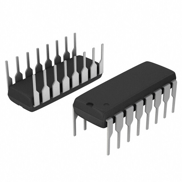
| 封装/外壳 | 16-SOIC(0.154",3.90mm 宽) |
| 封装/箱体 | SOP-16 |
| 工作温度 | -40°C ~ 85°C |
| 工作电源电压 | 34 V |
| 工作电源电流 | 2.5 mA |
| 工厂包装数量 | 48 |
| 开关频率 | 330 kHz |
| 拓扑结构 | Synchronous Buck |
| 描述/功能 | Synchronous buck switching regulator controller |
| 最大工作温度 | + 85 C |
| 最小工作温度 | - 40 C |
| 标准包装 | 48 |
| 电压-电源 | 4.5 V ~ 32 V |
| 类型 | Synchronous Buck Controller |
| 系列 | MIC2182 |
| 绝缘 | Non-Isolated |
| 输入电压 | 4.5 to 32 V |
| 输出数 | 1 |
| 输出电压 | 5 V |
| 输出电流 | 20 A |
| 输出端数量 | 5 Output |
| 输出类型 | Fixed |
| 降压 | 是 |
| 隔离式 | 无 |
| 频率-最大值 | 330kHz |


- 商务部:美国ITC正式对集成电路等产品启动337调查
- 曝三星4nm工艺存在良率问题 高通将骁龙8 Gen1或转产台积电
- 太阳诱电将投资9.5亿元在常州建新厂生产MLCC 预计2023年完工
- 英特尔发布欧洲新工厂建设计划 深化IDM 2.0 战略
- 台积电先进制程称霸业界 有大客户加持明年业绩稳了
- 达到5530亿美元!SIA预计今年全球半导体销售额将创下新高
- 英特尔拟将自动驾驶子公司Mobileye上市 估值或超500亿美元
- 三星加码芯片和SET,合并消费电子和移动部门,撤换高东真等 CEO
- 三星电子宣布重大人事变动 还合并消费电子和移动部门
- 海关总署:前11个月进口集成电路产品价值2.52万亿元 增长14.8%


PDF Datasheet 数据手册内容提取
MIC2182 Micrel MIC2182 High-Efficiency Synchronous Buck Controller General Description Features Micrel’s MIC2182 is a synchronous buck (step-down) switch- • 4.5V to 32V Input voltage range ing regulator controller. An all N-channel synchronous archi- • 1.25V to 6V Output voltage range tecture and powerful output drivers allow up to a 20A output • 95% efficiency current capabilty. The PWM and skip-mode control scheme • 300kHz oscillator frequency allows efficiency to exceed 95% over a wide range of load • Current sense blanking current, making it ideal for battery powered applications, as • 5Ω impedance MOSFET Drivers well as high current distributed power supplies. • Drives N-channel MOSFETs The MIC2182 operates from a 4.5V to 32V input and can • 600µA typical quiescent current (skip-mode) operate with a maximum duty cycle of 86% for use in low- • Logic controlled micropower shutdown (IQ < 0.1µA) dropout conditions. It also features a shutdown mode that • Current-mode control reduces quiescent current to 0.1µA. • Cycle-by-cycle current limiting • Built-in undervoltage protection The MIC2182 achieves high efficiency over a wide output • Adjustable undervoltage lockout current range by automatically switching between PWM and • Easily synchronizable skip mode. Skip-mode operation enables the converter to • Precision 1.245V reference output maintain high efficiency at light loads by turning off circuitry • 0.6% total regulation pertaining to PWM operation, reducing the no-load supply • 16-pin SOP and SSOP packages current from 1.6mA to 600µA. The operating mode is inter- • Frequency foldback overcurrent protection nally selected according to the output load conditions. Skip • Sustained short-circuit protection at any input voltage mode can be defeated by pulling the PWM pin low which • 20A output current capability reduces noise and RF interference. Applications The MIC2182 is available in a 16-pin SOP (small-outline package) and SSOP (shrink small-outline package) with an • DC power distribution systems operating range from –40°C to +85°C. • Notebook and subnotebook computers • PDAs and mobile communicators • Wireless modems • Battery-operated equipment Typical Application 4.5V VtoIN 30V* MIC2182-3.3BSM SD10D32BWS C221u1f 10VIN VDD11 35V R1070k C0.51µF BST14 C6 C41.697VµF x2 0.1µF 6 EN/UVLO HSD16 QSi24*884 10Lµ1H 0.R022Ω 3.V3VOU/4TA 2 PWM VSW15 C4 C7 1nF LSD13 Q1* D1 220uf Si4884 B140 10V ×2 1 SS PGND12 GND 3 COMP CSH 8 C13, 1nF C3 R1 5 SYNC VOUT 9 0.1µF 2k VREF 7 *30V maximum input voltage limit is due C2 to standard 30V MOSFET selection. 2.2nF SGND C1 GND 4 0.1µF 5SVe eto “ A3p.3pVlic/1a0tiAon a Inndfo ortmhearti ocnir”c useitsc.tion for 4.5V–30V* to 3.3V/4A Converter Micrel, Inc. • 1849 Fortune Drive • San Jose, CA 95131 • USA • tel + 1 (408) 944-0800 • fax + 1 (408) 474-1000 • http://www.micrel.com April 22, 2004 1 M9999-042204
MIC2182 Micrel Ordering Information Part Number Voltage Temperature Range Package Lead Finish MIC2182BM Adjustable –40°C to +85°C 16-pin narrow SOP Standard MIC2182-3.3BM 3.3V –40°C to +85°C 16-pin narrow SOP Standard MIC2182-5.0BM 5.0V –40°C to +85°C 16-pin narrow SOP Standard MIC2182BSM Adjustable –40°C to +85°C 16-pin narrow SSOP Standard MIC2182-3.3BSM 3.3V –40°C to +85°C 16-pin narrow SSOP Standard MIC2182-5.0BSM 5.0V –40°C to +85°C 16-pin narrow SSOP Standard MIC2182YM Adjustable –40°C to +85°C 16-pin narrow SOP Pb-Free MIC2182-3.3YM 3.3V –40°C to +85°C 16-pin narrow SOP Pb-Free MIC2182-5.0YM 5.0V –40°C to +85°C 16-pin narrow SOP Pb-Free MIC2182YSM Adjustable –40°C to +85°C 16-pin narrow SSOP Pb-Free MIC2182-3.3YSM 3.3V –40°C to +85°C 16-pin narrow SSOP Pb-Free MIC2182-5.0YSM 5.0V –40°C to +85°C 16-pin narrow SSOP Pb-Free Pin Configuration MIC2182 MIC2182-x.x SS 1 16 HSD SS 1 16 HSD PWM 2 15 VSW PWM 2 15 VSW COMP 3 14 BST COMP 3 14 BST SGND 4 13 LSD SGND 4 13 LSD SYNC 5 12 PGND SYNC 5 12 PGND EN/UVLO 6 11 VDD EN/UVLO 6 11 VDD FB 7 10 VIN VREF 7 10 VIN CSH 8 9 VOUT CSH 8 9 VOUT Adjustable Fixed 16-pin SOP (M) 16-pin SOP (M) 16-Pin SSOP (SM) 16-Pin SSOP (SM) M9999-042204 2 April 22, 2004
MIC2182 Micrel Pin Description Pin Number Pin Name Pin Function 1 SS Soft-Start (External Component): Connect external capacitor to ground to reduce inrush current by delaying and slowing the output voltage rise time. Rise time is controlled by an internal 5µA current source that charges an external capacitor to V . DD 2 PWM PWM/Skip-Mode Select (Input): Low sets PWM-mode operation. 1nF capacitor to ground sets automatic PWM/skip-mode selection. 3 COMP Compensation (Output): Internal error amplifier output. Connect to capacitor or series RC network to compensate the regulator control loop. 4 SGND Small Signal Ground (Return): Route separately from other ground traces to the (–) terminal of C . OUT 5 SYNC Frequency Synchronization (Input): Optional. Connect to external clock signal to synchronize the oscillator. Leading edge of signal above the threshold terminates the switching cycle. Connect to SGND if unused. 6 EN/UVLO Enable/Undervoltage Lockout (Input): Low-level signal powers down the controller. Input below the 2.5V threshold disables switching and functions as an accurate undervoltage lockout (UVLO). Input below the threshold forces complete micropower (< 0.1µA) shutdown. 7 (fixed) VREF Reference Voltage (Output): 1.245V output. Requires 0.1µf capacitor to ground. 7 (adj) FB Feedback (Input): Regulates FB pin to 1.245V. See “Application Information” for resistor divider calculations. 8 CSH Current-Sense High (Input): Current-limit comparator noninverting input. A built-in offset of 100mV between CSH and V pins in conjunction with the OUT current-sense resistor set the current-limit threshold level. This is also the positive input to the current sense amplifier. 9 VOUT Current-Sense Low (Input): Output voltage feedback input and inverting input for the current limit comparator and the current sense amplifier. 10 VIN [Battery] Unregulated Input (Input): +4.5V to +32V supply input. 11 VDD 5V Internal Linear-Regulator (Output): V is the external MOSFET gate DD drive supply voltage and an internal supply bus for the IC. Bypass to SGND with 4.7µF. V can supply up to 5mA for external loads. DD 12 PGND MOSFET Driver Power Ground (Return): Connects to source of synchro- nous MOSFET and the (–) terminal of C IN 13 LSD Low-Side Drive (Output): High-current driver output for external synchronous MOSFET. Voltage swing is between ground and V . DD 14 BST Boost (Input): Provides drive voltage for the high-side MOSFET driver. The drive voltage is higher than the input voltage by V minus a diode drop. DD 15 VSW Switch (Return): High-side MOSFET driver return. 16 HSD High-Side Drive (Output): High-current driver output for high-side MOSFET. This node voltage swing is between ground and V + 5V – V . IN diode drop April 22, 2004 3 M9999-042204
MIC2182 Micrel Absolute Maximum Ratings (Note 1) Operating Ratings (Note 2) Analog Supply Voltage (V ).......................................+34V Analog Supply Voltage (V )........................+4.5V to +32V IN IN Digital Supply Voltage (V ).........................................+7V Ambient Temperature (T ).........................–40°C to +85°C DD A Driver Supply Voltage (B )....................................V +7V Junction Temperature (T ).......................–40°C to +125°C ST IN J Sense Voltage (V , C ) ............................. 7V to –0.3V Package Thermal Resistance OUT SH Sync Pin Voltage (VSYNC)................................ 7V to –0.3V SSOSOP P(θ (JθA).).................................................................................................................115000°°CC//WW Enable Pin Voltage (V )......................................V JA EN/UVLO IN Power Dissipation (P ) D SOP................................................400mW @ T = 85°C A SSOP .............................................270mW @ T = 85°C A Ambient Storage Temperature (T ).........–65°C to +150°C S ESD, Note 3 Electrical Characteristics V = 15V; SS = open; V = 0V; V = 5V; I = 0.1A; T = 25°C, bold values indicate –40°C ≤ T ≤ +85°C; Note 4; unless IN PWM SHDN LOAD A A noted Parameter Condition Min Typ Max Units MIC2182 [Adjustable], (Note 5) Feedback Voltage Reference 1.233 1.245 1.257 V Feedback Voltage Reference 1.220 1.245 1.270 V Feedback Voltage Reference 4.5V < V < 32V, 0 < V – V < 75mV 1.208 1.245 1.282 V IN CSH OUT Feedback Bias Current 10 nA Output Voltage Range 1.25 6 V Output Voltage Line Regulation V = 4.5V to 32V, V – V = 50mV 0.03 %/V IN CSH OUT Output Voltage Load Regulation 25mV < (V – V ) < 75mV (PWM mode only) 0.5 % CSH OUT Output Voltage Total Regulation 0mV < (V – V ) < 75mV (full load range) 4.5V < V < 32V 0.6 % CSH OUT IN MIC2182-3.3 Output Voltage 3.267 3.3 3.333 V Output Voltage 3.234 3.3 3.366 V Output Voltage 4.5V < V < 32V, 0 < V – V < 75mV 3.201 3.3 3.399 V IN CSH OUT Output Voltage Line Regulation V = 4.5V to 32V, V – V = 50mV 0.03 %/V IN CSH OUT Output Voltage Load Regulation 25mV < (V – V ) < 75mV (PWM mode only) 0.5 % CSH OUT Output Voltage Total Regulation 0mV < (V – V ) < 75mV (full load range) 4.5V < V < 32V 0.8 % CSH OUT IN MIC2182-5.0 Output Voltage 4.95 5.0 5.05 V Output Voltage 4.90 5.0 5.10 V Output Voltage 6.5V < V < 32V, 0 < V – V < 75mV 4.85 5.0 5.150 V IN CSH OUT Output Voltage Line Regulation V = 6.5V to 32V, V – V = 50mV 0.03 %/V IN CSH OUT Output Voltage Load Regulation 25mV < (V – V ) < 75mV (PWM mode only) 0.5 % CSH OUT Output Voltage Total Regulation 0mV < (V – V ) < 75mV (full load range) 6.5V < V < 32V 0.8 % CSH OUT IN Input and VDD Supply PWM Mode V = 0V, excluding external MOSFET gate drive current 1.6 2.5 mA PWM Skip Mode I = 0mA, V floating (1nF capacitor to ground) 600 1500 µA L PWM Shutdown Quiescent Current V = 0V 0.1 5 µA EN/UVLO Digital Supply Voltage (V ) I = 0mA to 5mA 4.7 5.3 V DD L Undervoltage Lockout V upper threshold (turn on threshold) 4.2 V DD V lower threshold (turn off threshold) 4.1 V DD M9999-042204 4 April 22, 2004
MIC2182 Micrel Parameter Condition Min Typ Max Units Reference Output (Fixed Versions Only) Reference Voltage 1.220 1.245 1.270 V Reference Line Regulation 6V < V < 32V 1 mV IN Reference Load Regulation 0µA < I < 100µA 2 mV REF Enable/UVLO Enable Input Threshold 0.6 1.1 1.6 V UVLO Threshold 2.2 2.5 2.8 V Enable Input Current V = 5V 0.1 5 µA EN/UVLO Soft Start Soft-Start Current V = 0V –3.5 –5 –6.5 µA SS Current Limit Current-Limit Threshold Voltage V = V 75 100 135 mV CSH OUT Error Amplifier Error Sense Amplifier Gain 20 Current Amp Current Sense Amplifier Gain 2.0 Oscillator Section Oscillator Frequency 270 300 330 kHz Maximum Duty Cycle 86 % Minimum On-Time V = V + 200mV 140 250 ns OUT OUT(nominal) SYNC Threshold Level 0.7 1.3 1.9 V SYNC Input Current V = 5V 0.1 5 µA SYNC SYNC Minimum Pulse Width 200 ns SYNC Capture Range Note 6 330 kHz Frequency Foldback Threshold measured at VOUT pin 0.75 0.95 1.15 V Foldback Frequency 60 kHz Gate Drivers Rise/Fall Time C = 3000pF 60 ns L Output Driver Impedance source 5 8.5 Ω sink 3.5 6 Ω Driver Nonoverlap Time 80 ns PWM Input PWM Input Current V = 0V –10 µA PWM Note 1. Exceeding the absolute maximum rating may damage the device. Note 2. The device is not guaranteed to function outside its operating rating. Note 3. Devices are ESD sensitive. Handling precautions recommended. Human body model, 1.5k in series with 100pF. Note 4. 25°C limits are 100% production tested. Limits over the operating temperature range are guaranteed by design and are not production tested. Note 5. V > 1.3 × V (for the feedback voltage reference and output voltage line and total regulation). IN OUT Note 6. See applications information for limitations on the maximum operating frequency. April 22, 2004 5 M9999-042204
MIC2182 Micrel Typical Characteristics Quiescent Current Quiescent Current Quiescent Current vs. Temperature vs. Temperature vs. Supply Voltage 2.0 1.50 4.0 1.8 PWM 1.00 3.5 1.6 UVLO Mode A) 1.4 A)0.50 (mA) A) 3.0 ENT (m 11..02 ENT (m-00..52000 ENT (m 22..05 PWM CURR 00..68 Skip CURR00..1105 CURR 11..05 Skip 0.4 SHUTDOWN 0.2 0.05 (µA) 0.5 0 0 0 -40-20 0 20 40 60 80100120140 -40-20 0 20 40 60 80100120140 0 4 8 12 16 20 24 28 32 TEMPERATURE (°C) TEMPERATURE (°C) INPUT VOLTAGE (V) Quiescent Current V (Fixed Versions) V (Fixed Versions) REF REF vs. Supply Voltage Line Regulation Load Regulation 1.5 1.256 1.260 1.0 V) 1.254 V) A) 0.5 UVL(Om AM)ode GE ( 1.252 GE ( 1.250 µT ( 0 LTA 11..224580 LTA 1.240 N O O CURRE-0000....3455 SHU(TµDAO)WN ENCE V 111...222444246 ENCE V 11..222300 R R 0.2 FE 1.240 FE 1.210 0.1 RE 1.238 RE 0 1.236 1.200 0 4 8 12 16 20 24 28 32 0 4 8 12 16 20 24 28 32 0 200 400 600 800 1000 SUPPLY VOLTAGE (V) SUPPLY VOLTAGE (V) LOAD CURRENT (µA) V (Fixed Versions) V V REF DD DD vs. Temperature Line Regulation Load Regulation 1.260 5.0 5.00 V) V) REFERENCE VOLTAGE (V) 111...222455505 REGULATOR VOLTAGE (D 4444....2468 REGULATOR VOLTAGE (D444...899505 D D 1.240 V 4.0 V 4.80 -40-20 0 20 40 60 80100120140 0 4 8 12 16 20 24 28 32 0 5 10 15 20 25 TEMPERATURE (°C) SUPPLY VOLTAGE (V) LOAD CURRENT (mA) V Oscillator Frequency Oscillator Frequency DD vs. Temperature vs. Temperature vs. Supply Voltage 4.98 10 1.0 GE (V) 4.96 N (%) 68 N (%) 00..68 LTA 4.94 TIO 4 TIO 0.4 VO 4.92 RIA 2 RIA 0.2 OR 4.90 VA 0 VA 0 AT 4.88 CY -2 CY -0.2 GUL 4.86 UEN -4 UEN -0.4 E Q -6 Q -0.6 RD4.84 RE -8 RE -0.8 D F F V 4.82 -10 -1.0 -40-20 0 20 40 60 80100120140 -40-20 0 20 40 60 80100120140 0 4 8 12 16 20 24 28 32 TEMPERATURE (°C) TEMPERATURE (°C) SUPPLY VOLTAGE (V) M9999-042204 6 April 22, 2004
MIC2182 Micrel Soft-Start Current Overcurrent Threshold Current-Limit vs. Temperature vs. Temperature Foldback 5.0 V) 0.12 5 D ( 4.8 OL V)4 µCURRENT (A) 444...246 CURRENT THRESH 000...011901 OUTPUT VOLTAGE (123 RVCOVSUI NT= == 1 535m.V3ΩV R E 4.0-40-20 0 20 40 60 80100120140 OV 0.08-40-20 0 20 40 60 80100120140 00 1 2 3 4 5 6 7 8 TEMPERATURE (°C) TEMPERATURE (°C) OUTPUT CURRENT (A) April 22, 2004 7 M9999-042204
MIC2182 Micrel Block Diagrams V IN C IN EN/UVLO VDD VDD 6 Reference 11 4.7µF VIN VIN D2 10 SS1 VBG1.245V 1V4BST Control HSD C Logic 16 Q2 BST L1 R V PWM VSW CS OUT 2 15 LSD C D1 OUT 13 Q1 PGND Current 12 Limit PWM Mode to Skip Mode 0.024V Skip-Mode Current Limit 0.07V Low Comp –2%VBG UT Hysteresis UTP Comp O M W P Current Sense PWM Amp CSH 8 RESET CROAMRRPECTIVE VOUT VBG AV = 2 9 R1 SYNC Oscillator Error 5 Amp FB COMP 7 R2 C 3 SGND RCOCOMMPP 100k Gm = 0.2×10⁻³ 4 VOUT=1.245V1+RR21 MIC2182 [adj.] V =6.0V OUT(max) Figure 2a. Adjustable Output Voltage Version M9999-042204 8 April 22, 2004
MIC2182 Micrel V IN C IN EN/UVLO VDD VDD 6 Reference 11 4.7µF VIN VIN D2 10 SS1 VBG1.245V 1V4BST Control HSD C Logic 16 Q2 BST L1 R V PWM VSW CS OUT 2 15 LSD C D1 OUT 13 Q1 PGND Current 12 Limit PWM Mode to Skip Mode 0.024V Skip-Mode Current Limit 0.07V Low Comp –2%VBG UT Hysteresis UTP Comp O M W P Current Sense PWM Amp CSH 8 RESET CROAMRRPECTIVE VOUT VBG AV = 2 9 *82.5k for 3.3V Output SYNC Oscillator Error R1* 150k for 5V Output 5 Amp SGND COMP R2 4 C 3 50k VREF COMP 100k RCOMP Gm = 0.2×10⁻³ 7 MIC2182-x.x Figure 2b. Fixed Output Voltage Versions April 22, 2004 9 M9999-042204
MIC2182 Micrel Functional Description Control Loop PWM and Skip Modes of Operation See “Applications Information” following this section for com- ponent selection information and Figure14 and Tables 1 The MIC2182 operates in PWM (pulse-width-modulation) through 5 for predesigned circuits. mode at heavier output load conditions. At lighter load condi- tions, the controller can be configured to automatically switch The MIC2182 is a BiCMOS, switched-mode, synchronous to a pulse-skipping mode to improve efficiency. The potential step-down (buck) converter controller. Current-mode control disadvantage of skip mode is the variable switching fre- is used to achieve superior transient line and load regulation. quency that accompanies this mode of operation. The occur- An internal corrective ramp provides slope compensation for rence of switching pulses depends on component values as stable operation above a 50% duty cycle. The controller is well as line and load conditions. There is an external sync optimized for high-efficiency, high-performance dc-dc con- function that is disabled in skip mode. In PWM mode, the verter applications. synchronous buck converter forces continuous current to The MIC2182 block diagrams are shown in Figure 2a and flow in the inductor. In skip mode, current through the inductor Figure2b. can settle to zero, causing voltage ringing across the induc- The MIC2182 controller is divided into 6 functions. tor. Pulling the PWM pin (pin 2) low will force the controller to • Control loop operate in PWM mode for all load conditions, which will - PWM operation improve cross regulation of transformer-coupled, multiple - Skip-mode operation output configurations. • Current limit PWM Control Loop • Reference, enable, and UVLO The MIC2182 uses current-mode control to regulate the output voltage. This method senses the output voltage (outer • MOSFET gate drive loop) and the inductor current (inner loop). It uses inductor • Oscillator and sync current and output voltage to determine the duty cycle of the • Soft start buck converter. Sampling the inductor current removes the inductor from the control loop, which simplifies compensa- tion. V IN C IN VDD VDD Reference 11 4.7µF VIN VIN D2 10 PULSEC-OWNIDTTRHO LM LOODGUILCA ATONRD VBG1.245V 1V4BST HSD C BST 16 Q2 L1 R V VSW CS OUT 15 LSD C D1 OUT 13 Q1 PWM Mode to Skip PGND Mode 12 Q LOW 0.024V R S FORCES SKIP MODE Current Sense PWM Amp CSH COMPARATOR 8 VOUT RESET CORRECRTAIMVEP VBG AV = 2 9 R1 Oscillator Error Amp FB COMP 7 R2 CCOMP 3 100k V =1.245V1+R1 RCOMP Gm = 0.2×10⁻³ OUT R2 MIC2182 [adj.] PWM Mode Figure 3. PWM Operation M9999-042204 10 April 22, 2004
MIC2182 Micrel A block diagram of the MIC2182 PWM current-mode control Skip-Mode Control Loop loop is shown in Figure 3 and the PWM mode voltage and This control method is used to improve efficiency at light current waveforms are shown in figure 5A. The inductor output loads. At light output currents, the power drawn by the current is sensed by measuring the voltage across the MIC2182 is equal to the input voltage times the IC supply resistor, RCS. A ramp is added to the amplified current-sense current (IQ). At light output currents, the power dissipated by signal to provide slope compensation, which is required to the IC can be a significant portion of the total output power, prevent unstable operation at duty cycles greater than 50%. which lowers the efficiency of the power supply. The MIC2182 A transconductance amplifier is used for the error amplifier, draws less supply current in skip mode by disabling portions which compares an attenuated sample of the output voltage of the control and drive circuitry when the IC is not switching. with a reference voltage. The output of the error amplifier is The disadvantage of this method is greater output voltage the COMP (compensation) pin, which is compared to the ripple and variable switching frequency. current-sense waveform in the PWM block. When the current A block diagram of the MIC2182 skip mode is shown in Figure signal becomes greater than the error signal, the comparator 4. Skip mode voltage and current waveforms are shown in turns off the high-side drive. The COMP pin (pin 3) provides figure 5B. access to the output of the error amplifier and allows the use of external components to stabilize the voltage loop. V IN C IN VDD VDD Reference 11 4.7µF VIN VIN D2 10 CSKOINPT-MROODL EL OLOGGICI CAND VBG1.245V 1V4BST HSD C BST 16 Q2 L1 R V VSW CS OUT LOW-SIDE DRIVER ONE SHOT 15 LSD C OUT 13 Q1 PGND 12 Q R S Skip-Mode Current Limit 0.07V Low Comp ONE SHOT –2%VBG LOW FORCES PWM MODE G B Hysteresis V Comp ±1% Current Sense Amp CSH 8 VOUT A = 2 9 V R1 FB 7 MIC2182 [adj.] Skip Mode V =1.245V1+R1 R2 OUT R2 Figure 4. Skip-Mode Operation April 22, 2004 11 M9999-042204
MIC2182 Micrel V IN V SW 0V I I LOAD L1 0A V Reset DD Pulse 0V V + V IN DD V HSD 0V V DD V LSD 0V Figure 5a. PWM-Mode Timing V DD V HSD 0V V DD V LSD 0V V IN V V OUT SW 0V I LIM(skip) I L1 0A V DD V one-shot 0V V +1% V NOMINAL OUT –1% 0V I OUT 0A Figure 5b. Skip-Mode Timing A hysteretic comparator is used in place of the PWM error Figure 6 shows the improvement in efficiency that skip mode amplifier and a current-limit comparator senses the inductor makes when at lower output currents. current. A one-shot starts the switching cycle by momentarily 100 turning on the low side MOSFET to insure the high-side drive PWM boost capacitor, Cbst, is fully charged. The high-side MOS- 80 FET is turned on and current ramps up in the inductor, L1. %) Skip Y ( 60 The high-side drive is turned off when either the peak voltage C N on the input of the current-sense comparator exceeds the CIE 40 threshold, typically 35mV, or the output voltage rises above FFI E the hysteretic threshold of the output voltage comparator. 20 Once the high-side MOSFET is turned off, the load current 0 discharges the output capacitor, causing V to fall. The 0.01 0.1 1 10 100 OUT OUTPUT CURRENT (A) cycle repeats when V falls below the lower threshold, – OUT 1%. Figure 6. Efficiency The maximum peak inductor current depends on the skip- mode current-limit threshold and the value of the current- sense resistor, R . CS 35mV I = inductor(peak) R sense M9999-042204 12 April 22, 2004
MIC2182 Micrel Switching from PWM to Skip Mode rent-limit threshold is 100mV+35mV –25mV. The current- The current sense amplifier in Figure 3 monitors the average sense resistor must be sized using the minimum current-limit voltage across the current-sense resistor. The controller will threshold. The external components must be designed to switch from PWM to skip mode when the average voltage withstand the maximum current limit. The current-sense across the current-sense resistor drops below approximately resistor value is calculated by the equation below: 12mV. This is shown in Figure 7b. The average output current 75mV at this transition level for is calculated below. RCS =I OUT(max) 0.012 I = The maximum output current is: OUT(skipmode) R CS 135mV where: I = OUT(max) R CS 0.012 = threshold voltage of the internal comparator The current-sense pins CSH (pin 8) and V (pin 9) are R = current-sense resistor value OUT CS noise sensitive due to the low signal level and high input Switching from Skip to PWM Mode impedance. The PCB traces should be short and routed close The frequency of occurrence of the skip-mode current pulses to each other. A small (1nF to 0.1µF) capacitor across the pins increase as the output current increases until the hysteretic will attenuate high frequency switching noise. duty cycle reaches 100% (continuous pulses). Increasing the When the peak inductor current exceeds the current-limit current past this point will cause the output voltage will drop. threshold, the current-limit comparator, in Figure2, turns off The low limit comparator senses the output voltage when it the high-side MOSFET for the remainder of the cycle. The drops below 2% of the set output and automatically switches output voltage drops as additional load current is pulled from the converter to PWM mode. the converter. When the output voltage reaches approxi- The inductor current in skip mode is a triangular wave shape mately 0.95V, the circuit enters frequency-foldback mode a minimum value of 0 and a maximum value of 35mV/R and the oscillator frequency will drop to 60kHz while maintain- CS (see Figure 7b). The maximum average output current in skip ing the peak inductor current equal to the nominal 100mV mode is the average value of the inductor waveform: across the external current-sense resistor. This limits the maximum output power delivered to the load under a short 35mV I =0.5× circuit condition. OUT(maxskipmode) R CS Reference, Enable, and UVLO Circuits The capacitor on the PWM pin (pin 2) is discharged when the The output drivers are enabled when the following conditions IC transitions from skip to PWM mode. This forces the IC to are satisfied: remain in PWM mode for a fixed period of time. The added • The V voltage (pin 11) is greater than its delay prevents unwanted switching between PWM and skip DD undervoltage threshold (typically 4.2V). mode. The capacitor is charged with a 10uA current source on pin 2. The threshold on pin 2 is 2.5V. The delay for a typical • The voltage on the enable pin is greater than the 1nF capacitor is: enable UVLO threshold (typically 2.5V) The internal bias circuit generates a 1.245V bandgap refer- C ×V 1nF×2.5V t = PWM threshold = =250µs ence voltage for the voltage error amplifier and a 5V V delay I 10µA DD source voltage for the gate drive circuit. The reference voltage in the fixed-output-voltage versions of the MIC2182 is buffered and where: brought to pin 7. The V pin should be bypassed to GND C = capacitor connected to pin 2 REF PWM (pin 4) with a 0.1µF capacitor. The adjustable version of the Current Limit MIC2182 uses pin 7 for output voltage sensing. A decoupling The current-limit circuit operates during PWM mode. The capacitor on pin 7 is not used in the adjustable output voltage output current is detected by the voltage drop across the version. external current-sense resistor (R in Figure 2.). The cur- CS 35mV THRESHOLD Inductor ILIM(skip) ACROSS RCS. Current 0A Figure 7a. Maximum Skip-Mode-Load Inductor Current I MIN(PWM) 12mV THRESHOLD Inductor OF AVERAGE VOLTAGE Current ACROSS RCS. 0A Figure 7b. Minimum PWM-Mode-Load Inductor Current for PWM Operation April 22, 2004 13 M9999-042204
MIC2182 Micrel The enable pin (pin 6) has two threshold levels, allowing the Oscillator and Sync MIC2182 to shut down in a low current mode, or turn off output The internal oscillator is free running and requires no external switching in UVLO mode. An enable pin voltage lower than components. The nominal oscillator frequency is 300kHz. If the shutdown threshold turns off all the internal circuitry and the output voltage is below approximately 0.95V, the oscilla- reduces the input current to typically 0.1µA. tor operates in a frequency-foldback mode and the switching If the enable pin voltage is between the shutdown and UVLO frequency is reduced to 60kHz. thresholds, the internal bias, VDD, and reference voltages are The SYNC input (pin 5) allows the MIC2182 to synchronize turned on. The soft-start pin is forced low by an internal with an external clock signal. The rising edge of the sync discharge MOSFET. The output drivers are inhibited from signal generates a reset signal in the oscillator, which turns switching and remain in a low state. Raising the enable off the low-side gate drive output. The high-side drive then voltage above the UVLO threshold of 2.5V allows the soft- turns on, restarting the switching cycle. The sync signal is start capacitor to charge and enables the output drivers. inhibited when the controller operates in skip mode or during Either of two UVLO conditions will pull the soft-start capacitor frequency foldback. The sync signal frequency must be low. greater than the maximum specified free running frequency • When the V drops below 4.1V of the MIC2182. If the synchronizing frequency is lower, DD double pulsing of the gate drive outputs will occur. When not • When the enable pin drops below the 2.5V used, the sync pin must be connected to ground. threshold Figure 8 shows the timing between the external sync signal MOSFET Gate Drive (trace 2), the low-side drive (trace 1) and the high-side drive The MIC2182 high-side drive circuit is designed to switch an (trace R1). There is a delay of approximately 250ns between N-channel MOSFET. Referring to the block diagram in Figure the rising edge of the external sync signal and turnoff of the 2, a bootstrap circuit, consisting of D2 and CBST, supplies low-side MOSFET gate drive. energy to the high-side drive circuit. Capacitor C is BST Some concerns of operating at higher frequencies are: charged while the low-side MOSFET is on and the voltage on the VSW pin (pin 15) is approximately 0V. When the high-side • Higher power dissipation in the internal VDD MOSFET driver is turned on, energy from C is used to turn regulator. This occurs because the MOSFET BST the MOSFET on. As the MOSFET turns on, the voltage on the gates require charge to turn on the device. The V pin increases to approximately V . Diode D2 is re- average current required by the MOSFET gate SW IN versed biased and C floats high while continuing to keep increases with switching frequency. This in- BST the high-side MOSFET on. When the low-side switch is creases the power dissipated by the internal turned back on, CBST is recharged through D2. VDD regulator. Figure 10 shows the total gate charge which can be driven by the MIC2182 The drive voltage is derived from the internal 5V V bias DD over the input voltage range, for different values supply. The nominal low-side gate drive voltage is 5V and the of switching frequency. The total gate charge nominal high-side gate drive voltage is approximately 4.5V includes both the high- and low-side MOSFETs. due the voltage drop across D2. A fixed 80ns delay between The larger SOP package is capable of dissipat- the high- and low-side driver transitions is used to prevent ing more power than the SSOP package and current from simultaneously flowing unimpeded through both can drive larger MOSFETs with higher gate MOSFETs. drive requirements. E SIDVE HIGH-DRI VOUT E DE SIV W-RI OD L CAL NN YG SSI VSS TIME TIME Figure 8. Sync Waveforms Figure 9. Startup Waveforms M9999-042204 14 April 22, 2004
MIC2182 Micrel • Reduced maximum duty cycle due to switching The soft-start voltage is applied directly to the PWM compara- transition times and constant delay times in the tor. A 5uA internal current source is used to charge up the controller. As the switching frequency increased, soft-start capacitor. The capacitor is discharged when either the switching period decreases. The switching the enable voltage drops below the UVLO threshold (2.5V) or transition times and constant delays in the the V voltage drops below the UVLO level (4.1V). DD MIC2182 start to become noticeable. The effect The part switches at a minimum duty cycle when the soft-start is to reduce the maximum duty cycle of the pin voltage is less than 0.4V. This maintains a charge on the controller. This will cause the minimum input to bootstrap capacitor and insures high-side gate drive voltage. output differential voltage (dropout voltage) to As the soft-start voltage rises above 0.4V, the duty cycle increase. increases from the minimum duty cycle to the operating duty 100 cycle. The oscillator runs at the foldback frequency of 60kHz SOP until the output voltage rises above 0.95V. Above 0.95V, the C) 80 switching frequency increases to 300kHz (or the sync’d n E ( frequency), causing the output voltage to rise a greater rate. G 60 300kHz R The rise time of the output is dependent on the soft-start A H C 40 capacitor, output capacitance, output voltage, and load cur- E T 400kHz rent. The oscilloscope photo in Figure 9 show the output A G 20 500kHz voltage and the soft-start pin voltage at startup. 0 Minimum Pulse Width 0 4 8 12 16 20 24 28 32 SUPPLY VOLTAGE (V) The MIC2182 has a specified minimum pulse width. This minimum pulse width places a lower limit on the minimum Figure 10a. SOP Gate Charge vs. Input Voltage duty cycle of the buck converter. When the MIC2182 is 100 operating in forced PWM mode (pin 2 low) and when the SSOP output current is very low or zero, there is a limit on the ratio C) 80 of V /V . If this limit is exceeded, the output voltage will E (n rise OaUbToveIN the regulated voltage level. A minimum load is G 60 AR 300kHz required to prevent the output from rising up. This will not H C 40 occur for output voltages greater than 3V. E AT 400kHz Figure 11 should be used as a guide when the MIC2182 is G 20 500kHz forced into PWM-only mode. The actual maximum input 0 voltage will depend on the exact external components used 0 4 8 12 16 20 24 28 32 SUPPLY VOLTAGE (V) (MOSFETs, inductors, etc.). Figure 10b. SSOP Gate Charge vs. Input Voltage 35 It is recommended that the user limits the maximum synchro- V) 30 nized frequency to 600kHz. If a higher synchronized fre- E ( G quency is required, it may be possible and will be design A 25 T L dependent. Please consult Micrel applications for assis- O V 20 tance. T U P Soft Start IN 15 Soft start reduces the power supply input surge current at 10 0 1 2 3 4 5 6 startup by controlling the output voltage rise time. The input OUTPUT VOLTAGE (V) surge appears while the output capacitance is charged up. A Figure11. Max. Input Voltage in Forced-PWM Mode slower output rise time will draw a lower input surge current. Soft start may also be used for power supply sequencing. This restriction does not occur when the MIC2182 is set to automatic mode (pin 2 connected to a capacitor) since the converter operates in skip mode at low output current. April 22, 2004 15 M9999-042204
MIC2182 Micrel Applications Information output currents, the core losses can be a significant contribu- tor. Core loss information is usually available from the mag- The following applications information includes component netics vendor. selection and design guidelines. See Figure14 and Tables 1 Copper loss in the inductor is calculated by the equation through 5 for predesigned circuits. below: Inductor Selection Values for inductance, peak, and RMS currents are required P =I (rms)2×R inductorCu inductor winding to select the output inductor. The input and output voltages The resistance of the copper wire, R , increases with and the inductance value determine the peak to peak inductor winding temperature. The value of the winding resistance used should ripple current. Generally, higher inductance values are used be at the operating temperature. with higher input voltages. Larger peak to peak ripple currents will increase the power dissipation in the inductor and ( ) MOSFETs. Larger output ripple currents will also require R =R × 1+0.0042×(T −T ) winding(hot) winding(20°C) hot 20°C more output capacitance to smooth out the larger ripple current. Smaller peak to peak ripple currents require a larger where: inductance value and therefore a larger and more expensive T = temperature of the wire HOT inductor. A good compromise between size, loss and cost is under operating load to set the inductor ripple current to be equal to 20% of the T = ambient temperature 20°C maximum output current. R is room temperature winding resistance winding(20°C) The inductance value is calculated by the equation below. (usually specified by the manufacturer) V ×(V −V ) Current-Sense Resistor Selection L= OUT IN(max) OUT V ×f ×0.2×I Low inductance power resistors, such as metal film resistors IN(max) S OUT(max) should be used. Most resistor manufacturers make low where: inductance resistors with low temperature coefficients, de- f = switching frequency signed specifically for current-sense applications. Both resis- S tance and power dissipation must be calculated before the 0.2 = ratio of ac ripple current to dc output current resistor is selected. The value of R is chosen based on V = maximum input voltage SENSE IN(max) the maximum output current and the maximum threshold The peak-to-peak inductor current (ac ripple current) is: level. The power dissipated is based on the maximum peak output current at the minimum overcurrent threshold limit. V ×(V −V ) I = OUT IN(max) OUT PP VIN(max)×fS×L RSENSE =I 75mV OUT(max) The peak inductor current is equal to the average output current plus one half of the peak to peak inductor ripple The maximum overcurrent threshold is: current. 135mV I = I =I +0.5×I overcurrent(max) R PK OUT(max) PP CS The RMS inductor current is used to calculate the I2·R losses The maximum power dissipated in the sense resistor is: in the inductor. P =I 2×R D(R ) overcurrent(max) CS SENSE 2 1 I MOSFET Selection I (rms)=I × 1+ PP inductor OUT(max) 3I External N-channel logic-level power MOSFETs must be OUT(max) used for the high- and low-side switches. The MOSFET gate- Maximizing efficiency requires the proper selection of core to-source drive voltage of the MIC2182 is regulated by an material and minimizing the winding resistance. The high internal 5V V regulator. Logic-level MOSFETs, whose DD frequency operation of the MIC2182 requires the use of ferrite operation is specified at V = 4.5V must be used. GS materials for all but the most cost sensitive applications. It is important to note the on-resistance of a MOSFET Lower cost iron powder cores may be used but the increase increases with increasing temperature. A 75°C rise in junc- in core loss will reduce the efficiency of the power supply. This tion temperature will increase the channel resistance of the is especially noticeable at low output power. The winding MOSFET by 50% to 75% of the resistance specified at 25°C. resistance decreases efficiency at the higher output current This change in resistance must be accounted for when levels. The winding resistance must be minimized although calculating MOSFET power dissipation. this usually comes at the expense of a larger inductor. Total gate charge is the charge required to turn the MOSFET The power dissipated in the inductor is equal to the sum of the on and off under specified operating conditions (V and DS core and copper losses. At higher output loads, the core V ). The gate charge is supplied by the MIC2182 gate drive GS losses are usually insignificant and can be ignored. At lower circuit. At 300kHz switching frequency and above, the gate M9999-042204 16 April 22, 2004
MIC2182 Micrel charge can be a significant source of power dissipation in the C ×V +C ×V MIC2182. At low output load this power dissipation is notice- t = ISS GS OSS IN T I able as a reduction in efficiency. The average current re- G quired to drive the high-side MOSFET is: where: I =Q ×f C and C are measured at V = 0. G[high-side](avg) G S ISS OSS DS I = gate drive current (1A for the MIC2182) where: G The total high-side MOSFET switching loss is: I = G[high-side](avg) average high-side MOSFET gate current P =(V +V )×I ×t ×f AC IN D PK T S QG = total gate charge for the high-side MOSFET where: taken from manufacturer’s data sheet t = switching transition time with V = 5V. T GS (typically 20ns to 50ns) The low-side MOSFET is turned on and off at V = 0 DS V = freewheeling diode drop, typically 0.5V. because the freewheeling diode is conducting during this D f it the switching frequency, nominally 300kHz time. The switching losses for the low-side MOSFET is S usually negligable. Also, the gate drive current for the low- The low-side MOSFET switching losses are negligible and side MOSFET is more accurately calculated using C at can be ignored for these calculations. ISS VDS = 0 instead of gate charge. RMS Current and MOSFET Power Dissipation Calculation For the low-side MOSFET: Under normal operation, the high-side MOSFET’s RMS I =C ×V ×f current is greatest when VIN is low (maximum duty cycle). The G[low-side](avg) ISS GS S low-side MOSFET’s RMS current is greatest when V is high IN Since the current from the gate drive comes from the input (minimum duty cycle). However, the maximum stress the voltage, the power dissipated in the MIC2182 due to gate MOSFETs see occurs during short circuit conditions, where drive is: the output current is equal to I . (See the Sense overcurrent(max) ( ) Resistor section). The calculations below are for normal Pgatedrive =VIN IG[high-side](avg)+IG[low-side](avg) operation. To calculate the stress under short circuit condi- tions, substitute I for I . Use the formula A convenient figure of merit for switching MOSFETs is the on- overcurrent(max) OUT(max) below to calculate D under short circuit conditions. resistance times the total gate charge (R × Q ). Lower DS(on) G numbers translate into higher efficiency. Low gate-charge D =0.063−1.8×10⁻³×V shortcircuit IN logic-level MOSFETs are a good choice for use with the MIC2182. Power dissipation in the MIC2182 package limits The RMS value of the high-side switch current is: the maximum gate drive current. Refer to Figure10 for the MIC2182 gate drive limits. I 2 I (rms)= D×I 2 + PP Parameters that are important to MOSFET switch selection SW(highside) OUT(max) 12 are: • Voltage rating I (rms)= (1−D)I 2 +IPP2 • On-resistance SW(lowside) OUT(max) 12 • Total gate charge where: The voltage rating of the MOSFETs are essentially equal to the input voltage. A safety factor of 20% should be added to D = duty cycle of the converter the V of the MOSFETs to account for voltage spikes DS(max) V due to circuit parasitics. D= OUT η×V The power dissipated in the switching transistor is the sum of IN the conduction losses during the on-time (P ) and the η = efficiency of the converter. conduction switching losses that occur during the period of time when the Converter efficiency depends on component parameters, MOSFETs turn on and off (PAC). which have not yet been selected. For design purposes, an PSW =Pconduction+PAC efficiency of 90% can be used for VIN less than 10V and 85% can be used for V greater than 10V. The efficiency can be IN where: more accurately calculated once the design is complete. If the P =I (rms)2×R assumed efficiency is grossly inaccurate, a second iteration conduction SW SW through the design procedure can be made. PAC =PAC(off)+PAC(on) For the high-side switch, the maximum dc power dissipation is: R = on-resistance of the MOSFET switch. SW Making the assumption the turn-on and turnoff transition P =R ×I (rms)2 switch1(dc) DS(on)1 SW1 times are equal, the transition time can be approximated by: April 22, 2004 17 M9999-042204
MIC2182 Micrel For the low-side switch (N-channel MOSFET), the dc power circuit inductance will cause ringing during the high-side dissipation is: MOSFET turn-on. P =R ×I (rms)2 An external Schottky diode conducts at a lower forward switch2(dc) DS(on)2 SW2 voltage preventing the body diode in the MOSFET from Since the ac switching losses for the low side MOSFET is turning on. The lower forward voltage drop dissipates less near zero, the total power dissipation is: power than the body diode. The lack of a reverse recovery mechanism in a Schottky diode causes less ringing and less P =P low-side MOSFET(max) switch2(dc) power loss. Depending on the circuit components and oper- The total power dissipation for the high-side MOSFET is: ating conditions, an external Schottky diode will give a 1/2% to 1% improvement in efficiency. Figure 12 illustrates the P =P +P highsideMOSFET(max) SWITCH1(dc) AC difference in noise on the VSW pin with and without a External Schottky Diode Schottky diode. An external freewheeling diode is used to keep the inductor Output Capacitor Selection current flow continuous while both MOSFETs are turned off. The output capacitor values are usually determined by the This dead time prevents current from flowing unimpeded capacitors ESR (equivalent series resistance). Voltage rating through both MOSFETs and is typically 80ns The diode and RMS current capability are two other important factors in conducts twice during each switching cycle. Although the selecting the output capacitor. Recommended capacitors are average current through this diode is small, the diode must be tantalum, low-ESR aluminum electrolytics, and OS-CON. able to handle the peak current. The output capacitor’s ESR is usually the main cause of I =I ×2×80ns×f output ripple. The maximum value of ESR is calculated by: D(avg) OUT S ∆V The reverse voltage requirement of the diode is: R ≤ OUT ESR I V (rrm)=V PP diode IN where: The power dissipated by the Schottky diode is: V = peak to peak output voltage ripple P =I ×V OUT diode D(avg) F I = peak to peak inductor ripple current PP where: The total output ripple is a combination of the ESR and the V = forward voltage at the peak diode current output capacitance. The total ripple is calculated below: F The external Schottky diode, D2, is not necessary for circuit operation since the low-side MOSFET contains a parasitic ∆V = IPP×(1−D)2+(I ×R )2 body diode. The external diode will improve efficiency and OUT C ×f PP ESR OUT S decrease high frequency noise. If the MOSFET body diode is used, it must be rated to handle the peak and average current. where: The body diode has a relatively slow reverse recovery time D = duty cycle and a relatively high forward voltage drop. The power lost in C = output capacitance value the diode is proportional to the forward voltage drop of the OUT diode. As the high-side MOSFET starts to turn on, the body f = switching frequency S diode becomes a short circuit for the reverse recovery period, The voltage rating of capacitor should be twice the output dissipating additional power. The diode recovery and the voltage for a tantalum and 20% greater for an aluminum electrolytic or OS-CON. The output capacitor RMS current is calculated below: E D O DI I TG I (rms)= PP WITHOUHEELIN The poCwOeUrT dissipate1d2 in the output capacitor is: W E RE P =I (rms)2×R F DISS(C ) C ESR(C ) OUT OUT OUT E D O Input Capacitor Selection DI G The input capacitor should be selected for ripple current HN TLI rating and voltage rating. Tantalum input capacitors may fail WIEE H when subjected to high inrush currents, caused by turning the W E input supply on. Tantalum input capacitor voltage rating E R F should be at least 2 times the maximum input voltage to TIME maximize reliability. Aluminum electrolytic, OS-CON, and multilayer polymer film capacitors can handle the higher Figure12. Switch Output Noise inrush currents without voltage derating. With and Without Shottky Diode M9999-042204 18 April 22, 2004
MIC2182 Micrel The input voltage ripple will primarily depend on the input • Supply current to the MIC2182 capacitors ESR. The peak input current is equal to the peak • MOSFET gate-charge power (included in the IC inductor current, so: supply current) ∆V =I ×R • Core losses in the output inductor IN inductor(peak) ESR(C ) IN To maximize efficiency at light loads: The input capacitor must be rated for the input current ripple. The RMS value of input capacitor current is determined at the • Use a low gate-charge MOSFET or use the maximum output current. Assuming the peak to peak induc- smallest MOSFET, which is still adequate for tor ripple current is low: maximum output current. • Allow the MIC2182 to run in skip mode at lower I (rms)≈I × D×(1−D) C OUT(max) currents. IN The power dissipated in the input capacitor is: • Use a ferrite material for the inductor core, which has less core loss than an MPP or iron power PDISS(C ) =IC (rms)2×RESR(C ) core. IN IN IN Voltage Setting Components Under heavy output loads the significant contributors to power loss are (in approximate order of magnitude): The MIC2182-3.3 and MIC2182-5.0 ICs contain internal voltage dividers that set the output voltage. The MIC2182 • Resistive on-time losses in the MOSFETs adjustable version requires two resistors to set the output • Switching transition losses in the MOSFETs voltage as shown in Figure13. • Inductor resistive losses • Current-sense resistor losses R1 • Input capacitor resistive losses (due to the Error Amp FB capacitors ESR) 7 R2 To minimize power loss under heavy loads: • Use logic-level, low on-resistance MOSFETs. VREF Multiplying the gate charge by the on-resistance 1.245V gives a Figure of merit, providing a good bal- MIC2182 [adj.] ance between low and high load efficiency. Figure13. Voltage-Divider Configuration • Slow transition times and oscillations on the voltage and current waveforms dissipate more The output voltage is determined by the equation: power during turn-on and turnoff of the R1 MOSFETs. A clean layout will minimize parasitic V =V ×1+ O REF R2 inductance and capacitance in the gate drive and high current paths. This will allow the fastest Where: V for the MIC2182 is typically 1.245V. REF transition times and waveforms without oscilla- A typical value of R1 can be between 3k and 10k. If R1 is too tions. Low gate-charge MOSFETs will transition large it may allow noise to be introduced into the voltage faster than those with higher gate-charge feedback loop. If R1 is too small in value it will decrease the requirements. efficiency of the power supply, especially at low output loads. • For the same size inductor, a lower value will Once R1 is selected, R2 can be calculated using: have fewer turns and therefore, lower winding resistance. However, using too small of a value V ×R1 R2= REF will require more output capacitors to filter the V −V O REF output ripple, which will force a smaller band- width, slower transient response and possible Voltage Divider Power Dissipation instability under certain conditions. The reference voltage and R2 set the current through the voltage divider. • Lowering the current-sense resistor value will decrease the power dissipated in the resistor. V I = REF However, it will also increase the overcurrent divider R2 limit and will require larger MOSFETs and The power dissipated by the divider resistors is: inductor components. • Use low-ESR input capacitors to minimize the P =(R1+R2)×I 2 divider divider power dissipated in the capacitors ESR. Efficiency Calculation and Considerations Decoupling Capacitor Selection Efficiency is the ratio of output power to input power. The The 4.7µF decoupling capacitor is used to minimize noise on difference is dissipated as heat in the buck converter. Under the VDD pin. The placement of this capacitor is critical to the light output load, the significant contributors are: proper operation of the IC. It must be placed right next to the April 22, 2004 19 M9999-042204
MIC2182 Micrel pins and routed with a wide trace. The capacitor should be a • When the high-side MOSFET is switched on, the good quality tantalum. An additional 1µF ceramic capacitor critical flow of current is from the input capacitor may be necessary when driving large MOSFETs with high through the MOSFET, inductor, sense resistor, gate capacitance. Incorrect placement of the V decoupling output capacitor, and back to the input capacitor. DD capacitor will cause jitter or oscillations in the switching These paths must be made with short, wide waveform and large variations in the overcurrent limit. pieces of trace. It is good practice to locate the A 0.1µF ceramic capacitor is required to decouple the VIN. ground terminals of the input and output capaci- The capacitor should be placed near the IC and connected tors close to each. directly to between pin 10 (Vcc) and pin 12 (PGND). • When the low-side MOSFET is switched on, PCB Layout and Checklist current flows through the inductor, sense resistor, output capacitor, and MOSFET. The PCB layout is critical to achieve reliable, stable and efficient source of the low-side MOSFET should be performance. A ground plane is required to control EMI and located close to the output capacitor. minimize the inductance in power, signal and return paths. • The freewheeling diode, D1 in Figure 2, con- The following guidelines should be followed to insure proper ducts current during the dead time, when both operation of the circuit. MOSFETs are off. The anode of the diode • Signal and power grounds should be kept should be located close to the output capacitor separate and connected at only one location. ground terminal and the cathode should be Large currents or high di/dt signals that occur located close to the input side of the inductor. when the MOSFETs turn on and off must be • The 4.7µF capacitor, which connects to the VDD kept away from the small signal connections. terminal (pin 11) must be located right at the IC. • The connection between the current-sense The VDD terminal is very noise sensitive and resistor and the MIC2182 current-sense inputs placement of this capacitor is very critical. (pin 8 and 9) should have separate traces, Connections must be made with wide trace. The routed from the terminals directly to the IC pins. capacitor may be located on the bottom layer of The traces should be routed as closely as the board and connected to the IC with multiple possible to each other and their length should be vias. minimized. Avoid running the traces under the • The V bypass capacitor should be located inductor and other switching components. A 1nF IN close to the IC and connected between pins 10 to 0.1µF capacitor placed between pins 8 and 9 and 12. Connections should be made with a will help attenuate switching noise on the current ground and power plane or with short, wide sense traces. This capacitor should be placed trace. close to pins 8 and 9. M9999-042204 20 April 22, 2004
MIC2182 Micrel Predesigned Circuits Power supplies larger than 10A can also be constructed A single schematic diagram, shown in Figure14, can be used using the MIC2182 using larger power-handling compo- to build power supplies ranging from 3A to 10A at the common nents. output voltages of 1.8V, 2.5V, 3.3V, and 5V. Components that The “Power Supply Operating Characteristics” graphs follow- vary, depending upon output current and voltage, are listed ing the component and vendor tables provide useful informa- in the accompanying Tables 3 through 6. tion about the actual performance of some of these circuits. VIN VINMIC2182VDD SD10D32BWS C(ta1b1le) C9 R1070k C0.51µF BST C6 41.67VµF EN/UVLO HSD 0.1µF Q2 L1 R2 (table) (table) (table) V OUT PWM VSW C4 Q1 D1 C7 C12 1nF LSD (table) (table) (table) 0.1µF 50V SS PGND GND COMP CSH C13, 1nF C3 R1 SYNC VOUT 0.1µF 2k VREF C2 C1 2.2nF SGND 0.1µF GND 50V Figure14. Basic Circuit Diagram for Use with Tables 3 through 6 Specification Limit Switchingfrequencyripple 1%ofoutputvoltage Maximumambienttemperature 85°C Short-circuitcapability Continuous Switchingfrequency 300kHz Table 1. Specifications for Figure14 and Tables 3 through 6 Manufacturer Telephone Number (USA) Web Address AVX (803) 946-0690 www.avxcorp.com Central Semiconductor (516) 435-1110 www.centralsemi.com Coiltronics (561) 241-7876 www.coiltronics.com IRC (704) 264-8861 IR (310) 322-3331 www.irf.com Micrel (408) 944-0800 www.micrel.com Vishay/Lite On (805) 446-4800 www.vishay-liteon.com (diodes) Vishay/Siliconix (800) 554-5665 www.siliconix.com (MOSFETs) Vishay/Dale (800) 487-9437 www.vishaytechno.com (inductors and resistors) Sumida (847) 956-0666 www.japanlink.com/sumida Table 2. Component Suppliers April 22, 2004 21 M9999-042204
MIC2182 Micrel 3A (6.5V–30V) 4A (6.5V–30V) 5A (6.5V–30V) 10A (6.5V–10V) Reference Part No. / Description Part No. / Description Part No. / Description Part No. / Description C7 qty: 2 qty: 2 qty: 2 qty: 2 TPSE227M010R0100 TPSE227M010R0100 TPSV227M010R0060 TPSV337M010R0060 AVX, 220µF 10V, AVX, 220µF 10V, AVX, 220µF 10V, AVX, 330µF 10V, 0.1Ω ESR, 0.1Ω ESR, 0.06Ω ESR, 0.06Ω ESR, output filter capacitor output filter capacitor output filter capacitor output filter capacitor C11 qty: 2 qty: 3 qty: 4 qty: 4 TPSE226M035R0300 TPSE226M035R0300 TPSE226M035R0300 TPSV107M020R0085 AVX, 22µF 35V, AVX, 22µF 35V, AVX, 22µF 35V, AVX, 100µF 20V, 0.3Ω ESR, 0.3Ω ESR, 0.3Ω ESR, 0.06Ω ESR, input filter capacitor input filter capacitor input filter capacitor input filter capacitor D1 qty: 1 B140, Vishay, qty: 1 B140, Vishay, qty: 1 B140, Vishay, qty: 1 B330, Vishay, freewheeling diode freewheeling diode freewheeling diode freewheeling diode L1 qty: 1 CDRH125-100, qty: 1 CDRH127-100, qty: 1 CDRH127-100 qty: 1 UP4B-3R3, Sumida Inductor, Sumida Inductor, Sumida, Coiltronics, 10µH 4A, 10µH 5A, 10µH 5A, 3.3µH 11A, output inductor output inductor output inductor output inductor Q1 qty: 1 Si4800, Siliconix, qty: 1 Si4800, Siliconix, qty: 1 Si4884, Siliconix, qty: 2 Si4884, Siliconix low-side MOSFET low-side MOSFET low-side MOSFET low-side MOSFET Q2 qty: 1 Si4800, Siliconix, qty: 1 Si4800, Siliconix, qty: 1 Si4884, Siliconix, qty: 2 Si4884, Siliconix, high-side MOSFET high-side MOSFET high-side MOSFET high-side MOSFET R2 qty: 1 qty: 1 qty: 1 qty: 2 WSL-2010 .025 1%, WSL-2010 .020 1%, WSL-2512 .015 1%, WSL-2512 .015 1% , Vishay, 0.025, 1%, 0.5W, Vishay, 0.02, 1%, 0.5W, Vishay, 0.015, 1%, 1W, Vishay, 0.015, 1%, 1W, current sense resistor current sense resistor current sense resistor current sense resistor U1 MIC2182-5.0BSM or MIC2182-5.0BSM or MIC2182-5.0BSM or MIC2182-5.0BM MIC2182-5.0BM MIC2182-5.0BM MIC2182-5.0BM Table 3. Components for 5V Output 3A (4.5V–30V) 4A (4.5V–30V) 5A (4.5V–30V) 10A (4.5V–5.5V) Reference Part No. / Description Part No. / Description Part No. / Description Part No. / Description C7 qty: 2 qty: 2 qty: 2 qty: 2 TPSE227M010R0100 TPSE227M010R0100 TPSV227M010R0060 TPSV477M006R0055 AVX, 220µF 10V, AVX, 220µF 10V, AVX, 220µF 10V, AVX, 470µF 6.3V, 0.1Ω ESR, 0.1Ω ESR, 0.06Ω ESR, 0.055Ω ESR, output filter capacitor output filter capacitor output filter capacitor output filter capacitor C11 qty: 2 qty: 2 qty: 3 qty: 3 TPSE226M035R0300 TPSE226M035R0300 TPSE226M035R0300 TPSV227M016R0075 AVX, 22µF 35V, AVX, 22µF 35V, AVX, 22µF 35V, AVX, 220µF 16V, 0.3Ω ESR, 0.3Ω ESR, 0.3Ω ESR, 0.075Ω ESR, input filter capacitor input filter capacitor input filter capacitor filter capacitor D1 qty: 1 B140, Vishay, qty: 1 B140, Vishay, qty: 1 B140, Vishay, qty: 1 B330, Vishay, freewheeling diode freewheeling diode freewheeling diode freewheeling diode L1 qty: 1 CDRH125-100, qty: 1 CDRH127-100, qty: 1 CDRH127-100 qty: 1 UP4B-3R3, Sumida Inductor, Sumida Inductor, Sumida, Coiltronics, 10µH 4A, 10µH 5A, 10µH 5A, 3.3µH 11A, output inductor output inductor output inductor output inductor Q1 qty: 1 Si4800, Siliconix, qty: 1 Si4800, Siliconix, qty: 1 Si4800, Siliconix, qty: 2 Si4884, Siliconix, low-side MOSFET low-side MOSFET low-side MOSFET low-side MOSFET Q2 qty: 1 Si4800, Siliconix, qty: 1 Si4800, Siliconix, qty: 1 Si4884, Siliconix, qty: 2 Si4884, Siliconix, high-side MOSFET high-side MOSFET high-side MOSFET high-side MOSFET R2 qty: 1 qty: 1 qty: 1 qty: 2 WSL-2010 .025 1%, WSL-2010 .020 1%, WSL-2512 .015 1%, WSL-2512 .015 1% , Vishay, 0.025, 1%, 0.5W, Vishay, 0.02, 1%, 0.5W, Vishay, 0.015, 1%, 1W, Vishay, 0.015, 1%, 1W, current sense resistor current sense resistor current sense resistor current sense resistor U1 MIC2182-3.3BSM or MIC2182-3.3BM or MIC2182-3.3BM or MIC2182-3.3BM MIC2182-3.3BM MIC2182-3.3BSM MIC2182-3.3BSM Table 4. Components for 3.3V Output M9999-042204 22 April 22, 2004
MIC2182 Micrel 3A (4.5V–30V) 4A (4.5V–30V) 5A (4.5V–30V) 10A (4.5V–5.5V) Reference Part No. / Description Part No. / Description Part No. / Description Part No. / Description C7 qty: 2 qty: 2 qty: 2 qty: 2 TPSE227M010R0100 TPSE227M010R0100 TPSV227M010R0060 TPSV447M006R0055 AVX, 220µF 10V, AVX, 220µF 10V, AVX, 220µF 10V, AVX, 470µF 6.3V, 0.1Ω ESR, 0.1Ω ESR, 0.06Ω ESR, 0.06Ω ESR, output filter capacitor output filter capacitor output filter capacitor output filter capacitor C11 qty: 2 qty: 2 qty: 2 qty: 3 TPSE226M035R0300 TPSE226M035R0300 TPSE226M035R0300 TPSV227M016R0075 AVX, 22µF 35V, AVX, 22µF 35V, AVX, 22µF 35V, AVX, 220µF 16V, 0.3Ω ESR, 0.3Ω ESR, 0.3Ω ESR, 0.06Ω ESR, input filter capacitor input filter capacitor input filter capacitor input filter capacitor D1 qty: 1 B140, Vishay, qty: 1 B140, Vishay, qty: 1 B140, Vishay, qty: 1 B330, Vishay, freewheeling diode freewheeling diode freewheeling diode freewheeling diode L1 qty: 1 CDRH125-100, qty: 1 CDRH127-100, qty: 1 CDRH127-100 qty: 1 UP4B-3R3, Sumida Inductor, Sumida Inductor, Sumida, Coiltronics, 10µH 4A, 10µH 5A, 10µH 5A, 3.3µH 11A, output inductor output inductor output inductor output inductor Q1 qty: 1 Si4800, Siliconix, qty: 1 Si4884, Siliconix, qty: 1 Si4884, Siliconix, qty: 2 Si4884, Siliconix low-side MOSFET low-side MOSFET low-side MOSFET low-side MOSFET Q2 qty: 1 Si4800, Siliconix, qty: 1 Si4800, Siliconix, qty: 1 Si4800, Siliconix, qty: 2 Si4884, Siliconix, high-side MOSFET high-side MOSFET high-side MOSFET high-side MOSFET R2 qty: 1 qty: 1 qty: 1 qty: 1 WSL-2010 .025 1%, WSL-2010 .020 1%, WSL-2512 .015 1%, WSL-2512 .015 1% , Vishay, 0.025, 1%, 0.5W, Vishay, 0.02, 1%, 0.5W, Vishay, 0.015, 1%, 1W, Vishay, 0.015, 1%, 1W, current sense resistor current sense resistor current sense resistor current sense resistor U1 MIC2182BSM or MIC2182BSM or MIC2182BSM or MIC2182BM MIC2182BM MIC2182BM MIC2182BM Table 5. Components for 2.5V Output 3A (4.5V–30V) 4A (4.5V–30V) 5A (4.5V–8V) 10A (4.5V–5.5V) Reference Part No. / Description Part No. / Description Part No. / Description Part No. / Description C7 qty: 2 qty: 2 qty: 2 qty: 2 TPSE227M010R0100 TPSE227M010R0100 TPSV227M010R0060 TPSV447M006R0055 AVX, 220µF 10V, AVX, 220µF 10V, AVX, 220µF 10V, AVX, 470µF 6.3V, 0.1Ω ESR, 0.1Ω ESR, 0.06Ω ESR, 0.06Ω ESR, output filter capacitor output filter capacitor output filter capacitor output filter capacitor C11 qty: 2 qty: 2 qty: 2 qty: 2 TPSE226M035R0300 TPSE226M035R0300 TPSE226M035R0300 TPSV227M016R0075 AVX, 22µF 35V, AVX, 22µF 35V, AVX, 22µF 35V, AVX, 220µF 16V, 0.3Ω ESR, 0.3Ω ESR, 0.3Ω ESR, 0.06Ω ESR, input filter capacitor input filter capacitor input filter capacitor input filter capacitor D1 qty: 1 B140, Vishay, qty: 1 B140, Vishay, qty: 1 B140, Vishay, qty: 1 B330, Vishay, freewheeling diode freewheeling diode freewheeling diode freewheeling diode L1 qty: 1 CDRH125-100, qty: 1 CDRH127-100, qty: 1 CDRH127-100 qty: 1 UP4B-3R3, Sumida Inductor, Sumida Inductor, Sumida, Coiltronics, 10µH 4A, 10µH 5A, 10µH 5A, 3.3µH 11A, output inductor output inductor output inductor output inductor Q1 qty: 1 Si4800, Siliconix, qty: 1 Si4884, Siliconix, qty: 1 Si4884, Siliconix, qty: 2 Si4884, Siliconix low-side MOSFET low-side MOSFET low-side MOSFET low-side MOSFET Q2 qty: 1 Si4800, Siliconix, qty: 1 Si4800, Siliconix, qty: 1 Si4800, Siliconix, qty: 2 Si4884, Siliconix, high-side MOSFET high-side MOSFET high-side MOSFET high-side MOSFET R2 qty: 1 qty: 1 qty: 1 qty: 2 WSL-2010 .025 1%, WSL-2010 .020 1%, WSL-2512 .015 1%, WSL-2512 .015 1% , Vishay, 0.025, 1%, 0.5W, Vishay, 0.02, 1%, 0.5W, Vishay, 0.015, 1%, 1W, Vishay, 0.015, 1%, 1W, current sense resistor current sense resistor current sense resistor current sense resistor U1 MIC2182BSM or MIC2182BSM or MIC2182BSM or MIC2182BM MIC2182BM MIC2182BM MIC2182BM Table 6. Components for 1.8V Output April 22, 2004 23 M9999-042204
MIC2182 Micrel Power Supply Operating Characteristics Effect of Soft-Start Capacitor (CSS) Value Effect of Soft-Start Capacitor (CSS) Value On Output Voltage Waveforms On Output Voltage Waveforms During Turn-On During Turn-On (10A Power Supply Configuration) (4A Power Supply Configuration) Normal (300kHz Switching Frequency) and Output Short-Circuit (60kHz) Conditions Switch Node (Pin 15) Waveforms Converter Waveforms VSWPIN 15 SWVITOCLTHA-NGOEDE VL1IN == 37.V3µH V = 3.3V OUT VSW+HSDPIN 16 REFERDERHNIVICGEEH VD-OS TLIODTA EGGREOUND IOUT = 10A VGSHIGH-SIDEMOSFET GATEH-ITGOH--SSOIDUER MCEO SVFOELTTAGE QSHMiITO4GY8SH:8 F-24SE ITDSE VGSLOW-SIDEMOSFET GATEL-OTWO--SSOIDUER MCOES VFOELTTAGE QSLMOiTO4WY8S:8- F2S4EIDTSE v) IL1A/di INDUCTOR CURRENT 10Amps 2 ( Typical Skip-Mode Waveforms Typical PWM-Mode Waveforms UT VO OUT V VSWPin 15 VSWPin 15 v) di IL15A/div) IL1(0.5A/ 0. ( M9999-042204 24 April 22, 2004
MIC2182 Micrel Load Transient Response Load Transient Response and Bode Plot and Bode Plot (4A Power Supply Configuration) (10A Power Supply Configuration) OUT UT V O V VLV1ION U ==T 1=10 23µV.H3V VVL1ION U ==T 3=6. V33µ.3HV R2 = 20mΩ R2 = 7.5mΩ IOUT2A/div IOUT5A/div Bode Plot 5V Efficiency Bode Plot (4A Power Supply Configuration) (4A Power Supply Configuration) (10A Power Supply Configuration) 100 210 100 100 210 80 180 Skip PWM 80 180 80 60 GAIN 150 %) 60 GAIN 150 GAIN (dB) 24000 PHASE 6910020°PHASE () EFFICIENCY ( 4600 VRL1I2N = == 1 1505VµmHΩ GAIN (dB) 24000 6910020°PHASE () -20 30 20 1 high-side MOSFET: Si4800 -20 PHASE 30 1 low-side MOSFET: Si4800 -40 0 0 -40 0 00 00 30 30 3030 0.01 0.1 1 4 00 00 30 30 3030 x1 x1 x1 x1 x1 x1 OUTPUT CURRENT (A) x1 x1 x1 x1 x1 x1 0 0 1 0 0 0 0 0 1 0 0 0 1 0 1 0 0 1 0 1 0 0 1 1 3 1 1 3 FREQUENCY (Hz) FREQUENCY (Hz) 12V Efficiency 24V Efficiency Efficiency (4A Power Supply Configuration) (4A Power Supply Configuration) (10A Power Supply Configuration) 100 100 100 Skip PWM 80 Skip 80 80 %) %) Skip PWM %) Y ( 60 Y ( 60 Y ( 60 PWM C C C N N N E E E EFFICI 40 VRL1I2N = == 1 11052µmVHΩ EFFICI 40 VRL1I2N = == 1 12054µmVHΩ EFFICI 40 RL12 == 37..35µmHΩ 20 20 20 1 high-side MOSFET: Si4800 1 high-side MOSFET: Si4800 2 high-side MOSFETs: Si4884 1 low-side MOSFET: Si4800 1 low-side MOSFET: Si4800 2 low-side MOSFETs: Si4884 0 0 0 0.01 0.1 1 4 0.01 0.1 1 4 0.01 0.1 1 10 OUTPUT CURRENT (A) OUTPUT CURRENT (A) OUTPUT CURRENT (A) April 22, 2004 25 M9999-042204
MIC2182 Micrel Package Information PIN 1 0.157 (3.99) DIMENSIONS: 0.150 (3.81) INCHES (MM) 0.020 (0.51) REF 0.050 (1.27) 0.020 (0.51) BSC 0.013 (0.33) 0.0098 (0.249) 45° 0.0040 (0.102) 0°–8° 0.394 (10.00) 0.050 (1.27) 0.0648 (1.646) 0.386 (9.80) SEATING 0.016 (0.40) 0.0434 (1.102) PLANE 0.244 (6.20) 0.228 (5.79) 16-pin SOP (M) 5.40 (0.213) DIMENSIONS: 5.20 (0.205) MM (INCH) 7.90 (0.311) 7.65 (0.301) 0.875 (0.034) REF 6.33 (0.239) 2.00 (0.079) 6.07 (0.249) 1.73 (0.068) 10° 4° 0.22 (0.009) 0.13 (0.005) 0.38 (0.015) 1.25 (0.049) REF 0.25 (0.010) 0.21 (0.008) 0° 0.05 (0.002) –8° 0.95 (0.037) 0.65 (0.0260) COPLANARITY: 0.55 (0.022) BSC 0.10 (0.004) MAX 16-Pin SSOP (SM) M9999-042204 26 April 22, 2004
MIC2182 Micrel April 22, 2004 27 M9999-042204
MIC2182 Micrel MICREL, INC. 1849 FORTUNE DRIVE SAN JOSE, CA 95131 USA TEL + 1 (408) 944-0800 FAX + 1 (408) 474-1000 WEB http://www.micrel.com The information furnished by Micrel in this data sheet is believed to be accurate and reliable. However, no responsibility is assumed by Micrel for its use. Micrel reserves the right to change circuitry and specifications at any time without notification to the customer. Micrel Products are not designed or authorized for use as components in life support appliances, devices or systems where malfunction of a product can reasonably be expected to result in personal injury. Life support devices or systems are devices or systems that (a) are intended for surgical implant into the body or (b) support or sustain life, and whose failure to perform can be reasonably expected to result in a significant injury to the user. A Purchaser’s use or sale of Micrel Products for use in life support appliances, devices or systems is at Purchaser’s own risk and Purchaser agrees to fully indemnify Micrel for any damages resulting from such use or sale. © 2004 Micrel, Incorporated. M9999-042204 28 April 22, 2004
Mouser Electronics Authorized Distributor Click to View Pricing, Inventory, Delivery & Lifecycle Information: M icrochip: MIC2182-5.0YSM MIC2182-5.0BSM TR MIC2182-3.3YM TR MIC2182-5.0BSM MIC2182YSM MIC2182BSM MIC2182-5.0YM MIC2182-3.3BSM MIC2182-5.0YSM TR MIC2182YM MIC2182-5.0YM TR MIC2182-3.3YM MIC2182-3.3BSM TR MIC2182-3.3YSM MIC2182YSM TR MIC2182-5.0YSM-TR MIC2182-3.3YM-TR MIC2182- 3.3BSM-TR MIC2182-5.0YM-TR MIC2182YM-TR MIC2182YSM-TR MIC2182-3.3YSM-TR MIC2182BSM-TR MIC2182-5.0BSM-TR