ICGOO在线商城 > 集成电路(IC) > PMIC - 电池充电器 > MCP73871-2CCI/ML

 Datasheet下载
- 型号: MCP73871-2CCI/ML
- 制造商: Microchip
- 库位|库存: xxxx|xxxx
- 要求:
| 数量阶梯 | 香港交货 | 国内含税 |
| +xxxx | $xxxx | ¥xxxx |
查看当月历史价格
查看今年历史价格
MCP73871-2CCI/ML产品简介:
ICGOO电子元器件商城为您提供MCP73871-2CCI/ML由Microchip设计生产,在icgoo商城现货销售,并且可以通过原厂、代理商等渠道进行代购。 MCP73871-2CCI/ML价格参考。MicrochipMCP73871-2CCI/ML封装/规格:PMIC - 电池充电器, Charger IC Lithium-Ion/Polymer 20-QFN (4x4)。您可以下载MCP73871-2CCI/ML参考资料、Datasheet数据手册功能说明书,资料中有MCP73871-2CCI/ML 详细功能的应用电路图电压和使用方法及教程。
Microchip Technology的MCP73871-2CCI/ML是一款PMIC(电源管理集成电路),专门用于电池充电管理。这款器件主要用于便携式设备中,如智能手机、平板电脑、可穿戴设备和其他需要高效电池充电管理的应用。

 主要应用场景:

1. 便携式消费电子产品:
   - 智能手机和平板电脑:这些设备通常需要高效的电池充电解决方案,以确保快速充电和延长电池寿命。MCP73871-2CCI/ML可以提供精确的充电控制,支持多种电池类型,如锂离子(Li-ion)和锂聚合物(Li-Po)电池。
   - 可穿戴设备:如智能手表、健身追踪器等小型设备,对电池管理和空间要求非常严格。该芯片的小封装和低功耗特性使其非常适合这些应用。

2. 物联网(IoT)设备:
   - 传感器节点和无线模块:这些设备通常依赖电池供电,且需要长时间运行。MCP73871-2CCI/ML可以确保电池在低功耗模式下高效充电,同时提供过充保护,延长设备的工作时间。
   - 智能家居设备:如智能门锁、安防摄像头等,这些设备需要可靠的电池管理来保证持续工作。该芯片的高集成度和多功能性使其成为理想选择。

3. 医疗设备:
   - 便携式医疗设备:如血糖仪、脉搏血氧仪等,这些设备需要稳定的电源管理和安全的充电机制。MCP73871-2CCI/ML提供了多种保护功能,包括过压、过流和过温保护,确保设备的安全性和可靠性。

4. 工业应用:
   - 手持式测试仪器:如万用表、示波器等,这些设备需要在户外或远离电源的情况下工作。高效的电池充电管理可以确保设备在长时间使用中的稳定性。
   - 便携式数据采集设备:如条码扫描器、RFID读写器等,这些设备通常需要快速充电和长续航能力,MCP73871-2CCI/ML能够满足这些需求。

 特点:
- 高精度充电控制:支持恒流/恒压(CC/CV)充电模式,确保电池安全快速充电。
- 多重保护功能:包括热关断、短路保护、过压保护等,提高系统安全性。
- 小尺寸封装:适合紧凑型设计,节省PCB空间。
- 灵活配置:通过外部电阻设置充电电流和电压,适应不同电池需求。

总之,MCP73871-2CCI/ML凭借其高效、可靠和灵活的特性,广泛应用于各种便携式设备中,为用户提供优质的电池充电体验。
| 参数 | 数值 |
| 产品目录 | 集成电路 (IC)半导体 |
| 描述 | IC USB/AC BATT CHRGR W/PPM 20QFN电池管理 USB/AC Battery Charger |
| 产品分类 | |
| 品牌 | Microchip Technology |
| 产品手册 | |
| 产品图片 |
|
| rohs | 符合RoHS无铅 / 符合限制有害物质指令(RoHS)规范要求 |
| 产品系列 | 电源管理 IC,电池管理,Microchip Technology MCP73871-2CCI/ML- |
| 数据手册 | 点击此处下载产品Datasheethttp://www.microchip.com/mymicrochip/filehandler.aspx?ddocname=en536709 |
| 产品型号 | MCP73871-2CCI/ML |
| PCN组件/产地 | http://www.microchip.com/mymicrochip/NotificationDetails.aspx?id=5710&print=viewhttp://www.microchip.com/mymicrochip/NotificationDetails.aspx?id=5720&print=viewhttp://www.microchip.com/mymicrochip/NotificationDetails.aspx?id=5759&print=viewhttp://www.microchip.com/mymicrochip/NotificationDetails.aspx?id=5863&print=view |
| PCN设计/规格 | http://www.microchip.com/mymicrochip/NotificationDetails.aspx?id=5573&print=view |
| 产品目录页面 | |
| 产品种类 | 电池管理 |
| 产品类型 | Charge Management |
| 供应商器件封装 | 20-QFN-EP (4x4) |
| 其它名称 | MCP738712CCIML |
| 功能 | 充电管理 |
| 包装 | 管件 |
| 参考设计库 | http://www.digikey.com/rdl/4294959902/4294959891/812 |
| 商标 | Microchip Technology |
| 安装类型 | 表面贴装 |
| 安装风格 | SMD/SMT |
| 封装 | Tube |
| 封装/外壳 | 20-VFQFN 裸露焊盘 |
| 封装/箱体 | QFN |
| 工作温度 | -40°C ~ 85°C |
| 工作电源电压 | 4.5 V to 6 V |
| 工厂包装数量 | 91 |
| 最大工作温度 | + 85 C |
| 最小工作温度 | - 40 C |
| 标准包装 | 91 |
| 电压-电源 | 4.4 V ~ 6 V |
| 电池化学 | 锂离子,锂聚合物 |
| 电池类型 | Li-Ion, Li-Poly |
| 输出电压 | 4.2 V |
| 输出电流 | 50 mA to 1000 mA |
| 配用 | /product-detail/zh/MCP73871DM-VPCC/MCP73871DM-VPCC-ND/2125386/product-detail/zh/MCP73871EV/MCP73871EV-ND/1999515 |


- 商务部:美国ITC正式对集成电路等产品启动337调查
- 曝三星4nm工艺存在良率问题 高通将骁龙8 Gen1或转产台积电
- 太阳诱电将投资9.5亿元在常州建新厂生产MLCC 预计2023年完工
- 英特尔发布欧洲新工厂建设计划 深化IDM 2.0 战略
- 台积电先进制程称霸业界 有大客户加持明年业绩稳了
- 达到5530亿美元!SIA预计今年全球半导体销售额将创下新高
- 英特尔拟将自动驾驶子公司Mobileye上市 估值或超500亿美元
- 三星加码芯片和SET,合并消费电子和移动部门,撤换高东真等 CEO
- 三星电子宣布重大人事变动 还合并消费电子和移动部门
- 海关总署:前11个月进口集成电路产品价值2.52万亿元 增长14.8%


PDF Datasheet 数据手册内容提取
MCP73871 Stand-Alone System Load Sharing and Li-Ion / Li-Polymer Battery Charge Management Controller Features Applications • Integrated System Load Sharing and Battery • GPSs / Navigators Charge Management • PDAs and Smart Phones - Simultaneously Power the System and • Portable Media Players and MP3 Players Charge the Li-Ion Battery • Digital Cameras - Voltage Proportional Current Control (VPCC) • Bluetooth Headsets ensures system load has priority over Li-Ion • Portable Medical Devices battery charge current • Charge Cradles / Docking Stations - Low-Loss Power-Path Management with Ideal Diode Operation • Toys • Complete Linear Charge Management Controller Description - Integrated Pass Transistors - Integrated Current Sense The MCP73871 device is a fully integrated linear - Integrated Reverse Discharge Protection solution for system load sharing and Li-Ion / Li-Polymer battery charge management with ac-dc wall adapter - Selectable Input Power Sources: USB Port or and USB port power sources selection. It’s also AC-DC Wall Adapter capable of autonomous power source selection • Preset High Accuracy Charge Voltage Options: between input or battery. Along with its small physical - 4.10V, 4.20V, 4.35V or 4.40V size, the low number of required external components - ±0.5% Regulation Tolerance makes the device ideally suited for portable • Constant Current / Constant Voltage (CC/CV) applications. Operation with Thermal Regulation The MCP73871 device automatically obtains power for • Maximum 1.8A Total Input Current Control the system load from a single-cell Li-Ion battery or an • Resistor Programmable Fast Charge Current input power source (ac-dc wall adapter or USB port). Control: 50mA to 1A The MCP73871 device specifically adheres to the current drawn limits governed by the USB specification. • Resistor Programmable Termination Set Point With an ac-dc wall adapter providing power to the • Selectable USB Input Current Control system, an external resistor sets the magnitude of 1A - Absolute Maximum: 100mA (L) / 500mA (H) maximum charge current while supports up to 1.8A • Automatic Recharge total current for system load and battery charge • Automatic End-of-Charge Control current. • Safety Timer With Timer Enable/Disable Control The MCP73871 device employs a constant current / • 0.1C Preconditioning for Deeply Depleted Cells constant voltage (CC/CV) charge algorithm with select- • Battery Cell Temperature Monitor able charge termination point. The constant voltage regulation is fixed with four available options: 4.10V, • Undervoltage Lockout (UVLO) 4.20V, 4.35V, or 4.40V to accommodate new, emerging • Low Battery Status Indicator (LBO) battery charging requirements. The MCP73871 device • Power-Good Status Indicator (PG) also limits the charge current based on die temperature • Charge Status and Fault Condition Indicators during high power or high ambient conditions. This • Numerous Selectable Options Available for a thermal regulation optimizes the charge cycle time Variety of Applications: while maintaining device reliability. - Refer to Section1.0 “Electrical The MCP73871 device includes a low battery indicator, Characteristics” for Selectable Options” a power-good indicator and two charge status indica- - Refer to the “Product Identification tors that allows for outputs with LEDs or communica- System” for Standard Options tion with host microcontrollers. The MCP73871 device • Temperature Range: -40°C to 85°C is fully specified over the ambient temperature range of -40°C to +85°C. • Packaging: 20-Lead QFN (4mm x 4mm) © 2008 Microchip Technology Inc. DS22090A-page 1
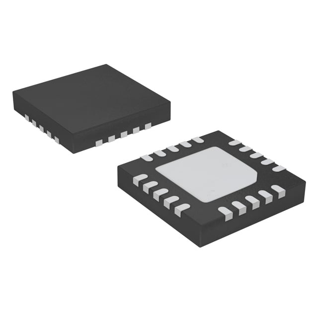
MCP73871 Package Types MCP73871 20-Lead QFN E S N E S _ T T A OU N N CE VB I I 20 19 18 17 16 OUT 1 15 V BAT VPCC 2 EXPOSED 14 VBAT PAD SEL 3 13 PROG1 V SS PROG2 4 12 PROG3 THERM 5 11 V SS 6 7 8 9 10 G 2 O E S P AT B T VS T L S 1 / T A T S Typical Application Circuit MCP73871 Typical Application Ac-dc Adapter or USB Port 18, 19 1, 20 System IN OUT Load 10µF 4.7µF 2 VPCC 14, 15, 16 V 470Ω BAT 6 PG 4.7µF NTC 470Ω THERM 5 7 STAT2 470Ω 10kΩ 8 STAT1 Single-Cell LBO PROG1 13 RPROG1 Li-Ion Battery 3 Hi SEL Low 4 12 RPROG3 Hi PROG2 PROG3 Low 9 TE Hi Low 17 V 10, 11, EP SS Hi CE Low DS22090A-page 2 © 2008 Microchip Technology Inc.
MCP73871 Functional Block Diagram Direction Control IN 0.2Ω OUT G=0.001 CURRENT LIMIT 0.2Ω Ideal + Diode, - VREF Synchronous Switch Direction Control VBAT PROG1 G=0.001 PROG3 G=0.001 G=0.001 CURRENT LIMIT + VREF /2 - VREF + VPCC - SEL CA PROG2 + - VREF PRECONDITION VBAT_SENSE + - VREF CHRG - VREF + VA + - VREF PG TERM - VREF UVLO, STAT1 REFERENCE, + CHARGE CONTROL, HTVT TIMER, STAT2 AND + VREF 50µA STATUS TE LOGIC - LTVT THERM + CE - VSS © 2008 Microchip Technology Inc. DS22090A-page 3
MCP73871 1.0 ELECTRICAL † Notice: Stresses above those listed under “Maximum Ratings” may cause permanent damage to the device. This is CHARACTERISTICS a stress rating only and functional operation of the device at those or any other conditions above those indicated in the Absolute Maximum Ratings† operational listings of this specification is not implied. Exposure to maximum rating conditions for extended periods VIN....................................................................................7.0V may affect device reliability. All Inputs and Outputs w.r.t.................V -0.3V to V +0.3V SS DD (V = V or V ) DD IN BAT Maximum Junction Temperature, T ............Internally Limited J Storage temperature.....................................-65°C to +150°C ESD protection on all pins Human Body Model (1.5kΩ in Series with 100pF)........≥ 4kV Machine Model (200pF, No Series Resistance).............300V DC CHARACTERISTICS Electrical Specifications: Unless otherwise indicated, all limits apply for V = V + 0.3V to 6V, T = -40°C to +85°C. IN REG A Typical values are at +25°C, V = [V (typical) + 1.0V] IN REG Parameters Sym Min Typ Max Units Conditions Supply Input Supply Voltage V V — 6 V IN REG +0.3V Supply Current I — 2500 3750 µA Charging SS — 260 350 µA Charge Complete — 180 300 µA Standby — 28 50 µA Shutdown (V < V - 100mV or DD BAT V < V ) DD STOP UVLO Start Threshold V V + V + V + V V = Low to High START REG REG REG DD 0.05V 0.15V 0.25V UVLO Stop Threshold V V – V + V + V V = High to Low STOP REG REG REG DD 0.07V 0.07V 0.17V UVLO Hysteresis V — 90 — mV HYS Voltage Regulation (Constant Voltage Mode) Regulated Charge Voltage V 4.080 4.10 4.121 V V =[V (typical)+1V] REG DD REG 4.179 4.20 4.221 V I =10mA OUT 4.328 4.35 4.372 V T =-5°C to +55°C A 4.378 4.40 4.422 Regulated Charge Voltage Tolerance V -0.5 — +0.5 % T = +25°C RTOL A -0.75 — +0.75 % T = -5°C to +55°C A Line Regulation |(ΔV /V )/ — 0.08 0.20 %/V V =[V (typical)+1V] to 6V BAT BAT DD REG ΔV | I =10mA DD OUT Load Regulation |ΔV /V | — 0.08 0.18 % I =10mA to 150mA BAT BAT OUT V = [V (typical)+1V] DD REG Supply Ripple Attenuation PSRR — -47 — dB I =10mA, 1kHz OUT — -40 — dB I =10mA, 10kHz OUT Current Regulation (Fast Charge Constant-Current Mode) AC-Adapter Fast Charge Current I 90 100 110 mA PROG1 = 10kΩ REG 900 1000 1100 mA PROG1 = 1kΩ, T =-5°C to +55°C, SEL = Hi A USB Fast Charge Current I 80 90 100 mA PROG2 = Low, SEL = Low, REG (Note2) 400 450 500 mA PROG2 = High, SEL = Low, (Note2) T = -5°C to +55°C A Note 1: The value is ensured by design and not production tested. 2: The maximum available charge current is also limited by the value set at PROG1 input. DS22090A-page 4 © 2008 Microchip Technology Inc.
MCP73871 DC CHARACTERISTICS (CONTINUED) Electrical Specifications: Unless otherwise indicated, all limits apply for V = V + 0.3V to 6V, T = -40°C to +85°C. IN REG A Typical values are at +25°C, V = [V (typical) + 1.0V] IN REG Parameters Sym Min Typ Max Units Conditions Input Current Limit Control (ICLC) USB-Port Supply Current Limit I 80 90 100 mA PROG2 = Low, SEL = Low LIMIT_USB 400 450 500 mA PROG2 = High, SEL = Low T =-5°C to +55°C A AC-DC Adapter Current Limit I 1500 1650 1800 mA SEL = High, T =-5°C to +55°C LIMIT_AC A Voltage Proportional Charge Control (VPCC - Input Voltage Regulation) VPCC Input Threshold V — 1.23 — V I =10mA VPCC OUT VPCC Input Threshold Tolerance V -3 — +3 % T =-5°C to +55°C RTOL A Input Leakage Current I — 0.01 1 µA V = V LK VPCC DD Precondition Current Regulation (Trickle Charge Constant-Current Mode) Precondition Current Ratio I / I 7.5 10 12.5 % PROG1 = 1.0kΩ to 10kΩ PREG REG T =-5°C to +55°C A Precondition Current Threshold Ratio V / V 69 72 75 % V Low to High PTH REG BAT Precondition Hysteresis V — 105 — mV V High to Low PHYS BAT Automatic Charge Termination Set Point Charge Termination Current Ratio I 75 100 125 mA PROG3 = 10kΩ TERM 7.5 10 12.5 mA PROG3 = 100kΩ T =-5°C to +55°C A Automatic Recharge Recharge Voltage Threshold Ratio V V - V - V - V V High to Low RTH REG REG REG BAT 0.21V 0.15V 0.09V IN-to-OUT Pass Transistor ON-Resistance ON-Resistance R — 200 — mΩ V = 4.5V, T = 105°C DS_ON DD J Charge Transistor ON-Resistance ON-Resistance R — 200 — mΩ V = 4.5V, T = 105°C DSON_ DD J Ideal Diode ON-Resistance ON-Resistance R — 200 — mΩ V = 4.5V, T = 105°C DS_ON DD J Diode Forward Voltage Drop V — 0.7 1 V Switch Off (Note1) FWD Battery Discharge Current Output Reverse Leakage Current I — 30 40 µA Shutdown DISCHARGE (V < V < V ) BAT DD UVLO — 30 40 µA Shutdown (0 < V < V ) DD BAT — 30 40 µA V = Power Out, No Load BAT — -6 -13 µA Charge Complete Status Indicators - STAT1 ( LBO), STAT2, PG Sink Current I — 16 35 mA SINK Low Output Voltage V — 0.4 1 V I = 4mA OL SINK Input Leakage Current I — 0.01 1 µA High Impedance, V on pin LK DD Low Battery Indicator (LBO) Low Battery Detection Threshold V — Disable — V > V , PG = Hi-Z LBO BAT IN 2.85 3.0 3.15 V T =-5°C to +55°C A 2.95 3.1 3.25 V 3.05 3.2 3.35 V Low Battery Detection Hysteresis V — 150 — mV V Low to High LBO_HYS BAT Note 1: The value is ensured by design and not production tested. 2: The maximum available charge current is also limited by the value set at PROG1 input. © 2008 Microchip Technology Inc. DS22090A-page 5
MCP73871 DC CHARACTERISTICS (CONTINUED) Electrical Specifications: Unless otherwise indicated, all limits apply for V = V + 0.3V to 6V, T = -40°C to +85°C. IN REG A Typical values are at +25°C, V = [V (typical) + 1.0V] IN REG Parameters Sym Min Typ Max Units Conditions PROG1 Input (PROG1) Charge Impedance Range R 1 — 20 kΩ PROG PROG3 Input (PROG3) Termination Impedance Range R 5 — 100 kΩ PROG PROG2 Input (PROG2) Input High Voltage Level V 1.8 — — V IH Input Low Voltage Level V — — 0.8 V IL Input Leakage Current I — 0.01 1 µA V = V LK PROG2 DD Timer Enable (TE) Input High Voltage Level V 1.8 — — V Note1 IH Input Low Voltage Level V — — 0.8 V Note1 IL Input Leakage Current I — 0.01 1 µA V = V LK TE DD Chip Enable (CE) Input High Voltage Level V 1.8 — — V IH Input Low Voltage Level V — — 0.8 V IL Input Leakage Current I — 0.01 1 µA V = V LK CE DD Input Source Selection (SEL) Input High Voltage Level V 1.8 — — V IH Input Low Voltage Level V — — 0.8 V IL Input Leakage Current I — 0.01 1 µA V = V LK SEL DD Thermistor Bias Thermistor Current Source I 47 50 53 µA 2kΩ < R < 50 kΩ THERM THERM Thermistor Comparator Upper Trip Threshold V 1.20 1.24 1.26 V V Low to High T1 T1 Upper Trip Point Hysteresis V — -40 — mV T1HYS Lower Trip Threshold V 0.23 0.25 0.27 V V High to Low T2 T2 Lower Trip Point Hysteresis V — 40 — mV T2HYS Thermal Shutdown Die Temperature T — 150 — °C SD Die Temperature Hysteresis T — 10 — °C SDHYS Note 1: The value is ensured by design and not production tested. 2: The maximum available charge current is also limited by the value set at PROG1 input. DS22090A-page 6 © 2008 Microchip Technology Inc.
MCP73871 AC CHARACTERISTICS Electrical Specifications: Unless otherwise indicated, all limits apply for V = 4.6V to 6V. IN Typical values are at +25°C, V = [V (typical) + 1.0V] DD REG Parameters Sym Min Typ Max Units Conditions UVLO Start Delay t — — 5 ms V Low to High START DD Current Regulation Transition Time Out of Precondition t — — 10 ms V < V to V > V DELAY BAT PTH BAT PTH Current Rise Time Out of Precondition t — — 10 ms I Rising to 90% of I RISE OUT REG Precondition Comparator Filter Time t 0.4 1.3 3.2 ms Average V Rise/Fall PRECON BAT Termination Comparator Filter Time t 0.4 1.3 3.2 ms Average I Falling TERM OUT Charge Comparator Filter Time t 0.4 1.3 3.2 ms Average V Falling CHARGE BAT Thermistor Comparator Filter Time t 0.4 1.3 3.2 ms Average THERM Rise/Fall THERM Elapsed Timer Elapsed Timer Period t — 0 — Hours ELAPSED 3.6 4.0 4.4 Hours 5.4 6.0 6.6 Hours 7.2 8.0 8.8 Hours Status Indicators Status Output Turn-off t — — 500 µs I = 1mA to 0mA OFF SINK Status Output Turn-on t — — 500 µs I = 0mA to 1mA ON SINK Note 1: Internal safety timer is tested base on internal oscillator frequency measurement. TEMPERATURE SPECIFICATIONS Electrical Specifications: Unless otherwise indicated, all limits apply for V = 4.6V to 6V. IN Typical values are at +25°C, V = [V (typical) + 1.0V] DD REG Parameters Sym Min Typ Max Units Conditions Temperature Ranges Specified Temperature Range T -40 — +85 °C A Operating Temperature Range T -40 — +125 °C J Storage Temperature Range T -65 — +150 °C A Thermal Package Resistances Thermal Resistance, 20LD-QFN, 4x4 θ — 35 — °C/W 4-Layer JC51-7 Standard Board, JA Natural Convection © 2008 Microchip Technology Inc. DS22090A-page 7
MCP73871 2.0 TYPICAL PERFORMANCE CURVES Note: The graphs and tables provided following this note are a statistical summary based on a limited number of samples and are provided for informational purposes only. The performance characteristics listed herein are not tested or guaranteed. In some graphs or tables, the data presented may be outside the specified operating range (e.g., outside specified power supply range) and therefore outside the warranted range. Note: Unless otherwise indicated, V = [V (typical) + 1V], I = 10mA and T = +25°C, Constant-voltage mode. IN REG OUT A 4.240 V) 4.232 Temperature = +25°C age 44..238000 Temperature = +25°C Regulation Voltage ( 44444.....122229001220864 IIIIOOOOUUUUTTTT==== 15910000000 m mmmAAAA ery Regulation Volt(V) 4444444.......111222246802460000000 VDD= 5.2V Battery 44..117864 Batt 44..1102000 00 00 00 00 00 00 00 00 00 00 4.6 4.9 5.1 5.4 5.6 5.9 1 2 3 4 5 6 7 8 9 0 1 Supply Voltage (V) Charge Current (mA) FIGURE 2-1: Battery Regulation Voltage FIGURE 2-4: Charge Current (I ) vs. OUT (V ) vs. Supply Voltage (V ). Battery Regulation Voltage (V ). BAT DD BAT 40.0 V)4.238 nt VBAT = 4.2V egulation Voltage (4444....222201236420 IIIOOOUUUTTT === 151000000 0mm mAAA y Discharge Curre(µA)22330505....0000 VDD= Floating Battery R44..119908 IOUT = 10 mA Batter 1105..00 -45 -30 -15 0 15 30 45 60 75 90 -45 -30 -15 0 15 30 45 60 75 90 Ambient Temperature (°C) Temperature (°C) FIGURE 2-2: Battery Regulation Voltage FIGURE 2-5: Output Leakage Current (V ) vs. Ambient Temperature (T ). (I ) vs. Ambient Temperature (T ). BAT A DISCHARGE A 1000 35.0 900 VDD= 5.2V nt VDD= VBAT Temperature = +25°C e 30.0 Temperature = +25°C 800 urr 700 C 25.0 I (mA)REG 345600000000 y Discharge (µA)112050...000 200 er 100 att 5.0 B 0 0.0 1 2 3 4 5 6 7 8 91011121314151617181920 3.0 3.2 3.4 3.6 3.8 4.0 4.2 RPROG (kΩ) Battery Voltage (V) FIGURE 2-3: Charge Current (I ) vs. FIGURE 2-6: Output Leakage Current OUT Programming Resistor (R ). (I ) vs. Battery Regulation Voltage PROG DISCHARGE (V ). BAT DS22090A-page 8 © 2008 Microchip Technology Inc.
MCP73871 Note: Unless otherwise indicated, V = [V (typical) + 1V], I = 10mA and T = +25°C, Constant-voltage mode. IN REG OUT A 35.0 110 ent 30.0 VTeDDm=p Felroaattuirneg = +25°C 108 RTePRmOpG e=r a1t0u rkeΩ = +25°C Curr 25.0 110046 y Discharge (µA) 112050...000 I (mA)REG1100990268 er 94 att 5.0 92 B 0.0 90 3.0 3.2 3.4 3.6 3.8 4.0 4.2 4.5 4.8 5.0 5.3 5.5 5.8 6.0 Battery Voltage (V) Supply Voltage (V) FIGURE 2-7: Output Leakage Current FIGURE 2-10: Charge Current (I ) vs. OUT (I ) vs. Battery Voltage (V ). Supply Voltage (V ). DISCHARGE BAT DD 1190 1100 1160 RPROG = 1 kΩ 1060 1130 Temperature = +25°C A)1020 1100 m (mA)G111000914780000 Current ( 999048000 IRE 899925000 harge 788826000 860 C RPROG= 1 kΩ 830 740 VDD= 5.2V 800 700 4.5 4.8 5.0 5.3 5.5 5.8 6.0 -45 -30 -15 0 15 30 45 60 75 90 Supply Voltage (V) Ambient Temperature (°C) FIGURE 2-8: Charge Current (I ) vs. FIGURE 2-11: Charge Current (I ) vs. OUT OUT Supply Voltage (V ). Ambient Temperature (T ). DD A 550 110 540 RPROG = 2 kΩ 108 530 Temperature = +25°C A)106 m A) 551200 ent (110024 (mREG459000 e Curr10908 I 480 arg 96 470 h 94 460 C 92 RPROVGD D= =1 05 .k2ΩV 450 90 4.5 4.8 5.0 5.3 5.5 5.8 6.0 -45 -30 -15 0 15 30 45 60 75 90 Supply Voltage (V) Ambient Temperature (°C) FIGURE 2-9: Charge Current (I ) vs. FIGURE 2-12: Charge Current (I ) vs. OUT OUT Supply Voltage (V ). Ambient Temperature (T ). DD A © 2008 Microchip Technology Inc. DS22090A-page 9
MCP73871 Note: Unless otherwise indicated, V = [V (typical) + 1V], I = 10mA and T = +25°C, Constant-voltage mode. IN REG OUT A 120 55 A)53 RVDPDR O=G 5=. 22V0 kΩ A)100 m m Charge Current (4444535791 Charge Current ( 24680000 VDD = 5.2V RPROG = 10 kΩ 41 0 -45 -30 -15 0 15 30 45 60 75 90 25 50 75 100 125 150 Ambient Temperature (°C) Ambient Temperature (°C) FIGURE 2-13: Charge Current (I ) vs. FIGURE 2-16: Charge Current (I ) vs. OUT OUT Ambient Temperature (T ). Junction Temperature (T ). A J 1200 52.0 Temperature = +25°C A) 1000 µA)5511..05 arge Current (m 468000000 mistor Current (4445589900.....50505 Ch 200 VDD = 5.2V her48.0 RPROG = 1 kΩ T47.5 0 47.0 25 50 75 100 125 150 4.6 4.8 5.0 5.2 5.4 5.6 5.8 6.0 Ambient Temperature (°C) Supply Voltage (V) FIGURE 2-14: Charge Current (I ) vs. FIGURE 2-17: Thermistor Current (I ) OUT THERM Junction Temperature (T ). vs. Supply Voltage (V ). J DD 600 52.0 A)500 µA) 5511..05 VDD = 5.2V arge Current (m234000000 mistor Current ( 4445589900.....50505 Ch100 VRDPDR O=G 5=. 22V kΩ Ther 4478..50 0 47.0 25 50 75 100 125 150 -45 -30 -15 0 15 30 45 60 75 90 Ambient Temperature (°C) Ambient Temperature (°C) FIGURE 2-15: Charge Current (I ) vs. FIGURE 2-18: Thermistor Current (I ) OUT THERM Junction Temperature (T ). vs. Ambient Temperature (T ). J A DS22090A-page 10 © 2008 Microchip Technology Inc.
MCP73871 Note: Unless otherwise indicated, V = [V (typical) + 1V], I = 10mA and T = +25°C, Constant-voltage mode. IN REG OUT A 0 1.8 0.2 PSRR (dB) -----5432100000 IOUT = 10 mA Output Current (A) 0000111.......12468246 IOUT = 100 mA ---00000.1...321 Output Ripple (V) -0.4 0 -60 -0.2 -0.5 0.01 0.1 1 10 100 1000 -0.001 0 0.001 0.002 0.003 0.004 Frequency (kHz) Time (s) FIGURE 2-19: Power Supply Ripple FIGURE 2-22: Load Transient Response. Rejection (PSRR). I = 100mA. OUT 9 0.3 1.8 0.2 Output Voltage (V) 5678....6785555 IOUT = 100 mA ---0000.1...531 Output Current (A) Output Current (A) 0000111.......012468246 IOUT = 500 mA ----000000.1....4321 Output Ripple (V) 5 -0.2 -0.5 4-.05.0008 -0.0006 -0.0004 -0.0002 0 0.000-20.7 0.00075 0.00115 0.00155 0.00195 0.00235 0.00275 Time (s) Time (s) FIGURE 2-20: Line Transient Response. FIGURE 2-23: Load Transient Response. I = 100mA. I = 500mA. OUT OUT 9 0.7 8.5 IOUT = 500 mA 0.6 8 Output Voltage (V) 567...567555 0000....2345 Output Current (A) put Voltage (V) UVLO (V) 4.5 0.1 In 4 0 -0.0008 -0.0006 -0.0004 -0.0002 0 0.0002 Time (ms) Time (s) FIGURE 2-21: Line Transient Response. FIGURE 2-24: Undervoltage Lockout. I = 500mA. OUT © 2008 Microchip Technology Inc. DS22090A-page 11
MCP73871 Note: Unless otherwise indicated, V = [V (typical) + 1V], I = 10mA and T = +25°C, Constant-voltage mode. IN REG OUT A 4.5 2 4 1.8 nput Voltage (V) artup Voltage (V) Charge Voltage (V) 123...123555 MVRRDPPCDRRP OO=GG7 1353 .==827 V121 5k (cid:525)k(cid:525) 0001111......468246 Charge Current (A) I St 0.5 0.2 0 0 0 10 20 30 40 50 60 70 80 Time (ms) Time (Minute) FIGURE 2-25: Startup Delay. FIGURE 2-27: Complete Charge Cycle (1000mAh Li-Ion Battery). 4.5 0.5 4.5 2 4 4 1.8 e Voltage (V) 23..5523 MVSPDERCDLOP = G7= 35 2L8. 2o=7Vw 1Low 000...234 e Current (A) e Voltage (V)23..2355 PFreacsot nCdhiatirognei n(Cgo Tnhsrteasnht oCldu rVreonltta) ge 01111....8246 e Current (A) Charg 01..551 0.1 Charg Charg01..155 Preconditioning MVRRDPPCDRRP OO=GG7 1353 .==827 V121 5k (cid:525)k(cid:525) 000...246 Charg 0 0 0 0 0 0.1 0.2 0.3 0.4 0.5 0 0.2 0.4 0.6 0.8 1 Time (Minutes) Time (Minute) FIGURE 2-26: Complete Charge Cycle FIGURE 2-28: Typical Charge Profile in (130mAh Li-Ion Battery). Preconditioning (1000mAh Battery). DS22090A-page 12 © 2008 Microchip Technology Inc.
MCP73871 3.0 PIN DESCRIPTION The descriptions of the pins are listed in Table3-1. TABLE 3-1: PIN FUNCTION TABLES Pin Symbol I/O Function Number 1, 20 OUT O System Output Terminal 2 VPCC I Voltage proportional charge control 3 SEL I Input type selection (Low for USB port, High for ac-dc adapter) 4 PROG2 I USB port input current limit selection when SEL = Low. (Low = 100mA, High = 500mA) 5 THERM I/O Thermistor monitoring input and bias current 6 PG O Power-Good Status Output (Open-Drain) 7 STAT2 O Charge Status Output 2 (Open-Drain) 8 STAT1 / O Charge Status Output 1 (Open-Drain). Low battery output indicator when LBO V >V BAT IN 9 TE I Timer Enable; Enables Safety Timer when active Low 10, 11, EP V — Battery Management 0V Reference. EP (Exposed Thermal Pad); There is an SS internal electrical connection between the exposed thermal pad and V . The EP SS must be connected to the same potential as the V pin on the Printed Circuit SS Board (PCB) 12 PROG3 I/O Termination set point for both ac-dc adapter and USB port 13 PROG1 I/O Fast charge current regulation setting with SEL = High. Preconditioning set point for both USB port and ac-dc adapter. 14, 15 V I/O Battery Positive Input and Output connection BAT 16 V I/O Battery Voltage Sense BAT_SENSE 17 CE I Device Charge Enable; Enabled when CE = High 18, 19 IN I Power Supply Input. Legend: I = Input, O = Output, I/O = Input/Output Note: The input pins should always tie to either High or Low, and never allow floating to ensure operation properly. 3.1 Power Supply Input (IN) 3.3 Voltage Proportional Charge Control (VPCC) A supply voltage of V + 0.3V to 6V is REG recommended. Bypass to VSS with a minimum of If the voltage on the IN pin drops to a preset value, 4.7µF. determined by the threshold established at the VPCC input, due to a limited amount of input current or input 3.2 System Output Terminal (OUT) source impedance, the battery charging current is reduced. Further demand from the system is supported The MCP73871 device powers the system via output by the battery, if possible. To active this feature, simply terminals while independently charging the battery. supply 1.23V or greater to VPCC pin. This feature can This feature reduces the charge and discharge cycles be disabled by connecting the VPCC pin to IN. on the battery, allows for proper charge termination and the system to run with an absent or defective battery For example, a system is designed with a 5.5V rated pack. Also, this feature gives the system priority on DC power supply with ±0.5V tolerance. The worst input power, allowing the system to power-up with condition of 5V is selected, which is used to calculate deeply depleted battery packs. Bypass to V with a the VPCC supply voltage with divider. SS minimum of 4.7µF is recommended. © 2008 Microchip Technology Inc. DS22090A-page 13
MCP73871 The voltage divider equation is shown below: 3.8 Charge Current Regulation Set R (PROG1) V = ⎛-----------2--------⎞×V =1.23V VPCC ⎝R +R ⎠ IN 1 2 The maximum constant charge current is set by placing a resistor from PROG1 to V . PROG1 sets the maxi- SS 1.23V = ⎛-------1---1---0----k--Ω-----------⎞×5V mum constant charge current for both ac-dc adapter ⎝110kΩ+R ⎠ 1 and USB port. However, the actual charge current is based on input source type and system load require- R = 337.2kΩ 1 ment. The calculated R equals to 337.2kΩ when 110kΩ is 1 3.9 USB-Port Current Regulation Set selected for R . The 330kΩ resistor is selected for R 2 1 (PROG2) to build the voltage divider for VPCC. The MCP73871 device USB-Port current regulation set V input (PROG2) is a digital input selection. A logic Low IN selects a 1 unit load input current from USB port 330kΩ (100mA); a logic High selects a 5 unit loads input cur- rent from USB port (500mA). VPCC 3.10 Charge Status Output 1 (STAT1) 110kΩ STAT1 is an open-drain logic output for connection to an LED for charge status indication. Alternatively, a pull-up resistor can be applied for interfacing to a host microcontroller. Refer to Table5-1 for a summary of the FIGURE 3-1: Voltage Divider Example. status output during a charge cycle. 3.4 Input Source Type Selection (SEL) 3.11 Charge Status Output 2 (STAT2) The input source type selection (SEL) pin is used to STAT2 is an open-drain logic output for connection to select input power source for input current limit control an LED for charge status indication. Alternatively, a feature. With the SEL input High, the MCP73871 pull-up resistor can be applied for interfacing to a host device is designed to provide a typical 1.65A to system microcontroller. Refer to Table5-1 for a summary of the power and charge Li-Ion battery from a regular 5V wall status output during a charge cycle. adapter. The MCP73871 device limits the input current up to 1.8A. When SEL active Low, the input source is 3.12 Power-Good (PG) designed to provide system power and Li-Ion battery charging from a USB Port input while adhering to the The power-good (PG) is an open-drain logic output for current limits governed by the USB specification. input power supply indication. The PG output is low whenever the input to the MCP73871 device is above 3.5 Battery Management 0V Reference the UVLO threshold and greater than the battery volt- (V ) age. The PG output can be used as an indication to the SS user via an illuminated LED or to the system via a pull- Connect to negative terminal of battery, system load up resistor for interfacing to a host microcontroller that and input supply. an input source other than the battery is supplying power. Refer to Table5-1 for a summary of the status 3.6 Battery Charge Control Output output during a charge cycle. (V ) BAT 3.13 Low Battery Output (LBO) Connect to positive terminal of Li-Ion / Li-Polymer batteries. Bypass to V with a minimum of 4.7µF to STAT1 also serves as low battery output (LBO) if the SS ensure loop stability when the battery is disconnected. selected MCP73871 is equipped with this feature. It reminds the system or end user when the Li-Ion battery 3.7 Battery Voltage Sense voltage level is low. The LBO feature enables when the (V ) system is running from the Li-Ion batteries. The LBO BAT_SENSE indicator can be used as an indication to the user via lit Connect to positive terminal of battery. A precision up LED or to the system via a pull-up resistor for inter- internal voltage sense regulates the final voltage on facing to a host microcontroller that an input source this pin to V . other than the battery is supplying power. Refer to REG Table5-1 for a summary of the status output during a charge cycle. DS22090A-page 14 © 2008 Microchip Technology Inc.
MCP73871 3.14 Timer Enable (TE) The timer enable (TE) feature is used to enable or dis- able the internal timer. A low signal on this pin enables the internal timer and a high signal disables the internal timer. The TE input can be used to disable the timer when the system load is substantially limiting the available supply current to charge the battery. The TE input is compatible with 1.8V logic. Note: The built-in safety timer is available for the following options: 4 HR, 6 HR and 8 HR. 3.15 Battery Temperature Monitor (THERM) The MCP73871 device continuously monitor battery temperature during a charge cycle by measuring the voltage between the THERM and V pins. An internal SS 50µA current source provides the bias for most common 10kΩ negative-temperature coefficient thermistors (NTC). The MCP73871 device compares the voltage at the THERM pin to factory set thresholds of 1.24V and 0.25V, typically. Once a voltage outside the thresholds is detected during a charge cycle, the MCP73871 device immediately suspends the charge cycle. The charge cycle resumes when the voltage at the THERM pin returns to the normal range. The charge temperature window can be set by placing fixed value resistors in series-parallel with a thermistor. Refer to Section6.0 “Applications” for calculations of resistance values. 3.16 Charge Enable (CE) With the CE input Low, the Li-Ion battery charger feature of the MCP73871 will be disabled. The charger feature is enabled when CE is active High. Allowing the CE pin to float during the charge cycle may cause system instability. The CE input is compatible with 1.8V logic. Refer to Section6.0 “Applications” for various applications in designing with CE features. © 2008 Microchip Technology Inc. DS22090A-page 15
MCP73871 4.0 DEVICE OVERVIEW The MCP73871 device is a simple, but fully integrated linear charge management controllers with system load sharing feature. Figure4-1 depicts the opera- tional flow algorithm. SHUTDOWN MODE * * Continuously Monitored V < V DD UVLO V < V DD BAT STAT1 = Hi-Z STAT2 = Hi-Z PG = Hi-Z STANDBY MODE * LBO * V > (V +100mV) BAT REG V < V CE = LOW IN BAT STAT1 = LOW STAT1 = Hi-Z STAT2 = Hi-Z STAT2 = Hi-Z PG = Hi-Z PG = LOW V < V BAT PTH PRECONDITIONING MODE Charge Current = I PREG STAT1 = LOW STAT2 = Hi-Z PG = LOW Timer Reset V > V BAT PTH V > V BAT PTH TEMPERATURE FAULT FAST CHARGE MODE TIMER FAULT No Charge Current Charge Current = I No Charge Current REG STAT1 = LOW STAT1 = LOW STAT1 = LOW STAT2 = LOW STAT2 = Hi-Z STAT2 = LOW Timer Expired PG = LOW PG = LOW PG = LOW Timer Suspended Timer Enabled Timer Reset CONSTANT VOLTAGE MODE Charge Voltage = V REG STAT1 = LOW STAT2 = Hi-Z PG = LOW I < I BAT TERM Timer Expired CHARGE COMPLETE MODE No Charge Current STAT1 = Hi-Z STAT2 = LOW PG = LOW Timer Reset FIGURE 4-1: MCP73871 Device Flow Chart. DS22090A-page 16 © 2008 Microchip Technology Inc.
MCP73871 4.1 UNDERVOLTAGE LOCKOUT 4.3 Charge Qualification (UVLO) For a charge cycle to begin, all UVLO conditions must be met and a battery or output load must be present. An internal undervoltage lockout (UVLO) circuit monitors the input voltage and keeps the charger in A charge current programming resistor must be shutdown mode until the input supply rises above the connected from PROG1 to V when SEL = High. SS UVLO threshold. When SEL = Low, PROG2 needs to tie to High or Low for proper operation. In the event a battery is present when the input power is applied, the input supply must rise approximately 4.4 PRECONDITIONING 100mV above the battery voltage before the MCP73871 device become operational. If the voltage at the VBAT pin is less than the precondi- The UVLO circuit places the device in shutdown mode tioning threshold, the MCP73871 device enters a pre- if the input supply falls to approximately 100mV of the conditioning mode. The preconditioning threshold is battery voltage. factory set. Refer to Section1.0 “Electrical Charac- teristics” for preconditioning threshold options. The UVLO circuit is always active. At any time, the input supply is below the UVLO threshold or approxi- In this mode, the MCP73871 device supplies 10% of mately 100mV of the voltage at the VBAT pin, the the fast charge current (established with the value of MCP73871 device is placed in a shutdown mode. the resistor connected to the PROG1 pin) to the bat- During any UVLO condition, the battery reverse tery. discharge current shall be less than 2µA. When the voltage at the VBAT pin rises above the preconditioning threshold, the MCP73871 device 4.2 SYSTEM LOAD SHARING enters the constant current (fast charge) mode. The system load sharing feature gives the system 4.5 CONSTANT CURRENT MODE - priority on input power, allowing the system to power- FAST CHARGE up with deeply depleted battery packs. With the SEL input active Low, the MCP73871 device During the constant current mode, the programmed charge current is supplied to the battery or load. The is designed to provide system power and Li-Ion battery charge current is established using a single resistor charging from a USB input while adhering to the current from PROG1 to V . The program resistor and the limits governed by the USB specification. SS charge current are calculated using the following With the SEL input active High, the MCP73871 device equation: limits the total supply current to 1.8A (system power and charge current combined). EQUATION 4-1: 1000V I = ----------------- System Direction REG RPROG Power Control Where: FET IN 0.2Ω OUT R = kilo-ohms (kΩ) PROG Ideal Current 0.2Ω Diode, IREG = milliampere (mA) Limit Synchronous Switch Charge Constant current mode is maintained until the voltage Control at the V pin reaches the regulation voltage, V . BAT REG VBAT When constant current mode is invoked, the internal timer is reset. Charge Direction FET Control 4.5.1 TIMER EXPIRED DURING FIGURE 4-2: System Load Sharing CONSTANT CURRENT - FAST Diagram. CHARGE MODE If the internal timer expires before the recharge voltage threshold is reached, a timer fault is indicated and the charge cycle terminates. The MCP73871 device remains in this condition until the battery is removed. If the battery is removed, the MCP73871 device enters the Stand-by mode where it remains until a battery is reinserted. © 2008 Microchip Technology Inc. DS22090A-page 17
MCP73871 4.6 CONSTANT VOLTAGE MODE 4.9 Thermal Regulation When the voltage at the V pin reaches the The MCP73871 device limits the charge current based BAT regulation voltage, V , constant voltage regulation on the die temperature. The thermal regulation opti- REG begins. The regulation voltage is factory set to 4.10V mizes the charge cycle time while maintaining device or 4.20V with a tolerance of ±0.5%. reliability. Figure4-3 depicts the thermal regulation for the MCP73871 device. Refer to Section1.0 “Electri- 4.7 CHARGE TERMINATION cal Characteristics” for thermal package resistances and Section6.1.1.2 “Thermal Considerations” for The charge cycle is terminated when, during constant calculating power dissipation. voltage mode, the average charge current diminishes . below a threshold established with the value of a resistor connected from PROG3 to V or internal timer 1200 SS has expired. A 1ms filter time on the termination A) 1000 comparator ensures that transient load conditions do m not result in premature charge cycle termination. The nt ( 800 e timer period is factory set and can be disabled. Refer to urr 600 Section1.0 “Electrical Characteristics” for timer C period options. ge 400 ar h The charge current is latched off and the MCP73871 C 200 VDD = 5.2V device enters a charge complete mode. RPROG = 1 kΩ 0 25 50 75 100 125 150 4.8 AUTOMATIC RECHARGE Ambient Temperature (°C) The MCP73871 device continuously monitors the volt- FIGURE 4-3: Thermal Regulation age at the VBAT pin in the charge complete mode. If the voltage drops below the recharge threshold, another 4.10 THERMAL SHUTDOWN charge cycle begins and current is once again supplied to the battery or load. The recharge threshold is factory The MCP73871 device suspends charge if the die tem- set. Refer to Section1.0 “Electrical Characteristics” perature exceeds 150°C. Charging will resume when for recharge threshold options. the die temperature has cooled by approximately 10°C. The thermal shutdown is a secondary safety feature in Note: Charge termination and automatic the event that there is a failure within the thermal recharge features avoid constant charging regulation circuitry. Li-Ion batteries to prolong life of Li-Ion batteries while keeping their capacity at 4.11 TEMPERATURE QUALIFICATION healthy level. The MCP73871 device continuously monitor battery temperature during a charge cycle by measuring the voltage between the THERM and V pins. An internal SS 50µA current source provides the bias for most common 10kΩ negative-temperature coefficient thermistors (NTC). The MCP73871 device compares the voltage at the THERM pin to factory set thresholds of 1.24V and 0.25V, typically. Once a voltage outside the thresholds is detected during a charge cycle, the MCP73871 device immediately suspends the charge cycle. The MCP73871 device suspends charge by turning off the charge pass transistor and holding the timer value. The charge cycle resumes when the voltage at the THERM pin returns to the normal range. DS22090A-page 18 © 2008 Microchip Technology Inc.
MCP73871 4.12 VOLTAGE PROPORTIONAL 4.13 INPUT CURRENT LIMIT CONTROL CHARGE CONTROL (VPCC) (ICLC) If the voltage on the IN pin drops to a preset value, If the input current threshold is reached, then the determined by the threshold established at the VPCC battery charging current is reduced. The ICLC tries to input, due to a limited amount of input current or input reach a steady-state condition where the system load source impedance, then the battery charging current is has priority and the battery is charged with the remain- reduced. The VPCC control tries to reach a steady- ing current. No active control limits the current to the state condition where the system load has priority and system. Therefore, if the system demands more the battery is charged with the remaining current. current than the input can provide or the input ICLC is Therefore, if the system demands more current than reached, the ideal diode will become forward biased the input can provide, the ideal diode will become and the battery is able to supplement the input current forward biased and the battery is able to supplement to the system load. the input current to the system load. The ICLC sustains the system load as its highest The VPCC sustains the system load as its highest priority. This is done by reducing the non-critical charge priority. It does this by reducing the noncritical charge current while adhering to the current limits governed by current while maintaining the maximum power output of the USB specification or the maximum ac-dc adapter the adapter. Further demand from the system is sup- current supported. Further demand from the system is ported by the battery, if possible. supported by the battery, if possible. The VPCC feature functions identically for USB port or ac-dc adapter inputs. This feature can be disabled by 700 connecting the VPCC to IN pin. 600 500 A) 400 m nt ( 300 IBnaptutet rCy uCrruernretnt e 200 Load Current urr 100 C 0 Ideal -100 Diode -200 0 100 200 300 400 500 600 700 Load Current (mA) FIGURE 4-4: Input Current Limit Control - USB Port. © 2008 Microchip Technology Inc. DS22090A-page 19
MCP73871 5.0 DETAILED DESCRIPTION 1.24V and 0.25V, typically. Once a voltage outside the thresholds is detected during a charge cycle, the MCP73871 device immediately suspends the charge 5.1 Analog Circuitry cycle. 5.1.1 LOAD SHARING AND LI-ION The MCP73871 device suspends charge by turning off BATTERY MANAGEMENT INPUT the pass transistor and holding the timer value. The SUPPLY (V ) charge cycle resumes when the voltage at the THERM IN pin returns to the normal range. The V input is the input supply to the MCP73871 IN device. The MCP73871 device can be supplied by If temperature monitoring is not required, place a either AC Adapter (VAC) or USB Port (VUSB) with SEL standard 10kΩ resistor from THERM to VSS pin. The MCP73871 device automatically powers the system with the Li-Ion battery when the V input is not 5.2 Digital Circuitry IN present. 5.2.1 STATUS INDICATORS AND POWER- 5.1.2 FAST CHARGE CURRENT GOOD (PG) REGULATION SET (PROG1) The charge status outputs have two different states: For the MCP73871 device, the charge current regula- Low (L), and High Impedance (Hi-Z). The charge status tion can be scaled by placing a programming resistor outputs can be used to illuminate LEDs. Optionally, the (R ) from the PROG1 pin to V . The program charge status outputs can be used as an interface to a PROG1 SS resistor and the charge current are calculated using host microcontroller. Table5-1 summarizes the state of the following equation: the status outputs during a charge cycle. EQUATION 5-1: TABLE 5-1: STATUS OUTPUTS I = -1---0---0---0----V--- CHARGE CYCLE STATE STAT1 STAT2 PG REG R PROG Shutdown (V = V ) Hi-Z Hi-Z Hi-Z DD BAT Where: Shutdown (V = IN) Hi-Z Hi-Z L DD RPROG = kilo-ohms (kΩ) Preconditioning L Hi-Z L IREG = milliampere (mA) Constant Current L Hi-Z L Constant Voltage L Hi-Z L The fast charge current is set for maximum charge Charge Complete - Standby Hi-Z L L current from ac-dc adapter and USB port. The precon- Temperature Fault L L L ditioning current is 10% (0.1C) to the fast charge Timer Fault L L L current. Low Battery Output L Hi-Z Hi-Z 5.1.3 BATTERY CHARGE CONTROL No Battery Present Hi-Z Hi-Z L OUTPUT (V ) BAT No Input Power Present Hi-Z Hi-Z Hi-Z The battery charge control output is the drain terminal of an internal P-channel MOSFET. The MCP73871 5.2.2 AC-DC ADAPTER AND USB PORT device provides constant current and voltage regula- POWER SOURCE REGULATION tion to the battery pack by controlling this MOSFET in SELECT (SEL) the linear region. The battery charge control output should be connected to the positive terminal of the With the SEL input Low, the MCP73871 device is designed to provide system power and Li-Ion battery battery pack. charging from a USB input while adhering to the current 5.1.4 TEMPERATURE QUALIFICATION limits governed by the USB specification. The host (THERM) microcontroller has the option selecting either a 100mA (L) or a 500mA (H) current limit based on the The MCP73871 device continuously monitors battery PROG2 input. With the SEL input High, the MCP73871 temperature during a charge cycle by measuring the device limits the input current to 1.8A. The pro- voltage between the THERM and VSS pins. An internal grammed charge current is established using a single 50µA current source provides the bias for most resistor from PROG1 to V when driving SEL High. SS common 10kΩ negative-temperature coefficient (NTC) or positive-temperature coefficient (PTC) thermistors.The current source is controlled, avoiding measurement sensitivity to fluctuations in the supply voltage (V ). The MCP73871 device compares the DD voltage at the THERM pin to factory set thresholds of DS22090A-page 20 © 2008 Microchip Technology Inc.
MCP73871 5.2.3 USB PORT CURRENT 5.2.5 TIMER ENABLE (TE) OPTION REGULATION SELECT (PROG2) The timer enable (TE) input option is used to enable or Driving the PROG2 input to a logic Low selects the low disable the internal timer. A low signal on this pin USB port source current setting (maximum 100mA). enables the internal timer and a high signal disables Driving the PROG2 input to a logic High selects the the internal timer. The TE input can be used to disable high USB port source current setting (Maximum the timer when the charger is supplying current to 500mA). charge the battery and power the system load. The TE input is compatible with 1.8V logic. 5.2.4 POWER-GOOD (PG) The power-good (PG) option is a pseudo open-drain output. The PG output can sink current, but not source current. However, there is a diode path back to the input, and as such, the output should only be pulled up to the input. The PG output is low whenever the input to the MCP73871 device is above the UVLO threshold and greater than the battery voltage. The PG output can be used as an indication to the system that an input source other than the battery is supplying power. © 2008 Microchip Technology Inc. DS22090A-page 21
MCP73871 6.0 APPLICATIONS Lithium-Polymer cells Constant-current followed by Constant-voltage. Figure6-1 depicts a typical stand- The MCP73871 device is designed to operate in alone MCP73871 application circuit, while Figures6- conjunction with a host microcontroller or in stand- 2 and6-3 depict the accompanying charge profile. alone applications. The MCP73871 device provides the preferred charge algorithm for Lithium-Ion and MCP73871 Device Typical Application 5V AC-DC Adapter or USB Port 18, 19 1, 20 System IN OUT Load 10µF 470Ω 4.7µF 6 PG VBAT 14, 15, 16 470Ω 7 STAT2 4.7µF 470Ω 8 THERM 5 NTC STAT1 330kΩ LBO 10kΩ 2 VPCC PROG1 13 RPROG1 SLii-nIognle -BCaettlel ry 3 110kΩ LowHi SEL 4 12 RPROG3 Hi PROG2 PROG3 Low 9 TE Hi Low 17 V 10, 11, EP SS Hi CE Low FIGURE 6-1: MCP73871Typical Stand-Alone Application Circuit with VPCC. 4.5 2 4.5 2 4 1.8 4 1.8 V) 3.5 1.6 A) V)3.5 1.6 A) Charge Voltage ( 12..12355 MVRRDPPCDRRP OO=GG7 1353 .==827 V121 5k (cid:525)k(cid:525) 000111.....46824 Charge Current ( Charge Voltage (12..12355 PFreacsot nCdhiatirognei n(Cgo TMVRnhsDPCrtDReaPs On=hG7t o1C53l du.=82 r7 VrV1e1o nlktta)(cid:525) ge 000111.....46824 Charge Current ( 0.5 0.2 0.5 Preconditioning RPROG3 = 25 k(cid:525) 0.2 0 0 0 0 0 10 20 30 40 50 60 70 80 0 0.2 0.4 0.6 0.8 1 Time (Minute) Time (Minute) FIGURE 6-2: Typical Charge Profile FIGURE 6-3: Typical Charge Profile in (1000mAh Battery). Preconditioning (1000mAh Battery). DS22090A-page 22 © 2008 Microchip Technology Inc.
MCP73871 6.1 Application Circuit Design This power dissipation with the battery charger in the QFN-20 package will cause thermal regulation to be Due to the low efficiency of linear charging, the most entered as depicted. Alternatively, the 4mm x 4mm important factors are thermal design and cost, which DFN package could be utilized to reduce heat by add- are a direct function of the input voltage, output current ing vias on the exposed pad. and thermal impedance between the battery charger and the ambient cooling air. The worst-case situation is 6.1.1.3 External Capacitors when the device has transitioned from the The MCP73871 device is stable with or without a Preconditioning mode to the Constant Current mode. In battery load. In order to maintain good AC stability in this situation, the battery charger has to dissipate the the Constant Voltage mode, a minimum capacitance of maximum power. A trade-off must be made between 4.7µF is recommended to bypass the V pin to V . the charge current, cost and thermal requirements of BAT SS This capacitance provides compensation when there is the charger. no battery load. In addition, the battery and intercon- 6.1.1 COMPONENT SELECTION nections appear inductive at high frequencies. These elements are in the control feedback loop during Selection of the external components in Figure6-1 is Constant Voltage mode. Therefore, the bypass capaci- crucial to the integrity and reliability of the charging tance may be necessary to compensate for the system. The following discussion is intended as a guide inductive nature of the battery pack. for the component selection process. Virtually any good quality output filter capacitor can be 6.1.1.1 Charge Current used, independent of the capacitor’s minimum Effective Series Resistance (ESR) value. The actual The preferred fast charge current for Lithium-Ion cells value of the capacitor (and its associated ESR) should always follow references and guidances from depends on the output load current. A 4.7µF ceramic, battery manufacturers. For example, a 1000mAh tantalum or aluminum electrolytic capacitor at the battery pack has a preferred fast charge current of output is usually sufficient to ensure stability for charge 0.7C. Charging at 700mA provides the shortest charge currents up to a 1000mA. cycle times without degradation to the battery pack performance or life. 6.1.1.4 Reverse-Blocking Protection 6.1.1.2 Thermal Considerations The MCP73871 device provides protection from a faulted or shorted input. Without the protection, a The worst-case power dissipation in the battery faulted or shorted input would discharge the battery charger occurs when the input voltage is at the pack through the body diode of the internal pass maximum and the device has transitioned from the transistor. Preconditioning mode to the Constant-current mode. In this case, the power dissipation is: 6.1.1.5 Temperature Monitoring The charge temperature window can be set by placing EQUATION 6-1: fixed value resistors in series-parallel with a thermistor. PowerDissipation = (VDDMAX–VPTHMIN)×IREGMAX The resistance values of RT1 and RT2 can be calculated with the following equations in order to set the Where: temperature window of interest. VDDMAX = the maximum input voltage For NTC thermistors: I = the maximum fast charge current REGMAX EQUATION 6-2: V = the minimum transition threshold PTHMIN voltage R ×R 24kΩ= R +----T---2-------------C---O----L---D--- T1 R +R T2 COLD For example, power dissipation with a 5V, ±10% input voltage source and 500mA, ±10% fast charge current 5kΩ= R +-R---T---2----×-----R----H----O---T-- is: T1 R +R T2 HOT Where: EXAMPLE 6-1: R = the fixed series resistance T1 PowerDissipation = (5.5V–2.7V)×550mA = 1.54W RT2 = the fixed parallel resistance R = the thermistor resistance at the COLD lower temperature of interest R = the thermistor resistance at the HOT upper temperature of interest © 2008 Microchip Technology Inc. DS22090A-page 23
MCP73871 For example, by utilizing a 10kΩ at 25°C NTC 6.2 PCB Layout Issues thermistor with a sensitivity index, β, of 3892, the charge temperature range can be set to 0°C - 50°C by For optimum voltage regulation, place the battery pack placing a 1.54kΩ resistor in series (RT1), and a as close as possible to the device’s VBAT and VSS pins, 69.8kΩ resistor in parallel (R ) with the thermistor. recommended to minimize voltage drops along the T2 high current-carrying PCB traces. 6.1.1.6 Charge Status Interface If the PCB layout is used as a heatsink, adding many A status output provides information on the state of vias in the heatsink pad can help conduct more heat to charge. The output can be used to illuminate external the backplane of the PCB, thus reducing the maximum LEDs or interface to a host microcontroller. Refer to junction temperature. Table5-1 for a summary of the state of the status output during a charge cycle. 6.1.1.7 System Load Current The preferred discharge current for Lithium-Ion cells should always follow references and guidance from battery manufacturers. Due to the safety concerns when using Lithium-Ion batteries and power dissipa- tion of linear solutions, the system load when design with the MCP73871 device is recommended to be less than 1A or the maximum discharge rate of the selected Lithium-Ion cell. Whichever is smaller is recommended. The idea diode between V and OUT is designed to BAT drive a maximum current up to 2A. The built-in thermal shutdown protection may turn the MCP73871 device off with high current. DS22090A-page 24 © 2008 Microchip Technology Inc.
MCP73871 7.0 PACKAGING 7.1 Package Marking Information 20-Lead QFN Example: Marking Marking XXXXX Part Number * Part Number * 73871 Code Code XXXXXX 1AA XXXXXX MCP73871-1AAI/ML 1AA MCP73871T-1AAI/ML 1AA I/ML^e3^ YWWNNN MCP73871-1CAI/ML 1CA MCP73871T-1CAI/ML 1CA 820256 MCP73871-1CCI/ML 1CC MCP73871T-1CCI/ML 1CC MCP73871-2AAI/ML 2AA MCP73871T-2AAI/ML 2AA MCP73871-2CAI/ML 2CA MCP73871T-2CAI/ML 2CA MCP73871-2CCI/ML 2CC MCP73871T-2CCI/ML 2CC MCP73871-3CAI/ML 3CA MCP73871T-3CAI/ML 3CA MCP73871-3CCI/ML 3CC MCP73871T-3CCI/ML 3CC MCP73871-4CAI/ML 4CA MCP73871T-4CAI/ML 4CA MCP73871-4CCI/ML 4CC MCP73871T-4CCI/ML 4CC * Consult Factory for Alternative Device Options. Legend: XX...X Customer-specific information Y Year code (last digit of calendar year) YY Year code (last 2 digits of calendar year) WW Week code (week of January 1 is week ‘01’) NNN Alphanumeric traceability code e3 Pb-free JEDEC designator for Matte Tin (Sn) * This package is Pb-free. The Pb-free JEDEC designator ( e 3 ) can be found on the outer packaging for this package. Note: In the event the full Microchip part number cannot be marked on one line, it will be carried over to the next line, thus limiting the number of available characters for customer-specific information. © 2008 Microchip Technology Inc. DS22090A-page 25
MCP73871 (cid:2)(cid:3)(cid:4)(cid:5)(cid:6)(cid:7)(cid:8)(cid:9)(cid:10)(cid:11)(cid:7)(cid:12)(cid:13)(cid:14)(cid:15)(cid:9)(cid:16)(cid:17)(cid:7)(cid:8)(cid:9)(cid:18)(cid:11)(cid:7)(cid:13)(cid:19)(cid:9)(cid:20)(cid:21)(cid:9)(cid:5)(cid:6)(cid:7)(cid:8)(cid:9)(cid:10)(cid:7)(cid:15)(cid:22)(cid:7)(cid:23)(cid:6)(cid:9)(cid:24)(cid:25)(cid:5)(cid:26)(cid:9)(cid:27)(cid:9)(cid:28)(cid:29)(cid:28)(cid:29)(cid:3)(cid:30)(cid:31)(cid:9) (cid:9)!(cid:21)(cid:8)"(cid:9)#(cid:16)(cid:18)(cid:20)$ (cid:20)(cid:21)(cid:13)(cid:6)% -(cid:23)(cid:18)(cid:2)(cid:17)(cid:26)(cid:14)(cid:2)(cid:19)(cid:23)(cid:9)(cid:17)(cid:2)(cid:24)(cid:10)(cid:18)(cid:18)(cid:14)(cid:7)(cid:17)(cid:2) (cid:11)(cid:24)(cid:28)(cid:11)(cid:29)(cid:14)(cid:2)(cid:13)(cid:18)(cid:11)(cid:25)(cid:6)(cid:7)(cid:29)(cid:9)(cid:21)(cid:2) (cid:12)(cid:14)(cid:11)(cid:9)(cid:14)(cid:2)(cid:9)(cid:14)(cid:14)(cid:2)(cid:17)(cid:26)(cid:14)(cid:2)#(cid:6)(cid:24)(cid:18)(cid:23)(cid:24)(cid:26)(cid:6) (cid:2)(cid:5)(cid:11)(cid:24)(cid:28)(cid:11)(cid:29)(cid:6)(cid:7)(cid:29)(cid:2)" (cid:14)(cid:24)(cid:6)(cid:16)(cid:6)(cid:24)(cid:11)(cid:17)(cid:6)(cid:23)(cid:7)(cid:2)(cid:12)(cid:23)(cid:24)(cid:11)(cid:17)(cid:14)(cid:13)(cid:2)(cid:11)(cid:17)(cid:2) (cid:26)(cid:17)(cid:17) *..(cid:25)(cid:25)(cid:25)(cid:4)(cid:19)(cid:6)(cid:24)(cid:18)(cid:23)(cid:24)(cid:26)(cid:6) (cid:4)(cid:24)(cid:23)(cid:19). (cid:11)(cid:24)(cid:28)(cid:11)(cid:29)(cid:6)(cid:7)(cid:29) D D2 EXPOSED PAD e E2 E 2 2 b 1 1 K N N NOTE1 L TOPVIEW BOTTOMVIEW A A3 A1 /(cid:7)(cid:6)(cid:17)(cid:9) #0110#$+$," (cid:31)(cid:6)(cid:19)(cid:14)(cid:7)(cid:9)(cid:6)(cid:23)(cid:7)(cid:2)1(cid:6)(cid:19)(cid:6)(cid:17)(cid:9) #02 23# #!4 2(cid:10)(cid:19)(cid:22)(cid:14)(cid:18)(cid:2)(cid:23)(cid:16)(cid:2)(cid:5)(cid:6)(cid:7)(cid:9) 2 (cid:27)5 (cid:5)(cid:6)(cid:17)(cid:24)(cid:26) (cid:14) 5(cid:4)’5(cid:2)(") 3(cid:8)(cid:14)(cid:18)(cid:11)(cid:12)(cid:12)(cid:2)6(cid:14)(cid:6)(cid:29)(cid:26)(cid:17) ! 5(cid:4)75 5(cid:4)85 (cid:3)(cid:4)55 "(cid:17)(cid:11)(cid:7)(cid:13)(cid:23)(cid:16)(cid:16)(cid:2) !(cid:3) 5(cid:4)55 5(cid:4)5(cid:27) 5(cid:4)5’ )(cid:23)(cid:7)(cid:17)(cid:11)(cid:24)(cid:17)(cid:2)+(cid:26)(cid:6)(cid:24)(cid:28)(cid:7)(cid:14)(cid:9)(cid:9) !(cid:30) 5(cid:4)(cid:27)5(cid:2),$- 3(cid:8)(cid:14)(cid:18)(cid:11)(cid:12)(cid:12)(cid:2)9(cid:6)(cid:13)(cid:17)(cid:26) $ &(cid:4)55(cid:2)(") $(cid:15) (cid:23)(cid:9)(cid:14)(cid:13)(cid:2)(cid:5)(cid:11)(cid:13)(cid:2)9(cid:6)(cid:13)(cid:17)(cid:26) $(cid:27) (cid:27)(cid:4):5 (cid:27)(cid:4);5 (cid:27)(cid:4)75 3(cid:8)(cid:14)(cid:18)(cid:11)(cid:12)(cid:12)(cid:2)1(cid:14)(cid:7)(cid:29)(cid:17)(cid:26) (cid:31) &(cid:4)55(cid:2)(") $(cid:15) (cid:23)(cid:9)(cid:14)(cid:13)(cid:2)(cid:5)(cid:11)(cid:13)(cid:2)1(cid:14)(cid:7)(cid:29)(cid:17)(cid:26) (cid:31)(cid:27) (cid:27)(cid:4):5 (cid:27)(cid:4);5 (cid:27)(cid:4)75 )(cid:23)(cid:7)(cid:17)(cid:11)(cid:24)(cid:17)(cid:2)9(cid:6)(cid:13)(cid:17)(cid:26) (cid:22) 5(cid:4)(cid:3)7 5(cid:4)(cid:27)’ 5(cid:4)(cid:30)5 )(cid:23)(cid:7)(cid:17)(cid:11)(cid:24)(cid:17)(cid:2)1(cid:14)(cid:7)(cid:29)(cid:17)(cid:26) 1 5(cid:4)(cid:30)5 5(cid:4)&5 5(cid:4)’5 )(cid:23)(cid:7)(cid:17)(cid:11)(cid:24)(cid:17)<(cid:17)(cid:23)<$(cid:15) (cid:23)(cid:9)(cid:14)(cid:13)(cid:2)(cid:5)(cid:11)(cid:13) = 5(cid:4)(cid:27)5 > > (cid:20)(cid:21)(cid:13)(cid:6)(cid:12)% (cid:3)(cid:4) (cid:5)(cid:6)(cid:7)(cid:2)(cid:3)(cid:2)(cid:8)(cid:6)(cid:9)(cid:10)(cid:11)(cid:12)(cid:2)(cid:6)(cid:7)(cid:13)(cid:14)(cid:15)(cid:2)(cid:16)(cid:14)(cid:11)(cid:17)(cid:10)(cid:18)(cid:14)(cid:2)(cid:19)(cid:11)(cid:20)(cid:2)(cid:8)(cid:11)(cid:18)(cid:20)(cid:21)(cid:2)(cid:22)(cid:10)(cid:17)(cid:2)(cid:19)(cid:10)(cid:9)(cid:17)(cid:2)(cid:22)(cid:14)(cid:2)(cid:12)(cid:23)(cid:24)(cid:11)(cid:17)(cid:14)(cid:13)(cid:2)(cid:25)(cid:6)(cid:17)(cid:26)(cid:6)(cid:7)(cid:2)(cid:17)(cid:26)(cid:14)(cid:2)(cid:26)(cid:11)(cid:17)(cid:24)(cid:26)(cid:14)(cid:13)(cid:2)(cid:11)(cid:18)(cid:14)(cid:11)(cid:4) (cid:27)(cid:4) (cid:5)(cid:11)(cid:24)(cid:28)(cid:11)(cid:29)(cid:14)(cid:2)(cid:6)(cid:9)(cid:2)(cid:9)(cid:11)(cid:25)(cid:2)(cid:9)(cid:6)(cid:7)(cid:29)(cid:10)(cid:12)(cid:11)(cid:17)(cid:14)(cid:13)(cid:4) (cid:30)(cid:4) (cid:31)(cid:6)(cid:19)(cid:14)(cid:7)(cid:9)(cid:6)(cid:23)(cid:7)(cid:6)(cid:7)(cid:29)(cid:2)(cid:11)(cid:7)(cid:13)(cid:2)(cid:17)(cid:23)(cid:12)(cid:14)(cid:18)(cid:11)(cid:7)(cid:24)(cid:6)(cid:7)(cid:29)(cid:2) (cid:14)(cid:18)(cid:2)!"#$(cid:2)%(cid:3)&(cid:4)’#(cid:4) (")* ((cid:11)(cid:9)(cid:6)(cid:24)(cid:2)(cid:31)(cid:6)(cid:19)(cid:14)(cid:7)(cid:9)(cid:6)(cid:23)(cid:7)(cid:4)(cid:2)+(cid:26)(cid:14)(cid:23)(cid:18)(cid:14)(cid:17)(cid:6)(cid:24)(cid:11)(cid:12)(cid:12)(cid:20)(cid:2)(cid:14)(cid:15)(cid:11)(cid:24)(cid:17)(cid:2)(cid:8)(cid:11)(cid:12)(cid:10)(cid:14)(cid:2)(cid:9)(cid:26)(cid:23)(cid:25)(cid:7)(cid:2)(cid:25)(cid:6)(cid:17)(cid:26)(cid:23)(cid:10)(cid:17)(cid:2)(cid:17)(cid:23)(cid:12)(cid:14)(cid:18)(cid:11)(cid:7)(cid:24)(cid:14)(cid:9)(cid:4) ,$-* ,(cid:14)(cid:16)(cid:14)(cid:18)(cid:14)(cid:7)(cid:24)(cid:14)(cid:2)(cid:31)(cid:6)(cid:19)(cid:14)(cid:7)(cid:9)(cid:6)(cid:23)(cid:7)(cid:21)(cid:2)(cid:10)(cid:9)(cid:10)(cid:11)(cid:12)(cid:12)(cid:20)(cid:2)(cid:25)(cid:6)(cid:17)(cid:26)(cid:23)(cid:10)(cid:17)(cid:2)(cid:17)(cid:23)(cid:12)(cid:14)(cid:18)(cid:11)(cid:7)(cid:24)(cid:14)(cid:21)(cid:2)(cid:16)(cid:23)(cid:18)(cid:2)(cid:6)(cid:7)(cid:16)(cid:23)(cid:18)(cid:19)(cid:11)(cid:17)(cid:6)(cid:23)(cid:7)(cid:2) (cid:10)(cid:18) (cid:23)(cid:9)(cid:14)(cid:9)(cid:2)(cid:23)(cid:7)(cid:12)(cid:20)(cid:4) #(cid:6)(cid:24)(cid:18)(cid:23)(cid:24)(cid:26)(cid:6) +(cid:14)(cid:24)(cid:26)(cid:7)(cid:23)(cid:12)(cid:23)(cid:29)(cid:20)(cid:31)(cid:18)(cid:11)(cid:25)(cid:6)(cid:7)(cid:29))5&<(cid:3)(cid:27):( DS22090A-page 26 © 2008 Microchip Technology Inc.
MCP73871 APPENDIX A: REVISION HISTORY Revision A (July 2008) • Original Release of this Document. © 2008 Microchip Technology Inc. DS22090A-page 27
MCP73871 NOTES: DS22090A-page 28 © 2008 Microchip Technology Inc.
MCP73871 PRODUCT IDENTIFICATION SYSTEM To order or obtain information, e.g., on pricing or delivery, refer to the factory or the listed sales office. PART NO. XX X/ XX Examples: * * a) MCP73871-1AAI/ML: 4.10V PPM Battery Device Output Temp. Package Charger, 20LD QFN Options* pkg. b) MCP73871-1CAI/ML: 4.10V, PPM Battery Charger, 20LD QFN Device: MCP73871: USB/AC Battery Charger with PPM pkg. MCP73871T:USB/AC Battery Charger with PPM (Tape and Reel) c) MCP73871-1CCI/ML: 4.10V, PPM Battery Charger, 20LD QFN pkg. Output Options * * * Refer to table below for different operational options. d) MCP73871-2AAI/ML: 4.20V, PPM Battery * * Consult Factory for Alternative Device Options. Charger, 20LD QFN pkg. e) MCP73871-2CAI/ML: 4.20V PPM Battery Temperature: I = -40°C to +85°C Charger, 20LD QFN pkg. Package Type: ML = Plastic Quad Flat No Lead (QFN) f) MCP73871-2CCI/ML: 4.20V PPM Battery (4x4x0.9 mm Body), 20-lead Charger, 20LD QFN pkg. g) MCP73871-3CAI/ML: 4.35V PPM Battery Charger, 20LD QFN pkg. h) MCP73871-3CCI/ML: 4.35V PPM Battery Charger, 20LD QFN pkg. * * Consult Factory for Alternative Device Options * Operational Output Options Output Safety Timer LBO Voltage V Options REG Duration (Hours) Threshold (V) 1AA 4.10V Disable Disabled 1CA 4.10V 6 Disabled 1CC 4.10V 6 3.1 2AA 4.20V Disable Disabled 2CA 4.20V 6 Disabled 2CC 4.20V 6 3.1 3CA 4.35V 6 Disabled 3CC 4.35V 6 3.1 4CA 4.40V 6 Disabled 4CC 4.40V 6 3.1 * * Consult Factory for Alternative Device Options. © 2008 Microchip Technology Inc. DS22090A-page 29
MCP73871 NOTES: DS22090A-page 30 © 2008 Microchip Technology Inc.
Note the following details of the code protection feature on Microchip devices: • Microchip products meet the specification contained in their particular Microchip Data Sheet. • Microchip believes that its family of products is one of the most secure families of its kind on the market today, when used in the intended manner and under normal conditions. • There are dishonest and possibly illegal methods used to breach the code protection feature. All of these methods, to our knowledge, require using the Microchip products in a manner outside the operating specifications contained in Microchip’s Data Sheets. Most likely, the person doing so is engaged in theft of intellectual property. • Microchip is willing to work with the customer who is concerned about the integrity of their code. • Neither Microchip nor any other semiconductor manufacturer can guarantee the security of their code. Code protection does not mean that we are guaranteeing the product as “unbreakable.” Code protection is constantly evolving. We at Microchip are committed to continuously improving the code protection features of our products. Attempts to break Microchip’s code protection feature may be a violation of the Digital Millennium Copyright Act. If such acts allow unauthorized access to your software or other copyrighted work, you may have a right to sue for relief under that Act. Information contained in this publication regarding device Trademarks applications and the like is provided only for your convenience The Microchip name and logo, the Microchip logo, Accuron, and may be superseded by updates. It is your responsibility to dsPIC, KEELOQ, KEELOQ logo, MPLAB, PIC, PICmicro, ensure that your application meets with your specifications. PICSTART, rfPIC and SmartShunt are registered trademarks MICROCHIP MAKES NO REPRESENTATIONS OR of Microchip Technology Incorporated in the U.S.A. and other WARRANTIES OF ANY KIND WHETHER EXPRESS OR countries. IMPLIED, WRITTEN OR ORAL, STATUTORY OR OTHERWISE, RELATED TO THE INFORMATION, FilterLab, Linear Active Thermistor, MXDEV, MXLAB, INCLUDING BUT NOT LIMITED TO ITS CONDITION, SEEVAL, SmartSensor and The Embedded Control Solutions QUALITY, PERFORMANCE, MERCHANTABILITY OR Company are registered trademarks of Microchip Technology FITNESS FOR PURPOSE. Microchip disclaims all liability Incorporated in the U.S.A. arising from this information and its use. Use of Microchip Analog-for-the-Digital Age, Application Maestro, CodeGuard, devices in life support and/or safety applications is entirely at dsPICDEM, dsPICDEM.net, dsPICworks, dsSPEAK, ECAN, the buyer’s risk, and the buyer agrees to defend, indemnify and ECONOMONITOR, FanSense, In-Circuit Serial hold harmless Microchip from any and all damages, claims, Programming, ICSP, ICEPIC, Mindi, MiWi, MPASM, MPLAB suits, or expenses resulting from such use. No licenses are Certified logo, MPLIB, MPLINK, mTouch, PICkit, PICDEM, conveyed, implicitly or otherwise, under any Microchip PICDEM.net, PICtail, PIC32 logo, PowerCal, PowerInfo, intellectual property rights. PowerMate, PowerTool, REAL ICE, rfLAB, Select Mode, Total Endurance, UNI/O, WiperLock and ZENA are trademarks of Microchip Technology Incorporated in the U.S.A. and other countries. SQTP is a service mark of Microchip Technology Incorporated in the U.S.A. All other trademarks mentioned herein are property of their respective companies. © 2008, Microchip Technology Incorporated, Printed in the U.S.A., All Rights Reserved. Printed on recycled paper. Microchip received ISO/TS-16949:2002 certification for its worldwide headquarters, design and wafer fabrication facilities in Chandler and Tempe, Arizona; Gresham, Oregon and design centers in California and India. The Company’s quality system processes and procedures are for its PIC® MCUs and dsPIC® DSCs, KEELOQ® code hopping devices, Serial EEPROMs, microperipherals, nonvolatile memory and analog products. In addition, Microchip’s quality system for the design and manufacture of development systems is ISO 9001:2000 certified. © 2008 Microchip Technology Inc. DS22090A-page 31
WORLDWIDE SALES AND SERVICE AMERICAS ASIA/PACIFIC ASIA/PACIFIC EUROPE Corporate Office Asia Pacific Office India - Bangalore Austria - Wels 2355 West Chandler Blvd. Suites 3707-14, 37th Floor Tel: 91-80-4182-8400 Tel: 43-7242-2244-39 Chandler, AZ 85224-6199 Tower 6, The Gateway Fax: 91-80-4182-8422 Fax: 43-7242-2244-393 Tel: 480-792-7200 Harbour City, Kowloon India - New Delhi Denmark - Copenhagen Fax: 480-792-7277 Hong Kong Tel: 91-11-4160-8631 Tel: 45-4450-2828 Technical Support: Tel: 852-2401-1200 Fax: 91-11-4160-8632 Fax: 45-4485-2829 http://support.microchip.com Web Address: Fax: 852-2401-3431 India - Pune France - Paris www.microchip.com Australia - Sydney Tel: 91-20-2566-1512 Tel: 33-1-69-53-63-20 Tel: 61-2-9868-6733 Fax: 33-1-69-30-90-79 Fax: 91-20-2566-1513 Atlanta Fax: 61-2-9868-6755 Germany - Munich Duluth, GA Japan - Yokohama China - Beijing Tel: 49-89-627-144-0 Tel: 678-957-9614 Tel: 81-45-471- 6166 Tel: 86-10-8528-2100 Fax: 49-89-627-144-44 Fax: 678-957-1455 Fax: 81-45-471-6122 Fax: 86-10-8528-2104 Italy - Milan Boston Korea - Daegu Westborough, MA China - Chengdu Tel: 82-53-744-4301 Tel: 39-0331-742611 Tel: 774-760-0087 Tel: 86-28-8665-5511 Fax: 82-53-744-4302 Fax: 39-0331-466781 Fax: 774-760-0088 Fax: 86-28-8665-7889 Korea - Seoul Netherlands - Drunen Chicago China - Hong Kong SAR Tel: 82-2-554-7200 Tel: 31-416-690399 Itasca, IL Tel: 852-2401-1200 Fax: 82-2-558-5932 or Fax: 31-416-690340 Tel: 630-285-0071 Fax: 852-2401-3431 82-2-558-5934 Spain - Madrid Fax: 630-285-0075 China - Nanjing Malaysia - Kuala Lumpur Tel: 34-91-708-08-90 Dallas Tel: 86-25-8473-2460 Tel: 60-3-6201-9857 Fax: 34-91-708-08-91 Addison, TX Fax: 86-25-8473-2470 Fax: 60-3-6201-9859 UK - Wokingham Tel: 972-818-7423 China - Qingdao Malaysia - Penang Tel: 44-118-921-5869 Fax: 972-818-2924 Tel: 86-532-8502-7355 Tel: 60-4-227-8870 Fax: 44-118-921-5820 Detroit Fax: 86-532-8502-7205 Fax: 60-4-227-4068 Farmington Hills, MI China - Shanghai Philippines - Manila Tel: 248-538-2250 Tel: 86-21-5407-5533 Tel: 63-2-634-9065 Fax: 248-538-2260 Fax: 86-21-5407-5066 Fax: 63-2-634-9069 Kokomo China - Shenyang Singapore Kokomo, IN Tel: 86-24-2334-2829 Tel: 65-6334-8870 Tel: 765-864-8360 Fax: 86-24-2334-2393 Fax: 65-6334-8850 Fax: 765-864-8387 China - Shenzhen Taiwan - Hsin Chu Los Angeles Tel: 86-755-8203-2660 Tel: 886-3-572-9526 Mission Viejo, CA Fax: 86-755-8203-1760 Fax: 886-3-572-6459 Tel: 949-462-9523 Fax: 949-462-9608 China - Wuhan Taiwan - Kaohsiung Tel: 86-27-5980-5300 Tel: 886-7-536-4818 Santa Clara Fax: 86-27-5980-5118 Fax: 886-7-536-4803 Santa Clara, CA China - Xiamen Taiwan - Taipei Tel: 408-961-6444 Tel: 86-592-2388138 Tel: 886-2-2500-6610 Fax: 408-961-6445 Fax: 86-592-2388130 Fax: 886-2-2508-0102 Toronto China - Xian Thailand - Bangkok Mississauga, Ontario, Tel: 86-29-8833-7252 Tel: 66-2-694-1351 Canada Fax: 86-29-8833-7256 Fax: 66-2-694-1350 Tel: 905-673-0699 Fax: 905-673-6509 China - Zhuhai Tel: 86-756-3210040 Fax: 86-756-3210049 01/02/08 DS22090A-page 32 © 2008 Microchip Technology Inc.
Mouser Electronics Authorized Distributor Click to View Pricing, Inventory, Delivery & Lifecycle Information: M icrochip: MCP73871-2AAI/ML MCP73871-2CAI/ML MCP73871-2CCI/ML MCP73871-3CAI/ML MCP73871-3CCI/ML MCP73871T-2AAI/ML MCP73871T-2CAI/ML MCP73871T-2CCI/ML MCP73871T-3CAI/ML MCP73871T-3CCI/ML