ICGOO在线商城 > 集成电路(IC) > 线性 - 放大器 - 仪表,运算放大器,缓冲器放大器 > MCP6481T-E/OT

 Datasheet下载
- 型号: MCP6481T-E/OT
- 制造商: Microchip
- 库位|库存: xxxx|xxxx
- 要求:
| 数量阶梯 | 香港交货 | 国内含税 |
| +xxxx | $xxxx | ¥xxxx |
查看当月历史价格
查看今年历史价格
MCP6481T-E/OT产品简介:
ICGOO电子元器件商城为您提供MCP6481T-E/OT由Microchip设计生产,在icgoo商城现货销售,并且可以通过原厂、代理商等渠道进行代购。 MCP6481T-E/OT价格参考。MicrochipMCP6481T-E/OT封装/规格:线性 - 放大器 - 仪表,运算放大器,缓冲器放大器, 通用 放大器 1 电路 满摆幅 SOT-23-5。您可以下载MCP6481T-E/OT参考资料、Datasheet数据手册功能说明书,资料中有MCP6481T-E/OT 详细功能的应用电路图电压和使用方法及教程。
MCP6481T-E/OT 是由 Microchip Technology 提供的一款低功耗、高精度的运算放大器,属于线性 - 放大器 - 仪表、运算放大器、缓冲器放大器类别。该型号具有低输入偏置电流、低噪声和轨到轨输出摆幅等特性,适合用于多种精密信号处理场景。以下是其主要应用场景:

1. 传感器信号调理
   MCP6481T-E/OT 的低功耗和高精度特性使其非常适合用于传感器信号的放大和调理。例如,在温度传感器、压力传感器或加速度计等应用中,可以将微弱的传感器信号放大到后续电路可处理的范围。

2. 医疗设备
   在医疗领域,如心电图(ECG)、脉搏血氧仪或其他生物信号监测设备中,这款运放可用于放大和滤波人体微弱的生理信号,确保测量结果的精确性和可靠性。

3. 工业自动化与控制
   工业环境中需要对各种模拟信号进行采集和处理,MCP6481T-E/OT 可用作信号调理放大器,将传感器输出转换为适配于数据采集系统的电压范围。

4. 音频信号处理
   由于其低失真和低噪声性能,MCP6481T-E/OT 可用于便携式音频设备中的前置放大器,提供清晰的音频信号放大功能。

5. 电池供电设备
   该运放的低功耗设计使其非常适合应用于电池供电的便携式设备,如手持测量仪器、无线传感器节点等,延长设备的续航时间。

6. 汽车电子
   在汽车电子系统中,例如胎压监测、发动机控制单元(ECU)或车载信息娱乐系统中,MCP6481T-E/OT 可用于信号放大和滤波,保证系统的稳定运行。

7. 消费电子产品
   在智能家居设备、健康手环或其他消费类电子产品中,该运放可用于信号放大和处理,支持产品的高性能需求。

总之,MCP6481T-E/OT 凭借其低功耗、高精度和宽工作电压范围的特点,广泛适用于需要精密信号处理的各种领域。
| 参数 | 数值 |
| -3db带宽 | - |
| 产品目录 | 集成电路 (IC)半导体 |
| 描述 | IC OPAMP GP 4MHZ RRO SOT23-5运算放大器 - 运放 16bit deltasigma ADC dual channel 15sps |
| 产品分类 | Linear - Amplifiers - Instrumentation, OP Amps, Buffer Amps集成电路 - IC |
| 品牌 | Microchip Technology |
| 产品手册 | |
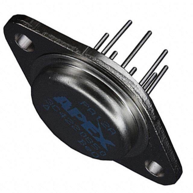
| 产品图片 | |
| rohs | 符合RoHS无铅 / 符合限制有害物质指令(RoHS)规范要求 |
| 产品系列 | 放大器 IC,运算放大器 - 运放,Microchip Technology MCP6481T-E/OT- |
| mouser_ship_limit | 该产品可能需要其他文件才能进口到中国。 |
| 数据手册 | http://www.microchip.com/mymicrochip/filehandler.aspx?ddocname=en560019 |
| 产品型号 | MCP6481T-E/OT |
| PCN设计/规格 | |
| 产品种类 | 运算放大器 - 运放 |
| 供应商器件封装 | SOT-23-5 |
| 共模抑制比—最小值 | 70 dB |
| 关闭 | No Shutdown |
| 其它名称 | MCP6481T-E/OTCT |
| 包装 | 剪切带 (CT) |
| 压摆率 | 2.7 V/µs |
| 商标 | Microchip Technology |
| 增益带宽生成 | 4 MHz |
| 增益带宽积 | 4MHz |
| 安装类型 | 表面贴装 |
| 安装风格 | SMD/SMT |
| 封装 | Reel |
| 封装/外壳 | SC-74A,SOT-753 |
| 封装/箱体 | SOT-23-5 |
| 工作温度 | -40°C ~ 125°C |
| 工作电源电压 | 2.2 V to 5.5 V |
| 工厂包装数量 | 3000 |
| 技术 | CMOS |
| 放大器类型 | 通用 |
| 最大工作温度 | + 125 C |
| 最小工作温度 | - 40 C |
| 标准包装 | 1 |
| 电压-电源,单/双 (±) | 2.2 V ~ 5.5 V, ±1.1 V ~ 2.25 V |
| 电压-输入失调 | 1.5mV |
| 电流-电源 | 240µA |
| 电流-输入偏置 | 1pA |
| 电流-输出/通道 | 12mA |
| 电源电流 | 240 uA |
| 电路数 | 1 |
| 系列 | MCP6481 |
| 转换速度 | 2.7 V/us |
| 输入偏压电流—最大 | 350 pA |
| 输入参考电压噪声 | 7 uV |
| 输入补偿电压 | - 1.5 mV |
| 输出类型 | 满摆幅 |
| 通道数量 | 1 Channel |


- 商务部:美国ITC正式对集成电路等产品启动337调查
- 曝三星4nm工艺存在良率问题 高通将骁龙8 Gen1或转产台积电
- 太阳诱电将投资9.5亿元在常州建新厂生产MLCC 预计2023年完工
- 英特尔发布欧洲新工厂建设计划 深化IDM 2.0 战略
- 台积电先进制程称霸业界 有大客户加持明年业绩稳了
- 达到5530亿美元!SIA预计今年全球半导体销售额将创下新高
- 英特尔拟将自动驾驶子公司Mobileye上市 估值或超500亿美元
- 三星加码芯片和SET,合并消费电子和移动部门,撤换高东真等 CEO
- 三星电子宣布重大人事变动 还合并消费电子和移动部门
- 海关总署:前11个月进口集成电路产品价值2.52万亿元 增长14.8%


PDF Datasheet 数据手册内容提取
MCP6481/2/4 4 MHz, Low-Input Bias Current Op Amps Features Description • Low-Input Bias Current The Microchip MCP6481/2/4 family of operational - 150pA (typical, T =+125°C) amplifiers (op amps) has low-input bias current A (150pA, typical at 125°C) and rail-to-rail input and • Low Quiescent Current output operation. This family is unity gain stable and - 240µA/amplifier (typical) has a gain bandwidth product of 4MHz (typical). These • Low-Input Offset Voltage devices operate with a single-supply voltage as low as - ±1.5mV (maximum) 2.2V, while only drawing 240µA/amplifier (typical) of • Supply Voltage Range: 2.2V to 5.5V quiescent current. These features make the family of • Rail-to-Rail Input/Output op amps well suited for photodiode amplifier, pH electrode amplifier, low leakage amplifier, and battery- • Gain Bandwidth Product: 4MHz (typical) powered signal conditioning applications, etc. • Slew Rate: 2.7V/µs (typical) The MCP6481/2/4 family is offered in single • Unity Gain Stable (MCP6481), dual (MCP6482), quad (MCP6484) • No Phase Reversal packages. All devices are designed using an advanced • Small Packages CMOS process and fully specified in extended - Singles in SC70-5, SOT-23-5 temperature range from -40°C to +125°C. • Extended Temperature Range Related Parts - -40°C to +125°C • MCP6471/2/4: 2MHz, Low-Input Bias Current Op Applications Amps • Photodiode Amplifier • MCP6491/2/4: 7.5MHz, Low-Input Bias Current Op Amps • pH Electrode Amplifier • Low Leakage Amplifier • Piezoelectric Transducer Amplifier • Active Analog Filter • Battery-Powered Signal Conditioning Design Aids • SPICE Macro Models • FilterLab® Software • MAPS (Microchip Advanced Part Selector) • Analog Demonstration and Evaluation Boards • Application Notes Package Types MCP6481 MCP6482 MCP6482 MCP6484 SC70, SOT-23 SOIC, MSOP 2x3TDFN* SOIC, TSSOP VOUT 11 55 VDD VOUTA 1 8 VDD VOUTA 1 8 VDD VOUTA 1 14 VOUTD VSS 22 VINA– 2 7 VOUTB VINA– 2 EP 7 VOUTB VINA– 2 13VIND– VIN+ 33 44 VIN– VINA+ 3 6 VINB– VINA+ 3 9 6 VINB– VINA+ 3 12 VIND+ VSS 4 5 VINB+ VSS 4 5 VINB+ VDD 4 11 VSS VINB+ 5 10 VINC+ VINB– 6 9 VINC– * Includes Exposed Thermal Pad (EP); see Table3-1. VOUTB 7 8 VOUTC 2012-2013 Microchip Technology Inc. DS20002322C-page 1
MCP6481/2/4 Typical Application C 2 R 2 V OUT ID1 VDD – Light D1 MCP648X + Photodiode Amplifier DS20002322C-page 2 2012-2013 Microchip Technology Inc.
MCP6481/2/4 1.0 ELECTRICAL CHARACTERISTICS 1.1 Absolute Maximum Ratings † V –V .........................................................................................................................................................................................6.5V DD SS Current at Input Pins......................................................................................................................................................................±2mA Analog Inputs (V +, V -)††............................................................................................................................V –1.0V to V +1.0V IN IN SS DD All Other Inputs and Outputs ...........................................................................................................................V –0.3V to V +0.3V SS DD Difference Input Voltage...........................................................................................................................................................V –V DD SS Output Short-Circuit Current...................................................................................................................................................continuous Current at Output and Supply Pins .............................................................................................................................................±55mA Storage Temperature.....................................................................................................................................................-65°C to +150°C Maximum Junction Temperature (T )...........................................................................................................................................+150°C J ESD protection on all pins (HBM)4kV Note1: See Section4.1.2, Input Voltage Limits. † Notice: Stresses above those listed under “Absolute Maximum Ratings” may cause permanent damage to the device. This is a stress rating only and functional operation of the device at those or any other conditions above those indicated in the operational listings of this specification is not implied. Exposure to maximum rating conditions for extended periods may affect device reliability. 1.2 Specifications TABLE 1-1: DC ELECTRICAL SPECIFICATIONS Electrical Characteristics: Unless otherwise indicated, V =+2.2V to +5.5V, V =GND, T =+25°C, DD SS A V =V /2, V V /2, V =V /2 and R =10kto V . (Refer to Figure1-1). CM DD OUT DD L DD L L Parameters Sym. Min. Typ. Max. Units Conditions Input Offset Input Offset Voltage V -1.5 — +1.5 mV V =3.0V, V =V /4 OS DD CM DD Input Offset Drift with Temperature V /T — ±2.5 — µV/°C T =-40°C to +125°C OS A A Power Supply Rejection Ratio PSRR 75 91 — dB V =V /4 CM DD Input Bias Current and Impedance Input Bias Current I — ±1 — pA B — 8 — pA T =+85°C A — 150 350 pA T =+125°C A Input Offset Current I — ±0.1 — pA OS Common Mode Input Impedance Z — 1013||6 — ||pF CM Differential Input Impedance Z — 1013||6 — ||pF DIFF Common Mode Common Mode Input Voltage Range V V -0.3 — V +0.3 V CMR SS DD Common Mode Rejection Ratio CMRR 65 87 — dB V =-0.3V to 2.5V, CM V =2.2V DD 70 89 — dB V =-0.3V to 5.8V, CM V =5.5V DD Open-Loop Gain DC Open-Loop Gain (Large Signal) A 95 115 — dB 0.2V<V <(V –0.2V) OL OUT DD V =5.5V, V =V DD CM SS 2012-2013 Microchip Technology Inc. DS20002322C-page 3
MCP6481/2/4 TABLE 1-1: DC ELECTRICAL SPECIFICATIONS (CONTINUED) Electrical Characteristics: Unless otherwise indicated, V =+2.2V to +5.5V, V =GND, T =+25°C, DD SS A V =V /2, V V /2, V =V /2 and R =10kto V . (Refer to Figure1-1). CM DD OUT DD L DD L L Parameters Sym. Min. Typ. Max. Units Conditions Output High-Level Output Voltage V 2.180 2.196 — V V =2.2V OH DD 0.5V input overdrive 5.480 5.493 — V V =5.5V DD 0.5V input overdrive Low-Level Output Voltage V — 0.004 0.020 V V =2.2V OL DD 0.5V input overdrive — 0.007 0.020 V V =5.5V DD 0.5V input overdrive Output Short-Circuit Current I — ±12 — mA V =2.2V SC DD — ±36 — mA V =5.5V DD Power Supply Supply Voltage V 2.2 — 5.5 V DD Quiescent Current per Amplifier I 100 240 400 µA I =0, V =V /4 Q O CM DD TABLE 1-2: AC ELECTRICAL SPECIFICATIONS Electrical Characteristics: Unless otherwise indicated, T =+25°C, V =+2.2V to +5.5V, V =GND, A DD SS V =V /2, V V /2, V =V /2, R =10kto V and C = 20pF. (Refer to Figure1-1). CM DD OUT DD L DD L L L Parameters Sym. Min. Typ. Max. Units Conditions AC Response Gain Bandwidth Product GBWP — 4 — MHz Phase Margin PM — 60 — ° G=+1V/V Slew Rate SR — 2.7 — V/µs Noise Input Noise Voltage E — 7 — µVp-p f=0.1Hz to 10Hz ni Input Noise Voltage Density e — 23 — nV/Hz f=1kHz ni — 18 — nV/Hz f=10kHz Input Noise Current Density i — 0.6 — fA/Hz f=1kHz ni TABLE 1-3: TEMPERATURE SPECIFICATIONS Electrical Characteristics: Unless otherwise indicated, V =+2.2V to +5.5V and V =GND. DD SS Parameters Sym. Min. Typ. Max. Units Conditions Temperature Ranges Operating Temperature Range T -40 — +125 °C Note1 A Storage Temperature Range T -65 — +150 °C A Thermal Package Resistances Thermal Resistance, 5L-SC-70 — 331 — °C/W JA Thermal Resistance, 5L-SOT-23 — 256 — °C/W JA Thermal Resistance, 8L-2x3 TDFN — 52.5 — °C/W JA Thermal Resistance, 8L-MSOP — 211 — °C/W JA Thermal Resistance, 8L-SOIC — 149.5 — °C/W JA Thermal Resistance, 14L-SOIC — 95.3 — °C/W JA Thermal Resistance, 14L-TSSOP — 100 — °C/W JA Note1: The internal junction temperature (T ) must not exceed the absolute maximum specification of +150°C. J DS20002322C-page 4 2012-2013 Microchip Technology Inc.
MCP6481/2/4 1.3 Test Circuits C The circuit used for most DC and AC tests is shown in F 6.8pF Figure1-1. This circuit can independently set V and CM V (refer to Equation1-1). Note that V is not the OUT CM circuit’s common mode voltage ((VP+VM)/2), and that RG RF V includes V plus the effects (on the input offset 100k 100k OST OS error, VOST) of temperature, CMRR, PSRR and AOL. VP VDD/2 V DD V EQUATION 1-1: IN+ C C B1 B2 GDM = RFRG MCP648X 100nF 1µF V = V +V 22 CM P DD VOST = VIN+–VIN– VIN– VOUT = VDD2+VP–VM+VOST1+GDM VM VOUT Where: RG RF RL CL 100k 100k 10k 20pF G = Differential Mode Gain (V/V) DM V = Op Amp’s Common Mode (V) CM C Input Voltage F 6.8pF VL V = Op Amp’s Total Input Offset (mV) OST Voltage FIGURE 1-1: AC and DC Test Circuit for Most Specifications. 2012-2013 Microchip Technology Inc. DS20002322C-page 5
MCP6481/2/4 NOTES: DS20002322C-page 6 2012-2013 Microchip Technology Inc.
MCP6481/2/4 2.0 TYPICAL PERFORMANCE CURVES Note: The graphs and tables provided following this note are a statistical summary based on a limited number of samples and are provided for informational purposes only. The performance characteristics listed herein are not tested or guaranteed. In some graphs or tables, the data presented may be outside the specified operating range (e.g., outside specified power supply range) and therefore outside the warranted range. Note: Unless otherwise indicated, T =+25°C, V =+2.2V to +5.5V, V =GND, V =V /2, V V /2, A DD SS CM DD OUT DD V =V /2, R =10kto V and C =20pF. L DD L L L 18% 1000 currences 11110246%%%% 2VV7DC0DM =S= a3Vm.D0DpV/l4 e s oltage (µV) 246800000000 +++-41820255°°°5CCC°C c V e of O 68%% Offset -2000 centag 24%% ut Inpu --644000000 VRDeDpr=e 5s.e5nVtative Part er 0% -800 P 00 00 00 00 00 00 0 00 00 00 00 00 00 -1000 -12 -10 -8 -6 -4 -2 2 4 6 8 10 12 0.5 0.0 0.5 1.0 1.5 2.0 2.5 3.0 3.5 4.0 4.5 5.0 5.5 6.0 - Input Offset Voltage (µV) Common Mode Input Voltage (V) FIGURE 2-1: Input Offset Voltage. FIGURE 2-4: Input Offset Voltage vs. Common Mode Input Voltage. 18% 1000 currences 1125%% 2VTV7ADC 0DM= =S =- 4a3V0m.D0°DpCV/l4 et os +125°C age (µV) 468000000 Representative Part VDD= 5.5V Oc olt 200 ercentage of 369%%% t Offset Vnput ---2644000000000 VDD= 2.2V P I -800 0% -1000 2 0 8 6 4 2 0 2 4 6 8 0 2 1 1 - - - - 1 1 0 5 0 5 0 5 0 5 0 5 0 5 - - 0. 0. 1. 1. 2. 2. 3. 3. 4. 4. 5. 5. Input Offset Voltage Drift (µV/°C) Output Voltage (V) FIGURE 2-2: Input Offset Voltage Drift. FIGURE 2-5: Input Offset Voltage vs. Output Voltage. 1000 1000 age (µV) 468000000 +++-41820255°°°5CCC°C ge (µV) 468000000 +++-41820255°°°5CCC°C Volt 200 olta 200 set 0 et V 0 ut Offpu --244000000 t Offsut ---244000000 Representative Part In --860000 VRDeDpr=e 2s.e2nVtative Part Inp --860000 -1000 -1000 0.50.30.10.10.30.50.70.91.11.31.51.71.92.12.32.52.7 0.0 0.5 1.0 1.5 2.0 2.5 3.0 3.5 4.0 4.5 5.0 5.5 6.0 6.5 ---Common Mode Input Voltage (V) Power Supply Voltage (V) FIGURE 2-3: Input Offset Voltage vs. FIGURE 2-6: Input Offset Voltage vs. Common Mode Input Voltage. Power Supply Voltage. 2012-2013 Microchip Technology Inc. DS20002322C-page 7
MCP6481/2/4 Note: Unless otherwise indicated, T =+25°C, V =+2.2V to +5.5V, V =GND, V =V /2, V V /2, A DD SS CM DD OUT DD V =V /2, R =10kto V and C =20pF. L DD L L L 1,000 105 y Voltage DensitV/Hz)(cid:165)100 R, PSRR (dB) 108990505 PSRR Noise N(n MRC 8705 CMRR @@@ VVVDDDD=== 522..522VVV ut 70 p n I 10 65 10.E.1- 1 1 . E1+ 0 1 .1E0+ 1 11.0E0+ 2 1.1Ek+3 11.E0+k4 11.0E0+k5 1 .1EM+6 -50 -25 0 25 50 75 100 125 Frequency (Hz) Temperature (°C) FIGURE 2-7: Input Noise Voltage Density FIGURE 2-10: CMRR, PSRR vs. Ambient vs. Frequency. Temperature. ensity 2350 urrents 1011001n00p00 VDD= 5.5 V D C Noise Hz)(cid:165) 1250 Offset A) 101p0 Input Bias Current e V/ d ( oltag(n 10 s ana 1p1 VInput 05 ffV =DD 11=00 5kk.HH5zz V Input Bi 00.0.011.00p.p11 Input Offset Current 5 0 5 0 5 0 5 0 5 0 5 0 5 0 -0. 0. 0.Co1.mm1.on2. Mo2.de I3.npu3.t Vo4.ltag4.e (5.V) 5. 6. 25 35 45Am55bien65t Tem75per85ature95 (°C105) 115 125 FIGURE 2-8: Input Noise Voltage Density FIGURE 2-11: Input Bias, Offset Currents vs. Common Mode Input Voltage. vs. Ambient Temperature. 100 250 90 Representative Part A) 200 VDD= 5.5 V RR (dB) 7800 PSRR+ urrent (p 150 TA= +125°C PS 60 CMRR s C 100 MRR, 50 PSRR- ut Biau 50 TAA= +85°C C 40 p n 0 I 30 T = +25°C A -50 20 11.000E + 0 1 11.0000E+ 0 2 1 .100kE + 0 3 11.000Ek+0 4 11.000E0+k05 1 . 010EM+0 6 0.0 0.5 1.0 1.5 2.0 2.5 3.0 3.5 4.0 4.5 5.0 5.5 Frequency (Hz) Common Mode Input Voltage (V) FIGURE 2-9: CMRR, PSRR vs. FIGURE 2-12: Input Bias Current vs. Frequency. Common Mode Input Voltage. DS20002322C-page 8 2012-2013 Microchip Technology Inc.
MCP6481/2/4 Note: Unless otherwise indicated, T =+25°C, V =+2.2V to +5.5V, V =GND, V =V /2, V V /2, A DD SS CM DD OUT DD V =V /2, R =10kto V and C =20pF. L DD L L L 300 350 300 Quiescent CurrentQ(µA/Amplifier) 222220257005050 VDD= 2.2VVDD= 5.5V Quiescent CurrentQ(µA/Amplifier) 112210505000000 +++-48210255°5°°CCC°C 175 VCM= VDD/4 50 VCM= VDD/4 0 150 0 5 0 5 0 5 0 5 0 5 0 5 0 5 -50 -25 0 25 50 75 100 125 0. 0. 1. 1. 2. 2. 3. 3. 4. 4. 5. 5. 6. 6. Ambient Temperature (°C) Power Supply Voltage (V) FIGURE 2-13: Quiescent Current vs. FIGURE 2-16: Quiescent Current vs. Ambient Temperature. Power Supply Voltage. 325 120 0 Open-Loop Gain Quiescent Current Q(µA/Amplifier) 222231202570700505050 VDD= 2.2V en-Loop Gain (dB)Ope 1024682000000 Open-Loop Phase -----963111000255000 en-Loop Phase (°)Ope 0 -180 150 53113579135791357 -20 -210 -0.-0.-0.0.0.0.0.0.1.1.1.1.1.2.2.2.2. 1.10E + 0 0 11.0E0+ 0 1 11.0E0+002 1.01E+k03 1 .10E0+0k4 1.10E0+005k 1 .0 E1+M06 11.0E0+0M7 Common Mode Input Voltage (V) Frequency (Hz) FIGURE 2-14: Quiescent Current vs. FIGURE 2-17: Open-Loop Gain, Phase vs. Common Mode Input Voltage. Frequency. 325 150 nt 300 dB) 140 VDD= 5.5V nt Curremplifier) 225705 p Gain ( 130 QuiesceQ(µA/A 222020050 V = 5.5V pen-LooOp 111211000 VDD= 2.2V DD C 175 D 100 150 90 0.5 0.0 0.5 1.0 1.5 2.0 2.5 3.0 3.5 4.0 4.5 5.0 5.5 6.0 -50 -25 0 25 50 75 100 125 - Common Mode Input Voltage (V) Temperature (°C) FIGURE 2-15: Quiescent Current vs. FIGURE 2-18: DC Open-Loop Gain vs. Common Mode Input Voltage. Ambient Temperature. 2012-2013 Microchip Technology Inc. DS20002322C-page 9
MCP6481/2/4 Note: Unless otherwise indicated, T =+25°C, V =+2.2V to +5.5V, V =GND, V =V /2, V V /2, A DD SS CM DD OUT DD V =V /2, R =10kto V and C =20pF. L DD L L L 7 70 10 V = 5.5V uct 6 60 )P-P DD d V Bandwidth Pro(MHz) 345 Gain BandwiPdhtha sPer oMdaurcgtin 345000 hase Margin (°) oltage Swing ( 1 VDD= 2.2V n Gain 2 20 PP t Vput 1 VDD= 2.2V 10 Out 0 0 0.1 -50 -25 0 25 50 75 100 125 110000 110k00 110000k0 10100000k0 1100M000 0 1100000M000 Ambient Temperature (°C) Frequency (Hz) FIGURE 2-19: Gain Bandwidth Product, FIGURE 2-22: Output Voltage Swing vs. Phase Margin vs. Ambient Temperature. Frequency. 7 70 1000 ct V) Bandwidth Produ(MHz) 3456 Gain BandwidPthha Psero Mduarcgtin 34560000 hase Margin (°) ge Headroom (m 10100 VDD= 2.2V VDD-VOH VOL-VSS n n PP a Gai 2 20 oltVo 11 1 VDD= 5.5V 10 ut p 0 0 Out 0.1 -50 -25 0 25 50 75 100 125 0.01 0.1 1 10 Ambient Temperature (°C) Output Current (mA) FIGURE 2-20: Gain Bandwidth Product, FIGURE 2-23: Output Voltage Headroom Phase Margin vs. Ambient Temperature. vs. Output Current. 60 uit Current 23450000 +++1-28420555°°°°CCCC oom (mV) 1010000 VDD= 5.5V VDD-VOH Short Circ(mA)--2110000 age Headr 10 VOL-VSS put -30 ++1182255°°°CCC oltVo 11 Out --5400 +-2405°°CC put -60 Out 0.1 0.0 0.5 1.0 1.5 2.0 2.5 3.0 3.5 4.0 4.5 5.0 5.5 6.0 0.01 0.1 1 10 100 Power Supply Voltage (V) Output Current (mA) FIGURE 2-21: Output Short Circuit Current FIGURE 2-24: Output Voltage Headroom vs. Power Supply Voltage. vs. Output Current. DS20002322C-page 10 2012-2013 Microchip Technology Inc.
MCP6481/2/4 Note: Unless otherwise indicated, T =+25°C, V =+2.2V to +5.5V, V =GND, V =V /2, V V /2, A DD SS CM DD OUT DD V =V /2, R =10kto V and C =20pF. L DD L L L V) 7 m m ( 6 v) adroo 5 VDD-VOH mV/di He 4 10 ge e ( Volta 3 VOL-VSS oltag Output 12 VDD= 2.2V Vutput VVGD =D =+155 VVV/V O 0 -50 -25 0 25 50 75 100 125 Temperature (°C) Time (0.5 µs/div) FIGURE 2-25: Output Voltage Headroom FIGURE 2-28: Small Signal Non-Inverting vs. Ambient Temperature. Pulse Response. V) 10 m droom ( 789 VDD-VOH mV/div) VDD= 5 V Hea 6 10 G = -1 V/V Voltage 3453 VOL-VSS Voltage ( utput 2 VDD= 5.5V utput O 1 O 0 -50 -25 0 25 50 75 100 125 Temperature (°C) Time (0.5 µs/div) FIGURE 2-26: Output Voltage Headroom FIGURE 2-29: Small Signal Inverting Pulse vs. Ambient Temperature. Response. 4.5 5.0 4.0 Falling Edge, VDD= 5.5V 4.5 s) 3.5 Rising Edge, VDD= 5.5V 4.0 Slew Rate (V/µS 12231....50505 put Voltage (V) 2233....0505 1.0 RisiFnagl lEindgg Ee,d VgDeD, V= D2D.2=V 2.2V tOut 1.5 0.5 1.0 VDD= 5 V G = +1 V/V 0.5 0.0 -50 -25 0 25 50 75 100 125 0.0 Temperature (°C) Time (2 µs/div) FIGURE 2-27: Slew Rate vs. Ambient FIGURE 2-30: Large Signal Non-Inverting Temperature. Pulse Response. 2012-2013 Microchip Technology Inc. DS20002322C-page 11
MCP6481/2/4 Note: Unless otherwise indicated, T =+25°C, V =+2.2V to +5.5V, V =GND, V =V /2, V V /2, A DD SS CM DD OUT DD V =V /2, R =10kto V and C =20pF. L DD L L L 5.0 1.10Em+09 4.5 110.00E+µ08 V = 5 V V) 4.0 GD =D -1 V/V 11.00E+µ07 e ( 3.5 1.01E+µ06 g olta 3.0 pA)110.0E0+n05 put V 22..05 -I(IN 11.00E+n04 ++1825°5C°C tOut 1.5 1.011E+n03 +-4205°°CC 1.0 110.00E+p02 0.5 11.00E+p01 0.0 -1.0 -0.9 -0.8 -0.7 -0.6 -0.5 -0.4 -0.3 -0.2 -0.1 0.0 Time (2 µs/div) V (V) IN FIGURE 2-31: Large Signal Inverting Pulse FIGURE 2-34: Measured Input Current vs. Response. Input Voltage (below V ). SS 6 100 es (V) 45 VOUT annel dB) 8900 utput Voltag 23 VIN hannel to ChhSeparation ( 567000 ut, O 1 VVGD =D =+255 VVV/V C 40 Input Referred p 30 n 0 I 20 -1 1.0E+02100 11.0E+03k 11.0E+040k 101.0E+050k 1M1.0E+06 Frequency (Hz) Time (1 ms/div) FIGURE 2-32: The MCP6481/2/4 Shows FIGURE 2-35: Channel-to-Channel No Phase Reversal. Separation vs. Frequency (MCP6482/4 only). 1000 ut p Outpce ()(cid:58)100 on oa Ld sed mpe 10 GN: ooI 110011VV//VV Cl 11 V/V 1 V/V 1 11.0E0+002 1 .10Ek+03 11.0E0+k04 11.00E0+k05 1 .01EM+06 11.00EM+07 Frequency (Hz) FIGURE 2-33: Closed Loop Output Impedance vs. Frequency. DS20002322C-page 12 2012-2013 Microchip Technology Inc.
MCP6481/2/4 3.0 PIN DESCRIPTIONS Descriptions of the pins are listed in Table3-1. TABLE 3-1: PIN FUNCTION TABLE MCP6481 MCP6482 MCP6484 Symbol Description SC70, SOT-23 SOIC, MSOP 2x3TDFN SOIC, TSSOP 1 1 1 1 V , V Analog Output (op amp A) OUT OUTA 4 2 2 2 V –, V – Inverting Input (op amp A) IN INA 3 3 3 3 V +, V + Non-inverting Input (op amp A) IN INA 5 8 8 4 V Positive Power Supply DD — 5 5 5 V + Non-inverting Input (op amp B) INB — 6 6 6 V – Inverting Input (op amp B) INB — 7 7 7 V Analog Output (op amp B) OUTB — — — 8 V Analog Output (op amp C) OUTC — — — 9 V – Inverting Input (op amp C) INC — — — 10 V + Non-Inverting Input (op amp C) INC 2 4 4 11 V Negative Power Supply SS — — — 12 V + Non-Inverting Input (op amp D) IND — — — 13 V – Inverting Input (op amp D) IND — — — 14 V Analog Output (op amp D) OUTD — — 9 — EP Exposed Thermal Pad (EP); must be connected to V . SS 3.1 Analog Outputs 3.4 Exposed Thermal Pad (EP) The output pins are low-impedance voltage sources. There is an internal electrical connection between the Exposed Thermal Pad (EP) and the V pin; they must SS 3.2 Analog Inputs be connected to the same potential on the Printed Circuit Board (PCB). The non-inverting and inverting inputs are This pad can be connected to a PCB ground plane to high-impedance CMOS inputs with low bias currents. provide a larger heat sink. This improves the package thermal resistance ( ). 3.3 Power Supply Pins JA The positive power supply (V ) is 2.2V to 5.5V higher DD than the negative power supply (V ). For normal SS operation, the other pins are at voltages between V SS and V . DD Typically, these parts are used in single-supply operation. In this case, V is connected to ground and SS V is connected to the supply. V will need bypass DD DD capacitors. 2012-2013 Microchip Technology Inc. DS20002322C-page 13
MCP6481/2/4 NOTES: DS20002322C-page 14 2012-2013 Microchip Technology Inc.
MCP6481/2/4 4.0 APPLICATION INFORMATION V DD The MCP6481/2/4 family of op amps is manufactured using Microchip’s state-of-the-art CMOS process and is specifically designed for low-power, high-precision D D 1 2 applications. V 1 V OUT 4.1 Inputs MCP648X V 2 4.1.1 PHASE REVERSAL The MCP6481/2/4 op amps are designed to prevent FIGURE 4-2: Protecting the Analog phase reversal when the input pins exceed the supply Inputs. voltages. Figure2-32 shows the input voltage exceeding the supply voltage without any phase A significant amount of current can flow out of the reversal. inputs when the Common mode voltage (VCM) is below ground (V ), as shown in Figure2-34. SS 4.1.2 INPUT VOLTAGE LIMITS 4.1.3 INPUT CURRENT LIMITS In order to prevent damage and/or improper operation In order to prevent damage and/or improper operation of these amplifiers, the circuit must limit the voltages at of these amplifiers, the circuit must limit the currents the input pins (see Section1.1 “Absolute Maximum into the input pins (see Section1.1 “Absolute Ratings †”). Maximum Ratings †”). The ESD protection on the inputs can be depicted as Figure4-3 shows one approach to protect these inputs. shown in Figure4-1. This structure was chosen to The R and R resistors limit the possible currents in or protect the input transistors against many (but not all) 1 2 out of the input pins (and the ESD diodes, D and D ). overvoltage conditions, and to minimize the input bias 1 2 The diode currents will go through either V or V . current (I ). DD SS B V DD Bond V DD Pad D D 1 2 V 1 V + Bond Input Bond V – R1 MCP648X V IN Pad Stage Pad IN OUT V 2 R 2 Bond V SS R Pad 3 V –min(V ,V ) SS 1 2 FIGURE 4-1: Simplified Analog Input ESD min (R ,R ) > 1 2 2mA Structures. max(V ,V )–V 1 2 DD min (R ,R )> The input ESD diodes clamp the inputs when they try 1 2 2mA to go more than one diode drop below VSS. They also FIGURE 4-3: Protecting the Analog clamp any voltages that go well above V . Their DD Inputs. breakdown voltage is high enough to allow normal operation, but not low enough to protect against slow overvoltage (beyond V ) events. Very fast ESD DD events (that meet the specification) are limited so that damage does not occur. In some applications, it may be necessary to prevent excessive voltages from reaching the op amp inputs; Figure4-2 shows one approach to protect these inputs. 2012-2013 Microchip Technology Inc. DS20002322C-page 15
MCP6481/2/4 4.1.4 NORMAL OPERATION Figure4-5 gives the recommended R values for ISO different capacitive loads and gains. The x-axis is the The inputs of the MCP6481/2/4 op amps use two normalized load capacitance (C /G ), where G is the differential input stages in parallel. One operates at a L N N circuit’s noise gain. For non-inverting gains, G and the low Common mode input voltage (V ), while the other N CM Signal Gain are equal. For inverting gains, G is operates at a high V . With this topology, the device N CM 1+|Signal Gain| (e.g., -1V/V gives G =+2V/V). operates with a V up to 0.3V above V and 0.3V N CM DD below VSS (refer to Figures2-3 and 2-4). The input After selecting RISO for your circuit, double check the offset voltage is measured at V =V –0.3V and resulting frequency response peaking and step CM SS VDD+0.3V to ensure proper operation. response overshoot. Modify RISO’s value until the response is reasonable. Bench evaluation and The transition between the input stages occurs when simulations with the MCP6481/2/4 SPICE macro V is near V –1.2V (refer to Figures2-3 and 2-4). CM DD model are helpful. For the best distortion performance and gain linearity, with non-inverting gains, avoid this region of operation. 1000 4.2 Rail-to-Rail Output )(cid:58) VDD= 5.5 V (O RL= 10 k(cid:525) The output voltage range of the MCP6481/2/4 op amps S R I 100 is 0.007V (typical) and 5.493V (typical) when d RRLef=er1 t0o kFig uisre sco2n-2n3e catnedd 2to- 2V4 DfoDr/ 2m oarned i nVfoDrDm=at5io.n5.V. mende G1 NV:/V m 10 2 V/V 4.3 Capacitive Loads oco (cid:116)(cid:116)55 VV//VV e R Driving large capacitive loads can cause stability 1 problems for voltage feedback op amps. As the load 1.1E0-1p1 1 1.E0-01p0 1 . E 1-n0 9 1 . E1-00n8 1 . E 0-.017µ 1 . E 1-0µ6 capacitance increases, the feedback loop’s phase Normalized Load Capacitance; C /G (F) margin decreases and the closed-loop bandwidth is L N FIGURE 4-5: Recommended R Values reduced. This produces gain peaking in the frequency ISO for Capacitive Loads. response, with overshoot and ringing in the step response. While a unity-gain buffer (G=+1V/V) is the most sensitive to capacitive loads, all gains show the 4.4 Supply Bypass same general behavior. With this family of operational amplifiers, the power When driving large capacitive loads with these op supply pin (V for single supply) should have a local DD amps (e.g., >100pF when G=+1V/V), a small series bypass capacitor (i.e., 0.01µF to 0.1µF) within 2mm resistor at the output (RISO in Figure4-4) improves the for good high-frequency performance. It can use a bulk feedback loop’s phase margin (stability) by making the capacitor (i.e., 1µF or larger) within 100mm to provide output load resistive at higher frequencies. The large, slow currents. This bulk capacitor can be shared bandwidth will generally be lower than the bandwidth with other analog parts. with no capacitance load. – R ISO MCP648X VOUT V + IN C L FIGURE 4-4: Output Resistor, R ISO Stabilizes Large Capacitive Loads. DS20002322C-page 16 2012-2013 Microchip Technology Inc.
MCP6481/2/4 4.5 Unused Op Amps 4.6 PCB Surface Leakage An unused op amp in a quad package (MCP6484) In applications where low-input bias current is critical, should be configured as shown in Figure4-6. These PCB surface leakage effects need to be considered. circuits prevent the output from toggling and causing Surface leakage is caused by humidity, dust or other crosstalk. Circuit A sets the op amp at its minimum contamination on the board. Under low-humidity noise gain. The resistor divider produces any desired conditions, a typical resistance between nearby traces reference voltage within the output voltage range of the is 1012. A 5V difference would cause 5pA of current op amp, and the op amp buffers that reference voltage. to flow, which is greater than the MCP6481/2/4 family’s Circuit B uses the minimum number of components bias current at +25°C (1pA, typical). and operates as a comparator, but it may draw more The easiest way to reduce surface leakage is to use a current. guard ring around sensitive pins (or traces). The guard ring is biased at the same voltage as the sensitive pin. ¼ MCP6484 (A) ¼ MCP6484 (B) An example of this type of layout is shown in V V Figure4-7. DD DD V R DD 1 Guard Ring V – V + V IN IN SS V R REF 2 R 2 V = V -------------------- REF DD R +R 1 2 FIGURE 4-6: Unused Op Amps. FIGURE 4-7: Example Guard Ring Layout for Inverting Gain. 1. Non-Inverting Gain and Unity-Gain Buffer: a.Connect the non-inverting pin (V +) to the IN input with a wire that does not touch the PCB surface. b.Connect the guard ring to the inverting input pin (V –). This biases the guard ring to the IN Common mode input voltage. 2. Inverting Gain and Transimpedance Gain Amplifiers (convert current to voltage, such as photo detectors): a.Connect the guard ring to the non-inverting input pin (V +). This biases the guard ring IN to the same reference voltage as the op amp (e.g., V /2 or ground). DD b.Connect the inverting pin (V –) to the input IN with a wire that does not touch the PCB surface. 2012-2013 Microchip Technology Inc. DS20002322C-page 17
MCP6481/2/4 4.7 Application Circuits 4.7.2 ACTIVE LOW PASS FILTER The MCP6481/2/4 op amps’ low-input bias current 4.7.1 PHOTO DETECTION makes it possible for the designer to use larger The MCP6481/2/4 op amps can be used to easily resistors and smaller capacitors for active low-pass convert the signal from a sensor that produces an filter applications. However, as the resistance output current (such as a photo diode) into a voltage (a increases, the noise generated also increases. transimpedance amplifier). This is implemented with a Parasitic capacitances and the large value resistors single resistor (R ) in the feedback loop of the could also modify the frequency response. These 2 amplifiers shown in Figure4-8 and Figure4-9. The trade-offs need to be considered when selecting circuit optional capacitor (C ) sometimes provides stability for elements. 2 these circuits. Usually, the op amp bandwidth is 100x the filter cutoff A photodiode configured in the Photovoltaic mode has frequency (or higher) for good performance. It is zero voltage potential placed across it (Figure4-8). In possible to have the op amp bandwidth 10x higher than this mode, the light sensitivity and linearity is the cutoff frequency, thus having a design that is more maximized, making it best suited for precision sensitive to component tolerances. applications. The key amplifier specifications for this Figure4-10 and Figure4-11 show low-pass, second- application are: low-input bias current, Common mode order, Butterworth filters with a cutoff frequency of input voltage range (including ground), and rail-to-rail 10Hz. The filter in Figure4-10 has a non-inverting gain output. of +1V/V, and the filter in Figure4-11 has an inverting gain of -1V/V. C 2 C 1 R2 47nF V ID1 VDD OUT – R1 R2 D 1 768k 1.27M Light MCP648X + V IN + C2 MCP648X VOUT 22nF V = I *R – OUT D1 2 FIGURE 4-8: Photovoltaic Mode Detector. In contrast, a photodiode that is configured in the f = 10Hz, G = +1V/V P Photoconductive mode has a reverse bias voltage FIGURE 4-10: Second-Order, Low-Pass across the photo-sensing element (Figure4-9). This decreases the diode capacitance, which facilitates Butterworth Filter with Sallen-Key Topology. high-speed operation (e.g., high-speed digital communications). However, the reverse bias voltage also increased diode leakage current and caused R 2 linearity errors. 618k C2 R1 R3 C1 618k 1.00M 8.2nF R2 VIN VOUT ID1 VOUT C2 – VDD 47nF – MCP648X D 1 Light MCP648X V /2 + DD VBIAS + VOUT = ID1*R2 fP = 10Hz, G = -1V/V V < 0V BIAS FIGURE 4-11: Second-Order, Low-Pass Butterworth Filter with Multiple-Feedback FIGURE 4-9: Photoconductive Mode Topology. Detector. DS20002322C-page 18 2012-2013 Microchip Technology Inc.
MCP6481/2/4 4.7.3 PH ELECTRODE AMPLIFIER The MCP6481/2/4 op amps can be used for sensing applications where the sensor has high output impedance, such as a pH electrode sensor; its output impedance is in the range of 1 M to 1G. The key op amp specifications for these kinds of applications are low-input bias current and high input impedance. A typical sensing circuit is shown in Figure4-12, it is implemented with a non-inverting amplifier which has a gain of 1+R /R . The input voltage error due to input 2 1 bias current is equal to I *R , which is amplified by B OUT 1+R /R at the output. To minimize the voltage error 2 1 and get the V with better accuracy, the I must be OUT B small enough. R 2 R 1 – MCP648X VOUT V IN + R OUT pH electrode + V SEN – V is the sensed voltage by pH electrode SEN R is the pH electrode’s output impedance OUT FIGURE 4-12: pH Electrode Amplifier. 2012-2013 Microchip Technology Inc. DS20002322C-page 19
MCP6481/2/4 NOTES: DS20002322C-page 20 2012-2013 Microchip Technology Inc.
MCP6481/2/4 5.0 DESIGN AIDS 5.4 Analog Demonstration and Evaluation Boards Microchip Technology Inc. provides the basic design tools needed for the MCP6481/2/4 family of op amps. Microchip offers a broad spectrum of Analog Demonstration and Evaluation Boards that are designed to help you achieve faster time to market. For 5.1 SPICE Macro Model a complete listing of these boards and their The latest SPICE macro model for the MCP6481/2/4 corresponding user’s guides and technical information, op amps is available on the Microchip web site at visit the Microchip web site: www.microchip.com. The model was written and tested www.microchip.com/analogtools. in PSpice, owned by Orcad (Cadence®). For other Some boards that are especially useful include: simulators, translation may be required. • MCP6XXX Amplifier Evaluation Board 1 The model covers a wide aspect of the op amp’s • MCP6XXX Amplifier Evaluation Board 2 electrical specifications. Not only does the model cover • MCP6XXX Amplifier Evaluation Board 3 voltage, current and resistance of the op amp, but it • MCP6XXX Amplifier Evaluation Board 4 also covers the temperature and noise effects on the • Active Filter Demo Board Kit behavior of the op amp. The model has not been • 5/6-Pin SOT-23 Evaluation Board, part number verified outside the specification range listed in the op VSUPEV2 amp data sheet. The model behaviors under these conditions cannot be guaranteed to match the actual • 8-Pin SOIC/MSOP/TSSOP/DIP Evaluation Board, op amp performance. part number SOIC8EV Moreover, the model is intended to be an initial design 5.5 Application Notes tool. Bench testing is a very important part of any The following Microchip analog design note and design and cannot be replaced with simulations. Also, application notes are available on the Microchip web simulation results using this macro model need to be site at www.microchip.com/appnotes, and are validated by comparing them to the data sheet recommended as supplemental reference resources. specifications and characteristic curves. • ADN003: “Select the Right Operational Amplifier for your Filtering Circuits”, DS21821 5.2 FilterLab Software • AN722: “Operational Amplifier Topologies and DC Microchip’s FilterLab software is an innovative software Specifications”, DS00722 tool that simplifies analog active filter (using op amps) • AN723: “Operational Amplifier AC Specifications design. Available at no cost from the Microchip web site and Applications”, DS00723 at www.microchip.com/filterlab, the FilterLab design • AN884: “Driving Capacitive Loads With Op tool provides full schematic diagrams of the filter circuit Amps”, DS00884 with component values. It also outputs the filter circuit • AN990: “Analog Sensor Conditioning Circuits– in SPICE format, which can be used with the macro An Overview”, DS00990 model to simulate actual filter performance. • AN1177: “Op Amp Precision Design: DC Errors”, DS01177 5.3 MAPS (Microchip Advanced Part • AN1228: “Op Amp Precision Design: Random Selector) Noise”, DS01228 • AN1297: “Microchip’s Op Amp SPICE Macro MAPS is a software tool that helps semiconductor Models”’ DS01297 professionals efficiently identify Microchip devices that • AN1332: “Current Sensing Circuit Concepts and fit a particular design requirement. Available at no cost, Fundamentals”’ DS01332 MAPS is an overall selection tool for Microchip’s prod- uct portfolio that includes analog, memory, MCUs and • AN1494: “Using MCP6491 Op Amps for DSCs. Using this tool, you can define a filter to sort Photodetection Applications" DS01494 features for a parametric search of devices and export These application notes and others are listed in: side-by-side technical comparison reports. Helpful links • “Signal Chain Design Guide”, DS21825 are also provided for data sheets, purchases and sampling of Microchip parts. The web site is available at www.microchip.com/maps. 2012-2013 Microchip Technology Inc. DS20002322C-page 21
MCP6481/2/4 NOTES: DS20002322C-page 22 2012-2013 Microchip Technology Inc.
MCP6481/2/4 6.0 PACKAGING INFORMATION 6.1 Package Marking Information 5-Lead SOT-23 (MCP6481 only) Example Part Number Code 3F25 MCP6481T-E/OT 3FNN 5-Lead SC-70 (MCP6481 only) Example Part Number Code DQ25 MCP6481T-E/LTY DQNN 8-Lead MSOP (3x3 mm) (MCP6482 only) Example 6482E 320256 8-Lead SOIC (3.90 mm) (MCP6482 only) Example MCP6482 E/SN1320 256 Legend: XX...X Customer-specific information Y Year code (last digit of calendar year) YY Year code (last 2 digits of calendar year) WW Week code (week of January 1 is week ‘01’) NNN Alphanumeric traceability code e3 Pb-free JEDEC designator for Matte Tin (Sn) * This package is Pb-free. The Pb-free JEDEC designator ( e 3 ) can be found on the outer packaging for this package. Note: In the event the full Microchip part number cannot be marked on one line, it will be carried over to the next line, thus limiting the number of available characters for customer-specific information. 2012-2013 Microchip Technology Inc. DS20002322C-page 23
MCP6481/2/4 8-Lead TDFN (2x3x0.75 mm) (MCP6482 only) Example Part Number Code AAN MCP6482T-E/MNY AAN 320 25 14-Lead SOIC (3.90 mm) (MCP6484 only) Example MCP6484 E/SL 1320256 14-Lead TSSOP (4.4 mm) (MCP6484 only) Example XXXXXXXX 6484E/ST YYWW 1320 256 NNN DS20002322C-page 24 2012-2013 Microchip Technology Inc.
MCP6481/2/4 5-Lead Plastic Small Outine Transistor (LTY) [SC70] Note: For the most current package drawings, please see the Microchip Packaging Specification located at http://www.microchip.com/packaging D b 3 2 1 E1 E 4 5 e e A A2 c A1 L )(cid:8)(cid:5)(cid:15)(cid:9) (cid:23)*++*(cid:23)(cid:14)%(cid:14),(cid:30) (cid:4)(cid:5)(cid:6)(cid:7)(cid:8)(cid:9)(cid:5)(cid:10)(cid:8)(cid:11)+(cid:5)(cid:6)(cid:5)(cid:15)(cid:9) (cid:23)*- -.(cid:23) (cid:23)(cid:29)/ -(cid:18)(cid:6)0(cid:7)(cid:21)(cid:11)(cid:10)(cid:19)(cid:11)1(cid:5)(cid:8)(cid:9) - ! 1(cid:5)(cid:15)(cid:16)(cid:20) (cid:7) (cid:25)(cid:3)2!(cid:11)"(cid:30)# .’(cid:7)(cid:21)(cid:12)(cid:17)(cid:17)(cid:11)3(cid:7)(cid:5)(cid:28)(cid:20)(cid:15) (cid:29) (cid:25)(cid:3)4(cid:25) 5 (cid:2)(cid:3)(cid:2)(cid:25) (cid:23)(cid:10)(cid:17)(cid:13)(cid:7)(cid:13)(cid:11)1(cid:12)(cid:16)6(cid:12)(cid:28)(cid:7)(cid:11)%(cid:20)(cid:5)(cid:16)6(cid:8)(cid:7)(cid:9)(cid:9) (cid:29)(cid:26) (cid:25)(cid:3)4(cid:25) 5 (cid:2)(cid:3)(cid:25)(cid:25) (cid:30)(cid:15)(cid:12)(cid:8)(cid:13)(cid:10)(cid:19)(cid:19) (cid:29)(cid:2) (cid:25)(cid:3)(cid:25)(cid:25) 5 (cid:25)(cid:3)(cid:2)(cid:25) .’(cid:7)(cid:21)(cid:12)(cid:17)(cid:17)(cid:11)7(cid:5)(cid:13)(cid:15)(cid:20) (cid:14) (cid:2)(cid:3)4(cid:25) (cid:26)(cid:3)(cid:2)(cid:25) (cid:26)(cid:3) (cid:25) (cid:23)(cid:10)(cid:17)(cid:13)(cid:7)(cid:13)(cid:11)1(cid:12)(cid:16)6(cid:12)(cid:28)(cid:7)(cid:11)7(cid:5)(cid:13)(cid:15)(cid:20) (cid:14)(cid:2) (cid:2)(cid:3)(cid:2)! (cid:2)(cid:3)(cid:26)! (cid:2)(cid:3)8! .’(cid:7)(cid:21)(cid:12)(cid:17)(cid:17)(cid:11)+(cid:7)(cid:8)(cid:28)(cid:15)(cid:20) (cid:4) (cid:2)(cid:3)4(cid:25) (cid:26)(cid:3)(cid:25)(cid:25) (cid:26)(cid:3)(cid:26)! 9(cid:10)(cid:10)(cid:15)(cid:11)+(cid:7)(cid:8)(cid:28)(cid:15)(cid:20) + (cid:25)(cid:3)(cid:2)(cid:25) (cid:25)(cid:3)(cid:26)(cid:25) (cid:25)(cid:3) 2 +(cid:7)(cid:12)(cid:13)(cid:11)%(cid:20)(cid:5)(cid:16)6(cid:8)(cid:7)(cid:9)(cid:9) (cid:16) (cid:25)(cid:3)(cid:25)4 5 (cid:25)(cid:3)(cid:26)2 +(cid:7)(cid:12)(cid:13)(cid:11)7(cid:5)(cid:13)(cid:15)(cid:20) 0 (cid:25)(cid:3)(cid:2)! 5 (cid:25)(cid:3) (cid:25) (cid:2)(cid:3)(cid:4)(cid:5)(cid:6)(cid:7) (cid:2)(cid:3) (cid:4)(cid:5)(cid:6)(cid:7)(cid:8)(cid:9)(cid:5)(cid:10)(cid:8)(cid:9)(cid:11)(cid:4)(cid:11)(cid:12)(cid:8)(cid:13)(cid:11)(cid:14)(cid:2)(cid:11)(cid:13)(cid:10)(cid:11)(cid:8)(cid:10)(cid:15)(cid:11)(cid:5)(cid:8)(cid:16)(cid:17)(cid:18)(cid:13)(cid:7)(cid:11)(cid:6)(cid:10)(cid:17)(cid:13)(cid:11)(cid:19)(cid:17)(cid:12)(cid:9)(cid:20)(cid:11)(cid:10)(cid:21)(cid:11)(cid:22)(cid:21)(cid:10)(cid:15)(cid:21)(cid:18)(cid:9)(cid:5)(cid:10)(cid:8)(cid:9)(cid:3)(cid:11)(cid:23)(cid:10)(cid:17)(cid:13)(cid:11)(cid:19)(cid:17)(cid:12)(cid:9)(cid:20)(cid:11)(cid:10)(cid:21)(cid:11)(cid:22)(cid:21)(cid:10)(cid:15)(cid:21)(cid:18)(cid:9)(cid:5)(cid:10)(cid:8)(cid:9)(cid:11)(cid:9)(cid:20)(cid:12)(cid:17)(cid:17)(cid:11)(cid:8)(cid:10)(cid:15)(cid:11)(cid:7)(cid:24)(cid:16)(cid:7)(cid:7)(cid:13)(cid:11)(cid:25)(cid:3)(cid:2)(cid:26)(cid:27)(cid:11)(cid:6)(cid:6)(cid:11)(cid:22)(cid:7)(cid:21)(cid:11)(cid:9)(cid:5)(cid:13)(cid:7)(cid:3) (cid:26)(cid:3) (cid:4)(cid:5)(cid:6)(cid:7)(cid:8)(cid:9)(cid:5)(cid:10)(cid:8)(cid:5)(cid:8)(cid:28)(cid:11)(cid:12)(cid:8)(cid:13)(cid:11)(cid:15)(cid:10)(cid:17)(cid:7)(cid:21)(cid:12)(cid:8)(cid:16)(cid:5)(cid:8)(cid:28)(cid:11)(cid:22)(cid:7)(cid:21)(cid:11)(cid:29)(cid:30)(cid:23)(cid:14)(cid:11)(cid:31)(cid:2) (cid:3)!(cid:23)(cid:3) "(cid:30)#$ "(cid:12)(cid:9)(cid:5)(cid:16)(cid:11)(cid:4)(cid:5)(cid:6)(cid:7)(cid:8)(cid:9)(cid:5)(cid:10)(cid:8)(cid:3)(cid:11)%(cid:20)(cid:7)(cid:10)(cid:21)(cid:7)(cid:15)(cid:5)(cid:16)(cid:12)(cid:17)(cid:17)&(cid:11)(cid:7)(cid:24)(cid:12)(cid:16)(cid:15)(cid:11)’(cid:12)(cid:17)(cid:18)(cid:7)(cid:11)(cid:9)(cid:20)(cid:10)((cid:8)(cid:11)((cid:5)(cid:15)(cid:20)(cid:10)(cid:18)(cid:15)(cid:11)(cid:15)(cid:10)(cid:17)(cid:7)(cid:21)(cid:12)(cid:8)(cid:16)(cid:7)(cid:9)(cid:3) MicrochipTechnologyDrawingC04-083B (cid:23)(cid:5)(cid:16)(cid:21)(cid:10)(cid:16)(cid:20)(cid:5)(cid:22)%(cid:7)(cid:16)(cid:20)(cid:8)(cid:10)(cid:17)(cid:10)(cid:28)&(cid:4)(cid:21)(cid:12)((cid:5)(cid:8)(cid:28)#(cid:25) :(cid:25)2(cid:2)" 2012-2013 Microchip Technology Inc. DS20002322C-page 25
MCP6481/2/4 5-Lead Plastic Small Outine Transistor (LTY) [SC70] Note: For the most current package drawings, please see the Microchip Packaging Specification located at http://www.microchip.com/packaging DS20002322C-page 26 2012-2013 Microchip Technology Inc.
MCP6481/2/4 (cid:8)(cid:9)(cid:10)(cid:5)(cid:11)(cid:12)(cid:13)(cid:14)(cid:15)(cid:11)(cid:6)(cid:4)(cid:16)(cid:17)(cid:13)(cid:18)(cid:19)(cid:11)(cid:15)(cid:15)(cid:13)(cid:20)(cid:21)(cid:4)(cid:15)(cid:16)(cid:22)(cid:5)(cid:13)(cid:23)(cid:24)(cid:11)(cid:22)(cid:6)(cid:16)(cid:6)(cid:4)(cid:3)(cid:24)(cid:13)(cid:25)(cid:20)(cid:23)(cid:26)(cid:13)(cid:27)(cid:18)(cid:20)(cid:23)(cid:9)(cid:28)(cid:29)(cid:30) (cid:2)(cid:3)(cid:4)(cid:5)(cid:7) 9(cid:10)(cid:21)(cid:11)(cid:15)(cid:20)(cid:7)(cid:11)(cid:6)(cid:10)(cid:9)(cid:15)(cid:11)(cid:16)(cid:18)(cid:21)(cid:21)(cid:7)(cid:8)(cid:15)(cid:11)(cid:22)(cid:12)(cid:16)6(cid:12)(cid:28)(cid:7)(cid:11)(cid:13)(cid:21)(cid:12)((cid:5)(cid:8)(cid:28)(cid:9)<(cid:11)(cid:22)(cid:17)(cid:7)(cid:12)(cid:9)(cid:7)(cid:11)(cid:9)(cid:7)(cid:7)(cid:11)(cid:15)(cid:20)(cid:7)(cid:11)(cid:23)(cid:5)(cid:16)(cid:21)(cid:10)(cid:16)(cid:20)(cid:5)(cid:22)(cid:11)1(cid:12)(cid:16)6(cid:12)(cid:28)(cid:5)(cid:8)(cid:28)(cid:11)(cid:30)(cid:22)(cid:7)(cid:16)(cid:5)(cid:19)(cid:5)(cid:16)(cid:12)(cid:15)(cid:5)(cid:10)(cid:8)(cid:11)(cid:17)(cid:10)(cid:16)(cid:12)(cid:15)(cid:7)(cid:13)(cid:11)(cid:12)(cid:15)(cid:11) (cid:20)(cid:15)(cid:15)(cid:22)$==((((cid:3)(cid:6)(cid:5)(cid:16)(cid:21)(cid:10)(cid:16)(cid:20)(cid:5)(cid:22)(cid:3)(cid:16)(cid:10)(cid:6)=(cid:22)(cid:12)(cid:16)6(cid:12)(cid:28)(cid:5)(cid:8)(cid:28) b N E E1 1 2 3 e e1 D A A2 c φ A1 L L1 )(cid:8)(cid:5)(cid:15)(cid:9) (cid:23)*++*(cid:23)(cid:14)%(cid:14),(cid:30) (cid:4)(cid:5)(cid:6)(cid:7)(cid:8)(cid:9)(cid:5)(cid:10)(cid:8)(cid:11)+(cid:5)(cid:6)(cid:5)(cid:15)(cid:9) (cid:23)*- -.(cid:23) (cid:23)(cid:29)/ -(cid:18)(cid:6)0(cid:7)(cid:21)(cid:11)(cid:10)(cid:19)(cid:11)1(cid:5)(cid:8)(cid:9) - ! +(cid:7)(cid:12)(cid:13)(cid:11)1(cid:5)(cid:15)(cid:16)(cid:20) (cid:7) (cid:25)(cid:3);!(cid:11)"(cid:30)# .(cid:18)(cid:15)(cid:9)(cid:5)(cid:13)(cid:7)(cid:11)+(cid:7)(cid:12)(cid:13)(cid:11)1(cid:5)(cid:15)(cid:16)(cid:20) (cid:7)(cid:2) (cid:2)(cid:3);(cid:25)(cid:11)"(cid:30)# .’(cid:7)(cid:21)(cid:12)(cid:17)(cid:17)(cid:11)3(cid:7)(cid:5)(cid:28)(cid:20)(cid:15) (cid:29) (cid:25)(cid:3);(cid:25) 5 (cid:2)(cid:3) ! (cid:23)(cid:10)(cid:17)(cid:13)(cid:7)(cid:13)(cid:11)1(cid:12)(cid:16)6(cid:12)(cid:28)(cid:7)(cid:11)%(cid:20)(cid:5)(cid:16)6(cid:8)(cid:7)(cid:9)(cid:9) (cid:29)(cid:26) (cid:25)(cid:3)4; 5 (cid:2)(cid:3)8(cid:25) (cid:30)(cid:15)(cid:12)(cid:8)(cid:13)(cid:10)(cid:19)(cid:19) (cid:29)(cid:2) (cid:25)(cid:3)(cid:25)(cid:25) 5 (cid:25)(cid:3)(cid:2)! .’(cid:7)(cid:21)(cid:12)(cid:17)(cid:17)(cid:11)7(cid:5)(cid:13)(cid:15)(cid:20) (cid:14) (cid:26)(cid:3)(cid:26)(cid:25) 5 8(cid:3)(cid:26)(cid:25) (cid:23)(cid:10)(cid:17)(cid:13)(cid:7)(cid:13)(cid:11)1(cid:12)(cid:16)6(cid:12)(cid:28)(cid:7)(cid:11)7(cid:5)(cid:13)(cid:15)(cid:20) (cid:14)(cid:2) (cid:2)(cid:3)8(cid:25) 5 (cid:2)(cid:3)4(cid:25) .’(cid:7)(cid:21)(cid:12)(cid:17)(cid:17)(cid:11)+(cid:7)(cid:8)(cid:28)(cid:15)(cid:20) (cid:4) (cid:26)(cid:3)(cid:27)(cid:25) 5 8(cid:3)(cid:2)(cid:25) 9(cid:10)(cid:10)(cid:15)(cid:11)+(cid:7)(cid:8)(cid:28)(cid:15)(cid:20) + (cid:25)(cid:3)(cid:2)(cid:25) 5 (cid:25)(cid:3)2(cid:25) 9(cid:10)(cid:10)(cid:15)(cid:22)(cid:21)(cid:5)(cid:8)(cid:15) +(cid:2) (cid:25)(cid:3)8! 5 (cid:25)(cid:3)4(cid:25) 9(cid:10)(cid:10)(cid:15)(cid:11)(cid:29)(cid:8)(cid:28)(cid:17)(cid:7) (cid:3) (cid:25)> 5 8(cid:25)> +(cid:7)(cid:12)(cid:13)(cid:11)%(cid:20)(cid:5)(cid:16)6(cid:8)(cid:7)(cid:9)(cid:9) (cid:16) (cid:25)(cid:3)(cid:25)4 5 (cid:25)(cid:3)(cid:26)2 +(cid:7)(cid:12)(cid:13)(cid:11)7(cid:5)(cid:13)(cid:15)(cid:20) 0 (cid:25)(cid:3)(cid:26)(cid:25) 5 (cid:25)(cid:3)!(cid:2) (cid:2)(cid:3)(cid:4)(cid:5)(cid:6)(cid:7) (cid:2)(cid:3) (cid:4)(cid:5)(cid:6)(cid:7)(cid:8)(cid:9)(cid:5)(cid:10)(cid:8)(cid:9)(cid:11)(cid:4)(cid:11)(cid:12)(cid:8)(cid:13)(cid:11)(cid:14)(cid:2)(cid:11)(cid:13)(cid:10)(cid:11)(cid:8)(cid:10)(cid:15)(cid:11)(cid:5)(cid:8)(cid:16)(cid:17)(cid:18)(cid:13)(cid:7)(cid:11)(cid:6)(cid:10)(cid:17)(cid:13)(cid:11)(cid:19)(cid:17)(cid:12)(cid:9)(cid:20)(cid:11)(cid:10)(cid:21)(cid:11)(cid:22)(cid:21)(cid:10)(cid:15)(cid:21)(cid:18)(cid:9)(cid:5)(cid:10)(cid:8)(cid:9)(cid:3)(cid:11)(cid:23)(cid:10)(cid:17)(cid:13)(cid:11)(cid:19)(cid:17)(cid:12)(cid:9)(cid:20)(cid:11)(cid:10)(cid:21)(cid:11)(cid:22)(cid:21)(cid:10)(cid:15)(cid:21)(cid:18)(cid:9)(cid:5)(cid:10)(cid:8)(cid:9)(cid:11)(cid:9)(cid:20)(cid:12)(cid:17)(cid:17)(cid:11)(cid:8)(cid:10)(cid:15)(cid:11)(cid:7)(cid:24)(cid:16)(cid:7)(cid:7)(cid:13)(cid:11)(cid:25)(cid:3)(cid:2)(cid:26)(cid:27)(cid:11)(cid:6)(cid:6)(cid:11)(cid:22)(cid:7)(cid:21)(cid:11)(cid:9)(cid:5)(cid:13)(cid:7)(cid:3) (cid:26)(cid:3) (cid:4)(cid:5)(cid:6)(cid:7)(cid:8)(cid:9)(cid:5)(cid:10)(cid:8)(cid:5)(cid:8)(cid:28)(cid:11)(cid:12)(cid:8)(cid:13)(cid:11)(cid:15)(cid:10)(cid:17)(cid:7)(cid:21)(cid:12)(cid:8)(cid:16)(cid:5)(cid:8)(cid:28)(cid:11)(cid:22)(cid:7)(cid:21)(cid:11)(cid:29)(cid:30)(cid:23)(cid:14)(cid:11)(cid:31)(cid:2) (cid:3)!(cid:23)(cid:3) "(cid:30)#$ "(cid:12)(cid:9)(cid:5)(cid:16)(cid:11)(cid:4)(cid:5)(cid:6)(cid:7)(cid:8)(cid:9)(cid:5)(cid:10)(cid:8)(cid:3)(cid:11)%(cid:20)(cid:7)(cid:10)(cid:21)(cid:7)(cid:15)(cid:5)(cid:16)(cid:12)(cid:17)(cid:17)&(cid:11)(cid:7)(cid:24)(cid:12)(cid:16)(cid:15)(cid:11)’(cid:12)(cid:17)(cid:18)(cid:7)(cid:11)(cid:9)(cid:20)(cid:10)((cid:8)(cid:11)((cid:5)(cid:15)(cid:20)(cid:10)(cid:18)(cid:15)(cid:11)(cid:15)(cid:10)(cid:17)(cid:7)(cid:21)(cid:12)(cid:8)(cid:16)(cid:7)(cid:9)(cid:3) (cid:23)(cid:5)(cid:16)(cid:21)(cid:10)(cid:16)(cid:20)(cid:5)(cid:22)%(cid:7)(cid:16)(cid:20)(cid:8)(cid:10)(cid:17)(cid:10)(cid:28)&(cid:4)(cid:21)(cid:12)((cid:5)(cid:8)(cid:28)#(cid:25) :(cid:25);(cid:2)" 2012-2013 Microchip Technology Inc. DS20002322C-page 27
MCP6481/2/4 Note: For the most current package drawings, please see the Microchip Packaging Specification located at http://www.microchip.com/packaging DS20002322C-page 28 2012-2013 Microchip Technology Inc.
MCP6481/2/4 Note: For the mostcurrent package drawings,please seetheMicrochip Packaging Specification located at http://www.microchip.com/packaging 2012-2013 Microchip Technology Inc. DS20002322C-page 29
MCP6481/2/4 Note: For the mostcurrent package drawings,please seetheMicrochip Packaging Specification located at http://www.microchip.com/packaging DS20002322C-page 30 2012-2013 Microchip Technology Inc.
MCP6481/2/4 Note: For the most current package drawings, please see the Microchip Packaging Specification located at http://www.microchip.com/packaging 2012-2013 Microchip Technology Inc. DS20002322C-page 31
MCP6481/2/4 Note: For the most current package drawings, please see the Microchip Packaging Specification located at http://www.microchip.com/packaging DS20002322C-page 32 2012-2013 Microchip Technology Inc.
MCP6481/2/4 Note: For the most current package drawings, please see the Microchip Packaging Specification located at http://www.microchip.com/packaging 2012-2013 Microchip Technology Inc. DS20002322C-page 33
MCP6481/2/4 (cid:31)(cid:9)(cid:10)(cid:5)(cid:11)(cid:12)(cid:13)(cid:14)(cid:15)(cid:11)(cid:6)(cid:4)(cid:16)(cid:17)(cid:13)(cid:18)(cid:19)(cid:11)(cid:15)(cid:15)(cid:13)(cid:20)(cid:21)(cid:4)(cid:15)(cid:16)(cid:22)(cid:5)(cid:13)(cid:25)(cid:18)(cid:2)(cid:26)(cid:13) (cid:13)(cid:2)(cid:11)(cid:24)(cid:24)(cid:3)!"(cid:13)(cid:29)#$%(cid:13)(cid:19)(cid:19)(cid:13)&(cid:3)(cid:12)’(cid:13)(cid:27)(cid:18)(cid:20)()(cid:30) (cid:2)(cid:3)(cid:4)(cid:5)(cid:7) 9(cid:10)(cid:21)(cid:11)(cid:15)(cid:20)(cid:7)(cid:11)(cid:6)(cid:10)(cid:9)(cid:15)(cid:11)(cid:16)(cid:18)(cid:21)(cid:21)(cid:7)(cid:8)(cid:15)(cid:11)(cid:22)(cid:12)(cid:16)6(cid:12)(cid:28)(cid:7)(cid:11)(cid:13)(cid:21)(cid:12)((cid:5)(cid:8)(cid:28)(cid:9)<(cid:11)(cid:22)(cid:17)(cid:7)(cid:12)(cid:9)(cid:7)(cid:11)(cid:9)(cid:7)(cid:7)(cid:11)(cid:15)(cid:20)(cid:7)(cid:11)(cid:23)(cid:5)(cid:16)(cid:21)(cid:10)(cid:16)(cid:20)(cid:5)(cid:22)(cid:11)1(cid:12)(cid:16)6(cid:12)(cid:28)(cid:5)(cid:8)(cid:28)(cid:11)(cid:30)(cid:22)(cid:7)(cid:16)(cid:5)(cid:19)(cid:5)(cid:16)(cid:12)(cid:15)(cid:5)(cid:10)(cid:8)(cid:11)(cid:17)(cid:10)(cid:16)(cid:12)(cid:15)(cid:7)(cid:13)(cid:11)(cid:12)(cid:15)(cid:11) (cid:20)(cid:15)(cid:15)(cid:22)$==((((cid:3)(cid:6)(cid:5)(cid:16)(cid:21)(cid:10)(cid:16)(cid:20)(cid:5)(cid:22)(cid:3)(cid:16)(cid:10)(cid:6)=(cid:22)(cid:12)(cid:16)6(cid:12)(cid:28)(cid:5)(cid:8)(cid:28) DS20002322C-page 34 2012-2013 Microchip Technology Inc.
MCP6481/2/4 Note: For the most current package drawings, please see the Microchip Packaging Specification located at http://www.microchip.com/packaging 2012-2013 Microchip Technology Inc. DS20002322C-page 35
MCP6481/2/4 Note: For the most current package drawings, please see the Microchip Packaging Specification located at http://www.microchip.com/packaging DS20002322C-page 36 2012-2013 Microchip Technology Inc.
MCP6481/2/4 (cid:31)(cid:9)(cid:10)(cid:5)(cid:11)(cid:12)(cid:13)(cid:14)(cid:15)(cid:11)(cid:6)(cid:4)(cid:16)(cid:17)(cid:13)*(cid:21)(cid:11)(cid:15)(cid:13)+(cid:15)(cid:11)(cid:4)"(cid:13)(cid:2)(cid:3)(cid:13)(cid:10)(cid:5)(cid:11)(cid:12)(cid:13)(cid:14)(cid:11)(cid:17),(cid:11)-(cid:5)(cid:13)(cid:25).(cid:2)(cid:26)(cid:13) (cid:13)(cid:28)/(cid:29)/%#0(cid:8)(cid:13)(cid:19)(cid:19)(cid:13)&(cid:3)(cid:12)’(cid:13)(cid:27)(cid:23)*+(cid:2)(cid:30) (cid:2)(cid:3)(cid:4)(cid:5)(cid:7) 9(cid:10)(cid:21)(cid:11)(cid:15)(cid:20)(cid:7)(cid:11)(cid:6)(cid:10)(cid:9)(cid:15)(cid:11)(cid:16)(cid:18)(cid:21)(cid:21)(cid:7)(cid:8)(cid:15)(cid:11)(cid:22)(cid:12)(cid:16)6(cid:12)(cid:28)(cid:7)(cid:11)(cid:13)(cid:21)(cid:12)((cid:5)(cid:8)(cid:28)(cid:9)<(cid:11)(cid:22)(cid:17)(cid:7)(cid:12)(cid:9)(cid:7)(cid:11)(cid:9)(cid:7)(cid:7)(cid:11)(cid:15)(cid:20)(cid:7)(cid:11)(cid:23)(cid:5)(cid:16)(cid:21)(cid:10)(cid:16)(cid:20)(cid:5)(cid:22)(cid:11)1(cid:12)(cid:16)6(cid:12)(cid:28)(cid:5)(cid:8)(cid:28)(cid:11)(cid:30)(cid:22)(cid:7)(cid:16)(cid:5)(cid:19)(cid:5)(cid:16)(cid:12)(cid:15)(cid:5)(cid:10)(cid:8)(cid:11)(cid:17)(cid:10)(cid:16)(cid:12)(cid:15)(cid:7)(cid:13)(cid:11)(cid:12)(cid:15)(cid:11) (cid:20)(cid:15)(cid:15)(cid:22)$==((((cid:3)(cid:6)(cid:5)(cid:16)(cid:21)(cid:10)(cid:16)(cid:20)(cid:5)(cid:22)(cid:3)(cid:16)(cid:10)(cid:6)=(cid:22)(cid:12)(cid:16)6(cid:12)(cid:28)(cid:5)(cid:8)(cid:28) 2012-2013 Microchip Technology Inc. DS20002322C-page 37
MCP6481/2/4 Note: For the most current package drawings, please see the Microchip Packaging Specification located at http://www.microchip.com/packaging DS20002322C-page 38 2012-2013 Microchip Technology Inc.
MCP6481/2/4 Note: For the most current package drawings, please see the Microchip Packaging Specification located at http://www.microchip.com/packaging 2012-2013 Microchip Technology Inc. DS20002322C-page 39
MCP6481/2/4 (cid:2)(cid:3)(cid:4)(cid:5)(cid:7) 9(cid:10)(cid:21)(cid:11)(cid:15)(cid:20)(cid:7)(cid:11)(cid:6)(cid:10)(cid:9)(cid:15)(cid:11)(cid:16)(cid:18)(cid:21)(cid:21)(cid:7)(cid:8)(cid:15)(cid:11)(cid:22)(cid:12)(cid:16)6(cid:12)(cid:28)(cid:7)(cid:11)(cid:13)(cid:21)(cid:12)((cid:5)(cid:8)(cid:28)(cid:9)<(cid:11)(cid:22)(cid:17)(cid:7)(cid:12)(cid:9)(cid:7)(cid:11)(cid:9)(cid:7)(cid:7)(cid:11)(cid:15)(cid:20)(cid:7)(cid:11)(cid:23)(cid:5)(cid:16)(cid:21)(cid:10)(cid:16)(cid:20)(cid:5)(cid:22)(cid:11)1(cid:12)(cid:16)6(cid:12)(cid:28)(cid:5)(cid:8)(cid:28)(cid:11)(cid:30)(cid:22)(cid:7)(cid:16)(cid:5)(cid:19)(cid:5)(cid:16)(cid:12)(cid:15)(cid:5)(cid:10)(cid:8)(cid:11)(cid:17)(cid:10)(cid:16)(cid:12)(cid:15)(cid:7)(cid:13)(cid:11)(cid:12)(cid:15)(cid:11) (cid:20)(cid:15)(cid:15)(cid:22)$==((((cid:3)(cid:6)(cid:5)(cid:16)(cid:21)(cid:10)(cid:16)(cid:20)(cid:5)(cid:22)(cid:3)(cid:16)(cid:10)(cid:6)=(cid:22)(cid:12)(cid:16)6(cid:12)(cid:28)(cid:5)(cid:8)(cid:28) DS20002322C-page 40 2012-2013 Microchip Technology Inc.
MCP6481/2/4 Note: For the most current package drawings, please see the Microchip Packaging Specification located at http://www.microchip.com/packaging 2012-2013 Microchip Technology Inc. DS20002322C-page 41
MCP6481/2/4 Note: For the most current package drawings, please see the Microchip Packaging Specification located at http://www.microchip.com/packaging DS20002322C-page 42 2012-2013 Microchip Technology Inc.
MCP6481/2/4 Note: For the most current package drawings, please see the Microchip Packaging Specification located at http://www.microchip.com/packaging 2012-2013 Microchip Technology Inc. DS20002322C-page 43
MCP6481/2/4 NOTES: DS20002322C-page 44 2012-2013 Microchip Technology Inc.
MCP6481/2/4 APPENDIX A: REVISION HISTORY Revision C (June 2013) The following is the list of modifications: 1. Added new devices to the family (MCP6482 and MCP6484) and related information throughout the document. 2. Updated thermal package resistance information in Table1-3. 3. Added Figure2-35 in Section2.0, Typical Per- formance Curves. 4. Updated Section3.0, Pin Descriptions. 5. Added new Section4.5, Unused Op Amps. 6. Updated the list of reference documents in Section5.5, Application Notes. 7. Added package markings and drawings for the MCP6482 and MCP6484 devices. 8. Updated Product Identification System. Revision B (October 2012) The following is the list of modifications: 1. Updated the maximum low input offset voltage value in the Section “Features”. 2. Updated the minimum and maximum input offset voltage in Table1-1 “DC Electrical Specifications”. 3. Replaced FIGURE 2-1: “Input Offset Voltage.” Revision A (September 2012) • Original Release of this Document. 2012-2013 Microchip Technology Inc. DS20002322C-page 45
MCP6481/2/4 NOTES: DS20002322C-page 46 2012-2013 Microchip Technology Inc.
MCP6481/2/4 PRODUCT IDENTIFICATION SYSTEM To order or obtain information, e.g., on pricing or delivery, refer to the factory or the listed sales office. PART NO. -X /XX Examples: a) MCP6481T-E/LTY: Tape and Reel, Device Temperature Package Extended Temp., Range 5LD SC70 package b) MCP6481T-E/OT: Tape and Reel, Extended Temp., 5LD SOT-23 package Device: MCP6481T: Single Op Amp (Tape and Reel) (SC70, SOT-23) MCP6482: Dual Op Amp (SOIC and MSOP only) c) MCP6482-E/MS: Extended Temp., MCP6482T: Dual Op Amp (Tape and Reel) 8LD MSOP package (SOIC, MSOP and 2x3 TDFN) d) MCP6482T-E/MS: Tape and Reel, MCP6484: Quad Op Amp Extended Temp., MCP6484T: Quad Op Amp (Tape and Reel) 8LD MSOP package (SOIC and TSSOP) e) MCP6482-E/SN: Extended Temp., 8LD SOIC package f) MCP6482T-E/SN: Tape and Reel, Temperature Range: E = -40°C to +125°C (Extended) Extended Temp., 8LD SOIC package g) MCP6482T-E/MNY: Tape and Reel, Package: LTY = Plastic Package (SC70), 5-lead Extended Temp., OT = Plastic Small Outline Transistor, (SOT-23), 8LD 2x3 TDFN package 5-lead MNY* = Plastic Dual Flat, No Lead, (2x3 TDFN), 8-lead (TDFN) h) MCP6484-E/SL: Extended Temp., 14LD SN = Lead Plastic Small Outline (150 mil body), SOIC package 8-lead (SOIC) i) MCP6484T-E/SL: Tape and Reel, MS = Plastic MSOP, 8-lead Extended Temp., 14LD SL = Plastic Small Outline, (150 mil body), SOIC package 14-lead (SOIC) j) MCP6484-E/ST: Extended Temp., ST = Plastic Thin Shrink Small Outline 14LD TSSOP package (150 mil body), 14-lead (TSSOP) k) MCP6484T-E/ST: Tape and Reel, * Y = Nickel palladium gold manufacturing designator. Only Extended Temp., available on the TDFN package. 14LD TSSOP package 2012-2013 Microchip Technology Inc. DS20002322C-page 47
MCP6481/2/4 NOTES: DS20002322C-page 48 2012-2013 Microchip Technology Inc.
MCP6481/2/4 Note the following details of the code protection feature on Microchip devices: • Microchip products meet the specification contained in their particular Microchip Data Sheet. • Microchip believes that its family of products is one of the most secure families of its kind on the market today, when used in the intended manner and under normal conditions. • There are dishonest and possibly illegal methods used to breach the code protection feature. All of these methods, to our knowledge, require using the Microchip products in a manner outside the operating specifications contained in Microchip’s Data Sheets. Most likely, the person doing so is engaged in theft of intellectual property. • Microchip is willing to work with the customer who is concerned about the integrity of their code. • Neither Microchip nor any other semiconductor manufacturer can guarantee the security of their code. Code protection does not mean that we are guaranteeing the product as “unbreakable.” Code protection is constantly evolving. We at Microchip are committed to continuously improving the code protection features of our products. Attempts to break Microchip’s code protection feature may be a violation of the Digital Millennium Copyright Act. If such acts allow unauthorized access to your software or other copyrighted work, you may have a right to sue for relief under that Act. Information contained in this publication regarding device Trademarks applications and the like is provided only for your convenience The Microchip name and logo, the Microchip logo, dsPIC, and may be superseded by updates. It is your responsibility to FlashFlex, KEELOQ, KEELOQ logo, MPLAB, PIC, PICmicro, ensure that your application meets with your specifications. PICSTART, PIC32 logo, rfPIC, SST, SST Logo, SuperFlash MICROCHIP MAKES NO REPRESENTATIONS OR and UNI/O are registered trademarks of Microchip Technology WARRANTIES OF ANY KIND WHETHER EXPRESS OR Incorporated in the U.S.A. and other countries. IMPLIED, WRITTEN OR ORAL, STATUTORY OR OTHERWISE, RELATED TO THE INFORMATION, FilterLab, Hampshire, HI-TECH C, Linear Active Thermistor, INCLUDING BUT NOT LIMITED TO ITS CONDITION, MTP, SEEVAL and The Embedded Control Solutions QUALITY, PERFORMANCE, MERCHANTABILITY OR Company are registered trademarks of Microchip Technology FITNESS FOR PURPOSE. Microchip disclaims all liability Incorporated in the U.S.A. arising from this information and its use. Use of Microchip Silicon Storage Technology is a registered trademark of devices in life support and/or safety applications is entirely at Microchip Technology Inc. in other countries. the buyer’s risk, and the buyer agrees to defend, indemnify and Analog-for-the-Digital Age, Application Maestro, BodyCom, hold harmless Microchip from any and all damages, claims, chipKIT, chipKIT logo, CodeGuard, dsPICDEM, suits, or expenses resulting from such use. No licenses are dsPICDEM.net, dsPICworks, dsSPEAK, ECAN, conveyed, implicitly or otherwise, under any Microchip ECONOMONITOR, FanSense, HI-TIDE, In-Circuit Serial intellectual property rights. Programming, ICSP, Mindi, MiWi, MPASM, MPF, MPLAB Certified logo, MPLIB, MPLINK, mTouch, Omniscient Code Generation, PICC, PICC-18, PICDEM, PICDEM.net, PICkit, PICtail, REAL ICE, rfLAB, Select Mode, SQI, Serial Quad I/O, Total Endurance, TSHARC, UniWinDriver, WiperLock, ZENA and Z-Scale are trademarks of Microchip Technology Incorporated in the U.S.A. and other countries. SQTP is a service mark of Microchip Technology Incorporated in the U.S.A. GestIC and ULPP are registered trademarks of Microchip Technology Germany II GmbH & Co. KG, a subsidiary of Microchip Technology Inc., in other countries. All other trademarks mentioned herein are property of their respective companies. © 2012-2013, Microchip Technology Incorporated, Printed in the U.S.A., All Rights Reserved. Printed on recycled paper. ISBN: 978-1-62077-246-1 QUALITY MANAGEMENT SYSTEM Microchip received ISO/TS-16949:2009 certification for its worldwide headquarters, design and wafer fabrication facilities in Chandler and CERTIFIED BY DNV Tempe, Arizona; Gresham, Oregon and design centers in California and India. The Company’s quality system processes and procedures == ISO/TS 16949 == are for its PIC® MCUs and dsPIC® DSCs, KEELOQ® code hopping devices, Serial EEPROMs, microperipherals, nonvolatile memory and analog products. In addition, Microchip’s quality system for the design and manufacture of development systems is ISO 9001:2000 certified. 2012-2013 Microchip Technology Inc. DS20002322C-page 49
Worldwide Sales and Service AMERICAS ASIA/PACIFIC ASIA/PACIFIC EUROPE Corporate Office Asia Pacific Office India - Bangalore Austria - Wels 2355 West Chandler Blvd. Suites 3707-14, 37th Floor Tel: 91-80-3090-4444 Tel: 43-7242-2244-39 Chandler, AZ 85224-6199 Tower 6, The Gateway Fax: 91-80-3090-4123 Fax: 43-7242-2244-393 Tel: 480-792-7200 Harbour City, Kowloon India - New Delhi Denmark - Copenhagen Fax: 480-792-7277 Hong Kong Tel: 91-11-4160-8631 Tel: 45-4450-2828 Technical Support: Tel: 852-2401-1200 Fax: 91-11-4160-8632 Fax: 45-4485-2829 http://www.microchip.com/ support Fax: 852-2401-3431 India - Pune France - Paris Web Address: Australia - Sydney Tel: 91-20-2566-1512 Tel: 33-1-69-53-63-20 www.microchip.com Tel: 61-2-9868-6733 Fax: 91-20-2566-1513 Fax: 33-1-69-30-90-79 Atlanta Fax: 61-2-9868-6755 Japan - Osaka Germany - Munich Duluth, GA China - Beijing Tel: 81-6-6152-7160 Tel: 49-89-627-144-0 Tel: 86-10-8569-7000 Fax: 49-89-627-144-44 Tel: 678-957-9614 Fax: 81-6-6152-9310 Fax: 678-957-1455 Fax: 86-10-8528-2104 Japan - Tokyo Italy - Milan China - Chengdu Tel: 39-0331-742611 Boston Tel: 81-3-6880- 3770 Tel: 86-28-8665-5511 Fax: 39-0331-466781 Westborough, MA Fax: 81-3-6880-3771 Tel: 774-760-0087 Fax: 86-28-8665-7889 Korea - Daegu Netherlands - Drunen Fax: 774-760-0088 China - Chongqing Tel: 82-53-744-4301 Tel: 31-416-690399 Chicago Tel: 86-23-8980-9588 Fax: 82-53-744-4302 Fax: 31-416-690340 Itasca, IL Fax: 86-23-8980-9500 Korea - Seoul Spain - Madrid Tel: 630-285-0071 China - Hangzhou Tel: 82-2-554-7200 Tel: 34-91-708-08-90 Fax: 630-285-0075 Tel: 86-571-2819-3187 Fax: 82-2-558-5932 or Fax: 34-91-708-08-91 Cleveland Fax: 86-571-2819-3189 82-2-558-5934 UK - Wokingham Independence, OH China - Hong Kong SAR Malaysia - Kuala Lumpur Tel: 44-118-921-5869 Tel: 216-447-0464 Tel: 852-2943-5100 Tel: 60-3-6201-9857 Fax: 44-118-921-5820 Fax: 216-447-0643 Fax: 852-2401-3431 Fax: 60-3-6201-9859 Dallas China - Nanjing Malaysia - Penang Addison, TX Tel: 86-25-8473-2460 Tel: 60-4-227-8870 Tel: 972-818-7423 Fax: 86-25-8473-2470 Fax: 60-4-227-4068 Fax: 972-818-2924 China - Qingdao Philippines - Manila Detroit Tel: 86-532-8502-7355 Tel: 63-2-634-9065 Farmington Hills, MI Fax: 86-532-8502-7205 Fax: 63-2-634-9069 Tel: 248-538-2250 Fax: 248-538-2260 China - Shanghai Singapore Tel: 86-21-5407-5533 Tel: 65-6334-8870 Indianapolis Fax: 86-21-5407-5066 Fax: 65-6334-8850 Noblesville, IN Tel: 317-773-8323 China - Shenyang Taiwan - Hsin Chu Fax: 317-773-5453 Tel: 86-24-2334-2829 Tel: 886-3-5778-366 Fax: 86-24-2334-2393 Fax: 886-3-5770-955 Los Angeles Mission Viejo, CA China - Shenzhen Taiwan - Kaohsiung Tel: 949-462-9523 Tel: 86-755-8864-2200 Tel: 886-7-213-7828 Fax: 949-462-9608 Fax: 86-755-8203-1760 Fax: 886-7-330-9305 Santa Clara China - Wuhan Taiwan - Taipei Santa Clara, CA Tel: 86-27-5980-5300 Tel: 886-2-2508-8600 Tel: 408-961-6444 Fax: 86-27-5980-5118 Fax: 886-2-2508-0102 Fax: 408-961-6445 China - Xian Thailand - Bangkok Toronto Tel: 86-29-8833-7252 Tel: 66-2-694-1351 Mississauga, Ontario, Fax: 86-29-8833-7256 Fax: 66-2-694-1350 Canada China - Xiamen Tel: 905-673-0699 Tel: 86-592-2388138 Fax: 905-673-6509 Fax: 86-592-2388130 China - Zhuhai Tel: 86-756-3210040 11/29/12 Fax: 86-756-3210049 DS20002322C-page 50 2012-2013 Microchip Technology Inc.
Mouser Electronics Authorized Distributor Click to View Pricing, Inventory, Delivery & Lifecycle Information: M icrochip: MCP6481T-E/OT MCP6482-E/MS MCP6484-E/ST MCP6484-E/SL MCP6482-E/SN MCP6482T-E/MNY MCP6484T-E/ST MCP6482T-E/SN MCP6484T-E/SL MCP6481T-E/LTY MCP6482T-E/MS MCP6482T-E/MSVAO MCP6481T-E/OTVAO MCP6484T-E/STVAO