ICGOO在线商城 > 集成电路(IC) > 数据采集 - 数模转换器 > MCP4728-E/UN

 Datasheet下载
- 型号: MCP4728-E/UN
- 制造商: Microchip
- 库位|库存: xxxx|xxxx
- 要求:
| 数量阶梯 | 香港交货 | 国内含税 |
| +xxxx | $xxxx | ¥xxxx |
查看当月历史价格
查看今年历史价格
MCP4728-E/UN产品简介:
ICGOO电子元器件商城为您提供MCP4728-E/UN由Microchip设计生产,在icgoo商城现货销售,并且可以通过原厂、代理商等渠道进行代购。 MCP4728-E/UN价格参考。MicrochipMCP4728-E/UN封装/规格:数据采集 - 数模转换器, 12 位 数模转换器 4 10-MSOP。您可以下载MCP4728-E/UN参考资料、Datasheet数据手册功能说明书,资料中有MCP4728-E/UN 详细功能的应用电路图电压和使用方法及教程。
MCP4728-E/UN 是 Microchip Technology 公司生产的 12 位数模转换器(DAC),属于数据采集系列中的数模转换器产品。该器件具有低功耗、高精度和小型封装的特点,适用于多种应用场景。以下是其主要应用场景:

1. 工业自动化与控制
   MCP4728-E/UN 可用于工业自动化系统中,实现精确的模拟信号输出。例如,在 PID 控制器中生成参考电压,或在传感器校准中提供可编程的偏移电压。

2. 医疗设备
   在医疗设备中,如心电图仪(ECG)、血压监测仪等,MCP4728-E/UN 可以生成稳定的基准电压或模拟信号,用于测试或校准传感器。

3. 消费电子
   该器件适用于音频设备、家用电器和其他消费电子产品中,用于生成高质量的模拟信号。例如,在音响设备中用作音量调节或均衡器的信号源。

4. 汽车电子
   在汽车电子领域,MCP4728-E/UN 可用于生成模拟信号以驱动仪表盘、传感器仿真或测试模块。其 I2C 接口便于与主控 MCU 进行通信。

5. 测试与测量设备
   该 DAC 器件适合用于便携式测试设备中,生成精确的模拟信号进行电路测试或校准。例如,在多功能校准仪中提供可编程的电压输出。

6. 电源管理
   在电源管理系统中,MCP4728-E/UN 可用于生成动态参考电压,以实现高效的电压调节或负载平衡。

7. 物联网(IoT)设备
   在 IoT 领域,该器件可用于生成模拟信号以驱动传感器或执行器,支持远程监控和控制功能。

MCP4728-E/UN 的优势在于其支持多达 4 个独立 DAC 通道,并可通过 I2C 接口轻松配置。此外,它还支持 EEPROM 存储,可在断电后保存设置值,进一步扩展了其应用范围。
| 参数 | 数值 |
| 产品目录 | 集成电路 (IC)半导体 |
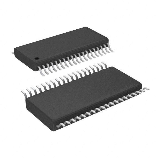
| 描述 | IC DAC 12BIT W/I2C 10-MSOP数模转换器- DAC Quad 12-bit NV DAC with I2C interface |
| 产品分类 | |
| 品牌 | Microchip Technology |
| 产品手册 | |
| 产品图片 |
|
| rohs | 符合RoHS无铅 / 符合限制有害物质指令(RoHS)规范要求 |
| 产品系列 | 数据转换器IC,数模转换器- DAC,Microchip Technology MCP4728-E/UN- |
| 数据手册 | http://www.microchip.com/mymicrochip/filehandler.aspx?ddocname=en542384 |
| 产品型号 | MCP4728-E/UN |
| 产品目录页面 | |
| 产品种类 | 数模转换器- DAC |
| 位数 | 12 |
| 供应商器件封装 | 10-MSOP |
| 其它名称 | MCP4728EUN |
| 分辨率 | 12 bit |
| 包装 | 管件 |
| 商标 | Microchip Technology |
| 安装类型 | 表面贴装 |
| 安装风格 | SMD/SMT |
| 封装 | Tube |
| 封装/外壳 | 10-TFSOP,10-MSOP(0.118",3.00mm 宽) |
| 封装/箱体 | MSOP-10 |
| 工作温度 | -40°C ~ 125°C |
| 工厂包装数量 | 100 |
| 建立时间 | 6µs |
| 接口类型 | I2C |
| 数据接口 | I²C, 串行 |
| 最大工作温度 | + 125 C |
| 最小工作温度 | - 40 C |
| 标准包装 | 100 |
| 电压参考 | 2.048 V |
| 电压源 | 单电源 |
| 电源电压-最大 | 5.5 V |
| 电源电压-最小 | 2.7 V |
| 积分非线性 | +/- 13 LSB |
| 稳定时间 | 6 us |
| 结构 | Resistor-String |
| 视频文件 | http://www.digikey.cn/classic/video.aspx?PlayerID=1364138032001&width=640&height=455&videoID=43013015001 |
| 转换器数 | 4 |
| 转换器数量 | 4 |
| 输出数和类型 | 4 电压,单极 |
| 输出类型 | Voltage |
| 配用 | /product-detail/zh/MCP4728EV/MCP4728EV-ND/2170202 |
| 采样率(每秒) | 3.4M |


- 商务部:美国ITC正式对集成电路等产品启动337调查
- 曝三星4nm工艺存在良率问题 高通将骁龙8 Gen1或转产台积电
- 太阳诱电将投资9.5亿元在常州建新厂生产MLCC 预计2023年完工
- 英特尔发布欧洲新工厂建设计划 深化IDM 2.0 战略
- 台积电先进制程称霸业界 有大客户加持明年业绩稳了
- 达到5530亿美元!SIA预计今年全球半导体销售额将创下新高
- 英特尔拟将自动驾驶子公司Mobileye上市 估值或超500亿美元
- 三星加码芯片和SET,合并消费电子和移动部门,撤换高东真等 CEO
- 三星电子宣布重大人事变动 还合并消费电子和移动部门
- 海关总署:前11个月进口集成电路产品价值2.52万亿元 增长14.8%


PDF Datasheet 数据手册内容提取
MCP4728 12-Bit, Quad Digital-to-Analog Converter with EEPROM Memory Features Description • 12-Bit Voltage Output DAC with Four Buffered The MCP4728 device is a quad, 12-bit voltage output Outputs Digital-to-Analog Convertor (DAC) with nonvolatile • On-Board Nonvolatile Memory (EEPROM) for memory (EEPROM). Its on-board precision output DAC Codes and I2C™ Address Bits amplifier allows it to achieve rail-to-rail analog output swing. • Internal or External Voltage Reference Selection • Output Voltage Range: The DAC input codes, device configuration bits, and I2C address bits are programmable to the nonvolatile - Using Internal V (2.048V): REF memory (EEPROM) by using I2C serial interface 0.000V to 2.048V with Gain Setting = 1 commands. The nonvolatile memory feature enables 0.000V to 4.096V with Gain Setting = 2 the DAC device to hold the DAC input codes during power-off time, allowing the DAC outputs to be - Using External V (V ): REF DD available immediately after power-up with the saved 0.000V to VDD settings. This feature is very useful when the DAC • ±0.2 Least Significant Bit (LSB) Differential device is used as a supporting device for other devices Nonlinearity (DNL) (typical) in the application’s network. • Fast Settling Time: 6µs (typical) The MCP4728 device has a high precision internal • Normal or Power-Down Mode voltage reference (VREF = 2.048V). The user can select the internal reference or external reference (V ) for • Low Power Consumption DD each channel individually. • Single-Supply Operation: 2.7V to 5.5V • I2C Interface: Each channel can be operated in Normal mode or Power-Down mode individually by setting the - Address bits: User Programmable to configuration register bits. In Power-Down mode, most EEPROM of the internal circuits in the powered down channel are - Standard (100kbps), Fast (400kbps) and turned off for power savings, and the output amplifier High Speed (HS) Mode (3.4Mbps) can be configured to present a known low, medium, or • 10-Lead MSOP Package high resistance output load. • Extended Temperature Range: -40°C to +125°C The MCP4728 device includes a Power-on Reset (POR) circuit to ensure reliable power-up and an Applications on-board charge pump for the EEPROM programming voltage. • Set Point or Offset Adjustment The MCP4728 has a two-wire I2C compatible serial • Sensor Calibration interface for standard (100kHz), fast (400kHz), or high • Closed-Loop Servo Control speed (3.4MHz) mode. • Low Power Portable Instrumentation The MCP4728 DAC is an ideal device for applications • PC Peripherals requiring design simplicity with high precision, and for • Programmable Voltage and Current Source applications requiring the DAC device settings to be • Industrial Process Control saved during power-off time. • Instrumentation The MCP4728 device is available in a 10-lead MSOP • Bias Voltage Adjustment for Power Amplifiers package and operates from a single 2.7V to 5.5V supply voltage. © 2010 Microchip Technology Inc. DS22187E-page 1
MCP4728 Package Type MCP4728 MSOP VDD 1 10VSS SCL 2 9 V D OUT SDA 3 8 VOUTC LDAC 4 7 V B OUT RDY/BSY 5 6 V A OUT Functional Block Diagram LDAC VDD E EPROM A UDAC VREFA C oGnatirno l O Luotpguict OP VSS REGINISPTUETR A REOGUISTPTEURT A STRINGDACA AMP A VOUTA Power Down E EPROM B UDAC VREFB Gain Control Output Logic Control gic REGINISPTUETR B REOGUITSPTUERT B STRINGDACB AOMPP B VOUTB o SDA e L E EPROM C Power Down SCL nterfac UDAC VREFC C Gonatirno l Control O Luotpguict 2IC I REGINISPTUETR C REOGUISTTPEURT C STRINGDACC AOMPP C VOUTC E EPROM D UDAC VREFD Gain PCoownetrro Dlown O Luotpguict Control RDY/BSY REGINISPTUETR D REOGUISTTPEURT D STRINGDACD AOMPP D VOUTD Int(e2r.n0a4l8 VVR) EF VREF Selector VREF PCoownetrro Dlown (VREFA, VREFB, VREFC, VREFD) VDD DS22187E-page 2 © 2010 Microchip Technology Inc.
MCP4728 1.0 ELECTRICAL † Notice: Stresses above those listed under “Maximum CHARACTERISTICS ratings” may cause permanent damage to the device. This is a stress rating only and functional operation of the device at these or any other conditions above those indicated in the Absolute Maximum Ratings† operation listings of this specification is not implied. Exposure to maximum rating conditions for extended periods may affect V ...................................................................................6.5V DD All inputs and outputs w.r.t V .................-0.3V to V +0.3V device reliability. SS DD Current at Input Pins ....................................................±2mA Current at Supply Pins .............................................±110mA Current at Output Pins ...............................................±25mA Storage Temperature ...................................-65°C to +150°C Ambient Temp. with Power Applied .............-55°C to +125°C ESD protection on all pins ................≥ 4kVHBM, ≥ 400VMM Maximum Junction Temperature (T ) .........................+150°C J ELECTRICAL CHARACTERISTICS Electrical Specifications: Unless otherwise indicated, all parameters apply at V =+2.7V to 5.5V, V =0V, DD SS R =5kΩ, C =100pF, G =1, T =-40°Cto+125°C. Typical values are at +25°C, V =V , V =V L L X A IH DD IL SS. Parameter Symbol Min Typical Max Units Conditions Power Requirements Operating Voltage V 2.7 5.5 V DD Supply Current with I — 800 1400 µA V =V , V =5.5V DD_EXT REF DD DD External Reference All 4 channels are in Normal mode. (VREF=VDD) — 600 — µA 3 channels are in Normal mode, (Note1) 1 channel is powered down. — 400 — µA 2 channels are in Normal mode, 2 channel are powered down. — 200 — µA 1 channel is in Normal mode, 3 channels are powered down. Power-Down Current with I — 40 — nA All 4 channels are powered down. PD_EXT External Reference (V =V ) REF DD Supply Current with I — 800 1400 µA V =Internal Reference DD_INT REF Internal Reference V =5.5V DD (V = Internal) All 4 channels are in normal mode. REF (Note1) — 600 — µA 3 channels are in Normal mode, 1 channel is powered down. — 400 — µA 2 channels are in Normal mode, 2 channels are powered down. — 200 — µA 1 channel is in Normal mode, 3 channels are powered down. Power-Down Current with I — 45 60 µA All 4 channels are powered down. PD_INT Internal Reference V =Internal Reference REF Note 1: All digital input pins (SDA, SCL, LDAC) are tied to “High”, Output pins are unloaded, code=0x000. 2: The power-up ramp rate measures the rise of V over time. DD 3: This parameter is ensured by design and not 100% tested. 4: This parameter is ensured by characterization and not 100% tested. 5: Test code range: 100 - 4000 codes, V = V , V = 5.5V. REF DD DD 6: Time delay to settle to a new reference when switching from external to internal reference or vice versa. 7: This parameter is indirectly tested by Offset and Gain error testing. 8: Within 1/2 LSB of the final value when code changes from 1/4 of to 3/4 of full scale. 9: This time delay is measured from the falling edge of ACK pulse in I2C command to the beginning of V . OUT This time delay is not included in the output settling time specification. © 2010 Microchip Technology Inc. DS22187E-page 3
MCP4728 ELECTRICAL CHARACTERISTICS (CONTINUED) Electrical Specifications: Unless otherwise indicated, all parameters apply at V =+2.7V to 5.5V, V =0V, DD SS R =5kΩ, C =100pF, G =1, T =-40°Cto+125°C. Typical values are at +25°C, V =V , V =V L L X A IH DD IL SS. Parameter Symbol Min Typical Max Units Conditions Power-on Reset V — 2.2 — V All circuits, including EEPROM, are POR Threshold Voltage ready to operate. Power-Up Ramp Rate V 1 — — V/s Note2, Note4 RAMP DC Accuracy Resolution n 12 — — Bits Code Change: 000h to FFFh Integral Nonlinearity (INL) INL — ±2 ±13 LSB Note5 Error DNL Error DNL -0.75 ±0.2 ±0.75 LSB Note5 Offset Error V — 5 20 mV Code=000h OS See Figure2-24 Offset Error Drift ΔV /°C — ±0.16 — ppm/°C -45°C to +25°C OS — ±0.44 — ppm/°C +25°C to +125°C Gain Error G -1.25 0.4 +1.25 % of Code=FFFh, E FSR Offset error is not included. Typical value is at room temperature See Figure2-25 Gain Error Drift ΔG /°C — -3 — ppm/°C E Internal Voltage Reference (V ), (Note3) REF Internal Voltage Reference V 2.007 2.048 2.089 V REF Temperature Coefficient ΔV /°C — 125 — ppm/°C -40 to 0°C REF — 0.25 — LSB/°C — 45 — ppm/°C 0 to +125°C — 0.09 — LSB/°C Reference Output Noise E — 290 — µV Code=FFFh, NREF p-p 0.1–10Hz, G =1 x Output Noise Density e — 1.2 — Code=FFFh, 1kHz, G =1 NREF x μV — 1.0 — HZ Code=FFFh, 10kHz, G =1 x 1/f Corner Frequency f — 400 — Hz CORNER Note 1: All digital input pins (SDA, SCL, LDAC) are tied to “High”, Output pins are unloaded, code=0x000. 2: The power-up ramp rate measures the rise of V over time. DD 3: This parameter is ensured by design and not 100% tested. 4: This parameter is ensured by characterization and not 100% tested. 5: Test code range: 100 - 4000 codes, V = V , V = 5.5V. REF DD DD 6: Time delay to settle to a new reference when switching from external to internal reference or vice versa. 7: This parameter is indirectly tested by Offset and Gain error testing. 8: Within 1/2 LSB of the final value when code changes from 1/4 of to 3/4 of full scale. 9: This time delay is measured from the falling edge of ACK pulse in I2C command to the beginning of V . OUT This time delay is not included in the output settling time specification. DS22187E-page 4 © 2010 Microchip Technology Inc.
MCP4728 ELECTRICAL CHARACTERISTICS (CONTINUED) Electrical Specifications: Unless otherwise indicated, all parameters apply at V =+2.7V to 5.5V, V =0V, DD SS R =5kΩ, C =100pF, G =1, T =-40°Cto+125°C. Typical values are at +25°C, V =V , V =V L L X A IH DD IL SS. Parameter Symbol Min Typical Max Units Conditions Analog Output (Output Amplifier) Output Voltage Swing V — FSR — V Note7 OUT Full Scale Range FSR — V — V V =V DD REF DD (Note7) FSR= from 0.0V to V DD — V — V V =Internal, G =1, REF REF x FSR= from 0.0 V to V REF — 2*V — V V =Internal, G =2, REF REF x FSR= from 0.0V to 2*V REF Output Voltage T — 6 — µs Note8 SETTLING Settling Time Analog Output Time Delay Td — 4.5 — µs V =5V, ExPD DD from Power-Down Mode Note4, Note9 Time delay to settle to new Td — 26 — µs From External to Internal REF reference Reference (Note4, Note6) — 44 — µs From Internal to External Reference Power Supply Rejection PSRR — -57 — dB VDD=5V±10%, VREF=Internal Capacitive Load Stability C — — 1000 pF R =5kΩ L L No oscillation, Note4 Slew Rate SR — 0.55 — V/µs Phase Margin p — 66 — Degree C =400pF, R =∞ M L L (°) Short Circuit Current I — 15 24 mA V =5V, SC DD All V Pins=Grounded. OUT Tested at room temperature. Short Circuit Current T — Infinite — hours Note4 SC_DUR Duration DC Output Impedance R — 1 — Ω Normal mode OUT (Note4) — 1 — kΩ Power-Down mode 1 (PD1:PD0 = 0:1), V to V OUT SS — 100 — kΩ Power-Down mode 2 (PD1:PD0 = 1:0), V to V OUT SS — 500 — kΩ Power-Down mode 3 (PD1:PD0 = 1:1), V to V OUT SS Note 1: All digital input pins (SDA, SCL, LDAC) are tied to “High”, Output pins are unloaded, code=0x000. 2: The power-up ramp rate measures the rise of V over time. DD 3: This parameter is ensured by design and not 100% tested. 4: This parameter is ensured by characterization and not 100% tested. 5: Test code range: 100 - 4000 codes, V = V , V = 5.5V. REF DD DD 6: Time delay to settle to a new reference when switching from external to internal reference or vice versa. 7: This parameter is indirectly tested by Offset and Gain error testing. 8: Within 1/2 LSB of the final value when code changes from 1/4 of to 3/4 of full scale. 9: This time delay is measured from the falling edge of ACK pulse in I2C command to the beginning of V . OUT This time delay is not included in the output settling time specification. © 2010 Microchip Technology Inc. DS22187E-page 5
MCP4728 ELECTRICAL CHARACTERISTICS (CONTINUED) Electrical Specifications: Unless otherwise indicated, all parameters apply at V =+2.7V to 5.5V, V =0V, DD SS R =5kΩ, C =100pF, G =1, T =-40°Cto+125°C. Typical values are at +25°C, V =V , V =V L L X A IH DD IL SS. Parameter Symbol Min Typical Max Units Conditions Dynamic Performance (Note4) Major Code Transition — 45 — nV-s 1 LSB code change around major Glitch carry (from 7FFh to 800h) Digital Feedthrough — <10 — nV-s Analog Crosstalk — <10 — nV-s DAC-to-DAC Crosstalk — <10 — nV-s Digital Interface Output Low Voltage V — — 0.4 V I =3mA OL OL SDA and RDY/BSY pins Schmitt Trigger V — — 0.3V V V >2.7V. IL DD DD Low Input SDA, SCL, LDAC pins Threshold Voltage — — 0.2V V V ≤2.7V. DD DD SDA, SCL, LDAC pins Schmitt Trigger V 0.7V — — V SDA, SCL, LDAC pins IH DD High Input Threshold Voltage Input Leakage I — — ±1 µA SCL=SDA=LDAC=V LI DD, SCL=SDA=LDAC=V SS Pin Capacitance C — — 3 pF Note4 PIN EEPROM EEPROM Write Time TWRITE — 25 50 ms EEPROM write time Data Retention — 200 — Years At +25°C, Note3 LDAC Input LDAC Low Time T 210 — — ns Updates analog outputs (Note3) LDAC Note 1: All digital input pins (SDA, SCL, LDAC) are tied to “High”, Output pins are unloaded, code=0x000. 2: The power-up ramp rate measures the rise of V over time. DD 3: This parameter is ensured by design and not 100% tested. 4: This parameter is ensured by characterization and not 100% tested. 5: Test code range: 100 - 4000 codes, V = V , V = 5.5V. REF DD DD 6: Time delay to settle to a new reference when switching from external to internal reference or vice versa. 7: This parameter is indirectly tested by Offset and Gain error testing. 8: Within 1/2 LSB of the final value when code changes from 1/4 of to 3/4 of full scale. 9: This time delay is measured from the falling edge of ACK pulse in I2C command to the beginning of V . OUT This time delay is not included in the output settling time specification. DS22187E-page 6 © 2010 Microchip Technology Inc.
MCP4728 THIGH TRSCL T FSCL T SCL SU:STA T SU:STO TLOW THD:DAT TSU:DAT TBUF SDA TSP THD:STA 0.3VDD 0.7VDD T T AA T FSDA RSDA FIGURE 1-1: I2C Bus Timing Data. LDAC T LDAC 0.7V DD 0.3V DD V (UDAC=1) OUT No Update Update FIGURE 1-2: LDAC Pin Timing vs. V Update. OUT © 2010 Microchip Technology Inc. DS22187E-page 7
MCP4728 I 2C SERIAL TIMING SPECIFICATIONS Electrical Specifications: Unless otherwise specified, all limits are specified for T = -40 to +125°C, V = 0V, A SS Standard and Fast Mode: V = +2.7V to +5.5V DD High Speed Mode: V = +4.5V to +5.5V. DD Parameters Sym Min Typ Max Units Conditions Clock Frequency f 0 — 100 kHz Standard Mode SCL C =400pF, 2.7V–5.5V b 0 — 400 kHz Fast Mode C =400pF, 2.7V–5.5V b 0 — 1.7 MHz High Speed Mode 1.7 C =400pF, 4.5V–5.5V b 0 — 3.4 MHz High Speed Mode 3.4 C =100pF, 4.5V–5.5V b Bus Capacitive Loading Cb — — 400 pF Standard Mode 2.7V–5.5V — — 400 pF Fast Mode 2.7V–5.5V — — 400 pF High Speed Mode 1.7 4.5V–5.5V — — 100 pF High Speed Mode 3.4 4.5V–5.5V Start Condition Setup Time TSU:STA 4700 — ns Standard Mode (Start, Repeated Start) 600 — — ns Fast Mode 160 — — ns High Speed Mode 1.7 160 — — ns High Speed Mode 3.4 Start Condition Hold Time THD:STA 4000 — ns Standard Mode 600 — — ns Fast Mode 160 — — ns High Speed Mode 1.7 160 — — ns High Speed Mode 3.4 Stop Condition Setup Time TSU:STO 4000 — ns Standard Mode 600 — — ns Fast Mode 160 — — ns High Speed Mode 1.7 160 — — ns High Speed Mode 3.4 Clock High Time THIGH 4000 — — ns Standard Mode 600 — — ns Fast Mode 120 — — ns High Speed Mode 1.7 60 — — ns High Speed Mode 3.4 Clock Low Time TLOW 4700 — — ns Standard Mode 1300 — — ns Fast Mode 320 — — ns High Speed Mode 1.7 160 — — ns High Speed Mode 3.4 Note 1: This parameter is ensured by characterization and is not 100% tested. 2: After a Repeated Start condition or an Acknowledge bit. 3: If this parameter is too short, it can create an unintentional Start or Stop condition to other devices on the I2C bus line. If this parameter is too long, the Data Input Setup (T ) or Clock Low time (T ) can be affected. SU:DAT LOW Data Input: This parameter must be longer than t . SP Data Output: This parameter is characterized, and tested indirectly by testing T parameter. AA 4: This specification is not a part of the I2C specification. This specification is equivalent to the Data Hold Time (THD:DAT) plus SDA Fall (or rise) time: TAA = THD:DAT + TFSDA (OR TRSDA). 5: Time between Start and Stop conditions. DS22187E-page 8 © 2010 Microchip Technology Inc.
MCP4728 I2C SERIAL TIMING SPECIFICATIONS (CONTINUED) Electrical Specifications: Unless otherwise specified, all limits are specified for T = -40 to +125°C, V = 0V, A SS Standard and Fast Mode: V = +2.7V to +5.5V DD High Speed Mode: V = +4.5V to +5.5V. DD Parameters Sym Min Typ Max Units Conditions SCL Rise Time TRSCL — — 1000 ns Standard Mode (Note1) 20+0.1Cb — 300 ns Fast Mode 20 — 80 ns High Speed Mode 1.7 20 — 160 ns High Speed Mode 1.7 (Note2) 10 — 40 ns High Speed Mode 3.4 10 — 80 ns High Speed Mode 3.4 (Note2) SDA Rise Time TRSDA — — 1000 ns Standard Mode (Note1) 20 + 0.1Cb — 300 ns Fast Mode 20 — 80 ns High Speed Mode 1.7 10 — 40 ns High Speed Mode 3.4 SCL Fall Time TFSCL — — 300 ns Standard Mode (Note1) 20 + 0.1Cb — 300 ns Fast Mode 20 — 80 ns High Speed Mode 1.7 10 — 40 ns High Speed Mode 3.4 SDA Fall Time TFSDA — — 300 ns Standard Mode (Note1) 20 + 0.1Cb — 300 ns Fast Mode 20 — 160 ns High Speed Mode 1.7 10 — 80 ns High Speed Mode 3.4 Data Input Setup Time TSU:DAT 250 — — ns Standard Mode 100 — — ns Fast Mode 10 — — ns High Speed Mode 1.7 10 — — ns High Speed Mode 3.4 Data Hold Time THD:DAT 0 — 3450 ns Standard Mode (Input, Output) 0 — 900 ns Fast Mode (Note3) 0 — 150 ns High Speed Mode 1.7 0 — 70 ns High Speed Mode 3.4 Output Valid from Clock TAA 0 — 3750 ns Standard Mode (Note4) 0 — 1200 ns Fast Mode 0 — 310 ns High Speed Mode 1.7 0 — 150 ns High Speed Mode 3.4 Note 1: This parameter is ensured by characterization and is not 100% tested. 2: After a Repeated Start condition or an Acknowledge bit. 3: If this parameter is too short, it can create an unintentional Start or Stop condition to other devices on the I2C bus line. If this parameter is too long, the Data Input Setup (T ) or Clock Low time (T ) can be affected. SU:DAT LOW Data Input: This parameter must be longer than t . SP Data Output: This parameter is characterized, and tested indirectly by testing T parameter. AA 4: This specification is not a part of the I2C specification. This specification is equivalent to the Data Hold Time (THD:DAT) plus SDA Fall (or rise) time: TAA = THD:DAT + TFSDA (OR TRSDA). 5: Time between Start and Stop conditions. © 2010 Microchip Technology Inc. DS22187E-page 9
MCP4728 I2C SERIAL TIMING SPECIFICATIONS (CONTINUED) Electrical Specifications: Unless otherwise specified, all limits are specified for T = -40 to +125°C, V = 0V, A SS Standard and Fast Mode: V = +2.7V to +5.5V DD High Speed Mode: V = +4.5V to +5.5V. DD Parameters Sym Min Typ Max Units Conditions Bus Free Time TBUF 4700 — — ns Standard Mode (Note5) 1300 — — ns Fast Mode — — — ns High Speed Mode 1.7 — — — ns High Speed Mode 3.4 Input Filter TSP — — — ns Standard Mode Spike Suppression (Not Applicable) (SDA and SCL) — 50 — ns Fast Mode (Not Tested) — 10 — ns High Speed Mode 1.7 — 10 — ns High Speed Mode 3.4 Note 1: This parameter is ensured by characterization and is not 100% tested. 2: After a Repeated Start condition or an Acknowledge bit. 3: If this parameter is too short, it can create an unintentional Start or Stop condition to other devices on the I2C bus line. If this parameter is too long, the Data Input Setup (T ) or Clock Low time (T ) can be affected. SU:DAT LOW Data Input: This parameter must be longer than t . SP Data Output: This parameter is characterized, and tested indirectly by testing T parameter. AA 4: This specification is not a part of the I2C specification. This specification is equivalent to the Data Hold Time (THD:DAT) plus SDA Fall (or rise) time: TAA = THD:DAT + TFSDA (OR TRSDA). 5: Time between Start and Stop conditions. TEMPERATURE CHARACTERISTICS Electrical Specifications: Unless otherwise indicated, V =+2.7V to +5.5V, V =GND. DD SS Parameters Symbol Min Typical Max Units Conditions Temperature Ranges Specified Temperature Range T -40 — +125 °C A Operating Temperature Range T -40 — +125 °C A Storage Temperature Range T -65 — +150 °C A Thermal Package Resistances Thermal Resistance, 10L-MSOP θ — 202 — °C/W JA DS22187E-page 10 © 2010 Microchip Technology Inc.
MCP4728 2.0 TYPICAL PERFORMANCE CURVES Note: The graphs and tables provided following this note are a statistical summary based on a limited number of samples and are provided for informational purposes only. The performance characteristics listed herein are not tested or guaranteed. In some graphs or tables, the data presented may be outside the specified operating range (e.g., outside specified power supply range) and therefore, outside the warranted range. Note: Unless otherwise indicated, T = -40°C to +125°C, V = +5.0V, V = 0V, R = 5kΩ, C = 100pF. A DD SS L L 6 VDD = 5.5V, VREF = Internal, Gain = x1 0.3 VDD = 5.5V, VREF = Internal, Gain = x1 4 0.2 2 SB) SB)0.1 L (L0 L(L N N 0 I-2 D -4 -0.1 -6 -0.2 0 1024 2048 3072 4096 0 1024 2048 3072 4096 Code Code FIGURE 2-1: INL vs. Code (T = +25°C). FIGURE 2-4: DNL vs. Code (T = +25°C). A A 6 0.3 VDD = 5.5V, VREF = Internal, Gain = x2 VDD = 5.5V, VREF = Internal, Gain = x2 4 0.2 B)2 B)0.1 NL (LS0 NL (LS 0 I-2 D -0.1 -4 -6 -0.2 0 1024 2048 3072 4096 0 1024 2048 3072 4096 Code Code FIGURE 2-2: INL vs. Code (T = +25°C). FIGURE 2-5: DNL vs. Code (T = +25°C). A A 6 0.2 VDD = 5.5V, VREF = VDD VDD = 5.5V, VREF = VDD 4 0.15 INL (LSB)-202 DNL (LSB)00.0.501 -4 -0.05 -6 -0.1 0 1024 2048 3072 4096 0 1024 2048 3072 4096 Code Code FIGURE 2-3: INL vs. Code (T = +25°C). FIGURE 2-6: DNL vs. Code (T = +25°C). A A © 2010 Microchip Technology Inc. DS22187E-page 11
MCP4728 Note: Unless otherwise indicated, T = -40°C to +125°C, V = +5.0V, V = 0V, R = 5kΩ, C = 100pF. A DD SS L L 6 0.4 V = 2.7V, V = Internal, Gain = x1 V = 2.7V, V = Internal, Gain = x1 DD REF DD REF 4 0.3 2 0.2 B) B) NL (LS0 NL (LS0.1 I-2 D 0 -4 -0.1 -6 -0.2 0 1024 2048 3072 4096 0 1024 2048 3072 4096 Code Code FIGURE 2-7: INL vs. Code (T = +25°C). FIGURE 2-10: DNL vs. Code (T = +25°C). A A 6 0.4 VDD = 2.7V, VREF = VDD VDD = 2.7V, VREF = VDD 4 0.3 2 0.2 B) B) NL (LS 0 NL (LS0.1 I-2 D 0 -4 -0.1 -6 -0.2 0 1024 2048 3072 4096 0 1024 2048 3072 4096 Code Code FIGURE 2-8: INL vs. Code (T = +25°C). FIGURE 2-11: DNL vs. Code (T = +25°C). A A 6 0.4 VDD = 5.5V, VREF = Internal, Gain = x1 VDD = 5.5V, VREF = Internal, Gain = x1 4 +85°C 0.3 2 -40oC 0.2 B) 0 B) S S INL (L --42 +25oC DNL(L0.01 -6 +125oC -0.1 -8 +125oC - 40oC to +85oC -10 -0.2 0 1024 2048 3072 4096 0 1024 2048 3072 4096 Code Code FIGURE 2-9: INL vs. Code and FIGURE 2-12: DNL vs. Code and Temperature. Temperature. DS22187E-page 12 © 2010 Microchip Technology Inc.
MCP4728 Note: Unless otherwise indicated, T = -40°C to +125°C, V = +5.0V, V = 0V, R = 5kΩ, C = 100pF. A DD SS L L 6 0.4 VDD = 5.5V, VREF = Internal, Gain = x2 VDD = 5.5V, VREF = Internal, Gain = x2 4 0.3 - 40oC +25oC +85oC 2 0.2 INL (LSB) --420 DNL (LSB)0.01 -0.1 -6 -8 -0.2 +125oC +125oC - 40oC to +85oC -10 -0.3 0 1024 2048 3072 4096 0 1024 2048 3072 4096 Code Code FIGURE 2-13: INL vs. Code and FIGURE 2-16: DNL vs. Code and Temperature. Temperature. 6 0.5 VDD = 2.7V, VREF = Internal, Gain = x1 VDD = 2.7V, VREF = Internal, Gain = x1 4 0.4 2 0.3 B) 0 B)0.2 S S NL (L --42 - 40oC NL (L0.10 I +25oC D -6 -0.1 +85oC -8 -0.2 +125oC +125oC - 40oC to +85oC -10 -0.3 0 1024 2048 3072 4096 0 1024 2048 3072 4096 Code Code FIGURE 2-14: INL vs. Code and FIGURE 2-17: DNL vs. Code and Temperature. Temperature. 6 VDD = 5.5V, VREF = VDD 0.4 VDD = 5.5V, VREF = VDD 4 0.3 +85oC INL (LSB)-202 - 40oC DNL (LSB)00..012 -4 -0.1 +125oC +25oC +125oC - 40oC to +85oC -6 -0.2 0 1024 2048 3072 4096 0 1024 2048 3072 4096 Code Code FIGURE 2-15: INL vs. Code and FIGURE 2-18: DNL vs. Code and Temperature. Temperature. © 2010 Microchip Technology Inc. DS22187E-page 13
MCP4728 Note: Unless otherwise indicated, T = -40°C to +125°C, V = +5.0V, V = 0V, R = 5kΩ, C = 100pF. A DD SS L L 6 0.5 VDD = 2.7V, VREF = VDD 0.4 VDD = 2.7V, VREF = VDD 4 - 40oC +85oC 0.3 2 INL (LSB)-20 +125oC DNL (LSB)00..012 -4 -0.1 +25oC -6 -0.2 +125oC - 40oC to +85oC -8 -0.3 0 1024 2048 3072 4096 0 1024 2048 3072 4096 Code Code FIGURE 2-19: INL vs. Code and FIGURE 2-22: DNL vs. Code and Temperature. Temperature. 6 -10 V = 2.7V, Gain = 1 5 mV)-20 DD V) VDD = 5.5V, Gain = 2 ale Error (-30 VDD = 5.5V, Gain = 1 et Error (m 34 VDD = 5.5V, Gain = 1 c s 2 Full S-40 Off 1 VDD = 2.7V, Gain = 1 VDD = 5.5V, Gain = 2 -50 0 -40 -25 -10 5 20 35 50 65 80 95 110 125 -40 -25 -10 5 20 35 50 65 80 95 110 125 Temperature (oC) Temperature (oC) FIGURE 2-20: Full Scale Error vs. FIGURE 2-23: Zero Scale Error vs. Temperature (Code = FFFh, V = Internal). Temperature (Code = 000h, V = Internal). REF REF 50 4 mV)40 VDD = 5.5V, Gain = 1 V) 3 VDD = 5.5V ull Scale Error (2300 VDD = 2.7V, Gain = 1 Offset Error (m 12 VDD = 2.7V F 0 10 -40 -25 -10 5 20 35 50 65 80 95 110 125 -40 -25 -10 5 20 35 50 65 80 95 110 125 Temperature (oC) Temperature (oC) FIGURE 2-21: Full Scale Error vs. FIGURE 2-24: Offset Error (Zero Scale Temperature (Code = FFFh, V = V ). Error). REF DD DS22187E-page 14 © 2010 Microchip Technology Inc.
MCP4728 Note: Unless otherwise indicated, T = -40°C to +125°C, V = +5.0V, V = 0V, R = 5kΩ, C = 100pF. A DD SS L L 16 V = Internal, Gain = x2 REF 14 2 Temp = +25oC 12 V (2V/Div) Ch. D OUT 10 SB8 Ch. A L Ch. B 6 Ch. C 4 LDAC Time (2µs/Div) 2 0 0 500 1000 1500 2000 2500 3000 3500 Codes FIGURE 2-25: Absolute DAC Output Error FIGURE 2-28: Full Scale Settling Time (V =5.5V). (V = Internal, V = 5V, UDAC = 1, DD REF DD Gain = x1, CodeChange: 000h to FFFh). V (2V/Div) OUT V (2V/Div) OUT LDAC Time (2µs/Div) LDAC Time (2µs/Div) FIGURE 2-26: Full Scale Settling Time FIGURE 2-29: Full Scale Settling Time (V = V , V = 5V, UDAC = 1, (V = V , V = 5V, UDAC = 1, REF DD DD REF DD DD CodeChange: 000h to FFFh). CodeChange: FFFh to 000h). VOUT (2V/Div) VOUT (2V/Div) Time (2µs/Div) Time (2µs/Div) LDAC LDAC FIGURE 2-27: Half Scale Settling Time FIGURE 2-30: Half Scale Settling Time (V = V , V = 5V, UDAC = 1, (V = V , V = 5V, UDAC = 1, REF DD DD REF DD DD CodeChange: 000h to 7FFh). CodeChange: 7FFh to 000h). © 2010 Microchip Technology Inc. DS22187E-page 15
MCP4728 Note: Unless otherwise indicated, T = -40°C to +125°C, V = +5.0V, V = 0V, R = 5kΩ, C = 100pF. A DD SS L L Discharging Time due to internal pull-down resistor (500kΩ) V (1V/Div) OUT V (2V/Div) OUT Time (2µs/Div) LDAC Time (10µs/Div) CLK Last ACK CLK pulse FIGURE 2-31: Full Scale Settling Time FIGURE 2-34: Entering Power Down Mode (V = Internal, V = 5V, UDAC = 1, (Code: FFFh, V = Internal, V = 5V, REF DD REF DD Gain = x1, CodeChange: FFFh to 000h). Gain = x1, PD1= PD0 = 1, No External Load). V (1V/Div) OUT V (1V/Div) OUT Time (2µs/Div) LDAC LDAC Time (2µs/Div) FIGURE 2-32: Half Scale Settling Time FIGURE 2-35: Half Scale Settling Time (VREF = Internal, VDD = 5V, UDAC = 1, (VREF = Internal, VDD = 5V, UDAC = 1, Gain = x1, CodeChange: 000h to 7FFh). Gain = x1, Code Change: 7FFh to 000h). VOUT (1V/Div) VOUT (2V/Div) TdExPD TdExPD Time (5µs/Div) Time (5µs/Div) CLK Last ACK CLK pulse CLK Last ACK CLK pulse FIGURE 2-33: Exiting Power Down Mode FIGURE 2-36: Exiting Power Down Mode (Code: FFFh, VREF = Internal, VDD = 5V, (Code: FFFh, VREF = VDD, VDD = 5V, for all Gain = x1, for all Channels.). Channels). DS22187E-page 16 © 2010 Microchip Technology Inc.
MCP4728 Note: Unless otherwise indicated, T = -40°C to +125°C, V = +5.0V, V = 0V, R = 5kΩ, C = 100pF. A DD SS L L Discharging Time due to internal pull-down resistor (500 kΩ) V at Channel D OUT (5V/Div) V (2V/Div) OUT LDAC V at Channel A OUT (100mV/Div) Time (5µs/Div) Time (20µs/Div) CLK Last ACK CLK pulse FIGURE 2-37: Entering Power Down Mode FIGURE 2-40: Channel Cross Talk (Code: FFFh, V = V , V = 5V, (V = V , V = 5V). REF DD DD REF DD DD PD1= PD0 = 1, No External Load). V (2V/Div) OUT V (50mV/Div) OUT Time (10µs/Div) Time (2µs/Div) CLK Last ACK CLK pulse FIGURE 2-38: V Time Delay when FIGURE 2-41: Code Change Glitch OUT V changes from Internal Reference to V . (V = External, V = 5V, No External Load), REF DD REF DD Code Change: 800h to 7FFh. V (2V/Div) OUT V (50mV/Div) OUT Time (2µs/Div) Time (10µs/Div) CLK Last ACK CLK pulse FIGURE 2-39: V Time Delay when FIGURE 2-42: Code Change Glitch OUT V changes from V to Internal Reference. (V = Internal, V = 5V, Gain = 1, No External REF DD REF DD Load), Code Change: 800h to 7FFh. © 2010 Microchip Technology Inc. DS22187E-page 17
MCP4728 Note: Unless otherwise indicated, T = -40°C to +125°C, V = +5.0V, V = 0V, R = 5kΩ, C = 100pF. A DD SS L L 6 900 All Channels On VDD = 5.5V 5 VDD = 5V 800 VDD = 5V 4 VREF = VDD A) (V)UT3 Code = FFFh (µEXT700 VDD = 4.5V VO2 IDD_ VDD = 3.3V 600 1 VDD = 2.7V 0 500 0 1 2 3 4 5 -40 -25 -10 5 20 35 50 65 80 95 110 125 Load Resistance (kΩ) Temperature (oC) FIGURE 2-43: V vs. Resistive Load. FIGURE 2-46: I vs. Temperature OUT DD (V = V , All channels are in Normal Mode, REF DD Code = FFFh). 1000 1000 VDD = 5.0V All Channels On All Channels On 800 VDD = 5.0V 800 3 Channels On A) 3 Channels On A) 600 I (µDD_EXT460000 2 Channels On I (µDD_INT 400 2 1C Chhanannnelesl OOnn 200 200 1 Channel On 0 0 -40 -25 -10 5 20 35 50 65 80 95 110125 -40 -25 -10 5 20 35 50 65 80 95 110125 Temperature (oC) Temperature (oC) FIGURE 2-44: IDD vs. Temperature FIGURE 2-47: IDD vs. Temperature (VREF = VDD, VDD = 5V, Code = FFFh). (VREF = Internal, VREF = 5V, Code = FFFh). 800 1000 VDD = 2.7V All Channels On 800 VDD = 2.7V All Channels On 600 (µA)D_EXT400 32 CChhaannnneellss OOnn (µA)DD_INT 460000 23 CChhaannnneellss OOnn D I I 1 Channel On 200 200 1 Channel On 0 0 -40 -25 -10 5 20 35 50 65 80 95 110125 -40 -25 -10 5 20 35 50 65 80 95 110 125 Temperature (oC) Temperature (oC) FIGURE 2-45: IDD vs. Temperature FIGURE 2-48: IDD vs. Temperature (VREF = VDD, VDD = 2.7V, Code = FFFh). (VREF=Internal, VDD = 2.7V, Code = FFFh). DS22187E-page 18 © 2010 Microchip Technology Inc.
MCP4728 Note: Unless otherwise indicated, T = -40°C to +125°C, V = +5.0V, V = 0V, R = 5kΩ, C = 100pF. A DD SS L L 900 6 All Channels On VDD = 5.5V Code = FFFh 5 800 VDD = 5V µA) V) 4 (DD_INT700 VDD = 3.V3DVD = 4.5V V (OUT 23 I 600 VDD = 2.7V 1 500 0 -40 -25 -10 5 20 35 50 65 80 95 110 125 0 2 4 6 8 10 12 14 16 Temperature (oC) Current (mA) FIGURE 2-49: I vs. Temperature FIGURE 2-51: Source Current Capability DD (V = Internal All Channels are in Normal (V = V , Code = FFFh). REF , REF DD Mode, Code = FFFh). 6 60 Code = 000h All Channels Off 5 I (µA)DDP_INT 4500 VDD = 4.5V VDD = 5V VDD = 5.5V V (V)OUT 234 30 1 VDD = 3.3V VDD = 2.7V 0 20 0 2 4 6 8 10 12 14 -40 -25 -10 5 20 35 50 65 80 95 110 125 Temperature (oC) Sink Current (mA) FIGURE 2-50: I vs. Temperature FIGURE 2-52: Sink Current Capability DD (V = Internal All Channels are in Powered (V = V , Code = 000h). REF , REF DD Down). © 2010 Microchip Technology Inc. DS22187E-page 19
MCP4728 NOTES: DS22187E-page 20 © 2010 Microchip Technology Inc.
MCP4728 3.0 PIN DESCRIPTIONS The descriptions of the pins are listed in Table3-1. TABLE 3-1: PIN FUNCTION TABLE Pin No. Name Pin Type Function 1 V P Supply Voltage DD 2 SCL OI I2C Serial Clock Input (Note1) 3 SDA OI/OO I2C Serial Data Input and Output (Note1) 4 LDAC ST This pin is used for two purposes: (a) Synchronization Input. It is used to transfer the contents of the DAC input registers to the output registers (V ). OUT (b) Select the device for reading and writing I2C address bits. (Note2) 5 RDY/BSY OO This pin is a status indicator of EEPROM programming activity. An external pull-up resistor (about 100kΩ) is needed from RDY/BSY pin to V line. (Note1) DD 6 V A AO Buffered analog voltage output of channel A. The output amplifier has rail-to-rail OUT operation. 7 V B AO Buffered analog voltage output of channel B. The output amplifier has rail-to-rail OUT operation. 8 V C AO Buffered analog voltage output of channel C. The output amplifier has rail-to-rail OUT operation. 9 V D AO Buffered analog voltage output of channel D. The output amplifier has rail-to-rail OUT operation. 10 V P Ground reference. SS Legend: P = Power, OI = Open-Drain Input, OO = Open-Drain Output, ST = Schmitt Trigger Input Buffer, AO = Analog Output Note 1: This pin needs an external pull-up resistor from V line. Leave this pin float if it is not used. DD 2: This pin can be driven by MCU. 3.1 Supply Voltage Pins (V , V ) 3.2 Serial Clock Pin (SCL) DD SS V is the power supply pin for the device. The voltage SCL is the serial clock pin of the I2C interface. The DD at the V pin is used as a power supply input as well MCP4728 device acts only as a slave and the SCL pin DD as a DAC external reference. The power supply at the accepts only external input serial clocks. The input data V pin should be as clean as possible for a good DAC from the Master device is shifted into the SDA pin on DD performance. the rising edges of the SCL clock, and output from the MCP4728 occurs at the falling edges of the SCL clock. It is recommended to use an appropriate bypass capacitor of about 0.1µF (ceramic) to ground. An The SCL pin is an open-drain N-channel driver. additional 10µF capacitor (tantalum) in parallel is also Therefore, it needs a pull-up resistor from the V line DD recommended to further attenuate high-frequency to the SCL pin. noise present in application boards. The supply voltage Refer to Section5.0 “I2C Serial Interface (VDD) must be maintained in the 2.7V to 5.5V range for Communications” for more details on I2C Serial specified operation. Interface communication. V is the ground pin and the current return path of the SS Typical range of the pull-up resistor value for SCL and device. The user must connect the V pin to a ground SS SDA is from 5kΩ to 10kΩ for Standard (100kHz) and plane through a low-impedance connection. If an Fast (400kHz) modes, and less than 1kΩ for High analog ground path is available in the application Speed mode (3.4MHz). printed circuit board (PCB), it is highly recommended that the V pin be tied to the analog ground path, or SS isolated within an analog ground plane of the circuit board. © 2010 Microchip Technology Inc. DS22187E-page 21
MCP4728 3.3 Serial Data Pin (SDA) 3.5 RDY/BSY Status Indicator Pin SDA is the serial data pin of the I2C interface. The SDA This pin is a status indicator of EEPROM programming pin is used to write or read the DAC register and activity. This pin is “High” when the EEPROM has no EEPROM data. Except for Start and Stop conditions, programming activity, and “Low” when the EEPROM is the data on the SDA pin must be stable during the high in programming mode. It goes “High” when the duration of the clock pulse. The High or Low state of the EEPROM program is completed. SDA pin can only change when the clock signal on the The RDY/BSY pin is an open-drain N-channel driver. SCL pin is Low. Therefore, it needs a pull-up resistor (about 100kΩ) The SDA pin is an open-drain N-channel driver. from the V line to the RDY/BSY pin. Let this pin float DD Therefore, it needs a pull-up resistor from the V line if it is not used. DD to the SDA pin. Refer to Section5.0 “I2C Serial Interface 3.6 Analog Output Voltage Pins Communications” for more details on the I2C Serial (VOUTA, VOUT B, VOUT C, VOUT D) Interface communication. The device has four analog voltage output (V ) pins. OUT Each output is driven by its own output buffer with a 3.4 LDAC Pin gain of 1 or 2, depending on the gain and V REF This pin can be driven by an external control device selection bit settings. In Normal mode, the DC such as an MCU I/O pin. This pin is used to: impedance of the output pin is about 1Ω. In Power-Down mode, the output pin is internally a) transfer the contents of the input registers to connected to 1kΩ, 100kΩ, or 500kΩ, depending on their corresponding DAC output registers and the Power-Down selection bit settings. b) select a device of interest when reading or writ- ing I2C address bits. The VOUT pin can drive up to 1000pF of capacitive load. It is recommended to use a load with R greater For more details on reading and writing the I2C address than 5kΩ. L bits, see Section5.4.4 “General Call Read Address Bits” and Section5.6.8 “Write Command: Write I2C Address bits (C2=0, C1=1, C0=1)”. When the logic status of the LDAC pin changes from “High” to “Low”, the contents of all input registers (Channels A – D) are transferred to their corresponding output registers, and all analog voltage outputs are updated simultaneously. If this pin is permanently tied to “Low”, the content of the input register is transferred to its output register (V ) immediately at the last input data byte’s OUT acknowledge pulse. The user can also use the UDAC bit instead. However, the UDAC bit updates a selected channel only. See Section4.8 “Output Voltage Update” for more information on the LDAC pin and UDAC bit functions. DS22187E-page 22 © 2010 Microchip Technology Inc.
MCP4728 4.0 THEORY OF DEVICE 4.2 Reset Conditions OPERATION The device can be reset by two independent events: The MCP4728 device is a 12-bit 4-channel buffered a) by Power-on Reset voltage output DAC with nonvolatile memory b) by I2C General Call Reset Command (EEPROM). The user can program the EEPROM with Under the reset conditions, the device uploads the I2C address bits, configuration and DAC input data of EEPROM data into both of the DAC input and output each channel. The device has an internal charge pump registers simultaneously. The analog output voltage of circuit to provide the programming voltage of the each channel is available immediately, regardless of EEPROM. the LDAC and UDAC bit conditions. When the device is first powered-up, it automatically The factory default settings for the EEPROM prior to loads the stored data in its EEPROM to the DAC input the device shipment are shown in Table4-2. and output registers, and provides analog outputs with the saved settings immediately. This event does not 4.3 Output Amplifier require an LDAC or UDAC bit condition. After the device is powered-up, the user can update the input The DAC output is buffered with a low power precision registers using I2C write commands. The analog amplifier. This amplifier provides low offset voltage and outputs can be updated with new register values if the low noise, as well as rail-to-rail output. LDAC pin or UDAC bit is low. The DAC output of each The output amplifier can drive the resistive and high channel is buffered with a low power and precision capacitive loads without oscillation. The amplifier can output amplifier. This amplifier provides a rail-to-rail provide a maximum load current of 24mA, which is output with low offset voltage and low noise. enough for most of programmable voltage reference The device uses a resistor string architecture. The applications. Refer to Section1.0 “Electrical resistor ladder DAC can be driven from VDD or internal Characteristics” for the specifications of the output VREF, depending on the reference selection. The user amplifier. can select internal (2.048V) or external reference (V ) DD for each DAC channel individually by software control. 4.3.1 PROGRAMMABLE GAIN BLOCK The V is used as the external reference. Each DD The rail-to-rail output amplifier of each channel has channel is controlled and operated independently. configurable gain option. When the internal voltage The device has a Power-Down mode feature. Most of reference is selected, the output amplifier gain has two the circuit in each powered down channel are turned selection options: Gain of 1 or Gain of 2. off. Therefore, operating power can be saved When the external reference is selected (V =V ), significantly by putting any unused channel to the REF DD the Gain of 2 option is disabled, and only the Gain of 1 Power-Down mode. is used by default. 4.1 Power-on Reset (POR) 4.3.1.1 Resistive and Capacitive Loads The device contains an internal Power-on Reset (POR) The analog output (VOUT) pin is capable of driving circuit that monitors power supply voltage (V ) during capacitive loads up to 1000pF in parallel with 5kΩ DD operation. This circuit ensures correct device start-up load resistance. Figure2-43 shows the VOUT vs. at system power-up and power-down events. Resistive Load. If the power supply voltage is less than the POR threshold (V =2V, typical), all circuits are disabled POR and there will be no analog output. When the V DD increases above the V , the device takes a reset POR state. During the reset period, each channel uploads all configuration and DAC input codes from EEPROM, and analog output (V ) will be available accordingly. OUT This enables the device to return to the same state that it was at the last write to the EEPROM, before it was powered off. The POR status is monitored by the POR status bit by using the I2C read command. See Figure5-15 for the details of the POR status bit. © 2010 Microchip Technology Inc. DS22187E-page 23
MCP4728 4.4 DAC Input Registers and Non-Volatile EEPROM Memory Each channel has its own volatile DAC input register and EEPROM. The details of the input registers and EEPROM are shown in Table4-1 and Table4-2, respectively. TABLE 4-1: INPUT REGISTER MAP (VOLATILE) Configuration Bits DAC Input Data (12 bits) Bit RDY A2 A1 A0 VREF DAC1 DAC0 PD1 PD0 GX D11 D10 D9 D8 D7 D6 D5 D4 D3 D2 D1 D0 Name /BSY Bit I2C Ref. DAC Channel Power-Down Gain (Note 2) Function Address Bits Select Select Select (Note1) (Note2) (Note 2) (Note 2) (Note 2) (Note 2) CH. A CH. B CH. C CH. D Note 1: EEPROM write status indication bit (flag). 2: Loaded from EEPROM during power-up, or can be updated by the user. TABLE 4-2: EEPROM MEMORY MAP AND FACTORY DEFAULT SETTINGS Configuration Bits DAC Input Data (12 bits) Bit Name A2 A1 A0 VREF PD1 PD0 GX D11 D10 D9 D8 D7 D6 D5 D4 D3 D2 D1 D0 Bit Ref. Power-Down Gain Function I2C Address Bits Select Select Select (Note1) (Note2) (Note3) CH. A 0 0 0 1 0 0 0 0 0 0 0 0 0 0 0 0 0 0 0 CH. B 1 0 0 0 0 0 0 0 0 0 0 0 0 0 0 0 CH. C 1 0 0 0 0 0 0 0 0 0 0 0 0 0 0 0 CH. D 1 0 0 0 0 0 0 0 0 0 0 0 0 0 0 0 Note 1: Device I2C address bits. The user can also specify these bits during the device ordering process. The factory default setting is “000”. These bits can be reprogrammed by the user using the I2C Address Write command. 2: Voltage Reference Select: 0 = External V (V ), 1 = Internal V (2.048V). REF DD REF 3: Gain Select: 0 = Gain of 1, 1 = Gain of 2. DS22187E-page 24 © 2010 Microchip Technology Inc.
MCP4728 TABLE 4-3: CONFIGURATION BITS Bit Name Functions RDY/BSY This is a status indicator (flag) of EEPROM programming activity: 1 = EEPROM is not in programming mode 0 = EEPROM is in programming mode Note: RDY/BSY status can also be monitored at the RDY/BSY pin. (A2, A1, A0) Device I2C address bits. See Section5.3 “MCP4728 Device Addressing” for more details. V Voltage Reference Selection bit: REF 0 = VDD 1 = Internal voltage reference (2.048V) Note: Internal voltage reference circuit is turned off if all channels select external reference (V = V . REF DD) DAC1, DAC0 DAC Channel Selection bits: 00 = Channel A 01 = Channel B 10 = Channel C 11 = Channel D PD1, PD0 Power-Down selection bits: 00 = Normal Mode 01 = VOUT is loaded with 1kΩ resistor to ground. Most of the channel circuits are powered off. 10 = VOUT is loaded with 100kΩ resistor to ground. Most of the channel circuits are powered off. 11 = VOUT is loaded with 500kΩ resistor to ground. Most of the channel circuits are powered off. Note: See Table4-7 and Figure4-1 for more details. G Gain selection bit: X 0 = x1 (gain of 1) 1 = x2 (gain of 2) Note: Applicable only when internal V is selected. If V = V , the device uses a gain of 1 REF REF DD regardless of the gain selection bit setting. UDAC DAC latch bit. Upload the selected DAC input register to its output register (V ): OUT 0 = Upload. Output (VOUT) is updated. 1 = Do not upload. Note: UDAC bit affects the selected channel only. © 2010 Microchip Technology Inc. DS22187E-page 25
MCP4728 4.5 Voltage Reference • When the external reference (V =V ) is REF DD selected: The device has a precision internal voltage reference - V = 0.000V to V which provides a nominal voltage of 2.048V. The user OUT DD can select the internal voltage reference or V as the DD Note: The gain selection bit is not applicable voltage reference source of each channel using the for V = V . In this case, Gain of 1 REF DD V configuration bit. The internal voltage reference REF is used regardless of the gain selection circuit is turned off when all channels select V as DD bit setting. their references. However, it stays turned on if any one of the channels selects the internal reference. EQUATION 4-1: V FOR V = OUT REF INTERNAL REFERENCE 4.6 LSB Size The LSB is defined as the ideal voltage difference VOUT = (VRE4F0 9x6 Dn ) x Gx ≤ V DD between two successive codes. LSB sizes of the Where: MCP4728 device are shown in Table4-4. V = 2.048V for internal reference selection REF TABLE 4-4: LSB SIZES (EXAMPLE) D = DAC input code n V Gain (GX) LSB Size Condition Gx = Gain Setting REF Selection Internal x1 0.5mV 2.048V/4096 EQUATION 4-2: V FOR V = V OUT REF DD VREF x2 1mV 4.096V/4096 (V ×D ) DD n (2.048V) V = ----------------------------- OUT 4096 V x1 V /4096 (Note1) Where: DD DD Note 1: LSB size varies with the VDD range. D = DAC input code n When V = V , the device uses REF DD G =1 by default. G = 2 option is X X 4.8 Output Voltage Update ignored. The following events update the output registers 4.7 DAC Output Voltage (V ): OUT Each channel has an independent output associated a. LDAC pin to “Low”: Updates all DAC channels. with its own configuration bit settings and DAC input b. UDAC bit to “Low”: Updates a selected channel code. When the internal voltage reference is selected only. (V = internal), it supplies the internal V voltage REF REF c. General Call Software Update Command: to the resistor string DAC of the channel. When the Updates all DAC channels. external reference (V =V ) is selected, V is used REF DD DD for the channel’s resistor string DAC. d. Power-on Reset or General Call Reset command: Both input and output registers are The V needs to be as clean as possible for accurate DD updated with EEPROM data. All channels are DAC performance. When the V is selected as the DD affected. voltage reference, any variation or noises on the V DD line can directly affect on the DAC output. 4.8.1 LDAC PIN AND UDAC BIT The analog output of each channel has a The user can use the LDAC pin or UDAC bit to upload programmable gain block. The rail-to-rail output the input DAC register to output DAC register (V ). OUT amplifier has a configurable gain of 1 or 2. But the gain However, the UDAC affects only the selected channel of 2 is not applicable if V is selected for the voltage DD while the LDAC affects all channels. The UDAC bit is reference. The formula for the analog output voltage is not used in the Fast Mode Writing. given in Equation4-1 and Equation4-2. Table4-5 shows the output update vs. LDAC pin and 4.7.1 OUTPUT VOLTAGE RANGE UDAC bit conditions. The DAC output voltage range varies depending on the voltage reference selection. • When the internal reference (V =2.048V) is REF selected: - V = 0.000V to 2.048V * 4095/4096 for OUT Gain of 1 - V = 0.000V to 4.096V * 4095/4096 for OUT Gain of 2 DS22187E-page 26 © 2010 Microchip Technology Inc.
MCP4728 4.9 DAC Input Code Vs. DAC Analog TABLE 4-5: LDAC AND UDAC Output CONDITIONS VS. OUTPUT UPDATE Table4-6 shows an example of the DAC input data LDAC Pin UDAC Bit DAC Output (V ) code vs. analog output. The MSB of the input data is OUT always transmitted first and the format is unipolar 0 0 Update all DAC channel binary. outputs 0 1 Update all DAC channel outputs 1 0 Update a selected DAC channel output 1 1 No update TABLE 4-6: DAC INPUT CODE VS. ANALOG OUTPUT (V ) OUT V = Internal (2.048 V) V = V REF REF DD DAC Input Code Gain Nominal Output Voltage (V) Gain Nominal Output Voltage (V) Selection (See Note1) Selection 111111111111 x1 VREF - 1 LSB Ignored VDD - 1 LSB x2 2*V - 1 LSB REF 111111111110 x1 VREF - 2 LSB VDD - 2 LSB x2 2*V - 2 LSB REF 000000000010 x1 2 LSB 2 LSB x2 2 LSB 000000000001 x1 1 LSB 1 LSB x2 1 LSB 000000000000 x1 0 0 x2 0 Note 1: (a) LSB with gain of 1 = 0.5mV, and (b) LSB with gain of 2 = 1mV. © 2010 Microchip Technology Inc. DS22187E-page 27
MCP4728 4.10 Normal and Power-Down Modes Exiting Power-Down Mode: The device exits Power-Down mode immediately by Each channel has two modes of operation: (a) Normal the following commands: mode where analog voltage is available and (b) Power-Down mode which turns off most of the internal • Any write command for normal mode. Only circuits for power savings. selected channel is affected The user can select the operating mode of each • I2C General Call Wake-Up Command. All channel individually by setting the Power-Down channels are affected selection bits (PD1 and PD0). For example, the user • I2C General Call Reset Command. This is a can select Normal mode for channel A while selecting conditional case. The device exits Power-Down Power-Down mode for all other channels. mode, depending on the Power-Down bit settings in EEPROM as the configuration bits and DAC See Section5.6 “Write Commands for DAC input codes are uploaded from EEPROM. All Registers and EEPROM” for more details on the channels are affected writing the power-down bits. When the DAC operation mode is changed from the Most of the internal circuit in the powered down Power-Down to Normal mode, there will be a time channel are turned off. However, the internal voltage delay until the analog output is available. Typical time reference circuit is not affected by the Power-Down delay for the output voltage is approximately 4.5µs. mode. The internal voltage reference circuit is turned This time delay is measured from the acknowledge off only if all channels select external reference (V REF pulse of the I2C serial communication command to the = V ). DD beginning of the analog output (V ). This time delay OUT Device actions during Power-Down mode: is not included in the output settling time specification. • The powered down channel stays in a See Section2.0 “Typical Performance Curves” for power-saving condition by turning off most of its more details. circuits TABLE 4-7: POWER-DOWN BITS • No analog voltage output at the powered down channel PD1 PD0 Function • The output (VOUT) pin of the powered down 0 0 Normal Mode channel is switched to a known resistive load. The 0 1 1kΩ resistor to ground (Note1) value of the resistive load is determined by the 1 0 100kΩ resistor to ground state of the Power-Down bits (PD1 and PD0). (Note1) Table4-7 shows the outcome of the Power-Down 1 1 500kΩ resistor to ground bit settings (Note1) • The contents of both the DAC registers and Note 1: In Power-Down mode: V is off and EEPROM are not changed OUT most of internal circuits in the selected • Draws less than 40nA (typical) when all four channel are disabled. channels are powered down and V is selected DD as the voltage reference Circuits that are not affected during Power-Down V OUT mode: OP Amp • The I2C serial interface circuits remain active in order to receive any command from the Master • The internal voltage reference circuit stays Power-Down turned-on if it is selected as reference by at least Control Circuit 1kΩ 100kΩ500kΩ one channel Resistor String DAC Resistive Load FIGURE 4-1: Output Stage for Power-Down Mode. DS22187E-page 28 © 2010 Microchip Technology Inc.
MCP4728 5.0 I2C SERIAL INTERFACE 5.1.1 HIGH-SPEED (HS) MODE COMMUNICATIONS The I2C specification requires that a high-speed mode device must be ‘activated’ to operate in High-Speed The MCP4728 device uses a two-wire I2C serial (3.4Mbit/s) mode. This is done by sending a special interface. When the device is connected to the I2C bus address byte of 00001XXX following the START bit. line, the device works as a slave device. The device The XXX bits are unique to the high-speed mode supports standard, fast and high speed modes. Master. This byte is referred to as the high-speed The following sections describe how to communicate Master Mode Code (HSMMC). The MCP4728 device with the MCP4728 device using the I2C serial interface does not acknowledge this byte. However, upon commands. receiving this command, the device switches to HS mode and can communicate at up to 3.4Mbit/s on SDA 5.1 Overview of I2C Serial Interface and SCL lines. The device will switch out of the HS Communications mode on the next STOP condition. For more information on the HS mode, or other I2C An example of the hardware connection diagram is modes, please refer to the Philips I2C specification. shown in Figure7-1. A device that sends data onto the bus is defined as the transmitter, and a device receiving 5.2 I2C BUS CHARACTERISTICS data, as the receiver. The bus has to be controlled by a master (MCU) device which generates the serial clock The specification of the I2C serial communication (SCL), controls the bus access and generates the defines the following bus protocol: START and STOP conditions. Both master (MCU) and • Data transfer may be initiated only when the bus slave (MCP4728) can operate as transmitter or is not busy receiver, but the master device determines which mode is activated. • During data transfer, the data line must remain stable whenever the clock line is HIGH. Changes Communication is initiated by the master (MCU) which in the data line while the clock line is HIGH will be sends the START bit, followed by the slave (MCP4728) interpreted as a START or STOP condition address byte. The first byte transmitted is always the slave (MCP4728) address byte, which contains the Accordingly, the following bus conditions have been device code (1100), the address bits (A2, A1, A0), and defined using Figure5-1. the R/W bit. The device code for the MCP4728 device 5.2.1 BUS NOT BUSY (A) is 1100, and the address bits are user-writable. Both data and clock lines remain HIGH. When the MCP4728 device receives a Read command (R/W = 1), it transmits the contents of the DAC input 5.2.2 START DATA TRANSFER (B) registers and EEPROM sequentially. When writing to the device (R/W = 0), the device will expect Write A HIGH to LOW transition of the SDA line, while the command type bits in the following byte. The reading clock (SCL) is HIGH, determines a START condition. and various writing commands are explained in the All commands must be preceded by a START following sections. condition. The MCP4728 device supports all three I2C serial 5.2.3 STOP DATA TRANSFER (C) communication operating modes: • Standard Mode: bit rates up to 100kbit/s A LOW to HIGH transition of the SDA line, while the clock (SCL) is HIGH, determines a STOP condition. All • Fast Mode: bit rates up to 400kbit/s operations must be ended with a STOP condition. • High Speed Mode (HS mode): bit rates up to 3.4Mbit/s 5.2.4 DATA VALID (D) Refer to the Philips I2C document for more details of The state of the data line represents valid data when, the I2C specifications. after a START condition, the data line is stable for the duration of the HIGH period of the clock signal. The data on the line must be changed during the LOW period of the clock signal. There is one clock pulse per bit of data. Each data transfer is initiated with a START condition and terminated with a STOP condition. © 2010 Microchip Technology Inc. DS22187E-page 29
MCP4728 5.2.5 ACKNOWLEDGE period of the acknowledge related clock pulse. Of course, setup and hold times must be taken into Each receiving device, when addressed, is obliged to account. During reads, a master must send an end of generate an acknowledge after the reception of each data to the slave by not generating an acknowledge bit byte. The master device must generate an extra clock on the last byte that has been clocked out of the slave. pulse, which is associated with this acknowledge bit. In this case, the slave (MCP4728) will leave the data The device that acknowledges has to pull down the line HIGH to enable the master to generate the STOP SDA line during the acknowledge clock pulse in such a condition. way that the SDA line is stable LOW during the HIGH (A) (B) (D) (D) (C) (A) SCL SDA START ADDRESS OR DATA STOP CONDITION ACKNOWLEDGE ALLOWED CONDITION VALID TO CHANGE FIGURE 5-1: Data Transfer Sequence On The Serial Bus. 5.3 MCP4728 Device Addressing 5.3.1 PROGRAMMING OF I2C ADDRESS BITS The address byte is the first byte received following the START condition from the master device. The first part When the customer first receives any new MCP4728 of the address byte consists of a 4-bit device code, device, its default address bit setting is “000” if the which is set to 1100 for the MCP4728 device. The address bit programming was not requested. The device code is followed by three I2C address bits (A2, customer can reprogram the I2C address bits into the A1, A0) which are programmable by the users. EEPROM by using “Write Address Bit” command. This Although the three address bits are programmable at write command needs current address bits. If the the user’s application PCB, the user can also specify address bits are unknown, the user can find them by the address bits during the product ordering process. If sending “General Call Read Address” Command. The there is no user’s request, the factory default setting of LDAC pin is also used to select the device of interest to the three address bits is “000”, programmed into the be programmed or to read the current address. EEPROM. The three address bits allow eight unique The following steps are needed for the I2C address addresses. programming. (a) Read the address bits using “General Call Read Acknowledge bit Address” Command. (This is the case when the Start bit Read/Write bit address is unknown.) (b) Write I2C address bits using “Write I2C Address Slave Address R/W ACK Bits” Command. Address Byte The Write Address command will replace the current address with a new address in both input registers and EEPROM. Slave Address for MCP4728 Device Code Address Bits See Section5.4.4 “General Call Read Address Bits” for the details of reading the address bits, and Section5.6.8 “Write Command: Write I2C Address 1 1 0 0 A2 A1 A0 bits (C2=0, C1=1, C0=1)” for writing the address bits. Device Code: Programmed (hard-wired) at the factory. Address Bits: Reprogrammable into EEPROM by the user. FIGURE 5-2: Device Addressing. DS22187E-page 30 © 2010 Microchip Technology Inc.
MCP4728 5.4 I2C General Call Commands 5.4.1 GENERAL CALL RESET The device acknowledges the general call address The General Call Reset occurs if the second byte is command (0x00 in the first byte). The meaning of the “00000110” (06h). At the acknowledgement of this general call address is always specified in the second byte, the device will abort the current conversion and byte. The I2C specification does not allow the use of perform the following tasks: “00000000” (00h) in the second byte. Refer to the • Internal Reset similar to a Power-on Reset (POR). Philips I2C document for more details of the General The contents of the EEPROM are loaded into Call specifications. each DAC input and output registers immediately The MCP4728 device supports the following I2C • VOUT will be available immediately regardless of General Calls: the LDAC pin condition • General Call Reset • General Call Wake-Up • General Call Software Update • General Call Read Address Bits ACK (MCP4728) Clock Pulse (CLK Line) Start Stop 1 2 3 4 5 6 7 8 9 1 2 3 4 5 6 7 8 9 1st Byte 2nd Byte (General Call Command) (Command Type = General Call Reset) Note 1 Data (SDA Line) Note 1: At this falling edge of the last ACK clock bit: a. Startup Timer starts a reset sequence and b. EEPROM data is loaded into the DAC Input and Output Registers immediately. FIGURE 5-3: General Call Reset. 5.4.2 GENERAL CALL WAKE-UP If the second byte is “00001001” (09h), the device will reset the Power-Down bits (PD1, PD0 = 0,0). ACK (MCP4728) Clock Pulse (CLK Line) Start Stop 1 2 3 4 5 6 7 8 9 1 2 3 4 5 6 7 8 9 1st Byte 2nd Byte Note 1 (General Call Command) (Command Type = General Call Wake-Up) Data (SDA Line) Note 1: Resets Power-Down bits at this falling edge of the last ACK clock bit. FIGURE 5-4: General Call Wake-Up. © 2010 Microchip Technology Inc. DS22187E-page 31
MCP4728 5.4.3 GENERAL CALL SOFTWARE UPDATE If the second byte is “00001000” (08h), the device updates all DAC analog outputs (V ) at the same OUT time. ACK (MCP4728) Clock Pulse (CLK Line) Start Stop 1 2 3 4 5 6 7 8 9 1 2 3 4 5 6 7 8 9 1st Byte 2nd Byte (General Call Command) (Command Type = General Call Software Update) Note 1 Data (SDA Line) Note 1: At this falling edge of the last ACK clock bit, V A, V B, V C, V D are updated. OUT OUT OUT OUT FIGURE 5-5: General Call Software Update. DS22187E-page 32 © 2010 Microchip Technology Inc.
MCP4728 5.4.4 GENERAL CALL READ ADDRESS select the device of interest to read on the I2C bus. The BITS LDAC pin needs a logic transition from “High” to “Low” during the negative pulse of the 8th clock of the second This command is used to read the I2C address bits of byte, and stays “Low” until the end of the 3rd byte. The the device. If the second byte is “00001100” (0Ch), the maximum clock rate for this command is 400kHz. device will output its address bits stored in EEPROM and register. This command uses the LDAC pin to ACK (MCP4728) ACK (Master) Restart Start 4th Byte Stop S 0 0 0 0 0 0 0 0 A 0 0 0 0 1 1 0 0 A Sr 1 1 0 0 X X X 1 A A2 A1 A0 1 A2 A1 A0 0 A P 1st Byte 2nd Byte 3rd Byte Address Bits Address Bits (General Call Address) Restart Byte in in Input EEPROM Register Reading Address Bits LDAC Pin (Notes 1, 2, 3) Note 3 Clock and LDAC Transition Details: ACK Clock Restart Clock ACK Clock Clock Pulse (CLK Line) 6 7 8 9 Sr 1 2 3 4 5 6 7 8 9 1 2 3 2nd Byte 4th Byte 3rd Byte Reading Address Bits Note 2(b, c) LDAC Pin Note 2(b) Note 3 Note 2 (a) Stay “Low” until the end of the 3rd Byte Note 1: Clock Pulse and LDAC Transition Details. 2: LDAC pin events at the 2nd and 3rd bytes. a. Keep LDAC pin “High” until the end of the positive pulse of the 8th clock of the 2nd byte. b. LDAC pin makes a transition from “High” to “Low” during the negative pulse of the 8th clock of the 2nd byte (just before the rising edge of the 9th clock) and stays “Low” until the rising edge of clock 9 of the 3rd byte. c. The MCP4728 device does not acknowledge the 3rd byte if the conditions (a) and (b) are not met. 3: LDAC pin resumes its normal function after “Stop” bit. FIGURE 5-6: General Call Read I2C Address. © 2010 Microchip Technology Inc. DS22187E-page 33
MCP4728 5.5 Writing and Reading Registers 5.6 Write Commands for DAC and EEPROM Registers and EEPROM The Master (MCU) can write or read the DAC input Table5-1 summarizes the write command types and registers or EEPROM using the I2C interface their functions.The write command is defined by using command. three write command type bits (C , C , C ) and two 2 1 0 write function bits (W1, W0). The register selection bits The following sections describe the communication (DAC1, DAC0) are used to select the DAC channel. examples to write and read the DAC registers and EEPROM using the I2C interface. TABLE 5-1: WRITE COMMAND TYPES Write Command Field Function Command Name Function C2 C1 C0 W1 W0 Fast Mode Write 0 0 X Not Used Fast Write for DAC This command writes to the DAC input registers sequentially with Input Registers limited configuration bits. The data is sent sequentially from channels A to D. The input register is written at the acknowledge clock pulse of the channel’s last input data byte. EEPROM is not affected. (Note1) Write DAC Input Register and EEPROM 0 1 0 0 0 Multi-Write for DAC This command writes to multiple DAC input registers, one DAC input Input Registers register at a time. The writing channel register is defined by the DAC selection bits (DAC1, DAC0). EEPROM is not affected. (Note2) 1 0 Sequential Write for This command writes to both the DAC input registers and EEPROM DAC Input Registers sequentially. The sequential writing is carried out from a starting and EEPROM channel to channel D. The starting channel is defined by the DAC selection bits (DAC1 and DAC0). The input register is written at the acknowledge clock pulse of the last input data byte of each register. However, the EEPROM data is written altogether at the same time sequentially at the end of the last byte. (Note2),(Note3) 1 1 Single Write for DAC This command writes to a single selected DAC input register and its Input Register and EEPROM. Both the input register and EEPROM are written at the EEPROM acknowledge clock pulse of the last input data byte. The writing channel is defined by the DAC selection bits (DAC1 and DAC0). (Note2),(Note3) Write I2C Address Bits (A2, A1, A0) 0 1 1 Not Used Write I2C Address Bits This command writes new I2C address bits (A2, A1, A0) to the DAC input register and EEPROM. Write V , Gain, and Power-Down Select Bits (Note4) REF 1 0 0 Not Used Write Reference This command writes Reference (V ) selection bits of each channel. REF (V ) selection bits REF to Input Registers 1 1 0 Not Used Write Gain selection This command writes Gain selection bits of each channel. bits to Input Registers 1 0 1 Not Used Write Power-Down This command writes Power-Down bits of each channel. bits to Input Registers Note 1: The analog output is updated when LDAC pin is (or changes to) “Low”. UDAC bit is not used for this command. 2: The DAC output is updated when LDAC pin or UDAC bit is “Low”. 3: The device starts writing to the EEPROM on the acknowledge clock pulse of the last channel. The device does not execute any command until RDY/BSY bit comes back to “High”. 4: The input and output registers are updated at the acknowledge clock pulse of the last byte. The update does not require LDAC pin or UDAC bit conditions. EEPROM is not affected. DS22187E-page 34 © 2010 Microchip Technology Inc.
MCP4728 5.6.1 FAST WRITE COMMAND 5.6.2 MULTI-WRITE COMMAND: WRITE (C2=0, C1=0, C0=X, X = DON’T DAC INPUT REGISTERS CARE) (C2=0, C1=1, C0=0; W1=0, W0=0) The Fast Write command is used to update the input This command is used to write DAC input register, one DAC registers from channels A to D sequentially. The at a time. The EEPROM data is not affected by this EEPROM data is not affected by this command. This command. command is called “Fast Write” because it updates the The DAC selection bits (DAC1, DAC0) select the DAC input registers with only limited data bits. Only the channel to write. Only a selected channel is affected. Power-Down mode selection bits (PD1 and PD0) and Repeated bytes are used to write more multiple DAC 12 bits of DAC input data are writable. registers. The input register is updated at the acknowledge pulse The D11 - D0 bits in the third and fourth bytes are the of each channel’s last data byte. Figure5-7 shows an DAC input data of the selected DAC channel. example of the Fast Write command. Bytes2-4 can be repeated for the other channels. Figure5-8 shows an example of the Multi-Write Updating Analog Outputs: command. a. When the LDAC pin is “High” before the last byte Updating Analog Outputs: of the channel D, all analog outputs are updated simultaneously by bringing down the LDAC pin The analog outputs can be updated by one of the to “Low” any time. following events after the falling edge of the b. If the command starts with the LDAC pin “Low”, acknowledge clock pulse of the 4th byte. the channel’s analog output is updated at the a. When the LDAC pin or UDAC bit is “Low”. falling edge of the acknowledge clock pulse of the channel’s last byte. b. If UDAC bit is “High”, bringing down the LDAC pin to “Low” any time. c. Send the General Call Software Update command: This command updates all channels c. By sending the General Call Software Update command. simultaneously. Note: The UDAC bit is not used in this Note: The UDAC bit can be used effectively to command. upload the input register to the output register, but it affects only a selected channel only, while the LDAC pin and General Call Software Update command affect all channels. © 2010 Microchip Technology Inc. DS22187E-page 35
MCP4728 5.6.3 SEQUENTIAL WRITE COMMAND: 5.6.4 SINGLE WRITE COMMAND: WRITE WRITE DAC INPUT REGISTERS A SINGLE DAC INPUT REGISTER AND EEPROM SEQUENTIALLY AND EEPROM FROM STARTING CHANNEL TO (C2=0, C1=1, C0=0; W1=1, W0=1) CHANNEL D When the device receives this command, it writes the (C2=0, C1=1, C0=0; W1=1, W0=0) input data to a selected single DAC input register and When the device receives this command, it writes the also to its EEPROM. The channel is selected by the input data to the DAC input registers sequentially from channel selection bits (DAC1 and DAC0). See the starting channel to channel D, and also writes to Table5-2 for the channel selection bit function. EEPROM sequentially. The starting channel is Figure5-10 shows an example of the single write determined by the DAC1 and DAC0 bits. Table5-2 command. shows the functions of the channel selection bits for the sequential write command. Updating Analog Outputs: When the device is writing EEPROM, the RDY/BSY bit The analog outputs can be updated by one of the stays “Low” until the EEPROM write operation is following events after the falling edge of the completed. The state of the RDY/BSY bit flag can be acknowledge clock pulse of the 4th byte. monitored by a read command or at the RDY/BSY pin. a. When the LDAC pin or UDAC bit is “Low”. Any new command received during the EEPROM write operation (RDY/BSY bit is “Low”) is ignored. Figure5-9 b. If UDAC bit is “High”, bringing down the LDAC shows an example of the sequential write command. pin to “Low” any time. c. By sending the General Call Software Update Updating Analog Outputs: command. The analog outputs can be updated by one of the Note: The UDAC bit can be used effectively to following events after the falling edge of the upload the input register to the output acknowledge clock pulse of the 4th byte. register, but it affects only a selected a. When the LDAC pin or UDAC bit is “Low”. channel only, while the LDAC pin and General Call Software Update command b. If UDAC bit is “High”, bringing down the LDAC affect all channels. pin to “Low” any time. c. By sending the General Call Software Update command. Note: The UDAC bit can be used effectively to upload the input register to the output register, but it affects only a selected channel only, while the LDAC pin and General Call Software Update command affect all channels. TABLE 5-2: DAC CHANNEL SELECTION BITS FOR SEQUENTIAL WRITE COMMAND DAC1 DAC0 Channels 0 0 Ch. A - Ch. D 0 1 Ch. B - Ch. D 1 0 Ch. C - Ch. D 1 1 Ch. D DS22187E-page 36 © 2010 Microchip Technology Inc.
MCP4728 5.6.5 WRITE COMMAND: SELECT VREF 5.6.8 WRITE COMMAND: WRITE I2C BIT (C2=1, C1=0, C0=0) ADDRESS BITS (C2=0, C1=1, C0=1) When the device receives this command, it updates the This command writes new I2C address bits (A2, A1, DAC voltage reference selection bit (V ) of each A0) to the DAC input registers and EEPROM. When REF channel. The EEPROM data is not affected by this the device receives this command, it overwrites the command. The affected channel’s analog output is current address bits with the new address bits. updated after the acknowledge pulse of the last byte. This command is valid only when the LDAC pin makes Figure5-12 shows an example of the write command a transition from “High” to “Low” at the low time of the for Select V bits. REF last bit (8th clock) of the second byte, and stays “Low” 5.6.6 WRITE COMMAND: SELECT until the end of the third byte. The update occurs after POWER-DOWN BITS (C2=1, C1=0, “Stop” bit, if the conditions are met. The LDAC pin is C0=1) used to select a device of interest to write. The highest clock rate of this command is 400kHz. Figure5-11 When the device receives this command, it updates the shows the details of the address write command. Power-Down selection bits (PD1, PD0) of each channel. The EEPROM data is not affected by this Note: To write a new device address, the current command. The affected channel is updated after the address of the device is also required. If acknowledge pulse of the last byte. Figure5-13 shows the current address is not known, it can be an example of the write command for the Select read out by sending General Call Read Power-Down bits. Address Bits command. See 5.4.4 “General Call Read Address Bits” for 5.6.7 WRITE COMMAND: SELECT GAIN more details of reading the I2C address BIT (C2=1, C1=1, C0=0) bits. When the device receives this command, it updates the 5.6.9 READ COMMAND gain selection bits (G ) of each channel. The EEPROM X data is not affected by this command. The analog If the R/W bit is set to a logic “High” in the I2C serial output is updated after the acknowledge pulse of the communications command, the device enters a last byte. Figure5-14 shows an example of the write reading mode and reads out the input registers and command for select gain bits. EEPROM. Figure5-15 shows the details of the read command. Note: The device address bits are read by using General Call Read Address Bits command. © 2010 Microchip Technology Inc. DS22187E-page 37
MCP4728 Command Type Bits: C2=0 C1=0 C0=X ACK (MCP4728) Start 1st byte (C2 C1) 2nd Byte 3rd Byte S 1 1 0 0 A2 A1 A0 0 A 0 0 PD1 PD0 D11 D10 D9 D8 A D7 D6 D5 D4 D3 D2 D1 D0 A R/W DAC Input Register of Channel A Device Addressing Fast Write Command Update Channel A DAC Input Register at this ACK pulse. ACK (MCP4728) 2nd Byte 3rd Byte X X PD1 PD0 D11 D10 D9 D8 A D7 D6 D5 D4 D3 D2 D1 D0 A DAC Input Register of Channel B Update Channel B DAC Input Register at this ACK pulse. ACK (MCP4728) 2nd Byte 3rd Byte X X PD1 PD0 D11 D10 D9 D8 A D7 D6 D5 D4 D3 D2 D1 D0 A DAC Input Register of Channel C Update Channel C DAC Input Register at this ACK pulse. ACK (MCP4728) 2nd Byte 3rd Byte X X PD1 PD0 D11 D10 D9 D8 A D7 D6 D5 D4 D3 D2 D1 D0 A DAC Input Register of Channel D Update Channel D DAC Input Register at this ACK pulse. Repeat Bytes P Stop Note 1: X is a don’t care bit. VOUT can be updated after the last byte’s ACK pulse is issued and by bringing down the LDAC pin to “Low”. FIGURE 5-7: Fast Write Command: Write DAC Input Registers Sequentially from Channel A to D. DS22187E-page 38 © 2010 Microchip Technology Inc.
MCP4728 Command Type Bits: C2=0 C1=1 C0=0 W1=0 W0=0 ACK (MCP4728) Start 1st byte S 1 1 0 0 A2 A1 A0 0 A R/W Device Addressing ACK (MCP4728) (C2 C1 C0 W1 W2) 2nd Byte 3rd Byte 4th Byte 0 1 0 0 0 DAC1 DAC0 UDAC A V PD1 PD0 Gx D11 D10 D9 D8 A D7 D6 D5 D4 D3 D2 D1 D0 A REF Multi-Write Channel DAC Input Register of Selected Channel Command Select Note 1 Repeat Bytes of the 2nd - 4th Bytes ACK (MCP4728) 2nd byte 3rd Byte 4th Byte X X X X X DAC1 DAC0 UDAC A V PD1 PD0 Gx D11 D10 D9 D8 A D7 D6 D5 D4 D3 D2 D1 D0 A REF Note 3 Channel DAC Input Register of Selected Channel Select Note 2 Note 1 Repeat Bytes of the 2nd - 4th Bytes P Stop Note 1: V Update: OUT If UDAC = 0 or LDAC Pin = 0: V is updated after the 4th byte’s ACK is issued. OUT 2: The user can write to the other channels by sending repeated bytes with new channel selection bits (DAC1, DAC0). 3: X is don’t care bit. FIGURE 5-8: Multi-Write Command: Write Multiple DAC Input Registers. © 2010 Microchip Technology Inc. DS22187E-page 39
MCP4728 Command Type Bits: C2=0 C1=1 C0=0 W1=1 W0=0 ACK (MCP4728) Start 1st byte S 1 1 0 0 A2 A1 A0 0 A R/W Device Addressing ACK (MCP4728) (C2 C1 C0 W1 W2) 2nd Byte 3rd Byte 4th Byte 0 1 0 1 0 DAC1 DAC0 UDAC A V PD1 PD0 Gx D11 D10 D9 D8 A D7 D6 D5 D4 D3 D2 D1 D0 A REF Sequential Write Sequential Write DAC Input Register of Starting Channel Command Starting Channel Select Note 1 Repeat Bytes of the 3rd - 4th Bytes for the Starting Channel + 1, ... until Channel D. ACK (MCP4728) Stop 3rd Byte 4th Byte V PD1 PD0 Gx D11 D10 D9 D8 A D7 D6 D5 D4 D3 D2 D1 D0 A P REF DAC Input Register of Channel D (Last Channel) Notes 1 and 2 Note 1: V Update: OUT If UDAC = 0 or LDAC Pin = 0: V is updated after the 4th byte’s ACK is issued. OUT 2: EEPROM Write: The MCP4728 device starts writing EEPROM at the falling edge of the 4th byte’s ACK pulse. FIGURE 5-9: Sequential Write Command: Write DAC Input Registers and EEPROM Sequentially from Starting Channel to Channel D. The sequential input register starts with the "Starting Channel" and ends at Channel D. For example, if DAC1:DAC0 = 00, then it starts with channel A and ends at channel D. If DAC1:DAC0 = 01, then it starts with channel B and ends at Channel D. Note that this command can send up to 10 bytes including the device addressing and command bytes. Any byte after the 10th byte is ignored. DS22187E-page 40 © 2010 Microchip Technology Inc.
MCP4728 Command Type Bits: C2=0 C1=1 C0=0 W1=1 W0=1 ACK (MCP4728) Start 1st byte S 1 1 0 0 A2 A1 A0 0 A R/W Device Addressing ACK (MCP4728) Stop C2C1C0W1W0 2nd Byte 3rd Byte 4th Byte 0 1 0 1 1 DAC1 DAC0 UDAC A V PD1 PD0 Gx D11 D10 D9 D8 A D7 D6 D5 D4 D3 D2 D1 D0 A P REF Single Write Channel DAC Input Register of Selected Channel Command Select Note 1 and Note 2 Note 1: V Update: OUT If UDAC = 0 or LDAC Pin = 0: V is updated after the 4th byte’s ACK is issued. OUT 2: EEPROM Write: The MCP4728 device starts writing EEPROM at the falling edge of the 4th byte’s ACK pulse. FIGURE 5-10: Single Write Command: Write to a Single DAC Input Register and EEPROM. © 2010 Microchip Technology Inc. DS22187E-page 41
MCP4728 Command Type Bits: C2=0 C1=1 C0=1 Start 1st Byte (C2 C1 C0) 2nd Byte 3rd Byte 4th Byte Stop S 1 1 0 0 A2A1A0 0 A 0 1 1 A2A1A0 0 1 A 0 1 1 A2 A1 A0 1 0 A 0 1 1 A2 A1 A0 1 1 A P Device Current R/W Command Current Command New CommandNew Address Bits Code Address Bits Type Address Bits Type Address Bits Type (for confirmation) Note 4 LDAC Pin (Notes 1, 2, 3) Note 3 Clock and LDAC Transition Details: ACK (MCP4728) Clock Pulse (CLK Line) Stop 5 6 7 8 9 1 2 3 4 5 6 7 8 9 1 ----- 9 P 2nd Byte 3rd Byte 4th Byte Note 4 Note 2(b) LDAC Pin Note 2 (a) Note 2(b) Note 3 Stay “Low” during this 3rd byte Note 1: Clock Pulse and LDAC Transition Details. 2: LDAC pin events at the 2nd and 3rd bytes: a. Keep LDAC pin “High” until the end of the positive pulse of the 8th clock of the 2nd byte. b. LDAC pin makes a transition from “High” to “Low” during the negative pulse of the 8th clock of the 2nd byte (just before the rising edge of the 9th clock), and stays “Low” until the rising edge of the 9th clock of the 3rd byte. c. The MCP4728 device does not acknowledge the 3rd byte if the conditions (a) and (b) are not met. 3: LDAC pin resumes its normal function after “Stop” bit. 4: EEPROM Write: a. Charge Pump initiates the EEPROM write sequence at the falling edge of the 4th byte’s ACK pulse. b. The RDY/BSY bit (pin) goes “Low” at the falling edge of this ACK clock and back to “High” immediately after the EEPROM write is completed. FIGURE 5-11: Write Command: Write I2C Address Bits to the DAC Registers and EEPROM. Note: The I2C address bits can also be programmed at the factory for customers. See the Product Identification System on page 65 for details. DS22187E-page 42 © 2010 Microchip Technology Inc.
MCP4728 Command Type Bits: C2=1 C1=0 C0=0 ACK (MCP4728) Start 1st byte (C2 C1 C0) 2nd Byte Stop S 1 1 0 0 A2 A1 A0 0 A 1 0 0 X V A V B V C V D A P REF REF REF REF R/W Device Addressing Write Note 1 Command Registers and V are updated OUT at this falling edge of ACK pulse. Note 1: V = 0: V REF DD = 1: Internal Reference (2.048V) V A = Voltage reference of Channel A REF V B = Voltage reference of Channel B REF V C = Voltage reference of Channel C REF V D = Voltage reference of Channel D REF 2: X is don’t care bit. FIGURE 5-12: Write Command: Write Voltage Reference Selection Bit (V ) to the DAC Input REF Registers. Command Type Bits: C2=1 C1=0 C0=1 ACK (MCP4728) Start 1st byte S 1 1 0 0 A2 A1 A0 0 A R/W Device Addressing Stop ACK (MCP4728) (C2 C1 C0) 2nd Byte 3rd Byte 1 0 1 X PD1 A PD0 A PD1 BPD0 B A PD1 C PD0 C PD1 D PD0 D X X X X A P WriteCommand Channel A Channel B Channel C Channel D for Power-Down Selection Bits Registers and V are updated OUT at this falling edge of ACK pulse. Note 1: X is don’t care bit. FIGURE 5-13: Write Command: Write Power-Down Selection Bits (PD1, PD0) to the DAC Input Registers. See Table4-7 for the power-down bit setting. © 2010 Microchip Technology Inc. DS22187E-page 43
MCP4728 Command Type Bits: C2=1 C1=1 C0=0 ACK (MCP4728) Start 1st Byte (C2 C1 C0) 2nd Byte Stop S 1 1 0 0 A2 A1 A0 0 A 1 1 0 X G A G B G C G D A P X X X X R/W Device Addressing WriteCommand Note 1 for Gain Selection Bits Registers and V are updated OUT at this falling edge of ACK pulse. Note 1: GXA = Gain Selection for Channel A GXB = Gain Selection for Channel B GXC = Gain Selection for Channel C GXD = Gain Selection for Channel D Ex: GXA = 0: Gain of 1 for Channel A = 1: Gain of 2 for Channel A 2: X is don’t care bit. FIGURE 5-14: Write Command: Write Gain Selection Bit (G ) to the DAC Input Registers. X DS22187E-page 44 © 2010 Microchip Technology Inc.
MCP4728 Read Command ACK (MCP4728) Start S 1 1 0 0 A2 A1 A0 1 A R/W Device Code Address Bits ACK (MASTER) 2nd Byte 3rd Byte 4th Byte Stop RDY/ BSY POR DAC1 DAC 0 0 A2 A1 A0 A VREF PD1 PD0 GX D11 D10 D9 D8 A D7 D6 D5 D4 D3 D2 D1 D0 A P Channel A DAC Input Register 5th Byte 6th Byte 7th Byte Stop RDY/ BSY POR DAC1 DAC 0 0 A2 A1 A0 A VREF PD1 PD0 GX D11 D10 D9 D8 A D7 D6 D5 D4 D3 D2 D1 D0 A P Channel A DAC EEPROM 2nd Byte 3rd Byte 4th Byte Stop RDY/ BSY POR DAC1 DAC 0 0 A2 A1 A0 A VREF PD1 PD0 GX D11 D10 D9 D8 A D7 D6 D5 D4 D3 D2 D1 D0 A P Channel B DAC Input Register 5th Byte 6th Byte 7th Byte Stop RDY/ BSY POR DAC1 DAC 0 0 A2 A1 A0 A VREF PD1 PD0 GX D11 D10 D9 D8 A D7 D6 D5 D4 D3 D2 D1 D0 A P Channel B DAC EEPROM 2nd Byte 3rd Byte 4th Byte Stop RDY/ BSY POR DAC1 DAC 0 0 A2 A1 A0 A VREF PD1 PD0 GX D11 D10 D9 D8 A D7 D6 D5 D4 D3 D2 D1 D0 A P Channel C DAC Input Register 5th Byte 6th Byte 7th Byte Stop RDY/ BSY POR DAC1 DAC 0 0 A2 A1 A0 A VREF PD1 PD0 GX D11 D10 D9 D8 A D7 D6 D5 D4 D3 D2 D1 D0 A P Channel C DAC EEPROM 2nd Byte 3rd Byte 4th Byte Stop RDY/ BSY POR DAC1 DAC 0 0 A2 A1 A0 A VREF PD1 PD0 GX D11 D10 D9 D8 A D7 D6 D5 D4 D3 D2 D1 D0 A P Channel D DAC Input Register 5th Byte 6th Byte 7th Byte Stop RDY/ BSY POR DAC1 DAC 0 0 A2 A1 A0 A VREF PD1 PD0 GX D11 D10 D9 D8 A D7 D6 D5 D4 D3 D2 D1 D0 A P Channel D DAC EEPROM Repeat Note 1: The 2nd - 4th bytes are the contents of the DAC Input Register and the 5th - 7th bytes are the EEPROM contents. The device outputs sequentially from channel A to D. POR Bit: 1 = Set (Device is powered on with V > V ), 0 = Powered off state. DD POR FIGURE 5-15: Read Command and Device Outputs. © 2010 Microchip Technology Inc. DS22187E-page 45
MCP4728 NOTES: DS22187E-page 46 © 2010 Microchip Technology Inc.
MCP4728 6.0 TERMINOLOGY 6.1 Resolution 7 INL = < -1 LSB 6 The resolution is the number of DAC output states that divide the full scale range. For the 12-bit DAC, the INL = - 1 LSB 5 resolution is 212, meaning the DAC code ranges from 0 to 4095. Analog4 Output 6.2 Least Significant Bit (LSB) (LSB) 3 INL = 0.5 LSB 2 The least significant bit is the ideal voltage difference between two successive codes. 1 EQUATION 6-1: 0 V 000 001 010 011 100 101 110 111 REF LSB = --------n----- DAC Input Code 2 (V –V ) Ideal Transfer Function Full Scale Zero Scale = --------------------------------------------------------- 12 Actual Transfer Function 2 –1 (V –V ) FIGURE 6-1: INL Accuracy. = -------F---u--l-l-- -S--c--a---l-e------------Z--e---r-o--- -S--c--a---l-e--- 4095 Where: 6.4 Differential Nonlinearity (DNL) V = V If external reference is Differential nonlinearity (DNL) error (see Figure6-2) is REF DD selected the measure of step size between codes in actual = 2.048V If internal reference is transfer function. The ideal step size between codes is selected 1LSB. A DNL error of zero would imply that every code is exactly 1LSB wide. If the DNL error is less than n = The number of digital input bits, 1LSB, the DAC guarantees monotonic output and no n = 12 for MCP4728 missing codes. The DNL error between any two adjacent codes is calculated as follows: 6.3 Integral Nonlinearity (INL) EQUATION 6-3: DNL ERROR Integral nonlinearity (INL) error is the maximum deviation of an actual transfer function from an ideal DNL = Δ-----V---O----U----T----–----L----S----B-- transfer function (straight line). In the MCP4728, INL is LSB calculated using two end-points (zero and full scale). Where: INL can be expressed as a percentage of full scale DNL is expressed in LSB. range (FSR) or in fractions of an LSB. INL is also called relative accuracy. Equation6-2 shows how to calculate ΔVOUT = The measured DAC output the INL error in LSB and Figure6-1 shows an example voltage difference between two of INL accuracy. adjacent input codes EQUATION 6-2: INL ERROR (V –V ) INL = -------O----U---T-------------I--d---e--a---l-- LSB Where: INL is expressed in LSB V = Code*LSB Ideal V = The output voltage measured at OUT the given input code © 2010 Microchip Technology Inc. DS22187E-page 47
MCP4728 For the MCP4728 device, the gain error is not calibrated at the factory and most of the gain error is contributed by the output buffer (op amp) saturation 7 DNL = 0.5 LSB near the code range beyond 4000. For applications that 6 need the gain error specification less than 1% maximum, a user may consider using the DAC code 5 range between 100 and 4000 instead of using full code DNL = 2 LSB range (code 0 to 4095). The DAC output of the code Analog 4 Output range between 100 and 4000 is much more linear than (LSB) 3 full scale range (0 to 4095). The gain error can be calibrated out by using applications’ software. 2 6.7 Full Scale Error (FSE) 1 Full scale error (see Figure6-4) is the sum of offset 0 error plus gain error. It is the difference between the 000 001 010 011 100 101 110 111 ideal and measured DAC output voltage with all bits set DAC Input Code to one (DAC input code = FFFh). Ideal Transfer Function EQUATION 6-4: Actual Transfer Function (V –V ) OUT Ideal FSE = --------------------------------------- FIGURE 6-2: DNL Accuracy. LSB Where: 6.5 Offset Error FSE is expressed in LSB. Offset error (see Figure6-3) is the deviation from zero V = (V ) (1 - 2-n) - Offset Voltage (V ) voltage output when the digital input code is zero (zero Ideal REF OS V = Voltage Reference scale voltage). This error affects all codes by the same REF amount. For the MCP4728 device, the offset error is not trimmed at the factory. However, it can be calibrated by software in application circuits. Full Scale Actual Transfer Function Error Actual Transfer Function Analog Output Gain Error Analog Output Actual Transfer Function Ideal Transfer Function after Offset Error is removed Offset Error Ideal Transfer Function 0 DAC Input Code FIGURE 6-3: Offset Error. 0 DAC Input Code 6.6 Gain Error FIGURE 6-4: Gain Error and Full Scale Gain error (see Figure6-4) is the difference between Error. the actual full scale output voltage from the ideal output voltage of the DAC transfer curve. The gain error is 6.8 Gain Error Drift calculated after nullifying the offset error, or full scale error minus the offset error. Gain error drift is the variation in gain error due to a change in ambient temperature. The gain error drift is The gain error indicates how well the slope of the actual typically expressed in ppm/°C. transfer function matches the slope of the ideal transfer function. The gain error is usually expressed as percent of full scale range (% of FSR) or in LSB. DS22187E-page 48 © 2010 Microchip Technology Inc.
MCP4728 6.9 Offset Error Drift 6.13 Analog Crosstalk Offset error drift is the variation in offset error due to a Analog crosstalk is a glitch that appears at the output of change in ambient temperature. The offset error drift is one DAC due to a change in the output of the other typically expressed in ppm/oC. DAC. The area of the glitch is expressed in nV-Sec, and measured by loading one of the input registers with 6.10 Settling Time a full scale code change (all 0s to all 1s and vice versa) while keeping both the UDAC bit and the LDAC pin The Settling time is the time delay required for the DAC high. Then bring down the LDAC pin to low and mea- output to settle to its new output value from the start of sure the output of the DAC whose digital code was not code transition, within specified accuracy. In the changed. MCP4728 device, the settling time is a measure of the time delay until the DAC output reaches its final value 6.14 DAC-to-DAC Crosstalk within 0.5 LSB when the DAC code changes from 400h to C00h. DAC-to-DAC crosstalk is the glitch that appears at the output of one DAC due to an input code change and 6.11 Major-Code Transition Glitch subsequent output change of the other DAC. This includes both digital and analog crosstalks. The area of Major-code transition glitch is the impulse energy the glitch is expressed in nV-Sec, and measured by injected into the DAC analog output when the code in loading one of the input registers with a full scale code the DAC register changes state. It is normally specified change (all 0s to all 1s and vice versa) while keeping as the area of the glitch in nV-Sec. and is measured UDAC bit or LDAC pin low. when the digital code is changed by 1 LSB at the major carry transition (Example: 011...111 to 100... 6.15 Power-Supply Rejection Ratio 000, or 100... 000 to 011... 111). (PSRR) 6.12 Digital Feedthrough PSRR indicates how the output of the DAC is affected by changes in the supply voltage. PSRR is the ratio of Digital feedthrough is a glitch that appears at the the change in V to a change in V for full scale OUT DD analog output caused by coupling from the digital input output of the DAC. It is measured on one DAC that is pins of the device. The area of the glitch is expressed using an internal V while the V is varied ±10%, REF DD in nV-Sec, and is measured with a full scale change and expressed in dB or µV/V. (Example: all 0s to all 1s and vice versa) on the digital input pins. The digital feedthrough is measured when the DAC is not being written to the output register. This condition can be created by writing the input register with both the UDAC bit and the LDAC pin high. © 2010 Microchip Technology Inc. DS22187E-page 49
MCP4728 NOTES: DS22187E-page 50 © 2010 Microchip Technology Inc.
MCP4728 7.0 TYPICAL APPLICATIONS 7.1 Connecting to I2C BUS Using Pull-Up Resistors The MCP4728 device is a part of Microchip’s latest DAC family with nonvolatile EEPROM memory. The The SCL, SDA, and RDY/BSY pins of the MCP4728 device is a general purpose resistor string DAC device are open-drain configurations. These pins intended to be used in applications where a precise require a pull-up resistor, as shown in Figure7-1. The and low power DAC, with moderate bandwidth, is LDAC pin has a Schmitt trigger input configuration and required. it can be driven by an external MCU I/O pin. Since the device includes nonvolatile EEPROM The pull-up resistor values (R and R ) for SCL and 1 2 memory, the user can use this device for applications SDA pins depend on the operating speed (standard, that require the output to return to the previous set-up fast, and high speed) and loading capacitance of the value on subsequent power-ups. I2C bus line. Higher value of pull-up resistor consumes less power, but increases the signal transition time Applications generally suited for the MCP4728 device (higher RC time constant) on the bus line. Therefore, it family include: can limit the bus operating speed. A lower resistor • Set Point or Offset Trimming value, on the other hand, consumes higher power, but • Sensor Calibration allows for higher operating speed. If the bus line has • Portable Instrumentation (Battery Powered) higher capacitance due to long metal traces or multiple • Motor Speed Control device connections to the bus line, a smaller pull-up resistor is needed to compensate for the long RC time constant. The pull-up resistor is typically chosen between 1kΩ and 10kΩ range for standard and fast modes, and less than 1kΩ for high speed mode. V DD C C 1 2 R 1 R2 VDD 1 10 VSS SCL 2 9 VOUT D R 3 SDA 3 MCP4728 8 VOUT C Analog Outputs LDAC 4 7 VOUT B RDY/BSY 5 6 VOUT A To MCU R and R = Pull-up resistors for I2C Serial Communications 1 2 = 5kΩ - 10kΩ for f = 100kHz to 400kHz SCL = ~700Ω for f = 3.4MHz SCL R = (a) Pull-up resistor to monitor RDY/BSY bit = ~ 100kΩ 3 (b) Let this pin float when not used C = 0.1µF, Ceramic capacitor 1 C = 10µF, Tantalum capacitor 2 FIGURE 7-1: Example of the MCP4728 Device Connection. © 2010 Microchip Technology Inc. DS22187E-page 51
MCP4728 7.1.1 DEVICE CONNECTION TEST 7.3 Power Supply Considerations The user can test the presence of the MCP4728 device The power source should be as clean as possible. The on the I2C bus line without performing a data power supply to the device is used for both V and DD conversion. This test can be achieved by checking an DAC voltage reference by selecting V = V Any REF DD. acknowledge response from the MCP4728 device after noise induced on the V line can affect DAC DD sending a read or write command. Figure7-2 shows an performance. A typical application will require a bypass example with a read command: capacitor in order to filter out high-frequency noise on a. Set the R/W bit “High” or “Low” in the address the V line. The noise can be induced onto the power DD byte. supply’s traces or as a result of changes on the DAC b. Check the ACK pulse after sending the address output. The bypass capacitor helps to minimize the byte. effect of these noise sources on signal integrity. If the device acknowledges (ACK = 0) the Figure7-1 shows an example of using two bypass command, then the device is connected, capacitors (a 10µF tantalum capacitor and a 0.1µF otherwise it is not connected. ceramic capacitor) in parallel on the VDD line. These capacitors should be placed as close to the V pin as c. Send Stop Bit. DD possible (within 4mm). If the application circuit has separate digital and analog power supplies, the V DD Address Byte and V pins of the MCP4728 device should reside on SS the analog plane. SCL 1 2 3 4 5 6 7 8 9 7.4 Using Power Saving Feature The device consumes very little power when it is in K 1 1 0 1 A2 A1 A0 1 C Power-Down (shut-down) mode. During the SDA A Power-Down mode, most circuits in the selected Start Stop Bit Device Code Address bits Bit channel are turned off. It is recommended to power down any unused channel. R/W The device consumes the least amount of power if it MCP4728 enters the Power-Down mode after the internal voltage Response reference is disabled. This can be achieved by FIGURE 7-2: I2C Bus Connection Test. selecting V as the voltage reference for all 4 DD channels, and then issuing the Power-Down mode for 7.2 Layout Considerations all channels. Inductively-coupled AC transients and digital switching 7.5 Using Nonvolatile EEPROM noise from other devices can affect DAC performance Memory and DAC output signal integrity. Careful board layout will minimize these effects. Bench testing has shown The user can store the I2C device address bits, that a multi-layer board utilizing a low-inductance configuration bits and DAC input code of each channel ground plane, isolated inputs, isolated outputs and in the on-board nonvolatile EEPROM memory using proper decoupling are critical to achieving good DAC the I2C write command. The contents of EEPROM are performance. readable and writable using the I2C command. Separate digital and analog ground planes are When the MCP4728 device is first powered-up or recommended. In this case, the V pin and the ground receives General Call Reset Command, it uploads the SS pins of the V capacitors of the MCP4728 should be EEPROM contents to the DAC output registers DD terminated to the analog ground plane. automatically and provides analog outputs immediately with the saved settings in EEPROM. This feature is very useful in applications where the MCP4728 device is used to provide set points or calibration data for other devices in the application systems. The MCP4728 device can save important system parameters when the application system experiences power failure. See Section5.5 “Writing and Reading Registers and EEPROM” for more details on using the nonvolatile EEPROM memory. DS22187E-page 52 © 2010 Microchip Technology Inc.
MCP4728 7.6 Application Examples 7.6.1 DC SET POINT OR CALIBRATION VOLTAGE SETTINGS The MCP4728 device is a rail-to-rail output DAC designed to operate with a V range of 2.7V to 5.5V. A common application for the MCP4728 device is a DD Its output amplifier of each channel is robust enough to digitally-controlled set point or a calibration of variable drive common, small-signal loads directly, thus parameters such as sensor offset or bias point. eliminating the cost and size of external buffers for Figure7-3 shows an example of the set point settings. most applications. Since each channel has its own Let us consider that the application requires different configuration bits for selecting the voltage reference, trip voltages (Trip 1 - Trip 4). Assuming the DAC output gain, power-down, etc., the MCP4728 device offers voltage requirements are given as shown in Table7-1, great simplicity and flexibility to use for various DAC examples of sending the Sequential Write and Fast applications. Write commands are shown in Figure7-4 and Figure7-5. TABLE 7-1: EXAMPLE: SETTING V OF OUT EACH CHANNEL Voltage DAC Output DAC Channel Reference (V ) OUT VOUT A VDD VDD/2 VOUT B VDD VDD - 1LSB V C Internal 2.048V OUT V D Internal 4.096V OUT © 2010 Microchip Technology Inc. DS22187E-page 53
MCP4728 V Light DD Comparator 1 R SENSE R 1 V 1 TRIP R2 0.1µF V Light DD Comparator 2 R SENSE V DD R 0.1µF 10µF 1 V 2 TRIP R 1 R2 0.1µF R R2 VDD 1 10 VSS 3 SCL 2 9 VOUT D R 4 SDA 3 MCP4728 8 VOUT C LDAC 4 7 VOUT B Light VDD RDY/BSY 5 6 VOUT A Analog Outputs Comparator 3 R SENSE R 1 To MCU VTRIP3 R2 0.1µF Light VDD Dn = Input Code (0 to 4095) Comparator 4 D RSENSE n V = V ×------------G OUT REF 4096 x R 1 ⎛ R2 ⎞ VTRIP4 V = V ------------------- TRIP OUT⎝R +R ⎠ 1 2 R2 0.1µF FIGURE 7-3: Using the MCP4728 for Set Point or Threshold Calibration. DS22187E-page 54 © 2010 Microchip Technology Inc.
MCP4728 ACK (MCP4728) Start R/W UDAC V G REF X S 1 1 0 0 0 0 0 0 A 0 1 0 1 0 0 0 0 A 0 0 0 0 1 0 0 0 A 0 0 0 0 0 0 0 0 A 1st Byte Sequential Write Selecting Dn = 211 = 2048 Device Addressing Command Channel A as for Writing Starting Channel Update DAC A Input Register at this ACK pulse. ACK (MCP4728) V G REF X 0 0 0 0 1 1 1 1 A 1 1 1 1 1 1 1 1 A Dn = 4095 Update DAC B Input Register at this ACK pulse. ACK (MCP4728) V G REF X 1 0 0 1 1 0 0 0 A 0 0 0 0 0 0 0 0 A Dn = 2048 Update DAC C Input Register at this ACK pulse. ACK (MCP4728) Stop V G REF X 1 0 0 1 1 1 1 1 A 1 1 1 1 1 1 1 1 A P Dn = 4095 Update DAC D Input Register at this ACK pulse. Expected Output Voltage at Each Channel: V A = V ×---D-----n---- = V ×2---0----4---8-- = V----D----D--- (V) OUT DD 4096 DD 4096 2 V B = V ×---D-----n---- = V ×4---0----9---5-- = (V – LSB) (V) OUT DD 4096 DD 4096 DD Dn 2048 V C = V ×------------ G = 2.048×------------ × 2 = 2.048 (V) OUT REF 4096 x 4096 V D = V ×---D-----n---- G = 2.048×4----0---9---5-- × 2 = 4.096 (V) OUT REF 4096 x 4096 FIGURE 7-4: Sequential Write Command for Setting Test Points in Figure7-3. © 2010 Microchip Technology Inc. DS22187E-page 55
MCP4728 Start 1st Byte 2nd Byte 3rd Byte Stop S 1 1 0 0 A2A1A0 0 A 0 1 1 A2A1A0 0 1 A 0 1 1 A2 A1 A0 1 0 A . . . . . . . P Address Byte Fast Mode DAC A Write Command Next DAC Channels The following example shows the expected analog outputs with the corresponding DAC input codes: DAC A Input Code = 001111-11111111 DAC B Input Code = 000111-11111111 DAC C Input Code = 000011-11111111 DAC D Input Code = 000001-11111111 (V ×D ) REF n V = ----------------------------------G OUT 4096 x (A) Channel A Output: Dn for Channel A = 0FFF (hex) = 4095 (decimal) (V ×4095) V A = -------D-----D------------------------ = V ⎛-4---0--9---6-----–----1---⎞= V ⎛1–-----1-------⎞= V – LSB OUT 4096 DD⎝ 4096 ⎠ DD⎝ 4096⎠ DD (B) Channel B Output: Dn for Channel B = 07FF (hex) = 2047 (decimal) (V ×2047) V V V B = -------D-----D------------------------ = V ⎛2----0--4---8-----–----1---⎞= ----D-----D----⎛1–-----2-------⎞= ----D-----D----– LSB OUT 4096 DD⎝ 4096 ⎠ 2 ⎝ 4096⎠ 2 (C) Channel C Output: Dn for Channel C = 03FF (hex) = 1023 (decimal) V ×1023 V V V C = ----D-----D------------------------- = V ⎛1---0---2---4-----–----1---⎞= ----D-----D----⎛1–-----4-------⎞= ----D-----D----– LSB OUT 4096 DD⎝ 4096 ⎠ 4 ⎝ 4096⎠ 4 (D) Channel D Output: Dn for Channel D = 01FF (hex) = 511 (decimal) V ×511 V V V D = ----D-----D---------------------- = V ⎛5---1---2-----–----1---⎞= ----D-----D----⎛1–-----8-------⎞= ----D-----D----– LSB OUT 4096 DD⎝ 4096 ⎠ 8 ⎝ 4096⎠ 8 FIGURE 7-5: Example of Writing Fast Write Command for Various V . V = V For All Channels. OUT REF DD DS22187E-page 56 © 2010 Microchip Technology Inc.
MCP4728 8.0 DEVELOPMENT SUPPORT 8.1 Evaluation & Demonstration Boards The MCP4728 Evaluation Board is available from Microchip Technology Inc. This board works with Microchip’s PICkit™ Serial Analyzer. The user can easily program the DAC input registers and EEPROM using the PICkit Serial Analyzer, and test out the DAC analog output voltages.The PICkit Serial Analyzer uses the PC Graphic User Interface software. Refer to www.microchip.com for further information on this product’s capabilities and availability. FIGURE 8-2: Setup for the MCP4728 Evaluation Board with PICkit™ Serial Analyzer. FIGURE 8-1: MCP4728 Evaluation Board. FIGURE 8-3: Example of PICkit™ Serial User Interface. © 2010 Microchip Technology Inc. DS22187E-page 57
MCP4728 NOTES: DS22187E-page 58 © 2010 Microchip Technology Inc.
MCP4728 9.0 PACKAGING INFORMATION 9.1 Package Marking Information 10-Lead MSOP Example Device Code XXXXXX MCP4728-E/UN 4728UN 4728UN MCP4728T-E/UN 4728UN YWWNNN 007256 MCP4728A0-E/UN 4728A0 MCP4728A0T-E/UN 4728A0 MCP4728A1-E/UN 4728A1 MCP4728A1T-E/UN 4728A1 MCP4728A2-E/UN 4728A2 MCP4728A2T-E/UN 4728A2 MCP4728A3-E/UN 4728A3 MCP4728A3T-E/UN 4728A3 MCP4728A4-E/UN 4728A4 MCP4728A4T-E/UN 4728A4 MCP4728A5-E/UN 4728A5 MCP4728A5T-E/UN 4728A5 MCP4728A6-E/UN 4728A6 MCP4728A6T-E/UN 4728A6 MCP4728A7-E/UN 4728A7 MCP4728A7T-E/UN 4728A7 Legend: XX...X Customer-specific information Y Year code (last digit of calendar year) YY Year code (last 2 digits of calendar year) WW Week code (week of January 1 is week ‘01’) NNN Alphanumeric traceability code e3 Pb-free JEDEC designator for Matte Tin (Sn) * This package is Pb-free. The Pb-free JEDEC designator ( e 3 ) can be found on the outer packaging for this package. Note: In the event the full Microchip part number cannot be marked on one line, it will be carried over to the next line, thus limiting the number of available characters for customer-specific information. © 2010 Microchip Technology Inc. DS22187E-page 59
MCP4728 (cid:2)(cid:3)(cid:4)(cid:5)(cid:6)(cid:7)(cid:8)(cid:9)(cid:10)(cid:11)(cid:7)(cid:12)(cid:13)(cid:14)(cid:15)(cid:9)(cid:16)(cid:14)(cid:15)(cid:17)(cid:18)(cid:9)(cid:19)(cid:20)(cid:7)(cid:11)(cid:11)(cid:9)(cid:21)(cid:22)(cid:13)(cid:11)(cid:14)(cid:23)(cid:6)(cid:9)(cid:10)(cid:7)(cid:15)(cid:24)(cid:7)(cid:25)(cid:6)(cid:9)(cid:26)(cid:27)(cid:28)(cid:29)(cid:9)(cid:30)(cid:16)(cid:19)(cid:21)(cid:10)(cid:31) (cid:28)(cid:18)(cid:13)(cid:6) 1(cid:22)(cid:21)(cid:14)%(cid:23)(cid:13)(cid:14)&(cid:22) %(cid:14)(cid:20)!(cid:21)(cid:21)(cid:13)(cid:25)%(cid:14)(cid:10)(cid:11)(cid:20)2(cid:11)(cid:12)(cid:13)(cid:14)"(cid:21)(cid:11))(cid:19)(cid:25)(cid:12) ’(cid:14)(cid:10)(cid:26)(cid:13)(cid:11) (cid:13)(cid:14) (cid:13)(cid:13)(cid:14)%(cid:23)(cid:13)(cid:14)(cid:18)(cid:19)(cid:20)(cid:21)(cid:22)(cid:20)(cid:23)(cid:19)(cid:10)(cid:14)(cid:30)(cid:11)(cid:20)2(cid:11)(cid:12)(cid:19)(cid:25)(cid:12)(cid:14)(cid:3)(cid:10)(cid:13)(cid:20)(cid:19)$(cid:19)(cid:20)(cid:11)%(cid:19)(cid:22)(cid:25)(cid:14)(cid:26)(cid:22)(cid:20)(cid:11)%(cid:13)"(cid:14)(cid:11)%(cid:14) (cid:23)%%(cid:10)033)))(cid:29)&(cid:19)(cid:20)(cid:21)(cid:22)(cid:20)(cid:23)(cid:19)(cid:10)(cid:29)(cid:20)(cid:22)&3(cid:10)(cid:11)(cid:20)2(cid:11)(cid:12)(cid:19)(cid:25)(cid:12) D N E E1 NOTE1 1 2 b e c A A2 φ L A1 L1 4(cid:25)(cid:19)% (cid:18)(cid:28)55(cid:28)(cid:18)*(cid:24)*(cid:8)(cid:3) (cid:2)(cid:19)&(cid:13)(cid:25) (cid:19)(cid:22)(cid:25)(cid:14)5(cid:19)&(cid:19)% (cid:18)(cid:28)6 67(cid:18) (cid:18)(cid:7)8 6!&((cid:13)(cid:21)(cid:14)(cid:22)$(cid:14)(cid:30)(cid:19)(cid:25) 6 (cid:15)(cid:4) (cid:30)(cid:19)%(cid:20)(cid:23) (cid:13) (cid:4)(cid:29)+(cid:4)(cid:14).(cid:3)/ 7(cid:31)(cid:13)(cid:21)(cid:11)(cid:26)(cid:26)(cid:14)9(cid:13)(cid:19)(cid:12)(cid:23)% (cid:7) : : (cid:15)(cid:29)(cid:15)(cid:4) (cid:18)(cid:22)(cid:26)"(cid:13)"(cid:14)(cid:30)(cid:11)(cid:20)2(cid:11)(cid:12)(cid:13)(cid:14)(cid:24)(cid:23)(cid:19)(cid:20)2(cid:25)(cid:13) (cid:7)(cid:16) (cid:4)(cid:29)(cid:17)+ (cid:4)(cid:29);+ (cid:4)(cid:29)(cid:6)+ (cid:3)%(cid:11)(cid:25)"(cid:22)$$(cid:14) (cid:7)(cid:15) (cid:4)(cid:29)(cid:4)(cid:4) : (cid:4)(cid:29)(cid:15)+ 7(cid:31)(cid:13)(cid:21)(cid:11)(cid:26)(cid:26)(cid:14)<(cid:19)"%(cid:23) * (cid:5)(cid:29)(cid:6)(cid:4)(cid:14).(cid:3)/ (cid:18)(cid:22)(cid:26)"(cid:13)"(cid:14)(cid:30)(cid:11)(cid:20)2(cid:11)(cid:12)(cid:13)(cid:14)<(cid:19)"%(cid:23) *(cid:15) ,(cid:29)(cid:4)(cid:4)(cid:14).(cid:3)/ 7(cid:31)(cid:13)(cid:21)(cid:11)(cid:26)(cid:26)(cid:14)5(cid:13)(cid:25)(cid:12)%(cid:23) (cid:2) ,(cid:29)(cid:4)(cid:4)(cid:14).(cid:3)/ 1(cid:22)(cid:22)%(cid:14)5(cid:13)(cid:25)(cid:12)%(cid:23) 5 (cid:4)(cid:29)(cid:5)(cid:4) (cid:4)(cid:29)=(cid:4) (cid:4)(cid:29);(cid:4) 1(cid:22)(cid:22)%(cid:10)(cid:21)(cid:19)(cid:25)% 5(cid:15) (cid:4)(cid:29)(cid:6)+(cid:14)(cid:8)*1 1(cid:22)(cid:22)%(cid:14)(cid:7)(cid:25)(cid:12)(cid:26)(cid:13) (cid:3) (cid:4)> : ;> 5(cid:13)(cid:11)"(cid:14)(cid:24)(cid:23)(cid:19)(cid:20)2(cid:25)(cid:13) (cid:20) (cid:4)(cid:29)(cid:4); : (cid:4)(cid:29)(cid:16), 5(cid:13)(cid:11)"(cid:14)<(cid:19)"%(cid:23) ( (cid:4)(cid:29)(cid:15)+ : (cid:4)(cid:29),, (cid:28)(cid:18)(cid:13)(cid:6)(cid:12) (cid:15)(cid:29) (cid:30)(cid:19)(cid:25)(cid:14)(cid:15)(cid:14)(cid:31)(cid:19) !(cid:11)(cid:26)(cid:14)(cid:19)(cid:25)"(cid:13)#(cid:14)$(cid:13)(cid:11)%!(cid:21)(cid:13)(cid:14)&(cid:11)(cid:27)(cid:14)(cid:31)(cid:11)(cid:21)(cid:27)’(cid:14)(!%(cid:14)&! %(cid:14)((cid:13)(cid:14)(cid:26)(cid:22)(cid:20)(cid:11)%(cid:13)"(cid:14))(cid:19)%(cid:23)(cid:19)(cid:25)(cid:14)%(cid:23)(cid:13)(cid:14)(cid:23)(cid:11)%(cid:20)(cid:23)(cid:13)"(cid:14)(cid:11)(cid:21)(cid:13)(cid:11)(cid:29) (cid:16)(cid:29) (cid:2)(cid:19)&(cid:13)(cid:25) (cid:19)(cid:22)(cid:25) (cid:14)(cid:2)(cid:14)(cid:11)(cid:25)"(cid:14)*(cid:15)(cid:14)"(cid:22)(cid:14)(cid:25)(cid:22)%(cid:14)(cid:19)(cid:25)(cid:20)(cid:26)!"(cid:13)(cid:14)&(cid:22)(cid:26)"(cid:14)$(cid:26)(cid:11) (cid:23)(cid:14)(cid:22)(cid:21)(cid:14)(cid:10)(cid:21)(cid:22)%(cid:21)! (cid:19)(cid:22)(cid:25) (cid:29)(cid:14)(cid:18)(cid:22)(cid:26)"(cid:14)$(cid:26)(cid:11) (cid:23)(cid:14)(cid:22)(cid:21)(cid:14)(cid:10)(cid:21)(cid:22)%(cid:21)! (cid:19)(cid:22)(cid:25) (cid:14) (cid:23)(cid:11)(cid:26)(cid:26)(cid:14)(cid:25)(cid:22)%(cid:14)(cid:13)#(cid:20)(cid:13)(cid:13)"(cid:14)(cid:4)(cid:29)(cid:15)+(cid:14)&&(cid:14)(cid:10)(cid:13)(cid:21)(cid:14) (cid:19)"(cid:13)(cid:29) ,(cid:29) (cid:2)(cid:19)&(cid:13)(cid:25) (cid:19)(cid:22)(cid:25)(cid:19)(cid:25)(cid:12)(cid:14)(cid:11)(cid:25)"(cid:14)%(cid:22)(cid:26)(cid:13)(cid:21)(cid:11)(cid:25)(cid:20)(cid:19)(cid:25)(cid:12)(cid:14)(cid:10)(cid:13)(cid:21)(cid:14)(cid:7)(cid:3)(cid:18)*(cid:14)-(cid:15)(cid:5)(cid:29)+(cid:18)(cid:29) .(cid:3)/0 .(cid:11) (cid:19)(cid:20)(cid:14)(cid:2)(cid:19)&(cid:13)(cid:25) (cid:19)(cid:22)(cid:25)(cid:29)(cid:14)(cid:24)(cid:23)(cid:13)(cid:22)(cid:21)(cid:13)%(cid:19)(cid:20)(cid:11)(cid:26)(cid:26)(cid:27)(cid:14)(cid:13)#(cid:11)(cid:20)%(cid:14)(cid:31)(cid:11)(cid:26)!(cid:13)(cid:14) (cid:23)(cid:22))(cid:25)(cid:14))(cid:19)%(cid:23)(cid:22)!%(cid:14)%(cid:22)(cid:26)(cid:13)(cid:21)(cid:11)(cid:25)(cid:20)(cid:13) (cid:29) (cid:8)*10 (cid:8)(cid:13)$(cid:13)(cid:21)(cid:13)(cid:25)(cid:20)(cid:13)(cid:14)(cid:2)(cid:19)&(cid:13)(cid:25) (cid:19)(cid:22)(cid:25)’(cid:14)! !(cid:11)(cid:26)(cid:26)(cid:27)(cid:14))(cid:19)%(cid:23)(cid:22)!%(cid:14)%(cid:22)(cid:26)(cid:13)(cid:21)(cid:11)(cid:25)(cid:20)(cid:13)’(cid:14)$(cid:22)(cid:21)(cid:14)(cid:19)(cid:25)$(cid:22)(cid:21)&(cid:11)%(cid:19)(cid:22)(cid:25)(cid:14)(cid:10)!(cid:21)(cid:10)(cid:22) (cid:13) (cid:14)(cid:22)(cid:25)(cid:26)(cid:27)(cid:29) (cid:18)(cid:19)(cid:20)(cid:21)(cid:22)(cid:20)(cid:23)(cid:19)(cid:10)(cid:24)(cid:13)(cid:20)(cid:23)(cid:25)(cid:22)(cid:26)(cid:22)(cid:12)(cid:27)(cid:2)(cid:21)(cid:11))(cid:19)(cid:25)(cid:12)/(cid:4)(cid:5)(cid:9)(cid:4)(cid:16)(cid:15). DS22187E-page 60 © 2010 Microchip Technology Inc.
MCP4728 10-Lead Plastic Micro Small Outline Package (UN) [MSOP] Note: For the most current package drawings, please see the Microchip Packaging Specification located at http://www.microchip.com/packaging © 2010 Microchip Technology Inc. DS22187E-page 61
MCP4728 NOTES: DS22187E-page 62 © 2010 Microchip Technology Inc.
MCP4728 APPENDIX A: REVISION HISTORY Revision E (October 2010) The following is the list of modifications: 1. Corrected values in I2C Serial Timing Specifications table (SCL Fall Time, SDA Fall Time, Data Hold Time, Output Valid from Clock). 2. Updated the Package Marking Information table in the “Packaging Information” section. 3. Updated the information in the section “Product Identification System”. Revision D (October 2009) The following is the list of modifications: 1. Front page - Applications: Added new item: Bias Voltage Adjustment for Power Amplifiers. 2. Electrical Characteristics: Changed typical, max values for Offset Error. 3. Electrical Characteristics: Changed Min, Max values for Gain Error. 4. Section 2.0 Typical Performance Curves: Added new Figure 2-25: Absolute Gain Error. 5. Page 45, Figure 5-15: Changed ACK (MCP4728) to ACK (MASTER). Revision C (September 2009) The following is the list of modifications: 6. Updated Figure5-11 and Figure7-4. Revision B (August 2009) The following is the list of modifications: 7. Updated Figure2-25 to Figure2-41 in Section2.0 “Typical Performance Curves”. 8. Updated Figure5-7, Figure5-8 and Figure5-11. Revision A (June 2009) • Original Release of this Document. © 2010 Microchip Technology Inc. DS22187E-page 63
MCP4728 NOTES: DS22187E-page 64 © 2010 Microchip Technology Inc.
MCP4728 PRODUCT IDENTIFICATION SYSTEM To order or obtain information, e.g., on pricing or delivery, refer to the factory or the listed sales office. PART NO. XX X -X /XX Examples: a) MCP4728-E/UN: Extended Temperature, Device Address Tape an d Temperature Package 10LD MSOP package. Options Reel Range b) MCP4728T-E/UN: Tape and Reel, Extended Temperature, 10LD MSOP package. Device: MCP4728: 12-bit, Quad Digital-to-Analog Convertor with c) MCP4728A0-E/UN: Address Option = A0 EEPROM memory Extended Temperature, 10LD MSOP package. d) MCP4728A0T-E/UN:Address Option = A0 Address Options: XX A2 A1 A0 Tape and Reel, A0 * = 0 0 0 Extended Temperature, 10LD MSOP package. A1 = 0 0 1 e) MCP4728A1-E/UN: Address Option = A1 A2 = 0 1 0 Extended Temperature, 10LD MSOP package. A3 = 0 1 1 f) MCP4728A1T-E/UN:Address Option = A1 A4 = 1 0 0 Tape and Reel, A5 = 1 0 1 Extended Temperature, 10LD MSOP package. A6 = 1 1 0 g) MCP4728A2-E/UN: Address Option = A2 A7 = 1 1 1 Extended Temperature, 10LD MSOP package. * Default option. Contact Microchip factory for other address h) MCP4728A2T-E/UN:Address Option = A2 options Tape and Reel, Note: These address bits are reprogrammable by the Extended Temperature, user. 10LD MSOP package. i) MCP4728A3-E/UN: Address Option = A3 Extended Temperature, Tape and Reel: T = Tape and Reel 10LD MSOP package. j) MCP4728A3T-E/UN:Address Option = A3 Tape and Reel, Temperature Range: E = -40°C to +125°C Extended Temperature, 10LD MSOP package. k) MCP4728A4-E/UN: Address Option = A4 Package: UN = Plastic Micro Small Outline Transistor, 10-lead Extended Temperature, 10LD MSOP package. l) MCP4728A4T-E/UN:Address Option = A4 Tape and Reel, Extended Temperature, 10LD MSOP package. m) MCP4728A5-E/UN: Address Option = A5 Extended Temperature, 10LD MSOP package. n) MCP4728A5T-E/UN:Address Option = A5 Tape and Reel, Extended Temperature, 10LD MSOP package. o) MCP4728A6-E/UN: Address Option = A6 Extended Temperature, 10LD MSOP package. p) MCP4728A6T-E/UN:Address Option = A6 Tape and Reel, Extended Temperature, 10LD MSOP package. q) MCP4728A7-E/UN: Address Option = A7 Extended Temperature, 10LD MSOP package. r) MCP4728A7T-E/UN:Address Option = A7 Tape and Reel, Extended Temperature, 10LD MSOP package. © 2010 Microchip Technology Inc. DS22187E-page 65
MCP4728 NOTES: DS22187E-page 66 © 2010 Microchip Technology Inc.
Note the following details of the code protection feature on Microchip devices: • Microchip products meet the specification contained in their particular Microchip Data Sheet. • Microchip believes that its family of products is one of the most secure families of its kind on the market today, when used in the intended manner and under normal conditions. • There are dishonest and possibly illegal methods used to breach the code protection feature. All of these methods, to our knowledge, require using the Microchip products in a manner outside the operating specifications contained in Microchip’s Data Sheets. Most likely, the person doing so is engaged in theft of intellectual property. • Microchip is willing to work with the customer who is concerned about the integrity of their code. • Neither Microchip nor any other semiconductor manufacturer can guarantee the security of their code. Code protection does not mean that we are guaranteeing the product as “unbreakable.” Code protection is constantly evolving. We at Microchip are committed to continuously improving the code protection features of our products. Attempts to break Microchip’s code protection feature may be a violation of the Digital Millennium Copyright Act. If such acts allow unauthorized access to your software or other copyrighted work, you may have a right to sue for relief under that Act. Information contained in this publication regarding device Trademarks applications and the like is provided only for your convenience The Microchip name and logo, the Microchip logo, dsPIC, and may be superseded by updates. It is your responsibility to KEELOQ, KEELOQ logo, MPLAB, PIC, PICmicro, PICSTART, ensure that your application meets with your specifications. PIC32 logo, rfPIC and UNI/O are registered trademarks of MICROCHIP MAKES NO REPRESENTATIONS OR Microchip Technology Incorporated in the U.S.A. and other WARRANTIES OF ANY KIND WHETHER EXPRESS OR countries. IMPLIED, WRITTEN OR ORAL, STATUTORY OR OTHERWISE, RELATED TO THE INFORMATION, FilterLab, Hampshire, HI-TECH C, Linear Active Thermistor, INCLUDING BUT NOT LIMITED TO ITS CONDITION, MXDEV, MXLAB, SEEVAL and The Embedded Control QUALITY, PERFORMANCE, MERCHANTABILITY OR Solutions Company are registered trademarks of Microchip FITNESS FOR PURPOSE. Microchip disclaims all liability Technology Incorporated in the U.S.A. arising from this information and its use. Use of Microchip Analog-for-the-Digital Age, Application Maestro, CodeGuard, devices in life support and/or safety applications is entirely at dsPICDEM, dsPICDEM.net, dsPICworks, dsSPEAK, ECAN, the buyer’s risk, and the buyer agrees to defend, indemnify and ECONOMONITOR, FanSense, HI-TIDE, In-Circuit Serial hold harmless Microchip from any and all damages, claims, Programming, ICSP, Mindi, MiWi, MPASM, MPLAB Certified suits, or expenses resulting from such use. No licenses are logo, MPLIB, MPLINK, mTouch, Octopus, Omniscient Code conveyed, implicitly or otherwise, under any Microchip Generation, PICC, PICC-18, PICDEM, PICDEM.net, PICkit, intellectual property rights. PICtail, REAL ICE, rfLAB, Select Mode, Total Endurance, TSHARC, UniWinDriver, WiperLock and ZENA are trademarks of Microchip Technology Incorporated in the U.S.A. and other countries. SQTP is a service mark of Microchip Technology Incorporated in the U.S.A. All other trademarks mentioned herein are property of their respective companies. © 2010, Microchip Technology Incorporated, Printed in the U.S.A., All Rights Reserved. Printed on recycled paper. ISBN: 978-1-60932-562-6 Microchip received ISO/TS-16949:2002 certification for its worldwide headquarters, design and wafer fabrication facilities in Chandler and Tempe, Arizona; Gresham, Oregon and design centers in California and India. The Company’s quality system processes and procedures are for its PIC® MCUs and dsPIC® DSCs, KEELOQ® code hopping devices, Serial EEPROMs, microperipherals, nonvolatile memory and analog products. In addition, Microchip’s quality system for the design and manufacture of development systems is ISO 9001:2000 certified. © 2010 Microchip Technology Inc. DS22187E-page 67
Worldwide Sales and Service AMERICAS ASIA/PACIFIC ASIA/PACIFIC EUROPE Corporate Office Asia Pacific Office India - Bangalore Austria - Wels 2355 West Chandler Blvd. Suites 3707-14, 37th Floor Tel: 91-80-3090-4444 Tel: 43-7242-2244-39 Chandler, AZ 85224-6199 Tower 6, The Gateway Fax: 91-80-3090-4123 Fax: 43-7242-2244-393 Tel: 480-792-7200 Harbour City, Kowloon India - New Delhi Denmark - Copenhagen Fax: 480-792-7277 Hong Kong Tel: 91-11-4160-8631 Tel: 45-4450-2828 Technical Support: Tel: 852-2401-1200 Fax: 91-11-4160-8632 Fax: 45-4485-2829 http://support.microchip.com Web Address: Fax: 852-2401-3431 India - Pune France - Paris www.microchip.com Australia - Sydney Tel: 91-20-2566-1512 Tel: 33-1-69-53-63-20 Tel: 61-2-9868-6733 Fax: 91-20-2566-1513 Fax: 33-1-69-30-90-79 ADtullaunthta, GA Fax: 61-2-9868-6755 Japan - Yokohama Germany - Munich Tel: 678-957-9614 China - Beijing Tel: 81-45-471- 6166 Tel: 49-89-627-144-0 Tel: 86-10-8528-2100 Fax: 49-89-627-144-44 Fax: 678-957-1455 Fax: 81-45-471-6122 Fax: 86-10-8528-2104 Italy - Milan Boston Korea - Daegu Westborough, MA China - Chengdu Tel: 82-53-744-4301 Tel: 39-0331-742611 Tel: 774-760-0087 Tel: 86-28-8665-5511 Fax: 82-53-744-4302 Fax: 39-0331-466781 Fax: 774-760-0088 Fax: 86-28-8665-7889 Korea - Seoul Netherlands - Drunen Chicago China - Chongqing Tel: 82-2-554-7200 Tel: 31-416-690399 Itasca, IL Tel: 86-23-8980-9588 Fax: 82-2-558-5932 or Fax: 31-416-690340 Tel: 630-285-0071 Fax: 86-23-8980-9500 82-2-558-5934 Spain - Madrid Fax: 630-285-0075 China - Hong Kong SAR Malaysia - Kuala Lumpur Tel: 34-91-708-08-90 Cleveland Tel: 852-2401-1200 Tel: 60-3-6201-9857 Fax: 34-91-708-08-91 Independence, OH Fax: 852-2401-3431 Fax: 60-3-6201-9859 UK - Wokingham Tel: 216-447-0464 China - Nanjing Malaysia - Penang Tel: 44-118-921-5869 Fax: 216-447-0643 Tel: 86-25-8473-2460 Tel: 60-4-227-8870 Fax: 44-118-921-5820 Dallas Fax: 86-25-8473-2470 Fax: 60-4-227-4068 Addison, TX China - Qingdao Philippines - Manila Tel: 972-818-7423 Tel: 86-532-8502-7355 Tel: 63-2-634-9065 Fax: 972-818-2924 Fax: 86-532-8502-7205 Fax: 63-2-634-9069 Detroit China - Shanghai Singapore Farmington Hills, MI Tel: 86-21-5407-5533 Tel: 65-6334-8870 Tel: 248-538-2250 Fax: 86-21-5407-5066 Fax: 65-6334-8850 Fax: 248-538-2260 China - Shenyang Taiwan - Hsin Chu Kokomo Tel: 86-24-2334-2829 Tel: 886-3-6578-300 Kokomo, IN Fax: 86-24-2334-2393 Fax: 886-3-6578-370 Tel: 765-864-8360 Fax: 765-864-8387 China - Shenzhen Taiwan - Kaohsiung Tel: 86-755-8203-2660 Tel: 886-7-213-7830 Los Angeles Fax: 86-755-8203-1760 Fax: 886-7-330-9305 Mission Viejo, CA Tel: 949-462-9523 China - Wuhan Taiwan - Taipei Tel: 86-27-5980-5300 Tel: 886-2-2500-6610 Fax: 949-462-9608 Fax: 86-27-5980-5118 Fax: 886-2-2508-0102 Santa Clara China - Xian Thailand - Bangkok Santa Clara, CA Tel: 408-961-6444 Tel: 86-29-8833-7252 Tel: 66-2-694-1351 Fax: 408-961-6445 Fax: 86-29-8833-7256 Fax: 66-2-694-1350 China - Xiamen Toronto Mississauga, Ontario, Tel: 86-592-2388138 Canada Fax: 86-592-2388130 Tel: 905-673-0699 China - Zhuhai Fax: 905-673-6509 Tel: 86-756-3210040 Fax: 86-756-3210049 08/04/10 DS22187E-page 68 © 2010 Microchip Technology Inc.
Mouser Electronics Authorized Distributor Click to View Pricing, Inventory, Delivery & Lifecycle Information: M icrochip: MCP4728EV MCP4728-E/UN MCP4728T-E/UN MCP4728A0-E/UN MCP4728A1-E/UN MCP4728A1T-E/UN MCP4728A0T-E/UN MCP4728A0T-E/UNVAO MCP4728A4T-E/UNVAO