
 Datasheet下载
- 型号: MCP2150-I/SO
- 制造商: Microchip
- 库位|库存: xxxx|xxxx
- 要求:
| 数量阶梯 | 香港交货 | 国内含税 |
| +xxxx | $xxxx | ¥xxxx |
查看当月历史价格
查看今年历史价格
MCP2150-I/SO产品简介:
ICGOO电子元器件商城为您提供MCP2150-I/SO由Microchip设计生产,在icgoo商城现货销售,并且可以通过原厂、代理商等渠道进行代购。 MCP2150-I/SO价格参考¥24.01-¥29.85。MicrochipMCP2150-I/SO封装/规格:接口 - 控制器, IRDA® 控制器 UART 接口 18-SOIC。您可以下载MCP2150-I/SO参考资料、Datasheet数据手册功能说明书,资料中有MCP2150-I/SO 详细功能的应用电路图电压和使用方法及教程。
MCP2150-I/SO 是由 Microchip Technology 生产的一款接口控制器,属于 USB 至 I²C/SMBus 桥接器系列。它主要用于实现 USB 和 I²C/SMBus 协议之间的转换,使设备可以通过 USB 接口与主机系统通信,同时支持 I²C 或 SMBus 设备的控制和数据传输。

以下是 MCP2150-I/SO 的主要应用场景:

1. 嵌入式系统开发
   在嵌入式系统中,MCP2150 可用于将 USB 接口连接到 I²C 或 SMBus 总线上的外设(如传感器、存储器或显示模块)。这使得开发人员可以轻松通过 USB 调试或配置 I²C 设备,而无需直接访问 I²C 总线。

2. 工业自动化
   在工业环境中,MCP2150 可用于监控和控制基于 I²C 的传感器或执行器。例如,通过 USB 连接主控计算机,实时读取温度、湿度或其他环境参数,并发送控制信号调整设备状态。

3. 消费电子设备
   该芯片适用于需要 USB 和 I²C 通信的消费电子产品,如打印机、扫描仪或数码相机。它可以简化产品设计,减少对复杂微控制器的需求,同时提高系统的灵活性和可扩展性。

4. 测试与测量设备
   在测试与测量领域,MCP2150 可用作 USB 接口适配器,将测试仪器中的 I²C 数据传输到 PC 上进行分析。例如,用于数据记录仪、示波器或信号发生器等设备。

5. 物联网 (IoT) 应用
   MCP2150 支持通过 USB 连接 IoT 网关或边缘设备,以便与 I²C 传感器网络交互。这种桥接功能可以帮助开发者快速构建原型,并实现远程监控和控制。

6. 汽车电子
   在汽车应用中,MCP2150 可用于诊断工具或车载信息娱乐系统,通过 USB 接口访问 I²C 总线上的器件(如 EEPROM 或显示屏控制器)。

7. 医疗设备
   医疗设备中常使用 I²C 接口的传感器或显示器,MCP2150 可以作为 USB 接口模块,方便医护人员通过计算机或手持设备读取数据或调整设置。

总结来说,MCP2150-I/SO 主要应用于需要 USB 和 I²C/SMBus 协议转换的场景,能够显著简化系统设计并提升开发效率。其广泛的应用范围涵盖了工业、消费、医疗及物联网等多个领域。
| 参数 | 数值 |
| 产品目录 | 集成电路 (IC)半导体 |
| 描述 | IC IRDA STD CONTROLLER 18SOIC输入/输出控制器接口集成电路 IrDA protocol handlr |
| 产品分类 | |
| 品牌 | Microchip Technology |
| 产品手册 | |
| 产品图片 |
|
| rohs | 符合RoHS无铅 / 符合限制有害物质指令(RoHS)规范要求 |
| 产品系列 | 接口 IC,输入/输出控制器接口集成电路,Microchip Technology MCP2150-I/SO- |
| 数据手册 | http://www.microchip.com/mymicrochip/filehandler.aspx?ddocname=en011645http://www.microchip.com/mymicrochip/filehandler.aspx?ddocname=en026098http://www.microchip.com/mymicrochip/filehandler.aspx?ddocname=en026100http://www.microchip.com/mymicrochip/filehandler.aspx?ddocname=en027808http://www.microchip.com/mymicrochip/filehandler.aspx?ddocname=en023833 |
| 产品型号 | MCP2150-I/SO |
| 产品 | IrDA Standard Protocol Stack Controllers |
| 产品培训模块 | http://www.digikey.cn/PTM/IndividualPTM.page?site=cn&lang=zhs&ptm=4963 |
| 产品目录页面 | |
| 产品种类 | 输入/输出控制器接口集成电路 |
| 供应商器件封装 | 18-SOIC |
| 其它名称 | MCP2150ISO |
| 功能 | 控制器 |
| 包装 | 管件 |
| 协议 | IRDA® |
| 商标 | Microchip Technology |
| 安装风格 | SMD/SMT |
| 封装 | Tube |
| 封装/外壳 | 18-SOIC(0.295",7.50mm 宽) |
| 封装/箱体 | SOIC-18 |
| 工作温度 | -40°C ~ 125°C |
| 工作温度范围 | - 40 C to + 85 C |
| 工作电源电压 | 3 V to 5.5 V |
| 工厂包装数量 | 42 |
| 接口 | UART |
| 接口类型 | UART |
| 最大工作温度 | + 85 C |
| 最小工作温度 | - 40 C |
| 标准 | - |
| 标准包装 | 42 |
| 电压-电源 | 3 V ~ 5.5 V |
| 电流-电源 | 7mA |
| 电源电流 | 4 mA |
| 配用 | /product-detail/zh/MCP215XDM/MCP215XDM-ND/735950 |


- 商务部:美国ITC正式对集成电路等产品启动337调查
- 曝三星4nm工艺存在良率问题 高通将骁龙8 Gen1或转产台积电
- 太阳诱电将投资9.5亿元在常州建新厂生产MLCC 预计2023年完工
- 英特尔发布欧洲新工厂建设计划 深化IDM 2.0 战略
- 台积电先进制程称霸业界 有大客户加持明年业绩稳了
- 达到5530亿美元!SIA预计今年全球半导体销售额将创下新高
- 英特尔拟将自动驾驶子公司Mobileye上市 估值或超500亿美元
- 三星加码芯片和SET,合并消费电子和移动部门,撤换高东真等 CEO
- 三星电子宣布重大人事变动 还合并消费电子和移动部门
- 海关总署:前11个月进口集成电路产品价值2.52万亿元 增长14.8%


PDF Datasheet 数据手册内容提取
M MCP2150 ® IrDA Standard Protocol Stack Controller Supporting DTE Applications Features Package Types • Implements the IrDA® standard including: PDIP, SOIC - IrLAP BAUD0 1 18 BAUD1 - IrLMP TXIR 2 17 CD - IAS RXIR 3 16 OSC1/CLKI RESET 4 M 15 OSC2 - TinyTP C VSS 5 P 14 VDD - IrCOMM (9-wire “cooked” service class) EN 6 21 13 RTS 5 • Provides IrDA standard physical signal layer TX 7 0 12 CTS RX 8 11 DTR support including: RI 9 10 DSR - Bidirectional communication SSOP - CRC implementation BAUD0 1 20 BAUD1 - Data communication rates up to 115.2kbaud TXIR 2 19 CD • Includes UART to IrDA standard encoder/decoder RXIR 3 18 OSC1/CLKI functionality: RESET 4 17 OSC2 M - Easily interfaces with industry standard VSS 5 C 16 VDD P UARTs and infrared transceivers VSS 6 2 15 VDD 1 EN 7 5 14 RTS • UART interface for connecting to Data Terminal 0 TX 8 13 CTS Equipment (DTE) systems RX 9 12 DTR • Transmit/Receive formats (bit width) supported: RI 10 11 DSR - 1.63µs • Hardware baud rate selection for UART: Block Diagram - 9.6kbaud - 19.2kbaud MCP2150 - 57.6kbaud - 115.2kbaud Encode and TX TXIR • Infrared baud rates supported: Protocol Handler - 9.6kbaud - 19.2kbaud EN Logic - 38.4 kbaud - 57.6kbaud - 115.2kbaud BAUD1 Baud Rate • 64 Byte Data Packet Size BAUD0 Generator • Programmable Device ID String • Operates as Secondary Device Protocol Handler RX RXIR and Decode CMOS Technology • Low power, high-speed CMOS technology RTS OSC1 • Fully static design CTS OSC2 • Low voltage operation DSR UART • Industrial temperature range DTR Control CD • Low power consumption RI - < 1mA @ 3.3V, 11.0592MHz (typical) - 3µA typical @ 5.0V when disabled 2002 Microchip Technology Inc. Preliminary DS21655B-page 1
MCP2150 NOTES: DS21655B-page 2 Preliminary 2002 Microchip Technology Inc.
MCP2150 1.0 DEVICE OVERVIEW The MCP2150 encodes an asynchronous serial data stream, converting each data bit to the corresponding This document contains device specific information for infrared (IR) formatted pulse. IR pulses received are the following device: decoded and then handled by the protocol handler • MCP2150 state machine. The protocol handler sends the appro- priate data bytes to the Host Controller in UART The MCP2150 is a cost effective, low pin count (18-pin), formatted serial data. easy to use device for implementing IrDA standard wire- less connectivity. The MCP2150 provides support for The MCP2150 supports “point-to-point” applications. the IrDA standard protocol “stack” plus bit encoding/ That is, one Primary device and one Secondary device. decoding. The MCP2150 operates as a Secondary device. It does not support “multi-point” applications. The serial interface baud rates are user selectable to one of four IrDA standard baud rates between 9600 Sending data using IR light requires some hardware baud and 115.2kbaud (9600, 19200, 57600, 115200). and the use of specialized communication protocols. The IR baud rates are user selectable to one of five These protocol and hardware requirements are IrDA standard baud rates between 9600 baud and described, in detail, by the IrDA standard specifica- 115.2kbaud (9600, 19200, 37400, 57600, 115200). tions. The encoding/decoding functionality of the The serial interface baud rate will be specified by the MCP2150 is designed to be compatible with the physi- BAUD1:BAUD0 pins, while the IR baud rate is specified cal layer component of the IrDA standard. This part of by the Primary Device (during Discover phase). This the standard is often referred to as “IrPHY”. means that the baud rates do not need to be the same. The complete IrDA standard specifications are avail- The MCP2150 operates in Data Terminal Equipment able for download from the IrDA website (DTE) applications and sits between a UART and an (www.IrDA.org). infrared optical transceiver. 2002 Microchip Technology Inc. Preliminary DS21655B-page 3
MCP2150 1.1 Applications Infrared communication is a wireless two-way data connection, using infrared light generated by low-cost The MCP2150 Infrared Communications Controller transceiver signaling technology. This provides reliable supporting the IrDA standard provides embedded sys- communication between two devices. tem designers the easiest way to implement IrDA stan- Infrared technology offers: dard wireless connectivity. Figure1-1 shows a typical application block diagram. Table1-2 shows the pin • Universal standard for connecting portable definitions. computing devices • Easy, effortless implementation TABLE 1-1: OVERVIEW OF FEATURES • Economical alternative to other connectivity solutions Features MCP2150 • Reliable, high-speed connection Serial Communications UART, IR • Safe to use in any environment (can even be Baud Rate Selection Hardware used during air travel) Low Power Mode Yes • Eliminates the hassle of cables Resets (and Delays) RESET, POR • Allows PCs and other electronic devices (such as (PWRT and OST) PDAs, cell phones, etc.) to communicate with each other Packages 18-pin DIP, SOIC, • Enhances mobility by allowing users to easily 20-pin SSOP connect The MCP2150 allows the easy addition of IrDA stan- dard wireless connectivity to any embedded applica- tion that uses serial data. Figure1-1 shows typical implementation of the MCP2150 in an embedded system. The IrDA protocols for printer support are not included in the IrCOMM 9-wire “cooked” service class. FIGURE 1-1: SYSTEM BLOCK DIAGRAM Host Controller MCP2150 Optical (Microcontroller) Transceiver TX TXIR TX Encode TXD T R A EN Power Down U Logic RX RXIR RX Decode RXD BAUD1 Baud Rate BAUD0 Generator RTS CTS DSR UART DTR Control CD RI DS21655B-page 4 Preliminary 2002 Microchip Technology Inc.
MCP2150 TABLE 1-2: PIN DESCRIPTIONS Pin Number Pin Name Pin Buffer Description PDIP SOIC SSOP Type Type BAUD0 1 1 1 I ST BAUD1:BAUD0 specify the baud rate of the device. TXIR 2 2 2 O — Asynchronous transmit to Infrared transceiver. RXIR 3 3 3 I ST Asynchronous receive from Infrared transceiver. RESET 4 4 4 I ST Resets the device. VSS 5 5 5, 6 — P Ground reference for logic and I/O pins. EN 6 6 7 I TTL Device enable. 1 = Device is enabled. 0 = Device is disabled (low power). MCP2150 only monitors this pin when in the NDM state. TX 7 7 8 I TTL Asynchronous receive; from Host Controller UART. RX 8 8 9 O — Asynchronous transmit; to Host Controller UART. RI 9 9 10 — — Ring Indicator. The value on this pin is driven high. DSR 10 10 11 O — Data Set Ready. Indicates that the MCP2150 has completed reset. 1 = MCP2150 is initialized. 0 = MCP2150 is not initialized. DTR 11 11 12 I TTL Data Terminal Ready. The value of this pin is ignored once the MCP2150 is initialized. It is recommended that this pin be connected so that the voltage level is either VSS or VCC. At device power up, this signal is used with the RTS signal to enter device ID programming. 1 = Enter Device ID programming mode (if RTS is cleared). 0 = Do not enter Device ID programming mode. CTS 12 12 13 O — Clear to Send. Indicates that the MCP2150 is ready to receive data from the Host Controller. 1 = Host Controller should not send data. 0 = Host Controller may send data. RTS 13 13 14 I TTL Request to Send. Indicates that a Host Controller is ready to receive data from the MCP2150. The MCP2150 prepares to send data, if available. 1 = Host Controller not ready to receive data. 0 = Host Controller ready to receive data. At device power up, this signal is used with the DTR signal to enter device ID programming. 1 = Do not enter Device ID programming mode. 0 = Enter Device ID programming mode (if DTR is set). VDD 14 14 15, 16 — P Positive supply for logic and I/O pins. OSC2 15 15 17 O — Oscillator crystal output. OSC1/CLKIN 16 16 18 I CMOS Oscillator crystal input/external clock source input. CD 17 17 19 O — Carrier Detect. Indicates that the MCP2150 has established a valid link with a Primary Device. 1 = An IR link has not been established (No IR Link). 0 = An IR link has been established (IR Link). BAUD1 18 18 20 I ST BAUD1:BAUD0 specify the baud rate of the device. Legend: TTL = TTL compatible input ST = Schmitt Trigger input with CMOS levels I = Input O = Output P = Power CMOS = CMOS compatible input 2002 Microchip Technology Inc. Preliminary DS21655B-page 5
MCP2150 1.1.1 SIGNAL DIRECTIONS Table1-3 shows the direction of the MCP2150 signals. The MCP2150 is designed for use in Data Terminal Equipment (DTE) applications. TABLE 1-3: MCP2150 SIGNAL DIRECTION DB-9 Signal Direction Comment Pin No. 1 CD MCP2150 → HC Carrier Detect 2 RX MCP2150 → HC Received Data 3 TX HC → MCP2150 Transmit Data 4 DTR (1) — Data Terminal Ready 5 GND — Ground 6 DSR MCP2150 → HC Data Set Ready 7 RTS HC → MCP2150 Request to Send 8 CTS MCP2150 → HC Clear to Send 9 RI (1) — Ring Indicator Legend: HC = Host Controller Note 1: This signal is not implemented in the MCP2150. DS21655B-page 6 Preliminary 2002 Microchip Technology Inc.
MCP2150 2.0 DEVICE OPERATION TABLE 2-1: CAPACITOR SELECTION FOR CERAMIC RESONATORS The MCP2150 is a cost effective, low pin count (18- pin), easy to use device for implementing IrDA stan- Freq OSC1 (C1) OSC2 (C2) dard wireless connectivity. The MCP2150 provides support for the IrDA standard protocol “stack” plus bit 11.0592MHz 10 - 22pF 10 - 22pF encoding/decoding. The Serial interface and IR baud Higher capacitance increases the stability of the oscil- rates are independantly selectable. lator but also increases the start-up time. These val- ues are for design guidance only. Since each 2.1 Power Up resonator has its own characteristics, the user should consult the resonator manufacturer for appropriate Any time the device is powered up (parameter D003), values of external components. the Power Up Timer delay (parameter 33) occurs, fol- lowed by an Oscillator Start-up Timer (OST) delay (parameter 32). Once these delays complete, commu- TABLE 2-2: CAPACITOR SELECTION FOR nication with the device may be initiated. This commu- CRYSTAL OSCILLATOR nication is from both the infrared transceiver’s side as well as the controller’s UART interface. Freq OSC1 (C1) OSC2 (C2) 2.2 Device Reset 11.0592MHz 15 - 30pF 15 - 30pF Higher capacitance increases the stability of the oscil- The MCP2150 is forced into the reset state when the lator but also increases the start-up time. These val- RESET pin is in the low state. Once the RESET pin is ues are for design guidance only. RS may be required brought to a high state, the Device Reset sequence to avoid overdriving crystals with low drive level spec- occurs. Once the sequence completes, functional ification. Since each crystal has its own operation begins. characteristics, the user should consult the crystal manufacturer for appropriate values of external 2.3 Clock Source components. The MCP2150 requires a clock source to operate. The frequency of this clock is 11.0592MHz (electrical spec- 2.3.2 EXTERNAL CLOCK IN ification parameter 1A). This clock can be supplied by For applications where a clock is already available either a crystal/resonator or as an external clock input. elsewhere, users may directly drive the MCP2150 pro- vided that this external clock source meets the AC/DC 2.3.1 CRYSTAL OSCILLATOR / CERAMIC timing requirements listed in Section4.3. Figure2-2 RESONATORS shows how an external clock circuit should be A crystal or ceramic resonator can be connected to the configured. OSC1 and OSC2 pins to establish oscillation (Figure2-1). The MCP2150 oscillator design requires FIGURE 2-2: EXTERNAL CLOCK INPUT the use of a parallel cut crystal. Use of a series cut crys- OPERATION tal may give a frequency outside of the crystal manufacturers specifications. Clock From external OSC1 FIGURE 2-1: CRYSTAL OPERATION system MCP2150 (OR CERAMIC Open OSC2 RESONATOR) OSC1 To internal logic C1 XTAL RF OSC2 RS C2 Note MCP2150 See Table2-1 and Table2-2 for recommended values of C1 and C2. Note: A series resistor may be required for AT strip cut crystals. 2002 Microchip Technology Inc. Preliminary DS21655B-page 7
MCP2150 2.4 Bit Clock 2.5 UART Interface The device crystal is used to derive the communication The UART interface communicates with the "control- bit clock (BITCLK). There are 16 BITCLKs for each bit ler". This interface is a half duplex interface, meaning time. The BITCLKs are used for the generation of the that the system is either transmitting or receiving, but start bit and the eight data bits. The stop bit uses the not both simultaneously. BITCLK when the data is transmitted (not for reception). 2.5.1 BAUD RATE This clock is a fixed frequency and has minimal The baud rate for the MCP2150 serial port (the TX and variation in frequency (specified by crystal RX pins) is configured by the state of the BAUD1 and manufacturer). BAUD0 pins. These two device pins are used to select the baud rate at which the MCP2150 will transmit and receive serial data (not IR data). Table2-3 shows the baud rate configurations. TABLE 2-3: SERIAL BAUD RATE SELECTION VS. FREQUENCY Baud Rate @ BAUD1:BAUD0 Bit Rate 11.0592MHz 00 9600 FOSC / 1152 01 19200 FOSC / 576 10 57600 FOSC / 192 11 115200 FOSC / 96 2.5.2 TRANSMITTING When the controller sends serial data to the MCP2150, the controller’s baud rate is required to match the baud rate of the MCP2150’s serial port. 2.5.3 RECEIVING When the controller receives serial data from the MCP2150, the controller’s baud rate is required to match the baud rate of the MCP2150’s serial port. DS21655B-page 8 Preliminary 2002 Microchip Technology Inc.
MCP2150 2.6 Modulation 2.7 Demodulation The data that the MCP2150 UART received (on the TX The modulated signal (data) from the IR transceiver pin) that needs to be transmitted (on the TXIR pin) will module (on RXIR pin) needs to be demodulated to form need to be modulated. This modulated signal drives the the received data (on RX pin). Once demodulation of IR transceiver module. Figure2-3 shows the encoding the data byte occurs, the data that is received is trans- of the modulated signal. mitted by the MCP2150 UART (on the RX pin). Figure2-4 shows the decoding of the modulated Note: The signal on the TXIR pin does not actu- signal. ally line up in time with the bit value that was transmitted on the TX pin, as shown in Note: The signal on the RX pin does not actually Figure2-3. The TX bit value is shown to line up in time with the bit value that was represent the value to be transmitted on received on the RXIR pin, as shown in the TXIR pin. Figure2-4. The RXIR bit value is shown to represent the value to be transmitted on Each bit time is comprised of 16-bit clocks. If the value the RX pin. to be transmitted (as determined by the TX pin) is a logic low, then the TXIR pin will output a low level for Each bit time is comprised of 16-bit clocks. If the value 7-bit clock cycles, a logic high level for 3-bit clock to be received is a logic low, then the RXIR pin will be cycles or a minimum of 1.6µsec. (see parameter a low level for the first 3-bit clock cycles or a minimum IR121). The remaining 6-bit clock cycles will be low. If of 1.6µs. The remaining 13-bit clock cycles (or differ- the value to transmit is a logic high, then the TXIR pin ence up to the 16-bit clock time) will be high. If the value will output a low level for the entire 16-bit clock cycles. to be received is a logic high, then the RXIR pin will be a high level for the entire 16-bit clock cycles. The level on the RX pin will be in the appropriate state for the entire 16 clock cycles. FIGURE 2-3: ENCODING Start Bit Data bit 0 Data bit 1 Data bit 2 Data bit ... 16 CLK BITCLK TX Bit Value 7 CLK TXIR 24 Tosc 0 1 0 0 1 0 FIGURE 2-4: DECODING Start Bit Data bit 0 Data bit 1 Data bit 2 Data bit ... 16 CLK BITCLK (CLK) ≥ 13 CLK RXIR Bit Value ≥ 1.6 µs (up to 3 CLK) 16 CLK 16 CLK 16 CLK 16 CLK 16 CLK 16 CLK RX 0 1 0 0 1 0 2002 Microchip Technology Inc. Preliminary DS21655B-page 9
MCP2150 2.8 Minimizing Power 2.9 Network Layering Reference Model The device can be placed in a low power mode by dis- abling the device (holding the EN pin at the low state). Figure2-5 shows the ISO Network Layering Reference The internal state machine is monitoring this pin for a Model. The shaded areas are implemented by the low level and, once this is detected, the device is MCP2150, the cross-hatched area is implemented by disabled and enters into a low power state. an infrared transceiver. The unshaded areas should be implemented by the Host Controller. 2.8.1 RETURNING TO DEVICE OPERATION When disabled, the device is in a low power state. When the EN pin is brought to a high level, the device will return to the operating mode. The device requires a delay of 1024 TOSC before data may be transmitted or received. FIGURE 2-5: ISO REFERENCE LAYER MODEL OSI REFERENCE LAYERS Has to be implemented in Host Application Controller firmware (such as a PICmicro® Presentation microcontroller) Session Regions implemented Transport by the MCP2150 Network Data Link Layer Regions implemented by the Optical Transceiver logic LLC (Logical Link Control) Acceptance Filtering Supervisor Overload Notification Recovery Management MAC (Medium Access Control) Data Encapsulation/Decapsulation Frame Coding (stuffing, destuffing) Fault Medium Access Management confinement Error Detection (MAC-LME) Error Signalling Acknowledgment Serialization/Deserialization Physical Layer PLS (Physical Signalling) Bit Encoding/Decoding Bus Failure Bit Timing management Synchronization (PLS-LME) PMA (Physical Medium Attachment) Driver/Receiver Characteristics MDI (Medium Dependent Interface) Connectors DS21655B-page 10 Preliminary 2002 Microchip Technology Inc.
MCP2150 The IrDA standard specifies the following protocols: 2.9.1 IrDA DATA PROTOCOLS • Physical Signaling Layer (PHY) SUPPORTED BY MCP2150 • Link Access Protocol (IrLAP) The MCP2150 supports these required IrDA standard • Link Management Protocol/Information Access protocols: Service (IrLMP/IAS) • Physical Signaling Layer (PHY) The IrDA data lists optional protocols. They are: • Link Access Protocol (IrLAP) • Tiny TP • Link Management Protocol/Information Access • IrTran-P Service (IrLMP/IAS) • IrOBEX The MCP2150 also supports some of the optional pro- • IrLAN tocols for IrDA data. The optional protocols that the MCP2150 implements are: • IrCOMM • IrMC • Tiny TP • IrDA Lite • IrCOMM Figure2-6 shows the IrDA data protocol stack and 2.9.1.1 Physical Signal Layer (PHY) which components are implemented by the MCP2150. The MCP2150 provides the following Physical Signal Layer specification support: FIGURE 2-6: IRDA DATA - PROTOCOL STACKS • Bidirectional communication • Data Packets are protected by a CRC - 16-bit CRC for speeds up to 115.2kbaud IrTran-P IrObex IrLan IrComm (1) IrMC • Data Communication Rate - 9600 baud minimum data rate LM-IAS Tiny Transport Protocol (Tiny TP) The following Physical Layer Specification is depen- dant on the optical transceiver logic used in the IR Link Management - Mux (IrLMP) application. The specification states: • Communication Range, which sets the end user IR Link Access Protocol (IrLAP) expectation for discovery, recognition and perfor- mance. Asynchronous Synchronous Synchronous - Continuous operation from contact to at least Serial IR (2) Serial IR 4PPM 1 meter (typically 2 meters can be reached) (9600 -115200b/s) (1.152Mb/s) (4Mb/s) - A low power specification reduces the objec- tive for operation from contact to at least 20cm (low power and low power) or 30cm (low power and standard power). Supported by Optional IrDA data the MCP2150 protocols not supported by the MCP2150 Note 1: The MCP2155 implements the 9-wire “cooked" service class serial replicator. 2: An optical transceiver is required. 2002 Microchip Technology Inc. Preliminary DS21655B-page 11
MCP2150 2.9.1.2 IrLAP Figure2-8 shows how the IrLAP frame is organized. The frame is proceeded by some number of Beginning The MCP2150 supports the IrLAP protocol. The IrLAP of Frame characters (BOFs). The value of the BOF is protocol provides: generally 0xC0, but 0xFF may be used if the last BOF • Management of communication processes on the character is a 0xC0. The purpose of multiple BOFs is to link between devices. give the other station some warning that a frame is • A device-to-device connection for the reliable, coming. ordered transfer of data. The IrLAP frame begins with an address byte (“A” • Device discover procedures. field), then a control byte (“C” field). The control byte is • Hidden node handling. used to differentiate between different types of frames and is also used to count frames. Frames can carry sta- Figure2-7 identifies the key parts and hierarchy of the tus, data or commands. The IrLAP protocol has a com- IrDA protocols. The bottom layer is the Physical layer, mand syntax of it’s own. These commands are part of IrPHY. This is the part that converts the serial data to the control byte. Lastly, IrLAP frames carry data. This and from pulses of IR light. IR transceivers can’t trans- data is the information (or “I”) field. The integrity of the mit and receive at the same time. The receiver has to frame is ensured with a 16-bit CRC, referred to as the wait for the transmitter to finish sending. This is some- Frame Check Sequence (FCS). The 16-bit CRC value times referred to as a “Half-Duplex” connection. The IR is transmitted LSB first. The end of the frame is marked Link Access Protocol (IrLAP) provides the structure for with an EOF character, which is always a 0xC1. The packets (or “frames”) of data to emulate data that would frame structure described here is used for all versions normally be free to stream back and forth. of IrDA protocols used for serial wire replacement for speeds up to 115.2kbaud. FIGURE 2-7: IRDA STANDARD PROTOCOL LAYERS Note 1: Another IrDA standard that is entering general usage is IR Object Exchange Host O.S. or Application (IrOBEX). This standard is not used for serial connection emulation. IrCOMM 2: IrDA communication standards faster Protocols than 115.2kbaud use a different CRC IrLMP – IAS resident in MCP2150 method and physical layer. IrLAP FIGURE 2-8: IRLAP FRAME IR pulses IrPHY transmitted X BOFs BOF A C I FCS EOF and received 2 (1+N) of C0h payload C1h bytes In addition to defining the frame structure, IrLAP pro- vides the “housekeeping” functions of opening, closing and maintaining connections. The critical parameters that determine the performance of the link are part of this function. These parameters control how many BOFs are used, identify the speed of the link, how fast either party may change from receiving to transmitting, etc. IrLAP has the responsibility of negotiating these parameters to the highest common set so that both sides can communicate as quickly, and as reliably, as possible. DS21655B-page 12 Preliminary 2002 Microchip Technology Inc.
MCP2150 2.9.1.3 IrLMP 2.9.1.4 Link Management - Information Access Service (LM-IAS) The MCP2150 implements the IrLMP protocol. The IrLMP protocol provides: The MCP2150 implements the LM-IAS. Each LM-IAS entity maintains an information database to provide: • Multiplexing of the IrLAP layer. This allows multi- ple channels above an IrLAP connection. • Information on services for other devices that • Protocol and service discovery. This is via the contain the IrDA standard feature (Discovery). Information Access Service (IAS). • Information on services for the device itself. When two devices that contain the IrDA standard fea- • Remote accessing of another device’s information ture are connected, there is generally one device that base. has something to do and the other device that has the This is required so that clients on a remote device can resource to do it. For example, a laptop may have a job find configuration information needed to access a to print and an IrDA standard compatible printer has the service. resources to print it. In IrDA standard terminology, the laptop is a Primary device and the printer is the Sec- 2.9.1.5 Tiny TP ondary device. When these two devices connect, the Tiny TP provides the flow control on IrLMP connec- Primary device must determine the capablities of the tions. An optional service of Segmentation and Secondary device to determine if the Secondary device Reassembly can be handled. is capable of doing the job. This determination is made by the Primary device asking the Secondary device a 2.9.1.6 IrCOMM series of questions. Depending on the answers to IrCOMM provides the method to support serial and par- these questions, the Primary device may or may not allel port emulation. This is useful for legacy COM elect to connect to the Secondary device. applications, such as printers and modem devices. The queries from the Primary device are carried to the The IrCOMM standard is just a syntax that allows the Secondary device using IrLMP. The responses to these Primary device to consider the Secondary device as a queries can be found in the Information Access Service serial device. IrCOMM allows for emulation of serial or (IAS) of the Secondary device. The IAS is a list of the parallel (printer) connections of various capabilities. resources of the Secondary device. The Primary The MCP2150 supports the 9-wire “cooked” service device compares the IAS responses with its require- class of IrCOMM. Other service classes supported by ments and then makes the decision if a connection IrCOMM are shown in Figure2-9. should be made. The MCP2150 identifies itself to the Primary device as a modem. Note: The MCP2150 identifies itself as a modem to ensure that it is identified as a serial device with a limited amount of memory. The MCP2150 is not a modem, and the non-data cir- cuits are not handled in a modem fashion. FIGURE 2-9: IRCOMM SERVICE CLASSES IrCOMM Services Uncooked Services Cooked Services Parallel Serial Parallel Serial IrLPT 3-wire Raw Centronics 3-wire Cooked IEEE 1284 9-wire Cooked Supported by MCP2150 2002 Microchip Technology Inc. Preliminary DS21655B-page 13
MCP2150 2.9.2 OTHER OPTIONAL IrDA DATA PROTOCOLS Other IrDA data protocols have been developed to spe- cific application requirements. These optional protocols are not supported by the MCP2150. These IrDA data protocols are briefly described in the following sub-sec- tions. For additional information, please refer to the IrDA website (www.IrDA.org). 2.9.2.1 IrTran-P IrTran-P provides the protocol to exchange images with digital image capture devices/cameras. 2.9.2.2 IrOBEX IrOBEX provides OBject EXchange services. This is similar to HTTP. 2.9.2.3 IrLAN IrLAN describes a protocol to support IR wireless access to a Local Area Network (LAN). 2.9.2.4 IrMC IrMC describes how mobile telephony and communica- tion devices can exchange information. This informa- tion includes phonebook, calender and message data. Also how call control and real-time voice are handled (RTCON). 2.9.2.5 IrDA Lite IrDA Lite describes how to reduce the application code requirements, while maintaining compatibility with the full implementation. DS21655B-page 14 Preliminary 2002 Microchip Technology Inc.
MCP2150 2.9.3 HOW DEVICES CONNECT ital Assistant (PDA), the PDA that supports the IrDA standard feature would be the Primary device and the When two devices implementing the IrDA standard fea- cellphone would be the Secondary device. ture establish a connection using the IrCOMM protocol, When a Primary device polls for another device, a the process is analogous to connecting two devices with serial ports using a cable. This is referred to as a nearby Secondary device may respond. When a Sec- "point-to-point" connection. This connection is limited ondary device responds, the two devices are defined to to half-duplex operation because the IR transceiver be in the Normal Disconnect Mode (NDM) state. NDM is established by the Primary device broadcasting a cannot transmit and receive at the same time. The pur- packet and waiting for a response. These broadcast pose of the IrDA protocol is to allow this half-duplex link packets are numbered. Usually 6 or 8 packets are sent. to emulate, as much as possible, a full-duplex connec- tion. In general, this is done by dividing the data into The first packet is number 0, the last packet is usually “packets”, or groups of data. These packets can then number 5 or 7. Once all the packets are sent, the Pri- be sent back and forth, when needed, without risk of mary device sends an ID packet, which is not num- bered. collision. The rules of how and when these packets are sent constitute the IrDA protocols. The MCP2150 sup- The Secondary device waits for these packets and then ports elements of this IrDA protocol to communicate responds to one of the packets. The packet it responds with other IrDA standard compatible devices. to determines the “time slot” to be used by the Second- ary device. For example, if the Secondary device When a wired connection is used, the assumption is responds after packet number 2, then the Secondary made that both sides have the same communications device will use time slot 2. If the Secondary device parameters and features. A wired connection has no need to identify the other connector because it is responds after packet number 0, then the Secondary assumed that the connectors are properly connected. device will use time slot 0. This mechanism allows the In the IrDA standard, a connection process has been Primary device to recognize as many nearby devices as there are time slots. The Primary device will con- defined to identify other IrDA compatible devices and tinue to generate time slots and the Secondary device establish a communication link. There are three steps should continue to respond, even if there’s nothing to that these two devices go through to make this connection. They are: do. • Normal Disconnect Mode (NDM) Note 1: The MCP2150 can only be used to • Discovery Mode implement a Secondary device. • Normal Connect Mode (NCM) 2: The MCP2150 supports a system with Figure2-10 shows the connection sequence. only one Secondary device having exclu- sive use of the IrDA standard infrared link 2.9.3.1 Normal Disconnect Mode (NDM) (known as "point-to-point" communica- tion). When two IrDA standard compatible devices come into range they must first recognize each other. The basis 3: The MCP2150 always responds to packet of this process is that one device has some task to number 2. This means that the MCP2150 accomplish and the other device has a resource will always use time slot 2. needed to accomplish this task. One device is referred 4: If another Secondary device is nearby, to as a Primary device and the other is referred to as a the Primary device may fail to recognize Secondary device. This distinction between Primary the MCP2150, or the Primary device may device and Secondary device is important. It is the not recognize either of the devices. responsibility of the Primary device to provide the mechanism to recognize other devices. So the Primary During NDM, the MCP2150 handles all of the device must first poll for nearby IrDA standard compat- responses to the Primary device (Figure2-10) without any communication with the Host Controller. The Host ible devices. During this polling, the defaut baud rate of Controller is inhibited by the CTS signal of the 9600 baud is used by both devices. MCP2150 from sending data to the MCP2150. For example, if you want to print from an IrDA equipped laptop to an IrDA printer, utilizing the IrDA standard feature, you would first bring your laptop in range of the printer. In this case, the laptop is the one that has something to do and the printer has the resource to do it. The laptop is called the Primary device and the printer is the Secondary device. Some data-capable cellphones have IrDA standard infrared ports. If you used such a cellphone with a Personal Dig- 2002 Microchip Technology Inc. Preliminary DS21655B-page 15
MCP2150 2.9.3.2 Discovery Mode 2.9.3.3 Normal Connect Mode (NCM) Discovery mode allows the Primary device to deter- Once discovery has been completed, the Primary mine the capabilities of the MCP2150 (Secondary device and MCP2150 (Secondary device) can freely device). Discovery mode is entered once the MCP2150 exchange data. (Secondary device) has sent an XID response to the The MCP2150 can receive IR data or serial data, but Primary device and the Primary device has completed not both simultaneously. The MCP2150 uses a hard- sending the XIDs and then sends a Broadcast ID. If this ware handshake to stop the local serial port from sequence is not completed, then a Primary and sending data while the MCP2150 is receiving IR data. Secondary device can stay in NDM indefinitely. Note: Data loss will result if this hardware When the Primary device has something to do, it handshake is not observed. initiates Discovery. Discovery has two parts. They are: Both the Primary device and the MCP2150 (Secondary • Link initialization device) check to make sure that data packets are • Resource determination received by the other without errors. Even when data is The first step is for the Primary and Secondary devices required to be sent, the Primary and Secondary to determine, and then adjust to, each other’s hardware devices will still exchange packets to ensure that the capabilities. These capabilities are parameters like: connection hasn’t, unexpectedly, been dropped. When the Primary device has finished, it then transmits the • Data rate close link command to the MCP2150 (Secondary • Turn around time device). The MCP2150 will confirm the close link com- • Number of packets without a response mand and both the Primary device and the MCP2150 • How long to wait before disconnecting (Secondary device) will revert to the NDM state. Both the Primary and Secondary device begin commu- Note: If the NCM mode is unexpectedly termi- nications at 9600 baud, which is the default baud rate. nated for any reason (including the Primary The Primary device sends its parameters, then the device not issuing a close link command), Secondary device responds with its parameters. For the MCP2150 will revert to the NDM state example, if the Primary supports all data rates up to 10 seconds after the last frame has been 115.2kbaud and the Secondary device only supports received. 19.2kbaud, the link will be established at 19.2kbaud. It is the responsability of the Host Controller program to Note: The MCP2150 is limited to a data rate of understand the meaning of the data received and how 115.2kbaud. the program should respond to it. It’s just as if the data Once the hardware parameters are established, the were being received by the Host Controller from a Primary device must determine if the Secondary device UART. has the resources it requires. If the Primary device has a job to print, then it must know if it’s talking to a printer, not a modem or other device. This determination is made using the Information Access Service (IAS). The job of the Secondary device is to respond to IAS que- ries made by the Primary device. The Primary device must ask a series of questions like: • What is the name of your service? • What is the address of this service? • What are the capabilities of this device? When all the Primary device’s questions are answered, the Primary device can access the service provided by the Secondary device. During Discovery mode, the MCP2150 handles all responses to the Primary device (see Figure2-10) without any communication with the Host Controller. The Host Controller is inhibited by the CTS signal of the MCP2150 from sending data to the MCP2150. DS21655B-page 16 Preliminary 2002 Microchip Technology Inc.
MCP2150 FIGURE 2-10: CONNECTION SEQUENCE Primary Device Secondary Device (ex. MCP2150) Normal Disconnect Mode (NDM) Send XID Commands (timeslots n, n+1, ...) (approximately 70ms between XID commands) No Response XID Response in timeslot y, claiming this timeslot, (MCP2150 Finish sending XIDs always claims timeslot 2) (max timeslots - y frames) Broadcast ID No Response to these XIDs No Response to Broadcast ID Discovery Send SNRM Command (w/ parameters and connection address) UA response with parameters using connect address Open channel for IAS Queries Confirm channel open for IAS Send IAS Queries Provide IAS responses Open channel for data Confirm channel open for data Normal Response Mode (NRM) (MCP2150 CD pin driven low) Send Data or Status Send Data or Status Send Data or Status Send Data or Status Shutdown link Confirm shutdown (back to NDM state) 2002 Microchip Technology Inc. Preliminary DS21655B-page 17
MCP2150 2.10 Operation 2.10.2 BUFFERS AND THROUGHPUT The MCP2150 emulates a null modem connection. The The maximum IR data rate of the MCP2150 is application on the DTE device sees a virtual serial port. 115.2kbaud. The actual throughput will be less, due to This serial port emulation is provided by the IrDA stan- several factors. The most significant factors are under dard protocols. The link between the DTE device and the control of the developer. One factor beyond the the embedded application is made using the control of the designer is the overhead associated with MCP2150. The connection between the MCP2150 and the IrDA standard. The MCP2150 uses a fixed data the embedded application is wired as if there were a block size of 64 bytes. To carry 64 bytes of data, the null modem connection. MCP2150 must send 72 bytes (64+8). The additional 8 bytes are used by the protocol. When the Primary The Carrier Detect (CD) signal of the MCP2150 is used device receives the frame, it must wait for a minimum to indicate that a valid IrDA standard infrared link has latency period before sending a packet of its own. This been established between the MCP2150 and the Pri- turnaround time is set by IrLAP when the parameters of mary device. The CD signal should be monitored the link are negotiated. A common turnaround time is closely to make sure that any communication tasks can 1ms, although longer and shorter times may be be completed. The MCP2150 DSR signal indicates that encountered. 1ms represents approximately 12 byte the device has powered-up, successfully initialized and times at a data rate of 115.2kbaud. The minimum size is ready for service. This signal is intended to be con- frame the Primary device can respond with is 6 bytes. nected to the DSR input of the Host Controller. If the The MCP2150 will add the 12 byte-time latency on its Host Controller was directly connected to an IrDA stan- own, again assuming a 1ms latency. This means that dard Primary device using a serial cable (the MCP2150 the maximum throughput will be 64 data bytes out of a is not present), the Host Controller would be connected total of 64 + 38 byte times. Thus, the maximum theoret- to the Primary device’s DTR output signal. ical throughput will be limited to about 64/(64+38)=63% The MCP2150 generates the CTS signal locally of the IR data rate. Actual maximum throughput will be because of buffer limitations. dependent on both the MCP2150 and the characteristics of the Primary device. Note 1:The MCP2150 generates non-data signals locally. The most significant factor in data throughput is how well the data frames are filled. If only 1 byte is sent at a 2: Only transceiver’s TXD and RXD signals time, then the maximum throughput is 1/(1+38)=2.5% are carried back and forth to the Primary of the IR data rate. The best way to maximize through- device. The MCP2150 emulates a 3-wire put is to align the amounts of data with the packet size serial connection (TXD, RXD and GND). of the MCP2150. Throughput examples are shown in 2.10.1 HARDWARE HANDSHAKING Table2-4. The MCP2150 uses a 64-byte buffer for incoming data Note: IrDA throughput is based on many factors from the IR Host. Another 64-byte buffer is provided to associated with characteristics of the Pri- buffer data from the UART serial port. When an IR mary and Secondary devices. These char- packet begins the IrComm, the MCP2150 handles IR acteristics may cause your application data exclusively (the UART serial port buffer is not throughput to be less than the theoretical available). A hardware handshaking pin (CTS) is pro- example shown in Table2-4. vided to inhibit the Host Controller from sending serial data while IR Data is being sent or received. Note: When the CTS output from the IrComm is high, no data should be sent from the Host Controller. The UART FIFO will store up to 2 bytes. Any additional data bytes will be lost. TABLE 2-4: THEORETICAL IrDA STANDARD THROUGHPUT EXAMPLES @ 115.2KBAUD MCP2150 Primary Device Primary Device MCP2150 Total Bytes Throughput Data Packet Overhead Minimum Turn-around Time(1) Turn-around Transmitted % (Data/Total) Size (Bytes) (Bytes) Response (Bytes) (Bytes) Time(1) (Bytes) 64 8 6 12 12 102 62.7% 1 8 6 12 12 39 2.6% Note 1: Number of bytes calculated based on a common turnaround time of 1ms. DS21655B-page 18 Preliminary 2002 Microchip Technology Inc.
MCP2150 2.11 Turnaround Latency TABLE 2-5: DTR/RTS STATE & DEVICE MODE An IR link can be compared to a one-wire data connec- tion. The IR transceiver can transmit or receive, but not DTR RTS After Device Reset * both at the same time. A delay of one bit time is recom- mended between the time a byte is received and 0 X Enter Normal Mode another byte is transmitted. 1 0 Enter Programmable Device ID 1 1 Enter Normal Mode 2.12 IR Port Baud Rate * Until device initialization is complete. The baud rate for the MCP2150 IR port (the TXIR and Once the MCP2150 is ready to receive data, the CTS RXIR pins) is, initially, at the default rate of 9600 baud. pin will be forced low. Data may now be transferred, fol- The Primary device determines the maximum baud rate that the MCP2150 will operate at. This information lowing the format in Figure2-11. The CTS pin deter- is used during NDM, with the Primary device setting the mines the flow control and the Host Controller must baud rate of the IR link. The maximum IR baud rate is monitor this signal to ensure that the data byte may be sent. not required to be the same as the MCP2150’s serial port (UART) baud rate (as determined by the Once the Host Controller has sent its last byte, the DTR BAUD1:BAUD0 pins). pin must be set low. This ensures that, if another reset occurs, the MCP2150 will not reenter ID String pro- 2.13 Programmable Device ID gramming mode. The MCP2150 uses the String Length (1st byte transmitted) to determine when the ID String The MCP2150 has a flexible feature that allows the programming mode has completed. This returns the MCP2150 Device ID to be changed by the Host Con- MCP2150 to normal operation. troller. The default ID is “Generic IrDA” and is stored in non-volatile, electrically erasable programmable mem- Note 1: If a non-valid ID String (containing an ASCII ory (EEPROM). The maximum ID String length is 19 character not in the valid range) is bytes. The format of the ID EEPROM is shown in programmed, the MCP2150 will not create Figure2-11. a link with a Primary device. The ID String must only contain the ASCII characters 2: The communication program supplied with from 20h to 7Ah (inclusive). Microsoft’s Windows® operating system (called HyperTerminal) may leave the DTR The MCP2150 enters into ID String programming when signal high and the RTS signals low when it exits the reset state and detects that the DTR pin is the program disconnects, or is closed. Care high and the RTS pin is low. should be taken to ensure that this does not A Host Controller connected to the MCP2150 would, accidently cause the MCP2150 to enter typically, perform the following steps to place the Device ID String Programming. MCP2150 into ID String programming mode: Example2-1 shows the firmware code for a 1. Force the MCP2150 into reset (RESET pin PIC16CXXX acting as the Host Controller to modify the forced low). MCP2150 Device ID String. 2. Force the DTR pin high and the RTS pin low. 3. Release the MCP2150 from reset (RESET pin forced high). 4. Wait for device to complete initialization. FIGURE 2-11: ID STRING FORMAT 1st Byte Last Byte Transferred Transferred Length ID String 1 Byte 1 to 19 Bytes 2002 Microchip Technology Inc. Preliminary DS21655B-page 19
MCP2150 EXAMPLE 2-1: PIC16FXX Code to Program the Device ID ;#define dtr PORTx, Pinx ; Must specify which Port and Which Pin ;#define cts PORTx, Pinx ; Must specify which Port and Which Pin ;#define rts PORTx, Pinx ; Must specify which Port and Which Pin ;#define clr PORTx, Pinx ; Must specify which Port and Which Pin ; ;***************************************************************** ; String Table ; This table stores a string, breg is the offset. The string ; is terminated by a null character. ;***************************************************************** string1 clrf PCLATH ; this routine is on page 0 movf breg, W ; get the offset addwf PCL, F ; add the offset to PC DT D'15' ; the first byte is the byte count DT "My IR ID String" ; UpdateID call deviceInit ; Initialize the PIC16Fxxx bcf clr ; place the MCP2150 in reset bsf dtr ; Force the DTR pin high for program mode bcf rts ; Force the RTS pin low for program mode call delay1mS ; delay for 1 ms. bsf clr ; allow the MCP2150 to come out of reset ; clrf LoopCnt ; LoopCnt = 0 ctsLP1 call delay1mS ; delay for 1 ms. btfss cts ; if cts=0 then we're ready to program goto ctsLow ; MCP2150 is ready to receive data decfsz LoopCnt, F ; goto ctsLP1 ; NO, wait for MCP2150 to be ready goto StuckReset ; The MCP2150 did not exit reset, do your recovery ; in this routine. DS21655B-page 20 Preliminary 2002 Microchip Technology Inc.
MCP2150 EXAMPLE 2-1: PIC16FXX Code to Program the Device ID (Continued) ctsLow clrf breg ; clear the offset call string1 ; get the byte count ; (ID length byte + # bytes in string) movwf creg ; use creg as the loop counter incf creg, f ; add 1 to the loop count since ; we're jumping into the middle movwf areg ; save the count in areg to send it goto sndwt ; start sending the count + ID string ; sndlp call string1 ; get the byte movwf areg ; save the byte sndwt btfsc cts ; check the cts input goto sndwt ; wait if cts=1 call txser ; send the byte using the Transmit Routine incf breg,f ; increment the table pointer decfsz creg, f ; more bytes to send? goto sndlp ; YES, send more bytes ; bcf clr ; NO, place the MCP2150 in reset bcf dtr ; Force the DTR pin low for normal mode bsf rts ; Force the RTS pin high for normal mode call delay1mS ; delay for 1 ms. bsf clr ; allow the MCP2150 to come out of reset ; ctsLP2 btfss cts ; if cts=1 then MCP2150 is in Normal mode goto ctsLP2 ; NO, wait for MCP2150 to be ready goto NormalOperation ; The MCP2150 in now programmed with new ID, ; and is ready to establish an IR link 2002 Microchip Technology Inc. Preliminary DS21655B-page 21
MCP2150 2.14 Optical Transceiver 2.15 References The MCP2150 requires an infrared transceiver. The The IrDA Standards download page can be found at: transceiver can be an integrated solution. Table2-6 http://www.irda.org/standards/specifications shows a list of common manufacturers of integrated Some common manufacturers of Optical Transceivers optical transceivers. A typical optical transceiver cir- cuit, using a Vishay/Temic TFDS4500, is shown in are shown in Table2-6. Figure2-12. TABLE 2-6: COMMON OPTICAL FIGURE 2-12: TYPICAL OPTICAL TRANSCEIVER TRANSCEIVER MANUFACTURERS CIRCUIT Company Company Web Site Address RXIR Infineon www.infineon.com (To MCP2150 +5V Pin 3) Agilent www.agilent.com +5V Vishay/Temic www.vishay.com R11 U6 Rohm www.rohm.com R13 22Ω 47Ω 1 8 2 7 3 TXIR 6 4 (To MCP2150 C18 5 Pin 2) .1µF TFDS4500 The optical transceiver logic can be implemented with discrete components for cost savings. Care must be taken in the design and layout of the photo detect cir- cuit, due to the small signals that are being detected and their sensitivity to noise. A discrete implementation of the optical transceiver logic is implemented on the MCP2120 and MCP2150 Developer’s Kit boards. Note: The discrete optical transceiver implemen- tation on the MCP2120 and MCP2150 Developer’s Kit boards may not meet the IrDA specifications for the physical layer (IrPHY). Any discrete solution will require appropriate validation for the user’s application. DS21655B-page 22 Preliminary 2002 Microchip Technology Inc.
MCP2150 3.0 DEVELOPMENT TOOLS The UART interface allows a direct connection to a PC (use a terminal emulation program), or a header, to The MCP2150 is supported by the MCP2120/ allow easy connection to host prototypes (or one of the MCP2150 Developer’s Kit (order number DM163008). Microchip PICDEM™ boards). This kit allows the user to evaluate the operation of the The transceiver logic is jumpered to allow the selection MCP2150. of either a single chip transceiver solution, or a low cost Each kit comes with two MCP2120 Developer’s Boards discrete solution. This low cost discrete solution allows and one MCP2150 Developer’s Board to demonstrate a lower system cost to be achieved. With the lower cost transmission/reception of infrared data streams. come some trade-offs of the IrDA standard physical Figure3-1 shows a block diagram of the MCP2150 layer specifications. These trade-offs need to be evalu- Developer’s Board. ated to ensure the characteristics of the component As can be seen, the user has jumper options for both solution meet the requirements of the system. the interface to the Host Controller (UART or Header) This kit comes with two identical MCP2120 Devel- and the transceiver solution (Integrated or discrete oper’s Boards and a single MCP2150 Developer’s component). Board. This allows a complete system (Transmitter and Receiver) to be implemented with either system requirement (simple encoder/decoder or IrDA standard protocol stack plus encoder/decoder). FIGURE 3-1: MCP2150 DEVELOPER’S KIT BLOCK DIAGRAM Power LED Transceiver Power +5VGND 9V Battery Power Supply 1 0 MCP2150 6 P 4 C E M 8 3 DB9 7 2 Component 3 P Integrated S 4 Encoder/ Header Host Interface Decoder 2002 Microchip Technology Inc. Preliminary DS21655B-page 23
MCP2150 NOTES: DS21655B-page 24 Preliminary 2002 Microchip Technology Inc.
MCP2150 4.0 ELECTRICAL CHARACTERISTICS Absolute Maximum Ratings† Ambient Temperature under bias...........................................................................................................–40°C to +125°C Storage Temperature.............................................................................................................................–65°C to +150°C Voltage on VDD with respect to VSS.........................................................................................................-0.3V to +6.5V Voltage on RESET with respect to VSS ....................................................................................................-0.3V to +14V Voltage on all other pins with respect to VSS...............................................................................–0.3V to (VDD + 0.3V) Total Power Dissipation (1)...................................................................................................................................800mW Max. Current out of VSS pin..................................................................................................................................300mA Max. Current into VDD pin.....................................................................................................................................250mA Input Clamp Current, IIK (VI < 0 or VI > VDD)...................................................................................................................±20mA Output Clamp Current, IOK (V0 < 0 or V0 > VDD).............................................................................................................±20mA Max. Output Current sunk by any Output pin..........................................................................................................25mA Max. Output Current sourced by any Output pin.....................................................................................................25mA Note 1: Power Dissipation is calculated as follows: PDIS = VDD x {IDD - ∑ IOH} + ∑ {(VDD-VOH) x IOH} + ∑(VOL x IOL) †NOTICE: Stresses above those listed under “Maximum ratings” may cause permanent damage to the device. This is a stress rating only and functional operation of the device at those or any other conditions above those indicated in the operational listings of this specification is not implied. Exposure to maximum rating conditions for extended periods may affect device reliability. 2002 Microchip Technology Inc. Preliminary DS21655B-page 25
MCP2150 FIGURE 4-1: VOLTAGE-FREQUENCY GRAPH, -40°C ≤ TA ≤ +85°C 6.0 5.5 55..00 4.5 VDD (Volts) 4.0 3.5 3.0 2.5 0 4 8 10 12 16 20 11.0592 Frequency (MHz) DS21655B-page 26 Preliminary 2002 Microchip Technology Inc.
MCP2150 4.1 DC Characteristics Electrical Characteristics: DC Specifications Standard Operating Conditions (unless otherwise specified) Operating Temperature: -40°C ≤ TA ≤ +85°C (industrial) Param. Sym Characteristic Min Typ(1) Max Units Conditions No. D001 VDD Supply Voltage 3.0 — 5.5 V See Figure4-1 D002 VDR RAM Data Retention 2.0 — — V Device Oscillator/Clock stopped Voltage (2) D003 VPOR VDD Start Voltage to — VSS — V ensure Power-on Reset D004 SVDD VDD Rise Rate to 0.05 — — V/ms ensure Power-on Reset D010 IDD Supply Current (3) — — 2.2 mA FOSC = 11.0592MHz, VDD = 3.0V — 4.0 7.0 mA FOSC = 11.0592MHz, VDD = 5.5V D020 IPD Device Disabled — — 2.2 µA VDD = 3.0V Current (3, 4) — — 9 µA VDD = 5.5V Note 1: Data in the Typical (“Typ”) column is based on characterization results at 25°C. This data is for design guidance only and is not tested. 2: This is the limit to which VDD can be lowered without losing RAM data. 3: The supply current is mainly a function of the operating voltage and frequency. Pin loading, pin rate and temperature have an impact on the current consumption. a) The test conditions for all IDD measurements are made when device is enabled (EN pin is high): OSC1 = external square wave, from rail-to-rail; all input pins pulled to VSS, RXIR = VDD, RESET = VDD; b) When device is disabled (EN pin is low), the conditions for current measurements are the same. 4: When the device is disabled (EN pin is low), current is measured with all input pins tied to VDD or VSS and the output pins driving a high or low level into infinite impedance. 2002 Microchip Technology Inc. Preliminary DS21655B-page 27
MCP2150 4.1 DC Characteristics (Continued) Electrical Characteristics: Standard Operating Conditions (unless otherwise specified) DC Specifications Operating temperature: -40°C ≤ TA ≤ +85°C (industrial) Operating voltage VDD range as described in DC spec Section4.1. Param Sym Characteristic Min Typ Max Units Conditions No. Input Low Voltage VIL Input pins D030 with TTL buffer VSS — 0.8V V 4.5V ≤ VDD ≤ 5.5V (TX, RI, DTR, RTS, and EN) D030A VSS — 0.15VDD V otherwise D031 with Schmitt Trigger buffer VSS — 0.2VDD V (BAUD1, BAUD0, and RXIR) D032 RESET VSS — 0.2VDD V D033 OSC1 VSS — 0.3VDD V Input High Voltage VIH Input pins — D040 with TTL buffer 2.0 — VDD V 4.5V ≤ VDD ≤ 5.5V (TX, RI, DTR, RTS, and EN) D040A 0.25VDD — VDD V + 0.8 otherwise D041 with Schmitt Trigger buffer 0.8VDD — VDD V (BAUD1, BAUD0, and RXIR) D042 RESET 0.8VDD — VDD V D043 OSC1 0.7VDD — VDD V Input Leakage Current (Notes1, 2) D060 IIL Input pins — — ±1 µA VSS ≤ VPIN ≤ VDD, Pin at high-impedance D061 RESET — — ±5 µA VSS ≤ VPIN ≤ VDD D063 OSC1 — — ±5 µA VSS ≤ VPIN ≤ VDD Note 1: The leakage current on the RESET pin is strongly dependent on the applied voltage level. The specified levels represent normal operating conditions. Higher leakage current may be measured at different input voltages. 2: Negative current is defined as coming out of the pin. DS21655B-page 28 Preliminary 2002 Microchip Technology Inc.
MCP2150 4.1 DC Characteristics (Continued) Electrical Characteristics: Standard Operating Conditions (unless otherwise specified) DC Specifications Operating temperature: -40°C ≤ TA ≤ +85°C (industrial) Operating voltage VDD range as described in DC spec Section4.1 Param Sym Characteristic Min Typ Max Units Conditions No. Output Low Voltage D080 VOL TXIR, RX, DSR, CTS, and — — 0.6 V IOL = 8.5mA, VDD = 4.5V CD pins D083 OSC2 — — 0.6 V IOL = 1.6mA, VDD = 4.5V Output High Voltage D090 VOH TXIR, RX, DSR, CTS, and VDD - 0.7 — — V IOH = -3.0mA, VDD = 4.5V CD pins (Note 1) D092 OSC2 VDD - 0.7 — — V IOH = -1.3mA, VDD = 4.5V Capacitive Loading Specs on Output Pins D100 COSC2 OSC2 pin — — 15 pF when external clock is used to drive OSC1. D101 CIO All Input or Output pins — — 50 pF Note 1: Negative current is defined as coming out of the pin. 2002 Microchip Technology Inc. Preliminary DS21655B-page 29
MCP2150 4.2 Timing Parameter Symbology and Load Conditions The timing parameter symbols have been created following one of the following formats: 4.2.1 TIMING CONDITIONS The temperature and voltages specified in Table4-2 apply to all timing specifications unless otherwise noted. Figure4-2 specifies the load conditions for the timing specifications. TABLE 4-1: SYMBOLOGY 1. TppS2ppS 2. TppS T F Frequency T Time E Error Lowercase letters (pp) and their meanings: pp io Input or Output pin osc Oscillator rx Receive tx Transmit bitclk RX/TX BITCLK RST Reset drt Device Reset Timer Uppercase letters and their meanings: S F Fall P Period H High R Rise I Invalid (high-impedance) V Valid L Low Z High-impedance TABLE 4-2: AC TEMPERATURE AND VOLTAGE SPECIFICATIONS Electrical Characteristics: Standard Operating Conditions (unless otherwise stated): AC Specifications Operating temperature: -40°C ≤ TA ≤ +85°C (industrial) Operating voltage VDD range as described in DC spec Section4.1. FIGURE 4-2: LOAD CONDITIONS FOR DEVICE TIMING SPECIFICATIONS PIN CL CL = 50pF for all pins except OSC2 15pF for OSC2 when external clock is used to drive OSC1 VSS DS21655B-page 30 Preliminary 2002 Microchip Technology Inc.
MCP2150 4.3 Timing Diagrams and Specifications FIGURE 4-3: EXTERNAL CLOCK TIMING Q4 Q1 Q2 Q3 Q4 Q1 OSC1 1 4 4 3 3 2 TABLE 4-3: EXTERNAL CLOCK TIMING REQUIREMENTS Electrical Characteristics: Standard Operating Conditions (unless otherwise specified): AC Specifcations Operating Temperature: -40°C ≤ TA ≤ +85°C (industrial) Operating Voltage VDD range is described in Section4.1 Param. Sym Characteristic Min Typ(1) Max Units Conditions No. 1 TOSC External CLKIN Period (2, 3) 90.422 — 90.422 ns Device Operation 90.422 — — ns Disable Clock for low power Oscillator Period (2) 90.422 — 90.422 ns 1A FOSC External CLKIN 11.0592 — 11.0592 MHz Frequency (2, 3) Oscillator Frequency (2) 11.0592 — 11.0592 MHz 1B FERR Error in Frequency — — ± 0.01 % 1C ECLK External Clock Error — — ± 0.01 % 4 TosR, Clock in (OSC1) — — 15 ns TosF Rise or Fall Time Note 1: Data in the Typical (“Typ”) column is at 5V, 25°C unless otherwise stated. These parameters are for design guidance only and are not tested. 2: All specified values are based on oscillator characterization data under standard operating conditions. Exceeding these specified limits may result in unstable oscillator operation and/or higher than expected current consumption. When an external clock input is used, the “max” cycle time limit is “DC” (no clock) for all devices. 3: A duty cycle of no more than 60% (High time/Low time or Low time/High time) is recommended for external clock inputs. 2002 Microchip Technology Inc. Preliminary DS21655B-page 31
MCP2150 FIGURE 4-4: OUTPUT WAVEFORM Q4 Q1 Q2 Q3 OSC1 Output Pin Old Value New Value 20, 21 Note: Refer to Figure4-2 for load conditions. TABLE 4-4: OUTPUT TIMING REQUIREMENTS Electrical Characteristics: Standard Operating Conditions (unless otherwise specified): AC Specifications Operating Temperature: -40°C ≤ TA ≤ +85°C (industrial) Operating Voltage VDD range is described in Section4.1 Param. Sym Characteristic Min Typ(1) Max Units Conditions No. 20 ToR RX and TXIR pin rise time (2) — 10 25 ns 21 ToF RX and TXIR pin fall time (2) — 10 25 ns Note 1: Data in the Typical (“Typ”) column is at 5V, 25°C unless otherwise stated. 2: See Figure4-2 for loading conditions. DS21655B-page 32 Preliminary 2002 Microchip Technology Inc.
MCP2150 FIGURE 4-5: RESET AND DEVICE RESET TIMING VDD RESET 30 Reset Detected 33 PWRT Timeout 32 OSC Timeout Internal RESET 34 34 Output Pin TABLE 4-5: RESET AND DEVICE RESET REQUIREMENTS Electrical Characteristics: Standard Operating Conditions (unless otherwise specified): AC Specifications Operating Temperature: -40°C ≤ TA ≤ +85°C (industrial) Operating Voltage VDD range is described in Section4.1 Param. Sym Characteristic Min Typ(1) Max Units Conditions No. 30 TRSTL RESET Pulse Width (low) 2000 — — ns VDD = 5.0 V 32 TOST Oscillator Start-up Timer Period 1024 — 1024 TOSC 33 TPWRT Power up Timer Period 28 72 132 ms VDD = 5.0 V 34 TIOZ Output High-impedance from — — 2 µs RESET Low or device Reset Note 1: Data in the Typical (“Typ”) column is at 5V, 25°C unless otherwise stated. 2002 Microchip Technology Inc. Preliminary DS21655B-page 33
MCP2150 FIGURE 4-6: UART ASYNCHRONOUS TRANSMISSION WAVEFORM Start Bit Data Bit Data Bit Data Bit IR100 IR100 IR100 IR100 TX pin IR103 IR103 Note: Refer to Figure4-2 for load conditions. TABLE 4-6: UART ASYNCHRONOUS TRANSMISSION REQUIREMENTS Electrical Characteristics: Standard Operating Conditions (unless otherwise specified): AC Specifications Operating Temperature: -40°C ≤ TA ≤ +85°C (industrial) Operating Voltage VDD range is described in Section4.1 Param. Sym Characteristic Min Typ Max Units Conditions No. IR100 TTXBIT Transmit Baud rate 1152 — 1152 TOSC BAUD2:BAUD0 = 00 576 — 576 TOSC BAUD2:BAUD0 = 01 192 — 192 TOSC BAUD2:BAUD0 = 10 96 — 96 TOSC BAUD2:BAUD0 = 11 IR101 ETXBIT Transmit (TX pin) Baud rate — — ±2 % Error (into MCP2150) IR102 ETXIRBIT Transmit (TXIR pin) Baud rate — — ±1 % Error (out of MCP2150) (1) IR103 TTXRF TX pin rise time and fall time — — 25 ns Note 1: This error is not additive to IR101 parameter. DS21655B-page 34 Preliminary 2002 Microchip Technology Inc.
MCP2150 FIGURE 4-7: UART ASYNCHRONOUS RECEIVE TIMING Start Bit Data Bit Data Bit Data Bit IR110 IR110 IR110 IR110 RX pin IR113 IR113 Note: Refer to Figure4-2 for load conditions. TABLE 4-7: UART ASYNCHRONOUS RECEIVE REQUIREMENTS Electrical Characterisitcs: Standard Operating Conditions (unless otherwise specified): AC Specifications Operating Temperature: -40°C ≤ TA ≤ +85°C (industrial) Operating Voltage VDD range is described in Section4.1 Param. Sym Characteristic Min Typ Max Units Conditions No. IR110 TRXBIT Receive Baud Rate 1152 — 1152 TOSC BAUD2:BAUD0 = 00 576 — 576 TOSC BAUD2:BAUD0 = 01 192 — 192 TOSC BAUD2:BAUD0 = 10 96 — 96 TOSC BAUD2:BAUD0 = 11 IR111 ERXBIT Receive (RXIR pin) Baud rate — — ±1 % Error (into MCP2150) IR112 ERXBIT Receive (RX pin) Baud rate — — ±1 % Error (out of MCP2150) (1) IR113 TTXRF RX pin rise time and fall time — — 25 ns Note 1: This error is not additive to the IR111 parameter. 2002 Microchip Technology Inc. Preliminary DS21655B-page 35
MCP2150 FIGURE 4-8: TXIR WAVEFORMS Start Bit Data bit 7 Data bit 6 Data bit 5 Data bit ... IR100A BITCLK IR122 IR122 IR122 IR122 IR122 IR122 TXIR IR121 0 1 0 0 1 0 TABLE 4-8: TXIR REQUIREMENTS Electrical Characteristics: Standard Operating Conditions (unless otherwise specified): AC Specifications Operating Temperature: -40°C ≤ TA ≤ +85°C (industrial) Operating Voltage VDD range is described in Section4.1 Param. Sym Characteristic Min Typ Max Units Conditions No. IR100A TTXIRBIT Transmit Baud Rate 1152 — 1152 TOSC BAUD = 9600 576 — 576 TOSC BAUD = 19200 288 — 288 TOSC BAUD = 38400 192 — 192 TOSC BAUD = 57600 96 — 96 TOSC BAUD = 115200 IR121 TTXIRPW TXIR pulse width 24 — 24 TOSC IR122 TTXIRP TXIR bit period (1) — 16 — TBITCLK Note 1: TBITCLK = TTXBIT/16. DS21655B-page 36 Preliminary 2002 Microchip Technology Inc.
MCP2150 FIGURE 4-9: RXIR WAVEFORMS Start Bit Data bit 7 Data bit 6 Data bit 5 Data bit ... IR110A BITCLK RXIR IR131A IR131B IR131B IR131B IR131B IR131B IR131B 0 1 0 0 1 0 Start Bit Data bit 7 Data bit 6 Data bit 5 Data bit ... TABLE 4-9: RXIR REQUIREMENTS Electrical Characteristics: Standard Operating Conditions (unless otherwise specified): AC Specifications Operating Temperature: -40°C ≤ TA ≤ +85°C (industrial) Operating Voltage VDD range is described in Section4.1 Param. Sym Characteristic Min Typ Max Units Conditions No. IR110A TRXIRBIT Receive Baud Rate 1152 — 1152 TOSC BAUD = 9600 576 — 576 TOSC BAUD = 19200 288 — 288 TOSC BAUD = 38400 192 — 192 TOSC BAUD = 57600 96 — 96 TOSC BAUD = 115200 IR131A TRXIRPW RXIR pulse width 2 — 24 TOSC IR132 TRXIRP RXIR bit period (1) — 16 — TBITCLK Note 1: TBITCLK = TRXBIT/16. 2002 Microchip Technology Inc. Preliminary DS21655B-page 37
MCP2150 NOTES: DS21655B-page 38 Preliminary 2002 Microchip Technology Inc.
MCP2150 5.0 DC AND AC CHARACTERISTICS GRAPHS AND TABLES Not available at this time. 2002 Microchip Technology Inc. Preliminary DS21655B-page 39
MCP2150 NOTES: DS21655B-page 40 Preliminary 2002 Microchip Technology Inc.
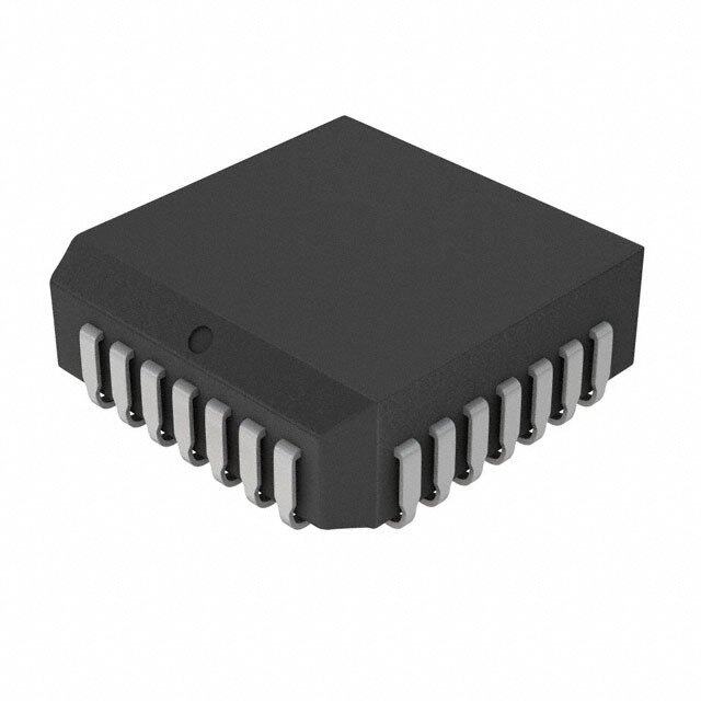
MCP2150 6.0 PACKAGING INFORMATION 6.1 Package Marking Information 18-Lead PDIP (300 mil) Example: XXXXXXXXXXXXXXXXX MCP2150-I/P XXXXXXXXXXXXXXXXX XXXXXXXXXXXXXXXXX XXXXXYYWWNNN XXXXXYYWWNNN 18-Lead SOIC (300 mil) Example: XXXXXXXXXXXXXXXXX MCP2150-I/SO XXXXXXXXXXXXXXXXX XXXXXXXXXXXXXXXXX XXXXXXXXXXXXXXXXX XXXXXXXXXXXXXXXXX XXXXXYYWWNNN XXXXXYYWWNNN 20-Lead SSOP (209 mil, 5.30 mm) Example: XXXXXXXXXXX MCP2150I/SS XXXXXXXXXXX XXXXXXXXXXX XXXYYWWNNN XXXYYWWNNN Legend: XX...X Customer specific information* YY Year code (last 2 digits of calendar year) WW Week code (week of January 1 is week ‘01’) NNN Alphanumeric traceability code Note: In the event the full Microchip part number cannot be marked on one line, it will be carried over to the next line thus limiting the number of available characters for customer specific information. * Standard device marking consists of Microchip part number, year code, week code and traceability code. 2002 Microchip Technology Inc. Preliminary DS21655B-page 41
MCP2150 18-Lead Plastic Dual In-line (P) – 300 mil (PDIP) E1 D 2 n 1 α E A2 A c L A1 B1 β B p eB Units INCHES* MILLIMETERS Dimension Limits MIN NOM MAX MIN NOM MAX Number of Pins n 18 18 Pitch p .100 2.54 Top to Seating Plane A .140 .155 .170 3.56 3.94 4.32 Molded Package Thickness A2 .115 .130 .145 2.92 3.30 3.68 Base to Seating Plane A1 .015 0.38 Shoulder to Shoulder Width E .300 .313 .325 7.62 7.94 8.26 Molded Package Width E1 .240 .250 .260 6.10 6.35 6.60 Overall Length D .890 .898 .905 22.61 22.80 22.99 Tip to Seating Plane L .125 .130 .135 3.18 3.30 3.43 Lead Thickness c .008 .012 .015 0.20 0.29 0.38 Upper Lead Width B1 .045 .058 .070 1.14 1.46 1.78 Lower Lead Width B .014 .018 .022 0.36 0.46 0.56 Overall Row Spacing § eB .310 .370 .430 7.87 9.40 10.92 Mold Draft Angle Top α 5 10 15 5 10 15 Mold Draft Angle Bottom β 5 10 15 5 10 15 * Controlling Parameter § Significant Characteristic Notes: Dimensions D and E1 do not include mold flash or protrusions. Mold flash or protrusions shall not exceed .010” (0.254mm) per side. JEDEC Equivalent: MS-001 Drawing No. C04-007 DS21655B-page 42 Preliminary 2002 Microchip Technology Inc.
MCP2150 18-Lead Plastic Small Outline (SO) – Wide, 300 mil (SOIC) E p E1 D 2 B n 1 h α 45° c A A2 φ β L A1 Units INCHES* MILLIMETERS Dimension Limits MIN NOM MAX MIN NOM MAX Number of Pins n 18 18 Pitch p .050 1.27 Overall Height A .093 .099 .104 2.36 2.50 2.64 Molded Package Thickness A2 .088 .091 .094 2.24 2.31 2.39 Standoff § A1 .004 .008 .012 0.10 0.20 0.30 Overall Width E .394 .407 .420 10.01 10.34 10.67 Molded Package Width E1 .291 .295 .299 7.39 7.49 7.59 Overall Length D .446 .454 .462 11.33 11.53 11.73 Chamfer Distance h .010 .020 .029 0.25 0.50 0.74 Foot Length L .016 .033 .050 0.41 0.84 1.27 Foot Angle φ 0 4 8 0 4 8 Lead Thickness c .009 .011 .012 0.23 0.27 0.30 Lead Width B .014 .017 .020 0.36 0.42 0.51 Mold Draft Angle Top α 0 12 15 0 12 15 Mold Draft Angle Bottom β 0 12 15 0 12 15 * Controlling Parameter § Significant Characteristic Notes: Dimensions D and E1 do not include mold flash or protrusions. Mold flash or protrusions shall not exceed .010” (0.254mm) per side. JEDEC Equivalent: MS-013 Drawing No. C04-051 2002 Microchip Technology Inc. Preliminary DS21655B-page 43
MCP2150 20-Lead Plastic Shrink Small Outline (SS) – 209 mil, 5.30 mm (SSOP) E E1 p D B 2 n 1 α c A A2 φ L A1 β Units INCHES* MILLIMETERS Dimension Limits MIN NOM MAX MIN NOM MAX Number of Pins n 20 20 Pitch p .026 0.65 Overall Height A .068 .073 .078 1.73 1.85 1.98 Molded Package Thickness A2 .064 .068 .072 1.63 1.73 1.83 Standoff § A1 .002 .006 .010 0.05 0.15 0.25 Overall Width E .299 .309 .322 7.59 7.85 8.18 Molded Package Width E1 .201 .207 .212 5.11 5.25 5.38 Overall Length D .278 .284 .289 7.06 7.20 7.34 Foot Length L .022 .030 .037 0.56 0.75 0.94 Lead Thickness c .004 .007 .010 0.10 0.18 0.25 Foot Angle φ 0 4 8 0.00 101.60 203.20 Lead Width B .010 .013 .015 0.25 0.32 0.38 Mold Draft Angle Top α 0 5 10 0 5 10 Mold Draft Angle Bottom β 0 5 10 0 5 10 * Controlling Parameter § Significant Characteristic Notes: Dimensions D and E1 do not include mold flash or protrusions. Mold flash or protrusions shall not exceed .010” (0.254mm) per side. JEDEC Equivalent: MO-150 Drawing No. C04-072 DS21655B-page 44 Preliminary 2002 Microchip Technology Inc.
MCP2150 APPENDIX A: REVISION HISTORY Revision A • This is a new data sheet Revision B • Updated feature list • Enhanced pin descriptions. Refer to Table1-2 • Added description for programmable device ID • Standardize use of terms for Host Controller and Primary Device 2002 Microchip Technology Inc. Preliminary DS21655B-page 45
MCP2150 NOTES: DS21655B-page 46 Preliminary 2002 Microchip Technology Inc.
MCP2150 ON-LINE SUPPORT Systems Information and Upgrade Hot Line The Systems Information and Upgrade Line provides Microchip provides on-line support on the Microchip system users a listing of the latest versions of all of World Wide Web (WWW) site. Microchip's development systems software products. The web site is used by Microchip as a means to make Plus, this line provides information on how customers files and information easily available to customers. To can receive any currently available upgrade kits.The view the site, the user must have access to the Internet Hot Line Numbers are: and a web browser, such as Netscape or Microsoft 1-800-755-2345 for U.S. and most of Canada, and Explorer. Files are also available for FTP download from our FTP site. 1-480-792-7302 for the rest of the world. Connecting to the Microchip Internet Web Site 013001 The Microchip web site is available by using your favorite Internet browser to attach to: www.microchip.com The file transfer site is available by using an FTP ser- vice to connect to: ftp://ftp.microchip.com The web site and file transfer site provide a variety of services. Users may download files for the latest Development Tools, Data Sheets, Application Notes, User's Guides, Articles and Sample Programs. A vari- ety of Microchip specific business information is also available, including listings of Microchip sales offices, distributors and factory representatives. Other data available for consideration is: • Latest Microchip Press Releases • Technical Support Section with Frequently Asked Questions • Design Tips • Device Errata • Job Postings • Microchip Consultant Program Member Listing • Links to other useful web sites related to Microchip Products • Conferences for products, Development Systems, technical information and more • Listing of seminars and events 2002 Microchip Technology Inc. DS21655B-page47
MCP2150 READER RESPONSE It is our intention to provide you with the best documentation possible to ensure successful use of your Microchip prod- uct. If you wish to provide your comments on organization, clarity, subject matter, and ways in which our documentation can better serve you, please FAX your comments to the Technical Publications Manager at (480) 792-4150. Please list the following information, and use this outline to provide us with your comments about this Data Sheet. To: Technical Publications Manager Total Pages Sent RE: Reader Response From: Name Company Address City / State / ZIP / Country Telephone: (_______) _________ - _________ FAX: (______) _________ - _________ Application (optional): Would you like a reply? Y N Device: MCP2150 Literature Number: DS21655B Questions: 1. What are the best features of this document? 2. How does this document meet your hardware and software development needs? 3. Do you find the organization of this data sheet easy to follow? If not, why? 4. What additions to the data sheet do you think would enhance the structure and subject? 5. What deletions from the data sheet could be made without affecting the overall usefulness? 6. Is there any incorrect or misleading information (what and where)? 7. How would you improve this document? 8. How would you improve our software, systems, and silicon products? DS21655B-page48 2002 Microchip Technology Inc.
MCP2150 PRODUCT IDENTIFICATION SYSTEM To order or obtain information, e.g., on pricing or delivery, refer to the factory or the listed sales office. PART NO. X /XX Examples: Device Temperature Package a) MCP2150-I/P = Industrial Temp., Range PDIP packaging b) MCP2150-I/SO = Industrial Temp., SOIC package Device MCP2150: Infrared Communications Controller c) MCP2150T-I/SS = Tape and Reel, MCP2150T: Infrared Communications Controller Industrial Temp., SSOP package (Tape and Reel) Temperature Range I = -40°C to +85°C Package P = Plastic DIP (300 mil, Body), 18-lead SO = Plastic SOIC (300 mil, Body), 18-lead SS = Plastic SSOP (209 mil, Body), 20-lead Sales and Support Data Sheets Products supported by a preliminary Data Sheet may have an errata sheet describing minor operational differences and recom- mended workarounds. To determine if an errata sheet exists for a particular device, please contact one of the following: 1. Your local Microchip sales office 2. The Microchip Corporate Literature Center U.S. FAX: (480) 792-7277 3. The Microchip Worldwide Site (www.microchip.com) Please specify which device, revision of silicon and Data Sheet (include Literature #) you are using. New Customer Notification System Register on our web site (www.microchip.com/cn) to receive the most current information on our products. 2002 Microchip Technology Inc. DS21655B-page 49
MCP2150 NOTES: DS21655B-page 50 2002 Microchip Technology Inc.
MCP2150 Information contained in this publication regarding device Trademarks applications and the like is intended through suggestion only and may be superseded by updates. It is your responsibility to The Microchip name and logo, the Microchip logo, FilterLab, ensure that your application meets with your specifications. KEELOQ, microID, MPLAB, MXDEV, PIC, PICmicro, No representation or warranty is given and no liability is PICMASTER, PICSTART, PRO MATE, SEEVAL and The assumed by Microchip Technology Incorporated with respect Embedded Control Solutions Company are registered trade- to the accuracy or use of such information, or infringement of marks of Microchip Technology Incorporated in the U.S.A. and patents or other intellectual property rights arising from such other countries. use or otherwise. Use of Microchip’s products as critical com- dsPIC, dsPICDEM.net, ECONOMONITOR, FanSense, ponents in life support systems is not authorized except with FlexROM, fuzzyLAB, In-Circuit Serial Programming, ICSP, express written approval by Microchip. No licenses are con- ICEPIC, microPort, Migratable Memory, MPASM, MPLIB, veyed, implicitly or otherwise, under any intellectual property MPLINK, MPSIM, MXLAB, PICC, PICDEM, PICDEM.net, rights. rfPIC, Select Mode and Total Endurance are trademarks of Microchip Technology Incorporated in the U.S.A. Serialized Quick Turn Programming (SQTP) is a service mark of Microchip Technology Incorporated in the U.S.A. All other trademarks mentioned herein are property of their respective companies. © 2002, Microchip Technology Incorporated, Printed in the U.S.A., All Rights Reserved. Printed on recycled paper. Microchip received QS-9000 quality system certification for its worldwide headquarters, design and wafer fabrication facilities in Chandler and Tempe, Arizona in July 1999 and Mountain View, California in March 2002. The Company’s quality system processes and procedures are QS-9000 compliant for its PICmicro® 8-bit MCUs, KEELOQ® code hopping devices, Serial EEPROMs, microperipherals, non-volatile memory and analog products. In addition, Microchip’s quality system for the design and manufacture of development systems is ISO 9001 certified. 2002 Microchip Technology Inc. DS21655B-page 51
M WORLDWIDE SALES AND SERVICE AMERICAS ASIA/PACIFIC Japan Corporate Office Australia Microchip Technology Japan K.K. Benex S-1 6F 2355 West Chandler Blvd. Microchip Technology Australia Pty Ltd 3-18-20, Shinyokohama Chandler, AZ 85224-6199 Suite 22, 41 Rawson Street Kohoku-Ku, Yokohama-shi Tel: 480-792-7200 Fax: 480-792-7277 Epping 2121, NSW Kanagawa, 222-0033, Japan Technical Support: 480-792-7627 Australia Tel: 81-45-471- 6166 Fax: 81-45-471-6122 Web Address: http://www.microchip.com Tel: 61-2-9868-6733 Fax: 61-2-9868-6755 Korea Rocky Mountain China - Beijing Microchip Technology Korea 2355 West Chandler Blvd. Microchip Technology Consulting (Shanghai) 168-1, Youngbo Bldg. 3 Floor Chandler, AZ 85224-6199 Co., Ltd., Beijing Liaison Office Samsung-Dong, Kangnam-Ku Tel: 480-792-7966 Fax: 480-792-4338 Unit 915 Seoul, Korea 135-882 Bei Hai Wan Tai Bldg. Atlanta Tel: 82-2-554-7200 Fax: 82-2-558-5934 No. 6 Chaoyangmen Beidajie 500 Sugar Mill Road, Suite 200B Singapore Beijing, 100027, No. China Atlanta, GA 30350 Tel: 86-10-85282100 Fax: 86-10-85282104 Microchip Technology Singapore Pte Ltd. Tel: 770-640-0034 Fax: 770-640-0307 200 Middle Road China - Chengdu Boston #07-02 Prime Centre Microchip Technology Consulting (Shanghai) 2 Lan Drive, Suite 120 Singapore, 188980 Westford, MA 01886 Co., Ltd., Chengdu Liaison Office Tel: 65-6334-8870 Fax: 65-6334-8850 Rm. 2401, 24th Floor, Tel: 978-692-3848 Fax: 978-692-3821 Taiwan Ming Xing Financial Tower Chicago Microchip Technology (Barbados) Inc., No. 88 TIDU Street 333 Pierce Road, Suite 180 Chengdu 610016, China Taiwan Branch Itasca, IL 60143 Tel: 86-28-86766200 Fax: 86-28-86766599 11F-3, No. 207 Tel: 630-285-0071 Fax: 630-285-0075 Tung Hua North Road China - Fuzhou Dallas Taipei, 105, Taiwan 4570 Westgrove Drive, Suite 160 Microchip Technology Consulting (Shanghai) Tel: 886-2-2717-7175 Fax: 886-2-2545-0139 Co., Ltd., Fuzhou Liaison Office Addison, TX 75001 Unit 28F, World Trade Plaza Tel: 972-818-7423 Fax: 972-818-2924 No. 71 Wusi Road EUROPE Detroit Fuzhou 350001, China Tri-Atria Office Building Tel: 86-591-7503506 Fax: 86-591-7503521 Denmark 32255 Northwestern Highway, Suite 190 China - Shanghai Microchip Technology Nordic ApS Farmington Hills, MI 48334 Microchip Technology Consulting (Shanghai) Regus Business Centre Tel: 248-538-2250 Fax: 248-538-2260 Lautrup hoj 1-3 Co., Ltd. Kokomo Room 701, Bldg. B Ballerup DK-2750 Denmark 2767 S. Albright Road Far East International Plaza Tel: 45 4420 9895 Fax: 45 4420 9910 Kokomo, Indiana 46902 No. 317 Xian Xia Road France Tel: 765-864-8360 Fax: 765-864-8387 Shanghai, 200051 Microchip Technology SARL Los Angeles Tel: 86-21-6275-5700 Fax: 86-21-6275-5060 Parc d’Activite du Moulin de Massy 43 Rue du Saule Trapu 18201 Von Karman, Suite 1090 China - Shenzhen Irvine, CA 92612 Microchip Technology Consulting (Shanghai) Batiment A - ler Etage Tel: 949-263-1888 Fax: 949-263-1338 Co., Ltd., Shenzhen Liaison Office 9Te1l3: 0303 -M1-a6s9s-y5, 3F-r6a3n-c2e0 Fax: 33-1-69-30-90-79 New York Rm. 1315, 13/F, Shenzhen Kerry Centre, Germany 150 Motor Parkway, Suite 202 Renminnan Lu Microchip Technology GmbH Hauppauge, NY 11788 Shenzhen 518001, China Tel: 631-273-5305 Fax: 631-273-5335 Tel: 86-755-2350361 Fax: 86-755-2366086 Gustav-Heinemann Ring 125 D-81739 Munich, Germany San Jose China - Hong Kong SAR Tel: 49-89-627-144 0 Fax: 49-89-627-144-44 Microchip Technology Inc. Microchip Technology Hongkong Ltd. Italy 2107 North First Street, Suite 590 Unit 901-6, Tower 2, Metroplaza Microchip Technology SRL San Jose, CA 95131 223 Hing Fong Road Tel: 408-436-7950 Fax: 408-436-7955 Kwai Fong, N.T., Hong Kong Centro Direzionale Colleoni Palazzo Taurus 1 V. Le Colleoni 1 Toronto Tel: 852-2401-1200 Fax: 852-2401-3431 20041 Agrate Brianza 6285 Northam Drive, Suite 108 India Milan, Italy Mississauga, Ontario L4V 1X5, Canada Microchip Technology Inc. Tel: 39-039-65791-1 Fax: 39-039-6899883 Tel: 905-673-0699 Fax: 905-673-6509 India Liaison Office United Kingdom Divyasree Chambers Microchip Ltd. 1 Floor, Wing A (A3/A4) 505 Eskdale Road No. 11, O’Shaugnessey Road Winnersh Triangle Bangalore, 560 025, India Wokingham Tel: 91-80-2290061 Fax: 91-80-2290062 Berkshire, England RG41 5TU Tel: 44 118 921 5869 Fax: 44-118 921-5820 Austria Microchip Technology Austria GmbH Durisolstrasse 2 A-4600 Wels Austria Tel: 43-7242-2244-399 Fax: 43-7242-2244-393 05/16/02 DS21655B-page 52 2002 Microchip Technology Inc.
Mouser Electronics Authorized Distributor Click to View Pricing, Inventory, Delivery & Lifecycle Information: M icrochip: MCP2150T-I/SO MCP2150T-I/SS MCP2150-I/SO MCP2150-I/SS MCP2150-I/P MCP2150DM