ICGOO在线商城 > 集成电路(IC) > PMIC - 稳压器 - 线性 > MCP1804T-3302I/OT

 Datasheet下载
- 型号: MCP1804T-3302I/OT
- 制造商: Microchip
- 库位|库存: xxxx|xxxx
- 要求:
| 数量阶梯 | 香港交货 | 国内含税 |
| +xxxx | $xxxx | ¥xxxx |
查看当月历史价格
查看今年历史价格
MCP1804T-3302I/OT产品简介:
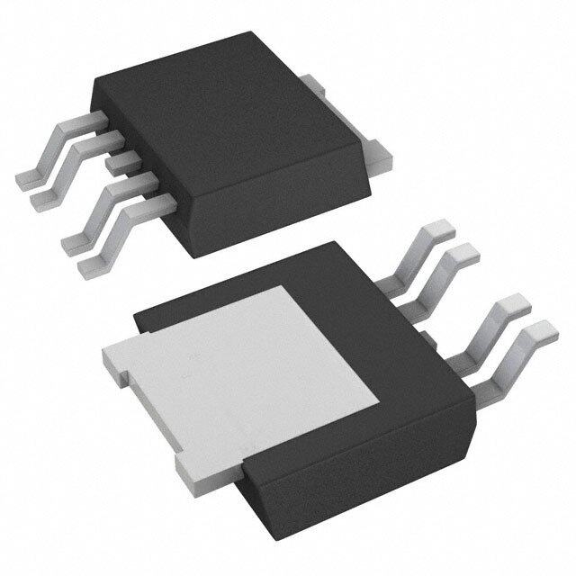
ICGOO电子元器件商城为您提供MCP1804T-3302I/OT由Microchip设计生产,在icgoo商城现货销售,并且可以通过原厂、代理商等渠道进行代购。 MCP1804T-3302I/OT价格参考。MicrochipMCP1804T-3302I/OT封装/规格:PMIC - 稳压器 - 线性, Linear Voltage Regulator IC Positive Fixed 1 Output 150mA SOT-23-5。您可以下载MCP1804T-3302I/OT参考资料、Datasheet数据手册功能说明书,资料中有MCP1804T-3302I/OT 详细功能的应用电路图电压和使用方法及教程。
Microchip Technology的MCP1804T-3302I/OT是一款低压差线性稳压器(LDO),属于PMIC中的线性稳压器类别。该器件可提供稳定的3.3V输出电压,最大输出电流可达500mA,具有低静态电流、高电源抑制比(PSRR)和出色的负载/线路调节能力。

其典型应用场景包括便携式电池供电设备,如智能手机、平板电脑、可穿戴设备和物联网终端,得益于其低功耗特性,有助于延长电池续航时间。此外,该LDO适用于噪声敏感的模拟电路供电,例如传感器模块、ADC/DAC参考电压源、射频模块和音频电路,能有效抑制输入电源噪声,保障系统稳定运行。

MCP1804T采用小型封装(如SOT-23或类似尺寸),适合空间受限的高密度PCB设计。工作温度范围为-40°C至+125°C,具备过温保护和过流保护功能,可靠性高,适用于工业控制、消费电子及汽车电子中的辅助电源管理。

综上,MCP1804T-3302I/OT广泛应用于对体积、功耗和电源纯净度有较高要求的中低功率电子系统中。
| 参数 | 数值 |
| 产品目录 | 集成电路 (IC)半导体 |
| 描述 | IC REG LDO 3.3V 0.15A SOT23-5低压差稳压器 150mA LDO Vin 28V Vout =3.3V |
| 产品分类 | |
| 品牌 | Microchip Technology |
| 产品手册 | |
| 产品图片 |
|
| rohs | 符合RoHS无铅 / 符合限制有害物质指令(RoHS)规范要求 |
| 产品系列 | 电源管理 IC,低压差稳压器,Microchip Technology MCP1804T-3302I/OT- |
| 数据手册 | http://www.microchip.com/mymicrochip/filehandler.aspx?ddocname=en544680 |
| 产品型号 | MCP1804T-3302I/OT |
| PCN设计/规格 | http://www.microchip.com/mymicrochip/NotificationDetails.aspx?id=5640&print=view |
| 产品目录页面 | |
| 产品种类 | 低压差稳压器 |
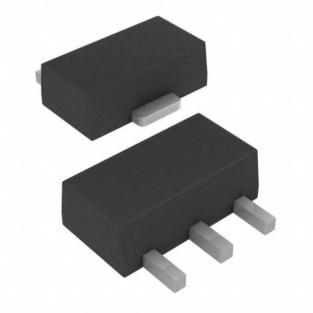
| 供应商器件封装 | SOT-23-5 |
| 其它名称 | MCP1804T-3302I/OTDKR |
| 包装 | Digi-Reel® |
| 商标 | Microchip Technology |
| 回动电压—最大值 | 360 mV |
| 安装类型 | 表面贴装 |
| 安装风格 | SMD/SMT |
| 封装 | Reel |
| 封装/外壳 | SC-74A,SOT-753 |
| 封装/箱体 | SOT-23-5 |
| 工作温度 | -40°C ~ 85°C |
| 工厂包装数量 | 3000 |
| 最大功率耗散 | 250 mW |
| 最大工作温度 | + 85 C |
| 最大输入电压 | 28 V |
| 最小工作温度 | - 40 C |
| 标准包装 | 1 |
| 电压-跌落(典型值) | 1.3V @ 100mA |
| 电压-输入 | 最高 28V |
| 电压-输出 | 3.3V |
| 电流-输出 | 150mA |
| 电流-限制(最小值) | - |
| 稳压器拓扑 | 正,固定式 |
| 稳压器数 | 1 |
| 负载调节 | 275 mV |
| 输出电压 | 3.3 V |
| 输出电流 | 150 mA |


- 商务部:美国ITC正式对集成电路等产品启动337调查
- 曝三星4nm工艺存在良率问题 高通将骁龙8 Gen1或转产台积电
- 太阳诱电将投资9.5亿元在常州建新厂生产MLCC 预计2023年完工
- 英特尔发布欧洲新工厂建设计划 深化IDM 2.0 战略
- 台积电先进制程称霸业界 有大客户加持明年业绩稳了
- 达到5530亿美元!SIA预计今年全球半导体销售额将创下新高
- 英特尔拟将自动驾驶子公司Mobileye上市 估值或超500亿美元
- 三星加码芯片和SET,合并消费电子和移动部门,撤换高东真等 CEO
- 三星电子宣布重大人事变动 还合并消费电子和移动部门
- 海关总署:前11个月进口集成电路产品价值2.52万亿元 增长14.8%


PDF Datasheet 数据手册内容提取
MCP1804 150 mA, 28V LDO Regulator With Shutdown Features: Description: • 150mA Output Current The MCP1804 is a family of CMOS low dropout (LDO) • Low Dropout Voltage, 260mV Typical @ 20mA, voltage regulators that can deliver up to 150mA of V =3.3V current while consuming only 50µA of quiescent R current (typical, 1.8VV 5.0V). The input • 50µA Typical Quiescent Current OUT operating range is specified from 2.0V to 28.0V. • 0.01µA Typical Shutdown Current The MCP1804 is capable of delivering 100mA with • Input Operating Voltage Range: 2.0V to 28.0V only 1300mV (typical) of input to output voltage • Standard Output Voltage Options differential (V =3.3V). The output voltage tolerance (1.8V, 2.5V, 3.0V, 3.3V, 5.0V, 10.0V, 12.0V) OUT of the MCP1804 at +25°C is a maximum of ±2%. Line • Output Voltage Accuracy: ±2% regulation is ±0.15% typical at +25°C. • Output Voltages from 1.8V to 18.0V in 0.1V The LDO input and output are stable with 0.1µF of Increments are Available upon Request input and output capacitance. Ceramic, tantalum or • Stable with Ceramic Output Capacitors aluminum electrolytic capacitors can all be used for • Current Limit Protection with Current Foldback input and output. Overcurrent limit with current foldback • Shutdown Pin to 40mA (typical) provides short circuit protection. • High PSRR: 50dB Typical @ 1kHz Ashutdown (SHDN) function allows the output to be enabled or disabled. When disabled, the MCP1804 draws only 0.01µA of current (typical). Applications: Package options include the 3-lead SOT-89, 3-lead • Cordless Phones, Wireless Communications SOT-223, 5-lead SOT-23 and 5-lead SOT-89. • PDAs, Notebook and Netbook Computers • Digital Cameras Package Types • Microcontroller Power SOT-89-3 SOT-223-3 • Car Audio and Navigation Systems • Home Appliances Related Literature: (Top View) (Top View) • AN765, “Using Microchip’s Micropower LDOs” (DS00765), Microchip Technology Inc., ©2002 • AN766, “Pin-Compatible CMOS Upgrades to 1 2 3 1 2 3 BiPolar LDOs” (DS00766), Microchip Technology VOUT GND VIN VOUT GND VIN Inc., ©2002 • AN792, “A Method to Determine How Much Power a SOT23 Can Dissipate in an Application” SOT-23-5 SOT-89-5 (DS00792), Microchip Technology Inc., ©2001 VOUT SHDN VIN NC 5 4 5 4 (Top View) 1 2 3 1 2 3 V GND NC V GND SHDN IN OUT 2009-2013 Microchip Technology Inc. DS20002200D-page 1
MCP1804 Functional Block Diagram V V IN OUT * Thermal Protection SHDN Shutdown Voltage Control Reference - Current Limiter + Error Amplifier GND *5-Pin Versions Only Typical Application Circuit MCP1804 V IN V 1 VIN VOUT 5 OUT 5.0V@30mA SOT-23 C OUT 1µFCeramic 2 GND 12V + Battery C 3 NCSHDN 4 IN 1µF Ceramic DS20002200D-page 2 2009-2013 Microchip Technology Inc.
MCP1804 1.0 ELECTRICAL CHARACTERISTICS Absolute Maximum Ratings † Input Voltage ........................................................................................................................................................... +30V Output Current (Continuous)............................................................................................................. P /(V -V ) mA D IN OUT Output Current (Peak).......................................................................................................................................... 300mA Output Voltage...................................................................................................................... (V -0.3V) to (V +0.3V) SS IN SHDN Voltage.................................................................................................................................. (V -0.3V) to +30V SS † Notice: Stresses above those listed under “Maximum Ratings” may cause permanent damage to the device. This is a stress rating only and functional operation of the device at those or any other conditions above those indicated in the operational listings of this specification is not implied. Exposure to maximum rating conditions for extended periods may affect device reliability. ELECTRICAL CHARACTERISTICS Electrical Specifications: Unless otherwise specified, all limits are established for V =V +2.0V, Note1, IN R C =1 µF (X7R), C =1 µF (X7R), V =V , T =+25°C OUT IN SHDN IN A Parameters Sym. Min. Typ. Max. Units Conditions Input / Output Characteristics Input Operating V 2.0 — 28.0 V Note1 IN Voltage Input Quiescent I — I =0mA Q L Current — 50 105 µA 1.8VV 5.0V OUT — 60 115 µA 5.1VV 12.0V OUT — 65 125 µA 12.1VV 18.0V OUT Shutdown Current I — 0.01 0.10 µA SHDN=0V SHDN Maximum Output I — V =V +3.0V OUT IN R Current 100 — — mA V <3.0V OUT 150 — — mA V 3.0V OUT Current Limiter I — 200 — mA LIMIT Output Short Circuit I — 40 — mA OUT_SC Current Output Voltage V V -2.0% V V +2.0% V I =10mA, Note2 OUT R R R OUT Regulation V Temperature TCV — ±100 — ppm/°C I =20mA, OUT OUT OUT Coefficient -40°CT 85°C, Note3 A Note 1: The minimum V must meet one condition: V (V +2.0V). IN IN R 2: V is the nominal regulator output voltage with an input voltage of V =V +2.0V. R IN R For example: V =1.8V, 2.5V, 3.0V, 3.3V, etc. R 3: TCV =(V -V )*106 / (V *Temperature), V =highest voltage measured OUT OUT-HIGH OUT-LOW R OUT-HIGH over the temperature range. V =lowest voltage measured over the temperature range. OUT-LOW 4: Load regulation is measured at a constant junction temperature using low duty cycle pulse testing. Changes in output voltage due to heating effects are determined using thermal regulation specification TCV . OUT 5: Dropout voltage is defined as the input to output differential at which the output voltage drops 2% below its measured value with an applied input voltage of V +2.0V. R 2009-2013 Microchip Technology Inc. DS20002200D-page 3
MCP1804 ELECTRICAL CHARACTERISTICS (CONTINUED) Electrical Specifications: Unless otherwise specified, all limits are established for V =V +2.0V, Note1, IN R C =1 µF (X7R), C =1 µF (X7R), V =V , T =+25°C OUT IN SHDN IN A Parameters Sym. Min. Typ. Max. Units Conditions Line Regulation V /(V — (V +2V)V 28V, Note1 OUT OUT- R IN XVIN) — 0.05 0.10 %/V IOUT=5mA — 0.15 0.30 %/V I =13mA OUT Load Regulation V /V — I =1.0mA to 50mA, Note4 OUT OUT L — 50 90 mV 1.8VV 5.0V OUT — 110 175 mV 5.1VV 12.0V OUT — 180 275 mV 12.1VV 18.0V OUT Dropout Voltage V — I =20mA DROPOUT L Note1, Note5 — 550 710 mV 1.8VV 1.9V R — 450 600 mV 2.0VV 2.1V R — 390 520 mV 2.2VV 2.4V R — 310 450 mV 2.5VV 2.9V R — 260 360 mV 3.0VV 3.9V R — 220 320 mV 4.0VV 4.9V R — 190 280 mV 5.0VV 6.4V R — 170 230 mV 6.5VV 8.0V R — 130 190 mV 8.1VV 10.0V R — 120 170 mV 10.1VV 18.0V R — I =100mA L — 2200 2700 mV 1.8VV 1.9V R — 1900 2600 mV 2.0VV 2.1V R — 1700 2200 mV 2.2VV 2.4V R — 1500 1900 mV 2.5VV 2.9V R — 1300 1700 mV 3.0VV 3.9V R — 1100 1500 mV 4.0VV 4.9V R — 1000 1300 mV 5.0VV 6.4V R — 800 1150 mV 6.5VV 8.0V R — 700 950 mV 8.1VV 10.0V R — 650 850 mV 10.1VV 18.0V R SHDN “H” Voltage V 1.1 — V V V =28V SHDN_H IN IN SHDN “L” Voltage V 0 — 0.35 V V =28V SHDN_L IN SHDN Current I -0.1 — 0.1 µA V =28V, V =GND or SHDN IN SHDN V IN Note 1: The minimum V must meet one condition: V (V +2.0V). IN IN R 2: V is the nominal regulator output voltage with an input voltage of V =V +2.0V. R IN R For example: V =1.8V, 2.5V, 3.0V, 3.3V, etc. R 3: TCV =(V -V )*106 / (V *Temperature), V =highest voltage measured OUT OUT-HIGH OUT-LOW R OUT-HIGH over the temperature range. V =lowest voltage measured over the temperature range. OUT-LOW 4: Load regulation is measured at a constant junction temperature using low duty cycle pulse testing. Changes in output voltage due to heating effects are determined using thermal regulation specification TCV . OUT 5: Dropout voltage is defined as the input to output differential at which the output voltage drops 2% below its measured value with an applied input voltage of V +2.0V. R DS20002200D-page 4 2009-2013 Microchip Technology Inc.
MCP1804 ELECTRICAL CHARACTERISTICS (CONTINUED) Electrical Specifications: Unless otherwise specified, all limits are established for V =V +2.0V, Note1, IN R C =1 µF (X7R), C =1 µF (X7R), V =V , T =+25°C OUT IN SHDN IN A Parameters Sym. Min. Typ. Max. Units Conditions Power Supply Ripple PSRR — 50 — dB f=1kHz, I =20 mA, L Rejection Ratio V =0.5V pk-pk, IN_AC C =0µF IN Thermal Shutdown TSD — 150 — °C T =150°C J Protection Thermal Shutdown TSD — 25 — °C Hysteresis Note 1: The minimum V must meet one condition: V (V +2.0V). IN IN R 2: V is the nominal regulator output voltage with an input voltage of V =V +2.0V. R IN R For example: V =1.8V, 2.5V, 3.0V, 3.3V, etc. R 3: TCV =(V -V )*106 / (V *Temperature), V =highest voltage measured OUT OUT-HIGH OUT-LOW R OUT-HIGH over the temperature range. V =lowest voltage measured over the temperature range. OUT-LOW 4: Load regulation is measured at a constant junction temperature using low duty cycle pulse testing. Changes in output voltage due to heating effects are determined using thermal regulation specification TCV . OUT 5: Dropout voltage is defined as the input to output differential at which the output voltage drops 2% below its measured value with an applied input voltage of V +2.0V. R TEMPERATURE SPECIFICATIONS Parameters Sym. Min. Typ. Max. Units Conditions Temperature Ranges Operating Temperature Range T -40 — +85 °C A Operating Junction Temperature T -40 — +125 °C Range J Storage Temperature Range T -55 — +125 °C A Thermal Package Resistance Thermal Resistance, 3LD SOT-89 JA — 180 — EIA/JEDEC® JESD51-7 °C/W — 52 — FR-4 0.063 4-Layer Board JC Thermal Resistance, 3LD SOT-223 JA — 62 — EIA/JEDEC JESD51-7 °C/W — 15 — FR-4 0.063 4-Layer Board JC Thermal Resistance, 5LD SOT-23 JA — 256 — EIA/JEDEC JESD51-7 °C/W — 81 — FR-4 0.063 4-Layer Board JC Thermal Resistance, 5LD SOT-89 JA — 180 — EIA/JEDEC JESD51-7 °C/W — 52 — FR-4 0.063 4-Layer Board JC 2009-2013 Microchip Technology Inc. DS20002200D-page 5
MCP1804 2.0 TYPICAL PERFORMANCE CURVES Note: The graphs and tables provided following this note are a statistical summary based on a limited number of samples and are provided for informational purposes only. The performance characteristics listed herein are not tested or guaranteed. In some graphs or tables, the data presented may be outside the specified operating range (e.g., outside specified power supply range) and therefore outside the warranted range. Note: Unless otherwise indicated: C =1µF Ceramic (X7R), C =1µF Ceramic (X7R), T =+25°C, OUT IN A V =V +2.0V. IN R 2.0 2.0 1.8 1.8 VIN= 2.8V put Voltage (V)Out 00111100.......80246466 TTTAAA=== -284550°°°CCC utput Voltage (V)Ou 00111100.......80246466 VVIINNV==R =34 ..188.VV8V 0.2 VVIRN== 2S.H8VDN = 4.8V 0.2 0.0 0.0 0 50 100 150 200 250 300 0 50 100 150 200 250 300 Output Current (mA) Output Current (mA) FIGURE 2-1: Output Voltage vs. Output FIGURE 2-4: Output Voltage vs. Output Current. Current. 6.0 6.0 5.0 5.0 V) tput Voltage (ut 2342....0000 TTTAAA=== -284550°°°CCC ut Voltage (V)pu 2342....0000 VVVIIINNN=== 678VVV O ut 1.0 VIN=SHDN = 8.0V O 1.0 VR= 5.0V VR= 5V 0.0 0.0 0 50 100 150 200 250 300 0 50 100 150 200 250 300 Output Current (mA) Output Current (mA) FIGURE 2-2: Output Voltage vs. Output FIGURE 2-5: Output Voltage vs. Output Current. Current. 14.0 14.0 12.0 12.0 put Voltage (V)p 1068...000 TTTAAA=== -284550°°°CCC ut Voltage (V) 1068...000 VVVIIINNN=== 111345VVV Out 4.0 utp 4.0 2.0 VIN= SHDN = 15V O 2.0 VR= 12 V VR= 12V 0.0 0.0 0 50 100 150 200 250 300 0 50 100 150 200 250 300 Output Current (mA) Output Current (mA) FIGURE 2-3: Output Voltage vs. Output FIGURE 2-6: Output Voltage vs. Output Current. Current. DS20002200D-page 6 2009-2013 Microchip Technology Inc.
MCP1804 Note: Unless otherwise indicated: C =1µF Ceramic (X7R), C =1µF Ceramic (X7R), T =+25°C, OUT IN A V =V +2.0V. IN R 2.1 2.1 VR= 1.8V VR= 1.8V 2.0 IOUT= 1 mA 2.0 V) IOUT= 10 mA age ( 1.9 IOUT= 30 mA e (V)1.9 olt 1.8 ag1.8 put VOutp 111...677 t VoltOutpu111...677 IIIIOOOUUUTTT==== 131100mm mmAAAA 1.5 1.5 0.8 1.3 1.8 2.3 2.8 3.3 3.8 4 8 12 16 20 24 28 Input Voltage (V) Input Voltage (V) FIGURE 2-7: Output Voltage vs. Input FIGURE 2-10: Output Voltage vs. Input Voltage. Voltage. 6.0 6.0 5.8 VR= 5V 5.8 VR= 5V 5.6 5.6 put Voltage (V)Outp 455544......802446 IIIOOOUUUTTT=== 113 00m mmAAA put Voltage (V)Outp455544......802446 IOUT= 1 mA IOUT= 10 mA 4.2 4.2 IOUT= 30 mA 4.0 4.0 4.0 4.5 5.0 5.5 6.0 8 12 16 20 24 28 Input Voltage (V) Input Voltage (V) FIGURE 2-8: Output Voltage vs. Input FIGURE 2-11: Output Voltage vs. Input Voltage. Voltage. 15.0 15.0 VR= 12V VR= 12V 14.0 14.0 e (V)13.0 ge (V)13.0 g a olta12.0 Volt12.0 ut VOutpu111011..000 IIIIOOOUUUTTT==== 131100mm mmAAAA put Outp111110..000 IIIOOOUUUTTT=== 113 00m mmAAA 9.0 9.0 10 11 12 13 14 14 16 18 20 22 24 26 28 Input Voltage (V) Input Voltage (V) FIGURE 2-9: Output Voltage vs. Input FIGURE 2-12: Output Voltage vs. Input Voltage. Voltage. 2009-2013 Microchip Technology Inc. DS20002200D-page 7
MCP1804 Note: Unless otherwise indicated: C =1µF Ceramic (X7R), C =1µF Ceramic (X7R), T =+25°C, OUT IN A V =V +2.0V. IN R 4.0 70 VR= 1.8V VR= 1.8V 3.5 60 oltage (V) 223...050 TTTAAA=== 82-4550°°°CCC Current (µA) 4500 ut V 1.5 ply 30 oDropo 01..50 pSup 1200 TTTAAA=== 2-884550°°°°CCCC 0.0 0 0 25 50 75 100 125 150 0 4 8 12 16 20 24 28 Output Current (mA) Input Voltage (V) FIGURE 2-13: Dropout Voltage vs. Load FIGURE 2-16: Supply Current vs. Input Current. Voltage. 4.0 70 3.5 VR= 5V 60 VR= 5V A) ge (V)23..50 TA= 85°C ent (µ 50 Volta2.0 TTAA== 2-450°°CC Curr 40 pout Drop11..50 pply Sup 3200 TTAA== 8255°°CC 0.5 10 TA= -40°C 0.0 0 0 25 50 75 100 125 150 0 4 8 12 16 20 24 28 Output Current (mA) Input Voltage (V) FIGURE 2-14: Dropout Voltage vs. Load FIGURE 2-17: Supply Current vs. Input Current. Voltage. 4.0 70 VR= 12V VR= 12V 3.5 60 pout Voltage (V)Dro 12231.....50500 TTTAAA=== 82-4550°°°CCC pply Current (µA)Sup34520000 TTAAA== 8255°°CC 0.5 10 TA= -40°C 0.0 0 0 25 50 75 100 125 150 0 4 8 12 16 20 24 28 Output Current (mA) Input Voltage (V) FIGURE 2-15: Dropout Voltage vs. Load FIGURE 2-18: Supply Current vs. Input Current. Voltage. DS20002200D-page 8 2009-2013 Microchip Technology Inc.
MCP1804 Note: Unless otherwise indicated: C =1µF Ceramic (X7R), C =1µF Ceramic (X7R), T =+25°C, OUT IN A V =V +2.0V. IN R 70 2.00 VR= 1.8V VR= 1.8V 60 1.95 urrent (µA) 4500 oltage (V) 111...889050 C V ply 30 put 1.75 pSup 20 tOut 1.70 IOUT= 1 mA 10 1.65 IIOOUUTT== 1200 mmAA 0 1.60 -40 -20 0 20 40 60 80 100 -50 -25 0 25 50 75 100 Ambient Temperature (°C) Ambient Temperature (°C(cid:15911) FIGURE 2-19: Supply Current vs. Input FIGURE 2-22: Output Voltage vs. Ambient Voltage. Temperature. 70 5.20 60 VR= 5V 5.15 VR= 5V urrent (µA)4500 Voltage (V)555...001050 pply Cup3200 utput Ou44..9950 IOUT=1 mA S IOUT= 10 mA 10 4.85 IOUT= 20 mA 0 4.80 -40 -20 0 20 40 60 80 100 -50 -25 0 25 50 75 100 Ambient Temperature (°C) Ambient Temperature (°C(cid:15911) FIGURE 2-20: Supply Current vs. Input FIGURE 2-23: Output Voltage vs. Ambient Voltage. Temperature. 70 12.5 60 VR= 12V 12.4 VR= 12V µA) V) 12.3 Current (4500 Voltage ( 111222...012 ply 30 put 11.9 pSup20 tOu 11.8 IOUT= 1 mA 11.7 IOUT= 10 mA 10 11.6 IOUT= 20 mA 0 11.5 -40 -20 0 20 40 60 80 100 -50 -25 0 25 50 75 100 Ambient Temperature (°C) Ambient Temperature (°C(cid:15911) FIGURE 2-21: Supply Current vs. Input FIGURE 2-24: Output Voltage vs. Ambient Voltage. Temperature. 2009-2013 Microchip Technology Inc. DS20002200D-page 9
MCP1804 Note: Unless otherwise indicated: C =1µF Ceramic (X7R), C =1µF Ceramic (X7R), T =+25°C, OUT IN A V =V +2.0V. IN R 7.3 3.38 7.3 3.38 nput Voltage (V)4563....3333 VVOINUT VIORUT= =3 .13 VmA 3333....33332460 put Voltage (V)utp ut Voltage (V)npu4563....3333 VOVUITN IVORUT= = 3 3.30V mA 3333....33332460 put Voltage (V)utp I O I O 2.3 3.28 2.3 3.28 1.3 3.26 1.3 3.26 Time (1 ms/div) FIGURE 2-25: Dynamic Line Response. FIGURE 2-28: Dynamic Line Response. 9 5.08 9 5.08 8 VIORUT= =5 V1 mA 5.06 8 VIN VIORUT= = 5 3V0 mA 5.06 ut Voltage (V)Inpu675 VVOINUT 555...000240 put Voltage (V)Outp put Voltage (V)Inp675 VOUT 555...000240 tput Voltage (V)Out 4 4.98 4 4.98 3 4.96 3 4.96 Time (1 ms/div) Time (1 ms/div) FIGURE 2-26: Dynamic Line Response. FIGURE 2-29: Dynamic Line Response. 16 12.08 16 12.08 15 VIN VIORUT= = 1 12 VmA 12.06 15 VIN VIORUT= = 1 320V mA 12.06 e (V)14 12.04ge (V) ge (V)14 12.04 age (V) ut VoltagInpu1132 VOUT 1122..0020put VoltaOutp put VoltaInp1132 VOUT 1122..0020 put VoltOut 11 11.98 11 11.98 10 11.96 10 11.96 Time (1 ms/div) Time (1 ms/div) FIGURE 2-27: Dynamic Line Response. FIGURE 2-30: Dynamic Line Response. DS20002200D-page 10 2009-2013 Microchip Technology Inc.
MCP1804 Note: Unless otherwise indicated: C =1µF Ceramic (X7R), C =1µF Ceramic (X7R), T =+25°C, OUT IN A V =V +2.0V. IN R 3.6 150 8 8 3.5 VR= 3.3V 6 VIN 7 put Voltage (V)Outp 3333322.......0123489 IOVUTOUT 693100020ut Current (mA)Outp put Voltage (V)Inp ---202442 VOUT VR= 3.3V 345623put Voltage (V)Outp 2.7 -6 IOUT = 1 mA 1 2.6 0 -8 0 Time (1 ms/div) Time (1 ms/div) FIGURE 2-31: Dynamic Load Response. FIGURE 2-34: Start-up Response. 5.4 150 8 8 5.3 VR= 5V 6 VIN 7 put Voltage (V)Outp 445554......890127 VIOOUUTT 6910020ut Current (mA)Outpu put Voltage (V)Inp ---202442 VOUT 345623 put Voltage (V)Outp 4.6 30 VR= 3.3V 4.5 -6 IOUT = 30 mA 1 4.4 0 -8 0 Time (1 ms/div) Time (1 ms/div) FIGURE 2-32: Dynamic Load Response. FIGURE 2-35: Start-up Response. 12.6 150 8 8 12.4 VR= 12V 6 VIN 7 Voltage (V) 11111122....0268 VOUT 91020urrent (mA) oltage (V) 024 VOUT 456 Voltage (V) put Outp 111111...424 IOUT 6600 ut COutpu ut VInp --242 323 put Outp 11.0 30 VR= 5.0V 10.8 -6 IOUT = 1 mA 1 10.6 0 -8 0 Time (1 ms/div) Time (1 ms/div) FIGURE 2-33: Dynamic Load Response. FIGURE 2-36: Start-up Response. 2009-2013 Microchip Technology Inc. DS20002200D-page 11
MCP1804 Note: Unless otherwise indicated: C =1µF Ceramic (X7R), C =1µF Ceramic (X7R), T =+25°C, OUT IN A V =V +2.0V. IN R 8 8 8 8 6 VIN 7 6 SHDN 7 put Voltage (V)Inp--202442 VOUT VR= 5.0V 345623put Voltage (V)Outp N Voltage (V)SHDN---202442 VOUT VR= 3.3V 345623ut Voltage (V)Outpu -6 IOUT = 30 mA 1 -6 IOUT = 1 mA 1 -8 0 -8 0 Time (1 ms/div) Time (1 ms/div) FIGURE 2-37: Start-up Response. FIGURE 2-40: SHDN Response. 15 18 8 8 10 VIN 15 6 SHDN 7 put Voltage (V)np -055 VOUT 9162put Voltage (V)utp DN Voltage (V)HD -20242 VOUT 34563 ut Voltage (V)pu I O S ut -10 IVORUT= = 1 12 VmA 3 --64 VIORUT= = 5 1V mA 12 O -15 0 -8 0 Time (1 ms/div) Time (1 ms/div) FIGURE 2-38: Start-up Response. FIGURE 2-41: SHDN Response. 15 18 15 18 VIN SHDN 10 15 10 15 put Voltage (V)Inp -505 VOUT 1962 put Voltage (V)Outp DN Voltage (V)SHD -055 VOUT 9162ut Voltage (V)Outpu -10 VR= 12V 3 -10 VR= 12V 3 IOUT = 30 mA IOUT = 1 mA -15 0 -15 0 Time (1 ms/div) Time (1 ms/div) FIGURE 2-39: Start-up Response. FIGURE 2-42: SHDN Response. DS20002200D-page 12 2009-2013 Microchip Technology Inc.
MCP1804 Note: Unless otherwise indicated: C =1µF Ceramic (X7R), C =1µF Ceramic (X7R), T =+25°C, OUT IN A V =V +2.0V. IN R 8 8 90 6 SHDN 7 80 VCOINU=T =0 3.3V DN Voltage (V)D-20242 VOUT 34563 ut Voltage (V)u PSRR (dB) 345673000000 IVOIUNT_ A=C 1= m0.A5Vpk-pk H p S ut 20 -4 2 O -6 VIORUT= = 3 3.30V mA 1 100 -8 0 0.01 0.1 1 10 100 Time (1 ms/div) Frequency (kHz) FIGURE 2-43: SHDN Response. FIGURE 2-46: PSRR 3.3V@1mA. 8 8 90 80 VOUT = 5V 6 SHDN 7 CIN= 0 70 IOUT = 1 mA Voltage (V) 024 VOUT 456Voltage (V) RR (dB)456000 VIN_AC = 0.5Vpk-pk DN D -22 33put p PS3300 SH -4 2Out 20 -6 VIORUT= = 5 3V0 mA 1 100 -8 0 0.01 0.1 1 10 100 Time (1 ms/div) Frequency (kHz) FIGURE 2-44: SHDN Response. FIGURE 2-47: PSRR 5.0V@1mA. 15 18 90 10 SHDN 15 7800 VCIOOIUNUT=T = =0 1 1 m2VA DN Voltage (V)D 05 VOUT 912ut Voltage (V)u PSRR (dB)P 3456300000 VIN_AC = 0.5Vpk-pk H -5 6 p S ut 20 O -10 IVORUT= = 1 320V mA 3 10 0 -15 0 0.01 0.1 1 10 100 Time (1 ms/div) Frequency (kHz) FIGURE 2-45: SHDN Response. FIGURE 2-48: PSRR 12.0V@1mA. 2009-2013 Microchip Technology Inc. DS20002200D-page 13
MCP1804 Note: Unless otherwise indicated: C =1µF Ceramic (X7R), C =1µF Ceramic (X7R), T =+25°C, OUT IN A V =V +2.0V. IN R 80 90 80 VCOINUT= =0 3.3V 70 VVOINU=T =8 V5V R (dB) 45670000 IVOIUNT_A=C 3=0 0 m.5AVpk-pk Current (µA) 5600 R d SPS 3300 nun 4400 o 20 Gr 30 10 0 20 0.01 0.1 1 10 100 0 25 50 75 100 125 150 Frequency (kHz) Output Current (mA) FIGURE 2-49: PSRR 3.3V@30mA. FIGURE 2-52: Ground Current vs. Output Current. 80 90 7800 VCIOOIUNUTT== =0 3 50V mA A) 70 VVOINU=T =1 51V2V B) 60 VIN_AC= 0.5Vpk-pk ent (µ 60 PSRR (dP 34530000 und Curru 454000 o 20 Gr 30 10 0 20 0.01 0.1 1 10 100 0 25 50 75 100 125 150 Frequency (kHz) Output Current (mA) FIGURE 2-50: PSRR 5.0V@30mA. FIGURE 2-53: Ground Current vs. Output Current. 90 100 7800 VCIVOOIIUNNUT_T=A=C =0 3 =10 20 mV.5AVp-p µA) 8900 VVOINU=T =1 81V5V RR (dB)456000 Current ( 6700 PS3300 nd un 50 o 20 Gr 40 10 30 0 0 25 50 75 100 125 150 0.01 0.1 1 10 100 Frequency (kHz) Output Current (mA) FIGURE 2-51: PSRR 12V@30mA. FIGURE 2-54: Ground Current vs. Output Current. DS20002200D-page 14 2009-2013 Microchip Technology Inc.
MCP1804 Note: Unless otherwise indicated: C =1µF Ceramic (X7R), C =1µF Ceramic (X7R), T =+25°C, OUT IN A V =V +2.0V. IN R 10.00 V = 3.3V R z) VIN = 5.0V H I = 50 mA OUT V/ 1.00 µ e ( s oi N ut 0.10 p ut O 0.01 0.01 0.1 1 10 100 Frequency (kHz) FIGURE 2-55: Output Noise vs. Frequency. 2009-2013 Microchip Technology Inc. DS20002200D-page 15
MCP1804 3.0 PIN DESCRIPTIONS The descriptions of the pins are listed in Table3-1. . TABLE 3-1: MCP1804 PIN FUNCTION TABLE MCP1804 Symbol Description SOT-23-5 SOT-89-5 SOT-89-3 SOT-223-3 1 5 3 3 V Unregulated Supply Voltage IN 2 2, TAB 2, TAB 2, TAB GND Ground Terminal 3 4 — — NC No connection 4 3 — — SHDN Shutdown 5 1 1 1 V Regulated Voltage Output OUT 3.1 Unregulated Input Voltage (V ) 3.4 Regulated Output Voltage (V ) IN OUT Connect V to the input unregulated source voltage. Connect V to the positive side of the load and the IN OUT Like all low dropout linear regulators, low source positive terminal of the output capacitor. The positive impedance is necessary for the stable operation of the side of the output capacitor should be physically LDO. The amount of capacitance required to ensure located as close to the LDO V pin as is practical. OUT low source impedance will depend on the proximity of The current flowing out of this pin is equal to the DC the input source capacitors or battery type. For most load current. For most applications, 0.1µF to 1.0µF of applications, 0.1µF to 1.0µF of capacitance will capacitance will ensure stable operation of the LDO ensure stable operation of the LDO circuit. The type of circuit. Larger values may be used to improve dynamic capacitor used can be ceramic, tantalum or aluminum load response. The type of capacitor used can be electrolytic. The low ESR characteristics of the ceramic ceramic, tantalum or aluminum electrolytic. The low will yield better noise and PSRR performance at high ESR characteristics of the ceramic will yield better frequency. noise and PSRR performance at high frequency. 3.2 Ground Terminal (GND) 3.5 No Connect (NC) Regulator ground. Tie GND to the negative side of the No internal connection. The pins marked NC are true output and the negative side of the input capacitor. “No Connect” pins. Only the LDO bias current (50 to 60µA typical) flows out of this pin; there is no high current. The LDO output regulation is referenced to this pin. Minimize voltage drops between this pin and the negative side of the load. 3.3 Shutdown Input (SHDN) The SHDN input is used to turn the LDO output voltage on and off. When the SHDN input is at a logic-high level, the LDO output voltage is enabled. When the SHDN input is pulled to a logic-low level, the LDO output voltage is disabled and the LDO enters a low quiescent current shutdown state where the typical quiescent current is 0.01µA. The SHDN pin does not have an internal pull-up or pull-down resistor. The SHDN pin must be connected to either V or GND to IN prevent the device from becoming unstable. DS20002200D-page 16 2009-2013 Microchip Technology Inc.
MCP1804 4.0 DETAILED DESCRIPTION 4.4 Output Capacitor The MCP1804 requires a minimum output capacitance 4.1 Output Regulation of 0.1µF to 1.0µF for output voltage stability. Ceramic capacitors are recommended because of their size, A portion of the LDO output voltage is fed back to the cost and environmental robustness qualities. internal error amplifier and compared with the precision internal bandgap reference. The error amplifier output Aluminum-electrolytic and tantalum capacitors can be will adjust the amount of current that flows through the used on the LDO output as well. The output capacitor P-Channel pass transistor, thus regulating the output should be located as close to the LDO output as is voltage to the desired value. Any changes in input practical. Ceramic materials X7R and X5R have low voltage or output current will cause the error amplifier temperature coefficients. to respond and adjust the output voltage to the target Larger LDO output capacitors can be used with the voltage (refer to Figure4-1). MCP1804 to improve dynamic performance and power supply ripple rejection performance. Aluminum- 4.2 Overcurrent electrolytic capacitors are not recommended for low temperature applications of <-25°C. The MCP1804 internal circuitry monitors the amount of current flowing through the P-Channel pass transistor. 4.5 Input Capacitor In the event that the load current reaches the current limiter level of 200mA (typical), the current limiter Low input source impedance is necessary for the LDO circuit will operate and the output voltage will drop. As output to operate properly. When operating from the output voltage drops, the internal current foldback batteries or in applications with long lead length circuit will further reduce the output voltage causing the (>10inches) between the input source and the LDO, output current to decrease. When the output is shorted, some input capacitance is recommended. A minimum a typical output current of 50mA flows. of 0.1µF to 1.0µF is recommended for most applications. 4.3 Shutdown For applications that have output step load The SHDN input is used to turn the LDO output voltage requirements, the input capacitance of the LDO is very on and off. When the SHDN input is at a logic-high important. The input capacitance provides the LDO level, the LDO output voltage is enabled. When the with a good local low-impedance source to pull the SHDN input is pulled to a logic-low level, the LDO transient currents from in order to respond quickly to output voltage is disabled and the LDO enters a low the output load step. For good step response quiescent current shutdown state where the typical performance, the input capacitor should be of quiescent current is 0.01µA. The SHDN pin does not equivalent or higher value than the output capacitor. have an internal pull-up or pull-down resistor. Therefore The capacitor should be placed as close to the input of the SHDN pin must be pulled either high or low to the LDO as is practical. Larger input capacitors will also prevent the device from becoming unstable. The help reduce any high-frequency noise on the input and internal device current will increase when the device is output of the LDO and reduce the effects of any operational and current flows through the pull-up or inductance that exists between the input source pull-down resistor to the SHDN pin internal logic. The voltage and the input capacitance of the LDO. SHDN pin internal logic is equivalent to an inverter input. 4.6 Thermal Shutdown The MCP1804 thermal shutdown circuitry protects the device when the internal junction temperature reaches the typical thermal limit value of +150°C. The thermal limit shuts off the output drive transistor. Device output will resume when the internal junction temperature falls below the thermal limit value by an amount equal to the thermal limit hysteresis value of +25°C. 2009-2013 Microchip Technology Inc. DS20002200D-page 17
MCP1804 V V IN OUT * Thermal Protection SHDN Shutdown Voltage Control Reference - Current Limiter + Error Amplifier GND *5-Pin Versions Only FIGURE 4-1: Block Diagram. DS20002200D-page 18 2009-2013 Microchip Technology Inc.
MCP1804 5.0 FUNCTIONAL DESCRIPTION The MCP1804 CMOS linear regulator is intended for applications that need low current consumption while maintaining output voltage regulation. The operating continuous load of the MCP1804 ranges from 0mA to 150mA. The input operating voltage ranges from 2.0V to 28.0V, making it capable of operating from a single 12V battery or single and multiple Li-Ion cell batteries. 5.1 Input The input of the MCP1804 is connected to the source of the P-Channel PMOS pass transistor. As with all LDO circuits, a relatively low source impedance (<10) is needed to prevent the input impedance from causing the LDO to become unstable. The size and type of the capacitor needed depend heavily on the input source type (battery, power supply) and the output current range of the application. For most applications, a 0.1µF ceramic capacitor will be sufficient to ensure circuit stability. Larger values can be used to improve circuit AC performance. 5.2 Output The maximum rated continuous output current for the MCP1804 is 150mA. A minimum output capacitance of 0.1µF to 1.0µF is required for small signal stability in applications that have up to 150mA output current capability. The capacitor type can be ceramic, tantalum or aluminum electrolytic. 2009-2013 Microchip Technology Inc. DS20002200D-page 19
MCP1804 NOTES: DS20002200D-page 20 2009-2013 Microchip Technology Inc.
MCP1804 6.0 APPLICATION CIRCUITS AND EQUATION 6-2: ISSUES T = P R +T JMAX TOTAL JA AMAX Where: 6.1 Typical Application T = Maximum continuous junction The MCP1804 is most commonly used as a voltage J(MAX) temperature regulator. Its low quiescent current and wide input P = Total power dissipation of the device voltage make it ideal for Li-Ion and 12V battery- TOTAL powered applications. RJA = Thermal resistance from junction to ambient T = Maximum ambient temperature A(MAX) SHDN M NC The maximum power dissipation capability for a C package can be calculated given the junction- P V 1 GND to-ambient thermal resistance and the maximum OUT 8 1.8V 04 VIN ambient temperature for the application. The following VOUT VIN 4.2V equation can be used to determine the package I5O0UmTA COUT CIN maximum internal power dissipation. 1µF Ceramic 1µF Ceramic EQUATION 6-3: FIGURE 6-1: Typical Application Circuit. P = ---T----J----M----A---X-------–----T----A-----M----A---X------ DMAX R JA 6.1.1 APPLICATION INPUT CONDITIONS Where: Package Type = SOT-23 P = Maximum power dissipation of the D(MAX) Input Voltage Range = 3.8V to 4.2V device VIN maximum = 4.6V TJ(MAX) = Maximum continuous junction temperature V typical = 1.8V OUT T = Maximum ambient temperature I = 50mA maximum A(MAX) OUT R = Thermal resistance from junction to JA ambient 6.2 Power Calculations EQUATION 6-4: 6.2.1 POWER DISSIPATION T = P R JRISE DMAX JA The internal power dissipation of the MCP1804 is a function of input voltage, output voltage and output Where: current. The power dissipation resulting from the T = Rise in the device’s junction quiescent current draw is so low it is insignificant J(RISE) temperature over the ambient (50.0µA x V ). The following equation can be used to IN temperature calculate the internal power dissipation of the LDO. P = Maximum power dissipation of the D(MAX) device EQUATION 6-1: R = Thermal resistance from junction to JA PLDO = VINMAX–VOUTMINIOUT ambient Where: EQUATION 6-5: PLDO = Internal power dissipation of the LDO T = T +T Pass device J JRISE A Where: V = Maximum input voltage IN(MAX) VOUT(MIN) = Minimum output voltage of the LDO TJ = Junction Temperature T = Rise in the device’s junction J(RISE) The maximum continuous operating temperature temperature over the ambient specified for the MCP1804 is +85°C. To estimate the temperature internal junction temperature of the MCP1804, the total T = Ambient temperature A internal power dissipation is multiplied by the thermal resistance from junction to ambient (R ). The thermal JA resistance from junction to ambient for the SOT-23 pin package is estimated at 256°C/W. 2009-2013 Microchip Technology Inc. DS20002200D-page 21
MCP1804 6.3 Voltage Regulator T = T +T J J(RISE) A(MAX) Internal power dissipation, junction temperature rise, T = 76.3°C J junction temperature and maximum power dissipation are calculated in the following example. The power Maximum Package Power Dissipation at +25°C dissipation resulting from ground current is small Ambient Temperature (minimum PCB footprint) enough to be neglected. 6.3.1 POWER DISSIPATION EXAMPLE SOT-23 (256°C/Watt=RJA): P = (125°C-25°C)/256°C/W Package: D(MAX) P = 390milli-Watts Package Type = SOT-23 D(MAX) SOT-89 (180°C/Watt=R ): Input Voltage: JA P = (125°C-25°C)/180°C/W V = 3.8V to 4.6V D(MAX) IN P = 555milli-Watts LDO Output Voltages and Currents: D(MAX) V = 1.8V 6.4 Voltage Reference OUT I = 50mA OUT The MCP1804 can be used not only as a regulator, but Maximum Ambient Temperature: also as a low quiescent current voltage reference. In T = +40°C many microcontroller applications, the initial accuracy A(MAX) of the reference can be calibrated using production test Internal Power Dissipation: equipment or by using a ratio measurement. When the Internal Power dissipation is the product of the LDO initial accuracy is calibrated, the thermal stability and output current times the voltage across the LDO line regulation tolerance are the only errors introduced (V to V ). IN OUT by the MCP1804 LDO. The low-cost, low quiescent PLDO(MAX) = (VIN(MAX)-VOUT(MIN))xIOUT(MAX) current and small ceramic output capacitor are all P = (4.6V-(0.98x1.8V))x50mA advantages when using the MCP1804 as a voltage LDO(MAX) reference. P = 141.8milli-Watts LDO(MAX) 6.3.1.1 Device Junction Temperature Rise Ratio Metric Reference The internal junction temperature rise is a function of MCP1804 PICmicro® internal power dissipation and the thermal resistance 50µA Bias Microcontroller from junction to ambient for the application. The thermal V rfreosmis taannc eE IfAro/JmE DjuEnCct iostna ntod aardm bfoiern mt (eRasJuAr)in igs tdheerrivmeadl C1IµNF GINNVDOUT C1OµUFT VREF resistance for small surface mount packages. The EIA/ AD0 JEDEC specification is JESD51-7, “High Effective AD1 Thermal Conductivity Test Board for Leaded Surface Mount Packages”. The standard describes the test Bridge Sensor method and board specifications for measuring the thermal resistance from junction to ambient. The actual thermal resistance for a particular application can vary FIGURE 6-2: Using the MCP1804 as a depending on many factors, such as copper area and Voltage Reference. thickness. Refer to AN792, “A Method to Determine How Much Power a SOT23 Can Dissipate in an 6.5 Pulsed Load Applications Application” (DS00792), for more information regarding this subject. For some applications, there are pulsed load current events that may exceed the specified 150mA T = P xR J(RISE) TOTAL JA maximum specification of the MCP1804. The internal TJ(RISE) = 141.8milli-Wattsx256.0°C/Watt current limit of the MCP1804 will prevent high peak TJ(RISE) = 36.3°C load demands from causing non-recoverable damage. The 150mA rating is a maximum average continuous 6.3.1.2 Junction Temperature Estimate rating. As long as the average current does not exceed To estimate the internal junction temperature, the 150mA or the maximum power dissipation of the calculated temperature rise is added to the ambient or packaged device, pulsed higher load currents can be offset temperature. For this example, the worst-case applied to the MCP1804. The typical current limit for junction temperature is estimated below. the MCP1804 is 200mA (TA=+25°C). DS20002200D-page 22 2009-2013 Microchip Technology Inc.
MCP1804 7.0 PACKAGING INFORMATION 7.1 Package Marking Information 3-Lead SOT-223 Example Part Number Code MCP1804T-1802I/DB 84KXX MCP1804T-2502I/DB 84TXX 84K25 MCP1804T-3002I/DB 84ZXX MCP1804T-3302I/DB 852XX MCP1804T-5002I/DB 85MXX MCP1804T-A002I/DB 879XX MCP1804T-C002I/DB 87ZXX 3-Lead SOT-89 Example Part Number Code MCP1804T-1802I/MB 84KXX 84K MCP1804T-2502I/MB 84TXX 25 MCP1804T-3002I/MB 84ZXX MCP1804T-3302I/MB 852XX MCP1804T-5002I/MB 85MXX MCP1804T-A002I/MB 879XX MCP1804T-C002I/MB 87ZXX 5-Lead SOT-23 Example Part Number Code MCP1804T-1802I/OT 80KXX MCP1804T-2502I/OT 80TXX 80K25 MCP1804T-3002I/OT 80ZXX MCP1804T-3302I/OT 812XX MCP1804T-5002I/OT 81MXX MCP1804T-A002I/OT 839XX MCP1804T-C002I/OT 83ZXX Legend: XX...X Customer-specific information Y Year code (last digit of calendar year) YY Year code (last 2 digits of calendar year) WW Week code (week of January 1 is week ‘01’) NNN Alphanumeric traceability code e3 Pb-free JEDEC® designator for Matte Tin (Sn) * This package is Pb-free. The Pb-free JEDEC designator ( e 3 ) can be found on the outer packaging for this package. Note: In the event the full Microchip part number cannot be marked on one line, it will be carried over to the next line, thus limiting the number of available characters for customer-specific information. 2009-2013 Microchip Technology Inc. DS20002200D-page 23
MCP1804 5-Lead SOT-89 Example Part Number Code MCP1804T-1802I/MT 80KXX MCP1804T-2502I/MT 80TXX 80K MCP1804T-3002I/MT 80ZXX 25 MCP1804T-3302I/MT 812XX MCP1804T-5002I/MT 81MXX MCP1804T-A002I/MT 839XX MCP1804T-C002I/MT 83ZXX DS20002200D-page 24 2009-2013 Microchip Technology Inc.
MCP1804 (cid:2)(cid:3)(cid:4)(cid:5)(cid:6)(cid:7)(cid:8)(cid:9)(cid:10)(cid:6)(cid:11)(cid:12)(cid:13)(cid:14)(cid:8)(cid:15)(cid:16)(cid:6)(cid:10)(cid:10)(cid:8)(cid:17)(cid:18)(cid:12)(cid:10)(cid:13)(cid:19)(cid:5)(cid:8)(cid:20)(cid:21)(cid:6)(cid:19)(cid:11)(cid:13)(cid:11)(cid:12)(cid:22)(cid:21)(cid:8)(cid:23)(cid:24)(cid:25)(cid:26)(cid:8)(cid:27)(cid:15)(cid:17)(cid:20)(cid:3)(cid:28)(cid:28)(cid:2)(cid:29) (cid:30)(cid:22)(cid:12)(cid:5)(cid:31) .(cid:10)(cid:9)(cid:2)#(cid:11)(cid:14)(cid:2)(cid:31)(cid:10) #(cid:2)(cid:8)$(cid:9)(cid:9)(cid:14)(cid:15)#(cid:2)(cid:12)(cid:28)(cid:8)/(cid:28)(cid:17)(cid:14)(cid:2)!(cid:9)(cid:28)-(cid:7)(cid:15)(cid:17) 0(cid:2)(cid:12)(cid:16)(cid:14)(cid:28) (cid:14)(cid:2) (cid:14)(cid:14)(cid:2)#(cid:11)(cid:14)(cid:2)(cid:6)(cid:7)(cid:8)(cid:9)(cid:10)(cid:8)(cid:11)(cid:7)(cid:12)(cid:2)1(cid:28)(cid:8)/(cid:28)(cid:17)(cid:7)(cid:15)(cid:17)(cid:2)(cid:22)(cid:12)(cid:14)(cid:8)(cid:7)%(cid:7)(cid:8)(cid:28)#(cid:7)(cid:10)(cid:15)(cid:2)(cid:16)(cid:10)(cid:8)(cid:28)#(cid:14)!(cid:2)(cid:28)#(cid:2) (cid:11)##(cid:12)+22---(cid:20)(cid:31)(cid:7)(cid:8)(cid:9)(cid:10)(cid:8)(cid:11)(cid:7)(cid:12)(cid:20)(cid:8)(cid:10)(cid:31)2(cid:12)(cid:28)(cid:8)/(cid:28)(cid:17)(cid:7)(cid:15)(cid:17) D b2 E1 E 1 2 3 e e1 A A2 φ c b A1 L 3(cid:15)(cid:7)# (cid:6)(cid:19)44(cid:19)(cid:6)"(cid:13)"(cid:26)(cid:22) (cid:21)(cid:7)(cid:31)(cid:14)(cid:15) (cid:7)(cid:10)(cid:15)(cid:2)4(cid:7)(cid:31)(cid:7)# (cid:6)(cid:19)5 56(cid:6) (cid:6)(cid:25)7 5$(cid:31)8(cid:14)(cid:9)(cid:2)(cid:10)%(cid:2)4(cid:14)(cid:28)! 5 (cid:29) 4(cid:14)(cid:28)!(cid:2)1(cid:7)#(cid:8)(cid:11) (cid:14) (cid:3)(cid:20)(cid:29)(cid:4)(cid:2))(cid:22)* 6$# (cid:7)!(cid:14)(cid:2)4(cid:14)(cid:28)!(cid:2)1(cid:7)#(cid:8)(cid:11) (cid:14)(cid:30) (cid:23)(cid:20)9(cid:4)(cid:2))(cid:22)* 6,(cid:14)(cid:9)(cid:28)(cid:16)(cid:16)(cid:2):(cid:14)(cid:7)(cid:17)(cid:11)# (cid:25) ; ; (cid:30)(cid:20)<(cid:4) (cid:22)#(cid:28)(cid:15)!(cid:10)%% (cid:25)(cid:30) (cid:4)(cid:20)(cid:4)(cid:3) ; (cid:4)(cid:20)(cid:30)(cid:4) (cid:6)(cid:10)(cid:16)!(cid:14)!(cid:2)1(cid:28)(cid:8)/(cid:28)(cid:17)(cid:14)(cid:2):(cid:14)(cid:7)(cid:17)(cid:11)# (cid:25)(cid:3) (cid:30)(cid:20)((cid:4) (cid:30)(cid:20)9(cid:4) (cid:30)(cid:20)(cid:5)(cid:4) 6,(cid:14)(cid:9)(cid:28)(cid:16)(cid:16)(cid:2)=(cid:7)!#(cid:11) " 9(cid:20)(cid:5)(cid:4) (cid:5)(cid:20)(cid:4)(cid:4) (cid:5)(cid:20)(cid:29)(cid:4) (cid:6)(cid:10)(cid:16)!(cid:14)!(cid:2)1(cid:28)(cid:8)/(cid:28)(cid:17)(cid:14)(cid:2)=(cid:7)!#(cid:11) "(cid:30) (cid:29)(cid:20)(cid:29)(cid:4) (cid:29)(cid:20)((cid:4) (cid:29)(cid:20)(cid:5)(cid:4) 6,(cid:14)(cid:9)(cid:28)(cid:16)(cid:16)(cid:2)4(cid:14)(cid:15)(cid:17)#(cid:11) (cid:21) 9(cid:20)(cid:29)(cid:4) 9(cid:20)((cid:4) 9(cid:20)(cid:5)(cid:4) 4(cid:14)(cid:28)!(cid:2)(cid:13)(cid:11)(cid:7)(cid:8)/(cid:15)(cid:14) (cid:8) (cid:4)(cid:20)(cid:3)(cid:29) (cid:4)(cid:20)(cid:29)(cid:4) (cid:4)(cid:20)(cid:29)( 4(cid:14)(cid:28)!(cid:2)=(cid:7)!#(cid:11) 8 (cid:4)(cid:20)9(cid:4) (cid:4)(cid:20)(cid:5)9 (cid:4)(cid:20)<(cid:23) (cid:13)(cid:28)8(cid:2)4(cid:14)(cid:28)!(cid:2)=(cid:7)!#(cid:11) 8(cid:3) (cid:3)(cid:20)(cid:24)(cid:4) (cid:29)(cid:20)(cid:4)(cid:4) (cid:29)(cid:20)(cid:30)(cid:4) .(cid:10)(cid:10)#(cid:2)4(cid:14)(cid:15)(cid:17)#(cid:11) 4 (cid:4)(cid:20)(cid:5)( ; ; 4(cid:14)(cid:28)!(cid:2)(cid:25)(cid:15)(cid:17)(cid:16)(cid:14) (cid:3) (cid:4)> ; (cid:30)(cid:4)> (cid:30)(cid:22)(cid:12)(cid:5)(cid:11)(cid:31) (cid:30)(cid:20) (cid:21)(cid:7)(cid:31)(cid:14)(cid:15) (cid:7)(cid:10)(cid:15) (cid:2)(cid:21)(cid:2)(cid:28)(cid:15)!(cid:2)"(cid:30)(cid:2)!(cid:10)(cid:2)(cid:15)(cid:10)#(cid:2)(cid:7)(cid:15)(cid:8)(cid:16)$!(cid:14)(cid:2)(cid:31)(cid:10)(cid:16)!(cid:2)%(cid:16)(cid:28) (cid:11)(cid:2)(cid:10)(cid:9)(cid:2)(cid:12)(cid:9)(cid:10)#(cid:9)$ (cid:7)(cid:10)(cid:15) (cid:20)(cid:2)(cid:6)(cid:10)(cid:16)!(cid:2)%(cid:16)(cid:28) (cid:11)(cid:2)(cid:10)(cid:9)(cid:2)(cid:12)(cid:9)(cid:10)#(cid:9)$ (cid:7)(cid:10)(cid:15) (cid:2) (cid:11)(cid:28)(cid:16)(cid:16)(cid:2)(cid:15)(cid:10)#(cid:2)(cid:14)&(cid:8)(cid:14)(cid:14)!(cid:2)(cid:4)(cid:20)(cid:30)(cid:3)(cid:5)(cid:2)(cid:31)(cid:31)(cid:2)(cid:12)(cid:14)(cid:9)(cid:2) (cid:7)!(cid:14)(cid:20) (cid:3)(cid:20) (cid:21)(cid:7)(cid:31)(cid:14)(cid:15) (cid:7)(cid:10)(cid:15)(cid:7)(cid:15)(cid:17)(cid:2)(cid:28)(cid:15)!(cid:2)#(cid:10)(cid:16)(cid:14)(cid:9)(cid:28)(cid:15)(cid:8)(cid:7)(cid:15)(cid:17)(cid:2)(cid:12)(cid:14)(cid:9)(cid:2)(cid:25)(cid:22)(cid:6)"(cid:2)’(cid:30)(cid:23)(cid:20)((cid:6)(cid:20) )(cid:22)*+ )(cid:28) (cid:7)(cid:8)(cid:2)(cid:21)(cid:7)(cid:31)(cid:14)(cid:15) (cid:7)(cid:10)(cid:15)(cid:20)(cid:2)(cid:13)(cid:11)(cid:14)(cid:10)(cid:9)(cid:14)#(cid:7)(cid:8)(cid:28)(cid:16)(cid:16)(cid:18)(cid:2)(cid:14)&(cid:28)(cid:8)#(cid:2),(cid:28)(cid:16)$(cid:14)(cid:2) (cid:11)(cid:10)-(cid:15)(cid:2)-(cid:7)#(cid:11)(cid:10)$#(cid:2)#(cid:10)(cid:16)(cid:14)(cid:9)(cid:28)(cid:15)(cid:8)(cid:14) (cid:20) (cid:6)(cid:7)(cid:8)(cid:9)(cid:10)(cid:8)(cid:11)(cid:7)(cid:12)(cid:13)(cid:14)(cid:8)(cid:11)(cid:15)(cid:10)(cid:16)(cid:10)(cid:17)(cid:18)(cid:21)(cid:9)(cid:28)-(cid:7)(cid:15)(cid:17)*(cid:4)(cid:23)(cid:27)(cid:4)(cid:29)(cid:3)) 2009-2013 Microchip Technology Inc. DS20002200D-page 25
MCP1804 (cid:2)(cid:3)(cid:4)(cid:5)(cid:6)(cid:7)(cid:8)(cid:9)(cid:10)(cid:6)(cid:11)(cid:12)(cid:13)(cid:14)(cid:8)(cid:15)(cid:16)(cid:6)(cid:10)(cid:10)(cid:8)(cid:17)(cid:18)(cid:12)(cid:10)(cid:13)(cid:19)(cid:5)(cid:8)(cid:20)(cid:21)(cid:6)(cid:19)(cid:11)(cid:13)(cid:11)(cid:12)(cid:22)(cid:21)(cid:8)(cid:23)(cid:24)(cid:25)(cid:26)(cid:8)(cid:27)(cid:15)(cid:17)(cid:20)(cid:3)(cid:28)(cid:28)(cid:2)(cid:29) (cid:30)(cid:22)(cid:12)(cid:5)(cid:31) .(cid:10)(cid:9)(cid:2)#(cid:11)(cid:14)(cid:2)(cid:31)(cid:10) #(cid:2)(cid:8)$(cid:9)(cid:9)(cid:14)(cid:15)#(cid:2)(cid:12)(cid:28)(cid:8)/(cid:28)(cid:17)(cid:14)(cid:2)!(cid:9)(cid:28)-(cid:7)(cid:15)(cid:17) 0(cid:2)(cid:12)(cid:16)(cid:14)(cid:28) (cid:14)(cid:2) (cid:14)(cid:14)(cid:2)#(cid:11)(cid:14)(cid:2)(cid:6)(cid:7)(cid:8)(cid:9)(cid:10)(cid:8)(cid:11)(cid:7)(cid:12)(cid:2)1(cid:28)(cid:8)/(cid:28)(cid:17)(cid:7)(cid:15)(cid:17)(cid:2)(cid:22)(cid:12)(cid:14)(cid:8)(cid:7)%(cid:7)(cid:8)(cid:28)#(cid:7)(cid:10)(cid:15)(cid:2)(cid:16)(cid:10)(cid:8)(cid:28)#(cid:14)!(cid:2)(cid:28)#(cid:2) (cid:11)##(cid:12)+22---(cid:20)(cid:31)(cid:7)(cid:8)(cid:9)(cid:10)(cid:8)(cid:11)(cid:7)(cid:12)(cid:20)(cid:8)(cid:10)(cid:31)2(cid:12)(cid:28)(cid:8)/(cid:28)(cid:17)(cid:7)(cid:15)(cid:17) DS20002200D-page 26 2009-2013 Microchip Technology Inc.
MCP1804 (cid:2)(cid:3)(cid:4)(cid:5)(cid:6)(cid:7)(cid:8)(cid:9)(cid:10)(cid:6)(cid:11)(cid:12)(cid:13)(cid:14)(cid:8)(cid:15)(cid:16)(cid:6)(cid:10)(cid:10)(cid:8)(cid:17)(cid:18)(cid:12)(cid:10)(cid:13)(cid:19)(cid:5)(cid:8)(cid:20)(cid:21)(cid:6)(cid:19)(cid:11)(cid:13)(cid:11)(cid:12)(cid:22)(cid:21)(cid:8) (cid:5)(cid:6)(cid:7)(cid:5)(cid:21)(cid:8)(cid:23)!(cid:25)(cid:26)(cid:8)(cid:27)(cid:15)(cid:17)(cid:20)(cid:3)"#(cid:29) (cid:30)(cid:22)(cid:12)(cid:5)(cid:31) .(cid:10)(cid:9)(cid:2)#(cid:11)(cid:14)(cid:2)(cid:31)(cid:10) #(cid:2)(cid:8)$(cid:9)(cid:9)(cid:14)(cid:15)#(cid:2)(cid:12)(cid:28)(cid:8)/(cid:28)(cid:17)(cid:14)(cid:2)!(cid:9)(cid:28)-(cid:7)(cid:15)(cid:17) 0(cid:2)(cid:12)(cid:16)(cid:14)(cid:28) (cid:14)(cid:2) (cid:14)(cid:14)(cid:2)#(cid:11)(cid:14)(cid:2)(cid:6)(cid:7)(cid:8)(cid:9)(cid:10)(cid:8)(cid:11)(cid:7)(cid:12)(cid:2)1(cid:28)(cid:8)/(cid:28)(cid:17)(cid:7)(cid:15)(cid:17)(cid:2)(cid:22)(cid:12)(cid:14)(cid:8)(cid:7)%(cid:7)(cid:8)(cid:28)#(cid:7)(cid:10)(cid:15)(cid:2)(cid:16)(cid:10)(cid:8)(cid:28)#(cid:14)!(cid:2)(cid:28)#(cid:2) (cid:11)##(cid:12)+22---(cid:20)(cid:31)(cid:7)(cid:8)(cid:9)(cid:10)(cid:8)(cid:11)(cid:7)(cid:12)(cid:20)(cid:8)(cid:10)(cid:31)2(cid:12)(cid:28)(cid:8)/(cid:28)(cid:17)(cid:7)(cid:15)(cid:17) D D1 E H L 1 2 N b b1 b1 e e1 E1 A C 3(cid:15)(cid:7)# (cid:6)(cid:19)44(cid:19)(cid:6)"(cid:13)"(cid:26)(cid:22) (cid:21)(cid:7)(cid:31)(cid:14)(cid:15) (cid:7)(cid:10)(cid:15)(cid:2)4(cid:7)(cid:31)(cid:7)# (cid:6)(cid:19)5 (cid:6)(cid:25)7 5$(cid:31)8(cid:14)(cid:9)(cid:2)(cid:10)%(cid:2)4(cid:14)(cid:28)! 5 (cid:29) 1(cid:7)#(cid:8)(cid:11) (cid:14) (cid:30)(cid:20)((cid:4)(cid:2))(cid:22)* 6$# (cid:7)!(cid:14)(cid:2)4(cid:14)(cid:28)!(cid:2)1(cid:7)#(cid:8)(cid:11) (cid:14)(cid:30) (cid:29)(cid:20)(cid:4)(cid:4)(cid:2))(cid:22)* 6,(cid:14)(cid:9)(cid:28)(cid:16)(cid:16)(cid:2):(cid:14)(cid:7)(cid:17)(cid:11)# (cid:25) (cid:30)(cid:20)(cid:23)(cid:4) (cid:30)(cid:20)9(cid:4) 6,(cid:14)(cid:9)(cid:28)(cid:16)(cid:16)(cid:2)=(cid:7)!#(cid:11) : (cid:29)(cid:20)(cid:24)(cid:23) (cid:23)(cid:20)(cid:3)( (cid:6)(cid:10)(cid:16)!(cid:14)!(cid:2)1(cid:28)(cid:8)/(cid:28)(cid:17)(cid:14)(cid:2)=(cid:7)!#(cid:11)(cid:2)(cid:28)#(cid:2))(cid:28) (cid:14) " (cid:3)(cid:20)(cid:3)(cid:24) (cid:3)(cid:20)9(cid:4) (cid:6)(cid:10)(cid:16)!(cid:14)!(cid:2)1(cid:28)(cid:8)/(cid:28)(cid:17)(cid:14)(cid:2)=(cid:7)!#(cid:11)(cid:2)(cid:28)#(cid:2)(cid:13)(cid:10)(cid:12) "(cid:30) (cid:3)(cid:20)(cid:30)(cid:29) (cid:3)(cid:20)(cid:3)(cid:24) 6,(cid:14)(cid:9)(cid:28)(cid:16)(cid:16)(cid:2)4(cid:14)(cid:15)(cid:17)#(cid:11) (cid:21) (cid:23)(cid:20)(cid:29)(cid:24) (cid:23)(cid:20)9(cid:4) (cid:13)(cid:28)8(cid:2)4(cid:14)(cid:15)(cid:17)#(cid:11) (cid:21)(cid:30) (cid:30)(cid:20)(cid:23)(cid:4) (cid:30)(cid:20)<(cid:29) .(cid:10)(cid:10)#(cid:2)4(cid:14)(cid:15)(cid:17)#(cid:11) 4 (cid:4)(cid:20)(cid:5)(cid:24) (cid:30)(cid:20)(cid:3)(cid:4) 4(cid:14)(cid:28)!(cid:2)(cid:13)(cid:11)(cid:7)(cid:8)/(cid:15)(cid:14) (cid:8) (cid:4)(cid:20)(cid:29)( (cid:4)(cid:20)(cid:23)(cid:23) 4(cid:14)(cid:28)!(cid:2)(cid:3)(cid:2)=(cid:7)!#(cid:11) 8 (cid:4)(cid:20)(cid:23)(cid:30) (cid:4)(cid:20)(9 4(cid:14)(cid:28)! (cid:2)(cid:30)(cid:2)?(cid:2)(cid:29)(cid:2)=(cid:7)!#(cid:11) 8(cid:30) (cid:4)(cid:20)(cid:29)9 (cid:4)(cid:20)(cid:23)< (cid:30)(cid:22)(cid:12)(cid:5)(cid:11)(cid:31) (cid:30)(cid:20) (cid:21)(cid:7)(cid:31)(cid:14)(cid:15) (cid:7)(cid:10)(cid:15) (cid:2)(cid:21)(cid:2)(cid:28)(cid:15)!(cid:2)"(cid:2)!(cid:10)(cid:2)(cid:15)(cid:10)#(cid:2)(cid:7)(cid:15)(cid:8)(cid:16)$!(cid:14)(cid:2)(cid:31)(cid:10)(cid:16)!(cid:2)%(cid:16)(cid:28) (cid:11)(cid:2)(cid:10)(cid:9)(cid:2)(cid:12)(cid:9)(cid:10)#(cid:9)$ (cid:7)(cid:10)(cid:15) (cid:20)(cid:2)(cid:6)(cid:10)(cid:16)!(cid:2)%(cid:16)(cid:28) (cid:11)(cid:2)(cid:10)(cid:9)(cid:2)(cid:12)(cid:9)(cid:10)#(cid:9)$ (cid:7)(cid:10)(cid:15) (cid:2) (cid:11)(cid:28)(cid:16)(cid:16)(cid:2)(cid:15)(cid:10)#(cid:2)(cid:14)&(cid:8)(cid:14)(cid:14)!(cid:2)(cid:4)(cid:20)(cid:30)(cid:3)(cid:5)(cid:2)(cid:31)(cid:31)(cid:2)(cid:12)(cid:14)(cid:9)(cid:2) (cid:7)!(cid:14)(cid:20) (cid:3)(cid:20) (cid:21)(cid:7)(cid:31)(cid:14)(cid:15) (cid:7)(cid:10)(cid:15)(cid:7)(cid:15)(cid:17)(cid:2)(cid:28)(cid:15)!(cid:2)#(cid:10)(cid:16)(cid:14)(cid:9)(cid:28)(cid:15)(cid:8)(cid:7)(cid:15)(cid:17)(cid:2)(cid:12)(cid:14)(cid:9)(cid:2)(cid:25)(cid:22)(cid:6)"(cid:2)’(cid:30)(cid:23)(cid:20)((cid:6)(cid:20) )(cid:22)*+ )(cid:28) (cid:7)(cid:8)(cid:2)(cid:21)(cid:7)(cid:31)(cid:14)(cid:15) (cid:7)(cid:10)(cid:15)(cid:20)(cid:2)(cid:13)(cid:11)(cid:14)(cid:10)(cid:9)(cid:14)#(cid:7)(cid:8)(cid:28)(cid:16)(cid:16)(cid:18)(cid:2)(cid:14)&(cid:28)(cid:8)#(cid:2),(cid:28)(cid:16)$(cid:14)(cid:2) (cid:11)(cid:10)-(cid:15)(cid:2)-(cid:7)#(cid:11)(cid:10)$#(cid:2)#(cid:10)(cid:16)(cid:14)(cid:9)(cid:28)(cid:15)(cid:8)(cid:14) (cid:20) (cid:6)(cid:7)(cid:8)(cid:9)(cid:10)(cid:8)(cid:11)(cid:7)(cid:12)(cid:13)(cid:14)(cid:8)(cid:11)(cid:15)(cid:10)(cid:16)(cid:10)(cid:17)(cid:18)(cid:21)(cid:9)(cid:28)-(cid:7)(cid:15)(cid:17)*(cid:4)(cid:23)(cid:27)(cid:4)(cid:3)(cid:24)) 2009-2013 Microchip Technology Inc. DS20002200D-page 27
MCP1804 Note: For the most current package drawings, please see the Microchip Packaging Specification located at http://www.microchip.com/packaging DS20002200D-page 28 2009-2013 Microchip Technology Inc.
MCP1804 $(cid:3)(cid:4)(cid:5)(cid:6)(cid:7)(cid:8)(cid:9)(cid:10)(cid:6)(cid:11)(cid:12)(cid:13)(cid:14)(cid:8)(cid:15)(cid:16)(cid:6)(cid:10)(cid:10)(cid:8)(cid:17)(cid:18)(cid:12)(cid:10)(cid:13)(cid:19)(cid:5)(cid:8)(cid:20)(cid:21)(cid:6)(cid:19)(cid:11)(cid:13)(cid:11)(cid:12)(cid:22)(cid:21)(cid:8)(cid:23)(cid:17)(cid:20)(cid:26)(cid:8)(cid:27)(cid:15)(cid:17)(cid:20)(cid:3)(cid:28)(cid:2)(cid:29) (cid:30)(cid:22)(cid:12)(cid:5)(cid:31) .(cid:10)(cid:9)(cid:2)#(cid:11)(cid:14)(cid:2)(cid:31)(cid:10) #(cid:2)(cid:8)$(cid:9)(cid:9)(cid:14)(cid:15)#(cid:2)(cid:12)(cid:28)(cid:8)/(cid:28)(cid:17)(cid:14)(cid:2)!(cid:9)(cid:28)-(cid:7)(cid:15)(cid:17) 0(cid:2)(cid:12)(cid:16)(cid:14)(cid:28) (cid:14)(cid:2) (cid:14)(cid:14)(cid:2)#(cid:11)(cid:14)(cid:2)(cid:6)(cid:7)(cid:8)(cid:9)(cid:10)(cid:8)(cid:11)(cid:7)(cid:12)(cid:2)1(cid:28)(cid:8)/(cid:28)(cid:17)(cid:7)(cid:15)(cid:17)(cid:2)(cid:22)(cid:12)(cid:14)(cid:8)(cid:7)%(cid:7)(cid:8)(cid:28)#(cid:7)(cid:10)(cid:15)(cid:2)(cid:16)(cid:10)(cid:8)(cid:28)#(cid:14)!(cid:2)(cid:28)#(cid:2) (cid:11)##(cid:12)+22---(cid:20)(cid:31)(cid:7)(cid:8)(cid:9)(cid:10)(cid:8)(cid:11)(cid:7)(cid:12)(cid:20)(cid:8)(cid:10)(cid:31)2(cid:12)(cid:28)(cid:8)/(cid:28)(cid:17)(cid:7)(cid:15)(cid:17) b N E E1 1 2 3 e e1 D A A2 c φ A1 L L1 3(cid:15)(cid:7)# (cid:6)(cid:19)44(cid:19)(cid:6)"(cid:13)"(cid:26)(cid:22) (cid:21)(cid:7)(cid:31)(cid:14)(cid:15) (cid:7)(cid:10)(cid:15)(cid:2)4(cid:7)(cid:31)(cid:7)# (cid:6)(cid:19)5 56(cid:6) (cid:6)(cid:25)7 5$(cid:31)8(cid:14)(cid:9)(cid:2)(cid:10)%(cid:2)1(cid:7)(cid:15) 5 ( 4(cid:14)(cid:28)!(cid:2)1(cid:7)#(cid:8)(cid:11) (cid:14) (cid:4)(cid:20)(cid:24)((cid:2))(cid:22)* 6$# (cid:7)!(cid:14)(cid:2)4(cid:14)(cid:28)!(cid:2)1(cid:7)#(cid:8)(cid:11) (cid:14)(cid:30) (cid:30)(cid:20)(cid:24)(cid:4)(cid:2))(cid:22)* 6,(cid:14)(cid:9)(cid:28)(cid:16)(cid:16)(cid:2):(cid:14)(cid:7)(cid:17)(cid:11)# (cid:25) (cid:4)(cid:20)(cid:24)(cid:4) ; (cid:30)(cid:20)(cid:23)( (cid:6)(cid:10)(cid:16)!(cid:14)!(cid:2)1(cid:28)(cid:8)/(cid:28)(cid:17)(cid:14)(cid:2)(cid:13)(cid:11)(cid:7)(cid:8)/(cid:15)(cid:14) (cid:25)(cid:3) (cid:4)(cid:20)<(cid:24) ; (cid:30)(cid:20)(cid:29)(cid:4) (cid:22)#(cid:28)(cid:15)!(cid:10)%% (cid:25)(cid:30) (cid:4)(cid:20)(cid:4)(cid:4) ; (cid:4)(cid:20)(cid:30)( 6,(cid:14)(cid:9)(cid:28)(cid:16)(cid:16)(cid:2)=(cid:7)!#(cid:11) " (cid:3)(cid:20)(cid:3)(cid:4) ; (cid:29)(cid:20)(cid:3)(cid:4) (cid:6)(cid:10)(cid:16)!(cid:14)!(cid:2)1(cid:28)(cid:8)/(cid:28)(cid:17)(cid:14)(cid:2)=(cid:7)!#(cid:11) "(cid:30) (cid:30)(cid:20)(cid:29)(cid:4) ; (cid:30)(cid:20)<(cid:4) 6,(cid:14)(cid:9)(cid:28)(cid:16)(cid:16)(cid:2)4(cid:14)(cid:15)(cid:17)#(cid:11) (cid:21) (cid:3)(cid:20)(cid:5)(cid:4) ; (cid:29)(cid:20)(cid:30)(cid:4) .(cid:10)(cid:10)#(cid:2)4(cid:14)(cid:15)(cid:17)#(cid:11) 4 (cid:4)(cid:20)(cid:30)(cid:4) ; (cid:4)(cid:20)9(cid:4) .(cid:10)(cid:10)#(cid:12)(cid:9)(cid:7)(cid:15)# 4(cid:30) (cid:4)(cid:20)(cid:29)( ; (cid:4)(cid:20)<(cid:4) .(cid:10)(cid:10)#(cid:2)(cid:25)(cid:15)(cid:17)(cid:16)(cid:14) (cid:3) (cid:4)> ; (cid:29)(cid:4)> 4(cid:14)(cid:28)!(cid:2)(cid:13)(cid:11)(cid:7)(cid:8)/(cid:15)(cid:14) (cid:8) (cid:4)(cid:20)(cid:4)< ; (cid:4)(cid:20)(cid:3)9 4(cid:14)(cid:28)!(cid:2)=(cid:7)!#(cid:11) 8 (cid:4)(cid:20)(cid:3)(cid:4) ; (cid:4)(cid:20)((cid:30) (cid:30)(cid:22)(cid:12)(cid:5)(cid:11)(cid:31) (cid:30)(cid:20) (cid:21)(cid:7)(cid:31)(cid:14)(cid:15) (cid:7)(cid:10)(cid:15) (cid:2)(cid:21)(cid:2)(cid:28)(cid:15)!(cid:2)"(cid:30)(cid:2)!(cid:10)(cid:2)(cid:15)(cid:10)#(cid:2)(cid:7)(cid:15)(cid:8)(cid:16)$!(cid:14)(cid:2)(cid:31)(cid:10)(cid:16)!(cid:2)%(cid:16)(cid:28) (cid:11)(cid:2)(cid:10)(cid:9)(cid:2)(cid:12)(cid:9)(cid:10)#(cid:9)$ (cid:7)(cid:10)(cid:15) (cid:20)(cid:2)(cid:6)(cid:10)(cid:16)!(cid:2)%(cid:16)(cid:28) (cid:11)(cid:2)(cid:10)(cid:9)(cid:2)(cid:12)(cid:9)(cid:10)#(cid:9)$ (cid:7)(cid:10)(cid:15) (cid:2) (cid:11)(cid:28)(cid:16)(cid:16)(cid:2)(cid:15)(cid:10)#(cid:2)(cid:14)&(cid:8)(cid:14)(cid:14)!(cid:2)(cid:4)(cid:20)(cid:30)(cid:3)(cid:5)(cid:2)(cid:31)(cid:31)(cid:2)(cid:12)(cid:14)(cid:9)(cid:2) (cid:7)!(cid:14)(cid:20) (cid:3)(cid:20) (cid:21)(cid:7)(cid:31)(cid:14)(cid:15) (cid:7)(cid:10)(cid:15)(cid:7)(cid:15)(cid:17)(cid:2)(cid:28)(cid:15)!(cid:2)#(cid:10)(cid:16)(cid:14)(cid:9)(cid:28)(cid:15)(cid:8)(cid:7)(cid:15)(cid:17)(cid:2)(cid:12)(cid:14)(cid:9)(cid:2)(cid:25)(cid:22)(cid:6)"(cid:2)’(cid:30)(cid:23)(cid:20)((cid:6)(cid:20) )(cid:22)*+ )(cid:28) (cid:7)(cid:8)(cid:2)(cid:21)(cid:7)(cid:31)(cid:14)(cid:15) (cid:7)(cid:10)(cid:15)(cid:20)(cid:2)(cid:13)(cid:11)(cid:14)(cid:10)(cid:9)(cid:14)#(cid:7)(cid:8)(cid:28)(cid:16)(cid:16)(cid:18)(cid:2)(cid:14)&(cid:28)(cid:8)#(cid:2),(cid:28)(cid:16)$(cid:14)(cid:2) (cid:11)(cid:10)-(cid:15)(cid:2)-(cid:7)#(cid:11)(cid:10)$#(cid:2)#(cid:10)(cid:16)(cid:14)(cid:9)(cid:28)(cid:15)(cid:8)(cid:14) (cid:20) (cid:6)(cid:7)(cid:8)(cid:9)(cid:10)(cid:8)(cid:11)(cid:7)(cid:12)(cid:13)(cid:14)(cid:8)(cid:11)(cid:15)(cid:10)(cid:16)(cid:10)(cid:17)(cid:18)(cid:21)(cid:9)(cid:28)-(cid:7)(cid:15)(cid:17)*(cid:4)(cid:23)(cid:27)(cid:4)(cid:24)(cid:30)) 2009-2013 Microchip Technology Inc. DS20002200D-page 29
MCP1804 Note: For the most current package drawings, please see the Microchip Packaging Specification located at http://www.microchip.com/packaging DS20002200D-page 30 2009-2013 Microchip Technology Inc.
MCP1804 $(cid:3)(cid:4)(cid:5)(cid:6)(cid:7)(cid:8)(cid:9)(cid:10)(cid:6)(cid:11)(cid:12)(cid:13)(cid:14)(cid:8)(cid:15)(cid:16)(cid:6)(cid:10)(cid:10)(cid:8)(cid:17)(cid:18)(cid:12)(cid:10)(cid:13)(cid:19)(cid:5)(cid:8)(cid:20)(cid:21)(cid:6)(cid:19)(cid:11)(cid:13)(cid:11)(cid:12)(cid:22)(cid:21)(cid:8) (cid:5)(cid:6)(cid:7)(cid:5)(cid:21)(cid:8)(cid:23)!(cid:20)(cid:26)(cid:8)(cid:27)(cid:15)(cid:17)(cid:20)(cid:3)"#(cid:29) (cid:30)(cid:22)(cid:12)(cid:5)(cid:31) .(cid:10)(cid:9)(cid:2)#(cid:11)(cid:14)(cid:2)(cid:31)(cid:10) #(cid:2)(cid:8)$(cid:9)(cid:9)(cid:14)(cid:15)#(cid:2)(cid:12)(cid:28)(cid:8)/(cid:28)(cid:17)(cid:14)(cid:2)!(cid:9)(cid:28)-(cid:7)(cid:15)(cid:17) 0(cid:2)(cid:12)(cid:16)(cid:14)(cid:28) (cid:14)(cid:2) (cid:14)(cid:14)(cid:2)#(cid:11)(cid:14)(cid:2)(cid:6)(cid:7)(cid:8)(cid:9)(cid:10)(cid:8)(cid:11)(cid:7)(cid:12)(cid:2)1(cid:28)(cid:8)/(cid:28)(cid:17)(cid:7)(cid:15)(cid:17)(cid:2)(cid:22)(cid:12)(cid:14)(cid:8)(cid:7)%(cid:7)(cid:8)(cid:28)#(cid:7)(cid:10)(cid:15)(cid:2)(cid:16)(cid:10)(cid:8)(cid:28)#(cid:14)!(cid:2)(cid:28)#(cid:2) (cid:11)##(cid:12)+22---(cid:20)(cid:31)(cid:7)(cid:8)(cid:9)(cid:10)(cid:8)(cid:11)(cid:7)(cid:12)(cid:20)(cid:8)(cid:10)(cid:31)2(cid:12)(cid:28)(cid:8)/(cid:28)(cid:17)(cid:7)(cid:15)(cid:17) D1 b2 b1 b1 N L L 1 2 b b1 b1 e e1 H D E A C 3(cid:15)(cid:7)# (cid:6)(cid:19)44(cid:19)(cid:6)"(cid:13)"(cid:26)(cid:22) (cid:21)(cid:7)(cid:31)(cid:14)(cid:15) (cid:7)(cid:10)(cid:15)(cid:2)4(cid:7)(cid:31)(cid:7)# (cid:6)(cid:19)5 (cid:6)(cid:25)7 5$(cid:31)8(cid:14)(cid:9)(cid:2)(cid:10)%(cid:2)4(cid:14)(cid:28)! 5 ( 4(cid:14)(cid:28)!(cid:2)1(cid:7)#(cid:8)(cid:11) (cid:14) (cid:30)(cid:20)((cid:4)(cid:2))(cid:22)* 6$# (cid:7)!(cid:14)(cid:2)4(cid:14)(cid:28)!(cid:2)1(cid:7)#(cid:8)(cid:11) (cid:14)(cid:30) (cid:29)(cid:20)(cid:4)(cid:4)(cid:2))(cid:22)* 6,(cid:14)(cid:9)(cid:28)(cid:16)(cid:16)(cid:2):(cid:14)(cid:7)(cid:17)(cid:11)# (cid:25) (cid:30)(cid:20)(cid:23)(cid:4) (cid:30)(cid:20)9(cid:4) 6,(cid:14)(cid:9)(cid:28)(cid:16)(cid:16)(cid:2)=(cid:7)!#(cid:11) : (cid:29)(cid:20)(cid:24)(cid:23) (cid:23)(cid:20)((cid:4) (cid:6)(cid:10)(cid:16)!(cid:14)!(cid:2)1(cid:28)(cid:8)/(cid:28)(cid:17)(cid:14)(cid:2)=(cid:7)!#(cid:11) " (cid:3)(cid:20)(cid:3)(cid:24) (cid:3)(cid:20)9(cid:4) 6,(cid:14)(cid:9)(cid:28)(cid:16)(cid:16)(cid:2)4(cid:14)(cid:15)(cid:17)#(cid:11) (cid:21) (cid:23)(cid:20)(cid:23)(cid:4) (cid:23)(cid:20)9(cid:4) (cid:13)(cid:28)8(cid:2)=(cid:7)!#(cid:11) (cid:21)(cid:30) (cid:30)(cid:20)(cid:23)(cid:4) (cid:30)(cid:20)<(cid:29) .(cid:10)(cid:10)#(cid:2)4(cid:14)(cid:15)(cid:17)#(cid:11) 4 (cid:4)(cid:20)<(cid:4) (cid:30)(cid:20)(cid:3)(cid:4) 4(cid:14)(cid:28)!(cid:2)(cid:13)(cid:11)(cid:7)(cid:8)/(cid:15)(cid:14) (cid:8) (cid:4)(cid:20)(cid:29)( (cid:4)(cid:20)(cid:23)(cid:23) 4(cid:14)(cid:28)!(cid:2)(cid:3)(cid:2)=(cid:7)!#(cid:11) 8 (cid:4)(cid:20)(cid:23)(cid:30) (cid:4)(cid:20)(9 4(cid:14)(cid:28)! (cid:2)(cid:30)0(cid:2)(cid:29)0(cid:2)(cid:23)(cid:2)?(cid:2)((cid:2)=(cid:7)!#(cid:11) 8(cid:30) (cid:4)(cid:20)(cid:29)9 (cid:4)(cid:20)(cid:23)< (cid:13)(cid:28)8(cid:2)4(cid:14)(cid:28)!(cid:2)=(cid:7)!#(cid:11) 8(cid:3) (cid:4)(cid:20)(cid:29)(cid:3) (cid:4)(cid:20)(cid:23)< (cid:30)(cid:22)(cid:12)(cid:5)(cid:11)(cid:31) (cid:30)(cid:20) (cid:21)(cid:7)(cid:31)(cid:14)(cid:15) (cid:7)(cid:10)(cid:15) (cid:2)(cid:21)(cid:2)(cid:28)(cid:15)!(cid:2)"(cid:2)!(cid:10)(cid:2)(cid:15)(cid:10)#(cid:2)(cid:7)(cid:15)(cid:8)(cid:16)$!(cid:14)(cid:2)(cid:31)(cid:10)(cid:16)!(cid:2)%(cid:16)(cid:28) (cid:11)(cid:2)(cid:10)(cid:9)(cid:2)(cid:12)(cid:9)(cid:10)#(cid:9)$ (cid:7)(cid:10)(cid:15) (cid:20)(cid:2)(cid:6)(cid:10)(cid:16)!(cid:2)%(cid:16)(cid:28) (cid:11)(cid:2)(cid:10)(cid:9)(cid:2)(cid:12)(cid:9)(cid:10)#(cid:9)$ (cid:7)(cid:10)(cid:15) (cid:2) (cid:11)(cid:28)(cid:16)(cid:16)(cid:2)(cid:15)(cid:10)#(cid:2)(cid:14)&(cid:8)(cid:14)(cid:14)!(cid:2)(cid:4)(cid:20)(cid:30)(cid:3)(cid:5)(cid:2)(cid:31)(cid:31)(cid:2)(cid:12)(cid:14)(cid:9)(cid:2) (cid:7)!(cid:14)(cid:20) (cid:3)(cid:20) (cid:21)(cid:7)(cid:31)(cid:14)(cid:15) (cid:7)(cid:10)(cid:15)(cid:7)(cid:15)(cid:17)(cid:2)(cid:28)(cid:15)!(cid:2)#(cid:10)(cid:16)(cid:14)(cid:9)(cid:28)(cid:15)(cid:8)(cid:7)(cid:15)(cid:17)(cid:2)(cid:12)(cid:14)(cid:9)(cid:2)(cid:25)(cid:22)(cid:6)"(cid:2)’(cid:30)(cid:23)(cid:20)((cid:6)(cid:20) )(cid:22)*+ )(cid:28) (cid:7)(cid:8)(cid:2)(cid:21)(cid:7)(cid:31)(cid:14)(cid:15) (cid:7)(cid:10)(cid:15)(cid:20)(cid:2)(cid:13)(cid:11)(cid:14)(cid:10)(cid:9)(cid:14)#(cid:7)(cid:8)(cid:28)(cid:16)(cid:16)(cid:18)(cid:2)(cid:14)&(cid:28)(cid:8)#(cid:2),(cid:28)(cid:16)$(cid:14)(cid:2) (cid:11)(cid:10)-(cid:15)(cid:2)-(cid:7)#(cid:11)(cid:10)$#(cid:2)#(cid:10)(cid:16)(cid:14)(cid:9)(cid:28)(cid:15)(cid:8)(cid:14) (cid:20) (cid:6)(cid:7)(cid:8)(cid:9)(cid:10)(cid:8)(cid:11)(cid:7)(cid:12)(cid:13)(cid:14)(cid:8)(cid:11)(cid:15)(cid:10)(cid:16)(cid:10)(cid:17)(cid:18)(cid:21)(cid:9)(cid:28)-(cid:7)(cid:15)(cid:17)*(cid:4)(cid:23)(cid:27)(cid:4)(cid:29)(cid:4)) 2009-2013 Microchip Technology Inc. DS20002200D-page 31
MCP1804 Note: For the most current package drawings, please see the Microchip Packaging Specification located at http://www.microchip.com/packaging DS20002200D-page 32 2009-2013 Microchip Technology Inc.
MCP1804 APPENDIX A: REVISION HISTORY Revision D (October 2013) The following is the list of modifications: 1. Added operating junction temperature range in Temperature Specifications. 2. Updated the maximum package power dissipation values in Section6.3.1.2, Junction Temperature Estimate. 3. Updated package specification drawings to reflect all view. 4. Minor typographical changes. Revision C (June 2011) The following is the list of modifications: 5. Added seven new characterization graphs to Section2.0, Typical Performance Curves (Figures2-49 - 2-55). 6. Changed layout of Table3-1. Added separate column for SOT-223-3. 7. Updated Package Marking drawings and examples in the Packaging Information section. 8. Added new voltage option to Product Identification System table. Revision B (November 2009) The following is the list of modifications: • Electrical characteristics, SHDN “H” Voltage item: Changed to SHDN “L” Voltage. Revision A (September 2009) • Original Release of this Document. 2009-2013 Microchip Technology Inc. DS20002200D-page 33
MCP1804 PRODUCT IDENTIFICATION SYSTEM To order or obtain information, e.g., on pricing or delivery, refer to the factory or the listed sales office. PART NO. T -XX XX X /XX Examples: Device Tape Voltage Output Temperature Package a) MCP1804T-1802I/OT: 1.8V, 5-LD SOT-23 and Voltage Range b) MCP1804T-2502I/OT: 2.5V, 5-LD SOT-23 c) MCP1804T-3002I/OT: 3.0V, 5-LD SOT-23 Reel Tolerance d) MCP1804T-3302I/OT: 3.3V, 5-LD SOT-23 e) MCP1804T-5002I/OT: 5.0V, 5-LD SOT-23 Device: MCP1804T: LDO Voltage Regulator (Tape and Reel) f) MCP1804T-A002I/OT: 10V, 5-LD SOT-23 g) MCP1804T-C002I/OT: 12V, 5-LD SOT-23 Voltage Options: 18 = 1.8V 25 = 2.5V a) MCP1804T-1802I/MB: 1.8V, 3-LD SOT-89 30 = 3.0V b) MCP1804T-2502I/MB: 2.5V, 3-LD SOT-89 33 = 3.3V c) MCP1804T-3002I/MB: 3.0V, 3-LD SOT-89 50 = 5.0V A0 = 10V d) MCP1804T-3302I/MB: 3.3V, 3-LD SOT-89 C0 = 12V e) MCP1804T-5002I/MB: 5.0V, 3-LD SOT-89 J0 = 18V f) MCP1804T-A002I/MB: 10V, 3-LD SOT-89 g) MCP1804T-C002I/MB: 12V, 3-LD SOT-89 Output Voltage 02 = ±2% Tolerance: a) MCP1804T-1802I/MT: 1.8V, 5-LD SOT-89 b) MCP1804T-2502I/MT: 2.5V, 5-LD SOT-89 c) MCP1804T-3002I/MT: 3.0V, 5-LD SOT-89 Temperature I = -40C to +85C (Industrial) d) MCP1804T-3302I/MT: 3.3V, 5-LD SOT-89 Range: e) MCP1804T-5002I/MT: 5.0V, 5-LD SOT-89 f) MCP1804T-A002I/MT: 10V, 5-LD SOT-89 Package: DB = 3-lead Plastic Small Outline Transistor (SOT-223) g) MCP1804T-C002I/MT: 12V, 5-LD SOT-89 MB = 3-lead Plastic Small Outline Transistor (SOT-89) MT = 5-lead Plastic Small Outline Transistor (SOT-89) OT = 5-lead Plastic Small Outline Transistor (SOT-23) a) MCP1804T-1802I/DB: 1.8V, 3-LD SOT-223 b) MCP1804T-2502I/DB: 2.5V, 3-LD SOT-223 c) MCP1804T-3002I/DB: 3.0V, 3-LD SOT-223 d) MCP1804T-3302I/DB: 3.3V, 3-LD SOT-223 e) MCP1804T-5002I/DB: 5.0V, 3-LD SOT-223 f) MCP1804T-A002I/DB: 10V, 3-LD SOT-223 g) MCP1804T-C002I/DB: 12V, 3-LD SOT-223 DS20002200D-page 34 2009-2013 Microchip Technology Inc.
Note the following details of the code protection feature on Microchip devices: • Microchip products meet the specification contained in their particular Microchip Data Sheet. • Microchip believes that its family of products is one of the most secure families of its kind on the market today, when used in the intended manner and under normal conditions. • There are dishonest and possibly illegal methods used to breach the code protection feature. All of these methods, to our knowledge, require using the Microchip products in a manner outside the operating specifications contained in Microchip’s Data Sheets. Most likely, the person doing so is engaged in theft of intellectual property. • Microchip is willing to work with the customer who is concerned about the integrity of their code. • Neither Microchip nor any other semiconductor manufacturer can guarantee the security of their code. Code protection does not mean that we are guaranteeing the product as “unbreakable.” Code protection is constantly evolving. We at Microchip are committed to continuously improving the code protection features of our products. Attempts to break Microchip’s code protection feature may be a violation of the Digital Millennium Copyright Act. If such acts allow unauthorized access to your software or other copyrighted work, you may have a right to sue for relief under that Act. Information contained in this publication regarding device Trademarks applications and the like is provided only for your convenience The Microchip name and logo, the Microchip logo, dsPIC, and may be superseded by updates. It is your responsibility to FlashFlex, KEELOQ, KEELOQ logo, MPLAB, PIC, PICmicro, ensure that your application meets with your specifications. PICSTART, PIC32 logo, rfPIC, SST, SST Logo, SuperFlash MICROCHIP MAKES NO REPRESENTATIONS OR and UNI/O are registered trademarks of Microchip Technology WARRANTIES OF ANY KIND WHETHER EXPRESS OR Incorporated in the U.S.A. and other countries. IMPLIED, WRITTEN OR ORAL, STATUTORY OR OTHERWISE, RELATED TO THE INFORMATION, FilterLab, Hampshire, HI-TECH C, Linear Active Thermistor, INCLUDING BUT NOT LIMITED TO ITS CONDITION, MTP, SEEVAL and The Embedded Control Solutions QUALITY, PERFORMANCE, MERCHANTABILITY OR Company are registered trademarks of Microchip Technology FITNESS FOR PURPOSE. Microchip disclaims all liability Incorporated in the U.S.A. arising from this information and its use. Use of Microchip Silicon Storage Technology is a registered trademark of devices in life support and/or safety applications is entirely at Microchip Technology Inc. in other countries. the buyer’s risk, and the buyer agrees to defend, indemnify and Analog-for-the-Digital Age, Application Maestro, BodyCom, hold harmless Microchip from any and all damages, claims, chipKIT, chipKIT logo, CodeGuard, dsPICDEM, suits, or expenses resulting from such use. No licenses are dsPICDEM.net, dsPICworks, dsSPEAK, ECAN, conveyed, implicitly or otherwise, under any Microchip ECONOMONITOR, FanSense, HI-TIDE, In-Circuit Serial intellectual property rights. Programming, ICSP, Mindi, MiWi, MPASM, MPF, MPLAB Certified logo, MPLIB, MPLINK, mTouch, Omniscient Code Generation, PICC, PICC-18, PICDEM, PICDEM.net, PICkit, PICtail, REAL ICE, rfLAB, Select Mode, SQI, Serial Quad I/O, Total Endurance, TSHARC, UniWinDriver, WiperLock, ZENA and Z-Scale are trademarks of Microchip Technology Incorporated in the U.S.A. and other countries. SQTP is a service mark of Microchip Technology Incorporated in the U.S.A. GestIC and ULPP are registered trademarks of Microchip Technology Germany II GmbH & Co. KG, a subsidiary of Microchip Technology Inc., in other countries. All other trademarks mentioned herein are property of their respective companies. © 2009-2013, Microchip Technology Incorporated, Printed in the U.S.A., All Rights Reserved. Printed on recycled paper. ISBN: 978-1-62077-590-5 QUALITY MANAGEMENT SYSTEM Microchip received ISO/TS-16949:2009 certification for its worldwide headquarters, design and wafer fabrication facilities in Chandler and CERTIFIED BY DNV Tempe, Arizona; Gresham, Oregon and design centers in California and India. The Company’s quality system processes and procedures == ISO/TS 16949 == are for its PIC® MCUs and dsPIC® DSCs, KEELOQ® code hopping devices, Serial EEPROMs, microperipherals, nonvolatile memory and analog products. In addition, Microchip’s quality system for the design and manufacture of development systems is ISO 9001:2000 certified. 2009-2013 Microchip Technology Inc. DS20002200D-page 35
Worldwide Sales and Service AMERICAS ASIA/PACIFIC ASIA/PACIFIC EUROPE Corporate Office Asia Pacific Office India - Bangalore Austria - Wels 2355 West Chandler Blvd. Suites 3707-14, 37th Floor Tel: 91-80-3090-4444 Tel: 43-7242-2244-39 Chandler, AZ 85224-6199 Tower 6, The Gateway Fax: 91-80-3090-4123 Fax: 43-7242-2244-393 Tel: 480-792-7200 Harbour City, Kowloon India - New Delhi Denmark - Copenhagen Fax: 480-792-7277 Hong Kong Tel: 91-11-4160-8631 Tel: 45-4450-2828 Technical Support: Tel: 852-2401-1200 Fax: 91-11-4160-8632 Fax: 45-4485-2829 http://www.microchip.com/ support Fax: 852-2401-3431 India - Pune France - Paris Web Address: Australia - Sydney Tel: 91-20-3019-1500 Tel: 33-1-69-53-63-20 Tel: 61-2-9868-6733 Fax: 33-1-69-30-90-79 www.microchip.com Japan - Osaka Atlanta Fax: 61-2-9868-6755 Tel: 81-6-6152-7160 Germany - Munich Duluth, GA China - Beijing Fax: 81-6-6152-9310 Tel: 49-89-627-144-0 Tel: 86-10-8569-7000 Fax: 49-89-627-144-44 TFealx: :6 67788-9-95577-9-1641545 Fax: 86-10-8528-2104 JTealp: a8n1 --3 T-6o8k8y0o- 3770 Italy - Milan China - Chengdu Tel: 39-0331-742611 Boston Fax: 81-3-6880-3771 Tel: 86-28-8665-5511 Fax: 39-0331-466781 Westborough, MA Korea - Daegu Tel: 774-760-0087 Fax: 86-28-8665-7889 Tel: 82-53-744-4301 Netherlands - Drunen Fax: 774-760-0088 China - Chongqing Fax: 82-53-744-4302 Tel: 31-416-690399 Tel: 86-23-8980-9588 Fax: 31-416-690340 Chicago Korea - Seoul Itasca, IL Fax: 86-23-8980-9500 Tel: 82-2-554-7200 Spain - Madrid Tel: 630-285-0071 China - Hangzhou Fax: 82-2-558-5932 or Tel: 34-91-708-08-90 Fax: 630-285-0075 Tel: 86-571-2819-3187 82-2-558-5934 Fax: 34-91-708-08-91 Cleveland Fax: 86-571-2819-3189 Malaysia - Kuala Lumpur UK - Wokingham Independence, OH China - Hong Kong SAR Tel: 60-3-6201-9857 Tel: 44-118-921-5869 Tel: 216-447-0464 Tel: 852-2943-5100 Fax: 60-3-6201-9859 Fax: 44-118-921-5820 Fax: 216-447-0643 Fax: 852-2401-3431 Malaysia - Penang Dallas China - Nanjing Tel: 60-4-227-8870 Addison, TX Tel: 86-25-8473-2460 Fax: 60-4-227-4068 Tel: 972-818-7423 Fax: 86-25-8473-2470 Fax: 972-818-2924 Philippines - Manila China - Qingdao Tel: 63-2-634-9065 Detroit Tel: 86-532-8502-7355 Fax: 63-2-634-9069 Farmington Hills, MI Fax: 86-532-8502-7205 Tel: 248-538-2250 Singapore Fax: 248-538-2260 China - Shanghai Tel: 65-6334-8870 Tel: 86-21-5407-5533 Fax: 65-6334-8850 Indianapolis Fax: 86-21-5407-5066 Noblesville, IN Taiwan - Hsin Chu Tel: 317-773-8323 China - Shenyang Tel: 886-3-5778-366 Fax: 317-773-5453 Tel: 86-24-2334-2829 Fax: 886-3-5770-955 Fax: 86-24-2334-2393 Los Angeles Taiwan - Kaohsiung Mission Viejo, CA China - Shenzhen Tel: 886-7-213-7828 Tel: 949-462-9523 Tel: 86-755-8864-2200 Fax: 886-7-330-9305 Fax: 86-755-8203-1760 Fax: 949-462-9608 Taiwan - Taipei China - Wuhan Tel: 886-2-2508-8600 Santa Clara Santa Clara, CA Tel: 86-27-5980-5300 Fax: 886-2-2508-0102 Fax: 86-27-5980-5118 Tel: 408-961-6444 Thailand - Bangkok Fax: 408-961-6445 China - Xian Tel: 66-2-694-1351 Toronto Tel: 86-29-8833-7252 Fax: 66-2-694-1350 Mississauga, Ontario, Fax: 86-29-8833-7256 Canada China - Xiamen Tel: 905-673-0699 Tel: 86-592-2388138 Fax: 905-673-6509 Fax: 86-592-2388130 China - Zhuhai Tel: 86-756-3210040 08/20/13 Fax: 86-756-3210049 DS20002200D-page 36 2009-2013 Microchip Technology Inc.