ICGOO在线商城 > 集成电路(IC) > PMIC - 稳压器 - DC DC 切换控制器 > MCP1631HV-500E/ST

 Datasheet下载
- 型号: MCP1631HV-500E/ST
- 制造商: Microchip
- 库位|库存: xxxx|xxxx
- 要求:
| 数量阶梯 | 香港交货 | 国内含税 |
| +xxxx | $xxxx | ¥xxxx |
查看当月历史价格
查看今年历史价格
MCP1631HV-500E/ST产品简介:
ICGOO电子元器件商城为您提供MCP1631HV-500E/ST由Microchip设计生产,在icgoo商城现货销售,并且可以通过原厂、代理商等渠道进行代购。 MCP1631HV-500E/ST价格参考¥11.63-¥15.05。MicrochipMCP1631HV-500E/ST封装/规格:PMIC - 稳压器 - DC DC 切换控制器, Sepic 稳压器 正 输出 升压/降压 DC-DC 控制器 IC 20-TSSOP。您可以下载MCP1631HV-500E/ST参考资料、Datasheet数据手册功能说明书,资料中有MCP1631HV-500E/ST 详细功能的应用电路图电压和使用方法及教程。
| 参数 | 数值 |
| 产品目录 | 集成电路 (IC)半导体 |
| Cuk | 无 |
| 描述 | IC REG CTRLR BUCK ISO CM 20TSSOP开关控制器 Hi Vltg Integ HS PWM I Mode |
| 产品分类 | |
| 品牌 | Microchip Technology |
| 产品手册 | |
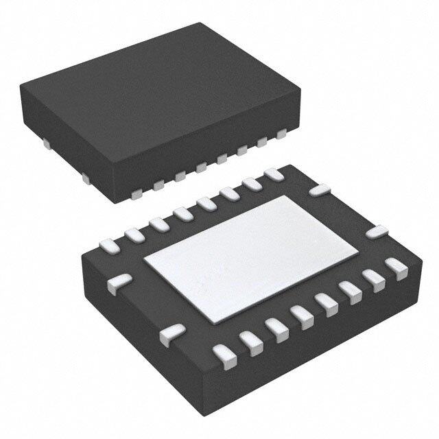
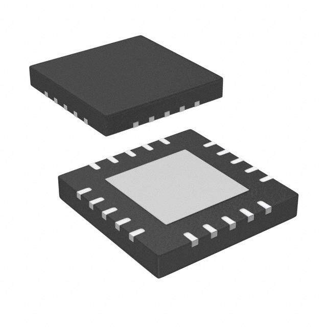
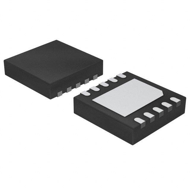
| 产品图片 |
|
| rohs | 符合RoHS无铅 / 符合限制有害物质指令(RoHS)规范要求 |
| 产品系列 | 电源管理 IC,开关控制器 ,Microchip Technology MCP1631HV-500E/ST- |
| 数据手册 | http://www.microchip.com/mymicrochip/filehandler.aspx?ddocname=en539550http://www.microchip.com/mymicrochip/filehandler.aspx?ddocname=en532151http://www.microchip.com/mymicrochip/filehandler.aspx?ddocname=en543908http://www.microchip.com/mymicrochip/filehandler.aspx?ddocname=en023833 |
| 产品型号 | MCP1631HV-500E/ST |
| PWM类型 | 电流模式 |
| 产品 | Voltage Controllers |
| 产品目录页面 | |
| 产品种类 | 开关控制器 |
| 倍增器 | 无 |
| 其它名称 | MCP1631HV500EST |
| 分频器 | 无 |
| 包装 | 管件 |
| 升压 | 无 |
| 占空比 | 10% |
| 参考设计库 | http://www.digikey.com/rdl/4294959902/4294959891/604http://www.digikey.com/rdl/4294959899/4294959898/633 |
| 反向 | 无 |
| 反激式 | 无 |
| 商标 | Microchip Technology |
| 安装风格 | SMD/SMT |
| 封装 | Tube |
| 封装/外壳 | 20-TSSOP(0.173",4.40mm 宽) |
| 封装/箱体 | TSSOP-20 |
| 工作温度 | -40°C ~ 125°C |
| 工厂包装数量 | 74 |
| 应用说明 | |
| 开关频率 | 2 MHz |
| 标准包装 | 74 |
| 电压-电源 | 3.5 V ~ 16 V |
| 类型 | Current Mode PWM Controllers |
| 输出数 | 1 |
| 输出电压 | 3.3 V to 5 V |
| 输出电流 | 250 mA |
| 配用 | /product-detail/zh/MCP1631RD-DCPC1/MCP1631RD-DCPC1-ND/2170222/product-detail/zh/MCP1631RD-MCC2/MCP1631RD-MCC2-ND/2059585 |
| 降压 | 是 |
| 隔离式 | 是 |
| 频率-最大值 | 2MHz |

.jpg)


- 商务部:美国ITC正式对集成电路等产品启动337调查
- 曝三星4nm工艺存在良率问题 高通将骁龙8 Gen1或转产台积电
- 太阳诱电将投资9.5亿元在常州建新厂生产MLCC 预计2023年完工
- 英特尔发布欧洲新工厂建设计划 深化IDM 2.0 战略
- 台积电先进制程称霸业界 有大客户加持明年业绩稳了
- 达到5530亿美元!SIA预计今年全球半导体销售额将创下新高
- 英特尔拟将自动驾驶子公司Mobileye上市 估值或超500亿美元
- 三星加码芯片和SET,合并消费电子和移动部门,撤换高东真等 CEO
- 三星电子宣布重大人事变动 还合并消费电子和移动部门
- 海关总署:前11个月进口集成电路产品价值2.52万亿元 增长14.8%


PDF Datasheet 数据手册内容提取
MCP1631/HV/MCP1631V/VHV High-Speed, Pulse Width Modulator Features General Description • Programmable Switching Battery Charger The MCP1631/MCP1631V is a high-speed microcon- Designs troller based pulse width modulator (PWM) used to • High-Speed Analog PWM Controller (2MHz develop intelligent power systems. When combined Operation) with a microcontroller, the MCP1631/MCP1631V will control the power system duty cycle providing output • Combine with Microcontroller for “Intelligent” voltage or current regulation. The microcontroller can Power System Development be used to adjust output voltage or current, switching • Peak Current Mode Control (MCP1631) frequency and maximum duty cycle while providing • Voltage Mode Control (MCP1631V) additional features making the power system more • High Voltage Options Operate to +16V Input: intelligent, robust and adaptable. - MCP1631HV Current Mode Typical applications for the MCP1631/MCP1631V - MCP1631VHV Voltage Mode include programmable switch mode battery chargers • Regulated Output Voltage Options: capable of charging multiple chemistries, like Li-Ion, - +5.0V or +3.3V NiMH, NiCd and Pb-Acid configured as single or multiple cells. By combining with a small microcontrol- - 250mA maximum current ler, intelligent LED lighting designs and programmable • External Oscillator Input sets Switching SEPIC topology voltage and current sources can also Frequency and Maximum Duty Cycle Limit be developed. • External Reference Input Sets Regulation Voltage The MCP1631/MCP1631V inputs were developed to or Current be attached to the I/O pins of a microcontroller for • Error Amplifier, Battery Current I Amplifier, SNS design flexibility. Additional features integrated into the Battery Voltage V Amplifier Integrated SNS MCP1631HV/MCP1631VHV provide signal condition- • Integrated Overvoltage Comparator ing and protection features for battery charger or • Integrated High Current Low Side MOSFET constant current source applications. Driver (1A Peak) For applications that operate from a high voltage input, • Shutdown mode reduces IQ to 2.4µA (typical) the MCP1631HV and MCP1631VHV device options • Internal Overtemperature Protection can be used to operate directly from a +3.5V to +16V • Undervoltage Lockout (UVLO) input. For these applications, an additional low drop out +5V or +3.3V regulated output is available and can • Package Options: provide current up to 250mA to power a microcontrol- - 4mmx4mm 20-Lead QFN ler and auxiliary circuits. (MCP1631/MCP1631V only) - 20-Lead TSSOP (All Devices) - 20-Lead SSOP (All Devices) Applications • High Input Voltage Programmable Switching Battery Chargers • Supports Multiple Chemistries Li-Ion, NiMH, NiCd Intelligent and Pb-Acid • LED Lighting Applications • Constant Current SEPIC Power Train Design • USB Input Programmable Switching Battery Chargers © 2007 Microchip Technology Inc. DS22063A-page 1
MCP1631/HV/MCP1631V/VHV Package Types 20-Lead SSOP and TSSOP 20-Lead SSOP and TSSOP MCP1631/MCP1631V MCP1631HV/MCP1631VHV PGND 1 20 V PGND 1 20 V EXT EXT SHDN 2 19 PVDD SHDN 2 19 PVDD OSCIN 3 18 CS/VRAMP OSCIN 3 18 CS/VRAMP OSC 4 17 FB OSC 4 17 FB DIS DIS OV 5 16 COMP OV 5 16 COMP IN IN VREF 6 15 ISOUT VREF 6 15 ISOUT AGND 7 14 VSOUT AGND 7 14 VSOUT NC 8 13 ISIN NC 8 13 ISIN NC 9 12 VS NC 9 12 VS IN IN NC 10 11 AVDD_IN VIN 10 11 AVDD_OUT S DI N N REF VIN SC SCI HD V O O O S 20 19 1 8 17 16 AGND 1 15 PGND NC 2 14 V EXT AVDD_IN 3 13 PVDD NC 4 12 NC VS 5 11 CS/V IN RAMP 6 7 8 9 10 SIN OUT OUT MP FB I S S O V I C 20-Lead 4x4 QFN MCP1631/MCP1631V DS22063A-page 2 © 2007 Microchip Technology Inc.
MCP1631/HV/MCP1631V/VHV Typical Application Diagram Multi-cell, Multi-Chemistry Charger SCHOTTKY C VIN Range +5.5V to +16V L1A C DIODE R THERM C C IN OUT L1B MCP1631HV V V EXT IN A CS VDD_OUT P P GND VDD IS OSC IN IN ISOUT OVIN NC VSIN FB VREF NC SHDN COMP OSCDIS AGND VSOUT R C PIC12F683 VDD GP1/C AVDD_OUT CCP1 GP3 GP4 GP5 GND GP0/C L E D © 2007 Microchip Technology Inc. DS22063A-page 3
MCP1631/HV/MCP1631V/VHV Functional Block Diagram(1) MCP1631HV/VHV High Speed PIC PWM Internal Regulator for MCP1631HV and MCP1631VHV Options Only; For MCP1631 and MCP1631V AV is input DD_IN VIN +3.3V or +5.0V VDD Internal LDO 1.2V V REF 250 mA V DD Overvoltage Comp A / A VDD_OUT VDD_IN - w/ Hysteresis C2 + Shutdown Control SHDN A3 Remains On OV P IN VDD VDD OSCDIS 100kΩ 0.1µA OT OSCIN VEXT UVLO S PGND V Q DD V DD 100kΩ CS/VRAMP + Q 10R R COMP C1 V - DD R IS IN - V DD A2 R FB + - V A1 REF + 2R IS OUT Remove for MCP1631V R and MCP1631VHV Options V DD A GND 2.7V Clamp VS IN + A3 - Note1: For Shutdown control, amplifier A3 remains functional so VS battery voltage can be sensed during discharge phase. OUT 2: For HV options, internal Low Drop Out Regulator provides +3.3V or +5.0V bias to V . DD DS22063A-page 4 © 2007 Microchip Technology Inc.
MCP1631/HV/MCP1631V/VHV 1.0 ELECTRICAL † Notice: Stresses above those listed under "Maximum CHARACTERISTICS Ratings" may cause permanent damage to the device. This is a stress rating only and functional operation of the device at those or any other conditions above those Absolute Maximum Ratings † indicated in the operational sections of this specifica- tion is not intended. Exposure to maximum rating con- V - GND (MCP1631/V)................................................+6.5V IN ditions for extended periods may affect device V - GND (MCP1631HV/VHV)....................................+18.0V IN reliability. All Other I/O..............................(GND - 0.3V) to (V + 0.3V) DD LX to GND.............................................-0.3V to (V + 0.3V) DD V Output Short Circuit Current........................Continuous EXT Storage temperature.....................................-65°C to +150°C Maximum Junction Temperature...................-40°C to +150°C Operating Junction Temperature...................-40°C to +125°C ESD Protection On All Pins: HBM.................................................................................4kV MM..................................................................................400V DC CHARACTERISTICS Electrical Specifications: Unless otherwise noted, V = 3.0V to 5.5V, F = 1MHz with 10% Duty Cycle, C = 0.1µF, IN OSC IN V for typical values=5.0V, T for typical values= +25°C, T =-40°C to +125°C for all minimum and maximums. DD A A Parameters Sym Min Typ Max Units Conditions Input Characteristics Input Voltage (MCP1631/V) V 3.0 — 5.5 V Non-HV Options DD Input Voltage V 3.5 — 16.0 V HV Options (Note2) DD (MCP1631HV/VHV) Undervoltage Lockout UVLO 2.7 2.8 3.0 V V Falling, V low when input IN EXT (MCP1631/V) below UVLO threshold Undervoltage Lockout Hysteresis UVLO 40 64 100 mV UVLO Hysteresis _HYS (MCP1631/MCP1631V) Input Quiescent Current I(V ) — 3.7 5 mA SHDN=V =OSC IN DD DIS (MCP1631/V, MCP1631HV,VHV) Shutdown Current I — SHDN=GND=OSC , IN_SHDN DIS I_AVDD for MCP1631/V 2.4 12 µA Note: Amplifier A3 remains pow- I_VIN for MCP1631HV/VHV 4.4 17 µA ered during Shutdown. OSC , OSC and SHDN Input Levels IN DIS Low Level Input Voltage V — — 0.8 V IL High Level Input Voltage V 2.0 — — V IH Input Leakage Current I 0.005 1 µA LEAK External Oscillator Range F — — 2 MHz Max. operating frequency is OSC dependent upon circuit topology and duty cycle. Min. Oscillator High Time T _MIN. — 10 — ns OH Min. Oscillator Low Time T _MIN. OL Oscillator Rise and Fall Time T and T 0.01 — 10 µs Note1 R F Oscillator Input Capacitance C — 5 — pf OSC Note 1: External Oscillator Input (OSC ) rise and fall times between 10ns and 10µs were determined during device IN characterization testing. Signal levels between 0.8V and 2.0V with rise and fall times measured between 10% and 90% of maximum and minimum values. Not production tested. Additional timing specifications were fully characterized and specified that are not production tested. 2: The minimum V must meet two conditions: V ≥ 3.5V and V ≥ (V + V ). IN IN IN OUT(MAX) DROPOUT(MAX) 3: TCV = (V - V ) *106 / (V * ΔTemperature), V = highest voltage measured over the OUT OUT-HIGH OUT-LOW R OUT-HIGH temperature range. V = lowest voltage measured over the temperature range. OUT-LOW 4: Load regulation is measured at a constant junction temperature using low duty cycle pulse testing. Changes in output voltage due to heating effects are determined using thermal regulation specification TCV . OUT 5: Dropout voltage is defined as the input to output differential at which the output voltage drops 2% below its measured value with an applied input voltage of V + V or 3.5V, whichever is greater. OUT(MAX) DROPOUT(MAX) © 2007 Microchip Technology Inc. DS22063A-page 5
MCP1631/HV/MCP1631V/VHV DC CHARACTERISTICS (CONTINUED) Electrical Specifications: Unless otherwise noted, V = 3.0V to 5.5V, F = 1MHz with 10% Duty Cycle, C = 0.1µF, IN OSC IN V for typical values=5.0V, T for typical values= +25°C, T =-40°C to +125°C for all minimum and maximums. DD A A Parameters Sym Min Typ Max Units Conditions External Reference Input Reference Voltage Input V 0 — AV V The reference input is capable of REF DD rail-to-rail operation. Internal Driver) R P-channel R — 7.2 15 Ω DSON DSon_P R N-channel R — 3.8 15 Ω DSON DSon_N V Rise Time T — 2.5 18 ns C =100pF EXT RISE L Typical for V =5V (Note1) IN V Fall Time T — 2.7 18 ns C =100pF EXT FALL L Typical for V =5V (Note1) IN Error Amplifier (A1) Input Offset Voltage V -0.6 — +0.6 mV OS A1 Input Bias Current I — 0.05 1 µA BIAS Error Amplifier PSRR PSRR — 85.4 — dB V =3.0V to 5.0V, V =1.2V IN CM Common Mode Input Range V GND-0.3 — V V CM IN Common Mode Rejection Ratio — 90 — dB V =5V, V =0V to 2.5V IN CM Open-loop Voltage Gain A 80 95 — dB R =5kΩ to V /2, 100mV < VOL L IN V < V - 100mV, EAOUT IN V =1.2V CM Low-level Output V — 25 GND + 65 mV RL=5kΩ to V /2 OL IN Gain Bandwidth Product GBWP — 3.5 — MHz V =5V IN Error Amplifier Sink Current I 4 12 — mA V =5V, V =1.2V, SINK IN REF V =1.4V, V =2.0V FB COMP Error Amplifier Source Current I -2 -9.8 — mA V =5V, V =1.2V, SOURCE IN REF V =1.0V, V =2.0V, Abso- FB COMP lute Value Current Sense (CS) Amplifier (A2) Input Offset Voltage V -3.0 1.2 +3.0 mV OS CS Input Bias Current I — 0.13 1 µA BIAS CS Amplifier PSRR PSRR — 65 — dB V =3.0V to 5.0V, V =0.12V, IN CM GAIN=10 Closed-loop Voltage Gain A2 — 10 — V/V R =5kΩ to V /2, 100mV < VCL L IN V < V - 100mV, OUT IN V =+0.12V CM Low-level Output V 5 11 GND + 50 mV RL=5kΩ to V /2 OL IN CS Sink Current I 5 17.7 — mA SINK CS Amplifier Source Current I -5 -19.5 — mA SOURCE Voltage Sense (VS) Amplifier (A3) Input Offset Voltage V -5 0.9 +5 mV OS VS Input Bias Current I — 0.001 1 µA BIAS Note 1: External Oscillator Input (OSC ) rise and fall times between 10ns and 10µs were determined during device IN characterization testing. Signal levels between 0.8V and 2.0V with rise and fall times measured between 10% and 90% of maximum and minimum values. Not production tested. Additional timing specifications were fully characterized and specified that are not production tested. 2: The minimum V must meet two conditions: V ≥ 3.5V and V ≥ (V + V ). IN IN IN OUT(MAX) DROPOUT(MAX) 3: TCV = (V - V ) *106 / (V * ΔTemperature), V = highest voltage measured over the OUT OUT-HIGH OUT-LOW R OUT-HIGH temperature range. V = lowest voltage measured over the temperature range. OUT-LOW 4: Load regulation is measured at a constant junction temperature using low duty cycle pulse testing. Changes in output voltage due to heating effects are determined using thermal regulation specification TCV . OUT 5: Dropout voltage is defined as the input to output differential at which the output voltage drops 2% below its measured value with an applied input voltage of V + V or 3.5V, whichever is greater. OUT(MAX) DROPOUT(MAX) DS22063A-page 6 © 2007 Microchip Technology Inc.
MCP1631/HV/MCP1631V/VHV DC CHARACTERISTICS (CONTINUED) Electrical Specifications: Unless otherwise noted, V = 3.0V to 5.5V, F = 1MHz with 10% Duty Cycle, C = 0.1µF, IN OSC IN V for typical values=5.0V, T for typical values= +25°C, T =-40°C to +125°C for all minimum and maximums. DD A A Parameters Sym Min Typ Max Units Conditions VS Amplifier PSRR PSRR — 65 — dB V =3.0V to 5.0V, V =1.2V IN CM Common Mode Input Range V GND — AV V Rail to Rail Input CM DD Closed-loop Voltage Gain A3 — 1 — V/V R =5kΩ to V /2, 100mV < VCL L IN V < V - 100mV, EAOUT IN V =1.2V CM Low-level Output V — 38 GND + 85 mV RL=5kΩ to V /2 OL IN VS Amplifier Sink Current I 1 5 — mA SINK VS Amplifier Source Current I -2 -5 — mA SOURCE Peak Current Sense Input (C1) Maximum Current Sense Signal V 0.85 0.9 0.98 V CS_MAX MCP1631/MCP1631HV Maximum Ramp Signal V 2.7 2.78 2.9 V V > 4V RAMP IN MCP1631V/MCP1631VHV Maximum CS input range limited by comparator input common mode range. V =V -1.4V CS_MAX IN Current Sense Input Bias Current I — -0.1 — µA V =5V CS_B IN Delay From CS to V T — 8.5 25 ns Note1 EXT CS_VEXT MCP1631 Minimum Duty Cycle DC — — 0 % V =V +0.1V, MIN FB REF V =GND CS Overvoltage Sense Comparator (C2) OV Reference Voltage High OV — 1.23 — V _VREF_H OV Reference Voltage Low OV 1.15 1.18 1.23 V _VREF_L OV Hysteresis OV_HYS — 50 — mV Overvoltage Comparator Hysteresis OV_IN Bias Current OV_ — 0.001 1 µA IBIAS Delay From OV to V T — 63 150 ns Delay from OV detection to PWM EXT OV_VEXT termination (Note1) OV Input Capacitance C_ — 5 — pF OV Internal Regulator HV Options Input / Output Characteristics Input Operating Voltage V 3.5 — 16.0 V Note2 IN Maximum Output Current I 250 — — mA OUT_mA Output Short Circuit Current I — 400 — mA V = V (Note2), OUT_SC IN IN(MIN) V = GND, OUT Current (average current) measured 10ms after short is applied. Output Voltage Regulation V V -3.0% V ±0.4% V +3.0% V V =3.3V or 5.0V OUT R R R R V Temperature Coefficient TCV — 50 150 ppm/ Note3 OUT OUT °C Note 1: External Oscillator Input (OSC ) rise and fall times between 10ns and 10µs were determined during device IN characterization testing. Signal levels between 0.8V and 2.0V with rise and fall times measured between 10% and 90% of maximum and minimum values. Not production tested. Additional timing specifications were fully characterized and specified that are not production tested. 2: The minimum V must meet two conditions: V ≥ 3.5V and V ≥ (V + V ). IN IN IN OUT(MAX) DROPOUT(MAX) 3: TCV = (V - V ) *106 / (V * ΔTemperature), V = highest voltage measured over the OUT OUT-HIGH OUT-LOW R OUT-HIGH temperature range. V = lowest voltage measured over the temperature range. OUT-LOW 4: Load regulation is measured at a constant junction temperature using low duty cycle pulse testing. Changes in output voltage due to heating effects are determined using thermal regulation specification TCV . OUT 5: Dropout voltage is defined as the input to output differential at which the output voltage drops 2% below its measured value with an applied input voltage of V + V or 3.5V, whichever is greater. OUT(MAX) DROPOUT(MAX) © 2007 Microchip Technology Inc. DS22063A-page 7
MCP1631/HV/MCP1631V/VHV DC CHARACTERISTICS (CONTINUED) Electrical Specifications: Unless otherwise noted, V = 3.0V to 5.5V, F = 1MHz with 10% Duty Cycle, C = 0.1µF, IN OSC IN V for typical values=5.0V, T for typical values= +25°C, T =-40°C to +125°C for all minimum and maximums. DD A A Parameters Sym Min Typ Max Units Conditions Line Regulation ΔV / -0.3 ±0.1 +0.3 %/V (V + V ) ≤ OUT OUT(MAX) DROPOUT(MAX) (V XΔ V ≤ 16V Note2 OUT IN V ) IN Load Regulation ΔV / -2.5 ±1.0 +2.5 % I = 1.0mA to 250mA, Note4 OUT L V OUT Dropout Voltage V — 330 650 mV I = 250mA, V = 5.0V DROPOUT L R Note2, Note5 — 525 725 mV I = 250mA, V = 3.3V L R Output Delay Time T — 1000 — µs V = 0V to 6V, V = 90% V , DELAY IN OUT R R = 50Ω resistive L Output Noise e — 8 — µV/ I = 50mA, f = 1kHz, C = N L OUT (Hz)1/2 1µF Power Supply Ripple Rejection PSRR — 44 — dB f = 100Hz, C = 1µF, I = 100 OUT L Ratio µA, V = 100mV pk-pk, INAC C = 0µF, V =1.2V IN R Protection Features Thermal Shutdown T — 150 — °C SHD Thermal Shutdown Hysteresis T — 18 — °C SHD_HYS Note 1: External Oscillator Input (OSC ) rise and fall times between 10ns and 10µs were determined during device IN characterization testing. Signal levels between 0.8V and 2.0V with rise and fall times measured between 10% and 90% of maximum and minimum values. Not production tested. Additional timing specifications were fully characterized and specified that are not production tested. 2: The minimum V must meet two conditions: V ≥ 3.5V and V ≥ (V + V ). IN IN IN OUT(MAX) DROPOUT(MAX) 3: TCV = (V - V ) *106 / (V * ΔTemperature), V = highest voltage measured over the OUT OUT-HIGH OUT-LOW R OUT-HIGH temperature range. V = lowest voltage measured over the temperature range. OUT-LOW 4: Load regulation is measured at a constant junction temperature using low duty cycle pulse testing. Changes in output voltage due to heating effects are determined using thermal regulation specification TCV . OUT 5: Dropout voltage is defined as the input to output differential at which the output voltage drops 2% below its measured value with an applied input voltage of V + V or 3.5V, whichever is greater. OUT(MAX) DROPOUT(MAX) TEMPERATURE SPECIFICATIONS Electrical Specifications: Unless otherwise indicated, all limits are specified for: V +3.0Vto5.5V IN Parameters Sym Min Typ Max Units Conditions Temperature Ranges Operating Junction Temperature T -40 — +125 °C Steady State J Range Storage Temperature Range T -65 — +150 °C A Maximum Junction Temperature T — — +150 °C Transient J Package Thermal Resistances Thermal Resistance, 20L-TSSOP θ — 90 — °C/W Typical 4 Layer board with inter- JA connecting vias Thermal Resistance, 20L-SSOP θ — 89.3 — °C/W Typical 4 Layer board with inter- JA connecting vias Thermal Resistance, 20L-QFN θ — 43 — °C/W Typical 4 Layer board with inter- JA connecting vias DS22063A-page 8 © 2007 Microchip Technology Inc.
MCP1631/HV/MCP1631V/VHV 2.0 TYPICAL PERFORMANCE CURVES Note: The graphs and tables provided following this note are a statistical summary based on a limited number of samples and are provided for informational purposes only. The performance characteristics listed herein are not tested or guaranteed. In some graphs or tables, the data presented may be outside the specified operating range (e.g., outside specified power supply range) and therefore outside the warranted range. Note: Unless otherwise noted, V = 3.0V to 5.5V, F = 1MHz with 10% Duty Cycle, C = 0.1µF, V for typical values=5.0V, T IN OSC IN IN A for typical values= +25°C. 2.89 4.00 ge Lockout (V) 22222.....8888845678 Device Turn On n Current (µA) 222333......258147000000 VDD = +5.0VVDD = +5.5V ndervolta 222...888123 Device Turn Off Shutdow 111...369000 VDD = +3.3V VDD = +4.0V VDD = +3.0V U 2.8 1.00 -40 -25 -10 5 20 35 50 65 80 95 110 125 -40 -25 -10 5 20 35 50 65 80 95 110 125 Ambient Temperature (°C) Ambient Temperature (°C) FIGURE 2-1: Undervoltage Lockout vs. FIGURE 2-4: Shutdown Current vs. Temperature. Temperature (MCP1631/MCP1631V). 0.068 1.60 0.067 d (V) 1.50 VDD = +5.5V O Hyst (V) 000...000666456 ut Threshol 11..3400 VDD = +3.3V VDD = V+4DD.0 =V +5.0V UVL 0.063 N Inp 1.20 VDD = +3.0V 0.062 _I 1.10 C S 0.061 O 1.00 0 5 0 5 0 5 0 5 0 5 0 5 0 5 0 5 0 5 0 5 0 5 0 5 4 2 1 2 3 5 6 8 9 1 2 4 2 1 2 3 5 6 8 9 1 2 - - - 1 1 - - - 1 1 Ambient Temperature (°C) Ambient Temperature (°C) FIGURE 2-2: Undervoltage Lockout FIGURE 2-5: Oscillator Input Threshold Hysteresis vs. Temperature. vs. Temperature. ent (mA) 34..8000 VDD = +5.0V VDD = +5.5V eshold 111...567000 VDD = +5V.0DVD = +5.5V put Quiescent Curr 3333....02460000 VDVDD =D +=3 +.33V.0V VDD = +4.0V OSC_DIS Input ThrVoltage (V) 011111......901234000000 VDD = +V3D.D0 V= +V3D.D3 V= +4.0V n 2.80 0.80 I 0 5 0 5 0 5 0 5 0 5 0 5 0 5 0 5 0 5 0 5 0 5 0 5 4 2 1 2 3 5 6 8 9 1 2 4 2 1 2 3 5 6 8 9 1 2 - - - 1 1 - - - 1 1 Ambient Temperature (°C) Ambient Temperature (°C) FIGURE 2-3: Input Quiescent Current vs. FIGURE 2-6: Oscillator Disable Input Temperature. Threshold vs. Temperature. © 2007 Microchip Technology Inc. DS22063A-page 9
MCP1631/HV/MCP1631V/VHV Typical Performance Curves (Continued) Note: Unless otherwise noted, V = 3.0V to 5.5V, F = 1MHz with 10% Duty Cycle, C = 0.1µF, IN OSC IN V for typical values=5.0V, T for typical values = +25°C. IN A ON 14 5.0 DS 4.7 CL = 100 pF XT Output P-Channel R(ohms) 110268 VDD = +V3.D0DV = +5.5VVDVDD =D +=3 +.35V.0V VDD = +4.0V V Fall Time (ns)EXT 22233344........36925814 VDD = +3.0V VDDV =DD + V=3D .+D3 5V=. 0+V5.V5VDD = +4.0V E 4 2.0 -40 -25 -10 5 20 35 50 65 80 95 110 125 -40 -25 -10 5 20 35 50 65 80 95 110 125 Ambient Temperature (°C) Ambient Temperature (°C) FIGURE 2-7: V P-Channel Driver FIGURE 2-10: V Fall Time vs. EXT EXT R vs. Temperature. Temperature. DSON 6.6 -0.50 hannel ms) 556...482 VDD = +3.3V e (mV) --00..6505 VDD = +5.5V VDD = +5.0V EXT Output N-CRDSON (oh 33445.....48260 VDD = V+D3D. 0=V +5.5V VDD = +5.0V VDD = +4.0V A1 Offset Voltag ---000...776505 VDD = +4.0VVDD = +3.3V VDD = +3.0V 3.0 -0.80 -40 -25 -10 5 20 35 50 65 80 95 110 125 -40 -25 -10 5 20 35 50 65 80 95 110 125 Ambient Temperature (°C) Ambient Temperature (°C) FIGURE 2-8: V N-Channel Driver FIGURE 2-11: Amplifier A1 Offset Voltage EXT R vs. Temperature. vs. Temperature. DSON 4.7 40 4.4 CL = 100 pF 35 V Rise Time (ns)EXT 223334......692581 VVDDDD == ++34..00VV VDD = +5.0VVDD = +V3.D3DV = +5.5V A1 V Low (mV)OUT 1122305050 VDD =V +VD3DD.D 3=V =V D+ D+5 4=.0. 0+VV5.5V 2.3 5 VDD = +3.0V 2.0 0 0 5 0 5 0 5 0 5 0 5 0 5 0 5 0 5 0 5 0 5 0 5 0 5 4 2 1 2 3 5 6 8 9 1 2 4 2 1 2 3 5 6 8 9 1 2 - - - 1 1 - - - 1 1 Ambient Temperature (°C) Ambient Temperature (°C) FIGURE 2-9: V Rise Time vs. FIGURE 2-12: Amplifier A1 Output Voltage EXT Temperature. Low vs. Temperature. DS22063A-page 10 © 2007 Microchip Technology Inc.
MCP1631/HV/MCP1631V/VHV Typical Performance Curves (Continued) Note: Unless otherwise noted, V = 3.0V to 5.5V, F = 1MHz with 10% Duty Cycle, C = 0.1µF, IN OSC IN V for typical values=5.0V, T for typical values = +25°C. IN A 18.8 18 17.6 Sink Current (mA) 111111012456......468024 VDD = +4.0V VDD = +5.0VVDD = +V3.D3DV = +3.0V 2 V Low (mV)OUT 111102468 VDD = +4.V0DVD = +5.5V VDD = +5.0V A1 9.2 VDD = +5.5V A 6 VDD = +3.3V 8.0 VDD = +3.0V 4 0 5 0 5 0 5 0 5 0 5 0 5 4 2 1 2 3 5 6 8 9 1 2 0 5 0 5 0 5 0 5 0 5 0 5 - - - 1 1 4 2 1 2 3 5 6 8 9 1 2 - - - 1 1 Ambient Temperature (°C) Ambient Temperature (°C) FIGURE 2-13: Amplifier A1 Sink Current FIGURE 2-16: Amplifier A2 Output Voltage vs. Temperature. Low vs. Temperature. 14.0 40 mA) 12.5 VDD = +5.0V A) 35 ent ( 11.0 VDD = +4.0V nt (m 30 VDD = +3.3V Curr 9.5 VDD = +5.5V urre 25 VDD = +3.0V 1 Source 68..50 VDD = +3.3V A2 Sink C 1250 VDD = +5.0V VDD = +4.0V A VDD = +3.0V VDD = +5.5V 5.0 10 -40 -25 -10 5 20 35 50 65 80 95 110 125 -40 -25 -10 5 20 35 50 65 80 95 110 125 Ambient Temperature (°C) Ambient Temperature (°C) FIGURE 2-14: Amplifier A1 Source Current FIGURE 2-17: Amplifier A2 Sink Current vs. Temperature. vs. Temperature. 1.6 26 mV) 1.4 VDD = +5.5V mA) 24 A2 Offset Voltage ( 0011....6802 VDD = +3.3V VDD = +4.0VVDD = +V3D.D0 V= +5.0V A2 Source Current ( 111122246802 VDD =V D+D5 .=0 V+3.0V VDD V=D +D3 =.3 +V5.5V 0.4 10 0 5 0 5 0 5 0 5 0 5 0 5 0 5 0 5 0 5 0 5 0 5 0 5 4 2 1 2 3 5 6 8 9 1 2 4 2 1 2 3 5 6 8 9 1 2 - - - 1 1 - - - 1 1 Ambient Temperature (°C) Ambient Temperature (°C) FIGURE 2-15: Amplifier A2 Offset Voltage FIGURE 2-18: Amplifier A2 Source Current vs. Temperature. vs. Temperature. © 2007 Microchip Technology Inc. DS22063A-page 11
MCP1631/HV/MCP1631V/VHV Typical Performance Curves (Continued) Note: Unless otherwise noted, V = 3.0V to 5.5V, F = 1MHz with 10% Duty Cycle, C = 0.1µF, IN OSC IN V for typical values=5.0V, T for typical values = +25°C. IN A 2.5 7.0 V) A) 6.5 A3 Offset Voltage (m 01..1255 VDD = +3.0VVDD = +4.0V VVDDDD == ++55V..D50DVV = +3.3V A3 Source Current (m 344556......505050 VDD = +3.0V VVDDDD == ++35..30VV VDD = +V4D.D0 V= +5.5V 0 3.0 0 5 0 5 0 5 0 5 0 5 0 5 4 2 1 2 3 5 6 8 9 1 2 0 5 0 5 0 5 0 5 0 5 0 5 - - - 1 1 4 2 1 2 3 5 6 8 9 1 2 - - - 1 1 Ambient Temperature (°C) Ambient Temperature (°C) FIGURE 2-19: Amplifier A3 Offset Voltage FIGURE 2-22: Amplifier A3 Source Current vs. Temperature. vs. Temperature. 70 V) 0.920 3 V Low (mV)OUT 2345600000 VDD = +4.0V VDD = +5.0VVDD =V +D3D .=3 V+5.5V Threshold Voltage ( 0000000.......999999900111116802468 VDD = +5.5V VDD = +4V.0DVD = +5.0V A 10 VDD = +3.0V ax 0.904 0 CS M 00..990002 VDD = +3.3V VDD = +3.0V -40 -25 -10 5 20 35 50 65 80 95 110 125 -40 -25 -10 5 20 35 50 65 80 95 110 125 Ambient Temperature (°C) Ambient Temperature (°C) FIGURE 2-20: Amplifier A3 Output Voltage FIGURE 2-23: MCP1631 and MCP1631HV Low vs. Temperature. CS Maximum Voltage (V) vs. Temperature. 66..38 um 22..778980 VDD = +5.0V mA) 5.8 xim 2.786 nk Current ( 445...383 VDD = +3.0V to +5.5V 1V V MaRAMPVoltage (V) 22222.....777777788868024 A3 Si 33..38 CP163 22..777724 2.8 M 2.770 -40 -25 -10 5 20 35 50 65 80 95 110 125 -40 -25 -10 5 20 35 50 65 80 95 110 125 Ambient Temperature (°C) Ambient Temperature (°C) FIGURE 2-21: Amplifier A3 Sink Current FIGURE 2-24: MCP1631V and vs. Temperature. MCP1631VHV V Max Voltage (V). RAMP DS22063A-page 12 © 2007 Microchip Technology Inc.
MCP1631/HV/MCP1631V/VHV Typical Performance Curves (Continued) Note: Unless otherwise noted, V = 3.0V to 5.5V, F = 1MHz with 10% Duty Cycle, C = 0.1µF, IN OSC IN V for typical values=5.0V, T for typical values = +25°C. IN A 1.27 1.7 V) 1.26 VDD = +5.5V old 1.6 VDD = +5.5V OV Threshold High ( 11111.....122222.123452 VDDVV =DD DD+ 3==. 3++V53..00VV VDD = +4.0V Shutdown Input ThreshVoltage (V) 0111111.......9012345 VVDDD D= =+ 3+.50.V0V VDD = +3.V3VDD = +4.0V 0.8 0 5 0 5 0 5 0 5 0 5 0 5 4 2 1 2 3 5 6 8 9 1 2 0 5 0 5 0 5 0 5 0 5 0 5 - - - 1 1 4 2 1 2 3 5 6 8 9 1 2 - - - 1 1 Ambient Temperature (°C) Ambinet Temperature (°C) FIGURE 2-25: Overvoltage Threshold High FIGURE 2-28: Shutdown Input Voltage (V) vs. Temperature. Threshold (V) vs. Temperature. 1.187 6.00 eshold Low (V) 111111......111111888888455667 VDD = +3.0VVDD = +3.3V VDD = +4.0V Quiescent Current (µA)345...000000 VIOOUUTT = = 0 5 µ.0A+V130°C -45°C 0°C hr 1.184 O +25°C V T 1.183 LD 2.00 +90°C O 1.183 VDD = +5.0V VDD = +5.5V HV 1.182 1.00 0 5 0 5 0 5 0 5 0 5 0 5 6 8 10 12 14 16 18 4 2 1 2 3 5 6 8 9 1 2 - - - 1 1 Ambient Temperature (°C) Input Voltage (V) FIGURE 2-26: Overvoltage Threshold Low FIGURE 2-29: LDO Quiescent Current vs. (V) vs. Temperature. Input Voltage. steresis (V) 0000....000056780000 VDD = +5.5V VDD = +3.3V nt Current 223...050000 VVOINU =T =3 .25.V5V VVOINU =T =2 .17.V2V IOUT = 0mA old Hy 00..003400 VDD = +4.0V uiesce(µA)1.50 h Q 1.00 es 0.020 VDD = +3.0V VDD = +5.0V O VOUT = 5.0V OV Thr 00..000100 HV LD 00..0500 VIN = 6.0V 40 25 10 5 20 35 50 65 80 95 10 25 -45 -20 5 30 55 80 105 130 - - - 1 1 Ambient Temperature (°C) Junction Temperature (°C) FIGURE 2-27: Overvoltage Threshold FIGURE 2-30: LDO Quiescent Current vs. Hysteresis (V) vs. Temperature. Junction Temperature. © 2007 Microchip Technology Inc. DS22063A-page 13
MCP1631/HV/MCP1631V/VHV Typical Performance Curves (Continued) Note: Unless otherwise noted, V = 3.0V to 5.5V, F = 1MHz with 10% Duty Cycle, C = 0.1µF, IN OSC IN V for typical values=5.0V, T for typical values = +25°C. IN A 5.06 0.18 VIN= 6V VOUT = 5.0V V) 5.04 +130°C +90°C VOUT = 5.0V %/V) 0.16 VIN = 6.0V to 16.0V ge ( 5.02 n ( 0.14 200 mA olta 5.00 atio 0.12 250 mA V 4.98 ul Output 44..9946 +25°C -45°C 0°C Line Reg 00..0180 0 mA 100 mA 4.92 0.06 0 50 100 150 200 250 -45 -20 5 30 55 80 105 130 Load Current (mA) Temperature (°C) FIGURE 2-31: LDO Output Voltage vs. FIGURE 2-34: LDO Line Regulation vs. Load Current. Temperature. 0.50 0 0.45 VOUT = 5.0V -10 V) 0.40 +130°C -20 age ( 00..3305 +90°C B)-30 Dropout Volt 0000....11220505 +25°C -45°C +0°C PSRR (d----76540000 VVVCRIIINNN==A=5C60 .. =00μV V1F00 mV p-p 0.05 -80 IOUT=100 µA 0.00 -90 0 25 50 75 100 125 150 175 200 225 250 0.01 0.1 1 10 100 1000 Load Current (mA) Frequency (kHz) FIGURE 2-32: LDO Dropout Voltage vs. FIGURE 2-35: LDO PSRR vs. Frequency. Load Current. 1.00 100 n (%) 00..6800 VIN = 16V VIN = 6V IOUT = 1V tOoU T2 5=0 5 m.0AV Hz) 10 VR = 5.0V, VIN = 6.0V IOUT = 50 mA atio 0.40 VIN = 12V V/√ 1 ul µ eg 0.20 e ( 0.1 oad R 0.00 VIN = 8V Nois 0.01 L -0.20 VIN = 14V -0.40 0.001 -45 -20 5 30 55 80 105 130 0.01 0.1 1 10 100 1000 Temperature (°C) Frequency (kHz) FIGURE 2-33: LDO Load Regulation vs. FIGURE 2-36: LDO Output Noise vs. Temperature. Frequency. DS22063A-page 14 © 2007 Microchip Technology Inc.
MCP1631/HV/MCP1631V/VHV 3.0 PIN DESCRIPTIONS The descriptions of the pins are listed in Table3-1. TABLE 3-1: PIN FUNCTION TABLE MCP1631/ MCP1631HV/ 4x4 MCP1631V MCP1631VHV Sym Description QFN TSSOP/SSOP TSSOP/SSOP 1 1 15 P Power ground return GND 2 2 16 SHDN Shutdown input 3 3 17 OSC External oscillator input IN 4 4 18 OSC Oscillator disable input DIS 5 5 19 OV Overvoltage comparator input IN 6 6 20 V External voltage reference input REF 7 7 1 A Quiet or analog ground GND 8,9,10 8,9 2,4,12 NC No connection 10 V High voltage input IN 11 3 A Analog bias voltage input VDD_IN 11 A Regulated V output VDD_OUT DD 12 12 5 VS Voltage sense amplifier (A3) input IN 13 13 6 IS Current sense input IN 14 14 7 VS Voltage sense amplifier output OUT 15 15 8 IS Current sense amplifier output OUT 16 16 9 COMP Error amplifier (A1) output 17 17 10 FB Error amplifier inverting input (A1) 18 18 11 CS/V CS - current sense input; V voltage ramp input RAMP RAMP 19 19 13 P Power V input VDD DD 20 20 14 V External driver output EXT NA NA 21 TAB Connect center thermal tab to A . GND 3.1 Power Ground (P ) 3.5 Overvoltage Input (OV ) GND IN Connect power ground return pin to power ground Overvoltage Comparator input, connect to voltage plane, high peak current flows through the P during divider, internal comparator terminates V output in GND EXT the turn on and turn off the external MOSFET devices. 50ns to limit output voltage to predetermined value. 3.2 Shutdown Input (SHDN) 3.6 External Reference Voltage Input (V ) REF Shutdown input logic low disables device and lowers I Q to minimum value, amplifier A3 (VS) remains functional External Voltage Reference input, connect fixed or for battery voltage sense applications. variable external reference to VREF, with A1 configured as an error amplifier, the power supply output variable 3.3 Oscillator Input (OSC ) (voltage or current) will follow this input. IN External Oscillator Input, used to set power train 3.7 Analog Ground (A ) GND switching frequency and maximum duty cycle, V EXT Quiet or analog ground, connect to analog ground enabled while low and disabled while high. plane to minimize noise on sensitive MCP1631 circuitry. 3.4 Oscillator Disable (OSC ) DIS Oscillator disable input, used to asycnronously 3.8 No Connection (NC) terminate the V duty cycle. Commonly used to EXT No connection modulate current for LED driver applications.For minimum shutdown I , connect OSC to SHDN. Q DIS © 2007 Microchip Technology Inc. DS22063A-page 15
MCP1631/HV/MCP1631V/VHV 3.9 Input Voltage (V ) 3.16 Error Amplifier Output (COMP) IN High voltage input for MCP1631HV/MCP1631VHV Error amplifier (A1) output, connect control loop com- devices, operates from 3.5V to 16V input supply. pensation from FB input to COMP output pin. 3.10 Analog supply Input (A ) 3.17 Feedback (FB) VDD_IN Analog bias input, minimum 3.0V to 5.5V operation for Error amplifier input (A1), connect to current sense MCP1631/MCP1631V devices. output amplifier (A2) to regulate current. 3.11 Analog Supply Output (A ) 3.18 Current Sense or Voltage Ramp VDD_OUT (CS/V ) Regulated V output used to power internal RAMP DD MCP1631HV/MCP1631VHV and external microcon- For MCP1631/MCP1631HV applications, connect to troller, supplies up to 250ma of bias current at 3.3V or low side current sense of SEPIC switch for current 5.0V regulated low drop out rail. mode control and peak current limit. For MCP1631/ MCP1631HV application, connect artificial ramp volt- 3.12 Voltage Sense Input (VS ) age to V input for voltage mode PWM control. IN RAMP Voltage sense amplifier (A3) input, connect to high 3.19 Power VDD (P ) VDD impedance battery voltage resistor divider to sense battery voltage with minimal loading. Power VDD input, VEXT gate drive supply input, connect to +5.0V or +3.3V supply for driving external MOSFET. 3.13 Current Sense Input (IS ) IN 3.20 External Driver (V ) EXT Connect to SEPIC secondary side sense resistor to High current driver output used to drive external develop a regulated current source used to charge MOSFET at high frequency, capable of 1A peak multi-chemistry batteries. currents with +5.0V P . VDD 3.14 Voltage Sense Output (VS ) OUT 3.21 Exposed PAD 4x4 QFN (EP) Voltage sense amplifier output, connect to microcon- Connect center thermal tab to A . troller analog to digital converter to measure battery GND voltage. 3.15 Current Sense Output (IS ) OUT Current sense amplifier output, connect to error amplifier (A1) inverting input (FB) to regulate SEPIC output current. DS22063A-page 16 © 2007 Microchip Technology Inc.
MCP1631/HV/MCP1631V/VHV 4.0 DETAILED DESCRIPTION 4.4 Current Sense Amplifier (A2) The A2 current sense amplifier is used to sense current 4.1 Device Overview in the secondary side of a SEPIC converter or free- wheeling current in a Buck converter. The inverting The MCP1631/MCP1631V device family combines the amplifier has a built in voltage gain of ten with low offset analog functions to develop high frequency switch and high speed. mode power systems while integrating features for battery charger and LED current source applications. 4.5 Voltage Sense Amplifier (A3) With the integration of a MOSFET driver, voltage sense, current sense and over voltage protection, the The A3 voltage sense amplifier is used to sense battery MCP1631/MCP1631V is a highly integrated, high- voltage. In battery powered applications, it is important speed analog pulse width modulator. to minimize the steady stage load current draw on the The MCP1631/MCP1631V output (VEXT) is used to battery. The voltage sense amplifier (A3) is used to control the switch of the power system (on and off buffer a high impedance series divider used to reduce time). By controlling the switch on and off time, the the battery pack voltage to a level that can be read power system output can be regulated. With the using an analog to digital converter. The voltage sense oscillator and reference voltage as inputs, a simple amplifier draws a very low quiescent current and interface to a microcontroller is available with the remains functional when the MCP1631/MCP1631V is MCP1631/MCP1631V to develop intelligent power shutdown making it possible to read battery voltage systems. A good example of an intelligent power without turning on the charger. system is a battery charger, programmable LED driver current source or programmable power supply. 4.6 Overvoltage Comparator(C2) The MCP1631/MCP1631V is a combination of The C2 overvoltage comparator is used to prevent the specialty analog blocks consisting of a Pulse Width power system from being damaged when the load Modulator (PWM), MOSFET Driver, Current Sense (battery) is disconnected. By comparing the divided Amplifier (A2), Voltage Sense Amplifier (A3), Overvolt- down power train output voltage with a 1.2V internal age Comparator (C2) and additional features (Shut- reference voltage, the MCP1631/MCP1631V V down, Undervoltage Lockout, Overtemperature EXT output switching is interrupted when the output voltage Protection). For the HV options, an internal low dropout is above a pre-set value. This limits the output voltage regulator is integrated for operation from high voltage of the power train, the 0V comparator’s hysteresis will inputs (MCP1631HV/MCP1631VHV). operate as a ripple regulator. 4.2 Pulse Width Modulator (PWM) 4.7 Shutdown Input The internal PWM of the MCP1631/MCP1631V is The MCP1631/MCP1631V shutdown feature is used to comprised of an error amplifier, high-speed comparator disable the device with the exception of the voltage and latch. The output of the amplifier is compared to sense amplifier A3 to minimize quiescent current draw. either the MCP1631 CS (primary current sense input) While shutdown, A3 remains operational while the or the MCP1631V V (voltage mode ramp input) of RAMP device draws 4.4µA from the input. the high speed comparator. When the CS or VRAMP signal reach the level of the error amplifier output, the 4.8 Protection on cycle is terminated and the external switch is latched off until the beginning of the next cycle (high to The MCP1631/MCP1631V has built in Undervoltage low transition of OSC ). IN Lockout (UVLO) that ensures the output V pin is EXT forced to a known state (low) when the input voltage or 4.3 V MOSFET Driver EXT AVDD is below the specified value. This prevents the main MOSFET switch from being turned on during a The MCP1631/MCP1631V output can be used to drive power up or down sequence. the external MOSFET directly for low side topology applications. The V is capable of sourcing up to The MCP1631/MCP1631V provides a thermal EXT 700mA and sinking up to 1A of current from a P shutdown protection feature, if the internal junction VDD source of 5V. Typical output power using the V temperature of the device becomes high, the EXT output to directly drive the external MOSFET can overtemperature protection feature will disable (pull the exceed 50W depending upon application and switching VEXT output low) and shut down the power train. frequency. © 2007 Microchip Technology Inc. DS22063A-page 17
MCP1631/HV/MCP1631V/VHV 5.0 APPLICATION INFORMATION inductors has significant advantages in addition to the size and cost benefits of a single core with multiple windings. 5.1 Typical Applications The MCP1631/MCP1631V can be used to develop 5.4 Mixed Signal Design intelligent power management solutions, typical applications include a multi-chemistry battery charger For intelligent battery charger design, a microcontroller used to charge Li-Ion, NiMH or NiCd batteries and is used to generate the proper charge profile, charge constant current LED drivers. termination, safety timers and battery charger features. When using the MCP1631/MCP1631V for Li-Ion battery charger applications, the microcontroller is also 5.2 Battery Charger Design Overview used to generate the constant voltage regulation phase The design approach for developing high current of the charge cycle. This is accomplished by using the switching battery chargers using the MCP1631 is external reference feature of the MCP1631/MCP1631V described in this section. Depending on input voltage as a programmable current source. The microcontroller range, there are two versions of the device that can be is used to vary the VREF input of the MCP1631/ used to accommodate a very wide range of input MCP1631V. The charge current into the battery is voltages. regulated by the MCP1631/MCP1631V, the level that it is regulated to is set by the programmability of the For a regulated input voltage range of 5V, the microcontroller. MCP1631/MCP1631V device is used, for this input voltage application (regulated ac-dc converter or USB The internal MCP1631/MCP1631V analog compo- input), the MCP1631/MCP1631V is powered directly nents are used to regulate the microcontroller from the 5V dc input. programmed current. The secondary or battery current is sensed using amplifier A2, the output of A2 is feed For input voltages to +16V steady state with +18V into the input of the error amplifier A1, the output of A1 transients, the MCP1631HV/MCP1631VHV, or high sets the peak switch current of the SEPIC converter, it voltage option can be used. The high voltage devices increases or decreases the battery current to match its integrate a low dropout (LDO) linear regulator with a set (A1) inputs. By increasing the V or non-inverting output voltage of +3.3V or +5.0V that internally powers REF input of A1, the battery current is increased. the MCP1631HV/MCP1631VHV and is also capable of providing 250mA of bias current for the attached 5.5 Safety Features microcontroller and other circuitry. MCP1631HV/ MCP1631VHV internal power dissipation must be The MCP1631/MCP1631V integrates a high-speed considered when loading the internal LDO regulator. comparator used to protect the charger and battery For higher input voltages the MCP1631/MCP1631V from being exposed to high voltages if the battery is can be biased from an external regulated +3.0V to removed or opens. Comparator C2 is used to sense the +5.5V supply. SEPIC output voltage. If the divided down output voltage becomes higher than the 1.2V internal 5.3 Programmable Single Ended MCP1631/MCP1631V reference, the VEXT PWM Primary Inductive (SEPIC) Current output is terminated within 50ns preventing the build up of voltage on the SEPIC output. Source Peak switch current is limited by the MCP1631/ The MCP1631/MCP1631V family integrates features MCP1631V comparator C1 and error amplifier A1 that are necessary to develop programmable current output voltage clamp. For the MCP1631, the error sources. The SEPIC converter is commonly used in amplifier output is clamped at 2.7V. The A1 output is battery charger applications. The primary or input divided down by 1/3 and compared with CS (current inductor is used to filter input current and minimize the sense) input. The V output is turned off if the CS EXT switching noise at the converter input. The primary to input reaches a level of 1/3 of 2.7V or 0.9V in 12ns, secondary capacitive isolation blocks any dc path from preventing the external switch current from becoming input to output making the SEPIC safer than Buck or high enough to damage the SEPIC power train. other non-isolated topologies. The SEPIC rectifier Internal overtemperature protection limits the device blocks the reverse path preventing battery leakage, in junction temperature to 150°C preventing catastrophic other topologies an additional diode for blocking is failure for overtemperature conditions. Once the necessary adding additional components and temperature decreases 10°C, the device will resume efficiency loss. normal operation. The input or primary inductor and output or secondary inductor are typically constructed from a single magnetic device with two windings, this is commonly referred to as a coupled inductor. Using coupled DS22063A-page 18 © 2007 Microchip Technology Inc.
MCP1631/HV/MCP1631V/VHV Safety timers are typically used to limit the amount of energy into a faulted battery or pack. This is accomplished using the microcontroller and MCP1631/ MCP1631V shutdown feature. 5.6 OSC Disable Feature The oscillator disable or OSC_DIS input is used to asychronously terminate the PWM V output. This EXT can be used with a slow PWM input to modulate current into an LED for lighting applications. © 2007 Microchip Technology Inc. DS22063A-page 19
MCP1631/HV/MCP1631V/VHV Multi-cell Multi-Chemistry Charger SCHOTTKY C VIN Range +4.5V to +5.5V L1A C DIODE R THERM CIN C OUT L1B MCP1631 NC VEXT AVDD_IN CS PVDD PGND OSC IS IN IN ISOUT OVIN NC VSIN FB VREF NC SHDN COMP OSCDIS AGND VSOUT R C PIC12F683 VDD GP1/C AVDD_OUT CCP1 GP3 GP4 GP5 GND GP0/C L E D FIGURE 5-1: +5V ac-dc or USB Input Application. DS22063A-page 20 © 2007 Microchip Technology Inc.
MCP1631/HV/MCP1631V/VHV Multi-cell Multi-Chemistry Charger SCHOTTKY C VIN Range +5.5V to +16V L1A C DIODE R THERM C C IN OUT L1B MCP1631HV VIN VEXT AVDD_OUT CS P PGND VDD OSC IS IN IN IS OV OUT IN NC VSIN FB VREF NC SHDN COMP OSCDIS AGND VSOUT R C PIC12F683 VDD GP1/C AVDD_OUT CCP1 GP3 GP4 GP5 GND GP0/C L E D FIGURE 5-2: +5.5V to +16.0V Input. © 2007 Microchip Technology Inc. DS22063A-page 21
MCP1631/HV/MCP1631V/VHV Multi-cell Multi-Chemistry Charger V Range +6V to +40V IN CIN C SCHOTTKY L1A C DIODE +5V HV R Regulator THERM C OUT C OUT MCP1631 L1B V NC EXT AVDD_IN CS PVDD PGND OSC IS IN IN IS OV OUT IN NC VSIN FB VREF NC SHDN COMP OSCDIS AGND VSOUT R C PIC12F683 VDD GP1/C A VDD_OUT CCP1 GP3 GP4 GP5 GND GP0/C L E D FIGURE 5-3: Wide Range High Voltage Input. DS22063A-page 22 © 2007 Microchip Technology Inc.
MCP1631/HV/MCP1631V/VHV 6.0 PACKAGING INFORMATION 6.1 Package Marking Information (Not to Scale) 20-Lead 4x4 QFN (MCP1631/MCP1631V) Example: XXXXX 1631 XXXXXX E/ML^e^3 XXXXXX 0738 YWWNNN 256 20-Lead SSOP (All Devices) Example: XXXXXXXXXXX 1631VHV330 XXXXXXXXXXX ESS^e^3 YYWWNNN 0738256 20-Lead TSSOP (All Devices) Example: XXXXXXXX 1631HV33 XXXXXNNN EST^e^3 256 YYWW 0738 Legend: XX...X Customer-specific information Y Year code (last digit of calendar year) YY Year code (last 2 digits of calendar year) WW Week code (week of January 1 is week ‘01’) NNN Alphanumeric traceability code e3 Pb-free JEDEC designator for Matte Tin (Sn) * This package is Pb-free. The Pb-free JEDEC designator ( e 3 ) can be found on the outer packaging for this package. Note: In the event the full Microchip part number cannot be marked on one line, it will be carried over to the next line, thus limiting the number of available characters for customer-specific information. © 2007 Microchip Technology Inc. DS22063A-page 23
MCP1631/HV/MCP1631V/VHV 20-Lead Plastic Quad Flat, No Lead Package (ML) – 4x4x0.9 mm Body [QFN] Note: For the most current package drawings, please see the Microchip Packaging Specification located at http://www.microchip.com/packaging D D2 EXPOSED PAD e E2 E 2 2 b 1 1 K N N NOTE 1 L TOP VIEW BOTTOM VIEW A A3 A1 Units MILLIMETERS Dimension Limits MIN NOM MAX Number of Pins N 20 Pitch e 0.50 BSC Overall Height A 0.80 0.90 1.00 Standoff A1 0.00 0.02 0.05 Contact Thickness A3 0.20 REF Overall Width E 4.00 BSC Exposed Pad Width E2 2.60 2.70 2.80 Overall Length D 4.00 BSC Exposed Pad Length D2 2.60 2.70 2.80 Contact Width b 0.18 0.25 0.30 Contact Length L 0.30 0.40 0.50 Contact-to-Exposed Pad K 0.20 – – Notes: 1. Pin 1 visual index feature may vary, but must be located within the hatched area. 2. Package is saw singulated. 3. Dimensioning and tolerancing per ASME Y14.5M. BSC: Basic Dimension. Theoretically exact value shown without tolerances. REF: Reference Dimension, usually without tolerance, for information purposes only. MicrochipTechnologyDrawingC04-126B DS22063A-page 24 © 2007 Microchip Technology Inc.
MCP1631/HV/MCP1631V/VHV 20-Lead Plastic Shrink Small Outline (SS) – 5.30 mm Body [SSOP] Note: For the most current package drawings, please see the Microchip Packaging Specification located at http://www.microchip.com/packaging D N E E1 NOTE 1 1 2 e b c A A2 φ A1 L1 L Units MILLIMETERS Dimension Limits MIN NOM MAX Number of Pins N 20 Pitch e 0.65 BSC Overall Height A – – 2.00 Molded Package Thickness A2 1.65 1.75 1.85 Standoff A1 0.05 – – Overall Width E 7.40 7.80 8.20 Molded Package Width E1 5.00 5.30 5.60 Overall Length D 6.90 7.20 7.50 Foot Length L 0.55 0.75 0.95 Footprint L1 1.25 REF Lead Thickness c 0.09 – 0.25 Foot Angle φ 0° 4° 8° Lead Width b 0.22 – 0.38 Notes: 1. Pin 1 visual index feature may vary, but must be located within the hatched area. 2. Dimensions D and E1 do not include mold flash or protrusions. Mold flash or protrusions shall not exceed 0.20 mm per side. 3. Dimensioning and tolerancing per ASME Y14.5M. BSC: Basic Dimension. Theoretically exact value shown without tolerances. REF: Reference Dimension, usually without tolerance, for information purposes only. MicrochipTechnologyDrawingC04-072B © 2007 Microchip Technology Inc. DS22063A-page 25
MCP1631/HV/MCP1631V/VHV 20-Lead Plastic Thin Shrink Small Outline (ST) – 4.4 mm Body [TSSOP] Note: For the most current package drawings, please see the Microchip Packaging Specification located at http://www.microchip.com/packaging D N E E1 NOTE 1 1 2 b e c φ A A2 A1 L1 L Units MILLIMETERS Dimension Limits MIN NOM MAX Number of Pins N 20 Pitch e 0.65 BSC Overall Height A – – 1.20 Molded Package Thickness A2 0.80 1.00 1.05 Standoff A1 0.05 – 0.15 Overall Width E 6.40 BSC Molded Package Width E1 4.30 4.40 4.50 Molded Package Length D 6.40 6.50 6.60 Foot Length L 0.45 0.60 0.75 Footprint L1 1.00 REF Foot Angle φ 0° – 8° Lead Thickness c 0.09 – 0.20 Lead Width b 0.19 – 0.30 Notes: 1. Pin 1 visual index feature may vary, but must be located within the hatched area. 2. Dimensions D and E1 do not include mold flash or protrusions. Mold flash or protrusions shall not exceed 0.15 mm per side. 3. Dimensioning and tolerancing per ASME Y14.5M. BSC: Basic Dimension. Theoretically exact value shown without tolerances. REF: Reference Dimension, usually without tolerance, for information purposes only. MicrochipTechnologyDrawingC04-088B DS22063A-page 26 © 2007 Microchip Technology Inc.
MCP1631/HV/MCP1631V/VHV APPENDIX A: REVISION HISTORY Revision A (October 2007) • Original Release of this Document. © 2007 Microchip Technology Inc. DS22063A-page 27
MCP1631/HV/MCP1631V/VHV NOTES: DS22063A-page 28 © 2007 Microchip Technology Inc.
MCP1631/HV/MCP1631V/VHV PRODUCT IDENTIFICATION SYSTEM To order or obtain information, e.g., on pricing or delivery, refer to the factory or the listed sales office. PART NO. X XX Examples: a) MCP1631-E/ML: High-Speed PWM, Device Temperature Package 20LD QFN package. Range b) MCP1631-E/SS: High-Speed PWM, 20LD SSOP package. Device: MCP1631: High-Speed PWM c) MCP1631-E/ST: High-Speed PWM, MCP1631T: High-Speed PWM 20LD TSSOP package. Tape and Reel MCP1631HV: High-Speed PWM a) MCP1631HV-E/ML: High-Speed PWM, MCP1631HVT: High-Speed PWM 20LD QFN package. Tape and Reel MCP1631V: High-Speed PWM b) MCP1631HV-E/SS: High-Speed PWM, MCP1631VT: High-Speed PWM 20LD SSOP package. Tape and Reel c) MCP1631HV-E/ST: High-Speed PWM, MCP1631VHV: High-Speed PWM MCP1631VHVT:High-Speed PWM 20LD TSSOP package. Tape and Reel a) MCP1631VT-E/ML: High-Speed PWM, 20LD QFN package. Temperature Range: E = -40°C to +125°C b) MCP1631V-E/SS: High-Speed PWM, 20LD SSOP package. Package: * ML = Plastic Quad Flat, No Lead (4x4x0.9), 20-lead c) MCP1631V-E/ST: High-Speed PWM, SS = Plastic Shrink Small Outline (5.30mm), 20-lead 20LD TSSOP package. ST = Plastic Thin Shrink Small Outline (4.4mm), 20-Lead a) MCP1631VHVT-E/ML:High-Speed PWM, * All package offerings are Pb Free (Lead Free) 20LD QFN package. b) MCP1631VHV-E/SS: High-Speed PWM, 20LD SSOP package. c) MCP1631VHV-E/ST: High-Speed PWM, 20LD TSSOP package. © 2007 Microchip Technology Inc. DS22063A-page 29
MCP1631/HV/MCP1631V/VHV NOTES: DS22063A-page 30 © 2007 Microchip Technology Inc.
Note the following details of the code protection feature on Microchip devices: • Microchip products meet the specification contained in their particular Microchip Data Sheet. • Microchip believes that its family of products is one of the most secure families of its kind on the market today, when used in the intended manner and under normal conditions. • There are dishonest and possibly illegal methods used to breach the code protection feature. All of these methods, to our knowledge, require using the Microchip products in a manner outside the operating specifications contained in Microchip’s Data Sheets. Most likely, the person doing so is engaged in theft of intellectual property. • Microchip is willing to work with the customer who is concerned about the integrity of their code. • Neither Microchip nor any other semiconductor manufacturer can guarantee the security of their code. Code protection does not mean that we are guaranteeing the product as “unbreakable.” Code protection is constantly evolving. We at Microchip are committed to continuously improving the code protection features of our products. Attempts to break Microchip’s code protection feature may be a violation of the Digital Millennium Copyright Act. If such acts allow unauthorized access to your software or other copyrighted work, you may have a right to sue for relief under that Act. Information contained in this publication regarding device Trademarks applications and the like is provided only for your convenience The Microchip name and logo, the Microchip logo, Accuron, and may be superseded by updates. It is your responsibility to dsPIC, KEELOQ, KEELOQ logo, microID, MPLAB, PIC, ensure that your application meets with your specifications. PICmicro, PICSTART, PROMATE, rfPIC and SmartShunt are MICROCHIP MAKES NO REPRESENTATIONS OR registered trademarks of Microchip Technology Incorporated WARRANTIES OF ANY KIND WHETHER EXPRESS OR in the U.S.A. and other countries. IMPLIED, WRITTEN OR ORAL, STATUTORY OR OTHERWISE, RELATED TO THE INFORMATION, AmpLab, FilterLab, Linear Active Thermistor, Migratable INCLUDING BUT NOT LIMITED TO ITS CONDITION, Memory, MXDEV, MXLAB, SEEVAL, SmartSensor and The QUALITY, PERFORMANCE, MERCHANTABILITY OR Embedded Control Solutions Company are registered FITNESS FOR PURPOSE. Microchip disclaims all liability trademarks of Microchip Technology Incorporated in the arising from this information and its use. Use of Microchip U.S.A. devices in life support and/or safety applications is entirely at Analog-for-the-Digital Age, Application Maestro, CodeGuard, the buyer’s risk, and the buyer agrees to defend, indemnify and dsPICDEM, dsPICDEM.net, dsPICworks, dsSPEAK, ECAN, hold harmless Microchip from any and all damages, claims, ECONOMONITOR, FanSense, FlexROM, fuzzyLAB, suits, or expenses resulting from such use. No licenses are In-Circuit Serial Programming, ICSP, ICEPIC, Mindi, MiWi, conveyed, implicitly or otherwise, under any Microchip MPASM, MPLAB Certified logo, MPLIB, MPLINK, PICkit, intellectual property rights. PICDEM, PICDEM.net, PICLAB, PICtail, PowerCal, PowerInfo, PowerMate, PowerTool, REAL ICE, rfLAB, Select Mode, Smart Serial, SmartTel, Total Endurance, UNI/O, WiperLock and ZENA are trademarks of Microchip Technology Incorporated in the U.S.A. and other countries. SQTP is a service mark of Microchip Technology Incorporated in the U.S.A. All other trademarks mentioned herein are property of their respective companies. © 2007, Microchip Technology Incorporated, Printed in the U.S.A., All Rights Reserved. Printed on recycled paper. Microchip received ISO/TS-16949:2002 certification for its worldwide headquarters, design and wafer fabrication facilities in Chandler and Tempe, Arizona; Gresham, Oregon and design centers in California and India. The Company’s quality system processes and procedures are for its PIC® MCUs and dsPIC® DSCs, KEELOQ® code hopping devices, Serial EEPROMs, microperipherals, nonvolatile memory and analog products. In addition, Microchip’s quality system for the design and manufacture of development systems is ISO 9001:2000 certified. © 2007 Microchip Technology Inc. DS22063A-page 31
WORLDWIDE SALES AND SERVICE AMERICAS ASIA/PACIFIC ASIA/PACIFIC EUROPE Corporate Office Asia Pacific Office India - Bangalore Austria - Wels 2355 West Chandler Blvd. Suites 3707-14, 37th Floor Tel: 91-80-4182-8400 Tel: 43-7242-2244-39 Chandler, AZ 85224-6199 Tower 6, The Gateway Fax: 91-80-4182-8422 Fax: 43-7242-2244-393 Tel: 480-792-7200 Harbour City, Kowloon India - New Delhi Denmark - Copenhagen Fax: 480-792-7277 Hong Kong Tel: 91-11-4160-8631 Tel: 45-4450-2828 Technical Support: Tel: 852-2401-1200 Fax: 91-11-4160-8632 Fax: 45-4485-2829 http://support.microchip.com Web Address: Fax: 852-2401-3431 India - Pune France - Paris www.microchip.com Australia - Sydney Tel: 91-20-2566-1512 Tel: 33-1-69-53-63-20 Tel: 61-2-9868-6733 Fax: 33-1-69-30-90-79 Fax: 91-20-2566-1513 Atlanta Fax: 61-2-9868-6755 Germany - Munich Duluth, GA Japan - Yokohama China - Beijing Tel: 49-89-627-144-0 Tel: 678-957-9614 Tel: 81-45-471- 6166 Tel: 86-10-8528-2100 Fax: 49-89-627-144-44 Fax: 678-957-1455 Fax: 81-45-471-6122 Fax: 86-10-8528-2104 Italy - Milan Boston Korea - Daegu Westborough, MA China - Chengdu Tel: 82-53-744-4301 Tel: 39-0331-742611 Tel: 774-760-0087 Tel: 86-28-8665-5511 Fax: 82-53-744-4302 Fax: 39-0331-466781 Fax: 774-760-0088 Fax: 86-28-8665-7889 Korea - Seoul Netherlands - Drunen Chicago China - Fuzhou Tel: 82-2-554-7200 Tel: 31-416-690399 Itasca, IL Tel: 86-591-8750-3506 Fax: 82-2-558-5932 or Fax: 31-416-690340 Tel: 630-285-0071 Fax: 86-591-8750-3521 82-2-558-5934 Spain - Madrid Fax: 630-285-0075 China - Hong Kong SAR Malaysia - Kuala Lumpur Tel: 34-91-708-08-90 Dallas Tel: 852-2401-1200 Tel: 60-3-6201-9857 Fax: 34-91-708-08-91 Addison, TX Fax: 852-2401-3431 Fax: 60-3-6201-9859 UK - Wokingham Tel: 972-818-7423 China - Nanjing Malaysia - Penang Tel: 44-118-921-5869 Fax: 972-818-2924 Tel: 86-25-8473-2460 Tel: 60-4-227-8870 Fax: 44-118-921-5820 Detroit Fax: 86-25-8473-2470 Fax: 60-4-227-4068 Farmington Hills, MI China - Qingdao Philippines - Manila Tel: 248-538-2250 Tel: 86-532-8502-7355 Tel: 63-2-634-9065 Fax: 248-538-2260 Fax: 86-532-8502-7205 Fax: 63-2-634-9069 Kokomo China - Shanghai Singapore Kokomo, IN Tel: 86-21-5407-5533 Tel: 65-6334-8870 Tel: 765-864-8360 Fax: 86-21-5407-5066 Fax: 65-6334-8850 Fax: 765-864-8387 China - Shenyang Taiwan - Hsin Chu Los Angeles Tel: 86-24-2334-2829 Tel: 886-3-572-9526 Mission Viejo, CA Fax: 86-24-2334-2393 Fax: 886-3-572-6459 Tel: 949-462-9523 Fax: 949-462-9608 China - Shenzhen Taiwan - Kaohsiung Tel: 86-755-8203-2660 Tel: 886-7-536-4818 Santa Clara Fax: 86-755-8203-1760 Fax: 886-7-536-4803 Santa Clara, CA China - Shunde Taiwan - Taipei Tel: 408-961-6444 Tel: 86-757-2839-5507 Tel: 886-2-2500-6610 Fax: 408-961-6445 Fax: 86-757-2839-5571 Fax: 886-2-2508-0102 Toronto China - Wuhan Thailand - Bangkok Mississauga, Ontario, Tel: 86-27-5980-5300 Tel: 66-2-694-1351 Canada Fax: 86-27-5980-5118 Fax: 66-2-694-1350 Tel: 905-673-0699 Fax: 905-673-6509 China - Xian Tel: 86-29-8833-7252 Fax: 86-29-8833-7256 10/05/07 DS22063A-page 32 © 2007 Microchip Technology Inc.
Mouser Electronics Authorized Distributor Click to View Pricing, Inventory, Delivery & Lifecycle Information: M icrochip: MCP1631-E/ML MCP1631T-EML MCP1631V-E/ML MCP1631VT-E/ML MCP1631-E/SS MCP1631-E/ST MCP1631HV-330E/SS MCP1631HV-330E/ST MCP1631HV-500E/SS MCP1631HV-500E/ST MCP1631HVT-330E/SS MCP1631HVT-330E/ST MCP1631HVT-500E/SS MCP1631HVT-500E/ST MCP1631T-E/SS MCP1631T-E/ST MCP1631V-E/SS MCP1631V-E/ST MCP1631VHV-330E/SS MCP1631VHV-330E/ST MCP1631VHV-500E/SS MCP1631VHV-500E/ST MCP1631VHVT-330E/SS MCP1631VHVT-330E/ST MCP1631VHVT-500E/SS MCP1631VHVT-500E/ST MCP1631VT-E/SS MCP1631VT-E/ST MCP1631T-E/ML