ICGOO在线商城 > 集成电路(IC) > PMIC - 监控器 > MCP1316MT-29KE/OT

 Datasheet下载
- 型号: MCP1316MT-29KE/OT
- 制造商: Microchip
- 库位|库存: xxxx|xxxx
- 要求:
| 数量阶梯 | 香港交货 | 国内含税 |
| +xxxx | $xxxx | ¥xxxx |
查看当月历史价格
查看今年历史价格
MCP1316MT-29KE/OT产品简介:
ICGOO电子元器件商城为您提供MCP1316MT-29KE/OT由Microchip设计生产,在icgoo商城现货销售,并且可以通过原厂、代理商等渠道进行代购。 MCP1316MT-29KE/OT价格参考。MicrochipMCP1316MT-29KE/OT封装/规格:PMIC - 监控器, 开路漏极或开路集电极 监控器 1 通道 SOT-23-5。您可以下载MCP1316MT-29KE/OT参考资料、Datasheet数据手册功能说明书,资料中有MCP1316MT-29KE/OT 详细功能的应用电路图电压和使用方法及教程。
| 参数 | 数值 |
| 产品目录 | 集成电路 (IC)半导体 |
| 描述 | IC SPRVSR SMPL RSET 2.9V SOT23-5监控电路 ACTIVE LO OPEN DRAIN W/INT 4.7K PULL UP |
| 产品分类 | |
| 品牌 | Microchip Technology |
| 产品手册 | |
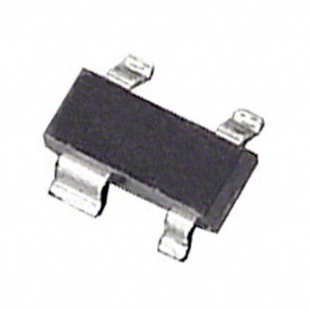
| 产品图片 |
|
| rohs | 符合RoHS无铅 / 符合限制有害物质指令(RoHS)规范要求 |
| 产品系列 | 电源管理 IC,监控电路,Microchip Technology MCP1316MT-29KE/OT- |
| NumberofInputsMonitored | 1 Input |
| 数据手册 | http://www.microchip.com/mymicrochip/filehandler.aspx?ddocname=en025429http://www.microchip.com/mymicrochip/filehandler.aspx?ddocname=en023833 |
| 产品型号 | MCP1316MT-29KE/OT |
| 产品目录页面 | |
| 产品种类 | 监控电路 |
| 人工复位 | Manual Reset |
| 供应商器件封装 | SOT-23-5 |
| 其它名称 | MCP1316MT-29KE/OTDKR |
| 功率失效检测 | No |
| 包装 | Digi-Reel® |
| 受监控电压数 | 1 |
| 商标 | Microchip Technology |
| 复位 | 低有效 |
| 复位超时 | 最小为 140 ms |
| 安装类型 | 表面贴装 |
| 安装风格 | SMD/SMT |
| 封装 | Reel |
| 封装/外壳 | SC-74A,SOT-753 |
| 封装/箱体 | SOT-23-5 |
| 工作温度 | -40°C ~ 125°C |
| 工作电源电流 | 5 uA |
| 工厂包装数量 | 3000 |
| 最大功率耗散 | 240 mW |
| 最大工作温度 | + 125 C |
| 最小工作温度 | - 40 C |
| 标准包装 | 1 |
| 欠电压阈值 | 2.857 V |
| 电压-阈值 | 2.9V |
| 电池备用开关 | No Backup |
| 电源电压-最大 | 5.5 V |
| 电源电压-最小 | 1 V |
| 监视器 | Watchdog |
| 类型 | Voltage Supervisory |
| 系列 | MCP131 |
| 芯片启用信号 | No Chip Enable |
| 被监测输入数 | 1 Input |
| 输出 | 开路漏极或开路集电极 |
| 输出类型 | Active Low, Open Drain |
| 过电压阈值 | 2.944 V |
| 阈值电压 | 2.9 V |


- 商务部:美国ITC正式对集成电路等产品启动337调查
- 曝三星4nm工艺存在良率问题 高通将骁龙8 Gen1或转产台积电
- 太阳诱电将投资9.5亿元在常州建新厂生产MLCC 预计2023年完工
- 英特尔发布欧洲新工厂建设计划 深化IDM 2.0 战略
- 台积电先进制程称霸业界 有大客户加持明年业绩稳了
- 达到5530亿美元!SIA预计今年全球半导体销售额将创下新高
- 英特尔拟将自动驾驶子公司Mobileye上市 估值或超500亿美元
- 三星加码芯片和SET,合并消费电子和移动部门,撤换高东真等 CEO
- 三星电子宣布重大人事变动 还合并消费电子和移动部门
- 海关总署:前11个月进口集成电路产品价值2.52万亿元 增长14.8%


PDF Datasheet 数据手册内容提取
MCP131X/2X Voltage Supervisor Features: Package Types • Low Supply Current: 1µA (Typical),10µA (Max.) SOT-23-5 MCP1316/16M/20 MCP1317 • Precision Monitoring Trip Point Options: - 2.9V and 4.6V (Standard Offerings) RST 1 5 VDD RST 1 5 VDD - 2.0V to 4.7V in 100mV Increments, VSS 2 VSS 2 (Contact the local Microchip Sales Office) MR 3 4 WDI MR 3 4 WDI • Resets Microcontroller in a Power-loss Event • Reset Delay Time-Out Option: MCP1318/18M/21 MCP1319/19M/22 - 1.4ms, 30ms, 200ms, or 1.6s (Typical) • Watchdog Timer Input Time-Out Options: RST 1 5 VDD RST 1 5 VDD - 6.3ms, 102ms, 1.6s, or 25.6s (Typical) VSS 2 VSS 2 • Manual Reset (MR) Input (Active-low) RST 3 4 WDI RST 3 4 MR • Single and Complementary Reset Output(s) • Reset Output Options: - Push-Pull (Active-high or Active-low) Block Diagram - Open-Drain (Internal or External Pull-up) V DD • Temperature Range: - -40°C to +85°C for Trip Points 2.0 to 2.4V and, Comparator + - -40°C to + 125°C for Trip Points >2.5V RST • Voltage Range: 1.0V to 5.5V – Output • Lead Free Packaging Reference Driver RST Voltage Description: The MCP131X/2X are voltage supervisor devices MR Noise Filter designed to keep a microcontroller in Reset until the V SS system voltage has reached and stabilized at the WDI Watchdog proper level for reliable system operation. The table below shows the available features for these devices. Note: Features available depend on the device. Device Features Reset Output A Reset Output B Device WDI Input MR Input Pull-up Active Pull-up Active Type Type Resistor Level Resistor Level MCP1316 Push-Pull — Low — — — Yes Yes MCP1316M Open-Drain Internal Low — — — Yes Yes MCP1317 Push-Pull — High — — — Yes Yes MCP1318 Push-Pull — Low Push-Pull — High Yes No MCP1318M Open-Drain Internal Low Push-Pull — High Yes No MCP1319 Push-Pull — Low Push-Pull — High No Yes MCP1319M Open-Drain Internal Low Push-Pull — High No Yes MCP1320 Open-Drain External Low — — — Yes Yes MCP1321 Open-Drain External Low Push-Pull — High Yes No MCP1322 Open-Drain External Low Push-Pull — High No Yes 2005-2012 Microchip Technology Inc. DS21985D-page 1
MCP131X/2X NOTES: DS21985D-page 2 2005-2012 Microchip Technology Inc.
MCP131X/2X 1.0 ELECTRICAL † Notice: Stresses above those listed under “Maximum Rat- ings” may cause permanent damage to the device. This is a CHARACTERISTICS stress rating only and functional operation of the device at those or any other conditions above those indicated in the Absolute Maximum Ratings† operational listings of this specification is not implied. Expo- sure to maximum rating conditions for extended periods may Supply Voltage (VDD to VSS). . . . . . . . . . . . . . . . . . . . . . 7.0V affect device reliability. Input current (V ) . . . . . . . . . . . . . . . . . . . . . . . . . . . .10mA DD Output current (RST) . . . . . . . . . . . . . . . . . . . . . . . . . .10mA Voltage on all inputs and outputs, except Open-Drain RST (with no internal pull-up resistor), w.r.t. V . .-0.6V to (V + SS DD 1.0V) Voltage on Open-Drain RST (with no internal pull-up resistor) w.r.t. V . . -0.6V to 13.5V SS Storage temperature. . . . . . . . . . . . . . . . . . .-65°C to +150°C Ambient temp. with power applied . . . . . . . .-40°C to +125°C Maximum Junction temp. with power applied. . . . . . .+150°C Power Dissipation (T +70°C): A 5-Pin SOT-23A.......................................................240mW ESD protection on all pins 4kV DC CHARACTERISTICS Electrical Specifications: Unless otherwise indicated, all limits are specified for V = 1V to 5.5V, R = 100k DD PU (only MCP1320, MCP1321 and MCP1322), T = -40°C to +125°C. A Parameters Sym Min Typ Max Units Conditions Operating Voltage Range V 1.0 — 5.5 V DD Specified V Value to V Low V 1.0 — — V I = 10µA, V < 0.3V DD OUT DD RST RST Operating Current: I — 5 10 µA Watchdog Timer Active DD — 1 2 µA Watchdog Timer Inactive — 1 2 µA V < V DD TRIP — 5 10 µA Reset Delay Timer Active Note 1: Trip point is ±1.5% from typical value. 2: Trip point is ±2.5% from typical value. 3: Hysteresis is minimum = 1%, maximum = 6% at +25°C. 4: This specification allows this device to be used in PIC® microcontroller applications that require the In- Circuit Serial Programming™ (ICSP™) feature (see device-specific programming specifications for voltage requirements). The total time that the RST pin can be above the maximum device operational voltage (5.5V) is 100s. Current into the RST pin should be limited to 2mA. It is recommended that the device operational temperature be maintained between 0°C to +70°C (+25°C preferred). For additional information, refer to Figure2-35. 5: This parameter is established by characterization and is not 100% tested. 6: Custom ordered voltage trip point; minimum order volume requirement. Information available upon request. 2005-2012 Microchip Technology Inc. DS21985D-page 3
MCP131X/2X DC CHARACTERISTICS (CONTINUED) Electrical Specifications: Unless otherwise indicated, all limits are specified for V = 1V to 5.5V, R = 100k DD PU (only MCP1320, MCP1321 and MCP1322), T = -40°C to +125°C. A Parameters Sym Min Typ Max Units Conditions V Trip Point MCP13XX-20 V 1.970 2.00 2.030 V T = +25°C (Note1) DD TRIP A (Note6) 1.950 2.00 2.050 V T = -40°C to +85°C (Note2) A MCP13XX-21 2.069 2.10 2.132 V T = +25°C (Note1) A (Note6) 2.048 2.10 2.153 V T = -40°C to +85°C (Note2) A MCP13XX-22 2.167 2.20 2.233 V T = +25°C (Note1) A (Note6) 2.145 2.20 2.255 V T = -40°C to +85°C (Note2) A MCP13XX-23 2.266 2.30 2.335 V T = +25°C (Note1) A (Note6) 2.243 2.30 2.358 V T = -40°C to +85°C (Note2) A MCP13XX-24 2.364 2.40 2.436 V T = +25°C (Note1) A (Note6) 2.340 2.40 2.460 V T = -40°C to +85°C (Note2) A MCP13XX-25 2.463 2.50 2.538 V T = +25°C (Note1) A (Note6) 2.438 2.50 2.563 V T = -40°C to +125°C (Note2) A MCP13XX-26 2.561 2.60 2.639 V T = +25°C (Note1) A (Note6) 2.535 2.60 2.665 V T = -40°C to +125°C (Note2) A MCP13XX-27 2.660 2.70 2.741 V T = +25°C (Note1) A (Note6) 2.633 2.70 2.768 V T = -40°C to +125°C (Note2) A MCP13XX-28 2.758 2.80 2.842 V T = +25°C (Note1) A (Note6) 2.730 2.80 2.870 V T = -40°C to +125°C (Note2) A MCP13XX-29 2.857 2.90 2.944 V T = +25°C (Note1) A 2.828 2.90 2.973 V T = -40°C to +125°C (Note2) A MCP13XX-30 2.955 3.00 3.045 V T = +25°C (Note1) A (Note6) 2.925 3.00 3.075 V T = -40°C to +125°C (Note2) A MCP13XX-31 3.054 3.10 3.147 V T = +25°C (Note1) A (Note6) 3.023 3.10 3.178 V T = -40°C to +125°C (Note2) A MCP13XX-32 3.152 3.20 3.248 V T = +25°C (Note1) A (Note6) 3.120 3.20 3.280 V T = -40°C to +125°C (Note2) A MCP13XX-33 3.251 3.30 3.350 V T = +25°C (Note1) A (Note6) 3.218 3.30 3.383 V T = -40°C to +125°C (Note2) A Note 1: Trip point is ±1.5% from typical value. 2: Trip point is ±2.5% from typical value. 3: Hysteresis is minimum = 1%, maximum = 6% at +25°C. 4: This specification allows this device to be used in PIC® microcontroller applications that require the In- Circuit Serial Programming™ (ICSP™) feature (see device-specific programming specifications for voltage requirements). The total time that the RST pin can be above the maximum device operational voltage (5.5V) is 100s. Current into the RST pin should be limited to 2mA. It is recommended that the device operational temperature be maintained between 0°C to +70°C (+25°C preferred). For additional information, refer to Figure2-35. 5: This parameter is established by characterization and is not 100% tested. 6: Custom ordered voltage trip point; minimum order volume requirement. Information available upon request. DS21985D-page 4 2005-2012 Microchip Technology Inc.
MCP131X/2X DC CHARACTERISTICS (CONTINUED) Electrical Specifications: Unless otherwise indicated, all limits are specified for V = 1V to 5.5V, R = 100k DD PU (only MCP1320, MCP1321 and MCP1322), T = -40°C to +125°C. A Parameters Sym Min Typ Max Units Conditions V Trip Point (Con’t) MCP13XX-34 V 3.349 3.40 3.451 V T = +25°C (Note1) DD TRIP A (Note6) 3.315 3.40 3.385 V T = -40°C to +125°C (Note2) A MCP13XX-35 3.448 3.50 3.553 V T = +25°C (Note1) A (Note6) 3.413 3.50 3.588 V T = -40°C to +125°C (Note2) A MCP13XX-36 3.546 3.60 3.654 V T = +25°C (Note1) A (Note6) 3.510 3.60 3.690 V T = -40°C to +125°C (Note2) A MCP13XX-37 3.645 3.70 3.756 V T = +25°C (Note1) A (Note6) 3.608 3.70 3.793 V T = -40°C to +125°C (Note2) A MCP13XX-38 3.743 3.80 3.857 V T = +25°C (Note1) A (Note6) 3.705 3.80 3.895 V T = -40°C to +125°C (Note2) A MCP13XX-39 3.842 3.90 3.959 V T = +25°C (Note1) A (Note6) 3.803 3.90 3.998 V T = -40°C to +125°C (Note2) A MCP13XX-40 3.940 4.00 4.060 V T = +25°C (Note1) A (Note6) 3.900 4.00 4.100 V T = -40°C to +125°C (Note2) A MCP13XX-41 4.039 4.10 4.162 V T = +25°C (Note1) A (Note6) 3.998 4.10 4.203 V T = -40°C to +125°C (Note2) A MCP13XX-42 4.137 4.20 4.263 V T = +25°C (Note1) A (Note6) 4.095 4.20 4.305 V T = -40°C to +125°C (Note2) A MCP13XX-43 4.236 4.30 4.365 V T = +25°C (Note1) A (Note6) 4.193 4.30 4.408 V T = -40°C to +125°C (Note2) A MCP13XX-44 4.334 4.40 4.466 V T = +25°C (Note1) A (Note6) 4.290 4.40 4.510 V T = -40°C to +125°C (Note2) A MCP13XX-45 4.433 4.50 4.568 V T = +25°C (Note1) A (Note6) 4.388 4.50 4.613 V T = -40°C to +125°C (Note2) A MCP13XX-46 4.531 4.60 4.669 V T = +25°C (Note1) A 4.485 4.60 4.715 V T = -40°C to +125°C (Note2) A MCP13XX-47 4.630 4.70 4.771 V T = +25°C (Note1) A (Note6) 4.583 4.70 4.818 V T = -40°C to +125°C (Note2) A V Trip Point Tempco T — ±40 — ppm/°C DD TPCO Note 1: Trip point is ±1.5% from typical value. 2: Trip point is ±2.5% from typical value. 3: Hysteresis is minimum = 1%, maximum = 6% at +25°C. 4: This specification allows this device to be used in PIC® microcontroller applications that require the In- Circuit Serial Programming™ (ICSP™) feature (see device-specific programming specifications for voltage requirements). The total time that the RST pin can be above the maximum device operational voltage (5.5V) is 100s. Current into the RST pin should be limited to 2mA. It is recommended that the device operational temperature be maintained between 0°C to +70°C (+25°C preferred). For additional information, refer to Figure2-35. 5: This parameter is established by characterization and is not 100% tested. 6: Custom ordered voltage trip point; minimum order volume requirement. Information available upon request. 2005-2012 Microchip Technology Inc. DS21985D-page 5
MCP131X/2X DC CHARACTERISTICS (CONTINUED) Electrical Specifications: Unless otherwise indicated, all limits are specified for V = 1V to 5.5V, R = 100k DD PU (only MCP1320, MCP1321 and MCP1322), T = -40°C to +125°C. A Parameters Sym Min Typ Max Units Conditions Threshold Hysteresis MCP13XX-20 V 0.020 — 0.120 V T = +25°C (Note3) HYS A Note3) (Note6) (Note6) V T = -40°C to +85°C A MCP13XX-21 0.021 — 0.126 V T = +25°C (Note3) A (Note6) (Note6) V T = -40°C to +85°C A MCP13XX-22 0.022 — 0.132 V T = +25°C (Note3) A (Note6) (Note6) V T = -40°C to +85°C A MCP13XX-23 0.023 — 0.138 V T = +25°C (Note3) A (Note6) (Note6) V T = -40°C to +85°C A MCP13XX-24 0.024 — 0.144 V T = +25°C (Note3) A (Note6) (Note6) V T = -40°C to +85°C A MCP13XX-25 0.025 — 0.150 V T = +25°C (Note3) A (Note6) (Note6) V T = -40°C to +125°C A MCP13XX-26 0.026 — 0.156 V T = +25°C (Note3) A (Note6) (Note6) V T = -40°C to +125°C A MCP13XX-27 0.027 — 0.162 V T = +25°C (Note3) A (Note6) (Note6) V T = -40°C to +125°C A MCP13XX-28 0.028 — 0.168 V T = +25°C (Note3) A (Note6) (Note6) V T = -40°C to +125°C A MCP13XX-29 0.029 — 0.174 V T = +25°C (Note3) A (Note6) V T = -40°C to +125°C A MCP13XX-30 0.030 — 0.180 V T = +25°C (Note3) A (Note6) (Note6) V T = -40°C to +125°C A MCP13XX-31 0.031 — 0.186 V T = +25°C (Note3) A (Note6) (Note6) V T = -40°C to +125°C A MCP13XX-32 0.032 — 0.192 V T = +25°C (Note3) A (Note6) (Note6) V T = -40°C to +125°C A MCP13XX-33 0.033 — 0.198 V T = +25°C (Note3) A (Note6) (Note6) V T = -40°C to +125°C A Note 1: Trip point is ±1.5% from typical value. 2: Trip point is ±2.5% from typical value. 3: Hysteresis is minimum = 1%, maximum = 6% at +25°C. 4: This specification allows this device to be used in PIC® microcontroller applications that require the In- Circuit Serial Programming™ (ICSP™) feature (see device-specific programming specifications for voltage requirements). The total time that the RST pin can be above the maximum device operational voltage (5.5V) is 100s. Current into the RST pin should be limited to 2mA. It is recommended that the device operational temperature be maintained between 0°C to +70°C (+25°C preferred). For additional information, refer to Figure2-35. 5: This parameter is established by characterization and is not 100% tested. 6: Custom ordered voltage trip point; minimum order volume requirement. Information available upon request. DS21985D-page 6 2005-2012 Microchip Technology Inc.
MCP131X/2X DC CHARACTERISTICS (CONTINUED) Electrical Specifications: Unless otherwise indicated, all limits are specified for V = 1V to 5.5V, R = 100k DD PU (only MCP1320, MCP1321 and MCP1322), T = -40°C to +125°C. A Parameters Sym Min Typ Max Units Conditions Threshold Hysteresis MCP13XX-34 V 0.034 — 0.204 V T = +25°C (Note3) HYS A (Continued) Note3) (Note6) (Note6) V T = -40°C to +125°C A MCP13XX-35 0.035 — 0.210 V T = +25°C (Note3) A (Note6) (Note6) V T = -40°C to +125°C A MCP13XX-36 0.036 — 0.216 V T = +25°C (Note3) A (Note6) (Note6) V T = -40°C to +125°C A MCP13XX-37 0.037 — 0.222 V T = +25°C (Note3) A (Note6) (Note6) V T = -40°C to +125°C A MCP13XX-38 0.038 — 0.228 V T = +25°C (Note3) A (Note6) (Note6) V T = -40°C to +125°C A MCP13XX-39 0.039 — 0.234 V T = +25°C (Note1) A (Note6) (Note6) V T = -40°C to +125°C A MCP13XX-40 0.040 — 0.240 V T = +25°C (Note3) A (Note6) (Note6) V T = -40°C to +125°C A MCP13XX-41 0.041 — 0.246 V T = +25°C (Note3) A (Note6) (Note6) V T = -40°C to +125°C A MCP13XX-42 0.042 — 0.252 V T = +25°C (Note3) A (Note6) (Note6) V T = -40°C to +125°C A MCP13XX-43 0.043 — 0.258 V T = +25°C (Note3) A (Note6) (Note6) V T = -40°C to +125°C A MCP13XX-44 0.044 — 0.264 V T = +25°C (Note3) A (Note6) (Note6) V T = -40°C to +125°C A MCP13XX-45 0.045 — 0.270 V T = +25°C (Note3) A (Note6) (Note6) V T = -40°C to +125°C A MCP13XX-46 0.046 — 0.276 V T = +25°C (Note3) A (Note6) V T = -40°C to +125°C A MCP13XX-47 0.047 — 0.282 V T = +25°C (Note3) A (Note6) (Note6) V T = -40°C to +125°C A Note 1: Trip point is ±1.5% from typical value. 2: Trip point is ±2.5% from typical value. 3: Hysteresis is minimum = 1%, maximum = 6% at +25°C. 4: This specification allows this device to be used in PIC® microcontroller applications that require the In- Circuit Serial Programming™ (ICSP™) feature (see device-specific programming specifications for voltage requirements). The total time that the RST pin can be above the maximum device operational voltage (5.5V) is 100s. Current into the RST pin should be limited to 2mA. It is recommended that the device operational temperature be maintained between 0°C to +70°C (+25°C preferred). For additional information, refer to Figure2-35. 5: This parameter is established by characterization and is not 100% tested. 6: Custom ordered voltage trip point; minimum order volume requirement. Information available upon request. 2005-2012 Microchip Technology Inc. DS21985D-page 7
MCP131X/2X DC CHARACTERISTICS (CONTINUED) Electrical Specifications: Unless otherwise indicated, all limits are specified for V = 1V to 5.5V, R = 100k DD PU (only MCP1320, MCP1321 and MCP1322), T = -40°C to +125°C. A Parameters Sym Min Typ Max Units Conditions RST/RST Low-Level Output Voltage V — — 0.3 V I = 50µA, 1.0V V 1.5V OL OL DD — — 0.3 V I = 100µA, OL 1.5V V 2.5V DD — — 0.3 V I = 2mA, 2.5V V 4.5V OL DD — — 0.3 V I = 4mA, V 4.5V OL DD RST/RST High-Level Output Voltage V V – — — V I = 2.5mA, V 2.5V OH DD OH DD 0.7 (Push-Pull Outputs only) V – — — V I = 500µA, V 1.5V DD OH DD 0.7 Input Low Voltage (MR and WDI pins) V V — 0.3V V IL SS DD Input High Voltage (MR and WDI pins) V 0.7 V — V V IH DD DD Open-Drain High Voltage on Output V — — 13.5 (4) V Open-Drain Output pin only, ODH (Note4) V = 3.0V, Time voltage> DD 5.5V applied 100s, current into pin limited to 2mA, +25°C operation recommended (Note4, Note5) Input Leakage Current (MR and WDI) I — — ±1 µA V V V IL SS PIN DD Open-Drain Output Leakage Current I — 0.003 1.0 µA OD (MCP1316M, MCP1318M, MCP1319M, MCP1320, MCP1321, and MCP1322 only) Pull-up Resistance MR pin R — 52 — k V = 5.5V PU DD WDI pin — 52 — k V = 5.5V DD RST pin — 4.7 — k V = 5.5V, DD MCP131XM devices only Input Pin Capacitance (MR and WDI) C — 100 — pF I Output Pin Capacitive Loading C — — 50 pF This is the tester loading to O (RST and RST) meet the AC timing specifications. Note 1: Trip point is ±1.5% from typical value. 2: Trip point is ±2.5% from typical value. 3: Hysteresis is minimum = 1%, maximum = 6% at +25°C. 4: This specification allows this device to be used in PIC® microcontroller applications that require the In- Circuit Serial Programming™ (ICSP™) feature (see device-specific programming specifications for voltage requirements). The total time that the RST pin can be above the maximum device operational voltage (5.5V) is 100s. Current into the RST pin should be limited to 2mA. It is recommended that the device operational temperature be maintained between 0°C to +70°C (+25°C preferred). For additional information, refer to Figure2-35. 5: This parameter is established by characterization and is not 100% tested. 6: Custom ordered voltage trip point; minimum order volume requirement. Information available upon request. DS21985D-page 8 2005-2012 Microchip Technology Inc.
MCP131X/2X VTRIPMAX VTRIPAC + VHYS V TRIPMIN VDD 1V tRST tR ST t RPD tRR VTRIP RST RST V < 1V is outside the device operating specification. The RST (or RST) output state is DD unknown while V < 1V. DD FIGURE 1-1: Device Voltage and Reset Pin Waveforms. TABLE 1-1: DEVICE VOLTAGE AND RESET PIN TIMINGS Electrical Specifications: Unless otherwise indicated, all limits are specified for V = 1V to 5.5V, R = 100k DD PU (only MCP1320, MCP1321, and MCP1322), T = -40°C to +125°C. A Parameters Sym Min Typ Max Units Conditions Falling V Trip Point Detected t — 650 — µs V ramped from DD RPD DD to RST or RST Active V + 250mV down to TRIPMAX V – 200mV, TRIPMIN V falling @ 5mV/µs, DD C = 50pF (Note1) L V Rise Rate t Note3 DD RR Reset active time t 1.0 1.4 2.0 ms Note2 RST (MR Rising Edge, POR/BOR 20 30 40 ms Note2 Inactive, or WDT time out) to 140 200 280 ms Standard Time Out RST/RST Inactive 1120 1600 2240 ms Note2 RST Rise Time after RSTActive t — 5 — µs For RST 10% to 90% of V , RT DD (Push-Pull Outputs only) C = 50pF (Note1) L RST Rise Time after RSTInactive — 5 — µs For RST 10% to 90% of V , DD (Push-Pull Outputs only) C = 50pF (Note1) L RST Fall Time after RSTInactive t — 5 — µs For RST 90% to 10% of V , FT DD C = 50pF (Note1) L RST Fall Time after RSTActive — 5 — µs For RST 90% to 10% of V , DD C = 50pF (Note1) L Note 1: These parameters are for design guidance only and are not 100% tested. 2: Custom ordered Reset active time; minimum order volume requirement. 3: Designed to be independent of V rise rate. Device characterization was done with a rise rate as slow as DD 0.1V/s (@ +25°C). 2005-2012 Microchip Technology Inc. DS21985D-page 9
MCP131X/2X MR tMR t RST t NF t MRD RST RST FIGURE 1-2: MR and Reset Pin Waveforms. TABLE 1-2: MR AND RESET PIN TIMINGS Electrical Specifications: Unless otherwise indicated, all limits are specified for V = 1V to 5.5V, R = 100k DD PU (only MCP1320, MCP1321, and MCP1322), T = -40°C to +125°C. A Parameters Sym Min Typ Max Units Conditions MR Pulse Width t 1 — — µs MR MR Active to RST/RST Active t — 235 — ns V = 5.0V MRD DD MR Input Noise filter t — 150 — ns V = 5.0V NF DD Note 1: These parameters are for design guidance only and are not 100% tested. RST RST WDI (Note 1) t tRST WP tWD tWD Note 1: The WDI pin was a weak pull-up resistor which is disabled after the 1st falling edge on the WDI pin. FIGURE 1-3: WDI and Reset Pin Waveforms. TABLE 1-3: WDI AND RESET PIN TIMINGS Electrical Specifications: Unless otherwise indicated, all limits are specified for V = 1V to 5.5V, R = 100k DD PU (only MCP1320, MCP1321, and MCP1322), T = -40°C to +125°C. A Parameters Sym Min Typ Max Units Conditions WDI Pulse Width t 50 — — ns WP Watchdog Time-Out Period t 4.3 6.3 9.3 ms Note1 WD 71 102 153 ms Note1 1.12 1.6 2.4 sec Standard Time Out 17.9 25.6 38.4 sec Note1 Note 1: Custom ordered WatchDog Timer time out; minimum order volume requirement. DS21985D-page 10 2005-2012 Microchip Technology Inc.
MCP131X/2X TEMPERATURE CHARACTERISTICS Electrical Specifications: Unless otherwise noted, all limits are specified for V = 1V to 5.5V, R = 100k DD PU (only MCP1316), T = -40°C to +125°C. A Parameters Sym Min Typ Max Units Conditions Temperature Ranges Specified Temperature Range T -40 — +85 °C MCP13XX-25 (or below) A Specified Temperature Range T -40 — +125 °C Except MCP13XX-25 (or below) A Maximum Junction Temperature T — — +150 °C J Storage Temperature Range T -65 — +150 °C A Package Thermal Resistances Thermal Resistance, 5L-SOT-23 — 220.7 — °C/W JA 2005-2012 Microchip Technology Inc. DS21985D-page 11
MCP131X/2X NOTES: DS21985D-page 12 2005-2012 Microchip Technology Inc.
MCP131X/2X 2.0 TYPICAL PERFORMANCE CURVES Note: The graphs and tables provided following this note are a statistical summary based on a limited number of samples and are provided for informational purposes only. The performance characteristics listed herein are not tested or guaranteed. In some graphs or tables, the data presented may be outside the specified operating range (e.g., outside specified power supply range) and therefore outside the warranted range. Note: Unless otherwise indicated, all limits are specified for V = 1V to 5.5V, R = 100k (only MCP1316; DD PU see Figure4-1), T = -40°C to +125°C. A 1.2 4.8V 5.0V 5.5V 1.0V 1.5V 2.0V 3.0V 4.3V 6 1 4.5V 4.8V 5.0V 5.5V 5 0.8 I(µA)DD 00..46 Idd (µA) 234 0.2 1 0 0 -100 -50 0 50 100 150 -100 -50 0 50 100 150 Temperature (°C) Temperature (°C) FIGURE 2-1: I vs. Temperature (Reset FIGURE 2-4: I vs. Temperature (Reset DD DD Power-up Timer Inactive and Watchdog Timer Power-up Timer Active) (MCP1318M-4.6). Inactive) (MCP1318M-4.6). 1.4 3.2V 4.0V 4.5V 5.0V 5.5V 1.0V 1.5V 2.5V 6 1.2 2.7V 3.2V 4.0V 1 4.5V 5.0V 5.5V 5 µA) 0.8 A) 4 I(DD0.6 (µDD 3 0.4 I 2 0.2 1 0 0 -100 -50 0 50 100 150 -100 -50 0 50 100 150 Temperature (°C) Temperature (°C) FIGURE 2-2: I vs. Temperature (Reset FIGURE 2-5: I vs. Temperature (Reset DD DD Power-up Timer Inactive and Watchdog Timer Power-up Timer Active) (MCP1319-2.9). Inactive) (MCP1319-2.9). 2.2V 2.5V 4.0V 4.5V 5.0V 5.5V 1.8 7 1.0V 1.5V 1.8V 1.6 2.2V 2.5V 4.0V 6 1.4 4.5V 5.0V 5.5V 5 1.2 I(µA)DD00..681 I(µA)DD 234 0.4 1 0.2 0 0 -100 -50 0 50 100 150 -100 -50 0 50 100 150 Temperature (°C) Temperature (°C) FIGURE 2-3: IDD vs. Temperature (Reset FIGURE 2-6: IDD vs. Temperature (Reset Power-up Timer Inactive and Watchdog Timer Power-up Timer Active) (MCP1316-2.0). Inactive) (MCP1316-2.0). 2005-2012 Microchip Technology Inc. DS21985D-page 13
MCP131X/2X Note: Unless otherwise indicated, all limits are specified for V = 1V to 5.5V, R = 100k (only MCP1316; DD PU see Figure4-1), T = -40°C to +125°C. A 4.8V 5.0V 5.5V 7 6 5 A) 4 µ ( D 3 D I 2 1 0 -100 -50 0 50 100 150 Temperature (°C) FIGURE 2-7: I vs. Temperature DD (Watchdog Timer Active) (MCP1318M-4.6). MCP1319 does not have a Watchdog Timer FIGURE 2-8: I vs. Temperature DD (Watchdog Timer Active) (MCP1319-2.9). 2.2V 2.5V 4.0V 4.5V 5.0V 5.5V 7 6 5 A) 4 µ ( D3 D I 2 1 0 -100 -50 0 50 100 150 Temperature (°C) FIGURE 2-9: I vs. Temperature DD (Watchdog Timer Active) (MCP1316-2.0). DS21985D-page 14 2005-2012 Microchip Technology Inc.
MCP131X/2X Note: Unless otherwise indicated, all limits are specified for V = 1V to 5.5V, R = 100k (only MCP1316; DD PU see Figure4-1), T = -40°C to +125°C. A 1.2 -45°C +25°C +90°C +130°C 6 +130°C 1 5 +90°C 0.8 I(µA)DD 00..46 +-2455°°CC I(µA)DD 234 0.2 1 0 0 0.0 2.0 4.0 6.0 4.6 4.8 5.0 5.2 5.4 5.6 V (V) V (V) DD DD FIGURE 2-10: I vs. V (Reset Power- FIGURE 2-13: I vs. V (Reset Power- DD DD DD DD up Timer Inactive and Watchdog Timer Inactive) up Timer Active or Watchdog Timer Active) (MCP1318M-4.6). (MCP1318M-4.6). -45°C +25°C +90°C +130°C 1.4 +130°C 6 1.2 +90°C 5 1 µA) 0.8 +25°C A) 4 (D 0.6 -45°C (µ 3 D D I D 0.4 I 2 0.2 1 0 0 0.0 2.0 4.0 6.0 0.0 2.0 4.0 6.0 V (V) V (V) DD DD FIGURE 2-11: I vs. V (Reset Power- FIGURE 2-14: I vs. V (Reset Power- DD DD DD DD up Timer Inactive and Watchdog Timer Inactive) up Timer Active or Watchdog Timer Active) (MCP1319-2.9). (MCP1319-2.9). -45°C +25°C +90°C +130°C 1.8 +130°C 7 1.6 1.4 +90°C 6 1.2 +25°C 5 µA) 1 -45°C A) 4 (D 0.8 (µ ID 0.6 IDD 3 0.4 2 0.2 1 0 0 0.0 2.0 4.0 6.0 2.0 3.0 4.0 5.0 6.0 V (V) V (V) DD DD FIGURE 2-12: I vs. V (Reset Power- FIGURE 2-15: I vs. V (Reset Power- DD DD DD DD up Timer Inactive and Watchdog Timer Inactive) up Timer Active or Watchdog Timer Active) (MCP1316-2.0). (MCP1316-2.0). 2005-2012 Microchip Technology Inc. DS21985D-page 15
MCP131X/2X Note: Unless otherwise indicated, all limits are specified for V = 1V to 5.5V, R = 100k (only MCP1316; DD PU see Figure4-1), T = -40°C to +125°C. A 4.800 4.0 1V 2V 3V 4.3V 4.5V 4.8V 5V 5.5V 3.9 0.16 4.750 VTRIPUp 3.8 0.14 3.7%) 0.12 V(V)TRIP 44..675000 VHYST 333...465Hyst (RIP V(V)OL 000..00.168 4.600 VTRIPDown 33..23VT 0.04 3.1 0.02 4.550 3.0 0 -50 0 50 100 150 0.00 2.00 4.00 6.00 8.00 10.00 Temperature (°C) IOL(mA) FIGURE 2-16: V and V vs. FIGURE 2-19: V vs. I TRIP HYST OL OL Temperature (MCP1318M-4.6). (MCP1318M-4.6). 3.020 3.5 1V 2.5V 2.7V 3.2V 4V 4.5V 5V 5.5V 3.000 VTRIPUp 3.4 0.16 3.4 0.14 2.980 VHYST 3.3%) 0.12 V(V)TRIP 222...999246000 333...223VHyst (TRIP V(V)OL 000..00.168 3.1 0.04 2.900 VTRIPDown 3.1 0.02 2.880 3.0 0 -50 0 50 100 150 0.00 2.00 4.00 6.00 8.00 10.00 Temperature (°C) IOL(mA) FIGURE 2-17: V and V vs. FIGURE 2-20: V vs. I TRIP HYST OL OL Temperature (MCP1319-2.9). (MCP1319-2.9). 2.050 3.0 0.02 2.040 VTRIPUp 2.5 0.018 1V 0.016 2.030 VHYST 2.0%) 0.014 V(V)TRIP 22..001200 11..05VHyst (TRIP V(V)OL 000...0000.00106821 1.8V 2.000 VTRIPDown 0.5 0.004 0.002 1.990 0.0 0 -50 0 50 100 150 0.00 0.05 0.10 0.15 0.20 0.25 Temperature (°C) IOL(mA) FIGURE 2-18: V and V vs. FIGURE 2-21: V vs. I TRIP HYST OL OL Temperature (MCP1316-2.0). (MCP1316-2.0). DS21985D-page 16 2005-2012 Microchip Technology Inc.
MCP131X/2X Note: Unless otherwise indicated, all limits are specified for V = 1V to 5.5V, R = 100k (only MCP1316; DD PU see Figure4-1), T = -40°C to +125°C. A 5 0.14 4.5 4.5V 0.12 4 mA 4 4.3V 3.5 00.11 33 mAA V) 3 (V)VLOL00..0068 22mmAA V(OH12..552 2V 3V 0.04 1 mA 1 1.5V 0.5 0.02 0 mA 0 0 0.00 2.00 4.00 6.00 -50 0 50 100 150 I (mA) OH FIGURE 2-22: V vs. Temperature FIGURE 2-25: V vs. I OL OH OH (MCP1318M-4.6 @ V = 4.5V). (MCP1318M-4.6 @ +25°C). DD 6 0.25 5.5V 5 5V 0.2 4 mA 4 4.5V 3 mA V) 4V (V) 0.15 (OH3 3.2V VLOL 0.1 2 mA V 2 2.7V 2.5V 0.05 11mmAA 1 1.5V 00mmAA 0 0 0.00 2.00 4.00 6.00 -50 0 50 100 150 I (mA) OH FIGURE 2-23: V vs. Temperature FIGURE 2-26: V vs. I OL OH OH (MCP1319-2.9 @ V = 2.7V). (MCP1319-2.9 @ +25°C). DD 0.016 6 0.014 0.2 mA 5 5.5V 0.012 5V 0.15 mA 4 4.5V V(V)OL00..000.000681 0.1 mA V(V)OH23 2.2V 4V 2.5V 0.004 0.05 mA 1 0.002 0 mA 0 0 -50 0 50 100 150 0.00 2.00 4.00 6.00 Temperature (°C) IOH(mA) FIGURE 2-24: V vs. Temperature FIGURE 2-27: V vs. I OL OH OH (MCP1316-2-0 @ V = 1.8V). (MCP1316-2.0 @ +25°C). DD 2005-2012 Microchip Technology Inc. DS21985D-page 17
MCP131X/2X Note: Unless otherwise indicated, all limits are specified for V = 1V to 5.5V, R = 100k (only MCP1316; DD PU see Figure4-1), T = -40°C to +125°C. A 350 4.8 V 5 V 5.5 V 230 300 5V 225 250 5.5V 220 (µs) 200 ms) 215 tRPD 150 (RPU 220150 100 t 200 50 195 0 190 -100 -50 0 50 100 150 -100 -50 0 50 100 150 Temperature (°C) Temperature (°C) FIGURE 2-28: t vs. Temperature FIGURE 2-31: t vs. Temperature RPD RPU (MCP1318M-4.6). (MCP1318M-4.6). 3.2V 4V 4.5V 5V 5.5V 3.2 V 4 V 4.5 V 5 V 5.5 V 450 250 245 400 240 350 235 (µs) 235000 (ms) 222350 RPD 200 RPU 220 t 150 t 215 100 210 50 205 0 200 -100 -50 0 50 100 150 -100 -50 0 50 100 150 Temperature (°C) Temperature (°C) FIGURE 2-29: t vs. Temperature FIGURE 2-32: t vs. Temperature RPD RPU (MCP1319-2.9). (MCP1319-2.9). 2.5V 4V 4.5V 5V 5.5V 2.5 V 4 V 4.5 V 5 V 5.5 V 2.2 V 350 250 245 300 240 250 235 µs) 200 ms) 230 ( ( 225 tRPD 110500 tRPU 221250 210 50 205 0 200 -100 -50 0 50 100 150 -100 -50 0 50 100 150 Temperature (°C) Temperature (°C) FIGURE 2-30: t vs. Temperature FIGURE 2-33: t vs. Temperature RPD RPU (MCP1316-2.0). (MCP1316-2.0). DS21985D-page 18 2005-2012 Microchip Technology Inc.
MCP131X/2X Note: Unless otherwise indicated, all limits are specified for V = 1V to 5.5V, R = 100k (only MCP1316; DD PU see Figure4-1), T = -40°C to +125°C. A VRST=2.0V VRST=2.9V VRST=4.6V 3.2 V 4 V 4.5 V 5 V 5.5 V 3500 350 µs) 3000 300 on ( 2500 250 nt Durati 12500000 2.0V (ns)MRD 125000 sie 1000 2.9V t 100 n Tra 500 50 0 0 0.001 0.01 0.1 1 10 -100 -50 0 50 100 150 Reset Threshold Overdrive (V) VTRIPMin -VDD Temperature (°C) FIGURE 2-34: Transient Duration vs. FIGURE 2-37: MR Low to Reset VTRIP (min) – VDD. Propagation Delay (MCP1319-2.9). 2.2 V 2.5 V 4 V 4.5 V 5 V 5.5 V 2.2 V 2.5 V 4 V 4.5 V 5 V 5.5 V A) 0.012 450 ge (µ 0.01 345000 aka 0.008 s) 300 Le 0.006 (n 250 Drain 0.004 tMRD 125000 en- 0.002 100 p 50 O 0 0 -100 -50 0 50 100 150 -100 -50 0 50 100 150 Temperature (°C) Temperature (°C) FIGURE 2-35: Open-Drain Leakage FIGURE 2-38: MR Low to Reset Current vs. Temperature (MCP1320-2.0). Propagation Delay (MCP1316-2.0). MCP1318M does not have an MR pin FIGURE 2-36: MR Low to Reset Propagation Delay (MCP1318M-4.6). 2005-2012 Microchip Technology Inc. DS21985D-page 19
MCP131X/2X Note: Unless otherwise indicated, all limits are specified for V = 1V to 5.5V, R = 100k (only MCP1316; DD PU see Figure4-1), T = -40°C to +125°C. A 1090000 out 0.145 e 0.14 800 m t(µs)RPD 345670000000000 5V to 4.5V alized Reset TiPeriod 00..011.231553 MCP1318M-4.6 120000 5V to 0V Norm 0.12 0 0.115 -100 -50 0 50 100 150 -100 -50 0 50 100 150 Temperature (°C) Temperature (°C) FIGURE 2-39: V Falling to Reset FIGURE 2-42: Normalized Reset Time-Out DD Propagation Delay vs. Temperature Period vs. Temperature (MCP1318M-4.6). (MCP1318M-4.6). 250 ut 0.15 o 200 5V to 2.7V me 0.145 Ti (µs)RPD 110500 VVTTRRIIPP TMyinp -+0 0.2.3VV to ed Reset Period 0.01.3154 MCP1319-2.9 t z ali 50 5V to 0V orm 0.13 N 0 0.125 -100 -50 0 50 100 150 -100 -50 0 50 100 150 Temperature (°C) Temperature (°C) FIGURE 2-40: V Falling to Reset FIGURE 2-43: Normalized Reset Time-Out DD Propagation Delay vs. Temperature (MCP1319- Period vs. Temperature (MCP1319-2.9). 2.9). 0.15 250 ut o 200 5V to 1.8V me 0.145 Ti t(µs)RPD 110500 VVTTRRIIPP TMyinp -+0 0.2.2VV to alized Reset Period 0.01.3154 MCP1316-2.0 50 5V to 0V Norm 0.13 0 0.125 -100 -50 0 50 100 150 -100 -50 0 50 100 150 Temperature (°C) Temperature (°C) FIGURE 2-41: V Falling to Reset FIGURE 2-44: Normalized Reset Time-Out DD Propagation Delay vs. Temperature (MCP1316- Period vs. Temperature (MCP1316-2.0). 2.0). DS21985D-page 20 2005-2012 Microchip Technology Inc.
MCP131X/2X Note: Unless otherwise indicated, all limits are specified for V = 1V to 5.5V, R = 100k (only MCP1316; DD PU see Figure4-1), T = -40°C to +125°C. A 1.25 VRST=2.0V VRST=2.9V VRST=4.6V 600 g 1.2 Normalized WatchdoTimeout Period 0111...901.15155 `MCP1318M-4.6 ansient Duration (µS) 123450000000000 Tr 0.9 0 -100 -50 0 50 100 150 0.001 0.01 0.1 1 10 Temperature (°C) Reset Threshold Overdrive (V) VTRIPMin -VDD FIGURE 2-45: Normalized Watchdog Time- FIGURE 2-48: Max V Transient Duration DD Out Period vs. Temperature (MCP1318M-4.6). vs. Reset Threshold Overdrive. MCP1319 does not have a Watchdog Timer FIGURE 2-46: Normalized Watchdog Time- FIGURE 2-49: “M” Part Number Pull-up Out Period vs. Temperature (MCP1319-2.9). Characteristics (MCP1318M-4.6). ut 1.25 o me 1.2 Ti g 1.15 o WatchdPeriod 11.0.15 MCP1316-2.0 d ze 1 ` ali m 0.95 or N 0.9 -100 -50 0 50 100 150 Temperature (°C) FIGURE 2-47: Normalized Watchdog Time- Out Period vs. Temperature (MCP1316-2.0). 2005-2012 Microchip Technology Inc. DS21985D-page 21
MCP131X/2X NOTES: DS21985D-page 22 2005-2012 Microchip Technology Inc.
MCP131X/2X 3.0 PIN DESCRIPTION The descriptions of the pins are listed in Table3-1. TABLE 3-1: PIN FUNCTION TABLE Pin No. Buffer/ Pin Device Symbol Driver Function Type SOT23-5 Type 1 MCP1316M (1), RST O Open-Drain Reset Output (active-low) MCP1318M (1), Goes active (Low) if one of these conditions occurs: MCP1319M (1), 1. If V falls below the selected Reset voltage DD MCP1320, threshold. MCP1321, 2. If the MR pin is forced low. MCP1322 3. If the WDI pin does not detect an edge transition within the minimum selected time-out period. 4. During power-up. V Falling: DD Open-Drain = V > V DD TRIP L = V < V DD TRIP V Rising: DD Open-Drain = V > V + V DD TRIP HYS L = V < V + V DD TRIP HYS MCP1316, O Push-Pull V Falling: DD MCP1318, H = V > V DD TRIP MCP1319 L = V < V DD TRIP V Rising: DD H = V > V + V DD TRIP HYS L = V < V + V DD TRIP HYS MCP1317 RST O Push-Pull Reset Output (active-high) Goes active (High) if one of these conditions occurs: 1. If V falls below the selected Reset voltage DD threshold. 2. If the MR pin is forced low. 3. If the WDI pin does not detect an edge transition within the minimum selected time-out period. 4. During power-up. V Falling: DD H = V < V DD TRIP L = V > V DD TRIP V Rising: DD H = V < V + V DD TRIP HYS L = V > V + V DD TRIP HYS 2 All V — P The ground reference for the device. SS Note 1: Open-Drain output with internal pull-up resistor. 2005-2012 Microchip Technology Inc. DS21985D-page 23
MCP131X/2X TABLE 3-1: PIN FUNCTION TABLE (CONTINUED) Pin No. Buffer/ Pin Device Symbol Driver Function Type SOT23-5 Type 3 MCP1316, MR I ST Manual Reset input for a Reset switch. MCP1316M, This input allows a push button switch to be directly con- MCP1317, nected to the MCP131X/2X MR pin, which can then be MCP1320 used to force a system Reset. This input filters (ignores) noise pulses that occur on the MR pin. L = Switch is depressed (shorted to ground). This forces the RST/RST pins Active. H = Switch is open (internal pull-up resistor pulls signal high). State of the RST/RST pins determined by other system conditions. MCP1318, RST O Push-Pull Reset Output (active-high) MCP1318M, Goes active (High) if one of these conditions occurs: MCP1319, 1. If V falls below the selected Reset voltage DD MCP1319M, threshold. MCP1321, 2. If the MR pin is forced low. MCP1322 3. If the WDI pin does not detect an edge transition within the minimum selected time-out period. 4. During power-up. V Falling: DD H = V < V DD TRIP L = V > V DD TRIP V Rising: DD H = V < V + V DD TRIP HYS L = V > V + V DD TRIP HYS 4 MCP1316, WDI I ST Watchdog Timer Input MCP1316M, The WDT period is specified at the time of device order. MCP1317, The Standard WDT period is 1.6s typical. MCP1318, An edge transition on the WDI pin resets the Watchdog MCP1318M, Timer counter (no time out). A Falling Edge is required to MCP1320, start the WDT Timer. MCP1321 MCP1319, MR I ST Manual Reset input for a Reset switch. MCP1319M, This input allows a push button switch to be directly con- MCP1322 nected to the MCP131X/2X MR pin, which can then be used to force a system Reset. This input filters (ignores) noise pulses that occur on the MR pin. L = Switch is depressed (shorted to ground). This forces the RST/RST pins Active. H = Switch is open (internal pull-up resistor pulls signal high). State of the RST/RST pins determined by other system conditions. 5 All V — P The positive supply for the device. DD Note 1: Open-Drain output with internal pull-up resistor. DS21985D-page 24 2005-2012 Microchip Technology Inc.
MCP131X/2X 3.1 Ground Terminal (V ) 3.4 Manual Reset Input (MR) SS V provides the negative reference for the analog The Manual Reset (MR) input pin allows a push button SS input voltage. Typically, the circuit ground is used. switch to easily be connected to the system. When the push button is depressed, it forces a system Reset. 3.2 Supply Voltage (V ) This pin has circuitry that filters noise that may be DD present on the MR signal. V can be used for power supply monitoring or a DD The MR pin is active-low and has an internal pull-up voltage level that requires monitoring. resistor. 3.3 Reset Output (RST and RST) 3.5 Watchdog Input There are four types of Reset output pins. These are: In some systems, it is desirable to have an external 1. Open-Drain active-low Reset, External pull-up Watchdog Timer to monitor the operation of the resistor required system. This is done by requiring the embedded 2. Open-Drain active-low Reset, Internal pull-up controller to “pet” the Watchdog Timer within a resistor predetermined time frame (T ). If the MCP131X/2X is WD 3. Push-Pull active-low Reset not “petted” within this time frame, the MCP131X/2X will force the Reset pin(s) active. 4. Push-Pull active-high Reset The embedded controller “pets” the MCP131X/2X by Some devices have both an active-low and active-high forcing an edge transition on the WDI pin. The WDT Reset output. Timer is activated by the first falling edge on the WDI 3.3.1 ACTIVE-LOW (RST) – OPEN-DRAIN, pin. EXTERNAL PULL-UP RESISTOR The standard offering devices have a typical Watchdog Timer period (T ) of 1.6s. Table1-3 shows the The RST open-drain output remains low while V is WD DD available Watchdog Timer periods. below the Reset voltage threshold (V ). Once the TRIP device voltage (V ) returns to a high level DD (V +V ), the device will remain in Reset for the TRIP HYS Reset delay timer (T ). After that time expires, the RST RST pin will float, and an external pull-up resistor is required to bring the output to the high state. 3.3.2 ACTIVE-LOW (RST) – OPEN-DRAIN, INTERNAL PULL-UP RESISTOR The RST open-drain output remains low while V is DD below the Reset voltage threshold (V ). Once the TRIP device voltage (V ) returns to a high level DD (V +V ), the device will remain in Reset for the TRIP HYS Reset delay timer (T ). After that time expires, the RST RST pin will be pulled high by an internal pull-up resistor (typically 4.7k). 3.3.3 ACTIVE-LOW (RST) – PUSH-PULL The RST push-pull output remains low while V is DD below the Reset voltage threshold (V ). Once the TRIP device voltage (V ) returns to a high level DD (V +V ), the device will remain in Reset for the TRIP HYS Reset delay timer (T ). After that time expires, the RST RST pin will be driven to the high state. 3.3.4 ACTIVE-HIGH (RST) – PUSH-PULL The RST push-pull output remains high while V is DD below the Reset voltage threshold (V ). Once the TRIP device voltage (V ) returns to a high level DD (V +V ), the device will remain in Reset for the TRIP HYS Reset delay timer (T ). After that time expires, the RST RST pin will be driven to the low state. 2005-2012 Microchip Technology Inc. DS21985D-page 25
MCP131X/2X NOTES: DS21985D-page 26 2005-2012 Microchip Technology Inc.
MCP131X/2X 4.0 OPERATIONAL DESCRIPTION V DD For many of today’s microcontroller applications, care must be taken to prevent low-power conditions that can V DD ccaomusme onm acanuy sedsif fearreen bt roswysnt-eomut cporonbdlietimonss. , Twhhee rem tohset 0.1 MCPVD1D3XX RPU(1) MicroPcoICn®troller µF system supply drops below the operating level momen- MCLR tarily. The second most common cause is when a RST (Reset input) slowly decaying power supply causes the (active-low) microcontroller to begin executing instructions without RST (2) sufficient voltage to sustain volatile memory (RAM), MR thus producing indeterminate results. Figure4-1 shows WDI I/O a typical application circuit. V SS The MCP131X/2X family of voltage supervisor devices V SS are designed to keep a microcontroller in Reset, until To system the system voltage has reached and stabilized at the device that proper level for reliable system operation. These requires active- devices also operate as protection from brown-out high resets conditions when the system supply voltage drops Push button below a safe operating level. switch Some MCP131X/2X family members include a Watch- Note1: Resistor RPU may be required with the dog Timer feature that after being enabled (by a falling MCP1320, MCP1321 or MCP1322 due edge on the WDI pin), monitors the WDI pin for falling to the open-drain output. or rising edges. If an edge transition is not detected Resistor RPU may not be required with within the expected time frame, the MCP131X/2X the MCP1316M, MCP1318M or devices will force the Reset pin active. This is useful to MCP1319M due to the internal pull-up ensure that the embedded system’s Host Controller resistor. program is operating as expected. The MCP1316, MCP1317, MCP1318 and MCP1319 do not require the Some MCP131X/2X family members include a Manual external pull-up resistor. Reset feature that allow a push button switch to be directly connected to the MCP131X/2X devices (on the 2: Not all devices offer the active-high MR pin). This allows the system to easily be reset from Reset output pin. the external control of the push button switch. FIGURE 4-1: Typical Application Circuit. A superset block diagram is shown in Figure4-2, with device specific block diagrams shown in Figure4-3 through Figure4-12. V DD Comparator + RST – Output Reference Driver RST Voltage MR Noise Filter V SS WDI Watchdog Note: Features available depend on the device. FIGURE 4-2: Family Block Diagram. 2005-2012 Microchip Technology Inc. DS21985D-page 27
MCP131X/2X 4.0.1 DEVICE SPECIFIC BLOCK DIAGRAMS V V DD DD Comparator Comparator + + RST – Output RST – Output Reference Driver Reference Driver RST Voltage Voltage MR Noise Filter V V SS SS WDI WDI Watchdog Watchdog FIGURE 4-3: MCP1316 Block Diagram. FIGURE 4-6: MCP1318 Block Diagram. V V DD DD Comparator Comparator + + RST RST – Output – Output Reference Driver Reference Driver RST Voltage Voltage MR Noise Filter V V SS SS WDI WDI Watchdog Watchdog FIGURE 4-4: MCP1316M Block Diagram. FIGURE 4-7: MCP1318M Block Diagram. V DD Comparator + – Output RST Reference Driver Voltage MR Noise Filter V SS WDI Watchdog FIGURE 4-5: MCP1317 Block Diagram. DS21985D-page 28 2005-2012 Microchip Technology Inc.
MCP131X/2X V V DD DD Comparator Comparator + + RST – Output – Output Reference Driver RST Reference Driver RST Voltage Voltage RST MR Noise Filter V V SS SS WDI Watchdog FIGURE 4-8: MCP1319 Block Diagram. FIGURE 4-11: MCP1321 Block Diagram. V V DD DD Comparator Comparator + + RST – Output – Output Reference Driver RST Reference Driver RST Voltage Voltage RST MR MR Noise Filter Noise Filter V V SS SS FIGURE 4-9: MCP1319M Block Diagram. FIGURE 4-12: MCP1322 Block Diagram. . V DD Comparator + – Output Reference Driver RST Voltage MR Noise Filter V SS WDI Watchdog FIGURE 4-10: MCP1320 Block Diagram. 2005-2012 Microchip Technology Inc. DS21985D-page 29
MCP131X/2X 4.1 Reset Voltage Trip Point (V ) The Reset pin (RST or RST) will be forced active if any TRIP Operation of the following occur: • The Manual Reset input (MR) goes low The device’s Reset voltage trip point (V ) is selected TRIP • The Watchdog Timer times out when the device is ordered. As the voltage on the device’s VDD pin is above or below this selected trip • VDD goes below the threshold point, the output of the Reset pin (RST/RST) will be • During device power-up forced to either the inactive or active state. After the device exits the Reset condition, the delay For the voltage trip point, there is a minimum trip voltage circuitry will hold the RST and RST pins active until the (V ) and a maximum trip voltage (V ). The appropriate Reset delay time (t ) has elapsed. TRIPMIN TRIPMAX RST voltage that the device “actually” trips at will be referred to as V . The trip voltage is specified for the falling of TRIP the device V . DD There is also a hysteresis (V ) on the trip point. This HYS is so that noise on the device voltage (V ) does not DD cause the Reset pin (RST/RST) to “jitter” (change between driving an active and inactive state). TABLE 4-1: RESET PIN STATES State of RST Pin when: State of RST (3) Pin when: Device VDD < VDD > VTRIP + VDD < VDD > VTRIP + Output Driver VTRIP VHYS VTRIP VHYS MCP1316 L H — — Push-pull MCP1316M L H (2) — — Open-drain (2) MCP1317 — — H L Push-pull MCP1318 L H H L Push-pull MCP1318M L H (2) H L Open-drain (2) MCP1319 L H H L Push-pull MCP1319M L H (2) H L Open-drain (2) MCP1320 L H (1) — — Open-drain (1) MCP1321 L H (1) H L Open-drain (1) MCP1322 L H (1) H L Open-drain (1) Note 1: Requires External Pull-up resistor. 2: Has Internal Pull-up resistor. 3: The RST pin output is always push-pull. DS21985D-page 30 2005-2012 Microchip Technology Inc.
MCP131X/2X 4.1.1 POWER-UP/RISING V FIGURE 4-13: Reset Pin Operation on a DD Power-up. As the device V rises, the device’s Reset circuit will DD remain active until the voltage rises above the “actual” 4.1.2 POWER-DOWN/BROWN-OUTS trip point (V ) plus the hysteresis (V ). TRIP HYS As the device powers-down/brown-outs, the voltage Figure4-13 shows a power-up sequence and the (V ) falls from a voltage above the device’s trip point waveform of the RST and RST pins. DD (V ). The device’s “actual” trip point voltage (V ) TRIP TRIP As the device powers up, the voltage will start below will be between the minimum trip point (V ) and TRIPMIN the valid operating voltage of the device. At this the maximum trip point (V ). Once the device TRIPMAX voltage, the Reset output value is not valid. Once the voltage (V ) goes below this voltage, the Reset pin(s) DD voltage is above the minimum operating voltage (1V) will be forced to the active state. There is a hysteresis and below the selected VTRIP, the Reset output will be on this trip point. This is so noise on the device voltage active. (V ) does not cause the Reset pin (RST/RST) to DD Once the device voltage rises above the “actual” trip “jitter” (change between driving an active and inactive). point (VTRIP) plus the hysteresis (VHYS), the Reset delay Figure4-14 shows the waveform of the RST pin as timer (tRST) starts. When the Reset delay timer times determined by the VDD voltage, while Table4-1 shows out, the Reset output (RST/RST) is driven inactive. the state of the RST pin. Note: While the Reset delay timer (t ) is 4.1.2.1 Operation of RST pin with Internal RST active, additional system current is Pull-Up Resistor consumed. Note: Only the MCP1316M, MCP1318M and MCP1319M devices have an open-drain RST output pin with an internal pull-up V V + V resistor. TRIPMAX TRIP HYS V TRIPMIN The internal pull-up resistor has a typical value of VDD 1V tRST 4.7k. The internal pull-up eliminates the need for an external resistor. V TRIP To reduce the current consumption of the device, when RST the RST pin is driving low, the resistor is disconnected. RST V DD V + V V TRIP HYS TRIPMAX V TRIP VTRIPMIN VTRIP 1V RST t RST < 1V is outside the tRST t tRPD device specifications RPD FIGURE 4-14: RST Operation as Determined by the V and V . TRIP HYS 2005-2012 Microchip Technology Inc. DS21985D-page 31
MCP131X/2X 4.2 Reset Delay Timer (t ) Figure4-15 illustrates when the Reset delay timer RST (t ) is active or inactive. RST The Reset delay timer ensures that the MCP131X/2X device will “hold” the embedded system in Reset until the system voltage has stabilized. There are several VDD time-out options to better meet the requirements of V different applications. These Reset delay timer time- TRIP outs are shown in Table4-2. The Standard offering time-out is typically 200ms. RST The Reset delay timer (tRST) starts after the device volt- tRST age rises above the “actual” trip point (V ) plus the TRIP hysteresis (V ). When the Reset delay timer times- HYS out, the Reset output pin (RST/RST) is driven inactive. Note: While the Reset delay timer (t ) is ye RST av active, additional system current is con- elcti Reset sumed. Reset Delay set Dmer A DTiemlaeyr e Timer Inactive RTi Inactive TABLE 4-2: RESET DELAY TIMER TIME OUTS (1) See Figures2-12, See Figures2-12, t RST Units 2-10 and2-11 2-10 and2-11 Min Typ Max 1.0 1.4 2.0 ms See Figures2-15, 2-14 and2-13 20 30 40 ms 140 200 280 ms FIGURE 4-15: Reset Power-up Timer 1120 1.6 2.24 sec Waveform. 4.2.1 EFFECT OF TEMPERATURE ON This is the This is the RESET POWER-UP TIMER (T ) minimum time that maximum time RPU the Reset delay that the Reset The Reset delay timer time-out period (tRST) timer will “hold” the delay timer will determines how long the device remains in the Reset Reset pin active “hold” the Reset condition. This time-out is affected by both the device after VDD rises pin active after VDD and temperature. Typical responses for different above VDD rises above VDD values and temperatures are shown in Figures2- 33, 2-32 and2-31. V + V V + V TRIP HYS TRIP HYS Note 1: Shaded rows are custom ordered time outs. DS21985D-page 32 2005-2012 Microchip Technology Inc.
MCP131X/2X 4.3 Negative Going V Transients 4.4 Manual Reset Input DD The minimum pulse width (time) required to cause a The Manual Reset input pin (MR) allows the Reset pins Reset may be an important criteria in the (RST/RST) to be manually forced to their active states. implementation of a Power-on Reset (POR) circuit. The MR pin has circuitry to filter noise pulses that may This time is referred to as transient duration. The be present on the pin. Figure4-17 shows a block MCP131X/2X devices are designed to reject a level of diagram for using the MCP131X/2X with a push-button negative-going transients (glitches) on the power switch. To minimize the required external components, supply line. the MR input has an internal pull-up resistor. Transient duration is the amount of time needed for A mechanical push button or active logic signal can these supervisory devices to respond to a drop in V . drive the MR input. DD The transient duration time (t ) is dependant on the TRAN Once MR has been low for a time, t (the Manual MRD magnitude of V – V (overdrive). Any combination TRIP DD Reset delay time), the Reset output pins are forced of duration and overdrive that lies under the active. The Reset output pins will remain in their active duration/overdrive curve will not generate a Reset states for the Reset delay timer time-out period (t ). signal. Generally speaking, the transient duration time RST decreases with, and increases in, the V –V Figure4-18 shows a waveform for the Manual Reset TRIP DD voltage. Combinations of duration and overdrive that lie switch input and the Reset pins output. above the duration/overdrive curve are detected as a brown-out or power-down condition. +5V Figure4-16 shows a typical transient duration versus Reset comparator overdrive, for which the V DD MCP131X/2X will not generate a Reset pulse. It shows that the farther below the trip point the transient pulse MR WDI I/O goes, the duration of the pulse required to cause a Reset gets shorter. Figure4-16 shows the transient MCP13XX PIC® MCU response characteristics for the MCP131X/2X. RST MCLR Transient immunity can be improved by adding a VSS bypass capacitor (typically 0.1µF) as close as possible to the V pin of the MCP131X/2X device. DD FIGURE 4-17: Push Button Reset and Watchdog Timer. 5V V TRIP(MAX) e V g TRIP(MIN) Volta V(OTRvIePr(dMrIiNv)e -) VDD tMR y pl t MR tMRD p TRANS Su (Duration) V IH 0V Time (µs) VIL t RST FIGURE 4-16: Example of Typical RST Transient Duration Waveform. RST The MR input typically ignores input pulses of 100ns. FIGURE 4-18: MR Input – Push Button. 4.4.1 NOISE FILTER The noise filter filters out noise spikes (glitches) on the Manual Reset pin (MR). Noise spikes less than 100ns (typical) are filtered. 2005-2012 Microchip Technology Inc. DS21985D-page 33
MCP131X/2X 4.5 Watchdog Timer Figure4-19 shows a block diagram for using the MCP131X/2X with a PIC® microcontroller (MCU) and The purpose of the Watchdog Timer (WDT) is to the Watchdog input. increase system reliability. The Watchdog Timer feature can be used to detect when the Host TABLE 4-3: WATCHDOG TIMER Controller’s program flow is not as expected. The PERIODS (1) Watchdog Timer monitors for activity on the Watchdog Input pin (WDI). The WDI pin is expected to be strobed t WDT within a given time frame. When this time frame is Units Min Typ Max exceeded, without an edge transition on the WDI pin, the Reset pin is driven active to reset the system. This 4.3 6.3 9.3 ms stops the Host Controller from continuing its erratic 71 102 153 ms behavior (“run-away” code execution). 1.12 1.6 2.4 sec The Watchdog Timer is external to the main portion of 17.9 25.6 38.4 sec the control system and monitors the operation of the system. This feature is enabled by a falling edge on the WDI pin (after device POR). Monitoring is then done by If the time between If the time requiring the embedded controller to force an edge WDI edges is less between WDI transition (falling or rising) on the WDI pin (“pet the than this, it edges is greater Watchdog”) within a predetermined time frame (TWD). ensures that the than this, it If the MCP131X/2X does not detect an edge on the MCP131X/2X ensures that the WDI pin within the expected time frame, the never forces a MCP131X/2X MCP131X/2X device will force the Reset pin active. Reset always forces a The Watchdog Timer is in the disabled state when: Reset Note 1: Shaded rows are custom ordered Watch- • The Device Powers up dog Timer Periods (t ) time outs. For • A POR event occurred WDT information on ordering devices with • A WDT event occurred these t time outs, please contact your WDT • A Manual Reset (MR) event occurred local Microchip sales office. Minimum When the Watchdog Timer is in the disabled state, the purchase volumes are required. WDI pin has an internal smart pull-up resistor enabled. This pull-up resistor has a typical value of 52k. This +5V pull-up resistor holds the WDI signal in the high state, until it is forced to another state. 10k MCP13XX After the embedded controller has initialized, if the 3-Terminal +5V Watchdog Timer feature is to be used, then the embed- Regulator VCC RST MCLR ded controller can force the WDI pin low (V ). This also (example: 0.1 PIC® IL MCP1700) µF MCU enables the Watchdog Timer feature and disables the WDI I/O WDI pull-up resistor. Disabling the pull-up resistor GND reduces the device’s current consumption. The pull-up resistor will remain disconnected until the device has a power-on, a Reset event occurs, or after the WDT time FIGURE 4-19: Watchdog Timer. out. The software routine that strobes WDI is critical. The Once the Watchdog Timer has been enabled, the Host code must be in a section of software that is executed Controller must force an edge transition (falling or ris- frequently enough so the time between edge ing) on the WDI pin before the minimum Watchdog transitions is less than the Watchdog time-out period. Timer time out to ensure that the Watchdog Timer does One common technique controls the Host Controllers not force the Reset pins (RST/RST) to the active state. I/O line from two sections of the program. The software If an edge transition does not occur before the maxi- might set the I/O line high while operating in the mum time out occurs, then the MCP131X/2X will force Foreground mode and set it low while in the the Reset pins to their active state. Background or Interrupt modes. If both modes do not execute correctly, the Watchdog Timer issues Reset The MCP131X/2X supports four time outs. The stan- pulses. dard offering devices have a typical Watchdog Timer period (T ) of 1.6s. Table4-3 shows the available WDT Watchdog Timer periods. The t time-out is a WDT function of the device voltage and temperature. DS21985D-page 34 2005-2012 Microchip Technology Inc.
MCP131X/2X 5.0 APPLICATION INFORMATION 5.3 Using in PIC® Microcontroller, ICSP™ Applications This section shows application-related information that may be useful for your particular design requirements. Note: This operation can only be done using the 5.1 Supply Monitor Noise Sensitivity device with the Open-Drain RST pin (MCP1320, MCP1321, and MCP1322). The MCP131X/2X devices are optimized for fast Devices that have the internal pull-up response to negative-going changes in VDD. Systems resistor are not recommended due to the with an inordinate amount of electrical noise on VDD current path of the internal pull-up resistor. (such as systems using relays) may require a 0.01µF or 0.1µF bypass capacitor to reduce detection Figure5-4 shows the typical application circuit for using sensitivity. This capacitor should be installed as close the MCP132X for a voltage supervisory function when to the MCP131X/2X as possible to keep the capacitor the PIC® microcontroller will be programmed via the In- lead length short. Circuit Serial Programming™ (ICSP™) feature. Addi- tional information is available in TB087, “Using Voltage Supervisors with PIC® Microcontroller Systems which Implement In-Circuit Serial Programming™” 0.1µF (DS91087). VDD Note: It is recommended that the current into the MCP131X/2X RST pin be current limited by a 1k WDI RST resistor. MR RST V SS V /V DD PP 0.1µF V FIGURE 5-1: Typical Application Circuit DD with Bypass Capacitor. VDD RPU PIC® MCP132X Microcontroller 5.2 Conventional Voltage Monitoring MCLR RST Reset input) Figure5-2 and Figure5-3 show the MCP131X/2X in 1k (Active-Low) V conventional voltage monitoring applications. SS V SS + V DD FIGURE 5-4: Typical Application Circuit –– for PIC® Microcontroller with the ICSP™ Feature. MCP131X/2X BATLOW RST V SS FIGURE 5-2: Battery Voltage Monitor. V DD + RST Pwr Sply MCP131X/2X Power Good – V SS FIGURE 5-3: Power Good Monitor. 2005-2012 Microchip Technology Inc. DS21985D-page 35
MCP131X/2X 5.4 Modifying The Trip Point, V 5.5 MOSFET Low-Drive Protection TRIP Although the MCP131X/2X device has a fixed voltage Low operating power and small physical size make the trip point (V ), it is sometimes necessary to make MCP131X/2X series ideal for many voltage detector TRIP custom adjustments. This can be accomplished by applications. Figure5-6 shows a low-voltage gate drive connecting an external resistor divider to the protection circuit that prevents overheating of the logic- MCP131X/2X V pin. This causes the V level MOSFET due to insufficient gate voltage. When DD SOURCE voltage to be at a higher voltage than when the the input signal is below the threshold of the MCP131X/2X input equals its V voltage MCP131X/2X, its output grounds the gate of the TRIP (Figure5-5). MOSFET. To maintain detector accuracy, the bleeder current through the divider should be significantly higher than the 10µA maximum operating current required by the VTRIP MCP131X/2X. A reasonable value for this bleeder 270 VDD current is 1mA (100 times the 10µA required by the MCP131X/2X). For example, if V = 2V and the V TRIP DD desired trip point is 2.5V, the value of R + R is 2.5k RL 1 2 (2.5V/1mA). The value of R1 + R2 can be rounded to RST the nearest standard value and plugged into the MCP131X/2X MTP3055EL equation of Figure5-5 to calculate values for R and 1 R . 1% tolerance resistors are recommended. 2 V SS V SOURCE FIGURE 5-6: MOSFET Low-Drive Protection. R 2 V 5.6 Low-Power Applications DD RST MCP131X/2X or RST In some low-power applications, the longer the micro- controller (such as a PIC® MCU) can be in the “Sleep R 1 mode”, the lower the average system current consump- V SS tion will be. The WDT feature can be used to “wake-up” the PIC MCU at a regular interval to service the required tasks before R returning to sleep. This “wake-up” occurs after the PIC V -----------1--------- V MCU detects a MCLR reset during Sleep mode (for mid- SOURCE R +R TRIP 1 2 range family; POR = 1, BOR = 1, TO = 1, and PD= 1). Where: V = Voltage to be monitored SOURCE V = Threshold Voltage setting TRIP Note: In this example, V must be SOURCE greater than (V ) TRIP FIGURE 5-5: Modify Trip-Point using External Resistor Divider. DS21985D-page 36 2005-2012 Microchip Technology Inc.
MCP131X/2X 5.7 Controllers and Processors With 5.8 RESET Signal Integrity During Bidirectional I/O Pins Power-Down Some microcontrollers have bidirectional Reset pins. The MCP131X/2X Reset output is valid to V = 1.0V. DD Depending on the current drive capability of the Below this 1.0V, the output becomes an "open circuit" controller pin, an indeterminate logic level may result if and does not sink or source current. This means there is a logic conflict. This can be avoided by adding CMOS logic inputs to the microcontroller will be floating a 4.7k resistor in series with the output of the at an undetermined voltage. Most digital systems are MCP131X/2X (Figure5-7). If there are other completely shut down well above this voltage. components in the system that require a Reset signal, However, in situations where the Reset signal must be they should be buffered so as not to load the Reset line. maintained valid to V = 0V, external circuitry is DD If the other components are required to follow the required. Reset I/O of the microcontroller, the buffer should be For devices where the Reset signal is active-low, a pull- connected as shown with the solid line. down resistor must be connected from the MCP131X/2X Reset pin(s) to ground to discharge stray capacitances and hold the output low (Figure5-8). Buffered Reset Buffer To Other System Similarly, for devices where the Reset signal is active- Components high, a pull-up resistor to V is required to ensure a V DD DD valid high Reset signal for V below 1.0V. DD PIC® This resistor value, though not critical, should be MCP13XX MCU chosen such that it does not appreciably load the Reset pin(s) under normal operation (100k will be suitable 4.7k RST MCLR for most applications). GND GND V DD FIGURE 5-7: Interfacing the V MCP131X/2X Push-Pull Outputs to a DD Bidirectional Reset I/O. MCP13XX RST R 1 GND 100k FIGURE 5-8: Ensuring a Valid Active-low Reset Pin Output State as V Approaches 0V. DD 2005-2012 Microchip Technology Inc. DS21985D-page 37
MCP131X/2X NOTES: DS21985D-page 38 2005-2012 Microchip Technology Inc.
MCP131X/2X 6.0 STANDARD DEVICE 6.1 Custom Configurations OFFERINGS Table6-2 shows the codes that specify the desired Reset time out (t ) and Watchdog Timer time-out Table6-1 shows the standard devices that are RST (t ) for custom devices. available and their respective configuration. The WDT configuration includes: The voltage trip point (V ) is specified by the two TRIP digits of the desired typical trip point voltage. As an • Voltage Trip Point (V ) TRIP example, if the desired V selection has a typical • Reset Time Out (t ) TRIP RST V of 2.7V, the code is 27. • Watchdog Time Out (t ) TRIP WDT Table6-1 also shows the order number for that given device configuration. TABLE 6-1: STANDARD VERSIONS Reset Time Out (ms) Watchdog Time Out (s) Reset Device Threshold (V) Minimum Typical Minimum Typical Order Number MCP1316 2.90 140 200 1.12 1.6 MCP1316T-29LE/OT MCP1316 4.60 140 200 1.12 1.6 MCP1316T-46LE/OT MCP1316M 2.90 140 200 1.12 1.6 MCP1316MT-29LE/OT MCP1316M 4.60 140 200 1.12 1.6 MCP1316MT-46LE/OT MCP1317 2.90 140 200 1.12 1.6 MCP1317T-29LE/OT MCP1317 4.60 140 200 1.12 1.6 MCP1317T-46LE/OT MCP1318 2.90 140 200 1.12 1.6 MCP1318T-29LE/OT MCP1318 4.60 140 200 1.12 1.6 MCP1318T-46LE/OT MCP1318M 2.90 140 200 1.12 1.6 MCP1318MT-29LE/OT MCP1318M 4.60 140 200 1.12 1.6 MCP1318MT-46LE/OT MCP1319 2.90 140 200 — — MCP1319T-29LE/OT MCP1319 4.60 140 200 — — MCP1319T-46LE/OT MCP1319M 2.90 140 200 — — MCP1319MT-29LE/OT MCP1319M 4.60 140 200 — — MCP1319MT-46LE/OT MCP1320 2.90 140 200 1.12 1.6 MCP1320T-29LE/OT MCP1320 4.60 140 200 1.12 1.6 MCP1320T-46LE/OT MCP1321 2.90 140 200 1.12 1.6 MCP1321T-29LE/OT MCP1321 4.60 140 200 1.12 1.6 MCP1321T-46LE/OT MCP1322 2.90 140 200 — — MCP1322T-29LE/OT MCP1322 4.60 140 200 — — MCP1322T-46LE/OT TABLE 6-2: DELAY TIME-OUT ORDERING CODES Typical Delay Time (ms) Typical Delay Time (ms) Code Reset WDT Comment Code Reset WDT Comment A 1.6 6.3 Note1 J 200.0 6.3 Note1 B 1.6 102.0 Note1 K 200.0 102.0 Note1 C 1.6 1600.0 Note1 L 200.0 1600.0 Delay timings for standard device offerings D 1.6 25600.0 Note1 M 200.0 25600.0 Note1 E 30.0 6.3 Note1 N 1600.0 6.3 Note1 F 30.0 102.0 Note1 P 1600.0 102.0 Note1 G 30.0 1600.0 Note1 Q 1600.0 1600.0 Note1 H 30.0 25600.0 Note1 R 1600.0 25600.0 Note1 Note 1: This delay timing combination is not the standard offering. For information on ordering devices with these delay times, contact your local Microchip sales office. Minimum purchase volumes are required. 2005-2012 Microchip Technology Inc. DS21985D-page 39
MCP131X/2X NOTES: DS21985D-page 40 2005-2012 Microchip Technology Inc.
MCP131X/2X 7.0 DEVELOPMENT TOOLS 7.1 Evaluation/Demonstration Boards The SOT-23-5/6 Evaluation Board (VSUPEV2) can be used to evaluate the characteristics of the MCP131X/2X devices. This blank PCB has footprints for: • Pull-up Resistor • Pull-down Resistor • Loading Capacitor • In-line Resistor There is also a power supply filtering capacitor. For evaluating the MCP131X/2X devices, the selected device should be installed into the Option A footprint. FIGURE 1: SOT-23-5/6 Voltage Supervisor Evaluation Board (VSUPEV2). This board may be purchased directly from the Microchip web site at www.microchip.com. 2005-2012 Microchip Technology Inc. DS21985D-page 41
MCP131X/2X NOTES: DS21985D-page 42 2005-2012 Microchip Technology Inc.
MCP131X/2X 8.0 PACKAGING INFORMATION 8.1 Package Marking Information 5-Pin SOT-23 Example: Part Number SOT-23 MCP1316T-29LE/OT QANN MCP1316MT-29LE/OT QBNN MCP1317T-29LE/OT QCNN QA25 MCP1318T-29LE/OT QDNN MCP1318MT-29LE/OT QENN MCP1319T-29LE/OT QFNN MCP1319MT-29LE/OT QGNN MCP1320T-29LE/OT QHNN MCP1321T-29LE/OT QJNN MCP1322T-29LE/OT QKNN MCP1316T-46LE/OT QLNN MCP1316MT-46LE/OT QMNN MCP1317T-46LE/OT QPNN MCP1318T-46LE/OT QQNN MCP1318MT-46LE/OT QRNN MCP1319T-46LE/OT QSNN MCP1319MT-46LE/OT QTNN MCP1320T-46LE/OT QUNN MCP1321T-46LE/OT QVNN MCP1322T-46LE/OT QWNN Legend: XX...X Customer-specific information Y Year code (last digit of calendar year) YY Year code (last 2 digits of calendar year) WW Week code (week of January 1 is week ‘01’) NNN Alphanumeric traceability code e3 Pb-free JEDEC designator for Matte Tin (Sn) * This package is Pb-free. The Pb-free JEDEC designator ( e 3 ) can be found on the outer packaging for this package. Note: In the event the full Microchip part number cannot be marked on one line, it will be carried over to the next line, thus limiting the number of available characters for customer-specific information. 2005-2012 Microchip Technology Inc. DS21985D-page 43
MCP131X/2X (cid:2)(cid:3)(cid:4)(cid:5)(cid:6)(cid:7)(cid:8)(cid:9)(cid:10)(cid:6)(cid:11)(cid:12)(cid:13)(cid:14)(cid:8)(cid:15)(cid:16)(cid:6)(cid:10)(cid:10)(cid:8)(cid:17)(cid:18)(cid:12)(cid:10)(cid:13)(cid:19)(cid:5)(cid:8)(cid:20)(cid:21)(cid:6)(cid:19)(cid:11)(cid:13)(cid:11)(cid:12)(cid:22)(cid:21)(cid:8)(cid:23)(cid:17)(cid:20)(cid:24)(cid:8)(cid:25)(cid:15)(cid:17)(cid:20)(cid:3)(cid:26)(cid:27)(cid:28) (cid:29)(cid:22)(cid:12)(cid:5)(cid:30) .(cid:22)(cid:21)(cid:14)#(cid:23)(cid:13)(cid:14)(cid:31)(cid:22) #(cid:14)(cid:20)$(cid:21)(cid:21)(cid:13)(cid:25)#(cid:14)(cid:10)(cid:11)(cid:20)/(cid:11)(cid:12)(cid:13)(cid:14)!(cid:21)(cid:11)-(cid:19)(cid:25)(cid:12) 0(cid:14)(cid:10)(cid:26)(cid:13)(cid:11) (cid:13)(cid:14) (cid:13)(cid:13)(cid:14)#(cid:23)(cid:13)(cid:14)(cid:18)(cid:19)(cid:20)(cid:21)(cid:22)(cid:20)(cid:23)(cid:19)(cid:10)(cid:14)1(cid:11)(cid:20)/(cid:11)(cid:12)(cid:19)(cid:25)(cid:12)(cid:14)(cid:3)(cid:10)(cid:13)(cid:20)(cid:19)%(cid:19)(cid:20)(cid:11)#(cid:19)(cid:22)(cid:25)(cid:14)(cid:26)(cid:22)(cid:20)(cid:11)#(cid:13)!(cid:14)(cid:11)#(cid:14) (cid:23)##(cid:10)+22---(cid:29)(cid:31)(cid:19)(cid:20)(cid:21)(cid:22)(cid:20)(cid:23)(cid:19)(cid:10)(cid:29)(cid:20)(cid:22)(cid:31)2(cid:10)(cid:11)(cid:20)/(cid:11)(cid:12)(cid:19)(cid:25)(cid:12) b N E E1 1 2 3 e e1 D A A2 c φ A1 L L1 3(cid:25)(cid:19)# (cid:18)(cid:28)44(cid:28)(cid:18)"(cid:24)"(cid:8)(cid:3) (cid:2)(cid:19)(cid:31)(cid:13)(cid:25) (cid:19)(cid:22)(cid:25)(cid:14)4(cid:19)(cid:31)(cid:19)# (cid:18)(cid:28)5 56(cid:18) (cid:18)(cid:7)7 5$(cid:31)8(cid:13)(cid:21)(cid:14)(cid:22)%(cid:14)1(cid:19)(cid:25) 5 ( 4(cid:13)(cid:11)!(cid:14)1(cid:19)#(cid:20)(cid:23) (cid:13) (cid:4)(cid:29)(cid:6)((cid:14))(cid:3)* 6$# (cid:19)!(cid:13)(cid:14)4(cid:13)(cid:11)!(cid:14)1(cid:19)#(cid:20)(cid:23) (cid:13)(cid:30) (cid:30)(cid:29)(cid:6)(cid:4)(cid:14))(cid:3)* 6,(cid:13)(cid:21)(cid:11)(cid:26)(cid:26)(cid:14)9(cid:13)(cid:19)(cid:12)(cid:23)# (cid:7) (cid:4)(cid:29)(cid:6)(cid:4) : (cid:30)(cid:29)(cid:5)( (cid:18)(cid:22)(cid:26)!(cid:13)!(cid:14)1(cid:11)(cid:20)/(cid:11)(cid:12)(cid:13)(cid:14)(cid:24)(cid:23)(cid:19)(cid:20)/(cid:25)(cid:13) (cid:7)(cid:16) (cid:4)(cid:29);(cid:6) : (cid:30)(cid:29)(cid:15)(cid:4) (cid:3)#(cid:11)(cid:25)!(cid:22)%% (cid:7)(cid:30) (cid:4)(cid:29)(cid:4)(cid:4) : (cid:4)(cid:29)(cid:30)( 6,(cid:13)(cid:21)(cid:11)(cid:26)(cid:26)(cid:14)<(cid:19)!#(cid:23) " (cid:16)(cid:29)(cid:16)(cid:4) : (cid:15)(cid:29)(cid:16)(cid:4) (cid:18)(cid:22)(cid:26)!(cid:13)!(cid:14)1(cid:11)(cid:20)/(cid:11)(cid:12)(cid:13)(cid:14)<(cid:19)!#(cid:23) "(cid:30) (cid:30)(cid:29)(cid:15)(cid:4) : (cid:30)(cid:29);(cid:4) 6,(cid:13)(cid:21)(cid:11)(cid:26)(cid:26)(cid:14)4(cid:13)(cid:25)(cid:12)#(cid:23) (cid:2) (cid:16)(cid:29)(cid:17)(cid:4) : (cid:15)(cid:29)(cid:30)(cid:4) .(cid:22)(cid:22)#(cid:14)4(cid:13)(cid:25)(cid:12)#(cid:23) 4 (cid:4)(cid:29)(cid:30)(cid:4) : (cid:4)(cid:29)=(cid:4) .(cid:22)(cid:22)#(cid:10)(cid:21)(cid:19)(cid:25)# 4(cid:30) (cid:4)(cid:29)(cid:15)( : (cid:4)(cid:29);(cid:4) .(cid:22)(cid:22)#(cid:14)(cid:7)(cid:25)(cid:12)(cid:26)(cid:13) (cid:3) (cid:4)> : (cid:15)(cid:4)> 4(cid:13)(cid:11)!(cid:14)(cid:24)(cid:23)(cid:19)(cid:20)/(cid:25)(cid:13) (cid:20) (cid:4)(cid:29)(cid:4); : (cid:4)(cid:29)(cid:16)= 4(cid:13)(cid:11)!(cid:14)<(cid:19)!#(cid:23) 8 (cid:4)(cid:29)(cid:16)(cid:4) : (cid:4)(cid:29)((cid:30) (cid:29)(cid:22)(cid:12)(cid:5)(cid:11)(cid:30) (cid:30)(cid:29) (cid:2)(cid:19)(cid:31)(cid:13)(cid:25) (cid:19)(cid:22)(cid:25) (cid:14)(cid:2)(cid:14)(cid:11)(cid:25)!(cid:14)"(cid:30)(cid:14)!(cid:22)(cid:14)(cid:25)(cid:22)#(cid:14)(cid:19)(cid:25)(cid:20)(cid:26)$!(cid:13)(cid:14)(cid:31)(cid:22)(cid:26)!(cid:14)%(cid:26)(cid:11) (cid:23)(cid:14)(cid:22)(cid:21)(cid:14)(cid:10)(cid:21)(cid:22)#(cid:21)$ (cid:19)(cid:22)(cid:25) (cid:29)(cid:14)(cid:18)(cid:22)(cid:26)!(cid:14)%(cid:26)(cid:11) (cid:23)(cid:14)(cid:22)(cid:21)(cid:14)(cid:10)(cid:21)(cid:22)#(cid:21)$ (cid:19)(cid:22)(cid:25) (cid:14) (cid:23)(cid:11)(cid:26)(cid:26)(cid:14)(cid:25)(cid:22)#(cid:14)(cid:13)&(cid:20)(cid:13)(cid:13)!(cid:14)(cid:4)(cid:29)(cid:30)(cid:16)(cid:17)(cid:14)(cid:31)(cid:31)(cid:14)(cid:10)(cid:13)(cid:21)(cid:14) (cid:19)!(cid:13)(cid:29) (cid:16)(cid:29) (cid:2)(cid:19)(cid:31)(cid:13)(cid:25) (cid:19)(cid:22)(cid:25)(cid:19)(cid:25)(cid:12)(cid:14)(cid:11)(cid:25)!(cid:14)#(cid:22)(cid:26)(cid:13)(cid:21)(cid:11)(cid:25)(cid:20)(cid:19)(cid:25)(cid:12)(cid:14)(cid:10)(cid:13)(cid:21)(cid:14)(cid:7)(cid:3)(cid:18)"(cid:14)’(cid:30)(cid:5)(cid:29)((cid:18)(cid:29) )(cid:3)*+ )(cid:11) (cid:19)(cid:20)(cid:14)(cid:2)(cid:19)(cid:31)(cid:13)(cid:25) (cid:19)(cid:22)(cid:25)(cid:29)(cid:14)(cid:24)(cid:23)(cid:13)(cid:22)(cid:21)(cid:13)#(cid:19)(cid:20)(cid:11)(cid:26)(cid:26)(cid:27)(cid:14)(cid:13)&(cid:11)(cid:20)#(cid:14),(cid:11)(cid:26)$(cid:13)(cid:14) (cid:23)(cid:22)-(cid:25)(cid:14)-(cid:19)#(cid:23)(cid:22)$#(cid:14)#(cid:22)(cid:26)(cid:13)(cid:21)(cid:11)(cid:25)(cid:20)(cid:13) (cid:29) (cid:18)(cid:19)(cid:20)(cid:21)(cid:22)(cid:20)(cid:23)(cid:19)(cid:10)(cid:24)(cid:13)(cid:20)(cid:23)(cid:25)(cid:22)(cid:26)(cid:22)(cid:12)(cid:27)(cid:2)(cid:21)(cid:11)-(cid:19)(cid:25)(cid:12)*(cid:4)(cid:5)(cid:9)(cid:4)(cid:6)(cid:30)) DS21985D-page 44 2005-2012 Microchip Technology Inc.
MCP131X/2X Note: For the most current package drawings, please see the Microchip Packaging Specification located at http://www.microchip.com/packaging 2005-2012 Microchip Technology Inc. DS21985D-page 45
MCP131X/2X 8.2 Product Tape and Reel Specifications FIGURE 8-1: EMBOSSED CARRIER DIMENSIONS (8MM TAPE ONLY) Top Cover Tape A 0 W K0 B0 P TABLE 8-1: CARRIER TAPE/CAVITY DIMENSIONS Carrier Cavity Dimensions Dimensions Output Reel Case Package Quantity Diameter in Outline Type W P A0 B0 K0 Units mm mm mm mm mm mm OT SOT-23 3L 8 4 3.23 3.17 1.37 3000 180 FIGURE 8-2: 5-LEAD SOT-23 DEVICE TAPE AND REEL SPECIFICATIONS Device Marking User Direction of Feed Pin 1 W, Width of Carrier Tape Pin 1 P, Pitch Standard Reel Component Orientation Reverse Reel Component Orientation DS21985D-page 46 2005-2012 Microchip Technology Inc.
MCP131X/2X APPENDIX A: REVISION HISTORY Revision D (August 2012) The following is the list of modifications: 1. Updated Figure2-22 and Figure2-23. Revision C (February 2012) The following is the list of modifications: 1. Updated package temperature in the Temperature Characteristics table. 2. Corrected text in Section4.0, Operational Description. 3. Updated package specification in Section8.0, Packaging Information to show all drawings available. 4. Other minor typographical corrections. Revision B (October 2007) The following is the list of modifications: 1. Clarified that devices with a Voltage Trip Point 2.4V are tested from -40C to + 85C. Devices with a Voltage Trip Point 2.5V are tested from -40C to +125C. Revision A (November 2005) • Original Release of this Document. 2005-2012 Microchip Technology Inc. DS21985D-page 47
MCP131X/2X NOTES: DS21985D-page 48 2005-2012 Microchip Technology Inc.
MCP131X/2X PRODUCT IDENTIFICATION SYSTEM To order or obtain information, e.g., on pricing or delivery, refer to the factory or the listed sales office. PART NO. X XX X X / XX Examples: a) MCP1316T-29LE/OT: 5-Lead SOT-23-5 Device Tape/Reel VTRIP Time-Out Temperature Package b) MCP1316T-46LE/OT: 5-Lead SOT-23-5 Option Options Options Range c) MCP1316MT-29LE/OT: 5-Lead SOT-23-5 d) MCP1316MT-46LE/OT: 5-Lead SOT-23-5 Device: MCP1316T: MicroPower Voltage Detector a) MCP1317T-29LE/OT: 5-Lead SOT-23-5 (Tape and Reel) b) MCP1317T-46LE/OT: 5-Lead SOT-23-5 MCP1316MT: MicroPower Voltage Detector (Tape and Reel) a) MCP1318T-29LE/OT: 5-Lead SOT-23-5 b) MCP1318MT-29LE/OT: 5-Lead SOT-23-5 MCP1317T: MicroPower Voltage Detector c) MCP1318T-46LE/OT: 5-Lead SOT-23-5 (Tape and Reel) d) MCP1318MT-46LE/OT: 5-Lead SOT-23-5 MCP1318T: MicroPower Voltage Detector (Tape and Reel) a) MCP1319T-29LE/OT: 5-Lead SOT-23-5 MCP1318MT: MicroPower Voltage Detector b) MCP1318MT-29LE/OT: 5-Lead SOT-23-5 (Tape and Reel) c) MCP1319T-46LE/OT: 5-Lead SOT-23-5 d) MCP1318MT-46LE/OT: 5-Lead SOT-23-5 MCP1319T: MicroPower Voltage Detector (Tape and Reel) a) MCP1320T-29LE/OT: 5-Lead SOT-23-5 MCP1319MT: MicroPower Voltage Detector b) MCP1320T-46LE/OT: 5-Lead SOT-23-5 (Tape and Reel) a) MCP1321T-29LE/OT: 5-Lead SOT-23-5 MCP1320T: MicroPower Voltage Detector b) MCP1321T-46LE/OT: 5-Lead SOT-23-5 (Tape and Reel) MCP1321T: MicroPower Voltage Detector a) MCP1322T-29LE/OT: 5-Lead SOT-23-5 (Tape and Reel) b) MCP1322T-46LE/OT: 5-Lead SOT-23-5 MCP1322T: MicroPower Voltage Detector (Tape and Reel) VTRIP Options: 29 = 2.90V (Note1) 46 = 4.60V Time-Out Options: L = tRST = 200ms (typ.), (Note1) tWDT = 1.6s (typ.) Temperature Range: I = -40°C to +85°C (Only for trip points 2.0V to 2.4V) E = -40°C to +125°C (For trip point 2.5V) Package: OT = SOT-23, 5-lead Note 1: Custom ordered voltage trip points and time outs available. Please contact your local Microchip sales office for additional information. Minimum purchase volumes are required. 2005-2012 Microchip Technology Inc. DS21985D-page 49
MCP131X/2X NOTES: DS21985D-page 50 2005-2012 Microchip Technology Inc.
Note the following details of the code protection feature on Microchip devices: • Microchip products meet the specification contained in their particular Microchip Data Sheet. • Microchip believes that its family of products is one of the most secure families of its kind on the market today, when used in the intended manner and under normal conditions. • There are dishonest and possibly illegal methods used to breach the code protection feature. All of these methods, to our knowledge, require using the Microchip products in a manner outside the operating specifications contained in Microchip’s Data Sheets. Most likely, the person doing so is engaged in theft of intellectual property. • Microchip is willing to work with the customer who is concerned about the integrity of their code. • Neither Microchip nor any other semiconductor manufacturer can guarantee the security of their code. Code protection does not mean that we are guaranteeing the product as “unbreakable.” Code protection is constantly evolving. We at Microchip are committed to continuously improving the code protection features of our products. Attempts to break Microchip’s code protection feature may be a violation of the Digital Millennium Copyright Act. If such acts allow unauthorized access to your software or other copyrighted work, you may have a right to sue for relief under that Act. Information contained in this publication regarding device Trademarks applications and the like is provided only for your convenience The Microchip name and logo, the Microchip logo, dsPIC, and may be superseded by updates. It is your responsibility to KEELOQ, KEELOQ logo, MPLAB, PIC, PICmicro, PICSTART, ensure that your application meets with your specifications. PIC32 logo, rfPIC and UNI/O are registered trademarks of MICROCHIP MAKES NO REPRESENTATIONS OR Microchip Technology Incorporated in the U.S.A. and other WARRANTIES OF ANY KIND WHETHER EXPRESS OR countries. IMPLIED, WRITTEN OR ORAL, STATUTORY OR OTHERWISE, RELATED TO THE INFORMATION, FilterLab, Hampshire, HI-TECH C, Linear Active Thermistor, INCLUDING BUT NOT LIMITED TO ITS CONDITION, MXDEV, MXLAB, SEEVAL and The Embedded Control QUALITY, PERFORMANCE, MERCHANTABILITY OR Solutions Company are registered trademarks of Microchip FITNESS FOR PURPOSE. Microchip disclaims all liability Technology Incorporated in the U.S.A. arising from this information and its use. Use of Microchip Analog-for-the-Digital Age, Application Maestro, BodyCom, devices in life support and/or safety applications is entirely at chipKIT, chipKIT logo, CodeGuard, dsPICDEM, the buyer’s risk, and the buyer agrees to defend, indemnify and dsPICDEM.net, dsPICworks, dsSPEAK, ECAN, hold harmless Microchip from any and all damages, claims, ECONOMONITOR, FanSense, HI-TIDE, In-Circuit Serial suits, or expenses resulting from such use. No licenses are Programming, ICSP, Mindi, MiWi, MPASM, MPLAB Certified conveyed, implicitly or otherwise, under any Microchip logo, MPLIB, MPLINK, mTouch, Omniscient Code intellectual property rights. Generation, PICC, PICC-18, PICDEM, PICDEM.net, PICkit, PICtail, REAL ICE, rfLAB, Select Mode, Total Endurance, TSHARC, UniWinDriver, WiperLock and ZENA are trademarks of Microchip Technology Incorporated in the U.S.A. and other countries. SQTP is a service mark of Microchip Technology Incorporated in the U.S.A. All other trademarks mentioned herein are property of their respective companies. © 2012, Microchip Technology Incorporated, Printed in the U.S.A., All Rights Reserved. Printed on recycled paper. ISBN: 978-1-62076-513-5 QUALITY MANAGEMENT SYSTEM Microchip received ISO/TS-16949:2009 certification for its worldwide headquarters, design and wafer fabrication facilities in Chandler and CERTIFIED BY DNV Tempe, Arizona; Gresham, Oregon and design centers in California and India. The Company’s quality system processes and procedures == ISO/TS 16949 == are for its PIC® MCUs and dsPIC® DSCs, KEELOQ® code hopping devices, Serial EEPROMs, microperipherals, nonvolatile memory and analog products. In addition, Microchip’s quality system for the design and manufacture of development systems is ISO 9001:2000 certified. 2012 Microchip Technology Inc. DS21985D-page 51
Worldwide Sales and Service AMERICAS ASIA/PACIFIC ASIA/PACIFIC EUROPE Corporate Office Asia Pacific Office India - Bangalore Austria - Wels 2355 West Chandler Blvd. Suites 3707-14, 37th Floor Tel: 91-80-3090-4444 Tel: 43-7242-2244-39 Chandler, AZ 85224-6199 Tower 6, The Gateway Fax: 91-80-3090-4123 Fax: 43-7242-2244-393 Tel: 480-792-7200 Harbour City, Kowloon India - New Delhi Denmark - Copenhagen Fax: 480-792-7277 Hong Kong Tel: 91-11-4160-8631 Tel: 45-4450-2828 Technical Support: Tel: 852-2401-1200 Fax: 91-11-4160-8632 Fax: 45-4485-2829 http://www.microchip.com/ support Fax: 852-2401-3431 India - Pune France - Paris Web Address: Australia - Sydney Tel: 91-20-2566-1512 Tel: 33-1-69-53-63-20 www.microchip.com Tel: 61-2-9868-6733 Fax: 91-20-2566-1513 Fax: 33-1-69-30-90-79 Atlanta Fax: 61-2-9868-6755 Japan - Osaka Germany - Munich Duluth, GA China - Beijing Tel: 81-66-152-7160 Tel: 49-89-627-144-0 Tel: 86-10-8569-7000 Fax: 49-89-627-144-44 Tel: 678-957-9614 Fax: 81-66-152-9310 Fax: 678-957-1455 Fax: 86-10-8528-2104 Japan - Yokohama Italy - Milan China - Chengdu Tel: 39-0331-742611 Boston Tel: 81-45-471- 6166 Tel: 86-28-8665-5511 Fax: 39-0331-466781 Westborough, MA Fax: 81-45-471-6122 Tel: 774-760-0087 Fax: 86-28-8665-7889 Korea - Daegu Netherlands - Drunen Fax: 774-760-0088 China - Chongqing Tel: 82-53-744-4301 Tel: 31-416-690399 Chicago Tel: 86-23-8980-9588 Fax: 82-53-744-4302 Fax: 31-416-690340 Itasca, IL Fax: 86-23-8980-9500 Korea - Seoul Spain - Madrid Tel: 630-285-0071 China - Hangzhou Tel: 82-2-554-7200 Tel: 34-91-708-08-90 Fax: 630-285-0075 Tel: 86-571-2819-3187 Fax: 82-2-558-5932 or Fax: 34-91-708-08-91 Cleveland Fax: 86-571-2819-3189 82-2-558-5934 UK - Wokingham Independence, OH China - Hong Kong SAR Malaysia - Kuala Lumpur Tel: 44-118-921-5869 Tel: 216-447-0464 Tel: 852-2401-1200 Tel: 60-3-6201-9857 Fax: 44-118-921-5820 Fax: 216-447-0643 Fax: 852-2401-3431 Fax: 60-3-6201-9859 Dallas China - Nanjing Malaysia - Penang Addison, TX Tel: 86-25-8473-2460 Tel: 60-4-227-8870 Tel: 972-818-7423 Fax: 86-25-8473-2470 Fax: 60-4-227-4068 Fax: 972-818-2924 China - Qingdao Philippines - Manila Detroit Tel: 86-532-8502-7355 Tel: 63-2-634-9065 Farmington Hills, MI Fax: 86-532-8502-7205 Fax: 63-2-634-9069 Tel: 248-538-2250 Fax: 248-538-2260 China - Shanghai Singapore Tel: 86-21-5407-5533 Tel: 65-6334-8870 Indianapolis Fax: 86-21-5407-5066 Fax: 65-6334-8850 Noblesville, IN Tel: 317-773-8323 China - Shenyang Taiwan - Hsin Chu Fax: 317-773-5453 Tel: 86-24-2334-2829 Tel: 886-3-5778-366 Fax: 86-24-2334-2393 Fax: 886-3-5770-955 Los Angeles Mission Viejo, CA China - Shenzhen Taiwan - Kaohsiung Tel: 949-462-9523 Tel: 86-755-8203-2660 Tel: 886-7-536-4818 Fax: 949-462-9608 Fax: 86-755-8203-1760 Fax: 886-7-330-9305 Santa Clara China - Wuhan Taiwan - Taipei Santa Clara, CA Tel: 86-27-5980-5300 Tel: 886-2-2500-6610 Tel: 408-961-6444 Fax: 86-27-5980-5118 Fax: 886-2-2508-0102 Fax: 408-961-6445 China - Xian Thailand - Bangkok Toronto Tel: 86-29-8833-7252 Tel: 66-2-694-1351 Mississauga, Ontario, Fax: 86-29-8833-7256 Fax: 66-2-694-1350 Canada China - Xiamen Tel: 905-673-0699 Tel: 86-592-2388138 Fax: 905-673-6509 Fax: 86-592-2388130 China - Zhuhai Tel: 86-756-3210040 11/29/11 Fax: 86-756-3210049 DS21985D-page 52 2005-2012 Microchip Technology Inc.
Mouser Electronics Authorized Distributor Click to View Pricing, Inventory, Delivery & Lifecycle Information: M icrochip: MCP1318MT-29LE/CH MCP1318T-29LE/CH MCP1316MT-29LE/OT MCP1316MT-46LE/OT MCP1316T-29LE/OT MCP1316T-46LE/OT MCP1317T-29LE/OT MCP1317T-46LE/OT MCP1318MT-29LE/OT MCP1318MT-46LE/OT MCP1318T-29LE/OT MCP1318T-46LE/OT MCP1319MT-29LE/OT MCP1319MT-46LE/OT MCP1319T-29LE/OT MCP1319T-46LE/OT MCP1320T-29LE/OT MCP1320T-46LE/OT MCP1321T-29LE/OT MCP1321T-46LE/OT MCP1322T-29LE/OT MCP1322T-46LE/OT MCP1316MT-29KE/OT MCP1316MT-29ME/OT MCP1316T-29AE/OT MCP1316T-29NE/OT MCP1316T-46BE/OT MCP1316T-46FE/OT MCP1318T-29HE/OT MCP1318T-46ME/OT MCP1320T-29BE/OT MCP1320T-29FE/OT MCP1320T-46GE/OT MCP1320T-46KE/OT MCP1321T-29KE/OT MCP1321T-29ME/OT MCP1321T-46CE/OT MCP1322T-46EE/OT MCP1316T-20LI/OT MCP1320T-25LE/OT MCP1320T-30LE/OT MCP1316T-44JE/OT MCP1316T-26JE/OT MCP1320T-42EE/OT MCP1316T-44LE/OT MCP1320T-31KE/OT MCP1320T-31LE/OT MCP1320T-46BE/OT MCP1316T-32LE/OT MCP1320T-29RE/OT MCP1320T-30BE/OT MCP1320T-30FE/OT MCP1316T-30FE/OT MCP1316T-46KE/OT MCP1316T-44NE/OT MCP1316T-27LE/OT MCP1320T-42JE/OT MCP1316T-31LE/OT MCP1316T-46CE/OT MCP1320T-29GE/OT MCP1316T-26LE/OT MCP1316T-47FE/OT MCP1320T-19HI/OT MCP1316T-30CE/OT MCP1316T-25LE/OT MCP1316T-23LI/OT MCP1316T-24MI/OT MCP1320T-41LE/OT MCP1320T-27ME/OT MCP1319MT-26EE/OT MCP1321T-20QI/OT MCP1319MT-47QE/OT MCP1321T-43BE/OT MCP1321T-26GE/OT MCP1321T-30LE/OT MCP1319MT-33AE/OT MCP1319T-44LE/OT MCP1319T-28LE/OT MCP1321T-29AE/OT MCP1321T-29DE/OT MCP1319MT-24QI/OT MCP1319MT-30GE/OT MCP1319MT-28LE/OT MCP1321T-29CE/OT MCP1321T-31LE/OT MCP1321T-20LI/OT MCP1321T-29FE/OT MCP1319T-29CE/OT MCP1322T-29CE/OT MCP1316MT-45GE/OT MCP1318MT-46BE/OT MCP1322T-27LE/OT MCP1316MT-23LI/OT MCP1316MT-20LI/OT MCP1317T-31LE/OT MCP1317T-31AE/OT MCP1322T-31GE/OT MCP1316MT-26CE/OT MCP1316MT-20RI/OT MCP1316MT-31LE/OT