ICGOO在线商城 > 集成电路(IC) > 嵌入式 - 微控制器 > MCF5307AI90B
 Datasheet下载
- 型号: MCF5307AI90B
- 制造商: Freescale Semiconductor
- 库位|库存: xxxx|xxxx
- 要求:
| 数量阶梯 | 香港交货 | 国内含税 |
| +xxxx | $xxxx | ¥xxxx |
查看当月历史价格
查看今年历史价格
MCF5307AI90B产品简介:
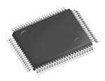
ICGOO电子元器件商城为您提供MCF5307AI90B由Freescale Semiconductor设计生产,在icgoo商城现货销售,并且可以通过原厂、代理商等渠道进行代购。 MCF5307AI90B价格参考。Freescale SemiconductorMCF5307AI90B封装/规格:嵌入式 - 微控制器, Coldfire V3 微控制器 IC MCF530x 32-位 90MHz ROMless 208-FQFP(28x28)。您可以下载MCF5307AI90B参考资料、Datasheet数据手册功能说明书,资料中有MCF5307AI90B 详细功能的应用电路图电压和使用方法及教程。
NXP USA Inc. 生产的型号为 MCF5307AI90B 的嵌入式微控制器(MCU),属于 ColdFire 系列,基于 32 位架构。该型号适用于多种工业和消费类应用场景,以下是其主要应用场景及特点:

1. 工业自动化
   MCF5307AI90B 可用于工业控制设备,例如 PLC(可编程逻辑控制器)、传感器接口和电机控制。其高性能处理能力和丰富的外设支持(如 UART、SPI、I²C 和定时器)使其能够高效管理复杂的工业任务。

2. 网络通信设备
   该微控制器适合用于小型网络设备,例如路由器、交换机或网关。它具备以太网控制器功能,可以实现数据包的快速传输和处理,满足实时通信需求。

3. 消费电子
   在家用电器中,MCF5307AI90B 可用于智能家电的主控单元,例如空调、洗衣机或冰箱。其低功耗特性和强大的计算能力有助于优化设备性能并降低能耗。

4. 汽车电子
   虽然 MCF5307AI90B 并非专门针对汽车应用设计,但在某些非关键系统(如车载信息娱乐系统或车身控制模块)中仍可发挥作用。其可靠性高且支持多种接口协议,便于与其他汽车子系统集成。

5. 医疗设备
   在便携式或小型医疗设备中,例如血压计、血糖仪或心率监测器,该微控制器可通过其精确的模拟信号处理能力和实时响应特性来确保数据采集的准确性。

6. 嵌入式系统开发
   开发人员可以利用 MCF5307AI90B 构建定制化嵌入式解决方案,适用于需要中等性能和灵活性的应用场景。其丰富的开发工具链(如 CodeWarrior IDE)简化了软件开发过程。

总结来说,MCF5307AI90B 的应用场景涵盖了工业、消费、通信和医疗等多个领域,凭借其高效的处理能力、多样的外设支持以及稳定的运行表现,成为许多嵌入式系统的理想选择。
| 参数 | 数值 |
| 产品目录 | 集成电路 (IC) |
| 描述 | IC MCU 32BIT ROMLESS 208FQFP |
| EEPROM容量 | - |
| 产品分类 | |
| I/O数 | 16 |
| 品牌 | Freescale Semiconductor |
| 数据手册 | |
| 产品图片 |
|
| 产品型号 | MCF5307AI90B |
| RAM容量 | 4K x 8 |
| rohs | 无铅 / 符合限制有害物质指令(RoHS)规范要求 |
| 产品系列 | MCF530x |
| 供应商器件封装 | 208-FQFP(28x28) |
| 包装 | 托盘 |
| 外设 | DMA,POR,WDT |
| 封装/外壳 | 208-BFQFP |
| 工作温度 | 0°C ~ 70°C |
| 振荡器类型 | 外部 |
| 数据转换器 | - |
| 标准包装 | 240 |
| 核心处理器 | Coldfire V3 |
| 核心尺寸 | 32-位 |
| 电压-电源(Vcc/Vdd) | 3 V ~ 3.6 V |
| 程序存储器类型 | ROMless |
| 程序存储容量 | - |
| 连接性 | EBI/EMI, I²C, UART/USART |
| 速度 | 90MHz |


PDF Datasheet 数据手册内容提取
Freescale Semiconductor, Inc. .. MCF5307 ColdFire® . c n Integrated Microprocessor I , r User’s Manual o t c u d n eescale Semico ReMv.C 2F.503, 0078U/2M00/D0 r F For More Information On This Product, Go to: www.freescale.com
Freescale Semiconductor, Inc. ColdFire is a registered trademark and DigitalDNA is a trademark of Motorola, Inc. I2C is a registered trademark of Philips Semiconductors . . . c n I , r o t Motorola reserves the right to make changes without further notice to any products herein. Motorola makes no warranty, c representation or guarantee regarding the suitability of its products for any particular purpose, nor does Motorola assume any liability u arising out of the application or use of any product or circuit, and specifically disclaims any and all liability, including without limitation d consequential or incidental damages. “Typical” parameters which may be provided in Motorola data sheets and/or specifications can n and do vary in different applications and actual performance may vary over time. All operating parameters, including “Typicals” must eescale Semico briwueauaHUoJ8nigesmtnnrA1hoStt eeh oad–1iPwpAvcn tru3–MaslAhn /odt–8tE lh eNioonye3t0dUohyetod 4:0a or re Rear f4i–eMtrf ez esrofot0O4aeeaheo,drl–4c ad iPe sts lrs31ohfu euEopuaur5–rr gibroure/rrsg62 Logiislee sssh94aodoiiia,t:dct4 n efuscJace i7gtar caahhlvoe rttpio eesifdmice aoun o uMfstnpt ontrs, iha lfo orsatL a eodstfa ntof,Nrmuedf ntsrid cml.ooy.iie;ian h r tlMraSaes tt Leocrau cPokpls iptcattsSslr,ohyhpio tm,are o el dooiuTnc fd ubr lnadeaaM :coiil ct nnltMdipedo hodtcirgytesnnoiooor,enti t erudrcboosdoiclaubyr rdeltto alcu lh odcyclIt,taanst uo,rhIo tefnsraLa oersMatc nirroru t.tem hyeo emanM art nacpaaaoerolotpum tarrisutoto’ltios ihilmrcndlte areuoat eos e CarotwDslsiicatzofei iai hg,aoesnpn snnIgndtsetnr eiea n icrcwabirdsinae.n,puho, tlg is3p etsenieilnt–olin r aigxatcae2ndelpena l 0;elinpen n t–PdcEidertoj1 lut .erqarstnOs,reodui. ,yom Mg . ,aM sB noaBosliu aunorr,Orop d lya td cxaopipiemnnoe uropr5ogjsa itruo4–shtl ttarst hrh0Aohoyt, a5ur dz eraodi l,nazo lss ra dDeibe isutndmeyduosesdes/ .actnAfn eaiaoiMggvafomtifrnneehtiit ren u nrs mcolm,dai,si fof rCe taeyaa wonm, t ony a–viaivo ldtaenooksher nuy dcr e cfasu Ac, oxao hdufuTpcranmooc rteoacy.ilh opd nk8tn S ulno ysu0iyMchro nen 2eEeoo eosi1 1nnmtuo,nth7 0otslfatedpe. e6sr tnn olr1h –Bo idudl–nae8ayu ne3 p re5 yspdaed0pr7eyaena .3l3osrirrdsc – tt rpoaJe. i 6it utantsmM7siro pac5 psoonabh–a tf nloaf2eitine.rcs1 o nee4ltar 0 os r, r ASIA/PACIFIC: Motorola Semiconductors H.K. Ltd.; Silicon Harbour Centre, 2 Dai King Street, Tai Po Industrial Estate, Tai Po, N.T., F Hong Kong. 852–26668334 Technical Information Center: 1–800–521–6274 HOME PAGE: http://www.motorola.com/semiconductors Document Comments: FAX (512) 895-2638, Attn: RISC Applications Engineering World Wide Web Addresses: http://www.motorola.com/PowerPC http://www.motorola.com/NetComm http://www.motorola.com/ColdFire © Motorola Inc., 2000. All rights reserved. For More Information On This Product, Go to: www.freescale.com
Freescale Semiconductor, Inc. Overview 1 Part I: MCF5307 Processor Core Part I ColdFire Core 2 Hardware Multiply/Accumulate (MAC) Unit 3 Local Memory 4 Debug Support 5 Part II: System Integration Module (SIM) Part II SIM Overview 6 . .. Phase-Locked Loop (PLL) c 7 In I2C Module 8 , r Interrupt Controller 9 o t c Chip-Select Module 10 u d Synchronous/Asynchronous DRAM Controller Module 11 n eescale Semico Parallel PPPaoarrttDr tI( MVGII:IA e:H n PCaeeMrorrdaUenipwlTctA-hrPahioRmerualerlTrenea p IrirlMcn oMMMatsoeloeoo drDd fdduIaa/uuulOcetllleeeaes) PP11111aa52346rrtt IIIVI r F Signal Descriptions 17 Bus Operation 18 IEEE 1149.1 Test Access Port (JTAG) 19 Electrical Specifications 20 Appendix: Memory Map A Glossary of Terms and Abbreviations GLO Index IND For More Information On This Product, Go to: www.freescale.com IND B GLO IND
Freescale Semiconductor, Inc. 1 Overview Part I Part I: MCF5307 Processor Core 2 ColdFire Core 3 Hardware Multiply/Accumulate (MAC) Unit 4 Local Memory 5 Debug Support Part II Part II: System Integration Module (SIM) SIM Overview 6 . .. 7 Phase-Locked Loop (PLL) c n 8 I2C Module I , r 9 Interrupt Controller o t c 10 Chip-Select Module u d 11 Synchronous/Asynchronous DRAM Controller Module n eescale Semico PP11111aa52346rrtt IIIVI PMDTUPPiaaaAMemrrrRcaAtte hTlII rlVIaeC IMM:n:l o PHPioonceodaadtrrrurluoi tdplD lle(ewlheGasearte rarMaenl eo IMnrdatuoel-ldrePfuaulcerpeose I/O) r F 17 Signal Descriptions 18 Bus Operation 19 IEEE 1149.1 Test Access Port (JTAG) 20 Electrical Specifications A Appendix B: Memory Map GLO Glossary of Terms and Abbreviations IND Index For More Information On This Product, Go to: www.freescale.com
Freescale Semiconductor, Inc. CONTENTS Paragraph Page Title Number Number About This Book . Chapter 1 . . c Overview n I 1.1 Features............................................................................................................... 1-1 r, 1.2 MCF5307 Features.............................................................................................. 1-4 o 1.2.1 Process............................................................................................................ 1-6 t c 1.3 ColdFire Module Description............................................................................. 1-7 u 1.3.1 ColdFire Core................................................................................................. 1-7 d 1.3.1.1 Instruction Fetch Pipeline (IFP).................................................................. 1-7 n 1.3.1.2 Operand Execution Pipeline (OEP)............................................................ 1-7 eescale Semico 11111111111...........33333333333...........11112345677.....34561 DDUTIS2yiRMACmMI8IEsnnARt -AxeeMtKtAMTreetm e gbrCCoM rn M eydnICo arnMtouan leootdD llt ed4 neorUuBriou-td.lfvrK.nulleau.oile.iscdebl..lfs e..elreiyI...ee.....n t......rMde......t.......e .......CSo.......r.......fdR.......aa.......uc.......cA.......hl.......e.......eMe...................................................................................................................................................................................................................................................................................................................................................................................................................................................................................................................................................................................................................................................................................................................................................................................................................................................................................................... .........11 111111111--11---------78889897800 r 1.3.7.2 Chip Selects.............................................................................................. 1-10 F 1.3.7.3 16-Bit Parallel Port Interface.................................................................... 1-10 1.3.7.4 Interrupt Controller................................................................................... 1-10 1.3.7.5 JTAG......................................................................................................... 1-11 1.3.8 System Debug Interface................................................................................ 1-11 1.3.9 PLL Module.................................................................................................. 1-11 1.4 Programming Model, Addressing Modes, and Instruction Set......................... 1-12 1.4.1 Programming Model..................................................................................... 1-13 1.4.2 User Registers............................................................................................... 1-14 1.4.3 Supervisor Registers..................................................................................... 1-14 1.4.4 Instruction Set............................................................................................... 1-15 Contents v For More Information On This Product, Go to: www.freescale.com
Freescale Semiconductor, Inc. CONTENTS Paragraph Page Title Number Number Part I MCF5407 Processor Core Chapter 2 ColdFire Core 2.1 Features and Enhancements.............................................................................. 2-21 2.1.1 Clock-Multiplied Microprocessor Core........................................................ 2-22 2.1.2 Enhanced Pipelines....................................................................................... 2-22 . 2.1.2.1 Instruction Fetch Pipeline (IFP)................................................................ 2-23 . . c 2.1.2.1.1 Branch Acceleration............................................................................. 2-23 n 2.1.2.2 Operand Execution Pipeline (OEP).......................................................... 2-24 I 2.1.2.2.1 Illegal Opcode Handling....................................................................... 2-24 r, 2.1.2.2.2 Hardware Multiply/Accumulate (MAC) Unit...................................... 2-24 o 2.1.2.2.3 Hardware Divide Unit.......................................................................... 2-25 t c 2.1.3 Debug Module Enhancements...................................................................... 2-25 u 2.2 Programming Model......................................................................................... 2-26 d 2.2.1 User Programming Model............................................................................ 2-27 n 2.2.1.1 Data Registers (D0–D7)........................................................................... 2-27 eescale Semico 22222222222...........22222222222...........11112222222..........2345123456 SuASPCSVCARMpetrtoaAdecaaoorcccndctvgMdhutedrkioruseessi a rlst Pos BmeR iC sBrooC a Beo nRiPasCongn easrenCtiotoe sesgrAtue ogtorriRe o nsddrlA(rat elteAd Re emgd( RrrrSR7eieds mse,(gRs re t(PgseSiegiA)si sCnr.PiRsts. s0get.)() tee.–r VRe...Mg r...Ar(...seBi ...C sg(o...6(...RtCAAid...)e...s)Ce....rCtC.... el.....(R......RRrR...... ......)()......0A.......M........–........M........AB................B........CA................AR........R................1R)................).........)............................................................................................................................................................................................................................................................................................................................................................................................................................................................................................................................................... 22222222222-----------3232232233217188199008 r 2.3 Integer Data Formats......................................................................................... 2-31 F 2.4 Organization of Data in Registers..................................................................... 2-31 2.4.1 Organization of Integer Data Formats in Registers...................................... 2-31 2.4.2 Organization of Integer Data Formats in Memory....................................... 2-32 2.5 Addressing Mode Summary............................................................................. 2-33 2.6 Instruction Set Summary................................................................................... 2-34 2.6.1 Instruction Set Summary.............................................................................. 2-37 2.7 Instruction Timing............................................................................................ 2-40 2.7.1 MOVE Instruction Execution Times............................................................ 2-41 2.7.2 Execution Timings—One-Operand Instructions.......................................... 2-43 2.7.3 Execution Timings—Two-Operand Instructions.......................................... 2-43 2.7.4 Miscellaneous Instruction Execution Times................................................. 2-45 vi MCF5307 User’s Manual For More Information On This Product, Go to: www.freescale.com
Freescale Semiconductor, Inc. CONTENTS Paragraph Page Title Number Number 2.7.5 Branch Instruction Execution Times............................................................ 2-46 2.8 Exception Processing Overview....................................................................... 2-47 2.8.1 Exception Stack Frame Definition................................................................ 2-49 2.8.2 Processor Exceptions.................................................................................... 2-50 Chapter 3 Hardware Multiply/Accumulate (MAC) Unit 3.1 Overview............................................................................................................. 3-1 . 3.1.1 MAC Programming Model............................................................................. 3-2 . . 3.1.2 General Operation........................................................................................... 3-3 c n 3.1.3 MAC Instruction Set Summary...................................................................... 3-4 I 3.1.4 Data Representation........................................................................................ 3-4 , 3.2 MAC Instruction Execution Timings.................................................................. 3-5 r o t c Chapter 4 u Local Memory d n eescale Semico 444444444444............123445567888....1112 ISSSSPCCnRRRRoaatSSCTweccAAAArhhRRhaeaMMMMeecerAAc h OOtMC MMieOOPIonvra raLgvpn iceoBIntaeesihrngian vnrraaeibrgvaelstiia eiieztaei emzaiSetwatm owal AwttimSntai.zeeio.dttoan...ieaen...dntnt...nrsi....rgto:...... e-...... L n......UIsM......nos ......Cp...... vco......R.......aaod.......e.......llde.......i g.......Mdel.......i........,s......... e.........Vt.........em..................ar......... o.........l(.........irR.........d.........y.........-A......... U.........M.........M.........n.........o.........m.........Bd..................ouA..................dl.........Re.........i.........sf.........).........i...........e...........d......................,........... ...........a......................n......................d...................... ...........V.................................a......................l...........i...........d......................-...........M............................................o......................d......................i...........f...........i......................e...........d.................................................................................................................................................................................. 444444444444------------312366457918 r F 4.9 Cache Operation................................................................................................ 4-11 4.9.1 Caching Modes............................................................................................. 4-13 4.9.1.1 Cacheable Accesses.................................................................................. 4-13 4.9.1.2 Write-Through Mode ............................................................................... 4-14 4.9.1.3 Copyback Mode ....................................................................................... 4-14 4.9.2 Cache-Inhibited Accesses............................................................................. 4-14 4.9.3 Cache Protocol.............................................................................................. 4-15 4.9.3.1 Read Miss................................................................................................. 4-15 4.9.3.2 Write Miss ............................................................................................... 4-16 4.9.3.3 Read Hit.................................................................................................... 4-16 4.9.3.4 Write Hit .................................................................................................. 4-16 4.9.4 Cache Coherency ......................................................................................... 4-17 Contents vii For More Information On This Product, Go to: www.freescale.com
Freescale Semiconductor, Inc. CONTENTS Paragraph Page Title Number Number 4.9.5 Memory Accesses for Cache Maintenance................................................... 4-17 4.9.5.1 Cache Filling............................................................................................. 4-17 4.9.5.2 Cache Pushes............................................................................................ 4-18 4.9.5.2.1 Push and Store Buffers......................................................................... 4-18 4.9.5.2.2 Push and Store Buffer Bus Operation................................................... 4-18 4.9.6 Cache Locking.............................................................................................. 4-19 4.10 Cache Registers................................................................................................. 4-21 4.10.1 Cache Control Register (CACR).................................................................. 4-21 4.10.2 Access Control Registers (ACR0–ACR1).................................................... 4-22 4.11 Cache Management........................................................................................... 4-24 . . . 4.12 Cache Operation Summary............................................................................... 4-25 c 4.12.1 Cache State Transitions................................................................................ 4-25 n 4.13 Cache Initialization Code.................................................................................. 4-29 I , r o Chapter 5 t Debug Support c u d 5.1 Overview............................................................................................................. 5-1 n 5.2 Signal Description............................................................................................... 5-2 eescale Semico 55555555555...........33444444445........11234567 RPBreaoBAABCDPTacglkrreDodda-roiggTtnaddgMgarimfrrgio nrimeeBae gu mssAEmrurenss eiDxd rd nTABaaCed egktrDcrtriofa pteeouMireucaonsntibenkibsii/oo unt tSpuSAidengtoott/rue eat Mni oMtlp Btnr Tfu.pRit.a robs .rToesR.ei du.kRrgaag.etet.kk gie..egR ..spee( g..itRB..enrosei.. gs..t ierDR..Benti ..ge(rs..etMr..Tisrt/..gaseM ..D((tn)..ire..CsAsc...aRtr... hSes...B (...()krD R...B(L .... (....PBR)....ARA.....S.....Re,A.....AT g..... ,.....AR i.....TD=.....s.....R)tB..... Be......0......)Hr......xMs..............5R .......(R.......)P)...............)B.............................R..............................,.......... ..........P....................B..............................M..............................R..............................).................................................................................................................................................................................................................................................................. ......55555 -555--5--5511111------69852370434 r 5.5.1 CPU Halt....................................................................................................... 5-16 F 5.5.2 BDM Serial Interface.................................................................................... 5-17 5.5.2.1 Receive Packet Format............................................................................. 5-19 5.5.2.2 Transmit Packet Format............................................................................ 5-19 5.5.3 BDM Command Set...................................................................................... 5-19 5.5.3.1 ColdFire BDM Command Format............................................................ 5-20 5.5.3.1.1 Extension Words as Required............................................................... 5-21 5.5.3.2 Command Sequence Diagrams................................................................. 5-21 5.5.3.3 Command Set Descriptions...................................................................... 5-23 5.5.3.3.1 Read A/D Register (RAREG/RDREG)..................................................... 5-24 5.5.3.3.2 Write A/D Register (WAREG/WDREG)................................................... 5-25 5.5.3.3.3 Read Memory Location (READ)............................................................ 5-26 viii MCF5307 User’s Manual For More Information On This Product, Go to: www.freescale.com
Freescale Semiconductor, Inc. CONTENTS Paragraph Page Title Number Number 5.5.3.3.4 Write Memory Location (WRITE)......................................................... 5-27 5.5.3.3.5 Dump Memory Block (DUMP).............................................................. 5-29 5.5.3.3.6 Fill Memory Block (FILL)..................................................................... 5-31 5.5.3.3.7 Resume Execution (GO)........................................................................ 5-33 5.5.3.3.8 No Operation (NOP).............................................................................. 5-34 5.5.3.3.9 Synchronize PC to the PST/DDATA Lines (SYNC_PC)....................... 5-35 5.5.3.3.10 Read Control Register (RCREG)............................................................ 5-36 5.5.3.3.11 Write Control Register (WCREG).......................................................... 5-37 5.5.3.3.12 Read Debug Module Register (RDMREG)............................................. 5-38 . 5.5.3.3.13 Write Debug Module Register (WDMREG)........................................... 5-39 . . 5.6 Real-Time Debug Support................................................................................ 5-39 c 5.6.1 Theory of Operation...................................................................................... 5-40 n 5.6.1.1 Emulator Mode......................................................................................... 5-41 I , 5.6.2 Concurrent BDM and Processor Operation.................................................. 5-41 r o 5.7 Motorola-Recommended BDM Pinout............................................................. 5-42 t 5.8 Processor Status, DDATA Definition............................................................... 5-42 c 5.8.1 User Instruction Set...................................................................................... 5-43 u 5.8.2 Supervisor Instruction Set............................................................................. 5-46 d n eescale Semico 66666.....12222...123 FPeroaSMRgtIeurMosradeem utsR lmS.ee..t gi.aBn.i.tsg.auS.ts .seM.ye .rR. s.AMo.e.td.dge.ee.dimm.sl.rt..eoe.. ..srr..Is.. ny..( S.. RRt..M..eI..eS..MCgga..R..pi..hr s)P..O...ata....ea....t....vpri....r ....oe(tt........Me n....rI....rvI.... B.... M....i 6....Ae.... ....ow....R .... d....)........u...............l.....e.......... .....(..........S...............I.....M....................).............................................................................................................................................................................................. 66666-----41335 r F 6.2.4 Software Watchdog Timer.............................................................................. 6-6 6.2.5 System Protection Control Register (SYPCR)............................................... 6-8 6.2.6 Software Watchdog Interrupt Vector Register (SWIVR)............................... 6-9 6.2.7 Software Watchdog Service Register (SWSR)............................................... 6-9 6.2.8 PLL Clock Control for CPU STOP Instruction............................................ 6-10 6.2.9 Pin Assignment Register (PAR)................................................................... 6-10 6.2.10 Bus Arbitration Control................................................................................ 6-11 6.2.10.1 Default Bus Master Park Register (MPARK).......................................... 6-11 6.2.10.1.1 Arbitration for Internally Generated Transfers (MPARK[PARK])...... 6-12 6.2.10.1.2 Arbitration between Internal and External Masters for Accessing Internal Resources .........................................................6-14 Contents ix For More Information On This Product, Go to: www.freescale.com
Freescale Semiconductor, Inc. CONTENTS Paragraph Page Title Number Number Chapter 7 Phase-Locked Loop (PLL) 7.1 Overview............................................................................................................. 7-1 7.1.1 PLL:PCLK Ratios........................................................................................... 7-2 7.2 PLL Operation.................................................................................................... 7-2 7.2.1 Reset/Initialization.......................................................................................... 7-2 7.2.2 Normal Mode.................................................................................................. 7-2 7.2.3 Reduced-Power Mode..................................................................................... 7-2 7.2.4 PLL Control Register (PLLCR)...................................................................... 7-3 . . . 7.3 PLL Port List...................................................................................................... 7-3 c 7.4 Timing Relationships.......................................................................................... 7-4 n 7.4.1 PCLK, PSTCLK, and BCLKO....................................................................... 7-4 I , 7.4.2 RSTI Timing................................................................................................... 7-5 r o 7.5 PLL Power Supply Filter Circuit........................................................................ 7-6 t c u Chapter 8 d I2C Module n eescale Semico 88888888888...........12344444555......123412 OIIIPn22rvCCtoACHCIIee22g rSPrllraCCfroovbnyraa ccioicmAFdsetkktterswroed ma ehSSFmcdt.qaiyti.oerorn.uk ne.laeCng.eisct..tnn ..oucshPM..g ch..nrrR..reyoi...foo...nsie n...cgdD....ggi....eue....ziid.....lsrva.....atu......it......etdir......iro......eeo...... n......(rn.......I ........AR...........................eD..................g.........R.........i.........s.........)t...................e..........r.................... ..........(..........I..........F..............................D....................R..............................)............................................................................................................................................................................................................................................................................................................................................................................................................................................................................................................................................................................................................................................................. 88888888888-----------61536734515 r 8.5.3 I2C Control Register (I2CR)........................................................................... 8-8 F 8.5.4 I2C Status Register (I2SR).............................................................................. 8-9 8.5.5 I2C Data I/O Register (I2DR)....................................................................... 8-10 8.6 I2C Programming Examples............................................................................. 8-10 8.6.1 Initialization Sequence.................................................................................. 8-10 8.6.2 Generation of START................................................................................... 8-10 8.6.3 Post-Transfer Software Response................................................................. 8-11 8.6.4 Generation of STOP...................................................................................... 8-12 8.6.5 Generation of Repeated START................................................................... 8-12 8.6.6 Slave Mode................................................................................................... 8-13 8.6.7 Arbitration Lost............................................................................................. 8-13 x MCF5307 User’s Manual For More Information On This Product, Go to: www.freescale.com
Freescale Semiconductor, Inc. CONTENTS Paragraph Page Title Number Number Chapter 9 Interrupt Controller 9.1 Overview............................................................................................................. 9-1 9.2 Interrupt Controller Registers............................................................................. 9-2 9.2.1 Interrupt Control Registers (ICR0–ICR9)...................................................... 9-3 9.2.2 Autovector Register (AVR)............................................................................ 9-5 9.2.3 Interrupt Pending and Mask Registers (IPR and IMR)................................... 9-6 9.2.4 Interrupt Port Assignment Register (IRQPAR).............................................. 9-7 . . . Chapter 10 c n Chip-Select Module I , 10.1 Overview........................................................................................................... 10-1 r o 10.2 Chip-Select Module Signals............................................................................. 10-1 t 10.3 Chip-Select Operation....................................................................................... 10-2 c u 10.3.1 General Chip-Select Operation..................................................................... 10-3 d 10.3.1.1 8-, 16-, and 32-Bit Port Sizing.................................................................. 10-4 n 10.3.1.2 Global Chip-Select Operation................................................................... 10-4 eescale Semico 11111110000001.......4444441.....11111....1234 SCOyhvnCiepcrh-vCCCChiSpihhhoere-iiidowlSpppeeen---c. .lSSSEt.oe .eeeR.xcu.lllt.aeeee .smM.cccg./ttt.ip.A so.AMClt.d.eesod.uar..ynd..ssl..etrkn...r...e ...oRcR...s...ls...he e... Rg...RgrC...ie...oies...sgh...tg...ntei...eais...rosr...tsp...tse...ue ....rt(....rss....eCs.... .... ( rS....(CD.... C....M1....SR....S1....CR....AA.... ....R0 ....RM....–0....0....C–.... –....CCS....C........MSo....S....C....nAR........R....t7R....r7....)....7o)..........)l.............l.......e..............r.............. .......M............................o..............d.....................u.....................l.......e......................................................................................................... 11111110100000-------6169568 r F 11.1.1 Definitions.................................................................................................... 11-2 11.1.2 Block Diagram and Major Components....................................................... 11-2 11.2 DRAM Controller Operation............................................................................ 11-3 11.2.1 DRAM Controller Registers......................................................................... 11-3 11.3 Asynchronous Operation.................................................................................. 11-4 11.3.1 DRAM Controller Signals in Asynchronous Mode...................................... 11-4 11.3.2 Asynchronous Register Set........................................................................... 11-4 11.3.2.1 DRAM Control Register (DCR) in Asynchronous Mode........................ 11-4 11.3.2.2 DRAM Address and Control Registers (DACR0/DACR1)..................... 11-5 11.3.2.3 DRAM Controller Mask Registers (DMR0/DMR1)................................ 11-7 11.3.3 General Asynchronous Operation Guidelines.............................................. 11-8 11.3.3.1 Non-Page-Mode Operation..................................................................... 11-11 Contents xi For More Information On This Product, Go to: www.freescale.com
Freescale Semiconductor, Inc. CONTENTS Paragraph Page Title Number Number 11.3.3.2 Burst Page-Mode Operation................................................................... 11-12 11.3.3.3 Continuous Page Mode........................................................................... 11-13 11.3.3.4 Extended Data Out (EDO) Operation..................................................... 11-15 11.3.3.5 Refresh Operation................................................................................... 11-16 11.4 Synchronous Operation................................................................................... 11-16 11.4.1 DRAM Controller Signals in Synchronous Mode...................................... 11-17 11.4.2 Using Edge Select (EDGESEL)................................................................. 11-18 11.4.3 Synchronous Register Set........................................................................... 11-19 11.4.3.1 DRAM Control Register (DCR) in Synchronous Mode..........................11-19 11.4.3.2 DRAM Address and Control Registers (DACR0/DACR1) . . . in Synchronous Mode .........................................................................11-20 c 11.4.3.3 DRAM Controller Mask Registers (DMR0/DMR1).............................. 11-22 n 11.4.4 General Synchronous Operation Guidelines............................................... 11-23 I , 11.4.4.1 Address Multiplexing............................................................................. 11-23 r o 11.4.4.2 Interfacing Example................................................................................ 11-27 t 11.4.4.3 Burst Page Mode..................................................................................... 11-27 c 11.4.4.4 Continuous Page Mode........................................................................... 11-29 u 11.4.4.5 Auto-Refresh Operation.......................................................................... 11-31 d n 11.4.4.6 Self-Refresh Operation........................................................................... 11-32 eescale Semico 111111111111111111.........445555555........55123456.1 SDISDDDMIRnnDCAMiioAMttRiRdiCRMaaeoA lRl I iidI RnzMz EneIaaie nixttt RtgiIiiiaiaoontiaemlisnntliagteiz pleziSrCaisrlafztte eaotiaeIqioc.ndtro.uien .ieonS.t e...iCn....ena....t.....olct.....i.....ienz.....n......fa......git......g......is......ou..............nPr.......a...............at........i........ro................tn........ .................I.........I.........I......... ......... ................................................................................................................................................................................................................................................................................................................................................................................................................................................................................................................................................... 111111111111111111---------333333333453575938 r Peripheral Module F Chapter 12 DMA Controller Module 12.1 Overview........................................................................................................... 12-1 12.1.1 DMA Module Features................................................................................. 12-2 12.2 DMA Signal Description.................................................................................. 12-2 12.3 DMA Transfer Overview.................................................................................. 12-3 12.4 DMA Controller Module Programming Model................................................ 12-4 12.4.1 Source Address Registers (SAR0–SAR3).................................................... 12-6 12.4.2 Destination Address Registers (DAR0–DAR3)........................................... 12-7 xii MCF5307 User’s Manual For More Information On This Product, Go to: www.freescale.com
Freescale Semiconductor, Inc. CONTENTS Paragraph Page Title Number Number 12.4.3 Byte Count Registers (BCR0–BCR3)........................................................... 12-7 12.4.4 DMA Control Registers (DCR0–DCR3)...................................................... 12-8 12.4.5 DMA Status Registers (DSR0–DSR3)....................................................... 12-10 12.4.6 DMA Interrupt Vector Registers (DIVR0–DIVR3)................................... 12-11 12.5 DMA Controller Module Functional Description........................................... 12-11 12.5.1 Transfer Requests (Cycle-Steal and Continuous Modes)........................... 12-12 12.5.2 Data Transfer Modes.................................................................................. 12-12 12.5.2.1 Dual-Address Transfers.......................................................................... 12-12 12.5.2.2 Single-Address Transfers........................................................................ 12-13 12.5.3 Channel Initialization and Startup.............................................................. 12-13 . . . 12.5.3.1 Channel Prioritization............................................................................. 12-13 c 12.5.3.2 Programming the DMA Controller Module........................................... 12-13 n 12.5.4 Data Transfer.............................................................................................. 12-14 I , 12.5.4.1 External Request and Acknowledge Operation...................................... 12-14 r o 12.5.4.2 Auto-Alignment...................................................................................... 12-17 t 12.5.4.3 Bandwidth Control.................................................................................. 12-18 c 12.5.5 Termination................................................................................................. 12-18 u d n Chapter 13 eescale Semico 111111111333333333.........112333333......112345 OGGveeKTTTTTnneiiiiireeemmmmmvrryaai eeeeeellFrrrrr--w ePPMRCCEa.uu.vteao.rrou.fpeupp.dre.ntnooe.reu.ttssse. re.eeRRne..r ..c seeTT..R..e gg..(ii.. emmiTi..Rssg....Ctteeei..ee..srrgN..rrt ..issUPe..s0T.. rr..((tn/s..oeTTiT.. im..rg(tME..CsTs..r ..RaeN(...CR...Tm0...r1R...0 R/...m)M.../T0...TR..../Ei....oMTn....0R....g..../Cd....TR1 ....MRu....R)1.........1l).....oRe.....)......d1..............e).......l................................................................................................................................................................................................................................................................................................................................................................................................................................................................................. 111111111333333333---------122532445 r 13.4 Code Example................................................................................................... 13-6 F 13.5 Calculating Time-Out Values........................................................................... 13-7 Chapter 14 UART Modules 14.1 Overview........................................................................................................... 14-1 14.2 Serial Module Overview................................................................................... 14-2 14.3 Register Descriptions........................................................................................ 14-2 14.3.1 UART Mode Registers 1 (UMR1n).............................................................. 14-4 14.3.2 UART Mode Register 2 (UMR2n)............................................................... 14-6 14.3.3 UART Status Registers (USRn)................................................................... 14-7 Contents xiii For More Information On This Product, Go to: www.freescale.com
Freescale Semiconductor, Inc. CONTENTS Paragraph Page Title Number Number 14.3.4 UART Clock-Select Registers (UCSRn)...................................................... 14-8 14.3.5 UART Command Registers (UCRn)............................................................ 14-9 14.3.6 UART Receiver Buffers (URBn)............................................................... 14-11 14.3.7 UART Transmitter Buffers (UTBn)........................................................... 14-11 14.3.8 UART Input Port Change Registers (UIPCRn).......................................... 14-12 14.3.9 UART Auxiliary Control Register (UACRn)............................................. 14-12 14.3.10 UART Interrupt Status/Mask Registers (UISRn/UIMRn).......................... 14-13 14.3.11 UART Divider Upper/Lower Registers (UDUn/UDLn)............................ 14-14 14.3.12 UART Interrupt Vector Register (UIVRn)................................................. 14-15 14.3.13 UART Input Port Register (UIPn).............................................................. 14-15 . . . 14.3.14 UART Output Port Command Registers (UOP1n/UOP0n)....................... 14-15 c 14.4 UART Module Signal Definitions.................................................................. 14-16 n 14.5 Operation......................................................................................................... 14-18 I , 14.5.1 Transmitter/Receiver Clock Source............................................................ 14-18 r o 14.5.1.1 Programmable Divider............................................................................ 14-18 t 14.5.1.2 Calculating Baud Rates........................................................................... 14-19 c 14.5.1.2.1 BCLKO Baud Rates........................................................................... 14-19 u 14.5.1.2.2 External Clock.................................................................................... 14-19 d n 14.5.2 Transmitter and Receiver Operating Modes............................................... 14-19 reescale Semico 111111111111444444444444............555555555555............222333345555.........123123123 LMBouuTRFALRRWIosnl IproteeeuOtFiariccmaedtinnOopeadtrregsroilmeo umv C tSrLCpMepeaayt i oyrtttaMtLc iiotocc.Acoil.odplknoe. ne.cEoe-s gd.sks...Bpc e....n.......-ha........Bo........oc........w........ak ........Mc........ l........Mke........o........d ........Mod........g........de........e........oe......... .........dC....................e..........y......................c...........l...........e......................s.......................................................................................................................................................................................................................................................................................................................................................................................................................................................................................................................................................................................................................................................................................................................................................................................................... 111111111111444444444444------------222222222222456828815568 F 14.5.6 Programming.............................................................................................. 14-28 14.5.6.1 UART Module Initialization Sequence.................................................. 14-29 Chapter 15 Parallel Port (General-Purpose I/O) 15.1 Parallel Port Operation...................................................................................... 15-1 15.1.1 Pin Assignment Register (PAR)................................................................... 15-1 15.1.2 Port A Data Direction Register (PADDR).................................................... 15-2 15.1.3 Port A Data Register (PADAT).................................................................... 15-2 15.1.4 Code Example............................................................................................... 15-3 xiv MCF5307 User’s Manual For More Information On This Product, Go to: www.freescale.com
Freescale Semiconductor, Inc. CONTENTS Paragraph Page Title Number Number Part IV Hardware Interface Chapter 16 Mechanical Data 16.1 Package............................................................................................................. 16-1 16.2 Pinout................................................................................................................ 16-1 16.3 Mechanical Diagram......................................................................................... 16-8 . 16.4 Case Drawing.................................................................................................... 16-9 . . c n Chapter 17 I Signal Descriptions , r o 17.1 Overview........................................................................................................... 17-1 t c 17.2 MCF5307 Bus Signals...................................................................................... 17-7 u 17.2.1 Address Bus.................................................................................................. 17-7 d 17.2.1.1 Address Bus (A[23:0]).............................................................................. 17-7 n eescale Semico 111111111111777777777777............222222222233...........12345678911.02 IntDRSTATTTTIenrirrrrreadtzraaaaaAeatudennnnnadrp rd sssssr(/eBtudfffffSW seeeeepCruIsrrrrreZtr s o sSiSAITM R[tns(nt1etyD crte aoB :roPpk(qr0[odRbutern3u]l io es)( of1/e(S TgiW .Tws:((e.ir0AtSA.rgTe .l)] (.)ens[()S..[I...3dsT1aR....) ....1gl:M(.....Qs0.....:eT......2] ......[1I/(......42PP......T/......]I:....../PA/0R......PP......[]......)QP1P/.............P7:.......[20.......P1).......,]........ 5[........)I4........:R.........8:.........2.........Q].........)]..................3)...................../...........I...........R.................................Q.................................6......................,........... ...........I...........R.................................Q......................5....................../......................I...........R.................................Q......................4......................,........... ...........a......................n......................d...................... ...........I......................R......................Q.................................7......................)...................................................................................................... .......11111 11711177117777-777--77--11111-------790899228800 r F 17.4 Bus Arbitration Signals................................................................................... 17-12 17.4.1 Bus Request (BR)....................................................................................... 17-12 17.4.2 Bus Grant (BG).......................................................................................... 17-12 17.4.3 Bus Driven (BD)......................................................................................... 17-13 17.5 Clock and Reset Signals.................................................................................. 17-13 17.5.1 Reset In (RSTI)........................................................................................... 17-13 17.5.2 Clock Input (CLKIN).................................................................................. 17-13 17.5.3 Bus Clock Output (BCLKO)...................................................................... 17-13 17.5.4 Reset Out (RSTO)....................................................................................... 17-13 17.5.5 Data/Configuration Pins (D[7:0])............................................................... 17-13 17.5.5.1 D[7:5Boot Chip-Select (CS0) Configuration......................................... 17-14 17.5.5.2 D7—Auto Acknowledge Configuration (AA_CONFIG)...................... 17-14 Contents xv For More Information On This Product, Go to: www.freescale.com
Freescale Semiconductor, Inc. CONTENTS Paragraph Page Title Number Number 17.5.5.3 D[6:5]—Port Size Configuration (PS_CONFIG[1:0])........................... 17-14 17.5.6 D4—Address Configuration (ADDR_CONFIG)....................................... 17-14 17.5.7 D[3:2]—Frequency Control PLL (FREQ[1:0]..........................................) 17-15 17.5.8 D[1:0]—Divide Control PCLK to BCLKO (DIVIDE[1:0])....................... 17-15 17.6 Chip-Select Module Signals........................................................................... 17-15 17.6.1 Chip-Select (CS[7:0])................................................................................. 17-16 17.6.2 Byte Enables/Byte Write Enables (BE[3:0]/BWE[3:0])............................ 17-16 17.6.3 Output Enable (OE).................................................................................... 17-16 17.7 DRAM Controller Signals.............................................................................. 17-16 17.7.1 Row Address Strobes (RAS[1:0])............................................................... 17-16 . . . 17.7.2 Column Address Strobes (CAS[3:0])......................................................... 17-16 c 17.7.3 DRAM Write (DRAMW)........................................................................... 17-17 n 17.7.4 Synchronous DRAM Column Address Strobe (SCAS)............................. 17-17 I , 17.7.5 Synchronous DRAM Row Address Strobe (SRAS)................................... 17-17 r o 17.7.6 Synchronous DRAM Clock Enable (SCKE).............................................. 17-17 t 17.7.7 Synchronous Edge Select (EDGESEL)...................................................... 17-17 c 17.8 DMA Controller Module Signals.................................................................... 17-17 u 17.8.1 DMA Request (DREQ[1:0]/PP[6:5]).......................................................... 17-18 d n 17.9 Serial Module Signals..................................................................................... 17-18 reescale Semico 111111111111777777777777............999911111111....000122231234....1212 TPID2aieCmrTRCRTTIIba22 riiueeleMlCCmmaelrcqgena euo eeMSSlrsai errd mvIeent so/uoIOrredOtnidiil r t aaeuStp uTt oSll Peteul Spe rCDeeonStsi u rsSrgdltSaei tto an (estn Si(Tac(l gradC(Pi kinlDIgT( asPTN (Sanl(ORa[. SSlDa[.Dt1s.T1Ual)C..5Asa... :S...TIL0:t....)0n)a....]1).....]p ).......,O)........u ........T.........tu......... O.........t(.........pR.........U.........u.........x.........tT.........D .........(.........0.........T).........)..........x......................D.................................)........................................................................................................................................................................................................................................................................................................................................................................................................................................................................................................................................................................................................................................................................................................... 111111111111777777777777------------111111112111899898990988 F 17.13.1 Test Mode (MTMOD[3:0])........................................................................ 17-20 17.13.2 High Impedance (HIZ)................................................................................ 17-20 17.13.3 Processor Clock Output (PSTCLK)............................................................ 17-20 17.13.4 Debug Data (DDATA[3:0])........................................................................ 17-20 17.13.5 Processor Status (PST[3:0])........................................................................ 17-20 17.14 Debug Module/JTAG Signals......................................................................... 17-21 17.14.1 Test Reset/Development Serial Clock (TRST/DSCLK)............................ 17-21 17.14.2 Test Mode Select/Breakpoint (TMS/BKPT).............................................. 17-22 17.14.3 Test Data Input/Development Serial Input (TDI/DSI)............................... 17-22 17.14.4 Test Data Output/Development Serial Output (TDO/DSO)....................... 17-22 17.14.5 Test Clock (TCK)....................................................................................... 17-23 xvi MCF5307 User’s Manual For More Information On This Product, Go to: www.freescale.com
Freescale Semiconductor, Inc. CONTENTS Paragraph Page Title Number Number Chapter 18 Bus Operation 18.1 Features............................................................................................................. 18-1 18.2 Bus and Control Signals................................................................................... 18-1 18.3 Bus Characteristics............................................................................................ 18-2 18.4 Data Transfer Operation................................................................................... 18-3 18.4.1 Bus Cycle Execution..................................................................................... 18-4 18.4.2 Data Transfer Cycle States........................................................................... 18-5 18.4.3 Read Cycle.................................................................................................... 18-7 . . . 18.4.4 Write Cycle................................................................................................... 18-8 c 18.4.5 Fast-Termination Cycles............................................................................... 18-9 n 18.4.6 Back-to-Back Bus Cycles........................................................................... 18-10 I , 18.4.7 Burst Cycles................................................................................................ 18-11 r o 18.4.7.1 Line Transfers......................................................................................... 18-12 t 18.4.7.2 Line Read Bus Cycles............................................................................. 18-12 c 18.4.7.3 Line Write Bus Cycles............................................................................ 18-14 u 18.4.7.4 Transfers Using Mixed Port Sizes.......................................................... 18-15 d n 18.5 Misaligned Operands...................................................................................... 18-16 reescale Semico 111111111111888888888888............677788999111.....00012112..12 BIBGRnuueetLIBTMMSesnssner oeweuEAtruatvfresu osltraOrer twptrA-blrileo Dptup iaOr 7rrteplE rbesre RpretaIvxi a.-n etteE.AicWtri.rtcsi.oaexeao.ecetp.natrtnti.k eirt..Btoo....unicr....nonnuh....po.... na sd....twSo....ss lo....Ai fl......Bgg ......eE......rnd ......ubR......axg......si......ltte e......seDr......s .......arCe.......ent.......ti.......yva........o........cil........nc ........lM........ ee........P .........A.........ar.........os.........r.........tt.........beo..................irc.........t .........roT.........a.........l.........rt .........a(i.........oT.........n.........n.........sw......... f.........P.........eo.........rr.........-.........soW...................t..........o..........i..........cr..........e..........o.......... ..........lM.......... ..........(..........T..........o....................hd....................re..........e)....................e...........-......................W............................................i...........r...........e...................... ...........M.................................o......................d......................e......................)............................................... 111111111111888888888888------------123231131222704138759519 F Chapter 19 IEEE 1149.1 Test Access Port (JTAG) 19.1 Overview........................................................................................................... 19-1 19.2 JTAG Signal Descriptions............................................................................... 19-2 19.3 TAP Controller.................................................................................................. 19-3 19.4 JTAG Register Descriptions............................................................................. 19-4 19.4.1 JTAG Instruction Shift Register.................................................................. 19-5 19.4.2 IDCODE Register......................................................................................... 19-6 19.4.3 JTAG Boundary-Scan Register.................................................................... 19-7 Contents xvii For More Information On This Product, Go to: www.freescale.com
Freescale Semiconductor, Inc. CONTENTS Paragraph Page Title Number Number 19.4.4 JTAG Bypass Register................................................................................ 19-10 19.5 Restrictions..................................................................................................... 19-10 19.6 Disabling IEEE Standard 1149.1 Operation................................................... 19-11 19.7 Obtaining the IEEE Standard 1149.1.............................................................. 19-12 Chapter 20 Electrical Specifications 20.1 General Parameters........................................................................................... 20-1 . 20.2 Clock Timing Specifications............................................................................. 20-2 . . 20.3 Input/Output AC Timing Specifications........................................................... 20-3 c n 20.4 Reset Timing Specifications........................................................................... 20-12 I 20.5 Debug AC Timing Specifications................................................................... 20-12 , 20.6 Timer Module AC Timing Specifications...................................................... 20-14 r o 20.7 I2C Input/Output Timing Specifications......................................................... 20-15 t 20.8 UART Module AC Timing Specifications..................................................... 20-16 c u 20.9 Parallel Port (General-Purpose I/O) Timing Specifications........................... 20-18 d 20.10 DMA Timing Specifications........................................................................... 20-19 n 20.11 IEEE 1149.1 (JTAG) AC Timing Specifications........................................... 20-20 eescale Semico r F xviii MCF5307 User’s Manual For More Information On This Product, Go to: www.freescale.com
Freescale Semiconductor, Inc. ILLUSTRATIONS Figure Page Title Number Number 1-1 MCF5307 Block Diagram.............................................................................................1-2 1-2 UART Module Block Diagram.....................................................................................1-9 . 1-3 PLL Module................................................................................................................1-12 . . 1-4 ColdFire MCF5307 Programming Model..................................................................1-13 c 2-1 ColdFire Enhanced Pipeline.......................................................................................2-23 n I 2-2 ColdFire Multiply-Accumulate Functionality Diagram.............................................2-25 , 2-3 ColdFire Programming Model....................................................................................2-27 r o 2-5 Status Register (SR)....................................................................................................2-30 t 2-6 Vector Base Register (VBR).......................................................................................2-30 c 2-7 Organization of Integer Data Formats in Data Registers............................................2-32 u 2-8 Organization of Integer Data Formats in Address Registers......................................2-32 d n 2-9 Memory Operand Addressing.....................................................................................2-33 eescale Semico 23344444444-----------112123456780 ECMSUCCCWCCRxoaaaaanArccccccliAidfehhhthhCieFMpeeieee- nt — iPdMOLCirg o rBeC ooorAin OasgMcnga ss:akSpctr erAnaaieihto nnatmirAeC zlagc R CamdtkOR .iMetdo. oiei.rFsorp.nnggeu.reny.gatail..s,s b..t nms a..MitBa..i pen..Rzec..rl:do..a i k e..Fca( dt.. LgCi..afoMe..oti..tilrAes..ninm...ootr...eCe ....dnI .....rF.....eRn .....a(......ov)R.....n.......ra.....d..mAl............ ..i.....A..dMa..............atc.......t.B.......c........i........ouA................nm........R........,........ u........C)........l.........a .........a.........t.........in.........o.........d.........n......... .........D..............................:.......... ..........L..............................o....................a..........d....................i..........n....................g.................... ..........P..............................a..........t....................t..........e..........r....................n......................................................................................................................................................................................................................................................................................244444.....-43----443-411221-----93026117820 r 4-9 Access Control Register Format (ACRn)...................................................................4-23 F 4-10 An Format ..................................................................................................................4-24 4-11 Cache Line State Diagram—Copyback Mode............................................................4-26 4-12 Cache Line State Diagram—Write-Through Mode....................................................4-26 5-1 Processor/Debug Module Interface...............................................................................5-1 5-2 PSTCLK Timing...........................................................................................................5-3 5-3 Example JMP Instruction Output on PST/DDATA......................................................5-5 5-4 Debug Programming Model.........................................................................................5-6 5-5 Address Attribute Trigger Register (AATR)................................................................5-7 5-6 Address Breakpoint Registers (ABLR, ABHR)...........................................................5-9 5-7 BDM Address Attribute Register (BAAR)...................................................................5-9 5-8 Configuration/Status Register (CSR)..........................................................................5-10 5-9 Data Breakpoint/Mask Registers (DBR and DBMR).................................................5-12 Illustrations xix For More Information On This Product, Go to: www.freescale.com
Freescale Semiconductor, Inc. ILLUSTRATIONS Figure Page Title Number Number 5-10 Program Counter Breakpoint Register (PBR).............................................................5-14 5-11 Program Counter Breakpoint Mask Register (PBMR)...............................................5-14 5-12 Trigger Definition Register (TDR).............................................................................5-15 5-13 BDM Serial Interface Timing.....................................................................................5-18 5-14 Receive BDM Packet..................................................................................................5-19 5-15 Transmit BDM Packet................................................................................................5-19 5-16 BDM Command Format.............................................................................................5-21 5-17 Command Sequence Diagram.....................................................................................5-22 5-19 RAREG/RDREG Command Sequence............................................................................5-24 5-18 RAREG/RDREG Command Format...............................................................................5-24 .. 5-21 WAREG/WDREG Command Sequence..........................................................................5-25 . c 5-20 WAREG/WDREG Command Format..............................................................................5-25 n 5-23 READ Command Sequence..........................................................................................5-26 I 5-22 READ Command/Result Formats.................................................................................5-26 , r 5-24 WRITE Command Format............................................................................................5-27 o 5-25 WRITE Command Sequence........................................................................................5-28 t c 5-26 DUMP Command/Result Formats................................................................................5-29 u 5-27 DUMP Command Sequence.........................................................................................5-30 d 5-28 FILL Command Format................................................................................................5-31 n eescale Semico 555555555555------------332333333334039125476981 FGGNNSSRRWWRIYYCCDOOOOLCCNNRRMPP LRRCCCCEE EERCCCooGG__GGEoommoPP G CCmmCCmCCmm oo CmmooCCmmmaammooonnaaammmnnmmddmmndd dmaammSFaa nn SFnnSeoaddaaddqeonrenn /mq /urSdqRddSRmue ueae SeeneSFqetasqesn.cnueout.uuqec..qcerl..eluteme...nut ...ne F.....ceFa.....cneno.....teo.....ccr.......re........me........m...................a..........a..........t..........ts..........s...................................................................................................................................................................................................................................................................................................................................................................................................................................................................................................................................................................................................................................................................................................................................................................................................................................................................................................................................................................................555555555555------------333333333333334562457867 r F 5-40 RDMREG bdm Command/Result Formats....................................................................5-38 5-43 WDMREG Command Sequence....................................................................................5-39 5-42 WDMREG BDM Command Format..............................................................................5-39 5-44 Recommended BDM Connector.................................................................................5-42 6-1 SIM Block Diagram......................................................................................................6-1 6-2 Module Base Address Register (MBAR).....................................................................6-4 6-3 Reset Status Register (RSR).........................................................................................6-5 6-4 MCF5307 Embedded System Recovery from Unterminated Access...........................6-7 6-5 System Protection Control Register (SYPCR).............................................................6-8 6-6 Software Watchdog Interrupt Vector Register (SWIVR).............................................6-9 6-7 Software Watchdog Service Register (SWSR).............................................................6-9 6-8 Pin Assignment Register (PAR).................................................................................6-10 xx MCF5307 User’s Manual For More Information On This Product, Go to: www.freescale.com
Freescale Semiconductor, Inc. ILLUSTRATIONS Figure Page Title Number Number 6-9 Default Bus Master Register (MPARK).....................................................................6-11 6-10 Round Robin Arbitration (PARK = 00)......................................................................6-12 6-11 Park on Master Core Priority (PARK = 01)...............................................................6-13 6-12 Park on DMA Module Priority (PARK = 10).............................................................6-13 6-13 Park on Current Master Priority (PARK = 01)...........................................................6-14 7-1 PLL Module Block Diagram........................................................................................7-1 7-2 PLL Control Register (PLLCR)....................................................................................7-3 7-3 CLKIN, PCLK, PSTCLK, and BCLKO Timing..........................................................7-5 7-4 Reset and Initialization Timing.....................................................................................7-6 . 7-5 PLL Power Supply Filter Circuit..................................................................................7-6 .. 8-1 I2C Module Block Diagram..........................................................................................8-2 c 8-2 I2C Standard Communication Protocol........................................................................8-3 n I 8-3 Repeated START..........................................................................................................8-4 , 8-4 Synchronized Clock SCL..............................................................................................8-5 or 8-5 I2C Address Register (IADR).......................................................................................8-6 t 8-6 I2C Frequency Divider Register (IFDR).......................................................................8-7 c 8-7 I2C Control Register (I2CR).........................................................................................8-8 u 8-8 I2CR Status Register (I2SR).........................................................................................8-9 d n 8-9 I2C Data I/O Register (I2DR).....................................................................................8-10 eescale Semico 89999911111------00001112345-----012341 FIIAIICCCCAnnnnlohhhusttttoeeeeyniiitwppporrrrnnrrrr -v-ceSSuuuuSCehcppppeeectrhllttttlitoee aeooCCPPnccrcnreotttooot s RnrouAMnnC tdffstte odoA rri/agToonSrdnsis llgyrkystEsl ret pRe nioRxeRsgricerltsc ene eh Bg aR(gRmgrrAillniosei oeseIsatVnggct2etnleoieCki rRtsrMsrsu t RtsD) e(sIe( Ien. r(Ieri.PDsmCCtas.g .eR gR(.iSR(or.sCrC).rMrAt.a0 uyeS.aSm.–pMr .nRCAP.I t..d(C nR.. oIRR.. CR)..IRr0..o0nto...Q– 9...u–tSn...eC)...tPCti...rir.z...SnAr.S...oeu....Ce....lARsp....l.....Ret......)R...... r7.......M 7.......B).......).......a........l.........os.........k.........c......... .........kR.................. .........De..................g.i.................ai.........sg..................tr.........e.........ar..........m........ .........(.........I.........M........................................R..............................)............................................................................................................................................................................................................................................................................111811.....909190-90091----------16527743874 r 11-2 DRAM Control Register (DCR) (Asynchronous Mode)............................................11-5 F 11-3 DRAM Address and Control Registers (DACR0/DACR1)........................................11-6 11-4 DRAM Controller Mask Registers (DMR0 and DMR1)............................................11-7 11-5 Basic Non-Page-Mode Operation RCD = 0, RNCN = 1 (4-4-4-4)..........................11-11 11-6 Basic Non-Page-Mode Operation RCD = 1, RNCN = 0 (5-5-5-5)..........................11-12 11-7 Burst Page-Mode Read Operation (4-3-3-3).............................................................11-13 11-8 Burst Page-Mode Write Operation (4-3-3-3)............................................................11-13 11-9 Continuous Page-Mode Operation............................................................................11-14 11-10 Write Hit in Continuous Page Mode.........................................................................11-15 11-11 EDO Read Operation (3-2-2-2)................................................................................11-15 11-12 DRAM Access Delayed by Refresh.........................................................................11-16 11-13 MCF5307 SDRAM Interface....................................................................................11-18 11-14 Using EDGESEL to Change Signal Timing.............................................................11-19 Illustrations xxi For More Information On This Product, Go to: www.freescale.com
Freescale Semiconductor, Inc. ILLUSTRATIONS Figure Page Title Number Number 11-15 DRAM Control Register (DCR) (Synchronous Mode)............................................11-19 11-16 DACR0 and DACR1 Registers (Synchronous Mode)..............................................11-20 11-17 DRAM Controller Mask Registers (DMR0 and DMR1)..........................................11-22 11-18 Burst Read SDRAM Access.....................................................................................11-28 11-19 Burst Write SDRAM Access....................................................................................11-29 11-20 Synchronous, Continuous Page-Mode Access—Consecutive Reads.......................11-30 11-21 Synchronous, Continuous Page-Mode Access—Read after Write...........................11-31 11-22 Auto-Refresh Operation............................................................................................11-32 11-23 Self-Refresh Operation.............................................................................................11-32 11-24 Mode Register Set (mrs) Command.........................................................................11-34 .. 11-25 Initialization Values for DCR...................................................................................11-35 . c 11-26 SDRAM Configuration.............................................................................................11-36 n 11-27 DACR Register Configuration..................................................................................11-36 I 11-28 DMR0 Register.........................................................................................................11-37 , r 11-29 Mode Register Mapping to MCF5307 A[31:0]........................................................11-38 o 12-1 DMA Signal Diagram.................................................................................................12-1 t c 12-2 Dual-Address Transfer................................................................................................12-3 u 12-3 Single-Address Transfers............................................................................................12-4 d 12-4 Source Address Registers (SARn)..............................................................................12-6 n eescale Semico 111111111111222222222333------------5678911111230123 DBB DDDSTTTDDiiiiyCeMRunmmmMMstaRgEetAleeeilAA -QnnrrreCA —- IaBMR oCSAnTdtuilettdoBioodoaefnmrndntdrecCteurtrke risruRRAsene osR pDnsge2R,dlst c eg4Pi dR CeeVagDiBregs geoieRertMisIgrnsiescTtaepsiterstAsmeg hsotr=Rtrr iseer (ass T . erBr0( .tiRasg(.enTr..CD laeri..t(-M..sssngDRt..St ,..osie( ..RRnCsD..-fTr..tSe)s0..nReRu—..r D/..)r(a.n..TRsD....RlB..).. M-0....(A...A..ADC/..........TRRd.....MRI.....RV1d.....n2.....,)r.....R)R 4.....eL.......1Bs.......n.......os).......)I.......w T.........D.........e......... M.........=r..................- .........PA1..................r.......... i..........T..........o..........r..........r..........ai..........tn..........y..........s.......... ..........fD..........e....................Mr...........................................A...................... ...........T.................................r...........a......................n......................s......................f...........e......................r......................................................................................................................................................................................................................................................11111.......222111221111---222--233311111-------507878167314 r F 13-4 Timer Capture Register (TCR0/TCR1)......................................................................13-5 13-5 Timer Counters (TCN0/TCN1)...................................................................................13-5 13-6 Timer Event Registers (TER0/TER1).........................................................................13-5 14-1 Simplified Block Diagram..........................................................................................14-1 14-2 UART Mode Registers 1 (UMR1n)............................................................................14-5 14-3 UART Mode Register 2 (UMR2n).............................................................................14-6 14-4 UART Status Register (USRn)...................................................................................14-7 14-5 UART Clock-Select Register (UCSRn)......................................................................14-8 14-6 UART Command Register (UCRn)............................................................................14-9 14-7 UART Receiver Buffer (URB0)...............................................................................14-11 14-8 UART Transmitter Buffer (UTB0)...........................................................................14-12 14-9 UART Input Port Change Register (UIPCRn)..........................................................14-12 xxii MCF5307 User’s Manual For More Information On This Product, Go to: www.freescale.com
Freescale Semiconductor, Inc. ILLUSTRATIONS Figure Page Title Number Number 14-10 UART Auxiliary Control Register (UACRn)...........................................................14-13 14-11 UART Interrupt Status/Mask Registers (UISRn/UIMRn)........................................14-13 14-12 UART Divider Upper Register (UDUn)...................................................................14-14 14-13 UART Divider Lower Register (UDLn)...................................................................14-14 14-14 UART Interrupt Vector Register (UIVRn)...............................................................14-15 14-15 UART Input Port Register (UIPn)............................................................................14-15 14-17 UART Block Diagram Showing External and Internal Interface Signals................14-16 14-16 UART Output Port Command Register (UOP1/UOP0)...........................................14-16 14-18 UART/RS-232 Interface...........................................................................................14-17 . 14-19 Clocking Source Diagram.........................................................................................14-18 . . 14-20 Transmitter and Receiver Functional Diagram.........................................................14-20 c 14-21 Transmitter Timing Diagram....................................................................................14-22 n I 14-22 Receiver Timing........................................................................................................14-23 , 14-23 Automatic Echo........................................................................................................14-25 r o 14-24 Local Loop-Back......................................................................................................14-26 t 14-25 Remote Loop-Back...................................................................................................14-26 c 14-26 Multidrop Mode Timing Diagram............................................................................14-27 u 14-27 UART Mode Programming Flowchart.....................................................................14-30 d n 15-1 Parallel Port Pin Assignment Register (PAR)............................................................15-1 eescale Semico 1111111111155666788888-----------23123112345 PPMMCMSCCDRooiaoheageCCrrsatnicnttapedFF nha AA - 55TeDalSC c33 nrReDDryta00ialicecneaao77wllacsttn eaaaCBlifts t n e FDiM DRalrgofols oi enoiScoea(rrgswkD tged DhaiE crusceDtiatxrtelphtieameai to aaTrwe tinrO olgr.(rts.i n Pra..Rnu)B..aanA...gtem...lCps... gD...iM(uL ...tGiw...tisA...K oe...teTi...enmTt...nOi...hr m...)eD o... (r....SfrP....iaioy....nia....lAgr .... gg P....VnND.... r....oDaa....ioD....erlm....i tnw....aI R....Sn-g.....)D.....)tir.....ez.......aR.......re.......mf.......sA.......a.......c.........M.........e..................s .........A.............................c....................c....................e....................s..........s................................................................................................................................................................................................................................................................................................................................................................................................................................................................................................11.........161161111115-85-86788811---------30221792464 r 18-6 Basic Read Bus Cycle.................................................................................................18-8 F 18-7 Write Cycle Flowchart................................................................................................18-9 18-8 Basic Write Bus Cycle................................................................................................18-9 18-9 Read Cycle with Fast Termination...........................................................................18-10 18-10 Write Cycle with Fast Termination...........................................................................18-10 18-11 Back-to-Back Bus Cycles.........................................................................................18-11 18-12 Line Read Burst (2-1-1-1), External Termination....................................................18-12 18-13 Line Read Burst (2-1-1-1), Internal Termination.....................................................18-13 18-14 Line Read Burst (3-2-2-2), External Termination....................................................18-13 18-15 Line Read Burst-Inhibited, Fast, External Termination............................................18-14 18-16 Line Write Burst (2-1-1-1), Internal/External Termination......................................18-14 18-17 Line Write Burst (3-2-2-2) with One Wait State, Internal Termination...................18-15 18-18 Line Write Burst-Inhibited, Internal Termination....................................................18-15 Illustrations xxiii For More Information On This Product, Go to: www.freescale.com
Freescale Semiconductor, Inc. ILLUSTRATIONS Figure Page Title Number Number 18-19 Longword Read from an 8-Bit Port, External Termination......................................18-16 18-20 Longword Read from an 8-Bit Port, Internal Termination.......................................18-16 18-21 Example of a Misaligned Longword Transfer (32-Bit Port)....................................18-17 18-22 Example of a Misaligned Word Transfer (32-Bit Port)............................................18-17 18-23 Interrupt-Acknowledge Cycle Flowchart.................................................................18-20 18-24 Basic No-Wait-State External Master Access..........................................................18-22 18-25 External Master Burst Line Access to 32-Bit Port....................................................18-24 18-26 MCF5307 Two-Wire Mode Bus Arbitration Interface.............................................18-25 18-27 Two-Wire Bus Arbitration with Bus Request Asserted............................................18-26 18-28 Two-Wire Implicit and Explicit Bus Mastership......................................................18-27 .. 18-29 MCF5307 Two-Wire Bus Arbitration Protocol State Diagram................................18-28 . c 18-30 Three-Wire Implicit and Explicit Bus Mastership....................................................18-30 n 18-31 Three-Wire Bus Arbitration......................................................................................18-31 I 18-32 Three-Wire Bus Arbitration Protocol State Diagram...............................................18-32 , r 18-33 Master Reset Timing.................................................................................................18-34 o 18-34 Software Watchdog Reset Timing............................................................................18-36 t c 19-1 JTAG Test Logic Block Diagram...............................................................................19-2 u 19-2 JTAG TAP Controller State Machine.........................................................................19-4 d 19-4 Disabling JTAG in JTAG Mode...............................................................................19-11 n eescale Semico 122222222222900000000000------------51234567891101 DCPASSSSSSARSDDDDDDleiCCossTRRRRRRa ceTOCbktAAAAAA ilu LTmiTMMMMMMtnKipiimgm nu RWRWRW TgJtii neeeTnisTrrrmaaag—iiigAidtdtdt.meeei..G nN.. CCC..CCCig.. no..yyyiyyy...ngr...cccccc...m —lll...Dllleee...eee...a ...eH wwwl...www...b ...Riiii...ugiiittt...tttehhh...ghhhh...a ... EEE...MdIEEE...m... DDD...DDDao...p...nGGGd...GGGe...de...EEEdEEE... ....WSSSa....SSS....nEEE....EEEr....c....iLLL....LLLet....e ..... TTT..... TTT.....B.....iiiiii.....eeeu.....eeeddd.....sddd..... ..... tHL.....CtHL.....oo.....oi.....y oi g.....BwgB.....cwh.....ulh.....ue.......f.........fs.........ff.........e..........e..........r..........re..........e..........d..........d.......... .......... B..........B..........C..........C....................L..........L....................KK....................O..........O..........................................................................................................................................................................................................................................................................................................................................................................21222.......2009202220220-0--0-00-0011111-------813213069175 r F 20-12 Real-Time Trace AC Timing....................................................................................20-13 20-13 BDM Serial Port AC Timing....................................................................................20-13 20-14 Timer Module AC Timing........................................................................................20-14 20-15 I2C Input/Output Timings.........................................................................................20-16 20-16 UART0/1 Module AC Timing—UART Mode.........................................................20-17 20-17 General-Purpose I/O Timing.....................................................................................20-18 20-18 DMA Timing............................................................................................................20-19 20-19 IEEE 1149.1 (JTAG) AC Timing.............................................................................20-21 xxiv MCF5307 User’s Manual For More Information On This Product, Go to: www.freescale.com
Freescale Semiconductor, Inc. TABLES Table Page Title Number Number 1-1 User-Level Registers...................................................................................................1-14 1-2 Supervisor-Level Registers.........................................................................................1-14 . 2-1 CCR Field Descriptions .............................................................................................2-28 . . 2-2 MOVEC Register Map...............................................................................................2-29 c 2-3 Status Field Descriptions............................................................................................2-30 n I 2-4 Integer Data Formats...................................................................................................2-31 , 2-5 ColdFire Effective Addressing Modes........................................................................2-34 r o 2-6 Notational Conventions..............................................................................................2-34 t 2-7 User-Mode Instruction Set Summary.........................................................................2-37 c 2-8 Supervisor-Mode Instruction Set Summary................................................................2-40 u 2-9 Misaligned Operand References.................................................................................2-41 d n 2-10 Move Byte and Word Execution Times......................................................................2-42 eescale Semico 22222222222-----------1111111112212345678901 MMOTMGBEFFMoawxcneoAiCurccnseovml ecFC-etI-eOpe r5nOa S altMLt3splitlp ato0Fa oereBonnt7urniruveea r cagVsEoaelntn d ni udExEedEo cs Eccx nnIx hItenIenc noe npEcsIcocsrstntuxo dtuirtArsotedurituitnuincsoicrocngcuusstntniigtscti .ogii oT..toTo...nnin...inon... imm ...Em nE ...ET...ex e...xeEx...nise...semex....tcc.....sce.....ueu......uc......tst......itui.......oio.......to.......nin.......no....... .......T nT.......T.......i .......iTm.......im.......m.......ie.......me.......es.......s.......se...................s.........................................................................................................................................................................................................................................................................................................................................................................................................................................................................................................................................................................................................................................................................................................22222222222-----------4455444444442003893756 r 3-1 MAC Instruction Summary...........................................................................................3-4 F 3-2 Two-Operand MAC Instruction Execution Times.......................................................3-5 3-3 MAC Move Instruction Execution Times.....................................................................3-6 4-1 RAMBAR Field Description........................................................................................4-3 4-2 Examples of Typical RAMBAR Settings.....................................................................4-6 4-3 Valid and Modified Bit Settings...................................................................................4-8 4-4 CACR Field Descriptions...........................................................................................4-21 4-5 ACRn Field Descriptions............................................................................................4-23 4-6 Cache Line State Transitions......................................................................................4-27 4-7 Cache Line State Transitions (Current State Invalid).................................................4-28 4-8 Cache Line State Transitions (Current State Valid)...................................................4-28 4-9 Cache Line State Transitions (Current State Modified).............................................4-29 5-1 Debug Module Signals..................................................................................................5-2 Tables xxv For More Information On This Product, Go to: www.freescale.com
Freescale Semiconductor, Inc. TABLES Table Page Title Number Number 5-2 Processor Status Encoding............................................................................................5-4 5-3 BDM/Breakpoint Registers...........................................................................................5-7 5-4 AATR Field Descriptions.............................................................................................5-8 5-5 ABLR Field Description...............................................................................................5-9 5-6 ABHR Field Description...............................................................................................5-9 5-7 BAAR Field Descriptions...........................................................................................5-10 5-8 CSR Field Descriptions..............................................................................................5-11 5-9 DBR Field Descriptions..............................................................................................5-13 5-10 DBMR Field Descriptions..........................................................................................5-13 5-11 Access Size and Operand Data Location....................................................................5-13 . .. 5-12 PBR Field Descriptions..............................................................................................5-14 c 5-13 PBMR Field Descriptions...........................................................................................5-14 n 5-14 TDR Field Descriptions..............................................................................................5-15 I 5-15 Receive BDM Packet Field Description.....................................................................5-19 , r 5-16 Transmit BDM Packet Field Description...................................................................5-19 o t 5-17 BDM Command Summary.........................................................................................5-20 c 5-18 BDM Field Descriptions.............................................................................................5-21 u 5-19 Control Register Map..................................................................................................5-36 d 5-20 Definition of DRc Encoding—Read...........................................................................5-38 n eescale Semico 555666666777------------222123456123123 DPPSMRSPMPPPSSIYLLLLSDMBPTTLLLLRPAAA// IC C DDRMMPFTRRRRLeiDDAKoo e g F FddlFAA[S idiF3suuiieeTT eet:illDlte0eleeldAAtddril] e sndIO / DsDCnDSS g cuDpe.ppsSere.tsu.ieeespsR..cptccc..scu.r .t[criir.S.iitBff.i.ipro ..piiIpSi..ccStngp..ttii..aaisinTot..goott.i.anii...nAonn...ools...ansssT...nnl......ss....... ]........ff .........ooB..................rr.........r .........USe..................au.........s.........kp.........e.........pre..................-or.........M.........vi.........n.........i.........ost......... o.........dR.........r.........e.........-e .........MIs..................np.........o.........so.........td.........nr.........e.........us......... .........ecI...................tn..........i..........so..........t..........nr....................us.....................c...........t...........i......................o......................n......................s..........................................................................................................................................................................................................................................................................................................................................................................................................................................65655.......6-76-66--77-14144-------313805603436 r F 8-1 I2C Interface Memory Map...........................................................................................8-6 8-2 I2C Address Register Field Descriptions......................................................................8-6 8-3 IFDR Field Descriptions...............................................................................................8-7 8-4 I2CR Field Descriptions................................................................................................8-8 8-5 I2SR Field Descriptions................................................................................................8-9 9-1 Interrupt Controller Registers.......................................................................................9-2 9-2 Interrupt Control Registers...........................................................................................9-2 9-3 ICRn Field Descriptions...............................................................................................9-3 9-4 Interrupt Priority Scheme..............................................................................................9-4 9-5 AVR Field Descriptions................................................................................................9-6 9-6 Autovector Register Bit Assignments...........................................................................9-6 9-7 IPR and IMR Field Descriptions...................................................................................9-7 xxvi MCF5307 User’s Manual For More Information On This Product, Go to: www.freescale.com
Freescale Semiconductor, Inc. TABLES Table Page Title Number Number 9-8 IRQPAR Field Descriptions.........................................................................................9-8 10-1 Chip-Select Module Signals.......................................................................................10-1 10-2 Byte Enables/Byte Write Enable Signal Settings.......................................................10-2 10-3 Accesses by Matches in CSCRs and DACRs.............................................................10-3 10-4 D7/AA, Automatic Acknowledge of Boot CS0..........................................................10-4 10-5 D[6:5]/PS[1:0], Port Size of Boot CS0.......................................................................10-4 10-6 Chip-Select Registers..................................................................................................10-5 10-7 CSARn Field Description...........................................................................................10-6 10-8 CSMRn Field Descriptions.........................................................................................10-7 10-9 CSCRn Field Descriptions..........................................................................................10-8 . .. 11-1 DRAM Controller Registers.......................................................................................11-3 c 11-2 SDRAM Signal Summary .........................................................................................11-4 n 11-3 DCR Field Descriptions (Asynchronous Mode).........................................................11-5 I 11-4 DACR0/DACR1 Field Description............................................................................11-6 , r 11-5 DMR0/DMR1 Field Descriptions...............................................................................11-7 o t 11-6 Generic Address Multiplexing Scheme......................................................................11-8 c 11-7 DRAM Addressing for Byte-Wide Memories..........................................................11-10 u 11-8 DRAM Addressing for 16-Bit Wide Memories........................................................11-10 d 11-9 DRAM Addressing for 32-Bit Wide Memories........................................................11-11 n eescale Semico 111111111111111111111111------------111111111122012345678901 SSDDDMMMMMMMDyCAMCCCCCCCnRRCcFFFFFFFRAh R55555550Fr3333333M0/oiD0000000e/n Dl7777777MCod Au tttttttoDoooooooRsmC e1SSSSSSSDRms DDDDDDDFcR1ariRRRRRRR AeinFpAAAAAAAldMidtesiMMMMMMM olD .dS.n .e IIIIIII.isD.nnnnnnngs .(c.tttttttne.Seeeeeeer.asi.rrrrrrryc.lpfffffff. nraaaaaaa.tCi.icccccccc.poo.heeeeeee.tnn .ri(((((((.oson.8888811..nne..-----66..socBBBBB..-- ..tuBB(..iiiiii..Ssttttto..ii ..yttPPPPPnM.. ..nPPsooooo....corrrrroo......ttttthdrr...,,,,,...ttr 1111e...9,,o...)0123 ...-89n....----C....--oCCCC....CC....ou....oooo....loos....llllu. ...lluuuu.M...muu....mmmm....mm....no....nnnn.... nnd....A ....AAAA e....AA....)d....dddd.....ddd.....dddd.....rdd.....rrrre.....rreeee.....see.....sssss.....ssssss..... ss.....L .....LLLL .....LLi.....iiii.....nii.....nnnn.....enn.....eeees.....eessss.....)ss.....))))......))..........................................................................................................................................................................................................111111111111111111111111------------121212222222717394444555 r F 11-22 MCF5307 to SDRAM Interface (16-Bit Port, 10-Column Address Lines)..............11-25 11-23 MCF5307 to SDRAM Interface (16-Bit Port, 11-Column Address Lines)..............11-25 11-24 MCF5307 to SDRAM Interface (16-Bit Port, 12-Column Address Lines)..............11-26 11-25 MCF5307to SDRAM Interface (16-Bit Port, 13-Column-Address Lines)..............11-26 11-26 MCF5307 to SDRAM Interface (32-Bit Port, 8-Column Address Lines)................11-26 11-27 MCF5307 to SDRAM Interface (32-Bit Port, 9-Column Address Lines)................11-26 11-28 MCF5307 to SDRAM Interface (32-Bit Port, 10-Column Address Lines)..............11-26 11-29 MCF5307 to SDRAM Interface (32-Bit Port, 11-Column Address Lines)..............11-27 11-30 MCF5307 to SDRAM Interface (32-Bit Port, 12-Column Address Lines)..............11-27 11-31 SDRAM Hardware Connections...............................................................................11-27 11-32 SDRAM Example Specifications.............................................................................11-34 11-33 SDRAM Hardware Connections...............................................................................11-35 Tables xxvii For More Information On This Product, Go to: www.freescale.com
Freescale Semiconductor, Inc. TABLES Table Page Title Number Number 11-34 DCR Initialization Values.........................................................................................11-35 11-35 DACR Initialization Values......................................................................................11-36 11-36 DMR0 Initialization Values......................................................................................11-37 11-37 Mode Register Initialization.....................................................................................11-38 12-1 DMA Signals..............................................................................................................12-2 12-2 Memory Map for DMA Controller Module Registers................................................12-5 12-3 DCRn Field Descriptions............................................................................................12-8 12-4 DSRn Field Descriptions..........................................................................................12-10 13-1 General-Purpose Timer Module Memory Map..........................................................13-3 13-2 TMRn Field Descriptions...........................................................................................13-4 . .. 13-3 TERn Field Descriptions.............................................................................................13-6 c 13-5 Calculated Time-out Values (90-MHz Processor Clock)...........................................13-7 n 14-1 UART Module Programming Model..........................................................................14-3 I 14-2 UMR1n Field Descriptions.........................................................................................14-5 , r 14-3 UMR2n Field Descriptions.........................................................................................14-6 o t 14-4 USRn Field Descriptions............................................................................................14-7 c 14-5 UCSRn Field Descriptions..........................................................................................14-9 u 14-6 UCRn Field Descriptions............................................................................................14-9 d 14-7 UIPCRn Field Descriptions......................................................................................14-12 n eescale Semico 111111111111444444455566------------89111111231201234 UUUUUUUPPRPPaAiieAIIIOAAnnrSVPlDassaCPRRRn Rlt151DlRTTi neFon–3/ RlUn/ni MM5– UFe P s21OFFlihIoood 0eiMiP(iddre le4pLDtd0luul R dedP( blleDFB feen iesDtDn i ,ecotSIeF w ensreTtlDiiistcdsigeepooctrce nelitmiprDrsdaipniai-oclp pe,tl tiDr nPisotsztLioiiscpaA-e.oone..Brtst.n.nfiiDsi..cpooto.s.r-....Atntn.....itit.....po soo.....TS.....t-nm......iR e......oRs......q......)in.......geu........s........ghe.................itn.........s).........ct....................ee..........r..................... ...........a...........n......................d...................... ...........P.................................a...........r......................a......................l...........l...........e......................l........... ...........P......................o......................r...........t........... ...........P.................................i...........n...................... ...........(...........P......................P......................).......................................................................................................................................................................................................................................................................................................................................1111111.....441444411114--5----5665-1111112-----672355421339 r F 16-3 Pins 105–156 (Right, Bottom-to-Top)........................................................................16-4 16-4 Pins 157–208 (Top, Right-to-Left).............................................................................16-6 16-5 Dimensions...............................................................................................................16-11 17-1 MCF5307 Signal Index...............................................................................................17-3 17-2 Data Pin Configuration...............................................................................................17-6 17-3 Bus Cycle Size Encoding............................................................................................17-7 17-4 Bus Cycle Transfer Type Encoding............................................................................17-9 17-5 TM[2:0] Encodings for TT = 00 (Normal Access).....................................................17-9 17-6 TM0 Encoding for DMA as Master (TT = 01)...........................................................17-9 17-7 TM[2:1] Encoding for DMA as Master (TT = 01)...................................................17-10 17-8 TM[2:0] Encodings for TT = 10 (Emulator Access)................................................17-10 17-9 TM[2:0] Encodings for TT = 11 (Interrupt Level)...................................................17-10 xxviii MCF5307 User’s Manual For More Information On This Product, Go to: www.freescale.com
Freescale Semiconductor, Inc. TABLES Table Page Title Number Number 17-10 Data Pin Configuration.............................................................................................17-12 17-11 D7 Selection of CS0 Automatic Acknowledge........................................................17-13 17-12 D6 and D5 Selection of CS0 Port Size.....................................................................17-13 17-13 D4/ADDR_CONFIG, Address Pin Assignment.......................................................17-13 17-14 CLKIN Frequency....................................................................................................17-13 17-15 BCLKO/PSTCLK Divide Ratios..............................................................................17-14 17-16 Processor Status Signal Encodings...........................................................................17-19 18-1 ColdFire Bus Signal Summary...................................................................................18-1 18-2 Bus Cycle Size Encoding............................................................................................18-3 18-3 Accesses by Matches in CSCRs and DACRs.............................................................18-5 . .. 18-4 Bus Cycle States.........................................................................................................18-6 c 18-5 Allowable Line Access Patterns...............................................................................18-12 n 18-6 MCF5307 Arbitration Protocol States......................................................................18-20 I 18-7 ColdFire Bus Arbitration Signal Summary...............................................................18-21 , r 18-8 Cycles for Basic No-Wait-State External Master Access.........................................18-23 o t 18-9 Cycles for External Master Burst Line Access to 32-Bit Port..................................18-24 c 18-10 MCF5307 Two-Wire Bus Arbitration Protocol Transition Conditions....................18-28 u 18-11 Three-Wire Bus Arbitration Protocol Transition Conditions...................................18-32 d 18-12 Data Pin Configuration.............................................................................................18-35 n eescale Semico 111122222222999900000000------------123412345678 JJIBAODCIORDDnTTolebpCuepoAACsbusetu cpeoErunGGOtktaul gd lAu t DTteT aPIi tAcnnACirEeiimtygsnm Cr C Mt- TBi irTSDc i nuTniTiaacemgtecgilx aim smt Am iSinSicSnmop siprpipgBnneisneuepe igrsgicScmgcatt. i ii .SpnitSffoD. fui.eimRpipn.ccrecc.eeesaaa.efai.cscttfti..ntiiiin...iiionf.o..tcfoi...siinga.nt..cnc....its.s....aoai......to........nt.i.......in........oso..................nn......................................................................................................................................................................................................................................................................................................................................................................................................................................................................................................................................................................................................................................................................................................................................................................................................................................................................................................................................................................................................22..........211121022202099909-000-011----------135617234222 r F 20-9 Timer Module AC Timing Specification..................................................................20-14 20-10 I2C Input Timing Specifications between SCL and SDA.........................................20-15 20-11 I2C Output Timing Specifications between SCL and SDA......................................20-15 20-12 UART Module AC Timing Specifications...............................................................20-16 20-13 General-Purpose I/O Port AC Timing Specifications...............................................20-18 20-14 DMA AC Timing Specifications..............................................................................20-19 20-15 IEEE 1149.1 (JTAG) AC Timing Specifications.....................................................20-20 A-1 SIM Registers...............................................................................................................A-1 A-2 Interrupt Controller Registers......................................................................................A-1 A-3 Chip-Select Registers...................................................................................................A-2 A-4 DRAM Controller Registers........................................................................................A-3 A-5 General-Purpose Timer Registers................................................................................A-4 Tables xxix For More Information On This Product, Go to: www.freescale.com
Freescale Semiconductor, Inc. TABLES Table Page Title Number Number A-6 UART0 Control Registers............................................................................................A-4 A-7 UART1 Control Registers............................................................................................A-6 A-8 Parallel Port Memory Map...........................................................................................A-7 A-9 I2C Interface Memory Map..........................................................................................A-8 A-10 DMA Controller Registers...........................................................................................A-8 . . . c n I , r o t c u d n eescale Semico r F xxx MCF5307 User’s Manual For More Information On This Product, Go to: www.freescale.com
Freescale Semiconductor, Inc. About This Book The primary objective of this user’s manual is to define the functionality of the MCF5307 processors for use by software and hardware developers. The information in this book is subject to change without notice, as described in the disclaimers on the title page of this book. As with any technical documentation, it is the . .. readers’ responsibility to be sure they are using the most recent version of the c documentation. n I To locate any published errata or updates for this document, refer to the world-wide web at , r http://www.motorola.com/coldfire. o t c Audience u d n This manual is intended for system software and hardware developers and applications eescale Semico puaOFnrnooddlrlg(cid:127)(cid:127) egohrrwaasCPamrtiiaadnnhnmnrwcgatdo pi eaIiszrt srr epise osaaro ,p w ir1tasenahu,nirt tooaem“detn Od winbmdn viaaegnaesnd r ristty cvyh ft iosedoaetr ne weM dstdmea,y ”Cviass le itsF,bne l m5oorcmi3pflieu c0 tfdpdhr 7edroee,ose ps fidCs rgogcuonocerccuelintedprssessFts rsif iiaowoonrlnerrg h d ts ooahieynr fesnsc ct tpheMhereaiiemtpdrCe tmt citFidcootae5uu njsu3rlosiaen0g rr.od 7n sofe.,e nrtIbchst ta nteiiasose nim wncads so p fstoderhuifuaemn tlt cueoheisrpidpe sea l stemrnh.as daa to tinf ofteuh nsaae otol u:frftre wetahsdae er er r MCF5307 ColdFire core. F — Chapter 2, “ColdFire Core,” provides an overview of the microprocessor core of the MCF5307. The chapter begins with a description of enhancements from the V2 ColdFire core, and then fully describes the V3 programming model as it is implemented on the MCF5307. It also includes a full description of exception handling, data formats, an instruction set summary, and a table of instruction timings. — Chapter 3, “Hardware Multiply/Accumulate (MAC) Unit,” describes the MCF5307 multiply/accumulate unit, which executes integer multiply, multiply-accumulate, and miscellaneous register instructions. The MAC is integrated into the operand execution pipeline (OEP). About This Book xxxi For More Information On This Product, Go to: www.freescale.com
Freescale Semiconductor, Inc. Organization — Chapter 4, “Local Memory.” This chapter describes the MCF5307 implementation of the ColdFire V3 local memory specification. It consists of the two following major sections. – Section 4.2, “SRAM Overview,” describes the MCF5307 on-chip static RAM (SRAM) implementation. It covers general operations, configuration, and initialization. It also provides information and examples showing how to minimize power consumption when using the SRAM. – Section 4.7, “Cache Overview,” describes the MCF5307 cache implementation, including organization, configuration, and coherency. It describes cache operations and how the cache interacts with other memory structures. — Chapter 5, “Debug Support,” describes the Revision C enhanced hardware debug . . support in the MCF5307. This revision of the ColdFire debug architecture . c encompasses earlier revisions. n I (cid:127) Part II, “System Integration Module (SIM),” describes the system integration , module, which provides overall control of the bus and serves as the interface r o between the ColdFire core processor complex and internal peripheral devices. It t includes a general description of the SIM and individual chapters that describe c u components of the SIM, such as the phase-lock loop (PLL) timing source, interrupt d controller for peripherals, configuration and operation of chip selects, and the n SDRAM controller. eescale Semico ———— pICCaCoPCtrrfL hhhhbo ataaaLaihlttsopppp eroictttta meeeeP otprrrriLlp o r,6798o lLnce,,,,v , lm“m“ ““ioadISPIcenno2eIhknCdtdMsae t us asserMy lryetxOeiun-soto.Lpevct nIdenhteot. mu rs rCcdvolik-eevoinpes,een”ircdw z toprd raLi,tor”ebteoilo sceoldgcoetsnerirrp oaiis,,n ” bmcna( erP nddmifsLdeebu ttsi enLhatncshci)egr lte,ti ” ihMbt eo hreedxeneC seagSs rsmF ioIefcsMp5ogtpree3irilb r sre0ptsatesh7e rts.ieoir n oIs cg 2M notarCh annoCe mfidmf FI gmst2o5huiCdg3iern una0 pigtla7nrie lo.otm,se ng irton rhradaucanmelptdu lts,i d nuocbigpopnu pnegsmort raIroo2ttdiC ltolehe nler. r F portion of the SIM. Includes descriptions of the registers in the interrupt controller memory map and the interrupt priority scheme. — Chapter 10, “Chip-Select Module,” describes the MCF5307 chip-select implementation, including the operation and programming model, which includes the chip-select address, mask, and control registers. — Chapter 11, “Synchronous/Asynchronous DRAM Controller Module,” describes configuration and operation of the synchronous/asynchronous DRAM controller component of the SIM. It begins with a general description and brief glossary, and includes a description of signals involved in DRAM operations. The remainder of the chapter is divided between descriptions of asynchronous and synchronous operations. xxxii MCF5307 User’s Manual For More Information On This Product, Go to: www.freescale.com
Freescale Semiconductor, Inc. Organization (cid:127) Part III, “Peripheral Module,” describes the operation and con figuration of the MCF5307 DMA, timer, UART, and parallel port modules, and describes how they interface with the system integration unit, described in Part II. — Chapter 12, “DMA Controller Module,” provides an overview of the DMA controller module and describes in detail its signals and registers. The latter sections of this chapter describe operations, features, and supported data transfer modes in detail, showing timing diagrams for various operations. — Chapter 13, “Timer Module,” describes configuration and operation of the two general-purpose timer modules, timer 0 and timer 1. It includes programming examples. — Chapter 14, “UART Modules,” describes the use of the universal . asynchronous/synchronous receiver/transmitters (UARTs) implemented on the . . MCF5307 and includes programming examples. c n — Chapter 15, “Parallel Port (General-Purpose I/O),” describes the operation and I programming model of the parallel port pin assignment, direction-control, and , r data registers. It includes a code example for setting up the parallel port. o t (cid:127) Part IV, “Hardware Interface,” provides a pinout and both electrical and functional c descriptions of the MCF5307 signals. It also describes how these signals interact to u d support the variety of bus operations shown in timing diagrams. n reescale Semico ——— CdCswpCaat“hirnSiuhhghhbaedlyaanagi il icnt-pppabrnruhcattltayteespe hmeta .rrri arr rr oT oan111eefncnoh 67s8ei,toiri,,, nixsas ou“““tpt tnhnoscSeMBud/eh rritAou sng saerM,fs eanspc o asylshaOtC rneeinbla g ptrdoFcuDn noe udh5sitaercpth er3almpsaoeses0tculcrn i a 7risaotrDoniss.titnp atubi, ae so,tts”ehtieurna o s,o Dpd s, ona”wtpe.Rfhsn sIop ,ede”ttAcrr h a rdtoMpiMeeicnevbrydhsocCie d cClvabssFurer iiuoidd5gdesbsn a e3ne eamtotss0as ra fplo7u ad ut telar lnernlstarta etiiac anapgnrrttlise linipslMefoosefahexeenndlaroetrssa s.bdsdt..l i ,ie u,ImN np tenlwiiieroi ctnnrp,hita”o aegaill trci d r elst dthciehdtisi icosaa stnbcunitiggn rgyldCria gn abaitrht ahmn,eoi aloesdifsspt n MMD tprssseehah,RrCC qcoo bA1ukFFwwu1ia55Msrsi,g e33n e 00g 77 F cycles. — Chapter 19, “IEEE 1149.1 Test Access Port (JTAG),” describes configuration and operation of the MCF5307 JTAG test implementation. It describes the use of JTAG instructions and provides information on how to disable JTAG functionality. — Chapter 20, “Electrical Specifications,” describes AC and DC electrical specifications and thermal characteristics for the MCF5307. Because additional speeds may have become available since the publication of this book, consult Motorola’s ColdFire web page, http://www.motorola.com/coldfire, to confirm that this is the latest information. About This Book xxxiii For More Information On This Product, Go to: www.freescale.com
Freescale Semiconductor, Inc. Suggested Reading This manual includes the following appendix: (cid:127) Appendix A, “List of Memory Maps,” lists the entire address-map for MCF5307 memory-mapped registers. This manual also includes a glossary and an index. Suggested Reading This section lists additional reading that provides background for the information in this manual as well as general information about the ColdFire architecture. General Information . The following documentation provides useful information about the ColdFire architecture . . and computer architecture in general: c n I ColdFire Documentation , r The ColdFire documentation is available from the sources listed on the back cover of this o manual. Document order numbers are included in parentheses for ease in ordering. t c (cid:127) ColdFire Programmers Reference Manual, R1.0 (MCF5200PRM/AD) u d (cid:127) User’s manuals—These books provide details about individual ColdFire n eescale Semico (cid:127)(cid:127) CUiP—————mrosopilCCCCCngdlegrFoooooma illlllMrmdddddeeFFFFFinm cPiiiiitrrrrrreareeeeeorto ipsMMMMMog rRnroCCCCCasecm FFFFFfeaes55555nmrs12222edoen00000 rrac22466ssre EeRaUUUU M nieUssssndfeeeeates rrrreneMr’’’’nerussssdn’i acsMMMMecl rd.Meoaaaa TcMtnnnnaohouuuun aemaaaabusnllllepae u ((((ul uaMMMMi t(nsleM,ecCCCCr dRlsCuFFFF :1id 5555FnT.e01222 5hc 0000t2(eoh2246M0 neMUUUE6j CufEUMMMoonFUtMloc///5lAAAMotr2/iowAoDDD0/lnAia0D)))n PwDFg)R:ai)tMmh i/TlAyh,D eW )CiolllidaFmi rCe . r F Wray, Ross Bannatyne, Joseph D. Greenfield Additional literature on ColdFire implementations is being released as new processors become available. For a current list of ColdFire documentation, refer to the World Wide Web at http://www.motorola.com/ColdFire/. Conventions This document uses the following notational conventions: MNEMONICS In text, instruction mnemonics are shown in uppercase. mnemonics In code and tables, instruction mnemonics are shown in lowercase. xxxiv MCF5307 User’s Manual For More Information On This Product, Go to: www.freescale.com
Freescale Semiconductor, Inc. Acronyms and Abbreviations italics Italics indicate variable command parameters. Book titles in text are set in italics. 0x0 Prefix to denote hexadecimal number 0b0 Prefix to denote binary number REG[FIELD] Abbreviations for registers are shown in uppercase. Specific bits, fields, or ranges appear in brackets. For example, RAMBAR[BA] identifies the base address field in the RAM base address register. nibble A 4-bit data unit byte An 8-bit data unit word A 16-bit data unit . longword A 32-bit data unit . . c x In some contexts, such as signal encodings, x indicates a don’t care. n I n Used to express an undefined numerical value , r ¬ NOT logical operator o t & AND logical operator c u | OR logical operator d n eescale Semico ATaAAABbcVDLDlerUECM ToCie lrnimstys macrsoAAABnunra itactyaohklmovmgnegrecos-tttu doiTocan-r adnld oi bgdAgdii letcaaeb blub u cingb.obi tnrmAevroevcderirseaoiovtnnioiyanmst suio saenndd is nA Mtbhebiasnr iednvogicautmede nTt.erms r F BIST Built-in self test BSDL Boundary-scan description language CODEC Code/decode DAC Digital-to-analog conversion DMA Direct memory access DSP Digital signal processing EA Effective address EDO Extended data output (DRAM) FIFO First-in, first-out About This Book xxxv For More Information On This Product, Go to: www.freescale.com
Freescale Semiconductor, Inc. Acronyms and Abbreviations Table i. Acronyms and Abbreviated Terms (Continued) Term Meaning GPIO General-purpose I/O I2C Inter-integrated circuit IEEE Institute for Electrical and Electronics Engineers IFP Instruction fetch pipeline IPL Interrupt priority level JEDEC Joint Electron Device Engineering Council JTAG Joint Test Action Group . LIFO Last-in, first-out . c. LRU Least recently used n LSB Least-significant byte I , lsb Least-significant bit r o MAC Multiple accumulate unit t c MBAR Memory base address register u d MSB Most-significant byte n msb Most-significant bit eescale Semico MNOPPPPPCCLLOOEuLRxLPRPUK NOPPPPMPorrhsopuoowea elgoctuseirerppaedarsle-n-oemoslrdo xaonl eccter ikar ooxceesuenlsdotnc e crutletoketcioroepnn tplyip uesliende r F PQFP Plastic quad flat pack RISC Reduced instruction set computing Rx Receive SIM System integration module SOF Start of frame TAP Test access port TTL Transistor-to-transistor logic Tx Transmit UART Universal asynchronous/synchronous receiver transmitter xxxvi MCF5307 User’s Manual For More Information On This Product, Go to: www.freescale.com
Freescale Semiconductor, Inc. Terminology and Notational Conventions Terminology and Notational Conventions Table ii shows notational conventions used throughout this document. Table ii Notational Conventions Instruction Operand Syntax Opcode Wildcard cc Logical condition (example: NE for not equal) Register Specifications An Any address register n (example: A3 is address register 3) Ay,Ax Source and destination address registers, respectively . Dn Any data register n (example: D5 is data register 5) . . c Dy,Dx Source and destination data registers, respectively n Rc Any control register (example VBR is the vector base register) I , Rm MAC registers (ACC, MAC, MASK) r o Rn Any address or data register t c Rw Destination register w (used for MAC instructions only) u Ry,Rx Any source and destination registers, respectively d Xi index register i (can be an address or data register: Ai, Di) n eescale Semico PSMMTCAAPSADCCCCRSDCRSKARTA MPSCMMPrtroAAAaoonCCCtgcuder siaasmts itmcosraaecont sguucr k cimosss or uttureaednelgtreatguei tsisrosret/retdge rreiresbgtueisgr t (edlorawtae rp RboyrettgPeio sortfte SNr RaN)mamees r F Miscellaneous Operands #<data> Immediate data following the 16-bit operation word of the instruction Í Effective address <ea>y,<ea>x Source and destination effective addresses, respectively <label> Assembly language program label <list> List of registers for MOVEM instruction (example: D3–D0) <shift> Shift operation: shift left (<<), shift right (>>) <size> Operand data size: byte (B), word (W), longword (L) bc Both instruction and data caches dc Data cache About This Book xxxvii For More Information On This Product, Go to: www.freescale.com
Freescale Semiconductor, Inc. Terminology and Notational Conventions Table ii Notational Conventions (Continued) Instruction Operand Syntax ic Instruction cache # <vector> Identifies the 4-bit vector number for trap instructions identifies an indirect data address referencing memory <xxx> identifies an absolute address referencing memory dn Signal displacement value, n bits wide (example: d16 is a 16-bit displacement) SF Scale factor (x1, x2, x4 for indexed addressing mode, <<1n>> for MAC operations) Operations + Arithmetic addition or postincrement indicator . – Arithmetic subtraction or predecrement indicator . . c x Arithmetic multiplication n / Arithmetic division I ~ Invert; operand is logically complemented , r o & Logical AND t | Logical OR c u ^ Logical exclusive OR d << Shift left (example: D0 << 3 is shift D0 left 3 bits) n eescale Semico sI<<fi goo<nppc-eeo←teehrr>n→xlaa{es>}→dttteeniiiootn innodssne>>>d SSTToaaOAwepnsholpls td oiuatibftoi t r onei otctnrhn slpeisaegea e eoxlho lr‘ ca fetpoai o smtl(epnhs neorepdeedxamrls ’aie naut ciim.adtpotlitaro pnepeiusne.dl se eIr,mfe :x ptt Dhocriosuehv0r ee atp ii>n,donr >ets ngShtts o ere3uaeu d drbnoicesefitpt ,ismso eetthnhlriandai efdpatst i eeoto Dia orpne0fnnoesq d rrrauoami gQfaptthiseleou ttrrnn oa a3‘sot ln hti bhfiaodeieftepnts ere’h) srari ag‘retehilo s-poneer.’ draRfeorerer fm bepirete tdorof.fo Ittrfhh mteehe eBldo cc.w coIfe n intrdh spiettoir ocurntoci ontiisnod nfitai odlsnee s iasc nrfiadpl tstiohene r F () Identifies an indirect address dn Displacement value, n-bits wide (example: d16 is a 16-bit displacement) Address Calculated effective address (pointer) Bit Bit selection (example: Bit 3 of D0) lsb Least significant bit (example: lsb of D0) LSB Least significant byte LSW Least significant word msb Most significant bit MSB Most significant byte MSW Most significant word xxxviii MCF5307 User’s Manual For More Information On This Product, Go to: www.freescale.com
Freescale Semiconductor, Inc. Terminology and Notational Conventions Table ii Notational Conventions (Continued) Instruction Operand Syntax Condition Code Register Bit Names C Carry N Negative V Overflow X Extend Z Zero . . . c n I , r o t c u d n eescale Semico r F About This Book xxxix For More Information On This Product, Go to: www.freescale.com
Freescale Semiconductor, Inc. Terminology and Notational Conventions . . . c n I , r o t c u d n eescale Semico r F xl MCF5307 User’s Manual For More Information On This Product, Go to: www.freescale.com
Freescale Semiconductor, Inc. Chapter 1 Overview This chapter is an overview of the MCF5307 ColdFire processor. It includes general descriptions of the modules and features incorporated in the MCF5307. . . 1.1 Features . c n The MCF5307 integrated microprocessor combines a V3 ColdFire processor core with the I following components, as shown in Figure 1-1: , r o (cid:127) 8-Kbyte uni fied cache t c (cid:127) 4-Kbyte on-chip SRAM u (cid:127) Integer/fractional multiply-accumulate (MAC) unit d n (cid:127) Divide unit eescale Semico (cid:127)(cid:127)(cid:127)(cid:127)(cid:127)(cid:127)(cid:127)(cid:127) SDFTTIPSwwoayy2RrussCooaAttree ™l-gUlMmmceehA lin adincIRenn/oetrOteTnbnaeresu lgtfi-rlagnrp oacD tulietelniMreroptfrenao Arfc sfom eeacr co otseidnymutnrelocerhl sl(r eSorIn Mou)s and asynchronous DRAM r Designed for embedded control applications, the MCF5307 delivers 75 Dhrystone 2.1 F MIPS at 90 MHz while minimizing system costs. Chapter 1. Overview 1-1 For More Information On This Product, Go to: www.freescale.com
Freescale Semiconductor, Inc. Features V3 COLDFIRE PROCESSOR COMPLEX JTAG Instruction Unit Branch Logic IAG Instruction Fetch CCR IC1 Pipeline (IFP) IC2 General- IED Purpose Registers A0–A7 Eight-Instruction 31 0 FIFO Buffer Operand Execution Pipeline (OEP) D0–D7 DSOC 31 0 DIV AGEX MAC Debug . Module . . c Local n Memory I PSTCLK SRAM Controller , RAMBAR r o BCLKO 4-Kbyte t (sent off-chip SRAM c and to on-chip u peripherals) Cache Controller d CACR n eescale Semico CRL KPSILTNLI PCLoLnPtXrLonLl PR SCS yRLLTsoSKtOceRaml MCSeWo mnSIVtYorRorSylT BEuMs B IaNsT eMEAA ABGCCAdRRRdR01AreTsIOs 8NC- KaMcb OhByteuDesU MMLEPaA s(RtSeKIrM P)ar3k1 0 Pa4SBr-tuaEo fPlrfnleeeLtrrlLy Port ChFDaoMnunAre ls r Software F SYPCR SWSR Watchdog DRAM Controller Chip-Select Module External Interrupt Controller I2C Module Bus Interface DRAM Control DCR 8 8 8 10 ICRs IRQPAR Two UARTs CSARs CSCRsCSMRs IPR Addr/Cntrl Mask IMR Two DACR0/1 DMR0/1 AVR PGuernpeorsael- Timers 8 32-Bit Address Bus 4 32-Bit Data Bus DRAM Controller Outputs CS[7:0] Control Signals IRQ[1,3,5,7] Figure 1-1. MCF5307 Block Diagram 1-2 MCF5307 User’s Manual For More Informatio n On This Product, Go to: www.freescale.com
Freescale Semiconductor, Inc. Features Features common to many embedded applications, such as DMAs, various DRAM controller interfaces, and on-chip memories, are integrated using advanced process technologies. The MCF5307 extends the legacy of Motorola’s 68K family by providing a compatible path for 68K and ColdFire customers in which development tools and customer code can be leveraged. In fact, customers moving from 68K to ColdFire can use code translation and emulation tools that facilitate modifying 68K assembly code to the ColdFire architecture. Based on the concept of variable-length RISC technology, the ColdFire family combines the architectural simplicity of conventional 32-bit RISC with a memory-saving, variable-length instruction set. In defining the Col d F i re architecture for embedded processing applications, a 68K-code compatible core combines performance advantages of . a RISC architecture with the optimum code density of a streamlined, variable-length . . M68000 instruction set. c n By using a variable-length instruction set architecture, embedded system designers using I ColdFire RISC processors enjoy significant advantages over conventional fixed-length , r RISC architectures. The denser binary code for ColdFire processors consumes less memory o t than many fixed-length instruction set RISC processors available. This improved code c density means more efficient system memory use for a given application and allows use of u d slower, less costly memory to help achieve a target performance level. n eescale Semico Tmep2pieSpnxni.ereh1iptothrrceee)feigarr oarlofrnnilMrMaanp cmacmeerclICeo a,mPomb .ncF bSmueTeca5r snsaebmh3 astn fle0swoteruc e7r nhfphw9 q ui ric0ucealilooe slaercc- ertMncdpeie tecousr.mhHyl onspeeT.ova zl r Toerdia.c dfix tehhciIi rr eoUanonest nnogmtcacA n,rc o tpeRtsehahrhaltlen Teeaess hd xn csi sniV . dlayg aogfFars2h rc eorute ekde tunqarh m prriucefi clparce ehodernhnvioidven actebds ietynldceieucs ngaer tcisenncudsottlhae r osfaelre ptb o n.o,fw py sfr Mwep e iiDnidtqehamhotM euniet scdpoeag tAh n nl eIsen oc 2 rutmeaoy foCpal mt glea sptoaenyhbuoiwnttn-ellrh dett ttiofee tpcoahr-aprol u rfereelp aresof ,rercae wfoV 2eas olvta- e ro pidldtrmmwdsosoeaoei aweeoto 4 anprd7nea cetus5 trlreripl la m3 mo,e(e niDw neneosCdasfshusdetn, rmoer srydhuo.ly uesd icfsgtrsF tttooihietwinonhuermogneeesr r a programmable burst mode independent of processor execution. The two 16-bit F general-purpose multimode timers provide separate input and output signals. For system protection, the processor includes a programmable 16-bit software watchdog timer. In addition, common system functions such as chip selects, interrupt control, bus arbitration, and an IEEE 1149.1 JTAG module are included. A sophisticated debug interface supports background-debug mode plus real-time trace and debug with expanded flexibility of on-chip breakpoint registers. This interface is present in all ColdFire standard products and allows common emulator support across the entire family of microprocessors. Chapter 1. Overview 1-3 For More Information On This Product, Go to: www.freescale.com
Freescale Semiconductor, Inc. MCF5307 Features 1.2 MCF5307 Features The following list summarizes MCF5307 features: (cid:127) ColdFire processor core — Variable-length RISC, clock-multiplied Version 3 microprocessor core — Fully code compatible with Version 2 processors — Two independent decoupled pipelines: four-stage instruction fetch pipeline (IFP) and two-stage operand execution pipeline (OEP) — Eight-instruction FIFO buffer provides decoupling between the pipelines — Branch prediction mechanisms for accelerating p r o gram execution — 32-bit internal address bus supporting 4 Gbytes of linear address space . .. — 32-bit data bus c n — 16 user-accessible, 32-bit-wide, general-purpose registers I — Supervisor/user modes for system protection , r — Vector base register to relocate exception-vector table o t — Optimized for high-level language constructs c u (cid:127) Multiply and accumulate unit (MAC) d — High-speed, complex arithmetic processing for DSP applications n eescale Semico (cid:127)(cid:127) H8———————-aKrdbTT1SUT3wy62iiihntggga /ersx1nhhre i e6uetteg1ll d n-nyyi6asn ie n otcctaadfideroong g eauuud3edenppn 2r 3edllsc /eex2di3 asgdde i2cixvn cg htt ioueoo3ndedpt 2eeett ehhd i umrpnee ainit ntupeOOiitgtleoetEEelnigiprPPn e slseriueu dpwspip pvisotuoihrdpr teto p,p nospreurolt updc, spula ooclsclrii gntkwng iie stqhdsuu 3foer2t ari-ceabtntiietto faanoncarcdl u1/oom6pr e uxrrle aa1mnt6eda osinpdeerar trioesnuslts r F — Four-way set-associative organization — Operates at higher processor core frequency — Provides pipelined, single-cycle access to critical code and data — Supports write-through and copyback modes — Four-entry, 32-bit store buffer to improve performance of operand writes (cid:127) 4-Kbyte SRAM — Programmable location anywhere within 4-Gbyte linear address space — Higher core-frequency operation — Pipelined, single-cycle access to critical code or data 1-4 MCF5307 User’s Manual For More Informatio n On This Product, Go to: www.freescale.com
Freescale Semiconductor, Inc. MCF5307 Features (cid:127) DMA controller — Four fully programmable channels: two support external requests — Dual-address and single-address transfer support with 8-, 16-, and 32-bit data capability — Source/destination address pointers that can increment or remain constant — 24-bit transfer counter per channel — Operand packing and unpacking supported — Auto-alignment transfers supported for efficient block movement — Bursting and cycle steal support — Two-bus-clock internal access . — Automatic DMA transfers from on-chip UARTs using internal interrupts . . c (cid:127) DRAM controller n — Synchronous DRAM (SDRAM), extended-data-out (EDO) DRAM, and fast I page mode support , r o — Up to 512 Mbytes of DRAM t c — Programmable timer provides CAS-before-RAS refresh for asynchronous u DRAMs d — Support for two separate memory blocks n eescale Semico (cid:127)(cid:127) DT———————wuaolP8TPFPM U1-rruribmooooA6lilccgd-t-eRbee redrpaTssim utrissm snpeoog cspmlrreeco--unxiiaantnne bl toaettrrleeapnroerrl edlrr-c ruup sloaioppugtucttrin topkccpanoaaulsppste aapa bbmviiinallusiiittllyytaibpllee -(mCoTdSe, tRimTSer)s r F — Up to 22-nS resolution at 45 MHz (cid:127) I 2C module — Interchip bus interface for EEPROMs, LCD controllers, A/D converters, and keypads — Fully compatible with industry-standard I2C bus — Master or slave modes support multiple masters — Automatic interrupt generation with programmable level (cid:127) System interface module (SIM) — Chip selects provide direct interface to 8-, 16-, and 32-bit SRAM, ROM, Chapter 1. Overview 1-5 For More Information On This Product, Go to: www.freescale.com
Freescale Semiconductor, Inc. MCF5307 Features FLASH, and memory-mapped I/O devices — Eight fully programmable chip selects, each with a base address register — Programmable wait states and port sizes per chip select — User-programmable processor clock/input clock frequency ratio — Programmable interrupt controller — Low interrupt latency — Four external interrupt request inputs — Programmable autovector generator — Software watchdog timer (cid:127) 16-bit general-purpose I/O interface . (cid:127) IEEE 1149.1 test (JTAG) module . . c (cid:127) System debug support n I — Real-time trace for determining dynamic execution path while in emulator mode r, — Background debug mode (BDM) for debug features while halted o — Real-time debug support, including 6 user-visible hardware breakpoint registers t c supporting a variety of breakpoint configurations u d — Supports comprehensive emulator functions through trace and breakpoint logic n (cid:127) On-chip PLL eescale Semico (cid:127) P——————rodSaS7Io20umn5p0°uuc–d e8pptpD 7 r-pplo9ape0hoof0tmi°frirrn/eo ytt2Ce ssrnsp2in t p lnlo.o(toa5rge5pnwosds.eetc0i -r eic-p2anVs o.tQ s1i0w onc F.Mrg3eoP rc5mtI le pmPoµpmaSc,olc ikp tdakar/eenitabrp tgu9a leIst0eu/ - cOMrllaeo ypHceakzrd -rsma)teiotasl o pfr 6o6c/e3s3s ,t 6e6ch/2n2o,l 6o6g/y1 w6.i5t,h 9 30./34-5V, 90/30, r F 1.2.1 Process The MCF5307 is manufactured in a 0.35-µ CMOS process with triple-layer-metal routing technology. This process combines the high performance and low power needed for embedded system applications. Inputs are 3.3-V tolerant; outputs are CMOS or open-drain CMOS with outputs operating from VDD + 0.5 V to GND - 0.5 V, with guaranteed TTL-level specifications. 1-6 MCF5307 User’s Manual For More Informatio n On This Product, Go to: www.freescale.com
Freescale Semiconductor, Inc. ColdFire Module Description 1.3 ColdFire Module Description The following sections provide overviews of the various modules incorporated in the MCF5307. 1.3.1 ColdFire Core The Version 4 ColdFire core consists of two independent and decoupled pipelines to maximize performance—the instruction fetch pipeline (IFP) and the operand execution pipeline (OEP). 1.3.1.1 Instruction Fetch Pipeline (IFP) The four-stage instruction fetch pipeline (IFP) is designed to prefetch instructions for the . . . operand execution pipeline (OEP). Because the fetch and execution pipelines are decoupled c by a eight-instruction FIFO buffer, the fetch mechanism can prefetch instructions in n I advance of their use by the OEP, thereby minimizing the time stalled waiting for , instructions. To maximize the performance of branch instructions, the Version 3 IFP r o implements a branch prediction mechanism. Backward branches are predicted to be taken. t c The prediction for forward branches is controlled by a bit in the Condition Code Register u (CCR). These predictions allow the IFP to redirect the fetch stream down the path predicted d to be taken well in advance of the actual instruction execution. The result is significantly n eescale Semico i1TTfr1Tameephhh..eq33ppeeedul r..iiOip11oMncrrveaEg..eA23det Pfid a oeCo cntnppOM co sueehna prAnriersnfaiideoiCtncts hrrldtipmu smnasMr ds ooaneaitfnvonrtnd iucaigdcdde c /t Eed.ttlruihosaioxgl egdensieniiti ct agcise oltnxuu rnaaeenutalaci ildtmuop titwro(n eoAi soasc L Pn-etgshdsUitaes apst)i gerne.e edergTlqv RifuohcnrIi eaocSre pmeoCO adn( b OEtctfihroulPoeEimntl i.cFPd epIteIsniu)Fo cttfeoOneog d.er reb natsught efietfndh ee Mera wsiCi nanittFnsoht5 era3tuxh 0rceee7tc gi utoiwitsnnitoo, e a-nrfs efituvatlancgerhie itaee icsOtnyc Eett hhosPeesf. r F processor’s OEP, the MAC unit implements a three-stage arithmetic pipeline optimized for 16 x 16 multiplies. Both 16- and 32-bit input operands are supported by this design in addition to a full set of extensions for signed and unsigned integers, plus signed, fixed-point fractional input operands. 1.3.1.4 Integer Divide Module Integrated into the OEP, the divide module performs operations using signed and unsigned integers. The module supports word and longword divides producing quotients and/or remainders. Chapter 1. Overview 1-7 For More Information On This Product, Go to: www.freescale.com
Freescale Semiconductor, Inc. ColdFire Module Description 1.3.1.5 8-Kbyte Unified Cache The MCF5307 architecture includes an 8-Kbyte unified cache. This four-way, set-associative cache provides pipelined, single-cycle access on cached instructions and operands. As with all ColdFire caches, the cache controller implements a non-lockup, streaming design. The use of processor-local memories decouples performance from external memory speeds and increases available bandwidth for external devices or the on-chip 4-channel DMA. The cache implements line-fill buffers to optimize 16-byte line burst accesses. Additionally, the cache supports copyback, write-through, or cache-inhibited modes. A 4-entr y , 3 2 - b i t buffer is used for cache line push operations and can be configured for deferred write . . buffering in write-through or cache-inhibited modes. . c n 1.3.1.6 Internal 4-Kbyte SRAM I , The 4-Kbyte on-chip SRAM module provides pipelined, single-cycle access to memory r o regions mapped to these devices. The memory can be mapped to any 0-modulo-32K t location in the 4-Gbyte address space. The SRAM module is useful for storing time-critical c u functions, the system stack, or heavily-referenced data operands. d n reescale Semico 1TTDrp1TDeahhh..IurgM33oeeeae ulMc..M M-tm23o iaCnnCs ongt. FdFd rDDA o5ea 5sl3 d 3RMilau0ned0nnr7grA7dAi es lq D esupsMu s-upRrCea oplp d AiavpoConddiMorerdndtoerssetr s ctssae8nso rns -Sfmnsto,doD irt1 unorlro6Rorlged -elw Alef,lsl uesrociMe rlrhrsl ip ryunes3r p mg2aopp -nverbbood ioiardg tatlEe rlmrbasoDdu mweasOrm. ssdm T t ioDfiranhorebRygercl Ateiwca n ionMnDicdndtrMestte chr.raoyfsAsal cealc lesnceer hd i fsnoa otc npesraane ynulres .paelt Ds teate mosfasi o ttl iawmyrn toq iernn umabotnielrcoosrmkrffcyae akdc rlsssae i mto zatafoero e DtdwPr 3aeRCin2 toA-hs 1brfoM 0eiuitrn0st.. F long with packing and unpacking supported along with an auto-alignment option for efficient block transfers. Automatic block transfers from on-chip serial UARTs are also supported through the DMA channels. 1.3.4 UART Modules The MCF5307 contains two UARTs, which function independently. Either UART can be clocked by the system bus clock, eliminating the need for an external crystal. Each UART module interfaces directly to the CPU, as shown in Figure 1-2. 1-8 MCF5307 User’s Manual For More Informatio n On This Product, Go to: www.freescale.com
Freescale Semiconductor, Inc. ColdFire Module Description UART CTS Internal Channel Control Logic Serial RTS Communications Channel RxD TxD System Integration Module (SIM) Interrupt Control Programmable BCLKO Clock or Interrupt Logic Generation External clock (TIN) Controller Figure 1-2. UART Module Block Diagram Each UART module consists of the following major functional areas: . (cid:127) Serial communication channel . c. (cid:127) 16-bit divider for clock generation n (cid:127) Internal channel control logic I (cid:127) Interrupt control logic , r o Each UART contains an programmable clock-rate generator. Data formats can be 5, 6, 7, t c or 8 bits with even, odd, or no parity, and up to 2 stop bits in 1/16 increments. The UARTs u include 4-byte and 2-byte FIFO buffers. The UART modules also provide several d error-detection and maskable-interrupt capabilities. Modem support includes n reescale Semico rBcaU1TfweranheCA.iqndt3eeuhL R - ae .rrKaTlt5usesnitsOmmno - ent c Teooxbpairtn-terni eesog m ersmiv nnnlo1ioaodtu6deeold r-e r(rpecbusrRv bei ulMtteeTdap h tnc Steif ktomir )t.nt h o Aidaecmemmnrln uu Code fodaod ltPcb ehreetUl saiesue ms r aseo taermew n-l trtilho oonovird nw- aoasepgrun e iuteognytrnetiuhd .gose s tFgfr(a i aCnnu etplhorglT-lrsrrp -oS emaduoge)nurfa rpl mpalei oUnlmxooesetArxdemes e ,er.R anrsatTrb.iau oml Olter ocs-e nioc-prgeeosnrn c,enmn ahsdelecooci aoatd tilclrieooeo hi norcnn . pa steoTepb.v frhta erTuecunwrh kpteUes,hts . sAi lt copthRhhcreo Tea g ltc C itrmoliaoPmnmeoUterapm iwvbsnaaachsblca eukllnaeee, F the timer reaches a set value, while a third mode counts external events. The timer unit has an 8-bit prescaler that allows programming of the clock input frequency, which is derived from the system bus cycle or an external clock input pin (TIN). The programmable timer-output pin generates either an active-low pulse or toggles the output. 2 1.3.6 I C Module The I2C interface is a two-wire, bidirectional serial bus used for quick data exchanges between devices. The I2C minimizes the interconnection between devices in the end system and is best suited for applications that need occasional bursts of rapid communication over Chapter 1. Overview 1-9 For More Information On This Product, Go to: www.freescale.com
Freescale Semiconductor, Inc. ColdFire Module Description short distances among several devices. The I2C can operate in master, slave, or multiple-master modes. 1.3.7 System Interface The MCF5307 processor provides a direct interface to 8-, 16-, and 32-bit FLASH, SRAM, ROM, and peripheral devices through the use of fully programmable chip selects and write enables. Support for burst ROMs is also included. Through the on-chip PLL, users can input a slower clock (16.6 to 45 MHz) that is internally multiplied to create the faster processor clock (33.3 to 90 MHz). 1.3.7.1 External Bus Interface . The bus interface controller transfers information between the ColdFire core or DMA and . . memory, peripherals, or other devices on the external bus. The external bus interface c n provides up to 32 bits of address bus space, a 32-bit data bus, and all associated control I signals. This interface implements an extended synchronous protocol that supports bursting r, operations. o t Simple two-wire request/acknowledge bus arbitration between the MCF5307 processor c and another bus master, such as an external DMA device, is glueless with arbitration logic u d internal to the MCF5307 processor. Multiple-master arbitration is also available with some n simple external arbitration logic. eescale Semico 1Epoag1Arerli.. eo g33r13 ibh62p..pa77t--hr lbbo ..efci23iugrttha l rgpli layp eC1omc nr6siphtrmees-crrli.oBuaae pTgblcii- thrtltspS eae fu mwPu ebrwnipamlateciohsrtathecs aibuoe talls cnsledpeoea drrnlco-lridfi htegPyeisgrp fisaouo ,mnr frsaa eemtbctd licoeIo aewnocbnsttatl s eReri opt epO-ruegsfatriMtparmsaauttc eleitulsers epsis nli os osfpunoneop rrsrrpt e,ti oe soasarennetctd r. h vft Tiho enhcerst he eiausnirspensi t eeaiss ailiet oglbhlifnezue acisrenl t xast.gr tn aieCtn nrhiStnnsee0pfa reMl uf raat mC cltoseeeForr mmt 5aop3noi r8n0 roo-ay7v,ut . ii1taodp6nneu-dsst, r F on a pin-by-pin basis. 1.3.7.4 Interrupt Controller The interrupt controller provides user-programmable control of ten internal peripheral interrupts and implements four external fixed interrupt-request pins. Each internal interrupt can be programmed to any one of seven interrupt levels and four priority levels within each of these levels. Additionally, the external interrupt request pins can be mapped to levels 1, 3, 5, and 7 or levels 2, 4, 6, and 7. Autovector capability is available for both internal and external interrupts. 1-10 MCF5307 User’s Manual For More Informatio n On This Product, Go to: www.freescale.com
Freescale Semiconductor, Inc. ColdFire Module Description 1.3.7.5 JTAG To help with system diagnostics and manufacturing testing, the MCF5307 processor includes dedicated user-accessible test logic that complies with the IEEE 1149.1a standard for boundary-scan testability, often referred to as the Joint Test Action Group, or JTAG. For more information, refer to the IEEE 1149.1a standard. 1.3.8 System Debug Interface The ColdFire processor core debug interface is provided to support system debugging in conjunction with low-cost debug and emulator development tools. Through a standard debug interface, users can access real-time trace and debug information. This allows the processor and system to be debugged at full speed without the need for costly in-circuit . emulators. The debug unit in the MCF5307 is a compatible upgrade to the MCF52xx debug . . c module with added flexibility in the breakpoint registers and a new command to view the n program counter (PC). I , The on-chip breakpoint resources include a total of 6 programmable registers—a set of r o address registers (with two 32-bit registers), a set of data registers (with a 32-bit data t register plus a 32-bit data mask register), and one 32-bit PC register plus a 32-bit PC mask c u register. These registers can be accessed through the dedicated debug serial communication d channel or from the processor’s supervisor mode programming model. The breakpoint n eescale Semico rcpTctTaeahexorncrohgieotend teirsigicvd s ecuuritMidbapatetteylyiimpr oCob s ioaennn muFrtncst g t5eae sts ph3rundtiardrne0r uotti ab 7uoCnpgtea’s agtrsPg , a c seUvtmn(coehnaDae’rna ersvpwttDfiir r ietcaat gcuAthltcieyuorenTeee rc t r,Aadeesk oot dy rh [fpuorr 3 sertuatpt:ios oetVp0neiec mnt]ere.ge ) agsrss e nsclesntepiodooroe ovn rnrorbd itah tcirea3stn aie t. nudasl d tge,eteT u ror sbaaihvo rgunlte ip-ogigcdslnt ee ee iomiorvdb tpsine roba ewalsbdutr n eahyusddc tei laeuehlecs efi r d oep itnepmnavaribnoregrtboguindv oicege indndetm ti iussehnnasu.sreg dtii le npn TdartPgrgtrhrhooe Su eeadcrspT seeadtmetCsb dreessuioLdbx oggddruKcrgge eeegse si fipt nrsaaoi nt,gnltiu eiluo.tdnotvesnpawgre .u(tr naP utptr, Sp repaotTca nrcale[o-denv3tvs ie :siPm0ndboC]teeer), r F 1.3.9 PLL Module The MCF5307 PLL module is shown in Figure 1-3. Chapter 1. Overview 1-11 For More Information On This Product, Go to: www.freescale.com
Freescale Semiconductor, Inc. Programming Model, Addressing Modes, and Instruction Set RSTO PCLK PSTCLK Divide by 2, PLL Divide CLKIN CLKIN X 4 by 2 3, or 4 BCLKO FREQ[1:0] RSTI DIVIDE[1:0] Figure 1-3. PLL Module The PLL module’s three modes of operation are described as follows. . . . (cid:127) Reset mode—When RSTI is asserted, the PLL enters reset mode. At reset, the PLL c n asserts RSTO from the MCF5307. The core:bus frequency ratio and other MCF5307 I configuration information are sampled during reset. , r (cid:127) Normal mode—In normal mode, the input frequency programmed at reset is o clock-multiplied to provide the processor clock (PCLK). t c (cid:127) Reduced-power mode—In reduced-power mode, the PCLK is disabled by executing u d a sequence that includes programming a control bit in the system configuration n register (SCR) and then executing the STOP instruction. Register contents are eescale Semico 1Tiasnudh .pdte4her eCre vs ossiruPIsl tednnaotthFtmrarus aiioosnarter tsegr dkrdupeieu sgrrfideofinaes rcg i trrnrameeetatdrndeim dtu(ormirSrmcaeunRetsipedins)st n - g sSopi bnpmgroeda ewrtcoi ewceetdMsa.reeet etlmeo nshiso ad tdsdshue eeetp,wt eepslocor,rv t i pvetAihrdsilioe.ved rgis lyedea sgnltreedev em leeus lvsc.ee asTrlns hi —mbnee osp gdurreepo esecMn rebavsbyoisslo oedardr c i aecdqneeussdnis ct,uiik nfisalgeye rsn .we Taidht hhleeo en rgS ai tcnbha ielt r F (cid:127) User mode—When the processor is in user mode (SR[S] = 0), only a subset of registers can be accessed, and privileged instructions cannot be executed. Typically, most application processing occurs in user mode. User mode is usually entered by executing a return from exception instruction (RTE, assuming the value of SR[S] saved on the stack is 0) or a MOVE, SR instruction (assuming SR[S] is 0). (cid:127) Supervisor mode—This mode protects system resources from uncontrolled access by users. In supervisor mode, complete access is provided to all registers and the entire ColdFire instruction set. Typically, system programmers use the supervisor programming model to implement operating system functions and provide I/O 1-12 MCF5307 User’s Manual For More Informatio n On This Product, Go to: www.freescale.com
Freescale Semiconductor, Inc. Programming Model, Addressing Modes, and Instruction Set control. The supervisor programming model provides access to the same registers as the user model, plus additional registers for configuring on-chip system resources, as described in Section 1.4.3, “Supervisor Registers.” Exceptions (including interrupts) are handled in supervisor mode. 1.4.1 Programming Model Figure 1-4 shows the MCF5307 programming model. 31 0 D0 Data registers D1 D2 D3 . D4 . . D5 c D6 n D7 I , 31 0 r A0 Address registers o s A1 ct ster A2 gi A3 u e R A4 d er A5 n Us A6 reescale Semico Supervisor Registers 3311 19 M15ust be zer o( Cs C R 0) APCMAMSVCAARCCC7CRBCAAAARCCRRMRCSR01KSBRAR SPSVCMMCAAMRettrccoaAAAAaaocccncMCCCctgteehudokr ssesiaamsr btssp i tmcaborc aaoecccsanot siooguucnes nkcnnimost est eaorttr u torrurerdrdenooeellgdre atllggr eir terrsieriosreesetgsretggtgeiessriiirss rtsretteteeergrrr i01s ter F MBAR Module base address register Figure 1-4. ColdFire MCF5307 Programming Model Chapter 1. Overview 1-13 For More Information On This Product, Go to: www.freescale.com
Freescale Semiconductor, Inc. Programming Model, Addressing Modes, and Instruction Set 1.4.2 User Registers The user programming model is shown in Figure 1-4 and summarized in Table 1-1. Table 1-1. User-Level Registers Register Description Data registers These 32-bit registers are for bit, byte, word, and longword operands. They can also be used as (D0–D7) index registers. Address registers These 32-bit registers serve as software stack pointers, index registers, or base address (A0–A7) registers. The base address registers can be used for word and longword operations. A7 functions as a hardware stack pointer during stacking for subroutine calls and exception handling. Program counter Contains the address of the instruction currently being executed by the MCF5307 processor (PC) . Condition code The CCR is the lower byte of the SR. It contains indicator flags that reflect the result of a previous .. register (CCR) operation and are used for conditional instruction execution. c n MAC status Defines the operating configuration of the MAC unit and contains indicator flags from the results register (MACSR) of MAC instructions. I , Accumulator General-purpose register used to accumulate the results of MAC operations r o (ACC) t Mask register General-purpose register provides an optional address mask for MAC instructions that fetch c (MASK) operands from memory. It is useful in the implementation of circular queues in operand memory. u d n 1.4.3 Supervisor Registers reescale Semico SV(CVeTtaaBccattRhuobes)rl Rbrceeeao gg1sniesfii-s tg2retueer rg sra( iuSstitRmoen)r marssDpMDTiihrhgeezbooenfifiycew nnateuseneelspi n ssastping hidtetnh hdTerFtgehe rb ia.e g e MuTyosbu tphopserlpepeCe. eoe er l1aFf ror 1-attw1i45hnt-2i.-e3ng2o bg Sr0m.id tRs7sSeot r adopu st2efreu op0st hvp o eobeifdef i rt tbersthvhasv eaei s iisrne CsVet oooeae flrdorrrdrs-d-ruFicLlorpieeernDteedsv ie 4s nvpets oforecolco afzrlr rcmtce iheepRhraesgotetis e,ioei oomlsxgnonrtc.ec ieeTiamsnrpht tsioatenie.rdo gi lerdno tssi whtv.i eeoeC cnrvo t beotnoycrt trtateooa rlvbo fiatlfea ert bihleudleetssy e S ocodnRof d nm 0iufis-orgm itdnuhoegredi n ieuCngxldCo cti-hceR1aep, t toaiorsns F register (CACR) instruction, data, and branch cache are provided by this register, along with the default attributes for the 4-Gbyte address space. Access control Define address ranges and attributes associated with various memory regions within the 4-Gbyte registers (ACR0/1) address space. Each ACR defines the location of a given memory region and assigns attributes such as write-protection and cache mode (copyback, write-through, cacheability). Additionally, CACR fields assign default attributes to the instruction and data memory spaces. RAM base address Provide the logical base address for the 4-Kbyte SRAM module and define attributes and access register (RAMBAR) types allowed for the SRAM. Module base address Defines the logical base address for the memory-mapped space containing the control registers register (MBAR) for the on-chip peripherals. 1-14 MCF5307 User’s Manual For More Informatio n On This Product, Go to: www.freescale.com
Freescale Semiconductor, Inc. Programming Model, Addressing Modes, and Instruction Set 1.4.4 Instruction Set The ColdFire instruction set supports high-level languages and is optimized for those instructions most commonly generated by compilers in embedded applications. Table 2-8 provides an alphabetized listing of the ColdFire instruction set opcodes, supported operation sizes, and assembler syntax. For two-operand instructions, the first operand is generally the source operand and the second is the destination. Because the ColdFire architecture provides an upgrade path for 68K customers, its instruction set supports most of the common 68K opcodes. A majority of the instructions are binary compatible or optimized 68K opcodes. This feature, when coupled with the code conversion tools from third-party developers, generally minimizes software porting issues for customers with 68K applications. . . . c n I , r o t c u d n eescale Semico r F Chapter 1. Overview 1-15 For More Information On This Product, Go to: www.freescale.com
Freescale Semiconductor, Inc. Programming Model, Addressing Modes, and Instruction Set . . . c n I , r o t c u d n eescale Semico r F 1-16 MCF5307 User’s Manual For More Informatio n On This Product, Go to: www.freescale.com
Freescale Semiconductor, Inc. Part I MCF5307 Processor Core Intended Audience . . . c Part I is intended for system designers who need a general understanding of the n I functionality supported by the MCF5307. It also describes the operation of the MCF5307 , r o Contents t c (cid:127) Chapter 2, “ColdFire Core,” provides an overview of the microprocessor core of the u d MCF5307. The chapter begins with a description of enhancements from the V2 n ColdFire core, and then fully describes the V3 programming model as it is eescale Semico (cid:127)(cid:127) CCihtmaeommihhxnafmuaaa endptjpplichd oltnmttueielreegpimt irrnCissls oyeg.e34con/cn,,,eal ttddl““pcieloHaFLcaidpntunioa aresomecr e.lfondai ouVnu wltrl esh3Mama et (rrelaOee eoM tmg ucsMEi,naCos Plaiutr Ft)enmyl,.r t5 .wi ”ie3ipn nmhT0lssyi7thotcr/r.iAuhr usIyc cctec t stcxiahiopuloeasnemcnpoc usts uie.tiefi lenrTtac s cdtsha leiueuten ism(d otMMceenmrgsi.AA ebaaIrCCert yfsmc) u, i o tsUluahln nl iensdtnd iiiMetpts e,satl”gscyC t drr,ao Faiembpft5s elttuc3eidhorl 0 etoini7ib nfp t e otwiliosmyfn o -tsetph ahtxfrlceoeecuc lMmecoulpotpmeiCtwoeniuoFnritanlan 5antg 3tid eo0 ,n7 r F — Section 4.2, “SRAM Overview,” describes the MCF5307 on-chip static RAM (SRAM) implementation. It covers general operations, configuration, and initialization. It also provides information and examples showing how to minimize power consumption when using the SRAM. — Section 4.7, “Cache Overview,” describes the MCF5307 cache implementation, including organization, configuration, and coherency. It describes cache operations and how the cache interacts with other memory structures. (cid:127) Chapter 5, “Debug Support,” describes the Revision C enhanced hardware debug support in the MCF5307. This revision of the ColdFire debug architecture encompasses earlier revisions. Part I. MCF5307 Processor Core I-xvii For More Information On This Product, Go to: www.freescale.com
Freescale Semiconductor, Inc. Suggested Reading The following literature may be helpful with respect to the topics in Part I: (cid:127) ColdFire Programmers Reference Manual, R1.0 (MCF5200PRM/AD) (cid:127) Using Microprocessors and Microcomputers: The Motorola Family, William C. Wray, Ross Bannatyne, Joseph D. Greenfield Acronyms and Abbreviations Table I-i contains acronyms and abbreviations are used in Part I. Table I-i. Acronyms and Abbreviated Terms . . . Term Meaning c n ADC Analog-to-digital conversion I ALU Arithmetic logic unit , r o BDM Background debug mode t c BIST Built-in self test u BSDL Boundary-scan description language d n CODEC Code/decode eescale Semico DDDEEFGI2IADAMSCPFCPOIOAO DEDEIDFnifxiiirtggrfesteeeiitrttcc-aan-titinillnd v -m,sttee oeifideg -gar amnsrddanataod-taloter ralpyeuod r stgo aocs uccicrtceocpesunussvittsi en(Drgs RioAnM) r F IEEE Institute for Electrical and Electronics Engineers IFP Instruction fetch pipeline IPL Interrupt priority level JEDEC Joint Electron Device Engineering Council JTAG Joint Test Action Group LIFO Last-in, first-out LRU Least recently used LSB Least-significant byte lsb Least-significant bit I-xviii MCF5307 User’s Manual For More Informatio n On This Product, Go to: www.freescale.com
Freescale Semiconductor, Inc. Table I-i. Acronyms and Abbreviated Terms (Continued) Term Meaning MAC Multiple accumulate unit MBAR Memory base address register MSB Most-significant byte msb Most-significant bit Mux Multiplex NOP No operation OEP Operand execution pipeline . PC Program counter . c. PCLK Processor clock n PLL Phase-locked loop I , PLRU Pseudo least recently used r o POR Power-on reset t c PQFP Plastic quad flat pack u d RISC Reduced instruction set computing n Rx Receive eescale Semico SSTTTUATxIOAMPLRFT TTSUSTrertynaaassinnvrtt tsseea miomrscsftci aotfiernlr as-tatemsos gy-pertnoaracrtinthosrnois nmtoooru dslou/sgleyicnchronous receiver transmitter r F Part I. MCF5307 Processor Core I-xix For More Information On This Product, Go to: www.freescale.com
Freescale Semiconductor, Inc. . . . c n I , r o t c u d n eescale Semico r F I-xx MCF5307 User’s Manual For More Informatio n On This Product, Go to: www.freescale.com
Freescale Semiconductor, Inc. Chapter 2 ColdFire Core This chapter provides an overview of the microprocessor core of the MCF5307. The chapter begins with a description of enhancements from the Version 2 (V2) ColdFire core, and then fully describes the V3 programming model as it is implemented on the MCF5307. .. It also includes a full description of exception handling, data formats, an instruction set . c summary, and a table of instruction timings. n I 2.1 Features and Enhancements , r o t The MCF5307 is the first standard product to contain a Version 3 ColdFire microprocessor c core. To reach higher levels of frequency and performance, numerous enhancements were u made to the V2 architecture. Most notable are a deeper instruction pipeline, branch d n acceleration, and a unified cache, which together provide 75 (Dhrystone 2.1) MIPS at 90 eescale Semico MTrTehhpHeer(cid:127)(cid:127)(cid:127) ezfs.oM VTEelanlwaiCongtroswdFih a tt5iitbh-nnw3ilegdne0o es-n7l-ltpies ersetuxntacn ctgsgo dtsuteirehtome en on Rptmp , dFI eodSaeIrnreFasC icintzOg,ho denc eus bl e poCuMxlecfeeofmkCdcle-du rpFmpF thp5iiiuopar3rlosnee0tiv li 7zpippine delifesipreee sfesado—l tp idruVnemefrereoecfa rsouo(sn:Ourric-ompEesnlt aPia rnn3og)gc aeme d bi,im necstraawtopnrpue.d rec onticb oteahnsce skf oepwrti capchreod lrpi enipceeoslminpea (tiIbFiPli)t y r (cid:127) Branch prediction mechanisms for accelerating program execution F (cid:127) 32-bit internal address bus supporting 4 Gbytes of linear address space (cid:127) 32-bit data bus (cid:127) 16 user-accessible, 32-bit-wide, general-purpose registers (cid:127) Supervisor/user modes for system protection (cid:127) Vector base register to relocate exception-vector table (cid:127) Optimized for high-level language constructs Chapter 2. ColdFire Core 2-21 For More Information On This Product, Go to: www.freescale.com
Freescale Semiconductor, Inc. Features and Enhancements 2.1.1 Clock-Multiplied Microprocessor Core The MCF5307 incorporates a clock-multiplying phase-locked loop (PLL). Increasing the internal speed of the core also allows higher performance while providing the system designer with an easy-to-use lower speed system interface. The frequency of the processor complex can be 2x, 3x, or 4x the external bus speed. The processor, cache, integrated SRAM, and misalignment module operate at the higher speed clock (PCLK); other system integrated modules operate at the speed of the bus clock (BCLKO). When combined with the enhanced pipeline structure of the Version 3 ColdFire core, the processor and its local memories provide a high level of performance for today’s demanding embedded applications. . PCLK can be disabled to minimize dissipation when a low-power mode is entered. This is . . c described in Section 7.2.3, “Reduced-Power Mode.” n I 2.1.2 Enhanced Pipelines , r o The IFP prefetches instructions. The OEP decodes instructions, fetches required operands, t c then executes the specified function. The two independent, decoupled pipeline structures u maximize performance while minimizing core size. Pipeline stages are shown in Figure 2-1 d and are summarized as follows: n reescale Semico (cid:127) F—————ourIIiIlItIf-nohnnnnnestscessssstcattttat trOhrrrrrgluuuuuu ebElcccccc autItttttPtiiiiiiFse.oooooo.Pnnnnnnnc (befafbypeeaud.ulttrsdfucclf.ryhshee rodcsc syp(eyI cctcgBiolloeee)dnn 2eo1ae p lr((( aIItiIiECtnCoisoD2n1tn)ra)) u lc(gi cnIosetAtiminatoGiegpanre)tl aee bcutstueaes sfplsef c rstepuie rmFrfl eaesIeftttFeae-cOcsgthcr e tihoqh)t inueoc e natnuhl et eedhx eetpto c rpp oomrrdceoeeifcnes esistismcogshrnoi’ zaasre’ dlsl sode infcrnfeeaseseltc srdt.usec dot iffo onr F (cid:127) Two-stage OEP — Decode, select/operand fetch (DSOC) decodes the instruction and selects the required components for the effective address calculation, or the operand fetch cycle. — Address generation/execute (AGEX) Calculates the oeprand address, or performs the execution of the instruction. 2-22 MCF5307 User’s Manual For More Informatio n On This Product, Go to: www.freescale.com
Freescale Semiconductor, Inc. Features and Enhancements Instruction IAG Address Generation Instruction Address [31:0] IC1 Fetch Cycle 1 Instruction Fetch Instruction Pipeline IC2 Fetch Cycle 2 Instruction IED Early Decode . . . c n I FIFO IB Instruction Buffer , r o t c u d n eescale Semico 2.1.2.1 InOEPsxippeetecrrluaiuntneicodntioDAGnSFOE iXFCgueDrteOecG cph2oeAeEd-rdn xa1ePdeen .rr&cd eaiuC stpSFtisoeoee entllec,dlhcitFn,iere (EIFnPha)nced Pipeline D ata[31:0] r Because the fetch and execution pipelines are decoupled by an eight-instruction FIFO F buffer, the IFP can prefetch instructions before the OEP needs them, minimizing stalls. 2.1.2.1.1 Branch Acceleration Because the IFP and the OEP are decoupled by the instruction buffer, the increased depth of the IFP is generally hidden from the OEP’s instruction execution. The one exception is change-of-flow instructions such as unconditional branches or jumps, subroutine calls, and taken conditional branches. To minimize the effects of the increased depth of the IFP, the prefetched instruction stream is monitored for change-of-flow opcodes. When certain types of change-of-flow instructions are detected, the target instruction address is calculated, and fetching immediately begins in the target stream. Chapter 2. ColdFire Core 2-23 For More Information On This Product, Go to: www.freescale.com
Freescale Semiconductor, Inc. Features and Enhancements For example, if an unconditional BRA instruction is detected, the IED calculates the target of the BRA instruction, and the IAG immediately begins fetching at the target address. Because of the decoupled nature of the two pipelines, the target instruction is available to the OEP immediately after the BRA instruction, giving it a single-cycle execution time. The acceleration logic uses a static prediction algorithm when processing conditional branch (Bcc) instructions. The default scheme is forward Bcc instructions are predicted as not-taken, while backward Bcc instructions are predicted as taken. A user-mode control bit, CCR[7], allows users to dynamically alter the prediction algorithm for forward Bcc instructions. See Section 2.2.1.5, “Condition Code Register (CCR). 2.1.2.2 Operand Execution Pipeline (OEP) The OEP is a two-stage pipeline featuring a traditional RISC datapath with a register file . . feeding an arithmetic/logic unit. For simple register-to-register instructions, the first stage . c of the OEP performs the instruction decode and fetching of the required register operands n (OC), while the actual instruction execution is performed in the second stage (EX). I , r For memory-to-register instructions, the instruction is effectively staged through the OEP o twice in the following way: t c (cid:127) The instruction is decoded and the components of the operand address are selected u d (DS). n eescale Semico Fpio2nepo.s1rertf (cid:127)(cid:127)(cid:127)rr.or2auertc.TTTmgi2tfoiihhhe.esno1eeettd.nce omihs rn,I-pe slesttdeloithmemrr -e(augmoO uncpraledtCyitilmp ao )aoneOn.dople idrpieonysrruce e aeos sonexlspydfde efi c eesriusa ca g tttHfleiielevodonaten cwen(lshrEyi,dae n Xtctdlgehio) d new.m gushsbistiniailnnegge gleaes n t-fahcyu ye mnr ce“celgetemixi oseontecersxuyr et-(oetcDop ueS-etnrir/eogaOgnniCni.ds e, t i”eAFs r (o sGAoirpm /GEeur)rXe.alta)tai dona-nermeo w ouedsiftlifhyfey ca-t wisvtroeilrtyee r To aid in conversion from M68000 code, every 16-bit operation word is decoded to ensure F that each instruction is valid. If the processor attempts execution of an illegal or unsupported instruction, an illegal instruction exception (vector 4) is taken. 2.1.2.2.2 Hardware Multiply/Accumulate (MAC) Unit The MAC is an optional unit in Version 3 that provides hardware support for a limited set of digital signal processing (DSP) operations used in embedded code, while supporting the integer multiply instructions in the ColdFire microprocessor family. The MAC features a three-stage execution pipeline, optimized for 16 x 16 multiplies. It is tightly coupled to the OEP, which can issue a 16 x 16 multiply with a 32-bit accumulation plus fetch a 32-bit operand in a single cycle. A 32 x 32 multiply with a 32-bit accumulation requires three cycles before the next instruction can be issued. 2-24 MCF5307 User’s Manual For More Informatio n On This Product, Go to: www.freescale.com
Freescale Semiconductor, Inc. Features and Enhancements Figure 2-2 shows basic functionality of the MAC. A full set of instructions are provided for signed and unsigned integers plus signed, fixed-point fractional input operands. Operand Y Operand X X Shift 0,1,-1 +/- . . Accumulator . c n I , r Figure 2-2. ColdFire Multiply-Accumulate Functionality Diagram o t c The MAC provides functionality in the following three related areas, which are described u in detail in Chapter 3, “Hardware Multiply/Accumulate (MAC) Unit.” d n (cid:127) Signed and unsigned integer multiplies eescale Semico 2T.h1e(cid:127)(cid:127)(cid:127)(cid:127)(cid:127). 2ha.MM3332r222d.ui---3wsbbblc tiiiai etttpHr loooellaay pppdn-reeeaiedrrrvcoaaawicnnnduudddaesm ///rru133eeun622g li---aDitbbbs tpetiiiietttve orooori pdfopppoepeeeerrrrrem aaaaUrtnnnasinot dddtin hioppptsenrrr swooofodddiltuuulhccco iiiwsnnnigigggnn aaage d133in 622at---enbbbgdiiiettt urqqr neduusmiooivgttaiiinsieeniennoddttne af rornapdce tari ao1tni6oa-lnb soit:p reermanadinsder r 2.1.3 Debug Module Enhancements F The ColdFire processor core debug interface supports system integration in conjunction with low-cost development tools. Real-time trace and debug information can be accessed through a standard interface, which allows the processor and system to be debugged at full speed without costly in-circuit emulators. The MCF5307 debug unit is a compatible upgrade to the MCF52xx debug module with enhancements that include: (cid:127) A new command to obtain the value of the program counter (PC) (cid:127) Allowing ORing of terms in creating breakpoints (cid:127) Increased flexibility of the breakpoint registers Chapter 2. ColdFire Core 2-25 For More Information On This Product, Go to: www.freescale.com
Freescale Semiconductor, Inc. Programming Model On-chip breakpoint resources include the following: (cid:127) Con figuration/status register (CSR) (cid:127) Background debug mode (BDM) address attributes register (BAAR) (cid:127) Bus attributes and mask register (AATR) (cid:127) Breakpoint registers. These can be used to de fine triggers combining address, data, and PC conditions in single- or dual-level definitions. They include the following: — PC breakpoint register (PBR) — PC breakpoint mask register (PBMR) — Data operand address breakpoint registers (ABHR/ABLR) — Data breakpoint register (DBR) . (cid:127) Data breakpoint mask register (DBMR) . . c (cid:127) Trigger de finition register (TDR) can be programmed to generate a processor halt or n initiate a debug interrupt exception. I r, These registers can be accessed through the dedicated debug serial communication channel, o or from the processor’s supervisor programming model, using the WDEBUG instruction. t c The enhancements of the Revision B debug specification are fully backward-compatible u d with the A revision. For more information, see Chapter 5, “Debug Support.” n eescale Semico 2TMrsapreeydrhgs.oAsdet2itgris eCtMirtmi cae o tm(rCe nPasdsaF mlois lr5n ofito3 tno tws0hgu ug7ea supe rmsrpueerer-rsa oromvecd gmiraeaos,rn olndMa rdmmeir sA )em, Mfi Cisneainer,snAn letagderCgnnu c mc dstc eeui toM nsdipoduas eneltpborlrlse vau crudsicvosestaoiniedesnorrs o,dn-li omrs ss nt phso car odoSoonwefnRgd nttr [rhaa Sopnrmi]lenrd .oem gFTrMiinreinhaggsAgemutir sCrmumtfee oc ori2itlnsndil-oo.gse2 nwt l.rs Tmuai.Unnchogstdeide orersne elugsmscs. it esoairStodne nuedrsp o g perrrd erroovegussgiiupsscrotpsraei—rmebr-rsmesv u ioasastnedhorrdeeer, r F 2-26 MCF5307 User’s Manual For More Informatio n On This Product, Go to: www.freescale.com
Freescale Semiconductor, Inc. Programming Model 31 0 D0 Data registers D1 D2 D3 D4 D5 D6 D7 31 0 A0 Address registers s A1 ster A2 gi A3 e R A4 er A5 s . U A6 . . A7 Stack pointer c PC Program counter n CCR Condition code register I , 31 0 r MACSR MAC status register o ACC MAC accumulator t MASK MAC mask register c u 15 d 31 19 (CCR) SR Status register eescale Semicon 2A.s2 F(cid:127) .iSupervisor1g1 Registersu 6r eUg e2sn-3ee rsarhl -oPpwursrop, otghFseierg au3us2mre-erb m2pit-r 3roMie.ngu gsCrti gabsoemt lezMdemrrsoFsi,oin rDged0 mPe–VCAARMDroloCCBAAdB7RCRRgMAe R01alRrB anAcmdRo nAms0iVCAAMRisn–eccaAtocsccgAcdMtee hou o ss7eMrblssef abc ccobstaoooheasndnn seetarttee orr droo fellad ollgr drerrelieedsglsggrtoiesesiissw rstrettseeeri grrrn ei01sgg tei srrteegristers: r F (cid:127) 32-bit program counter (cid:127) 8-bit condition code register 2.2.1.1 Data Registers (D0–D7) Registers D0–D7 are used as data registers for bit, byte (8-bit), word (16-bit), and longword (32-bit) operations. They may also be used as index registers. 2.2.1.2 Address Registers (A0–A6) The address registers (A0–A6) can be used as software stack pointers, index registers, or base address registers and may be used for word and longword operations. Chapter 2. ColdFire Core 2-27 For More Information On This Product, Go to: www.freescale.com
Freescale Semiconductor, Inc. Programming Model 2.2.1.3 Stack Pointer (A7, SP) The processor core supports a single hardware stack pointer (A7) used during stacking for subroutine calls, returns, and exception handling. The stack pointer is implicitly referenced by certain operations and can be explicitly referenced by any instruction specifying an address register. The initial value of A7 is loaded from the reset exception vector, address 0x0000. The same register is used for user and supervisor modes, and may be used for word and longword operations. A subroutine call saves the program counter (PC) on the stack and the return restores the PC from the stack. The PC and the status register (SR) are saved on the stack during exception and interrupt processing. The return from exception instruction restores SR and PC values from the stack. . . 2.2.1.4 Program Counter (PC) . c n The PC holds the address of the executing instruction. For sequential instructions, the I processor automatically increments PC. When program flow changes, the PC is updated , r with the target instruction. For some instructions, the PC specifies the base address for o PC-relative operand addressing modes. t c u 2.2.1.5 Condition Code Register (CCR) d n The CCR, Figure 2-4, occupies SR[7–0], as shown in Figure 2-3. CCR[4–0] are indicator eescale Semico flBa Tiabltge 2-s1 desscribes theb CCNR fiealdsaMAsCm Progerammeidng Mod elFigoure 2-3n shows t he rregisteers in thse MACu pRortionFl oRfe tthei usssee/r pWroe lgrdamgmting meodel. TnhRese regeP0i/7steWrs Tarre deascaribedt as bfeollows:dAlccuemu lat6obr (AC2C)y—Th-is0 —3 2R-1bait0, read.r/wr itei, gCenter5alh-purCposem registRer is uesed t o atcRcFumiulaXcte/4 ithWe ere sulDtos olf MAdepC opesrae tioncsD.RrraN/3ieWptsitiooUcnnnrsidRp.eZ/2WfitnioednsRV /1W RC/0W r F 7 P Branch prediction bit. Alters the static prediction algorithm used by the branch acceleration logic in the IFP on forward conditional branches. 0Predicted as not-taken. 1Predicted as taken. 6–5 — Reserved, should be cleared. 4 X Extend condition code bit. Assigned the value of the carry bit for arithmetic operations; otherwise not affected or set to a specified result. Also used as an input operand for multiple-precision arithmetic. 3 N Negative condition code bit. Set if the msb of the result is set; otherwise cleared. 2 Z Zero condition code bit. Set if the result equals zero; otherwise cleared. 2-28 MCF5307 User’s Manual For More Informatio n On This Product, Go to: www.freescale.com
Freescale Semiconductor, Inc. Programming Model Table 2-1. CCR Field Descriptions (Continued) Bits Name Description 1 V Overflow condition code bit. Set if an arithmetic overflow occurs, implying that the result cannot be represented in the operand size; otherwise cleared. 0 C Carry condition code bit. Set if a carry-out of the data operand msb occurs for an addition or if a borrow occurs in a subtraction; otherwise cleared. (cid:127) Mask register (MASK)—This 16-bit general-purpose register provides an optional address mask for MAC instructions that fetch operands from memory. It is useful in the implementation of circular queues in operand memory. (cid:127) MAC status register (MACSR)—This 8-bit register de fines configuration of the MAC unit and contains indicator flags affected by MAC instructions. Unless noted . otherwise, MACSR indicator flag settings are based on the final result, that is, the . . c result of the final operation involving the product and accumulator. n I 2.2.2 Supervisor Programming Model , r o The MCF5307 supervisor programming model is shown in Figure 2-3. Typically, system t c programmers use the supervisor programming model to implement operating system u functions and provide memory and I/O control. The supervisor programming model d provides access to the user registers and additional supervisor registers, which include the n eescale Semico ucsreuopgpnpiefiesrtrgve ubris rydiontereg-fi m onafiottt dirtoihebn eurs et sRiegtns000cai s xxx[tTo1000ut1eaf000s– r245b t0shrl] eeeag Tr2aeiCAAa-sd cca2btadccce.cleehrresscee ss es(2c Sccsso-oo snR2snnetpr.tt)dorr ,aooMl llcrb terrOheeeyg ggei VRcsiiu ssoteEvettsgeenreiC rrinn(s cC01 tget eRA((oc rAACt retCCDhe RgRReebd)fii 01a sMnt))sotiete Oi torhrnV eeMgE VaiCseptr e is rni os(tnVr u3Bc Rptiro)o,n ca ewnsdsito hrr e tcghoiesr etce.o rMsn tofroosrtl r 0x801 Vector base register (VBR) F 0xC04 RAM base address register (RAMBAR) 0xC0F Module base address register (MBAR) 2.2.2.1 Status Register (SR) The SR stores the processor status, the interrupt priority mask, and other control bits. Supervisor software can read or write the entire SR; user software can read or write only SR[7–0], described in Section 2.2.1.5, “Condition Code Register (CCR).” The control bits indicate processor states—trace mode (T), supervisor or user mode (S), and master or interrupt state (M). SR is set to 0x27xx after reset. Chapter 2. ColdFire Core 2-29 For More Information On This Product, Go to: www.freescale.com
Freescale Semiconductor, Inc. Programming Model 15 14 13 12 11 10 9 8 7 6 5 4 3 2 1 0 System byte Condition code register (CCR) Field T — S M — I P — X N Z V C Reset 0 0 1 0 0 111 0 00 — — — — — R/W R/W R R/W R/W R R/W R/W R R/W R/W R/W R/W R/W Figure 2-5. Status Register (SR) Table 2-3 describes SR fields. Table 2-3. Status Field Descriptions Bits Name Description 15 T Trace enable. When T is set, the processor performs a trace exception after every instruction. . . . 13 S Supervisor/user state. Indicates whether the processor is in supervisor or user mode c 0User mode n 1Supervisor mode I 12 M Master/interrupt state. Cleared by an interrupt exception. It can be set by software during execution , r of the RTE or move to SR instructions so the OS can emulate an interrupt stack pointer. o 10–8 I Interrupt priority mask. Defines the current interrupt priority. Interrupt requests are inhibited for all t c priority levels less than or equal to the current priority, except the edge-sensitive level-7 request, u which cannot be masked. d 7–0 CCR Condition code register. See Table 2-1. n eescale Semico 2ToValfh.Bi 2RgeaFRRen .niVse2/e[W el1ddB.et29 xR3 oW– 1cEn 0erVhx 3ipt]cao0te eet al0inp2dcro t9-feisortnmo n2otn m8h ovvor eedea2t c 7 BcubBtiotmlaD2oroa6 sMtrp-aes 12 lb si5eae-leseMmdr 2ibdRa4aeabldr snc2eeyde3ots0t gmeeaes02ddd m 2i0obd s0aarft2o_ent on1t0usdeh d0s n2ot0re 0hadr0 eefr(_a1rexVo0 9r m0vycaB10.ae s8t0lphsR_ue1tu0ei7 C0m)o 0P1ni0e6nU _dv 01u et50tshco0ini1t0 s4gob_ r0etr1h 0 t3eeza0g e0Mb1i2_rslOo0et1V0e, 1i 0Erfn0 Co1 _tm0 r—o0inc0 es9i0atnmr0cug8cco tteriohys7ne.s. TVv6tBhheRcee5 t cdovair4nes ctpbatel3oba rrlcee 2aet dmta of1bre olbnme0et. r F the debug module only. The upper 12 bits are returned, the low-order 20 bits are undefined. Rc[11–0] 0x801 Figure 2-6. Vector Base Register (VBR) 2.2.2.3 Cache Control Register (CACR) The CACR controls operation of both the instruction and data cache memory. It includes bits for enabling, freezing, and invalidating cache contents. It also includes bits for defining the default cache mode and write-protect fields. See Section 4.10.1, “Cache Control Register (CACR).” 2-30 MCF5307 User’s Manual For More Informatio n On This Product, Go to: www.freescale.com
Freescale Semiconductor, Inc. Integer Data Formats 2.2.2.4 Access Control Registers (ACR0–ACR1) The access control registers (ACR0–ACR1) define attributes for two user-defined memory regions. Attributes include definition of cache mode, write protect and buffer write enables. See Section 4.10.2, “Access Control Registers (ACR0–ACR1).” 2.2.2.5 RAM Base Address Register (RAMBAR) The RAMBAR register determines the base address location of the internal SRAM module and indicates the types of references mapped to it. The RAMBAR includes a base address, write-protect bit, address space mask bits, and an enable. The RAM base address must be aligned on a 0-modulo-32-Kbyte boundary. See Section 4.4.1, “SRAM Base Address Register (RAMBAR).” .. 2.2.2.6 Module Base Address Register (MBAR) . c n The module base address register (MBAR) defines the logical base address for the I memory-mapped space containing the control registers for the on-chip peripherals. See , Section 6.2.2, “Module Base Address Register (MBAR).” r o t c 2.3 Integer Data Formats u d Table 2-4 lists the integer operand data formats. Integer operands can reside in registers, n eescale Semico mine tmheo riny,s torru cintisotnru ocrt iiomnsp.l iTchiteTlBBWLy aooiyt onbtdpergdle Oewie nfiirpno taent2eredngre-g aed4idennr .rt d sebI ignDyzeate rtet ahfg oeFe roir rne mDsaatcarthut acit niFsootnr13ru 8S162mo c b ipbbbztiatieiiietsttosstrsnat iiso ne.i ther explicitly encoded r 2.4 Organization of Data in Registers F The following sections describe data organization within the data, address, and control registers. 2.4.1 Organization of Integer Data Formats in Registers Figure 2-7 shows the integer format for data registers. Each integer data register is 32 bits wide. Byte and word operands occupy the lower 8- and 16-bit portions of integer data registers, respectively. Longword operands occupy the entire 32 bits of integer data registers. A data register that is either a source or destination operand only uses or changes the appropriate lower 8 or 16 bits in byte or word operations, respectively. The remaining Chapter 2. ColdFire Core 2-31 For More Information On This Product, Go to: www.freescale.com
Freescale Semiconductor, Inc. Organization of Data in Registers high-order portion does not change. The least significant bit (lsb) of all integer sizes is zero, the most-significant bit (msb) of a longword integer is 31, the msb of a word integer is 15, and the msb of a byte integer is 7. 31 30 1 0 msb lsb Bit (0 ≤ bit number ≤ 31) 31 7 0 Not used msb Low order byte lsb Byte (8 bits) 31 15 0 Not used msb Lower order word lsb Word (16 bits) 31 0 . msb Longword lsb Longword (32 bits) . . c Figure 2-7. Organization of Integer Data Formats in Data Registers n I The instruction set encodings do not allow the use of address registers for byte-sized , r operands. When an address register is a source operand, either the low-order word or the o t entire longword operand is used, depending on the operation size. Word-length source c operands are sign-extended to 32 bits and then used in the operation with anaddress register u destination. When an address register is a destination, the entire register is affected, d n regardless of the operation size. Figure 2-8 shows integer formats for address registers. eescale Semico Trwehrsieet rtevsnieFz daei 33gs f11 ouozrfer efrcuo 2otsu- nf8rtoe.r ro Od lfe Surfigritgeunangr-inEeitsiix ozctteeaonnrtm dsbie oypdvn aaM troiFibofeui tlslIlo ni 3tr2ayto-ec.Bl cgaito .eA1 rT6rdd dhDirnoe1a5gsstse a O t poFpa eorrfatruinm1cnd6uc a-lBtatiisotr A nbid.ni dt rSsAe sordsem dOaedrpe e arhsasasn vzd R ee reougsni sdanete00fidr nsme du stb ibtes r F All operations to the SR and CCR are word-size operations. For all CCR operations, the upper byte is read as all zeros and is ignored when written, regardless of privilege mode. 2.4.2 Organization of Integer Data Formats in Memory All ColdFire processors use a big-endian addressing scheme. The byte-addressable organization of memory allows lower addresses to correspond to higher order bytes. The address N of a longword data item corresponds to the address of the high-order word. The lower order word is located at address N + 2. The address N of a word data item corresponds to the address of the high-order byte. The lower order byte is located at address N + 1. This 2-32 MCF5307 User’s Manual For More Informatio n On This Product, Go to: www.freescale.com
Freescale Semiconductor, Inc. Addressing Mode Summary organization is shown in Figure 2-9. 31 23 15 7 0 Longword 0x0000_0000 Word 0x0000_0000 Word 0x0000_0002 Byte 0x0000_0000 Byte 0x0000_0001 Byte 0x0000_0002 Byte 0x0000_0003 Longword 0x0000_0004 Word 0x0000_0004 Word 0x0000_0006 Byte 0x0000_0004 Byte 0x0000_0005 Byte 0x0000_0006 Byte 0x0000_0007 . . . . . . c Longword 0xFFFF_FFFC n I Word 0xFFFF_FFFC Word 0xFFFF_FFFE , r Byte 0xFFFF_FFFC Byte 0xFFFF_FFFD Byte 0xFFFF_FFFE Byte 0xFFFF_FFFF o t Figure 2-9. Memory Operand Addressing c u d 2.5 Addressing Mode Summary n eescale Semico AdmmTcatthhllahdatoeeeteesdam sdrsseM raeoeioe bfism psr6 clcysee8oraai re 0nodttaafei0gpenneogs0 edrdnom r sa sratFd.n oio naeaMadd drstm eeaa stess hl) imatwo .lee aylmTiotrir retaewr aherbyc ratoecal iebaeluamt veld ttaeee eg(dav g wsomrnoa oercr ifiresali oeiatsmtszasmhibsen;boeol dbgel rce im y inbm)oa eoy(tnodb es tdhatdooC eot tc ashswofoi olzrma odreetlpmFhftm.eeeei rrrroymae ant b noaolmldyr remees i u. aceu rsnrmesCeodesdpoo td mrrrn.eioy tcfeDrc ftoomeieavplsct oesetaari or vycdaarea)sndd t.drdaae ensrgdTse.doda sAs brrisdniellieaetsgnests ga.2ri ma n -Tmab5gwoll toedmesod eura eoascmds bdod rmlemrreesee fa bf(sefrebisrrinriozo neetmttogodhs r F Chapter 2. ColdFire Core 2-33 For More Information On This Product, Go to: www.freescale.com
Freescale Semiconductor, Inc. Instruction Set Summary Table 2-5. ColdFire Effective Addressing Modes Category Mode Reg. Addressing Modes Syntax Field Field Data Memory Control Alterable Register direct Data Dn 000 reg. no. X — — X Address An 001 reg. no. — — — X Register indirect Address (An) 010 reg. no. X X X X Address with (An)+ 011 reg. no. X X — X Postincrement –(An) 100 reg. no. X X — X Address with (d16, An) 101 reg. no. X X X X Predecrement Address with . Displacement . c. Address register indirect with n index (d8, An, 110 reg. no. X X X X 8-bit displacement Xi) I , Program counter indirect r o with displacement (d16, PC) 111 010 X X X — t Program counter indirect c with index (d8, PC, 111 011 X X X — u 8-bit displacement Xi) d n Absolute data addressing eescale Semico 2TriTneahImt.mbee6SLlmg ooehCe ven o rd2gero iIt-damln6td e uiFlsnliitssritttepsrr lu inyunco tswcittoaritunttihicso otnaii oan6nlnc4 l c -us(o#(Sbxexd<nxixtxextvx ex ) )ire.x.WBseL>tn sC tauiS oDlstn.i,u ms111 N 111bump111iistnl eiefifimd ene tdlehda001 wr000,vo r010 elMuoyrgsgAhiiocoCnauXXX lit on trfsho tittrshau tecme t,iMa oXXXndn6ues8ca r0hl.e0a mv0e e inbntes —XXtearnnu dcat dibodrnead ns.c e———ht., Tanhde r Table 2-6. Notational Conventions F Instruction Operand Syntax Opcode Wildcard cc Logical condition (example: NE for not equal) 2-34 MCF5307 User’s Manual For More Informatio n On This Product, Go to: www.freescale.com
Freescale Semiconductor, Inc. Instruction Set Summary Table 2-6. Notational Conventions (Continued) Instruction Operand Syntax Register Specifications An Any address register n (example: A3 is address register 3) Ay,Ax Source and destination address registers, respectively Dn Any data register n (example: D5 is data register 5) Dy,Dx Source and destination data registers, respectively Rc Any control register (example VBR is the vector base register) Rm MAC registers (ACC, MAC, MASK) Rn Any address or data register . Rw Destination register w (used for MAC instructions only) . . c Ry,Rx Any source and destination registers, respectively n Xi index register i (can be an address or data register: Ai, Di) I , Register Names r o ACC MAC accumulator register t c CCR Condition code register (lower byte of SR) u MACSR MAC status register d n MASK MAC mask register eescale Semico <e a#D>Í<PDPSydS,ACRa<TTteaAa>>xEffecPSPDSItmirtroevaoomeubtgc urueearcsgadsde misrd daeaora tgnecert idoas ssds u ttdpaaeneottrtauser tstrfio nplalootriwotnin ge ftMfheecist i1cv6ee-l lbaaPidtno doerrptoe eNusrssaae mtOiso,ep nre ewrsaopnreddc stoivf ethlye instruction r <label> Assembly language program label F <list> List of registers for MOVEM instruction (example: D3–D0) <shift> Shift operation: shift left (<<), shift right (>>) <size> Operand data size: byte (B), word (W), longword (L) uc Unified cache # <vector> Identifies the 4-bit vector number for trap instructions identifies an indirect data address referencing memory <xxx> identifies an absolute address referencing memory dn Signal displacement value, n bits wide (example: d16 is a 16-bit displacement) SF Scale factor (x1, x2, x4 for indexed addressing mode, <<1n>> for MAC operations) Chapter 2. ColdFire Core 2-35 For More Information On This Product, Go to: www.freescale.com
Freescale Semiconductor, Inc. Instruction Set Summary Table 2-6. Notational Conventions (Continued) Instruction Operand Syntax Operations + Arithmetic addition or postincrement indicator – Arithmetic subtraction or predecrement indicator x Arithmetic multiplication / Arithmetic division ~ Invert; operand is logically complemented & Logical AND | Logical OR . ^ Logical exclusive OR . . c << Shift left (example: D0 << 3 is shift D0 left 3 bits) n >> Shift right (example: D0 >> 3 is shift D0 right 3 bits) I → Source operand is moved to destination operand , r o ←→ Two operands are exchanged t sign-extended All bits of the upper portion are made equal to the high-order bit of the lower portion c u If <condition> Test the condition. If the condition is true, the operations in the then clause are performed. If the d then condition is false and the optional else clause is present, the operations in the else claue are n <operations> performed. If the condition is false and the else clause is omitted, the instruction performs no eescale Semico <oApedLerldBdsSla{(sr})nbitBeteios nss> LDoOLBCIdepeiiapetsaea ltnpscisrsoetaluttain filtlesscaiaeoiiectgglsne tmnon i.doa ipiRe fifinneencce f(ritaafnfae eevnndxtcraittiao t rtlibbemunovyiece tptt t ,he( a leaene dxd:- dBbaBdrimcrtietesc sSp 3s wsilus ne oi(bs:df ptl fiesrDoue bi(0ncle do)ttxeisfoa r Dn)ma 0ndp)deles Q:c drui1pa6tl iiiosfin ea ra s1s6 a-bni te dxiasmplpalcee.ment) r F LSW Least significant word msb Most significant bit MSB Most significant byte MSW Most significant word Condition Code Register Bit Names 2-36 MCF5307 User’s Manual For More Informatio n On This Product, Go to: www.freescale.com
Freescale Semiconductor, Inc. Instruction Set Summary Table 2-6. Notational Conventions (Continued) Instruction Operand Syntax P Branch prediction C Carry N Negative V Overflow X Extend Z Zero 2.6.1 Instruction Set Summary . Table 2-7 lists implemented user-mode instructions by opcode. . . c Table 2-7. User-Mode Instruction Set Summary n I Instruction Operand Syntax Operand Size Operation , r o ADD Dy,<ea>x .L Source + destination → destination <ea>y,Dx .L t c ADDA <ea>y,Ax .L Source + destination → destination u d ADDI #<data>,Dx .L Immediate data + destination → destination n ADDQ #<data>,<ea>x .L Immediate data + destination → destination reescale Semico BAAAAABcSNSDNCcLRDDDH XIG ##D<<DDD##D<<<<leyyyyya,,,,,ddaddbDDD<<aa>aaeeexxxttttylaaaaaa,>D>>>>>>,,,,xxxDD<Dexxxa-1>x ...........LLLLLLBBBLL,,,...LLW MMSXX~BSIImf (//oioSSct<CCm uuooBBb rrn←←eficc t →→dd deen iie ((tau &+iDDs((otmDD etxxnddin xx b eed<<ta erssa>><<utrttit>> i>ioeanD#n n, D#a<ao &yt<tdtfh)yi i ododa)de← naneten→a t s s +a→>0Pt ti >Xi)nXCn )/←daa C →→+ettii o so02 tnndXi n +)e/→ aC s→dtt iindon Zen→a,st it oiPnnCation F BCLR Dy,<ea>x .B,.L ~(<bit number> of destination) → Z; #<data>,<ea-1>x .B,.L 0 → bit of destination BRA <label> .B,.W PC + 2 + dn → PC BSET Dy,<ea>x .B,.L ~(<bit number> of destination) → Z; #<data>,<ea-1>x .B,.L 1→ bit of destination BSR <label> .B,.W SP – 4 → SP; next sequential PC→ (SP); PC + 2 + dn → PC BTST Dy,<ea>x .B,.L ~(<bit number> of destination) → Z #<data>,<ea-1>x .B,.L CLR <ea>y,Dx .B,.W,.L 0 → destination CMP <ea>y,Ax .L Destination – source CMPA <ea>y,Dx .L Destination – source Chapter 2. ColdFire Core 2-37 For More Information On This Product, Go to: www.freescale.com
Freescale Semiconductor, Inc. Instruction Set Summary Table 2-7. User-Mode Instruction Set Summary (Continued) Instruction Operand Syntax Operand Size Operation CMPI <ea>y,Dx .L Destination – immediate data DIVS <ea-1>y,Dx .W Dx /<ea>y → Dx {16-bit remainder; 16-bit quotient} <ea>y,Dx .L Dx /<ea>y → Dx {32-bit quotient} Signed operation DIVU <ea-1>y,Dx .W Dx /<ea>y → Dx {16-bit remainder; 16-bit quotient} Dy,<ea>x .L Dx /<ea>y → Dx {32-bit quotient} Unsigned operation EOR Dy,<ea>x .L Source ^ destination → destination EORI #<data>,Dx .L Immediate data ^ destination → destination EXT #<data>,Dx .B →.W Sign-extended destination → destination . .W →.L . . c EXTB Dx .B →.L Sign-extended destination → destination n HALT1 None Unsized Enter halted state I JMP <ea-3>y Unsized Address of <ea> → PC , r o JSR <ea-3>y Unsized SP – 4 → SP; next sequential PC → (SP); <ea> → PC ct LEA <ea-3>y,Ax .L <ea> → Ax u LINK Ax,#<d16> .W SP – 4 → SP; Ax → (SP); SP → Ax; SP + d16 → SP d LSL Dy,Dx .L X/C ← (Dx << Dy) ← 0 n eescale Semico LMMMMMSAAOOARCCCVVLEE from #MA#DRR<<<eCyyyA,,,ddaCDRRSaa>,xxxKttyRaaSS,,<x>>RFFe,,,xDD<ae>xxax-1>y,Rw .........LLLLLLLBL ,++++.W ((((....,LLWW.L ×× ×× .. LL..WW)) →→)) →→ ..LL ..,LL .,L .L 0X0AARAA→R< eCCCC/wm→→C aRCCCC > →←w(( y++++DD →Rxx(((((DRRRR x>> xyyyy<>> e<×××× D#a< RRRR<>y #d)xxxxx <a))))→{{{{dt<<<<aa <<<<>Xt a)/1111 C>→ ||||) >>>> ←X>>>>/ C01111}}}} →→→→ AAAACCCCCCCC;; ((<<eeaa>-1y>{&y{M&AMSAKS}K) }→) r MACSR,Rx F MACSR,CCR .L MACSR → CCR MOVE to Ry,ACC .L Ry → Rm MAC Ry,MACSR Ry,MASK #<data>,ACC .L #<data> → Rm #<data>,MACSR #<data>,MASK MOVE from CCR,Dx .W CCR → Dx CCR MOVE to Dy,CCR .B Dy → CCR CCR #<data>,CCR #<data> → CCR MOVEA <ea>y,Ax .W,.L → .L Source → destination 2-38 MCF5307 User’s Manual For More Informatio n On This Product, Go to: www.freescale.com
Freescale Semiconductor, Inc. Instruction Set Summary Table 2-7. User-Mode Instruction Set Summary (Continued) Instruction Operand Syntax Operand Size Operation MOVEM #<list>,<ea-2>x .L Listed registers → destination <ea-2>y,#<list> .L Source → listed registers MOVEQ #<data>,Dx .B → .L Sign-extended immediate data → destination MSAC Ry,RxSF .L - (.W × .W) → .L ACC – (Ry × Rx){<< 1 | >> 1} → ACC .L - (.L × .L) → .L MSACL Ry,RxSF,<ea-1>y,Rw .L - (.W × .W) → .L, .L ACC – (Ry × Rx){<< 1 | >> 1} → ACC; .L - (.L × .L) → .L, .L (<ea-1>y{&MASK}) → Rw MULS <ea>y,Dx .W X .W → .L Source × destination → destination .L X .L → .L Signed operation MULU <ea>y,Dx .W X .W → .L Source × destination → destination . .L X .L → .L Unsigned operation . . c NEG Dx .L 0 – destination → destination n NEGX Dx .L 0 – destination – X → destination I NOP none Unsized Synchronize pipelines; PC + 2 → PC , r o NOT Dx .L ~ Destination → destination ct OR <ea>y,Dx .L Source | destination → destination Dy,<ea>x u d ORI #<data>,Dx .L Immediate data | destination → destination n eescale Semico PPRRRSSEUcUTEEcSALMMBSSUE <D<Dn<n<ooeeeexynn,aaaa<ee->--e311ya>>>,D>y,,DDxxxx ...UU...BLLLLLnnssiizzeedd DSUEISS(DDfS ilPenexxcgsP//tsso en<< –)tiPn ge iee 0→nd4Sndaasai e T>>t →toiP→ido=yyopC n noe S→→0d ; prt xP–earS e4uDD ;stP srieAtoawwoi ,nn+td u ita{{o dhr334tcnrei22 eoe→n--sn bb →s1 iiS ttso Pdrr fee e<mms edtaaianeii>nnasdd tt→iieenorran }}(tSioPn); r SUBA <ea>y,Ax .L Destination – source → destination F SUBI #<data>,Dx .L Destination – immediate data → destination SUBQ #<data>,<ea>x .L Destination – immediate data → destination SUBX Dy,Dx .L Destination – source – X → destination SWAP Dx .W MSW of Dx ←→ LSW of Dx TRAP #<vector> Unsized SP – 4 → SP;PC → (SP); SP – 2 → SP;SR → (SP); SP – 2 → SP; format → (SP); Vector address → PC TRAPF None Unsized PC + 2 → PC #<data> .W PC + 4 → PC .L PC + 6 → PC Chapter 2. ColdFire Core 2-39 For More Information On This Product, Go to: www.freescale.com
Freescale Semiconductor, Inc. Instruction Timing Table 2-7. User-Mode Instruction Set Summary (Continued) Instruction Operand Syntax Operand Size Operation TST <ea>y .B,.W,.L Set condition codes UNLK Ax Unsized Ax →SP; (SP) → Ax; SP + 4 → SP WDDATA <ea>y .B,.W,.L <ea>y →DDATA port 1 By default the HALT instruction is a supervisor-mode instruction; however, it can be configured to allow user-mode execution by setting CSR[UHE]. Table 2-8 describes supervisor-mode instructions. Table 2-8. Supervisor-Mode Instruction Set Summary Instruction Operand Syntax Operand Size Operation . . CPUSHL (An) Unsized Invalidate instruction cache line . c Push and invalidate data cache line n Push data cache line and invalidate (I,D)-cache lines I , HALT1 none Unsized Enter halted state r o MOVE from SR SR, Dx .W SR → Dx t c MOVE to SR Dy,SR .W Source → SR u #<data>,SR d MOVEC Ry,Rc .L Ry → Rc n reescale Semico 1RSWTTTDOEhEePB HUAGLT instrucN#<ti<oeondan a-ec2taa>n>y be configurU..eWLdn stoiz eadllow user-R00000000(I<mmSxxxxxxxxecoP000008CCmad000000+-00ee2245671245d >e)i yax→ etRCAAAAVRR→ec ecccceaAAS u dcccccgcdMMRtateeeehieioo;st sssse barbbnStssss u eaab c →Pbgccccrssaoy+ oooo eesn Dm Snnnn4 estaaertttt oRe orrrr→ddrfidoooote;ltdd n ulllli egr nrrSierrrrleenietgeeeesPgisst oggggteiCe;sss iiiinrssss( rtS rrS ettttsee(eeeeRrtVPggo rrrr[( B)iipUC0123ss →Rp ttHA((((eee)AAAAC ErrdP CCCC01]R C.sRRRR )((t;RRa 0123St))))AAePMM +BB fAAoRRrm01a))tfield SP F 2.7 Instruction Timing The timing data presented in this section assumes the following: (cid:127) The OEP is loaded with the opword and all required extension words at the beginning of each instruction execution. This implies that the OEP spends no time waiting for the IFP to supply opwords and/or extension words. (cid:127) The OEP experiences no sequence-related pipeline stalls. For the MCF5307, the most common example of this type of stall involves consecutive store operations, excluding the MOVEM instruction. For all store operations (except MOVEM), 2-40 MCF5307 User’s Manual For More Informatio n On This Product, Go to: www.freescale.com
Freescale Semiconductor, Inc. Instruction Timing certain hardware resources within the processor are marked as “busy” for two clock cycles after the final DSOC cycle of the store instruction. If a subsequent store instruction is encountered within this two-cycle window, it is stalled until the resource again becomes available. Thus, the maximum pipeline stall involving consecutive store operations is two cycles. (cid:127) The OEP can complete all memory accesses without memory causing any stall conditions. Thus, timing details in this section assume an infinite zero-wait state memory attached to the core. (cid:127) All operand data accesses are assumed to be aligned on the same byte boundary as the operand size: — 16-bit operands aligned on 0-modulo-2 addresses . — 32-bit operands aligned on 0-modulo-4 addresses . c. Operands that do not meet these guidelines are misaligned. Table 2-9 shows how the n core decomposes a misaligned operand reference into a series of aligned accesses. I Table 2-9. Misaligned Operand References , r o A[1:0] Size Bus Operations Additional C(R/W) 1 t c x1 Word Byte, Byte 2(1/0) if read u 1(0/1) if write d n x1 Long Byte, Word, Byte 3(2/0) if read eescale Semico 2Th.7e .e11xe ECwrp/ cewae Miurscl flio htstaihr Ostomt1eih m0an iennVli lnugn tigm nuEia tmmeb erne rbeentrIear asonyrd l f- oi cmsfpsfoo rpooortrerpdce r eiefcstyrushyeaL scwnneoocltedrn reis tgMtdcre elr i oaefaoOucsqdnk usVCn cci rt((yierEro )c/dw nEl.a eW {t)nios,sxB od, d cdr ienwd,oeeWsc,mrn clciWutopre,ditLlobuseeirne dt}d(egdtw a ita)asih onlsr el(e 1as fqnio/nptu1lrspli)o urtl.Triewccudascti :bitbmioloyen n to hesepe xe seairnacr212sune(((tt00d1r iuo// /sf210cneh)))t.ti cooiiifffhn wwwre.e rrsAnaii ttndaee niondp ewtrrhaitteeios n,n aesx t tables. r Table 2-12 shows the timing for the other generic move operations. F NOTE: For all tables in this chapter, the execution time of any instruction using the PC-relative effective addressing modes is equivalent to the time using comparable An-relative mode. ET with {<ea> = (d16,PC)} equals ET with {<ea> = (d16,An)} ET with {<ea> = (d8,PC,Xi*SF)} equals ET with {<ea> = (d8,An,Xi*SF)} The nomenclature “(xxx).wl” refers to both forms of absolute addressing, (xxx).w and (xxx).l. Chapter 2. ColdFire Core 2-41 For More Information On This Product, Go to: www.freescale.com
Freescale Semiconductor, Inc. Instruction Timing Table 2-10 lists execution times for MOVE.{B,W} instructions. Table 2-10. Move Byte and Word Execution Times Destination Source Rx (Ax) (Ax)+ -(Ax) (d16,Ax) (d8,Ax,Xi*SF) (xxx).wl Dy 1(0/0) 1(0/1) 1(0/1) 1(0/1) 1(0/1) 2(0/1) 1(0/1) Ay 1(0/0) 1(0/1) 1(0/1) 1(0/1) 1(0/1) 2(0/1) 1(0/1) (Ay) 4(1/0) 4(1/1) 4(1/1) 4(1/1) 4(1/1) 5(1/1) 4(1/1) (Ay)+ 4(1/0) 4(1/1) 4(1/1) 4(1/1) 4(1/1) 5(1/1) 4(1/1) -(Ay) 4(1/0) 4(1/1) 4(1/1) 4(1/1) 4(1/1) 5(1/1) 4(1/1) (d16,Ay) 4(1/0) 4(1/1) 4(1/1) 4(1/1) 4(1/1) — — . . (d8,Ay,Xi*SF) 5(1/0) 5(1/1) 5(1/1) 5(1/1) — — — . c (xxx).w 4(1/0) 4(1/1) 4(1/1) 4(1/1) — — — n I (xxx).l 4(1/0) 4(1/1) 4(1/1) 4(1/1) — — — , (d16,PC) 4(1/0) 4(1/1) 4(1/1) 4(1/1) 4(1/1) — — r o (d8,PC,Xi*SF) 5(1/0) 5(1/1) 5(1/1) 5(1/1) — — — t c #<xxx> 1(0/0) 2(0/1) 2(0/1) 2(0/1) — — — u d Table 2-11 lists timings for MOVE.L. n eescale Semico (Sd(-o1(A(DAA6uAyyyy,ry)A)c+)ye) 113333((((((R001111x//////000000)))))) Tab113333(l((((((Ae001111x////// 111111)2))))))-11. M113333(Ao((((((001111xv//////)111111+e)))))) LonDg113333e- (((((((sEA001111t//////ixx111111n)e))))))atciountio(dn1133331(((((( 6001111T,//////A111111im))))))x)es (d8,A22444(((((x—00111,/////X11111i)))))*SF) (x11333x(((((—00111x/////)11111.w)))))l r F (d8,Ay,Xi*SF) 4(1/0) 4(1/1) 4(1/1) 4(1/1) — — — (xxx).w 3(1/0) 3(1/1) 3(1/1) 3(1/1) — — — (xxx).l 3(1/0) 3(1/1) 3(1/1) 3(1/1) — — — (d16,PC) 3(1/0) 3(1/1) 3(1/1) 3(1/1) 3(1/1) — — (d8,PC,Xi*SF) 4(1/0) 4(1/1) 4(1/1) 4(1/1) — — — #<xxx> 1(0/0) 2(0/1) 2(0/1) 2(0/1) — — — Table 2-12 gives execution times for MOVE.L instructions accessing program-visible registers of the MAC unit, along with other MOVE.L timings. Execution times for moving contents of the ACC or MACSR into a destination location represent the best-case scenario when the store instruction is executed and there are no load or MAC or MSAC instruction 2-42 MCF5307 User’s Manual For More Informatio n On This Product, Go to: www.freescale.com
Freescale Semiconductor, Inc. Instruction Timing in the MAC execution pipeline. Table 2-12. MAC Move Execution Times Effective Address Opcode Í Rn (An) (An)+ -(An) (d16,An) (d8,An,Xi*SF) (xxx).wl #<xxx> move.l <ea>,ACC 1(0/0) — — — — — — 1(0/0) move.l <ea>,MACSR 2(0/0) — — — — — — 2(0/0) move.l <ea>,MASK 1(0/0) — — — — — — 1(0/0) move.l ACC,Rx 3(0/0) — — — — — — — move.l MACSR,CCR 3(0/0) — — — — — — — move.l MACSR,Rx 3(0/0) — — — — — — — . . move.l MASK,Rx 3(0/0) — — — — — — — . c n 2.7.2 Execution Timings—One-Operand Instructions I , r Table 2-13 shows standard timings for single-operand instructions. o t Table 2-13. One-Operand Instruction Execution Times c u Effective Address d Opcode Í n Rn (An) (An)+ -(An) (d16,An) (d8,An,Xi*SF) (xxx).wl #xxx eescale Semico neencnceecxxelloxrlgrttr.g.tb.t.wxb.w.l..ll.lll ÍÍÍDDDDDDxxxxxx 111(((000///000111111)))((((((000000//////000000)))))) 111(((000///111)))—————— 111(((000///111)))—————— 111(((000///111)))—————— 111(((000///111)))—————— 222(((000///111)))—————— 111(((000///111)))—————— ——— —————— r F scc Dx 1(0/0) — — — — — — — swap Dx 1(0/0) — — — — — — — tst.b Í 1(0/0) 4(1/0) 4(1/0) 4(1/0) 4(1/0) 5(1/0) 4(1/0) 1(0/0) tst.w Í 1(0/0) 4(1/0) 4(1/0) 4(1/0) 4(1/0) 5(1/0) 4(1/0) 1(0/0) tst.l Í 1(0/0) 3(1/0) 3(1/0) 3(1/0) 3(1/0) 4(1/0) 3(1/0) 1(0/0) 2.7.3 Execution Timings—Two-Operand Instructions Table 2-14 shows standard timings for two-operand instructions. Chapter 2. ColdFire Core 2-43 For More Information On This Product, Go to: www.freescale.com
Freescale Semiconductor, Inc. Instruction Timing Table 2-14. Two-Operand Instruction Execution Times Effective Address Opcode Í Rn (An) (An)+ -(An) (d16,An) (d8,An,Xi*SF) (xxx).wl #<xxx> add.l <ea>,Rx 1(0/0) 4(1/0) 4(1/0) 4(1/0) 4(1/0) 5(1/0) 4(1/0) 1(0/0) add.l Dy,<ea> — 4(1/1) 4(1/1) 4(1/1) 4(1/1) 5(1/1) 4(1/1) — addi.l #imm,Dx 1(0/0) — — — — — — — addq.l #imm,<ea> 1(0/0) 4(1/1) 4(1/1) 4(1/1) 4(1/1) 5(1/1) 4(1/1) — addx.l Dy,Dx 1(0/0) — — — — — — — and.l <ea>,Rx 1(0/0) 4(1/0) 4(1/0) 4(1/0) 4(1/0) 5(1/0) 4(1/0) 1(0/0) and.l Dy,<ea> — 4(1/1) 4(1/1) 4(1/1) 4(1/1) 5(1/1) 4(1/1) — . andi.l #imm,Dx 1(0/0) — — — — — — — . . c asl.l <ea>,Dx 1(0/0) — — — — — — 1(0/0) n asr.l <ea>,Dx 1(0/0) — — — — — — 1(0/0) I , bchg Dy,<ea> 2(0/0) 5(1/1) 5(1/1) 5(1/1) 5(1/1) 6(1/1) 5(1/1) — r o bchg #imm,<ea> 2(0/0) 5(1/1) 5(1/1) 5(1/1) 5(1/1) — — — t c bclr Dy,<ea> 2(0/0) 5(1/1) 5(1/1) 5(1/1) 5(1/1) 6(1/1) 5(1/1) — u bclr #imm,<ea> 2(0/0) 5(1/1) 5(1/1) 5(1/1) 5(1/1) — — — d bset Dy,<ea> 2(0/0) 5(1/1) 5(1/1) 5(1/1) 5(1/1) 6(1/1) 5(1/1) — n reescale Semico ddccddebiibbmmviviovsvttuspssuespr...tti.w.t.wl.llll ###ii<<<<<DDmmieeeeemyymmaaaaa,,<<m>>>>>,,ee<<,,,,,,DDDDRaaDee>>aaxxxxxx>> 22331112110055((((((((((0000000000//////0////000000000)))))))))) 2233444543355(((((—((((111111111/////0////01100000))))))))) 2233444543355(((((—((((111111111/////00////1100000))))))))) 2233444543355(((((—((((111111111/////001////100000))))))))) 2233444543355(((((—((((111111111/////0011////00000))))))))) 2255544(((—————((11111///001//00))))) 2244433(((—————((11111///001//00))))) 22100(———————((000/0//00))) F eori.l #imm,Dx 1(0/0) — — — — — — — lea <ea>,Ax — 1(0/0) — — 1(0/0) 2(0/0) 1(0/0) — lsl.l <ea>,Dx 1(0/0) — — — — — — 1(0/0) lsr.l <ea>,Dx 1(0/0) — — — — — — 1(0/0) mac.w Ry,Rx 1(0/0) — — — — — — — mac.l Ry,Rx 3(0/0) — — — — — — — msac.w Ry,Rx 1(0/0) — — — — — — — msac.l Ry,Rx 3(0/0) — — — — — — — mac.w Ry,Rx,ea,Rw — 3(1/0) 3(1/0) 3(1/0) 3(1/0) — — — 2-44 MCF5307 User’s Manual For More Informatio n On This Product, Go to: www.freescale.com
Freescale Semiconductor, Inc. Instruction Timing Table 2-14. Two-Operand Instruction Execution Times (Continued) Effective Address Opcode Í Rn (An) (An)+ -(An) (d16,An) (d8,An,Xi*SF) (xxx).wl #<xxx> mac.l Ry,Rx,ea,Rw — 5(1/0) 5(1/0) 5(1/0) 5(1/0) — — — moveq #imm,Dx — — — — — — — 1(0/0) msac.w Ry,Rx,ea,Rw — 3(1/0) 3(1/0) 3(1/0) 3(1/0) — — — msac.l Ry,Rx,ea,Rw — 5(1/0) 5(1/0) 5(1/0) 5(1/0) — — — muls.w <ea>,Dx 3(0/0) 6(1/0) 6(1/0) 6(1/0) 6(1/0) 7(1/0) 6(1/0) 3(0/0) mulu.w <ea>,Dx 3(0/0) 6(1/0) 6(1/0) 6(1/0) 6(1/0) 7(1/0) 6(1/0) 3(0/0) muls.l <ea>,Dx 5(0/0) 8(1/0) 8(1/0) 8(1/0) 8(1/0) — — — . mulu.l <ea>,Dx 5(0/0) 8(1/0) 8(1/0) 8(1/0) 8(1/0) — — — . . c or.l <ea>,Rx 1(0/0) 4(1/0) 4(1/0) 4(1/0) 4(1/0) 5(1/0) 4(1/0) 1(0/0) n or.l Dy,<ea> — 4(1/1) 4(1/1) 4(1/1) 4(1/1) 5(1/1) 4(1/1) — I or.l #imm,Dx 1(0/0) — — — — — — — , r o rems.l <ea>,Dx 35(0/0) 35(1/0) 35(1/0) 35(1/0) 35(1/0) — — — t remu.l <ea>,Dx 35(0/0) 35(1/0) 35(1/0) 35(1/0) 35(1/0) — — — c u sub.l <ea>,Rx 1(0/0) 4(1/0) 4(1/0) 4(1/0) 4(1/0) 5(1/0) 4(1/0) 1(0/0) d sub.l Dy,<ea> — 4(1/1) 4(1/1) 4(1/1) 4(1/1) 5(1/1) 4(1/1) — n eescale Semico 2TOaps.ssbcuu7uoblbbe.dqxi. 4..el2ll- 1 5M l#ii#iÍsmsitDmsmyc m,t,TD<i,emaDexaxbli>nllaegs n2 f-111Roe1(((nr0005 o///m000. )))uMiscsise4 lc((lI——1Aaen/n1nl)le)saotnur4es(u ——o1(iAn/u1cns)st)t+r uiIonc4t(s——in1-o(t/A1rnE )nuEsff).cexctit4ioe(vd(——ne11c /6 A1Eu,)dAxdntre)ieocssu(ndt58i (o,——T1A/nn1i, )mXTii*mSeFe)ss 4( x(——1x/x1)).wl #<———xxx> r F cpushl (Ax) — 11(0/1) — — — — — — link.w Ay,#imm 2(0/1) — — — — — — — move.w CCR,Dx 1(0/0) — — — — — — — move.w <ea>,CCR 1(0/0) — — — — — — 1(0/0) move.w SR,Dx 1(0/0) — — — — — — — move.w <ea>,SR 9(0/0) — — — — — — 9(0/0)1 movec Ry,Rc 11(0/1) — — — — — — — movem.l 2 <ea>,&list — 2+n(n/0) — — 2+n(n/0) — — — movem.l &list,<ea> — 2+n(0/n) — — 2+n(0/n) — — — Chapter 2. ColdFire Core 2-45 For More Information On This Product, Go to: www.freescale.com
Freescale Semiconductor, Inc. Instruction Timing Table 2-15. Miscellaneous Instruction Execution Times (Continued) Effective Address Opcode Í Rn (An) (An)+ -(An) (d16,An) (d8,An,Xi*SF) (xxx).wl #<xxx> nop 3(0/0) — — — — — — — pea Í — 2(0/1) — — 2(0/1) 3 3(0/1)4 2(0/1) — pulse 1(0/0) — — — — — — — stop #imm — — — — — — — 3(0/0)5 trap #imm — — — — — — — 18(1/2) trapf 1(0/0) — — — — — — — trapf.w 1(0/0) — — — — — — — . trapf.l 1(0/0) — — — — — — — . . c unlk Ax 3(1/0) — — — — — — — n wddata.l Í — 7(1/0) 7(1/0) 7(1/0) 7(1/0) 8(1/0) 7(1/0) — I wdebug.l Í — 10(2/0) — — 10(2/0) — — — , or 1 If a MOVE.W #imm,SR instruction is executed and #imm[13] = 1, the execution time is 1(0/0). t 2 n is the number of registers moved by the MOVEM opcode. c 3 PEA execution times are the same for (d16,PC). u 4 PEA execution times are the same for (d8,PC,Xi*SF). d n 5 The execution time for STOP is the time required until the processor begins sampling continuously for eescale Semico 2TOina.ptb7beclrroae.rdu5 2ep -ts 1.B6Í rshaonTwacsb hgRl—een nI2en-r1as6lt .( brAG—runae)ncncethri aoi(nAl —nsnBt)r +ruEacntxicoeh-n(—A c ItnnEiu)mfsfetticrintuoi(gvd1c.en1(t0 6Ai/ ,o1ATd)ndn1ir) emEsxs(ede8cs,Aunt—i,Xoin*S FT)ime(xsx— x).wl #<x—xx> r bsr — — — — 1(0/1)1 — — — F jmp Í — 5(0/0) — — 5(0/0) 1 6(0/0) 1(0/0)1 — jsr Í — 5(0/1) — — 5(0/1) 6(0/1) 1(0/1) 1 — rte — — 14(2/0) — — — — — rts — — 8(1/0) — — — — — 1 Assumes branch acceleration. Depending on the pipeline status, execution times may vary from 1 to 3 cycles. For the conditional branch opcodes (bcc), a static algorithm is used to determine the prediction state of the branch. This algorithm is: if bcc is a forward branch && CCR[7] == 0 then the bcc is predicted as not-taken 2-46 MCF5307 User’s Manual For More Informatio n On This Product, Go to: www.freescale.com
Freescale Semiconductor, Inc. Exception Processing Overview if bcc is a forward branch && CCR[7] == 1 then the bcc is predicted as taken else if bcc is a backward branch then the bcc is predicted as taken Table 2-17 shows timing for Bcc instructions. Table 2-17. Bcc Instruction Execution Times Predicted Predicted Predicted Opcode Correctly as Not Correctly as Taken Incorrectly Taken bcc 1(0/0) 1(0/0) 5(0/0) . 2.8 Exception Processing Overview . . c n Exception processing for ColdFire processors is streamlined for performance. Differences I from previous M68000 Family processors include the following: , r (cid:127) A simpli fied exception vector table o t (cid:127) Reduced relocation capabilities using the vector base register c u (cid:127) A single exception stack frame format d n (cid:127) Use of a single, self-aligning system stack pointer eescale Semico CsEufounxolptclli1podel w.oFptrthiitTsitirne nooeetgh ot n tbefp et fierre prnoprteo rcugusrcochoep roecS t ctvms e oRetseesofsaox[rs sS jirtctfoonhsh]rerr g eoepu am s mtnlsctfiieeedoaa vrc pkn nsaedese t nlirab :s st hole aiasaanf ibond nnstl eht dfiiarnnfioelucegtr ncecccr etr teueirdnissoran asr ncaSse lee s tnRcrr r teumtor[ hsoicpMntoertyais td]o ret.o eit rntm Sf ore b uet xehybhep ca ee ftcesT r rlS cpoaeebltRmbaeqieolra ue eainrtenn nhe2 sg dmde-ti . 1 nStdaoh8iRnedte itdfe[aneoT lt ct reeh]bt dn.ideu o.tTe t eni tInhrra tseteo ie ql ifssors uur.t cupihccrpeeoeur t mrf vmrpaiepursoniroloritcres re ce im stodoyoon f fo mddtafwein at itab sohrkynee r 2. The processor determines the exception vector number. For all faults except F interrupts, the processor performs this calculation based on the exception type. For interrupts, the processor performs an interrupt-acknowledge (IACK) bus cycle to obtain the vector number from a peripheral device. The IACK cycle is mapped to a special acknowledge address space with the interrupt level encoded in the address. 3. The processor saves the current context by creating an exception stack frame on the system stack. ColdFire processors support a single stack pointer in the A7 address register; therefore, there is no notion of separate supervisor and user stack pointers. As a result, the exception stack frame is created at a 0-modulo-4 address on the top of the current system stack. Additionally, the processor uses a simplified Chapter 2. ColdFire Core 2-47 For More Information On This Product, Go to: www.freescale.com
Freescale Semiconductor, Inc. Exception Processing Overview fixed-length stack frame for all exceptions. The exception type determines whether the program counter in the exception stack frame defines the address of the faulting instruction (fault) or of the next instruction to be executed (next). 4. The processor acquires the address of the first instruction of the exception handler. The exception vector table is aligned on a 1-Mbyte boundary. This instruction address is obtained by fetching a value from the table at the address defined in the vector base register. The index into the exception table is calculated as 4 x vector_number. When the index value is generated, the vector table contents determine the address of the first instruction of the desired handler. After the fetch of the first opcode of the handler is initiated, exception processing terminates and normal instruction processing continues in the handler. ColdFire processors support a 1024-byte vector table aligned on any 1-Mbyte address . . boundary; see Table 2-18. The table contains 256 exception vectors where the first 64 are . c defined by Motorola; the remaining 192 are user-defined interrupt vectors. n I Table 2-18. Exception Vector Assignments , r o Vector Numbers Vector Offset (Hex) Stacked Program Counter 1 Assignment t c 0 000 — Initial stack pointer u 1 004 — Initial program counter d n 2 008 Fault Access error eescale Semico 6111345–890127 0100800000002–112223CC00404801C FFFFFFNNaaaaaa—eeuuuuuuxxlllllltttttttt ATUDIDRPUlrldrneeeinavidvsibgicimmdieruaeleeepprgl svg lli beenseienymm sd et vtezreeriurroennroclruttaroteepitodditon nlliinnee--fa o oppccooddee r 13 034 — Reserved F 14 038 Fault Format error 15 03C Next Uninitialized interrupt 16–23 040–05C — Reserved 24 060 Next Spurious interrupt 25–31 064–07C Next Level 1–7 autovectored interrupts 32–47 080–0BC Next Trap #0–15 instructions 48–60 0C0–0F0 — Reserved 61 0F4 Fault Unsupported instruction 2-48 MCF5307 User’s Manual For More Informatio n On This Product, Go to: www.freescale.com
Freescale Semiconductor, Inc. Exception Processing Overview Table 2-18. Exception Vector Assignments (Continued) Vector Numbers Vector Offset (Hex) Stacked Program Counter 1 Assignment 62–63 0F8–0FC — Reserved 64–255 100–3FC Next User-defined interrupts 1 The term ‘fault’ refers to the PC of the instruction that caused the exception. The term ‘next’ refers to the PC of the instruction that immediately follows the instruction that caused the fault. ColdFire processors inhibit sampling for interrupts during the first instruction of all exception handlers. This allows any handler to effectively disable interrupts, if necessary, by raising the interrupt mask level contained in the status register. 2.8.1 Exception Stack Frame Definition . . . c The exception stack frame is shown in Figure 2-10. The first longword of the exception n stack frame contains the 16-bit format/vector word (F/V) and the 16-bit status register. The I second longword contains the 32-bit program counter address. , r o t 31 28 27 26 25 18 17 16 15 0 c A7→ Format FS[3–2] Vector[7–0] FS[1–0] Status Register u d + 0x04 Program Counter [31–0] n Figure 2-10. Exception Stack Frame Form eescale Semico The(cid:127) 16FvTm-obaarailbmtuy lfe eaho to2ar mfv-fi O1e{Eae9r 4itxelg./d,cx vi5Ten—ie,psah6ctlt iTie,tAos7odhn 7}rfi , i aw sBewbt TlihT4ytodsaie- mr tbb1nrdhee–i l et te0cco h fio ofp e2renr -dloet1dasxc9 iecaan.se tnsF sApty ohto7t hirle roao r mitetnnn oFe gadipo rwutiHs cc otnaFco afIniunirt qdetidsrhnulrtle rdeegemru d csfiaEi.tys ieno2aslntlc-dei loogsomf:ndn mgisntweagnFco oktr rd omi sffa 3 ratt1a hlF–mwei2e 8aelsdty faBsoci trwksm rpiaottti.e nSnt eewre itthha at r F 00 Original A[7–8] 0100 01 Original A[7–9] 0101 10 Original A[7–10] 0110 11 Original A[7–11] 0111 (cid:127) Fault status field—The 4-bit field, FS[3–0], at the top of the system stack is defined for access and address errors along with interrupted debug service routines. See Table 2-20. Chapter 2. ColdFire Core 2-49 For More Information On This Product, Go to: www.freescale.com
Freescale Semiconductor, Inc. Exception Processing Overview Table 2-20. Fault Status Encodings FS[3–0] Definition 0000 Not an access or address error 0001-001x Reserved 0100 Error on instruction fetch 0101–011x Reserved 1000 Error on operand write 1001 Attempted write to write-protected space 101x Reserved 1100 Error on operand read . 1101–111x Reserved . . c (cid:127) Vector number—This 8-bit field, vector[7–0], defines the exception type. It is n calculated by the processor for internal faults and is supplied by the peripheral for I interrupts. See Table 2-18. , r o t 2.8.2 Processor Exceptions c u Table 2-21 describes MCF5307 exceptions. d n eescale Semico AAEIIlnlEcdresrcdxgotrercarue selc sspts iEot inorr nor TCt8iOiteAnlhhlx hecadnoeiesucgue n c Vtesasex auea,seelx r trnsaigcdedsn cee eiisbaanocptrty dndnerrta ouid e saodi2rclxsrnnlsd eete C i ersoagidaeforsn ta rrsetelieo eldnsx ef rlmfFg reixseineTs icc pcrmepa aueetst osieot pAvebiisrdomdett toi)lo enoe e,epacr d .nxa oldi ea l.ein of2dnTmt c enare-ahueedln2 ytetsFtn i ewo 1usiV tnomainni.net p t shcgtpriMocruso taiomneipnnonCdsdpsjonus,e ot d Ffurno e3rugesctn5r ce,eeptrl itidy3oon rnDiooo rneg0sief ncna r o swa7eac stfmtco setti ewertsrntEehumcsioot p ch riaxrrpulottdl ineidtoncolo-e gterisnaeqodn aic otzu itplaoespee eoxnd etdma ep eeir otoaicpcxstndeunotc dnetdmteddheid osp eiepxnr ntsse t sifer o tauotewodrndlfgrule. e ait1caArsy net6tctpdioe o-cidedbn rnew esiist( st:iacrX to sorivodtuineepe.ddwcas-ccertp l)oetiladoo yrdsoor, rn aesersta e n w a(tna1cttd iehon0tst ehmagtd c ad tepa ap gn inol msteedfies,un n esfri1lgaflaemi- 1b bcftrtoel,aotoie tordtr .me0ry a.s o aon ftf r respectively. F ColdFire processors do not provide illegal instruction detection on extension words of any instruction, including MOVEC. Attempting to execute an instruction with an illegal extension word causes undefined results. Divide by Attempted division by zero causes an exception (vector 5, offset = 0x014) except when the PC points Zero to the faulting instruction (DIVU, DIVS, REMU, REMS). Privilege Caused by attempted execution of a supervisor mode instruction while in user mode. The ColdFire Violation Programmer’s Reference Manual lists supervisor- and user-mode instructions. 2-50 MCF5307 User’s Manual For More Informatio n On This Product, Go to: www.freescale.com
Freescale Semiconductor, Inc. Exception Processing Overview Table 2-21. MCF5307 Exceptions (Continued) Exception Description Trace ColdFire processors provide instruction-by-instruction tracing. While the processor is in trace mode Exception (SR[T] = 1), instruction completion signals a trace exception. This allows a debugger to monitor program execution. The only exception to this definition is the STOP instruction. If the processor is in trace mode, the instruction before the STOP executes and then generates a trace exception. In the exception stack frame, the PC points to the STOP opcode. When the trace handler is exited, the STOP instruction is executed, loading the SR with the immediate operand from the instruction. The processor then generates a trace exception. The PC in the exception stack frame points to the instruction after STOP, and the SR reflects the just-loaded value. If the processor is not in trace mode and executes a STOP instruction where the immediate operand sets the trace bit in the SR, hardware loads the SR and generates a trace exception. The PC in the exception stack frame points to the instruction after STOP, and the SR reflects the just-loaded value. Because ColdFire processors do not support hardware stacking of multiple exceptions, it is the .. responsibility of the operating system to check for trace mode after processing other exception types. . As an example, consider a TRAP instruction executing in trace mode. The processor initiates the c TRAP exception and passes control to the corresponding handler. If the system requires that a trace n exception be processed, the TRAP exception handler must check for this condition (SR[15] in the I exception stack frame asserted) and pass control to the trace handler before returning from the r, original exception. o Debug Caused by a hardware breakpoint register trigger. Rather than generating an IACK cycle, the t c Interrupt processor internally calculates the vector number (12). Additionally, the M bit and the interrupt priority mask fields of the SR are unaffected by the interrupt. See Section 2.2.2.1, “Status Register (SR).” u d RTE and When an RTE instruction executes, the processor first examines the 4-bit format field to validate the n Format Error frame type. For a ColdFire processor, any attempted execution of an RTE where the format is not reescale Semico ETRxcAePptions ewfFseI1234iEnofyqr axisrtrRFAlTftsuhmeomrhotrteardeaecnaoeruiatm jlull gnumcuoyo cftttow hst esntaoiv pinrfedst.o od aemsrag{tsinorslr4sa u d tsa TCctt,hcmteu h5tehRkfce o ere,fisae po6 blAptsed sy rncs,iSoPtonlF7o htadebirvgR}r in.c corae sid egtdk otl,l eoh ew u e enttpprpeofihsnsa droien ee esyoo tlirelhd in srcoramStasei ytengnfteRt piooseagtidirnneir s s wc.cwcbva sdo aheoyaatla r rlda.s rlel suaiydfe dnxo ca d abz gcrotntdtmieueyepo itrpgnpe enhaofe xgtrr etsi;oaca o , u se tmedtnnthoporhpdd er ,fppeou trr. aio eaf rosoop.trsm etnfrTrtes m or tehfma hoctd eanoaeerpe t d n se ptsfisvi sdxonunitasoac rgpetl truechu edi ankepedsr n.bg vt oe tsiB y iooefRstcu ain sotottTlh c h rd3stfEek eohe0mte a resu a dfooc iesrumf kfdooPci tn temolpofChlgro.-lnae ei wMnptdm mhlcoi o6nileresoin8neg nnfgo0tm:ostgwl0ird newt 0o otgnfho ro atdRerserdp ym Tdaf psoo Edaaltripedc.tmdT emargdehartera iseteocn ns easnesderslserlr dsa .iola n e.Ot brfe Tc ttyineshths i roet eaM hctn hrsetf6 erotoe a8aarf p0mc fitte k0rhasd 0ett F Interrupt Interrupt exception processing, with interrupt recognition and vector fetching, includes uninitialized Exception and spurious interrupts as well as those where the requesting device supplies the 8-bit interrupt vector. Autovectoring may optionally be configured through the system interface module (SIM). See Section 9.2.2, “Autovector Register (AVR).” Chapter 2. ColdFire Core 2-51 For More Information On This Product, Go to: www.freescale.com
Freescale Semiconductor, Inc. Exception Processing Overview Table 2-21. MCF5307 Exceptions (Continued) Exception Description Reset Asserting the reset input signal (RSTI) causes a reset exception. Reset has the highest exception Exception priority; it provides for system initialization and recovery from catastrophic failure. When assertion of RSTI is recognized, current processing is aborted and cannot be recovered. The reset exception places the processor in supervisor mode by setting SR[S] and disables tracing by clearing SR[T]. This exception also clears SR[M] and sets the processor’s interrupt priority mask in the SR to the highest level (level 7). Next, the VBR is initialized to 0x0000_0000. Configuration registers controlling the operation of all processor-local memories (cache and RAM modules on the MCF5307) are invalidated, disabling the memories. Note: Other implementation-specific supervisor registers are also affected. Refer to each of the modules in this manual for details on these registers. After RSTI is negated, the processor waits 80 cycles before beginning the actual reset exception process. During this time, certain events are sampled, including the assertion of the debug breakpoint signal. If the processor is not halted, it initiates the reset exception by performing two .. longword read bus cycles. The longword at address 0 is loaded into the stack pointer and the . longword at address 4 is loaded into the PC. After the initial instruction is fetched from memory, c program execution begins at the address in the PC. If an access error or address error occurs before n the first instruction executes, the processor enters the fault-on-fault halted state. I , Unsupported If the MCF5307 attempts to execute a valid instruction but the required optional hardware module is r Instruction not present in the OEP, a non-supported instruction exception is generated (vector 0x61). Control is o Exception then passed to an exception handler that can then process the opcode as required by the system. t c u If a ColdFire processor encounters any type of fault during the exception processing of d another fault, the processor immediately halts execution with the catastrophic fault-on-fault n condition. A reset is required to force the processor to exit this halted state. eescale Semico r F 2-52 MCF5307 User’s Manual For More Informatio n On This Product, Go to: www.freescale.com
Freescale Semiconductor, Inc. Chapter 3 Hardware Multiply/Accumulate (MAC) Unit This chapter describes the MCF5307 multiply/accumulate (MAC) unit, which executes . integer multiply, multiply-accumulate, and miscellaneous register instructions. The MAC . . is integrated into the operand execution pipeline (OEP). c n I 3.1 Overview , r o The MAC unit provides hardware support for a limited set of digital signal processing t c (DSP) operations used in embedded code, while supporting the integer multiply u instructions in the ColdFire microprocessor family. d n The MAC unit provides signal processing capabilities for the MCF5307 in a variety of eescale Semico ap1afTrpdr6haopd cecx(cid:127)(cid:127)lit iteMi cios1oSMasnA6ontioai gp uCotrlmneol’ n itsre uniusa apdOn pl niltf inuyiaEdutpc tn-slPp lallodi,u rc esp otducesheviu.tnenr imosad BgMifneg uo ddsenAlt ixsahfge.Cttu diee1tn n aui6ocnsln-pt itai ioeeotau nrgnnidamseadit roilf p oiom 3talnyre2n us sm-id libnstg euiis pnttnep hletripirsvndeeo op asear ut cntrihtonde rnlgo euat petsrnee-oissgdrlita.ng a anIengrnddeeets,dae ausg air:nrnriatesthtei egmsgdunee peratsdpis c ,opa arplnutni epsedd xe s selibiigcgnynune et etiodhodp,in sftfi irumxdaneceiidtsztii -eoigpndnno atf ihloni nert r F (cid:127) Miscellaneous register operations Each of the three areas of support is addressed in detail in the succeeding sections. Logic that supports this functionality is contained in a MAC module, as shown in Figure 3-1. The MAC unit is tightly coupled to the OEP and features a three-stage execution pipeline. To minimize silicon costs, the ColdFire MAC is optimized for 16 x 16 multiply instructions. The OEP can issue a 16 x 16 multiply with a 32-bit accumulation and fetch a 32-bit operand in the same cycle. A 32 x 32 multiply with a 32-bit accumulation takes three cycles before the next instruction can be issued. Figure 3-1 shows the basic functionality of the ColdFire MAC. A full set of instructions is provided for signed and unsigned integers plus signed, fixed-point, fractional input operands. Chapter 3. Hardware Multiply/Accumulate (MAC) Unit 3-1 For More Information On This Product, Go to: www.freescale.com
Freescale Semiconductor, Inc. Overview Operand Y Operand X X Shift 0,1,-1 +/- Accumulator . . . c n Figure 3-1. ColdFire MAC Multiplication and Accumulation I , The MAC unit is an extension of the basic multiplier found on most microprocessors. It can r o perform operations native to signal processing algorithms in an acceptable number of t cycles, given the application constraints. For example, small digital filters can tolerate some c u variance in the execution time of the algorithm; larger, more complicated algorithms such d as orthogonal transforms may have more demanding speed requirements exceeding the n scope of any processor architecture and requiring a fully developed DSP implementation. eescale Semico TDbomwpacleefrhSilu orttoetwPlhcowa te iMpieaep snee fnsl 6ponriDigea8onr isrt S0sgni apsoa0P eneiarn0 b erwposo ladpap epoy,r le teu aicshircrlcihsaaadza cittnoet tiu bieo,dpom iecna tnn iftsnuvemues.dxlo.tra ice clIzftvh eniueweo s dni sanna cidf ms vtcopd ieynourai ctonlirsitnlatoaiie npllnad liglfe,nteio yllc ste l,ehaiw l-gmtotechiinw yotbeCehcn iedC nlo dae glodfa ,d .molne1 FdTrdd6u iFh rh leixetiicrnis g epu1c vh ilmo6Misy-r r s,oucme Apinol enauaCmmetcrli tdcrevmuieh pnensaoil tiitsi.ngte eai I ncnisdinst gnad uplos irr aottppeori votli rdiaekhonmurriacsgancsie.leigz lsn be sSpagpdeipo nee maerfrgn tofc3i,i odr iom2fia rdna-mncolb desoadaim ltfingla fiyrsacr ee,oille gasldu urtnfs nhgoltaetodeerlt, r F 3.1.1 MAC Programming Model Figure 3-2 shows the registers in the MAC portion of the user programming model. 31 0 MACSR MAC status register ACC MAC accumulator MASK MAC mask register Figure 3-2. MAC Programming Model 3-2 MCF5307 User’s Manual For More Informatio n On This Product, Go to: www.freescale.com
Freescale Semiconductor, Inc. Overview These registers are described as follows: (cid:127) Accumulator (ACC)—This 32-bit, read/write, general-purpose register is used to accumulate the results of MAC operations. (cid:127) Mask register (MASK)—This 16-bit general-purpose register provides an optional address mask for MAC instructions that fetch operands from memory. It is useful in the implementation of circular queues in operand memory. (cid:127) MAC status register (MACSR)—This 8-bit register de fines configuration of the MAC unit and contains indicator flags affected by MAC instructions. Unless noted otherwise, the setting of MACSR indicator flags is based on the final result, that is, the result of the final operation involving the product and accumulator. 3.1.2 General Operation . . . c The MAC unit supports the ColdFire integer multiply instructions (MULS and MULU) and n provides additional functionality for multiply-accumulate operations. The added MAC I instructions to the ColdFire ISA provide for the multiplication of two numbers, followed , r by the addition or subtraction of this number to or from the value contained in the o accumulator. The product may be optionally shifted left or right one bit before the addition t c or subtraction takes place. Hardware support for saturation arithmetic may be enabled to u minimize software overhead when dealing with potential overflow conditions using signed d n or unsigned operands. eescale Semico TT1ttthhh6oheee- e bm(cid:127)(cid:127)(cid:127)p1slieer6taoa SUS-iMosdbniintpgguit Atasenncs iirmiCteegnag ddon nunoc ,fedi li opntfidtsifiwmet pcieprxanlopagrient teoaed3eitrcrdo g-2 st3punae-n2robcsrers e iisatntb rs yateoi,, t ap a3stfthe t2r otare-thachf be Mnteiti td hoo Aespenpx rC iaeposplr ed aramnnoun u3sdocdme2utds .- cu obabLtlfes ie otr aa osnrri nseesg esm wocu opaaoltfltlr.li cd t mFuha oolmeiazpr tfoe eeloduordla nnl.fot tgoiF woworon ifo1rn s er6 gfdax- rr bftaieroinca trtpt miemceogoarnuefntaolrstt l:rrio ompopllp eeilcedroaar gatbtiiityoocio n.nr nAsse.,su g,oTs anitwinhlnygoe, r entire 63-bit product is calculated and then either truncated or rounded to a 32-bit result F using the round-to-nearest (even) method. Because the multiplier array is implemented in a 3-stage pipeline, MAC instructions can have an effective issue rate of one clock for word operations, three for longword integer operations, and four for 32-bit fractional operations. Arithmetic operations use register-based input operands, and summed values are stored internally in the accumulator. Thus, an additional MOVE instruction is necessary to store data in a general-purpose register. MAC instructions can choose the upper or lower word of a register as the input, which helps filtering operations in which one data register is loaded with input data and another is loaded with coefficient data. Two 16-bit MAC operations can be performed without fetching additional operands between instructions by alternating the word choice Chapter 3. Hardware Multiply/Accumulate (MAC) Unit 3-3 For More Information On This Product, Go to: www.freescale.com
Freescale Semiconductor, Inc. Overview during the calculations. The need to move large amounts of data quickly can limit throughput in DSP engines. However, data can be moved efficiently by using the MOVEM instruction, which automatically generates line-sized burst references and is ideal for filling registers quickly with input data, filter coefficients, and output data. Loading an operand from memory into a register during a MAC operation makes some DSP operations, especially filtering and convolution, more manageable. The MACSR has a 4-bit operational mode field and three condition flags. The operational mode bits control the overflow/saturation mode, whether operands are signed or unsigned, whether operands are treated as integers or fractions, and how rounding is performed. Negative, zero and overflow flags are also provided. . . The three program-visible MAC registers, a 32-bit accumulator (ACC), the MAC mask . c register (MASK), and MACSR, are described in Section 3.1.1, “MAC Programming n Model.” I , r o 3.1.3 MAC Instruction Set Summary t c The MAC unit supports the integer multiply operations defined by the baseline ColdFire u architecture, as well as the new multiply-accumulate instructions. Table 3-1 summarizes d n the MAC unit instruction set. reescale Semico LMMMMwoiuuuutahllllttttd iiiiLpppp AIollllnyyyyac sASUAcdtucicrngmuccsnuuciugemmtlndiaouuetnolldaar ttee MMMMMMMASSUUOACCAALLV.SUCC LRR <<RRyyT{MR,,eeyyRRaana,,yRRxxb,>>e#SSxxymylim,SFSF,eDD,oFFRm xxn,3Rw}i-,cwA1C. CMACMtMtmMML ooIonueu//uuffalmlrrllsttttdooiiiipppposmmtllll rriiiitee eeyhutt sshhsseoc ee ttttpawwww teaacioooorccoca ccuoosunnuuimppngdmm eesnuSirruueglaaalludnaannt eottddmooodrssp rr w,, meo wttirphhtDahheaeenie lrnnaerdas y sncaa3lo drdd2yaisdd-piedb sstyliii dntioooe igorrnnl d pgssaieuu n arrbbgea tts gnrraiaaigdnsccn tttueessnrd ttsw hhrigeeeitnh sppue trrldhoot eddr euusccutt lt F Store Accumulator MOV.L ACC,Rx Writes the contents of the accumulator to a register Load MACSR MOV.L {Ry,#imm},MACSR Writes a value to the MACSR Store MACSR MOV.L MACSR,Rx Write the contents of MACSR to a register Store MACSR to CCR MOV.L MACSR,CCR Write the contents of MACSR to the processor’s CCR register Load MASK MOV.L {Ry,#imm},MASK Writes a value to MASK Store MASK MOV.L MASK,Rx Writes the contents of MASK to a register 3.1.4 Data Representation The MAC unit supports three basic operand types: 3-4 MCF5307 User’s Manual For More Informatio n On This Product, Go to: www.freescale.com
Freescale Semiconductor, Inc. MAC Instruction Execution Timings (cid:127) Two’s complement signed integer: In this format, an N-bit operand represents a number within the range -2(N-1) < operand < 2(N-1) - 1. The binary point is to the right of the least significant bit. (cid:127) Two’s complement unsigned integer: In this format, an N-bit operand represents a number within the range 0 < operand < 2N - 1. The binary point is to the right of the least significant bit. (cid:127) Two’s complement, signed fractional: In an N-bit number, the first bit is the sign bit. The remaining bits signify the first N-1 bits after the binary point. Given an N-bit number, a a a ... a a a , its value is given by the following formula: N-1 N-2 N-3 2 1 0 N–2 ... + ∑ 2(i+1–N)⋅ai c n i = 0 I This format can represent numbers in the range -1 < operand < 1 - 2(N-1). , r o For words and longwords, the greatest negative number that can be represented is -1, t whose internal representation is 0x8000 and 0x0x8000_0000, respectively. The c u most positive word is 0x7FFF or (1 - 2-15); the most positive longword is d n 0x7FFF_FFFF or (1 - 2-31). eescale Semico 3TOamm.pba2calcoce. .dw l 3eM-2 AshoCRRÍTwyya,, RRsbI xxsnleta sn3d-t2ar13.r u((dRT00 n//wt00ci))mot-iiOno(gpA——snne )fr oaErn t(dxAw—— neMo)+c-AouCpet -(Iri——Anaonns)Edntrf fuM eT(ccdtA1tiivi——6mCoe,A nA nii dn)nEdsrxtg(erdesu8sscc,Autin——to,iXonis*nS. FT)im(exxs——x ) .wl #<x——xx> r F msac.w Ry,Rx 1(0/0) — — — — — — — msac.l Ry,Rx 3(0/0) — — — — — — — mac.w Ry,Rx,ea,Rw — 1(1/0) 1(1/0) 1(1/0) 1(1/0) — — — mac.l Ry,Rx,ea,Rw — 3(1/0) 3(1/0) 3(1/0) 3(1/0) — — — msac.w Ry,Rx,ea,Rw — 1(1/0) 1(1/0) 1(1/0) 1(1/0) — — — msac.l Ry,Rx,ea,Rw — 3(1/0) 3(1/0) 3(1/0) 3(1/0) — — — muls.w <ea>,Dx 3(0/0) 3(1/0) 3(1/0) 3(1/0) 3(1/0) 4(1/0) 3(1/0) 3(0/0) mulu.w <ea>,Dx 3(0/0) 3(1/0) 3(1/0) 3(1/0) 3(1/0) 4(1/0) 3(1/0) 3(0/0) muls.l <ea>,Dx 5(0/0) 5(1/0) 5(1/0) 5(1/0) 5(1/0) — — — mulu.l <ea>,Dx 5(0/0) 5(1/0) 5(1/0) 5(1/0) 5(1/0) — — — Chapter 3. Hardware Multiply/Accumulate (MAC) Unit 3-5 For More Information On This Product, Go to: www.freescale.com
Freescale Semiconductor, Inc. MAC Instruction Execution Timings Table 3-3 shows standard timings for MAC move instructions. Table 3-3. MAC Move Instruction Execution Times Effective Address Opcode Í Rn (An) (An)+ -(An) (d16,An) (d8,An,Xi*SF) (xxx).wl #<xxx> move.l <ea>,ACC 1(0/0) — — — — — — 1(0/0) move.l <ea>,MACSR 6(0/0) — — — — — — 6(0/0) move.l <ea>,MASK 5(0/0) — — — — — — 5(0/0) move.l ACC,Rx 1(0/0) — — — — — — — move.l MACSR,CCR 1(0/0) — — — — — — — move.l MACSR,Rx 1(0/0) — — — — — — — . . move.l MASK,Rx 1(0/0) — — — — — — — . c n I , r o t c u d n eescale Semico r F 3-6 MCF5307 User’s Manual For More Informatio n On This Product, Go to: www.freescale.com
Freescale Semiconductor, Inc. Chapter 4 Local Memory This chapter describes the MCF5307 implementation of the ColdFire Version 3 local memory specification. It consists of two major sections. (cid:127) Section 4.2, “SRAM Overview,” describes the MCF5307 on-chip static RAM . . (SRAM) implementation. It covers general operations, configuration, and . c initialization. It also provides information and examples showing how to minimize n power consumption when using the SRAM. I , (cid:127) Section 4.7, “Cache Overview,” describes the MCF5307 cache implementation, r o including organization, configuration, and coherency. It describes cache operations t and how the cache interfaces with other memory structures. c u d 4.1 Interactions between Local Memory Modules n eescale Semico DsbctImAphfeoor eceanotntpch shtccRe keee susen AscirasdmdsorecMo)einscu,nnr teBl’tgrttshsfloaA rysoellno o lnRawReemc dosrcAaisd outtl hrtMo nsbhea l fitsuymreh epsg s e ta ru Rio posmsrr kerAv atmieah tiouMidmdeaorne ipndo Rtusyp ar msiAty etnehsao-dMfdce mod a h idarcu naeamdacltpmnetdoepaad rs et etes bai hcdfos.ra eoas enPc cr dr,sok herenpiw engetveaoa sieivcco cdtrteeron eh udsrrns e ecid tw sfctrpeasieoahfironirlcopenendlhcenan e feertecdteisdsvhoe t.s.be cesn oTrhy Tri cheh sp,ta his iahosant enaes/ s amsdbn Rfpci edobitopsA h llmdmrsleeoMo a. ipactwdna lcaei(e smhcrta:teeh neiirae zdsmd ed dr tdiaeehan cfiqtibaascunyt eiriii orsstecies ngoodde inniso sifib sncme goa cimuafrsa dyr auinte nhbdsodgeeeet. r if (RAM “hits” F ) RAM supplies data to the processor else if (cache “hits”) cache supplies data to the processor else system memory reference to access data For data write references, the memory mapping into the local memories is resolved before the appropriate destination memory is accessed. Accordingly, only the targeted local memory is accessed for data write transfers. 4.2 SRAM Overview The 4-Kbyte on-chip SRAM module is connected to the internal bus and provides pipelined, single-cycle access to memory mapped to the module. Memory can be mapped to any Chapter 4. Local Memory 4-1 For More Information On This Product, Go to: www.freescale.com
Freescale Semiconductor, Inc. SRAM Operation 0-modulo-32K location in the 4-Gbyte address space and configured to respond to either instruction or data accesses.Time-critical functions can be mapped into instruction the system stack. Other heavily-referenced data can be mapped into memory. The following summarizes features of the MCF5307 SRAM implementation: (cid:127) 4-Kbyte SRAM, organized as 1024 x 32 bits (cid:127) Single-cycle throughput. When the pipeline is full, one access can occur per clock cycle. (cid:127) Physical location on the processor’s high-speed local bus (cid:127) Memory location programmable on any 0-modulo-32K address boundary (cid:127) Byte, word, and longword address capabilities . (cid:127) The RAM base address register (RAMBAR) de fines the logical base address, . . attributes, and access types for the SRAM module. c n I 4.3 SRAM Operation , r o The SRAM module provides a general-purpose memory block that the ColdFire processor t c can access with single-cycle throughput. The location of the memory block can be specified u to any word-aligned address in the 4-Gbyte address space by RAMBAR[BA], described in d Section 4.4.1, “SRAM Base Address Register (RAMBAR).” The memory is ideal for n eescale Semico smpIspSNccntioorrRomooosondrttAdvcfieuireenuiu lMgdostaglcuaeesrlt ns o rsicmdoao errcatd-ni oooititta oduinhanctfnu sianaafetl lt rieylte aaot ctc.o lcth mhalteIo oserefdt d ew hstt S ehp ahens Recha e oop cncy Aitrrerodn s ecoMdsin tfacsceaecdceae rtruacnahslselrta saenyaorsnoldec tr nrrnS. ert umoeot Rai cat snec tAd bumtdomhsMer r oeeea aca sr n poyaca pyponcrn-r e rre docc edsbf aacf soDecceieenr hhrsMd etsseeuo noe bsA wcrdnaey’i at sh nr eatt eigaxthslgoh e eedtii i c hosgpeobu enhebnodt r-uis-tidfoshscygoepnch s rfiema,ttim eenhprwoddmee iDnde hd gduec lsMbo .lrtaa eayeccAD c a Dhcttklsahheo M..t eem abTB a ASucmnhaesRo cdeca,trc rAa neoaeuSi dMnntsscR sss-ea.e,ccfA nedhtath hrMn ir.peef er foSSssbeeymRRrlrsoevAA tncetihMkMccmeees r F 4-2 MCF5307 User’s Manual For More Informatio n On This Product, Go to: www.freescale.com
Freescale Semiconductor, Inc. SRAM Programming Model Accesses are attempted in the following order: 1. SRAM 2. Cache (if space is defined as cacheable) 3. External access 4.4 SRAM Programming Model The SRAM programming model consists of RAMBAR. 4.4.1 SRAM Base Address Register (RAMBAR) The SRAM modules are configured through the RAMBAR, shown in Figure 4-1. . . . (cid:127) RAMBAR holds the base address of the SRAM. The MOVEC instruction provides c n write-only access to this register from the processor. I (cid:127) RAMBAR can be read or written from the debug module in a similar manner. , r o (cid:127) All unde fined RAMBAR bits are reserved. These bits are ignored during writes to t the RAMBAR and return zeros when read from the debug module. c u (cid:127) The valid bit, RAMBAR[V], is cleared at reset, disabling the SRAM module. All d other bits are unaffected. n eescale Semico ARdARdFRerMiees/sWeldsBt A31R fieldsF aigreu drBeeA s4cT-ra1ibb. eSledR 4iAn-1 Md. e RBta1Aa5iWlsM i1e nf4BCo APrAT CUdaRP bsdU p—lFr—a;e eRci e4es/W l-s+d1 0f R.oxDrC ede90ges4bi cusWgr8tP ieprt i(7oR—nA 6MBCA5/IRS)4C S3D U2C U1D V00 r F Bits Name Description 31–15 BA Base address. Defines the SRAM module’s word-aligned base address. The SRAM module occupies a 4-Kbyte space defined by the contents of BA. SRAM may reside on any 32-Kbyte boundary in the 4-Gbyte address space. 14–9 — Reserved, should be cleared. 8 WP Write protect. Controls read/write properties of the SRAM. 0Allows read and write accesses to the SRAM module 1Allows only read accesses to the SRAM module. Any attempted write reference generates an access error exception to the ColdFire processor core. 7–6 — Reserved, should be cleared. Chapter 4. Local Memory 4-3 For More Information On This Product, Go to: www.freescale.com
Freescale Semiconductor, Inc. SRAM Initialization Table 4-1. RAMBAR Field Description (Continued) Bits Name Description 5–1 C/I, Address space masks (ASn). These fields allow certain types of accesses to be masked, or SC, inhibited from accessing the SRAM module. These bits are useful for power management as SD, described in Section 4.6, “Power Management.” In particular, C/I is typically set. UC, The address space mask bits are follows: UD C/I = CPU space/interrupt acknowledge cycle mask. Note that C/I must be set if BA = 0. SC = Supervisor code address space mask SD = Supervisor data address space mask UC = User code address space mask UD = User data address space mask For each ASn bit: 0An access to the SRAM module can occur for this address space 1Disable this address space from the SRAM module. If a reference using this address space is made, it is inhibited from accessing the SRAM module and is processed like any other . non-SRAM reference. . . c 0 V Valid. Enables/disables the SRAM module. V is cleared at reset. n 0RAMBAR contents are not valid. 1RAMBAR contents are valid. I , r The mapping of a given access into the RAM uses the following algorithm to determine if o the access hits in the memory: t c u if (RAMBAR[0] = 1) d if (requested address[31:15] = RAMBAR[31:15]) n if (requested address[14:12] = 0) eescale Semico A4ASf.t5ner r e afS ehraRsr dtAow taMhree fiirIvefnes e (iatAt,d Sidtnahr eeloAiis icfcffsz o c ste((naphsaataetescccni ccetoriee smesssRie noq sseflaum fa ss ea==d(ektsp h R btprwtASeieeerhMi tSddaieBgs dt:R AnW tt)eCRRarAyo)A[li/p M8 tMI,et ]ae hS a m=en=wtC d rho,0R 0ie dS)Ar)t uDMeedl t-ae,m upt UoarradrCno eu ti, l tenuaehctnnetodd e datUfiachDntceeae .dsR.sA MTehrer ovralid bit, r F RAMBAR[V], is cleared, disabling the SRAM module. If the SRAM requires initialization with instructions or data, the following steps should be performed: 1. Read the source data and write it to the SRAM. Various instructions support this function, including memory-to-memory move instructions and the move multiple instruction (MOVEM). MOVEM is optimized to generate line-sized burst fetches on line-aligned addresses, so it generally provides maximum performance. 2. After the data is loaded into the SRAM, it may be appropriate to revise the RAMBAR attribute bits, including the write-protect and address space mask fields. Remember that the SRAM cannot be accessed by the on-chip DMAs. The on-chip system configuration allows concurrent core and DMA execution where the core can execute code 4-4 MCF5307 User’s Manual For More Informatio n On This Product, Go to: www.freescale.com
Freescale Semiconductor, Inc. SRAM Initialization out of internal SRAM or cache during DMA access. The ColdFire processor or an external emulator using the debug module can perform these initialization functions. 4.5.1 SRAM Initialization Code The code segment below initializes the SRAM. The code sets the base address of the SRAM at 0x2000_0000 and then initializes the RAM to zeros. RAMBASE EQU 0x20000000 ;set this variable to 0x20000000 RAMVALID EQU 0x00000035 move.l #RAMBASE+RAMVALID,D0 ;load RAMBASE + valid bit into D0 movec.l D0, RAMBAR ;load RAMBAR and enable SRAM . . The following loop initializes the entire SRAM to zero: . c n lea.l RAMBASE,A0 ;load pointer to SRAM I move.l #1024,D0 ;load loop counter into D0 , r o SRAM_INIT_LOOP: t c clr.l (A0)+ ;clear 4 bytes of SRAM subq.l #1,D0 ;decrement loop counter u bne.b SRAM_INIT_LOOP ;exit if done; else continue looping d n eescale Semico Tpda;RRn AArehocMMsdectoBF idepALfneosySAasslTEGtlotioSoiornlmCw’neoaspOi tavuni.elRofgoflman sc.mf eaSul tl .nR( EETc*RAQQtshiUUAMroec#- nMb ,01 ayc x2 dtod1(aedecaptsr s,7iTe00et()asoxxsnia,sM 02en7a t00hsa)7oo00 etsfv00 fihen00soo eu00mnut30mO lu50dfrbsef tebl sbraee et otil viaf,n e ;;;; mbe SRsaby-tARutlyaotMAolltel tiBMroesigtpA TecshnbRl aToeee aDtoM d vso2eMS ae/ foo(R 0l Dtv1vai-3eeAe6mdd/m) .Mf dDpFor+r4oodo e rmurbsmra lbaaser otessgy-heski 1et ss6 pabtps)edo.iea rdturcfrsseorecrsems (a*dnsecrfiec,n) setoodu trbhcyee r ; stack arguments and locations F ; +0 saved d2 ; +4 saved d3 ; +8 saved d4 ; +12 returnPc ; +16 pointer to source operand ; +20 destinationOffset ; +24 bytesToMove move.l RAMBASE+RAMFLAGS,a0 ;define RAMBAR contents movec.l a0,rambar ;load it move.l 16(a7),a0 ;load argument defining *src lea.l RAMBASE,a1 ;memory pointer to RAM base add.l 20(a7),a1 ;include destinationOffset Chapter 4. Local Memory 4-5 For More Information On This Product, Go to: www.freescale.com
Freescale Semiconductor, Inc. Power Management move.l 24(a7),d4 ;load byte count asr.l #4,d4 ;divide by 16 to convert to loop count .align 4 ;force loop on 0-mod-4 address loop: movem.l (a0),#0xf ;read 16 bytes from source movem.l #0xf,(a1) ;store into RAM destination lea.l 16(a0),a0 ;increment source pointer lea.l 16(a1),a1 ;increment destination pointer subq.l #1,d4 ;decrement loop counter bne.b loop ;if done, then exit, else continue movem.l (a7),#0x1c ;restore d2/d3/d4 registers lea.l 12(a7),a7 ;deallocate temporary space rts 4.6 Power Management . . . Because processor memory references may be simultaneously sent to an SRAM module c n and cache, power can be minimized by configuring RAMBAR address space masks as I precisely as possible. For example, if an SRAM is mapped to the internal instruction bus , and contains instruction data, setting the ASn mask bits associated with operand references r o can decrease power dissipation. Similarly, if the SRAM contains data, setting ASn bits t c associated with instruction fetches minimizes power. u d Table 4-2 shows typical RAMBAR configurations. n eescale Semico 4Tcoh..ni7sfi g s ueCrcattaiioocnn ,h daeensdc TCDB rOoaoacitdtbobhaDeve h lc oaesoeonten a drl4yl eeytCrh- nao2vecnn. dy tiEa .Md eixnaItetCawa dmdF ien5ps 3Slce0Rrs7Aib Moecsfa Tcchayceph iceim aolp pRleeRArmAaMMtei0B00onBxxxAnt232AaRsB51t R[i5ao –nnS0d,]e thitnoincwlgu stdhien gc aocrhgea ninizteartaiocnts, r with other memory structures. F The MCF5307 processor contains a nonblocking, 8-Kbyte, 4-way set-associative, unified (instruction and data) cache with a 16-byte line size. The cache improves system performance by providing low-latency access to the instruction and data pipelines. This decouples processor performance from system memory performance, increasing bus availability for on-chip DMA or external devices. Figure 4-2 shows the organization and integration of the data cache. 4-6 MCF5307 User’s Manual For More Informatio n On This Product, Go to: www.freescale.com
Freescale Semiconductor, Inc. Cache Organization Cache Control External Control Bus Control Logic Control Data Array System ColdFire Integration Processor Directory Array Module Address/ Core (SIM) Data Data Data Data Path Address Address . Address Path . . c n Figure 4-2. Unified Cache Organization I , r The cache supports operation of copyback, write-through, or cache-inhibited modes. The o cache lock feature can be used to guarantee deterministic response for critical code or data t c areas. u d A nonblocking cache services read hits or write hits from the processor while a fill (caused n by a cache allocation) is in progress. As Figure 4-2 shows, instruction and data accesses eescale Semico uAwF(ptTbhmuseohlheerslriee f ss aaomnaSsy dr esRsaamwdsitnsnA erstr etgmeai hMsatlrdeese sdib,e nm bmrucstteu haseoufs scegrdcss h ory cutpmae moclbrt)elnaioe e otntdoc chmnoeoerhe ncsemae ist spifseton o h rndraatdoeo a tuc cutiiowe nalnpi escmerttd sheihd(atopreSee tnirl e Ince eaMsata mnlo sc cttbo) cehrh.tufey nheets.st we. s F ca b acaonumracrdsech u a.shces nroe.t eo rIaabrofedre pesa, i p nnwtpho ghrean;iy c dtcctsciaeaineccncsgahh slltee y hd a scrooduoonedpuh srptge ehlrhnsiee oes nteestoc xsdm y.t ame Awatraetn ic mctathhoalo c obatrhhut yheecs, e a phbtrchr iyhptoe eowc o sceceasascnyiscbut ohrolrryeesf. r F 4.8 Cache Organization A four-way set associative cache is organized as four ways (levels). There are 128 sets in the 8-Kbyte cache with each line containing 16 bytes (4 longwords). Entire cache lines are loaded from memory by burst-mode accesses that cache 4 longwords of data or instructions. All 4 longwords must be loaded for the cache line to be valid. Figure 4-3 shows cache organization as well as terminology used. Chapter 4. Local Memory 4-7 For More Information On This Product, Go to: www.freescale.com
Freescale Semiconductor, Inc. Cache Organization Way 0 Way 1 Way 2 Way 3 Set 0 Set 1 • • • • • • • • • • • • Set 126 Line Set 127 Cache Line Format TAG V M Longword 0 Longword 1 Longword 2 Longword 3 Where: TAG—21-bit address tag V—Valid bit for line . M—Modified bit for line . . Figure 4-3. Cache Organization and Line Format c n I A set is a group of four lines (one from each level, or way), corresponding to the same index , into the cache array. r o t c 4.8.1 Cache Line States: Invalid, Valid-Unmodified, and u Valid-Modified d n eescale Semico AeAxs cv lasuV011lhsidoiv wlei)nn, e M01xo icnr a vnTaIVV nlbaaavillbedaiiddl l-i,,ede mmu.x n4Ioponm-Tdvld3aioiafiicld,eifib diidfit elal.elei dnCy d e..a c4 siCcan- haa3cverche.a h l iVeelingi edlani nlocalieirotned nehdet daa a ds inun bcvsrayadi nmln i gdeM o xldsobtoaeoD ertckdeae uuc sitpiehftcnsiinar.envittp dgadmtali aoiatBadtn c,Ci, hdt e aPvSstU aase lyaStisttd tHsie-nymuLsgt nem simmne msomtoderrumiyfi.coetriydo l onc(.ao tfiotne nis sctaalell.ed r F 4-8 MCF5307 User’s Manual For More Informatio n On This Product, Go to: www.freescale.com
Freescale Semiconductor, Inc. Cache Organization 4.8.2 The Cache at Start-Up As Figure 4-4 (A) shows, after power-up, cache contents are undefined; V and M may be set on some lines even though the cache may not contain the appropriate data for start up. Because reset and power-up do not invalidate cache lines automatically, the cache should be cleared explicitly by setting CACR[CINVA] before the cache is enabled (B). After the entire cache is flushed, cacheable entries are loaded first in way 0. If way 0 is occupied, the cacheable entry is loaded into the same set in way 1, as shown in Figure 4-4 (D). This process is described in detail in Section 4.9, “Cache Operation.” . . . c n I , r o t c u d n eescale Semico r F Chapter 4. Local Memory 4-9 For More Information On This Product, Go to: www.freescale.com
Freescale Semiconductor, Inc. Cache Organization Invalid (V = 0) Valid, not modified (V = 1, M = 0) Valid, modified (V = 1, M = 1) A:Cache population at B:Cache after invalidation, C:Cache after loads in D:First load in Way 1 start-up before it is enabled Way 0 Way 0Way 1Way 2Way 3 Way 0Way 1Way 2Way 3 Way 0Way 1Way 2Way 3 Way 0Way 1Way 2Way 3 Set 0 . . . c n I , r o t c u d n eescale Semico Set 127 r F At reset, cache contents Setting CACR[CINVA] Initial cacheable A line is loaded in are indeterminate; V and invalidates the entire accesses to memory-fill way 1 only if that set is M may be set. The cache cache. positions in way 0. full in way 0. should be cleared explicitly by setting CACR[CINVA] before the cache is enabled. Figure 4-4. Cache—A: at Reset, B: after Invalidation, C and D: Loading Pattern 4-10 MCF5307 User’s Manual For More Informatio n On This Product, Go to: www.freescale.com
Freescale Semiconductor, Inc. Cache Operation 4.9 Cache Operation Figure 4-5 shows the general flow of a caching operation. Address 31 11 10 4 3 0 Way 3 Tag Data/Tag Reference Index Way 2 Way 1 Way 0 Set 0 TAG STATUS LW0LW1LW2LW3 . .. Set Set 1 c Select • • • • • • • n A[10:4] •• •• •• •• •• •• •• I Set 127 TAG STATUS LW0LW1LW2LW3 , r o Data or t Address Instruction c A[31:11] MUX u d 3 Line Select n 2 Hit 3 eescale Semico The12 f..olTAtclhoah[enw3e c 1ibcna:ea1cg chm1 hse]tae ealp pisnnpesdee t d dtithen attedgoe e rcfiomxaen,c ileAhndF eeo.[i 1gfNsi 0feuto h:tar4t ee ie]cn ,fat4d ohsCc-eueaoh5xlrmte.e Aaw pCclrait[aearns3ay cetuo1os hsn:ri.1 seien 1d acg0] la al cosOca 1chapnae ett saesrpgdeaet trf.cieooiffrnye aHHHr 2e iiitttg n1210ic vpeeo nos rsa iLdabordlgeeric e uaaslsd sOe:d Rdr etsos Heuitsp dthaatet r 3. The four tags from the selected cache set are compared with the tag reference. A F cache hit occurs if a tag matches the tag reference and the V bit is set, indicating that the cache line contains valid data. If a cacheable write access hits in a valid cache line, the write can occur to the cache line without having to load it from memory. If the memory space is copyback, the updated cache line is marked modified (M = 1), because the new data has made the data in memory out of date. If the memory location is write-through, the write is passed on to system memory and the M bit is never used. Note that the tag does not have TT or TM bits. To allocate a cache entry, the cache set index selects one of the cache’s 128 sets. The cache control logic looks for an invalid cache line to use for the new entry. If none is available, the cache controller uses a pseudo-round-robin replacement algorithm to choose the line to Chapter 4. Local Memory 4-11 For More Information On This Product, Go to: www.freescale.com
Freescale Semiconductor, Inc. Cache Operation be deallocated and replaced. First the cache controller looks for an invalid line, with way 0 the highest priority. If all lines have valid data, a 2-bit replacement counter is used to choose the way. After a line is allocated, the pointer increments to point to the next way. Cache lines from ways 0 and 1 can be protected from deallocation by enabling half-cache locking. If CACR[HLCK] = 1, the replacement pointer is restricted to way 2 or 3. As part of deallocation, a valid, unmodified cache line is invalidated. It is consistent with system memory, so memory does not need to be updated. To deallocate a modified cache line, data is placed in a push buffer (for an external cache line push) before being invalidated. After invalidation, the new entry can replace it. The old cache line may be written after the new line is read. When a cache line is selected to host a new cache entry, the following three things happen: . . . 1. The new address tag bits A[31:11] are written to the tag. c n 2. The cache line is updated with the new memory data. I 3. The cache line status changes to a valid state (V = 1). , r o Read cycles that miss in the cache allocate normally as previously described. t c Write cycles that miss in the cache do not allocate on a cacheable write-through region, but u do allocate for addresses in a cacheable copyback region. d n eescale Semico AN oct1234(cid:127)(cid:127)oe....p tyRIhfTSVDtbeh eptha aaehfaacetd oenadck l c dehal ciabo stiaiMcatwy scswh t ho iea ecnraer,l ai rgl itiwnohentn:e nciiosbttnaostiro rat tdieuot tn,hcedcn hl s tt sofhi aaeaoone nt wrng lg atiswaroenl i la enototierh nercefi dewdaa lr, cilt s ec eocltoaaidaernrdt t s elesu flsif p.ns,vru a oedabsc mlahiweitt.ds. ar t N ihaaitsnneeo ddw cmw amnricriostiohstt edede cn .eit afi aoutelo lsmdo et.chesa metth iaooepr nyfp o roolorlcp orcrweuiparinltsae.g c p:eomrteinotn o ocfc tuhres ; r F accessed cache line. Write hits in cacheable, write-through regions generate an external write cycle and the cache line is marked valid, but is never marked modified. Write hits in cacheable copyback regions do not perform an external write cycle; the cache line is marked valid and modified (V = 1 and M = 1). (cid:127) Misaligned accesses are broken into at least two cache accesses. (cid:127) Validity is provided only on a line basis. Unless a whole line is loaded on a cache miss, the cache controller does not validate data in the cache line. Write accesses designated as cache-inhibited by the CACR or ACR bypass the cache and perform a corresponding external write. 4-12 MCF5307 User’s Manual For More Informatio n On This Product, Go to: www.freescale.com
Freescale Semiconductor, Inc. Cache Operation Normally, cache-inhibited reads bypass the cache and are performed on the external bus. The exception to this normal operation occurs when all of the following conditions are true during a cache-inhibited read: (cid:127) The cache-inhibited fill buffer bit, CACR[DNFB], is set. (cid:127) The access is an instruction read. (cid:127) The access is normal (that is, transfer type (TT) equals 0). In this case, an entire line is fetched and stored in the fill buffer. It remains valid there, and the cache can service additional read accesses from this buffer until either another fill or a cache-invalidate-all operation occurs. Valid cache entries that match during cache-inhibited address accesses are neither pushed nor invalidated. Such a scenario suggests that the associated cache mode for this address . . . space was changed. To avoid this, it is generally recommended to use the CPUSHL c instruction to push or invalidate the cache entry or set CACR[CINVA] to invalidate the n I cache before switching cache modes. , r o 4.9.1 Caching Modes t c u For every memory reference generated by the processor or debug module, a set of effective d attributes is determined based on the address and the ACRs. Caching modes determine how n the cache handles an access. An access can be cacheable in either write-through or eescale Semico cacbieAnocaflyodcc sp tdC eh(eymrsia AbensadiaseCgtdfcssc r Rekm,hee e(s [ flt osaemDmhfssddietCeeo daeh c d=rtsMAecte.=eer hifC sI; ]A ifvf.AsRn ieeeTCC atgfn cnR=hR fc[ata0= eCaeati n- cdnctvsM aAAadtp redCnibreCi ]dR e vcebabr1Rsbei ute-esfi ci ttsa ctcwadaer sda ctosic darnhteo bilir tgeras=urnee- rloi tcs-nsiebprAenlsoosiurCsu htp tobthR diiomtebem0=inens i ncacwtd aCieglttis=certAd un i hdtCamd tgAe rRsiai uan-C i sntnfpsR bdokgoi rp1Auen ) lo rltftgmtCoehaeaea wcCetRcsusi ttlsskA,ear :et)tdCdi h dboauRerurt s[ed titDsnieermsfgWsi a pbAou]rufl.Ce tt cteRchisas[eecW hami]cn.c ogAed smdesds or.s depFeses oicersis fi dnteheosfiar tmnt dheadoel r F Reset disables the cache and clears all CACR bits. As shown in Figure 4-4, reset does not automatically invalidate cache entries; they must be invalidated through software. The ACRs allow the defaults selected in the CACR to be overridden. In addition, some instructions (for example, CPUSHL) and processor core operations perform accesses that have an implicit caching mode associated with them. The following sections discuss the different caching accesses and their associated cache modes. 4.9.1.1 Cacheable Accesses If ACRn[CM] or the default field of the CACR indicates write-through or copyback, the access is cacheable. A read access to a write-through or copyback region is read from the Chapter 4. Local Memory 4-13 For More Information On This Product, Go to: www.freescale.com
Freescale Semiconductor, Inc. Cache Operation cache if matching data is found. Otherwise, the data is read from memory and the cache is updated. When a line is being read from memory for either a write-through or copyback read miss, the longword within the line that contains the core-requested data is loaded first and the requested data is given immediately to the processor, without waiting for the three remaining longwords to reach the cache. The following sections describe write-through and copyback modes in detail. 4.9.1.2 Write-Through Mode Write accesses to regions specified as write-through are always passed on to the external bus, although the cycle can be buffered, depending on the state of CACR[ESB]. Writes in write-through mode are handled with a no-write-allocate policy—that is, writes that miss in the cache are written to the external bus but do not cause the corresponding line in . . memory to be loaded into the cache. Write accesses that hit always write through to . c memory and update matching cache lines. The cache supplies data to data-read accesses n that hit in the cache; read misses cause a new cache line to be loaded into the cache. I , r 4.9.1.3 Copyback Mode o t c Copyback regions are typically used for local data structures or stacks to minimize external u bus use and reduce write-access latency. Write accesses to regions specified as copyback d that hit in the cache update the cache line and set the corresponding M bit without an n eescale Semico 4eBcblumaixonepne.otpcdde9 edasy artwiu.ubthnfi2irsareaneeei c lgd t p kteob Cou cufta smh aflscaahce cuo ah cmbesdcecushhcei asfs de.c ft esmsahehM stor-eeia. I rs o.c c nsmodaaWen ihcosCfith vheiiePeneenbdU sntu t ish cStst oaeaaiHen rcctegdLmhha eet ct ihi h shAnpdeseesun a t,cCts s rtwauhechP lc reiebUetis citur ostStefwesnHfqsn e ru paLiretit. ourt sTeime snmnhdhso e eetcdtsr moarui fit cecohmhpetreieldyeo a l .mlcniicnen oabemecre. y heifIs oenf o rrta neell i alibniyndnye e vt fi efarif ,oslo ti mwrhdr eeao ram treidldnpie n,gilm nael otct ohoinerse mygt h,wrc eeteanhop ccterlh,daar eecc,t bhehoindyeer r F Memory regions can be designated as cache-inhibited, which is useful for memory containing targets such as I/O devices and shared data structures in multiprocessing systems. It is also important to not cache the MCF5307 memory mapped registers. If the corresponding ACRn[CM] or CACR[DCM] indicates cache-inhibited, precise or imprecise, the access is cache-inhibited. The caching operation is identical for both cache-inhibited modes, which differ only regarding recovery from an external bus error. In determining whether a memory location is cacheable or cache-inhibited, the CPU checks memory-control registers in the following order: 1. RAMBAR 2. ACR0 4-14 MCF5307 User’s Manual For More Informatio n On This Product, Go to: www.freescale.com
Freescale Semiconductor, Inc. Cache Operation 3. ACR1 4. If an access does not hit in the RAMBAR or the ACRs, the default is provided for all accesses in CACR. Cache-inhibited write accesses bypass the cache and a corresponding external write is performed. Cache-inhibited reads bypass the cache and are performed on the external bus, except when all of the following conditions are true: (cid:127) The cache-inhibited fill-buffer bit, CACR[DNFB], is set. (cid:127) The access is an instruction read. (cid:127) The access is normal (that is, TT = 0). In this case, a fetched line is stored in the fill buffer and remains valid there; the cache can . service additional read accesses from this buffer until another fill occurs or a . . cache-invalidate-all operation occurs. c n If ACRn[CM] indicates cache-inhibited mode, precise or imprecise, the controller bypasses I , the cache and performs an external transfer. If a line in the cache matches the address and r o the mode is cache-inhibited, the cache does not automatically push the line if it is modified, t nor does it invalidate the line if it is valid. Before switching cache mode, execute a c CPUSHL instruction or set CACR[CINVA] to invalidate the entire cache. u d If ACRn[CM] indicates precise mode, the sequence of read and write accesses to the region n eescale Semico iafcPppaACsrlacrrro PCleocceogmUvheccRwuesiee nassnsssa er[(ep st aCt ripdoahnenor rMcaagte peaetid v es]-geti ir rhsdaaioenan,eic gu otndtt ciishotoi ies nca niwtismsneants thrt semrfaep teuosatsrrun cccru etcps hcthcciteret otia hesibststnoh cees e nheied fsmr s.iaire etin,otW n oaassimmsddn-turtrre o rciueftbt,udhrha ceoecae edtsaitimn nioasac oa gnn eraMtncex d hc ci c ihenOsnaese eetl osbVpeiq srtugtrtu eEeoirsndosseu )Cee tnno.pad f,f cct ero aeaectarrbedr.urc edoe rcIa ad. rnet nbtfr s stTe pesie aimfathernhots seesperdt.sd te raerdi e utan accacssgtoi a ttsuimcir-seouaar pnerccfmalae hteindttoeotcot i-dnehoa ieen ecnoa,shdc cn oeti.c dhbasfuOp ei strtae pteh phsldeop yre tneoa rdhnlwcnoaaydedtnti as is lnomsp eymogn,r i er csiaw wcesfyc i hros ttbiehhbertnyeeeee. r F 4.9.3 Cache Protocol The following sections describe the cache protocol for processor accesses and assumes that the data is cacheable (that is, write-through or copyback). 4.9.3.1 Read Miss A processor read that misses in the cache requests the cache controller to generate a bus transaction. This bus transaction reads the needed line from memory and supplies the required data to the processor core. The line is placed in the cache in the valid state. Chapter 4. Local Memory 4-15 For More Information On This Product, Go to: www.freescale.com
Freescale Semiconductor, Inc. Cache Operation 4.9.3.2 Write Miss The cache controller handles processor writes that miss in the cache differently for write-through and copyback regions. Write misses to copyback regions cause the cache line to be read from system memory, as shown in Figure 4-6. 1. Writing character X to 0x0B generates a write miss. Data cannot be written to an invalid line. Cache Line 0x0C 0x08 0x04 0x00 V = 0 MCF5307 M = 0 X . . . c 2. The cache line (characters A–P) is updated from system memory, and line is marked valid. n I 0x0C 0x08 0x04 0x00 r, ABCDEFGH IJKL MNOP MV == 10 MSyesmteomry o t c u d 3. After the cache line is filled, the write that initiated the write miss (the character X) completes to 0x0B. n eescale Semico Til4to h.ia9ned .imn3neg.owM3 dtC ihc fiFeRa5e c3cdeh0o 7seart rdaleitns eHpe. o Wiinst drtFihitnieegg nmu curiaspecsAd 0he4Baxse-0Ct6 eCtDlo.di n W Eww0eXx rrGi0iiitn8ttHheet o--w0ItM JhtxrKh0riiLs4teoe suc Md g0aiNaxhnc0Oth a0rCPee a.go nMVipod =y=n t b1sh1 aewc Mrkit eMb dioti drisee cstelty f toor mtheem lionrey, wleiathvoinugt r F On a read hit, the cache provides the data to the processor core and the cache line state remains unchanged. If the cache mode changes for a specific region of address space, lines in the cache corresponding to that region that contain modified data are not pushed out to memory when a read hit occurs within that line. First execute a CPUSHL instruction or set CACR[CINVA] before switching the cache mode. 4.9.3.4 Write Hit The cache controller handles processor writes that hit in the cache differently for write-through and copyback regions. For write hits to a write-through region, portions of cache lines corresponding to the size of the access are updated with the data. The data is 4-16 MCF5307 User’s Manual For More Informatio n On This Product, Go to: www.freescale.com
Freescale Semiconductor, Inc. Cache Operation also written to external memory. The cache line state is unchanged. For copyback accesses, the cache controller updates the cache line and sets the M bit for the line. An external write is not performed and the cache line state changes to (or remains in) the modified state. 4.9.4 Cache Coherency The MCF5307 provides limited cache coherency support in multiple-master environments. Both write-through and copyback memory update techniques are supported to maintain coherency between the cache and memory. The cache does not support snooping (that is, cache coherency is not supported while external or DMA masters are using the bus). Therefore, on-chip DMAs of the MCF5307 cannot access local memory and do not maintain coherency with the unified cache. . . . c 4.9.5 Memory Accesses for Cache Maintenance n I The cache controller performs all maintenance activities that supply data from the cache to , r the core, including requests to the SIM for reading new cache lines and writing modified o lines to memory. The following sections describe memory accesses resulting from cache t c fill and push operations. Chapter 18, “Bus Operation,” describes required bus cycles in u detail. d n eescale Semico 4WaTicSiTnnh Ihh.bhfM9iheoeupie b.rr-fi r5nmssielrt te.iseas-a1nlprtd et neei oc co aeyntCondwa cdcrc al r tiocecrneecnae aggontnscha rfsashdor eeabfdeeles l v ic errlFnaiei dicgbnicgm el yehiel tsp eishxiitnls-unertil eocpdrgrisrnieupitn cqegl(laayiC uhrelt ie i Ssrbnra etCeu4gdhdqs R e,clau ob0oa eluab –nisldnrutCiss nseretS sbe c-tathmC uu rcerteRcrosi aevletd7oda-ese)mnd s . il ga/sooww cwndrciregoeteiqht wrseu dost oeh eperesesendtn, re tssasardi eybtzo ief lefocer Cnoods isrmabhgr tiaena fttpssr.ah po tlBeesom( r,uBSn S1rdISsm8MIitTZn, e o,gR[“m 1pw B/t:eBoo0uhr rS]atsiyhc. tT.Oihe oW Fprngeeose)qr rnaciu entameir nosaot tnthbeer.deee”s r F address. Subsequent transfers load the remaining longword entries. A burst operation is aborted by an a write-protection fault, which is the only possible access error. Exception processing proceeds immediately. Because the write cycle can be decoupled from the processor’s issuing of the operation, error signaling appears to be decoupled from the instruction that generated the write. Accordingly, the PC in the exception stack frame represents the program location when the access error was signaled. See Section 2.8.2, “Processor Exceptions.” Chapter 4. Local Memory 4-17 For More Information On This Product, Go to: www.freescale.com
Freescale Semiconductor, Inc. Cache Operation 4.9.5.2 Cache Pushes Cache pushes occur for line replacement and as required for the execution of the CPUSHL instruction. To reduce the requested data’s latency in the new line, the modified line being replaced is temporarily placed in the push buffer while the new line is fetched from memory. After the bus transfer for the new line completes, the modified cache line is written back to memory and the push buffer is invalidated. 4.9.5.2.1 Push and Store Buffers The 16-byte push buffer reduces latency for requested new data on a cache miss by holding a displaced modified cache line while the new data is read from memory. If a cache miss displaces a modified line, a miss read reference is immediately generated. While waiting for the response, the current contents of the cache location load into the push . . . buffer. When the burst-read bus transaction completes, the cache controller can generate the c appropriate line-write bus transaction to write the push buffer contents into memory. n I In imprecise mode, the FIFO store buffer can defer pending writes to maximize , r performance. The store buffer can support as many as four entries (16 bytes maximum) for o t this purpose. c u Data writes destined for the store buffer cannot stall the core. The store buffer effectively d provides a measure of decoupling between the pipeline’s ability to generate writes (one per n eescale Semico cwiIeiwsTcnsftyxah orrttncthiieehrettl ere eeeerbsnl ns etbdsaim oa stu slslori tfa newesabrfxt te elubar tli raih smblu toln ieuefecsnudf fyd ceplmfn cy yecriof lp )rlcoeeite elfi nrsaaeus l natir a5snhniebdres oeedelc d e htt y.s hgub u ecbtSeenyolslid ntee etreit,,eeesdl h x ,Cr s eSebt(atmetAx atuehMreltcfaCnlaedftikatOrein R dnoilirgVn s[ ianbi rE,glts Eeus 2h S bcttCsf.eohBtu1u’ l sreds.ly]i e2l n ,aa m tf.abstcbr2oatnauoii,rr nl ndfneu “iefist xtcOemyaarfetroe c ipc uwotrdhloues mni rtr tpsei.tiar a thiorewneEpbment deSilr o ree iilpBpEentidneni ea xp a teoirthtebesia riwocol lm tizciuinsnnroeaeet iegrcinti o.oes ehw o n i qeosrafr u-e ipPtitot canheeirnelprehse i ae.ts vit ostbehlIeiit tionenod6 t n aeer. ii end.cn mT ( yTd tbOphepc hurraeElreenfelerfPcl eascei i )fnlwirs w.os.”seb rertT huierm tuemhs,e .nocise osTt d a iatdbeohhcre)ihneeet,, r F performed in order (precise mode). ACRn[CM] or CACR[DCM] generates the mode used when ESB is set. Cacheable write-through and cache-inhibited imprecise modes use the store buffer. The store buffer can queue data as much as 4 bytes wide per entry. Each entry matches the corresponding bus cycle it generates; therefore, a misaligned longword write to a write-through region creates two entries if the address is to an odd-word boundary. It creates three entries if it is to an odd-byte boundary—one per bus cycle. 4.9.5.2.2 Push and Store Buffer Bus Operation As soon as the push or store buffer has valid data, the internal bus controller uses the next available external bus cycle to generate the appropriate write cycles. In the event that 4-18 MCF5307 User’s Manual For More Informatio n On This Product, Go to: www.freescale.com
Freescale Semiconductor, Inc. Cache Operation another cache fill is required (for example, cache miss to process) during the continued instruction execution by the processor pipeline, the pipeline stalls until the push and store buffers are empty, then generate the required external bus transaction. Supervisor instructions, the NOP instruction, and exception processing synchronize the processor core and guarantee the push and store buffers are empty before proceeding. Note that the NOP instruction should be used only to synchronize the pipeline. The preferred no-operation function is the TPF instruction. 4.9.6 Cache Locking Ways 0 and 1 of the cache can be locked by setting CACR[HLCK]. If the cache is locked, cache lines in ways 0 and 1 are not subject to being deallocated by normal cache operations. . . . As Figure 4-7 (B and C) shows, the algorithm for updating the cache and for identifying c cache lines to be deallocated is otherwise unchanged. If ways 2 and 3 are entirely invalid, n I cacheable accesses are first allocated in way 2. Way 3 is not used until the location in way 2 , is occupied. r o t Ways 0 and 1 are still updated on write hits (D in Figure 4-7) and may be pushed or cleared c only explicitly by using specific cache push/invalidate instructions. However, new cache u lines cannot be allocated in ways 0 and 1. d n eescale Semico r F Chapter 4. Local Memory 4-19 For More Information On This Product, Go to: www.freescale.com
Freescale Semiconductor, Inc. Cache Operation Invalid (V = 0) Valid, not modified (V = 1, M = 0) Valid, modified (V = 1, M = 1) A:Ways 0 and 1 are filled. B:CACR[DHLCK] is set, C:When a set in Way 2 is D:Write hits to ways 0 Ways 2 and 3 are locking ways 0 and 1. occupied, the set in way 3 and 1 update cache invalid. is used for a cacheable lines. access. Way 0Way 1Way 2Way 3 Way 0Way 1Way 2Way 3 Way 0Way 1Way 2Way 3 Way 0Way 1Way 2Way 3 Set 0 . . . c n I , r o t c u d n eescale Semico r F Set 127 After reset, the cache is After CACR[HLCK] is While the cache is While the cache is invalidated, ways 0 and 1 set, subsequent cache locked and after a locked, ways 0 and 1 can are then written with data accesses go to ways 2 position in ways is full, be updated by write hits. that should not be and 3. the set in Way 3 is In this example, memory deallocated. updated. is configured as copyback, so updated cache lines are marked modified. Figure 4-7. Cache Locking 4-20 MCF5307 User’s Manual For More Informatio n On This Product, Go to: www.freescale.com
Freescale Semiconductor, Inc. Cache Registers 4.10 Cache Registers This section describes the MCF5307 implementation of the Version 3 cache registers. 4.10.1 Cache Control Register (CACR) The CACR in Figure 4-8 contains bits for configuring the cache. It can be written by the MOVEC register instruction and can be read or written from the debug facility. A hardware reset clears CACR, which disables the cache; however, reset does not affect the tags, state information, or data in the cache. 31 30 29 28 27 26 25 24 23 20 19 18 17 16 Field EC — ESB DPI HLCK — CINVA — . . Reset 0000_0000_0000_0000 . c R/W Write (R/W by debug module) n I 15 14 13 12 11 10 9 8 7 0 , r Field — DNFB DCM — DW — o t Reset 0000_0000_0000_0000 c u R/W Write (R/W by debug module) d Rc 0x002 n eescale Semico T332aB109bitlse 4—E-4NS EBadmCeescri01EREbnneCCeaassaaebb ccllrCeevhh eeecsFAd atdeoi,cC ginrssheahaRue bbTob.rl uuleaefiefldddfbe e. .4 rbllT.e de-h8 sec4..l ec-Caa4rca.eh dcCe. hiAse Cn oCRt oo pFneitreartloDidoeln sDaRcl,ree ibpsgutctii osdrnatipteart ai o(nCdn Atsag Cs Rar)e preserved. r 0Writes to write-through or noncachable in imprecise mode bypass the store buffer and F generate bus cycles directly. Section 4.9.5.2.1, “Push and Store Buffers,” describes the performance penalty for this. 1The four-entry FIFO store buffer is enabled; when imprecise mode is used, this buffer defers pending writes to write-through or cache-inhibited regions to maximize performance. Cache-inhibited, precise-mode accesses always bypass the store buffer. 28 DPI Disable CPUSHL invalidation. 0Normal operation. A CPUSHL instruction causes the selected line to be pushed if modified and then invalidated. 1No clear operation. A CPUSHL instruction causes the selected line to be pushed if modified, then left valid. Chapter 4. Local Memory 4-21 For More Information On This Product, Go to: www.freescale.com
Freescale Semiconductor, Inc. Cache Registers Table 4-4. CACR Field Descriptions (Continued) Bits Name Description 27 HLCK Half-cache lock mode 0Normal operation. The cache allocates the lowest invalid way. If all ways are valid, the cache allocates the way pointed at by the counter and then increments this counter modulo-4. 1Half-cache operation. The cache allocates to the lower invalid way of levels 2 and 3; if both are valid, the cache allocates to way 2 if the high-order bit of the round-robin counter is zero; otherwise, it allocates way 3 and increments the round-robin counter modulo-2. This locks the content of ways 0 and 1. Ways 0 and 1 are still updated on write hits and may be pushed or cleared by specific cache push/invalidate instructions. This implementation allows maximum use of available cache memory and provides the flexibility of setting HLCK before, during, or after allocations occur. 26–25 — Reserved, should be cleared. 24 CINVA Cache invalidate all. Writing a 1 to this bit initiates entire cache invalidation. Once invalidation is . complete, this bit automatically returns to 0; it is not necessary to clear it explicitly. Note the . caches are not cleared on power-up or normal reset, as shown in Figure 4-4. . c 0No invalidation is performed. n 1Initiate invalidation of the entire cache. The cache controller sequentially clears V and M bits in I all sets. Subsequent accesses stall until the invalidation is finished, at which point, this bit is automatically cleared. In copyback mode, the cache should be flushed using a CPUSHL r, instruction before setting this bit. o 23–11 — Reserved, should be cleared. t c 10 DNFB Default noncacheable fill buffer. Determines if the fill buffer can store noncacheable accesses u 0Fill buffer not used to store noncacheable instruction accesses (16 or 32 bits). d 1Fill buffer used to store noncacheable accesses. The fill buffer is used only for normal (TT = 0) n instruction reads of a noncacheable region. Instructions are loaded into the fill buffer by a burst eescale Semico 97––86 D—CM NcctS0011RDoaa0101uoee aacctbtsfhccaehhSCCCCeseccu eeeeaaaartee lh--vlcqcccctiiiss eannnthhhhucssidvtheoeeeeae e a,t(i naa--cnb hsisiilns hnnbbit iai4dt hsm ellhhretm.eea oeh9 iifda,,bbtmeuaee. ey 2wciiaald tt-o dfioaee,tnacrs du lps“iddoclbl tC lero ey,, ebteeai . f-an-pi usa bmtSctclcshsrfphiafelaneht preeparcuocneleurareetkseiu -csrgccfiaweIcgetentalorisilsrhdo s )huei oe .t.nte it stshxTbnh e, e c eei hetnatt oexe hea nfid dcpdey tloceelhat itAsoebfpoethaatxhcutn aeuie tceof ayrelfmxe tren rrc teiescnr enoa,mns aa r dcsitcencnlohehe ysahbsdeler .letpuv”e -rbbi irsulcnm.ouu. ce hPbfsotfdiil erbodew erbinemt cieyuts iha sdn ftrooneh tebiurd elm a ut st anfihrueascldepllit fncy ,b-di e m mouvaasraftorps fieaelndr id ep rgidm f cra yiieonsiiinssncrp eds tiglihsa n trmiechvcoe oaeaoncfidldted lil ade ,iienbv sa.ss eui Itto ffii foan as fDeslrgttleaeourN tlswbudehF snsae eBie:tn s ifi bqlcf= louualr .ri1f e bAmfe nea ratwdn. t rdiioin tnae . r F 5 DW Default write protect. Use of this bit is described in Section 4.9.1, “Caching Modes.” 0Read and write accesses permitted 1Write accesses not permitted 4–0 — Reserved, should be cleared. 4.10.2 Access Control Registers (ACR0–ACR1) The ACRs, Figure 4-9, assign control attributes, such as cache mode and write protection, to specified memory regions. Registers are accessed with the MOVEC instruction with the Rc encodings in Figure 4-9. For overlapping regions, ACR0 takes priority. Data transfers to and from these registers are longword transfers. Bits 12–7, 4, 3, 1, and 0 are always read as zeros. 4-22 MCF5307 User’s Manual For More Informatio n On This Product, Go to: www.freescale.com
Freescale Semiconductor, Inc. Cache Registers NOTE: The SIM MBAR region should be mapped as cache-inhibited through an ACR. 31 24 23 16 15 14 13 12 7 6 5 4 3 2 1 0 Field Address Base Address Mask E S — CM — W — Reset Uninitialized 0 Uninitialized R/W Write (R/W by debug module) Rc ACR0: 0x004; ACR1: 0x005 Figure 4-9. Access Control Register Format (ACRn) . . . c Table 4-5 describes ACRn fields. n I I Table 4-5. ACRn Field Descriptions , r o Bits Name Description t c 31–24 Address Address base. Compared with address bits A[31:24]. Eligible addresses that match are u base assigned the access control attributes of this register. d 23–16 Address Address mask. Setting a mask bit causes the corresponding address base bit to be ignored. n mask The low-order mask bits can be set to define contiguous regions larger than 16 Mbytes. The reescale Semico 1116542–––5173 C—ESM mE01a001d0SRCd01xe0nueaaAAdsapscsEMMCcccrehbekeccrxalrer aaieseecbevvc tts.ssameiccec hs Essnhhdudreoo an ;t ccar ddaaeinsa noobmeedd ghb cnnl.fiddSeeo loatteSnrr,rre udcee oooseewclhess dllr lt oe m.ressiaa ioirbfS eecttt muenttetdtssprrhsl- tiii ae4tbbsc ieoohpttc.aluuh nnce9rltiebttoheyllfia.eeyy2l upei ern ssnc,iiegessnn oga“de dh Cnw cotusin.ohshcfauhsan aeoeacepeb b n achoretlmleht cleetrimlhgde evod-aeIu risodsnc rosdoeoch uAen eriiasb slCsmyn i astr Rdeuoee ddnsdgsao eeicAbonrcin c’toetscs rs.ce osass fursp emper.eesecr.m”visiosioorynr. . aPcrceecsissee sa nadre i malplorweceids ein m thoidse s are F 01 Cacheable, copyback 10 Cache-inhibited, precise 11 Cache-inhibited, imprecise 4–3 — Reserved, should be cleared. 2 W Write protect. Selects the write privilege of the memory region. 0Read and write accesses permitted 1Write accesses not permitted 1–0 — Reserved, should be cleared. Chapter 4. Local Memory 4-23 For More Information On This Product, Go to: www.freescale.com
Freescale Semiconductor, Inc. Cache Management 4.11 Cache Management The cache can be enabled and configured by using a MOVEC instruction to access CACR. A hardware reset clears CACR, disabling the cache and removing all configuration information; however, reset does not affect the tags, state information, and data in the cache. Set CACR[CINVA] to invalidate the cache before enabling it. The privileged CPUSHL instruction supports cache management by selectively pushing and invalidating cache lines. The address register used with CPUSHL directly addresses the cache’s directory array. The CPUSHL instruction flushes a cache line. The value of CACR[DPI] determines whether CPUSHL invalidates a cache line after it is pushed. To push the entire cache, implement a software loop to index through all sets and .. through each of the four lines within each set (a total of 512 lines). The state of CACR[EC] . c does not affect the operation of CPUSHL or CACR[CINVA]. Disabling the cache by setting n CACR[EC] makes the cache nonoperational without affecting tags, state information, or I contents. , r o The contents of An used with CPUSHL specify cache row and line indexes. This differs t c from the MC68040 where a physical address is specified. Figure 4-10 shows the An format. u d 31 11 10 4 3 0 n eescale Semico T_chaec fhoel_lodnmjcmmmmwioosloooosipvrrvvvvane.eeeebg.lcc.cl cwleo:de0 exampl##dddd_e000000c flx,,x,au20AACcs71CCAhFh00RRCeie0001R_gs,0fu S0ltrhR0uee0s ,h4ed-n10t0ir.e ;;;;;A cImfAAnanalCCc vsuRRFShaks01eoel h t :rIio oonmdftffdafhffeaxt eteI RcaQanscdh ed icsoambpllee tcealLcyinhee Index r rts F _cache_flush: nop ;synchronize—flush store buffer moveq.l #0,d0 ;initialize way counter moveq.l #0,d1 ;initialize set counter move.l d0,a0 ;initialize cpushl pointer setloop: cpushl bc,(a0) ;push cache line a0 add.l #0x0010,a0 ;increment set index by 1 addq.l #1,d1 ;increment set counter cmpi.l #128,d1 ;are sets for this way done? bne setloop moveq.l #0,d1 ;set counter to zero again addq.l #1,d0 ;increment to next way 4-24 MCF5307 User’s Manual For More Informatio n On This Product, Go to: www.freescale.com
Freescale Semiconductor, Inc. Cache Operation Summary move.l d0,a0 ;set = 0, way = d0 cmpi.l #4,d0 ;flushed all the ways? bne setloop rts The following CACR loads assume the default cache mode is copyback. CacheLoadAndLock: move.l #0xA1000100,d0; enable and invalidate cache ... movec d0,cacr ; ... in the CACR The following code preloads half of the cache (4 Kbytes). It assumes a contiguous block of data is to be mapped into the cache, starting at a 0-modulo-4K address. . . move.l #256,d0 ;256 16-byte lines in 4K space . c lea data_,a0 ; load pointer defining data area n CacheLoop: tst.b (a0) ;touch location + load into data cache I lea 16(a0),a0 ;increment address to next line , subq.l #1,d0 ;decrement loop counter r o bne.b CacheLoop ;if done, then exit, else continue t c ; A 4K region has been loaded into levels 0 and 1 of the 8K cache. lock it! u move.l #0xA8000100,d0 ;set the cache lock bit ... d movec d0,cacr ; ... in the CACR n rts eescale Semico 4T4Uh.s.1ii1sn 2g2s e.t c1h te iaC o VlCnia aggancnidvche Mhse 1eo b6 p iOetSsr,at pttahioeetn e rac laaT cdtrheiaetoa sniulnssp fp ioSotrir ottush neam clsianmceh-eba aarsneydd pprreosteonctosl caallcohwe-ilnign ei nsdtaivteid duiaalg craamchse. r lines to be invalid, valid, or modified. To maintain memory coherency, the cache supports F both write-through and copyback modes, specified by the corresponding ACR[CM], or CACR[DCM] if no ACR matches. Read or write misses to copyback regions cause the cache controller to read a cache line from memory into the cache. If available, tag and data from memory update an invalid line in the selected set. The line state then changes from invalid to valid by setting the V bit. If all lines in the row are already valid or modified, the pseudo-round-robin replacement algorithm selects one of the four lines and replaces the tag and data. Before replacement, modified lines are temporarily buffered and later copied back to memory after the new line has been read from memory. Chapter 4. Local Memory 4-25 For More Information On This Product, Go to: www.freescale.com
Freescale Semiconductor, Inc. Cache Operation Summary Figure 4-11 shows the three possible cache line states and possible processor-initiated transitions for memory configured as copyback. Transitions are labeled with a capital letter indicating the previous state and a number indicating the specific case listed in Table 4-11. CI5—CINVA CV1—CPU read miss CI6—CPUSHL & DPI CV2—CPU read hit CI7—CPUSHL & DPI CV7—CPUSHL & DPI CI1—CPU read miss Valid Invalid V = 1 V = 0 CV5—CINVA M = 0 CV6—CPUSHL & DPI CI3—CPU write miss CD1—CPU read miss CD7—CPUSHL CD5—CINVA & DPI .. CD6—CPUSHL & DPI CCVV34——CCPPUU wwrriittee mhitiss . c Modified n V = 1 M = 1 I CD2—CPU read hit , CD3—CPU write miss r o CD4—CPU write hit t c Figure 4-11. Cache Line State Diagram—Copyback Mode u d Figure 4-12 shows the two possible states for a cache line in write-through mode. n eescale Semico TWWWWabIIII5367l————eCCCC 4IPPPN-UUUV6 SSAw HHdriLLteeF && smi cDDgisrPPusiIIb rees 4 c-a1cI2Vnhv .=a eC l0i dlainceh ter aLnisnieti oWWWSnVVIt1s56a— ——taCeCCnP IPdUNDU V rtSiAeahHaegdL mr&aa icDsmscPeI—ssWesr tihtea-tT cVVha a=ruli od1sue gthheWWWWW mMVVVVV31247.o —————dCCCCCePPPPPUUUUU SwrrweeHrraaiiLttddee & mhmh iDititissPssI r F 4-26 MCF5307 User’s Manual For More Informatio n On This Product, Go to: www.freescale.com
Freescale Semiconductor, Inc. Cache Operation Summary Table 4-6. Cache Line State Transitions Current State Access Invalid (V = 0) Valid (V = 1, M = 0) Modified (V = 1, M = 1) Read (C,W)I1 Read line from (C,W)V1 Read new line from CD1 Push modified line to miss memory and update memory and update buffer; cache; cache; read new line from memory supply data to supply data to processor; and update cache; processor; stay in valid state. supply data to processor; go to valid state. write push buffer contents to memory; go to valid state. Read hit (C,W)I2 Not possible. (C,W)V2 Supply data to processor; CD2 Supply data to processor; stay in valid state. stay in modified state. . . Write CI3 Read line from CV3 Read new line from CD3 Push modified line to c. miss memory and update memory and update buffer; n (copy- cache; cache; read new line from memory back) write data to cache; write data to cache; and update cache; I go to modified state. go to modified state. write push buffer contents , r to memory; o stay in modified state. t c Write WI3 Write data to WV3 Write data to memory; WD3 Write data to memory; u miss memory; stay in valid state. stay in modified state. d (write- stay in invalid state. Cache mode changed for through) the region corresponding to n eescale Semico W(bW(thcwaorrrrcoiipittktueeey)g --hhhii)tt CWII44 NNoott ppoossssiibbllee.. CWVV44 gtsWWotoa rr ciiytttaoee ic n mddh vaaeoatt;daalii dfittooe s dmtca asetctemah.toeer;. y and WCDD44 teiCsstgCttWWnhohhwtxoAasai eirressc itciiyCt tttc r raochee llueiiuRich nnne cgvtddhi[ee e tnaiCmmaaeio.. ogl attiTT;InodonaaN oo m d Cdc V sottaaoieoooPfitAravvr deUcrcms]ootee dehaebiiSesdds .actesH.p m hntttfohhoaLegoniirt ;essreedy d. ssi nattfaaognttr deet o ,, r F execute a CPUSHL instruction or set CACR[CINVA] before switching modes. Cache (C,W)I5 No action; (C,W)V5 No action; CD5 No action (modified data invalidate stay in invalid state. go to invalid state. lost); go to invalid state. Cache (C,W)I6 No action; (C,W)V6 No action; CD6 Push modified line to push (C,W)I7 stay in invalid state. go to invalid state. memory; go to invalid state. (C,W)V7 No action; CD7 Push modified line to stay in valid state. memory; go to valid state. Chapter 4. Local Memory 4-27 For More Information On This Product, Go to: www.freescale.com
Freescale Semiconductor, Inc. Cache Operation Summary The following tables present the same information as Table 4-6, organized by the current state of the cache line. In Table 4-7 the current state is invalid. Table 4-7. Cache Line State Transitions (Current State Invalid) Access Response Read miss (C,W)I1 Read line from memory and update cache; supply data to processor; go to valid state. Read hit (C,W)I2 Not possible Write miss (copyback) CI3 Read line from memory and update cache; write data to cache; go to modified state. Write miss (write-through) WI3 Write data to memory; .. stay in invalid state. . c Write hit (copyback) CI4 Not possible n Write hit (write-through) WI4 Not possible I , Cache invalidate (C,W)I5 No action; r stay in invalid state. o t Cache push (C,W)I6 No action; c stay in invalid state. u d Cache push (C,W)I7 No action; stay in invalid state. n eescale Semico In TableRRW 4eer-aait8eddT mmhtahitiissbessA l ce(ccuc o4erpsr-yes8bna. ctC ks)atacthe ei((Cs CCL Vv,,iWW3na))leVVid 12S.tsswgRSRautoureeatpi paaetytepop dd i l nly Tdmynn a vdreeodtaaawwadalt iitn adtfialloii enn sts todceeotia a tpsffptcirretrooorhaoo.mmRetcnce;ee e.smmssss psee(oommoCrrn;;oo ussrrtyyera ryaae nninddn vuuta pplSidddaat satteetat cceteaa .ccVhhaee;;lid) r F Write miss (write-through) WV3 Write data to memory; stay in valid state. Write hit (copyback) CV4 Write data to cache; go to modified state. Write hit (write-through) WV4 Write data to memory and to cache; stay in valid state. Cache invalidate (C,W)V5 No action; go to invalid state. Cache push (C,W)V6 No action; go to invalid state. Cache push (C,W)V7 No action; stay in valid state. 4-28 MCF5307 User’s Manual For More Informatio n On This Product, Go to: www.freescale.com
Freescale Semiconductor, Inc. Cache Initialization Code In the current state is modified. Table 4-9. Cache Line State Transitions (Current State Modified) Access Response Read miss CD1 Push modified line to buffer; read new line from memory and update cache; supply data to processor; write push buffer contents to memory; go to valid state. Read hit CD2 Supply data to processor; stay in modified state. Write miss CD3 Push modified line to buffer; (copyback) read new line from memory and update cache; write push buffer contents to memory; .. stay in modified state. . c Write miss WD3 Write data to memory; n (write-through) stay in modified state. I Cache mode changed for the region corresponding to this line. To avoid this state, , execute a CPUSHL instruction or set CACR[CINVA] before switching modes. r o Write hit CD4 Write data to cache; t (copyback) stay in modified state. c u Write hit WD4 Write data to memory and to cache; d (write-through) go to valid state. Cache mode changed for the region corresponding to this line. To avoid this state, n eescale Semico 4TCCChaaa.eccc1hhh feee3o ippnl uulvo ssahhCwlidiaantegc ehxCCCaeDDDm675 pIlnegggPPNexooouu oes iss tttcaeooohhtuc t iiivmmttsnneiaao vvoo lunaaaidddl llpii(ii Cfifiddism eeP ttzssaoddhUtttd aaeaellSiiitt.finn eeHectee..Lda itt oocidon hammstnteaeeru mmlfoc oootsCirrort)yy n;;;F ooLr dAseSte CHA CoRr[ CRINOVMA] bsepfoarcee s wointclhyin. g modes. r move.l#0x81000300,D0 //enable cache, invalidate it, F //default mode is cache-inhibited imprecise movecD0, CACR move.l #0xFF00C000,D0//cache FLASH space, enable, //ignore FC2, cacheable, writethrough movecD0,ACR0 Chapter 4. Local Memory 4-29 For More Information On This Product, Go to: www.freescale.com
Freescale Semiconductor, Inc. Cache Initialization Code . . . c n I , r o t c u d n eescale Semico r F 4-30 MCF5307 User’s Manual For More Informatio n On This Product, Go to: www.freescale.com
Freescale Semiconductor, Inc. Chapter 5 Debug Support This chapter describes the Revision B enhanced hardware debug support in the MC5307. This revision of the ColdFire debug architecture encompasses the earlier revision. . . 5.1 Overview . c n The debug module is shown in Figure 5-1. I , r High-speed o ColdFire CPU Core local bus t c u Debug Module d n eescale Semico Deb(cid:127)ugR tidshmeauartppola-plu tetoigommrh tae eainn snt t resd CBaax oiKcapvtnFeePntpiri rTdo gls8nlieuuc-adpbalr ptieieitPno o mS5ptrnTo-atu[ —1 3riTlt:Psa.rah0a S ]lTtPrc,flT oeeDuehCr reDPlnoLe o AsKdoac rTyatAaurebse[mt3stpia:el0sesuim]t:onty t.rb aC/tSDuDlooS emsf eC deomtbL ehruKSu tna,dee icDgterca Srm tbtiMIeoi,u onpiDno gnPSoegdoO r5r ituttns.h3l gepe,. r “dITonRychtneeeeasa rsCmlf-oaToirccl ideem exFxeeie rcTecur utsaitoociolenun Sts iptuoaapnttup hso ratn.”d r F (cid:127) Background debug mode (BDM)—Provides low-level debugging in the ColdFire processor complex. In BDM, the processor complex is halted and a variety of commands can be sent to the processor to access memory and registers. The external emulator uses a three-pin, serial, full-duplex channel. See Section 5.5, “Background Debug Mode (BDM),” and Section 5.4, “Programming Model.” (cid:127) Real-time debug support—BDM requires the processor to be halted, which many real-time embedded applications cannot do. Debug interrupts let real-time systems execute a unique service routine that can quickly save the contents of key registers and variables and return the system to normal operation. The emulator can access saved data because the hardware supports concurrent operation of the processor and BDM-initiated commands. See Section 5.6, “Real-Time Debug Support.” Chapter 5. Debug Support 5-1 For More Information On This Product, Go to: www.freescale.com
Freescale Semiconductor, Inc. Signal Description The Version 2 ColdFire core implemented the original debug architecture, now called Revision A. Based on feedback from customers and third-party developers, enhancements have been added to succeeding generations of ColdFire cores. The Version 3 core implements Revision B of the debug architecture, providing more flexibility for configuring the hardware breakpoint trigger registers and removing the restrictions involving concurrent BDM processing while hardware breakpoint registers are active. 5.2 Signal Description Table 5-1 describes debug module signals. All ColdFire debug signals are unidirectional and related to a rising edge of the processor core’s clock signal. The standard 26-pin debug connector is shown in Section 5.7, “Motorola-Recommended BDM Pinout.” . . Table 5-1. Debug Module Signals . c n Signal Description I Development Serial Internally synchronized input. (The logic level on DSCLK is validated if it has the same value on r, Clock (DSCLK) two consecutive rising CLKIN edges.) Clocks the serial communication port to the debug o module. Maximum frequency is 1/5 the processor CLK speed. At the synchronized rising edge t of DSCLK, the data input on DSI is sampled and DSO changes state. c u Development Serial Internally synchronized input that provides data input for the serial communication port to the Input (DSI) debug module. d n Development Serial Provides serial output communication for debug module responses. DSO is registered eescale Semico OBPCrrluoeotcacpkeku pst( Pso(oDiSnrST tS OC(BtaL)KtKuP)sT ) isdfDDsItCPdInunfotaa uSeDStarpngemtreltTRuacgAiarenaptCt lTny[ ii sglPonAla-ueaeLi tgngfsCdsli KtlmoPna yeey Dw v.ualsdreSsie t]titl t ttp,yTsertathh osr)ua m roea,(ai ttl Portu cs.a ne hcrnSe Stsdeucqo sdTeo slriuuoDserie[efsege3 crD tntashtnkF: hi0eobAtn itei nt xg]tlTaghii) gnncuAup eam Besgrsr o esovtpe eKarnt a ctmurdt5nPliihleyocgu,-uuT e sn2tgsewail s o a.eesgv lpho Pnt.tarebroetrs oSil nrcrnun.ce c eTogeNm laeotrmC haoksC0uceLpptnskxsSe Kil.o-Ftfin esq RI.i rrg ttn iuesIsean[.ftPits s. de Tr CdynC.Aiisa scenSHocsDbiabcnneRsalt]uheg-ee nl[kztgr Bsrt 5oeee s t oKii-ndwertno2aopiDgptnzh t eedesuPe] err o e s iranSPaswfus t p iTSBitcpsisohtp rT hteKvneri eb etCeaP t acedxh(fllLTurdacseeesKe ine vc ps PP ,i eptan(u beSP0Sltb toeidtsxoTSTlhp i Cnnr otT emveha g,n ia eencane 0 lnnpe dn unxptoarn dhetDroD rbto ess,mecDlD .cy e oerpCDaes Adrsortls TAho se0fbBsA TacomxvyoAKe prFa or cst Ps sl)uoeiils tdnheToturaop t oa cttPo7rupuur.c ,Situsa lunsd/Tt rg.ds hs eaa frbnltouedmgd r “Phase-Locked Loop (PLL),” describes PSTCLK generation. F Debug Data These output signals display the hardware register breakpoint status as a default, or optionally, (DDATA[3:0]) captured address and operand values. The capturing of data values is controlled by the setting of the CSR. Additionally, execution of the WDDATA instruction by the processor captures operands which are displayed on DDATA. These signals are updated each processor cycle. Processor Status These output signals report the processor status. Table 5-2 shows the encoding of these (PST[3:0]) signals. These outputs indicate the current status of the processor pipeline and, as a result, are not related to the current bus transfer. The PST value is updated each processor cycle. 5-2 MCF5307 User’s Manual For More Informatio n On This Product, Go to: www.freescale.com
Freescale Semiconductor, Inc. Real-Time Trace Support Figure 5-2 shows PSTCLK timing with respect to PST and DDATA. PSTCLK PST or DDATA Figure 5-2. PSTCLK Timing 5.3 Real-Time Trace Support Real-time trace, which defines the dynamic execution path, is a fundamental debug function. The ColdFire solution is to include a parallel output port providing encoded . . processor status and data to an external development system. This port is partitioned into . c two 4-bit nibbles: one nibble allows the processor to transmit processor status, (PST), and n the other allows operand data to be displayed (debug data, DDATA). The processor status I may not be related to the current bus transfer. , r o External development systems can use PST outputs with an external image of the program t c to completely track the dynamic execution path. This tracking is complicated by any u change in flow, especially when branch target address calculation is based on the contents d of a program-visible register (variant addressing). DDATA outputs can be configured to n eescale Semico dTdmBpDeEvuiraxrDsuoebmaeplcnAnlctleepitcauTpu sehy5tAsladi e-ool [2( ttrn3dpPho ’s :irseS 0shos t hTphp]oct.ileae ew ga= resTDyhgs sd0 h- eoD otsxethripn A5s ece a b) tTledae.huo”Adfnde fcf cfr TelkDpeeoocw roscdcDt seroyaic tAndl c.ao g3 TlbTpfeo 2uA tohsnu-ss,fe bl rup tya teioccohts s oh rew tsdtr hsb,teehi eoeron se asrsecnsnatnitxraeg grcilt ubbenhlens coear i etnbdtlutihslaab one.i rllnnmtg seids tel Seo e atonvei rtn nacteaas getld iost edofFiep mornIqemerF uelm5seeO se.smn3 ent ats.eate 1 inrsna,Ftayt iltrn“Ins syFBtd nge cO ii emswbocg bnea iibtnrtltvhuheat aarf Ei ioftniilhnexnua re evbcg dcralhlcueesalo ib.mPttdnai.So ennTdvne aatc[os3tltaf ui: n 0aeTtgcs]ao rak otfnbheosdneesr r F Chapter 5. Debug Support 5-3 For More Information On This Product, Go to: www.freescale.com
Freescale Semiconductor, Inc. Real-Time Trace Support Table 5-2. Processor Status Encoding PST[3:0] Definition Hex Binary 0x0 0000 Continue execution. Many instructions execute in one processor cycle. If an instruction requires more clock cycles, subsequent clock cycles are indicated by driving PST outputs with this encoding. 0x1 0001 Begin execution of one instruction. For most instructions, this encoding signals the first clock cycle of an instruction’s execution. Certain change-of-flow opcodes, plus the PULSE and WDDATA instructions, generate different encodings. 0x2 0010 Reserved 0x3 0011 Entry into user-mode. Signaled after execution of the instruction that caused the ColdFire processor to enter user mode. 0x4 0100 Begin execution of PULSE and WDDATA instructions. PULSE defines logic analyzer triggers for debug . . and/or performance analysis. WDDATA lets the core write any operand (byte, word, or longword) . c directly to the DDATA port, independent of debug module configuration. When WDDATA is executed, a n value of 0x4 is signaled on the PST port, followed by the appropriate marker, and then the data transfer I on the DDATA port. Transfer length depends on the WDDATA operand size. , 0x5 0101 Begin execution of taken branch. For some opcodes, a branch target address may be displayed on r o DDATA depending on the CSR settings. CSR also controls the number of address bytes displayed, t indicated by the PST marker value preceding the DDATA nibble that begins the data output. See c Section 5.3.1, “Begin Execution of Taken Branch (PST = 0x5).” u 0x6 0110 Reserved d n 0x7 0111 Begin execution of return from exception (RTE) instruction. eescale Semico 00000xxxxx8CDBE– 11111001110100101010– Iv0000gmBpEEPnaxxxxerexnrodool89ABncctudicrcceeaeyeeeapruBBBB ,sasiit tsnseseeeePitsoe etisggggodoSnn iiiirtar gtnnnnT h eihp vi dsimce3412sreo ioo ----fsnuunefbbbbcmte tluonyyyyeoparpmttttpcsenuteeeeolopsntteb osridttttettn errrr emidaaaaaetgnrhs .nnnnrn.go o.ee AsssscE df dffffo pPdexeeeebedprc.Srrrry ifii eDevtnooooTneeapginnnn essnrpt, issp DDDD ootaw loniaarDDDDsn tiys bt AAAAmdhoe metTTTTe ndhu 0AAAAusde alxdltc....i titsCcipur pepillr boleunlieanec-nt-cygkedctey ir ylPbe c dceeemSl lemxoelTou cn muwfCle oaltaop.Lhrt iBmtdtKoeiiooeen aDcnn,c tmy Pa DmpwcuSoArlhoseodTTeed cAeobn ee t ue( hp std(tfhseoopdeie rruen0bet tb gxMus out Cg hncCag oe ire sFniem nnud5t etcbdpa3erosrlt0rreaideurv7t uiqeepi nspeunstg tx.de o weodinrsc rietotp uhfiocplta nplet0oyietsoxcieso nDkad n aa cauSo lylmlynnTlcy tu Olti Derltl atrPseDiapc.x cAelTceeT)he-.A) cep .y ticolne r F instruction. The ColdFire processor remains stopped until an interrupt occurs, thus PST outputs display 0xE until the stopped mode is exited. 0xF 1111 Processor is halted. Because this encoding defines a multiple-cycle mode, the PST outputs display 0xF until the processor is restarted or reset. (see Section 5.5.1, “CPU Halt”) 5.3.1 Begin Execution of Taken Branch (PST = 0x5) PST is 0x5 when a taken branch is executed. For some opcodes, a branch target address may be displayed on DDATA depending on the CSR settings. CSR also controls the number of address bytes displayed, which is indicated by the PST marker value immediately preceding the DDATA nibble that begins the data output. 5-4 MCF5307 User’s Manual For More Informatio n On This Product, Go to: www.freescale.com
Freescale Semiconductor, Inc. Programming Model Bytes are displayed in least-to-most-significant order. The processor captures only those target addresses associated with taken branches which use a variant addressing mode, that is, RTE and RTS instructions, JMP and JSR instructions using address register indirect or indexed addressing modes, and all exception vectors. The simplest example of a branch instruction using a variant address is the compiled code for a C language case statement. Typically, the evaluation of this statement uses the variable of an expression as an index into a table of offsets, where each offset points to a unique case within the structure. For such change-of-flow operations, the MCF5307 uses the debug pins to output the following sequence of information on successive processor clock cycles: 1. Use PST (0x5) to identify that a taken branch was executed. 2. Using the PST pins, optionally signal the target address to be displayed sequentially . on the DDATA pins. Encodings 0x9–0xB identify the number of bytes displayed. . . c 3. The new target address is optionally available on subsequent cycles using the n DDATA port. The number of bytes of the target address displayed on this port is I configurable (2, 3, or 4 bytes). , r o Another example of a variant branch instruction would be a JMP (A0) instruction. t Figure 5-3 shows when the PST and DDATA outputs that indicate when a JMP (A0) c u executed, assuming the CSR was programmed to display the lower 2 bytes of an address. d n eescale Semico PbnriSbaPTnbDS clDTiehsCAPs LTd SadKAnTriidsvp etlhnFae iywg m tuihtarhere k a l00e5o 0xxr-w05 x3ve5.a r El iu2nxe abt 0hmyxetp 9e00fis xxlire09 nso dtJf icMacydaPctdle reIsen A aass[ns3 2t :dr0r-u e]b0gcyxitts9ieot eiannrd AAdOth[r70uee: 4 stis]psne.u clTeto hanousdntAs-. ,[ tP1 Tot1hSh-:8emeT] 4/o0D ssxtDu5-bs AiiAsngTe[1dnqA5iiu:cfi1ea2cnt]aetns D ta Dn tiaAbkTbelAne r F order. The PST output after the JMP instruction completes depends on the target instruction. The PST can continue with the next instruction before the address has completely displayed on DDATA because of the DDATA FIFO. If the FIFO is full and the next instruction has captured values to display on DDATA, the pipeline stalls (PST = 0x0) until space is available in the FIFO. 5.4 Programming Model In addition to the existing BDM commands that provide access to the processor’s registers and the memory subsystem, the debug module contains nine registers to support the required functionality. These registers are also accessible from the processor’s supervisor Chapter 5. Debug Support 5-5 For More Information On This Product, Go to: www.freescale.com
Freescale Semiconductor, Inc. Programming Model programming model by executing the WDEBUG instruction. Thus, the breakpoint hardware in the debug module can be accessed by the external development system using the debug serial interface or by the operating system running on the processor core. Software is responsible for guaranteeing that accesses to these resources are serialized and logically consistent. Hardware provides a locking mechanism in the CSR to allow the external development system to disable any attempted writes by the processor to the breakpoint registers (setting CSR[IPW]). BDM commands must not be issued if the MCF5307 is using the WDEBUG instruction to access debug module registers or the resulting behavior is undefined. These registers, shown in Figure 5-4, are treated as 32-bit quantities, regardless of the number of implemented bits. . 3311 1155 7 00 . . AATR Address attribute trigger register c n 31 15 0 I ABLR Address low breakpoint register ABHR Address high breakpoint register , r 31 15 7 0 o BAAR BDM address attribute register t c 31 15 0 u CSR Configuration/status register d 31 15 0 n DBR Data breakpoint register eescale Semico N33o11te:AWCRElaSDlD cdRMEhe BibdsRUu ewEgbGGr uci tgio ena n-sronettrrndgoul iylcsW rttfieeorDogrn miiM.ss11t 55eatRhrcsEec Geapsrr eosc egowdrmar iamtmasmba alnei nd3 gfs2r .o-mbmoit dtrheeelg. 00ieIstx tcetDPPTearDBBB;rn nsRRMM abhRRlea d dreeevadePPDTd filrCCao ieogtp alrbbgdm rrwesbeeer rraaa neidtkkbttaee pposkfnooviypn eiisotnnih ttittaienro mrormtnee uma g rgnoseiashorkg st tt eti khrshuer etersgee eCirBgsdPtiD se(UtMdre or vpniao’t r tcth auers ein).g the r F Figure 5-4. Debug Programming Model These registers are accessed through the BDM port by new BDM commands, WDMREG and RDMREG, described in Section 5.5.3.3, “Command Set Descriptions.” These commands contain a 5-bit field, DRc, that specifies the register, as shown in Table 5-3. 5-6 MCF5307 User’s Manual For More Informatio n On This Product, Go to: www.freescale.com
Freescale Semiconductor, Inc. Programming Model Table 5-3. BDM/Breakpoint Registers DRc[4–0] Register Name Abbreviation Initial State Page 0x00 Configuration/status register CSR 0x0010_0000 p. 5-10 0x01–0x04 Reserved — — — 0x05 BDM address attribute register BAAR 0x0000_0005 p. 5-9 0x06 Address attribute trigger register AATR 0x0000_0005 p. 5-7 0x07 Trigger definition register TDR 0x0000_0000 p. 5-14 0x08 Program counter breakpoint register PBR — p. 5-13 0x09 Program counter breakpoint mask register PBMR — p. 5-13 0x0A–0x0B Reserved — — — . 0x0C Address breakpoint high register ABHR — p. 5-8 . c. 0x0D Address breakpoint low register ABLR — p. 5-8 n 0x0E Data breakpoint register DBR — p. 5-12 I 0x0F Data breakpoint mask register DBMR — p. 5-12 , r o NOTE: t c Debug control registers can be written by the external u development system or the CPU through the WDEBUG d instruction. n eescale Semico 5Tmtrheh.gae4et ics p.athr1edeord dc (r eTAeisnsDs sdot Rhrad’eCoW)tst. rr rStD ilreRboiMwgusc RgriatsiseEelt twrG teh.Ar nriTicigg tothhegtmteh--er osrrmripon ebreulageyenguig dsdhfitt rss eobet.rtemu h rvsTe a,(t rhAlauBiesAge D p TdigrMsRoe eficg )o rnrpdame oemRdrpfit ma nberueiyegnss d gitia nh swmdgedt i otresthdehe resteatsl di. (n aRdIAgttrD t ecrAMosiabsfnRT u aEtbtRhtGeetesr ) ir baaetrnunaiddtgdeg aes irmg ndaaesfilksn tfiortio obmne r F 15 14 13 12 11 10 9 8 7 6 5 4 3 2 1 0 Field RM SZM TTM TMM R SZ TT TM Reset 0000_0000_0000_0101 R/W Write only. AATR is accessible in supervisor mode as debug control register 0x06 using the WDEBUG instruction and through the BDM port using the WDMREG command. DRc[4–0] 0x06 Figure 5-5. Address Attribute Trigger Register (AATR) Table 5-4 describes AATR fields. Chapter 5. Debug Support 5-7 For More Information On This Product, Go to: www.freescale.com
Freescale Semiconductor, Inc. Programming Model Table 5-4. AATR Field Descriptions Bits Name Description 15 RM Read/write mask. Setting RM masks R in address comparisons. 14–13 SZM Size mask. Setting an SZM bit masks the corresponding SZ bit in address comparisons. 12–11 TTM Transfer type mask. Setting a TTM bit masks the corresponding TT bit in address comparisons. 10–8 TMM Transfer modifier mask. Setting a TMM bit masks the corresponding TM bit in address comparisons. 7 R Read/write. R is compared with the R/W signal of the processor’s local bus. 6–5 SZ Size. Compared to the processor’s local bus size signals. 00 Longword 01 Byte 10 Word 11 Reserved . . 4–3 TT Transfer type. Compared with the local bus transfer type signals. c. 00 Normal processor access 01 Reserved n 10 Emulator mode access I 11 Acknowledge/CPU space access , These bits also define the TT encoding for BDM memory commands. In this case, the 01 encoding r o indicates an external or DMA access (for backward compatibility). These bits affect the TM bits. t 2–0 TM Transfer modifier. Compared with the local bus transfer modifier signals, which give supplemental c information for each transfer type. u TT = 00 (normal mode): d 000 Explicit cache line push n 001 User data access eescale Semico 001111T0111T00T110011x01100TThx01010110101e ==––s 1e1URRSSREERC110 101uummbseeeeP01 eppissssU(( uut Reasreeeeee ll Iaa mcrrrrrrcsneavvvvvvkttoptsoolueeeeiiensssdaerrlddddrooaoo ecrrmmw vturre do aep dcoolereacdto addfi dccmadteenecgaceo eese dck da ssao/antCechscdtoc)aePce:we eU aTslasecMs cssdccp geeeaesnscs scleeo vtderianlsng s1 ff–oe7rr sB):DM memory commands (for backward compatibility). r F 5.4.2 Address Breakpoint Registers (ABLR, ABHR) The address breakpoint low and high registers (ABLR, ABHR), Figure 5-6, define regions in the processor’s data address space that can be used as part of the trigger. These register values are compared with the address for each transfer on the processor’s high-speed local bus. The trigger definition register (TDR) identifies the trigger as one of three cases: 1. identically the value in ABLR 2. inside the range bound by ABLR and ABHR inclusive 3. outside that same range 5-8 MCF5307 User’s Manual For More Informatio n On This Product, Go to: www.freescale.com
Freescale Semiconductor, Inc. Programming Model 31 0 Field Address Reset — R/W Write only. ABHR is accessible in supervisor mode as debug control register 0x0C using the WDEBUG instruction and via the BDM port using the RDMREG and WDMREG commands. ABLR is accessible in supervisor mode as debug control register 0x0D using the WDEBUG instruction and via the BDM port using the WDMREG command. DRc[4–0] 0x0D (ABLR); 0x0C (ABHR) Figure 5-6. Address Breakpoint Registers (ABLR, ABHR) Table 5-5 describes ABLR fields. Table 5-5. ABLR Field Description . . . c Bits Name Description n 31–0 Address Low address. Holds the 32-bit address marking the lower bound of the address breakpoint range. I Breakpoints for specific addresses are programmed into ABLR. , r o Table 5-6 describes ABHR fields. t c Table 5-6. ABHR Field Description u d Bits Name Description n eescale Semico 5TF3ih1.g–4eRuF0 Re.riseB/3eWelAd At 5d W-dAB7rreRi.ts eDTs Ro7dhMnHeelyfii .g rBnheAA esaAesddR td [rdtvRehas,6reSsl .euZ Ha]e soad SolrddseZfs rl oet0hAasxeds 5et53 d 2tss -rdpebiiairttebs cac edstuld yu rftpferoeoser4smr vm 0Rmthi0ase0reeo kT0BmirT_ngD 0gdoM1 itar0hs yct1eao3- tu mreapemspfr eaet rnrh (dbeeB;on BudcnAAeidAnf2 ARoagfu[ TtRhlBTte, TD a)aMddM]dd crr eaeTsncs1sM obs bme rs eppmaraokagpcroneaidn.mts mr.a0 endSg eea.se r F debug control register 0x05 from the external development system. For compatibility with Rev. A, BAAR is loaded each time AATR is written. DRc[4–0] 0x05 Figure 5-7. BDM Address Attribute Register (BAAR) Table 5-7 describes BAAR fields. Chapter 5. Debug Support 5-9 For More Information On This Product, Go to: www.freescale.com
Freescale Semiconductor, Inc. Programming Model Table 5-7. BAAR Field Descriptions Bits Name Description 7 R Read/write 0Write 1Read 6–5 SZ Size 00 Longword 01 Byte 10 Word 11 Reserved 4–3 TT Transfer type. See the TT definition in Table 5-4. 2–0 TM Transfer modifier. See the TM definition in Table 5-4. .. 5.4.4 Configuration/Status Register (CSR) . c n The configuration/status register (CSR) defines the debug configuration for the processor I and memory subsystem and contains status information from the breakpoint logic. , r o 31 30 29 28 27 26 25 24 23 22 21 20 19 18 17 16 t c Field BSTAT FOF TRG HALT BKPT HRL — BKD — IPW u Reset 0000 0 0 0 0 0001 — — — 0 d n R/W1 R R R R R R — — — R/W eescale Semico 12DRCitBshcRiS et[Fa 4ReR 7ciB–es/ c Wie0Dlisedst] M srwseMR ripsb1i0A/eto5WleerPr-v toi enund TsRls yi1Rf0un/ o4WfpgCrro e MtmrhvEFoeR ist1tM 0/ihoR3WogerUDro uMmplaRrro oEeu1dgGs2 erDe 5Raa 0 aDm-/an0Ws8Cndm dd .1W ie1 nCmDbgMuuo mgsRnURt oE c1Hb0/fGdo0WieEe ngc ltw.oru Iomrtir lt cmtar9eaeatnngBRin 0 ioaT/bsd0WstBense .arr8/ e S00zaxextd00ra o00ftr. —ouuR07ms2si n agRn NRdteh0P/6 WwegL rWiitstDetI——nEPe5 BItro U (tGChSRr S0o/4iSnWMusRgtrh)u tch3tieo nB DanM2d pth———orrot.u 1CgSh R 0 r F Table 5-8 describes CSR fields. 5-10 MCF5307 User’s Manual For More Informatio n On This Product, Go to: www.freescale.com
Freescale Semiconductor, Inc. Programming Model Table 5-8. CSR Field Descriptions Bit Name Description 31–28 BSTAT Breakpoint status. Provides read-only status information concerning hardware breakpoints. BSTAT is cleared by a TDR write or by a CSR read when either a level-2 breakpoint is triggered or a level-1 breakpoint is triggered and the level-2 breakpoint is disabled. 0000 No breakpoints enabled 0001 Waiting for level-1 breakpoint 0010 Level-1 breakpoint triggered 0101 Waiting for level-2 breakpoint 0110 Level-2 breakpoint triggered 27 FOF Fault-on-fault. If FOF is set, a catastrophic halt occurred and forced entry into BDM. 26 TRG Hardware breakpoint trigger. If TRG is set, a hardware breakpoint halted the processor core and forced entry into BDM. Reset and the debug GO command clear TRG. . 25 HALT Processor halt. If HALT is set, the processor executed a HALT and forced entry into BDM. Reset .. and the debug GO command reset HALT. c 24 BKPT Breakpoint assert. If BKPT is set, BKPT was asserted, forcing the processor into BDM. Reset and n the debug GO command clears this bit. I , 23–20 HRL Hardware revision level. Indicates the level of debug module functionality. An emulator could use r this information to identify the level of functionality supported. o 0000 Initial debug functionality (Revision A) t 0001 Revision B (this is the only valid value for the MCF5307) c u 19 — Reserved, should be cleared. d 18 BKD Breakpoint disable. Used to disable the normal BKPT input functionality and to allow the assertion n of BKPT to generate a debug interrupt. eescale Semico 111765 PIMPCAWDP 01fpd01PIFonreoSrhoNBTeiATvcrnTigxchheKlbeoslCcer eelistrPeaoter m L pummppTpptpKhrcamrrr tuomoieooit lsoi dlcecmcocoa inieneneeenspt osgdtssasit.e s osr gssTssbrm -o ooaoyiemlhrneresrrotr-e ii . sottrmo dmmwreiSeedaenemarfanaeet elieii tpskt sn.rretrdeiees ie tsnn.qi sgn vf.agoIe u icenStsl rilheP:s e tee treisauhssCentr t pce fcisihDiennepn e.iC r g gnotIseedeP hotr mnIi.ratsPW-lr cdtrafuuoWoeeF blp-cars illm traoet in ewonrnwsaee rhh a ps qgbimeirbtplueeciedinoeethn gsmgiddsiene t e tperod i aen.oprcdeotmttneiiboufioc nuu Breensdelgdsa Kui,o ns tipPotnofogh enTtrPr ee ru-l mSyv isrnnir iniTsobutgititoCdylipne ar ettarLc htsrc elKoute.soodm,p d an Patwme e sdSr sxaaaiepTttnm enbes dsdauacp s ngimtlda eod failr p n ptotDalhtaeoemdDe irsdnp rAdptrutohTe eapoiAensbctc s t eueoct, o sgxsuuw .t prttemhphsare ueocnont edanps ,ult cr haToleeenTc ’p dse = e s rs1 o0r,. r TM = 101 or 110. F 14 TRC Force emulation mode on trace exception. If TRC = 1, the processor enters emulator mode when a trace exception occurs. 13 EMU Force emulation mode. If EMU = 1, the processor begins executing in emulator mode. See Section 5.6.1.1, “Emulator Mode.” 12–11 DDC Debug data control. Controls operand data capture for DDATA, which displays the number of bytes defined by the operand reference size before the actual data; byte displays 8 bits, word displays 16 bits, and long displays 32 bits (one nibble at a time across multiple clock cycles). See Table 5-2. 00 No operand data is displayed. 01 Capture all write data. 10 Capture all read data. 11 Capture all read and write data. Chapter 5. Debug Support 5-11 For More Information On This Product, Go to: www.freescale.com
Freescale Semiconductor, Inc. Programming Model Table 5-8. CSR Field Descriptions (Continued) Bit Name Description 10 UHE User halt enable. Selects the CPU privilege level required to execute the HALT instruction. 0HALT is a supervisor-only instruction. 1HALT is a supervisor/user instruction. 9–8 BTB Branch target bytes. Defines the number of bytes of branch target address DDATA displays. 00 0 bytes 01 Lower 2 bytes of the target address 10 Lower 3 bytes of the target address 11 Entire 4-byte target address See Section 5.3.1, “Begin Execution of Taken Branch (PST = 0x5).” 7 — Reserved, should be cleared. 6 NPL Non-pipelined mode. Determines whether the core operates in pipelined or mode or not. 0Pipelined mode .. 1Nonpipelined mode. The processor effectively executes one instruction at a time with no overlap. . This adds at least 5 cycles to the execution time of each instruction. Instruction folding is c disabled. Given an average execution latency of 1.6, throughput in non-pipeline mode would be n 6.6, approximately 25% or less of pipelined performance. I Regardless of the NPL state, a triggered PC breakpoint is always reported before the triggering , instruction executes. In normal pipeline operation, the occurrence of an address and/or data r o breakpoint trigger is imprecise. In non-pipeline mode, triggers are always reported before the next instruction begins execution and trigger reporting can be considered precise. t c An address or data breakpoint should always occur before the next instruction begins execution. u Therefore the occurrence of the address/data breakpoints should be guaranteed. d 5 IPI Ignore pending interrupts. n 1 Core ignores any pending interrupt requests signalled while in single-instruction-step mode. eescale Semico 5Tinh.t3o4e4– 0.dd5aet baS u SD—bgMr aematoka001SRdpie nBCNSneosBgeiD.ooien lxnrreMrgtOemrv- tli s een seacnt-rdseeols el,tarmpmt ryvgesu omimhp kccido sDetoamieputosdne.Blo neddarod . naR sbceSyn,ae.i e dTn pnFbct htehlbiiienentaetgag dsl/ pture isM eSnrx rondgaSeec.o gcMaie nau5ts t itspesn-emour.9d rkTrtu.,s a h hOp sstiatshRn kplr et pesere erq pedcaocurfci oegetfeewcispysreti tss ise sodt sxcthfhoeao tt arcnhte atuaite niwt n ri GopcsuesnOioearne sgotr c trlsf(ouee eiemDng-rssatnnmitpclae BshSaolpl neS inunmRddMsds, o wte tir,dihsunhd ee ciDgcl . etpali eo riszBanno re .cp seWerMidanso.hgrs itolRleie rn-o seh )ftxaeD eltptcehB umdet,Meo atsdnr Retiyh.g ega reer r F compared with the data from the processor’s local bus, as defined in TDR. 31 0 Field Data (DBR); Mask (DBMR) Reset Uninitialized R/W DBR is accessible in supervisor mode as debug control register 0x0E, using the WDEBUG instruction and through the BDM port using the RDMREG and WDMREG commands. DBMR is accessible in supervisor mode as debug control register 0x0F using the WDEBUG instruction and via the BDM port using the WDMREG command. DRc[4–0] 0x0E (DBR), 0x0F (DBMR) Figure 5-9. Data Breakpoint/Mask Registers (DBR and DBMR) 5-12 MCF5307 User’s Manual For More Informatio n On This Product, Go to: www.freescale.com
Freescale Semiconductor, Inc. Programming Model Table 5-9 describes DBR fields. Table 5-9. DBR Field Descriptions Bits Name Description 31–0 Data Data breakpoint value. Contains the value to be compared with the data value from the processor’s local bus as a breakpoint trigger. Table 5-10 describes DBMR fields. Table 5-10. DBMR Field Descriptions Bits Name Description 31–0 Mask Data breakpoint mask. The 32-bit mask for the data breakpoint trigger. Clearing a DBR bit allows the corresponding DBR bit to be compared to the appropriate bit of the processor’s local data bus. .. Setting a DBMR bit causes that bit to be ignored. . c n The DBR supports both aligned and misaligned references. Table 5-11 shows relationships I between processor address, access size, and location within the 32-bit data bus. , r Table 5-11. Access Size and Operand Data Location o t c A[1:0] Access Size Operand Location u 00 Byte D[31:24] d n 01 Byte D[23:16] eescale Semico 5Th.4e . 6PC P(bPrreoBakgRpro,ai nPmt Br eCgMisoRteu1101xr)x01 xxn(PtBeRr ) BderfieLnoaeWWnBBsgkyyoo wttrreeapddonrdo iinnsttru/MctiaoDDDDnDs[[3[[ 1[1371ak551::d:01::800 ]6dR]]]]reessg fiosr tuesres a s part of the r trigger. This register’s contents are compared with the processor’s program counter register F when TDR is configured appropriately. PBR bits are masked by clearing corresponding PBMR bits. Results are compared with the processor’s program counter register, as defined in TDR. Figure 5-10 shows the PC breakpoint register. Chapter 5. Debug Support 5-13 For More Information On This Product, Go to: www.freescale.com
Freescale Semiconductor, Inc. Programming Model 31 1 0 Field Program Counter Reset — R/W Write. PC breakpoint register is accessible in supervisor mode using the WDEBUG instruction and through the BDM port using the RDMREG and WDMREG commands using values shown in Section 5.5.3.3, “Command Set Descriptions.” DRc[4–0] 0x08 Figure 5-10. Program Counter Breakpoint Register (PBR) Table 5-12 describes PBR fields. Table 5-12. PBR Field Descriptions . . Bits Name Description . c 31–0 Address PC breakpoint address. The 32-bit address to be compared with the PC as a breakpoint trigger. n I Figure 5-11 shows PBMR. , r o t 31 0 c Field Mask u d Reset — n eescale Semico T3BaD1ib–Rts0lce[4R 5M–N/W0-aa]1smk3Fe idgWetPurhsiCtercee r.ba iP rpb5eBpae-rMko1sppR 1Por i.iias BnPt tea Mm rcTPiocnaaCRessgsb tkbr sr.ufil iiatAebc.e tlm S eizlo5 edeni n-trsC o1 aP.s n3ioBundp.M u aevPR nribav Bitb itste ihpMtosreor RscmBBiatD oiuroFdMseneeiD aec p0aPeakolxssBdur0p ctsdR9 reoueD issbpbi ieinutnttihsgosgt e tn ccot Mhco robeniare ptwrr seoitdgslki mnpor eoorRngreneigdsesd itcng.eogri m s0PxmtB0eaR9rn ubd(si.Pt i ntoBg bMthee Rc Wo)mDpEaBreUdG t o r F 5.4.7 Trigger Definition Register (TDR) The TDR, shown in Table 5-12, configures the operation of the hardware breakpoint logic that corresponds with the ABHR/ABLR/AATR, PBR/PBMR, and DBR/DBMR registers within the debug module. The TDR controls the actions taken under the defined conditions. Breakpoint logic may be configured as a one- or two-level trigger. TDR[31–16] define the second-level trigger and bits 15–0 define the first-level trigger. 5-14 MCF5307 User’s Manual For More Informatio n On This Product, Go to: www.freescale.com
Freescale Semiconductor, Inc. Programming Model NOTE: The debug module has no hardware interlocks, so to prevent spurious breakpoint triggers while the breakpoint registers are being loaded, disable TDR (by clearing TDR[29,13] before defining triggers. A write to TDR clears the CSR trigger status bits, CSR[BSTAT]. Section Table 5-14., “TDR Field Descriptions,” describes how to handle multiple breakpoint conditions. Second-Level Trigger 31 30 29 28 27 26 25 24 23 22 21 20 19 18 17 16 . . Field TRC EBL EDLW EDWL EDWU EDLL EDLM EDUM EDUU DI EAI EAR EAL EPC PCI . c Reset 0000_0000_0000_0000 n I First-Level Trigger , r 15 14 13 12 11 10 9 8 7 6 5 4 3 2 1 0 o t Field LxT EBL EDLW EDWL EDWU EDLL EDLM EDUM EDUU DI EAI EAR EAL EPC PCI c Reset 0000_0000_0000_0000 u d R/W Write only. Accessible in supervisor mode as debug control register 0x07 using the WDEBUG instruction and n through the BDM port using the WDMREG command. reescale Semico 31BD–Ti3tRsa0cb[4l–eTN0 R5]aCm-1e4 dt001Trr010eiiggsgDPDgceeriersrorb ip crbrueleeagsessy psspi nFooo otTnnrien gs hrsDDeraeuuD l RiptcsrAto eTT anfiA lawt5 reoboa-lnly1ld. lseyD2s de..5i tseT-pr1rlma4iygin.e egdTs eoD hnroR DwD D FtehAifeTeiA nplD.0drioext c0siDoe7csrneispso tRrci orerenisgppiotsinotdensr ts o( Ta DcoRm)pleted trigger condition. The F 11 Reserved 15:14 LxT Level-x trigger. This is a Rev. B function. The Level-x Trigger bit determines the logic operation for the trigger between the PC_condition and the (Address_range & Data_condition) where the inclusion of a Data condition is optional. The ColdFire debug architecture supports the creation of single or double-level triggers. TDR[15] 0Level-2 trigger = PC_condition & Address_range & Data_condition 1Level-2 trigger = PC_condition | (Address_range & Data_condition) TDR[14] 0Level-1 trigger = PC_condition & Address_range & Data_condition 1Level-1 trigger = PC_condition | (Address_range & Data_condition) 29/13 EBL Enable breakpoint. Global enable for the breakpoint trigger. Setting TDR[EBL] enables a breakpoint trigger. Clearing it disables all breakpoints. Chapter 5. Debug Support 5-15 For More Information On This Product, Go to: www.freescale.com
Freescale Semiconductor, Inc. Background Debug Mode (BDM) Table 5-14. TDR Field Descriptions (Continued) Bits Name Description 28–22 EDx Setting an EDx bit enables the corresponding data breakpoint condition based on the size and placement 12–6 on the processor’s local data bus. Clearing all EDx bits disables data breakpoints. 28/12 EDLW Data longword. Entire processor’s local data bus. 27/11 EDWL Lower data word. 26/10 EDWU Upper data word. 25/9 EDLL Lower lower data byte. Low-order byte of the low-order word. 24/8 EDLM Lower middle data byte. High-order byte of the low-order word. 23/7 EDUM Upper middle data byte. Low-order byte of the high-order word. 22/6 EDUU Upper upper data byte. High-order byte of the high-order word. . . 21/5 DI Data breakpoint invert. Provides a way to invert the logical sense of all the data breakpoint comparators. . c This can develop a trigger based on the occurrence of a data value other than the DBR contents. n 20–18/ EAx Enable address bits. Setting an EA bit enables the corresponding address breakpoint. Clearing all three I 4–2 bits disables the breakpoint. , r 20/4 EAI Enable address breakpoint inverted. Breakpoint is based outside the range between ABLR and o ABHR. t c 19/3 EAR Enable address breakpoint range. The breakpoint is based on the inclusive range defined by u ABLR and ABHR. d 18/2 EAL Enable address breakpoint low. The breakpoint is based on the address in the ABLR. n eescale Semico 1176//105Thhcreoaihgg.rne5idhts rw-EPt CosePC aplroCBlIr eeleaedr.cad FicC nieEBecrs onsnreaeeakmsa rabedbiFkllgmaseeepa, l doa P umrir incCtnceortioi iaqglbincmygtruuveaee eiamtdrrirn.ik mte oI.pafh Iondcnfpta ilh snedlrwe etead. t Drm ,Iwiie fCtnt dhsheate,Peis ne rtt Uth,erbtb hetsf iht ma e Pituasc aoCl odleb o gdei.bbwlt vorueeseT we nl aeMehhalkx-o.bpeae llpAocee lotuimsvCnelt tteitddo ohehilsne,nl o ed dosPotue FuyCt gsfithiss n(yhrbiteedeBsre rdeest m a eoawaBDkmm ripgtDchdoi veMhiinieMen si bnBttt. h e uh)rDececga gortMngeiumogderni roel moae n ps diaid nemd ner etfidhapfitnshntrlei,eeoedo dmu snb ubgmysey ch,Pn i Ph csBtaB surRa R oc dsat pha henmrn dedaod isPe ccPB BmeCaBMsDtMoPseRMRrodU.y r,to r accesses, can be executed while the processor is running. F 5.5.1 CPU Halt Although many BDM operations can occur in parallel with CPU operations, unrestricted BDM operation requires the CPU to be halted. The sources that can cause the CPU to halt are listed below in order of priority: 1. A catastrophic fault-on-fault condition automatically halts the processor. 5-16 MCF5307 User’s Manual For More Informatio n On This Product, Go to: www.freescale.com
Freescale Semiconductor, Inc. Background Debug Mode (BDM) 2. A hardware breakpoint can be configured to generate a pending halt condition similar to the assertion of BKPT. This type of halt is always first made pending in the processor. Next, the processor samples for pending halt and interrupt conditions once per instruction. When a pending condition is asserted, the processor halts execution at the next sample point. See Section 5.6.1, “Theory of Operation.” 3. The execution of a HALT instruction immediately suspends execution. Attempting to execute HALT in user mode while CSR[UHE] = 0 generates a privilege violation exception. If CSR[UHE] = 1, HALT can be executed in user mode. After HALT executes, the processor can be restarted by serial shifting a GO command into the debug module. Execution continues at the instruction after HALT. 4. The assertion of the BKPT input is treated as a pseudo-interrupt; that is, the halt condition is postponed until the processor core samples for halts/interrupts. The . . processor samples for these conditions once during the execution of each . c instruction. If there is a pending halt condition at the sample time, the processor n suspends execution and enters the halted state. I , The assertion of BKPT should be considered in the following two special cases: r o (cid:127) After the system reset signal is negated, the processor waits for 16 processor clock t c cycles before beginning reset exception processing. If the BKPT input is asserted u within eight cycles after RSTI is negated, the processor enters the halt state, d n signaling halt status (0xF) on the PST outputs. While the processor is in this state, eescale Semico (cid:127) TaoAtSencthhhxlanoplfeeeui lrte t ryemsCsp cehre eirsco asfiatosohll lycco tdutarhsaeefFrnetel dscsecBil s eryempesoeDs,t tr r t aioaeai Moftinrxcc e stcifecc h thocsaseeietoiarsnpso tcolmPsdetipeiirczC ob p mptattnl uehoatreaid rsee poneest g brnhpxd iaocy,rrissl otcoot t s peehenhucorxeseteag rhsre wslhpofitacsnoe rlaonut ogdrshtrdtmoc . i el sloie oIe nettdnsfahasdt se t odteo aoehbw e f reieusad n’hmp tgsn,Pshi e dtrtlueCmcrhee l uic se Saoaiwcop ttTldGi tno aioicuOOsotnsnali nsPhens cnem eau ooaci ltemndootato esnddflr mdot te reBrhbe asu afeteKesdonch s teGtrrdP r ide eioO oaTnxcf,u n e accbttg.r huohebr ehFeepsmeen e ao tCiGcPimsnkroeSO CgpttndahR h o,nc a. eip i[bosdTsn Erpsy m othcdeMr.pca ioremsatespcUe sesaieedsss,]nsni i.tndswt ndhhog gseher . io tlone r processor exits the stopped mode and enters the halted state, at which point, all BDM F commands may be exercised. When restarted, the processor continues by executing the next sequential instruction, that is, the instruction following the STOP opcode. CSR[27–24] indicates the halt source, showing the highest priority source for multiple halt conditions. 5.5.2 BDM Serial Interface When the CPU is halted and PST reflects the halt status, the development system can send unrestricted commands to the debug module. The debug module implements a synchronous protocol using two inputs (DSCLK and DSI) and one output (DSO), where DSCLK and Chapter 5. Debug Support 5-17 For More Information On This Product, Go to: www.freescale.com
Freescale Semiconductor, Inc. Background Debug Mode (BDM) DSI must meet the required input setup and hold timings and the DSO is specified as a delay relative to the rising edge of the processor clock. See Table 5-1. The development system serves as the serial communication channel master and must generate DSCLK. The serial channel operates at a frequency from DC to 1/5 of the processor frequency. The channel uses full-duplex mode, where data is sent and received simultaneously by both master and slave devices. The transmission consists of 17-bit packets composed of a status/control bit and a 16-bit data word. As shown in Figure 5-13, all state transitions are enabled on a rising edge of the processor clock when DSCLK is high; that is, DSI is sampled and DSO is driven. C1 C2 C3 C4 CPU CLK . .. PSTCLK c n DSCLK I , r DSI Current Next o t c BDM State Current State Next State u Machine d DSO Past Current n eescale Semico DstArbiaChnia is1Slettmsli e– eC nDrepeCrgnxLivlS aa4eceeKClld hdn la yaLtgtroarsn-eeKann r g.neidd -netDcs eeh. fDons etSegchTa SrCrrn.ebhiI i Lislb TezediaeK nehderdMdgee b C m aureSsdLsigFuydsB e Kifsngivgmon tce e iulgrah osllio rolo rsdesfeowiptdou nr ntm5ga lshgibe:ne-ze e’e1e se sno pd3f dstefrsg. a oreDiseBmrncry e(iSDeppsdarsCutleMl ese gtfiLomsds iSt.rrKs as l teDCottme,e. rwr DLS iueaBm CKdSs(leto LDa aIcannccKfaOs htota ue ewi u arsncrp neceaefaot atln slsBDacn c iartaeDolSeisos vt OMT ctebbahki ae m ee scps dctuheDisaygnsdeatSeceegun dl Io dgoem. n oetsfDo a s Ct c icShinlshnLOeo tidaK acn ipt ikece)srg a osbeidtbvtcneeeaaeet alttwsnsaebhes y leecodteee hrr s dan aaton ca nnfnelsrrgdo atfo e eaccomi)rnhksf.. r F (cid:127) C1—First synchronization cycle for DSI (DSCLK is high). (cid:127) C2—Second synchronization cycle for DSI (DSCLK is high). (cid:127) C3—BDM state machine changes state depending upon DSI and whether the entire input data transfer has been transmitted. (cid:127) C4—DSO changes to next value. NOTE: A not-ready response can be ignored except during a memory-referencing cycle. Otherwise, the debug module can accept a new serial transfer after 32 processor clock periods. 5-18 MCF5307 User’s Manual For More Informatio n On This Product, Go to: www.freescale.com
Freescale Semiconductor, Inc. Background Debug Mode (BDM) 5.5.2.1 Receive Packet Format The basic receive packet, Figure 5-14, consists of 16 data bits and 1 status bit. 16 15 0 S Data Field [15:0] Figure 5-14. Receive BDM Packet Table 5-15 describes receive BDM packet fields. Table 5-15. Receive BDM Packet Field Description Bits Name Description 16 S Status. Indicates the status of CPU-generated messages listed below. The not-ready response can . be ignored unless a memory-referencing cycle is in progress. Otherwise, the debug module can . . accept a new serial transfer after 32 processor clock periods. c S Data Message n 0 xxxx Valid data transfer I 0 0xFFFF Status OK , 1 0x0000 Not ready with response; come again r 1 0x0001 Error—Terminated bus cycle; data invalid o 1 0xFFFF Illegal command t c 15–0 Data Data. Contains the message to be sent from the debug module to the development system. The u response message is always a single word, with the data field encoded as shown above. d n 5.5.2.2 Transmit Packet Format eescale Semico TTBah 1Cib6tesl eb a5Ns1-ai51mc6 et rdaensscmriiTbt aepsba ltcerka 5ent-s,1m FF6iii.gt g TuBurrrDaeen M55s-- m11p55ait,.c ckTBoerDant MsnfiisDes Plt[mD1dsea5 sios:ct.0c fk]Br i1epD6tti o MFdnia ePtalad bc Diktese tsacnrdi p1t icoonntrol bit. 0 r F 16 C Control. This bit is reserved. Command and data transfers initiated by the development system should clear C. 15–0 Data Contains the data to be sent from the development system to the debug module. 5.5.3 BDM Command Set Table 5-17 summarizes the BDM command set. Subsequent paragraphs contain detailed descriptions of each command. Issuing a BDM command when the processor is accessing debug module registers using the WDEBUG instruction causes undefined behavior. Chapter 5. Debug Support 5-19 For More Information On This Product, Go to: www.freescale.com
Freescale Semiconductor, Inc. Background Debug Mode (BDM) Table 5-17. BDM Command Summary CPU Command Command Mnemonic Description State1 Section (Hex) Read A/D RAREG/ Read the selected address or data register and Halted 5.5.3.3.1 0x218 {A/D, register RDREG return the results through the serial interface. Reg[2:0]} Write A/D WAREG/ Write the data operand to the specified address or Halted 5.5.3.3.2 0x208 {A/D, register WDREG data register. Reg[2:0]} Read READ Read the data at the memory location specified by Steal 5.5.3.3.3 0x1900—byte memory the longword address. 0x1940—word location 0x1980—lword Write WRITE Write the operand data to the memory location Steal 5.5.3.3.4 0x1800—byte memory specified by the longword address. 0x1840—word location 0x1880—lword . Dump DUMP Used with READ to dump large blocks of memory. Steal 5.5.3.3.5 0x1D00—byte . memory An initial READ is executed to set up the starting 0x1D40—word . c block address of the block and to retrieve the first result. 0x1D80—lword n A DUMP command retrieves subsequent operands. I Fill memory FILL Used with WRITE to fill large blocks of memory. An Steal 5.5.3.3.6 0x1C00—byte , block initial WRITE is executed to set up the starting 0x1C40—word r o address of the block and to supply the first operand. 0x1C80—lword t A FILL command writes subsequent operands. c Resume GO The pipeline is flushed and refilled before resuming Halted 5.5.3.3.7 0x0C00 u execution instruction execution at the current PC. d No operation NOP Perform no operation; may be used as a null Parallel 5.5.3.3.8 0x0000 n command. eescale Semico OcRrWrRmrWmreeeeueeuooggggrrraaiitrddiiiittpsssseeedduuttttun eeeellcdcdeettrrrr ooee tPhnnbbCettuurr gogo l l SRWRWYCDCDNRMRMCERER_GEGEPGGC CPRWrRWreeSaeeggrrpaaiiTiittsseetdd/uttD eettrtthhDhherr..eeee At hToosdAeyppe seebcotrruueuaagrmtnnrp emdd unc toddot pdaanPiutttnCaarlsoe tt.al oo rrne ettdghhg ieeidss ittsdseeyperr.sl.batueygm i tm ocoondn tuthrleoe l PPPHHaaaaarrrllaaatteelllllleeeddlll 55555....5.5555....3.3333....3.3333....1.11191302 DD00000xxxxxRrc02222c[08C9D4[8084 :{{0010:000]}xx]}4422 r 1 General command effect and/or requirements on CPU operation: F - Halted. The CPU must be halted to perform this command. - Steal. Command generates bus cycles that can be interleaved with bus accesses. - Parallel. Command is executed in parallel with CPU activity. 2 0x4 is a three-bit field. Unassigned command opcodes are reserved by Motorola. All unused command formats within any revision level perform a NOP and return the illegal command response. 5.5.3.1 ColdFire BDM Command Format All ColdFire Family BDM commands include a 16-bit operation word followed by an optional set of one or more extension words, as shown in Figure 5-16. 5-20 MCF5307 User’s Manual For More Informatio n On This Product, Go to: www.freescale.com
Freescale Semiconductor, Inc. Background Debug Mode (BDM) 15 10 9 8 7 6 5 4 3 2 0 Operation 0 R/W Op Size 0 0 A/D Register Extension Word(s) Figure 5-16. BDM Command Format Table 5-18 describes BDM fields. Table 5-18. BDM Field Descriptions Bit Name Description 15–10 Operation Specifies the command. These values are listed in Table 5-17. 9 0 Reserved . 8 R/W Direction of operand transfer. . . 0Data is written to the CPU or to memory from the development system. c 1The transfer is from the CPU to the development system. n I 7–6 Operand Operand data size for sized operations. Addresses are expressed as 32-bit absolute values. Size Note that a command performing a byte-sized memory read leaves the upper 8 bits of the , r response data undefined. Referenced data is returned in the lower 8 bits of the response. o Operand Size Bit Values t 00 Byte 8 bits c 01 Word 16 bits u 10 Longword 32 bits d 11 Reserved — n 5–4 00 Reserved eescale Semico 5SraIe32emxco.–q5ct0mmeue.n3sieerss .decie1o iARosta.wn/e m1Dtg ea ow im sr teEdeoea xarrx nfdttoaetd e anrs01ACccnn sdoriaIIidnndbenson ddrtqlnleai iiyoccousi bnaa wsnisnett/rleed goo et ssahwW1r n teaaeda go nx.rodso e wDrtaa grbrdeetd ioadsne td2e dtrrrcsesrdee amiragsw -otnuasiiaansnu os ltresme erierswger gdb .Rowiqnesosnhrtue ere eilldidnrytqo.rh sec neua aosfrgbmn iott.rhsdmwr eeo Ba aolrdwneudy dgetdtosieexs rrt t ethldeeoaasr nntsnfi aoesedgcpilsd ocea warsendapns otdeewsdrcr eod/eiofiosn ser rdspds ai riasaonrm.t cegd ae ma sitfesasoeoa opdrrc rceir heaairbg dtmeidrlsyer tiedetq srtasuwest. diarore..egr LAsdis o-tdeaanrd l. girsgewinnsosgeerdldes. r F Operands and addresses are transferred most-significant word first. In the following descriptions of the BDM command set, the optional set of extension words is defined as address, data, or operand data. 5.5.3.2 Command Sequence Diagrams The command sequence diagram in Figure 5-17 shows serial bus traffic for commands. Each bubble represents a 17-bit bus transfer. The top half of each bubble indicates the data the development system sends to the debug module; the bottom half indicates the debug module’s response to the previous development system commands. Command and result transactions overlap to minimize latency. Chapter 5. Debug Support 5-21 For More Information On This Product, Go to: www.freescale.com
Freescale Semiconductor, Inc. Background Debug Mode (BDM) COMMANDS TRANSMITTED TO THE DEBUG MODULE COMMAND CODE TRANSMITTED DURING THIS CYCLE HIGH-ORDER 16 BITS OF MEMORY ADDRESS LOW-ORDER 16 BITS OF MEMORY ADDRESS NONSERIAL-RELATED ACTIVITY SEQUENCE TAKEN IF OPERATION HAS NOT COMPLETED NEXT COMMAND READ READ (LONG) MS ADDR LS ADDR XXX CODE MEMORY ??? "NOT READY" "NOT READY" "NOT READY" LOCATION .. XXX NEXT CMD XXXXXXXX NEXT CMD . "ILLEGAL" "NOT READY" MS RESULT LS RESULT c n XXX NEXT CMD I BERR "NOT READY" DATA UNUSED FROM , THIS TRANSFER r o SEQUENCE TAKEN IF BUS t SEQUENCE TAKEN IF E RROR OCCURS ON c ILLEGAL COMMAND MEMORY ACCESS u IS RECEIVED BY DEBUG MODULE d HIGH- AND LOW-ORDER n RESULTS FROM PREVIOUS COMMAND 16 BITS OF RESULT eescale Semico The(cid:127)(cid:127) RsEeSIIqPnndodaOus ereNcc ebbSauyyEnuu ncScccgg lilFoeemeR mm mO i12pMsoom,, lT adedtHthashmuEu n eelDflee deEo ddnB lrrUecFelteeGoveovit sgdwMeumepOl,ruls ooDonpwr:UpnpsleLehm dEma ti5se cene - whn1son tt7ttiia - tss.strh yuyeCi snesasot ditdeotemiyhmfmc eramt r ehcts esoaetuhpd mnppeo dbprm nleyl osiSva eewtinesh oud- qetuon h uisirlsele del c sieenhossgricsm gtaurehhleme es-cDd ouaro ie(rnlamtdcdsgReem ,Eor riiva Aaff1e m nDt6ndhd o iea cn e dorp nedtmrhcsreuoiemvslds itaseiosn nx ubagdasir.m t ei scsI .pofr d Telmteeqhhc)muie.os i T ardenheddde. r occurs, the development system should retransmit the command. F NOTE: A not-ready response can be ignored except during a memory-referencing cycle. Otherwise, the debug module can accept a new serial transfer after 32 processor clock periods. (cid:127) In cycle 3, the development system supplies the low-order 16 address bits. The debug module always returns a not-ready response. (cid:127) At the completion of cycle 3, the debug module initiates a memory read operation. Any serial transfers that begin during a memory access return a not-ready response. 5-22 MCF5307 User’s Manual For More Informatio n On This Product, Go to: www.freescale.com
Freescale Semiconductor, Inc. Background Debug Mode (BDM) (cid:127) Results are returned in the two serial transfer cycles after the memory access completes. For any command performing a byte-sized memory read operation, the upper 8 bits of the response data are undefined and the referenced data is returned in the lower 8 bits. The next command’s opcode is sent to the debug module during the final transfer. If a memory or register access is terminated with a bus error, the error status (S = 1, DATA = 0x0001) is returned instead of result data. 5.5.3.3 Command Set Descriptions The following sections describe the commands summarized in Table 5-17. NOTE: The BDM status bit (S) is 0 for normally completed . commands; S = 1 for illegal commands, not-ready responses, . . and transfers with bus-errors. Section 5.5.2, “BDM Serial c n Interface,” describes the receive packet format. I Motorola reserves unassigned command opcodes for future expansion. Unused command , r o formats in any revision level perform a NOP and return an illegal command response. t c u d n eescale Semico r F Chapter 5. Debug Support 5-23 For More Information On This Product, Go to: www.freescale.com
Freescale Semiconductor, Inc. Background Debug Mode (BDM) 5.5.3.3.1 Read A/D Register (RAREG/RDREG) Read the selected address or data register and return the 32-bit result. A bus error response is returned if the CPU core is not halted. Command/Result Formats: 15 14 13 12 11 10 9 8 7 6 5 4 3 2 1 0 Command 0x2 0x1 0x8 A/D Register Result D[31:16] D[15:0] Figure 5-18. RAREG/RDREG Command Format . Command Sequence: . . c n RAREG/RDREG XXX NEXT CMD I ??? MS RESULT LS RESULT , XXX NEXT CMD r o BERR "NOT READY" t c u Figure 5-19. RAREG/RDREG Command Sequence d n Operand Data: None eescale Semico Result Data: vTahleu ec,o mntoesntt-ss iogfn tihfiec asnelte wctoerdd rfiegrsits.ter are returned as a longword r F 5-24 MCF5307 User’s Manual For More Informatio n On This Product, Go to: www.freescale.com
Freescale Semiconductor, Inc. Background Debug Mode (BDM) 5.5.3.3.2 Write A/D Register (WAREG/WDREG) The operand longword data is written to the specified address or data register. A write alters all 32 register bits. A bus error response is returned if the CPU core is not halted. Command Format: 15 14 13 12 11 10 9 8 7 6 5 4 3 2 1 0 0x2 0x0 0x8 A/D Register D[31:16] D[15:0] Figure 5-20. WAREG/WDREG Command Format . Command Sequence . . c n WDREG/WAREG MS DATA LS DATA NEXT CMD I ??? "NOT READY" "NOT READY" "CMD COMPLETE" , XXX NEXT CMD r o BERR "NOT READY" t Figure 5-21. WAREG/WDREG Command Sequence c u Operand Data Longword data is written into the specified address or data register. d n The data is supplied most-significant word first. eescale Semico Result Data cCloeamremda)n wd hceonm tphlee tree gsitsatteurs wisr iinted iisc actoemd bpyle rtee.turning 0xFFFF (with S r F Chapter 5. Debug Support 5-25 For More Information On This Product, Go to: www.freescale.com
Freescale Semiconductor, Inc. Background Debug Mode (BDM) 5.5.3.3.3 Read Memory Location (READ) Read data at the longword address. Address space is defined by BAAR[TT,TM]. Hardware forces low-order address bits to zeros for word and longword accesses to ensure that word addresses are word-aligned and longword addresses are longword-aligned. Command/Result Formats: 15 14 13 12 11 10 9 8 7 6 5 4 3 2 1 0 Byte 0x1 0x9 0x0 0x0 Command A[31:16] A[15:0] Result X X X X X X X X D[7:0] . . Word Command 0x1 0x9 0x4 0x0 . c A[31:16] n I A[15:0] , r Result D[15:0] o t Longword Command 0x1 0x9 0x8 0x0 c A[31:16] u d A[15:0] n eescale Semico ComRmEAaD??n (?Bd/W RS)eesqulutence"N:MFOSTi AgRDEuDARDrYe" 5-22".N RLOSTE ARADEDDARD YC"ommLMOaRECnEMAAOTdDDIRDO/[YNR[3115e::10s6]u] lt For"mN N OREaBTEXXXX ESRtXTXXRUs EXXXCRLAMTDDY" "NNOEXT TR CEMADDY" r F READ READ (LONG) MS ADDR LS ADDR XXX MEMORY ??? "NOT READY" "NOT READY" "NOT READY" LOCATION XXXXXX NEXT CMD MS RESULT LS RESULT XXX NEXT CMD BERR "NOT READY" Figure 5-23. READ Command Sequence Operand Data The only operand is the longword address of the requested location. Result Data Word results return 16 bits of data; longword results return 32. Bytes are returned in the LSB of a word result, the upper byte is undefined. 0x0001 (S = 1) is returned if a bus error occurs. 5-26 MCF5307 User’s Manual For More Informatio n On This Product, Go to: www.freescale.com
Freescale Semiconductor, Inc. Background Debug Mode (BDM) 5.5.3.3.4 Write Memory Location (WRITE) Write data to the memory location specified by the longword address. The address space is defined by BAAR[TT,TM]. Hardware forces low-order address bits to zeros for word and longword accesses to ensure that word addresses are word-aligned and longword addresses are longword-aligned. Command Formats: 15 14 13 12 11 10 9 8 7 6 5 4 3 2 1 Byte 0x1 0x8 0x0 0x0 A[31:16] A[15:0] . . X X X X X X X X D[7:0] . c Word 0x1 0x8 0x4 0x0 n I A[31:16] , r A[15:0] o t D[15:0] c Longword 0x1 0x8 0x8 0x0 u d A[31:16] n eescale Semico Figure 5-24. WRITE CDoDA[m[3[11155m::1:006]a]]nd Format r F Chapter 5. Debug Support 5-27 For More Information On This Product, Go to: www.freescale.com
Freescale Semiconductor, Inc. Background Debug Mode (BDM) Command Sequence: WRITE WRITE (B/W) MS ADDR LS ADDR DATA XXX MEMORY ??? "NOT READY" "NOT READY" "NOT READY" "NOT READY" LOCATION NXEXXXT CMD "CMD COMPLETE" XXX BERR NEXT CMD "NOT READY" WRITE (LONG) MS ADDR LS ADDR MS DATA . ??? "NOT READY" "NOT READY" "NOT READY" . . c n I WRITE r, "NLOST DRAETAADY" MEMORY "NOTX RXEXADY" o LOCATION t NXEXXXT CMD c "CMD COMPLETE" u XXX d BERR n eescale Semico ORepseuraltn Dd aDtaata tBocSTChFlp hyoeasieiatmegtsre rtsua )emtdpn wrdiaeedas)otc n sawr5-i d efioai-h ts2rpecu ees5soern e rn.msa naetWe hnptlnd oedRalt ec is rIafitaT ene astagE is1s1 oi tbtsC6r6nautu- e toasbcturo nmti sewit d orw imwr srn3ohi o ait2rriner nce o ddbihqdsc,ii uc t cjtcsSuhiauor,tsee ermert sqseidd.fi psu aabpelt eeyladeont c eoirnctn.epig eAv tteuwhe rrvleaonya nrLildnduS g eaiB s b0o ;stxf o1o F0 6lbFxu-"e0tFN Nae O0EFwn TX0a TdR(rd 1CE wi3dAMt (tD2DirweYte-hn"sbi .tsSi h t r F 5-28 MCF5307 User’s Manual For More Informatio n On This Product, Go to: www.freescale.com
Freescale Semiconductor, Inc. Background Debug Mode (BDM) 5.5.3.3.5 Dump Memory Block (DUMP) DUMP is used with the READ command to access large blocks of memory. An initial READ is executed to set up the starting address of the block and to retrieve the first result. If an initial READ is not executed before the first DUMP, an illegal command response is returned. The DUMP command retrieves subsequent operands. The initial address is incremented by the operand size (1, 2, or 4) and saved in a temporary register. Subsequent DUMP commands use this address, perform the memory read, increment it by the current operand size, and store the updated address in the temporary register. NOTE: DUMP does not check for a valid address; it is a valid command only when preceded by NOP, READ, or another DUMP command. . Otherwise, an illegal command response is returned. NOP can . c. be used for intercommand padding without corrupting the n address pointer. I , The size field is examined each time a DUMP command is processed, allowing the operand r o size to be dynamically altered. t c Command/Result Formats: u d 15 14 13 12 11 10 9 8 7 6 5 4 3 2 1 0 n eescale Semico LoWnBgyowtredord CCCoooRRRmmmeeemmmsssuuuaaallltttnnnddd FXiguXre000 xxx5111-X26. XDUMXP CoXm000xxxmDDDXandDDDX/[R[[311155e:::1s006]]u]lt Fo000xxxr048matsD[7:0] 000xxx000 r F Chapter 5. Debug Support 5-29 For More Information On This Product, Go to: www.freescale.com
Freescale Semiconductor, Inc. Background Debug Mode (BDM) Command Sequence: READ DUMP (B/W) XXX MEMORY ??? LOCATION "NOT READY" NEXT CMD RESULT XXX NEXT CMD XXX NEXT CMD "ILLEGAL" "NOT READY" BERR "NOT READY" READ DUMP (LONG) XXX MEMORY ??? LOCATION "NOT READY" NEXT CMD NEXT CMD MS RESULT LS RESULT . . . XXX NEXT CMD XXX NEXT CMD c "ILLEGAL" "NOT READY" BERR "NOT READY" n I Figure 5-27. DUMP Command Sequence , r Operand Data: None o t Result Data: Requested data is returned as either a word or longword. Byte data is c u returned in the least-significant byte of a word result. Word results d return 16 bits of significant data; longword results return 32 bits. A n value of 0x0001 (with S set) is returned if a bus error occurs. eescale Semico r F 5-30 MCF5307 User’s Manual For More Informatio n On This Product, Go to: www.freescale.com
Freescale Semiconductor, Inc. Background Debug Mode (BDM) 5.5.3.3.6 Fill Memory Block (FILL) A FILL command is used with the WRITE command to access large blocks of memory. An initial WRITE is executed to set up the starting address of the block and to supply the first operand. The FILL command writes subsequent operands. The initial address is incremented by the operand size (1, 2, or 4) and saved in a temporary register after the memory write. Subsequent FILL commands use this address, perform the write, increment it by the current operand size, and store the updated address in the temporary register. If an initial WRITE is not executed preceding the first FILL command, the illegal command response is returned. NOTE: The FILL command does not check for a valid address—FILL is . .. a valid command only when preceded by another FILL, a NOP, c or a WRITE command. Otherwise, an illegal command response n I is returned. The NOP command can be used for intercommand , padding without corrupting the address pointer. r o t The size field is examined each time a FILL command is processed, allowing the operand c size to be altered dynamically. u d Command Formats: n eescale Semico LoWnBgyowtredord 1X5 1X4000xxx1111X3Figu1X2re 51X-128. 1X 0F000IxxxLCCCLX9 CoDmDDX8[[3[m11155::1:a006n7]]]d F6o000rxxxm0485at 4D[7:0]3 2000xxx0001 0 r F Chapter 5. Debug Support 5-31 For More Information On This Product, Go to: www.freescale.com
Freescale Semiconductor, Inc. Background Debug Mode (BDM) Command Sequence: WRITE FFILILLL ( L(BO/WNG)) MS DATA LS DATA MEMORY XXX ??? "NOT READY" "NOT READY" LOCATION "NOT READY" XXX NEXT CMD NEXT CMD "ILLEGAL" "NOT READY" "CMD COMPLETE" XXX NEXT CMD BERR "NOT READY" WRITE FFILILLL ( L(OBN/WG)) DATA MEMORY XXX ??? "NOT READY" LOCATION "NOT READY" . XXX NEXT CMD NEXT CMD .. "ILLEGAL" "NOT READY" "CMD COMPLETE" c XXX NEXT CMD n BERR "NOT READY" I , Figure 5-29. FILL Command Sequence r o t Operand Data: A single operand is data to be written to the memory location. Byte c data is sent as a 16-bit word, justified in the least-significant byte; 16- u d and 32-bit operands are sent as 16 and 32 bits, respectively. n eescale Semico Result Data: weCrorriomtre m oisca ccnuodrm sc.opmletpel.e Ate vsatalutues o (f0 0xxF0F0F0F1) (iws irteht uSr nseedt) wish reentu trhnee dre igfi ast beur s r F 5-32 MCF5307 User’s Manual For More Informatio n On This Product, Go to: www.freescale.com
Freescale Semiconductor, Inc. Background Debug Mode (BDM) 5.5.3.3.7 Resume Execution (GO) The pipeline is flushed and refilled before normal instruction execution resumes. Prefetching begins at the current address in the PC and at the current privilege level. If any register (such as the PC or SR) is altered by a BDM command while the processor is halted, the updated value is used when prefetching resumes. If a GO command is issued and the CPU is not halted, the command is ignored. 15 14 13 12 11 10 9 8 7 6 5 4 3 2 1 0 0x0 0xC 0x0 0x0 Figure 5-30. GO Command Format Command Sequence: . . . c GO NEXT CMD n ??? "CMD COMPLETE" I Figure 5-31. GO Command Sequence , r o Operand Data: None t c Result Data: The command-complete response (0xFFFF) is returned during the u next shift operation. d n eescale Semico r F Chapter 5. Debug Support 5-33 For More Information On This Product, Go to: www.freescale.com
Freescale Semiconductor, Inc. Background Debug Mode (BDM) 5.5.3.3.8 No Operation (NOP) NOP performs no operation and may be used as a null command where required. Command Formats: 15 12 11 8 7 4 3 0 0x0 0x0 0x0 0x0 Figure 5-32. NOP Command Format Command Sequence: NOP NEXT CMD ??? "CMD COMPLETE" . . . Figure 5-33. NOP Command Sequence c n Operand Data: None I , Result Data: The command-complete response, 0xFFFF (with S cleared), is r o returned during the next shift operation. t c u d n eescale Semico r F 5-34 MCF5307 User’s Manual For More Informatio n On This Product, Go to: www.freescale.com
Freescale Semiconductor, Inc. Background Debug Mode (BDM) 5.5.3.3.9 Synchronize PC to the PST/DDATA Lines (SYNC_PC) The SYNC_PC command captures the current PC and displays it on the PST/DDATA outputs. After the debug module receives the command, it sends a signal to the ColdFire processor that the current PC must be displayed. The processor then forces an instruction fetch at the next PC with the address being captured in the DDATA logic under control of CSR[BTB]. The specific sequence of PST and DDATA values is as follows: 1. Debug signals a SYNC_PC command is pending. 2. CPU completes the current instruction. 3. CPU forces an instruction fetch to the next PC, generates a PST = 0x5 value indicating a taken branch and signals the capture of DDATA. 4. The instruction address corresponding to the PC is captured. . .. 5. The PST marker (0x9–0xB) is generated and displayed as defined by CSR[BTB] c followed by the captured PC address. n I The SYNC_PC command can be used to dynamically access the PC for performance , r monitoring. The execution of this command is considerably less obtrusive to the real-time o t operation of an application than a HALT-CPU/READ-PC/RESUME command sequence. c u Command Formats: d n eescale Semico COop15mermanadn dD0 xaS0teaq:uenc1e2:FNiFog1in1ugeruer e5 -53S0-Y53xNN0?.4C O?S?_.P PYSCNYCN_C8P_CP CC "CoC7MmoNDmE mCXOTmaM CnPaML0DdnExT d0ES" eFqourmen4acte 3 0x1 0 r Result Data: Command complete status (0xFFFF) is returned when the register F write is complete. Chapter 5. Debug Support 5-35 For More Information On This Product, Go to: www.freescale.com
Freescale Semiconductor, Inc. Background Debug Mode (BDM) 5.5.3.3.10 Read Control Register (RCREG) Read the selected control register and return the 32-bit result. Accesses to the processor/memory control registers are always 32 bits wide, regardless of register width. The second and third words of the command form a 32-bit address, which the debug module uses to generate a special bus cycle to access the specified control register. The 12-bit Rc field is the same as that used by the MOVEC instruction. Command/Result Formats: 15 14 13 12 11 10 9 8 7 6 5 4 3 2 1 0 Command 0x2 0x9 0x8 0x0 0x0 0x0 0x0 0x0 . 0x0 Rc . . c Result D[31:16] n D[15:0] I , Figure 5-36. RCREG Command/Result Formats r o t Rc encoding: c Table 5-19. Control Register Map u d n Rc Register Definition Rc Register Definition reescale Semico Co1m00000mAxxxxx00088vR00000aaC?24514inlR?a?dEbG lCAAVMeSe ccaAiefcccc Cqteethoh sseusress t ebc aoccaontpoousnctnnseitorett "orrrnrN:ooEeeMlaO Xllggr SlTTerr ii see M sARgWtggtDEeiAeOsiiADrssrCRt D eRtt(D(ee YMrVu rr"( nBAC01iRCt A ((i)SAAsCCC RRpRR)r")1eNE01MsOX))SeTT nAWRtDE.ODARDRDY" CMO00000RENxxxxxEMC8T888AOR00000DROEF564YL RPMSMrtAAAaoMCCtgur samab mcaraecs sgurekeim s agrt"uedieNslgdrOat eirT(tsXeoSr tRX sre(REX sPr(A) AC(rDMeCY)g"CAisS)1teKr) 1(RAMBAR) F RLEOGCIASTTIOERN XXXXXX NEXT CMD MS RESULT LS RESULT XXX NEXT CMD BERR "NOT READY" Figure 5-37. RCREG Command Sequence Operand Data: The only operand is the 32-bit Rc control register select field. Result Data: Control register contents are returned as a longword, most-significant word first. The implemented portion of registers smaller than 32 bits is guaranteed correct; other bits are undefined. 5-36 MCF5307 User’s Manual For More Informatio n On This Product, Go to: www.freescale.com
Freescale Semiconductor, Inc. Background Debug Mode (BDM) 5.5.3.3.11 Write Control Register (WCREG) The operand (longword) data is written to the specified control register. The write alters all 32 register bits. Command/Result Formats: 15 14 13 12 11 10 9 8 7 6 5 4 3 2 1 0 Command 0x2 0x8 0x8 0x0 0x0 0x0 0x0 0x0 0x0 Rc Result D[31:16] D[15:0] . .. Figure 5-38. WCREG Command/Result Formats c n Command Sequence: I , r o WCREG EMXST AWDODRRD EMXST AWDODRRD MS DATA ??? "NOT READY" "NOT READY" "NOT READY" t c u d n LS DATA WWRRITITEE XXX eescale Semico Operand Data: rTFehgiigissu tienrers t t5rou- 3cwt9iho. iWnch rC eRtqhEueGi or eCpseo" NtrmOwaTn omRdE lA aodDnnYa"gdtaw Sioser RCLtqdMEoOO uEGCo NMIbAeSTpOTRTenIeROEO YrRcNwLaenridttse.n T; hteh efi " "NrsCOsMeBTt"XDcNN XENRsX EoCXOREEXeXXORTXnATl MTDR edC PYCEcM L"AMEDtDDsTYE "t"he r F contains the data. Result Data: Successful write operations return 0xFFFF. Bus errors on the write cycle are indicated by the setting of bit 16 in the status message and by a data pattern of 0x0001. Chapter 5. Debug Support 5-37 For More Information On This Product, Go to: www.freescale.com
Freescale Semiconductor, Inc. Background Debug Mode (BDM) 5.5.3.3.12 Read Debug Module Register (RDMREG) Read the selected debug module register and return the 32-bit result. The only valid register selection for the RDMREG command is CSR (DRc = 0x00). Note that this read of the CSR clears the trigger status bits (CSR[BSTAT]) if either a level-2 breakpoint has been triggered or a level-1 breakpoint has been triggered and no level-2 breakpoint has been enabled. Command/Result Formats: 15 14 13 12 11 10 9 8 7 6 5 4 3 2 1 0 Command 0x2 0xD 0x41 DRc Result D[31:16] D[15:0] . . Figure 5-40. RDMREG BDM Command/Result Formats . c 1 Note 0x4 is a 3-bit field n I , Table 5-20 shows the definition of DRc encoding. r o Table 5-20. Definition of DRc Encoding—Read t c u DRc[4:0] Debug Register Definition Mnemonic Initial State Page d 0x00 Configuration/Status CSR 0x0 p. 5-10 n eescale Semico OCop0mexr0ma1n–a0dnx d1DF aSteaq:uence: NFiognuReRreDesM?e ?R5r?vE-eG4d1. RDMREGM"SI L CRLXXEEXXoGSXXUAmLLT"ma—nd" NLSNNOSEE eTRXX RTTEq SECCuUAMMDLeDDTYn" ce — — r Result Data: The contents of the selected debug register are returned as a F longword value. The data is returned most-significant word first. 5-38 MCF5307 User’s Manual For More Informatio n On This Product, Go to: www.freescale.com
Freescale Semiconductor, Inc. Real-Time Debug Support 5.5.3.3.13 Write Debug Module Register (WDMREG) The operand (longword) data is written to the specified debug module register. All 32 bits of the register are altered by the write. DSCLK must be inactive while the debug module register writes from the CPU accesses are performed using the WDEBUG instruction. Command Format: Figure 5-42. WDMREG BDM Command Format 15 14 13 12 11 10 9 8 7 6 5 4 3 2 1 0 0x2 0xC 0x41 DRc D[31:16] D[15:0] . 1 Note: 0x4 is a three-bit field . . c Table 5-3 shows the definition of the DRc write encoding. n I Command Sequence: , r o t WDMREG MS DATA LS DATA NEXT CMD c ??? "NOT READY" "NOT READY" "CMD COMPLETE" u XXX NEXT CMD d "ILLEGAL" "NOT READY" n eescale Semico OR5Temhep.se6ebu reCal dt on dDRlded adDFet aisara:yteas lF:t-eaTmmsii,lm yt hpiiLCFeerss oio opg scvnmrDuouiogpdmmrcwepeeepasl osb5il nrssee-ddoudt4ue rp cd3m .pgoma. omotWau rs StpDsti -tdslM se uecwiRtgboeEprnun siGigtttfipit agneCctinuuoano esngimr nt( tr t0otmweox a ooaFtlhpr-nFdteediF rmfis aFSprte)esee at icq.dspi ufiurpereelitidnnuc gcardnt eeideobednub sgwu. ghrFe.eo gnTri shrttheeege rfsi.o seTtu ethnyred pw adetrsaii ottoaenf r F of this area of debug support is that while the processor cannot be halted to allow debugging, the system can generally tolerate small intrusions into the real-time operation. The debug module provides three types of breakpoints—PC with mask, operand address range, and data with mask. These breakpoints can be configured into one- or two-level triggers with the exact trigger response also programmable. The debug module programming model can be written from either the external development system using the debug serial interface or from the processor’s supervisor programming model using the WDEBUG instruction. Only CSR is readable using the external development system. Chapter 5. Debug Support 5-39 For More Information On This Product, Go to: www.freescale.com
Freescale Semiconductor, Inc. Real-Time Debug Support 5.6.1 Theory of Operation Breakpoint hardware can be configured to respond to triggers in several ways. The response desired is programmed into TDR. As shown in Table 5-21, when a breakpoint is triggered, an indication (CSR[BSTAT]) is provided on the DDATA output port when it is not displaying captured processor status, operands, or branch addresses. Table 5-21. DDATA[3:0]/CSR[BSTAT] Breakpoint Response DDATA[3:0]/CSR[BSTAT] 1 Breakpoint Status 0000/0000 No breakpoints enabled 0010/0001 Waiting for level-1 breakpoint 0100/0010 Level-1 breakpoint triggered .. 1010/0101 Waiting for level-2 breakpoint . c 1100/0110 Level-2 breakpoint triggered n 1 Encodings not shown are reserved for future use. I , r The breakpoint status is also posted in CSR. Note that CSR[BSTAT] is cleared by a CSR o read when either a level-2 breakpoint is triggered or a level-1 breakpoint is triggered and a t c level-2 breakpoint is not enabled. Status is also cleared by writing to TDR. u d BDM instructions use the appropriate registers to load and configure breakpoints. As the n system operates, a breakpoint trigger generates the response defined in TDR. eescale Semico IcpPirlITnifenorCkD cio netto scRifihb aygoeerg[tssnteTe uhtsiadepRozrek marerrCpbot, d iisoec]wno o fietn=tnohnesh, trirs 0astcerToh t1uh a rDe,p t rt iheaotpRsc e l rcotb[te ororrTrreeceeneaRxaea atdtcsteCckeiees tadpd]oiptno oh rt=inhni’inens nois 1 g gat.ltp0 o h Atpr,rcebi oinrsartegec h sl atgce tehb hriser auussarebencso lsrc t, truem etai bhoaldutbuaken,,snet p et nianhtoisnhosree ige tennrsh —e emtmeh x d tiaaeaecrenslcdixobttgkueeecrugaert degpereb p,u tedr lot enpi.ai nbo dth lAsteneiBae cnv allrrDoltgrere eum (lMcot-P pooi7temSth -g st eiehT npncnare irat t= t eerpnibd ryocr 0reri noeubxbsc caepuFeaaek.t gn)ns p.u rds oeios bnpqiernetru dea toe. rnu crseduseWtv.e sp seAdsitanti .mhns ttos gWwp ttlaahiihettrrihhdeees r F all interrupts, it is made pending until the processor reaches a sample point, which occurs once per instruction. Again, the hardware forces the PC breakpoint to occur before the targeted instruction executes. This is possible because the PC breakpoint is enabled when interrupt sampling occurs. For address and data breakpoints, reporting is considered imprecise because several instructions may execute after the triggering address or data is detected. As soon as the debug interrupt is recognized, the processor aborts execution and initiates exception processing. This event is signaled externally by the assertion of a unique PST value (PST = 0xD) for multiple cycles. The core enters emulator mode when exception processing begins. After the standard 8-byte exception stack is created, the processor 5-40 MCF5307 User’s Manual For More Informatio n On This Product, Go to: www.freescale.com
Freescale Semiconductor, Inc. Real-Time Debug Support fetches a unique exception vector, 12, from the vector table. Execution continues at the instruction address in the vector corresponding to the breakpoint triggered. All interrupts are ignored while the processor is in emulator mode. The debug interrupt handler can use supervisor instructions to save the necessary context such as the state of all program-visible registers into a reserved memory area. When debug interrupt operations complete, the RTE instruction executes and the processor exits emulator mode. After the debug interrupt handler completes execution, the external development system can use BDM commands to read the reserved memory locations. The generation of another debug interrupt during the first instruction after the RTE exits emulator mode is inhibited. This behavior is consistent with the existing logic involving trace mode where the first instruction executes before another trace exception is generated. . . Thus, all hardware breakpoints are disabled until the first instruction after the RTE . c completes execution, regardless of the programmed trigger response. n I 5.6.1.1 Emulator Mode , r o Emulator mode is used to facilitate non-intrusive emulator functionality. This mode can be t entered in three different ways: c u (cid:127) Setting CSR[EMU] forces the processor into emulator mode. EMU is examined d only if RSTI is negated and the processor begins reset exception processing. It can n eescale Semico Wh(cid:127)(cid:127)(cid:127)(cid:127)ileASAI ofbSipen lpereCdtltoet ceeisiScrtnnrbeaieRrtgotutuse i[ ngwsprnCMi r tg5hniuS nAe .igpRi5ltxn eteP.b[sc 1 rT]e teer,a hmgu p=Rr“eipte CuCn i1t polis ,P]aargn . oaUtlfn iwlopcool err Hanrccosey aesacmdscosle ,t hpro s.ti” hsiudninisetecng s ,hlgp uttoa rhhdblofetei ecemn gpepdgiesrr n bosomlseoecc.vorfee oerssiylnrss-e oot7ao rrr n ieieednnsmx te tehehtur imeerlbua xiuStptcilsRtoae sttpnA.hit oemMino f on ommd lpleooro dodwwecuhi elwneesgn sha i epnrtrnergao ddcbpieeees bgareutbxiingelces se.d:p S.t Aieoeln l r memory accesses are forced into a specially mapped address space signaled by F TT = 0x2, TM = 0x5 or 0x6. This includes stack frame writes and the vector fetch for the exception that forced entry into this mode. The RTE instruction exits emulation mode. The processor status output port provides a unique encoding for emulator mode entry (0xD) and exit (0x7). 5.6.2 Concurrent BDM and Processor Operation The debug module supports concurrent operation of both the processor and most BDM commands. BDM commands may be executed while the processor is running, except those following operations that access processor/memory registers: Chapter 5. Debug Support 5-41 For More Information On This Product, Go to: www.freescale.com
Freescale Semiconductor, Inc. Motorola-Recommended BDM Pinout (cid:127) Read/write address and data registers (cid:127) Read/write control registers For BDM commands that access memory, the debug module requests the processor’s local bus. The processor responds by stalling the instruction fetch pipeline and waiting for current bus activity to complete before freeing the local bus for the debug module to perform its access. After the debug module bus cycle, the processor reclaims the bus. Breakpoint registers must be carefully configured in a development system if the processor is executing. The debug module contains no hardware interlocks, so TDR should be disabled while breakpoint registers are loaded, after which TDR can be written to define the exact trigger. This prevents spurious breakpoint triggers. Because there are no hardware interlocks in the debug unit, no BDM operations are allowed . .. while the CPU is writing the debug’s registers (DSCLK must be inactive). c n I 5.7 Motorola-Recommended BDM Pinout , r o The ColdFire BDM connector, Figure 5-44, is a 26-pin Berg connector arranged 2 x 13. t c u Developer reserved 1 1 2 BKPT d GND 3 4 DSCLK n reescale Semico 1MPiontso rPCroeaolsadree -rrVDD-evRVoseDDolEePPdtAAGGGlarSt SSTTavfgNNNoEAATTegerDDDT2020de2 BDM developer use57911111222.13579135 11111222268024680246 DDDPPDDGMCTASSeSSDDLNovKTTIOtAADoe31_TTrlAAoCop31lPae Urre rseesrevrevded 1 F 2Supplied by target Figure 5-44. Recommended BDM Connector 5.8 Processor Status, DDATA Definition This section specifies the ColdFire processor and debug module’s generation of the processor status (PST) and debug data (DDATA) output on an instruction basis. In general, the PST/DDATA output for an instruction is defined as follows: PST = 0x1, {PST = [0x89B], DDATA= operand} where the {...} definition is optional operand information defined by the setting of the CSR. 5-42 MCF5307 User’s Manual For More Informatio n On This Product, Go to: www.freescale.com
Freescale Semiconductor, Inc. Processor Status, DDATA Definition The CSR provides capabilities to display operands based on reference type (read, write, or both). Additionally, for certain change-of-flow branch instructions, another CSR field provides the capability to display {0x2, 0x3, 0x4} bytes of the target instruction address. For both situations, an optional PST value {0x8, 0x9, 0xB} provides the marker identifying the size and presence of valid data on the DDATA output. 5.8.1 User Instruction Set Table 5-22 shows the PST/DDATA specification for user-mode instructions. Rn represents any {Dn, An} register. In this definition, the ‘y’ suffix generally denotes the source and ‘x’ denotes the destination operand. For a given instruction, the optional operand data is displayed only for those effective addresses referencing memory. The ‘DD’ nomenclature refers to the DDATA outputs. . . . c Table 5-22. PST/DDATA Specification for User-Mode Instructions n I Instruction Operand Syntax PST/DDATA , r add.l <ea>y,Rx PST = 0x1, {PST = 0xB, DD = source operand} o add.l Dy,<ea>x PST = 0x1, {PST = 0xB, DD = source}, {PST = 0xB, DD = destination} t c addi.l #imm,Dx PST = 0x1 u d addq.l #imm,<ea>x PST = 0x1, {PST = 0xB, DD = source}, {PST = 0xB, DD = destination} n addx.l Dy,Dx PST = 0x1 eescale Semico aaaaabbbbnnnsscccclrchhlddd.r.l.ggl..i{.lllb,w} #D{#<D#{DDiiieyymmmyy,,a<<,,mmm>##eeyii,,,mmaa,<<DD>>eemmxxxxaa}}>>,,DDxxxx PiPPPPPPPf SSSSSSSStaTTTTTTTTk e========n 00000000, xxxxxxxxth11111111e,,,,, n{{{{{PPPPP PSSSSSSTTTTTT ===== = 00000 0xxxxxx8BB885,,,,, ,DDDDD eDDDDDls e===== PsssssoooooSuuuuuTrrrrr ccccc=eeeee }}}0 },,,o,x {{{p{1PPPPeSSSSraTTTTn ===d=} 0000xxxx888B,,,, DDDDDDDD ==== ddddeeeessssttttiiiinnnnaaaattttiiiioooonnnn}}}} r F bclr Dy,<ea>x PST = 0x1, {PST = 0x8, DD = source}, {PST = 0x8, DD = destination} bra.{b,w} PST = 0x5 bset #imm,<ea>x PST = 0x1, {PST = 0x8, DD = source}, {PST = 0x8, DD = destination} bset Dy,<ea>x PST = 0x1, {PST = 0x8, DD = source}, {PST = 0x8, DD = destination} bsr.{b,w} PST = 0x5, {PST = 0xB, DD = destination operand} btst #imm,<ea>x PST = 0x1, {PST = 0x8, DD = source operand} btst Dy,<ea>x PST = 0x1, {PST = 0x8, DD = source operand} clr.b <ea>x PST = 0x1, {PST = 0x8, DD = destination operand} clr.l <ea>x PST = 0x1, {PST = 0xB, DD = destination operand} clr.w <ea>x PST = 0x1, {PST = 0x9, DD = destination operand} Chapter 5. Debug Support 5-43 For More Information On This Product, Go to: www.freescale.com
Freescale Semiconductor, Inc. Processor Status, DDATA Definition Table 5-22. PST/DDATA Specification for User-Mode Instructions (Continued) Instruction Operand Syntax PST/DDATA cmp.l <ea>y,Rx PST = 0x1, {PST = 0xB, DD = source operand} cmpi.l #imm,Dx PST = 0x1 divs.l <ea>y,Dx PST = 0x1, {PST = 0xB, DD = source operand} divs.w <ea>y,Dx PST = 0x1, {PST = 0x9, DD = source operand} divu.l <ea>y,Dx PST = 0x1, {PST = 0xB, DD = source operand} divu.w <ea>y,Dx PST = 0x1, {PST = 0x9, DD = source operand} eor.l Dy,<ea>x PST = 0x1, {PST = 0xB, DD = source}, {PST = 0xB, DD = destination} eori.l #imm,Dx PST = 0x1 ext.l Dx PST = 0x1 . . . ext.w Dx PST = 0x1 c n extb.l Dx PST = 0x1 I jmp <ea>x PST = 0x5, {PST = [0x9AB], DD = target address} 1 , r jsr <ea>x PST = 0x5, {PST = [0x9AB], DD = target address}, o {PST = 0xB , DD = destination operand}1 t c lea <ea>y,Ax PST = 0x1 u link.w Ay,#imm PST = 0x1, {PST = 0xB, DD = destination operand} d n lsl.l {Dy,#imm},Dx PST = 0x1 eescale Semico lmmmmmmmmsraaaaaaoo.lvvccccccee......lllwww..bl {RRRR<<Deeyyyyy,,,,aaRRRR,>>#xxxxyyim , ,,,ee<<maaee,,aa}RR,>>Dwwxxx PPPPPPPPPSSSSSSSSSTTTTTTTTT ========= 000000000xxxxxxxxx111111111,,,, {{{{PPPPSSSSTTTT ==== 0000xxxx8BBB,,,, DDDDDDDD ==== ssssoooouuuurrrrcccceeee}} ,oo, {pp{PPeeSSrraaTTnn =dd=}} 00xx8B,, DDDD == ddeessttiinnaattiioonn}} r move.l <ea>y,ACC PST = 0x1 F move.l <ea>y,MACSR PST = 0x1 move.l <ea>y,MASK PST = 0x1 move.l ACC,Rx PST = 0x1 move.l MACSR,CCR PST = 0x1 move.l MACSR,Rx PST = 0x1 move.l MASK,Rx PST = 0x1 move.w <ea>y,<ea>x PST = 0x1, {PST = 0x9, DD = source}, {PST = 0x9, DD = destination} move.w CCR,Dx PST = 0x1 move.w {Dy,#imm},CCR PST = 0x1 5-44 MCF5307 User’s Manual For More Informatio n On This Product, Go to: www.freescale.com
Freescale Semiconductor, Inc. Processor Status, DDATA Definition Table 5-22. PST/DDATA Specification for User-Mode Instructions (Continued) Instruction Operand Syntax PST/DDATA movem.l #list,<ea>x PST = 0x1, {PST = 0xB, DD = destination},... 2 movem.l <ea>y,#list PST = 0x1, {PST = 0xB, DD = source},... 2 moveq #imm,Dx PST = 0x1 msac.l Ry,Rx PST = 0x1 msac.l Ry,Rx,ea,Rw PST = 0x1, {PST = 0xB, DD = source}, {PST = 0xB, DD = destination} msac.w Ry,Rx PST = 0x1 msac.w Ry,Rx,ea,Rw PST = 0x1, {PST = 0xB, DD = source}, {PST = 0xB, DD = destination} muls.l <ea>y,Dx PST = 0x1, {PST = 0xB, DD = source operand} muls.w <ea>y,Dx PST = 0x1, {PST = 0x9, DD = source operand} . . . mulu.l <ea>y,Dx PST = 0x1, {PST = 0xB, DD = source operand} c n mulu.w <ea>y,Dx PST = 0x1, {PST = 0x9, DD = source operand} I neg.l Dx PST = 0x1 , r negx.l Dx PST = 0x1 o t nop PST = 0x1 c u not.l Dx PST = 0x1 d or.l <ea>y,Dx PST = 0x1, {PST = 0xB, DD = source operand} n eescale Semico oopprrrsseetcurreus.mmicball.sl.usel..ll D<<D#<<ieeeexym,aaaa<m>>>>eyyyy,a,,,DRDD>xxxxx::DDww PPPPPPPPPPSSSSSSSSSSTTTTTTTTTT ========== 0000000000xxxxxxxxxx5141111111,,,,,,, {{{{{{{PPPPPPPSSSSSSSTTTTTTT ======= [0000000xxxxxxxBBBBBB9,,,,,,A DDDDDDBDDDDDD], ======D Dsdssssoooooe =uuuuus trrrrrticccccaneeeeerag } toooo,ie opppp{tPn eeeea SrrrrodaaaaTpdnnnn erdddd=er}}}} as,0 nsx}dB}, DD = destination} r sub.l Dy,<ea>x PST = 0x1, {PST = 0xB, DD = source}, {PST = 0xB, DD = destination} F subi.l #imm,Dx PST = 0x1 subq.l #imm,<ea>x PST = 0x1, {PST = 0xB, DD = source}, {PST = 0xB, DD = destination} subx.l Dy,Dx PST = 0x1 swap Dx PST = 0x1 trap #imm PST = 0x1 3 trapf PST = 0x1 tst.b <ea>x PST = 0x1, {PST = 0x8, DD = source operand} tst.l <ea>x PST = 0x1, {PST = 0xB, DD = source operand} tst.w <ea>x PST = 0x1, {PST = 0x9, DD = source operand} Chapter 5. Debug Support 5-45 For More Information On This Product, Go to: www.freescale.com
Freescale Semiconductor, Inc. Processor Status, DDATA Definition Table 5-22. PST/DDATA Specification for User-Mode Instructions (Continued) Instruction Operand Syntax PST/DDATA unlk Ax PST = 0x1, {PST = 0xB, DD = destination operand} wddata.b <ea>y PST = 0x4, {PST = 0x8, DD = source operand wddata.l <ea>y PST = 0x4, {PST = 0xB, DD = source operand wddata.w <ea>y PST = 0x4, {PST = 0x9, DD = source operand 1 For JMP and JSR instructions, the optional target instruction address is displayed only for those effective address fields defining variant addressing modes. This includes the following <ea>x values: (An), (d16,An), (d8,An,Xi), (d8,PC,Xi). 2 For Move Multiple instructions (MOVEM), the processor automatically generates line-sized transfers if the operand address reaches a 0-modulo-16 boundary and there are four or more registers to be transferred. For these line-sized transfers, the operand data is never captured nor displayed, regardless of the CSR value. The automatic line-sized burst transfers are provided to maximize performance during these sequential . . memory access operations. . c 3 During normal exception processing, the PST output is driven to a 0xC indicating the exception processing n state. The exception stack write operands, as well as the vector read and target address of the exception I handler may also be displayed. , r o Exception Processing PST = 0xC, {PST = 0xB, DD = destination},// stack frame {PST = 0xB, DD = destination},// stack frame t c {PST = 0xB, DD = source},// vector read PST = 0x5, {PST = [0x9AB], DD = target}// PC of handler u d The PST/DDATA specification for the reset exception is shown below: n eescale Semico ETaFP(50cxoSh.xccr8eTe5 e a s.)poil2s.ntlue iit tstyp oi aSpanulre t eu sPir sertop rfonfeeec eaereeetxresdncvdsece idiepasn sstfg i oooiarnntPP rs o SS tpanrITTdruen od c==ocsrt efeio t00ssthrnssxxi eC5u nf0 ,,eogc {tp,acP tttnhSiihdoeoTe sn n.4Pa= lS am[STr0e aex= r9n kt0AeexBvrC] ev,r av lcaDualDeup set =uo irrste fdadorr rign vteohetnre} /tada/tik saeplPnllC a tb yimroeafden schs,h iaun nincndledle iestcsrha etthoseer r The supervisor instruction set has complete access to the user mode instructions plus the F opcodes shown below. The PST/DDATA specification for these opcodes is shown in Table 5-23. Table 5-23. PST/DDATA Specification for Supervisor-Mode Instructions Instruction Operand Syntax PSTDDATA cpushl PST = 0x1 halt PST = 0x1, PST = 0xF move.w SR,Dx PST = 0x1 move.w {Dy,#imm},SR PST = 0x1, {PST = 3} 5-46 MCF5307 User’s Manual For More Informatio n On This Product, Go to: www.freescale.com
Freescale Semiconductor, Inc. Processor Status, DDATA Definition Table 5-23. PST/DDATA Specification for Supervisor-Mode Instructions Instruction Operand Syntax PSTDDATA movec Ry,Rc PST = 0x1 rte PST = 0x7, {PST = 0xB, DD = source operand}, {PST = 3}, {PST = 0xB, DD = source operand}, PST = 0x5, {[PST = 0x9AB], DD = target address} stop #imm PST = 0x1, PST = 0xE wdebug <ea>y PST = 0x1, {PST = 0xB, DD = source, PST = 0xB, DD = source} The move-to-SR and RTE instructions include an optional PST = 0x3 value, indicating an entry into user mode. Additionally, if the execution of a RTE instruction returns the . processor to emulator mode, a multiple-cycle status of 0xD is signaled. . . c Similar to the exception processing mode, the stopped state (PST = 0xE) and the halted n state (PST = 0xF) display this status throughout the entire time the ColdFire processor is in I the given mode. , r o t c u d n eescale Semico r F Chapter 5. Debug Support 5-47 For More Information On This Product, Go to: www.freescale.com
Freescale Semiconductor, Inc. Processor Status, DDATA Definition . . . c n I , r o t c u d n eescale Semico r F 5-48 MCF5307 User’s Manual For More Informatio n On This Product, Go to: www.freescale.com
Freescale Semiconductor, Inc. Part II System Integration Module (SIM) Intended Audience . . . c Part II is intended for users who need to understand the interface between the ColdFire core n I processor complex, described in Part I, and internal peripheral devices, described in , Part III. It includes a general description of the SIM and individual chapters that describe r o components of the SIM, such as the phase-lock loop (PLL) timing source, interrupt t controller for both on-chip and external peripherals, configuration and operation of chip c u selects, and the SDRAM controller. d n eescale Semico CParot(cid:127)(cid:127)(cid:127) nIICCC tcatiphmhhheorrbeaaaonpn pppittPtloatttretLeeeciamnsrrrotL isle678o ,mn,,,t n cht“““,olae SPIoatd 2ifcIhnuoCoMkadlnl es lsM. seo.Oy y-wInoLstv itcdedonehurecmgvrlsk oeic-cee,npr”hdwiir ab zdo,Lp”aeet ottessdei occoiertnrpsnsii : ocb,d ( nrPeaei snbtLfa duetLih snlt) echt,t”h hteMi ee dor CreneSesgsFIgc iMf5sirosit3 betrpe0 retrrs7shos ie Igcan2 ornM CatndhmC emsfim FigIgo52iundn3Crauga0 ll pts7emi ro.,to honignad artcea nlslmu,du db pioinupnpgsoge r mrtIa 2tothCidoe en Pl .oL IfLt r also provides extensive programming examples. F (cid:127) Chapter 9, “Interrupt Controller,” describes operation of the interrupt controller portion of the SIM. Includes descriptions of the registers in the interrupt controller memory map and the interrupt priority scheme. (cid:127) Chapter 10, “Chip-Select Module,” describes the MCF5307 chip-select implementation, including the operation and programming model, which includes the chip-select address, mask, and control registers. (cid:127) Chapter 11, “Synchronous/Asynchronous DRAM Controller Module,” describes configuration and operation of the synchronous/asynchronous DRAM controller component of the SIM. It begins with a general description and brief glossary, and Part II. System Integration Module (SIM) II-i For More Information On This Product, Go to: www.freescale.com
Freescale Semiconductor, Inc. includes a description of signals involved in DRAM operations. The remainder of the chapter is divided between descriptions of asynchronous and synchronous operations. Suggested Reading The following literature may be helpful with respect to the topics in Part II: • The I2C Bus Specification, Version 2.1 (January 2000) Acronyms and Abbreviations Table II-i contains acronyms and abbreviations are used in Part II. . . . c Table II-i. Acronyms and Abbreviated Terms n I Term Meaning , r ADC Analog-to-digital conversion o t BDM Background debug mode c u CODEC Code/decode d DAC Digital-to-analog conversion n eescale Semico DDEFIIGI2EPIDMSCPFELPOIOAEO DEIIIDFnnnixiirtstgreesteteiitrrtct-an-ruitiunlnd t mpe,ste et ifide gfgpor mnsrdrraa itaooE-tloter rlapyieudt r ycto aoc tulccrieritcecvcpesaeuussllit tsi an(nDgd R EAlMec)tronics Engineers r JEDEC Joint Electron Device Engineering Council F LIFO Last-in, first-out LRU Least recently used LSB Least-significant byte lsb Least-significant bit MBAR Memory base address register MSB Most-significant byte msb Most-significant bit Mux Multiplex II-ii MCF5307 User’s Manual For More Informatio n On This Product, Go to: www.freescale.com
Freescale Semiconductor, Inc. Table II-i. Acronyms and Abbreviated Terms (Continued) Term Meaning NOP No operation PCLK Processor clock PLL Phase-locked loop POR Power-on reset Rx Receive SIM System integration module SOF Start of frame . TAP Test access port . c. TTL Transistor-to-transistor logic n Tx Transmit I , UART Universal asynchronous/synchronous receiver transmitter r o t c u d n eescale Semico r F Part II. System Integration Module (SIM) II-iii For More Information On This Product, Go to: www.freescale.com
Freescale Semiconductor, Inc. . . . c n I , r o t c u d n eescale Semico r F II-iv MCF5307 User’s Manual For More Informatio n On This Product, Go to: www.freescale.com
Freescale Semiconductor, Inc. Chapter 6 SIM Overview This chapter provides detailed operation information regarding the system integration module (SIM). It describes the SIM programming model, bus arbitration, and system-protection functions for the MCF5307. . . . c 6.1 Features n I The SIM, shown in Figure 6-1, provides overall control of the bus and serves as the , r interface between the ColdFire core processor complex and the internal peripheral devices. o t c u d BCLKO (to on-chip peripherals) n V3 COLDFIRE PROCESSOR COMPLEX reescale Semico CRL KPDS DILRTNLRIA PACML MoDL CnC PCtoXRrLoonnLlntrtorollelrPR SSCS yYRLTsPSKtOCeRCmR8h CS iSpWo W SnSIVSteYrRRloSe8lcTtE MM oB dIaNu8sTl eeME ABGAdRdRAreTsIOsB NuEs M xI tnOBetreuDnrsUaf a MMlLcEPaeA s(RtSeKIrM P)arkI1n0te ICrrRuPspatr aC PlloAe InRlR tPQrooPlrlAetRr TI W2CwSCohaoFD aMtfoUctMnwuhoAnAarddRe rouleTsgle s F CSARs CSCRsCSMRs IPR Addr/Cntrl Mask IMR Two DACR0/1 DMR0/1 AVR PGuernpeorsael- Timers 8 32-Bit Data Bus 4 DRAM Controller Outputs CS[7:0] 32-Bit Address Bus IRQ[1,3,5,7] Control Signals Figure 6-1. SIM Block Diagram Chapter 6. SIM Overview 6-1 For More Information On This Product, Go to: www.freescale.com
Freescale Semiconductor, Inc. Features The following is a list of the key SIM features: (cid:127) Module base address register (MBAR) — Base address location of all internal peripherals and SIM resources — Address space masking to internal peripherals and SIM resources (cid:127) Phase-locked loop (PLL) clock control register (PLLCR) for CPU STOP instruction — Control for turning off clocks to core and interrupt levels that turn clocks back on Chapter 7, “Phase-Locked Loop (PLL).” (cid:127) Interrupt controller — Programmable interrupt level (1–7) for internal peripheral interrupts — Programmable priority level (0–3) within each interrupt level . . — Four external interrupts; one set to interrupt level 7; three others programmable . c to two interrupt levels n See Chapter 9, “Interrupt Controller.” I , (cid:127) Chip select module r o — Eight independent, user-programmable chip-select signals (CS[7:0]) that can t c interface with SRAM, PROM, EPROM, EEPROM, Flash, and peripherals u — Address masking for 64-Kbyte to 4-Gbyte memory block sizes d n — Programmable wait states and port sizes eescale Semico (cid:127)(cid:127) SP—S——SAyineess eetsaeERS isCSgmoxesenhfits cgetmpaewtrnptrine oomatsnaetnrtelteare c6nt mR1wut.t0i2e saoar,g .se itn4“itncg se,Chad itr“sendi hStacrdoei caop (grctrPf -i e(etStnAPwsisgemeAsRal t eter Rt)hsoec.r”t)e t aWw c cMtchuoiaaitsonpuhtcd s hspfieuedr gllooeouefg.gc”r rle taaTssms ittmh mreeea rspb.e”altera sleleclo pnodratr. yS beeu sS mecotinointo 6r.2.9, “Pin r (cid:127) Bus arbitration F — Default bus master park register (MPARK) controls internal and external bus arbitration and enables display of internal accesses on the external bus for debugging — Supports several arbitration algorithms See Section 6.2.10, “Bus Arbitration Control.” 6-2 MCF5307 User’s Manual For More Informatio n On This Product, Go to: www.freescale.com
Freescale Semiconductor, Inc. Programming Model 6.2 Programming Model The following sections describe the registers incorporated into the SIM. 6.2.1 SIM Register Memory Map Table 6-1 shows the memory map for the SIM registers. The internal registers in the SIM are memory-mapped registers offset from the MBAR address pointer defined in MBAR[BA]. This supervisor-level register is described in Section 6.2.2, “Module Base Address Register (MBAR).” Because SIM registers depend on the base address defined in MBAR[BA], MBAR must be programmed before SIM registers can be accessed. NOTE: . . Although external masters cannot access the MCF5307’s . c on-chip memories or MBAR, they can access any of the SIM n memory map and peripheral registers, such as those belonging I to the interrupt controller, chip-select module, UARTs, timers, , or DMA, and I2C. t c Table 6-1. SIM Registers u d MBAR n Offset [31:24] [23:16] [15:8] [7:0] eescale Semico 0000xxxx00000000C480 DPRefLeraeLsu(g PeRlctits ioS nb[st[pneu Rpta.tars .r)s 6t o (7mus-[Ml-p1 si3g(a.P1 P ]rns6A]eLtm-eRg5Lrei]CKs pnt)Reat r)rr ke gisterS ((SyPcsoAYtnRPetmrC)o [R lpp r).r e o6[gpt-ei1.s c06tte]-io8r n] inatSe(s(oIrSsRrfIuitWngQwpRRtnePatIm VeerArvrsseReeRuee cn)wp)rr tt vvto[a [ preepprte. cdd .or g6he9ri-dtgs-9 7oti]se]gtre r serSvoicftew Rrae[eprgse.i es 6wtr-ev9are]t (cdShWdoSgR ) r 0x010– Reserved F 0x03C Interrupt Controller Registers [p. 9-2] 0x040 Interrupt pending register (IPR) [p. 9-6] 0x044 Interrupt mask register (IMR) [p. 9-6] 0x048 Reserved Autovector register (AVR) [p. 9-5] Interrupt Control Registers (ICRs) [p. 9-3] Chapter 6. SIM Overview 6-3 For More Information On This Product, Go to: www.freescale.com
Freescale Semiconductor, Inc. Programming Model Table 6-1. SIM Registers (Continued) MBAR [31:24] [23:16] [15:8] [7:0] Offset 0x04C Software watchdog Timer0 (ICR1) [p. 9-3] Timer1 (ICR2) [p. 9-3] I2C (ICR3) [p. 9-3] timer (ICR0) [p. 9-3] 0x050 UART0 (ICR4) [p. 9-3] UART1 (ICR5) [p. 9-3] DMA0 (ICR6) [p. 9-3] DMA1 (ICR7) [p. 9-3] 0x054 DMA2 (ICR8) [p. 9-3] DMA3 (ICR9) [p. 9-3] Reserved 6.2.2 Module Base Address Register (MBAR) The supervisor-level MBAR, Figure 6-2, specifies the base address and allowable access types for all internal peripherals. It is written with a MOVEC instruction using the CPU . address 0xC0F. (See the ColdFire Family Programmer’s Reference Manual.) MBAR can . . c be read or written through the debug module as a read/write register, as described in n Chapter 5, “Debug Support.” Only the debug module can read MBAR. I , The valid bit, MBAR[V], is cleared at system reset to prevent incorrect references before r o MBAR is written; other MBAR bits are uninitialized at reset. To access internal peripherals, t write MBAR with the appropriate base address (BA) and set MBAR[V] after system reset. c u All internal peripheral registers occupy a single relocatable memory block along 4-Kbyte d n boundaries. If MBAR[V] is set, MBAR[BA] is compared to the upper 20 bits of the full reescale Semico 3maAd2dad-sdb123rkrei...etss s ssMSCis npseRhtpeBseiAc aprAhicnM fiisReatect Tl igl anaehaengdcedndt d deo MrcrrveaeaeBstscressAhl asaeRtppnsopa recidenxeeggtstei e orumrnnsmea imnmli ngbuoe ustr htsyi feb a s ecaap Ncdnmaed cOsiarensepTs.tsp eEtsear :ndskpa etla o tch pneee o rfifnioep-llhcdlaoescrw.a hAilen taigtsbe plmbere pisoitpnsragi ttc yoea: .caccecsessesd a. mMaBskAeRd F Attribute Mask Bits 31 12 11 10 9 8 7 6 5 4 3 2 1 0 Field BA — WP — AM C/I SC SD UC UD V Reset Undefined 0 R/W W (supervisor only); R/W through debug module (only the debug module can read MBAR) Address CPU + 0x0C0F Figure 6-2. Module Base Address Register (MBAR) 6-4 MCF5307 User’s Manual For More Informatio n On This Product, Go to: www.freescale.com
Freescale Semiconductor, Inc. Programming Model Table 6-2 describes MBAR fields. Table 6-2. MBAR Field Descriptions Bits Field Description 31–12 BA Base address. Defines the base address for a 4-Kbyte address range. 11–9 — Reserved, should be cleared. 8 WP Write protect. Mask bit for write cycles in the MBAR-mapped register address range. 0Module address range is read/write. 1Module address range is read only. 7 — Reserved, should be cleared. 6 AM Alternate master mask. When AM = 0 and an alternate master (external master or DMA) accesses MBAR-mapped registers, MBAR[SC,SD,UC,UD] are ignored in address decoding. These fields mask address space, placing the MBAR-mapped register in a specific address space or spaces. . .. 5 C/I Mask CPU space and interrupt acknowledge cycles. c 0Activates the corresponding MBAR-mapped register n 1Regular external bus access I 4 SC Setting masks supervisor code space in MBAR address range , r 3 SD Setting masks supervisor data space in MBAR address range o t 2 UC Setting masks user code space in MBAR address range c u 1 UD Setting masks user data space in MBAR address range d 0 V Valid. Determines whether MBAR settings are valid. n 0MBAR contents are invalid. eescale Semico mm6TTraecoohh.gcvv2eeieees fs..crto3see1 elrs D l.seo #O tRwaS0, rsxMeieet1Bnta t0Avgsit1nu0Ra eeM0glsxi 0 Bdtar0AM :em0SRg1B pict,sloAtaeDne OtRstre hnu[(tVosRs wa]S rseRRv hva)aoe,ll iiwdFdg. aitgitoseu ssrt eeett 6htrh-e 3e (, MR McBoSBnAARtaRRi)n tsloo tclwoactoia otsnito.a ntuT 0shx ib1si0 t0se,x0 a_Hm0R0pS0leT0 uaassnisdnu gmS tWheseT DaRl0l. r Reset control logic sets one of the bits depending on whether the last reset was caused by F an external device asserting RSTI (HRST = 1) or by the software watchdog timer (SWTR = 1). Only one RSR bit can be set at any time. If a reset occurs, reset control logic sets only the bit that indicates the cause of reset. 7 6 5 4 0 Field HRST — SWTR — Reset 1/0 0 1/0 0_0000 R/W Read/Write Address MBAR + 0x000 Figure 6-3. Reset Status Register (RSR) Chapter 6. SIM Overview 6-5 For More Information On This Product, Go to: www.freescale.com
Freescale Semiconductor, Inc. Programming Model Table 6-3 describes RSR fields. Table 6-3. RSR Field Descriptions Bits Name Description 7 HRST Hardware or system reset 1An external device driving RSTI caused the last reset. Assertion of reset by an external device causes the core processor to take a reset exception. All registers in internal peripherals and the SIM are reset. 6 — Reserved, should be cleared. 5 SWTR Software watchdog timer reset 1 The last reset was caused by the software watchdog timer. If SYPCR[SWRI] = 1 and the software watchdog timer times out, a hardware reset occurs. 4–0 — Reserved, should be cleared. . . . 6.2.4 Software Watchdog Timer c n I The software watchdog timer prevents system lockup should the software become trapped , in loops with no controlled exit. The software watchdog timer can be enabled or disabled r o through SYPCR[SWE]. If enabled, the watchdog timer requires the periodic execution of t a software watchdog servicing sequence. If this periodic servicing action does not occur, c u the timer times out, resulting in a watchdog timer IRQ or hardware reset with RSTO driven d low, as programmed by SYPCR[SWRI]. n eescale Semico I(tIiTFisffSmih gYaaeteu sh sPrsrsoe CeeeI f rAttR6tttweii-C[mnd4aSKg reWsie n rhoc woTyfat wAicnaSmlt s]ecYa) e htt cisePtdsea rC ommnsogRenupit on[tt,t iSt aam tatWb owineeo tdrTa nea t AI rcuoAmtVhthfoCdA ieavno K Lealgsoc t] oce ttciyof ikmtntcrhweedleedediar c .r bbhI aeuRuat esssQw s.nc aiyotshtctc aalohetsc d staceohnurgetdr e r wdetard.laa lN ntoacwsofhftte edetrro h t aghean acItotAik ttmhhnCeeoeKr rws toTlciefmAytdwce glwoaeeru aettseo ,w n SapaasWrbtsoclecTehre dt TeeboddAigt.. r F 6-6 MCF5307 User’s Manual For More Informatio n On This Product, Go to: www.freescale.com
Freescale Semiconductor, Inc. Programming Model Code in the watchdog timer interrupt handler polls SYPCR[SWTAVAL] to Code enables software watchdog timer interrupt and determine if SWT TA was needed. If so, SWTA functionality by writing SYPCR. execute code to identify bad address. Problem: 1. Watchdog timer times out due to unterminated bus NOTE: The watchdog timer IRQ should be set to the highest level in the system. Software watchdog timer IRQ Timeout 2. Watchdog timer interrupt cannot be serviced due to hung bus . cycle. Wait for another timeout before setting SYPCR[SWTA]. . . c 3. TA held until another n bus cycle starts I Software watchdog , r timer TA Timeout o t c u d SYPCR[SWTAVAL] 1 n eescale Semico WrTbeyosh Fepp1etier.gn,e r aufvtWnorhe reneimrn ti6 twtitee-nh4 arg0en.t cxaMtwhh5l 1daCe5r tSoe FcftWsgooh5e Tl d3tStlA ioo0iVWmswgA7 eLa iStE nrsiiRs msgm tes.i eesrmbtrte e eieqff ddswru o adaeomtnnecuhdcd tdie noRaS:gt nSe ytdirRmsr tue[SerSp YTmWtAiPn iRsTCg aRe Roscs][r eoS irrsvtWee essdeeR.ryttIt. i]fn rigos, m pth rWUeoa gnIStAcrtWChaedKmroS mcgmRy tciien mlemdae rut fesodtr bAae c sscoeefrtvswiscaerde r F 2. Write 0xAA to the SWSR. Both writes must occur in order before the timeout, but any number of instructions or SWSR accesses can be executed between the two writes. This order allows interrupts and exceptions to occur, if necessary, between the two writes. Caution should be exercised when changing SYPCR values after the software watchdog timer has been enabled with the setting of SYPCR[SWE], because it is difficult to determine the state of the watchdog timer while it is running. The countdown value is constantly compared with the timeout period specified by SYPCR[SWP,SWT]. Therefore, altering SWP and SWT improperly causes unpredictable processor behavior. The following steps must be taken to change SWP or SWT: Chapter 6. SIM Overview 6-7 For More Information On This Product, Go to: www.freescale.com
Freescale Semiconductor, Inc. Programming Model 1. Disable the software watchdog timer by clearing SYPCR[SWE]. 2. Reset the counter by writing 0x55 and then 0xAA to SWSR. 3. Update SYPCR[SWT,SWP]. 4. Reenable the watchdog timer by setting SYPCR[SWE]. This can be done in step 3. 6.2.5 System Protection Control Register (SYPCR) The SYPCR, Figure 6-5, controls the software watchdog timer, timeout periods, and software watchdog timer transfer acknowledge. The SYPCR can be read at any time, but can be written only if a software watchdog timer IRQ is not pending. At system reset, the software watchdog timer is disabled. . . 7 6 5 4 3 2 1 0 . c Field SWE SWRI SWP SWT SWTA SWTAVAL — n I Reset 0000_0000 r, R/W R/W o Address MBAR + 0x01 t c Figure 6-5. System Protection Control Register (SYPCR) u d Table 6-4 describes SYPCR fields. n eescale Semico B765it s NSSSaWWWmREPeI 0101SSSooolesSSITeffffhx ttthoovawwwcoeeff tteaaaut lwwi sprrrlmpdeeeaaotr e rrfofnwwwteeoowgo aaaruwwrTa ttttat tcccrhcaa ameohhhhettbcc cdddam whhPcooonlauddeeLggggtroodL ce strpgg 6 hi,e)im(rn .drtsett-theiieo4emmosesrgtc . /eeeI a eiCwnttrrSlin eamRtmdeeaYrtin0.ecrbos rTa[hPralduIe bLhdbcepCl]ioal est.es gu dRsdeb setlieie tlm eFscinc etissttreeo, grDlfsatdeu ecrnc estesDhsc r ewraaeittspi etst htoPsic o SPbarneY_ni pR PainECsttiseSRoerE[rrnSutTeWps_dtS T tf oEo]. r Lt ha oellr cmcohoriedp u-pslereoslec oecfts tsshoeert t pianatg rtsht ,e r F 0Software watchdog timer clock not prescaled. 1Software watchdog timer clock prescaled by 8192. 4–3 SWT Software watchdog timing delay. SWT and SWP select the timeout period for the watchdog timer. At system reset, the software watchdog timer is set to the minimum timeout period. SWP = 0 SWP = 1 00 29/system frequency 00 222/system frequency 01 211/system frequency 01 224/system frequency 10 213/system frequency 10 226/system frequency 11 215/system frequency 11 228/system frequency Note that if SWP and SWT are modified to select a new software timeout, the software service sequence must be performed (0x55 followed by 0xAA written to the SWSR) before the new timeout period takes effect. 6-8 MCF5307 User’s Manual For More Informatio n On This Product, Go to: www.freescale.com
Freescale Semiconductor, Inc. Programming Model Table 6-4. SYPCR Field Descriptions (Continued) Bits Name Description 2 SWTA Software watchdog transfer acknowledge enable 0SWTA transfer acknowledge disabled 1SWTA asserts transfer acknowledge enabled. After one timeout period of the unacknowledged assertion of the software watchdog timer interrupt, the software watchdog transfer acknowledge asserts, which allows the watchdog timer to terminate a bus cycle and allow the IACK to occur. 1 SWTAVAL Software watchdog transfer acknowledge valid 0SWTA transfer acknowledge has not occurred. 1SWTA transfer acknowledge has occurred. Write a 1 to clear this flag bit. 6.2.6 Software Watchdog Interrupt Vector Register (SWIVR) . . The SWIVR, shown in Figure 6-6, contains the 8-bit interrupt vector (SWIV) that the SIM . c returns during an interrupt-acknowledge cycle in response to a software watchdog n timer-generated interrupt. SWIVR is set to the uninitialized vector 0x0F at system reset. I , r o 7 0 t Field SWIV c u Reset 0000_1111 d R/W Supervisor write only n eescale Semico N6Tsbpheeh.oo r2etfupe oS.le r7dtWrmh fb aoe SAetrFSd dRmtwi dhgoi,rere nesuid sf thsrso ttooee(rwfwn0d t6.xewna -Tr56 a iro5b.nr e ep e SF ffr woWoieoglvraflueetotacw rnwtehthta edc6aerdo -ehw t7g ibW,ma d iyitnsceao t hoetw0gcdurxhrhot Au,egdS prbA oettuei gmctthrwM aaIeevnBnrnr Anis tiytteRoocti em rftn+e ntrbu weu0 emoxptaR 0ouartb0 et ue2eV, t twrhtoge heovacei tfet scS socihoWttnrodfe stRroStwerrgeRud a g(tc.r)i eSi.tms i osBtWeenerorsr vst Sh(oieSc rrRev Wwa is)ccrIeiVicqtneeRugsse) s snemecsq ueut somet ntubhcseeet r SWSR can be executed between the two writes. If the timer has timed out, writing to SWSR F does not cancel the interrupt (that is, IPR[SWT] remains set). The interrupt is cancelled (and SWT is cleared) automatically when the IACK cycle is run. 7 0 Field SWSR Reset Undetermined R/W Supervisor write only Address MBAR + 0x003 Figure 6-7. Software Watchdog Service Register (SWSR) Chapter 6. SIM Overview 6-9 For More Information On This Product, Go to: www.freescale.com
Freescale Semiconductor, Inc. Programming Model 6.2.8 PLL Clock Control for CPU STOP Instruction The SIM contains the PLL clock control register, which is described in detail in Section 7.2.4, “PLL Control Register (PLLCR).” PLLCR[ENBSTOP,PLLIPL] are significant to the operation of the SIM, and are described as follows: (cid:127) PLLCR[ENBSTOP] must be set for the ColdFire CPU STOP instruction to be acknowledged. This bit is cleared at reset and must be set for the MCF5307 to enter low-power modes. The CPU STOP instruction stops only clocks to the core processor. All internal modules remain clocked and can generate interrupts to restart the ColdFire core. For example, the on-chip timer can be used to interrupt the processor after a given timer countdown. (cid:127) PLLCR[PLLIPL] determines the minimum level at which an interrupt (decoded as . an interrupt priority level or IPL) must occur to awaken the PLL. The PLL then turns . . c clocks back on to the core processor and interrupt exception processing takes place. n Table 6-5 describes PLLIPL settings to be compared against the interrupt ranges that I awaken the core processor from a CPU STOP instruction. , r o Table 6-5. PLLIPL Settings t c PLLIPL Description u d 000 Any interrupts can wake core n 001 Interrupts 2–7 eescale Semico 6Th.2e .p9in aPssiingn mAesnts riegginstmer (ePnA001111110011tR010101 )R, Feigguirse IIIIINtnnnnn6oettttt-eeeee 8irrrrrnrrrrrr,tuuuuu e pppppa(rtttttrlPssss u7l po3456 Aot––––wsn7777 lcRs ya nt)h wea ksee lceocretion of pin assignments. r F 15 14 13 12 11 10 9 8 7 6 5 4 3 2 1 0 FieldPAR15PAR14PAR13PAR12PAR11PAR10PAR9PAR8 PAR7 PAR6 PAR5 PAR4 PAR3 PAR2 PAR1PAR0 PARn = 0 PP15 PP14 PP13 PP12 PP11 PP10 PP9 PP8 PP7 PP6 PP5 PP4 PP3 PP2 PP1 PP0 PARn = 1 A31 A30 A29 A28 A27 A26 A25 A24 TIP DREQ0DREQ1 TM2 TM1 TM0 TT1 TT0 ResetDetermined by driving D4/ADDR_CONFIG with a 1 or 0 when RSTI negates. The system is configured as PP[15:0] if D4 is low; otherwise alternate pin functions selected by PAR = 1 are used. R/W R/W Address Address MBAR + 0x004 Figure 6-8. Pin Assignment Register (PAR) 6-10 MCF5307 User’s Manual For More Informatio n On This Product, Go to: www.freescale.com
Freescale Semiconductor, Inc. Programming Model 6.2.10 Bus Arbitration Control This section describes the bus arbitration register and the four arbitration schemes. 6.2.10.1 Default Bus Master Park Register (MPARK) The MPARK, shown in Figure 6-9, determines the default bus master arbitration between internal transfers (core and DMA module) and between internal and external transfers to internal resources. This arbitration is needed because external masters can access internal registers within the MCF5307 peripherals. 7 6 5 4 3 2 0 Field PARK IARBCTRL EARBCTRL SHOWDATA — BCR24BIT . Reset 0000_0000 . . c R/W R/W n Address MBAR + 0x0C I , r Figure 6-9. Default Bus Master Register (MPARK) o t Table 6-6 describes MPARK bits. c u Table 6-6. MPARK Field Descriptions d n eescale Semico B7–5it6s IARNPBAaCRmTKeRL 0011UG01UPIn0101 ass•etrAAe reeen kRPPPrrrI sebbnn.ooaaa oorii Iaffttrrraanuu rrkkklttaat dnrhh esbcttoooidiiiiicdussenoonnn-a s srgnnT fibot mmc rl eaeilebdeautiskrl aa-diinnrdbnes mssrt aseiea hitttsbtfabeerpnbehea elsrretdlere t e ttasniCDmedw eod Drds.(roMbne a M sc(RIlsi esAsdtA cryrPoAtniiFoRanb esAnm MnitgerDtBr iReotewldo rMCecmn Ko dhc-oiT Anlmu[,eo.pnP R l ICtrrdeatAaAheirLoesonoeRR rttndmlreailKB tet tyriruC]hClr o ) s sioe.oolTn”ytsf l r R dss b SiDecntyFeLexehseti emtrcstisseepertehc)rin montcsora noeiaiu flph rlll6et edetardi.cxa so2esttn se.nvts1as.iric0ynfnee .gac1r lslale. e1 mc aao,c mar“reesA osmdtresn,bu rgtdisltot ri iMs apatahtlrCeieboe F lnm iuMn5 sfag3oCisn 0riFt ng7eI5nt reir3nsteer,0tns era7noars nauli naalrfloctyrle ebl lrosintw.r aaslt i:bo uns . r by external masters. In this scenario, MPARK[PARK] applies only to priority of internal F masters over one another. Note that the internal DMA (master 3) has priority over the ColdFire core (master 2), if internal DMA bandwidth is at its maximum (BWC = 000). • In multiple master systems that expect to use internal resources like the DRAM controller or chip selects, internal arbitration should be enabled. The external master defaults to the highest priority internal master anytime BG is negated. 4 EARBCTRL External bus arbitration control. Enables internal register memory space to external bus arbitration. Internal registers are those accessed at offsets to the MBAR. These include the SIM, DMA, chip selects, timers, UARTs, I2C, and parallel port registers. These registers do not include the MBAR; only the core can access the MBAR. 0Arbitration disabled 1Arbitration enabled The use of this field is described in detail in Section 6.2.10.1.2, “Arbitration between Internal and External Masters for Accessing Internal Resources.” Chapter 6. SIM Overview 6-11 For More Information On This Product, Go to: www.freescale.com
Freescale Semiconductor, Inc. Programming Model Table 6-6. MPARK Field Descriptions (Continued) Bits Name Description 3 SHOWDATA Enable internal register data bus to be driven on external bus. EARBCTRL must be set for this function to work. Section 6.2.10.1.2, “Arbitration between Internal and External Masters for Accessing Internal Resources,” describes the proper use of SHOWDATA. 0Do not drive internal register data bus values to external bus. 1Drive internal register data bus values to external bus. 2–1 — Reserved, should be cleared. 0 BCR24BIT Controls the BCR and address mapping for DMA. Allows the BCR to be used as a 24-bit register. Chapter 12, “DMA Controller Module,” describes the BCRs. 0DMA BCRs function as 16-bit counters. 1DMA BCRs function as 24-bit counters. 6.2.10.1.1 Arbitration for Internally Generated Transfers (MPARK[PARK]) . . c. MPARK[PARK] prioritizes internal transfers, which can be initiated by the core and the n on-chip DMA module, which contains all four DMA channels. Priority among the four I DMA channels in the module is determined by the BWC bits in their respective DMA , r control registers (see Chapter 12, “DMA Controller Module”). o t The four arbitration schemes for internally generated transfers are described as follows: c u (cid:127) Round-robin scheme (PARK = 00)—Figure 6-10 shows round-robin arbitration d between the core and DMA module. Bus mastership alternates between the core and n eescale Semico DMA modFulieg.u( ArlCteeO r6nRa-Et1e0sIn .b teeRrtwno351aeurtslehd tBnnu dCso MRreao satbne24drintsh ndDh MiApAr bMiotdruaDletMi)oA nM CCCCO(PhhhhDaaaaAUnnnnLnnnnREeeeeKllll 0123 = 00) r F The DMA module presents only the highest-priority DMA request, and bus mastership alternates between the core and DMA channel as long as both are requesting bus mastership. Section 12.5.4.1, “External Request and Acknowledge Operation,” includes a timing diagram showing a lower-priority DMA transfer. When the processor is initialized, the core has first priority. If DMA channels 0 and 1 (both set to BWC = 010) assert an internal bus request during a core-generated bus transfer, DMA channel 0 would gain bus mastership next. However, if the core requests the bus during this DMA transfer, bus mastership returns to the core rather than being granted to DMA channel 1. 6-12 MCF5307 User’s Manual For More Informatio n On This Product, Go to: www.freescale.com
Freescale Semiconductor, Inc. Programming Model Note that the internal DMA has higher priority than the core if the internal DMA has its bandwidth BWC bits set to 000 (maximum bandwidth). (cid:127) Park on master core priority (PARK = 01)—The core retains bus mastership as long as it needs it. After it negates its internal bus request, the core does not have to rearbitrate for the bus unless the DMA module has requested the bus when it is idle. The DMA module can be granted bus mastership only when the core is not asserting its bus request. See Figure 6-11. Core BR negated Core BR negated DMA module BR asserted DMA module BR negated . Core DMA Module . . c n I , Core BR asserted r DMA module BR negated/asserted o t Figure 6-11. Park on Master Core Priority (PARK = 01) c u (cid:127) Park on master DMA priority (PARK = 10)—The DMA module retains bus d n mastership as long as it needs it. After it negates its internal bus request, the DMA eescale Semico mwis honedonut liaets idsseo iredtsiln eng. oT itt hhsCe aob vcrueoeCsD r toMerore eA crq BaemuRnaoe rdnbsbueteil.get agr SBtareeRtadee n/aa fFtsseossiedergr r uttbteherudDdeesM b 6mAu- M1sa 2soutd.neurlleDCeshMosrsiAep t BB hoRRen nncleyeogg rwaaettee hhddeans trheeq uDeMsteAd mthoed buules r F Core BR asserted DMA module BR negated Figure 6-12. Park on DMA Module Priority (PARK = 10) Chapter 6. SIM Overview 6-13 For More Information On This Product, Go to: www.freescale.com
Freescale Semiconductor, Inc. Programming Model (cid:127) Park on current master priority (PARK = 11)—The current bus master retains mastership as long as it needs the bus. The other device can become the bus master only when the bus is idle. For example, if the core is bus master out of reset, it retains mastership as long as it needs the bus. It loses mastership only when it negates its bus request signal and the DMA asserts its internal bus request signal. At this point the DMA module is the bus master, and retains bus mastership as long as it needs the bus. See Figure 6-13. DMA module BR asserted Core BR negated Core BR negated DMA module BR negated DMA module BR negated Core BR negated . Core DMA Module . . c n I Core BR asserted DMA module BR asserted Core BR asserted r, DMA module BR asserted DMA module BR negated Core BR asserted o Figure 6-13. Park on Current Master Priority (PARK = 01) t c u 6.2.10.1.2 Arbitration between Internal and External Masters for d Accessing Internal Resources n eescale Semico I(TeTePBfEvxAhh GetAiuRens,as rR Ktnn mhiiB faf e s elCt P caehcdAhTnxeoeest RrRvcem enoLirK cnheerI e ea= inari t ls nehaa 1a tsdsepl)ussridl,rrece ienattorarhhvrttstrssbeeie ic t t isioBeyctet rsx o tGpao htritrennee.iio sro tAng tneDnharrof eaMnpltmr e mar dnrtoAoleh em gdbtv exhreusei taecsDh sdma ,e o erMvf iuemxcufaql atAindNBeelunca dr e GOtchnbg isoaalo aTteivn ltnios Eonetbi mnr n n :uob pgaetsluhargs l iascecitaose ncrytmr reedficic std alfiraytess,shnn. tt tre ieThbeas irDgehucnhs caehsteMee ersnicxdrp s,yAnits l teecoaa s rtslinfl hnes stblee a, yug or liM se itfwvm t xehCttehtxrhaeneaFeees r nn5ct bbnves u3uuaBrfat0slsele G u7rbsmt e r uaaia asnso nrsb defuntsu es fnePsaoregAt ssruciahs,lyRr teicttecprKhhedlt.eeess.. r F interface has highest priority. In this case, the ColdFire core has second-highest priority, until the internal bus grant is asserted. (cid:127) In a single-master system, the setting of EARBCTRL does not affect arbitration performance. Typically, BG is tied low and the MCF5307 always owns the external bus and internal register transfers are already shown on the external bus. In a system where MCF5307 is the only master, this bit may remain cleared. If the system needs external visibility of the data bus values during internal register transfers for system debugging, both EARBCTRL and SHOWDATA must be set. Note that when an internal register transfer is driven externally, TA becomes an output, which is asserted (normally an input) to prevent external devices and 6-14 MCF5307 User’s Manual For More Informatio n On This Product, Go to: www.freescale.com
Freescale Semiconductor, Inc. Programming Model memories from responding to internal register transfers that go to the external bus. The AS signal and all chip-select-related strobe signals are not asserted. Do not immediately follow a cycle in which SHOWDATA is set with a cycle using fast termination. (cid:127) In multiple-master systems, disabling arbitration with EARBCTRL allows performance improvement because internal register bus transfer cycles do not interfere with the external bus. Having internal transfers go external may affect performance in two ways: — If the internal device does not control the bus immediately, the core stalls until it wins arbitration of the external bus. — If the core wins arbitration instantly, it may kick the external master off of the . external bus unnecessarily for a transfer that did not need the external bus. For . . debug, where this performance penalty is not a concern, setting EARBCTRL and c n SHOWDATA provides external visibility of the internal bus cycles. I , r o t c u d n eescale Semico r F Chapter 6. SIM Overview 6-15 For More Information On This Product, Go to: www.freescale.com
Freescale Semiconductor, Inc. Programming Model . . . c n I , r o t c u d n eescale Semico r F 6-16 MCF5307 User’s Manual For More Informatio n On This Product, Go to: www.freescale.com
Freescale Semiconductor, Inc. Chapter 7 Phase-Locked Loop (PLL) This chapter describes configuration and operation of the phase-locked loop (PLL) module. It describes in detail the registers and signals that support the PLL implementation. . . 7.1 Overview . c n The basic features of the MCF5307 PLL implementation are as follows: I , (cid:127) The PLL locks to the clock input (CLKIN) frequency. It provides a processor clock r o (PCLK) that is twice the input clock frequency and a programmable system bus t clock output (BCLKO) that is 1/2, 1/3, or 1/4 the PCLK frequency. c u (cid:127) A buffered processor status clock (PSTCLK) is equal to the PCLK frequency, as d indicated in Figure 7-1. This signal is made available for system development. n eescale Semico TFihgeu(cid:127)(cid:127)(cid:127) PreLRNR acri7Lneeeonl-osdef r1dmoemncu trksiaco msahmbsed l ocdl aauoemwl-trolddipeeoosc eo b ndtkh—twuyh e-airm —eessIna r nnfeust h Drmad lreuteme uiqoon spfrudpfmeolifeeilntl ee an—wlgmddosc ki .wnoyItt Aehoond irdno r eteprm gu,eilrr na tetdoat httshlulvieoee orcior tsednrec,pieu esdonte phh-rgmrapetiea pt/moo tohbPsiwdro ueaL oenr exsLrsfes rie fs m,P ogrm aetefLisuth sqo.soLme tudeep rdee mreft n,isrrc vocate othidytqhdnieu uoeert leeha n errnnti:ea ig cctostshilye ooa-s tos c noiopkfsd u te 9 hpsteo0 iardstgo thi M nggpteahnrrrHlaoe ascm czl.so,e ymnRsssetSfioedTgrm uOac troc. a rrateenis o ebnte r F z RSTO PCLK PSTCLK Divide by 2, PLL Divide CLKIN CLKIN X 4 by 2 3, or 4 BCLKO FREQ[1:0] RSTI DIVIDE[1:0] Figure 7-1. PLL Module Block Diagram Chapter 7. Phase-Locked Loop (PLL) 7-1 For More Information On This Product, Go to: www.freescale.com
Freescale Semiconductor, Inc. PLL Operation 7.1.1 PLL:PCLK Ratios The specifications for the clocks in the PLL module are summarized in Table 0-1. Table 0-1. PLL Clock Specifications Symbol Description Frequency — PLL lock time 2.2 mS with CLKIN running at 45 MHz CLKIN Input clock 16.67 MHz–45 MHz PCLK Internal processor clock 33.34 MHz–90 MHz (CLKIN x 2) PSTCLK Processor status clock 33.34 MHz–90 MHz (CLKIN x 2) BCLKO Output clock 16.67 MHz–45 MHz 11.11 MHz–30 MHz 8.24 MHz–22.5 MHz BCLKO/PCLK ratio 1/2 1/3 1/4 . . . c 7.2 PLL Operation n I , The following sections provide detailed information about the three PLL modes. r o t c 7.2.1 Reset/Initialization u d The PLL receives RSTI as an input directly from the pin. Additionally, signals are n multiplexed with D[3:0]/FREQ[1:0]:DIVIDE[1:0] while RSTI is asserted. These signals eescale Semico aiC7PDonrfCL.Iei Vt2t LKihsaI.KeaIlD2 NimP zE i aCp sf[tN rl1Lieedo:Kdqoi0nv u] driif/ednDrumneefrc[oqdi1ynaru :m gte0rlo an ]ar n Mctedcigysore.eeoet n etaa. drt anemFned Ridt nshE eereQets g ts[thyi1hses:et0 te CeB]rm eLCadnK L bdbIKu NyDsO / ItP chVdCleoiIv LDcPiKksELo, [Lrr1B.a :tToC0inoh]L ,ea Ktr hrbeOeeus p.sun esAcecelgttdoa i cvrtbkieeoyls cyn eta. th,on ef t b hPReeL S 1LlT/o2 Itg,o it1 cos/ e 3lple,e rvocoertvl 1 itdho/4eef r 7.2.3 Reduced-Power Mode F The PCLK can be turned off in a predictable manner to conserve system power. To allow fast restart of the MCF5307 processor core, the PLL continues to operate at the frequency configured at reset. PCLK is disabled using the CPU STOP instruction and resumes normal operation on interrupt, as described in Section 7.2.4, “PLL Control Register (PLLCR).” 7-2 MCF5307 User’s Manual For More Informatio n On This Product, Go to: www.freescale.com
Freescale Semiconductor, Inc. PLL Port List 7.2.4 PLL Control Register (PLLCR) The PLL control register (PLLCR), Figure 7-2, provides control over the PLL. 7 6 5 4 3 2 1 0 Field ENBSTOP PLLIPL — Reset 0000_0000 R/W R/W Address MBAR + 0x08 Figure 7-2. PLL Control Register (PLLCR) Table 7-1 describes PLLCR bits. . . Table 7-1. PLLCR Field Descriptions . c n Bit Name Description I 7 ENBSTOP Enable CPU STOP instruction. Must be set for the ColdFire CPU STOP instruction to be , r acknowledged. Cleared at reset and must be subsequently set for the processor to enter o low-power modes. Only clocks to the core are turned off because of the CPU STOP instruction. t Internal modules remain clocked and can generate interrupts to restart the ColdFire core. c 0Disable CPU STOP u 1Enable CPU STOP; STOP instruction turns off clocks to the ColdFire core. d 6–4 PLLIPL PLL interrupt priority level to wake up from CPU STOP. Determines the minimum level an n eescale Semico 73–.03 P—LL Pic00001111NRnl00110011oooete01010101c sPrkerrLsurAIIIIIINnnnnnnvt Lpnbotttttte teeeeee yap di(rrrrrr Lnch,dirrrrrrn ktuuuuuuaseet ppppppsihecorettttttrosornsssss ur 7ud ulpto23456 letopodtc–––––ds tn kt77777sb hlc a yetecaism a nc canl eoewn rwai aesirnak eprtkeedere oq.rc rccuoueoirpresrete.s d pAo.rrni oyar nirtedys lieenvtt,ee irlnr)u cmplutud esintx cgbe eap ttwoio awntc aphkrdeooncg et hsrseei snPegLt ,Lo c.c aTcnuh rews .Pa kLeL tthhee nc oturern. s r F Table 7-2 describes PLL module inputs. Table 7-2. PLL Module Input SIgnals SIgnal Description CLKIN Input clock to the PLL. Input frequency must not be changed during operation. Changes are recognized only at reset. RSTI Active-low asynchronous input that, when asserted, indicates PLL is to enter reset mode. As long as RSTI is asserted, the PLL is held in reset and does not begin to lock. Chapter 7. Phase-Locked Loop (PLL) 7-3 For More Information On This Product, Go to: www.freescale.com
Freescale Semiconductor, Inc. Timing Relationships Table 7-2. PLL Module Input SIgnals SIgnal Description FREQ[1:0] Input bus indicating the CLKIN frequency range. FREQ[1:0] are multiplexed with D[3:2] and are sampled while RSTI is asserted. FREQ[1:0] must be correctly set for proper operation. These signals do not affect CLKIN frequency but are required to set up the analog PLL to handle the input clock frequency. 00 16.6–27.999 MHz 01 28–38.999 MHz 10 39–45 MHz 11 Not used DIVIDE[1:0] The MCF5307 samples clock ratio encodings on the lower data bits of the bus to determine the CLKIN-to-processor clock ratio. D[1:0]/DIVIDE[1:0] support the divide-ratio combinations. 00 1/4 01 Not used 10 1/2 .. 11 1/3 . c n Table 7-3 describes PLL module outputs. I Table 7-3. PLL Module Output Signals , r o Output Description t c BCLKO This bus clock output provides a divided version of the processor clock frequency, determined by u DIVIDE[1:0]. d PSTCLK Provides a buffered processor status clock at 2X the CLKIN frequency. PSTCLK is a delayed version of n eescale Semico 7Ta1BcRsl/hCoS2. te4cT,Lh OkMe1K /r bO3CaTu,tF. is ioo5 Fmt rPT3imu mhC01riaLsi7t/i Kyh4nno u. ue g dSttsgr pheimerufeees ft of eSRpCeprrreore rcLfeveo,trii KndocodlencemIas ee7Ns pa .s t4ftn eoo.hai 1nrenroe, x d “ dctePCein lxnrCBoLntgLsaceCKK lkr ,roLhn I.eP nNasKISiel n- TOptt dt Cfhoote,sLer h-v wK ppii,seurc ha roseiindpcecsdhoerh. e B cs TriaCcusshlooLm degKrne eOefivcMnni,lc”g toeeaCu,scnr r.aFdbka tu5 Fterisi3dago 0ut ntbiri7oe,my .7B tit-h1nhCe.geL sPBK aLCOrLeL fKarrneeOfqde-u rmteoenna-pcycyre bo dcec a efunsrsos ebomder r F 7.4.1 PCLK, PSTCLK, and BCLKO Figure 7-3 shows the frequency relationships between PCLK, PSTCLK,CLKIN, and the three possible versions of BCLKO. This figure does not show the skew between CLKIN and PCLK, PSTCLK, and BCLKO. PSTCLK is equal to frequency of PCLK. Similarly, the skew between PCLK and BCLKO is unspecified. 7-4 MCF5307 User’s Manual For More Informatio n On This Product, Go to: www.freescale.com
Freescale Semiconductor, Inc. Timing Relationships CLKIN PCLK PSTCLK BCLKO (/2) BCLKO (/3) BCLKO (/4) NOTE: The clock signals are shown with edges aligned to show frequency relationships only. . . Actual signal edges have some skew between them. . c n Figure 7-3. CLKIN, PCLK, PSTCLK, and BCLKO Timing I r, 7.4.2 RSTI Timing o t Figure 7-4 shows PLL timing during reset. As shown, RSTI must be asserted for at least 80 c u CLKIN cycles to give the MCF5307 time to begin its initialization sequence. At this time, d the configuration pins should be asserted (D[3:2] for FREQ[1:0] and D[1:0] for n DIVIDE[1:0]), meeting the minimum setup and hold times to RSTI given in Chapter 20, eescale Semico “atCTeBOixnEmhLCntdlee KeeL t rhc,tPKnI hteBNLareO irlC ,Lc i P asapcL Litlyren K ewLScrgqiOlp hp euebei hsidacec,re gnhgeiarfied isastn ci l oPms1ssaf h0St rerioB0aToe wBm,qnCC0Cusn0LpL.i ”L0iriKKn ni KngOC FagO L tri bogeaaKe nu hfiIdcrtoeNesl rlPo ed 7ficSc -tnklyT4hoa c.eCwsl l oerL.o isuTsKp ritehcn obreega e, gt PgeiRunLdinagSgLr enTa f lonrOooertfcem q kRreueas SemlP niTonLacpI iLya,ne .b t rshlDao oetaucui sodtkr snai2.en t .riTa2gnt oe o mttd nhha S ielfDsl os ow[rrpw7a ieta:m ch0 fi ]pnofia uri esa 4md rn5le adbm-stM eeclortho dHecooedkzff. r F Chapter 7. Phase-Locked Loop (PLL) 7-5 For More Information On This Product, Go to: www.freescale.com
Freescale Semiconductor, Inc. PLL Power Supply Filter Circuit 100K CLKIN >80 CLKIN Cycle Lock Time CLKIN 30 BCLKO BCLKO (1/2 MODE) 20 BCLKO BCLKO (1/3 MODE) 15 BCLKO BCLKO (1/4 MODE) . . . c PSTCLK n I , r o RSTI t c u D[7:0] d n eescale Semico 7Tcthiore. c5 ePuni Lst uLsPri empRL oSPiwlTLLaOerL rtP osp tiotanhb ewtio loi teenFyne,ir gs tiu hnuSre reF ep uim go7wupa-4rxeep.ir mR 7sl-ueuyD5msp[.7 ep:T F0nlt]yh olaia eitltncs othcede ei td rfihIcrnelut i eitPCtri aLisnlhLiigzro .apuc otliduwo bneiert T ppiilmnac isnehdgo ausld c lboes efi latse rpeods suisbilneg t oa r F 10 Ω Vdd PLL power pin 10 µF 0.1 µF Figure 7-5. PLL Power Supply Filter Circuit 7-6 MCF5307 User’s Manual For More Informatio n On This Product, Go to: www.freescale.com
Freescale Semiconductor, Inc. Chapter 8 2 I C Module This chapter describes the MCF5307 I2C module, including I2C protocol, clock synchronization, and the registers in the I2C programing model. It also provides extensive programming examples. . . . c 8.1 Overview n I , I2C is a two-wire, bidirectional serial bus that provides a simple, efficient method of data r o exchange, minimizing the interconnection between devices. This bus is suitable for t applications requiring occasional communications over a short distance between many c u devices. The flexible I2C allows additional devices to be connected to the bus for expansion d and system development. n eescale Semico TtTra8Thashhhpa.siee2tei(cid:127)s d mp IIf 22reC bCCetaIlevo ty nsmuesm-tynrlitoeipnstensd tagse eutdu rm ilcapbfeaot pi anailhmosid ta ccry pastos u earwtt trrchle uuiioegtrFpehm .nf t omeimIpolllune2aeoCln xwtittif apub imnpluoergpsuf- l emlskitcteiesaapanynstld itedfoe eardnapr esbdtrv uuwoirsdcei teusihns:c ctmaslt uutedltmthiinrppogrtu o atgcorehb sc istoreonaxrtt tirceooornlnn tatahrlnoe d lbc acounonsd lnsl cieismacintoui noblt neads nue etsetoeocdu t sifolaoynnr. r F (cid:127) Support for 3.3-V tolerant devices (cid:127) Multiple-master operation (cid:127) Software-programmable for one of 64 different serial clock frequencies (cid:127) Software-selectable acknowledge bit (cid:127) Interrupt-driven, byte-by-byte data transfer (cid:127) Arbitration-lost interrupt with automatic mode switching from master to slave (cid:127) Calling address identi fication interrupt (cid:127) Start and stop signal generation/detection (cid:127) Repeated START signal generation Chapter 8. I2C Module 8-1 For More Information On This Product, Go to: www.freescale.com
Freescale Semiconductor, Inc. Interface Features (cid:127) Acknowledge bit generation/detection (cid:127) Bus-busy detection Figure 8-1 is a block diagram of the I2C module. Internal Bus IRQ Address Data Registers and ColdFire Interface Address Decode Data MUX . . . c I2C Frequency I2C Control I2C Status I2C Data I2C Address n Divider Register Register Register I/O Register Register I (IFDR) (I2CR) (I2SR) (I2DR) (IADR) , r o t c In/Out Clock Data u Control Shift d Register Start, Stop, n and eescale Semico ISnypnuct FiSgCuLArerCb oi8trna-t1rtioSo.lD nI A2C ModuClAeod mdBrpelasorseck Diagram r Figure 8-1 shows the relationships of the I2C registers, listed below: F (cid:127) I 2C address register (IADR) (cid:127) I 2C frequency divider register (IFDR) (cid:127) I 2C control register (I2CR) (cid:127) I 2C status register (I2SR) (cid:127) I 2C data I/O register (I2DR) These registers are described in Section 8.5, “Programming Model.” 8-2 MCF5307 User’s Manual For More Informatio n On This Product, Go to: www.freescale.com
Freescale Semiconductor, Inc. I2C System Configuration 2 8.3 I C System Configuration The I2C module uses a serial data line (SDA) and a serial clock line (SCL) for data transfer. For I2C compliance, all devices connected to these two signals must have open drain or open collector outputs. (There is no such requirement for inputs.) The logic AND function is exercised on both lines with external pull-up resistors. Out of reset, the I2C default is as slave receiver. Thus, when not programmed to be a master or responding to a slave transmit address, the I2C module should return to the default slave receiver state. See Section 8.6.1, “Initialization Sequence,” for exceptions. NOTE: The I2C module is designed to be compatible with the Philips .. I2C bus protocol. For information on system configuration, . c protocol, and restrictions, see The I2C Bus Specification, n I Version 2.1. , r o 8.4 I2C Protocol t c u Normally, a standard communication is composed of the following parts: d 1. START signal—When no other device is bus master (both SCL and SDA lines are n eescale Semico SSCDLAaAwtrta hliAniomnD1lsg sef7Fb ieScAirg2 DC hcu6iLarAgen D3hi 5s8b) ,-Aeh 2a4D is) g4de.h AevA.5Dve T3irScaAhTel6Di Asb2c yaARsniD7tTge1 isn Rns lasl8/iiWbolgt inndagaet9e)ln oicasont edmdXse X matfiXhwnueaen mbkdDi1cee s7abagnstisD in2 ao6an nlhil Dni b3sg5gylh a o-svD4tfeeo4 nas-d. lDd5oi3nawtga D 6t ar2ta rSanDT7ns1AistfilReDso8br0Tn ( oes9iafg cSnhDa dlA a(s tae e Fr A SSTigAnRaTl CallingB Address RC/W ABCitKD E Data Byte ACNBKoit SSTigOnaPl F Figure 8-2. I2C Standard Communication Protocol 2. Slave address transmission—The master sends the slave address in the first byte after the START signal (B). After the seven-bit calling address, it sends the R/W bit (C), which tells the slave data transfer direction. Each slave must have a unique address. An I2C master must not transmit an address that is the same as its slave address; it cannot be master and slave at the same time. Chapter 8. I2C Module 8-3 For More Information On This Product, Go to: www.freescale.com
Freescale Semiconductor, Inc. I2C Protocol The slave whose address matches that sent by the master pulls SDA low at the ninth clock (D) to return an acknowledge bit. 3. Data transfer—When successful slave addressing is achieved, the data transfer can proceed (E) on a byte-by-byte basis in the direction specified by the R/W bit sent by the calling master. Data can be changed only while SCL is low and must be held stable while SCL is high, as Figure 8-2 shows. SCL is pulsed once for each data bit, with the msb being sent first. The receiving device must acknowledge each byte by pulling SDA low at the ninth clock; therefore, a data byte transfer takes nine clock pulses. If it does not acknowledge the master, the slave receiver must leave SDA high. The master can then generate a STOP signal to abort the data transfer or generate a START signal (repeated start, shown in Figure 8-3) to start a new calling sequence. . . . If the master receiver does not acknowledge the slave transmitter after a byte c n transmission, it means end-of-data to the slave. The slave releases SDA for the I master to generate a STOP or START signal. , r 4. STOP signal—The master can terminate communication by generating a STOP o signal to free the bus. A STOP signal is defined as a low-to-high transition of SDA t c while SCL is at logical high (F). Note that a master can generate a STOP even if the u slave has made an acknowledgment, at which point the slave must release the bus. d n Instead of signalling a STOP, the master can repeat the START signal, followed by a calling eescale Semico cwoimtSShCDSSmoLATiugAantRna fiTldAmr,D1 ss(7btA Ag2D ei6nnCA eaFD3rlliia5ngtgAui 4DnAr4dgedA r8aD5e -s3S3sAT)D6.O A2PA 7rD es1ipRgRles/n/8WbWaatelA BdC9tiotK S XeTXRnASedTpR AethaTRtTee od AmccD1soc7bmuAr2mDNs6 euwwAn3 DhCi5ecalAnali4nDt aig4o AASn5dDT.d3AreAsR6Ds2TA s7Di1gRRlns8//bWaWl AiNCs9o Kg enSSTiegOrnaaPtled r Signal A Bit F Stop Figure 8-3. Repeated START The master uses a repeated START to communicate with another slave or with the same slave in a different mode (transmit/receive mode) without releasing the bus. 8.4.1 Arbitration Procedure If multiple devices simultaneously request the bus, the bus clock is determined by a synchronization procedure in which the low period equals the longest clock-low period among the devices and the high period equals the shortest. A data arbitration procedure 8-4 MCF5307 User’s Manual For More Informatio n On This Product, Go to: www.freescale.com
Freescale Semiconductor, Inc. I2C Protocol determines the relative priority of competing devices. A device loses arbitration if it sends logic high while another sends logic low; it immediately switches to slave-receive mode and stops driving SDA. In this case, the transition from master to slave mode does not generate a STOP condition. Meanwhile, hardware sets I2SR[IAL] to indicate loss of arbitration. 8.4.2 Clock Synchronization Because wire-AND logic is used, a high-to-low transition on SCL affects devices connected to the bus. Devices start counting their low period when the master drives SCL low. When a device clock goes low, it holds SCL low until the clock high state is reached. However, the low-to-high change in this device clock may not change the state of SCL if another device clock is still in its low period. Therefore, the device with the longest low . .. period holds the synchronized clock SCL low. Devices with shorter low periods enter a high c wait state during this time (See Figure 8-4). When all devices involved have counted off n I their low period, the synchronized clock SCL is released and pulled high. There is then no , difference between device clocks and the state of SCL, so all of the devices start counting r o their high periods. The first device to complete its high period pulls SCL low again. t c u Wait Start counting high period d n SCL1 eescale Semico 8.4.3 HSSCaCLnL2 dshakinFigguInrtee r8na-l4 C. oSunytnerc Rhersoetnized Clock SCL r The clock synchronization mechanism can be used as a handshake in data transfers. Slave F devices can hold SCL low after completing one byte transfer (9 bits). In such a case, the clock mechanism halts the bus clock and forces the master clock into wait states until the slave releases SCL. 8.4.4 Clock Stretching Slaves can use the clock synchronization mechanism to slow down the transfer bit rate. After the master has driven SCL low, the slave can drive SCL low for the required period and then release it. If the slave SCL low period is longer than the master SCL low period, the resulting SCL bus signal low period is stretched. Chapter 8. I2C Module 8-5 For More Information On This Product, Go to: www.freescale.com
Freescale Semiconductor, Inc. Programming Model 8.5 Programming Model Table 8-1 lists the configuration registers used in the I2C interface. Table 8-1. I2C Interface Memory Map MBAR [31:24] [23:16] [15:8] [7:0] Offset 0x280 I2C address register (IADR) [p. 8-6] Reserved 0x284 I2C frequency divider register (IFDR) [p. 8-7] Reserved 0x288 I2C control register (I2CR) [p. 8-8] Reserved 0x28C I2C status register (I2SR) [p. 8-9] Reserved 0x290 I2C data I/O register (I2DR) [p. 8-10] Reserved . . c. NOTE: n External masters cannot access the MCF5307’s on-chip I , memories or MBAR, but can access any I2C module register. r o t 8.5.1 I2C Address Register (IADR) c u d The IADR holds the address the I2C responds to when addressed as a slave. Note that it is n not the address sent on the bus during the address transfer. reescale Semico Table 8-2 AddeRdFsRerciese/sWreldsitbeTsa Ib7AleDF 8Ri-g2 fiu. erI6el2dC 8s .-A5d. Id2rC5e sAsd RdMAreDBR0egR0A4es0iaRs0sd _+t/ W0Re 00rrxe0i t20Feg8i0i3esltde rD (eIAs2DcrRip)tio1ns —0 F Bits Name Description 7–1 ADR Slave address. Contains the specific slave address to be used by the I2C module. Slave mode is the default I2C mode for an address match on the bus. 0 — Reserved, should be cleared. 8-6 MCF5307 User’s Manual For More Informatio n On This Product, Go to: www.freescale.com
Freescale Semiconductor, Inc. Programming Model 2 8.5.2 I C Frequency Divider Register (IFDR) The IFDR, Figure 8-6, provides a programmable prescaler to configure the clock for bit-rate selection. 7 6 5 4 3 2 1 0 Field — IC Reset 0000_0000 R/W Read/Write Address MBAR + 0x284 Figure 8-6. I2C Frequency Divider Register (IFDR) . Table 8-3 describes IFDR[IC]. . . c Table 8-3. IFDR Field Descriptions n I Bits Name Description , r 7–6 — Reserved, should be cleared. o t 5–0 IC I2C clock rate. Prescales the clock for bit-rate selection. Due to potentially slow SCL and SDA rise and c fall times, bus signals are sampled at the prescaler frequency. The serial bit clock frequency is equal to u BCLK0 divided by the divider shown below. Note that IC can be changed anywhere in a program. d n eescale Semico 000000000xxxxxxxxxIC000000000 012345678 Div233444568i804048680der 000000000xxxxxxxxxIC111111111 012345678 D1i23345679v182887466i5d804060802er 000000000xxxxxxxxxIC222222222012345678 Div222223344i024682608der 000000000xxxxxxxxxIC333333333012345678 Di112233456v692528414id024604820er r F 0x09 88 0x19 1280 0x29 56 0x39 768 0x0A 104 0x1A 1536 0x2A 64 0x3A 896 0x0B 128 0x1B 1920 0x2B 72 0x3B 1024 0x0C 144 0x1C 2304 0x2C 80 0x3C 1280 0x0D 160 0x1D 2560 0x2D 96 0x3D 1536 0x0E 192 0x1E 3072 0x2E 112 0x3E 1792 0x0F 240 0x1F 3840 0x2F 128 0x3F 2048 Chapter 8. I2C Module 8-7 For More Information On This Product, Go to: www.freescale.com
Freescale Semiconductor, Inc. Programming Model 2 8.5.3 I C Control Register (I2CR) The I2CR is used to enable the I2C module and the I2C interrupt. It also contains bits that govern operation as a slave or a master. 7 6 5 4 3 2 1 0 Field IEN IIEN MSTA MTX TXAK RSTA — Reset 0000_0000 R/W Read/Write Address MBAR + 0x288 Figure 8-7. I2C Control Register (I2CR) . Table 8-4 describes I2CR fields. . . c Table 8-4. I2CR Field Descriptions n I Bits Name Description , r 7 IEN I2C enable. Controls the software reset of the entire I2C module. If the module is enabled in the o middle of a byte transfer, slave mode ignores the current bus transfer and starts operating when the t c next start condition is detected. Master mode is not aware that the bus is busy; so initiating a start cycle may corrupt the current bus cycle, ultimately causing either the current master or the I2C u module to lose arbitration, after which bus operation returns to normal. d 0 The module is disabled, but registers can still be accessed. n 1 The I2C module is enabled. This bit must be set before any other I2CR bits have any effect. reescale Semico 6543 IMMTIEXSTNAXT KA 01S0101TMTI2rr TCaaamcIISMRT22Onnsry leCCiaaaatcssnPecnssv lmmtemm erettess/eesiiirsm ioovttrrmr,g /le uddaraimnMmetopuuvc.a cdoeTkotWlllee e.ned dXem iho.eeiivn nnieCwe,.oas tt nCM eed bhlmea rrelahaTerrdlo wnauu .Xsgs dgnppaee lesaigttyln sse hevsisgn ceo aane 1gt uMrra li. eebes lMbdS ci ltdea eSt.Tb ind.IsbAT efadSa iA ttbrsfbh.pr e lefSoleeerestom cde sdmami.lefi, ec 1Aadeb cc0 sn,suott tso sttretI o doh2ctr0h Ci feu1n lteogw r gvir ssenda eaietntgironlersueene tr telr aarhycsau l trehdtspibpeo or teitasinytu vnro p ealSaoddcent Tfi ciS n os AomuoTgenfrRn atO,sti tTrnsM MoPaitt f eeon TS SIarrns2XTDr nf SauAe tAdahnpRr ci edstsdr[ c eI ec ubIsocqFlorulelrauien]dnsc viadii rgtsneaseri teg n aaditsod rdcl.tlas na oTk wosn vn haeI seio2setrlfh eeeewSrmoe ctrRln.seufotoso.[dtd S r tggmee Rcee.,al We nfocsaeytr]er.r c aeaIrlnd dtemi nd.sog rfeo dasre s . F both master and slave receivers. Note that writing TXAK applies only when the I2C bus is a receiver. 0 An acknowledge signal is sent to the bus at the ninth clock bit after receiving one byte of data. 1 No acknowledge signal response is sent (that is, acknowledge bit = 1). 2 RSTA Repeat start. Always read as 0. Attempting a repeat start without bus mastership causes loss of arbitration. 0No repeat start 1 Generates a repeated START condition. 1–0 — Reserved, should be cleared. 8-8 MCF5307 User’s Manual For More Informatio n On This Product, Go to: www.freescale.com
Freescale Semiconductor, Inc. Programming Model 2 8.5.4 I C Status Register (I2SR) This I2SR contains bits that indicate transaction direction and status. 7 6 5 4 3 2 1 0 Field ICF IAAS IBB IAL — SRW IIF RXAK Reset 1000_0001 R/W R R/W R R/W R Address MBAR + 0x28C Figure 8-8. I2CR Status Register (I2SR) Table 8-5 describes I2SR fields. . . Table 8-5. I2SR Field Descriptions . c n Bits Name Description I 7 ICF Data transferring bit. While one byte of data is transferred, ICF is cleared. , r 0 Transfer in progress o 1 Transfer complete. Set by the falling edge of the ninth clock of a byte transfer. t c 6 IAAS I2C addressed as a slave bit. The CPU is interrupted if I2CR[IIEN] is set. Next, the CPU must check u SRW and set its TX/RX mode accordingly. Writing to I2CR clears this bit. d 0 Not addressed. 1 Addressed as a slave. Set when its own address (IADR) matches the calling address. n eescale Semico 5432 II—SBARBLW 01wRIAS2 rlreC•••••aBBbi st v iiuuSSAAAbetncerssurDD gya srs vrsc iiteAAettssezi laoopeba e dibrpssne.uddr,tuaa o asl/clscewsomm tyohyte.yso rnppco.Ibdti ft.Wldllui i eeeettaSsi.l.. tddd )h tiieIW Saso nelltb rnooT dnahtbeww Oi teiycc Stsc e ynaPww hTldmc et aAIehhsleAaeprseeRitdrgA et enniTetwnscShd d atttaeir .hhes lierw seed esiqds h ts ummw eiaendeetthaan eteust,essh t csttSeettneth eeeocRd errtftdf ho eW idd,btneld hlrruIo ,Beiiismvv snwI lBee Babdaiisssn vuiBsic segsbhht a e i.usiis cmtggrees i rhhcodsytcl. . dieudddtheamuu ne.rrresoii nnvtdtaagg .rnl euatchqeneeu soa ea.f ds (ctdIthkA rineteL.o s Rmws/ lWuoesrd tcgd boeaem tba cmi-tlte raoaanfnr daes dmbd ibatit yt oac fs-y rotcehfltceewe .caivareell i nbgy r address sent from the master. SRW is valid only when a complete transfer has occurred, no other F transfers have been initiated, and the I2C module is a slave and has an address match. 0 Slave receive, master writing to slave. 1 Slave transmit, master reading from slave. 1 IIF I2C interrupt. Must be cleared by software by writing a zero to it in the interrupt routine. 0No I2C interrupt pending 1An interrupt is pending, which causes a processor interrupt request (if IIEN = 1). Set when one of the following occurs: • Complete one byte transfer (set at the falling edge of the ninth clock) • Reception of a calling address that matches its own specific address in slave-receive mode • Arbitration lost 0 RXAK Received acknowledge. The value of SDA during the acknowledge bit of a bus cycle. 0 An acknowledge signal was received after the completion of 8-bit data transmission on the bus 1 No acknowledge signal was detected at the ninth clock. Chapter 8. I2C Module 8-9 For More Information On This Product, Go to: www.freescale.com
Freescale Semiconductor, Inc. I2C Programming Examples 2 8.5.5 I C Data I/O Register (I2DR) In master-receive mode, reading the I2DR, Figure 8-9, allows a read to occur and initiates next byte data receiving. In slave mode, the same function is available after it is addressed. 7 6 5 4 3 2 1 0 Field D Reset 0000_0000 R/W Read/Write Address MBAR + 0x290 Figure 8-9. I2C Data I/O Register (I2DR) .. 8.6 I2C Programming Examples . c n The following examples show programming for initialization, signalling START, I post-transfer software response, signalling STOP, and generating a repeated START. , r o t 8.6.1 Initialization Sequence c u Before the interface can transfer serial data, registers must be initialized, as follows: d n 1. Set IFDR[IC] to obtain SCL frequency from the system bus clock. See eescale Semico 234... SUSMineeptocted dtrIiar2iotufCenypIf Rfott8th -hlI[.eleB5Ieon E .IwSaI2AN2bR,i CnDl]“[e gIIRtR 2Bo o C rtBcteo o non] F s odadwrebteee.lh lfiqeeecusn ntteeeh qmn teihuct aseIyes2 n sItCDecl2aCr eibv/v s Nueiblbd sauOaee vsidfrTne o dm RtEmrreeeoer:o sfgdasdiup.cselrtee,oe tsrcir syea( seIenFtdnseDimamnbRgi.lt e)/r.d”we,c ieetxhive cenu moterom tdhaeel, and r initialization code. This issues a STOP command to the slave F device, placing it in idle state as if it were just power-cycled on. I2CR = 0x0 I2CR = 0xA dummy read of I2DR IBSR = 0x0 I2CR = 0x0 8.6.2 Generation of START After completion of the initialization procedure, serial data can be transmitted by selecting the master transmitter mode. On a multiple-master bus system, IBSR[IBB] must be tested to determine whether the serial bus is free. If the bus is free (IBB = 0), the START signal 8-10 MCF5307 User’s Manual For More Informatio n On This Product, Go to: www.freescale.com
Freescale Semiconductor, Inc. I2C Programming Examples and the first byte (the slave address) can be sent. The data written to the data register comprises the address of the desired slave and the lsb indicates the transfer direction. The free time between a STOP and the next START condition is built into the hardware that generates the START cycle. Depending on the relative frequencies of the system clock and the SCL period, it may be necessary to wait until the I2C is busy after writing the calling address to the I2DR before proceeding with the following instructions. The following example signals START and transmits the first byte of data (slave address): CHFLAG MOVE.B I2SR,-(A0);Check I2SR[MBB] BTST.B #5, (A0)+ BNE.S CHFLAG;If I2SR[MBB] = 1, wait until it is clear TXSTART MOVE.B I2CR,-(A0);Set transmit mode BSET.B #4,(A0) MOVE.B (A0)+, I2CR . . MOVE.B I2CR, -(A0);Set master mode c. BSET.B #5, (A0);Generate START condition MOVE.B (A0)+, I2CR n MOVE.B CALLING,-(A0);Transmit the calling address, D0=R/W I MOVE.B (A0)+, I2DR , IFREE MOVE.B I2SR,-(A0);Check I2SR[MBB] r ;If it is clear, wait until it is set. o BTST.B #5, (A0)+; t BEQ.S IFREE; c u d 8.6.3 Post-Transfer Software Response n eescale Semico SifdWmeitSsnounieo fot nhanIefffidc2bteedrnwterDrnliiieue;noa s Rdnpaghrnt ntet he dio iwrdnaiscuornt. ah ru tdtrirneIeteinia2is nsrcngns,raS e eue sabRiitmr.rpvlnh vbeI[tiieiiCI indttcotI i g.rFFeamc aa P l ]cdatiito iuoszh doidb arlsercnlseyte ili .nIeatsoia e2ssalgtnCs r sl otesio ehbs hdIstey /sso tO ee s. eutsiet hntl.enih dedntAtet . imIr otnn2 hIfbg oSf eyit n nRhI immr2tet[eeoC IaaaraCrsirRd dnutIFied[I pn]IFprrt,gI e r E worrsifaessNrgh tc orhc]igemac.yeie mhvcrS nI el teo2ie bhnrfD,myaa dttwntR iheomc ae ddIair Con temeeni F rfsaimie tssbotoc htueenreresicierenvt a qigiebufisnu y smrtIiaesetIreltoF erw t rdd hccuai eolafpye ( tmotaI st oh2r rmf i peDbunI euyIn RirtFnn craw[i tattRceiiinronaori/srn ttWnmuiit on hpii]ingesstt, r F I2CR[MTX] should be toggled. During slave-mode address cycles (I2SR[IAAS] = 1), I2SR[SRW] is read to determine the direction of the next transfer. MTX is programmed accordingly. For slave-mode data cycles (IAAS = 0), SRW is invalid. MTX should be read to determine the current transfer direction. The following is an example of a software response by a master transmitter in the interrupt routine (see Figure 8-10). I2SR LEA.L I2SR,-(A7);Load effective address BCLR.B #1,(A7)+;Clear the IIF flag MOVE.B I2CR,-(A7);Push the address on stack, Chapter 8. I2C Module 8-11 For More Information On This Product, Go to: www.freescale.com
Freescale Semiconductor, Inc. I2C Programming Examples BTST.B #5,(A7)+;check the MSTA flag BEQ.S SLAVE;Branch if slave mode MOVE.B I2CR,-(A7);Push the address on stack BTST.B #4,(A7)+;check the mode flag BEQ.S RECEIVE;Branch if in receive mode MOVE.B I2SR,-(A7);Push the address on stack, BTST.B #0,(A7)+;check ACK from receiver BNE.B END;If no ACK, end of transmission TRANSMITMOVE.B DATABUF,-(A7);Stack data byte MOVE.B (A7)+, I2DR;Transmit next byte of data 8.6.4 Generation of STOP A data transfer ends when the master signals a STOP, which can occur after all data is sent, as in the following example. MASTX MOVE.B I2SR, -(A7);If no ACK, branch to end .. BTST.B #0,(A7)+ . BNE.B END c MOVE.B TXCNT,D0;Get value from the transmitting counter n BEQ.S END;If no more data, branch to end I MOVE.B DATABUF,-(A7);Transmit next byte of data , MOVE.B (A7)+,I2DR r MOVE.B TXCNT,D0;Decrease the TXCNT o SUBQ.L #1,D0 t MOVE.B D0,TXCNT c BRA.S EMASTX;Exit u END LEA.L I2CR,-(A7);Generate a STOP condition d BCLR.B #5,(A7)+ n EMASTX RTE;Return from interrupt eescale Semico FanfMocAeolkSxrl Rnota-wo tmowi-nallegasMSMBMESBLdt sOUOEOXUNAeetgVBVQVTBEM xrib EQE.EBI.Aanrye...S...SRmgtcBLB BLL epet E NB.hli R#DNRD#XSveBeX10MX11ME.e eC,,AC,ATlrafNDRSNDR. tsoT0XRT1;Botr,C;,;N edtDNLDo#e a0Ta1t3trht;s; ,maeDtClI i be ha2nlyacbesCastryctRteteetk ; . ae oDb aTs sniy dheteesteai oc as tR oobi aisXbnrl s tCed e rrdN -s aeTrteAonaeocCdnsa-oKf,e edln abrad ,y Ss i ttlTs ameObstutytPistn tseg ii ngItfn2ooaC rlmRb me[ tTuhrsXeet aAsbldaeKv ]ge eb tneraefonrarsteme rdiet,t aeadrsi bninyg ntthhoeet r F BRA NXMAR ENMASR BCLR.B #5,I2CR;Last one, generate STOP signal NXMAR MOVE.B I2DR,RXBUF;Read data and store RTE 8.6.5 Generation of Repeated START After the data transfer, if the master still wants the bus, it can signal another START followed by another slave address without signalling a STOP, as in the following example. RESTART MOVE.B I2CR,-(A7);Repeat START (RESTART) BSET.B #2, (A7) MOVE.B (A7)+, I2CR MOVE.B CALLING,-(A7);Transmit the calling address, D0=R/W- MOVE.B CALLING,-(A7); MOVE.B (A7)+, I2DR 8-12 MCF5307 User’s Manual For More Informatio n On This Product, Go to: www.freescale.com
Freescale Semiconductor, Inc. I2C Programming Examples 8.6.6 Slave Mode In the slave interrupt service routine, the module addressed as slave bit (IAAS) should be tested to check if a calling of its own address has just been received. If IAAS is set, software should set the transmit/receive mode select bit (I2CR[MTX]) according to the I2SR[SRW]. Writing to the I2CR clears the IAAS automatically. The only time IAAS is read as set is from the interrupt at the end of the address cycle where an address match occurred; interrupts resulting from subsequent data transfers will have IAAS cleared. A data transfer can now be initiated by writing information to I2DR for slave transmits, or read from I2DR in slave-receive mode. A dummy read of I2DR in slave/receive mode releases SCL, allowing the master to send data. In the slave transmitter routine, I2SR[RXAK] must be tested before sending the next byte . of data. Setting RXAK means an end-of-data signal from the master receiver, after which . c. software must switch it from transmitter to receiver mode. Reading I2DR then releases SCL n so that the master can generate a STOP signal. I , r 8.6.7 Arbitration Lost o t c If several devices try to engage the bus at the same time, one becomes master. Hardware u immediately switches devices that lose arbitration to slave receive mode. Data output to d SDA stops, but SCL is still generated until the end of the byte during which arbitration is n eescale Semico lIItatorh2fna seSdant R .s s sldm[eAaeItvAivsnse i sLI csiAie]one Lnrt=tev, h rti1caorc ulte ae ip nniartsdord s uionI ctM2coaicnCtt SeueRa Tr a ss[A mh Mfoaa awSutis llTeittdtedhAh r fieo a] tr utr=sfttieat e 0smltslie. ig psntnottg a It loAtelr iadLenngng saeg mna ad ogiSt fes T oottOhfrht ePewd , b oangu rieeasnn. t seSWhhrT oahcAtueelloRsndc T ackc,no l e hnoiaansfrri t ddeittehrw rriiufaisn p riegttt r itatisohnn sehsteshfitebee. ri ct Csaw PsteiUhtshe,, r F Chapter 8. I2C Module 8-13 For More Information On This Product, Go to: www.freescale.com
Freescale Semiconductor, Inc. I2C Programming Examples Clear IIF Y Master N Mode? TX TX/Rx RX Y Arbitration ? Lost? N Last Byte Transmitted Y Clear IAL . . ? . c N n r, I RXA?K= 0 N ByRtLeea atsodt ? be Y N IAA?S=1 Y IAA?S=1 o Y N Address Y N Data t Cycle Cycle c u Y End of 2nd Last (Read)Y d A(MDaDsRte Cr yRcXle) Y ByRtee atod ?b e SRW?=1 Tx/?Rx RX n ? eescale Semico SRwx itMcho dtBoeW ytreit eto N IN2eDxtR Set TXAKR =e1ad DNaStaGT OenPe Sraigten al WtSroMite eIot2 dTDDeXaR taS Meto RdNeX(W TRxBI TNyEtYee)xt SARRCwexcKi tMec? fhioTrvNo deXtmoRerfar eonamdd S ID2tDoartRea r Dummy Read Generate Dummy Read Dummy Read F from I2DR STOP Signal from I2DR from I2DR from I2DR And Store RTE Figure 8-10. Flow-Chart of Typical I2C Interrupt Routine 8-14 MCF5307 User’s Manual For More Informatio n On This Product, Go to: www.freescale.com
Freescale Semiconductor, Inc. Chapter 9 Interrupt Controller This chapter describes the operation of the interrupt controller portion of the system integration module (SIM). It includes descriptions of the registers in the interrupt controller memory map and the interrupt priority scheme. . . . c 9.1 Overview n I The SIM provides a centralized interrupt controller for all MCF5307 interrupt sources, , r which consist of the following: o t (cid:127) External interrupts c u (cid:127) Software watchdog timer d n (cid:127) Timer modules eescale Semico Figu(cid:127)(cid:127)(cid:127) reIUD 9A2M-C1RA mTis m omado boudldluoeulcelke sdiagSryasmtem o Ifn ttehgera tiinoInnte tMerrroruudpuptl etC c(oSonItMnrot)lrleorller. CShoFDafotMnwunAare rles r Watchdog F 12 ICRs IRQPAR I2C Module IPR IMR Two UARTs AVR Two General- 4 Purpose Timers IRQ[1,3,5,7] Figure 9-1. Interrupt Controller Block Diagram Chapter 9. Interrupt Controller 9-1 For More Information On This Product, Go to: www.freescale.com
Freescale Semiconductor, Inc. Interrupt Controller Registers The SIM provides the following registers for managing interrupts: (cid:127) Each potential interrupt source is assigned one of the 10 interrupt control registers (ICR0–ICR9), which are used to prioritize the interrupt sources. (cid:127) The interrupt mask register (IMR) provides bits for masking individual interrupt sources. (cid:127) The interrupt pending register (IPR) provides bits for indicating when an interrupt request is being made (regardless of whether it is masked in the IMR). (cid:127) The autovector register (AVEC) controls whether the SIM supplies an autovector or executes an external interrupt acknowledge cycle for each IRQ. (cid:127) The interrupt port assignment register (IRQPAR) provides the level assignment of the primary external interrupt pins—IRQ5, IRQ3, and IRQ1. . . . c 9.2 Interrupt Controller Registers n I The interrupt controller register portion of the SIM memory map is shown in Table 9-2. , r o Table 9-1. Interrupt Controller Registers t c MBAR u [31:24] [23:16] [15:8] [7:0] Offset d n 0x040 Interrupt pending register (IPR) [p. 9-6] eescale Semico ETaa0b0000cxxxxxlh00000e 44455 iC9n4804-te2r anUnaDtSAdilMm oR iAedfnTtrw2et0 e(as (I(CIrrcICeCrRr uRRwi0bp84a)) et)t [c p[ds[php. o. d.9 i 9ou9-n-3g-3r 3] Sc]]Ieen cthetarUTiDrosiAumM nRpieAt tTrs9 30CI1R n .o (o2t(e(IeIwICnsC.Cr1etrRRRnrur,o9v1p 5 li)“e)t) n R d[Im[[pptnpe.ea.. g t 99sr9ei-kr-s-3r33u tr]r]e]epurgstpi sct(tI TeoDCCirmMnR o(tIseAMnr)r0o 1tR[ rpl(()Io I. Cr C[9lpeR R-.gR 3692]i)-)es 6 [[gtp]pe.i. r9s9 -tR-(3e3Ie]]rCsse R(rvI0eDC–dAIM2RIuCAC(t0oA 1(vRV–I eC(RII9cCRC)t) oR3[,Rrp) 7 s.r[ )9eph9 [g.-)po 5i9..s”w ]-9t3 e-n]r3 ] in r F Table 9-2. Interrupt Control Registers MBAR Offset Register Name 0x04C ICR0 Software watchdog timer 0x04D ICR1 Timer0 0x04E ICR2 Timer1 0x04F ICR3 I2C 0x050 ICR4 UART0 0x051 ICR5 UART1 0x052 ICR6 DMA0 9-2 MCF5307 User’s Manual For More Informatio n On This Product, Go to: www.freescale.com
Freescale Semiconductor, Inc. Interrupt Controller Registers Table 9-2. Interrupt Control Registers (Continued) MBAR Offset Register Name 0x053 ICR7 DMA1 0x054 ICR8 DMA2 0x055 ICR9 DMA3 Internal interrupts are programmed to a level and priority. Each internal interrupt has a unique ICR. Each of the 7 interrupt levels has 5 priorities, for a total of 35 possible priority levels, encompassing internal and external interrupts. The four external interrupt pins offer seven possible settings at a fixed interrupt level and priority. The IRQPAR determines these settings for external interrupt request levels. External . interrupts can be programmed to supply an autovector or execute an external interrupt . . c acknowledge cycle. This is described in Section 9.2.2, “Autovector Register (AVR).” n I 9.2.1 Interrupt Control Registers (ICR0–ICR9) , r o The interrupt control registers (ICR0–ICR9) provide bits for defining the interrupt level and t c priority for the interrupt source assigned to the ICR, shown in Table 9-2. u d 7 6 5 4 3 2 1 0 n eescale Semico TBAaibdtsRdlFReeriees /sW9elFdst-ie3l ddAMeVs0BEcACrRib F+e i0sgx I0uC4rCRe ( I9fiC-eRT20l0——ax.d )0b; s 5I0.nl2xe 0t( eI49CDr-Rr 3(6uI.C) p; IR0Ctx1 R0C);5 0no3x n(0FI4CtirEReo D7(lRlIde)C ;/sR W R0cDxe2r0ie)gp0;5 st0_4iIiLsocx0 (00ntIrC4eiFpRr s8t(Ii) Co;( 0RInCx3s0)R5; 050x (–0IC5IC0R 9(RI)C9R)4 ); 0x050IP10 (ICR5); r F 7 AVEC Autovector enable. Determines whether the interrupt-acknowledge cycle input (for the internal interrupt level indicated in IL for each interrupt) requires an autovector response. 0Interrupting source returns vector during interrupt-acknowledge cycle. 1SIM generates autovector during interrupt acknowledge cycle. 6–5 — Reserved, should be cleared. 4–2 IL Interrupt level. Indicates the interrupt level assigned to each interrupt input. See Table 9-4. 1–0 IP Interrupt priority. Indicates the interrupt priority for internal modules within the interrupt-level assignment. See Table 9-4. 00 Lowest 01 Low 10 High 11 Highest Chapter 9. Interrupt Controller 9-3 For More Information On This Product, Go to: www.freescale.com
Freescale Semiconductor, Inc. Interrupt Controller Registers NOTE: Assigning the same interrupt level and priority to multiple ICRs causes unpredictable system behavior. Table 9-4 shows possible priority schemes for internal and external sources of the MCF5307. The internal module interrupt source in this table can be any internal interrupt source programmed to the given level and priority. This table shows how external interrupts are prioritized with respect to internal interrupt sources within the same level. For example, UART0 and UART1 sources are programmed to IL = 110; in this case, UART0 is given lower priority than UART1, so ICR4[IP] = 01 and the ICR5[IP] = 10. IRQ3 is programmed to level 6. If all three assert an interrupt request at the same time, they are serviced in the following order: . . 1. ICR5[IL] = 110 and ICR5[IP] = 10, so UART1 is serviced first (priority 7 in . c Table 9-4). n I 2. External interrupt IRQ3, set to level 6, is serviced next (priority 8). , r 3. ICR4[IL] = 110 and ICR5[IP] = 01, so UART0 is serviced last (priority 9). o t Table 9-4. Interrupt Priority Scheme c u ICR d Priority Interrupt Interrupt Source IRQPAR[IRQPAR] Level n IL IP eescale Semico 123456789 76 1111111xx1111111xxxx1110010 1001011xxxx0100111 EEIIIInnnnxxtttteeeetteerrrrrrnnnnnnaaaaaallll llmmmm iinnooootteeddddrruuuurrlllluueeeepptt ppiinn IIRRQQ37 (programmed as IRQ6) xxxxxxxxx1xxxxxxxxxxxxxxxxx r F 10 110 00 xxx 11 5 101 11 Internal module xxx 12 101 10 xxx 13 xxx xx External interrupt pin IRQ5 0xx 14 101 01 Internal module xxx 15 101 00 xxx 9-4 MCF5307 User’s Manual For More Informatio n On This Product, Go to: www.freescale.com
Freescale Semiconductor, Inc. Interrupt Controller Registers Table 9-4. Interrupt Priority Scheme (Continued) ICR Interrupt Priority Interrupt Source IRQPAR[IRQPAR] Level IL IP 16 4 100 11 Internal module xxx 17 100 10 xxx 18 xxx xx External interrupt pin IRQ5 (programmed as IRQ4) 1xx 19 100 01 Internal module xxx 20 100 00 xxx 21 3 011 11 Internal module xxx 22 011 10 xxx . 23 xxx xx External interrupt pin IRQ3 x0x . . c 24 011 01 Internal module xxx n 25 011 00 xxx I 26 2 010 11 Internal module xxx , r o 27 010 10 xxx t 28 xxx xx External interrupt pin IRQ1 (programmed as IRQ2) xx1 c u 29 010 01 Internal module xxx d 30 010 00 xxx n eescale Semico 9TbPerh.o 2eac u33333.ea123452tsuost vio nevAgce tucOotrotveore1d rr,vv euigeesiwcsint.et”g0000xro 0000x N tx1111(hrAoe tVR e1100vx Rx1010teeh)ca,gt tEIIosnn ixtrhttheest eorroernntwnf aaaefallns ulmm re itniooo ttn edd(vd ruuAFerellueecifipVgttno upRerirn dee )I nR9ianQ-b3 1Tl,e ae bfnolaerb i2lne-t1se 9ren xiantle irSnnetaeclrt irionuntpe t2r sr.ou8up, rt “xxxxx cxxxxsExexxxx0oxsu carepcpeptslii oetnos r F for respective ICRs. 7 6 5 4 3 2 1 0 Field AVEC BLK Reset 0000_0000 R/W R/W Address MBAR + 0x04B Figure 9-3. Autovector Register (AVR) Chapter 9. Interrupt Controller 9-5 For More Information On This Product, Go to: www.freescale.com
Freescale Semiconductor, Inc. Interrupt Controller Registers Table 9-5 describes AVR fields. . Table 9-5. AVR Field Descriptions Bit Name Description 7–1 AVEC Autovector control. Determines whether the external interrupt at that level is autovectored. 0Interrupting source returns vector during interrupt-acknowledge cycle. 1SIM generates autovector during interrupt-acknowledge cycle. 0 BLK Block address strobe (AS) for external AVEC access. Available for users who use AS as a global chip select for peripherals and do not want to enable them during an AVEC cycle. 0Do not block address strobe. 1Block address strobe from asserting. Table 9-6 shows the correlation between AVR[AVEC] and the external interrupts. Note that an AVECn bit is valid only when the corresponding external interrupt request level is . . enabled in the IRQPAR. . c n Table 9-6. Autovector Register Bit Assignments I , Autovector Interrupt Source Autovector Register Bit Location Vector Offset r o External interrupt request 1 AVEC1 0x64 t c External interrupt request 2 AVEC2 0x68 u External interrupt request 3 AVEC3 0x6C d n External interrupt request 4 AVEC4 0x70 eescale Semico 9Thuash.ev2ede . ita3nEEEontxxx e mttt ieeernIrrrrannnnutsaaaeplllktr tiiirennn tutttpheeerperrrerrrrtnuuu uippppdntttei ptrrrnneeeegqqqtrdnuuu ireeenPaessslgtttg e .a567i nTsntdhed ere ix(innItPetgerRnr r)aau,l pFninti dgtmeNu rarOMresuk Tp9a AAAEtr-VVV e4ss:EEEg,okCCC iums567 rtReacrke ese(.IsgM viRiss)itb, elaelr sstoh es( hIionPwteRnrr uianp000 xntxxF 777siC48dgouu rIreMc e9sR- 4th,) aist r F To mask interrupt sources, first set the core’s status register interrupt mask level to that of the source being masked in the IMR. Then, the IMR bit can be masked. An interrupt is masked by setting, and enabled by clearing, the corresponding IMR bit. When a masked interrupt occurs, the corresponding IPR bit is still set, but no interrupt request is passed to the core. 9-6 MCF5307 User’s Manual For More Informatio n On This Product, Go to: www.freescale.com
Freescale Semiconductor, Inc. Interrupt Controller Registers 31 30 29 28 27 26 25 24 23 22 21 20 19 18 17 16 Field — DMA3 DMA2 Reset — 1 1 R/W Read-only (IPR); R/W (IMR) 15 14 13 12 11 10 9 8 7 6 5 4 3 2 1 0 FieldDMA1DMA0UART1UART0 I2C TIMER2TIMER1SWTEINT7EINT6EINT5EINT4EINT3EINT2 EINT1 — Reset 1111 1111 1111 1 1 1 — R/W Read-only (IPR); R/W (IMR) Addr MBAR + 0x040 (IPR); + 0x044 (IMR) Figure 9-4. Interrupt Pending Register (IPR) and Interrupt Mask Register (IMR) . . . Table 9-7 describes IPR and IMR fields. c n Table 9-7. IPR and IMR Field Descriptions I , Bits Name Description r o 31–18 — Reserved, should be cleared. t c 17–1 See Interrupt pending/mask. Each bit corresponds to an interrupt source defined by the ICR. The u Figure corresponding IMR bit determines whether an interrupt condition can generate an interrupt. At d 9-4 every clock, the IPR samples the signal generated by the interrupting source. The corresponding n IPR bit reflects the state of the interrupt signal even if the corresponding IMR bit is set. eescale Semico 9TaIRsh.sQ2eig P.iFnn4Aiemtl eRd er2IrnnuI–tRp ItQoRtef P7pQ AtrohR01Prre2AutTT phhaRpeersI 0iRsccmtoo iQ dgrraPrrPe6neerAtssmyoeRpp roo1eermnnnxtddttiii nn enIArRggree nQiisgnnsa P5ttiteelAssh rrtRirreeuuin0 gpprti tten (nssrtIooreRuuumrrrQrpccueet4eP p iipAsstn i nmnlRoetast)v s —,mRek esalI dhseoR ko(feIg3QMw dt Rih5n(sI)eM, aistIRnneRe)d Fea Qrhnxia g3dts—( e2u, hIa raraRnnesn ia nndQ9lto e - iIr5inPnRru,tte pAQeprtrr r1up1rRopeu. vtnp T)pditdeih npneegdis (insn IPtesghR.t (te)I0iP nlReg)v. oefl r Reset 0000_0000 F R/W R/W Address MBAR + 0x06 Figure 9-5. Interrupt Port Assignment Register (IRQPAR) Table 9-8 describes IRQPAR fields. Chapter 9. Interrupt Controller 9-7 For More Information On This Product, Go to: www.freescale.com
Freescale Semiconductor, Inc. Interrupt Controller Registers Table 9-8. IRQPAR Field Descriptions Bits Name Description 7–5 IRQPARn Configures the IRQ pin assignments and priorities IRQPARn External Pin IRQPARn = 0 IRQPARn = 1 IRQPAR2 IRQ5 Level 5 Level 4 IRQPAR1 IRQ3 Level 3 Level 6 IRQPAR0 IRQ1 Level 1 Level 2 4–0 — Reserved, should be cleared. . . . c n I , r o t c u d n eescale Semico r F 9-8 MCF5307 User’s Manual For More Informatio n On This Product, Go to: www.freescale.com
Freescale Semiconductor, Inc. Chapter 10 Chip-Select Module This chapter describes the MCF5307 chip-select module, including the operation and programming model of the chip-select registers, which include the chip-select address, mask, and control registers. . . . c 10.1 Overview n I The following list summarizes the key chip-select features: , r o (cid:127) Eight independent, user-programmable chip-select signals (CS [7:0]) that can t interface with SRAM, PROM, EPROM, EEPROM, Flash, and peripherals c u (cid:127) Address masking for 64-Kbyte to 4-Gbyte memory block sizes d n (cid:127) Programmable wait states and port sizes eescale Semico 1TC(aC0hbSi(cid:127)lp.S[e7 2iS :gE01en ]l0)xea -cltC1etsr lnhiasEistlissi az pmi encsh,ii-ta i rgaCesSlnatiSzedaneer/l dw cs alara icueTntte c srab ecbeeebsusd eirltsn ste b dtwt- eMyco1hpa e 0etpcnh-noah 1diebti e.i dpal cintCc ythtsl,usy heiw paplialpser-ioe tsca--gesSt r gtslaaelSemoteclbme taig Dcelgem cdenth s eofnMiocrpdarr saiotuapieondltlnlie eoau,sc. dnatl dnethrde a Ssitn sait egllolronncwaaastl/il oebsxno t oeatrs nR waOle tMlel r atmos ifbnoear tmaiotna a.s nOkyinn dglye, fiCpnoSer0dt r F address space. Port size and termination (internal versus external) and byte enables for CS0 are configured by the logic levels of D[7:5] when RSTI negates. Output Interfaces to memory or to peripheral devices and enables a read transfer. It is asserted and Enable (OE) negated on the falling edge of the clock. OE is asserted only when one of the chip selects matches for the current address decode. Byte Enables/ These multiplexed signals are individually programmed through the byte enable mode bit, Byte Write CSCRn[BEM], described in Section 10.4.1.3, “Chip-Select Control Registers (CSCR0–CSCR7).” Enables These generated signals provide byte data select signals, which are decoded from the transfer (BE[3:0]/ size, A1, and A0 signals in addition to the programmed port size and burstability of the memory BWE[3:0]) accessed, as Table 10-2 shows. Table 10-2 shows the interaction of the byte enable/byte-write enables with related signals. Chapter 10. Chip-Select Module 10-1 For More Information On This Product, Go to: www.freescale.com
Freescale Semiconductor, Inc. Chip-Select Operation Table 10-2. Byte Enables/Byte Write Enable Signal Settings BE0/BWE0 BE1/BWE1 BE2/BWE2 BE3/BWE3 Transfer Size Port Size A1 A0 D[31:24] D[23:16] D[15:8] D[7:0] Byte 8-bit 0 0 0 1 1 1 0 1 0 1 1 1 1 0 0 1 1 1 1 1 0 1 1 1 16-bit 0 0 0 1 1 1 0 1 1 0 1 1 1 0 0 1 1 1 1 1 1 0 1 1 32-bit 0 0 0 1 1 1 . 0 1 1 0 1 1 . c. 1 0 1 1 0 1 n 1 1 1 1 1 0 I Word 8-bit 0 0 0 1 1 1 , 0 1 0 1 1 1 r o 1 0 0 1 1 1 t 1 1 0 1 1 1 c u 16-bit 0 0 0 0 1 1 d 1 0 0 0 1 1 n 32-bit 0 0 0 0 1 1 eescale Semico LonLginweord 138862----bbbbiittiitt 10111010000 01010100000 10000000000 11110110011 01111111011 01111111101 r 1 1 0 1 1 1 F 16-bit 0 0 0 0 1 1 1 0 0 0 1 1 32-bit 0 0 0 0 0 0 10.3 Chip-Select Operation Each chip select has a dedicated set of the following registers for configuration and control. (cid:127) Chip-select address registers (CSAR n) control the base address space of the chip select. See Section 10.4.1.1, “Chip-Select Address Registers (CSAR0–CSAR7).” 10-2 MCF5307 User’s Manual For More Informatio n On This Product, Go to: www.freescale.com
Freescale Semiconductor, Inc. Chip-Select Operation (cid:127) Chip-select mask registers (CSMR n) provide 16-bit address masking and access control. See Section 10.4.1.2, “Chip-Select Mask Registers (CSMR0–CSMR7).” (cid:127) Chip-select control registers (CSCR n) provide port size and burst capability indication, wait-state generation, and automatic acknowledge generation features. See Section 10.4.1.3, “Chip-Select Control Registers (CSCR0–CSCR7).” Each CSn can assert during specific CPU space accesses such as interrupt-acknowledge cycles and each can be accessed by an external master. CS0 is a global chip select after reset and provides relocatable boot ROM capability. 10.3.1 General Chip-Select Operation When a bus cycle is initiated, the MCF5307 first compares its address with the base address . . and mask configurations programmed for chip selects 0–7 (configured in CSCR0–CSCR7) . c and DRAM block 0 and 1 address and control registers (configured in DACR0 and n DACR1). If the driven address matches a programmed chip select or DRAM block, the I appropriate chip select is asserted or the DRAM block is selected using the specifications , r programmed in the respective configuration register. Otherwise, the following occurs: o t c (cid:127) If the address and attributes do not match in CSCR or DACR, the MCF5307 runs an u external burst-inhibited bus cycle with a default of external termination on a 32-bit d port. n eescale Semico Tab(cid:127)(cid:127)le SS1swoN0hhipug-ooimte3nuuhr ballsa ddeelhtsrx io aao otaTwnnenfr a rCe saanib S sdddtalC hddreulRi err nvte1 e eMdetss0ryneassm-pt fi; 3caa eihnh.nnn oeoeAdadswdft ca ia.aeo cttctvtnerrcNe iiseobrub,ssnum utse thtb aeesaee s 3mr mbM o2aayfa- Ctf DbtcMucAiFhhtnCa 5 cpiRbt3ntoc oi0 Mormht7tahne. tu r csDoulht fneiiA npssmCl aeCaRn tCS cseCSh xo CRtiren Rsra nt shDaa,T enltAy hbpdCCeeu S DRromsCfA taAa-RCtinccnscdRh hea issainnbs dCg it eScDdhCA ibRpCu-,sRs t ehcsly.eec clte r 0 0 External F 1 0 Defined by CSCR Multiple 0 External, burst-inhibited, 32-bit 0 1 Defined by DACRs 1 1 Undefined Multiple 1 Undefined 0 Multiple Undefined 1 Multiple Undefined Multiple Multiple Undefined Chapter 10. Chip-Select Module 10-3 For More Information On This Product, Go to: www.freescale.com
Freescale Semiconductor, Inc. Chip-Select Operation 10.3.1.1 8-, 16-, and 32-Bit Port Sizing Static bus sizing is programmable through the port size bits, CSCR[PS]. See Section 10.4.1.3, “Chip-Select Control Registers (CSCR0–CSCR7).” Figure 10-1 shows the correspondence between data byte lanes and the external chip-select memory. Note that all lanes are driven, although unused lines are undefined. BE0 BE1 BE2 BE3 External D[31:24] D[23:16] D[15:8] D[7:0] data bus 32-bit port memory Byte 0 Byte 1 Byte 2 Byte 3 16-bit port .. memory Byte 0 Byte 1 Driven, undefined . Byte 2 Byte 3 c n 8-bit port I Byte 0 memory , Byte 1 r Driven, undefined o Byte 2 t Byte 3 c u Figure 10-1. Connections for External Memory Port Sizes d n 10.3.1.2 Global Chip-Select Operation eescale Semico CiAugTDCnslaSSf[ioebt7t0[bedil:7a,era 5 l:u lt]i1s1 hnz.cy]0eath si-c tliti5g paeotllnm-hnioss e.be bt rI alveTettelsah sa cu l(eeotbibs tdpal,evoe erdbaCoe r.ri1ta Stdi)A0t,o 0 eic-Cuott 4h eisnSrs.ir ep dMmrDase ies7sfisRfsnete/e,eA0let err td[AsthecVe ntbfe,d, r] cy Ao, pao fmtiluoodhslrotr i estoo nw eeltgmsovhtsis,e gze a aareriftdtyc o ie ca d wrxlen e rtAxhtevdehtiserc ecesnalkrh suandcn lotpaoe oocfolcnm hwtiofiahnidaclpgetetci -u inCdiescrngesg aSpsla te0ef.uic oo c ktNofrtsnun f oo ob nosBu nocwiotgo otptDilnhtooeu a[ednRtt7lrs gssC O: ac 5eaSmfMh ]stf.i0e uupc Trbnl-o atssecinbyepftfilsiloleoetegr ecnxe1umts e0r s ecd -yorda4 esfwn staa eteinnbhtmtdhdee. r F D7/AA Boot CS0 AA Configuration at Reset 0 Disabled 1 Enable with 15 wait states Provided the required address range is in the chip-select address register (CSAR0), CS0 can Table 10-5. D[6:5]/PS[1:0], Port Size of Boot CS0 D[6:5]/PS[1:0] Boot CS0 Port Size at Reset 00 32-bit port 01 8-bit port 1x 16-bit port 10-4 MCF5307 User’s Manual For More Informatio n On This Product, Go to: www.freescale.com
Freescale Semiconductor, Inc. Chip-Select Registers be programmed to continue decoding for a range of addresses after the CSMR0[V] is set, after which the global chip-select can be restored only by a system reset. 10.4 Chip-Select Registers Table 10-6Table 10-6 is the chip-select register memory map. Reading reserved locations returns zeros. Table 10-6. Chip-Select Registers MBAR [31:24] [23:16] [15:8] [7:0] Offset 0x080 Chip-select address register—bank 0 (CSAR0) [p. 10-6] Reserved1 . 0x084 Chip-select mask register—bank 0 (CSMR0) [p. 10-6] . c. 0x088 Reserved1 Chip-select control register—bank 0 n (CSCR0) [p. 10-8] I 0x08C Chip-select address register—bank 1 (CSAR1) [p. 10-6] Reserved1 , r 0x090 Chip-select mask register—bank 1 (CSMR1) [p. 10-6] o t 0x094 Reserved1 Chip-select control register—bank 1 c (CSCR1) [p. 10-8] u 0x098 Chip-select address register—bank 2 (CSAR2) [p. 10-6] Reserved1 d n 0x09C Chip-select mask register—bank 2 (CSMR2) [p. 10-6] eescale Semico 0000000xxxxxxx0000000AAAABBBC084840 CChhiipp--sseelleecctt aaddddrreessss rreeRRRggiieeeCCssssstthheeeeeiirrpprrr——vvv--sseeebbeedddaall111eenncckktt 34mm ((aaCCssSSkk AArreeRRgg34iiss)) tt[[eepprr..—— 1100bb--aa66nn]]kk 34 ((CCSSMMCCCRRhhhiii34ppp))--- sss[[ppeee..lll eee11(((cccCCC00ttt-- SSS66cccRRCCCooo]]eennnRRRssttt234rrreeooo)))rr lll vv[[[rrrpppeeeee...dd ggg11111iii000sssttt---eee888rrr]]]———bbbaaannnkkk 234 r 0x0BC Chip-select address register—bank 5 (CSAR5) [p. 10-6] Reserved1 F 0x0C0 Chip-select mask register—bank 5 (CSMR5) [p. 10-6] 0x0C4 Reserved Chip-select control register—bank 5 (CSCR5) [p. 10-8] 0x0C8 Chip-select address register—bank 6 (CSAR6) [p. 10-6] Reserved1 0x0CC Chip-select mask register—bank 6 (CSMR6) [p. 10-6] 0x0D0 Reserved1 Chip-select control register—bank 6 (CSCR6) [p. 10-8] 0x0D4 Chip-select address register—bank 7 (CSAR7) [p. 10-6] Reserved1 Chapter 10. Chip-Select Module 10-5 For More Information On This Product, Go to: www.freescale.com
Freescale Semiconductor, Inc. Chip-Select Registers Table 10-6. Chip-Select Registers (Continued) MBAR [31:24] [23:16] [15:8] [7:0] Offset 0x0D8 Chip-select mask register—bank 7 (CSMR7) [p. 10-6] 0x0DC Reserved1 Chip-select control register—bank 7 (CSCR7) [p. 10-8] 1 Addresses not assigned to a register and undefined register bits are reserved for expansion. Write accesses to these reserved address spaces and reserved register bits have no effect. NOTE: External masters cannot access MCF5307 on-chip memories or MBAR, but can access any of the chip-select module registers. . . . c 10.4.1 Chip-Select Module Registers n I The chip-select module is programmed through the chip select address registers r, (CSAR0–CSAR7), chip select mask registers (CSMR0–CSMR7), and the chip select o control registers (CSCR0–CSCR7). t c u 10.4.1.1 Chip-Select Address Registers (CSAR0–CSAR7) d n Chip select address registers, Figure 10-2, specify the chip select base addresses. eescale Semico Table 10-7 dFeiRgsFAReciudes/rWdelridrtbee 11s50 C00-2xxS00.A B8 00CR ((hCC[BiSSpAAA RRS]04.e));;l 00exxc00t8B CCA (d(CCdSSUArAeRnRis1n5R)Bis)t;/; i AWa 00Rlxxiz00ee9Cdg88 i (s(CCtSSeAArRsR2 6)();C ; 00xSx00AAD4R4 ( 0C(CS–SACARRS37A);) R07) r Table 10-7. CSARn Field Description F Bits Name Description 15–0 BA Base address. Defines the base address for memory dedicated to chip select CS[7:0]. BA is compared to bits 31–16 on the internal address bus to determine if chip-select memory is being accessed. 10.4.1.2 Chip-Select Mask Registers (CSMR0–CSMR7) The chip select mask registers, Figure 10-3, are used to specify the address mask and allowable access types for the respective chip selects. 10-6 MCF5307 User’s Manual For More Informatio n On This Product, Go to: www.freescale.com
Freescale Semiconductor, Inc. Chip-Select Registers . 31 16 15 9 8 7 6 5 4 3 2 1 0 Field BAM — WP — AM C/I SC SD UC UD V Reset Unitialized 0 R/W R/W Addr 0x084 (CSMR0); 0x090 (CSMR1); 0x09C (CSMR2); 0x0A8 (CSMR3); 0x0B4 (CSMR4); 0x0C0 (CSMR5); 0x0CC (CSMR6); 0x0D8 (CSMR7) Figure 10-3. Chip Select Mask Registers (CSMRn) Table 10-8 describes CSMR fields. Table 10-8. CSMRn Field Descriptions Bits Name Description . . . 31–16 BAM Base address mask. Defines the chip select block by masking address bits. Setting a BAM bit c causes the corresponding CSAR bit to be ignored in the decode. n 0Corresponding address bit is used in chip-select decode. I 1Corresponding address bit is a don’t care in chip-select decode. , The block size for CS[7:0] is 2n; n = (number of bits set in respective CSMR[BAM]) + 16. r o So, if CSAR0 = 0x0000 and CSMR0[BAM] = 0x0008, CS0 would address two discontinuous t 64-Kbyte memory blocks: one from 0x0000–0xFFFF and one from 0x8_0000–0x8_FFFF. c Likewise, for CS0 to access 32 Mbytes of address space starting at location 0x0, CS1 must begin u at the next byte after CS0 for a 16-Mbyte address space. Then CSAR0 = 0x0000, d CSMR0[BAM] = 0x01FF, CSAR1 = 0x0200, and CSMR1[BAM] = 0x00FF. n 8 WP Write protect. Controls write accesses to the address range in the corresponding CSAR. reescale Semico 576–1 USSCAU—CDCM/DI,,,, Ac01RaAaCSSUAhrdtldCDe/CetBOtIideedps orndremr ensetlorSSUChyspeasvn uussPtlsetrre’ie eppeetn Uds cs reeaacg,mptp arrdd cs sanavvtarop ohcaaiioecsssda oeecntswtooec ue c dbdrrerim lren a edi.e cdtw s aadeWi fiotanbsrhnsd ndtigteehtkedaroeee e se s cdb ciat snnaaelha ihedstb tdclersAeie adeypcds .crrr Mr e-prTreetaatseuhseah dsnles=plesdcose.glse t e.e ws0 B e ssaNc se mepA tdcop ao dabkMdufaar .cnieeeracst iesoxf cnedkoa cwog dmdrlmeld lreoetapaeehatwdntses.isi sgeo ksrke meednc x s. hitcone iyfcpeorccn rslwu aewerhl s lmheme.ictacahths.se k trCe tSrh oAer R sDpnMe[WcAiPfi ae] cd=c ae1cs rcsee,s sSusClets,s S incDa t,nh U eo Cca,cp uaprnr odtop U rtihDaet e F UD User data address space mask 0The address space assigned to this chip select. is available to the specified access type. 1The address space assigned to this chip select. is not available (masked) to the specified access type. If this address space is accessed, chip select is not activated and a regular external bus cycle occurs. Note that if if AM = 0, SC, SD, UC, and UD are ignored in the chip select decode on external master or DMA access. 0 V Valid bit. Indicates whether the corresponding CSAR, CSMR, and CSCR contents are valid. Programmed chip selects do not assert until V is set (except for CS0, which acts as the global chip select). Reset clears each CSMRn[V]. 0Chip select invalid 1Chip select valid Chapter 10. Chip-Select Module 10-7 For More Information On This Product, Go to: www.freescale.com
Freescale Semiconductor, Inc. Chip-Select Registers 10.4.1.3 Chip-Select Control Registers (CSCR0–CSCR7) Each chip-select control register, Figure 10-4, controls the auto acknowledge, external master support, port size, burst capability, and activation of each chip select. Note that to support the global chip select, CS0, the CSCR0 reset values differ from the other CSCRs. CS0 allows address decoding for boot ROM before system initialization. 15 14 13 10 9 8 7 6 5 4 3 2 0 Field — WS — AA PS1 PS0 BEM BSTR BSTW — Reset: CSCR0 — 11_11 — D7 D6 D5 — — Reset: Other CSCRs Unitialized R/W R/W .. Address 0x08A (CSCR0); 0x096 (CSCR1); 0x0A2 (CSCR2); 0x0AE (CSCR3); . 0x0BA (CSCR4); 0x0C6 (CSCR5); 0x0D2 (CSCR6); 0x0DE (CSCR7) c n Figure 10-4. Chip-Select Control Registers (CSCR0–CSCR7) I , r Table 10-9 describes CSCRn fields. o t Table 10-9. CSCRn Field Descriptions c u Bits Name Description d n 15–14 — Reserved, should be cleared. eescale Semico 13798––160 WAP—ASS (ttRa01APWhrWcaoueeaecNIcnrtnSs yxioteoetste c t -essx =fseraleirisetvntr zcnear0ene te kiaret asasde.innl rn c l ,Ssasno tT skses.pwAlap eny Trhsele mrslo oheiyTctcstwsueedAsiii nfifi altl mgz edeaeneiseesd umtd ssbaer gm eaoee sdbterhns rs yb.ewt cseaee eBegltea berdhnrwuaritl at edesotrri aesdrds s.fae sc dtltt Dw eah htnd.csh set i a.Cyppeeoesticexe-tsfy sclot,rcscete eyhmfWltis efiarclete nieh ltinS einecadsdee. tcsla = sAtbrnT ate ie aAny0undtrmh sxmm d WaebeeFresbxie ernS nastietfsneaoet.osr s srtrdNs tce.noehee iodabaf errt t ttehlw teese aiTfeo xaoddA1t nthir wdet5 we asorars eiwutnaftti thaspianat-fhs ts el ieeAlti etyrn baass.sA tui tcteenge ash=drte t en c eebcn1roassehen ulf) t iraot.pwtna hrlrI ta tefe sdte anrAe eoadg snclAwne.ef o eI scenn=nrrfta re e. aea t0crrIhsasct ,h aa spktTd iectinooAen krconntt tneaemws doorsr iltumnnfweeh sagad,eli tenl ngt Chbidet neeieeSgsnt rei etnmsaewer xsnfgraihontsnaeneeraeal ndrr trTlenei toATte arhdAna,dle a.t.t ehbtadey r is driven during write cycles and where data is sampled during read cycles. See Section 10.3.1.1, F “8-, 16-, and 32-Bit Port Sizing.” 00 32-bit port size. Valid data sampled and driven on D[31:0] 01 8-bit port size. Valid data sampled and driven on D[31:24] 1x 16-bit port size. Valid data sampled and driven on D[31:16] 5 BEM Byte enable mode. Specifies the byte enable operation. Certain SRAMs have byte enables that must be asserted during reads as well as writes. BEM can be set in the relevant CSCR to provide the appropriate mode of byte enable in support of these SRAMs. 0Neither BE nor BWE is asserted for read. BWE is generated for data write only. 1BE is asserted for read; BWE is asserted for write. 4 BSTR Burst read enable. Specifies whether burst reads are used for memory associated with each CSn. 0Data exceeding the specified port size is broken into individual, port-sized non-burst reads. For example, a longword read from an 8-bit port is broken into four 8-bit reads. 1Enables data burst reads larger than the specified port size, including longword reads from 8- and 16-bit ports, word reads from 8-bit ports, and line reads from 8-, 16-, and 32-bit ports. 10-8 MCF5307 User’s Manual For More Informatio n On This Product, Go to: www.freescale.com
Freescale Semiconductor, Inc. Chip-Select Registers Table 10-9. CSCRn Field Descriptions Bits Name Description 3 BSTW Burst write enable. Specifies whether burst writes are used for memory associated with each CSn. 0Break data larger than the specified port size into individual port-sized, non-burst writes. For example, a longword write to an 8-bit port takes four byte writes. 1Enables burst write of data larger than the specified port size, including longword writes to 8 and 16-bit ports, word writes to 8-bit ports and line writes to 8-, 16-, and 32-bit ports. 2–0 — Reserved, should be cleared. 10.4.1.4 Code Example The code below provides an example of how to initialize the chip-selects. Only chip selects 0, 1, 2, and 3 are programmed here; chip selects 4, 5, 6, and 7 are left invalid. MBARx defines the base of the module address space. . . . c CSAR0 EQU MBARx+0x080 ;Chip select 0 address register n CSMR0 EQU MBARx+0x084 ;Chip select 0 mask register CSCR0 EQU MBARx+0x08A ;Chip select 0 control register I , CSAR1 EQU MBARx+0x08C ;Chip select 1 address register r o CSMR1 EQU MBARx+0x090 ;Chip select 1 mask register CSCR1 EQU MBARx+0x096 ;Chip select 1 control register t c CSAR2 EQU MBARx+0x098 ;Chip select 2 address register u CSMR2 EQU MBARx+0x09C ;Chip select 2 mask register d CSCR2 EQU MBARx+0x0A2 ;Chip select 2 control register n eescale Semico CCCCCCCCCCCCCSSSSSSSSSSSSSAMCAAMAMCAMCARRRRRRRRRRRRR3334445556667 EEEEEEEEEEEEEQQQQQQQQQQQQQUUUUUUUUUUUUU MMMMMMMMMMMMMBBBBBBBBBBBBBAAAAAAAAAAAAARRRRRRRRRRRRRxxxxxxxxxxxxx+++++++++++++0000000000000xxxxxxxxxxxxx0000000000000AAABBBBCCCCDD48E04AC068C24 ;;;;;;;;;;;;;CCCCCCCCCCCCChhhhhhhhhhhhhiiiiiiiiiiiiippppppppppppp ssssssssssssseeeeeeeeeeeeellllllllllllleeeeeeeeeeeeecccccccccccccttttttttttttt 3334445556667 amcamcamcamcadaodaodaodaoddsndsndsndsndrktrktrktrktre re re re resrosrosrosrosselselselsels g g g g rirrirrirrirreseeseeseeseegtggtggtggtggieiieiieiieiisrssrssrssrssttttttttteeeeeeeeerrrrrrrrr r CSMR7 EQU MBARx+0x0D8 ;Chip select 7 mask register F CSCR7 EQU MBARx+0x0DE ;Chip select 7 control register ; All other chip selects should be programmed and made valid before global ; chip select is de-activated by validating CS0 ; Program Chip Select 3 Registers move.w #0x0040,D0 ;CSAR3 base address 0x00400000 move.w D0,CSAR3 move.w #0x00A0,D0 ;CSCR3 = no wait states, AA=0, PS=16-bit, BEM=1, move.w D0,CSCR3 ;BSTR=0, BSTW=0 move.l #0x001F016B,D0 ;Address range from 0x00400000 to 0x005FFFFF move.l D0,CSMR3 ;WP,EM,C/I,SD,UD,V=1; SC,UC=0 ; Program Chip Select 2 Registers move.w #0x0020,D0 ;CSAR2 base address 0x00200000 (to 0x003FFFFF) Chapter 10. Chip-Select Module 10-9 For More Information On This Product, Go to: www.freescale.com
Freescale Semiconductor, Inc. Chip-Select Registers move.w D0,CSAR2 move.w #0x0538,D0 ;CSCR2 = 1 wait state, AA=1, PS=32-bit, BEM=1, move.w D0,CSCR2 ;BSTR=1, BSTW=1 move.l #0x001F0001,D0 ;Address range from 0x00200000 to 0x003FFFFF move.l D0,CSMR2 ;WP,EM,C/I,SC,SD,UC,UD=0; V=1 ; Program Chip Select 1 Registers move.w #0x0000,D0 ;CSAR1 base addresses 0x00000000 (to 0x001FFFFF) move.w D0,CSAR1 ;and 0x80000000 (to 0x801FFFFF) move.w #0x09B0,D0 ;CSCR1 = 2 wait states, AA=1, PS=16-bit, BEM=1, move.w D0,CSCR1 ;BSTR=1, BSTW=0 move.l #0x801F0001,D0 ;Address range from 0x00000000 to 0x001FFFFF and move.l D0,CSMR1 ;0x80000000 to 0x801FFFFF ;WP, EM, C/I, SC, SD, UC, UD=0, V=1 . ; Program Chip Select 0 Registers . . c move.w #0x0080,D0 ;CSAR0 base address 0x00800000 (to 0x009FFFFF) n move.w D0,CSAR0 I move.w #0x0D80,D0 ;CSCR0 = three wait states, AA=1, PS=16-bit, BEM=0, r, move.w D0,CSCR0 ;BSTR=0, BSTW=0 o ; Program Chip Select 0 Mask Register (validate chip selects) t c move.l #0x001F0001,D0 ;Address range from 0x00800000 to 0x009FFFFF u move.l D0,CSMR0 ;WP,EM,C/I,SC,SD,UC,UD=0; V=1 d n eescale Semico r F 10-10 MCF5307 User’s Manual For More Informatio n On This Product, Go to: www.freescale.com
Freescale Semiconductor, Inc. Chapter 11 Synchronous/Asynchronous DRAM Controller Module This chapter describes configuration and operation of the synchronous/asynchronous . DRAM controller component of the system integration module (SIM). It begins with a . . general description and brief glossary, and includes a description of signals involved in c n DRAM operations. The remainder of the chapter consists of the two following parts: I (cid:127) Section 11.3, “Asynchronous Operation,” describes the programming model and , r signal timing for the four basic asynchronous modes. o t — Non-page mode c u — Burst page mode d — Continuous page mode n eescale Semico 1Tprh1oed(cid:127) .uD1cSR—ssut e.ie An cgTcOdtnMtihEeioaoervx lns nc tkt teeo i1aeamnnn1ylrdstd.i rv4onef oeh,d g liiao“ ,lned teSwacuarswylr tu metanwods-co e oehcodlsuorlf u to ena tlnmxhsfieo te gtoephu unDdresrose RecOivv oAtipehdm eMeeerm sxaD actagiRmonloundAnpet ,lrsM”leoee sdslt l cserte hoesricqenn ir uttndireibcoegrleelsrulsidaegd t trfneih oof eetornrh r p sec oyrs afofnyn ogcDn lrhfclRaoorhmolwArlnoomiMonwniuog n sutw:go soi mtbpoheepo trtetdaheretearil ot Cianonosnd.ls dT .F hiirse r F (cid:127) Support for two independent blocks of DRAM (cid:127) Interface to standard synchronous/asynchronous dynamic random access memory (ADRAM/SDRAM) components (cid:127) Programmable SRAS , SCAS, and refresh timing (cid:127) Support for page mode (cid:127) Support for 8-, 16-, and 32-bit wide DRAM blocks (cid:127) Support for synchronous and asynchronous DRAMs, including EDO DRAM, SDRAM, and fast page mode Chapter 11. Synchronous/Asynchronous DRAM Controller Module 11-1 For More Information On This Product, Go to: www.freescale.com
Freescale Semiconductor, Inc. Overview 11.1.1 Definitions The following terminology is used in this chapter: (cid:127) A/SDRAM block—Any group of DRAM memories selected by one of the MCF5307 RAS[1:0] signals. Thus, the MCF5307 can support two independent memory blocks. The base address of each block is programmed in the DRAM address and control registers (DACR0 and DACR1). (cid:127) SDRAM—RAMs that operate like asynchronous DRAMs but with a synchronous clock, a pipelined, multiple-bank architecture, and faster speed. (cid:127) SDRAM bank—An internal partition in an SDRAM device. For example, a 64-Mbit SDRAM component might be configured as four 512K x 32 banks. Banks are selected through the SDRAM component’s bank select lines. . . . c 11.1.2 Block Diagram and Major Components n I The basic components of the DRAM controller are shown in Figure 11-1. , r o t DRAM Controller Module c u A[31:0] Address d Internal Multiplexing A[31:0] Bus n eescale Semico DDRRAAMMMMee AAmmddooddrrrryyee P((BBssDDassLllooAA//goCCccCCegkkoo iRR Hcnn0101tti trrHH))ooiilltt RRLLeeooggggiiiisscctteerr 01 RRDSeCeRtfaogrAetniesMst tarhMeo n CrlCa d Lo(coDonhuCgtinrnioRcteel )r RCDSSSCRCAARSSAAKA[[SSEM13::W00]] TaSrhDeeR suAesM esdi go fnonarly ls r F Figure 11-1. Asynchronous/Synchronous DRAM Controller Block Diagram The DRAM controller’s major components, shown in Figure 11-1, are described as follows: (cid:127) DRAM address and control registers (DACR0 and DACR1)—The DRAM controller consists of two configuration register units, one for each supported memory block. DACR0 is accessed at MBAR + 0x0108; DACR1 is accessed at 0x010. The register information is passed on to the hit logic. 11-2 MCF5307 User’s Manual For More Informatio n On This Product, Go to: www.freescale.com
Freescale Semiconductor, Inc. DRAM Controller Operation (cid:127) Control logic and state machine—Generates all DRAM signals, taking bus cycle characteristic data from the block logic, along with hit information to generate DRAM accesses. Handles refresh requests from the refresh counter. — DRAM control register (DCR)—Contains data to control refresh operation of the DRAM controller. Both memory blocks are refreshed concurrently as controlled by DCR[RC]. — Refresh counter—Determines when refresh should occur, determined by the value of DCR[RC]. It generates a refresh request to the control block. (cid:127) Hit logic—Compares address and attribute signals of a current DRAM bus cycle to both DACRs to determine if a DRAM block is being accessed. Hits are passed to the control logic along with characteristics of the bus cycle to be generated. (cid:127) Page hit logic—Determines if the next DRAM access is in the same DRAM page as . .. the previous one. This information is passed on to the control logic. c n (cid:127) Address multiplexing—Multiplexes addresses to allow column and row addresses I to share pins. This allows glueless interface to DRAMs. , r o 11.2 DRAM Controller Operation t c u The DRAM controller mode is programmed through DCR[SO]. Asynchronous mode d (SO = 0) includes support for page mode and EDO DRAMs. Synchronous mode is n reescale Semico doc1Taasenh1ynMOseeinn. fB gfD2acosAnnhetRR.e tor1o doAtph ntMe eooDrr ua ,wc stReoe oos nriAprktn re[s 3oMwdcy1liin:liaf2et cfl4hCrelh] yrrireeo noTrngdnaentiuog sbmsttualetrersrordoy sdD1i- neml1sRlsgt-eea;1A mntb.rh MdoD oe[aRt2r Rhr3iyuds :Ae a1s muS6erMge]s aD eo ipeCRdsf,i ,toTA DthanaeeMlRbttrrhr lAssoseo.y M lu1Tlneg1ch rh-rhe 1e Rrsbg,oe ei[iin t1ssmg 5o tctie:uoho8sr]snedts e fieosarsagrsn muaa dcrse atyp trvniieonecgnrshay.sr r odMdmnliefaoefsymues[ 7sr voo:e.0arfn]yr twy ly.bh lefortcohkmesr F 0x100 DRAM control register (DCR) [p. 11-4] Reserved 0x104 Reserved 0x108 DRAM address and control register 0 (DACR0) [p. 11-5] 0x10C DRAM mask register block 0 (DMR0) [p. 11-7] 0x110 DRAM address and control register 1 (DACR1) [p. 11-5] 0x114 DRAM mask register block 1 (DMR1) [p. 11-7] NOTE: External masters cannot access MCF5307 on-chip memories or MBAR, but they can access DRAM controller registers. Chapter 11. Synchronous/Asynchronous DRAM Controller Module 11-3 For More Information On This Product, Go to: www.freescale.com
Freescale Semiconductor, Inc. Asynchronous Operation 11.3 Asynchronous Operation The DRAM controller supports asynchronous DRAMs for cost-effective systems. Typical access times for the DRAM controller interfacing to ADRAM are 4-3-3-3. The DRAM controller supports the following four asynchronous modes: (cid:127) Non-page mode (cid:127) Burst page mode (cid:127) Continuous page mode (cid:127) Extended data-out mode In asynchronous mode, RAS and CAS always transition at the falling clock edge. As summarized previously, operation and timing of each ADRAM block is controlled by . . separate registers, but refresh is the same for both. All ADRAM accesses should be . c terminated by the DRAM controller. There is no priority encoding between memory n blocks, so programming blocks to overlap with other blocks or with other internal resources I causes undefined behavior. , r o t 11.3.1 DRAM Controller Signals in Asynchronous Mode c u Table 11-2 summarizes DRAM signals used in asynchronous mode. d n Table 11-2. SDRAM Signal Summary eescale Semico 1CRDAAR1SSSAi.g[[M133n::Wa00.l]]2 StlaDRCAihn DRoogeewliRsAus vfe emoAMa ynrsMdn iredAg ensaarnD.aed caCdcRsdhl/ssAr wAhoe SisMrfns ti[sttrtr3 eheob :os.erb0l fotA ae]rtc nowscsskbse.to .ro eeI Wo ntbrsobtt.lue he oetIhredncsfesnak twde sccSar .hehfDtRae aitpconR -ei enAsRa et MlAoDgele SsaCRc is atAiAnts rl-SMieptnot ue ui-wntemssspr e wDoiroutdesntie ,tst h sS cC isnoicyniAdngcr eaiuS lnpeinnsi[t tfi3t diiSrsco:uy0 aDnu-s]ns ntRcrttd ayoAbe-nnyMsrdtttwre’aaosa nr lomd ydtr.h daAeNeermD derb Rogy(DraCtAyeRtAMe bAedSlsnMo 0.fa coW skbirs. .lhT erTMeehshan Se(ud DsBSs eb,Q)D .utpMhRsre oAxcrv)Mey ifd coisslere a ossCrn.teaAe nuS Rds faeAordSrd , r F The following register configurations apply when DCR[SO] is 0, indicating the DRAM controller is interfacing to asynchronous DRAMs. 11.3.2.1 DRAM Control Register (DCR) in Asynchronous Mode The DCR provides programmable options for the refresh logic as well as the control bit to determine if the module is operating with synchronous or asynchronous DRAMs. The DCR is shown in Figure 11-2. 11-4 MCF5307 User’s Manual For More Informatio n On This Product, Go to: www.freescale.com
Freescale Semiconductor, Inc. Asynchronous Operation 15 14 13 12 11 10 9 8 0 Field SO — NAM RRA RRP RC Reset 0 Uninitialized R/W R/W Address MBAR + 0x100 Figure 11-2. DRAM Control Register (DCR) (Asynchronous Mode) Table 11-3 describes DCR fields. Table 11-3. DCR Field Descriptions (Asynchronous Mode) Bits Name Description .. 15 SO Synchronous operation. Selects synchronous or asynchronous mode. A DRAM controller in . synchronous mode can be switched to ADRAM mode only by resetting the MCF5307. c 0Asynchronous DRAMs. Default at reset. n 1Synchronous DRAMs I , 14 — Reserved, should be cleared. r o 13 NAM No address multiplexing. Some implementations require external multiplexing. For example, when t linear addressing is required, the DRAM should not multiplex addresses on DRAM accesses. c 0The DRAM controller multiplexes the external address bus to provide column addresses. u 1The DRAM controller does not multiplex the external address bus to provide column addresses. d 12–11 RRA Refresh RAS asserted. Determines how long RAS is asserted during a refresh operation. n 00 2 clocks reescale Semico 180––09 RRRCP 011b0011(lTrRRoRe101e0101heewfCferffo-err3451234 peerf+s eoocccccccssh llllllllw1hhla ooooooooe) ecccccccccRw v*ckkkkkkkroe Ai essssssn1DurSsg6ynRs .t 1pee.AR 5xrCsMeea. o6acfmsrn2hr eewpt5asr l oriaheµtglhl sslecco b.aarfw oeCunlcerfs or urd eeancl aastntloorthcgoec h Delsfks r r eR fRoohrqAowpCoumeMw e(fr6o n.a1 m2rct6 i5yaoa–. nnn b8Ty u1afh rsc9ueo l2t mocon lcb-ou krluecmessksf br sRscee Alastorh thSco a4 k fpni 0ssbe 2 uMrtpo isoMrH e dacHcz clfho)zco.ac ortk rom4gs 0e gmb9dreoe6 atda wrfatoteeetwerer stnbah ot aroretenh frf r er5esec0tssae hhMni v cdoHeyap zc6re.dl4er a samt niiosSdn o f F # of bus clocks = 625 = (RC field + 1) * 16 RC = (625 bus clocks/16) -1 = 38.06, which rounds to 38; therefore, RC = 0x26. 11.3.2.2 DRAM Address and Control Registers (DACR0/DACR1) DACR0 and DACR1, Figure 11-3, contain the base address compare value and the control bits for memory blocks 0 and 1. Address and timing are also controlled by these registers. Memory areas defined for each block should not overlap; operation is undefined for accesses in overlapping regions. Chapter 11. Synchronous/Asynchronous DRAM Controller Module 11-5 For More Information On This Product, Go to: www.freescale.com
Freescale Semiconductor, Inc. Asynchronous Operation 31 18 17 16 15 14 13 12 11 10 9 8 7 6 5 4 3 2 1 0 Field BA — RE — CAS RP RNCN RCD — EDO PS PM — Reset Unitialized 0 Unitialized R/W R/W Addr MBAR + 0x10C (DACR0); 0x110 (DACR1) Figure 11-3. DRAM Address and Control Registers (DACR0/DACR1) Table 11-4 describes DACRn fields. Table 11-4. DACR0/DACR1 Field Description Bits Name Description .. 31–18 BA Base address. Used with DMR[BAM] to determine the address range in which the associated . DRAM block is located. Each BA bit is compared with the corresponding address of the bus cycle in c progress. If each bit matches, or if bits that do not match are masked in the BAM, the address n selects the associated DRAM block. I , 17–16 — Reserved, should be cleared. r o 15 RE Refresh enable. Determines whether the DRAM controller generates a refresh to the associated t DRAM block. DRAM contents are not preserved during hard reset or software watchdog reset. c 0 Do not refresh associated DRAM block. (Default at reset) u 1 Refresh associated DRAM block. d 14 — Reserved, should be cleared. n eescale Semico 11139––1120 RCNRACPSN i00110011aRRRCs01010101p NAAAdaSSSCi12341234rft -f Ne.tpncccccccc iRmr rlllllllleooooooooieesgNiccccccccnc nakkkkkkkkuChtg t safeccccccccN.r eryyyyyyyy-oD gdtccccccccimosee llllllllo-eeeeeeee t CietDngssssssirmAlnCymoS iRnfiro-neg[nreRd. e snDR gi ofheaP nCott]-ee.wAp .r a mSClog ioinnesnge- mat srCso ohslAdsoeS ewrwt eai hslodce acn tfhesogessr R esro erARntseSlAy da S i onsd n daupe nrrs idecnin clgCogh clAaaek rS D gaa eRcnndcedAe g bMbsaeos ttaeetwhc sce c RoieennAns pc sSaua. cragrcneeed nms tsCloyeA dsoSe.r . N oaonretee n ctehlogacatk tR ePd. r 0RAS negates concurrently with CAS. F 1RAS negates one clock before CAS. 8 RCD RAS-to-CAS delay. Determines the number of system clocks between assertions of RAS and CAS. 01 clock cycle 12 clock cycles 7 — Reserved, should be cleared. 6 EDO Extended data out. Determines whether the DRAM block operates in a mode to take advantage of industry-standard EDO DRAMs. Do not use EDO mode with non-EDO DRAM. 0EDO operation disabled. 1EDO operation enabled. 11-6 MCF5307 User’s Manual For More Informatio n On This Product, Go to: www.freescale.com
Freescale Semiconductor, Inc. Asynchronous Operation Table 11-4. DACR0/DACR1 Field Description (Continued) Bits Name Description 5–4 PS Port size. Determines the port size of the associated DRAM block. For example, if two 16-bit wide DRAM components form one DRAM block, the port size is 32 bits. Programming PS allows the DRAM controller to execute dynamic bus sizing for associated accesses. 00 32-bit port 01 8-bit port 1x 16-bit port 3–2 PM Page mode. Configures page-mode operation for the memory block. 00 No page mode 01 Burst page mode (page mode for bursts only) 10 Reserved 11 Continuous page mode 1–0 — Reserved, should be cleared. . . . 11.3.2.3 DRAM Controller Mask Registers (DMR0/DMR1) c n The DRAM controller mask registers (DMR0 and DMR1), shown in Figure 11-4, include I mask bits for the base address and for address attributes. , r o t 31 18 17 9 8 7 6 5 4 3 2 1 0 c Field BAM — WP — C/I AM SC SD UC UD V u d Reset Uninitialized 0 n eescale Semico 3TB1aAR–itbd1s/Wd8ler 1NB1aA-m5MFe idgeusD01BcraRTTersAhhie beeM1 a eaa1 dssssd-izss 4rDeooeT.sccs aM.iiDs aaMb ttmReeRalddaesAn sk aak1 Mddb.fi 1ddiMte rrs-Ceeal 5nsssdoM.essk s esDnBbb. dtiiAttthM nrRiiessoo R at+unl sblso 00seeet/o x druDc1c soii0MaMnenCt dteda iR g(deinDsu cR1D MooktD/h AudWF ReeCsiRns 0i DR(gec)es, Rnr letgi0hd[ApeBxeit M A1sS iDDo1] te.hn4R eecLi ttA(sre iDdosMtcsenM cr t(h1hRoiDi1petd1 . tMe5)tDo.i, R oaR“S Anm0DMse R am cAonoMnrdty rE obDxllloaeMcmr kcpR.olen1.n”))ect to various r F 17–9 — Reserved, should be cleared. 8 WP Write protect. Determines whether the associated block of DRAM is write protected. 0Allow write accesses 1Ignore write accesses. The DRAM controller ignores write accesses to the memory block and an address exception occurs. Write accesses to a write-protected DRAM region are compared in the chip select module for a hit. If no hit occurs, an external bus cycle is generated. If this external bus cycle is not acknowledged, an access exception occurs. 7 — Reserved, should be cleared. Chapter 11. Synchronous/Asynchronous DRAM Controller Module 11-7 For More Information On This Product, Go to: www.freescale.com
Freescale Semiconductor, Inc. Asynchronous Operation Table 11-5. DMR0/DMR1 Field Descriptions (Continued) Bits Name Description 6–1 AMx Address modifier masks. Determine which accesses can occur in a given DRAM block. 0Allow access type to hit in DRAM 1Do not allow access type to hit in DRAM Bit Associated Access Type Access Definition C/I CPU space/interrupt acknowledge MOVEC instruction or interrupt acknowledge cycle AM Alternate master External or DMA master SC Supervisor code Any supervisor-only instruction access SD Supervisor data Any data fetched during the instruction access UC User code Any user instruction .. UD User data Any user data . c n 0 V Valid. Cleared at reset to ensure that the DRAM block is not erroneously decoded. I 0Do not decode DRAM accesses. , 1Registers controlling the DRAM block are initialized; DRAM accesses can be decoded. r o t 11.3.3 General Asynchronous Operation Guidelines c u The DRAM controller provides control for RAS, CAS, and DRAMW signals, as well as d n address multiplexing and bus cycle termination. Whether the mode is synchronous or eescale Semico rnamcAosouuwdynmdlnfistrbci e11gpehes76ulqsrrer ouPoxanaitfininol orsguo n Rstwsh io.ses wT d anAteh11Tnhutd76iadeesmdr b rcmsebslcoseaeishl mnru1e emom1esCf - noe 6fcls o.uswo imra glG orunnebr01e mA kaodnldsnt iehd fsfrfr )oceei moscrar sen ssoAn tydrwtd88moe)--ed.lb s am li.rtnl e pdeaTaos tn1sarrs6tdi b c-o a bMln seictlyty upoe1molnr1trmNfimti-spo6g ioetln euentassrlrxy ithaRciitoone iwlcongaon.t s iSnns gfiTct(h githooneu e Prwmsoarecrthetidh ioS cuenihmzcse e tse (h ienfc o onwrmu hmDpiclbRehexA rit thMoyef, r 15 15 2 F 14 14 3 13 13 4 12 12 5 11 11 6 10 10 7 9 9 8 17 17 16 32-bit port only 18 18 17 16-bit port only or 32-bit port with only 8 column address lines 19 19 18 16-bit port only when at least 9 column address lines are used 11-8 MCF5307 User’s Manual For More Informatio n On This Product, Go to: www.freescale.com
Freescale Semiconductor, Inc. Asynchronous Operation Table 11-6. Generic Address Multiplexing Scheme (Continued) Address Pin Row Address Column Address Notes Relating to Port Sizes 20 20 19 21 21 20 22 22 21 23 23 22 24 24 23 25 25 24 Note the following: (cid:127) Each MCF5307 address bit drives both a row address and a column address bit. . . (cid:127) As the user upgrades ADRAM, corresponding MCF5307 address bits must be . c connected. This multiplexing scheme allows various memory widths to be n connected to the address bus. I , (cid:127) Some differences exist for each of the three possible port sizes. Note that only 8-bit r o ports use an A0 address from the MCF5307. Because 16- and 32-bit ports issue t c either words or longwords when accessed, they do not use the MCF5307 A0 signal. u Likewise, the configuration for 32-bit ports uses neither A0 or A1. This presents a d slight problem because DRAM address signal A0 is issued on physical pin A17 of n reescale Semico (cid:127) IftftpDatcaahhh ododdraAeierodndd s 3 cClMrnrr C2abeeeeeRrA-yssssCcgbssss ntSceFo iiA[bltohr riP5 c ipn na0pt3wSyo en oA0cs]d rhg ricl7tu1ssetei h isner 8n asne,iptgl. e ntmoAu oi ivOgntntsnh1ee egtcAgtr.e7hdh os aw1e. ecniw nrs7 oFniCw t ilso8edhtuAtihrc-ri sm tblt iSe8holvei ,n- entden cb i sl peaAnyiwy eotd lc D3odeirdpltte2giehrRo g.-eiid rschbAWmst. a stisnTM t,ol ch o t hpMrahoet eeoad alns u Cdrdtt Met hm1draF laec6erpC5nensoc-p3 s Fs ntaoee es0A5fidari d7sg3 dgr1.3i sh 0rugp6T2 et7ronh, -sha cnbyasaDitol issisl ptolRAi i uicihnnpsnA1amyeso dld7,ssMr n ie,p.ittc c hAtAi asaeanceidt1rllzo e tA mdM8ehpndr s1oiti meCni rn7uasno euFs Arg lddte sl5hlhe1r t i3 bp iernA7dv0 yr e prgeo0o7 isrstevg f .hoi pn ersltevoahe hDn imgryedoiiRs cemcti sAcau ealfsM dole ,rd F (cid:127) All ADRAM blocks have a fixed page size of 512 bytes for page-mode operation. The addresses are connected differently for various width combinations. Table 11-7, Table 11-8, and Table 11-9 show how 8-, 16-, and 32-bit symmetrical ADRAM memories are connected to the address bus. The memory sizes show what DRAM size is accessed if the corresponding bits are connected to the memory. In each case, there is a base memory size. This limitation exists to allow simple page-mode multiplexing. Notice also that MCF5307 pin 17 is treated differently in byte-wide operations. In byte-wide operations, address bits 16 and 17 are driven on MCF5307 physical address pins 16 and 17, rather than the two bits being driven solely on A17, as they are for 32-wide memories. Chapter 11. Synchronous/Asynchronous DRAM Controller Module 11-9 For More Information On This Product, Go to: www.freescale.com
Freescale Semiconductor, Inc. Asynchronous Operation Table 11-7. DRAM Addressing for Byte-Wide Memories MCF5307 Address Bit MCF5307 Address Bit Driven MCF5307 Address Pin Memory Size Driven for RAS when CAS is Asserted 17 17 0 Base memory size of 256 Kbytes 16 16 1 15 15 2 14 14 3 13 13 4 12 12 5 11 11 6 10 10 7 9 9 8 . . 19 19 18 1 Mbyte . c 21 21 20 4 Mbytes n 23 23 22 16 Mbytes I 25 25 24 64 Mbytes , r o Note that in Table 11-8, MCF5307 pin A19 is not connected because DRAM address bit 18 t c is already provided on MCF5307 pin A18; thus, the next MCF5307 pin used should be A20. u Table 11-8. DRAM Addressing for 16-Bit Wide Memories d n eescale Semico MCF5307 11111111A965432108ddress Pin MCFD5ri3v0e7n 11111111A 9f65432108odrd RreAsSs Bit MCwF5h3e0n7 C AAdSd1 12345678ri7ess Ass Bsiet rDteridven BasMe15 em21m82e omKKrobbyyyr ySttee issszieze of r 20 20 19 2 Mbytes F 22 22 21 8 Mbytes 24 24 23 32 Mbytes 11-10 MCF5307 User’s Manual For More Informatio n On This Product, Go to: www.freescale.com
Freescale Semiconductor, Inc. Asynchronous Operation Table 11-9. DRAM Addressing for 32-Bit Wide Memories MCF5307 Address MCF5307 Address Bit MCF5307 Address Bit Driven Memory Size Pin Driven for RAS when CAS is Asserted 15 15 2 14 14 3 13 13 4 12 12 5 Base Memory Size of 64 Kbytes 11 11 6 10 10 7 9 9 8 17 17 16 256 Kbytes 19 19 18 1 Mbyte .. 21 21 20 4 Mbytes . c 23 23 22 16 Mbytes n 25 25 24 64 Mbytes I , 11.3.3.1 Non-Page-Mode Operation r o t In non-page mode, the simplest mode, the DRAM controller provides termination and runs c a separate bus cycle for each data transfer. Figure 11-5 shows a non-page-mode access in u which a DRAM read is followed by a write. Addresses for a new bus cycle are driven at the d n rising clock edge. reescale Semico FDcrsreiooosAm liriunC ta mgaiiRs n BnAe nD pCd[ a3[rLaRgsR1eKds:eAc0OCed ]horrMDtaefe rs] tdg shb =e.ef ld oTo 0c rcohRl, ko tneohs cw eoehrk cei ptttlqhh,oeu earctii tkhro ae Ceddbd Ade pafCrsSroeosA sroigessScCr Caivi oassmlaAu tilemmgmiSddnnu e.ai lRsdlts i nAp inealSe grDe xa ietAstedh Cd ed.aRn rtOi nvdtn[ehrC neiav A renaeSneta ]x d.tat h, tH erdtie hsarniteenae ,g x niD tse e xAsfdtaaCg mlfelRai pnlntllgoie[n Rdpge Nrod oengCvd eNtig.hd e]eeH =altea nhr1sdeet, F RAS[1] or [0] DACRn[RCD] = 0 DACRn[RNCN] = 1 CAS[3:0] DACRn[CAS] = 01] DRAMW D[31:0] Figure 11-5. Basic Non-Page-Mode Operation RCD = 0, RNCN = 1 (4-4-4-4) Chapter 11. Synchronous/Asynchronous DRAM Controller Module 11-11 For More Information On This Product, Go to: www.freescale.com
Freescale Semiconductor, Inc. Asynchronous Operation Figure 11-6 shows a variation of the basic cycle. In this case, RCD is 1, so there are two clocks between RAS and CAS. Note that the address is multiplexed on the rising clock immediately before CAS is asserted. Because RNCN = 0, RAS and CAS are negated together. The next bus cycle is initiated, but because DACRn[RP] requires RAS to be precharged for two clocks, RAS is delayed for a clock in the bus cycle. Note that this does not delay the address signals, only RAS. BCLKO A[31:0] Row Column RP = 01 RAS[1] or [0] . . . c RCD = 1 RNCN = 0 n CAS[3:0] CAS = 01 I , r o DRAMW t c u D[31:0] d n Figure 11-6. Basic Non-Page-Mode Operation RCD = 1, RNCN = 0 (5-5-5-5) eescale Semico 1BbdpanBrecyiro1uusfec nfirr.ceaeds-s3hsplrttels .eaa op3p inrgwangat.teig 2egimt-cenh em oa-g ee-mBlnmo; us dadoamuos edmudarrn eobaseses wsc so .teape cp TrcqeaPaetcsguh draesReeiadessg.ntArs siIteoee.e nSslsn-a is. t m Mc (hoTDtcifioohsen A aseamdrsnCrteeeeeyomRssf d o snOaetraiih[,eznrP pe,tee hM —e roseesern] gtbD talr=uiyyestRp atti0ete Aomh1a,r en)eMnlw i ddonfi o pcerihrtodnsdiotn.m , lt tdbhrSiluz ooeitesnln il smDggec wmrlyRee gsco eA elrmaaendMcs oe,cis rnreooayw scrt ts eiahhealscieist lnce a eeped lbs—oa asuwgocereackiss ret theti stant shrkat iaephnesn aesgssgsu fnatemdehme rameee teo ddaof n udatiltlonyoesl r F when the operand is larger than the DRAM block port size (such as, a line transfer to a 32-bit port or a longword transfer to an 8-bit port). The primary cycle asserts RAS and CAS; subsequent cycles assert only CAS. At the end of the access, RAS is precharged. The DRAM controller increments addresses between cycles. Figure 11-7 shows a read access in burst page mode. Four accesses take place, which could be a 32-bit access to an 8-bit port or a line access to a 32-bit port. Other burst page-mode operations may be from 2 to 16 accesses long, depending on the access and port sizes. In those cases, timing is similar with more or fewer accesses. 11-12 MCF5307 User’s Manual For More Informatio n On This Product, Go to: www.freescale.com
Freescale Semiconductor, Inc. Asynchronous Operation BCLKO A[31:0] Row Column Column Column Column RAS[1] or [0] RCD = 0 CAS[3:0] CAS = 01 DRAMW . .. D[31:0] c n Figure 11-7. Burst Page-Mode Read Operation (4-3-3-3) I , Figure 11-8 shows the write operation with the same configuration. r o t c BCLKO u d n A[31:0] Row Column Column Column Column eescale Semico RASCD[1ADR]S [Ao3[Mr31 ::[W000]]] RCD = 0 CAS = 01 r Figure 11-8. Burst Page-Mode Write Operation (4-3-3-3) F 11.3.3.3 Continuous Page Mode Continuous page mode (DACRn[PM] = 11) is a type of page mode that balances performance, complexity, and size. In typical page-mode implementations, sequential addresses are checked for multiple hits in a DRAM block. On a hit, RAS remains asserted and CAS is asserted with the new column address. On a miss, RAS must be precharged again before the bus cycle begins. Continuous page mode supports page-mode operation without requiring an address holding register per memory block and eliminates the delay for a miss-to-precharge RAS for the upcoming bus cycle. Because the internal MCF5307 address bus is pipelined, addresses for Chapter 11. Synchronous/Asynchronous DRAM Controller Module 11-13 For More Information On This Product, Go to: www.freescale.com
Freescale Semiconductor, Inc. Asynchronous Operation the next bus cycle are often available before the current cycle completes. The two addresses are compared at the end of the cycle to determine if the next address hits the same page. If so, RAS remains asserted. If not, or if no access is pending, RAS is precharged before the next bus cycle is active on the external bus. As a result, a page miss suffers no penalty. Single accesses not followed by a hit in the page look like non-page-mode accesses. Figure 11-9 shows a write cycle followed by a read cycle in continuous page mode. The read hits in the same page as the write so RAS is not negated before the second cycle. Note that the row address does not appear on the pins for a bus cycle that hits in the page. Column addresses are immediately multiplexed onto the pins. The third bus cycle is a page miss, so RAS is precharged before the end of the bus cycle and no extra precharge delay is incurred. BCLKO . . . c n A[31:0] Row Column Column Row Column I Page Miss , Page Hit r RAS[1] or [0] RNCN=1 o t RCD=0 c CAS[3:0] CAS=01 u d n eescale Semico Ivfa ali DdwDR, r[Aa3itMs1e :W0s c]hyocwlen h iint sF iFingi gButhuureser Cep1y a11cg-l1e1e -1,09 C.. ACoSn mtiunsut obue sd BePulasa ygCeyecd-leM b 2yo doen eO cploecrka ttioo anlBluosw C ydcalet a3 to become r F 11-14 MCF5307 User’s Manual For More Informatio n On This Product, Go to: www.freescale.com
Freescale Semiconductor, Inc. Asynchronous Operation BCLKO A[31:0] Row Column Column Page Miss RAS[1] or [0] Page Hit RCD = 0 CAS[3:0] CAS = 01 DRAMW . D[31:0] . . c Bus Cycle 1 Bus Cycle 2 n I Figure 11-10. Write Hit in Continuous Page Mode , r o 11.3.3.4 Extended Data Out (EDO) Operation t c EDO is a variation of page mode that allows the DRAM to continue driving data out of the u device while CAS is precharging. To support EDO DRAMs, the DRAM controller delays d internal termination of the cycle by one clock so data can continue to be captured as CAS n eescale Semico inclFitsishoeki agngnebtueat eBintgrtniheCeonaued Lntg1 oeK.d- 1OdupEpa- sat1raD agepn1 ceOaid sh-sg m htaedohor ropaogwidtevre rseoedba nn.ufat .o ircF tosTuhcontreeh r p s icdlassadooe gsaanesettls. sa lpme o ancwtoguoodset t i e bRvaaseecfA. f cSeEdSecirDs nittsv ogO,we lCben ra e Aiact bcepcSyc er o eeisstpscsh seheheesrae sa.rl D tgdnNie oRouodntAnt sfebto.Mi eltlE hflasooaD,fw rtte eORde rtA da hdDt SebaaR ty eiai Asnsa i d ssMhha sioemtsaf l im dpcnt hla pteaenhldf e etc bde ayper fct a tolCeuge rase.A es ClsSdoAu oiriSnkes r A[31:0] F RAS[1] or [0] RCD = 0 CAS[3:0] CAS = 00 DRAMW D[31:0] Figure 11-11. EDO Read Operation (3-2-2-2) Chapter 11. Synchronous/Asynchronous DRAM Controller Module 11-15 For More Information On This Product, Go to: www.freescale.com
Freescale Semiconductor, Inc. Synchronous Operation 11.3.3.5 Refresh Operation The DRAM controller supports CAS-before-RAS refresh operations that are not synchronized to bus activity. A special DRAMW pin is provided so refresh can occur regardless of the state of the processor bus. When the refresh counter rolls over, it sets an internal flag to indicate that a refresh is pending. If that happens during a continuous page-mode access, the page is closed (RAS precharged) when the data transfer completes to allow the refresh to occur. The flag is cleared when the refresh cycle is run. Both memory blocks are simultaneously refreshed as determined by the DCR. DRAM accesses are delayed during refresh. Only an active bus access to a DRAM block can delay refresh. Figure 11-12 shows a bus cycle delayed by a refresh operation. Notice that DRAMW is . . forced high during refresh. The row address is held until the pending DRAM access. . c n BCLKO I , r o A[31:0] t uc RAS[1] or [0] RRA = 01 RRP = 01 d n CAS[3:0] eescale Semico 1Bc5o-y11n -tr.1ruD4o-nR1l n A s iMiisnSgW gany atsylynspn,i cccShaDhrlF oRMringAooCuuMnFrse5l oy c31 a0u1wn7- i1s (tbah2u f .t OrteDhRsrteeR pf rarsAaenyestM ehsi rnt teAoaimt icSta cDilc eollRoascntAsek nMD ciney. sl atpeyeaerdido odbf)y rb eRes epafocrncedessihnsAegcd ct eoos nsa seyvnecryh rcolnoocuks; r F Note that because the MCF5307 cannot have more than one page open at a time, it does not support interleaving. SDRAM controllers are more sophisticated than asynchronous DRAM controllers. Not only must they manage addresses and data, but they must send special commands for such functions as precharge, read, write, burst, auto-refresh, and various combinations of these functions. Table 11-10 lists common SDRAM commands. 11-16 MCF5307 User’s Manual For More Informatio n On This Product, Go to: www.freescale.com
Freescale Semiconductor, Inc. Synchronous Operation Table 11-10. SDRAM Commands Command Definition ACTV Activate. Executed before READ or WRITE executes; SDRAM registers and decodes row address. MRS Mode register set. NOP No-op. Does not affect SDRAM state machine; DRAM controller control signals negated; RAS asserted. PALL Precharge all. Precharges all internal banks of an SDRAM component; executed before new page is opened. READ Read access. SDRAM registers column address and decodes that a read access is occurring. REF Refresh. Refreshes internal bank rows of an SDRAM component. SELF Self refresh. Refreshes internal bank rows of an SDRAM component when it is in low-power mode. SELFX Exit self refresh. This command is sent to the DRAM controller when DCR[IS] is cleared. . .. WRITE Write access. SDRAM registers column address and decodes that a write access is occurring. c n SDRAMs operate differently than asynchronous DRAMs, particularly in the use of data I pipelines and commands to initiate special actions. Commands are issued to memory using , r specific encodings on address and control pins. Soon after system reset, a command must o be sent to the SDRAM mode register to configure SDRAM operating parameters. Note that, t c after synchronous operation is selected by setting DCR[SO], DRAM controller registers u reflect the synchronous operation and there is no way to return to asynchronous operation d n without resetting the processor. eescale Semico 1TSSaRC1SbAAi.glSSe4n a1.l11- 1 bwSS1Dyyyit nnhtshRcc htehhho rreASooTw DnnDaooMRsRbuu AAtsslhM M ecrCeo.o cw1S lubooR 1maneA-dtnnhr1Sdo aar1l tlesvde.rhsdr is’oSosor eu srRyslltd rsAnolo besSbfcet e[rh 1Dro.c :bIo r0nReSno]d,.n AniwIceinahocgMdttiieceucnhsd ass tasteia oh gDsDv ot lanheaRusles ialdvd Aclac SsrnoliiMi Dodprnirt tnRec ib Soos AesSpnluMi yoigmnn ynrtnndoecn iwranahfa gdlarc c doCSderhdeDdnors RoetrsnosAu o isntsMsh ie neps mS rcSpeRortosDeAieduRosSneeAtn. n s.DaMstn o a dS Mnn RcdoaA tco nSca ob ndsne ibfg euleans talecal hstSc.e RhdeA bdSy r the SDRAM. SCAS should be connected to the corresponding signal labeled SCAS on the SDRAM. Do F not confuse SCAS with the DRAM controller’s CAS[3:0] signals. DRAMW DRAM read/write. Asserted for write operations and negated for read operations. RAS[1:0] Row address strobe. Select each memory block of SDRAMs connected to the MCF5307. One RAS signal selects one SDRAM block and connects to the corresponding CS signals. SCKE Synchronous DRAM clock enable. Connected directly to the CKE (clock enable) signal of SDRAMs. Enables and disables the clock internal to SDRAM. When CKE is low, memory can enter a power-down mode where operations are suspended or they can enter self-refresh mode. SCKE functionality is controlled by DCR[COC]. For designs using external multiplexing, setting COC allows SCKE to provide command-bit functionality. CAS[3:0] Column address strobe. For synchronous operation, CAS[3:0] function as byte enables to the SDRAMs. They connect to the DQM signals (or mask qualifiers) of the SDRAMs. Chapter 11. Synchronous/Asynchronous DRAM Controller Module 11-17 For More Information On This Product, Go to: www.freescale.com
Freescale Semiconductor, Inc. Synchronous Operation Table 11-11. Synchronous DRAM Signal Connections (Continued) Signal Description BCLKO Bus clock output. Connects to the CLK input of SDRAMs. EDGESEL Synchronous edge select. Provides additional output hold time for signals that interface to external SDRAMs. EDGESEL supports the three following modes for SDRAM interface signals: • Tied high. Signals change on the rising edge of BCLKO. • Tied low. Signals change on the falling edge of BCLKO. • Tied to buffered BCLKO. Signals change on the rising edge of the buffered clock. EDGESEL can provide additional output hold time for SDRAM interface signals, however the SDRAM clock and BCLKO frequencies must be the same. See Section 11.4.2, “Using Edge Select (EDGESEL).” Figure 11-13 shows a typical signal configuration for synchronous mode. MCF5307 SDRAM .. A[31:0] ADDRESS . c D[31:0] DATA n CAS DQM I DRAMW WE , SCAS CAS r o SRAS RAS t SCKE CKE c 1 u EDGESEL CLK d BCLKO n eescale Semico 1EfdaodaD1rtd aGm.r e4iEess.ms S2h,E oed Lrl adiUt e acsu,as ntnahitn 1inae ldTt ar g tanschceeo ee eEn sldenytndr Feseogxtixtgleght t m surfeeriaorgd- meldngSe eaebv1luel e1asoffly.-lef 1er)t i.t3tm ohcT. eCitMh nL ebKgC( uc EsmFsl o (u5Dcnsc3ltok oG0et cqea7ukE t at S,thl hSalDaeedntRE gditntAhihLnpe Mfgur )oo t m rIptne otbqti uoetufhfnreiefrara e tlSodc b DE euoDRfuGfAteEprMSu Eitn Lih .sFo milgdou ntriiemt o1er1 et-do1 3atn hides r To generate SDRAM interface timing, address, data, and control signals are clocked F through a two-stage shift register. The first stage is clocked on the rising edge of BCLKO; the second is clocked on the falling edge. This makes the signal available for up to an additional half bus clock cycle, of which only a small amount is needed for proper timing. Using the connection shown in Figure 11-13 ensures that data remains held for a longer time after the rising edge of the SDRAM clock input. This helps to match the MCF5307 output timing with the SDRAM clock. Figure 11-14 shows the output wave forms for the interface signals changing on the rising edge (A) and falling edge (B) of BCLKO as determined by whether EDGESEL is tied high or low. It also shows timing (C) with EDGESEL tied to buffered BCLKO. 11-18 MCF5307 User’s Manual For More Informatio n On This Product, Go to: www.freescale.com
Freescale Semiconductor, Inc. Synchronous Operation BCLKO BCLKO Address/ Address/ Data VALID VALID VALID VALID Data VALID VALID VALID A: Address and Data Timing with EDGESEL Tied High B: Address and Data Timing with EDGESEL Tied Low Buffer Delay BCLKO Buffered BCLKO Address/ .. Data VALID VALID VALID VALID . c C: Address and Data Timing with EDGESEL Tied to Buffered Clock n Figure 11-14. Using EDGESEL to Change Signal Timing I , r o 11.4.3 Synchronous Register Set t c The memory map in Table 11-1 is the same for both synchronous and asynchronous u operation. However, some bits are different, as noted in the following sections. d n eescale Semico R1TFAReih1dse/Wdeel.drt 4D.3RS10O5.A1FM i gD —1cu4oRrneAt Nr11AMo13Ml- r1Ce5Cgo.1Oi 2DsCntRetrrA oI1(SM1Dl C RCRoe1)0ngR, tTFirIsioMgtl9u eRrreMe g(1BDA1i8sRU-RCt1 n/e+W5iRn r0,i t x7()ica1D ol0iizC0nnetdR rS6o) ly(sS nryec5nfrhcerhsohrRo 4nClonogouiucss3. MMood2dee) 1 0 r Table 11-12 describes DCR fields. F Table 11-12. DCR Field Descriptions (Synchronous Mode) Bits Name Description 15 SO Synchronous operation. Selects synchronous or asynchronous mode. When in synchronous mode, the DRAM controller can be switched to ADRAM mode only by resetting the MCF5307. 0Asynchronous DRAMs. Default at reset. 1Synchronous DRAMs 14 — Reserved, should be cleared. 13 NAM No address multiplexing. Some implementations require external multiplexing. For example, when linear addressing is required, the DRAM should not multiplex addresses on DRAM accesses. 0The DRAM controller multiplexes the external address bus to provide column addresses. 1The DRAM controller does not multiplex the external address bus to provide column addresses. Chapter 11. Synchronous/Asynchronous DRAM Controller Module 11-19 For More Information On This Product, Go to: www.freescale.com
Freescale Semiconductor, Inc. Synchronous Operation Table 11-12. DCR Field Descriptions (Synchronous Mode) (Continued) Bits Name Description 12 COC Command on SDRAM clock enable (SCKE). Implementations that use external multiplexing (NAM = 1) must support command information to be multiplexed onto the SDRAM address bus. 0SCKE functions as a clock enable; self-refresh is initiated by the DRAM controller through DCR[IS]. 1SCKE drives command information. Because SCKE is not a clock enable, self-refresh cannot be used (setting DCR[IS]). Thus, external logic must be used if this functionality is desired. External multiplexing is also responsible for putting the command information on the proper address bit. 11 IS Initiate self-refresh command. 0Take no action or issue a SELFX command to exit self refresh. 1If DCR[COC] = 0, the DRAM controller sends a SELF command to both SDRAM blocks to put them in low-power, self-refresh state where they remain until IS is cleared, at which point the controller sends a SELFX command for the SDRAMs to exit self-refresh. The refresh counter is suspended while the SDRAMs are in self-refresh; the SDRAM controls the refresh period. . 10–9 RTIM Refresh timing. Determines the timing operation of auto-refresh in the DRAM controller. Specifically, .. it determines the number of clocks inserted between a REF command and the next possible ACTV c command. This same timing is used for both memory blocks controlled by the DRAM controller. This n corresponds to tRC in the SDRAM specifications. I 00 3 clocks 01 6 clocks , r 1x 9 clocks o t 8–0 RC Refresh count. Controls refresh frequency. The number of bus clocks between refresh cycles is c (RC + 1) * 16. Refresh can range from 16–8192 bus clocks to accommodate both standard and u low-power DRAMs with bus clock operation from less than 2 MHz to greater than 50 MHz. d The following example calculates RC for an auto-refresh period for 4096 rows to receive 64 mS of n refresh every 15.625 µs for each row (625 bus clocks at 40 MHz). This operation is the same as in eescale Semico 1Tc1o h1one.ft 4 atDhi.n3R3e1 .tAD2hMeSR bADy aa#RanMRs dsCoyecdf nA = bcrcha ue(hoMd6srrsn2o dosc5nt rl ro Aonaebocunuskolsdsssdl me udc =crlco oo.sr6do cAm2eek n5.sM sdt p/=r1daso 6o(rrR)l e1 ed -aC8rs1 ve es nfi=ga1 e ad73lildnus8 t.de1+C0e6 61rato,s)i n mw *1nd( h15Di it6nctrhAhgo e1rC o4a lcuRr noRe1d0n 3sae t alrtosg1on o23ldi 8s bc;1D otit1htenAse trr1Cfre0soofoRr lr9l( e1beD, )doR8,A tCbsh h7Cy= mo 0bRwxei2tm0n66s . /oiiDnnry A5DF bCiA4gloRuCcrR3k1e sn)1 .01i2 n-a1 n16d0, r Field BA — RE — CASL — CBM — IMRS PS IP PM — F Reset Uninitialized 0 Uninitialized 0 Uninitialized R/W R/W Addr MBAR+0x108 (DACR0); 0x110(DACR1) Figure 11-16. DACR0 and DACR1 Registers (Synchronous Mode) 11-20 MCF5307 User’s Manual For More Informatio n On This Product, Go to: www.freescale.com
Freescale Semiconductor, Inc. Synchronous Operation Table 11-13 describes DACRn fields. Table 11-13. DACR0/DACR1 Field Descriptions (Synchronous Mode) Bit Name Description 31–18 BA Base address register. With DCMR[BAM], determines the address range in which the associated DRAM block is located. Each BA bit is compared with the corresponding address of the current bus cycle. If all unmasked bits match, the address hits in the associated DRAM block. BA functions the same as in asynchronous operation. 17–16 — Reserved, should be cleared. 15 RE Refresh enable. Determines when the DRAM controller generates a refresh cycle to the DRAM block. 0Do not refresh associated DRAM block 1Refresh associated DRAM block . 14 — Reserved, should be cleared. . c. 13–12 CASL CAS latency. Affects the following SDRAM timing specifications. Timing nomenclature varies with manufacturers. Refer to the SDRAM specification for the appropriate timing nomenclature: n I Number of Bus Clocks , Parameter r o CASL= 00 CASL = 01 CASL= 10 CASL= 11 t t —SRAS assertion to SCAS assertion 1 2 3 3 c RCD u t —SCAS assertion to data out 1 2 3 3 CASL d n tRAS—ACTV command to precharge command 2 4 6 6 eescale Semico 1110–8 C—BM RbdC000Cae001eBont010ttctsmMeRREkoePPWrm mm—r—sLv,aemtie111CLPnRnledD789aaerodc,Lesns m —tsact d tlhhmndhiLnoadaeaaeur t snbgasaldtd ae d to d on dbBcua kreoctiet t aoMmtcso rlsiUmre nepeapX112Basrsreu890 n pae[oct 2dond aaanht: nk.onnn0tt a ood ddd]Srp. g AwterBuuuoeeClhpppe e cTdciccchVioaftha f mceuB rtogrshmietmeesena smdtne iadaf ffd)enudrdnercentsti osSneDss ,Ra t111ArheeM sm ecu orltneipfislgoeuuxrreac121dtei.o sn asr ec apurosegr ta131hme mcoamblme. aCnBd131M a nd r F 011 20 21 and up 100 21 22 and up 101 22 23 and up 110 23 24 and up 111 24 25 and up This encoding and the address multiplexing scheme handle common SDRAM organizations. Bank select bits include a base bit and all address bits above for SDRAMs with multiple bank select bits. 7 — Reserved, should be cleared. Chapter 11. Synchronous/Asynchronous DRAM Controller Module 11-21 For More Information On This Product, Go to: www.freescale.com
Freescale Semiconductor, Inc. Synchronous Operation Table 11-13. DACR0/DACR1 Field Descriptions (Synchronous Mode) (Continued) Bit Name Description 6 IMRS Initiate mode register set (MRS) command. Setting IMRS generates a MRS command to the associated SDRAMs. In initialization, IMRS should be set only after all DRAM controller registers are initialized and PALL and REFRESH commands have been issued. After IMRS is set, the next access to an SDRAM block programs the SDRAM’s mode register. Thus, the address of the access should be programmed to place the correct mode information on the SDRAM address pins. Because the SDRAM does not register this information, it doesn’t matter if the IMRS access is a read or a write or what, if any, data is put onto the data bus. The DRAM controller clears IMRS after the MRS command finishes. 0Take no action 1Initiate MRS command 5–4 PS Port size. Indicates the port size of the associated block of SDRAM, which allows for dynamic sizing of associated SDRAM accesses. PS functions the same in asynchronous operation. . 00 32-bit port . 01 8-bit port . c 1x 16-bit port n 3 IP Initiate precharge all (PALL) command. The DRAM controller clears IP after the PALL command is I finished. Accesses via IP should be no wider than the port size programmed in PS. , 0Take no action. r o 1A PALL command is sent to the associated SDRAM block. During initialization, this command is executed after all DRAM controller registers are programmed. After IP is set, the next write to an t c appropriate SDRAM address generates the PALL command to the SDRAM block. u 2 PM Page mode. Indicates how the associated SDRAM block supports page-mode operation. d 0Page mode on bursts only. The DRAM controller dynamically bursts the transfer if it falls within a n single page and the transfer size exceeds the port size of the SDRAM block. After the burst, the eescale Semico 1TT1–Fhh10ieee.ly 4dD .a3M31re.R—3 thn e,D Fs1RRiaegpCSmsAauDoegnreRreMvet Ai ean cM1dBusl o,oC1 A saisuM-enhcso1sco p ae7uanassln,dgs ytdi eebrn n saeomcc tpclhohlrulaldeeretdeaco h.hre rneTiat do hmriMg.ne u1e a8tsp hasia se1okgs 7 isspe bkas esmui trteaReasdy tp.sf ie aoooggrpne —et.i,nh sr eeatg nebadrar dosslneel sy (sa S9 DdoCfd WMAwr8SPheR esntseh—07 eea/drn DsthCd t6eMo/ If abocReArc5 M aea1ssdss)Sde 4iCsrrt eeads Sb s3fDuo rars tsUtt.e2 rCqibueUu1nDtteiasVl0 . r F Reset Uninitialized 0 R/W R/W Addr MBAR + 0x10C (DMR0), 0x114 (DMR1) Figure 11-17. DRAM Controller Mask Registers (DMR0 and DMR1) Table 11-14 describes DMRn fields. 11-22 MCF5307 User’s Manual For More Informatio n On This Product, Go to: www.freescale.com
Freescale Semiconductor, Inc. Synchronous Operation Table 11-14. DMR0/DMR1 Field Descriptions Bits Name Description 31–18 BAM Base address mask. Masks the associated DACRn[BA]. Lets the DRAM controller connect to various DRAM sizes. Mask bits need not be contiguous (see Section 11.5, “SDRAM Example.”) 0The associated address bit is used in decoding the DRAM hit to a memory block. 1The associated address bit is not used in the DRAM hit decode. 17–9 — Reserved, should be cleared. 8 WP Write protect. Determines whether the associated block of DRAM is write protected. 0Allow write accesses 1Ignore write accesses. The DRAM controller ignores write accesses to the memory block and an address exception occurs. Write accesses to a write-protected DRAM region are compared in the chip select module for a hit. If no hit occurs, an external bus cycle is generated. If this external bus cycle is not acknowledged, an access exception occurs. . 7 — Reserved, should be cleared. . . 6–1 AMx Address modifier masks. Determine which accesses can occur in a given DRAM block. c 0Allow access type to hit in DRAM n 1Do not allow access type to hit in DRAM I , Bit Associated Access Type Access Definition r o C/I CPU space/interrupt acknowledge MOVEC instruction or interrupt acknowledge cycle t c AM Alternate master External or DMA master u SC Supervisor code Any supervisor-only instruction access d n SD Supervisor data Any data fetched during the instruction access reescale Semico 1Tpto0ro1 ot hvr.e4eidd .Seu4sDcV e SR DGsAyRMsV01eAtaeDRn.liMUUmdoe.e gCD nC i solcrltoteeo adaUUgrnsersslie tcceec droorr So daancdlettona y r srdotDdeaielnlRsg inetAncogt Ma t tohhls aseuecr napDcosespRus onrAwserMe eottsh l.baalul to atcvshskae a ar DOri emeR tiApnyuMit lieAAota iblnnfpirlzoyy elaS ceuudkDssx;t ieeDseiRrr oRd nidnAoA anrstMt otMaer wurarGc oc tscinaoieeudznsodesuiesrdses,ly sect dshae lneaci bnonDedd eedR dce.sAoc olMduemd c.no andtrdorlelsesr F When SDRAM blocks are accessed, the DRAM controller can operate in either burst or continuous page mode. The following sections describe the DRAM controller interface to SDRAM, the supported bus transfers, and initialization. 11.4.4.1 Address Multiplexing Table 11-6 shows the generic address multiplexing scheme for SDRAM configurations. All possible address connection configurations can be derived from this table. The following tables provide a more comprehensive, step-by-step way to determine the correct address line connections for interfacing the MCF5307 to SDRAM. To use the Chapter 11. Synchronous/Asynchronous DRAM Controller Module 11-23 For More Information On This Product, Go to: www.freescale.com
Freescale Semiconductor, Inc. Synchronous Operation tables, find the one that corresponds to the number of column address lines on the SDRAM and to the port size as seen by the MCF5307, which is not necessarily the SDRAM port size. For example, if two 1M x 16-bit SDRAMs together form a 2M x 32-bit memory, the port size is 32 bits. Most SDRAMs likely have fewer address lines than are shown in the tables, so follow only the connections shown until all SDRAM address lines are connected. Table 11-15. MCF5307 to SDRAM Interface (8-Bit Port, 9-Column Address Lines) MCF5307 A17A16A15A14A13A12A11A10 A9 A18A19A20A21A22A23A24A25A26A27A28A29A30A31 Pins Row 17 16 15 14 13 12 11 10 9 18 19 20 21 22 23 24 25 26 27 28 29 30 31 Column 0 1 2 3 4 5 6 7 8 SDRAM A0 A1 A2 A3 A4 A5 A6 A7 A8 A9 A10A11A12A13A14A15A16A17A18A19A20A21A22 Pins . . . c Table 11-16. MCF5307 to SDRAM Interface (8-Bit Port,10-Column Address Lines) n I MCF5307 A17A16A15A14A13A12A11A10 A9 A19A20A21A22A23A24A25A26A27A28A29A30A31 , Pins r o Row 17 16 15 14 13 12 11 10 9 19 20 21 22 23 24 25 26 27 28 29 30 31 t c Column 0 1 2 3 4 5 6 7 8 18 u SDRAM A0 A1 A2 A3 A4 A5 A6 A7 A8 A9 A10A11A12A13A14A15A16A17A18A19A20A21 d Pins n eescale Semico TMPRCSPaiDiooCnnbwlRTFssulA5mae3Mbn 01 l7e1 A A-1101170718-A.A11 1 161M76.C AA 121MF5255CA3A1F314304573AA 14t1034o37 AS A1t51o2D52 RSAA16A1D161MRAA1A 71I070nMtAAe 89IL89rnfitanAAe11c1e899r9esfa AA)(22c1280101e-B AA(2i1282t12 -PBAA2o12i3t23r tPAA,21o124324r-tAAC,21125o451l-AAu2C126m56oAAln2u12 7Am67dAAn212d8 78AreAAd212s9d89srAA eL3130si90nsAAe 3231s01) r F MCF5307 A17A16A15A14A13A12A11A10 A9 A19A21A23A24A25A26A27A28A29A30A31 Pins Row 17 16 15 14 13 12 11 10 9 19 21 23 24 25 26 27 28 29 30 31 Column 0 1 2 3 4 5 6 7 8 18 20 22 SDRAM A0 A1 A2 A3 A4 A5 A6 A7 A8 A9 A10A11A12A13A14A15A16A17A18A19 Pins 11-24 MCF5307 User’s Manual For More Informatio n On This Product, Go to: www.freescale.com
Freescale Semiconductor, Inc. Synchronous Operation Table 11-19. MCF5307 to SDRAM Interface (8-Bit Port,13-Column Address Lines) MCF5307 A17A16A15A14A13A12A11A10 A9 A19A21A23A25A26A27A28A29A30A31 Pins Row 17 16 15 14 13 12 11 10 9 19 21 23 25 26 27 28 29 30 31 Column 0 1 2 3 4 5 6 7 8 18 20 22 24 SDRAM A0 A1 A2 A3 A4 A5 A6 A7 A8 A9 A10A11A12A13A14A15A16A17A18 Pins Table 11-20. MCF5307 to SDRAM Interface (16-Bit Port, 8-Column Address Lines) MCF5307 A16A15A14A13A12A11A10 A9 A17A18A19A20A21A22A23A24A25A26A27A28A29A30A31 Pins .. Row 16 15 14 13 12 11 10 9 17 18 19 20 21 22 23 24 25 26 27 28 29 30 31 . c Column 1 2 3 4 5 6 7 8 n SDRAM A0 A1 A2 A3 A4 A5 A6 A7 A8 A9 A10A11A12A13A14A15A16A17A18A19A20A21A22 I Pins , r o Table 11-21. MCF5307 to SDRAM Interface (16-Bit Port, 9-Column Address Lines) t c MCF5307 A16A15A14A13A12A11A10 A9 A18A19A20A21A22A23A24A25A26A27A28A29A30A31 u Pins d n Row 16 15 14 13 12 11 10 9 18 19 20 21 22 23 24 25 26 27 28 29 30 31 eescale Semico CSPMPRCSTDiiDoooaCnnwllRRbFssuuAA5mmle3MMnn0 17 1AAA1-111602062A.AA1 2211 51M5 ACAA1331242F45AA34A134133037AA5 A14t5124o2 ASA6A1561D151RA7A6A1A71060MA87 AA89I79nA1teA78A111r7888fAa9AcA12290e9A0 1(AA0121216A01-1BAA1212i2At12 1P2AA2o12A323r1t3AA,2 12A1434104AA-2C12A5451o5AAl2uA126m5616AAn2A127 167A7dAA2A12d81788reAAA2s129189s9 AAAL31320i90n0eAAA3s2321011) r Pins F Table 11-23. MCF5307 to SDRAM Interface (16-Bit Port, 11-Column Address Lines) MCF5307 A16 A15 A14 A13 A12 A11 A10 A9 A18 A20 A22 A23 A24 A25 A26 A27 A28 A29 A30 A31 Pins Row 16 15 14 13 12 11 10 9 18 20 22 23 24 25 26 27 28 29 30 31 Column 1 2 3 4 5 6 7 8 17 19 21 SDRAM A0 A1 A2 A3 A4 A5 A6 A7 A8 A9 A10 A11 A12 A13 A14 A15 A16 A17 A18 A19 Pins Chapter 11. Synchronous/Asynchronous DRAM Controller Module 11-25 For More Information On This Product, Go to: www.freescale.com
Freescale Semiconductor, Inc. Synchronous Operation Table 11-24. MCF5307 to SDRAM Interface (16-Bit Port, 12-Column Address Lines) MCF5307 A16 A15 A14 A13 A12 A11 A10 A9 A18 A20 A22 A24 A25 A26 A27 A28 A29 A30 A31 Pins Row 16 15 14 13 12 11 10 9 18 20 22 24 25 26 27 28 29 30 31 Column 1 2 3 4 5 6 7 8 17 19 21 23 SDRAM A0 A1 A2 A3 A4 A5 A6 A7 A8 A9 A10 A11 A12 A13 A14 A15 A16 A17 A18 Pins Table 11-25. MCF5307to SDRAM Interface (16-Bit Port, 13-Column-Address Lines) MCF5307 A16 A15 A14 A13 A12 A11 A10 A9 A18 A20 A22 A24 A26 A27 A28 A29 A30 A31 Pins . Row 16 15 14 13 12 11 10 9 18 20 22 24 26 27 28 29 30 31 . c. Column 1 2 3 4 5 6 7 8 17 19 21 23 25 n SDRAM A0 A1 A2 A3 A4 A5 A6 A7 A8 A9 A10 A11 A12 A13 A14 A15 A16 A17 I Pins , r o Table 11-26. MCF5307 to SDRAM Interface (32-Bit Port, 8-Column Address Lines) t c MCF5307 A15A14A13A12A11A10 A9 A17A18A19A20A21A22A23A24A25A26A27A28A29A30A31 u Pins d Row 15 14 13 12 11 10 9 17 18 19 20 21 22 23 24 25 26 27 28 29 30 31 n eescale Semico CSPMPRCSPTDiiDioooCnnnawllRRFsssuubAA5mml3MMenn0 71 1AAA1221-500257AAA1.331 141M4 CAAA144123F235AA3A5153123027AA 6A14t6114o1 ASA7A1571D050RA8AA6A9896MA1A6A711 1I767n7AtAe8A111r9889fAaA9Ac2209e0A 1(AA023121201A-1AAB12122iA12t 1PAA2212o3A23r1tAA32,12 4A9341-4AAC2125Ao451l5uAA221mA6561n6AA2 21A7A671d7AA2dA21878r1e8AAs2A219s891 9LAA3A31i0n2900eAA3sA2312)011 r F Table 11-28. MCF5307 to SDRAM Interface (32-Bit Port, 10-Column Address Lines) MCF5307 A15 A14 A13 A12 A11 A10 A9 A17 A19 A21 A22 A23 A24 A25 A26 A27 A28 A29 A30 A31 Pins Row 15 14 13 12 11 10 9 17 19 21 22 23 24 25 26 27 28 29 30 31 Column 2 3 4 5 6 7 8 16 18 20 SDRAM A0 A1 A2 A3 A4 A5 A6 A7 A8 A9 A10 A11 A12 A13 A14 A15 A16 A17 A18 A19 Pins 11-26 MCF5307 User’s Manual For More Informatio n On This Product, Go to: www.freescale.com
Freescale Semiconductor, Inc. Synchronous Operation Table 11-29. MCF5307 to SDRAM Interface (32-Bit Port, 11-Column Address Lines) MCF5307 A15 A14 A13 A12 A11 A10 A9 A17 A19 A21 A23 A24 A25 A26 A27 A28 A29 A30 A31 Pins Row 15 14 13 12 11 10 9 17 19 21 23 24 25 26 27 28 29 30 31 Column 2 3 4 5 6 7 8 16 18 20 22 SDRAM A0 A1 A2 A3 A4 A5 A6 A7 A8 A9 A10 A11 A12 A13 A14 A15 A16 A17 A18 Pins Table 11-30. MCF5307 to SDRAM Interface (32-Bit Port, 12-Column Address Lines) MCF5307 A15 A14 A13 A12 A11 A10 A9 A17 A19 A21 A23 A25 A26 A27 A28 A29 A30 A31 Pins Row 15 14 13 12 11 10 9 17 19 21 23 25 26 27 28 29 30 31 . . Column 2 3 4 5 6 7 8 16 18 20 22 24 . c SDRAM A0 A1 A2 A3 A4 A5 A6 A7 A8 A9 A10 A11 A12 A13 A14 A15 A16 A17 n Pins I r, 11.4.4.2 Interfacing Example o t The tables in the previous section can be used to configure the interface in the following c example. To interface one 2M x 32-bit x 4 bank SDRAM component (8 columns) to the u d MCF5307, the connections would be as shown in Table 11-31. n reescale Semico 1SiaesvcD1 ceis.SPMPRer4syDiisCnnAus .RssFAe4eMA5dCs.3M ,3T0 a c7tVr ha e Bne ciAA onSe01um 5fDtrfihmsRcaAittAaAe 1 p1nP4nMadTtagl a iyAegaAnb 1.c2p l3etIecrhn eo eM1 pAvb A1S1tui3osd2-Dr 3esad1Rt Ad enA.pA 1ae4 a1StwMgaDe wA a AiRm1df5h0 AdtoehrMdneee AAs ar,H69s net aaqh SnrueAdADdre1e7w s7Ra taeasArsdAreAeMe 1 8tmr8 rtC aspun oAaSlAstng1Cif99peenAl reei sSsc r i toAezei1aepov0d eneeA =nrxos2 yeC0cr d Mecw.elD Aordicstsek ts hofoBAeopoA2 rep10n rao aasrts til BA osoSA2ninz2C1sge Af aooSsfr F the associated SDRAM. The primary cycle of the transfer generates the ACTV and READ or WRITE commands; secondary cycles generate only READ or WRITE commands. As soon as the transfer completes, the PALL command is generated to prepare for the next access. Note that in synchronous operation, burst mode and address incrementing during burst cycles are controlled by the MCF5307 DRAM controller. Thus, instead of the SDRAM enabling its internal burst incrementing capability, the MCF5307 controls this function. This means that the burst function that is enabled in the mode register of SDRAMs must be disabled when interfacing to the MCF5307. Figure 11-18 shows a burst read operation. In this example, DACR[CASL] = 01, for an SRAS-to-SCAS delay (t ) of 2 BCLKO cycles. Because t is equal to the read CAS RCD RCD Chapter 11. Synchronous/Asynchronous DRAM Controller Module 11-27 For More Information On This Product, Go to: www.freescale.com
Freescale Semiconductor, Inc. Synchronous Operation latency (SCAS assertion to data out), this value is also 2 BCLKO cycles. Notice that NOPs are executed until the last data is read. A PALL command is executed one cycle after the last data transfer. BCLKO A[31:0] Row Column Column Column Column SRAS tRCD = 2 SCAS tEP . . . c DRAMW n tCASL = 2 I , D[31:0] r o t RAS[0] or [1] c u d CAS[3:0] n eescale Semico FcucSyrpiDegcoaRulnetreA eSsw M C1ai1Atn hc- S1y S9t cRahl sseeAsh ueoSsArnaCw-ttTmtiioVosl e -nttS h hatCeFeRn NAiCbdpgOuD rSPuaer. srcbdTethu e hwar1lersar1gt yi -etnw 1e-(e 8ttrxooRi.tt p-Ce BAe bDcurCu)ayrT stcsoiV RlotfcEe ndyAR 2cD.ec eoIllBaenamy C dtpi h sLclS ioeKsiDtm neeORispxt iAlatcaewmyMtteeocpd sl Alce. eyNssc,O.oc c DPloNeeAnssoe Cstsreo,RN otOb[hnPCuaetAtr cdtShaaLPantAa]nnL o=Laist 0b abu1ver, agswtii lnhrae ibcaalhnde r F 11-28 MCF5307 User’s Manual For More Informatio n On This Product, Go to: www.freescale.com
Freescale Semiconductor, Inc. Synchronous Operation BCLKO A[31:0] Row Column Column Column Column SRAS tRP SCAS tCASL = 2 tRWL DRAMW .. D[31:0] . c n RAS[0] or [1] I , r o CAS[3:0] t c ACTV NOP WRITE NOP PALL u Figure 11-19. Burst Write SDRAM Access d n eescale Semico Acc123456e......ssANNRgSPReAisoCOOeev LmqqTiPPenL Vuunecc iis c oorrcptyoeemmroonaddmmrcmmn tnnmh smsaauufrianneommaznrddnnesbdbsso.d )eenut.rroes eo o abdffsu RsimrdusElotrAe erp D ecSa lgNoRoerOcA kWPmSs cR o-iotIdnTomesE-e Sm arcCltoaweAnmdad Symtso s da tacoensal daasususys sr et(ueo it r fphse Cere ter hAfvcoehiSc laAl eolrC agwttTheeiV-ennt -ogcttry-o asA -neipCsqsr Tfu1eeVec,r nh tdshcaeieezrlgr:aeeey w .adrietehl an tyoh. e r F 11.4.4.4 Continuous Page Mode Continuous page mode is identical to burst page mode, except that it allows the processor core to handle successive bus cycles that hit the same page without having to close the page. When the current bus cycle finishes, the MCF5307 core internal pipelined bus can predict whether the upcoming cycle will hit in the same page. (cid:127) If the next bus cycle is not pending or misses in the page, the PALL command is generated to the SDRAM. (cid:127) If the next bus cycle is pending and hits in the page, the page is left open, and the next SDRAM access begins with a READ or WRITE command. Chapter 11. Synchronous/Asynchronous DRAM Controller Module 11-29 For More Information On This Product, Go to: www.freescale.com
Freescale Semiconductor, Inc. Synchronous Operation (cid:127) Because of the nature of the internal CPU pipeline this condition does not occur often; however, the use of continuous page mode is recommended because it can provide a slight performance increase. Figure 11-20 shows two read accesses in continuous page mode. Note that there is no precharge between the two accesses. Also notice that the second cycle begins with a read operation with no ACTV command. BCLKO A[31:0] Row Column Column SRAS . . . c SCAS n tRCD = 2 tEP I r, DRAMW o t tCASL = 2 tCASL = 2 c D[31:0] u d RAS[0] or [1] n eescale Semico FctNFhyioiagcgntuleCue r aA retifhSe st1[a e3t11tr:e 01 -irt]2n-mh21 eci0 nosr.h aenAStoaCteiyTdwndVn.us Awc oahu i rtrwsheNo aO prnaidPat o eWgru eefRs qomI,ulTR liCoEEorAd weoDcesnoe , ddmtsia enbmtcuayoa o tnnaou dd rsba,e retaPyh dNra e Oeai gPtcsnueec rcce-nMoosesnnodetdid snb ceouey ufoAcotulpcreseuRc bEptet AheatsDhggesei e—bn cumso CsNsol OooucdPoymnencs.n leeBe rac ecdauNcafdOattnrPieuv ertsse eetsr h Rmtoehen PiewAnal LyabdrL.itu stees . r F 11-30 MCF5307 User’s Manual For More Informatio n On This Product, Go to: www.freescale.com
Freescale Semiconductor, Inc. Synchronous Operation BCLKO A[31:0] Row Column Column SRAS SCAS tRCD = 3 tEP DRAMW . tCASL = 3 . D[31:0] . c n RAS[0] or [1] I , r o CAS[3:0] t c ACTV NOP WRITE NOP READ NOP NOP NOP PALL u Figure 11-21. Synchronous, Continuous Page-Mode Access—Read after Write d n 11.4.4.5 Auto-Refresh Operation eescale Semico TrcrcDaraeeeoocuhRsffcuntrrepoeAeent or-ssstDorMsnehhe lsrR ifl inercribcAersieyolt s qeiMccsnhau loet tefec rtemo ,osocd ritalpom n ldnlnepcflemudrtrltar ur oeaogtridvshnnel eilefgdaidesrns ,nrei t n ahysaisnighen esad idt aictt seietiutaahm liqtevanteoueniyedn-nsia r p gbaebftap ufrhld earoerereednsdme lst d,fac h rw oytoe ahccp uisunoeytehnhny ncr ct t atlecioreaptlryoiu raoiclnesrbn nle cteetyd efoh ga rerAa anei lrnnrcCasdegdoshyT fe ut erVh ccendc teloscot oenhusuoua nnmrtntptotshthteiim eelnerzt r fhtg ae hoaSen raeruo Dddnm rt.co ode iRAyswsf- Arcracatneel lo Mes tflPhrnoh aAiei.wt sg ssrLr aO ohceeLtilo dqinn .mco m.u.c AoTpeeepTmse, hnl trhteiay mhasefltn t eeS ai a dloiDDngorn.ned.gRRt .fe,i T rAAcTrenth hhMMsaiiheessl r Figure 11-22 shows the auto-refresh timing. In this case, there is an SDRAM access when F the refresh request becomes active. The request is delayed by the precharge to ACTV delay programmed into the active SDRAM bank by the CAS bits. The REF command is then generated and the delay required by DCR[RTIM] is inserted before the next ACTV command is generated. In this example, the next bus cycle is initiated, but does not generate an SDRAM access until TRC is finished. Because both chip selects are active during the REF command, it is passed to both blocks of external SDRAM. Chapter 11. Synchronous/Asynchronous DRAM Controller Module 11-31 For More Information On This Product, Go to: www.freescale.com
Freescale Semiconductor, Inc. Synchronous Operation BCLKO A[31:0] SRAS tRC = 6 tRCD = 2 SCAS DRAMW RAS[0] or [1] . . . PALL NOP REF NOP ACTV c Figure 11-22. Auto-Refresh Operation n I 11.4.4.6 Self-Refresh Operation , r o Self-refresh is a method of allowing the SDRAM to enter into a low-power state, while at t c the same time to perform an internal refresh operation and to maintain the integrity of the u data stored in the SDRAM. The DRAM controller supports self-refresh with DCR[IS]. d When IS is set, the SELF command is sent to the SDRAM. When IS is cleared, the SELFX n eescale Semico commDBaRCSSnALRCMdKAA WOSSis sent to thtReC DD = R2AM controller. Figure 11-23 shotRwC s= t6he self-refresh operation. r F RAS[0] or [1] SCKE (DCR[COC] = 0) First PALL NOP SELF Self- SELFX NOP Possible Refresh ACTV Active Figure 11-23. Self-Refresh Operation 11-32 MCF5307 User’s Manual For More Informatio n On This Product, Go to: www.freescale.com
Freescale Semiconductor, Inc. Synchronous Operation 11.4.5 Initialization Sequence Synchronous DRAMs have a prescribed initialization sequence. The DRAM controller supports this sequence with the following procedure: 1. SDRAM control signals are reset to idle state. Wait the prescribed period after reset before any action is taken on the SDRAMs. This is normally around 100 µs. 2. Initialize the DCR, DACR, and DMR in their operational configuration. Do not yet enable PALL or REF commands. 3. Issue a PALL command to the SDRAMs by setting DCR[IP] and accessing a SDRAM location. Wait the time (determined by t )before any other execution. RP 4. Enable refresh (set DACR[RE]) and wait for at least 8 refreshes to occur. .. 5. Before issuing the MRS command, determine if the DMR mask bits need to be c. modified to allow the MRS to execute properly n 6. Issue the MRS command by setting DACR[IMRS] and accessing a location in the I SDRAM. Note that mode register settings are driven on the SDRAM address bus, so , r care must be taken to change DMR[BAM] if the mode register configuration does o t not fall in the address range determined by the address mask bits. After the mode c register is set, DMR mask bits can be restored to their desired configuration. u d 11.4.5.1 Mode Register Settings n eescale Semico IlsoAb4bcaatpy up,e tlR ieccreetsoEhselonr reptAdaomc isotn uD1y eoesrgg,6 sa sfso ht it fahrbtbh eptht ryleh aWoreeartteou e u Rt CtSbgsMorhIlD eTAh aeclsCE nomRoSt ho nFnc tAalefhg5ofiat Me,i3tmStg ch e0tSuD. emnh 7arD ceRTeS naDy R hdnADtc hReo dAoMRterf nhAeMf Ao1ce ofMcope ,r Mo bd pre2 emueecrts,a v,a so. opoc tinBticcrhofhot le ne3roenat.ocer. c BaloanfiMklnuftee x’ ssrocSCsef ea fsDedmF uutrt 5Rhs hpobw3eeepAdu 0 ioterMDtMh7s rhrtet RCi ess DnlM g,AFeb niRtnu5sMChagtAr3emeFst0 rMthc5b.i7e no3ulC iygnc0nrcAsa t7 toortnhtS ,onphg el tbteeellihruaerr noea Strrbel e.tsl DSruinteToa rDrcRotnsh eyptRsAegs ,oe i Ae MsDaripnt a Mea nRensdr er fdoAa awmumt etsMines oooiac szndndd teci eodetaosoh t rn n rrneeoudee ts fosggr s bCeof1ii u ssalA,tttlt nrhheee2sSdeerrrt, r F should be set either to a burst length of one or to not burst. This allows bursting to be controlled by the MCF5307 instead. The SDRAM mode register is written by setting the associated block’s DACR[IMRS]. First, the base address and mask registers must be set to the appropriate configuration to allow the mode register to be set. Note that improperly set DMR mask bits may prevent access to the mode register address. Thus, the user should determine the mapping of the mode register address to the MCF5307 address bits to find out if an access is blocked. If the DMR setting prohibits mode register access, the DMR should be reconfigured to enable the access and then set to its necessary configuration after the MRS command executes. Chapter 11. Synchronous/Asynchronous DRAM Controller Module 11-33 For More Information On This Product, Go to: www.freescale.com
Freescale Semiconductor, Inc. SDRAM Example The associated CBM bits should also be initialized. After DACR[IMRS] is set, the next access to the SDRAM address space generates the MRS command to that SDRAM. The address of the access should be selected to place the correct mode information on the SDRAM address pins. The address is not multiplexed for the MRS command. The MRS access can be a read or write. The important thing is that the address output of that access needs the correct mode programming information on the correct address bits. Figure 11-24 shows the MRS command, which occurs in the first clock of the bus cycle. BCLKO A[31:0] . . SRAS, SCAS . c n I DRAMW , r o D[31:0] t c u RAS[1] or [0] d MRS n eescale Semico 1Toph1eisr.a 5etixn a gmS aptSD l4pee0 Re idMn AgterHaFrMdfzieaTg. ca(uT -e8bErasEelb e) xla1 e1 1 a211-M12-mP3-a4 32r.ax p2.Mm lSe3loites2Dedtr-sReb diARte Mesxig gE4insx tsbaepamren cSpkie lfieStc DS(aMtpRiRoeAS4nc0)sMi MfCfi ocHocrSzamo pt(t2mihemo5ci-psninfia oSsecnn ax pdteaeionrminot dpt)loe .a MCF5307 r 10 rows, 8 columns F Two bank-select lines to access four internal banks ACTV-to-read/write delay (tRCD) 20 nS (min.) Period between auto refresh and ACTV command (tRC) 70 nS ACTV command to precharge command (tRAS) 48 nS (min.) Precharge command to ACTV command (tRP) 20 nS (min.) Last data input to PALL command (tRWL) 1 bus clock (25 nS) Auto refresh period for 4096 rows (tREF) 64 mS 11-34 MCF5307 User’s Manual For More Informatio n On This Product, Go to: www.freescale.com
Freescale Semiconductor, Inc. SDRAM Example 11.5.1 SDRAM Interface Configuration To interface this component to the MCF5307 DRAM controller, use the connection table that corresponds to a 32-bit port size with 8 columns (Table 11-26). Two pins select one of four banks when the part is functional. Table 11-33 shows the proper hardware hook-up. Table 11-33. SDRAM Hardware Connections MCF5307 A15 A14 A13 A12 A11 A10 A9 A17 A18 A19 A20 A21 A22 Pins SDRAM A0 A1 A2 A3 A4 A5 A6 A7 A8 A9 A10 = CMD BA0 BA1 Pins 11.5.2 DCR Initialization . . . At power-up, the DCR has the following configuration if synchronous operation and c SDRAM address multiplexing is desired. n I , 15 14 13 12 11 10 9 8 0 r o Field SO res NAM COC IS RTIM RC t c Setting 1 X 0 0 0 0 0 0 0 0 1 0 0 1 1 0 u (hex) 8 0 2 6 d n Figure 11-25. Initialization Values for DCR eescale Semico TB1111ih5432tsis cNoNCSan—AOmOfiMCegurSaetit100xotinng reDaIISsnnduCodddnlKiiccrt’etEaasT sctt aiiisiannsn br ggleui n la ssSe(eeyr Dse vnd 1Rsce aaeh1AxlsrrtuM-evo c3eern lncod4o aooc)u.lnk lsfyD t er o0oanCplnxaleedRb8rr al r0em et Ii2oqiunnnu6lstiiittr peefilaaeosxd lreei oxzDsDtf ae eacCrstdonicdmRaorrliem n,pcs oata siVmno sldin mans belahuistno bidenwe stfeecnaren udias.nlely Tusaebr lies n1o1t -m3u4lti.plexing r 11 IS 0 At power-up, allowing power self-refresh state is not appropriate because registers are F being set up. 10–9 RTIM 00 Because tRC value is 70 nS, indicating a 3-clock refresh-to-ACTV timing. 8–0 RC 0x26 Specification indicates auto-refresh period for 4096 rows to be 64 mS or refresh every 15.625 µs for each row, or 625 bus clocks at 40 MHz. Because DCR[RC] is incremented by 1 and multiplied by 16, RC = (625 bus clocks/16) -1 = 38.06 = 0x38 11.5.3 DACR Initialization As shown in Figure 11-26, in this example the SDRAM is programmed to access only the second 512-Kbyte block of each 1-Mbyte partition in the SDRAM (each 16 Mbytes). The starting address of the SDRAM is 0xFF80_0000. Continuous page mode feature is used. Chapter 11. Synchronous/Asynchronous DRAM Controller Module 11-35 For More Information On This Product, Go to: www.freescale.com
Freescale Semiconductor, Inc. SDRAM Example SDRAM Component Accessible Memory Bank 0 Bank 1 Bank 2 Bank 3 512 Kbyte 512 Kbyte 512 Kbyte 512 Kbyte 1 Mbyte 1 Mbyte 1 Mbyte 1 Mbyte 512 Kbyte 512 Kbyte 512 Kbyte 512 Kbyte Figure 11-26. SDRAM Configuration The DACRs should be programmed as shown in Figure 11-27. 31 18 17 16 . .. Field BA — c n Setting 1111_1111_1000_10 xx I (hex) 15 15 8 8 , r o 15 14 13 12 11 10 8 7 6 5 4 3 2 1 0 t Field RE — CASL — CBM — IMRS PS IP PM — c u Setting 0 X 00 X 011 X 0 00 0 1 xx d (hex) 0 3 0 4 n eescale Semico TTS31auh17bB––bis11liste 86se cq1ou1ne-3finN5tgBa—l.muyA ,re DaDtAiAoSCCnetR tRinr11Feg [siRgiuTnSRBluaEiDatetsrbs,sRieI eealMA er liav1Min dezR11 ddaa1-r.Sca te2D-ic s,3o7eoIsvPsnn5.. sS’a ].Dti bol cDisul AaesDherA ACemo .CnCueRoRomlRf d0toR [ r3IbDyenn1 ea–geAi tt1e cii06Csdalx]et eRlF=eiadF z00rrD8 axe 8eCFtdb_s=iF;oe0oc8 0crenn8i00apv,f 0 tuwxeiV.igosrhFanyeuicFl thruh8 atpei8htlnasi_eogcr0e ens3e l0thsi4ese , s itosaa nrastil nydgd o aenodsd’nctre reci sbasb eroledfo .t hceikn . r F 15 RE 0 0, which keeps auto-refresh disabled because registers are being set up at this time. 14 — Reserved. Don’t care. 13–12 CASL 00 Indicates a delay of data 1 cycle after CAS is asserted 11 — Reserved. Don’t care. 10–8 CBM 011 Command bit is pin 20 and bank selects are 21 and up. 7 — Reserved. Don’t care. 6 IMRS 0 Indicates MRS command has not been initiated. 5–4 PS 00 32-bit port. 3 IP 0 Indicates precharge has not been initiated. 11-36 MCF5307 User’s Manual For More Informatio n On This Product, Go to: www.freescale.com
Freescale Semiconductor, Inc. SDRAM Example Table 11-35. DACR Initialization Values Bits Name Setting Description 2 PM 1 Indicates continuous page mode 1–0 — Reserved. Don’t care. 11.5.4 DMR Initialization In this example, again, only the second 512-Kbyte block of each 1-Mbyte space is accessed in each bank. In addition the SDRAM component is mapped only to readable and writable supervisor and user data. The DMRs have the following configuration. 31 18 17 16 . .. Field BAM — c n Setting 0 0 0 0 0 0 0 0 0 1 1 1 0 1 X X I (hex) 0 0 7 4 , r o 15 9 8 7 6 5 4 3 2 1 0 t Field — WP — C/I AM SC SD UC UD V c u Setting X X X X X X X 0 X 1 1 1 0 1 0 1 d (hex) 0 0 7 5 n eescale Semico W318B15i––itt19sh6 thNiBsWa—A mcPMoe nfiSgeut0trinagtiouaRAWnpslel,i opt sbThtweea harbr n rve5biektes1 aldDs 2ed1e.K Fs7 DMle1 isaoacg1ennnRtslud-’det;30 crwcb1t6 eai 6r=tbir . t2ei a e1tDs00.ss1 xuiMds-no0 2smRn0e8’att70 . sc b4 kDaeIe_rnceMda0is. ut,0NR isBa7oe0Atl 5eii DMt z,R tce h aa=oseasnt ct0gi trborxdiioip0tsenls0tsits 72oetcVh42nrre, a ai wb1nluh-deMi ced2bh1s y i latenera ebvT eosaseub tnb bldaeean crk1ya s1uaes-dle3ed crt6het .esbysit. sa raen uds ed r 7 — Reserved F 6 C/I 1 Disable CPU space access 5 AM 1 Disable alternate master access 4 SC 1 Disable supervisor code accesses 3 SD 0 Enable supervisor data accesses 2 UC 1 Disable user code accesses 1 UD 0 Enable user data accesses 0 V 1 Enable accesses. Chapter 11. Synchronous/Asynchronous DRAM Controller Module 11-37 For More Information On This Product, Go to: www.freescale.com
Freescale Semiconductor, Inc. SDRAM Example 11.5.5 Mode Register Initialization When DACR[IMRS] is set, a bus cycle initializes the mode register. If the mode register setting is read on A[10:0] of the SDRAM on the first bus cycle, the bit settings on the corresponding MCF5307 address pins must be determined while being aware of masking requirements. Table 11-37 lists the desired initialization setting: Table 11-37. Mode Register Initialization MCF5307 Pins SDRAM Pins Mode Register Initialization A20 A10 Reserved X . A19 A9 WB 0 . . c A18 A8 Opmode 0 n A17 A7 Opmode 0 I , A9 A6 CASL 0 r o A10 A5 CASL 0 t c A11 A4 CASL 1 u d A12 A3 BT 0 n eescale Semico NeSxe(Fhttti,eei nxltdgh)is3 Xi1nfor3Xm0 a0tio2X9nAAA i111s345 2mX8app2Xe7d to2X 6aAAAn2100 a2dX5dres2Xs4 to d2XBBBe3LLLterm2X2in0e t2Xh1e he2Xx0000ade10c9ima1l08 va0lu10e7. 1X6 r F 15 14 13 12 11 10 9 8 7 6 5 4 3 2 1 0 Field V Setting 0 0 0 0 1 0 0 X X X X X X X X X (hex) 0 8 0 0 Figure 11-29. Mode Register Mapping to MCF5307 A[31:0] Although A[31:20] corresponds to the address programmed in DACR0, according to how DACR0 and DMR0 are initialized, bit 19 must be set to hit in the SDRAM. Thus, before the mode register bit is set, DMR0[19] must be set to enable masking. 11-38 MCF5307 User’s Manual For More Informatio n On This Product, Go to: www.freescale.com
Freescale Semiconductor, Inc. SDRAM Example 11.5.6 Initialization Code The following assembly code initializes the SDRAM example. Power-Up Sequence: move.w #0x8026, d0 //Initialize DCR move.w d0, DCR move.l #0xFF880300, d0 //Initialize DACR0 move.l d0, DACR0 move.l #0x00740075, d0 //Initialize DMR0 move.l d0, DMR0 Precharge Sequence: move.l #0xFF880308, d0 //Set DACR0[IP] move.l d0, DACR0 . move.l #0xBEADDEED, d0 //Write to memory location to init. precharge . . move.l d0, 0xFF880000 c n Refresh Sequence: I , move.l #0xFF888300, d0 //Enable refresh bit in DACR0 r o move.l d0, DACR0 t c u Mode Register Initialization Sequence: d move.l #0x00600075, d0 //Mask bit 19 of address n eescale Semico mmmmrmooooeovvvvgveeeeie....s.lllltlerd#d#d00000,x,x, F 0 DFD00M8A0xR8C0F08R0F3008400000,,8 0dd000 ////EAncacbelses DASCDRR0A[MI MRaSd]d;r eDsAsC R0[tRoE ] irneimtaiianlsi zsee t mode r F Chapter 11. Synchronous/Asynchronous DRAM Controller Module 11-39 For More Information On This Product, Go to: www.freescale.com
Freescale Semiconductor, Inc. SDRAM Example . . . c n I , r o t c u d n eescale Semico r F 11-40 MCF5307 User’s Manual For More Informatio n On This Product, Go to: www.freescale.com
Freescale Semiconductor, Inc. Part III Peripheral Module Intended Audience . . . c Part III describes the operation and configuration of the MCF5307 DMA, timer, UART, and n I parallel port modules, and describes how they interface with the system integration unit, , described in Part II. r o t c Contents u d Part III contains the following chapters: n eescale Semico (cid:127)(cid:127)(cid:127) CCCcodgeaMhhhxosfeeaaa yCantntapppnhmteFirtttcirleeeo5spa,h rrr l3llsrc le-111oeh0hpsr234no7a.u ,,,wmo pr a“““putnioeDTUnosddr/igsA Ms mudei yntlR eiAeentcmsiTr cmlac uCh MinrMnedirdobogreo no edn smddtd eoroupiuoosuaplrcldelgsoeelr,u re”gsrirabalr, er”edm taecM isemdseo,ss ienoi tcvmfnsisdroemc ,iidurr rbnf/e elivteegebrtrsaaa , ea”0e trisnc uxli p aoosrtiarmnhteunmossdes vi,sfi p t outiitaglidgepsemnuerneesdsrs ae.r oa al(rsatsfU tuin1 ioatpoA .hnno pnIeRv dtosa e uT.rinrrntnesdvecgi) div loieiu sempwdtdreease prrtoassalalfe . tp tmiTtrorhaohenengen soD rtlfeafaeM dmttrth eAommern iost nwtedhgceoe ts i oinn s r (cid:127) Chapter 15, “Parallel Port (General-Purpose I/O),” describes the operation and F programming model of the parallel port pin assignment, direction-control, and data registers. It includes a code example for setting up the parallel port. Part III. Peripheral Module III-i For More Information On This Product, Go to: www.freescale.com
Freescale Semiconductor, Inc. Acronyms and Abbreviations Table III-i describes acronyms and abbreviations used in Part III. Table III-i. Acronyms and Abbreviated Terms Term Meaning ADC Analog-to-digital conversion BIST Built-in self test CODEC Code/decode DAC Digital-to-analog conversion DMA Direct memory access . . . DSP Digital signal processing c n EDO Extended data output (DRAM) I FIFO First-in, first-out , r o GPIO t c I2C Inter-integrated circuit u IEEE Institute for Electrical and Electronics Engineers d n IFP Instruction fetch pipeline eescale Semico IJJLLLlMsPETIRSbAFLADBUOCGEC IJLJLLMLnooeeeautiieaaasnnlttrssstti-rp tttiTuEn-- lrsseep,leeii s tggfica ctpnnre ctsArriincfifitioco-tucconltryaamiiu o tDnnuytuntt esl laGbbeevtyividertcteoee luu Enpint gineering Council r MBAR Memory base address register F MSB Most-significant byte msb Most-significant bit Mux Multiplex NOP No operation OEP Operand execution pipeline PC Program counter PCLK Processor clock PLL Phase-locked loop III-ii MCF5307 User’s Manual For More Informatio n On This Product, Go to: www.freescale.com
Freescale Semiconductor, Inc. Table III-i. Acronyms and Abbreviated Terms (Continued) Term Meaning PLRU Pseudo least recently used POR Power-on reset PQFP Plastic quad flat pack RISC Reduced instruction set computing Rx Receive SIM System integration module SOF Start of frame . TAP Test access port . c. TTL Transistor-to-transistor logic n Tx Transmit I , UART Universal asynchronous/synchronous receiver transmitter r o t c u d n eescale Semico r F Part III. Peripheral Module III-iii For More Information On This Product, Go to: www.freescale.com
Freescale Semiconductor, Inc. . . . c n I , r o t c u d n eescale Semico r F III-iv MCF5307 User’s Manual For More Informatio n On This Product, Go to: www.freescale.com
Freescale Semiconductor, Inc. Chapter 12 DMA Controller Module This chapter describes the MCF5307 DMA controller module. It provides an overview of the module and describes in detail its signals and registers. The latter sections of this chapter describe operations, features, and supported data transfer modes in detail. . . . c 12.1 Overview n I The direct memory access (DMA) controller module provides an efficient way to move , r blocks of data with minimal processor interaction. The DMA module, shown in o t Figure 12-1, provides four channels that allow byte, word, or longword operand transfers. c Each channel has a dedicated set of registers that define the source and destination u addresses (SARn and DARn), byte count (BCRn), and control and status (DCRn and d n DSRn). Transfers can be dual or single address to off-chip devices or dual address to eescale Semico on-chip devices, sREIunextcBqetehuurrnes RnaasCaelts slhq auUneAnstesRlCThDBDDSa,C ACASnSRRRRRnDe00000Cl Rh0aAnCnMheDBDDSalCACAS ncRRRRRnoe11111nl 1troCCAlhthlDtBDDSraaeiCACASnbnrRRuRRR,nn tee22222aellsn 2d CphaDBDDSarCACASnaRRRRRnle33l333el l3 porItn.terrupts r Enables External Bus Address F MUX External Bus Size MUX Current Master Attributes Control Arbitration/ Control Data Path Interface Bus Data Path Control Read Bus Data Write Bus Data Registered Bus Signals Figure 12-1. DMA Signal Diagram Chapter 12. DMA Controller Module 12-1 For More Information On This Product, Go to: www.freescale.com
Freescale Semiconductor, Inc. DMA Signal Description 12.1.1 DMA Module Features The DMA controller module features are as follows: (cid:127) Four fully independent, programmable DMA controller channels/bus modules (cid:127) Auto-alignment feature for source or destination accesses (cid:127) Dual- and single-address transfers (cid:127) Two external request pins (DREQ [1:0]) provided for channels 1 and 0 (cid:127) Channel arbitration on transfer boundaries (cid:127) Data transfers in 8-, 16-, 32-, or 128-bit blocks using a 16-byte buffer (cid:127) Continuous-mode and cycle-steal transfers (cid:127) Independent transfer widths for source and destination . . . (cid:127) Independent source and destination address registers c n (cid:127) Data transfer can occur in as few as two clocks I , r o 12.2 DMA Signal Description t c Table 12-1 briefly describes the DMA module signals that provide handshake control for u either a source or destination external device. d n eescale Semico DPTPTPPRS[[[E161i:Qg::050n[]]]1/a:l0 ]/ IO/IO biDssmeEDTnrhixixRRgtpaotostneundEEe.u artsiTrQQfislnndlfhse ea a t essrodrlfl, oiiy r mtggDTryi rvenna pMaMceqaareshe [uAllu.t2s,a e ep An :inrran0srue nor t]Dosqt eeghacreMu lorenasDdeaTAn s sMMmo2Dafis tp ag.eACmaR becDurn FEcartlarRdeaee5abQc dnEs3tl3c ei dso10seQ t ao nii7sti2gn[r srss 1ieandon - .:i nsai1nn0icvthslidl]oi.say dfo icen tcDutwcearnoaah nne bMtDllae l oceysbMndtgt Aeeenwt iDAhbrcldeove yr e lSewhoaets sot iucn h giac0 acgg tehsri hrehtai e. nept st anrAh t stamhnadUeilentoed elhAs1sD n saoP mR ficMen unATeorig ARn t0mnthhgy .nr eaopfAeeeu nrearqc yldep c.tuop sehtUeniporn slAice ypsteh Rc, hix iantfTeTti nvpeTTr1eanurT[ n 1lebt[c sa1d:luh0 l:ehos a0]Dv a rn]=i i nsRacn= t0esEeae 01 lnrQtas1r.w u.sTi , nopT sphidn iehtnpe idresvsa titi is.crgrdsDa aanyutlRhntslaaieesntEllels fsg eQp.me rao nrt r TM[2:0] O Multiplexed transfer attribute pins. The encodings below are valid when TT[1:0] = 01 and F /PP[4:2] internal DMA channels are driving the bus. DMA transfer information on TM[2:1] can be provided on every DMA transfer or only on the last transfer by programming DCR[AT]. TM[2:1]Encoding 00 DMA acknowledge information not provided 01 DMA transfer, channel 0 10 DMA transfer, channel 1 11 Reserved TM0 Encoding for DMA as master (TT = 01) 0 Single-address access negated 1 Single-address access For TT[1:0] = 01, the TM0 encoding is independent of TM[2:1]. If DCR[SAA] is set, TM0 designates a single-address DMA access. 12-2 MCF5307 User’s Manual For More Informatio n On This Product, Go to: www.freescale.com
Freescale Semiconductor, Inc. DMA Transfer Overview 12.3 DMA Transfer Overview The DMA module usually transfers data faster than the ColdFire core can under software control. The term ‘direct memory access’ refers to peripheral device’s ability to access system memory directly, greatly improving overall system performance. The DMA module consists of four independent, functionally equivalent channels, so references to DMA in this chapter apply to any of the channels. It is not possible to implicitly address all four channels at once. The MCF5307 on-chip peripherals do not support single-address transfers. The processor generates DMA requests internally by setting DCR[START]; a device can generate a DMA request externally by using DREQ pins. The processor can program bus bandwidth for each channel. The channels support cycle-steal and continuous transfer . modes; see Section 12.5.1, “Transfer Requests (Cycle-Steal and Continuous Modes).” . . c The DMA controller supports dual- and single-address transfers as follows. In both, the n I DMA channel supports 32 address bits and 32 data bits. , r (cid:127) Dual-address transfers—A dual-address transfer consists of a read followed by a o write and is initiated by an internal request using the START bit or by an external t c device using DREQ. Two types of transfer can occur, a read from a source device or u a write to a destination device; see Figure 12-2. d n eescale Semico FigDDuMMreAA 1CC2oo-nn2ttrr.oo llD aannudda DDl-aaAttaaddress TPPMMeereerraiimmppnhhooeesrrrryyfaa//ellr r F (cid:127) Single-address transfers—An external device can initiate a single-address transfer by asserting DREQ. The MCF5307 provides address and control signals for single-address transfers. The external device reads to or writes from the specified address, as Figure 12-3 shows. External logic is required. Chapter 12. DMA Controller Module 12-3 For More Information On This Product, Go to: www.freescale.com
Freescale Semiconductor, Inc. DMA Controller Module Programming Model Write: Control Signals DMA Control Signals Data Memory Peripheral Read: Control Signals DMA Control Signals Data . Memory Peripheral . . c n I Figure 12-3. Single-Address Transfers , r o Any operation involving the DMA module follows the same three steps: t c 1. Channel initialization—Channel registers are loaded with control information, u address pointers, and a byte-transfer count. d n 2. Data transfer—The DMA accepts requests for operand transfers and provides eescale Semico 1Ttmoh a2ipp3s.rp .s4eievnddaCc egd tuenh iDsdeootac rnfntreaM o inds Db seewaeiMlAsnnd rct ig eeArti riernCabm r noceStidoorosen. n ceabTnattaturi hicooostcehl nnorc l c ei—noo1nhrtn2 tralOetr.onrl4erlocnneg. 5cleair urs,elfl torg“ riesnerMDir sgdasttMhi.fie socterNteAa ertdtdorr et Sautashuentr nea tisdh lnttfohue eegipes tr os e saR Pdp.rb aieeiDfttrrgfi aaoeMiotssrnitseoAg eiinnrgs csr ntsfi era(mtsanDa nmietfSsusnohfsRtree m. i0 rdNtn.–h, otDieTehnt iaeSetbbh Rgtyclheeth3rae a)1t Ms. nc”2tuhno-coe2eucrl ne’edssst hi sDserfoe unwSgllolRisy s w,t teoharryes r depending on the value of MPARK[BCR24BIT]. F 12-4 MCF5307 User’s Manual For More Informatio n On This Product, Go to: www.freescale.com
Freescale Semiconductor, Inc. DMA Controller Module Programming Model Table 12-2. Memory Map for DMA Controller Module Registers DMA MBAR [31:24] [23:16] [15:8] [7:0] Channel Offset 0 0x300 Source address register 0 (SAR0) [p. 12-6] 0x304 Destination address register 0 (DAR0) [p. 12-7] 0x308 DMA control register 0 (DCR0) [p. 12-8] 0x30C Byte count register 0 (BCR24BIT = 0) 1 Reserved 0x30C Reserved Byte count register 0 (BCR24BIT = 1) 1 (BCR0) [p. 12-7] 0x310 DMA status register 0 Reserved (DSR0) [p. 12-10] 0x314 DMA interrupt vector Reserved . register 0 (DIVR0) . [p. 12-11] . c 1 0x340 Source address register 1 (SAR1) [p. 12-6] n I 0x344 Destination address register 1 (DAR1) [p. 12-7] r, 0x348 DMA control register 1 (DCR1) [p. 12-8] o 0x34C Byte count register 1 (BCR24BIT = 0) 1 Reserved t c 0x34C Reserved Byte count register 1 (BCR24BIT = 1) 1 (BCR1) [p. 12-7] u d 0x350 DMA status register 1 Reserved (DSR1) [p. 12-10] n reescale Semico 2 00000000xxxxxxxx3333333388588899CC448004 DDDMr(MMeDBAgAASy is sRRt[iitnnetpea2ett . reect)s1u orr1e2[srrup ruu- (rv.n1Dpp ee1t1tt gId 2rV]vvie-seeR1gtcce01isttr]oo)t 2err r 2D (eBSsCoDtiuRnMra2cABt4ei oyB cantoIedT na d ctd=rrooed u0lsr n)ers ets1 rgrsee isgrgetiiessgtrtie es2rtr e 2(2rD (2(CSB RRR(RACDeeeR2RAsss)22 Reee[)4prrr 2[vvvB.p) eee1 I.[ Tddd2p1 -.2= 81- ]R621]-)e7 s1] e(rBvCedR2) [p. 12-7] F register 2 (DIVR2) [p. 12-11] Chapter 12. DMA Controller Module 12-5 For More Information On This Product, Go to: www.freescale.com
Freescale Semiconductor, Inc. DMA Controller Module Programming Model Table 12-2. Memory Map for DMA Controller Module Registers (Continued) DMA MBAR [31:24] [23:16] [15:8] [7:0] Channel Offset 3 0x3C0 Source address register 3 (SAR3) [p. 12-6] 0x3C4 Destination address register 3 (DAR3) [p. 12-7] 0x3C8 DMA control register 3 (DCR3) [p. 12-8] 0x3CC Byte count register 3 (BCR24BIT = 0) 1 Reserved 0x3CC Reserved Byte count register 3 (BCR24BIT = 1) 1 (BCR3) [p. 12-7] 0x3D0 DMA status register 3 Reserved (DSR3) [p. 12-10] 0x3D4 DMA interrupt vector Reserved register 3 (DIVR3) . . [p. 12-11] . c 1 On the original MCF5307 mask set (H55J), the BCR of the DMA channels can accommodate only 16 bits. n However, because the revised MCF5307 supports a 24-bit byte count range, the position of the BCR in the I memory map depends on whether a 16- or 24-bit byte counter is selected. The 24-bit byte count can be , selected by setting BCR24BIT = 1, making DCR[AT] available. The AT bit selects whether DMA channels r o assert acknowledge during the entire transfer or only at the final transfer of a DMA transaction. t New applications should take advantage of the full range of the 24-bit byte counter, including the AT bit. The c 16-bit byte count option (BCR24BIT = 0) retains compatibility with older MCF5307 revisions. u d NOTE: n eescale Semico 1SsiAn2RgFRe.iles4eneld-,.t a1F3d1i dg ruSerseosEM 1umx2Btro-eA4cdr,neR ec,a ,o lS bAnmAutadatR istnndthes eprr ytsre0h o0ccesv0aa 0ainns_ddn 0e ado0Rscr0t ce0 taehes_cs0segc0 s fae0 riD0dsos_sdMm0 tMr0ee A0wSsC0rs A_hmFs 0Rri05ceo 0gh3(d0Sa 0_utr07hldA0e eol0 er0nDRes_-sg0Mc0 0ihos0A–ift0pe _ St rc0hmso0eA.0en 0dmtRrirooe3lrclie)etirso roner.quests data. I0n r F R/W R/W Address MBAR + 0x300, 0x340, 0x380, 0x3C0 Figure 12-4. Source Address Registers (SARn) NOTE: SAR/DAR address ranges cannot be programmed to on-chip SRAM because it cannot be accessed by on-chip DMA. 12-6 MCF5307 User’s Manual For More Informatio n On This Product, Go to: www.freescale.com
Freescale Semiconductor, Inc. DMA Controller Module Programming Model 12.4.2 Destination Address Registers (DAR0–DAR3) For dual-address transfers only, DARn, Figure 12-5, holds the address to which the DMA controller sends data. 31 0 Field DAR Reset 0000_0000_0000_0000_0000_0000_0000_0000 R/W R/W Address MBAR + 304, 0x344, 0x384, 0x3C4 Figure 12-5. Destination Address Registers (DARn) . . NOTE: . c On-chip DMAs do not maintain coherency with MCF5307 n I caches and so must not transfer data to cacheable memory. , r o 12.4.3 Byte Count Registers (BCR0–BCR3) t c u BCRn, Figure 12-6 and Figure 12-7, holds the number of bytes yet to be transferred for a d given block.The offset within the memory map is based on the value of n MPARK[BCR24BIT]. BCRn decrements on the successful completion of the address eescale Semico tmrFreiasogRnpFduReseieser/fWceel.ed tt ri1B v32o1Ce-fl6R ye .nsith hdoeewr——c sra e BmwCreRintet fs o t2r4bra yB2n3 sC1f,eR r22 ,i4 nB4 d,I Tuoa r=l - 1a16d. d0fr0oeR0rs0/ Ws_b 0ym0t0eo0,_d 0ew0 0ooB0rrC_d 0Ra,0 n0ly0o_ n0trg0a0wn0o_s0fr0ed0r,0 ionr sliinngel ea-cacdedsrsees0ss, r Address MBAR + 0x30C, 0x34C, 0x38C, 0x3AC F Figure 12-6. Byte Count Registers (BCRn)—BCR24BIT = 1 Figure 12-7 shows BCR for BCR24BIT = 0. Chapter 12. DMA Controller Module 12-7 For More Information On This Product, Go to: www.freescale.com
Freescale Semiconductor, Inc. DMA Controller Module Programming Model Bit 15 14 13 12 11 10 9 8 7 6 5 4 3 2 1 0 Field BCR Reset 0000_0000_0000_0000 R/W Addr MBAR + 0x30C, 0x34C, 0x38C, 0x3AC Figure 12-7. BCRn—BCR24BIT = 0 DSR[DONE], shown in Figure 12-9, is set when the block transfer is complete. When a transfer sequence is initiated and BCRn[BCR] is not divisible by 16, 4, or 2 when the DMA is configured for line, longword, or word transfers, respectively, DSRn[CE] is set . and no transfer occurs. See Section 12.4.5, “DMA Status Registers (DSR0–DSR3).” . . c n 12.4.4 DMA Control Registers (DCR0–DCR3) I , DCRn, Figure 12-8, is used for configuring the DMA controller module. Note that r o DCR[AT] is available only if BCR24BIT = 1. t c u 31 30 29 28 27 25 24 23 22 21 20 19 18 17 16 d Field INT EEXT CS AA BWC SAA S_RW SINC SSIZE DINC DSIZE START n eescale Semico 1AdARRdFvRReeraieses//isWWleeladsttbleA1 T0o5 n1ly if 1B4CR24BIFT i=g 1u, roeth e1rw2i-s8e. rMe DsBeMArvReA 0d+ 0. C00x0o3_0n080t,0r 0RRo0x_//l3WW0 N4R0—8/0A,e0 0g_x0i3s080t80e, 0rsx3 A(D8CRn) 0 r F Table 12-3 describes DCR fields. Table 12-3. DCRn Field Descriptions Bits Name Description 31 INT Interrupt on completion of transfer. Determines whether an interrupt is generated by completing a transfer or by the occurrence of an error condition. 0 No interrupt is generated. 1 Internal interrupt signal is enabled. 30 EEXT Enable external request. Care should be taken because a collision can occur between the START bit and DREQ when EEXT = 1. 0External request is ignored. 1Enables external request to initiate transfer. Internal request is always enabled. It is initiated by writing a 1 to the START bit. 12-8 MCF5307 User’s Manual For More Informatio n On This Product, Go to: www.freescale.com
Freescale Semiconductor, Inc. DMA Controller Module Programming Model Table 12-3. DCRn Field Descriptions (Continued) Bits Name Description 29 CS Cycle steal. 0DMA continuously makes read/write transfers until the BCR decrements to 0. 1Forces a single read/write transfer per request. The request may be internal by setting the START bit, or external by asserting DREQ. 28 AA Auto-align. AA and SIZE determine whether the source or destination is auto-aligned, that is, transfers are optimized based on the address and size. See Section 12.5.4.2, “Auto-Alignment.” 0Auto-align disabled 1If SSIZE indicates a transfer no smaller than DSIZE, source accesses are auto-aligned; otherwise, destination accesses are auto-aligned. Source alignment takes precedence over destination alignment. If auto-alignment is enabled, the appropriate address register increments, regardless of DINC or SINC. 27–25 BWC Bandwidth control. Indicates the number of bytes in a block transfer. When the byte count reaches . a multiple of the BWC value, the DMA releases the bus. For example, if BCR24BIT is 0, BWC is .. 001 (512 bytes or value of 0x0200), and BCR is 0x1000, the bus is relinquished after BCR values of c 0x2000, 0x1E00, 0x1C00, 0x1A00, 0x1800, 0x1600, 0x1400, 0x1200, 0x1000, 0x0E00, 0x0C00, n 0x0A00, 0x0800, 0x0600, 0x0400, and 0x0200. If BCR24BIT is 0, BWC is 110, and BCR is 33000, I the bus is released after 232 bytes because the BCR is at 32768, a multiple of 16384. , BWC BCR24BIT = 0 BCR24BIT = 1 r 000 DMA has priority. It does not negate its request until its transfer completes. o 001 512 16384 t 010 1024 32768 c 011 2048 65536 u 100 4096 131072 d 101 8192 262144 n 110 16384 524288 eescale Semico 222432 SSSA_INRACW 101d0101SSS1uiionnSDDSFFNT1ruggiooh_iauonrnllrrecRat eeggccace l-- WeelS-h saae aissisaiAddn,-3nd anttddctRn2gdhhodgrrro7lr eee eeedeieat6nm ss- r srrls8aectlsseeoosetr ds oaa e waansdmSrddmcct erA.mt occe wssdeCReedsiio noggbsosse dt nnassy n.speaaaf . t ertt.cbrDll eheo Trcyttrieaeloopeh s1 da1t hseD e01,/ w0se wsr..MD24 emhrura,8sMAeic itl4.5necst .AhT,7ee (ve ho6ssoparir snsr w laofu1 euph ve6 slrmie .,doo t Vtraeivuhagasisrendhlc irdsedate ftes nbe hoat ereednad. rildmdrDymedr eMiecirfnme tsSAiesosoA ds ncri Anayhbfrc)l ayo = rctn emo to1nhm n .eeet tehSxl r tnecoiprsaht le sSniatcn oAsani fifdfRgtetehueer sea ar s d ntlbei-hazd uaeote ascd r.v h icwsar eoislinutcnuhgettciilr noecoo ne-lfaal aset dhsslr .difcenuro gelr neltsertasra od anml c,ss cofbiegeditrnse .as.l r 21–20 SSIZE Source size. Determines the data size of the source bus cycle for the DMA control module. F 00 Longword 01 Byte 10 Word 11 Line 19 DINC Destination increment. Controls whether a destination address increments after each successful transfer. 0No change to the DAR after a successful transfer. 1The DAR increments by 1, 2, 4, or 16, depending upon the size of the transfer. 18–17 DSIZE Destination size. Determines the data size of the destination bus cycle for the DMA controller. 00 Longword 01 Byte 10 Word 11 Line Chapter 12. DMA Controller Module 12-9 For More Information On This Product, Go to: www.freescale.com
Freescale Semiconductor, Inc. DMA Controller Module Programming Model Table 12-3. DCRn Field Descriptions (Continued) Bits Name Description 16 START Start transfer. 0DMA inactive 1The DMA begins the transfer in accordance to the values in the control registers. START is cleared automatically after one clock and is always read as logic 0. 15 AT AT is available only if BCR24BIT = 1. DMA acknowledge type. Controls whether acknowledge information is provided for the entire transfer or only the final transfer. 0Entire transfer. DMA acknowledge information is displayed anytime the channel is selected as the result of an external request. 1Final transfer (when BCR reaches zero). For dual-address transfer, the acknowledge information is displayed for both the read and write cycles. 14–0 — Reserved, should be cleared. . . . c 12.4.5 DMA Status Registers (DSR0–DSR3) n I In response to an event, the DMA controller writes to the appropriate DSRn bit, r, Figure 12-9. Only a write to DSRn[DONE] results in action. o t c 7 6 5 4 3 2 1 0 u Field — CE BES BED — REQ BSY DONE d n Reset — 0 0 0 — 0 0 0 eescale Semico T76aBbitlse 1—CN2Ea-4m edesRCAceodrsndieRbfirerg/evsWuessrd aD,Ft iosiShngo ReTuurnalrrdo eb rfib. le1Oee lc2c dl1ce-us9a2r.r.s-e M 4 dwDB..h A MeDRnA SB+ CR0SRxnt3,a 1 SF0tAu,i DRe0Rse,xl / ds3oWRc5r r0DDei,pA ge0tRiixsos 3dnc9toer0ei,rs p0s ntx io3(otDD mn0SsaRt chn t)he requested transfer size, r or if BCR = 0 when the DMA receives a start condition. CE is cleared at hardware reset or by F writing a 1 to DSR[DONE]. 0 No configuration error exists. 1 A configuration error has occurred. 5 BES Bus error on source 0No bus error occurred. 1The DMA channel terminated with a bus error either during the read portion of a transfer or during an access in single-address mode (SAA = 1). 4 BED Bus error on destination 0No bus error occurred. 1The DMA channel terminated with a bus error during the write portion of a transfer. 3 — Reserved, should be cleared. 12-10 MCF5307 User’s Manual For More Informatio n On This Product, Go to: www.freescale.com
Freescale Semiconductor, Inc. DMA Controller Module Functional Description Table 12-4. DSRn Field Descriptions (Continued) Bits Name Description 2 REQ Request 0No request is pending or the channel is currently active. Cleared when the channel is selected. 1The DMA channel has a transfer remaining and the channel is not selected. 1 BSY Busy 0DMA channel is inactive. Cleared when the DMA has finished the last transaction. 1BSY is set the first time the channel is enabled after a transfer is initiated. 0 DONE Transactions done. Set when all DMA controller transactions complete normally, as determined by transfer count and error conditions. When BCR reaches zero, DONE is set when the final transfer completes successfully. DONE can also be used to abort a transfer by resetting the status bits. When a transfer completes, software must clear DONE before reprogramming the DMA. 0Writing or reading a 0 has no effect. 1 DMA transfer completed. Writing a 1 to this bit clears all DMA status bits and can be used as an . interrupt handler to clear the DMA interrupt and error bits. . . c n 12.4.6 DMA Interrupt Vector Registers (DIVR0–DIVR3) I , The contents of a DMA interrupt vector register (DIVRn), Figure 12-10, are driven onto the r o internal bus in response to an interrupt acknowledge cycle. t c u 7 0 d Field Interrupt Vector Bits n eescale Semico 1IDcnhC2 atnR.hn5[eeE lEf boXDellgToMi]wAn dsiiRAsd na RerFgesns/ iseW e gsCtitd,nu itfsroeoecrlu nnl1osa2stwli- roa1eocnd0c, . l ebDltsyhesM e.ar AsM ts BeMeIAnrrmRttioe o+ r n‘0drD xuo3upM1f0 4t0Dl ,A0 Ve0R0R xe_/ 3WrE1c5Fe1tQ4q1o,u 1u.0r ex TnR3sh9tec’4e g, t0iSimxsiT3otpDAel4rniRseTs a( DblthI iVtaD tRi sen Dc)slCeacRr[erSdiT pwAthRieTon] nthoer r F Before initiating a dual-address access, the DMA module verifies that DCR[SSIZE,DSIZE] are consistent with the source and destination addresses. If the source and destination are not the same size, the configuration error bit, DSR[CE], is also set. If misalignment is detected, no transfer occurs, CE is set, and, depending on the DCR configuration, an interrupt event is issued. Note that if the auto-align bit, DCR[AA], is set, error checking is performed on appropriate registers. A read/write transfer reads bytes from the source address and writes them to the destination address. The number of bytes is the larger of the sizes specified by SSIZE and DSIZE. See Section 12.4.4, “DMA Control Registers (DCR0–DCR3).” Source and destination address registers (SAR and DAR) can be programmed in the DCR Chapter 12. DMA Controller Module 12-11 For More Information On This Product, Go to: www.freescale.com
Freescale Semiconductor, Inc. DMA Controller Module Functional Description to increment at the completion of a successful transfer. BCR decrements when an address transfer write completes for a single-address access (DCR[SAA] = 0) or when SAA = 1. 12.5.1 Transfer Requests (Cycle-Steal and Continuous Modes) The DMA channel supports internal and external requests. A request is issued by setting DCR[START] or by asserting DREQ. Setting DCR[EEXT] enables recognition of external interrupts. Internal interrupts are always recognized. Bus usage is minimized for either internal or external requests by selecting between cycle-steal and continuous modes. (cid:127) Cycle-steal mode (DCR[CS] = 1)—Only one complete transfer from source to destination occurs for each request. If DCR[EEXT] is set, a request can be either . internal or external. Internal request is selected by setting DCR[START]. An . . c external request is initiated by asserting DREQ while EEXT is set. n (cid:127) Continuous mode (DCR[CS] = 0)—After an internal or external request, the DMA I continuously transfers data until BCR reaches zero or a multiple of DCR[BWC] or , r o DSR[DONE] is set. If BCR is a multiple of BWC, the DMA request signal is t negated until the bus cycle terminates to allow the internal arbiter to switch masters. c DCR[BWC] = 000 specifies the maximum transfer rate; other values specify a u d transfer rate limit. n eescale Semico 1E1a22c..h55 .c.2hTTabt2h.a uhhm1e nsee n uDD r DDeleDMtlqaMMi upsuAtulAAeaeap s ll otpnp o- TftoAeeso grterr hdftsaarsoe etd bern dgbmusruaos seiiasu tn flcsstn- e ohmi sdannera ant tTs errsdpMyorrt ene asls rcaioipnsnsilhefi g sdbocielupfienedfies -ea asenrr tbedd ustqud hmiusrnee be cBesseysatrWc r otollrneiCfae. ntts.rh stOa efone nlpsra fscpse,oot r dmtrsrte,au pstnnhclesiretftinyibeo. rer n Tedb,lh e iitnfenho q emtru heDiie nstM hhinmeeeA sBxu btrmC eusRa ests ci csmrteoeioearntn ctstrhsh oi.eat lsst. r F Dual-address transfers consist of a source operand read and a destination operand write. The DMA controller module begins a dual-address transfer sequence when DCR[SAA] is cleared during a DMA request. If no error condition exists, DSR[REQ] is set. (cid:127) Dual-address read—The DMA controller drives the SAR value onto the internal address bus. If DCR[SINC] is set, the SAR increments by the appropriate number of bytes upon a successful read cycle. When the appropriate number of read cycles complete (multiple reads if the destination size is wider than the source), the DMA initiates the write portion of the transfer. If a termination error occurs, DSR[BES,DONE] are set and DMA transactions stop. 12-12 MCF5307 User’s Manual For More Informatio n On This Product, Go to: www.freescale.com
Freescale Semiconductor, Inc. DMA Controller Module Functional Description (cid:127) Dual-address write—The DMA controller drives the DAR value onto the address bus. If DCR[DINC] is set, DAR increments by the appropriate number of bytes at the completion of a successful write cycle. The BCR decrements by the appropriate number of bytes. DSR[DONE] is set when BCR reaches zero. If the BCR is greater than zero, another read/write transfer is initiated. If the BCR is a multiple of DCR[BWC], the DMA request signal is negated until termination of the bus cycle to allow the internal arbiter to switch masters. If a termination error occurs, DSR[BES,DONE] are set and DMA transactions stop. 12.5.2.2 Single-Address Transfers Single-address transfers consist of one DMA bus cycle, allowing either a read or a write cycle to occur. The DMA controller begins a single-address transfer sequence when . . DCR[SAA] is set during a DMA request. If no error condition exists, DSR[REQ] is set. . c When the channel is enabled, DSR[BSY] is set and REQ is cleared. SAR contents are then n driven onto the address bus and the value of DCR[S_RW] is driven on R/W. The BCR I decrements on each successful address access until it is zero, when DSR[DONE] is set. , r o If a termination error occurs, DSR[BES,DONE] are set and DMA transactions stop. t c u 12.5.3 Channel Initialization and Startup d n eescale Semico IBd1TpDpcfherrh2 eMiesaDfeo.ccno 5rAeCrnrifid.teo beRy3i ulcin 1 .naahr2g1[ gna B D(b idn catWlC .nMosoc FesnchhCuAlokfia m]ar n gi snct=enuir nhxer an0gaDaaln et0 nm3siDC0nolf p eRhC,enP lral,e2R st vr,rh[ s 2ieiBiaatnofq[atrW gB rueDrt ceWistCCthphs, iter]aCRz-ci ngo=al]3hnoe r[a ≠tiwenB0nit leio00en Wzr00senehat0,ldCta) i) sDo]ro i bennrM=pgu amrit0aAis sno0set edcor0t1hireet,t s notyohD edd vamrMi,omse nau nrgApin slnD yrtd e oic M odbtrhohrd eaAibveet neyy r idncr n Daeho(ictlttvaCa ihh3nea eaRbrl n hin lez[DoacnBlesch eMd1W kalp . .nAr w0Cnio ie]0htr.lh i aIta vyfinmi i nBondmfvg WoDe errhCmdM iDi gaafAMhtotiee rol2A synat. r DCR2[BWC] = 000 in this case does not affect prioritization. F Prioritization of simultaneous external requests is either ascending or as determined by each channel’s BWC bits as described in the previous paragraphs. 12.5.3.2 Programming the DMA Controller Module Note the following general guidelines for programming the DMA: (cid:127) No mechanism exists to prevent writes to control registers during DMA accesses. (cid:127) If the BWC of sequential channels are equal, channel priority is in ascending order. The SAR is loaded with the source (read) address. If the transfer is from a peripheral device to memory, the source address is the location of the peripheral data register. If the transfer Chapter 12. DMA Controller Module 12-13 For More Information On This Product, Go to: www.freescale.com
Freescale Semiconductor, Inc. DMA Controller Module Functional Description is from memory to either a peripheral device or memory, the source address is the starting address of the data block. This can be any aligned byte address. In single-address mode, this data register is used regardless of transfer direction. The DAR should contain the destination (write) address. If the transfer is from a peripheral device to memory, or memory to memory, the DAR is loaded with the starting address of the data block to be written. If the transfer is from memory to a peripheral device, DAR is loaded with the address of the peripheral data register. This address can be any aligned byte address. DAR is not used in single-address mode. SAR and DAR change after each cycle depending on DCR[SSIZE,DSIZE,SINC,DINC] and on the starting address. Increment values can be 1, 2, 4, or 16 for byte, word, longword, or line transfers, respectively. If the address register is programmed to remain unchanged . (no count), the register is not incremented after the data transfer. . . c BCRn[BCR] must be loaded with the number of byte transfers to occur. It is decremented n by 1, 2, 4, or 16 at the end of each transfer, depending on the transfer size. DSR must be I cleared for channel startup. , r o As soon as the channel has been initialized, it is started by writing a one to DCR[START] t c or asserting DREQ, depending on the status of DCR[EEXT]. Programming the channel for u internal request causes the channel to request the bus and start transferring data d immediately. If the channel is programmed for external request, DREQ must be asserted n eescale Semico bCw1Tt1reha2h2iftnia.ohs.s5nr 5fcseg.eeh.4 ertc4assh.tn. 1i e tog Io tcDni nEhDa igaalnxCs nacottRn la eDued adr leMT rnesreercsAa qraeti liufcb mnfehReesaisscnten tsafginq vuet ehdeutlroei iaes- mbegastulrmuitasg pm.ean,d msnwi atderhtinea ttleAt y aia clnw lokduhn snbietlra oetano wttde hD wleteSh icedRdh ti[ghanDn etceOno reONnalc tEiprtsoi] eol at.nroc at osivtftoi esop.i g nTtnhoae al Dsv oiMnid AD p McrhoAabnl denmaetlas. r Channels 0 and 1 initiate transfers to an external module by means of DREQ[1:0]. The F request for channels 2 and 3 are connected internally to the UART0 and UART1 interrupt signals, respectively. If DCR[EEXT] = 1 and the channel is idle, the DMA initiates a transfer when DREQ is asserted. Figure 12-11 shows the minimum 4-clock cycle delay from when DREQ is sampled asserted to when a DMA bus cycle begins. This delay may be longer, depending on DMA priority, bus arbitration, DRAM refresh operations, and other factors. 12-14 MCF5307 User’s Manual For More Informatio n On This Product, Go to: www.freescale.com
Freescale Semiconductor, Inc. DMA Controller Module Functional Description 0 1 2 3 4 5 6 7 8 9 10 11 CLKIN DREQ0 TM0 TT1 TT0 TS CS TA . . R/W . c n A[31:0] I , Read Write r o Figure 12-11. DREQ Timing Constraints, Dual-Address DMA Transfer t c Although Figure 12-11 does not show TM0 signaling a DMA acknowledgement, this signal u can provide an external request acknowledge response, as shown in subsequent diagrams. d n eescale Semico Tcloo ci(cid:127)(cid:127)nki teIIinnt——pdar rtgabceoneyu gFwFta.scrr roo fasHlrraeetrrinem tro -mqssde.sw fimu DutneopeeeargdeoRasv,lld erl-teEea t,a,.m ir-s QdD(o,Da Dsodnnd RRhmdr,odCe oEeEatrusRwe eQsQ(ss s [D tnts stC h nhr nb CietaeSoenre nRea]wef nsd Fond[=fne lCsi eo lgng f0oirSneuoan)swlr],rtt, ys e eFmi=Db, nd bi1D egug R1ea 2ul nR) pErt-a,reie1 pEseQptgg3hsr Qla1ao ee,em tr2rp cemrdrt-ruleedei1iousadna a1cutdsd gt lk,entb//o wl tcwbtencyhile lyrorg en tiiDnc c oteteneleekg Sene a g tat gocRvrr4atayaauoet.[netncdgiDiddslso hebOf a n bge tec7N oreefto.sfni o Ebf oocer en]rDear e a nisTiR stTas i oS EmnsSlc iegQi mpcits s,ual: i eainratnds esoosd dstoneeih ntrc rteota theroe tae dindrn ebse ffgqio uonr urstirg hs e ttaliheshenst ee g. r block transfer is complete. Another transfer cannot be initiated until the DMA F registers are reprogrammed. Figure 12-12 shows a dual-address, peripheral-to-SDRAM DMA transfer. The DMA is not parked on the bus, so the diagram shows how the CPU can generate multiple bus cycles during DMA transfers. It also shows TM0 timing. The TT signals indicate whether the CPU (0) or DMA (1) has bus mastership. TM2 indicates dual-address mode. If DCR[AT] is 1, TM is asserted during the final transfer. If DCR[AT] is 0, TM asserts during all DMA accesses. Chapter 12. DMA Controller Module 12-15 For More Information On This Product, Go to: www.freescale.com
Freescale Semiconductor, Inc. DMA Controller Module Functional Description CLKIN TS AS TIP A[31:0] R/W SIZ[1:0] D[31:0] CSx . . . c TA n DRAMW I Precharge , r SRAS o t SCAS c u RAS[1:0] d n CAS[3:0] eescale Semico FFigiugDrTuReTr ETT[e11MMQ: 201200]-21-301 s2h. oDwusa alC- AsPiUdn gdlree-sasdd, rPeesDrsM1i pDAh MReeAraad lt-rt0aon-sSfeDrCR iPnAU wMh, iLcoh wthee1r -pPeDrrMiiopArh Wietyrriat eDl iMs rAe aT0driCanPngUs ffreorm r memory. Note that TM2 is high, indicating a single-address transfer. Note that DREQ is F negated in clock 4, before the assertion of TS in clock 6. 12-16 MCF5307 User’s Manual For More Informatio n On This Product, Go to: www.freescale.com
Freescale Semiconductor, Inc. DMA Controller Module Functional Description 0 1 2 3 4 5 6 7 8 9 10 11 CLKIN DREQ0 TM0 TS A[31:0], SIZ[1:0] TIP R/W TM2 . . TT0 . c n TT1 I CSx, AS , OE, BE/BWE r o TA t c D[31:0] u d n Figure 12-13. Single-Address DMA Transfer eescale Semico 1AbaptrnIhefuyro2 ugeeBtttto .ace ocC5dre -ch-dad.eRaool4lselieu stign.isigens2nncs nntg ee a, om dtrfaoAifeo one viartufnnde ht aet rStep l roita iS srhigtlo -nIhlenZAogaca mduwrrEnlaeeti e somm1sgin n-t6bitmnaedn.,lln oimiatectghctd ainevke ots ea eannitdlszdr u w.taeda en. rTh. t sTeerChfsoaneeson r utndsshas ffieeedtetog drest uhrorsomeriiucaszsrci tsecfniu eoeelrrana s eatra guntgetrird reasetr rtnhdo,e seterDrhf sceoaCtchrinphn Res toaDici[mztsAkiSeeoiaAn.Inn lZB g] ssfE ymioiizz.str eeeu S ps ssaob,e t lau awribrgfrseeoocen erredsmmd qe asoeutel,.nnia dgTot l n.trho h iOmlenneo tc esnrharonegeedugtwrm driwtsrcaoeetiekrenss dereitssssss,, r F are transferred until the address is aligned to the programmed size boundary, at which time accesses begin using the programmed size. If BCR is less than 16 at the start of a transfer, the number of bytes remaining dictates transfer size. For example, AA = 1, SAR = 0x0001, BCR = 0x00F0, SSIZE = 00 (longword), and DSIZE = 01 (byte). Because SSIZE > DSIZE, the source is auto-aligned. Error checking is performed on destination registers. The access sequence is as follows: 1. Read byte from 0x0001—write 1 byte, increment SAR. 2. Read word from 0x0002—write 2 bytes, increment SAR. 3. Read longword from 0x0004—write 4 bytes, increment SAR. Chapter 12. DMA Controller Module 12-17 For More Information On This Product, Go to: www.freescale.com
Freescale Semiconductor, Inc. DMA Controller Module Functional Description 4. Repeat longwords until SAR = 0x00F0. 5. Read byte from 0x00F0—write byte, increment SAR. If DSIZE is another size, data writes are optimized to write the largest size allowed based on the address, but not exceeding the configured size. 12.5.4.3 Bandwidth Control Bandwidth control makes it possible to force the DMA off the bus to allow access to another device. DCR[BWC] provides seven levels of block transfer sizes. If the BCR decrements to a multiple of the decode of the BWC, the DMA bus request negates until the bus cycle terminates. If a request is pending, the arbiter may then pass bus mastership to another device. If auto-alignment is enabled, DCR[AA] = 1, the BCR may skip over the . programmed boundary, in which case, the DMA bus request is not negated. . . c If BWC = 000, the request signal remains asserted until BCR reaches zero. DMA has n priority over the core. Note that in this scheme, the arbiter can always force the DMA to I relinquish the bus. See Section 6.2.10.1, “Default Bus Master Park Register (MPARK).” , r o t 12.5.5 Termination c u An unsuccessful transfer can terminate for one of the following reasons: d n (cid:127) Error conditions—When the MCF5307 encounters a read or write cycle that eescale Semico (cid:127) Intftssiehnoiutgreetrcme nr cairrane iruwnlustp.esa prtTrftistnuet h—easale ln lbwy Idphef io r fottDoorhhl cdr eCwaeei nnRD sitts gheh[Oo Ier rrNarN e toncrgTEra ai e]nsc n ratois rensrfoner edsr dari. ei es diDtt rs ,ilrD o oStohhnsSRraet, R l.b[ DtDDei ttSdMsOoR.. NdIA[feBE ttdhEe]r reSiim sve] e itrinhsrso ee tsr hnew e otw hcfaoecrpitrutph trareer oernre pd twarh idienia t a thtaenr aawdinn orDstienftSereenrR c tato[yelB crcimlnEleetD,iea ndrr]ar a iutttsheap eds ti e nt r F 12-18 MCF5307 User’s Manual For More Informatio n On This Product, Go to: www.freescale.com
Freescale Semiconductor, Inc. Chapter 13 Timer Module This chapter describes the configuration and operation of the two general-purpose timer modules (timer 0 and timer 1). It includes programming examples. . . 13.1 Overview . c n The timer module incorporates two independent, general-purpose 16-bit timers, timer 0 and I timer 1. The output of an 8-bit prescaler clocks each timer. There are two sets of registers, , r one for each timer. The timers can operate from the system bus clock (BCLKO) or from an o t external clocking source using one of the TIN signals. If BCLKO is selected, it can be c divided by 16 or 1. u d Figure 13-1 is a block diagram of one of the two identical ti5mer modules. n eescale Semico S(y÷s1tT eoImNrC ÷lBo1uc6ks) DCeatpetcutrioen GeTCnilmeorceakrto15r GclEoNckE(cRoAnTtLiam-iPnesUr RiCPnDPrToceruiiOvmesnicSmdetaeEerelr re nM T(rtTIioMnCdgEeN v RnRa)leugei)ster M(ToMd0Re nB) its r F 15 0 15 0 Timer Capture Register (TCRn) Timer Reference Register (TRRn) TOUT (latches TCN value when triggered by TIN) (reference value for comparison with TCN) Timer Event Register (TERn) IRQn (indicates capture or when TCN = TRRn) Figure 13-1. Timer Block Diagram Chapter 13. Timer Module 13-1 For More Information On This Product, Go to: www.freescale.com
Freescale Semiconductor, Inc. General-Purpose Timer Units 13.1.1 Key Features Each general-purpose 16-bit timer unit has the following features: (cid:127) Maximum period of 5.96 seconds at 45 MHz (cid:127) 27-nS resolution at 45 MHz (cid:127) Programmable sources for the clock input, including external clock (cid:127) Input-capture capability with programmable trigger edge on input pin (cid:127) Output-compare with programmable mode for the output pin (cid:127) Free run and restart modes (cid:127) Maskable interrupts on input capture or reference-compare . . 13.2 General-Purpose Timer Units . c n The general-purpose timer units provide the following features: I , (cid:127) Each timer can be programmed to count and compare to a reference value stored in r o a register or capture the timer value at an edge detected on TIN. t c (cid:127) System bus clock can be divided by 16 or 1. This clock is input to the prescaler. u d (cid:127) TIN is fed directly into the 8-bit prescaler. The maximum value of TIN is 1/5 of n CLKIN, as described in Chapter 20, “Electrical Specifications.” eescale Semico 1Th3e(cid:127)(cid:127)(cid:127)(cid:127) .f3oTPTPlf lrrhhro oeoeeGwsgm c8triiana -em1lbmge nie trtfmor— e pe oae2rtTduer5u tsh6aerpcee.vuals etpl- nearsPrrteis egsc u cnglpoaaerrlclone pkg(erT rrdcoaaOiltmvoesUic mdikTenea )tis be nT crtlphaeriuun etmtp h cbitrlsseooe . succergoklhn ienP ctgfithe rgesd uoot firumregrodcemr ert o a arB entmgCodig LsigmtsKel eurOs sio,e n (rsrd -hpgipovurw ilodsMgneer dioaon mnb T dymaa n1eba leboelvlr e e11 n36t-).1 : r or from the corresponding timer input, TIN. TIN is synchronized to BCLKO. The F synchronization delay is between two and three BCLKO clocks. The corresponding TMRn[ICLK] selects the clock input source. A programmable prescaler divides the clock input by values from 1 to 256. The prescaler is an input to the 16-bit counter. (cid:127) Capture mode—Each timer has a 16-bit timer capture register (TCR0 and TCR1) that latches the counter value when the corresponding input capture edge detector senses a defined TIN transition. The capture edge bits (TMRn[CE]) select the type of transition that triggers the capture, sets the timer event register capture event bit, TERn[CAP], and issues a maskable interrupt. 13-2 MCF5307 User’s Manual For More Informatio n On This Product, Go to: www.freescale.com
Freescale Semiconductor, Inc. General-Purpose Timer Programming Model (cid:127) Reference compare—A timer can be con figured to count up to a reference value, at which point TERn[REF] is set. If TMRn[ORI] is one, an interrupt is issued. If the free run/restart bit TMRn[FRR] is set, a new count starts. If it is clear, the timer keeps running. (cid:127) Output mode—When a timer reaches the reference value selected by TMR n[OM], it can send an output signal on TOUTn. TOUTn can be an active-low pulse or a toggle of the current output under program control. NOTE: Although external devices cannot access MCF5307 on-chip memories or MBAR, they can access timer module registers. The timer module registers, shown in Table 13-1, can be modified at any time. . . . Table 13-1. General-Purpose Timer Module Memory Map c n MBAR I [31:24] [23:16] [15:8] [7:0] Offset , r o 0x140 Timer 0 mode register (TMR0) [p. 13-3] Reserved t 0x144 Timer 0 reference register (TRR0) [p. 13-4] Reserved c u 0x148 Timer 0 capture register (TCR0) [p. 13-4] Reserved d 0x14C Timer 0 counter (TCN0) [p. 13-5] Reserved n eescale Semico 13000000xxxxxx.1111113858889C.004801 TiTmTiTmimiRRmeeerTeee rss1ir rm1ee 1r rreeMc vvrmfaee e1pddoro etdcuneordce ure nere etgreegi rsgi sRt(iesTtertTTC eer(ii rNTmm( ((Tg(M1TTeeTC)EErrRR i R[01RR1psR1 .)01ee 1 )1t[))vv )p [3e eep[[[.-pp pnn.15 ..r.tt1 3] 111rr3s-ee3333-gg--4- ]554ii](ss]]]ttTeerrM R0/TMR1) RRRRRReeeeeesssssseeeeeerrrrrrvvvvvveeeeeedddddd r Timer mode registers (TMR0/TMR1), Figure 13-2, program the prescaler and various F timer modes. 15 8 7 6 5 4 3 2 1 0 Field PS CE OM ORI FRR CLK RST Reset 0000_0000_0000_0000 R/W R/W Address MBAR + 0x140 (TMR0); + 0x180 (TMR1) Figure 13-2. Timer Mode Registers (TMR0/TMR1) Table 13-2 describes TMRn fields. Chapter 13. Timer Module 13-3 For More Information On This Product, Go to: www.freescale.com
Freescale Semiconductor, Inc. General-Purpose Timer Programming Model Table 13-2. TMRn Field Descriptions Bits Name Description 15–8 PS Prescaler value. The prescaler is programmed to divide the clock input (BCLKO/(16 or 1) or clock on TIN) by values from 1 (PS = 0000_0000) to 256 (PS = 1111_1111). 7–6 CE Capture edge and enable interrupt 00 Disable interrupt on capture event 01 Capture on rising edge only and enable interrupt on capture event 10 Capture on falling edge only and enable interrupt on capture event 11 Capture on any edge and enable interrupt on capture event 5 OM Output mode 0Active-low pulse for one BCLKO cycle (22 nS at 45 MHz, 33 nS at 30 MHz, 44 nS at 22.5 MHz). 1Toggle output. 4 ORI Output reference interrupt enable. If ORI is set when TERn[REF] = 1, an interrupt occurs. . 0Disable interrupt for reference reached (does not affect interrupt on capture function). . 1Enable interrupt upon reaching the reference value. . c 3 FRR Free run/restart n 0Free run. Timer count continues to increment after reaching the reference value. I 1Restart. Timer count is reset immediately after reaching the reference value. , r 2–1 CLK Input clock source for the timer o 00 Stop count t 01 System bus clock divided by 1 c 10 System bus clock divided by 16. Note that this clock source is not synchronized to the timer; thus u successive time-outs may vary slightly. d 11 TIN pin (falling edge) n 0 RST Reset timer. Performs a software timer reset similar to an external reset, although other register reescale Semico 1Ecooua=3mtcp.hpu3 att.-ri2cmeod em rTw priiaetvt01m1rihamf5eREel ue nreteferheas uscebrne noclte c uact Rrinentmteiti mesoeserrterpi en lirl(sfg e.sb encoiTesoft trwthitw veecrearielto r tne rec(e fknrTcrfee weesdReeehr ueRti-l) nernRl0 ueRc/sneSTesn TRtvgih =naeR il g0tus1i. m eA)ttei , i tmerrs Fais renn iessrgoin tuit aco r(bnomelT euo ad1fnR .t R3tceS-hR3rTe , 0df (rToc /umoCTnn 1NtRt iatlo0 i RTn/0T sCr1e CNst)Nhentes1 er)erq egauifsseat erlpres v naTarcltRu0e e Rosv.f nTa .htl hue ee F Field REF Reset 1111_1111_1111_1111 R/W R/W Address MBAR + 0x144 (TRR0),+ 0x184 (TRR1) Figure 13-3. Timer Reference Registers (TRR0/TRR1) 13.3.3 Timer Capture Registers (TCR0/TCR1) Each timer capture register (TCR0/TCR1), Figure 13-4, latches the corresponding TCNn value during a capture operation when an edge occurs on TIN, as programmed in TMRn. 13-4 MCF5307 User’s Manual For More Informatio n On This Product, Go to: www.freescale.com
Freescale Semiconductor, Inc. General-Purpose Timer Programming Model BCLKO is assumed to be the clock source. TIN cannot simultaneously function as a clocking source and as an input capture pin. 15 0 Field CAP (16-bit capture counter value) Reset 0000_0000_0000_0000 R/W Read only Address MBAR + 0x148 (TCR0); + 0x188 (TCR1) Figure 13-4. Timer Capture Register (TCR0/TCR1) 13.3.4 Timer Counters (TCN0/TCN1) .. The current value of the 16-bit, incrementing timer counters (TCN0/TCN1), Figure 13-5, . c can be read anytime without affecting counting. Writing to TCNn clears it. The timer n counter decrements on the clock source rising edge (BCLKO ÷ 1, BCLKO ÷ 16, or TIN). I , r 15 0 o t Field 16-bit timer counter value count c u Reset 0000_0000_0000_0000 d R/W R/W (to reset) n eescale Semico 1EeoWchvafaa3 nernctinh .dhtb3itel nsee tA. cigr td5m,hoc d aberlr eee r e1rtesaTfi s srmeotpeiovrmdeoe eer n n tiardhettteh ie rcrnet eohtg rgi Ege mRii nsnFvsEetiteazireFegrm ern usrn(oeeu Trbrg tpe EtyaC ti t-1mRRsAee3e0sneePt- /.Mta5tT ihgbcBn.R EellAgTieeE RRs Ii aTFRmb 1r+tE isQ )ete0a ,R ix rnvnrtF1 n ad sC4(ti[l wCoguCo C u(e(rtuATAirhTstCne,ePiP NEntT 1]ei 0g nM3moR)r ;t-sa re+6uR 0 T r0(,s0rn TEtx /urd [1TCeRpbO8optCNeEneR o cs[0(rcRTIoR t/n,lCsTnCeEo1 NtaCcEtrF1r )aoN)ae]]pl.,fd1l ftwe ue)recrh.a etir cblohyir t i itrvn eda folteuhereees) nr;e cebxgeoc aeetrhvpd etlbienoisttnsss r F 7 2 1 0 Field — REF CAP Reset 0000_0000 R/W R/W (ones clear/zeros have no effect) Address MBAR + 0x151 (TER0); + 0x191 (TER1) Figure 13-6. Timer Event Registers (TER0/TER1) Chapter 13. Timer Module 13-5 For More Information On This Product, Go to: www.freescale.com
Freescale Semiconductor, Inc. Code Example Table 13-3 describes TERn fields. Table 13-3. TERn Field Descriptions Bits Name Description 7–2 — Reserved 1 REF Output reference event. The counter has reached the TRRn value. Setting TMRn[ORI] enables the interrupt request caused by this event. Writing a one to REF clears the event condition. 0 CAP Capture event. The counter value has been latched into TCRn. Setting TMRn[CE] enables the interrupt request caused by this event. Writing a 1 to CAP clears the event condition. 13.4 Code Example The following code provides an example of how to initialize timer 0 and how to use the . . . timer for counting time-out periods. c n MBARx EQU 0x10000 ;Defines the module base address at 0x10000 I TMR0 EQU MBARx+0x140;Timer 0 register , TMR1 EQU MBARx+0x180 ;Timer 1 register r TRR0 EQU MBARx+0x144 ;Timer 0 reference register o TRR1 EQU MBARx+0x184 ;Timer 1 reference register t TCR0 EQU MBARx+0x148 ;Timer 0 capture register c TCR1 EQU MBARx+0x188 ;Timer 1 capture register u TCN0 EQU MBARx+0x14C ;Timer 0 counter d TCN1 EQU MBARx+0x18C ;Timer 1 counter n TER0 EQU MBARx+0x151 ;Timer 0 event register eescale Semico T********E [[[[[[[RTPCOOFCR1MSEMRRLS R]]]IRKTmmmmE0= ]]]]ooooQ == vvvvUi0 ====eeee sx00 ....M F0 0110wwwwBdFdo,,0, Ae,iu , #D#DRf stdr t000OxidapieBix,x,+nibussCmFT0T0evltatLeFM0Cxdie=baKr0R0N1 d alrO C0009aeicet/0,, 1s nt 1 DD; :ctirm6d00v; leveoi;aT*orefdswlicr-.earumkuli biee ponelt rbtwtneir y eadne1 prbgs 2url ee5luettv6spdoseet ntitht e r tetogi imzseetrre orcounter with any r move.w #AFAF,DO ;set the timer 0 reference to be F move.w #D0,TRR0 ;defined as 0xAFAF The simple example below uses 0 to count time-out loops. A time-out occurs when the reference value, 0xAFAF, is reached. timer0_ex clr.l DO clr.l D1 clt.l D2 move.w #0x0000,D0 move,w D0,TCN0;reset the counter to 0x0000 move.b #0x03,D0 ;writing ones to TER0[REF,CAP] move.b D0,TER0 ;clears the event flags 13-6 MCF5307 User’s Manual For More Informatio n On This Product, Go to: www.freescale.com
Freescale Semiconductor, Inc. Calculating Time-Out Values move.w TMR0,D0;save the contents of TMR0 while setting bset #0,D0 ;the 0 bit. This enables timer 0 and starts counting move.w D0, TMR0 ;load the value back into the register, setting TMR0[RST] T0_LOOP move.b TER0,D1 ;load TER0 and see if btst #1,D1 ;TER0[REF] has been set beq T0_LOOP addi.l #1,D2;Increment D2 cmp.l #5,D2;Did D2 reach 5? (i.e. timer ref has timed) beq T0_FINISH;If so, end timer0 example. Otherwise jump back. move.b #0x02,D0 ;writing one to TER0[REF] clears the event flag move.b D0,TER0 jmp T0_LOOP T0_FINISH HALT;End processing. Example is finished . . . c 13.5 Calculating Time-Out Values n I , The formula below determines time-out periods for various reference values: r o Time-out period = (1/clock frequency) x (1 or 16) x (TMRn[PS] + 1) x t c (TRRn[REF]) u d When calculating time-out periods, add 1 to the prescaler to simplify calculating, because n TMRn[PS] = 0x00 yields a prescaler of 1 and TMRn[PS] = 0xFF yields a prescaler of 256. eescale Semico FiTvvrATseaaohh nsrllreepuuye eefee Btcexc siltmCr taooTeimsvLc enihgekm-Kcpoool eylsewO uedof)-t,r.n ou afoiv urrtfmcea f t0a oeqlp ux r0u(4ee ABxer5sBni0B C-ociM0CnCdLy0L HDK0=TdK azeO t((Ob po14t le ÷i/ 3etm4nh ,a 159d1ere,)8es3 r Bd 1-xoc5ed C nld(f oi1a rLvetceu6hciKkpdl)ietm rOe ixeprdsa se r÷( ldeef1)b enis1,2vyr ct6t7e ia hdt,n lh 1e+eeoc e drert1 ia vtTm)bvni amIyaxdelNl u -eu1(oe)b 4e6 ui cy3,(t,t aT ,T Tt9pna1MR8Me k6b1rRRe eiR)so( nn p n=Td[[tr[Rh PMei1PesSsE.S R6c]acF]a)7sno ] l= a[ uefS=Cn odn0 dlL t0xule ooKx7srwn iFF]nv , Fst ga:haiFl snTeuF deM.P0 TL1tiRhn iLem noT [ctrePCi l-moSo1Nc]ue0nk.rt, r F setting, as described inChapter 7, “Phase-Locked Loop (PLL).” Table 13-5. Calculated Time-out Values (90-MHz Processor Clock) TMR[PS] TMR[CLK] = 10 (System Bus Clock/16) TMR[CLK] = 01 (System Bus Clock/1) Decimal Hex 45 MHz 30 MHz 22.5 MHz 45 MHz 30 MHz 22.5 MHz 0 0 0.0233 0.03495 0.0466 0.00146 0.00218 0.00291 1 1 0.0466 0.06991 0.09321 0.00291 0.00437 0.00583 2 2 0.06991 0.10486 0.13981 0.00437 0.00655 0.00874 3 3 0.09321 0.13981 0.18641 0.00583 0.00874 0.01165 4 4 0.11651 0.17476 0.23302 0.00728 0.01092 0.01456 5 5 0.13981 0.20972 0.27962 0.00874 0.01311 0.01748 Chapter 13. Timer Module 13-7 For More Information On This Product, Go to: www.freescale.com
Freescale Semiconductor, Inc. Calculating Time-Out Values Table 13-5. Calculated Time-out Values (90-MHz Processor Clock) (Continued) TMR[PS] TMR[CLK] = 10 (System Bus Clock/16) TMR[CLK] = 01 (System Bus Clock/1) Decimal Hex 45 MHz 30 MHz 22.5 MHz 45 MHz 30 MHz 22.5 MHz 6 6 0.16311 0.24467 0.32622 0.01019 0.01529 0.02039 7 7 0.18641 0.27962 0.37283 0.01165 0.01748 0.0233 8 8 0.20972 0.31457 0.41943 0.01311 0.01966 0.02621 9 9 0.23302 0.34953 0.46603 0.01456 0.02185 0.02913 10 0A 0.25632 0.38448 0.51264 0.01602 0.02403 0.03204 11 0B 0.27962 0.41943 0.55924 0.01748 0.02621 0.03495 12 0C 0.30292 0.45438 0.60584 0.01893 0.0284 0.03787 13 0D 0.32622 0.48934 0.65245 0.02039 0.03058 0.04078 14 0E 0.34953 0.52429 0.69905 0.02185 0.03277 0.04369 . . . 15 0F 0.37283 0.55924 0.74565 0.0233 0.03495 0.0466 c 16 10 0.39613 0.59419 0.79226 0.02476 0.03714 0.04952 n I 17 11 0.41943 0.62915 0.83886 0.02621 0.03932 0.05243 , 18 12 0.44273 0.6641 0.88546 0.02767 0.04151 0.05534 r o 19 13 0.46603 0.69905 0.93207 0.02913 0.04369 0.05825 t c 20 14 0.48934 0.734 0.97867 0.03058 0.04588 0.06117 u 21 15 0.51264 0.76896 1.02527 0.03204 0.04806 0.06408 d 22 16 0.53594 0.80391 1.07188 0.0335 0.05024 0.06699 n eescale Semico 2222222333334567890123 11111111122CDABEF78901 00000000000...........6666755677779580252469599229255827014325869255555444566 11000001111...........9900088911114370478158383838388386576588744327283617839 11111111111..........23.11245533416150938594848511741842840639551799889111 00000000000..........00000.0000004443333444423546790896261379480563952851762 00000000000..........000.000000006666555677535792481246357991460285421873197 00000000000...........0000000000088977896799470539281694327265981078391461223 r 34 22 0.81556 1.22334 1.63112 0.05097 0.07646 0.10194 F 35 23 0.83886 1.25829 1.67772 0.05243 0.07864 0.10486 36 24 0.86216 1.29324 1.72432 0.05389 0.08083 0.10777 37 25 0.88546 1.3282 1.77093 0.05534 0.08301 0.11068 38 26 0.90877 1.36315 1.81753 0.0568 0.0852 0.1136 39 27 0.93207 1.3981 1.86414 0.05825 0.08738 0.11651 40 28 0.95537 1.43305 1.91074 0.05971 0.08957 0.11942 41 29 0.97867 1.46801 1.95734 0.06117 0.09175 0.12233 42 2A 1.00197 1.50296 2.00395 0.06262 0.09393 0.12525 43 2B 1.02527 1.53791 2.05055 0.06408 0.09612 0.12816 44 2C 1.04858 1.57286 2.09715 0.06554 0.0983 0.13107 45 2D 1.07188 1.60782 2.14376 0.06699 0.10049 0.13398 13-8 MCF5307 User’s Manual For More Informatio n On This Product, Go to: www.freescale.com
Freescale Semiconductor, Inc. Calculating Time-Out Values Table 13-5. Calculated Time-out Values (90-MHz Processor Clock) (Continued) TMR[PS] TMR[CLK] = 10 (System Bus Clock/16) TMR[CLK] = 01 (System Bus Clock/1) Decimal Hex 45 MHz 30 MHz 22.5 MHz 45 MHz 30 MHz 22.5 MHz 46 2E 1.09518 1.64277 2.19036 0.06845 0.10267 0.1369 47 2F 1.11848 1.67772 2.23696 0.06991 0.10486 0.13981 48 30 1.14178 1.71267 2.28357 0.07136 0.10704 0.14272 49 31 1.16508 1.74763 2.33017 0.07282 0.10923 0.14564 50 32 1.18839 1.78258 2.37677 0.07427 0.11141 0.14855 51 33 1.21169 1.81753 2.42338 0.07573 0.1136 0.15146 52 34 1.23499 1.85248 2.46998 0.07719 0.11578 0.15437 53 35 1.25829 1.88744 2.51658 0.07864 0.11796 0.15729 54 36 1.28159 1.92239 2.56319 0.0801 0.12015 0.1602 . . . 55 37 1.30489 1.95734 2.60979 0.08156 0.12233 0.16311 c 56 38 1.3282 1.99229 2.65639 0.08301 0.12452 0.16602 n I 57 39 1.3515 2.02725 2.703 0.08447 0.1267 0.16894 , 58 3A 1.3748 2.0622 2.7496 0.08592 0.12889 0.17185 r o 59 3B 1.3981 2.09715 2.7962 0.08738 0.13107 0.17476 t c 60 3C 1.4214 2.1321 2.84281 0.08884 0.13326 0.17768 u 61 3D 1.4447 2.16706 2.88941 0.09029 0.13544 0.18059 d 62 3E 1.46801 2.20201 2.93601 0.09175 0.13763 0.1835 n eescale Semico 6666666777734567890123 34444444444F0123456789 11111111111...........4555566667791368035702147147147143692581470311111222222 22222222222...........2233344455537047148158616161616169988776655461727283839 23333333333...........9001122334482726160504295295285286284062840622233344455 00000000000...........000001111119999900000034679014673261504983741628394617 00000000000...........111111111113444455556591468027915891357924611986532976 00000000000...........111112222228899900011069258039256432109876581345689234 r 74 4A 1.74763 2.62144 3.49525 0.10923 0.16384 0.21845 F 75 4B 1.77093 2.65639 3.54186 0.11068 0.16602 0.22137 76 4C 1.79423 2.69135 3.58846 0.11214 0.16821 0.22428 77 4D 1.81753 2.7263 3.63506 0.1136 0.17039 0.22719 78 4E 1.84083 2.76125 3.68167 0.11505 0.17258 0.2301 79 4F 1.86414 2.7962 3.72827 0.11651 0.17476 0.23302 80 50 1.88744 2.83116 3.77487 0.11796 0.17695 0.23593 81 51 1.91074 2.86611 3.82148 0.11942 0.17913 0.23884 82 52 1.93404 2.90106 3.86808 0.12088 0.18132 0.24176 83 53 1.95734 2.93601 3.91468 0.12233 0.1835 0.24467 84 54 1.98064 2.97097 3.96129 0.12379 0.18569 0.24758 85 55 2.00395 3.00592 4.00789 0.12525 0.18787 0.25049 Chapter 13. Timer Module 13-9 For More Information On This Product, Go to: www.freescale.com
Freescale Semiconductor, Inc. Calculating Time-Out Values Table 13-5. Calculated Time-out Values (90-MHz Processor Clock) (Continued) TMR[PS] TMR[CLK] = 10 (System Bus Clock/16) TMR[CLK] = 01 (System Bus Clock/1) Decimal Hex 45 MHz 30 MHz 22.5 MHz 45 MHz 30 MHz 22.5 MHz 86 56 2.02725 3.04087 4.05449 0.1267 0.19005 0.25341 87 57 2.05055 3.07582 4.1011 0.12816 0.19224 0.25632 88 58 2.07385 3.11078 4.1477 0.12962 0.19442 0.25923 89 59 2.09715 3.14573 4.1943 0.13107 0.19661 0.26214 90 5A 2.12045 3.18068 4.24091 0.13253 0.19879 0.26506 91 5B 2.14376 3.21563 4.28751 0.13398 0.20098 0.26797 92 5C 2.16706 3.25059 4.33411 0.13544 0.20316 0.27088 93 5D 2.19036 3.28554 4.38072 0.1369 0.20535 0.27379 94 5E 2.21366 3.32049 4.42732 0.13835 0.20753 0.27671 . . . 95 5F 2.23696 3.35544 4.47392 0.13981 0.20972 0.27962 c 96 60 2.26026 3.3904 4.52053 0.14127 0.2119 0.28253 n I 97 61 2.28357 3.42535 4.56713 0.14272 0.21408 0.28545 , 98 62 2.30687 3.4603 4.61373 0.14418 0.21627 0.28836 r o 99 63 2.33017 3.49525 4.66034 0.14564 0.21845 0.29127 t c 100 64 2.35347 3.53021 4.70694 0.14709 0.22064 0.29418 u 101 65 2.37677 3.56516 4.75354 0.14855 0.22282 0.2971 d 102 66 2.40007 3.60011 4.80015 0.15 0.22501 0.30001 n eescale Semico 111111111110000000111134567890123 66666666677CDABEF78901 22222222222...........5544445566636246918035933693669368136925470389888889999 33333333333...........8866777899904370377148945049494948700998766538627273849 55444455555...........0188990122372493837161966396329627373951951777556667889 00000000000...........111111111115555556666681245713460749382615024627396172 00000000000...........222222222223223334444487913524690113579468031986538754 00000000000...........333333333331000112223272581436920498765321049235671245 r 114 72 2.67969 4.01954 5.35939 0.16748 0.25122 0.33496 F 115 73 2.703 4.05449 5.40599 0.16894 0.25341 0.33787 116 74 2.7263 4.08945 5.4526 0.17039 0.25559 0.34079 117 75 2.7496 4.1244 5.4992 0.17185 0.25777 0.3437 118 76 2.7729 4.15935 5.5458 0.17331 0.25996 0.34661 119 77 2.7962 4.1943 5.59241 0.17476 0.26214 0.34953 120 78 2.8195 4.22926 5.63901 0.17622 0.26433 0.35244 121 79 2.84281 4.26421 5.68561 0.17768 0.26651 0.35535 122 7A 2.86611 4.29916 5.73222 0.17913 0.2687 0.35826 123 7B 2.88941 4.33411 5.77882 0.18059 0.27088 0.36118 124 7C 2.91271 4.36907 5.82542 0.18204 0.27307 0.36409 125 7D 2.93601 4.40402 5.87203 0.1835 0.27525 0.367 13-10 MCF5307 User’s Manual For More Informatio n On This Product, Go to: www.freescale.com
Freescale Semiconductor, Inc. Calculating Time-Out Values Table 13-5. Calculated Time-out Values (90-MHz Processor Clock) (Continued) TMR[PS] TMR[CLK] = 10 (System Bus Clock/16) TMR[CLK] = 01 (System Bus Clock/1) Decimal Hex 45 MHz 30 MHz 22.5 MHz 45 MHz 30 MHz 22.5 MHz 126 7E 2.95931 4.43897 5.91863 0.18496 0.27744 0.36991 127 7F 2.98262 4.47392 5.96523 0.18641 0.27962 0.37283 128 80 3.00592 4.50888 6.01184 0.18787 0.2818 0.37574 129 81 3.02922 4.54383 6.05844 0.18933 0.28399 0.37865 130 82 3.05252 4.57878 6.10504 0.19078 0.28617 0.38157 131 83 3.07582 4.61373 6.15165 0.19224 0.28836 0.38448 132 84 3.09912 4.64869 6.19825 0.1937 0.29054 0.38739 133 85 3.12243 4.68364 6.24485 0.19515 0.29273 0.3903 134 86 3.14573 4.71859 6.29146 0.19661 0.29491 0.39322 . . . 135 87 3.16903 4.75354 6.33806 0.19806 0.2971 0.39613 c 136 88 3.19233 4.7885 6.38466 0.19952 0.29928 0.39904 n I 137 89 3.21563 4.82345 6.43127 0.20098 0.30147 0.40195 , 138 8A 3.23893 4.8584 6.47787 0.20243 0.30365 0.40487 r o 139 8B 3.26224 4.89335 6.52447 0.20389 0.30583 0.40778 t c 140 8C 3.28554 4.92831 6.57108 0.20535 0.30802 0.41069 u 141 8D 3.30884 4.96326 6.61768 0.2068 0.3102 0.4136 d 142 8E 3.33214 4.99821 6.66428 0.20826 0.31239 0.41652 n eescale Semico 111111111114444444555534567890123 89999999999F0123456789 33333333333...........3344444555557024791468582581581584703692581444555556666 55555555555...........0011122233336037047148383827272721100998877662727383949 66667777666...........7789001188915093837594074073060738405173973999911122 00000000000..........2222222222.2110111122214591289124057716493828427351728 00000000000...........333333333332211122333213468792465135796802453176486532 00000000000...........4444444444432312233444381925692589104329876597834612346 r 154 9A 3.61176 5.41764 7.22352 0.22574 0.3386 0.45147 F 155 9B 3.63506 5.4526 7.27013 0.22719 0.34079 0.45438 156 9C 3.65837 5.48755 7.31673 0.22865 0.34297 0.4573 157 9D 3.68167 5.5225 7.36333 0.2301 0.34516 0.46021 158 9E 3.70497 5.55745 7.40994 0.23156 0.34734 0.46312 159 9F 3.72827 5.59241 7.45654 0.23302 0.34953 0.46603 160 A0 3.75157 5.62736 7.50314 0.23447 0.35171 0.46895 161 A1 3.77487 5.66231 7.54975 0.23593 0.35389 0.47186 162 A2 3.79818 5.69726 7.59635 0.23739 0.35608 0.47477 163 A3 3.82148 5.73222 7.64295 0.23884 0.35826 0.47768 164 A4 3.84478 5.76717 7.68956 0.2403 0.36045 0.4806 165 A5 3.86808 5.80212 7.73616 0.24176 0.36263 0.48351 Chapter 13. Timer Module 13-11 For More Information On This Product, Go to: www.freescale.com
Freescale Semiconductor, Inc. Calculating Time-Out Values Table 13-5. Calculated Time-out Values (90-MHz Processor Clock) (Continued) TMR[PS] TMR[CLK] = 10 (System Bus Clock/16) TMR[CLK] = 01 (System Bus Clock/1) Decimal Hex 45 MHz 30 MHz 22.5 MHz 45 MHz 30 MHz 22.5 MHz 166 A6 3.89138 5.83707 7.78276 0.24321 0.36482 0.48642 167 A7 3.91468 5.87203 7.82937 0.24467 0.367 0.48934 168 A8 3.93799 5.90698 7.87597 0.24612 0.36919 0.49225 169 A9 3.96129 5.94193 7.92257 0.24758 0.37137 0.49516 170 AA 3.98459 5.97688 7.96918 0.24904 0.37356 0.49807 171 AB 4.00789 6.01184 8.01578 0.25049 0.37574 0.50099 172 AC 4.03119 6.04679 8.06238 0.25195 0.37792 0.5039 173 AD 4.05449 6.08174 8.10899 0.25341 0.38011 0.50681 174 AE 4.0778 6.11669 8.15559 0.25486 0.38229 0.50972 . . . 175 AF 4.1011 6.15165 8.20219 0.25632 0.38448 0.51264 c 176 B0 4.1244 6.1866 8.2488 0.25777 0.38666 0.51555 n I 177 B1 4.1477 6.22155 8.2954 0.25923 0.38885 0.51846 , 178 B2 4.171 6.2565 8.342 0.26069 0.39103 0.52138 r o 179 B3 4.1943 6.29146 8.38861 0.26214 0.39322 0.52429 t c 180 B4 4.21761 6.32641 8.43521 0.2636 0.3954 0.5272 u 181 B5 4.24091 6.36136 8.48181 0.26506 0.39759 0.53011 d 182 B6 4.26421 6.39631 8.52842 0.26651 0.39977 0.53303 n eescale Semico 111111111118888888999934567890123 BBBBBBCCBBBCDABEF78901 44444444444...........3344452334481358025792700370704474769255810322223311122 66666666666...........5567774456636037047148615050161601098872210928394972738 88888888889...........7799905668872616050494411741518848428400620634555622344 00000000000...........2222222222266777777788790235689123716059482749628373851 00000000000..........44444.4444440000111112214680257913562469138081953154286 00000000000..........555.555555556445563345555814736920065321987457893454562 r 194 C2 4.54383 6.81574 9.08766 0.28399 0.42598 0.56798 F 195 C3 4.56713 6.8507 9.13426 0.28545 0.42817 0.57089 196 C4 4.59043 6.88565 9.18087 0.2869 0.43035 0.5738 197 C5 4.61373 6.9206 9.22747 0.28836 0.43254 0.57672 198 C6 4.63704 6.95555 9.27407 0.28981 0.43472 0.57963 199 C7 4.66034 6.99051 9.32068 0.29127 0.43691 0.58254 200 C8 4.68364 7.02546 9.36728 0.29273 0.43909 0.58545 201 C9 4.70694 7.06041 9.41388 0.29418 0.44128 0.58837 202 CA 4.73024 7.09536 9.46049 0.29564 0.44346 0.59128 203 CB 4.75354 7.13032 9.50709 0.2971 0.44564 0.59419 204 CC 4.77685 7.16527 9.55369 0.29855 0.44783 0.59711 205 CD 4.80015 7.20022 9.6003 0.30001 0.45001 0.60002 13-12 MCF5307 User’s Manual For More Informatio n On This Product, Go to: www.freescale.com
Freescale Semiconductor, Inc. Calculating Time-Out Values Table 13-5. Calculated Time-out Values (90-MHz Processor Clock) (Continued) TMR[PS] TMR[CLK] = 10 (System Bus Clock/16) TMR[CLK] = 01 (System Bus Clock/1) Decimal Hex 45 MHz 30 MHz 22.5 MHz 45 MHz 30 MHz 22.5 MHz 206 CE 4.82345 7.23517 9.6469 0.30147 0.4522 0.60293 207 CF 4.84675 7.27013 9.6935 0.30292 0.45438 0.60584 208 D0 4.87005 7.30508 9.74011 0.30438 0.45657 0.60876 209 D1 4.89335 7.34003 9.78671 0.30583 0.45875 0.61167 210 D2 4.91666 7.37498 9.83331 0.30729 0.46094 0.61458 211 D3 4.93996 7.40994 9.87992 0.30875 0.46312 0.61749 212 D4 4.96326 7.44489 9.92652 0.3102 0.46531 0.62041 213 D5 4.98656 7.47984 9.97312 0.31166 0.46749 0.62332 214 D6 5.00986 7.51479 10.01973 0.31312 0.46967 0.62623 . . . 215 D7 5.03316 7.54975 10.06633 0.31457 0.47186 0.62915 c 216 D8 5.05647 7.5847 10.11293 0.31603 0.47404 0.63206 n I 217 D9 5.07977 7.61965 10.15954 0.31749 0.47623 0.63497 , 218 DA 5.10307 7.6546 10.20614 0.31894 0.47841 0.63788 r o 219 DB 5.12637 7.68956 10.25274 0.3204 0.4806 0.6408 t c 220 DC 5.14967 7.72451 10.29935 0.32185 0.48278 0.64371 u 221 DD 5.17297 7.75946 10.34595 0.32331 0.48497 0.64662 d 222 DE 5.19628 7.79441 10.39255 0.32477 0.48715 0.64953 n eescale Semico 222222222222222222333334567890123 DEEEEEEEEEEF0123456789 55555555555...........222233334441468135802592692692592581470369268888999999 87777788888...........1888990001172693603704894949494838332211009997273838494 1111111111100000000000...........9445566778803837271615595285285181173951739596667778889 00000000000...........3333333333342223333333067902346797261505948392849516273 0000000000.........0.5444455554.189990000591915802460319358024687842976431 00000000000..........6.66666666665785566677688125179254265431098717675691245 r 234 EA 5.4759 8.21385 10.95179 0.34224 0.51337 0.68449 F 235 EB 5.4992 8.2488 10.9984 0.3437 0.51555 0.6874 236 EC 5.5225 8.28375 11.045 0.34516 0.51773 0.69031 237 ED 5.5458 8.3187 11.0916 0.34661 0.51992 0.69323 238 EE 5.5691 8.35366 11.13821 0.34807 0.5221 0.69614 239 EF 5.59241 8.38861 11.18481 0.34953 0.52429 0.69905 240 F0 5.61571 8.42356 11.23141 0.35098 0.52647 0.70196 241 F1 5.63901 8.45851 11.27802 0.35244 0.52866 0.70488 242 F2 5.66231 8.49347 11.32462 0.35389 0.53084 0.70779 243 F3 5.68561 8.52842 11.37122 0.35535 0.53303 0.7107 244 F4 5.70891 8.56337 11.41783 0.35681 0.53521 0.71361 245 F5 5.73222 8.59832 11.46443 0.35826 0.5374 0.71653 Chapter 13. Timer Module 13-13 For More Information On This Product, Go to: www.freescale.com
Freescale Semiconductor, Inc. Calculating Time-Out Values Table 13-5. Calculated Time-out Values (90-MHz Processor Clock) (Continued) TMR[PS] TMR[CLK] = 10 (System Bus Clock/16) TMR[CLK] = 01 (System Bus Clock/1) Decimal Hex 45 MHz 30 MHz 22.5 MHz 45 MHz 30 MHz 22.5 MHz 246 F6 5.75552 8.63328 11.51103 0.35972 0.53958 0.71944 247 F7 5.77882 8.66823 11.55764 0.36118 0.54176 0.72235 248 F8 5.80212 8.70318 11.60424 0.36263 0.54395 0.72527 249 F9 5.82542 8.73813 11.65084 0.36409 0.54613 0.72818 250 FA 5.84872 8.77309 11.69745 0.36555 0.54832 0.73109 251 FB 5.87203 8.80804 11.74405 0.367 0.5505 0.734 252 FC 5.89533 8.84299 11.79065 0.36846 0.55269 0.73692 253 FD 5.91863 8.87794 11.83726 0.36991 0.55487 0.73983 254 FE 5.94193 8.9129 11.88386 0.37137 0.55706 0.74274 . . . 255 FF 5.96523 8.94785 11.93046 0.37283 0.55924 0.74565 c n I , r o t c u d n eescale Semico r F 13-14 MCF5307 User’s Manual For More Informatio n On This Product, Go to: www.freescale.com
Freescale Semiconductor, Inc. Chapter 14 UART Modules This chapter describes the use of the universal asynchronous/synchronous receiver/transmitters (UARTs) implemented on the MCF5307 and includes programming examples. All references to UART refer to one of these modules. . . . c 14.1 Overview n I The MCF5307 contains two independent UARTs. Each UART can be clocked by BCLKO, , r eliminating the need for an external crystal. As Figure 14-1 shows, each UART module o t interfaces directly to the CPU and consists of the following: c u (cid:127) Serial communication channel d (cid:127) Programmable transmitter and receiver clock generation n eescale Semico (cid:127)(cid:127) IInnStteeysMrrtnreouCaImdnpolut netIlcne trrcht roe(uoSalgplenInrtMartnt)rioeonll cloognitcrol IInnlCotteeogrrnnriuLtacrpolo tgCl CiLhcooagnnitncroell UARTCPorGmoCgemCrnShaueleaomnrrncaiimancktiale oatlnbio len s CRRToEBrxxCTTxDtDSSLeKrnOal clock (TIN) r F Figure 14-1. Simplified Block Diagram The serial communication channel provides a full-duplex asynchronous/synchronous receiver and transmitter deriving an operating frequency from BCLKO or an external clock using the timer pin. The transmitter converts parallel data from the CPU to a serial bit stream, inserting appropriate start, stop, and parity bits. It outputs the resulting stream on the channel transmitter serial data output (TxD). See Section 14.5.2.1, “Transmitting.” The receiver converts serial data from the channel receiver serial data input (RxD) to parallel format, checks for a start, stop, and parity bits, or break conditions, and transfers the assembled character onto the bus during read operations. The receiver may be polled- or interrupt-driven. See Section 14.5.2.2, “Receiver.” Chapter 14. UART Modules 14-1 For More Information On This Product, Go to: www.freescale.com
Freescale Semiconductor, Inc. Serial Module Overview 14.2 Serial Module Overview The MCF5307 contains two independent UART modules, whose features are as follows: (cid:127) Each can be clocked by BCLKO, eliminating a need for an external crystal (cid:127) Full-duplex asynchronous/synchronous receiver/transmitter channel (cid:127) Quadruple-buffered receiver (cid:127) Double-buffered transmitter (cid:127) Independently programmable receiver and transmitter clock sources (cid:127) Programmable data format: — 5–8 data bits plus parity — Odd, even, no parity, or force parity . . — One, one-and-a-half, or two stop bits . c (cid:127) Each channel programmable to normal (full-duplex), automatic echo, local n I loop-back, or remote loop-back mode , r (cid:127) Automatic wake-up mode for multidrop applications o t (cid:127) Four maskable interrupt conditions c u (cid:127) UART0 and UART1 have interrupt capability to DMA channels 2 and 3, d respectively, when either the RxRDY or FFULL bit is set in the USR. n eescale Semico 1TFlh4oiw(cid:127)(cid:127)(cid:127)(cid:127)(cid:127)s. 3csPFLDShe aaatice anrlrttRsritieetstoe-yc/ -nbeie,tsn in rfto egcadrSnaaor ebtk imno csr bttdfeiaii nteaotbi gntkendre,se e cir1 aantta4nek it ocDe.ds5dnt r oi.roe o6euarvtn,ianpe gs“idtrli/Pren csgurdtaoaenr ttgni diunerepersgarrsma otcitnrriim io odptnihetnnietgoe m,nsc” t iidodoefdns lceera iocbfhe a b rceahgsaiicsr taUecrAt eaRrnTd mitosd usplee cpirfiocg rfaumnmctiionng.. r F The operation of the UART module is controlled by writing control bytes into the appropriate registers. Table 14-1 is a memory map for UART module registers. 14-2 MCF5307 User’s Manual For More Informatio n On This Product, Go to: www.freescale.com
Freescale Semiconductor, Inc. Register Descriptions Table 14-1. UART Module Programming Model MBAR Offset [31:24] [23:16] [15:8] [7:0] UART0 UART1 0x1C0 0x200 UART mode — registers1—(UMR1n) [p. 14-4], (UMR2n) [p. 14-6] 0x1C4 0x204 (Read) UART status — registers—(USRn) [p. 14-7] (Write) UART — clock-select register1—(UCSRn) . . [p. 14-8] . c 0x1C8 0x208 (Read) Do not access2 — n I (Write) UART — command , r registers—(UCRn) [p. o 14-9] t c 0x1CC 0x20C (UART/Read) UART — u receiver d buffers—(URBn) [p. n 14-11] eescale Semico 00xx11DD40 00xx221104 (tb1pr[(cr[((rppUeWeRRou4oa..ggA eenf-rnr11f1iitaateissRs t44r1cettddrmoT--eesh])))11l/r r— i aWtU22UssUtne1—]]AA(Arg—UriRRR et(eTU(T TTU)BI PaiUiAnnnuC)ACtp ex[RRuRpirlrtiTn.n au ) )rp yt ———— r F status registers—(UISRn) [p. 14-13] (Write) UART interrupt — mask registers—(UIMRn) [p. 14-13] 0x1D8 0x218 UART divider upper — registers—(UDUn) [p. 14-14] 0x1DC 0x21C UART divider lower — registers—(UDLn) [p. 14-14] Chapter 14. UART Modules 14-3 For More Information On This Product, Go to: www.freescale.com
Freescale Semiconductor, Inc. Register Descriptions Table 14-1. UART Module Programming Model (Continued) MBAR Offset [31:24] [23:16] [15:8] [7:0] UART0 UART1 0x1E0– 0x220– Do not access2 — 0x1EC 0x22C 0x1F0 0x230 UART interrupt vector — register—(UIVRn) [p. 14-15] 0x1F4 0x234 (Read) UART input — port registers—(UIPn) [p. 14-15] (Write) Do not access2 — .. 0x1F8 0x238 (Read) Do not access2 — . c (Write) UART output — n port bit set command I registers—(UOP1n3) , [p. 14-15] r o 0x1FC 0x23C (Read) Do not access2 — t c (Write) UART output — u port bit reset d command registers—(UOP0n3) n eescale Semico 123 UTtAcroahdMmnidsRsr meam1sadnissnd, -sdrUteir.o iMsTgnsghR oeia2srrt nUma efrio,sedc Ar,aca [ c cpifensfaoeR. pd tccm1ste htTiU4soomra- rCn sn1ayra Sn5e onntce]Refgdy alscs ni onths UipsnanthegerAoaor.r acuRtsRtt li eedoaaTra ncsbrd .eeci risRn ee cagnegshc ogstaihctis ns ideosttgeie ssenlrorasd -ccsbi cooab.lNehnntlidtoleiyeO,pn nuao trTnfsemntde sEmleruey s:atlmth iysraea asio bnrl erls beuioc yener bedstivesee eu osscrli/.thrrts er Aa adMmnn lgeasteBfhymfde oAoi.ctctutesRcgr u a,ihrsn . tdiehs psxeuotyese sdrci nbaala esnl oinftcwoarrreec rte set r F 14.3.1 UART Mode Registers 1 (UMR1n) The UART mode registers 1 (UMR1n) control configuration. UMR1n can be read or written when the mode register pointer points to it, at RESET or after a RESET MODE REGISTER POINTER command using UCRn[MISC]. After UMR1n is read or written, the pointer points to UMR2n. 14-4 MCF5307 User’s Manual For More Informatio n On This Product, Go to: www.freescale.com
Freescale Semiconductor, Inc. Register Descriptions 7 6 5 4 3 2 1 0 Field RxRTS RxIRQ/FFULL ERR PM PT B/C Reset 0000_0000 R/W R/W Address MBAR + 0x1C0 (UART0), 0x200 (UART1). After UMR1n is read or written, the pointer points to UMR2n. Figure 14-2. UART Mode Registers 1 (UMR1n) Table 14-2 describes UMR1n fields. Table 14-2. UMR1n Field Descriptions Bits Name Description .. 7 RxRTS Receiver request-to-send. Allows the RTS output to control the CTS input of the transmitting device . to prevent receiver overrun. If both the receiver and transmitter are incorrectly programmed for RTS c control, RTS control is disabled for both. Transmitter RTS control is configured in UMR2n[TxRTS]. n 0 The receiver has no effect on RTS. I 1 When a valid start bit is received, RTS is negated if the UART's FIFO is full. RTS is reasserted , when the FIFO has an empty position available. r o 6 RxIRQ/ Receiver interrupt select. t FFULL 0 RxRDY is the source that generates IRQ. c 1 FFULL is the source that generates IRQ. u d 5 ERR Error mode. Configures the FIFO status bits, USRn[RB,FE,PE]. n 0Character mode. The USRn values reflect the status of the character at the top of the FIFO. ERR eescale Semico 42–3 PPTM 1tacPPrh faaafmtBSaenrrhiielrcsutteoayytcms csc Ftttmk itiy oPIte bFtpmonerTeOe d ,doi 1P s.0e00 a d4Pb cM. 01ts ef.ehrSMo3 a.sca re.Tn ha5raclhaseou,no WFmecc“wsdrUot terUiei nstertPA trhc SPtec,tbThRe htdaRpaee eTAt rpanln o(o i laPrd/ptaC gwDivyr tasMeotyai. thrt Mfltyml i huetR=ayoeem Eg r1drsoSe ai1 serEcnan )eTemfr.do le ieEv ur RcmetRlhttreRi aed pgpELOt railieooRvoosrPwrep ntgiftSeaon y i mTcwrprr siAtpamahtyo Taly(rp edsUUOir teTn eiySatCRy y (i fcRnpPop oo reaMnmf m rt)t(h i.uhtP”=mye le tT 0ai ccds=xnhhrt )doae0a o ptc)nfurok n ms dreo feotlonh.td OHr eTei enaird hg.cmPcldelhh oa i c anppmprhneaaiaatin rrnyrwriiietatg tyTyhylc ydewtbepatiahtrte sasei s .(rr i P TseaasThad udec=deah ev1dtidana). glSotuo rete h ta ehoed ef td oPrpeM so sf r F 10 No parity n/a 11 Multidrop mode Data character Address character 1–0 B/C Bits per character. Select the number of data bits per character to be sent. The values shown do not include start, parity, or stop bits. 00 5 bits 01 6 bits 10 7 bits 11 8 bits Chapter 14. UART Modules 14-5 For More Information On This Product, Go to: www.freescale.com
Freescale Semiconductor, Inc. Register Descriptions 14.3.2 UART Mode Register 2 (UMR2n) UART mode registers 2 (UMR2n) control UART module configuration. UMR2n can be read or written when the mode register pointer points to it, which occurs after any access to UMR1n. UMR2n accesses do not update the pointer. 7 6 5 4 3 0 Field CM TxRTS TxCTS SB Reset 0000_0000 R/W R/W Address MBAR + 0x1C0, 0x200. After UMR1n is read or written, the pointer points to UMR2n. Figure 14-3. UART Mode Register 2 (UMR2n) . . . Table 14-3 describes UMR2n fields. c n Table 14-3. UMR2n Field Descriptions I , r Bits Name Description o t 7–6 CM Channel mode. Selects a channel mode. Section 14.5.3, “Looping Modes,” describes individual c modes. u 00 Normal d 01 Automatic echo 10 Local loop-back n eescale Semico 45 TTxxCRTTSS tn01t011TTrrrro 1aaaaahsiTICEtnnnnnn euohRnTp ss sstntlaeammheSdeommdp berimm tnii mphrliist aettathgoalattse iiseeni ctcttisgrrtoe irrsa.hecec h n nmtcraaldgl ieeo.oosllr ieilasaAoaat tynteaatrdpcne tse-cftrtty-dtrf ee-relebow t-es mhortdaca- .ahosa a-tincpIsres- esfrkossdt aeern iC enen nbnU tdcn r goTldtta eOodhh o S.tnes m.eeopPI sffCi Ref s[ptmtpebRrrro TlrcaaaaeoiTnosStnntstt tgSiehsososs rcrilo ]nmemnoyTa olo r .nsmxiR insttnTt CetteitnT eeeshrdanTeoS r re, d.bt gSl r,. i teeis tfah tioral c ntaaetdrienicon ym ibcisldnesvuohae dmedTotab rhiaxufin lrt ea.RaftnR gtednceTt Tri ttdrl aShe S c Cafert h tr anTte aieopsryrSnec r satocs k rieeuhmssgann t arnaotiaatthrs;stmam beemiscflra e emst iisteitdrtni etscari,e ss diattTod eh lninlxn. ney eoC uC cgftstmT hehoaaCerSambmtmTe n ecpcSedgirhnlo ,ee oac aenttshfnhetat erasinescon tn,e halo csCnsl p ht meteiTt ramhbtlaeS tnefiienston n sa ssorgei.s tma p R l t igeaTshiTter tixcrSsae Deh tr bia ca osridotrneh ayn mico ftttrtfao oe ati lrnhn iisedss r being sent do not affect its transmission. F 14-6 MCF5307 User’s Manual For More Informatio n On This Product, Go to: www.freescale.com
Freescale Semiconductor, Inc. Register Descriptions Table 14-3. UMR2n Field Descriptions (Continued) Bits Name Description 3–0 SB Stop-bit length control. Selects the length of the stop bit appended to the transmitted character. Stop-bit lengths of 9/16th to 2 bits are programmable for 6–8 bit characters. Lengths of 1 1/16th to 2 bits are programmable for 5-bit characters. In all cases, the receiver checks only for a high condition at the center of the first stop-bit position, that is, one bit time after the last data bit or after the parity bit, if parity is enabled. If an external 1x clock is used for the transmitter, clearing bit 3 selects one stop bit and setting bit 3 selects 2 stop bits for transmission. SB 5 Bits 6–8 Bits SB 5 Bits 6–8 Bits SB 5–8 Bits SB 5–8 Bits 0000 1.063 0.563 0100 1.313 0.813 1000 1.563 1100 1.813 0001 1.125 0.625 0101 1.375 0.875 1001 1.625 1101 1.875 0010 1.188 0.688 0110 1.438 0.938 1010 1.688 1110 1.938 . 0011 1.250 0.750 0111 1.500 1.000 1011 1.750 1111 2.000 . . c n I r, 14.3.3 UART Status Registers (USRn) o t The USRn, Figure 14-4, shows status of the transmitter, the receiver, and the FIFO. c u d 7 6 5 4 3 2 1 0 n eescale Semico TBaAbidtRdslFeRerie se/s1Weldst4N-a4m edReBscribes UFFSiEgRTunar ebfi le1el4 d1-sP44.EM.- 4BU.A AURR S+ TR0x nSO1C EtF0a4R0 ite(0euUDa0lSdes_d sR0 o cR00DnrT0)liey,xep0 0EgtsixMoic2snP0rt4iep (rUt iS(oURTn1Sxs)RR DnY) FFULL RxRDY r 7 RB Received break. The received break circuit detects breaks that originate in the middle of a received F character. However, a break in the middle of a character must persist until the end of the next detected character time. 0 No break was received. 1 An all-zero character of the programmed length was received without a stop bit. RB is valid only when RxRDY = 1. Only a single FIFO position is occupied when a break is received. Further entries to the FIFO are inhibited until RxD returns to the high state for at least one-half bit time, which is equal to two successive edges of the UART clock. 6 FE Framing error. 0 No framing error occurred. 1 No stop bit was detected when the corresponding data character in the FIFO was received. The stop-bit check occurs in the middle of the first stop-bit position. FE is valid only when RxRDY = 1. Chapter 14. UART Modules 14-7 For More Information On This Product, Go to: www.freescale.com
Freescale Semiconductor, Inc. Register Descriptions Table 14-4. USRn Field Descriptions (Continued) Bits Name Description 5 PE Parity error. Valid only if RxRDY = 1. 0 No parity error occurred. 1 If UMR1n[PM] = 0x (with parity or force parity), the corresponding character in the FIFO was received with incorrect parity. If UMR1n[PM] = 11 (multidrop), PE stores the received A/D bit. 4 OE Overrun error. Indicates whether an overrun occurs. 0 No overrun occurred. 1 One or more characters in the received data stream have been lost. OE is set upon receipt of a new character when the FIFO is full and a character is already in the shift register waiting for an empty FIFO position. When this occurs, the character in the receiver shift register and its break detect, framing error status, and parity error, if any, are lost. OE is cleared by the RESET ERROR STATUS command in UCRn. 3 TxEMP Transmitter empty. . 0 The transmitter buffer is not empty. Either a character is being shifted out, or the transmitter is . disabled. The transmitter is enabled/disabled by programming UCRn[TC]. . c 1 The transmitter has underrun (both the transmitter holding register and transmitter shift registers n are empty). This bit is set after transmission of the last stop bit of a character if there are no characters in the transmitter holding register awaiting transmission. I , 2 TxRDY Transmitter ready. r 0 The CPU loaded the transmitter holding register or the transmitter is disabled. o 1 The transmitter holding register is empty and ready for a character. TxRDY is set when a t character is sent to the transmitter shift register and when the transmitter is first enabled. If the c transmitter is disabled, characters loaded into the transmitter holding register are not sent. u d 1 FFULL FIFO full. n 0 The FIFO is not full but may hold up to two unread characters. eescale Semico 1T(rrdeeh4cci0veee. iii3dvvUeee.ARdrr4. x Rc bRSa TyDUneY e 1ucA lsSo101RoeR reecATO ccd1kh neTctie6-eiihfv so ) faCeoe eCnrrProal r rmeUcree1ltc aoen4ohatdrrat e. y w5pcs rc c a.errlhk1eseoga a,src-ri deacsSk“ cctateTh teelseierevrro sseadrlu e dnwe c (rBaseeUccnmriCevedCet s iLrir. tesS tbR KcTewRueorafOifven/ei teRui )rngd a saeg sasen cii nedn setBd l hnite htvaeoCceere ect Lcrr h rewl KaaocsCarencaOiit l cvikon(et eeigfcUrnxr okbsingtr uCe r tfeSbrhfsemneoSoor aaurtFuiehlRnrIr cF c,ciec Onenseil v. teo.ehf”)trceo b UkrTFu ItCfhFfoheOeSnre F Ra ttfIrtrtFnaheaOr nen t.t os hsmTi ms0 IrixieNtttDate edrD.ir n aa.p nnuddt r F 7 4 3 0 Field RCS TCS Reset 0000_0000 R/W Write only Address MBAR + 0x1C4 (UCSR0), 0x204 (UCSR1) Figure 14-5. UART Clock-Select Register (UCSRn) 14-8 MCF5307 User’s Manual For More Informatio n On This Product, Go to: www.freescale.com
Freescale Semiconductor, Inc. Register Descriptions Table 14-5 describes UCSRn fields. Table 14-5. UCSRn Field Descriptions Bits Name Description 7–4 RCS Receiver clock select. Selects the clock source for the receiver channel. 1101 Prescaled BCLKO 1110 TIN divided by 16 1111 TIN 3–0 TCS Transmitter clock select. Selects the clock source for the transmitter channel. 1101 Prescaled BCLKO 1110 TIN divided by 16 1111 TIN . 14.3.5 UART Command Registers (UCRn) . . c n The UART command registers (UCRn), Figure 14-6, supply commands to the UART. Only I multiple commands that do not conflict can be specified in a single write to a UCRn. For r, example, RESET TRANSMITTER and ENABLE TRANSMITTER cannot be specified in one o command. t c u 7 6 4 3 2 1 0 d Field — MISC TC RC n eescale Semico T“BTaibtrsalen sV1ma4lu-iAt6edt RedrRere ds/asWeesntsCdco rRmibmeFecasieng idvuUerTreC a O1Rbp4lnee- 6 r1a.fi 4tUie-nAl6gd.R sMU TC oaMCRdnBoednAsm R ,F0”W mc0+ is0 eor0ih0atmlxe_don1 0omCw d0nD80l ay,R0eh n0osexdDw2cgse0r.s i8 itscphrtiEteepistoxrie oan( nmUcsoC pmlRemsn a)nidns aSreec utisoend .1 4.5.2, r 7 — — Reserved, should be cleared. F Chapter 14. UART Modules 14-9 For More Information On This Product, Go to: www.freescale.com
Freescale Semiconductor, Inc. Register Descriptions Table 14-6. UCRn Field Descriptions (Continued) Bits Value Command Description 6–4 MISC Field (This field selects a single command.) 000 NO COMMAND — 001 RESET MODE Causes the mode register pointer to point to UMR1n. REGISTER POINTER 010 RESET RECEIVER Immediately disables the receiver, clears USRn[FFULL,RxRDY], and reinitializes the receiver FIFO pointer. No other registers are altered. Because it places the receiver in a known state, use this command instead of RECEIVER DISABLE when reconfiguring the receiver. 011 RESET disables the transmitter and clears USRn[TxEMP,TxRDY]. No other registers TRANSMITTER are altered. Because it places the transmitter in a known state, use this . command instead of TRANSMITTER DISABLE when reconfiguring the transmitter. . c. 100 RESET ERROR lears USRn[RB,FE,PE,OE]. Also used in block mode to clear all error bits after a n STATUS data block is received. I 101 RESET BREAK– Clears the delta break bit, UISRn[DB]. , CHANGE INTERRUPT r o 110 START BREAK Forces TxD low. If the transmitter is empty, the break may be delayed up to one t bit time. If the transmitter is active, the break starts when character transmission c completes. The break is delayed until any character in the transmitter shift u register is sent. Any character in the transmitter holding register is sent after the d break. The transmitter must be enabled for the command to be accepted. This n command ignores the state of CTS. eescale Semico 3–2 101011001 SNTETDRRTNOISOAAA AANNPBBC SSLLBTEMMERIOIIETTNTTA EEKTRRA KEN CtCrEtTithsrhreeaaanaa eTmbrsnnauu mCe tssabssnri mmiainleeonFnengss aiisisttees tt t Tsteeefeomlhfedxerrnspen iD ctabeb (ttttrtT ebe urr.tawaaohlrcfenf tnh oieiisdgssosemr m; on mnfi aai e ef ilhorit trstlhteteitfdheg e e iat nesrhrhs det a o eertt(ynocarpml a etct neei.sncavhsrnttsearaamsakm.tyn bi)iIao nt filitwt e nneettshed ilriait’ner t,shisn sg tiit stdnh lrcrde a aiudcsti nswncrl iescrassooeaaombmm nbrmbleisitlmtit ett mdtmU eedat,ira rSo,mnt . r nidiRdsUated e )nrnaSs :ehs [.lRi rTmmafAe nxtsaanihE[s diTynensM yxo iscto EP r dhenad,MiaTfs nifcsrexaPsaoaRc,bmcmTbtlDte.lixeeptYdtRrdlese,]D. r. tt ihIeYinfse s ]a t ehabc cneroehea mfao bsrrmleaeetacd .t tnh,Ie fdei rt r F 11 — Reserved, do not use. 14-10 MCF5307 User’s Manual For More Informatio n On This Product, Go to: www.freescale.com
Freescale Semiconductor, Inc. Register Descriptions Table 14-6. UCRn Field Descriptions (Continued) Bits Value Command Description 1–0 RC (This field selects a single command) 00 NO ACTION TAKEN Causes the receiver to stay in its current mode. If the receiver is enabled, it remains enabled; if disabled, it remains disabled. 01 RECEIVER ENABLE If the UART module is not in multidrop mode (UMR1n[PM] ≠ 11), RECEIVER ENABLE enables the channel's receiver and forces it into search-for-start-bit state. If the receiver is already enabled, this command has no effect. 10 RECEIVER DISABLE Disables the receiver immediately. Any character being received is lost. The command does not affect receiver status bits or other control registers. If the UART module is programmed for local loop-back or multidrop mode, the receiver operates even though this command is selected. If the receiver is already disabled, the command has no effect. . .. 11 — Reserved, do not use. c n 14.3.6 UART Receiver Buffers (URBn) I , r The receiver buffers contain one serial shift register and three receiver holding registers, o t which act as a FIFO. RxD is connected to the serial shift register. The CPU reads from the c top of the stack while the receiver shifts and updates from the bottom when the shift register u is full (see Figure 14-20). RB contains the character in the receiver. d n eescale Semico 1TAh4dRedF.R er3ietes/rsWela.dst7ns m Uit7tAerR buTf fTerrFsa icgnounsrseim s1t 4iot-f7t t.e hUreA tBrRaMTunBs fRAmfRee0iR tc0+tre0 ee0a0sRrixd_v 1B h0oCe(0noCrU0lly ,0dB0Txiun2B0gfCf erner g)(iUstReBr a0n)d the transmitter0 shift r register. The holding register accepts characters from the bus master if channel’s F USRn[TxRDY] is set. A write to the transmitter buffer clears TxRDY, inhibiting any more characters until the shift register can accept more data. When the shift register is empty, it checks if the holding register has a valid character to be sent (TxRDY = 0). If there is a valid character, the shift register loads it and sets USRn[TxRDY] again. Writes to the transmitter buffer when the channel’s TxRDY = 0 and when the transmitter is disabled have no effect on the transmitter buffer. Figure 14-8 shows UTB0. TB contains the character in the transmitter buffer. Chapter 14. UART Modules 14-11 For More Information On This Product, Go to: www.freescale.com
Freescale Semiconductor, Inc. Register Descriptions 7 0 Field TB Reset 0000_0000 R/W Write only Address MBAR + 0x1CC,0x20C Figure 14-8. UART Transmitter Buffer (UTB0) 14.3.8 UART Input Port Change Registers (UIPCRn) The input port change registers (UIPCRn), Figure 14-9, hold the current state and the change-of-state for CTS. . . c. 7 5 4 3 1 0 n Field — COS 111 CTS I Reset 0000 0 11 CTS , r o R/W Read only t Address MBAR + 0x1D0 (UIPCR0), 0x210 (UIPCR1) c u Figure 14-9. UART Input Port Change Register (UIPCRn) d n Table 14-7 describes UIPCRn fields. eescale Semico B7340––it51s NCCa——OTmSSe 01dRRCC eeeuhAgNtssaree roeencecn rrhgtcnevveaehtreed an asddo tgnta,,efa e gsss sta-seehhtoean-.oo fort S-uueitsfne-tll Ttaddst(adehtr at abbtrieaigrbteen utehl goplt cc-hse nttlltoeei awgnt -aaot1eco lorr ter t4ieewms h tddt-ehe he..7ora e,iCra n. C CPll oU 2OcUPw5lIoSU –-Pwct 5o iklhsC0a- ehp ssµRnieteg s rrthan i,eoo watc dcrFDdhachs anue iiUcaensrshfrIgictPlet eideirodnCri n p ioRortD)ieftan. ni ssot e.etet nhaRsste,t e eca CaC nriTdsT ii SipnndS tge treie tinrUeoflrpcueIunPtpcetCt.std sUiR.f tAUhnCe Ac RClsentRaa rcntsea[ I nUEo fCIb SCe]R T ipsnS r[eo.C nIgfOar CabSmTl]e.Smd .ei sd to r 0 The current state of the CTS input is asserted. F 1 The current state of the CTS input is negated. 14.3.9 UART Auxiliary Control Register (UACRn) The UART auxiliary control registers (UACRn), Figure 14-7, control the input enable. 14-12 MCF5307 User’s Manual For More Informatio n On This Product, Go to: www.freescale.com
Freescale Semiconductor, Inc. Register Descriptions 7 1 0 Field — IEC Reset 0000_0000 R/W Write only Address MBAR + 0x1D0 (UACR0), 0x210 (UACR1) Figure 14-10. UART Auxiliary Control Register (UACRn) Table 14-8 describes UACRn fields. Table 14-8. UACRn Field Descriptions Bits Name Description .. 7–1 — Reserved, should be cleared. . c 0 IEC Input enable control. n 0 Setting the corresponding UIPCRn bit has no effect on UISRn[COS]. I 1 UISRn[COS] is set and an interrupt is generated when the UIPCRn[COS] is set by an external transition on the CTS input (if UIMRn[COS] = 1). , r o t c 14.3.10 UART Interrupt Status/Mask Registers u d (UISRn/UIMRn) n eescale Semico sTiUnthaItMeteFer iU reRouldAfnp ttRbh TsietoC sciuO 7naorStrcTsreereerre tsursts.uiee pnpt Uo,gst n ItstshSad.t 6teaRiUun tinsuIgn S s ticU Resrore InnngpS atiriResslo nt nvicetn ilsrbdtes eiae at(rr—dr Urheeu da IipmSns tw R NnaothoshnuOek e)ten,Tep f dFUufEte hitI:g bceSiuyts RU r oaeUnAn3s s1 IRtreM4heTr-egtR1 e amo1dnru,.d.o tpIldpIefDrfuu 2so Baltscve . Uo i odirsIfreM er FsUseFRtpsaUIeonMtLtun L.bsdR/1R iiftnxno RigrsD aYcUllleI SpaTroRxetRnd0eD n, Yattnihadel r F Reset 0000_0000 R/W Read only for status, write only for mask. Address MBAR + 0x1D4 (UISR0), 0x214 (UISR1); MBAR + 0x1D4 (UIMR0), 0x214 (UIMR1) Figure 14-11. UART Interrupt Status/Mask Registers (UISRn/UIMRn) Table 14-9 describes UISRn and UIMRn fields. Chapter 14. UART Modules 14-13 For More Information On This Product, Go to: www.freescale.com
Freescale Semiconductor, Inc. Register Descriptions Table 14-9. UISRn/UIMRn Field Descriptions Bits Name Description 7 COS Change-of-state. 0UIPCRn[COS] is not selected. 1Change-of-state occurred on CTS and was programmed in UACRn[IEC] to cause an interrupt. 6–3 — Reserved, should be cleared. 2 DB Delta break. 0No new break-change condition to report. Section 14.3.5, “UART Command Registers (UCRn),” describes the RESET BREAK-CHANGE INTERRUPT command. 1The receiver detected the beginning or end of a received break. 1 FFULL/ RxRDY (receiver ready) if UMR1n[FFULL/RxRDY] = 0; FIFO full (FFULL) if UMR1n[FFULL/RxRDY] RxRDY = 1. Duplicate of USRn[FFULL/RxRDY]. If FFULL is enabled for UART0 or UART1, DMA channels 2 or 3 are respectively interrupted when the FIFO is full. .. 0 TxRDY Transmitter ready. This bit is the duplication of USRn[TxRDY]. . 0 The transmitter holding register was loaded by the CPU or the transmitter is disabled. Characters c loaded into the transmitter holding register when TxRDY = 0 are not sent. n 1 The transmitter holding register is empty and ready to be loaded with a character. I , r 14.3.11 UART Divider Upper/Lower Registers (UDUn/UDLn) o t c The UDUn registers (formerly called UBG1n) holds the MSB, and the UDLn registers u (formerly UBG2n) hold the LSB of the preload value. UDUn and UDLn concatenate to d provide a divider to BCLKO for transmitter/receiver operation, as described in n eescale Semico SAedcRdFtReriieseo/sWeldnst 14.577.1.2.1F,i g“BurCeL 1K4O-1 B2.a UuMdA BRRATaRt e+D s0i.”vx1 iDdD08ei0 v(r0iUd R0UeD_/rWU0 pM00p0S),0e B0rx 2R18e g(UiDsUte1r) (UDUn) 00 r F Field Divider LSB Reset 0000_0000 R/W R/W Address MBAR + 0x1DC (UDL0), 0x21C (UDL1) Figure 14-13. UART Divider Lower Register (UDLn) NOTE: The minimum value that can be loaded on the concatenation of UDUn with UDLn is 0x0002. Both UDUn and UDLn are write-only and cannot be read by the CPU. 14-14 MCF5307 User’s Manual For More Informatio n On This Product, Go to: www.freescale.com
Freescale Semiconductor, Inc. Register Descriptions 14.3.12 UART Interrupt Vector Register (UIVRn) The UIVRn, Figure 14-14, contain the 8-bit internal interrupt vector number (IVR). 7 0 Field IVR Reset 0000_1111 R/W R/W Address MBAR + 0x1F0 (UIVR0), 0x230 (UIVR1) Figure 14-14. UART Interrupt Vector Register (UIVRn) Table 14-10 describes UIVRn fields. . . Table 14-10. UIVRn Field Descriptions . c n Bits Name Description I 7–0 IVR Interrupt vector. Indicates the vector number where the address of the exception handler for the r, specified interrupt is located. UIVRn is reset to 0x0F, indicating an uninitialized interrupt condition. o t 14.3.13 UART Input Port Register (UIPn) c u The UART input port registers (UIPn), Figure 14-15, show the current state of the CTS d n input. eescale Semico TaAbdRdlFReeriees /sW1eldst4-11 d7escribeFsi gUuIrPTean 1b fi4lee-l1 d15s4.. - UM1B1AA.R RUT +IP 0Innx—1p F1FRu41ie 1te(a 1UlPd_dI P1oo 10nDr1)lty,1e 0Rsx2ce3rg4i ip(sUttiIePo1rn )(sUIPn) 1 CT0S r F Bits Name Description 7–1 — Reserved, should be cleared. 0 CTS Current state. The CTS value is latched and reflects the state of the input pin when UIPn is read. Note: This bit has the same function and value as UIPCRn[RTS]. 0 The current state of the CTS input is logic 0. 1 The current state of the CTS input is logic 1. 14.3.14 UART Output Port Command Registers (UOP1n/UOP0n) In UART mode, the RTS output can be asserted by writing a 1 to UOP1n[RTS] and negated by writing a 1 to UOP0n[RTS]. See Figure 14-16. Chapter 14. UART Modules 14-15 For More Information On This Product, Go to: www.freescale.com
Freescale Semiconductor, Inc. UART Module Signal Definitions 7 1 0 Field — RTS Reset 0000_0000 R/W Write only Addr UART0: MBAR + 0x1F8 (UOP1), 0x1FC (UOP0); UART1 0x238 (UOP1), 0x23C (UOP0) Figure 14-16. UART Output Port Command Register (UOP1/UOP0) Table 14-12 describes UOP1 fields. Table 14-12. UOP1/UOP0 Field Descriptions Bits Name Description .. 7–1 — Reserved, should be cleared. . c 0 RTS Output port parallel output. Controls assertion (UOP1)/negation (UOP0) of RTS output. n 0 Not affected. I 1 Asserts RTS (UOP1). Negates RTS (UOP0). , r o 14.4 UART Module Signal Definitions t c u Figure 14-17 shows both the external and internal signal groups. d n eescale Semico InttoeE rCfxaPtceUernBaCl oCLrKloOAckd dC(TroeInNsts)r oBlus ICnLotoengrtnircoall UIAntReTrn Malo Bduusle FRCoOeGluIocnureec-ptCkpinuv uehetS tra P oaBProutauoorrcftrcrftteeerr CRRTTxDSS EISnxitgetenrrfaanlscael r F Data Two-Character TxD Transmit Buffer To Interrupt Controller IRQ (SIM) Figure 14-17. UART Block Diagram Showing External and Internal Interface Signals An internal interrupt request signal (IRQ) is provided to notify the interrupt controller of an interrupt condition. The output is the logical NOR of unmasked UISRn bits. The interrupt level of a UART module is programmed in the interrupt controller in the system integration module (SIM). The UART can use the autovector for the programmed interrupt level or supply the vector from the UIVRn when the UART interrupt is acknowledged. 14-16 MCF5307 User’s Manual For More Informatio n On This Product, Go to: www.freescale.com
Freescale Semiconductor, Inc. UART Module Signal Definitions The interrupt level, priority, and auto-vectoring capability is programmed in SIM register ICR4 for UART0 and ICR5 for UART1. See Section 9.2.1, “Interrupt Control Registers (ICR0–ICR9).” Note that the UARTs can also automatically transfer data by using the DMA rather than interrupting the core. When UIMR[FFULL] is 1 and a receiver’s FIFO is full, it can send an interrupt to a DMA channel so the FIFO data can be transferred to memory. Note also that UART0 and UART1’s interrupt requests are connected to DMA channel 2 and channel 3, respectively. Table 14-13 briefly describes the UART module signals. NOTE: The terms ‘assertion’ and ‘negation’ are used to avoid . .. confusion between active-low and active-high signals. c ‘Asserted’ indicates that a signal is active, independent of the n I voltage level; ‘negated’ indicates that a signal is inactive. , r Table 14-13. UART Module Signals o t c Signal Description u Transmitter TxD is held high (mark condition) when the transmitter is disabled, idle, or operating in the local d Serial Data loop-back mode. Data is shifted out on TxD on the falling edge of the clock source, with the least n Output (TxD) significant bit (lsb) sent first. eescale Semico FRSICSRSnieeeelegpernncquuaieddautrr i l-e(v ((etRDCsRoe t-xarTT1- DttSSo4a)-)) - 18DTTt rsahhahniitssaso oimnrwuepittcsuptee tui ravct. eaWcsdanih n goge nbenn en aRc eploxr UrDancoAtn goeieRsr naac Tstmnfiea dmmgin uttepeodlrer aa rdtuo t tpio rbaotn enon tsnnh m feeaog i trcatriesht ieraan’sdn g U gC oeeRrTAd aSSogsRf,e- s2sR Teo3tTarf2/ ttSteR ehT d.rec Sa a acn-nuls2o tccoc3eomk2in vast erotioircnula rtscleleeyrr, i bfawayl i ctdeheai ttth.haee flr oltshwbe. rreecceeiivveedr ofirr stht. e r RTS DI2 F CTS DO2 TxD DI1 RxD DO1 Figure 14-18. UART/RS-232 Interface Chapter 14. UART Modules 14-17 For More Information On This Product, Go to: www.freescale.com
Freescale Semiconductor, Inc. Operation 14.5 Operation This section describes operation of the clock source generator, transmitter, and receiver. 14.5.1 Transmitter/Receiver Clock Source BCLKO serves as the basic timing reference for the clock source generator logic, which consists of a clock generator and a programmable 16-bit divider dedicated to the UART. The clock generator cannot produce standard baud rates if BCLKO is used, so the 16-bit divider should be used. 14.5.1.1 Programmable Divider As Figure 14-19 shows, the UART transmitter and receiver can use the following clock . . . sources: c n (cid:127) An external clock signal on the TIN pin that can be divided by 16. When not divided, I TIN provides a synchronous clock mode; when divided by 16, it is asynchronous. , r (cid:127) BCLKO supplies an asynchronous clock source that is divided by 32 and then o t divided by the 16-bit value programmed in UDUn and UDLn. See Section 14.3.11, c “UART Divider Upper/Lower Registers (UDUn/UDLn).” u d The choice of TIN or BCLKO is programmed in the UCSR. n eescale Semico TOTTUxIDNT Tx BTuxffTeirmOenr- MChoidpuleClockPinrgex xs1s1co6 aUu lreAcrResT pTTroIINNgrammed in UCSR r F Prescaler Rx Clock 16-Bit x32 Generator Divider Prescaler RxD Rx Buffer BCLKO Figure 14-19. Clocking Source Diagram NOTE: If TIN is a clocking source for either the timer or UART, the timer module cannot use TIN for timer capture. 14-18 MCF5307 User’s Manual For More Informatio n On This Product, Go to: www.freescale.com
Freescale Semiconductor, Inc. Operation 14.5.1.2 Calculating Baud Rates The following sections describe how to calculate baud rates. 14.5.1.2.1 BCLKO Baud Rates When BCLKO is the UART clocking source, it goes through a divide-by-32 prescaler and then passes through the 16-bit divider of the concatenated UDUn and UDLn registers. Using a 45-MHz BCLKO, the baud-rate calculation is as follows: 45MHz Baudrate = ------------------------------------ [32×divider] let baud rate = 9600, then ... Divider = [---3--4-2--5--×--M---9--H-6---0-z--0----]- = 146(decimal) = 0092(hexadecimal) c n therefore UDU = 0x00 and UDL = 0x92. I , r 14.5.1.2.2 External Clock o t c An external source clock (TIN) can be used as is or divided by 16. u Externalclockfrequency d Baudrate = --------------------------------------------------------------------- 16or1 n eescale Semico 1Fcaoni4gmdu. dm5ree.a s21nc4dr i- b2aTen0drd ia ison np ade serfatumatniinlci gttiin tor eneSgarelic satbtieolnronscd ,1 kw 4 Rd.h3iiea,c gh“crR aaeemregiv idsoetefe srrtc h DrOeibe etsprcdaer ngipsremtanioeittnritasenl.r”l gya ninMd throeecd feoeivlsleor w sihnogw siencgti othnes r F Chapter 14. UART Modules 14-19 For More Information On This Product, Go to: www.freescale.com
Freescale Semiconductor, Inc. Operation UART0 UART Command Register (UCR0) W UART Mode Register 1 (UMR1) R/W UART Mode Register 2 (UMR2) R/W UART Status Register (USR0) R External UART Transmitter Holding Register W Interface Transmitter Buffer (UTB0) Transmitter Shift Register TXD (2 Registers) . . . c FIFO Receiver Holding Register 1 R n I Receiver Holding Register 2 , r Receiver Holding Register 3 o UART Receive t Buffer (URB0) Receiver Shift Register RXD c (4 Registers) u d Figure 14-20. Transmitter and Receiver Functional Diagram n eescale Semico r F 14-20 MCF5307 User’s Manual For More Informatio n On This Product, Go to: www.freescale.com
Freescale Semiconductor, Inc. Operation 14.5.2.1 Transmitting The transmitter is enabled through the UART command register (UCRn). When it is ready to accept a character, the UART sets USRn[TxRDY]. The transmitter converts parallel data from the CPU to a serial bit stream on TxD. It automatically sends a start bit followed by the programmed number of data bits, an optional parity bit, and the programmed number of stop bits. The lsb is sent first. Data is shifted from the transmitter output on the falling edge of the clock source. After the stop bits are sent, if no new character is in the transmitter holding register, the TxD output remains high (mark condition) and the transmitter empty bit, USRn[TxEMP], is set. Transmission resumes and TxEMP is cleared when the CPU loads a new character into the UART transmitter buffer (UTBn). If the transmitter receives a disable command, it . continues until any character in the transmitter shift register is completely sent. . . c If the transmitter is reset through a software command, operation stops immediately (see n Section 14.3.5, “UART Command Registers (UCRn)”). The transmitter is reenabled I through the UCRn to resume operation after a disable or software reset. , r o If the clear-to-send operation is enabled, CTS must be asserted for the character to be t c transmitted. If CTS is negated in the middle of a transmission, the character in the shift u register is sent and TxD remains in mark state until CTS is reasserted. If the transmitter is d forced to send a continuous low condition by issuing a SEND BREAK command, the n eescale Semico tIcwpcbFrfooreia hogtmmfnhiogucsepprrrmh eaellt ee rm itt1attthheetn4meeelss-y r ,e2mtn ridR1etgair, xTtn nasttsnhReoS mmrsor T emmwiieSssts i stu pttes htsitrareshtoe g die gbsens. r e tfeaTdiau sgmitahn seatsecamo tsoe tb eitbdfelorr ede aCtnde noatsTd osnela mS enftami .ttuime.btatrtoinie tntmur rg aatmai nlimtlnsuiycmfes ao tbi lraeslbmyfsfetoi aen ormtrenei og atiaanhns t e uefmc oa oRcerlml hTsytsahSp arerl agew etceetrhte naeie nasranb s n smiladnee midn Rt ttteh.ebT sreyIS.s n a rs igeshaea pia fstpptsr laepirnrcretoasigmntpiigsroiit snaeRsstrieT oliiSnyns r F Chapter 14. UART Modules 14-21 For More Information On This Product, Go to: www.freescale.com
Freescale Semiconductor, Inc. Operation C1 in transmission TxD C11 C2 C3 Break C4 C6 Transmitter Enabled USRn[TxRDY] internal module W2 W W W W W W W . . select . C11 C2 C3 Start C4 Stop C5 C6 c break break not n transmitted I CTS3 , r o ct RTS4 Manually asserted Manually by BIT-SET command asserted u d 1 Cn = transmit characters n 2 W = write eescale Semico 1TCh4oem. 5mr34. e2UUacMM.ne2RRdiv 22 RnneR[[rTTe xxegRCiiscTsT tSSeee]] i r=n=vs a1 1e(bUFrleiCgdRu rtnhe)r .”1o 4uF-gi2gh1u .r ie tTs 1 r4aU-nC2s2Rm snih,t oteawrss T rdiemecseicnirvgieb reD dfiu angincr taiSomnecatli toinm 1in4g.3..5, “UART r F 14-22 MCF5307 User’s Manual For More Informatio n On This Product, Go to: www.freescale.com
Freescale Semiconductor, Inc. Operation TxD C1 C2 C3 C4 C5 C6 C7 C8 C6, C7, and C8 will be lost Receiver Enabled USRn[RxRDY] USRn[FFULL] internal module select Status Status StatusStatus Data Data Data Data C5 will (C1) be lost (C2) (C3) (C4) . . . Overrun Reset by c USRn[OE] command n I Manually asserted first time, Automatically asserted RTS4 automatically negated if overrun occurs when ready to receive , r UOP0[RTS] = 1 o t Figure 14-22. Receiver Timing c u d When the receiver detects a high-to-low (mark-to-space) transition of the start bit on RxD, n the state of RxD is sampled each 16× clock for eight clocks, starting one-half clock after eescale Semico t(tIabsdcrhhsfeathia y geetmRtaos n air nvsxtp aacrtaeDilncheasel-trndri b ded iots aisr hp ntio rs tseaoeittnitsinaor uim cirl tntsllthltyee erloeb,s( aoa i aspiinrnwrtf seei st tysb,dreahf ianaeern.natvg crynvgirahio,a e n lreneildssosidi), d gn .agata hoogIsestft ut as t aoaehRisbrnf metix ro. t t besDtbhphc,ilee t eee it riodishpasv r er tseaaeio aornstmgm isndcrhuo)a apo omsmllolt nedc ermdese id n ianes hgagtttdin oen g tirrpdchhfi el o e,cgtob hftaici nhsettnk hete itre xe s sersu toc tdb naauereiurnitirttvs,csed ieubeecn rd.nitUg te cTt idSbioelhs.i Rnd tetiDhstgn ni leneva[si Rn tbuapao l erx iitfosodshR p n estrDahea entrermYch ed nee]cpb iu t evlihRimitiesn evx dtb geisDs mer efiet r htarhie .osner o ctI fpc.lifh dnlud To ipttfanhhc outigkeeasrt r F After the stop bit is detected, the receiver immediately looks for the next start bit. However, if a non-zero character is received without a stop bit (framing error) and RxD remains low for one-half of the bit period after the stop bit is sampled, the receiver operates as if a new start bit were detected. Parity error, framing error, overrun error, and received break conditions set the respective PE, FE, OE, RB error and break flags in the USRn at the received character boundary and are valid only if USRn[RxRDY] is set. If a break condition is detected (RxD is low for the entire character including the stop bit), a character of all zeros is loaded into the receiver holding register (RHR) and USRn[RB,RxRDY] are set. RxD must return to a high condition for at least one-half bit time before a search for the next start bit begins. Chapter 14. UART Modules 14-23 For More Information On This Product, Go to: www.freescale.com
Freescale Semiconductor, Inc. Operation The receiver detects the beginning of a break in the middle of a character if the break persists through the next character time. If the break begins in the middle of a character, the receiver places the damaged character in the Rx FIFO stack and sets the corresponding USRn error bits and USRn[RxRDY]. Then, if the break lasts until the next character time, the receiver places an all-zero character into the Rx FIFO and sets USRn[RB,RxRDY]. 14.5.2.3 FIFO Stack The FIFO stack is used in the UART’s receiver buffer logic. The stack consists of three receiver holding registers. The receive buffer consists of the FIFO and a receiver shift register connected to the RxD (see Figure 14-20). Data is assembled in the receiver shift register and loaded into the top empty receiver holding register position of the FIFO. Thus, data flowing from the receiver to the CPU is quadruple-buffered. . . In addition to the data byte, three status bits, parity error (PE), framing error (FE), and . c received break (RB), are appended to each data character in the FIFO; OE (overrun error) n is not appended. By programming the ERR bit in the channel’s mode register (UMR1n), I , status is provided in character or block modes. r o USRn[RxRDY] is set when at least one character is available to be read by the CPU. A read t c of the receiver buffer produces an output of data from the top of the FIFO stack. After the u read cycle, the data at the top of the FIFO stack and its associated status bits are popped and d the receiver shift register can add new data at the bottom of the stack. The FIFO-full status n eescale Semico bFTiFht eU(cid:127)(cid:127)( FtLwFIILnnatcatoUho thd bc beelLavtiehr lhtrLaFror aaeacnoc)Irc ta Ftratketai onceO msdgmp tr b.ee ss o sHoeo r erdwt fdtaemsoe ehcatewisho,fkcel eaedehtr ashcer ve Flitete e lnhet( I rhsceUdUFt,ehe e eOtMSlt r oersoteR.rhpoc Reoce tf oerat1n sswfldut a satna sashbhcre[rteyeoEk eRa w FnRUnoEpoIsv RSoMFi teEnas ]OdrTi tR=htlee ios1Eret o0egtraRnnauc,id[Rc scptsE e kOaottaRda.l.Rf rt B OReu ueS lnsrR]Tofir tiAaoc ilsollskrT e-fgt Ufdhc miaovh eSllow e ellcc donccihoetwk hehim inoacs n rm:dfktgafha e icaetesrtnaa sepU.d cr ae.sEhS r dS ifrRcatoethhantaraeatm cuf-rrhor aseetir cdhnic tts egeeha pu rtetR tph tcichxdeoaheR nanta tneo DresnopapdYdct e o ta b eoefosde rf r r F an entire message—the faulting character is not identified. In either mode, reading the USRn does not affect the FIFO. The FIFO is popped only when the receive buffer is read. The USRn should be read before reading the receive buffer. If all three receiver holding registers are full, a new character is held in the receiver shift register until space is available. However, if a second new character is received, the contents of the the character in the receiver shift register is lost, the FIFOs are unaffected, and USRn[OE] is set when the receiver detects the start bit of the new overrunning character. To support flow control, the receiver can be programmed to automatically negate and assert RTS, in which case the receiver automatically negates RTS when a valid start bit is detected and the FIFO stack is full. The receiver asserts RTS when a FIFO position becomes 14-24 MCF5307 User’s Manual For More Informatio n On This Product, Go to: www.freescale.com
Freescale Semiconductor, Inc. Operation available; therefore, overrun errors can be prevented by connecting RTS to the CTS input of the transmitting device. NOTE: The receiver can still read characters in the FIFO stack if the receiver is disabled. If the receiver is reset, the FIFO stack, RTS control, all receiver status bits, and interrupt requests are reset. No more characters are received until the receiver is reenabled. 14.5.3 Looping Modes The UART can be configured to operate in various looping modes as shown in Figure 14-22 on page 14-23. These modes are useful for local and remote system diagnostic functions. . . The modes are described in the following paragraphs and in Section 14.3, “Register . c Descriptions.” n I The UART’s transmitter and receiver should be disabled when switching between modes. , r The selected mode is activated immediately upon mode selection, regardless of whether a o character is being received or transmitted. t c u 14.5.3.1 Automatic Echo Mode d n In automatic echo mode, shown in Figure 14-23, the UART automatically resends received eescale Semico dCcBlaPeotcacUa k-ub tasointe- dtbtrh ayreen ssbtermiant.nit t stToemnhr ieTlt itnxelCorkDP c iU.ias s Tl i dnhDCiaeiFssPc aairtUgbbeivllceu-eedterod,ie v-.U re1IeSrn4c RTR m-etxx2hinuv3i[sseT. trmA x bDcEuoeisoM tdaemobenlPme,ma ,drTbauelxtcneiRecidci D,vaE betYciudoh]t n doat ahrRTcetexaox DiD tnnir sItaIanni npnccpusutluitomtvecseik t taenendord ronm dneaae ttldhal ye ni, s or bets ucebetne it.vt haeesr r it is received. Received parity is checked but is not recalculated for transmission. Character F framing is also checked, but stop bits are sent as they are received. A received break is echoed as received until the next valid start bit is detected. 14.5.3.2 Local Loop-Back Mode Figure 14-24 shows how TxD and RxD are internally connected in local loop-back mode. This mode is for testing the operation of a local UART module channel by sending data to the transmitter and checking data assembled by the receiver to ensure proper operations. Chapter 14. UART Modules 14-25 For More Information On This Product, Go to: www.freescale.com
Freescale Semiconductor, Inc. Operation Disabled Rx RxD Input CPU Tx Disabled TxD Input Figure 14-24. Local Loop-Back Features of this local loop-back mode are as follows: (cid:127) Transmitter and CPU-to-receiver communications continue normally in this mode. (cid:127) RxD input data is ignored (cid:127) TxD is held marking (cid:127) The receiver is clocked by the transmitter clock. The transmitter must be enabled, . but the receiver need not be. . . c n 14.5.3.3 Remote Loop-Back Mode I In remote loop-back mode, shown in Figure 14-25, the channel automatically transmits , r received data bit by bit on the TxD output. The local CPU-to-transmitter link is disabled. o t This mode is useful in testing receiver and transmitter operation of a remote channel. For c this mode, the transmitter uses the receiver clock. u d Because the receiver is not active, received data cannot be read by the CPU and error status n eescale Semico ctu1rona4ntni.dsl5 imtth.iio4esn sn si oe Mxnat.r uevS atlolitinpidad bcsritttaiosvCr etaPp .rbU e iR Mts FDDieesiiioncgss deaatud bbieavllrteeseeeedd tcd h1t ee4pdy-a2. RTar5xxirt.e y Rr eeicDDsme iissionaavbbotelleeetd dd .L cAoh eorcepkc-eeBidva ecadRTkn xxbdDDr eIInniapspku ut tniso et chreoceadl causl aretecde ivfeodr r F Setting UMR1n[PM] programs the UART to operate in a wake-up mode for multidrop or multiprocessor applications. In this mode, a master can transmit an address character followed by a block of data characters targeted for one of up to 256 slave stations. Although slave stations have their channel receivers disabled, they continuously monitor the master’s data stream. When the master sends an address character, the slave receiver channel notifies its respective CPU by setting USRn[RxRDY] and generating an interrupt (if programmed to do so). Each slave station CPU then compares the received address to its station address and enables its receiver if it wishes to receive the subsequent data characters or block of data from the master station. Slave stations not addressed continue monitoring the data stream. Data fields in the data stream are separated by an address character. After 14-26 MCF5307 User’s Manual For More Informatio n On This Product, Go to: www.freescale.com
Freescale Semiconductor, Inc. Operation a slave receives a block of data, its CPU disables the receiver and repeats the process.Functional timing information for multidrop mode is shown in Figure 14-26. Master Station A/D A/D A/D TxD ADD11 C0 ADD21 Transmitter Enabled USRn[TxRDY] internal module select . . UMR1n[PM] = 11 ADD 1 C0 ADD 2 c. UMR1n[PT] = 1 UMR1n[PT] = 0 UMR1n[PT] = 2 n Peripheral Station I A/D A/D A/D A/D A/D , r RxD 0 ADD11 C0 ADD21 0 o t c Receiver u Enabled d n USRn[RxRDY] eescale Semico tAdisrneaa dltcneaihscc mbataertidietatssc t, et imtnaearhston rneerad r losnneuaaeuaclddedtlng ddlthUUror e feMMarssRUdRoss1Fi1m /Mnncdni[Pggh[ aPRtM autMhta]1rh r]e= ane=e (1c mA[ 11ct1P1eo/a4TDrsr;-]rt 2).eAe 6rsb/ U.piD stMotM afln=utdaRi logi0tA1nin, Dd ngi aDnrc n dod1osdapinhc ts oaaaMi u tsbpeSlotidrsstatdo st(oaugCe bs if0r nd De)Taataa mio ttmapsa mttr haiocnerehgtgd art b rarnDaiamutnci,am mstaegmb errp.eid atrTr mo bhobgueferf affspometoror.emlSpa t( areAbetiudDtnisyDt asnD 2b.oau) tAlfami nA/bDg/e D r=t ho i1esf r F In multidrop mode, the receiver continuously monitors the received data stream, regardless of whether it is enabled or disabled. If the receiver is disabled, it sets the RxRDY bit and loads the character into the receiver holding register FIFO stack provided the received A/D bit is a one (address tag). The character is discarded if the received A/D bit is zero (data tag). If the receiver is enabled, all received characters are transferred to the CPU through the receiver holding register stack during read operations. In either case, the data bits are loaded into the data portion of the stack while the A/D bit is loaded into the status portion of the stack normally used for a parity error (USRn[PE]). Framing error, overrun error, and break detection operate normally. The A/D bit takes the place of the parity bit; therefore, parity is neither calculated nor checked. Messages in this Chapter 14. UART Modules 14-27 For More Information On This Product, Go to: www.freescale.com
Freescale Semiconductor, Inc. Operation mode may still contain error detection and correction information. One way to provide error detection, if 8-bit characters are not required, is to use software to calculate parity and append it to the 5-, 6-, or 7-bit character. 14.5.5 Bus Operation This section describes bus operation during read, write, and interrupt acknowledge cycles to the UART module. 14.5.5.1 Read Cycles The UART module responds to reads with byte data. Reserved registers return zeros. 14.5.5.2 Write Cycles . . . c The UART module accepts write data as bytes. Write cycles to read-only or reserved n registers complete normally without exception processing, but data is ignored. I , NOTE: r o The UART module is accessed by the CPU with zero wait t c states, as BCLKO is used for the UART module. u d 14.5.5.3 Interrupt Acknowledge Cycles n eescale Semico TUia1Tn hhp4ItVeeer(cid:127).ro R5srUguoUn.rApf1a6 tAt imwR as iRTns amnP dTr goeam e 2r mtbnfl )ooli.eooedn Bgrwd uiaptuelrticreeafliaheo odlasi rrm.izur einTettp i,ySdh tmpF iI ilalNtsieiolgi eviwIn zuseTp aorlgrt e.trihois ko 1ev scn 4i aidi—-nnl2elt e7ceTador,h r ncvaueojtespu ncsetny ts rocvisostretitu ecosntmt niuoon mfrwie ntsibiihn ttcehei ora r ,tfnle hoiasszelp ial ssoiottpniw nooutsenifrenr i,Sr o gtutIuh:oNpse t a I cecT axoU lacnlAneitnrpdRogt TCil rol eoHnIruA ,C tiwisCHn hKteKai c ak c(hlesly nohac clelilaeefot .twe saIs nsf r 2 words on the system stack. On return to the calling routine, SINIT passes UART F status data on the stack. If SINIT finds no errors, the transmitter and receiver are enabled. SINIT calls CHCHK to perform the checks. When called, SINIT places the UART in local loop-back mode and checks for the following errors: — Transmitter never ready — Receiver never ready — Parity error — Incorrect character received (cid:127) I/O driver routine—This routine (sheets 4 and 5) consists of INCH, the terminal input character routine which gets a character from the receiver, and OUTCH, which sends a character to the transmitter. 14-28 MCF5307 User’s Manual For More Informatio n On This Product, Go to: www.freescale.com
Freescale Semiconductor, Inc. Operation (cid:127) Interrupt handling—Consists of SIRQ (sheet 4), which is executed after the UART module generates an interrupt caused by a change-in-break (beginning of a break). SIRQ then clears the interrupt source, waits for the next change-in-break interrupt (end of break), clears the interrupt source again, then returns from exception processing to the system monitor. 14.5.6.1 UART Module Initialization Sequence NOTE: UART module registers can be accessed by word or byte operations, but only data byte D[7:0] is valid. Table 14-14 shows the UART module initialization sequence. . . Table 14-14. UART Module Initialization Sequence . c n Register Setting I UCRn Reset the receiver and transmitter. r, Reset the mode pointer (MISC[2–0] = 0b001). o UIVRn Program the vector number for a UART module interrupt. t c UIMRn Enable the preferred interrupt sources. u d UACRn Initialize the input enable control (IEC bit). n UCSRn Select the receiver and transmitter clock. Use timer as source if required. eescale Semico UUUMMCRRR12nn ISSSSSIISfff eeeeeepppllllllrrreeeeeeeeeccccccffftttttteee rcpntsrrrherrrhtuaeeeoecamrdddpe irmt,,,-abiy vbppp ceoemirrrttrdroooe -loeoegggrrd efnrrroo aaaeabgrfmmm d itatobhsy npl oooo (pdoeSpppce rrkeeet aBryF rrr texpcaaaiIoF rehtttbrniiiO aooooi( trnnnrP(s-a Cf )mMuoooc.Mltfffo le axrtcdnrren l aeoeb(cdn tBaie(i tfisEPsr/iCv-cm)RTte.aoxi Rrtt-b itbsore iteebinrstas ni )tr()).ddeR..y a(x-dTtRoyxD--CstYoTe-/nSsFde Fb nU(iRdt)L .x(LTR bxTRitS)T. bSit)).. r F Chapter 14. UART Modules 14-29 For More Information On This Product, Go to: www.freescale.com
Freescale Semiconductor, Inc. Operation ENAENBALBELA SERIAL MODULE ANY ERRORS Y SINIT ? INITIATE: N CHANNEL INTERRUPTS ENABLE RECEIVER CHK1 . . . c CALL CHCHK ASSERT n REQUEST TO SEND I , SINITR r SAVE CHANNEL o STATUS t RETURN c u d Figure 14-27. UART Mode Programming Flowchart (Sheet 1 of 5) n eescale Semico r F 14-30 MCF5307 User’s Manual For More Informatio n On This Product, Go to: www.freescale.com
Freescale Semiconductor, Inc. Operation CHCHK CHCHK PLACE CHANNEL IN LOCAL LOOPBACK MODE ENABLE TRANSMITTER CLEAR STATUS WORD . . TxCHK c. N n IS I TRANSMITTER YN WAITED Y SET TRANSMITTER- READY TOO LONG NEVER-READY FLAG , ? r ? o NY t SNDCHR c u SEND CHARACTER d TO TRANSMITTER n eescale Semico CRHxACRRHEAKCCHAETA?EISVYR E DBEEN N TOWOA I?LTOENNDG Y NESVEETR -RREECAEDIVYE FRL-AG B r Figure 14-27. UART Mode Programming Flowchart (Sheet 2 of 5) F Chapter 14. UART Modules 14-31 For More Information On This Product, Go to: www.freescale.com
Freescale Semiconductor, Inc. Operation A B FRCHK RSTCHN HAVE DISABLE FRAMING ERROR N TRANSMITTER ? Y RESTORE TO ORIGINAL MODE SET FRAMING ERROR FLAG PRCHK RETURN . .. HAVE c PARITY ERROR N n ? I , Y r o SET PARITY t c ERROR FLAG A u d CHRCHK n eescale Semico CGFSHREETACOTRTRH SAMCIANAAN HCRCRMSATEOA?MERECCR IARNATETRC TSIEFEVTE RLCEEDATRRG Y r F B Figure 14-27. UART Mode Programming Flowchart (Sheet 3 of 5) 14-32 MCF5307 User’s Manual For More Informatio n On This Product, Go to: www.freescale.com
Freescale Semiconductor, Inc. Operation SIRQ INCH ABRKI WAS DOES IRQ CAUSED N CHANNEL A N BY BEGINNING RECEIVER HAVE A OF A BREAK CHARACTER ? ? Y Y CLEAR CHANGE-IN- PLACE CHARACTER BREAK STATUS BIT IN D0 ABRKI1 ... END-OHFA-SBREAK N RETURN c IRQ ARRIVED n YET ? I Y , r o CLEAR CHANGE-IN- t BREAK STATUS BIT c u d n REMOVE BREAK eescale Semico FiguWrASADeCTRRDASHRE MCRI1APER KERLSCQ4 SAATAERSC-CANIRV 2ERTODTEE TE 7NRRMR A E S.O FDFT YINURUFDSIOORRTTANOMEESRMRST Mode Programming Flowchart (Sheet 4 of 5) r F Chapter 14. UART Modules 14-33 For More Information On This Product, Go to: www.freescale.com
Freescale Semiconductor, Inc. Operation OUTCH IS TRANSMITTER N READY ? Y SEND CHARACTER TO TRANSMITTER . . . c n I RETURN , r o t Figure 14-27. UART Mode Programming Flowchart (Sheet 5 of 5) c u d n eescale Semico r F 14-34 MCF5307 User’s Manual For More Informatio n On This Product, Go to: www.freescale.com
Freescale Semiconductor, Inc. Chapter 15 Parallel Port (General-Purpose I/O) This chapter describes the operation and programming model of the parallel port pin assignment, direction-control, and data registers. It includes a code example for setting up the parallel port. . . . c 15.1 Parallel Port Operation n I The MCF5307 parallel port module has 16 signals, which are programmed as follows: , r o (cid:127) The pin assignment register (PAR) selects the function of the 16 multiplexed pins. t c (cid:127) Port A data direction register (PADDR) determines whether pins con figured as u parallel port signals are inputs or outputs. d n (cid:127) The Port A data register (PADAT) shows the status of the parallel port signals. eescale Semico P1TdTAehh 5Rfiee[.nn F1op]e i=epis.n le0d 1h ra PaoPsA twP1sRPi51io1 5g5eninansPmPc AoP1 hR4e1Af1 4 nP4tsAthP PerAsRP1e R3P1g1 i3bA3gisiRtPtnP AedP1,Rr2 m1e1 P2(2tAPeePArPDAmP1nRR1D11i1t)1nR, e PRw,PsA P1 aRh0e1en10ai0dcgch PhPPAi P9 sARip9s9i tDnpPePA AaP8fRrrTu8t8 n (oaPcPPfArtP7 eRitA7o7 hdneRe, PP ssAaP6c)yRs6r6s istbehemPoPdAwP5 R 5ii5nnnt ietPPnhAgP4R er4F4 afitogiPoPluAlP3nRro3e3 wm 1ion5PPAdg-P2R1u2 2s.l eecP PA(tP1SRi1o1InMPPsAP0.)R0,0 r F PAR[n] = 1 A31 A30 A29 A28 A27 A26 A25 A24 TIP DREQ0 DREQ1 TM2 TM1 TM0 TT1 TT0 Reset Determined by driving D4/ADDR_CONFIG with a 1 or 0 when RSTI negates. The system is configured as PP[15:0] if D4 is low; otherwise alternate pin functions selected by PAR[n] = 1 are used. R/W R/W Address Address MBAR + 0x004 Figure 15-1. Parallel Port Pin Assignment Register (PAR) If PP[9:8]/A[25:24] are unavailable because A[25:0] are needed for external addressing, PP[15:10]/A[31:26] can be configured as general-purpose I/O. Table 15-1 summarizes MCF5307 parallel port pins, described in detail in Chapter 17, “Signal Descriptions.” Chapter 15. Parallel Port (General-Purpose I/O) 15-1 For More Information On This Product, Go to: www.freescale.com
Freescale Semiconductor, Inc. Parallel Port Operation Table 15-1. Parallel Port Pin Descriptions Pin Description PP[15:8]/ MSB of the address bus/parallel port. Programmed through PAR[15–8]. If a PAR bit is 0, the associated A[31:24] pin functions as a parallel port signal. If a bit is 1, the pin functions as an address bus signal. If all pins are address signals, as much as 4 Gbytes of memory space are available. TIP/PP7 Transfer-in-progress output/parallel port bit 7. Programmed through PAR[7]. Assertion indicates a bus transfer is in progress; negation indicates an idle bus cycle if the bus is still granted to the processor. Note that TIP is held asserted on back-to-back bus cycles. DREQ[1:0]/ DMA request inputs/two bits of the parallel port. Programmed through PAR[6–5]. These inputs are PP[6:5] asserted by a peripheral device to request a DMA transfer. TM[2:0]/ Transfer type outputs/parallel port bits 4–2. Programmed through PAR[4–2]. For DMA transfers, these PP[4:2]] signals provide acknowledge information. For emulation transfers, TM[2:0] indicate user or data transfer types. For CPU space transfers, TM[2:0] are low. For interrupt acknowledge transfers, TM[2:0] carry the . interrupt level being acknowledged. . . c TT[1:0]/ Transfer type outputs/parallel port bits 1–0. Programmed through PAR[1–0]. n PP[1:0] When the MCF5307 is bus master, it outputs these signals. They indicate the current bus access type. I , 15.1.2 Port A Data Direction Register (PADDR) r o t The PADDR determines the signal direction of each parallel port pin programmed as a c u general-purpose I/O port in the PAR. d n eescale Semico TaBbitlse 1A5dN-Rd2FaRer mieesd/sWeleedstsc1r5Fibigesu PreA 1DT5Da-2bR.l ePfi 1eol5rdt-s 2A.. PDAaA0tDa0dD0d D0rRe_si0 rs0Fe PM0iDcRA0eBDet_/lWAisD0doRc0R rn0 Di+0p _Ret0i0xose02nc04g0r4iisptteior n(PADDR) 0 r F 15–0 PADDR Data direction bits. Each data direction bit selects the direction of the signal as follows: 0 Signal is defined as an input. 1 Signal is defined as an output. 15.1.3 Port A Data Register (PADAT) The PADAT value for inputs corresponds to the logic level at the pin; for outputs, the value corresponds to the logic level driven onto the pin. Note the following: (cid:127) PADAT has no effect on pins not con figured for general-purpose I/O. (cid:127) PADAT settings do not affect inputs. PADAT bit values determine the corresponding logic levels of pins configured as outputs. 15-2 MCF5307 User’s Manual For More Informatio n On This Product, Go to: www.freescale.com
Freescale Semiconductor, Inc. Parallel Port Operation (cid:127) PADAT can be written to anytime. A read from PADAT returns values of corresponding pins configured as general-purpose I/O in the PAR and designated as inputs by the PADDR. 15 0 Field PADAT Reset 0000_0000_0000_0000 R/W R/W Address Address MBAR+0x248 Figure 15-3. Port A Data Register (PADAT) Table 15-3 shows relationships between PADAT bits and parallel port pins when PADAT is . accessed. The effect differs when the parallel port pin is an input or output. . . c The following results occur when a parallel port pin is configured as an input: n I (cid:127) When the PADAT is read, the value returned is the logic value on the pin. , r (cid:127) When the PADAT is written, the register contents are updated without affecting the o t logic value on the pin. c u The following results occur when a parallel port pin is configured as an output: d (cid:127) When the PADAT is read, the register contents are returned and the pin is the logic n eescale Semico TPhPeI n(cid:127)STsptaeua Wbttruvvelseaahllla euu1tPniee5Ao t-DoonRWh3Affsee.rT hai tttRP edhhiRpAeee/Ws lDrr aaeeAtrggRRieoTiiee ssngga ttiiileessssstt rrheewo..rri rpbcdioiett nbtvsetEaecenlfnruft,teiews btc ihutese p eodetdh n rnaei ePtn epgAP diTniDAs’saAt DbeTlorlgAe cic To1 v n5aRlt-uee3eng. tiss aterNNeroo u aeepffnffeeddccatt .t PoeSndao tu rharaecEn ellfdlo feoeg tfcli hc ltoP evoga onipclu r iPvetnaP a Pliuts eit nhteh (epP inlPog)ic r Read Register contents are returned Pin is the logic value of the register bit F Output Write Register contents updated Pin is the logic value of the register bit NOTE: Although external devices cannot access the MCF5307’s on-chip memories or MBAR, they can access any parallel port module registers in the SIM. 15.1.4 Code Example The following code example shows how to set up the parallel port. Here, PP[7:0] are general-purpose I/O, PP[3:0] are inputs, and PP[7:4] are outputs. Chapter 15. Parallel Port (General-Purpose I/O) 15-3 For More Information On This Product, Go to: www.freescale.com
Freescale Semiconductor, Inc. Parallel Port Operation MBARx EQU 0x00010000 PAR EQU MBARx+0x004 PADDR EQU MBARx+0x244 PADAT EQU MBARx+0x248 move.l #MBARx,D0 ;because MBAR is an internal register, MBARx is used as movec D0, MBAR ;label for the memory map address move.w #0x00FF,D0 move.w D0,PAR ;set up the PAR. PP[7:0] set up as I/O move.w #0x00F0,D0 move.w D0,PADDR ;set PP[7:4] as outputs; PP[3:0] as inputs move.b #0xA0,D0 move.b D0,PADAT ;0xA0 written into PADAT; PP[7:4] being outputs, ;PP[7:4] becomes 1010; i.e. PP7, PP5 = 1 and ;PP6, PP4 = 0 . . . c n I , r o t c u d n eescale Semico r F 15-4 MCF5307 User’s Manual For More Informatio n On This Product, Go to: www.freescale.com
Freescale Semiconductor, Inc. Part IV Hardware Interface Intended Audience . . . c Part IV is intended for hardware designers who need to know the functions and electrical n characteristics of the MCF5407 interface. It includes a pinout, and both electrical and I functional descriptions of the MCF5307 signals. It also describes how these signals interact , r to support the variety of bus operations shown in timing diagrams. o t c Contents u d n Part IV contains the following chapters: eescale Semico (cid:127)(cid:127)(cid:127) CCCdsarabinhhheirriygesbataaa ein gapppisirtanrnttttraeeealoa pcserrrmtrtu. xisi 111otT o,tfs678 ennaoh ,,,ro,n ri no“““asr dat MSBf nho c ltdis uehuhgebi sartgecnuMp ep nhOasssut aalCteemtp alnsDtrFset ,i aoe drc5eihspa naes3ototecle s0ifsw rcror D7ua,iern p.tpiataai,bht”cpontiaee ohondd,syn” rs e si t t.sansiep h,Igcr”dcretenr o l dpi ubaMvmberdulieo sdCesuascv estl oFri td sidridp5b apeeaee3etsls taree0sfa a xua t7titt.rlnenri eaaosd cdannin,tgl issswtponffi.henem ahNrraalissisbclon, . ih e ptgenIet in risi ndcrtt iiho pgiaalaarailntgs teralct rtidCiloiasnsc tnmbh giurdnyae lsaipga q ttnsrht iu,oeohde irifno r t Mpews 1Msa ,1p hCicbCn,uok uFgFwlasl5 5g-t s3hu3e 0wep 07 7h a icnhd r F “Synchronous/Asynchronous DRAM Controller Module,” describes DRAM cycles. (cid:127) Chapter 19, “IEEE 1149.1 Test Access Port (JTAG),” describes con figuration and operation of the MCF5307 JTAG test implementation. It describes the use of JTAG instructions and provides information on how to disable JTAG functionality. (cid:127) Chapter 20, “Electrical Speci fications,” describes AC and DC electrical specifications and thermal characteristics for the MCF5307. Because additional speeds may have become available since the publication of this book, consult Motorola’s ColdFire web page, http://www.motorola.com/coldfire, to confirm that this is the latest information. Part IV. Hardware Interface IV-i For More Information On This Product, Go to: www.freescale.com
Freescale Semiconductor, Inc. Suggested Reading The following literature may be helpful with respect to the topics in Part IV: • IEEE Standard Test Access Port and Boundary-Scan Architecture • IEEE Supplement to Standard Test Access Port and Boundary-Scan Architecture (1149.1) Acronyms and Abbreviations Table IV-i describes acronyms and abbreviations used in Part IV. Table IV-i. Acronyms and Abbreviated Terms . . . Term Meaning c n BDM Background debug mode I BIST Built-in self test , r o BSDL Boundary-scan description language t c DMA Direct memory access u DSP Digital signal processing d n EDO Extended data output (DRAM) eescale Semico GIIIJJLls2EPETSbCPELADBIEGOEC IIIJLLJnnnooeetstiieaeanntirsrsttt-ru ttiTuE--ntssepeltieisetgg fctgponn tArrririafifi iocoEcctnteraalii eodtDnnycn ttc et lrGbbievricyivicrtcateuoeelliu taEpnndg iEnleeecrtirnogn iCcso uEnncgili neers r F MAC Multiple accumulate unit MBAR Memory base address register MSB Most-significant byte msb Most-significant bit Mux Multiplex PCLK Processor clock PLL Phase-locked loop POR Power-on reset PQFP Plastic quad flat pack IV-ii MCF5307 User’s Manual For More Informatio n On This Product, Go to: www.freescale.com
Freescale Semiconductor, Inc. Table IV-i. Acronyms and Abbreviated Terms (Continued) Term Meaning RISC Reduced instruction set computing Rx Receive SIM System integration module TAP Test access port TTL Transistor-to-transistor logic Tx Transmit . . . c n I , r o t c u d n eescale Semico r F Part IV. Hardware Interface IV-iii For More Information On This Product, Go to: www.freescale.com
Freescale Semiconductor, Inc. . . . c n I , r o t c u d n eescale Semico r F IV-iv MCF5307 User’s Manual For More Informatio n On This Product, Go to: www.freescale.com
Freescale Semiconductor, Inc. Chapter 16 Mechanical Data This chapter provides a function pin listing and package diagram for the MCF5307. See the website [http://www.motorola.com/coldfire] for any updated information. . . 16.1 Package . c n The MCF5307 is assembled in a 208-pin, thermally enhanced plastic QFP package. I , r o 16.2 Pinout t c The MCF5307 pinout is detailed in the following tables, including the primary and u d secondary functions of multiplexed signals. Additional columns indicate the output drive n capability of each pin, whether it is internally synchronized, and if the signal can change eescale Semico oTconhl euas mne engtsaa bitnilvedseic caslhtNo12eooc twkhP eitNnVrM aAdaTCm0niaCCresebFictl5ietoi3 AFon10uln.t67ne ,——- rc 1dntpiae.o itsnPnec irnnipsut IIm—i//1OOo–bn5e, 2raPAs n,o(d Lwddire eneorfs cuitsnl, tup bpTDuudutesoit snbp cdigtr-ri tpiosvtii-eogBn ncoaatplt oambmiul)il tt yipD (omlr—e8fiAvx ee)i ancgh. pAind.d itional r F 3 A1 — I/O Address bus bit 8 4 GND — — Ground pin — 5 A2 — I/O Address bus bit 8 6 A3 — I/O Address bus bit 8 7 VCC — — Power input — 8 A4 — I/O Address bus bit 8 9 A5 — I/O Address bus bit 8 10 GND — — Ground pin — 11 A6 — I/O Address bus bit 8 12 A7 — I/O Address bus bit 8 Chapter 16. Mechanical Data 16-1 For More Information On This Product, Go to: www.freescale.com
Freescale Semiconductor, Inc. Pinout Table 16-1. Pins 1–52 (Left, Top-to-Bottom) (Continued) Pin Alternate Drive I/O Description Function (mA) No Name 13 VCC — — Power input — 14 A8 — I/O Address bus bit 8 15 A9 — I/O Address bus bit 8 16 A10 — I/O Address bus bit 8 17 GND — — Ground pin — 18 A11 — I/O Address bus bit 8 19 A12 — I/O Address bus bit 8 . 20 A13 — I/O Address bus bit 8 . . c 21 VCC — — Power input — n 22 A14 — I/O Address bus bit 8 I 23 A15 — I/O Address bus bit 8 , r o 24 A16 — I/O Address bus bit 8 t 25 GND — — Ground pin — c u 26 A17 — I/O Address bus bit 8 d 27 A18 — I/O Address bus bit 8 n eescale Semico 33333332325673429018 GVVPPAAAAACCNPP22221C32C01989D AA————————2245 IIIIIII———///////OOOOOOO PGPAAPPAAAooaadddddrowwrrdddddaaurrrrreelleeeeenllrreesssss diillsssssnn ppp ppbbbbbooiuunuuuuurrttssssstt bbbbbbbiiiiiiittttttt//AAddddrreessss bbuuss bbiitt ———8888888 r F 38 PP10 A26 I/O Parallel port bit/Address bus bit 8 39 PP11 A27 I/O Parallel port bit/Address bus bit 8 40 PP12 A28 I/O Parallel port bit/Address bus bit 8 41 GND — — Ground pin — 42 PP13 A29 I/O Parallel port bit/Address bus bit 8 43 PP14 A30 I/O Parallel port bit/Address bus bit 8 44 PP15 A31 I/O Parallel port bit/Address bus bit 8 45 VCC — — Power input — 46 SIZ0 — I/O Size attribute 8 47 SIZ1 — I/O Size attribute 8 16-2 MCF5307 User’s Manual For More Informatio n On This Product, Go to: www.freescale.com
Freescale Semiconductor, Inc. Pinout Table 16-1. Pins 1–52 (Left, Top-to-Bottom) (Continued) Pin Alternate Drive I/O Description Function (mA) No Name 48 GND — — Ground pin — 49 OE — O Output enable for chip selects 8 50 CS0 — O Chip select 8 51 CS1 — O Chip select 8 52 VCC — — Power input — Table 16-2. Pins 53–104 (Bottom, Left-to-Right) . Pin . Alternate Drive c. No Name Function I/O Description (mA) n I 53 GND — — Ground pin — , 54 CS2 — O Chip select 8 r o 55 CS3 — O Chip select 8 t c 56 CS4 — O Chip select 8 u 57 VCC — — Power input — d n 58 CS5 — O Chip select 8 eescale Semico 566666666901234567 RGVCCRATTSCNSS/ASSWTCD67I ————————— IIII——OO////IOOOO CCPRGARTTrrodhheeraaowdiisannppuerdess ensst/rffsWee deeisrrn ll eerp passiccittuncteattrktorntboewledge ———888888 r 68 IRQ7 — I Interrupt request — F 69 GND — — Ground pin — 70 IRQ5 IRQ4 I Interrupt request — 71 IRQ3 IRQ6 I Interrupt request — 72 IRQ1 IRQ2 I Interrupt request — 73 VCC — — Power input — 74 BR — O Bus request 8 75 BD — O Bus driven 8 76 BG — I Bus grant — 77 GND — — Ground pin — Chapter 16. Mechanical Data 16-3 For More Information On This Product, Go to: www.freescale.com
Freescale Semiconductor, Inc. Pinout Table 16-2. Pins 53–104 (Bottom, Left-to-Right) (Continued) Pin Alternate Drive I/O Description Function (mA) No Name 78 TOUT1 — O Timer output 8 79 TOUT0 — O Timer output 8 80 TIN0 — I Timer input — 81 VCC — — Power input — 82 TIN1 — I Timer input — 83 RAS0 — O DRAM row address strobe 16 84 RAS1 — O DRAM row address strobe 16 . 85 GND — — Ground pin — . . c 86 CAS0 — O DRAM column address strobe 16 n 87 CAS1 — O DRAM column address strobe 16 I 88 CAS2 — O DRAM column address strobe 16 , r o 89 VCC — — Power input — t 90 CAS3 — O DRAM column address strobe 16 c u 91 DRAMW — O DRAM write 16 d 92 SRAS — O SDRAM row address strobe 16 n eescale Semico 11199999990003456789012 SSGGVSBBBBCCCNNCEEEEAKC012D3DLSE BBBBWWWW——————EEEE0123 I/O———OOOOOOD 1 SPSGBBBBSGoeDyyyyDrroowttttrRReeeeiuuae AAnneeeelr MMddnnnncin laaaao pppccbbbbciiuolnnllllkoeeeetl uc////lbbbbikmnyyyy eentttteeeen a awwwwdbrrrrdliiiiettttreeeee seeeesnnnn aaaastbbbbrlllloeeeebe 11———8888866 r F 103 SDA — I/OD 1 Serial data line 8 104 GND — — Ground pin — 1 OD: Open-drain output Table 16-3. Pins 105–156 (Right, Bottom-to-Top) Pin Alternate Drive I/O Description Function (mA) No Name 105 VCC — — Power input — 106 D31 — I/O Data bus 8 16-4 MCF5307 User’s Manual For More Informatio n On This Product, Go to: www.freescale.com
Freescale Semiconductor, Inc. Pinout Table 16-3. Pins 105–156 (Right, Bottom-to-Top) (Continued) Pin Alternate Drive I/O Description Function (mA) No Name 107 D30 — I/O Data bus 8 108 D29 — I/O Data bus 8 109 GND — — Ground pin — 110 D28 — I/O Data bus 8 111 D27 — I/O Data bus 8 112 D26 — I/O Data bus 8 113 VCC — — Power input — . 114 D25 — I/O Data bus 8 . . c 115 D24 — I/O Data bus 8 n 116 D23 — I/O Data bus 8 I 117 GND — — Ground pin — , r o 118 D22 — I/O Data bus 8 t 119 D21 — I/O Data bus 8 c u 120 D20 — I/O Data bus 8 d 121 VCC — — Power input — n eescale Semico 111111111132322222221089745632 GVDDDDDDDDCN11111111C23546879D —————————— IIIIIIII——////////OOOOOOOO PGDDDDDDDDoaaaaaaaarowttttttttaaaaaaaaue nbbbbbbbbr duuuuuuuuin ssssssssppiunt ——88888888 r F 132 D11 — I/O Data bus 8 133 GND — — Ground pin — 134 D10 — I/O Data bus 8 135 D9 — I/O Data bus 8 136 D8 — I/O Data bus 8 137 VCC — — Power input — 138 D7 CS_CONF2 I/O Data bus/Chip select configuration 8 139 D6 CS_CONF1 I/O Data bus/Chip select configuration 8 140 D5 CS_CONF0 I/O Data bus/Chip select configuration 8 141 GND — — Ground pin — Chapter 16. Mechanical Data 16-5 For More Information On This Product, Go to: www.freescale.com
Freescale Semiconductor, Inc. Pinout Table 16-3. Pins 105–156 (Right, Bottom-to-Top) (Continued) Pin Alternate Drive I/O Description Function (mA) No Name 142 D4 ADDR_CONF I/O Data bus/Address configuration 8 143 D3 FREQ1 I/O Data bus/CLKIN Frequency 8 144 D2 FREQ0 I/O Data bus/CLKIN Frequency 8 145 VCC — — Power input — 146 D1 DIVIDE1 I/O Data bus/Divide control PCLK:BCLKO 8 147 D0 DIVIDE0 I/O Data bus/Divide control PCLK:BCLKO 8 148 GND — — Ground pin — . 149 DSCLK TRST I Debug serial clock/JTAG Reset — . . c 150 TCK TCK I JTAG clock — n 151 DSO TDO O Debug serial out/JTAG data out 8 I 152 VCC — — Power input — , r o 153 DSI TDI I Debug serial input/JTAG data in — t 154 BKPT TMS I Debug breakpoint/JTAG mode select — c u 155 HIZ — I High impedance override — d 156 GND — — Ground pin — n eescale Semico 1111N5556o7890 PiNRCRnVaXTTCmSSDC111e TaAFbultnle————ercn ti1aot6ne- 4. PI—O/IIOinsPUUU 1oAAAw5RRRe7TTTr111– i n2crrpeel0euqcae8turie -vt(seoTt --dstooae-tpnsade,D nReds icgrihptti-oton-Left) D(mr———8iAve) r F 161 TXD1 — O UART1 transmit data 8 162 GND — — Ground pin — 163 CTS0 — I UART0 clear-to-send — 164 RTS0 — O UART0 request-to-send 8 165 RXD0 — I UART0 receive data — 166 TXD0 — O UART0 transmit data 8 167 VCC — — Power input — 168 EDGESEL — I SDRAM bus clock edge select — 169 GND — — Ground pin — 170 BCLKO — O Bus clock output 16 16-6 MCF5307 User’s Manual For More Informatio n On This Product, Go to: www.freescale.com
Freescale Semiconductor, Inc. Pinout Table 16-4. Pins 157–208 (Top, Right-to-Left) (Continued) Pin Alternate Drive I/O Description Function (mA) No Name 171 VCC — — Power input — 172 RSTO — O Processor reset output 8 173 GND — — Ground pin — 174 CLKIN — I Clock input — 175 VCC — — Power input — 176 MTMOD0 — I JTAG/BDM select (Tie high or low) — 177 MTMOD1 — I Tie high or low — . 178 PGND — — PLL ground pin — . . c 179 NC — O — n 180 PVCC — — Filter supply for PLL — I 181 MTMOD2 — I Tie high or low — , r o 182 MTMOD3 — I Tie high or low — t 183 GND — — Ground pin — c u 184 PSTCLK — O Processor status clock 8 d 185 VCC — — Power input — n eescale Semico 111111111198889989994678359012 DDDDPPPGGDDDDVSSSAAAACNNTTTTTTTCDDAAAA1200123 —————————— ———OOOOOOO PPGPGPDDDDorrreeeerrooooowbbbbcccuuuuuueeeennggggrsss dd isssddddn oooppaaaaprrriittttunn aaaassst tttaaatttuuusss ———8888888 r F 196 PST3 — O Processor status 8 197 VCC — — Power input — 198 PP7 TIP I/O Parallel port bit/transfer in progress 8 199 PP6 DREQ0 I/O Parallel port bit/DMA request 8 200 PP5 DREQ1 I/O Parallel port bit/DMA request 8 201 GND — — Ground pin — 202 PP4 TM2 I/O Parallel port bit/Transfer modifier 8 203 PP3 TM1 I/O Parallel port bit/Transfer modifier 8 204 PP2 TM0 I/O Parallel port bit/Transfer modifier 8 205 VCC — — Power input — Chapter 16. Mechanical Data 16-7 For More Information On This Product, Go to: www.freescale.com
Freescale Semiconductor, Inc. Mechanical Diagram Table 16-4. Pins 157–208 (Top, Right-to-Left) (Continued) Pin Alternate Drive I/O Description Function (mA) No Name 206 PP1 TT1 I/O Parallel port bit/Transfer type 8 207 PP0 TT0 I/O Parallel port bit/Transfer type 8 208 GND — — Ground pin — 16.3 Mechanical Diagram Figure 16-1 is a mechanical diagram of the 208-pin QFP MCF5307. . . . c n I , r o t c u d n eescale Semico r F 16-8 MCF5307 User’s Manual For More Informatio n On This Product, Go to: www.freescale.com
Freescale Semiconductor, Inc. Case Drawing GNDPP0PP1VCCPP2PP3PP4GNDPP5PP6PP7VCCPST3PST2GNDPST1PST0EVCCDDATA3DDATA2GNDDDATA1DDATA0VCCPSTCLKGNDMTMOD3MTMOD2PVCCNCPGNDMTMOD1MTMOD0VCCCLKINGNDRSTOVCCBCLKOGNDEDGESELVCCTXD0RXD0RTS0CTS0GNDTXD1RXD1RTS1CTS1VCC 208 157 1 156 VCC 205 200 195 190 185 180 175 170 165 160 GND A0 155 HIZ A1 BKPT GND DSI A2 5 VCC A3 DSO VCC 150 TCK A4 DSCLK A5 GND GND 1100 D0 A6 D1 A7 145 VCC VCC D2 A8 D3 A9 15 D4 A10 GND . GND 140 D5 . A11 D6 . A12 D7 c A13 20 VCC VCC D8 n A14 135 D9 r, I GAAAAN1111D5678 25 130 DDDGD1111N3210D o A19 VCC t VAC2C0 30 DD1154 c A21 D16 u GAN2D2 125 DG1N7D d A23 D18 PP8 35 D19 n PP9 VCC reescale Semico PPPPPPGGSSVVVCCPPPPPPOIICCNNCSSZZ111111CDCDCE0101234501 52 53445050GNDCS2CS355CS4VCCCS5CS6CS760GNDASR/WTAVCC65TSRSTIIRQ7GNDIRQ570IRQ3IRQ1VCCBRBD75BGGNDTOUT1TOUT0TIN080VCCTIN1RAS0RAS1GND85CAS0CAS1CAS2VCCCAS390DRAMWSRASGNDSCASSCKE95BE0VCCBE1BE2BE3100GNDSCLSDAGND111121100505104 105 VDDDGDDDVDDDGDDDCC332222222222NN109876543210CCDD F Figure 16-1. Mechanical Diagram 16.4 Case Drawing Figure 16-2 and Figure 16-3 show the MCF5307 case drawings. Chapter 16. Mechanical Data 16-9 For More Information On This Product, Go to: www.freescale.com
Freescale Semiconductor, Inc. Case Drawing . . . c n I , r o t c u d n eescale Semico r F Figure 16-2. MCF5307 Case Drawing (General View) 16-10 MCF5307 User’s Manual For More Informatio n On This Product, Go to: www.freescale.com
Freescale Semiconductor, Inc. Case Drawing View A: Three Places Section A-A: 160 Places Rotated 90° CW . . . c n I , r o t c u d n eescale Semico The dimensions in Figure F1i6g-u2r aeTn 1ad6b F-l3eVig. i 1euC6rwae-5 s B1.e 6D -D3imr aaerweni snreigofe n(rDsene ctaeidls i)n Table 16-5. r F Dimension (Millimeters) Reference Minimum Maximum A — 4.10 A1 0.25 0.50 A2 3.20 3.60 b 0.17 0.27 b1 0.17 0.23 c 0.09 0.20 c1 0.09 0.16 D 30.60 BSC Chapter 16. Mechanical Data 16-11 For More Information On This Product, Go to: www.freescale.com
Freescale Semiconductor, Inc. Case Drawing Table 16-5. Dimensions (Continued) Dimension (Millimeters) Reference Minimum Maximum D1 28.00 BSC e 0.50 BSC E 30.60 BSC E1 28.00 BSC L 0.45 0.75 L1 1.30 REF R1 0.08 — . R2 0.08 0.25 . . c S 0.20 — n ϑ 0* 8* I ϑ1 0* — , r o ϑ2 5* 16* t c u d n eescale Semico r F 16-12 MCF5307 User’s Manual For More Informatio n On This Product, Go to: www.freescale.com
Freescale Semiconductor, Inc. Chapter 17 Signal Descriptions This chapter describes MCF5307 signals. It includes an alphabetical listing of signals, showing multiplexing, whether it is an input or output to the MCF5307, the state at reset, and whether a pull-up resistor should be used. The following chapter, Chapter 18, “Bus .. Operation,” describes how these signals interact. . c NOTE: n I The terms ‘assertion’ and ‘negation’ are used to avoid , r confusion when dealing with a mixture of active-low and o active-high signals. The term ‘asserted’ indicates that a signal t c is active, independent of the voltage level. The term ‘negated’ u indicates that a signal is inactive. d n Active-low signals, such as SRAS and TA, are indicated with eescale Semico 1Fi7gu.r1e 1 7O-1 vsheaonwr ovsv teihereb wabrl.o ck diagram of the MCF5307 with the signal interface. r F Chapter 17. Signal Descriptions 17-1 For More Information On This Product, Go to: www.freescale.com
Freescale Semiconductor, Inc. Overview TDO/DSO BR TCK 3:0] BG TMS/BKPT JPToArGt OD[ RSBTDI TRST/TDDSIC/DLSKI MTMHIZ RSTO 4 AS ColdFire V3 Core TA Test TS Controller TT[1:0]]/PP[1:0] 2 Bus Debug Module PST[3:0] SIZ[1:0] 2 Interface 4 DDATA[3:0] R/W 4 TIP/PP7 32 4-Kbyte SRAM D[31:0] DIV MAC ... A[23:0] 284 toE xIBntetuersnrnaall Uni8fi-eKdb Cytaeche PPaorartll1el c A[31:24]/PP[15:8] n TM[2:0]/PP[4:2] 2 I 8 r, BE[3:0]/BWCSE[[37::00]] 4 SCelheicpts Internal Bus Arbiter o OE t IRQ7 c IRQ5 Interrupt u IRQ3 Controller d IRQ1 n RAS[1:0] 2 System eescale Semico 12 NI2oCt eis: Paa EPrDaChPDliBGAlSRleCiSSSpCSETlA LsRCCLp[CSM3K KopAAKLE:IWr0rONSSEKLto] ppirniest a4(PryP i nn)tC eaDorrfPneRatL crAmoeLMluleltriplexIneMtde(S ogwdIrMiauthtl)ie oonther buMsDREQ[1:0]/D 2ofuMdPP[6:5]nuAcletionsTxD0 aUSsRxD0A Ies/RRTS0OrhiTaoCTS0l0wnTxD1.USRxD1AIe/ROrRTS1iTaCTS1l1 2MTIN[1:0]TDoimud2aueTOUT[1:0]llre MSCLoId2uCleSDA 2 r F Figure 17-1. MCF5307 Block Diagram with Signal Interfaces Table 17-1 lists the MCF5307 signals grouped by functionality. 17-2 MCF5307 User’s Manual For More Informatio n On This Product, Go to: www.freescale.com
Freescale Semiconductor, Inc. Overview Table 17-1. MCF5307 Signal Index Signal Name Abbreviation Function I/O Reset Pull-Up Page Section 17.2, “MCF5307 Bus Signals” 17-7 Address A[31:0] 32-bit address bus. A[4:2] indicate I/O Three 17-7 the interrupt level for external state interrupts. Data D[31:0] Data bus. D[7:0] are loaded at reset I/O Three 17-8 for bus configuration. state Read/Write R/W Identifies read and write transfers I/O Three Up 17-8 state Size SIZ[1:0] Indicates the data transfer size I/O Three 17-8 state . . Transfer start TS Indicates the start of a bus transfer I/O Three 17-9 . c state n Address strobe AS Indicates a bus cycle has been I/O Three Up 17-9 I initiated and address is stable state , r Transfer acknowledge TA Assertion terminates transfer I/O Three Up 17-9 o synchronously state t c Transfer in progress TIP/PP7 Indicates a bus cycle is in progress; O Parallel 17-10 u multiplexed with PP7 port d Transfer type TT[1:0] Indicates transfer type: normal, CPU O Parallel 17-10 n space, emulator mode, or DMA; port eescale Semico TIBBnruuatessnr srrgeufreaqprnut mter esoqtd uifieesrt IBBTIRRMRGQQ[237:,,0 IIS]RR SeQQec51cti,to ionn 1 177.3.miPFdIAP4,nn eoPr“r,fud boof“uI[alinvirt4cBrtium ietpa:deue2lrlttaexe ers ]la.ttrsxes ieusAoe v trsppndrenraerb;t la osw nrMiClt ct s1siirteuonf h,aets3lnto ttresPi,i tp 5oromrgPrl,onerru7o[ alx 1np; dS neS:euti0stidfiesi g ]gm eeadwnnrrrsa ai-eat aslhb lstslsu te”ee”srtrs athobip le.. OOII PHap——roiagrlhtlel NoUtpe 1 111111777777------111111202222 r F Bus driven BD Indicates processor is driving bus O High 17-13 Section 17.5, “Clock and Reset Signals” 17-13 Reset in RSTI Processor reset input I — Up 17-13 Clock input CLKIN Input used to clock internal logic I — 17-13 Bus clock out BCLKO Bus clock reference output O — 17-13 Reset out RSTO Processor reset output O Low 17-13 Auto-acknowledge AA_CONFIG Controls auto acknowledge timing I — 17-14 configuration 2 for CS0 at reset Port size configuration 2 PS_CONFIG[1:0] Controls port size for CS0 at reset I — User cfg 17-14 Address configuration 2 ADDR_CONFIG Programs parallel I/O ports I — User cfg 17-14 Chapter 17. Signal Descriptions 17-3 For More Information On This Product, Go to: www.freescale.com
Freescale Semiconductor, Inc. Overview Table 17-1. MCF5307 Signal Index (Continued) Signal Name Abbreviation Function I/O Reset Pull-Up Page Frequency control PLL FREQ[1:0] Indicates CLKIN frequency range. I 17-15 Divide control PCLK to DIVIDE[1:0] Indicates the BCLKO/PSTCLK ratio. I 17-15 BCLKO Section 17.6, “Chip-Select Module Signals” 17-15 Chip selects[7:0] CS[7:0] Enables peripherals at programmed O High 17-16 addresses; CS0 provides boot ROM selection. Byte enable[3:0]/ BE[3:0]/ BE[3:0] select bytes in memory. O High 17-16 Byte write enable[3:0] BWE[3:0] Output enable OE Output enable for chip select read O High 17-16 .. cycles . c Section 17.7, “DRAM Controller Signals” 17-16 n I Row address strobe RAS[1:0] DRAM row address strobe O High 17-16 r, Column address strobe CAS[3:0] DRAM column address strobe O High 17-16 o DRAM write DRAMW Asserted for DRAM write; negated O High 17-17 t c for DRAM read u Synchronous column SCAS SDRAM column address strobe O High 17-17 d address strobe n eescale Semico SaSeSsDRednyyyMeldannnecArbcccecel hhhtiervsrrreesoooq nnnsduoootaeruuuotsasssbt erceoldowgc ek SSERDRCDxRDAKGES[SEQEe1c:S[01tE]i:So0Len]c 1ti7o.8n, 1“7DSCmTER.M9iDxleum,oA tc“lRectie SinkrpACing evleMoea ersnxlni aesaerDtollerbde MwoMrl cewil aAtlo a eiflf to ddothrdrrd ur aa M PrelenteeaxPoxss t td[fSeisee6nur irr:psgn5n ltruean]aret olal S q fSblSouisegDrDe” nURsRatAA;A lsRMM”T OOIII HL———oigwh User cfg 11111117777777-------11111117887778 r F Transmit data TxD[1:0] Transmit serial data output for UART O High 17-18 Request-to-send RTS[1:0] UART asserts when ready to O High 17-18 receive data query. Clear-to-send CTS[1:0] Signals UART that data can be sent I — 17-18 to peripheral Section 17.10, “Timer Module Signals” 17-18 Timer input TIN[1:0] Clock input to timer or trigger to I — 17-19 timer value capture logic Timer outputs TOUT[1:0] Outputs waveform or pulse. O High 17-19 Section 17.11, “Parallel I/O Port (PP[15:0])” 17-19 17-4 MCF5307 User’s Manual For More Informatio n On This Product, Go to: www.freescale.com
Freescale Semiconductor, Inc. Overview Table 17-1. MCF5307 Signal Index (Continued) Signal Name Abbreviation Function I/O Reset Pull-Up Page Parallel port PP[15:0] Interfaces with I/O; multiplexed with I/O Input 17-19 bus address and attribute signals. Section 17.12, “I2C Module Signals” 17-19 Serial clock line SCL Clock signal for I2C operation I/O Open Up 17-19 drain Serial data line SDA Serial data port for I2C operation I/O Open Up 17-19 drain Section 17.13, “Debug and Test Signals” 17-20 Motorola test mode MTMOD0 Puts processor in functional or I — User cfg 17-20 . emulator mode . . Motorola test mode MTMOD[3:1] Reserved I — Down 17-20 c n High impedance HIZ Assertion three-states all outputs I — Up 17-20 I Processor clock out PSTCLK Output clock used for PSTDDATA O — 17-20 , r Processor status PST[3:0] Displays captured processor data . O Driven 17-20 o t Debug data DDATA[3:0] Displays captured processor data O Driven 17-20 c and breakpoint status. u d Section 17.14, “Debug Module/JTAG Signals” 17-21 n reescale Semico 1TTDcTBTDiTDoneeeeelureoeepIessssstfvvvcup tttttaeeekt tuhcrmddkllleoootlpeaaoosppporttcedaaemmmiknte /ioi eeetns sunnn pnettttup olsssetu /eeeca t/rrrtr/iiibaaailllt er, BGTTTTT sRMDDChSIOKoS/DuT//DBl/SdDKSI bSPOeCT tLieKd low; dT(oJAMMCodTreMstluue ohAbbyllSbcettGunaiiukr ppgcc( w glloJhks eem)iTrgirsxxg oArboeeenonGa,dddau ociu )ltnssu k/ lfhseeedsoghar r rrcrdii ooraaeIldeoEuulls wbcilnoeEndukadutEp g br tfiude pno e1mte upr b1 fnbtuoJor4 euftTedro9 gAgautr.ha 1 Gklmetetp he;J ooeJdTdi TA.nuAtG lGe OIIII Dr————iven LUUUopppw 1111177777-----2222212223 F 2 These data pins are sampled at reset for configuration. Table 17-2 lists signals in alphabetical order by abbreviated name. Table 17-2. MCF507 Alphabetical Signal Index Abbreviation Signal Name Function I/O Page AA_CONFIG Auto-acknowledge configuration Clock/reset I 17-14 ADDR_CONFIG Address configuration Clock/reset I 17-14 AS Address strobe Bus I/O 17-9 A[31:0] Address Bus I/O 17-7 Chapter 17. Signal Descriptions 17-5 For More Information On This Product, Go to: www.freescale.com
Freescale Semiconductor, Inc. Overview Table 17-2. MCF507 Alphabetical Signal Index (Continued) Abbreviation Signal Name Function I/O Page BCLKO Bus clock out Clock/reset O 17-13 BD Bus driven Bus arbitration O 17-13 BE[3:0]/BWE[3:0] Byte enable[3:0]/Byte write enable[3:0] Chip select O 17-16 BG Bus grant Bus arbitration I 17-12 BR Bus request Bus arbitration O 17-12 CAS[3:0] Column address strobe DRAM O 17-16 CLKIN Clock input Clock/reset I 17-13 CS[7:0] Chip selects[7:0] UART O 17-16 CTS[1:0] Clear-to-send Serial module I 17-18 . . . DDATA[3:0] Debug data Debug O 17-20 c n Clock/Reset I 17-15 I DRAMW DRAM write DRAM O 17-17 , r DREQ[1:0] DMA request DMA I 17-18 o t D[31:0] Data Bus I/O 17-8 c u EDGESEL Sync edge select DRAM I 17-17 d Clock/Reset I 17-15 n eescale Semico HIIMOPPPPRRRPSSSI/ETZQQW[TT_M173CC[5:O,,0 OL:II0D]RRKN][QQ3F:51I0G,] [1:0] HIORPPPMPnoarrieutogooerratthatccpro dr eelsurliu/emoissWtzp lssle eaptproo n eirocrrtteaeed orcsqbs tanlt ulotanefi ecmtcgukseuos tor dauettion DBCDIDPCDnaueheeletoersbibbbpcaruuuukr llsugggg/ereple ltpes coecotrttntrol II/OOO/IIIIOO 111111111777777777---------21221211806000924 r RAS[1:0] Row address strobe DRAM O 17-16 F RSTI Reset In Clock/reset I 17-13 RSTO Reset Out Clock/reset O 17-13 RTS[1:0] Request-to-send Serial module O 17-18 RxD[1:0] Receive data Serial module I 17-18 SCAS Synchronous column address strobe DRAM O 17-17 SCKE Synchronous clock enable DRAM O 17-17 SCL Serial clock line I2C I/O 17-19 SDA Serial data line I2C I/O 17-19 SIZ[1:0] Size Bus I/O 17-8 17-6 MCF5307 User’s Manual For More Informatio n On This Product, Go to: www.freescale.com
Freescale Semiconductor, Inc. MCF5307 Bus Signals Table 17-2. MCF507 Alphabetical Signal Index (Continued) Abbreviation Signal Name Function I/O Page SRAS Synchronous row address strobe DRAM O 17-17 TA Transfer acknowledge Bus I/O 17-9 TCK Test clock JTAG I 17-23 TDI/DSI Test data input/Development serial input JTAG I 17-22 TDO/DSO Test data output/Development serial output JTAG O 17-22 TIN[1:0] Timer input Timer I 17-19 TIP Transfer in progress Bus O 17-10 TMS/BKPT Test mode select/Breakpoint JTAG I 17-22 TM[2:0] Transfer modifier Bus O 17-10 . . . TOUT[1:0] Timer outputs Timer O 17-19 c n TRST/DSCLK Test reset/Development serial clock JTAG I 17-21 I TS Transfer start Bus I/O 17-9 , r TT[1:0] Transfer type Bus O 17-10 o t TxD[1:0] Transmit data Serial module O 17-18 c u d 17.2 MCF5307 Bus Signals n eescale Semico T1Twpottohwrhh7o eoieenr nv.id end2bia drtoiuds.ecirsd1hnra rlrigst oupeei ngsp Amotsgnthf wauel dbetll uhossvtdi tsereppa d rlMrlrp eetobbr xovoCeeseifiviFndnd sia5gedg b 3r e tBtaous0hrcw as7euktn h cnebssyaexofun cetwsaeldr,edrr l te.endhc ddDaroeeg.l lu sTdeubrsdemuhi nv.osengi fcia naedtathn ddeme rrdi efnurbasetsycests e rtslder i utrn soiopevi rgtste h na matecalh skolMesons . at oCs-dWewsFdirglv5hreene3eds in0agfis 7s ecba . taaunhncs etc e aDexbnstyRdset, rAe aAn sMa(s[Ml4e ra:dS2td eB]Tdv iSr)ine c odsoesfir c i hAntahagtSees, r F 17.2.1.1 Address Bus (A[23:0]) The lower 24 bits of the address bus become valid when TS is asserted. A[4:2] indicate the interrupt level during interrupt acknowledge cycles. 17.2.1.2 Address Bus (A[31:24]/PP[15:8]) These multiplexed pins can serve as the most-significant byte of the address bus, or as the most-significant byte of the parallel port. Programming the PAR in the system integration module (SIM) determines the function of each of these eight multiplexed pins. These pins are programmable on a bit-by-bit basis. Chapter 17. Signal Descriptions 17-7 For More Information On This Product, Go to: www.freescale.com
Freescale Semiconductor, Inc. MCF5307 Bus Signals (cid:127) A[31:24]—Pins are con figured as address bits by setting corresponding PAR bits; they represent the most-significant address bus bits. As much as 4 Gbytes of memory are available when all of these pins are programmed as address signals. (cid:127) PP[15:8]—Pins are con figured as parallel port signals by clearing corresponding PAR bits; these represent the most-significant parallel port bits. 17.2.2 Data Bus (D[31:0]) The data bus is bidirectional and non-multiplexed. Data is sampled by the MCF5307 on the rising BCLKO edge. The data bus port width, wait states, and internal termination are initially defined for the boot chip select by D[7:0] during reset. The port width for each chip select and DRAM bank are programmable. The data bus uses a default configuration if none of the chip selects or DRAM bank match the address decode. The default configuration is . .. a 32-bit port with external termination and burst-inhibited transfers. The data bus can c transfer byte, word, or longword data widths. All 32 data bus signals are driven during n I writes, regardless of port width and operand size. , r D[7:0] are used during reset initialization as inputs to configure the functions as described o in Table 17-3. They are defined in Section 17.5.5, “Data/Configuration Pins (D[7:0]).” t c u Table 17-3. Data Pin Configuration d n Pin Function Section eescale Semico 1DDD7DD[[[63174:::.5202]]] .(AAPFD3AroudievAr tdiqot_d r u-seCeRaeis zcOCnseke cNo nccynoFoao tCnwIrnGofidolfiegl)ng d(u/tuDgrrWroaeIaVlt ticPioIoDornLnnE Li (fi([tA P1(gFeD:uS0RDr_ ]a)ERC(tiQRo_OnC[N1 O/:F0WNI]G)F[I1)G:0/D])4) S((((SSSSAPADeeeeeASDIcccccV__DtttttIiiiiioCCooooDRnnnnnOOE_ 11111[CNN177777OFF:.....055555IINGG].....)56857F)[1.,,.,”I2 3 G“““:0,,DDD )““]”4[[)DD13”—7:[:062—A]:]—5—dA]d—DFurrteiPeovsioq dAsrue tcCe kSCnonicoznoyenfiw gtCCrleuooodrln angPttfireiCoog CnLlu P KroaL nttLoifio g (nBuF CrRaLEtKioQOn[ 1:0] ) r F When the MCF5307 is the bus master, it drives the R/W signal to indicate the direction of subsequent data transfers. It is driven high during read bus cycles and driven low during write bus cycles. This signal is an input during an external master access. 17.2.4 Size (SIZ[1:0]) When it is the bus master, the MCF5307 outputs these signals to indicate the requested data transfer size. Table 17-4 shows the definition of the bus request size encodings. When the MCF5307 device is not the bus master, these signals function as inputs. Note that for misaligned transfers, SIZ[1:0] indicate the size of each transfer. For example, if a longword access occurs at a misaligned offset of 0x1, a byte is transferred first (SIZ[1:0] 17-8 MCF5307 User’s Manual For More Informatio n On This Product, Go to: www.freescale.com
Freescale Semiconductor, Inc. MCF5307 Bus Signals = 01), a word is next transferred at offset 0x2 (SIZ[1:0] = 10), then the final byte is transferred at offset 0x4 (SIZ[1:0] = 01). For aligned transfers larger than the port size, SIZ[1:0] behaves as follows: (cid:127) If bursting is used, SIZ[1:0] stays at the size of transfer. (cid:127) If bursting is inhibited, SIZ[1:0] first shows the size of the transfer and then shows the port size. Table 17-4. Bus Cycle Size Encoding SIZ[1:0] Port Size 00 Longword 01 Byte . . 10 Word . c 11 Line n I For burst-inhibited transfers, SIZ[1:0] changes with each TS assertion to reflect the next , r transfer size. For transfers to port sizes smaller than the transfer size, SIZ[1:0] indicates the o size of the entire transfer on the first access and the size of the current port transfer on t c subsequent transfers. For example, for a longword write to an 8-bit port, SIZ[1:0] = 00 for u the first byte transfer and 01 for the next three. d n eescale Semico 1TTM1AcisyhI 77dCcPaedl,s.. F erMs22eR.5e ..sT3rC/56stW0he Fs 7ed,5 t .rTAai3 oasTd0n brddnh7dearoi d seat(n Sss AsrtssIshie eSZgaerf)ns)n te b sadisau slrT ars iaeSt sSSmst rsdavittaebsuarasrsulrttoeiieretdnredrbtt.gs,e t TeTd(atohTr SS aeei( nSn igAfiisddsu )ri a Ssacnnntrae e)actgigennlao atptwecteueekdhtdd . ec ontyionn ct blhtehteeh e w vea f ahdalfedilondlrlie lnadosgdusw dreiiirsdnne gggsste s at chabolenlofe dcet hknaaet tt it ctrrchyeilbe copu lcseetktre.a i.so rW Wt(d To hhtMfhee naan,t TbAtthhuTSees, r F MCF5307 is not the bus master, AS is an input. 17.2.7 Transfer Acknowledge (TA) When the MCF5307 is bus master, the external system drives this input to terminate the bus transfer. The bus continues to be driven until this synchronous signal is asserted. For write cycles, the processor continues to drive data one clock after TA is asserted. During read cycles, the peripheral must continue to drive data until TA is recognized. If all bus cycles support fast termination, TA can be tied low. However, note that TA cannot be tied low if potential external bus masters are present. The MCF5307 drives TA for an Chapter 17. Signal Descriptions 17-9 For More Information On This Product, Go to: www.freescale.com
Freescale Semiconductor, Inc. MCF5307 Bus Signals external master access. This condition is indicated by the AM bit in the chip-select mask register (CSMR) being cleared. See Chapter 10, “Chip-Select Module.” 17.2.8 Transfer In Progress (TIP/PP7) The TIP/PP7 pin is programmed in the PAR to serve as the transfer-in-progress output or as a parallel port bits. The TIP output is asserted indicating a bus transfer is in progress. It is negated during idle bus cycles if the bus is still granted to the processor. It is three-stated for external master accesses. Note that TIP is held asserted on back-to-back bus cycles. 17.2.9 Transfer Type (TT[1:0]/PP[1:0]) The TT[1:0]/PP[1:0] pins are programmed in the PAR to serve as the transfer type outputs . . or as two parallel port bits. When the MCF5307 is bus master and TT[1:0] are enabled, . c these signals are driven as outputs only. If an external master owns the bus and TT[1:0] are n enabled, these pins are three-stated by the MCF5307 and can be driven by the external I , master. Table 17-5 shows the definition of the encodings. r o Table 17-5. Bus Cycle Transfer Type Encoding t c u TT[1:0] Transfer Type d 00 Normal access n eescale Semico 1ToeWauh7chteph.e u2 Tnttr M.sta1h no[e0s2r f M: ea0 rsC]T /ttPFyhrPp5raee3[n4e;0 :s7sp2e a]ief sr011e pa 101Ttilhranlee bsMl l b eapu roo1ser7 DECdmtp-m MP6briaUuAo fiisl t tasgahtstpeecor.ra crarorT ce maaues ch nsg(comedTerhs sei neTsMTdt eMao ribr[unu[2ltp 2eptt: :hua100cet7]ks ] -n aP/1porPAw0reol. eRPe vdn ig[tdaeo4eb l:sse2eudrp],v )ptehl eeamsse et hsnietga ntlr aialnnsf soafrreemr damrtiiovodenin fif aoesrr r outputs only. If an external device is bus master and TM[2:0] are enabled, these pins are F three-stated by the MCF5307 and can be driven by the external master. Table 17-6. TM[2:0] Encodings for TT = 00 (Normal Access) TM[2:0] Transfer Modifier 000 Cache push access 001 User data access 010 User code access 011–100 Reserved 101 Supervisor data access 17-10 MCF5307 User’s Manual For More Informatio n On This Product, Go to: www.freescale.com
Freescale Semiconductor, Inc. MCF5307 Bus Signals Table 17-6. TM[2:0] Encodings for TT = 00 (Normal Access) (Continued) TM[2:0] Transfer Modifier 110 Supervisor code access 111 Reserved As shown in Table 17-7, if the DMA is bus master (TT = 01), TM[2:0] indicate the type of DMA access and provide the DMA acknowledgement information for channels 0 and 1. NOTE: When TT= 01, the TM0 encoding is independent from TM[2:1] encoding. . Table 17-7. TM0 Encoding for DMA as Master (TT = 01) . . c TM0 Transfer Modifier Encoding n I 0 Single-address access negated , r 1 Single-address access o t c Table 17-8. TM[2:1] Encoding for DMA as Master (TT = 01) u d TM[2:1] Transfer Modifier Encoding n 00 DMA acknowledges negated eescale Semico Table 17-9 sThaobwles T17M-9[2. :0TT00MM]10 [0–e[2011112n:10100:c0]0o]d EinDDRngMMecERssAAome ef srduaaovelcceiarrkknvd tnnoeegoordm wwsmllu oeefTldddoareggart eedon ,,Ta srcctf Thhaemaa r ann= oMcnn cdeeo1elleds 001 isfi a(ecErcmesusleast.or Access) r F 110 Emulator mode code access 111 Reserved The TM signals indicate user or data transfer types during emulation transfers, while for interrupt acknowledge transfers, the TM signals carry the interrupt level being acknowledged; see Table 17-10. Table 17-10. TM[2:0] Encodings for TT = 11 (Interrupt Level) TM[2:0] Transfer Modifier 000 CPU Space 001 Interrupt level 1 acknowledge Chapter 17. Signal Descriptions 17-11 For More Information On This Product, Go to: www.freescale.com
Freescale Semiconductor, Inc. Interrupt Control Signals Table 17-10. TM[2:0] Encodings for TT = 11 (Interrupt Level) (Continued) TM[2:0] Transfer Modifier 010 Interrupt level 2 acknowledge 011 Interrupt level 3 acknowledge 100 Interrupt level 4 acknowledge 101 Interrupt level 5 acknowledge 110 Interrupt level 6 acknowledge 111 Interrupt level 7 acknowledge 17.3 Interrupt Control Signals .. The interrupt control signals supply the external interrupt level to the MCF5307 device. . c n 17.3.1 Interrupt Request (IRQ1/IRQ2, IRQ3/IRQ6, IRQ5/IRQ4, I , and IRQ7) r o t The IRQ1, IRQ3, IRQ5, and IRQ7 signals are the default interrupt request signals (IRQn). c However, by setting the appropriate bit in the interrupt port assignment register (IRQPAR), u IRQ1, IRQ3, and IRQ5 can be changed to function as IRQ2, IRQ6, and IRQ4, respectively. d n See Section 9.2.4, “Interrupt Port Assignment Register (IRQPAR).” eescale Semico 1T1Tmtihnhh7eta7eee s.er .t4bnxBe4uart.Re ls 1f r orano Berr auq bBoltuu ipnbteurueussa tststo i iowro nA cRnmidct irhusoeci rbargnsqetno.ei uba stolu rstetsho ap se crartyto niic vno (lieetBdexsner.tRn e BtarhSn)Rle aa ielicg sxca tenrnebsersignateeaaslrtl e s pbtdehu nawsdt ahitrnehbgnei. t trpBhareRtoi ocM renesC mcsFooa5nri n3tirss0o 7nlr eefbqogeuarg tetiehsndtesi n uMagnn tC italoF ca 5cbn3eeos0 tsb7h u.teosr r F 17.4.2 Bus Grant (BG) An external arbiter asserts the BG input to indicate that the MCF5307 can take control of the bus on the next rising edge of BCLKO. When the arbiter negates BG, the MCF5307 will release the bus as soon as the current transfer completes. The external arbiter must not grant the bus to any other master until both BD and BG are negated. 17-12 MCF5307 User’s Manual For More Informatio n On This Product, Go to: www.freescale.com
Freescale Semiconductor, Inc. Clock and Reset Signals 17.4.3 Bus Driven (BD) The MCF5307 asserts BD to indicate that it is the current master and is driving the bus. The MCF5307 behaves as follows: (cid:127) If the MCF5307 is the bus master but is not using the bus, BD is asserted. (cid:127) If the MCF5307 loses mastership during a transfer, it completes the last transfer of the access, negates BD, and three-states all bus signals on the rising edge of BCLKO. (cid:127) If the MCF5307 loses bus mastership during an idle clock cycle, it three-states all bus signals on the rising edge of BCLKO. (cid:127) BD cannot be negated unless BG is negated. . . 17.5 Clock and Reset Signals . c n The clock and reset signals configure the MCF5307 and provide interface signals to the I external system. , r o t 17.5.1 Reset In (RSTI) c u Asserting RSTI causes the MCF5307 to enter reset exception processing. When RSTI is d n recognized, BR and BD are negated and the address bus, data bus, TT, SIZ, R/W, AS, and eescale Semico T1Cci1TnlhSL77otee cKa..r k55firIna eNg..ct 23teee hrin srnae e atCBrte hlaa- te Plusos otLeMras.ltLc eeC Cc kdCgLFt.e e K5lRIdno3n IeSm0NcrpT7au kOti ulesit n sitiuOp ps Bsl u(eaeuCtCds osctL tfLelpoK ort KthcuOienkedtI t a iNe fanrn(ruepnBd)tqua ouclCtml aeyfnnrLa ec ctbqiKlycoeu ac Otelpoknlr y )ctoo hywgre rush aeosemqenndu-m bR efeonoSdacrT re tidI ont ih tpsbeeh rea anM ss1ase/lCe2 -rmlF,to e5o1cd3d/k.30ue,7ld eo -i rlnlo o1toeg/pr4inc (.oa Plf L btLhues) r F processor clock frequency. BCLKO should be used as the bus timing reference. 17.5.4 Reset Out (RSTO) After RSTI is asserted, the PLL temporarily loses its lock, during which time RSTO is asserted. When the PLL regains its lock, RSTO negates again. This signal can be used to reset external devices. 17.5.5 Data/Configuration Pins (D[7:0]) This section describes data pins, D[7:0], that are read at reset for configuration. Table 17-11 shows pin assignments. Chapter 17. Signal Descriptions 17-13 For More Information On This Product, Go to: www.freescale.com
Freescale Semiconductor, Inc. Clock and Reset Signals Table 17-11. Data Pin Configuration Pin Function D7 Auto-acknowledge configuration (AA_CONFIG) D[6:5] Port size configuration (PS_CONFIG[1:0]) D4 Address configuration (ADDR_CONFIG/D4) D[3:2] Frequency Control PLL (FREQ[1:0]) D[1:0] Divide Control (DIVIDE[1:0]) 17.5.5.1 D[7:5Boot Chip-Select (CS0) Configuration D[7:5] determine defaults for the global chip select (CS0), the only chip select valid at reset. These signals correspond to bits in chip-select configuration register 0 (CSCR0). . . . c 17.5.5.2 D7—Auto Acknowledge Configuration (AA_CONFIG) n I At reset, the enabling and disabling of auto acknowledge for boot CS0 is determined by the , logic level driven on D7 at the rising edge of RSTI. AA_CONFIG is multiplexed with D7 r o and sampled only at reset. The D7 logic level is reflected as the reset value of CSCR[AA]. t Table 17-12 shows how the D7 logic level corresponds to the auto acknowledge timing for c u CS0 at reset. Note that auto acknowledge can be disabled by driving a logic 0 on D7 at reset. d n Table 17-12. D7 Selection of CS0 Automatic Acknowledge eescale Semico 1TD17h7[-6e.1 :553d.] e5s fah.at3o utwh l tes D p rh[oios6riwtn: 5gs Tti ]haze—eedb gllDvePoe7a g o1 ol(iuC7fcre S -Rtl 1C e01oSS3RvfT.0e i [DtzlIAhs,e 6A ewo ] )afChb nDioocDEdo[hninst 6a D aa:bfiCb5rl5leeeg]Sd d S r0cuweoe iflrtirlhsaere B 1ecctdo5stit oepewoittodo aeCnni nrtaS m s ds0o(t a PittAftnhoe ACSees td Shr_ ee0Cbs CyePOt S otvhN0rae tlFp uSloeIoiGr zgot eif[sc 1iC zl:eSe0 vCa]etR) lrs[e PsdSerti].v. eTna bolne r F D[6:5] (CSCR0[PS]) Boot CS0 Port Size 00 32-bit port 01 8-bit port 1x 16-bit port 17.5.6 D4—Address Configuration (ADDR_CONFIG) The address configuration signal (ADDR_CONFIG) programs the PAR of the parallel I/O port to be either parallel I/O or to be the upper address bus bits along with various attribute and control signals at reset to give the user the option to access a broader addressing range 17-14 MCF5307 User’s Manual For More Informatio n On This Product, Go to: www.freescale.com
Freescale Semiconductor, Inc. Chip-Select Module Signals of memory if desired. ADDR_CONFIG is multiplexed with D4 and its configuration is sampled at reset as shown in Table 17-14. Table 17-14. D4/ADDR_CONFIG, Address Pin Assignment D4/ADDR_CONFIG PAR Configuration at Reset 0 PP[15:0], defaulted to inputs upon reset 1 A[31:24]/TIP/DREQ[1:0]/TM[2:0]/TT[1:0] 17.5.7 D[3:2]—Frequency Control PLL (FREQ[1:0]) The frequency control PLL input bus (FREQ[1:0]) indicates the CLKIN frequency range. These signals are multiplexed with D[3:2] and are sampled during the assertion of RESET. . These signals indicate the operating frequency range to the PLL, as shown in Table 17-15. . . Note that these signals do not affect the PLL frequency but are required to set up the analog c n PLL. I Table 17-15. CLKIN Frequency , r o FREQ[1:0]/D[3:2] CLKIN Frequency (MHz) t c 00 16.6–27.999 u d 01 28–38.999 n 10 39–45 eescale Semico 1Tthh7ei s.a 5s2s-.eb8rit ti oiDnnp [ou1ft :bR0uEs]S —inETdTDai cbaainltveDed Isi V1i dInt7Dh1d-eEe11i[ c 160BCa:0.0C t]Beo/LD Ct[nKh1L:eOt0K r]r/aOoPtSi/lPoR TsPSaC tsTiCoLhC ooKLRLfw eBKrKnsaCe 1tLD iri/nvt4Koeio O.vdT T/i aPdBhbSeeTlC esCR eL1La Ks7tiK-igo1nO6sa.l s( aDreI sVamIDplEed[ 1du:r0in]g) r 01 Reserved F 10 1/2 11 1/3 17.6 Chip-Select Module Signals The MCF5307 device provides eight programmable chip-select signals that can directly interface with SRAM, EPROM, EEPROM, and peripherals. These signals are asserted and negated on the falling edge of the clock. Chapter 17. Signal Descriptions 17-15 For More Information On This Product, Go to: www.freescale.com
Freescale Semiconductor, Inc. DRAM Controller Signals 17.6.1 Chip-Select (CS[7:0]) Each chip select can be programmed for a base address location and for masking addresses, port size and burst-capability indication, wait-state generation, and internal/external termination. Reset clears all chip select programming; CS0 is the only chip select initialized out of reset. CS0 is also unique because it can function at reset as a global chip select that allows boot ROM to be selected at any defined address space. Port size and termination (internal vs. external) for boot CS0 are configured by the levels on D[7:5] on the rising edge of RSTI, as described in Section 17.5.5.1, “D[7:5Boot Chip-Select (CS0) Configuration.” The chip-select implementation is described in Chapter 10, “Chip-Select Module.” . .. 17.6.2 Byte Enables/Byte Write Enables (BE[3:0]/BWE[3:0]) c n The four byte enables are multiplexed with the MCF5307 byte-write-enable signals. Each I pin can be individually programmed through the chip-select control registers (CSCRs). For , r o each chip select, assertion of byte enables for reads and byte-write enables for write cycles t can be programmed. Alternatively, users can program byte-write enables to assert on writes c and no byte enable assertion for read transfers. u d n 17.6.3 Output Enable (OE) eescale Semico Ta1Tw1 hhr7i7deee.at .oh7Dd7us .Rt t 1orp aAfu Dn 8 MtsR ,ef R1 enos6rai.A, gbw OanleMnEa dAl( sOi 3s dCi E2an d)s bo stsihretisngere t naesftradoerls l oolis osnuS wlslpyleptie nnrwotgorr ht to esebSe dntceh aatienis go cid nnh n(ctsiRepa arin nsfA aletaecslcSericnfcea[gtsc 1 msme: aa0etstomc ]m h)eoeuxrscyt eht arh naneasd c l/5 uoD1rr2r Rpe MenArtMbi apydh.t deeDrsrea Rosl fAst o DdM eeRnc AwoabdMitlehe.. r F The row address strobes (RAS[1:0]) interface to RAS inputs on industry-standard ADRAMs. When SDRAMs are used, these signals interface to the chip-select lines of the SDRAMs within a memory block. Thus, there is one RAS line for each memory block. 17.7.2 Column Address Strobes (CAS[3:0]) The column address strobes (CAS[3:0]) interface to CAS inputs on industry-standard DRAMs. These provide CAS for a given ADRAM block. When SDRAMs are used, CAS signals control the byte enables for standard SDRAMs (referred to as DQMx). CAS3 accesses the LSB and CAS0 accesses the MSB of data. 17-16 MCF5307 User’s Manual For More Informatio n On This Product, Go to: www.freescale.com
Freescale Semiconductor, Inc. DMA Controller Module Signals 17.7.3 DRAM Write (DRAMW) The DRAM write signal (DRAMW) is asserted to signify that a DRAM write cycle is underway. A read bus cycle is indicated by the negation of DRAMW. 17.7.4 Synchronous DRAM Column Address Strobe (SCAS) The synchronous DRAM column address strobe (SCAS) is registered during synchronous mode to route directly to the SCAS signal of SDRAMs. 17.7.5 Synchronous DRAM Row Address Strobe (SRAS) The synchronous DRAM row address strobe output (SRAS) is registered during . synchronous mode to route directly to the SRAS signal of external SDRAMs. . . c n 17.7.6 Synchronous DRAM Clock Enable (SCKE) I r, The synchronous DRAM clock enable output (SCKE) is registered during synchronous o mode to route directly to the SCKE signal of external SDRAMs. This signal provides the t c clock enable to the SDRAM. u d 17.7.7 Synchronous Edge Select (EDGESEL) n eescale Semico Tfoophree (cid:127)(cid:127)(cid:127)rs asigtyWWWinnBBdMoacrnhhhCCilCh veeesfLLr nnnFeootKKs r5hnEEE 3aOOtSoDDDht0Du ..eGG 7Gis nR S EEEmetADedSSSarMgREEfEkaeAeLLL c c s e aMiioie ss snltt erottttaiaicir eenenotedd ddsxli inhltsottoeopiiitgorwgh untnnhe,tha a ,rSeo( ll S E dDsnSeD:eD xRDtvhRtGAieRecArE MeAnrMSsiaMs, El ci SnccoLsoDgl.n)o n t IRecrhttdork Aeopgl l (lMrpes nosis oogvi sgsrfniimed ngatleahlneasslecals lctl tSyc shha Dhaebadan ruRdfnegfoiAg ftegleie lMoeoro oennnw dnaec ti l rlhnBt aohoegtcCeeu kf dtLtarh.pi lKwsrSulieitOennie tehggh ) m,o iee nwlddod tgghd hteeieiec m soo h ffoe sf r F Figure 11-14 on page 11-19. This loop-back configuration provides additional output hold time for MCF5307 interface signals provided to the SDRAM. In this case, the SDRAM clock operates at the BCLKO frequency, with a possible slight phase delay. 17.8 DMA Controller Module Signals The DMA controller module uses the signals in the following subsections to provide external request for either a source or destination. Chapter 17. Signal Descriptions 17-17 For More Information On This Product, Go to: www.freescale.com
Freescale Semiconductor, Inc. Serial Module Signals 17.8.1 DMA Request (DREQ[1:0]/PP[6:5]) The DMA request pins (DREQ[1:0]/PP[6:5]) can serve as the DMA request inputs or as two bits of the parallel port, as determined by individually programmable bits in the PAR. These inputs are asserted by a peripheral device to request an operand transfer between that peripheral and memory by either channel 0 or 1 of the on-chip DMA. Note that DMA acknowledge indication is displayed on TM[2:0], during DMA transfers of channel 0 and 1. 17.9 Serial Module Signals . The signals in the following sections are used to transfer serial data between the two UART . . modules and external peripherals. c n I 17.9.1 Transmitter Serial Data Output (TxD) , r o TxD is held high (mark condition) when the transmitter is disabled, idle, or operating in the t c local loop-back mode. Data is shifted out least-significant bit (lsb) first on TxD on the u falling edge of the clock source. d n eescale Semico 1Dr1T1eh777acites...ai 999 virne...epd234cu e fit i rvRCRcseatd.elen e cqgoaeneunr iRee vrtxsaoeDtte r Sa itsSnoe sie nnaSrmtdeierpa rnl(uelCp ddDt T oo(annSR t at)aTh c eShI nar)ins pgineug ot f e (dsRtgaetxe o.D f )t he clock source, with the lsb r This output can be programmed to be negated or asserted automatically by either the F receiver or the transmitter. When connected to a transmitter’s CTS, RTS can control serial data flow. 17.10 Timer Module Signals The signals in the following sections are external interfaces to the two general-purpose MCF5307 timers. These 16-bit timers can capture timer values, trigger external events or internal interrupts, or count external events. 17-18 MCF5307 User’s Manual For More Informatio n On This Product, Go to: www.freescale.com
Freescale Semiconductor, Inc. Parallel I/O Port (PP[15:0]) 17.10.1 Timer Inputs (TIN[1:0]) TIN[1:0] can be programmed as clocks that cause events in the counter and prescalers. They can also cause captures on the rising edge, falling edge, or both edges. 17.10.2 Timer Outputs (TOUT1, TOUT0) The programmable timer outputs (TOUT1 and TOUT0) pulse or toggle on various timer events. 17.11 Parallel I/O Port (PP[15:0]) This 16-bit bus is dedicated for general-purpose I/O. The parallel port is multiplexed with . . the A[31:24], TT[1:0], TM[2:0], TIP, and DREQ[1:0]. These 16 bits are programmed for . c functionality with the PAR in the SIM. n I The system designer controls the reset value of this register by driving D4 with a 1 or 0 on , r the rising edge of RSTI (reset input to MCF5307 device). At reset, the system is configured o as PP[15:0] if D4 is 0; otherwise alternate pin functions selected by PAR = 1 are used. t c Motorola recommends that D4 be driven during reset to a logic level. u d 2 n 17.12 I C Module Signals eescale Semico Tpc1TmI2oehh7Corneeid v. p dIu1ebh2elriC2eevtder i .ioamcrr1)plee.sose c D d rtwdiIaueor2tilviinteCvohia ecna l eac,.tS snhtTos ice hpsIao e2esrsnC n iiIang-2a detnCiwnlcra attmloCeei -tnrdoowf l ad toIsiocu2ry eCecltne ,h kc( becsshi eoudIr(rnc2oiSiChrtanre liC oc azmlctsesiLlu o oItLsn)h2ctECa ikhslD atsssiv eiimcggeroinn iaonnaalpgtl lir e.nwo(ntSlhe-lCderefrrnLa,a c)itAn hei- esbot oebrt -tuhoDwsep e eiccesno lni-onn ctcvh okmeel lr aesMtescigtrtCe,on rFroa ml5ro 3ufoD0otdp-7ret u o;aIt 2-sanAC.ldl r 2 F 17.12.2 I C Serial Data (SDA) The bidirectional, open-drain I2C serial data signal (SDA) is the data input/output for the serial I2C interface. Chapter 17. Signal Descriptions 17-19 For More Information On This Product, Go to: www.freescale.com
Freescale Semiconductor, Inc. Debug and Test Signals 17.13 Debug and Test Signals The signals in this section interface with external I/O to provide processor status signals. 17.13.1 Test Mode (MTMOD[3:0]) The test mode signals choose between multiplexed debug module and JTAG signals. If MTMOD0 is low, the part is in normal and background debug mode (BDM); if it is high, it is in normal and JTAG mode. All other MTMOD values are reserved; MTMOD[3:1] should be tied to ground and MTMOD[3:0] should not be changed while RSTI is negated. 17.13.2 High Impedance (HIZ) . . The assertion of HIZ forces all output drivers to high-impedance state. The timing on HIZ . c is independent of the clock. Note that HIZ does not override the JTAG operation; n TDO/DSO can be forced to high impedance by asserting TRST. I , r o 17.13.3 Processor Clock Output (PSTCLK) t c The internal PLL generates this output signal, and is the processor clock output that is used u as the timing reference for the debug bus timing (DDATA[3:0] and PST[3:0]). PSTCLK is d n at the same frequency as the core processor and cache memory. The frequency is 2x the eescale Semico C1Ts1TtitmhhLa77eteKiu.. n11psdIg.rNe33 oSib.cs..eu 45eesgs y sC nodDPhcra ahtrseaprto oatbestncuiruog se5un gp,ssa i“ lnwssDDs io e(taiDhbnrt udDt aghiSAc e SaT(t ptuDaAerp ot[tpDh3ucoee:Ar0s stM]s,T ”)o( CArfPd oFci[rsS5l 3poa3Tlcd:0ak0dy7[ i3 (]tpPci):oraSo0npTca]teCul) sriLsenoKdfro )prs matraonatcdutei sots.h snDeo orus ntrdai tntahugtias sd ibaesnub ndsuo. gtb mrreeoaladktepe,od ti hntoet r F the current bus transfer. Table 2-11 shows the encodings of these signals. 17-20 MCF5307 User’s Manual For More Informatio n On This Product, Go to: www.freescale.com
Freescale Semiconductor, Inc. Debug Module/JTAG Signals . Table 17-17. Processor Status Signal Encodings PST[3:0] Definition Hex Binary 0x0 0000 Continue execution 0x1 0001 Begin execution of an instruction 0x2 0010 Reserved 0x3 0011 Entry into user-mode 0x4 0100 Begin execution of PULSE and WDDATA instructions 0x5 0101 Begin execution of taken branch or Synch_PC1 0x6 0110 Reserved . 0x7 0111 Begin execution of RTE instruction . . c 0x8 1000 Begin 1-byte data transfer on DDATA n 0x9 1001 Begin 2-byte data transfer on DDATA I , 0xA 1010 Begin 3-byte data transfer on DDATA r o 0xB 1011 Begin 4-byte data transfer on DDATA ct 0xC 1100 Exception processing2 u 0xD 1101 Emulator mode entry exception processing2 d 0xE 1110 Processor is stopped, waiting for interrupt2 n eescale Semico 1Tmvmahuo7leuld t.euMi1p loelC4e fsx F iMe5g d3nDT 0aw12Ml7esi t RTOchbahe0or Devbxemu.sF a 0Becpcg .ehe klnnIiog echfsMo raseodMn wnicun1oe.Tgni 1mstMd1Mhd ea1 ndrTtOeuthe. MaDebls uOsePI0egEr Dor/ itEpcesJ0edi Esn hTfss os1iohr.gAr 1 om Ehi4suu,Gx 9 hlltcdJai.p1Tel tlbeepaSA de ctJ2G yficTcog hlAersas iGnT.ngCgn ateaeKdllss,ts iotnahngrele yss e tcwa hsnhiogdislnaeeran dRl;s. S iJafTTr eAiIt s iGsies l a teelscosstwtee rdp,t iebdndyes.b atuhrgee r F 17.14.1 Test Reset/Development Serial Clock (TRST/DSCLK) If MTMOD0 is high, TRST is selected. TRST asynchronously resets the internal JTAG controller to the test logic reset state, causing the JTAG instruction register to choose the bypass instruction. When this occurs, JTAG logic is benign and does not interfere with normal MCF5307 functionality. Although TRST is asynchronous, Motorola recommends that it makes an asserted-to-negated transition only while TMS is held high. TRST has an internal pull-up resistor so if it is not driven low, it defaults to a logic level of 1. If TRST is not used, it can be tied to ground or, if TCK is clocked, to V . Tying TRST to ground places the JTAG DD Chapter 17. Signal Descriptions 17-21 For More Information On This Product, Go to: www.freescale.com
Freescale Semiconductor, Inc. Debug Module/JTAG Signals controller in test logic reset state immediately. Tying it to V causes the JTAG controller DD (if TMS is a logic level of 1) to eventually enter test logic reset state after 5 TCK clocks. If MTMOD0 is low, DSCLK is selected. DSCLK is the development serial clock for the serial interface to the debug module. The maximum DSCLK frequency is 1/5 CLKIN. See Chapter 5, “Debug Support.” 17.14.2 Test Mode Select/Breakpoint (TMS/BKPT) If MTMOD0 is high, TMS is selected. The TMS input provides information to determine the JTAG test operation mode. The state of TMS and the internal 16-state JTAG controller state machine at the rising edge of TCK determine whether the JTAG controller holds its current state or advances to the next state. This directly controls whether JTAG data or . instruction operations occur. TMS has an internal pull-up resistor so that if it is not driven . . c low, it defaults to a logic level of 1. But if TMS is not used, it should be tied to V . DD n I If MTMOD0 is low, BKPT is selected. BKPT signals a hardware breakpoint to the , processor in debug mode. See Chapter 5, “Debug Support.” r o t c 17.14.3 Test Data Input/Development Serial Input (TDI/DSI) u d If MTMOD0 is high, TDI is selected. TDI provides the serial data port for loading the n various JTAG boundary scan, bypass, and instruction registers. Shifting in data depends on eescale Semico tSdIm1Ihffrh 7eoiMMiv df.setu1TtTsnal MM4 teole oc.c OOow4cofDuDm itr (0t0h mT T od eiieas neDsJ nf lTsahtodOAhuiwtsgel G./t, hD sSDTD , ce tCaTooSSen K IDthC Otai irOshgor )ia hsOlsilpe.ise lnt Bureesg crsuet ttlt5epaee d,itdc feug“.t TeDemDtd.D/e Sa.DT bIcIT uD hiephsgiIrn ev noS ehovTe uaatiDpl dsnuo pedOsaos pent rhdto thm.e,iu” en it i ttpnes esuisrnnhttnr goatpulul erc lSo-tpdibvuo eibilntdle r c-ei iutonsaip m ett ldhhrm eeeOt osuisin nuesVsitrctotDiraapruD,lt c i.udos tioanto t nafwo rphre oedgnreit s bntfueoorgrt. r F outputting data from JTAG logic. Shifting out data depends on the JTAG controller state machine and the instruction in the instruction register. Data shifting occurs on the falling edge of TCK. When TDO is not outputting test data, it is three-stated. TDO can be three-stated to allow bused or parallel connections to other devices having JTAG. If MTMOD0 is low, DSO is selected. DSO provides single-bit communication for debug module responses. See Chapter 5, “Debug Support.” 17-22 MCF5307 User’s Manual For More Informatio n On This Product, Go to: www.freescale.com
Freescale Semiconductor, Inc. Debug Module/JTAG Signals 17.14.5 Test Clock (TCK) TCK is the dedicated JTAG test logic clock independent of the MCF5307 processor clock. Various JTAG operations occur on the rising or falling edge of TCK. Holding TCK high or low for an indefinite period does not cause JTAG test logic to lose state information. If TCK is not used, it must be tied to ground. . . . c n I , r o t c u d n eescale Semico r F Chapter 17. Signal Descriptions 17-23 For More Information On This Product, Go to: www.freescale.com
Freescale Semiconductor, Inc. Debug Module/JTAG Signals . . . c n I , r o t c u d n eescale Semico r F 17-24 MCF5307 User’s Manual For More Informatio n On This Product, Go to: www.freescale.com
Freescale Semiconductor, Inc. Chapter 18 Bus Operation This chapter describes data-transfer operations, error conditions, bus arbitration, and reset operations. It describes transfers initiated by the MCF5307 and by an external bus master, and includes detailed timing diagrams showing the interaction of signals in supported bus .. operations. Chapter 11, “Synchronous/Asynchronous DRAM Controller Module,” . c describes DRAM cycles. n I 18.1 Features , r o t The following list summarizes bus operation features: c u (cid:127) Up to 32 bits of address and data d (cid:127) 8-, 16-, and 32-bit port sizes n eescale Semico N1o8t(cid:127)(cid:127)(cid:127)(cid:127)(cid:127)e. 2tBBBIEhn axyuu ttettsrB,ees r tarn,th n urawarbalnoio lsttdu retr g edarbarhmt,u miolorniousninnntta d- gfattiohitnw oirihoC osnein r bxmf doioot,teaf ernarn dbncnu tuoadtarrslr la el ,odcin naeayslnevncf eidlsoScer ive sDzss eieucMgr opbtrnApanatorn r baroistnufl lledsesr idcscy abctyeles a sann e axctetirvnea-ll obwus s migansatle.r r Table 18-1 summarizes MCF5307 bus signals described in Chapter 17, “Signal F Descriptions.” Table 18-1. ColdFire Bus Signal Summary Signal Name Description MCF5307 Master External Master Edge AS Address strobe O I Falling A[31:0] Address bus O I Rising BE/BWE 1 Byte enable/Byte write enable O O Falling CS[7:0] 1 Chip selects O O Falling D[31:0] Data bus I/O I/O Rising Chapter 18. Bus Operation 18-1 For More Information On This Product, Go to: www.freescale.com
Freescale Semiconductor, Inc. Bus Characteristics Table 18-1. ColdFire Bus Signal Summary (Continued) Signal Name Description MCF5307 Master External Master Edge IRQ[7,5,3,1] Interrupt request I I Rising OE 1 Output enable O I Falling R/W Read/write O I Rising SIZ[1:0] Transfer size O I Rising TA Transfer acknowledge I O Rising TIP Transfer in progress O Three-state Rising TM[2:0] Transfer modifier O Three-state Rising TS Transfer start O I Rising TT[1:0] Transfer type O Three-state Rising . . . 1 These signals change after the falling edge. In Chapter 20, “Electrical Specifications,” these signals are specified c off the rising edge because CLKIN is squared up internally. n I , 18.3 Bus Characteristics r o t The MCF5307 uses an input clock signal (CLKIN) to generate its internal clock. BCLKO c is the bus clock rate, where all bus operations are synchronous to the rising edge of u d BCLKO. Some of the bus control signals (BE/BWE, OE, CSx, and AS) are synchronous to n the falling edge, shown in Figure 18-1. Bus characteristics may differ somewhat for eescale Semico inFtReaislrliifnnaBSSggcC--iiggEEiLnnnddKaagggOlleess with external tDsiRAMttvhoi. tvo tho tho r Inputs F tvo=Propagation delay of signal relative to BCLKO edge tho=Output hold time relative to BCLKO edge tsi=Required input setup time relative to BCLKO edge thi=Required input hold time relative to BCLKO edge Figure 18-1. Signal Relationship to BCLKO for Non-DRAM Access 18-2 MCF5307 User’s Manual For More Informatio n On This Product, Go to: www.freescale.com
Freescale Semiconductor, Inc. Data Transfer Operation 18.4 Data Transfer Operation Data transfers between the MCF5307 and other devices involve the following signals: (cid:127) Address bus (A[31:0]) (cid:127) Data bus (D[31:0]) (cid:127) Control signals (TS and TA) (cid:127) AS , CSx, OE, BE/BWE (cid:127) Attribute signals (R/W, SIZ, TT, TM, and TIP) The address bus, write data, TS, and all attribute signals change on the rising edge of BCLKO. Read data is latched into the MCF5307 on the rising edge of BCLKO. AS, CSx, OE, and BE/BWE change on the falling edge. . . . c The MCF5307 bus supports byte, word, and longword operand transfers and allows n accesses to 8-, 16-, and 32-bit data ports. Transfer parameters such as port size, the number I of wait states for the external slave being accessed, and whether internal transfer , r termination is enabled, can be programmed in the chip-select control registers (CSCRs) and o DRAM control registers (DACRs). t c u For aligned transfers larger than the port size, SIZ[1:0] behaves as follows: d (cid:127) If bursting is used, SIZ[1:0] stays at the size of transfer. n eescale Semico Tab(cid:127)le I1ft8h b-e2u p rssohtriotn wgsi szi see .ninchoidbiinTtegad bf,o lSer001 I010S1ZS8I[ZI-1Z2[[:110. ::]B00 ]u]fi.sr sCLBWt oyysonthcergdolwePwo orSsdr t i tzSheiez e Esinzce oodf itnhge transfer and then shows r 11 Line F Figure 18-2 shows the byte lanes that external memory should be connected to and the sequential transfers if a longword is transferred for three port sizes. For example, an 8-bit memory should be connected to D[31:24] (BE0). A longword transfer takes four transfers on D[31:24], starting with the MSB and going to the LSB. Chapter 18. Bus Operation 18-3 For More Information On This Product, Go to: www.freescale.com
Freescale Semiconductor, Inc. Data Transfer Operation Byte Enable BE0 BE1 BE2 BE3 Processor External D[31:24] D[23:16] D[15:8] D[7:0] Data Bus 32-Bit Port Byte 0 Byte 1 Byte 2 Byte 3 Memory 16-Bit Port Byte 0 Byte 1 Driven with Memory indeterminate values Byte 2 Byte 3 8-Bit Port Byte 0 Memory Byte 1 Driven with indeterminate values Byte 2 Byte 3 . . Figure 18-2. Connections for External Memory Port Sizes . c n The timing relationships between BCLKOchip select (CS[7:0]), byte enable/byte write I enables (BE/BWE[3:0]), and output enable (OE) are similar to their relationships with , r address strobe (AS) in that all transitions occur during the low phase of BCLKO. However, o as shown in Figure 18-3, differences in on-chip signal routing and external loading may t c prevent signals from asserting simultaneously. u d n BCLKO eescale Semico 1WaDand8RhddA.e re4nmMs .asa1 sbmbk ul aosBtcc BccokEhuyns/eFcB fissl0WiCAeg g aSSE uaCiu ,[[snr p73rO a::dyire00Ento ]]i c1i1ogt in8rlaaaes-dtm3 e d.pdE mrCr,eo xetshhgdseier paac cM-nmhSduiCmpe tc lFeseio5edocnl3 tetn f0rcMoo7trl o o firdcrre hsugDtili pecRs to AeOsmreMsulp et(a pcDbrtuelsAost c C0iTkt–Rsi,m 7 0at hd in(aedCn gradSe pDs CDpsiR rawAog0pCir–trhaRCia mt1Sthe)Ce. c RIbhfa7 istp)he es aae nddldedric rvetfe osinssr r F asserted or the DRAM block is selected using the specifications programmed in the respective configuration register. Otherwise, the following occurs: (cid:127) If the address and attributes do not match in CSCR or DACR, the MCF5307 runs an external burst-inhibited bus cycle with a default of external termination on a 32-bit port. (cid:127) If an address and attribute match in multiple CSCRs, the matching chip-select signals are driven; however, the MCF5307 runs an external burst-inhibited bus cycle with external termination on a 32-bit port. (cid:127) If an address and attribute match both DACRs or a DACR and a CSCR, the operation is undefined. 18-4 MCF5307 User’s Manual For More Informatio n On This Product, Go to: www.freescale.com
Freescale Semiconductor, Inc. Data Transfer Operation Table 18-3 shows the type of access as a function of match in the CSCRs and DACRs. Table 18-3. Accesses by Matches in CSCRs and DACRs Number of CSCR Matches Number of DACR Matches Type of Access 0 0 External 1 0 Defined by CSCRs Multiple 0 External, burst-inhibited, 32-bit 0 1 Defined by DACRs 1 1 Undefined Multiple 1 Undefined 0 Multiple Undefined . 1 Multiple Undefined . . c Multiple Multiple Undefined n I Basic bus operations occur in three clocks, as follows: , r 1. During the first clock, the address, attributes, and TS are driven. AS is asserted at the o falling edge of the clock to indicate that address and attributes are valid and stable. t c 2. Data and TA are sampled during the second clock of a bus-read cycle. During a read, u d the external device provides data and is sampled at the rising edge at the end of the n second bus clock. This data is concurrent with TA, which is also sampled at the eescale Semico 3. rDfiabnTpFideorirshuogs ditecrn tvuegi oglcinrdeadnel g nscoe fib 1tleac eg oh8rc ktwuacow-l otrk8tlreoedec idesdt e ktethd n hi it,oomgn oettwfeth h e erb.tee i rhetsf nhMofi eigane rrbleCg slbanuty Fd caes,a 5lsd rtnocia3rhcdycet0e ek csr s7dsesl eee ,y ad cid adsnurogtti tsenvtaeeremedn risabsn d ct wuam d lwttloahheluytcreasasik , ttt t e ef shawprn nrobordoodomyp uu ov ewldg firtddheh art ilete bhtati eeheoriyt i enid absne sinauDxn.gt stiAga edtc. hCrc lyFneelRco i acaglclselsluk oy.sa r .ceWene krd dt1a gi b8ioCete-n Stsa6 wtoCt a atfetRhn eeTedssnA . e ccI.na fyTd ncTA olAbe fesc t i ahstno e r F 18.4.2 Data Transfer Cycle States The data transfer operation in the MCF5307 is controlled by an on-chip state machine. Each bus clock cycle is divided into two states. Even states occur when BCLKO is high and odd states occur when BCLKO is low. The state transition diagram for basic and fast-termination read and write cycles is shown in Figure 18-4. Chapter 18. Bus Operation 18-5 For More Information On This Product, Go to: www.freescale.com
Freescale Semiconductor, Inc. Data Transfer Operation Next Cycle S0 S5 S1 Basic Read/Write Fast Termination S4 S2 Wait States S3 . . Figure 18-4. Data Transfer State Transition Diagram . c n Table 18-4 describes the states as they appear in subsequent timing diagrams. Note that the I TT[1:0], TM[2:0], and TIP functions are chosen in the PAR, as described in Section 15.1.1, , r “Pin Assignment Register (PAR).” o t Table 18-4. Bus Cycle States c u State Cycle BCLKO Description d n S0 All High The read or write cycle is initiated. On the rising edge of BCLKO, the MCF5307 eescale Semico SS12 F(tAResalekrlsmaiptd iptn/eewardtmrii otfieonn r)a ftaiosnt HLoigwh epasataTAThAtl dtnSSaartegrd e ct miiaeeB basei.ssu u dC sonTs ts seLfeaaeht a sKBgn rebvmt adOC saaeMt p rl L eloiaeofldCaKednsw lsFd Oa lsoit t n5dehfa.onog3drebn rtt 0r le heefeat7adhed.s lw Te lgasdirn hresiuorsigse.tirinse nei eni a,ngrt dghpitg fsge e p St eedT hra1o dgeTod.pges [fdD1re e iBor:aa e0sofCtt s]eiafB,gL s BTCnCi KsbCMaLSO umlLKs[xs,2K O,,aia :nOaBd0.rdsee]E ,iws c/naSeBaiovtIrthWZattins [iTalE1 gaTAl:r ,bI0t e Phaal]ae,,ans d aastdb ynent y hOdrd intet EhedT tead rhSsi d.veei gdeo xanrsnteepa Rstrplhsns/reW aoaa lprs n ihdrssdiieaeig nvtrhgeitc ofeon r r Write The data bus is driven out of high impedance as data is placed on the bus on F the rising edge of BCLKO. S3 Read/write Low The MCF5307 waits for TA assertion. If TA is not sampled as asserted before (skipped for fast the rising edge of BCLKO at the end of the first clock cycle, the MCF5307 termination) inserts wait states (full clock cycles) until TA is sampled as asserted. Read Data is made available by the external device on the falling edge of BCLKO and is sampled on the rising edge of BCLKO with TA asserted. S4 All High The external device should negate TA. Read (including The external device can stop driving data after the rising edge of BCLKO. fast termination) However, data could be driven up to S5. 18-6 MCF5307 User’s Manual For More Informatio n On This Product, Go to: www.freescale.com
Freescale Semiconductor, Inc. Data Transfer Operation Table 18-4. Bus Cycle States (Continued) State Cycle BCLKO Description S5 S5 Low AS, CS, BE/BWE, and OE are negated on the BCLKO falling edge. The MCF5307 stops driving address lines and R/W on the rising edge of BCLKO, terminating the read or write cycle. At the same time, the MCF5307 negates TT[1:0], TM[2:0], TIP, and SIZ[1:0] on the rising edge of BCLKO. Note that the rising edge of BCLKO may be the start of S0 for the next access cycle; in this case, TIP remains asserted and R/W may not transition, depending on the nature of the back-to-back cycles. Read The external device stops driving data between S4 and S5. Write The data bus returns to high impedance on the rising edge of BCLKO. The rising edge of BCLKO may be the start of S0 for the next access. NOTE: . . . An external device has at most two BCLKO cycles after the c n start of S4 to three-state the data bus after data is sampled in S3. I This applies to basic read cycles, fast-termination cycles, and , r the last transfer of a burst. o t c 18.4.3 Read Cycle u d During a read cycle, the MCF5307 receives data from memory or from a peripheral device. n Figure 18-5 is a read cycle flowchart. eescale Semico 123456...... aSPAAANnelssseadssstgc eee RaeSrrrt/ tttIeWa ZTTA Md[T TSS1dtSCo[:r10e Fr:]se0 5sa]3, d 0oT7nM A[2[3:01]:,0 T]IP, 12.. aDDperipvcreoo dpderai aataSdte dyo srsnetl easDmvs[e 3a 1dn:ed0v ]siecele.ct the r 3. Assert TA F 1. Sample TA low and latch data 1. Negate TA. 2. Stop driving D[31:0] 1. Start next cycle Figure 18-5. Read Cycle Flowchart The read cycle timing diagram is shown in Figure 18-6. NOTE: In the following timing diagrams, TA waveforms apply for chip selects programmed to enable either internal or external termination. TA assertion should look the same in either case. Chapter 18. Bus Operation 18-7 For More Information On This Product, Go to: www.freescale.com
Freescale Semiconductor, Inc. Data Transfer Operation S0 S1 S2 S3 S4 S5 BCLKO R/W TT[1:0], TM[2:0] SIZ[1:0], A[31:0] TIP TS AS, CSx BEx, OE . D[31:0] Read . . c n TA I Figure 18-6. Basic Read Bus Cycle , r o Note the following characteristics of a basic read: t c (cid:127) In S3, data is made available by the external device on the falling edge of BCLKO u and is sampled on the rising edge of BCLKO with TA asserted. d n (cid:127) In S4, the external device can stop driving data after the rising edge of BCLKO. eescale Semico S1Dwt8urairtt(cid:127).iee4ns cg F.ayH 4oracero l w ewadW reflerisevotrceaewri drict,c b yecdheycaa dlcCtre alti,e n iyc,ts hoTt csheuahle lbMeod lew exbC n1teFe 8idr5-nnr43 iaFv.0l ei7dgn eus vuerenipc d 1etso8 s -dSt7oa5.pt.as tdor imvienmg odrayta o br ettow ae epne rSip4h aenrda lS d5e.v ice. The r F 18-8 MCF5307 User’s Manual For More Informatio n On This Product, Go to: www.freescale.com
Freescale Semiconductor, Inc. Data Transfer Operation MCF5307 System 1. Set R/W to write 2. Place address on A[31:0] 3. Assert TT[1:0], TM[2:0], TIP, and SIZ[1:0] 4. Assert TS 5. Assert AS 6. Place data on D[31:0] 1. Decode address 7. Negate TS 2. Store data on D[31:0] 3. Assert TA 1. Sample TA low 1. Negate TA 1. Tree-state D[31:0] . . 2. Start next cycle . c Figure 18-7. Write Cycle Flowchart n I , The write cycle timing diagram is shown in Figure 18-8. r o S0 S1 S2 S3 S4 S5 t c BCLKO u d A[31:0], TT[1:0] TM[2:0], SIZ[1:0] n eescale Semico ADSB[,3 WRC1TT/EST:IW0SPAxx] Figure 18-8. Basic Write BWursite Cycle r Table 18-4 describes the six states of a basic write cycle. F 18.4.5 Fast-Termination Cycles Two clock-cycle transfers are supported on the MCF5307 bus. In most cases, this is impractical to use in a system because the termination must take place in the same half clock during which AS is asserted. Because this is atypical, it is not referred to as the zero-wait-state case but is called the fast-termination case. A fast-termination cycle is one in which an external device or memory asserts TA as soon as TS is detected. This means that the MCF5307 samples TA on the rising edge of the second cycle of the bus transfer. Figure 18-9 shows a read cycle with fast termination. Note that fast termination cannot be used with internal termination. Chapter 18. Bus Operation 18-9 For More Information On This Product, Go to: www.freescale.com
Freescale Semiconductor, Inc. Data Transfer Operation S0 S1 S4 S5 BCLKO A[31:0],TT[1:0] TM[2:0, SIZ[1:0]] R/W TIP TS AS, CSx BEx, OE D[31:0] Read . TA . . c Figure 18-9. Read Cycle with Fast Termination n I Figure 18-10 shows a write cycle with fast termination. , r o S0 S1 S4 S5 t c BCLKO u d A[31:0], TT[1:0] n TM[2:0], SIZ[1:0] eescale Semico BWADES[x,3 ,RC 1TOT/ST:IW0APSEx] Figure 18-10. Write Cycle withW Friatest Termination r F 18.4.6 Back-to-Back Bus Cycles The MCF5307 runs back-to-back bus cycles whenever possible. For example, when a longword read is started on a word-size bus, the processor performs two back-to-back word read accesses. Back-to-back accesses are distinguished by the continuous assertion of TIP throughout the cycle. Figure 18-11 shows a read back-to-back with a write. 18-10 MCF5307 User’s Manual For More Informatio n On This Product, Go to: www.freescale.com
Freescale Semiconductor, Inc. Data Transfer Operation S0 S1 S2 S3 S4 S5 S0 S1 S2 S3 S4 S5 BCLKO A[31:0], TT[1:0] TM[2:0], SIZ[1:0] R/W TIP TS AS, CSx BE/BWEx . . . OE c n D[31:0] Read Write I , r TA o t Figure 18-11. Back-to-Back Bus Cycles c u d Basic read and write cycles are used to show a back-to-back cycle, but there is no restriction n as to the type of operations to be placed back to back. The initiation of a back-to-back cycle eescale Semico i1TsattTsrhinhah z8rn neeoe8o. s u-4oMMtfbg efu.ih rCC7tts o heFFtp ueor o55 t Bdp.r33a teo00 ufiw3r77tn2 r oibca-stubaub ilntislsdte cbCt.pt raaeaonky nrp etscsr fuowaelp gero2prrus-iaonblmrdgyt m tt2teoae- k.b1d eFu- 1 trooas-r1 t i4e ncbx-yiluatocimralnsetgtpe fwlc oebyo,ruc rwrwldsei thst bh ictuc yobrhc su mltSre sacIstZ xyiinic[fm1g lie: ti0e,sz n] eft ao r=cbar anl1wecs0dhfh e,et irha c p rhswoei zruSofegIro Zdhre mox[t1rucaa:te0nn.e ]csAd ef=se lar it 1nnhto1dee r optimize DMA transfers. A user can add wait states by delaying termination of the cycle. F The initiation of a burst cycle is encoded on the size pins. For burst transfers to smaller port sizes, SIZ[1:0] indicates the size of the entire transfer. For example, if the MCF5307 writes a longword to an 8-bit port, SIZ[1:0] = 00 for the first byte transfer and does not change. CSCRs are used to enable bursting for reads, writes, or both. MCF5307 memory space can be declared burst-inhibited for reads and writes by clearing the appropriate CSCRx[BSTR,BSTW]. A line access to a burst-inhibited region is broken into separate port-width accesses. Unlike a burst access, SIZ[1:0] = 11 only for the first port-width access; for the remaining accesses, SIZ[1:0] reflects the port width, with individual accesses separated by AS negations. The address changes if internal termination is used but does not change if external termination is used, as shown in Figure 18-12 and Figure 18-14. Chapter 18. Bus Operation 18-11 For More Information On This Product, Go to: www.freescale.com
Freescale Semiconductor, Inc. Data Transfer Operation 18.4.7.1 Line Transfers A line is a 16-byte-aligned, 16-byte value. Despite the alignment, a line access may not begin on the aligned address; therefore, the bus interface supports line transfers on multiple address boundaries. Table 18-5 shows allowable patterns for line accesses. Table 18-5. Allowable Line Access Patterns A[3:2] Longword Accesses 00 0–4–8–C 01 4–8–C–0 10 8–C–0–4 11 C–0–4–8 . .. 18.4.7.2 Line Read Bus Cycles c n Figure 18-12 shows line read with zero wait states. The access starts like a basic read bus I cycle with the first data transfer sampled on the rising edge of S4, but the next pipelined , r burst data is sampled a cycle later on the rising edge of S6. Each subsequent pipelined data o burst is single cycle until the last one, which can be held for up to 2 BCLKO cycles after t c TA is asserted. Note that AS and CSx are asserted throughout the burst transfer. This u example shows the timing for external termination, which differs only from the internal d n termination example in Figure 18-13 in that the address lines change only at the beginning eescale Semico (TaAMs[s[32e1:r0:0t],i] ,oS BTnICTZ L[R[o11TKT/f::IW00OSP T]] S and TIP)S a0nd Se1nd S(2negSa3tionS 4of TSI5P) oSf6 theS 7tranSs8ferS. 9 S10 S11 S12 r AS, CSx F BE/BWEx, OE D[31:0] Read Read Read Read TA Figure 18-12. Line Read Burst (2-1-1-1), External Termination Figure 18-13 shows timing when internal termination is used. 18-12 MCF5307 User’s Manual For More Informatio n On This Product, Go to: www.freescale.com
Freescale Semiconductor, Inc. Data Transfer Operation S0 S1 S2 S3 S4 S5 S6 S7 S8 S9 S10 S11 S12 BCLKO A[31:0] TT[1:0] TM[2:0], SIZ[1:0] R/W TIP TS AS, CSx BE/BWEx, OE . D[31:0] Read Read Read Read . . c TA n I Figure 18-13. Line Read Burst (2-1-1-1), Internal Termination , r o Figure 18-14 shows a line access read with one wait state programmed in CSCRx to give t the peripheral or memory more time to return read data. This figure follows the same c execution as a zero-wait state read burst with the exception of an added wait state. u d . S11 S13 n S0 S1 S2 S3 WS S4 S5 WS S6 S7 WS S8 S9 WS S10 S12 eescale Semico TAMB[[32E1:/0:B0]W,] A,S BDETSICTZ[x,3 ,[R[LC 111TOKT/S:::IW000OSPEx]]] Read Read Read Read r F TA Figure 18-14. Line Read Burst (3-2-2-2), External Termination Figure 18-15 shows a burst-inhibited line read access with fast termination. The external device executes a basic read cycle while determining that a line is being transferred. The external device uses fast termination for subsequent transfers. Chapter 18. Bus Operation 18-13 For More Information On This Product, Go to: www.freescale.com
Freescale Semiconductor, Inc. Data Transfer Operation S0 S1 S2 S3 S4 S5 S0 S1 S4 S5 S0 S1 S4 S5 S0 S1 S4 S5 S6 S7 BCLKO A[31:0] A[3:2] = 00 A[3:2] = 01 A[3:2] = 10 A[3:2] = 11 R/W TT[1:0] TM[2:0] TIP SIZ[1:0] Line Longword TS AS, CSx .. BE/BWEx, OE c. D[31:0] Read Read Read Read n TA I r, Basic Fast Fast Fast o Figure 18-15. Line Read Burst-Inhibited, Fast, External Termination t c 18.4.7.3 Line Write Bus Cycles u d Figure 18-16 shows a line access write with zero wait states. It begins like a basic write bus n eescale Semico casafliIoiysfnnn tsrtceee gelrrsberln ,eto at el hwlt cidThekyie ttercwhhim nlBS AreridtnCo[iI.e3ata ZLur1etNtKign:o, a0O donhaT ]daltoT etruaa ,it vtn ah ietdsnahn dter e e oaxTbgsntuM ieewsrr st,nceit St hlartho0elro cadtltkhnd e( es rSoatfm h1fnleiteri ne.nt srheTaS a eTt2rhmi eoSirasien.s d eS.ivT nx3eaNhgaxlemu oaeS etmndp4e efgl poextelh rte sS aoh t5pihtfoni epwwS FeSe6sil6int) ightn.th ui eEreerdeSe axb 7 cttb1erehuah8r nrna-Sss1svua8tf2li be od,str raeAe.S toqr9aSmfu ietaisShnnn 1edat0d trab iiCdovuSdnerS1srn,x1 te asartdase cdkmlyiernaecseis lneass r A[31:0] F External Termination SIZ[1:0] TM[1:0], TT[1:0] R/W, TIP TS AS, CSx OE, BE/BWE D[31:0] Write Write Write Write TA Figure 18-16. Line Write Burst (2-1-1-1), Internal/External Termination 18-14 MCF5307 User’s Manual For More Informatio n On This Product, Go to: www.freescale.com
Freescale Semiconductor, Inc. Data Transfer Operation Figure 18-17 shows a line burst write with one wait-state insertion. S0 S1 S2 S3 WS S4 S5 WS S6 S7 WS S8 S9 WS S10S11 BCLKO A[31:0] R/W, TIP TM[2:0], TT[1:0] SIZ[1:0] TS AS, CSx OE, BWE . .. D[31:0] Write Write Write Write c n TA I Figure 18-17. Line Write Burst (3-2-2-2) with One Wait State, Internal Termination , r o Figure 18-18 shows a burst-inhibited line write. The external device executes a basic write t c cycle while determining that a line is being transferred. The external device uses fast u termination to end each subsequent transfer. d n eescale Semico RASTB/ATSWIMCTZ[,3 ,L[[[C 1112TKTS::::I0000OSPx]]]] S0 S1A[S3L:22in] e=S 300S4 S5 S0A[S31:2]S =4 01S5 S0ALS[o31n:2g]wS =4o r1d0S5 S0AS[31:2]S =4 11S5 r OE, BWE F D[31:0] Write Write Write Write TA Basic Fast Fast Fast Figure 18-18. Line Write Burst-Inhibited, Internal Termination 18.4.7.4 Transfers Using Mixed Port Sizes Figure 18-19 shows timing for a longword read from an 8-bit port using external termination. Figure 18-20 shows the same transfer with internal termination. For both, SIZ[1:0] change only at the start of a new transfer because this burst is implemented as one Chapter 18. Bus Operation 18-15 For More Information On This Product, Go to: www.freescale.com
Freescale Semiconductor, Inc. Misaligned Operands transfer. S0 S1 S2 S3 S4 S5 S6 S7 S8 S9 S10 S11 S12 BCLKO A[31:0], TT[1:0] TM[2:0], SIZ[1:0] R/W TIP TS AS, CSx BE/BWEx, OE .. D[31:0] Read Read Read Read . c TA n I Figure 18-19. Longword Read from an 8-Bit Port, External Termination , r o Note that with external termination, address signals do not change. With internal t termination, Figure 18-20, A[1:0] increment for the same longword transfer. c u S0 S1 S2 S3 S4 S5 S6 S7 S8 S9 S10 S11 S12 d n BCLKO eescale Semico TAMB[[32E1:/0:B2]W,] A,S DETSIATZ[x,3 ,[[R[C 1111TOT/S::::IW0000SPEx]]]] Read Read Read Read r F TA Figure 18-20. Longword Read from an 8-Bit Port, Internal Termination 18.5 Misaligned Operands Because operands, unlike opcodes, can reside at any byte boundary, they are allowed to be misaligned. A byte operand is properly aligned at any address, a word operand is misaligned at an odd address, and a longword is misaligned at an address not a multiple of four. Although the MCF5307 enforces no alignment restrictions for data operands (including program counter (PC) relative data addressing), additional bus cycles are required for misaligned operands. 18-16 MCF5307 User’s Manual For More Informatio n On This Product, Go to: www.freescale.com
Freescale Semiconductor, Inc. Bus Errors Instruction words and extension words (opcodes) must reside on word boundaries. Attempting to prefetch a misaligned instruction word causes an address error exception. The MCF5307 converts misaligned, cache-inhibited operand accesses to multiple aligned accesses. Figure 18-21 shows the transfer of a longword operand from a byte address to a 32-bit port. In this example, SIZ[1:0] specify a byte transfer and a byte offset of 0x1. The slave device supplies the byte and acknowledges the data transfer. When the MCF5307 starts the second cycle, SIZ[1:0] specify a word transfer with a byte offset of 0x2. The next two bytes are transferred in this cycle. In the third cycle, byte 3 is transferred. The byte offset is now 0x0, the port supplies the final byte, and the operation is complete. 31 24 23 16 15 8 7 0 A[2:0] Transfer 1 — Byte 0 — — 001 . . Transfer 2 — — Byte 1 Byte 2 010 . c Transfer 3 Byte 3 — — — 100 n I Figure 18-21. Example of a Misaligned Longword Transfer (32-Bit Port) , r o If an operand is cacheable and is misaligned across a cache-line boundary, both lines are t c loaded into the cache. The example in Figure 18-22 differs from the one in Figure 18-21 in u that the operand is word-sized and the transfer takes only two bus cycles. d eescale Semicon 18.6 FTTBrriaagnnussuffeesEdrrr ee12x ft1Eae38ur1rn-lt2ar 2mlo B. emy—Ertmexas 0osatrmeyr2 p4sc lo e2un3 stoirnfo gla —— s MiingitnNseaarOlnl1si6aT g m1lE5 nuMe:sdtC iW——Fn5iot3ira0dt7e T 8ac r7lahignipns eBfsdey—et retl re0(a3cnt2ss- fBe0arintsd .PA01[o200:100r]t) r F The MCF5307 has no bus monitor. If the auto-acknowledge feature is not enabled for the address that generates the error, the bus cycle can be terminated by asserting TA or by using the software watchdog timer. If it is required that the MCF5307 handle a bus error differently, an interrupt handler can be invoked by asserting an interrupt to the core along with TA when the bus error occurs. 18.7 Interrupt Exceptions A peripheral device uses the interrupt-request signals (IRQx) to signal the core to take an interrupt exception when it needs the MCF5307 or is ready to send information to it. The interrupt transfers control to an appropriate routine. Chapter 18. Bus Operation 18-17 For More Information On This Product, Go to: www.freescale.com
Freescale Semiconductor, Inc. Interrupt Exceptions The MCF5307 has the following two levels of interrupt masking: (cid:127) Interrupt mask registers in the SIM compare interrupt inputs with programmable interrupt mask levels. The SIM outputs only unmasked interrupts. (cid:127) The status register uses a 3-bit interrupt priority mask. The core recognizes only interrupt requests of higher priority than the value in the mask. See Section 2.2.2.1, “Status Register (SR).” NOTE: To mask a level 1–6 interrupt source, write a higher-level SR interrupt mask before setting IMR. Then restore the mask to its previous value. Do not mask a level 7 interrupt source. The MCF5307 continuously samples and synchronizes external interrupt inputs. An . . . interrupt request must be held for at least two consecutive BCLKO periods to be considered c valid. To guarantee that the interrupt is recognized, the request level must be maintained n I until the MCF5307 acknowledges the interrupt with an interrupt-acknowledge cycle. , r NOTE: o t Interrupt levels 1–7 are level-sensitive. Level 7 is also c edge-triggered. See Section 18.7.1, “Level 7 Interrupts.” u d The MCF5307 takes an interrupt exception for a pending interrupt within one instruction n eescale Semico beaIaoIse“ffAhxxncon koetoau auetcwnutunhtrhuoottndenoeotvw aae vreveolr slex eiycen nctcit da enottttaegtorohtr fnerer retlrR ra ee uvgrglereaupe e exbgspcntpnttui tt eersreo seorortr.rmeanqa cn rtiauteeius il(ose os gAsnsbitneint V un .nisbissgRtese r (ru) uAuaa.sc”cntseSleteyeidd od a i n sfihrnfoe iontgdrier onh e rt ienix nnaraat- nteslpetls rhyrrneinien raoaat tlnreel ii iddnrtniyr) tnnut e etuoprperrn trreiu lrunnepueptdsxtept sircstn srs,Aeug e pnV(rp tIvoetiCR oi xaciR[ncnceB ektn ehpLn[rratAooKrinuuowV]dptn liElit.enes Cdae rT0 gc.] h .bke S=ue nCces foyo1,oew cn )rtl,eslSh ee etee dhirq csegeuM tcg eieooie nCncgnnttyFn lee9yc5irr,.zlar 32euitt0n. hep2i7dgest, r F 18.7.1 Level 7 Interrupts Level 7 interrupts are nonmaskable and are handled differently than other interrupts. Level 7 interrupts are edge triggered by a transition from a lower priority request to the level 7 request. Interrupts at all other levels are level sensitive. Therefore, if IRQ7 remains asserted, the MCF5307 recognizes only one level 7 interrupt because only one transition from a lower level request to a level 7evel 7 request occurred. For the processor to recognize two consecutive level 7 interrupts, one of the following must occur: 18-18 MCF5307 User’s Manual For More Informatio n On This Product, Go to: www.freescale.com
Freescale Semiconductor, Inc. Interrupt Exceptions (cid:127) The interrupt request on the interrupt control pins is raised to level 7 and stays there until an interrupt-acknowledge cycle begins. The level later drops but then returns to level 7, causing a second transition on the interrupt control lines. (cid:127) The interrupt request on the interrupt control pins is raised to level 7 and stays there. If the level 7 interrupt routine lowers the mask level, a second level 7 interrupt is recognized without a transition of the interrupt control pins. After the level 7 routine completes, the MCF5307 compares the mask level to the request level on the IRQx signals. Because the mask level is lower than the requested level, the interrupt mask is set back to level 7. To ensure it is recognized, the level 7 request on IRQ7 must be held until the second interrupt-acknowledge bus cycle begins. 18.7.2 Interrupt-Acknowledge Cycle . . . When the MCF5307 processes an interrupt exception, it performs an interrupt- c n acknowledge bus cycle to obtain the vector number that contains the starting location of the I interrupt exception handler. The interrupt-acknowledge bus cycle is a read transfer that r, differs from normal read cycles in the following respects: o t (cid:127) TT[1:0] = 0x3 to indicate a CPU space or acknowledge bus cycle. c (cid:127) TM[2:0] = the level of interrupt being acknowledged. u d (cid:127) A[31:5] = 0x7F_FFFF. n eescale Semico Dva eflucrot(cid:127)(cid:127)iownrgAA dn t[[iuh41ameg:: 20ribna]]e mt==re r ot0frhonu0er p.D tia-n[na3t cei1knr:rnt2ueo4prw]rt u alrpeentdqd-gua teceh ksbetnu closeyw vcceylleelc d lbiegse e (itna ec grryme caalcidenk actnetyoercwdml elnie)no,da rtgthmeeedda r l wel(yssiap twmho inTetdh Aai nTs. gAT d.M eFv[i2gic:u0er] ep) .l1a8c-e2s3 th ies r F Chapter 18. Bus Operation 18-19 For More Information On This Product, Go to: www.freescale.com
Freescale Semiconductor, Inc. Bus Arbitration MCF5307 SYSTEM 1. Drive 0x7FFFFF on A[31:5] 2. Drive 0x0 on A[1:0] 3. Drive interrupt level on A[4:2] 4. Drive R/W to read (R/W = 1) 5. Drive SIZ[1:0] to indicate byte (SIZ[1:0] = 01) 6. Drive TT[1:0] and TM[2:0] to indicate interrupt acknowledge (TT[1:0] = 11; TM[2:0] = interrupt level) 7. Assert TS for one BCLKO cycle 1. Negate TS 2. Drive TM[2:0] to indicate interrupt .. acknowledge (TM[2:0] = interrupt level) 1. Decode address and select the appropriate slave . device. c 1. Read and store data (D[31:24]) 2. Drive data on D[31:24] n I 2. Recognize the transfer is done 3. Assert TA for one BCLKO cycle , r Figure 18-23. Interrupt-Acknowledge Cycle Flowchart o t c 18.8 Bus Arbitration u d The MCF5307 bus protocol gives either the MCF5307 or an external device access to the n eescale Semico erueiS“TdinsexxSsewe qteuvttcyeeeoussitrnrrc i-eeatnnocwesdhchaan.tt ei sllrw Tr 1 oebdbtahhh0n ueunbeir.ovsss4duoru. i e. sutmcI1sdo efgt/a.e oh A3 hmfritdeebs,e s e otriiyMbct“ mtrrnuusheCaC cssi tntihe chiFhnmeoshiras5p oniaBtnw3p-nr sS iu0-Gtoohsseec7 nuie rlutca e,esliss hneo c theeDh cdntaddx te sRr,eB t C eweMvaADsDronih ncMCtnR.dehae tTF rlAe r te Ciro5h ds baMlt3eeo un hb v0n esseRui7t fxc crwsMee otoec gremin al CutrildnthsneasrFat raoesmemt 5ltslaMr e,3 osu d trt h0nlo.eoat e7(ivdnWi tCap ioudbscnlShrl uheede Ctetsa .r ehc”,nrfaR xaeera nottn s0neehs m – xtrfieehnegCt x eereMantS r xleobn tCCtrdreueaneRerFsrla mv n B75mlwia i)3caRnla,ie0”r tsa.mbhs 7 ttT.i ei a eatoTirhenms ’nsrrhd se i bo ic ntessurragC -iyasrngwl.en he nmpqWsia arerfupaeilexhitoss rretm.etrsee erin sr oSatr1n i,ndaaez 1aindneeetl, r external bus arbiter and uses BG, BD, and BR. In either mode, the MCF5307 bus arbiter F operates synchronously and transitions between states on the rising edge of BCLKO. Table 18-6 shows the four arbitration states the MCF5307 can be in during bus operation. Table 18-6. MCF5307 Arbitration Protocol States State Master Bus BD Description Reset None Not Negated The MCF5307 enters reset state from any other state when RSTI or driven software watchdog reset is asserted. If both are negated, the MCF5307 enters implicit or external device mastership state, depending on BG. Implicit MCF5307 Not Negated The MCF5307 is bus master (BG input is asserted) but is not ready to master driven begin a bus cycle. It continues to three-state the bus until an internal bus request. 18-20 MCF5307 User’s Manual For More Informatio n On This Product, Go to: www.freescale.com
Freescale Semiconductor, Inc. General Operation of External Master Transfers Table 18-6. MCF5307 Arbitration Protocol States (Continued) State Master Bus BD Description Explicit MCF5307 Driven Asserted The MCF5307 is explicit bus master when BG is asserted and at least master one bus cycle has been initiated. It asserts BD and retains explicit mastership until BG is negated even if no active bus cycles are executed. It releases the bus at the end of the current bus cycle, then negates BD and three-states the bus signals. External External Not Negated An external device is bus master (BG negated to MCF5307). The master driven MCF5307 can assert OE, CS[7:0], BE/BWE[3:0], TA, and all DRAM controller signals (RAS[1:0], CAS[3:0], SRAS, SCAS, DRAMW, SCKE). If the MCF5307 is the only possible master, BG can be tied to GND—no arbiter is needed. . 18.8.1 Bus Arbitration Signals . . c Bus arbitration signal timings in Table 18-7 are referenced to the system clock, which is not n I considered a bus signal. Clock routing is expected to meet application requirements. , r Table 18-7. ColdFire Bus Arbitration Signal Summary o t c Signal I/O Description u BR O Bus request. Indicates to an external arbiter that the processor needs to become bus master. BR is d negated when the MCF5307 begins an access to the external bus with no other internal accesses n pending. BR remains negated until another internal request occurs. eescale Semico 1An8BB GDe.9xte rnGOIale mnsdbacBBnolueenuuoaoxvsdsscstie n kc mtdgtr h eaiercrasrr aisyveurisnn cae entttglehna-te. i sre.llAs,e s t T b asidnhctho tOegu itepeetherrhs xr rtd Me teosBpaeunefC lrDr tl-Bni i Fnsebt taCrat5gusaaln 3L s rntaade0 Khsrs a s7tbOfBoireg iaaaGt.rltn en Wldscla irs sa ob lfhoaseresumees rrosit, snpngs n neis l tete nB rihtgcgtt haDeseonaeo slm aBta t .ero lrGisTp(fdsb silh.i noie nttueeodntEge cr i e cit senhhnxa xddteett heegi gcaerrt eaainis st lett aoa ieienslfHss g rattBc h BrOtueCnabrGradtiLrLt nge,etaK hsentrDOhe f temol e .mRMr f uI MfoBaMCs EifsCCtt F ttQnlhFeLo5aoerK5s3) t a3eO0 cgsn0s7wu.r d7 armctr hniemasaetenn sudttn ht scrreae itovr c i rsnibTctenht uerlgieoepssr atl s x htdast,ohee uen e acr nbeti nnhuubgygeusats .esot abeI stffnuahs i st eeti aB d tlraho lDresesb, e suss r F cycle, driving BG high and forcing the MCF5307 to hold all bus requests. During an external master cycle, the MCF5307 can provide memory control signals (OE, CS[7:0], BE/BWE[3:0], RAS[1:0], CAS[3:0]) and TA while the external master drives the address and data bus and other required bus control signals. When the external master asserts TS or AS to the MCF5307, the beginning of a bus cycle is identified and the MCF5307 starts decoding the address driven. Chapter 18. Bus Operation 18-21 For More Information On This Product, Go to: www.freescale.com
Freescale Semiconductor, Inc. General Operation of External Master Transfers Note the following regarding external master accesses: (cid:127) For the MCF5307 to assert a CS x during external master accesses, CSMRn[AM] must be set. External master hits use the corresponding CSCRn settings for auto-acknowledge, byte enables, and wait states. See Section 10.4.1.3, “Chip-Select Control Registers (CSCR0–CSCR7).” (cid:127) To enable DRAM control signals during external master accesses, DCMR n[AM] must be set. (cid:127) During external master bus cycles, either TS or AS (but not both) should be driven to the MCF5307. Driving both during a bus cycle causes indeterminate results. External master transfers that use the MCF5307 to drive memory control signals and TA are like normal MCF5307 transfers. Figure 18-24 shows timing for basic back-to-back bus . cycles during an external master transfer. . . c C1 C2 C3 C4 C5 C6 C7 C8 C9 C10 C11 n I BCLKO , r A[31:0], TT[1:0] o SIZ[1:0], TM[2:0] t c u R/W d n TIP eescale Semico BE/DB[W3CT1ASEAT:0 SS111] r F BR 2 BG, BD 2 HOLDREQ External Master 1 Depending on programming, these signals may or may not be driven by the processor. 2 This signal is driven by the processor for an external master transfer. Figure 18-24. Basic No-Wait-State External Master Access R/W is asserted high for reads and low for writes; otherwise, the transfers are the same. In Figure 18-24, the MCF5307 chip select’s internal transfer acknowledge is enabled and the MCF5307 drives TA as an output after a programmed number of wait states. 18-22 MCF5307 User’s Manual For More Informatio n On This Product, Go to: www.freescale.com
Freescale Semiconductor, Inc. General Operation of External Master Transfers NOTE: Bus timing diagrams for external master transfers are not valid for on-chip internal four-channel DMA accesses on the MCF5307. Timing diagrams describe transactions in general terms of bus cycles (Cn) rather than the states (Sn) used in the bus diagrams. Table 18-8 defines the cycles for Figure 18-24. Table 18-8. Cycles for Basic No-Wait-State External Master Access Cycle Definition C1 The external master asserts HOLDREQ, signaling the MCF5307 to hold bus requests. BD should not be .. asserted. The external master drives address, TS, R/W, TT[1:0], TM[2:0], TIP, and SIZ[1:0] as MCF5307 . inputs. c n C2–C3 The MCF5307 decodes the external master’s address and control signals to identify the proper chip select I and byte enable assertion. The external master negates TS in C2. r, C4 On the falling edge of BCLKO, the MCF5307 asserts the appropriate chip select for the external master o access along with the appropriate byte enables. t c C5 On the rising edge of BCLKO, data is driven onto the bus by the device selected by CS. On the rising edge, u the MCF5307 asserts TA to indicate the cycle is complete. d C6 TA negates on the rising edge of BCLKO. On the falling edge, the MCF5307 negates the chip select and n byte enables and the next cycle can begin. eescale Semico FiCCgCCC11u78901re 1aBcaTSTTTO8hnchhhhICnZ-icdeeeep L2e[t 1 hbKeeMMss5:eyxxOes0CCt tt l]efee,sea aFF a rrshclel55onnlsitingo33 nnaa aian00ggllnw nbadm77 pdwelles uelacd diiv bnt toseagshaiygctnc se tet eteotsot bhriho ne d reuentafeureh nettBrtaese iaaosgipCs t itb natMn phwLt l.tsoree leCKTao i bsOndahpFen utesxerT5,essi stc aI3t ee Pehtomt0aoxrered n7t octa e aeiab.Mnoscrr ylt ntnb eChtetmh.aietesrFrela s sae5me hsrt n3xteiifapesat0 oesi rfbn7ao’trsrleg nenr a ar dsaates hd.n lnsd dededegr rgeibreeevvtauxe ssiotsc ssettf e he swtaB’he srTnhCe ndSaae Laa dpn.c KTddp lotO dhrrhnmeoree.t espr Mosascri sulas aC srttbnreFieegud 5rcnns 3c h,tat o0iTclrpsn7ySa t scta,rno eloseR sllise d/fcseWceeoirgtn, mrtn fstT oia pfwBrTyll se t[Rith1 thtt ee:oohe0s n e]i .p,d tx tTrehhtoeMneeprt n[e ir2ficayrs: hl0ic tnmh]hig,ep iaTp e spI dPsstre,egeo raleple ne ecodrctf t r F set to no-wait states and with internal transfer-acknowledge assertion enabled. Chapter 18. Bus Operation 18-23 For More Information On This Product, Go to: www.freescale.com
Freescale Semiconductor, Inc. General Operation of External Master Transfers C1 C2 C3 C4 C5 C6 C7 C8 C9 C10 C11 BCLKO A[31:0] R/W TT[1:0], TM[2:0] SIZ[1:0] TIP TS . . AS, BR 2 . c n CS 1 I r, BE/BWE 1 o t c D[31:0] u d TA 1 n eescale Semico TCabyH12cl OeBlTDeLG he1DTe,p 8RBsaeeED-nb 9Q ds2lii eFngdgn ie1 agofil8snun -apr9erereos. g dC1trrha8iyvme-ec2 mncl 5eiybn.yscg E,t l hfetxhoese t rpsef reoEor cnrsxe igaFtsneslia ogrMlrsnu f oamarresla a ytM1n eo 8erar- x ms2Bteat5EDrueynx.e arrtnfies lo nrBmtnti t baauiLoels rMi tndesnarrtie svt rtLe aeAnnir nscbfyeec rt e.hAesc spcr otecose ss3s 2otr-o.B 3it2 P-Boirtt Port r F C1 The external device is bus master and asserts HOLDREQ, indicating to the MCF5307 to hold all bus requests. In other words, BD should not be asserted. The external master drives address, TS, R/W, TT[1:0], TM[2:0], TIP, and SIZ[1:0] as inputs to the MCF5307. SIZ[1:0] inputs indicate a line transfer. The MCF5307 is not asserting BR. C2–C3 The MCF5307 decodes the external device’s address and control signals to identify the proper chip-select and byte-enable assertion. The external device negates TS in C2. Address and R/W are latched in the MCF5307 on the rising edge of BCLKO in C2. After C2, the address and R/W are ignored for the rest of the burst transfer. C4 On the falling edge of BCLKO, the MCF5307 asserts the appropriate chip select for the external device access along with the appropriate byte enables. C5 On the rising edge of BCLKO, data is driven onto the bus by the device selected by CS. The MCF5307 asserts TA on the rising edge of BCLKO, indicating the first data transfer is complete. 18-24 MCF5307 User’s Manual For More Informatio n On This Product, Go to: www.freescale.com
Freescale Semiconductor, Inc. General Operation of External Master Transfers Table 18-9. Cycles for External Master Burst Line Access to 32-Bit Port (Continued) Cycle Definition C6–C8 No-wait state data transfers 2–4 occur on the rising edges of BCLKO. TA continues to be asserted indicating completion of each transfer. TIP, CSx, and BE/BWE[3:0] are driven. C9 TA negates on the rising edge of BCLKO along with external device’s negation of TIP. On the falling edge, the MCF5307 negates chip select and byte enables, creating an opportunity for another cycle to begin. 18.9.1 Two-Device Bus Arbitration Protocol (Two-Wire Mode) Two-wire mode bus arbitration lets the MCF5307 share the external bus with a single external bus device without requiring an external bus arbiter. Figure 18-26 shows the . MCF5307 connecting to an external device using the two-wire mode. The MCF5307 BG . . c input is connected to the HOLDREQ output of the external device; the MCF5307 BD n output is connected to the HOLDACK input of the external device. Because the external I device controls the state of HOLDREQ, it controls when the MCF5307 is granted the bus, , r giving the MCF5307 lower priority. o t c BG HOLDREQ u d BD HOLDACK n BR eescale Semico When the FeixMgtCueFrrn5e3a 01SlDA7 8IdZ[[33-e[R1112vTT/:::W6000TSAi]]]c.o e/Mfr oiCsm F ne5oxt3te r0un7sail nTmgwe mtoho-erWy bainurdes ,c Moint otnrodelgea Bteuss H AOrLbDitrRaARSDTTESAEt[I/[3ZW3ixQo1[1t1:e:n0:0,r0 ]]n d]Ianrl iBtveuisrn fMga acBsetGer low and r F granting the bus to the MCF5307. When the MCF5307 has an internal bus request pending and BG is low, the MCF5307 drives BD low, negating HOLDACK to the external device. When the external bus device needs the external bus, it asserts HOLDREQ, driving BG high, requesting the MCF5307 to release the bus. If BG is negated while a bus cycle is in progress, the MCF5307 releases the bus at the completion of the bus cycle. Note that the MCF5307 considers the individual transfers of a burst or burst-inhibited access to be a single bus cycle and does not release the bus until the last transfer of the series completes. When the bus has been granted to the MCF5307, one of two situations can occur. In the first case, if the MCF5307 has an internal bus request pending, the MCF5307 asserts BD to indicate explicit bus mastership and begins the pending bus cycle by asserting TS. As Chapter 18. Bus Operation 18-25 For More Information On This Product, Go to: www.freescale.com
Freescale Semiconductor, Inc. General Operation of External Master Transfers shown in Figure 18-25, the MCF5307 continues to assert BD until the completion of the bus cycle. If BG is negated by the end of the bus cycle, the MCF5307 negates BD. While BG is asserted, BD remains asserted to indicate the MCF5307 is master, and it continuously drives the address bus, attributes, and control signals. s C1 C2 C3 C4 C5 C6 C7 C8 C9 BCLKO A[31:0], TT[1:0] SIZ[1:0], TM[2:0] R/W TIP . . . TS c n I AS , r o D[31:0] t c TA u d BG n eescale Semico Ibbgansuue snsstuh eramerena qesdtueed Fcdde bos,oi getne tcupdsha er enusen ios tdMe1Buti D 8anaaCt-gsni2Fso, 7ei5nsnr.o3, tt T e 0tiBhwr7tn eD Etoa axab -ltkesi uWfrresns eusati q rilhm isMeuem ae eg Bsbspsrte utaulr ienswscx ti heaptA daslbr is guctb oaiesit tn n tmrh ebaieramuta issMotpt eenlmdCri cs,wFa hitts5hii ttpm3eeh. 0r aMTsB7shh,tCu ieMebpsrF uC..M 5tRFI I35fiCfet 30 aq0Fd7en7uo5x ie3epimns0slit m7tnce iroAedtnt dos amhieslaa setabv esrnuelttyos eea trdrbn sedeh qirginiupvitne eessrw ttn haaainessl r access and asserts BD. F In Figure 18-28, the external device is bus master during C1 and C2. During C3 the external device releases control of the bus by asserting BG to the MCF5307. At this point, there is an internal access pending so the MCF5307 asserts BD during C4 and begins the access. Thus, the MCF5307 becomes the explicit external bus master. Also during C4, the external device removes the grant from the MCF5307 by negating BG. As the current bus master, the MCF5307 continues to assert BD until the current transfer completes. Because BG is negated, the MCF5307 negates BD during C9 and three-states the external bus, thereby returning external bus mastership to the external device. 18-26 MCF5307 User’s Manual For More Informatio n On This Product, Go to: www.freescale.com
Freescale Semiconductor, Inc. General Operation of External Master Transfers C1 C2 C3 C4 C5 C6 C7 C8 C9 BCLKO A[31:0], TT[1:0] SIZ[1:0], TM[2:0] R/W TIP TS AS .. D[31:0] . c n TA I , BG r o t BD c u d Implicit Explicit n Mastership Mastership eescale Semico ICbcebnxaue3 utcsF e asb(riiuygtnnhs uagaeelr s etMdsnh ee1oeCvr8 tiiFM-iFcnn2i5etgg8Ce 3r ,urBF0 entrm75hGae 3el co 1 0tovaeo87xcne - ctstt2thei eont8reshE nu. sbx eMaet Tee ilsbrwcs Cn ud toaoopFsle mM v-e5gaWanie3srsc dats0ieeeenrir7 xnerit.ts pg t I DolB.mmi cuIDtapnhiNrts)i el n itOCb uceMgurn5Ti t sCt,Cd E ialuam4F: nntr 5haaid n3snei ngtE0 dett 7r xreCCa. pr ni1Tn5nls ia,h acf lCteen ihMtr bd6M e CuB e CbFMsnCu5 y2dsrF3C .se0 a5.IMqF7s3tu5 sa0ree3es7rs0ltt tedi7e nabo rsgiesese csh sBi o minbpDmoup.tes l rsiI cec niplo teCen amnt7srdaeo, is lnttt hheigneer, r F The MCF5307 can start a transfer in the clock cycle after BG is asserted. The external master must not assert BG to the MCF5307 while driving the bus or the part may be damaged. Chapter 5, “Debug Support is a MCF5307 bus arbitration state diagram. States are described in Table 18-6. Chapter 18. Bus Operation 18-27 For More Information On This Product, Go to: www.freescale.com
Freescale Semiconductor, Inc. General Operation of External Master Transfers A1 A2 Reset A3 A4 B1 External Implicit D1 Master D3 Master B3 D2 D4 B2 C3 B4 C5 . . Explicit . c Master n C1 I C2 , C4 r o Figure 18-29. MCF5307 Two-Wire Bus Arbitration Protocol State Diagram t c u Table 18-10 describes the two-wire bus arbitration protocol transition conditions. d Table 18-10. MCF5307 Two-Wire Bus Arbitration Protocol Transition Conditions n eescale Semico PIMmRSraeeptassslitteeceentirtt CoLnaAAABBBAdb1231234ietilon RNASNNNNN23TI SoftwaRree— NNNNNAWseattchdog B——NNAAAG ReBq——————Nuuse st TPrarongs———————rfeers sin ECny———————dcl eo1f EIImmxpppSNRRElllEiiiteecccMeaMssiiitttx tee 4mmmettt aaasss r F B4 N N A A — — Explicit mas C1 N N A — — — Explicit mas C2 N N N — — — Explicit mas Explicit C3 N N N — N — EM Master C4 N N N — A N Explicit mas C5 N N N — A A EM D1 N N N — — — EM mas External D2 N N A — — — Explicit mas Master D3 N N A N — — Implicit mas D4 N N A A — — Explicit mas 18-28 MCF5307 User’s Manual For More Informatio n On This Product, Go to: www.freescale.com
Freescale Semiconductor, Inc. General Operation of External Master Transfers 1 Both normal terminations and terminations due to bus errors generate an end of cycle. Bus cycles resulting from a burst-inhibited transfer are considered part of that original transfer. 2 A means asserted. 3 N means negated. 4 EM means external master. 18.9.2 Multiple External Bus Device Arbitration Protocol (Three-Wire Mode) Three-wire mode lets the MCF5307 share the external bus with multiple external devices. This mode requires an external arbiter to assign priorities to each potential master and to determine which device accesses the external bus. The arbiter uses the MCF5307 bus arbitration signals, BR, BD, and BG, to control use of the external bus by the MCF5307. . . . The MCF5307 requests the bus from the external bus arbiter by asserting BR when the core c n requests an access. It continues to assert BR until after the transfer starts. It can negate BR I at any time regardless of the BG status. If the MCF5307 is granted the bus when an internal , bus request is generated, it asserts BD and the access begins immediately. The MCF5307 r o always drives BR and BD, which cannot be directly wire-ORed with other devices. t c The external arbiter asserts BG to grant the bus to MCF5307, which can begin a bus cycle u d after the next rising edge of BCLKO. If BG is negated during a bus cycle, the MCF5307 n releases the bus when the cycle completes. To guarantee that the bus is released, BG must eescale Semico btaWtmactahhhnsoteteeaesdhm rn e si eMMtbreMdpnetugol r CCeCtatsBeehtthFFsiFseDeo i55,dn5p n 3M3a o3,u b 0n0ot0aneC 7d7fn7rft e Ftido cthhllri5 r oeaeebset3an sa he bs0tt btgehreusa7u oie nsn teasl ih src xnsisie y mntysitg eghcti brraenslneuaneserg ansnatp.r l e iAetlaesuee rdl.n,nsbsd gd b tu aloietiuoslnhnf sno tdeg abhgf r r ubeb ettbahr uhuqlsiseseatsu teB s eBacortMGs f yrCtttn cr e CaiaLeplrs engF eKb i asan5btusOf td3yraesesi 0 esrsinat sr 7n-osgteBi esfnw,rc e dGthtisorhh,ti ,t nbiBe Biacntai DshiRstgfnese t , teduerTr hiorer oeSett mnusrs w.ale s aaTBcn lhisoyoshniDtf cmf es Tedh,t aprAwMr issilnB vo esCiadeetD sseitFsr ch as t a5aei.sit ns3tdshsi ge0 inetnnrs7o gte g ea cgicleddnaeaox.dnd tn pbeNr itoceuldiioanscs csttc uaieec tute y bttrsbhth.cu h utalaIsoeesftt, r F If no internal request is pending, the MCF5307 takes implicit bus mastership. It does not drive the bus and does not assert BD if the bus has an implicit master. If an internal bus request is generated, the MCF5307 assumes explicit bus mastership and immediately begins an access and asserts BD. Figure 18-30 shows implicit and explicit bus mastership due to generation of an internal bus request. Chapter 18. Bus Operation 18-29 For More Information On This Product, Go to: www.freescale.com
Freescale Semiconductor, Inc. General Operation of External Master Transfers C1 C2 C3 C4 C5 C6 C7 C8 C9 BCLKO A[31:0], TT[1:0] SIZ[1:0], TM[2:0] R/W TIP TS AS . . D[31:0] . c n TA I , BR r o BG t c u BD d n eescale Semico ICMraTnesh3q sCeF,eu FraieMgt5tsi unt3wC rg0beFh 7e Bi51 cci38RoFhs0- m i 3itg7ami0em nuds,pdr o etel p heiBt cese1hDin et8ned . -mox ei3Intxtna0 egrts .ree,E Ctn Trlxecenat7rheaala r, urnb sldtae seehlae ie cMenrtv-ahba giWseueci ttxes eteibrhetr reuiee snras nMIos bm(as utielChpn srde Fttlm esie5Mc rvBM3aniitCsaI0caG mstae7lFtepe n lratr5irtcso dceoih3dt cim pt0uEteha7rosexik svn apeM egsi lsssie Cc CexptMirhFp1tetC esl5 nBiF a 3cdBb5nui0iu3Dtdns70 s bg 7). MCM ug.DauE 2srIsaxnat nu,pesm tnl rriricstCitleiheant ilt5tpsrgehots,a e e Chatsr htnisi4rnpeh a gi ainnMp nstc defiConer nCnFr tC a55erlo63n, bl 0dt bhui7synes.. r F NOTE: The MCF5307 can start a transfer in the cycle after BG is asserted. The external arbiter should not assert BG to the MCF5307 until the previous external master stops driving the bus. Asserting BG during another external master’s transfer may damage the part. 18-30 MCF5307 User’s Manual For More Informatio n On This Product, Go to: www.freescale.com
Freescale Semiconductor, Inc. General Operation of External Master Transfers C1 C2 C3 C4 C5 C6 C7 C8 C9 BCLKO A[31:0], TT[1:0] SIZ[1:0], TM[2:0] R/W TIP TS AS . . . D[31:0] c n TA I , r BR o t c BG u d BD n eescale Semico IMeaddBnxsuue sCtrrceeFiiaFnnrrintuggg5iasnu 3CelCgr0 e4 r74t eBh 1,al erG8ente ah-dMq.3se ubeA1 Ceese,t s gFx mttitt5shnhe 3aesrits0 sn htt e7aheepFxEl Mer xoiitse atsgeaaeihxs nrrrcutinbtenbtpcearru,ailer etslnaaes 1snanrmd .l8d e rTai -evbn3tshmiuhtt1cueeseoe.rsr n,v,Tbe iateixehshtlsc t r e ecbaei trsoMuuhen nsse-aaCe Wt cli mg nFcoairuer5aafrese sb3nsa tsi0tBe t 7eprtpfuo r ereb ds onMngeau mddAcsCrriasoii Fnrnenntm5bghrggt3tis ee0 t s7r isBCtonaM htD1 ttheeti Ce horaubn eFnennua x5 dtMslp3i ltl0tC Criot7cah2 Fi nte.t5bh s b3yfDecue 0 uursMn7r. r erm iOeCgnanaasgFnstst 5iteCtCne3rrrgat203.s n,A7, B sB ttlfbGhhseDoyeer. r completes. Because BG is negated, the MCF5307 negates BD during C9 and three-states F the external bus, thereby passing mastership to an external device. The MCF5307 can assert BR to signal the external arbiter that it needs the bus. However, there is no guarantee that when the bus is granted to the MCF5307 that a bus cycle will be performed. At best, BR must be used as a status output that indicates when the MCF5307 needs the bus, but not as an indication that the MCF5307 is in a certain bus arbitration state. Figure 18-32 is a high-level state diagram for MCF5307 bus arbitration protocol. Table 18-6 describes the four states shown in Figure 18-32. Chapter 18. Bus Operation 18-31 For More Information On This Product, Go to: www.freescale.com
Freescale Semiconductor, Inc. General Operation of External Master Transfers A1 A2 Reset A3 A4 B1 External Implicit D1 Master Master B3 D3 D2 D4 B2 .. CC35 B4 . c Explicit Master n I C1 r, C2 o C4 t c Figure 18-32. Three-Wire Bus Arbitration Protocol State Diagram u d Table 18-11 lists conditions that cause state transitions. n eescale Semico CIRmSuetrparsletieceTntitat bleC o1Lna8AAABAdb23411-iet1ilo1n. TAhNNNNseeeeRrsggggeSeaaaaerTttttteeeeIe-ddddWd irWeSANNN aoRsBeeetfsegggct—euwsaaahretttdstaeeeetro ddddeAg rbANNitseersBgga——eaaGtrtttieeeodddn PRroeBqt—————uousec sot l TPrTarroang—————ninsrs efiestris on CCEyon—————cdnl eod f1i tioNnEeImsRRmxxE atteepe sMssSlriteencet attiart t l e r master device F master B2 Negated Negated Asserted — — — Explicit master B3 Negated Negated Asserted Negated — — Implicit master B4 Negated Negated Asserted Asserted — — Explicit master 18-32 MCF5307 User’s Manual For More Informatio n On This Product, Go to: www.freescale.com
Freescale Semiconductor, Inc. Reset Operation Table 18-11. Three-Wire Bus Arbitration Protocol Transition Conditions (Continued) Software Transfer Current Condition Bus End of State Label RSTI Watchdog BG Request in Cycle 1 Next State Reset Progress Explicit C1 Negated Negated Asserted — — — Explicit master master C2 Negated Negated Negated — — — Explicit master C3 Negated Negated Negated — Negated — External device master C4 Negated Negated Negated — Yes Negated Explicit master . . C5 Negated Negated Negated — Yes Yes External c. device n master I External D1 Negated Negated Negated1 — — — External , master device r o master t D2 Negated Negated Asserted — — — Explicit c master u d D3 Negated Negated Asserted Negated — — Implicit n master eescale Semico 1TpocetoxorrhBa o tntA eoebhtnt ourheSbenrc snu cMaotso-stliilren mg CmadhtnoariF babla i i5atstnileettps3rddremD p0 aiirt4vrinrts7naioi a.nowda xtsTinu ofiies mnlharslys le ta halsaaN rytMtaenteee e dvgcmt Cetooatdehnt Ferriesatmaedi5h rdglihen3eeeria r a0agetteisi7mdohNexe n -peddtd slaegc eo drarttavtehount neoeesegadf l tbletn boh bte oauabhe ttrusu eh oAbs mrsaar sie iefgtvsaoretdeirinneonrro a.trrdfie srl o tt dT togrhoeraehr aefntn ec ehsetn fhhxAreeeea sert xt.xbeMse eMttru a enrrCstnrieaC nsFeddliFan 5nebdl5v3g u o3ai0 sfcer0 7cedbm7y ’g—ict.stahl eee IsrB .tr oteB eiDfemusr -s bwoa uacespysnisfctredo lueere —rm saBnbe tr iueesRaosudss un r sslate teihirrn gerbagttnghE tmiifa tnraaxaroalprgtalmss dllt it cae B iiaTirnontr GSgnye r bus arbitration. F NOTE: The MCF5307 can start a transfer on the rising edge of the cycle after BG is asserted. The external arbiter should not assert BG to the MCF5307 until the previous external master stops driving the bus or the part may be damaged. 18.10 Reset Operation The MCF5307 supports two types of reset. Asserting RSTI resets the entire MCF5307. A software watchdog reset resets everything but the internal PLL module. Chapter 18. Bus Operation 18-33 For More Information On This Product, Go to: www.freescale.com
Freescale Semiconductor, Inc. Reset Operation 18.10.1 Master Reset To perform a master reset, an external device asserts RSTI. When power is applied to the system, external circuitry should assert RSTI for a minimum of 80 CLKIN cycles after Vcc is within tolerance. Figure 18-33 is a functional timing diagram of the master reset operation, showing relationships among Vcc, RSTI, mode selects, and bus signals. CLKIN must be stable by the time Vcc reaches the minimum operating specification. CLKIN should start oscillating as Vcc is ramped up to clear out contention internal to the MCF5307 caused by the random states of internal flip-flops on power up. RSTI is internally synchronized for two CLKIN cycles before being used and must meet the specified setup and hold times in relationship to CLKIN to be recognized. 100K CLKIN cycles .. >80 CLKIN cycles PLL lock time . c n CLKIN I , VCC r o t RSTI c u RSTO d n eescale Semico Dhiugrhi-nBigmus ptSheDiged[n 7aBBam:0nDRls]caest;e ar llr eostehte prsFe riagiorued r,ne ae 1gll8a st-e3igd3n.. aWMlsah sceatnep rRa bRSlTee sIo enft e bTgeiamitnegisn , gtahlrle eb-usst astiegdn aalrse rdermivaeinn tion aa r high-impedance state until the MCF5307 is granted the bus and the core begins the first bus F cycle for reset exception processing. A master reset causes any bus cycle (including DRAM refresh cycle) to terminate and initializes registers appropriately for a reset exception. Note that during reset D[7:0] are sampled on the negating edge of RSTI for initial MCF5307 configurations listed in Table 18-12. 18-34 MCF5307 User’s Manual For More Informatio n On This Product, Go to: www.freescale.com
Freescale Semiconductor, Inc. Reset Operation Table 18-12. Data Pin Configuration Pin Function D7 Auto-Acknowledge Configuration (AA_CONFIG) D[6:5] Port Size Configuration (PS_CONFIG[1:0]) D4 Address Configuration (ADDR_CONFIG/D4) D[3:2] Frequency of CLKIN (FREQ[1:0]) D[1:0] Ratio of BCLKO/Processor Clock {DIVIDE[1:0]) See Section 17.5.5, “Data/Configuration Pins (D[7:0]).” Motorola recommends that the data pins be driven rather than using a weak pull-up or pull-down resistor. Table 17-1 lists the encoding of these pins sampled at reset. . . c. 18.10.2 Software Watchdog Reset n I A software watchdog reset is performed if the executing software does not provide the , correct write data sequence with the enable-control bit set. This reset helps prevent runaway r o software or unterminated bus cycles. Figure 18-34 is a functional timing diagram of the t c software watchdog reset operation, showing RSTO and bus signal relationships. u d n eescale Semico r F Chapter 18. Bus Operation 18-35 For More Information On This Product, Go to: www.freescale.com
Freescale Semiconductor, Inc. Reset Operation 100K CLKIN >80 CLKIN Cycle Lock Time CLKIN 30 BCLKO BCLKO (1/2 MODE) 20 BCLKO BCLKO (1/3 MODE) 15 BCLKO BCLKO (1/4 MODE) . . . c PSTCLK n I , r o RSTI t c u D[7:0] d n D[7:0] latched eescale Semico DhsCiigougnlrhdia-nFilgmsi r erpte heRcmdeSoT aarOnesino cb feiet nwgs itaanaFr stehie g ti;hg wueahra l-efilti c mr1thsh8ptdo -ebo3sduge4as .n trcShceyeaosc tef lsttect w aafptaoneerrn re uioro entWd stib,eal te t at echlaxlhe rc deseM oipgngtCnei ogaFRnla5se t3 pes0drteho7.t ac WtTei ssi cmhsgaienrinnnag ng.bRteeSd T atOrhee ndberugisva etaenns d, t obt huaes r F 18-36 MCF5307 User’s Manual For More Informatio n On This Product, Go to: www.freescale.com
Freescale Semiconductor, Inc. Chapter 19 IEEE 1149.1 Test Access Port (JTAG) This chapter describes configuration and operation of the MCF5307 JTAG test implementation. It describes the use of JTAG instructions and provides information on how to disable JTAG functionality. . . c. 19.1 Overview n I The MCF5307 dedicated user-accessible test logic is fully compliant with the publication r, Standard Test Access Port and Boundary-Scan Architecture, IEEE Standard 1149.1. Use the o following description in conjunction with the supporting IEEE document listed above. This t c section includes the description of those chip-specific items that the IEEE standard requires u as well as those items specific to the MCF5307 implementation. d n The MCF5307 JTAG test architecture supports circuit board test strategies based on the eescale Semico IbrwCaTEenohhhsEdaeeae(cid:127)(cid:127)r E tprtdM het p-esPB eeiCtr tnedayT hF5r,ngpA ef,5Tdeoa P“3 asrRJcD0ms rTpoSd 7teAi n.hT bnb JnGTe.osuT e hTug MAccine iatsSGssoCdn utara Fsi brplrmtuco5yephhbg3 -opruisoi0orltcsceret7ue a.dmc” gddnbit henWu e yfos anro tieptrhhtgreea ee epn dotrn ir tautsoio ohtistcnivn ae oi sni norcsndt dgtaaupseha ntbu steitr h corodrdap e r coatdo fcecs noistoshendheutmsia s erfscit,-t ps eifp ta rrlo oiiicesmnlnm gulad dooiitleesteweldn tspsbdeeitcteo,naar r n arJtagipaybdcTr:a d eceAatde tnhneGes t dlis sten oo t tc c pef Thtam sorta itirhsp obctlie oadlnc( elgegTso sicy1lAnce,os9 t Ptrni-caeso1)tes m ilp.l na lpl ndualideoincts gesytc dihfrc reii obn eJmex Trdce A etshpiGenett r (cid:127) Set MCF5307 output drive pins to fixed logic values while reducing the shift register F path to a single cell (cid:127) Sample MCF5307 system pins during operation and transparently shift out the result (cid:127) Protect MCF5307 system output and input pins from backdriving and random toggling (such as during in-circuit testing) by placing all system pins in high- impedance state NOTE: IEEE Standard 1149.1 may interfere with system designs that do not incorporate JTAG capability. Section 19.6, “Disabling IEEE Standard 1149.1 Operation,” describes precautions for ensuring that this logic does not affect system or debug operation. Chapter 19. IEEE 1149.1 Test Access Port (JTAG) 19-1 For More Information On This Product, Go to: www.freescale.com
Freescale Semiconductor, Inc. JTAG Signal Descriptions Figure 19-1 is a block diagram of the MCF5307 implementation of the 1149.1 IEEE standard. The test logic includes several test data registers, an instruction register, instruction register control decode, and a 16-state dedicated TAP controller. Test Data Registers Boundary Scan Register V+ M TDI ID Code U X Bypass . . . 3-Bit Instruction Decode c n M TDO I U , 3-Bit Instruction Register X r V+ o t c TMS u TAP TCK d V+ n eescale Semico 1JiiannTs t9sAeTerG.rapt2be roeld Tept .Re e 1SdrJ9Ta -taT1iso.A ntO hoGetnh etdhSrFewebi igMiugsugeCr ,nT eFpJa oa51Tbr39Altl0 e- G17pD 1. i in9JsTes -TAe.1s nAP.M aGcJ bsTT lriTeAgMidenGp sOwa tltPD hsLi,ie0 ononT g nDsMCihceKsoT sBu,Mc llTrdoOi MpcDntkSoi0 oDt, niisTbsa ehDg irIgca,hh mT a(nlDoggOeid,c 1awn),hd ai lsTe d ReRSsScTTr,i Iba erides r F Pin Description TCK Test clock. The dedicated JTAG test logic clock is independent of the MCF5307 processor clock. Various JTAG operations occur on the rising or falling edge of TCK. Internal JTAG controller logic is designed such that holding TCK high or low indefinitely does cause the JTAG test logic to lose state information. If TCK is not used, it should be tied to ground. TMS/ Test mode select (MTMOD0 high)/breakpoint (MTMOD0 low). TMS provides the JTAG controller with BKPT information to determine the test operation mode. The states of TMS and of the internal 16-state JTAG controller state machine at the rising edge of TCK determine whether the JTAG controller holds its current state or advances to the next state. This directly controls whether JTAG data or instruction operations occur. TMS has an internal pull-up, so if it is not driven low, its value defaults to a logic level of 1. If TMS is not used, it should be tied to VDD. BKPT signals a hardware breakpoint to the processor in debug mode. See Chapter 5, “Debug Support.” 19-2 MCF5307 User’s Manual For More Informatio n On This Product, Go to: www.freescale.com
Freescale Semiconductor, Inc. TAP Controller Table 19-1. JTAG Pin Descriptions Pin Description TDI/DSI Test data input (MTMOD0 high)/development serial input (MTMOD0 low). TDI provides the serial data port for loading the JTAG boundary-scan, bypass, and instruction registers. Shifting in of data depends on the state of the JTAG controller state machine and the instruction in the instruction register. This shift occurs on the rising edge of TCK. TDI has an internal pull-up so if it is not driven low its value defaults to a logical 1. If TDI is not used, it should be tied to VDD. DSI provides single-bit communication for debug module commands. See Chapter 5, “Debug Support.” TDO/ Test data output (MTMOD0 high)/development serial output (MTMOD0 low). TDO is the serial data port for DSO outputting data from JTAG logic. Shifting data out depends on the state of the JTAG controller state machine and the instruction currently in the instruction register. This shift occurs on the falling edge of TCK. When not outputting test data, TDO is three-stated. It can also be placed in three-state mode to allow bussed or parallel connections to other devices having JTAG. DSO provides single-bit communication for debug module commands. See Chapter 5, “Debug Support.” .. TRST/ Test reset (MTMOD0 high)/development serial clock (MTMOD0 low). As TRST, this pin asynchronously c. DSCLK resets the internal JTAG controller to the test logic reset state, causing the JTAG instruction register to choose the IDCODE instruction. When this occurs, all JTAG logic is benign and does not interfere with n normal MCF5307 functionality. Although this signal is asynchronous, Motorola recommends that TRST I make only an asserted-to-negated transition while TMS is held at a logic 1 value. TRST has an internal r, pull-up; if it is not driven low its value defaults to a logic level of 1. However, if TRST is not used, it can o either be tied to ground or, if TCK is clocked, to VDD. The former connection places the JTAG controller in t the test logic reset state immediately; the latter connection eventually puts the JTAG controller (if TMS is a c logic 1) into the test logic reset state after 5 TCK cycles. u DSCLK is the development serial clock for the serial interface to the debug module.The maximum DSCLK d frequency is 1/2 the BCLKO frequency. See Chapter 5, “Debug Support.” n eescale Semico 1TcivssTnetoahCas9ernetti Ketrot .ruh,s.3uo cettFslaet l iIitess ogEettrTna- .uE lotsrAoTeE efgsah 1PiSnTeoc9d tfM-aT - rt2nCetAhSh dses Peeao haT t ro otcdA ncwto tahP1hnstne1 et cr rtr4 b ohoor9fenelio.ls tl1erJeril nrTonJem glAtTcle areaAGrenrneGd i adTpgfr Aoudeeifll oPsla ocoTh tfcuiwoM nomwT gntSe CnwtJ rn KioiTotsn.lA l bhNFedGaerieog sl tsdtideutec arar hmettttheai wg1i anmbho9te a -rasfp2seco ea.ght rdtFha ih naroesodte r, nl c.lmeo eusJnarosTrse reAote nff Gfido tt ver hs etietane a xirsTtlitee sAroc iunnuPoc gtf etic i anoeotcghndnh esgtJ r.seT oTtsTaAlA lthoeGePefr, r F Chapter 19. IEEE 1149.1 Test Access Port (JTAG) 19-3 For More Information On This Product, Go to: www.freescale.com
Freescale Semiconductor, Inc. JTAG Register Descriptions Test-Logic-Reset 1 TLR 0 <-- Value of TMS at rising edge of TCK 1 1 1 Run-Test-Idle Select-DR-Scan Select-IR-Scan 0 RTI SeDR SeIR 0 0 1 Capture-DR 1 Capture-IR CaDR CaIR . 0 0 . . c Shift-DR Shift-IR n ShDR 0 ShIR 0 I r, 1 1 o t Exit1-DR 1 Exit1-IR 1 c E1DR E1IR u d 0 0 n eescale Semico 0 UPEpaUExdPui2aptas2DtDDee-D-RRR-DD11RRR 0 0 UPEpaUExPduia2apts2IItIeRReR--I-11RIIRR 0 r F 1 0 1 0 Figure 19-2. JTAG TAP Controller State Machine 19.4 JTAG Register Descriptions The following sections describe the JTAG registers implemented on the MCF5307. 19-4 MCF5307 User’s Manual For More Informatio n On This Product, Go to: www.freescale.com
Freescale Semiconductor, Inc. JTAG Register Descriptions 19.4.1 JTAG Instruction Shift Register The MCF5307 IEEE Standard 1149.1 implementation uses a 3-bit instruction-shift register (IR) without parity. This register transfers its value to a parallel hold register and applies one of six instructions on the falling edge of TCK when the TAP state machine is in Update-IR state. To load instructions into the shift portion of the register, place the serial data on TDI before each rising edge of TCK. The msb of the instruction shift register is the bit closest to the TDI pin, and the lsb is the bit closest to TDO. Table 19-2 describes customer-usable instructions. Table 19-2. JTAG Instructions Instruction Class IR Description . . EXTEST Required 000 Selects the boundary-scan register. Forces all output pins and bidirectional pins . c (EXT) configured as outputs to the preloaded fixed values (with the SAMPLE/PRELOAD n instruction) and held in the boundary-scan update registers. EXTEST can also I configure the direction of bidirectional pins and establish high-impedance states on some pins. EXTEST becomes active on the falling edge of TCK in the Update-IR state , r when the data held in the instruction-shift register is equivalent to octal 0. o t IDCODE Optional 001 Selects the IDCODE register for connection as a shift path between TDI and TDO. c (IDC) Interrogates the MCF5307 for version number and other part identification. The u IDCODE register is implemented in accordance with IEEE Standard 1149.1 so the lsb d of the shift register stage is set to logic 1 on the rising edge of TCK following entry into n the capture-DR state. Therefore, the first bit shifted out after selecting the IDCODE eescale Semico PSRA(SEMMLPOPLA)ED/ Required 100 trSttrvspibITPnhoeDeeaiyiRergnse sggCol ecuntsSts iivr-fssnOteh.aaulTi itototTd ileelcDef solgnehtoitrrr nifEii ) nsa iro ci1s.tgo s gte-nhT ti9 c rssw ets oaeh.ihtea t4tdaotlls e-edwnmht.gll eho 2 icseas1enMptrg,oe hy o glsd“iaiCdpisicnIun tefTDfiaa t-F ntggaf rCeMrtarCe5gh e aeorluas3 SoO tgocttaelpe0hght icfD l tsht7 esievfuu cotuiEsoa egrr icbfinten1s l rhautfpRoc -p.at pto eIhlutwTeeaulRion on h4gcitrh rn( ndistee inptsish ilisatsste oioitaenhnr.r e nreitty gesIcnmrehrt m- l. io ”o easesIota aRfahcci ndb lnndti kae dgtnhogwdeain eniepi fbnihne aan.g er egiesdAeu s nrTTf tnga glo3s rtaCJC uet irt1asiv TreocK Ks-ua toA btJena t cilfrGhotuTir mtthiTo Asisenet orfCpori Go nnaebrotl KeuehTg rs ofrer gg e Deeuoeioe nih tganscOsTfd ctitlAedtatgssea hhabtatPetorl e eue .yorl 1 ey sorsS sccsu a-eectiiacayssnasssctupsmc ittt unltoertt taooeusfihprg nas tm vmrel fihbe e.dse cxyeaT d-he edeD rA c ideiiladdfnhslRPt i ta -twiasiavnDhn ttsstai agere tRatttuhl a ar huniei c stntsaeetdedet httis so oog aoecmw.sb netu oSetesdhah stnr.eepee cettTarieufrnh navonh t ige unalde dlen t r data capture and shift are transparent to system operation. The users must provide F external synchronization to achieve meaningful results because there is no internal synchronization between TCK and CLK. SAMPLE/PRELOAD also initializes the boundary-scan register update cells before selecting EXTEST or CLAMP. This is done by ignoring data shifted out of TDO while shifting in initialization data. The Update-DR state in conjunction with the falling edge of TCK can then transfer this data to the update cells. This data is applied to external outputs when an instruction listed above is applied. HIGHZ Optional 101 Anticipates the need to backdrive outputs and protects inputs from random toggling (HIZ) during board testing. Selects the bypass register, forcing all output and bidirectional pins into high-impedance. HIGHZ goes active on the falling edge of TCK in the Update-IR state when instruction shift register data held is equivalent to octal 5. Chapter 19. IEEE 1149.1 Test Access Port (JTAG) 19-5 For More Information On This Product, Go to: www.freescale.com
Freescale Semiconductor, Inc. JTAG Register Descriptions Table 19-2. JTAG Instructions (Continued) Instruction Class IR Description CLAMP Optional 110 Selects the bypass register and asserts functional reset while forcing all output and (CMP) bidirectional pins configured as outputs to fixed, preloaded values in the boundary-scan update registers. Enhances test efficiency by reducing the overall shift path to one bit (the bypass register) while conducting an EXTEST type of instruction through the boundary-scan register. CLAMP becomes active on the falling edge of TCK in the Update-IR state when instruction-shift register data is equivalent to octal 6. BYPASS Required 111 Selects the single-bit bypass register, creating a single-bit shift register path from TDI (BYP) to the bypass register to TDO. Enhances test efficiency by reducing the overall shift path when a device other than the MCF5307 is under test on a board design with multiple chips on the overall 1149.1 defined boundary-scan chain. The bypass register is implemented in accordance with 1149.1 so the shift register stage is set to logic 0 on the rising edge of TCK following entry into the capture-DR state. Therefore, the first . bit shifted out after selecting the bypass register is always a logic 0 (to differentiate a .. part that supports an IDCODE register from a part that supports only the bypass c register). n BYPASS goes active on the falling edge of TCK in the Update-IR state when I instruction shift register data is equivalent to octal 7. , r o The IEEE Standard 1149.1 requires the EXTEST, SAMPLE/PRELOAD, and BYPASS t instructions. IDCODE, CLAMP, and HIGHZ are optional standard instructions that the c MCF5307 implementation supports and are described in the IEEE Standard 1149.1. u d n 19.4.2 IDCODE Register eescale Semico TITD(ah031b0Ce0l Oe0M fD1oVCr9eEHFr3-s50,35i 5ow 3Jnd, 0 heN07si0ucc0 m2ihr19nbi fbeicosrelr usJr2de I0aeD2Cds8) C abTOnya 027 DbItEhlE126eeE b1ME025i9 tCS0- 24a3tFsa.123 s5nIiD3dg1220aCn7rm021Od J eD0201Tn1AEt0194s G.B9018 .ii1tn 0-17Asctosr016umsc015ipgtilno014ianmn113 ete nn1J12cTtosA011dGe010d i 09daes08 notci07fitac06la 1t05i.on14 r13eg12ist01er1,0 r F Bits Description 31–28 Version number. Indicates the revision number of the MCF5307 27–22 Design center. Indicates the ColdFire design center 21–12 Device number. Indicates an MCF5307 11–1 Indicates the reduced JEDEC ID for Motorola. Joint Electron Device Engineering Council (JEDEC) Publication 106-A and Chapter 11 of the IEEE Standard 1149.1 give more information on this field. 0 Identifies this as the JTAG IDCODE register (and not the bypass register) according to the IEEE Standard 1149.1 19-6 MCF5307 User’s Manual For More Informatio n On This Product, Go to: www.freescale.com
Freescale Semiconductor, Inc. JTAG Register Descriptions 19.4.3 JTAG Boundary-Scan Register The MCF5307 model includes an IEEE Standard 1149.1-compliant boundary-scan register connected between TDI and TDO when the EXTEST or SAMPLE/PRELOAD instructions are selected. This register captures signal data on the input pins, forces fixed values on the output pins, and selects the direction and drive characteristics (a logic value or high impedance) of the bidirectional and three-state pins. Table 19-4 shows MCF5307 boundary-scan register bits. Table 19-4. Boundary-Scan Bit Definitions Bit Cell Type Pin Cell Pin Type Bit Cell Type Pin Cell Pin Type 0 O.Ctl PP0 enable — 120 O.Pin BE0 O . 1 O.Pin PP0 I/O 121 O.Pin SCKE O . . c 2 I.Pin PP0 I/O 122 O.Pin SCAS O n 3 IO.Ctl PP1 enable — 123 O.Pin SRAS O I 4 O.Pin PP1 I/O 124 O.Pin DRAMW O , r o 5 I.Pin PP1 I/O 125 O.Pin CAS3 O t 6 IO.Ctl PP2 enable — 126 O.Pin CAS2 O c u 7 O.Pin PP2 I/O 127 O.Pin CAS1 O d 8 I.Pin PP2 I/O 128 O.Pin CAS0 O n eescale Semico 1111111119012345678 IIIIOOOIIIOOOO......PPP....PPPCCCCiiinnniiinnnttttllll PPPPPPPPPPPPPPPPPPPP3453345456 eeeennnnaaaabbbblllleeee IIIIII————//////OOOOOO 111111111123333333339013467258 OOOOOOIIII..........PPPPPPPPPPiiiinnnniiiiiinnnnnn TRRTTBBTBIROOIIDRGAANNQUUSS10110TT01 OOOOOOIIII r F 19 O.Pin PP6 I/O 139 I.Pin IRQ3 I 20 I.Pin PP6 I/O 140 I.Pin IRQ5 I 21 IO.Ctl PP7 enable — 141 I.Pin IRQ7 I 22 O.Pin PP7 I/O 142 I.Pin RSTI I 23 I.Pin PP7 I/O 143 O.Pin TS I/O 24 O.Pin PST3 O 144 I.Pin TS I/O 25 O.Pin PST2 O 145 IO.Ctl TA enable — 26 O.Pin PST1 O 146 O.Pin TA I/O 27 O.Pin PST0 O 147 I.Pin TA I/O 28 O.Pin DDATA3 O 148 O.Pin R/W I/O Chapter 19. IEEE 1149.1 Test Access Port (JTAG) 19-7 For More Information On This Product, Go to: www.freescale.com
Freescale Semiconductor, Inc. JTAG Register Descriptions Table 19-4. Boundary-Scan Bit Definitions Bit Cell Type Pin Cell Pin Type Bit Cell Type Pin Cell Pin Type 29 O.Pin DDATA2 O 149 I.Pin R/W I/O 30 O.Pin DDATA1 O 150 O.Pin AS I/O 31 O.Pin DDATA0 O 151 I.Pin AS I/O 32 O.Pin PSTCLK O 152 O.Pin CS7 O 33 I.Pin CLKIN I 153 O.Pin CS6 O 34 IO.Ctl RSTO enable — 154 O.Pin CS5 O 35 O.Pin RSTO I/O 155 O.Pin CS4 O 36 I.Pin RSTO I/O 156 O.Pin CS3 O 37 O.Pin BCLKO O 157 O.Pin CS2 O . . . 38 I.Pin EDGESEL I 158 O.Pin CS1 O c n 39 O.Pin TXD0 O 159 O.Pin CS0 O I 40 I.Pin RXD0 I 160 O.Pin OE O , r 41 O.Pin RTS0 O 161 O.Pin SIZ1 I/O o t 42 I.Pin CTS0 I 162 I.Pin SIZ1 I/O c u 43 O.Pin TXD1 O 163 O.Pin SIZ0 I/O d 44 I.Pin RXD1 I 164 I.Pin SIZ0 I/O n eescale Semico 44555554445678901234 IOOOOIIIIIO.........PPPPP.PPPPCiiiiinnnnniiiinnnntl CHDDDDDDRDTTI012012aZtSSa11 enable IIIIII—//////OIIOOOOOO 111111111166777667767024569138 IIIIOOOIIIOOOO......PPP....PPPCCCCiiinnniiinnnttttllll PPPPPPPPPPPPPPPPPPPP11111111115544332354 eeeennnnaaaabbbblllleeee IIIIII————//////OOOOOO r F 55 O.Pin D3 I/O 175 I.Pin PP12 I/O 56 I.Pin D3 I/O 176 O.Pin PP12 I/O 57 O.Pin D4 I/O 177 IO.Ctl PP11 enable — 58 I.Pin D4 I/O 178 I.Pin PP11 I/O 59 O.Pin D5 I/O 179 O.Pin PP11 I/O 60 I.Pin D5 I/O 180 IO.Ctl PP10 enable — 61 O.Pin D6 I/O 181 I.Pin PP10 I/O 62 I.Pin D6 I/O 182 O.Pin PP10 I/O 63 O.Pin D7 I/O 183 IO.Ctl PP9 enable — 64 I.Pin D7 I/O 184 I.Pin PP9 I/O 19-8 MCF5307 User’s Manual For More Informatio n On This Product, Go to: www.freescale.com
Freescale Semiconductor, Inc. JTAG Register Descriptions Table 19-4. Boundary-Scan Bit Definitions Bit Cell Type Pin Cell Pin Type Bit Cell Type Pin Cell Pin Type 65 O.Pin D8 I/O 185 O.Pin PP9 I/O 66 I.Pin D8 I/O 186 IO.Ctl PP8 enable — 67 O.Pin D9 I/O 187 I.Pin PP8 I/O 68 I.Pin D9 I/O 188 O.Pin PP8 I/O 69 O.Pin D10 I/O 189 IO.Ctl TS/R/W/SIZ enable — 70 I.Pin D10 I/O 190 IO.Ctl Address enable — 71 O.Pin D11 I/O 191 O.Pin A23 I/O 72 I.Pin D11 I/O 192 I.Pin A23 I/O 73 O.Pin D12 I/O 193 O.Pin A22 I/O . . . 74 I.Pin D12 I/O 194 I.Pin A22 I/O c n 75 O.Pin D13 I/O 195 O.Pin A21 I/O I 76 I.Pin D13 I/O 196 I.Pin A21 I/O , r 77 O.Pin D14 I/O 197 O.Pin A20 I/O o t 78 I.Pin D14 I/O 198 I.Pin A20 I/O c u 79 O.Pin D15 I/O 199 O.Pin A19 I/O d 80 I.Pin D15 I/O 200 I.Pin A19 I/O n eescale Semico 88888888891234567890 OOOOOIIIII..........PPPPPPPPPPiiiiinnnnniiiiinnnnn DDDDDDDDDD11112111126789067890 IIIIIIIIII//////////OOOOOOOOOO 222222222200000000011234567890 OOOOOIIIII..........PPPPPPPPPPiiiiinnnnniiiiinnnnn AAAAAAAAAA11111111118765487654 IIIIIIIIII//////////OOOOOOOOOO r F 91 O.Pin D21 I/O 211 O.Pin A13 I/O 92 I.Pin D21 I/O 212 I.Pin A13 I/O 93 O.Pin D22 I/O 213 O.Pin A12 I/O 94 I.Pin D22 I/O 214 I.Pin A12 I/O 95 O.Pin D23 I/O 215 O.Pin A11 I/O 96 I.Pin D23 I/O 216 I.Pin A11 I/O 97 O.Pin D24 I/O 217 O.Pin A10 I/O 98 I.Pin D24 I/O 218 I.Pin A10 I/O 99 O.Pin D25 I/O 219 O.Pin A9 I/O 100 I.Pin D25 I/O 220 I.Pin A9 I/O Chapter 19. IEEE 1149.1 Test Access Port (JTAG) 19-9 For More Information On This Product, Go to: www.freescale.com
Freescale Semiconductor, Inc. Restrictions Table 19-4. Boundary-Scan Bit Definitions Bit Cell Type Pin Cell Pin Type Bit Cell Type Pin Cell Pin Type 101 O.Pin D26 I/O 221 O.Pin A8 I/O 102 I.Pin D26 I/O 222 I.Pin A8 I/O 103 O.Pin D27 I/O 223 O.Pin A7 I/O 104 I.Pin D27 I/O 224 I.Pin A7 I/O 105 O.Pin D28 I/O 225 O.Pin A6 I/O 106 I.Pin D28 I/O 226 I.Pin A6 I/O 107 O.Pin D29 I/O 227 O.Pin A5 I/O 108 I.Pin D29 I/O 228 I.Pin A5 I/O 109 O.Pin D30 I/O 229 O.Pin A4 I/O . . . 110 I.Pin D30 I/O 230 I.Pin A4 I/O c n 111 O.Pin D31 I/O 231 O.Pin A3 I/O I 112 I.Pin D31 I/O 232 I.Pin A3 I/O , r 113 O.Pin SDA OD 233 O.Pin A2 I/O o t 114 I.Pin SDA I 234 I.Pin A2 I/O c u 115 O.Pin SCL OD 235 O.Pin A1 I/O d 116 I.Pin SCL I 236 I.Pin A1 I/O n eescale Semico 1Tf1111rh111o99897em. .I4 5ET.ED 4 EI R OOO tSJ...oPPPet aTiiitnnnhnsAedt aGbrrydiBBB pc B1EEEa3211tsys4i o9pre.1ang-iscssotsemr pRtoli eaTngDOOOt Oibsy wtpeahsersn r te22hg33e78is BteYr PcrAOIe..PSaPitSnine si nas stAAri00uncgtlieo-nb iits s sheilfet crteegdi.steIIr//OO path r F Test logic design is static, so TCK can be stopped in high or low state with no data loss. However, system logic uses a different system clock not internally synchronized to TCK. Operation mixing 1149.1 test logic with system functional logic that uses both clocks must coordinate and synchronize these clocks externally to the MCF5307. 19-10 MCF5307 User’s Manual For More Informatio n On This Product, Go to: www.freescale.com
Freescale Semiconductor, Inc. Disabling IEEE Standard 1149.1 Operation 19.6 Disabling IEEE Standard 1149.1 Operation There are two ways to use the MCF5307 without IEEE Standard 1149.1 test logic being active: (cid:127) Nonuse of JTAG test logic by either nontermination (disconnection) or intentionally fixing TAP logic values. The following issues must be addressed if IEEE Standard 1149.1 logic is not to be used when the MCF5307 is assembled onto a board. — IEEE Standard 1149.1 test logic must remain transparent and benign to the system logic during functional operation. To ensure that the part enters the test-logic-reset state requires either connecting TRST to logic 0 or connecting TCK to a source that supplies five rising edges and a falling edge after the fifth rising edge. The recommended solution is to connect TRST to logic 0. . . — TCK has no internal pull-up as is required on TMS, TDI, and TRST; therefore, . c it must be terminated to preclude mid-level input values. Figure 19-4 shows pin n values recommended for disabling JTAG with the MCF5307 in JTAG mode. I r, VDD o t • TMS/BKPT c u TDI/DSI d n eescale Semico (cid:127) DTwpiihshnaiessbn. laI iTnlnl RogJwT SJATTs AG tihsG meiF n ItoitegEedsuEretn r,El aeoi nl Sgl1Npyit9ocua at- nteb4ss:d s y.MT ae DTrhrDdtMioesI Old1/adDD 1bti••0on4Sl ihg9Itni,h .g M1gThe MatcJTelTTolTosMRCSnwtAKS/ tsOcBrTG Joo/KDDT nlAilSP0tneGCr rT o lL.Jmo ,lKT TlowaeAdAnre d Pd.Gt uo Tp r MieRinnnoSsgt deTf rure/e DntseceSstttiC -o(lLdnoe Kgabis uch d-gare vembesu eoigntd tsmeet)aro.n tdeae l r pull-ups enabled. Figure 19-5 shows pin values recommended for disabling JTAG in F debug mode. TDI/DSI Debug Interface TMS/BKPT TRST/DSCLK TCK Note: MTMOD0 low prohibits JTAG. Figure 19-5. Disabling JTAG in Debug Mode Chapter 19. IEEE 1149.1 Test Access Port (JTAG) 19-11 For More Information On This Product, Go to: www.freescale.com
Freescale Semiconductor, Inc. Obtaining the IEEE Standard 1149.1 19.7 Obtaining the IEEE Standard 1149.1 The IEEE Standard 1149.1 JTAG specification is a copyrighted document and must be obtained directly from the IEEE: IEEE Standards Department 445 Hoes Lane P.O. Box 1331 Piscataway, NJ 08855-1331 USA http://stdsbbs.ieee.org/ FAX: 908-981-9667 .. Information: 908-981-0060 or 1-800-678-4333 . c n I , r o t c u d n eescale Semico r F 19-12 MCF5307 User’s Manual For More Informatio n On This Product, Go to: www.freescale.com
Freescale Semiconductor, Inc. Chapter 20 Electrical Specifications This chapter describes the AC and DC electrical specifications and thermal characteristics for the MCF5307. Note that this information was correct at the time this book was published. As process technologies improve, there is a likelihood that this information may .. change. To confirm that this is the latest information, see Motorola’s ColdFire webpage, . c http://www.motorola.com/coldfire. n I 20.1 General Parameters , r o t Table 20-1 lists maximum and minimum ratings for supply and operating voltages and c storage temperature. Operating outside of these ranges may cause erratic behavior or u damage to the processor. d n eescale Semico TabSMMISnlutiapoenpxuri pamit2m lgvyu0ueo mv-m ltto2a eo ltgom aplepigepesereratrastait nitnjugugr e vnv orocaltlttanaiggRogeeaenTt ianaTgbnadleb a l2em0 2b-01ie-. n2 At. oObpspeoerlaruatittneing M gte aTSmxyeTiVVVVpmmmscccietnbcccgrupoalmetur arRetusa.rtiensg---500s5..35V ++t atto33ool u..+ 60++e1455..050 UonVVVVCits r F Characteristic Symbol Value Units Maximum operating junction temperature Tj 105 oC Maximum operating ambient temperature TAmax 70 1 oC Minimum operating ambient temperature TAmin 0 oC 1 This published maximum operating ambient temperature should be used only as a system design guideline. All device operating parameters are guaranteed only when the junction temperature lies within the specified range. Table 20-3 lists DC electrical operating temperatures. This table is based on an operating Chapter 20. Electrical Specifications 20-1 For More Information On This Product, Go to: www.freescale.com
Freescale Semiconductor, Inc. Clock Timing Specifications voltage of Vcc = 3.3 Vdc ± 0.3 Vdc. Table 20-3. DC Electrical Specifications Characteristic Symbol Min Max Units Operation voltage range Vcc 3.0 3.6 V Input high voltage VIH 2.0 3.6 V Input low voltage VIL -0.5 0.8 V Input signal undershoot — — 0.8 V Input signal overshoot — — 0.8 V Input leakage current @ 0.5/2.4 V during normal operation Iin — 20 µA High impedance (three-state) leakage current @ 0.5/2.4 V during ITSI — 20 µA normal operation . c.. Signal low input current, VIL = 0.8 V 1 IIL 0 1 mA n Signal high input current, VIH = 2.0 V 1 IIH 0 1 mA I Output high voltage IOH = 6 mA 2, 12 mA 3 VOH 2.4 — V , or Output low voltage IOL = 6 mA 2, 12 mA 3 VOL — 0.5 V t Load capacitance (all outputs) CL — 50 pF c u Capacitance 4, Vin = 0 V, f = 1 MHz CIN — 10 pF d 1 BKPT/TMS, DSI/TDI, DSCLK/TRST n 2 D[31:0], A[23:0], PP[15:0],TS, TA, SIZ[1:0], R/W, BR, BD, RSTO, AS, CS[7:0], BE[3:0], OE, PSTCLK, eescale Semico 2TF34ai0gbPBCul.CSaer2peT L2a[K 3 2c0O: i00t-,aC ]4-R,n 2 DcAll.eDSi o sCA[1tITs:Nc0A ]is[s,k3 p Cp:e0 AeT]cr,S iioD[fii3dSm:ci0cOaT]a,, lt alDTiiyob ORnsnlAaUesgmMT [p2Wf1 lo0e:,S0 dr-S] ,4rC tpSa.hK tChCeEeLe ,l,r c o ScStlhRcoDaiAkcAnfiSk ,1 T,R c0StiT0imCS%amA[i1 6itStn:e6n0isg ]gMot,e THSdpXnz.paDres[a1c:m0i]feictear9ts0i o sMnhHozwn in Figure 20-1 and r Num Characteristic Units F Min Max Min Max C1 CLKIN cycle time 30 — 22 — nS C2 CLKIN rise time (0.5V to 2.4 V) — 5 — 5 nS C3 CLKIN fall time (2.4V to 0.5 V) — 5 — 5 nS C4 CLKIN duty cycle (at 1.5 V) 40 60 40 60 % C5 PSTCLK cycle time 15 — 11 — nS C6 PSTCLK duty cycle (at 1.5 V) 40 60 40 60 % C7 BCLKO cycle time 30 — 22 — nS C8 BCLKO duty cycle (at 1.5 V) 45 55 45 55 % 20-2 MCF5307 User’s Manual For More Informatio n On This Product, Go to: www.freescale.com
Freescale Semiconductor, Inc. Input/Output AC Timing Specifications Figure 20-1 shows timings for the parameters listed in Table 20-4. C1 C3 BCLKO C4 C4 C2 C7 BCLKO C8 C8 . . . c n Note: Input and output AC timing specifications are measured to BCLKO with a 50-pF load capacitance I (not including pin capacitance). , r o Figure 20-1. Clock Timing t c Figure 20-2 shows PSTCLK timings for parameters listed in Table 20-4. u d n C5 reescale Semico 2Tthaa0btl .ie3n 2p 0u -tI5sn IlRipsQtPsuS[ s7TtpC,/5eLOK,c3i,fiu1c]at, tpBioKunPstF Tf io,gA rau npCrdae r A a2TmS0i- ea2mtr.ee Pr issSn ysTnhgCcCo6hw LrSKonn piTinzi eemFdciiC gni6niugfitreer cn2a0al-l3ty i;ao tnhdna tF siisg, utrhee 2lo0g-4ic. Nleovteel F is validated if the value does not change for two consecutive rising BCLKO edges. Setup and hold times must be met only if recognition on a particular clock edge is required. Table 20-5. Input AC Timing Specification 66 MHz 90 MHz Num Characteristic Units Min Max Min Max B1 1 Valid to BCLKO rising (setup) 7.5 — 5.5 — nS B2 1 BCLKO rising to invalid (hold) 3 — 2 — nS B3 2 Valid to BCLKO falling (setup) 7.5 — 5.5 — nS B4 2 BCLKO falling to invalid (hold) 3 — 2 — nS Chapter 20. Electrical Specifications 20-3 For More Information On This Product, Go to: www.freescale.com
Freescale Semiconductor, Inc. Input/Output AC Timing Specifications Table 20-5. Input AC Timing Specification 66 MHz 90 MHz Num Characteristic Units Min Max Min Max B5 3 BCLKO to input high impedance — 2 — 2 Bus clock B6 BCLKO to EDGESEL delay 0 7.5 0 5.5 nS 1 Inputs: BG, TA, A[23:0], PP[15:0], SIZ[1:0], R/W, TS, EDGESEL, D[31:0], IRQ[7,5,3,1], and BKPT 2 Inputs: AS 3 Inputs: D[31:0] Table 20-6 lists specifications for timings in Figure 20-3, Figure 20-4, and Figure 20-10. Although output signals that share a specification number have approximately the same timing, due to loading differences, they do not necessarily change at the same time. . . . However, they have similar timings; that is, minimum and maximum times are not mixed. c n Table 20-6. Output AC Timing Specification I , 66 MHz 90 MHz r o Num Characteristic Units t Min Max Min Max c B10 1,2,3 BCLKO rising to valid — 15 — 11 nS u d B11 1,2,3,4 BCLKO rising to invalid (hold) 1 — 1 — nS reescale Semicon 12BBBBBHHB11111112OPO124563Puu a 22688t[t 1,,pp,,,1337225uu,,,233t:t,8ss3 ,]5tt hhwaahtteBBBBEEHH ocnCCCCDDIIanZZ cnLLLGGLl yott KKKK ooEEcncOOOOh SShfihloa gaEEirtrrwgnoiiiunLLssshg rgiii hI nnneettmeiooimgggd g o po hviptttannenoooa evs id m ledai riviadnnpiiaalstpnivvahdilneaacnired cdae(llgriiehaddl lBeoen ((dCllchhd pgeLoo)oe Kll(ddr toOth)) for eeBuedtCp-gsLuetKta sdOt)ee.:)p ReSndTiOng, To0—————S33n.5l,y B uRp,o BnD E,D 1T1661———8GA5005.5E, RSE/WL:, DS[I3Z01—————[22.1:50:0],] ,A P[2P3[7:0:01],1661———]3 S1001(.5aCnKdE , nnnnnnnSSSSSSS F SRAS, SCAS, DRAMW (and PP[15:8] when individually configured as address outputs). 3 Outputs that can change on either BCLKO edge depending only upon EDGESEL: D[31:0], A[23:0], SCKE, SRAS, SCAS, DRAMW (and PP[15:8] when individually configured as address outputs). 4 Applies to D[31:0], A[23:0], RSTO, TS, BR, BD, TA, R/W, SIZ[1:0], PP[7:0] (and PP[15:8] when configured as parallel port outputs). 5 Applies to RAS[1:0], CAS[1:0], SCKE, SRAS, SCAS, DRAMW 6 High Impedance (three-state): D[31:0] 7 Outputs that transition to high-impedance due to bus arbitration: A[23:0], R/W, SIZ[1:0], TS, AS, TA, (and PP[15:0] when individually configured as address outputs) 8 Outputs that only change on falling edge of BCLKO: AS, CS[7:0], BE[3:0], OE Note that these figures show two representative bus operations and do not attempt to show all cases. For explanations of the states, S0–S5, see Section 18.4, “Data Transfer 20-4 MCF5307 User’s Manual For More Informatio n On This Product, Go to: www.freescale.com
Freescale Semiconductor, Inc. Input/Output AC Timing Specifications Operation.” Note that Figure 20-4 does not show all signals that apply to each timing specification. See the previous tables for a complete listing. Figure 20-3 shows AC timings for normal read and write bus cycles. S0 S1 S2 S3 S4 S5 S0 S1 S2 S3 S4 S5 BCLKO B10 B11 A[31:0] TM[2:0] TT[1:0] SIZ[1:0] R/W B11 . . c. TS n I TIP , r o t B13 B14 c AS, CS, OE u BE/BWE[3:0] B12 d B2 B10 D[31:0] n eescale Semico Figure 2T0A-4F sihgouwres 2ti0m-3in. gAsC fo Tr iBam1 rienagds c—ycNleo rwmitahl ERDeaGdE aSnEdLB5 Wtierdit eto B buusff Ceryecdl eBsCLKO. r F Chapter 20. Electrical Specifications 20-5 For More Information On This Product, Go to: www.freescale.com
Freescale Semiconductor, Inc. Input/Output AC Timing Specifications 0 1 2 3 4 5 6 7 8 9 10 11 12 13 14 BCLKO B6 EDGESEL B15 A[31:0] Row Column TS B16 . SRAS . . B15 c n SCAS 1 I , B16 r o DRAMW t B1 c u D[31:0] d B16 n B2 eescale Semico FigurFe RCi2gAA0uSS-r5e s1 2 hD0oA-wC4RsA. [C CSaTAnVDS RSL]DA = R M2 A NROMPea wdr Citey ccyRleEcA lwDe iwthi tEh DNEOGDPEGSEESLNEO LTPi teided t oto B PbAuuLffLffeerreeddB 1BB6CNCOLLPKKOO. r F 20-6 MCF5307 User’s Manual For More Informatio n On This Product, Go to: www.freescale.com
Freescale Semiconductor, Inc. Input/Output AC Timing Specifications 0 1 2 3 4 5 6 7 8 9 10 11 12 BCLKO B6 EDGESEL B15 A[31:0] Row Column TS B16 . . . SRAS c n B15 I , SCAS 1 r o B16 t c DRAMW u B15 d n D[31:0] eescale Semico FigurFe i2g0u-r6eRC s AA2hSS0o-w15 Ds. ASaCnDR RS[ACCDAATVSRML A] W= M 2 r i tr N ee O a P Cd yccylcel ew wWitRihtITh EE EDDGGEESNSOEPELL T tiieePBdAd1L6 Lthoig Bhu. ffeBr1e6d BCLKO r F Chapter 20. Electrical Specifications 20-7 For More Information On This Product, Go to: www.freescale.com
Freescale Semiconductor, Inc. Input/Output AC Timing Specifications 0 1 2 3 4 5 6 7 8 9 10 11 12 13 14 15 BCLKO B10 A[31:0] Row Column B11 TS B11a SRAS B10 SCAS 1 . . . B11a c n DRAMW I B1 , r o D[31:0] t B11a c B2 u RAS d n B11a eescale Semico FiguCreA S20-71 DsAhFCoiARgwC[uTCsVrA eaSn L2 ] S0= D- 2 6 NR.O SAPDMR w A Mrit eRR EceAyDacdle C wyicNthOleP E wDitGhE NEOSPDEGLE tiSeEd LhP AiTLgLihe.d High r F 20-8 MCF5307 User’s Manual For More Informatio n On This Product, Go to: www.freescale.com
Freescale Semiconductor, Inc. Input/Output AC Timing Specifications 0 1 2 3 4 5 6 7 8 9 10 11 12 BCLKO B10 A[31:0] Row Column B11 TS B11a SRAS B10 .. SCAS1 . c B11a n I DRAMW , r B10 o t D[31:0] c u B11 d RAS n eescale Semico Figure 20-8C sAFhSoigwus1r DeaAn 2C SA0RCD[-CT7 VAR . S SA L D ]M = R 2 rA N eOMaPd W cyrcitlee CwWyRitIcThEl eE DwGitNhEO SPEEDLG tEieBPS1Ad1LE aLlLo wT.i ed BH11igah r F Chapter 20. Electrical Specifications 20-9 For More Information On This Product, Go to: www.freescale.com
Freescale Semiconductor, Inc. Input/Output AC Timing Specifications 0 1 2 3 4 5 6 7 8 9 10 11 12 13 14 15 BCLKO B13 A[31:0] Row Column TS B14 SRAS B13 SCAS1 . . . B14 c n DRAMW I B1 , r o D[31:0] t B14 c B2 u RAS d n B14 eescale Semico FiguCreA S20-91 DshAFoCiAgwRCu[TsCVr AaeSn L2 ]S0 = D- 2 8N R.O APSDMR wA rM i t eR R E c eA y D acdle C wNyOictPhle E wDiGthEN EOSPDEGL EtiSedE LlPoA TwLLi.e d Low r F 20-10 MCF5307 User’s Manual For More Informatio n On This Product, Go to: www.freescale.com
Freescale Semiconductor, Inc. Input/Output AC Timing Specifications 0 1 2 3 4 5 6 7 8 9 10 11 12 BCLKO B13 A[31:0] Row Column TS B14 SRAS B13 .. SCAS1 . c B14 n I DRAMW , r B13 o t D[31:0] c u B14 d RAS n eescale Semico Figure 20-1C0A FsShigow1u DrseA AC 2RCA0[CC -Tt9AiV mS. LS i ] n D= g R 2 s AN h O MoPw Winrgi thei gCWhRy IiTcmElep ewdiatNhnO cPEeD. GEPSALELL Tied LB1o4w r HIZ H1 H2 F OUTPUTS Figure 20-10. AC Output Timing—High Impedance Chapter 20. Electrical Specifications 20-11 For More Information On This Product, Go to: www.freescale.com
Freescale Semiconductor, Inc. Reset Timing Specifications 20.4 Reset Timing Specifications Table 20-7 lists specifications for the reset timing parameters shown in Figure 20-11. Table 20-7. Reset Timing Specification 66 MHz 90 MHz Num Characteristic Units Min Max Min Max R1 1 Valid to CLKIN (setup) 7.5 — 5.5 — nS R2 CLKIN to invalid (hold) 3 — 2 — nS R3 RSTI to invalid (hold) 3 — 2 — nS 1 RSTI and D[7:0] are synchronized internally. Setup and hold times must be met only if recognition on a particular clock is required. . . . c Figure 20-11 shows reset timing for the values in Table 20-7. n I , r CLKIN o t R1 c u d RSTI R2 n eescale Semico 20.N5oret ec :o DMgnoeidzeeb ds eauDlse[7 gcb:R0tes]1 i naAgre nC reegg aTisteteidmrF.ei d g i ou nn r tegh e 2 r0 Si s - i1 np 1g .eC RLceKsIiNfie etc dTgaiem tbieinfoogren thse cycRle3 in which RSTI is r F Table 20-8 lists specifications for the debug AC timing parameters shown in Figure 20-13. Table 20-8. Debug AC Timing Specification 66 MHz 90 MHz Num Characteristic Units Min Max Min Max D1 PST, DDATA to PSTCLK setup 7.5 5.5 nS D2 PSTCLK to PST, DDATA hold 7.5 5.5 nS D3 DSI-to-DSCLK setup 1 1 PSTCLKs 20-12 MCF5307 User’s Manual For More Informatio n On This Product, Go to: www.freescale.com
Freescale Semiconductor, Inc. Debug AC Timing Specifications Table 20-8. Debug AC Timing Specification 66 MHz 90 MHz Num Characteristic Units Min Max Min Max D4 1 DSCLK-to-DSO hold 4 4 PSTCLKs D5 DSCLK cycle time 5 5 PSTCLKs 1 DSCLK and DSI are synchronized internally. D4 is measured from the synchronized DSCLK input relative to the rising edge of PSTCLK. Figure 20-12 shows real-time trace timing for the values in Table 20-8. . PSTCLK . . c n I D1 D2 , r o t PST[3:0] c DDATA[3:0] u d Figure 20-12. Real-Time Trace AC Timing n eescale Semico FPiSDgTSuCCrDeLLS KK2I0-13 shDo3ws BDM seriaClu prroerntt AC tim i n g D f 5 o r th e values in TableN e2x0t-8. r F D4 DSO Past Current Figure 20-13. BDM Serial Port AC Timing Chapter 20. Electrical Specifications 20-13 For More Information On This Product, Go to: www.freescale.com
Freescale Semiconductor, Inc. Timer Module AC Timing Specifications 20.6 Timer Module AC Timing Specifications Table 20-9 lists specifications for timer module AC timing parameters shown in Figure 20-14. Figure 20-14 shows timings for Table 20-9. Table 20-9. Timer Module AC Timing Specification 66 MHz 90 MHz Num Characteristic Units Min Max Min Max T1 TIN cycle time 3 — 3 — Bus clocks T2 TIN valid to BCLKO (input setup) 7.5 — 5.5 — nS . T3 BCLKO to TIN invalid (input hold) 3 — 2 — nS . c. T4 BCLKO to TOUT valid (output valid) — 15 — 11 nS n T5 BCLKO to TOUT invalid (output hold) 1.5 — 1.5 — nS I T6 TIN pulse width 1 — 1 — Bus clocks , r o T7 TOUT pulse width 1 — 1 — Bus clocks t c u d n BCLKO eescale Semico TTIINN T2 T6 TT31 T7 r F TOUT T4 T5 Figure 20-14. Timer Module AC Timing 20-14 MCF5307 User’s Manual For More Informatio n On This Product, Go to: www.freescale.com
Freescale Semiconductor, Inc. I2C Input/Output Timing Specifications 2 20.7 I C Input/Output Timing Specifications Table 20-10 lists specifications for the I2C input timing parameters shown in Figure 20.8. Table 20-10. I2C Input Timing Specifications between SCL and SDA 66 MHz 90 MHz Num Characteristic Units Min Max Min Max I1 Start condition hold time 2 — 2 — Bus clocks I2 Clock low period 8 — 8 — Bus clocks I3 SCL/SDA rise time (VIL = 0.5 V to VIH = 2.4 V) — 1 — 1 mS I4 Data hold time 0 — 0 — nS .. I5 SCL/SDA fall time (VIH = 2.4 V to VIL = 0.5 V) — 1 — 1 mS . c I6 Clock high time 4 — 4 — Bus clocks n I7 Data setup time 0 — 0 — nS I , I8 Start condition setup time (for repeated start condition only) 2 — 2 — Bus clocks r o I9 Stop condition setup time 2 — 2 — Bus clocks t c Table 20-11 lists specifications for the I2C output timing parameters shown in Figure 20.8. u d Table 20-11. I2C Output Timing Specifications between SCL and SDA n eescale Semico IIIIIII2345671N1 121311um SCSDSCDtCCalalooattLLccraat//kk SShsc lhDDeoooitnlwgAAdudh prfpti ati itmesitiolimlemr neit oeit emihdmoeCel dh( V( atViIrmHIaL e c==t e20r..4i5s V tVi c ttoo V VILIH = = 0 2.5.4 V V)) M11——726i00n66 MHzM——————3ax M 11——726 i 00n 9 0 M H zM —————— 3a x BBBBB uuuuu U sssss µnn ccccc SS illlll ooooot s ccccc kkkkk sssss r F I8 1 Start condition setup time (for repeated start 20 — 20 — Bus clocks condition only) I9 1 Stop condition setup time 10 — 10 — Bus clocks 1 Note: Output numbers depend on the value programmed into the IFDR; an IFDR programmed with the maximum frequency (IFDR = 0x20) results in minimum output timings as shown in Table 20-11. The I2C interface is designed to scale the actual data transition time to move it to the middle of the SCL low period. The actual position is affected by the prescale and division values programmed into the IFDR; however, the numbers given in Table 20-11 are minimum values. 2 Because SCL and SDA are open-collector-type outputs, which the processor can only actively drive low, the time SCL or SDA take to reach a high level depends on external signal capacitance and pull-up resistor values. 3 Specified at a nominal 50-pF load. Chapter 20. Electrical Specifications 20-15 For More Information On This Product, Go to: www.freescale.com
Freescale Semiconductor, Inc. UART Module AC Timing Specifications Figure 20.8 shows timing for the values in Table 20-10 and Table 20-11. I2 I6 I5 SCL I3 I1 I4 I8 I9 I7 SDA Figure 20-15. I2C Input/Output Timings .. 20.8 UART Module AC Timing Specifications . c n Table 20-12 lists specifications for UART module AC timing parameters in Figure 20-16. I , Table 20-12. UART Module AC Timing Specifications r o t 66 MHz 90 MHz c Num Characteristic Units u Min Max Min Max d U1 RXD valid to BCLKO (input setup) 7.5 — 5.5 — nS n eescale Semico FigureUUUUUUU 223567480-16 BCBBBBBshCCCCCCToSLLLLLLKKKKKKw vOOOOOOasl i ttttttdooooooU tTTRCRRoAXX TTXTBDDRSSSDC TviviiLinnnnaaKv vvvlltaaiiaOaddilllmlii i iddd(((dooi n i(((uu(ooinpinttnuuuppgpptttuuupp u sttftuu t evv ohttha at ohruholl iilopoldddtdl)lh)))dd)))e values i171n——33...5 55Table11————— 5520-12151——22....555 11—————11 nnnnnnnSSSSSSS r F 20-16 MCF5307 User’s Manual For More Informatio n On This Product, Go to: www.freescale.com
Freescale Semiconductor, Inc. UART Module AC Timing Specifications BCLKO U1 RXD U2 U3 CTS . U4 . . U5 c n I TXD , r o U6 t U7 c u d RTS n eescale Semico Figure 20-16. UART0/1 Module AC Timing—U8UART Mode r F Chapter 20. Electrical Specifications 20-17 For More Information On This Product, Go to: www.freescale.com
Freescale Semiconductor, Inc. Parallel Port (General-Purpose I/O) Timing Specifications 20.9 Parallel Port (General-Purpose I/O) Timing Specifications Table 20-13 lists specifications for general-purpose I/O timing parameters in Figure 20-17. Table 20-13. General-Purpose I/O Port AC Timing Specifications 66 MHz 90 MHz Num Characteristic Units Min Max Min Max P1 PP valid to BCLKO (input setup) 7.5 — 5.5 — nS P2 BCLKO to PP invalid (input hold) 3 — 2 — nS P3 BCLKO to PP valid (output valid) — 15 — 11 nS . P4 BCLKO to PP invalid (output hold) 1 — 1 — nS . . c Figure 20-17 shows general-purpose I/O timing. n I , r o BCLKO t c P1 u d n PP IN eescale Semico FiguPPr eOU 2T0-17. GeneraPP24l-Purpose I/O PT3iming r F 20-18 MCF5307 User’s Manual For More Informatio n On This Product, Go to: www.freescale.com
Freescale Semiconductor, Inc. DMA Timing Specifications 20.10 DMA Timing Specifications Table 20-14 lists specifications for DMA timing parameters shown in Figure 20-17. Table 20-14. DMA AC Timing Specifications 66 MHz 90 MHz Num Characteristic Units Min Max Min Max M1 DREQ valid to BCLKO (input setup) 7.5 — 5.5 — nS M2 BCLKO to DREQ invalid (input hold) 3 — 2 — nS Figure 20-18 shows DMA AC timing. . . c. BCLKO n I , r M1 o DREQ t c u M2 d n Figure 20-18. DMA Timing eescale Semico r F Chapter 20. Electrical Specifications 20-19 For More Information On This Product, Go to: www.freescale.com
Freescale Semiconductor, Inc. IEEE 1149.1 (JTAG) AC Timing Specifications 20.11 IEEE 1149.1 (JTAG) AC Timing Specifications Table 20-15 lists specifications for JTAG AC timing parameters shown in Figure 20-19. Table 20-15. IEEE 1149.1 (JTAG) AC Timing Specifications All Frequencies Num Characteristic Units Min Max — TCK frequency of operation 0 10 MHz J1 TCK cycle time 100 — nS J2a TCK clock pulse high width (measured at 1.5 V) 40 — nS J2b TCK clock pulse low width (measured at 1.5 V) 40 — nS . .. J3a TCK fall time (VIH = 2.4 V to VIL = 0.5V) — 5 nS c n J3b TCK rise time (VIL = 0.5v to VIH = 2.4V) — 5 nS I J4 TDI, TMS to TCK rising (input setup) 10 — nS , r J5 TCK rising to TDI, TMS invalid (hold) 15 — nS o t J6 Boundary scan data valid to TCK (setup) 10 — nS c J7 TCK to boundary-scan data invalid (hold) 15 — nS u d J8 TRST pulse width (asynchronous to clock edges) 15 — — n J9 TCK falling to TDO valid (signal from driven or — 30 nS eescale Semico Figure 20-19JJJ111 s012howtdTTThrCCCsrive KKKeJe nTfff-aaas Aollltlllaiiirnnn tGtegggh) r tttetoooie mTbb-sooDtiuuOannnt egddh)aa.igrrhyy ssimccaapnne dddaaanttaac evhaiglihd i(msipgendaal nfrcoem ——— 333000 nnnSSS r F 20-20 MCF5307 User’s Manual For More Informatio n On This Product, Go to: www.freescale.com
Freescale Semiconductor, Inc. IEEE 1149.1 (JTAG) AC Timing Specifications J1 J3a J2b TCK J2a J3b J4 TDI, TMS J5 J6 BOUNDARY SCAN DATA INPUT J7 . . . c TRST n I J8 , r J9 o t TDO c J10 u d J11 BOUNDARY n eescale Semico SCAONU DTPAUTAT Figure 20-19. IEEE 1149.1 (JTAG) AJC12 Timing r F Chapter 20. Electrical Specifications 20-21 For More Information On This Product, Go to: www.freescale.com
Freescale Semiconductor, Inc. IEEE 1149.1 (JTAG) AC Timing Specifications . . . c n I , r o t c u d n eescale Semico r F 20-22 MCF5307 User’s Manual For More Informatio n On This Product, Go to: www.freescale.com
Freescale Semiconductor, Inc. Appendix A List of Memory Maps Table A-1. SIM Registers MBAR [31:24] [23:16] [15:8] [7:0] Offset . . . 0x000 Reset status register System protection Software watchdog Software watchdog c (RSR) [p. 6-5] control register interrupt vector register service register (SWSR) n (SYPCR) [p. 6-8] (SWIVR) [p. 6-9] [p. 6-9] I , 0x004 Pin assignment register (PAR) [p. 6-10] Interrupt port Reserved r assignment register o (IRQPAR) [p. 9-7] t c 0x008 PLL control (PLLCR) Reserved u [p. 7-3] d 0x00C Default bus master park Reserved n eescale Semico 0M0O0xxxfB00f01sA340eCR0–t regis[t[pe3.r 1 6(:-M214P1]A]TRaKb) le A-2. IInInntette[re2rrr3ruu:rpp1utt6 pRp]eetn gCdisiRnotgeen rsrseet rrg[vpoise.l td9ele-r3 (r]I PRR[1e) 5g[p:8.i s]9-t6e]rs [7:0] r 0x044 Interrupt mask register (IMR) [p. 9-6] F 0x048 Reserved Autovector register (AVR) [p. 9-5] Interrupt Control Registers (ICRs) [p. 9-3] 0x04C Software watchdog Timer0 (ICR1) [p. 9-2] Timer1 (ICR2) [p. 9-3] I2C (ICR3) [p. 9-3] timer (ICR0) [p. 6-6] 0x050 UART0 (ICR4) [p. 9-3] UART1 (ICR5) [p. 9-3] DMA0 (ICR6) [p. 9-3] DMA1 (ICR7) [p. 9-3] 0x054 DMA2 (ICR8) [p. 9-3] DMA3 (ICR9) [p. 9-3] Reserved Appendix A. List of Memory Maps A-1 For More Information On This Product, Go to: www.freescale.com
Freescale Semiconductor, Inc. Table A-3. Chip-Select Registers MBAR [31:24] [23:16] [15:8] [7:0] Offset 0x080 Chip-select address register—bank 0 (CSAR0) Reserved1 [p. 10-6] 0x084 Chip-select mask register—bank 0 (CSMR0) [p. 10-6] 0x088 Reserved1 Chip-select control register—bank 0 (CSCR0) [p. 10-8] 0x08C Chip-select address register—bank 1 (CSAR1) Reserved1 [p. 10-6] 0x090 Chip-select mask register—bank 1 (CSMR1) [p. 10-6] 0x094 Reserved1 Chip-select control register—bank 1 (CSCR1) . [p. 10-8] . . c 0x098 Chip-select address register—bank 2 (CSAR2) Reserved1 n [p. 10-6] I 0x09C Chip-select mask register—bank 2 (CSMR2) [p. 10-6] , r 0x0A0 Reserved1 Chip-select control register—bank 2 (CSCR2) o [p. 10-8 t c 0x0A4 Chip-select address register—bank 3 (CSAR3) Reserved1 u [p. 10-6] d 0x0A8 Chip-select mask register—bank 3 (CSMR3) [p. 10-6] n eescale Semico 0000000xxxxxxx0000000BACCBBBCC04804 CChhiipp--sseelleecctt aaddddrreessRRRss[[eepp errss..ees ee11eggCCrr00riivvsshhv--eett66eiieeppdd]]drr--11——sseebblleeaaccnnttkk mm 45aa ((ssCCkkSS rreeAAggRRiiss45tt))ee rr——bbaaCCCnnkkhhh iii45ppp ---((sssCCeeeSSllleeeMMccctttRR ccc45ooo))nnn [[tttpprrrooo..RR 11lll [[eerrrpp00eeess..-- ggg66ee11iii]]rr00sssvv--ttteeeee88ddrrr]]———11bbbaaannnkkk 345 (((CCCSSSCCCRRR345))) r [p. 10-8] F 0x0C8 Chip-select address register—bank 6 (CSAR6) Reserved1 [p. 10-6] 0x0CC Chip-select mask register—bank 6 (CSMR6) [p. 10-6] 0x0D0 Reserved1 Chip-select control register—bank 6 (CSCR6) [p. 10-8] 0x0D4 Chip-select address register—bank 7 (CSAR7) Reserved1 [p. 10-6] 0x0D8 Chip-select mask register—bank 7 (CSMR7) [p. 10-6] 0x0DC Reserved1 Chip-select control register—bank 7 (CSCR7) [p. 10-8 A-2 MCF5307 User’s Manual For More Informatio n On This Product, Go to: www.freescale.com
Freescale Semiconductor, Inc. Table A-3. Chip-Select Registers (Continued) MBAR [31:24] [23:16] [15:8] [7:0] Offset MBAR [31:24] [23:16] [15:8] [7:0] Offset 0x080 Chip-select address register—bank 0 (CSAR0) Reserved1 [p. 10-6] 0x084 Chip-select mask register—bank 0 (CSMR0) [p. 10-6] 0x088 Reserved1 Chip-select control register—bank 0 (CSCR0) [p. 10-8] 0x08C Chip-select address register—bank 1 (CSAR1) Reserved1 [p. 10-6] .. 0x090 Chip-select mask register—bank 1 (CSMR1) [p. 10-6] . c 0x094 Reserved1 Chip-select control register—bank 1 (CSCR1) n [p. 10-8] I 0x098 Chip-select address register—bank 2 (CSAR2) Reserved1 , r [p. 10-6] o 0x09C Chip-select mask register—bank 2 (CSMR2) [p. 10-6] t c 0x0A0 Reserved1 Chip-select control register—bank 2 (CSCR2) u [p. 10-8] d n 0x0A4 Chip-select address register—bank 3 (CSAR3) Reserved1 eescale Semico 1 0At0000hxxxxxde00000dsAABBBreeC8048 sresseesr nvCeodth a iapsd-ssdiegrelnesecsdt satopd adacr reeessRRgs [[aieepp srnss..te eeed11gCCrrr 00i rvvsahh--eeet66niiseppdd]]der--11— ssruveeneblleeddacce nrttfk eimmn g4eaai sd(sstC ekkreS rrr gbeeAiiggsRtsiitss4e htt)ree abrrv——ites bb naaaorCCnne ekkhh r fiie34fppes --((csseCCteer.vSSlleeeMMccdttRR fcco34oor)) nn e[[ttppxrroo..pR 11lla [[errpp00nees..--s gg66e11iiio]]r00ssvn--tteee88. drr]]W——1rbbiteaa nnakkc c34e ((sCCsSSeCCs RRto34 )) r F Table A-4. DRAM Controller Registers MBAR [31:24] [23:16] [15:8] [7:0] Offset 0x100 DRAM control register (DCR) [p. 11-3] Reserved 0x104 Reserved 0x108 DRAM address and control register 0 (DACR0) [p. 11-3] 0x10C DRAM mask register block 0 (DMR0) [p. 11-3] 0x110 DRAM address and control register 1 (DACR1) [p. 11-3] 0x114 DRAM mask register block 1 (DMR1) [p. 11-3] Appendix A. List of Memory Maps A-3 For More Information On This Product, Go to: www.freescale.com
Freescale Semiconductor, Inc. Table A-5. General-Purpose Timer Registers MBAR [31:24] [23:16] [15:8] [7:0] Offset 0x140 Timer 0 mode register (TMR0) [p. 13-3] Reserved 0x144 Timer 0 reference register (TRR0) [p. 13-4] Reserved 0x148 Timer 0 capture register (TCR0) [p. 13-4] Reserved 0x14C Timer 0 counter (TCN0) [p. 13-5] Reserved Reserved Timer 0 event register Reserved 0x150 (TER0) [p. 13-5] 0x180 Timer 1 mode register (TMR1) [p. 13-3] Reserved 0x184 Timer 1 reference register (TRR1) [p. 13-4] Reserved .. 0x188 Timer 1 capture register (TCR1) [p. 13-4] Reserved . c 0x18C Timer 1 counter (TCN1) [p. 13-5] Reserved n Reserved Timer 1 event register Reserved I 0x190 (TER1) [p. 13-5] , r o Table A-6. UART0 Module Programming Model t c u MBAR [31:24] [23:16] [15:8] [7:0] Offset d n 0x1C0 UART mode — eescale Semico 00xx11CC48 (rr[[r[(r[((ppppeeWeWeRR....gggg eerr1111iiiiaaiisssstt4444eettttdd----eeee))))4678rrrr UU]]]]1sssUD, —1—— AAAo(—U RRR(((nUUUM(TTToUCSC tRccs MSRaRlo2toacRRnmnnctc))u)1nkme sn-)ss a)se n2lde ct ———— r [p. 14-9] F 0x1CC (UART/Read) UART — receiver buffers—(URBn) [p. 14-11] (UART/Write) UART — transmitter buffers—(UTBn) [p. 14-11] 0x1D0 (Read) UART input port — change registers—(UIPCRn) [p. 14-12] A-4 MCF5307 User’s Manual For More Informatio n On This Product, Go to: www.freescale.com
Freescale Semiconductor, Inc. Table A-6. UART0 Module Programming Model (Continued) MBAR [31:24] [23:16] [15:8] [7:0] Offset (Write) UART auxiliary — control registers1—(UACRn) [p. 14-12] 0x1D4 (Read) UART interrupt — status registers—(UISRn) [p. 14-13] (Write) UART interrupt — mask registers—(UIMRn) [p. 14-13] . 0x1D8 UART divider upper — .. registers—(UDUn) c [p. 14-14] n 0x1DC UART divider lower — I registers—(UDLn) , r [p. 14-14] o 0x1E0– Do not access2 — t c 0x1EC u 0x1F0 UART interrupt vector — d register—(UIVRn) n [p. 14-15] eescale Semico 000xxx111FFFC84 (br[(r[((((ppeWWeWRRRit..gg eee rrr11siiaaaiiissettt44eeettdddt--ee ))))))11crr UUD55ssDDUo——]]AAmoAoo RRR((mnnnUUTTToooaIO t ttPoon i naaaPuudnpccct1t )cuppcc neeetuu 3sssptt) sss opp222rootrr tt —————— r bit reset command F registers—(UOP0n3) [p. 14-15] 1 UMR1n, UMR2n, and UCSRn should be changed only after the receiver/transmitter is issued a software reset command. That is, if channel operation is not disabled, undesirable results may occur. 2 This address is for factory testing. Reading this location results in undesired effects and possible incorrect transmission or reception of characters. Register contents may also be changed. 3 Address-triggered commands Appendix A. List of Memory Maps A-5 For More Information On This Product, Go to: www.freescale.com
Freescale Semiconductor, Inc. Table A-7. UART1 Module Programming Model MBAR [31:24] [23:16] [15:8] [7:0] Offset 0x200 UART mode — registers1—(UMR1n) [p. 14-4], (UMR2n) [p. 14-6] 0x204 (Read) UART status — registers—(USRn) [p. 14-7] (Write) UART — clock-select register1—(UCSRn) [p. 14-8] . .. 0x208 (Read) Do not access2 — c n (Write) UART — I command registers—(UCRn) , r [p. 14-9] o t 0x20C (UART/Read) UART — c receiver u buffers—(URBn) d [p. 14-11] n (UART/Write) UART — reescale Semico 00xx221104 tb[pr[(cr[s((rpppeWeRRotuoaa...gg eenfrnr111tfiitaatueisss t444rcettddsrmo---eesh )))111lr r— i atU122UssUtne1—]]]AA(Ag—UrRRR e(TU(T TTUBI PaiiAnnnuC)Ctp exRuRirlrtinn au))rp yt ——— F registers—(UISRn) [p. 14-13] (Write) UART interrupt — mask registers—(UIMRn) [p. 14-13] 0x218 UART divider upper — registers—(UDUn) [p. 14-14] 0x21C UART divider lower — registers—(UDLn) [p. 14-14] A-6 MCF5307 User’s Manual For More Informatio n On This Product, Go to: www.freescale.com
Freescale Semiconductor, Inc. Table A-7. UART1 Module Programming Model (Continued) MBAR [31:24] [23:16] [15:8] [7:0] Offset 0x220– Do not access2 — 0x22C 0x230 UART interrupt vector — register—(UIVRn) [p. 14-15] 0x234 (Read) UART input — port registers—(UIPn) [p. 14-15] (Write) Do not access2 — 0x238 (Read) Do not access2 — . . . (Write) UART output — c port bit set command n registers—(UOP1n3) I [p. 14-15] r, 0x23C (Read) Do not access2 — o t (Write) UART output — c port bit reset u command d registers—(UOP0n3) n [p. 14-15] reescale Semico OM0xf123Bf2sA4eUsTiA4nRtohdMc fidotsRwrr [Pear1apesadn.rc serd1,ta - r5Utrtlerler-eiMas2gslsn ]geRp [seti3o2s mrc1 rnefotio:,s d2m drsa 4acifmnoa]otdancam tnUdoomdirrCr yT.ae rST encatRehctdibsaeosnttpnl i sneit sirhgoe ,o. Ang iuRf i os-lced8fth ea cba.rd he n[ i(a2n nPPcr3geAaha: lDtca1 hortn6Deipasg]rRe lselrlo).dae cR toalieo ntPgniolyi snoi sat e rrfnetrteo s crtMuo dtlnthiseste eami nnrbe tlusoec[n 1edmrd5i,yv ea:ue8 synrM]i /rdaterelaasdsno piers bafRmfebeeil ctecstte hesrra er avinssneug ddilest sdps u.omesasdyi b[a 7ol e:c0 c]ur. F 0x248 Parallel port data register (PADAT) [p. 15-2] Reserved Table A-9. I2C Interface Memory Map MBAR [31:24] [23:16] [15:8] [7:0] Offset 0x280 I2C address register Reserved (IADR) [p. 8-6] 0x284 I2C frequency divider Reserved register (IFDR) [p. 8-7] Appendix A. List of Memory Maps A-7 For More Information On This Product, Go to: www.freescale.com
Freescale Semiconductor, Inc. Table A-9. I2C Interface Memory Map MBAR [31:24] [23:16] [15:8] [7:0] Offset 0x288 I2C control register Reserved (I2CR) [p. 8-8] 0x28C I2C status register Reserved (I2SR) [p. 8-9] 0x290 I2C data I/O register Reserved (I2DR) [p. 8-10] Table A-10. DMA Controller Registers . . MBAR . [31:24] [23:16] [15:8] [7:0] c Offset n 0x300 Source address register 0 (SAR0) [p. 12-6] I , 0x304 Destination address register 0 (DAR0) [p. 12-7] r o 0x308 DMA control register 0 (DCR0) [p. 12-8] t c 0x30C Byte count register 0 (BCR24BIT = 0) 1 Reserved u 0x30C Reserved Byte count register 0 (BCR24BIT = 1) 1 (BCR0) [p. 12-7] d n 0x310 DMA status register 0 Reserved eescale Semico 0000000xxxxxxx33333334451444CC40480 DDMr((MeDDAgABSS is syRRR[itnpttea10eet. ret))s 1 uc r0e2[[sropp ru- (uv..r1Dp een111tIgdt 22V] vir--seRe11tcg00e0ti]]ro)s r1t e r 1 (BDCeSsRoDt2iunM4racBAteiBI oT canyo dt= nead t 0drrco)edo lsr1 uersnes rtgs er isgreetigesgitrsie st1ret e r1(r D 1 (1C S( B(RADRRCR1Aee)R1 Rss[)2eep 1[4.rrp) vvB1 .[ee 2pI1ddT-.2 8 1=-]62 1]-R7) ]e1s (eBrCveRd1) [p. 12-7] r F 0x354 DMA interrupt vector Reserved register 1 (DIVR1) [p. 12-11] 0x380 Source address register 2 (SAR2) [p. 12-6] 0x384 Destination address register 2 (DAR2) [p. 12-7] 0x388 DMA control register 2 (DCR2) [p. 12-8] 0x38C Byte count register 2 (BCR24BIT = 0) 1 Reserved 0x38C Reserved Byte count register 2 (BCR24BIT = 1) 1 (BCR2) [p. 12-7] 0x390 DMA status register 2 Reserved (DSR2) [p. 12-10] A-8 MCF5307 User’s Manual For More Informatio n On This Product, Go to: www.freescale.com
Freescale Semiconductor, Inc. Table A-10. DMA Controller Registers (Continued) MBAR [31:24] [23:16] [15:8] [7:0] Offset 0x394 DMA interrupt vector Reserved register 2 (DIVR2) [p. 12-11] 0x3C0 Source address register 3 (SAR3) [p. 12-6] 0x3C4 Destination address register 3 (DAR3) [p. 12-7] 0x3C8 DMA control register 3 (DCR3) [p. 12-8] 0x3CC Byte count register 3 (BCR24BIT = 0) 1 Reserved 0x3CC Reserved Byte count register 3 (BCR24BIT = 1) 1 (BCR3) [p. 12-7] 0x3D0 DMA status register 3 Reserved . . (DSR3) [p. 12-10] . c 0x3D4 DMA interrupt vector Reserved n register 3 (DIVR3) I [p. 12-11] , r 1 On the 0H55J and 1H55J revisions of the MCF5307, the byte count register of the DMA channels can o accommodate only 16 bits. However, on the newest revision of the MCF5307, an expanded 24-bit byte count t range provides greater flexibility. For this reason, the position of the byte count register (BCR) in the memory c map depends on whether a 16- or 24-bit byte counter is chosen. The selection is made by programming u MPARK[BCR24BIT] in the SIM module. d In the new MCF5307, the 24-bit byte count can be selected by setting BCR24BIT = 1, making DCR[AT] n available. The AT bit selects whether the DMA channels assert an acknowledge during the entire transfer or eescale Semico oN1n6el-wyb iata tbp typhtleeic aficntoioaunln tstr aosnphstoifouenlrd o( Btfa Cak eRD 2aM4dABva ItTnra t=an gs0ea) ciostif o ktnhe.ep tf utoll rreatnagine coof mthpea 2ti4b-ilbitiyt bwyitthe ocolduenrt erer,v iisnicolnusd ionfg t hthee M ACT Fb5it3. T07h.e r F Appendix A. List of Memory Maps A-9 For More Information On This Product, Go to: www.freescale.com
Freescale Semiconductor, Inc. . . . c n I , r o t c u d n eescale Semico r F A-10 MCF5307 User’s Manual For More Informatio n On This Product, Go to: www.freescale.com
Freescale Semiconductor, Inc. Glossary of Terms and Abbreviations The glossary contains an alphabetical list of terms, phrases, and abbreviations used in this book. A Architecture. A detailed specification of requirements for a processor or computer system. It does not specify details of how the processor or . .. computer system must be implemented; instead it provides a c template for a family of compatible implementations. n I Autovector. A method of determining the starting address of the service , r routine by fetching the value from a lookup table internal to the o t processor instead of requesting the value from the system. c u B d Branch prediction.The process of guessing whether a branch will be taken. n reescale Semico Branch Si(tdphtmprtahseraueu ukeievtsrcsiece dgoesphncrie lbrm ceb.udpe rutsetda rieAssineendieofcnfde uc,dnrt bihloew tsc.)rh Tdpmt.ahh ie ehinoei scpcecirn unaeh htshdlts n ahicteeondirt,a tsiu tsoevn tcaerper stmnrbsuliaiey pdoeciisd e nntnoecil asaooxilon ttnvtneofri yeeoorc p e dinulbmaclr toeaetteoph wa nsdoflu srd tyir eclown tsia gspntohtnf a rhcelet eokvoahcttdfcehetore ih.rde mc seIipr ttpnfch eprw aegteetdl;h ce hd ,btue teihpercc lnbiaera otn( een rtnstsiadtdcevehttni hirreecebncum t ruhcicieasp ooe t‘x inirnspmstoeoc a rncrchpkeeiusfe dlessr tets nioohistcoo imclaotovonnoter ne r, drm d)rc’ntta.e ahh aaaorcInyeeessftt F nonpredicted path. Burst. A multiple-beat data transfer. C Cache. High-speed memory containing recently accessed data and/or instructions (subset of main memory). Cache coherency. An attribute wherein an accurate and common view of memory is provided to all devices that share the same memory system. Caches are coherent if a processor performing a read from Glossary of Terms and Abbreviations Glossary-11 For More Information On This Product, Go to: www.freescale.com
Freescale Semiconductor, Inc. its cache is supplied with data corresponding to the most recent value written to memory or to another processor’s cache. Cache flush. An operation that removes from a cache any data from a specified address range. This operation ensures that any modified data within the specified address range is written back to main memory. Cache line. The smallest unit of consecutive data or instructions that is stored in a cache. For ColdFire processors a line consists of 16 bytes. Caching-inhibited. A memory update policy in which the cache is bypassed and the load or store is performed to or from main memory. . Cast outs. Cache lines that must be written to memory when a cache miss . . causes a cache line to be replaced. c n Clear. To cause a bit or bit field to register a value of zero. See also Set. I , r Copyback. A cache memory update policy in which processor write cycles o are directly written only to the cache. External memory is updated t c only indirectly, for example, when a modified cache line is cast out u to make room for newer data. d n E eescale Semico EEEfxxfcceeecpptittviiooestcmavann uadeaka. upcdd heytseArond aeerir. vrdsnn c sei dNdcost sehlolnfsouefieor drdr(- nrmiE.lee t eexi AeaAvdoacale n bl)ebcsly. op h yo,epT rt fnitrtthteoihhocwnxeneeocg ca, eu3 C ereson2tepxshort- itc ebelrnipdeoro igeetpFpun .rdtarit firoi doohnebgdrna eyrmarn a erthtdmschshal hsaeesn ito rtsdt hp epmeliarcexesoettrce uc icciocerfiduaetoseehut.srednesors teerrfi dc ofiwmtt rehsth edh aaeat tnehnn b re iieeyann xq ncsgcuato fereniunuprx ldect ceistiteoxati iopssncopknte)nie. .po (ctTttniihho ahaailnestt, r F F Fetch. The act of retrieving instructions from either the cache or main memory and making them available to the instruction unit. Flush. An operation that causes a modified cache line to be invalidated and the data to be written to memory. H I Illegal instructions. A class of instructions that are not implemented for a particular processor. These include instructions not defined by the ColdFire architecture. Glossary-12 MCF5307 User’s Manual For More Information On This Product, Go to: www.freescale.com
Freescale Semiconductor, Inc. Implementation. A particular processor that conforms to the ColdFire architecture, but may differ from other architecture-compliant implementations for example in design, feature set, and implementation of optional features. The ColdFire architecture has many different implementations. Imprecise mode. A memory access mode that allows write accesses to a specified memory region to occur out of order. Instruction queue. A holding place for instructions fetched from the current instruction stream. Instruction latency. The total number of clock cycles necessary to execute an instruction and make the results of that instruction available. . . . Interrupt. An asynchronous exception. On ColdFire processors, interrupts c n are a special case of exceptions. See also asynchronous exception. I , Invalid state. State of a cache entry that does not currently contain a valid r o copy of a cache line from memory. t L c L u Least-significant bit (lsb). The bit of least value in an address, register, data d element, or instruction encoding. n eescale Semico M LLMMeoaeanmssgtteow-rsro.iy gAdtcdr onodaec dvtni.oafi aeitAh cr cveoee afil3lsrceenl2 eemaeot-n tr nabue bcbc inryyttoelht te.,d n ee Aoatsn ob(utrenLa upcii nsnSeptae islBowstedtiprrm)a itue.ttet ohcceeTd ottn hdti uthooeabten ft yba g beyc otnusatrieoacnsc mnohgotsdio fentf i h elngcerrbgo oasiu.m sunostg mn vwh aaau hrtl nchbuiicheuechi saCti .ent iePBc ta tUudunissi.r ra emeedscn datsrtlsuhyetersa ewrsti d,n i ratghetlh lg roaoeiwsttf hte eaerrnasr, r F accurate view of memory is provided to all devices that share system memory. Modified state. Cache state in which only one caching device has the valid data for that address. Most-significant bit (msb). The highest-order bit in an address, registers, data element, or instruction encoding. Most-significant byte (MSB). The highest-order byte in an address, registers, data element, or instruction encoding. Glossary of Terms and Abbreviations Glossary-13 For More Information On This Product, Go to: www.freescale.com
Freescale Semiconductor, Inc. N Nop. No-operation. A single-cycle operation that does not affect registers or generate bus activity. O Overflow. An condition that occurs during arithmetic operations when the result cannot be stored accurately in the destination register(s). For example, if two 16-bit numbers are multiplied, the result may not be representable in 16 bits. P Pipelining. A technique that breaks operations, such as instruction processing or bus transactions, into smaller distinct stages or tenures (respectively) so that a subsequent operation can begin before the previous one completes. . . . c Precise mode. A memory access mode that ensures that all write accesses to n a specified memory region occur in order. I , r S o Set (v) To write a nonzero value to a bit or bit field; the opposite of clear. The t term ‘set’ may also be used to generally describe the updating of a c bit or bit field. u d n Set (n). A subdivision of a cache. Cacheable data can be stored in a given eescale Semico Set-assolosladpocoiasiriarnvacdms reraoittee diietcrccgvie iooluaiiadootnrdlt ycarni di.eviarn, nr s Aitmtewtip oyoassoai .snnpt sni hy,ebned i ccci noimtattns inct.oogehe hBmfn eet osoec do,cfca r atcdactyhchauah ahaeltseltaed ee s .aod diessdrr te gesdstvyas,er esnetptrs ysiiwa.zcsp la Tai imwtctlhhilaoaye eltsnm lhp yc eulioa a ncsccrceo yohwedr neldr ho tel ceeiicsnconapah ntstotsi thtno troehrodne feslis cln ae eecc gtrpnaa w acnttalorh hsymt esoi.i co tasSssucep pelil eacaaoto ratcwSe ecstsee ehh irtteaes--, r Slave. The device addressed by a master device. The slave is identified in the F address tenure and is responsible for supplying or latching the requested data for the master during the data tenure. Static branch prediction. Mechanism by which software (for example, compilers) can hint to the machine hardware about the direction a branch is likely to take. Supervisor mode. The privileged operation state of a processor. In supervisor mode, software, typically the operating system, can access all control registers and can access the supervisor memory space, among other privileged operations. Glossary-14 MCF5307 User’s Manual For More Information On This Product, Go to: www.freescale.com
Freescale Semiconductor, Inc. System memory. The physical memory available to a processor. T Tenure. A tenure consists of three phases: arbitration, transfer, termination. There can be separate address bus tenures and data bus tenures. Throughput. The measure of the number of instructions that are processed per clock cycle. Transfer termination. The successful or unsuccessful conclusion of a data transfer. U Underflow. A condition that occurs during arithmetic operations when the result cannot be represented accurately in the destination register. . . . User mode. The operating state of a processor used typically by application c n software. In user mode, software can access only certain control I registers and can access only user memory space. No privileged , operations can be performed. r o t V c W Word. A 16-bit data element. u d Write-through. A cache memory update policy in which all processor write n eescale Semico cycles are written to both the cache and memory. r F Glossary of Terms and Abbreviations Glossary-15 For More Information On This Product, Go to: www.freescale.com
Freescale Semiconductor, Inc. . . . c n I , r o t c u d n eescale Semico r F Glossary-16 MCF5307 User’s Manual For More Information On This Product, Go to: www.freescale.com
Freescale Semiconductor, Inc. INDEX A C Accumulator (ACC), 2-28 CCR, 2-28 Addressing Chip-select module mode summary, 2-33 8-, 16-, and 32-bit port sizing, 10-4 variant, 5-5 enable signals, 17-15 Arbitration operation, 10-2 between masters, 6-14 general, 10-3 . bus control, 6-11 global, 10-4 . . for internal transfers, 6-12 overview, 10-1 c registers, 10-5, 10-6, A-2 n B code example, 10-9 I control, 10-8 r, Baud rates mask, 10-6 o calculating, 14-19 signals, 10-1 t Bus operation Clock c arbitration control, 6-11 PLL control, 6-10 u characteristics, 18-2 ColdFire core d control signals, 18-1 addressing mode summary, 2-33 n data transfer condition code register (CCR), 2-28 eescale Semico errbbccforwoaeyyauprrsacccrelllmositdiiistkll,-rvnnneee ttai-1c ee eeex ttccesy8rori eytyrtwovxmc--darecc1nieblatr aeiellcep7,nianeedw ,tusoc1s sea, 1, tfkb,r8 t1i eb81ti u1o- o8cru-83ss8nsny7-is-,,-,8z c5 , 11c1 e1l11y8es888,sc--- 1-,l114 1e2128s48-, 1-11580-9 CDDPeefiiMpssubnnUetuxrsauastoApec etttgSgreuerugC uprrTspreavc terrOrrimitos eeosid Pgoggonmaa rniirn tiasspi an dpnttmsr ees refgoetrroomtr cs,n mgur se,2him rcusn1o-aatsm2ga-dinmi1ot9 necmsm4nmgle,, ,amo 2 io26rnd-yev--3ge21n,e1, 6 0trm22sv-,-oi3 2e2d4w7-e2l,1, 22--4279 r external master transfers attribute trigger register, 5-7 F general, 18-21 BDM command set summary, 5-20 two-device arbitration protocol, 18-25 breakpoint operation, 5-40 two-wire mode, 18-25 real-time support, 5-39 features, 18-1 taken branch, 5-4 interrupt exceptions, 18-17 theory, 5-40 master park register, 6-11 DMA controller module misaligned operands, 18-16 byte count registers, 12-7 reset programming model, 12-4 master, 18-34 signal description, 12-2 overview, 18-33 source address registers, 12-6 software watchdog, 18-35 timing specifications, 20-19 transfer overview, 12-3 DRAM controller asynchronous operation Index Index-17 For More Information On This Product, Go to: www.freescale.com
Freescale Semiconductor, Inc. INDEX burst page mode, 11-12 I continuous page mode, 11-13 I2C extended data out, 11-15 address register, 8-6 general, 11-4 arbitration procedure, 8-4 mode signals, 11-4 clock register set, 11-4 stretching, 8-5 general guidelines, 11-8 synchronization, 8-5 non-page mode, 11-11 control register, 8-8 refresh operation, 11-16 data I/O register, 8-10 registers, 11-3 features, 8-1 address and control, 11-5 frequency divider register, 8-7 mask, 11-7 handshaking, 8-5 signals, 17-16 interface memory map, A-7 synchronous operation . lost arbitration, 8-13 c.. aaddddrreessss amnudl tcipolnetxroinl gre, g1i1s-t2er3s, 11-20 opvroegrvraiemwm, i8n-g1 n auto-refresh, 11-31 examples, 8-10 I burst page mode, 11-27 model, 8-6 continuous page mode, 11-29 , protocol, 8-3 r controller signals, 11-17 o repeated START generation, 8-12 edge select, 11-18 t general guidelines, 11-23 slave mode, 8-13 c software response, 8-11 initialization, 11-33 u START generation, 8-10 interfacing, 11-27 d status register, 8-9 mask registers, 11-22 n STOP generation, 8-12 eescale Semico DEElSecdDgIiJn2CTcleeoMCptmrsbnALrceue ueiAiKkgoGlctrngf/ idaa i-,tp stu llreiAAti5u met emspr-pCCtfrpae/2iru ione ergsntttaucgesiii gmmmAshitt,,f,p t , 2ieCiie2 1ucnn10rt01ta egg1- ts-t-tir2,,-ei1i1ms 3om22t9,9t2n i00i2innsn--0g12gg-,20s,1 2,2 010-1-3-1353 IIIIEnnnsttstgMMmraopEeeiteyuevemrEgrgesAAuntnreemo ituicerdSserCCnvvptr timotgidaeeni taorsue lrcag nycsun swcntts pod,,oam oaiu s,enat2 2rn nem fcm 9rt-e-dorftdri33-xeimo fra1 g2m1gime1lrcualciy1aeasarru,4srytatt tei3sk9t,iori o- .2o,nr14 ne-n9s 3gT,,-t 4i5i28ems0s-t3ete- r1sAs,5 ,c3 9c-e-56ss Port, see JTAG r F parallel port timing, 20-18 port assignment register, 9-7 reset timing, 20-12 timer module AC timing, 20-14 J UART module AC timing, 20-16 JTAG AC timing, 20-20 F obtaining IEEE Standard 1149.1, 19-12 Fault-on-fault halt, 5-16 overview, 19-1 registers boundary scan, 19-7 H bypass, 19-10 Halt descriptions, 19-4 fault-on-fault, 5-16 IDCODE, 19-6 instruction shift, 19-5 restrictions, 19-10 Index-18 MCF5307 User’s Manual For More Information On This Product, Go to: www.freescale.com
Freescale Semiconductor, Inc. INDEX signal descriptions, 19-2 PST outputs, 5-3 TAP controller, 19-3 PULSE instruction, 5-4 test logic disabling, 19-11 R M Registers MAC ABLR/ABHR, 5-7, 5-8 data representation, 3-4 address (A0 – A6), 2-27 instruction execution timings, 3-5 AVR, 9-5 instruction set summary, 3-4 BDM address attribute, 5-9 operation, 3-3 bus master park, 6-11 programming model, 2-26, 3-2 chip-select status register (MACSR), 1-14, 2-29 control, 10-8 Mask registers mask, 10-6 . DRAM, 11-7, 11-22 module, 10-5 . . MAC, 1-14, 2-29 condition code, 2-28 c MBAR, 6-4 condition code (CCR), 2-28 n Mechanical data data breakpoint/mask, 5-12 I case drawing, 16-9 data D0 - D7, 2-27 r, diagram, 16-8 DBR/DBMR, 5-7 o pinout, 16-1 debug attribute trigger, 5-7 t Memory SIM register, 6-3 DMA c MOVEC instruction, 5-36 byte count, 12-7 u source address, 12-6 d O DRAM n asynchronous eescale Semico OPPPPaiLuncddocccrLta olloaappaool,dttneus laacc7eertst kkral - idrope g2tepicfilxongrro ooeaerrminnretcsmqt ,ttgtecu eri1pinoooers5lt,mnnlte -e1rc f,1mrre oy51e,gr -ag57r i2Snsei--s3t3dlTeta eOrtrr,ie o,P6g n1,-i s5s16ht-0-e2i1,rp s01s,5, 1-741--415 I2CgsacydoenndnaDDDmDDDmcertdrACMACMeoohrdoasddrRRrCClsRRloeee, ,,, RRnos ,, 8ss8 11sop,1,1-ie- 11gu8ea1111t6--trnsn1-1-i41a72and--9tl522gi sco0s,on ,1 n,1 1t11r-1o-43-l,33 11-5 r modes, 7-2 F operation, 7-2 data I/O, 8-10 frequency divider, 8-7 overview, 7-1 status, 8-9 port list, 7-3 I2CR, 8-8 power supply filter circuit, 7-6 I2DR, 8-10 reset/initialization, 7-2 I2SR, 8-9 timing relationships, 7-4 IADR, 8-6 Power supply filter circuit, 7-6 IFDR, 8-7 Privilege level modes, 1-12 interrupt controller Programming models autovector, 9-5 overview, 2-26 pending and mask, 9-6 SIM, 6-3 port assignment, 9-7 summary, A-1 IPR and IMR, 9-6 supervisor, 2-29 IRQPAR, 9-7 user, 2-27 JTAG Index Index-19 For More Information On This Product, Go to: www.freescale.com
Freescale Semiconductor, Inc. INDEX boundary scan, 19-7 RSTI timing, 7-5 bypass, 19-10 descriptions, 19-4 S IDCODE, 19-6 instruction shift, 19-5 SDRAM MAC status, 1-14, 2-29 block diagram and major components, 11-2 MASK, 2-29 controller registers, A-3 MBAR, 6-4 DACR initialization, 11-35 MPARK, 6-11 DCR initialization, 11-35 output port command, 14-15 definitions, 11-2 PADAT, 15-2 DMR initialization, 11-37 PADDR, 15-2 example, 11-34 PAR, 6-10, 15-1 initialization code, 11-39 parallel port interface configuration, 11-35 .. data, 15-2 mode register initialization, 11-38 c. pin assignment, 6-10, 15-1 overview, 11-1 n PLL control, 7-3 Signal descriptions, 17-1 I PLLCR, 7-3 address read control, 5-36 bus, 17-7 r, read debug module, 5-38 configuration, 17-14 o reset status, 6-5 strobe, 17-9 t RSR, 6-5 bus c S bit, 1-12 arbitration, 17-12 u SDRAM mode initialization, 11-38 clock output, 17-13 d SIM data, 17-8 reescale Semicon ssSSSsTTtiotyWWYmCEafsbmcemrttRePtReavuawISefeorpVCses,,meR m d ae,tnm11rR Rur e,2 et3oa3 epr,,o,,6n- d -er - r121d6w65-cy4,od93 93u-e- 1tram89-,-ele3t 5e3c1csa-tsh34pi,do- ,64 on6-g -4c3 oinntterrorlu, p6t-,8 6-9 cccdddhllaaeoodgrdhJptittbepccaaeTrriiruskk /qvg-iaoAcbcgvts, nuihclo auedeGo1tee nlnsin,essce7 m,,df ,1ts k cc- i,11 o17p1g t,or17 7re7-e3u1mn 17--sd-cr7t82e12-aorla-11oott3dn2 i2clsouc3,ik enlg1e , on7 ,p1 ua-1i71lnt7sp-5s-2u,1 0t15, 71-71-320 F TMR, 13-3 mode, 17-20 trigger definition, 5-14 overview, 17-20 UACR, 14-12 DMA controller module, 17-17 UART modules, 14-2–14-16 DRAM controller UCR, 14-9 address strobes, 17-16 UCSR, 14-8 overview, 17-16 UDU/UDL, 14-14 synchronous UIP, 14-15 clock enable, 17-17 UIPCR, 14-12 column address strobe, 17-17 UISR, 14-13 edge select, 17-17 UIVR, 14-15 row address strobe, 17-17 vector base, 2-30 write, 17-17 write control, 5-37 I2C module write debug module, 5-39 general, 17-19 serial data and clock, 17-19 Index-20 MCF5307 User’s Manual For More Information On This Product, Go to: www.freescale.com
Freescale Semiconductor, Inc. INDEX interrupt write cycles, 14-28 control signals, 17-12 clock source baud rates, 14-19 request, 17-12 external clock, 14-19 JTAG, 19-2 FIFO stack in UART0, 14-24 parallel I/O port, 17-19 initialization sequence, 14-29 read/write, 17-8 looping modes, 14-25 reset in, out, 17-13 automatic echo, 14-25 serial module local loop-back, 14-25 general, 17-18 remote loop-back, 14-26 receiver serial data input, 17-18 mode registers, 14-4 send, 17-18 multidrop mode, 14-26 transmitter serial data output, 17-18 programming, 14-28 size, 17-8 receiver timer module, 17-18 enabled, 14-22 . . transfer register description, 14-2 c. acknowledge, 17-9 serial overview, 14-2 n in progress, 17-10 signal definitions, 14-16 I modifier, 17-10 transmitter/receiver start, 17-9 clock source, 14-18 , r Signals modes, 14-19 o overview, 17-1 transmitting in UART mode, 14-21 t SIM User programming model, 2-27 c features, 6-1 u d programming model, 6-3 V register memory map, 6-3 eescale Semicon SSSTToTyimistccccefsOnieaaoovttmweterlpduePevcrmetnenar uiurmir trct nl,eur eep eareosx6pr er t wtsdrai-otrgrn,e 6emuut aivgg1egslctepceit 3citsctestilh-itiotertm5edooes,nr ,onrre1 ,,s 1 g -r356,coe3 -o--1gu-649n35it,s t- vrt54oea-rll1 ,ur 76ee-sg9,i s1t3e-r7, 6-8 VVWWaeDrcitDaonrAt b TaadAsde re rexesegsc,i us5tte-i5or,n 2, -53-04 r F general-purpose programming model, 13-2 mode registers, 13-3 reference registers, 13-4 Timing MAC unit instructions, 3-5 PLL, 7-4 RSTI, 7-5 Transfers generated internally, 6-12 U UART modules bus operation interrupt acknowledge cycles, 14-28 read cycles, 14-28 Index Index-21 For More Information On This Product, Go to: www.freescale.com
Freescale Semiconductor, Inc. INDEX . . . c n I , r o t c u d n eescale Semico r F Index-22 MCF5307 User’s Manual For More Information On This Product, Go to: www.freescale.com
Freescale Semiconductor, Inc. Overview 1 Part I: MCF5307 Processor Core Part I ColdFire Core 2 Hardware Multiply/Accumulate (MAC) Unit 3 Local Memory 4 Debug Support 5 Part II: System Integration Module (SIM) Part II SIM Overview 6 . .. Phase-Locked Loop (PLL) c 7 In I2C Module 8 , r Interrupt Controller 9 o t c Chip-Select Module 10 u d Synchronous/Asynchronous DRAM Controller Module 11 n eescale Semico Parallel PPPaoarrttDr tI( MVGII:IA e:H n PCaeeMrorrdaUenipwlTctA-hrPahioRmerualerlTrenea p IrirlMcn oMMMatsoeloeoo drDd fdduIaa/uuulOcetllleeeaes) PP11111aa52346rrtt IIIVI r F Signal Descriptions 17 Bus Operation 18 IEEE 1149.1 Test Access Port (JTAG) 19 Electrical Specifications 20 Appendix: Memory Map A Glossary of Terms and Abbreviations GLO Index IND For More Information On This Product, Go to: www.freescale.com IND B GLO IND
Freescale Semiconductor, Inc. 1 Overview Part I Part I: MCF5307 Processor Core 2 ColdFire Core 3 Hardware Multiply/Accumulate (MAC) Unit 4 Local Memory 5 Debug Support Part II Part II: System Integration Module (SIM) SIM Overview 6 . .. 7 Phase-Locked Loop (PLL) c n 8 I2C Module I , r 9 Interrupt Controller o t c 10 Chip-Select Module u d 11 Synchronous/Asynchronous DRAM Controller Module n eescale Semico PP11111aa52346rrtt IIIVI PMDTUPPiaaaAMemrrrRcaAtte hTlII rlVIaeC IMM:n:l o PHPioonceodaadtrrrurluoi tdplD lle(ewlheGasearte rarMaenl eo IMnrdatuoel-ldrePfuaulcerpeose I/O) r F 17 Signal Descriptions 18 Bus Operation 19 IEEE 1149.1 Test Access Port (JTAG) 20 Electrical Specifications A Appendix: Memory Map GLO Glossary of Terms and Abbreviations IND Index For More Information On This Product, Go to: www.freescale.com
Freescale Semiconductor, Inc. . . . c n I , r o t c u d n eescale Semico r F For More Information On This Product, Go to: www.freescale.com
Freescale Semiconductor, Inc. . . . c n I , r o t c u d n eescale Semico r F For More Information On This Product, Go to: www.freescale.com
Mouser Electronics Authorized Distributor Click to View Pricing, Inventory, Delivery & Lifecycle Information: N XP: MCF5307CAI66B MCF5307AI90B MCF5307AI66B MCF5307CAI90B