ICGOO在线商城 > 集成电路(IC) > 嵌入式 - 微控制器 > MCF52258CAG66
 Datasheet下载
- 型号: MCF52258CAG66
- 制造商: Freescale Semiconductor
- 库位|库存: xxxx|xxxx
- 要求:
| 数量阶梯 | 香港交货 | 国内含税 |
| +xxxx | $xxxx | ¥xxxx |
查看当月历史价格
查看今年历史价格
MCF52258CAG66产品简介:
ICGOO电子元器件商城为您提供MCF52258CAG66由Freescale Semiconductor设计生产,在icgoo商城现货销售,并且可以通过原厂、代理商等渠道进行代购。 MCF52258CAG66价格参考。Freescale SemiconductorMCF52258CAG66封装/规格:嵌入式 - 微控制器, Coldfire V2 微控制器 IC MCF5225x 32-位 66MHz 512KB(512K x 8) 闪存 144-LQFP(20x20)。您可以下载MCF52258CAG66参考资料、Datasheet数据手册功能说明书,资料中有MCF52258CAG66 详细功能的应用电路图电压和使用方法及教程。
NXP USA Inc. 的 MCF52258CAG66 是一款基于 ColdFire 架构的嵌入式微控制器,广泛应用于需要高性能、低功耗和丰富外设集成的场景。以下是其主要应用场景:

1. 工业自动化:MCF52258CAG66 可用于工业控制设备,如可编程逻辑控制器(PLC)、传感器接口和数据采集系统。其强大的处理能力和丰富的外设支持,使其能够高效管理复杂的工业任务。

2. 消费电子:该微控制器适用于家用电器、智能电视和多媒体设备。它能够提供稳定的数据处理能力,并支持多种通信协议(如 UART、SPI 和 I²C),便于与其他设备互联。

3. 网络与通信:MCF52258CAG66 集成了以太网控制器,适合用于网络路由器、交换机和家庭网关等设备,实现高效的网络数据传输和管理。

4. 汽车电子:在车载信息娱乐系统、车身控制系统和诊断工具中,MCF52258CAG66 提供了可靠的性能和实时响应能力,满足汽车行业的严格要求。

5. 医疗设备:该微控制器可用于便携式医疗设备,如血糖仪、心率监测器和患者监护系统。其低功耗特性和高可靠性确保设备长时间稳定运行。

6. 物联网(IoT):凭借其强大的处理能力和网络功能,MCF52258CAG66 适合用作 IoT 网关或节点控制器,连接各种传感器和执行器,实现数据采集与云端通信。

总之,MCF52258CAG66 的高性能、低功耗和丰富的外设资源使其成为多种嵌入式应用的理想选择,尤其是在需要实时处理和网络连接的场景中表现出色。
| 参数 | 数值 |
| A/D位大小 | 12 bit |
| 品牌 | Freescale Semiconductor |
| 产品目录 | 半导体 |
| 描述 | 32位微控制器 - MCU KIRIN3 COLDFIRE V2 |
| 产品分类 | 集成电路 - IC |
| 产品手册 | |
| 产品图片 |
|
| rohs | 符合RoHS |
| 产品系列 | 嵌入式处理器和控制器,微控制器 - MCU,32位微控制器 - MCU,Freescale Semiconductor MCF52258CAG66 |
| 产品型号 | MCF52258CAG66 |
| 产品种类 | 32位微控制器 - MCU |
| 单位重量 | 1.319 g |
| 可用A/D通道 | 8 |
| 可编程输入/输出端数量 | 96 |
| 商标 | Freescale Semiconductor |
| 商标名 | ColdFire |
| 处理器系列 | MCF522x |
| 安装风格 | SMD/SMT |
| 定时器数量 | 4 Timer |
| 封装 | Tray |
| 封装/箱体 | LQFP-144 |
| 工作电源电压 | 3 V to 3.6 V |
| 工厂包装数量 | 300 |
| 接口类型 | I2C, QSPI, UART |
| 数据RAM大小 | 64 kB |
| 数据总线宽度 | 32 bit |
| 最大工作温度 | + 85 C |
| 最大时钟频率 | 80 MHz |
| 最小工作温度 | - 40 C |
| 核心 | ColdFire V2 |
| 片上ADC | Yes |
| 程序存储器大小 | 512 kB |
| 程序存储器类型 | Flash |
| 系列 | MCF5225X |
| 输入/输出端数量 | 96 I/O |


- 商务部:美国ITC正式对集成电路等产品启动337调查
- 曝三星4nm工艺存在良率问题 高通将骁龙8 Gen1或转产台积电
- 太阳诱电将投资9.5亿元在常州建新厂生产MLCC 预计2023年完工
- 英特尔发布欧洲新工厂建设计划 深化IDM 2.0 战略
- 台积电先进制程称霸业界 有大客户加持明年业绩稳了
- 达到5530亿美元!SIA预计今年全球半导体销售额将创下新高
- 英特尔拟将自动驾驶子公司Mobileye上市 估值或超500亿美元
- 三星加码芯片和SET,合并消费电子和移动部门,撤换高东真等 CEO
- 三星电子宣布重大人事变动 还合并消费电子和移动部门
- 海关总署:前11个月进口集成电路产品价值2.52万亿元 增长14.8%


PDF Datasheet 数据手册内容提取
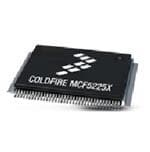
Freescale Document Number: MCF52259 Data Sheet: Technical Data Rev. 5, 5/2012 MCF52259 MCF52259 ColdFire Microcontroller 144 LQFP 20mmx20mm Supports MCF52252, MCF52254, 144 MAPBGA 100 LQFP MCF52255, MCF52256, MCF52258, 13mmx13mm 14mmx14mm MCF52259 The MCF52259 microcontroller family (MCF52252, (PWM), pulse-code modulation (PCM), and pulse MCF52254, MCF52255, MCF52256, MCF52258, and accumulation MCF52259 devices) is a member of the ColdFire family of • Eight-channel/Four-channel, 8-bit/16-bit pulse width reduced instruction set computing (RISC) microprocessors. modulation timer • Two 16-bit periodic interrupt timers (PITs) This document provides an overview of the 32-bit MCF52259 • Real-time clock (RTC) module with 32kHz crystal microcontroller, focusing on its highly integrated and diverse • Programmable software watchdog timer feature set. • Secondary watchdog timer with independent clock This 32-bit device is based on the Version 2 ColdFire core • Interrupt controller capable of handling 57 sources operating at a frequency up to 80MHz, offering high • Clock module with 8MHz on-chip relaxation oscillator performance and low power consumption. On-chip memories and integrated phase-locked loop (PLL) connected tightly to the processor core include up to 512KB • Test access/debug port (JTAG, BDM) of flash memory and 64KB of static random access memory (SRAM). On-chip modules include: • V2 ColdFire core delivering 76 MIPS (Dhrystone 2.1) at 80MHz running from internal flash memory with Enhanced Multiply Accumulate (MAC) Unit and hardware divider • Cryptography Acceleration Unit (CAU). • Fast Ethernet controller (FEC) • Mini-FlexBus external bus interface available on 144 pin packages • Universal Serial Bus On-The-Go (USBOTG) • USB Transceiver • FlexCAN controller area network (CAN) module • Three universal asynchronous/synchronous receiver/transmitters (UARTs) • Two inter-integrated circuit (I2C) bus interface modules • Queued serial peripheral interface (QSPI) module • Eight-channel 12-bit fast analog-to-digital converter (ADC) with simultaneous sampling • Four-channel direct memory access (DMA) controller • Four 32-bit input capture/output compare timers with DMA support (DTIM) • Four-channel general-purpose timer (GPT) capable of input capture/output compare, pulse width modulation Freescale reserves the right to change the detail specifications as may be required to permit improvements in the design of its products. ©Freescale, Inc., 2011, 2012. All rights reserved.
Table of Contents 1 Family Configurations. . . . . . . . . . . . . . . . . . . . . . . . . . . . . . . .3 2.10 Mini-FlexBus External Interface Specifications . . . . . . 32 1.1 Block Diagram. . . . . . . . . . . . . . . . . . . . . . . . . . . . . . . . .4 2.11 Fast Ethernet Timing Specifications . . . . . . . . . . . . . . 33 1.2 Features . . . . . . . . . . . . . . . . . . . . . . . . . . . . . . . . . . . . .4 2.12 General Purpose I/O Timing . . . . . . . . . . . . . . . . . . . . 35 2 Electrical Characteristics . . . . . . . . . . . . . . . . . . . . . . . . . . . .24 2.13 Reset Timing. . . . . . . . . . . . . . . . . . . . . . . . . . . . . . . . 36 2.1 Maximum Ratings. . . . . . . . . . . . . . . . . . . . . . . . . . . . .24 2.14 I2C Input/Output Timing Specifications. . . . . . . . . . . . 37 2.2 Current Consumption . . . . . . . . . . . . . . . . . . . . . . . . . .25 2.15 Analog-to-Digital Converter (ADC) Parameters. . . . . . 38 2.3 Thermal Characteristics . . . . . . . . . . . . . . . . . . . . . . . .26 2.16 Equivalent Circuit for ADC Inputs . . . . . . . . . . . . . . . . 39 2.4 Flash Memory Characteristics . . . . . . . . . . . . . . . . . . .28 2.17 DMA Timers Timing Specifications . . . . . . . . . . . . . . . 40 2.5 EzPort Electrical Specifications . . . . . . . . . . . . . . . . . .29 2.18 QSPI Electrical Specifications. . . . . . . . . . . . . . . . . . . 40 2.6 ESD Protection. . . . . . . . . . . . . . . . . . . . . . . . . . . . . . .29 2.19 JTAG and Boundary Scan Timing. . . . . . . . . . . . . . . . 40 2.7 DC Electrical Specifications . . . . . . . . . . . . . . . . . . . . .30 2.20 Debug AC Timing Specifications. . . . . . . . . . . . . . . . . 43 2.8 Clock Source Electrical Specifications . . . . . . . . . . . . .31 3 Package Information . . . . . . . . . . . . . . . . . . . . . . . . . . . . . . . 44 2.9 USB Operation . . . . . . . . . . . . . . . . . . . . . . . . . . . . . . .32 4 Revision History . . . . . . . . . . . . . . . . . . . . . . . . . . . . . . . . . . 45 MCF52259 ColdFire Microcontroller, Rev. 5 2 Freescale
Family Configurations 1 Family Configurations Table1. MCF52259 Family Configurations Module 52252 52254 52255 52256 52258 52259 Version 2 ColdFire Core with eMAC (Enhanced multiply-accumulate unit) and CAU (Cryptographic acceleration unit) System Clock up to up to up to 66 or 80 MHz1 up to 66 or 80 MHz1 80 MHz1 80 MHz1 Performance (Dhrystone 2.1 MIPS) up to 63 or 76 Flash 256KB 512KB 512KB 256KB 512KB 512KB Static RAM (SRAM) 32KB 64KB 64KB 32 / 64KB 64KB 64KB Two Interrupt Controllers (INTC) Fast Analog-to-Digital Converter (ADC) USB On-The-Go (USB OTG) Mini-FlexBus external bus interface — — — Fast Ethernet Controller (FEC) Random Number Generator and — — — — Cryptographic Acceleration Unit (CAU) FlexCAN 2.0B Module Varies Varies Varies Varies Four-channel Direct-Memory Access (DMA) Software Watchdog Timer (WDT) Secondary Watchdog Timer Two-channel Periodic Interrupt Timer (PIT) 2 2 2 2 2 2 Four-Channel General Purpose Timer (GPT) 32-bit DMA Timers 4 4 4 4 4 4 QSPI UART(s) 3 3 3 3 3 3 I2C 2 2 2 2 2 2 Eight/Four-channel 8/16-bit PWM Timer General Purpose I/O Module (GPIO) Chip Configuration and Reset Controller Module Background Debug Mode (BDM) JTAG - IEEE 1149.1 Test Access Port Package 100 LQFP 144 LQFP or 144 MAPBGA 1 66 MHz = 63 MIPS; 80 MHz = 76 MIPS MCF52259 ColdFire Microcontroller, Rev. 5 3 Freescale
Family Configurations 1.1 Block Diagram Figure1 shows a top-level block diagram of the device. Package options for this family are described later in this document. EzPD EzPCK EzPort EzPQ EzPCS USB Mini-FlexBus Mini-FlexBus Interrupt To/From PADI Arbiter AN[7:0] Controllers USB I2Cs ng QSPI xi u UARTs M To/From n GPTn PADI FEC UARTs PITs I2C QSPI – Pi IRQn 0–2 0–1 0–1 DI FEC A 4 ch DMA P DTINn/DTOUTn CANRX DTIMs Edge To/From PADI 0–3 FlexCAN Port RTC CANTX PWMn EzPort JTAG_EN MUX JTAG/BDM V2 ColdFire CPU IFP OEP CAU EMAC PMM JTAG TAP ToP/AFrDoIm ADC u(p4 SKtoR 16A64M)K4B u(p6 4toFK la511s6h2)K4B P(GOPRITOS) RCeCsMe,t RRSSTTOINUT V V RH RL PLL Watchdog RNGA GPT PWM CLKGEN Timer EXTAL XTAL CLKOUT Figure1. MCF52259 Block Diagram 1.2 Features 1.2.1 Feature Overview The MCF52259 family includes the following features: • Version 2 ColdFire variable-length RISC processor core — Static operation — 32-bit address and data paths on-chip MCF52259 ColdFire Microcontroller, Rev. 5 Freescale 4
Family Configurations — Up to 80MHz processor core frequency — 40MHz or 33MHz peripheral bus frequency — Sixteen general-purpose, 32-bit data and address registers — Implements ColdFire ISA_A with extensions to support the user stack pointer register and four new instructions for improved bit processing (ISA_A+) — Enhanced Multiply-Accumulate (EMAC) unit with four 32-bit accumulators to support 161632 or 323248 operations — Cryptographic Acceleration Unit (CAU) – Tightly-coupled coprocessor to accelerate software-based encryption and message digest functions – Support for DES, 3DES, AES, MD5, and SHA-1 algorithms • System debug support — Real-time trace for determining dynamic execution path — Background debug mode (BDM) for in-circuit debugging (DEBUG_B+) — Real-time debug support, with six hardware breakpoints (4 PC, 1 address and 1 data) configurable into a 1- or 2-level trigger • On-chip memories — Up to 64KB dual-ported SRAM on CPU internal bus, supporting core, DMA, and USB access with standby power supply support for the first 16KB — Up to 512KB of interleaved flash memory supporting 2-1-1-1 accesses • Power management — Fully static operation with processor sleep and whole chip stop modes — Rapid response to interrupts from the low-power sleep mode (wake-up feature) — Clock enable/disable for each peripheral when not used (except backup watchdog timer) — Software controlled disable of external clock output for low-power consumption • FlexCAN 2.0B module — Based on and includes all existing features of the Freescale TouCAN module — Full implementation of the CAN protocol specification version 2.0B – Standard data and remote frames (up to 109 bits long) – Extended data and remote frames (up to 127 bits long) – Zero to eight bytes data length – Programmable bit rate up to 1 Mbit/s — Flexible message buffers (MBs), totalling up to 16 message buffers of 0–8 byte data length each, configurable as Rx or Tx, all supporting standard and extended messages — Unused MB space can be used as general purpose RAM space — Listen-only mode capability — Content-related addressing — No read/write semaphores — Three programmable mask registers: global for MBs 0–13, special for MB14, and special for MB15 — Programmable transmit-first scheme: lowest ID or lowest buffer number — Time stamp based on 16-bit free-running timer — Global network time, synchronized by a specific message — Maskable interrupts • Universal Serial Bus On-The-Go (USB OTG) dual-mode host and device controller — Full-speed / low-speed host controller — USB 1.1 and 2.0 compliant full-speed / low speed device controller — 16 bidirectional end points MCF52259 ColdFire Microcontroller, Rev. 5 5 Freescale
Family Configurations — DMA or FIFO data stream interfaces — Low power consumption — OTG protocol logic • Fast Ethernet controller (FEC) — 10/100 BaseT/TX capability, half duplex or full duplex — On-chip transmit and receive FIFOs — Built-in dedicated DMA controller — Memory-based flexible descriptor rings • Mini-FlexBus — External bus interface available on 144 pin packages — Supports glueless interface with 8-bit ROM/flash/SRAM/simple slave peripherals. Can address up to 2MB of addresses — 2 chip selects (FB_CS[1:0]) — Non-multiplexed mode: 8-bit dedicated data bus, 20-bit address bus — Multiplexed mode: 16-bit data and 20-bit address bus — FB_CLK output to support synchronous memories — Programmable base address, size, and wait states to support slow peripherals — Operates at up to 40MHz (bus clock) in 1:2 mode or up to 80MHz (core clock) in 1:1 mode • Three universal asynchronous/synchronous receiver transmitters (UARTs) — 16-bit divider for clock generation — Interrupt control logic with maskable interrupts — DMA support — Data formats can be 5, 6, 7, or 8 bits with even, odd, or no parity — Up to two stop bits in 1/16 increments — Error-detection capabilities — Modem support includes request-to-send (RTS) and clear-to-send (CTS) lines for two UARTs — Transmit and receive FIFO buffers • Two I2C modules — Interchip bus interface for EEPROMs, LCD controllers, A/D converters, and keypads — Fully compatible with industry-standard I2C bus — Master and slave modes support multiple masters — Automatic interrupt generation with programmable level • Queued serial peripheral interface (QSPI) — Full-duplex, three-wire synchronous transfers — Up to three chip selects available — Master mode operation only — Programmable bit rates up to half the CPU clock frequency — Up to 16 pre-programmed transfers • Fast analog-to-digital converter (ADC) — Eight analog input channels — 12-bit resolution — Minimum 1.125s conversion time — Simultaneous sampling of two channels for motor control applications — Single-scan or continuous operation — Optional interrupts on conversion complete, zero crossing (sign change), or under/over low/high limit MCF52259 ColdFire Microcontroller, Rev. 5 Freescale 6
Family Configurations — Unused analog channels can be used as digital I/O • Four 32-bit timers with DMA support — 12.5ns resolution at 80MHz — Programmable sources for clock input, including an external clock option — Programmable prescaler — Input capture capability with programmable trigger edge on input pin — Output compare with programmable mode for the output pin — Free run and restart modes — Maskable interrupts on input capture or output compare — DMA trigger capability on input capture or output compare • Four-channel general purpose timer — 16-bit architecture — Programmable prescaler — Output pulse-widths variable from microseconds to seconds — Single 16-bit input pulse accumulator — Toggle-on-overflow feature for pulse-width modulator (PWM) generation — One dual-mode pulse accumulation channel • Pulse-width modulation timer — Support for PCM mode (resulting in superior signal quality compared to conventional PWM) — Operates as eight channels with 8-bit resolution or four channels with 16-bit resolution — Programmable period and duty cycle — Programmable enable/disable for each channel — Software selectable polarity for each channel — Period and duty cycle are double buffered. Change takes effect when the end of the current period is reached (PWM counter reaches zero) or when the channel is disabled. — Programmable center or left aligned outputs on individual channels — Four clock sources (A, B, SA, and SB) provide for a wide range of frequencies — Emergency shutdown • Two periodic interrupt timers (PITs) — 16-bit counter — Selectable as free running or count down • Real-Time Clock (RTC) — Maintains system time-of-day clock — Provides stopwatch and alarm interrupt functions — Standby power supply (Vstby) keeps the RTC running when the system is shut down • Software watchdog timer — 32-bit counter — Low-power mode support • Backup watchdog timer (BWT) — Independent timer that can be used to help software recover from runaway code — 16-bit counter — Low-power mode support • Clock generation features — Crystal, on-chip trimmed relaxation oscillator, or external oscillator reference options — Trimmed relaxation oscillator MCF52259 ColdFire Microcontroller, Rev. 5 7 Freescale
Family Configurations — Pre-divider capable of dividing the clock source frequency into the PLL reference frequency range — System can be clocked from PLL or directly from crystal oscillator or relaxation oscillator — Low power modes supported — 2n (0n15) low-power divider for extremely low frequency operation • Interrupt controller — Uniquely programmable vectors for all interrupt sources — Fully programmable level and priority for all peripheral interrupt sources — Seven external interrupt signals with fixed level and priority — Unique vector number for each interrupt source — Ability to mask any individual interrupt source or all interrupt sources (global mask-all) — Support for hardware and software interrupt acknowledge (IACK) cycles — Combinatorial path to provide wake-up from low-power modes • DMA controller — Four fully programmable channels — Dual-address transfer support with 8-, 16-, and 32-bit data capability, along with support for 16-byte (432-bit) burst transfers — Source/destination address pointers that can increment or remain constant — 24-bit byte transfer counter per channel — Auto-alignment transfers supported for efficient block movement — Bursting and cycle-steal support — Software-programmable DMA requests for the UARTs (3) and 32-bit timers (4) — Channel linking support • Reset — Separate reset in and reset out signals — Seven sources of reset: – Power-on reset (POR) – External – Software – Watchdog – Loss of clock / loss of lock – Low-voltage detection (LVD) – JTAG — Status flag indication of source of last reset • Chip configuration module (CCM) — System configuration during reset — Selects one of six clock modes — Configures output pad drive strength — Unique part identification number and part revision number • General purpose I/O interface — Up to 56 bits of general purpose I/O on 100-pin package — Up to 96 bits of general purpose I/O on 144-pin package — Bit manipulation supported via set/clear functions — Programmable drive strengths — Unused peripheral pins may be used as extra GPIO • JTAG support for system level board testing MCF52259 ColdFire Microcontroller, Rev. 5 Freescale 8
Family Configurations 1.2.2 V2 Core Overview The version 2 ColdFire processor core is comprised of two separate pipelines decoupled by an instruction buffer. The two-stage instruction fetch pipeline (IFP) is responsible for instruction-address generation and instruction fetch. The instruction buffer is a first-in-first-out (FIFO) buffer that holds prefetched instructions awaiting execution in the operand execution pipeline (OEP). The OEP includes two pipeline stages. The first stage decodes instructions and selects operands (DSOC); the second stage (AGEX) performs instruction execution and calculates operand effective addresses, if needed. The V2 core implements the ColdFire instruction set architecture revision A+ with support for a separate user stack pointer register and four new instructions to assist in bit processing. Additionally, the core includes the enhanced multiply-accumulate (EMAC) unit for improved signal processing capabilities. The EMAC implements a three-stage arithmetic pipeline, optimized for 32x32 bit operations, with support for four 48-bit accumulators. Supported operands include 16- and 32-bit signed and unsigned integers, signed fractional operands, and a complete set of instructions to process these data types. The EMAC provides support for execution of DSP operations within the context of a single processor at a minimal hardware cost. 1.2.3 Integrated Debug Module The ColdFire processor core debug interface is provided to support system debugging with low-cost debug and emulator development tools. Through a standard debug interface, access to debug information and real-time tracing capability is provided on 144-lead packages. This allows the processor and system to be debugged at full speed without the need for costly in-circuit emulators. The on-chip breakpoint resources include a total of nine programmable 32-bit registers: an address and an address mask register, a data and a data mask register, four PC registers, and one PC mask register. These registers can be accessed through the dedicated debug serial communication channel or from the processor’s supervisor mode programming model. The breakpoint registers can be configured to generate triggers by combining the address, data, and PC conditions in a variety of single- or dual-level definitions. The trigger event can be programmed to generate a processor halt or initiate a debug interrupt exception. This device implements revision B+ of the ColdFire Debug Architecture. The processor’s interrupt servicing options during emulator mode allow real-time critical interrupt service routines to be serviced while processing a debug interrupt event. This ensures the system continues to operate even during debugging. To support program trace, the V2 debug module provides processor status (PST[3:0]) and debug data (DDATA[3:0]) ports. These buses and the PSTCLK output provide execution status, captured operand data, and branch target addresses defining processor activity at the CPU’s clock rate. The device includes a new debug signal, ALLPST. This signal is the logical AND of the processor status (PST[3:0]) signals and is useful for detecting when the processor is in a halted state (PST[3:0] = 1111). The full debug/trace interface is available only on the 144-pin packages. However, every product features the dedicated debug serial communication channel (DSI, DSO, DSCLK) and the ALLPST signal. 1.2.4 JTAG The processor supports circuit board test strategies based on the Test Technology Committee of IEEE and the Joint Test Action Group (JTAG). The test logic includes a test access port (TAP) consisting of a 16-state controller, an instruction register, and three test registers (a 1-bit bypass register, a boundary-scan register, and a 32-bit ID register). The boundary scan register links the device’s pins into one shift register. Test logic, implemented using static logic design, is independent of the device system logic. The device implementation can: • Perform boundary-scan operations to test circuit board electrical continuity • Sample system pins during operation and transparently shift out the result in the boundary scan register • Bypass the device for a given circuit board test by effectively reducing the boundary-scan register to a single bit • Disable the output drive to pins during circuit-board testing • Drive output pins to stable levels MCF52259 ColdFire Microcontroller, Rev. 5 9 Freescale
Family Configurations 1.2.5 On-Chip Memories 1.2.5.1 SRAM The dual-ported SRAM module provides a general-purpose 64KB memory block that the ColdFire core can access in a single cycle. The location of the memory block can be set to any 64KB boundary within the 4GB address space. This memory is ideal for storing critical code or data structures and for use as the system stack. Because the SRAM module is physically connected to the processor's high-speed local bus, it can quickly service core-initiated accesses or memory-referencing commands from the debug module. The SRAM module is also accessible by the DMA, FEC, and USB. The dual-ported nature of the SRAM makes it ideal for implementing applications with double-buffer schemes, where the processor and a DMA device operate in alternate regions of the SRAM to maximize system performance. 1.2.5.2 Flash Memory The ColdFire flash module (CFM) is a non-volatile memory (NVM) module that connects to the processor’s high-speed local bus. The CFM is constructed with four banks of 64KB16-bit flash memory arrays to generate 512KB of 32-bit flash memory. These electrically erasable and programmable arrays serve as non-volatile program and data memory. The flash memory is ideal for program and data storage for single-chip applications, allowing for field reprogramming without requiring an external high voltage source. The CFM interfaces to the ColdFire core through an optimized read-only memory controller that supports interleaved accesses from the 2-cycle flash memory arrays. A backdoor mapping of the flash memory is used for all program, erase, and verify operations, as well as providing a read datapath for the DMA. Flash memory may also be programmed via the EzPort, which is a serial flash memory programming interface that allows the flash memory to be read, erased and programmed by an external controller in a format compatible with most SPI bus flash memory chips. 1.2.6 Cryptographic Acceleration Unit The MCF52235 device incorporates two hardware accelerators for cryptographic functions. First, the CAU is a coprocessor tightly-coupled to the V2 ColdFire core that implements a set of specialized operations to increase the throughput of software-based encryption and message digest functions, specifically the DES, 3DES, AES, MD5 and SHA-1 algorithms. Second, a random number generator provides FIPS-140 compliant 32-bit values to security processing routines. Both modules supply critical acceleration to software-based cryptographic algorithms at a minimal hardware cost. 1.2.7 Power Management The device incorporates several low-power modes of operation entered under program control and exited by several external trigger events. An integrated power-on reset (POR) circuit monitors the input supply and forces an MCU reset as the supply voltage rises. The low voltage detector (LVD) monitors the supply voltage and is configurable to force a reset or interrupt condition if it falls below the LVD trip point. The RAM standby switch provides power to RAM when the supply voltage to the chip falls below the standby battery voltage. 1.2.8 FlexCAN The FlexCAN module is a communication controller implementing version 2.0 of the CAN protocol parts A and B. The CAN protocol can be used as an industrial control serial data bus, meeting the specific requirements of reliable operation in a harsh EMI environment with high bandwidth. This instantiation of FlexCAN has 16 message buffers. MCF52259 ColdFire Microcontroller, Rev. 5 Freescale 10
Family Configurations 1.2.9 Mini-FlexBus A multi-function external bus interface called the Mini-FlexBus is provided on the device with basic functionality of interfacing to slave-only devices with a maximum slave bus frequency up to 40MHz in 1:2 mode and 80MHz in 1:1 mode. It can be directly connected to the following asynchronous or synchronous devices with little or no additional circuitry: • External ROMs • Flash memories • Programmable logic devices • Other simple target (slave) devices The Mini-FlexBus is a subset of the FlexBus module found on higher-end ColdFire microprocessors. The Mini-FlexBus minimizes package pin-outs while maintaining a high level of configurability and functionality. 1.2.10 USB On-The-Go Controller The device includes a Universal Serial Bus On-The-Go (USB OTG) dual-mode controller. USB is a popular standard for connecting peripherals and portable consumer electronic devices such as digital cameras and handheld computers to host PCs. The OTG supplement to the USB specification extends USB to peer-to-peer application, enabling devices to connect directly to each other without the need for a PC. The dual-mode controller on the device can act as a USB OTG host and as a USB device. It also supports full-speed and low-speed modes. 1.2.11 Fast Ethernet Controller (FEC) The Ethernet media access controller (MAC) supports 10 and 100 Mbps Ethernet/IEEE 802.3 networks. An external transceiver interface and transceiver function are required to complete the interface to the media. The FEC supports three different standard MAC-PHY (physical) interfaces for connection to an external Ethernet transceiver. The FECs supports the 10/100Mbps MII, and the 10Mbps-only 7-wire interface. 1.2.12 UARTs The device has three full-duplex UARTs that function independently. The three UARTs can be clocked by the system bus clock, eliminating the need for an external clock source. On smaller packages, the third UART is multiplexed with other digital I/O functions. 1.2.13 I2C Bus The processor includes two I2C modules. The I2C bus is an industry-standard, two-wire, bidirectional serial bus that provides a simple, efficient method of data exchange and minimizes the interconnection between devices. This bus is suitable for applications requiring occasional communications over a short distance between many devices. 1.2.14 QSPI The queued serial peripheral interface (QSPI) provides a synchronous serial peripheral interface with queued transfer capability. It allows up to 16 transfers to be queued at once, minimizing the need for CPU intervention between transfers. 1.2.15 Fast ADC The fast ADC consists of an eight-channel input select multiplexer and two independent sample and hold (S/H) circuits feeding separate 12-bit ADCs. The two separate converters store their results in accessible buffers for further processing. Signals on the SYNCA and SYNCB pins initiate an ADC conversion. MCF52259 ColdFire Microcontroller, Rev. 5 11 Freescale
Family Configurations The ADC can be configured to perform a single scan and halt, a scan when triggered, or a programmed scan sequence repeatedly until manually stopped. The ADC can be configured for sequential or simultaneous conversion. When configured for sequential conversions, up to eight channels can be sampled and stored in any order specified by the channel list register. Both ADCs may be required during a scan, depending on the inputs to be sampled. During a simultaneous conversion, both S/H circuits are used to capture two different channels at the same time. This configuration requires that a single channel may not be sampled by both S/H circuits simultaneously. Optional interrupts can be generated at the end of the scan sequence if a channel is out of range (measures below the low threshold limit or above the high threshold limit set in the limit registers) or at several different zero crossing conditions. 1.2.16 DMA Timers (DTIM0–DTIM3) There are four independent, DMA transfer capable 32-bit timers (DTIM0, DTIM1, DTIM2, and DTIM3) on the device. Each module incorporates a 32-bit timer with a separate register set for configuration and control. The timers can be configured to operate from the system clock or from an external clock source using one of the DTINn signals. If the system clock is selected, it can be divided by 16 or 1. The input clock is further divided by a user-programmable 8-bit prescaler that clocks the actual timer counter register (TCRn). Each of these timers can be configured for input capture or reference (output) compare mode. Timer events may optionally cause interrupt requests or DMA transfers. 1.2.17 General Purpose Timer (GPT) The general purpose timer (GPT) is a four-channel timer module consisting of a 16-bit programmable counter driven by a seven-stage programmable prescaler. Each of the four channels can be configured for input capture or output compare. Additionally, channel three, can be configured as a pulse accumulator. A timer overflow function allows software to extend the timing capability of the system beyond the 16-bit range of the counter. The input capture and output compare functions allow simultaneous input waveform measurements and output waveform generation. The input capture function can capture the time of a selected transition edge. The output compare function can generate output waveforms and timer software delays. The 16-bit pulse accumulator can operate as a simple event counter or a gated time accumulator. 1.2.18 Periodic Interrupt Timers (PIT0 and PIT1) The two periodic interrupt timers (PIT0 and PIT1) are 16-bit timers that provide interrupts at regular intervals with minimal processor intervention. Each timer can count down from the value written in its PIT modulus register or it can be a free-running down-counter. 1.2.19 Real-Time Clock (RTC) The Real-Time Clock (RTC) module maintains the system (time-of-day) clock and provides stopwatch, alarm, and interrupt functions. It includes full clock features: seconds, minutes, hours, days and supports a host of time-of-day interrupt functions along with an alarm interrupt. 1.2.20 Pulse-Width Modulation (PWM) Timers The device has an 8-channel, 8-bit PWM timer. Each channel has a programmable period and duty cycle as well as a dedicated counter. Each of the modulators can create independent continuous waveforms with software-selectable duty rates from 0% to 100%. The timer supports PCM mode, which results in superior signal quality when compared to that of a conventional PWM. The PWM outputs have programmable polarity, and can be programmed as left aligned outputs or center aligned outputs. For MCF52259 ColdFire Microcontroller, Rev. 5 Freescale 12
Family Configurations higher period and duty cycle resolution, each pair of adjacent channels ([7:6], [5:4], [3:2], and [1:0]) can be concatenated to form a single 16-bit channel. The module can, therefore, be configured to support 8/0, 6/1, 4/2, 2/3, or 0/4 8-/16-bit channels. 1.2.21 Software Watchdog Timer The watchdog timer is a 32-bit timer that facilitates recovery from runaway code. The watchdog counter is a free-running down-counter that generates a reset on underflow. To prevent a reset, software must periodically restart the countdown. 1.2.22 Backup Watchdog Timer The backup watchdog timer is an independent 16-bit timer that, like the software watchdog timer, facilitates recovery from runaway code. This timer is a free-running down-counter that generates a reset on underflow. To prevent a reset, software must periodically restart the countdown. The backup watchdog timer can be clocked by either the relaxation oscillator or the system clock. 1.2.23 Phase-Locked Loop (PLL) The clock module contains a crystal oscillator, 8MHz on-chip relaxation oscillator (OCO), phase-locked loop (PLL), reduced frequency divider (RFD), low-power divider status/control registers, and control logic. To improve noise immunity, the PLL, crystal oscillator, and relaxation oscillator have their own power supply inputs: VDDPLL and VSSPLL. All other circuits are powered by the normal supply pins, VDD and VSS. 1.2.24 Interrupt Controllers (INTCn) The device has two interrupt controllers that supports up to 128 interrupt sources. There are 56 programmable sources, 49 of which are assigned to unique peripheral interrupt requests. The remaining seven sources are unassigned and may be used for software interrupt requests. 1.2.25 DMA Controller The direct memory access (DMA) controller provides an efficient way to move blocks of data with minimal processor intervention. It has four channels that allow byte, word, longword, or 16-byte burst line transfers. These transfers are triggered by software explicitly setting a DCRn[START] bit or by the occurrence of certain UART or DMA timer events. 1.2.26 Reset The reset controller determines the source of reset, asserts the appropriate reset signals to the system, and keeps track of what caused the last reset. There are seven sources of reset: • External reset input • Power-on reset (POR) • Watchdog timer • Phase locked-loop (PLL) loss of lock / loss of clock • Software • Low-voltage detector (LVD) • JTAG Control of the LVD and its associated reset and interrupt are managed by the reset controller. Other registers provide status flags indicating the last source of reset and a control bit for software assertion of the RSTO pin. MCF52259 ColdFire Microcontroller, Rev. 5 13 Freescale
Family Configurations 1.2.27 GPIO Nearly all pins on the device have general purpose I/O capability and are grouped into 8-bit ports. Some ports do not use all eight bits. Each port has registers that configure, monitor, and control the port pin. 1.2.28 Part Numbers and Packaging This product is RoHS-compliant. Refer to the product page at freescale.com or contact your sales office for up-to-date RoHS information. Table2. Orderable part number summary Freescale Part Speed Flash SRAM Temp range FlexCAN Encryption Package Number (MHz) (KB) (KB) (C) MCF52252AF80 — — 80 0 to +70 256 32 100 LQFP MCF52252CAF66 — 66 -40 to +85 MCF52254AF80 — — 80 0 to +70 512 64 100 LQFP MCF52254CAF66 — 66 -40 to +85 MCF52255CAF80 80 512 64 100 LQFP -40 to +85 MCF52256AG80 — — 80 32 0 to +70 144 LQFP MCF52256CAG66 — 66 64 -40 to +85 256 MCF52256CVN66 — 66 64 -40 to +85 144 MAPBGA MCF52256VN80 — — 80 32 0 to +70 MCF52258AG80 — — 80 0 to +70 144 LQFP MCF52258CAG66 — 66 -40 to +85 512 64 MCF52258CVN66 — 66 -40 to +85 144 MAPBGA MCF52258VN80 — — 80 0 to +70 MCF52259CAG80 144 LQFP -40 to +85 80 512 64 MCF52259CVN80 144 MAPBGA -40 to +85 MCF52259 ColdFire Microcontroller, Rev. 5 Freescale 14
Family Configurations Figure2 shows the pinout configuration for the 144 LQFP. CLKMOD1 CLKMOD0 RSTOUT RSTIN FB_D5 FB_D6 FB_D7 FB_OE FB_A15 VDD VSS FB_A16 FB_A17 FB_A18 FB_A19 IRQ3 IRQ5 FEC_RXD3 FEC_RXD2 VDD VSS FEC_RXD1 FEC_RXD0 FEC_RXDV FEC_RXCLK FEC_RXER FEC_TXER FEC_TXCLK FEC_TXEN VDD VSS FEC_TXD0 FEC_TXD1 FEC_TXD2 FEC_TXD3 FEC_COL (cid:129) 4 3 2 1 0 9 8 7 6 5 4 3 2 1 0 9 8 7 6 5 4 3 2 1 0 9 8 7 6 5 4 3 2 1 0 9 4 4 4 4 4 3 3 3 3 3 3 3 3 3 3 2 2 2 2 2 2 2 2 2 2 1 1 1 1 1 1 1 1 1 1 0 1 1 1 1 1 1 1 1 1 1 1 1 1 1 1 1 1 1 1 1 1 1 1 1 1 1 1 1 1 1 1 1 1 1 1 1 FB_D4 1 108 FEC_CRS FB_A14 2 107 VDDPLL FB_A13 3 106 EXTAL FB_A12 4 105 XTAL FB_A11 5 104 VSSPLL FB_A10 6 103 IRQ1 VDD 7 102 URXD2 VSS 8 101 UTXD2 TEST 9 100 VDD RCON 10 99 VSS TIN0 11 98 URTS2 TIN1 12 97 UCTS2 RTC_EXTAL 13 96 IRQ7 RTC_XTAL 14 95 ICOC2 UCTS0 15 94 ICOC1 UTXD0 16 93 ICOC0 URXD0 17 92 VDD URTS0 18 91 VSS TIN3 19 90 PST0 VDD 20 89 PST1 VSS 21 88 PST2 PCS3 22 87 PST3 PCS2 23 86 DDATA3 QSDI 24 85 DDATA2 QSD0 25 84 DDATA1 SCK 26 83 DDATA0 PCS0 27 82 VSSUSB SCL 28 81 USB_DP SDA 29 80 USB_DM VDD 30 79 VDDUSB VSS 31 78 VSTBY FB_A9 32 77 AN4 FB_A8 33 76 AN5 FB_A7 34 75 AN6 FB_A6 35 74 AN7 FB_A5 36 73 VDDA 7 8 9 0 1 2 3 4 5 6 7 8 9 0 1 2 3 4 5 6 7 8 9 0 1 2 3 4 5 6 7 8 9 0 1 2 3 3 3 4 4 4 4 4 4 4 4 4 4 5 5 5 5 5 5 5 5 5 5 6 6 6 6 6 6 6 6 6 6 7 7 7 FB_ALE TMS TRST TDI TDO ALLPST TCLK TAG_EN FB_RW FB_D3 FB_D2 VDD VSS FB_D1 FB_D0 FB_CS0 FB_A4 FB_A3 FB_A2 FB_A1 FB_A0 ICOC3 VDD VSS UCTS1 UTXD1 URXD1 URTS1 TIN2 AN0 AN1 AN2 AN3 VSSA VRL VRH J Figure2. 144 LQFP Pin Assignment MCF52259 ColdFire Microcontroller, Rev. 5 15 Freescale
F Figure3 shows the pinout configuration for the 100 LQFP. re e s K K cale CLKMOD1CLKMOD0RSTOUTRSTINIRQ3IRQ5FEC_RXD3FEC_RXD2VDDVSSFEC_RXD1FEC_RXD0FEC_RXDVFEC_RXCLFEC_RXERFEC_TXER FEC_TXCLFEC_TXENVDDVSSFEC_TXD0FEC_TXD1FEC_TXD2FEC_TXD3FEC_COL 0987654321098765432109876 0999999999988888888887777 VDD 1 1 75 FEC_CRS V 2 74 V SS DDPLL TEST 3 73 EXTAL RCON 4 72 XTAL TIN0 5 71 VSSPLL TIN1 6 70 IRQ1 M C RTC_EXTAL 7 69 URXD2 F 5 RTC_XTAL 8 68 UTXD2 22 UCTS0 9 67 VDD 5 9 C UURTXXDD00 1101 6665 VUSRSTS2 o ld URTS0 12 64 UCTS2 F ire TIN3 13 100 LQFP 63 IRQ7 M VDD 14 62 ICOC2 ic VSS 15 61 ICOC1 r o PCS3 16 60 ICOC0 c on PCS2 17 59 VSSUSB tr QSDI 18 58 USB_DP o lle QSDO 19 57 USB_DM r, Re PSCCSK0 2201 5565 VVDSTDBUYSB v. 5 SCL 22 54 AN4 SDA 23 53 AN5 VDD 24 52 AN6 V 25 51 AN7 SS 6789012345678901234567890 2222333333333344444444445 TMS TRSTTDITDOLPSTTCLKG_ENVDDVSSCOC3 VDDVSSCTS1TXD1RXD1RTS1 TIN2AN0AN1AN2AN3VSSAVRLVRHVDDA Fam AL JTA I UUUU ily C Figure3. 100 LQFP Pin Assignments o n fig u r a tio 1 n 6 s
1 Figure4 shows the pinout configuration for the 144 MAPBGA. F 7 a m 1 2 3 4 5 6 7 8 9 10 11 12 ily C o A VSS RSTOUT RSTIN FB_D6 FB_D7 IRQ3 IRQ5 FEC_ FEC_ FEC_ FEC_ VSS A n RXD0 RXER TXEN TXD3 fig u r FEC_ FEC_ FEC_ FEC_ a B TEST FB_A14 FB_D4 FB_D5 FB_OE FB_A19 FEC_COL FEC_CRS B t RXD1 RXCLK TXCLK TXD2 io n s FEC_ FEC_ FEC_ C TIN1 FB_A12 FB_A13 FB_A15 FB_A16 FB_A18 URXD2 VDDPLL EXTAL C RXD2 RXDV TXD1 RTC_ FEC_ FEC_ FEC_ D TIN0 FB_A11 CLKMOD1 CLKMOD0 FB_A17 UTXD2 VSSPLL XTAL D EXTAL RXD3 TXER TXD0 RTC_ M E XTAL UCTS0 FB_A10 RCON VDD VDD VDD VDD IRQ1 URTS2 UCTS2 IRQ7 E C F 5 22 F UTXD0 URXD0 URTS0 TIN3 VDD VSS VSS VSS PST3 DDATA0 DDATA1 ICOC0 F 5 9 C old G QSDO QSDI PCS2 PCS3 VDD VSS VSS VSS DDATA3 PST2 PST1 PST0 G F ir e M H SCL SDA SCK PCS0 VDD VDD VDD VSS VSSUSB DDATA2 USB_DM USB_DP H ic r o c o J FB_A6 FB_A7 FB_A9 FB_A8 FB_D0 FB_A3 VDD TIN2 VDDUSB ICOC2 ICOC1 VSTBY J n tr o lle K TMS TRST FB_ALE FB_A5 FB_D2 FB_A4 UCTS1 UTXD1 AN3 AN6 AN4 AN5 K r , R e v . 5 L TDI TDO ALLPST FB_D3 FB_D1 FB_A1 FB_A0 URXD1 AN2 VRH VDDA AN7 L JTAG_ M VSS TCLK FB_RW FB_CS0 FB_A2 ICOC3 URTS1 AN0 AN1 VRL VSSA M EN 1 2 3 4 5 6 7 8 9 10 11 12 Figure4. Pinout Top View (144 MAPBGA) F re e s c a le
F Table3 shows the pin functions by primary and alternate purpose, and illustrates which packages contain each pin. re e s Table3. Pin Functions by Primary and Alternate Purpose c a le Secondary Tertiary Quaternary Drive Primary Slew Pull-up/ Pin on Pin on Pin on Pin Group Function Function Function Strength/Co Function Rate Pull-down2 144 MAPBGA 144 LQFP 100 LQFP (Alt 1) (Alt 2) (GPIO) ntrol1 ADC AN[7:0] — — PAN[7:0] Low Low — L12, K10, K12, 74–77; 69, 51–54, 46, K11, K9, L9, 68, 67 ,66 45, 44, 43 M10, M9 VDDA — — — N/A N/A — L11 73 50 VSSA — — — N/A N/A — M12 70 47 VRH — — — N/A N/A — L10 72 49 M C F VRL — — — N/A N/A — M11 71 48 5 2 2 Clock EXTAL — — — N/A N/A — C12 106 73 5 9 Generation C XTAL — — — N/A N/A — D12 105 72 o ld VDDPLL — — — N/A N/A — C11 107 74 F ir e VSSPLL — — — N/A N/A — D11 104 71 M ic RTC RTC_EXTAL — — — N/A N/A — D1 13 7 r o c o RTC_XTAL — — — N/A N/A — E1 14 8 n tro Debug ALLPST — — — Low High — L3 42 30 lle Data r DDATA[3:0] — — PDD[7:4] Low High — G9, H10, F11, 86, 85, 84, — , R F10 83 e v . 5 PST[3:0] — — PDD[3:0] Low High — F9, G10, G11, 87–90 — G12 F a m ily C o n fig u r a tio 1 n 8 s
1 Table3. Pin Functions by Primary and Alternate Purpose (continued) F 9 a m Pin Group Primary SFeucnocntdioanry FTuenrtcitairoyn QFuuantecrtnioanry Slew StreDnrgivthe /Co Pull-up/ Pin on Pin on Pin on ily C Function Rate Pull-down2 144 MAPBGA 144 LQFP 100 LQFP o (Alt 1) (Alt 2) (GPIO) ntrol1 n fig FEC FEC_COL — — PTI0 PSRRH[0] PDSRH[0] — B11 109 76 u r a t FEC_CRS — — PTI1 PSRRH[1] PDSRH[1] — B12 108 75 io n s FEC_RXCLK — — PTI2 PSRRH[2] PDSRH[2] — B8 120 87 FEC_RXD[3:0] — — PTI[6:3] PSRRH[6:3] PDSRH[6:3] — D7, C7, B7, A8 127, 126, 94, 93, 90, 123, 122 89 FEC_RXDV — — PTI7 PSRRH[7] PDSRH[7] — C8 121 88 FEC_RXER — — PTJ0 PSRRH[8] PDSRH[8] — A9 119 86 M C F FEC_TXCLK — — PTJ1 PSRRH[9] PDSRH[9] — B9 117 84 5 2 2 FEC_TXD[3:0] — — PTJ[5:2] PSRRH[13:10] PDSRH[13:1 — A11, B10, C9, 110–113 77, 78, 79, 5 9 C 0] D9 80 o ld FEC FEC_TXEN — — PTJ6 PSRRH[14] PDSRH[14] — A10 116 83 F ire FEC_TXER — — PTJ7 PSRRH[15] PDSRH[15] — D8 118 85 M ic I2C03 I2C_SCL0 — UTXD2 PAS0 PSRR[0] PDSR[0] Pull-Up4 H1 28 22 r o c I2C_SDA0 — URXD2 PAS1 PSRR[0] PDSR[0] Pull-Up4 H2 29 23 o n tr Interrupts IRQ7 — — PNQ7 Low Low Pull-Up4 E12 96 63 o lle IRQ5 FEC_MDC — PNQ5 Low Low Pull-Up4 A7 128 95 r , Re IRQ3 FEC_MDIO — PNQ3 Low Low Pull-Up4 A6 129 96 v . 5 IRQ1 — USB_ALT PNQ1 Low High Pull-Up4 E9 103 70 CLK JTAG/BDM JTAG_EN — — — N/A N/A Pull-Down M2 44 32 TCLK/ — FB_CLK — Low Low Pull-Up5 M3 43 31 PSTCLK/ CLKOUT TDI/DSI — — — N/A N/A Pull-Up5 L1 40 28 TDO/DSO — — — Low Low — L2 41 29 TMS/BKPT — — — N/A N/A Pull-Up5 K1 38 26 F re TRST/DSCLK — — — N/A N/A Pull-Up5 K2 39 27 e s c a le
2 Table3. Pin Functions by Primary and Alternate Purpose (continued) F 0 a m Pin Group Primary SFeucnocntdioanry FTuenrtcitairoyn QFuuantecrtnioanry Slew StreDnrgivthe /Co Pull-up/ Pin on Pin on Pin on ily C Function Rate Pull-down2 144 MAPBGA 144 LQFP 100 LQFP o (Alt 1) (Alt 2) (GPIO) ntrol1 n fig Mode RCON/EZPCS — — — N/A N/A Pull-Up E4 10 4 u r a Selection t CLKMOD[1:0] — — — N/A N/A Pull-Down D4, D5 144, 143 100, 99 io n s QSPI QSPI_CS3 SYNCA USB_DP_ PQS6 PSRR[7] PDSR[7] — G4 22 16 PDOWN QSPI_CS2 SYNCB USB_DM PQS5 PSRR[6] PDSR[6] — G3 23 17 _ PDOWN M QSPI_CS0 I2C_SDA0 UCTS1 PQS3 PSRR[4] PDSR[4] Pull-Up6 H4 27 21 C F5 QSPI_CLK/ I2C_SCL0 URTS1 PQS2 PSRR[3] PDSR[3] Pull-Up6 H3 26 20 2 2 EZPCK 5 9 C QSPI QSPI_DIN/ I2C_SDA1 URXD1 PQS1 PSRR[2] PDSR[2] Pull-Up6 G2 24 18 o ld EZPD F ir QSPI_DOUT/E I2C_SCL1 UTXD1 PQS0 PSRR[1] PDSR[1] Pull-Up6 G1 25 19 e M ZPQ ic ro Reset7 RSTI — — — N/A N/A Pull-Up7 A3 141 97 c o n RSTO — — — Low High — A2 142 98 tr o lle Test TEST — — — N/A N/A Pull-Down B1 9 3 r , R Timer 3, GPT3 — PWM7 PTA3 PSRR[23] PDSR[23] Pull-Up8 M7 58 35 ev 16-bit . 5 Timer 2, GPT2 — PWM5 PTA2 PSRR[22] PDSR[22] Pull-Up8 J10 95 62 16-bit Timer 1, GPT1 — PWM3 PTA1 PSRR[21] PDSR[21] Pull-Up8 J11 94 61 16-bit Timer 0, GPT0 — PWM1 PTA0 PSRR[20] PDSR[20] Pull-Up8 F12 93 60 16-bit Timer 3, DTIN3 DTOUT3 PWM6 PTC3 PSRR[19] PDSR[19] — F4 19 13 32-bit Timer 2, DTIN2 DTOUT2 PWM4 PTC2 PSRR[18] PDSR[18] — J8 65 42 F 32-bit re e s c a le
F Table3. Pin Functions by Primary and Alternate Purpose (continued) re e sc Secondary Tertiary Quaternary Drive a Primary Slew Pull-up/ Pin on Pin on Pin on le Pin Group Function Function Function Function Rate Strength/Co Pull-down2 144 MAPBGA 144 LQFP 100 LQFP (Alt 1) (Alt 2) (GPIO) ntrol1 Timer 1, DTIN1 DTOUT1 PWM2 PTC1 PSRR[17] PDSR[17] — C1 12 6 32-bit Timer 0, DTIN0 DTOUT0 PWM0 PTC0 PSRR[16] PDSR[16] — D2 11 5 32-bit UART 0 UCTS0 — USB_VBU PUA3 PSRR[11] PDSR[11] — E2 15 9 SE URTS0 — USB_VBU PUA2 PSRR[10] PDSR[10] — F3 18 12 SD M C F URXD0 — — PUA1 PSRR[9] PDSR[9] — F2 17 11 5 2 2 UTXD0 — — PUA0 PSRR[8] PDSR[8] — F1 16 10 5 9 C UART 1 UCTS1 SYNCA URXD2 PUB3 PSRR[15] PDSR[15] — K7 61 38 o ld URTS1 SYNCB UTXD2 PUB2 PSRR[14] PDSR[14] — M8 64 41 F ir e M URXD1 I2C_SDA1 — PUB1 PSRR[13] PDSR[13] Pull-Up6 L8 63 40 ic UTXD1 I2C_SCL1 — PUB0 PSRR[12] PDSR[12] Pull-Up6 K8 62 39 r o co UART 2 UCTS2 I2C_SCL1 USB_ PUC3 PSRR[27] PDSR[27] Pull-Up6 E11 97 64 n tr VBUSCH o lle G r , R URTS2 I2C_SDA1 USB_ PUC2 PSRR[26] PDSR[26] Pull-Up6 E10 98 65 ev VBUSDIS . 5 URXD2 CANRX — PUC1 PSRR[25] PDSR[25] — C10 102 69 UTXD2 CANTX — PUC0 PSRR[24] PDSR[24] — D10 101 68 USB OTG USB_DM — — — N/A N/A — H11 80 57 USB_DP — — — N/A N/A — H12 81 58 USB_VDD — — — N/A N/A — J9 79 56 F a m USB_VSS — — — N/A N/A — H9 82 59 ily C o n fig u r a tio 2 n 1 s
2 Table3. Pin Functions by Primary and Alternate Purpose (continued) F 2 a m Pin Group Primary SFeucnocntdioanry FTuenrtcitairoyn QFuuantecrtnioanry Slew StreDnrgivthe /Co Pull-up/ Pin on Pin on Pin on ily C Function Rate Pull-down2 144 MAPBGA 144 LQFP 100 LQFP o (Alt 1) (Alt 2) (GPIO) ntrol1 n fig Mini- FB_ALE FB_CS1 — PAS2 PSRRL[20] PDSRL[20] — K3 37 — u r FlexBus9 at FB_AD[7:0] — — PTE[7:0] PSRRL[7:0] PDSRL[7:0] — J2, J1, K4, K6, 34–36; — io n J6, M6, L6, L7 53–57 s FB_AD[15:8] — — PTF[7:0] PSRRL[15:8] PDSRL[15:8] — C4, B2, C3, 136, 2–6, — C2, D3, E3, J3, 32–33 J4 FB_AD[19:16] — — PTG[3:0] PSRRL[19:16] PDSRL[19:16 — B6, C6, D6, C5 130–133 — ] M C F FB_CS0 — — PTG5 PSRRL[21] PDSRL[21] — M5 52 — 5 2 2 FB_R/W — — PTG7 PSRRL[31] PDSRL[31] — M4 45 — 5 9 C FB_OE — — PTG6 PSRRL[30] PDSRL[30] — B5 137 — o ld FB_D7 CANRX — PTH5 PSRRL[29] PDSRL[29] — A5 138 — F ir e M FB_D6 CANTX — PTH4 PSRRL[28] PDSRL[28] — A4 139 — ic FB_D5 I2C_SCL1 — PTH3 PSRRL[27] PDSRL[27] Pull-Up6 B4 140 — r o co FB_D4 I2C_SDA1 — PTH2 PSRRL[26] PDSRL[26] Pull-Up6 B3 1 — n tr o FB_D3 USB_ — PTH1 PSRRL[25] PDSRL[25] — L4 46 — lle VBUSD r , R e FB_D2 USB_ — PTH0 PSRRL[24] PDSRL[24] — K5 47 — v . 5 VBUSE FB_D1 SYNCA — PTH7 PSRRL[23] PDSRL[23] — L5 50 — FB_D0 SYNCB — PTH6 PSRRL[22] PDSRL[22] — J5 51 — Standby VSTBY — — — N/A N/A — J12 78 55 Voltage VDD10 VDD — — — N/A N/A — E5–E8; F5; 7; 20; 30; 1; 14; 24; G5; H5–7; J7 48; 59; 92; 33; 36; 67; 100; 115; 82; 92 125; 135 F re e s c a le
F Table3. Pin Functions by Primary and Alternate Purpose (continued) re e sc Secondary Tertiary Quaternary Drive a Primary Slew Pull-up/ Pin on Pin on Pin on le Pin Group Function Function Function Function Rate Strength/Co Pull-down2 144 MAPBGA 144 LQFP 100 LQFP (Alt 1) (Alt 2) (GPIO) ntrol1 VSS VSS — — — N/A N/A — A1; A12; F6–8; 8; 21; 31; 2; 15; 25; G6–8; H8; M1 49; 60; 91; 34; 37; 66; 99; 114; 81; 91 124; 134 1 The PDSR and PSSR registers are part of the GPIO module. All programmable signals default to 2mA drive in normal (single-chip) mode. 2 All signals have a pull-up in GPIO mode. 3 I2C1 is multiplexed with specific pins of the QSPI, UART1, UART2, and Mini-FlexBus pin groups. 4 For primary and GPIO functions only. M 5 Only when JTAG mode is enabled. CF 6 For secondary and GPIO functions only. 5 2 7 RSTI has an internal pull-up resistor; however, the use of an external resistor is strongly recommended. 2 59 8 For GPIO functions, the Primary Function has pull-up control within the GPT module. Co 9 Available on 144-pin packages only. ldF 10This list for power and ground does not include those dedicated power/ground pins included elsewhere, such as in the ADC, USB, and PLL. ir e M ic r o c o n tr o lle r , R e v . 5 F a m ily C o n fig u r a tio 2 n 3 s
Electrical Characteristics 2 Electrical Characteristics This section contains electrical specification tables and reference timing diagrams for the microcontroller unit, including detailed information on power considerations, DC/AC electrical characteristics, and AC timing specifications. NOTE The parameters specified in this data sheet supersede any values found in the module specifications. 2.1 Maximum Ratings Table4. Absolute Maximum Ratings1, 2 Rating Symbol Value Unit Supply voltage V –0.3 to 4.0 V DD Clock synthesizer supply voltage V –0.3 to 4.0 V DDPLL RAM standby supply voltage V +1.8 to 3.5 V STBY USB standby supply voltage V –0.3 to 4.0 V DDUSB Digital input voltage 3 V –0.3 to 4.0 V IN EXTAL pin voltage V 0 to 3.3 V EXTAL XTAL pin voltage V 0 to 3.3 V XTAL Instantaneous maximum current I 25 mA DD Single pin limit (applies to all pins)4, 5 Operating temperature range (packaged) T –40 to 85 or C A (T - T ) 0 to 706 L H Storage temperature range T –65 to 150 C stg 1 Functional operating conditions are given in DC Electrical Specifications. Absolute Maximum Ratings are stress ratings only, and functional operation at the maxima is not guaranteed. Stress beyond those listed may affect device reliability or cause permanent damage to the device. 2 This device contains circuitry protecting against damage due to high static voltage or electrical fields; however, it is advised that normal precautions be taken to avoid application of any voltages higher than maximum-rated voltages to this high-impedance circuit. Reliability of operation is enhanced if unused inputs are tied to an appropriate logic voltage level (V or V ). SS DD 3 Input must be current limited to the I value specified. To determine the value of the required DD current-limiting resistor, calculate resistance values for positive and negative clamp voltages, then use the larger of the two values. 4 All functional non-supply pins are internally clamped to V and V . SS DD 5 The power supply must maintain regulation within operating V range during instantaneous and DD operating maximum current conditions. If positive injection current (V > V ) is greater than I , the in DD DD injection current may flow out of V and could result in the external power supply going out of DD regulation. Ensure that the external V load shunts current greater than maximum injection current. DD This is the greatest risk when the MCU is not consuming power (e.g., no clock). 6 Depending on the packaging; see orderable part number summary (Table2) MCF52259 ColdFire Microcontroller, Rev. 5 Freescale 24
Electrical Characteristics 2.2 Current Consumption Table5. Typical Active Current Consumption Specifications Typical1 Typical1 Peak2 Characteristic Symbol Active Active Unit (Flash) (SRAM) (Flash) PLL @ 8 MHz I 22 30 36 mA DD PLL @ 16 MHz 31 45 60 PLL @ 64 MHz 84 100 155 PLL @ 80 MHz 102 118 185 RAM standby supply current (cid:129) Normal operation: V > V - 0.3 V I — 5 A DD STBY STBY (cid:129) Standby operation: V < V + 0.5 V — 20 A DD SS Analog supply current (cid:129) Normal operation I 2 3 15 mA DDA USB supply current I — 2 mA DDUSB PLL supply current I — 6 4 mA DDPLL 1 Tested at room temperature with CPU polling a status register. All clocks were off except the UART and CFM (when running from flash memory). 2 Peak current measured with all modules active, CPU polling a status register, and default drive strength with matching load. 3 Tested using Auto Power Down (APD), which powers down the ADC between conversions; ADC running at 4 MHz in Once Parallel mode with a sample rate of 3 kHz. 4 Tested with the PLL MFD set to 7 (max value). Setting the MFD to a lower value results in lower current consumption. Table6. Current Consumption in Low-Power Mode, Code From Flash Memory1,2,3 Mode 8MHz(Typ) 16MHz(Typ) 64MHz(Typ) 80MHz(Typ) Unit Symbol Stop mode 3 (Stop 11)4 0.150 Stop mode 2 (Stop 10)4 7.0 Stop mode 1 (Stop 01)4,5 9 10 15 17 mA I Stop mode 0 (Stop 00)5 9 10 15 17 DD Wait / Doze 21 32 56 65 Run 23 36 70 81 1 All values are measured with a 3.30V power supply. Tests performed at room temperature. 2 Refer to the Power Management chapter in the MCF52259 Reference Manual for more information on low-power modes. 3 CLKOUT, PST/DDATA signals, and all peripheral clocks except UART0 and CFM off before entering low-power mode. CLKOUT is disabled. 4 See the description of the Low-Power Control Register (LPCR) in the MCF52259 Reference Manual for more information on stop modes 0–3. 5 Results are identical to STOP 00 for typical values because they only differ by CLKOUT power consumption. CLKOUT is already disabled in this instance prior to entering low-power mode. MCF52259 ColdFire Microcontroller, Rev. 5 25 Freescale
Electrical Characteristics Table7. Current Consumption in Low-Power Mode, Code From SRAM1,2,3 Mode 8MHz(Typ) 16MHz(Typ) 64MHz(Typ) 80MHz(Typ) Unit Symbol Stop mode 3 (Stop 11)4 0.090 Stop mode 2 (Stop 10)4 7 Stop mode 1 (Stop 01)4,5 9 10 15 17 mA I Stop mode 0 (Stop 00)5 9 10 15 17 DD Wait / Doze 13 18 42 50 Run 16 21 55 65 1 All values are measured with a 3.3V power supply. Tests performed at room temperature. 2 Refer to the Power Management chapter in the MCF52259 Reference Manual for more information on low-power modes. 3 CLKOUT, PST/DDATA signals, and all peripheral clocks except UART0 off before entering low-power mode. CLKOUT is disabled. Code executed from SRAM with flash memory shut off by writing 0x0 to the FLASHBAR register. 4 See the description of the Low-Power Control Register (LPCR) in the MCF52259 Reference Manual for more information on stop modes 0–3. 5 Results are identical to STOP 00 for typical values because they only differ by CLKOUT power consumption. CLKOUT is already disabled in this instance prior to entering low-power mode. 2.3 Thermal Characteristics Table8 lists thermal resistance values. Table8. Thermal Characteristics Characteristic Symbol Value Unit 144 MAPBGA Junction to ambient, natural convection Single layer board (1s) 531,2 C / W JA Junction to ambient, natural convection Four layer board (2s2p) 301,3 C / W JA Junction to ambient, (@200 ft/min) Single layer board (1s) 431,3 C / W JMA Junction to ambient, (@200 ft/min) Four layer board (2s2p) 261,3 C / W JMA Junction to board — 164 C / W JB Junction to case — 95 C / W JC Junction to top of package Natural convection 26 C / W jt Maximum operating junction temperature — T 105 oC j 144 LQFP Junction to ambient, natural convection Single layer board (1s) 447,8 C / W JA Junction to ambient, natural convection Four layer board (2s2p) 351,9 C / W JA Junction to ambient, (@200 ft/min) Single layer board (1s) 351,3 C / W JMA Junction to ambient, (@200 ft/min) Four layer board (2s2p) 291,3 C / W JMA Junction to board — 2310 C / W JB Junction to case — 711 C / W JC Junction to top of package Natural convection 212 C / W jt Maximum operating junction temperature — T 105 oC j MCF52259 ColdFire Microcontroller, Rev. 5 Freescale 26
Electrical Characteristics Table8. Thermal Characteristics (continued) Characteristic Symbol Value Unit 100 LQFP Junction to ambient, natural convection Single layer board (1s) 5313,14 C / W JA Junction to ambient, natural convection Four layer board (2s2p) 391,15 C / W JA Junction to ambient, (@200 ft/min) Single layer board (1s) 421,3 C / W JMA Junction to ambient, (@200 ft/min) Four layer board (2s2p) 331,3 C / W JMA Junction to board — 2516 C / W JB Junction to case — 917 C / W JC Junction to top of package Natural convection 218 C / W jt Maximum operating junction temperature — T 105 oC j 1 and parameters are simulated in conformance with EIA/JESD Standard 51-2 for natural convection. Freescale JA jt recommends the use of and power dissipation specifications in the system design to prevent device junction JA temperatures from exceeding the rated specification. System designers should be aware that device junction temperatures can be significantly influenced by board layout and surrounding devices. Conformance to the device junction temperature specification can be verified by physical measurement in the customer’s system using the parameter, the device power jt dissipation, and the method described in EIA/JESD Standard 51-2. 2 Per JEDEC JESD51-2 with the single-layer board (JESD51-3) horizontal. 3 Per JEDEC JESD51-6 with the board JESD51-7) horizontal. 4 Thermal resistance between the die and the printed circuit board in conformance with JEDEC JESD51-8. Board temperature is measured on the top surface of the board near the package. 5 Thermal resistance between the die and the case top surface as measured by the cold plate method (MIL SPEC-883 Method 1012.1). 6 Thermal characterization parameter indicating the temperature difference between package top and the junction temperature per JEDEC JESD51-2. When Greek letters are not available, the thermal characterization parameter is written in conformance with Psi-JT. 7 and parameters are simulated in conformance with EIA/JESD Standard 51-2 for natural convection. Freescale JA jt recommends the use of and power dissipation specifications in the system design to prevent device junction JA temperatures from exceeding the rated specification. System designers should be aware that device junction temperatures can be significantly influenced by board layout and surrounding devices. Conformance to the device junction temperature specification can be verified by physical measurement in the customer’s system using the parameter, the device power jt dissipation, and the method described in EIA/JESD Standard 51-2. 8 Per JEDEC JESD51-2 with the single-layer board (JESD51-3) horizontal. 9 Per JEDEC JESD51-6 with the board JESD51-7) horizontal. 10Thermal resistance between the die and the printed circuit board in conformance with JEDEC JESD51-8. Board temperature is measured on the top surface of the board near the package. 11Thermal resistance between the die and the case top surface as measured by the cold plate method (MIL SPEC-883 Method 1012.1). 12Thermal characterization parameter indicating the temperature difference between package top and the junction temperature per JEDEC JESD51-2. When Greek letters are not available, the thermal characterization parameter is written in conformance with Psi-JT. 13 and parameters are simulated in conformance with EIA/JESD Standard 51-2 for natural convection. Freescale JA jt recommends the use of and power dissipation specifications in the system design to prevent device junction JA temperatures from exceeding the rated specification. System designers should be aware that device junction temperatures can be significantly influenced by board layout and surrounding devices. Conformance to the device junction temperature specification can be verified by physical measurement in the customer’s system using the parameter, the device power jt dissipation, and the method described in EIA/JESD Standard 51-2. 14Per JEDEC JESD51-2 with the single-layer board (JESD51-3) horizontal. 15Per JEDEC JESD51-6 with the board JESD51-7) horizontal. MCF52259 ColdFire Microcontroller, Rev. 5 27 Freescale
Electrical Characteristics 16Thermal resistance between the die and the printed circuit board in conformance with JEDEC JESD51-8. Board temperature is measured on the top surface of the board near the package. 17Thermal resistance between the die and the case top surface as measured by the cold plate method (MIL SPEC-883 Method 1012.1). 18Thermal characterization parameter indicating the temperature difference between package top and the junction temperature per JEDEC JESD51-2. When Greek letters are not available, the thermal characterization parameter is written in conformance with Psi-JT. The average chip-junction temperature (T ) in C can be obtained from: J T = T +P (1) J A D JMA Where: T = ambient temperature, C A = package thermal resistance, junction-to-ambient, C/W JA P = P P D INT I/O P = chip internal power, I V , W INT DD DD P = power dissipation on input and output pins — user determined, W I/O For most applications P P and can be ignored. An approximate relationship between P and T (if P is neglected) is: I/O INT D J I/O P = KT +273C (2) D J Solving equations 1 and 2 for K gives: K = P (T + 273 C) + P 2 (3) D A JMA D where K is a constant pertaining to the particular part. K can be determined from equation (3) by measuring P (at equilibrium) D for a known T . Using this value of K, the values of P and T can be obtained by solving equations (1) and (2) iteratively for A D J any value of T . A 2.4 Flash Memory Characteristics The flash memory characteristics are shown in Table9 and Table10. Table9. SGFM Flash Program and Erase Characteristics (V = 3.0 to 3.6 V) DD Parameter Symbol Min Typ Max Unit System clock (read only) f 0 — 66.67 or 801 MHz sys(R) System clock (program/erase)2 f 0.15 — 66.67 or 801 MHz sys(P/E) 1 Depending on packaging; see the orderable part number summary (Table2). 2 Refer to the flash memory section for more information (Section2.4, “Flash Memory Characteristics”) Table10. SGFM Flash Module Life Characteristics (V = 3.0 to 3.6 V) DD Parameter Symbol Value Unit Maximum number of guaranteed program/erase cycles1 before failure P/E 10,0002 Cycles Data retention at average operating temperature of 85C Retention 10 Years 1 A program/erase cycle is defined as switching the bits from 1 0 1. MCF52259 ColdFire Microcontroller, Rev. 5 Freescale 28
Electrical Characteristics 2 Reprogramming of a flash memory array block prior to erase is not required. 2.5 EzPort Electrical Specifications Table11. EzPort Electrical Specifications Name Characteristic Min Max Unit EP1 EPCK frequency of operation (all commands except READ) — f / 2 MHz sys EP1a EPCK frequency of operation (READ command) — f / 8 MHz sys EP2 EPCS_b negation to next EPCS_b assertion 2 × T — ns cyc EP3 EPCS_B input valid to EPCK high (setup) 5 — ns EP4 EPCK high to EPCS_B input invalid (hold) 5 — ns EP5 EPD input valid to EPCK high (setup) 2 — ns EP6 EPCK high to EPD input invalid (hold) 5 — ns EP7 EPCK low to EPQ output valid (out setup) — 12 ns EP8 EPCK low to EPQ output invalid (out hold) 0 — ns EP9 EPCS_B negation to EPQ tri-state — 12 ns 2.6 ESD Protection Table12. ESD Protection Characteristics1, 2 Characteristics Symbol Value Units ESD target for Human Body Model HBM 2000 V ESD target for Machine Model MM 200 V HBM circuit description R 1500 series C 100 pF MM circuit description R 0 series C 200 pF Number of pulses per pin (HBM) — (cid:129) Positive pulses — 1 (cid:129) Negative pulses — 1 Number of pulses per pin (MM) — (cid:129) Positive pulses — 3 (cid:129) Negative pulses — 3 Interval of pulses — 1 sec 1 All ESD testing is in conformity with CDF-AEC-Q100 Stress Test Qualification for Automotive Grade Integrated Circuits. 2 A device is defined as a failure if after exposure to ESD pulses the device no longer meets the device specification requirements. Complete DC parametric and functional testing is performed per applicable device specification at room temperature followed by hot temperature, unless specified otherwise in the device specification. MCF52259 ColdFire Microcontroller, Rev. 5 29 Freescale
Electrical Characteristics 2.7 DC Electrical Specifications Table13. DC Electrical Specifications1 Characteristic Symbol Min Max Unit Supply voltage V 3.0 3.6 V DD Standby voltage V 1.8 3.5 V STBY Input high voltage V 0.7 V 4.0 V IH DD Input low voltage VIL VSS – 0.3 0.35 VDD V Input hysteresis2 V 0.06 V — mV HYS DD Low-voltage detect trip voltage (V falling) V 2.15 2.3 V DD LVD Low-voltage detect hysteresis (V rising) V 60 120 mV DD LVDHYS Input leakage current I –1.0 1.0 A in V = V or V , digital pins in DD SS Output high voltage (all input/output and all output pins) V V – 0.5 — V OH DD IOH = –2.0mA Output low voltage (all input/output and all output pins) V — 0.5 V OL IOL = 2.0mA Output high voltage (high drive) V V – 0.5 — V OH DD IOH = -5mA Output low voltage (high drive) V — 0.5 V OL IOL = 5mA Output high voltage (low drive) V V - 0.5 — V OH DD IOH = -2mA Output low voltage (low drive) V — 0.5 V OL IOL = 2mA Weak internal pull Up device current, tested at V Max.3 I –10 –130 A IL APU Input Capacitance 4 C pF in (cid:129) All input-only pins — 7 (cid:129) All input/output (three-state) pins — 7 1 Refer to Table14 for additional PLL specifications. 2 Only for pins: IRQ1, IRQ3. IRQ5, IRQ7, RSTIN_B, TEST, RCON_B, PCS0, SCK, I2C_SDA, I2C_SCL, TCLK, TRST_B 3 Refer to Table3 for pins having internal pull-up devices. 4 This parameter is characterized before qualification rather than 100% tested. MCF52259 ColdFire Microcontroller, Rev. 5 Freescale 30
Electrical Characteristics 2.8 Clock Source Electrical Specifications Table14. Oscillator and PLL Specifications (V and V = 3.0 to 3.6 V, V = V = 0 V) DD DDPLL SS SSPLL Characteristic Symbol Min Max Unit Clock Source Frequency Range of EXTAL Frequency Range MHz (cid:129) Crystal f 12 25.02 crystal (cid:129) External1 f 0 66.67 or 80 ext PLL reference frequency range f 2 10.0 MHz ref_pll System frequency 3 f MHz sys (cid:129) External clock mode 0 66.67 or 804 (cid:129) On-chip PLL frequency f / 32 66.67 or 804 ref Loss of reference frequency 5, 7 f 100 1000 kHz LOR Self clocked mode frequency 6 f 1 5 MHz SCM Crystal start-up time 7, 8 t — 0.1 ms cst EXTAL input high voltage V V IHEXT (cid:129) External reference 2.0 3.02 EXTAL input low voltage V V ILEXT (cid:129) External reference V 0.8 SS PLL lock time4,9 t — 500 s lpll Duty cycle of reference 4 t 40 60 % f dc ref Frequency un-LOCK range f –1.5 1.5 % f UL ref Frequency LOCK range f –0.75 0.75 % f LCK ref CLKOUT period jitter 4, 5, 10 ,11, measured at f Max C SYS jitter (cid:129) Peak-to-peak (clock edge to clock edge) — 10 % f sys (cid:129) Long term (averaged over 2 ms interval) — .01 On-chip oscillator frequency f 7.84 8.16 MHz oco 1 In external clock mode, it is possible to run the chip directly from an external clock source without enabling the PLL. 2 This value has been updated. 3 All internal registers retain data at 0 Hz. 4 Depending on packaging; see the orderable part number summary (Table2). 5 Loss of Reference Frequency is the reference frequency detected internally, which transitions the PLL into self clocked mode. 6 Self clocked mode frequency is the frequency at which the PLL operates when the reference frequency falls below f with LOR default MFD/RFD settings. 7 This parameter is characterized before qualification rather than 100% tested. 8 Proper PC board layout procedures must be followed to achieve specifications. 9 This specification applies to the period required for the PLL to relock after changing the MFD frequency control bits in the synthesizer control register (SYNCR). 10Jitter is the average deviation from the programmed frequency measured over the specified interval at maximum f . sys Measurements are made with the device powered by filtered supplies and clocked by a stable external clock signal. Noise injected into the PLL circuitry via V and V and variation in crystal oscillator frequency increase the C percentage DDPLL SSPLL jitter for a given interval. 11Based on slow system clock of 40MHz measured at f max. sys MCF52259 ColdFire Microcontroller, Rev. 5 31 Freescale
Electrical Characteristics 2.9 USB Operation Table15. USB Operation Specifications Characteristic Symbol Value Unit Minimum core speed for USB operation f 16 MHz sys_USB_min 2.10 Mini-FlexBus External Interface Specifications A multi-function external bus interface called Mini-FlexBus is provided with basic functionality to interface to slave-only devices up to a maximum bus frequency of 80MHz. It can be directly connected to asynchronous or synchronous devices such as external boot ROMs, flash memories, gate-array logic, or other simple target (slave) devices with little or no additional circuitry. For asynchronous devices a simple chip-select based interface can be used. All processor bus timings are synchronous; that is, input setup/hold and output delay are given in respect to the rising edge of a reference clock, MB_CLK. The MB_CLK frequency is half the internal system bus frequency. The following timing numbers indicate when data is latched or driven onto the external bus, relative to the Mini-FlexBus output clock (MB_CLK). All other timing relationships can be derived from these values. Table16. Mini-FlexBus AC Timing Specifications Num Characteristic Min Max Unit Notes Frequency of Operation — 80 MHz MB1 Clock Period 12.5 — ns MB2 Output Valid — 8 ns 1 MB3 Output Hold 2 — ns 1 MB4 Input Setup 6 — ns 2 MB5 Input Hold 0 — ns 2 1 Specification is valid for all MB_A[19:0], MB_D[7:0], MB_CS[1:0], MB_OE, MB_R/W, and MB_ALE. 2 Specification is valid for all MB_D[7:0]. MCF52259 ColdFire Microcontroller, Rev. 5 Freescale 32
Electrical Characteristics MB_CLK MB1 MB3 MB_A[19:X] A[19:X] MB2 MB5 MB_D[7:0] / ADDRESS D[Y:0] MB_A[15:0] MB4 MB_R/W MB3 MB2 MB_ALE MB_CSn MB2 MB3 MB_OE Figure5. Mini-FlexBus Read Timing MB_CLK MB1 MB3 MB_A[19:X] A[19:X] MB2 MB_D[7:0] / ADDRESS DATA[Y:0] MB_A[15:0] MB_R/W MB3 MB2 MB_ALE MB_CSn MB2 MB3 MB_OE Figure6. Mini-FlexBus Write Timing 2.11 Fast Ethernet Timing Specifications The following timing specs are defined at the chip I/O pin and must be translated appropriately to arrive at timing specs/constraints for the physical interface. MCF52259 ColdFire Microcontroller, Rev. 5 33 Freescale
Electrical Characteristics 2.11.1 Receive Signal Timing Specifications The following timing specs meet the requirements for MII and 7-Wire style interfaces for a range of transceiver devices. Table17. Receive Signal Timing MII Mode Num Characteristic Unit Min Max — RXCLK frequency — 25 MHz E1 RXD[n:0], RXDV, RXER to RXCLK setup1 5 — ns E2 RXCLK to RXD[n:0], RXDV, RXER hold1 5 — ns E3 RXCLK pulse width high 35% 65% RXCLK period E4 RXCLK pulse width low 35% 65% RXCLK period 1 In MII mode, n = 3 E4 RXCLK (Input) E3 E1 E2 RXD[n:0] RXDV, Valid Data RXER Figure7. MII Receive Signal Timing Diagram 2.11.2 Transmit Signal Timing Specifications Table18. Transmit Signal Timing MII Mode Num Characteristic Unit Min Max — TXCLK frequency — 25 MHz E5 TXCLK to TXD[n:0], TXEN, TXER invalid1 5 — ns E6 TXCLK to TXD[n:0], TXEN, TXER valid1 — 25 ns E7 TXCLK pulse width high 35% 65% t TXCLK E8 TXCLK pulse width low 35% 65% t TXCLK 1 In MII mode, n = 3 E8 TXCLK (Input) E7 E6 E5 TXD[n:0] TXEN, Valid Data TXER Figure8. MII Transmit Signal Timing Diagram MCF52259 ColdFire Microcontroller, Rev. 5 Freescale 34
Electrical Characteristics 2.11.3 Asynchronous Input Signal Timing Specifications Table19. MII Transmit Signal Timing Num Characteristic Min Max Unit E9 CRS, COL minimum pulse width 1.5 — TXCLK period CRS, COL E9 Figure9. MII Async Inputs Timing Diagram 2.11.4 MII Serial Management Timing Specifications Table20. MII Serial Management Channel Signal Timing Num Characteristic Symbol Min Max Unit E10 MDC cycle time t 400 — ns MDC E11 MDC pulse width 40 60 % t MDC E12 MDC to MDIO output valid — 375 ns E13 MDC to MDIO output invalid 25 — ns E14 MDIO input to MDC setup 10 — ns E15 MDIO input to MDC hold 0 — ns E10 E11 MDC (Output) E11 E12 E13 MDIO (Output) Valid Data E14 E15 MDIO (Input) Valid Data Figure10. MII Serial Management Channel TIming Diagram 2.12 General Purpose I/O Timing GPIO can be configured for certain pins of the QSPI, DDR Control, timer, UART, Interrupt and USB interfaces. When in GPIO mode, the timing specification for these pins is given in Table21 and Figure11. The GPIO timing is met under the following load test conditions: • 50pF/50 for high drive MCF52259 ColdFire Microcontroller, Rev. 5 35 Freescale
Electrical Characteristics • 25pF/25 for low drive Table21. GPIO Timing NUM Characteristic Symbol Min Max Unit G1 CLKOUT High to GPIO Output Valid t — 10 ns CHPOV G2 CLKOUT High to GPIO Output Invalid t 1.5 — ns CHPOI G3 GPIO Input Valid to CLKOUT High t 9 — ns PVCH G4 CLKOUT High to GPIO Input Invalid t 1.5 — ns CHPI CLKOUT G1 G2 GPIO Outputs G3 G4 GPIO Inputs Figure11. GPIO Timing 2.13 Reset Timing Table22. Reset and Configuration Override Timing (VDD = 3.0 to 3.6 V, VSS = 0 V, TA = TL to TH)1 NUM Characteristic Symbol Min Max Unit R1 RSTI input valid to CLKOUT High t 9 — ns RVCH R2 CLKOUT High to RSTI Input invalid t 1.5 — ns CHRI R3 RSTI input valid time 2 t 5 — t RIVT CYC R4 CLKOUT High to RSTO Valid t — 10 ns CHROV 1 All AC timing is shown with respect to 50% V levels unless otherwise noted. DD 2 During low power STOP, the synchronizers for the RSTI input are bypassed and RSTI is asserted asynchronously to the system. Thus, RSTI must be held a minimum of 100 ns. CLKOUT 1R1 R2 R3 RSTI R4 R4 RSTO Figure12. RSTI and Configuration Override Timing MCF52259 ColdFire Microcontroller, Rev. 5 Freescale 36
Electrical Characteristics 2.14 I2C Input/Output Timing Specifications Table23 lists specifications for the I2C input timing parameters shown in Figure13. Table23. I2C Input Timing Specifications between I2C_SCL and I2C_SDA Num Characteristic Min Max Units I1 Start condition hold time 2 t — ns CYC I2 Clock low period 8 t — ns CYC I3 SCL/SDA rise time (V =0.5 V to V =2.4 V) — 1 ms IL IH I4 Data hold time 0 — ns I5 SCL/SDA fall time (V =2.4 V to V =0.5 V) — 1 ms IH IL I6 Clock high time 4 t — ns CYC I7 Data setup time 0 — ns I8 Start condition setup time (for repeated start condition only) 2 t — ns CYC I9 Stop condition setup time 2 t — ns CYC Table24 lists specifications for the I2C output timing parameters shown in Figure13. Table24. I2C Output Timing Specifications between I2C_SCL and I2C_SDA Num Characteristic Min Max Units I11 Start condition hold time 6 t — ns CYC I21 Clock low period 10 t — ns CYC I32 I2C_SCL/I2C_SDA rise time — — s (V =0.5 V to V =2.4 V) IL IH I41 Data hold time 7 t — ns CYC I53 I2C_SCL/I2C_SDA fall time — 3 ns (V =2.4 V to V =0.5 V) IH IL I61 Clock high time 10 t — ns CYC I71 Data setup time 2 t — ns CYC I81 Start condition setup time (for repeated start 20 t — ns CYC condition only) I91 Stop condition setup time 10 t — ns CYC 1 Output numbers depend on the value programmed into the IFDR; an IFDR programmed with the maximum frequency (IFDR=0x20) results in minimum output timings as shown in Table24. The I2C interface is designed to scale the actual data transition time to move it to the middle of the SCL low period. The actual position is affected by the prescale and division values programmed into the IFDR; however, the numbers given in Table24 are minimum values. 2 Because SCL and SDA are open-collector-type outputs, which the processor can only actively drive low, the time SCL or SDA take to reach a high level depends on external signal capacitance and pull-up resistor values. 3 Specified at a nominal 50pF load. MCF52259 ColdFire Microcontroller, Rev. 5 37 Freescale
Electrical Characteristics Figure13 shows timing for the values in Table23 and Table24. I2 I6 I5 SCL I3 I1 I4 I8 I9 I7 SDA Figure13. I2C Input/Output Timings 2.15 Analog-to-Digital Converter (ADC) Parameters Table25 lists specifications for the analog-to-digital converter. Table25. ADC Parameters1 Name Characteristic Min Typical Max Unit V Low reference voltage V — V V REFL SSA SSA + 50 mV V High reference voltage V — V V REFH DDA DDA - 50 mV V ADC analog supply voltage 3.1 3.3 3.6 V DDA V Input voltages V — V V ADIN REFL REFH RES Resolution 12 — 12 Bits INL Integral non-linearity (full input signal range)2 — 2.5 3 LSB3 INL Integral non-linearity (10% to 90% input signal range)4 — 2.5 3 LSB DNL Differential non-linearity — –1 < DNL < 1 <1 LSB Monotonicity GUARANTEED f ADC internal clock 0.1 — 5.0 MHz ADIC R Conversion range V — V V AD REFL REFH t ADC power-up time5 — 6 13 t cycles6 ADPU AIC t Recovery from auto standby — 0 1 t cycles REC AIC t Conversion time — 6 — t cycles ADC AIC t Sample time — 1 — t cycles ADS AIC C Input capacitance — See Figure14 — pF ADI X Input impedance — See Figure14 — W IN I Input injection current7, per pin — — 3 mA ADI I V current — 0 — mA VREFH REFH V Offset voltage internal reference — 8 15 mV OFFSET E Gain error (transfer path) .99 1 1.01 — GAIN V Offset voltage external reference — 3 9 mV OFFSET MCF52259 ColdFire Microcontroller, Rev. 5 Freescale 38
Electrical Characteristics Table25. ADC Parameters1 (continued) Name Characteristic Min Typical Max Unit SNR Signal-to-noise ratio — 62 to 66 — dB THD Total harmonic distortion — 75 — dB SFDR Spurious free dynamic range — 67 to 70.3 — dB SINAD Signal-to-noise plus distortion — 61 to 63.9 — dB ENOB Effective number of bits 9.1 10.6 — Bits 1 All measurements are preliminary pending full characterization, and made at V = 3.3V, V = 3.3V, and V = ground DD REFH REFL 2 INL measured from V = V to V = V IN REFL IN REFH 3 LSB = Least Significant Bit 4 INL measured from V = 0.1V to V = 0.9V IN REFH IN REFH 5 Includes power-up of ADC and V REF 6 ADC clock cycles 7 Current that can be injected or sourced from an unselected ADC signal input without impacting the performance of the ADC 2.16 Equivalent Circuit for ADC Inputs Figure14 shows the ADC input circuit during sample and hold. S1 and S2 are always open/closed at the same time that S3 is closed/open. When S1/S2 are closed and S3 is open, one input of the sample and hold circuit moves to (V -V )/2, while REFH REFL the other charges to the analog input voltage. When the switches are flipped, the charge on C1 and C2 are averaged via S3, with the result that a single-ended analog input is switched to a differential voltage centered about (V -V )/2. The switches REFH REFL switch on every cycle of the ADC clock (open one-half ADC clock, closed one-half ADC clock). There are additional capacitances associated with the analog input pad, routing, etc., but these do not filter into the S/H output voltage, as S1 provides isolation during the charge-sharing phase. One aspect of this circuit is that there is an on-going input current, which is a function of the analog input voltage, V and the ADC clock frequency. REF 125W ESD Resistor 8pF noise damping capacitor Analog Input 3 4 S1 C1 S3 S/H 1 2 (VREFH- VREFL)/ 2 S2 C2 C1 = C2 = 1pF 1. Parasitic capacitance due to package, pin-to-pin and pin-to-package base coupling; 1.8pF 2. Parasitic capacitance due to the chip bond pad, ESD protection devices and signal routing; 2.04pF 3. Equivalent resistance for the channel select mux; 100 4. Sampling capacitor at the sample and hold circuit. Capacitor C1 is normally disconnected from the input and is only connected to it at sampling time; 1.4pF 5. Equivalent input impedance, when the input is selected = 1 (ADC Clock Rate) (1.410-12) Figure14. Equivalent Circuit for A/D Loading MCF52259 ColdFire Microcontroller, Rev. 5 39 Freescale
Electrical Characteristics 2.17 DMA Timers Timing Specifications Table26 lists timer module AC timings. Table26. Timer Module AC Timing Specifications Name Characteristic1 Min Max Unit T1 DTIN0 / DTIN1 / DTIN2 / DTIN3 cycle time 3 t — ns CYC T2 DTIN0 / DTIN1 / DTIN2 / DTIN3 pulse width 1 t — ns CYC 1 All timing references to CLKOUT are given to its rising edge. 2.18 QSPI Electrical Specifications Table27 lists QSPI timings. Table27. QSPI Modules AC Timing Specifications Name Characteristic Min Max Unit QS1 QSPI_CS[3:0] to QSPI_CLK 1 510 t CYC QS2 QSPI_CLK high to QSPI_DOUT valid — 10 ns QS3 QSPI_CLK high to QSPI_DOUT invalid (Output hold) 2 — ns QS4 QSPI_DIN to QSPI_CLK (Input setup) 9 — ns QS5 QSPI_DIN to QSPI_CLK (Input hold) 9 — ns The values in Table27 correspond to Figure15. QS1 QSPI_CS[3:0] QSPI_CLK QS2 QSPI_DOUT QS3 QS4 QS5 QSPI_DIN Figure15. QSPI Timing 2.19 JTAG and Boundary Scan Timing MCF52259 ColdFire Microcontroller, Rev. 5 Freescale 40
Electrical Characteristics Table28. JTAG and Boundary Scan Timing Num Characteristics1 Symbol Min Max Unit J1 TCLK frequency of operation f DC 1/4 f JCYC sys/2 J2 TCLK cycle period t 4 t — ns JCYC CYC J3 TCLK clock pulse width t 26 — ns JCW J4 TCLK rise and fall times t 0 3 ns JCRF J5 Boundary scan input data setup time to TCLK rise t 4 — ns BSDST J6 Boundary scan input data hold time after TCLK rise t 26 — ns BSDHT J7 TCLK low to boundary scan output data valid t 0 33 ns BSDV J8 TCLK low to boundary scan output high Z t 0 33 ns BSDZ J9 TMS, TDI input data setup time to TCLK rise t 4 — ns TAPBST J10 TMS, TDI Input data hold time after TCLK rise t 10 — ns TAPBHT J11 TCLK low to TDO data valid t 0 26 ns TDODV J12 TCLK low to TDO high Z t 0 8 ns TDODZ J13 TRST assert time t 100 — ns TRSTAT J14 TRST setup time (negation) to TCLK high t 10 — ns TRSTST 1 JTAG_EN is expected to be a static signal. Hence, it is not associated with any timing. J2 J3 J3 TCLK VIH (input) V IL J4 J4 Figure16. Test Clock Input Timing MCF52259 ColdFire Microcontroller, Rev. 5 41 Freescale
Electrical Characteristics TCLK V V IL IH J5 J6 Data Inputs Input Data Valid J7 Data Outputs Output Data Valid J8 Data Outputs J7 Data Outputs Output Data Valid Figure17. Boundary Scan (JTAG) Timing TCLK V V IL IH J9 J10 TDI TMS Input Data Valid J11 TDO Output Data Valid J12 TDO J11 TDO Output Data Valid Figure18. Test Access Port Timing TCLK 14 TRST 13 Figure19. TRST Timing MCF52259 ColdFire Microcontroller, Rev. 5 Freescale 42
Electrical Characteristics 2.20 Debug AC Timing Specifications Table29 lists specifications for the debug AC timing parameters shown in Figure21. Table29. Debug AC Timing Specification 66/80MHz Num Characteristic Units Min Max D1 PST, DDATA to CLKOUT setup 4 — ns D2 CLKOUT to PST, DDATA hold 1.5 — ns D3 DSI-to-DSCLK setup 1 t — ns CYC D41 DSCLK-to-DSO hold 4 t — ns CYC D5 DSCLK cycle time 5 t — ns CYC D6 BKPT input data setup time to CLKOUT rise 4 — ns D7 BKPT input data hold time to CLKOUT rise 1.5 — ns D8 CLKOUT high to BKPT high Z 0.0 10.0 ns 1 DSCLK and DSI are synchronized internally. D4 is measured from the synchronized DSCLK input relative to the rising edge of CLKOUT. Figure20 shows real-time trace timing for the values in Table29. CLKOUT D1 D2 PST[3:0] DDATA[3:0] Figure20. Real-Time Trace AC Timing MCF52259 ColdFire Microcontroller, Rev. 5 43 Freescale
Package Information Figure21 shows BDM serial port AC timing for the values in Table29. CLKOUT D5 DSCLK D3 DSI Current Next D4 DSO Past Current Figure21. BDM Serial Port AC Timing 3 Package Information The latest package outline drawings are available on the product summary pages on http://www.freescale.com/coldfire. Table30 lists the case outline numbers per device. Use these numbers in the web page’s keyword search engine to find the latest package outline drawings. Table30. Package Information Device Package Type Case Outline Numbers MCF52252 MCF52254 100 LQFP 98ASS23308W MCF52255 MCF52256 144 LQFP 98ASS23177W MCF52258 or 144 MAPBGA 98ASH70694A MCF52259 MCF52259 ColdFire Microcontroller, Rev. 5 Freescale 44
Revision History 4 Revision History Table31. Revision History Revision Description 0 Initial public release. 1 (cid:129) Added package dimensions to package diagrams (cid:129) Added listing of devices for MCF52259 family (cid:129) Changed “Four-channel general-purpose timer (GPT) capable of input capture/output compare, pulse width modulation (PWM), and pulse accumulation” to “Four-channel general-purpose timer (GPT) capable of input capture/output compare, pulse width modulation (PWM), pulse-code modulation (PCM), and pulse accumulation” (cid:129) Updated the figure Pinout Top View (144 MAPBGA) (cid:129) Removed an extraneous instance of the table Pin Functions by Primary and Alternate Purpose (cid:129) In the table Pin Functions by Primary and Alternate Purpose, changed a footnote from “This list for power and ground does not include those dedicated power/ground pins included elsewhere, such as in the ADC” to “This list for power and ground does not include those dedicated power/ground pins included elsewhere, such as in the ADC, USB, and PLL” (cid:129) In the table SGFM Flash Program and Erase Characteristics, changed “(V = 2.7 to 3.6 V)“ to DDF “(V = 3.0 to 3.6 V)“ DD (cid:129) In the table SGFM Flash Module Life Characteristics, changed “(V = 2.7 to 3.6 V)“ to “(V = 3.0 DDF DD to 3.6 V)“ (cid:129) In the table Oscillator and PLL Specifications, changed “V and V = 2.7 to 3.6 V“ to “V and DD DDPLL DD V = 3.0 to 3.6 V“ DDPLL (cid:129) In the table Reset and Configuration Override Timing, changed “V = 2.7 to 3.6 V“ to “V = 3.0 to DD DD 3.6 V“ 2 (cid:129) Added EzPort Electrical Specifications. (cid:129) Updated Table2 for part numbers. (cid:129) In Table13, added slew rate column, updated derive strength, pull-up/pull-down values,JTAG pin alternate functions, removed Wired/OR control column, and reordered AN[7:0] list of pin numbers for 144 LQFP and 100 LQFP. (cid:129) Updated Table14. (cid:129) Updated Table13, to change MIN voltage spec for Standby Voltage (VSTBY) to 1.8V (from 3.0V). (cid:129) Updated Figure2 for RTC_EXTAL and RTC_XTAL pin positions. 3 (cid:129) Updated EzPort Electrical Specifications (cid:129) Added hysteresis note in the DC electrical table (cid:129) Clarified pin function table for VSS pins. (cid:129) Clarified orderable part summary. 4 (cid:129) Updated EXTAL input high voltage (External reference) Maximum to "3.0V" (Instead of "VDD"). Also, added a footnote saying, “This value has been update” (cid:129) Updated crystal frequency value to 25 MHz 5 (cid:129) Updated TOC MCF52259 ColdFire Microcontroller, Rev. 5 45 Freescale
How to Reach Us: Information in this document is provided solely to enable system and software implementers to use Freescale products. There are no express or implied copyright Home Page: licenses granted hereunder to design or fabricate any integrated circuits or integrated www.freescale.com circuits based on the information in this document. Web Support: http://www.freescale.com/support Freescale reserves the right to make changes without further notice to any products herein. Freescale makes no warranty, representation or guarantee regarding the USA/Europe or Locations Not Listed: suitability of its products for any particular purpose, nor does Freescale assume any Freescale, Inc. liability arising out of the application or use of any product or circuit, and specifically Technical Information Center, EL516 disclaims any and all liability, including without limitation consequential or incidental 2100 East Elliot Road Tempe, Arizona 85284 damages. “Typical” parameters that may be provided in Freescale data sheets and/or 1-800-521-6274 or +1-480-768-2130 specifications can and do vary in different applications and actual performance may vary www.freescale.com/support over time. All operating parameters, including “Typicals”, must be validated for each customer application by customer’s technical experts. Freescale does not convey any Europe, Middle East, and Africa: license under its patent rights nor the rights of others. Freescale products are not Freescale Halbleiter Deutschland GmbH designed, intended, or authorized for use as components in systems intended for Technical Information Center surgical implant into the body, or other applications intended to support or sustain life, Schatzbogen 7 or for any other application in which the failure of the Freescale product could create a 81829 Muenchen, Germany +44 1296 380 456 (English) situation where personal injury or death may occur. Should Buyer purchase or use +46 8 52200080 (English) Freescale products for any such unintended or unauthorized application, Buyer shall +49 89 92103 559 (German) indemnify and hold Freescale and its officers, employees, subsidiaries, affiliates, and +33 1 69 35 48 48 (French) distributors harmless against all claims, costs, damages, and expenses, and reasonable www.freescale.com/support attorney fees arising out of, directly or indirectly, any claim of personal injury or death associated with such unintended or unauthorized use, even if such claim alleges that Japan: Freescale was negligent regarding the design or manufacture of the part. Freescale Japan Ltd. Headquarters ARCO Tower 15F RoHS-compliant and/or Pb-free versions of Freescale products have the functionality 1-8-1, Shimo-Meguro, Meguro-ku, and electrical characteristics as their non-RoHS-compliant and/or non-Pb-free Tokyo 153-0064 counterparts. For further information, see http://www.freescale.com or contact your Japan Freescale sales representative. 0120 191014 or +81 3 5437 9125 support.japan@freescale.com For information on Freescale’s Environmental Products program, go to Asia/Pacific: http://www.freescale.com/epp. Freescale China Ltd. Exchange Building 23F No. 118 Jianguo Road Freescale™ and the Freescale logo are trademarks of Freescale, Inc. All other product Chaoyang District or service names are the property of their respective owners. Beijing 100022 © Freescale, Inc. 2011, 2012. All rights reserved. China +86 10 5879 8000 support.asia@freescale.com Freescale Literature Distribution Center 1-800-441-2447 or +1-303-675-2140 Fax: +1-303-675-2150 LDCForFreescaleSemiconductor@hibbertgroup.com Document Number: MCF52259 Rev. 5 5/2012
Mouser Electronics Authorized Distributor Click to View Pricing, Inventory, Delivery & Lifecycle Information: N XP: MCF52252AF80 MCF52252CAF66 MCF52254AF80 MCF52254CAF66 MCF52255CAF80 MCF52256AG80 MCF52256CAG66 MCF52256CVN66 MCF52258AG80 MCF52258CAG66 MCF52258CVN66 MCF52258VN80 MCF52259CAG80 MCF52259CVN80 MCF52264AF80 MCF52258CVN66J MCF52258VN80J MCF52259CVN80J MCF52259CAG80R