ICGOO在线商城 > 集成电路(IC) > 嵌入式 - 微控制器 > MCF51EM256CLL
 Datasheet下载
- 型号: MCF51EM256CLL
- 制造商: Freescale Semiconductor
- 库位|库存: xxxx|xxxx
- 要求:
| 数量阶梯 | 香港交货 | 国内含税 |
| +xxxx | $xxxx | ¥xxxx |
查看当月历史价格
查看今年历史价格
MCF51EM256CLL产品简介:
ICGOO电子元器件商城为您提供MCF51EM256CLL由Freescale Semiconductor设计生产,在icgoo商城现货销售,并且可以通过原厂、代理商等渠道进行代购。 MCF51EM256CLL价格参考¥43.61-¥57.59。Freescale SemiconductorMCF51EM256CLL封装/规格:嵌入式 - 微控制器, Coldfire V1 微控制器 IC MCF51EM 32-位 50MHz 256KB(256K x 8) 闪存 100-LQFP(14x14)。您可以下载MCF51EM256CLL参考资料、Datasheet数据手册功能说明书,资料中有MCF51EM256CLL 详细功能的应用电路图电压和使用方法及教程。
NXP USA Inc.生产的嵌入式微控制器型号MCF51EM256CLL属于ColdFire系列,基于MCF51EM256芯片设计。该型号集成了高性能32位CPU内核、丰富的外设和低功耗特性,广泛应用于需要高效处理能力与多种接口支持的场景。以下是其主要应用场景:

1. 工业自动化
   适用于工业控制设备,如PLC(可编程逻辑控制器)、传感器节点、电机控制器等。MCF51EM256CLL的高集成度和实时性能使其能够快速响应复杂的工业流程需求。

2. 消费电子
   可用于家用电器(如洗衣机、冰箱)的智能控制模块,提供精确的温度、湿度或速度控制功能。此外,在音频设备中也可作为信号处理单元。

3. 物联网(IoT)设备
   支持连接性和数据采集任务,例如环境监测系统、智能家居网关或健康追踪器。其低功耗模式有助于延长电池供电设备的续航时间。

4. 汽车电子
   在车身电子系统中发挥重要作用,比如车窗升降控制、雨刷管理以及车内灯光调节等非关键安全应用领域。

5. 医疗设备
   用于便携式健康监护仪器,如血糖仪、脉搏血氧仪等小型化且对精度要求较高的医疗器械中,确保测量结果准确可靠。

6. 通信设施
   为简单网络终端或远程监控单元提供基础计算能力,帮助实现基本的数据传输与协议解析功能。

总之,MCF51EM256CLL凭借其强大的处理能力、灵活的外围配置以及良好的能耗表现,成为众多嵌入式应用的理想选择。
| 参数 | 数值 |
| 产品目录 | 集成电路 (IC)半导体 |
| 描述 | IC MCU 32BIT 256KB FLASH 100LQFP32位微控制器 - MCU 16 Bit256K Flash CFV1 |
| EEPROM容量 | - |
| 产品分类 | |
| I/O数 | 63 |
| 品牌 | Freescale Semiconductor |
| 产品手册 | |
| 产品图片 |
|
| rohs | 符合RoHS无铅 / 符合限制有害物质指令(RoHS)规范要求 |
| 产品系列 | 嵌入式处理器和控制器,微控制器 - MCU,32位微控制器 - MCU,Freescale Semiconductor MCF51EM256CLLMCF51EM |
| 数据手册 | |
| 产品型号 | MCF51EM256CLL |
| RAM容量 | 16K x 8 |
| 产品培训模块 | http://www.digikey.cn/PTM/IndividualPTM.page?site=cn&lang=zhs&ptm=24957 |
| 产品种类 | 32位微控制器 - MCU |
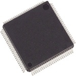
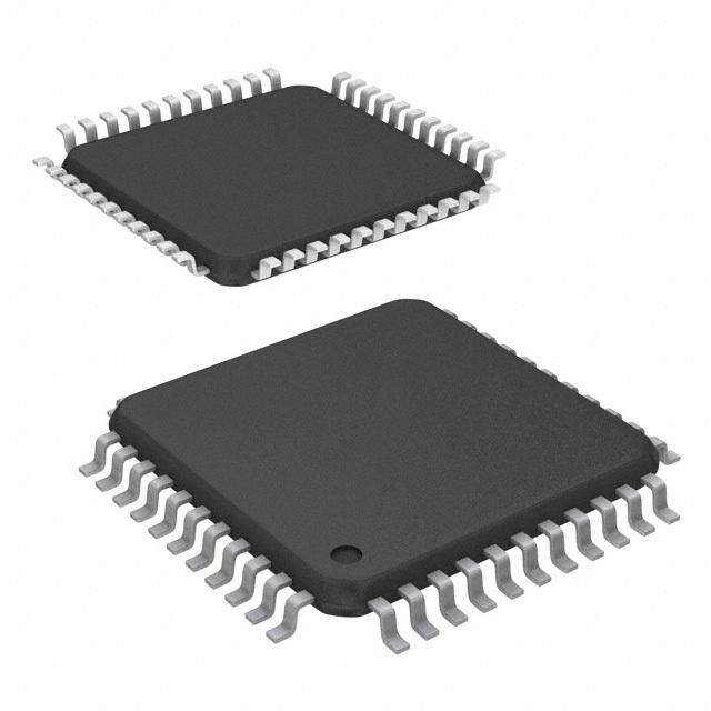
| 供应商器件封装 | 100-LQFP(14x14) |
| 包装 | 托盘 |
| 单位重量 | 685.200 mg |
| 商标 | Freescale Semiconductor |
| 商标名 | ColdFire |
| 处理器系列 | MCF51EM |
| 外设 | LCD,LVD,PWM,WDT |
| 安装风格 | SMD/SMT |
| 定时器数量 | 3 Timer |
| 封装 | Tray |
| 封装/外壳 | 100-LQFP |
| 封装/箱体 | LQFP-100 |
| 工作温度 | -40°C ~ 85°C |
| 工作电源电压 | 1.8 V to 3.6 V |
| 工厂包装数量 | 450 |
| 振荡器类型 | 外部 |
| 接口类型 | LIN, RS-232 |
| 数据RAM大小 | 16 kB |
| 数据Ram类型 | SRAM |
| 数据总线宽度 | 32 bit |
| 数据转换器 | A/D 16x12b |
| 最大工作温度 | + 85 C |
| 最大时钟频率 | 50 MHz |
| 最小工作温度 | - 40 C |
| 标准包装 | 900 |
| 核心 | ColdFire V1 |
| 核心处理器 | Coldfire V1 |
| 核心尺寸 | 32-位 |
| 片上ADC | Yes |
| 电压-电源(Vcc/Vdd) | 1.8 V ~ 3.6 V |
| 程序存储器大小 | 256 kB |
| 程序存储器类型 | Flash |
| 程序存储容量 | 256KB(256K x 8) |
| 系列 | MCF51EM |
| 连接性 | I²C, SCI, SPI |
| 速度 | 50MHz |


- 商务部:美国ITC正式对集成电路等产品启动337调查
- 曝三星4nm工艺存在良率问题 高通将骁龙8 Gen1或转产台积电
- 太阳诱电将投资9.5亿元在常州建新厂生产MLCC 预计2023年完工
- 英特尔发布欧洲新工厂建设计划 深化IDM 2.0 战略
- 台积电先进制程称霸业界 有大客户加持明年业绩稳了
- 达到5530亿美元!SIA预计今年全球半导体销售额将创下新高
- 英特尔拟将自动驾驶子公司Mobileye上市 估值或超500亿美元
- 三星加码芯片和SET,合并消费电子和移动部门,撤换高东真等 CEO
- 三星电子宣布重大人事变动 还合并消费电子和移动部门
- 海关总署:前11个月进口集成电路产品价值2.52万亿元 增长14.8%


PDF Datasheet 数据手册内容提取
Freescale Semiconductor Document Number: MCF51EM256 Data Sheet: Advance Information Rev.3, 8/2010 MCF51EM256 MCF51EM256 Series 80LQFP 100LQFP 14mm×14mm 14mm×14mm ColdFire Microcontroller 917A-03 983-02 Covers: MCF51EM256 MCF51EM128 The MCF51EM256/128 series microcontrollers are • Three serial communications interface a member of the ColdFire® family of reduced modules (SCI) instruction set computing (RISC) microprocessors. • Three serial peripheral interfaces This document provides an overview of these • Inter-integrated circuit (IIC) 32-bit microcontrollers, focusing on their highly • Two 8-bit and one 16-bit modulo timers integrated and diverse feature set. (MTIM) • Two-channel timer/PWM module (TPM) These microcontrollers are systems-on-chips (SoCs) that are based on the V1 ColdFire core and the following features: • Operating at processor core speeds up to 50.33MHz (peripherals operate at half of this speed) at 3.6 V to 2.5 V and 20 MHz at 3.6 V to 1.8 V • Up to 256 KB of flash memory • Up to 16 KB of RAM • Less than 1.3 μA of typical power consumption in battery mode, with MCU supply off • Ultra-low power independent RTC with calendar features, separate time base, power domain, and 32 bytes of RAM • A collection of communications peripherals, including UART, IIC and SPI • Integrated 16-bit SAR analog-to-digital converter • Programmable delay block (PDB) • Two analog comparators with selectable interrupt (PRACMP) • LCD driver This document contains information on a product under development. Freescale reserves the right to change or discontinue this product without notice. ©Freescale Semiconductor, Inc., 2008-2010. All rights reserved. Preliminary—Subject to Change Without Notice
Table of Contents 1 MCF51EM256 Series Configurations. . . . . . . . . . . . . . . . . . . .3 2.9 External Oscillator (XOSC) Characteristics. . . . . . . . . 34 1.1 Device Comparison. . . . . . . . . . . . . . . . . . . . . . . . . . . . .3 2.10 Internal Clock Source (ICS) Characteristics . . . . . . . . 35 1.2 Block Diagram. . . . . . . . . . . . . . . . . . . . . . . . . . . . . . . . .4 2.11 LCD Specifications . . . . . . . . . . . . . . . . . . . . . . . . . . . 37 1.3 Features . . . . . . . . . . . . . . . . . . . . . . . . . . . . . . . . . . . . .6 2.12 AC Characteristics. . . . . . . . . . . . . . . . . . . . . . . . . . . . 37 1.3.1 Feature List . . . . . . . . . . . . . . . . . . . . . . . . . . . . .7 2.12.1 Control Timing . . . . . . . . . . . . . . . . . . . . . . . . . 38 1.4 Part Numbers . . . . . . . . . . . . . . . . . . . . . . . . . . . . . . . . .9 2.12.2 Timer (TPM/FTM) Module Timing . . . . . . . . . . 39 1.5 Pinouts and Packaging. . . . . . . . . . . . . . . . . . . . . . . . .11 2.13 VREF Characteristics . . . . . . . . . . . . . . . . . . . . . . . . . 40 1.5.1 Pinout: 80-Pin LQFP . . . . . . . . . . . . . . . . . . . . .11 2.14 SPI Characteristics . . . . . . . . . . . . . . . . . . . . . . . . . . . 40 1.5.2 Pinout: 100-Pin LQFP . . . . . . . . . . . . . . . . . . . .12 2.15 Flash Specifications. . . . . . . . . . . . . . . . . . . . . . . . . . . 43 2 Electrical Characteristics . . . . . . . . . . . . . . . . . . . . . . . . . . . .16 2.16 EMC Performance. . . . . . . . . . . . . . . . . . . . . . . . . . . . 44 2.1 Parameter Classification. . . . . . . . . . . . . . . . . . . . . . . .16 2.16.1 Radiated Emissions. . . . . . . . . . . . . . . . . . . . . 44 2.2 Absolute Maximum Ratings . . . . . . . . . . . . . . . . . . . . .17 3 Mechanical Outline Drawings . . . . . . . . . . . . . . . . . . . . . . . . 45 2.3 Thermal Characteristics . . . . . . . . . . . . . . . . . . . . . . . .18 3.1 80-pin LQFP Package. . . . . . . . . . . . . . . . . . . . . . . . . 45 2.4 Electrostatic Discharge (ESD) Protection Characteristics 3.2 100-pin LQFP Package. . . . . . . . . . . . . . . . . . . . . . . . 49 19 4 Revision History . . . . . . . . . . . . . . . . . . . . . . . . . . . . . . . . . . 53 2.5 DC Characteristics . . . . . . . . . . . . . . . . . . . . . . . . . . . .20 2.6 Supply Current Characteristics. . . . . . . . . . . . . . . . . . .24 2.7 Analog Comparator (PRACMP) Electricals. . . . . . . . . .27 2.8 ADC Characteristics . . . . . . . . . . . . . . . . . . . . . . . . . . .27 MCF51EM256 Series ColdFire Microcontroller Data Sheet, Rev.3 2 Preliminary—Subject to Change Without Notice Freescale Semiconductor
MCF51EM256 Series Configurations 1 MCF51EM256 Series Configurations 1.1 Device Comparison The MCF51EM256 series is summarized in Table 1. Table1. MCF51EM256 Series Features by MCU and Package Feature MCF51EM256 MCF51EM128 Flash size (bytes) 262144 131072 RAM size (bytes) 16384 8192 Robust flash update Yes supported Pin quantity 100 80 100 80 PRACMP1 inputs 5 3 5 3 PRACMP2 inputs 5 ADC modules 4 4 ADC differential 4 2 4 2 channels1 ADC single-ended 16 12 16 12 channels DBG Yes ICS Yes IIC Yes IRQ Yes IRTC Yes VREF Yes LCD drivers 44 37 44 37 Rapid GPIO2 16 16 16 16 Port I/O3 47 40 47 40 Keyboard interface 1 8 Keyboard interface 2 8 SCI1 Yes SCI2 Yes SCI3 Yes SPI1 (FIFO) Yes SPI2 (standard) Yes SPI3 (standard) Yes No Yes No MCF51EM256 Series ColdFire Microcontroller Data Sheet, Rev.3 Freescale Semiconductor Preliminary—Subject to Change Without Notice 3
MCF51EM256 Series Configurations Table1. MCF51EM256 Series Features by MCU and Package (continued) Feature MCF51EM256 MCF51EM128 MTIM1 (8-bit) Yes MTIM2 (8-bit) Yes MTIM3 (16-it) Yes TPM channels 2 PDB Yes XOSC14 Yes XOSC25 Yes 1 Each differential channel is comprised of 2 pin inputs 2 RGPIO is muxed with standard Port I/O 3 Port I/O count does not include the ouput only PTC2/BKGD/MS. 4 IRTC crystal input and possible crystal input to the ICS module 5 Main external crystal input for the ICS module 1.2 Block Diagram Figure 1 shows the connections between the MCF51EM256 series pins and modules. MCF51EM256 Series ColdFire Microcontroller Data Sheet, Rev.3 4 Preliminary—Subject to Change Without Notice Freescale Semiconductor
MCF51EM256 Series Configurations VDDA/VSSA trig[D] PDB VREFH/VREFL Port F: sel[D][1:0] trig[D:A] AD[20] AD[7], AD[19:17] sel[D:A][1:0] Port F: ADC 4 DADP/M[3] EXTRIG PPTTAA67//RRGGPPIIOO67//TTPPMMCCHLK1//PARDA12CMP1P2/AD13 trig[C] PTA5/RGPIO5/TPMCH0/AD11 VVADRDDE[FA2H/0V/V]SRSAEFL Port E, A: sel[C][1:0] COUT2 COUPTR1ACMP1* Port A PPPPTTTTAAAA2134////RRRRGGGGPPPPIIIIOOOO2134////MMSSCSIOS1LSOKI111/AD10 AD[4], AD[13,9:8] PTA0/RGPIO0/IRQ/CLKOUT ADC 3 DADP/M[0] PRACMP2 PTB7/RGPIO15/KBI1P5/TMRCLK2/AD15 COUT1 PTB6/RGPIO14/KBI1P4/TMRCLK1/AD14 VRVEDFDHA/V/VRSESFAL VVDRDEFAH/V/VSRSAEFL Port F, B: tsreigl[[BB]][1:0] COUT2 SCI1PorRTt XXB11: Port B PPPPTTTTBBBB3245////RRRRGGGGPPPPIIIIOOOO11111023////KKSSBBCDIIAL11//PPPP32RR//APPACCRRMMAACCPPMM22PPPP2321PP10//TRXX11 PTB1/RGPIO9/KBI1P1/SS3/TX2 AD[20] AD[6], AD[19:14] PTB0/RGPIO8/KBI1P0/PRACMP2P0/RX2 ADC 2 DADP/M[2] Port B, E: PTC7/LCD4 SCI2 RX2 PTC6/LCD3/PRACMP2P4 trig[A] TX2 PTC5/LCD2/PRACMP1P4 VVDRDEFAH/V/VSRSAEFL Port A: sel[A][1:0] SCI3 Port CR,XF3: Port C PBPPTKTTCCCG413D///LK/LMCCBSDDI1/10PP//TP7PC/RRX2AATACCLMM2PP/T21XOO3 AD[20] AD[5], AD[13:10] TX3 PTC0/KBI1P6/EXTAL2/RX3 ADC 1 DADP/M[1] PTD7/LCD34/KBI2P7 Port B: PTD6/LCD33/KBI2P6 IIC SDA PTD5/LCD32/KBI2P5/TMRCLK2 VREFO VREF SCL ort D PPTTDD34//LLCCDD3301//KKBBII22PP34/TMRCLK1 P PTD2/LCD29/KBI2P2 Port B/C & D: KBI 1 & 2 KBI1P[7:0] PTD1/LCD28/KBI2P1 Hardware CRC 2 Channel TPM TPMCPoHr[t1 :A0:] KBI2P[7:0] PPTTDE07//LLCCDD257/KBI2P0 TPMCLK 8-Bit MTIM1 Port B, D: PTE6/SS3/TX2 PTE5/SCLK3 DBG 16-Bit MTIM3 Port B, D: TMRCLK[n] ort E PPTTEE34//MMOISSOI33//MMIOSSOI33 BDM TMRCLK[n] 8-Bit MTIM2 Port B, D: P PTE2/PRACMP1P1 TMRCLK[n] PTE1/PRACMP1P3/AD9 BKGD/MS/PTC2 BPKoGrtD C/M:S INTC RGPIO RGPIPOo[1rt5 :B8:] PPTTFE70//LPCRDA4C3M/APD11O9/AD8 Port A: Internal Clock Source PTF6/LCD42/AD18 RGPIO[7:0] REF CLK IRCLK PTF5/LCD41/AD17 ort F PPTTFF43//LLCCDD4309//ATXD316 V1 ColdFire Core Port A: ol P PTF2/LCD38/RX3 with MAC SPI1 MOSI1SS1 Clock Check ntr PTF1/LCD37/EXTRIG MISO1 SPSCK1 & Select o PTF0/LCD36 c LCD[9:6]: RESET SPI2 MISOM2OSSIP2SCSSK22 XOSC2EPXoTrAt LC2: DADAD[7P,4/M] [3,0] SIM XTAL2 PTA0/RPGPIO0/ IRQ/CLKOUT Port A0 or LCD25 DADP/M[2:1] Port E, B: CLKO AD[6:5] SPI3 MOSI3 SS3 COP LVD IRQ MISO3 SPSCK3 XOSC1 EXTAL1 FLASH1 XTAL1 Robust LCD 128/64KB Port A0 or LCD25 1F12LR68A//A86S4MKHKB2B UMpadnaaVtgeRerEG LCD[35] (CLKOUT)LCD[26:25, 20:16] LCD[24:21, 15:10] VLL[3:1], VCAP[2:1] LLPCCLLoDCDCPPr[SDt[oo4D3 PC3r[r4[9tt5I:,: 23:E2F:D60:67::]:]]] IndReTpCeCnLdKeOnt TpLoChweD e IcRr oTdnoCtmr oisall ieinnr,. aa ss eisp athraete VDD VSS1 VSS2 EXTAL1XTAL1 VBAT TAMPER 1 Pins with • are not present on 80-pin devices. 2 PRACMP1 has two less available inputs on the 80-pin devices. Figure1. MCF51EM256 Series Block Diagram MCF51EM256 Series ColdFire Microcontroller Data Sheet, Rev.3 Freescale Semiconductor Preliminary—Subject to Change Without Notice 5
MCF51EM256 Series Configurations 1.3 Features Table 2 describes the functional units of the MCF51EM256 series. Table2. MCF51EM256 Series Functional Units Unit Function ADC (analog-to-digital converter) Measures analog voltages at up to 16 bits of resolution. Each ADC has up to four differential and 24 single-ended inputs. BDM (background debug module) Provides single pin debugging interface (part of the V1 ColdFire core) CF1 CORE (V1 ColdFire core) with MAC Executes programs, handles interrupts and containes unit multiply-accumulate hardware (MAC). PRACMP1, PRACMP2 (comparators) Analog comparators for comparing external analog signals against each other, or a variety of reference levels. COP (computer operating poperly) Software watchdog IRQ (interrupt request) Single pin high priority interrupt (part of the V1 ColdFire core) CRC (cyclic Redundancy Check) High-speed CRC calculation DBG (debug) Provides debugging and emulation capabilities (part of the V1 ColdFire core) FLASH (flash memory) Provides storage for program code, constants and variables IIC (inter-integrated circuits) Supports standard IIC communications protocol and SMBus INTC (interrupt controller) Controls and prioritizes all device interrupts KBI1 & KBI2 Keyboard Interfaces 1 and 2 LCD Liquid crystal display driver LVD (low voltage detect) Provides an interrupt to the CF1CORE in the event that the supply voltage drops below a critical value. The LVD can also be programmed to reset the device upon a low voltage event ICS (internal clock source) Provides clocking options for the device, including a three frequency-locked loops (FLLs) for multiplying slower reference clock sources IRTC (independent real-time clock) The independent real time clock provides an independent time-base with optional interrupt, battery backup and tamper protection VREF (voltage reference) The voltage reference output is available for both on and off-chip use MTIM1, MTIM2 (modulo timers) 8-bit modulo timers with configurable clock inputs and interrupt generation on overflow MTIM3 (modulo timer) 16-bit modulo timer with configurable clock inputs and interrupt generation on overflow PDB (programmable delay block) This timer is optimized for scheduling ADC conversions RAM (random-access memory) Provides stack and variable storage RGPIO (rapid general-purpose Allows for I/O port access at CPU clock speeds and is used to input/output) implement GPIO functionality for PTA and PTB. MCF51EM256 Series ColdFire Microcontroller Data Sheet, Rev.3 6 Preliminary—Subject to Change Without Notice Freescale Semiconductor
MCF51EM256 Series Configurations Table2. MCF51EM256 Series Functional Units (continued) Unit Function SCI1, SCI2, SCI3(serial communications Serial communications UARTs capable of supporting RS-232 and LIN interfaces) protocols SIM (system integration unit) SPI1 (FIFO), SPI2, SPI3 (serial peripheral SPI1 has full-complementary drive outputs. SPI2 may be configured interfaces) with full-complementary drive output via LCD control registers. SPI3 has open drain outputs on SCLK and (MISO or MOSI). These coupled with off-chip pull-up resistors, allow interface to an external 5 V SPI. TPM (Timer/PWM Module) Timer/PWM module can be used for a variety of generic timer operations as well as pulse-width modulation VREG (voltage regulator) Controls power management across the device XOSC1 and XOSC2 (crystal oscillators) These devices incorporate redundant crystal oscillators in separate power domains.One is intended primarily for use by the IRTC, and the other by the CPU and other peripherals. 1.3.1 Feature List • 32-bit ColdFire V1 central processor unit (CPU) — Up to 50.33 MHz ColdFire CPU from 3.6 V to 2.5 V and 20 MHz CPU at 3.6 V to 1.8 V across temperature range of –40 °C to 85 °C — ColdFire instruction set revision C (ISA_C) plus MAC — 32-bit multiply and accumulate (MAC) optimized for 16×16±32 operations; supports signed or unsigned integer or signed fractional inputs • On-chip memory — MCF51EM256/128 series support two independent flash arrays; read/program/erase over full operating voltage and temperature; allows interrupt processing while programming for robust program updates — Random-access memory (RAM) — Security circuitry to prevent unathorized access to RAM and Flash contents • Power-saving modes — Two ultra-low power stop modes — New low-power run and low-power wait modes — Reduced power wait mode — Peripheral clock enable register can disable clocks to unused modules, thereby reducing currents — Ultra-low power independent real time clock with calendar features (IRTC); runs in all MCU modes; external clock source with trim capabilities; independent voltage source runs IRTC when MCU is powered-down; tamper detection and indicator; battery monitor output to ADC; unaffected by MCU resets — Ultra-low power external oscillator that can be used in stop modes to provide accurate clock source to IRTC, ICS and LCD MCF51EM256 Series ColdFire Microcontroller Data Sheet, Rev.3 Freescale Semiconductor Preliminary—Subject to Change Without Notice 7
MCF51EM256 Series Configurations — 6 μs typical wakeup time from stop3 mode • Clock source options — Two independent oscillators (XOSC1 and XOSC2) — loop-control Pierce oscillator; 32.768kHz crystal or ceramic resonator. XOSC1 nominally supports the independent real time clock, and can be powered by a separate battery backup. XOSC2 is the primary external clock source for the ICS — Internal clock source (ICS) — internal clock source module containing a frequency-locked-loop (FLL) controlled by internal or external reference (XOSC1 or XOSC2); precision trimming of internal reference allowing 0.2% resolution and typical 0.5% to –1% deviation over temperature and voltage; supporting CPU frequencies from 4 kHz to 50 MHz • System protection — Watchdog computer operating properly (COP) reset with option to run from dedicated 1 kHz internal clock source or bus clock — Low voltage detection with reset or interrupt; selectable trip points; seperate low voltage warning with optional interrupt; selectable trip points — Illegal opcode and illegal address detection with reset — Flash block protection for each array to prevent accidental write/erasure — Hardware CRC module to support fast cyclic redundancy checks • Development support — Integrated ColdFire DEBUG_Rev_B+ interface with single wire BDM connection supports same electrical interface used by the S08 family debug modules — Real-time debug support with six hardware breakpoints (4 PC, 1 address and 1 data) — On-chip trace buffer provides programmable start/stop recording conditions • Peripherals — ADC16 — 4 analog-to-digital converters; the 100 pin version of the device has 1 dedicated differential channel and 1 dedicated single-ended channel per ADC, along with 3 muxed single-ended channels per ADC. The ADCs have 16-bit resolution, range compare function, 1.7mV/°C temperature sensor, internal bandgap reference channel, operate in stop3 and are fully functional from 3.6 V to 1.8 V — PDB — Programmable delay block with 16-bit counter and modulus and 3-bit prescaler; 8 trigger outputs for ADC16 modules (2 per ADC); provides periodic coordination of ADC sampling sequence with programmable sequence completion interrupt — IRTC — Ultra-low power independent real time clock with calendar features (IRTC); runs in all MCU modes; external clock source with trim capabilities (XOSC1); independent voltage source runs IRTC when MCU is powered-down; tamper detection and indicator; battery monitor output to ADC; unaffected by MCU resets — PRACMPx — Two analog comparators with selectable interrupt on rising, falling, or either edge of comparator output; compare option to programmable internal reference voltage; operation in stop3 — LCD — up to 288 segments (8 × 36); 160 segments (4 × 40); internal charge pump and option to provide internal reference voltage that can be trimmed for contrast control; flexible MCF51EM256 Series ColdFire Microcontroller Data Sheet, Rev.3 8 Preliminary—Subject to Change Without Notice Freescale Semiconductor
MCF51EM256 Series Configurations front-plane/backplane pin assignments; operation in all low power modes with blink functionality — SCIx — Three serial communications interface modules with optional 13-bit break; option to connect Rx input to PRACMP output on SCI1 and SCI2; high current drive on Tx on SCI1 and SCI2; wakeup from stop3 on Rx edge. SCI1 and SCI2 Tx pins can be modulated with timer outputs for use with IR interfaces — SPIx— Two serial peripheral interfaces (SPI2, SPI3) with full-duplex or single-wire bidirectional; double-buffered transmit and receive; master or slave mode; MSB-first or LSB-first shifting — SPI16— Serial peripheral interface (SPI1) with 32-bit FIFO buffer; 16-bit or 8-bit data transfers; full-duplex or single-wire bidirectional; double-buffered transmit and receive; master or slave mode; MSB-first or LSB-first shifting — IIC — Up to 100 kbps with maximum bus loading; multi-master operation; programmable slave address; interrupt driven byte-by-byte data transfer; supports broadcast mode and 10 bit addressing — MTIMx — Two 8-bit and one 16-bit modulo timers with 4-bit prescaler; overflow interrupt; external clock input/pulse accumulator — TPM — 2-channel Timer/PWM module; selectable input capture, output compare, or buffered edge- or center-aligned PWM on each channel; external clock input/pulse accumulator; can be used modulate SCI1 and SCI2 TX pins • Input/output — up to 16 rapid GPIO and 48 standard GPIOs, including 1 output-only pin and 3 open-drain pins. — up to 16 keyboard interrupts with selectable polarity — Hysteresis and configurable pullup device on all input pins; configurable slew rate and drive strength on all output pins • Package options — 100-pin LQFP, 80-pin LQFP 1.4 Part Numbers MCF 51 EM 256 C XX Status Package designator (MCF = Fully Qualified ColdFire) Temperature range (PCF = Product Engineering) (C= –40°C to 85°C ) Core Family Memory size designator MCF51EM256 Series ColdFire Microcontroller Data Sheet, Rev.3 Freescale Semiconductor Preliminary—Subject to Change Without Notice 9
MCF51EM256 Series Configurations Table3. Orderable Part Number Summary Freescale Part Number Flash / SRAM (KB) Package Temperature MCF51EM256CLL 256/16 100-Pin LQFP –40°C to 85°C MCF51EM256CLK 256/16 80-Pin LQFP –40°C to 85°C MCF51EM128CLL 128/16 100-Pin LQFP –40°C to 85°C MCF51EM128CLK 128/16 80-Pin LQFP –40°C to 85°C MCF51EM256 Series ColdFire Microcontroller Data Sheet, Rev.3 10 Preliminary—Subject to Change Without Notice Freescale Semiconductor
MCF51EM256 Series Configurations 1.5 Pinouts and Packaging 1.5.1 Pinout: 80-Pin LQFP Pins not available on the 80-pin LQFP are automatically disabled for reduced current consumption. No user interaction is needed. Software access to the functions on these pins will be ignored Figure 2 shows the pinout of the 80-pin LQFP. 222 CAP1CAP2LL1LL2LL3 SSCD24CD23CD22CD21CD15CD14CD13CD12CD11CD10CD9/SS2CD8/SCLKCD7/MISOCD6/MOSI VVVVVVLLLLLLLLLLLLLL 09876543210987654321 PTD0/LCD27/KBI2P0 18777777777766666666660 PTE7/LCD5 PTD1/LCD28/KBI2P1 2 59 PTC7/LCD4 PTD2/LCD29/KBI2P2 3 58 PTC6/LCD3/PRACMP2P5 PTD3/LCD30/KBI2P3 4 57 PTC5/LCD2/PRACMP1P4 PTD4/LCD31/KBI2P4/TMRCLK1 5 56 PTC4/LCD1/PRACMP2O PTD5/LCD32/KBI2P5/TMRCLK2 6 55 PTC3/LCD0/PRACMP1O PTD6/LCD33/KBI2P6 7 54 BKGD/MS/PTC2 PTD7/LCD34/KBI2P7 8 53 PTC1/KBI1P7/XTAL2/TX3 LCD35/CLKOUT 9 52 PTC0/KBI1P6/EXTAL2/RX3 PTF0/LCD36 10 51 RESET 80 LQFP PTF1/LCD37/EXTRIG 11 50 PTB7/RGPIO15/KBI1P5/TMRCLK2/AD15 PTF2/LCD38/RX3 12 49 PTB6/RGPIO14/KBI1P4/TMRCLK1/AD14 PTF3/LCD39/TX3 13 48 PTB5/RGPIO13/SDA/PRACMP2P3 PTF4/LCD40/AD16 14 47 PTB4/RGPIO12/SCL/PRACMP2P2 PTF5/LCD41/AD17 15 46 PTB3/RGPIO11/KBI1P3/PRACMP2P1/TX1 PTF6/LCD42/AD18 16 45 PTB2/RGPIO10/KBI1P2/PRACMP1P0/RX1 PTF7/LCD43/AD19 17 44 VSS VDDA 18 43 VDD VREFH 19 42 PTB1/RGPIO9/KBI1P1/SS3/TX2 DADP1 20 41 PTB0/RGPIO8/KBI1P0/PRACMP2P0/RX2 12345678901234567890 22222222233333333334 DADM1AD5DADP2DADM2AD6VREFOVREFLVSSAEXTAL1XTAL1VBATTAMPERPTA0/RGPIO0/IRQ/CLKOUTPTA1/RGPIO1/MOSI1PTA2/RGPIO2/MISO1/AD10PTA3/RGPIO3/SCLK1PTA4/RGPIO4/SS1PTA5/RGPIO5/TPMCH0/AD11PTA6/RGPIO6/TPMCH1/AD127/TPMCLK/PRACMP1P2/AD13 O PI G R 7/ A T P Figure2. 80-Pin LQFP Pinout MCF51EM256 Series ColdFire Microcontroller Data Sheet, Rev.3 Freescale Semiconductor Preliminary—Subject to Change Without Notice 11
MCF51EM256 Series Configurations 1.5.2 Pinout: 100-Pin LQFP Figure 3 shows the pinout configuration for the 100-pin LQFP. Pins which are blacked out do not have an equivalent pin on the 80-pin LQFP package. 2 2 2 CAP1 CAP2 LL1 LL2 LL3 SSCD24CD23 CD22 CD21 CD20 CD19 CD18 CD17 CD16CD15 CD14 CD13 CD12 CD11 CD10 CD9/SS2 CD8/SCLK CD7/MISO CD6/MOSI V V V V V V LL L L L L L L LL L L L L L L L L L 0 9 8 7 6 5 4 3 2 1 0 9 8 7 6 5 4 3 2 1 0 9 8 7 6 0 9 9 9 9 9 9 9 9 9 9 8 8 8 8 8 8 8 8 8 8 7 7 7 7 1 LCD25 1 75 PTE7/LCD5 LCD26 2 74 PTC7/LCD4 PTD0/LCD27/KBI2P0 3 73 PTC6/LCD3/PRACMP2P4 PTD1/LCD28/KBI2P1 4 72 PTC5/LCD2/PRACMP1P4 PTD2/LCD29/KBI2P2 5 71 PTC4/LCD1/PRACMP2O PTD3/LCD30/KBI2P3 6 70 PTC3/LCD0/PRACMP1O PTD4/LCD31/KBI2P4/TMRCLK1 7 69 BKGD/MS/PTC2 PTD5/LCD32/KBI2P5/TMRCLK2 8 68 PTC1/KBI1P7/XTAL2/TX3 PTD6/LCD33/KBI2P6 9 67 PTC0/KBI1P6/EXTAL2/RX3 PTD7/LCD34/KBI2P7 10 66 RESET LCD35/CLKOUT 11 65 PTB7/RGPIO15/KBI1P5/TMRCLK2/AD15 PTF0/LCD36 12 64 PTB6/RGPIO14/KBI1P4/TMRCLK1/AD14 PTF1/LCD37/EXTRIG 13 100 LQFP 63 PTE6/SS3/TX2 PTF2/LCD38/RX3 14 62 PTE5/SCLK3 PTF3/LCD39/TX3 15 61 PTE4/MISO3/MOSI3 PTF4/LCD40/AD16 16 60 PTE3/MOSI3/MISO3 PTF5/LCD41/AD17 17 59 PTB5/RGPIO13/SDA/PRACMP2P3 PTF6/LCD42/AD18 18 58 PTB4/RGPIO12/SCL/PRACMP2P2 PTF7/LCD43/AD19 19 57 PTB3/RGPIO11/KBI1P3/PRACMP2P1/TX VDDA 20 56 PTB2/RGPIO10/KBI1P2/PRACMP1P0/RX VREFH 21 55 VSS DADP0 22 54 VDD DADM0 23 53 PTB1/RGPIO9/KBI1P1/SS3/TX2 AD4 24 52 PTB0/RGPIO8/KBI1P0/PRACMP2P0RX2 DADP1 25 51 PTE2/PRACMP1P1 6 7 8 9 0 1 2 3 4 5 6 7 8 9 0 1 2 3 4 5 6 7 8 9 0 2 2 2 2 3 3 3 3 3 3 3 3 3 3 4 4 4 4 4 4 4 4 4 4 5 3 1 DADM1 AD5 DADP2 DADM2 AD6 DADP3 DADM3 AD7 VREFOVREFLVSSAEXTAL1 XTAL1 VBAT TAMPER PTA0/RGPIO0/IRQ/CLKOUT PTE0/PRACMP1O/AD8 PTE1/PRACMP1P3/AD9 PTA1/RGPIO1/MOSI1 PTA2/RGPIO2/MISO1/AD10 PTA3/RGPIO3/SCLK1PTA4/RGPIO4/SS1 PTA5/RGPIO5/TPMCH0/AD11 PTA6/RGPIO6/TPMCH1/AD12 PIO7/TPMCLK/PRACMP1P2/AD G R 7/ A T P Figure3. 100-Pin LQFP Pinout Table 4 shows the package pin assignments. MCF51EM256 Series ColdFire Microcontroller Data Sheet, Rev.3 12 Preliminary—Subject to Change Without Notice Freescale Semiconductor
MCF51EM256 Series Configurations Table4. MCF51EM256 Series Package Pin Assignments 100 80 Default Function ALT1 ALT2 ALT3 Comment LQFP LQFP 1 — LCD25 2 — LCD26 3 1 PTD0 LCD27 KBI2P0 4 2 PTD1 LCD28 KBI2P1 5 3 PTD2 LCD29 KBI2P2 6 4 PTD3 LCD30 KBI2P3 7 5 PTD4 LCD31 KBI2P4 TMRCLK1 8 6 PTD5 LCD32 KBI2P5 TMRCLK2 9 7 PTD6 LCD33 KBI2P6 10 8 PTD7 LCD34 KBI2P7 11 9 LCD35 CLKOUT 12 10 PTF0 LCD36 13 11 PTF1 LCD37 EXTRIG 14 12 PTF2 LCD38 RX3 15 13 PTF3 LCD39 TX3 16 14 PTF4 LCD40 AD16 17 15 PTF5 LCD41 AD17 18 16 PTF6 LCD42 AD18 19 17 PTF7 LCD43 AD19 20 18 V DDA 21 19 V REFH 22 — DADP0 23 — DADM0 24 — AD4 25 20 DADP1 26 21 DADM1 27 22 AD5 28 23 DADP2 29 24 DADM2 30 25 AD6 31 — DADP3 32 — DADM3 MCF51EM256 Series ColdFire Microcontroller Data Sheet, Rev.3 Freescale Semiconductor Preliminary—Subject to Change Without Notice 13
MCF51EM256 Series Configurations Table4. MCF51EM256 Series Package Pin Assignments (continued) 100 80 Default Function ALT1 ALT2 ALT3 Comment LQFP LQFP 33 — AD7 34 26 V REFO 35 27 V REFL 36 28 V SSA 37 29 EXTAL1 38 30 XTAL1 39 31 V BAT 40 32 TAMPER 41 33 PTA0/RGPIO0 IRQ CLKOUT 42 — PTE0 PRACMP1O AD8 43 — PTE1 PRACMP1P3 AD9 44 34 PTA1/RGPIO1 MOSI1 45 35 PTA2/RGPIO2 MISO1 AD10 46 36 PTA3/RGPIO3 SCLK1 RGPIO_ENB is used to select 47 37 PTA4/RGPIO4 SS1 between standard GPIO and RGPIO 48 38 PTA5/RGPIO5 TPMCH0 AD11 49 39 PTA6/RGPIO6 TPMCH1 AD12 50 40 PTA7/RGPIO7 TPMCLK PRACMP1P2 AD13 51 — PTE2 PRACMP1P1 RGPIO_ENB is used to select 52 41 PTB0/RGPIO8 KBI1P0 PRACMP2P0 RX2 between standard GPIO and RGPIO 2X Drive Output RGPIO_ENB is used to select 53 42 PTB1/RGPIO9 KBI1P1 SS3 TX2 between standard GPIO and RGPIO 54 43 V DD 55 44 V SS RGPIO_ENB is used to select 56 45 PTB2/RGPIO10 KBI1P2 PRACMP1P0 RX1 between standard GPIO and RGPIO 2X drive output RGPIO_ENB is 57 46 PTB3/RGPIO11 KBI1P3 PRACMP2P1 TX1 used to select between standard GPIO and RGPIO MCF51EM256 Series ColdFire Microcontroller Data Sheet, Rev.3 14 Preliminary—Subject to Change Without Notice Freescale Semiconductor
MCF51EM256 Series Configurations Table4. MCF51EM256 Series Package Pin Assignments (continued) 100 80 Default Function ALT1 ALT2 ALT3 Comment LQFP LQFP 58 47 PTB4/RGPIO12 SCL PRACMP2P2 RGPIO_ENB is used to select between standard GPIO and 59 48 PTB5/RGPIO13 SDA PRACMP2P3 RGPIO 60 — PTE3 MOSI3 MISO3 61 — PTE4 MISO3 MOSI3 Open Drain 62 — PTE5 SCLK3 Open Drain 63 — PTE6 SS3 TX2 Open Drain 64 49 PTB6/RGPIO14 KBI1P4 TMRCLK1 AD14 RGPIO_ENB is used to select between standard GPIO and 65 50 PTB7/RGPIO15 KBI1P5 TMRCLK2 AD15 RGPIO This pin is an open drain device 66 51 RESET and has an internal pullup. There is no clamp diode to V . DD 67 52 PTC0 KBI1P6 EXTAL2 RX3 68 53 PTC1 KBI1P7 XTAL2 TX3 This pin has an internal pullup. 69 54 BKGD/MS PTC2 PTC2 can only be programmed as an output. 701 551 PTC3 LCD0 PRACMP1O 711 561 PTC4 LCD1 PRACMP2O 721 571 PTC5 LCD2 PRACMP1P4 731 581 PTC6 LCD3 PRACMP2P4 741 591 PTC7 LCD4 751 601 PTE7 LCD5 761 611 LCD6 MOSI2 771 621 LCD7 MISO2 781 631 LCD8 SCLK2 791 641 LCD9 SS2 80 65 LCD10 81 66 LCD11 82 67 LCD12 83 68 LCD13 84 69 LCD14 85 70 LCD15 86 — LCD16 MCF51EM256 Series ColdFire Microcontroller Data Sheet, Rev.3 Freescale Semiconductor Preliminary—Subject to Change Without Notice 15
Electrical Characteristics Table4. MCF51EM256 Series Package Pin Assignments (continued) 100 80 Default Function ALT1 ALT2 ALT3 Comment LQFP LQFP 87 — LCD17 88 — LCD18 89 — LCD19 90 — LCD20 91 71 LCD21 92 72 LCD22 93 73 LCD23 94 74 LCD24 95 75 V SS 96 76 VLL3 97 77 VLL2 98 78 VLL1 99 79 VCAP2 100 80 VCAP1 1 These pins that are shared with the LCD are open-drain by default if not used as LCD pins. To configure this pins as full complementary drive outputs, you must have the LCD modules bits configured as follow: FCDEN =1, VSUPPLY = 11 and RVEN = 0. The Input levels and internal pullup resistors are referenced to VLL3. Referer to the LCD chapter for further information. 2 Electrical Characteristics This section contains electrical specification tables and reference timing diagrams for the MCF51EM256/128 series microcontrollers, including detailed information on power considerations, DC/AC electrical characteristics, and AC timing specifications. The electrical specifications are preliminary and are from previous designs or design simulations. These specifications may not be fully tested or guaranteed at this early stage of the product life cycle. These specifications will, however, be met for production silicon. Finalized specifications will be published after complete characterization and device qualifications have been completed. NOTE The parameters specified in this data sheet supersede any values found in the module specifications. 2.1 Parameter Classification The electrical parameters shown in this supplement are guaranteed by various methods. To give the customer a better understanding the following classification is used and the parameters are tagged accordingly in the tables where appropriate: MCF51EM256 Series ColdFire Microcontroller Data Sheet, Rev.3 16 Preliminary—Subject to Change Without Notice Freescale Semiconductor
Electrical Characteristics Table5. Parameter Classifications P Those parameters are guaranteed during production testing on each individual device. Those parameters are achieved by the design characterization by measuring a statistically relevant C sample size across process variations. Those parameters are achieved by design characterization on a small sample size from typical devices T under typical conditions unless otherwise noted. All values shown in the typical column are within this category. D Those parameters are derived mainly from simulations. NOTE The classification is shown in the column labeled “C” in the parameter tables where appropriate. 2.2 Absolute Maximum Ratings Absolute maximum ratings are stress ratings only, and functional operation at the maxima is not guaranteed. Stress beyond the limits specified in Table 6 may affect device reliability or cause permanent damage to the device. For functional operating conditions, refer to the remaining tables in this section. This device contains circuitry protecting against damage due to high static voltage or electrical fields; however, it is advised that normal precautions be taken to avoid application of any voltages higher than maximum-rated voltages to this high-impedance circuit. Reliability of operation is enhanced if unused inputs are tied to an appropriate logic voltage level (for instance, either V or V ). SS DD Table6. Absolute Maximum Ratings Rating Symbol Value Unit Supply voltage V –0.3 to 4.0 V DD Input voltage V –0.3 to V + 0.3 V In DD Instantaneous maximum current Single pin limit (applies to all port pins except PTB1 I ±25 mA D and PTB3)1,2,3 Instantaneous maximum current I ±50 mA Single pin limit (applies to PTB1 and PTB3)4,5,6 D Maximum current into V I 120 mA DD DD Storage temperature Tstg –55 to 150 °C 1 Input must be current limited to the value specified. To determine the value of the required current-limiting resistor, calculate resistance values for positive (V ) and negative (V ) clamp DD SS voltages, then use the larger of the two resistance values. 2 All functional non-supply pins are internally clamped to V and V . SS DD MCF51EM256 Series ColdFire Microcontroller Data Sheet, Rev.3 Freescale Semiconductor Preliminary—Subject to Change Without Notice 17
Electrical Characteristics 3 Power supply must maintain regulation within operating V range during instantaneous and DD operating maximum current conditions. If positive injection current (V > V ) is greater than In DD I , the injection current may flow out of V and could result in external power supply going DD DD out of regulation. Ensure external V load will shunt current greater than maximum injection DD current. This will be the greatest risk when the MCU is not consuming power. Examples are: if no system clock is present, or if the clock rate is very low which would reduce overall power consumption. 4 Input must be current limited to the value specified. To determine the value of the required current-limiting resistor, calculate resistance values for positive (V ) and negative (V ) clamp DD SS voltages, then use the larger of the two resistance values. 5 All functional non-supply pins are internally clamped to V and V . SS DD 6 Power supply must maintain regulation within operating V range during instantaneous and DD operating maximum current conditions. If positive injection current (V > V ) is greater than In DD I , the injection current may flow out of V and could result in external power supply going DD DD out of regulation. Ensure external V load will shunt current greater than maximum injection DD current. This will be the greatest risk when the MCU is not consuming power. Examples are: if no system clock is present, or if the clock rate is very low which would reduce overall power consumption. 2.3 Thermal Characteristics This section provides information about operating temperature range, power dissipation, and package thermal resistance. Power dissipation on I/O pins is usually small compared to the power dissipation in on-chip logic and it is user-determined rather than being controlled by the MCU design. In order to take P into account in power calculations, determine the difference between actual pin voltage and V or I/O SS V and multiply by the pin current for each I/O pin. Except in cases of unusually high pin current (heavy DD loads), the difference between pin voltage and V or V will be very small. SS DD Table7. Thermal Characteristics Rating Symbol Value Unit Operating temperature range (packaged) T –40 to 85 °C A Maximum junction temperature T 95 °C JM Thermal resistance 1,2,3,4 100-pin LQFP 1s 54 θ °C/W 2s2p JA 42 80-pin LQFP 1s 55 2s2p 42 1 Junction temperature is a function of die size, on-chip power dissipation, package thermal resistance, mounting site (board) temperature, ambient temperature, air flow, power dissipation of other components on the board, and board thermal resistance. 2 Junction to Ambient Natural Convection 3 1s — Single layer board, one signal layer 4 2s2p — Four layers board, two signal and two power layers The average chip-junction temperature (T ) in °C can be obtained from: J MCF51EM256 Series ColdFire Microcontroller Data Sheet, Rev.3 18 Preliminary—Subject to Change Without Notice Freescale Semiconductor
Electrical Characteristics T = T + (P × θ ) Eqn.1 J A D JA where: T = Ambient temperature, °C A θ = Package thermal resistance, junction-to-ambient, °C/W JA P = P + P D int I/O P = I × V , Watts — chip internal power int DD DD P = Power dissipation on input and output pins — user determined I/O For most applications, P << P and can be neglected. An approximate relationship between P and T I/O int D J (if P is neglected) is: I/O P = K ÷ (T + 273°C) Eqn.2 D J Solving Equation1 and Equation2 for K gives: K = P × (T + 273°C) + θ × (P )2 Eqn.3 D A JA D where K is a constant pertaining to the particular part. K can be determined from Equation3 by measuring P (at equilibrium) for a known T . Using this value of K, the values of P and T can be obtained by D A D J solving Equation1 and Equation2 iteratively for any value of T . A 2.4 Electrostatic Discharge (ESD) Protection Characteristics Although damage from static discharge is much less common on these devices than on early CMOS circuits, normal handling precautions should be used to avoid exposure to static discharge. Qualification tests are performed to ensure that these devices can withstand exposure to reasonable levels of static without suffering any permanent damage. All ESD testing is in conformity with CDF-AEC-Q00 Stress Test Qualification for Automotive Grade Integrated Circuits. (http://www.aecouncil.com/) This device was qualified to AEC-Q100 Rev E. A device is considered to have failed if, after exposure to ESD pulses, the device no longer meets the device specification requirements. Complete dc parametric and functional testing is performed per the applicable device specification at room temperature followed by hot temperature, unless specified otherwise in the device specification. Table8. ESD and Latch-up Test Conditions Model Description Symbol Value Unit Human Body Series Resistance R1 1500 Ω Storage Capacitance C 100 pF Number of Pulse per pin — 3 Machine Series Resistance R1 0 Ω Storage Capacitance C 200 pF Number of Pulse per pin — 3 Latch-up Minimum input voltage limit –2.5 V Maximum input voltage limit 7.5 V MCF51EM256 Series ColdFire Microcontroller Data Sheet, Rev.3 Freescale Semiconductor Preliminary—Subject to Change Without Notice 19
Electrical Characteristics Table9. ESD and Latch-Up Protection Characteristics Num Rating Symbol Min Max Unit 1 Human Body Model (HBM) V ±2000 — V HBM 2 Machine Model (MM) V ±200 — V MM 3 Charge Device Model (CDM) V ±500 — V CDM 4 Latch-up Current at T = 85 °C I ±100 — mA A LAT 2.5 DC Characteristics This section includes information about power supply requirements, I/O pin characteristics, and power supply current in various operating modes. Table10. DC Characteristics Num C Parameter Symbol Min Typical1 Max Unit Digital supply — 50 MHz operation V 2.5 — 3.6 DD Operating 1 P Digital supply2 — 20 MHz maximum V voltage V 1.8 — 3.6 operation DD 2 P Analog supply V 1.8 — 3.6 V DDA 3 D Battery supply V 2.2 3 3.3 V BAT 4 P Bandgap voltage reference3 V 1.15 1.17 1.18 V BG PTA[7:0], PTB[7:0], PTC[2:0], PTE[6:0], C low-drive strength. V ≥ 1.8 V, I = –0.6 mA DD Load PTA[7:0], PTB[7:0], PTC[2:0], PTE[6:0], Output high 5 P high-drive strength. V V – 0.5 — — V voltage OH DD V ≥ 2.7 V, I = –10 mA DD Load PTA[7:0], PTB[7:0], PTC[2:0], PTE[6:0], C high-drive strength. V ≥ 1.8 V, I = –3 mA DD Load PTC[7:3], PTD[7:0], PTE7, PTF[7:0], LCD35/CLKOUT, MOSI2, MISO2, C SCK2, SS2, low drive strength. VDD ≥ 1.8 V, I = –0.5 mA Load PTC[7:3], PTD[7:0], PTE7, PTF[7:0], Output high LCD35/CLKOUT, MOSI2, MISO2, 6 P V V – 0.5 — — V voltage SCK2, SS2, high-drive strength. OH DD V ≥ 2.7 V, I = –3 mA DD Load PTC[7:3], PTD[7:0], PTE7, PTF[7:0], LCD35/CLKOUT, MOSI2, MISO2, C SCK2, SS2, high-drive strength. V ≥ 1.8 V, I = –1 mA DD Load Output high 7 D Max total I for all ports I — — 100 mA current OH OHT MCF51EM256 Series ColdFire Microcontroller Data Sheet, Rev.3 20 Preliminary—Subject to Change Without Notice Freescale Semiconductor
Electrical Characteristics Table10. DC Characteristics (continued) Num C Parameter Symbol Min Typical1 Max Unit PTA[7:0], PTB[7:0], PTC[2:0], PTE[6:0], C low-drive strength. V ≥ 1.8 V, I = 2 mA DD Load PTA[7:0], PTB[7:0], PTC[2:0], PTE[6:0], Output low 8 P high-drive strength. V — — 0.50 V voltage OL V ≥ 2.7 V, I = 10 mA DD Load PTA[7:0], PTB[7:0], PTC[2:0], PTE[6:0], C high-drive strength. V ≥ 1.8 V, I = 3 mA DD Load PTC[7:3], PTD[7:0], PTE7, PTF[7:0], LCD35/CLKOUT, MOSI2, MISO2, C SCK2, SS2, low drive strength. VDD ≥ 1.8 V, I = 0.5 mA Load PTC[7:3], PTD[7:0], PTE7, PTF[7:0], Output low LCD35/CLKOUT, MOSI2, MISO2, 9 P V — — 0.50 V voltage SCK2, SS2, high-drive strength. OL V ≥ 2.7 V, I = 3 mA DD Load PTC[7:3], PTD[7:0], PTE7, PTF[7:0], LCD35/CLKOUT, MOSI2, MISO2, C SCK2, SS2, high-drive strength. V ≥ 1.8 V, I = 1 mA DD Load Output low 10 D Max total I for all ports I — — 100 mA current OL OLT All digital inputs except tamper_in, 0.70 × V — — V > 2.7 V DD DD Input high 11 P All digital inputs except tamper_in, V voltage IH 0.85 × V — — V 2.7 V > V ≥ 1.8 V DD DD Tamper_in 1.5 — — All digital inputs except tamper_in, — — 0.35 × V V > 2.7 V DD DD Input low 12 P all digital inputs except tamper_in, V V voltage IL — — 0.3 × V 2.7 V > V ≥ 1.8 V DD DD Tamper_in — — 0.5 13 C Input hysteresis; all digital inputs V 0.06 × V — — mV hys DD 14 P Input leakage current; input only pins4 |I | — 0.1 1 μA In 15 P High Impedance (off-state) leakage current4 |I | — 0.1 1 μA OZ 16 P Internal pullup resistors5 R 17.5 — 52.5 kΩ PU 17 P Internal pulldown resistors6 R 17.5 — 52.5 kΩ PD 18 C Input capacitance; all non-supply pins C — — 8 pF In 19 P POR rearm voltage V 0.9 1.4 2.0 V POR 20 D POR rearm time t 10 — — μs POR Low-voltage High range — V falling 2.300 2.355 2.410 DD 21 P detection V V LVDH High range — V rising 2.370 2.425 2.480 threshold DD MCF51EM256 Series ColdFire Microcontroller Data Sheet, Rev.3 Freescale Semiconductor Preliminary—Subject to Change Without Notice 21
Electrical Characteristics Table10. DC Characteristics (continued) Num C Parameter Symbol Min Typical1 Max Unit Low-voltage Low range — V falling 1.800 1.845 1.890 V DD 22 C detection V LVDL Low range — V rising 1.870 1.915 1.960 V threshold DD Low-voltage V falling, LVWV = 1 2.590 2.655 2.720 DD 23 P warning V V LVWH V rising, LVWV = 1 2.580 2.645 2.710 threshold DD Low-voltage VDD falling, LVWV = 0 2.300 2.355 2.410 24 C V V warning V rising, LVWV = 0 LVWL 2.360 2.425 2.490 DD 25 D RAM retention voltage V — 0.6 1.0 V RAM DC injection current7 8 9 10 (single pin limit), mA V > V V < V –0.2 — 0.2 IN DD, IN SS 26 D I IC DC injection current (Total MCU limit, includes sum of all –5 — 5 mA stressed pins), V > V V < V IN DD, IN SS 1 Typical values are based on characterization data at 25 °C unless otherwise stated. 2 Switch to lower frequency when the low-voltage interrupt asserts (V ). LVDH 3 Factory trimmed at V = 3.0 V, Temp = 25°C DD 4 Measured with V = V or V . In DD SS 5 Measured with V = V . In SS 6 Measured with V = V . In DD 7 Power supply must maintain regulation within operating V range during instantaneous and operating maximum current DD conditions. If positive injection current (V > V ) is greater than I , the injection current may flow out of V and could result In DD DD DD in external power supply going out of regulation. Ensure external V load will shunt current greater than maximum injection DD current. This will be the greatest risk when the MCU is not consuming power. Examples are: if no system clock is present, or if clock rate is very low (which would reduce overall power consumption). 8 All functional non-supply pins are internally clamped to V and V . SS DD 9 Input must be current limited to the value specified. To determine the value of the required current-limiting resistor, calculate resistance values for positive and negative clamp voltages, then use the larger of the two values. 10The RESET pin does not have a clamp diode to V . Do not drive this pin above V . DD DD PullUp Resistor PullDown Resistor 45 41.5 85C 41 85C hm)4434 2-450CC hm)404.05 2-450CC O O k42 k39.5 or (41 or ( 39 st st esi40 esi38.5 R R 38 39 37.5 38 37 1.9 2.2 2.5 2.8 3.1 3.4 1.9 2.2 2.5 2.8 3.1 3.4 VDD(V) VDD(V) Figure4. Pullup and Pulldown Typical Resistor Values MCF51EM256 Series ColdFire Microcontroller Data Sheet, Rev.3 22 Preliminary—Subject to Change Without Notice Freescale Semiconductor
Electrical Characteristics VOL vs IOL (Low Drive) Typical VOL vs VDD (IOL = 2mA) 1.60 0.39 85C 1.40 0.34 25C 1.20 -40C 85C VOL(V) 001...680000 2-450CC VOL(V) 00..2249 0.40 0.19 0.20 0.00 0.14 0 1 3 5 7 IOL9(mA) 11 13 15 17 19 1.8 2 2.2 2.4 2.V6DD(V2).8 3 3.2 3.4 3.6 Figure5. Typical Low-Side Driver (Sink) Characteristics — Low Drive (PTxDSn = 0) VOL vs IOL (High Drive) Typical VOL vs VDD 1.00 0.8 0.90 0.7 85oC 0.80 25oC 0.6 0.70 85C -40oC OL(V)00..5600 2-450CC OL(V) 00..45 IOL = 10mA V0.40 V 0.3 0.30 0.20 0.2 IOL = 6mA 0.10 0.1 0.00 IOL = 3mA 0.0 0 1 3 5 7 9 11 13 15 17 19 IOL(mA) 1.8 2 2.2 2.4 2.6VDD(V2).8 3 3.2 3.4 3.6 Figure6. Typical Low-Side Driver (Sink) Characteristics — High Drive (PTxDSn = 1) VOH vs IOH (Low Drive) Typical VDD - VOH vs VDD (IOH = -2mA) 1.80 0.84 85C 1.60 0.74 25C 1.40 0.64 -40C 1.20 85C V) VOH(V) 01..8000 2-450CC DD - VOH( 00..4544 0.60 V 0.34 0.40 0.24 0.20 0.00 0.14 0 -2 -4 -6 -8 IOH-1(0mA) -12 -14 -16 -18 -20 1.8 2 2.2 2.4 2.6VDD(V2).8 3 3.2 3.4 3.6 Figure7. Typical High-Side (Source) Characteristics — Low Drive (PTxDSn = 0) MCF51EM256 Series ColdFire Microcontroller Data Sheet, Rev.3 Freescale Semiconductor Preliminary—Subject to Change Without Notice 23
Electrical Characteristics VOH vs IOH (High Drive) Typical VDD - VOH vs VDD 1.40 1.0 0.9 1.20 85oC 0.8 25oC 1.00 Hot 0.7 -40oC H(V)0.80 RCoooldm VOH(V) 00..56 IOH = -10mA VO0.60 DD - 0.4 V 0.40 0.3 IOH = -6mA 0.2 0.20 0.00 0.1 IOH = -3mA 0.0 0 -2 -4 -6 -8 -10 -12 -14 -16 -18 -20 IOH(mA) 1.8 2 2.2 2.4 2.6VDD(V)2.8 3 3.2 3.4 3.6 Figure8. Typical High-Side (Source) Characteristics — High Drive (PTxDSn = 1) 2.6 Supply Current Characteristics 90 80 70 FEI Off - Hot FEI Off - Room A) FEI On FFEEII OOfnf -- RCoooldm FFEEII OOnn -- HCootld m D ( 60 D I 50 FEI Off 40 30 1.8 2.1 2.4 2.7 3.0 3.3 3.6 VDD (V) Figure9. Typical Run I for FBE and FEI, I vs. V DD DD DD (All Modules Enabled) MCF51EM256 Series ColdFire Microcontroller Data Sheet, Rev.3 24 Preliminary—Subject to Change Without Notice Freescale Semiconductor
Electrical Characteristics Table11. Supply Current Characteristics Temp Num C Parameter Symbol V (V) Typical1 Max Unit DD (°C) P 25.165 MHz 66.2 100 T Run supply current 20 MHz 55.3 — –40 to 1 FEI mode, all RI 3 mA T 8 MHz DD 23.9 — 85°C modules on T 1 MHz 4.56 — C 25.165 MHz 55.1 56 T Run supply current 20 MHz 46.6 — –40 to 2 FEI mode, all RI 3 mA T 8 MHz DD 19.9 — 85°C modules off T 1 MHz 3.92 — T Run supply current 16 kHz FBILP 239 — 3 LPS=0, all modules 16 kHz RIDD 3 μA — T off FBELP 249 — Run supply current LPS = 1, all 16 kHz 4 T RI 3 50 — μA — modules off, FBELP DD running from flash C 25.165 MHz 51.1 69 Wait mode supply T current 20 MHz 42.6 — –40 to 5 WI 3 mA T FEI mode, all 8 MHz DD 18.8 — 85°C modules off T 1 3.69 — Wait mode supply current 6 T WI 3 1 — μA — LPRS = 1, all mods off DD P S2I 3 30 μA –40 to 7 Stop2 mode supply current DD 0.576 C 2 16 85°C 8 P 3 45 –40 to Stop3 mode supply current S3I 1.05 μA C DD 2 27 85°C LVD adder to stop3, stop2 (LVDE = 9 T S3I 3 120 — μA — LVDSE = 1) DDLVD Low power 90 mode Voltage reference 10 T adder to stop3 Tight S3IDDLVD 3 — μA — regulation 270 mode PRACMP adder to PRG disabled 13 11 T S3I 3 — μA — stop3 PRG enabled DDLVD 29 LCD adder to stop3, stop2, VIREG enabled, 1/4 duty cycle, 4x39 12 T configuration for 156 segments, S3I 3 1.3 — μA — DDLVD 32Hz frame rate, no LCD glass connected Adder to stop3 for oscillator enabled2 13 C S3I 3 5 μA — (ERCLKEN =1 and EREFSTEN = 1) DDOSC MCF51EM256 Series ColdFire Microcontroller Data Sheet, Rev.3 Freescale Semiconductor Preliminary—Subject to Change Without Notice 25
Electrical Characteristics Table11. Supply Current Characteristics (continued) Temp Num C Parameter Symbol V (V) Typical1 Max Unit DD (°C) –40 to 14 P IRTC supply current3,4,5 I 1.5 5 μA DD-BAT 85°C 1 Typicals are measured at 25 °C. 2 Values given under the following conditions: low range operation (RANGE = 0), low power mode (HGO = 0). 3 This is the current consumed when the IRTC is being powered by the V . BAT 4 The IRTC power source depends on the MCU configuration and V voltage level. Refer to reference manual for further DD information. 5 The IRTC current consumption includes the IRTC XOSC1. MCF51EM256 Series ColdFire Microcontroller Data Sheet, Rev.3 26 Preliminary—Subject to Change Without Notice Freescale Semiconductor
Electrical Characteristics 2.7 Analog Comparator (PRACMP) Electricals Table12. PRACMP Electrical Specifications N C Characteristic Symbol Min Typical Max Unit 1 — Supply voltage V 1.8 — 3.6 V PWR 2 C Supply current (active) (PRG enabled) I — — 60 μA DDACT1 3 C Supply current (active) (PRG disabled) I — — 40 μA DDACT2 Supply current (ACMP and PRG all 4 D I — — 2 nA disabled) DDDIS 5 — Analog input voltage VAIN V – 0.3 — V V SS DD 6 T Analog input offset voltage VAIO — 5 40 mV 7 T Analog comparator hysteresis V 3.0 — 20.0 mV H 8 D Analog input leakage current I — — 1 nA ALKG 9 T Analog comparator initialization delay t — — 1.0 μs AINIT 10 — Programmable reference generator input1 V (V ) — V — V In1 DD DD 11 T Programmable reference generator input2 V (V ) 1.8 — 2.75 V In2 DD25 Programmable reference generator setup 12 D t — 1 — μs delay PRGST Programmable reference generator step 13 D Vstep –0.25 0 0.25 LSB size Programmable reference generator voltage 14 P V V /32 — V V range prgout In in 2.8 ADC Characteristics These specs all assume seperate V supply for ADC and isolated pad segment for ADC supplies and DDAD differential inputs. Spec’s should be de-rated for V = V condition. REFH bg Table13. 16-bit ADC Operating Conditions Charact Num Conditions Symb Min Typ1 Max Unit Comment eristic 1 Absolute V 1.8 — 3.6 V DDA Supply 2 voltage Delta to VDD (VDD–VDDA)2 ΔV –100 0 100 mV DDA Ground 3 Delta to V (V –V )2 ΔV –100 0 100 mV voltage SS SS SSA SSA Ref 4 Voltage V 1.15 V V V REFH DDA DDA High MCF51EM256 Series ColdFire Microcontroller Data Sheet, Rev.3 Freescale Semiconductor Preliminary—Subject to Change Without Notice 27
Electrical Characteristics Table13. 16-bit ADC Operating Conditions Charact Num Conditions Symb Min Typ1 Max Unit Comment eristic Ref 5 Voltage V V V V V REFL SSA SSA SSA Low Input 6 V V — V V Voltage ADIN REFL REFH Input 16-bit modes 8 10 7 Capacit C — pF 8/10/12-bit modes ADIN 4 5 ance Input 8 Resista R — 2 5 kΩ ADIN nce 16 bit modes f > 8MHz — — 0.5 9 ADCK 4MHz < f < 8MHz — — 1 ADCK f < 4MHz — — 2 ADCK 13/12 bit modes f > 8MHz — — 1 10 ADCK Analog 4MHz < f < 8MHz — — 2 External to MCU ADCK Source f < 4MHz — — 5 ADCK R kΩ Resista AS Assumes nce 11/10 bit modes ADLSMP=0 f > 8MHz — — 2 11 ADCK 4MHz < f < 8MHz — — 5 ADCK f < 4MHz — — 10 ADCK 9/8 bit modes 12 f > 8MHz — — 5 ADCK f < 8MHz — — 10 ADCK 13 ADLPC = 0, ADHSC = 1 ADC 1.0 — 8 Convers 14 ion ADLPC = 0, ADHSC = 0 f MHz ADCK 1.0 — 5 Clock Freq. 15 ADLPC = 1, ADHSC = 0 1.0 — 2.5 1 Typical values assume V = 3.0 V, Temp = 25 °C, f = 1.0 MHz unless otherwise stated. Typical values are for reference DDA ADCK only and are not tested in production. 2 DC potential difference. MCF51EM256 Series ColdFire Microcontroller Data Sheet, Rev.3 28 Preliminary—Subject to Change Without Notice Freescale Semiconductor
Electrical Characteristics SIMPLIFIED INPUT PIN EQUIVALENT CIRCUIT ZADIN SIMPLIFIED Pad ZAS leakage CHANNEL SELECT due to CIRCUIT ADC SAR R input R ENGINE AS protection ADIN + V ADIN – C V + AS AS – R ADIN INPUT PIN R ADIN For Differential Mode, this figure applies to both inputs INPUT PIN R ADIN INPUT PIN C ADIN Figure10. ADC Input Impedance Equivalency Diagram Ta ble14. 16-bit ADC Characteristics full operating range(V = V > 1.8, V = V , F < 8MHz) REFH DDAD REFL SSAD ADCK Characteristic Conditions1 C Symb Min Typ2 Max Unit Comment Supply Current ADLPC = 1, ADHSC = 0 — 215 — ADLSMP = 0 ADLPC = 0, ADHSC = 0 T I — 470 — μA ADCO = 1 DDA ADLPC=0, ADHSC=1 — 610 — Supply Current Stop, Reset, Module Off C I — 0.01 — μA DDA ADC ADLPC = 1, ADHSC = 0 — 2.4 — Asynchronous Clock Source ADLPC = 0, ADHSC = 0 P f — 5.2 — MHz t = ADACK ADACK 1/f ADLPC = 0, ADHSC = 1 — 6.2 — ADACK Sample Time See reference manual for sample times Conversion See reference manual for conversion times Time MCF51EM256 Series ColdFire Microcontroller Data Sheet, Rev.3 Freescale Semiconductor Preliminary—Subject to Change Without Notice 29
Electrical Characteristics Table14. 16-bit ADC Characteristics full operating range(V = V > 1.8, V = V , F < 8MHz) REFH DDAD REFL SSAD ADCK Characteristic Conditions1 C Symb Min Typ2 Max Unit Comment Total 16-bit differential mode T TUE — ±16 +48/-40 LSB3 32x Unadjusted 16-bit single-ended mode — ±20 +56/-28 Hardware Error Averaging 13-bit differential mode T — ±1.5 ±3.0 (AVGE = %1 12-bit single-ended mode — ±1.75 ±3.5 AVGS = %11) 11-bit differential mode T — ±0.7 ±1.5 10-bit single-ended mode — ±0.8 ±1.5 9-bit differential mode T — ±0.5 ±1.0 8-bit single-ended mode — ±0.5 ±1.0 Differential 16-bit differential mode T DNL — ±2.5 +5/-3 LSB2 Non-Linearity 16-bit single-ended mode — ±2.5 +5/-3 13-bit differential mode T — ±0.7 ±1 12-bit single-ended mode — ±0.7 ±1 11-bit differential mode T — ±0.5 ±0.75 10-bit single-ended mode — ±0.5 ±0.75 9-bit differential mode T — ±0.2 ±0.5 8-bit single-ended mode — ±0.2 ±0.5 Integral 16-bit differential mode T INL — ±6.0 ±16.0 LSB2 Non-Linearity 16-bit single-ended mode — ±10.0 ±20.0 13-bit differential mode T — ±1.0 ±2.5 12-bit single-ended mode — ±1.0 ±2.5 11-bit differential mode T — ±0.5 ±1.0 10-bit single-ended mode — ±0.5 ±1.0 9-bit differential mode T — ±0.3 ±0.5 8-bit single-ended mode — ±0.3 ±0.5 Zero-Scale 16-bit differential mode T E — ±4.0 +32/-24 LSB2 V = V ZS ADIN SSAD Error 16-bit single-ended mode — ±4.0 +24/-16 13-bit differential mode T — ±0.7 ±2.5 12-bit single-ended mode — ±0.7 ±2.0 11-bit differential mode T — ±0.4 ±1.0 10-bit single-ended mode — ±0.4 ±1.0 9-bit differential mode T — ±0.2 ±0.5 8-bit single-ended mode — ±0.2 ±0.5 MCF51EM256 Series ColdFire Microcontroller Data Sheet, Rev.3 30 Preliminary—Subject to Change Without Notice Freescale Semiconductor
Electrical Characteristics Table14. 16-bit ADC Characteristics full operating range(V = V > 1.8, V = V , F < 8MHz) REFH DDAD REFL SSAD ADCK Characteristic Conditions1 C Symb Min Typ2 Max Unit Comment Full-Scale 16-bit differential mode T E — +10/0 +42/-2 LSB2 V = V FS ADIN DDAD Error 16-bit single-ended mode — +14/0 +46/-2 13-bit differential mode T — ±1.0 ±3.5 12-bit single-ended mode — ±1.0 ±3.5 11-bit differential mode T — ±0.4 ±1.5 10-bit single-ended mode — ±0.4 ±1.5 9-bit differential mode T — ±0.2 ±0.5 8-bit single-ended mode — ±0.2 ±0.5 Quantization 16 bit modes D E — -1 to 0 — LSB2 Q Error <13 bit modes — — ±0.5 Effective 16 bit differential mode C ENOB Bits F = in Number of Bits Avg=32 12.8 14.2 — F /100 sample Avg=16 12.7 13.8 — Avg=8 12.6 13.6 — Avg=4 12.5 13.3 — Avg=1 11.9 12.5 — 16 bit single-ended mode C Avg=32 — TBD — Avg=16 — TBD — Avg=8 — TBD — Avg=4 — TBD — Avg=1 — TBD — Signal to Noise See ENOB plus Distortion SINAD SINAD= 6.02⋅ENOB+1.76 dB Total Harmonic 16-bit differential mode C THD F = in Distortion Avg = 32 — -91.5 -74.3 dB F /100 sample 16-bit single-ended mode D Avg = 32 — -85.5 — Spurious Free 16-bit differential mode C SFDR dB F = in Dynamic Avg = 32 75.0 92.2 — F /100 sample Range 16-bit single-ended mode D Avg = 32 — 86.2 — Input Leakage all modes D E I * R mV I = leakage IL In AS In Error current (refer to DC characteristics) Temp Sensor -40°C– 25°C C m — 1.646 — mV/°C Slope 25°C– 125°C — 1.769 — Temp Sensor 25°C C V — 701.2 — mV TEMP25 Voltage MCF51EM256 Series ColdFire Microcontroller Data Sheet, Rev.3 Freescale Semiconductor Preliminary—Subject to Change Without Notice 31
Electrical Characteristics 1 All accuracy numbers assume the ADC is calibrated with V = V REFH DDAD 2 Typical values assume V = 3.0V, Temp = 25°C, f = 2.0 MHz unless otherwise stated. Typical values are for reference DDAD ADCK only and are not tested in production. 3 1 LSB = (V – V )/2N REFH REFL Table15. 16-bit ADC Characteristics(V = V > 2.7V, V = V , F < 4MHz, ADHSC=1) REFH DDAD REFL SSAD ADCK Characteristic Conditions1 C Symb Min Typ2 Max Unit Comment Total 16-bit differential mode T TUE — ±16 +24/-24 LSB3 32x Unadjusted 16-bit single-ended mode — ±20 +32/-20 Hardware Error Averaging 13-bit differential mode T — ±1.5 ±2.0 (AVGE = %1 12-bit single-ended mode — ±1.75 ±2.5 AVGS = %11) 11-bit differential mode T — ±0.7 ±1.0 10-bit single-ended mode — ±0.8 ±1.25 9-bit differential mode T — ±0.5 ±1.0 8-bit single-ended mode — ±0.5 ±1.0 Differential 16-bit differential mode T DNL — ±2.5 ±3 LSB2 Non-Linearity 16-bit single-ended mode — ±2.5 ±3 13-bit differential mode T — ±0.7 ±1 12-bit single-ended mode — ±0.7 ±1 11-bit differential mode T — ±0.5 ±0.75 10-bit single-ended mode — ±0.5 ±0.75 9-bit differential mode T — ±0.2 ±0.5 8-bit single-ended mode — ±0.2 ±0.5 Integral 16-bit differential mode T INL — ±6.0 ±12.0 LSB2 Non-Linearity 16-bit single-ended mode — ±10.0 ±16.0 13-bit differential mode T — ±1.0 ±2.0 12-bit single-ended mode — ±1.0 ±2.0 11-bit differential mode T — ±0.5 ±1.0 10-bit single-ended mode — ±0.5 ±1.0 9-bit differential mode T — ±0.3 ±0.5 8-bit single-ended mode — ±0.3 ±0.5 Zero-Scale 16-bit differential mode T E — ±4.0 +16/0 LSB2 V = V ZS ADIN SSAD Error 16-bit single-ended mode — ±4.0 +16/-8 13-bit differential mode T — ±0.7 ±2.0 12-bit single-ended mode — ±0.7 ±2.0 11-bit differential mode T — ±0.4 ±1.0 10-bit single-ended mode — ±0.4 ±1.0 9-bit differential mode T — ±0.2 ±0.5 8-bit single-ended mode — ±0.2 ±0.5 MCF51EM256 Series ColdFire Microcontroller Data Sheet, Rev.3 32 Preliminary—Subject to Change Without Notice Freescale Semiconductor
Electrical Characteristics Table15. 16-bit ADC Characteristics(V = V > 2.7V, V = V , F < 4MHz, ADHSC=1) REFH DDAD REFL SSAD ADCK Characteristic Conditions1 C Symb Min Typ2 Max Unit Comment Full-Scale 16-bit differential mode T E — +8/0 +24/0 LSB2 V = V FS ADIN DDAD Error 16-bit single-ended mode — +12/0 +24/0 13-bit differential mode T — ±0.7 ±2.0 12-bit single-ended mode — ±0.7 ±2.5 11-bit differential mode T — ±0.4 ±1.0 10-bit single-ended mode — ±0.4 ±1.0 9-bit differential mode T — ±0.2 ±0.5 8-bit single-ended mode — ±0.2 ±0.5 Quantization 16 bit modes D E — -1 to 0 — LSB2 Q Error <13 bit modes — — ±0.5 Effective 16 bit differential mode C ENOB Bits F = in Number of Bits Avg = 32 14.3 14.5 — F /100 sample Avg = 16 13.8 14.0 — Avg = 8 13.4 13.7 — Avg = 4 13.1 13.4 — Avg = 1 12.4 12.6 — Signal to Noise See ENOB plus Distortion SINAD SINAD= 6.02⋅ENOB+1.76 dB Total Harmonic 16-bit differential mode C THD dB F = in Distortion Avg = 32 — -95.8 -90.4 F /100 sample 16-bit single-ended mode D Avg = 32 — — — Spurious Free 16-bit differential mode C SFDR dB F = in Dynamic Avg = 32 91.0 96.5 — F /100 sample Range 16-bit single-ended mode D Avg = 32 — — — Input Leakage all modes D E I * R mV I = leakage IL In AS In Error current (refer to DC characteristics) Temp Sensor –40°C–25°C D m — 1.646 — mV/°C Slope 25°C–125°C — 1.769 — Temp Sensor 25°C D V — 701.2 — mV TEMP25 Voltage 1 All accuracy numbers assume the ADC is calibrated with V =V REFH DDAD 2 Typical values assume V = 3.0 V, Temp = 25 °C, f =2.0MHz unless otherwise stated. Typical values are for reference DDAD ADCK only and are not tested in production. 3 1 LSB = (V –V )/2N REFH REFL MCF51EM256 Series ColdFire Microcontroller Data Sheet, Rev.3 Freescale Semiconductor Preliminary—Subject to Change Without Notice 33
Electrical Characteristics 2.9 External Oscillator (XOSC) Characteristics Reference Figure 11 and Figure 12 for crystal or resonator circuits. XOSC1 operates only in low power low range mode. XOSC2 operates in all the power and range modes. Table16. XOSC Specifications (Temperature Range = –40 to 85 °C Ambient) Num C Characteristic Symbol Min Typ1 Max Unit Oscillator crystal or resonator (EREFS=1, ERCLKEN = 1) Low range (RANGE = 0) flo 32 — 38.4 kHz 1 C High range (RANGE = 1), high gain (HGO = 1) fhi 1 — 16 MHz High range (RANGE = 1), low power (HGO = 0) f 1 — 8 MHz hi Load capacitors See Note2 2 D Low range (RANGE=0), low power (HGO = 0) C1,C2 See Note3 Other oscillator settings Feedback resistor Low range, low power (RANGE = 0, HGO = 0)2 — — — 3 D R MΩ Low range, high gain (RANGE = 0, HGO = 1) F — 10 — High range (RANGE = 1, HGO = X) — 1 — Series resistor — Low range, low power (RANGE = 0, HGO = 0)2 — — — Low range, high gain (RANGE = 0, HGO = 1) — 0 — High range, low power (RANGE = 1, HGO = 0) — 100 — 4 D High range, high gain (RANGE = 1, HGO = 1) RS kΩ ≥ 8 MHz — 0 0 4 MHz — 0 10 1 MHz — 0 20 Crystal start-up time 4 Low range, low power t — 600 — CSTL 5 T Low range, high power — 400 — ms High range, low power t — 5 — CSTH High range, high power — 15 — Square wave input clock frequency (EREFS=0, ERCLKEN = 1) 6 D FEE mode fextal 0.03125 — 50.33 MHz FBE or FBELP mode 0 — 50.33 MHz 1 Data in Typical column was characterized at 3.0 V, 25 °C or is typical recommended value. 2 Load capacitors (C ,C ), feedback resistor (R ) and series resistor (R ) are incorporated internally when RANGE = HGO = 0. 1 2 F S 3 See crystal or resonator manufacturer’s recommendation. 4 Proper PC board layout procedures must be followed to achieve specifications. MCF51EM256 Series ColdFire Microcontroller Data Sheet, Rev.3 34 Preliminary—Subject to Change Without Notice Freescale Semiconductor
Electrical Characteristics XOSC EXTAL XTAL R R S F Crystal or Resonator C 1 C 2 Figure11. Typical Crystal or Resonator Circuit: High Range and Low Range/High Gain XOSC EXTAL XTAL Crystal or Resonator Figure12. Typical Crystal or Resonator Circuit: Low Range/Low Gain 2.10 Internal Clock Source (ICS) Characteristics Table17. ICS Frequency Specifications (Temperature Range = –40 to 85 °C Ambient) Num C Characteristic Symbol Min Typical1 Max Unit Average internal reference frequency — factory trimmed 1 P at V = 3.6 V and temperature = 25 °C fint_ft — 32.768 — kHz DD 2 P Internal reference frequency — user trimmed fint_ut 31.25 — 39.06 kHz 3 T Internal reference start-up time tIRST — 60 100 μs P Low range (DRS = 00) 16 — 20 DCO output frequency range 4 C — trimmed2 Mid range (DRS = 01) fdco_u 32 — 40 MHz P High range (DRS = 10) 48 — 60 P Low range (DRS = 00) — 19.92 — DCO output frequency2 5 P Reference = 32768 Hz Mid range (DRS = 01) fdco_DMX32 — 39.85 — MHz and DMX32 = 1 P High range (DRS = 10) — 59.77 — Resolution of trimmed DCO output frequency at fixed voltage 6 C and temperature (using FTRIM) Δfdco_res_t — ±0.1 ±0.2 %fdco Resolution of trimmed DCO output frequency at fixed voltage 7 C and temperature (not using FTRIM) Δfdco_res_t — ±0.2 ±0.4 %fdco MCF51EM256 Series ColdFire Microcontroller Data Sheet, Rev.3 Freescale Semiconductor Preliminary—Subject to Change Without Notice 35
Electrical Characteristics Table17. ICS Frequency Specifications (Temperature Range = –40 to 85 °C Ambient) (continued) Num C Characteristic Symbol Min Typical1 Max Unit Total deviation of trimmed DCO output frequency over voltage 0.5 8 C and temperature Δfdco_t — –1.0 ±2 %fdco Total deviation of trimmed DCO output frequency over fixed 9 C voltage and temperature range of 0 °C to 70 °C Δfdco_t — ±0.5 ±1 %fdco 10 C FLL acquisition time 3 tAcquire — — 1 ms Long term jitter of DCO output clock (averaged over 2 ms 11 C interval)4 CJitter — 0.02 0.2 %fdco 1 Data in Typical column was characterized at 3.0 V, 25 °C or is typical recommended value. 2 The resulting bus clock frequency should not exceed the maximum specified bus clock frequency of the device. 3 This specification applies to any time the FLL reference source or reference divider is changed, trim value changed or changing from FLL disabled (FBELP, FBILP) to FLL enabled (FEI, FEE, FBE, FBI). If a crystal/resonator is being used as the reference, this specification assumes it is already running. 4 Jitter is the average deviation from the programmed frequency measured over the specified interval at maximum f . Bus Measurements are made with the device powered by filtered supplies and clocked by a stable external clock signal. Noise injected into the FLL circuitry via V and V and variation in crystal oscillator frequency increase the C percentage for a DD SS Jitter given interval. 60 50 z) 40 HR h q (M 30 MR e LR Fr 20 10 0 -40 -30 -20 -10 0 10 25 35 45 55 65 75 85 95 Temp (C) Figure13. Deviation of DCO Output from Trimmed Frequency (50.33 MHz, 3.0 V) MCF51EM256 Series ColdFire Microcontroller Data Sheet, Rev.3 36 Preliminary—Subject to Change Without Notice Freescale Semiconductor
Electrical Characteristics 60 50 HR MR hz) 40 LR M q ( 30 e r 20 F 10 0 2.00 V 2.25 V 2.50 V 2.75 V 3.00 V 3.25 V 3.50 V 3.75 V 4.00 V Vdd (V) Figure14. Deviation of DCO Output from Trimmed Frequency (50.33 MHz, 25 °C) o 2.11 LCD Specifications Table18. LCD Electricals, 3 V Glass N C Characteristic Symbol Min Typical Max Unit 1 D LCD frame frequency f 28 30 58 Hz Frame 2 D LCD charge pump capacitance C 100 100 nF LCD 3 D LCD bypass capacitance C 100 100 nF BYLCD 4 D LCD glass capacitance C 2000 8000 pF glass 5 HRefSel = 0 .89 1.00 1.15 D V V V 6 IREG HRefSel = 1 IREG 1.49 1.67 1.851 % 7 D V trim resolution Δ 1.5 IREG RTRIM V IREG HRefSel = 0 0.1 8 D V ripple — V IREG HRefSel = 1 0.15 9 D V current adder RVEN = 1 I — 12 μA IREG VIREG 10 D V buffered adder3 I — 1 μA LCD Buff 1 V Max can not exceed V – 0.15 V IREG DD 2 2000 pF Load LCD, frame frequency = 32 Hz 3 VSUPPLY = 10, BYPASS = 0 2.12 AC Characteristics This section describes AC timing characteristics for each peripheral system. MCF51EM256 Series ColdFire Microcontroller Data Sheet, Rev.3 Freescale Semiconductor Preliminary—Subject to Change Without Notice 37
Electrical Characteristics 2.12.1 Control Timing Table19. Control Timing Num C Parameter Symbol Min Typical1 Max Unit 1 D Bus frequency (t = 1/f ) f DC — 25.165 MHz cyc Bus Bus 2 D Internal low-power oscillator period t 700 1300 μs LPO External reset pulse width2 3 D t 100 — ns (t = 1/f ) extrst cyc Self_reset 4 D Reset low drive t 66 × t — ns rstdrv cyc 5 D Active background debug mode latch setup time t 500 — ns MSSU 6 D Active background debug mode latch hold time t 100 — ns MSH IRQ pulse width 7 D Asynchronous path2 100 t t — — ns Synchronous path3 ILIH, IHIL 1.5 × t cyc KBIPx pulse width 8 D Asynchronous path2 100 t t — — ns Synchronous path3 ILIH, IHIL 1.5 × t cyc Port rise and fall time (load = 50 pF)4 Slew rate control disabled (PTxSE = 0), low drive 11 9 D Slew rate control enabled (PTxSE = 1), low drive t , t — 35 ns Rise Fall Slew rate control disabled (PTxSE = 0), low drive — 40 Slew rate control enabled (PTxSE = 1), low drive 75 1 Typical values are based on characterization data at V = 5.0 V, 25 °C unless otherwise stated. DD 2 This is the shortest pulse that is guaranteed to be recognized as a reset pin request. Shorter pulses are not guaranteed to override reset requests from internal sources. 3 This is the minimum pulse width that is guaranteed to pass through the pin synchronization circuitry. Shorter pulses may or may not be recognized. In stop mode, the synchronizer is bypassed so shorter pulses can be recognized in that case. 4 Timing is shown with respect to 20% V and 80% V levels. Temperature range –40 °C to 105 °C. DD DD t extrst RESET PIN Figure15. Reset Timing MCF51EM256 Series ColdFire Microcontroller Data Sheet, Rev.3 38 Preliminary—Subject to Change Without Notice Freescale Semiconductor
Electrical Characteristics t IHIL IRQ/KBIPx IRQ/KBIPx t ILIH Figure16. IRQ/KBIPx Timing 2.12.2 Timer (TPM/FTM) Module Timing Synchronizer circuits determine the shortest input pulses that can be recognized or the fastest clock that can be used as the optional external source to the timer counter. These synchronizers operate from the current bus rate clock. Table20. TPM Input Timing No. C Function Symbol Min Max Unit 1 D External clock frequency f 0 f /4 Hz TCLK Bus 2 D External clock period t 4 — t TCLK cyc 3 D External clock high time t 1.5 — t clkh cyc 4 D External clock low time t 1.5 — t clkl cyc 5 D Input capture pulse width t 1.5 — t ICPW cyc t TCLK t clkh TCLK t clkl Figure17. Timer External Clock t ICPW TPMCHn TPMCHn t ICPW Figure18. Timer Input Capture Pulse MCF51EM256 Series ColdFire Microcontroller Data Sheet, Rev.3 Freescale Semiconductor Preliminary—Subject to Change Without Notice 39
Electrical Characteristics 2.13 VREF Characteristics Table21. VREF Electrical Specifications Num C Characteristic Symbol Min Typical Max Unit 1 — Supply voltage V 1.80 — 3.60 V DDAD 2 — Operating temperature range T –40 — 105 °C op 3 D Load capability I — — 10 mA load Voltage reference output 4 C untrimmed V 1.070 — 1.202 V REFO P factory trimmed 1.04 1.150 1.17 V Load regulation 5 D 20 — 100 μV/mA mode = 10, I = 1 mA load Line regulation (power supply rejection) 6 T DC ±0.1from room temp voltage mV AC –60 dB 7 T Bandgap only (mode = 00) I — 72 — μA BG 8 C Low power mode (mode = 01) I — 90 125 μA LP 9 T Tight regulation mode (mode =10) I — 0.27 — mA TR 2.14 SPI Characteristics Table 22 and Figure19 through Figure 22 describe the timing requirements for the SPI system. MCF51EM256 Series ColdFire Microcontroller Data Sheet, Rev.3 40 Preliminary—Subject to Change Without Notice Freescale Semiconductor
Electrical Characteristics Table22. SPI Electrical Characteristic1,2 Num3 C Characteristic4 Symbol Min Max Unit Operating frequency 1 D Master f /2048 f /2 f Bus Bus Hz Slave op 0 f /4 Bus SPSCK period 2 D Master 2 2048 t t Slave SPSCK 4 — cyc Enable lead time t 3 D Master 1/2 — SPSCK t t Slave Lead — — cyc Enable lag time t 4 D Master 1/2 — SPSCK t t Slave Lag — — cyc Clock (SPSCK) high or low time 5 D Master 1024 t t t – 30 cyc ns Slave WSPSCK cyc — Data setup time (inputs) 6 D Master 15 — t ns Slave SI 15 — Data hold time (inputs) 7 D Master 0 — t ns Slave HI 25 — 8 D Slave access time5 t — 1 t a cyc 9 D Slave MISO disable time6 t — 1 t dis cyc Data valid (after SPSCK edge) 10 D Master — 25 t ns Slave v — 25 Data hold time (outputs) 11 D Master 0 — t ns Slave HO 0 — Rise time 12 D Input t — t – 25 RI cyc ns Output t — —25 RO Fall time 13 D Input t — t – 25 FI cyc ns Output t — —25 FO 1 The performance of SPI2 depends on the configuration of power supply of the LCD pins. When the LCD pins are configured with full complementary drive enabled (FCDEN = 1, VSUPPLY = 11 and RVEN = 0), and VLL3 is driven with external VDD, the SPI2 can operate at the max performance as the above table. When the internal LCD charge pump is used to power the LCD pins, the SPI2 is configured with open-drain outputs. Its performance depends on the value of the external pullup resistor implemented, and the max operating frequency must be limited to 1 MHz. 2 SPI3 has open-drain outputs and its performance depends on the value of the external pullup resistor implemented. 3 Refer to Figure19 through Figure22. MCF51EM256 Series ColdFire Microcontroller Data Sheet, Rev.3 Freescale Semiconductor Preliminary—Subject to Change Without Notice 41
Electrical Characteristics 4 All timing is shown with respect to 20% V and 70% V , unless noted; 100 pF load on all SPI pins. All timing DD DD assumes slew rate control disabled and high drive strength enabled for SPI output pins. 5 Time to data active from high-impedance state. 6 Hold time to high-impedance state. SS1 (OUTPUT) 2 2 3 SCK 5 (CPOL = 0) (OUTPUT) 4 SCK 5 (CPOL = 1) 4 (OUTPUT) 6 7 MISO (INPUT) MSB IN2 BIT 6 . . . 1 LSB IN 11 11 12 MOSI MSB OUT2 BIT 6 . . . 1 LSB OUT (OUTPUT) NOTES: 1. SS output mode (MODFEN = 1, SSOE = 1). 2. LSBF = 0. For LSBF = 1, bit order is LSB, bit 1, ..., bit 6, MSB. Figure19. SPI Master Timing (CPHA = 0) SS(1) (OUTPUT) 2 2 3 SCK 5 (CPOL = 0) (OUTPUT) 4 SCK 5 (CPOL = 1) 4 (OUTPUT) 6 7 MISO (INPUT) MSB IN(2) BIT 6 . . . 1 LSB IN 11 12 MOSI MSB OUT(2) BIT 6 . . . 1 LSB OUT (OUTPUT) NOTES: 1. SS output mode (MODFEN = 1, SSOE = 1). 2. LSBF = 0. For LSBF = 1, bit order is LSB, bit 1, ..., bit 6, MSB. Figure20. SPI Master Timing (CPHA = 1) MCF51EM256 Series ColdFire Microcontroller Data Sheet, Rev.3 42 Preliminary—Subject to Change Without Notice Freescale Semiconductor
Electrical Characteristics SS (INPUT) 2 3 SCK 5 (CPOL = 0) (INPUT) 4 2 SCK 5 (CPOL = 1) (INPUT) 4 9 8 11 12 MISO SEE (OUTPUT) SLAVE MSB OUT BIT 6 . . . 1 SLAVE LSB OUT NOTE 6 7 MOSI (INPUT) MSB IN BIT 6 . . . 1 LSB IN NOTE: 1. Not defined but normally MSB of character just received Figure21. SPI Slave Timing (CPHA = 0) SS (INPUT) 2 3 2 SCK (CPOL = 0) 5 (INPUT) 4 SCK 5 (CPOL = 1) 4 (INPUT) 11 12 9 MISO SEE (OUTPUT) NOTE SLAVE MSB OUT BIT 6 . . . 1 SLAVE LSB OUT 8 6 7 MOSI (INPUT) MSB IN BIT 6 . . . 1 LSB IN NOTE: 1. Not defined but normally LSB of character just received Figure22. SPI Slave Timing (CPHA = 1) 2.15 Flash Specifications This section provides details about program/erase times and program-erase endurance for the flash memory. Program and erase operations do not require any special power sources other than the normal V supply. DD For more detailed information about program/erase operations, see the Memory section of the MCF51EM256 Series ColdFire Microcontroller Reference Manual. MCF51EM256 Series ColdFire Microcontroller Data Sheet, Rev.3 Freescale Semiconductor Preliminary—Subject to Change Without Notice 43
Electrical Characteristics Table23. Flash Characteristics N C Characteristic Symbol Min Typical Max Unit Supply voltage for program/erase 1 D –40 °C to 85 °C V 1.8 3.6 V prog/erase 2 D Supply voltage for read operation V 1.8 3.6 V Read 3 D Internal FCLK frequency1 f 150 200 kHz FCLK 4 D Internal FCLK period (1/f ) t 5 6.67 μs FCLK Fcyc 5 P Longword program time (random location)2 t 9 t prog Fcyc 6 P Longword program time (burst mode)2 t 4 t Burst Fcyc 7 P Page erase time2 t 4000 t Page Fcyc 8 P Mass erase time2 t 20,000 t Mass Fcyc 9 Longword program current3 R — 9.7 — mA IDDBP 10 Page erase current3 R — 7.6 — mA IDDPE Program/erase endurance4 11 C T to T = –40 °C to 85 °C 10,000 — — cycles L H T = 25 °C — 100,000 — 12 C Data retention5 t 15 100 — years D_ret 1 The frequency of this clock is controlled by a software setting. 2 These values are hardware state machine controlled. User code does not need to count cycles. This information supplied for calculating approximate time to program and erase. 3 The program and erase currents are additional to the standard run I . These values are measured at room temperatures with DD V = 3.0 V, bus frequency = 4.0 MHz. DD 4 Typical endurance for flash was evaluated for this product family on the HC9S12Dx64. For additional information on how Freescale defines typical endurance, please refer to Engineering Bulletin EB619, Typical Endurance for Nonvolatile Memory. 5 Typical data retention values are based on intrinsic capability of the technology measured at high temperature and de-rated to 25°C using the Arrhenius equation. For additional information on how Freescale defines typical data retention, please refer to Engineering Bulletin EB618, Typical Data Retention for Nonvolatile Memory. 2.16 EMC Performance Electromagnetic compatibility (EMC) performance is highly dependant on the environment in which the MCU resides. Board design and layout, circuit topology choices, location and characteristics of external components as well as MCU software operation all play a significant role in EMC performance. The system designer should consult Freescale applications notes such as AN2321, AN1050, AN1263, AN2764, and AN1259 for advice and guidance specifically targeted at optimizing EMC performance. 2.16.1 Radiated Emissions Microcontroller radiated RF emissions are measured from 150 kHz to 1 GHz using the TEM/GTEM Cell method in accordance with the IEC 61967-2 and SAE J1752/3 standards. The measurement is performed with the microcontroller installed on a custom EMC evaluation board while running specialized EMC test software. The radiated emissions from the microcontroller are measured in a TEM cell in two package orientations (North and East). For more detailed information concerning the evaluation results, conditions and setup, please refer to the EMC Evaluation Report for this device. MCF51EM256 Series ColdFire Microcontroller Data Sheet, Rev.3 44 Preliminary—Subject to Change Without Notice Freescale Semiconductor
Mechanical Outline Drawings 3 Mechanical Outline Drawings 3.1 80-pin LQFP Package MCF51EM256 Series ColdFire Microcontroller Data Sheet, Rev.3 Freescale Semiconductor Preliminary—Subject to Change Without Notice 45
Mechanical Outline Drawings MCF51EM256 Series ColdFire Microcontroller Data Sheet, Rev.3 46 Preliminary—Subject to Change Without Notice Freescale Semiconductor
Mechanical Outline Drawings MCF51EM256 Series ColdFire Microcontroller Data Sheet, Rev.3 Freescale Semiconductor Preliminary—Subject to Change Without Notice 47
Mechanical Outline Drawings MCF51EM256 Series ColdFire Microcontroller Data Sheet, Rev.3 48 Preliminary—Subject to Change Without Notice Freescale Semiconductor
Mechanical Outline Drawings 3.2 100-pin LQFP Package MCF51EM256 Series ColdFire Microcontroller Data Sheet, Rev.3 Freescale Semiconductor Preliminary—Subject to Change Without Notice 49
Mechanical Outline Drawings MCF51EM256 Series ColdFire Microcontroller Data Sheet, Rev.3 50 Preliminary—Subject to Change Without Notice Freescale Semiconductor
Mechanical Outline Drawings MCF51EM256 Series ColdFire Microcontroller Data Sheet, Rev.3 Freescale Semiconductor Preliminary—Subject to Change Without Notice 51
Mechanical Outline Drawings MCF51EM256 Series ColdFire Microcontroller Data Sheet, Rev.3 52 Preliminary—Subject to Change Without Notice Freescale Semiconductor
4 Revision History Table24. Revision History Revision Date Description 1 10/15/2009 Initial public release. 2 4/29/2010 Updated teh descriptions of SPI in the Table2. Changed the FSPIx to SPI16 to keep the term in accordance. Updated Figure4 to Figure8. Updated WI , S2I , S3I in the Table11. DD DD DD Updated the ADC characteristics in the Table13 to Table15. Updated description of XOSC in the Section2.9, “External Oscillator (XOSC) Characteristics.” Updated t in the Table16. CSTL Updated the the classification of IBG and ITR to T and added Voltage reference output (factory trimmed) in the Table21. Update SPI data in the Table22. 3 8/9/2010 Updated the V at 20 MHz maximum operation to 3.6 V. DD Updated the RI (at Run supply current FEI mode, all module on), S2I and S3I at 3 DD DD DD V, S3I in the Table11. DDLVD Updated ENOB at 16 bit single-ended mode in the Table14.
How to Reach Us: Home Page: www.freescale.com Web Support: http://www.freescale.com/support USA/Europe or Locations Not Listed: Freescale Semiconductor, Inc. Technical Information Center, EL516 2100 East Elliot Road Tempe, Arizona 85284 1-800-521-6274 or +1-480-768-2130 www.freescale.com/support Europe, Middle East, and Africa: Freescale Halbleiter Deutschland GmbH Technical Information Center Schatzbogen 7 81829 Muenchen, Germany +44 1296 380 456 (English) +46 8 52200080 (English) +49 89 92103 559 (German) +33 1 69 35 48 48 (French) www.freescale.com/support Japan: Freescale Semiconductor Japan Ltd. Headquarters ARCO Tower 15F 1-8-1, Shimo-Meguro, Meguro-ku, Tokyo 153-0064 Japan 0120 191014 or +81 3 5437 9125 support.japan@freescale.com Information in this document is provided solely to enable system and software implementers to use Freescale Semiconductor products. There are Asia/Pacific: no express or implied copyright licenses granted hereunder to design or Freescale Semiconductor China Ltd. fabricate any integrated circuits or integrated circuits based on the Exchange Building 23F information in this document. No. 118 Jianguo Road Chaoyang District Beijing 100022 Freescale Semiconductor reserves the right to make changes without further China notice to any products herein. Freescale Semiconductor makes no warranty, +86 10 5879 8000 representation or guarantee regarding the suitability of its products for any support.asia@freescale.com particular purpose, nor does Freescale Semiconductor assume any liability arising out of the application or use of any product or circuit, and specifically For Literature Requests Only: disclaims any and all liability, including without limitation consequential or incidental damages. “Typical” parameters that may be provided in Freescale Freescale Semiconductor Literature Distribution Center Semiconductor data sheets and/or specifications can and do vary in different P.O. Box 5405 applications and actual performance may vary over time. All operating Denver, Colorado 80217 parameters, including “Typicals”, must be validated for each customer 1-800-441-2447 or +1-303-675-2140 application by customer’s technical experts. Freescale Semiconductor does Fax: +1-303-675-2150 not convey any license under its patent rights nor the rights of others. LDCForFreescaleSemiconductor@hibbertgroup.com Freescale Semiconductor products are not designed, intended, or authorized for use as components in systems intended for surgical implant into the body, or other applications intended to support or sustain life, or for any other application in which the failure of the Freescale Semiconductor product could create a situation where personal injury or death may occur. Should Buyer purchase or use Freescale Semiconductor products for any such unintended or unauthorized application, Buyer shall indemnify and hold Freescale Semiconductor and its officers, employees, subsidiaries, affiliates, and distributors harmless against all claims, costs, damages, and expenses, and reasonable attorney fees arising out of, directly or indirectly, any claim of personal injury or death associated with such unintended or unauthorized use, even if such claim alleges that Freescale Semiconductor was negligent regarding the design or manufacture of the part. Freescale™ and the Freescale logo are trademarks of Freescale Semiconductor, Inc. All other product or service names are the property of their respective owners. © Freescale Semiconductor, Inc. 2008-2009. All rights reserved. MCF51EM256 Preliminary—Subject to Change Without Notice Rev.3 8/2010
Mouser Electronics Authorized Distributor Click to View Pricing, Inventory, Delivery & Lifecycle Information: N XP: MCF51EM128CLK MCF51EM128CLL MCF51EM256CLK MCF51EM256CLL MCF51EM256CLLR