ICGOO在线商城 > 集成电路(IC) > 嵌入式 - 微控制器 > MC9S12XDT256MAA

 Datasheet下载
- 型号: MC9S12XDT256MAA
- 制造商: Freescale Semiconductor
- 库位|库存: xxxx|xxxx
- 要求:
| 数量阶梯 | 香港交货 | 国内含税 |
| +xxxx | $xxxx | ¥xxxx |
查看当月历史价格
查看今年历史价格
MC9S12XDT256MAA产品简介:
ICGOO电子元器件商城为您提供MC9S12XDT256MAA由Freescale Semiconductor设计生产,在icgoo商城现货销售,并且可以通过原厂、代理商等渠道进行代购。 MC9S12XDT256MAA价格参考¥284.11-¥284.11。Freescale SemiconductorMC9S12XDT256MAA封装/规格:嵌入式 - 微控制器, HCS12X 微控制器 IC HCS12X 16-位 80MHz 256KB(256K x 8) 闪存 80-QFP(14x14)。您可以下载MC9S12XDT256MAA参考资料、Datasheet数据手册功能说明书,资料中有MC9S12XDT256MAA 详细功能的应用电路图电压和使用方法及教程。
型号为 MC9S12XDT256MAA 的嵌入式微控制器,属于 NXP USA Inc.(恩智浦半导体公司)的产品线。该芯片基于 S12X 内核,具有高性能、低功耗和高集成度的特点,广泛应用于以下场景:

1. 汽车电子控制系统:如发动机控制单元(ECU)、车身控制模块(BCM)、车门控制、灯光控制等,适合需要实时处理和高可靠性的场合。

2. 工业自动化设备:用于PLC(可编程逻辑控制器)、传感器控制、电机控制及现场总线通信系统,支持复杂的I/O管理和实时响应。

3. 智能家电与消费类电子产品:如洗衣机、冰箱、空调等家电的主控单元,实现智能化控制与节能运行。

4. 电机控制与电源管理:具备PWM输出功能,适用于无刷直流电机控制、变频器、UPS电源等应用。

5. 物联网边缘设备:作为本地数据采集与处理节点,配合通信模块实现远程监控和数据上传。

该芯片内置256KB Flash存储器,具备较强的抗干扰能力,适应工业级温度范围,适合在复杂电磁环境和恶劣工况下稳定工作。
| 参数 | 数值 |
| 产品目录 | 集成电路 (IC) |
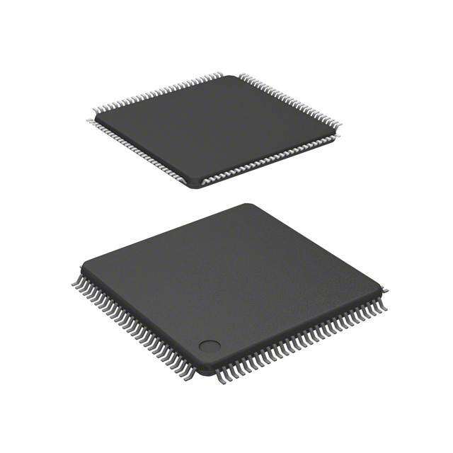
| 描述 | IC MCU 16BIT 256KB FLASH 80QFP |
| EEPROM容量 | 4K x 8 |
| 产品分类 | |
| I/O数 | 59 |
| 品牌 | Freescale Semiconductor |
| 数据手册 | |
| 产品图片 |
|
| 产品型号 | MC9S12XDT256MAA |
| PCN设计/规格 | http://cache.freescale.com/files/shared/doc/pcn/PCN16235.htm |
| RAM容量 | 16K x 8 |
| rohs | 无铅 / 符合限制有害物质指令(RoHS)规范要求 |
| 产品系列 | HCS12X |
| 供应商器件封装 | 80-QFP(14x14) |
| 包装 | 托盘 |
| 外设 | LVD,POR,PWM,WDT |
| 封装/外壳 | 80-QFP |
| 工作温度 | -40°C ~ 125°C |
| 振荡器类型 | 外部 |
| 数据转换器 | A/D 8x10b |
| 标准包装 | 420 |
| 核心处理器 | HCS12X |
| 核心尺寸 | 16-位 |
| 电压-电源(Vcc/Vdd) | 2.35 V ~ 5.5 V |
| 程序存储器类型 | 闪存 |
| 程序存储容量 | 256KB(256K x 8) |
| 连接性 | CAN, EBI/EMI, I²C, IrDA, LIN, SCI, SPI |
| 速度 | 80MHz |


- 商务部:美国ITC正式对集成电路等产品启动337调查
- 曝三星4nm工艺存在良率问题 高通将骁龙8 Gen1或转产台积电
- 太阳诱电将投资9.5亿元在常州建新厂生产MLCC 预计2023年完工
- 英特尔发布欧洲新工厂建设计划 深化IDM 2.0 战略
- 台积电先进制程称霸业界 有大客户加持明年业绩稳了
- 达到5530亿美元!SIA预计今年全球半导体销售额将创下新高
- 英特尔拟将自动驾驶子公司Mobileye上市 估值或超500亿美元
- 三星加码芯片和SET,合并消费电子和移动部门,撤换高东真等 CEO
- 三星电子宣布重大人事变动 还合并消费电子和移动部门
- 海关总署:前11个月进口集成电路产品价值2.52万亿元 增长14.8%


_renders/CS4265-CNZR.jpg)
PDF Datasheet 数据手册内容提取
MC9S12XDP512 Data Sheet Covers S12XD, S12XB & S12XA Families HCS12X Microcontrollers MC9S12XDP512RMV2 Rev. 2.21 October 2009 freescale.com
None
MC9S12XDP512RMV2 Data Sheet MC9S12XDP512RMV2 Rev. 2.21 October 2009
Toprovidethemostup-to-dateinformation,therevisionofourdocumentsontheWorldWideWebwillbe the most current. Your printed copymay bean earlier revision.To verify youhave thelatest information available, refer to: http://freescale.com/ A full list of family members and options is included in the appendices. Read page 29 first to understand the maskset specific chapters of this document Thisdocumentcontainsinformationforallconstituentmodules,withtheexceptionoftheS12XCPU.For S12X CPU information please refer to the CPU S12X Reference Manual. Freescale™ and the Freescale logo are trademarks of Freescale Semiconductor, Inc. This product incorporates SuperFlash® technology licensed from SST. ©Freescale Semiconductor, Inc., 2008. All rights reserved. MC9S12XDP512 Data Sheet, Rev. 2.21 4 Freescale Semiconductor
Revision History Revision Date Description Level April, 2005 02.07 New Book May, 2005 02.08 Minor corrections removed ESD Machine Model from electrical characteristics added thermal characteristics added more details to run current measurement configurations May, 2005 02.09 VDDA supply voltage range 3.15V - 3.6V fot ATD Operating Characteristics I/O Chararcteristics for alll pins except EXTAL, XTAL .... corrected VREG electrical spec IDD wait max 95mA May 2005 02.10 Improvements to NVM reliabity spec, added part numbers July 2005 02.11 Added ROM parts to App. October 2005 02.12 Single Souce S12XD Fam. Document, New Memory Map Figures, SPI electricals updated Voltage Regulator electricals updated May 2006 2.13 Added Partnumbers and 1L15Y maskset Updated App. E 6SCI’s on 112 pin DT/P512 and 3 SPI’s on all D256 parts Data Sheet covers S12XD/B & A Family June 2006 2.14 Included differnt pull device specification for differnt masksets July 2006 2.15 Minor Corrections and Improvments June 2007 2.16 Added 2M42E and 1M84E masksets July 2007 2.17 Modified Appendix Better explanation of ATD0/1 for S12XD-Family see page 1305 April 2008 2.18 S12XB256 ATD specification changed see Appendix E.6 added M23S maskset Corrected XGRAMSIZE of S12XD256 on page 44 August 2008 2.19 Corrected 17.4.2.4 XGATE Memory Map Scheme Corrected 18.4.2.4 XGATE Memory Map Scheme September 2.20 Corrected Table E-6 , 30K flash memory available for XGATE on B256 2009 October 2009 2.21 Corrected Footnote in Appendix E3 regarding Shared XGATE/CPU area MC9S12XDP512 Data Sheet, Rev. 2.21 Freescale Semiconductor 5
MC9S12XDP512 Data Sheet, Rev. 2.21 6 Freescale Semiconductor
Section Number Title Page Chapter 1 Device Overview MC9S12XD-Family . . . . . . . . . . . . . . . . . . . .31 Chapter 2 Clocks and Reset Generator (S12CRGV6). . . . . . . . . . . . . . . .79 Chapter 3 Pierce Oscillator (S12XOSCLCPV1) . . . . . . . . . . . . . . . . . . . .119 Chapter 4 Analog-to-Digital Converter (ATD10B16CV4) Block Description125 Chapter 5 Analog-to-Digital Converter (S12ATD10B8CV3) . . . . . . . . . .159 Chapter 6 XGATE (S12XGATEV2). . . . . . . . . . . . . . . . . . . . . . . . . . . . . . .183 Chapter 7 Enhanced Capture Timer (S12ECT16B8CV2) . . . . . . . . . . . .309 Chapter 8 Pulse-Width Modulator (S12PWM8B8CV1) . . . . . . . . . . . . . .363 Chapter 9 Inter-Integrated Circuit (IICV2) Block Description. . . . . . . . .395 Chapter 10 Freescale’s Scalable Controller Area Network (S12MSCANV3). 419 Chapter 11 Serial Communication Interface (S12SCIV5) . . . . . . . . . . . . .477 Chapter 12 Serial Peripheral Interface (S12SPIV4). . . . . . . . . . . . . . . . . .515 Chapter 13 Periodic Interrupt Timer (S12PIT24B4CV1) . . . . . . . . . . . . . .541 Chapter 14 Voltage Regulator (S12VREG3V3V5) . . . . . . . . . . . . . . . . . . .555 Chapter 15 Background Debug Module (S12XBDMV2) . . . . . . . . . . . . . .569 Chapter 16 Interrupt (S12XINTV1) . . . . . . . . . . . . . . . . . . . . . . . . . . . . . . .595 Chapter 17 Memory Mapping Control (S12XMMCV2). . . . . . . . . . . . . . . .613 Chapter 18 Memory Mapping Control (S12XMMCV3) . . . . . . . . . . . . . . .651 Chapter 19 S12X Debug (S12XDBGV2) Module . . . . . . . . . . . . . . . . . . . .693 Chapter 20 S12X Debug (S12XDBGV3) Module . . . . . . . . . . . . . . . . . . . .745 Chapter 21 External Bus Interface (S12XEBIV2) . . . . . . . . . . . . . . . . . . .787 Chapter 22 DP512 Port Integration Module (S12XDP512PIMV2). . . . . . .807 Chapter 23 DQ256 Port Integration Module (S12XDQ256PIMV2) . . . . . .901 Chapter 24 DG128 Port Integration Module (S12XDG128PIMV2) . . . . . .975 MC9S12XDP512 Data Sheet, Rev. 2.21 Freescale Semiconductor 5
Section Number Title Page Chapter 25 2 Kbyte EEPROM Module (S12XEETX2KV1) . . . . . . . . . . . .1039 Chapter 26 4 Kbyte EEPROM Module (S12XEETX4KV2) . . . . . . . . . . . .1073 Chapter 27 512 Kbyte Flash Module (S12XFTX512K4V2). . . . . . . . . . . .1107 Chapter 28 256 Kbyte Flash Module (S12XFTX256K2V1). . . . . . . . . . . .1149 Chapter 29 128 Kbyte Flash Module (S12XFTX128K1V1). . . . . . . . . . . .1191 Chapter 30 Security (S12X9SECV2) . . . . . . . . . . . . . . . . . . . . . . . . . . . .1231 Appendix A Electrical Characteristics. . . . . . . . . . . . . . . . . . . . . . . . . . . .1239 Appendix B Package Information . . . . . . . . . . . . . . . . . . . . . . . . . . . . . . .1290 Appendix C Recommended PCB Layout . . . . . . . . . . . . . . . . . . . . . . . . .1294 Appendix D Using L15Y Silicon. . . . . . . . . . . . . . . . . . . . . . . . . . . . . . . . .1299 Appendix E Derivative Differences . . . . . . . . . . . . . . . . . . . . . . . . . . . . . .1300 Appendix F Ordering Information . . . . . . . . . . . . . . . . . . . . . . . . . . . . . . .1308 Appendix G Detailed Register Map . . . . . . . . . . . . . . . . . . . . . . . . . . . . . .1309 MC9S12XDP512 Data Sheet, Rev. 2.21 6 Freescale Semiconductor
Section Number Title Page Chapter 1Device Overview MC9S12XD-Family 1.1 Introduction . . . . . . . . . . . . . . . . . . . . . . . . . . . . . . . . . . . . . . . . . . . . . . . . . . . . . . . . . . . . . . . . . .31 1.1.1 MC9S12XD/B/A Family Features . . . . . . . . . . . . . . . . . . . . . . . . . . . . . . . . . . . . . . . . . .32 1.1.2 Modes of Operation . . . . . . . . . . . . . . . . . . . . . . . . . . . . . . . . . . . . . . . . . . . . . . . . . . . . .34 1.1.3 Block Diagram . . . . . . . . . . . . . . . . . . . . . . . . . . . . . . . . . . . . . . . . . . . . . . . . . . . . . . . . .34 1.1.4 Device Memory Map . . . . . . . . . . . . . . . . . . . . . . . . . . . . . . . . . . . . . . . . . . . . . . . . . . . .37 1.1.5 Part ID Assignments & Maskset Numbers . . . . . . . . . . . . . . . . . . . . . . . . . . . . . . . . . . .47 1.2 Signal Description . . . . . . . . . . . . . . . . . . . . . . . . . . . . . . . . . . . . . . . . . . . . . . . . . . . . . . . . . . . . .47 1.2.1 Device Pinout . . . . . . . . . . . . . . . . . . . . . . . . . . . . . . . . . . . . . . . . . . . . . . . . . . . . . . . . . .47 1.2.2 Signal Properties Summary . . . . . . . . . . . . . . . . . . . . . . . . . . . . . . . . . . . . . . . . . . . . . . .52 1.2.3 Detailed Signal Descriptions . . . . . . . . . . . . . . . . . . . . . . . . . . . . . . . . . . . . . . . . . . . . . .55 1.2.4 Power Supply Pins . . . . . . . . . . . . . . . . . . . . . . . . . . . . . . . . . . . . . . . . . . . . . . . . . . . . . .65 1.3 System Clock Description . . . . . . . . . . . . . . . . . . . . . . . . . . . . . . . . . . . . . . . . . . . . . . . . . . . . . . .68 1.4 Chip Configuration Summary . . . . . . . . . . . . . . . . . . . . . . . . . . . . . . . . . . . . . . . . . . . . . . . . . . . .69 1.5 Modes of Operation . . . . . . . . . . . . . . . . . . . . . . . . . . . . . . . . . . . . . . . . . . . . . . . . . . . . . . . . . . . .71 1.5.1 User Modes . . . . . . . . . . . . . . . . . . . . . . . . . . . . . . . . . . . . . . . . . . . . . . . . . . . . . . . . . . .71 1.5.2 Low-Power Modes . . . . . . . . . . . . . . . . . . . . . . . . . . . . . . . . . . . . . . . . . . . . . . . . . . . . . . 71 1.5.3 Freeze Mode . . . . . . . . . . . . . . . . . . . . . . . . . . . . . . . . . . . . . . . . . . . . . . . . . . . . . . . . . . .72 1.6 Resets and Interrupts . . . . . . . . . . . . . . . . . . . . . . . . . . . . . . . . . . . . . . . . . . . . . . . . . . . . . . . . . . .72 1.6.1 Vectors . . . . . . . . . . . . . . . . . . . . . . . . . . . . . . . . . . . . . . . . . . . . . . . . . . . . . . . . . . . . . . .72 1.6.2 Effects of Reset . . . . . . . . . . . . . . . . . . . . . . . . . . . . . . . . . . . . . . . . . . . . . . . . . . . . . . . .76 1.7 COP Configuration . . . . . . . . . . . . . . . . . . . . . . . . . . . . . . . . . . . . . . . . . . . . . . . . . . . . . . . . . . . . .76 1.8 ATD0 External Trigger Input Connection . . . . . . . . . . . . . . . . . . . . . . . . . . . . . . . . . . . . . . . . . . . 77 1.9 ATD1 External Trigger Input Connection . . . . . . . . . . . . . . . . . . . . . . . . . . . . . . . . . . . . . . . . . . . 77 Chapter 2 Clocks and Reset Generator (S12CRGV6) 2.1 Introduction . . . . . . . . . . . . . . . . . . . . . . . . . . . . . . . . . . . . . . . . . . . . . . . . . . . . . . . . . . . . . . . . . .79 2.1.1 Features . . . . . . . . . . . . . . . . . . . . . . . . . . . . . . . . . . . . . . . . . . . . . . . . . . . . . . . . . . . . . .79 2.1.2 Modes of Operation . . . . . . . . . . . . . . . . . . . . . . . . . . . . . . . . . . . . . . . . . . . . . . . . . . . . .80 2.1.3 Block Diagram . . . . . . . . . . . . . . . . . . . . . . . . . . . . . . . . . . . . . . . . . . . . . . . . . . . . . . . . .81 2.2 External Signal Description . . . . . . . . . . . . . . . . . . . . . . . . . . . . . . . . . . . . . . . . . . . . . . . . . . . . . .82 2.2.1 V and V — Operating and Ground Voltage Pins . . . . . . . . . . . . . . . . . . . . .82 DDPLL SSPLL 2.2.2 XFC — External Loop Filter Pin . . . . . . . . . . . . . . . . . . . . . . . . . . . . . . . . . . . . . . . . . . .82 2.2.3 RESET — Reset Pin . . . . . . . . . . . . . . . . . . . . . . . . . . . . . . . . . . . . . . . . . . . . . . . . . . . .82 2.3 Memory Map and Register Definition . . . . . . . . . . . . . . . . . . . . . . . . . . . . . . . . . . . . . . . . . . . . . .82 2.3.1 Module Memory Map . . . . . . . . . . . . . . . . . . . . . . . . . . . . . . . . . . . . . . . . . . . . . . . . . . .83 2.3.2 Register Descriptions . . . . . . . . . . . . . . . . . . . . . . . . . . . . . . . . . . . . . . . . . . . . . . . . . . . .84 2.4 Functional Description . . . . . . . . . . . . . . . . . . . . . . . . . . . . . . . . . . . . . . . . . . . . . . . . . . . . . . . . . .98 2.4.1 Functional Blocks . . . . . . . . . . . . . . . . . . . . . . . . . . . . . . . . . . . . . . . . . . . . . . . . . . . . . .98 2.4.2 Operating Modes . . . . . . . . . . . . . . . . . . . . . . . . . . . . . . . . . . . . . . . . . . . . . . . . . . . . . .103 2.4.3 Low Power Options . . . . . . . . . . . . . . . . . . . . . . . . . . . . . . . . . . . . . . . . . . . . . . . . . . . .104 MC9S12XDP512 Data Sheet, Rev. 2.21 Freescale Semiconductor 9
Section Number Title Page 2.5 Resets . . . . . . . . . . . . . . . . . . . . . . . . . . . . . . . . . . . . . . . . . . . . . . . . . . . . . . . . . . . . . . . . . . . . . .113 2.5.1 Description of Reset Operation . . . . . . . . . . . . . . . . . . . . . . . . . . . . . . . . . . . . . . . . . . .113 2.5.2 Clock Monitor Reset . . . . . . . . . . . . . . . . . . . . . . . . . . . . . . . . . . . . . . . . . . . . . . . . . . .115 2.5.3 Computer Operating Properly Watchdog (COP) Reset . . . . . . . . . . . . . . . . . . . . . . . . .115 2.5.4 Power On Reset, Low Voltage Reset . . . . . . . . . . . . . . . . . . . . . . . . . . . . . . . . . . . . . . .115 2.6 Interrupts . . . . . . . . . . . . . . . . . . . . . . . . . . . . . . . . . . . . . . . . . . . . . . . . . . . . . . . . . . . . . . . . . . .116 2.6.1 Real Time Interrupt . . . . . . . . . . . . . . . . . . . . . . . . . . . . . . . . . . . . . . . . . . . . . . . . . . . .116 2.6.2 PLL Lock Interrupt . . . . . . . . . . . . . . . . . . . . . . . . . . . . . . . . . . . . . . . . . . . . . . . . . . . . 117 2.6.3 Self Clock Mode Interrupt . . . . . . . . . . . . . . . . . . . . . . . . . . . . . . . . . . . . . . . . . . . . . . .117 Chapter 3 Pierce Oscillator (S12XOSCLCPV1) 3.1 Introduction . . . . . . . . . . . . . . . . . . . . . . . . . . . . . . . . . . . . . . . . . . . . . . . . . . . . . . . . . . . . . . . . .119 3.1.1 Features . . . . . . . . . . . . . . . . . . . . . . . . . . . . . . . . . . . . . . . . . . . . . . . . . . . . . . . . . . . . .119 3.1.2 Modes of Operation . . . . . . . . . . . . . . . . . . . . . . . . . . . . . . . . . . . . . . . . . . . . . . . . . . . .119 3.1.3 Block Diagram . . . . . . . . . . . . . . . . . . . . . . . . . . . . . . . . . . . . . . . . . . . . . . . . . . . . . . . .120 3.2 External Signal Description . . . . . . . . . . . . . . . . . . . . . . . . . . . . . . . . . . . . . . . . . . . . . . . . . . . . .120 3.2.1 V and V — Operating and Ground Voltage Pins . . . . . . . . . . . . . . . . . . . .120 DDPLL SSPLL 3.2.2 EXTAL and XTAL — Input and Output Pins . . . . . . . . . . . . . . . . . . . . . . . . . . . . . . . .120 3.2.3 XCLKS — Input Signal . . . . . . . . . . . . . . . . . . . . . . . . . . . . . . . . . . . . . . . . . . . . . . . . .122 3.3 Memory Map and Register Definition . . . . . . . . . . . . . . . . . . . . . . . . . . . . . . . . . . . . . . . . . . . . .122 3.4 Functional Description . . . . . . . . . . . . . . . . . . . . . . . . . . . . . . . . . . . . . . . . . . . . . . . . . . . . . . . . .122 3.4.1 Gain Control. . . . . . . . . . . . . . . . . . . . . . . . . . . . . . . . . . . . . . . . . . . . . . . . . . . . . . . . . .122 3.4.2 Clock Monitor . . . . . . . . . . . . . . . . . . . . . . . . . . . . . . . . . . . . . . . . . . . . . . . . . . . . . . . .122 3.4.3 Wait Mode Operation . . . . . . . . . . . . . . . . . . . . . . . . . . . . . . . . . . . . . . . . . . . . . . . . . . .123 3.4.4 Stop Mode Operation . . . . . . . . . . . . . . . . . . . . . . . . . . . . . . . . . . . . . . . . . . . . . . . . . . .123 Chapter 4 Analog-to-Digital Converter (ATD10B16CV4) Block Description 4.1 Introduction . . . . . . . . . . . . . . . . . . . . . . . . . . . . . . . . . . . . . . . . . . . . . . . . . . . . . . . . . . . . . . . . .125 4.1.1 Features . . . . . . . . . . . . . . . . . . . . . . . . . . . . . . . . . . . . . . . . . . . . . . . . . . . . . . . . . . . . .125 4.1.2 Modes of Operation . . . . . . . . . . . . . . . . . . . . . . . . . . . . . . . . . . . . . . . . . . . . . . . . . . . .125 4.1.3 Block Diagram . . . . . . . . . . . . . . . . . . . . . . . . . . . . . . . . . . . . . . . . . . . . . . . . . . . . . . . .125 4.2 External Signal Description . . . . . . . . . . . . . . . . . . . . . . . . . . . . . . . . . . . . . . . . . . . . . . . . . . . . .127 4.2.1 ANx(x=15,14,13,12,11,10,9,8,7,6,5,4,3,2,1,0)—AnalogInputChannelxPins 127 4.2.2 ETRIG3, ETRIG2, ETRIG1, ETRIG0 — External Trigger Pins . . . . . . . . . . . . . . . . .127 4.2.3 V , V — High Reference Voltage Pin, Low Reference Voltage Pin . . . . . . . . . . . .127 RH RL 4.2.4 V , V — Analog Circuitry Power Supply Pins . . . . . . . . . . . . . . . . . . . . . . . . .127 DDA SSA 4.3 Memory Map and Register Definition . . . . . . . . . . . . . . . . . . . . . . . . . . . . . . . . . . . . . . . . . . . . .127 MC9S12XDP512 Data Sheet, Rev. 2.21 10 Freescale Semiconductor
Section Number Title Page 4.3.1 Module Memory Map . . . . . . . . . . . . . . . . . . . . . . . . . . . . . . . . . . . . . . . . . . . . . . . . . .127 4.3.2 Register Descriptions . . . . . . . . . . . . . . . . . . . . . . . . . . . . . . . . . . . . . . . . . . . . . . . . . . . 129 4.4 Functional Description . . . . . . . . . . . . . . . . . . . . . . . . . . . . . . . . . . . . . . . . . . . . . . . . . . . . . . . . .152 4.4.1 Analog Sub-block . . . . . . . . . . . . . . . . . . . . . . . . . . . . . . . . . . . . . . . . . . . . . . . . . . . . . 152 4.4.2 Digital Sub-Block . . . . . . . . . . . . . . . . . . . . . . . . . . . . . . . . . . . . . . . . . . . . . . . . . . . . .153 4.4.3 Operation in Low Power Modes . . . . . . . . . . . . . . . . . . . . . . . . . . . . . . . . . . . . . . . . . .154 4.5 Resets . . . . . . . . . . . . . . . . . . . . . . . . . . . . . . . . . . . . . . . . . . . . . . . . . . . . . . . . . . . . . . . . . . . . . .155 4.6 Interrupts . . . . . . . . . . . . . . . . . . . . . . . . . . . . . . . . . . . . . . . . . . . . . . . . . . . . . . . . . . . . . . . . . . .155 Chapter 5Analog-to-Digital Converter (S12ATD10B8CV3) 5.1 Introduction . . . . . . . . . . . . . . . . . . . . . . . . . . . . . . . . . . . . . . . . . . . . . . . . . . . . . . . . . . . . . . . . .159 5.1.1 Features . . . . . . . . . . . . . . . . . . . . . . . . . . . . . . . . . . . . . . . . . . . . . . . . . . . . . . . . . . . . .159 5.1.2 Modes of Operation . . . . . . . . . . . . . . . . . . . . . . . . . . . . . . . . . . . . . . . . . . . . . . . . . . . .159 5.1.3 Block Diagram . . . . . . . . . . . . . . . . . . . . . . . . . . . . . . . . . . . . . . . . . . . . . . . . . . . . . . . .160 5.2 External Signal Description . . . . . . . . . . . . . . . . . . . . . . . . . . . . . . . . . . . . . . . . . . . . . . . . . . . . .160 5.2.1 ANx (x = 7, 6, 5, 4, 3, 2, 1, 0) — Analog Input Pin . . . . . . . . . . . . . . . . . . . . . . . . . . .160 5.2.2 ETRIG3, ETRIG2, ETRIG1, and ETRIG0 — External Trigger Pins . . . . . . . . . . . . . .160 5.2.3 V V — High and Low Reference Voltage Pins . . . . . . . . . . . . . . . . . . . . . . . .160 RH and RL 5.2.4 V and V — Power Supply Pins . . . . . . . . . . . . . . . . . . . . . . . . . . . . . . . . . . . . .160 DDA SSA 5.3 Memory Map and Register Definition . . . . . . . . . . . . . . . . . . . . . . . . . . . . . . . . . . . . . . . . . . . . .162 5.3.1 Module Memory Map . . . . . . . . . . . . . . . . . . . . . . . . . . . . . . . . . . . . . . . . . . . . . . . . . .162 5.3.2 Register Descriptions . . . . . . . . . . . . . . . . . . . . . . . . . . . . . . . . . . . . . . . . . . . . . . . . . . . 162 5.4 Functional Description . . . . . . . . . . . . . . . . . . . . . . . . . . . . . . . . . . . . . . . . . . . . . . . . . . . . . . . . .180 5.4.1 Analog Sub-Block . . . . . . . . . . . . . . . . . . . . . . . . . . . . . . . . . . . . . . . . . . . . . . . . . . . . . 180 5.4.2 Digital Sub-Block . . . . . . . . . . . . . . . . . . . . . . . . . . . . . . . . . . . . . . . . . . . . . . . . . . . . .181 5.5 Resets . . . . . . . . . . . . . . . . . . . . . . . . . . . . . . . . . . . . . . . . . . . . . . . . . . . . . . . . . . . . . . . . . . . . . .182 5.6 Interrupts . . . . . . . . . . . . . . . . . . . . . . . . . . . . . . . . . . . . . . . . . . . . . . . . . . . . . . . . . . . . . . . . . . .182 Chapter 6 XGATE (S12XGATEV2) 6.1 Introduction . . . . . . . . . . . . . . . . . . . . . . . . . . . . . . . . . . . . . . . . . . . . . . . . . . . . . . . . . . . . . . . . .183 6.1.1 Glossary of Terms . . . . . . . . . . . . . . . . . . . . . . . . . . . . . . . . . . . . . . . . . . . . . . . . . . . . .183 6.1.2 Features . . . . . . . . . . . . . . . . . . . . . . . . . . . . . . . . . . . . . . . . . . . . . . . . . . . . . . . . . . . . .184 6.1.3 Modes of Operation . . . . . . . . . . . . . . . . . . . . . . . . . . . . . . . . . . . . . . . . . . . . . . . . . . . .184 6.1.4 Block Diagram . . . . . . . . . . . . . . . . . . . . . . . . . . . . . . . . . . . . . . . . . . . . . . . . . . . . . . . .185 6.2 External Signal Description . . . . . . . . . . . . . . . . . . . . . . . . . . . . . . . . . . . . . . . . . . . . . . . . . . . . .185 6.3 Memory Map and Register Definition . . . . . . . . . . . . . . . . . . . . . . . . . . . . . . . . . . . . . . . . . . . . .186 6.3.1 Register Descriptions . . . . . . . . . . . . . . . . . . . . . . . . . . . . . . . . . . . . . . . . . . . . . . . . . . . 186 6.4 Functional Description . . . . . . . . . . . . . . . . . . . . . . . . . . . . . . . . . . . . . . . . . . . . . . . . . . . . . . . . .202 6.4.1 XGATE RISC Core . . . . . . . . . . . . . . . . . . . . . . . . . . . . . . . . . . . . . . . . . . . . . . . . . . . .202 6.4.2 Programmer’s Model . . . . . . . . . . . . . . . . . . . . . . . . . . . . . . . . . . . . . . . . . . . . . . . . . . .202 6.4.3 Memory Map . . . . . . . . . . . . . . . . . . . . . . . . . . . . . . . . . . . . . . . . . . . . . . . . . . . . . . . . .203 MC9S12XDP512 Data Sheet, Rev. 2.21 Freescale Semiconductor 11
Section Number Title Page 6.4.4 Semaphores . . . . . . . . . . . . . . . . . . . . . . . . . . . . . . . . . . . . . . . . . . . . . . . . . . . . . . . . . .204 6.4.5 Software Error Detection . . . . . . . . . . . . . . . . . . . . . . . . . . . . . . . . . . . . . . . . . . . . . . . .205 6.5 Interrupts . . . . . . . . . . . . . . . . . . . . . . . . . . . . . . . . . . . . . . . . . . . . . . . . . . . . . . . . . . . . . . . . . . .206 6.5.1 Incoming Interrupt Requests . . . . . . . . . . . . . . . . . . . . . . . . . . . . . . . . . . . . . . . . . . . . .206 6.5.2 Outgoing Interrupt Requests . . . . . . . . . . . . . . . . . . . . . . . . . . . . . . . . . . . . . . . . . . . . .206 6.6 Debug Mode . . . . . . . . . . . . . . . . . . . . . . . . . . . . . . . . . . . . . . . . . . . . . . . . . . . . . . . . . . . . . . . . .206 6.6.1 Debug Features . . . . . . . . . . . . . . . . . . . . . . . . . . . . . . . . . . . . . . . . . . . . . . . . . . . . . . .206 6.6.2 Entering Debug Mode . . . . . . . . . . . . . . . . . . . . . . . . . . . . . . . . . . . . . . . . . . . . . . . . . .207 6.6.3 Leaving Debug Mode . . . . . . . . . . . . . . . . . . . . . . . . . . . . . . . . . . . . . . . . . . . . . . . . . . .208 6.7 Security . . . . . . . . . . . . . . . . . . . . . . . . . . . . . . . . . . . . . . . . . . . . . . . . . . . . . . . . . . . . . . . . . . . . .208 6.8 Instruction Set . . . . . . . . . . . . . . . . . . . . . . . . . . . . . . . . . . . . . . . . . . . . . . . . . . . . . . . . . . . . . . .208 6.8.1 Addressing Modes . . . . . . . . . . . . . . . . . . . . . . . . . . . . . . . . . . . . . . . . . . . . . . . . . . . . .208 6.8.2 Instruction Summary and Usage . . . . . . . . . . . . . . . . . . . . . . . . . . . . . . . . . . . . . . . . . .212 6.8.3 Cycle Notation . . . . . . . . . . . . . . . . . . . . . . . . . . . . . . . . . . . . . . . . . . . . . . . . . . . . . . . .215 6.8.4 Thread Execution . . . . . . . . . . . . . . . . . . . . . . . . . . . . . . . . . . . . . . . . . . . . . . . . . . . . . .215 6.8.5 Instruction Glossary . . . . . . . . . . . . . . . . . . . . . . . . . . . . . . . . . . . . . . . . . . . . . . . . . . . .215 6.8.6 Instruction Coding . . . . . . . . . . . . . . . . . . . . . . . . . . . . . . . . . . . . . . . . . . . . . . . . . . . . .288 6.9 Initialization and Application Information . . . . . . . . . . . . . . . . . . . . . . . . . . . . . . . . . . . . . . . . . .291 6.9.1 Initialization . . . . . . . . . . . . . . . . . . . . . . . . . . . . . . . . . . . . . . . . . . . . . . . . . . . . . . . . . .291 6.9.2 Code Example (Transmit "Hello World!" on SCI) . . . . . . . . . . . . . . . . . . . . . . . . . . . .291 Chapter 7 Enhanced Capture Timer (S12ECT16B8CV2) 7.1 Introduction . . . . . . . . . . . . . . . . . . . . . . . . . . . . . . . . . . . . . . . . . . . . . . . . . . . . . . . . . . . . . . . . .309 7.1.1 Features . . . . . . . . . . . . . . . . . . . . . . . . . . . . . . . . . . . . . . . . . . . . . . . . . . . . . . . . . . . . .309 7.1.2 Modes of Operation . . . . . . . . . . . . . . . . . . . . . . . . . . . . . . . . . . . . . . . . . . . . . . . . . . . .309 7.1.3 Block Diagram . . . . . . . . . . . . . . . . . . . . . . . . . . . . . . . . . . . . . . . . . . . . . . . . . . . . . . . .310 7.2 External Signal Description . . . . . . . . . . . . . . . . . . . . . . . . . . . . . . . . . . . . . . . . . . . . . . . . . . . . .311 7.2.1 IOC7 — Input Capture and Output Compare Channel 7 . . . . . . . . . . . . . . . . . . . . . . . .311 7.2.2 IOC6 — Input Capture and Output Compare Channel 6 . . . . . . . . . . . . . . . . . . . . . . . .311 7.2.3 IOC5 — Input Capture and Output Compare Channel 5 . . . . . . . . . . . . . . . . . . . . . . . .311 7.2.4 IOC4 — Input Capture and Output Compare Channel 4 . . . . . . . . . . . . . . . . . . . . . . . .311 7.2.5 IOC3 — Input Capture and Output Compare Channel 3 . . . . . . . . . . . . . . . . . . . . . . . .311 7.2.6 IOC2 — Input Capture and Output Compare Channel 2 . . . . . . . . . . . . . . . . . . . . . . . .311 7.2.7 IOC1 — Input Capture and Output Compare Channel 1 . . . . . . . . . . . . . . . . . . . . . . . .311 7.2.8 IOC0 — Input Capture and Output Compare Channel 0 . . . . . . . . . . . . . . . . . . . . . . . .311 7.3 Memory Map and Register Definition . . . . . . . . . . . . . . . . . . . . . . . . . . . . . . . . . . . . . . . . . . . . .312 7.3.1 Module Memory Map . . . . . . . . . . . . . . . . . . . . . . . . . . . . . . . . . . . . . . . . . . . . . . . . . .312 7.3.2 Register Descriptions . . . . . . . . . . . . . . . . . . . . . . . . . . . . . . . . . . . . . . . . . . . . . . . . . . . 314 7.4 Functional Description . . . . . . . . . . . . . . . . . . . . . . . . . . . . . . . . . . . . . . . . . . . . . . . . . . . . . . . . .350 7.4.1 Enhanced Capture Timer Modes of Operation . . . . . . . . . . . . . . . . . . . . . . . . . . . . . . .357 7.4.2 Reset . . . . . . . . . . . . . . . . . . . . . . . . . . . . . . . . . . . . . . . . . . . . . . . . . . . . . . . . . . . . . . . .360 MC9S12XDP512 Data Sheet, Rev. 2.21 12 Freescale Semiconductor
Section Number Title Page 7.4.3 Interrupts . . . . . . . . . . . . . . . . . . . . . . . . . . . . . . . . . . . . . . . . . . . . . . . . . . . . . . . . . . . .361 Chapter 8 Pulse-Width Modulator (S12PWM8B8CV1) 8.1 Introduction . . . . . . . . . . . . . . . . . . . . . . . . . . . . . . . . . . . . . . . . . . . . . . . . . . . . . . . . . . . . . . . . .363 8.1.1 Features . . . . . . . . . . . . . . . . . . . . . . . . . . . . . . . . . . . . . . . . . . . . . . . . . . . . . . . . . . . . .363 8.1.2 Modes of Operation . . . . . . . . . . . . . . . . . . . . . . . . . . . . . . . . . . . . . . . . . . . . . . . . . . . .363 8.1.3 Block Diagram . . . . . . . . . . . . . . . . . . . . . . . . . . . . . . . . . . . . . . . . . . . . . . . . . . . . . . . .364 8.2 External Signal Description . . . . . . . . . . . . . . . . . . . . . . . . . . . . . . . . . . . . . . . . . . . . . . . . . . . . .364 8.2.1 PWM7 — PWM Channel 7 . . . . . . . . . . . . . . . . . . . . . . . . . . . . . . . . . . . . . . . . . . . . . .364 8.2.2 PWM6 — PWM Channel 6 . . . . . . . . . . . . . . . . . . . . . . . . . . . . . . . . . . . . . . . . . . . . . .364 8.2.3 PWM5 — PWM Channel 5 . . . . . . . . . . . . . . . . . . . . . . . . . . . . . . . . . . . . . . . . . . . . . .365 8.2.4 PWM4 — PWM Channel 4 . . . . . . . . . . . . . . . . . . . . . . . . . . . . . . . . . . . . . . . . . . . . . .365 8.2.5 PWM3 — PWM Channel 3 . . . . . . . . . . . . . . . . . . . . . . . . . . . . . . . . . . . . . . . . . . . . . .365 8.2.6 PWM3 — PWM Channel 2 . . . . . . . . . . . . . . . . . . . . . . . . . . . . . . . . . . . . . . . . . . . . . .365 8.2.7 PWM3 — PWM Channel 1 . . . . . . . . . . . . . . . . . . . . . . . . . . . . . . . . . . . . . . . . . . . . . .365 8.2.8 PWM3 — PWM Channel 0 . . . . . . . . . . . . . . . . . . . . . . . . . . . . . . . . . . . . . . . . . . . . . .365 8.3 Memory Map and Register Definition . . . . . . . . . . . . . . . . . . . . . . . . . . . . . . . . . . . . . . . . . . . . .365 8.3.1 Module Memory Map . . . . . . . . . . . . . . . . . . . . . . . . . . . . . . . . . . . . . . . . . . . . . . . . . .365 8.3.2 Register Descriptions . . . . . . . . . . . . . . . . . . . . . . . . . . . . . . . . . . . . . . . . . . . . . . . . . . . 366 8.4 Functional Description . . . . . . . . . . . . . . . . . . . . . . . . . . . . . . . . . . . . . . . . . . . . . . . . . . . . . . . . .380 8.4.1 PWM Clock Select . . . . . . . . . . . . . . . . . . . . . . . . . . . . . . . . . . . . . . . . . . . . . . . . . . . . .380 8.4.2 PWM Channel Timers . . . . . . . . . . . . . . . . . . . . . . . . . . . . . . . . . . . . . . . . . . . . . . . . . .384 8.5 Resets . . . . . . . . . . . . . . . . . . . . . . . . . . . . . . . . . . . . . . . . . . . . . . . . . . . . . . . . . . . . . . . . . . . . . .392 8.6 Interrupts . . . . . . . . . . . . . . . . . . . . . . . . . . . . . . . . . . . . . . . . . . . . . . . . . . . . . . . . . . . . . . . . . . .393 Chapter 9 Inter-Integrated Circuit (IICV2) Block Description 9.1 Introduction . . . . . . . . . . . . . . . . . . . . . . . . . . . . . . . . . . . . . . . . . . . . . . . . . . . . . . . . . . . . . . . . .395 9.1.1 Features . . . . . . . . . . . . . . . . . . . . . . . . . . . . . . . . . . . . . . . . . . . . . . . . . . . . . . . . . . . . .395 9.1.2 Modes of Operation . . . . . . . . . . . . . . . . . . . . . . . . . . . . . . . . . . . . . . . . . . . . . . . . . . . .396 9.1.3 Block Diagram . . . . . . . . . . . . . . . . . . . . . . . . . . . . . . . . . . . . . . . . . . . . . . . . . . . . . . . .396 9.2 External Signal Description . . . . . . . . . . . . . . . . . . . . . . . . . . . . . . . . . . . . . . . . . . . . . . . . . . . . .397 9.2.1 IIC_SCL — Serial Clock Line Pin . . . . . . . . . . . . . . . . . . . . . . . . . . . . . . . . . . . . . . . .397 9.2.2 IIC_SDA — Serial Data Line Pin . . . . . . . . . . . . . . . . . . . . . . . . . . . . . . . . . . . . . . . . .397 9.3 Memory Map and Register Definition . . . . . . . . . . . . . . . . . . . . . . . . . . . . . . . . . . . . . . . . . . . . .397 9.3.1 Module Memory Map . . . . . . . . . . . . . . . . . . . . . . . . . . . . . . . . . . . . . . . . . . . . . . . . . .397 9.3.2 Register Descriptions . . . . . . . . . . . . . . . . . . . . . . . . . . . . . . . . . . . . . . . . . . . . . . . . . . . 398 9.4 Functional Description . . . . . . . . . . . . . . . . . . . . . . . . . . . . . . . . . . . . . . . . . . . . . . . . . . . . . . . . .409 9.4.1 I-Bus Protocol . . . . . . . . . . . . . . . . . . . . . . . . . . . . . . . . . . . . . . . . . . . . . . . . . . . . . . . .409 9.4.2 Operation in Run Mode . . . . . . . . . . . . . . . . . . . . . . . . . . . . . . . . . . . . . . . . . . . . . . . . .412 9.4.3 Operation in Wait Mode . . . . . . . . . . . . . . . . . . . . . . . . . . . . . . . . . . . . . . . . . . . . . . . . .412 MC9S12XDP512 Data Sheet, Rev. 2.21 Freescale Semiconductor 13
Section Number Title Page 9.4.4 Operation in Stop Mode . . . . . . . . . . . . . . . . . . . . . . . . . . . . . . . . . . . . . . . . . . . . . . . . .412 9.5 Resets . . . . . . . . . . . . . . . . . . . . . . . . . . . . . . . . . . . . . . . . . . . . . . . . . . . . . . . . . . . . . . . . . . . . . .413 9.6 Interrupts . . . . . . . . . . . . . . . . . . . . . . . . . . . . . . . . . . . . . . . . . . . . . . . . . . . . . . . . . . . . . . . . . . .413 9.7 Initialization/Application Information . . . . . . . . . . . . . . . . . . . . . . . . . . . . . . . . . . . . . . . . . . . . .413 9.7.1 IIC Programming Examples . . . . . . . . . . . . . . . . . . . . . . . . . . . . . . . . . . . . . . . . . . . . .413 Chapter 10 Freescale’s Scalable Controller Area Network (S12MSCANV3) 10.1 Introduction . . . . . . . . . . . . . . . . . . . . . . . . . . . . . . . . . . . . . . . . . . . . . . . . . . . . . . . . . . . . . . . . .419 10.1.1 Glossary . . . . . . . . . . . . . . . . . . . . . . . . . . . . . . . . . . . . . . . . . . . . . . . . . . . . . . . . . . . . .419 10.1.2 Block Diagram . . . . . . . . . . . . . . . . . . . . . . . . . . . . . . . . . . . . . . . . . . . . . . . . . . . . . . . .420 10.1.3 Features . . . . . . . . . . . . . . . . . . . . . . . . . . . . . . . . . . . . . . . . . . . . . . . . . . . . . . . . . . . . .420 10.1.4 Modes of Operation . . . . . . . . . . . . . . . . . . . . . . . . . . . . . . . . . . . . . . . . . . . . . . . . . . . . 421 10.2 External Signal Description . . . . . . . . . . . . . . . . . . . . . . . . . . . . . . . . . . . . . . . . . . . . . . . . . . . . .421 10.2.1 RXCAN — CAN Receiver Input Pin . . . . . . . . . . . . . . . . . . . . . . . . . . . . . . . . . . . . . .421 10.2.2 TXCAN — CAN Transmitter Output Pin . . . . . . . . . . . . . . . . . . . . . . . . . . . . . . . . . .421 10.2.3 CAN System . . . . . . . . . . . . . . . . . . . . . . . . . . . . . . . . . . . . . . . . . . . . . . . . . . . . . . . . .421 10.3 Memory Map and Register Definition . . . . . . . . . . . . . . . . . . . . . . . . . . . . . . . . . . . . . . . . . . . . . 422 10.3.1 Module Memory Map . . . . . . . . . . . . . . . . . . . . . . . . . . . . . . . . . . . . . . . . . . . . . . . . . .422 10.3.2 Register Descriptions . . . . . . . . . . . . . . . . . . . . . . . . . . . . . . . . . . . . . . . . . . . . . . . . . . .424 10.3.3 Programmer’s Model of Message Storage . . . . . . . . . . . . . . . . . . . . . . . . . . . . . . . . . . .445 10.4 Functional Description . . . . . . . . . . . . . . . . . . . . . . . . . . . . . . . . . . . . . . . . . . . . . . . . . . . . . . . . .456 10.4.1 General . . . . . . . . . . . . . . . . . . . . . . . . . . . . . . . . . . . . . . . . . . . . . . . . . . . . . . . . . . . . . .456 10.4.2 Message Storage . . . . . . . . . . . . . . . . . . . . . . . . . . . . . . . . . . . . . . . . . . . . . . . . . . . . . .457 10.4.3 Identifier Acceptance Filter . . . . . . . . . . . . . . . . . . . . . . . . . . . . . . . . . . . . . . . . . . . . . .460 10.4.4 Modes of Operation . . . . . . . . . . . . . . . . . . . . . . . . . . . . . . . . . . . . . . . . . . . . . . . . . . . . 466 10.4.5 Low-Power Options . . . . . . . . . . . . . . . . . . . . . . . . . . . . . . . . . . . . . . . . . . . . . . . . . . . .467 10.4.6 Reset Initialization . . . . . . . . . . . . . . . . . . . . . . . . . . . . . . . . . . . . . . . . . . . . . . . . . . . . .472 10.4.7 Interrupts . . . . . . . . . . . . . . . . . . . . . . . . . . . . . . . . . . . . . . . . . . . . . . . . . . . . . . . . . . . .472 10.5 Initialization/Application Information . . . . . . . . . . . . . . . . . . . . . . . . . . . . . . . . . . . . . . . . . . . . .474 10.5.1 MSCAN initialization . . . . . . . . . . . . . . . . . . . . . . . . . . . . . . . . . . . . . . . . . . . . . . . . . .474 10.5.2 Bus-Off Recovery . . . . . . . . . . . . . . . . . . . . . . . . . . . . . . . . . . . . . . . . . . . . . . . . . . . . .474 Chapter 11 Serial Communication Interface (S12SCIV5) 11.1 Introduction . . . . . . . . . . . . . . . . . . . . . . . . . . . . . . . . . . . . . . . . . . . . . . . . . . . . . . . . . . . . . . . . .477 11.1.1 Glossary . . . . . . . . . . . . . . . . . . . . . . . . . . . . . . . . . . . . . . . . . . . . . . . . . . . . . . . . . . . . .477 11.1.2 Features . . . . . . . . . . . . . . . . . . . . . . . . . . . . . . . . . . . . . . . . . . . . . . . . . . . . . . . . . . . . .477 11.1.3 Modes of Operation . . . . . . . . . . . . . . . . . . . . . . . . . . . . . . . . . . . . . . . . . . . . . . . . . . . . 478 11.1.4 Block Diagram . . . . . . . . . . . . . . . . . . . . . . . . . . . . . . . . . . . . . . . . . . . . . . . . . . . . . . . .478 11.2 External Signal Description . . . . . . . . . . . . . . . . . . . . . . . . . . . . . . . . . . . . . . . . . . . . . . . . . . . . .480 11.2.1 TXD — Transmit Pin . . . . . . . . . . . . . . . . . . . . . . . . . . . . . . . . . . . . . . . . . . . . . . . . . . .480 MC9S12XDP512 Data Sheet, Rev. 2.21 14 Freescale Semiconductor
Section Number Title Page 11.2.2 RXD — Receive Pin . . . . . . . . . . . . . . . . . . . . . . . . . . . . . . . . . . . . . . . . . . . . . . . . . . .480 11.3 Memory Map and Register Definition . . . . . . . . . . . . . . . . . . . . . . . . . . . . . . . . . . . . . . . . . . . . . 480 11.3.1 Module Memory Map and Register Definition . . . . . . . . . . . . . . . . . . . . . . . . . . . . . . .480 11.3.2 Register Descriptions . . . . . . . . . . . . . . . . . . . . . . . . . . . . . . . . . . . . . . . . . . . . . . . . . . .481 11.4 Functional Description . . . . . . . . . . . . . . . . . . . . . . . . . . . . . . . . . . . . . . . . . . . . . . . . . . . . . . . . .493 11.4.1 Infrared Interface Submodule . . . . . . . . . . . . . . . . . . . . . . . . . . . . . . . . . . . . . . . . . . . .494 11.4.2 LIN Support . . . . . . . . . . . . . . . . . . . . . . . . . . . . . . . . . . . . . . . . . . . . . . . . . . . . . . . . . .494 11.4.3 Data Format . . . . . . . . . . . . . . . . . . . . . . . . . . . . . . . . . . . . . . . . . . . . . . . . . . . . . . . . . .495 11.4.4 Baud Rate Generation . . . . . . . . . . . . . . . . . . . . . . . . . . . . . . . . . . . . . . . . . . . . . . . . . .496 11.4.5 Transmitter . . . . . . . . . . . . . . . . . . . . . . . . . . . . . . . . . . . . . . . . . . . . . . . . . . . . . . . . . . .497 11.4.6 Receiver . . . . . . . . . . . . . . . . . . . . . . . . . . . . . . . . . . . . . . . . . . . . . . . . . . . . . . . . . . . . .502 11.4.7 Single-Wire Operation . . . . . . . . . . . . . . . . . . . . . . . . . . . . . . . . . . . . . . . . . . . . . . . . . .510 11.4.8 Loop Operation . . . . . . . . . . . . . . . . . . . . . . . . . . . . . . . . . . . . . . . . . . . . . . . . . . . . . . .511 11.5 Initialization/Application Information . . . . . . . . . . . . . . . . . . . . . . . . . . . . . . . . . . . . . . . . . . . . .511 11.5.1 Reset Initialization . . . . . . . . . . . . . . . . . . . . . . . . . . . . . . . . . . . . . . . . . . . . . . . . . . . . .511 11.5.2 Modes of Operation . . . . . . . . . . . . . . . . . . . . . . . . . . . . . . . . . . . . . . . . . . . . . . . . . . . . 511 11.5.3 Interrupt Operation . . . . . . . . . . . . . . . . . . . . . . . . . . . . . . . . . . . . . . . . . . . . . . . . . . . . .512 11.5.4 Recovery from Wait Mode . . . . . . . . . . . . . . . . . . . . . . . . . . . . . . . . . . . . . . . . . . . . . . .514 11.5.5 Recovery from Stop Mode . . . . . . . . . . . . . . . . . . . . . . . . . . . . . . . . . . . . . . . . . . . . . . .514 Chapter 12 Serial Peripheral Interface (S12SPIV4) 12.1 Introduction . . . . . . . . . . . . . . . . . . . . . . . . . . . . . . . . . . . . . . . . . . . . . . . . . . . . . . . . . . . . . . . . .515 12.1.1 Glossary of Terms . . . . . . . . . . . . . . . . . . . . . . . . . . . . . . . . . . . . . . . . . . . . . . . . . . . . .515 12.1.2 Features . . . . . . . . . . . . . . . . . . . . . . . . . . . . . . . . . . . . . . . . . . . . . . . . . . . . . . . . . . . . .515 12.1.3 Modes of Operation . . . . . . . . . . . . . . . . . . . . . . . . . . . . . . . . . . . . . . . . . . . . . . . . . . . . 515 12.1.4 Block Diagram . . . . . . . . . . . . . . . . . . . . . . . . . . . . . . . . . . . . . . . . . . . . . . . . . . . . . . . .516 12.2 External Signal Description . . . . . . . . . . . . . . . . . . . . . . . . . . . . . . . . . . . . . . . . . . . . . . . . . . . . .517 12.2.1 MOSI — Master Out/Slave In Pin . . . . . . . . . . . . . . . . . . . . . . . . . . . . . . . . . . . . . . . . .517 12.2.2 MISO — Master In/Slave Out Pin . . . . . . . . . . . . . . . . . . . . . . . . . . . . . . . . . . . . . . . . .517 12.2.3 SS — Slave Select Pin . . . . . . . . . . . . . . . . . . . . . . . . . . . . . . . . . . . . . . . . . . . . . . . . . .518 12.2.4 SCK — Serial Clock Pin . . . . . . . . . . . . . . . . . . . . . . . . . . . . . . . . . . . . . . . . . . . . . . . .518 12.3 Memory Map and Register Definition . . . . . . . . . . . . . . . . . . . . . . . . . . . . . . . . . . . . . . . . . . . . . 518 12.3.1 Module Memory Map . . . . . . . . . . . . . . . . . . . . . . . . . . . . . . . . . . . . . . . . . . . . . . . . . .518 12.3.2 Register Descriptions . . . . . . . . . . . . . . . . . . . . . . . . . . . . . . . . . . . . . . . . . . . . . . . . . . .519 12.4 Functional Description . . . . . . . . . . . . . . . . . . . . . . . . . . . . . . . . . . . . . . . . . . . . . . . . . . . . . . . . .528 12.4.1 Master Mode . . . . . . . . . . . . . . . . . . . . . . . . . . . . . . . . . . . . . . . . . . . . . . . . . . . . . . . . .529 12.4.2 Slave Mode . . . . . . . . . . . . . . . . . . . . . . . . . . . . . . . . . . . . . . . . . . . . . . . . . . . . . . . . . .530 12.4.3 Transmission Formats . . . . . . . . . . . . . . . . . . . . . . . . . . . . . . . . . . . . . . . . . . . . . . . . . .531 12.4.4 SPI Baud Rate Generation . . . . . . . . . . . . . . . . . . . . . . . . . . . . . . . . . . . . . . . . . . . . . . .535 12.4.5 Special Features . . . . . . . . . . . . . . . . . . . . . . . . . . . . . . . . . . . . . . . . . . . . . . . . . . . . . . .535 12.4.6 Error Conditions. . . . . . . . . . . . . . . . . . . . . . . . . . . . . . . . . . . . . . . . . . . . . . . . . . . . . . .537 MC9S12XDP512 Data Sheet, Rev. 2.21 Freescale Semiconductor 15
Section Number Title Page 12.4.7 Low Power Mode Options . . . . . . . . . . . . . . . . . . . . . . . . . . . . . . . . . . . . . . . . . . . . . . .537 Chapter 13 Periodic Interrupt Timer (S12PIT24B4CV1) 13.1 Introduction . . . . . . . . . . . . . . . . . . . . . . . . . . . . . . . . . . . . . . . . . . . . . . . . . . . . . . . . . . . . . . . . .541 13.1.1 Glossary . . . . . . . . . . . . . . . . . . . . . . . . . . . . . . . . . . . . . . . . . . . . . . . . . . . . . . . . . . . . .541 13.1.2 Features . . . . . . . . . . . . . . . . . . . . . . . . . . . . . . . . . . . . . . . . . . . . . . . . . . . . . . . . . . . . .541 13.1.3 Modes of Operation . . . . . . . . . . . . . . . . . . . . . . . . . . . . . . . . . . . . . . . . . . . . . . . . . . . . 541 13.1.4 Block Diagram . . . . . . . . . . . . . . . . . . . . . . . . . . . . . . . . . . . . . . . . . . . . . . . . . . . . . . . .542 13.2 External Signal Description . . . . . . . . . . . . . . . . . . . . . . . . . . . . . . . . . . . . . . . . . . . . . . . . . . . . .542 13.3 Memory Map and Register Definition . . . . . . . . . . . . . . . . . . . . . . . . . . . . . . . . . . . . . . . . . . . . . 543 13.4 Functional Description . . . . . . . . . . . . . . . . . . . . . . . . . . . . . . . . . . . . . . . . . . . . . . . . . . . . . . . . .551 13.4.1 Timer . . . . . . . . . . . . . . . . . . . . . . . . . . . . . . . . . . . . . . . . . . . . . . . . . . . . . . . . . . . . . . .551 13.4.2 Interrupt Interface . . . . . . . . . . . . . . . . . . . . . . . . . . . . . . . . . . . . . . . . . . . . . . . . . . . . .552 13.4.3 Hardware Trigger . . . . . . . . . . . . . . . . . . . . . . . . . . . . . . . . . . . . . . . . . . . . . . . . . . . . . .553 13.5 Initialization/Application Information . . . . . . . . . . . . . . . . . . . . . . . . . . . . . . . . . . . . . . . . . . . . .553 13.5.1 Startup . . . . . . . . . . . . . . . . . . . . . . . . . . . . . . . . . . . . . . . . . . . . . . . . . . . . . . . . . . . . . .553 13.5.2 Shutdown . . . . . . . . . . . . . . . . . . . . . . . . . . . . . . . . . . . . . . . . . . . . . . . . . . . . . . . . . . . .553 13.5.3 Flag Clearing . . . . . . . . . . . . . . . . . . . . . . . . . . . . . . . . . . . . . . . . . . . . . . . . . . . . . . . . .553 Chapter 14 Voltage Regulator (S12VREG3V3V5) 14.1 Introduction . . . . . . . . . . . . . . . . . . . . . . . . . . . . . . . . . . . . . . . . . . . . . . . . . . . . . . . . . . . . . . . . .555 14.1.1 Features . . . . . . . . . . . . . . . . . . . . . . . . . . . . . . . . . . . . . . . . . . . . . . . . . . . . . . . . . . . . .555 14.1.2 Modes of Operation . . . . . . . . . . . . . . . . . . . . . . . . . . . . . . . . . . . . . . . . . . . . . . . . . . . . 555 14.1.3 Block Diagram . . . . . . . . . . . . . . . . . . . . . . . . . . . . . . . . . . . . . . . . . . . . . . . . . . . . . . . .556 14.2 External Signal Description . . . . . . . . . . . . . . . . . . . . . . . . . . . . . . . . . . . . . . . . . . . . . . . . . . . . .557 14.2.1 VDDR — Regulator Power Input Pins . . . . . . . . . . . . . . . . . . . . . . . . . . . . . . . . . . . . .557 14.2.2 VDDA, VSSA — Regulator Reference Supply Pins . . . . . . . . . . . . . . . . . . . . . . . . . . .557 14.2.3 VDD, VSS — Regulator Output1 (Core Logic) Pins . . . . . . . . . . . . . . . . . . . . . . . . . .557 14.2.4 VDDPLL, VSSPLL — Regulator Output2 (PLL) Pins . . . . . . . . . . . . . . . . . . . . . . . . .558 14.2.5 V Optional Regulator Enable Pin . . . . . . . . . . . . . . . . . . . . . . . . . . . . . . . . . .558 REGEN — 14.3 Memory Map and Register Definition . . . . . . . . . . . . . . . . . . . . . . . . . . . . . . . . . . . . . . . . . . . . . 558 14.3.1 Module Memory Map . . . . . . . . . . . . . . . . . . . . . . . . . . . . . . . . . . . . . . . . . . . . . . . . . .558 14.3.2 Register Descriptions . . . . . . . . . . . . . . . . . . . . . . . . . . . . . . . . . . . . . . . . . . . . . . . . . . .559 14.4 Functional Description . . . . . . . . . . . . . . . . . . . . . . . . . . . . . . . . . . . . . . . . . . . . . . . . . . . . . . . . .564 14.4.1 General . . . . . . . . . . . . . . . . . . . . . . . . . . . . . . . . . . . . . . . . . . . . . . . . . . . . . . . . . . . . . .564 14.4.2 Regulator Core (REG) . . . . . . . . . . . . . . . . . . . . . . . . . . . . . . . . . . . . . . . . . . . . . . . . . .564 14.4.3 Low-Voltage Detect (LVD) . . . . . . . . . . . . . . . . . . . . . . . . . . . . . . . . . . . . . . . . . . . . . .565 14.4.4 Power-On Reset (POR) . . . . . . . . . . . . . . . . . . . . . . . . . . . . . . . . . . . . . . . . . . . . . . . . .565 14.4.5 Low-Voltage Reset (LVR) . . . . . . . . . . . . . . . . . . . . . . . . . . . . . . . . . . . . . . . . . . . . . . .565 14.4.6 Regulator Control (CTRL) . . . . . . . . . . . . . . . . . . . . . . . . . . . . . . . . . . . . . . . . . . . . . . .565 MC9S12XDP512 Data Sheet, Rev. 2.21 16 Freescale Semiconductor
Section Number Title Page 14.4.7 Autonomous Periodical Interrupt (API) . . . . . . . . . . . . . . . . . . . . . . . . . . . . . . . . . . . . .565 14.4.8 Resets . . . . . . . . . . . . . . . . . . . . . . . . . . . . . . . . . . . . . . . . . . . . . . . . . . . . . . . . . . . . . . .566 14.4.9 Description of Reset Operation . . . . . . . . . . . . . . . . . . . . . . . . . . . . . . . . . . . . . . . . . . .566 14.4.10Interrupts . . . . . . . . . . . . . . . . . . . . . . . . . . . . . . . . . . . . . . . . . . . . . . . . . . . . . . . . . . . .566 Chapter 15 Background Debug Module (S12XBDMV2) 15.1 Introduction . . . . . . . . . . . . . . . . . . . . . . . . . . . . . . . . . . . . . . . . . . . . . . . . . . . . . . . . . . . . . . . . .569 15.1.1 Features . . . . . . . . . . . . . . . . . . . . . . . . . . . . . . . . . . . . . . . . . . . . . . . . . . . . . . . . . . . . .569 15.1.2 Modes of Operation . . . . . . . . . . . . . . . . . . . . . . . . . . . . . . . . . . . . . . . . . . . . . . . . . . . . 570 15.1.3 Block Diagram . . . . . . . . . . . . . . . . . . . . . . . . . . . . . . . . . . . . . . . . . . . . . . . . . . . . . . . .571 15.2 External Signal Description . . . . . . . . . . . . . . . . . . . . . . . . . . . . . . . . . . . . . . . . . . . . . . . . . . . . .572 15.3 Memory Map and Register Definition . . . . . . . . . . . . . . . . . . . . . . . . . . . . . . . . . . . . . . . . . . . . . 572 15.3.1 Module Memory Map . . . . . . . . . . . . . . . . . . . . . . . . . . . . . . . . . . . . . . . . . . . . . . . . . .572 15.3.2 Register Descriptions . . . . . . . . . . . . . . . . . . . . . . . . . . . . . . . . . . . . . . . . . . . . . . . . . . .573 15.3.3 Family ID Assignment . . . . . . . . . . . . . . . . . . . . . . . . . . . . . . . . . . . . . . . . . . . . . . . . . .577 15.4 Functional Description . . . . . . . . . . . . . . . . . . . . . . . . . . . . . . . . . . . . . . . . . . . . . . . . . . . . . . . . .578 15.4.1 Security . . . . . . . . . . . . . . . . . . . . . . . . . . . . . . . . . . . . . . . . . . . . . . . . . . . . . . . . . . . . .578 15.4.2 Enabling and Activating BDM . . . . . . . . . . . . . . . . . . . . . . . . . . . . . . . . . . . . . . . . . . .578 15.4.3 BDM Hardware Commands . . . . . . . . . . . . . . . . . . . . . . . . . . . . . . . . . . . . . . . . . . . . .579 15.4.4 Standard BDM Firmware Commands . . . . . . . . . . . . . . . . . . . . . . . . . . . . . . . . . . . . . .580 15.4.5 BDM Command Structure . . . . . . . . . . . . . . . . . . . . . . . . . . . . . . . . . . . . . . . . . . . . . . .582 15.4.6 BDM Serial Interface . . . . . . . . . . . . . . . . . . . . . . . . . . . . . . . . . . . . . . . . . . . . . . . . . . . 584 15.4.7 Serial Interface Hardware Handshake Protocol . . . . . . . . . . . . . . . . . . . . . . . . . . . . . . .586 15.4.8 Hardware Handshake Abort Procedure . . . . . . . . . . . . . . . . . . . . . . . . . . . . . . . . . . . . .588 15.4.9 SYNC — Request Timed Reference Pulse . . . . . . . . . . . . . . . . . . . . . . . . . . . . . . . . . .591 15.4.10Instruction Tracing . . . . . . . . . . . . . . . . . . . . . . . . . . . . . . . . . . . . . . . . . . . . . . . . . . . . .592 15.4.11Serial Communication Time Out . . . . . . . . . . . . . . . . . . . . . . . . . . . . . . . . . . . . . . . . . .593 Chapter 16 Interrupt (S12XINTV1) 16.1 Introduction . . . . . . . . . . . . . . . . . . . . . . . . . . . . . . . . . . . . . . . . . . . . . . . . . . . . . . . . . . . . . . . . .595 16.1.1 Glossary . . . . . . . . . . . . . . . . . . . . . . . . . . . . . . . . . . . . . . . . . . . . . . . . . . . . . . . . . . . . .596 16.1.2 Features . . . . . . . . . . . . . . . . . . . . . . . . . . . . . . . . . . . . . . . . . . . . . . . . . . . . . . . . . . . . .596 16.1.3 Modes of Operation . . . . . . . . . . . . . . . . . . . . . . . . . . . . . . . . . . . . . . . . . . . . . . . . . . . . 596 16.1.4 Block Diagram . . . . . . . . . . . . . . . . . . . . . . . . . . . . . . . . . . . . . . . . . . . . . . . . . . . . . . . .598 16.2 External Signal Description . . . . . . . . . . . . . . . . . . . . . . . . . . . . . . . . . . . . . . . . . . . . . . . . . . . . .599 16.3 Memory Map and Register Definition . . . . . . . . . . . . . . . . . . . . . . . . . . . . . . . . . . . . . . . . . . . . . 599 16.3.1 Register Descriptions . . . . . . . . . . . . . . . . . . . . . . . . . . . . . . . . . . . . . . . . . . . . . . . . . . .600 16.4 Functional Description . . . . . . . . . . . . . . . . . . . . . . . . . . . . . . . . . . . . . . . . . . . . . . . . . . . . . . . . .607 16.4.1 S12X Exception Requests . . . . . . . . . . . . . . . . . . . . . . . . . . . . . . . . . . . . . . . . . . . . . . .607 16.4.2 Interrupt Prioritization . . . . . . . . . . . . . . . . . . . . . . . . . . . . . . . . . . . . . . . . . . . . . . . . . .607 MC9S12XDP512 Data Sheet, Rev. 2.21 Freescale Semiconductor 17
Section Number Title Page 16.4.3 XGATE Requests . . . . . . . . . . . . . . . . . . . . . . . . . . . . . . . . . . . . . . . . . . . . . . . . . . . . . . 608 16.4.4 Priority Decoders . . . . . . . . . . . . . . . . . . . . . . . . . . . . . . . . . . . . . . . . . . . . . . . . . . . . . .608 16.4.5 Reset Exception Requests . . . . . . . . . . . . . . . . . . . . . . . . . . . . . . . . . . . . . . . . . . . . . . .609 16.4.6 Exception Priority . . . . . . . . . . . . . . . . . . . . . . . . . . . . . . . . . . . . . . . . . . . . . . . . . . . . .609 16.5 Initialization/Application Information . . . . . . . . . . . . . . . . . . . . . . . . . . . . . . . . . . . . . . . . . . . . .610 16.5.1 Initialization . . . . . . . . . . . . . . . . . . . . . . . . . . . . . . . . . . . . . . . . . . . . . . . . . . . . . . . . . .610 16.5.2 Interrupt Nesting . . . . . . . . . . . . . . . . . . . . . . . . . . . . . . . . . . . . . . . . . . . . . . . . . . . . . .610 16.5.3 Wake Up from Stop or Wait Mode . . . . . . . . . . . . . . . . . . . . . . . . . . . . . . . . . . . . . . . .611 Chapter 17 Memory Mapping Control (S12XMMCV2) 17.1 Introduction . . . . . . . . . . . . . . . . . . . . . . . . . . . . . . . . . . . . . . . . . . . . . . . . . . . . . . . . . . . . . . . . .613 17.1.1 Features . . . . . . . . . . . . . . . . . . . . . . . . . . . . . . . . . . . . . . . . . . . . . . . . . . . . . . . . . . . . .613 17.1.2 Modes of Operation . . . . . . . . . . . . . . . . . . . . . . . . . . . . . . . . . . . . . . . . . . . . . . . . . . . . 613 17.1.3 Block Diagram . . . . . . . . . . . . . . . . . . . . . . . . . . . . . . . . . . . . . . . . . . . . . . . . . . . . . . . .614 17.2 External Signal Description . . . . . . . . . . . . . . . . . . . . . . . . . . . . . . . . . . . . . . . . . . . . . . . . . . . . .614 17.3 Memory Map and Registers . . . . . . . . . . . . . . . . . . . . . . . . . . . . . . . . . . . . . . . . . . . . . . . . . . . . .616 17.3.1 Module Memory Map . . . . . . . . . . . . . . . . . . . . . . . . . . . . . . . . . . . . . . . . . . . . . . . . . .616 17.3.2 Register Descriptions . . . . . . . . . . . . . . . . . . . . . . . . . . . . . . . . . . . . . . . . . . . . . . . . . . .617 17.4 Functional Description . . . . . . . . . . . . . . . . . . . . . . . . . . . . . . . . . . . . . . . . . . . . . . . . . . . . . . . . .630 17.4.1 MCU Operating Mode . . . . . . . . . . . . . . . . . . . . . . . . . . . . . . . . . . . . . . . . . . . . . . . . . .630 17.4.2 Memory Map Scheme . . . . . . . . . . . . . . . . . . . . . . . . . . . . . . . . . . . . . . . . . . . . . . . . . .631 17.4.3 Chip Access Restrictions . . . . . . . . . . . . . . . . . . . . . . . . . . . . . . . . . . . . . . . . . . . . . . . .640 17.4.4 Chip Bus Control . . . . . . . . . . . . . . . . . . . . . . . . . . . . . . . . . . . . . . . . . . . . . . . . . . . . . .642 17.4.5 Interrupts . . . . . . . . . . . . . . . . . . . . . . . . . . . . . . . . . . . . . . . . . . . . . . . . . . . . . . . . . . . .643 17.5 Initialization/Application Information . . . . . . . . . . . . . . . . . . . . . . . . . . . . . . . . . . . . . . . . . . . . .643 17.5.1 CALL and RTC Instructions . . . . . . . . . . . . . . . . . . . . . . . . . . . . . . . . . . . . . . . . . . . . .643 17.5.2 Port Replacement Registers (PRRs) . . . . . . . . . . . . . . . . . . . . . . . . . . . . . . . . . . . . . . .644 17.5.3 On-Chip ROM Control . . . . . . . . . . . . . . . . . . . . . . . . . . . . . . . . . . . . . . . . . . . . . . . . .646 Chapter 18 Memory Mapping Control (S12XMMCV3) 18.1 Introduction . . . . . . . . . . . . . . . . . . . . . . . . . . . . . . . . . . . . . . . . . . . . . . . . . . . . . . . . . . . . . . . . .651 18.1.1 Terminology . . . . . . . . . . . . . . . . . . . . . . . . . . . . . . . . . . . . . . . . . . . . . . . . . . . . . . . . . .652 18.1.2 Features . . . . . . . . . . . . . . . . . . . . . . . . . . . . . . . . . . . . . . . . . . . . . . . . . . . . . . . . . . . . .652 18.1.3 S12X Memory Mapping . . . . . . . . . . . . . . . . . . . . . . . . . . . . . . . . . . . . . . . . . . . . . . . .653 18.1.4 Modes of Operation . . . . . . . . . . . . . . . . . . . . . . . . . . . . . . . . . . . . . . . . . . . . . . . . . . . . 653 18.1.5 Block Diagram . . . . . . . . . . . . . . . . . . . . . . . . . . . . . . . . . . . . . . . . . . . . . . . . . . . . . . . .654 18.2 External Signal Description . . . . . . . . . . . . . . . . . . . . . . . . . . . . . . . . . . . . . . . . . . . . . . . . . . . . .654 18.3 Memory Map and Registers . . . . . . . . . . . . . . . . . . . . . . . . . . . . . . . . . . . . . . . . . . . . . . . . . . . . .656 18.3.1 Module Memory Map . . . . . . . . . . . . . . . . . . . . . . . . . . . . . . . . . . . . . . . . . . . . . . . . . .656 18.3.2 Register Descriptions . . . . . . . . . . . . . . . . . . . . . . . . . . . . . . . . . . . . . . . . . . . . . . . . . . .657 MC9S12XDP512 Data Sheet, Rev. 2.21 18 Freescale Semiconductor
Section Number Title Page 18.4 Functional Description . . . . . . . . . . . . . . . . . . . . . . . . . . . . . . . . . . . . . . . . . . . . . . . . . . . . . . . . .671 18.4.1 MCU Operating Mode . . . . . . . . . . . . . . . . . . . . . . . . . . . . . . . . . . . . . . . . . . . . . . . . . .671 18.4.2 Memory Map Scheme . . . . . . . . . . . . . . . . . . . . . . . . . . . . . . . . . . . . . . . . . . . . . . . . . .672 18.4.3 Chip Access Restrictions . . . . . . . . . . . . . . . . . . . . . . . . . . . . . . . . . . . . . . . . . . . . . . . .681 18.4.4 Chip Bus Control . . . . . . . . . . . . . . . . . . . . . . . . . . . . . . . . . . . . . . . . . . . . . . . . . . . . . .683 18.4.5 Interrupts . . . . . . . . . . . . . . . . . . . . . . . . . . . . . . . . . . . . . . . . . . . . . . . . . . . . . . . . . . . .684 18.5 Initialization/Application Information . . . . . . . . . . . . . . . . . . . . . . . . . . . . . . . . . . . . . . . . . . . . .684 18.5.1 CALL and RTC Instructions . . . . . . . . . . . . . . . . . . . . . . . . . . . . . . . . . . . . . . . . . . . . .684 18.5.2 Port Replacement Registers (PRRs) . . . . . . . . . . . . . . . . . . . . . . . . . . . . . . . . . . . . . . .685 18.5.3 On-Chip ROM Control . . . . . . . . . . . . . . . . . . . . . . . . . . . . . . . . . . . . . . . . . . . . . . . . .687 Chapter 19 S12X Debug (S12XDBGV2) Module 19.1 Introduction . . . . . . . . . . . . . . . . . . . . . . . . . . . . . . . . . . . . . . . . . . . . . . . . . . . . . . . . . . . . . . . . .693 19.1.1 Glossary of Terms . . . . . . . . . . . . . . . . . . . . . . . . . . . . . . . . . . . . . . . . . . . . . . . . . . . . .693 19.1.2 Features . . . . . . . . . . . . . . . . . . . . . . . . . . . . . . . . . . . . . . . . . . . . . . . . . . . . . . . . . . . . .694 19.1.3 Modes of Operation . . . . . . . . . . . . . . . . . . . . . . . . . . . . . . . . . . . . . . . . . . . . . . . . . . . . 694 19.1.4 Block Diagram . . . . . . . . . . . . . . . . . . . . . . . . . . . . . . . . . . . . . . . . . . . . . . . . . . . . . . . .695 19.2 External Signal Description . . . . . . . . . . . . . . . . . . . . . . . . . . . . . . . . . . . . . . . . . . . . . . . . . . . . .695 19.3 Memory Map and Register Definition . . . . . . . . . . . . . . . . . . . . . . . . . . . . . . . . . . . . . . . . . . . . . 697 19.3.1 Register Descriptions . . . . . . . . . . . . . . . . . . . . . . . . . . . . . . . . . . . . . . . . . . . . . . . . . . .697 19.4 Functional Description . . . . . . . . . . . . . . . . . . . . . . . . . . . . . . . . . . . . . . . . . . . . . . . . . . . . . . . . .714 19.4.1 DBG Operation . . . . . . . . . . . . . . . . . . . . . . . . . . . . . . . . . . . . . . . . . . . . . . . . . . . . . . .714 19.4.2 Comparator Modes . . . . . . . . . . . . . . . . . . . . . . . . . . . . . . . . . . . . . . . . . . . . . . . . . . . . . 715 19.4.3 Trigger Modes . . . . . . . . . . . . . . . . . . . . . . . . . . . . . . . . . . . . . . . . . . . . . . . . . . . . . . . .718 19.4.4 State Sequence Control . . . . . . . . . . . . . . . . . . . . . . . . . . . . . . . . . . . . . . . . . . . . . . . . .720 19.4.5 Trace Buffer Operation . . . . . . . . . . . . . . . . . . . . . . . . . . . . . . . . . . . . . . . . . . . . . . . . .721 19.4.6 Tagging . . . . . . . . . . . . . . . . . . . . . . . . . . . . . . . . . . . . . . . . . . . . . . . . . . . . . . . . . . . . .728 19.4.7 Breakpoints . . . . . . . . . . . . . . . . . . . . . . . . . . . . . . . . . . . . . . . . . . . . . . . . . . . . . . . . . .729 Chapter 20 S12X Debug (S12XDBGV3) Module 20.1 Introduction . . . . . . . . . . . . . . . . . . . . . . . . . . . . . . . . . . . . . . . . . . . . . . . . . . . . . . . . . . . . . . . . .745 20.1.1 Glossary Of Terms . . . . . . . . . . . . . . . . . . . . . . . . . . . . . . . . . . . . . . . . . . . . . . . . . . . . .745 20.1.2 Overview . . . . . . . . . . . . . . . . . . . . . . . . . . . . . . . . . . . . . . . . . . . . . . . . . . . . . . . . . . . .745 20.1.3 Features . . . . . . . . . . . . . . . . . . . . . . . . . . . . . . . . . . . . . . . . . . . . . . . . . . . . . . . . . . . . .746 20.1.4 Modes of Operation . . . . . . . . . . . . . . . . . . . . . . . . . . . . . . . . . . . . . . . . . . . . . . . . . . . . 746 20.1.5 Block Diagram . . . . . . . . . . . . . . . . . . . . . . . . . . . . . . . . . . . . . . . . . . . . . . . . . . . . . . . .747 20.2 External Signal Description . . . . . . . . . . . . . . . . . . . . . . . . . . . . . . . . . . . . . . . . . . . . . . . . . . . . .747 20.3 Memory Map and Registers . . . . . . . . . . . . . . . . . . . . . . . . . . . . . . . . . . . . . . . . . . . . . . . . . . . . .748 20.3.1 Module Memory Map . . . . . . . . . . . . . . . . . . . . . . . . . . . . . . . . . . . . . . . . . . . . . . . . . .748 20.3.2 Register Descriptions . . . . . . . . . . . . . . . . . . . . . . . . . . . . . . . . . . . . . . . . . . . . . . . . . . .749 MC9S12XDP512 Data Sheet, Rev. 2.21 Freescale Semiconductor 19
Section Number Title Page 20.4 Functional Description . . . . . . . . . . . . . . . . . . . . . . . . . . . . . . . . . . . . . . . . . . . . . . . . . . . . . . . . .768 20.4.1 S12XDBG Operation . . . . . . . . . . . . . . . . . . . . . . . . . . . . . . . . . . . . . . . . . . . . . . . . . . .768 20.4.2 Comparator Modes . . . . . . . . . . . . . . . . . . . . . . . . . . . . . . . . . . . . . . . . . . . . . . . . . . . . . 769 20.4.3 Trigger Modes . . . . . . . . . . . . . . . . . . . . . . . . . . . . . . . . . . . . . . . . . . . . . . . . . . . . . . . .772 20.4.4 State Sequence Control . . . . . . . . . . . . . . . . . . . . . . . . . . . . . . . . . . . . . . . . . . . . . . . . .774 20.4.5 Trace Buffer Operation . . . . . . . . . . . . . . . . . . . . . . . . . . . . . . . . . . . . . . . . . . . . . . . . .775 20.4.6 Tagging . . . . . . . . . . . . . . . . . . . . . . . . . . . . . . . . . . . . . . . . . . . . . . . . . . . . . . . . . . . . .782 20.4.7 Breakpoints . . . . . . . . . . . . . . . . . . . . . . . . . . . . . . . . . . . . . . . . . . . . . . . . . . . . . . . . . .783 Chapter 21 External Bus Interface (S12XEBIV2) 21.1 Introduction . . . . . . . . . . . . . . . . . . . . . . . . . . . . . . . . . . . . . . . . . . . . . . . . . . . . . . . . . . . . . . . . .787 21.1.1 Features . . . . . . . . . . . . . . . . . . . . . . . . . . . . . . . . . . . . . . . . . . . . . . . . . . . . . . . . . . . . .787 21.1.2 Modes of Operation . . . . . . . . . . . . . . . . . . . . . . . . . . . . . . . . . . . . . . . . . . . . . . . . . . . . 787 21.1.3 Block Diagram . . . . . . . . . . . . . . . . . . . . . . . . . . . . . . . . . . . . . . . . . . . . . . . . . . . . . . . .788 21.2 External Signal Description . . . . . . . . . . . . . . . . . . . . . . . . . . . . . . . . . . . . . . . . . . . . . . . . . . . . .788 21.3 Memory Map and Register Definition . . . . . . . . . . . . . . . . . . . . . . . . . . . . . . . . . . . . . . . . . . . . . 790 21.3.1 Module Memory Map . . . . . . . . . . . . . . . . . . . . . . . . . . . . . . . . . . . . . . . . . . . . . . . . . .790 21.3.2 Register Descriptions . . . . . . . . . . . . . . . . . . . . . . . . . . . . . . . . . . . . . . . . . . . . . . . . . . .790 21.4 Functional Description . . . . . . . . . . . . . . . . . . . . . . . . . . . . . . . . . . . . . . . . . . . . . . . . . . . . . . . . .794 21.4.1 Operating Modes and External Bus Properties . . . . . . . . . . . . . . . . . . . . . . . . . . . . . . .794 21.4.2 Internal Visibility . . . . . . . . . . . . . . . . . . . . . . . . . . . . . . . . . . . . . . . . . . . . . . . . . . . . . .795 21.4.3 Accesses to Port Replacement Registers . . . . . . . . . . . . . . . . . . . . . . . . . . . . . . . . . . . .798 21.4.4 Stretched External Bus Accesses . . . . . . . . . . . . . . . . . . . . . . . . . . . . . . . . . . . . . . . . . .798 21.4.5 Data Select and Data Direction Signals . . . . . . . . . . . . . . . . . . . . . . . . . . . . . . . . . . . . .799 21.4.6 Low-Power Options . . . . . . . . . . . . . . . . . . . . . . . . . . . . . . . . . . . . . . . . . . . . . . . . . . . .801 21.5 Initialization/Application Information . . . . . . . . . . . . . . . . . . . . . . . . . . . . . . . . . . . . . . . . . . . . .801 21.5.1 Normal Expanded Mode . . . . . . . . . . . . . . . . . . . . . . . . . . . . . . . . . . . . . . . . . . . . . . . .802 21.5.2 Emulation Modes . . . . . . . . . . . . . . . . . . . . . . . . . . . . . . . . . . . . . . . . . . . . . . . . . . . . . .803 Chapter 22 DP512 Port Integration Module (S12XDP512PIMV2) 22.1 Introduction . . . . . . . . . . . . . . . . . . . . . . . . . . . . . . . . . . . . . . . . . . . . . . . . . . . . . . . . . . . . . . . . .807 22.1.1 Features . . . . . . . . . . . . . . . . . . . . . . . . . . . . . . . . . . . . . . . . . . . . . . . . . . . . . . . . . . . . .808 22.1.2 Block Diagram . . . . . . . . . . . . . . . . . . . . . . . . . . . . . . . . . . . . . . . . . . . . . . . . . . . . . . . .808 22.2 External Signal Description . . . . . . . . . . . . . . . . . . . . . . . . . . . . . . . . . . . . . . . . . . . . . . . . . . . . .810 22.2.1 Signal Properties . . . . . . . . . . . . . . . . . . . . . . . . . . . . . . . . . . . . . . . . . . . . . . . . . . . . . .810 22.3 Memory Map and Register Definition . . . . . . . . . . . . . . . . . . . . . . . . . . . . . . . . . . . . . . . . . . . . . 817 22.3.1 Module Memory Map . . . . . . . . . . . . . . . . . . . . . . . . . . . . . . . . . . . . . . . . . . . . . . . . . .817 22.3.2 Register Descriptions . . . . . . . . . . . . . . . . . . . . . . . . . . . . . . . . . . . . . . . . . . . . . . . . . . .820 22.4 Functional Description . . . . . . . . . . . . . . . . . . . . . . . . . . . . . . . . . . . . . . . . . . . . . . . . . . . . . . . . .881 22.4.1 Registers . . . . . . . . . . . . . . . . . . . . . . . . . . . . . . . . . . . . . . . . . . . . . . . . . . . . . . . . . . . . .881 MC9S12XDP512 Data Sheet, Rev. 2.21 20 Freescale Semiconductor
Section Number Title Page 22.4.2 Ports . . . . . . . . . . . . . . . . . . . . . . . . . . . . . . . . . . . . . . . . . . . . . . . . . . . . . . . . . . . . . . . .883 22.4.3 Pin Interrupts . . . . . . . . . . . . . . . . . . . . . . . . . . . . . . . . . . . . . . . . . . . . . . . . . . . . . . . . .887 22.4.4 Expanded Bus Pin Functions . . . . . . . . . . . . . . . . . . . . . . . . . . . . . . . . . . . . . . . . . . . . .888 22.4.5 Low-Power Options . . . . . . . . . . . . . . . . . . . . . . . . . . . . . . . . . . . . . . . . . . . . . . . . . . . .889 22.5 Initialization and Application Information . . . . . . . . . . . . . . . . . . . . . . . . . . . . . . . . . . . . . . . . . .889 Chapter 23 DQ256 Port Integration Module (S12XDQ256PIMV2) Chapter23Introduction . . . . . . . . . . . . . . . . . . . . . . . . . . . . . . . . . . . . . . . . . . . . . . . . . . . . . . . . . . . . .901 23.0.1 Features . . . . . . . . . . . . . . . . . . . . . . . . . . . . . . . . . . . . . . . . . . . . . . . . . . . . . . . . . . . . .901 23.0.2 Block Diagram . . . . . . . . . . . . . . . . . . . . . . . . . . . . . . . . . . . . . . . . . . . . . . . . . . . . . . . .902 Figure23-1.External Signal Description . . . . . . . . . . . . . . . . . . . . . . . . . . . . . . . . . . . . . . . . . . . . . . . .904 23.0.3 Signal Properties . . . . . . . . . . . . . . . . . . . . . . . . . . . . . . . . . . . . . . . . . . . . . . . . . . . . . .904 Table23-1.Memory Map and Register Definition . . . . . . . . . . . . . . . . . . . . . . . . . . . . . . . . . . . . . . . . .910 23.0.4 Module Memory Map . . . . . . . . . . . . . . . . . . . . . . . . . . . . . . . . . . . . . . . . . . . . . . . . . .910 23.0.5 Register Descriptions . . . . . . . . . . . . . . . . . . . . . . . . . . . . . . . . . . . . . . . . . . . . . . . . . . .913 Table23-66.Functional Description . . . . . . . . . . . . . . . . . . . . . . . . . . . . . . . . . . . . . . . . . . . . . . . . . . . .962 23.0.6 Registers . . . . . . . . . . . . . . . . . . . . . . . . . . . . . . . . . . . . . . . . . . . . . . . . . . . . . . . . . . . . .963 23.0.7 Ports . . . . . . . . . . . . . . . . . . . . . . . . . . . . . . . . . . . . . . . . . . . . . . . . . . . . . . . . . . . . . . . .965 23.0.8 Pin Interrupts . . . . . . . . . . . . . . . . . . . . . . . . . . . . . . . . . . . . . . . . . . . . . . . . . . . . . . . . .968 23.0.9 Expanded Bus Pin Functions . . . . . . . . . . . . . . . . . . . . . . . . . . . . . . . . . . . . . . . . . . . . .969 23.0.10Low-Power Options . . . . . . . . . . . . . . . . . . . . . . . . . . . . . . . . . . . . . . . . . . . . . . . . . . . . 971 23.0.10.3Initialization and Application Information . . . . . . . . . . . . . . . . . . . . . . . . . . . . . . . . . . . . . . .971 Chapter 24 DG128 Port Integration Module (S12XDG128PIMV2) Chapter24Introduction . . . . . . . . . . . . . . . . . . . . . . . . . . . . . . . . . . . . . . . . . . . . . . . . . . . . . . . . . . . . .975 24.0.1 Features . . . . . . . . . . . . . . . . . . . . . . . . . . . . . . . . . . . . . . . . . . . . . . . . . . . . . . . . . . . . .975 24.0.2 Block Diagram . . . . . . . . . . . . . . . . . . . . . . . . . . . . . . . . . . . . . . . . . . . . . . . . . . . . . . . .976 Figure24-1.External Signal Description . . . . . . . . . . . . . . . . . . . . . . . . . . . . . . . . . . . . . . . . . . . . . . . .978 24.0.3 Signal Properties . . . . . . . . . . . . . . . . . . . . . . . . . . . . . . . . . . . . . . . . . . . . . . . . . . . . . .978 Table24-1.Memory Map and Register Definition . . . . . . . . . . . . . . . . . . . . . . . . . . . . . . . . . . . . . . . . .983 24.0.4 Module Memory Map . . . . . . . . . . . . . . . . . . . . . . . . . . . . . . . . . . . . . . . . . . . . . . . . . .983 24.0.5 Register Descriptions . . . . . . . . . . . . . . . . . . . . . . . . . . . . . . . . . . . . . . . . . . . . . . . . . . .985 Table24-59.Functional Description . . . . . . . . . . . . . . . . . . . . . . . . . . . . . . . . . . . . . . . . . . . . . . . . . . .1028 24.0.6 Registers . . . . . . . . . . . . . . . . . . . . . . . . . . . . . . . . . . . . . . . . . . . . . . . . . . . . . . . . . . . .1029 24.0.7 Ports . . . . . . . . . . . . . . . . . . . . . . . . . . . . . . . . . . . . . . . . . . . . . . . . . . . . . . . . . . . . . . .1031 24.0.8 Pin Interrupts . . . . . . . . . . . . . . . . . . . . . . . . . . . . . . . . . . . . . . . . . . . . . . . . . . . . . . . .1033 24.0.9 Low-Power Options . . . . . . . . . . . . . . . . . . . . . . . . . . . . . . . . . . . . . . . . . . . . . . . . . . .1034 24.0.9.3Initialization and Application Information . . . . . . . . . . . . . . . . . . . . . . . . . . . . . . . . . . . . . . . 1035 MC9S12XDP512 Data Sheet, Rev. 2.21 Freescale Semiconductor 21
Section Number Title Page Chapter 25 2 Kbyte EEPROM Module (S12XEETX2KV1) 25.1 Introduction . . . . . . . . . . . . . . . . . . . . . . . . . . . . . . . . . . . . . . . . . . . . . . . . . . . . . . . . . . . . . . . .1039 25.1.1 Glossary . . . . . . . . . . . . . . . . . . . . . . . . . . . . . . . . . . . . . . . . . . . . . . . . . . . . . . . . . . . .1039 25.1.2 Features . . . . . . . . . . . . . . . . . . . . . . . . . . . . . . . . . . . . . . . . . . . . . . . . . . . . . . . . . . . .1039 25.1.3 Modes of Operation . . . . . . . . . . . . . . . . . . . . . . . . . . . . . . . . . . . . . . . . . . . . . . . . . . .1039 25.1.4 Block Diagram . . . . . . . . . . . . . . . . . . . . . . . . . . . . . . . . . . . . . . . . . . . . . . . . . . . . . . .1040 25.2 External Signal Description . . . . . . . . . . . . . . . . . . . . . . . . . . . . . . . . . . . . . . . . . . . . . . . . . . . .1040 25.3 Memory Map and Register Definition . . . . . . . . . . . . . . . . . . . . . . . . . . . . . . . . . . . . . . . . . . . .1040 25.3.1 Module Memory Map . . . . . . . . . . . . . . . . . . . . . . . . . . . . . . . . . . . . . . . . . . . . . . . . .1040 25.3.2 Register Descriptions . . . . . . . . . . . . . . . . . . . . . . . . . . . . . . . . . . . . . . . . . . . . . . . . . .1043 25.4 Functional Description . . . . . . . . . . . . . . . . . . . . . . . . . . . . . . . . . . . . . . . . . . . . . . . . . . . . . . . .1051 25.4.1 EEPROM Command Operations . . . . . . . . . . . . . . . . . . . . . . . . . . . . . . . . . . . . . . . . .1051 25.4.2 EEPROM Commands . . . . . . . . . . . . . . . . . . . . . . . . . . . . . . . . . . . . . . . . . . . . . . . . .1054 25.4.3 Illegal EEPROM Operations . . . . . . . . . . . . . . . . . . . . . . . . . . . . . . . . . . . . . . . . . . . .1068 25.5 Operating Modes . . . . . . . . . . . . . . . . . . . . . . . . . . . . . . . . . . . . . . . . . . . . . . . . . . . . . . . . . . . .1069 25.5.1 Wait Mode . . . . . . . . . . . . . . . . . . . . . . . . . . . . . . . . . . . . . . . . . . . . . . . . . . . . . . . . . .1069 25.5.2 Stop Mode . . . . . . . . . . . . . . . . . . . . . . . . . . . . . . . . . . . . . . . . . . . . . . . . . . . . . . . . . .1069 25.5.3 Background Debug Mode . . . . . . . . . . . . . . . . . . . . . . . . . . . . . . . . . . . . . . . . . . . . . .1069 25.6 EEPROM Module Security . . . . . . . . . . . . . . . . . . . . . . . . . . . . . . . . . . . . . . . . . . . . . . . . . . . .1069 25.6.1 Unsecuring the MCU in Special Single Chip Mode using BDM . . . . . . . . . . . . . . . .1070 25.7 Resets . . . . . . . . . . . . . . . . . . . . . . . . . . . . . . . . . . . . . . . . . . . . . . . . . . . . . . . . . . . . . . . . . . . . .1070 25.7.1 EEPROM Reset Sequence . . . . . . . . . . . . . . . . . . . . . . . . . . . . . . . . . . . . . . . . . . . . . .1070 25.7.2 Reset While EEPROM Command Active . . . . . . . . . . . . . . . . . . . . . . . . . . . . . . . . . .1070 25.8 Interrupts . . . . . . . . . . . . . . . . . . . . . . . . . . . . . . . . . . . . . . . . . . . . . . . . . . . . . . . . . . . . . . . . . .1070 25.8.1 Description of EEPROM Interrupt Operation . . . . . . . . . . . . . . . . . . . . . . . . . . . . . . .1071 Chapter 26 4 Kbyte EEPROM Module (S12XEETX4KV2) 26.1 Introduction . . . . . . . . . . . . . . . . . . . . . . . . . . . . . . . . . . . . . . . . . . . . . . . . . . . . . . . . . . . . . . . .1073 26.1.1 Glossary . . . . . . . . . . . . . . . . . . . . . . . . . . . . . . . . . . . . . . . . . . . . . . . . . . . . . . . . . . . .1073 26.1.2 Features . . . . . . . . . . . . . . . . . . . . . . . . . . . . . . . . . . . . . . . . . . . . . . . . . . . . . . . . . . . .1073 26.1.3 Modes of Operation . . . . . . . . . . . . . . . . . . . . . . . . . . . . . . . . . . . . . . . . . . . . . . . . . . .1073 26.1.4 Block Diagram . . . . . . . . . . . . . . . . . . . . . . . . . . . . . . . . . . . . . . . . . . . . . . . . . . . . . . .1074 26.2 External Signal Description . . . . . . . . . . . . . . . . . . . . . . . . . . . . . . . . . . . . . . . . . . . . . . . . . . . .1074 26.3 Memory Map and Register Definition . . . . . . . . . . . . . . . . . . . . . . . . . . . . . . . . . . . . . . . . . . . .1074 26.3.1 Module Memory Map . . . . . . . . . . . . . . . . . . . . . . . . . . . . . . . . . . . . . . . . . . . . . . . . .1074 26.3.2 Register Descriptions . . . . . . . . . . . . . . . . . . . . . . . . . . . . . . . . . . . . . . . . . . . . . . . . . .1078 26.4 Functional Description . . . . . . . . . . . . . . . . . . . . . . . . . . . . . . . . . . . . . . . . . . . . . . . . . . . . . . . .1086 26.4.1 EEPROM Command Operations . . . . . . . . . . . . . . . . . . . . . . . . . . . . . . . . . . . . . . . . .1086 26.4.2 EEPROM Commands . . . . . . . . . . . . . . . . . . . . . . . . . . . . . . . . . . . . . . . . . . . . . . . . .1089 26.4.3 Illegal EEPROM Operations . . . . . . . . . . . . . . . . . . . . . . . . . . . . . . . . . . . . . . . . . . . .1103 MC9S12XDP512 Data Sheet, Rev. 2.21 22 Freescale Semiconductor
Section Number Title Page 26.5 Operating Modes . . . . . . . . . . . . . . . . . . . . . . . . . . . . . . . . . . . . . . . . . . . . . . . . . . . . . . . . . . . .1104 26.5.1 Wait Mode . . . . . . . . . . . . . . . . . . . . . . . . . . . . . . . . . . . . . . . . . . . . . . . . . . . . . . . . . .1104 26.5.2 Stop Mode . . . . . . . . . . . . . . . . . . . . . . . . . . . . . . . . . . . . . . . . . . . . . . . . . . . . . . . . . .1104 26.5.3 Background Debug Mode . . . . . . . . . . . . . . . . . . . . . . . . . . . . . . . . . . . . . . . . . . . . . .1104 26.6 EEPROM Module Security . . . . . . . . . . . . . . . . . . . . . . . . . . . . . . . . . . . . . . . . . . . . . . . . . . . .1104 26.6.1 Unsecuring the MCU in Special Single Chip Mode using BDM . . . . . . . . . . . . . . . .1105 26.7 Resets . . . . . . . . . . . . . . . . . . . . . . . . . . . . . . . . . . . . . . . . . . . . . . . . . . . . . . . . . . . . . . . . . . . . .1105 26.7.1 EEPROM Reset Sequence . . . . . . . . . . . . . . . . . . . . . . . . . . . . . . . . . . . . . . . . . . . . . .1105 26.7.2 Reset While EEPROM Command Active . . . . . . . . . . . . . . . . . . . . . . . . . . . . . . . . . .1105 26.8 Interrupts . . . . . . . . . . . . . . . . . . . . . . . . . . . . . . . . . . . . . . . . . . . . . . . . . . . . . . . . . . . . . . . . . .1105 26.8.1 Description of EEPROM Interrupt Operation . . . . . . . . . . . . . . . . . . . . . . . . . . . . . . .1106 Chapter 27 512 Kbyte Flash Module (S12XFTX512K4V2) 27.1 Introduction . . . . . . . . . . . . . . . . . . . . . . . . . . . . . . . . . . . . . . . . . . . . . . . . . . . . . . . . . . . . . . . .1107 27.1.1 Glossary . . . . . . . . . . . . . . . . . . . . . . . . . . . . . . . . . . . . . . . . . . . . . . . . . . . . . . . . . . . .1107 27.1.2 Features . . . . . . . . . . . . . . . . . . . . . . . . . . . . . . . . . . . . . . . . . . . . . . . . . . . . . . . . . . . .1107 27.1.3 Modes of Operation . . . . . . . . . . . . . . . . . . . . . . . . . . . . . . . . . . . . . . . . . . . . . . . . . . .1108 27.1.4 Block Diagram . . . . . . . . . . . . . . . . . . . . . . . . . . . . . . . . . . . . . . . . . . . . . . . . . . . . . . .1108 27.2 External Signal Description . . . . . . . . . . . . . . . . . . . . . . . . . . . . . . . . . . . . . . . . . . . . . . . . . . . .1109 27.3 Memory Map and Register Definition . . . . . . . . . . . . . . . . . . . . . . . . . . . . . . . . . . . . . . . . . . . .1110 27.3.1 Module Memory Map . . . . . . . . . . . . . . . . . . . . . . . . . . . . . . . . . . . . . . . . . . . . . . . . .1110 27.3.2 Register Descriptions . . . . . . . . . . . . . . . . . . . . . . . . . . . . . . . . . . . . . . . . . . . . . . . . . .1113 27.4 Functional Description . . . . . . . . . . . . . . . . . . . . . . . . . . . . . . . . . . . . . . . . . . . . . . . . . . . . . . . .1126 27.4.1 Flash Command Operations . . . . . . . . . . . . . . . . . . . . . . . . . . . . . . . . . . . . . . . . . . . . .1126 27.4.2 Flash Commands . . . . . . . . . . . . . . . . . . . . . . . . . . . . . . . . . . . . . . . . . . . . . . . . . . . . .1129 27.4.3 Illegal Flash Operations . . . . . . . . . . . . . . . . . . . . . . . . . . . . . . . . . . . . . . . . . . . . . . . .1144 27.5 Operating Modes . . . . . . . . . . . . . . . . . . . . . . . . . . . . . . . . . . . . . . . . . . . . . . . . . . . . . . . . . . . .1145 27.5.1 Wait Mode . . . . . . . . . . . . . . . . . . . . . . . . . . . . . . . . . . . . . . . . . . . . . . . . . . . . . . . . . .1145 27.5.2 Stop Mode . . . . . . . . . . . . . . . . . . . . . . . . . . . . . . . . . . . . . . . . . . . . . . . . . . . . . . . . . .1145 27.5.3 Background Debug Mode . . . . . . . . . . . . . . . . . . . . . . . . . . . . . . . . . . . . . . . . . . . . . .1145 27.6 Flash Module Security . . . . . . . . . . . . . . . . . . . . . . . . . . . . . . . . . . . . . . . . . . . . . . . . . . . . . . . .1145 27.6.1 Unsecuring the MCU using Backdoor Key Access . . . . . . . . . . . . . . . . . . . . . . . . . . .1146 27.6.2 Unsecuring the MCU in Special Single Chip Mode using BDM . . . . . . . . . . . . . . . .1147 27.7 Resets . . . . . . . . . . . . . . . . . . . . . . . . . . . . . . . . . . . . . . . . . . . . . . . . . . . . . . . . . . . . . . . . . . . . .1147 27.7.1 Flash Reset Sequence . . . . . . . . . . . . . . . . . . . . . . . . . . . . . . . . . . . . . . . . . . . . . . . . . .1147 27.7.2 Reset While Flash Command Active . . . . . . . . . . . . . . . . . . . . . . . . . . . . . . . . . . . . . .1147 27.8 Interrupts . . . . . . . . . . . . . . . . . . . . . . . . . . . . . . . . . . . . . . . . . . . . . . . . . . . . . . . . . . . . . . . . . .1147 27.8.1 Description of Flash Interrupt Operation . . . . . . . . . . . . . . . . . . . . . . . . . . . . . . . . . . .1148 MC9S12XDP512 Data Sheet, Rev. 2.21 Freescale Semiconductor 23
Section Number Title Page Chapter 28 256 Kbyte Flash Module (S12XFTX256K2V1) 28.1 Introduction . . . . . . . . . . . . . . . . . . . . . . . . . . . . . . . . . . . . . . . . . . . . . . . . . . . . . . . . . . . . . . . .1149 28.1.1 Glossary . . . . . . . . . . . . . . . . . . . . . . . . . . . . . . . . . . . . . . . . . . . . . . . . . . . . . . . . . . . .1149 28.1.2 Features . . . . . . . . . . . . . . . . . . . . . . . . . . . . . . . . . . . . . . . . . . . . . . . . . . . . . . . . . . . .1149 28.1.3 Modes of Operation . . . . . . . . . . . . . . . . . . . . . . . . . . . . . . . . . . . . . . . . . . . . . . . . . . .1150 28.1.4 Block Diagram . . . . . . . . . . . . . . . . . . . . . . . . . . . . . . . . . . . . . . . . . . . . . . . . . . . . . . .1150 28.2 External Signal Description . . . . . . . . . . . . . . . . . . . . . . . . . . . . . . . . . . . . . . . . . . . . . . . . . . . .1150 28.3 Memory Map and Register Definition . . . . . . . . . . . . . . . . . . . . . . . . . . . . . . . . . . . . . . . . . . . .1151 28.3.1 Module Memory Map . . . . . . . . . . . . . . . . . . . . . . . . . . . . . . . . . . . . . . . . . . . . . . . . .1151 28.3.2 Register Descriptions . . . . . . . . . . . . . . . . . . . . . . . . . . . . . . . . . . . . . . . . . . . . . . . . . .1153 28.4 Functional Description . . . . . . . . . . . . . . . . . . . . . . . . . . . . . . . . . . . . . . . . . . . . . . . . . . . . . . . .1166 28.4.1 Flash Command Operations . . . . . . . . . . . . . . . . . . . . . . . . . . . . . . . . . . . . . . . . . . . . .1166 28.4.2 Flash Commands . . . . . . . . . . . . . . . . . . . . . . . . . . . . . . . . . . . . . . . . . . . . . . . . . . . . .1169 28.4.3 Illegal Flash Operations . . . . . . . . . . . . . . . . . . . . . . . . . . . . . . . . . . . . . . . . . . . . . . . .1185 28.5 Operating Modes . . . . . . . . . . . . . . . . . . . . . . . . . . . . . . . . . . . . . . . . . . . . . . . . . . . . . . . . . . . .1186 28.5.1 Wait Mode . . . . . . . . . . . . . . . . . . . . . . . . . . . . . . . . . . . . . . . . . . . . . . . . . . . . . . . . . .1186 28.5.2 Stop Mode . . . . . . . . . . . . . . . . . . . . . . . . . . . . . . . . . . . . . . . . . . . . . . . . . . . . . . . . . .1186 28.5.3 Background Debug Mode . . . . . . . . . . . . . . . . . . . . . . . . . . . . . . . . . . . . . . . . . . . . . .1186 28.6 Flash Module Security . . . . . . . . . . . . . . . . . . . . . . . . . . . . . . . . . . . . . . . . . . . . . . . . . . . . . . . .1186 28.6.1 Unsecuring the MCU using Backdoor Key Access . . . . . . . . . . . . . . . . . . . . . . . . . . .1187 28.6.2 Unsecuring the MCU in Special Single Chip Mode using BDM . . . . . . . . . . . . . . . .1188 28.7 Resets . . . . . . . . . . . . . . . . . . . . . . . . . . . . . . . . . . . . . . . . . . . . . . . . . . . . . . . . . . . . . . . . . . . . .1188 28.7.1 Flash Reset Sequence . . . . . . . . . . . . . . . . . . . . . . . . . . . . . . . . . . . . . . . . . . . . . . . . . .1188 28.7.2 Reset While Flash Command Active . . . . . . . . . . . . . . . . . . . . . . . . . . . . . . . . . . . . . .1188 28.8 Interrupts . . . . . . . . . . . . . . . . . . . . . . . . . . . . . . . . . . . . . . . . . . . . . . . . . . . . . . . . . . . . . . . . . .1188 28.8.1 Description of Flash Interrupt Operation . . . . . . . . . . . . . . . . . . . . . . . . . . . . . . . . . . .1189 Chapter 29 128 Kbyte Flash Module (S12XFTX128K1V1) 29.1 Introduction . . . . . . . . . . . . . . . . . . . . . . . . . . . . . . . . . . . . . . . . . . . . . . . . . . . . . . . . . . . . . . . .1191 29.1.1 Glossary . . . . . . . . . . . . . . . . . . . . . . . . . . . . . . . . . . . . . . . . . . . . . . . . . . . . . . . . . . . .1191 29.1.2 Features . . . . . . . . . . . . . . . . . . . . . . . . . . . . . . . . . . . . . . . . . . . . . . . . . . . . . . . . . . . .1191 29.1.3 Modes of Operation . . . . . . . . . . . . . . . . . . . . . . . . . . . . . . . . . . . . . . . . . . . . . . . . . . .1192 29.1.4 Block Diagram . . . . . . . . . . . . . . . . . . . . . . . . . . . . . . . . . . . . . . . . . . . . . . . . . . . . . . .1192 29.2 External Signal Description . . . . . . . . . . . . . . . . . . . . . . . . . . . . . . . . . . . . . . . . . . . . . . . . . . . .1192 29.3 Memory Map and Register Definition . . . . . . . . . . . . . . . . . . . . . . . . . . . . . . . . . . . . . . . . . . . .1193 29.3.1 Module Memory Map . . . . . . . . . . . . . . . . . . . . . . . . . . . . . . . . . . . . . . . . . . . . . . . . .1193 29.3.2 Register Descriptions . . . . . . . . . . . . . . . . . . . . . . . . . . . . . . . . . . . . . . . . . . . . . . . . . .1195 29.4 Functional Description . . . . . . . . . . . . . . . . . . . . . . . . . . . . . . . . . . . . . . . . . . . . . . . . . . . . . . . .1208 29.4.1 Flash Command Operations . . . . . . . . . . . . . . . . . . . . . . . . . . . . . . . . . . . . . . . . . . . . .1208 29.4.2 Flash Commands . . . . . . . . . . . . . . . . . . . . . . . . . . . . . . . . . . . . . . . . . . . . . . . . . . . . .1211 MC9S12XDP512 Data Sheet, Rev. 2.21 24 Freescale Semiconductor
Section Number Title Page 29.4.3 Illegal Flash Operations . . . . . . . . . . . . . . . . . . . . . . . . . . . . . . . . . . . . . . . . . . . . . . . .1226 29.5 Operating Modes . . . . . . . . . . . . . . . . . . . . . . . . . . . . . . . . . . . . . . . . . . . . . . . . . . . . . . . . . . . .1227 29.5.1 Wait Mode . . . . . . . . . . . . . . . . . . . . . . . . . . . . . . . . . . . . . . . . . . . . . . . . . . . . . . . . . .1227 29.5.2 Stop Mode . . . . . . . . . . . . . . . . . . . . . . . . . . . . . . . . . . . . . . . . . . . . . . . . . . . . . . . . . .1227 29.5.3 Background Debug Mode . . . . . . . . . . . . . . . . . . . . . . . . . . . . . . . . . . . . . . . . . . . . . .1227 29.6 Flash Module Security . . . . . . . . . . . . . . . . . . . . . . . . . . . . . . . . . . . . . . . . . . . . . . . . . . . . . . . .1227 29.6.1 Unsecuring the MCU using Backdoor Key Access . . . . . . . . . . . . . . . . . . . . . . . . . . .1227 29.6.2 Unsecuring the MCU in Special Single Chip Mode using BDM . . . . . . . . . . . . . . . .1229 29.7 Resets . . . . . . . . . . . . . . . . . . . . . . . . . . . . . . . . . . . . . . . . . . . . . . . . . . . . . . . . . . . . . . . . . . . . .1229 29.7.1 Flash Reset Sequence . . . . . . . . . . . . . . . . . . . . . . . . . . . . . . . . . . . . . . . . . . . . . . . . . .1229 29.7.2 Reset While Flash Command Active . . . . . . . . . . . . . . . . . . . . . . . . . . . . . . . . . . . . . .1229 29.8 Interrupts . . . . . . . . . . . . . . . . . . . . . . . . . . . . . . . . . . . . . . . . . . . . . . . . . . . . . . . . . . . . . . . . . .1229 29.8.1 Description of Flash Interrupt Operation . . . . . . . . . . . . . . . . . . . . . . . . . . . . . . . . . . .1230 Chapter 30 Security (S12X9SECV2) 30.1 Introduction . . . . . . . . . . . . . . . . . . . . . . . . . . . . . . . . . . . . . . . . . . . . . . . . . . . . . . . . . . . . . . . .1231 30.1.1 Features . . . . . . . . . . . . . . . . . . . . . . . . . . . . . . . . . . . . . . . . . . . . . . . . . . . . . . . . . . . .1231 30.1.2 Modes of Operation . . . . . . . . . . . . . . . . . . . . . . . . . . . . . . . . . . . . . . . . . . . . . . . . . . .1232 30.1.3 Securing the Microcontroller . . . . . . . . . . . . . . . . . . . . . . . . . . . . . . . . . . . . . . . . . . . .1232 30.1.4 Operation of the Secured Microcontroller . . . . . . . . . . . . . . . . . . . . . . . . . . . . . . . . . .1233 30.1.5 Unsecuring the Microcontroller . . . . . . . . . . . . . . . . . . . . . . . . . . . . . . . . . . . . . . . . . .1235 30.1.6 Reprogramming the Security Bits . . . . . . . . . . . . . . . . . . . . . . . . . . . . . . . . . . . . . . . .1236 30.1.7 Complete Memory Erase (Special Modes) . . . . . . . . . . . . . . . . . . . . . . . . . . . . . . . . .1236 Appendix A Electrical Characteristics A.1 General . . . . . . . . . . . . . . . . . . . . . . . . . . . . . . . . . . . . . . . . . . . . . . . . . . . . . . . . . . . . . . . . . . . .1239 A.1.1 Parameter Classification. . . . . . . . . . . . . . . . . . . . . . . . . . . . . . . . . . . . . . . . . . . . . . . .1239 A.1.2 Power Supply . . . . . . . . . . . . . . . . . . . . . . . . . . . . . . . . . . . . . . . . . . . . . . . . . . . . . . . .1239 A.1.3 Pins . . . . . . . . . . . . . . . . . . . . . . . . . . . . . . . . . . . . . . . . . . . . . . . . . . . . . . . . . . . . . . . .1240 A.1.4 Current Injection. . . . . . . . . . . . . . . . . . . . . . . . . . . . . . . . . . . . . . . . . . . . . . . . . . . . . .1240 A.1.5 Absolute Maximum Ratings. . . . . . . . . . . . . . . . . . . . . . . . . . . . . . . . . . . . . . . . . . . . .1241 A.1.6 ESD Protection and Latch-up Immunity. . . . . . . . . . . . . . . . . . . . . . . . . . . . . . . . . . . .1241 A.1.7 Operating Conditions . . . . . . . . . . . . . . . . . . . . . . . . . . . . . . . . . . . . . . . . . . . . . . . . . .1243 A.1.8 Power Dissipation and Thermal Characteristics. . . . . . . . . . . . . . . . . . . . . . . . . . . . . .1244 A.1.9 I/O Characteristics . . . . . . . . . . . . . . . . . . . . . . . . . . . . . . . . . . . . . . . . . . . . . . . . . . . .1246 A.1.10 Supply Currents . . . . . . . . . . . . . . . . . . . . . . . . . . . . . . . . . . . . . . . . . . . . . . . . . . . . . .1249 A.2 ATD Characteristics . . . . . . . . . . . . . . . . . . . . . . . . . . . . . . . . . . . . . . . . . . . . . . . . . . . . . . . . . .1253 A.2.1 ATD Operating Characteristics. . . . . . . . . . . . . . . . . . . . . . . . . . . . . . . . . . . . . . . . . . .1253 A.2.2 Factors Influencing Accuracy. . . . . . . . . . . . . . . . . . . . . . . . . . . . . . . . . . . . . . . . . . . .1254 A.2.3 ATD Accuracy . . . . . . . . . . . . . . . . . . . . . . . . . . . . . . . . . . . . . . . . . . . . . . . . . . . . . . . 1256 MC9S12XDP512 Data Sheet, Rev. 2.21 Freescale Semiconductor 25
Section Number Title Page A.3 NVM, Flash, and EEPROM . . . . . . . . . . . . . . . . . . . . . . . . . . . . . . . . . . . . . . . . . . . . . . . . . . . .1259 A.3.1 NVM Timing . . . . . . . . . . . . . . . . . . . . . . . . . . . . . . . . . . . . . . . . . . . . . . . . . . . . . . . . 1259 A.3.2 NVM Reliability. . . . . . . . . . . . . . . . . . . . . . . . . . . . . . . . . . . . . . . . . . . . . . . . . . . . . . 1262 A.4 Voltage Regulator. . . . . . . . . . . . . . . . . . . . . . . . . . . . . . . . . . . . . . . . . . . . . . . . . . . . . . . . . . . .1264 A.4.1 Chip Power-up and Voltage Drops. . . . . . . . . . . . . . . . . . . . . . . . . . . . . . . . . . . . . . . .1265 A.4.2 Output Loads. . . . . . . . . . . . . . . . . . . . . . . . . . . . . . . . . . . . . . . . . . . . . . . . . . . . . . . . .1265 A.5 Reset, Oscillator, and PLL . . . . . . . . . . . . . . . . . . . . . . . . . . . . . . . . . . . . . . . . . . . . . . . . . . . . .1267 A.5.1 Startup. . . . . . . . . . . . . . . . . . . . . . . . . . . . . . . . . . . . . . . . . . . . . . . . . . . . . . . . . . . . . .1267 A.5.2 Oscillator. . . . . . . . . . . . . . . . . . . . . . . . . . . . . . . . . . . . . . . . . . . . . . . . . . . . . . . . . . . .1268 A.5.3 Phase Locked Loop. . . . . . . . . . . . . . . . . . . . . . . . . . . . . . . . . . . . . . . . . . . . . . . . . . . .1270 A.6 MSCAN. . . . . . . . . . . . . . . . . . . . . . . . . . . . . . . . . . . . . . . . . . . . . . . . . . . . . . . . . . . . . . . . . . . .1273 A.7 SPI Timing . . . . . . . . . . . . . . . . . . . . . . . . . . . . . . . . . . . . . . . . . . . . . . . . . . . . . . . . . . . . . . . . .1274 A.7.1 Master Mode. . . . . . . . . . . . . . . . . . . . . . . . . . . . . . . . . . . . . . . . . . . . . . . . . . . . . . . . .1274 A.7.2 Slave Mode. . . . . . . . . . . . . . . . . . . . . . . . . . . . . . . . . . . . . . . . . . . . . . . . . . . . . . . . . .1276 A.8 External Bus Timing. . . . . . . . . . . . . . . . . . . . . . . . . . . . . . . . . . . . . . . . . . . . . . . . . . . . . . . . . .1279 A.8.1 Normal Expanded Mode (External Wait Feature Disabled). . . . . . . . . . . . . . . . . . . . .1279 A.8.2 Normal Expanded Mode (External Wait Feature Enabled) . . . . . . . . . . . . . . . . . . . . .1281 A.8.3 Emulation Single-Chip Mode (Without Wait States). . . . . . . . . . . . . . . . . . . . . . . . . .1284 A.8.4 Emulation Expanded Mode (With Optional Access Stretching) . . . . . . . . . . . . . . . . .1286 A.8.5 External Tag Trigger Timing . . . . . . . . . . . . . . . . . . . . . . . . . . . . . . . . . . . . . . . . . . . .1289 Appendix B Package Information B.1 144-Pin LQFP. . . . . . . . . . . . . . . . . . . . . . . . . . . . . . . . . . . . . . . . . . . . . . . . . . . . . . . . . . . . . . .1291 B.2 112-Pin LQFP Package. . . . . . . . . . . . . . . . . . . . . . . . . . . . . . . . . . . . . . . . . . . . . . . . . . . . . . . .1292 B.3 80-Pin QFP Package . . . . . . . . . . . . . . . . . . . . . . . . . . . . . . . . . . . . . . . . . . . . . . . . . . . . . . . . . .1293 Appendix C Recommended PCB Layout Appendix D Using L15Y Silicon Appendix E Derivative Differences E.1 Memory Sizes and Package Options S12XD - Family. . . . . . . . . . . . . . . . . . . . . . . . . . . . . . . .1300 E.2 Memory Sizes and Package Options S12XA & S12XB Family. . . . . . . . . . . . . . . . . . . . . . . . .1302 E.3 MC9S12XD-Family Flash Configuration . . . . . . . . . . . . . . . . . . . . . . . . . . . . . . . . . . . . . . . .1303 E.4 MC9S12XD/A/B -Family SRAM & EEPROM Configuration . . . . . . . . . . . . . . . . . . . . . . . . .1304 E.5 Peripheral Sets S12XD - Family. . . . . . . . . . . . . . . . . . . . . . . . . . . . . . . . . . . . . . . . . . . . . . . . .1305 E.6 Peripheral Sets S12XA & S12XB - Family . . . . . . . . . . . . . . . . . . . . . . . . . . . . . . . . . . . . . . . .1306 MC9S12XDP512 Data Sheet, Rev. 2.21 26 Freescale Semiconductor
Section Number Title Page E.7 Pinout explanations: . . . . . . . . . . . . . . . . . . . . . . . . . . . . . . . . . . . . . . . . . . . . . . . . . . . . . . . . . .1307 Appendix F Ordering Information Appendix G Detailed Register Map MC9S12XDP512 Data Sheet, Rev. 2.21 Freescale Semiconductor 27
Section Number Title Page MC9S12XDP512 Data Sheet, Rev. 2.21 28 Freescale Semiconductor
NOTE This documentation covers all devices in the S12XD, S12XB and S12XA families. A full list of these devices and their features can be found in the following chapters: • E.1 Memory Sizes and Package Options S12XD - Family • E.2 Memory Sizes and Package Options S12XA & S12XB Family • E.5 Peripheral Sets S12XD - Family • E.6 Peripheral Sets S12XA & S12XB - Family • Table1-6 Partnames, Masksets and assigned PartID’s This document includes different sections for S12XDPIM, S1XMMC, S12XDBG, S12XEETX and S12XFTX because the different masksets of theS12XD,S12XBandS12XAfamiliesincludedifferntconfigurationsor versionsofthemodulesorhavedifferentmemorysizes.Table0-1showsthe maskset specific chapters in this documentation. Table0-1. Maskset Specific Documentation L15Y M84E M42E Chapters in this Documentation (512k (256K (128K Flash) Flash) Flash) Chapter21 External Bus Interface (S12XEBIV2) 787 ✓ ✓ Chapter17 Memory Mapping Control (S12XMMCV2) 613 ✓ Chapter18 Memory Mapping Control (S12XMMCV3) 649 ✓ ✓ Chapter19 Debug (S12XDBGV2) 691 ✓ Chapter20 S12X Debug (S12XDBGV3) Module 743 ✓ ✓ Chapter22 DP512 Port Integration Module (S12XDP512PIMV2) 805 ✓ Chapter23 DQ256 Port Integration Module (S12XDQ256PIMV2) 899 ✓ Chapter24 DG128 Port Integration Module (S12XDG128PIMV2) 973 ✓ Chapter25 2 Kbyte EEPROM Module (S12XEETX2KV1) 1037 ✓ Chapter26 4 Kbyte EEPROM Module (S12XEETX4KV2) 1071 ✓ ✓ Chapter27 512 Kbyte Flash Module (S12XFTX512K4V2) 1105 ✓ Chapter28 256 Kbyte Flash Module (S12XFTX256K2V1) 1147 ✓ Chapter29 128 Kbyte Flash Module (S12XFTX128K1V1) 1189 ✓ Chapter5 Analog-to-Digital Converter (S12ATD10B8CV3) 157 ✓ ✓ MC9S12XDP512 Data Sheet, Rev. 2.21 Freescale Semiconductor 29
Chapter1 Device Overview MC9S12XD-Family describes pinouts, detailed pin description , interrupts and register map of the cover part MC9S12XDP512 (maskset L15Y). For availability of the modules on other members of the S12XA, S12XB and S12XD families please refer to AppendixE Derivative Differences. For pinout explanations of the different parts refer to E.7 Pinout explanations:. For a list of available partnames /masksets refer toTable1-6. MC9S12XDP512 Data Sheet, Rev. 2.21 30 Freescale Semiconductor
Chapter1 Device Overview MC9S12XD-Family Chapter 1 Device Overview MC9S12XD-Family 1.1 Introduction The MC9S12XD family will retain the low cost, power consumption, EMC and code-size efficiency advantages currently enjoyed by users of Freescale's existing 16-Bit MC9S12 MCU Family. BasedaroundanenhancedS12core,theMC9S12XDfamilywilldeliver2to5timestheperformanceof a 25-MHz S12 whilst retaining a high degree of pin and code compatibility with the S12. The MC9S12XD family introduces the performance boosting XGATE module. Using enhanced DMA functionality, this parallel processing module offloads the CPU by providing high-speed data processing andtransferbetweenperipheralmodules,RAM,FlashEEPROMandI/Oports.Providingupto80MIPS of performance additional to the CPU, the XGATE can access all peripherals, Flash EEPROM and the RAM block. TheMC9S12XDfamilyiscomposedofstandardon-chipperipheralsincludingupto512KbytesofFlash EEPROM,32KbytesofRAM,4KbytesofEEPROM,sixasynchronousserialcommunicationsinterfaces (SCI),threeserialperipheralinterfaces(SPI),an8-channelIC/OCenhancedcapturetimer,an8-channel, 10-bit analog-to-digital converter, a 16-channel, 10-bit analog-to-digital converter, an 8-channel pulse-width modulator (PWM), five CAN 2.0 A, B software compatible modules (MSCAN12), two inter-IC bus blocks, and a periodic interrupt timer. The MC9S12XD family has full 16-bit data paths throughout. Thenon-multiplexedexpandedbusinterfaceavailableonthe144-pinversionsallowsaneasyinterfaceto external memories The inclusion of a PLL circuit allows power consumption and performance to be adjusted to suit operationalrequirements.Systempowerconsumptioncanbefurtherimprovedwiththenew“fastexitfrom stop mode” feature. InadditiontotheI/Oportsavailableineachmodule,upto25furtherI/Oportsareavailablewithinterrupt capability allowing wake-up from stop or wait mode. Familymembersin144-pinLQFPwillbeavailablewithexternalbusinterfaceandpartsin112-pinLQFP or80-pinQFPpackagewithoutexternalbusinterface.SeeAppendixEDerivativeDifferencesforpackage options. MC9S12XDP512 Data Sheet, Rev. 2.21 Freescale Semiconductor 31
Chapter1 Device Overview MC9S12XD-Family 1.1.1 MC9S12XD/B/A Family Features This section lists the features which are available on MC9S12XDP512RMV2. See AppendixE Derivative Differences for availability of features and memory sizes on other family members. • HCS12X Core — 16-bit HCS12X CPU – Upward compatible with MC9S12 instruction set – Interrupt stacking and programmer’s model identical to MC9S12 – Instruction queue – Enhanced indexed addressing – Enhanced instruction set — EBI (external bus interface) — MMC (module mapping control) — INT (interrupt controller) — DBG (debug module to monitor HCS12X CPU and XGATE bus activity) — BDM (background debug mode) • XGATE (peripheral coprocessor) — Parallel processing module off loads the CPU by providing high-speed data processing and transfer — Data transfer between Flash EEPROM, RAM, peripheral modules, and I/O ports • PIT (periodic interrupt timer) — Four timers with independent time-out periods — Time-out periods selectable between 1 and 224 bus clock cycles • CRG (clock and reset generator) — Low noise/low power Pierce oscillator — PLL — COP watchdog — Real time interrupt — Clock monitor — Fast wake-up from stop mode • Port H & Port J with interrupt functionality — Digital filtering — Programmable rising or falling edge trigger • Memory — 512, 256 and 128-Kbyte Flash EEPROM — 4 and 2-Kbyte EEPROM — 32, 16 and 12-Kbyte RAM • One 16-channel and one 8-channel ADC (analog-to-digital converter) MC9S12XDP512 Data Sheet, Rev. 2.21 32 Freescale Semiconductor
Chapter1 Device Overview MC9S12XD-Family — 10-bit resolution — External and internal conversion trigger capabilityFiveFourTwo 1M bit per second, CAN2.0A,B software compatible modules — Five receive and three transmit buffers — Flexible identifier filter programmable as 2x32 bit, 4 x16bit, or 8x8bit — Four separate interrupt channels for Rx, Tx, error, and wake-up — Low-pass filter wake-up function — Loop-back for self-test operation • ECT (enhanced capture timer) — 16-bit main counter with 7-bit prescaler — 8 programmable input capture or output compare channels — Four 8-bit or two 16-bit pulse accumulators • 8 PWM (pulse-width modulator) channels — Programmable period and duty cycle — 8-bit 8-channel or 16-bit 4-channel — Separate control for each pulse width and duty cycle — Center-aligned or left-aligned outputs — Programmable clock select logic with a wide range of frequencies — Fast emergency shutdown input • Serial interfaces — SixFourTwoasynchronousserialcommunicationinterfaces(SCI)withadditionalLINsupport and selectable IrDA 1.4 return-to-zero-inverted (RZI) format with programmable pulse width — ThreeTwo Synchronous Serial Peripheral Interfaces (SPI) • TwoOne IIC (Inter-IC bus) Modules — Compatible with IIC bus standard — Multi-master operation — Software programmable for one of 256 different serial clock frequencies • On-Chip Voltage Regulator — Two parallel, linear voltage regulators with bandgap reference — Low-voltage detect (LVD) with low-voltage interrupt (LVI) — Power-on reset (POR) circuit — 3.3-V–5.5-V operation — Low-voltage reset (LVR) — Ultra low-power wake-up timer • 144-pin LQFP, 112-pin LQFP, and 80-pin QFP packages — I/O lines with 5-V input and drive capability — Input threshold on external bus interface inputs switchable for 3.3-V or 5-V operation — 5-V A/D converter inputs — Operation at 80 MHz equivalent to 40-MHz bus speed MC9S12XDP512 Data Sheet, Rev. 2.21 Freescale Semiconductor 33
Chapter1 Device Overview MC9S12XD-Family • Development support — Single-wire background debug™ mode (BDM) — Four on-chip hardware breakpoints 1.1.2 Modes of Operation Normal expanded mode, Emulation of single-chip mode and Emulation of expanded mode are ony available on family members with an external bus interface in 144-pin LQFP. See AppendixE Derivative Differences for package options. User modes: • Normal and emulation operating modes — Normal single-chip mode — Normal expanded mode — Emulation of single-chip mode — Emulation of expanded mode • Special Operating Modes — Special single-chip mode with active background debug mode — Special test mode (Freescale use only) Low-power modes: • System stop modes — Pseudo stop mode — Full stop mode • System wait mode 1.1.3 Block Diagram Figure1-1 shows a block diagram of theMC9S12X-Family. The block diagram shows all modules available on cover part MC9S12XDP512RMV2. Availability of modules on other family members see AppendixEDerivativeDifferences.Figure1-2showsblocksintegratedonmasksetM42E.The16channel ATD Converter is routed to pins PAD00 - PAD15 on maskset M42E. See Chapter4 Analog-to-Digital Converter (ATD10B16CV4) Block Description 123. MC9S12XDP512 Data Sheet, Rev. 2.21 34 Freescale Semiconductor
Chapter1 Device Overview MC9S12XD-Family 512/384/256/128/64-Kbyte Flash ATD0 VVRRHL ATD1 VVRRHL VVRRHL 32/20/16/14/10/8/4-Kbyte RAM VDDA VDDA VDDA VSSA VSSA VSSA 4/2/1-Kbyte EEPROM AN0 PAD00 AN8 PAD08 VDDR AANN21 AD0 PPAADD0012 AANN190 PPAADD0190 VRVEGSSERN Voltage Regulator AANN34 D0 & PPAADD0034 AANN1112 PPAADD1112 VBVDKSDSG11D,,22 BSaincgklger-oWuinred AAANNN675 DDRA PPPAAADDD000567 AAANNN111453 1 & AD1 PPPAAADDD111345 Debug Module CPU12X AN16 D PAD16 A XFC Enhanced Multilevel AN17 R PAD17 D VDDPLL Clock Interrupt Module AN18 D PAD18 VSSPLL PLL and Reset Periodic Interrupt AN19 PAD19 EXTAL Generation COP Watchdog AN20 PAD20 REXSTEATL Module CBlorecak kMpooinnittsor PeripheraXlG CAoT-PErocessor AANN2221 PPAADD2212 ption o TEST AN23 PAD23 e PE0 XIRQ IOC0 PT0 kag IOC1 PT1 c PPPPEEEE3412 PTE DDRE RILERSC/WQTLR/KWBE/LDS/EROMCTL EnhancTeimd eCrapture IIIIOOOOCCCC2345 DDRT PTT PPPPTTTT3452 e 80-pin oa PE5 MODA/RE/TAGLO h AADDDDRR1167 PPPPKKEE0167 IIMEQQCOSSLDTTKAABXTT/01T2A/XGCHLIKS SCI0 IIROOTXXCCDD67 PPPPTTSS6701 pin nor on t AAAAAAAAAAAAAADDDDDDDDDDDEDDDDDDDDDDDDDDWDDDRRRRRRRRRRRARRR11111111222IT98721054398012 PPPPPPPPPPPPPPPKKKKKKBAAAAAAAA362457743210765 PTAPTK DDRADDRK IARAIAQQCCOCSSCCCMTT201AACTTT23Lf/o1EDr6W iI-gnBSAittiC4eaItAPT -rlIw8 lCnr3lSToo-aihtBiugwhmla priT stanPe p iPmn4mrlryePe-R T eMssAl2XXbpcG.B5aaDDayE slcVeteeers SSCCCCCCPAAAAAIINNNNN0101243 RRRRRTTTTTXXXXXXXXXXMMCCCCCCCCCCSIOSCAAAAAAAAAASSONNNNNNNNNNSKI RTModule to Port RoutingXXDD DDRSDDRM PTSPTM PPPPPPPPPPPPPPSSSSSSMMMMMMMM34526710234567 old-Italics are neither available on the 112-old are not available on the 80-pin package UDS DAAAAAAAADDDDDDDTDDDDDDDARRRRRRR143216505 PPPPPPPPCBBBBBBB74321065 PTB DDRB al Bus Interface (EBI) PLVVVLVDS DSSDSDSuPP11pLL,,22LLply 2.5 V ISIIICCC01I2 PWSSRSSTDDXMXCCAADDLL0 KKKKKKKKWWWWWWWWPJJJJJJJ67245010 DDRJ PTJ PPPPPPPPPJJJJJJJ67240150CCCCSSSS1032 Signals shown inBSignals shown inB DATA14 PC6 n DDDDAAAATTTTAAAA11112103 PPPPCCCC4325 PTC DDRC plexed Exter AnaIlV/VoOgDS SDSSuAAuppppllyy 33--55 VV PWM PPPPPWWWWWMMMMM21345 KKKKKWWWWWPPPPP21345 DDRP PTP PPPPPPPPPP34512 DATA9 PC1 ulti VDDX1,2 PWM6 KWP6 PP6 DDAATTAA87 PPCD07 n-M VSSX1,2 PWM7 KWP7 PP7 DATA6 PD6 No Voltage Regulator 3-5 V MISO KWH0 PH0 DATA5 PD5 VDDR1,2 SPI1 MOSI KWH1 PH1 DDDAAATTTAAA432 PPPDDD432 PTD DDRD VSSCSRI41,2 RXD MSISCSOKS KKKWWWHHH243 DDRH PTH PPPHHH342 TXD MOSI KWH5 PH5 DATA1 PD1 SPI2 RXD SCK KWH6 PH6 DATA0 PD0 SCI5 TXD SS KWH7 PH7 Figure1-1. MC9S12XD-Family Block Diagram MC9S12XDP512 Data Sheet, Rev. 2.21 Freescale Semiconductor 35
Chapter1 Device Overview MC9S12XD-Family 128-Kbyte Flash VRH VRH ATD1 VRL VRL 12 Kbyte RAM VVSDSDAA VVDSSDAA 2-Kbyte EEPROM AN0 PAD00 VDDR AN1 PAD01 AN2 PAD02 VSSR AN3 PAD03 VREGEN Voltage Regulator AN4 PAD04 VDD1,2 AN5 PAD05 VSS1,2 Single-Wire AN6 D1 1 PAD06 BKGD Background AN7 A D PAD07 Debug Module CPU12X AN8 DR PTA PAD08 XFC Enhanced Multilevel AN9 D PAD09 VDDPLL Clock Interrupt Module AN10 PAD10 VSSPLL PLL and Reset Periodic Interrupt AN11 PAD11 EXTAL Generation COP Watchdog AN12 PAD12 REXSTEATL Module CBlorecak kMpooinnittsor PeXrGipAhTeEral AANN1143 PPAADD1134 ption TEST Co-Processor AN15 PAD15 e o PE0 XIRQ IOC0 PT0 kag IOC1 PT1 c PPPPEEEE3412 PTE DDRE IERCQLK EnhancTeimd eCrapture IIIIOOOOCCCC2345 DDRT PTT PPPPTTTT3452 e 80-pin oa PE5 h PE6 IOC6 PT6 n t PPPKKE701 ECLKX2/XCLKS SCI0 IROTXXCDD7 PPPTSS701 pin nor o PPPPPPPPPPPPPPKKKKKBAAAAAAAA74321076532457 PTAPTK DDRADDRK fo1Dr6 iI-gnBitti4eatAP -rlw8 lCnrlSToo-aihtBiugwhmla priT stanPe p iPmn4mrlryePe- eMssAl2bpcG.B5aaayE slcVeteeers CSSCACPANIIN0140 RTRTXXXXMMCCCCSIOAASCAASSNNONNSKI RTModule to Port RoutingXXDD DDRSDDRM PTSPTM PPPPPPPPPPPPPPSSSSSSMMMMMMMM34526710234567 old-Italics are neither available on the 112-old are not available on the 80-pin package PPPBBB465 B RB VVDSDS11,,22 KKWWJJ01 PPJJ01 wn inBwn inB PPPPBBBB3210 PT DD PLVVLDS SDSuPPpLLLLply 2.5 V IIC0 SSDCAL KKWWJJ67 DDRJ PTJ PPJJ67 Signals shoSignals sho PWM0 KWP0 PP0 Analog Supply 3-5 V PWM1 KWP1 PP1 VDDA PWM2 KWP2 PP2 I/VOS SSuApply 3-5 V PWM PPWWMM34 KKWWPP34 DDRP PTP PPPP34 PWM5 KWP5 PP5 VDDX PWM6 KWP6 PP6 VSSX PWM7 KWP7 PP7 Voltage Regulator 3-5 V MISO KWH0 PH0 VDDR SPI1 MOSI KWH1 PH1 VSSR SCSSK KKWWHH23 RH H PPHH32 KWH4 DD PT PH4 KWH5 PH5 KWH6 PH6 KWH7 PH7 Figure1-2. Block Diagram Maskset M42E MC9S12XDP512 Data Sheet, Rev. 2.21 36 Freescale Semiconductor
Chapter1 Device Overview MC9S12XD-Family 1.1.4 Device Memory Map Table1-1shows the device register memory map of the MC9S12XDP512. Available modules on other Family members please refer to AppendixE Derivative Differences Unimplemented register space shown in Table1-1 is not allocated to any module. Writing to these locationshavenoeffect.Readaccesstotheselocationsreturnszero.Figure1-1showstheglobaladdress mapping for the parts listed inTable 1-2. Table1-1. Device Register Memory Map Size Address Module (Bytes) 0x0000–0x0009 PIM (port integration module) 10 0x000A–0x000B MMC (memory map control) 2 0x000C–0x000D PIM (port integration module) 2 0x000E–0x000F EBI (external bus interface) 2 0x0010–0x0017 MMC (memory map control) 8 0x0018–0x0019 Unimplemented 2 0x001A–0x001B Device ID register 2 0x001C–0x001F PIM (port integration module) 4 0x0020–0x002F DBG (debug module) 16 0x0030–0x0031 MMC (memory map control) 2 0x0032–0x0033 PIM (port integration module) 2 0x0034–0x003F CRG (clock and reset generator) 12 0x0040–0x007F ECT (enhanced capture timer 16-bit 8-channel)s 64 0x0080–0x00AF ATD1(analog-to-digitalconverter10-bit16-channel) 48 0x00B0–0x00B7 IIC1 (inter IC bus) 8 0x00B8–0x00C7 Reserved 16 0x00B8–0x00BF SCI2 (serial communications interface) 8 0x00C0–0x00C7 SCI3 (serial communications interface) 8 0x00C8–0x00CF SCI0 (serial communications interface) 8 0x00D0–0x00D7 SCI1 (serial communications interface) 8 0x00D8–0x00DF SPI0 (serial peripheral interface) 8 0x00E0–0x00E7 IIC0 (inter IC bus) 8 0x00E8–0x00EF Unimplemented 8 0x00F0–0x00F7 SPI1 (serial peripheral interface) 8 0x00F8–0x013F Reserved 8 0x00F8–0x00FF SPI2 (serial peripheral interface) 8 0x0100–0x010F Flash control register 16 MC9S12XDP512 Data Sheet, Rev. 2.21 Freescale Semiconductor 37
Chapter1 Device Overview MC9S12XD-Family Table1-1. Device Register Memory Map (continued) Size Address Module (Bytes) 0x0110–0x011B EEPROM control register 12 0x011C–0x011F MMC (memory map control) 4 0x0120–0x012F INT (interrupt module) 16 0x0130–0x013F Reserved 16 0x0130–0x0137 SCI4 (serial communications interface) 8 0x0138–0x013F SCI5 (serial communications interface) 8 0x0140–0x017F CAN0 (scalable CAN) 64 0x0180–0x01BF CAN1 (scalable CAN) 64 0x0180–0x023F Reserved 192 0x01C0–0x01FF CAN2 (scalable CAN) 64 0x0200–0x023F Reserved 64 0x0200–0x023F CAN3 (scalable CAN) 64 0x0240–0x027F PIM (port integration module) 64 0x0280–0x02BF CAN4 (scalable CAN) 64 0x02C0–0x02DF Reserved 32 0x02C0–0x02DF ATD0 (analog-to-digital converter 10 bit 8-channel) 32 0x02E0–0x02EF Unimplemented 16 0x02F0–0x02F7 Voltage regulator 8 0x02F8–0x02FF Unimplemented 8 0x0300–0x0327 PWM (pulse-width modulator 8 channels) 40 0x0328–0x033F Unimplemented 24 0x0340–0x0367 Periodic interrupt timer 40 0x0368–0x037F Unimplemented 24 0x0380–0x03BF XGATE 64 0x03C0–0x03FF Unimplemented 64 0x0400–0x07FF Unimplemented 1024 MC9S12XDP512 Data Sheet, Rev. 2.21 38 Freescale Semiconductor
Chapter1 Device Overview MC9S12XD-Family CPU and BDM Global Memory Map Local Memory Map 0x00_0000 2K REGISTERS 0x00_07FF Unimplemented 3 S RAM C RAM_LOW E Z RAM SI 0x0000 M 2K REGISTERS A R 0x0800 1K EEPROM window EPAGE 0x0F_FFFF 0x0C00 1K EEPROM Unimplemented 0x1000 2 4K RAM window RPAGE EEPROM CS 0x2000 E 8K RAM EEPROM_LOW Z SI M 0x4000 EEPROM O R 0x13_FFFF P E E Unpaged 2 16K FLASH S C 0x1F_FFFF External 0x8000 Space 1 S C 16K FLASH window PPAGE 0x3F_FFFF 0xC000 Unimplemented 0 S FLASH C Unpaged 16K FLASH Reset Vectors FLASH_LOW 0xFFFF E Z SI FLASH H S A L F 0x7F_FFFF Figure1-3. S12X CPU & BDM Global Address Mapping MC9S12XDP512 Data Sheet, Rev. 2.21 Freescale Semiconductor 39
Chapter1 Device Overview MC9S12XD-Family Table1-2. Device Internal Resources (seeFigure1-3) RAMSIZE/ EEPROMSIZE/ FLASHSIZE/ Device RAM_LOW EEPROM_LOW FLASH_LOW 9S12XDP512 32K 4K 512K 0x0F_8000 0x13_F000 0x78_0000 9S12XDT512 20K 4K 512K 0x0F_B000 0x13_F000 0x78_0000 9S12XA512 32K 4K 512K 0x0F_8000 0x13_F000 0x78_0000 9S12XDG128 12K 2K 128K 0x0F_D000 0x13_F800 7E_0000 3S12XDG128 12K 2K 128K 0x0F_D000 0x13_F800 7E_0000 9S12XD128 8K 2K 128K 0x0F_E000 0x13_F800 7E_0000 9S12XD64 4K 1K 64K 0x0F_F000 0x13_FC00 7F_0000 9S12XB128 6K 1K 128K 0x0F_E800 0x13_FC00 7E_0000 9S12XA128 12K 2K 128K 0x0F_D000 0x13_F800 7E_0000 MC9S12XDP512 Data Sheet, Rev. 2.21 40 Freescale Semiconductor
Chapter1 Device Overview MC9S12XD-Family CPU and BDM Global Memory Map Local Memory Map 0x00_0000 2K REGISTERS 0x00_07FF Unimplemented 3 S RAM C RAM_LOW E Z RAM SI 0x0000 M 2K REGISTERS A R 0x0800 1K EEPROM window EPAGE 0x0F_FFFF 0x0C00 1K EEPROM Unimplemented 0x1000 2 4K RAM window RPAGE EEPROM CS 0x2000 E 8K RAM EEPROM_LOW Z SI M 0x4000 EEPROM O R 0x13_FFFF P E Unpaged E 16K FLASH 2 S C 0x1F_FFFF External 0x8000 Space 1 S C 16K FLASH window PPAGE 0x3F_FFFF 0xC000 Unimplemented 0 S FLASH C Unpaged 16K FLASH 0x78_0000 Reset Vectors 0xFFFF FLASH0 FLASH0_LOW E Z Unimplemented SI S0 FLASH SH C A FLASH1_HIGH L F FLASH1 0x7F_FFFF Figure1-4. S12X CPU & BDM Global Address Mapping MC9S12XDP512 Data Sheet, Rev. 2.21 Freescale Semiconductor 41
Chapter1 Device Overview MC9S12XD-Family Table1-3. Device Internal Resources (seeFigure1-4) RAMSIZE/ EEPROMSIZE/ FLASHSIZE0/ FLASHSIZE1/ Device RAM_LOW EEPROM_LOW FLASH_LOW FLASH_HIGH 9S12XDT384 20K 4K 128K 256K 0x0F_B000 0x13_F000 0x79_FFFF 0x7C_0000 9S12XDQ256 16K 4K 0x0F_C000 0x13_F000 9S12XDT256 16K 4K 0x0F_C000 0x13_F000 9S12XD256 14K 4K 128K 128K 0x0F_C800 0x13_F000 0x79_FFFF 0x7E_0000 9S12XA256 16K 4K 0x0F_C000 0x13_F000 9S12XB256 10K 2K 0x0F_D800 0x13_F800 MC9S12XDP512 Data Sheet, Rev. 2.21 42 Freescale Semiconductor
Chapter1 Device Overview MC9S12XD-Family Figure1-5. GATE Global Address Mapping XGATE Global Memory Map Local Memory Map 0x00_0000 Registers 0x00_07FF 0x0000 Registers E XGRAM_LOW Z E SI 0x0800 Z M SI A RAM M R A R G 0x0F_FFFF X FLASH RAM 0x78_0800 FLASH XGFLASH_HIGH E Z 0xFFFF SI H S A L F 0x7F_FFFF MC9S12XDP512 Data Sheet, Rev. 2.21 Freescale Semiconductor 43
Chapter1 Device Overview MC9S12XD-Family Table1-4. XGATE Resources (seeFigure1-5) XGRANMSIZE XGFLASHSIZE1 Device XGRAM_LOW XGFLASH_HIGH 9S12XDP512 32K 0x0F_8000 9S12XDT512 20K 0x0F_B000 9S12XDT384 20K 0x0F_B000 9S12XA512 32K 0x0F_8000 30K 9S12XDQ256 16K 0x78_7FFF 0x0F_C000 9S12XD256 14K 0x0F_C800 9S12XB256 10K 0x0F_D800 9S12XA256 16K 0x0F_C000 1 Available Flah Memory 30K on all listed parts MC9S12XDP512 Data Sheet, Rev. 2.21 44 Freescale Semiconductor
Chapter1 Device Overview MC9S12XD-Family Figure1-6. XGATE Global Address Mapping XGATE Global Memory Map Local Memory Map 0x00_0000 Registers 0x00_07FF 0x0000 Registers E XGRAM_LOW Z E SI 0x0800 Z M SI A RAM M R A R G 0x0F_FFFF X RAM 0xFFFF 0x7F_FFFF MC9S12XDP512 Data Sheet, Rev. 2.21 Freescale Semiconductor 45
Chapter1 Device Overview MC9S12XD-Family Table1-5. XGATE Resources (seeFigure1-6) Device XGRAMSIZE XGRAM_LOW 9S12XDG128 12K 0x0F_D000 3S12XDG128 12K 0x0F_D000 9S12XD128 8K 0x0F_E000 9S12XD64 4K 0x0F_F000 9S12XB128 6K 0x0F_E800 9S12XA128 12K 0x0F_D000 MC9S12XDP512 Data Sheet, Rev. 2.21 46 Freescale Semiconductor
Chapter1 Device Overview MC9S12XD-Family 1.1.5 Part ID Assignments & Maskset Numbers The part ID is located in two 8-bit registers PARTIDH and PARTIDL (addresses 0x001A and 0x001B). Theread-onlyvalueisauniquepartIDforeachrevisionofthechip.Table 1-6showstheassignedpartID number and Mask Set number. Table1-6. Part Names, Masksets and Assigned Part ID Numbers Part Names Mask Set Number Part ID1 MC9S12XDP512 0L15Y/1L15Y/0M23S 0xC410/0xC411/0xC412 MC9S12XDT512 0L15Y/1L15Y/0M23S 0xC410/0xC411/0xC412 MC9S12XA512 0L15Y/1L15Y/0M23S 0xC410/0xC411/0xC412 MC9S12XDT384 0L15Y/1L15Y/0M23S 0xC410/0xC411/0xC412 0L15Y/1L15Y/0M23S 0xC410/0xC411/0xC412 MC9S12XDQ256 0M84E/1M84E 0xC000/0xC001 0L15Y/1L15Y/0M23S 0xC410/0xC4110xC412 MC9S12XDT256 0M84E/1M84E 0xC000/0xC001 0L15Y/1L15Y/0M23S 0xC410/0xC411/0xC412 MC9S12XD256 0M84E/1M84E 0xC000/0xC001 MC9S12XB256 0L15Y/1L15Y/0M23S 0xC410/0xC411/0xC412 0M84E/1M84E 0xC000/0xC001 MC9S12XA256 0L15Y/1L15Y/0M23S 0xC410/0xC411/0xC412 0M84E/1M84E 0xC000/0xC001 0L15Y/1L15Y/0M23S 0xC410/0xC411/0xC412 MC9S12XDG128 0M42E/1M42E/2M42E 0xC100/0xC101/0xC102 0L15Y/1L15Y/0M23S 0xC410/0xC4110xC412 MC9S12XD128 0M42E/1M42E/2M42E 0xC100/0xC101/0xC102 MC9S12XA128 0L15Y/1L15Y/0M23S 0xC410/0xC411/0xC412 0M42E/1M42E/2M42E 0xC100/0xC101/0xC102 MC9S12XB128 0L15Y/1L15Y/0M23S 0xC410/0xC411/0xC412 0M42E/1M42E/2M42E 0xC100/0xC101/0xC102 1 The coding is as follows: Bit 15-12: Major family identifier Bit 11-8: Minor family identifier Bit 7-4: Major mask set revision number including FAB transfers Bit 3-0: Minor — non full — mask set revision 1.2 Signal Description This section describes signals that connect off-chip. It includes a pinout diagram, a table of signal properties, and detailed discussion of signals. 1.2.1 Device Pinout The MC9S12XD family of devices offers pin-compatible packaged devices to assist with system development and accommodate expansion of the application. MC9S12XDP512 Data Sheet, Rev. 2.21 Freescale Semiconductor 47
Chapter1 Device Overview MC9S12XD-Family The S12XD, S12XA and S12XB family devices are offered in the following packages: • 144-pin LQFP package with an external bus interface (address/data bus) • 112-pin LQFP without external bus interface • 80-pin QFP without external bus interface See AppendixE Derivative Differences for package options. CAUTION Most the I/O Pins have different functionality depending on the module configuration. Not all functions are shown in the following pinouts. Please refertoTable1-7foracompletedescription.Foravalabilityofthemodules on different family members refer to AppendixE Derivative Differences. For pinout explanations of the different parts refer to E.7 Pinout explanations: MC9S12XDP512 Data Sheet, Rev. 2.21 48 Freescale Semiconductor
Chapter1 Device Overview MC9S12XD-Family 0 SI0 OK PP4/KWP4/PWM4/MISO2PP5/KPW5/PWM5/MOSI2PP6/KWP6/PWM6/SS2PP7/KWP7/PWM7/SCK2PK7/ROMCTL/EWAITVDDX1VSSX1PM0/RXCAN0PM1/TXCAN0PM2/RXCAN1/RXCAN0/MISO0PM3/TXCAN1/TXCAN0/SS0PM4/RXCAN2/RXCAN0/RXCAN4/MPM5/TXCAN2/TXCAN0/TXCAN4/SCPJ4/KWJ4/SDA1/CS0PJ5/KWJ5/SCL1/CS2PJ6/KWJ6/RXCAN4/SDA0/RXCAN0PJ7/KWJ7/TXCAN4/SCL0/TXCAN0VREGENPS7/SS0PS6/SCK0PS5/MOSI0PS4/MISO0PS3/TXD1PS2/RXD1PS1/TXD0PS0/RXD0PM6/RXCAN3/RXCAN4/RXD3PM7/TXCAN3/TXCAN4/TXD3PAD23/AN23PAD22/AN22PAD21/AN21PAD20/AN20PAD19/AN19PAD18/AN18VSSAVRL 432109876543210987654321098765432109 444443333333333222222222211111111110 111111111111111111111111111111111111 SS1/PWM3/KWP3/PP3 1 108 VRH SCK1/PWM2/KWP2/PP2 2 107 VDDA MOSI1/PWM1/KWP1/PP1 3 106 PAD17/AN17 MISO1/PWM0/KWP0/PP0 4 105 PAD16/AN16 CS1/KWJ2/PJ2 5 104 PAD15/AN15 ACC2/ADDR22/PK6 6 103 PAD07/AN07 IQSTAT3/ADDR19/PK3 7 102 PAD14/AN14 IQSTAT2/ADDR18/PK2 8 101 PAD06/AN06 IQSTAT1/ADDR17/PK1 9 100 PAD13/AN13 IQSTAT0/ADDR16/PK0 10 99 PAD05/AN05 IOC0/PT0 11 98 PAD12/AN12 IOC1/PT1 12 97 PAD04/AN04 IOC2/PT2 13 96 PAD11/AN11 IOC3/PT3 14 95 PAD03/AN03 VDD1 15 94 PAD10/AN10 VSS1 16 93 PAD02/AN02 MC9S12XD-Family IOC4/PT4 17 92 PAD09/AN09 IOC5/PT5 18 144-Pin LQFP 91 PAD01/AN01 IOC6/PT6 19 90 PAD08/AN08 IOC7/PT7 20 89 PAD00/AN00 ACC1/ADDR21/PK5 21 88 VSS2 ACC0/ADDR20/PK4 22 87 VDD2 TXD2/KWJ1/PJ1 23 86 PD7/DATA7 CS3/RXD2/KWJ0/PJ0 24 85 PD6/DATA6 MODC/BKGD 25 84 PD5/DATA5 VDDX2 26 83 PD4/DATA4 VSSX2 27 82 VDDR2 Pins shown inBOLD-ITALICS are not available on the DATA8/PC0 28 81 VSSR2 112-Pin LQFP or the 80-Pin QFP package option DATA9/PC1 29 80 PA7/ADDR15 DATA10/PC2 30 79 PA6/ADDR14 DATA11/PC3 31 Pins shown inBOLD are not available on the 78 PA5/ADDR13 UDS/ADDR0/PB0 32 80-Pin QFP package option 77 PA4/ADDR12 ADDR1/PB1 33 76 PA3/ADDR11 ADDR2/PB2 34 75 PA2/ADDR10 ADDR3/PB3 35 74 PA1/ADDR9 ADDR4/PB4 36 73 PA0/ADDR8 789012345678901234567890123456789012 333444444444455555555556666666666777 56745677654765411TLCLLLT32100123L210 ADDR5/PBADDR6/PBADDR7/PBDATA12/PCDATA13/PCDATA14/PCDATA15/PCTXD5/SS2/KWH7/PHRXD5/SCK2/KWH6/PHTXD4/MOSI2/KWH5/PHRXD4/MISO2/KWH4/PHXCLKS/ECLKX2/PETAGHI/MODB/PERE/TAGLO/MODA/PEECLK/PEVSSRVDDRRESEVDDPLXFVSSPLEXTAXTATESSS1/KWH3/PHSCK1/KWH2/PHMOSI1/KWH1/PHMISO1/KWH0/PHPD0/DATAPD1/DATAPD2/DATAPD3/DATAS/LSTRB/PE3/EROMCTWE/R/W/PEIRQ/PEXIRQ/PE D L Figure1-7. MC9S12XD Family Pin Assignment 144-Pin LQFP Package MC9S12XDP512 Data Sheet, Rev. 2.21 Freescale Semiconductor 49
Chapter1 Device Overview MC9S12XD-Family S0 OK P4/KWP4/PWM4/MISO2P5/KPW5/PWM5/MOSI2P6/KWP6/PWM6/SS2P7/KWP7/PWM7/SCK2K7DDXSSXM0/RXCAN0M1/TXCAN0M2/RXCAN1/RXCAN0/MISO0M3/TXCAN1/TXCAN0/SS0M4/RXCAN2/RXCAN0/RXCAN4/MM5/TXCAN2/TXCAN0/TXCAN4/SCJ6/KWJ6/RXCAN4/SDA0/RXCAN0J7/KWJ7/TXCAN4/SCL0/TXCAN0REGENS7/SS0S6/SCK0S5/MOSI0S4/MISO0S3/TXD1S2/RXD1S1/TXD0S0/RXD0M6/RXCAN3/RXCAN4/RXD3M7/TXCAN3/TXCAN4/TXD3SSARL PPPPPVVPPPPPPPPVPPPPPPPPPPVV 2109876543210987654321098765 SS1/PWM3/KWP3/PP3 11111111010101010101010101099999999998888884 VRH SCK1/PWM2/KWP2/PP2 2 83 VDDA MOSI1/PWM1/KWP1/PP1 3 82 PAD15/AN15 MISO1/PWM0/KWP0/PP0 4 81 PAD07/AN07 PK3 5 80 PAD14/AN14 PK2 6 79 PAD06/AN06 PK1 7 78 PAD13/AN13 PK0 8 77 PAD05/AN05 IOC0/PT0 9 76 PAD12/AN12 IOC1/PT1 10 75 PAD04/AN04 IOC2/PT2 11 74 PAD11/AN11 IOC3/PT3 12 73 PAD03/AN03 VDD1 13 MC9S12XD-Family 72 PAD10/AN10 VSS1 14 71 PAD02/AN02 112-Pin LQFP IOC4/PT4 15 70 PAD09/AN09 IOC5/PT5 16 69 PAD01/AN01 IOC6/PT6 17 68 PAD08/AN08 Pins shown inBOLD are not available on the IOC7/PT7 18 67 PAD00/AN00 80-Pin QFP package option PK5 19 66 VSS2 PK4 20 65 VDD2 TXD2/KWJ1/PJ1 21 64 PA7 RXD2/KWJ0/PJ0 22 63 PA6 MODC/BKGD 23 62 PA5 PB0 24 61 PA4 PB1 25 60 PA3 PB2 26 59 PA2 PB3 27 58 PA1 PB4 28 57 PA0 9012345678901234567890123456 2333333333344444444445555555 5677654765411TLCLLLT32103210 PBPBPB2/KWH7/PH2/KWH6/PH2/KWH5/PH2/KWH4/PHXCLKS/PEPEPEECLK/PEVSSRVDDRRESEVDDPLXFVSSPLEXTAXTATES1/KWH3/PH1/KWH2/PH1/KWH1/PH1/KWH0/PHPEPEIRQ/PEXIRQ/PE TXD5/SSRXD5/SCKTXD4/MOSIRXD4/MISO SSSCKMOSIMISO Figure1-8. MC9S12XD Family Pin Assignments 112-Pin LQFP Package MC9S12XDP512 Data Sheet, Rev. 2.21 50 Freescale Semiconductor
Chapter1 Device Overview MC9S12XD-Family 0 SI0 OK P4/KWP4/PWM4/MISO2P5/KWP5/PWM5/MOSI2P7/KWP7/PWM7/SCK2DDXSSXM0/RXCAN0M1/TXCAN0M2/RXCAN1/RXCAN0/MISO0M3/TXCAN1/TXCAN0/SS0M4/RXCAN2/RXCAN0/RXCAN4/MM5/TXCAN2/TXCAN0/TXCAN4/SCJ6/KWJ6/RXCAN4/SDA0/RXCAN0J7/KWJ7/TXCAN4/SCL0/TXCAN0 REGENS3/TXD1S2/RXD1S1/TXD0S0/RXD0SSARL PPPVVPPPPPPPPVPPPPVV 09876543210987654321 SS1/PWM3/KWP3/PP3 18777777777766666666660 VRH SCK1/PWM2/KWP2/PP2 2 59 VDDA MOSI1/PWM1/KWP1/PP1 3 58 PAD07/AN07 MISO1/PWM0/KWP0/PP0 4 57 PAD06/AN06 IOC0/PT0 5 56 PAD05/AN05 IOC1/PT1 6 55 PAD04/AN04 IOC2/PT2 7 54 PAD03/AN03 IOC3/PT3 8 53 PAD02/AN02 VDD1 9 52 PAD01/AN01 VSS1 10 MC9S12XD-Family 51 PAD00/AN00 IOC4/PT4 11 50 VSS2 80-Pin QFP IOC5/PT5 12 49 VDD2 IOC6/PT6 13 48 PA7 IOC7/PT7 14 47 PA6 MODC/BKGD 15 46 PA5 PB0 16 45 PA4 PB1 17 44 PA3 PB2 18 43 PA2 PB3 19 42 PA1 PB4 20 41 PA0 12345678901234567890 22222222233333333334 567765411TLCLLLT3210 PBPBPBCLKS/PEPEPEECLK/PEVSSRVDDRRESEVDDPLXFVSSPLEXTAXTATESPEPEIRQ/PEXIRQ/PE X Figure1-9. MC9S12XD Family Pin Assignments 80-Pin QFP Package MC9S12XDP512 Data Sheet, Rev. 2.21 Freescale Semiconductor 51
Chapter1 Device Overview MC9S12XD-Family 1.2.2 Signal Properties Summary Table1-7summarizesthepinfunctionalityoftheMC9S12XDP512.Foravailablemodulesonotherparts of the S12XD, S12XB and S12XA family please refer to AppendixE Derivative Differences. Table1-7. Signal Properties Summary (Sheet 1 of 4) Internal Pull Pin Pin Pin Pin Pin Resistor Power Name Name Name Name Name Description Supply Function 1 Function 2 Function 3 Function 4 Function 5 Reset CTRL State EXTAL — — — — V NA NA Oscillator pins DDPLL XTAL — — — — V NA NA DDPLL RESET — — — — V PULLUP External reset DDR TEST — — — — N.A. RESET pin DOWN Test input VREGEN — — — — V PUCR Up Voltage regulator enable DDX Input XFC — — — — V NA NA PLL loop filter DDPLL BKGD MODC — — — V Always on Up Background debug DDX PAD[23:08] AN[23:8] — — — V PER0/ Disabled Port AD I/O, Port AD inputs DDA PER1 of ATD1 and analog inputs of ATD1 PAD[07:00] AN[7:0] — — — V PER1 Disabled Port AD I/O, Port AD inputs DDA of ATD0 and analog inputs of ATD0 PA[7:0] — — — — V PUCR Disabled Port A I/O DDR PB[7:0] — — — — V PUCR Disabled Port BI/O DDR PA[7:0] ADDR[15:8] IVD[15:8] — — V PUCR Disabled Port A I/O, address bus, DDR internal visibility data PB[7:1] ADDR[7:1] IVD[7:0] — — V PUCR Disabled Port B I/O, address bus, DDR internal visibility data PB0 ADDR0 UDS V PUCR Disabled Port B I/O, address bus, DDR upper data strobe PC[7:0] DATA[15:8] — — — V PUCR Disabled Port C I/O, data bus DDR PD[7:0] DATA[7:0] — — — V PUCR Disabled Port D I/O, data bus DDR PE7 ECLKX2 XCLKS — — V PUCR Up Port E I/O, system clock DDR output, clock select PE6 TAGHI MODB — — V WhileRESET Port E I/O, tag high, mode DDR pin is low: down input PE5 RE MODA TAGLO — V WhileRESET Port E I/O, read enable, DDR pin is low: down mode input, tag low input PE4 ECLK — — — V PUCR Up Port E I/O, bus clock output DDR PE3 LSTRB LDS EROMCTL — V PUCR Up Port E I/O, low byte data DDR strobe, EROMON control PE2 R/W WE — — V PUCR Up Port E I/O, read/write DDR PE1 IRQ — — — V PUCR Up Port E Input, maskable DDR interrupt MC9S12XDP512 Data Sheet, Rev. 2.21 52 Freescale Semiconductor
Chapter1 Device Overview MC9S12XD-Family Table1-7. Signal Properties Summary (Sheet 2 of 4) Internal Pull Pin Pin Pin Pin Pin Resistor Power Name Name Name Name Name Description Supply Function 1 Function 2 Function 3 Function 4 Function 5 Reset CTRL State PE0 XIRQ — — — V PUCR Up Port E input, non-maskable DDR interrupt PH7 KWH7 SS2 TXD5 — V PERH/PPSH Disabled Port H I/O, interrupt,SS of DDR SPI2, TXD of SCI5 PH6 KWH6 SCK2 RXD5 — V PERH/ Disabled PortHI/O,interrupt,SCKof DDR PPSH SPI2, RXD of SCI5 PH5 KWH5 MOSI2 TXD4 — V PERH/ Disabled Port H I/O, interrupt, MOSI DDR PPSH of SPI2, TXD of SCI4 PH4 KWH4 MISO2 RXD4 — V PERH/PPSH Disabled Port H I/O, interrupt, MISO DDR of SPI2, RXD of SCI4 PH3 KWH3 SS1 — — V PERH/PPSH Disabled Port H I/O, interrupt,SS of DDR SPI1 PH2 KWH2 SCK1 — — V PERH/PPSH Disabled PortHI/O,interrupt,SCKof DDR SPI1 PH1 KWH1 MOSI1 — — V PERH/PPSH Disabled Port H I/O, interrupt, MOSI DDR of SPI1 PH0 KWH0 MISO1 — — V PERH/PPSH Disabled Port H I/O, interrupt, MISO DDR of SPI1 PJ7 KWJ7 TXCAN4 SCL0 TXCAN0 V PERJ/ Up Port J I/O, interrupt, TX of DDX PPSJ CAN4, SCL of IIC0, TX of CAN0 PJ6 KWJ6 RXCAN4 SDA0 RXCAN0 V PERJ/ Up Port J I/O, interrupt, RX of DDX PPSJ CAN4, SDA of IIC0, RX of CAN0 PJ5 KWJ5 SCL1 CS2 — V PERJ/ Up Port J I/O, interrupt, SCL of DDX PPSJ IIC1, chip select 2 PJ4 KWJ4 SDA1 CS0 — V PERJ/ Up Port J I/O, interrupt, SDA of DDX PPSJ IIC1, chip select 0 PJ2 KWJ2 CS1 — — V PERJ/ Up Port J I/O, interrupt, chip DDX PPSJ select 1 PJ1 KWJ1 TXD2 — — V PERJ/ Up Port J I/O, interrupt, TXD of DDX PPSJ SCI2 PJ0 KWJ0 RXD2 CS3 — V PERJ/ Up Port J I/O, interrupt, RXD of DDX PPSJ SCI2 PK7 — — — — V PUCR Up Port K I/O DDX PK[5:4] — — — — V PUCR Up Port K I/O DDX PK7 EWAIT ROMCTL — — V PUCR Up Port K I/O, EWAIT input, DDX ROM on control PK[6:4] ADDR ACC[2:0] — — V PUCR Up Port K I/O, extended DDX [22:20] addresses, access source for external access PK3 ADDR19 IQSTAT3 — — V PUCR Up Extended address, PIPE DDX status MC9S12XDP512 Data Sheet, Rev. 2.21 Freescale Semiconductor 53
Chapter1 Device Overview MC9S12XD-Family Table1-7. Signal Properties Summary (Sheet 3 of 4) Internal Pull Pin Pin Pin Pin Pin Resistor Power Name Name Name Name Name Description Supply Function 1 Function 2 Function 3 Function 4 Function 5 Reset CTRL State PK2 ADDR18 IQSTAT2 — — V PUCR Up Extended address, PIPE DDX status PK1 ADDR17 IQSTAT1 — — V PUCR Up Extended address, PIPE DDX status PK0 ADDR16 IQSTAT0 — — V PUCR Up Extended address, PIPE DDX status PM7 TXCAN3 TXD3 TXCAN4 — V PERM/ Disabled PortMI/O,TXofCAN3and DDX PPSM CAN4, TXD of SCI3 PM6 RXCAN3 RXD3 RXCAN4 — V PERM/PPSM Disabled Port M I/O RX of CAN3 and DDX CAN4, RXD of SCI3 PM5 TXCAN2 TXCAN0 TXCAN4 SCK0 V PERM/PPSM Disabled Port M I/O CAN0, CAN2, DDX CAN4, SCK of SPI0 PM4 RXCAN2 RXCAN0 RXCAN4 MOSI0 V PERM/PPSM Disabled Port M I/O, CAN0, CAN2, DDX CAN4, MOSI of SPI0 PM3 TXCAN1 TXCAN0 — SS0 V PERM/PPSM Disabled Port M I/O TX of CAN1, DDX CAN0,SS of SPI0 PM2 RXCAN1 RXCAN0 — MISO0 V PERM/PPSM Disabled Port M I/O, RX of CAN1, DDX CAN0, MISO of SPI0 PM1 TXCAN0 — — V PERM/PPSM Disabled Port M I/O, TX of CAN0 DDX PM0 RXCAN0 — — V PERM/PPSM Disabled Port M I/O, RX of CAN0 DDX PP7 KWP7 PWM7 SCK2 — V PERP/ Disabled PortPI/O,interrupt,channel DDX PPSP 7 of PWM, SCK of SPI2 PP6 KWP6 PWM6 SS2 — V PERP/ Disabled PortPI/O,interrupt,channel DDX PPSP 6 of PWM,SS of SPI2 PP5 KWP5 PWM5 MOSI2 — V PERP/ Disabled PortPI/O,interrupt,channel DDX PPSP 5 of PWM, MOSI of SPI2 PP4 KWP4 PWM4 MISO2 — V PERP/ Disabled PortPI/O,interrupt,channel DDX PPSP 4 of PWM, MISO2 of SPI2 PP3 KWP3 PWM3 SS1 — V PERP/ Disabled PortPI/O,interrupt,channel DDX PPSP 3 of PWM,SS of SPI1 PP2 KWP2 PWM2 SCK1 — V PERP/ Disabled PortPI/O,interrupt,channel DDX PPSP 2 of PWM, SCK of SPI1 PP1 KWP1 PWM1 MOSI1 — V PERP/ Disabled PortPI/O,interrupt,channel DDX PPSP 1 of PWM, MOSI of SPI1 PP0 KWP0 PWM0 MISO1 — V PERP/ Disabled PortPI/O,interrupt,channel DDX PPSP 0 of PWM, MISO2 of SPI1 PS7 SS0 — — — V PERS/ Up Port S I/O,SS of SPI0 DDX PPSS PS6 SCK0 — — — V PERS/ Up Port S I/O, SCK of SPI0 DDX PPSS MC9S12XDP512 Data Sheet, Rev. 2.21 54 Freescale Semiconductor
Chapter1 Device Overview MC9S12XD-Family Table1-7. Signal Properties Summary (Sheet 4 of 4) Internal Pull Pin Pin Pin Pin Pin Resistor Power Name Name Name Name Name Description Supply Function 1 Function 2 Function 3 Function 4 Function 5 Reset CTRL State PS5 MOSI0 — — — V PERS/ Up Port S I/O, MOSI of SPI0 DDX PPSS PS4 MISO0 — — — V PERS/ Up Port S I/O, MISO of SPI0 DDX PPSS PS3 TXD1 — — — V PERS/ Up Port S I/O, TXD of SCI1 DDX PPSS PS2 RXD1 — — — V PERS/ Up Port S I/O, RXD of SCI1 DDX PPSS PS1 TXD0 — — — V PERS/ Up Port S I/O, TXD of SCI0 DDX PPSS PS0 RXD0 — — — V PERS/ Up Port S I/O, RXD of SCI0 DDX PPSS PT[7:0] IOC[7:0] — — — V PERT/ Disabled Port T I/O, timer channels DDX PPST NOTE For devices assembled in 80-pin and 112-pin packages all non-bonded out pins should be configured as outputs after reset in order to avoid current drawn from floating inputs. Refer toTable1-7 for affected pins. 1.2.3 Detailed Signal Descriptions NOTE This section describes all pins which are availabe on the cover part MC9S12XDP512 in 144-pin LQFP package. For modules and pinout explanations of the different family members refer to E.7 Pinout explanations: and E.5 Peripheral Sets S12XD - Family and E.6 Peripheral Sets S12XA & S12XB - Family 1.2.3.1 EXTAL, XTAL — Oscillator Pins EXTALandXTALarethecrystaldriverandexternalclockpins.Onresetallthedeviceclocksarederived from the EXTAL input frequency. XTAL is the crystal output. 1.2.3.2 RESET — External Reset Pin TheRESETpinisanactivelowbidirectionalcontrolsignal.ItactsasaninputtoinitializetheMCUtoa knownstart-upstate.Asanoutputitisdriven;owtoindicatewhenanyinternalMCUresetsourcetriggers. TheRESET pin has an internal pullup device. MC9S12XDP512 Data Sheet, Rev. 2.21 Freescale Semiconductor 55
Chapter1 Device Overview MC9S12XD-Family 1.2.3.3 TEST — Test Pin This input only pin is reserved for test. This pin has a pulldown device. NOTE The TEST pin must be tied to V in all applications. SS 1.2.3.4 VREGEN — Voltage Regulator Enable Pin This input only pin enables or disables the on-chip voltage regulator. The input has a pullup device. 1.2.3.5 XFC — PLL Loop Filter Pin Please ask your Freescale representative for the interactive application note to compute PLL loop filter elements. Any current leakage on this pin must be avoided. V V DDPLL DDPLL C S MCU C P R 0 XFC Figure1-10. PLL Loop Filter Connections 1.2.3.6 BKGD / MODC — Background Debug and Mode Pin The BKGD/MODC pin is used as a pseudo-open-drain pin for the background debug communication. It isusedasaMCUoperatingmodeselectpinduringreset.ThestateofthispinislatchedtotheMODCbit at the rising edge ofRESET. The BKGD pin has a pullup device. 1.2.3.7 PAD[23:8] / AN[23:8] — Port AD Input Pins of ATD1 PAD[23:8] are general-purpose input or output pins and analog inputs AN[23:8] of the analog-to-digital converter ATD1. 1.2.3.8 PAD[7:0] / AN[7:0] — Port AD Input Pins of ATD0 PAD[7:0] are general-purpose input or output pins and analog inputs AN[7:0] of the analog-to-digital converter ATD0. 1.2.3.9 PAD[15:0] / AN[15:0] — Port AD Input Pins of ATD1 PAD[15:0] are general-purpose input or output pins and analog inputs AN[15:0] of the analog-to-digital converter ATD1. MC9S12XDP512 Data Sheet, Rev. 2.21 56 Freescale Semiconductor
Chapter1 Device Overview MC9S12XD-Family 1.2.3.10 PA[7:0] / ADDR[15:8] / IVD[15:8] — Port A I/O Pins PA[7:0] are general-purpose input or output pins. In MCU expanded modes of operation, these pins are usedfortheexternaladdressbus.InMCUemulationmodesofoperation,thesepinsareusedforexternal address bus and internal visibility read data. 1.2.3.11 PB[7:1] / ADDR[7:1] / IVD[7:1] — Port B I/O Pins PB[7:1] are general-purpose input or output pins. In MCU expanded modes of operation, these pins are usedfortheexternaladdressbus.InMCUemulationmodesofoperation,thesepinsareusedforexternal address bus and internal visibility read data. 1.2.3.12 PB0 / ADDR0 / UDS / IVD[0] — Port B I/O Pin 0 PB0 is a general-purpose input or output pin. In MCU expanded modes of operation, this pin is used for the external address bus ADDR0 or as upper data strobe signal. In MCU emulation modes of operation, this pin is used for external address bus ADDR0 and internal visibility read data IVD0. 1.2.3.13 PB[7:0] — Port B I/O Pins PB[7:0] are general-purpose input or output pins. 1.2.3.14 PC[7:0] / DATA [15:8] — Port C I/O Pins PC[7:0] are general-purpose input or output pins. In MCU expanded modes of operation, these pins are used for the external data bus. TheinputvoltagethresholdsforPC[7:0]canbeconfiguredtoreducedlevels,toallowdatafromanexternal 3.3-V peripheral to be read by the MCU operating at 5.0 V. The input voltage thresholds for PC[7:0] are configuredtoreducedlevelsoutofresetinexpandedandemulationmodes.Theinputvoltagethresholds for PC[7:0] are configured to 5-V levels out of reset in normal modes. 1.2.3.15 PD[7:0] / DATA [7:0] — Port D I/O Pins PD[7:0] are general-purpose input or output pins. In MCU expanded modes of operation, these pins are used for the external data bus. The input voltage thresholds for PD[7:0] can be configured to reduced levels, to allow data from an external 3.3-V peripheral to be read by the MCU operating at 5.0 V. The input voltage thresholds for PD[7:0]areconfiguredtoreducedlevelsoutofresetinexpandedandemulationmodes.Theinputvoltage thresholds for PC[7:0] are configured to 5-V levels out of reset in normal modes. 1.2.3.16 PE7 / ECLKX2 / XCLKS — Port E I/O Pin 7 PE7 is a general-purpose input or output pin. TheXCLKS is an input signal which controls whether a crystal in combination with the internal loop controlled (low power) Pierce oscillator is used or whether full swing Pierce oscillator/external clock circuitry is used. MC9S12XDP512 Data Sheet, Rev. 2.21 Freescale Semiconductor 57
Chapter1 Device Overview MC9S12XD-Family TheXCLKSsignalselectstheoscillatorconfigurationduringresetlowphasewhileaclockqualitycheck is ongoing. This is the case for: • Power on reset or low-voltage reset • Clock monitor reset • Any reset while in self-clock mode or full stop mode The selected oscillator configuration is frozen with the rising edge of reset. The pin can be configured to drive the internal system clock ECLKX2. EXTAL C 1 MCU Crystal or Ceramic Resonator XTAL C 2 V SSPLL Figure1-11. Loop Controlled Pierce Oscillator Connections (PE7 = 1) EXTAL C 1 MCU R Crystal or B Ceramic Resonator R S XTAL C 2 V SSPLL Figure1-12. Full Swing Pierce Oscillator Connections (PE7 = 0) CMOS-Compatible EXTAL External Oscillator MCU XTAL Not Connected Figure1-13. External Clock Connections (PE7 = 0) 1.2.3.17 PE6 / MODB / TAGHI — Port E I/O Pin 6 PE6isageneral-purposeinputoroutputpin.ItisusedasaMCUoperatingmodeselectpinduringreset. The state of this pin is latched to the MODB bit at the rising edge ofRESET. This pin is an input with a MC9S12XDP512 Data Sheet, Rev. 2.21 58 Freescale Semiconductor
Chapter1 Device Overview MC9S12XD-Family pull-down device which is only active when RESETis low.TAGHI is used to tag the high half of the instruction word being read into the instruction queue. The input voltage threshold for PE6 can be configured to reduced levels, to allow data from an external 3.3-V peripheral to be read by the MCU operating at 5.0 V. The input voltage threshold for PE6 is configured to reduced levels out of reset in expanded and emulation modes. 1.2.3.18 PE5 / MODA / TAGLO / RE — Port E I/O Pin 5 PE5isageneral-purposeinputoroutputpin.ItisusedasaMCUoperatingmodeselectpinduringreset. The state of this pin is latched to the MODA bit at the rising edge of RESET. This pin is shared with the readenableREoutput.Thispinisaninputwithapull-downdevicewhichisonlyactivewhenRESETis low. TAGLO is used to tag the low half of the instruction word being read into the instruction queue. The input voltage threshold for PE5 can be configured to reduced levels, to allow data from an external 3.3-V peripheral to be read by the MCU operating at 5.0 V. The input voltage threshold for PE5 is configured to reduced levels out of reset in expanded and emulation modes. 1.2.3.19 PE4 / ECLK — Port E I/O Pin 4 PE4 is a general-purpose input or output pin. It can be configured to drive the internal bus clock ECLK. ECLK can be used as a timing reference. 1.2.3.20 PE3 / LSTRB / LDS / EROMCTL— Port E I/O Pin 3 PE3isageneral-purposeinputoroutputpin.InMCUexpandedmodesofoperation,LSTRBorLDScan be used for the low byte strobe function to indicate the type of bus access. At the rising edge of RESET the state of this pin is latched to the EROMON bit. 1.2.3.21 PE2 / R/W / WE—Port E I/O Pin 2 PE2 is a general-purpose input or output pin. In MCU expanded modes of operations, this pin drives the read/writeoutputsignalorwriteenableoutputsignalfortheexternalbus.Itindicatesthedirectionofdata on the external bus 1.2.3.22 PE[6:2] — Port E I/O Pins PE[6:2] are general-purpose input or output pins. 1.2.3.23 PE1 / IRQ — Port E Input Pin 1 PE1 is a general-purpose input pin and the maskable interrupt request input that provides a means of applying asynchronous interrupt requests. This will wake up the MCU from stop or wait mode. 1.2.3.24 PE0 / XIRQ — Port E Input Pin 0 PE0isageneral-purposeinputpinandthenon-maskableinterruptrequestinputthatprovidesameansof applying asynchronous interrupt requests. This will wake up the MCU from stop or wait mode. MC9S12XDP512 Data Sheet, Rev. 2.21 Freescale Semiconductor 59
Chapter1 Device Overview MC9S12XD-Family 1.2.3.25 PH7 / KWH7 / SS2 / TXD5 — Port H I/O Pin 7 PH7 is a general-purpose input or output pin. It can be configured to generate an interrupt causing the MCU to exit stop or wait mode. It can be configured as slave select pin SS of the serial peripheral interface2 (SPI2). It can be configured as the transmit pin TXD of serial communication interface 5 (SCI5). 1.2.3.26 PH6 / KWH6 / SCK2 / RXD5 — Port H I/O Pin 6 PH6 is a general-purpose input or output pin. It can be configured to generate an interrupt causing the MCU to exit stop or wait mode. It can be configured as serial clock pin SCK of the serial peripheral interface 2 (SPI2). It can be configured as the receive pin (RXD) of serial communication interface 5 (SCI5). 1.2.3.27 PH5 / KWH5 / MOSI2 / TXD4 — Port H I/O Pin 5 PH5 is a general-purpose input or output pin. It can be configured to generate an interrupt causing the MCUtoexitstoporwaitmode.Itcanbeconfiguredasmasteroutput(duringmastermode)orslaveinput pin (during slave mode) MOSI of the serial peripheral interface 2 (SPI2). It can be configured as the transmit pin TXD of serial communication interface 4 (SCI4). 1.2.3.28 PH4 / KWH4 / MISO2 / RXD4 — Port H I/O Pin 4 PH4 is a general-purpose input or output pin. It can be configured to generate an interrupt causing the MCUtoexitstoporwaitmode.Itcanbeconfiguredasmasterinput(duringmastermode)orslaveoutput (duringslavemode)pinMISOoftheserialperipheralinterface2(SPI2).Itcanbeconfiguredasthereceive pin RXD of serial communication interface 4 (SCI4). 1.2.3.29 PH3 / KWH3 / SS1 — Port H I/O Pin 3 PH3 is a general-purpose input or output pin. It can be configured to generate an interrupt causing the MCU to exit stop or wait mode. It can be configured as slave select pin SS of the serial peripheral interface1 (SPI1). 1.2.3.30 PH2 / KWH2 / SCK1 — Port H I/O Pin 2 PH2 is a general-purpose input or output pin. It can be configured to generate an interrupt causing the MCU to exit stop or wait mode. It can be configured as serial clock pin SCK of the serial peripheral interface 1 (SPI1). 1.2.3.31 PH1 / KWH1 / MOSI1 — Port H I/O Pin 1 PH1 is a general-purpose input or output pin. It can be configured to generate an interrupt causing the MCUtoexitstoporwaitmode.Itcanbeconfiguredasmasteroutput(duringmastermode)orslaveinput pin (during slave mode) MOSI of the serial peripheral interface 1 (SPI1). MC9S12XDP512 Data Sheet, Rev. 2.21 60 Freescale Semiconductor
Chapter1 Device Overview MC9S12XD-Family 1.2.3.32 PH0 / KWH0 / MISO1 — Port H I/O Pin 0 PH0 is a general-purpose input or output pin. It can be configured to generate an interrupt causing the MCUtoexitstoporwaitmode.Itcanbeconfiguredasmasterinput(duringmastermode)orslaveoutput (during slave mode) pin MISO of the serial peripheral interface 1 (SPI1). 1.2.3.33 PJ7 / KWJ7 / TXCAN4 / SCL0 / TXCAN0— PORT J I/O Pin 7 PJ7isageneral-purposeinputoroutputpin.ItcanbeconfiguredtogenerateaninterruptcausingtheMCU toexitstoporwaitmode.ItcanbeconfiguredasthetransmitpinTXCANforthescalablecontrollerarea network controller 0 or 4 (CAN0 or CAN4) or as the serial clock pin SCL of the IIC0 module. 1.2.3.34 PJ6 / KWJ6 / RXCAN4 / SDA0 / RXCAN0 — PORT J I/O Pin 6 PJ6isageneral-purposeinputoroutputpin.ItcanbeconfiguredtogenerateaninterruptcausingtheMCU toexitstoporwaitmode.Itcanbeconfiguredasthereceivepin RXCANforthescalablecontrollerarea network controller 0 or 4 (CAN0 or CAN4) or as the serial data pin SDA of the IIC0 module. 1.2.3.35 PJ5 / KWJ5 / SCL1 / CS2 — PORT J I/O Pin 5 PJ5isageneral-purposeinputoroutputpin.ItcanbeconfiguredtogenerateaninterruptcausingtheMCU to exit stop or wait mode. It can be configured as the serial clock pin SCL of the IIC1 module. It can be configured to provide a chip-select output. 1.2.3.36 PJ4 / KWJ4 / SDA1 / CS0 — PORT J I/O Pin 4 PJ4isageneral-purposeinputoroutputpin.ItcanbeconfiguredtogenerateaninterruptcausingtheMCU to exit stop or wait mode. It can be configured as the serial data pin SDA of the IIC1 module. It can be configured to provide a chip-select output. 1.2.3.37 PJ2 / KWJ2 / CS1 — PORT J I/O Pin 2 PJ2 is a general-purpose input or output pins. It can be configured to generate an interrupt causing the MCU to exit stop or wait mode. It can be configured to provide a chip-select output. 1.2.3.38 PJ1 / KWJ1 / TXD2 — PORT J I/O Pin 1 PJ1isageneral-purposeinputoroutputpin.ItcanbeconfiguredtogenerateaninterruptcausingtheMCU to exit stop or wait mode. It can be configured as the transmit pin TXD of the serial communication interface 2 (SCI2). 1.2.3.39 PJ0 / KWJ0 / RXD2 / CS3 — PORT J I/O Pin 0 PJ0isageneral-purposeinputoroutputpin.ItcanbeconfiguredtogenerateaninterruptcausingtheMCU toexitstoporwaitmode.ItcanbeconfiguredasthereceivepinRXDoftheserialcommunicationinterface 2 (SCI2).It can be configured to provide a chip-select output. MC9S12XDP512 Data Sheet, Rev. 2.21 Freescale Semiconductor 61
Chapter1 Device Overview MC9S12XD-Family 1.2.3.40 PK7 / EWAIT / ROMCTL — Port K I/O Pin 7 PK7isageneral-purposeinputoroutputpin.DuringMCUemulationmodesandnormalexpandedmodes of operation, this pin is used to enable the Flash EEPROM memory in the memory map (ROMCTL). At the rising edge ofRESET, the state of this pin is latched to the ROMON bit. The EWAIT input signal maintainstheexternalbusaccessuntiltheexternaldeviceisreadytocapturedata(write)orprovidedata (read). The input voltage threshold for PK7 can be configured to reduced levels, to allow data from an external 3.3-V peripheral to be read by the MCU operating at 5.0 V. The input voltage threshold for PK7 is configured to reduced levels out of reset in expanded and emulation modes. 1.2.3.41 PK[6:4] / ADDR[22:20] / ACC[2:0] — Port K I/O Pin [6:4] PK[6:4] are general-purpose input or output pins. During MCU expanded modes of operation, the ACC[2:0] signals are used to indicate the access source of the bus cycle. This pins also provide the expandedaddressesADDR[22:20]fortheexternalbus.InEmulationmodesACC[2:0]isavailableandis time multiplexed with the high addresses 1.2.3.42 PK[3:0] / ADDR[19:16] / IQSTAT[3:0] — Port K I/O Pins [3:0] PK3-PK0 are general-purpose input or output pins. In MCU expanded modes of operation, these pins provide the expanded address ADDR[19:16] for the external bus and carry instruction pipe information. 1.2.3.43 PK7,PK[5:0] — Port K I/O Pins 7 & [5:0] PK7 and PK[5:0] are general-purpose input or output pins. 1.2.3.44 PM7 / TXCAN3 / TXCAN4 / TXD3 — Port M I/O Pin 7 PM7 is a general-purpose input or output pin. It can be configured as the transmit pin TXCAN of the scalablecontrollerareanetworkcontroller3or4(CAN3orCAN4).PM7canbeconfiguredasthetransmit pin TXD3 of the serial communication interface 3 (SCI3). 1.2.3.45 PM6 / RXCAN3 / RXCAN4 / RXD3 — Port M I/O Pin 6 PM6 is a general-purpose input or output pin. It can be configured as the receive pin RXCAN of the scalablecontrollerareanetworkcontroller3or4(CAN3orCAN4).PM6canbeconfiguredasthereceive pin RXD3 of the serial communication interface 3 (SCI3). 1.2.3.46 PM5 / TXCAN0 / TXCAN2 / TXCAN4 / SCK0 — Port M I/O Pin 5 PM5 is a general-purpose input or output pin. It can be configured as the transmit pin TXCAN of the scalable controller area network controllers 0, 2 or 4 (CAN0, CAN2, or CAN4). It can be configured as the serial clock pin SCK of the serial peripheral interface 0 (SPI0). MC9S12XDP512 Data Sheet, Rev. 2.21 62 Freescale Semiconductor
Chapter1 Device Overview MC9S12XD-Family 1.2.3.47 PM4 / RXCAN0 / RXCAN2 / RXCAN4 / MOSI0 — Port M I/O Pin 4 PM4 is a general-purpose input or output pin. It can be configured as the receive pin RXCAN of the scalable controller area network controllers 0, 2, or 4 (CAN0, CAN2, or CAN4). It can be configured as the master output (during master mode) or slave input pin (during slave mode) MOSI for the serial peripheral interface 0 (SPI0). 1.2.3.48 PM3 / TXCAN1 / TXCAN0 / SS0 — Port M I/O Pin 3 PM3 is a general-purpose input or output pin. It can be configured as the transmit pin TXCAN of the scalable controller area network controllers 1 or 0 (CAN1 or CAN0). It can be configured as the slave select pinSS of the serial peripheral interface 0 (SPI0). 1.2.3.49 PM2 / RXCAN1 / RXCAN0 / MISO0 — Port M I/O Pin 2 PM2 is a general-purpose input or output pin. It can be configured as the receive pin RXCAN of the scalable controller area network controllers 1 or 0 (CAN1 or CAN0). It can be configured as the master input (during master mode) or slave output pin (during slave mode) MISO for the serial peripheral interface 0 (SPI0). 1.2.3.50 PM1 / TXCAN0 — Port M I/O Pin 1 PM1 is a general-purpose input or output pin. It can be configured as the transmit pin TXCAN of the scalable controller area network controller 0 (CAN0). 1.2.3.51 PM0 / RXCAN0 — Port M I/O Pin 0 PM0 is a general-purpose input or output pin. It can be configured as the receive pin RXCAN of the scalable controller area network controller 0 (CAN0). 1.2.3.52 PP7 / KWP7 / PWM7 / SCK2 — Port P I/O Pin 7 PP7isageneral-purposeinputoroutputpin.ItcanbeconfiguredtogenerateaninterruptcausingtheMCU to exit stop or wait mode. It can be configured as pulse width modulator (PWM) channel 7 output. It can be configured as serial clock pin SCK of the serial peripheral interface 2 (SPI2). 1.2.3.53 PP6 / KWP6 / PWM6 / SS2 — Port P I/O Pin 6 PP6isageneral-purposeinputoroutputpin.ItcanbeconfiguredtogenerateaninterruptcausingtheMCU to exit stop or wait mode. It can be configured as pulse width modulator (PWM) channel 6 output. It can be configured as slave select pin SS of the serial peripheral interface 2 (SPI2). 1.2.3.54 PP5 / KWP5 / PWM5 / MOSI2 — Port P I/O Pin 5 PP5isageneral-purposeinputoroutputpin.ItcanbeconfiguredtogenerateaninterruptcausingtheMCU to exit stop or wait mode. It can be configured as pulse width modulator (PWM) channel 5 output. It can MC9S12XDP512 Data Sheet, Rev. 2.21 Freescale Semiconductor 63
Chapter1 Device Overview MC9S12XD-Family beconfiguredasmasteroutput(duringmastermode)orslaveinputpin(duringslavemode)MOSI ofthe serial peripheral interface 2 (SPI2). 1.2.3.55 PP4 / KWP4 / PWM4 / MISO2 — Port P I/O Pin 4 PP4isageneral-purposeinputoroutputpin.ItcanbeconfiguredtogenerateaninterruptcausingtheMCU to exit stop or wait mode. It can be configured as pulse width modulator (PWM) channel 4 output. It can beconfiguredasmasterinput(duringmastermode)orslaveoutput(duringslavemode)pinMISO ofthe serial peripheral interface 2 (SPI2). 1.2.3.56 PP3 / KWP3 / PWM3 / SS1 — Port P I/O Pin 3 PP3isageneral-purposeinputoroutputpin.ItcanbeconfiguredtogenerateaninterruptcausingtheMCU to exit stop or wait mode. It can be configured as pulse width modulator (PWM) channel 3 output. It can be configured as slave select pin SS of the serial peripheral interface 1 (SPI1). 1.2.3.57 PP2 / KWP2 / PWM2 / SCK1 — Port P I/O Pin 2 PP2isageneral-purposeinputoroutputpin.ItcanbeconfiguredtogenerateaninterruptcausingtheMCU to exit stop or wait mode. It can be configured as pulse width modulator (PWM) channel 2 output. It can be configured as serial clock pin SCK of the serial peripheral interface 1 (SPI1). 1.2.3.58 PP1 / KWP1 / PWM1 / MOSI1 — Port P I/O Pin 1 PP1isageneral-purposeinputoroutputpin.ItcanbeconfiguredtogenerateaninterruptcausingtheMCU to exit stop or wait mode. It can be configured as pulse width modulator (PWM) channel 1 output. It can beconfiguredasmasteroutput(duringmastermode)orslaveinputpin(duringslavemode)MOSI ofthe serial peripheral interface 1 (SPI1). 1.2.3.59 PP0 / KWP0 / PWM0 / MISO1 — Port P I/O Pin 0 PP0isageneral-purposeinputoroutputpin.ItcanbeconfiguredtogenerateaninterruptcausingtheMCU to exit stop or wait mode. It can be configured as pulse width modulator (PWM) channel 0 output. It can beconfiguredasmasterinput(duringmastermode)orslaveoutput(duringslavemode)pinMISO ofthe serial peripheral interface 1 (SPI1). 1.2.3.60 PS7 / SS0 — Port S I/O Pin 7 PS7 is a general-purpose input or output pin. It can be configured as the slave select pin SS of the serial peripheral interface 0 (SPI0). 1.2.3.61 PS6 / SCK0 — Port S I/O Pin 6 PS6isageneral-purposeinputoroutputpin.ItcanbeconfiguredastheserialclockpinSCKoftheserial peripheral interface 0 (SPI0). MC9S12XDP512 Data Sheet, Rev. 2.21 64 Freescale Semiconductor
Chapter1 Device Overview MC9S12XD-Family 1.2.3.62 PS5 / MOSI0 — Port S I/O Pin 5 PS5isageneral-purposeinputoroutputpin.Itcanbeconfiguredasmasteroutput(duringmastermode) or slave input pin (during slave mode) MOSI of the serial peripheral interface 0 (SPI0). 1.2.3.63 PS4 / MISO0 — Port S I/O Pin 4 PS4isageneral-purposeinputoroutputpin.Itcanbeconfiguredasmasterinput(duringmastermode)or slave output pin (during slave mode) MOSI of the serial peripheral interface 0 (SPI0). 1.2.3.64 PS3 / TXD1 — Port S I/O Pin 3 PS3 is a general-purpose input or output pin. It can be configured as the transmit pin TXD of serial communication interface 1 (SCI1). 1.2.3.65 PS2 / RXD1 — Port S I/O Pin 2 PS2 is a general-purpose input or output pin. It can be configured as the receive pin RXD of serial communication interface 1 (SCI1). 1.2.3.66 PS1 / TXD0 — Port S I/O Pin 1 PS1 is a general-purpose input or output pin. It can be configured as the transmit pin TXD of serial communication interface 0 (SCI0). 1.2.3.67 PS0 / RXD0 — Port S I/O Pin 0 PS0 is a general-purpose input or output pin. It can be configured as the receive pin RXD of serial communication interface 0 (SCI0). 1.2.3.68 PT[7:0] / IOC[7:0] — Port T I/O Pins [7:0] PT[7:0] are general-purpose input or output pins. They can be configured as input capture or output compare pins IOC[7:0] of the enhanced capture timer (ECT). 1.2.4 Power Supply Pins MC9S12XDP512RMV2 power and ground pins are described below. NOTE All V pins must be connected together in the application. SS 1.2.4.1 V , V , V ,V — Power and Ground Pins for I/O Drivers DDX1 DDX2 SSX1 SSX2 External power and ground for I/O drivers. Because fast signal transitions place high, short-duration currentdemandsonthepowersupply,usebypasscapacitorswithhigh-frequencycharacteristicsandplace them as close to the MCU as possible. Bypass requirements depend on how heavily the MCU pins are loaded. MC9S12XDP512 Data Sheet, Rev. 2.21 Freescale Semiconductor 65
Chapter1 Device Overview MC9S12XD-Family 1.2.4.2 V , V , V , V — Power and Ground Pins for I/O Drivers DDR1 DDR2 SSR1 SSR2 and for Internal Voltage Regulator ExternalpowerandgroundforI/Odriversandinputtotheinternalvoltageregulator.Becausefastsignal transitions place high, short-duration current demands on the power supply, use bypass capacitors with high-frequency characteristics and place them as close to the MCU as possible. Bypass requirements depend on how heavily the MCU pins are loaded. 1.2.4.3 V , V , V , V — Core Power Pins DD1 DD2 SS1 SS2 Power is supplied to the MCU through V and V . Because fast signal transitions place high, DD SS short-duration current demands on the power supply, use bypass capacitors with high-frequency characteristics and place them as close to the MCU as possible. This 2.5-V supply is derived from the internal voltage regulator. There is no static load on those pins allowed. The internal voltage regulator is turned off, if V is tied to ground. REGEN NOTE No load allowed except for bypass capacitors. 1.2.4.4 V , V — Power Supply Pins for ATD and V DDA SSA REG V ,V arethepowersupplyandgroundinputpinsforthevoltageregulatorandtheanalog-to-digital DDA SSA converters. 1.2.4.5 V , V — ATD Reference Voltage Input Pins RH RL V and V are the reference voltage input pins for the analog-to-digital converter. RH RL 1.2.4.6 V , V — Power Supply Pins for PLL DDPLL SSPLL Provides operating voltage and ground for the oscillator and the phased-locked loop. This allows the supplyvoltagetotheoscillatorandPLLtobebypassedindependently.This2.5-Vvoltageisgeneratedby the internal voltage regulator. NOTE No load allowed except for bypass capacitors. MC9S12XDP512 Data Sheet, Rev. 2.21 66 Freescale Semiconductor
Chapter1 Device Overview MC9S12XD-Family Table1-8. MC9S12XD Family Power and Ground Connection Summary Pin Number Nominal Mnemonic Description 144-Pin 112-Pin 80-Pin Voltage LQFP LQFP QFP V 15, 87 13, 65 9, 49 2.5 V Internal power and ground generated by DD1, 2 internal regulator V 16, 88 14, 66 10, 50 0V SS1, 2 V 53 41 29 5.0 V External power and ground, supply to pin DDR1 drivers and internal voltage regulator V 52 40 28 0 V SSR1 V 139 107 77 5.0 V External power and ground, supply to pin DDX1 drivers V 138 106 76 0 V SSX1 V 26 N.A. N.A. 5.0 V External power and ground, supply to pin DDX2 drivers V 27 N.A. N.A. 0 V SSX2 V 82 N.A. N.A. 5.0 V External power and ground, supply to pin DDR2 drivers V 81 N.A. N.A. 0 V SSR2 V 107 83 59 5.0 V Operating voltage and ground for the DDA analog-to-digital converters and the V 110 86 62 0 V SSA reference for the internal voltage regulator, allows the supply voltage to the A/D to be bypassed independently. V 109 85 61 0 V Referencevoltagesfortheanalog-to-digital RL converter. V 108 84 60 5.0 V RH V 55 43 31 2.5 V Provides operating voltage and ground for DDPLL the phased-locked loop. This allows the V 57 45 33 0 V SSPLL supply voltage to the PLL to be bypassed independently. Internal power and ground generated by internal regulator. MC9S12XDP512 Data Sheet, Rev. 2.21 Freescale Semiconductor 67
Chapter1 Device Overview MC9S12XD-Family 1.3 System Clock Description The clock and reset generator module (CRG) provides the internal clock signals for the core and all peripheral modules.Figure 1-12 shows the clock connections from the CRG to all modules. See 79Chapterf or details on clock generation. SCI Modules SPI Modules CAN Modules IIC Modules ATD Modules Bus Clock PIT EXTAL Oscillator Clock ECT CRG PIM XTAL Core Clock RAM S12X XGATE FLASH EEPROM Figure1-14. MC9S12XD Family Clock Connections TheMCU’ssystemclockcanbesuppliedinseveralwaysenablingarangeofsystemoperatingfrequencies to be supported: • The on-chip phase locked loop (PLL) • the PLL self clocking • the oscillator The clock generated by the PLL or oscillator provides the main system clock frequencies core clock and busclock.AsshowninFigure1-12,thissystemclocksareusedthroughouttheMCUtodrivethecore,the memories, and the peripherals. TheprogramFlashmemoryandtheEEPROMaresuppliedbythebusclockandtheoscillatorclock.The oscillatorclockisusedasatimebasetoderivetheprogramanderasetimesfortheNVM’s.SeetheFlash and EEPROM section for more details on the operation of the NVM’s. MC9S12XDP512 Data Sheet, Rev. 2.21 68 Freescale Semiconductor
Chapter1 Device Overview MC9S12XD-Family The CAN modules may be configured to have their clock sources derived either from the bus clock or directly from the oscillator clock. This allows the user to select its clock based on the required jitter performance. Consult MSCAN block description for more details on the operation and configuration of the CAN blocks. InordertoensurethepresenceoftheclocktheMCUincludesanon-chipclockmonitorconnectedtothe outputoftheoscillator.TheclockmonitorcanbeconfiguredtoinvokethePLLself-clockingmodeorto generate a system reset if it is allowed to time out as a result of no oscillator clock being present. In addition to the clock monitor, the MCU also provides a clock quality checker which performs a more accurate check of the clock. The clock quality checker counts a predetermined number of clock edges within a defined time window to insure that the clock is running. The checker can be invoked following specific events such as on wake-up or clock monitor failure. 1.4 Chip Configuration Summary CAUTION Emulationsinglechipmode,Normalexpandedmode,Emulationexpanded mode and ROMCTL/EROMCTL functionality is only available on parts with external bus interface in 144 LQFP package. see AppendixE Derivative Differences. TheMCUcanoperateinsixdifferentmodes.Thedifferentmodes,thestateofROMCTLandEROMCTL signal on rising edge ofRESET, and the security state of the MCU affects the following device characteristics: • External bus interface configuration • Flash in memory map, or not • Debug features enabled or disabled The operating mode out of reset is determined by the states of the MODC, MODB, and MODA signals duringreset(seeTable1-9).TheMODC,MODB,andMODAbitsintheMODEregistershowthecurrent operatingmodeandprovidelimitedmodeswitchingduringoperation.ThestatesoftheMODC,MODB, and MODA signals are latched into these bits on the rising edge ofRESET. In normal expanded mode and in emulation modes the ROMON bit and the EROMON bit in the MMCCTL1 register defines if the on chip flash memory is the memory map, or not. (See Table1-9.) For a detailed description of the ROMON and EROMON bits refer to the S12X_MMC section. ThestateoftheROMCTLsignalislatchedintotheROMONbitintheMMCCTL1registerontherising edgeofRESET.ThestateoftheEROMCTLsignalislatchedintotheEROMONbitintheMISCregister on the rising edge ofRESET. TheMCUcanoperateintwodifferentmodes.Theoperatingmodeoutofresetisdeterminedbythestate oftheMODCsignalduringreset.TheMODCbitintheMODEregistershowsthecurrentoperatingmode and provide limited mode switching during operation. The state of the MODC signal is latched into this bit on the rising edge ofRESET. MC9S12XDP512 Data Sheet, Rev. 2.21 Freescale Semiconductor 69
Chapter1 Device Overview MC9S12XD-Family Table1-9. Chip Modes and Data Sources BKGD = PE6 = PE5 = PK7 = PE3 = Chip Modes Data Source1 MODC MODB MODA ROMCTL EROMCTL Normal single chip 1 0 0 X X Internal Special single chip 0 0 0 Emulation single chip 0 0 1 X 0 Emulation memory X 1 Internal Flash Normal expanded 1 0 1 0 X External application 1 X Internal Flash Emulation expanded 0 1 1 0 X External application 1 0 Emulation memory 1 1 Internal Flash Special test 0 1 0 0 X External application 1 X Internal Flash 1 Internal means resources inside the MCU are read/written. Internal Flash means Flash resources inside the MCU are read/written. Emulationmemorymeansresourcesinsidetheemulatorareread/written(PRUregisters,Flashreplacement,RAM,EEPROM, and register space are always considered internal). External application means resources residing outside the MCU are read/written. TheconfigurationoftheoscillatorcanbeselectedusingtheXCLKSsignal(seeTable 1-10).Foradetailed description please refer to the S12CRG section. Table1-10. Clock Selection Based on PE7 PE7 =XCLKS Description 0 Full swing Pierce oscillator or external clock source selected 1 Loop controlled Pierce oscillator selected The logic level on the voltage regulator enable pin V determines whether the on-chip voltage REGEN regulator is enabled or disabled (seeTable1-11). Table1-11. Voltage Regulator VREGEN V Description REGEN 1 Internal voltage regulator enabled 0 Internal voltage regulator disabled, V and V must be DD1,2 DDPLL supplied externally MC9S12XDP512 Data Sheet, Rev. 2.21 70 Freescale Semiconductor
Chapter1 Device Overview MC9S12XD-Family 1.5 Modes of Operation 1.5.1 User Modes 1.5.1.1 Normal Expanded Mode PortsK,A,andBareconfiguredasa23-bitaddressbus,portsCandDareconfiguredasa16-bitdatabus, and port E provides bus control and status signals. This mode allows 16-bit external memory and peripheral devices to be interfaced to the system. The fastest external bus rate is divide by 2 from the internal bus rate. 1.5.1.2 Normal Single-Chip Mode Thereisnoexternalbusinthismode.Theprocessorprogramisexecutedfrominternalmemory.PortsA, B,C,D, K, and most pins of port E are available as general-purpose I/O. 1.5.1.3 Special Single-Chip Mode Thismodeisusedfordebuggingsingle-chipoperation,boot-strapping,orsecurityrelatedoperations.The background debug module BDM is active in this mode. The CPU executes a monitor program located in anon-chipROM.BDMfirmwareiswaitingforadditionalserialcommandsthroughtheBKGDpin.There is no external bus after reset in this mode. 1.5.1.4 Emulation of Expanded Mode Developersusethismodeforemulationsystemsinwhichtheuserstargetapplicationisnormalexpanded mode. Code is executed from external memory or from internal memory depending on the state of ROMON and EROMON bit. In this mode the internal operation is visible on external bus interface. 1.5.1.5 Emulation of Single-Chip Mode Developers use this mode for emulation systems in which the user’s target application is normal single-chipmode.Codeisexecutedfromexternalmemoryorfrominternalmemorydependingonthestate of ROMON and EROMON bit. In this mode the internal operation is visible on external bus interface. 1.5.1.6 Special Test Mode Freescale internal use only. 1.5.2 Low-Power Modes Themicrocontrollerfeaturestwomainlow-powermodes.Consulttherespectivesectionsforinformation onthemodulebehaviorinsystemstop,systempseudostop,andsystemwaitmode.Animportantsource of information about the clock system is the Clock and Reset Generator S12CRG section. MC9S12XDP512 Data Sheet, Rev. 2.21 Freescale Semiconductor 71
Chapter1 Device Overview MC9S12XD-Family 1.5.2.1 System Stop Modes The system stop modes are entered if the CPU executes the STOP instruction and the XGATE doesn’t execute a thread and the XGFACT bit in the XGMCTL register is cleared. Depending on the state of the PSTPbitintheCLKSELregistertheMCUgoesintopseudostopmodeorfullstopmode.Pleasereferto CRG section. AssertingRESET, XIRQ, IRQ or any other interrupt ends the system stop modes. 1.5.2.2 Pseudo Stop Mode In this mode the clocks are stopped but the oscillator is still running and the real time interrupt (RTI) or watchdog(COP)submodulecanstayactive.Otherperipheralsareturnedoff.Thismodeconsumesmore current than the system stop mode, but the wake up time from this mode is significantly shorter. 1.5.2.3 Full Stop Mode Theoscillatorisstoppedinthismode.Allclocksareswitchedoff.Allcountersanddividersremainfrozen. 1.5.2.4 System Wait Mode ThismodeisenteredwhentheCPUexecutestheWAIinstruction.InthismodetheCPUwillnotexecute instructions. The internal CPU clock is switched off. All peripherals and the XGATE can be active in system wait mode. For further power consumption the peripherals can individually turn off their local clocks. AssertingRESET, XIRQ, IRQ or any other interrupt that has not been masked ends system wait mode. 1.5.3 Freeze Mode The enhanced capture timer, pulse width modulator, analog-to-digital converters, the periodic interrupt timerandtheXGATEmoduleprovideasoftwareprogrammableoptiontofreezethemodulestatusduring thebackgrounddebugmoduleisactive.Thisisusefulwhendebuggingapplicationsoftware.Fordetailed descriptionofthebehavioroftheATD0,ATD1,ECT,PWM,XGATEandPITwhenthebackgrounddebug module is active consult the corresponding sections.. 1.6 Resets and Interrupts Consult the S12XCPU Block Guide for information on exception processing. 1.6.1 Vectors Table1-12 lists all interrupt sources and vectors in the default order of priority. The interrupt module (S12XINT)providesaninterruptvectorbaseregister(IVBR)torelocatethevectors.Associatedwitheach I-bit maskable service request is a configuration register. It selects if the service request is enabled, the servicerequestprioritylevelandwhethertheservicerequestishandledeitherbytheS12XCPUorbythe XGATE module. MC9S12XDP512 Data Sheet, Rev. 2.21 72 Freescale Semiconductor
Chapter1 Device Overview MC9S12XD-Family Table1-12. Interrupt Vector Locations (Sheet 1 of 3) XGATE CCR Vector Address1 Interrupt Source Local Enable Channel ID2 Mask $FFFE — System reset or illegal access reset None None $FFFC — Clock monitor reset None PLLCTL (CME, SCME) $FFFA — COP watchdog reset None COP rate select Vector base + $F8 — Unimplemented instruction trap None None Vector base+ $F6 — SWI None None Vector base+ $F4 — XIRQ X Bit None Vector base+ $F2 — IRQ I bit IRQCR (IRQEN) Vector base+ $F0 $78 Real time interrupt I bit CRGINT (RTIE) Vector base+ $EE $77 Enhanced capture timer channel 0 I bit TIE (C0I) Vector base + $EC $76 Enhanced capture timer channel 1 I bit TIE (C1I) Vector base+ $EA $75 Enhanced capture timer channel 2 I bit TIE (C2I) Vector base+ $E8 $74 Enhanced capture timer channel 3 I bit TIE (C3I) Vector base+ $E6 $73 Enhanced capture timer channel 4 I bit TIE (C4I) Vector base+ $E4 $72 Enhanced capture timer channel 5 I bit TIE (C5I) Vector base + $E2 $71 Enhanced capture timer channel 6 I bit TIE (C6I) Vector base+ $E0 $70 Enhanced capture timer channel 7 I bit TIE (C7I) Vector base+ $DE $6F Enhanced capture timer overflow I bit TSRC2 (TOF) Vector base+ $DC $6E Pulse accumulator A overflow I bit PACTL (PAOVI) Vector base + $DA $6D Pulse accumulator input edge I bit PACTL (PAI) Vector base + $D8 $6C SPI0 I bit SPI0CR1 (SPIE, SPTIE) Vector base+ $D6 $6B SCI0 I bit SCI0CR2 (TIE, TCIE, RIE, ILIE) Vector base + $D4 $6A SCI1 I bit SCI1CR2 (TIE, TCIE, RIE, ILIE) Vector base + $D2 $69 ATD0 I bit ATD0CTL2 (ASCIE) Vector base + $D2 Reserved Vector base + $D0 $68 ATD1 I bit ATD1CTL2 (ASCIE) Vector base + $CE $67 Port J I bit PIEJ (PIEJ7-PIEJ0) Vector base + $CC $66 Port H I bit PIEH (PIEH7-PIEH0) Vector base + $CA $65 Modulus down counter underflow I bit MCCTL(MCZI) Vector base + $C8 $64 Pulse accumulator B overflow I bit PBCTL(PBOVI) Vector base + $C6 $63 CRG PLL lock I bit CRGINT(LOCKIE) Vector base + $C4 $62 CRG self-clock mode I bit CRGINT (SCMIE) Vector base + $C2 Reserved Vector base + $C0 $60 IIC0 bus I bit IBCR0 (IBIE) MC9S12XDP512 Data Sheet, Rev. 2.21 Freescale Semiconductor 73
Chapter1 Device Overview MC9S12XD-Family Table1-12. Interrupt Vector Locations (Sheet 2 of 3) XGATE CCR Vector Address1 Interrupt Source Local Enable Channel ID2 Mask Vector base + $BE $5F SPI1 I bit SPI1CR1 (SPIE, SPTIE) Vector base + $BC $5E SPI2 I bit SPI2CR1 (SPIE, SPTIE) Vector base + $BC RESERVED Vector base + $BA $5D EEPROM I bit ECNFG (CCIE, CBEIE) Vector base + $B8 $5C FLASH I bit FCNFG (CCIE, CBEIE) Vector base + $B6 $5B CAN0 wake-up I bit CAN0RIER (WUPIE) Vector base + $B4 $5A CAN0 errors I bit CAN0RIER (CSCIE, OVRIE) Vector base + $B2 $59 CAN0 receive I bit CAN0RIER (RXFIE) Vector base + $B0 $58 CAN0 transmit I bit CAN0TIER (TXEIE[2:0]) Vector base + $AE $57 CAN1 wake-up I bit CAN1RIER (WUPIE) Vector base + $AC $56 CAN1 errors I bit CAN1RIER (CSCIE, OVRIE) Vector base + $AA $55 CAN1 receive I bit CAN1RIER (RXFIE) Vector base + $A8 $54 CAN1 transmit I bit CAN1TIER (TXEIE[2:0]) Vector base + $A6 $53 CAN2 wake-up I bit CAN2RIER (WUPIE) Vector base + $A4 $52 CAN2 errors I bit CAN2RIER (CSCIE, OVRIE) Vector base + $A2 $51 CAN2 receive I bit CAN2RIER (RXFIE) Vector base + $A0 $50 CAN2 transmit I bit CAN2TIER (TXEIE[2:0]) Vector base + $9E $4F CAN3 wake-up I bit CAN3RIER (WUPIE) Vector base+ $9C $4E CAN3 errors I bit CAN3RIER (CSCIE, OVRIE) Vector base+ $9A $4D CAN3 receive I bit CAN3RIER (RXFIE) Vector base + $98 $4C CAN3 transmit I bit CAN3TIER (TXEIE[2:0]) Vector base + $AE to Reserved Vector base + 98 Vector base + $9E to Reserved Vector base + 98 Vector base + $96 $4B CAN4 wake-up I bit CAN4RIER (WUPIE) Vector base + $94 $4A CAN4 errors I bit CAN4RIER (CSCIE, OVRIE) Vector base + $92 $49 CAN4 receive I bit CAN4RIER (RXFIE) Vector base + $90 $48 CAN4 transmit I bit CAN4TIER (TXEIE[2:0]) Vector base + $8E $47 Port P Interrupt I bit PIEP (PIEP7-PIEP0) Vector base+ $8C $46 PWM emergency shutdown I bit PWMSDN (PWMIE) Vector base + $8A $45 SCI2 I bit SCI2CR2 (TIE, TCIE, RIE, ILIE) MC9S12XDP512 Data Sheet, Rev. 2.21 74 Freescale Semiconductor
Chapter1 Device Overview MC9S12XD-Family Table1-12. Interrupt Vector Locations (Sheet 3 of 3) XGATE CCR Vector Address1 Interrupt Source Local Enable Channel ID2 Mask Vector base + $88 $44 SCI3 I bit SCI3CR2 (TIE, TCIE, RIE, ILIE) Vector base + $8A to Reserved Vector base + $88 Vector base + $86 $43 SCI4 I bit SCI4CR2 (TIE, TCIE, RIE, ILIE) Vector base + $84 $42 SCI5 I bit SCI5CR2 (TIE, TCIE, RIE, ILIE) Vector base + $86 to Reserved Vector base + $84 Vector base + $82 $41 IIC1 Bus I bit IBCR (IBIE) Vector base + $82 Reserved Vector base + $80 $40 Low-voltage interrupt (LVI) I bit VREGCTRL (LVIE) Vector base + $7E $3F Autonomous periodical interrupt (API) I bit VREGAPICTRL (APIE) Vector base + $7C Reserved Vector base + $7A $3D Periodic interrupt timer channel 0 I bit PITINTE (PINTE0) Vector base + $78 $3C Periodic interrupt timer channel 1 I bit PITINTE (PINTE1) Vector base + $76 $3B Periodic interrupt timer channel 2 I bit PITINTE (PINTE2) Vector base + $74 $3A Periodic interrupt timer channel 3 I bit PITINTE (PINTE3) Vector base + $72 $39 XGATE software trigger 0 I bit XGMCTL (XGIE) Vector base + $70 $38 XGATE software trigger 1 I bit XGMCTL (XGIE) Vector base + $6E $37 XGATE software trigger 2 I bit XGMCTL (XGIE) Vector base + $6C $36 XGATE software trigger 3 I bit XGMCTL (XGIE) Vector base + $6A $35 XGATE software trigger 4 I bit XGMCTL (XGIE) Vector base + $68 $34 XGATE software trigger 5 I bit XGMCTL (XGIE) Vector base + $66 $33 XGATE software trigger 6 I bit XGMCTL (XGIE) Vector base + $64 $32 XGATE software trigger 7 I bit XGMCTL (XGIE) Vector base + $62 — XGATE software error interrupt I bit XGMCTL (XGIE) Vector base + $60 — S12XCPU RAM access violation I bit RAMWPC (AVIE) Vector base+ $12 Reserved to Vector base + $5E Vector base + $10 — Spurious interrupt — None 1 16 bits vector address based 2 For detailed description of XGATE channel ID refer to XGATE Block Guide MC9S12XDP512 Data Sheet, Rev. 2.21 Freescale Semiconductor 75
Chapter1 Device Overview MC9S12XD-Family 1.6.2 Effects of Reset When a reset occurs, MCU registers and control bits are changed to known start-up states. Refer to the respective module Block Guides for register reset states. 1.6.2.1 I/O Pins Refer to the PIM Block Guide for reset configurations of all peripheral module ports. 1.6.2.2 Memory The RAM array is not initialized out of reset. 1.7 COP Configuration TheCOPtimeoutratebitsCR[2:0]andtheWCOPbitintheCOPCTLregisterareloadedonrisingedge ofRESET from the Flash control register FCTL ($0107) located in the Flash EEPROM block. See Table1-13andTable1-14forcoding.TheFCTLregisterisloadedfromtheFlashconfigurationfieldbyte at global address $7FFF0E during the reset sequence NOTE If the MCU is secured the COP timeout rate is always set to the longest period (CR[2:0] = 111) after COP reset. Table1-13. Initial COP Rate Configuration NV[2:0] in CR[2:0] in FCTL Register COPCTL Register 000 111 001 110 010 101 011 100 100 011 101 010 110 001 111 000 Table1-14. Initial WCOP Configuration NV[3] in WCOP in FCTL Register COPCTL Register 1 0 0 1 MC9S12XDP512 Data Sheet, Rev. 2.21 76 Freescale Semiconductor
Chapter1 Device Overview MC9S12XD-Family 1.8 ATD0 External Trigger Input Connection TheATD_10B8CmoduleincludesfourexternaltriggerinputsETRIG0,ETRIG1,ETRIG,andETRIG3. TheexternaltriggerallowstheusertosynchronizeATDconversiontoexternaltriggerevents.Table1-15 shows the connection of the external trigger inputs on MC9S12XDP512RMV2. Table1-15. ATD0 External Trigger Sources ExternalTrigger Connected to . . Input ETRIG0 Pulse width modulator channel 1 ETRIG1 Pulse width modulator channel 3 ETRIG2 Periodic interrupt timer hardware trigger0 PITTRIG[0]. ETRIG3 Periodic interrupt timer hardware trigger1 PITTRIG[1]. See SectionChapter5, “Analog-to-Digital Converter (S12ATD10B8CV2) for information about the analog-to-digital converter module. When this section refers to freeze mode this is equivalent to active BDM mode. 1.9 ATD1 External Trigger Input Connection TheATD_10B16CmoduleincludesfourexternaltriggerinputsETRIG0,ETRIG1,ETRIG,andETRIG3. The external trigger feature allows the user to synchronize ATD conversion to external trigger events. Table1-16 shows the connection of the external trigger inputs on MC9S12XDP512RMV2. Table1-16. ATD1 External Trigger Sources ExternalTrigger Connected to . . Input ETRIG0 Pulse width modulator channel 1 ETRIG1 Pulse width modulator channel 3 ETRIG2 Periodic interrupt timer hardware trigger0 PITTRIG[0]. ETRIG3 Periodic interrupt timer hardware trigger1 PITTRIG[1]. SeeSectionChapter4,“Analog-to-DigitalConverter(ATD10B16CV4)BlockDescriptionforinformation abouttheanalog-to-digitalconvertermodule.Whenthissectionreferstofreezemodethisisequivalentto active BDM mode. MC9S12XDP512 Data Sheet, Rev. 2.21 Freescale Semiconductor 77
Chapter1 Device Overview MC9S12XD-Family MC9S12XDP512 Data Sheet, Rev. 2.21 78 Freescale Semiconductor
Chapter 2 Clocks and Reset Generator (S12CRGV6) 2.1 Introduction This specification describes the function of the clocks and reset generator (CRG). 2.1.1 Features The main features of this block are: • Phase locked loop (PLL) frequency multiplier — Reference divider — Automatic bandwidth control mode for low-jitter operation — Automatic frequency lock detector — Interrupt request on entry or exit from locked condition — Self clock mode in absence of reference clock • System clock generator — Clock quality check — User selectable fast wake-up from Stop in self-clock mode for power saving and immediate program execution — Clock switch for either oscillator or PLL based system clocks • Computer operating properly (COP) watchdog timer with time-out clear window • System reset generation from the following possible sources: — Power on reset — Low voltage reset — Illegal address reset — COP reset — Loss of clock reset — External pin reset • Real-time interrupt (RTI) MC9S12XDP512 Data Sheet, Rev. 2.21 Freescale Semiconductor 79
Chapter2 Clocks and Reset Generator (S12CRGV6) 2.1.2 Modes of Operation This subsection lists and briefly describes all operating modes supported by the CRG. • Run mode AllfunctionalpartsoftheCRGarerunningduringnormalrunmode.IfRTIorCOPfunctionality is required, the individual bits of the associated rate select registers (COPCTL, RTICTL) have to be set to a nonzero value. • Wait mode Inthismode,thePLLcanbedisabledautomaticallydependingonthePLLSELbitintheCLKSEL register. • Stop mode DependingonthesettingofthePSTPbit,stopmodecanbedifferentiatedbetweenfullstopmode (PSTP= 0) and pseudo stop mode (PSTP= 1). — Full stop mode The oscillator is disabled and thus all system and core clocks are stopped. The COP and the RTI remain frozen. — Pseudo stop mode The oscillator continues to run and most of the system and core clocks are stopped. If the respectiveenablebitsareset,theCOPandRTIwillcontinuetorun,orelsetheyremainfrozen. • Self clock mode Self clock mode will be entered if the clock monitor enable bit (CME) and the self clock mode enablebit(SCME)arebothassertedandtheclockmonitorintheoscillatorblockdetectsalossof clock.Assoonasselfclockmodeisentered,theCRGstartstoperformaclockqualitycheck.Self clock mode remains active until the clock quality check indicates that the required quality of the incomingclocksignalismet(frequencyandamplitude).Selfclockmodeshouldbeusedforsafety purposes only. It provides reduced functionality to the MCU in case a loss of clock is causing severe system conditions. MC9S12XDP512 Data Sheet, Rev. 2.21 80 Freescale Semiconductor
Chapter2 Clocks and Reset Generator (S12CRGV6) 2.1.3 Block Diagram Figure2-1 shows a block diagram of the CRG. Illegal Address Reset S12X_MMC Power on Reset Voltage Regulator Low Voltage Reset CRG RESET Reset System Reset Generator CM fail Clock XCLKS Monitor ut o e Clock Quality OSCCLK m EXTAL Oscillator Ti Checker P Bus Clock O XTAL C Core Clock COP RTI Oscillator Clock Registers XFC PLLCLK V Clock and Reset Real Time Interrupt DDPLL PLL VSSPLL Control PLL Lock Interrupt Self Clock Mode Interrupt Figure2-1. CRG Block Diagram MC9S12XDP512 Data Sheet, Rev. 2.21 Freescale Semiconductor 81
Chapter2 Clocks and Reset Generator (S12CRGV6) 2.2 External Signal Description This section lists and describes the signals that connect off chip. 2.2.1 V and V — Operating and Ground Voltage Pins DDPLL SSPLL These pins provide operating voltage (V ) and ground (V ) for the PLL circuitry. This allows DDPLL SSPLL the supply voltage to the PLL to be independently bypassed. Even if PLL usage is not required, V DDPLL and V must be connected to properly. SSPLL 2.2.2 XFC — External Loop Filter Pin A passive external loop filter must be placed on the XFC pin. The filter is a second-order, low-pass filter thateliminatestheVCOinputripple.Thevalueoftheexternalfilternetworkandthereferencefrequency determines the speed of the corrections and the stability of the PLL. Refer to the device specification for calculationofPLLLoopFilter(XFC)components.IfPLLusageisnotrequired,theXFCpinmustbetied to V . DDPLL V DDPLL C C S P MCU R S XFC Figure2-2. PLL Loop Filter Connections 2.2.3 RESET — Reset Pin RESET is an active low bidirectional reset pin. As an input. it initializes the MCU asynchronously to a known start-up state. As an open-drain output, it indicates that a system reset (internal to the MCU) has been triggered. 2.3 Memory Map and Register Definition This section provides a detailed description of all registers accessible in the CRG. MC9S12XDP512 Data Sheet, Rev. 2.21 82 Freescale Semiconductor
Chapter2 Clocks and Reset Generator (S12CRGV6) 2.3.1 Module Memory Map Table2-1 gives an overview on all CRG registers. Table2-1. CRG Memory Map Address Use Access Offset 0x_00 CRG Synthesizer Register (SYNR) R/W 0x_01 CRG Reference Divider Register (REFDV) R/W 0x_02 CRG Test Flags Register (CTFLG)1 R/W 0x_03 CRG Flags Register (CRGFLG) R/W 0x_04 CRG Interrupt Enable Register (CRGINT) R/W 0x_05 CRG Clock Select Register (CLKSEL) R/W 0x_06 CRG PLL Control Register (PLLCTL) R/W 0x_07 CRG RTI Control Register (RTICTL) R/W 0x_08 CRG COP Control Register (COPCTL) R/W 0x_09 CRG Force and Bypass Test Register (FORBYP)2 R/W 0x_0A CRG Test Control Register (CTCTL)3 R/W 0x_0B CRG COP Arm/Timer Reset (ARMCOP) R/W 1 CTFLG is intended for factory test purposes only. 2 FORBYP is intended for factory test purposes only. 3 CTCTL is intended for factory test purposes only. NOTE RegisterAddress=BaseAddress+AddressOffset,wheretheBaseAddress isdefinedattheMCUlevelandtheAddressOffsetisdefinedatthemodule level. MC9S12XDP512 Data Sheet, Rev. 2.21 Freescale Semiconductor 83
Chapter2 Clocks and Reset Generator (S12CRGV6) 2.3.2 Register Descriptions This section describes in address order all the CRG registers and their individual bits. Register Bit 7 6 5 4 3 2 1 Bit 0 Name SYNR R 0 0 SYN5 SYN4 SYN3 SYN2 SYN1 SYN0 W REFDV R 0 0 REFDV5 REFDV4 REFDV3 REFDV2 REFDV1 REFDV0 W CTFLG R 0 0 0 0 0 0 0 0 W CRGFLG R LOCK TRACK SCM RTIF PORF LVRF LOCKIF SCMIF W CRGINT R 0 0 0 0 RTIE ILAF LOCKIE SCMIE W CLKSEL R 0 0 0 PLLSEL PSTP PLLWAI RTIWAI COPWAI W PLLCTL R CME PLLON AUTO ACQ FSTWKP PRE PCE SCME W RTICTL R RTDEC RTR6 RTR5 RTR4 RTR3 RTR2 RTR1 RTR0 W COPCTL R 0 0 0 WCOP RSBCK CR2 CR1 CR0 W WRTMASK FORBYP R 0 0 0 0 0 0 0 0 W CTCTL R 1 0 0 0 0 0 0 0 W ARMCOP R 0 0 0 0 0 0 0 0 W Bit 7 Bit 6 Bit 5 Bit 4 Bit 3 Bit 2 Bit 1 Bit 0 = Unimplemented or Reserved Figure2-3. S12CRGV6 Register Summary MC9S12XDP512 Data Sheet, Rev. 2.21 84 Freescale Semiconductor
Chapter2 Clocks and Reset Generator (S12CRGV6) 2.3.2.1 CRG Synthesizer Register (SYNR) The SYNR register controls the multiplication factor of the PLL. If the PLL is on, the count in the loop divider(SYNR)registereffectivelymultipliesupthePLLclock(PLLCLK)fromthereferencefrequency by 2 x (SYNR + 1). PLLCLK will not be below the minimum VCO frequency (f ). SCM (SYNR+1) PLLCLK = 2xOSCCLKx------------------------------------ (REFDV+1) NOTE If PLL is selected (PLLSEL=1), Bus Clock = PLLCLK / 2 Bus Clock must not exceed the maximum operating system frequency. 7 6 5 4 3 2 1 0 R 0 0 SYN5 SYN4 SYN3 SYN2 SYN1 SYN0 W Reset 0 0 0 0 0 0 0 0 = Unimplemented or Reserved Figure2-4. CRG Synthesizer Register (SYNR) Read: Anytime Write: Anytime except if PLLSEL = 1 NOTE Write to this register initializes the lock detector bit and the track detector bit. 2.3.2.2 CRG Reference Divider Register (REFDV) The REFDV register provides a finer granularity for the PLL multiplier steps. The count in the reference divider divides OSCCLK frequency by REFDV + 1. 7 6 5 4 3 2 1 0 R 0 0 REFDV5 REFDV4 REFDV3 REFDV2 REFDV1 REFDV0 W Reset 0 0 0 0 0 0 0 0 = Unimplemented or Reserved Figure2-5. CRG Reference Divider Register (REFDV) Read: Anytime Write: Anytime except when PLLSEL = 1 NOTE Write to this register initializes the lock detector bit and the track detector bit. MC9S12XDP512 Data Sheet, Rev. 2.21 Freescale Semiconductor 85
Chapter2 Clocks and Reset Generator (S12CRGV6) 2.3.2.3 Reserved Register (CTFLG) This register is reserved for factory testing of the CRG module and is not available in normal modes. 7 6 5 4 3 2 1 0 R 0 0 0 0 0 0 0 0 W Reset 0 0 0 0 0 0 0 0 = Unimplemented or Reserved Figure2-6. Reserved Register (CTFLG) Read: Always reads 0x_00 in normal modes Write: Unimplemented in normal modes NOTE Writing to this register when in special mode can alter the CRG fucntionality. 2.3.2.4 CRG Flags Register (CRGFLG) This register provides CRG status bits and flags. 7 6 5 4 3 2 1 0 R LOCK TRACK SCM RTIF PORF LVRF LOCKIF SCMIF W Reset 0 1 2 0 0 0 0 0 1. PORF is set to 1 when a power on reset occurs. Unaffected by system reset. 2. LVRF is set to 1 when a low-voltage reset occurs. Unaffected by system reset. = Unimplemented or Reserved Figure2-7. CRG Flags Register (CRGFLG) Read: Anytime Write: Refer to each bit for individual write conditions Table2-2. CRGFLG Field Descriptions Field Description 7 RealTimeInterruptFlag—RTIFissetto1attheendoftheRTIperiod.Thisflagcanonlybeclearedbywriting RTIF a 1. Writing a 0 has no effect. If enabled (RTIE = 1), RTIF causes an interrupt request. 0 RTI time-out has not yet occurred. 1 RTI time-out has occurred. 6 PoweronResetFlag—PORFissetto1whenapoweronresetoccurs.Thisflagcanonlybeclearedbywriting PORF a 1. Writing a 0 has no effect. 0 Power on reset has not occurred. 1 Power on reset has occurred. MC9S12XDP512 Data Sheet, Rev. 2.21 86 Freescale Semiconductor
Chapter2 Clocks and Reset Generator (S12CRGV6) Table2-2. CRGFLG Field Descriptions (continued) Field Description 5 LowVoltageResetFlag—Iflowvoltageresetfeatureisnotavailable(seedevicespecification)LVRFalways LVRF reads0.LVRFissetto1whenalowvoltageresetoccurs.Thisflagcanonlybeclearedbywritinga1.Writing a 0 has no effect. 0 Low voltage reset has not occurred. 1 Low voltage reset has occurred. 4 PLL Lock Interrupt Flag — LOCKIF is set to 1 when LOCK status bit changes. This flag can only be cleared LOCKIF by writing a 1. Writing a 0 has no effect.If enabled (LOCKIE = 1), LOCKIF causes an interrupt request. 0 No change in LOCK bit. 1 LOCK bit has changed. 3 LockStatusBit—LOCKreflectsthecurrentstateofPLLlockcondition.Thisbitisclearedinselfclockmode. LOCK Writes have no effect. 0 PLL VCO is not within the desired tolerance of the target frequency. 1 PLL VCO is within the desired tolerance of the target frequency. 2 TrackStatusBit—TRACKreflectsthecurrentstateofPLLtrackcondition.Thisbitisclearedinselfclockmode. TRACK Writes have no effect. 0 Acquisition mode status. 1Tracking mode status. 1 Self Clock Mode Interrupt Flag — SCMIF is set to 1 when SCM status bit changes. This flag can only be SCMIF cleared by writing a 1. Writing a 0 has no effect. If enabled (SCMIE = 1), SCMIF causes an interrupt request. 0 No change in SCM bit. 1 SCM bit has changed. 0 Self Clock Mode Status Bit — SCM reflects the current clocking mode. Writes have no effect. SCM 0 MCU is operating normally with OSCCLK available. 1 MCUisoperatinginselfclockmodewithOSCCLKinanunknownstate.AllclocksarederivedfromPLLCLK running at its minimum frequency f . SCM MC9S12XDP512 Data Sheet, Rev. 2.21 Freescale Semiconductor 87
Chapter2 Clocks and Reset Generator (S12CRGV6) 2.3.2.5 CRG Interrupt Enable Register (CRGINT) This register enables CRG interrupt requests. 7 6 5 4 3 2 1 0 R 0 0 0 0 RTIE ILAF LOCKIE SCMIE W Reset 0 1 0 0 0 0 0 0 1. ILAF is set to 1 when an illegal address reset occurs. Unaffected by system reset. Cleared by power on or low voltage reset. = Unimplemented or Reserved Figure2-8. CRG Interrupt Enable Register (CRGINT) Read: Anytime Write: Anytime Table2-3. CRGINT Field Descriptions Field Description 7 Real Time Interrupt Enable Bit RTIE 0 Interrupt requests from RTI are disabled. 1 Interrupt will be requested whenever RTIF is set. 6 IllegalAddressResetFlag—ILAFissetto1whenanillegaladdressresetoccurs.RefertoS12XMMCBlock ILAF Guide for details. This flag can only be cleared by writing a 1. Writing a 0 has no effect. 0 Illegal address reset has not occurred. 1 Illegal address reset has occurred. 4 Lock Interrupt Enable Bit LOCKIE 0 LOCK interrupt requests are disabled. 1 Interrupt will be requested whenever LOCKIF is set. 1 Self ClockMmode Interrupt Enable Bit SCMIE 0 SCM interrupt requests are disabled. 1 Interrupt will be requested whenever SCMIF is set. MC9S12XDP512 Data Sheet, Rev. 2.21 88 Freescale Semiconductor
Chapter2 Clocks and Reset Generator (S12CRGV6) 2.3.2.6 CRG Clock Select Register (CLKSEL) ThisregistercontrolsCRGclockselection.RefertoFigure2-17formoredetailsontheeffectofeachbit. 7 6 5 4 3 2 1 0 R 0 0 0 PLLSEL PSTP PLLWAI RTIWAI COPWAI W Reset 0 0 0 0 0 0 0 0 = Unimplemented or Reserved Figure2-9. CRG Clock Select Register (CLKSEL) Read: Anytime Write: Refer to each bit for individual write conditions Table2-4. CLKSEL Field Descriptions Field Description 7 PLLSelectBit—Writeanytime.Writinga1whenLOCK=0andAUTO=1,orTRACK=0andAUTO=0has PLLSEL noeffectThispreventstheselectionofanunstablePLLCLKasSYSCLK.PLLSELbitisclearedwhentheMCU enters self clock mode, Stop mode or wait mode with PLLWAI bit set. 0 System clocks are derived from OSCCLK (Bus Clock = OSCCLK / 2). 1 System clocks are derived from PLLCLK (Bus Clock = PLLCLK / 2). 6 Pseudo Stop Bit PSTP Write: Anytime This bit controls the functionality of the oscillator during stop mode. 0 Oscillator is disabled in stop mode. 1 Oscillator continues to run in stop mode (pseudo stop). Note:PseudostopmodeallowsforfasterSTOPrecoveryandreducesthemechanicalstressandagingofthe resonatorincaseoffrequentSTOPconditionsattheexpenseofaslightlyincreasedpowerconsumption. 3 PLL Stops in Wait Mode Bit PLLWAI Write: Anytime IfPLLWAIisset,theCRGwillclearthePLLSELbitbeforeenteringwaitmode.ThePLLONbitremainssetduring waitmode,butthePLLispowereddown.Uponexitingwaitmode,thePLLSELbithastobesetmanuallyifPLL clock is required. WhilethePLLWAIbitisset,theAUTObitissetto1inordertoallowthePLLtoautomaticallylockontheselected target frequency after exiting wait mode. 0 PLL keeps running in wait mode. 1 PLL stops in wait mode. 1 RTI Stops in Wait Mode Bit RTIWAI Write: Anytime 0 RTI keeps running in wait mode. 1 RTI stops and initializes the RTI dividers whenever the part goes into wait mode. 0 COP Stops in Wait Mode Bit COPWAI Normal modes: Write once Special modes: Write anytime 0 COP keeps running in wait mode. 1 COP stops and initializes the COP counter whenever the part goes into wait mode. MC9S12XDP512 Data Sheet, Rev. 2.21 Freescale Semiconductor 89
Chapter2 Clocks and Reset Generator (S12CRGV6) 2.3.2.7 CRG PLL Control Register (PLLCTL) This register controls the PLL functionality. 7 6 5 4 3 2 1 0 R CME PLLON AUTO ACQ FSTWKP PRE PCE SCME W Reset 1 1 1 1 0 0 0 1 Figure2-10. CRG PLL Control Register (PLLCTL) Read: Anytime Write: Refer to each bit for individual write conditions Table2-5. PLLCTL Field Descriptions Field Description 7 Clock Monitor Enable Bit — CME enables the clock monitor. Write anytime except when SCM = 1. CME 0 Clock monitor is disabled. 1 Clock monitor is enabled. Slow or stopped clocks will cause a clock monitor reset sequence or self clock mode. Note:Operating with CME = 0 will not detect any loss of clock. In case of poor clock quality, this could cause unpredictable operation of the MCU! Note:Instopmode(PSTP=0)theclockmonitorisdisabledindependentlyoftheCMEbitsettingandanyloss of external clock will not be detected. Also after wake-up from stop mode (PSTP = 0) with fast wake-up enabled(FSTWKP=1)theclockmonitorisdisabledindependentlyoftheCMEbitsettingandanylossof external clock will not be detected. 6 PhaseLockLoopOnBit—PLLONturnsonthePLLcircuitry.Inselfclockmode,thePLListurnedon,butthe PLLON PLLON bit reads the last latched value. Write anytime except when PLLSEL = 1. 0 PLL is turned off. 1 PLL is turned on. If AUTO bit is set, the PLL will lock automatically. 5 Automatic Bandwidth Control Bit— AUTO selects either the high bandwidth (acquisition) mode or the low AUTO bandwidth(tracking)modedependingonhowclosetothedesiredfrequencytheVCOisrunning.Writeanytime except when PLLWAI = 1, because PLLWAI sets the AUTO bit to 1. 0 Automatic mode control is disabled and the PLL is under software control, using ACQ bit. 1 Automatic mode control is enabled and ACQ bit has no effect. 4 Acquisition Bit ACQ Write anytime. If AUTO=1 this bit has no effect. 0 Low bandwidth filter is selected. 1 High bandwidth filter is selected. 3 Fast Wake-up from Full Stop Bit — FSTWKP enables fast wake-up from full stop mode. Write anytime. If FSTWKP self-clock mode is disabled (SCME = 0) this bit has no effect. 0 Fast wake-up from full stop mode is disabled. 1 Fast wake-up from full stop mode is enabled. When waking up from full stop mode the system will immediately resume operation i self-clock mode (see Section2.4.1.4,“ClockQualityChecker”).TheSCMIFflagwillnotbeset.Thesystemwillremaininself-clock mode with oscillator and clock monitor disabled until FSTWKP bit is cleared. The clearing of FSTWKP will starttheoscillator,theclockmonitorandtheclockqualitycheck.Iftheclockqualitycheckissuccessful,the CRG will switch all system clocks to OSCCLK. The SCMIF flag will be set. See application examples in Figure2-23 andFigure2-24. MC9S12XDP512 Data Sheet, Rev. 2.21 90 Freescale Semiconductor
Chapter2 Clocks and Reset Generator (S12CRGV6) Table2-5. PLLCTL Field Descriptions (continued) Field Description 2 RTI Enable during Pseudo Stop Bit — PRE enables the RTI during pseudo stop mode. Write anytime. PRE 0 RTI stops running during pseudo stop mode. 1 RTI continues running during pseudo stop mode. Note:IfthePREbitisclearedtheRTIdividerswillgostaticwhilepseudostopmodeisactive.TheRTIdividers willnot initialize like in wait mode with RTIWAI bit set. 1 COP Enable during Pseudo Stop Bit — PCE enables the COP during pseudo stop mode. Write anytime. PCE 0 COP stops running during pseudo stop mode 1 COP continues running during pseudo stop mode Note:If the PCE bit is cleared, the COP dividers will go static while pseudo stop mode is active. The COP dividers willnot initialize like in wait mode with COPWAI bit set. 0 Self Clock Mode Enable Bit SCME Normal modes: Write once Special modes: Write anytime SCME can not be cleared while operating in self clock mode (SCM = 1). 0 Detection of crystal clock failure causes clock monitor reset (seeSection2.5.2, “Clock Monitor Reset”). 1 DetectionofcrystalclockfailureforcestheMCUinselfclockmode(seeSection2.4.2.2,“SelfClockMode”). 2.3.2.8 CRG RTI Control Register (RTICTL) This register selects the timeout period for the real time interrupt. 7 6 5 4 3 2 1 0 R RTDEC RTR6 RTR5 RTR4 RTR3 RTR2 RTR1 RTR0 W Reset 0 0 0 0 0 0 0 0 Figure2-11. CRG RTI Control Register (RTICTL) Read: Anytime Write: Anytime NOTE A write to this register initializes the RTI counter. Table2-6. RTICTL Field Descriptions Field Description 7 Decimal or Binary Divider Select Bit— RTDEC selects decimal or binary based prescaler values. RTDEC 0 Binary based divider value. SeeTable2-7 1 Decimal based divider value. SeeTable2-8 6–4 RealTimeInterruptPrescaleRateSelectBits—ThesebitsselecttheprescaleratefortheRTI.SeeTable2-7 RTR[6:4] andTable2-8. 3–0 Real Time Interrupt Modulus Counter Select Bits — These bits select the modulus counter target value to RTR[3:0] provideadditionalgranularity.Table2-7andTable2-8showallpossibledividevaluesselectablebytheRTICTL register. The source clock for the RTI is OSCCLK. MC9S12XDP512 Data Sheet, Rev. 2.21 Freescale Semiconductor 91
Chapter2 Clocks and Reset Generator (S12CRGV6) Table2-7. RTI Frequency Divide Rates for RTDEC = 0 RTR[6:4] = RTR[3:0] 000 001 010 011 100 101 110 111 (OFF) (210) (211) (212) (213) (214) (215) (216) 0000 (÷1) OFF* 210 211 212 213 214 215 216 0001 (÷2) OFF 2x210 2x211 2x212 2x213 2x214 2x215 2x216 0010 (÷3) OFF 3x210 3x211 3x212 3x213 3x214 3x215 3x216 0011 (÷4) OFF 4x210 4x211 4x212 4x213 4x214 4x215 4x216 0100 (÷5) OFF 5x210 5x211 5x212 5x213 5x214 5x215 5x216 0101 (÷6) OFF 6x210 6x211 6x212 6x213 6x214 6x215 6x216 0110 (÷7) OFF 7x210 7x211 7x212 7x213 7x214 7x215 7x216 0111 (÷8) OFF 8x210 8x211 8x212 8x213 8x214 8x215 8x216 1000 (÷9) OFF 9x210 9x211 9x212 9x213 9x214 9x215 9x216 1001 (÷10) OFF 10x210 10x211 10x212 10x213 10x214 10x215 10x216 1010 (÷11) OFF 11x210 11x211 11x212 11x213 11x214 11x215 11x216 1011 (÷12) OFF 12x210 12x211 12x212 12x213 12x214 12x215 12x216 1100 (÷13) OFF 13x210 13x211 13x212 13x213 13x214 13x215 13x216 1101 (÷14) OFF 14x210 14x211 14x212 14x213 14x214 14x215 14x216 1110 (÷15) OFF 15x210 15x211 15x212 15x213 15x214 15x215 15x216 1111 (÷16) OFF 16x210 16x211 16x212 16x213 16x214 16x215 16x216 *Denotesthedefaultvalueoutofreset.ThisvalueshouldbeusedtodisabletheRTItoensurefuturebackwardscompatibility. MC9S12XDP512 Data Sheet, Rev. 2.21 92 Freescale Semiconductor
Chapter2 Clocks and Reset Generator (S12CRGV6) Table2-8. RTI Frequency Divide Rates for RTDEC = 1 RTR[6:4] = RTR[3:0] 000 001 010 011 100 101 110 111 (1x10³) (2x10³) (5x10³) (10x103) (20x103) (50x103) (100x103) (200x103) 0000 (÷1) 1x10³ 2x10³ 5x10³ 10x103 20x103 50x103 100x103 200x103 0001 (÷2) 2x10³ 4x10³ 10x103 20x103 40x103 100x103 200x103 400x103 0010 (÷3) 3x10³ 6x10³ 15x103 30x103 60x103 150x103 300x103 600x103 0011 (÷4) 4x10³ 8x10³ 20x103 40x103 80x103 200x103 400x103 800x103 0100 (÷5) 5x10³ 10x103 25x103 50x103 100x103 250x103 500x103 1x10⁶ 0101 (÷6) 6x10³ 12x103 30x103 60x103 120x103 300x103 600x103 1.2x10⁶ 0110 (÷7) 7x10³ 14x103 35x103 70x103 140x103 350x103 700x103 1.4x10⁶ 0111 (÷8) 8x10³ 16x103 40x103 80x103 160x103 400x103 800x103 1.6x10⁶ 1000 (÷9) 9x10³ 18x103 45x103 90x103 180x103 450x103 900x103 1.8x10⁶ 1001 (÷10) 10 x103 20x103 50x103 100x103 200x103 500x103 1x10⁶ 2x10⁶ 1010 (÷11) 11 x103 22x103 55x103 110x103 220x103 550x103 1.1x10⁶ 2.2x10⁶ 1011 (÷12) 12x103 24x103 60x103 120x103 240x103 600x103 1.2x10⁶ 2.4x10⁶ 1100 (÷13) 13x103 26x103 65x103 130x103 260x103 650x103 1.3x10⁶ 2.6x10⁶ 1101 (÷14) 14x103 28x103 70x103 140x103 280x103 700x103 1.4x10⁶ 2.8x10⁶ 1110 (÷15) 15x103 30x103 75x103 150x103 300x103 750x103 1.5x10⁶ 3x10⁶ 1111 (÷16) 16x103 32x103 80x103 160x103 320x103 800x103 1.6x10⁶ 3.2x10⁶ MC9S12XDP512 Data Sheet, Rev. 2.21 Freescale Semiconductor 93
Chapter2 Clocks and Reset Generator (S12CRGV6) 2.3.2.9 CRG COP Control Register (COPCTL) This register controls the COP (computer operating properly) watchdog. 7 6 5 4 3 2 1 0 R 0 0 0 WCOP RSBCK CR2 CR1 CR0 W WRTMASK Reset1 0 0 0 0 1. Refer to Device User Guide (Section: CRG) for reset values of WCOP, CR2, CR1, and CR0. = Unimplemented or Reserved Figure2-12. CRG COP Control Register (COPCTL) Read: Anytime Write: 1. RSBCK: Anytime in special modes; write to “1” but not to “0” in all other modes 2. WCOP, CR2, CR1, CR0: — Anytime in special modes — Write once in all other modes Writing CR[2:0] to “000” has no effect, but counts for the “write once” condition. Writing WCOP to “0” has no effect, but counts for the “write once” condition. The COP time-out period is restarted if one these two conditions is true: 1. Writing a nonzero value to CR[2:0] (anytime in special modes, once in all other modes) with WRTMASK = 0. or 2. Changing RSBCK bit from “0” to “1”. Table2-9. COPCTL Field Descriptions Field Description 7 WindowCOPModeBit—Whenset,awritetotheARMCOPregistermustoccurinthelast25%oftheselected WCOP period. A write during the first 75% of the selected period will reset the part. As long as all writes occur during thiswindow,0x_55canbewrittenasoftenasdesired.Once0x_AAiswrittenafterthe0x_55,thetime-outlogic restartsandtheusermustwaituntilthenextwindowbeforewritingtoARMCOP.Table2-10showstheduration of this window for the seven available COP rates. 0 Normal COP operation 1 Window COP operation 6 COP and RTI Stop in Active BDM Mode Bit RSBCK 0 Allows the COP and RTI to keep running in active BDM mode. 1 Stops the COP and RTI counters whenever the part is in active BDM mode. MC9S12XDP512 Data Sheet, Rev. 2.21 94 Freescale Semiconductor
Chapter2 Clocks and Reset Generator (S12CRGV6) Table2-9. COPCTL Field Descriptions (continued) Field Description 5 WriteMaskforWCOPandCR[2:0]Bit—Thiswrite-onlybitservesasamaskfortheWCOPandCR[2:0]bits WRTMASK while writing the COPCTL register. It is intended for BDM writing the RSBCK without touching the contents of WCOP and CR[2:0]. 0 Write of WCOP and CR[2:0] has an effect with this write of COPCTL 1 Write of WCOP and CR[2:0] has no effect with this write of COPCTL. (Does not count for “write once”.) 2–0 COP Watchdog Timer Rate Select— These bits select the COP time-out rate (seeTable2-10). The COP CR[1:0] time-out period is OSCCLK period divided by CR[2:0] value. Writing a nonzero value to CR[2:0] enables the COP counter and starts the time-out period. A COP counter time-out causes a system reset. This can be avoided by periodically (before time-out) reinitializing the COP counter via the ARMCOP register. WhileallofthefollowingfourconditionsaretruetheCR[2:0],WCOPbitsareignoredandtheCOPoperatesat highest time-out period (224 cycles) in normal COP mode (Window COP mode disabled): 1) COP is enabled (CR[2:0] is not 000) 2) BDM mode active 3) RSBCK = 0 4) Operation in emulation or special modes Table2-10. COP Watchdog Rates1 OSCCLK CR2 CR1 CR0 Cycles to Time-out 0 0 0 COP disabled 0 0 1 214 0 1 0 216 0 1 1 218 1 0 0 220 1 0 1 222 1 1 0 223 1 1 1 224 1 OSCCLKcyclesarereferencedfromthepreviousCOPtime-outreset (writing 0x_55/0x_AA to the ARMCOP register) MC9S12XDP512 Data Sheet, Rev. 2.21 Freescale Semiconductor 95
Chapter2 Clocks and Reset Generator (S12CRGV6) 2.3.2.10 Reserved Register (FORBYP) NOTE This reserved register is designed for factory test purposes only, and is not intended for general user access. Writing to this register when in special modes can alter the CRG’s functionality. 7 6 5 4 3 2 1 0 R 0 0 0 0 0 0 0 0 W Reset 0 0 0 0 0 0 0 0 = Unimplemented or Reserved Figure2-13. Reserved Register (FORBYP) Read: Always read 0x_00 except in special modes Write: Only in special modes 2.3.2.11 Reserved Register (CTCTL) NOTE This reserved register is designed for factory test purposes only, and is not intendedforgeneraluseraccess.Writingtothisregisterwheninspecialtest modes can alter the CRG’s functionality. 7 6 5 4 3 2 1 0 R 1 0 0 0 0 0 0 0 W Reset 0 0 0 0 0 0 0 0 = Unimplemented or Reserved Figure2-14. Reserved Register (CTCTL) Read: always read 0x_80 except in special modes Write: only in special modes MC9S12XDP512 Data Sheet, Rev. 2.21 96 Freescale Semiconductor
Chapter2 Clocks and Reset Generator (S12CRGV6) 2.3.2.12 CRG COP Timer Arm/Reset Register (ARMCOP) This register is used to restart the COP time-out period. 7 6 5 4 3 2 1 0 R 0 0 0 0 0 0 0 0 W Bit 7 Bit 6 Bit 5 Bit 4 Bit 3 Bit 2 Bit 1 Bit 0 Reset 0 0 0 0 0 0 0 0 Figure2-15. ARMCOP Register Diagram Read: Always reads 0x_00 Write: Anytime When the COP is disabled (CR[2:0] = “000”) writing to this register has no effect. When the COP is enabled by setting CR[2:0] nonzero, the following applies: Writing any value other than 0x_55 or 0x_AA causes a COP reset. To restart the COP time-out period you must write 0x_55 followed by a write of 0x_AA. Other instructions may be executed between these writes but the sequence (0x_55, 0x_AA) must be completed prior to COP end of time-out period to avoid a COP reset. Sequences of 0x_55 writes or sequences of 0x_AA writes areallowed.WhentheWCOPbitisset,0x_55and0x_AAwritesmustbedoneinthelast25%of theselectedtime-outperiod;writinganyvalueinthefirst75%oftheselectedperiodwillcausea COP reset. MC9S12XDP512 Data Sheet, Rev. 2.21 Freescale Semiconductor 97
Chapter2 Clocks and Reset Generator (S12CRGV6) 2.4 Functional Description 2.4.1 Functional Blocks 2.4.1.1 Phase Locked Loop (PLL) The PLL is used to run the MCU from a different time base than the incoming OSCCLK. For increased flexibility,OSCCLKcanbedividedinarangeof1to16togeneratethereferencefrequency.Thisoffers a finer multiplication granularity. The PLL can multiply this reference clock by a multiple of 2, 4, 6,... 126,128 based on the SYNR register. [SYNR+1] PLLCLK = 2×OSCCLK×------------------------------------ [REFDV+1] CAUTION Althoughitispossibletosetthetwodividerstocommandaveryhighclock frequency, do not exceed the specified bus frequency limit for the MCU. If (PLLSEL = 1), Bus Clock = PLLCLK / 2 ThePLLisafrequencygeneratorthatoperatesineitheracquisitionmodeortrackingmode,dependingon the difference between the output frequency and the target frequency. The PLL can change between acquisition and tracking modes either automatically or manually. TheVCOhasaminimumoperatingfrequency,whichcorrespondstotheselfclockmodefrequencyf . SCM REFERENCE LOCK LOCK REFDV <5:0> EXTAL FEEDBACK DETECTOR REDUCED CONSUMPTION OSCCLK REFERENCE OSCILLATOR PROGRAMMABLE VDDPLL/VSSPLL DIVIDER UP PDET XTAL PHASE DOWN CPUMP VCO DETECTOR CRYSTAL V DDPLL MONITOR LOOP PROGRAMMABLE DIVIDER LOOP FILTER supplied by: XFC SYN <5:0> PIN VDDPLL/VSSPLL PLLCLK V /V DD SS Figure2-16. PLL Functional Diagram MC9S12XDP512 Data Sheet, Rev. 2.21 98 Freescale Semiconductor
Chapter2 Clocks and Reset Generator (S12CRGV6) 2.4.1.1.1 PLL Operation The oscillator output clock signal (OSCCLK) is fed through the reference programmable divider and is divided in a range of 1 to 64 (REFDV + 1) to output the REFERENCE clock. The VCO output clock, (PLLCLK) is fed back through the programmable loop divider and is divided in a range of 2 to 128 in increments of [2 x (SYNR + 1)] to output the FEEDBACK clock. Figure 2-16. ThephasedetectorthencomparestheFEEDBACKclock,withtheREFERENCEclock.Correctionpulses aregeneratedbasedonthephasedifferencebetweenthetwosignals.Theloopfilterthenslightlyaltersthe DCvoltageontheexternalfiltercapacitorconnectedtoXFCpin,basedonthewidthanddirectionofthe correction pulse. The filter can make fast or slow corrections depending on its mode, as described in the nextsubsection.Thevaluesoftheexternalfilternetworkandthereferencefrequencydeterminethespeed of the corrections and the stability of the PLL. TheminimumVCOfrequencyisreachedwiththeXFCpinforcedtoV .Thisistheselfclockmode DDPLL frequency. 2.4.1.1.2 Acquisition and Tracking Modes The lock detector compares the frequencies of the FEEDBACK clock, and the REFERENCE clock. Therefore, the speed of the lock detector is directly proportional to the final reference frequency. The circuit determines the mode of the PLL and the lock condition based on this comparison. The PLL filter can be manually or automatically configured into one of two possible operating modes: • Acquisition mode Inacquisitionmode,thefiltercanmakelargefrequencycorrectionstotheVCO.Thismodeisused at PLL start-up or when the PLL has suffered a severe noise hit and the VCO frequency is far off thedesiredfrequency.Wheninacquisitionmode,theTRACKstatusbitisclearedintheCRGFLG register. • Tracking mode In tracking mode, the filter makes only small corrections to the frequency of the VCO. PLL jitter ismuchlowerintrackingmode,buttheresponsetonoiseisalsoslower.ThePLLenterstracking modewhentheVCOfrequencyisnearlycorrectandtheTRACKbitissetintheCRGFLGregister. The PLL can change the bandwidth or operational mode of the loop filter manually or automatically. In automatic bandwidth control mode (AUTO = 1), the lock detector automatically switches between acquisition and tracking modes. Automatic bandwidth control mode also is used to determine when the PLLclock(PLLCLK)issafetouseasthesourceforthesystemandcoreclocks.IfPLLLOCKinterrupt requests are enabled, the software can wait for an interrupt request and then check the LOCK bit. If interruptrequestsaredisabled,softwarecanpolltheLOCKbitcontinuously(duringPLLstart-up,usually) oratperiodicintervals.Ineithercase,onlywhentheLOCKbitisset,isthePLLCLKclocksafetouseas thesourceforthesystemandcoreclocks.IfthePLLisselectedasthesourceforthesystemandcoreclocks andtheLOCKbitisclear,thePLLhassufferedaseverenoisehitandthesoftwaremusttakeappropriate action, depending on the application. MC9S12XDP512 Data Sheet, Rev. 2.21 Freescale Semiconductor 99
Chapter2 Clocks and Reset Generator (S12CRGV6) The following conditions apply when the PLL is in automatic bandwidth control mode (AUTO = 1): • The TRACK bit is a read-only indicator of the mode of the filter. • TheTRACKbitissetwhentheVCOfrequencyiswithinacertaintolerance,∆ ,andisclearwhen trk the VCO frequency is out of a certain tolerance, ∆ . unt • The LOCK bit is a read-only indicator of the locked state of the PLL. • The LOCK bit is set when the VCO frequency is within a certain tolerance, ∆ , and is cleared Lock when the VCO frequency is out of a certain tolerance, ∆ . unl • Interrupt requests can occur if enabled (LOCKIE = 1) when the lock condition changes, toggling the LOCK bit. The PLL can also operate in manual mode (AUTO = 0). Manual mode is used by systems that do not requireanindicatorofthelockconditionforproperoperation.Suchsystemstypicallyoperatewellbelow the maximum system frequency (f )and require fast start-up. The following conditions apply when in sys manual mode: • ACQ is a writable control bit that controls the mode of the filter. Before turning on the PLL in manual mode, the ACQ bit should be asserted to configure the filter in acquisition mode. • After turning on the PLL by setting the PLLON bit software must wait a given time (t ) before acq entering tracking mode (ACQ = 0). • After entering tracking mode software must wait a given time (t ) before selecting the PLLCLK al as the source for system and core clocks (PLLSEL = 1). 2.4.1.2 System Clocks Generator PLLSEL or SCM STOP PHASE PLLCLK 1 SYSCLK LOCK CORE CLOCK LOOP 0 ÷2 CLOCK PHASE SCM BUS CLOCK GENERATOR WAIT(RTIWAI), STOP(PSTP,PRE), EXTAL RTI ENABLE 1 RTI OSCCLK OSCILLATOR 0 WAIT(COPWAI), STOP(PSTP,PCE), XTAL COP ENABLE COP CLOCK MONITOR STOP GATING CONDITION OSCILLATOR CLOCK = CLOCK GATE Figure2-17. System Clocks Generator MC9S12XDP512 Data Sheet, Rev. 2.21 100 Freescale Semiconductor
Chapter2 Clocks and Reset Generator (S12CRGV6) TheclockgeneratorcreatestheclocksusedintheMCU(seeFigure 2-17).Thegatingconditionplacedon top of the individual clock gates indicates the dependencies of different modes (STOP, WAIT) and the setting of the respective configuration bits. The peripheral modules use the bus clock. Some peripheral modules also use the oscillator clock. The memory blocks use the bus clock. If the MCU enters self clock mode (see Section2.4.2.2, “Self Clock Mode”)oscillatorclocksourceisswitchedtoPLLCLKrunningatitsminimumfrequencyf .Thebus SCM clockisusedtogeneratetheclockvisibleattheECLKpin.ThecoreclocksignalistheclockfortheCPU. The core clock is twice the bus clock as shown in Figure2-18. But note that a CPU cycle corresponds to one bus clock. PLL clock mode is selected with PLLSEL bit in the CLKSEL registerr. When selected, the PLL output clockdrivesSYSCLKforthemainsystemincludingtheCPUandperipherals.ThePLLcannotbeturned offbyclearingthePLLONbit,ifthePLLclockisselected.WhenPLLSELischanged,ittakesamaximum of 4 OSCCLK plus 4 PLLCLK cycles to make the transition. During the transition, all clocks freeze and CPU activity ceases. CORE CLOCK BUS CLOCK / ECLK Figure2-18. Core Clock and Bus Clock Relationship 2.4.1.3 Clock Monitor (CM) If no OSCCLK edges are detected within a certain time, the clock monitor within the oscillator block generates a clock monitor fail event. The CRG then asserts self clock mode or generates a system reset dependingonthestateofSCMEbit.Iftheclockmonitorisdisabledorthepresenceofclocksisdetected nofailureisindicatedbytheoscillatorblock.Theclockmonitorfunctionisenabled/disabledbytheCME control bit. 2.4.1.4 Clock Quality Checker The clock monitor performs a coarse check on the incoming clock signal. The clock quality checker provides a more accurate check in addition to the clock monitor. A clock quality check is triggered by any of the following events: • Power on reset (POR) • Low voltage reset (LVR) • Wake-up from full stop mode (exit full stop) • Clock monitor fail indication (CM fail) A time window of 50,000 VCO clock cycles1 is calledcheck window. 1.VCO clock cycles are generated by the PLL when running at minimum frequency f . SCM MC9S12XDP512 Data Sheet, Rev. 2.21 Freescale Semiconductor 101
Chapter2 Clocks and Reset Generator (S12CRGV6) Anumbergreaterequalthan4096risingOSCCLKedgeswithinacheckwindowiscalledoscok.Notethat osc ok immediately terminates the currentcheck window. See Figure2-19 as an example. check window 1 2 3 49999 50000 VCO Clock 1 2 3 4 5 4096 OSCCLK 4095 osc ok Figure2-19. Check Window Example The sequence for clock quality check is shown in Figure 2-20. CM fail Clock OK no exit full stop POR SCME = 1 & yes num = 0 Enter SCM FSTWKP = 0 LVR FSTWKP = 1 ? ? yes no Clock Monitor Reset Enter SCM num = 0 num = 50 no yes SCM active? check window num=num–1 yes yes no no no osc ok num > 0 SCME=1 ? ? ? yes SCM yes Switch to OSCCLK active? no Exit SCM Figure2-20. Sequence for Clock Quality Check MC9S12XDP512 Data Sheet, Rev. 2.21 102 Freescale Semiconductor
Chapter2 Clocks and Reset Generator (S12CRGV6) NOTE Remember that in parallel to additional actions caused by self clock mode or clock monitor reset1 handling the clock quality checker continues to check the OSCCLK signal. The clock quality checker enables the PLL and the voltage regulator (VREG) anytime a clock check has to be performed. An ongoing clock quality check could also cause a running PLL (f ) and an active VREG SCM during pseudo stop mode or wait mode. 2.4.1.5 Computer Operating Properly Watchdog (COP) The COP (free running watchdog timer) enables the user to check that a program is running and sequencing properly. When the COP is being used, software is responsible for keeping the COP from timing out. If the COP times out it is an indication that the software is no longer being executed in the intended sequence; thus a system reset is initiated (see Section2.4.1.5, “Computer Operating Properly Watchdog (COP)”). The COP runs with a gated OSCCLK. Three control bits in the COPCTL register allow selection of seven COP time-out periods. WhenCOPisenabled,theprogrammustwrite0x_55and0x_AA(inthisorder)totheARMCOPregister duringtheselectedtime-outperiod.Oncethisisdone,theCOPtime-outperiodisrestarted.Iftheprogram failstodothisandtheCOPtimesout,thepartwillreset.Also,ifanyvalueotherthan0x_55or0x_AAis written, the part is immediately reset. Windowed COP operation is enabled by setting WCOP in the COPCTL register. In this mode, writes to theARMCOPregistertocleartheCOPtimermustoccurinthelast25%oftheselectedtime-outperiod. A premature write will immediately reset the part. If PCE bit is set, the COP will continue to run in pseudo stop mode. 2.4.1.6 Real Time Interrupt (RTI) The RTI can be used to generate a hardware interrupt at a fixed periodic rate. If enabled (by setting RTIE= 1),thisinterruptwilloccurattherateselectedbytheRTICTLregister.TheRTIrunswithagated OSCCLK. At the end of the RTI time-out period the RTIF flag is set to 1 and a new RTI time-out period starts immediately. A write to the RTICTL register restarts the RTI time-out period. If the PRE bit is set, the RTI will continue to run in pseudo stop mode. 2.4.2 Operating Modes 2.4.2.1 Normal Mode The CRG block behaves as described within this specification in all normal modes. 1.A Clock Monitor Reset will always set the SCME bit to logical 1. MC9S12XDP512 Data Sheet, Rev. 2.21 Freescale Semiconductor 103
Chapter2 Clocks and Reset Generator (S12CRGV6) 2.4.2.2 Self Clock Mode The VCO has a minimum operating frequency, f . If the external clock frequency is not available due SCM toafailureorduetolongcrystalstart-uptime,thebusclockandthecoreclockarederivedfromtheVCO runningatminimumoperatingfrequency;thismodeofoperationiscalledselfclockmode.Thisrequires CME=1andSCME=1.IftheMCUwasclockedbythePLLclockpriortoenteringselfclockmode,the PLLSELbitwillbecleared. Ifthe external clocksignalhas stabilizedagain,theCRGwillautomatically select OSCCLK to be the system clock and return to normal mode.Section2.4.1.4, “Clock Quality Checker” for more information on entering and leaving self clock mode. NOTE In order to detect a potential clock loss the CME bit should be always enabled (CME = 1)! If CME bit is disabled and the MCU is configured to run on PLL clock (PLLCLK),alossofexternalclock(OSCCLK)willnotbedetectedandwill cause the system clock to drift towards the VCO’s minimum frequency f . As soon as the external clock is available again the system clock SCM ramps up to its PLL target frequency. If the MCU is running on external clock any loss of clock will cause the system to go static. 2.4.3 Low Power Options This section summarizes the low power options available in the CRG. 2.4.3.1 Run Mode The RTI can be stopped by setting the associated rate select bits to 0. The COP can be stopped by setting the associated rate select bits to 0. 2.4.3.2 Wait Mode The WAI instruction puts the MCU in a low power consumption stand-by mode depending on setting of theindividualbitsintheCLKSELregister.Allindividualwaitmodeconfigurationbitscanbesuperposed. This provides enhanced granularity in reducing the level of power consumption during wait mode. Table2-11 lists the individual configuration bits and the parts of the MCU that are affected in wait mode . Table2-11. MCU Configuration During Wait Mode PLLWAI RTIWAI COPWAI PLL Stopped — — RTI — Stopped — COP — — Stopped AfterexecutingtheWAIinstructionthecorerequeststheCRGtoswitchMCUintowaitmode.TheCRG thencheckswhetherthePLLWAIbitisasserted(Figure2-21).Dependingontheconfiguration,theCRG switches the system and core clocks to OSCCLK by clearing the PLLSEL bit and disables the PLL. As soon as all clocks are switched off wait mode is active. MC9S12XDP512 Data Sheet, Rev. 2.21 104 Freescale Semiconductor
Chapter2 Clocks and Reset Generator (S12CRGV6) CPU Req’s Wait Mode. No PLLWAI=1 ? Yes Clear PLLSEL, Disable PLL No Enter No CME=1 INT Wait Mode ? ? Wait Mode left due to external reset Yes Yes Exit Wait w. No CM Fail ext.RESET ? Yes Exit Wait w. No SCME=1 CMRESET ? Yes Exit No Wait Mode SCMIE=1 ? Generate Yes SCM Interrupt No (Wakeup from Wait) Exit SCM=1 ? Wait Mode Yes Enter Enter SCM SCM Continue w. Normal OP Figure2-21. Wait Mode Entry/Exit Sequence MC9S12XDP512 Data Sheet, Rev. 2.21 Freescale Semiconductor 105
Chapter2 Clocks and Reset Generator (S12CRGV6) There are four different scenarios for the CRG to restart the MCU from wait mode: • External reset • Clock monitor reset • COP reset • Any interrupt IftheMCUgetsanexternalresetorCOPresetduringwaitmodeactive,theCRGasynchronouslyrestores all configuration bits in the register space to its default settings and starts the reset generator. After completing the reset sequence processing begins by fetching the normal or COP reset vector. Wait mode is left and the MCU is in run mode again. If the clock monitor is enabled (CME = 1) the MCU is able to leave wait mode when loss of oscillator/external clock is detected by a clock monitor fail. If the SCME bit is not asserted the CRG generates a clock monitor fail reset (CMRESET). The CRG’s behavior for CMRESET is the same comparedtoexternalreset,butanotherresetvectorisfetchedaftercompletionoftheresetsequence.Ifthe SCME bit is asserted the CRG generates a SCM interrupt if enabled (SCMIE = 1). After generating the interrupt the CRG enters self-clock mode and starts the clock quality checker (Section2.4.1.4, “Clock Quality Checker”). Then the MCU continues with normal operation.If the SCM interrupt is blocked by SCMIE= 0,theSCMIFflagwillbeassertedandclockqualitycheckswillbeperformedbuttheMCUwill not wake-up from wait-mode. Ifanyotherinterruptsource(e.g.,RTI)triggersexitfromwaitmode,theMCUimmediatelycontinueswith normal operation. If the PLL has been powered-down during wait mode, the PLLSEL bit is cleared and the MCU runs on OSCCLK after leaving wait mode. The software must manually set the PLLSEL bit again, in order to switch system and core clocks to the PLLCLK. Ifwaitmodeisenteredfromself-clockmodetheCRGwillcontinuetochecktheclockqualityuntilclock check is successful. The PLL and voltage regulator (VREG) will remain enabled. Table2-12 summarizes the outcome of a clock loss while in wait mode. 2.4.3.3 System Stop Mode All clocks are stopped in STOP mode, dependent of the setting of the PCE, PRE, and PSTP bit. The oscillatorisdisabledinSTOPmodeunlessthePSTPbitisset.Allcountersanddividersremainfrozenbut donotinitialize.IfthePREorPCEbitsareset,theRTIorCOPcontinuestoruninpseudostopmode.In addition to disabling system and core clocks the CRG requests other functional units of the MCU (e.g., voltage-regulator)toentertheirindividualpowersavingmodes(ifavailable).Thisisthemaindifference between pseudo stop mode and wait mode. IfthePLLSELbitisstillsetwhenenteringstopmode,theCRGwillswitchthesystemandcoreclocksto OSCCLKbyclearingthePLLSELbit.ThentheCRGdisablesthePLL,disablesthecoreclockandfinally disables the remaining system clocks. As soon as all clocks are switched off, stop mode is active. Ifpseudostopmode(PSTP= 1)isenteredfromself-clockmode,theCRGwillcontinuetochecktheclock qualityuntilclockcheckissuccessful.ThePLLandthevoltageregulator(VREG)willremainenabled.If full stop mode (PSTP= 0) is entered from self-clock mode, an ongoing clock quality check will be stopped. A complete timeout window check will be started when stop mode is left again. Wake-up from stop mode also depends on the setting of the PSTP bit. MC9S12XDP512 Data Sheet, Rev. 2.21 106 Freescale Semiconductor
Chapter2 Clocks and Reset Generator (S12CRGV6) Table2-12. Outcome of Clock Loss in Wait Mode CME SCME SCMIE CRG Actions Clock failure --> 0 X X No action, clock loss not detected. Clock failure --> 1 0 X CRG performs Clock Monitor Reset immediately Clock failure --> Scenario 1: OSCCLK recovers prior to exiting wait mode. – MCU remains in wait mode, – VREG enabled, – PLL enabled, – SCM activated, – Start clock quality check, – Set SCMIF interrupt flag. Some time later OSCCLK recovers. – CM no longer indicates a failure, – 4096 OSCCLK cycles later clock quality check indicates clock o.k., – SCM deactivated, – PLL disabled depending on PLLWAI, – VREG remains enabled (never gets disabled in wait mode). – MCU remains in wait mode. Some time later either a wakeup interrupt occurs (no SCM interrupt) – Exit wait mode using OSCCLK as system clock (SYSCLK), – Continue normal operation. 1 1 0 or an External Reset is applied. – Exit wait mode using OSCCLK as system clock, – Start reset sequence. Scenario 2: OSCCLK does not recover prior to exiting wait mode. – MCU remains in wait mode, – VREG enabled, – PLL enabled, – SCM activated, – Start clock quality check, – Set SCMIF interrupt flag, –Keepperformingclockqualitychecks(couldcontinueinfinitely)whileinwaitmode. Some time later either a wakeup interrupt occurs (no SCM interrupt) – Exit wait mode in SCM using PLL clock (f ) as system clock, SCM – Continue to perform additional clock quality checks until OSCCLK is o.k. again. or an External RESET is applied. – Exit wait mode in SCM using PLL clock (f ) as system clock, SCM – Start reset sequence, – Continue to perform additional clock quality checks until OSCCLKis o.k.again. Clock failure --> – VREG enabled, – PLL enabled, – SCM activated, 1 1 1 – Start clock quality check, – SCMIF set. SCMIF generates self clock mode wakeup interrupt. – Exit wait mode in SCM using PLL clock (f ) as system clock, SCM – Continue to perform a additional clock quality checks until OSCCLK is o.k. again. MC9S12XDP512 Data Sheet, Rev. 2.21 Freescale Semiconductor 107
Chapter2 Clocks and Reset Generator (S12CRGV6) Core req’s Stop Mode. Clear PLLSEL, Disable PLL Stop Mode left Exit Stop w. due to external reset Enter ext.RESET Stop Mode No No No Yes No INT PSTP=1 CME=1 INT ? ? ? ? Yes Yes Yes Yes SCME=1 & FSTWKP=1 No ? CM fail ? No Yes No Clock Exit Stop w. no OK CMRESET SCME=1 ? ? Exit Stop w. No Yes SCME=1 CMRESET Yes ? Exit Yes No Stop Mode Exit SCMIE=1 Stop Mode ? Generate Yes SCM Interrupt No Exit Exit (Wakeup from Stop) Exit SCM=1 Stop Mode Stop Mode Stop Mode ? Yes Enter SCM Enter SCMIF not Enter Enter SCM set! SCM SCM Continue w. normal OP Figure2-22. Stop Mode Entry/Exit Sequence MC9S12XDP512 Data Sheet, Rev. 2.21 108 Freescale Semiconductor
Chapter2 Clocks and Reset Generator (S12CRGV6) 2.4.3.3.1 Wake-up from Pseudo Stop Mode (PSTP=1) Wake-up from pseudo stop mode is the same as wake-up from wait mode. There are also four different scenarios for the CRG to restart the MCU from pseudo stop mode: • External reset • Clock monitor fail • COP reset • Wake-up interrupt IftheMCUgetsanexternalresetorCOPresetduringpseudostopmodeactive,theCRGasynchronously restoresallconfigurationbitsintheregisterspacetoitsdefaultsettingsandstartstheresetgenerator.After completingtheresetsequenceprocessingbeginsbyfetchingthenormalorCOPresetvector.pseudostop mode is left and the MCU is in run mode again. If the clock monitor is enabled (CME = 1), the MCU is able to leave pseudo stop mode when loss of oscillator/external clock is detected by a clock monitor fail. If the SCME bit is not asserted the CRG generates a clock monitor fail reset (CMRESET). The CRG’s behavior for CMRESET is the same comparedtoexternalreset,butanotherresetvectorisfetchedaftercompletionoftheresetsequence.Ifthe SCME bit is asserted the CRG generates a SCM interrupt if enabled (SCMIE = 1). After generating the interrupt the CRG enters self-clock mode and starts the clock quality checker (Section2.4.1.4, “Clock Quality Checker”). Then the MCU continues with normal operation. If the SCM interrupt is blocked by SCMIE=0, the SCMIF flag will be asserted but the CRG will not wake-up from pseudo stop mode. If any other interrupt source (e.g., RTI) triggers exit from pseudo stop mode, the MCU immediately continues with normal operation. Because the PLL has been powered-down during stop mode, the PLLSELbitisclearedandtheMCUrunsonOSCCLKafterleavingstopmode.Thesoftwaremustsetthe PLLSEL bit again, in order to switch system and core clocks to the PLLCLK. Table2-13 summarizes the outcome of a clock loss while in pseudo stop mode. MC9S12XDP512 Data Sheet, Rev. 2.21 Freescale Semiconductor 109
Chapter2 Clocks and Reset Generator (S12CRGV6) Table2-13. Outcome of Clock Loss in Pseudo Stop Mode CME SCME SCMIE CRG Actions Clock failure --> 0 X X No action, clock loss not detected. Clock failure --> 1 0 X CRG performs Clock Monitor Reset immediately Clock Monitor failure --> Scenario 1: OSCCLKrecovers prior to exiting pseudo stop mode. – MCU remains in pseudo stop mode, – VREG enabled, – PLL enabled, – SCM activated, – Start clock quality check, – Set SCMIF interrupt flag. Some time later OSCCLK recovers. – CM no longer indicates a failure, – 4096 OSCCLK cycles later clock quality check indicates clock o.k., – SCM deactivated, – PLL disabled, – VREG disabled. – MCU remains in pseudo stop mode. Some time later either a wakeup interrupt occurs (no SCM interrupt) – Exit pseudo stop mode using OSCCLK as system clock (SYSCLK), – Continue normal operation. 1 1 0 or an External Reset is applied. – Exit pseudo stop mode using OSCCLK as system clock, – Start reset sequence. Scenario 2: OSCCLKdoes not recover prior to exiting pseudo stop mode. – MCU remains in pseudo stop mode, – VREG enabled, – PLL enabled, – SCM activated, – Start clock quality check, – Set SCMIF interrupt flag, – Keep performing clock quality checks (could continue infinitely) while in pseudo stop mode. Some time later either a wakeup interrupt occurs (no SCM interrupt) – Exit pseudo stop mode in SCM using PLL clock (f ) as system clock SCM – Continue to perform additional clock quality checks until OSCCLK is o.k. again. or an External RESET is applied. – Exit pseudo stop mode in SCM using PLL clock (f ) as system clock SCM – Start reset sequence, – Continue to perform additional clock quality checks until OSCCLK is o.k.again. Clock failure --> – VREG enabled, – PLL enabled, – SCM activated, 1 1 1 – Start clock quality check, – SCMIF set. SCMIF generates self clock mode wakeup interrupt. – Exit pseudo stop mode in SCM using PLL clock (f ) as system clock, SCM – Continue to perform a additional clock quality checks until OSCCLK is o.k. again. MC9S12XDP512 Data Sheet, Rev. 2.21 110 Freescale Semiconductor
Chapter2 Clocks and Reset Generator (S12CRGV6) 2.4.3.3.2 Wake-up from Full Stop (PSTP = 0) The MCU requires an external interrupt or an external reset in order to wake-up from stop-mode. If the MCU gets an external reset during full stop mode active, the CRG asynchronously restores all configuration bits in the register space to its default settings and will perform a maximum of 50 clock check_windows(seeSection2.4.1.4,“ClockQualityChecker”).Aftercompletingtheclockqualitycheck theCRGstartstheresetgenerator.Aftercompletingtheresetsequenceprocessingbeginsbyfetchingthe normal reset vector. Full stop-mode is left and the MCU is in run mode again. If the MCU is woken-up by an interrupt and the fast wake-up feature is disabled (FSTWKP = 0 or SCME= 0), the CRG will also perform a maximum of 50 clock check_windows (see Section2.4.1.4, “Clock Quality Checker”). If the clock quality check is successful, the CRG will release all system and core clocks and will continue with normal operation. If all clock checks within the Timeout-Window are failing,theCRGwillswitchtoself-clockmodeorgenerateaclockmonitorreset(CMRESET)depending on the setting of the SCME bit. If the MCU is woken-up by an interrupt and the fast wake-up feature is enabled (FSTWKP = 1 and SCME= 1),thesystemwillimmediatelyresumeoperationinself-clockmode(seeSection2.4.1.4,“Clock Quality Checker”). The SCMIF flag will not be set. The system will remain in self-clock mode with oscillatordisableduntilFSTWKPbitiscleared.TheclearingofFSTWKPwillstarttheoscillatorandthe clock quality check. If the clock quality check is successful, the CRG will switch all system clocks to oscillator clock. The SCMIF flag will be set. See application examples in Figure 2-23 and Figure2-24. BecausethePLLhasbeenpowered-downduringstop-modethePLLSELbitisclearedandtheMCUruns onOSCCLKafterleavingstop-mode.ThesoftwaremustmanuallysetthePLLSELbitagain,inorderto switch system and core clocks to the PLLCLK. NOTE Infullstopmodeorself-clockmodecausedbythefastwake-upfeature,the clock monitor and the oscillator are disabled. MC9S12XDP512 Data Sheet, Rev. 2.21 Freescale Semiconductor 111
Chapter2 Clocks and Reset Generator (S12CRGV6) CPU resumes program execution immediately Instruction FSTWKP=1 SCME=1 STOP IRQ Service STOP IRQ Service STOP IRQ Service Interrupt Interrupt Interrupt Power Saving Oscillator Clock Oscillator Disabled PLL Clock Core Clock Self-Clock Mode Figure2-23. Fast Wake-up from Full Stop Mode: Example 1 . CPU resumes program execution immediately Instruction FSTWKP=1 SCME=1 STOP IRQ Service FSTWKP=0 SCMIE=1 Freq. Uncritical Freq. Critical Instructions Instr. Possible IRQ Interrupt SCM Interrupt Clock Quality Check Oscillator Clock Oscillator Disabled OSC Startup PLL Clock Self-Clock Mode Core Clock Figure2-24. Fast Wake-up from Full Stop Mode: Example 2 MC9S12XDP512 Data Sheet, Rev. 2.21 112 Freescale Semiconductor
Chapter2 Clocks and Reset Generator (S12CRGV6) 2.5 Resets This section describes how to reset the CRG, and how the CRG itself controls the reset of the MCU. It explains all special reset requirements. Since the reset generator for the MCU is part of the CRG, this sectionalsodescribesallautomaticactionsthatoccurduringorasaresultofindividualresetconditions. The reset values of registers and signals are provided in Section2.3, “Memory Map and Register Definition”. All reset sources are listed inTable2-14. Refer to MCU specification for related vector addresses and priorities. Table2-14. Reset Summary Reset Source Local Enable Power on Reset None Low Voltage Reset None External Reset None Illegal Address Reset None Clock Monitor Reset PLLCTL (CME = 1, SCME = 0) COP Watchdog Reset COPCTL (CR[2:0] nonzero) 2.5.1 Description of Reset Operation The reset sequence is initiated by any of the following events: • Low level is detected at the RESET pin (external reset) • Power on is detected • Low voltage is detected • Illegal Address Reset is detected (see S12XMMC Block Guide for details) • COP watchdog times out • Clock monitor failure is detected and self-clock mode was disabled (SCME=0) Upon detection of any reset event, an internal circuit drives the RESET pin low for 128 SYSCLK cycles (seeFigure2-25).Sinceentryintoresetisasynchronous,itdoesnotrequirearunningSYSCLK.However, the internal reset circuit of the CRG cannot sequence out of current reset condition without a running SYSCLK.Thenumberof128SYSCLKcyclesmightbeincreasedbyn=3to6additionalSYSCLKcycles depending on the internal synchronization latency. After 128 + n SYSCLK cycles the RESET pin is released. The reset generator of the CRG waits for additional 64 SYSCLK cycles and then samples the RESET pin to determine the originating source.Table 2-15 shows which vector will be fetched. MC9S12XDP512 Data Sheet, Rev. 2.21 Freescale Semiconductor 113
Chapter2 Clocks and Reset Generator (S12CRGV6) Table2-15. Reset Vector Selection SampledRESET Pin Clock Monitor COP (64 cycles Vector Fetch Reset Pending Reset Pending after release) 1 0 0 POR / LVR / Illegal Address Reset / External Reset 1 1 X Clock Monitor Reset 1 0 1 COP Reset 0 X X POR / LVR / Illegal Address Reset / External Reset with rise ofRESET pin NOTE External circuitry connected to theRESET pin should not include a large capacitance that would interfere with the ability of this signal to rise to a valid logic 1 within 64 SYSCLK cycles after the low drive is released. TheinternalresetoftheMCUremainsassertedwhiletheresetgeneratorcompletesthe192SYSCLKlong reset sequence. The reset generator circuitry always makes sure the internal reset is deasserted synchronously after completion of the 192 SYSCLK cycles. In case the RESET pin is externally driven low for more than these 192 SYSCLK cycles (external reset), the internal reset remains asserted too. RESET ) ( ) ( CRG drivesRESET pin low RESET pin released ) ) ) SYSCLK ( ( ( 128 + n cycles 64 cycles Withnbeing Possibly Possibly min 3 / max 6 SYSCLK RESET cycles depending not driven low on internal running externally synchronization delay Figure2-25. RESET Timing MC9S12XDP512 Data Sheet, Rev. 2.21 114 Freescale Semiconductor
Chapter2 Clocks and Reset Generator (S12CRGV6) 2.5.2 Clock Monitor Reset The CRG generates a clock monitor reset in case all of the following conditions are true: • Clock monitor is enabled (CME = 1) • Loss of clock is detected • Self-clock mode is disabled (SCME = 0). Thereseteventasynchronouslyforcestheconfigurationregisterstotheirdefaultsettings(seeSection2.3, “MemoryMapandRegisterDefinition”).IndetailtheCMEandtheSCMEareresettological‘1’(which doesn’t change the state of the CME bit, because it has already been set). As a consequence the CRG immediatelyentersselfclockmodeandstartsitsinternalresetsequence.Inparalleltheclockqualitycheck starts.AssoonasclockqualitycheckindicatesavalidoscillatorclocktheCRGswitchestoOSCCLKand leaves self clock mode. Since the clock quality checker is running in parallel to the reset generator, the CRG may leave self clock mode while still completing the internal reset sequence. When the reset sequenceisfinished,theCRGcheckstheinternallylatchedstateoftheclockmonitorfailcircuit.Ifaclock monitor fail is indicated, processing begins by fetching the clock monitor reset vector. 2.5.3 Computer Operating Properly Watchdog (COP) Reset When COP is enabled, the CRG expects sequential write of 0x_55 and 0x_AA (in this order) to the ARMCOPregisterduringtheselectedtime-outperiod.Oncethisisdone,theCOPtime-outperiodrestarts. IftheprogramfailstodothistheCRGwillgenerateareset.Also,ifanyvalueotherthan0x_55or0x_AA is written, the CRG immediately generates a reset. In case windowed COP operation is enabled writes (0x_55or0x_AA)totheARMCOPregistermustoccurinthelast25%oftheselectedtime-outperiod.A premature write the CRG will immediately generate a reset. As soon as the reset sequence is completed the reset generator checks the reset condition. If no clock monitorfailureisindicatedandthelatchedstateoftheCOPtimeoutistrue,processingbeginsbyfetching the COP vector. 2.5.4 Power On Reset, Low Voltage Reset Theon-chipvoltageregulatordetectswhenV totheMCUhasreachedacertainlevelandassertspower DD onresetorlowvoltageresetorboth.AssoonasapoweronresetorlowvoltageresetistriggeredtheCRG performs a quality check on the incoming clock signal. As soon as clock quality check indicates a valid oscillator clock signal, the reset sequence starts using the oscillator clock. If after 50 check windows the clockqualitycheckindicatedanon-validoscillatorclock,theresetsequencestartsusingself-clockmode. Figure2-26 andFigure 2-27 show the power-up sequence for cases when theRESET pin is tied to V DD and when theRESET pin is held low. MC9S12XDP512 Data Sheet, Rev. 2.21 Freescale Semiconductor 115
Chapter2 Clocks and Reset Generator (S12CRGV6) Clock Quality Check RESET (no Self-Clock Mode) ) ( Internal POR ) ( 128 SYSCLK InternalRESET 64 SYSCLK ) ( Figure2-26.RESET Pin Tied to V (by a pull-up resistor) DD Clock Quality Check RESET (no Self Clock Mode) ) ( Internal POR ) ( 128 SYSCLK InternalRESET 64 SYSCLK ) ( Figure2-27.RESET Pin Held Low Externally 2.6 Interrupts Theinterrupts/resetvectorsrequestedbytheCRGarelistedinTable2-16.RefertoMCUspecificationfor related vector addresses and priorities. Table2-16. CRG Interrupt Vectors CCR Interrupt Source Local Enable Mask Real time interrupt I bit CRGINT (RTIE) LOCK interrupt I bit CRGINT (LOCKIE) SCM interrupt I bit CRGINT (SCMIE) 2.6.1 Real Time Interrupt TheCRGgeneratesarealtimeinterruptwhentheselectedinterrupttimeperiodelapses.RTIinterruptsare locallydisabledbysettingtheRTIEbitto0.Therealtimeinterruptflag(RTIF)issetto1whenatimeout occurs, and is cleared to 0 by writing a 1 to the RTIF bit. TheRTIcontinuestorunduringpseudostopmodeifthePREbitissetto1.Thisfeaturecanbeusedfor periodic wakeup from pseudo stop if the RTI interrupt is enabled. MC9S12XDP512 Data Sheet, Rev. 2.21 116 Freescale Semiconductor
Chapter2 Clocks and Reset Generator (S12CRGV6) 2.6.2 PLL Lock Interrupt TheCRGgeneratesaPLLLockinterruptwhentheLOCKconditionofthePLLhaschanged,eitherfrom a locked state to an unlocked state or vice versa. Lock interrupts are locally disabled by setting the LOCKIE bit to 0. The PLL Lock interrupt flag (LOCKIF) is set to1 when the LOCK condition has changed, and is cleared to 0 by writing a 1 to the LOCKIF bit. 2.6.3 Self Clock Mode Interrupt TheCRGgeneratesaselfclockmodeinterruptwhentheSCMconditionofthesystemhaschanged,either entered or exited self clock mode. SCM conditions can only change if the self clock mode enable bit (SCME)issetto1.SCMconditionsarecausedbyafailingclockqualitycheckafterpoweronreset(POR) orlowvoltagereset(LVR)orrecoveryfromfullstopmode(PSTP=0)orclockmonitorfailure.Fordetails on the clock quality check refer toSection2.4.1.4, “Clock Quality Checker”. If the clock monitor is enabled (CME = 1) a loss of external clock will also cause a SCM condition (SCME= 1). SCMinterruptsarelocallydisabledbysettingtheSCMIEbitto0.TheSCMinterruptflag(SCMIF)isset to1 when the SCM condition has changed, and is cleared to 0 by writing a 1 to the SCMIF bit. MC9S12XDP512 Data Sheet, Rev. 2.21 Freescale Semiconductor 117
Chapter2 Clocks and Reset Generator (S12CRGV6) MC9S12XDP512 Data Sheet, Rev. 2.21 118 Freescale Semiconductor
Chapter 3 Pierce Oscillator (S12XOSCLCPV1) 3.1 Introduction The Pierce oscillator (XOSC) module provides a robust, low-noise and low-power clock source. The modulewillbeoperatedfromtheV supplyrail(2.5Vnominal)andrequiretheminimumnumber DDPLL of external components. It is designed for optimal start-up margin with typical crystal oscillators. 3.1.1 Features TheXOSCwillcontaincircuitrytodynamicallycontrolcurrentgainintheoutputamplitude.Thisensures a signal with low harmonic distortion, low power and good noise immunity. • High noise immunity due to input hysteresis • Low RF emissions with peak-to-peak swing limited dynamically • Transconductance (gm) sized for optimum start-up margin for typical oscillators • Dynamic gain control eliminates the need for external current limiting resistor • Integrated resistor eliminates the need for external bias resistor • Low power consumption: — Operates from 2.5 V (nominal) supply — Amplitude control limits power • Clock monitor 3.1.2 Modes of Operation Two modes of operation exist: 1. Loop controlled Pierce oscillator 2. External square wave mode featuring also full swing Pierce without internal feedback resistor MC9S12XDP512 Data Sheet, Rev. 2.21 Freescale Semiconductor 119
Chapter3 Pierce Oscillator (S12XOSCLCPV1) 3.1.3 Block Diagram Figure3-1 shows a block diagram of the XOSC. Monitor_Failure Clock Monitor OSCCLK Peak Detector Gain Control V = 2.5 V DDPLL Rf EXTAL XTAL Figure3-1. XOSC Block Diagram 3.2 External Signal Description This section lists and describes the signals that connect off chip 3.2.1 V and V — Operating and Ground Voltage Pins DDPLL SSPLL Theses pins provides operating voltage (V ) and ground (V ) for the XOSC circuitry. This DDPLL SSPLL allows the supply voltage to the XOSC to be independently bypassed. 3.2.2 EXTAL and XTAL — Input and Output Pins These pins provide the interface for either a crystal or a CMOS compatible clock to control the internal clockgeneratorcircuitry.EXTAListheexternalclockinputortheinputtothecrystaloscillatoramplifier. XTAListheoutputofthecrystaloscillatoramplifier.TheMCUinternalsystemclockisderivedfromthe MC9S12XDP512 Data Sheet, Rev. 2.21 120 Freescale Semiconductor
Chapter3 Pierce Oscillator (S12XOSCLCPV1) EXTAL input frequency. In full stop mode (PSTP = 0), the EXTAL pin is pulled down by an internal resistor of typical 200 kΩ. NOTE Freescale recommends an evaluation of the application board and chosen resonator or crystal by the resonator or crystal supplier. Loop controlled circuit is not suited for overtone resonators and crystals. EXTAL C1 MCU Crystal or Ceramic Resonator XTAL C2 V SSPLL Figure3-2. Loop Controlled Pierce Oscillator Connections (XCLKS = 1) NOTE Full swing Pierce circuit is not suited for overtone resonators and crystals without a careful component selection. EXTAL C1 MCU RB Crystal or Ceramic Resonator RS* XTAL C2 V SSPLL * R can be zero (shorted) when use with higher frequency crystals. s Refer to manufacturer’s data. Figure3-3. Full Swing Pierce Oscillator Connections (XCLKS = 0) CMOS Compatible EXTAL External Oscillator (V Level) DDPLL MCU XTAL Not Connected Figure3-4. External Clock Connections (XCLKS = 0) MC9S12XDP512 Data Sheet, Rev. 2.21 Freescale Semiconductor 121
Chapter3 Pierce Oscillator (S12XOSCLCPV1) 3.2.3 XCLKS — Input Signal TheXCLKS is an input signal which controls whether a crystal in combination with the internal loop controlled (low power) Pierce oscillator is used or whether full swing Pierce oscillator/external clock circuitryisused.RefertotheDeviceOverviewchapterforpolarityandsamplingconditionsoftheXCLKS pin.Table3-1 lists the state coding of the sampled XCLKS signal. . Table3-1. Clock Selection Based onXCLKS XCLKS Description 1 Loop controlled Pierce oscillator selected 0 Full swing Pierce oscillator/external clock selected 3.3 Memory Map and Register Definition The CRG contains the registers and associated bits for controlling and monitoring the oscillator module. 3.4 Functional Description TheXOSCmodulehascontrolcircuitrytomaintainthecrystaloscillatorcircuitvoltageleveltoanoptimal level which is determined by the amount of hysteresis being used and the maximum oscillation range. The oscillator block has two external pins, EXTAL and XTAL. The oscillator input pin, EXTAL, is intended to be connected to either a crystal or an external clock source. The selection of loop controlled Pierce oscillator or full swing Pierce oscillator/external clock depends on the XCLKS signal which is sampled during reset. The XTAL pin is an output signal that provides crystal circuit feedback. A buffered EXTAL signal becomes the internal clock. To improve noise immunity, the oscillator is powered by the V and V power supply pins. DDPLL SSPLL 3.4.1 Gain Control A closed loop control system will be utilized whereby the amplifier is modulated to keep the output waveform sinusoidal and to limit the oscillation amplitude. The output peak to peak voltage will be kept abovetwicethemaximumhysteresisleveloftheinputbuffer.Electricalspecificationdetailsareprovided in the Electrical Characteristics appendix. 3.4.2 Clock Monitor The clock monitor circuit is based on an internal RC time delay so that it can operate without any MCU clocks. If no OSCCLK edges are detected within this RC time delay, the clock monitor indicates failure whichassertsself-clockmodeorgeneratesasystemresetdependingonthestateofSCMEbit.Iftheclock monitorisdisabledorthepresenceofclocksisdetectednofailureisindicated.Theclockmonitorfunction is enabled/disabled by the CME control bit, described in the CRG block description chapter. MC9S12XDP512 Data Sheet, Rev. 2.21 122 Freescale Semiconductor
Chapter3 Pierce Oscillator (S12XOSCLCPV1) 3.4.3 Wait Mode Operation During wait mode, XOSC is not impacted. 3.4.4 Stop Mode Operation XOSCisplacedinastaticstatewhenthepartisinstopmodeexceptwhenpseudo-stopmodeisenabled. During pseudo-stop mode, XOSC is not impacted. MC9S12XDP512 Data Sheet, Rev. 2.21 Freescale Semiconductor 123
Chapter3 Pierce Oscillator (S12XOSCLCPV1) MC9S12XDP512 Data Sheet, Rev. 2.21 124 Freescale Semiconductor
Chapter 4 Analog-to-Digital Converter (ATD10B16CV4) Block Description 4.1 Introduction The ATD10B16C is a 16-channel, 10-bit, multiplexed input successive approximation analog-to-digital converter. Refer to theElectrical Specifications chapter for ATD accuracy. 4.1.1 Features • 8-/10-bit resolution • 7µs, 10-bit single conversion time • Sample buffer amplifier • Programmable sample time • Left/right justified, signed/unsigned result data • External trigger control • Conversion completion interrupt generation • Analog input multiplexer for 16 analog input channels • Analog/digital input pin multiplexing • 1 to 16 conversion sequence lengths • Continuous conversion mode • Multiple channel scans • Configurable external trigger functionality on any AD channel or any of four additional trigger inputs. The four additional trigger inputs can be chip external or internal. Refer to device specification for availability and connectivity • Configurablelocationforchannelwraparound(whenconvertingmultiplechannelsinasequence) 4.1.2 Modes of Operation There is software programmable selection between performing single orcontinuous conversion on a single channel ormultiple channels. 4.1.3 Block Diagram Refer to Figure4-1 for a block diagram of the ATD0B16C block. MC9S12XDP512 Data Sheet, Rev. 2.21 Freescale Semiconductor 125
Chapter4 Analog-to-Digital Converter (ATD10B16CV4) Block Description Bus Clock ATD clock Clock ATD10B16C Prescaler ETRIG0 Trigger Sequence Complete Mode and Mux ETRIG1 Timing Control Interrupt ETRIG2 ETRIG3 (see Device Overview chapter for availability and connectivity) ATDCTL1 ATDDIEN Results ATD 0 ATD 1 PORTAD ATD 2 V ATD 3 DDA ATD 4 VSSA ATD 5 Successive ATD 6 V RH Approximation ATD 7 VRL Register (SAR) ATD 8 ATD 9 and DAC AN15 ATD 10 ATD 11 AN14 ATD 12 ATD 13 AN13 ATD 14 ATD 15 AN12 AN11 + AN10 Sample & Hold AN9 1 - 1 AN8 Comparator Analog MUX AN7 AN6 AN5 AN4 AN3 AN2 AN1 AN0 Figure4-1. ATD10B16C Block Diagram MC9S12XDP512 Data Sheet, Rev. 2.21 126 Freescale Semiconductor
Chapter4 Analog-to-Digital Converter (ATD10B16CV4) Block Description 4.2 External Signal Description This section lists all inputs to the ATD10B16C block. 4.2.1 ANx (x = 15, 14, 13, 12, 11, 10, 9, 8, 7, 6, 5, 4, 3, 2, 1, 0) — Analog Input Channel x Pins This pin serves as the analog input channel x. It can also be configured as general-purpose digital input and/or external trigger for the ATD conversion. 4.2.2 ETRIG3, ETRIG2, ETRIG1, ETRIG0 — External Trigger Pins These inputs can be configured to serve as an external trigger for the ATD conversion. Refer to theDevice Overview chapter for availability and connectivity of these inputs. 4.2.3 V , V — High Reference Voltage Pin, Low Reference Voltage Pin RH RL V is the high reference voltage, V is the low reference voltage for ATD conversion. RH RL 4.2.4 V , V — Analog Circuitry Power Supply Pins DDA SSA These pins are the power supplies for the analog circuitry of the ATD10B16CV4 block. 4.3 Memory Map and Register Definition This section provides a detailed description of all registers accessible in the ATD10B16C. 4.3.1 Module Memory Map Table4-1 gives an overview of all ATD10B16C registers MC9S12XDP512 Data Sheet, Rev. 2.21 Freescale Semiconductor 127
Chapter4 Analog-to-Digital Converter (ATD10B16CV4) Block Description . Table4-1. ATD10B16CV4 Memory Map Address Offset Use Access 0x0000 ATD Control Register 0 (ATDCTL0) R/W 0x0001 ATD Control Register 1 (ATDCTL1) R/W 0x0002 ATD Control Register 2 (ATDCTL2) R/W 0x0003 ATD Control Register 3 (ATDCTL3) R/W 0x0004 ATD Control Register 4 (ATDCTL4) R/W 0x0005 ATD Control Register 5 (ATDCTL5) R/W 0x0006 ATD Status Register 0 (ATDSTAT0) R/W 0x0007 Unimplemented 0x0008 ATD Test Register 0 (ATDTEST0)1 R 0x0009 ATD Test Register 1 (ATDTEST1) R/W 0x000A ATD Status Register 2 (ATDSTAT2) R 0x000B ATD Status Register 1 (ATDSTAT1) R 0x000C ATD Input Enable Register 0 (ATDDIEN0) R/W 0x000D ATD Input Enable Register 1 (ATDDIEN1) R/W 0x000E Port Data Register 0 (PORTAD0) R 0x000F Port Data Register 1 (PORTAD1) R 0x0010, 0x0011 ATD Result Register 0 (ATDDR0H, ATDDR0L) R/W 0x0012, 0x0013 ATD Result Register 1 (ATDDR1H, ATDDR1L) R/W 0x0014, 0x0015 ATD Result Register 2 (ATDDR2H, ATDDR2L) R/W 0x0016, 0x0017 ATD Result Register 3 (ATDDR3H, ATDDR3L) R/W 0x0018, 0x0019 ATD Result Register 4 (ATDDR4H, ATDDR4L) R/W 0x001A, 0x001B ATD Result Register 5 (ATDDR5H, ATDDR5L) R/W 0x001C, 0x001D ATD Result Register 6 (ATDDR6H, ATDDR6L) R/W 0x001E, 0x001F ATD Result Register 7 (ATDDR7H, ATDDR7L) R/W 0x0020, 0x0021 ATD Result Register 8 (ATDDR8H, ATDDR8L) R/W 0x0022, 0x0023 ATD Result Register 9 (ATDDR9H, ATDDR9L) R/W 0x0024, 0x0025 ATD Result Register 10 (ATDDR10H, ATDDR10L) R/W 0x0026, 0x0027 ATD Result Register 11 (ATDDR11H, ATDDR11L) R/W 0x0028, 0x0029 ATD Result Register 12 (ATDDR12H, ATDDR12L) R/W 0x002A, 0x002B ATD Result Register 13 (ATDDR13H, ATDDR13L) R/W 0x002C, 0x002D ATD Result Register 14 (ATDDR14H, ATDDR14L) R/W 0x002E, 0x002F ATD Result Register 15 (ATDDR15H, ATDDR15L) R/W 1 ATDTEST0 is intended for factory test purposes only. NOTE RegisterAddress=BaseAddress+AddressOffset,wheretheBaseAddress isdefinedattheMCUlevelandtheAddressOffsetisdefinedatthemodule level. MC9S12XDP512 Data Sheet, Rev. 2.21 128 Freescale Semiconductor
Chapter4 Analog-to-Digital Converter (ATD10B16CV4) Block Description 4.3.2 Register Descriptions This section describes in address order all the ATD10B16C registers and their individual bits. Register Bit 7 6 5 4 3 2 1 Bit 0 Name 0x0000 R 0 0 0 0 WRAP3 WRAP2 WRAP1 WRAP0 ATDCTL0 W 0x0001 R 0 0 0 ETRIGSEL ETRIGCH3 ETRIGCH2 ETRIGCH1 ETRIGCH0 ATDCTL1 W 0x0002 R ASCIF ADPU AFFC AWAI ETRIGLE ETRIGP ETRIGE ASCIE ATDCTL2 W 0x0003 R 0 S8C S4C S2C S1C FIFO FRZ1 FRZ0 ATDCTL3 W 0x0004 R SRES8 SMP1 SMP0 PRS4 PRS3 PRS2 PRS1 PRS0 ATDCTL4 W 0x0005 R DJM DSGN SCAN MULT CD CC CB CA ATDCTL5 W 0x0006 R 0 CC3 CC2 CC1 CC0 SCF ETORF FIFOR ATDSTAT0 W 0x0007 R Unimplemented W 0x0008 R Unimplemented ATDTEST0 W 0x0009 R Unimplemented SC ATDTEST1 W 0x000A R CCF15 CCF14 CCF13 CCF12 CCF11 CCF10 CCF9 CCF8 ATDSTAT2 W 0x000B R CCF7 CCF6 CCF5 CCF4 CCF3 CCF2 CCF1 CCF0 ATDSTAT1 W 0x000C R IEN15 IEN14 IEN13 IEN12 IEN11 IEN10 IEN9 IEN8 ATDDIEN0 W = Unimplemented or Reserved u = Unaffected Figure4-2. ATD Register Summary MC9S12XDP512 Data Sheet, Rev. 2.21 Freescale Semiconductor 129
Chapter4 Analog-to-Digital Converter (ATD10B16CV4) Block Description Register Bit 7 6 5 4 3 2 1 Bit 0 Name 0x000D R IEN7 IEN6 IEN5 IEN4 IEN3 IEN2 IEN1 IEN0 ATDDIEN1 W 0x000E R PTAD15 PTAD14 PTAD13 PTAD12 PTAD11 PTAD10 PTAD9 PTAD8 PORTAD0 W 0x000F R PTAD7 PTAD6 PTAD5 PTAD4 PTAD3 PTAD2 PTAD1 PTAD0 PORTAD1 W R BIT 9 MSB BIT 8 BIT 7 BIT 6 BIT 5 BIT 4 BIT 3 BIT 2 BIT 7 MSB BIT 6 BIT 5 BIT 4 BIT 3 BIT 2 BIT 1 BIT 0 0x0010–0x002F W ATDDRxH– ATDDRxL R BIT 1 BIT 0 0 0 0 0 0 0 u u 0 0 0 0 0 0 W = Unimplemented or Reserved u = Unaffected Figure4-2. ATD Register Summary (continued) 4.3.2.1 ATD Control Register 0 (ATDCTL0) Writes to this register will abort current conversion sequence but will not start a new sequence. 7 6 5 4 3 2 1 0 R 0 0 0 0 WRAP3 WRAP2 WRAP1 WRAP0 W Reset 0 0 0 0 1 1 1 1 = Unimplemented or Reserved Figure4-3. ATD Control Register 0 (ATDCTL0) Read: Anytime Write: Anytime Table4-2. ATDCTL0 Field Descriptions Field Description 3:0 Wrap Around Channel Select Bits — These bits determine the channel for wrap around when doing WRAP[3:0] multi-channel conversions. The coding is summarized inTable4-3. MC9S12XDP512 Data Sheet, Rev. 2.21 130 Freescale Semiconductor
Chapter4 Analog-to-Digital Converter (ATD10B16CV4) Block Description Table4-3. Multi-Channel Wrap Around Coding Multiple Channel Conversions WRAP3 WRAP2 WRAP1 WRAP0 (MULT = 1) Wrap Around to AN0 after Converting 0 0 0 0 Reserved 0 0 0 1 AN1 0 0 1 0 AN2 0 0 1 1 AN3 0 1 0 0 AN4 0 1 0 1 AN5 0 1 1 0 AN6 0 1 1 1 AN7 1 0 0 0 AN8 1 0 0 1 AN9 1 0 1 0 AN10 1 0 1 1 AN11 1 1 0 0 AN12 1 1 0 1 AN13 1 1 1 0 AN14 1 1 1 1 AN15 4.3.2.2 ATD Control Register 1 (ATDCTL1) Writes to this register will abort current conversion sequence but will not start a new sequence. 7 6 5 4 3 2 1 0 R 0 0 0 ETRIGSEL ETRIGCH3 ETRIGCH2 ETRIGCH1 ETRIGCH0 W Reset 0 0 0 0 1 1 1 1 = Unimplemented or Reserved Figure4-4. ATD Control Register 1 (ATDCTL1) Read: Anytime Write: Anytime Table4-4. ATDCTL1 Field Descriptions Field Description 7 External Trigger Source Select — This bit selects the external trigger source to be either one of the AD ETRIGSEL channels or one of the ETRIG[3:0] inputs. See device specification for availability and connectivity of ETRIG[3:0]inputs.IfETRIG[3:0]inputoptionisnotavailable,writinga1toETRISELonlysetsthebitbuthas no effect, that means one of the AD channels (selected by ETRIGCH[3:0]) remains the source for external trigger. The coding is summarized inTable4-5. 3:0 ExternalTriggerChannelSelect—ThesebitsselectoneoftheADchannelsoroneoftheETRIG[3:0]inputs ETRIGCH[3:0] as source for the external trigger. The coding is summarized inTable4-5. MC9S12XDP512 Data Sheet, Rev. 2.21 Freescale Semiconductor 131
Chapter4 Analog-to-Digital Converter (ATD10B16CV4) Block Description Table4-5. External Trigger Channel Select Coding ETRIGSEL ETRIGCH3 ETRIGCH2 ETRIGCH1 ETRIGCH0 External Trigger Source 0 0 0 0 0 AN0 0 0 0 0 1 AN1 0 0 0 1 0 AN2 0 0 0 1 1 AN3 0 0 1 0 0 AN4 0 0 1 0 1 AN5 0 0 1 1 0 AN6 0 0 1 1 1 AN7 0 1 0 0 0 AN8 0 1 0 0 1 AN9 0 1 0 1 0 AN10 0 1 0 1 1 AN11 0 1 1 0 0 AN12 0 1 1 0 1 AN13 0 1 1 1 0 AN14 0 1 1 1 1 AN15 1 0 0 0 0 ETRIG01 1 0 0 0 1 ETRIG11 1 0 0 1 0 ETRIG21 1 0 0 1 1 ETRIG31 1 0 1 X X Reserved 1 1 X X X Reserved 1 OnlyifETRIG[3:0]inputoptionisavailable(seedevicespecification),elseETRISELisignored,thatmeans external trigger source remains on one of the AD channels selected by ETRIGCH[3:0] 4.3.2.3 ATD Control Register 2 (ATDCTL2) Thisregistercontrolspowerdown,interruptandexternaltrigger.Writestothisregisterwillabortcurrent conversion sequence but will not start a new sequence. MC9S12XDP512 Data Sheet, Rev. 2.21 132 Freescale Semiconductor
Chapter4 Analog-to-Digital Converter (ATD10B16CV4) Block Description 7 6 5 4 3 2 1 0 R ASCIF ADPU AFFC AWAI ETRIGLE ETRIGP ETRIGE ASCIE W Reset 0 0 0 0 0 0 0 0 = Unimplemented or Reserved Figure4-5. ATD Control Register 2 (ATDCTL2) Read: Anytime Write: Anytime Table4-6. ATDCTL2 Field Descriptions Field Description 7 ATDPowerDown—Thisbitprovideson/offcontrolovertheATD10B16CblockallowingreducedMCUpower ADPU consumption.Becauseanalogelectronicisturnedoffwhenpowereddown,theATDrequiresarecoverytime period after ADPU bit is enabled. 0 Power down ATD 1 Normal ATD functionality 6 ATD Fast Flag Clear All AFFC 0 ATD flag clearing operates normally (read the status register ATDSTAT1 before reading the result register to clear the associate CCF flag). 1 Changes all ATD conversion complete flags to a fast clear sequence. Any access to a result register will cause the associate CCF flag to clear automatically. 5 ATD Power Down in Wait Mode — When entering Wait Mode this bit provides on/off control over the AWAI ATD10B16CblockallowingreducedMCUpower.Becauseanalogelectronicisturnedoffwhenpowereddown, the ATD requires a recovery time period after exit from Wait mode. 0 ATD continues to run in Wait mode 1 Halt conversion and power down ATD during Wait mode After exiting Wait mode with an interrupt conversion will resume. But due to the recovery time the result of this conversion should be ignored. 4 External Trigger Level/Edge Control— This bit controls the sensitivity of the external trigger signal. See ETRIGLE Table4-7 for details. 3 External Trigger Polarity — This bit controls the polarity of the external trigger signal. SeeTable4-7 for ETRIGP details. 2 External Trigger Mode Enable — This bit enables the external trigger on one of the AD channels or one of ETRIGE theETRIG[3:0]inputsasdescribedinTable4-5.IfexternaltriggersourceisoneoftheADchannels,thedigital input buffer of this channel is enabled. The external trigger allows to synchronize the start of conversion with external events. 0 Disable external trigger 1 Enable external trigger 1 ATD Sequence Complete Interrupt Enable ASCIE 0 ATD Sequence Complete interrupt requests are disabled. 1 ATD Interrupt will be requested whenever ASCIF = 1 is set. 0 ATD Sequence Complete Interrupt Flag — If ASCIE = 1 the ASCIF flag equals the SCF flag (see ASCIF Section4.3.2.7, “ATD Status Register 0 (ATDSTAT0)”), else ASCIF reads zero. Writes have no effect. 0 No ATD interrupt occurred 1 ATD sequence complete interrupt pending MC9S12XDP512 Data Sheet, Rev. 2.21 Freescale Semiconductor 133
Chapter4 Analog-to-Digital Converter (ATD10B16CV4) Block Description Table4-7. External Trigger Configurations ETRIGLE ETRIGP External Trigger Sensitivity 0 0 Falling Edge 0 1 Ring Edge 1 0 Low Level 1 1 High Level MC9S12XDP512 Data Sheet, Rev. 2.21 134 Freescale Semiconductor
Chapter4 Analog-to-Digital Converter (ATD10B16CV4) Block Description 4.3.2.4 ATD Control Register 3 (ATDCTL3) This register controls the conversion sequence length, FIFO for results registers and behavior in Freeze Mode. Writes to this register will abort current conversion sequence but will not start a new sequence. 7 6 5 4 3 2 1 0 R 0 S8C S4C S2C S1C FIFO FRZ1 FRZ0 W Reset 0 0 1 0 0 0 0 0 = Unimplemented or Reserved Figure4-6. ATD Control Register 3 (ATDCTL3) Read: Anytime Write: Anytime Table4-8. ATDCTL3 Field Descriptions Field Description 6 ConversionSequenceLength—Thisbitcontrolsthenumberofconversionspersequence.Table4-9shows S8C allcombinations.Atreset,S4Cissetto1(sequencelengthis4).ThisistomaintainsoftwarecontinuitytoHC12 Family. 5 ConversionSequenceLength—Thisbitcontrolsthenumberofconversionspersequence.Table4-9shows S4C allcombinations.Atreset,S4Cissetto1(sequencelengthis4).ThisistomaintainsoftwarecontinuitytoHC12 Family. 4 ConversionSequenceLength—Thisbitcontrolsthenumberofconversionspersequence.Table4-9shows S2C allcombinations.Atreset,S4Cissetto1(sequencelengthis4).ThisistomaintainsoftwarecontinuitytoHC12 Family. 3 ConversionSequenceLength—Thisbitcontrolsthenumberofconversionspersequence.Table4-9shows S1C allcombinations.Atreset,S4Cissetto1(sequencelengthis4).ThisistomaintainsoftwarecontinuitytoHC12 Family. MC9S12XDP512 Data Sheet, Rev. 2.21 Freescale Semiconductor 135
Chapter4 Analog-to-Digital Converter (ATD10B16CV4) Block Description Table4-8. ATDCTL3 Field Descriptions (continued) Field Description 2 Result Register FIFO Mode —If this bit is zero (non-FIFO mode), the A/D conversion results map into the FIFO resultregistersbasedontheconversionsequence;theresultofthefirstconversionappearsinthefirstresult register, the second result in the second result register, and so on. If this bit is one (FIFO mode) the conversion counter is not reset at the beginning or ending of a conversion sequence;sequentialconversionresultsareplacedinconsecutiveresultregisters.Inacontinuouslyscanning conversionsequence,theresultregistercounterwillwraparoundwhenitreachestheendoftheresultregister file.Theconversioncountervalue(CC3-0inATDSTAT0)canbeusedtodeterminewhereintheresultregister file, the current conversion result will be placed. Aborting a conversion or starting a new conversion by write to an ATDCTL register (ATDCTL5-0) clears the conversion counter even if FIFO=1. So the first result of a new conversion sequence, started by writing to ATDCTL5, will always be place in the first result register (ATDDDR0). Intended usage of FIFO mode is continuos conversion (SCAN=1) or triggered conversion (ETRIG=1). Finally,whichresultregistersholdvaliddatacanbetrackedusingtheconversioncompleteflags.Fastflagclear mode may or may not be useful in a particular application to track valid data. 0 Conversion results are placed in the corresponding result register up to the selected sequence length. 1 Conversion results are placed in consecutive result registers (wrap around at end). 1:0 BackgroundDebugFreezeEnable—Whendebugginganapplication,itisusefulinmanycasestohavethe FRZ[1:0] ATDpausewhenabreakpoint(FreezeMode)isencountered.These2bitsdeterminehowtheATDwillrespond toabreakpointasshowninTable4-10.Leakageontothestoragenodeandcomparatorreferencecapacitors may compromise the accuracy of an immediately frozen conversion depending on the length of the freeze period. Table4-9. Conversion Sequence Length Coding Number of Conversions S8C S4C S2C S1C per Sequence 0 0 0 0 16 0 0 0 1 1 0 0 1 0 2 0 0 1 1 3 0 1 0 0 4 0 1 0 1 5 0 1 1 0 6 0 1 1 1 7 1 0 0 0 8 1 0 0 1 9 1 0 1 0 10 1 0 1 1 11 1 1 0 0 12 1 1 0 1 13 1 1 1 0 14 1 1 1 1 15 MC9S12XDP512 Data Sheet, Rev. 2.21 136 Freescale Semiconductor
Chapter4 Analog-to-Digital Converter (ATD10B16CV4) Block Description Table4-10. ATD Behavior in Freeze Mode (Breakpoint) FRZ1 FRZ0 Behavior in Freeze Mode 0 0 Continue conversion 0 1 Reserved 1 0 Finish current conversion, then freeze 1 1 Freeze Immediately MC9S12XDP512 Data Sheet, Rev. 2.21 Freescale Semiconductor 137
Chapter4 Analog-to-Digital Converter (ATD10B16CV4) Block Description 4.3.2.5 ATD Control Register 4 (ATDCTL4) Thisregisterselectstheconversionclockfrequency,thelengthofthesecondphaseofthesampletimeand the resolution of the A/D conversion (i.e., 8-bits or 10-bits). Writes to this register will abort current conversion sequence but will not start a new sequence. 7 6 5 4 3 2 1 0 R SRES8 SMP1 SMP0 PRS4 PRS3 PRS2 PRS1 PRS0 W Reset 0 0 0 0 0 1 0 1 Figure4-7. ATD Control Register 4 (ATDCTL4) Read: Anytime Write: Anytime Table4-11. ATDCTL4 Field Descriptions Field Description 7 A/D Resolution Select— This bit selects the resolution of A/D conversion results as either 8 or 10 bits. The SRES8 A/Dconverterhasanaccuracyof10bits.However,iflowresolutionisrequired,theconversioncanbespeeded up by selecting 8-bit resolution. 0 10 bit resolution 1 8 bit resolution 6:5 SampleTimeSelect—ThesetwobitsselectthelengthofthesecondphaseofthesampletimeinunitsofATD SMP[1:0] conversion clock cycles. Note that the ATD conversion clock period is itself a function of the prescaler value (bits PRS4-0). The sample time consists of two phases. The first phase is two ATD conversion clock cycles long and transfers the sample quickly (via the buffer amplifier) onto the A/D machine’s storage node. The second phase attaches the external analog signal directly to the storage node for final charging and high accuracy.Table4-12 lists the lengths available for the second sample phase. 4:0 ATD Clock Prescaler — These 5 bits are the binary value prescaler value PRS. The ATD conversion clock PRS[4:0] frequency is calculated as follows: [BusClock] ATDclock = --------------------------------×0.5 [PRS+1] Note:ThemaximumATDconversionclockfrequencyishalfthebusclock.Thedefault(afterreset)prescaler value is 5 which results in a default ATD conversion clock frequency that is bus clock divided by 12. Table4-13illustrates the divide-by operation and the appropriate range of the bus clock. Table4-12. Sample Time Select SMP1 SMP0 Length of 2nd Phase of Sample Time 0 0 2 A/D conversion clock periods 0 1 4 A/D conversion clock periods 1 0 8 A/D conversion clock periods 1 1 16 A/D conversion clock periods MC9S12XDP512 Data Sheet, Rev. 2.21 138 Freescale Semiconductor
Chapter4 Analog-to-Digital Converter (ATD10B16CV4) Block Description Table4-13. Clock Prescaler Values Total Divisor Prescale Value Max. Bus Clock1 Min. Bus Clock2 Value 00000 Divide by 2 4 MHz 1 MHz 00001 Divide by 4 8 MHz 2 MHz 00010 Divide by 6 12 MHz 3 MHz 00011 Divide by 8 16 MHz 4 MHz 00100 Divide by 10 20 MHz 5 MHz 00101 Divide by 12 24 MHz 6 MHz 00110 Divide by 14 28 MHz 7 MHz 00111 Divide by 16 32 MHz 8 MHz 01000 Divide by 18 36 MHz 9 MHz 01001 Divide by 20 40 MHz 10 MHz 01010 Divide by 22 44 MHz 11 MHz 01011 Divide by 24 48 MHz 12 MHz 01100 Divide by 26 52 MHz 13 MHz 01101 Divide by 28 56 MHz 14 MHz 01110 Divide by 30 60 MHz 15 MHz 01111 Divide by 32 64 MHz 16 MHz 10000 Divide by 34 68 MHz 17 MHz 10001 Divide by 36 72 MHz 18 MHz 10010 Divide by 38 76 MHz 19 MHz 10011 Divide by 40 80 MHz 20 MHz 10100 Divide by 42 84 MHz 21 MHz 10101 Divide by 44 88 MHz 22 MHz 10110 Divide by 46 92 MHz 23 MHz 10111 Divide by 48 96 MHz 24 MHz 11000 Divide by 50 100 MHz 25 MHz 11001 Divide by 52 104 MHz 26 MHz 11010 Divide by 54 108 MHz 27 MHz 11011 Divide by 56 112 MHz 28 MHz 11100 Divide by 58 116 MHz 29 MHz 11101 Divide by 60 120 MHz 30 MHz 11110 Divide by 62 124 MHz 31 MHz 11111 Divide by 64 128 MHz 32 MHz 1 MaximumATDconversionclockfrequencyis2MHz.Themaximumallowedbusclockfrequencyis shown in this column. 2 MinimumATDconversionclockfrequencyis500kHz.Theminimumallowedbusclockfrequencyis shown in this column. MC9S12XDP512 Data Sheet, Rev. 2.21 Freescale Semiconductor 139
Chapter4 Analog-to-Digital Converter (ATD10B16CV4) Block Description 4.3.2.6 ATD Control Register 5 (ATDCTL5) Thisregisterselectsthetypeofconversionsequenceandtheanaloginputchannelssampled.Writestothis registerwillabortcurrentconversionsequenceandstartanewconversionsequence.Ifexternaltriggeris enabled(ETRIGE=1)aninitialwritetoATDCTL5isrequiredtoallowstartingofaconversionsequence which will then occur on each trigger event. Start of conversion means the beginning of the sampling phase. 7 6 5 4 3 2 1 0 R DJM DSGN SCAN MULT CD CC CB CA W Reset 0 0 0 0 0 0 0 0 Figure4-8. ATD Control Register 5 (ATDCTL5) Read: Anytime Write: Anytime Table4-14. ATDCTL5 Field Descriptions Field Description 7 ResultRegisterDataJustification—Thisbitcontrolsjustificationofconversiondataintheresultregisters. DJM SeeSection4.3.2.16, “ATD Conversion Result Registers (ATDDRx)” for details. 0 Left justified data in the result registers. 1 Right justified data in the result registers. 6 ResultRegisterDataSignedorUnsignedRepresentation—Thisbitselectsbetweensignedandunsigned DSGN conversiondatarepresentationintheresultregisters.Signeddataisrepresentedas2’scomplement.Signed data is not available in right justification. See <st-bold>4.3.2.16 ATD Conversion Result Registers (ATDDRx) for details. 0 Unsigned data representation in the result registers. 1 Signed data representation in the result registers. Table4-15 summarizes the result data formats available and how they are set up using the control bits. Table4-16 illustrates the difference between the signed and unsigned, left justified output codes for an input signal range between 0 and 5.12 Volts. 5 ContinuousConversionSequenceMode—Thisbitselectswhetherconversionsequencesareperformed SCAN continuouslyoronlyonce.Ifexternaltriggerisenabled(ETRIGE=1)settingthisbithasnoeffect,thatmeans each trigger event starts a single conversion sequence. 0 Single conversion sequence 1 Continuous conversion sequences (scan mode) 4 Multi-Channel Sample Mode — When MULT is 0, the ATD sequence controller samples only from the MULT specifiedanaloginputchannelforanentireconversionsequence.Theanalogchannelisselectedbychannel selectioncode(controlbitsCD/CC/CB/CAlocatedinATDCTL5).WhenMULTis1,theATDsequencecontroller samplesacrosschannels.Thenumberofchannelssampledisdeterminedbythesequencelengthvalue(S8C, S4C, S2C, S1C). The first analog channel examined is determined by channel selection code (CC, CB, CA control bits); subsequent channels sampled in the sequence are determined by incrementing the channel selection code or wrapping around to AN0 (channel 0. 0 Sample only one channel 1 Sample across several channels MC9S12XDP512 Data Sheet, Rev. 2.21 140 Freescale Semiconductor
Chapter4 Analog-to-Digital Converter (ATD10B16CV4) Block Description Table4-14. ATDCTL5 Field Descriptions (continued) Field Description 3:0 Analog Input Channel Select Code — These bits select the analog input channel(s) whose signals are C[D:A} sampled and converted to digital codes.Table4-17 lists the coding used to select the various analog input channels. Inthecaseofsinglechannelconversions(MULT=0),thisselectioncodespecifiedthechanneltobeexamined. Inthecaseofmultiplechannelconversions(MULT=1),thisselectioncoderepresentsthefirstchanneltobe examined in the conversion sequence. Subsequent channels are determined by incrementing the channel selectioncodeorwrappingaroundtoAN0(afterconvertingthechanneldefinedbytheWrapAroundChannel Select Bits WRAP[3:0] in ATDCTL0). In case starting with a channel number higher than the one defined by WRAP[3:0] the first wrap around will be AN15 to AN0. Table4-15. Available Result Data Formats. Result Data Formats SRES8 DJM DSGN Description and Bus Bit Mapping 1 0 0 8-bit / left justified / unsigned — bits 15:8 1 0 1 8-bit / left justified / signed — bits 15:8 1 1 X 8-bit / right justified / unsigned — bits 7:0 0 0 0 10-bit / left justified / unsigned — bits 15:6 0 0 1 10-bit / left justified / signed -— bits 15:6 0 1 X 10-bit / right justified / unsigned — bits 9:0 Table4-16. Left Justified, Signed and Unsigned ATD Output Codes. Input Signal Signed Unsigned Signed Unsigned V = 0 Volts RL 8-Bit Codes 8-Bit Codes 10-Bit Codes 10-Bit Codes V = 5.12 Volts RH 5.120 Volts 7F FF 7FC0 FFC0 5.100 7F FF 7F00 FF00 5.080 7E FE 7E00 FE00 2.580 01 81 0100 8100 2.560 00 80 0000 8000 2.540 FF 7F FF00 7F00 0.020 81 01 8100 0100 0.000 80 00 8000 0000 MC9S12XDP512 Data Sheet, Rev. 2.21 Freescale Semiconductor 141
Chapter4 Analog-to-Digital Converter (ATD10B16CV4) Block Description Table4-17. Analog Input Channel Select Coding Analog Input CD CC CB CA Channel 0 0 0 0 AN0 0 0 0 1 AN1 0 0 1 0 AN2 0 0 1 1 AN3 0 1 0 0 AN4 0 1 0 1 AN5 0 1 1 0 AN6 0 1 1 1 AN7 1 0 0 0 AN8 1 0 0 1 AN9 1 0 1 0 AN10 1 0 1 1 AN11 1 1 0 0 AN12 1 1 0 1 AN13 1 1 1 0 AN14 1 1 1 1 AN15 MC9S12XDP512 Data Sheet, Rev. 2.21 142 Freescale Semiconductor
Chapter4 Analog-to-Digital Converter (ATD10B16CV4) Block Description 4.3.2.7 ATD Status Register 0 (ATDSTAT0) Thisread-onlyregistercontainstheSequenceCompleteFlag,overrunflagsforexternaltriggerandFIFO mode, and the conversion counter. 7 6 5 4 3 2 1 0 R 0 CC3 CC2 CC1 CC0 SCF ETORF FIFOR W Reset 0 0 0 0 0 0 0 0 = Unimplemented or Reserved Figure4-9. ATD Status Register 0 (ATDSTAT0) Read: Anytime Write: Anytime (No effect on CC[3:0]) Table4-18. ATDSTAT0 Field Descriptions Field Description 7 Sequence Complete Flag — This flag is set upon completion of a conversion sequence. If conversion SCF sequences are continuously performed (SCAN = 1), the flag is set after each one is completed. This flag is cleared when one of the following occurs: • Write “1” to SCF • Write to ATDCTL5 (a new conversion sequence is started) • If AFFC = 1 and read of a result register 0 Conversion sequence not completed 1 Conversion sequence has completed 5 External Trigger Overrun Flag —While in edge trigger mode (ETRIGLE = 0), if additional active edges are ETORF detectedwhileaconversionsequenceisinprocesstheoverrunflagisset.Thisflagisclearedwhenoneofthe following occurs: • Write “1” to ETORF • Write to ATDCTL0,1,2,3,4 (a conversion sequence is aborted) • Write to ATDCTL5 (a new conversion sequence is started) 0 No External trigger over run error has occurred 1 External trigger over run error has occurred MC9S12XDP512 Data Sheet, Rev. 2.21 Freescale Semiconductor 143
Chapter4 Analog-to-Digital Converter (ATD10B16CV4) Block Description Table4-18. ATDSTAT0 Field Descriptions (continued) Field Description 4 FIFO Over Run Flag — This bit indicates that a result register has been written to before its associated FIFOR conversioncompleteflag(CCF)hasbeencleared.ThisflagismostusefulwhenusingtheFIFOmodebecause the flag potentially indicates that result registers are out of sync with the input channels. However, it is also practicalfornon-FIFOmodes,andindicatesthataresultregisterhasbeenoverwrittenbeforeithasbeenread (i.e., the old data has been lost). This flag is cleared when one of the following occurs: • Write “1” to FIFOR • Start a new conversion sequence (write to ATDCTL5 or external trigger) 0 No over run has occurred 1 Overrun condition exists (result register has been written while associated CCFx flag remained set) 3:0 ConversionCounter—These4read-onlybitsarethebinaryvalueoftheconversioncounter.Theconversion CC[3:0} counterpointstotheresultregisterthatwillreceivetheresultofthecurrentconversion.Forexample,CC3=0, CC2=1,CC1=1,CC0=0indicatesthattheresultofthecurrentconversionwillbeinATDResultRegister6. If in non-FIFO mode (FIFO=0) the conversion counter is initialized to zero at the begin and end of the conversion sequence. If in FIFO mode (FIFO=1) the register counter is not initialized. The conversion counters wraps around when its maximum value is reached. Aborting a conversion or starting a new conversion by write to an ATDCTL register (ATDCTL5-0) clears the conversion counter even if FIFO=1. MC9S12XDP512 Data Sheet, Rev. 2.21 144 Freescale Semiconductor
Chapter4 Analog-to-Digital Converter (ATD10B16CV4) Block Description 4.3.2.8 Reserved Register 0 (ATDTEST0) 7 6 5 4 3 2 1 0 R u u u u u u u u W Reset 1 0 0 0 0 0 0 0 = Unimplemented or Reserved u = Unaffected Figure4-10. Reserved Register 0 (ATDTEST0) Read: Anytime, returns unpredictable values Write: Anytime in special modes, unimplemented in normal modes NOTE Writing to this register when in special modes can alter functionality. 4.3.2.9 ATD Test Register 1 (ATDTEST1) This register contains the SC bit used to enable special channel conversions. 7 6 5 4 3 2 1 0 R u u u u u u u SC W Reset 0 0 0 0 0 0 0 0 = Unimplemented or Reserved u = Unaffected Figure4-11. Reserved Register 1 (ATDTEST1) Read: Anytime, returns unpredictable values for bit 7 and bit 6 Write: Anytime NOTE Writing to this register when in special modes can alter functionality. Table4-19. ATDTEST1 Field Descriptions Field Description 0 Special Channel Conversion Bit — If this bit is set, then special channel conversion can be selected using SC CC, CB, and CA of ATDCTL5.Table4-20 lists the coding. 0 Special channel conversions disabled 1 Special channel conversions enabled MC9S12XDP512 Data Sheet, Rev. 2.21 Freescale Semiconductor 145
Chapter4 Analog-to-Digital Converter (ATD10B16CV4) Block Description Table4-20. Special Channel Select Coding SC CD CC CB CA Analog Input Channel 1 0 0 X X Reserved 1 0 1 0 0 V RH 1 0 1 0 1 V RL 1 0 1 1 0 (V +V ) / 2 RH RL 1 0 1 1 1 Reserved 1 1 X X X Reserved 4.3.2.10 ATD Status Register 2 (ATDSTAT2) This read-only register contains the Conversion Complete Flags CCF15 to CCF8. 7 6 5 4 3 2 1 0 R CCF15 CCF14 CCF13 CCF12 CCF11 CCF10 CCF9 CCF8 W Reset 0 0 0 0 0 0 0 0 = Unimplemented or Reserved Figure4-12. ATD Status Register 2 (ATDSTAT2) Read: Anytime Write: Anytime, no effect Table4-21. ATDSTAT2 Field Descriptions Field Description 7:0 Conversion Complete Flag Bits— A conversion complete flag is set at the end of each conversion in a CCF[15:8] conversionsequence.Theflagsareassociatedwiththeconversionpositioninasequence(andalsotheresult registernumber).Therefore,CCF8issetwhentheninthconversioninasequenceiscompleteandtheresult isavailableinresultregisterATDDR8;CCF9issetwhenthetenthconversioninasequenceiscompleteand the result is available in ATDDR9, and so forth. A flag CCFx (x = 15, 14, 13, 12, 11, 10, 9, 8) is cleared when one of the following occurs: • Write to ATDCTL5 (a new conversion sequence is started) • If AFFC = 0 and read of ATDSTAT2 followed by read of result register ATDDRx • If AFFC = 1 and read of result register ATDDRx IncaseofaconcurrentsetandclearonCCFx:TheclearingbymethodA)willoverwritetheset.Theclearing by methods B) or C) will be overwritten by the set. 0 Conversion number x not completed 1 Conversion number x has completed, result ready in ATDDRx MC9S12XDP512 Data Sheet, Rev. 2.21 146 Freescale Semiconductor
Chapter4 Analog-to-Digital Converter (ATD10B16CV4) Block Description 4.3.2.11 ATD Status Register 1 (ATDSTAT1) This read-only register contains the Conversion Complete Flags CCF7 to CCF0 7 6 5 4 3 2 1 0 R CCF7 CCF6 CCF5 CCF4 CCF3 CCF2 CCF1 CCF0 W Reset 0 0 0 0 0 0 0 0 = Unimplemented or Reserved Figure4-13. ATD Status Register 1 (ATDSTAT1) Read: Anytime Write: Anytime, no effect Table4-22. ATDSTAT1 Field Descriptions Field Description 7:0 Conversion Complete Flag Bits — A conversion complete flag is set at the end of each conversion in a CCF[7:0] conversionsequence.Theflagsareassociatedwiththeconversionpositioninasequence(andalsotheresult registernumber).Therefore,CCF0issetwhenthefirstconversioninasequenceiscompleteandtheresultis availableinresultregisterATDDR0;CCF1issetwhenthesecondconversioninasequenceiscompleteand the result is available in ATDDR1, and so forth. A CCF flag is cleared when one of the following occurs: • Write to ATDCTL5 (a new conversion sequence is started) • If AFFC = 0 and read of ATDSTAT1 followed by read of result register ATDDRx • If AFFC = 1 and read of result register ATDDRx IncaseofaconcurrentsetandclearonCCFx:TheclearingbymethodA)willoverwritetheset.Theclearing by methods B) or C) will be overwritten by the set. Conversion number x not completed Conversion number x has completed, result ready in ATDDRx MC9S12XDP512 Data Sheet, Rev. 2.21 Freescale Semiconductor 147
Chapter4 Analog-to-Digital Converter (ATD10B16CV4) Block Description 4.3.2.12 ATD Input Enable Register 0 (ATDDIEN0) 7 6 5 4 3 2 1 0 R IEN15 IEN14 IEN13 IEN12 IEN11 IEN10 IEN9 IEN8 W Reset 0 0 0 0 0 0 0 0 Figure4-14. ATD Input Enable Register 0 (ATDDIEN0) Read: Anytime Write: anytime Table4-23. ATDDIEN0 Field Descriptions Field Description 7:0 ATD Digital Input Enable on Channel Bits— This bit controls the digital input buffer from the analog input IEN[15:8] pin (ANx) to PTADx data register. 0 Disable digital input buffer to PTADx 1 Enable digital input buffer to PTADx. Note:Setting this bit will enable the corresponding digital input buffer continuously. If this bit is set while simultaneouslyusingitasananalogport,thereispotentiallyincreasedpowerconsumptionbecausethe digital input buffer maybe in the linear region. 4.3.2.13 ATD Input Enable Register 1 (ATDDIEN1) 7 6 5 4 3 2 1 0 R IEN7 IEN6 IEN5 IEN4 IEN3 IEN2 IEN1 IEN0 W Reset 0 0 0 0 0 0 0 0 Figure4-15. ATD Input Enable Register 1 (ATDDIEN1) Read: Anytime Write: Anytime Table4-24. ATDDIEN1 Field Descriptions Field Description 7:0 ATD Digital Input Enable on Channel Bits— This bit controls the digital input buffer from the analog input IEN[7:0] pin (ANx) to PTADx data register. 0 Disable digital input buffer to PTADx 1 Enable digital input buffer to PTADx. Note:Setting this bit will enable the corresponding digital input buffer continuously. If this bit is set while simultaneouslyusingitasananalogport,thereispotentiallyincreasedpowerconsumptionbecausethe digital input buffer maybe in the linear region. MC9S12XDP512 Data Sheet, Rev. 2.21 148 Freescale Semiconductor
Chapter4 Analog-to-Digital Converter (ATD10B16CV4) Block Description 4.3.2.14 Port Data Register 0 (PORTAD0) ThedataportassociatedwiththeATDisinput-only.TheportpinsaresharedwiththeanalogA/Dinputs AN[15:8]. 7 6 5 4 3 2 1 0 R PTAD15 PTAD14 PTAD13 PTAD12 PTAD11 PTAD10 PTAD9 PTAD8 W Reset 1 1 1 1 1 1 1 1 Pin AN15 AN14 AN13 AN12 AN11 AN10 AN9 AN8 Function = Unimplemented or Reserved Figure4-16. Port Data Register 0 (PORTAD0) Read: Anytime Write: Anytime, no effect The A/D input channels may be used for general-purpose digital input. Table4-25. PORTAD0 Field Descriptions Field Description 7:0 A/D Channel x (ANx) Digital Input Bits— If the digital input buffer on the ANx pin is enabled (IENx = 1) or PTAD[15:8] channel x is enabled as external trigger (ETRIGE = 1, ETRIGCH[3-0] = x, ETRIGSEL=0) read returns the logiclevelonANxpin(signalpotentialsnotmeetingV orV specificationswillhaveanindeterminatevalue)). IL IH Ifthedigitalinputbuffersaredisabled(IENx=0)andchannelxisnotenabledasexternaltrigger,readreturns a “1”. Reset sets all PORTAD0 bits to “1”. MC9S12XDP512 Data Sheet, Rev. 2.21 Freescale Semiconductor 149
Chapter4 Analog-to-Digital Converter (ATD10B16CV4) Block Description 4.3.2.15 Port Data Register 1 (PORTAD1) ThedataportassociatedwiththeATDisinput-only.TheportpinsaresharedwiththeanalogA/Dinputs AN7-0. 7 6 5 4 3 2 1 0 R PTAD7 PTAD6 PTAD5 PTAD4 PTAD3 PTAD2 PTAD1 PTAD0 W Reset 1 1 1 1 1 1 1 1 Pin AN 7 AN6 AN5 AN4 AN3 AN2 AN1 AN0 Function = Unimplemented or Reserved Figure4-17. Port Data Register 1 (PORTAD1) Read: Anytime Write: Anytime, no effect The A/D input channels may be used for general-purpose digital input. Table4-26. PORTAD1 Field Descriptions Field Description 7:0 A/D Channel x (ANx) Digital Input Bits— If the digital input buffer on the ANx pin is enabled (IENx=1) or PTAD[7:8] channel x is enabled as external trigger (ETRIGE=1, ETRIGCH[3-0]=x, ETRIGSEL=0) read returns the logiclevelonANxpin(signalpotentialsnotmeetingV orV specificationswillhaveanindeterminatevalue)). IL IH Ifthedigitalinputbuffersaredisabled(IENx=0)andchannelxisnotenabledasexternaltrigger,readreturns a “1”. Reset sets all PORTAD1 bits to “1”. MC9S12XDP512 Data Sheet, Rev. 2.21 150 Freescale Semiconductor
Chapter4 Analog-to-Digital Converter (ATD10B16CV4) Block Description 4.3.2.16 ATD Conversion Result Registers (ATDDRx) The A/D conversion results are stored in 16 read-only result registers. The result data is formatted in the result registers bases on two criteria. First there is left and right justification; this selection is made using theDJMcontrolbitinATDCTL5.Secondthereissignedandunsigneddata;thisselectionismadeusing theDSGNcontrolbitinATDCTL5.Signeddataisstoredin2’scomplementformatandonlyexistsinleft justified format. Signed data selected for right justified format is ignored. Read: Anytime Write: Anytime in special mode, unimplemented in normal modes 4.3.2.16.1 Left Justified Result Data 7 6 5 4 3 2 1 0 R (10-BIT) BIT 9 MSB BIT 8 BIT 7 BIT 6 BIT 5 BIT 4 BIT 3 BIT 2 R (8-BIT) BIT 7 MSB BIT 6 BIT 5 BIT 4 BIT 3 BIT 2 BIT 1 BIT 0 W Reset 0 0 0 0 0 0 0 0 = Unimplemented or Reserved Figure4-18. Left Justified, ATD Conversion Result Register x, High Byte (ATDDRxH) 7 6 5 4 3 2 1 0 R (10-BIT) BIT 1 BIT 0 0 0 0 0 0 0 R (8-BIT) u u 0 0 0 0 0 0 W Reset 0 0 0 0 0 0 0 0 = Unimplemented or Reserved u = Unaffected Figure4-19. Left Justified, ATD Conversion Result Register x, Low Byte (ATDDRxL) MC9S12XDP512 Data Sheet, Rev. 2.21 Freescale Semiconductor 151
Chapter4 Analog-to-Digital Converter (ATD10B16CV4) Block Description 4.3.2.16.2 Right Justified Result Data 7 6 5 4 3 2 1 0 R (10-BIT) 0 0 0 0 0 0 BIT 9 MSB BIT 8 R (8-BIT) 0 0 0 0 0 0 0 0 W Reset 0 0 0 0 0 0 0 0 = Unimplemented or Reserved Figure4-20. Right Justified, ATD Conversion Result Register x, High Byte (ATDDRxH) 7 6 5 4 3 2 1 0 R (10-BIT) BIT 7 BIT 6 BIT 5 BIT 4 BIT 3 BIT 2 BIT 1 BIT 0 R (8-BIT) BIT 7 MSB BIT 6 BIT 5 BIT 4 BIT 3 BIT 2 BIT 1 BIT 0 W Reset 0 0 0 0 0 0 0 0 = Unimplemented or Reserved Figure4-21. Right Justified, ATD Conversion Result Register x, Low Byte (ATDDRxL) 4.4 Functional Description The ATD10B16C is structured in an analog and a digital sub-block. 4.4.1 Analog Sub-block The analog sub-block contains all analog electronics required to perform a single conversion. Separate powersuppliesV andV allowtoisolatenoiseofotherMCUcircuitryfromtheanalogsub-block. DDA SSA 4.4.1.1 Sample and Hold Machine The sample and hold (S/H) machine accepts analog signals from the external world and stores them as capacitor charge on a storage node. The sample process uses a two stage approach. During the first stage, the sample amplifier is used to quickly charge the storage node.The second stage connects the input directly to the storage node to complete the sample for high accuracy. Whennotsampling,thesampleandholdmachinedisablesitsownclocks.Theanalogelectronicscontinue drawingtheirquiescentcurrent.Thepowerdown(ADPU)bitmustbesettodisableboththedigitalclocks and the analog power consumption. The input analog signals are unipolar and must fall within the potential range of V to VDDA. SSA MC9S12XDP512 Data Sheet, Rev. 2.21 152 Freescale Semiconductor
Chapter4 Analog-to-Digital Converter (ATD10B16CV4) Block Description 4.4.1.2 Analog Input Multiplexer Theanaloginputmultiplexerconnectsoneofthe16externalanaloginputchannelstothesampleandhold machine. 4.4.1.3 Sample Buffer Amplifier The sample amplifier is used to buffer the input analog signal so that the storage node can be quickly charged to the sample potential. 4.4.1.4 Analog-to-Digital (A/D) Machine TheA/Dmachineperformsanalogtodigitalconversions.Theresolutionisprogramselectableateither8 or10bits.TheA/Dmachineusesasuccessiveapproximationarchitecture.Itfunctionsbycomparingthe storedanalogsamplepotentialwithaseriesofdigitallygeneratedanalogpotentials.Byfollowingabinary search algorithm, the A/D machine locates the approximating potential that is nearest to the sampled potential. When not converting the A/D machine disables its own clocks. The analog electronics continue drawing quiescentcurrent.Thepowerdown(ADPU)bitmustbesettodisableboththedigitalclocksandtheanalog power consumption. OnlyanaloginputsignalswithinthepotentialrangeofV toV (A/Dreferencepotentials)willresult RL RH in a non-railed digital output codes. 4.4.2 Digital Sub-Block Thissubsectionexplainssomeofthedigitalfeaturesinmoredetail.Seeregisterdescriptionsforalldetails. 4.4.2.1 External Trigger Input The external trigger feature allows the user to synchronize ATD conversions to the external environment eventsratherthanrelyingonsoftwaretosignaltheATDmodulewhenATDconversionsaretotakeplace. Theexternaltriggersignal(outofresetATDchannel15,configurableinATDCTL1)isprogrammableto be edge or level sensitive with polarity control. Table4-27 gives a brief description of the different combinations of control bits and their effect on the external trigger function. Table4-27. External Trigger Control Bits ETRIGLE ETRIGP ETRIGE SCAN Description X X 0 0 Ignores external trigger. Performs one conversion sequence and stops. X X 0 1 Ignores external trigger. Performs continuous conversion sequences. 0 0 1 X Falling edge triggered. Performs one conversion sequence per trigger. 0 1 1 X Rising edge triggered. Performs one conversion sequence per trigger. 1 0 1 X Trigger active low. Performs continuous conversions while trigger is active. 1 1 1 X Trigger active high. Performs continuous conversions while trigger is active. During a conversion, if additional active edges are detected the overrun error flag ETORF is set. MC9S12XDP512 Data Sheet, Rev. 2.21 Freescale Semiconductor 153
Chapter4 Analog-to-Digital Converter (ATD10B16CV4) Block Description In either level or edge triggered modes, the first conversion begins when the trigger is received. In both cases,themaximumlatencytimeisonebusclockcycleplusanyskewordelayintroducedbythetrigger circuitry. After ETRIGE is enabled, conversions cannot be started by a write to ATDCTL5, but rather must be triggered externally. Ifthelevelmodeisactiveandtheexternaltriggerbothde-assertsandre-assertsitselfduringaconversion sequence,thisdoesnotconstituteanoverrun.Therefore,theflagisnotset.Ifthetriggerremainsasserted in level mode while a sequence is completing, another sequence will be triggered immediately. 4.4.2.2 General-Purpose Digital Input Port Operation The input channel pins can be multiplexed between analog and digital data. As analog inputs, they are multiplexed and sampled to supply signals to the A/D converter. As digital inputs, they supply external input data that can be accessed through the digital port registers (PORTAD0 & PORTAD1) (input-only). Theanalog/digitalmultiplexoperationisperformedintheinputpads.Theinputpadisalwaysconnected totheanaloginputsoftheATD10B16C.Theinputpadsignalisbufferedtothedigitalportregisters.This buffer can be turned on or off with the ATDDIEN0 & ATDDIEN1 register. This is important so that the buffer does not draw excess current when analog potentials are presented at its input. 4.4.3 Operation in Low Power Modes The ATD10B16C can be configured for lower MCU power consumption in three different ways: • Stop Mode StopMode:ThishaltsA/Dconversion.ExitfromStopmodewillresumeA/Dconversion,Butdue to the recovery time the result of this conversion should be ignored. Entering stop mode causes all clocks to halt and thus the system is placed in a minimum power standby mode. This halts any conversion sequence in progress. During recovery from stop mode, there must be a minimum delay for the stop recovery time t before initiating a new ATD SR conversion sequence. • Wait Mode Wait Mode with AWAI = 1: This halts A/D conversion. Exit from Wait mode will resume A/D conversion, but due to the recovery time the result of this conversion should be ignored. Enteringwaitmode,theATDconversioneithercontinuesorhaltsforlowpowerdependingonthe logical value of the AWAIT bit. • Freeze Mode Writing ADPU = 0 (Note that all ATD registers remain accessible.): This aborts any A/D conversion in progress. Infreezemode,theATD10B16CwillbehaveaccordingtothelogicalvaluesoftheFRZ1andFRZ0 bits. This is useful for debugging and emulation. NOTE The reset value for the ADPU bit is zero. Therefore, when this module is reset, it is reset into the power down state. MC9S12XDP512 Data Sheet, Rev. 2.21 154 Freescale Semiconductor
Chapter4 Analog-to-Digital Converter (ATD10B16CV4) Block Description 4.5 Resets At reset the ATD10B16C is in a power down state. The reset state of each individual bit is listed within Section4.3, “Memory Map and Register Definition,” which details the registers and their bit fields. 4.6 Interrupts TheinterruptrequestedbytheATD10B16CislistedinTable 4-28.RefertoMCUspecificationforrelated vector address and priority. Table4-28. ATD Interrupt Vectors Interrupt Source CCR Mask Local Enable Sequence Complete Interrupt I bit ASCIE in ATDCTL2 See Section4.3.2, “Register Descriptions,” for further details. MC9S12XDP512 Data Sheet, Rev. 2.21 Freescale Semiconductor 155
Chapter4 Analog-to-Digital Converter (ATD10B16CV4) Block Description MC9S12XDP512 Data Sheet, Rev. 2.21 156 Freescale Semiconductor
Chapter4 Analog-to-Digital Converter (ATD10B16CV4) Block Description MC9S12XDP512 Data Sheet, Rev. 2.21 Freescale Semiconductor 157
Chapter4 Analog-to-Digital Converter (ATD10B16CV4) Block Description MC9S12XDP512 Data Sheet, Rev. 2.21 158 Freescale Semiconductor
Chapter 5 Analog-to-Digital Converter (S12ATD10B8CV2) 5.1 Introduction The ATD10B8C is an 8-channel, 10-bit, multiplexed input successive approximation analog-to-digital converter. Refer to device electrical specifications for ATD accuracy. 5.1.1 Features • 8/10-bit resolution • 7µsec, 10-bit single conversion time • Sample buffer amplifier • Programmable sample time • Left/right justified, signed/unsigned result data • External trigger control • Conversion completion interrupt generation • Analog input multiplexer for 8 analog input channels • Analog/digital input pin multiplexing • 1-to-8 conversion sequence lengths • Continuous conversion mode • Multiple channel scans • Configurable external trigger functionality on any AD channel or any of four additional external triggerinputs.Thefouradditionaltriggerinputscanbechipexternalorinternal.Refertothedevice overview chapter for availability and connectivity. • Configurablelocationforchannelwraparound(whenconvertingmultiplechannelsinasequence). 5.1.2 Modes of Operation 5.1.2.1 Conversion Modes Thereissoftwareprogrammableselectionbetweenperformingsingleorcontinuousconversiononasingle channel or multiple channels. MC9S12XDP512 Data Sheet, Rev. 2.21 Freescale Semiconductor 159
Chapter5 Analog-to-Digital Converter (S12ATD10B8CV2) 5.1.2.2 MCU Operating Modes • Stop mode Entering stop mode causes all clocks to halt and thus the system is placed in a minimum power standbymode.Thisabortsanyconversionsequenceinprogress.Duringrecoveryfromstopmode, there must be a minimum delay for the stop recovery time t before initiating a new ATD SR conversion sequence. • Wait mode EnteringwaitmodetheATDconversioneithercontinuesorabortsforlowpowerdependingonthe logical value of the AWAIT bit. • Freeze mode In freeze mode the ATD will behave according to the logical values of the FRZ1 and FRZ0 bits. This is useful for debugging and emulation. 5.1.3 Block Diagram Figure5-1 shows a block diagram of the ATD. 5.2 External Signal Description This section lists all inputs to the ATD block. 5.2.1 ANx (x = 7, 6, 5, 4, 3, 2, 1, 0) — Analog Input Pin Thispinservesastheanaloginputchannelx.Itcanalsobeconfiguredasgeneralpurposedigitalportpin and/or external trigger for the ATD conversion. 5.2.2 ETRIG3, ETRIG2, ETRIG1, and ETRIG0 — External Trigger Pins These inputs can be configured to serve as an external trigger for the ATD conversion. Refer to the device overview chapter for availability and connectivity of these inputs. 5.2.3 V and V — High and Low Reference Voltage Pins RH RL V is the high reference voltage and V is the low reference voltage for ATD conversion. RH RL 5.2.4 V and V — Power Supply Pins DDA SSA These pins are the power supplies for the analog circuitry of the ATD block. MC9S12XDP512 Data Sheet, Rev. 2.21 160 Freescale Semiconductor
Chapter5 Analog-to-Digital Converter (S12ATD10B8CV2) Bus Clock ATD clock Clock ATD10B8C Prescaler ETRIG0 Trigger Sequence Complete Mode and Mux ETRIG1 Timing Control Interrupt ETRIG2 ETRIG3 (See Device Overview chapter for availability and connectivity) ATDCTL1 ATDDIEN PORTAD Results V DDA ATD 0 V SSA ATD 1 Successive ATD 2 V RH Approximation ATD 3 VRL Register (SAR) ATD 4 and DAC ATD 5 ATD 6 ATD 7 AN7 AN6 + AN5 Sample & Hold AN4 1 – 1 AN3 Analog Comparator AN2 MUX AN1 AN0 Figure5-1. ATD Block Diagram MC9S12XDP512 Data Sheet, Rev. 2.21 Freescale Semiconductor 161
Chapter5 Analog-to-Digital Converter (S12ATD10B8CV2) 5.3 Memory Map and Register Definition This section provides a detailed description of all registers accessible in the ATD. 5.3.1 Module Memory Map Figure5-2 gives an overview of all ATD registers. NOTE RegisterAddress=BaseAddress+AddressOffset,wheretheBaseAddress isdefinedattheMCUlevelandtheAddressOffsetisdefinedatthemodule level. 5.3.2 Register Descriptions This section describes in address order all the ATD registers and their individual bits. Register Bit 7 6 5 4 3 2 1 Bit 0 Name ATDCTL0 R 0 0 0 0 0 WRAP2 WRAP1 WRAP0 W ATDCTL1 R 0 0 0 0 ETRIGSEL ETRIGCH2 ETRIGCH1 ETRIGCH0 W ATDCTL2 R ASCIF ADPU AFFC AWAI ETRIGLE ETRIGP ETRIGE ASCIE W ATDCTL3 R 0 S8C S4C S2C S1C FIFO FRZ1 FRZ0 W ATDCTL4 R SRES8 SMP1 SMP0 PRS4 PRS3 PRS2 PRS1 PRS0 W ATDCTL5 R 0 DJM DSGN SCAN MULT CC CB CA W ATDSTAT0 R 0 0 CC2 CC1 CC0 SCF ETORF FIFOR W Unimplemente R d W ATDTEST0 R U U U U U U U U W ATDTEST1 R U U 0 0 0 0 0 SC W = Unimplemented or Reserved Figure5-2. ATD Register Summary (Sheet 1 of 5) MC9S12XDP512 Data Sheet, Rev. 2.21 162 Freescale Semiconductor
Chapter5 Analog-to-Digital Converter (S12ATD10B8CV2) Register Bit 7 6 5 4 3 2 1 Bit 0 Name Unimplemente R d W ATDSTAT1 R CCF7 CCF6 CCF5 CCF4 CCF3 CCF2 CCF1 CCF0 W Unimplemente R d W ATDDIEN R IEN7 IEN6 IEN5 IEN4 IEN3 IEN2 IEN1 IEN0 W Unimplemente R d W PORTAD R PTAD7 PTAD6 PTAD5 PTAD4 PTAD3 PTAD2 PTAD1 PTAD0 W Left Justified Result Data Note:Thereadportionoftheleftjustifiedresultdataregistershasbeendividedtoshowthebitpositionwhenreading10-bitand 8-bit conversion data. For more detailed information refer toSection5.3.2.13, “ATD Conversion Result Registers (ATDDRx)”. ATDDR0H 10-BIT BIT 9 MSB BIT 8 BIT 7 BIT 6 BIT 5 BIT 4 BIT 3 BIT 2 8-BIT BIT 7 MSB BIT 6 BIT 5 BIT 4 BIT 3 BIT 2 BIT 1 BIT 0 W ATDDR0L 10-BIT BIT 1 BIT 0 0 0 0 0 0 0 8-BIT U U 0 0 0 0 0 0 W ATDDR1H 10-BIT BIT 9 MSB BIT 8 BIT 7 BIT 6 BIT 5 BIT 4 BIT 3 BIT 2 8-BIT BIT 7 MSB BIT 6 BIT 5 BIT 4 BIT 3 BIT 2 BIT 1 BIT 0 W ATDDR1L 10-BIT BIT 1 BIT 0 0 0 0 0 0 0 8-BIT U U 0 0 0 0 0 0 W ATDDR2H 10-BIT BIT 9 MSB BIT 8 BIT 7 BIT 6 BIT 5 BIT 4 BIT 3 BIT 2 8-BIT BIT 7 MSB BIT 6 BIT 5 BIT 4 BIT 3 BIT 2 BIT 1 BIT 0 W ATDDR2L 10-BIT BIT 1 BIT 0 0 0 0 0 0 0 8-BIT U U 0 0 0 0 0 0 W ATDDR3H 10-BIT BIT 9 MSB BIT 8 BIT 7 BIT 6 BIT 5 BIT 4 BIT 3 BIT 2 8-BIT BIT 7 MSB BIT 6 BIT 5 BIT 4 BIT 3 BIT 2 BIT 1 BIT 0 W = Unimplemented or Reserved Figure5-2. ATD Register Summary (Sheet 2 of 5) MC9S12XDP512 Data Sheet, Rev. 2.21 Freescale Semiconductor 163
Chapter5 Analog-to-Digital Converter (S12ATD10B8CV2) Register Bit 7 6 5 4 3 2 1 Bit 0 Name ATDDR3L 10-BIT BIT 1 BIT 0 0 0 0 0 0 0 8-BIT U U 0 0 0 0 0 0 W ATDDR4H 10-BIT BIT 9 MSB BIT 8 BIT 7 BIT 6 BIT 5 BIT 4 BIT 3 BIT 2 8-BIT BIT 7 MSB BIT 6 BIT 5 BIT 4 BIT 3 BIT 2 BIT 1 BIT 0 W ATDDR4L 10-BIT BIT 1 BIT 0 0 0 0 0 0 0 8-BIT U U 0 0 0 0 0 0 W ATDD45H 10-BIT BIT 9 MSB BIT 8 BIT 7 BIT 6 BIT 5 BIT 4 BIT 3 BIT 2 8-BIT BIT 7 MSB BIT 6 BIT 5 BIT 4 BIT 3 BIT 2 BIT 1 BIT 0 W ATDD45L 10-BIT BIT 1 BIT 0 0 0 0 0 0 0 8-BIT U U 0 0 0 0 0 0 W ATDD46H 10-BIT BIT 9 MSB BIT 8 BIT 7 BIT 6 BIT 5 BIT 4 BIT 3 BIT 2 8-BIT BIT 7 MSB BIT 6 BIT 5 BIT 4 BIT 3 BIT 2 BIT 1 BIT 0 W ATDDR6L 10-BIT BIT 1 BIT 0 0 0 0 0 0 0 8-BIT U U 0 0 0 0 0 0 W ATDD47H 10-BIT BIT 9 MSB BIT 8 BIT 7 BIT 6 BIT 5 BIT 4 BIT 3 BIT 2 8-BIT BIT 7 MSB BIT 6 BIT 5 BIT 4 BIT 3 BIT 2 BIT 1 BIT 0 W ATDD47L 10-BIT BIT 1 BIT 0 0 0 0 0 0 0 8-BIT U U 0 0 0 0 0 0 W Right Justified Result Data Note:The read portion of the right justified result data registers has been divided to show the bit position when reading 10-bit and 8-bit conversion data. For more detailed information refer toSection5.3.2.13, “ATD Conversion Result Registers (ATDDRx)”. ATDDR0H 10-BIT 0 0 0 0 0 0 BIT 9 MSB BIT 8 8-BIT 0 0 0 0 0 0 0 0 W ATDDR0L 10-BIT BIT 7 BIT 6 BIT 5 BIT 4 BIT 3 BIT 2 BIT 1 BIT 0 8-BIT BIT 7 MSB BIT 6 BIT 5 BIT 4 BIT 3 BIT 2 BIT 1 BIT 0 W = Unimplemented or Reserved Figure5-2. ATD Register Summary (Sheet 3 of 5) MC9S12XDP512 Data Sheet, Rev. 2.21 164 Freescale Semiconductor
Chapter5 Analog-to-Digital Converter (S12ATD10B8CV2) Register Bit 7 6 5 4 3 2 1 Bit 0 Name ATDDR1H 10-BIT 0 0 0 0 0 0 BIT 9 MSB BIT 8 8-BIT 0 0 0 0 0 0 0 0 W ATDDR1L 10-BIT BIT 7 BIT 6 BIT 5 BIT 4 BIT 3 BIT 2 BIT 1 BIT 0 8-BIT BIT 7 MSB BIT 6 BIT 5 BIT 4 BIT 3 BIT 2 BIT 1 BIT 0 W ATDDR2H 10-BIT 0 0 0 0 0 0 BIT 9 MSB BIT 8 8-BIT 0 0 0 0 0 0 0 0 W ATDDR2L 10-BIT BIT 7 BIT 6 BIT 5 BIT 4 BIT 3 BIT 2 BIT 1 BIT 0 8-BIT BIT 7 MSB BIT 6 BIT 5 BIT 4 BIT 3 BIT 2 BIT 1 BIT 0 W ATDDR3H 10-BIT 0 0 0 0 0 0 BIT 9 MSB BIT 8 8-BIT 0 0 0 0 0 0 0 0 W ATDDR3L 10-BIT BIT 7 BIT 6 BIT 5 BIT 4 BIT 3 BIT 2 BIT 1 BIT 0 8-BIT BIT 7 MSB BIT 6 BIT 5 BIT 4 BIT 3 BIT 2 BIT 1 BIT 0 W ATDDR4H 10-BIT 0 0 0 0 0 0 BIT 9 MSB BIT 8 8-BIT 0 0 0 0 0 0 0 0 W ATDDR4L 10-BIT BIT 7 BIT 6 BIT 5 BIT 4 BIT 3 BIT 2 BIT 1 BIT 0 8-BIT BIT 7 MSB BIT 6 BIT 5 BIT 4 BIT 3 BIT 2 BIT 1 BIT 0 W ATDD45H 10-BIT 0 0 0 0 0 0 BIT 9 MSB BIT 8 8-BIT 0 0 0 0 0 0 0 0 W ATDD45L 10-BIT BIT 7 BIT 6 BIT 5 BIT 4 BIT 3 BIT 2 BIT 1 BIT 0 8-BIT BIT 7 MSB BIT 6 BIT 5 BIT 4 BIT 3 BIT 2 BIT 1 BIT 0 W ATDD46H 10-BIT 0 0 0 0 0 0 BIT 9 MSB BIT 8 8-BIT 0 0 0 0 0 0 0 0 W ATDDR6L 10-BIT BIT 7 BIT 6 BIT 5 BIT 4 BIT 3 BIT 2 BIT 1 BIT 0 8-BIT BIT 7 MSB BIT 6 BIT 5 BIT 4 BIT 3 BIT 2 BIT 1 BIT 0 W = Unimplemented or Reserved Figure5-2. ATD Register Summary (Sheet 4 of 5) MC9S12XDP512 Data Sheet, Rev. 2.21 Freescale Semiconductor 165
Chapter5 Analog-to-Digital Converter (S12ATD10B8CV2) Register Bit 7 6 5 4 3 2 1 Bit 0 Name ATDD47H 10-BIT 0 0 0 0 0 0 BIT 9 MSB BIT 8 8-BIT 0 0 0 0 0 0 0 0 W ATDD47L 10-BIT BIT 7 BIT 6 BIT 5 BIT 4 BIT 3 BIT 2 BIT 1 BIT 0 BIT 7 MSB BIT 6 BIT 5 BIT 4 BIT 3 BIT 2 BIT 1 BIT 0 8-BIT = Unimplemented or Reserved Figure5-2. ATD Register Summary (Sheet 5 of 5) 5.3.2.1 ATD Control Register 0 (ATDCTL0) Writes to this register will abort current conversion sequence but will not start a new sequence. 7 6 5 4 3 2 1 0 R 0 0 0 0 0 WRAP2 WRAP1 WRAP0 W Reset 0 0 0 0 0 1 1 1 = Unimplemented or Reserved Figure5-3. ATD Control Register 0 (ATDCTL0) Read: Anytime Write: Anytime Table5-1. ATDCTL0 Field Descriptions Field Description 2–0 Wrap Around Channel Select Bits — These bits determine the channel for wrap around when doing WRAP[2:0] multi-channel conversions. The coding is summarized inTable5-2. Table5-2. Multi-Channel Wrap Around Coding Multiple Channel Conversions (MULT = 1) WRAP2 WRAP1 WRAP0 Wrap Around to AN0 after Converting 0 0 0 Reserved 0 0 1 AN1 0 1 0 AN2 0 1 1 AN3 1 0 0 AN4 1 0 1 AN5 1 1 0 AN6 1 1 1 AN7 MC9S12XDP512 Data Sheet, Rev. 2.21 166 Freescale Semiconductor
Chapter5 Analog-to-Digital Converter (S12ATD10B8CV2) 5.3.2.2 ATD Control Register 1 (ATDCTL1) Writes to this register will abort current conversion sequence but will not start a new sequence. 7 6 5 4 3 2 1 0 R 0 0 0 0 ETRIGSEL ETRIGCH2 ETRIGCH1 ETRIGCH0 W Reset 0 0 0 0 0 1 1 1 = Unimplemented or Reserved Figure5-4. ATD Control Register 1 (ATDCTL1) Read: Anytime Write: Anytime Table5-3. ATDCTL1 Field Descriptions Field Description 7 External Trigger Source Select — This bit selects the external trigger source to be either one of the AD ETRIGSEL channels or one of the ETRIG3–0 inputs. See the device overview chapter for availability and connectivity of ETRIG3–0 inputs. If ETRIG3–0 input option is not available, writing a 1 to ETRISEL only sets the bit but has noteffect,thatmeansstilloneoftheADchannels(selectedbyETRIGCH2–0)isthesourceforexternaltrigger. The coding is summarized inTable5-4. 2–0 ExternalTriggerChannelSelect—ThesebitsselectoneoftheADchannelsoroneoftheETRIG3–0inputs ETRIGCH[2:0] as source for the external trigger. The coding is summarized inTable5-4. Table5-4. External Trigger Channel Select Coding ETRIGSEL ETRIGCH2 ETRIGCH1 ETRIGCH0 External trigger source is 0 0 0 0 AN0 0 0 0 1 AN1 0 0 1 0 AN2 0 0 1 1 AN3 0 1 0 0 AN4 0 1 0 1 AN5 0 1 1 0 AN6 0 1 1 1 AN7 1 0 0 0 ETRIG01 1 0 0 1 ETRIG11 1 0 1 0 ETRIG21 1 0 1 1 ETRIG31 1 1 X X Reserved 1 Only if ETRIG3–0 input option is available (see device overview chapter), else ETRISEL is ignored, that means external trigger source is still on one of the AD channels selected by ETRIGCH2–0 MC9S12XDP512 Data Sheet, Rev. 2.21 Freescale Semiconductor 167
Chapter5 Analog-to-Digital Converter (S12ATD10B8CV2) 5.3.2.3 ATD Control Register 2 (ATDCTL2) Thisregistercontrolspowerdown,interruptandexternaltrigger.Writestothisregisterwillabortcurrent conversion sequence but will not start a new sequence. 7 6 5 4 3 2 1 0 R ASCIF ADPU AFFC AWAI ETRIGLE ETRIGP ETRIGE ASCIE W Reset 0 0 0 0 0 0 0 0 = Unimplemented or Reserved Figure5-5. ATD Control Register 2 (ATDCTL2) Read: Anytime Write: Anytime Table5-5. ATDCTL2 Field Descriptions Field Description 7 ATD Power Up— This bit provides on/off control over the ATD block allowing reduced MCU power ADPU consumption.Becauseanalogelectronicisturnedoffwhenpowereddown,theATDrequiresarecoverytime period after ADPU bit is enabled. 0 Power down ATD 1 Normal ATD functionality 6 ATD Fast Flag Clear All AFFC 0 ATDflagclearingoperatesnormally(readthestatusregisterATDSTAT1beforereadingtheresultregisterto clear the associate CCF flag). 1 Changes all ATD conversion complete flags to a fast clear sequence. Any access to a result register will cause the associate CCF flag to clear automatically. 5 ATDPowerDowninWaitMode—Whenenteringwaitmodethisbitprovideson/offcontrolovertheATDblock AWAI allowingreducedMCUpower.Becauseanalogelectronicisturnedoffwhenpowereddown,theATDrequires a recovery time period after exit from Wait mode. 0 ATD continues to run in Wait mode 1 Halt conversion and power down ATD during wait mode After exiting wait mode with an interrupt conversion will resume. But due to the recovery time the result of this conversion should be ignored. 4 External Trigger Level/Edge Control — This bit controls the sensitivity of the external trigger signal. See ETRIGLE Table5-6 for details. 3 External Trigger Polarity — This bit controls the polarity of the external trigger signal. SeeTable5-6 for ETRIGP details. 2 External Trigger Mode Enable — This bit enables the external trigger on one of the AD channels or one of ETRIGE theETRIG3–0inputsasdescribedinTable5-4.IfexternaltriggersourceisoneoftheADchannels,thedigital inputbufferofthischannelisenabled.TheexternaltriggerallowstosynchronizesampleandATDconversions processes with external events. 0 Disable external trigger 1 Enable external trigger Note:IfusingoneoftheADchannelasexternaltrigger(ETRIGSEL=0)theconversionresultsforthischannel have no meaning while external trigger mode is enabled. MC9S12XDP512 Data Sheet, Rev. 2.21 168 Freescale Semiconductor
Chapter5 Analog-to-Digital Converter (S12ATD10B8CV2) Table5-5. ATDCTL2 Field Descriptions (continued) Field Description 1 ATD Sequence Complete Interrupt Enable ASCIE 0 ATD Sequence Complete interrupt requests are disabled. 1 ATD Interrupt will be requested whenever ASCIF = 1 is set. 0 ATD Sequence Complete Interrupt Flag — If ASCIE = 1 the ASCIF flag equals the SCF flag (see ASCIF Section5.3.2.7, “ATD Status Register 0 (ATDSTAT0)”), else ASCIF reads zero. Writes have no effect. 0 No ATD interrupt occurred 1 ATD sequence complete interrupt pending Table5-6. External Trigger Configurations ETRIGLE ETRIGP External Trigger Sensitivity 0 0 Falling edge 0 1 Rising edge 1 0 Low level 1 1 High level 5.3.2.4 ATD Control Register 3 (ATDCTL3) This register controls the conversion sequence length, FIFO for results registers and behavior in freeze mode. Writes to this register will abort current conversion sequence but will not start a new sequence. 7 6 5 4 3 2 1 0 R 0 S8C S4C S2C S1C FIFO FRZ1 FRZ0 W Reset 0 0 0 0 0 0 0 0 = Unimplemented or Reserved Figure5-6. ATD Control Register 3 (ATDCTL3) Read: Anytime Write: Anytime Table5-7. ATDCTL3 Field Descriptions Field Description 6–3 ConversionSequenceLength—Thesebitscontrolthenumberofconversionspersequence.Table5-8shows S8C, S4C, allcombinations.Atreset,S4Cissetto1(sequencelengthis4).ThisistomaintainsoftwarecontinuitytoHC12 S2C, S1C Family. MC9S12XDP512 Data Sheet, Rev. 2.21 Freescale Semiconductor 169
Chapter5 Analog-to-Digital Converter (S12ATD10B8CV2) Table5-7. ATDCTL3 Field Descriptions (continued) Field Description 2 ResultRegisterFIFOMode—Ifthisbitiszero(non-FIFOmode),theA/Dconversionresultsmapintotheresult FIFO registersbasedontheconversionsequence;theresultofthefirstconversionappearsinthefirstresultregister, the second result in the second result register, and so on. If this bit is one (FIFO mode) the conversion counter is not reset at the beginning or ending of a conversion sequence;sequentialconversionresultsareplacedinconsecutiveresultregisters.Inacontinuouslyscanning conversionsequence,theresultregistercounterwillwraparoundwhenitreachestheendoftheresultregister file.Theconversioncountervalue(CC2-0inATDSTAT0)canbeusedtodeterminewhereintheresultregister file, the current conversion result will be placed. Aborting a conversion or starting a new conversion by write to an ATDCTL register (ATDCTL5-0) clears the conversion counter even if FIFO=1. So the first result of a new conversion sequence, started by writing to ATDCTL5,willalwaysbeplaceinthefirstresultregister(ATDDDR0).IntendedusageofFIFOmodeiscontinuos conversion (SCAN=1) or triggered conversion (ETRIG=1). Finally,whichresultregistersholdvaliddatacanbetrackedusingtheconversioncompleteflags.Fastflagclear mode may or may not be useful in a particular application to track valid data. 0 Conversion results are placed in the corresponding result register up to the selected sequence length. 1 Conversion results are placed in consecutive result registers (wrap around at end). 1–0 BackgroundDebugFreezeEnable—Whendebugginganapplication,itisusefulinmanycasestohavethe FRZ[1:0] ATDpausewhenabreakpoint(FreezeMode)isencountered.These2bitsdeterminehowtheATDwillrespond toabreakpointasshowninTable5-9.Leakageontothestoragenodeandcomparatorreferencecapacitorsmay compromise the accuracy of an immediately frozen conversion depending on the length of the freeze period. Table5-8. Conversion Sequence Length Coding Number of Conversions S8C S4C S2C S1C per Sequence 0 0 0 0 8 0 0 0 1 1 0 0 1 0 2 0 0 1 1 3 0 1 0 0 4 0 1 0 1 5 0 1 1 0 6 0 1 1 1 7 1 X X X 8 Table5-9. ATD Behavior in Freeze Mode (Breakpoint) FRZ1 FRZ0 Behavior in Freeze Mode 0 0 Continue conversion 0 1 Reserved 1 0 Finish current conversion, then freeze 1 1 Freeze Immediately MC9S12XDP512 Data Sheet, Rev. 2.21 170 Freescale Semiconductor
Chapter5 Analog-to-Digital Converter (S12ATD10B8CV2) 5.3.2.5 ATD Control Register 4 (ATDCTL4) Thisregisterselectstheconversionclockfrequency,thelengthofthesecondphaseofthesampletimeand the resolution of the A/D conversion (i.e.: 8-bits or 10-bits). Writes to this register will abort current conversion sequence but will not start a new sequence. 7 6 5 4 3 2 1 0 R SRES8 SMP1 SMP0 PRS4 PRS3 PRS2 PRS1 PRS0 W Reset 0 0 0 0 0 1 0 1 Figure5-7. ATD Control Register 4 (ATDCTL4) Read: Anytime Write: Anytime Table5-10. ATDCTL4 Field Descriptions Field Description 7 A/D Resolution Select— This bit selects the resolution of A/D conversion results as either 8 or 10 bits. The SRES8 A/Dconverterhasanaccuracyof10bits;however,iflowresolutionisrequired,theconversioncanbespeeded up by selecting 8-bit resolution. 0 10-bit resolution 8-bit resolution 6–5 Sample Time Select— These two bits select the length of the second phase of the sample time in units of SMP[1:0] ATD conversion clock cycles. Note that the ATD conversion clock period is itself a function of the prescaler value (bits PRS4–0). The sample time consists of two phases. The first phase is two ATD conversion clock cycles long and transfers the sample quickly (via the buffer amplifier) onto the A/D machine’s storage node. Thesecondphaseattachestheexternalanalogsignaldirectlytothestoragenodeforfinalchargingandhigh accuracy.Table5-11 lists the lengths available for the second sample phase. 4–0 ATD Clock Prescaler —These 5 bits are the binary value prescaler value PRS. The ATD conversion clock PRS[4:0] frequency is calculated as follows: ATDclock = [---B----u----s----C----l--o----c----k---]-×0.5 [PRS+1] Note:ThemaximumATDconversionclockfrequencyishalfthebusclock.Thedefault(afterreset)prescaler value is 5 which results in a default ATD conversion clock frequency that is bus clock divided by 12. Table5-12 illustrates the divide-by operation and the appropriate range of the bus clock. Table5-11. Sample Time Select SMP1 SMP0 Length of 2nd Phase of Sample Time 0 0 2 A/D conversion clock periods 0 1 4 A/D conversion clock periods 1 0 8 A/D conversion clock periods 1 1 16 A/D conversion clock periods MC9S12XDP512 Data Sheet, Rev. 2.21 Freescale Semiconductor 171
Chapter5 Analog-to-Digital Converter (S12ATD10B8CV2) Table5-12. Clock Prescaler Values Total Divisor Prescale Value Max. Bus Clock1 Min. Bus Clock2 Value 00000 Divide by 2 4 MHz 1 MHz 00001 Divide by 4 8 MHz 2 MHz 00010 Divide by 6 12 MHz 3 MHz 00011 Divide by 8 16 MHz 4 MHz 00100 Divide by 10 20 MHz 5 MHz 00101 Divide by 12 24 MHz 6 MHz 00110 Divide by 14 28 MHz 7 MHz 00111 Divide by 16 32 MHz 8 MHz 01000 Divide by 18 36 MHz 9 MHz 01001 Divide by 20 40 MHz 10 MHz 01010 Divide by 22 44 MHz 11 MHz 01011 Divide by 24 48 MHz 12 MHz 01100 Divide by 26 52 MHz 13 MHz 01101 Divide by 28 56 MHz 14 MHz 01110 Divide by 30 60 MHz 15 MHz 01111 Divide by 32 64 MHz 16 MHz 10000 Divide by 34 68 MHz 17 MHz 10001 Divide by 36 72 MHz 18 MHz 10010 Divide by 38 76 MHz 19 MHz 10011 Divide by 40 80 MHz 20 MHz 10100 Divide by 42 84 MHz 21 MHz 10101 Divide by 44 88 MHz 22 MHz 10110 Divide by 46 92 MHz 23 MHz 10111 Divide by 48 96 MHz 24 MHz 11000 Divide by 50 100 MHz 25 MHz 11001 Divide by 52 104 MHz 26 MHz 11010 Divide by 54 108 MHz 27 MHz 11011 Divide by 56 112 MHz 28 MHz 11100 Divide by 58 116 MHz 29 MHz 11101 Divide by 60 120 MHz 30 MHz 11110 Divide by 62 124 MHz 31 MHz 11111 Divide by 64 128 MHz 32 MHz 1 MaximumATDconversionclockfrequencyis2MHz.Themaximumallowedbusclockfrequencyis shown in this column. 2 MinimumATDconversionclockfrequencyis500kHz.Theminimumallowedbusclockfrequencyis shown in this column. MC9S12XDP512 Data Sheet, Rev. 2.21 172 Freescale Semiconductor
Chapter5 Analog-to-Digital Converter (S12ATD10B8CV2) 5.3.2.6 ATD Control Register 5 (ATDCTL5) Thisregisterselectsthetypeofconversionsequenceandtheanaloginputchannelssampled.Writestothis register will abort current conversion sequence and start a new conversion sequence. 7 6 5 4 3 2 1 0 R 0 DJM DSGN SCAN MULT CC CB CA W Reset 0 0 0 0 0 0 0 0 = Unimplemented or Reserved Figure5-8. ATD Control Register 5 (ATDCTL5) Read: Anytime Write: Anytime Table5-13. ATDCTL5 Field Descriptions Field Description 7 Result Register Data Justification— This bit controls justification of conversion data in the result registers. DJM SeeSection5.3.2.13, “ATD Conversion Result Registers (ATDDRx),” for details. 0 Left justified data in the result registers 1 Right justified data in the result registers 6 ResultRegisterDataSignedorUnsignedRepresentation—Thisbitselectsbetweensignedandunsigned DSGN conversion data representation in the result registers. Signed data is represented as 2’s complement. Signed data is not available in right justification. SeeSection5.3.2.13, “ATD Conversion Result Registers (ATDDRx),” for details. 0 Unsigned data representation in the result registers 1 Signed data representation in the result registers Table5-14 summarizes the result data formats available and how they are set up using the control bits. Table5-15 illustrates the difference between the signed and unsigned, left justified output codes for an input signal range between 0 and 5.12 Volts. 5 Continuous Conversion Sequence Mode — This bit selects whether conversion sequences are performed SCAN continuously or only once. 0 Single conversion sequence 1 Continuous conversion sequences (scan mode) 4 Multi-ChannelSampleMode—WhenMULTis0,theATDsequencecontrollersamplesonlyfromthespecified MULT analog input channel for an entire conversion sequence. The analog channel is selected by channel selection code (control bits CC/CB/CA located in ATDCTL5). When MULT is 1, the ATD sequence controller samples across channels. The number of channels sampled is determined by the sequence length value (S8C, S4C, S2C, S1C). The first analog channel examined is determined by channel selection code (CC, CB, CA control bits); subsequent channels sampled in the sequence are determined by incrementing the channel selection code. 0 Sample only one channel 1 Sample across several channels 2–0 Analog Input Channel Select Code — These bits select the analog input channel(s) whose signals are CC, CB, CA sampled and converted to digital codes.Table5-16 lists the coding used to select the various analog input channels.Inthecaseofsinglechannelscans(MULT=0),thisselectioncodespecifiedthechannelexamined. Inthecaseofmulti-channelscans(MULT=1),thisselectioncoderepresentsthefirstchanneltobeexamined in the conversion sequence. Subsequent channels are determined by incrementing channel selection code; selection codes that reach the maximum value wrap around to the minimum value. MC9S12XDP512 Data Sheet, Rev. 2.21 Freescale Semiconductor 173
Chapter5 Analog-to-Digital Converter (S12ATD10B8CV2) Table5-14. Available Result Data Formats Result Data Formats SRES8 DJM DSGN Description and Bus Bit Mapping 1 0 0 8-bit / left justified / unsigned — bits 8–15 1 0 1 8-bit / left justified / signed — bits 8–15 1 1 X 8-bit / right justified / unsigned — bits 0–7 0 0 0 10-bit / left justified / unsigned — bits 6–15 0 0 1 10-bit / left justified / signed — bits 6–15 0 1 X 10-bit / right justified / unsigned — bits 0–9 Table5-15. Left Justified, Signed, and Unsigned ATD Output Codes Input Signal Signed Unsigned Signed Unsigned V = 0 Volts 8-Bit 8-Bit 10-Bit 10-Bit RL V = 5.12 Volts Codes Codes Codes Codes RH 5.120 Volts 7F FF 7FC0 FFC0 5.100 7F FF 7F00 FF00 5.080 7E FE 7E00 FE00 2.580 01 81 0100 8100 2.560 00 80 0000 8000 2.540 FF 7F FF00 7F00 0.020 81 01 8100 0100 0.000 80 00 8000 0000 Table5-16. Analog Input Channel Select Coding Analog Input CC CB CA Channel 0 0 0 AN0 0 0 1 AN1 0 1 0 AN2 0 1 1 AN3 1 0 0 AN4 1 0 1 AN5 1 1 0 AN6 1 1 1 AN7 MC9S12XDP512 Data Sheet, Rev. 2.21 174 Freescale Semiconductor
Chapter5 Analog-to-Digital Converter (S12ATD10B8CV2) 5.3.2.7 ATD Status Register 0 (ATDSTAT0) This read-only register contains the sequence complete flag, overrun flags for external trigger and FIFO mode, and the conversion counter. 7 6 5 4 3 2 1 0 R 0 0 CC2 CC1 CC0 SCF ETORF FIFOR W Reset 0 0 0 0 0 0 0 0 = Unimplemented or Reserved Figure5-9. ATD Status Register 0 (ATDSTAT0) Read: Anytime Write: Anytime (No effect on (CC2, CC1, CC0)) Table5-17. ATDSTAT0 Field Descriptions Field Description 7 Sequence Complete Flag— This flag is set upon completion of a conversion sequence. If conversion SCF sequences are continuously performed (SCAN=1), the flag is set after each one is completed. This flag is cleared when one of the following occurs: A) Write “1” to SCF B) Write to ATDCTL5 (a new conversion sequence is started) C) If AFFC=1 and read of a result register 0 Conversion sequence not completed 1 Conversion sequence has completed 5 External Trigger Overrun Flag — While in edge trigger mode (ETRIGLE = 0), if additional active edges are ETORF detectedwhileaconversionsequenceisinprocesstheoverrunflagisset.Thisflagisclearedwhenoneofthe following occurs: A) Write “1” to ETORF B) Write to ATDCTL2, ATDCTL3 or ATDCTL4 (a conversion sequence is aborted) C) Write to ATDCTL5 (a new conversion sequence is started) 0 No External trigger over run error has occurred 1 External trigger over run error has occurred 4 FIFO Over Run Flag — This bit indicates that a result register has been written to before its associated FIFOR conversioncompleteflag(CCF)hasbeencleared.ThisflagismostusefulwhenusingtheFIFOmodebecause the flag potentially indicates that result registers are out of sync with the input channels. However, it is also practicalfornon-FIFOmodes,andindicatesthataresultregisterhasbeenoverwrittenbeforeithasbeenread (i.e., the old data has been lost). This flag is cleared when one of the following occurs: A) Write “1” to FIFOR B) Start a new conversion sequence (write to ATDCTL5 or external trigger) 0 No over run has occurred 1 An over run condition exists 2–0 ConversionCounter—These3read-onlybitsarethebinaryvalueoftheconversioncounter.Theconversion CC[2:0] counterpointstotheresultregisterthatwillreceivetheresultofthecurrentconversion.E.g.CC2=1,CC1=1, CC0=0indicatesthattheresultofthecurrentconversionwillbeinATDresultregister6.Ifinnon-FIFOmode (FIFO=0) the conversion counter is initialized to zero at the begin and end of the conversion sequence. If in FIFO mode (FIFO=1) the register counter is not initialized. The conversion counters wraps around when its maximum value is reached. Aborting a conversion or starting a new conversion by write to an ATDCTL register (ATDCTL5-0) clears the conversion counter even if FIFO=1. MC9S12XDP512 Data Sheet, Rev. 2.21 Freescale Semiconductor 175
Chapter5 Analog-to-Digital Converter (S12ATD10B8CV2) 5.3.2.8 Reserved Register (ATDTEST0) 7 6 5 4 3 2 1 0 R U U U U U U U U W Reset 1 0 0 0 0 0 0 0 = Unimplemented or Reserved Figure5-10. Reserved Register (ATDTEST0) Read: Anytime, returns unpredictable values Write: Anytime in special modes, unimplemented in normal modes NOTE Writing to this register when in special modes can alter functionality. 5.3.2.9 ATD Test Register 1 (ATDTEST1) This register contains the SC bit used to enable special channel conversions. 7 6 5 4 3 2 1 0 R U U 0 0 0 0 0 SC W Reset 0 0 0 0 0 0 0 0 = Unimplemented or Reserved Figure5-11. ATD Test Register 1 (ATDTEST1) Read: Anytime, returns unpredictable values for Bit7 and Bit6 Write: Anytime Table5-18. ATDTEST1 Field Descriptions Field Description 0 SpecialChannelConversionBit—Ifthisbitisset,thenspecialchannelconversioncanbeselectedusingCC, SC CB and CA of ATDCTL5.Table5-19 lists the coding. 0 Special channel conversions disabled 1 Special channel conversions enabled Note:AlwayswriteremainingbitsofATDTEST1(Bit7toBit1)zerowhenwritingSCbit.Notdoingsomightresult in unpredictable ATD behavior. Table5-19. Special Channel Select Coding SC CC CB CA Analog Input Channel 1 0 X X Reserved 1 1 0 0 V RH 1 1 0 1 V RL 1 1 1 0 (V +V ) / 2 RH RL 1 1 1 1 Reserved MC9S12XDP512 Data Sheet, Rev. 2.21 176 Freescale Semiconductor
Chapter5 Analog-to-Digital Converter (S12ATD10B8CV2) 5.3.2.10 ATD Status Register 1 (ATDSTAT1) This read-only register contains the conversion complete flags. 7 6 5 4 3 2 1 0 R CCF7 CCF6 CCF5 CCF4 CCF3 CCF2 CCF1 CCF0 W Reset 0 0 0 0 0 0 0 0 = Unimplemented or Reserved Figure5-12. ATD Status Register 1 (ATDSTAT1) Read: Anytime Write: Anytime, no effect Table5-20. ATDSTAT1 Field Descriptions Field Description 7–0 ConversionCompleteFlagx(x=7,6,5,4,3,2,1,0)—Aconversioncompleteflagissetattheendofeach CCF[7:0] conversioninaconversionsequence.Theflagsareassociatedwiththeconversionpositioninasequence(and alsotheresultregisternumber).Therefore,CCF0issetwhenthefirstconversioninasequenceiscompleteand the result is available in result register ATDDR0; CCF1 is set when the second conversion in a sequence is complete and the result is available in ATDDR1, and so forth. A flag CCFx (x = 7, 6, 5, 4, 3, 2,1, 70) is cleared when one of the following occurs: A) Write to ATDCTL5 (a new conversion sequence is started) B) If AFFC=0 and read of ATDSTAT1 followed by read of result register ATDDRx C) If AFFC=1 and read of result register ATDDRx IncaseofaconcurrentsetandclearonCCFx:TheclearingbymethodA)willoverwritetheset.Theclearingby methods B) or C) will be overwritten by the set. 0 Conversion number x not completed 1 Conversion number x has completed, result ready in ATDDRx MC9S12XDP512 Data Sheet, Rev. 2.21 Freescale Semiconductor 177
Chapter5 Analog-to-Digital Converter (S12ATD10B8CV2) 5.3.2.11 ATD Input Enable Register (ATDDIEN) 7 6 5 4 3 2 1 0 R IEN7 IEN6 IEN5 IEN4 IEN3 IEN2 IEN1 IEN0 W Reset 0 0 0 0 0 0 0 0 Figure5-13. ATD Input Enable Register (ATDDIEN) Read: Anytime Write: Anytime Table5-21. ATDDIEN Field Descriptions Field Description 7–0 ATDDigitalInputEnableonchannelx(x=7,6,5,4,3,2,1,0)—Thisbitcontrolsthedigitalinputbufferfrom IEN[7:0] the analog input pin (ANx) to PTADx data register. 0 Disable digital input buffer to PTADx 1 Enable digital input buffer to PTADx. Note:Setting this bit will enable the corresponding digital input buffer continuously. If this bit is set while simultaneouslyusingitasananalogport,thereispotentiallyincreasedpowerconsumptionbecausethe digital input buffer maybe in the linear region. 5.3.2.12 Port Data Register (PORTAD) ThedataportassociatedwiththeATDcanbeconfiguredasgeneral-purposeI/Oorinputonly,asspecified in the device overview. The port pins are shared with the analog A/D inputs AN7–0. 7 6 5 4 3 2 1 0 R PTAD7 PTAD6 PTAD5 PTAD4 PTAD3 PTAD2 PTAD1 PTAD0 W Reset 1 1 1 1 1 1 1 1 Pin AN7 AN6 AN5 AN4 AN3 AN2 AN1 AN0 Function = Unimplemented or Reserved Figure5-14. Port Data Register (PORTAD) Read: Anytime Write: Anytime, no effect The A/D input channels may be used for general purpose digital input. Table5-22. PORTAD Field Descriptions Field Description 7–0 A/DChannelx(ANx)DigitalInput(x=7,6,5,4,3,2,1,0)—IfthedigitalinputbufferontheANxpinisenabled PTAD[7:0] (IENx=1) or channel x is enabled as external trigger (ETRIGE=1,ETRIGCH[2–0]=x,ETRIGSEL=0) read returns the logic level on ANx pin (signal potentials not meeting V or V specifications will have an IL IH indeterminate value). Ifthedigitalinputbuffersaredisabled(IENx=0)andchannelxisnotenabledasexternaltrigger,readreturns a “1”. Reset sets all PORTAD0 bits to “1”. MC9S12XDP512 Data Sheet, Rev. 2.21 178 Freescale Semiconductor
Chapter5 Analog-to-Digital Converter (S12ATD10B8CV2) 5.3.2.13 ATD Conversion Result Registers (ATDDRx) The A/D conversion results are stored in 8 read-only result registers. The result data is formatted in the resultregistersbasedontwocriteria.Firstthereisleftandrightjustification;thisselectionismadeusing theDJMcontrolbitinATDCTL5.Secondthereissignedandunsigneddata;thisselectionismadeusing theDSGNcontrolbitinATDCTL5.Signeddataisstoredin2’scomplementformatandonlyexistsinleft justified format. Signed data selected for right justified format is ignored. Read: Anytime Write: Anytime in special mode, unimplemented in normal modes 5.3.2.13.1 Left Justified Result Data 7 6 5 4 3 2 1 0 R BIT 9 MSB BIT 8 BIT 7 BIT 6 BIT 5 BIT 4 BIT 3 BIT 2 10-bit data R BIT 7 MSB BIT 6 BIT 5 BIT 4 BIT 3 BIT 2 BIT 1 BIT 0 8-bit data W Reset 0 0 0 0 0 0 0 0 = Unimplemented or Reserved Figure5-15. Left Justified, ATD Conversion Result Register, High Byte (ATDDRxH) 7 6 5 4 3 2 1 0 R BIT 1 BIT 0 0 0 0 0 0 0 R U U 0 0 0 0 0 0 W Reset 0 0 0 0 0 0 0 0 = Unimplemented or Reserved Figure5-16. Left Justified, ATD Conversion Result Register, Low Byte (ATDDRxL) 5.3.2.13.2 Right Justified Result Data 7 6 5 4 3 2 1 0 R 0 0 0 0 0 0 BIT 9 MSB BIT 8 10-bit data R 0 0 0 0 0 0 0 0 8-bit data W Reset 0 0 0 0 0 0 0 0 = Unimplemented or Reserved Figure5-17. Right Justified, ATD Conversion Result Register, High Byte (ATDDRxH) 7 6 5 4 3 2 1 0 R BIT 7 BIT 6 BIT 5 BIT 4 BIT 3 BIT 2 BIT 1 BIT 0 10-bit data R BIT 7 MSB BIT 6 BIT 5 BIT 4 BIT 3 BIT 2 BIT 1 BIT 0 8-bit data W Reset 0 0 0 0 0 0 0 0 = Unimplemented or Reserved Figure5-18. Right Justified, ATD Conversion Result Register, Low Byte (ATDDRxL) MC9S12XDP512 Data Sheet, Rev. 2.21 Freescale Semiconductor 179
Chapter5 Analog-to-Digital Converter (S12ATD10B8CV2) 5.4 Functional Description The ATD is structured in an analog and a digital sub-block. 5.4.1 Analog Sub-Block The analog sub-block contains all analog electronics required to perform a single conversion. Separate powersuppliesV andV allowtoisolatenoiseofotherMCUcircuitryfromtheanalogsub-block. DDA SSA 5.4.1.1 Sample and Hold Machine Thesampleandhold(S/H)machineacceptsanalogsignalsfromtheexternalsurroundingsandstoresthem as capacitor charge on a storage node. The sample process uses a two stage approach. During the first stage, the sample amplifier is used to quickly charge the storage node.The second stage connects the input directly to the storage node to complete the sample for high accuracy. Whennotsampling,thesampleandholdmachinedisablesitsownclocks.Theanalogelectronicsstilldraw theirquiescentcurrent.Thepowerdown(ADPU)bitmustbesettodisableboththedigitalclocksandthe analog power consumption. The input analog signals are unipolar and must fall within the potential range of V to V . SSA DDA 5.4.1.2 Analog Input Multiplexer Theanaloginputmultiplexerconnectsoneofthe8externalanaloginputchannelstothesampleandhold machine. 5.4.1.3 Sample Buffer Amplifier The sample amplifier is used to buffer the input analog signal so that the storage node can be quickly charged to the sample potential. 5.4.1.4 Analog-to-Digital (A/D) Machine TheA/DMachineperformsanalogtodigitalconversions.Theresolutionisprogramselectableateither8 or10bits.TheA/Dmachineusesasuccessiveapproximationarchitecture.Itfunctionsbycomparingthe storedanalogsamplepotentialwithaseriesofdigitallygeneratedanalogpotentials.Byfollowingabinary search algorithm, the A/D machine locates the approximating potential that is nearest to the sampled potential. WhennotconvertingtheA/Dmachinedisablesitsownclocks.Theanalogelectronicsstilldrawsquiescent current.Thepowerdown(ADPU)bitmustbesettodisableboththedigitalclocksandtheanalogpower consumption. OnlyanaloginputsignalswithinthepotentialrangeofV toV (A/Dreferencepotentials)willresult RL RH in a non-railed digital output codes. MC9S12XDP512 Data Sheet, Rev. 2.21 180 Freescale Semiconductor
Chapter5 Analog-to-Digital Converter (S12ATD10B8CV2) 5.4.2 Digital Sub-Block Thissubsectionexplainssomeofthedigitalfeaturesinmoredetail.Seeregisterdescriptionsforalldetails. 5.4.2.1 External Trigger Input The external trigger feature allows the user to synchronize ATD conversions to the external environment eventsratherthanrelyingonsoftwaretosignaltheATDmodulewhenATDconversionsaretotakeplace. The external trigger signal (out of reset ATD channel 7, configurable in ATDCTL1) is programmable to be edge or level sensitive with polarity control. Table5-23 gives a brief description of the different combinations of control bits and their effect on the external trigger function. Table5-23. External Trigger Control Bits ETRIGLE ETRIGP ETRIGE SCAN Description X X 0 0 Ignoresexternaltrigger.Performsone conversion sequence and stops. X X 0 1 Ignores external trigger. Performs continuous conversion sequences. 0 0 1 X Falling edge triggered. Performs one conversion sequence per trigger. 0 1 1 X Rising edge triggered. Performs one conversion sequence per trigger. 1 0 1 X Trigger active low. Performs continuous conversions while trigger is active. 1 1 1 X Trigger active high. Performs continuous conversions while trigger is active. During a conversion, if additional active edges are detected the overrun error flag ETORF is set. In either level or edge triggered modes, the first conversion begins when the trigger is received. In both cases,themaximumlatencytimeisonebusclockcycleplusanyskewordelayintroducedbythetrigger circuitry. NOTE The conversion results for the external trigger ATD channel 7 have no meaning while external trigger mode is enabled. Once ETRIGE is enabled, conversions cannot be started by a write to ATDCTL5, but rather must be triggered externally. Ifthelevelmodeisactiveandtheexternaltriggerbothde-assertsandre-assertsitselfduringaconversion sequence,thisdoesnotconstituteanoverrun;therefore,theflagisnotset.Ifthetriggerisleftassertedin level mode while a sequence is completing, another sequence will be triggered immediately. MC9S12XDP512 Data Sheet, Rev. 2.21 Freescale Semiconductor 181
Chapter5 Analog-to-Digital Converter (S12ATD10B8CV2) 5.4.2.2 General Purpose Digital Input Port Operation The input channel pins can be multiplexed between analog and digital data. As analog inputs, they are multiplexed and sampled to supply signals to the A/D converter. As digital inputs, they supply external input data that can be accessed through the digital port register PORTAD (input-only). Theanalog/digitalmultiplexoperationisperformedintheinputpads.Theinputpadisalwaysconnected to the analog inputs of the ATD. The input pad signal is buffered to the digital port registers. This buffer can be turned on or off with the ATDDIEN register. This is important so that the buffer does not draw excess current when analog potentials are presented at its input. 5.4.2.3 Low Power Modes The ATD can be configured for lower MCU power consumption in 3 different ways: 1. Stopmode:ThishaltsA/Dconversion.ExitfromstopmodewillresumeA/Dconversion,butdue to the recovery time the result of this conversion should be ignored. 2. Wait mode with AWAI = 1: This halts A/D conversion. Exit from wait mode will resume A/D conversion, but due to the recovery time the result of this conversion should be ignored. 3. Writing ADPU = 0 (Note that all ATD registers remain accessible.): This aborts any A/D conversion in progress. NotethattheresetvaluefortheADPUbitiszero.Therefore,whenthismoduleisreset,itisresetintothe power down state. 5.5 Resets AtresettheATDisinapowerdownstate.TheresetstateofeachindividualbitislistedwithintheRegister Descriptionsection(seeSection5.3,“MemoryMapandRegisterDefinition”),whichdetailstheregisters and their bit-field. 5.6 Interrupts TheinterruptrequestedbytheATDislistedinTable5-24.Refertothedeviceoverviewchapterforrelated vector address and priority. Table5-24. ATD Interrupt Vectors CCR Interrupt Source Local Enable Mask Sequence complete I bit ASCIE in ATDCTL2 interrupt See register descriptions for further details. MC9S12XDP512 Data Sheet, Rev. 2.21 182 Freescale Semiconductor
Chapter 6 XGATE (S12XGATEV2) 6.1 Introduction The XGATE module is a peripheral co-processor that allows autonomous data transfers between the MCU’s peripherals and the internal memories. It has a built in RISC core that is able to pre-process the transferred data and perform complex communication protocols. The XGATE module is intended to increase the MCU’s data throughput by lowering the S12X_CPU’s interrupt load. Figure6-1 gives an overview on the XGATE architecture. This document describes the functionality of the XGATE module, including: • XGATE registers (Section6.3, “Memory Map and Register Definition”) • XGATE RISC core (Section6.4.1, “XGATE RISC Core”) • Hardware semaphores (Section6.4.4, “Semaphores”) • Interrupt handling (Section6.5, “Interrupts”) • Debug features (Section6.6, “Debug Mode”) • Security (Section6.7, “Security”) • Instruction set (Section6.8, “Instruction Set”) 6.1.1 Glossary of Terms XGATE Request A service request from a peripheral module which is directed to the XGATE by the S12X_INT module (seeFigure6-1). XGATE Channel The resources in the XGATE module (i.e. Channel ID number, Priority level, Service Request Vector, Interrupt Flag) which are associated with a particular XGATE Request. XGATE Channel ID A 7-bit identifier associated with an XGATE channel. In S12X designs valid Channel IDs range from $78 to $09. XGATE Channel Interrupt An S12X_CPU interrupt that is triggered by a code sequence running on the XGATE module. XGATE Software Channel MC9S12XDP512 Data Sheet,Rev. 2.21 Freescale Semiconductor 183
Chapter6 XGATE (S12XGATEV2) Special XGATE channel that is not associated with any peripheral service request. A Software Channel is triggered by its Software Trigger Bit which is implemented in the XGATE module. XGATE Semaphore A set of hardware flip-flops that can be exclusively set by either the S12X_CPU or the XGATE. (see6.4.4/6-204) XGATE Thread AcodesequencewhichisexecutedbytheXGATE’sRISCcoreafterreceivinganXGATErequest. XGATE Debug Mode AspecialmodeinwhichtheXGATE’sRISCcoreishaltedfordebugpurposes.Thismodeenables the XGATE’s debug features (see 6.6/6-206). XGATE Software Error The XGATE is able to detect a number of error conditions caused by erratic software (see 6.4.5/6-205).TheseerrorconditionswillcausetheXGATEtoseizeprogramexecutionandflagan Interrupt to the S12X_CPU. Word A 16 bit entity. Byte An 8 bit entity. 6.1.2 Features The XGATE module includes these features: • Data movement between various targets (i.e Flash, RAM, and peripheral modules) • Data manipulation through built in RISC core • Provides up to 112 XGATE channels — 104 hardware triggered channels — 8 software triggered channels • Hardware semaphores which are shared between the S12X_CPU and the XGATE module • Able to trigger S12X_CPU interrupts upon completion of an XGATE transfer • Software error detection to catch erratic application code 6.1.3 Modes of Operation There are four run modes on S12X devices. • Run mode, wait mode, stop mode The XGATE is able to operate in all of these three system modes. Clock activity will be automatically stopped when the XGATE module is idle. • Freeze mode (BDM active) MC9S12XDP512 Data Sheet,Rev. 2.21 184 Freescale Semiconductor
Chapter6 XGATE (S12XGATEV2) In freeze mode all clocks of the XGATE module may be stopped, depending on the module configuration (seeSection6.3.1.1, “XGATE Control Register (XGMCTL)”). 6.1.4 Block Diagram FigureFigure6-1 shows a block diagram of the XGATE. Peripheral Interrupts S12X_INT S S T T XGATE ATERUP ATEUES GR GQ XE XE NT R I Interrupt Flags Semaphores RISC Core Software Triggers Software Triggers e d o C ata/ S12X_DBG D Peripherals S12X_MMC Figure6-1. XGATE Block Diagram 6.2 External Signal Description The XGATE module has no external pins. MC9S12XDP512 Data Sheet,Rev. 2.21 Freescale Semiconductor 185
Chapter6 XGATE (S12XGATEV2) 6.3 Memory Map and Register Definition This section provides a detailed description of address space and registers used by the XGATE module. ThememorymapfortheXGATEmoduleisgivenbelowinFigure 6-2.Theaddresslistedforeachregister is the sum of a base address and an address offset. The base address is defined at the SoC level and the addressoffsetisdefinedatthemodulelevel.Reservedregistersreadzero.Writeaccessestothereserved registers have no effect. 6.3.1 Register Descriptions Thissectionconsistsofregisterdescriptionsinaddressorder.Eachdescriptionincludesastandardregister diagram with an associated figure number. Details of register bit and field function follow the register diagrams, in bit order. Register 15 14 13 12 11 10 9 8 7 6 5 4 3 2 1 0 Name XGMCTL R 0 0 0 0 0 0 0 0 0 XG XG XGEM XG XG XGSSM XG XG XGIEM XGE XGFRZXGDBG XGSS FACT SWEIF XGIE W FRZM DBGM FACTM SWEIFM XGMCHID R 0 XGCHID[6:0] W Reserved R W Reserved R W Reserved R W XGVBR R 0 XGVBR[15:1] W = Unimplemented or Reserved Figure6-2. XGATE Register Summary (Sheet 1 of 3) MC9S12XDP512 Data Sheet,Rev. 2.21 186 Freescale Semiconductor
Chapter6 XGATE (S12XGATEV2) 127 126 125 124 123 122 121 120 119 118 117 116 115 114 113 112 XGIF R 0 0 0 0 0 0 0 XGIF_78 XGF_77 XGIF_76 XGIF_75 XGIF_74 XGIF_73 XGIF_72 XGIF_71 XGIF_70 W 111 110 109 108 107 106 105 104 103 102 101 100 99 98 97 96 XGIF R XGIF_6F XGIF_6E XGIF_6D XGIF_6C XGIF_6B XGIF_6A XGIF_69 XGIF_68 XGF_67 XGIF_66 XGIF_65 XGIF_64 XGIF_63 XGIF_62 XGIF_61 XGIF_60 W 95 94 93 92 91 90 89 88 87 86 85 84 83 82 81 80 XGIF R XGIF_5F XGIF_5E XGIF_5D XGIF_5C XGIF_5B XGIF_5A XGIF_59 XGIF_58 XGF_57 XGIF_56 XGIF_55 XGIF_54 XGIF_53 XGIF_52 XGIF_51 XGIF_50 W 79 78 77 76 75 74 73 72 71 70 69 68 67 66 65 64 XGIF R XGIF_4F XGIF_4E XGIF_4D XGIF_4C XGIF_4B XGIF_4A XGIF_49 XGIF_48 XGF _47 XGIF_46 XGIF_45 XGIF_44 XGIF_43 XGIF_42 XGIF_41 XGIF_40 W Register 63 62 61 60 59 58 57 56 55 54 53 52 51 50 49 48 Name XGIF R XGIF_3F XGIF_3E XGIF_3D XGIF_3C XGIF_3B XGIF_3A XGIF_39 XGIF_38 XGF _37 XGIF_36 XGIF_35 XGIF_34 XGIF_33 XGIF_32 XGIF_31 XGIF_30 W 47 46 45 44 43 42 41 40 39 38 37 36 35 34 33 32 XGIF R XGIF_2F XGIF_2E XGIF_2D XGIF_2C XGIF_2B XGIF_2A XGIF_29 XGIF_28 XGF _27 XGIF_26 XGIF_25 XGIF_24 XGIF_23 XGIF_22 XGIF_21 XGIF_20 W 31 30 29 28 27 26 25 24 23 22 21 20 19 18 17 16 XGIF R XGIF_1F XGIF_1E XGIF_1D XGIF_1C XGIF_1B XGIF_1A XGIF_19 XGIF_18 XGF _17 XGIF_16 XGIF_15 XGIF_14 XGIF_13 XGIF_12 XGIF_11 XGIF_10 W 15 14 13 12 11 10 9 8 7 6 5 4 3 2 1 0 XGIF R 0 0 0 0 0 0 0 0 0 XGIF_0F XGIF_0E XGIF_0D XGIF_0C XGIF_0B XGIF_0A XGIF_09 W = Unimplemented or Reserved Figure6-2. XGATE Register Summary (Sheet 2 of 3) MC9S12XDP512 Data Sheet,Rev. 2.21 Freescale Semiconductor 187
Chapter6 XGATE (S12XGATEV2) 15 14 13 12 11 10 9 8 7 6 5 4 3 2 1 0 XGSWTM R 0 0 0 0 0 0 0 0 XGSWT[7:0] W XGSWTM[7:0] XGSEMM R 0 0 0 0 0 0 0 0 XGSEM[7:0] W XGSEMM[7:0] Reserved R W XGCCR R 0 0 0 0 XGN XGZ XGV XGC W XGPC R XGPC W Reserved R W Reserved R W XGR1 R XGR1 W XGR2 R XGR2 W XGR3 R XGR3 W XGR4 R XGR4 W XGR5 R XGR5 W XGR6 R XGR6 W XGR7 R XGR7 W = Unimplemented or Reserved Figure6-2. XGATE Register Summary (Sheet 3 of 3) MC9S12XDP512 Data Sheet,Rev. 2.21 188 Freescale Semiconductor
Chapter6 XGATE (S12XGATEV2) 6.3.1.1 XGATE Control Register (XGMCTL) All module level switches and flags are located in the module control registerFigure6-3. 15 14 13 12 11 10 9 8 7 6 5 4 3 2 1 0 R 0 0 0 0 0 0 0 0 0 XG W XG XG XG XG XG XGE XGFRZ XGDBG XGSS XGFACT XGIE XGEM XGIEM SWEIF FRZM DBGM SSM FACTM SWEIFM Reset 0 0 0 0 0 0 0 0 0 0 0 0 0 0 0 0 = Unimplemented or Reserved Figure6-3. XGATE Control Register (XGMCTL) Read: Anytime Write: Anytime Table6-1. XGMCTL Field Descriptions (Sheet 1 of 3) Field Description 15 XGEMask—ThisbitcontrolsthewriteaccesstotheXGEbit.TheXGEbitcanonlybesetorclearedifa"1"is XGEM written to the XGEM bit in the same register access. Read: This bit will always read "0". Write: 0 Disable write access to the XGE in the same bus cycle 1 Enable write access to the XGE in the same bus cycle 14 XGFRZMask—ThisbitcontrolsthewriteaccesstotheXGFRZbit.TheXGFRZbitcanonlybesetorcleared XGFRZM if a "1" is written to the XGFRZM bit in the same register access. Read: This bit will always read "0". Write: 0 Disable write access to the XGFRZ in the same bus cycle 1 Enable write access to the XGFRZ in the same bus cycle 13 XGDBGMask—ThisbitcontrolsthewriteaccesstotheXGDBGbit.TheXGDBGbitcanonlybesetorcleared XGDBGM if a "1" is written to the XGDBGM bit in the same register access. Read: This bit will always read "0". Write: 0 Disable write access to the XGDBG in the same bus cycle 1 Enable write access to the XGDBG in the same bus cycle 12 XGSSMask—ThisbitcontrolsthewriteaccesstotheXGSSbit.TheXGSSbitcanonlybesetorclearedifa XGSSM "1" is written to the XGSSM bit in the same register access. Read: This bit will always read "0". Write: 0 Disable write access to the XGSS in the same bus cycle 1 Enable write access to the XGSS in the same bus cycle MC9S12XDP512 Data Sheet,Rev. 2.21 Freescale Semiconductor 189
Chapter6 XGATE (S12XGATEV2) Table6-1. XGMCTL Field Descriptions (Sheet 2 of 3) Field Description 11 XGFACT Mask — This bit controls the write access to the XGFACT bit. The XGFACT bit can only be set or XGFACTM cleared if a "1" is written to the XGFACTM bit in the same register access. Read: This bit will always read "0". Write: 0 Disable write access to the XGFACT in the same bus cycle 1 Enable write access to the XGFACT in the same bus cycle 9 XGSWEIFMask—ThisbitcontrolsthewriteaccesstotheXGSWEIFbit.TheXGSWEIFbitcanonlybecleared XGSWEIFM if a "1" is written to the XGSWEIFM bit in the same register access. Read: This bit will always read "0". Write: 0 Disable write access to the XGSWEIF in the same bus cycle 1 Enable write access to the XGSWEIF in the same bus cycle 8 XGIEMask—ThisbitcontrolsthewriteaccesstotheXGIEbit.TheXGIEbitcanonlybesetorclearedifa"1" XGIEM is written to the XGIEM bit in the same register access. Read: This bit will always read "0". Write: 0 Disable write access to the XGIE in the same bus cycle 1 Enable write access to the XGIE in the same bus cycle 7 XGATE Module Enable— This bit enables the XGATE module. If the XGATE module is disabled, pending XGE XGATErequestswillbeignored.ThethreadthatisexecutedbytheRISCcorewhiletheXGEbitisclearedwill continue to run. Read: 0 XGATE module is disabled 1 XGATE module is enabled Write: 0 Disable XGATE module 1 Enable XGATE module 6 Halt XGATE in Freeze Mode — The XGFRZ bit controls the XGATE operation in Freeze Mode (BDM active). XGFRZ Read: 0 RISC core operates normally in Freeze (BDM active) 1 RISC core stops in Freeze Mode (BDM active) Write: 0 Don’t stop RISC core in Freeze Mode (BDM active) 1 Stop RISC core in Freeze Mode (BDM active) 5 XGATEDebugMode—ThisbitindicatesthattheXGATEisinDebugMode(seeSection6.6,“DebugMode”). XGDBG Debug Mode can be entered by Software Breakpoints (BRK instruction), Tagged or Forced Breakpoints (see S12X_DBG Section), or by writing a "1" to this bit. Read: 0 RISC core is not in Debug Mode 1 RISC core is in Debug Mode Write: 0 Leave Debug Mode 1 Enter Debug Mode Note:Freeze Mode and Software Error Interrupts have no effect on the XGDBG bit. MC9S12XDP512 Data Sheet,Rev. 2.21 190 Freescale Semiconductor
Chapter6 XGATE (S12XGATEV2) Table6-1. XGMCTL Field Descriptions (Sheet 3 of 3) Field Description 4 XGATESingleStep—ThisbitforcestheexecutionofasingleinstructioniftheXGATEisinDEBUGModeand XGSS no software error has occurred (XGSWEIF cleared). Read: 0 No single step in progress 1 Single step in progress Write 0 No effect 1 Execute a single RISC instruction Note:Invoking a Single Step will cause the XGATE to temporarily leave Debug Mode until the instruction has been executed. 3 FakeXGATEActivity—ThisbitforcestheXGATEtoflagactivitytotheMCUevenwhenitisidle.Whenitisset XGFACT theMCUwillneverentersystemstopmodewhichassuresthatperipheralmoduleswillbeclockedduringXGATE idle periods Read: 0 XGATE will only flag activity if it is not idle or in debug mode. 1 XGATE will always signal activity to the MCU. Write: 0 Only flag activity if not idle or in debug mode. 1 Always signal XGATE activity. 1 XGATESoftwareErrorInterruptFlag—ThisbitsignalsapendingSoftwareErrorInterrupt.ItissetiftheRISC XGSWEIF coredetectsanerrorcondition(seeSection6.4.5,“SoftwareErrorDetection”).TheRISCcoreisstoppedwhile this bit is set. Clearing this bit will terminate the current thread and cause the XGATE to become idle. Read: 0 Software Error Interrupt is not pending 1 Software Error Interrupt is pending if XGIE is set Write: 0 No effect 1 Clears the XGSWEIF bit 0 XGATE Interrupt Enable — This bit acts as a global interrupt enable for the XGATE module XGIE Read: 0 All XGATE interrupts disabled 1 All XGATE interrupts enabled Write: 0 Disable all XGATE interrupts 1 Enable all XGATE interrupts MC9S12XDP512 Data Sheet,Rev. 2.21 Freescale Semiconductor 191
Chapter6 XGATE (S12XGATEV2) 6.3.1.2 XGATE Channel ID Register (XGCHID) TheXGATEchannelIDregister(Figure6-4)showstheidentifieroftheXGATEchannelthatiscurrently active.Thisregisterwillread“$00”iftheXGATEmoduleisidle.Indebugmodethisregistercanbeused to start and terminate threads (see Section6.6.1, “Debug Features”). 7 6 5 4 3 2 1 0 R 0 XGCHID[6:0] W Reset 0 0 0 0 0 0 0 0 = Unimplemented or Reserved Figure6-4. XGATE Channel ID Register (XGCHID) Read: Anytime Write: In Debug Mode Table6-2. XGCHID Field Descriptions Field Description 6–0 Request Identifier — ID of the currently active channel XGCHID[6:0] 6.3.1.3 XGATE Vector Base Address Register (XGVBR) Thevectorbaseaddressregister(Figure6-5andFigure6-6)determinesthelocationoftheXGATEvector block. 15 14 13 12 11 10 9 8 7 6 5 4 3 2 1 0 R 0 XGVBR[15:1] W Reset 0 0 0 0 0 0 0 0 0 0 0 0 0 0 0 0 = Unimplemented or Reserved Figure6-5. XGATE Vector Base Address Register (XGVBR) Read: Anytime Write: Only if the module is disabled (XGE = 0) and idle (XGCHID = $00)) Table6-3. XGVBR Field Descriptions Field Description 15–1 Vector Base Address — The XGVBR register holds the start address of the vector block in the XGATE XBVBR[15:1] memory map. MC9S12XDP512 Data Sheet,Rev. 2.21 192 Freescale Semiconductor
Chapter6 XGATE (S12XGATEV2) 6.3.1.4 XGATE Channel Interrupt Flag Vector (XGIF) Theinterruptflagvector(Figure6-6)providesaccesstotheinterruptflagsbitsofeachchannel.Eachflag may be cleared by writing a "1" to its bit location. 127 126 125 124 123 122 121 120 119 118 117 116 115 114 113 112 R 0 0 0 0 0 0 0 XGIF_78 XGF_77 XGIF_76 XGIF_75 XGIF_74 XGIF_73 XGIF_72 XGIF_71 XGIF_70 W Reset 0 0 0 0 0 0 0 0 0 0 0 0 0 0 0 0 111 110 109 108 107 106 105 104 103 102 101 100 99 98 97 96 R XGIF_6F XGIF_6E XGIF_6D XGIF_6C XGIF_6B XGIF_6A XGIF_69 XGIF_68 XGF_67 XGIF_66 XGIF_65 XGIF_64 XGIF_63 XGIF_62 XGIF_61 XGIF_60 W Reset 0 0 0 0 0 0 0 0 0 0 0 0 0 0 0 0 95 94 93 92 91 90 89 88 87 86 85 84 83 82 81 80 R XGIF_5F XGIF_5E XGIF_5D XGIF_5C XGIF_5B XGIF_5A XGIF_59 XGIF_58 XGF_57 XGIF_56 XGIF_55 XGIF_54 XGIF_53 XGIF_52 XGIF_51 XGIF_50 W Reset 0 0 0 0 0 0 0 0 0 0 0 0 0 0 0 0 79 78 77 76 75 74 73 72 71 70 69 68 67 66 65 64 R XGIF_4F XGIF_4E XGIF_4D XGIF_4C XGIF_4B XGIF_4A XGIF_49 XGIF_48 XGF _47 XGIF_46 XGIF_45 XGIF_44 XGIF_43 XGIF_42 XGIF_41 XGIF_40 W Reset 0 0 0 0 0 0 0 0 0 0 0 0 0 0 0 0 63 62 61 60 59 58 57 56 55 54 53 52 51 50 49 48 R XGIF_3F XGIF_3E XGIF_3D XGIF_3C XGIF_3B XGIF_3A XGIF_39 XGIF_38 XGF _37 XGIF_36 XGIF_35 XGIF_34 XGIF_33 XGIF_32 XGIF_31 XGIF_30 W Reset 0 0 0 0 0 0 0 0 0 0 0 0 0 0 0 0 47 46 45 44 43 42 41 40 39 38 37 36 35 34 33 32 R XGIF_2F XGIF_2E XGIF_2D XGIF_2C XGIF_2B XGIF_2A XGIF_29 XGIF_28 XGF _27 XGIF_26 XGIF_25 XGIF_24 XGIF_23 XGIF_22 XGIF_21 XGIF_20 W Reset 0 0 0 0 0 0 0 0 0 0 0 0 0 0 0 0 31 30 29 28 27 26 25 24 23 22 21 20 19 18 17 16 R XGIF_1F XGIF_1E XGIF_1D XGIF_1C XGIF_1B XGIF_1A XGIF_19 XGIF_18 XGF _17 XGIF_16 XGIF_15 XGIF_14 XGIF_13 XGIF_12 XGIF_11 XGIF_10 W Reset 0 0 0 0 0 0 0 0 0 0 0 0 0 0 0 0 15 14 13 12 11 10 9 8 7 6 5 4 3 2 1 0 R 0 0 0 0 0 0 0 0 0 XGIF_0F XGIF_0E XGIF_0D XGIF_0C XGIF_0B XGIF_0A XGIF_09 W Reset 0 0 0 0 0 0 0 0 0 0 0 0 0 0 0 0 = Unimplemented or Reserved Figure6-6. XGATE Channel Interrupt Flag Vector (XGIF) Read: Anytime Write: Anytime MC9S12XDP512 Data Sheet,Rev. 2.21 Freescale Semiconductor 193
Chapter6 XGATE (S12XGATEV2) Table6-4. XGIV Field Descriptions Field Description 127–9 Channel Interrupt Flags — These bits signal pending channel interrupts. They can only be set by the RISC XGIF[78:9] core.Eachflagcanbeclearedbywritinga"1"toitsbitlocation.Unimplementedinterruptflagswillalwaysread "0". Refer to Section “Interrupts” of theSoC Guide for a list of implemented Interrupts. Read: 0 Channel interrupt is not pending 1 Channel interrupt is pending if XGIE is set Write: 0 No effect 1 Clears the interrupt flag NOTE Suggested Mnemonics for accessing the interrupt flag vector on a word basis are: XGIF_7F_70 (XGIF[127:112]), XGIF_6F_60 (XGIF[111:96]), XGIF_5F_50 (XGIF[95:80]), XGIF_4F_40 (XGIF[79:64]), XGIF_3F_30 (XGIF[63:48]), XGIF_2F_20 (XGIF[47:32]), XGIF_1F_10 (XGIF[31:16]), XGIF_0F_00 (XGIF[15:0]) MC9S12XDP512 Data Sheet,Rev. 2.21 194 Freescale Semiconductor
Chapter6 XGATE (S12XGATEV2) 6.3.1.5 XGATE Software Trigger Register (XGSWT) The eight software triggers of the XGATE module can be set and cleared through the XGATE software trigger register (Figure 6-7). The upper byte of this register, the software trigger mask, controls the write accesstothelowerbyte,thesoftwaretriggerbits.Thesebitscanbesetorclearedifa"1"iswrittentothe associated mask in the same bus cycle. 15 14 13 12 11 10 9 8 7 6 5 4 3 2 1 0 R 0 0 0 0 0 0 0 0 XGSWT[7:0] W XGSWTM[7:0] Reset 0 0 0 0 0 0 0 0 0 0 0 0 0 0 0 0 Figure6-7. XGATE Software Trigger Register (XGSWT) Read: Anytime Write: Anytime Table6-5. XGSWT Field Descriptions Field Description 15–8 SoftwareTriggerMask—ThesebitscontrolthewriteaccesstotheXGSWTbits.EachXGSWTbitcanonly XGSWTM[7:0] be written if a "1" is written to the corresponding XGSWTM bit in the same access. Read: These bits will always read "0". Write: 0 Disable write access to the XGSWT in the same bus cycle 1 Enable write access to the corresponding XGSWT bit in the same bus cycle 7–0 Software Trigger Bits — These bits act as interrupt flags that are able to trigger XGATE software channels. XGSWT[7:0] They can only be set and cleared by software. Read: 0 No software trigger pending 1 Software trigger pending if the XGIE bit is set Write: 0 Clear Software Trigger 1 Set Software Trigger NOTE TheXGATEchannelIDsthatareassociatedwiththeeightsoftwaretriggers aredeterminedonchipintegrationlevel.(seeSection“Interrupts”oftheSoc Guide) XGATE software triggers work like any peripheral interrupt. They can be usedasXGATErequestsaswellasS12X_CPUinterrupts.Thetargetofthe software trigger must be selected in the S12X_INT module. MC9S12XDP512 Data Sheet,Rev. 2.21 Freescale Semiconductor 195
Chapter6 XGATE (S12XGATEV2) 6.3.1.6 XGATE Semaphore Register (XGSEM) TheXGATEprovidesasetofeighthardwaresemaphoresthatcanbesharedbetweentheS12X_CPUand the XGATE RISC core. Each semaphore can either be unlocked, locked by the S12X_CPU or locked by the RISC core. The RISC core is able to lock and unlock a semaphore through its SSEM and CSEM instructions. The S12X_CPU has access to the semaphores through the XGATE semaphore register (Figure 6-8). Refer to sectionSection6.4.4, “Semaphores” for details. 15 14 13 12 11 10 9 8 7 6 5 4 3 2 1 0 R 0 0 0 0 0 0 0 0 XGSEM[7:0] W XGSEMM[7:0] Reset 0 0 0 0 0 0 0 0 0 0 0 0 0 0 0 0 Figure6-8. XGATE Semaphore Register (XGSEM) Read: Anytime Write: Anytime (see Section6.4.4, “Semaphores”) Table6-6. XGSEM Field Descriptions Field Description 15–8 Semaphore Mask — These bits control the write access to the XGSEM bits. XGSEMM[7:0] Read: These bits will always read "0". Write: 0 Disable write access to the XGSEM in the same bus cycle 1 Enable write access to the XGSEM in the same bus cycle 7–0 SemaphoreBits—ThesebitsindicatewhetherasemaphoreislockedbytheS12X_CPU.Asemaphorecan XGSEM[7:0] be attempted to be set by writing a "1" to the XGSEM bit and to the corresponding XGSEMM bit in the same write access. Only unlocked semaphores can be set. A semaphore can be cleared by writing a "0" to the XGSEM bit and a "1" to the corresponding XGSEMM bit in the same write access. Read: 0 Semaphore is unlocked or locked by the RISC core 1 Semaphore is locked by the S12X_CPU Write: 0 Clear semaphore if it was locked by the S12X_CPU 1 Attempt to lock semaphore by the S12X_CPU MC9S12XDP512 Data Sheet,Rev. 2.21 196 Freescale Semiconductor
Chapter6 XGATE (S12XGATEV2) 6.3.1.7 XGATE Condition Code Register (XGCCR) The XGCCR register (Figure6-9) provides access to the RISC core’s condition code register. 7 6 5 4 3 2 1 0 R 0 0 0 0 XGN XGZ XGV XGC W Reset 0 0 0 0 0 0 0 0 = Unimplemented or Reserved Figure6-9. XGATE Condition Code Register (XGCCR) Read: In debug mode if unsecured Write: In debug mode if unsecured Table6-7. XGCCR Field Descriptions Field Description 3 Sign Flag— The RISC core’s Sign flag XGN 2 Zero Flag — The RISC core’s Zero flag XGZ 1 Overflow Flag — The RISC core’s Overflow flag XGV 0 Carry Flag — The RISC core’s Carry flag XGC MC9S12XDP512 Data Sheet,Rev. 2.21 Freescale Semiconductor 197
Chapter6 XGATE (S12XGATEV2) 6.3.1.8 XGATE Program Counter Register (XGPC) The XGPC register (Figure6-10) provides access to the RISC core’s program counter. 15 14 13 12 11 10 9 8 7 6 5 4 3 2 1 0 R XGPC W Reset 0 0 0 0 0 0 0 0 0 0 0 0 0 0 0 0 Figure6-10. XGATE Program Counter Register (XGPC) Figure6-11. Read: In debug mode if unsecured Write: In debug mode if unsecured Table6-8. XGPC Field Descriptions Field Description 15–0 Program Counter — The RISC core’s program counter XGPC[15:0] 6.3.1.9 XGATE Register 1 (XGR1) The XGR1 register (Figure 6-12) provides access to the RISC core’s register 1. 15 14 13 12 11 10 9 8 7 6 5 4 3 2 1 0 R XGR1 W Reset 0 0 0 0 0 0 0 0 0 0 0 0 0 0 0 0 Figure6-12. XGATE Register 1 (XGR1) Read: In debug mode if unsecured Write: In debug mode if unsecured Table6-9. XGR1 Field Descriptions Field Description 15–0 XGATE Register 1 — The RISC core’s register 1 XGR1[15:0] MC9S12XDP512 Data Sheet,Rev. 2.21 198 Freescale Semiconductor
Chapter6 XGATE (S12XGATEV2) 6.3.1.10 XGATE Register 2 (XGR2) The XGR2 register (Figure 6-13) provides access to the RISC core’s register 2. 15 14 13 12 11 10 9 8 7 6 5 4 3 2 1 0 R XGR2 W Reset 0 0 0 0 0 0 0 0 0 0 0 0 0 0 0 0 Figure6-13. XGATE Register 2 (XGR2) Read: In debug mode if unsecured Write: In debug mode if unsecured Table6-10. XGR2 Field Descriptions Field Description 15–0 XGATE Register 2 — The RISC core’s register 2 XGR2[15:0] 6.3.1.11 XGATE Register 3 (XGR3) The XGR3 register (Figure 6-14) provides access to the RISC core’s register 3. 15 14 13 12 11 10 9 8 7 6 5 4 3 2 1 0 R XGR3 W Reset 0 0 0 0 0 0 0 0 0 0 0 0 0 0 0 0 Figure6-14. XGATE Register 3 (XGR3) Read: In debug mode if unsecured Write: In debug mode if unsecured Table6-11. XGR3 Field Descriptions Field Description 15–0 XGATE Register 3 — The RISC core’s register 3 XGR3[15:0] MC9S12XDP512 Data Sheet,Rev. 2.21 Freescale Semiconductor 199
Chapter6 XGATE (S12XGATEV2) 6.3.1.12 XGATE Register 4 (XGR4) The XGR4 register (Figure 6-15) provides access to the RISC core’s register 4. 15 14 13 12 11 10 9 8 7 6 5 4 3 2 1 0 R XGR4 W Reset 0 0 0 0 0 0 0 0 0 0 0 0 0 0 0 0 Figure6-15. XGATE Register 4 (XGR4) Read: In debug mode if unsecured Write: In debug mode if unsecured Table6-12. XGR4 Field Descriptions Field Description 15–0 XGATE Register 4— The RISC core’s register 4 XGR4[15:0] 6.3.1.13 XGATE Register 5 (XGR5) The XGR5 register (Figure 6-16) provides access to the RISC core’s register 5. 15 14 13 12 11 10 9 8 7 6 5 4 3 2 1 0 R XGR5 W Reset 0 0 0 0 0 0 0 0 0 0 0 0 0 0 0 0 Figure6-16. XGATE Register 5 (XGR5) Read: In debug mode if unsecured Write: In debug mode if unsecured Table6-13. XGR5 Field Descriptions Field Description 15–0 XGATE Register 5— The RISC core’s register 5 XGR5[15:0] MC9S12XDP512 Data Sheet,Rev. 2.21 200 Freescale Semiconductor
Chapter6 XGATE (S12XGATEV2) 6.3.1.14 XGATE Register 6 (XGR6) The XGR6 register (Figure 6-17) provides access to the RISC core’s register 6. 15 14 13 12 11 10 9 8 7 6 5 4 3 2 1 0 R XGR6 W Reset 0 0 0 0 0 0 0 0 0 0 0 0 0 0 0 0 Figure6-17. XGATE Register 6 (XGR6) Read: In debug mode if unsecured Write: In debug mode if unsecured Table6-14. XGR6 Field Descriptions Field Description 15–0 XGATE Register 6— The RISC core’s register 6 XGR6[15:0] 6.3.1.15 XGATE Register 7 (XGR7) The XGR7 register (Figure 6-18) provides access to the RISC core’s register 7. 15 14 13 12 11 10 9 8 7 6 5 4 3 2 1 0 R XGR7 W Reset 0 0 0 0 0 0 0 0 0 0 0 0 0 0 0 0 Figure6-18. XGATE Register 7 (XGR7) Read: In debug mode if unsecured Write: In debug mode if unsecured Table6-15. XGR7 Field Descriptions Field Description 15–0 XGATE Register 7— The RISC core’s register 7 XGR7[15:0] MC9S12XDP512 Data Sheet,Rev. 2.21 Freescale Semiconductor 201
Chapter6 XGATE (S12XGATEV2) 6.4 Functional Description ThecoreoftheXGATEmoduleisaRISCprocessorwhichisabletoaccesstheMCU’sinternalmemories and peripherals (seeFigure6-1). The RISC processor always remains in an idle state until it is triggered byanXGATErequest.Thenitexecutesacodesequencethatisassociatedwiththerequestandoptionally triggers an interrupt to the S12X_CPU upon completion. Code sequences are not interruptible. A new XGATErequestcanonlybeservicedwhentheprevioussequenceisfinishedandtheRISCcorebecomes idle. The XGATE module also provides a set of hardware semaphores which are necessary to ensure data consistency whenever RAM locations or peripherals are shared with the S12X_CPU. The following sections describe the components of the XGATE module in further detail. 6.4.1 XGATE RISC Core The RISC core is a 16 bit processor with an instruction set that is well suited for data transfers, bit manipulations, and simple arithmetic operations (see Section6.8, “Instruction Set”). It is able to access the MCU’s internal memories and peripherals without blocking these resources from the S12X_CPU1. Whenever the S12X_CPU and the RISC core access the same resource, the RISC core will be stalled until the resource becomes available again1. TheXGATEoffersahighaccessratetotheMCU’sinternalRAM.Dependingonthebusload,theRISC core can perform up to two RAM accesses per S12X_CPU bus cycle. Bus accesses to peripheral registers or flash are slower. A transfer rate of one bus access per S12X_CPU cycle can not be exceeded. TheXGATEmoduleisintendedtoexecuteshortinterruptserviceroutinesthataretriggeredbyperipheral modules or by software. 6.4.2 Programmer’s Model Register Block Program Counter 15 0 15 0 R7 PC 15 0 R6 Condition 15 0 Code R5 Register 15 0 R4 N Z VC 15 0 3 2 1 0 R3 15 0 R2 15 0 R1(Variable Pointer) 15 0 R0 = 0 Figure6-19. Programmer’s Model 1.With the exception of PRR registers (see Section “S12X_MMC”). MC9S12XDP512 Data Sheet,Rev. 2.21 202 Freescale Semiconductor
Chapter6 XGATE (S12XGATEV2) Theprogrammer’smodeloftheXGATERISCcoreisshowninFigure6-19.Theprocessoroffersasetof sevengeneralpurposeregisters(R1-R7),whichserveasaccumulatorsandindexregisters.Anadditional eighthregister(R0)istiedtothevalue“$0000”.RegisterR1hasanadditionalfunctionality.Itispreloaded withtheinitialvariablepointerofthechannel’sservicerequestvector(seeFigure 6-20).Theinitialcontent of the remaining general purpose registers is undefined. The 16 bit program counter allows the addressing of a 64 kbyte address space. Theconditioncoderegistercontainsfourbits:thesignbit(S),thezeroflag(Z),theoverflowflag(V),and the carry bit (C). The initial content of the condition code register is undefined. 6.4.3 Memory Map TheXGATE’sRISCcoreisabletoaccessanaddressspaceof64Kbytes.Theallocationofmemoryblocks within this address space is determined on chip level. Refer to the S12X_MMC Section for a detailed information. The XGATE vector block assigns a start address and a variable pointer to each XGATE channel. Its position in the XGATE memory map can be adjusted through the XGVBR register (see Section6.3.1.3, “XGATE Vector Base Address Register (XGVBR)”).Figure 6-20 shows the layout of the vector block. Each vector consists of two 16 bit words. The first contains the start address of the service routine. This value will be loaded into the program counter before a service routine is executed. The second word is a pointer to the service routine’s variable space. This value will be loaded into register R1 before a service routine is executed. XGVBR +$0000 unused Code +$0024 Channel $09 Initial Program Counter Channel $09 Initial Variable Pointer +$0028 Channel $0A Initial Program Counter Variables Channel $0A Initial Variable Pointer +$002C Channel $0B Initial Program Counter Channel $0B Initial Variable Pointer +$0030 Channel $0C Initial Program Counter Code Channel $0C Initial Variable Pointer +$01E0 Variables Channel $78 Initial Program Counter Channel $78 Initial Variable Pointer Figure6-20. XGATE Vector Block MC9S12XDP512 Data Sheet,Rev. 2.21 Freescale Semiconductor 203
Chapter6 XGATE (S12XGATEV2) 6.4.4 Semaphores TheXGATEmoduleoffersasetofeighthardwaresemaphores.Thesesemaphoresprovideamechanism to protect system resources that are shared between two concurrent threads of program execution; one thread running on the S12X_CPU and one running on the XGATE RISC core. Eachsemaphorecanonlybeinoneofthethreestates:“Unlocked”,“LockedbyS12X_CPU”,and“Locked byXGATE”.TheS12X_CPUcancheckandchangeasemaphore’sstatethroughtheXGATEsemaphore register (XGSEM, see Section6.3.1.6, “XGATE Semaphore Register (XGSEM)”). The RISC core does this through its SSEM and CSEM instructions. Figure6-21 illustrates the valid state transitions. %1⇒ XGSEM %1⇒ XGSEM SSEM Instruction %0⇒ XGSEM CSEM Instruction SSEM Instruction LOCKED BY LOCKED BY S12X_CPU XGATE %1 %0⇒ XG CnSstEruMction an%d S1S⇒E XG⇒oSr XGSEMSEM I ISnSstrEuMction M InEM UNLOCKED str. %0⇒ XGSEM CSEM Instruction Figure6-21. Semaphore State Transitions MC9S12XDP512 Data Sheet,Rev. 2.21 204 Freescale Semiconductor
Chapter6 XGATE (S12XGATEV2) Figure6-22 gives an example of the typical usage of the XGATE hardware semaphores. Two concurrent threads are running on the system. One is running on the S12X_CPU and the other is runningontheRISCcore.Theybothhaveacriticalsectionofcodethataccessesthesamesystemresource. Toguaranteethatthesystemresourceisonlyaccessedbyonethreadatatime,thecriticalcodesequence must be embedded in a semaphore lock/release sequence as shown. S12X_CPU XGATE ......... ......... %1 ⇒XGSEMx SSEM XGSEM ≡ %1? BCC? critical critical code code sequence sequence XGSEM ⇒ %0 CSEM ......... ......... Figure6-22. Algorithm for Locking and Releasing Semaphores 6.4.5 Software Error Detection The XGATE module will immediately terminate program execution after detecting an error condition caused by erratic application code. There are three error conditions: • Execution of an illegal opcode • Illegal vector or opcode fetches • Illegal load or store accesses AllopcodeswhicharenotlistedinsectionSection6.8,“InstructionSet”areillegalopcodes.Illegalvector and opcode fetches as well as illegal load and store accesses are defined on chip level. Refer to the S12X_MMC Section for a detailed information. MC9S12XDP512 Data Sheet,Rev. 2.21 Freescale Semiconductor 205
Chapter6 XGATE (S12XGATEV2) 6.5 Interrupts 6.5.1 Incoming Interrupt Requests XGATE threads are triggered by interrupt requests which are routed to the XGATE module (see S12X_INTSection).OnlyasubsetoftheMCU’sinterruptrequestscanberoutedtotheXGATE.Which specific interrupt requests these are and which channel ID they are assigned to is documented in Section “Interrupts” of theSoC Guide. 6.5.2 Outgoing Interrupt Requests There are three types of interrupt requests which can be triggered by the XGATE module: 4. Channel interrupts For each XGATE channel there is an associated interrupt flag in the XGATE interrupt flag vector (XGIF,seeSection6.3.1.4,“XGATEChannelInterruptFlagVector(XGIF)”).Theseflagscanbe set through the "SIF" instruction by the RISC core. They are typically used to flag an interrupt to the S12X_CPU when the XGATE has completed one of its tasks. 5. Software triggers Softwaretriggersareinterruptflags,whichcanbesetandclearedbysoftware(seeSection6.3.1.5, “XGATESoftwareTriggerRegister(XGSWT)”).TheyaretypicallyusedtotriggerXGATEtasks by the S12X_CPU software. However these interrupts can also be routed to the S12X_CPU (see S12X_INT Section) and triggered by the XGATE software. 6. Software error interrupt The software error interrupt signals to the S12X_CPU the detection of an error condition in the XGATE application code (see Section6.4.5, “Software Error Detection”). AllXGATEinterruptscanbedisabledbytheXGIEbitintheXGATEmodulecontrolregister(XGMCTL, seeSection6.3.1.1, “XGATE Control Register (XGMCTL)”). 6.6 Debug Mode The XGATE debug mode is a feature to allow debugging of application code. 6.6.1 Debug Features In debug mode the RISC core will be halted and the following debug features will be enabled: • Read and Write accesses to RISC core registers (XGCCR, XGPC, XGR1–XGR7)1 AllRISCcoreregisterscanbemodified.LeavingdebugmodewillcausetheRISCcoretocontinue program execution with the modified register values. 1.Only possible if MCU is unsecured MC9S12XDP512 Data Sheet,Rev. 2.21 206 Freescale Semiconductor
Chapter6 XGATE (S12XGATEV2) • Single Stepping Writinga"1"totheXGSSbitwillcalltheRISCcoretoexecuteasingleinstruction.AllRISCcore registers will be updated accordingly. • Write accesses to the XGCHID register Three operations can be performed by writing to the XGCHID register: – Change of channel ID Ifanon-zerovalueiswrittentotheXGCHIDwhileathreadisactive(XGCHID≠$00),then thecurrentchannelIDwillbechangedwithoutanyinfluenceontheprogramcounterorthe other RISC core registers. – Start of a thread If a non-zero value is written to the XGCHID while the XGATE is idle (XGCHID = $00), then the thread that is associated with the new channel ID will be executed upon leaving debug mode. – Termination of a thread IfzeroiswrittentotheXGCHIDwhileathreadisactive(XGCHID≠$00),thenthecurrent thread will be terminated and the XGATE will become idle. 6.6.2 Entering Debug Mode Debug mode can be entered in four ways: 1. Setting XGDBG to "1" Writing a "1" to XGDBG and XGDBGM in the same write access causes the XGATE to enter debug mode upon completion of the current instruction. NOTE After writing to the XGDBG bit the XGATE will not immediately enter debugmode.Dependingontheinstructionthatisexecutedatthistimethere may be a delay of several clock cycles. The XGDBG will read "0" until debug mode is entered. 2. Software breakpoints XGATEprogramswhicharestoredintheinternalRAMallowtheuseofsoftwarebreakpoints.A software breakpoint is set by replacing an instruction of the program code with the "BRK" instruction. Assoonastheprogramexecutionreachesthe"BRK"instruction,theXGATEentersdebugmode. Additionally a software breakpoint request is sent to the S12X_DBG module (see section 4.9 of theS12X_DBG Section). Upon entering debug mode, the program counter will point to the "BRK" instruction. The other RISC core registers will hold the result of the previous instruction. Toresumeprogramexecution,the"BRK"instructionmustbereplacedbytheoriginalinstruction before leaving debug mode. MC9S12XDP512 Data Sheet,Rev. 2.21 Freescale Semiconductor 207
Chapter6 XGATE (S12XGATEV2) 3. Tagged Breakpoints The S12X_DBG module is able to place tags on fetched opcodes. The XGATE is able to enter debugmoderightbeforeataggedopcodeisexecuted(seesection4.9oftheS12X_DBGSection). Upon entering debug mode, the program counter will point to the tagged instruction. The other RISC core registers will hold the result of the previous instruction. 4. Forced Breakpoints Forced breakpoints are triggered by the S12X_DBG module (see section 4.9 of theS12X_DBG Section).Whenaforcedbreakpointoccurs,theXGATEwillenterdebugmodeuponcompletion of the current instruction. 6.6.3 Leaving Debug Mode DebugmodecanonlybeleftbysettingtheXGDBGbitto"0".Ifathreadisactive(XGCHIDhasnotbeen cleared in debug mode), program execution will resume at the value of XGPC. 6.7 Security In order to protect XGATE application code on secured S12X devices, a few restrictions in the debug features have been made. These are: • Registers XGCCR, XGPC, and XGR1–XGR7 will read zero on a secured device • Registers XGCCR, XGPC, and XGR1–XGR7 can not be written on a secured device • Single stepping is not possible on a secured device 6.8 Instruction Set 6.8.1 Addressing Modes For the ease of implementation the architecture is a strict Load/Store RISC machine, which means all operations must have one of the eight general purpose registers R0 … R7 as their source as well their destination. All word accesses must work with a word aligned address, that is A[0] = 0! MC9S12XDP512 Data Sheet,Rev. 2.21 208 Freescale Semiconductor
Chapter6 XGATE (S12XGATEV2) 6.8.1.1 Naming Conventions RD Destination register, allowed range is R0–R7 RD.L Low byte of the destination register, bits [7:0] RD.H High byte of the destination register, bits [15:8] RS, RS1, RS2 Source register, allowed range is R0–R7 RS.L, RS1.L, RS2.L Low byte of the source register, bits [7:0] RS.H, RS1.H, RS2.H High byte of the source register, bits[15:8] RB Base register for indexed addressing modes, allowed range is R0–R7 RI Offset register for indexed addressing modes with register offset, allowed range is R0–R7 RI+ Offset register for indexed addressing modes with register offset and post-increment, Allowed range is R0–R7 (R0+ is equivalent to R0) –RI Offset register for indexed addressing modes with register offset and pre-decrement, Allowed range is R0–R7 (–R0 is equivalent to R0) NOTE Even though register R1 is intended to be used as a pointer to the variable segment, it may be used as a general purpose data register as well. SelectingR0asdestinationregisterwilldiscardtheresultoftheinstruction. Only the condition code register will be updated 6.8.1.2 Inherent Addressing Mode (INH) InstructionsthatusethisaddressingmodeeitherhavenooperandsoralloperandsareininternalXGATE registers:. Examples BRK RTS 6.8.1.3 Immediate 3-Bit Wide (IMM3) Operandsforimmediatemodeinstructionsareincludedintheinstructionstreamandarefetchedintothe instruction queue along with the rest of the 16 bit instruction. The ’#’ symbol is used to indicate an immediate addressing mode operand. This address mode is used for semaphore instructions. Examples: CSEM #1 ; Unlock semaphore 1 SSEM #3 ; Lock Semaphore 3 MC9S12XDP512 Data Sheet,Rev. 2.21 Freescale Semiconductor 209
Chapter6 XGATE (S12XGATEV2) 6.8.1.4 Immediate 4 Bit Wide (IMM4) The 4 bit wide immediate addressing mode is supported by all shift instructions. RD = RD∗ imm4 Examples: LSL R4,#1 ; R4 = R4 << 1; shift register R4 by 1 bit to the left LSR R4,#3 ; R4 = R4 >> 3; shift register R4 by 3 bits to the right 6.8.1.5 Immediate 8 Bit Wide (IMM8) The8bitwideimmediateaddressingmodeissupportedbyfourmajorcommands(ADD,SUB,LD,CMP). RD = RD∗ imm8 Examples: ADDL R1,#1 ; adds an 8 bit value to register R1 SUBL R2,#2 ; subtracts an 8 bit value from register R2 LDH R3,#3 ; loads an 8 bit immediate into the high byte of Register R3 CMPL R4,#4 ; compares the low byte of register R4 with an immediate value 6.8.1.6 Immediate 16 Bit Wide (IMM16) The16bitwideimmediateaddressingmodeisaconstructtosimplifyassemblercode.Instructionswhich offer this mode are translated into two opcodes using the eight bit wide immediate addressing mode. RD = RD∗ imm16 Examples: LDW R4,#$1234 ; translated to LDL R4,#$34; LDH R4,#$12 ADD R4,#$5678 ; translated to ADDL R4,#$78; ADDH R4,#$56 6.8.1.7 Monadic Addressing (MON) Inthisaddressingmodeonlyoneoperandisexplicitlygiven.Thisoperandcaneitherbethesource(f(RD)), the target (RD =f()), or both source and target of the operation (RD = f(RD)). Examples: JAL R1 ; PC = R1, R1 = PC+2 SIF R2 ; Trigger IRQ associated with the channel number in R2.L MC9S12XDP512 Data Sheet,Rev. 2.21 210 Freescale Semiconductor
Chapter6 XGATE (S12XGATEV2) 6.8.1.8 Dyadic Addressing (DYA) In this mode the result of an operation between two registers is stored in one of the registers used as operands. RD = RD∗ RS is the general register to register format, with register RD being the first operand and RS the second. RD and RS can be any of the 8 general purpose registers R0 … R7. If R0 is used as the destinationregister,onlytheconditioncodeflagsareupdated.Thisaddressingmodeisusedonlyforshift operations with a variable shift value Examples: LSL R4,R5 ; R4 = R4 << R5 LSR R4,R5 ; R4 = R4 >> R5 6.8.1.9 Triadic Addressing (TRI) In this mode the result of an operation between two or three registers is stored into a third one. RD=RS1∗RS2isthegeneralformatusedintheorderRD,RS1,RS1.RD,RS1,RS2canbeanyofthe 8generalpurposeregistersR0…R7.IfR0isusedasthedestinationregisterRD,onlytheconditioncode flags are updated. This addressing mode is used for all arithmetic and logical operations. Examples: ADC R5,R6,R7 ; R5 = R6 + R7 + Carry SUB R5,R6,R7 ; R5 = R6 - R7 6.8.1.10 Relative Addressing 9-Bit Wide (REL9) A 9-bit signed word address offset is included in the instruction word. This addressing mode is used for conditional branch instructions. Examples: BCC REL9 ; PC = PC + 2 + (REL9 << 1) BEQ REL9 ; PC = PC + 2 + (REL9 << 1) 6.8.1.11 Relative Addressing 10-Bit Wide (REL10) An11-bitsignedwordaddressoffsetisincludedintheinstructionword.Thisaddressingmodeisusedfor the unconditional branch instruction. Examples: BRA REL10 ; PC = PC + 2 + (REL10 << 1) 6.8.1.12 Index Register plus Immediate Offset (IDO5) (RS, #offset5) provides an unsigned offset from the base register. Examples: LDB R4,(R1,#offset) ; loads a byte from R1+offset into R4 STW R4,(R1,#offset) ; stores R4 as a word to R1+offset MC9S12XDP512 Data Sheet,Rev. 2.21 Freescale Semiconductor 211
Chapter6 XGATE (S12XGATEV2) 6.8.1.13 Index Register plus Register Offset (IDR) For load and store instructions (RS, RI) provides a variable offset in a register. Examples: LDB R4,(R1,R2) ; loads a byte from R1+R2 into R4 STW R4,(R1,R2) ; stores R4 as a word to R1+R2 6.8.1.14 Index Register plus Register Offset with Post-increment (IDR+) [RS,RI+]providesavariableoffsetinaregister,whichisincrementedafteraccessingthememory.Incase of a byte access the index register will be incremented by one. In case of a word access it will be incremented by two. Examples: LDB R4,(R1,R2+) ; loads a byte from R1+R2 into R4, R2+=1 STW R4,(R1,R2+) ; stores R4 as a word to R1+R2, R2+=2 6.8.1.15 Index Register plus Register Offset with Pre-decrement (–IDR) [RS, -RI] provides a variable offset in a register, which is decremented before accessing the memory. In case of a byte access the index register will be decremented by one. In case of a word access it will be decremented by two. Examples: LDB R4,(R1,-R2) ; R2 -=1, loads a byte from R1+R2 into R4 STW R4,(R1,-R2) ; R2 -=2, stores R4 as a word to R1+R2 6.8.2 Instruction Summary and Usage 6.8.2.1 Load & Store Instructions Any register can be loaded either with an immediate or from the address space using indexed addressing modes. LDL RD,#IMM8 ; loads an immediate 8 bit value to the lower byte of RD LDW RD,(RB,RI) ; loads data using RB+RI as effective address LDB RD,(RB, RI+) ; loads data using RB+RI as effective address ; followed by an increment of RI depending on ; the size of the operation The same set of modes is available for the store instructions STB RS,(RB, RI) ; stores data using RB+RI as effective address STW RS,(RB, RI+) ; stores data using RB+RI as effective address ; followed by an increment of RI depending on ; the size of the operation. MC9S12XDP512 Data Sheet,Rev. 2.21 212 Freescale Semiconductor
Chapter6 XGATE (S12XGATEV2) 6.8.2.2 Logic and Arithmetic Instructions All logic and arithmetic instructions support the 8 bit immediate addressing mode (IMM8: RD = RD∗ #IMM8) and the triadic addressing mode (TRI: RD = RS1∗ RS2). All arithmetic is considered as signed, sign, overflow, zero and carry flag will be updated. The carry will not be affected for logical operations. ADDL R2,#1 ; increment R2 ANDH R4,#$FE ; R4.H = R4.H & $FE, clear lower bit of higher byte ADD R3,R4,R5 ; R3 = R4 + R5 SUB R3,R4,R5 ; R3 = R4 - R5 AND R3,R4,R5 ; R3 = R4 & R5 logical AND on the whole word OR R3,R4,R5 ; R3 = R4 | R5 6.8.2.3 Register – Register Transfers This group comprises transfers from and to some special registers TFR R3,CCR ; transfers the condition code register to the low byte of ; register R3 Branch Instructions Thebranchoffsetis+255wordsor-256wordscountedfromthebeginningofthenextinstruction.Since instructionshaveafixed16bitwidth,thebranchoffsetsarewordalignedbyshiftingtheoffsetvalueby2. BEQ label ; if Z flag = 1 branch to label An unconditional branch allows a +511 words or -512 words branch distance. BRA label 6.8.2.4 Shift Instructions Shiftoperationsallowtheuseofa4bitwideimmediatevaluetoidentifyashiftwidthwithina16bitword. Forshiftoperationsavalueof0doesnotshiftatall,whileavalueof15shiftstheregisterRDby15bits. In a second form the shift value is contained in the bits 3:0 of the register RS. Examples: LSL R4,#1 ; R4 = R4 << 1; shift register R4 by 1 bit to the left LSR R4,#3 ; R4 = R4 >> 3; shift register R4 by 3 bits to the right ASR R4,R2 ; R4 = R4 >> R2;arithmetic shift register R4 right by the amount ; of bits contained in R2[3:0]. MC9S12XDP512 Data Sheet,Rev. 2.21 Freescale Semiconductor 213
Chapter6 XGATE (S12XGATEV2) 6.8.2.5 Bit Field Operations Thisaddressingmodeisusedtoidentifythepositionandsizeofabitfieldforinsertionorextraction.The widthandoffsetarecodedinthelowerbyteofthesourceregister2,RS2.Thecontentoftheupperbyteis ignored. An offset of 0 denotes the right most position and a width of 0 denotes 1 bit. These instructions are very useful to extract, insert, clear, set or toggle portions of a 16 bit word. W4 O4 RS2 15 5 2 0 W4=3, O4=2 RS1 Bit Field Extract Bit Field Insert 15 3 0 RD Figure6-23. Bit Field Addressing BFEXT R3,R4,R5 ; R5: W4 bits offset O4, will be extracted from R4 into R3 6.8.2.6 Special Instructions for DMA Usage The XGATE offers a number of additional instructions for flag manipulation, program flow control and debugging: 1. SIF: Set a channel interrupt flag 2. SSEM: Test and set a hardware semaphore 3. CSEM: Clear a hardware semaphore 4. BRK: Software breakpoint 5. NOP: No Operation 6. RTS: Terminate the current thread MC9S12XDP512 Data Sheet,Rev. 2.21 214 Freescale Semiconductor
Chapter6 XGATE (S12XGATEV2) 6.8.3 Cycle Notation Table6-16showtheXGATEaccessdetailnotation.EachcodeletterequalsoneXGATEcycle.Eachletter impliesadditionalwaitcyclesifmemoriesorperipheralsarenotaccessible.Memoriesorperipheralsare not accessible if they are blocked by the S12X_CPU. In addition to this Peripherals are only accessible every other XGATE cycle. Uppercase letters denote 16 bit operations. Lowercase letters denote 8 bit operations. The XGATE is able to perform two bus or wait cycles per S12X_CPU cycle. Table6-16. Access Detail Notation V—Vector fetch: always an aligned word read, lasts for at least one RISC core cycle P—Program word fetch: always an aligned word read, lasts for at least one RISC core cycle r—8 bit data read: lasts for at least one RISC core cycle R—16 bit data read: lasts for at least one RISC core cycle w—8 bit data write: lasts for at least one RISC core cycle W—16 bit data write: lasts for at least one RISC core cycle A—Alignment cycle: no read or write, lasts for zero or one RISC core cycles f—Free cycle: no read or write, lasts for one RISC core cycles Special Cases PP/P—Branch:PP if branch taken,P if not 6.8.4 Thread Execution When the RISC core is triggered by an interrupt request (seeFigure6-1) it first executes a vector fetch sequence which performs three bus accesses: 1. AV-cycle to fetch the initial content of the program counter. 2. AV-cycle to fetch the initial content of the data segment pointer (R1). 3. AP-cycle to load the initial opcode. Afterwardsasequenceofinstructions(thread)isexecutedwhichisterminatedbyan"RTS"instruction.If further interrupt requests are pending after a thread has been terminated, a new vector fetch will be performed.OtherwisetheRISCcorewillidleuntilanewinterruptrequestisreceived.Athreadcannotbe interrupted by an interrupt request. 6.8.5 Instruction Glossary This section describes the XGATE instruction set in alphabetical order. MC9S12XDP512 Data Sheet,Rev. 2.21 Freescale Semiconductor 215
Chapter6 XGATE (S12XGATEV2) ADC ADC Add with Carry Operation RS1 + RS2 + C ⇒RD Adds the content of register RS1, the content of register RS2 and the value of the Carry bit using binary additionandstorestheresultinthedestinationregisterRD.TheZeroFlagisalsocarriedforwardfromthe previous operation allowing 32 and more bit additions. Example: ADC R6,R2,R2 ADC R7,R3,R3 ; R7:R6 = R5:R4 + R3:R2 BCC ; conditional branch on 32 bit addition CCR Effects N Z V C ∆ ∆ ∆ ∆ N: Set if bit 15 of the result is set; cleared otherwise. Z: Set if the result is $0000 and Z was set before this operation; cleared otherwise. V: Set if a two´s complement overflow resulted from the operation; cleared otherwise. RS1[15] & RS2[15] &RD[15] |RS1[15] &RS2[15] & RD[15] new new C: Set if there is a carry from bit 15 of the result; cleared otherwise. RS1[15] & RS2[15] | RS1[15] &RD[15] | RS2[15] &RD[15] new new Code and CPU Cycles Address Source Form Machine Code Cycles Mode ADC RD, RS1, RS2 TRI 0 0 0 1 1 RD RS1 RS2 1 1 P MC9S12XDP512 Data Sheet,Rev. 2.21 216 Freescale Semiconductor
Chapter6 XGATE (S12XGATEV2) ADD ADD Add without Carry Operation RS1 + RS2 ⇒RD RD +IMM16 ⇒RD (translates to ADDL RD, #IMM16[7:0]; ADDH RD, #[15:8]) Performs a 16 bit addition and stores the result in the destination register RD. CCR Effects N Z V C ∆ ∆ ∆ ∆ N: Set if bit 15 of the result is set; cleared otherwise. Z: Set if the result is $0000; cleared otherwise. V: Set if a two´s complement overflow resulted from the operation; cleared otherwise. RS1[15] & RS2[15] &RD[15] |RS1[15] &RS2[15] & RD[15] new new Refer to ADDH instruction for #IMM16 operations. C: Set if there is a carry from bit 15 of the result; cleared otherwise. RS1[15] & RS2[15] | RS1[15] &RD[15] | RS2[15] &RD[15] new new Refer to ADDH instruction for #IMM16 operations. Code and CPU Cycles Address Source Form Machine Code Cycles Mode ADD RD, RS1, RS2 TRI 0 0 0 1 1 RD RS1 RS2 1 0 P ADD RD, #IMM16 IMM8 1 1 1 0 0 RD IMM16[7:0] P IMM8 1 1 1 0 1 RD IMM16[15:8] P MC9S12XDP512 Data Sheet,Rev. 2.21 Freescale Semiconductor 217
Chapter6 XGATE (S12XGATEV2) ADDH ADDH Add Immediate 8 bit Constant (High Byte) Operation RD + IMM8:$00 ⇒ RD AddsthecontentofhighbyteofregisterRDandasignedimmediate8bitconstantusingbinaryaddition and stores the result in the high byte of the destination register RD. This instruction can be used after an ADDL for a 16 bit immediate addition. Example: ADDL R2,#LOWBYTE ADDH R2,#HIGHBYTE ; R2 = R2 + 16 bit immediate CCR Effects N Z V C ∆ ∆ ∆ ∆ N: Set if bit 15 of the result is set; cleared otherwise. Z: Set if the result is $0000; cleared otherwise. V: Set if a two´s complement overflow resulted from the operation; cleared otherwise. RD[15] & IMM8[7] &RD[15] |RD[15] &IMM8[7] & RD[15] old new old new C: Set if there is a carry from the bit 15 of the result; cleared otherwise. RD[15] & IMM8[7] | RD[15] &RD[15] | IMM8[7] &RD[15] old old new new Code and CPU Cycles Address Source Form Machine Code Cycles Mode ADDH RD, #IMM8 IMM8 1 1 1 0 1 RD IMM8 P MC9S12XDP512 Data Sheet,Rev. 2.21 218 Freescale Semiconductor
Chapter6 XGATE (S12XGATEV2) ADDL ADDL Add Immediate 8 bit Constant (Low Byte) Operation RD + $00:IMM8 ⇒ RD AddsthecontentofregisterRDandanunsignedimmediate8bitconstantusingbinaryadditionandstores theresultinthedestinationregisterRD.Thisinstructionmustbeusedfirstfora16bitimmediateaddition in conjunction with the ADDH instruction. CCR Effects N Z V C ∆ ∆ ∆ ∆ N: Set if bit 15 of the result is set; cleared otherwise. Z: Set if the result is $0000; cleared otherwise. V: Set if a two´s complement overflow resulted from the 8 bit operation; cleared otherwise. RD[15] & RD[15] old new C: Set if there is a carry from the bit 15 of the result; cleared otherwise. RD[15] &RD[15] old new Code and CPU Cycles Address Source Form Machine Code Cycles Mode ADDL RD, #IMM8 IMM8 1 1 1 0 0 RD IMM8 P MC9S12XDP512 Data Sheet,Rev. 2.21 Freescale Semiconductor 219
Chapter6 XGATE (S12XGATEV2) AND AND Logical AND Operation RS1 & RS2 ⇒RD RD &IMM16⇒RD (translates to ANDL RD, #IMM16[7:0]; ANDH RD, #IMM16[15:8]) Performs a bit wise logical AND of two 16 bit values and stores the result in the destination register RD. Remark:ThereisnocomplementtotheBITHandBITLfunctions.ThiscanbeimitatedbyusingR0asa destination register. AND R0, RS1, RS2 performs a bit wise test without storing a result. CCR Effects N Z V C ∆ ∆ 0 — N: Set if bit 15 of the result is set; cleared otherwise. Z: Set if the result is $0000; cleared otherwise. Refer to ANDH instruction for #IMM16 operations. V: 0; cleared. C: Not affected. Code and CPU Cycles Address Source Form Machine Code Cycles Mode AND RD, RS1, RS2 TRI 0 0 0 1 0 RD RS1 RS2 0 0 P AND RD, #IMM16 IMM8 1 0 0 0 0 RD IMM16[7:0] P IMM8 1 0 0 0 1 RD IMM16[15:8] P MC9S12XDP512 Data Sheet,Rev. 2.21 220 Freescale Semiconductor
Chapter6 XGATE (S12XGATEV2) ANDH ANDH Logical AND Immediate 8 bit Constant (High Byte) Operation RD.H & IMM8 ⇒RD.H PerformsabitwiselogicalANDbetweenthehighbyteofregisterRDandanimmediate8bitconstantand stores the result in the destination register RD.H. The low byte of RD is not affected. CCR Effects N Z V C ∆ ∆ 0 — N: Set if bit 15 of the result is set; cleared otherwise. Z: Set if the 8 bit result is $00; cleared otherwise. V: 0; cleared. C: Not affected. Code and CPU Cycles Address Source Form Machine Code Cycles Mode ANDH RD, #IMM8 IMM8 1 0 0 0 1 RD IMM8 P MC9S12XDP512 Data Sheet,Rev. 2.21 Freescale Semiconductor 221
Chapter6 XGATE (S12XGATEV2) ANDL ANDL Logical AND Immediate 8 bit Constant (Low Byte) Operation RD.L & IMM8 ⇒RD.L PerformsabitwiselogicalANDbetweenthelowbyteofregisterRDandanimmediate8bitconstantand stores the result in the destination register RD.L. The high byte of RD is not affected. CCR Effects N Z V C ∆ ∆ 0 — N: Set if bit 7 of the result is set; cleared otherwise. Z: Set if the 8 bit result is $00; cleared otherwise. V: 0; cleared. C: Not affected. Code and CPU Cycles Address Source Form Machine Code Cycles Mode ANDL RD, #IMM8 IMM8 1 0 0 0 0 RD IMM8 P MC9S12XDP512 Data Sheet,Rev. 2.21 222 Freescale Semiconductor
Chapter6 XGATE (S12XGATEV2) ASR ASR Arithmetic Shift Right Operation n b15 RD C n = RS or IMM4 Shifts the bits in register RD n positions to the right. The highern bits of the register RD become filled withthesignbit(RD[15]).ThecarryflagwillbeupdatedtothebitcontainedinRD[n-1]beforetheshift forn > 0. n can range from 0 to 16. In immediate address mode,n is determined by the operand IMM4.n is considered to be 16 in IMM4 is equal to 0. Indyadicaddressmode,nisdeterminedbythecontentofRS.nisconsideredtobe16ifthecontentofRS is greater than 15. CCR Effects N Z V C ∆ ∆ 0 ∆ N: Set if bit 15 of the result is set; cleared otherwise. Z: Set if the result is $0000; cleared otherwise. V: Set if a two´s complement overflow resulted from the operation; cleared otherwise. RD[15] ^ RD[15] old new C: Set ifn > 0 and RD[n-1] = 1; if n = 0 unaffected. Code and CPU Cycles Address Source Form Machine Code Cycles Mode ASR RD, #IMM4 IMM4 0 0 0 0 1 RD IMM4 1 0 0 1 P ASR RD, RS DYA 0 0 0 0 1 RD RS 1 0 0 0 1 P MC9S12XDP512 Data Sheet,Rev. 2.21 Freescale Semiconductor 223
Chapter6 XGATE (S12XGATEV2) BCC BCC Branch if Carry Cleared (Same as BHS) Operation If C = 0, then PC + $0002 + (REL9 << 1)⇒ PC Tests the Carry flag and branches if C = 0. CCR Effects N Z V C — — — — N: Not affected. Z: Not affected. V: Not affected. C: Not affected. Code and CPU Cycles Address Source Form Machine Code Cycles Mode BCC REL9 REL9 0 0 1 0 0 0 0 REL9 PP/P MC9S12XDP512 Data Sheet,Rev. 2.21 224 Freescale Semiconductor
Chapter6 XGATE (S12XGATEV2) BCS BCS Branch if Carry Set (Same as BLO) Operation If C = 1, then PC + $0002 + (REL9 << 1)⇒ PC Tests the Carry flag and branches if C = 1. CCR Effects N Z V C — — — — N: Not affected. Z: Not affected. V: Not affected. C: Not affected. Code and CPU Cycles Address Source Form Machine Code Cycles Mode BCS REL9 REL9 0 0 1 0 0 0 1 REL9 PP/P MC9S12XDP512 Data Sheet,Rev. 2.21 Freescale Semiconductor 225
Chapter6 XGATE (S12XGATEV2) BEQ BEQ Branch if Equal Operation If Z = 1, then PC + $0002 + (REL9 << 1)⇒ PC Tests the Zero flag and branches if Z = 1. CCR Effects N Z V C — — — — N: Not affected. Z: Not affected. V: Not affected. C: Not affected. Code and CPU Cycles Address Source Form Machine Code Cycles Mode BEQ REL9 REL9 0 0 1 0 0 1 1 REL9 PP/P MC9S12XDP512 Data Sheet,Rev. 2.21 226 Freescale Semiconductor
Chapter6 XGATE (S12XGATEV2) BFEXT BFEXT Bit Field Extract Operation RS1[(o+w):o] ⇒ RD[w:0]; 0 ⇒ RD[15:(w+1)] w= (RS2[7:4]) o = (RS2[3:0]) Extractsw+1bitsfromregisterRS1startingatpositionoandwritesthemrightalignedintoregisterRD. The remaining bits in RD will be cleared. If (o+w) > 15 only bits [15:o] get extracted. 15 7 4 3 0 W4 O4 RS2 15 5 2 0 W4=3, O4=2 RS1 Bit Field Extract 15 3 0 0 RD CCR Effects N Z V C 0 ∆ 0 ∆ N: Set if bit 15 of the result is set; cleared otherwise. Z: Set if the result is $0000; cleared otherwise. V: 0; cleared. C: Not affected. Code and CPU Cycles Address Source Form Machine Code Cycles Mode BFEXT RD, RS1, RS2 TRI 0 1 1 0 0 RD RS1 RS2 1 1 P MC9S12XDP512 Data Sheet,Rev. 2.21 Freescale Semiconductor 227
Chapter6 XGATE (S12XGATEV2) BFFO BFFO Bit Field Find First One Operation FirstOne (RS) ⇒ RD; Searches the first “1” in register RS (from MSB to LSB) and writes the bit position into the destination register RD. The upper bits of RD are cleared. In case the content of RS is equal to $0000, RD will be cleared and the carry flag will be set. This is used to distinguish a “1” in position 0 versus no “1” in the whole RS register at all. CCR Effects N Z V C 0 ∆ 0 ∆ N: 0; cleared. Z: Set if the result is $0000; cleared otherwise. V: 0; cleared. C: Set if RS = $00001; cleared otherwise. 1 Before executing the instruction Code and CPU Cycles Address Source Form Machine Code Cycles Mode BFFO RD, RS DYA 0 0 0 0 1 RD RS 1 0 0 0 0 P MC9S12XDP512 Data Sheet,Rev. 2.21 228 Freescale Semiconductor
Chapter6 XGATE (S12XGATEV2) BFINS BFINS Bit Field Insert Operation RS1[w:0] ⇒ RD[(w+o):o]; w= (RS2[7:4]) o = (RS2[3:0]) Extractsw+1 bits from register RS1 starting at position 0 and writes them into register RD starting at positiono.TheremainingbitsinRDarenotaffected.If(o+w)>15theupperbitsareignored.UsingR0 as a RS1, this command can be used to clear bits. 15 7 4 3 0 W4 O4 RS2 15 3 0 RS1 Bit Field Insert 15 5 2 0 W4=3, O4=2 RD CCR Effects N Z V C ∆ ∆ 0 — N: Set if bit 15 of the result is set; cleared otherwise. Z: Set if the result is $0000; cleared otherwise. V: 0; cleared. C: Not affected. Code and CPU Cycles Address Source Form Machine Code Cycles Mode BFINS RD, RS1, RS2 TRI 0 1 1 0 1 RD RS1 RS2 1 1 P MC9S12XDP512 Data Sheet,Rev. 2.21 Freescale Semiconductor 229
Chapter6 XGATE (S12XGATEV2) BFINSI BFINSI Bit Field Insert and Invert Operation !RS1[w:0]⇒ RD[w+o:o]; w= (RS2[7:4]) o = (RS2[3:0]) Extractsw+1bitsfromregisterRS1startingatposition0,invertsthemandwritesintoregisterRDstarting at positiono. The remaining bits in RD are not affected. If (o+w) > 15 the upper bits are ignored. Using R0 as a RS1, this command can be used to set bits. 15 7 4 3 0 W4 O4 RS2 15 3 0 RS1 Inverted Bit Field Insert 15 5 2 0 W4=3, O4=2 RD CCR Effects N Z V C ∆ ∆ 0 — N: Set if bit 15 of the result is set; cleared otherwise. Z: Set if the result is $0000; cleared otherwise. V: 0; cleared. C: Not affected. Code and CPU Cycles Address Source Form Machine Code Cycles Mode BFINSI RD, RS1, RS2 TRI 0 1 1 1 0 RD RS1 RS2 1 1 P MC9S12XDP512 Data Sheet,Rev. 2.21 230 Freescale Semiconductor
Chapter6 XGATE (S12XGATEV2) BFINSX BFINSX Bit Field Insert and XNOR Operation !(RS1[w:0] ^ RD[w+o:o]) ⇒ RD[w+o:o]; w= (RS2[7:4]) o = (RS2[3:0]) Extractsw+1bitsfromregisterRS1startingatposition0,performsanXNORwithRD[w+o:o]andwrites the bits back io RD. The remaining bits in RD are not affected. If (o+w) > 15 the upper bits are ignored. Using R0 as a RS1, this command can be used to toggle bits. 15 7 4 3 0 W4 O4 RS2 15 3 0 RS1 Bit Field Insert XNOR 15 5 2 0 W4=3, O4=2 RD CCR Effects N Z V C ∆ ∆ 0 — N: Set if bit 15 of the result is set; cleared otherwise. Z: Set if the result is $0000; cleared otherwise. V: 0; cleared. C: Not affected. Code and CPU Cycles Address Source Form Machine Code Cycles Mode BFINSX RD, RS1, RS2 TRI 0 1 1 1 1 RD RS1 RS2 1 1 P MC9S12XDP512 Data Sheet,Rev. 2.21 Freescale Semiconductor 231
Chapter6 XGATE (S12XGATEV2) BGE BGE Branch if Greater than or Equal to Zero Operation If N ^ V = 0, then PC + $0002 + (REL9 << 1) ⇒ PC Branch instruction to comparesigned numbers. Branch if RS1≥ RS2: SUB R0,RS1,RS2 BGE REL9 CCR Effects N Z V C — — — — N: Not affected. Z: Not affected. V: Not affected. C: Not affected. Code and CPU Cycles Address Source Form Machine Code Cycles Mode BGE REL9 REL9 0 0 1 1 0 1 0 REL9 PP/P MC9S12XDP512 Data Sheet,Rev. 2.21 232 Freescale Semiconductor
Chapter6 XGATE (S12XGATEV2) BGT BGT Branch if Greater than Zero Operation If Z | (N ^ V) = 0, then PC + $0002 + (REL9 << 1)⇒ PC Branch instruction to comparesigned numbers. Branch if RS1> RS2: SUB R0,RS1,RS2 BGE REL9 CCR Effects N Z V C — — — — N: Not affected. Z: Not affected. V: Not affected. C: Not affected. Code and CPU Cycles Address Source Form Machine Code Cycles Mode BGT REL9 REL9 0 0 1 1 1 0 0 REL9 PP/P MC9S12XDP512 Data Sheet,Rev. 2.21 Freescale Semiconductor 233
Chapter6 XGATE (S12XGATEV2) BHI BHI Branch if Higher Operation If C | Z = 0, then PC + $0002 + (REL9 << 1) ⇒ PC Branch instruction to compareunsigned numbers. Branch if RS1> RS2: SUB R0,RS1,RS2 BHI REL9 CCR Effects N Z V C — — — — N: Not affected. Z: Not affected. V: Not affected. C: Not affected. Code and CPU Cycles Address Source Form Machine Code Cycles Mode BHI REL9 REL9 0 0 1 1 0 0 0 REL9 PP/P MC9S12XDP512 Data Sheet,Rev. 2.21 234 Freescale Semiconductor
Chapter6 XGATE (S12XGATEV2) BHS BHS Branch if Higher or Same (Same as BCC) Operation If C = 0, then PC + $0002 + (REL9 << 1)⇒ PC Branch instruction to compareunsigned numbers. Branch if RS1≥ RS2: SUB R0,RS1,RS2 BHS REL9 CCR Effects N Z V C — — — — N: Not affected. Z: Not affected. V: Not affected. C: Not affected. Code and CPU Cycles Address Source Form Machine Code Cycles Mode BHS REL9 REL9 0 0 1 0 0 0 0 REL9 PP/P MC9S12XDP512 Data Sheet,Rev. 2.21 Freescale Semiconductor 235
Chapter6 XGATE (S12XGATEV2) BITH BITH Bit Test Immediate 8 bit Constant (High Byte) Operation RD.H & IMM8 ⇒NONE Performs a bit wise logical AND between the high byte of register RD and an immediate 8 bit constant. Only the condition code flags get updated, but no result is written back CCR Effects N Z V C ∆ ∆ 0 — N: Set if bit 15 of the result is set; cleared otherwise. Z: Set if the 8 bit result is $00; cleared otherwise. V: 0; cleared. C: Not affected. Code and CPU Cycles Address Source Form Machine Code Cycles Mode BITH RD, #IMM8 IMM8 1 0 0 1 1 RD IMM8 P MC9S12XDP512 Data Sheet,Rev. 2.21 236 Freescale Semiconductor
Chapter6 XGATE (S12XGATEV2) BITL BITL Bit Test Immediate 8 bit Constant (Low Byte) Operation RD.L & IMM8 ⇒NONE Performs a bit wise logical AND between the low byte of register RD and an immediate 8 bit constant. Only the condition code flags get updated, but no result is written back. CCR Effects N Z V C ∆ ∆ 0 — N: Set if bit 7 of the result is set; cleared otherwise. Z: Set if the 8 bit result is $00; cleared otherwise. V: 0; cleared. C: Not affected. Code and CPU Cycles Address Source Form Machine Code Cycles Mode BITL RD, #IMM8 IMM8 1 0 0 1 0 RD IMM8 P MC9S12XDP512 Data Sheet,Rev. 2.21 Freescale Semiconductor 237
Chapter6 XGATE (S12XGATEV2) BLE BLE Branch if Less or Equal to Zero Operation If Z | (N ^ V) = 1, then PC + $0002 + (REL9 << 1)⇒ PC Branch instruction to comparesigned numbers. Branch if RS1≤ RS2: SUB R0,RS1,RS2 BLE REL9 CCR Effects N Z V C — — — — N: Not affected. Z: Not affected. V: Not affected. C: Not affected. Code and CPU Cycles Address Source Form Machine Code Cycles Mode BLE REL9 REL9 0 0 1 1 1 0 1 REL9 PP/P MC9S12XDP512 Data Sheet,Rev. 2.21 238 Freescale Semiconductor
Chapter6 XGATE (S12XGATEV2) BLO BLO Branch if Carry Set (Same as BCS) Operation If C = 1, then PC + $0002 + (REL9 << 1)⇒ PC Branch instruction to compareunsigned numbers. Branch if RS1< RS2: SUB R0,RS1,RS2 BLO REL9 CCR Effects N Z V C — — — — N: Not affected. Z: Not affected. V: Not affected. C: Not affected. Code and CPU Cycles Address Source Form Machine Code Cycles Mode BLO REL9 REL9 0 0 1 0 0 0 1 REL9 PP/P MC9S12XDP512 Data Sheet,Rev. 2.21 Freescale Semiconductor 239
Chapter6 XGATE (S12XGATEV2) BLS BLS Branch if Lower or Same Operation If C | Z = 1, then PC + $0002 + (REL9 << 1) ⇒ PC Branch instruction to compareunsigned numbers. Branch if RS1≤ RS2: SUB R0,RS1,RS2 BLS REL9 CCR Effects N Z V C — — — — N: Not affected. Z: Not affected. V: Not affected. C: Not affected. Code and CPU Cycles Address Source Form Machine Code Cycles Mode BLS REL9 REL9 0 0 1 1 0 0 1 REL9 PP/P MC9S12XDP512 Data Sheet,Rev. 2.21 240 Freescale Semiconductor
Chapter6 XGATE (S12XGATEV2) BLT BLT Branch if Lower than Zero Operation If N ^ V = 1, then PC + $0002 + (REL9 << 1) ⇒ PC Branch instruction to comparesigned numbers. Branch if RS1< RS2: SUB R0,RS1,RS2 BLT REL9 CCR Effects N Z V C — — — — N: Not affected. Z: Not affected. V: Not affected. C: Not affected. Code and CPU Cycles Address Source Form Machine Code Cycles Mode BLT REL9 REL9 0 0 1 1 0 1 1 REL9 PP/P MC9S12XDP512 Data Sheet,Rev. 2.21 Freescale Semiconductor 241
Chapter6 XGATE (S12XGATEV2) BMI BMI Branch if Minus Operation If N = 1, then PC + $0002 + (REL9 << 1)⇒ PC Tests the Sign flag and branches if N = 1. CCR Effects N Z V C — — — — N: Not affected. Z: Not affected. V: Not affected. C: Not affected. Code and CPU Cycles Address Source Form Machine Code Cycles Mode BMI REL9 REL9 0 0 1 0 1 0 1 REL9 PP/P MC9S12XDP512 Data Sheet,Rev. 2.21 242 Freescale Semiconductor
Chapter6 XGATE (S12XGATEV2) BNE BNE Branch if Not Equal Operation If Z = 0, then PC + $0002 + (REL9 << 1)⇒ PC Tests the Zero flag and branches if Z = 0. CCR Effects N Z V C — — — — N: Not affected. Z: Not affected. V: Not affected. C: Not affected. Code and CPU Cycles Address Source Form Machine Code Cycles Mode BNE REL9 REL9 0 0 1 0 0 1 0 REL9 PP/P MC9S12XDP512 Data Sheet,Rev. 2.21 Freescale Semiconductor 243
Chapter6 XGATE (S12XGATEV2) BPL BPL Branch if Plus Operation If N = 0, then PC + $0002 + (REL9 << 1)⇒ PC Tests the Sign flag and branches if N = 0. CCR Effects N Z V C — — — — N: Not affected. Z: Not affected. V: Not affected. C: Not affected. Code and CPU Cycles Address Source Form Machine Code Cycles Mode BPL REL9 REL9 0 0 1 0 1 0 0 REL9 PP/P MC9S12XDP512 Data Sheet,Rev. 2.21 244 Freescale Semiconductor
Chapter6 XGATE (S12XGATEV2) BRA BRA Branch Always Operation PC + $0002 + (REL10 << 1) ⇒ PC Branches always CCR Effects N Z V C — — — — N: Not affected. Z: Not affected. V: Not affected. C: Not affected. Code and CPU Cycles Address Source Form Machine Code Cycles Mode BRA REL10 REL10 0 0 1 1 1 1 REL10 PP MC9S12XDP512 Data Sheet,Rev. 2.21 Freescale Semiconductor 245
Chapter6 XGATE (S12XGATEV2) BRK BRK Break Operation Put XGATE into Debug Mode (see Section6.6.2, “Entering Debug Mode”)and signals a Software breakpoint to the S12X_DBG module (see section 4.9 of the S12X_DBG Section). NOTE ItisnotpossibletosinglestepoveraBRKinstruction.Thisinstructiondoes not advance the program counter. CCR Effects N Z V C — — — — N: Not affected. Z: Not affected. V: Not affected. C: Not affected. Code and CPU Cycles Address Source Form Machine Code Cycles Mode BRK INH 0 0 0 0 0 0 0 0 0 0 0 0 0 0 0 0 PAff MC9S12XDP512 Data Sheet,Rev. 2.21 246 Freescale Semiconductor
Chapter6 XGATE (S12XGATEV2) BVC BVC Branch if Overflow Cleared Operation If V = 0, then PC + $0002 + (REL9 << 1)⇒ PC Tests the Overflow flag and branches if V = 0. CCR Effects N Z V C — — — — N: Not affected. Z: Not affected. V: Not affected. C: Not affected. Code and CPU Cycles Address Source Form Machine Code Cycles Mode BVC REL9 REL9 0 0 1 0 1 1 0 REL9 PP/P MC9S12XDP512 Data Sheet,Rev. 2.21 Freescale Semiconductor 247
Chapter6 XGATE (S12XGATEV2) BVS BVS Branch if Overflow Set Operation If V = 1, then PC + $0002 + (REL9 << 1)⇒ PC Tests the Overflow flag and branches if V = 1. CCR Effects N Z V C — — — — N: Not affected. Z: Not affected. V: Not affected. C: Not affected. Code and CPU Cycles Address Source Form Machine Code Cycles Mode BVS REL9 REL9 0 0 1 0 1 1 1 REL9 PP/P MC9S12XDP512 Data Sheet,Rev. 2.21 248 Freescale Semiconductor
Chapter6 XGATE (S12XGATEV2) CMP CMP Compare Operation RS2 – RS1 ⇒NONE (translates to SUB R0, RS1, RS2) RD – IMM16 ⇒NONE (translates to CMPL RD, #IMM16[7:0]; CPCH RD, #IMM16[15:8]) Subtracts two 16 bit values and discards the result. CCR Effects N Z V C ∆ ∆ ∆ ∆ N: Set if bit 15 of the result is set; cleared otherwise. Z: Set if the result is $0000; cleared otherwise. V: Set if a two´s complement overflow resulted from the operation; cleared otherwise. RS1[15] &RS2[15] &result[15] |RS1[15] & RS2[15] & result[15] RD[15] &IMM16[15] &result[15] |RD[15] & IMM16[15] & result[15] C: Set if there is a carry from the bit 15 of the result; cleared otherwise. RS1[15] & RS2[15] |RS1[15] & result[15] | RS2[15] & result[15] RD[15] & IMM16[15] |RD[15] & result[15] | IMM16[15] & result[15] Code and CPU Cycles Address Source Form Machine Code Cycles Mode CMP RS1, RS2 TRI 0 0 0 1 1 0 0 0 RS1 RS2 0 0 P CMP RS, #IMM16 IMM8 1 1 0 1 0 RS IMM16[7:0] P IMM8 1 1 0 1 1 RS IMM16[15:8] P MC9S12XDP512 Data Sheet,Rev. 2.21 Freescale Semiconductor 249
Chapter6 XGATE (S12XGATEV2) CMPL CMPL Compare Immediate 8 bit Constant (Low Byte) Operation RS.L – IMM8 ⇒NONE, only condition code flags get updated Subtractsthe8bitconstantIMM8containedintheinstructioncodefromthelowbyteofthesourceregister RS.L using binary subtraction and updates the condition code register accordingly. Remark:Thereisnoequivalentoperationusingtriadicaddressing.Comparingthevaluesoftworegisters can be performed by using the subtract instruction with R0 as destination register. CCR Effects N Z V C ∆ ∆ ∆ ∆ N: Set if bit 7 of the result is set; cleared otherwise. Z: Set if the 8 bit result is $00; cleared otherwise. V: Set if a two´s complement overflow resulted from the 8 bit operation; cleared otherwise. RS[7] &IMM8[7] &result[7] |RS[7] & IMM8[7] & result[7] C: Set if there is a carry from the Bit 7 to Bit 8 of the result; cleared otherwise. RS[7] & IMM8[7] |RS[7] & result[7] | IMM8[7] & result[7] Code and CPU Cycles Address Source Form Machine Code Cycles Mode CMPL RS, #IMM8 IMM8 1 1 0 1 0 RS IMM8 P MC9S12XDP512 Data Sheet,Rev. 2.21 250 Freescale Semiconductor
Chapter6 XGATE (S12XGATEV2) COM COM One’s Complement Operation ~RS ⇒RD (translates to XNOR RD, R0, RS) ~RD ⇒RD (translates to XNOR RD, R0, RD) Performs a one’s complement on a general purpose register. CCR Effects N Z V C ∆ ∆ 0 — N: Set if bit 15 of the result is set; cleared otherwise. Z: Set if the result is $0000; cleared otherwise. V: 0; cleared. C: Not affected. Code and CPU Cycles Address Source Form Machine Code Cycles Mode COM RD, RS TRI 0 0 0 1 0 RD 0 0 0 RS 1 1 P COM RD TRI 0 0 0 1 0 RD 0 0 0 RD 1 1 P MC9S12XDP512 Data Sheet,Rev. 2.21 Freescale Semiconductor 251
Chapter6 XGATE (S12XGATEV2) CPC CPC Compare with Carry Operation RS2 – RS1 - C ⇒NONE (translates to SBC R0, RS1, RS2) Subtracts the carry bit and the content of register RS2 from the content of register RS1 using binary subtraction and discards the result. CCR Effects N Z V C ∆ ∆ ∆ ∆ N: Set if bit 15 of the result is set; cleared otherwise. Z: Set if the result is $0000; cleared otherwise. V: Set if a two´s complement overflow resulted from the operation; cleared otherwise. RS1[15] &RS2[15] &result[15] |RS1[15] & RS2[15] & result[15] C: Set if there is a carry from the bit 15 of the result; cleared otherwise. RS1[15] & RS2[15] |RS1[15] & result[15] | RS2[15] & result[15] Code and CPU Cycles Address Source Form Machine Code Cycles Mode CPC RS1, RS2 TRI 0 0 0 1 1 0 0 0 RS1 RS2 0 1 P MC9S12XDP512 Data Sheet,Rev. 2.21 252 Freescale Semiconductor
Chapter6 XGATE (S12XGATEV2) CPCH CPCH Compare Immediate 8 bit Constant with Carry (High Byte) Operation RS.H - IMM8 - C ⇒NONE, only condition code flags get updated Subtractsthecarrybitandthe8bitconstantIMM8containedintheinstructioncodefromthehighbyteof thesourceregisterRDusingbinarysubtractionandupdatestheconditioncoderegisteraccordingly.The carry bit and Zero bits are taken into account to allow a 16 bit compare in the form of CMPL R2,#LOWBYTE CPCH R2,#HIGHBYTE BCC ; branch condition Remark:Thereisnoequivalentoperationusingtriadicaddressing.Comparingthevaluesoftworegisters can be performed by using the subtract instruction with R0 as destination register. CCR Effects N Z V C ∆ ∆ ∆ ∆ N: Set if bit 15 of the result is set; cleared otherwise. Z: Set if the result is $00 and Z was set before this operation; cleared otherwise. V: Set if a two´s complement overflow resulted from the operation; cleared otherwise. RS[15] &IMM8[7] &result[15] |RS[15] & IMM8[7] & result[15] C: Set if there is a carry from the bit 15 of the result; cleared otherwise. RS[15] & IMM8[7] |RS[15] & result[15] | IMM8[7] & result[15] Code and CPU Cycles Address Source Form Machine Code Cycles Mode CPCH RD, #IMM8 IMM8 1 1 0 1 1 RS IMM8 P MC9S12XDP512 Data Sheet,Rev. 2.21 Freescale Semiconductor 253
Chapter6 XGATE (S12XGATEV2) CSEM CSEM Clear Semaphore Operation Unlocks a semaphore that was locked by the RISC core. In monadic address mode, bits RS[2:0] select the semaphore to be cleared. CCR Effects N Z V C — — — — N: Not affected. Z: Not affected. V: Not affected. C: Not affected. Code and CPU Cycles Address Source Form Machine Code Cycles Mode CSEM #IMM3 IMM3 0 0 0 0 0 IMM3 1 1 1 1 0 0 0 0 PA CSEM RS MON 0 0 0 0 0 RS 1 1 1 1 0 0 0 1 PA MC9S12XDP512 Data Sheet,Rev. 2.21 254 Freescale Semiconductor
Chapter6 XGATE (S12XGATEV2) CSL CSL Logical Shift Left with Carry Operation n C RD C C C C n bits n = RS or IMM4 ShiftsthebitsinregisterRDnpositionstotheleft.ThelowernbitsoftheregisterRDbecomefilledwith the carry flag. The carry flag will be updated to the bit contained in RD[16-n] before the shift forn > 0. n can range from 0 to 16. In immediate address mode,n is determined by the operand IMM4.n is considered to be 16 in IMM4 is equal to 0. Indyadicaddressmode,nisdeterminedbythecontentofRS.nisconsideredtobe16ifthecontentofRS is greater than 15. CCR Effects N Z V C ∆ ∆ ∆ ∆ N: Set if bit 15 of the result is set; cleared otherwise. Z: Set if the result is $0000; cleared otherwise. V: Set if a two´s complement overflow resulted from the operation; cleared otherwise. RD[15] ^ RD[15] old new C: Set ifn > 0 and RD[16-n] = 1; if n = 0 unaffected. Code and CPU Cycles Address Source Form Machine Code Cycles Mode CSL RD, #IMM4 IMM4 0 0 0 0 1 RD IMM4 1 0 1 0 P CSL RD, RS DYA 0 0 0 0 1 RD RS 1 0 0 1 0 P MC9S12XDP512 Data Sheet,Rev. 2.21 Freescale Semiconductor 255
Chapter6 XGATE (S12XGATEV2) CSR CSR Logical Shift Right with Carry Operation n C C C C RD C n bits n = RS or IMM4 Shifts the bits in register RD n positions to the right. The highern bits of the register RD become filled withthecarryflag.ThecarryflagwillbeupdatedtothebitcontainedinRD[n-1]beforetheshiftforn>0. n can range from 0 to 16. In immediate address mode,n is determined by the operand IMM4.n is considered to be 16 in IMM4 is equal to 0. Indyadicaddressmode,nisdeterminedbythecontentofRS.nisconsideredtobe16ifthecontentofRS is greater than 15. CCR Effects N Z V C ∆ ∆ ∆ ∆ N: Set if bit 15 of the result is set; cleared otherwise. Z: Set if the result is $0000; cleared otherwise. V: Set if a two´s complement overflow resulted from the operation; cleared otherwise. RD[15] ^ RD[15] old new C: Set ifn > 0 and RD[n-1] = 1; if n = 0 unaffected. Code and CPU Cycles Address Source Form Machine Code Cycles Mode CSR RD, #IMM4 IMM4 0 0 0 0 1 RD IMM4 1 0 1 1 P CSR RD, RS DYA 0 0 0 0 1 RD RS 1 0 0 1 1 P MC9S12XDP512 Data Sheet,Rev. 2.21 256 Freescale Semiconductor
Chapter6 XGATE (S12XGATEV2) JAL JAL Jump and Link Operation PC + $0002⇒ RD; RD⇒ PC Jumps to the address stored in RD and saves the return address in RD. CCR Effects N Z V C — — — — N: Not affected. Z: Not affected. V: Not affected. C: Not affected. Code and CPU Cycles Address Source Form Machine Code Cycles Mode JAL RD MON 0 0 0 0 0 RD 1 1 1 1 0 1 1 0 PP MC9S12XDP512 Data Sheet,Rev. 2.21 Freescale Semiconductor 257
Chapter6 XGATE (S12XGATEV2) LDB LDB Load Byte from Memory (Low Byte) Operation M[RB, #OFFS5 ⇒RD.L; $00 ⇒ RD.H M[RB, RI] ⇒RD.L; $00 ⇒ RD.H M[RB, RI] ⇒RD.L; $00 ⇒ RD.H; RI+1 ⇒ RI;1 RI-1⇒ RI; M[RS, RI]⇒RD.L; $00 ⇒ RD.H Loads a byte from memory into the low byte of register RD. The high byte is cleared. CCR Effects N Z V C — — — — N: Not affected. Z: Not affected. V: Not affected. C: Not affected. Code and CPU Cycles Address Source Form Machine Code Cycles Mode LDB RD, (RB, #OFFS5) IDO5 0 1 0 0 0 RD RB OFFS5 Pr LDB RD, (RS, RI) IDR 0 1 1 0 0 RD RB RI 0 0 Pr LDB RD, (RS, RI+) IDR+ 0 1 1 0 0 RD RB RI 0 1 Pr LDB RD, (RS, -RI) -IDR 0 1 1 0 0 RD RB RI 1 0 Pr 1.Ifthesamegeneralpurposeregisterisusedasindex(RI)anddestinationregister(RD),thecontentoftheregisterwillnot be incremented after the data move: M[RB, RI]⇒ RD.L; $00⇒ RD.H MC9S12XDP512 Data Sheet,Rev. 2.21 258 Freescale Semiconductor
Chapter6 XGATE (S12XGATEV2) LDH LDH Load Immediate 8 bit Constant (High Byte) Operation IMM8 ⇒RD.H; Loads an eight bit immediate constant into the high byte of register RD. The low byte is not affected. CCR Effects N Z V C — — — — N: Not affected. Z: Not affected. V: Not affected. C: Not affected. Code and CPU Cycles Address Source Form Machine Code Cycles Mode LDH RD, #IMM8 IMM8 1 1 1 1 1 RD IMM8 P MC9S12XDP512 Data Sheet,Rev. 2.21 Freescale Semiconductor 259
Chapter6 XGATE (S12XGATEV2) LDL LDL Load Immediate 8 bit Constant (Low Byte) Operation IMM8 ⇒RD.L; $00 ⇒ RD.H Loads an eight bit immediate constant into the low byte of register RD. The high byte is cleared. CCR Effects N Z V C — — — — N: Not affected. Z: Not affected. V: Not affected. C: Not affected. Code and CPU Cycles Address Source Form Machine Code Cycles Mode LDL RD, #IMM8 IMM8 1 1 1 1 0 RD IMM8 P MC9S12XDP512 Data Sheet,Rev. 2.21 260 Freescale Semiconductor
Chapter6 XGATE (S12XGATEV2) LDW LDW Load Word from Memory Operation M[RB, #OFFS5] ⇒RD M[RB, RI] ⇒RD M[RB, RI] ⇒RD; RI+2⇒ RI1 RI-2⇒ RI; M[RS, RI] ⇒RD IMM16⇒RD (translates to LDL RD, #IMM16[7:0]; LDH RD, #IMM16[15:8]) Loads a 16 bit value into the register RD. CCR Effects N Z V C — — — — N: Not affected. Z: Not affected. V: Not affected. C: Not affected. Code and CPU Cycles Address Source Form Machine Code Cycles Mode LDW RD, (RB, #OFFS5) IDO5 0 1 0 0 1 RD RB OFFS5 PR LDW RD, (RB, RI) IDR 0 1 1 0 1 RD RB RI 0 0 PR LDW RD, (RB, RI+) IDR+ 0 1 1 0 1 RD RB RI 0 1 PR LDW RD, (RB, -RI) -IDR 0 1 1 0 1 RD RB RI 1 0 PR LDW RD, #IMM16 IMM8 1 1 1 1 0 RD IMM16[7:0] P IMM8 1 1 1 1 1 RD IMM16[15:8] P 1.Ifthesamegeneralpurposeregisterisusedasindex(RI)anddestinationregister(RD),thecontentoftheregisterwillnotbe incremented after the data move: M[RB, RI]⇒ RD MC9S12XDP512 Data Sheet,Rev. 2.21 Freescale Semiconductor 261
Chapter6 XGATE (S12XGATEV2) LSL LSL Logical Shift Left Operation n C RD 0 0 0 0 n bits n = RS or IMM4 ShiftsthebitsinregisterRDnpositionstotheleft.ThelowernbitsoftheregisterRDbecomefilledwith zeros. The carry flag will be updated to the bit contained in RD[16-n] before the shift forn > 0. n can range from 0 to 16. In immediate address mode,n is determined by the operand IMM4.n is considered to be 16 in IMM4 is equal to 0. Indyadicaddressmode,nisdeterminedbythecontentofRS.nisconsideredtobe16ifthecontentofRS is greater than 15. CCR Effects N Z V C ∆ ∆ ∆ ∆ N: Set if bit 15 of the result is set; cleared otherwise. Z: Set if the result is $0000; cleared otherwise. V: Set if a two´s complement overflow resulted from the operation; cleared otherwise. RD[15] ^ RD[15] old new C: Set ifn > 0 and RD[16-n] = 1; if n = 0 unaffected. Code and CPU Cycles Address Source Form Machine Code Cycles Mode LSL RD, #IMM4 IMM4 0 0 0 0 1 RD IMM4 1 1 0 0 P LSL RD, RS DYA 0 0 0 0 1 RD RS 1 0 1 0 0 P MC9S12XDP512 Data Sheet,Rev. 2.21 262 Freescale Semiconductor
Chapter6 XGATE (S12XGATEV2) LSR LSR Logical Shift Right Operation n 0 0 0 0 RD C n bits n = RS or IMM4 Shifts the bits in register RD n positions to the right. The highern bits of the register RD become filled with zeros. The carry flag will be updated to the bit contained in RD[n-1] before the shift forn > 0. n can range from 0 to 16. In immediate address mode,n is determined by the operand IMM4.n is considered to be 16 in IMM4 is equal to 0. Indyadicaddressmode,nisdeterminedbythecontentofRS.nisconsideredtobe16ifthecontentofRS is greater than 15. CCR Effects N Z V C ∆ ∆ ∆ ∆ N: Set if bit 15 of the result is set; cleared otherwise. Z: Set if the result is $0000; cleared otherwise. V: Set if a two´s complement overflow resulted from the operation; cleared otherwise. RD[15] ^ RD[15] old new C: Set ifn > 0 and RD[n-1] = 1; if n = 0 unaffected. Code and CPU Cycles Address Source Form Machine Code Cycles Mode LSR RD, #IMM4 IMM4 0 0 0 0 1 RD IMM4 1 1 0 1 P LSR RD, RS DYA 0 0 0 0 1 RD RS 1 0 1 0 1 P MC9S12XDP512 Data Sheet,Rev. 2.21 Freescale Semiconductor 263
Chapter6 XGATE (S12XGATEV2) MOV MOV Move Register Content Operation RS ⇒ RD (translates to OR RD, R0, RS) Copies the content of RS to RD. CCR Effects N Z V C ∆ ∆ 0 — N: Set if bit 15 of the result is set; cleared otherwise. Z: Set if the result is $0000; cleared otherwise. V: 0; cleared. C: Not affected. Code and CPU Cycles Address Source Form Machine Code Cycles Mode MOV RD, RS TRI 0 0 0 1 0 RD 0 0 0 RS 1 0 P MC9S12XDP512 Data Sheet,Rev. 2.21 264 Freescale Semiconductor
Chapter6 XGATE (S12XGATEV2) NEG NEG Two’s Complement Operation –RS ⇒RD (translates to SUB RD, R0, RS) –RD ⇒RD (translates to SUB RD, R0, RD) Performs a two’s complement on a general purpose register. CCR Effects N Z V C ∆ ∆ ∆ ∆ N: Set if bit 15 of the result is set; cleared otherwise. Z: Set if the result is $0000; cleared otherwise. V: Set if a two´s complement overflow resulted from the operation; cleared otherwise. RS[15] & RD[15] new C: Set if there is a carry from the bit 15 of the result; cleared otherwise RS[15] | RD[15] new Code and CPU Cycles Address Source Form Machine Code Cycles Mode NEG RD, RS TRI 0 0 0 1 1 RD 0 0 0 RS 0 0 P NEG RD TRI 0 0 0 1 1 RD 0 0 0 RD 0 0 P MC9S12XDP512 Data Sheet,Rev. 2.21 Freescale Semiconductor 265
Chapter6 XGATE (S12XGATEV2) NOP NOP No Operation Operation No Operation for one cycle. CCR Effects N Z V C — — — — N: Not affected. Z: Not affected. V: Not affected. C: Not affected. Code and CPU Cycles Address Source Form Machine Code Cycles Mode NOP INH 0 0 0 0 0 0 0 1 0 0 0 0 0 0 0 0 P MC9S12XDP512 Data Sheet,Rev. 2.21 266 Freescale Semiconductor
Chapter6 XGATE (S12XGATEV2) OR OR Logical OR Operation RS1 |RS2 ⇒RD RD |IMM16⇒RD (translates to ORL RD, #IMM16[7:0]; ORH RD, #IMM16[15:8] Performs a bit wise logical OR between two 16 bit values and stores the result in the destination register RD. CCR Effects N Z V C ∆ ∆ 0 — N: Set if bit 15 of the result is set; cleared otherwise. Z: Set if the result is $0000; cleared otherwise. Refer to ORH instruction for #IMM16 operations. V: 0; cleared. C: Not affected. Code and CPU Cycles Address Source Form Machine Code Cycles Mode OR RD, RS1, RS2 TRI 0 0 0 1 0 RD RS1 RS2 1 0 P OR RD, #IMM16 IMM8 1 0 1 0 0 RD IMM16[7:0] P IMM8 1 0 1 0 1 RD IMM16[15:8] P MC9S12XDP512 Data Sheet,Rev. 2.21 Freescale Semiconductor 267
Chapter6 XGATE (S12XGATEV2) ORH ORH Logical OR Immediate 8 bit Constant (High Byte) Operation RD.H | IMM8 ⇒ RD.H PerformsabitwiselogicalORbetweenthehighbyteofregisterRDandanimmediate8bitconstantand stores the result in the destination register RD.H. The low byte of RD is not affected. CCR Effects N Z V C ∆ ∆ 0 — N: Set if bit 15 of the result is set; cleared otherwise. Z: Set if the 8 bit result is $00; cleared otherwise. V: 0; cleared. C: Not affected. Code and CPU Cycles Address Source Form Machine Code Cycles Mode ORH RD, #IMM8 IMM8 1 0 1 0 1 RD IMM8 P MC9S12XDP512 Data Sheet,Rev. 2.21 268 Freescale Semiconductor
Chapter6 XGATE (S12XGATEV2) ORL ORL Logical OR Immediate 8 bit Constant (Low Byte) Operation RD.L | IMM8 ⇒RD.L Performsa bitwiselogicalORbetweenthelowbyteofregisterRDandan immediate8bitconstantand stores the result in the destination register RD.L. The high byte of RD is not affected. CCR Effects N Z V C ∆ ∆ 0 — N: Set if bit 7 of the result is set; cleared otherwise. Z: Set if the 8 bit result is $00; cleared otherwise. V: 0; cleared. C: Not affected. Code and CPU Cycles Address Source Form Machine Code Cycles Mode ORL RD, #IMM8 IMM8 1 0 1 0 0 RD IMM8 P MC9S12XDP512 Data Sheet,Rev. 2.21 Freescale Semiconductor 269
Chapter6 XGATE (S12XGATEV2) PAR PAR Calculate Parity Operation CalculatesthenumberofonesintheregisterRD.TheCarryflagwillbesetifthenumberisodd,otherwise it will be cleared. CCR Effects N Z V C 0 ∆ 0 ∆ N: 0; cleared. Z: Set if RD is $0000; cleared otherwise. V: 0; cleared. C: Set if there the number of ones in the register RD is odd; cleared otherwise. Code and CPU Cycles Address Source Form Machine Code Cycles Mode PAR, RD MON 0 0 0 0 0 RD 1 1 1 1 0 1 0 1 P MC9S12XDP512 Data Sheet,Rev. 2.21 270 Freescale Semiconductor
Chapter6 XGATE (S12XGATEV2) ROL ROL Rotate Left Operation RD n bits n = RS or IMM4 RotatesthebitsinregisterRDnpositionstotheleft.ThelowernbitsoftheregisterRDarefilledwiththe uppern bits. Two source forms are available. In the first form, the parameter n is contained in the instructioncodeasanimmediateoperand.Inthesecondform,theparameteriscontainedinthelowerbits ofthesourceregisterRS[3:0].AllotherbitsinRSareignored.Ifniszero,noshiftwilltakeplaceandthe register RD will be unaffected; however, the condition code flags will be updated. CCR Effects N Z V C ∆ ∆ 0 — N: Set if bit 15 of the result is set; cleared otherwise. Z: Set if the result is $0000; cleared otherwise. V: 0; cleared. C: Not affected. Code and CPU Cycles Address Source Form Machine Code Cycles Mode ROL RD, #IMM4 IMM4 0 0 0 0 1 RD IMM4 1 1 1 0 P ROL RD, RS DYA 0 0 0 0 1 RD RS 1 0 1 1 0 P MC9S12XDP512 Data Sheet,Rev. 2.21 Freescale Semiconductor 271
Chapter6 XGATE (S12XGATEV2) ROR ROR Rotate Right Operation RD n bits n = RS or IMM4 Rotates the bits in register RD n positions to the right. The upper n bits of the register RD are filled with the lower n bits. Two source forms are available. In the first form, the parameter n is contained in the instructioncodeasanimmediateoperand.Inthesecondform,theparameteriscontainedinthelowerbits ofthesourceregisterRS[3:0].AllotherbitsinRSareignored.Ifniszeronoshiftwilltakeplaceandthe register RD will be unaffected; however, the condition code flags will be updated. CCR Effects N Z V C ∆ ∆ 0 — N: Set if bit 15 of the result is set; cleared otherwise. Z: Set if the result is $0000; cleared otherwise. V: 0; cleared. C: Not affected. Code and CPU Cycles Address Source Form Machine Code Cycles Mode ROR RD, #IMM4 IMM4 0 0 0 0 1 RD IMM4 1 1 1 1 P ROR RD, RS DYA 0 0 0 0 1 RD RS 1 0 1 1 1 P MC9S12XDP512 Data Sheet,Rev. 2.21 272 Freescale Semiconductor
Chapter6 XGATE (S12XGATEV2) RTS RTS Return to Scheduler Operation Terminates the current thread of program execution and remains idle until a new thread is started by the hardware scheduler. CCR Effects N Z V C — — — — N: Not affected. Z: Not affected. V: Not affected. C: Not affected. Code and CPU Cycles Address Source Form Machine Code Cycles Mode RTS INH 0 0 0 0 0 0 1 0 0 0 0 0 0 0 0 0 PA MC9S12XDP512 Data Sheet,Rev. 2.21 Freescale Semiconductor 273
Chapter6 XGATE (S12XGATEV2) SBC SBC Subtract with Carry Operation RS1 - RS2 - C ⇒RD SubtractsthecontentofregisterRS2andthevalueoftheCarrybitfromthecontentofregisterRS1using binarysubtractionandstorestheresultinthedestinationregisterRD.Alsothezeroflagiscarriedforward from the previous operation allowing 32 and more bit subtractions. Example: SUB R6,R4,R2 SBC R7,R5,R3 ; R7:R6 = R5:R4 - R3:R2 BCC ; conditional branch on 32 bit subtraction CCR Effects N Z V C ∆ ∆ ∆ ∆ N: Set if bit 15 of the result is set; cleared otherwise. Z: Set if the result is $0000 and Z was set before this operation; cleared otherwise. V: Set if a two´s complement overflow resulted from the operation; cleared otherwise. RS1[15] &RS2[15] &RD[15] |RS1[15] & RS2[15] & RD[15] new new C: Set if there is a carry from bit 15 of the result; cleared otherwise. RS1[15] & RS2[15] |RS1[15] & RD[15] | RS2[15] & RD[15] new new Code and CPU Cycles Address Source Form Machine Code Cycles Mode SBC RD, RS1, RS2 TRI 0 0 0 1 1 RD RS1 RS2 0 1 P MC9S12XDP512 Data Sheet,Rev. 2.21 274 Freescale Semiconductor
Chapter6 XGATE (S12XGATEV2) SEX SEX Sign Extend Byte to Word Operation TheresultinRDisthe16bitsignextendedrepresentationoftheoriginaltwo’scomplementnumberinthe low byte of RD.L. CCR Effects N Z V C ∆ ∆ 0 — N: Set if bit 15 of the result is set; cleared otherwise. Z: Set if the result is $0000; cleared otherwise. V: 0; cleared. C: Not affected. Code and CPU Cycles Address Source Form Machine Code Cycles Mode SEX RD MON 0 0 0 0 0 RD 1 1 1 1 0 1 0 0 P MC9S12XDP512 Data Sheet,Rev. 2.21 Freescale Semiconductor 275
Chapter6 XGATE (S12XGATEV2) SIF SIF Set Interrupt Flag Operation Sets the Interrupt Flag of an XGATE Channel. This instruction supports two source forms. If inherent addressmodeisused,thentheinterruptflagofthecurrentchannel(XGCHID)willbeset.Ifthemonadic addressformisused,theinterruptflagassociatedwiththechannelidnumbercontainedinRS[6:0]isset. The content of RS[15:7] is ignored. CCR Effects N Z V C — — — — N: Not affected. Z: Not affected. V: Not affected. C: Not affected. Code and CPU Cycles Address Source Form Machine Code Cycles Mode SIF INH 0 0 0 0 0 0 1 1 0 0 0 0 0 0 0 0 PA SIF RS MON 0 0 0 0 0 RS 1 1 1 1 0 1 1 1 PA MC9S12XDP512 Data Sheet,Rev. 2.21 276 Freescale Semiconductor
Chapter6 XGATE (S12XGATEV2) SSEM SSEM Set Semaphore Operation Attempts to set a semaphore. The state of the semaphore will be stored in the Carry-Flag: 1 = Semaphore is locked by the RISC core 0 = Semaphore is locked by the S12X_CPU In monadic address mode, bits RS[2:0] select the semaphore to be set. CCR Effects N Z V C — — — ∆ N: Not affected. Z: Not affected. V: Not affected. C: Set if semaphore is locked by the RISC core; cleared otherwise. Code and CPU Cycles Address Source Form Machine Code Cycles Mode SSEM #IMM3 IMM3 0 0 0 0 0 IMM3 1 1 1 1 0 0 1 0 PA SSEM RS MON 0 0 0 0 0 RS 1 1 1 1 0 0 1 1 PA MC9S12XDP512 Data Sheet,Rev. 2.21 Freescale Semiconductor 277
Chapter6 XGATE (S12XGATEV2) STB STB Store Byte to Memory (Low Byte) Operation RS.L ⇒M[RB, #OFFS5] RS.L ⇒M[RB, RI] RS.L ⇒ M[RB, RI];RI+1 ⇒ RI; RI–1⇒ RI; RS.L ⇒M[RB, RI]1 Stores the low byte of register RD to memory. CCR Effects N Z V C — — — — N: Not affected. Z: Not affected. V: Not affected. C: Not affected. Code and CPU Cycles Address Source Form Machine Code Cycles Mode STB RS, (RB, #OFFS5), IDO5 0 1 0 1 0 RS RB OFFS5 Pw STB RS, (RB, RI) IDR 0 1 1 1 0 RS RB RI 0 0 Pw STB RS, (RB, RI+) IDR+ 0 1 1 1 0 RS RB RI 0 1 Pw STB RS, (RB, -RI) -IDR 0 1 1 1 0 RS RB RI 1 0 Pw 1.If the same general purpose register is used as index (RI) and source register (RS), the unmodified content of the source register is written to the memory: RS.L⇒ M[RB, RS-1]; RS-1⇒ RS MC9S12XDP512 Data Sheet,Rev. 2.21 278 Freescale Semiconductor
Chapter6 XGATE (S12XGATEV2) STW STW Store Word to Memory Operation RS⇒ M[RB, #OFFS5] RS ⇒ M[RB, RI] RS⇒ M[RB, RI];RI+2 ⇒ RI; RI–2⇒ RI; RS⇒ M[RB, RI]1 Stores the content of register RS to memory. CCR Effects N Z V C — — — — N: Not affected. Z: Not affected. V: Not affected. C: Not affected. Code and CPU Cycles Address Source Form Machine Code Cycles Mode STW RS, (RB, #OFFS5) IDO5 0 1 0 1 1 RS RB OFFS5 PW STW RS, (RB, RI) IDR 0 1 1 1 1 RS RB RI 0 0 PW STW RS, (RB, RI+) IDR+ 0 1 1 1 1 RS RB RI 0 1 PW STW RS, (RB, -RI) -IDR 0 1 1 1 1 RS RB RI 1 0 PW 1.If the same general purpose register is used as index (RI) and source register (RS), the unmodified content of the source register is written to the memory: RS⇒ M[RB, RS–2]; RS–2⇒ RS MC9S12XDP512 Data Sheet,Rev. 2.21 Freescale Semiconductor 279
Chapter6 XGATE (S12XGATEV2) SUB SUB Subtract without Carry Operation RS1 – RS2 ⇒RD RD −IMM16 ⇒RD (translates to SUBL RD, #IMM16[7:0]; SUBH RD, #IMM16{15:8]) Subtracts two 16 bit values and stores the result in the destination register RD. CCR Effects N Z V C ∆ ∆ ∆ ∆ N: Set if bit 15 of the result is set; cleared otherwise. Z: Set if the result is $0000; cleared otherwise. V: Set if a two´s complement overflow resulted from the operation; cleared otherwise. RS1[15] &RS2[15] &RD[15] |RS1[15] & RS2[15] & RD[15] new new Refer to SUBH instruction for #IMM16 operations. C: Set if there is a carry from the bit 15 of the result; cleared otherwise. RS1[15] & RS2[15] |RS1[15] & RD[15] | RS2[15] & RD[15] new new Refer to SUBH instruction for #IMM16 operations. Code and CPU Cycles Address Source Form Machine Code Cycles Mode SUB RD, RS1, RS2 TRI 0 0 0 1 1 RD RS1 RS2 0 0 P SUB RD, #IMM16 IMM8 1 1 0 0 0 RD IMM16[7:0] P IMM8 1 1 0 0 1 RD IMM16[15:8] P MC9S12XDP512 Data Sheet,Rev. 2.21 280 Freescale Semiconductor
Chapter6 XGATE (S12XGATEV2) SUBH SUBH Subtract Immediate 8 bit Constant (High Byte) Operation RD – IMM8:$00 ⇒ RD Subtractsasignedimmediate8bitconstantfromthecontentofhighbyteofregisterRDandusingbinary subtraction and stores the result in the high byte of destination register RD. This instruction can be used after an SUBL for a 16 bit immediate subtraction. Example: SUBL R2,#LOWBYTE SUBH R2,#HIGHBYTE ; R2 = R2 - 16 bit immediate CCR Effects N Z V C ∆ ∆ ∆ ∆ N: Set if bit 15 of the result is set; cleared otherwise. Z: Set if the result is $0000; cleared otherwise. V: Set if a two´s complement overflow resulted from the operation; cleared otherwise. RD[15] &IMM8[7] &RD[15] |RD[15] & IMM8[7] & RD[15] old new old new C: Set if there is a carry from the bit 15 of the result; cleared otherwise. RD[15] & IMM8[7] |RD[15] & RD[15] | IMM8[7] & RD[15] old old new new Code and CPU Cycles Address Source Form Machine Code Cycles Mode SUBH RD, #IMM8 IMM8 1 1 0 0 1 RD IMM8 P MC9S12XDP512 Data Sheet,Rev. 2.21 Freescale Semiconductor 281
Chapter6 XGATE (S12XGATEV2) SUBL SUBL Subtract Immediate 8 bit Constant (Low Byte) Operation RD – $00:IMM8 ⇒ RD Subtractsanimmediate8bitconstantfromthecontentofregisterRDusingbinarysubtractionandstores the result in the destination register RD. CCR Effects N Z V C ∆ ∆ ∆ ∆ N: Set if bit 15 of the result is set; cleared otherwise. Z: Set if the result is $0000; cleared otherwise. V: Set if a two´s complement overflow resulted from the 8 bit operation; cleared otherwise. RD[15] &RD[15] old new C: Set if there is a carry from the bit 15 of the result; cleared otherwise. RD[15] & RD[15] old new Code and CPU Cycles Address Source Form Machine Code Cycles Mode SUBL RD, #IMM8 IMM8 1 1 0 0 0 RD IMM8 P MC9S12XDP512 Data Sheet,Rev. 2.21 282 Freescale Semiconductor
Chapter6 XGATE (S12XGATEV2) TFR TFR Transfer from and to Special Registers Operation TFR RD,CCR: CCR ⇒ RD[3:0]; 0 ⇒ RD[15:4] TFR CCR,RD: RD[3:0]⇒ CCR TFR RD,PC: PC+4⇒ RD Transfers the content of one RISC core register to another. The TFR RD,PC instruction can be used to implement relative subroutine calls. Example: TFR R7,PC ;Return address (RETADDR) is stored in R7 BRA SUBR ;Relative branch to subroutine (SUBR) RETADDR ... SUBR ... JAL R7 ;Jump to return address (RETADDR) CCR Effects TFR RD,CCR, TFR RD,PC: TFR CCR,RS: N Z V C N Z V C — — — — ∆ ∆ ∆ ∆ N: Not affected. N: RS[3]. Z: Not affected. Z: RS[2]. V: Not affected. V: RS[1]. C: Not affected. C: RS[0]. Code and CPU Cycles Address Source Form Machine Code Cycles Mode TFR RD,CCR CCR⇒ RD MON 0 0 0 0 0 RD 1 1 1 1 1 0 0 0 P TFR CCR,RS RS⇒ CCR MON 0 0 0 0 0 RS 1 1 1 1 1 0 0 1 P TFR RD,PCPC+4⇒ RD MON 0 0 0 0 0 RD 1 1 1 1 1 0 1 0 P MC9S12XDP512 Data Sheet,Rev. 2.21 Freescale Semiconductor 283
Chapter6 XGATE (S12XGATEV2) TST TST Test Register Operation RS – 0 ⇒ NONE (translates to SUB R0, RS, R0) Subtracts zero from the content of register RS using binary subtraction and discards the result. CCR Effects N Z V C ∆ ∆ ∆ ∆ N: Set if bit 15 of the result is set; cleared otherwise. Z: Set if the result is $0000; cleared otherwise. V: Set if a two´s complement overflow resulted from the operation; cleared otherwise. RS[15] &result[15] C: Set if there is a carry from the bit 15 of the result; cleared otherwise. RS1[15] & result[15] Code and CPU Cycles Address Source Form Machine Code Cycles Mode TST RS TRI 0 0 0 1 1 0 0 0 RS1 0 0 0 0 0 P MC9S12XDP512 Data Sheet,Rev. 2.21 284 Freescale Semiconductor
Chapter6 XGATE (S12XGATEV2) XNOR XNOR Logical Exclusive NOR Operation ~(RS1 ^ RS2) ⇒RD ~(RD^ IMM16)⇒RD (translates to XNOR RD, #IMM16{15:8]; XNOR RD, #IMM16[7:0]) PerformsabitwiselogicalexclusiveNORbetweentwo16bitvaluesandstorestheresultinthedestination register RD. Remark: Using R0 as a source registers will calculate the one’s complement of the other source register. Using R0 as both source operands will fill RD with $FFFF. CCR Effects N Z V C ∆ ∆ 0 — N: Set if bit 15 of the result is set; cleared otherwise. Z: Set if the result is $0000; cleared otherwise. Refer to XNORH instruction for #IMM16 operations. V: 0; cleared. C: Not affected. Code and CPU Cycles Address Source Form Machine Code Cycles Mode XNOR RD, RS1, RS2 TRI 0 0 0 1 0 RD RS1 RS2 1 1 P XNOR RD, #IMM16 IMM8 1 0 1 1 0 RD IMM16[7:0] P IMM8 1 0 1 1 1 RD IMM16[15:8] P MC9S12XDP512 Data Sheet,Rev. 2.21 Freescale Semiconductor 285
Chapter6 XGATE (S12XGATEV2) XNORH XNORH Logical Exclusive NOR Immediate 8 bit Constant (High Byte) Operation ~(RD.H ^ IMM8) ⇒ RD.H Performs a bit wise logical exclusive NOR between the high byte of register RD and an immediate 8 bit constant and stores the result in the destination register RD.H. The low byte of RD is not affected. CCR Effects N Z V C ∆ ∆ 0 — N: Set if bit 15 of the result is set; cleared otherwise. Z: Set if the 8 bit result is $00; cleared otherwise. V: 0; cleared. C: Not affected. Code and CPU Cycles Address Source Form Machine Code Cycles Mode XNORH RD, #IMM8 IMM8 1 0 1 1 1 RD IMM8 P MC9S12XDP512 Data Sheet,Rev. 2.21 286 Freescale Semiconductor
Chapter6 XGATE (S12XGATEV2) XNORL XNORL Logical Exclusive NOR Immediate 8 bit Constant (Low Byte) Operation ~(RD.L ^ IMM8) ⇒ RD.L Performs a bit wise logical exclusive NOR between the low byte of register RD and an immediate 8 bit constant and stores the result in the destination register RD.L. The high byte of RD is not affected. CCR Effects N Z V C ∆ ∆ 0 — N: Set if bit 7 of the result is set; cleared otherwise. Z: Set if the 8 bit result is $00; cleared otherwise. V: 0; cleared. C: Not affected. Code and CPU Cycles Address Source Form Machine Code Cycles Mode XNORL RD, #IMM8 IMM8 1 0 1 1 0 RD IMM8 P MC9S12XDP512 Data Sheet,Rev. 2.21 Freescale Semiconductor 287
Chapter6 XGATE (S12XGATEV2) 6.8.6 Instruction Coding Table6-17 summarizes all XGATE instructions in the order of their machine coding. Table6-17. Instruction Set Summary (Sheet 1 of 3) Functionality 15 14 13 12 11 10 9 8 7 6 5 4 3 2 1 0 Return to Scheduler and Others BRK 0 0 0 0 0 0 0 0 0 0 0 0 0 0 0 0 NOP 0 0 0 0 0 0 0 1 0 0 0 0 0 0 0 0 RTS 0 0 0 0 0 0 1 0 0 0 0 0 0 0 0 0 SIF 0 0 0 0 0 0 1 1 0 0 0 0 0 0 0 0 Semaphore Instructions CSEM IMM3 0 0 0 0 0 IMM3 1 1 1 1 0 0 0 0 CSEM RS 0 0 0 0 0 RS 1 1 1 1 0 0 0 1 SSEM IMM3 0 0 0 0 0 IMM3 1 1 1 1 0 0 1 0 SSEM RS 0 0 0 0 0 RS 1 1 1 1 0 0 1 1 Single Register Instructions SEX RD 0 0 0 0 0 RD 1 1 1 1 0 1 0 0 PAR RD 0 0 0 0 0 RD 1 1 1 1 0 1 0 1 JAL RD 0 0 0 0 0 RD 1 1 1 1 0 1 1 0 SIF RS 0 0 0 0 0 RS 1 1 1 1 0 1 1 1 Special Move instructions TFR RD,CCR 0 0 0 0 0 RD 1 1 1 1 1 0 0 0 TFR CCR,RS 0 0 0 0 0 RS 1 1 1 1 1 0 0 1 TFR RD,PC 0 0 0 0 0 RD 1 1 1 1 1 0 1 0 Shift instructions Dyadic BFFO RD, RS 0 0 0 0 1 RD RS 1 0 0 0 0 ASR RD, RS 0 0 0 0 1 RD RS 1 0 0 0 1 CSL RD, RS 0 0 0 0 1 RD RS 1 0 0 1 0 CSR RD, RS 0 0 0 0 1 RD RS 1 0 0 1 1 LSL RD, RS 0 0 0 0 1 RD RS 1 0 1 0 0 LSR RD, RS 0 0 0 0 1 RD RS 1 0 1 0 1 ROL RD, RS 0 0 0 0 1 RD RS 1 0 1 1 0 ROR RD, RS 0 0 0 0 1 RD RS 1 0 1 1 1 Shift instructions immediate ASR RD, #IMM4 0 0 0 0 1 RD IMM4 1 0 0 1 CSL RD, #IMM4 0 0 0 0 1 RD IMM4 1 0 1 0 CSR RD, #IMM4 0 0 0 0 1 RD IMM4 1 0 1 1 LSL RD, #IMM4 0 0 0 0 1 RD IMM4 1 1 0 0 LSR RD, #IMM4 0 0 0 0 1 RD IMM4 1 1 0 1 ROL RD, #IMM4 0 0 0 0 1 RD IMM4 1 1 1 0 ROR RD, #IMM4 0 0 0 0 1 RD IMM4 1 1 1 1 MC9S12XDP512 Data Sheet,Rev. 2.21 288 Freescale Semiconductor
Chapter6 XGATE (S12XGATEV2) Table6-17. Instruction Set Summary (Sheet 2 of 3) Functionality 15 14 13 12 11 10 9 8 7 6 5 4 3 2 1 0 Logical Triadic AND RD, RS1, RS2 0 0 0 1 0 RD RS1 RS2 0 0 OR RD, RS1, RS2 0 0 0 1 0 RD RS1 RS2 1 0 XNOR RD, RS1, RS2 0 0 0 1 0 RD RS1 RS2 1 1 Arithmetic Triadic For compare use SUB R0,Rs1,Rs2 SUB RD, RS1, RS2 0 0 0 1 1 RD RS1 RS2 0 0 SBC RD, RS1, RS2 0 0 0 1 1 RD RS1 RS2 0 1 ADD RD, RS1, RS2 0 0 0 1 1 RD RS1 RS2 1 0 ADC RD, RS1, RS2 0 0 0 1 1 RD RS1 RS2 1 1 Branches BCC REL9 0 0 1 0 0 0 0 REL9 BCS REL9 0 0 1 0 0 0 1 REL9 BNE REL9 0 0 1 0 0 1 0 REL9 BEQ REL9 0 0 1 0 0 1 1 REL9 BPL REL9 0 0 1 0 1 0 0 REL9 BMI REL9 0 0 1 0 1 0 1 REL9 BVC REL9 0 0 1 0 1 1 0 REL9 BVS REL9 0 0 1 0 1 1 1 REL9 BHI REL9 0 0 1 1 0 0 0 REL9 BLS REL9 0 0 1 1 0 0 1 REL9 BGE REL9 0 0 1 1 0 1 0 REL9 BLT REL9 0 0 1 1 0 1 1 REL9 BGT REL9 0 0 1 1 1 0 0 REL9 BLE REL9 0 0 1 1 1 0 1 REL9 BRA REL10 0 0 1 1 1 1 REL10 Load and Store Instructions LDB RD, (RB, #OFFS5) 0 1 0 0 0 RD RB OFFS5 LDW RD, (RB, #OFFS5) 0 1 0 0 1 RD RB OFFS5 STB RS, (RB, #OFFS5) 0 1 0 1 0 RS RB OFFS5 STW RS, (RB, #OFFS5) 0 1 0 1 1 RS RB OFFS5 LDB RD, (RB, RI) 0 1 1 0 0 RD RB RI 0 0 LDW RD, (RB, RI) 0 1 1 0 1 RD RB RI 0 0 STB RS, (RB, RI) 0 1 1 1 0 RS RB RI 0 0 STW RS, (RB, RI) 0 1 1 1 1 RS RB RI 0 0 LDB RD, (RB, RI+) 0 1 1 0 0 RD RB RI 0 1 LDW RD, (RB, RI+) 0 1 1 0 1 RD RB RI 0 1 STB RS, (RB, RI+) 0 1 1 1 0 RS RB RI 0 1 STW RS, (RB, RI+) 0 1 1 1 1 RS RB RI 0 1 LDB RD, (RB, –RI) 0 1 1 0 0 RD RB RI 1 0 LDW RD, (RB, –RI) 0 1 1 0 1 RD RB RI 1 0 STB RS, (RB, –RI) 0 1 1 1 0 RS RB RI 1 0 STW RS, (RB, –RI) 0 1 1 1 1 RS RB RI 1 0 Bit Field Instructions BFEXT RD, RS1, RS2 0 1 1 0 0 RD RS1 RS2 1 1 BFINS RD, RS1, RS2 0 1 1 0 1 RD RS1 RS2 1 1 BFINSI RD, RS1, RS2 0 1 1 1 0 RD RS1 RS2 1 1 BFINSX RD, RS1, RS2 0 1 1 1 1 RD RS1 RS2 1 1 Logic Immediate Instructions ANDL RD, #IMM8 1 0 0 0 0 RD IMM8 MC9S12XDP512 Data Sheet,Rev. 2.21 Freescale Semiconductor 289
Chapter6 XGATE (S12XGATEV2) Table6-17. Instruction Set Summary (Sheet 3 of 3) Functionality 15 14 13 12 11 10 9 8 7 6 5 4 3 2 1 0 ANDH RD, #IMM8 1 0 0 0 1 RD IMM8 BITL RD, #IMM8 1 0 0 1 0 RD IMM8 BITH RD, #IMM8 1 0 0 1 1 RD IMM8 ORL RD, #IMM8 1 0 1 0 0 RD IMM8 ORH RD, #IMM8 1 0 1 0 1 RD IMM8 XNORL RD, #IMM8 1 0 1 1 0 RD IMM8 XNORH RD, #IMM8 1 0 1 1 1 RD IMM8 Arithmetic Immediate Instructions SUBL RD, #IMM8 1 1 0 0 0 RD IMM8 SUBH RD, #IMM8 1 1 0 0 1 RD IMM8 CMPL RS, #IMM8 1 1 0 1 0 RS IMM8 CPCH RS, #IMM8 1 1 0 1 1 RS IMM8 ADDL RD, #IMM8 1 1 1 0 0 RD IMM8 ADDH RD, #IMM8 1 1 1 0 1 RD IMM8 LDL RD, #IMM8 1 1 1 1 0 RD IMM8 LDH RD, #IMM8 1 1 1 1 1 RD IMM8 MC9S12XDP512 Data Sheet,Rev. 2.21 290 Freescale Semiconductor
Chapter6 XGATE (S12XGATEV2) 6.9 Initialization and Application Information 6.9.1 Initialization The recommended initialization of the XGATE is as follows: 1. Clear the XGE bit to suppress any incoming service requests. 2. Make sure that no thread is running on the XGATE. This can be done in several ways: a) Poll the XGCHID register until it reads $00. Also poll XGDBG and XGSWEIF to make sure that the XGATE has not been stopped. b) EnterDebugModebysettingtheXGDBGbit.CleartheXGCHIDregister.CleartheXGDBG bit. The recommended method is a). 3. Set the XGVBR register to the lowest address of the XGATE vector space. 4. Clear all Channel ID flags. 5. Copy XGATE vectors and code into the RAM. 6. Initialize the S12X_INT module. 7. Enable the XGATE by setting the XGE bit. The following code example implements the XGATE initialization sequence. 6.9.2 Code Example (Transmit "Hello World!" on SCI) CPU S12X ;########################################### ;# SYMBOLS # ;########################################### SCI_REGS EQU $00C8 ;SCI register space SCIBDH EQU SCI_REGS+$00 ;SCI Baud Rate Register SCIBDL EQU SCI_REGS+$00 ;SCI Baud Rate Register SCICR2 EQU SCI_REGS+$03 ;SCI Control Register 2 SCISR1 EQU SCI_REGS+$04 ;SCI Status Register 1 SCIDRL EQU SCI_REGS+$07 ;SCI Control Register 2 TIE EQU $80 ;TIE bit mask TE EQU $08 ;TE bit mask RE EQU $04 ;RE bit mask SCI_VEC EQU $D6 ;SCI vector number INT_REGS EQU $0120 ;S12X_INT register space INT_CFADDR EQU INT_REGS+$07 ;Interrupt Configuration Address Register INT_CFDATA EQU INT_REGS+$08 ;Interrupt Configuration Data Registers RQST EQU $80 ;RQST bit mask XGATE_REGS EQU $0380 ;XGATE register space XGMCTL EQU XGATE_REGS+$00 ;XGATE Module Control Register XGMCTL_CLEAR EQU $FA02 ;Clear all XGMCTL bits XGMCTL_ENABLE EQU $8282 ;Enable XGATE XGCHID EQU XGATE_REGS+$02 ;XGATE Channel ID Register XGVBR EQU XGATE_REGS+$06 ;XGATE ISP Select Register XGIF EQU XGATE_REGS+$08 ;XGATE Interrupt Flag Vector MC9S12XDP512 Data Sheet,Rev. 2.21 Freescale Semiconductor 291
Chapter6 XGATE (S12XGATEV2) XGSWT EQU XGATE_REGS+$18 ;XGATE Software Trigger Register XGSEM EQU XGATE_REGS+$1A ;XGATE Semaphore Register RPAGE EQU $0016 RAM_SIZE EQU 32*$400 ;32k RAM RAM_START EQU $1000 RAM_START_XG EQU $10000-RAM_SIZE RAM_START_GLOB EQU $100000-RAM_SIZE XGATE_VECTORS EQU RAM_START XGATE_VECTORS_XG EQU RAM_START_XG XGATE_DATA EQU RAM_START+(4*128) XGATE_DATA_XG EQU RAM_START_XG+(4*128) XGATE_CODE EQU XGATE_DATA+(XGATE_CODE_FLASH-XGATE_DATA_FLASH) XGATE_CODE_XG EQU XGATE_DATA_XG+(XGATE_CODE_FLASH-XGATE_DATA_FLASH) BUS_FREQ_HZ EQU 40000000 ;########################################### ;# S12XE VECTOR TABLE # ;########################################### ORG $FF10 ;non-maskable interrupts DW DUMMY_ISR DUMMY_ISR DUMMY_ISR DUMMY_ISR ORG $FFF4 ;non-maskable interrupts DW DUMMY_ISR DUMMY_ISR DUMMY_ISR ;########################################### ;# DISABLE COP # ;########################################### ORG $FF0E DW $FFFE ORG $C000 START_OF_CODE ;########################################### ;# INITIALIZE S12XE CORE # ;########################################### SEI MOVB #(RAM_START_GLOB>>12), RPAGE;set RAM page ;########################################### ;# INITIALIZE SCI # ;########################################### INIT_SCI MOVW #(BUS_FREQ_HZ/(16*9600)), SCIBDH;set baud rate MOVB #(TIE|TE), SCICR2;enable tx buffer empty interrupt ;########################################### ;# INITIALIZE S12X_INT # ;########################################### INIT_INT MOVB #(SCI_VEC&$F0), INT_CFADDR ;switch SCI interrupts to XGATE MOVB #RQST|$01, INT_CFDATA+((SCI_VEC&$0F)>>1) MC9S12XDP512 Data Sheet,Rev. 2.21 292 Freescale Semiconductor
Chapter6 XGATE (S12XGATEV2) ;########################################### ;# INITIALIZE XGATE # ;########################################### INIT_XGATE MOVW #XGMCTL_CLEAR , XGMCTL;clear all XGMCTL bits INIT_XGATE_BUSY_LOOP TST XGCHID ;wait until current thread is finished BNE INIT_XGATE_BUSY_LOOP LDX #XGIF ;clear all channel interrupt flags LDD #$FFFF STD 2,X+ STD 2,X+ STD 2,X+ STD 2,X+ STD 2,X+ STD 2,X+ STD 2,X+ STD 2,X+ MOVW #XGATE_VECTORS_XG, XGVBR;set vector base register MOVW #$FF00, XGSWT ;clear all software triggers ;########################################### ;# INITIALIZE XGATE VECTOR TABLE # ;########################################### LDAA #128 ;build XGATE vector table LDY #XGATE_VECTORS INIT_XGATE_VECTAB_LOOP MOVW #XGATE_DUMMY_ISR_XG, 4,Y+ DBNE A, INIT_XGATE_VECTAB_LOOP MOVW #XGATE_CODE_XG, RAM_START+(2*SCI_VEC) MOVW #XGATE_DATA_XG, RAM_START+(2*SCI_VEC)+2 ;########################################### ;# COPY XGATE CODE # ;########################################### COPY_XGATE_CODE LDX #XGATE_DATA_FLASH COPY_XGATE_CODE_LOOP MOVW 2,X+, 2,Y+ MOVW 2,X+, 2,Y+ MOVW 2,X+, 2,Y+ MOVW 2,X+, 2,Y+ CPX #XGATE_CODE_FLASH_END BLS COPY_XGATE_CODE_LOOP ;########################################### ;# START XGATE # ;########################################### START_XGATE MOVW #XGMCTL_ENABLE, XGMCTL;enable XGATE BRA * ;########################################### ;# DUMMY INTERRUPT SERVICE ROUTINE # ;########################################### DUMMY_ISR RTI CPU XGATE MC9S12XDP512 Data Sheet,Rev. 2.21 Freescale Semiconductor 293
Chapter6 XGATE (S12XGATEV2) ;########################################### ;# XGATE DATA # ;########################################### ALIGN1 XGATE_DATA_FLASH EQU * XGATE_DATA_SCI EQU *-XGATE_DATA_FLASH DW SCI_REGS ;pointer to SCI register space XGATE_DATA_IDX EQU *-XGATE_DATA_FLASH DB XGATE_DATA_MSG ;string pointer XGATE_DATA_MSG EQU *-XGATE_DATA_FLASH FCC "Hello World! ;ASCII string DB $0D ;CR ;########################################### ;# XGATE CODE # ;########################################### ALIGN1 XGATE_CODE_FLASH LDW R2,(R1,#XGATE_DATA_SCI);SCI -> R2 LDB R3,(R1,#XGATE_DATA_IDX);msg -> R3 LDB R4,(R1,R3+) ;curr. char -> R4 STB R3,(R1,#XGATE_DATA_IDX);R3 -> idx LDB R0,(R2,#(SCISR1-SCI_REGS));initiate SCI transmit STB R4,(R2,#(SCIDRL-SCI_REGS));initiate SCI transmit CMPL R4,#$0D BEQ XGATE_CODE_DONE RTS XGATE_CODE_DONE LDL R4,#$00 ;disable SCI interrupts STB R4,(R2,#(SCICR2-SCI_REGS)) LDL R3,#XGATE_DATA_MSG;reset R3 STB R3,(R1,#XGATE_DATA_IDX) XGATE_CODE_FLASH_END RTS XGATE_DUMMY_ISR_XG EQU (XGATE_CODE_FLASH_END-XGATE_CODE_FLASH)+XGATE_CODE_XG MC9S12XDP512 Data Sheet,Rev. 2.21 294 Freescale Semiconductor
Chapter6 XGATE (S12XGATEV2) MC9S12XDP512 Data Sheet,Rev. 2.21 Freescale Semiconductor 295
Chapter6 XGATE (S12XGATEV2) MC9S12XDP512 Data Sheet,Rev. 2.21 296 Freescale Semiconductor
Chapter6 XGATE (S12XGATEV2) MC9S12XDP512 Data Sheet,Rev. 2.21 Freescale Semiconductor 297
Chapter6 XGATE (S12XGATEV2) MC9S12XDP512 Data Sheet,Rev. 2.21 298 Freescale Semiconductor
Chapter6 XGATE (S12XGATEV2) MC9S12XDP512 Data Sheet,Rev. 2.21 Freescale Semiconductor 299
Chapter6 XGATE (S12XGATEV2) MC9S12XDP512 Data Sheet,Rev. 2.21 300 Freescale Semiconductor
Chapter6 XGATE (S12XGATEV2) MC9S12XDP512 Data Sheet,Rev. 2.21 Freescale Semiconductor 301
Chapter6 XGATE (S12XGATEV2) MC9S12XDP512 Data Sheet,Rev. 2.21 302 Freescale Semiconductor
Chapter6 XGATE (S12XGATEV2) MC9S12XDP512 Data Sheet,Rev. 2.21 Freescale Semiconductor 303
Chapter6 XGATE (S12XGATEV2) MC9S12XDP512 Data Sheet,Rev. 2.21 304 Freescale Semiconductor
Chapter6 XGATE (S12XGATEV2) MC9S12XDP512 Data Sheet,Rev. 2.21 Freescale Semiconductor 305
Chapter6 XGATE (S12XGATEV2) MC9S12XDP512 Data Sheet,Rev. 2.21 306 Freescale Semiconductor
Chapter6 XGATE (S12XGATEV2) MC9S12XDP512 Data Sheet,Rev. 2.21 Freescale Semiconductor 307
Chapter6 XGATE (S12XGATEV2) MC9S12XDP512 Data Sheet,Rev. 2.21 308 Freescale Semiconductor
Chapter 7 Enhanced Capture Timer (S12ECT16B8CV2) 7.1 Introduction The HCS12 enhanced capture timer module has the features of the HCS12 standard timer module enhanced by additional features in order to enlarge the field of applications, in particular for automotive ABS applications. This design specification describes the standard timer as well as the additional features. Thebasictimerconsistsofa16-bit,software-programmablecounterdrivenbyaprescaler.Thistimercan beusedformanypurposes,includinginputwaveformmeasurementswhilesimultaneouslygeneratingan output waveform. Pulse widths can vary from microseconds to many seconds. Afullaccessforthecounterregistersortheinputcapture/outputcompareregisterswilltakeplaceinone clockcycle.Accessinghighbyteandlowbyteseparatelyforalloftheseregisterswillnotyieldthesame result as accessing them in one word. 7.1.1 Features • 16-bit buffer register for four input capture (IC) channels. • Four 8-bit pulse accumulators with 8-bit buffer registers associated with the four buffered IC channels. Configurable also as two 16-bit pulse accumulators. • 16-bit modulus down-counter with 8-bit prescaler. • Four user-selectable delay counters for input noise immunity increase. 7.1.2 Modes of Operation • Stop — Timer and modulus counter are off since clocks are stopped. • Freeze—Timerandmoduluscounterkeeponrunning,unlesstheTSFRZbitintheTSCR1register is set to one. • Wait — Counters keep on running, unless the TSWAI bit in the TSCR1 register is set to one. • Normal—Timerandmoduluscounterkeeponrunning,unlesstheTENbitintheTSCR1register or the MCEN bit in the MCCTL register are cleared. MC9S12XDP512 Data Sheet, Rev. 2.21 Freescale Semiconductor 309
Chapter7 Enhanced Capture Timer (S12ECT16B8CV2) 7.1.3 Block Diagram Prescaler Channel 0 Bus Clock Input Capture IOC0 Output Compare 16-bit Counter Channel 1 Input Capture IOC1 Modulus Counter 16-Bit Modulus Counter Output Compare Interrupt Channel 2 Input Capture Timer Overflow IOC2 Output Compare Interrupt Timer Channel 0 Channel 3 Interrupt Input Capture IOC3 Output Compare Registers Channel 4 Input Capture IOC4 Output Compare Channel 5 Input Capture IOC5 Output Compare Timer Channel 7 Interrupt Channel 6 PA Overflow Input Capture 16-Bit IOC6 Interrupt Output Compare Pulse Accumulator A PA Input Channel 7 Interrupt PB Overflow 16-Bit Input Capture IOC7 Interrupt Pulse Accumulator B Output Compare Figure7-1. ECT Block Diagram MC9S12XDP512 Data Sheet, Rev. 2.21 310 Freescale Semiconductor
Chapter7 Enhanced Capture Timer (S12ECT16B8CV2) 7.2 External Signal Description The ECT module has a total of eight external pins. 7.2.1 IOC7 — Input Capture and Output Compare Channel 7 This pin serves as input capture or output compare for channel 7. 7.2.2 IOC6 — Input Capture and Output Compare Channel 6 This pin serves as input capture or output compare for channel 6. 7.2.3 IOC5 — Input Capture and Output Compare Channel 5 This pin serves as input capture or output compare for channel 5. 7.2.4 IOC4 — Input Capture and Output Compare Channel 4 This pin serves as input capture or output compare for channel 4. 7.2.5 IOC3 — Input Capture and Output Compare Channel 3 This pin serves as input capture or output compare for channel 3. 7.2.6 IOC2 — Input Capture and Output Compare Channel 2 This pin serves as input capture or output compare for channel 2. 7.2.7 IOC1 — Input Capture and Output Compare Channel 1 This pin serves as input capture or output compare for channel 1. 7.2.8 IOC0 — Input Capture and Output Compare Channel 0 This pin serves as input capture or output compare for channel 0. NOTE For the description of interrupts seeSection7.4.3, “Interrupts”. MC9S12XDP512 Data Sheet, Rev. 2.21 Freescale Semiconductor 311
Chapter7 Enhanced Capture Timer (S12ECT16B8CV2) 7.3 Memory Map and Register Definition This section provides a detailed description of all memory and registers. 7.3.1 Module Memory Map ThememorymapfortheECTmoduleisgivenbelowinTable7-1.Theaddresslistedforeachregisteris the address offset. The total address for each register is the sum of the base address for the ECT module and the address offset for each register. Table7-1. ECT Memory Map Address Register Access Offset 0x0000 Timer Input Capture/Output Compare Select (TIOS) R/W 0x0001 Timer Compare Force Register (CFORC) R/W1 0x0002 Output Compare 7 Mask Register (OC7M) R/W 0x0003 Output Compare 7 Data Register (OC7D) R/W 0x0004 Timer Count Register High (TCNT) R/W2 0x0005 Timer Count Register Low (TCNT) R/W2 0x0006 Timer System Control Register 1 (TSCR1) R/W 0x0007 Timer Toggle Overflow Register (TTOV) R/W 0x0008 Timer Control Register 1 (TCTL1) R/W 0x0009 Timer Control Register 2 (TCTL2) R/W 0x000A Timer Control Register 3 (TCTL3) R/W 0x000B Timer Control Register 4 (TCTL4) R/W 0x000C Timer Interrupt Enable Register (TIE) R/W 0x000D Timer System Control Register 2 (TSCR2) R/W 0x000E Main Timer Interrupt Flag 1 (TFLG1) R/W 0x000F Main Timer Interrupt Flag 2 (TFLG2) R/W 0x0010 Timer Input Capture/Output Compare Register 0 High (TC0) R/W3 0x0011 Timer Input Capture/Output Compare Register 0 Low (TC0) R/W3 0x0012 Timer Input Capture/Output Compare Register 1 High (TC1) R/W3 0x0013 Timer Input Capture/Output Compare Register 1 Low (TC1) R/W3 0x0014 Timer Input Capture/Output Compare Register 2 High (TC2) R/W3 0x0015 Timer Input Capture/Output Compare Register 2 Low (TC2) R/W3 0x0016 Timer Input Capture/Output Compare Register 3 High (TC3) R/W3 0x0017 Timer Input Capture/Output Compare Register 3 Low (TC3) R/W3 0x0018 Timer Input Capture/Output Compare Register 4 High (TC4) R/W3 0x0019 Timer Input Capture/Output Compare Register 4 Low (TC4) R/W3 0x001A Timer Input Capture/Output Compare Register 5 High (TC5) R/W3 0x001B Timer Input Capture/Output Compare Register 5 Low (TC5) R/W3 0x001C Timer Input Capture/Output Compare Register 6 High (TC6) R/W3 0x001D Timer Input Capture/Output Compare Register 6 Low (TC6) R/W3 MC9S12XDP512 Data Sheet, Rev. 2.21 312 Freescale Semiconductor
Chapter7 Enhanced Capture Timer (S12ECT16B8CV2) Table7-1. ECT Memory Map (continued) Address Register Access Offset 0x001E Timer Input Capture/Output Compare Register 7 High (TC7) R/W3 0x001F Timer Input Capture/Output Compare Register 7 Low (TC7) R/W3 0x0020 16-Bit Pulse Accumulator A Control Register (PACTL) R/W 0x0021 Pulse Accumulator A Flag Register (PAFLG) R/W 0x0022 Pulse Accumulator Count Register 3 (PACN3) R/W 0x0023 Pulse Accumulator Count Register 2 (PACN2) R/W 0x0024 Pulse Accumulator Count Register 1 (PACN1) R/W 0x0025 Pulse Accumulator Count Register 0 (PACN0) R/W 0x0026 16-Bit Modulus Down Counter Register (MCCTL) R/W 0x0027 16-Bit Modulus Down Counter Flag Register (MCFLG) R/W 0x0028 Input Control Pulse Accumulator Register (ICPAR) R/W 0x0029 Delay Counter Control Register (DLYCT) R/W 0x002A Input Control Overwrite Register (ICOVW) R/W 0x002B Input Control System Control Register (ICSYS) R/W4 0x002C Reserved -- 0x002D Timer Test Register (TIMTST) R/W2 0x002E Precision Timer Prescaler Select Register (PTPSR) R/W 0x002F Precision Timer Modulus Counter Prescaler Select Register (PTMCPSR) R/W 0x0030 16-Bit Pulse Accumulator B Control Register (PBCTL) R/W 0x0031 16-Bit Pulse Accumulator B Flag Register (PBFLG) R/W 0x0032 8-Bit Pulse Accumulator Holding Register 3 (PA3H) R/W5 0x0033 8-Bit Pulse Accumulator Holding Register 2 (PA2H) R/W5 0x0034 8-Bit Pulse Accumulator Holding Register 1 (PA1H) R/W5 0x0035 8-Bit Pulse Accumulator Holding Register 0 (PA0H) R/W5 0x0036 Modulus Down-Counter Count Register High (MCCNT) R/W 0x0037 Modulus Down-Counter Count Register Low (MCCNT) R/W 0x0038 Timer Input Capture Holding Register 0 High (TC0H) R/W5 0x0039 Timer Input Capture Holding Register 0 Low (TC0H) R/W5 0x003A Timer Input Capture Holding Register 1 High(TC1H) R/W5 0x003B Timer Input Capture Holding Register 1 Low (TC1H) R/W5 0x003C Timer Input Capture Holding Register 2 High (TC2H) R/W5 0x003D Timer Input Capture Holding Register 2 Low (TC2H) R/W5 0x003E Timer Input Capture Holding Register 3 High (TC3H) R/W5 0x003F Timer Input Capture Holding Register 3 Low (TC3H) R/W5 1 Always read 0x0000. 2 Only writable in special modes (test_mode = 1). 3 Writes to these registers have no meaning or effect during input capture. 4 May be written once when not in test00mode but writes are always permitted when test00mode is enabled. 5 Writes have no effect. MC9S12XDP512 Data Sheet, Rev. 2.21 Freescale Semiconductor 313
Chapter7 Enhanced Capture Timer (S12ECT16B8CV2) 7.3.2 Register Descriptions Thissectionconsistsofregisterdescriptionsinaddressorder.Eachdescriptionincludesastandardregister diagram with an associated figure number. Details of register bit and field function follow the register diagrams, in bit order. Register Bit 7 6 5 4 3 2 1 Bit 0 Name TIOS R IOS7 IOS6 IOS5 IOS4 IOS3 IOS2 IOS1 IOS0 W CFORC R 0 0 0 0 0 0 0 0 W FOC7 FOC6 FOC5 FOC4 FOC3 FOC2 FOC1 FOC0 OC7M R OC7M7 OC7M6 OC7M5 OC7M4 OC7M3 OC7M2 OC7M1 OC7M0 W OC7D R OC7D7 OC7D6 OC7D5 OC7D4 OC7D3 OC7D2 OC7D1 OC7D0 W TCNT (High) R TCNT15 TCNT14 TCNT13 TCNT12 TCNT11 TCNT10 TCNT9 TCNT8 W TCNT (Low) R TCNT7 TCNT6 TCNT5 TCNT4 TCNT3 TCNT2 TCNT1 TCNT0 W TSCR1 R 0 0 0 TEN TSWAI TSFRZ TFFCA PRNT W TTOF R TOV7 TOV6 TOV5 TOV4 TOV3 TOV2 TOV1 TOV0 W TCTL1 R OM7 OL7 OM6 OL6 OM5 OL5 OM4 OL4 W TCTL2 R OM3 OL3 OM2 OL2 OM1 OL1 OM0 OL0 W TCTL3 R EDG7B EDG7A EDG6B EDG6A EDG5B EDG5A EDG4B EDG4A W TCTL4 R EDG3B EDG3A EDG2B EDG2A EDG1B EDG1A EDG0B EDG0A W TIE R C7I C6I C5I C4I C3I C2I C1I C0I W = Unimplemented or Reserved Figure7-2. ECT Register Summary (Sheet 1 of 5) MC9S12XDP512 Data Sheet, Rev. 2.21 314 Freescale Semiconductor
Chapter7 Enhanced Capture Timer (S12ECT16B8CV2) Register Bit 7 6 5 4 3 2 1 Bit 0 Name TSCR2 R 0 0 0 TOI TCRE PR2 PR1 PR0 W TFLG1 R C7F C6F C5F C4F C3F C2F C1F C0F W TFLG2 R 0 0 0 0 0 0 0 TOF W TC0 (High) R Bit 15 Bit 14 Bit 13 Bit 12 Bit 11 Bit 10 Bit 9 Bit 8 W TC0 (Low) R Bit 7 Bit 6 Bit 5 Bit 4 Bit 3 Bit 2 Bit 1 Bit 0 W TC1 (High) R Bit 15 Bit 14 Bit 13 Bit 12 Bit 11 Bit 10 Bit 9 Bit 8 W TC1 (Low) R Bit 7 Bit 6 Bit 5 Bit 4 Bit 3 Bit 2 Bit 1 Bit 0 W TC2 (High) R Bit 15 Bit 14 Bit 13 Bit 12 Bit 11 Bit 10 Bit 9 Bit 8 W TC2 (Low) R Bit 7 Bit 6 Bit 5 Bit 4 Bit 3 Bit 2 Bit 1 Bit 0 W TC3 (High) R Bit 15 Bit 14 Bit 13 Bit 12 Bit 11 Bit 10 Bit 9 Bit 8 W TC3 (Low) R Bit 7 Bit 6 Bit 5 Bit 4 Bit 3 Bit 2 Bit 1 Bit 0 W TC4 (High) R Bit 15 Bit 14 Bit 13 Bit 12 Bit 11 Bit 10 Bit 9 Bit 8 W TC4 (Low) R Bit 7 Bit 6 Bit 5 Bit 4 Bit 3 Bit 2 Bit 1 Bit 0 W TC5 (High) R Bit 15 Bit 14 Bit 13 Bit 12 Bit 11 Bit 10 Bit 9 Bit 8 W TC5 (Low) R Bit 7 Bit 6 Bit 5 Bit 4 Bit 3 Bit 2 Bit 1 Bit 0 W = Unimplemented or Reserved Figure7-2. ECT Register Summary (Sheet 2 of 5) MC9S12XDP512 Data Sheet, Rev. 2.21 Freescale Semiconductor 315
Chapter7 Enhanced Capture Timer (S12ECT16B8CV2) Register Bit 7 6 5 4 3 2 1 Bit 0 Name TC6 (High) R Bit 15 Bit 14 Bit 13 Bit 12 Bit 11 Bit 10 Bit 9 Bit 8 W TC6 (Low) R Bit 7 Bit 6 Bit 5 Bit 4 Bit 3 Bit 2 Bit 1 Bit 0 W TC7 (High) R Bit 15 Bit 14 Bit 13 Bit 12 Bit 11 Bit 10 Bit 9 Bit 8 W TC7 (Low) R Bit 7 Bit 6 Bit 5 Bit 4 Bit 3 Bit 2 Bit 1 Bit 0 W PACTL R 0 PAEN PAMOD PEDGE CLK1 CLK0 PA0VI PAI W PAFLG R 0 0 0 0 0 0 PA0VF PAIF W PACN3 R PACNT7(15) PACNT6(14) PACNT5(13) PACNT4(12) PACNT3(11) PACNT2(10) PACNT1(9) PACNT0(8) W PACN2 R PACNT7 PACNT6 PACNT5 PACNT4 PACNT3 PACNT2 PACNT1 PACNT0 W PACN1 R PACNT7(15) PACNT6(14) PACNT5(13) PACNT4(12) PACNT3(11) PACNT2(10) PACNT1(9) PACNT0(8) W PACN0 R PACNT7 PACNT6 PACNT5 PACNT4 PACNT3 PACNT2 PACNT1 PACNT0 W MCCTL R 0 0 MCZI MODMC RDMCL MCEN MCPR1 MCPR0 W ICLAT FLMC MCFLG R 0 0 0 POLF3 POLF2 POLF1 POLF0 MCZF W ICPAR R 0 0 0 0 PA3EN PA2EN PA1EN PA0EN W DLYCT R DLY7 DLY6 DLY5 DLY4 DLY3 DLY2 DLY1 DLY0 W ICOVW R NOVW7 NOVW6 NOVW5 NOVW4 NOVW3 NOVW2 NOVW1 NOVW0 W = Unimplemented or Reserved Figure7-2. ECT Register Summary (Sheet 3 of 5) MC9S12XDP512 Data Sheet, Rev. 2.21 316 Freescale Semiconductor
Chapter7 Enhanced Capture Timer (S12ECT16B8CV2) Register Bit 7 6 5 4 3 2 1 Bit 0 Name ICSYS R SH37 SH26 SH15 SH04 TFMOD PACMX BUFEN LATQ W Reserved R Reserved W TIMTST R Timer Test Register W PTPSR R PTPS7 PTPS6 PTPS5 PTPS4 PTPS3 PTPS2 PTPS1 PTPS0 W PTMCPSR R PTMPS7 PTMPS6 PTMPS5 PTMPS4 PTMPS3 PTMPS2 PTMPS1 PTMPS0 W PBCTL R 0 0 0 0 0 0 PBEN PBOVI W PBFLG R 0 0 0 0 0 0 0 PBOVF W PA3H R PA3H7 PA3H6 PA3H5 PA3H4 PA3H3 PA3H2 PA3H1 PA3H0 W PA2H R PA2H7 PA2H6 PA2H5 PA2H4 PA2H3 PA2H2 PA2H1 PA2H0 W PA1H R PA1H7 PA1H6 PA1H5 PA1H4 PA1H3 PA1H2 PA1H1 PA1H0 W PA0H R PA0H7 PA0H6 PA0H5 PA0H4 PA0H3 PA0H2 PA0H1 PA0H0 W MCCNT R MCCNT15 MCCNT14 MCCNT13 MCCNT12 MCCNT11 MCCNT10 MCCNT9 MCCNT8 (High) W MCCNT R MCCNT7 MCCNT6 MCCNT5 MCCNT4 MCCNT3 MCCNT2 MCCNT1 MCCNT9 (Low) W TC0H (High) R TC15 TC14 TC13 TC12 TC11 TC10 TC9 TC8 W TC0H (Low) R TC7 TC6 TC5 TC4 TC3 TC2 TC1 TC0 = Unimplemented or Reserved Figure7-2. ECT Register Summary (Sheet 4 of 5) MC9S12XDP512 Data Sheet, Rev. 2.21 Freescale Semiconductor 317
Chapter7 Enhanced Capture Timer (S12ECT16B8CV2) Register Bit 7 6 5 4 3 2 1 Bit 0 Name TC1H (High) R TC15 TC14 TC13 TC12 TC11 TC10 TC9 TC8 W TC1H (Low) R TC7 TC6 TC5 TC4 TC3 TC2 TC1 TC0 W TC2H (High) R TC15 TC14 TC13 TC12 TC11 TC10 TC9 TC8 W TC2H (Low) R TC7 TC6 TC5 TC4 TC3 TC2 TC1 TC0 W TC3H (High) R TC15 TC14 TC13 TC12 TC11 TC10 TC9 TC8 W TC3H (Low) R TC7 TC6 TC5 TC4 TC3 TC2 TC1 TC0 W = Unimplemented or Reserved Figure7-2. ECT Register Summary (Sheet 5 of 5) 7.3.2.1 Timer Input Capture/Output Compare Select Register (TIOS) 7 6 5 4 3 2 1 0 R IOS7 IOS6 IOS5 IOS4 IOS3 IOS2 IOS1 IOS0 W Reset 0 0 0 0 0 0 0 0 Figure7-3. Timer Input Capture/Output Compare Register (TIOS) Read or write: Anytime All bits reset to zero. Table7-2. TIOS Field Descriptions Field Description 7:0 Input Capture or Output Compare Channel Configuration IOS[7:0] 0 The corresponding channel acts as an input capture. 1 The corresponding channel acts as an output compare. MC9S12XDP512 Data Sheet, Rev. 2.21 318 Freescale Semiconductor
Chapter7 Enhanced Capture Timer (S12ECT16B8CV2) 7.3.2.2 Timer Compare Force Register (CFORC) 7 6 5 4 3 2 1 0 R 0 0 0 0 0 0 0 0 W FOC7 FOC6 FOC5 FOC4 FOC3 FOC2 FOC1 FOC0 Reset 0 0 0 0 0 0 0 0 Figure7-4. Timer Compare Force Register (CFORC) Read or write: Anytime but reads will always return 0x0000 (1 state is transient). All bits reset to zero. Table7-3. CFORC Field Descriptions Field Description 7:0 ForceOutputCompareActionforChannel7:0—Awritetothisregisterwiththecorrespondingdatabit(s)set FOC[7:0] causes the action which is programmed for output compare “x” to occur immediately. The action taken is the sameasifasuccessfulcomparisonhadjusttakenplacewiththeTCxregisterexcepttheinterruptflagdoesnot get set. Note:Asuccessfulchannel7outputcompareoverridesanychannel6:0compares.Ifaforcedoutputcompare onanychanneloccursatthesametimeasthesuccessfuloutputcompare,thentheforcedoutputcompare action will take precedence and the interrupt flag will not get set. 7.3.2.3 Output Compare 7 Mask Register (OC7M) 7 6 5 4 3 2 1 0 R OC7M7 OC7M6 OC7M5 OC7M4 OC7M3 OC7M2 OC7M1 OC7M0 W Reset 0 0 0 0 0 0 0 0 Figure7-5. Output Compare 7 Mask Register (OC7M) Read or write: Anytime All bits reset to zero. Table7-4. OC7M Field Descriptions Field Description 7:0 Output Compare Mask Action for Channel 7:0 OC7M[7:0] 0 ThecorrespondingOC7Dxbitintheoutputcompare7dataregisterwillnotbetransferredtothetimerporton a successful channel 7 output compare, even if the corresponding pin is setup for output compare. 1 ThecorrespondingOC7Dxbitintheoutputcompare7dataregisterwillbetransferredtothetimerportona successful channel 7 output compare. Note:The corresponding channel must also be setup for output compare (IOSx = 1) for data to be transferred from the output compare 7 data register to the timer port. MC9S12XDP512 Data Sheet, Rev. 2.21 Freescale Semiconductor 319
Chapter7 Enhanced Capture Timer (S12ECT16B8CV2) 7.3.2.4 Output Compare 7 Data Register (OC7D) 7 6 5 4 3 2 1 0 R OC7D7 OC7D6 OC7D5 OC7D4 OC7D3 OC7D2 OC7D1 OC7D0 W Reset 0 0 0 0 0 0 0 0 Figure7-6. Output Compare 7 Data Register (OC7D) Read or write: Anytime All bits reset to zero. Table7-5. OC7D Field Descriptions Field Description 7:0 Output Compare 7 Data Bits — A channel 7 output compare can cause bits in the output compare 7 data OC7D[7:0] register to transfer to the timer port data register depending on the output compare 7 mask register. MC9S12XDP512 Data Sheet, Rev. 2.21 320 Freescale Semiconductor
Chapter7 Enhanced Capture Timer (S12ECT16B8CV2) 7.3.2.5 Timer Count Register (TCNT) 15 14 13 12 11 10 9 8 R TCNT15 TCNT14 TCNT13 TCNT12 TCNT11 TCNT10 TCNT9 TCNT8 W Reset 0 0 0 0 0 0 0 0 Figure7-7. Timer Count Register High (TCNT) 7 6 5 4 3 2 1 0 R TCNT7 TCNT6 TCNT5 TCNT4 TCNT3 TCNT2 TCNT1 TCNT0 W Reset 0 0 0 0 0 0 0 0 Figure7-8. Timer Count Register Low (TCNT) Read: Anytime Write: Has no meaning or effect All bits reset to zero. Table7-6. TCNT Field Descriptions Field Description 15:0 TimerCounterBits—The16-bitmaintimerisanupcounter.Areadtothisregisterwillreturnthecurrentvalue TCNT[15:0] of the counter. Access to the counter register will take place in one clock cycle. Note:Aseparateread/writeforhighbyteandlowbyteintestmodewillgiveadifferentresultthanaccessingthem asaword.TheperiodofthefirstcountafterawritetotheTCNTregistersmaybeadifferentsizebecause the write is not synchronized with the prescaler clock. MC9S12XDP512 Data Sheet, Rev. 2.21 Freescale Semiconductor 321
Chapter7 Enhanced Capture Timer (S12ECT16B8CV2) 7.3.2.6 Timer System Control Register 1 (TSCR1) 7 6 5 4 3 2 1 0 R 0 0 0 TEN TSWAI TSFRZ TFFCA PRNT W Reset 0 0 0 0 0 0 0 0 = Unimplemented or Reserved Figure7-9. Timer System Control Register 1 (TSCR1) Read or write: Anytime except PRNT bit is write once All bits reset to zero. Table7-7. TSCR1 Field Descriptions Field Description 7 Timer Enable TEN 0 Disables the main timer, including the counter. Can be used for reducing power consumption. 1 Allows the timer to function normally. Note:If for any reason the timer is not active, there is no÷64 clock for the pulse accumulator since the÷64 is generated by the timer prescaler. 6 Timer Module Stops While in Wait TSWAI 0 Allows the timer module to continue running during wait. 1 Disables the timer counter, pulse accumulators and modulus down counter when the MCU is in wait mode. Timer interrupts cannot be used to get the MCU out of wait. 5 Timer and Modulus Counter Stop While in Freeze Mode TSFRZ 0 Allows the timer and modulus counter to continue running while in freeze mode. 1 Disables the timer and modulus counter whenever the MCU is in freeze mode. This is useful for emulation. The pulse accumulators do not stop in freeze mode. 4 Timer Fast Flag Clear All TFFCA 0 Allows the timer flag clearing to function normally. 1 A read from an input capture or a write to the output compare channel registers causes the corresponding channel flag, CxF, to be cleared in the TFLG1 register. Any access to the TCNT register clears the TOF flag intheTFLG2register.AnyaccesstothePACN3andPACN2registersclearsthePAOVFandPAIFflagsinthe PAFLGregister.AnyaccesstothePACN1andPACN0registersclearsthePBOVFflaginthePBFLGregister. Any access to the MCCNT register clears the MCZF flag in the MCFLG register. This has the advantage of eliminating software overhead in a separate clear sequence. Extra care is required to avoid accidental flag clearing due to unintended accesses. Note:The flags cannot be cleared via the normal flag clearing mechanism (writing a one to the flag) when TFFCA = 1. 3 Precision Timer PRNT 0 Enableslegacytimer.OnlybitsDLY0andDLY1oftheDLYCTregisterareusedforthedelayselectionofthe delaycounter.PR0,PR1,andPR2bitsoftheTSCR2registerareusedfortimercounterprescalerselection. MCPR0 and MCPR1 bits of the MCCTL register are used for modulus down counter prescaler selection. 1 Enablesprecisiontimer.AllbitsintheDLYCTregisterareusedforthedelayselection,allbitsofthePTPSR registerareusedforPrecisionTimerPrescalerSelection,andallbitsofPTMCPSRregisterareusedforthe prescaler Precision Timer Modulus Counter Prescaler selection. MC9S12XDP512 Data Sheet, Rev. 2.21 322 Freescale Semiconductor
Chapter7 Enhanced Capture Timer (S12ECT16B8CV2) 7.3.2.7 Timer Toggle On Overflow Register 1 (TTOV) 7 6 5 4 3 2 1 0 R TOV7 TOV6 TOV5 TOV4 TOV3 TOV2 TOV1 TOV0 W Reset 0 0 0 0 0 0 0 0 Figure7-10. Timer Toggle On Overflow Register 1 (TTOV) Read or write: Anytime All bits reset to zero. Table7-8. TTOV Field Descriptions Field Description 7:0 ToggleOnOverflowBits—TOV97:0]togglesoutputcomparepinontimercounteroverflow.Thisfeatureonly TOV[7:0] takes effect when in output compare mode. When set, it takes precedence over forced output compare but not channel 7 override events. 0 Toggle output compare pin on overflow feature disabled. 1 Toggle output compare pin on overflow feature enabled. MC9S12XDP512 Data Sheet, Rev. 2.21 Freescale Semiconductor 323
Chapter7 Enhanced Capture Timer (S12ECT16B8CV2) 7.3.2.8 Timer Control Register 1/Timer Control Register 2 (TCTL1/TCTL2) 7 6 5 4 3 2 1 0 R OM7 OL7 OM6 OL6 OM5 OL5 OM4 OL4 W Reset 0 0 0 0 0 0 0 0 Figure7-11. Timer Control Register 1 (TCTL1) 7 6 5 4 3 2 1 0 R OM3 OL3 OM2 OL2 OM1 OL1 OM0 OL0 W Reset 0 0 0 0 0 0 0 0 Figure7-12. Timer Control Register 2 (TCTL2) Read or write: Anytime All bits reset to zero. Table7-9. TCTL1/TCTL2 Field Descriptions Field Description OM[7:0] OMx — Output Mode 7, 5, 3, 1 OLx — Output Level Theseeightpairsofcontrolbitsareencodedtospecifytheoutputactiontobetakenasaresultofasuccessful OL[7:0] OCx compare. When either OMx or OLx is one, the pin associated with OCx becomes an output tied to OCx. 6, 4, 2, 0 SeeTable7-10. Table7-10. Compare Result Output Action OMx OLx Action 0 0 Timer disconnected from output pin logic 0 1 Toggle OCx output line 1 0 Clear OCx output line to zero 1 1 Set OCx output line to one NOTE To enable output action by OMx and OLx bits on timer port, the corresponding bit in OC7M should be cleared. MC9S12XDP512 Data Sheet, Rev. 2.21 324 Freescale Semiconductor
Chapter7 Enhanced Capture Timer (S12ECT16B8CV2) 7.3.2.9 Timer Control Register 3/Timer Control Register 4 (TCTL3/TCTL4) 7 6 5 4 3 2 1 0 R EDG7B EDG7A EDG6B EDG6A EDG5B EDG5A EDG4B EDG4A W Reset 0 0 0 0 0 0 0 0 Figure7-13. Timer Control Register 3 (TCTL3) 7 6 5 4 3 2 1 0 R EDG3B EDG3A EDG2B EDG2A EDG1B EDG1A EDG0B EDG0A W Reset 0 0 0 0 0 0 0 0 Figure7-14. Timer Control Register 4 (TCTL4) Read or write: Anytime All bits reset to zero. Table7-11. TCTL3/TCTL4 Field Descriptions Field Description EDG[7:0]B Input Capture Edge Control — These eight pairs of control bits configure the input capture edge detector 7, 5, 3, 1 circuits for each input capture channel. The four pairs of control bits in TCTL4 also configure the input capture edgecontrolforthefour8-bitpulseaccumulatorsPAC0–PAC3.EDG0BandEDG0AinTCTL4alsodeterminethe EDG[7:0]A active edge for the 16-bit pulse accumulator PACB. SeeTable7-12. 6, 4, 2, 0 Table7-12. Edge Detector Circuit Configuration EDGxB EDGxA Configuration 0 0 Capture disabled 0 1 Capture on rising edges only 1 0 Capture on falling edges only 1 1 Capture on any edge (rising or falling) MC9S12XDP512 Data Sheet, Rev. 2.21 Freescale Semiconductor 325
Chapter7 Enhanced Capture Timer (S12ECT16B8CV2) 7.3.2.10 Timer Interrupt Enable Register (TIE) 7 6 5 4 3 2 1 0 R C7I C6I C5I C4I C3I C2I C1I C0I W Reset 0 0 0 0 0 0 0 0 Figure7-15. Timer Interrupt Enable Register (TIE) Read or write: Anytime All bits reset to zero. The bits C7I–C0I correspond bit-for-bit with the flags in the TFLG1 status register. Table7-13. TIE Field Descriptions Field Description 7:0 Input Capture/Output Compare “x” Interrupt Enable C[7:0]I 0 The corresponding flag is disabled from causing a hardware interrupt. 1 The corresponding flag is enabled to cause an interrupt. MC9S12XDP512 Data Sheet, Rev. 2.21 326 Freescale Semiconductor
Chapter7 Enhanced Capture Timer (S12ECT16B8CV2) 7.3.2.11 Timer System Control Register 2 (TSCR2) 7 6 5 4 3 2 1 0 R 0 0 0 TOI TCRE PR2 PR1 PR0 W Reset 0 0 0 0 0 0 0 0 = Unimplemented or Reserved Figure7-16. Timer System Control Register 2 (TSCR2) Read or write: Anytime All bits reset to zero. Table7-14. TSCR2 Field Descriptions Field Description 7 Timer Overflow Interrupt Enable TOI 0 Timer overflow interrupt disabled. 1 Hardware interrupt requested when TOF flag set. 3 TimerCounterResetEnable—Thisbitallowsthetimercountertoberesetbyasuccessfulchannel7output TCRE compare. This mode of operation is similar to an up-counting modulus counter. 0 Counter reset disabled and counter free runs. 1 Counter reset by a successful output compare on channel 7. Note:IfregisterTC7=0x0000andTCRE=1,thentheTCNTregisterwillstayat0x0000continuously.Ifregister TC7=0xFFFFandTCRE=1,theTOFflagwillneverbesetwhenTCNTisresetfrom0xFFFFto0x0000. 2:0 TimerPrescalerSelect—ThesethreebitsspecifythedivisionrateofthemainTimerprescalerwhenthePRNT PR[2:0] bitofregisterTSCR1issetto0.Thenewlyselectedprescalefactorwillnottakeeffectuntilthenextsynchronized edge where all prescale counter stages equal zero. SeeTable7-15. Table7-15. Prescaler Selection PR2 PR1 PR0 Prescale Factor 0 0 0 1 0 0 1 2 0 1 0 4 0 1 1 8 1 0 0 16 1 0 1 32 1 1 0 64 1 1 1 128 MC9S12XDP512 Data Sheet, Rev. 2.21 Freescale Semiconductor 327
Chapter7 Enhanced Capture Timer (S12ECT16B8CV2) 7.3.2.12 Main Timer Interrupt Flag 1 (TFLG1) 7 6 5 4 3 2 1 0 R C7F C6F C5F C4F C3F C2F C1F C0F W Reset 0 0 0 0 0 0 0 0 Figure7-17. Main Timer Interrupt Flag 1 (TFLG1) Read: Anytime Writeusedintheflagclearingmechanism.Writingaonetotheflagclearstheflag.Writingazerowillnot affect the current status of the bit. NOTE When TFFCA = 1, the flags cannot be cleared via the normal flag clearing mechanism (writing a one to the flag). ReferenceSection7.3.2.6, “Timer System Control Register 1 (TSCR1)”. All bits reset to zero. TFLG1 indicates when interrupt conditions have occurred. The flags can be cleared via the normal flag clearingmechanism(writingaonetotheflag)orviathefastflagclearingmechanism(referenceTFFCA bit in Section7.3.2.6, “Timer System Control Register 1 (TSCR1)”). UseoftheTFMODbitintheICSYSregisterinconjunctionwiththeuseoftheICOVWregisterallowsa timer interrupt to be generated after capturing two values in the capture and holding registers, instead of generating an interrupt for every capture. Table7-16. TFLG1 Field Descriptions Field Description 7:0 InputCapture/OutputCompareChannel“x”Flag—ACxFflagissetwhenacorrespondinginputcaptureor C[7:0]F outputcompareisdetected.C0Fcanalsobesetby16-bitPulseAccumulatorB(PACB).C3F–C0Fcanalsobe set by 8-bit pulse accumulators PAC3–PAC0. If the delay counter is enabled, the CxF flag will not be set until after the delay. MC9S12XDP512 Data Sheet, Rev. 2.21 328 Freescale Semiconductor
Chapter7 Enhanced Capture Timer (S12ECT16B8CV2) 7.3.2.13 Main Timer Interrupt Flag 2 (TFLG2) 7 6 5 4 3 2 1 0 R 0 0 0 0 0 0 0 TOF W Reset 0 0 0 0 0 0 0 0 = Unimplemented or Reserved Figure7-18. Main Timer Interrupt Flag 2 (TFLG2) Read: Anytime Writeusedintheflagclearingmechanism.Writingaonetotheflagclearstheflag.Writingazerowillnot affect the current status of the bit. NOTE When TFFCA = 1, the flag cannot be cleared via the normal flag clearing mechanism (writing a one to the flag). ReferenceSection7.3.2.6, “Timer System Control Register 1 (TSCR1)”. All bits reset to zero. TFLG2 indicates when interrupt conditions have occurred. The flag can be cleared via the normal flag clearingmechanism(writingaonetotheflag)orviathefastflagclearingmechanism(ReferenceTFFCA bit in Section7.3.2.6, “Timer System Control Register 1 (TSCR1)”). Table7-17. TFLG2 Field Descriptions Field Description 7 Timer Overflow Flag — Set when 16-bit free-running timer overflows from 0xFFFF to 0x0000. TOF MC9S12XDP512 Data Sheet, Rev. 2.21 Freescale Semiconductor 329
Chapter7 Enhanced Capture Timer (S12ECT16B8CV2) 7.3.2.14 Timer Input Capture/Output Compare Registers 0–7 15 14 13 12 11 10 9 8 R Bit 15 Bit 14 Bit 13 Bit 12 Bit 11 Bit 10 Bit 9 Bit 8 W Reset 0 0 0 0 0 0 0 0 Figure7-19. Timer Input Capture/Output Compare Register 0 High (TC0) 7 6 5 4 3 2 1 0 R Bit 7 Bit 6 Bit 5 Bit 4 Bit 3 Bit 2 Bit 1 Bit 0 W Reset 0 0 0 0 0 0 0 0 Figure7-20. Timer Input Capture/Output Compare Register 0 Low (TC0) 15 14 13 12 11 10 9 8 R Bit 15 Bit 14 Bit 13 Bit 12 Bit 11 Bit 10 Bit 9 Bit 8 W Reset 0 0 0 0 0 0 0 0 Figure7-21. Timer Input Capture/Output Compare Register 1 High (TC1) 7 6 5 4 3 2 1 0 R Bit 7 Bit 6 Bit 5 Bit 4 Bit 3 Bit 2 Bit 1 Bit 0 W Reset 0 0 0 0 0 0 0 0 Figure7-22. Timer Input Capture/Output Compare Register 1 Low (TC1) 15 14 13 12 11 10 9 8 R Bit 15 Bit 14 Bit 13 Bit 12 Bit 11 Bit 10 Bit 9 Bit 8 W Reset 0 0 0 0 0 0 0 0 Figure7-23. Timer Input Capture/Output Compare Register 2 High (TC2) 7 6 5 4 3 2 1 0 R Bit 7 Bit 6 Bit 5 Bit 4 Bit 3 Bit 2 Bit 1 Bit 0 W Reset 0 0 0 0 0 0 0 0 Figure7-24. Timer Input Capture/Output Compare Register 2 Low (TC2) 15 14 13 12 11 10 9 8 R Bit 15 Bit 14 Bit 13 Bit 12 Bit 11 Bit 10 Bit 9 Bit 8 W Reset 0 0 0 0 0 0 0 0 Figure7-25. Timer Input Capture/Output Compare Register 3 High (TC3) MC9S12XDP512 Data Sheet, Rev. 2.21 330 Freescale Semiconductor
Chapter7 Enhanced Capture Timer (S12ECT16B8CV2) 7 6 5 4 3 2 1 0 R Bit 7 Bit 6 Bit 5 Bit 4 Bit 3 Bit 2 Bit 1 Bit 0 W Reset 0 0 0 0 0 0 0 0 Figure7-26. Timer Input Capture/Output Compare Register 3 Low (TC3) 15 14 13 12 11 10 9 8 R Bit 15 Bit 14 Bit 13 Bit 12 Bit 11 Bit 10 Bit 9 Bit 8 W Reset 0 0 0 0 0 0 0 0 Figure7-27. Timer Input Capture/Output Compare Register 4 High (TC4) 7 6 5 4 3 2 1 0 R Bit 7 Bit 6 Bit 5 Bit 4 Bit 3 Bit 2 Bit 1 Bit 0 W Reset 0 0 0 0 0 0 0 0 Figure7-28. Timer Input Capture/Output Compare Register 4 Low (TC4) 15 14 13 12 11 10 9 8 R Bit 15 Bit 14 Bit 13 Bit 12 Bit 11 Bit 10 Bit 9 Bit 8 W Reset 0 0 0 0 0 0 0 0 Figure7-29. Timer Input Capture/Output Compare Register 5 High (TC5) 7 6 5 4 3 2 1 0 R Bit 7 Bit 6 Bit 5 Bit 4 Bit 3 Bit 2 Bit 1 Bit 0 W Reset 0 0 0 0 0 0 0 0 Figure7-30. Timer Input Capture/Output Compare Register 5 Low (TC5) 15 14 13 12 11 10 9 8 R Bit 15 Bit 14 Bit 13 Bit 12 Bit 11 Bit 10 Bit 9 Bit 8 W Reset 0 0 0 0 0 0 0 0 Figure7-31. Timer Input Capture/Output Compare Register 6 High (TC6) 7 6 5 4 3 2 1 0 R Bit 7 Bit 6 Bit 5 Bit 4 Bit 3 Bit 2 Bit 1 Bit 0 W Reset 0 0 0 0 0 0 0 0 Figure7-32. Timer Input Capture/Output Compare Register 6 Low (TC6) MC9S12XDP512 Data Sheet, Rev. 2.21 Freescale Semiconductor 331
Chapter7 Enhanced Capture Timer (S12ECT16B8CV2) 15 14 13 12 11 10 9 8 R Bit 15 Bit 14 Bit 13 Bit 12 Bit 11 Bit 10 Bit 9 Bit 8 W Reset 0 0 0 0 0 0 0 0 Figure7-33. Timer Input Capture/Output Compare Register 7 High (TC7) 7 6 5 4 3 2 1 0 R Bit 7 Bit 6 Bit 5 Bit 4 Bit 3 Bit 2 Bit 1 Bit 0 W Reset 0 0 0 0 0 0 0 0 Figure7-34. Timer Input Capture/Output Compare Register 7 Low (TC7) Read: Anytime Write anytime for output compare function. Writes to these registers have no meaning or effect during input capture. All bits reset to zero. DependingontheTIOSbitforthecorrespondingchannel,theseregistersareusedtolatchthevalueofthe free-runningcounterwhenadefinedtransitionissensedbythecorrespondinginputcaptureedgedetector or to trigger an output action for output compare. 7.3.2.15 16-Bit Pulse Accumulator A Control Register (PACTL) 7 6 5 4 3 2 1 0 R 0 PAEN PAMOD PEDGE CLK1 CLK0 PAOVI PAI W Reset 0 0 0 0 0 0 0 0 = Unimplemented or Reserved Figure7-35. 16-Bit Pulse Accumulator Control Register (PACTL) Read: Anytime Write: Anytime All bits reset to zero. Table7-18. PACTL Field Descriptions Field Description 6 Pulse Accumulator A System Enable— PAEN is independent from TEN. With timer disabled, the pulse PAEN accumulator can still function unless pulse accumulator is disabled. 0 16-BitPulseAccumulatorAsystemdisabled.8-bitPAC3andPAC2canbeenabledwhentheirrelatedenable bits in ICPAR are set. Pulse Accumulator Input Edge Flag (PAIF) function is disabled. 1 16-BitPulseAccumulatorAsystemenabled.Thetwo8-bitpulseaccumulatorsPAC3andPAC2arecascaded toformthePACA16-bitpulseaccumulator.WhenPACAinenabled,thePACN3andPACN2registerscontents arerespectivelythehighandlowbyteofthePACA.PA3ENandPA2ENcontrolbitsinICPARhavenoeffect. Pulse Accumulator Input Edge Flag (PAIF) function is enabled. The PACA shares the input pin with IC7. MC9S12XDP512 Data Sheet, Rev. 2.21 332 Freescale Semiconductor
Chapter7 Enhanced Capture Timer (S12ECT16B8CV2) Table7-18. PACTL Field Descriptions (continued) Field Description 5 Pulse Accumulator Mode — This bit is active only when the Pulse Accumulator A is enabled (PAEN = 1). PAMOD 0 Event counter mode 1 Gated time accumulation mode 4 Pulse Accumulator Edge Control— This bit is active only when the Pulse Accumulator A is enabled PEDGE (PAEN=1). Refer toTable7-19. For PAMOD bit = 0 (event counter mode). 0 Falling edges on PT7 pin cause the count to be incremented 1 Rising edges on PT7 pin cause the count to be incremented For PAMOD bit = 1 (gated time accumulation mode). 0 PT7inputpinhighenablesbusclockdividedby64toPulseAccumulatorandthetrailingfallingedgeonPT7 sets the PAIF flag. 1 PT7 input pin low enables bus clock divided by 64 to Pulse Accumulator and the trailing rising edge on PT7 sets the PAIF flag. If the timer is not active (TEN = 0 in TSCR1), there is no divide-by-64 since the÷64 clock is generated by the timer prescaler. 3:2 Clock Select Bits — For the description of PACLK please refer toFigure7-70. CLK[1:0] If the pulse accumulator is disabled (PAEN = 0), the prescaler clock from the timer is always used as an input clocktothetimercounter.Thechangefromoneselectedclocktotheotherhappensimmediatelyafterthesebits are written. Refer toTable7-20. 2 Pulse Accumulator A Overflow Interrupt Enable PAOVI 0 Interrupt inhibited 1 Interrupt requested if PAOVF is set 0 Pulse Accumulator Input Interrupt Enable PAI 0 Interrupt inhibited 1 Interrupt requested if PAIF is set . Table7-19. Pin Action PAMOD PEDGE Pin Action 0 0 Falling edge 0 1 Rising edge 1 0 Divide by 64 clock enabled with pin high level 1 1 Divide by 64 clock enabled with pin low level Table7-20. Clock Selection CLK1 CLK0 Clock Source 0 0 Use timer prescaler clock as timer counter clock 0 1 Use PACLK as input to timer counter clock 1 0 Use PACLK/256 as timer counter clock frequency 1 1 Use PACLK/65536 as timer counter clock frequency MC9S12XDP512 Data Sheet, Rev. 2.21 Freescale Semiconductor 333
Chapter7 Enhanced Capture Timer (S12ECT16B8CV2) 7.3.2.16 Pulse Accumulator A Flag Register (PAFLG) 7 6 5 4 3 2 1 0 R 0 0 0 0 0 0 PAOVF PAIF W Reset 0 0 0 0 0 0 0 0 = Unimplemented or Reserved Figure7-36. Pulse Accumulator A Flag Register (PAFLG) Read: Anytime Writeusedintheflagclearingmechanism.Writingaonetotheflagclearstheflag.Writingazerowillnot affect the current status of the bit. NOTE When TFFCA = 1, the flags cannot be cleared via the normal flag clearing mechanism (writing a one to the flag). ReferenceSection7.3.2.6, “Timer System Control Register 1 (TSCR1)”. All bits reset to zero. PAFLG indicates when interrupt conditions have occurred. The flags can be cleared via the normal flag clearingmechanism(writingaonetotheflag)orviathefastflagclearingmechanism(ReferenceTFFCA bit in Section7.3.2.6, “Timer System Control Register 1 (TSCR1)”). Table7-21. PAFLG Field Descriptions Field Description 1 Pulse Accumulator A Overflow Flag — Set when the 16-bit pulse accumulator A overflows from 0xFFFF to PAOVF 0x0000, or when 8-bit pulse accumulator 3 (PAC3) overflows from 0x00FF to 0x0000. When PACMX = 1, PAOVF bit can also be set if 8-bit pulse accumulator 3 (PAC3) reaches 0x00FF followed by an active edge on PT3. 0 PulseAccumulatorInputedgeFlag—SetwhentheselectededgeisdetectedatthePT7inputpin.Inevent PAIF mode the event edge triggers PAIF and in gated time accumulation mode the trailing edge of the gate signal at the PT7 input pin triggers PAIF. 7.3.2.17 Pulse Accumulators Count Registers (PACN3 and PACN2) 7 6 5 4 3 2 1 0 R PACNT7(15) PACNT6(14) PACNT5(13) PACNT4(12) PACNT3(11) PACNT2(10) PACNT1(9) PACNT0(8) W Reset 0 0 0 0 0 0 0 0 Figure7-37. Pulse Accumulators Count Register 3 (PACN3) MC9S12XDP512 Data Sheet, Rev. 2.21 334 Freescale Semiconductor
Chapter7 Enhanced Capture Timer (S12ECT16B8CV2) 7 6 5 4 3 2 1 0 R PACNT7 PACNT6 PACNT5 PACNT4 PACNT3 PACNT2 PACNT1 PACNT0 W Reset 0 0 0 0 0 0 0 0 Figure7-38. Pulse Accumulators Count Register 2 (PACN2) Read: Anytime Write: Anytime All bits reset to zero. The two 8-bit pulse accumulators PAC3 and PAC2 are cascaded to form the PACA 16-bit pulse accumulator. When PACA in enabled (PAEN = 1 in PACTL), the PACN3 and PACN2 registers contents are respectively the high and low byte of the PACA. When PACN3 overflows from 0x00FF to 0x0000, the interrupt flag PAOVF in PAFLG is set. Full count register access will take place in one clock cycle. NOTE Aseparateread/writeforhighbyteandlowbytewillgiveadifferentresult than accessing them as a word. Whenclockingpulseandwritetotheregistersoccurssimultaneously,write takes priority and the register is not incremented. 7.3.2.18 Pulse Accumulators Count Registers (PACN1 and PACN0) 7 6 5 4 3 2 1 0 R PACNT7(15) PACNT6(14) PACNT5(13) PACNT4(12) PACNT3(11) PACNT2(10) PACNT1(9) PACNT0(8) W Reset 0 0 0 0 0 0 0 0 Figure7-39. Pulse Accumulators Count Register 1 (PACN1) 7 6 5 4 3 2 1 0 R PACNT7 PACNT6 PACNT5 PACNT4 PACNT3 PACNT2 PACNT1 PACNT0 W Reset 0 0 0 0 0 0 0 0 Figure7-40. Pulse Accumulators Count Register 0 (PACN0) Read: Anytime Write: Anytime All bits reset to zero. The two 8-bit pulse accumulators PAC1 and PAC0 are cascaded to form the PACB 16-bit pulse accumulator. When PACB in enabled, (PBEN = 1 in PBCTL) the PACN1 and PACN0 registers contents are respectively the high and low byte of the PACB. MC9S12XDP512 Data Sheet, Rev. 2.21 Freescale Semiconductor 335
Chapter7 Enhanced Capture Timer (S12ECT16B8CV2) When PACN1 overflows from 0x00FF to 0x0000, the interrupt flag PBOVF in PBFLG is set. Full count register access will take place in one clock cycle. NOTE Aseparateread/writeforhighbyteandlowbytewillgiveadifferentresult than accessing them as a word. Whenclockingpulseandwritetotheregistersoccurssimultaneously,write takes priority and the register is not incremented. MC9S12XDP512 Data Sheet, Rev. 2.21 336 Freescale Semiconductor
Chapter7 Enhanced Capture Timer (S12ECT16B8CV2) 7.3.2.19 16-Bit Modulus Down-Counter Control Register (MCCTL) 7 6 5 4 3 2 1 0 R 0 0 MCZI MODMC RDMCL MCEN MCPR1 MCPR0 W ICLAT FLMC Reset 0 0 0 0 0 0 0 0 Figure7-41. 16-Bit Modulus Down-Counter Control Register (MCCTL) Read: Anytime Write: Anytime All bits reset to zero. Table7-22. MCCTL Field Descriptions Field Description 7 Modulus Counter Underflow Interrupt Enable MCZI 0 Modulus counter interrupt is disabled. 1 Modulus counter interrupt is enabled. 6 Modulus Mode Enable MODMC 0 The modulus counter counts down from the value written to it and will stop at 0x0000. 1 Modulusmodeisenabled.Whenthemoduluscounterreaches0x0000,thecounterisloadedwiththelatest value written to the modulus count register. Note:For proper operation, the MCEN bit should be cleared before modifying the MODMC bit in order to reset the modulus counter to 0xFFFF. 5 Read Modulus Down-Counter Load RDMCL 0 Reads of the modulus count register (MCCNT) will return the present value of the count register. 1 Reads of the modulus count register (MCCNT) will return the contents of the load register. 4 Input Capture Force Latch Action — When input capture latch mode is enabled (LATQ and BUFEN bit in ICLAT ICSYSareset),awriteonetothisbitimmediatelyforcesthecontentsoftheinputcaptureregistersTC0toTC3 andtheircorresponding8-bitpulseaccumulatorstobelatchedintotheassociatedholdingregisters.Thepulse accumulators will be automatically cleared when the latch action occurs. Writing zero to this bit has no effect. Read of this bit will always return zero. 3 Force Load Register into the Modulus Counter Count Register — This bit is active only when the modulus FLMC down-counter is enabled (MCEN = 1). Awriteoneintothisbitloadstheloadregisterintothemoduluscountercountregister(MCCNT).Thisalsoresets the modulus counter prescaler. Write zero to this bit has no effect. Read of this bit will return always zero. 2 Modulus Down-Counter Enable MCEN 0 Modulus counter disabled. The modulus counter (MCCNT) is preset to 0xFFFF. This will prevent an early interrupt flag when the modulus down-counter is enabled. 1 Modulus counter is enabled. 1:0 ModulusCounterPrescalerSelect—Thesetwobitsspecifythedivisionrateofthemoduluscounterprescaler MCPR[1:0] when PRNT of TSCR1 is set to 0. The newly selected prescaler division rate will not be effective until a load of the load register into the modulus counter count register occurs. MC9S12XDP512 Data Sheet, Rev. 2.21 Freescale Semiconductor 337
Chapter7 Enhanced Capture Timer (S12ECT16B8CV2) Table7-23. Modulus Counter Prescaler Select MCPR1 MCPR0 Prescaler Division 0 0 1 0 1 4 1 0 8 1 1 16 7.3.2.20 16-Bit Modulus Down-Counter FLAG Register (MCFLG) 7 6 5 4 3 2 1 0 R 0 0 0 POLF3 POLF2 POLF1 POLF0 MCZF W Reset 0 0 0 0 0 0 0 0 = Unimplemented or Reserved Figure7-42. 16-Bit Modulus Down-Counter FLAG Register (MCFLG) Read: Anytime Write only used in the flag clearing mechanism for bit 7. Writing a one to bit 7 clears the flag. Writing a zero will not affect the current status of the bit. NOTE When TFFCA = 1, the flag cannot be cleared via the normal flag clearing mechanism (writing a one to the flag). ReferenceSection7.3.2.6, “Timer System Control Register 1 (TSCR1)”. All bits reset to zero. Table7-24. MCFLG Field Descriptions Field Description 7 Modulus Counter Underflow Flag — The flag is set when the modulus down-counter reaches 0x0000. MCZF Theflagindicateswheninterruptconditionshaveoccurred.Theflagcanbeclearedviathenormalflagclearing mechanism (writing a one to the flag) or via the fast flag clearing mechanism (Reference TFFCA bit in Section7.3.2.6, “Timer System Control Register 1 (TSCR1)”). 3:0 First Input Capture Polarity Status — These are read only bits. Writes to these bits have no effect. POLF[3:0] Eachstatusbitgivesthepolarityofthefirstedgewhichhascausedaninputcapturetooccuraftercapturelatch has been read. Each POLFx corresponds to a timer PORTx input. 0 The first input capture has been caused by a falling edge. 1 The first input capture has been caused by a rising edge. MC9S12XDP512 Data Sheet, Rev. 2.21 338 Freescale Semiconductor
Chapter7 Enhanced Capture Timer (S12ECT16B8CV2) 7.3.2.21 ICPAR — Input Control Pulse Accumulators Register (ICPAR) 7 6 5 4 3 2 1 0 R 0 0 0 0 PA3EN PA2EN PA1EN PA0EN W Reset 0 0 0 0 0 0 0 0 = Unimplemented or Reserved Figure7-43. Input Control Pulse Accumulators Register (ICPAR) Read: Anytime Write: Anytime. All bits reset to zero. The8-bitpulseaccumulatorsPAC3andPAC2canbeenabledonlyifPAENinPACTLiscleared.IfPAEN is set, PA3EN and PA2EN have no effect. The8-bitpulseaccumulatorsPAC1andPAC0canbeenabledonlyifPBENinPBCTLiscleared.IfPBEN is set, PA1EN and PA0EN have no effect. Table7-25. ICPAR Field Descriptions Field Description 3:0 8-Bit Pulse Accumulator ‘x’ Enable PA[3:0]EN 0 8-Bit Pulse Accumulator is disabled. 1 8-Bit Pulse Accumulator is enabled. MC9S12XDP512 Data Sheet, Rev. 2.21 Freescale Semiconductor 339
Chapter7 Enhanced Capture Timer (S12ECT16B8CV2) 7.3.2.22 Delay Counter Control Register (DLYCT) 7 6 5 4 3 2 1 0 R DLY7 DLY6 DLY5 DLY4 DLY3 DLY2 DLY1 DLY0 W Reset 0 0 0 0 0 0 0 0 Figure7-44. Delay Counter Control Register (DLYCT) Read: Anytime Write: Anytime All bits reset to zero. Table7-26. DLYCT Field Descriptions Field Description 7:0 Delay Counter Select— When the PRNT bit of TSCR1 register is set to 0, only bits DLY0, DLY1 are used to DLY[7:0] calculate the delay.Table7-27 shows the delay settings in this case. WhenthePRNTbitofTSCR1registerissetto1,allbitsareusedtosetamoreprecisedelay.Table7-28shows thedelaysettingsinthiscase.Afterdetectionofavalidedgeonaninputcapturepin,thedelaycountercounts thepre-selectednumberof[(dly_cnt+1)*4]busclockcycles,thenitwillgenerateapulseonitsoutputifthelevel of input signal, after the preset delay, is the opposite of the level before the transition.This will avoid reaction to narrow input pulses. Delay between two active edges of the input signal period should be longer than the selected counter delay. Note:Itisrecommendedtonotwritetothisregisterwhilethetimerisenabled,thatiswhenTENissetinregister TSCR1. Table7-27. Delay Counter Select when PRNT = 0 DLY1 DLY0 Delay 0 0 Disabled 0 1 256 bus clock cycles 1 0 512 bus clock cycles 1 1 1024 bus clock cycles Table7-28. Delay Counter Select Examples when PRNT = 1 DLY7 DLY6 DLY5 DLY4 DLY3 DLY2 DLY1 DLY0 Delay 0 0 0 0 0 0 0 0 Disabled (bypassed) 0 0 0 0 0 0 0 1 8 bus clock cycles 0 0 0 0 0 0 1 0 12 bus clock cycles 0 0 0 0 0 0 1 1 16 bus clock cycles 0 0 0 0 0 1 0 0 20 bus clock cycles 0 0 0 0 0 1 0 1 24 bus clock cycles 0 0 0 0 0 1 1 0 28 bus clock cycles 0 0 0 0 0 1 1 1 32 bus clock cycles 0 0 0 0 1 1 1 1 64 bus clock cycles 0 0 0 1 1 1 1 1 128 bus clock cycles 0 0 1 1 1 1 1 1 256 bus clock cycles 0 1 1 1 1 1 1 1 512 bus clock cycles 1 1 1 1 1 1 1 1 1024 bus clock cycles MC9S12XDP512 Data Sheet, Rev. 2.21 340 Freescale Semiconductor
Chapter7 Enhanced Capture Timer (S12ECT16B8CV2) 7.3.2.23 Input Control Overwrite Register (ICOVW) 7 6 5 4 3 2 1 0 R NOVW7 NOVW6 NOVW5 NOVW4 NOVW3 NOVW2 NOVW1 NOVW0 W Reset 0 0 0 0 0 0 0 0 Figure7-45. Input Control Overwrite Register (ICOVW) Read: Anytime Write: Anytime All bits reset to zero. Table7-29. ICOVW Field Descriptions Field Description 7:0 No Input Capture Overwrite NOVW[7:0] 0 Thecontentsoftherelatedcaptureregisterorholdingregistercanbeoverwrittenwhenanewinputcapture or latch occurs. 1 The related capture register or holding register cannot be written by an event unless they are empty (see Section7.4.1.1,“ICChannels”).Thiswillpreventthecapturedvaluebeingoverwrittenuntilitisreadorlatched in the holding register. MC9S12XDP512 Data Sheet, Rev. 2.21 Freescale Semiconductor 341
Chapter7 Enhanced Capture Timer (S12ECT16B8CV2) 7.3.2.24 Input Control System Control Register (ICSYS) 7 6 5 4 3 2 1 0 R SH37 SH26 SH15 SH04 TFMOD PACMX BUFEN LATQ W Reset 0 0 0 0 0 0 0 0 Figure7-46. Input Control System Register (ICSYS) Read: Anytime Write: Once in normal modes All bits reset to zero. Table7-30. ICSYS Field Descriptions Field Description 7:4 Share Input action of Input Capture Channels x and y SHxy 0 Normal operation 1 Thechannelinput‘x’causesthesameactiononthechannel‘y’.Theportpin‘x’andthecorrespondingedge detector is used to be active on the channel ‘y’. 3 TimerFlagSettingMode—UseoftheTFMODbitinconjunctionwiththeuseoftheICOVWregisterallowsa TFMOD timer interrupt to be generated after capturing two values in the capture and holding registers instead of generating an interrupt for every capture. BysettingTFMODinqueuemode,whenNOVWxbitissetandthecorrespondingcaptureandholdingregisters are emptied, an input capture event will first update the related input capture register with the main timer contents. At the next event, the TCx data is transferred to the TCxH register, the TCx is updated and the CxF interrupt flag is set. In all other input capture cases the interrupt flag is set by a valid external event on PTx. 0 ThetimerflagsC3F–C0FinTFLG1aresetwhenavalidinputcapturetransitiononthecorrespondingportpin occurs. 1 If in queue mode (BUFEN = 1 and LATQ = 0), the timer flags C3F–C0F in TFLG1 are set only when a latch onthecorrespondingholdingregisteroccurs.Ifthequeuemodeisnotengaged,thetimerflagsC3F–C0Fare set the same way as for TFMOD = 0. 2 8-Bit Pulse Accumulators Maximum Count PACMX 0 Normaloperation.Whenthe8-bitpulseaccumulatorhasreachedthevalue0x00FF,withthenextactiveedge, it will be incremented to 0x0000. 1 Whenthe8-bitpulseaccumulatorhasreachedthevalue0x00FF,itwillnotbeincrementedfurther.Thevalue 0x00FF indicates a count of 255 or more. 1 IC Buffer Enable BUFFEN 0 Input capture and pulse accumulator holding registers are disabled. 1 Input capture and pulse accumulator holding registers are enabled. The latching mode is defined by LATQ control bit. MC9S12XDP512 Data Sheet, Rev. 2.21 342 Freescale Semiconductor
Chapter7 Enhanced Capture Timer (S12ECT16B8CV2) Table7-30. ICSYS Field Descriptions (continued) Field Description 0 InputControlLatchorQueueModeEnable—TheBUFENcontrolbitshouldbesetinordertoenabletheIC LATQ and pulse accumulators holding registers. Otherwise LATQ latching modes are disabled. Write one into ICLAT bit in MCCTL, when LATQ and BUFEN are set will produce latching of input capture and pulse accumulators registers into their holding registers. 0 QueuemodeofInputCaptureisenabled.ThemaintimervalueismemorizedintheICregisterbyavalidinput pintransition.Withanewoccurrenceofacapture,thevalueoftheICregisterwillbetransferredtoitsholding register and the IC register memorizes the new timer value. 1 Latch mode is enabled. Latching function occurs when modulus down-counter reaches zero or a zero is writtenintothecountregisterMCCNT(seeSection7.4.1.1.2,“BufferedICChannels”).Withalatchingevent thecontentsofICregistersand8-bitpulseaccumulatorsaretransferredtotheirholdingregisters.8-bitpulse accumulators are cleared. 7.3.2.25 Precision Timer Prescaler Select Register (PTPSR) 7 6 5 4 3 2 1 0 R PTPS7 PTPS6 PTPS5 PTPS4 PTPS3 PTPS2 PTPS1 PTPS0 W Reset 0 0 0 0 0 0 0 0 Figure7-47. Precision Timer Prescaler Select Register (PTPSR) Read: Anytime Write: Anytime All bits reset to zero. Table7-31. PTPSR Field Descriptions Field Description 7:0 PrecisionTimerPrescalerSelectBits—TheseeightbitsspecifythedivisionrateofthemainTimerprescaler. PTPS[7:0] TheseareeffectiveonlywhenthePRNTbitofTSCR1issetto1.Table7-32showssomeselectionexamplesin this case. Thenewlyselectedprescalefactorwillnottakeeffectuntilthenextsynchronizededgewhereallprescalecounter stages equal zero. Table7-32. Precision Timer Prescaler Selection Examples when PRNT = 1 Prescale PTPS7 PTPS6 PTPS5 PTPS4 PTPS3 PTPS2 PTPS1 PTPS0 Factor 0 0 0 0 0 0 0 0 1 0 0 0 0 0 0 0 1 2 0 0 0 0 0 0 1 0 3 0 0 0 0 0 0 1 1 4 0 0 0 0 0 1 0 0 5 0 0 0 0 0 1 0 1 6 0 0 0 0 0 1 1 0 7 MC9S12XDP512 Data Sheet, Rev. 2.21 Freescale Semiconductor 343
Chapter7 Enhanced Capture Timer (S12ECT16B8CV2) Table7-32. Precision Timer Prescaler Selection Examples when PRNT = 1 Prescale PTPS7 PTPS6 PTPS5 PTPS4 PTPS3 PTPS2 PTPS1 PTPS0 Factor 0 0 0 0 0 1 1 1 8 0 0 0 0 1 1 1 1 16 0 0 0 1 1 1 1 1 32 0 0 1 1 1 1 1 1 64 0 1 1 1 1 1 1 1 128 1 1 1 1 1 1 1 1 256 7.3.2.26 PrecisionTimerModulusCounterPrescalerSelectRegister(PTMCPSR) 7 6 5 4 3 2 1 0 R PTMPS7 PTMPS6 PTMPS5 PTMPS4 PTMPS3 PTMPS2 PTMPS1 PTMPS0 W Reset 0 0 0 0 0 0 0 0 Figure7-48. Precision Timer Modulus Counter Prescaler Select Register (PTMCPSR) Read: Anytime Write: Anytime All bits reset to zero. Table7-33. PTMCPSR Field Descriptions Field Description 7:0 Precision Timer Modulus Counter Prescaler Select Bits — These eight bits specify the division rate of the PTMPS[7:0] moduluscounterprescaler.TheseareeffectiveonlywhenthePRNTbitofTSCR1issetto1.Table7-34shows some possible division rates. The newly selected prescaler division rate will not be effective until a load of the load register into the modulus counter count register occurs. Table7-34. Precision Timer Modulus Counter Prescaler Select Examples when PRNT = 1 Prescaler PTMPS7 PTMPS6 PTMPS5 PTMPS4 PTMPS3 PTMPS2 PTMPS1 PTMPS0 Division Rate 0 0 0 0 0 0 0 0 1 0 0 0 0 0 0 0 1 2 0 0 0 0 0 0 1 0 3 0 0 0 0 0 0 1 1 4 0 0 0 0 0 1 0 0 5 0 0 0 0 0 1 0 1 6 0 0 0 0 0 1 1 0 7 MC9S12XDP512 Data Sheet, Rev. 2.21 344 Freescale Semiconductor
Chapter7 Enhanced Capture Timer (S12ECT16B8CV2) Table7-34. Precision Timer Modulus Counter Prescaler Select Examples when PRNT = 1 (continued) Prescaler PTMPS7 PTMPS6 PTMPS5 PTMPS4 PTMPS3 PTMPS2 PTMPS1 PTMPS0 Division Rate 0 0 0 0 0 1 1 1 8 0 0 0 0 1 1 1 1 16 0 0 0 1 1 1 1 1 32 0 0 1 1 1 1 1 1 64 0 1 1 1 1 1 1 1 128 1 1 1 1 1 1 1 1 256 7.3.2.27 16-Bit Pulse Accumulator B Control Register (PBCTL) 7 6 5 4 3 2 1 0 R 0 0 0 0 0 0 PBEN PBOVI W Reset 0 0 0 0 0 0 0 0 = Unimplemented or Reserved Figure7-49. 16-Bit Pulse Accumulator B Control Register (PBCTL) Read: Anytime Write: Anytime All bits reset to zero. Table7-35. PBCTL Field Descriptions Field Description 6 Pulse Accumulator B System Enable — PBEN is independent from TEN. With timer disabled, the pulse PBEN accumulator can still function unless pulse accumulator is disabled. 0 16-bitpulseaccumulatorsystemdisabled.8-bitPAC1andPAC0canbeenabledwhentheirrelatedenablebits in ICPAR are set. 1 PulseaccumulatorBsystemenabled.Thetwo8-bitpulseaccumulatorsPAC1andPAC0arecascadedtoform thePACB16-bitpulseaccumulatorB.WhenPACBisenabled,thePACN1andPACN0registerscontentsare respectively the high and low byte of the PACB. PA1EN and PA0EN control bits in ICPAR have no effect. The PACB shares the input pin with IC0. 1 Pulse Accumulator B Overflow Interrupt Enable PBOVI 0 Interrupt inhibited 1 Interrupt requested if PBOVF is set MC9S12XDP512 Data Sheet, Rev. 2.21 Freescale Semiconductor 345
Chapter7 Enhanced Capture Timer (S12ECT16B8CV2) 7.3.2.28 Pulse Accumulator B Flag Register (PBFLG) 7 6 5 4 3 2 1 0 R 0 0 0 0 0 0 0 PBOVF W Reset 0 0 0 0 0 0 0 0 = Unimplemented or Reserved Figure7-50. Pulse Accumulator B Flag Register (PBFLG) Read: Anytime Writeusedintheflagclearingmechanism.Writingaonetotheflagclearstheflag.Writingazerowillnot affect the current status of the bit. NOTE When TFFCA = 1, the flag cannot be cleared via the normal flag clearing mechanism (writing a one to the flag). ReferenceSection7.3.2.6, “Timer System Control Register 1 (TSCR1)”. All bits reset to zero. PBFLG indicates when interrupt conditions have occurred. The flag can be cleared via the normal flag clearingmechanism(writingaonetotheflag)orviathefastflagclearingmechanism(ReferenceTFFCA bit in Section7.3.2.6, “Timer System Control Register 1 (TSCR1)”). Table7-36. PBFLG Field Descriptions Field Description 1 Pulse Accumulator B Overflow Flag — This bit is set when the 16-bit pulse accumulator B overflows from PBOVF 0xFFFF to 0x0000, or when 8-bit pulse accumulator 1 (PAC1) overflows from 0x00FF to 0x0000. WhenPACMX=1,PBOVFbitcanalsobesetif8-bitpulseaccumulator1(PAC1)reaches0x00FFandanactive edge follows on PT1. MC9S12XDP512 Data Sheet, Rev. 2.21 346 Freescale Semiconductor
Chapter7 Enhanced Capture Timer (S12ECT16B8CV2) 7.3.2.29 8-Bit Pulse Accumulators Holding Registers (PA3H–PA0H) 7 6 5 4 3 2 1 0 R PA3H7 PA3H6 PA3H5 PA3H4 PA3H3 PA3H2 PA3H1 PA3H0 W Reset 0 0 0 0 0 0 0 0 = Unimplemented or Reserved Figure7-51. 8-Bit Pulse Accumulators Holding Register 3 (PA3H) 7 6 5 4 3 2 1 0 R PA2H7 PA2H6 PA2H5 PA2H4 PA2H3 PA2H2 PA2H1 PA2H0 W Reset 0 0 0 0 0 0 0 0 = Unimplemented or Reserved Figure7-52. 8-Bit Pulse Accumulators Holding Register 2 (PA2H) 7 6 5 4 3 2 1 0 R PA1H7 PA1H6 PA1H5 PA1H4 PA1H3 PA1H2 PA1H1 PA1H0 W Reset 0 0 0 0 0 0 0 0 = Unimplemented or Reserved Figure7-53. 8-Bit Pulse Accumulators Holding Register 1 (PA1H) 7 6 5 4 3 2 1 0 R PA0H7 PA0H6 PA0H5 PA0H4 PA0H3 PA0H2 PA0H1 PA0H0 W Reset 0 0 0 0 0 0 0 0 = Unimplemented or Reserved Figure7-54. 8-Bit Pulse Accumulators Holding Register 0 (PA0H) Read: Anytime. Write: Has no effect. All bits reset to zero. Theseregistersareusedtolatchthevalueofthecorrespondingpulseaccumulatorwhentherelatedbitsin register ICPAR are enabled (see Section7.4.1.3, “Pulse Accumulators”). MC9S12XDP512 Data Sheet, Rev. 2.21 Freescale Semiconductor 347
Chapter7 Enhanced Capture Timer (S12ECT16B8CV2) 7.3.2.30 Modulus Down-Counter Count Register (MCCNT) 15 14 13 12 11 10 9 8 R MCCNT15 MCCNT14 MCCNT13 MCCNT12 MCCNT11 MCCNT10 MCCNT9 MCCNT8 W Reset 1 1 1 1 1 1 1 1 Figure7-55. Modulus Down-Counter Count Register High (MCCNT) 7 6 5 4 3 2 1 0 R MCCNT7 MCCNT6 MCCNT5 MCCNT4 MCCNT3 MCCNT2 MCCNT1 MCCNT9 W Reset 1 1 1 1 1 1 1 1 Figure7-56. Modulus Down-Counter Count Register Low (MCCNT) Read: Anytime Write: Anytime. All bits reset to one. A full access for the counter register will take place in one clock cycle. NOTE A separate read/write for high byte and low byte will give different results than accessing them as a word. IftheRDMCLbitinMCCTLregisteriscleared,readsoftheMCCNTregisterwillreturnthepresentvalue of the count register. If the RDMCL bit is set, reads of the MCCNT will return the contents of the load register. Ifa0x0000iswrittenintoMCCNTwhenLATQandBUFENinICSYSregisterareset,theinputcapture and pulse accumulator registers will be latched. Witha0x0000writetotheMCCNT,themoduluscounterwillstayatzeroanddoesnotsettheMCZFflag in MCFLG register. Ifthemodulusdowncounterisenabled(MCEN=1)andmodulusmodeisenabled(MODMC=1),awrite toMCCNTwillupdatetheloadregisterwiththevaluewrittentoit.Thecountregisterwillnotbeupdated with the new value until the next counter underflow. Ifmodulusmodeisnotenabled(MODMC=0),awritetoMCCNTwillclearthemodulusprescalerand will immediately update the counter register with the value written to it and down-counts to 0x0000 and stops. The FLMC bit in MCCTL can be used to immediately update the count register with the new value if an immediate load is desired. MC9S12XDP512 Data Sheet, Rev. 2.21 348 Freescale Semiconductor
Chapter7 Enhanced Capture Timer (S12ECT16B8CV2) 7.3.2.31 Timer Input Capture Holding Registers 0–3 (TCxH) 15 14 13 12 11 10 9 8 R TC15 TC14 TC13 TC12 TC11 TC10 TC9 TC8 W Reset 0 0 0 0 0 0 0 0 = Unimplemented or Reserved Figure7-57. Timer Input Capture Holding Register 0 High (TC0H) 7 6 5 4 3 2 1 0 R TC7 TC6 TC5 TC4 TC3 TC2 TC1 TC0 W Reset 0 0 0 0 0 0 0 0 = Unimplemented or Reserved Figure7-58. Timer Input Capture Holding Register 0 Low (TC0H) 15 14 13 12 11 10 9 8 R TC15 TC14 TC13 TC12 TC11 TC10 TC9 TC8 W Reset 0 0 0 0 0 0 0 0 = Unimplemented or Reserved Figure7-59. Timer Input Capture Holding Register 1 High (TC1H) 7 6 5 4 3 2 1 0 R TC7 TC6 TC5 TC4 TC3 TC2 TC1 TC0 W Reset 0 0 0 0 0 0 0 0 = Unimplemented or Reserved Figure7-60. Timer Input Capture Holding Register 1 Low (TC1H) 15 14 13 12 11 10 9 8 R TC15 TC14 TC13 TC12 TC11 TC10 TC9 TC8 W Reset 0 0 0 0 0 0 0 0 = Unimplemented or Reserved Figure7-61. Timer Input Capture Holding Register 2 High (TC2H) 7 6 5 4 3 2 1 0 R TC7 TC6 TC5 TC4 TC3 TC2 TC1 TC0 W Reset 0 0 0 0 0 0 0 0 = Unimplemented or Reserved Figure7-62. Timer Input Capture Holding Register 2 Low (TC2H) MC9S12XDP512 Data Sheet, Rev. 2.21 Freescale Semiconductor 349
Chapter7 Enhanced Capture Timer (S12ECT16B8CV2) 15 14 13 12 11 10 9 8 R TC15 TC14 TC13 TC12 TC11 TC10 TC9 TC8 W Reset 0 0 0 0 0 0 0 0 = Unimplemented or Reserved Figure7-63. Timer Input Capture Holding Register 3 High (TC3H) 7 6 5 4 3 2 1 0 R TC7 TC6 TC5 TC4 TC3 TC2 TC1 TC0 W Reset 0 0 0 0 0 0 0 0 = Unimplemented or Reserved Figure7-64. Timer Input Capture Holding Register 3 Low (TC3H) Read: Anytime Write: Has no effect. All bits reset to zero. These registers are used to latch the value of the input capture registers TC0–TC3. The corresponding IOSx bits in TIOS should be cleared (see Section7.4.1.1, “IC Channels”). 7.4 Functional Description This section provides a complete functional description of the ECT block, detailing the operation of the design from the end user perspective in a number of subsections. MC9S12XDP512 Data Sheet, Rev. 2.21 350 Freescale Semiconductor
Chapter7 Enhanced Capture Timer (S12ECT16B8CV2) 16-Bit Free-Running 16-Bit Load Register ÷ 1, 2, ..., 128 16 BITM MaiAnI NTi mTIeMrER ÷1, 4, 8, 16 16-Bit Modulus Bus Clock Timer Prescaler Bus Clock Modulus Prescaler Down Counter 0 RESET Comparator w P0 Pin Logic Delay TC0 Capture/Compare Reg. PAC0 erflo Counter EDG0 d n U TC0H Hold Reg. PA0H Hold Reg. 0 RESET Comparator P1 Pin Logic Delay TC1 Capture/Compare Reg. PAC1 Counter EDG1 TC1H Hold Reg. PA1H Hold Reg. 0 RESET Comparator P2 Pin Logic Delay TC2 Capture/Compare Reg. PAC2 Counter EDG2 TC2H Hold Reg. PA2H Hold Reg. 0 RESET Comparator P3 Pin Logic Delay TC3 Capture/Compare Reg. PAC3 Counter EDG3 TC3H Hold Reg. PA3H Hold Reg. H Comparator C P4 Pin Logic EDG4 TC4 Capture/Compare Reg. LAT MUX ICLAT, LATQ, BUFEN EDG0 (Force Latch) SH04 Comparator P5 Pin Logic EDG5 TC5 Capture/Compare Reg. Write 0x0000 MUX EDG1 to Modulus Counter SH15 Comparator LATQ P6 Pin Logic (MDC Latch Enable) EDG6 TC6 Capture/Compare Reg. MUX EDG2 SH26 Comparator P7 Pin Logic EDG7 TC7 Capture/Compare Reg. MUX EDG3 SH37 Figure7-65. Detailed Timer Block Diagram in Latch Mode when PRNT = 0 MC9S12XDP512 Data Sheet, Rev. 2.21 Freescale Semiconductor 351
Chapter7 Enhanced Capture Timer (S12ECT16B8CV2) 16-Bit Free-Running 16-Bit Load Register ÷ 1, 2,3, ..., 256 16 BITM MaAinI NT iTmIMerER ÷ 1, 2,3, ..., 256 16-Bit Modulus Bus Clock Timer Prescaler Bus Clock Modulus Prescaler Down Counter 0 RESET Comparator w P0 Pin Logic Delay TC0 Capture/Compare Reg. PAC0 erflo Counter EDG0 d n U 8, 12, 16, ..., 1024 TC0H Hold Reg. PA0H Hold Reg. 0 RESET Comparator P1 Pin Logic Delay TC1 Capture/Compare Reg. PAC1 Counter EDG1 8, 12, 16, ..., 1024 TC1H Hold Reg. PA1H Hold Reg. 0 RESET Comparator P2 Pin Logic Delay TC2 Capture/Compare Reg. PAC2 Counter EDG2 8, 12, 16, ..., 1024 TC2H Hold Reg. PA2H Hold Reg. 0 RESET Comparator P3 Pin Logic Delay TC3 Capture/Compare Reg. PAC3 Counter EDG3 8, 12, 16, ..., 1024 TC3H Hold Reg. PA3H Hold Reg. H Comparator C P4 Pin Logic EDG4 TC4 Capture/Compare Reg. LAT MUX ICLAT, LATQ, BUFEN EDG0 (Force Latch) SH04 Comparator P5 Pin Logic EDG5 TC5 Capture/Compare Reg. Write 0x0000 MUX EDG1 to Modulus Counter SH15 Comparator LATQ P6 Pin Logic (MDC Latch Enable) EDG6 TC6 Capture/Compare Reg. MUX EDG2 SH26 Comparator P7 Pin Logic EDG7 TC7 Capture/Compare Reg. MUX EDG3 SH37 Figure7-66. Detailed Timer Block Diagram in Latch Mode when PRNT = 1 MC9S12XDP512 Data Sheet, Rev. 2.21 352 Freescale Semiconductor
Chapter7 Enhanced Capture Timer (S12ECT16B8CV2) ÷1, 2, ..., 128 Bus Clock PrTeismcearler 161 6B-IBTMi tM aFiArneI NeT-i RmTIueMnrEniRng ÷ 1, 4, 8, 16 16-Bit Load Register Bus Clock Modulus 16-Bit Modulus Prescaler Down Counter 0 RESET Comparator P0 Pin Logic Delay TC0 Capture/Compare Reg. PAC0 Counter EDG0 0 TC0H Hold Reg. PA0H Hold Reg. H C T 0 RESET LA Comparator P1 Pin Logic Delay TC1 Capture/Compare Reg. PAC1 Counter EDG1 1 TC1H Hold Reg. PA1H Hold Reg. H C T 0 RESET A L Comparator P2 Pin Logic Delay TC2 Capture/Compare Reg. PAC2 Counter EDG2 2 H TC2H Hold Reg. PA2H Hold Reg. C T 0 RESET LA Comparator P3 Pin Logic Delay TC3 Capture/Compare Reg. PAC3 Counter EDG3 3 H TC3H Hold Reg. PA3H Hold Reg. C T A L Comparator P4 Pin Logic LATQ, BUFEN EDG4 TC4 Capture/Compare Reg. (Queue Mode) MUX EDG0 SH04 Read TC3H Comparator Hold Reg. P5 Pin Logic EDG5 TC5 Capture/Compare Reg. MUX EDG1 Read TC2H SH15 Hold Reg. Comparator P6 Pin Logic EDG6 TC6 Capture/Compare Reg. MUX Read TC1H EDG2 Hold Reg. SH26 Comparator P7 Pin Logic Read TC0H EDG7 TC7 Capture/Compare Reg. Hold Reg. MUX EDG3 SH37 Figure7-67. Detailed Timer Block Diagram in Queue Mode when PRNT = 0 MC9S12XDP512 Data Sheet, Rev. 2.21 Freescale Semiconductor 353
Chapter7 Enhanced Capture Timer (S12ECT16B8CV2) ÷1, 2, 3, ... 256 Bus Clock PrTeismcearler 161 6B-IBTMi tM aFiArneI NeT-i RmTIueMnrEniRng ÷ 1, 2, 3, ... 256 16-Bit Load Register Bus Clock Modulus 16-Bit Modulus Prescaler Down Counter 0 RESET Comparator P0 Pin Logic Delay TC0 Capture/Compare Reg. PAC0 Counter EDG0 8, 12, 16, ... 1024 0 TC0H Hold Reg. PA0H Hold Reg. H C T 0 RESET LA Comparator P1 Pin Logic Delay TC1 Capture/Compare Reg. PAC1 Counter EDG1 8, 12, 16, ... 1024 1 TC1H Hold Reg. PA1H Hold Reg. H C T 0 RESET A L Comparator P2 Pin Logic Delay TC2 Capture/Compare Reg. PAC2 Counter EDG2 8, 12, 16, ... 1024 2 H TC2H Hold Reg. PA2H Hold Reg. C T 0 RESET LA Comparator P3 Pin Logic Delay TC3 Capture/Compare Reg. PAC3 Counter EDG3 8, 12, 16, ... 1024 3 H TC3H Hold Reg. PA3H Hold Reg. C T A L Comparator P4 Pin Logic LATQ, BUFEN EDG4 TC4 Capture/Compare Reg. (Queue Mode) MUX EDG0 SH04 Read TC3H Comparator Hold Reg. P5 Pin Logic EDG5 TC5 Capture/Compare Reg. MUX EDG1 Read TC2H SH15 Hold Reg. Comparator P6 Pin Logic EDG6 TC6 Capture/Compare Reg. MUX Read TC1H EDG2 Hold Reg. SH26 Comparator P7 Pin Logic Read TC0H EDG7 TC7 Capture/Compare Reg. Hold Reg. MUX EDG3 SH37 Figure7-68. Detailed Timer Block Diagram in Queue Mode when PRNT = 1 MC9S12XDP512 Data Sheet, Rev. 2.21 354 Freescale Semiconductor
Chapter7 Enhanced Capture Timer (S12ECT16B8CV2) Load Holding Register and Reset Pulse Accumulator 0 8, 12,16, ..., 1024 EDG0 8-Bit PAC0 (PACN0) P0 Edge Detector Delay Counter PA0H Holding Register Interrupt 0 8, 12,16, ..., 1024 EDG1 8-Bit PAC1 (PACN1) P1 Edge Detector Delay Counter PA1H Holding Register 0 8, 12,16, ..., 1024 EDG2 8-Bit PAC2 (PACN2) P2 Edge Detector Delay Counter PA2H Holding Register Interrupt 00 8, 12,16, ..., 1024 EDG3 8-Bit PAC3 (PACN3) P3 Edge Detector Delay Counter PA3H Holding Register Figure7-69. 8-Bit Pulse Accumulators Block Diagram MC9S12XDP512 Data Sheet, Rev. 2.21 Freescale Semiconductor 355
Chapter7 Enhanced Capture Timer (S12ECT16B8CV2) TIMCLK (Timer Clock) CLK1 4:1 MUX CLK0 6 3 Prescaled Clock 55 56 Clock Select (PCLK) K / 6 K / 2 K (PAMOD) Edge Detector P7 L L L C C C A A A P P P Interrupt 8-Bit PAC3 8-Bit PAC2 MUX (PACN3) (PACN2) PACA Divide by 64 Bus Clock Interrupt 8-Bit PAC1 8-Bit PAC0 Delay Counter (PACN1) (PACN0) PACB Edge Detector P0 Figure7-70. 16-Bit Pulse Accumulators Block Diagram 16-Bit Main Timer Edge Delay Px Detector Counter TCx Input Set CxF Capture Register Interrupt TCxH I.C. BUFEN•LATQ• TFMOD Holding Register Figure7-71. Block Diagram for Port 7 with Output Compare/Pulse Accumulator A MC9S12XDP512 Data Sheet, Rev. 2.21 356 Freescale Semiconductor
Chapter7 Enhanced Capture Timer (S12ECT16B8CV2) 7.4.1 Enhanced Capture Timer Modes of Operation Theenhancedcapturetimerhas8inputcapture,outputcompare(IC/OC)channels,sameasontheHC12 standardtimer(timerchannelsTC0toTC7).Whenchannelsareselectedasinputcapturebyselectingthe IOSx bit in TIOS register, they are called input capture (IC) channels. FourICchannels(channels7–4)arethesameasonthestandardtimerwithonecaptureregistereachthat memorizes the timer value captured by an action on the associated input pin. FourotherICchannels(channels3–0),inadditiontothecaptureregister,alsohaveonebuffereachcalled a holding register. This allows two different timer values to be saved without generating any interrupts. Four8-bitpulseaccumulatorsareassociatedwiththefourbufferedICchannels(channels3–0).Eachpulse accumulatorhasaholdingregistertomemorizetheirvaluebyanactiononitsexternalinput.Eachpairof pulse accumulators can be used as a 16-bit pulse accumulator. The 16-bit modulus down-counter can control the transfer of the IC registers and the pulse accumulators contents to the respective holding registers for a given period, every time the count reaches zero. Themodulusdown-countercanalsobeusedasastand-alonetimebasewithperiodicinterruptcapability. 7.4.1.1 IC Channels The IC channels are composed of four standard IC registers and four buffered IC channels. • An IC register is empty when it has been read or latched into the holding register. • A holding register is empty when it has been read. 7.4.1.1.1 Non-Buffered IC Channels ThemaintimervalueismemorizedintheICregisterbyavalidinputpintransition.Ifthecorresponding NOVWx bit of the ICOVW register is cleared, with a new occurrence of a capture, the contents of IC registerareoverwrittenbythenewvalue.IfthecorrespondingNOVWxbitoftheICOVWregisterisset, the capture register cannot be written unless it is empty. This will prevent the captured value from being overwritten until it is read. 7.4.1.1.2 Buffered IC Channels There are two modes of operations for the buffered IC channels: 1. IC latch mode (LATQ = 1) ThemaintimervalueismemorizedintheICregisterbyavalidinputpintransition(seeFigure7-65 and Figure7-66). ThevalueofthebufferedICregisterislatchedtoitsholdingregisterbythemoduluscounterfora givenperiodwhenthecountreacheszero,byawrite0x0000tothemoduluscounterorbyawrite to ICLAT in the MCCTL register. If the corresponding NOVWx bit of the ICOVW register is cleared, with a new occurrence of a capture, the contents of IC register are overwritten by the new value. In case of latching, the contents of its holding register are overwritten. MC9S12XDP512 Data Sheet, Rev. 2.21 Freescale Semiconductor 357
Chapter7 Enhanced Capture Timer (S12ECT16B8CV2) If the corresponding NOVWx bit of the ICOVW register is set, the capture register or its holding registercannotbewrittenbyaneventunlesstheyareempty(seeSection7.4.1.1,“ICChannels”). Thiswillpreventthecapturedvaluefrombeingoverwrittenuntilitisreadorlatchedintheholding register. 2. IC Queue Mode (LATQ = 0) ThemaintimervalueismemorizedintheICregisterbyavalidinputpintransition(seeFigure7-67 and Figure7-68). If the corresponding NOVWx bit of the ICOVW register is cleared, with a new occurrence of a capture, the value of the IC register will be transferred to its holding register and the IC register memorizes the new timer value. If the corresponding NOVWx bit of the ICOVW register is set, the capture register or its holding register cannot be written by an event unless they are empty (see Section7.4.1.1, “IC Channels”). Inqueuemode,readsoftheholdingregisterwilllatchthecorrespondingpulseaccumulatorvalue to its holding register. 7.4.1.1.3 Delayed IC Channels There are four delay counters in this module associated with IC channels 0–3. The use of this feature is explained in the diagram and notes below. BUS CLOCK DLY_CNT 0 1 2 3 253 254 255 256 INPUT ON Rejected CH0–3 255 Cycles INPUT ON Rejected CH0–3 255.5 Cycles INPUT ON CH0–3 255.5 Cycles Accepted INPUT ON Accepted CH0–3 256 Cycles Figure7-72. Channel Input Validity with Delay Counter Feature InFigure 7-72 a delay counter value of 256 bus cycles is considered. 1. Input pulses with a duration of (DLY_CNT – 1) cycles or shorter are rejected. 2. Input pulses with a duration between (DLY_CNT – 1) and DLY_CNT cycles may be rejected or accepted, depending on their relative alignment with the sample points. 3. Input pulses with a duration between (DLY_CNT – 1) and DLY_CNT cycles may be rejected or accepted, depending on their relative alignment with the sample points. 4. Input pulses with a duration of DLY_CNT or longer are accepted. MC9S12XDP512 Data Sheet, Rev. 2.21 358 Freescale Semiconductor
Chapter7 Enhanced Capture Timer (S12ECT16B8CV2) 7.4.1.2 OC Channel Initialization Internal register whose output drives OCx when TIOS is set, can be force loaded with a desired data by writingtoCFORCregisterbeforeOCxisconfiguredforoutputcompareaction.Thisallowsaglitchfree switch over of port from general purpose I/O to timer output once the output compare is enabled. 7.4.1.3 Pulse Accumulators There are four 8-bit pulse accumulators with four 8-bit holding registers associated with the four IC bufferedchannels3–0.Apulseaccumulatorcountsthenumberofactiveedgesattheinputofitschannel. TheminimumpulsewidthforthePAIinputisgreaterthantwobusclocks.Themaximuminputfrequency on the pulse accumulator channel is one half the bus frequency or Eclk. The user can prevent the 8-bit pulse accumulators from counting further than 0x00FF by utilizing the PACMXcontrolbitintheICSYSregister.Inthiscase,avalueof0x00FFmeansthat255countsormore have occurred. Each pair of pulse accumulators can be used as a 16-bit pulse accumulator (seeFigure7-70). Pulse accumulator B operates only as an event counter, it does not feature gated time accumulation mode.The edge control for pulse accumulator B as a 16-bit pulse accumulator is defined by TCTL4[1:0]. To operate the 16-bit pulse accumulators A and B (PACA and PACB) independently of input capture or output compare 7 and 0 respectively, the user must set the corresponding bits: IOSx = 1, OMx = 0, and OLx= 0. OC7M7 or OC7M0 in the OC7M register must also be cleared. There are two modes of operation for the pulse accumulators: • Pulse accumulator latch mode The value of the pulse accumulator is transferred to its holding register when the modulus down-counterreacheszero,awrite0x0000tothemoduluscounterorwhentheforcelatchcontrol bit ICLAT is written. At the same time the pulse accumulator is cleared. • Pulse accumulator queue mode Whenqueuemodeisenabled,readsofaninputcaptureholdingregisterwilltransferthecontents of the associated pulse accumulator to its holding register. At the same time the pulse accumulator is cleared. 7.4.1.4 Modulus Down-Counter Themodulusdown-countercanbeusedasatimebasetogenerateaperiodicinterrupt.Itcanalsobeused to latch the values of the IC registers and the pulse accumulators to their holding registers. The action of latching can be programmed to be periodic or only once. MC9S12XDP512 Data Sheet, Rev. 2.21 Freescale Semiconductor 359
Chapter7 Enhanced Capture Timer (S12ECT16B8CV2) 7.4.1.5 Precision Timer By enabling the PRNT bit of the TSCR1 register, the performance of the timer can be enhanced. In this case,itispossibletosetadditionalprescalersettingsforthemaintimercounterandmodulusdowncounter and enhance delay counter settings compared to the settings in the present ECT timer. 7.4.1.6 Flag Clearing Mechanisms The flags in the ECT can be cleared one of two ways: 1. Normal flag clearing mechanism (TFFCA = 0) Any of the ECT flags can be cleared by writing a one to the flag. 2. Fast flag clearing mechanism (TFFCA = 1) Withthetimerfastflagclearall(TFFCA)enabled,theECTflagscanonlybeclearedbyaccessing the various registers associated with the ECT modes of operation as described below. The flags cannot be cleared via the normal flag clearing mechanism.This fast flag clearing mechanism has the advantage of eliminating the software overhead required by a separate clear sequence. Extra care must be taken to avoid accidental flag clearing due to unintended accesses. — Input capture A read from an input capture channel register causes the corresponding channel flag, CxF, to be cleared in the TFLG1 register. — Output compare Awritetotheoutputcomparechannelregistercausesthecorrespondingchannelflag,CxF,to be cleared in the TFLG1 register. — Timer counter Any access to the TCNT register clears the TOF flag in the TFLG2 register. — Pulse accumulator A Any access to the PACN3 and PACN2 registers clears the PAOVF and PAIF flags in the PAFLG register. — Pulse accumulator B AnyaccesstothePACN1andPACN0registersclearsthePBOVFflaginthePBFLGregister. — Modulus down counter Any access to the MCCNT register clears the MCZF flag in the MCFLG register. 7.4.2 Reset Theresetstateofeachindividualbitislistedwithintheregisterdescriptionsection(Section7.3,“Memory Map and Register Definition”) which details the registers and their bit-fields. MC9S12XDP512 Data Sheet, Rev. 2.21 360 Freescale Semiconductor
Chapter7 Enhanced Capture Timer (S12ECT16B8CV2) 7.4.3 Interrupts This section describes interrupts originated by the ECT block. The MCU must service the interrupt requests.Table 7-37 lists the interrupts generated by the ECT to communicate with the MCU. Table7-37. ECT Interrupts Interrupt Source Description Timer channel 7–0 Active high timer channel interrupts 7–0 Modulus counter underflow Active high modulus counter interrupt Pulse accumulator B overflow Active high pulse accumulator B interrupt Pulse accumulator A input Active high pulse accumulator A input interrupt Pulse accumulator A overflow Pulse accumulator overflow interrupt Timer overflow Timer 0verflow interrupt The ECT only originates interrupt requests. The following is a description of how the module makes a request and how the MCU should acknowledge that request. The interrupt vector offset and interrupt number are chip dependent. 7.4.3.1 Channel [7:0] Interrupt This active high output will be asserted by the module to request a timer channel 7–0 interrupt to be serviced by the system controller. 7.4.3.2 Modulus Counter Interrupt This active high output will be asserted by the module to request a modulus counter underflow interrupt to be serviced by the system controller. 7.4.3.3 Pulse Accumulator B Overflow Interrupt This active high output will be asserted by the module to request a timer pulse accumulator B overflow interrupt to be serviced by the system controller. 7.4.3.4 Pulse Accumulator A Input Interrupt This active high output will be asserted by the module to request a timer pulse accumulator A input interrupt to be serviced by the system controller. 7.4.3.5 Pulse Accumulator A Overflow Interrupt This active high output will be asserted by the module to request a timer pulse accumulator A overflow interrupt to be serviced by the system controller. 7.4.3.6 Timer Overflow Interrupt Thisactivehighoutputwillbeassertedbythemoduletorequestatimeroverflowinterrupttobeserviced by the system controller. MC9S12XDP512 Data Sheet, Rev. 2.21 Freescale Semiconductor 361
Chapter7 Enhanced Capture Timer (S12ECT16B8CV2) MC9S12XDP512 Data Sheet, Rev. 2.21 362 Freescale Semiconductor
Chapter 8 Pulse-Width Modulator (S12PWM8B8CV1) 8.1 Introduction ThePWMdefinitionisbasedontheHC12PWMdefinitions.ItcontainsthebasicfeaturesfromtheHC11 withsomeoftheenhancementsincorporatedontheHC12:centeralignedoutputmodeandfouravailable clock sources.The PWM module has eight channels with independent control of left and center aligned outputs on each channel. Each of the eight channels has a programmable period and duty cycle as well as a dedicated counter. A flexibleclockselectschemeallowsatotaloffourdifferentclocksourcestobeusedwiththecounters.Each ofthemodulatorscancreateindependentcontinuouswaveformswithsoftware-selectabledutyratesfrom 0% to 100%. The PWM outputs can be programmed as left aligned outputs or center aligned outputs. 8.1.1 Features The PWM block includes these distinctive features: • Eight independent PWM channels with programmable period and duty cycle • Dedicated counter for each PWM channel • Programmable PWM enable/disable for each channel • Software selection of PWM duty pulse polarity for each channel • Periodanddutycyclearedoublebuffered.Changetakeseffectwhentheendoftheeffectiveperiod is reached (PWM counter reaches zero) or when the channel is disabled. • Programmable center or left aligned outputs on individual channels • Eight 8-bit channel or four 16-bit channel PWM resolution • Four clock sources (A, B, SA, and SB) provide for a wide range of frequencies • Programmable clock select logic • Emergency shutdown 8.1.2 Modes of Operation Thereisasoftwareprogrammableoptionforlowpowerconsumptioninwaitmodethatdisablestheinput clock to the prescaler. Infreezemodethereisasoftwareprogrammableoptiontodisabletheinputclocktotheprescaler.Thisis useful for emulation. MC9S12XDP512 Data Sheet, Rev. 2.21 Freescale Semiconductor 363
Chapter8 Pulse-Width Modulator (S12PWM8B8CV1) 8.1.3 Block Diagram Figure8-1 shows the block diagram for the 8-bit 8-channel PWM block. PWM8B8C PWM Channels Channel 7 PWM7 Period and Duty Counter Channel 6 PWM6 Period and Duty Counter Bus Clock PWM Clock Clock Select Channel 5 PWM5 Period and Duty Counter Control Channel 4 PWM4 Period and Duty Counter Channel 3 PWM3 Period and Duty Counter Enable Channel 2 Polarity PWM2 Period and Duty Counter Alignment Channel 1 PWM1 Period and Duty Counter Channel 0 PWM0 Period and Duty Counter Figure8-1. PWM Block Diagram 8.2 External Signal Description The PWM module has a total of 8 external pins. 8.2.1 PWM7 — PWM Channel 7 This pin serves as waveform output of PWM channel 7 and as an input for the emergency shutdown feature. 8.2.2 PWM6 — PWM Channel 6 This pin serves as waveform output of PWM channel 6. MC9S12XDP512 Data Sheet, Rev. 2.21 364 Freescale Semiconductor
Chapter8 Pulse-Width Modulator (S12PWM8B8CV1) 8.2.3 PWM5 — PWM Channel 5 This pin serves as waveform output of PWM channel 5. 8.2.4 PWM4 — PWM Channel 4 This pin serves as waveform output of PWM channel 4. 8.2.5 PWM3 — PWM Channel 3 This pin serves as waveform output of PWM channel 3. 8.2.6 PWM3 — PWM Channel 2 This pin serves as waveform output of PWM channel 2. 8.2.7 PWM3 — PWM Channel 1 This pin serves as waveform output of PWM channel 1. 8.2.8 PWM3 — PWM Channel 0 This pin serves as waveform output of PWM channel 0. 8.3 Memory Map and Register Definition This section describes in detail all the registers and register bits in the PWM module. Thespecial-purposeregistersandregisterbitfunctionsthatarenotnormallyavailabletodeviceendusers, suchasfactorytestcontrolregistersandreservedregisters,areclearlyidentifiedbymeansofshadingthe appropriate portions of address maps and register diagrams. Notes explaining the reasons for restricting access to the registers and functions are also explained in the individual register descriptions. 8.3.1 Module Memory Map This section describes the content of the registers in the PWM module. The base address of the PWM module is determined at the MCU level when the MCU is defined. The register decode map is fixed and begins at the first address of the module address offset. The figure below shows the registers associated with the PWM and their relative offset from the base address. The register detail description follows the order they appear in the register map. Reservedbitswithinaregisterwillalwaysreadas0andthewritewillbeunimplemented.Unimplemented functions are indicated by shading the bit. . MC9S12XDP512 Data Sheet, Rev. 2.21 Freescale Semiconductor 365
Chapter8 Pulse-Width Modulator (S12PWM8B8CV1) NOTE RegisterAddress=BaseAddress+AddressOffset,wheretheBaseAddress isdefinedattheMCUlevelandtheAddressOffsetisdefinedatthemodule level. 8.3.2 Register Descriptions This section describes in detail all the registers and register bits in the PWM module. Register Bit 7 6 5 4 3 2 1 Bit 0 Name PWME R PWME7 PWME6 PWME5 PWME4 PWME3 PWME2 PWME1 PWME0 W PWMPOL R PPOL7 PPOL6 PPOL5 PPOL4 PPOL3 PPOL2 PPOL1 PPOL0 W PWMCLK R PCLK7 PCLKL6 PCLK5 PCLK4 PCLK3 PCLK2 PCLK1 PCLK0 W PWMPRCLK R 0 0 PCKB2 PCKB1 PCKB0 PCKA2 PCKA1 PCKA0 W PWMCAE R CAE7 CAE6 CAE5 CAE4 CAE3 CAE2 CAE1 CAE0 W PWMCTL R 0 0 CON67 CON45 CON23 CON01 PSWAI PFRZ W PWMTST1 R 0 0 0 0 0 0 0 0 W PWMPRSC1 R 0 0 0 0 0 0 0 0 W PWMSCLA R Bit 7 6 5 4 3 2 1 Bit 0 W PWMSCLB R Bit 7 6 5 4 3 2 1 Bit 0 W PWMSCNTA R 0 0 0 0 0 0 0 0 1 W PWMSCNTB R 0 0 0 0 0 0 0 0 1 W = Unimplemented or Reserved Figure8-2. PWM Register Summary (Sheet 1 of 3) MC9S12XDP512 Data Sheet, Rev. 2.21 366 Freescale Semiconductor
Chapter8 Pulse-Width Modulator (S12PWM8B8CV1) Register Bit 7 6 5 4 3 2 1 Bit 0 Name PWMCNT0 R Bit 7 6 5 4 3 2 1 Bit 0 W 0 0 0 0 0 0 0 0 PWMCNT1 R Bit 7 6 5 4 3 2 1 Bit 0 W 0 0 0 0 0 0 0 0 PWMCNT2 R Bit 7 6 5 4 3 2 1 Bit 0 W 0 0 0 0 0 0 0 0 PWMCNT3 R Bit 7 6 5 4 3 2 1 Bit 0 W 0 0 0 0 0 0 0 0 PWMCNT4 R Bit 7 6 5 4 3 2 1 Bit 0 W 0 0 0 0 0 0 0 0 PWMCNT5 R Bit 7 6 5 4 3 2 1 Bit 0 W 0 0 0 0 0 0 0 0 PWMCNT6 R Bit 7 6 5 4 3 2 1 Bit 0 W 0 0 0 0 0 0 0 0 PWMCNT7 R Bit 7 6 5 4 3 2 1 Bit 0 W 0 0 0 0 0 0 0 0 PWMPER0 R Bit 7 6 5 4 3 2 1 Bit 0 W PWMPER1 R Bit 7 6 5 4 3 2 1 Bit 0 W PWMPER2 R Bit 7 6 5 4 3 2 1 Bit 0 W PWMPER3 R Bit 7 6 5 4 3 2 1 Bit 0 W PWMPER4 R Bit 7 6 5 4 3 2 1 Bit 0 W PWMPER5 R Bit 7 6 5 4 3 2 1 Bit 0 W PWMPER6 R Bit 7 6 5 4 3 2 1 Bit 0 W = Unimplemented or Reserved Figure8-2. PWM Register Summary (Sheet 2 of 3) MC9S12XDP512 Data Sheet, Rev. 2.21 Freescale Semiconductor 367
Chapter8 Pulse-Width Modulator (S12PWM8B8CV1) Register Bit 7 6 5 4 3 2 1 Bit 0 Name PWMPER7 R Bit 7 6 5 4 3 2 1 Bit 0 W PWMDTY0 R Bit 7 6 5 4 3 2 1 Bit 0 W PWMDTY1 R Bit 7 6 5 4 3 2 1 Bit 0 W PWMDTY2 R Bit 7 6 5 4 3 2 1 Bit 0 W PWMDTY3 R Bit 7 6 5 4 3 2 1 Bit 0 W PWMDTY4 R Bit 7 6 5 4 3 2 1 Bit 0 W PWMDTY5 R Bit 7 6 5 4 3 2 1 Bit 0 W PWMDTY6 R Bit 7 6 5 4 3 2 1 Bit 0 W PWMDTY7 R Bit 7 6 5 4 3 2 1 Bit 0 W PWMSDN R 0 0 PWM7IN PWMIF PWMIE PWMLVL PWM7INL PWM7ENA W PWMRSTRT = Unimplemented or Reserved Figure8-2. PWM Register Summary (Sheet 3 of 3) 1 Intended for factory test purposes only. 8.3.2.1 PWM Enable Register (PWME) Each PWM channel has an enable bit (PWMEx) to start its waveform output. When any of the PWMEx bitsareset(PWMEx=1),theassociatedPWMoutputisenabledimmediately.However,theactualPWM waveformisnotavailableontheassociatedPWMoutputuntilitsclocksourcebeginsitsnextcycledueto the synchronization of PWMEx and the clock source. NOTE The first PWM cycle after enabling the channel can be irregular. Anexceptiontothisiswhenchannelsareconcatenated.Onceconcatenatedmodeisenabled(CONxxbits setinPWMCTLregister),enabling/disablingthecorresponding16-bitPWMchanneliscontrolledbythe MC9S12XDP512 Data Sheet, Rev. 2.21 368 Freescale Semiconductor
Chapter8 Pulse-Width Modulator (S12PWM8B8CV1) low order PWMEx bit.In this case, the high order bytes PWMEx bits have no effect and their corresponding PWM output lines are disabled. While in run mode, if all eight PWM channels are disabled (PWME7–0 = 0), the prescaler counter shuts off for power savings. 7 6 5 4 3 2 1 0 R PWME7 PWME6 PWME5 PWME4 PWME3 PWME2 PWME1 PWME0 W Reset 0 0 0 0 0 0 0 0 Figure8-3. PWM Enable Register (PWME) Read: Anytime Write: Anytime Table8-1. PWME Field Descriptions Field Description 7 Pulse Width Channel 7 Enable PWME7 0 Pulse width channel 7 is disabled. 1 Pulsewidthchannel7isenabled.ThepulsemodulatedsignalbecomesavailableatPWMoutputbit7when its clock source begins its next cycle. 6 Pulse Width Channel 6 Enable PWME6 0 Pulse width channel 6 is disabled. 1 Pulsewidthchannel6isenabled.ThepulsemodulatedsignalbecomesavailableatPWMoutputbit6when its clock source begins its next cycle. If CON67=1, then bit has no effect and PWM output line 6 is disabled. 5 Pulse Width Channel 5 Enable PWME5 0 Pulse width channel 5 is disabled. 1 Pulsewidthchannel5isenabled.ThepulsemodulatedsignalbecomesavailableatPWMoutputbit5when its clock source begins its next cycle. 4 Pulse Width Channel 4 Enable PWME4 0 Pulse width channel 4 is disabled. 1 Pulsewidthchannel4isenabled.ThepulsemodulatedsignalbecomesavailableatPWM,outputbit4when its clock source begins its next cycle. If CON45 = 1, then bit has no effect and PWM output bit4 is disabled. 3 Pulse Width Channel 3 Enable PWME3 0 Pulse width channel 3 is disabled. 1 Pulsewidthchannel3isenabled.ThepulsemodulatedsignalbecomesavailableatPWM,outputbit3when its clock source begins its next cycle. 2 Pulse Width Channel 2 Enable PWME2 0 Pulse width channel 2 is disabled. 1 Pulsewidthchannel2isenabled.ThepulsemodulatedsignalbecomesavailableatPWM,outputbit2when its clock source begins its next cycle. If CON23 = 1, then bit has no effect and PWM output bit2 is disabled. 1 Pulse Width Channel 1 Enable PWME1 0 Pulse width channel 1 is disabled. 1 Pulsewidthchannel1isenabled.ThepulsemodulatedsignalbecomesavailableatPWM,outputbit1when its clock source begins its next cycle. 0 Pulse Width Channel 0 Enable PWME0 0 Pulse width channel 0 is disabled. 1 Pulsewidthchannel0isenabled.ThepulsemodulatedsignalbecomesavailableatPWM,outputbit0when itsclocksourcebeginsitsnextcycle.IfCON01=1,thenbithasnoeffectandPWMoutputline0isdisabled. MC9S12XDP512 Data Sheet, Rev. 2.21 Freescale Semiconductor 369
Chapter8 Pulse-Width Modulator (S12PWM8B8CV1) 8.3.2.2 PWM Polarity Register (PWMPOL) The starting polarity of each PWM channel waveform is determined by the associated PPOLx bit in the PWMPOLregister.Ifthepolaritybitisone,thePWMchanneloutputishighatthebeginningofthecycle andthengoeslowwhenthedutycountisreached.Conversely,ifthepolaritybitiszero,theoutputstarts low and then goes high when the duty count is reached. 7 6 5 4 3 2 1 0 R PPOL7 PPOL6 PPOL5 PPOL4 PPOL3 PPOL2 PPOL1 PPOL0 W Reset 0 0 0 0 0 0 0 0 Figure8-4. PWM Polarity Register (PWMPOL) Read: Anytime Write: Anytime NOTE PPOLxregisterbitscanbewrittenanytime.Ifthepolarityischangedwhile a PWM signal is being generated, a truncated or stretched pulse can occur during the transition Table8-2. PWMPOL Field Descriptions Field Description 7–0 Pulse Width Channel 7–0 Polarity Bits PPOL[7:0] 0 PWM channel 7–0 outputs are low at the beginning of the period, then go high when the duty count is reached. 1 PWM channel 7–0 outputs are high at the beginning of the period, then go low when the duty count is reached. 8.3.2.3 PWM Clock Select Register (PWMCLK) Each PWM channel has a choice of two clocks to use as the clock source for that channel as described below. 7 6 5 4 3 2 1 0 R PCLK7 PCLKL6 PCLK5 PCLK4 PCLK3 PCLK2 PCLK1 PCLK0 W Reset 0 0 0 0 0 0 0 0 Figure8-5. PWM Clock Select Register (PWMCLK) Read: Anytime Write: Anytime MC9S12XDP512 Data Sheet, Rev. 2.21 370 Freescale Semiconductor
Chapter8 Pulse-Width Modulator (S12PWM8B8CV1) NOTE Register bits PCLK0 to PCLK7 can be written anytime. If a clock select is changed while a PWM signal is being generated, a truncated or stretched pulse can occur during the transition. Table8-3. PWMCLK Field Descriptions Field Description 7 Pulse Width Channel 7 Clock Select PCLK7 0 Clock B is the clock source for PWM channel 7. 1 Clock SB is the clock source for PWM channel 7. 6 Pulse Width Channel 6 Clock Select PCLK6 0 Clock B is the clock source for PWM channel 6. 1 Clock SB is the clock source for PWM channel 6. 5 Pulse Width Channel 5 Clock Select PCLK5 0 Clock A is the clock source for PWM channel 5. 1 Clock SA is the clock source for PWM channel 5. 4 Pulse Width Channel 4 Clock Select PCLK4 0 Clock A is the clock source for PWM channel 4. 1 Clock SA is the clock source for PWM channel 4. 3 Pulse Width Channel 3 Clock Select PCLK3 0 Clock B is the clock source for PWM channel 3. 1 Clock SB is the clock source for PWM channel 3. 2 Pulse Width Channel 2 Clock Select PCLK2 0 Clock B is the clock source for PWM channel 2. 1 Clock SB is the clock source for PWM channel 2. 1 Pulse Width Channel 1 Clock Select PCLK1 0 Clock A is the clock source for PWM channel 1. 1 Clock SA is the clock source for PWM channel 1. 0 Pulse Width Channel 0 Clock Select PCLK0 0 Clock A is the clock source for PWM channel 0. 1 Clock SA is the clock source for PWM channel 0. 8.3.2.4 PWM Prescale Clock Select Register (PWMPRCLK) This register selects the prescale clock source for clocks A and B independently. 7 6 5 4 3 2 1 0 R 0 0 PCKB2 PCKB1 PCKB0 PCKA2 PCKA1 PCKA0 W Reset 0 0 0 0 0 0 0 0 = Unimplemented or Reserved Figure8-6. PWM Prescale Clock Select Register (PWMPRCLK) Read: Anytime Write: Anytime MC9S12XDP512 Data Sheet, Rev. 2.21 Freescale Semiconductor 371
Chapter8 Pulse-Width Modulator (S12PWM8B8CV1) NOTE PCKB2–0 and PCKA2–0 register bits can be written anytime. If the clock pre-scaleischangedwhileaPWMsignalisbeinggenerated,atruncatedor stretched pulse can occur during the transition. Table8-4. PWMPRCLK Field Descriptions Field Description 6–4 PrescalerSelectforClockB—ClockBisoneoftwoclocksourceswhichcanbeusedforchannels2,3,6,or PCKB[2:0] 7. These three bits determine the rate of clock B, as shown inTable8-5. 2–0 PrescalerSelectforClockA—ClockAisoneoftwoclocksourceswhichcanbeusedforchannels0,1,4or PCKA[2:0] 5. These three bits determine the rate of clock A, as shown inTable8-6. s Table8-5. Clock B Prescaler Selects PCKB2 PCKB1 PCKB0 Value of Clock B 0 0 0 Bus clock 0 0 1 Bus clock / 2 0 1 0 Bus clock / 4 0 1 1 Bus clock / 8 1 0 0 Bus clock / 16 1 0 1 Bus clock / 32 1 1 0 Bus clock / 64 1 1 1 Bus clock / 128 Table8-6. Clock A Prescaler Selects PCKA2 PCKA1 PCKA0 Value of Clock A 0 0 0 Bus clock 0 0 1 Bus clock / 2 0 1 0 Bus clock / 4 0 1 1 Bus clock / 8 1 0 0 Bus clock / 16 1 0 1 Bus clock / 32 1 1 0 Bus clock / 64 1 1 1 Bus clock / 128 8.3.2.5 PWM Center Align Enable Register (PWMCAE) ThePWMCAEregistercontainseightcontrolbitsfortheselectionofcenteralignedoutputsorleftaligned outputs for each PWM channel. If the CAEx bit is set to a one, the corresponding PWM output will be center aligned. If the CAEx bit is cleared, the corresponding PWM output will be left aligned. See Section8.4.2.5,“LeftAlignedOutputs”andSection8.4.2.6,“CenterAlignedOutputs”foramoredetailed description of the PWM output modes. 7 6 5 4 3 2 1 0 R CAE7 CAE6 CAE5 CAE4 CAE3 CAE2 CAE1 CAE0 W Reset 0 0 0 0 0 0 0 0 Figure8-7. PWM Center Align Enable Register (PWMCAE) MC9S12XDP512 Data Sheet, Rev. 2.21 372 Freescale Semiconductor
Chapter8 Pulse-Width Modulator (S12PWM8B8CV1) Read: Anytime Write: Anytime NOTE Write these bits only when the corresponding channel is disabled. Table8-7. PWMCAE Field Descriptions Field Description 7–0 Center Aligned Output Modes on Channels 7–0 CAE[7:0] 0 Channels 7–0 operate in left aligned output mode. 1 Channels 7–0 operate in center aligned output mode. 8.3.2.6 PWM Control Register (PWMCTL) The PWMCTL register provides for various control of the PWM module. 7 6 5 4 3 2 1 0 R 0 0 CON67 CON45 CON23 CON01 PSWAI PFRZ W Reset 0 0 0 0 0 0 0 0 = Unimplemented or Reserved Figure8-8. PWM Control Register (PWMCTL) Read: Anytime Write: Anytime There are three control bits for concatenation, each of which is used to concatenate a pair of PWM channelsintoone16-bitchannel.Whenchannels6and7areconcatenated,channel6registersbecomethe highorderbytesofthedoublebytechannel.Whenchannels4and5areconcatenated,channel4registers becomethehighorderbytesofthedoublebytechannel.Whenchannels2and3areconcatenated,channel 2 registers become the high order bytes of the double byte channel. When channels 0 and 1 are concatenated, channel 0 registers become the high order bytes of the double byte channel. SeeSection8.4.2.7,“PWM16-BitFunctions”foramoredetaileddescriptionoftheconcatenationPWM Function. NOTE Change these bits only when both corresponding channels are disabled. MC9S12XDP512 Data Sheet, Rev. 2.21 Freescale Semiconductor 373
Chapter8 Pulse-Width Modulator (S12PWM8B8CV1) Table8-8. PWMCTL Field Descriptions Field Description 7 Concatenate Channels 6 and 7 CON67 0 Channels 6 and 7 are separate 8-bit PWMs. 1 Channels 6 and 7 are concatenated to create one 16-bit PWM channel. Channel 6 becomes the high order byte and channel 7 becomes the low order byte. Channel 7 output pin is used as the output for this 16-bit PWM(bit7ofportPWMP).Channel7clockselectcontrol-bitdeterminestheclocksource,channel7polarity bit determines the polarity, channel 7 enable bit enables the output and channel 7 center aligned enable bit determines the output mode. 6 Concatenate Channels 4 and 5 CON45 0 Channels 4 and 5 are separate 8-bit PWMs. 1 Channels 4 and 5 are concatenated to create one 16-bit PWM channel. Channel 4 becomes the high order byte and channel 5 becomes the low order byte. Channel 5 output pin is used as the output for this 16-bit PWM(bit5ofportPWMP).Channel5clockselectcontrol-bitdeterminestheclocksource,channel5polarity bit determines the polarity, channel 5 enable bit enables the output and channel 5 center aligned enable bit determines the output mode. 5 Concatenate Channels 2 and 3 CON23 0 Channels 2 and 3 are separate 8-bit PWMs. 1 Channels 2 and 3 are concatenated to create one 16-bit PWM channel. Channel 2 becomes the high order byte and channel 3 becomes the low order byte. Channel 3 output pin is used as the output for this 16-bit PWM(bit3ofportPWMP).Channel3clockselectcontrol-bitdeterminestheclocksource,channel3polarity bit determines the polarity, channel 3 enable bit enables the output and channel 3 center aligned enable bit determines the output mode. 4 Concatenate Channels 0 and 1 CON01 0 Channels 0 and 1 are separate 8-bit PWMs. 1 Channels 0 and 1 are concatenated to create one 16-bit PWM channel. Channel 0 becomes the high order byte and channel 1 becomes the low order byte. Channel 1 output pin is used as the output for this 16-bit PWM(bit1ofportPWMP).Channel1clockselectcontrol-bitdeterminestheclocksource,channel1polarity bit determines the polarity, channel 1 enable bit enables the output and channel 1 center aligned enable bit determines the output mode. 3 PWM Stops in Wait Mode —Enabling this bit allows for lower power consumption in wait mode by disabling PSWAI the input clock to the prescaler. 0 Allow the clock to the prescaler to continue while in wait mode. 1 Stop the input clock to the prescaler whenever the MCU is in wait mode. 2 PWM Counters Stop in Freeze Mode — In freeze mode, there is an option to disable the input clock to the PFREZ prescalerbysettingthePFRZbitinthePWMCTLregister.Ifthisbitisset,whenevertheMCUisinfreezemode, theinputclocktotheprescalerisdisabled.ThisfeatureisusefulduringemulationasitallowsthePWMfunction tobesuspended.Inthisway,thecountersofthePWMcanbestoppedwhileinfreezemodesothatoncenormal programflowiscontinued,thecountersarere-enabledtosimulatereal-timeoperations.Sincetheregisterscan stillbeaccessedinthismode,tore-enabletheprescalerclock,eitherdisablethePFRZbitorexitfreezemode. 0 Allow PWM to continue while in freeze mode. 1 Disable PWM input clock to the prescaler whenever the part is in freeze mode. This is useful for emulation. 8.3.2.7 Reserved Register (PWMTST) This register is reserved for factory testing of the PWM module and is not available in normal modes. MC9S12XDP512 Data Sheet, Rev. 2.21 374 Freescale Semiconductor
Chapter8 Pulse-Width Modulator (S12PWM8B8CV1) 7 6 5 4 3 2 1 0 R 0 0 0 0 0 0 0 0 W Reset 0 0 0 0 0 0 0 0 = Unimplemented or Reserved Figure8-9. Reserved Register (PWMTST) Read: Always read $00 in normal modes Write: Unimplemented in normal modes NOTE Writing to this register when in special modes can alter the PWM functionality. 8.3.2.8 Reserved Register (PWMPRSC) This register is reserved for factory testing of the PWM module and is not available in normal modes. 7 6 5 4 3 2 1 0 R 0 0 0 0 0 0 0 0 W Reset 0 0 0 0 0 0 0 0 = Unimplemented or Reserved Figure8-10. Reserved Register (PWMPRSC) Read: Always read $00 in normal modes Write: Unimplemented in normal modes NOTE Writing to this register when in special modes can alter the PWM functionality. 8.3.2.9 PWM Scale A Register (PWMSCLA) PWMSCLA is the programmable scale value used in scaling clock A to generate clock SA. Clock SA is generatedbytakingclockA,dividingitbythevalueinthePWMSCLAregisteranddividingthatbytwo. Clock SA = Clock A / (2 * PWMSCLA) NOTE WhenPWMSCLA=$00,PWMSCLAvalueisconsideredafullscalevalue of 256. Clock A is thus divided by 512. Any value written to this register will cause the scale counter to load the new scale value (PWMSCLA). MC9S12XDP512 Data Sheet, Rev. 2.21 Freescale Semiconductor 375
Chapter8 Pulse-Width Modulator (S12PWM8B8CV1) 7 6 5 4 3 2 1 0 R Bit 7 6 5 4 3 2 1 Bit 0 W Reset 0 0 0 0 0 0 0 0 Figure8-11. PWM Scale A Register (PWMSCLA) Read: Anytime Write: Anytime (causes the scale counter to load the PWMSCLA value) 8.3.2.10 PWM Scale B Register (PWMSCLB) PWMSCLB is the programmable scale value used in scaling clock B to generate clock SB. Clock SB is generatedbytakingclockB,dividingitbythevalueinthePWMSCLBregisteranddividingthatbytwo. Clock SB = Clock B / (2 * PWMSCLB) NOTE WhenPWMSCLB=$00,PWMSCLBvalueisconsideredafullscalevalue of 256. Clock B is thus divided by 512. Any value written to this register will cause the scale counter to load the new scale value (PWMSCLB). 7 6 5 4 3 2 1 0 R Bit 7 6 5 4 3 2 1 Bit 0 W Reset 0 0 0 0 0 0 0 0 Figure8-12. PWM Scale B Register (PWMSCLB) Read: Anytime Write: Anytime (causes the scale counter to load the PWMSCLB value). 8.3.2.11 Reserved Registers (PWMSCNTx) TheregistersPWMSCNTAandPWMSCNTBarereservedforfactorytestingofthePWMmoduleandare not available in normal modes. 7 6 5 4 3 2 1 0 R 0 0 0 0 0 0 0 0 W Reset 0 0 0 0 0 0 0 0 = Unimplemented or Reserved Figure8-13. Reserved Registers (PWMSCNTx) Read: Always read $00 in normal modes Write: Unimplemented in normal modes MC9S12XDP512 Data Sheet, Rev. 2.21 376 Freescale Semiconductor
Chapter8 Pulse-Width Modulator (S12PWM8B8CV1) NOTE Writing to these registers when in special modes can alter the PWM functionality. 8.3.2.12 PWM Channel Counter Registers (PWMCNTx) Each channel has a dedicated 8-bit up/down counter which runs at the rate of the selected clock source. ThecountercanbereadatanytimewithoutaffectingthecountortheoperationofthePWMchannel.In leftalignedoutputmode,thecountercountsfrom0tothevalueintheperiodregister-1.Incenteraligned output mode, the counter counts from 0 up to the value in the period register and then back down to 0. Any value written to the counter causes the counter to reset to $00, the counter direction to be set to up, theimmediateloadofbothdutyandperiodregisterswithvaluesfromthebuffers,andtheoutputtochange according to the polarity bit. The counter is also cleared at the end of the effective period (see Section8.4.2.5,“LeftAlignedOutputs”andSection8.4.2.6,“CenterAlignedOutputs”formoredetails). When the channel is disabled (PWMEx = 0), the PWMCNTx register does not count. When a channel becomes enabled (PWMEx = 1), the associated PWM counter starts at the count in the PWMCNTx register.Formoredetailedinformationontheoperationofthecounters,seeSection8.4.2.4,“PWMTimer Counters”. In concatenated mode, writes to the 16-bit counter by using a 16-bit access or writes to either the low or high order byte of the counter will reset the 16-bit counter. Reads of the 16-bit counter must be made by 16-bit access to maintain data coherency. NOTE Writing to the counter while the channel is enabled can cause an irregular PWM cycle to occur. 7 6 5 4 3 2 1 0 R Bit 7 6 5 4 3 2 1 Bit 0 W 0 0 0 0 0 0 0 0 Reset 0 0 0 0 0 0 0 0 Figure8-14. PWM Channel Counter Registers (PWMCNTx) Read: Anytime Write: Anytime (any value written causes PWM counter to be reset to $00). 8.3.2.13 PWM Channel Period Registers (PWMPERx) There is a dedicated period register for each channel. The value in this register determines the period of the associated PWM channel. The period registers for each channel are double buffered so that if they change while the channel is enabled, the change will NOT take effect until one of the following occurs: • The effective period ends • The counter is written (counter resets to $00) • The channel is disabled MC9S12XDP512 Data Sheet, Rev. 2.21 Freescale Semiconductor 377
Chapter8 Pulse-Width Modulator (S12PWM8B8CV1) Inthisway,theoutputofthePWMwillalwaysbeeithertheoldwaveformorthenewwaveform,notsome variationinbetween.Ifthechannelisnotenabled,thenwritestotheperiodregisterwillgodirectlytothe latches as well as the buffer. NOTE Reads of this register return the most recent value written. Reads do not necessarilyreturnthevalueofthecurrentlyactiveperiodduetothedouble buffering scheme. See Section8.4.2.3, “PWM Period and Duty” for more information. Tocalculatetheoutputperiod,taketheselectedclocksourceperiodforthechannelofinterest(A,B,SA, or SB) and multiply it by the value in the period register for that channel: • Left aligned output (CAEx = 0) • PWMxPeriod=ChannelClockPeriod*PWMPERxCenterAlignedOutput(CAEx=1) PWMx Period = Channel Clock Period * (2 * PWMPERx) For boundary case programming values, please refer to Section8.4.2.8, “PWM Boundary Cases”. 7 6 5 4 3 2 1 0 R Bit 7 6 5 4 3 2 1 Bit 0 W Reset 1 1 1 1 1 1 1 1 Figure8-15. PWM Channel Period Registers (PWMPERx) Read: Anytime Write: Anytime 8.3.2.14 PWM Channel Duty Registers (PWMDTYx) There is a dedicated duty register for each channel. The value in this register determines the duty of the associatedPWMchannel.Thedutyvalueiscomparedtothecounterandifitisequaltothecountervalue a match occurs and the output changes state. Thedutyregistersforeachchannelaredoublebufferedsothatiftheychangewhilethechannelisenabled, the change will NOT take effect until one of the following occurs: • The effective period ends • The counter is written (counter resets to $00) • The channel is disabled Inthisway,theoutputofthePWMwillalwaysbeeithertheolddutywaveformorthenewdutywaveform, notsomevariationinbetween.Ifthechannelisnotenabled,thenwritestothedutyregisterwillgodirectly to the latches as well as the buffer. MC9S12XDP512 Data Sheet, Rev. 2.21 378 Freescale Semiconductor
Chapter8 Pulse-Width Modulator (S12PWM8B8CV1) NOTE Reads of this register return the most recent value written. Reads do not necessarily return the value of the currently active duty due to the double buffering scheme. See Section8.4.2.3, “PWM Period and Duty” for more information. NOTE Depending on the polarity bit, the duty registers will contain the count of eitherthehightimeorthelowtime.Ifthepolaritybitisone,theoutputstarts highandthengoeslowwhenthedutycountisreached,sothedutyregisters containacountofthehightime.Ifthepolaritybitiszero,theoutputstarts lowandthengoeshighwhenthedutycountisreached,sothedutyregisters contain a count of the low time. To calculate the output duty cycle (high time as a% of period) for a particular channel: • Polarity = 0 (PPOL x =0) Duty Cycle = [(PWMPERx-PWMDTYx)/PWMPERx] * 100% • Polarity = 1 (PPOLx = 1) Duty Cycle = [PWMDTYx / PWMPERx] * 100% For boundary case programming values, please refer to Section8.4.2.8, “PWM Boundary Cases”. 7 6 5 4 3 2 1 0 R Bit 7 6 5 4 3 2 1 Bit 0 W Reset 1 1 1 1 1 1 1 1 Figure8-16. PWM Channel Duty Registers (PWMDTYx) Read: Anytime Write: Anytime 8.3.2.15 PWM Shutdown Register (PWMSDN) The PWMSDN register provides for the shutdown functionality of the PWM module in the emergency cases.Forproperoperation,channel7mustbedriventotheactivelevelforaminimumoftwobusclocks. 7 6 5 4 3 2 1 0 R 0 0 PWM7IN PWMIF PWMIE PWMLVL PWM7INL PWM7ENA W PWMRSTRT Reset 0 0 0 0 0 0 0 0 = Unimplemented or Reserved Figure8-17. PWM Shutdown Register (PWMSDN) Read: Anytime Write: Anytime MC9S12XDP512 Data Sheet, Rev. 2.21 Freescale Semiconductor 379
Chapter8 Pulse-Width Modulator (S12PWM8B8CV1) Table8-9. PWMSDN Field Descriptions Field Description 7 PWM Interrupt Flag — Any change from passive to asserted (active) state or from active to passive state will PWMIF beflaggedbysettingthePWMIFflag=1.Theflagisclearedbywritingalogic1toit.Writinga0hasnoeffect. 0 No change on PWM7IN input. 1 Change on PWM7IN input 6 PWM Interrupt Enable — If interrupt is enabled an interrupt to the CPU is asserted. PWMIE 0 PWM interrupt is disabled. 1 PWM interrupt is enabled. 5 PWMRestart—ThePWMcanonlyberestartedifthePWMchannelinput7isde-asserted.Afterwritingalogic PWMRSTRT 1tothePWMRSTRTbit(triggerevent)thePWMchannelsstartrunningafterthecorrespondingcounterpasses next “counter == 0” phase. Also, if the PWM7ENA bit is reset to 0, the PWM do not start before the counter passes $00. The bit is always read as “0”. 4 PWMShutdownOutputLevelIfactivelevelasdefinedbythePWM7INinput,getsassertedallenabledPWM PWMLVL channels are immediately driven to the level defined by PWMLVL. 0 PWM outputs are forced to 0 1 Outputs are forced to 1. 2 PWM Channel 7 Input Status — This reflects the current status of the PWM7 pin. PWM7IN 1 PWM Shutdown Active Input Level for Channel 7 — If the emergency shutdown feature is enabled PWM7INL (PWM7ENA = 1), this bit determines the active level of the PWM7channel. 0 Active level is low 1 Active level is high 0 PWMEmergencyShutdownEnable—Ifthisbitislogic1,thepinassociatedwithchannel7isforcedtoinput PWM7ENA and the emergency shutdown feature is enabled. All the other bits in this register are meaningful only if PWM7ENA = 1. 0 PWM emergency feature disabled. 1 PWM emergency feature is enabled. 8.4 Functional Description 8.4.1 PWM Clock Select There are four available clocks: clock A, clock B, clock SA (scaled A), and clock SB (scaled B). These four clocks are based on the bus clock. ClockAandBcanbesoftwareselectedtobe1,1/2,1/4,1/8,...,1/64,1/128timesthebusclock.ClockSA usesclockAasaninputanddividesitfurtherwithareloadablecounter.Similarly,clockSBusesclockB asaninputanddividesitfurtherwithareloadablecounter.TheratesavailableforclockSAaresoftware selectable to be clock A divided by 2, 4, 6, 8,..., or 512 in increments of divide by 2. Similar rates are available for clock SB. Each PWM channel has the capability of selecting one of two clocks, either the pre-scaled clock (clock A or B) or the scaled clock (clock SA or SB). The block diagram inFigure8-18 shows the four different clocks and how the scaled clocks are created. MC9S12XDP512 Data Sheet, Rev. 2.21 380 Freescale Semiconductor
Chapter8 Pulse-Width Modulator (S12PWM8B8CV1) 8.4.1.1 Prescale The input clock to the PWM prescaler is the bus clock. It can be disabled whenever the part is in freeze mode by setting the PFRZ bit in the PWMCTL register. If this bit is set, whenever the MCU is in freeze mode(freezemodesignalactive)theinputclocktotheprescalerisdisabled.Thisisusefulforemulation in order to freeze the PWM. The input clock can also be disabled when all eight PWM channels are disabled (PWME7-0 = 0). This is useful for reducing power by disabling the prescale counter. ClockAandclockBarescaledvaluesoftheinputclock.Thevalueissoftwareselectableforbothclock AandclockBandhasoptionsof1,1/2,1/4,1/8,1/16,1/32,1/64,or1/128timesthebusclock.Thevalue selectedforclockAisdeterminedbythePCKA2,PCKA1,PCKA0bitsinthePWMPRCLKregister.The value selected for clock B is determined by the PCKB2, PCKB1, PCKB0 bits also in the PWMPRCLK register. 8.4.1.2 Clock Scale The scaled A clock uses clock A as an input and divides it further with a user programmable value and then divides this by 2. The scaled B clock uses clock B as an input and divides it further with a user programmablevalueandthendividesthisby2.TheratesavailableforclockSAaresoftwareselectableto beclockAdividedby2,4,6,8,...,or512inincrementsofdivideby2.Similarratesareavailableforclock SB. MC9S12XDP512 Data Sheet, Rev. 2.21 Freescale Semiconductor 381
Chapter8 Pulse-Width Modulator (S12PWM8B8CV1) Clock A M Clock to U PWM Ch 0 Clock A/2, A/4, A/6,....A/512 X PCLK0 210 AAA 8-Bit Down Count = 1 KKK CCC Counter M PPP U Clock to PWM Ch 1 Load X Clock SA PCLK1 PWMSCLA DIV 2 M M U Clock to PWM Ch 2 X U PCLK2 X M Clock to 8 U PWM Ch 3 2 X 1 s: 64 p byTa 32 PCLK3 Divide escaler 816 ClockC Blo/c2k, BB/4, B/6,....B/512 MU CPWlocMk Ctoh 4 Pr 4 X 2 M PCLK4 8-Bit Down Count = 1 U Counter M Clock to U PWM Ch 5 X Load X Clock SB PCLK5 PWMSCLB DIV 2 M Clock to U PWM Ch 6 X 210 BBB KKK ock RZnal PCPCPC PCLK6 Cl PFSig Bus Mode ME7-0 MUX CPWlocMk Ctoh 7 e W z e P e Fr PCLK7 Prescale Scale Clock Select Figure8-18. PWM Clock Select Block Diagram MC9S12XDP512 Data Sheet, Rev. 2.21 382 Freescale Semiconductor
Chapter8 Pulse-Width Modulator (S12PWM8B8CV1) ClockAisusedasaninputtoan8-bitdowncounter.Thisdowncounterloadsauserprogrammablescale valuefromthescaleregister(PWMSCLA).Whenthedowncounterreachesone,apulseisoutputandthe 8-bitcounterisre-loaded.Theoutputsignalfromthiscircuitisfurtherdividedbytwo.Thisgivesagreater rangewithonlyaslightreductioningranularity.ClockSAequalsclockAdividedbytwotimesthevalue in the PWMSCLA register. NOTE Clock SA = Clock A / (2 * PWMSCLA) WhenPWMSCLA=$00,PWMSCLAvalueisconsideredafullscalevalue of 256. Clock A is thus divided by 512. Similarly,clockBisusedasaninputtoan8-bitdowncounterfollowedbyadividebytwoproducingclock SB. Thus, clock SB equals clock B divided by two times the value in the PWMSCLB register. NOTE Clock SB = Clock B / (2 * PWMSCLB) WhenPWMSCLB=$00,PWMSCLBvalueisconsideredafullscalevalue of 256. Clock B is thus divided by 512. Asanexample,considerthecaseinwhichtheuserwrites$FFintothePWMSCLAregister.ClockAfor this case will be E divided by 4. A pulse will occur at a rate of once every 255x4 E cycles. Passing this through the divide by two circuit produces a clock signal at an E divided by 2040 rate. Similarly, a value of$01inthePWMSCLAregisterwhenclockAisEdividedby4willproduceaclockatanEdividedby 8 rate. Writing to PWMSCLA or PWMSCLB causes the associated 8-bit down counter to be re-loaded. Otherwise,whenchangingratesthecounterwouldhavetocountdownto$01beforecountingattheproper rate. Forcing the associated counter to re-load the scale register value every time PWMSCLA or PWMSCLB is written prevents this. NOTE Writing to the scale registers while channels are operating can cause irregularities in the PWM outputs. 8.4.1.3 Clock Select EachPWMchannelhasthecapabilityofselectingoneoftwoclocks.Forchannels0,1,4,and5theclock choicesareclockAorclockSA.Forchannels2,3,6,and7thechoicesareclockBorclockSB.Theclock selection is done with the PCLKx control bits in the PWMCLK register. NOTE Changing clock control bits while channels are operating can cause irregularities in the PWM outputs. MC9S12XDP512 Data Sheet, Rev. 2.21 Freescale Semiconductor 383
Chapter8 Pulse-Width Modulator (S12PWM8B8CV1) 8.4.2 PWM Channel Timers ThemainpartofthePWMmodulearetheactualtimers.Eachofthetimerchannelshasacounter,aperiod registerandadutyregister(eachare8-bit).Thewaveformoutputperiodiscontrolledbyamatchbetween theperiodregisterandthevalueinthecounter.Thedutyiscontrolledbyamatchbetweenthedutyregister andthecountervalueandcausesthestateoftheoutputtochangeduringtheperiod.Thestartingpolarity of the output is also selectable on a per channel basis. Shown below in Figure 8-19 is the block diagram for the PWM timer. Clock Source From Port PWMP 8-Bit Counter Data Register Gate PWMCNTx (Clock Edge Sync) Up/Down Reset 8-bit Compare = T Q M M PWMDTYx U U Q X X To Pin R Driver 8-bit Compare = PWMPERx PPOLx T Q CAEx Q R PWMEx Figure8-19. PWM Timer Channel Block Diagram 8.4.2.1 PWM Enable Each PWM channel has an enable bit (PWMEx) to start its waveform output. When any of the PWMEx bitsareset(PWMEx=1),theassociatedPWMoutputsignalisenabledimmediately.However,theactual PWMwaveformisnotavailableontheassociatedPWMoutputuntilitsclocksourcebeginsitsnextcycle due to the synchronization of PWMEx and the clock source. An exception to this is when channels are concatenated. Refer to Section8.4.2.7, “PWM 16-Bit Functions” for more detail. NOTE The first PWM cycle after enabling the channel can be irregular. MC9S12XDP512 Data Sheet, Rev. 2.21 384 Freescale Semiconductor
Chapter8 Pulse-Width Modulator (S12PWM8B8CV1) OnthefrontendofthePWMtimer,theclockisenabledtothePWMcircuitbythePWMExbitbeinghigh. There is an edge-synchronizing circuit to guarantee that the clock will only be enabled or disabled at an edge. When the channel is disabled (PWMEx = 0), the counter for the channel does not count. 8.4.2.2 PWM Polarity Eachchannelhasapolaritybittoallowstartingawaveformcyclewithahighorlowsignal.Thisisshown on the block diagram as a mux select of either the Q output or theQ output of the PWM output flip flop. When one of the bits in the PWMPOL register is set, the associated PWM channel output is high at the beginning of the waveform, then goes low when the duty count is reached. Conversely, if the polarity bit is zero, the output starts low and then goes high when the duty count is reached. 8.4.2.3 PWM Period and Duty Dedicated period and duty registers exist for each channel and are double buffered so that if they change while the channel is enabled, the change will NOT take effect until one of the following occurs: • The effective period ends • The counter is written (counter resets to $00) • The channel is disabled Inthisway,theoutputofthePWMwillalwaysbeeithertheoldwaveformorthenewwaveform,notsome variation in between. If the channel is not enabled, then writes to the period and duty registers will go directly to the latches as well as the buffer. A change in duty or period can be forced into effect “immediately” by writing the new value to the duty and/or period registers and then writing to the counter. This forces the counter to reset and the new duty and/orperiodvaluestobelatched.Inaddition,sincethecounterisreadable,itispossibletoknowwhere the count is with respect to the duty value and software can be used to make adjustments NOTE When forcing a new period or duty into effect immediately, an irregular PWM cycle can occur. Depending on the polarity bit, the duty registers will contain the count of either the high time or the low time. 8.4.2.4 PWM Timer Counters Eachchannelhasadedicated8-bitup/downcounterwhichrunsattherateoftheselectedclocksource(see Section8.4.1, “PWM Clock Select” for the available clock sources and rates). The counter compares to two registers, a duty register and a period register as shown in Figure 8-19. When the PWM counter matches the duty register, the output flip-flop changes state, causing the PWM waveform to also change state. A match between the PWM counter and the period register behaves differently depending on what outputmodeisselectedasshowninFigure8-19anddescribedinSection8.4.2.5,“LeftAlignedOutputs” and Section8.4.2.6, “Center Aligned Outputs”. MC9S12XDP512 Data Sheet, Rev. 2.21 Freescale Semiconductor 385
Chapter8 Pulse-Width Modulator (S12PWM8B8CV1) Each channel counter can be read at anytime without affecting the count or the operation of the PWM channel. Any value written to the counter causes the counter to reset to $00, the counter direction to be set to up, theimmediateloadofbothdutyandperiodregisterswithvaluesfromthebuffers,andtheoutputtochange according to the polarity bit. When the channel is disabled (PWMEx = 0), the counter stops. When a channel becomes enabled (PWMEx = 1), the associated PWM counter continues from the count in the PWMCNTx register. This allows the waveform to continue where it left off when the channel is re-enabled.Whenthechannelisdisabled,writing“0”totheperiodregisterwillcausethecountertoreset on the next selected clock. NOTE If the user wants to start a new “clean” PWM waveform without any “history” from the old waveform, the user must write to channel counter (PWMCNTx) prior to enabling the PWM channel (PWMEx = 1). Generally,writestothecounteraredonepriortoenablingachannelinordertostartfromaknownstate. However,writingacountercanalsobedonewhilethePWMchannelisenabled(counting).Theeffectis similar to writing the counter when the channel is disabled, except that the new period is started immediately with the output set according to the polarity bit. NOTE Writing to the counter while the channel is enabled can cause an irregular PWM cycle to occur. Thecounterisclearedattheendoftheeffectiveperiod(seeSection8.4.2.5,“LeftAlignedOutputs”and Section8.4.2.6, “Center Aligned Outputs” for more details). Table8-10. PWM Timer Counter Conditions Counter Clears ($00) Counter Counts Counter Stops When PWMCNTx register written to When PWM channel is enabled When PWM channel is disabled any value (PWMEx=1).Countsfromlastvaluein (PWMEx = 0) PWMCNTx. Effective period ends 8.4.2.5 Left Aligned Outputs The PWM timer provides the choice of two types of outputs, left aligned or center aligned. They are selected with the CAEx bits in the PWMCAE register. If the CAEx bit is cleared (CAEx = 0), the corresponding PWM output will be left aligned. In left aligned output mode, the 8-bit counter is configured as an up counter only. It compares to two registers, a duty register and a period register as shown in the block diagram in Figure8-19. When the PWMcountermatchesthedutyregistertheoutputflip-flopchangesstatecausingthePWMwaveformto also change state. A match between the PWM counter and the period register resets the counter and the outputflip-flop,as showninFigure8-19,aswellasperformingaloadfromthedoublebufferperiodand duty register to the associated registers, as described inSection8.4.2.3, “PWM Period and Duty”. The counter counts from 0 to the value in the period register – 1. MC9S12XDP512 Data Sheet, Rev. 2.21 386 Freescale Semiconductor
Chapter8 Pulse-Width Modulator (S12PWM8B8CV1) NOTE ChangingthePWMoutputmodefromleftalignedtocenteralignedoutput (or vice versa) while channels are operating can cause irregularities in the PWM output. It is recommended to program the output mode before enabling the PWM channel. PPOLx = 0 PPOLx = 1 PWMDTYx Period = PWMPERx Figure8-20. PWM Left Aligned Output Waveform To calculate the output frequency in left aligned output mode for a particular channel, take the selected clocksourcefrequencyforthechannel(A,B,SA,orSB)anddivideitbythevalueintheperiodregister for that channel. • PWMx Frequency = Clock (A, B, SA, or SB) / PWMPERx • PWMx Duty Cycle (high time as a% of period): — Polarity = 0 (PPOLx = 0) • Duty Cycle = [(PWMPERx-PWMDTYx)/PWMPERx] * 100% — Polarity = 1 (PPOLx = 1) Duty Cycle = [PWMDTYx / PWMPERx] * 100% As an example of a left aligned output, consider the following case: Clock Source = E, where E = 10 MHz (100 ns period) PPOLx = 0 PWMPERx = 4 PWMDTYx = 1 PWMx Frequency = 10 MHz/4 = 2.5 MHz PWMx Period = 400 ns PWMx Duty Cycle = 3/4 *100% = 75% The output waveform generated is shown in Figure 8-21. MC9S12XDP512 Data Sheet, Rev. 2.21 Freescale Semiconductor 387
Chapter8 Pulse-Width Modulator (S12PWM8B8CV1) E = 100 ns Duty Cycle = 75% Period = 400 ns Figure8-21. PWM Left Aligned Output Example Waveform 8.4.2.6 Center Aligned Outputs Forcenteralignedoutputmodeselection,settheCAExbit(CAEx=1)inthePWMCAEregisterandthe corresponding PWM output will be center aligned. The 8-bit counter operates as an up/down counter in this mode and is set to up whenever the counter is equalto$00.Thecountercomparestotworegisters,adutyregisterandaperiodregisterasshowninthe block diagram inFigure8-19. When the PWM counter matches the duty register, the output flip-flop changesstate,causingthePWMwaveformtoalsochangestate.AmatchbetweenthePWMcounterand the period register changes the counter direction from an up-count to a down-count. When the PWM counter decrements and matches the duty register again, the output flip-flop changes state causing the PWM output to also change state. When the PWM counter decrements and reaches zero, the counter direction changes from a down-count back to an up-count and a load from the double buffer period and dutyregisterstotheassociatedregistersisperformed,asdescribedinSection8.4.2.3,“PWMPeriodand Duty”.Thecountercountsfrom0uptothevalueintheperiodregisterandthenbackdownto0.Thusthe effective period is PWMPERx*2. NOTE ChangingthePWMoutputmodefromleftalignedtocenteralignedoutput (or vice versa) while channels are operating can cause irregularities in the PWM output. It is recommended to program the output mode before enabling the PWM channel. PPOLx = 0 PPOLx = 1 PWMDTYx PWMDTYx PWMPERx PWMPERx Period = PWMPERx*2 Figure8-22. PWM Center Aligned Output Waveform MC9S12XDP512 Data Sheet, Rev. 2.21 388 Freescale Semiconductor
Chapter8 Pulse-Width Modulator (S12PWM8B8CV1) Tocalculatetheoutputfrequencyincenteralignedoutputmodeforaparticularchannel,taketheselected clock source frequency for the channel (A, B, SA, or SB) and divide it by twice the value in the period register for that channel. • PWMx Frequency = Clock (A, B, SA, or SB) / (2*PWMPERx) • PWMx Duty Cycle (high time as a% of period): — Polarity = 0 (PPOLx = 0) Duty Cycle = [(PWMPERx-PWMDTYx)/PWMPERx] * 100% — Polarity = 1 (PPOLx = 1) Duty Cycle = [PWMDTYx / PWMPERx] * 100% MC9S12XDP512 Data Sheet, Rev. 2.21 Freescale Semiconductor 389
Chapter8 Pulse-Width Modulator (S12PWM8B8CV1) As an example of a center aligned output, consider the following case: Clock Source = E, where E = 10 MHz (100 ns period) PPOLx = 0 PWMPERx = 4 PWMDTYx = 1 PWMx Frequency = 10 MHz/8 = 1.25 MHz PWMx Period = 800 ns PWMx Duty Cycle = 3/4 *100% = 75% Shown inFigure8-23 is the output waveform generated. E = 100 ns E = 100 ns DUTY CYCLE = 75% PERIOD = 800 ns Figure8-23. PWM Center Aligned Output Example Waveform 8.4.2.7 PWM 16-Bit Functions ThePWMtimeralsohastheoptionofgenerating8-channelsof8-bitsor4-channelsof16-bitsforgreater PWM resolution.This 16-bitchanneloption isachieved throughtheconcatenationoftwo8-bit channels. The PWMCTL register contains four control bits, each of which is used to concatenate a pair of PWM channelsintoone16-bitchannel.Channels6and7areconcatenatedwiththeCON67bit,channels4and 5 are concatenated with the CON45 bit, channels 2 and 3 are concatenated with the CON23 bit, and channels 0 and 1 are concatenated with the CON01 bit. NOTE Change these bits only when both corresponding channels are disabled. When channels 6 and 7 are concatenated, channel 6 registers become the high order bytes of the double byte channel, as shown in Figure8-24. Similarly, when channels 4 and 5 are concatenated, channel 4 registersbecomethehighorderbytesofthedoublebytechannel.Whenchannels2and3areconcatenated, channel 2 registers become the high order bytes of the double byte channel. When channels 0 and 1 are concatenated, channel 0 registers become the high order bytes of the double byte channel. Whenusingthe16-bitconcatenatedmode,theclocksourceisdeterminedbytheloworder8-bitchannel clock select control bits. That is channel 7 when channels 6 and 7 are concatenated, channel 5 when channels4and5areconcatenated,channel3whenchannels2and3areconcatenated,andchannel1when channels0and1areconcatenated.TheresultingPWMisoutputtothepinsofthecorrespondingloworder 8-bitchannelasalsoshowninFigure8-24.ThepolarityoftheresultingPWMoutputiscontrolledbythe PPOLx bit of the corresponding low order 8-bit channel as well. MC9S12XDP512 Data Sheet, Rev. 2.21 390 Freescale Semiconductor
Chapter8 Pulse-Width Modulator (S12PWM8B8CV1) Clock Source 7 High Low PWMCNT6 PWCNT7 Period/Duty Compare PWM7 Clock Source 5 High Low PWMCNT4 PWCNT5 Period/Duty Compare PWM5 Clock Source 3 High Low PWMCNT2 PWCNT3 Period/Duty Compare PWM3 Clock Source 1 High Low PWMCNT0 PWCNT1 Period/Duty Compare PWM1 Figure8-24. PWM 16-Bit Mode Once concatenated mode is enabled (CONxx bits set in PWMCTL register), enabling/disabling the corresponding16-bitPWMchanneliscontrolledbytheloworderPWMExbit.Inthiscase,thehighorder bytes PWMEx bits have no effect and their corresponding PWM output is disabled. In concatenated mode, writes to the 16-bit counter by using a 16-bit access or writes to either the low or high order byte of the counter will reset the 16-bit counter. Reads of the 16-bit counter must be made by 16-bit access to maintain data coherency. MC9S12XDP512 Data Sheet, Rev. 2.21 Freescale Semiconductor 391
Chapter8 Pulse-Width Modulator (S12PWM8B8CV1) Either left aligned or center aligned output mode can be used in concatenated mode and is controlled by the low order CAEx bit. The high order CAEx bit has no effect. Table8-11 is used to summarize which channels are used to set the various control bits when in 16-bit mode. Table8-11. 16-bit Concatenation Mode Summary PWMx CONxx PWMEx PPOLx PCLKx CAEx Output CON67 PWME7 PPOL7 PCLK7 CAE7 PWM7 CON45 PWME5 PPOL5 PCLK5 CAE5 PWM5 CON23 PWME3 PPOL3 PCLK3 CAE3 PWM3 CON01 PWME1 PPOL1 PCLK1 CAE1 PWM1 8.4.2.8 PWM Boundary Cases Table8-12summarizestheboundaryconditionsforthePWMregardlessoftheoutputmode(leftaligned or center aligned) and 8-bit (normal) or 16-bit (concatenation). Table8-12. PWM Boundary Cases PWMDTYx PWMPERx PPOLx PWMx Output $00 >$00 1 Always low (indicates no duty) $00 >$00 0 Always high (indicates no duty) XX $001 1 Always high (indicates no period) XX $001 0 Always low (indicates no period) >= PWMPERx XX 1 Always high >= PWMPERx XX 0 Always low 1 Counter = $00 and does not count. 8.5 Resets The reset state of each individual bit is listed within the Section8.3.2, “Register Descriptions” which detailstheregistersandtheirbit-fields.Allspecialfunctionsormodeswhichareinitializedduringorjust following reset are described within this section. • The 8-bit up/down counter is configured as an up counter out of reset. • All the channels are disabled and all the counters do not count. MC9S12XDP512 Data Sheet, Rev. 2.21 392 Freescale Semiconductor
Chapter8 Pulse-Width Modulator (S12PWM8B8CV1) 8.6 Interrupts The PWM module has only one interrupt which is generated at the time of emergency shutdown, if the correspondingenablebit(PWMIE)isset.Thisbitistheenablefortheinterrupt.TheinterruptflagPWMIF issetwhenevertheinputlevelofthePWM7channelchangeswhilePWM7ENA=1orwhenPWMENA is being asserted while the level at PWM7 is active. Instopmodeorwaitmode(withthePSWAIbitset),theemergencyshutdownfeaturewilldrivethePWM outputs to their shutdown output levels but the PWMIF flag will not be set. A description of the registers involved and affected due to this interrupt is explained in Section8.3.2.15, “PWM Shutdown Register (PWMSDN)”. The PWM block only generates the interrupt and does not service it. The interrupt signal name is PWM interrupt signal. MC9S12XDP512 Data Sheet, Rev. 2.21 Freescale Semiconductor 393
Chapter8 Pulse-Width Modulator (S12PWM8B8CV1) MC9S12XDP512 Data Sheet, Rev. 2.21 394 Freescale Semiconductor
Chapter 9 Inter-Integrated Circuit (IICV2) Block Description 9.1 Introduction Theinter-ICbus(IIC)isatwo-wire,bidirectionalserialbusthatprovidesasimple,efficientmethodofdata exchangebetweendevices.Beingatwo-wiredevice,theIICbusminimizestheneedforlargenumbersof connections between devices, and eliminates the need for an address decoder. Thisbusissuitableforapplicationsrequiringoccasionalcommunicationsoverashortdistancebetweena number of devices. It also provides flexibility, allowing additional devices to be connected to the bus for further expansion and system development. Theinterfaceisdesignedtooperateupto100kbpswithmaximumbusloadingandtiming.Thedeviceis capable of operating at higher baud rates, up to a maximum of clock/20, with reduced bus loading. The maximum communication length and the number of devices that can be connected are limited by a maximum bus capacitance of 400 pF. 9.1.1 Features The IIC module has the following key features: • Compatible with I2C bus standard • Multi-master operation • Software programmable for one of 256 different serial clock frequencies • Software selectable acknowledge bit • Interrupt driven byte-by-byte data transfer • Arbitration lost interrupt with automatic mode switching from master to slave • Calling address identification interrupt • Start and stop signal generation/detection • Repeated start signal generation • Acknowledge bit generation/detection • Bus busy detection MC9S12XDP512 Data Sheet, Rev. 2.21 Freescale Semiconductor 395
Chapter9 Inter-Integrated Circuit (IICV2) Block Description 9.1.2 Modes of Operation The IIC functions the same in normal, special, and emulation modes. It has two low power modes: wait and stop modes. 9.1.3 Block Diagram The block diagram of the IIC module is shown in Figure 9-1. IIC Start Stop Registers Arbitration Control Interrupt In/Out SCL Clock Data bus_clock Control Shift SDA Register Address Compare Figure9-1. IIC Block Diagram MC9S12XDP512 Data Sheet, Rev. 2.21 396 Freescale Semiconductor
Chapter9 Inter-Integrated Circuit (IICV2) Block Description 9.2 External Signal Description The IICV2 module has two external pins. 9.2.1 IIC_SCL — Serial Clock Line Pin This is the bidirectional serial clock line (SCL) of the module, compatible to the IIC bus specification. 9.2.2 IIC_SDA — Serial Data Line Pin This is the bidirectional serial data line (SDA) of the module, compatible to the IIC bus specification. 9.3 Memory Map and Register Definition This section provides a detailed description of all memory and registers for the IIC module. 9.3.1 Module Memory Map The memory map for the IIC module is given below in Table 1-1. The address listed for each register is theaddressoffset.ThetotaladdressforeachregisteristhesumofthebaseaddressfortheIICmoduleand the address offset for each register. MC9S12XDP512 Data Sheet, Rev. 2.21 Freescale Semiconductor 397
Chapter9 Inter-Integrated Circuit (IICV2) Block Description 9.3.2 Register Descriptions Thissectionconsistsofregisterdescriptionsinaddressorder.Eachdescriptionincludesastandardregister diagram with an associated figure number. Details of register bit and field function follow the register diagrams, in bit order. Register Bit 7 6 5 4 3 2 1 Bit 0 Name IBAD R 0 ADR7 ADR6 ADR5 ADR4 ADR3 ADR2 ADR1 W IBFD R IBC7 IBC6 IBC5 IBC4 IBC3 IBC2 IBC1 IBC0 W IBCR R 0 0 IBEN IBIE MS/SL Tx/Rx TXAK IBSWAI W RSTA IBSR R TCF IAAS IBB 0 SRW RXAK IBAL IBIF W IBDR R D7 D6 D5 D4 D3 D2 D1 D0 W = Unimplemented or Reserved Figure9-2. IIC Register Summary 9.3.2.1 IIC Address Register (IBAD) 7 6 5 4 3 2 1 0 R 0 ADR7 ADR6 ADR5 ADR4 ADR3 ADR2 ADR1 W Reset 0 0 0 0 0 0 0 0 = Unimplemented or Reserved Figure9-3. IIC Bus Address Register (IBAD) Read and write anytime ThisregistercontainstheaddresstheIICbuswillrespondtowhenaddressedasaslave;notethatitisnot the address sent on the bus during the address transfer. Table9-1. IBAD Field Descriptions Field Description 7:1 SlaveAddress—Bit1tobit7containthespecificslaveaddresstobeusedbytheIICbusmodule.Thedefault ADR[7:1] mode of IIC bus is slave mode for an address match on the bus. 0 Reserved — Bit 0 of the IBAD is reserved for future compatibility. This bit will always read 0. Reserved MC9S12XDP512 Data Sheet, Rev. 2.21 398 Freescale Semiconductor
Chapter9 Inter-Integrated Circuit (IICV2) Block Description 9.3.2.2 IIC Frequency Divider Register (IBFD) 7 6 5 4 3 2 1 0 R IBC7 IBC6 IBC5 IBC4 IBC3 IBC2 IBC1 IBC0 W Reset 0 0 0 0 0 0 0 0 = Unimplemented or Reserved Figure9-4. IIC Bus Frequency Divider Register (IBFD) Read and write anytime Table9-2. IBFD Field Descriptions Field Description 7:0 I Bus Clock Rate 7:0— This field is used to prescale the clock for bit rate selection. The bit clock generator is IBC[7:0] implementedasaprescaledivider—IBC7:6,prescaledshiftregister—IBC5:3selecttheprescalerdividerand IBC2-0selecttheshiftregistertappoint.TheIBCbitsaredecodedtogivethetapandprescalevaluesasshown inTable9-3. Table9-3. I-Bus Tap and Prescale Values IBC2-0 SCL Tap SDA Tap (bin) (clocks) (clocks) 000 5 1 001 6 1 010 7 2 011 8 2 100 9 3 101 10 3 110 12 4 111 15 4 IBC5-3 scl2start scl2stop scl2tap tap2tap (bin) (clocks) (clocks) (clocks) (clocks) 000 2 7 4 1 001 2 7 4 2 010 2 9 6 4 011 6 9 6 8 100 14 17 14 16 101 30 33 30 32 110 62 65 62 64 111 126 129 126 128 MC9S12XDP512 Data Sheet, Rev. 2.21 Freescale Semiconductor 399
Chapter9 Inter-Integrated Circuit (IICV2) Block Description Table9-4. Multiplier Factor IBC7-6 MUL 00 01 01 02 10 04 11 RESERVED ThenumberofclocksfromthefallingedgeofSCLtothefirsttap(Tap[1])isdefinedbythevaluesshown in the scl2tap column ofTable9-3, all subsequent tap points are separated by 2IBC5-3 as shown in the tap2tap column inTable 9-3. The SCL Tap is used to generated the SCL period and the SDA Tap is used to determine the delay from the falling edge of SCL to SDA changing, the SDA hold time. IBC7–6 defines the multiplier factor MUL. The values of MUL are shown in the Table 9-4. SCL Divider SCL SDA SDA Hold SDA SCL Hold(start) SCL Hold(stop) SCL START condition STOP condition Figure9-5. SCL Divider and SDA Hold The equation used to generate the divider values from the IBFD bits is: SCL Divider = MUL x {2 x (scl2tap + [(SCL_Tap -1) x tap2tap] + 2)} MC9S12XDP512 Data Sheet, Rev. 2.21 400 Freescale Semiconductor
Chapter9 Inter-Integrated Circuit (IICV2) Block Description The SDA hold delay is equal to the CPU clock period multiplied by the SDA Hold value shown in Table9-5. The equation used to generate the SDA Hold value from the IBFD bits is: SDA Hold = MUL x {scl2tap + [(SDA_Tap - 1) x tap2tap] + 3} The equation for SCL Hold values to generate the start and stop conditions from the IBFD bits is: SCL Hold(start) = MUL x [scl2start + (SCL_Tap - 1) x tap2tap] SCL Hold(stop) = MUL x [scl2stop + (SCL_Tap - 1) x tap2tap] Table9-5. IIC Divider and Hold Values (Sheet 1 of 5) IBC[7:0] SCL Divider SDA Hold SCL Hold SCL Hold (hex) (clocks) (clocks) (start) (stop) MUL=1 00 20 7 6 11 01 22 7 7 12 02 24 8 8 13 03 26 8 9 14 04 28 9 10 15 05 30 9 11 16 06 34 10 13 18 07 40 10 16 21 08 28 7 10 15 09 32 7 12 17 0A 36 9 14 19 0B 40 9 16 21 0C 44 11 18 23 0D 48 11 20 25 0E 56 13 24 29 0F 68 13 30 35 10 48 9 18 25 11 56 9 22 29 12 64 13 26 33 13 72 13 30 37 14 80 17 34 41 15 88 17 38 45 16 104 21 46 53 17 128 21 58 65 18 80 9 38 41 19 96 9 46 49 1A 112 17 54 57 1B 128 17 62 65 1C 144 25 70 73 1D 160 25 78 81 1E 192 33 94 97 1F 240 33 118 121 20 160 17 78 81 21 192 17 94 97 22 224 33 110 113 MC9S12XDP512 Data Sheet, Rev. 2.21 Freescale Semiconductor 401
Chapter9 Inter-Integrated Circuit (IICV2) Block Description Table9-5. IIC Divider and Hold Values (Sheet 2 of 5) IBC[7:0] SCL Divider SDA Hold SCL Hold SCL Hold (hex) (clocks) (clocks) (start) (stop) 23 256 33 126 129 24 288 49 142 145 25 320 49 158 161 26 384 65 190 193 27 480 65 238 241 28 320 33 158 161 29 384 33 190 193 2A 448 65 222 225 2B 512 65 254 257 2C 576 97 286 289 2D 640 97 318 321 2E 768 129 382 385 2F 960 129 478 481 30 640 65 318 321 31 768 65 382 385 32 896 129 446 449 33 1024 129 510 513 34 1152 193 574 577 35 1280 193 638 641 36 1536 257 766 769 37 1920 257 958 961 38 1280 129 638 641 39 1536 129 766 769 3A 1792 257 894 897 3B 2048 257 1022 1025 3C 2304 385 1150 1153 3D 2560 385 1278 1281 3E 3072 513 1534 1537 3F 3840 513 1918 1921 MUL=2 40 40 14 12 22 41 44 14 14 24 42 48 16 16 26 43 52 16 18 28 44 56 18 20 30 45 60 18 22 32 46 68 20 26 36 47 80 20 32 42 48 56 14 20 30 49 64 14 24 34 4A 72 18 28 38 4B 80 18 32 42 4C 88 22 36 46 4D 96 22 40 50 4E 112 26 48 58 MC9S12XDP512 Data Sheet, Rev. 2.21 402 Freescale Semiconductor
Chapter9 Inter-Integrated Circuit (IICV2) Block Description Table9-5. IIC Divider and Hold Values (Sheet 3 of 5) IBC[7:0] SCL Divider SDA Hold SCL Hold SCL Hold (hex) (clocks) (clocks) (start) (stop) 4F 136 26 60 70 50 96 18 36 50 51 112 18 44 58 52 128 26 52 66 53 144 26 60 74 54 160 34 68 82 55 176 34 76 90 56 208 42 92 106 57 256 42 116 130 58 160 18 76 82 59 192 18 92 98 5A 224 34 108 114 5B 256 34 124 130 5C 288 50 140 146 5D 320 50 156 162 5E 384 66 188 194 5F 480 66 236 242 60 320 34 156 162 61 384 34 188 194 62 448 66 220 226 63 512 66 252 258 64 576 98 284 290 65 640 98 316 322 66 768 130 380 386 67 960 130 476 482 68 640 66 316 322 69 768 66 380 386 6A 896 130 444 450 6B 1024 130 508 514 6C 1152 194 572 578 6D 1280 194 636 642 6E 1536 258 764 770 6F 1920 258 956 962 70 1280 130 636 642 71 1536 130 764 770 72 1792 258 892 898 73 2048 258 1020 1026 74 2304 386 1148 1154 75 2560 386 1276 1282 76 3072 514 1532 1538 77 3840 514 1916 1922 78 2560 258 1276 1282 79 3072 258 1532 1538 7A 3584 514 1788 1794 7B 4096 514 2044 2050 MC9S12XDP512 Data Sheet, Rev. 2.21 Freescale Semiconductor 403
Chapter9 Inter-Integrated Circuit (IICV2) Block Description Table9-5. IIC Divider and Hold Values (Sheet 4 of 5) IBC[7:0] SCL Divider SDA Hold SCL Hold SCL Hold (hex) (clocks) (clocks) (start) (stop) 7C 4608 770 2300 2306 7D 5120 770 2556 2562 7E 6144 1026 3068 3074 7F 7680 1026 3836 3842 MUL=4 80 80 28 24 44 81 88 28 28 48 82 96 32 32 52 83 104 32 36 56 84 112 36 40 60 85 120 36 44 64 86 136 40 52 72 87 160 40 64 84 88 112 28 40 60 89 128 28 48 68 8A 144 36 56 76 8B 160 36 64 84 8C 176 44 72 92 8D 192 44 80 100 8E 224 52 96 116 8F 272 52 120 140 90 192 36 72 100 91 224 36 88 116 92 256 52 104 132 93 288 52 120 148 94 320 68 136 164 95 352 68 152 180 96 416 84 184 212 97 512 84 232 260 98 320 36 152 164 99 384 36 184 196 9A 448 68 216 228 9B 512 68 248 260 9C 576 100 280 292 9D 640 100 312 324 9E 768 132 376 388 9F 960 132 472 484 A0 640 68 312 324 A1 768 68 376 388 A2 896 132 440 452 A3 1024 132 504 516 A4 1152 196 568 580 A5 1280 196 632 644 A6 1536 260 760 772 A7 1920 260 952 964 MC9S12XDP512 Data Sheet, Rev. 2.21 404 Freescale Semiconductor
Chapter9 Inter-Integrated Circuit (IICV2) Block Description Table9-5. IIC Divider and Hold Values (Sheet 5 of 5) IBC[7:0] SCL Divider SDA Hold SCL Hold SCL Hold (hex) (clocks) (clocks) (start) (stop) A8 1280 132 632 644 A9 1536 132 760 772 AA 1792 260 888 900 AB 2048 260 1016 1028 AC 2304 388 1144 1156 AD 2560 388 1272 1284 AE 3072 516 1528 1540 AF 3840 516 1912 1924 B0 2560 260 1272 1284 B1 3072 260 1528 1540 B2 3584 516 1784 1796 B3 4096 516 2040 2052 B4 4608 772 2296 2308 B5 5120 772 2552 2564 B6 6144 1028 3064 3076 B7 7680 1028 3832 3844 B8 5120 516 2552 2564 B9 6144 516 3064 3076 BA 7168 1028 3576 3588 BB 8192 1028 4088 4100 BC 9216 1540 4600 4612 BD 10240 1540 5112 5124 BE 12288 2052 6136 6148 BF 15360 2052 7672 7684 9.3.2.3 IIC Control Register (IBCR) 7 6 5 4 3 2 1 0 R 0 0 IBEN IBIE MS/SL Tx/Rx TXAK IBSWAI W RSTA Reset 0 0 0 0 0 0 0 0 = Unimplemented or Reserved Figure9-6. IIC Bus Control Register (IBCR) Read and write anytime MC9S12XDP512 Data Sheet, Rev. 2.21 Freescale Semiconductor 405
Chapter9 Inter-Integrated Circuit (IICV2) Block Description Table9-6. IBCR Field Descriptions Field Description 7 I-Bus Enable — This bit controls the software reset of the entire IIC bus module. IBEN 0 Themoduleisresetanddisabled.Thisisthepower-onresetsituation.Whenlowtheinterfaceisheldinreset but registers can be accessed 1 The IIC bus module is enabled.This bit must be set before any other IBCR bits have any effect If the IIC bus module is enabled in the middle of a byte transfer the interface behaves as follows: slave mode ignoresthecurrenttransferonthebusandstartsoperatingwheneverasubsequentstartconditionisdetected. Master mode will not be aware that the bus is busy, hence if a start cycle is initiated then the current bus cycle may become corrupt. This would ultimately result in either the current bus master or the IIC bus module losing arbitration, after which bus operation would return to normal. 6 I-Bus Interrupt Enable IBIE 0 InterruptsfromtheIICbusmodulearedisabled.Notethatthisdoesnotclearanycurrentlypendinginterrupt condition 1 InterruptsfromtheIICbusmoduleareenabled.AnIICbusinterruptoccursprovidedtheIBIFbitinthestatus register is also set. 5 Master/SlaveModeSelectBit—Uponreset,thisbitiscleared.Whenthisbitischangedfrom0to1,aSTART MS/SL signalisgeneratedonthebus,andthemastermodeisselected.Whenthisbitischangedfrom1to0,aSTOP signal is generated and the operation mode changes from master to slave.A STOP signal should only be generated if the IBIF flag is set. MS/SL is cleared without generating a STOP signal when the master loses arbitration. 0 Slave Mode 1 Master Mode 4 Transmit/Receive Mode Select Bit — This bit selects the direction of master and slave transfers.When Tx/Rx addressedasaslavethisbitshouldbesetbysoftwareaccordingtotheSRWbitinthestatusregister.Inmaster modethisbitshouldbesetaccordingtothetypeoftransferrequired.Therefore,foraddresscycles,thisbitwill always be high. 0 Receive 1 Transmit 3 TransmitAcknowledgeEnable—ThisbitspecifiesthevaluedrivenontoSDAduringdataacknowledgecycles TXAK for both master and slave receivers. The IIC module will always acknowledge address matches, provided it is enabled,regardlessofthevalueofTXAK.NotethatvalueswrittentothisbitareonlyusedwhentheIICbusisa receiver, not a transmitter. 0 An acknowledge signal will be sent out to the bus at the 9th clock bit after receiving one byte data 1 No acknowledge signal response is sent (i.e., acknowledge bit = 1) 2 Repeat Start — Writing a 1 to this bit will generate a repeated START condition on the bus, provided it is the RSTA currentbusmaster.Thisbitwillalwaysbereadasalow.Attemptingarepeatedstartatthewrongtime,ifthebus is owned by another master, will result in loss of arbitration. 1 Generate repeat start cycle 1 Reserved — Bit 1 of the IBCR is reserved for future compatibility. This bit will always read 0. RESERVED 0 I Bus Interface Stop in Wait Mode IBSWAI 0 IIC bus module clock operates normally 1 Halt IIC bus module clock generation in wait mode WaitmodeisenteredviaexecutionofaCPUWAIinstruction.IntheeventthattheIBSWAIbitisset,all clocks internal to the IIC will be stopped and any transmission currently in progress will halt.If the CPU werewokenupbyasourceotherthantheIICmodule,thenclockswouldrestartandtheIICwouldresume MC9S12XDP512 Data Sheet, Rev. 2.21 406 Freescale Semiconductor
Chapter9 Inter-Integrated Circuit (IICV2) Block Description fromwherewasduringtheprevioustransmission.ItisnotpossiblefortheIICtowakeuptheCPUwhen its internal clocks are stopped. IfitwerethecasethattheIBSWAIbitwasclearedwhentheWAIinstructionwasexecuted,theIICinternal clocksandinterfacewouldremainalive,continuingtheoperationwhichwascurrentlyunderway.Itisalso possible to configure the IIC such that it will wake up the CPU via an interrupt at the conclusion of the current operation. See the discussion on the IBIF and IBIE bits in the IBSR and IBCR, respectively. 9.3.2.4 IIC Status Register (IBSR) 7 6 5 4 3 2 1 0 R TCF IAAS IBB 0 SRW RXAK IBAL IBIF W Reset 1 0 0 0 0 0 0 0 = Unimplemented or Reserved Figure9-7. IIC Bus Status Register (IBSR) This status register is read-only with exception of bit 1 (IBIF) and bit 4 (IBAL), which are software clearable. Table9-7. IBSR Field Descriptions Field Description 7 Data Transferring Bit — While one byte of data is being transferred, this bit is cleared. It is set by the falling TCF edge of the 9th clock of a byte transfer. Note that this bit is only valid during or immediately following a transfer to the IIC module or from the IIC module. 0 Transfer in progress 1 Transfer complete 6 AddressedasaSlaveBit—Whenitsownspecificaddress(I-busaddressregister)ismatchedwiththecalling IAAS address, this bit is set.The CPU is interrupted provided the IBIE is set.Then the CPU needs to check the SRW bit and set its Tx/Rx mode accordingly.Writing to the I-bus control register clears this bit. 0 Not addressed 1 Addressed as a slave 5 Bus Busy Bit IBB 0 This bit indicates the status of the bus. When a START signal is detected, the IBB is set. If a STOP signal is detected, IBB is cleared and the bus enters idle state. 1 Bus is busy 4 Arbitration Lost — The arbitration lost bit (IBAL) is set by hardware when the arbitration procedure is lost. IBAL Arbitration is lost in the following circumstances: 1. SDA sampled low when the master drives a high during an address or data transmit cycle. 2. SDA sampled low when the master drives a high during the acknowledge bit of a data receive cycle. 3. A start cycle is attempted when the bus is busy. 4. A repeated start cycle is requested in slave mode. 5. A stop condition is detected when the master did not request it. This bit must be cleared by software, by writing a one to it. A write of 0 has no effect on this bit. 3 Reserved — Bit 3 of IBSR is reserved for future use. A read operation on this bit will return 0. RESERVED MC9S12XDP512 Data Sheet, Rev. 2.21 Freescale Semiconductor 407
Chapter9 Inter-Integrated Circuit (IICV2) Block Description Table9-7. IBSR Field Descriptions (continued) Field Description 2 SlaveRead/Write—WhenIAASissetthisbitindicatesthevalueoftheR/Wcommandbitofthecallingaddress SRW sent from the master ThisbitisonlyvalidwhentheI-busisinslavemode,acompleteaddresstransferhasoccurredwithanaddress match and no other transfers have been initiated. Checking this bit, the CPU can select slave transmit/receive mode according to the command of the master. 0 Slave receive, master writing to slave 1 Slave transmit, master reading from slave 1 I-Bus Interrupt — The IBIF bit is set when one of the following conditions occurs: IBIF — Arbitration lost (IBAL bit set) — Byte transfer complete (TCF bit set) — Addressed as slave (IAAS bit set) ItwillcauseaprocessorinterruptrequestiftheIBIEbitisset.Thisbitmustbeclearedbysoftware,writingaone to it. A write of 0 has no effect on this bit. 0 Received Acknowledge — The value of SDA during the acknowledge bit of a bus cycle. If the received RXAK acknowledge bit (RXAK) is low, it indicates an acknowledge signal has been received after the completion of 8 bits data transmission on the bus. If RXAK is high, it means no acknowledge signal is detected at the 9th clock. 0 Acknowledge received 1 No acknowledge received 9.3.2.5 IIC Data I/O Register (IBDR) 7 6 5 4 3 2 1 0 R D7 D6 D5 D4 D3 D2 D1 D0 W Reset 0 0 0 0 0 0 0 0 Figure9-8. IIC Bus Data I/O Register (IBDR) Inmastertransmitmode,whendataiswrittentotheIBDRadatatransferisinitiated.Themostsignificant bit is sent first. In master receive mode, reading this register initiates next byte data receiving. In slave mode,thesamefunctionsareavailableafteranaddressmatchhasoccurred.NotethattheTx/Rxbitinthe IBCRmustcorrectlyreflectthedesireddirectionoftransferinmasterandslavemodesforthetransmission to begin. For instance, if the IIC is configured for master transmit but a master receive is desired, then reading the IBDR will not initiate the receive. ReadingtheIBDRwillreturnthelastbytereceivedwhiletheIICisconfiguredineithermasterreceiveor slave receive modes. The IBDR does not reflect every byte that is transmitted on the IIC bus, nor can software verify that a byte has been written to the IBDR correctly by reading it back. In master transmit mode, the first byte of data written to IBDR following assertion of MS/SL is used for theaddresstransferandshouldcom.priseofthecallingaddress(inpositionD7:D1)concatenatedwiththe required R/W bit (in position D0). MC9S12XDP512 Data Sheet, Rev. 2.21 408 Freescale Semiconductor
Chapter9 Inter-Integrated Circuit (IICV2) Block Description 9.4 Functional Description This section provides a complete functional description of the IICV2. 9.4.1 I-Bus Protocol TheIICbussystemusesaserialdataline(SDA)andaserialclockline(SCL)fordatatransfer.Alldevices connectedtoitmusthaveopendrainoropencollectoroutputs.LogicANDfunctionisexercisedonboth lines with external pull-up resistors. The value of these resistors is system dependent. Normally,astandardcommunicationiscomposedoffourparts:STARTsignal,slaveaddresstransmission, data transfer and STOP signal. They are described briefly in the following sections and illustrated in Figure9-9. MSB LSB MSB LSB SCL 1 2 3 4 5 6 7 8 9 1 2 3 4 5 6 7 8 9 SDA AD7 AD6 AD5 AD4 AD3 AD2 AD1 R/W XXX D7 D6 D5 D4 D3 D2 D1 D0 Start Calling Address Read/ Ack Data Byte No Stop Signal Write Bit Ack Signal Bit MSB LSB MSB LSB SCL 1 2 3 4 5 6 7 8 9 1 2 3 4 5 6 7 8 9 SDA AD7 AD6 AD5 AD4 AD3 AD2 AD1 R/W XX AD7 AD6 AD5 AD4 AD3 AD2 AD1 R/W Start Calling Address Read/ Ack Repeated New Calling Address Read/ No Stop Signal Write Bit Start Write Ack Signal Signal Bit Figure9-9. IIC-Bus Transmission Signals 9.4.1.1 START Signal When the bus is free, i.e. no master device is engaging the bus (both SCL and SDA lines are at logical high),amastermayinitiatecommunicationbysendingaSTARTsignal.AsshowninFigure 9-9,aSTART signalisdefinedasahigh-to-lowtransitionofSDAwhileSCLishigh.Thissignaldenotesthebeginning of a new data transfer (each data transfer may contain several bytes of data) and brings all slaves out of their idle states. MC9S12XDP512 Data Sheet, Rev. 2.21 Freescale Semiconductor 409
Chapter9 Inter-Integrated Circuit (IICV2) Block Description SDA SCL START Condition STOP Condition Figure9-10. Start and Stop Conditions 9.4.1.2 Slave Address Transmission The first byte of data transfer immediately after the START signal is the slave address transmitted by the master. This is a seven-bit calling address followed by a R/W bit. The R/W bit tells the slave the desired direction of data transfer. 1 = Read transfer, the slave transmits data to the master. 0 = Write transfer, the master transmits data to the slave. Only the slave with a calling address that matches the one transmitted by the master will respond by sending back an acknowledge bit. This is done by pulling the SDA low at the 9th clock (see Figure 9-9). No two slaves in the system may have the same address. If the IIC bus is master, it must not transmit an address that is equal to its own slave address. The IIC bus cannot be master and slave at the same time.However,ifarbitrationislostduringanaddresscycletheIICbuswillreverttoslavemodeandoperate correctly even if it is being addressed by another master. 9.4.1.3 Data Transfer As soon as successful slave addressing is achieved, the data transfer can proceed byte-by-byte in a direction specified by the R/W bit sent by the calling master Alltransfersthatcomeafteranaddresscyclearereferredtoasdatatransfers,eveniftheycarrysub-address information for the slave device. Each data byte is 8 bits long. Data may be changed only while SCL is low and must be held stable while SCL is high as shown in Figure9-9. There is one clock pulse on SCL for each data bit, the MSB being transferred first. Each data byte has to be followed by an acknowledge bit, which is signalled from the receivingdevicebypullingtheSDAlowattheninthclock.Soonecompletedatabytetransferneedsnine clock pulses. If the slave receiver does not acknowledge the master, the SDA line must be left high by the slave. The master can then generate a stop signal to abort the data transfer or a start signal (repeated start) to commence a new calling. MC9S12XDP512 Data Sheet, Rev. 2.21 410 Freescale Semiconductor
Chapter9 Inter-Integrated Circuit (IICV2) Block Description If the master receiver does not acknowledge the slave transmitter after a byte transmission, it means 'end ofdata'totheslave,sotheslavereleasestheSDAlineforthemastertogenerateSTOPorSTARTsignal. 9.4.1.4 STOP Signal The master can terminate the communication by generating a STOP signal to free the bus. However, the master may generate a START signal followed by a calling command without generating a STOP signal first. This is called repeated START. A STOP signal is defined as a low-to-high transition of SDA while SCL at logical 1 (seeFigure 9-9). ThemastercangenerateaSTOPeveniftheslavehasgeneratedanacknowledgeatwhichpointtheslave must release the bus. 9.4.1.5 Repeated START Signal AsshowninFigure9-9,arepeatedSTARTsignalisaSTARTsignalgeneratedwithoutfirstgeneratinga STOP signal to terminate the communication. This is used by the master to communicate with another slave or with the same slave in different mode (transmit/receive mode) without releasing the bus. 9.4.1.6 Arbitration Procedure TheInter-ICbusisatruemulti-masterbusthatallowsmorethanonemastertobeconnectedonit.Iftwo ormoremasterstrytocontrolthebusatthesametime,aclocksynchronizationproceduredeterminesthe bus clock, for which the low period is equal to the longest clock low period and the high is equal to the shortest one among the masters. The relative priority of the contending masters is determined by a data arbitration procedure, a bus master loses arbitration if it transmits logic 1 while another master transmits logic0.ThelosingmastersimmediatelyswitchovertoslavereceivemodeandstopdrivingSDAoutput. In this case the transition from master to slave mode does not generate a STOP condition. Meanwhile, a status bit is set by hardware to indicate loss of arbitration. 9.4.1.7 Clock Synchronization Because wire-AND logic is performed on SCL line, a high-to-low transition on SCL line affects all the devices connected on the bus. The devices start counting their low period and as soon as a device's clock hasgonelow,itholdstheSCLlinelowuntiltheclockhighstateisreached.However,thechangeoflowto highinthisdeviceclockmaynotchangethestateoftheSCLlineifanotherdeviceclockiswithinitslow period.Therefore,synchronizedclockSCLisheldlowbythedevicewiththelongestlowperiod.Devices with shorter low periods enter a high wait state during this time (see Figure9-10). When all devices concernedhavecountedofftheirlowperiod,thesynchronizedclockSCLlineisreleasedandpulledhigh. ThereisthennodifferencebetweenthedeviceclocksandthestateoftheSCLlineandallthedevicesstart counting their high periods.The first device to complete its high period pulls the SCL line low again. MC9S12XDP512 Data Sheet, Rev. 2.21 Freescale Semiconductor 411
Chapter9 Inter-Integrated Circuit (IICV2) Block Description WAIT Start Counting High Period SCL1 SCL2 SCL Internal Counter Reset Figure9-11. IIC-Bus Clock Synchronization 9.4.1.8 Handshaking Theclocksynchronizationmechanismcanbeusedasahandshakeindatatransfer.Slavedevicesmayhold the SCL low after completion of one byte transfer (9 bits). In such case, it halts the bus clock and forces the master clock into wait states until the slave releases the SCL line. 9.4.1.9 Clock Stretching Theclocksynchronizationmechanismcanbeusedbyslavestoslowdownthebitrateofatransfer.After the master has driven SCL low the slave can drive SCL low for the required period and then release it.If theslaveSCLlowperiodisgreaterthanthemasterSCLlowperiodthentheresultingSCLbussignallow period is stretched. 9.4.2 Operation in Run Mode This is the basic mode of operation. 9.4.3 Operation in Wait Mode IICoperationinwaitmodecanbeconfigured.Dependingonthestateofinternalbits,theIICcanoperate normallywhentheCPUisinwaitmodeortheIICclockgenerationcanbeturnedoffandtheIICmodule enters a power conservation state during wait mode. In the later case, any transmission or reception in progress stops at wait mode entry. 9.4.4 Operation in Stop Mode TheIICisinactiveinstopmodeforreducedpowerconsumption.TheSTOPinstructiondoesnotaffectIIC register states. MC9S12XDP512 Data Sheet, Rev. 2.21 412 Freescale Semiconductor
Chapter9 Inter-Integrated Circuit (IICV2) Block Description 9.5 Resets TheresetstateofeachindividualbitislistedinSection9.3,“MemoryMapandRegisterDefinition,”which details the registers and their bit-fields. 9.6 Interrupts IICV2 uses only one interrupt vector. Table9-8. Interrupt Summary Interrupt Offset Vector Priority Source Description IIC — — — IBAL,TCF,IAAS When either of IBAL, TCF or IAAS bits is set Interrupt bits in IBSR may cause an interrupt based on arbitration register lost, transfer complete or address detect conditions InternallytherearethreetypesofinterruptsinIIC.Theinterruptserviceroutinecandeterminetheinterrupt type by reading the status register. IIC Interrupt can be generated on 1. Arbitration lost condition (IBAL bit set) 2. Byte transfer condition (TCF bit set) 3. Address detect condition (IAAS bit set) The IIC interrupt is enabled by the IBIE bit in the IIC control register. It must be cleared by writing 0 to the IBF bit in the interrupt service routine. 9.7 Initialization/Application Information 9.7.1 IIC Programming Examples 9.7.1.1 Initialization Sequence ResetwillputtheIICbuscontrolregistertoitsdefaultstatus.Beforetheinterfacecanbeusedtotransfer serial data, an initialization procedure must be carried out, as follows: 1. Update the frequency divider register (IBFD) and select the required division ratio to obtain SCL frequency from system clock. 2. Update the IIC bus address register (IBAD) to define its slave address. 3. Set the IBEN bit of the IIC bus control register (IBCR) to enable the IIC interface system. 4. ModifythebitsoftheIICbuscontrolregister(IBCR)toselectmaster/slavemode,transmit/receive mode and interrupt enable or not. MC9S12XDP512 Data Sheet, Rev. 2.21 Freescale Semiconductor 413
Chapter9 Inter-Integrated Circuit (IICV2) Block Description 9.7.1.2 Generation of START After completion of the initialization procedure, serial data can be transmitted by selecting the 'master transmitter'mode.Ifthedeviceisconnectedtoamulti-masterbussystem,thestateoftheIICbusbusybit (IBB) must be tested to check whether the serial bus is free. If the bus is free (IBB=0), the start condition and the first byte (the slave address) can be sent. The data writtentothedataregistercomprisestheslavecallingaddressandtheLSBsettoindicatethedirectionof transfer required from the slave. The bus free time (i.e., the time between a STOP condition and the following START condition) is built into the hardware that generates the START cycle. Depending on the relative frequencies of the system clockandtheSCLperioditmaybenecessarytowaituntiltheIICisbusyafterwritingthecallingaddress totheIBDRbeforeproceedingwiththefollowinginstructions.Thisisillustratedinthefollowingexample. An example of a program which generates the START signal and transmits the first byte of data (slave address) is shown below: CHFLAG BRSET IBSR,#$20,* ;WAIT FOR IBB FLAG TO CLEAR TXSTART BSET IBCR,#$30 ;SET TRANSMIT AND MASTER MODE;i.e. GENERATE START CONDITION MOVB CALLING,IBDR ;TRANSMIT THE CALLING ADDRESS, D0=R/W IBFREE BRCLR IBSR,#$20,* ;WAIT FOR IBB FLAG TO SET 9.7.1.3 Post-Transfer Software Response Transmissionorreceptionofabytewillsetthedatatransferringbit(TCF)to1,whichindicatesonebyte communicationisfinished.TheIICbusinterruptbit(IBIF)issetalso;aninterruptwillbegeneratedifthe interruptfunctionisenabledduringinitializationbysettingtheIBIEbit.SoftwaremustcleartheIBIFbit in the interrupt routine first. The TCF bit will be cleared by reading from the IIC bus data I/O register (IBDR) in receive mode or writing to IBDR in transmit mode. SoftwaremayservicetheIICI/OinthemainprogrambymonitoringtheIBIFbitiftheinterruptfunction is disabled. Note that polling should monitor the IBIF bit rather than the TCF bit because their operation is different when arbitration is lost. Note that when an interrupt occurs at the end of the address cycle the master will always be in transmit mode, i.e. the address is transmitted. If master receive mode is required, indicated by R/W bit in IBDR, then the Tx/Rx bit should be toggled at this stage. During slave mode address cycles (IAAS=1), the SRW bit in the status register is read to determine the direction of the subsequent transfer and the Tx/Rx bit is programmed accordingly. For slave mode data cycles(IAAS=0)theSRWbitisnotvalid,theTx/Rxbitinthecontrolregistershouldbereadtodetermine the direction of the current transfer. The following is an example of a software response by a 'master transmitter' in the interrupt routine. ISR BCLR IBSR,#$02 ;CLEAR THE IBIF FLAG BRCLR IBCR,#$20,SLAVE ;BRANCH IF IN SLAVE MODE BRCLR IBCR,#$10,RECEIVE ;BRANCH IF IN RECEIVE MODE BRSET IBSR,#$01,END ;IF NO ACK, END OF TRANSMISSION TRANSMIT MOVB DATABUF,IBDR ;TRANSMIT NEXT BYTE OF DATA MC9S12XDP512 Data Sheet, Rev. 2.21 414 Freescale Semiconductor
Chapter9 Inter-Integrated Circuit (IICV2) Block Description 9.7.1.4 Generation of STOP AdatatransferendswithaSTOPsignalgeneratedbythe'master'device.Amastertransmittercansimply generateaSTOPsignalafterallthedatahasbeentransmitted.Thefollowingisanexampleshowinghow a stop condition is generated by a master transmitter. MASTX TST TXCNT ;GET VALUE FROM THE TRANSMITING COUNTER BEQ END ;END IF NO MORE DATA BRSET IBSR,#$01,END ;END IF NO ACK MOVB DATABUF,IBDR ;TRANSMIT NEXT BYTE OF DATA DEC TXCNT ;DECREASE THE TXCNT BRA EMASTX ;EXIT END BCLR IBCR,#$20 ;GENERATE A STOP CONDITION EMASTX RTI ;RETURN FROM INTERRUPT If a master receiver wants to terminate a data transfer, it must inform the slave transmitter by not acknowledging the last byte of data which can be done by setting the transmit acknowledge bit (TXAK) before reading the 2nd last byte of data. Before reading the last byte of data, a STOP signal must be generatedfirst.ThefollowingisanexampleshowinghowaSTOPsignalisgeneratedbyamasterreceiver. MASR DEC RXCNT ;DECREASE THE RXCNT BEQ ENMASR ;LAST BYTE TO BE READ MOVB RXCNT,D1 ;CHECK SECOND LAST BYTE DEC D1 ;TO BE READ BNE NXMAR ;NOT LAST OR SECOND LAST LAMAR BSET IBCR,#$08 ;SECOND LAST, DISABLE ACK ;TRANSMITTING BRA NXMAR ENMASR BCLR IBCR,#$20 ;LAST ONE, GENERATE ‘STOP’ SIGNAL NXMAR MOVB IBDR,RXBUF ;READ DATA AND STORE RTI 9.7.1.5 Generation of Repeated START At the end of data transfer, if the master continues to want to communicate on the bus, it can generate another START signal followed by another slave address without first generating a STOP signal. A program example is as shown. RESTART BSET IBCR,#$04 ;ANOTHER START (RESTART) MOVB CALLING,IBDR ;TRANSMIT THE CALLING ADDRESS;D0=R/W 9.7.1.6 Slave Mode Intheslaveinterruptserviceroutine,themoduleaddressedasslavebit(IAAS)shouldbetestedtocheck ifacallingofitsownaddresshasjustbeenreceived.IfIAASisset,softwareshouldsetthetransmit/receive mode select bit (Tx/Rx bit of IBCR) according to the R/W command bit (SRW). Writing to the IBCR clearstheIAASautomatically.NotethattheonlytimeIAASisreadassetisfromtheinterruptattheend oftheaddresscyclewhereanaddressmatchoccurred,interruptsresultingfromsubsequentdatatransfers will have IAAS cleared. A data transfer may now be initiated by writing information to IBDR, for slave transmits,ordummyreadingfromIBDR,inslavereceivemode.TheslavewilldriveSCLlowin-between byte transfers, SCL is released when the IBDR is accessed in the required mode. MC9S12XDP512 Data Sheet, Rev. 2.21 Freescale Semiconductor 415
Chapter9 Inter-Integrated Circuit (IICV2) Block Description Inslavetransmitterroutine,thereceivedacknowledgebit(RXAK)mustbetestedbeforetransmittingthe nextbyteofdata.SettingRXAKmeansan'endofdata'signalfromthemasterreceiver,afterwhichitmust be switched from transmitter mode to receiver mode by software. A dummy read then releases the SCL line so that the master can generate a STOP signal. 9.7.1.7 Arbitration Lost If several masters try to engage the bus simultaneously, only one master wins and the others lose arbitration. The devices which lost arbitration are immediately switched to slave receive mode by the hardware.TheirdataoutputtotheSDAlineisstopped,butSCLcontinuestobegenerateduntiltheendof thebyteduringwhicharbitrationwaslost.Aninterruptoccursatthefallingedgeoftheninthclockofthis transfer with IBAL=1 and MS/SL=0. If one master attempts to start transmission while the bus is being engaged by another master, the hardware will inhibit the transmission; switch the MS/SL bit from 1 to 0 without generating STOP condition; generate an interrupt to CPU and set the IBAL to indicate that the attempttoengagethebusisfailed.Whenconsideringthesecases,theslaveserviceroutineshouldtestthe IBAL first and the software should clear the IBAL bit if it is set. MC9S12XDP512 Data Sheet, Rev. 2.21 416 Freescale Semiconductor
Chapter9 Inter-Integrated Circuit (IICV2) Block Description Clear IBIF Master Y N Mode ? Arbitration TX Tx/Rx RX Y Lost ? ? N Last Byte Clear IBAL Transmitted Y ? N RXAK=0 N Byte TLoa Bset Read Y N IAAS=1 Y IAAS=1 ? ? ? ? Y N Y N Address Transfer Data Transfer Y AdEdnrd C Oycfle Y Byte2 Tnod BLea sRtead (ReaYd) SRW=1 TX/RX RX (Master Rx) ? ? ? ? N N N(Write) TX Y ACK From Write Next Generate Set TX Set TXAK =1 Receiver Byte To IBDR Stop Signal Mode ? N Read Data Write Data Tx Next From IBDR To IBDR Byte And Store Switch To Set RX Switch To Rx Mode Mode Rx Mode Read Data Dummy Read Generate Dummy Read Dummy Read From IBDR From IBDR Stop Signal From IBDR From IBDR And Store RTI Figure9-12. Flow-Chart of Typical IIC Interrupt Routine MC9S12XDP512 Data Sheet, Rev. 2.21 Freescale Semiconductor 417
Chapter9 Inter-Integrated Circuit (IICV2) Block Description MC9S12XDP512 Data Sheet, Rev. 2.21 418 Freescale Semiconductor
Chapter 10 Freescale’s Scalable Controller Area Network (S12MSCANV3) 10.1 Introduction Freescale’s scalable controller area network (S12MSCANV3) definition is based on the MSCAN12 definition, which is the specific implementation of the MSCAN concept targeted for the M68HC12 microcontroller family. The module is a communication controller implementing the CAN 2.0A/B protocol as defined in the Bosch specification dated September 1991. For users to fully understand the MSCAN specification, it is recommended that the Bosch specification be read first to familiarize the reader with the terms and concepts contained within this document. Though not exclusively intended for automotive applications, CAN protocol is designed to meet the specific requirements of a vehicle serial data bus: real-time processing, reliable operation in the EMI environment of a vehicle, cost-effectiveness, and required bandwidth. MSCAN uses an advanced buffer arrangement resulting in predictable real-time behavior and simplified application software. 10.1.1 Glossary ACK: Acknowledge of CAN message CAN: Controller Area Network CRC: Cyclic Redundancy Code EOF: End of Frame FIFO: First-In-First-Out Memory IFS: Inter-Frame Sequence SOF: Start of Frame CPU bus: CPU related read/write data bus CAN bus: CAN protocol related serial bus oscillator clock: Direct clock from external oscillator bus clock: CPU bus realated clock CAN clock: CAN protocol related clock MC9S12XDP512 Data Sheet, Rev. 2.21 Freescale Semiconductor 419
Chapter10 Freescale’s Scalable Controller Area Network (S12MSCANV3) 10.1.2 Block Diagram MSCAN Oscillator Clock CANCLK Tq Clk MUX Presc. Bus Clock RXCAN Receive/ Transmit Engine TXCAN Transmit Interrupt Req. Message Receive Interrupt Req. Control Filtering and and Errors Interrupt Req. Status Buffering Wake-Up Interrupt Req. Configuration Registers Wake-Up Low Pass Filter Figure10-1. MSCAN Block Diagram 10.1.3 Features The basic features of the MSCAN are as follows: • Implementation of the CAN protocol — Version 2.0A/B — Standard and extended data frames — Zero to eight bytes data length — Programmable bit rate up to 1 Mbps1 — Support for remote frames • Five receive buffers with FIFO storage scheme • Three transmit buffers with internal prioritization using a “local priority” concept • Flexiblemaskableidentifierfiltersupportstwofull-size(32-bit)extendedidentifierfilters,orfour 16-bit filters, or eight 8-bit filters • Programmable wakeup functionality with integrated low-pass filter • Programmable loopback mode supports self-test operation • Programmable listen-only mode for monitoring of CAN bus • Programmable bus-off recovery functionality • Separate signalling and interrupt capabilities for all CAN receiver and transmitter error states (warning, error passive, bus-off) • Programmable MSCAN clock source either bus clock or oscillator clock 1.Depending on the actual bit timing and the clock jitter of the PLL. MC9S12XDP512 Data Sheet, Rev. 2.21 420 Freescale Semiconductor
Chapter10 Freescale’s Scalable Controller Area Network (S12MSCANV3) • Internal timer for time-stamping of received and transmitted messages • Three low-power modes: sleep, power down, and MSCAN enable • Global initialization of configuration registers 10.1.4 Modes of Operation ThefollowingmodesofoperationarespecifictotheMSCAN.SeeSection10.4,“FunctionalDescription,” for details. • Listen-Only Mode • MSCAN Sleep Mode • MSCAN Initialization Mode • MSCAN Power Down Mode 10.2 External Signal Description The MSCAN uses two external pins: 10.2.1 RXCAN — CAN Receiver Input Pin RXCAN is the MSCAN receiver input pin. 10.2.2 TXCAN — CAN Transmitter Output Pin TXCAN is the MSCAN transmitter output pin. The TXCAN output pin represents the logic level on the CAN bus: 0 = Dominant state 1 = Recessive state 10.2.3 CAN System AtypicalCANsystemwithMSCANisshowninFigure10-2.EachCANstationisconnectedphysically to the CAN bus lines through a transceiver device. The transceiver is capable of driving the large current needed for the CAN bus and has current protection against defective CAN or defective stations. MC9S12XDP512 Data Sheet, Rev. 2.21 Freescale Semiconductor 421
Chapter10 Freescale’s Scalable Controller Area Network (S12MSCANV3) CAN node 1 CAN node 2 CAN node n MCU CAN Controller (MSCAN) TXCAN RXCAN Transceiver CAN_H CAN_L CAN Bus Figure10-2. CAN System 10.3 Memory Map and Register Definition This section provides a detailed description of all registers accessible in the MSCAN. 10.3.1 Module Memory Map Figure10-3givesanoverviewonallregistersandtheirindividualbitsintheMSCANmemorymap.The register address results from the addition of base address and address offset. Thebase address is determinedattheMCUlevelandcanbefoundintheMCUmemorymapdescription.Theaddressoffset is defined at the module level. The MSCAN occupies 64 bytes in the memory space. The base address of the MSCAN module is determinedattheMCUlevelwhentheMCUisdefined.Theregisterdecodemapisfixedandbeginsatthe first address of the module address offset. The detailed register descriptions follow in the order they appear in the register map. Register Bit 7 6 5 4 3 2 1 Bit 0 Name 0x0000 R RXACT SYNCH RXFRM CSWAI TIME WUPE SLPRQ INITRQ CANCTL0 W 0x0001 R SLPAK INITAK CANE CLKSRC LOOPB LISTEN BORM WUPM CANCTL1 W = Unimplemented or Reserved u = Unaffected Figure10-3. MSCAN Register Summary MC9S12XDP512 Data Sheet, Rev. 2.21 422 Freescale Semiconductor
Chapter10 Freescale’s Scalable Controller Area Network (S12MSCANV3) Register Bit 7 6 5 4 3 2 1 Bit 0 Name 0x0002 R SJW1 SJW0 BRP5 BRP4 BRP3 BRP2 BRP1 BRP0 CANBTR0 W 0x0003 R SAMP TSEG22 TSEG21 TSEG20 TSEG13 TSEG12 TSEG11 TSEG10 CANBTR1 W 0x0004 R RSTAT1 RSTAT0 TSTAT1 TSTAT0 WUPIF CSCIF OVRIF RXF CANRFLG W 0x0005 R WUPIE CSCIE RSTATE1 RSTATE0 TSTATE1 TSTATE0 OVRIE RXFIE CANRIER W 0x0006 R 0 0 0 0 0 TXE2 TXE1 TXE0 CANTFLG W 0x0007 R 0 0 0 0 0 TXEIE2 TXEIE1 TXEIE0 CANTIER W 0x0008 R 0 0 0 0 0 ABTRQ2 ABTRQ1 ABTRQ0 CANTARQ W 0x0009 R 0 0 0 0 0 ABTAK2 ABTAK1 ABTAK0 CANTAAK W 0x000A R 0 0 0 0 0 TX2 TX1 TX0 CANTBSEL W 0x000B R 0 0 0 IDHIT2 IDHIT1 IDHIT0 IDAM1 IDAM0 CANIDAC W 0x000C R 0 0 0 0 0 0 0 0 Reserved W 0x000D R 0 0 0 0 0 0 0 BOHOLD CANMISC W 0x000E R RXERR7 RXERR6 RXERR5 RXERR4 RXERR3 RXERR2 RXERR1 RXERR0 CANRXERR W 0x000F R TXERR7 TXERR6 TXERR5 TXERR4 TXERR3 TXERR2 TXERR1 TXERR0 CANTXERR W 0x0010–0x0013 R AC7 AC6 AC5 AC4 AC3 AC2 AC1 AC0 CANIDAR0–3 W = Unimplemented or Reserved u = Unaffected Figure10-3. MSCAN Register Summary (continued) MC9S12XDP512 Data Sheet, Rev. 2.21 Freescale Semiconductor 423
Chapter10 Freescale’s Scalable Controller Area Network (S12MSCANV3) Register Bit 7 6 5 4 3 2 1 Bit 0 Name 0x0014–0x0017 R AM7 AM6 AM5 AM4 AM3 AM2 AM1 AM0 CANIDMRx W 0x0018–0x001B R AC7 AC6 AC5 AC4 AC3 AC2 AC1 AC0 CANIDAR4–7 W 0x001C–0x001F R AM7 AM6 AM5 AM4 AM3 AM2 AM1 AM0 CANIDMR4–7 W 0x0020–0x002F R SeeSection10.3.3, “Programmer’s Model of Message Storage” CANRXFG W 0x0030–0x003F R SeeSection10.3.3, “Programmer’s Model of Message Storage” CANTXFG W = Unimplemented or Reserved u = Unaffected Figure10-3. MSCAN Register Summary (continued) 10.3.2 Register Descriptions ThissectiondescribesindetailalltheregistersandregisterbitsintheMSCANmodule.Eachdescription includes a standard register diagram with an associated figure number. Details of register bit and field function follow the register diagrams, in bit order. All bits of all registers in this module are completely synchronous to internal clocks during a register read. 10.3.2.1 MSCAN Control Register 0 (CANCTL0) The CANCTL0 register provides various control bits of the MSCAN module as described below. 7 6 5 4 3 2 1 0 R RXACT SYNCH RXFRM CSWAI TIME WUPE SLPRQ INITRQ W Reset: 0 0 0 0 0 0 0 1 = Unimplemented Figure10-4. MSCAN Control Register 0 (CANCTL0) NOTE TheCANCTL0register,exceptWUPE,INITRQ,andSLPRQ,isheldinthe reset state when the initialization mode is active (INITRQ = 1 and INITAK = 1). This register is writable again as soon as the initialization mode is exited (INITRQ = 0 and INITAK = 0). Read: Anytime MC9S12XDP512 Data Sheet, Rev. 2.21 424 Freescale Semiconductor
Chapter10 Freescale’s Scalable Controller Area Network (S12MSCANV3) Write:Anytimewhenoutofinitializationmode;exceptionsareread-onlyRXACTandSYNCH,RXFRM (which is set by the module only), and INITRQ (which is also writable in initialization mode). Table10-1. CANCTL0 Register Field Descriptions Field Description 7 ReceivedFrameFlag—Thisbitisreadandclearonly.Itissetwhenareceiverhasreceivedavalidmessage RXFRM1 correctly,independentlyofthefilterconfiguration.Afteritisset,itremainssetuntilclearedbysoftwareorreset. Clearing is done by writing a 1. Writing a 0 is ignored. This bit is not valid in loopback mode. 0 No valid message was received since last clearing this flag 1 A valid message was received since last clearing of this flag 6 Receiver Active Status — This read-only flag indicates the MSCAN is receiving a message. The flag is RXACT controlled by the receiver front end. This bit is not valid in loopback mode. 0 MSCAN is transmitting or idle2 1 MSCAN is receiving a message (including when arbitration is lost)2 5 CANStopsinWaitMode—Enablingthisbitallowsforlowerpowerconsumptioninwaitmodebydisablingall CSWAI3 the clocks at the CPU bus interface to the MSCAN module. 0 The module is not affected during wait mode 1 The module ceases to be clocked during wait mode 4 SynchronizedStatus—Thisread-onlyflagindicateswhethertheMSCANissynchronizedtotheCANbusand SYNCH able to participate in the communication process. It is set and cleared by the MSCAN. 0 MSCAN is not synchronized to the CAN bus 1 MSCAN is synchronized to the CAN bus 3 TimerEnable—Thisbitactivatesaninternal16-bitwidefreerunningtimerwhichisclockedbythebitclockrate. TIME If the timer is enabled, a 16-bit time stamp will be assigned to each transmitted/received message within the active TX/RX buffer. Right after the EOF of a valid message on the CAN bus, the time stamp is written to the highestbytes(0x000E,0x000F)intheappropriatebuffer(seeSection10.3.3,“Programmer’sModelofMessage Storage”). The internal timer is reset (all bits set to 0) when disabled. This bit is held low in initialization mode. 0 Disable internal MSCAN timer 1 Enable internal MSCAN timer 2 Wake-UpEnable—ThisconfigurationbitallowstheMSCANtorestartfromsleepmodewhentrafficonCANis WUPE4 detected(seeSection10.4.5.4,“MSCANSleepMode”).Thisbitmustbeconfiguredbeforesleepmodeentryfor the selected function to take effect. 0 Wake-up disabled — The MSCAN ignores traffic on CAN 1 Wake-up enabled — The MSCAN is able to restart MC9S12XDP512 Data Sheet, Rev. 2.21 Freescale Semiconductor 425
Chapter10 Freescale’s Scalable Controller Area Network (S12MSCANV3) Table10-1. CANCTL0 Register Field Descriptions (continued) Field Description 1 Sleep Mode Request — This bit requests the MSCAN to enter sleep mode, which is an internal power saving SLPRQ5 mode(seeSection10.4.5.4,“MSCANSleepMode”).ThesleepmoderequestisservicedwhentheCANbusis idle, i.e., the module is not receiving a message and all transmit buffers are empty. The module indicates entry to sleep mode by setting SLPAK = 1 (seeSection10.3.2.2, “MSCAN Control Register 1 (CANCTL1)”). SLPRQ cannotbesetwhiletheWUPIFflagisset(seeSection10.3.2.5,“MSCANReceiverFlagRegister(CANRFLG)”). SleepmodewillbeactiveuntilSLPRQisclearedbytheCPUor,dependingonthesettingofWUPE,theMSCAN detects activity on the CAN bus and clears SLPRQ itself. 0 Running — The MSCAN functions normally 1 Sleep mode request — The MSCAN enters sleep mode when CAN bus idle 0 Initialization Mode Request — When this bit is set by the CPU, the MSCAN skips to initialization mode (see INITRQ6,7 Section10.4.5.5, “MSCAN Initialization Mode”). Any ongoing transmission or reception is aborted and synchronization to the CAN bus is lost. The module indicates entry to initialization mode by setting INITAK = 1 (Section10.3.2.2, “MSCAN Control Register 1 (CANCTL1)”). The following registers enter their hard reset state and restore their default values: CANCTL08, CANRFLG9, CANRIER10, CANTFLG, CANTIER, CANTARQ, CANTAAK, and CANTBSEL. The registers CANCTL1, CANBTR0, CANBTR1, CANIDAC, CANIDAR0-7, and CANIDMR0-7 can only be written by the CPU when the MSCAN is in initialization mode (INITRQ = 1 and INITAK = 1). The values of the error counters are not affected by initialization mode. When this bit is cleared by the CPU, the MSCAN restarts and then tries to synchronize to the CAN bus. If the MSCANisnotinbus-offstate,itsynchronizesafter11consecutiverecessivebitsontheCANbus;iftheMSCAN is in bus-off state, it continues to wait for 128 occurrences of 11 consecutive recessive bits. Writing to otherbits in CANCTL0, CANRFLG, CANRIER, CANTFLG, or CANTIER must be done only after initialization mode is exited, which is INITRQ = 0 and INITAK = 0. 0 Normal operation 1 MSCAN in initialization mode 1 The MSCAN must be in normal mode for this bit to become set. 2 See the Bosch CAN 2.0A/B specificationfor a detailed definition of transmitter and receiver states. 3 InordertoprotectfromaccidentallyviolatingtheCANprotocol,theTXCANpinisimmediatelyforcedtoarecessivestatewhen the CPU enters wait (CSWAI = 1) or stop mode (seeSection10.4.5.2, “Operation in Wait Mode” andSection10.4.5.3, “Operation in Stop Mode”). 4 The CPU has to make sure that the WUPE register and the WUPIE wake-up interrupt enable register (seeSection10.3.2.6, “MSCANReceiverInterruptEnableRegister(CANRIER))isenabled,iftherecoverymechanismfromstoporwaitisrequired. 5 The CPU cannot clear SLPRQ before the MSCAN has entered sleep mode (SLPRQ = 1 and SLPAK = 1). 6 The CPU cannot clear INITRQ before the MSCAN has entered initialization mode (INITRQ = 1 and INITAK = 1). 7 InordertoprotectfromaccidentallyviolatingtheCANprotocol,theTXCANpinisimmediatelyforcedtoarecessivestatewhen the initialization mode is requested by the CPU. Thus, the recommended procedure is to bring the MSCAN into sleep mode (SLPRQ = 1 and SLPAK = 1) before requesting initialization mode. 8 Not including WUPE, INITRQ, and SLPRQ. 9 TSTAT1 and TSTAT0 are not affected by initialization mode. 10RSTAT1 and RSTAT0 are not affected by initialization mode. 10.3.2.2 MSCAN Control Register 1 (CANCTL1) The CANCTL1 register provides various control bits and handshake status information of the MSCAN module as described below. MC9S12XDP512 Data Sheet, Rev. 2.21 426 Freescale Semiconductor
Chapter10 Freescale’s Scalable Controller Area Network (S12MSCANV3) 7 6 5 4 3 2 1 0 R SLPAK INITAK CANE CLKSRC LOOPB LISTEN BORM WUPM W Reset: 0 0 0 1 0 0 0 1 = Unimplemented Figure10-5. MSCAN Control Register 1 (CANCTL1) Read: Anytime Write: Anytime when INITRQ=1 and INITAK = 1, except CANE which is write once in normal and anytimeinspecialsystemoperationmodeswhentheMSCANisininitializationmode(INITRQ= 1and INITAK = 1). Table10-2. CANCTL1 Register Field Descriptions Field Description 7 MSCAN Enable CANE 0 MSCAN module is disabled 1 MSCAN module is enabled 6 MSCANClockSource—ThisbitdefinestheclocksourcefortheMSCANmodule(onlyforsystemswithaclock CLKSRC generationmodule;Section10.4.3.2,“ClockSystem,”andSectionFigure10-43.,“MSCANClockingScheme,”). 0 MSCAN clock source is the oscillator clock 1 MSCAN clock source is the bus clock 5 LoopbackSelfTestMode—Whenthisbitisset,theMSCANperformsaninternalloopbackwhichcanbeused LOOPB forselftestoperation.Thebitstreamoutputofthetransmitterisfedbacktothereceiverinternally.TheRXCAN inputpinisignoredandtheTXCANoutputgoestotherecessivestate(logic1).TheMSCANbehavesasitdoes normallywhentransmittingandtreatsitsowntransmittedmessageasamessagereceivedfromaremotenode. Inthisstate,theMSCANignoresthebitsentduringtheACKslotintheCANframeacknowledgefieldtoensure proper reception of its own message. Both transmit and receive interrupts are generated. 0 Loopback self test disabled 1 Loopback self test enabled 4 ListenOnlyMode—ThisbitconfigurestheMSCANasaCANbusmonitor.WhenLISTENisset,allvalidCAN LISTEN messages with matching ID are received, but no acknowledgement or error frames are sent out (see Section10.4.4.4, “Listen-Only Mode”). In addition, the error counters are frozen. Listen only mode supports applications which require “hot plugging” or throughput analysis. The MSCAN is unable to transmit any messages when listen only mode is active. 0 Normal operation 1 Listen only mode activated 3 Bus-Off Recovery Mode — This bits configures the bus-off state recovery mode of the MSCAN. Refer to BORM Section10.5.2, “Bus-Off Recovery,” for details. 0 Automatic bus-off recovery (see Bosch CAN 2.0A/B protocol specification) 1 Bus-off recovery upon user request 2 Wake-Up Mode — If WUPE in CANCTL0 is enabled, this bit defines whether the integrated low-pass filter is WUPM applied to protect the MSCAN from spurious wake-up (seeSection10.4.5.4, “MSCAN Sleep Mode”). 0 MSCAN wakes up on any dominant level on the CAN bus 1 MSCAN wakes up only in case of a dominant pulse on the CAN bus that has a length of T wup MC9S12XDP512 Data Sheet, Rev. 2.21 Freescale Semiconductor 427
Chapter10 Freescale’s Scalable Controller Area Network (S12MSCANV3) Table10-2. CANCTL1 Register Field Descriptions (continued) Field Description 1 Sleep Mode Acknowledge — This flag indicates whether the MSCAN module has entered sleep mode (see SLPAK Section10.4.5.4, “MSCAN Sleep Mode”). It is used as a handshake flag for the SLPRQ sleep mode request. Sleep mode is active when SLPRQ=1 and SLPAK=1. Depending on the setting of WUPE, the MSCAN will clear the flag if it detects activity on the CAN bus while in sleep mode. 0 Running — The MSCAN operates normally 1 Sleep mode active — The MSCAN has entered sleep mode 0 Initialization Mode Acknowledge — This flag indicates whether the MSCAN module is in initialization mode INITAK (seeSection10.4.5.5,“MSCANInitializationMode”).ItisusedasahandshakeflagfortheINITRQinitialization mode request. Initialization mode is active when INITRQ=1 and INITAK=1. The registers CANCTL1, CANBTR0,CANBTR1,CANIDAC,CANIDAR0–CANIDAR7,andCANIDMR0–CANIDMR7canbewrittenonlyby the CPU when the MSCAN is in initialization mode. 0 Running — The MSCAN operates normally 1 Initialization mode active — The MSCAN has entered initialization mode 10.3.2.3 MSCAN Bus Timing Register 0 (CANBTR0) The CANBTR0 register configures various CAN bus timing parameters of the MSCAN module. 7 6 5 4 3 2 1 0 R SJW1 SJW0 BRP5 BRP4 BRP3 BRP2 BRP1 BRP0 W Reset: 0 0 0 0 0 0 0 0 Figure10-6. MSCAN Bus Timing Register 0 (CANBTR0) Read: Anytime Write: Anytime in initialization mode (INITRQ= 1 and INITAK = 1) Table10-3. CANBTR0Register Field Descriptions Field Description 7:6 SynchronizationJumpWidth—Thesynchronizationjumpwidthdefinesthemaximumnumberoftimequanta SJW[1:0] (Tq) clock cycles a bit can be shortened or lengthened to achieve resynchronization to data transitions on the CAN bus (seeTable10-4). 5:0 BaudRatePrescaler—Thesebitsdeterminethetimequanta(Tq)clockwhichisusedtobuildupthebittiming BRP[5:0] (seeTable10-5). Table10-4. Synchronization Jump Width SJW1 SJW0 Synchronization Jump Width 0 0 1 Tq clock cycle 0 1 2 Tq clock cycles 1 0 3 Tq clock cycles 1 1 4 Tq clock cycles MC9S12XDP512 Data Sheet, Rev. 2.21 428 Freescale Semiconductor
Chapter10 Freescale’s Scalable Controller Area Network (S12MSCANV3) Table10-5. Baud Rate Prescaler BRP5 BRP4 BRP3 BRP2 BRP1 BRP0 Prescaler value (P) 0 0 0 0 0 0 1 0 0 0 0 0 1 2 0 0 0 0 1 0 3 0 0 0 0 1 1 4 : : : : : : : 1 1 1 1 1 1 64 10.3.2.4 MSCAN Bus Timing Register 1 (CANBTR1) The CANBTR1 register configures various CAN bus timing parameters of the MSCAN module. 7 6 5 4 3 2 1 0 R SAMP TSEG22 TSEG21 TSEG20 TSEG13 TSEG12 TSEG11 TSEG10 W Reset: 0 0 0 0 0 0 0 0 Figure10-7. MSCAN Bus Timing Register 1(CANBTR1) Read: Anytime Write: Anytime in initialization mode (INITRQ= 1 and INITAK = 1) Table10-6. CANBTR1 Register Field Descriptions Field Description 7 Sampling — This bit determines the number of CAN bus samples taken per bit time. SAMP 0 One sample per bit. 1 Three samples per bit1. If SAMP = 0, the resulting bit value is equal to the value of the single bit positioned at the sample point. If SAMP=1,theresultingbitvalueisdeterminedbyusingmajorityruleonthethreetotalsamples.Forhigherbit rates, it is recommended that only one sample is taken per bit time (SAMP = 0). 6:4 TimeSegment2—Timesegmentswithinthebittimefixthenumberofclockcyclesperbittimeandthelocation TSEG2[2:0] of the sample point (seeFigure10-44). Time segment 2 (TSEG2) values are programmable as shown in Table10-7. 3:0 TimeSegment1—Timesegmentswithinthebittimefixthenumberofclockcyclesperbittimeandthelocation TSEG1[3:0] of the sample point (seeFigure10-44). Time segment 1 (TSEG1) values are programmable as shown in Table10-8. 1 In this case, PHASE_SEG1 must be at least 2 time quanta (Tq). MC9S12XDP512 Data Sheet, Rev. 2.21 Freescale Semiconductor 429
Chapter10 Freescale’s Scalable Controller Area Network (S12MSCANV3) Table10-7. Time Segment 2 Values TSEG22 TSEG21 TSEG20 Time Segment 2 0 0 0 1 Tq clock cycle1 0 0 1 2 Tq clock cycles : : : : 1 1 0 7 Tq clock cycles 1 1 1 8 Tq clock cycles 1 This setting is not valid. Please refer toTable10-35 for valid settings. Table10-8. Time Segment 1 Values TSEG13 TSEG12 TSEG11 TSEG10 Time segment 1 0 0 0 0 1 Tq clock cycle1 0 0 0 1 2 Tq clock cycles1 0 0 1 0 3 Tq clock cycles1 0 0 1 1 4 Tq clock cycles : : : : : 1 1 1 0 15 Tq clock cycles 1 1 1 1 16 Tq clock cycles 1 This setting is not valid. Please refer toTable10-35 for valid settings. The bit time is determined by the oscillator frequency, the baud rate prescaler, and the number of time quanta (Tq) clock cycles per bit (as shown in Table10-7 and Table10-8). Eqn.10-1 (Prescaler value) Bit Time= ------------------------------------------------------•(1+TimeSegment1+TimeSegment2) f CANCLK 10.3.2.5 MSCAN Receiver Flag Register (CANRFLG) Aflagcanbeclearedonlybysoftware(writinga1tothecorrespondingbitposition)whenthecondition which caused the setting is no longer valid. Every flag has an associated interrupt enable bit in the CANRIER register. 7 6 5 4 3 2 1 0 R RSTAT1 RSTAT0 TSTAT1 TSTAT0 WUPIF CSCIF OVRIF RXF W Reset: 0 0 0 0 0 0 0 0 = Unimplemented Figure10-8. MSCAN Receiver Flag Register(CANRFLG) MC9S12XDP512 Data Sheet, Rev. 2.21 430 Freescale Semiconductor
Chapter10 Freescale’s Scalable Controller Area Network (S12MSCANV3) NOTE The CANRFLG register is held in the reset state1 when the initialization modeisactive(INITRQ=1andINITAK=1).Thisregisteriswritableagain as soon as the initialization mode is exited (INITRQ = 0 and INITAK = 0). Read: Anytime Write: Anytime when out of initialization mode, except RSTAT[1:0] and TSTAT[1:0] flags which are read-only; write of 1 clears flag; write of 0 is ignored. Table10-9. CANRFLG Register Field Descriptions Field Description 7 Wake-UpInterruptFlag—IftheMSCANdetectsCANbusactivitywhileinsleepmode(seeSection10.4.5.4, WUPIF “MSCAN Sleep Mode,”) and WUPE = 1 in CANTCTL0 (seeSection10.3.2.1, “MSCAN Control Register 0 (CANCTL0)”), the module will set WUPIF. If not masked, a wake-up interrupt is pending while this flag is set. 0 No wake-up activity observed while in sleep mode 1 MSCAN detected activity on the CAN bus and requested wake-up 6 CAN Status Change Interrupt Flag — This flag is set when the MSCAN changes its current CAN bus status CSCIF due to the actual value of the transmit error counter (TEC) and the receive error counter (REC). An additional 4-bit (RSTAT[1:0], TSTAT[1:0]) status register, which is split into separate sections for TEC/REC, informs the system on the actual CAN bus status (seeSection10.3.2.6, “MSCAN Receiver Interrupt Enable Register (CANRIER)”). If not masked, an error interrupt is pending while this flag is set. CSCIF provides a blocking interrupt. That guarantees that the receiver/transmitter status bits (RSTAT/TSTAT) are only updated when no CAN status change interrupt is pending. If the TECs/RECs change their current value after the CSCIF is asserted, which would cause an additional state change in the RSTAT/TSTAT bits, these bits keep their status until the current CSCIF interrupt is cleared again. 0 No change in CAN bus status occurred since last interrupt 1 MSCAN changed current CAN bus status 5:4 ReceiverStatusBits—ThevaluesoftheerrorcounterscontroltheactualCANbusstatusoftheMSCAN.As RSTAT[1:0] soonasthestatuschangeinterruptflag(CSCIF)isset,thesebitsindicatetheappropriatereceiverrelatedCAN bus status of the MSCAN. The coding for the bits RSTAT1, RSTAT0 is: 00 RxOK:0≤ receive error counter≤ 96 01 RxWRN: 96< receive error counter≤ 127 10 RxERR: 127< receive error counter 11 Bus-off1: transmit error counter> 255 3:2 TransmitterStatusBits—ThevaluesoftheerrorcounterscontroltheactualCANbusstatusoftheMSCAN. TSTAT[1:0] Assoonasthestatuschangeinterruptflag(CSCIF)isset,thesebitsindicatetheappropriatetransmitterrelated CAN bus status of the MSCAN. The coding for the bits TSTAT1, TSTAT0 is: 00 TxOK:0≤transmit error counter≤ 96 01 TxWRN: 96< transmit error counter≤ 127 10 TxERR: 127< transmit error counter≤ 255 11 Bus-Off:transmit error counter> 255 1.The RSTAT[1:0], TSTAT[1:0] bits are not affected by initialization mode. MC9S12XDP512 Data Sheet, Rev. 2.21 Freescale Semiconductor 431
Chapter10 Freescale’s Scalable Controller Area Network (S12MSCANV3) Table10-9. CANRFLG Register Field Descriptions (continued) Field Description 1 OverrunInterruptFlag—Thisflagissetwhenadataoverrunconditionoccurs.Ifnotmasked,anerrorinterrupt OVRIF is pending while this flag is set. 0 No data overrun condition 1 A data overrun detected 0 Receive Buffer Full Flag — RXF is set by the MSCAN when a new message is shifted in the receiver FIFO. RXF2 This flag indicates whether the shifted buffer is loaded with a correctly received message (matching identifier, matching cyclic redundancy code (CRC) and no other errors detected). After the CPU has read that message from the RxFG buffer in the receiver FIFO, the RXF flag must be cleared to release the buffer. A set RXF flag prohibitstheshiftingofthenextFIFOentryintotheforegroundbuffer(RxFG).Ifnotmasked,areceiveinterrupt is pending while this flag is set. 0 No new message available within the RxFG 1 The receiver FIFO is not empty. A new message is available in the RxFG 1 RedundantInformationforthemostcriticalCANbusstatuswhichis“bus-off”.ThisonlyoccursiftheTxerrorcounterexceeds anumberof255errors.Bus-offaffectsthereceiverstate.Assoonasthetransmitterleavesitsbus-offstatethereceiverstate skips to RxOK too. Refer also to TSTAT[1:0] coding in this register. 2 To ensure data integrity, do not read the receive buffer registers while the RXF flag is cleared. For MCUs with dual CPUs, reading the receive buffer registers while the RXF flag is cleared may result in a CPU fault condition. 10.3.2.6 MSCAN Receiver Interrupt Enable Register (CANRIER) ThisregistercontainstheinterruptenablebitsfortheinterruptflagsdescribedintheCANRFLGregister. 7 6 5 4 3 2 1 0 R WUPIE CSCIE RSTATE1 RSTATE0 TSTATE1 TSTATE0 OVRIE RXFIE W Reset: 0 0 0 0 0 0 0 0 Figure10-9. MSCAN Receiver Interrupt Enable Register (CANRIER) NOTE TheCANRIERregisterisheldintheresetstatewhentheinitializationmode isactive(INITRQ=1andINITAK=1).Thisregisteriswritablewhennotin initialization mode (INITRQ=0 and INITAK=0). The RSTATE[1:0], TSTATE[1:0] bits are not affected by initialization mode. Read: Anytime Write: Anytime when not in initialization mode MC9S12XDP512 Data Sheet, Rev. 2.21 432 Freescale Semiconductor
Chapter10 Freescale’s Scalable Controller Area Network (S12MSCANV3) Table10-10. CANRIER Register Field Descriptions Field Description 7 Wake-Up Interrupt Enable WUPIE1 0 No interrupt request is generated from this event. 1 A wake-up event causes a Wake-Up interrupt request. 6 CAN Status Change Interrupt Enable CSCIE 0 No interrupt request is generated from this event. 1 A CAN Status Change event causes an error interrupt request. 5:4 ReceiverStatusChangeEnable—TheseRSTATenablebitscontrolthesensitivitylevelinwhichreceiverstate RSTATE[1:0] changesarecausingCSCIFinterrupts.IndependentofthechosensensitivityleveltheRSTATflagscontinueto indicate the actual receiver state and are only updated if no CSCIF interrupt is pending. 00 Do not generate any CSCIF interrupt caused by receiver state changes. 01 Generate CSCIF interrupt only if the receiver enters or leaves “bus-off” state. Discard other receiver state changes for generating CSCIF interrupt. 10 Generate CSCIF interrupt only if the receiver enters or leaves “RxErr” or “bus-off”2 state. Discard other receiver state changes for generating CSCIF interrupt. 11 Generate CSCIF interrupt on all state changes. 3:2 TransmitterStatusChangeEnable—TheseTSTATenablebitscontrolthesensitivitylevelinwhichtransmitter TSTATE[1:0] state changes are causing CSCIF interrupts. Independent of the chosen sensitivity level, the TSTAT flags continue to indicate the actual transmitter state and are only updated if no CSCIF interrupt is pending. 00 Do not generate any CSCIF interrupt caused by transmitter state changes. 01 Generate CSCIF interrupt only if the transmitter enters or leaves “bus-off” state. Discard other transmitter state changes for generating CSCIF interrupt. 10 Generate CSCIF interrupt only if the transmitter enters or leaves “TxErr” or “bus-off” state. Discard other transmitter state changes for generating CSCIF interrupt. 11 Generate CSCIF interrupt on all state changes. 1 Overrun Interrupt Enable OVRIE 0 No interrupt request is generated from this event. 1 An overrun event causes an error interrupt request. 0 Receiver Full Interrupt Enable RXFIE 0 No interrupt request is generated from this event. 1 A receive buffer full (successful message reception) event causes a receiver interrupt request. 1 WUPIE and WUPE(seeSection10.3.2.1, “MSCAN Control Register 0 (CANCTL0)”) must both be enabled if the recovery mechanism from stop or wait is required. 2 Bus-offstateisdefinedbytheCANstandard(seeBoschCAN2.0A/Bprotocolspecification:foronlytransmitters.Becausethe only possible state change for the transmitter from bus-off to TxOK also forces the receiver to skip its current state to RxOK, thecodingoftheRXSTAT[1:0]flagsdefineanadditionalbus-offstateforthereceiver(seeSection10.3.2.5,“MSCANReceiver Flag Register (CANRFLG)”). 10.3.2.7 MSCAN Transmitter Flag Register (CANTFLG) The transmit buffer empty flags each have an associated interrupt enable bit in the CANTIER register. MC9S12XDP512 Data Sheet, Rev. 2.21 Freescale Semiconductor 433
Chapter10 Freescale’s Scalable Controller Area Network (S12MSCANV3) 7 6 5 4 3 2 1 0 R 0 0 0 0 0 TXE2 TXE1 TXE0 W Reset: 0 0 0 0 0 1 1 1 = Unimplemented Figure10-10. MSCAN Transmitter Flag Register (CANTFLG) NOTE The CANTFLG register is held in the reset state when the initialization modeisactive(INITRQ=1andINITAK=1).Thisregisteriswritablewhen not in initialization mode (INITRQ = 0 and INITAK = 0). Read: Anytime Write:AnytimeforTXExflagswhennotininitializationmode;writeof1clearsflag,writeof0isignored Table10-11. CANTFLG Register Field Descriptions Field Description 2:0 TransmitterBufferEmpty—Thisflagindicatesthattheassociatedtransmitmessagebufferisempty,andthus TXE[2:0] notscheduledfortransmission.TheCPUmustcleartheflagafteramessageissetupinthetransmitbufferand isduefortransmission.TheMSCANsetstheflagafterthemessageissentsuccessfully.Theflagisalsosetby the MSCAN when the transmission request is successfully aborted due to a pending abort request (see Section10.3.2.9, “MSCAN Transmitter Message Abort Request Register (CANTARQ)”). If not masked, a transmit interrupt is pending while this flag is set. Clearing a TXEx flag also clears the corresponding ABTAKx (seeSection10.3.2.10, “MSCAN Transmitter Message Abort Acknowledge Register (CANTAAK)”). When a TXEx flag is set, the corresponding ABTRQx bit is cleared (seeSection10.3.2.9, “MSCAN Transmitter Message Abort Request Register (CANTARQ)”). When listen-mode is active (seeSection10.3.2.2, “MSCAN Control Register 1 (CANCTL1)”) the TXEx flags cannot be cleared and no transmission is started. Read and write accesses to the transmit buffer will be blocked, if the corresponding TXEx bit is cleared (TXEx=0) and the buffer is scheduled for transmission. 0 The associated message buffer is full (loaded with a message due for transmission) 1 The associated message buffer is empty (not scheduled) 10.3.2.8 MSCAN Transmitter Interrupt Enable Register (CANTIER) This register contains the interrupt enable bits for the transmit buffer empty interrupt flags. 7 6 5 4 3 2 1 0 R 0 0 0 0 0 TXEIE2 TXEIE1 TXEIE0 W Reset: 0 0 0 0 0 0 0 0 = Unimplemented Figure10-11. MSCAN Transmitter Interrupt Enable Register (CANTIER) MC9S12XDP512 Data Sheet, Rev. 2.21 434 Freescale Semiconductor
Chapter10 Freescale’s Scalable Controller Area Network (S12MSCANV3) NOTE TheCANTIERregisterisheldintheresetstatewhentheinitializationmode isactive(INITRQ=1andINITAK=1).Thisregisteriswritablewhennot in initialization mode (INITRQ = 0 and INITAK = 0). Read: Anytime Write: Anytime when not in initialization mode Table10-12. CANTIER Register Field Descriptions Field Description 2:0 Transmitter Empty Interrupt Enable TXEIE[2:0] 0 No interrupt request is generated from this event. 1 A transmitter empty (transmit buffer available for transmission) event causes a transmitter empty interrupt request. 10.3.2.9 MSCAN Transmitter Message Abort Request Register (CANTARQ) The CANTARQ register allows abort request of queued messages as described below. 7 6 5 4 3 2 1 0 R 0 0 0 0 0 ABTRQ2 ABTRQ1 ABTRQ0 W Reset: 0 0 0 0 0 0 0 0 = Unimplemented Figure10-12. MSCAN Transmitter Message Abort Request Register (CANTARQ) NOTE The CANTARQ register is held in the reset state when the initialization modeisactive(INITRQ=1andINITAK=1).Thisregisteriswritablewhen not in initialization mode (INITRQ = 0 and INITAK = 0). Read: Anytime Write: Anytime when not in initialization mode Table10-13. CANTARQ Register Field Descriptions Field Description 2:0 Abort Request — The CPU sets the ABTRQx bit to request that a scheduled message buffer (TXEx=0) be ABTRQ[2:0] aborted. The MSCAN grants the request if the message has not already started transmission, or if the transmission is not successful (lost arbitration or error). When a message is aborted, the associated TXE (see Section10.3.2.7, “MSCAN Transmitter Flag Register (CANTFLG)”) and abort acknowledge flags (ABTAK, see Section10.3.2.10, “MSCAN Transmitter Message Abort Acknowledge Register (CANTAAK)”) are set and a transmitinterruptoccursifenabled.TheCPUcannotresetABTRQx.ABTRQxisresetwhenevertheassociated TXE flag is set. 0 No abort request 1 Abort request pending MC9S12XDP512 Data Sheet, Rev. 2.21 Freescale Semiconductor 435
Chapter10 Freescale’s Scalable Controller Area Network (S12MSCANV3) 10.3.2.10 MSCAN Transmitter Message Abort Acknowledge Register (CANTAAK) The CANTAAK register indicates the successful abort of a queued message, if requested by the appropriate bits in the CANTARQ register. 7 6 5 4 3 2 1 0 R 0 0 0 0 0 ABTAK2 ABTAK1 ABTAK0 W Reset: 0 0 0 0 0 0 0 0 = Unimplemented Figure10-13. MSCAN Transmitter Message Abort Acknowledge Register (CANTAAK) NOTE The CANTAAK register is held in the reset state when the initialization mode is active (INITRQ = 1 and INITAK = 1). Read: Anytime Write: Unimplemented for ABTAKx flags Table10-14. CANTAAK Register Field Descriptions Field Description 2:0 Abort Acknowledge — This flag acknowledges that a message was aborted due to a pending abort request ABTAK[2:0] from the CPU. After a particular message buffer is flagged empty, this flag can be used by the application software to identify whether the message was aborted successfully or was sent anyway. The ABTAKx flag is cleared whenever the corresponding TXE flag is cleared. 0 The message was not aborted. 1 The message was aborted. 10.3.2.11 MSCAN Transmit Buffer Selection Register (CANTBSEL) The CANTBSEL register allows the selection of the actual transmit message buffer, which then will be accessible in the CANTXFG register space. 7 6 5 4 3 2 1 0 R 0 0 0 0 0 TX2 TX1 TX0 W Reset: 0 0 0 0 0 0 0 0 = Unimplemented Figure10-14. MSCAN Transmit Buffer Selection Register (CANTBSEL) MC9S12XDP512 Data Sheet, Rev. 2.21 436 Freescale Semiconductor
Chapter10 Freescale’s Scalable Controller Area Network (S12MSCANV3) NOTE The CANTBSEL register is held in the reset state when the initialization modeisactive(INITRQ=1andINITAK=1).Thisregisteriswritablewhen not in initialization mode (INITRQ = 0 and INITAK = 0). Read: Find the lowest ordered bit set to 1, all other bits will be read as 0 Write: Anytime when not in initialization mode Table10-15. CANTBSEL Register Field Descriptions Field Description 2:0 Transmit Buffer Select — The lowest numbered bit places the respective transmit buffer in the CANTXFG TX[2:0] register space (e.g., TX1 = 1 and TX0 = 1 selects transmit buffer TX0; TX1 = 1 and TX0 = 0 selects transmit bufferTX1).Readandwriteaccessestotheselectedtransmitbufferwillbeblocked,ifthecorrespondingTXEx bit is cleared and the buffer is scheduled for transmission (seeSection10.3.2.7, “MSCAN Transmitter Flag Register (CANTFLG)”). 0 The associated message buffer is deselected 1 The associated message buffer is selected, if lowest numbered bit The following gives a short programming example of the usage of the CANTBSEL register: Togetthenextavailabletransmitbuffer,applicationsoftwaremustreadtheCANTFLGregisterandwrite thisvaluebackintotheCANTBSELregister.InthisexampleTxbuffersTX1andTX2areavailable.The valuereadfromCANTFLGistherefore0b0000_0110.WhenwritingthisvaluebacktoCANTBSEL,the TxbufferTX1isselectedintheCANTXFGbecausethelowestnumberedbitsetto1isatbitposition1. Reading back this value out of CANTBSEL results in 0b0000_0010, because only the lowest numbered bit position set to 1 is presented. This mechanism eases the application software the selection of the next available Tx buffer. • LDD CANTFLG; value read is 0b0000_0110 • STD CANTBSEL; value written is 0b0000_0110 • LDD CANTBSEL; value read is 0b0000_0010 If all transmit message buffers are deselected, no accesses are allowed to the CANTXFG registers. 10.3.2.12 MSCAN Identifier Acceptance Control Register (CANIDAC) The CANIDAC register is used for identifier acceptance control as described below. 7 6 5 4 3 2 1 0 R 0 0 0 IDHIT2 IDHIT1 IDHIT0 IDAM1 IDAM0 W Reset: 0 0 0 0 0 0 0 0 = Unimplemented Figure10-15. MSCAN Identifier Acceptance Control Register (CANIDAC) MC9S12XDP512 Data Sheet, Rev. 2.21 Freescale Semiconductor 437
Chapter10 Freescale’s Scalable Controller Area Network (S12MSCANV3) Read: Anytime Write: Anytime in initialization mode (INITRQ = 1 and INITAK = 1), except bits IDHITx, which are read-only Table10-16. CANIDAC Register Field Descriptions Field Description 5:4 IdentifierAcceptanceMode—TheCPUsetstheseflagstodefinetheidentifieracceptancefilterorganization IDAM[1:0] (seeSection10.4.3,“IdentifierAcceptanceFilter”).Table10-17summarizesthedifferentsettings.Infilterclosed mode, no message is accepted such that the foreground buffer is never reloaded. 2:0 Identifier Acceptance Hit Indicator — The MSCAN sets these flags to indicate an identifier acceptance hit (see IDHIT[2:0] Section10.4.3, “Identifier Acceptance Filter”).Table10-18 summarizes the different settings. Table10-17. Identifier Acceptance Mode Settings IDAM1 IDAM0 Identifier Acceptance Mode 0 0 Two 32-bit acceptance filters 0 1 Four 16-bit acceptance filters 1 0 Eight 8-bit acceptance filters 1 1 Filter closed Table10-18. Identifier Acceptance Hit Indication IDHIT2 IDHIT1 IDHIT0 Identifier Acceptance Hit 0 0 0 Filter 0 hit 0 0 1 Filter 1 hit 0 1 0 Filter 2 hit 0 1 1 Filter 3 hit 1 0 0 Filter 4 hit 1 0 1 Filter 5 hit 1 1 0 Filter 6 hit 1 1 1 Filter 7 hit The IDHITx indicators are always related to the message in the foreground buffer (RxFG). When a message gets shifted into the foreground buffer of the receiver FIFO the indicators are updated as well. 10.3.2.13 MSCAN Reserved Register This register is reserved for factory testing of the MSCAN module and is not available in normal system operation modes. MC9S12XDP512 Data Sheet, Rev. 2.21 438 Freescale Semiconductor
Chapter10 Freescale’s Scalable Controller Area Network (S12MSCANV3) 7 6 5 4 3 2 1 0 R 0 0 0 0 0 0 0 0 W Reset: 0 0 0 0 0 0 0 0 = Unimplemented Figure10-16. MSCAN Reserved Register Read: Always read 0x0000 in normal system operation modes Write: Unimplemented in normal system operation modes NOTE Writing to this register when in special modes can alter the MSCAN functionality. 10.3.2.14 MSCAN Miscellaneous Register (CANMISC) This register provides additional features. 7 6 5 4 3 2 1 0 R 0 0 0 0 0 0 0 BOHOLD W Reset: 0 0 0 0 0 0 0 0 = Unimplemented Figure10-17. MSCAN Miscellaneous Register (CANMISC) Read: Anytime Write: Anytime; write of ‘1’ clears flag; write of ‘0’ ignored Table10-19. CANMISC Register Field Descriptions Field Description 0 Bus-off State Hold Until User Request — If BORM is set inSection10.3.2.2, “MSCAN Control Register 1 BOHOLD (CANCTL1), this bit indicates whether the module has entered the bus-off state. Clearing this bit requests the recovery from bus-off. Refer toSection10.5.2, “Bus-Off Recovery,” for details. 0 Module is not bus-off or recovery has been requested by user in bus-off state 1 Module is bus-off and holds this state until user request 10.3.2.15 MSCAN Receive Error Counter (CANRXERR) This register reflects the status of the MSCAN receive error counter. MC9S12XDP512 Data Sheet, Rev. 2.21 Freescale Semiconductor 439
Chapter10 Freescale’s Scalable Controller Area Network (S12MSCANV3) 7 6 5 4 3 2 1 0 R RXERR7 RXERR6 RXERR5 RXERR4 RXERR3 RXERR2 RXERR1 RXERR0 W Reset: 0 0 0 0 0 0 0 0 = Unimplemented Figure10-18. MSCAN Receive Error Counter (CANRXERR) Read: Only when in sleep mode (SLPRQ = 1 and SLPAK = 1) or initialization mode (INITRQ = 1 and INITAK = 1) Write: Unimplemented NOTE Reading this register when in any other mode other than sleep or initialization mode may return an incorrect value. For MCUs with dual CPUs, this may result in a CPU fault condition. Writing to this register when in special modes can alter the MSCAN functionality. 10.3.2.16 MSCAN Transmit Error Counter (CANTXERR) This register reflects the status of the MSCAN transmit error counter. 7 6 5 4 3 2 1 0 R TXERR7 TXERR6 TXERR5 TXERR4 TXERR3 TXERR2 TXERR1 TXERR0 W Reset: 0 0 0 0 0 0 0 0 = Unimplemented Figure10-19. MSCAN Transmit Error Counter (CANTXERR) Read: Only when in sleep mode (SLPRQ = 1 and SLPAK = 1) or initialization mode (INITRQ = 1 and INITAK = 1) Write: Unimplemented NOTE Reading this register when in any other mode other than sleep or initialization mode, may return an incorrect value. For MCUs with dual CPUs, this may result in a CPU fault condition. Writing to this register when in special modes can alter the MSCAN functionality. MC9S12XDP512 Data Sheet, Rev. 2.21 440 Freescale Semiconductor
Chapter10 Freescale’s Scalable Controller Area Network (S12MSCANV3) 10.3.2.17 MSCAN Identifier Acceptance Registers (CANIDAR0-7) On reception, each message is written into the background receive buffer. The CPU is only signalled to read the message if it passes the criteria in the identifier acceptance and identifier mask registers (accepted); otherwise, the message is overwritten by the next message (dropped). The acceptance registers of the MSCAN are applied on the IDR0–IDR3 registers (see Section10.3.3.1, “Identifier Registers (IDR0–IDR3)”) of incoming messages in a bit by bit manner (see Section10.4.3, “Identifier Acceptance Filter”). Forextendedidentifiers,allfouracceptanceandmaskregistersareapplied.Forstandardidentifiers,only the first two (CANIDAR0/1, CANIDMR0/1) are applied. Module Base + 0x0010 (CANIDAR0) 0x0011 (CANIDAR1) 0x0012 (CANIDAR2) 0x0013 (CANIDAR3) 7 6 5 4 3 2 1 0 R AC7 AC6 AC5 AC4 AC3 AC2 AC1 AC0 W Reset 0 0 0 0 0 0 0 0 7 6 5 4 3 2 1 0 R AC7 AC6 AC5 AC4 AC3 AC2 AC1 AC0 W Reset 0 0 0 0 0 0 0 0 7 6 5 4 3 2 1 0 R AC7 AC6 AC5 AC4 AC3 AC2 AC1 AC0 W Reset 0 0 0 0 0 0 0 0 7 6 5 4 3 2 1 0 R AC7 AC6 AC5 AC4 AC3 AC2 AC1 AC0 W Reset 0 0 0 0 0 0 0 0 Figure10-20. MSCAN Identifier Acceptance Registers (First Bank) — CANIDAR0–CANIDAR3 Read: Anytime Write: Anytime in initialization mode (INITRQ = 1 and INITAK = 1) MC9S12XDP512 Data Sheet, Rev. 2.21 Freescale Semiconductor 441
Chapter10 Freescale’s Scalable Controller Area Network (S12MSCANV3) Table10-20. CANIDAR0–CANIDAR3 Register Field Descriptions Field Description 7:0 AcceptanceCodeBits—AC[7:0]compriseauser-definedsequenceofbitswithwhichthecorrespondingbits AC[7:0] oftherelatedidentifierregister(IDRn)ofthereceivemessagebufferarecompared.Theresultofthiscomparison is then masked with the corresponding identifier mask register. Module Base + 0x0018 (CANIDAR4) 0x0019 (CANIDAR5) 0x001A (CANIDAR6) 0x001B (CANIDAR7) 7 6 5 4 3 2 1 0 R AC7 AC6 AC5 AC4 AC3 AC2 AC1 AC0 W Reset 0 0 0 0 0 0 0 0 7 6 5 4 3 2 1 0 R AC7 AC6 AC5 AC4 AC3 AC2 AC1 AC0 W Reset 0 0 0 0 0 0 0 0 7 6 5 4 3 2 1 0 R AC7 AC6 AC5 AC4 AC3 AC2 AC1 AC0 W Reset 0 0 0 0 0 0 0 0 7 6 5 4 3 2 1 0 R AC7 AC6 AC5 AC4 AC3 AC2 AC1 AC0 W Reset 0 0 0 0 0 0 0 0 Figure10-21. MSCAN Identifier Acceptance Registers (Second Bank) — CANIDAR4–CANIDAR7 Read: Anytime Write: Anytime in initialization mode (INITRQ = 1 and INITAK = 1) MC9S12XDP512 Data Sheet, Rev. 2.21 442 Freescale Semiconductor
Chapter10 Freescale’s Scalable Controller Area Network (S12MSCANV3) Table10-21. CANIDAR4–CANIDAR7 Register Field Descriptions Field Description 7:0 AcceptanceCodeBits—AC[7:0]compriseauser-definedsequenceofbitswithwhichthecorrespondingbits AC[7:0] oftherelatedidentifierregister(IDRn)ofthereceivemessagebufferarecompared.Theresultofthiscomparison is then masked with the corresponding identifier mask register. 10.3.2.18 MSCAN Identifier Mask Registers (CANIDMR0–CANIDMR7) Theidentifiermaskregisterspecifieswhichofthecorrespondingbitsintheidentifieracceptanceregister are relevant for acceptance filtering. To receive standard identifiers in 32 bit filter mode, it is required to programthelastthreebits(AM[2:0])inthemaskregistersCANIDMR1andCANIDMR5to“don’tcare.” Toreceivestandardidentifiersin16bitfiltermode,itisrequiredtoprogramthelastthreebits(AM[2:0]) in the mask registers CANIDMR1, CANIDMR3, CANIDMR5, and CANIDMR7 to “don’t care.” Module Base + 0x0014 (CANIDMR0) 0x0015 (CANIDMR1) 0x0016 (CANIDMR2) 0x0017 (CANIDMR3) 7 6 5 4 3 2 1 0 R AM7 AM6 AM5 AM4 AM3 AM2 AM1 AM0 W Reset 0 0 0 0 0 0 0 0 7 6 5 4 3 2 1 0 R AM7 AM6 AM5 AM4 AM3 AM2 AM1 AM0 W Reset 0 0 0 0 0 0 0 0 7 6 5 4 3 2 1 0 R AM7 AM6 AM5 AM4 AM3 AM2 AM1 AM0 W Reset 0 0 0 0 0 0 0 0 7 6 5 4 3 2 1 0 R AM7 AM6 AM5 AM4 AM3 AM2 AM1 AM0 W Reset 0 0 0 0 0 0 0 0 Figure10-22. MSCAN Identifier Mask Registers (First Bank) — CANIDMR0–CANIDMR3 MC9S12XDP512 Data Sheet, Rev. 2.21 Freescale Semiconductor 443
Chapter10 Freescale’s Scalable Controller Area Network (S12MSCANV3) Read: Anytime Write: Anytime in initialization mode (INITRQ = 1 and INITAK = 1) Table10-22. CANIDMR0–CANIDMR3 Register Field Descriptions Field Description 7:0 AcceptanceMaskBits—Ifaparticularbitinthisregisteriscleared,thisindicatesthatthecorrespondingbitin AM[7:0] theidentifieracceptanceregistermustbethesameasitsidentifierbitbeforeamatchisdetected.Themessage isacceptedifallsuchbitsmatch.Ifabitisset,itindicatesthatthestateofthecorrespondingbitintheidentifier acceptance register does not affect whether or not the message is accepted. 0 Match corresponding acceptance code register and identifier bits 1 Ignore corresponding acceptance code register bit Module Base + 0x001C (CANIDMR4) 0x001D (CANIDMR5) 0x001E (CANIDMR6) 0x001F (CANIDMR7) 7 6 5 4 3 2 1 0 R AM7 AM6 AM5 AM4 AM3 AM2 AM1 AM0 W Reset 0 0 0 0 0 0 0 0 7 6 5 4 3 2 1 0 R AM7 AM6 AM5 AM4 AM3 AM2 AM1 AM0 W Reset 0 0 0 0 0 0 0 0 7 6 5 4 3 2 1 0 R AM7 AM6 AM5 AM4 AM3 AM2 AM1 AM0 W Reset 0 0 0 0 0 0 0 0 7 6 5 4 3 2 1 0 R AM7 AM6 AM5 AM4 AM3 AM2 AM1 AM0 W Reset 0 0 0 0 0 0 0 0 Figure10-23. MSCAN Identifier Mask Registers (Second Bank) — CANIDMR4–CANIDMR7 Read: Anytime Write: Anytime in initialization mode (INITRQ = 1 and INITAK = 1) MC9S12XDP512 Data Sheet, Rev. 2.21 444 Freescale Semiconductor
Chapter10 Freescale’s Scalable Controller Area Network (S12MSCANV3) Table10-23. CANIDMR4–CANIDMR7 Register Field Descriptions Field Description 7:0 AcceptanceMaskBits—Ifaparticularbitinthisregisteriscleared,thisindicatesthatthecorrespondingbitin AM[7:0] theidentifieracceptanceregistermustbethesameasitsidentifierbitbeforeamatchisdetected.Themessage isacceptedifallsuchbitsmatch.Ifabitisset,itindicatesthatthestateofthecorrespondingbitintheidentifier acceptance register does not affect whether or not the message is accepted. 0 Match corresponding acceptance code register and identifier bits 1 Ignore corresponding acceptance code register bit 10.3.3 Programmer’s Model of Message Storage The following section details the organization of the receive and transmit message buffers and the associated control registers. To simplify the programmer interface, the receive and transmit message buffers have the same outline. Each message buffer allocates 16 bytes in the memory map containing a 13 byte data structure. An additional transmit buffer priority register (TBPR) is defined for the transmit buffers. Within the last twobytesofthismemorymap,theMSCANstoresaspecial16-bittimestamp,whichissampledfroman internal timer after successful transmission or reception of a message. This feature is only available for transmit and receiver buffers, if the TIME bit is set (see Section10.3.2.1, “MSCAN Control Register 0 (CANCTL0)”). The time stamp register is written by the MSCAN. The CPU can only read these registers. Table10-24. Message Buffer Organization Offset Register Access Address 0x00X0 Identifier Register 0 0x00X1 Identifier Register 1 0x00X2 Identifier Register 2 0x00X3 Identifier Register 3 0x00X4 Data Segment Register 0 0x00X5 Data Segment Register 1 0x00X6 Data Segment Register 2 0x00X7 Data Segment Register 3 0x00X8 Data Segment Register 4 0x00X9 Data Segment Register 5 0x00XA Data Segment Register 6 0x00XB Data Segment Register 7 0x00XC Data Length Register 0x00XD Transmit Buffer Priority Register1 0x00XE Time Stamp Register (High Byte)2 0x00XF Time Stamp Register (Low Byte)3 MC9S12XDP512 Data Sheet, Rev. 2.21 Freescale Semiconductor 445
Chapter10 Freescale’s Scalable Controller Area Network (S12MSCANV3) 1 Not applicable for receive buffers 2 Read-only for CPU 3 Read-only for CPU Figure10-24 shows the common 13-byte data structure of receive and transmit buffers for extended identifiers. The mapping of standard identifiers into the IDR registers is shown in Figure10-25. All bits of the receive and transmit buffers are ‘x’ out of reset because of RAM-based implementation1. All reserved or unused bits of the receive and transmit buffers always read ‘x’. 1.Exception: The transmit priority registers are 0 out of reset. MC9S12XDP512 Data Sheet, Rev. 2.21 446 Freescale Semiconductor
Chapter10 Freescale’s Scalable Controller Area Network (S12MSCANV3) MC9S12XDP512 Data Sheet, Rev. 2.21 Freescale Semiconductor 447
Chapter10 Freescale’s Scalable Controller Area Network (S12MSCANV3) Figure10-24. Receive/Transmit Message Buffer — Extended Identifier Mapping Register Bit 7 6 5 4 3 2 1 Bit0 Name R IDR0 ID28 ID27 ID26 ID25 ID24 ID23 ID22 ID21 W MC9S12XDP512 Data Sheet, Rev. 2.21 448 Freescale Semiconductor
Chapter10 Freescale’s Scalable Controller Area Network (S12MSCANV3) Figure10-24. Receive/Transmit Message Buffer — Extended Identifier Mapping Register Bit 7 6 5 4 3 2 1 Bit0 Name R IDR1 ID20 ID19 ID18 SRR (=1) IDE (=1) ID17 ID16 ID15 W R ID14 ID13 ID12 ID11 ID10 ID9 ID8 ID7 IDR2 W R ID6 ID5 ID4 ID3 ID2 ID1 ID0 RTR IDR3 W R DB7 DB6 DB5 DB4 DB3 DB2 DB1 DB0 DSR0 W R DB7 DB6 DB5 DB4 DB3 DB2 DB1 DB0 DSR1 W R DB7 DB6 DB5 DB4 DB3 DB2 DB1 DB0 DSR2 W R DB7 DB6 DB5 DB4 DB3 DB2 DB1 DB0 DSR3 W R DB7 DB6 DB5 DB4 DB3 DB2 DB1 DB0 DSR4 W R DB7 DB6 DB5 DB4 DB3 DB2 DB1 DB0 DSR5 W R DB7 DB6 DB5 DB4 DB3 DB2 DB1 DB0 DSR6 W R DB7 DB6 DB5 DB4 DB3 DB2 DB1 DB0 DSR7 W R DLC3 DLC2 DLC1 DLC0 DLR W = Unused, always read ‘x’ MC9S12XDP512 Data Sheet, Rev. 2.21 Freescale Semiconductor 449
Chapter10 Freescale’s Scalable Controller Area Network (S12MSCANV3) Read: For transmit buffers, anytime when TXEx flag is set (see Section10.3.2.7, “MSCAN Transmitter Flag Register (CANTFLG)”) and the corresponding transmit buffer is selected in CANTBSEL (see Section10.3.2.11, “MSCAN Transmit Buffer Selection Register (CANTBSEL)”). For receive buffers, only when RXF flag is set (seeSection10.3.2.5, “MSCAN Receiver Flag Register (CANRFLG)”). Write: For transmit buffers, anytime when TXEx flag is set (see Section10.3.2.7, “MSCAN Transmitter Flag Register (CANTFLG)”) and the corresponding transmit buffer is selected in CANTBSEL (see Section10.3.2.11, “MSCAN Transmit Buffer Selection Register (CANTBSEL)”). Unimplemented for receive buffers. Reset: Undefined (0x00XX) because of RAM-based implementation Figure10-25. Receive/Transmit Message Buffer — Standard Identifier Mapping Register Bit 7 6 5 4 3 2 1 Bit 0 Name R IDR0 ID10 ID9 ID8 ID7 ID6 ID5 ID4 ID3 W R IDR1 ID2 ID1 ID0 RTR IDE (=0) W R IDR2 W R IDR3 W = Unused, always read ‘x’ 10.3.3.1 Identifier Registers (IDR0–IDR3) Theidentifierregistersforanextendedformatidentifierconsistofatotalof32bits;ID[28:0],SRR,IDE, andRTRbits.Theidentifierregistersforastandardformatidentifierconsistofatotalof13bits;ID[10:0], RTR, and IDE bits. 10.3.3.1.1 IDR0–IDR3 for Extended Identifier Mapping 7 6 5 4 3 2 1 0 R ID28 ID27 ID26 ID25 ID24 ID23 ID22 ID21 W Reset: x x x x x x x x Figure10-26. Identifier Register 0 (IDR0) — Extended Identifier Mapping MC9S12XDP512 Data Sheet, Rev. 2.21 450 Freescale Semiconductor
Chapter10 Freescale’s Scalable Controller Area Network (S12MSCANV3) Table10-25. IDR0 Register Field Descriptions— Extended Field Description 7:0 Extended Format Identifier— The identifiers consist of 29 bits (ID[28:0]) for the extended format. ID28 is the ID[28:21] most significant bit and is transmitted first on the CAN bus during the arbitration procedure. The priority of an identifier is defined to be highest for the smallest binary number. 7 6 5 4 3 2 1 0 R ID20 ID19 ID18 SRR (=1) IDE (=1) ID17 ID16 ID15 W Reset: x x x x x x x x Figure10-27. Identifier Register 1 (IDR1) — Extended Identifier Mapping Table10-26. IDR1 Register Field Descriptions— Extended Field Description 7:5 Extended Format Identifier —The identifiers consist of 29 bits (ID[28:0]) for the extended format. ID28 is the ID[20:18] most significant bit and is transmitted first on the CAN bus during the arbitration procedure. The priority of an identifier is defined to be highest for the smallest binary number. 4 Substitute Remote Request — This fixed recessive bit is used only in extended format. It must be set to 1 by SRR the user for transmission buffers and is stored as received on the CAN bus for receive buffers. 3 IDExtended—Thisflagindicateswhethertheextendedorstandardidentifierformatisappliedinthisbuffer.In IDE the case of a receive buffer, the flag is set as received and indicates to the CPU how to process the buffer identifierregisters.Inthecaseofatransmitbuffer,theflagindicatestotheMSCANwhattypeofidentifiertosend. 0 Standard format (11 bit) 1 Extended format (29 bit) 2:0 Extended Format Identifier —The identifiers consist of 29 bits (ID[28:0]) for the extended format. ID28 is the ID[17:15] most significant bit and is transmitted first on the CAN bus during the arbitration procedure. The priority of an identifier is defined to be highest for the smallest binary number. 7 6 5 4 3 2 1 0 R ID14 ID13 ID12 ID11 ID10 ID9 ID8 ID7 W Reset: x x x x x x x x Figure10-28. Identifier Register 2 (IDR2) — Extended Identifier Mapping Table10-27. IDR2 Register Field Descriptions— Extended Field Description 7:0 Extended Format Identifier —The identifiers consist of 29 bits (ID[28:0]) for the extended format. ID28 is the ID[14:7] most significant bit and is transmitted first on the CAN bus during the arbitration procedure. The priority of an identifier is defined to be highest for the smallest binary number. MC9S12XDP512 Data Sheet, Rev. 2.21 Freescale Semiconductor 451
Chapter10 Freescale’s Scalable Controller Area Network (S12MSCANV3) 7 6 5 4 3 2 1 0 R ID6 ID5 ID4 ID3 ID2 ID1 ID0 RTR W Reset: x x x x x x x x Figure10-29. Identifier Register 3 (IDR3) — Extended Identifier Mapping Table10-28. IDR3 Register Field Descriptions— Extended Field Description 7:1 Extended Format Identifier —The identifiers consist of 29 bits (ID[28:0]) for the extended format. ID28 is the ID[6:0] most significant bit and is transmitted first on the CAN bus during the arbitration procedure. The priority of an identifier is defined to be highest for the smallest binary number. 0 Remote Transmission Request — This flag reflects the status of the remote transmission request bit in the RTR CAN frame. In the case of a receive buffer, it indicates the status of the received frame and supports the transmission of an answering frame in software. In the case of a transmit buffer, this flag defines the setting of the RTR bit to be sent. 0 Data frame 1 Remote frame 10.3.3.1.2 IDR0–IDR3 for Standard Identifier Mapping 7 6 5 4 3 2 1 0 R ID10 ID9 ID8 ID7 ID6 ID5 ID4 ID3 W Reset: x x x x x x x x Figure10-30. Identifier Register 0 — Standard Mapping Table10-29. IDR0 Register Field Descriptions— Standard Field Description 7:0 Standard Format Identifier —The identifiers consist of 11 bits (ID[10:0]) for the standard format. ID10 is the ID[10:3] most significant bit and is transmitted first on the CAN bus during the arbitration procedure. The priority of an identifier is defined to be highest for the smallest binary number. See also ID bits inTable10-30. 7 6 5 4 3 2 1 0 R ID2 ID1 ID0 RTR IDE (=0) W Reset: x x x x x x x x = Unused; always read ‘x’ Figure10-31. Identifier Register 1 — Standard Mapping MC9S12XDP512 Data Sheet, Rev. 2.21 452 Freescale Semiconductor
Chapter10 Freescale’s Scalable Controller Area Network (S12MSCANV3) Table10-30. IDR1 Register Field Descriptions Field Description 7:5 Standard Format Identifier —The identifiers consist of 11 bits (ID[10:0]) for the standard format. ID10 is the ID[2:0] most significant bit and is transmitted first on the CAN bus during the arbitration procedure. The priority of an identifier is defined to be highest for the smallest binary number. See also ID bits inTable10-29. 4 RemoteTransmissionRequest—ThisflagreflectsthestatusoftheRemoteTransmissionRequestbitinthe RTR CAN frame. In the case of a receive buffer, it indicates the status of the received frame and supports the transmission of an answering frame in software. In the case of a transmit buffer, this flag defines the setting of the RTR bit to be sent. 0 Data frame 1 Remote frame 3 IDExtended—Thisflagindicateswhethertheextendedorstandardidentifierformatisappliedinthisbuffer.In IDE the case of a receive buffer, the flag is set as received and indicates to the CPU how to process the buffer identifierregisters.Inthecaseofatransmitbuffer,theflagindicatestotheMSCANwhattypeofidentifiertosend. 0 Standard format (11 bit) 1 Extended format (29 bit) 7 6 5 4 3 2 1 0 R W Reset: x x x x x x x x = Unused; always read ‘x’ Figure10-32. Identifier Register 2 — Standard Mapping 7 6 5 4 3 2 1 0 R W Reset: x x x x x x x x = Unused; always read ‘x’ Figure10-33. Identifier Register 3 — Standard Mapping 10.3.3.2 Data Segment Registers (DSR0-7) The eight data segment registers, each with bits DB[7:0], contain the data to be transmitted or received. The number of bytes to be transmitted or received is determined by the data length code in the corresponding DLR register. MC9S12XDP512 Data Sheet, Rev. 2.21 Freescale Semiconductor 453
Chapter10 Freescale’s Scalable Controller Area Network (S12MSCANV3) Module Base + 0x0004 (DSR0) 0x0005 (DSR1) 0x0006 (DSR2) 0x0007 (DSR3) 0x0008 (DSR4) 0x0009 (DSR5) 0x000A (DSR6) 0x000B (DSR7) 7 6 5 4 3 2 1 0 R DB7 DB6 DB5 DB4 DB3 DB2 DB1 DB0 W Reset: x x x x x x x x Figure10-34. Data Segment Registers (DSR0–DSR7) — Extended Identifier Mapping Table10-31. DSR0–DSR7 Register Field Descriptions Field Description 7:0 Data bits 7:0 DB[7:0] 10.3.3.3 Data Length Register (DLR) This register keeps the data length field of the CAN frame. 7 6 5 4 3 2 1 0 R DLC3 DLC2 DLC1 DLC0 W Reset: x x x x x x x x = Unused; always read “x” Figure10-35. Data Length Register (DLR) — Extended Identifier Mapping Table10-32. DLR Register Field Descriptions Field Description 3:0 DataLengthCodeBits—Thedatalengthcodecontainsthenumberofbytes(databytecount)oftherespective DLC[3:0] message.Duringthetransmissionofaremoteframe,thedatalengthcodeistransmittedasprogrammedwhile the number of transmitted data bytes is always 0. The data byte count ranges from 0 to 8 for a data frame. Table10-33 shows the effect of setting the DLC bits. MC9S12XDP512 Data Sheet, Rev. 2.21 454 Freescale Semiconductor
Chapter10 Freescale’s Scalable Controller Area Network (S12MSCANV3) Table10-33. Data Length Codes Data Length Code Data Byte Count DLC3 DLC2 DLC1 DLC0 0 0 0 0 0 0 0 0 1 1 0 0 1 0 2 0 0 1 1 3 0 1 0 0 4 0 1 0 1 5 0 1 1 0 6 0 1 1 1 7 1 0 0 0 8 10.3.3.4 Transmit Buffer Priority Register (TBPR) This register defines the local priority of the associated message buffer. The local priority is used for the internalprioritizationprocessoftheMSCANandisdefinedtobehighestforthesmallestbinarynumber. The MSCAN implements the following internal prioritization mechanisms: • All transmission buffers with a cleared TXEx flag participate in the prioritization immediately before the SOF (start of frame) is sent. • The transmission buffer with the lowest local priority field wins the prioritization. Incasesofmorethanonebufferhavingthesamelowestpriority,themessagebufferwiththelowerindex number wins. 7 6 5 4 3 2 1 0 R PRIO7 PRIO6 PRIO5 PRIO4 PRIO3 PRIO2 PRIO1 PRIO0 W Reset: 0 0 0 0 0 0 0 0 Figure10-36. Transmit Buffer Priority Register (TBPR) Read: Anytime when TXEx flag is set (seeSection10.3.2.7, “MSCAN Transmitter Flag Register (CANTFLG)”) and the corresponding transmit buffer is selected in CANTBSEL (see Section10.3.2.11, “MSCAN Transmit Buffer Selection Register (CANTBSEL)”). Write: Anytime when TXEx flag is set (seeSection10.3.2.7, “MSCAN Transmitter Flag Register (CANTFLG)”) and the corresponding transmit buffer is selected in CANTBSEL (see Section10.3.2.11, “MSCAN Transmit Buffer Selection Register (CANTBSEL)”). 10.3.3.5 Time Stamp Register (TSRH–TSRL) If the TIME bit is enabled, the MSCAN will write a time stamp to the respective registers in the active transmit or receive buffer right after the EOF of a valid message on the CAN bus (see Section10.3.2.1, MC9S12XDP512 Data Sheet, Rev. 2.21 Freescale Semiconductor 455
Chapter10 Freescale’s Scalable Controller Area Network (S12MSCANV3) “MSCAN Control Register 0 (CANCTL0)”). In case of a transmission, the CPU can only read the time stamp after the respective transmit buffer has been flagged empty. Thetimervalue,whichisusedforstamping,istakenfromafreerunninginternalCANbitclock.Atimer overrunisnotindicatedbytheMSCAN.Thetimerisreset(allbitssetto0)duringinitializationmode.The CPU can only read the time stamp registers. 7 6 5 4 3 2 1 0 R TSR15 TSR14 TSR13 TSR12 TSR11 TSR10 TSR9 TSR8 W Reset: x x x x x x x x Figure10-37. Time Stamp Register — High Byte (TSRH) 7 6 5 4 3 2 1 0 R TSR7 TSR6 TSR5 TSR4 TSR3 TSR2 TSR1 TSR0 W Reset: x x x x x x x x Figure10-38. Time Stamp Register — Low Byte (TSRL) Read: Anytime when TXEx flag is set (seeSection10.3.2.7, “MSCAN Transmitter Flag Register (CANTFLG)”) and the corresponding transmit buffer is selected in CANTBSEL (see Section10.3.2.11, “MSCAN Transmit Buffer Selection Register (CANTBSEL)”). Write: Unimplemented 10.4 Functional Description 10.4.1 General This section provides a complete functional description of the MSCAN. It describes each of the features and modes listed in the introduction. MC9S12XDP512 Data Sheet, Rev. 2.21 456 Freescale Semiconductor
Chapter10 Freescale’s Scalable Controller Area Network (S12MSCANV3) 10.4.2 Message Storage CAN CPU12 Receive / Transmit Memory Mapped Engine I/O Rx0 Rx1 Rx2 MSCAN G Rx3 B Rx4 x R RXF CPU bus G Receiver F x R Tx0 TXE0 G B x T PRIO Tx1 TXE1 CPU bus MSCAN G F x T PRIO Tx2 TXE2 G B Transmitter x PRIO T Figure10-39. User Model for Message Buffer Organization MSCAN facilitates a sophisticated message storage system which addresses the requirements of a broad range of network applications. MC9S12XDP512 Data Sheet, Rev. 2.21 Freescale Semiconductor 457
Chapter10 Freescale’s Scalable Controller Area Network (S12MSCANV3) 10.4.2.1 Message Transmit Background Modern application layer software is built upon two fundamental assumptions: • AnyCANnodeisabletosendoutastreamofscheduledmessageswithoutreleasingtheCANbus between the two messages. Such nodes arbitrate for the CAN bus immediately after sending the previous message and only release the CAN bus in case of lost arbitration. • The internal message queue within any CAN node is organized such that the highest priority message is sent out first, if more than one message is ready to be sent. Thebehaviordescribedinthebulletsabovecannotbeachievedwithasingletransmitbuffer.Thatbuffer mustbereloadedimmediatelyafterthepreviousmessageissent.Thisloadingprocesslastsafiniteamount of time and must be completed within the inter-frame sequence (IFS) to be able to send an uninterrupted stream of messages. Even if this is feasible for limited CAN bus speeds, it requires that the CPU reacts with short latencies to the transmit interrupt. A double buffer scheme de-couples the reloading of the transmit buffer from the actual message sending and, therefore, reduces the reactiveness requirements of the CPU. Problems can arise if the sending of a message is finished while the CPU re-loads the second buffer. No buffer would then be ready for transmission, and the CAN bus would be released. At least three transmit buffers are required to meet the first of the above requirements under all circumstances. The MSCAN has three transmit buffers. ThesecondrequirementcallsforsomesortofinternalprioritizationwhichtheMSCANimplementswith the “local priority” concept described in Section10.4.2.2, “Transmit Structures.” 10.4.2.2 Transmit Structures The MSCAN triple transmit buffer scheme optimizes real-time performance by allowing multiple messages to be set up in advance. The three buffers are arranged as shown in Figure10-39. All three buffers have a 13-byte data structure similar to the outline of the receive buffers (see Section10.3.3, “Programmer’s Model of Message Storage”). An additional Section10.3.3.4, “Transmit Buffer Priority Register (TBPR) contains an 8-bit local priority field (PRIO) (seeSection10.3.3.4, “Transmit Buffer Priority Register (TBPR)”). The remaining two bytes are used for time stamping of a message, if required (seeSection10.3.3.5, “Time Stamp Register (TSRH–TSRL)”). To transmit a message, the CPU must identify an available transmit buffer, which is indicated by a set transmitter buffer empty (TXEx) flag (see Section10.3.2.7, “MSCAN Transmitter Flag Register (CANTFLG)”).Ifatransmitbufferisavailable,theCPUmustsetapointertothisbufferbywritingtothe CANTBSEL register (seeSection10.3.2.11, “MSCAN Transmit Buffer Selection Register (CANTBSEL)”). This makes the respective buffer accessible within the CANTXFG address space (see Section10.3.3,“Programmer’sModelofMessageStorage”).Thealgorithmicfeatureassociatedwiththe CANTBSEL register simplifies the transmit buffer selection. In addition, this scheme makes the handler software simpler because only one address area is applicable for the transmit process, and the required address space is minimized. The CPU then stores the identifier, the control bits, and the data content into one of the transmit buffers. Finally, the buffer is flagged as ready for transmission by clearing the associated TXE flag. MC9S12XDP512 Data Sheet, Rev. 2.21 458 Freescale Semiconductor
Chapter10 Freescale’s Scalable Controller Area Network (S12MSCANV3) The MSCAN then schedules the message for transmission and signals the successful transmission of the bufferbysettingtheassociatedTXEflag.Atransmitinterrupt(seeSection10.4.7.2,“TransmitInterrupt”) is generated1 when TXEx is set and can be used to drive the application software to re-load the buffer. IfmorethanonebufferisscheduledfortransmissionwhentheCANbusbecomesavailableforarbitration, the MSCAN uses the local priority setting of the three buffers to determine the prioritization. For this purpose,everytransmitbufferhasan8-bitlocalpriorityfield(PRIO).Theapplicationsoftwareprograms this field when the message is set up. The local priority reflects the priority of this particular message relativetothesetofmessagesbeingtransmittedfromthisnode.ThelowestbinaryvalueofthePRIOfield is defined to be the highest priority. The internal scheduling process takes place whenever the MSCAN arbitrates for the CAN bus. This is also the case after the occurrence of a transmission error. Whenahighprioritymessageisscheduledbytheapplicationsoftware,itmaybecomenecessarytoabort a lower priority message in one of the three transmit buffers. Because messages that are already in transmissioncannotbeaborted,theusermustrequesttheabortbysettingthecorrespondingabortrequest bit (ABTRQ) (seeSection10.3.2.9, “MSCAN Transmitter Message Abort Request Register (CANTARQ)”.) The MSCAN then grants the request, if possible, by: 1. Setting the corresponding abort acknowledge flag (ABTAK) in the CANTAAK register. 2. Setting the associated TXE flag to release the buffer. 3. Generating a transmit interrupt. The transmit interrupt handler software can determine from the settingoftheABTAKflagwhetherthemessagewasaborted(ABTAK=1)orsent(ABTAK= 0). 10.4.2.3 Receive Structures The received messages are stored in a five stage input FIFO. The five message buffers are alternately mapped into a single memory area (seeFigure 10-39). The background receive buffer (RxBG) is exclusively associated with the MSCAN, but the foreground receive buffer (RxFG) is addressable by the CPU (seeFigure10-39). This scheme simplifies the handler software because only one address area is applicable for the receive process. All receive buffers have a size of 15 bytes to store the CAN control bits, the identifier (standard or extended), the data contents, and a time stamp, if enabled (seeSection10.3.3, “Programmer’s Model of Message Storage”). The receiver full flag (RXF) (see Section10.3.2.5, “MSCAN Receiver Flag Register (CANRFLG)”) signalsthestatusoftheforegroundreceivebuffer.Whenthebuffercontainsacorrectlyreceivedmessage with a matching identifier, this flag is set. On reception, each message is checked to see whether it passes the filter (see Section10.4.3, “Identifier Acceptance Filter”) and simultaneously is written into the active RxBG. After successful reception of a valid message, the MSCAN shifts the content of RxBG into the receiver FIFO2, sets the RXF flag, and generates a receive interrupt (see Section10.4.7.3, “Receive Interrupt”) to the CPU3. The user’s receive handler must read the received message from the RxFG and then reset the RXF flag to acknowledge the interruptandtoreleasetheforegroundbuffer.Anewmessage,whichcanfollowimmediatelyaftertheIFS 1.The transmit interrupt occurs only if not masked. A polling scheme can be applied on TXEx also. 2.Only if the RXF flag is not set. 3.The receive interrupt occurs only if not masked. A polling scheme can be applied on RXF also. MC9S12XDP512 Data Sheet, Rev. 2.21 Freescale Semiconductor 459
Chapter10 Freescale’s Scalable Controller Area Network (S12MSCANV3) field of the CAN frame, is received into the next available RxBG. If the MSCAN receives an invalid message in its RxBG (wrong identifier, transmission errors, etc.) the actual contents of the buffer will be over-written by the next message. The buffer will then not be shifted into the FIFO. When the MSCAN module is transmitting, the MSCAN receives its own transmitted messages into the backgroundreceivebuffer,RxBG,butdoesnotshiftitintothereceiverFIFO,generateareceiveinterrupt, or acknowledge its own messages on the CAN bus. The exception to this rule is in loopback mode (see Section10.3.2.2,“MSCANControlRegister1(CANCTL1)”)wheretheMSCANtreatsitsownmessages exactlylikeallotherincomingmessages.TheMSCANreceivesitsowntransmittedmessagesintheevent that it loses arbitration. If arbitration is lost, the MSCAN must be prepared to become a receiver. An overrun condition occurs when all receive message buffers in the FIFO are filled with correctly receivedmessageswithacceptedidentifiersandanothermessageiscorrectlyreceivedfromtheCANbus withanacceptedidentifier.Thelattermessageisdiscardedandanerrorinterruptwithoverrunindication is generated if enabled (seeSection10.4.7.5, “Error Interrupt”). The MSCAN remains able to transmit messages while the receiver FIFO being filled, but all incoming messages are discarded. As soon as a receive buffer in the FIFO is available again, new valid messages will be accepted. 10.4.3 Identifier Acceptance Filter The MSCAN identifier acceptance registers (see Section10.3.2.12, “MSCAN Identifier Acceptance Control Register (CANIDAC)”) define the acceptable patterns of the standard or extended identifier (ID[10:0] or ID[28:0]). Any of these bits can be marked ‘don’t care’ in the MSCAN identifier mask registers (seeSection10.3.2.18, “MSCAN Identifier Mask Registers (CANIDMR0–CANIDMR7)”). Afilterhitisindicatedtotheapplicationsoftwarebyasetreceivebufferfullflag(RXF=1)andthreebits in the CANIDAC register (see Section10.3.2.12, “MSCAN Identifier Acceptance Control Register (CANIDAC)”). These identifier hit flags (IDHIT[2:0]) clearly identify the filter section that caused the acceptance.Theysimplifytheapplicationsoftware’stasktoidentifythecauseofthereceiverinterrupt.If more than one hit occurs (two or more filters match), the lower hit has priority. A very flexible programmable generic identifier acceptance filter has been introduced to reduce the CPU interrupt loading. The filter is programmable to operate in four different modes (see Bosch CAN 2.0A/B protocol specification): • Two identifier acceptance filters, each to be applied to: — The full 29 bits of the extended identifier and to the following bits of the CAN 2.0B frame: – Remote transmission request (RTR) – Identifier extension (IDE) – Substitute remote request (SRR) — The11bitsofthestandardidentifierplustheRTRandIDEbitsoftheCAN2.0A/Bmessages1. This mode implements two filters for a full length CAN 2.0B compliant extended identifier. Figure10-40 shows how the first 32-bit filter bank (CANIDAR0–CANIDAR3, CANIDMR0–CANIDMR3) produces a filter 0 hit. Similarly, the second filter bank (CANIDAR4–CANIDAR7, CANIDMR4–CANIDMR7) produces a filter 1 hit. 1.Although this mode can be used for standard identifiers, it is recommended to use the four or eight identifier acceptance filters for standard identifiers MC9S12XDP512 Data Sheet, Rev. 2.21 460 Freescale Semiconductor
Chapter10 Freescale’s Scalable Controller Area Network (S12MSCANV3) • Four identifier acceptance filters, each to be applied to — a)the14mostsignificantbitsoftheextendedidentifierplustheSRRandIDEbitsofCAN2.0B messages or — b) the 11 bits of the standard identifier, the RTR and IDE bits of CAN 2.0A/B messages. Figure10-41 shows how the first 32-bit filter bank (CANIDAR0–CANIDA3, CANIDMR0–3CANIDMR) produces filter 0 and 1 hits. Similarly, the second filter bank (CANIDAR4–CANIDAR7, CANIDMR4–CANIDMR7) produces filter 2 and 3 hits. • Eightidentifieracceptancefilters,eachtobeappliedtothefirst8bitsoftheidentifier.Thismode implements eight independent filters for the first 8 bits of a CAN 2.0A/B compliant standard identifier or a CAN 2.0B compliant extended identifier. Figure10-42 shows how the first 32-bit filter bank (CANIDAR0–CANIDAR3, CANIDMR0–CANIDMR3) produces filter 0 to 3 hits. Similarly, the second filter bank (CANIDAR4–CANIDAR7, CANIDMR4–CANIDMR7) produces filter 4 to 7 hits. • Closed filter. No CAN message is copied into the foreground buffer RxFG, and the RXF flag is never set. CAN 2.0B Extended Identifier ID28 IDR0 ID21 ID20 IDR1 ID15 ID14 IDR2 ID7 ID6 IDR3 RTR CAN 2.0A/B Standard Identifier ID10 IDR0 ID3 ID2 IDR1 IDE ID10 IDR2 ID3 ID10 IDR3 ID3 AM7 CANIDMR0 AM0 AM7 CANIDMR1 AM0 AM7 CANIDMR2 AM0 AM7 CANIDMR3 AM0 AC7 CANIDAR0 AC0 AC7 CANIDAR1 AC0 AC7 CANIDAR2 AC0 AC7 CANIDAR3 AC0 ID Accepted (Filter 0 Hit) Figure10-40. 32-bit Maskable Identifier Acceptance Filter MC9S12XDP512 Data Sheet, Rev. 2.21 Freescale Semiconductor 461
Chapter10 Freescale’s Scalable Controller Area Network (S12MSCANV3) CAN 2.0B Extended Identifier ID28 IDR0 ID21 ID20 IDR1 ID15 ID14 IDR2 ID7 ID6 IDR3 RTR CAN 2.0A/B ID10 IDR0 ID3 ID2 IDR1 IDE ID10 IDR2 ID3 ID10 IDR3 ID3 Standard Identifier AM7 CANIDMR0 AM0 AM7 CANIDMR1 AM0 AC7 CANIDAR0 AC0 AC7 CANIDAR1 AC0 ID Accepted (Filter 0 Hit) AM7 CANIDMR2 AM0 AM7 CANIDMR3 AM0 AC7 CANIDAR2 AC0 AC7 CANIDAR3 AC0 ID Accepted (Filter 1 Hit) Figure10-41. 16-bit Maskable Identifier Acceptance Filters MC9S12XDP512 Data Sheet, Rev. 2.21 462 Freescale Semiconductor
Chapter10 Freescale’s Scalable Controller Area Network (S12MSCANV3) CAN 2.0B Extended Identifier ID28 IDR0 ID21 ID20 IDR1 ID15 ID14 IDR2 ID7 ID6 IDR3 RTR CAN 2.0A/B ID10 IDR0 ID3 ID2 IDR1 IDE ID10 IDR2 ID3 ID10 IDR3 ID3 Standard Identifier AM7 CIDMR0 AM0 AC7 CIDAR0 AC0 ID Accepted (Filter 0 Hit) AM7 CIDMR1 AM0 AC7 CIDAR1 AC0 ID Accepted (Filter 1 Hit) AM7 CIDMR2 AM0 AC7 CIDAR2 AC0 ID Accepted (Filter 2 Hit) AM7 CIDMR3 AM0 AC7 CIDAR3 AC0 ID Accepted (Filter 3 Hit) Figure10-42. 8-bit Maskable Identifier Acceptance Filters MC9S12XDP512 Data Sheet, Rev. 2.21 Freescale Semiconductor 463
Chapter10 Freescale’s Scalable Controller Area Network (S12MSCANV3) 10.4.3.1 Protocol Violation Protection TheMSCANprotectstheuserfromaccidentallyviolatingtheCANprotocolthroughprogrammingerrors. The protection logic implements the following features: • The receive and transmit error counters cannot be written or otherwise manipulated. • AllregisterswhichcontroltheconfigurationoftheMSCANcannotbemodifiedwhiletheMSCAN is on-line. The MSCAN has to be in Initialization Mode. The corresponding INITRQ/INITAK handshake bits in the CANCTL0/CANCTL1 registers (see Section10.3.2.1, “MSCAN Control Register 0 (CANCTL0)”) serve as a lock to protect the following registers: — MSCAN control 1 register (CANCTL1) — MSCAN bus timing registers 0 and 1 (CANBTR0, CANBTR1) — MSCAN identifier acceptance control register (CANIDAC) — MSCAN identifier acceptance registers (CANIDAR0–CANIDAR7) — MSCAN identifier mask registers (CANIDMR0–CANIDMR7) • TheTXCANpinisimmediatelyforcedtoarecessivestatewhentheMSCANgoesintothepower down mode or initialization mode (seeSection10.4.5.6, “MSCAN Power Down Mode,” and Section10.4.5.5, “MSCAN Initialization Mode”). • The MSCAN enable bit (CANE) is writable only once in normal system operation modes, which provides further protection against inadvertently disabling the MSCAN. 10.4.3.2 Clock System Figure10-43 shows the structure of the MSCAN clock generation circuitry. MSCAN Bus Clock Time quanta clock (Tq) CANCLK Prescaler (1 .. 64) CLKSRC CLKSRC Oscillator Clock Figure10-43. MSCAN Clocking Scheme Theclocksourcebit(CLKSRC)intheCANCTL1register(10.3.2.2/10-426)defineswhethertheinternal CANCLK is connected to the output of a crystal oscillator (oscillator clock) or to the bus clock. Theclocksourcehastobechosensuchthatthetightoscillatortolerancerequirements(upto0.4%)ofthe CAN protocol are met. Additionally, for high CAN bus rates (1 Mbps), a 45% to 55% duty cycle of the clock is required. MC9S12XDP512 Data Sheet, Rev. 2.21 464 Freescale Semiconductor
Chapter10 Freescale’s Scalable Controller Area Network (S12MSCANV3) If the bus clock is generated from a PLL, it is recommended to select the oscillator clock rather than the bus clock due to jitter considerations, especially at the faster CAN bus rates. For microcontrollers without a clock and reset generator (CRG), CANCLK is driven from the crystal oscillator (oscillator clock). A programmable prescaler generates the time quanta (Tq) clock from CANCLK. A time quantum is the atomic unit of time handled by the MSCAN. Eqn.10-2 f CANCLK = ------------------------------------------------------ Tq (Prescaler value) A bit time is subdivided into three segments as described in the Bosch CAN specification. (see Figure10-44): • SYNC_SEG: This segment has a fixed length of one time quantum. Signal edges are expected to happen within this section. • Time Segment 1: This segment includes the PROP_SEG and the PHASE_SEG1 of the CAN standard.ItcanbeprogrammedbysettingtheparameterTSEG1toconsistof4to16timequanta. • Time Segment 2: This segment represents the PHASE_SEG2 of the CAN standard. It can be programmed by setting the TSEG2 parameter to be 2 to 8 time quanta long. Eqn.10-3 f Tq Bit Rate= --------------------------------------------------------------------------------- (number of Time Quanta) NRZ Signal Time Segment 1 Time Segment 2 SYNC_SEG (PROP_SEG + PHASE_SEG1) (PHASE_SEG2) 1 4 ... 16 2 ... 8 8 ... 25 Time Quanta = 1 Bit Time Transmit Point Sample Point (single or triple sampling) Figure10-44. Segments within the Bit Time MC9S12XDP512 Data Sheet, Rev. 2.21 Freescale Semiconductor 465
Chapter10 Freescale’s Scalable Controller Area Network (S12MSCANV3) Table10-34. Time Segment Syntax Syntax Description System expects transitions to occur on the CAN bus during this SYNC_SEG period. A node in transmit mode transfers a new value to the CAN bus at Transmit Point this point. A node in receive mode samples the CAN bus at this point. If the Sample Point three samples per bit option is selected, then this point marks the position of the third sample. The synchronization jump width (see the Bosch CAN specification for details) can be programmed in a range of 1 to 4 time quanta by setting the SJW parameter. TheSYNC_SEG,TSEG1,TSEG2,andSJWparametersaresetbyprogrammingtheMSCANbustiming registers(CANBTR0,CANBTR1)(seeSection10.3.2.3,“MSCANBusTimingRegister0(CANBTR0)” and Section10.3.2.4, “MSCAN Bus Timing Register 1 (CANBTR1)”). Table10-35 gives an overview of the CAN compliant segment settings and the related parameter values. NOTE Itistheuser’sresponsibilitytoensurethebittimesettingsareincompliance with the CAN standard. Table10-35. CAN Standard Compliant Bit Time Segment Settings Synchronization Time Segment 1 TSEG1 Time Segment 2 TSEG2 SJW Jump Width 5 .. 10 4 .. 9 2 1 1 .. 2 0 .. 1 4 .. 11 3 .. 10 3 2 1 .. 3 0 .. 2 5 .. 12 4 .. 11 4 3 1 .. 4 0 .. 3 6 .. 13 5 .. 12 5 4 1 .. 4 0 .. 3 7 .. 14 6 .. 13 6 5 1 .. 4 0 .. 3 8 .. 15 7 .. 14 7 6 1 .. 4 0 .. 3 9 .. 16 8 .. 15 8 7 1 .. 4 0 .. 3 10.4.4 Modes of Operation 10.4.4.1 Normal Modes TheMSCANmodulebehavesasdescribedwithinthisspecificationinallnormalsystemoperationmodes. 10.4.4.2 Special Modes TheMSCANmodulebehavesasdescribedwithinthisspecificationinallspecialsystemoperationmodes. MC9S12XDP512 Data Sheet, Rev. 2.21 466 Freescale Semiconductor
Chapter10 Freescale’s Scalable Controller Area Network (S12MSCANV3) 10.4.4.3 Emulation Modes In all emulation modes, the MSCAN module behaves just like normal system operation modes as described within this specification. 10.4.4.4 Listen-Only Mode InanoptionalCANbusmonitoringmode(listen-only),theCANnodeisabletoreceivevaliddataframes and valid remote frames, but it sends only “recessive” bits on the CAN bus. In addition, it cannot start a transmision.IftheMACsub-layerisrequiredtosenda“dominant”bit(ACKbit,overloadflag,oractive errorflag),thebitisreroutedinternallysothattheMACsub-layermonitorsthis“dominant”bit,although the CAN bus may remain in recessive state externally. 10.4.4.5 Security Modes The MSCAN module has no security features. 10.4.5 Low-Power Options If the MSCAN is disabled (CANE = 0), the MSCAN clocks are stopped for power saving. If the MSCAN is enabled (CANE = 1), the MSCAN has two additional modes with reduced power consumption,comparedtonormalmode:sleepandpowerdownmode.Insleepmode,powerconsumption is reduced by stopping all clocks except those to access the registers from the CPU side. In power down mode, all clocks are stopped and no power is consumed. Table10-36 summarizes the combinations of MSCAN and CPU modes. A particular combination of modes is entered by the given settings on the CSWAI and SLPRQ/SLPAK bits. Forallmodes,anMSCANwake-upinterruptcanoccuronlyiftheMSCANisinsleepmode(SLPRQ=1 and SLPAK = 1), wake-up functionality is enabled (WUPE = 1), and the wake-up interrupt is enabled (WUPIE=1). MC9S12XDP512 Data Sheet, Rev. 2.21 Freescale Semiconductor 467
Chapter10 Freescale’s Scalable Controller Area Network (S12MSCANV3) Table10-36. CPU vs. MSCAN Operating Modes MSCAN Mode Reduced Power Consumption CPU Mode Normal Disabled Sleep Power Down (CANE=0) CSWAI = X1 CSWAI = X CSWAI = X RUN SLPRQ = 0 SLPRQ = 1 SLPRQ = X SLPAK = 0 SLPAK = 1 SLPAK = X CSWAI = 0 CSWAI = 0 CSWAI = 1 CSWAI = X WAIT SLPRQ = 0 SLPRQ = 1 SLPRQ = X SLPRQ = X SLPAK = 0 SLPAK = 1 SLPAK = X SLPAK = X CSWAI = X CSWAI = X STOP SLPRQ = X SLPRQ = X SLPAK = X SLPAK = X 1 ‘X’ means don’t care. 10.4.5.1 Operation in Run Mode AsshowninTable 10-36,onlyMSCANsleepmodeisavailableaslowpoweroptionwhentheCPUisin run mode. 10.4.5.2 Operation in Wait Mode The WAI instruction puts the MCU in a low power consumption stand-by mode. If the CSWAI bit is set, additional power can be saved in power down mode because the CPU clocks are stopped. After leaving this power down mode, the MSCAN restarts its internal controllers and enters normal mode again. While the CPU is in wait mode, the MSCAN can be operated in normal mode and generate interrupts (registers can be accessed via background debug mode). The MSCAN can also operate in any of the low-powermodesdependingonthevaluesoftheSLPRQ/SLPAKandCSWAIbitsasseeninTable10-36. 10.4.5.3 Operation in Stop Mode The STOP instruction puts the MCU in a low power consumption stand-by mode. In stop mode, the MSCAN is set in power down mode regardless of the value of the SLPRQ/SLPAK and CSWAI bits (Table10-36). 10.4.5.4 MSCAN Sleep Mode The CPU can request the MSCAN to enter this low power mode by asserting the SLPRQ bit in the CANCTL0 register. The time when the MSCAN enters sleep mode depends on a fixed synchronization delay and its current activity: MC9S12XDP512 Data Sheet, Rev. 2.21 468 Freescale Semiconductor
Chapter10 Freescale’s Scalable Controller Area Network (S12MSCANV3) • Ifthereareoneormoremessagebuffersscheduledfortransmission(TXEx=0),theMSCANwill continue to transmit until all transmit message buffers are empty (TXEx = 1, transmitted successfully or aborted) and then goes into sleep mode. • If the MSCANis receiving, it continues to receive and goes into sleep mode as soon as the CAN bus next becomes idle. • If the MSCAN is neither transmitting nor receiving, it immediately goes into sleep mode. Bus Clock Domain CAN Clock Domain SLPRQ SLPRQ SYNC sync. Flag CPU SLPRQ Sleep Request SLPAK sync. SYNC SLPAK Flag SLPAK MSCAN in Sleep Mode Figure10-45. Sleep Request / Acknowledge Cycle NOTE Theapplicationsoftwaremustavoidsettingupatransmission(byclearing oneormoreTXExflag(s))andimmediatelyrequestsleepmode(bysetting SLPRQ).WhethertheMSCANstartstransmittingorgoesintosleepmode directly depends on the exact sequence of operations. Ifsleepmodeisactive,theSLPRQandSLPAKbitsareset(Figure10-45).Theapplicationsoftwaremust use SLPAK as a handshake indication for the request (SLPRQ) to go into sleep mode. Wheninsleepmode(SLPRQ=1andSLPAK=1),theMSCANstopsitsinternalclocks.However,clocks that allow register accesses from the CPU side continue to run. If the MSCAN is in bus-off state, it stops counting the 128 occurrences of 11 consecutive recessive bits due to the stopped clocks. The TXCAN pin remains in a recessive state. If RXF = 1, the message can be read and RXF can be cleared. Shifting a new message into the foreground buffer of the receiver FIFO (RxFG) does not take place while in sleep mode. ItispossibletoaccessthetransmitbuffersandtocleartheassociatedTXEflags.Nomessageaborttakes place while in sleep mode. IftheWUPEbitinCANCTL0isnotasserted,theMSCANwillmaskanyactivityitdetectsonCAN.The RXCAN pin is therefore held internally in a recessive state. This locks the MSCAN in sleep mode (Figure 10-46). WUPE must be set before entering sleep mode to take effect. The MSCAN is able to leave sleep mode (wake up) only when: • CAN bus activity occurs and WUPE = 1 MC9S12XDP512 Data Sheet, Rev. 2.21 Freescale Semiconductor 469
Chapter10 Freescale’s Scalable Controller Area Network (S12MSCANV3) or • the CPU clears the SLPRQ bit NOTE The CPU cannot clear the SLPRQ bit before sleep mode (SLPRQ = 1 and SLPAK = 1) is active. After wake-up, the MSCAN waits for 11 consecutive recessive bits to synchronize to the CAN bus. As a consequence, if the MSCAN is woken-up by a CAN frame, this frame is not received. Thereceivemessagebuffers(RxFGandRxBG)containmessagesiftheywerereceivedbeforesleepmode wasentered.Allpendingactionswillbeexecuteduponwake-up;copyingofRxBGintoRxFG,message abortsandmessagetransmissions.IftheMSCANremainsinbus-offstateaftersleepmodewasexited,it continues counting the 128 occurrences of 11 consecutive recessive bits. CAN Activity (CAN Activity & WUPE) |SLPRQ Wait StartUp for Idle CAN Activity SLPRQ CAN Activity & Idle Sleep SLPRQ (CAN Activity &WUPE) | CAN Activity CAN Activity & CAN Activity SLPRQ Tx/Rx Message Active CAN Activity Figure10-46. Simplified State Transitions for Entering/Leaving Sleep Mode 10.4.5.5 MSCAN Initialization Mode Ininitializationmode,anyon-goingtransmissionorreceptionisimmediatelyabortedandsynchronization totheCANbusislost,potentiallycausingCANprotocolviolations.ToprotecttheCANbussystemfrom fatal consequences of violations, the MSCAN immediately drives the TXCAN pin into a recessive state. MC9S12XDP512 Data Sheet, Rev. 2.21 470 Freescale Semiconductor
Chapter10 Freescale’s Scalable Controller Area Network (S12MSCANV3) NOTE The user is responsible for ensuring that the MSCAN is not active when initialization mode is entered. The recommended procedure is to bring the MSCAN into sleep mode (SLPRQ = 1 and SLPAK = 1) before setting the INITRQbitintheCANCTL0register.Otherwise,theabortofanon-going message can cause an error condition and can impact other CAN bus devices. Ininitializationmode,theMSCANisstopped.However,interfaceregistersremainaccessible.Thismode is used to reset the CANCTL0, CANRFLG, CANRIER, CANTFLG, CANTIER, CANTARQ, CANTAAK, and CANTBSEL registers to their default values. In addition, the MSCAN enables the configuration of the CANBTR0, CANBTR1 bit timing registers; CANIDAC; and the CANIDAR, CANIDMR message filters. SeeSection10.3.2.1, “MSCAN Control Register 0 (CANCTL0),” for a detailed description of the initialization mode. Bus Clock Domain CAN Clock Domain INIT INITRQ SYNC sync. Flag CPU INITRQ Init Request INITAK sync. SYNC INITAK Flag INITAK Figure10-47. Initialization Request/Acknowledge Cycle DuetoindependentclockdomainswithintheMSCAN,INITRQmustbesynchronizedtoalldomainsby using a special handshake mechanism. This handshake causes additional synchronization delay (see SectionFigure10-47., “Initialization Request/Acknowledge Cycle”). If there is no message transfer ongoing on the CAN bus, the minimum delay will be two additional bus clocks and three additional CAN clocks. When all parts of the MSCAN are in initialization mode, the INITAK flag is set. The application software must use INITAK as a handshake indication for the request (INITRQ) to go into initialization mode. NOTE TheCPUcannotclearINITRQbeforeinitializationmode(INITRQ=1and INITAK = 1) is active. 10.4.5.6 MSCAN Power Down Mode The MSCAN is in power down mode (Table 10-36) when • CPU is in stop mode MC9S12XDP512 Data Sheet, Rev. 2.21 Freescale Semiconductor 471
Chapter10 Freescale’s Scalable Controller Area Network (S12MSCANV3) or • CPU is in wait mode and the CSWAI bit is set When entering the power down mode, the MSCAN immediately stops all ongoing transmissions and receptions, potentially causing CAN protocol violations. To protect the CAN bus system from fatal consequences of violations to the above rule, the MSCAN immediately drives the TXCAN pin into a recessive state. NOTE The user is responsible for ensuring that the MSCAN is not active when power down mode is entered. The recommended procedure is to bring the MSCAN into Sleep mode before the STOP or WAI instruction (if CSWAI isset)isexecuted.Otherwise,theabortofanongoingmessagecancausean error condition and impact other CAN bus devices. In power down mode, all clocks are stopped and no registers can be accessed. If the MSCAN was not in sleepmodebeforepowerdownmodebecameactive,themoduleperformsaninternalrecoverycycleafter powering up. This causes some fixed delay before the module enters normal mode again. 10.4.5.7 Programmable Wake-Up Function The MSCAN can be programmed to wake up the MSCAN as soon as CAN bus activity is detected (see control bit WUPE inSection10.3.2.1, “MSCAN Control Register 0 (CANCTL0)”). The sensitivity to existingCANbusactioncanbemodifiedbyapplyingalow-passfilterfunctiontotheRXCANinputline while in sleep mode (see control bit WUPM inSection10.3.2.2, “MSCAN Control Register 1 (CANCTL1)”). ThisfeaturecanbeusedtoprotecttheMSCANfromwake-upduetoshortglitchesontheCANbuslines. Such glitches can result from—for example—electromagnetic interference within noisy environments. 10.4.6 Reset Initialization TheresetstateofeachindividualbitislistedinSection10.3.2,“RegisterDescriptions,”whichdetailsall the registers and their bit-fields. 10.4.7 Interrupts ThissectiondescribesallinterruptsoriginatedbytheMSCAN.Itdocumentstheenablebitsandgenerated flags. Each interrupt is listed and described separately. 10.4.7.1 Description of Interrupt Operation TheMSCANsupportsfourinterruptvectors(seeTable10-37),anyofwhichcanbeindividuallymasked (for details see sections fromSection10.3.2.6, “MSCAN Receiver Interrupt Enable Register (CANRIER),” toSection10.3.2.8, “MSCAN Transmitter Interrupt Enable Register (CANTIER)”). MC9S12XDP512 Data Sheet, Rev. 2.21 472 Freescale Semiconductor
Chapter10 Freescale’s Scalable Controller Area Network (S12MSCANV3) NOTE The dedicated interrupt vector addresses are defined in the Resets and Interrupts chapter. Table10-37. Interrupt Vectors Interrupt Source CCR Mask Local Enable Wake-Up Interrupt (WUPIF) I bit CANRIER (WUPIE) Error Interrupts Interrupt (CSCIF, OVRIF) I bit CANRIER (CSCIE, OVRIE) Receive Interrupt (RXF) I bit CANRIER (RXFIE) Transmit Interrupts (TXE[2:0]) I bit CANTIER (TXEIE[2:0]) 10.4.7.2 Transmit Interrupt Atleastoneofthethreetransmitbuffersisempty(notscheduled)andcanbeloadedtoscheduleamessage for transmission. The TXEx flag of the empty message buffer is set. 10.4.7.3 Receive Interrupt A message is successfully received and shifted into the foreground buffer (RxFG) of the receiver FIFO. ThisinterruptisgeneratedimmediatelyafterreceivingtheEOFsymbol.TheRXFflagisset.Ifthereare multiple messages in the receiver FIFO, the RXF flag is set as soon as the next message is shifted to the foreground buffer. 10.4.7.4 Wake-Up Interrupt Awake-upinterruptisgeneratedifactivityontheCANbusoccursduringMSCANinternalsleepmode. WUPE (seeSection10.3.2.1, “MSCAN Control Register 0 (CANCTL0)”) must be enabled. 10.4.7.5 Error Interrupt An error interrupt is generated if an overrun of the receiver FIFO, error, warning, or bus-off condition occurrs.Section10.3.2.5, “MSCAN Receiver Flag Register (CANRFLG) indicates one of the following conditions: • Overrun—AnoverrunconditionofthereceiverFIFOasdescribedinSection10.4.2.3,“Receive Structures,” occurred. • CAN Status Change — The actual value of the transmit and receive error counters control the CAN bus state of the MSCAN. As soon as the error counters skip into a critical range (Tx/Rx-warning, Tx/Rx-error, bus-off) the MSCAN flags an error condition. The status change, which caused the error condition, is indicated by the TSTAT and RSTAT flags (see Section10.3.2.5,“MSCANReceiverFlagRegister(CANRFLG)”andSection10.3.2.6,“MSCAN Receiver Interrupt Enable Register (CANRIER)”). 10.4.7.6 Interrupt Acknowledge Interrupts are directly associated with one or more status flags in either theSection10.3.2.5, “MSCAN Receiver Flag Register (CANRFLG)” or the Section10.3.2.7, “MSCAN Transmitter Flag Register MC9S12XDP512 Data Sheet, Rev. 2.21 Freescale Semiconductor 473
Chapter10 Freescale’s Scalable Controller Area Network (S12MSCANV3) (CANTFLG).” Interrupts are pending as long as one of the corresponding flags is set. The flags in CANRFLGandCANTFLGmustberesetwithintheinterrupthandlertohandshaketheinterrupt.Theflags are reset by writing a 1 to the corresponding bit position. A flag cannot be cleared if the respective condition prevails. NOTE It must be guaranteed that the CPU clears only the bit causing the current interrupt.Forthisreason,bitmanipulationinstructions(BSET)mustnotbe used to clear interrupt flags. These instructions may cause accidental clearing of interrupt flags which are set after entering the current interrupt service routine. 10.4.7.7 Recovery from Stop or Wait TheMSCANcanrecoverfromstoporwaitviathewake-upinterrupt.Thisinterruptcanonlyoccurifthe MSCANwasinsleepmode(SLPRQ=1andSLPAK=1)beforeenteringpowerdownmode,thewake-up option is enabled (WUPE = 1), and the wake-up interrupt is enabled (WUPIE = 1). 10.5 Initialization/Application Information 10.5.1 MSCAN initialization The procedure to initially start up the MSCAN module out of reset is as follows: 1. Assert CANE 2. Write to the configuration registers in initialization mode 3. Clear INITRQ to leave initialization mode and enter normal mode If the configuration of registers which are writable in initialization mode needs to be changed only when the MSCAN module is in normal mode: 1. BringthemoduleintosleepmodebysettingSLPRQandawaitingSLPAKtoassertaftertheCAN bus becomes idle. 2. Enter initialization mode: assert INITRQ and await INITAK 3. Write to the configuration registers in initialization mode 4. Clear INITRQ to leave initialization mode and continue in normal mode 10.5.2 Bus-Off Recovery The bus-off recovery is user configurable. The bus-off state can either be left automatically or on user request. For reasons of backwards compatibility, the MSCAN defaults to automatic recovery after reset. In this case, the MSCAN will become error active again after counting 128 occurrences of 11 consecutive recessive bits on the CAN bus (See the Bosch CAN specification for details). MC9S12XDP512 Data Sheet, Rev. 2.21 474 Freescale Semiconductor
Chapter10 Freescale’s Scalable Controller Area Network (S12MSCANV3) IftheMSCANisconfiguredforuserrequest(BORMsetinSection10.3.2.2,“MSCANControlRegister 1 (CANCTL1)”), the recovery from bus-off starts after both independent events have become true: • 128 occurrences of 11 consecutive recessive bits on the CAN bus have been monitored • BOHOLDinSection10.3.2.14,“MSCANMiscellaneousRegister(CANMISC)hasbeencleared by the user These two events may occur in any order. MC9S12XDP512 Data Sheet, Rev. 2.21 Freescale Semiconductor 475
Chapter10 Freescale’s Scalable Controller Area Network (S12MSCANV3) MC9S12XDP512 Data Sheet, Rev. 2.21 476 Freescale Semiconductor
Chapter 11 Serial Communication Interface (S12SCIV5) 11.1 Introduction This block guide provides an overview of the serial communication interface (SCI) module. The SCI allows asynchronous serial communications with peripheral devices and other CPUs. 11.1.1 Glossary IR: InfraRed IrDA: Infrared Design Associate IRQ: Interrupt Request LIN: Local Interconnect Network LSB: Least Significant Bit MSB: Most Significant Bit NRZ: Non-Return-to-Zero RZI: Return-to-Zero-Inverted RXD: Receive Pin SCI : Serial Communication Interface TXD: Transmit Pin 11.1.2 Features The SCI includes these distinctive features: • Full-duplex or single-wire operation • Standard mark/space non-return-to-zero (NRZ) format • Selectable IrDA 1.4 return-to-zero-inverted (RZI) format with programmable pulse widths • 13-bit baud rate selection • Programmable 8-bit or 9-bit data format • Separately enabled transmitter and receiver • Programmable polarity for transmitter and receiver MC9S12XDP512 Data Sheet, Rev. 2.21 Freescale Semiconductor 477
Chapter11 Serial Communication Interface (S12SCIV5) • Programmable transmitter output parity • Two receiver wakeup methods: — Idle line wakeup — Address mark wakeup • Interrupt-driven operation with eight flags: — Transmitter empty — Transmission complete — Receiver full — Idle receiver input — Receiver overrun — Noise error — Framing error — Parity error — Receive wakeup on active edge — Transmit collision detect supporting LIN — Break Detect supporting LIN • Receiver framing error detection • Hardware parity checking • 1/16 bit-time noise detection 11.1.3 Modes of Operation The SCI functions the same in normal, special, and emulation modes. It has two low power modes, wait and stop modes. • Run mode • Wait mode • Stop mode 11.1.4 Block Diagram Figure11-1isahighlevelblockdiagramoftheSCImodule,showingtheinteractionofvariousfunction blocks. MC9S12XDP512 Data Sheet, Rev. 2.21 478 Freescale Semiconductor
Chapter11 Serial Communication Interface (S12SCIV5) SCI Data Register RXD Data In Infrared Receive Shift Register Decoder IDLE Receive RDRF/OR Interrupt Receive & Wakeup Control Generation BRKD SCI Interrupt RXEDG Request Bus Clock Baud Rate BERR Data Format Control Generator Transmit TDRE Interrupt 1/16 Transmit Control Generation TC Infrared Data Out TXD Transmit Shift Register Encoder SCI Data Register Figure11-1. SCI Block Diagram MC9S12XDP512 Data Sheet, Rev. 2.21 Freescale Semiconductor 479
Chapter11 Serial Communication Interface (S12SCIV5) 11.2 External Signal Description The SCI module has a total of two external pins. 11.2.1 TXD — Transmit Pin The TXD pin transmits SCI (standard or infrared) data. It will idle high in either mode and is high impedance anytime the transmitter is disabled. 11.2.2 RXD — Receive Pin TheRXDpinreceivesSCI(standardorinfrared)data.Anidlelineisdetectedasalinehigh.Thisinputis ignored when the receiver is disabled and should be terminated to a known voltage. 11.3 Memory Map and Register Definition This section provides a detailed description of all the SCI registers. 11.3.1 Module Memory Map and Register Definition ThememorymapfortheSCImoduleisgivenbelowinFigure11-2.Theaddresslistedforeachregisteris theaddressoffset.ThetotaladdressforeachregisteristhesumofthebaseaddressfortheSCImoduleand the address offset for each register. MC9S12XDP512 Data Sheet, Rev. 2.21 480 Freescale Semiconductor
Chapter11 Serial Communication Interface (S12SCIV5) 11.3.2 Register Descriptions Thissectionconsistsofregisterdescriptionsinaddressorder.Eachdescriptionincludesastandardregister diagram with an associated figure number. Writes to a reserved register locations do not have any effect and reads of these locations return a zero. Details of register bit and field function follow the register diagrams, in bit order. Register Bit 7 6 5 4 3 2 1 Bit 0 Name SCIBDH1 R IREN TNP1 TNP0 SBR12 SBR11 SBR10 SBR9 SBR8 W SCIBDL1 R SBR7 SBR6 SBR5 SBR4 SBR3 SBR2 SBR1 SBR0 W SCICR11 R LOOPS SCISWAI RSRC M WAKE ILT PE PT W SCIASR12 R 0 0 0 0 RXEDGIF BERRV BERRIF BKDIF W SCIACR12 R 0 0 0 0 0 RXEDGIE BERRIE BKDIE W SCIACR22 R 0 0 0 0 0 BERRM1 BERRM0 BKDFE W SCICR2 R TIE TCIE RIE ILIE TE RE RWU SBK W SCISR1 R TDRE TC RDRF IDLE OR NF FE PF W SCISR2 R 0 0 RAF AMAP TXPOL RXPOL BRK13 TXDIR W SCIDRH R R8 0 0 0 0 0 0 T8 W SCIDRL R R7 R6 R5 R4 R3 R2 R1 R0 W T7 T6 T5 T4 T3 T2 T1 T0 1.These registers are accessible if the AMAP bit in the SCISR2 register is set to zero. 2,These registers are accessible if the AMAP bit in the SCISR2 register is set to one. = Unimplemented or Reserved Figure11-2. SCI Register Summary 1 Those registers are accessible if the AMAP bit in the SCISR2 register is set to zero 2 Those registers are accessible if the AMAP bit in the SCISR2 register is set to one MC9S12XDP512 Data Sheet, Rev. 2.21 Freescale Semiconductor 481
Chapter11 Serial Communication Interface (S12SCIV5) 11.3.2.1 SCI Baud Rate Registers (SCIBDH, SCIBDL) 7 6 5 4 3 2 1 0 R IREN TNP1 TNP0 SBR12 SBR11 SBR10 SBR9 SBR8 W Reset 0 0 0 0 0 0 0 0 Figure11-3. SCI Baud Rate Register (SCIBDH) 7 6 5 4 3 2 1 0 R SBR7 SBR6 SBR5 SBR4 SBR3 SBR2 SBR1 SBR0 W Reset 0 0 0 0 0 0 0 0 Figure11-4. SCI Baud Rate Register (SCIBDL) Read: Anytime, if AMAP = 0. If only SCIBDH is written to, a read will not return the correct data until SCIBDL is written to as well, following a write to SCIBDH. Write: Anytime, if AMAP = 0. NOTE ThosetworegistersareonlyvisibleinthememorymapifAMAP=0(reset condition). The SCI baud rate register is used by to determine the baud rate of the SCI, and to control the infrared modulation/demodulation submodule. Table11-1. SCIBDH and SCIBDL Field Descriptions Field Description 7 Infrared Enable Bit — This bit enables/disables the infrared modulation/demodulation submodule. IREN 0 IR disabled 1 IR enabled 6:5 TransmitterNarrowPulseBits—ThesebitsenablewhethertheSCItransmitsa1/16,3/16,1/32or1/4narrow TNP[1:0] pulse. SeeTable11-2. 4:0 SCI Baud Rate Bits — The baud rate for the SCI is determined by the bits in this register. The baud rate is 7:0 calculated two different ways depending on the state of the IREN bit. SBR[12:0] The formulas for calculating the baud rate are: When IREN = 0 then, SCI baud rate = SCI bus clock / (16 x SBR[12:0]) When IREN = 1 then, SCI baud rate = SCI bus clock / (32 x SBR[12:1]) Note:The baud rate generator is disabled after reset and not started until the TE bit or the RE bit is set for the firsttime.Thebaudrategeneratorisdisabledwhen(SBR[12:0]=0andIREN=0)or(SBR[12:1]=0and IREN = 1). Note: WritingtoSCIBDHhasnoeffectwithoutwritingtoSCIBDL,becausewritingtoSCIBDHputsthedatain a temporary location until SCIBDL is written to. MC9S12XDP512 Data Sheet, Rev. 2.21 482 Freescale Semiconductor
Chapter11 Serial Communication Interface (S12SCIV5) Table11-2. IRSCI Transmit Pulse Width TNP[1:0] Narrow Pulse Width 11 1/4 10 1/32 01 1/16 00 3/16 11.3.2.2 SCI Control Register 1 (SCICR1) 7 6 5 4 3 2 1 0 R LOOPS SCISWAI RSRC M WAKE ILT PE PT W Reset 0 0 0 0 0 0 0 0 Figure11-5. SCI Control Register 1 (SCICR1) Read: Anytime, if AMAP = 0. Write: Anytime, if AMAP = 0. NOTE This register is only visible in the memory map if AMAP = 0 (reset condition). Table11-3. SCICR1 Field Descriptions Field Description 7 LoopSelectBit—LOOPSenablesloopoperation.Inloopoperation,theRXDpinisdisconnectedfromtheSCI LOOPS andthetransmitteroutputisinternallyconnectedtothereceiverinput.Boththetransmitterandthereceivermust be enabled to use the loop function. 0 Normal operation enabled 1 Loop operation enabled The receiver input is determined by the RSRC bit. 6 SCI Stop in Wait Mode Bit— SCISWAI disables the SCI in wait mode. SCISWAI 0 SCI enabled in wait mode 1 SCI disabled in wait mode 5 Receiver Source Bit— When LOOPS = 1, the RSRC bit determines the source for the receiver shift register RSRC input. SeeTable11-4. 0 Receiver input internally connected to transmitter output 1 Receiver input connected externally to transmitter 4 Data Format Mode Bit — MODE determines whether data characters are eight or nine bits long. M 0 One start bit, eight data bits, one stop bit 1 One start bit, nine data bits, one stop bit 3 WakeupConditionBit—WAKEdetermineswhichconditionwakesuptheSCI:alogic1(addressmark)inthe WAKE most significant bit position of a received data character or an idle condition on the RXD pin. 0 Idle line wakeup 1 Address mark wakeup MC9S12XDP512 Data Sheet, Rev. 2.21 Freescale Semiconductor 483
Chapter11 Serial Communication Interface (S12SCIV5) Table11-3. SCICR1 Field Descriptions (continued) Field Description 2 Idle Line Type Bit— ILT determines when the receiver starts counting logic 1s as idle character bits. The ILT countingbeginseitherafterthestartbitorafterthestopbit.Ifthecountbeginsafterthestartbit,thenastringof logic 1s preceding the stop bit may cause false recognition of an idle character. Beginning the count after the stop bit avoids false idle character recognition, but requires properly synchronized transmissions. 0 Idle character bit count begins after start bit 1 Idle character bit count begins after stop bit 1 ParityEnableBit—PEenablestheparityfunction.Whenenabled,theparityfunctioninsertsaparitybitinthe PE most significant bit position. 0 Parity function disabled 1 Parity function enabled 0 ParityTypeBit—PTdetermineswhethertheSCIgeneratesandchecksforevenparityoroddparity.Witheven PT parity,anevennumberof1sclearstheparitybitandanoddnumberof1ssetstheparitybit.Withoddparity,an odd number of 1s clears the parity bit and an even number of 1s sets the parity bit. 1 Even parity 1 Odd parity Table11-4. Loop Functions LOOPS RSRC Function 0 x Normal operation 1 0 Loop mode with transmitter output internally connected to receiver input 1 1 Single-wire mode with TXD pin connected to receiver input MC9S12XDP512 Data Sheet, Rev. 2.21 484 Freescale Semiconductor
Chapter11 Serial Communication Interface (S12SCIV5) 11.3.2.3 SCI Alternative Status Register 1 (SCIASR1) 7 6 5 4 3 2 1 0 R 0 0 0 0 BERRV RXEDGIF BERRIF BKDIF W Reset 0 0 0 0 0 0 0 0 = Unimplemented or Reserved Figure11-6. SCI Alternative Status Register 1 (SCIASR1) Read: Anytime, if AMAP = 1 Write: Anytime, if AMAP = 1 Table11-5. SCIASR1 Field Descriptions Field Description 7 Receive Input Active Edge Interrupt Flag — RXEDGIF is asserted, if an active edge (falling if RXPOL = 0, RXEDGIF rising if RXPOL = 1) on the RXD input occurs. RXEDGIF bit is cleared by writing a “1” to it. 0 No active receive on the receive input has occurred 1 An active edge on the receive input has occurred 2 BitErrorValue—BERRVreflectsthestateoftheRXDinputwhenthebiterrordetectcircuitryisenabledand BERRV a mismatch to the expected value happened. The value is only meaningful, if BERRIF = 1. 0 A low input was sampled, when a high was expected 1 A high input reassembled, when a low was expected 1 Bit Error Interrupt Flag — BERRIF is asserted, when the bit error detect circuitry is enabled and if the value BERRIF sampled at the RXD input does not match the transmitted value. If the BERRIE interrupt enable bit is set an interrupt will be generated. The BERRIF bit is cleared by writing a “1” to it. 0 No mismatch detected 1 A mismatch has occurred 0 BreakDetectInterruptFlag—BKDIFisasserted,ifthebreakdetectcircuitryisenabledandabreaksignalis BKDIF received.IftheBKDIEinterruptenablebitissetaninterruptwillbegenerated.TheBKDIFbitisclearedbywriting a “1” to it. 0 No break signal was received 1 A break signal was received MC9S12XDP512 Data Sheet, Rev. 2.21 Freescale Semiconductor 485
Chapter11 Serial Communication Interface (S12SCIV5) 11.3.2.4 SCI Alternative Control Register 1 (SCIACR1) 7 6 5 4 3 2 1 0 R 0 0 0 0 0 RXEDGIE BERRIE BKDIE W Reset 0 0 0 0 0 0 0 0 = Unimplemented or Reserved Figure11-7. SCI Alternative Control Register 1 (SCIACR1) Read: Anytime, if AMAP = 1 Write: Anytime, if AMAP = 1 Table11-6. SCIACR1 Field Descriptions Field Description 7 ReceiveInputActiveEdgeInterruptEnable—RXEDGIEenablesthereceiveinputactiveedgeinterruptflag, RSEDGIE RXEDGIF, to generate interrupt requests. 0 RXEDGIF interrupt requests disabled 1 RXEDGIF interrupt requests enabled 1 Bit Error Interrupt Enable — BERRIE enables the bit error interrupt flag, BERRIF, to generate interrupt BERRIE requests. 0 BERRIF interrupt requests disabled 1 BERRIF interrupt requests enabled 0 Break Detect Interrupt Enable — BKDIE enables the break detect interrupt flag, BKDIF, to generate interrupt BKDIE requests. 0 BKDIF interrupt requests disabled 1 BKDIF interrupt requests enabled MC9S12XDP512 Data Sheet, Rev. 2.21 486 Freescale Semiconductor
Chapter11 Serial Communication Interface (S12SCIV5) 11.3.2.5 SCI Alternative Control Register 2 (SCIACR2) 7 6 5 4 3 2 1 0 R 0 0 0 0 0 BERRM1 BERRM0 BKDFE W Reset 0 0 0 0 0 0 0 0 = Unimplemented or Reserved Figure11-8. SCI Alternative Control Register 2 (SCIACR2) Read: Anytime, if AMAP = 1 Write: Anytime, if AMAP = 1 Table11-7. SCIACR2 Field Descriptions Field Description 2:1 Bit Error Mode — Those two bits determines the functionality of the bit error detect feature. SeeTable11-8. BERRM[1:0] 0 Break Detect Feature Enable — BKDFE enables the break detect circuitry. BKDFE 0 Break detect circuit disabled 1 Break detect circuit enabled Table11-8. Bit Error Mode Coding BERRM1 BERRM0 Function 0 0 Bit error detect circuit is disabled 0 1 Receive input sampling occurs during the 9th time tick of a transmitted bit (refertoFigure11-19) 1 0 Receive input sampling occurs during the 13th time tick of a transmitted bit (refer toFigure11-19) 1 1 Reserved MC9S12XDP512 Data Sheet, Rev. 2.21 Freescale Semiconductor 487
Chapter11 Serial Communication Interface (S12SCIV5) 11.3.2.6 SCI Control Register 2 (SCICR2) 7 6 5 4 3 2 1 0 R TIE TCIE RIE ILIE TE RE RWU SBK W Reset 0 0 0 0 0 0 0 0 Figure11-9. SCI Control Register 2 (SCICR2) Read: Anytime Write: Anytime Table11-9. SCICR2 Field Descriptions Field Description 7 Transmitter Interrupt Enable Bit — TIE enables the transmit data register empty flag, TDRE, to generate TIE interrupt requests. 0 TDRE interrupt requests disabled 1 TDRE interrupt requests enabled 6 TransmissionCompleteInterruptEnableBit—TCIEenablesthetransmissioncompleteflag,TC,togenerate TCIE interrupt requests. 0 TC interrupt requests disabled 1 TC interrupt requests enabled 5 ReceiverFullInterruptEnableBit—RIEenablesthereceivedataregisterfullflag,RDRF,ortheoverrunflag, RIE OR, to generate interrupt requests. 0 RDRF and OR interrupt requests disabled 1 RDRF and OR interrupt requests enabled 4 Idle Line Interrupt Enable Bit — ILIE enables the idle line flag, IDLE, to generate interrupt requests. ILIE 0 IDLE interrupt requests disabled 1 IDLE interrupt requests enabled 3 Transmitter Enable Bit— TE enables the SCI transmitter and configures the TXD pin as being controlled by TE the SCI. The TE bit can be used to queue an idle preamble. 0 Transmitter disabled 1 Transmitter enabled 2 Receiver Enable Bit— RE enables the SCI receiver. RE 0 Receiver disabled 1 Receiver enabled 1 Receiver Wakeup Bit— Standby state RWU 0 Normal operation. 1 RWUenablesthewakeupfunctionandinhibitsfurtherreceiverinterruptrequests.Normally,hardwarewakes the receiver by automatically clearing RWU. 0 Send Break Bit— Toggling SBK sends one break character (10 or 11 logic 0s, respectively 13 or 14 logics 0s SBK if BRK13 is set). Toggling implies clearing the SBK bit before the break character has finished transmitting. As long as SBK is set, the transmitter continues to send complete break characters (10 or 11 bits, respectively 13 or 14 bits). 0 No break characters 1 Transmit break characters MC9S12XDP512 Data Sheet, Rev. 2.21 488 Freescale Semiconductor
Chapter11 Serial Communication Interface (S12SCIV5) 11.3.2.7 SCI Status Register 1 (SCISR1) The SCISR1 and SCISR2 registers provides inputs to the MCU for generation of SCI interrupts. Also, these registers can be polled by the MCU to check the status of these bits. The flag-clearing procedures requirethatthestatusregisterbereadfollowedbyareadorwritetotheSCIdataregister.Itispermissible toexecuteotherinstructionsbetweenthetwostepsaslongasitdoesnotcompromisethehandlingofI/O, but the order of operations is important for flag clearing. 7 6 5 4 3 2 1 0 R TDRE TC RDRF IDLE OR NF FE PF W Reset 1 1 0 0 0 0 0 0 = Unimplemented or Reserved Figure11-10. SCI Status Register 1 (SCISR1) Read: Anytime Write: Has no meaning or effect Table11-10. SCISR1 Field Descriptions Field Description 7 Transmit Data Register Empty Flag — TDRE is set when the transmit shift register receives a byte from the TDRE SCIdataregister.WhenTDREis1,thetransmitdataregister(SCIDRH/L)isemptyandcanreceiveanewvalue totransmit.ClearTDREbyreadingSCIstatusregister1(SCISR1),withTDREsetandthenwritingtoSCIdata register low (SCIDRL). 0 No byte transferred to transmit shift register 1 Byte transferred to transmit shift register; transmit data register empty 6 TransmitCompleteFlag—TCissetlowwhenthereisatransmissioninprogressorwhenapreambleorbreak TC characterisloaded.TCissethighwhentheTDREflagissetandnodata,preamble,orbreakcharacterisbeing transmitted.When TC is set, the TXD pin becomes idle (logic 1). Clear TC by reading SCI status register 1 (SCISR1)withTCsetandthenwritingtoSCIdataregisterlow(SCIDRL).TCisclearedautomaticallywhendata, preamble,orbreakisqueuedandreadytobesent.TCisclearedintheeventofasimultaneoussetandclearof the TC flag (transmission not complete). 0 Transmission in progress 1 No transmission in progress 5 ReceiveDataRegisterFullFlag—RDRFissetwhenthedatainthereceiveshiftregistertransferstotheSCI RDRF dataregister.ClearRDRFbyreadingSCIstatusregister1(SCISR1)withRDRFsetandthenreadingSCIdata register low (SCIDRL). 0 Data not available in SCI data register 1 Received data available in SCI data register 4 IdleLineFlag—IDLEissetwhen10consecutivelogic1s(ifM=0)or11consecutivelogic1s(ifM=1)appear IDLE on the receiver input. Once the IDLE flag is cleared, a valid frame must again set the RDRF flag before an idle condition can set the IDLE flag.Clear IDLE by reading SCI status register 1 (SCISR1) with IDLE set and then reading SCI data register low (SCIDRL). 0 Receiver input is either active now or has never become active since the IDLE flag was last cleared 1 Receiver input has become idle Note:When the receiver wakeup bit (RWU) is set, an idle line condition does not set the IDLE flag. MC9S12XDP512 Data Sheet, Rev. 2.21 Freescale Semiconductor 489
Chapter11 Serial Communication Interface (S12SCIV5) Table11-10. SCISR1 Field Descriptions (continued) Field Description 3 Overrun Flag — OR is set when software fails to read the SCI data register before the receive shift register OR receives the next frame. The OR bit is set immediately after the stop bit has been completely received for the secondframe.Thedataintheshiftregisterislost,butthedataalreadyintheSCIdataregistersisnotaffected. Clear OR by reading SCI status register 1 (SCISR1) with OR set and then reading SCI data register low (SCIDRL). 0 No overrun 1 Overrun Note:OR flag may read back as set when RDRF flag is clear. This may happen if the following sequence of events occurs: 1. Afterthefirstframeisreceived,readstatusregisterSCISR1(returnsRDRFsetandORflagclear); 2. Receive second frame without reading the first frame in the data register (the second frame is not received and OR flag is set); 3. Read data register SCIDRL (returns first frame and clears RDRF flag in the status register); 4. Read status register SCISR1 (returns RDRF clear and OR set). Event 3 may be at exactly the same time as event 2 or any time after. When this happens, a dummy SCIDRL read following event 4 will be required to clear the OR flag if further frames are to be received. 2 NoiseFlag—NFissetwhentheSCIdetectsnoiseonthereceiverinput.NFbitissetduringthesamecycleas NF theRDRFflagbutdoesnotgetsetinthecaseofanoverrun.ClearNFbyreadingSCIstatusregister1(SCISR1), and then reading SCI data register low (SCIDRL). 0 No noise 1 Noise 1 FramingErrorFlag—FEissetwhenalogic0isacceptedasthestopbit.FEbitissetduringthesamecycle FE as the RDRF flag but does not get set in the case of an overrun. FE inhibits further data reception until it is cleared.ClearFEbyreadingSCIstatusregister1(SCISR1)withFEsetandthenreadingtheSCIdataregister low (SCIDRL). 0 No framing error 1 Framing error 0 ParityErrorFlag—PFissetwhentheparityenablebit(PE)issetandtheparityofthereceiveddatadoesnot PF match the parity type bit (PT). PF bit is set during the same cycle as the RDRF flag but does not get set in the caseofanoverrun.ClearPFbyreadingSCIstatusregister1(SCISR1),andthenreadingSCIdataregisterlow (SCIDRL). 0 No parity error 1 Parity error MC9S12XDP512 Data Sheet, Rev. 2.21 490 Freescale Semiconductor
Chapter11 Serial Communication Interface (S12SCIV5) 11.3.2.8 SCI Status Register 2 (SCISR2) 7 6 5 4 3 2 1 0 R 0 0 RAF AMAP TXPOL RXPOL BRK13 TXDIR W Reset 0 0 0 0 0 0 0 0 = Unimplemented or Reserved Figure11-11. SCI Status Register 2 (SCISR2) Read: Anytime Write: Anytime Table11-11. SCISR2 Field Descriptions Field Description 7 AlternativeMap—Thisbitcontrolswhichregisterssharingthesameaddressspaceareaccessible.Inthereset AMAP conditiontheSCIbehavesaspreviousversions.SettingAMAP=1allowstheaccesstoanothersetofcontroland status registers and hides the baud rate and SCI control Register 1. 0 The registers labelled SCIBDH (0x0000),SCIBDL (0x0001), SCICR1 (0x0002) are accessible 1 The registers labelled SCIASR1 (0x0000),SCIACR1 (0x0001), SCIACR2 (0x00002) are accessible 4 TransmitPolarity—Thisbitcontrolthepolarityofthetransmitteddata.InNRZformat,aoneisrepresentedby TXPOL a mark and a zero is represented by a space for normal polarity, and the opposite for inverted polarity. In IrDA format,azeroisrepresentedbyshorthighpulseinthemiddleofabittimeremainingidlelowforaonefornormal polarity,andazeroisrepresentedbyshortlowpulseinthemiddleofabittimeremainingidlehighforaonefor inverted polarity. 0 Normal polarity 1 Inverted polarity 3 Receive Polarity— This bit control the polarity of the received data. In NRZ format, a one is represented by a RXPOL mark and a zero is represented by a space for normal polarity, and the opposite for inverted polarity. In IrDA format,azeroisrepresentedbyshorthighpulseinthemiddleofabittimeremainingidlelowforaonefornormal polarity,andazeroisrepresentedbyshortlowpulseinthemiddleofabittimeremainingidlehighforaonefor inverted polarity. 0 Normal polarity 1 Inverted polarity 2 Break Transmit Character Length —This bit determines whether the transmit break character is 10 or 11 bit BRK13 respectively 13 or 14 bits long. The detection of a framing error is not affected by this bit. 0 Break character is 10 or 11 bit long 1 Break character is 13 or 14 bit long 1 Transmitter Pin Data Direction in Single-Wire Mode — This bit determines whether the TXD pin is going to TXDIR be used as an input or output, in the single-wire mode of operation. This bit is only relevant in the single-wire mode of operation. 0 TXD pin to be used as an input in single-wire mode 1 TXD pin to be used as an output in single-wire mode 0 ReceiverActiveFlag—RAFissetwhenthereceiverdetectsalogic0duringtheRT1timeperiodofthestart RAF bit search. RAF is cleared when the receiver detects an idle character. 0 No reception in progress 1 Reception in progress MC9S12XDP512 Data Sheet, Rev. 2.21 Freescale Semiconductor 491
Chapter11 Serial Communication Interface (S12SCIV5) 11.3.2.9 SCI Data Registers (SCIDRH, SCIDRL) 7 6 5 4 3 2 1 0 R R8 0 0 0 0 0 0 T8 W Reset 0 0 0 0 0 0 0 0 = Unimplemented or Reserved Figure11-12. SCI Data Registers (SCIDRH) 7 6 5 4 3 2 1 0 R R7 R6 R5 R4 R3 R2 R1 R0 W T7 T6 T5 T4 T3 T2 T1 T0 Reset 0 0 0 0 0 0 0 0 Figure11-13. SCI Data Registers (SCIDRL) Read: Anytime; reading accesses SCI receive data register Write: Anytime; writing accesses SCI transmit data register; writing to R8 has no effect Table11-12. SCIDRH and SCIDRL Field Descriptions Field Description SCIDRH Received Bit 8 — R8 is the ninth data bit received when the SCI is configured for 9-bit data format (M = 1). 7 R8 SCIDRH Transmit Bit 8 — T8 is the ninth data bit transmitted when the SCI is configured for 9-bit data format (M = 1). 6 T8 SCIDRL R7:R0 — Received bits seven through zero for 9-bit or 8-bit data formats 7:0 T7:T0— Transmit bits seven through zero for 9-bit or 8-bit formats R[7:0] T[7:0] NOTE If the value of T8 is the same as in the previous transmission, T8 does not have to be rewritten.The same value is transmitted until T8 is rewritten In 8-bit data format, only SCI data register low (SCIDRL) needs to be accessed. When transmitting in 9-bit data format and using 8-bit write instructions, write first to SCI data register high (SCIDRH), then SCIDRL. MC9S12XDP512 Data Sheet, Rev. 2.21 492 Freescale Semiconductor
Chapter11 Serial Communication Interface (S12SCIV5) 11.4 Functional Description This section provides a complete functional description of the SCI block, detailing the operation of the design from the end user perspective in a number of subsections. Figure11-14 shows the structure of the SCI module. The SCI allows full duplex, asynchronous, serial communication between the CPU and remote devices, including other CPUs. The SCI transmitter and receiver operate independently, although they use the same baud rate generator. The CPU monitors the status of the SCI, writes the data to be transmitted, and processes received data. R8 IREN SCI Data Register NF FE RXD Infrared Ir_RXD SCRXD Receive PF Receive Shift Register Decoder RAF ILIE IDLE RE IDLE K Receive RWU RDRF CL and Wakeup LOOPS OR X Control 6 RSRC R R1 RIE F/O R Bus M TIE D Clock Baud Rate R WAKE Generator Data Format Control ILT TDRE TDRE PE TC SCI SBR12:SBR0 PT Interrupt TCIE TC Request TE Transmit RXEDGIE ÷16 LOOPS Control SBK Active Edge RXEDGIF RSRC Detect Transmit BKDIF T8 Shift Register Break Detect RXD SCI Data BKDIE BKDFE Register LIN Transmit BERRIF Collision SCTXD Detect R16XCLK BERRIE BERRM[1:0] Infrared Transmit Ir_TXD TXD Encoder R32XCLK TNP[1:0] IREN Figure11-14. Detailed SCI Block Diagram MC9S12XDP512 Data Sheet, Rev. 2.21 Freescale Semiconductor 493
Chapter11 Serial Communication Interface (S12SCIV5) 11.4.1 Infrared Interface Submodule This module provides the capability of transmitting narrow pulses to an IR LED and receiving narrow pulses and transforming them to serial bits, which are sent to the SCI. The IrDA physical layer specification defines a half-duplex infrared communication link for exchange data. The full standard includes data rates up to 16 Mbits/s. This design covers only data rates between 2.4 Kbits/s and 115.2 Kbits/s. The infrared submodule consists of two major blocks: the transmit encoder and the receive decoder. The SCItransmitsserialbitsofdatawhichareencodedbytheinfraredsubmoduletotransmitanarrowpulse foreveryzerobit.Nopulseistransmittedforeveryonebit.Whenreceivingdata,theIRpulsesshouldbe detected using an IR photo diode and transformed to CMOS levels by the IR receive decoder (external fromtheMCU).Thenarrowpulsesarethenstretchedbytheinfraredsubmoduletogetbacktoaserialbit stream to be received by the SCI.The polarity of transmitted pulses and expected receive pulses can be invertedsothatadirectconnectioncanbemadetoexternalIrDAtransceivermodulesthatusesactivelow pulses. The infrared submodule receives its clock sources from the SCI. One of these two clocks are selected in the infrared submodule in order to generate either 3/16, 1/16, 1/32 or 1/4 narrow pulses during transmission. The infrared block receives two clock sources from the SCI, R16XCLK and R32XCLK, which are configured to generate the narrow pulse width during transmission. The R16XCLK and R32XCLK are internal clocks with frequencies 16 and 32 times the baud rate respectively. Both R16XCLK and R32XCLK clocks are used for transmitting data. The receive decoder uses only the R16XCLK clock. 11.4.1.1 Infrared Transmit Encoder The infrared transmit encoder converts serial bits of data from transmit shift register to the TXD pin. A narrowpulseistransmittedforazerobitandnopulseforaonebit.Thenarrowpulseissentinthemiddle of the bit with a duration of 1/32, 1/16, 3/16 or 1/4 of a bit time. A narrow high pulse is transmitted for a zerobitwhenTXPOLiscleared,whileanarrowlowpulseistransmittedforazerobitwhenTXPOLisset. 11.4.1.2 Infrared Receive Decoder TheinfraredreceiveblockconvertsdatafromtheRXDpintothereceiveshiftregister.Anarrowpulseis expected for each zero received and no pulse is expected for each one received. A narrow high pulse is expectedforazerobitwhenRXPOLiscleared,whileanarrowlowpulseisexpectedforazerobitwhen RXPOLisset.ThisreceivedecodermeetstheedgejitterrequirementasdefinedbytheIrDAserialinfrared physical layer specification. 11.4.2 LIN Support This module provides some basic support for the LIN protocol. At first this is a break detect circuitry makingiteasierfortheLINsoftwaretodistinguishabreakcharacterfromanincomingdatastream.Asa furtheradditionissupportsacollisiondetectionatthebitlevelaswellascancellingpendingtransmissions. MC9S12XDP512 Data Sheet, Rev. 2.21 494 Freescale Semiconductor
Chapter11 Serial Communication Interface (S12SCIV5) 11.4.3 Data Format TheSCIusesthestandardNRZmark/spacedataformat.WhenInfraredisenabled,theSCIusesRZIdata format where zeroes are represented by light pulses and ones remain low. See Figure11-15 below. 8-Bit Data Format Possible (Bit M in SCICR1 Clear) Parity Bit Next Start Start Standard Bit Bit 0 Bit 1 Bit 2 Bit 3 Bit 4 Bit 5 Bit 6 Bit 7 STOP Bit SCI Data Bit Infrared SCI Data 9-Bit Data Format POSSIBLE (Bit M in SCICR1 Set) PARITY Bit NEXT Start START Standard Bit Bit 0 Bit 1 Bit 2 Bit 3 Bit 4 Bit 5 Bit 6 Bit 7 Bit 8 STOP Bit SCI Data Bit Infrared SCI Data Figure11-15. SCI Data Formats Eachdatacharacteriscontainedinaframethatincludesastartbit,eightorninedatabits,andastopbit. ClearingtheMbitinSCIcontrolregister1configurestheSCIfor8-bitdatacharacters.Aframewitheight data bits has a total of 10 bits. Setting the M bit configures the SCI for nine-bit data characters. A frame with nine data bits has a total of 11 bits. Table11-13. Example of 8-Bit Data Formats Start Data Address Parity Stop Bit Bits Bits Bits Bit 1 8 0 0 1 1 7 0 1 1 1 7 11 0 1 1 The address bit identifies the frame as an address character. SeeSection11.4.6.6, “Receiver Wakeup”. When the SCI is configured for 9-bit data characters, the ninth data bit is the T8 bit in SCI data register high(SCIDRH).Itremainsunchangedaftertransmissionandcanbeusedrepeatedlywithoutrewritingit. A frame with nine data bits has a total of 11 bits. Table11-14. Example of 9-Bit Data Formats Start Data Address Parity Stop Bit Bits Bits Bits Bit 1 9 0 0 1 1 8 0 1 1 1 8 11 0 1 MC9S12XDP512 Data Sheet, Rev. 2.21 Freescale Semiconductor 495
Chapter11 Serial Communication Interface (S12SCIV5) 1 The address bit identifies the frame as an address character. SeeSection11.4.6.6, “Receiver Wakeup”. 11.4.4 Baud Rate Generation A 13-bit modulus counter in the baud rate generator derives the baud rate for both the receiver and the transmitter. The value from 0 to 8191 written to the SBR12:SBR0 bits determines the bus clock divisor. The SBR bits are in the SCI baud rate registers (SCIBDH and SCIBDL). The baud rate clock is synchronized with the bus clock and drives the receiver. The baud rate clock divided by 16 drives the transmitter. The receiver has an acquisition rate of 16 samples per bit time. Baud rate generation is subject to one source of error: • Integer division of the bus clock may not give the exact target frequency. Table11-15 lists some examples of achieving target baud rates with a bus clock frequency of 25 MHz. When IREN = 0 then, SCI baud rate = SCI bus clock / (16 * SCIBR[12:0]) Table11-15. Baud Rates (Example: Bus Clock = 25 MHz) Bits Receiver Transmitter Target Error SBR[12:0] Clock (Hz) Clock (Hz) Baud Rate (%) 41 609,756.1 38,109.8 38,400 .76 81 308,642.0 19,290.1 19,200 .47 163 153,374.2 9585.9 9,600 .16 326 76,687.1 4792.9 4,800 .15 651 38,402.5 2400.2 2,400 .01 1302 19,201.2 1200.1 1,200 .01 2604 9600.6 600.0 600 .00 5208 4800.0 300.0 300 .00 MC9S12XDP512 Data Sheet, Rev. 2.21 496 Freescale Semiconductor
Chapter11 Serial Communication Interface (S12SCIV5) 11.4.5 Transmitter Internal Bus CBloucsk Baud Divider ÷16 SCI Data Registers SBR12:SBR0 op art St 11-Bit Transmit Register St TXPOL SCTXD M H 8 7 6 5 4 3 2 1 0 L B S M LOOP To Receiver T8 CONTROL TDRE IRQ PPET GePnaerriatytionTIE Load from SCIDR Shift Enable Preamble (All 1s) Break (All 0s) LROSORPCS TDRE Transmitter Control TC TC IRQ TCIE TE SBK BERRM[1:0] SCTXD BERRIF Transmit BER IRQ Collision Detect SCRXD TCIE (From Receiver) Figure11-16. Transmitter Block Diagram 11.4.5.1 Transmitter Character Length The SCI transmitter can accommodate either 8-bit or 9-bit data characters. The state of the M bit in SCI controlregister1(SCICR1)determinesthelengthofdatacharacters.Whentransmitting9-bitdata,bitT8 in SCI data register high (SCIDRH) is the ninth bit (bit 8). 11.4.5.2 Character Transmission Totransmitdata,theMCUwritesthedatabitstotheSCIdataregisters(SCIDRH/SCIDRL),whichinturn are transferred to the transmitter shift register. The transmit shift register then shifts a frame out through the TXD pin, after it has prefaced them with a start bit and appended them with a stop bit. The SCI data registers(SCIDRHandSCIDRL)arethewrite-onlybuffersbetweentheinternaldatabusandthetransmit shift register. MC9S12XDP512 Data Sheet, Rev. 2.21 Freescale Semiconductor 497
Chapter11 Serial Communication Interface (S12SCIV5) TheSCIalsosetsaflag,thetransmitdataregisteremptyflag(TDRE),everytimeittransfersdatafromthe buffer(SCIDRH/L)tothetransmittershiftregister.Thetransmitdriverroutinemayrespondtothisflagby writinganotherbytetotheTransmitterbuffer(SCIDRH/SCIDRL),whiletheshiftregisterisstillshifting out the first byte. To initiate an SCI transmission: 1. Configure the SCI: a) Select a baud rate. Write this value to the SCI baud registers (SCIBDH/L) to begin the baud rate generator. Remember that the baud rate generator is disabled when the baud rate is zero. Writing to the SCIBDH has no effect without also writing to SCIBDL. b) Write to SCICR1 to configure word length, parity, and other configuration bits (LOOPS,RSRC,M,WAKE,ILT,PE,PT). c) Enablethetransmitter,interrupts,receive,andwakeupasrequired,bywritingtotheSCICR2 register bits (TIE,TCIE,RIE,ILIE,TE,RE,RWU,SBK). A preamble or idle character will now be shifted out of the transmitter shift register. 2. Transmit Procedure for each byte: a) PolltheTDREflagbyreadingtheSCISR1orrespondingtotheTDREinterrupt.Keepinmind that the TDRE bit resets to one. b) If the TDRE flag is set, write the data to be transmitted to SCIDRH/L, where the ninth bit is writtentotheT8bitinSCIDRHiftheSCIisin9-bitdataformat.Anewtransmissionwillnot result until the TDRE flag has been cleared. 3. Repeat step 2 for each subsequent transmission. NOTE TheTDREflagissetwhentheshiftregisterisloadedwiththenextdatato betransmittedfromSCIDRH/L,whichhappens,generallyspeaking,alittle over half-way through the stop bit of the previous frame. Specifically, this transfer occurs 9/16ths of a bit time AFTER the start of the stop bit of the previous frame. WritingtheTEbitfrom0toa1automaticallyloadsthetransmitshiftregisterwithapreambleof10logic 1s(ifM=0)or11logic1s(ifM=1).Afterthepreambleshiftsout,controllogictransfersthedatafrom the SCI data register into the transmit shift register. A logic 0 start bit automatically goes into the least significant bit position of the transmit shift register. A logic 1 stop bit goes into the most significant bit position. Hardwaresupportsoddorevenparity.Whenparityisenabled,themostsignificantbit(MSB)ofthedata character is the parity bit. Thetransmitdataregisteremptyflag,TDRE,inSCIstatusregister1(SCISR1)becomessetwhentheSCI data register transfers a byte to the transmit shift register. The TDRE flag indicates that the SCI data register can accept new data from the internal data bus. If the transmit interrupt enable bit, TIE, in SCI control register 2 (SCICR2) is also set, the TDRE flag generates a transmitter interrupt request. MC9S12XDP512 Data Sheet, Rev. 2.21 498 Freescale Semiconductor
Chapter11 Serial Communication Interface (S12SCIV5) Whenthetransmitshiftregisterisnottransmittingaframe,theTXDpingoestotheidlecondition,logic 1.IfatanytimesoftwareclearstheTEbitinSCIcontrolregister2(SCICR2),thetransmitterenablesignal goes low and the transmit signal goes idle. IfsoftwareclearsTEwhileatransmissionisinprogress(TC=0),theframeinthetransmitshiftregister continuestoshiftout.Toavoidaccidentallycuttingoffthelastframeinamessage,alwayswaitforTDRE to go high after the last frame before clearing TE. To separate messages with preambles with minimum idle line time, use this sequence between messages: 1. Write the last byte of the first message to SCIDRH/L. 2. Wait for the TDRE flag to go high, indicating the transfer of the last frame to the transmit shift register. 3. Queue a preamble by clearing and then setting the TE bit. 4. Write the first byte of the second message to SCIDRH/L. 11.4.5.3 Break Characters Writing a logic 1 to the send break bit, SBK, in SCI control register 2 (SCICR2) loads the transmit shift registerwithabreakcharacter.Abreakcharactercontainsalllogic0sandhasnostart,stop,orparitybit. BreakcharacterlengthdependsontheMbitinSCIcontrolregister1(SCICR1).AslongasSBKisatlogic 1, transmitter logic continuously loads break characters into the transmit shift register. After software clearstheSBKbit,theshiftregisterfinishestransmittingthelastbreakcharacterandthentransmitsatleast onelogic1.Theautomaticlogic1attheendofabreakcharacterguaranteestherecognitionofthestartbit of the next frame. TheSCIrecognizesabreakcharacterwhenthereare10or11(M=0orM=1)consecutivezeroreceived. DependingifthebreakdetectfeatureisenabledornotreceivingabreakcharacterhastheseeffectsonSCI registers. If the break detect feature is disabled (BKDFE = 0): • Sets the framing error flag, FE • Sets the receive data register full flag, RDRF • Clears the SCI data registers (SCIDRH/L) • Maysettheoverrunflag,OR,noiseflag,NF,parityerrorflag,PE,orthereceiveractiveflag,RAF (see 3.4.4 and 3.4.5 SCI Status Register 1 and 2) If the break detect feature is enabled (BKDFE = 1) there are two scenarios1 The break is detected right from a start bit or is detected during a byte reception. • Sets the break detect interrupt flag, BLDIF • Does not change the data register full flag, RDRF or overrun flag OR • Does not change the framing error flag FE, parity error flag PE. • Does not clear the SCI data registers (SCIDRH/L) • May set noise flag NF, or receiver active flag RAF. 1.A Break character in this context are either 10 or 11 consecutive zero received bits MC9S12XDP512 Data Sheet, Rev. 2.21 Freescale Semiconductor 499
Chapter11 Serial Communication Interface (S12SCIV5) Figure11-17 shows two cases of break detect. In trace RXD_1 the break symbol starts with the start bit, while in RXD_2 the break starts in the middle of a transmission. If BRKDFE = 1, in RXD_1 case there willbenobytetransferredtothereceivebufferandtheRDRFflagwillnotbemodified.Alsonoframing errororparityerrorwillbeflaggedfromthistransfer.InRXD_2case,howeverthebreaksignalstartslater duringthetransmission.Attheexpectedstopbitpositionthebytereceivedsofarwillbetransferredtothe receivebuffer,thereceivedataregisterfullflagwillbeset,aframingerrorandifenabledandappropriate a parity error will be set. Once the break is detected the BRKDIF flag will be set. Start Bit Position Stop Bit Position BRKDIF = 1 RXD_1 Zero Bit Counter 1 2 3 4 5 6 7 8 9 10 . . . FE = 1 BRKDIF = 1 RXD_2 Zero Bit Counter 1 2 3 4 5 6 7 8 9 10 . . . Figure11-17. Break Detection if BRKDFE = 1 (M = 0) 11.4.5.4 Idle Characters An idle character (or preamble) contains all logic 1s and has no start, stop, or parity bit. Idle character length depends on the M bit in SCI control register 1 (SCICR1). The preamble is a synchronizing idle character that begins the first transmission initiated after writing the TE bit from 0 to 1. If the TE bit is cleared during a transmission, the TXD pin becomes idle after completion of the transmission in progress. Clearing and then setting the TE bit during a transmission queues an idle character to be sent after the frame currently being transmitted. NOTE Whenqueueinganidlecharacter,returntheTEbittologic1beforethestop bitofthecurrentframeshiftsoutthroughtheTXDpin.SettingTEafterthe stop bit appears on TXDcauses data previously written to the SCI data register to be lost. Toggle the TE bit for a queued idle character while the TDRE flag is set and immediately before writing the next byte to the SCI data register. If the TE bit is clear and the transmission is complete, the SCI is not the master of the TXD pin MC9S12XDP512 Data Sheet, Rev. 2.21 500 Freescale Semiconductor
Chapter11 Serial Communication Interface (S12SCIV5) 11.4.5.5 LIN Transmit Collision Detection This module allows to check for collisions on the LIN bus. LIN Physical Interface Synchronizer Stage Receive Shift Register Compare Bit Error RXD Pin LIN Bus Bus Clock Sample Point Transmit Shift Register TXD Pin Figure11-18. Collision Detect Principle If the bit error circuit is enabled (BERRM[1:0] = 0:1 or = 1:0]), the error detect circuit will compare the transmittedandthereceiveddatastreamatapointintimeandflaganymismatch.Thetimingchecksrun whentransmitterisactive(notidle).Assoonasamismatchbetweenthetransmitteddataandthereceived data is detected the following happens: • The next bit transmitted will have a high level (TXPOL = 0) or low level (TXPOL = 1) • The transmission is aborted and the byte in transmit buffer is discarded. • the transmit data register empty and the transmission complete flag will be set • The bit error interrupt flag, BERRIF, will be set. • No further transmissions will take place until the BERRIF is cleared. 0 1 2 3 4 5 6 7 8 9 10 11 12 13 14 15 0 OuStphuiftt TRreagnissmteirt egin End egin End g B ng g B ng Input Receive mplin mpli mplin mpli a a Shift Register Sa S Sa S BERRM[1:0] = 0:1 BERRM[1:0] = 1:1 Compare Sample Points Figure11-19. Timing Diagram Bit Error Detection If the bit error detect feature is disabled, the bit error interrupt flag is cleared. NOTE The RXPOL and TXPOL bit should be set the same when transmission collisiondetectfeatureisenabled,otherwisethebiterrorinterruptflagmay be set incorrectly. MC9S12XDP512 Data Sheet, Rev. 2.21 Freescale Semiconductor 501
Chapter11 Serial Communication Interface (S12SCIV5) 11.4.6 Receiver Internal Bus SBR12:SBR0 SCI Data Register Bus Baud Divider Clock op art St 11-Bit Receive Shift Register St RXPOL Data H 8 7 6 5 4 3 2 1 0 L Recovery SCRXD s 1 All From TXD Pin Loop B or Transmitter Control RE S M RAF FE LOOPS M NF RWU RSRC WAKE Wakeup PE Logic ILT PE Parity R8 Checking PT Idle IRQ IDLE ILIE BRKDFE RDRF RDRF/OR IRQ OR RIE Break BRKDIF Detect Logic Break IRQ BRKDIE Active Edge RXEDGIF Detect Logic RX Active Edge IRQ RXEDGIE Figure11-20. SCI Receiver Block Diagram 11.4.6.1 Receiver Character Length The SCI receiver can accommodate either 8-bit or 9-bit data characters. The state of the M bit in SCI controlregister1(SCICR1)determinesthelengthofdatacharacters.Whenreceiving9-bitdata,bitR8in SCI data register high (SCIDRH) is the ninth bit (bit 8). 11.4.6.2 Character Reception DuringanSCIreception,thereceiveshiftregistershiftsaframeinfromtheRXDpin.TheSCIdataregister is the read-only buffer between the internal data bus and the receive shift register. After a complete frame shifts into the receive shift register, the data portion of the frame transfers to the SCIdataregister.Thereceivedataregisterfullflag,RDRF,inSCIstatusregister1(SCISR1)becomesset, MC9S12XDP512 Data Sheet, Rev. 2.21 502 Freescale Semiconductor
Chapter11 Serial Communication Interface (S12SCIV5) indicating that the received byte can be read. If the receive interrupt enable bit, RIE, in SCI control register 2 (SCICR2) is also set, the RDRF flag generates an RDRF interrupt request. 11.4.6.3 Data Sampling The RT clock rate. The RT clock is an internal signal with a frequency 16 times the baud rate. To adjust for baud rate mismatch, the RT clock (see Figure11-21) is re-synchronized: • After every start bit • After the receiver detects a data bit change from logic 1 to logic 0 (after the majority of data bit samplesatRT8,RT9,andRT10returnsavalidlogic1andthemajorityofthenextRT8,RT9,and RT10 samples returns a valid logic 0) Tolocatethestartbit,datarecoverylogicdoesanasynchronoussearchforalogic0precededbythreelogic 1s.When the falling edge of a possible start bit occurs, the RT clock begins to count to 16. Start Bit LSB RXD Samples 1 1 1 1 1 1 1 1 0 0 0 0 0 0 0 Start Bit Start Bit Data Qualification Verification Sampling RT Clock 1 1 1 1 1 1 1 1 1 2 3 4 5 6 7 8 9 0 1 2 3 4 5 6 1 2 3 4 RT CLock Count T T T T T T T T T T T T T T T T T 1 1 1 1 1 1 1 T T T T R R R R R R R R R R R R R R R R R T T T T T T T R R R R R R R R R R R Reset RT Clock Figure11-21. Receiver Data Sampling To verify the start bit and to detect noise, data recovery logic takes samples at RT3, RT5, and RT7. Figure11-16 summarizes the results of the start bit verification samples. Table11-16. Start Bit Verification RT3, RT5, and RT7 Samples Start Bit Verification Noise Flag 000 Yes 0 001 Yes 1 010 Yes 1 011 No 0 100 Yes 1 101 No 0 110 No 0 111 No 0 If start bit verification is not successful, the RT clock is reset and a new search for a start bit begins. MC9S12XDP512 Data Sheet, Rev. 2.21 Freescale Semiconductor 503
Chapter11 Serial Communication Interface (S12SCIV5) To determine the value of a data bit and to detect noise, recovery logic takes samples at RT8, RT9, and RT10.Table11-17 summarizes the results of the data bit samples. Table11-17. Data Bit Recovery RT8, RT9, and RT10 Samples Data Bit Determination Noise Flag 000 0 0 001 0 1 010 0 1 011 1 1 100 0 1 101 1 1 110 1 1 111 1 0 NOTE TheRT8,RT9,andRT10samplesdonotaffectstartbitverification.Ifany or all of the RT8, RT9, and RT10 start bit samples are logic 1s following a successful start bit verification, the noise flag (NF) is set and the receiver assumes that the bit is a start bit (logic 0). Toverifyastopbitandtodetectnoise,recoverylogictakessamplesatRT8,RT9,andRT10.Table11-18 summarizes the results of the stop bit samples. Table11-18. Stop Bit Recovery RT8, RT9, and RT10 Samples Framing Error Flag Noise Flag 000 1 0 001 1 1 010 1 1 011 0 1 100 1 1 101 0 1 110 0 1 111 0 0 MC9S12XDP512 Data Sheet, Rev. 2.21 504 Freescale Semiconductor
Chapter11 Serial Communication Interface (S12SCIV5) InFigure 11-22theverificationsamplesRT3andRT5determinethatthefirstlowdetectedwasnoiseand not the beginning of a start bit. The RT clock is reset and the start bit search begins again. The noise flag is not set because the noise occurred before the start bit was found. Start Bit LSB RXD Samples 1 1 1 0 1 1 1 0 0 0 0 0 0 0 RT Clock 1 1 1 1 2 3 4 5 1 1 2 3 4 5 6 7 8 9 0 1 2 3 4 5 6 1 2 3 RT Clock Count T T T T T T T T T T T T T T T T T T 1 1 1 1 1 1 1 T T T R R R R R R R R R R R R R R R R R R T T T T T T T R R R R R R R R R R Reset RT Clock Figure11-22. Start Bit Search Example 1 InFigure 11-23, verification sample at RT3 is high. The RT3 sample sets the noise flag. Although the perceived bit time is misaligned, the data samples RT8, RT9, and RT10 are within the bit time and data recovery is successful. Perceived Start Bit Actual Start Bit LSB RXD Samples 1 1 1 1 1 0 1 0 0 0 0 0 RT Clock 1 1 1 1 1 1 2 3 4 5 6 7 8 9 0 1 2 3 4 5 6 1 2 3 4 5 6 7 RT Clock Count T T T T T T T T T T T T T T 1 1 1 1 1 1 1 T T T T T T T R R R R R R R R R R R R R R T T T T T T T R R R R R R R R R R R R R R Reset RT Clock Figure11-23. Start Bit Search Example 2 MC9S12XDP512 Data Sheet, Rev. 2.21 Freescale Semiconductor 505
Chapter11 Serial Communication Interface (S12SCIV5) InFigure11-24,alargeburstofnoiseisperceivedasthebeginningofastartbit,althoughthetestsample atRT5ishigh.TheRT5samplesetsthenoiseflag.Althoughthisisaworst-casemisalignmentofperceived bit time, the data samples RT8, RT9, and RT10 are within the bit time and data recovery is successful. Perceived Start Bit Actual Start Bit LSB RXD Samples 1 1 1 0 0 1 0 0 0 0 RT Clock 1 1 1 1 2 3 4 5 6 7 8 9 0 1 2 3 4 5 6 1 2 3 4 5 6 7 8 9 RT Clock Count T T T T T T T T T T T T 1 1 1 1 1 1 1 T T T T T T T T T R R R R R R R R R R R R T T T T T T T R R R R R R R R R R R R R R R R Reset RT Clock Figure11-24. Start Bit Search Example 3 Figure11-25showstheeffectofnoiseearlyinthestartbittime.Althoughthisnoisedoesnotaffectproper synchronization with the start bit time, it does set the noise flag. Perceived and Actual Start Bit LSB RXD Samples 1 1 1 1 1 1 1 1 1 0 1 0 RT Clock 1 1 1 1 1 1 1 1 1 1 2 3 4 5 6 7 8 9 0 1 2 3 4 5 6 1 2 3 RT Clock Count T T T T T T T T T T T T T T T T T T 1 1 1 1 1 1 1 T T T R R R R R R R R R R R R R R R R R R T T T T T T T R R R R R R R R R R Reset RT Clock Figure11-25. Start Bit Search Example 4 MC9S12XDP512 Data Sheet, Rev. 2.21 506 Freescale Semiconductor
Chapter11 Serial Communication Interface (S12SCIV5) Figure11-26showsaburstofnoisenearthebeginningofthestartbitthatresetstheRTclock.Thesample after the reset is low but is not preceded by three high samples that would qualify as a falling edge. Dependingonthetimingofthestartbitsearchandonthedata,theframemaybemissedentirelyoritmay set the framing error flag. Start Bit LSB RXD No Start Bit Found Samples 1 1 1 1 1 1 1 1 1 0 0 1 1 0 0 0 0 0 0 0 0 RT Clock 1 1 1 1 1 1 1 1 1 1 2 3 4 5 6 7 1 1 1 1 1 1 1 1 1 1 1 1 RT Clock Count T T T T T T T T T T T T T T T T T T T T T T T T T T T T R R R R R R R R R R R R R R R R R R R R R R R R R R R R Reset RT Clock Figure11-26. Start Bit Search Example 5 InFigure11-27,anoiseburstmakesthemajorityofdatasamplesRT8,RT9,andRT10high.Thissetsthe noise flag but does not reset the RT clock. In start bits only, the RT8, RT9, and RT10 data samples are ignored. Start Bit LSB RXD Samples 1 1 1 1 1 1 1 1 1 0 0 0 0 1 0 1 RT Clock 1 1 1 1 1 1 1 1 1 1 2 3 4 5 6 7 8 9 0 1 2 3 4 5 6 1 2 3 RT Clock Count T T T T T T T T T T T T T T T T T T 1 1 1 1 1 1 1 T T T R R R R R R R R R R R R R R R R R R T T T T T T T R R R R R R R R R R Reset RT Clock Figure11-27. Start Bit Search Example 6 11.4.6.4 Framing Errors If the data recovery logic does not detect a logic 1 where the stop bit should be in an incoming frame, it sets the framing error flag, FE, in SCI status register 1 (SCISR1). A break character also sets the FE flag because a break character has no stop bit. The FE flag is set at the same time that the RDRF flag is set. MC9S12XDP512 Data Sheet, Rev. 2.21 Freescale Semiconductor 507
Chapter11 Serial Communication Interface (S12SCIV5) 11.4.6.5 Baud Rate Tolerance Atransmittingdevicemaybeoperatingatabaudratebeloworabovethereceiverbaudrate.Accumulated bittimemisalignmentcancauseoneofthethreestopbitdatasamples(RT8,RT9,andRT10)tofalloutside theactualstopbit.AnoiseerrorwilloccuriftheRT8,RT9,andRT10samplesarenotallthesamelogical values.Aframingerrorwilloccurifthereceiverclockismisalignedinsuchawaythatthemajorityofthe RT8, RT9, and RT10 stop bit samples are a logic zero. As the receiver samples an incoming frame, it re-synchronizes the RT clock on any valid falling edge within the frame. Re synchronization within frames will correct a misalignment between transmitter bit times and receiver bit times. 11.4.6.5.1 Slow Data Tolerance Figure11-28 shows how much a slow received frame can be misaligned without causing a noise error or a framing error. The slow stop bit begins at RT8 instead of RT1 but arrives in time for the stop bit data samples at RT8, RT9, and RT10. MSB Stop Receiver RT Clock 1 2 3 4 5 6 7 8 9 0 1 2 3 4 5 6 T T T T T T T T T 1 1 1 1 1 1 1 R R R R R R R R R T T T T T T T R R R R R R R Data Samples Figure11-28. Slow Data Let’s take RTras receiver RT clock and RTt as transmitter RT clock. Foran8-bitdatacharacter,ittakesthereceiver9bittimesx16RTrcycles+7RTrcycles=151RTrcycles to start data sampling of the stop bit. WiththemisalignedcharactershowninFigure11-28,thereceivercounts151RTrcyclesatthepointwhen the count of the transmitting device is 9 bit times x 16 RTt cycles = 144 RTt cycles. Themaximumpercentdifferencebetweenthereceivercountandthetransmittercountofaslow8-bitdata character with no errors is: ((151 – 144) / 151) x 100 = 4.63% Fora9-bitdatacharacter,ittakesthereceiver10bittimesx16RTrcycles+7RTrcycles=167RTrcycles to start data sampling of the stop bit. WiththemisalignedcharactershowninFigure11-28,thereceivercounts167RTrcyclesatthepointwhen the count of the transmitting device is 10 bit times x 16 RTt cycles = 160 RTt cycles. The maximum percent difference between the receiver count and the transmitter count of a slow 9-bit character with no errors is: ((167 – 160) / 167) X 100 = 4.19% MC9S12XDP512 Data Sheet, Rev. 2.21 508 Freescale Semiconductor
Chapter11 Serial Communication Interface (S12SCIV5) 11.4.6.5.2 Fast Data Tolerance Figure11-29 shows how much a fast received frame can be misaligned. The fast stop bit ends at RT10 instead of RT16 but is still sampled at RT8, RT9, and RT10. Stop Idle or Next Frame Receiver RT Clock 1 2 3 4 5 6 7 8 9 0 1 2 3 4 5 6 T T T T T T T T T 1 1 1 1 1 1 1 R R R R R R R R R T T T T T T T R R R R R R R Data Samples Figure11-29. Fast Data Foran8-bitdatacharacter,ittakesthereceiver9bittimesx16RTrcycles+10RTrcycles=154RTrcycles to finish data sampling of the stop bit. WiththemisalignedcharactershowninFigure11-29,thereceivercounts154RTrcyclesatthepointwhen the count of the transmitting device is 10 bit times x 16 RTt cycles = 160 RTt cycles. The maximum percent difference between the receiver count and the transmitter count of a fast 8-bit character with no errors is: ((160 – 154) / 160) x 100 = 3.75% Fora9-bitdatacharacter,ittakesthereceiver10bittimesx16RTrcycles+10RTrcycles=170RTrcycles to finish data sampling of the stop bit. WiththemisalignedcharactershowninFigure11-29,thereceivercounts170RTrcyclesatthepointwhen the count of the transmitting device is 11 bit times x 16 RTt cycles = 176 RTt cycles. The maximum percent difference between the receiver count and the transmitter count of a fast 9-bit character with no errors is: ((176 – 170) /176) x 100 = 3.40% 11.4.6.6 Receiver Wakeup ToenabletheSCIto ignoretransmissionsintendedonly forotherreceivers inmultiple-receiversystems, thereceivercanbeputintoastandbystate.Settingthereceiverwakeupbit,RWU,inSCIcontrolregister 2 (SCICR2) puts the receiver into standby state during which receiver interrupts are disabled.The SCI will still load the receive data into the SCIDRH/L registers, but it will not set the RDRF flag. Thetransmittingdevicecanaddressmessagestoselectedreceiversbyincludingaddressinginformationin the initial frame or frames of each message. TheWAKEbitinSCIcontrolregister1(SCICR1)determineshowtheSCIisbroughtoutofthestandby state to process an incoming message. The WAKE bit enables either idle line wakeup or address mark wakeup. MC9S12XDP512 Data Sheet, Rev. 2.21 Freescale Semiconductor 509
Chapter11 Serial Communication Interface (S12SCIV5) 11.4.6.6.1 Idle Input line Wakeup (WAKE = 0) Inthiswakeupmethod,anidleconditionontheRXDpinclearstheRWUbitandwakesuptheSCI.The initial frame or frames of every message contain addressing information. All receivers evaluate the addressinginformation,andreceiversforwhichthemessageisaddressedprocesstheframesthatfollow. AnyreceiverforwhichamessageisnotaddressedcansetitsRWUbitandreturntothestandbystate.The RWUbitremainssetandthereceiverremainsonstandbyuntilanotheridlecharacterappearsontheRXD pin. Idle line wakeup requires that messages be separated by at least one idle character and that no message contains idle characters. Theidlecharacterthatwakesareceiverdoesnotsetthereceiveridlebit,IDLE,orthereceivedataregister full flag, RDRF. Theidlelinetypebit,ILT,determineswhetherthereceiverbeginscountinglogic1sasidlecharacterbits after the start bit or after the stop bit. ILT is in SCI control register 1 (SCICR1). 11.4.6.6.2 Address Mark Wakeup (WAKE = 1) Inthiswakeupmethod,alogic1inthemostsignificantbit(MSB)positionofaframeclearstheRWUbit and wakes up the SCI. The logic 1 in the MSB position marks a frame as an address frame that contains addressinginformation.Allreceiversevaluatetheaddressinginformation,andthereceiversforwhichthe messageisaddressedprocesstheframesthatfollow.Anyreceiverforwhichamessageisnotaddressedcan set its RWU bit and return to the standby state. The RWU bit remains set and the receiver remains on standby until another address frame appears on the RXD pin. Thelogic1MSBofanaddressframeclearsthereceiver’sRWUbitbeforethestopbitisreceivedandsets the RDRF flag. Address mark wakeup allows messages to contain idle characters but requires that the MSB be reserved for use in address frames. NOTE With the WAKE bit clear, setting the RWU bit after the RXD pin has been idle can cause the receiver to wake up immediately. 11.4.7 Single-Wire Operation Normally, the SCI uses two pins for transmitting and receiving. In single-wire operation, the RXD pin is disconnected from the SCI. The SCI uses the TXD pin for both receiving and transmitting. Transmitter TXD Receiver RXD Figure11-30. Single-Wire Operation (LOOPS = 1, RSRC = 1) MC9S12XDP512 Data Sheet, Rev. 2.21 510 Freescale Semiconductor
Chapter11 Serial Communication Interface (S12SCIV5) Enablesingle-wireoperationbysettingtheLOOPSbitandthereceiversourcebit,RSRC,inSCIcontrol register 1 (SCICR1). Setting the LOOPS bit disables the path from the RXD pin to the receiver. Setting the RSRC bit connects the TXD pin to the receiver. Both the transmitter and receiver must be enabled (TE= 1andRE=1).TheTXDIRbit(SCISR2[1])determineswhethertheTXDpinisgoingtobeusedas an input (TXDIR = 0) or an output (TXDIR = 1) in this mode of operation. NOTE Insingle-wireoperationdatafromtheTXDpinisinvertedifRXPOLisset. 11.4.8 Loop Operation Inloopoperationthetransmitteroutputgoestothereceiverinput.TheRXDpinisdisconnectedfromthe SCI. Transmitter TXD Receiver RXD Figure11-31. Loop Operation (LOOPS = 1, RSRC = 0) Enable loop operation by setting the LOOPS bit and clearing the RSRC bit in SCI control register 1 (SCICR1).SettingtheLOOPSbitdisablesthepathfromtheRXDpintothereceiver.ClearingtheRSRC bitconnectsthetransmitteroutputtothereceiverinput.Boththetransmitterandreceivermustbeenabled (TE = 1 and RE = 1). NOTE Inloopoperationdatafromthetransmitterisnotrecognizedbythereceiver if RXPOL and TXPOL are not the same. 11.5 Initialization/Application Information 11.5.1 Reset Initialization See Section11.3.2, “Register Descriptions”. 11.5.2 Modes of Operation 11.5.2.1 Run Mode Normal mode of operation. To initialize a SCI transmission, see Section11.4.5.2, “Character Transmission”. MC9S12XDP512 Data Sheet, Rev. 2.21 Freescale Semiconductor 511
Chapter11 Serial Communication Interface (S12SCIV5) 11.5.2.2 Wait Mode SCI operation in wait mode depends on the state of the SCISWAI bit in the SCI control register 1 (SCICR1). • If SCISWAI is clear, the SCI operates normally when the CPU is in wait mode. • IfSCISWAIisset,SCIclockgenerationceasesandtheSCImoduleentersapower-conservation state when the CPU is in wait mode. Setting SCISWAI does not affect the state of the receiver enable bit, RE, or the transmitter enable bit, TE. If SCISWAI is set, any transmission or reception in progress stops at wait mode entry. The transmissionorreceptionresumeswheneitheraninternalorexternalinterruptbringstheCPUout of wait mode. Exiting wait mode by reset aborts any transmission or reception in progress and resets the SCI. 11.5.2.3 Stop Mode The SCI is inactive during stop mode for reduced power consumption. The STOP instruction does not affect the SCI register states, but the SCI bus clock will be disabled. The SCI operation resumes from where it left off after an external interrupt brings the CPU out of stop mode. Exiting stop mode by reset aborts any transmission or reception in progress and resets the SCI. Thereceiveinputactiveedgedetectcircuitisstillactiveinstopmode.Anactiveedgeonthereceiveinput can be used to bring the CPU out of stop mode. 11.5.3 Interrupt Operation This section describes the interrupt originated by the SCI block.The MCU must service the interrupt requests.Table 11-19 lists the eight interrupt sources of the SCI. Table11-19. SCI Interrupt Sources Interrupt Source Local Enable Description TDRE SCISR1[7] TIE Active high level. Indicates that a byte was transferred from SCIDRH/L to the transmit shift register. TC SCISR1[6] TCIE Active high level. Indicates that a transmit is complete. RDRF SCISR1[5] RIE Active high level. The RDRF interrupt indicates that received data is available in the SCI data register. OR SCISR1[3] Active high level. This interrupt indicates that an overrun condition has occurred. IDLE SCISR1[4] ILIE Active high level. Indicates that receiver input has become idle. RXEDGIF SCIASR1[7] RXEDGIE Active high level. Indicates that an active edge (falling for RXPOL = 0, rising for RXPOL = 1) was detected. BERRIF SCIASR1[1] BERRIE Activehighlevel.Indicatesthatamismatchbetweentransmittedandreceiveddata in a single wire application has happened. BKDIF SCIASR1[0] BRKDIE Active high level. Indicates that a break character has been received. MC9S12XDP512 Data Sheet, Rev. 2.21 512 Freescale Semiconductor
Chapter11 Serial Communication Interface (S12SCIV5) 11.5.3.1 Description of Interrupt Operation TheSCIonlyoriginatesinterruptrequests.ThefollowingisadescriptionofhowtheSCImakesarequest andhowtheMCUshouldacknowledgethatrequest.Theinterruptvectoroffsetandinterruptnumberare chipdependent.TheSCIonlyhasasingleinterruptline(SCIInterruptSignal,activehighoperation)and all the following interrupts, when generated, are ORed together and issued through that port. 11.5.3.1.1 TDRE Description The TDRE interrupt is set high by the SCI when the transmit shift register receives a byte from the SCI data register. A TDRE interrupt indicates that the transmit data register (SCIDRH/L) is empty and that a new byte can be written to the SCIDRH/L for transmission.Clear TDRE by reading SCI status register 1 with TDRE set and then writing to SCI data register low (SCIDRL). 11.5.3.1.2 TC Description The TC interrupt is set by the SCI when a transmission has been completed. Transmission is completed when all bits including the stop bit (if transmitted) have been shifted out and no data is queued to be transmitted. No stop bit is transmitted when sending a break character and the TC flag is set (providing there is no more data queued for transmission) when the break character has been shifted out. A TC interruptindicatesthatthereisnotransmissioninprogress.TCissethighwhentheTDREflagissetand no data, preamble, or break character is being transmitted. When TC is set, the TXD pin becomes idle (logic 1). Clear TC by reading SCI status register 1 (SCISR1) with TC set and then writing to SCI data registerlow(SCIDRL).TCisclearedautomaticallywhendata,preamble,orbreakisqueuedandreadyto be sent. 11.5.3.1.3 RDRF Description The RDRF interrupt is set when the data in the receive shift register transfers to the SCI data register. A RDRF interrupt indicates that the received data has been transferred to the SCI data register and that the byte can now be read by the MCU. The RDRF interrupt is cleared by reading the SCI status register one (SCISR1) and then reading SCI data register low (SCIDRL). 11.5.3.1.4 OR Description The OR interrupt is set when software fails to read the SCI data register before the receive shift register receivesthenextframe.Thenewlyacquireddataintheshiftregisterwillbelostinthiscase,butthedata already in the SCI data registers is not affected. The OR interrupt is cleared by reading the SCI status register one (SCISR1) and then reading SCI data register low (SCIDRL). 11.5.3.1.5 IDLE Description The IDLE interrupt is set when 10 consecutive logic 1s (if M = 0) or 11 consecutive logic 1s (if M = 1) appearonthereceiverinput.OncetheIDLEiscleared,avalidframemustagainsettheRDRFflagbefore anidleconditioncansettheIDLEflag.ClearIDLEbyreadingSCIstatusregister1(SCISR1)withIDLE set and then reading SCI data register low (SCIDRL). MC9S12XDP512 Data Sheet, Rev. 2.21 Freescale Semiconductor 513
Chapter11 Serial Communication Interface (S12SCIV5) 11.5.3.1.6 RXEDGIF Description The RXEDGIF interrupt is set when an active edge (falling if RXPOL = 0, rising if RXPOL = 1) on the RXD pin is detected. Clear RXEDGIF by writing a “1” to the SCIASR1 SCI alternative status register 1. 11.5.3.1.7 BERRIF Description The BERRIF interrupt is set when a mismatch between the transmitted and the received data in a single wire application like LIN was detected. Clear BERRIF by writing a “1” to the SCIASR1 SCI alternative status register 1. This flag is also cleared if the bit error detect feature is disabled. 11.5.3.1.8 BKDIF Description The BKDIF interrupt is set when a break signal was received. Clear BKDIF by writing a “1” to the SCIASR1 SCI alternative status register 1. This flag is also cleared if break detect feature is disabled. 11.5.4 Recovery from Wait Mode The SCI interrupt request can be used to bring the CPU out of wait mode. 11.5.5 Recovery from Stop Mode An active edge on the receive input can be used to bring the CPU out of stop mode. MC9S12XDP512 Data Sheet, Rev. 2.21 514 Freescale Semiconductor
Chapter 12 Serial Peripheral Interface (S12SPIV4) 12.1 Introduction The SPI module allows a duplex, synchronous, serial communication between the MCU and peripheral devices. Software can poll the SPI status flags or the SPI operation can be interrupt driven. 12.1.1 Glossary of Terms SPI Serial Peripheral Interface SS Slave Select SCK Serial Clock MOSI Master Output, Slave Input MISO Master Input, Slave Output MOMI Master Output, Master Input SISO Slave Input, Slave Output 12.1.2 Features The SPI includes these distinctive features: • Master mode and slave mode • Bidirectional mode • Slave select output • Mode fault error flag with CPU interrupt capability • Double-buffered data register • Serial clock with programmable polarity and phase • Control of SPI operation during wait mode 12.1.3 Modes of Operation The SPI functions in three modes: run, wait, and stop. • Run mode This is the basic mode of operation. • Wait mode MC9S12XDP512 Data Sheet, Rev. 2.21 Freescale Semiconductor 515
Chapter12 Serial Peripheral Interface (S12SPIV4) SPI operation in wait mode is a configurable low power mode, controlled by the SPISWAI bit located in the SPICR2 register. In wait mode, if the SPISWAI bit is clear, the SPI operates like in runmode.IftheSPISWAIbitisset,theSPIgoesintoapowerconservativestate,withtheSPIclock generationturnedoff.IftheSPIisconfiguredasamaster,anytransmissioninprogressstops,but is resumed after CPU goes into run mode. If the SPI is configured as a slave, reception and transmission of a byte continues, so that the slave stays synchronized to the master. • Stop mode The SPI is inactive in stop mode for reduced power consumption. If the SPI is configured as a master,anytransmissioninprogressstops,butisresumedafterCPUgoesintorunmode.IftheSPI is configured as a slave, reception and transmission of a byte continues, so that the slave stays synchronized to the master. This is a high level description only, detailed descriptions of operating modes are contained in Section12.4.7, “Low Power Mode Options”. 12.1.4 Block Diagram Figure12-1 gives an overview on the SPI architecture. The main parts of the SPI are status, control and data registers, shifter logic, baud rate generator, master/slave control logic, and port control logic. MC9S12XDP512 Data Sheet, Rev. 2.21 516 Freescale Semiconductor
Chapter12 Serial Peripheral Interface (S12SPIV4) SPI 2 SPI Control Register 1 BIDIROE 2 SPI Control Register 2 SPC0 SPI Status Register Slave CPOL CPHA MOSI Control SPIF MODFSPTEF Phase + SCK In Interrupt Control Slave Baud Rate Polarity SPI Control Interrupt Master Baud Rate Phase + SCK Out Request Polarity Port Control Control SCK Baud Rate Generator Master Logic Control Counter SS Bus Clock Baud Rate Prescaler Clock Select Shift Sample Clock Clock SPPR 3 SPR 3 Shifter SPI Baud Rate Register Data In LSBFE=1 LSBFE=0 8 LSBFE=1 SPI Data Register 8 MSB LSB LSBFE=0 LSBFE=0 LSBFE=1 Data Out Figure12-1. SPI Block Diagram 12.2 External Signal Description Thissectionliststhenameanddescriptionofallportsincludinginputsandoutputsthatdo,ormay,connect off chip. The SPI module has a total of four external pins. 12.2.1 MOSI — Master Out/Slave In Pin ThispinisusedtotransmitdataoutoftheSPImodulewhenitisconfiguredasamasterandreceivedata when it is configured as slave. 12.2.2 MISO — Master In/Slave Out Pin This pin is used to transmit data out of the SPI module when it is configured as a slave and receive data when it is configured as master. MC9S12XDP512 Data Sheet, Rev. 2.21 Freescale Semiconductor 517
Chapter12 Serial Peripheral Interface (S12SPIV4) 12.2.3 SS — Slave Select Pin This pin is used to output the select signal from the SPI module to another peripheral with which a data transferistotakeplacewhenitisconfiguredasamasteranditisusedasaninputtoreceivetheslaveselect signal when the SPI is configured as slave. 12.2.4 SCK — Serial Clock Pin In master mode, this is the synchronous output clock. In slave mode, this is the synchronous input clock. 12.3 Memory Map and Register Definition This section provides a detailed description of address space and registers used by the SPI. 12.3.1 Module Memory Map The memory map for the SPI is given in Figure12-2. The address listed for each register is the sum of a base address and an address offset. The base address is defined at the SoC level and the address offset is definedatthemodulelevel.Readsfromthereservedbitsreturnzerosandwritestothereservedbitshave no effect. Register Bit 7 6 5 4 3 2 1 Bit 0 Name SPICR1 R SPIE SPE SPTIE MSTR CPOL CPHA SSOE LSBFE W SPICR2 R 0 0 0 0 MODFEN BIDIROE SPISWAI SPC0 W SPIBR R 0 0 SPPR2 SPPR1 SPPR0 SPR2 SPR1 SPR0 W SPISR R SPIF 0 SPTEF MODF 0 0 0 0 W Reserved R W SPIDR R Bit 7 6 5 4 3 2 1 Bit 0 W Reserved R W Reserved R W = Unimplemented or Reserved Figure12-2. SPI Register Summary MC9S12XDP512 Data Sheet, Rev. 2.21 518 Freescale Semiconductor
Chapter12 Serial Peripheral Interface (S12SPIV4) 12.3.2 Register Descriptions Thissectionconsistsofregisterdescriptionsinaddressorder.Eachdescriptionincludesastandardregister diagram with an associated figure number. Details of register bit and field function follow the register diagrams, in bit order. MC9S12XDP512 Data Sheet, Rev. 2.21 Freescale Semiconductor 519
Chapter12 Serial Peripheral Interface (S12SPIV4) 12.3.2.1 SPI Control Register 1 (SPICR1) 7 6 5 4 3 2 1 0 R SPIE SPE SPTIE MSTR CPOL CPHA SSOE LSBFE W Reset 0 0 0 0 0 1 0 0 Figure12-3. SPI Control Register 1 (SPICR1) Read: Anytime Write: Anytime Table12-1. SPICR1 Field Descriptions Field Description 7 SPI Interrupt Enable Bit — This bit enables SPI interrupt requests, if SPIF or MODF status flag is set. SPIE 0 SPI interrupts disabled. 1 SPI interrupts enabled. 6 SPI System Enable Bit — This bit enables the SPI system and dedicates the SPI port pins to SPI system SPE functions. If SPE is cleared, SPI is disabled and forced into idle state, status bits in SPISR register are reset. 0 SPI disabled (lower power consumption). 1 SPI enabled, port pins are dedicated to SPI functions. 5 SPI Transmit Interrupt Enable — This bit enables SPI interrupt requests, if SPTEF flag is set. SPTIE 0 SPTEF interrupt disabled. 1 SPTEF interrupt enabled. 4 SPI Master/Slave Mode Select Bit — This bit selects whether the SPI operates in master or slave mode. MSTR Switching the SPI from master to slave or vice versa forces the SPI system into idle state. 0 SPI is in slave mode. 1 SPI is in master mode. 3 SPIClockPolarityBit—Thisbitselectsaninvertedornon-invertedSPIclock.TotransmitdatabetweenSPI CPOL modules, the SPI modules must have identical CPOL values. In master mode, a change of this bit will abort a transmission in progress and force the SPI system into idle state. 0 Active-high clocks selected. In idle state SCK is low. 1 Active-low clocks selected. In idle state SCK is high. 2 SPIClockPhaseBit—ThisbitisusedtoselecttheSPIclockformat.Inmastermode,achangeofthisbitwill CPHA abort a transmission in progress and force the SPI system into idle state. 0 Sampling of data occurs at odd edges (1,3,5,...,15) of the SCK clock. 1 Sampling of data occurs at even edges (2,4,6,...,16) of the SCK clock. 1 Slave Select Output Enable — TheSS output feature is enabled only in master mode, if MODFEN is set, by SSOE asserting the SSOE as shown inTable12-2. In master mode, a change of this bit will abort a transmission in progress and force the SPI system into idle state. 0 LSB-First Enable — This bit does not affect the position of the MSB and LSB in the data register. Reads and LSBFE writes of the data register always have the MSB in bit 7. In master mode, a change of this bit will abort a transmission in progress and force the SPI system into idle state. 0 Data is transferred most significant bit first. 1 Data is transferred least significant bit first. MC9S12XDP512 Data Sheet, Rev. 2.21 520 Freescale Semiconductor
Chapter12 Serial Peripheral Interface (S12SPIV4) Table12-2.SS Input / Output Selection MODFEN SSOE Master Mode Slave Mode 0 0 SS not used by SPI SS input 0 1 SS not used by SPI SS input 1 0 SS input with MODF feature SS input 1 1 SS is slave select output SS input 12.3.2.2 SPI Control Register 2 (SPICR2) 7 6 5 4 3 2 1 0 R 0 0 0 0 MODFEN BIDIROE SPISWAI SPC0 W Reset 0 0 0 0 0 0 0 0 = Unimplemented or Reserved Figure12-4. SPI Control Register 2 (SPICR2) Read: Anytime Write: Anytime; writes to the reserved bits have no effect Table12-3. SPICR2 Field Descriptions Field Description 4 Mode Fault Enable Bit — This bit allows the MODF failure to be detected. If the SPI is in master mode and MODFEN MODFENiscleared,thentheSSportpinisnotusedbytheSPI.Inslavemode,theSSisavailableonlyasan inputregardlessofthevalueofMODFEN.ForanoverviewontheimpactoftheMODFENbitontheSSportpin configuration,refertoTable12-4.Inmastermode,achangeofthisbitwillabortatransmissioninprogressand force the SPI system into idle state. 0 SS port pin is not used by the SPI. 1 SS port pin with MODF feature. 3 OutputEnableintheBidirectionalModeofOperation—ThisbitcontrolstheMOSIandMISOoutputbuffer BIDIROE of the SPI, when in bidirectional mode of operation (SPC0 is set). In master mode, this bit controls the output bufferoftheMOSIport,inslavemodeitcontrolstheoutputbufferoftheMISOport.Inmastermode,withSPC0 set, a change of this bit will abort a transmission in progress and force the SPI into idle state. 0 Output buffer disabled. 1 Output buffer enabled. 1 SPI Stop in Wait Mode Bit — This bit is used for power conservation while in wait mode. SPISWAI 0 SPI clock operates normally in wait mode. 1 Stop SPI clock generation when in wait mode. 0 Serial Pin Control Bit 0 — This bit enables bidirectional pin configurations as shown inTable12-4. In master SPC0 mode, a change of this bit will abort a transmission in progress and force the SPI system into idle state. MC9S12XDP512 Data Sheet, Rev. 2.21 Freescale Semiconductor 521
Chapter12 Serial Peripheral Interface (S12SPIV4) Table12-4. Bidirectional Pin Configurations Pin Mode SPC0 BIDIROE MISO MOSI Master Mode of Operation Normal 0 X Master In Master Out Bidirectional 1 0 MISO not used by SPI Master In 1 Master I/O Slave Mode of Operation Normal 0 X Slave Out Slave In Bidirectional 1 0 Slave In MOSI not used by SPI 1 Slave I/O 12.3.2.3 SPI Baud Rate Register (SPIBR) 7 6 5 4 3 2 1 0 R 0 0 SPPR2 SPPR1 SPPR0 SPR2 SPR1 SPR0 W Reset 0 0 0 0 0 0 0 0 = Unimplemented or Reserved Figure12-5. SPI Baud Rate Register (SPIBR) Read: Anytime Write: Anytime; writes to the reserved bits have no effect Table12-5. SPIBR Field Descriptions Field Description 6–4 SPIBaudRatePreselectionBits—ThesebitsspecifytheSPIbaudratesasshowninTable12-6.Inmaster SPPR[2:0] mode, a change of these bits will abort a transmission in progress and force the SPI system into idle state. 2–0 SPIBaudRateSelectionBits—ThesebitsspecifytheSPIbaudratesasshowninTable12-6.Inmastermode, SPR[2:0] a change of these bits will abort a transmission in progress and force the SPI system into idle state. The baud rate divisor equation is as follows: BaudRateDivisor = (SPPR + 1)• 2(SPR + 1) Eqn.12-1 The baud rate can be calculated with the following equation: Baud Rate = BusClock / BaudRateDivisor Eqn.12-2 NOTE For maximum allowed baud rates, please refer to the SPI Electrical Specification in the Electricals chapter of this data sheet. MC9S12XDP512 Data Sheet, Rev. 2.21 522 Freescale Semiconductor
Chapter12 Serial Peripheral Interface (S12SPIV4) Table12-6. Example SPI Baud Rate Selection (25 MHz Bus Clock) Baud Rate SPPR2 SPPR1 SPPR0 SPR2 SPR1 SPR0 Baud Rate Divisor 0 0 0 0 0 0 2 12.5 MHz 0 0 0 0 0 1 4 6.25 MHz 0 0 0 0 1 0 8 3.125 MHz 0 0 0 0 1 1 16 1.5625 MHz 0 0 0 1 0 0 32 781.25 kHz 0 0 0 1 0 1 64 390.63 kHz 0 0 0 1 1 0 128 195.31 kHz 0 0 0 1 1 1 256 97.66 kHz 0 0 1 0 0 0 4 6.25 MHz 0 0 1 0 0 1 8 3.125 MHz 0 0 1 0 1 0 16 1.5625 MHz 0 0 1 0 1 1 32 781.25 kHz 0 0 1 1 0 0 64 390.63 kHz 0 0 1 1 0 1 128 195.31 kHz 0 0 1 1 1 0 256 97.66 kHz 0 0 1 1 1 1 512 48.83 kHz 0 1 0 0 0 0 6 4.16667 MHz 0 1 0 0 0 1 12 2.08333 MHz 0 1 0 0 1 0 24 1.04167 MHz 0 1 0 0 1 1 48 520.83 kHz 0 1 0 1 0 0 96 260.42 kHz 0 1 0 1 0 1 192 130.21 kHz 0 1 0 1 1 0 384 65.10 kHz 0 1 0 1 1 1 768 32.55 kHz 0 1 1 0 0 0 8 3.125 MHz 0 1 1 0 0 1 16 1.5625 MHz 0 1 1 0 1 0 32 781.25 kHz 0 1 1 0 1 1 64 390.63 kHz 0 1 1 1 0 0 128 195.31 kHz 0 1 1 1 0 1 256 97.66 kHz 0 1 1 1 1 0 512 48.83 kHz 0 1 1 1 1 1 1024 24.41 kHz 1 0 0 0 0 0 10 2.5 MHz 1 0 0 0 0 1 20 1.25 MHz 1 0 0 0 1 0 40 625 kHz 1 0 0 0 1 1 80 312.5 kHz 1 0 0 1 0 0 160 156.25 kHz 1 0 0 1 0 1 320 78.13 kHz 1 0 0 1 1 0 640 39.06 kHz MC9S12XDP512 Data Sheet, Rev. 2.21 Freescale Semiconductor 523
Chapter12 Serial Peripheral Interface (S12SPIV4) Table12-6. Example SPI Baud Rate Selection (25 MHz Bus Clock) (continued) Baud Rate SPPR2 SPPR1 SPPR0 SPR2 SPR1 SPR0 Baud Rate Divisor 1 0 0 1 1 1 1280 19.53 kHz 1 0 1 0 0 0 12 2.08333 MHz 1 0 1 0 0 1 24 1.04167 MHz 1 0 1 0 1 0 48 520.83 kHz 1 0 1 0 1 1 96 260.42 kHz 1 0 1 1 0 0 192 130.21 kHz 1 0 1 1 0 1 384 65.10 kHz 1 0 1 1 1 0 768 32.55 kHz 1 0 1 1 1 1 1536 16.28 kHz 1 1 0 0 0 0 14 1.78571 MHz 1 1 0 0 0 1 28 892.86 kHz 1 1 0 0 1 0 56 446.43 kHz 1 1 0 0 1 1 112 223.21 kHz 1 1 0 1 0 0 224 111.61 kHz 1 1 0 1 0 1 448 55.80 kHz 1 1 0 1 1 0 896 27.90 kHz 1 1 0 1 1 1 1792 13.95 kHz 1 1 1 0 0 0 16 1.5625 MHz 1 1 1 0 0 1 32 781.25 kHz 1 1 1 0 1 0 64 390.63 kHz 1 1 1 0 1 1 128 195.31 kHz 1 1 1 1 0 0 256 97.66 kHz 1 1 1 1 0 1 512 48.83 kHz 1 1 1 1 1 0 1024 24.41 kHz 1 1 1 1 1 1 2048 12.21 kHz MC9S12XDP512 Data Sheet, Rev. 2.21 524 Freescale Semiconductor
Chapter12 Serial Peripheral Interface (S12SPIV4) 12.3.2.4 SPI Status Register (SPISR) 7 6 5 4 3 2 1 0 R SPIF 0 SPTEF MODF 0 0 0 0 W Reset 0 0 1 0 0 0 0 0 = Unimplemented or Reserved Figure12-6. SPI Status Register (SPISR) Read: Anytime Write: Has no effect Table12-7. SPISR Field Descriptions Field Description 7 SPIFInterruptFlag—ThisbitissetafterareceiveddatabytehasbeentransferredintotheSPIdataregister. SPIF This bit is cleared by reading the SPISR register (with SPIF set) followed by a read access to the SPI data register. 0 Transfer not yet complete. 1 New data copied to SPIDR. 5 SPITransmitEmptyInterruptFlag—Ifset,thisbitindicatesthatthetransmitdataregisterisempty.Toclear SPTEF thisbitandplacedataintothetransmitdataregister,SPISRmustbereadwithSPTEF=1,followedbyawrite to SPIDR. Any write to the SPI data register without reading SPTEF = 1, is effectively ignored. 0 SPI data register not empty. 1 SPI data register empty. 4 ModeFaultFlag—ThisbitissetiftheSSinputbecomeslowwhiletheSPIisconfiguredasamasterandmode MODF fault detection is enabled, MODFEN bit of SPICR2 register is set. Refer to MODFEN bit description in Section12.3.2.2,“SPIControlRegister2(SPICR2)”.TheflagisclearedautomaticallybyareadoftheSPIstatus register (with MODF set) followed by a write to the SPI control register 1. 0 Mode fault has not occurred. 1 Mode fault has occurred. MC9S12XDP512 Data Sheet, Rev. 2.21 Freescale Semiconductor 525
Chapter12 Serial Peripheral Interface (S12SPIV4) 12.3.2.5 SPI Data Register (SPIDR) 7 6 5 4 3 2 1 0 R Bit 7 6 5 4 3 2 2 Bit 0 W Reset 0 0 0 0 0 0 0 0 Figure12-7. SPI Data Register (SPIDR) Read: Anytime; normally read only when SPIF is set Write: Anytime The SPI data register is both the input and output register for SPI data. A write to this register allowsadatabytetobequeuedandtransmitted.ForanSPIconfiguredasamaster,aqueueddata byteistransmittedimmediatelyaftertheprevioustransmissionhascompleted.TheSPItransmitter emptyflagSPTEFintheSPISRregisterindicateswhentheSPIdataregisterisreadytoacceptnew data. Received data in the SPIDR is valid when SPIF is set. If SPIF is cleared and a byte has been received, the received byte is transferred from the receive shift register to the SPIDR and SPIF is set. If SPIF is set and not serviced, and a second byte has been received, the second received byte is keptasvalidbyteinthereceiveshiftregisteruntilthestartofanothertransmission.Thebyteinthe SPIDR does not change. IfSPIFissetandavalidbyteisinthereceiveshiftregister,andSPIFisservicedbeforethestartof a third transmission, the byte in the receive shift register is transferred into the SPIDR and SPIF remains set (seeFigure12-8). IfSPIFissetandavalidbyteisinthereceiveshiftregister,andSPIFisservicedafterthestartof athirdtransmission,thebyteinthereceiveshiftregisterhasbecomeinvalidandisnottransferred into the SPIDR (seeFigure12-9). MC9S12XDP512 Data Sheet, Rev. 2.21 526 Freescale Semiconductor
Chapter12 Serial Peripheral Interface (S12SPIV4) Data A Received Data B Received Data C Received SPIF Serviced Receive Shift Register Data A Data B Data C SPIF SPI Data Register Data A Data B Data C = Unspecified = Reception in progress Figure12-8. Reception with SPIF Serviced in Time Data A Received Data B Received Data C Received Data B Lost SPIF Serviced Receive Shift Register Data A Data B Data C SPIF SPI Data Register Data A Data C = Unspecified = Reception in progress Figure12-9. Reception with SPIF Serviced too Late MC9S12XDP512 Data Sheet, Rev. 2.21 Freescale Semiconductor 527
Chapter12 Serial Peripheral Interface (S12SPIV4) 12.4 Functional Description The SPI module allows a duplex, synchronous, serial communication between the MCU and peripheral devices. Software can poll the SPI status flags or SPI operation can be interrupt driven. TheSPIsystemisenabledbysettingtheSPIenable(SPE)bitinSPIcontrolregister1.WhileSPEisset, the four associated SPI port pins are dedicated to the SPI function as: • Slave select (SS) • Serial clock (SCK) • Master out/slave in (MOSI) • Master in/slave out (MISO) The main element of the SPI system is the SPI data register. The 8-bit data register in the master and the 8-bitdataregisterintheslavearelinkedbytheMOSIandMISOpinstoformadistributed16-bitregister. Whenadatatransferoperationisperformed,this16-bitregisterisseriallyshiftedeightbitpositionsbythe S-clockfromthemaster,sodataisexchangedbetweenthemasterandtheslave.Datawrittentothemaster SPIdataregisterbecomestheoutputdatafortheslave,anddatareadfromthemasterSPIdataregisterafter a transfer operation is the input data from the slave. A read of SPISR with SPTEF = 1 followed by a write to SPIDR puts data into the transmit data register. WhenatransferiscompleteandSPIFiscleared,receiveddataismovedintothereceivedataregister.This 8-bit data register acts as the SPI receive data register for reads and as the SPI transmit data register for writes.AsingleSPIregisteraddressisusedforreadingdatafromthereaddatabufferandforwritingdata to the transmit data register. Theclockphasecontrolbit(CPHA)andaclockpolaritycontrolbit(CPOL)in theSPIcontrolregister1 (SPICR1) select one of four possible clock formats to be used by the SPI system. The CPOL bit simply selects a non-inverted or inverted clock. The CPHA bit is used to accommodate two fundamentally different protocols by sampling data on odd numbered SCK edges or on even numbered SCK edges (see Section12.4.3, “Transmission Formats”). TheSPIcanbeconfiguredtooperateasamasterorasaslave.WhentheMSTRbitinSPIcontrolregister1 is set, master mode is selected, when the MSTR bit is clear, slave mode is selected. NOTE A change of CPOL or MSTR bit while there is a received byte pending in thereceiveshiftregisterwilldestroythereceivedbyteandmustbeavoided. MC9S12XDP512 Data Sheet, Rev. 2.21 528 Freescale Semiconductor
Chapter12 Serial Peripheral Interface (S12SPIV4) 12.4.1 Master Mode The SPI operates in master mode when the MSTR bit is set. Only a master SPI module can initiate transmissions. A transmission begins by writing to the master SPI data register. If the shift register is empty, the byte immediately transfers to the shift register. The byte begins shifting out on the MOSI pin under the control of the serial clock. • Serial clock TheSPR2,SPR1,andSPR0baudrateselectionbits,inconjunctionwiththeSPPR2,SPPR1,and SPPR0baudratepreselectionbitsintheSPIbaudrateregister,controlthebaudrategeneratorand determine the speed of the transmission. The SCK pin is the SPI clock output. Through the SCK pin, the baud rate generator of the master controls the shift register of the slave peripheral. • MOSI, MISO pin In master mode, the function of the serial data output pin (MOSI) and the serial data input pin (MISO) is determined by the SPC0 and BIDIROE control bits. • SS pin If MODFEN and SSOE are set, theSS pin is configured as slave select output. The SS output becomes low during each transmission and is high when the SPI is in idle state. IfMODFENissetandSSOEiscleared,theSSpinisconfiguredasinputfordetectingmodefault error. If theSS input becomes low this indicates a mode fault error where another master tries to drive the MOSI and SCK lines. In this case, the SPI immediately switches to slave mode, by clearing the MSTR bit and also disables the slave output buffer MISO (or SISO in bidirectional mode). So the result is that all outputs are disabled and SCK, MOSI, and MISO are inputs. If a transmissionisinprogresswhenthemodefaultoccurs,thetransmissionisabortedandtheSPIis forced into idle state. This mode fault error also sets the mode fault (MODF) flag in the SPI status register (SPISR). If the SPI interrupt enable bit (SPIE) is set when the MODF flag becomes set, then an SPI interrupt sequence is also requested. When a write to the SPI data register in the master occurs, there is a half SCK-cycle delay. After the delay, SCK is started within the master. The rest of the transfer operation differs slightly, dependingontheclockformatspecifiedbytheSPIclockphasebit,CPHA,inSPIcontrolregister 1 (seeSection12.4.3, “Transmission Formats”). NOTE A change of the bits CPOL, CPHA, SSOE, LSBFE, MODFEN, SPC0, or BIDIROE with SPC0 set, SPPR2-SPPR0 and SPR2-SPR0 in master mode will abort a transmission in progress and force the SPI into idle state. The remote slave cannot detect this, therefore the master must ensure that the remote slave is returned to idle state. MC9S12XDP512 Data Sheet, Rev. 2.21 Freescale Semiconductor 529
Chapter12 Serial Peripheral Interface (S12SPIV4) 12.4.2 Slave Mode The SPI operates in slave mode when the MSTR bit in SPI control register 1 is clear. • Serial clock In slave mode, SCK is the SPI clock input from the master. • MISO, MOSI pin Inslavemode,thefunctionoftheserialdataoutputpin(MISO)andserialdatainputpin(MOSI) is determined by the SPC0 bit and BIDIROE bit in SPI control register 2. • SS pin TheSSpinistheslaveselectinput.Beforeadatatransmissionoccurs,theSSpinoftheslaveSPI must be low. SS must remain low until the transmission is complete. If SS goes high, the SPI is forced into idle state. TheSS input also controls the serial data output pin, ifSS is high (not selected), the serial data outputpinishighimpedance,and,ifSSislow,thefirstbitintheSPIdataregisterisdrivenoutof the serial data output pin. Also, if the slave is not selected (SS is high), then the SCK input is ignored and no internal shifting of the SPI shift register occurs. Although the SPI is capable of duplex operation, some SPI peripherals are capable of only receiving SPI data in a slave mode. For these simpler devices, there is no serial data out pin. NOTE When peripherals with duplex capability are used, take care not to simultaneously enable two receivers whose serial outputs drive the same system slave’s serial data output line. Aslongasnomorethanoneslavedevicedrivesthesystemslave’sserialdataoutputline,itispossiblefor severalslavestoreceivethesametransmissionfromamaster,althoughthemasterwouldnotreceivereturn information from all of the receiving slaves. IftheCPHAbitinSPIcontrolregister1isclear,oddnumberededgesontheSCKinputcausethedataat the serial data input pin to be latched. Even numbered edges cause the value previously latched from the serial data input pin to shift into the LSB or MSB of the SPI shift register, depending on the LSBFE bit. IftheCPHAbitisset,evennumberededgesontheSCKinputcausethedataattheserialdatainputpinto belatched.Oddnumberededgescausethevaluepreviouslylatchedfromtheserialdatainputpintoshift into the LSB or MSB of the SPI shift register, depending on the LSBFE bit. WhenCPHAisset,thefirstedgeisusedtogetthefirstdatabitontotheserialdataoutputpin.WhenCPHA isclearandtheSSinputislow(slaveselected),thefirstbitoftheSPIdataisdrivenoutoftheserialdata output pin. After the eighth shift, the transfer is considered complete and the received data is transferred into the SPI data register. To indicate transfer is complete, the SPIF flag in the SPI status register is set. NOTE A change of the bits CPOL, CPHA, SSOE, LSBFE, MODFEN, SPC0, or BIDIROE with SPC0 set in slave mode will corrupt a transmission in progress and must be avoided. MC9S12XDP512 Data Sheet, Rev. 2.21 530 Freescale Semiconductor
Chapter12 Serial Peripheral Interface (S12SPIV4) 12.4.3 Transmission Formats During an SPI transmission, data is transmitted (shifted out serially) and received (shifted in serially) simultaneously.Theserialclock(SCK)synchronizesshiftingandsamplingoftheinformationonthetwo serial data lines. A slave select line allows selection of an individual slave SPI device; slave devices that arenotselecteddonotinterferewithSPIbusactivities.Optionally,onamasterSPIdevice,theslaveselect line can be used to indicate multiple-master bus contention. MASTER SPI SLAVE SPI MISO MISO SHIFT REGISTER MOSI MOSI SHIFT REGISTER SCK SCK BAUD RATE GENERATOR SS SS V DD Figure12-10. Master/Slave Transfer Block Diagram 12.4.3.1 Clock Phase and Polarity Controls UsingtwobitsintheSPIcontrolregister1,softwareselectsoneoffourcombinationsofserialclockphase and polarity. TheCPOLclockpolaritycontrolbitspecifiesanactivehighorlowclockandhasnosignificanteffecton the transmission format. The CPHA clock phase control bit selects one of two fundamentally different transmission formats. Clock phase and polarity should be identical for the master SPI device and the communicating slave device.Insomecases,thephaseandpolarityarechangedbetweentransmissionstoallowamasterdevice to communicate with peripheral slaves having different requirements. 12.4.3.2 CPHA = 0 Transfer Format The first edge on the SCK line is used to clock the first data bit of the slave into the master and the first databitofthemasterintotheslave.Insomeperipherals,thefirstbitoftheslave’sdataisavailableatthe slave’sdataoutpinassoonastheslaveisselected.Inthisformat,thefirstSCKedgeisissuedahalfcycle afterSS has become low. AhalfSCKcyclelater,thesecondedgeappearsontheSCKline.Whenthissecondedgeoccurs,thevalue previously latched from the serial data input pin is shifted into the LSB or MSB of the shift register, depending on LSBFE bit. Afterthissecondedge,thenextbitoftheSPImasterdataistransmittedoutoftheserialdataoutputpinof the master to the serial input pin on the slave. This process continues for a total of 16 edges on the SCK line, with data being latched on odd numbered edges and shifted on even numbered edges. MC9S12XDP512 Data Sheet, Rev. 2.21 Freescale Semiconductor 531
Chapter12 Serial Peripheral Interface (S12SPIV4) Datareceptionisdoublebuffered.DataisshiftedseriallyintotheSPIshiftregisterduringthetransferand is transferred to the parallel SPI data register after the last bit is shifted in. After the 16th (last) SCK edge: • DatathatwaspreviouslyinthemasterSPIdataregistershouldnowbeintheslavedataregisterand the data that was in the slave data register should be in the master. • The SPIF flag in the SPI status register is set, indicating that the transfer is complete. Figure12-11 is a timing diagram of an SPI transfer where CPHA = 0. SCK waveforms are shown for CPOL= 0 and CPOL = 1. The diagram may be interpreted as a master or slave timing diagram because theSCK,MISO,andMOSIpinsareconnecteddirectlybetweenthemasterandtheslave.TheMISOsignal is the output from the slave and the MOSI signal is the output from the master. The SS pin of the master must be either high or reconfigured as a general-purpose output not affecting the SPI. End of Idle State Begin Transfer End Begin of Idle State SCK Edge Number 1 2 3 4 5 6 7 8 9 10 11 12 13 14 15 16 SCK (CPOL = 0) SCK (CPOL = 1) SAMPLE I MOSI/MISO e er h s n CHANGE O gi MOSI pin be er CHANGE O sf n MISO pin a xt tr e n SELSS (O) If Master only SELSS (I) tL tT tI tL MSB first (LSBFE = 0): MSB Bit 6 Bit 5 Bit 4 Bit 3 Bit 2 Bit 1 LSB Minimum 1/2 SCK LSB first (LSBFE = 1): LSB Bit 1 Bit 2 Bit 3 Bit 4 Bit 5 Bit 6 MSB for tT, tl, tL t = Minimum leading time before the first SCK edge L t = Minimum trailing time after the last SCK edge T t = Minimum idling time between transfers (minimumSS high time) I t , t, and t are guaranteed for the master mode and required for the slave mode. L T I Figure12-11. SPI Clock Format 0 (CPHA = 0) MC9S12XDP512 Data Sheet, Rev. 2.21 532 Freescale Semiconductor
Chapter12 Serial Peripheral Interface (S12SPIV4) Inslavemode,iftheSSlineisnotdeassertedbetweenthesuccessivetransmissionsthenthecontentofthe SPIdataregisterisnottransmitted;insteadthelastreceivedbyteistransmitted.IftheSSlineisdeasserted foratleastminimumidletime(halfSCKcycle)betweensuccessivetransmissions,thenthecontentofthe SPI data register is transmitted. Inmastermode,withslaveselectoutputenabledtheSSlineisalwaysdeassertedandreassertedbetween successive transfers for at least minimum idle time. 12.4.3.3 CPHA = 1 Transfer Format SomeperipheralsrequirethefirstSCKedgebeforethefirstdatabitbecomesavailableatthedataoutpin, the second edge clocks data into the system. In this format, the first SCK edge is issued by setting the CPHA bit at the beginning of the 8-cycle transfer operation. ThefirstedgeofSCKoccursimmediatelyafterthehalfSCKclockcyclesynchronizationdelay.Thisfirst edge commands the slave to transfer its first data bit to the serial data input pin of the master. A half SCK cycle later, the second edge appears on the SCK pin. This is the latching edge for both the master and slave. When the third edge occurs, the value previously latched from the serial data input pin is shifted into the LSBorMSBoftheSPIshiftregister,dependingonLSBFEbit.Afterthisedge,thenextbitofthemaster data is coupled out of the serial data output pin of the master to the serial input pin on the slave. Thisprocesscontinuesforatotalof16edgesontheSCKlinewithdatabeinglatchedonevennumbered edges and shifting taking place on odd numbered edges. Datareceptionisdoublebuffered,dataisseriallyshiftedintotheSPIshiftregisterduringthetransferand is transferred to the parallel SPI data register after the last bit is shifted in. After the 16th SCK edge: • Data that was previously in the SPI data register of the master is now in the data register of the slave, and data that was in the data register of the slave is in the master. • The SPIF flag bit in SPISR is set indicating that the transfer is complete. Figure12-12showstwoclockingvariationsforCPHA=1.Thediagrammaybeinterpretedasamasteror slavetimingdiagrambecausetheSCK,MISO,andMOSIpinsareconnecteddirectlybetweenthemaster and the slave. The MISO signal is the output from the slave, and the MOSI signal is the output from the master. TheSS line is the slave select input to the slave. The SS pin of the master must be either high or reconfigured as a general-purpose output not affecting the SPI. MC9S12XDP512 Data Sheet, Rev. 2.21 Freescale Semiconductor 533
Chapter12 Serial Peripheral Interface (S12SPIV4) End of Idle State Begin Transfer End Begin of Idle State SCK Edge Number 1 2 3 4 5 6 7 8 9 10 11 12 13 14 15 16 SCK (CPOL = 0) SCK (CPOL = 1) SAMPLE I MOSI/MISO e er h s n CHANGE O gi MOSI pin be er CHANGE O sf n MISO pin a xt tr e n SELSS (O) If Master only SELSS (I) tL tT tI tL MSB first (LSBFE = 0): MSB Bit 6 Bit 5 Bit 4 Bit 3 Bit 2 Bit 1 LSB Minimum 1/2 SCK LSB first (LSBFE = 1): LSB Bit 1 Bit 2 Bit 3 Bit 4 Bit 5 Bit 6 MSB for tT, tl, tL t = Minimum leading time before the first SCK edge, not required for back-to-back transfers L t = Minimum trailing time after the last SCK edge T t = Minimum idling time between transfers (minimumSS high time), not required for back-to-back transfers I Figure12-12. SPI Clock Format 1 (CPHA = 1) TheSSlinecanremainactivelowbetweensuccessivetransfers(canbetiedlowatalltimes).Thisformat issometimespreferredinsystemshavingasinglefixedmasterandasingleslavethatdrivetheMISOdata line. • Back-to-back transfers in master mode In master mode, if a transmission has completed and a new data byte is available in the SPI data register, this byte is sent out immediately without a trailing and minimum idle time. The SPI interrupt request flag (SPIF) is common to both the master and slave modes. SPIF gets set one half SCK cycle after the last SCK edge. MC9S12XDP512 Data Sheet, Rev. 2.21 534 Freescale Semiconductor
Chapter12 Serial Peripheral Interface (S12SPIV4) 12.4.4 SPI Baud Rate Generation Baud rate generation consists of a series of divider stages. Six bits in the SPI baud rate register (SPPR2, SPPR1, SPPR0, SPR2, SPR1, and SPR0) determine the divisor to the SPI module clock which results in the SPI baud rate. The SPI clock rate is determined by the product of the value in the baud rate preselection bits (SPPR2–SPPR0) and the value in the baud rate selection bits (SPR2–SPR0). The module clock divisor equation is shown in Equation12-3. BaudRateDivisor = (SPPR + 1)• 2(SPR + 1) Eqn.12-3 When all bits are clear (the default condition), the SPI module clock is divided by 2. When the selection bits (SPR2–SPR0) are 001 and the preselection bits (SPPR2–SPPR0) are 000, the module clock divisor becomes 4. When the selection bits are 010, the module clock divisor becomes 8, etc. When the preselection bits are 001, the divisor determined by the selection bits is multiplied by 2. When the preselection bits are 010, the divisor is multiplied by 3, etc. See Table12-6 for baud rate calculations forallbitconditions,basedona25MHzbusclock.Thetwosetsofselectsallowstheclocktobedivided by a non-power of two to achieve other baud rates such as divide by 6, divide by 10, etc. The baud rate generator is activated only when the SPI is in master mode and a serial transfer is taking place. In the other cases, the divider is disabled to decrease I current. DD NOTE For maximum allowed baud rates, please refer to the SPI Electrical Specification in the Electricals chapter of this data sheet. 12.4.5 Special Features 12.4.5.1 SS Output TheSS output feature automatically drives the SS pin low during transmission to select external devices and drives it high during idle to deselect external devices. When SS output is selected, theSS output pin is connected to theSS input pin of the external device. TheSS output is available only in master mode during normal SPI operation by asserting SSOE and MODFEN bit as shown in Table12-2. The mode fault feature is disabled whileSS output is enabled. NOTE Care must be taken when using theSS output feature in a multimaster systembecausethemodefaultfeatureisnotavailablefordetectingsystem errors between masters. MC9S12XDP512 Data Sheet, Rev. 2.21 Freescale Semiconductor 535
Chapter12 Serial Peripheral Interface (S12SPIV4) 12.4.5.2 Bidirectional Mode (MOMI or SISO) The bidirectional mode is selected when the SPC0 bit is set in SPI control register 2 (see Table12-8). In this mode, the SPI uses only one serial data pin for the interface with external device(s). The MSTR bit decideswhichpintouse.TheMOSIpinbecomestheserialdataI/O(MOMI)pinforthemastermode,and theMISOpinbecomesserialdataI/O(SISO)pinfortheslavemode.TheMISOpininmastermodeand MOSI pin in slave mode are not used by the SPI. Table12-8. Normal Mode and Bidirectional Mode When SPE = 1 Master Mode MSTR = 1 Slave Mode MSTR = 0 Serial Out MOSI Serial In MOSI Normal Mode SPC0 = 0 SPI SPI Serial In MISO Serial Out MISO Serial Out MOMI Serial In Bidirectional Mode BIDIROE SPC0 = 1 SPI SPI BIDIROE Serial In Serial Out SISO The direction of each serial I/O pin depends on the BIDIROE bit. If the pin is configured as an output, serialdatafromtheshiftregisterisdrivenoutonthepin.Thesamepinisalsotheserialinputtotheshift register. • The SCK is output for the master mode and input for the slave mode. • TheSS is the input or output for the master mode, and it is always the input for the slave mode. • The bidirectional mode does not affect SCK and SS functions. NOTE Inbidirectionalmastermode,withmodefaultenabled,bothdatapinsMISO and MOSI can be occupied by the SPI, though MOSI is normally used for transmissions in bidirectional mode and MISO is not used by the SPI. If a modefaultoccurs,theSPIisautomaticallyswitchedtoslavemode.Inthis caseMISObecomesoccupiedbytheSPIandMOSIisnotused.Thismust be considered, if the MISO pin is used for another purpose. MC9S12XDP512 Data Sheet, Rev. 2.21 536 Freescale Semiconductor
Chapter12 Serial Peripheral Interface (S12SPIV4) 12.4.6 Error Conditions The SPI has one error condition: • Mode fault error 12.4.6.1 Mode Fault Error IftheSSinputbecomeslowwhiletheSPIisconfiguredasamaster,itindicatesasystemerrorwheremore than one master may be trying to drive the MOSI and SCK lines simultaneously. This condition is not permitted in normal operation, the MODF bit in the SPI status register is set automatically, provided the MODFEN bit is set. InthespecialcasewheretheSPIisinmastermodeandMODFENbitiscleared,theSSpinisnotusedby theSPI.Inthisspecialcase,themodefaulterrorfunctionisinhibitedandMODFremainscleared.Incase theSPIsystemisconfiguredasaslave,theSSpinisadedicatedinputpin.Modefaulterrordoesn’toccur in slave mode. If a mode fault error occurs, the SPI is switched to slave mode, with the exception that the slave output buffer is disabled. So SCK, MISO, and MOSI pins are forced to be high impedance inputs to avoid any possibility of conflict with another output driver. A transmission in progress is aborted and the SPI is forced into idle state. IfthemodefaulterroroccursinthebidirectionalmodeforaSPIsystemconfiguredinmastermode,output enable of the MOMI (MOSI in bidirectional mode) is cleared if it was set. No mode fault error occurs in the bidirectional mode for SPI system configured in slave mode. ThemodefaultflagisclearedautomaticallybyareadoftheSPIstatusregister(withMODFset)followed by a write to SPI control register 1. If the mode fault flag is cleared, the SPI becomes a normal master or slave again. NOTE Ifamodefaulterroroccursandareceiveddatabyteispendinginthereceive shift register, this data byte will be lost. 12.4.7 Low Power Mode Options 12.4.7.1 SPI in Run Mode In run mode with the SPI system enable (SPE) bit in the SPI control register clear, the SPI system is in a low-power, disabled state. SPI registers remain accessible, but clocks to the core of this module are disabled. MC9S12XDP512 Data Sheet, Rev. 2.21 Freescale Semiconductor 537
Chapter12 Serial Peripheral Interface (S12SPIV4) 12.4.7.2 SPI in Wait Mode SPI operation in wait mode depends upon the state of the SPISWAI bit in SPI control register 2. • If SPISWAI is clear, the SPI operates normally when the CPU is in wait mode • If SPISWAI is set, SPI clock generation ceases and the SPI module enters a power conservation state when the CPU is in wait mode. – If SPISWAI is set and the SPI is configured for master, any transmission and reception in progressstopsatwaitmodeentry.ThetransmissionandreceptionresumeswhentheSPIexits wait mode. – If SPISWAI is set and the SPI is configured as a slave, any transmission and reception in progress continues if the SCK continues to be driven from the master. This keeps the slave synchronized to the master and the SCK. Ifthemastertransmitsseveralbyteswhiletheslaveisinwaitmode,theslavewillcontinueto send out bytes consistent with the operation mode at the start of wait mode (i.e., if the slave is currently sending its SPIDR to the master, it will continue to send the same byte. Else if the slave is currently sending the last received byte from the master, it will continue to send each previous master byte). NOTE Caremustbetakenwhenexpectingdatafromamasterwhiletheslaveisin wait or stop mode. Even though the shift register will continue to operate, therestoftheSPIisshutdown(i.e.,aSPIFinterruptwillnotbegenerated until exiting stop or wait mode). Also, the byte from the shift register will notbecopiedintotheSPIDRregisteruntilaftertheslaveSPIhasexitedwait or stop mode. In slave mode, a received byte pending in the receive shift register will be lost when entering wait or stop mode. An SPIF flag and SPIDR copy is generated only if wait mode is entered or exited during a tranmission.Iftheslaveenterswaitmodeinidlemodeandexitswaitmode in idle mode, neither a SPIF nor a SPIDR copy will occur. 12.4.7.3 SPI in Stop Mode Stopmodeisdependentonthesystem.TheSPIentersstopmodewhenthemoduleclockisdisabled(held high or low). If the SPI is in master mode and exchanging data when the CPU enters stop mode, the transmission is frozen until the CPU exits stop mode. After stop, data to and from the external SPI is exchanged correctly. In slave mode, the SPI will stay synchronized with the master. The stop mode is not dependent on the SPISWAI bit. MC9S12XDP512 Data Sheet, Rev. 2.21 538 Freescale Semiconductor
Chapter12 Serial Peripheral Interface (S12SPIV4) 12.4.7.4 Reset The reset values of registers and signals are described in Section12.3, “Memory Map and Register Definition”, which details the registers and their bit fields. • If a data transmission occurs in slave mode after reset without a write to SPIDR, it will transmit garbage, or the byte last received from the master before the reset. • Reading from the SPIDR after reset will always read a byte of zeros. 12.4.7.5 Interrupts TheSPIonlyoriginatesinterruptrequestswhenSPIisenabled(SPEbitinSPICR1set).Thefollowingis a description of how the SPI makes a request and how the MCU should acknowledge that request. The interrupt vector offset and interrupt priority are chip dependent. The interrupt flags MODF, SPIF, and SPTEF are logically ORed to generate an interrupt request. 12.4.7.5.1 MODF MODFoccurswhenthemasterdetectsanerrorontheSSpin.ThemasterSPImustbeconfiguredforthe MODFfeature(seeTable12-2).AfterMODFisset,thecurrenttransferisabortedandthefollowingbitis changed: • MSTR = 0, The master bit in SPICR1 resets. The MODF interrupt is reflected in the status register MODF flag. Clearing the flag will also clear the interrupt. This interrupt will stay active while the MODF flag is set. MODF has an automatic clearing process which is described inSection12.3.2.4, “SPI Status Register (SPISR)”. 12.4.7.5.2 SPIF SPIFoccurswhennewdatahasbeenreceivedandcopiedtotheSPIdataregister.AfterSPIFisset,itdoes not clear until it is serviced. SPIF has an automatic clearing process, which is described in Section12.3.2.4, “SPI Status Register (SPISR)”. 12.4.7.5.3 SPTEF SPTEFoccurswhentheSPIdataregisterisreadytoacceptnewdata.AfterSPTEFisset,itdoesnotclear untilitisserviced.SPTEFhasanautomaticclearingprocess,whichisdescribedinSection12.3.2.4,“SPI Status Register (SPISR)”. MC9S12XDP512 Data Sheet, Rev. 2.21 Freescale Semiconductor 539
Chapter12 Serial Peripheral Interface (S12SPIV4) MC9S12XDP512 Data Sheet, Rev. 2.21 540 Freescale Semiconductor
Chapter 13 Periodic Interrupt Timer (S12PIT24B4CV1) 13.1 Introduction Theperiodinterrupttimer(PIT)isanarrayof24-bittimersthatcanbeusedtotriggerperipheralmodules or raise periodic interrupts. Refer toFigure13-1 for a simplified block diagram. 13.1.1 Glossary Acronyms and Abbreviations PIT Periodic Interrupt Timer ISR Interrupt Service Routine CCR Condition Code Register SoC System on Chip clockperiodsofthe16-bittimermodulusdown-counters,whicharegeneratedbythe8-bit micro time bases modulus down-counters. 13.1.2 Features The PIT includes these features: • Four timers implemented as modulus down-counters with independent time-out periods. • Time-out periods selectable between 1 and 224 bus clock cycles. Time-out equals m*n bus clock cycles with 1 <= m <= 256 and 1 <= n <= 65536. • Timers that can be enabled individually. • Four time-out interrupts. • Four time-out trigger output signals available to trigger peripheral modules. • Start of timer channels can be aligned to each other. 13.1.3 Modes of Operation Refer to the SoC guide for a detailed explanation of the chip modes. • Run mode This is the basic mode of operation. • Wait mode MC9S12XDP512 Data Sheet, Rev. 2.21 Freescale Semiconductor 541
Chapter13 Periodic Interrupt Timer (S12PIT24B4CV1) PIT operation in wait mode is controlled by the PITSWAI bit located in the PITCFLMT register. Inwaitmode,ifthebusclockisgloballyenabledandifthePITSWAIbitisclear,thePIToperates like in run mode. In wait mode, if the PITSWAI bit is set, the PIT module is stalled. • Stop mode In full stop mode or pseudo stop mode, the PIT module is stalled. • Freeze mode PIToperationinfreezemodeiscontrolledbythePITFRZbitlocatedinthePITCFLMTregister. Infreezemode,ifthePITFRZbitisclear,thePIToperateslikeinrunmode.Infreezemode,ifthe PITFRZ bit is set, the PIT module is stalled. 13.1.4 Block Diagram Figure13-1 shows a block diagram of the PIT. Micro Time Interrupt 0 Time-Out 0 8-Bit Base 0 16-Bit Timer 0 Interface Trigger 0 Bus Clock Micro Timer 0 Interrupt 1 Time-Out 1 16-Bit Timer 1 Interface Trigger 1 Micro 8-Bit Interrupt 2 Time Micro Timer 1 Time-Out 2 Base 1 16-Bit Timer 2 Interface Trigger 2 Interrupt 3 Time-Out 3 16-Bit Timer 3 Interface Trigger 3 Figure13-1. PIT Block Diagram 13.2 External Signal Description The PIT module has no external pins. MC9S12XDP512 Data Sheet, Rev. 2.21 542 Freescale Semiconductor
Chapter13 Periodic Interrupt Timer (S12PIT24B4CV1) 13.3 Memory Map and Register Definition Thissectionconsistsofregisterdescriptionsinaddressorder.Eachdescriptionincludesastandardregister diagram with an associated figure number. Details of register bit and field function follow the register diagrams, in bit order. Register Bit 7 6 5 4 3 2 1 Bit 0 Name PITCFLMT R 0 0 0 0 0 PITE PITSWAI PITFRZ W PFLMT1 PFLMT0 PITFLT R 0 0 0 0 0 0 0 0 W PFLT3 PFLT2 PFLT1 PFLT0 PITCE R 0 0 0 0 PCE3 PCE2 PCE1 PCE0 W PITMUX R 0 0 0 0 PMUX3 PMUX2 PMUX1 PMUX0 W PITINTE R 0 0 0 0 PINTE3 PINTE2 PINTE1 PINTE0 W PITTF R 0 0 0 0 PTF3 PTF2 PTF1 PTF0 W PITMTLD0 R PMTLD7 PMTLD6 PMTLD5 PMTLD4 PMTLD3 PMTLD2 PMTLD1 PMTLD0 W PITMTLD1 R PMTLD7 PMTLD6 PMTLD5 PMTLD4 PMTLD3 PMTLD2 PMTLD1 PMTLD0 W PITLD0 (High) R PLD15 PLD14 PLD13 PLD12 PLD11 PLD10 PLD9 PLD8 W PITLD0 (Low) R PLD7 PLD6 PLD5 PLD4 PLD3 PLD2 PLD1 PLD0 W PITCNT0 (High) R PCNT15 PCNT14 PCNT13 PCNT12 PCNT11 PCNT10 PCNT9 PCNT8 W PITCNT0 (Low) R PCNT7 PCNT6 PCNT5 PCNT4 PCNT3 PCNT2 PCNT1 PCNT0 W PITLD1 (High) R PLD15 PLD14 PLD13 PLD12 PLD11 PLD10 PLD9 PLD8 W = Unimplemented or Reserved Figure13-2. PIT Register Summary (Sheet 1 of 2) MC9S12XDP512 Data Sheet, Rev. 2.21 Freescale Semiconductor 543
Chapter13 Periodic Interrupt Timer (S12PIT24B4CV1) Register Bit 7 6 5 4 3 2 1 Bit 0 Name PITLD1 (Low) R PLD7 PLD6 PLD5 PLD4 PLD3 PLD2 PLD1 PLD0 W PITCNT1 (High) R PCNT15 PCNT14 PCNT13 PCNT12 PCNT11 PCNT10 PCNT9 PCNT8 W PITCNT1 (Low) R PCNT7 PCNT6 PCNT5 PCNT4 PCNT3 PCNT2 PCNT1 PCNT0 W PITLD2 (High) R PLD15 PLD14 PLD13 PLD12 PLD11 PLD10 PLD9 PLD8 W PITLD2 (Low) R PLD7 PLD6 PLD5 PLD4 PLD3 PLD2 PLD1 PLD0 W PITCNT2 (High) R PCNT15 PCNT14 PCNT13 PCNT12 PCNT11 PCNT10 PCNT9 PCNT8 W PITCNT2 (Low) R PCNT7 PCNT6 PCNT5 PCNT4 PCNT3 PCNT2 PCNT1 PCNT0 W PITLD3 (High) R PLD15 PLD14 PLD13 PLD12 PLD11 PLD10 PLD9 PLD8 W PITLD3 (Low) R PLD7 PLD6 PLD5 PLD4 PLD3 PLD2 PLD1 PLD0 W PITCNT3 (High) R PCNT15 PCNT14 PCNT13 PCNT12 PCNT11 PCNT10 PCNT9 PCNT8 W PITCNT3 (Low) R PCNT7 PCNT6 PCNT5 PCNT4 PCNT3 PCNT2 PCNT1 PCNT0 W = Unimplemented or Reserved Figure13-2. PIT Register Summary (Sheet 2 of 2) MC9S12XDP512 Data Sheet, Rev. 2.21 544 Freescale Semiconductor
Chapter13 Periodic Interrupt Timer (S12PIT24B4CV1) 13.3.0.1 PIT Control and Force Load Micro Timer Register (PITCFLMT) 7 6 5 4 3 2 1 0 R 0 0 0 0 0 PITE PITSWAI PITFRZ W PFLMT1 PFLMT0 Reset 0 0 0 0 0 0 0 0 = Unimplemented or Reserved Figure13-3. PIT Control and Force Load Micro Timer Register (PITCFLMT) Read: Anytime Write: Anytime; writes to the reserved bits have no effect Table13-1. PITCFLMT Field Descriptions Field Description 7 PIT Module Enable Bit — This bit enables the PIT module. If PITE is cleared, the PIT module is disabled and PITE flag bits in the PITTF register are cleared. When PITE is set, individually enabled timers (PCE set) start down-counting with the corresponding load register values. 0 PIT disabled (lower power consumption). 1 PIT is enabled. 6 PIT Stop in Wait Mode Bit— This bit is used for power conservation while in wait mode. PITSWAI 0 PIT operates normally in wait mode 1 PIT clock generation stops and freezes the PIT module when in wait mode 5 PIT Counter Freeze while in Freeze Mode Bit — When during debugging a breakpoint (freeze mode) is PITFRZ encountereditisusefulinmanycasestofreezethePITcounterstoavoide.g.interruptgeneration.ThePITFRZ bit controls the PIT operation while in freeze mode. 0 PIT operates normally in freeze mode 1 PIT counters are stalled when in freeze mode 1:0 PITForceLoadBitsforMicroTimer1:0—Thesebitshaveonlyaneffectifthecorrespondingmicrotimeris PFLMT[1:0] activeandifthePITmoduleisenabled(PITEset).WritingaoneintoaPFLMTbitloadsthecorresponding8-bit microtimerloadregisterintothe8-bitmicrotimerdown-counter.Writingazerohasnoeffect.Readingthesebits will always return zero. Note:A micro timer force load affects all timer channels that use the corresponding micro time base. MC9S12XDP512 Data Sheet, Rev. 2.21 Freescale Semiconductor 545
Chapter13 Periodic Interrupt Timer (S12PIT24B4CV1) 13.3.0.2 PIT Force Load Timer Register (PITFLT) 7 6 5 4 3 2 1 0 R 0 0 0 0 0 0 0 0 W PFLT3 PFLT2 PFLT1 PFLT0 Reset 0 0 0 0 0 0 0 0 = Unimplemented or Reserved Figure13-4. PIT Force Load Timer Register (PITFLT) Read: Anytime Write: Anytime; writes to the reserved bits have no effect Table13-2. PITFLT Field Descriptions Field Description 3:0 PIT Force Load Bits for Timer 3-0 — These bits have only an effect if the corresponding timer channel (PCE PFLT[3:0] set)isenabledandifthePITmoduleisenabled(PITEset).WritingaoneintoaPFLTbitloadsthecorresponding 16-bittimerloadregisterintothe16-bittimerdown-counter.Writingazerohasnoeffect.Readingthesebitswill always return zero. 13.3.0.3 PIT Channel Enable Register (PITCE) 7 6 5 4 3 2 1 0 R 0 0 0 0 PCE3 PCE2 PCE1 PCE0 W Reset 0 0 0 0 0 0 0 0 = Unimplemented or Reserved Figure13-5. PIT Channel Enable Register (PITCE) Read: Anytime Write: Anytime; writes to the reserved bits have no effect Table13-3. PITCE Field Descriptions Field Description 3:0 PIT Enable Bits for Timer Channel 3:0— These bits enable the PIT channels 3-0. If PCE is cleared, the PIT PCE[3:0] channelisdisabledandthecorrespondingflagbitinthePITTFregisteriscleared.WhenPCEisset,andifthe PIT module is enabled (PITE = 1) the 16-bit timer counter is loaded with the start count value and starts down-counting. 0 The corresponding PIT channel is disabled. 1 The corresponding PIT channel is enabled. MC9S12XDP512 Data Sheet, Rev. 2.21 546 Freescale Semiconductor
Chapter13 Periodic Interrupt Timer (S12PIT24B4CV1) 13.3.0.4 PIT Multiplex Register (PITMUX) 7 6 5 4 3 2 1 0 R 0 0 0 0 PMUX3 PMUX2 PMUX1 PMUX0 W Reset 0 0 0 0 0 0 0 0 = Unimplemented or Reserved Figure13-6. PIT Multiplex Register (PITMUX) Read: Anytime Write: Anytime; writes to the reserved bits have no effect Table13-4. PITMUX Field Descriptions Field Description 3:0 PITMultiplexBitsforTimerChannel3:0—Thesebitsselectifthecorresponding16-bittimerisconnectedto PMUX[3:0] microtimebase1or0.IfPMUXismodified,thecorresponding16-bittimerisimmediatelyswitchedtotheother micro time base. 0 The corresponding 16-bit timer counts with micro time base 0. 1 The corresponding 16-bit timer counts with micro time base 1. 13.3.0.5 PIT Interrupt Enable Register (PITINTE) 7 6 5 4 3 2 1 0 R 0 0 0 0 PINTE3 PINTE2 PINTE1 PINTE0 W Reset 0 0 0 0 0 0 0 0 = Unimplemented or Reserved Figure13-7. PIT Interrupt Enable Register (PITINTE) Read: Anytime Write: Anytime; writes to the reserved bits have no effect Table13-5. PITINTE Field Descriptions Field Description 3:0 PIT Time-out Interrupt Enable Bits for Timer Channel 3:0 — These bits enable an interrupt service request PINTE[3:0] wheneverthetime-outflagPTFofthecorrespondingPITchannelisset.Whenaninterruptispending(PTFset) enabling the interrupt will immediately cause an interrupt. To avoid this, the corresponding PTF flag has to be cleared first. 0 Interrupt of the corresponding PIT channel is disabled. 1 Interrupt of the corresponding PIT channel is enabled. MC9S12XDP512 Data Sheet, Rev. 2.21 Freescale Semiconductor 547
Chapter13 Periodic Interrupt Timer (S12PIT24B4CV1) 13.3.0.6 PIT Time-Out Flag Register (PITTF) 7 6 5 4 3 2 1 0 R 0 0 0 0 PTF3 PTF2 PTF1 PTF0 W Reset 0 0 0 0 0 0 0 0 = Unimplemented or Reserved Figure13-8. PIT Time-Out Flag Register (PITTF) Read: Anytime Write: Anytime (write to clear); writes to the reserved bits have no effect Table13-6. PITTF Field Descriptions Field Description 3:0 PIT Time-out Flag Bits for Timer Channel 3:0— PTF is set when the corresponding 16-bit timer modulus PTF[3:0] down-counter and the selected 8-bit micro timer modulus down-counter have counted to zero. The flag can be clearedbywritingaonetotheflagbit.Writingazerohasnoeffect.Ifflagclearingbywritingaoneandflagsetting happeninthesamebusclockcycle,theflagremainsset.TheflagbitsareclearedifthePITmoduleisdisabled or if the corresponding timer channel is disabled. 0 Time-out of the corresponding PIT channel has not yet occurred. 1 Time-out of the corresponding PIT channel has occurred. 13.3.0.7 PIT Micro Timer Load Register 0 to 1 (PITMTLD0–1) 7 6 5 4 3 2 1 0 R PMTLD7 PMTLD6 PMTLD5 PMTLD4 PMTLD3 PMTLD2 PMTLD1 PMTLD0 W Reset 0 0 0 0 0 0 0 0 Figure13-9. PIT Micro Timer Load Register 0 (PITMTLD0) 7 6 5 4 3 2 1 0 R PMTLD7 PMTLD6 PMTLD5 PMTLD4 PMTLD3 PMTLD2 PMTLD1 PMTLD0 W Reset 0 0 0 0 0 0 0 0 Figure13-10. PIT Micro Timer Load Register 1 (PITMTLD1) Read: Anytime Write: Anytime Table13-7. PITMTLD0–1 Field Descriptions Field Description 7:0 PITMicroTimerLoadBits7:0—Thesebitssetthe8-bitmodulusdown-counterloadvalueofthemicrotimers. PMTLD[7:0] WritinganewvalueintothePITMTLDregisterwillnotrestartthetimer.Whenthemicrotimerhascounteddown to zero, the PMTLD register value will be loaded. The PFLMT bits in the PITCFLMT register can be used to immediately update the count register with the new value if an immediate load is desired. MC9S12XDP512 Data Sheet, Rev. 2.21 548 Freescale Semiconductor
Chapter13 Periodic Interrupt Timer (S12PIT24B4CV1) 13.3.0.8 PIT Load Register 0 to 3 (PITLD0–3) 15 14 13 12 11 10 9 8 7 6 5 4 3 2 1 0 R PLD15 PLD14 PLD13 PLD12 PLD11 PLD10 PLD9 PLD8 PLD7 PLD6 PLD5 PLD4 PLD3 PLD2 PLD1 PLD0 W Reset 0 0 0 0 0 0 0 0 0 0 0 0 0 0 0 0 Figure13-11. PIT Load Register 0 (PITLD0) 15 14 13 12 11 10 9 8 7 6 5 4 3 2 1 0 R PLD15 PLD14 PLD13 PLD12 PLD11 PLD10 PLD9 PLD8 PLD7 PLD6 PLD5 PLD4 PLD3 PLD2 PLD1 PLD0 W Reset 0 0 0 0 0 0 0 0 0 0 0 0 0 0 0 0 Figure13-12. PIT Load Register 1 (PITLD1) 15 14 13 12 11 10 9 8 7 6 5 4 3 2 1 0 R PLD15 PLD14 PLD13 PLD12 PLD11 PLD10 PLD9 PLD8 PLD7 PLD6 PLD5 PLD4 PLD3 PLD2 PLD1 PLD0 W Reset 0 0 0 0 0 0 0 0 0 0 0 0 0 0 0 0 Figure13-13. PIT Load Register 2 (PITLD2) 15 14 13 12 11 10 9 8 7 6 5 4 3 2 1 0 R PLD15 PLD14 PLD13 PLD12 PLD11 PLD10 PLD9 PLD8 PLD7 PLD6 PLD5 PLD4 PLD3 PLD2 PLD1 PLD0 W Reset 0 0 0 0 0 0 0 0 0 0 0 0 0 0 0 0 Figure13-14. PIT Load Register 3 (PITLD3) Read: Anytime Write: Anytime Table13-8. PITLD0–3 Field Descriptions Field Description 15:0 PITLoadBits15:0—Thesebitssetthe16-bitmodulusdown-counterloadvalue.Writinganewvalueintothe PLD[15:0] PITLDregistermustbea16-bitaccess,toensuredataconsistency.Itwillnotrestartthetimer.Whenthetimer has counted down to zero the PTF time-out flag will be set and the register value will be loaded. The PFLT bits inthePITFLTregistercanbeusedtoimmediatelyupdatethecountregisterwiththenewvalueifanimmediate load is desired. MC9S12XDP512 Data Sheet, Rev. 2.21 Freescale Semiconductor 549
Chapter13 Periodic Interrupt Timer (S12PIT24B4CV1) 13.3.0.9 PIT Count Register 0 to 3 (PITCNT0–3) 15 14 13 12 11 10 9 8 7 6 5 4 3 2 1 0 R PCNT PCNT PCNT PCNT PCNT PCNT PCNT PCNT PCNT PCNT PCNT PCNT PCNT PCNT PCNT PCNT W 15 14 13 12 11 10 9 8 7 6 5 4 3 2 1 0 Reset 0 0 0 0 0 0 0 0 0 0 0 0 0 0 0 0 Figure13-15. PIT Count Register 0 (PITCNT0) 15 14 13 12 11 10 9 8 7 6 5 4 3 2 1 0 R PCNT PCNT PCNT PCNT PCNT PCNT PCNT PCNT PCNT PCNT PCNT PCNT PCNT PCNT PCNT PCNT W 15 14 13 12 11 10 9 8 7 6 5 4 3 2 1 0 Reset 0 0 0 0 0 0 0 0 0 0 0 0 0 0 0 0 Figure13-16. PIT Count Register 1 (PITCNT1) 15 14 13 12 11 10 9 8 7 6 5 4 3 2 1 0 R PCNT PCNT PCNT PCNT PCNT PCNT PCNT PCNT PCNT PCNT PCNT PCNT PCNT PCNT PCNT PCNT W 15 14 13 12 11 10 9 8 7 6 5 4 3 2 1 0 Reset 0 0 0 0 0 0 0 0 0 0 0 0 0 0 0 0 Figure13-17. PIT Count Register 2 (PITCNT2) 15 14 13 12 11 10 9 8 7 6 5 4 3 2 1 0 R PCNT PCNT PCNT PCNT PCNT PCNT PCNT PCNT PCNT PCNT PCNT PCNT PCNT PCNT PCNT PCNT W 15 14 13 12 11 10 9 8 7 6 5 4 3 2 1 0 Reset 0 0 0 0 0 0 0 0 0 0 0 0 0 0 0 0 Figure13-18. PIT Count Register 3 (PITCNT3) Read: Anytime Write: Has no meaning or effect Table13-9. PITCNT0–3 Field Descriptions Field Description 15:0 PIT Count Bits 15-0 — These bits represent the current 16-bit modulus down-counter value. The read access PCNT[15:0] for the count register must take place in one clock cycle as a 16-bit access. MC9S12XDP512 Data Sheet, Rev. 2.21 550 Freescale Semiconductor
Chapter13 Periodic Interrupt Timer (S12PIT24B4CV1) 13.4 Functional Description Figure13-19 shows a detailed block diagram of the PIT module. The main parts of the PIT are status, control and data registers, two 8-bit down-counters, four 16-bit down-counters and an interrupt/trigger interface. 4 PFLT0 PIT_24B4C PITFLT Register Timer 0 PMUX0 4 PITLD0 Register PITMUX Register time-out 0 PITCNT0 Register PFLT1 Bus P8-IBTMit MLDic0ro R Teigmisetre 0r [1] TimePrI T1LD1 Register time- Interrupt / 4 Clock [0] out 1 Trigger Interface PITCNT1 Register Hardware X U Trigger M P PFLT2 PITTF Register Timer 2 PITMLD1 Register [2] PITLD2 Register time- 4 8-Bit Micro Timer 1 out 2 [1] PITCNT2 Register PITINTE Register Interrupt Request PITCFLMT Register PFLMT PFLT3 Timer 3 PITLD3 Register PMUX3 PITCNT3 Register Time-Out 3 Figure13-19. PIT Detailed Block Diagram 13.4.1 Timer AsshowninFigure13-1andFigure 13-19,the24-bittimersarebuiltinatwo-stagearchitecturewithfour 16-bitmodulusdown-countersandtwo8-bitmodulusdown-counters.The16-bittimersareclockedwith twoselectablemicrotimebaseswhicharegeneratedwith8-bitmodulusdown-counters.Each16-bittimer is connected to micro time base 0 or 1 via the PMUX[3:0] bit setting in the PIT Multiplex (PITMUX) register. A timer channel is enabled if the module enable bit PITE in the PIT control and force load micro timer (PITCFLMT)registerissetandifthecorrespondingPCEbitinthePITchannelenable(PITCE)register is set. Two 8-bit modulus down-counters are used to generate two micro time bases. As soon as a micro timebaseisselectedforanenabledtimerchannel,thecorrespondingmicrotimermodulusdown-counter willloaditsstartvalueasspecifiedinthePITMTLD0orPITMTLD1registerandwillstartdown-counting. Whenever the micro timer down-counter has counted to zero the PITMTLD register is reloaded and the connected 16-bit modulus down-counters count one cycle. MC9S12XDP512 Data Sheet, Rev. 2.21 Freescale Semiconductor 551
Chapter13 Periodic Interrupt Timer (S12PIT24B4CV1) Whenever a 16-bit timer counter and the connected 8-bit micro timer counter have counted to zero, the PITLD register is reloaded and the corresponding time-out flag PTF in the PIT time-out flag (PITTF) registerisset,asshowninFigure13-20.Thetime-outperiodisafunctionofthetimerload(PITLD)and micro timer load (PITMTLD) registers and the bus clock f : BUS time-out period = (PITMTLD + 1) * (PITLD + 1) / f . BUS For example, for a 40 MHz bus clock, the maximum time-out period equals: 256 * 65536 * 25 ns = 419.43ms. The current 16-bit modulus down-counter value can be read via the PITCNT register. The micro timer down-counter values cannot be read. The8-bitmicrotimerscanindividuallyberestartedbywritingaonetothecorrespondingforceloadmicro timerPFLMTbitsinthePITcontrolandforceloadmicrotimer(PITCFLMT)register.The16-bittimers can individually be restarted by writing a one to the corresponding force load timer PFLT bits in the PIT forceloadtimer(PITFLT)register.Ifdesired,anygroupoftimersandmicrotimerscanberestartedatthe same time by using one 16-bit write to the adjacent PITCFLMT and PITFLT registers with the relevant bits set, as shown in Figure 13-20. Bus Clock 8-Bit Micro 0 2 1 0 2 1 0 2 1 0 2 1 2 1 0 2 1 0 2 1 0 2 Timer Counter PITCNT Register 00 0001 0000 0001 0000 0001 0000 0001 8-Bit Force Load 16-Bit Force Load PTF Flag1 PITTRIG Time-Out Period Time-Out Period After Restart Note 1. The PTF flag clearing depends on the software Figure13-20. PIT Trigger and Flag Signal Timing 13.4.2 Interrupt Interface Each time-out event can be used to trigger an interrupt service request. For each timer channel, an individualbitPINTEinthePITinterruptenable(PITINTE)registerexiststoenablethisfeature.IfPINTE MC9S12XDP512 Data Sheet, Rev. 2.21 552 Freescale Semiconductor
Chapter13 Periodic Interrupt Timer (S12PIT24B4CV1) isset,aninterruptserviceisrequestedwheneverthecorrespondingtime-outflagPTFinthePITtime-out flag (PITTF) register is set. The flag can be cleared by writing a one to the flag bit. NOTE BecarefulwhenresettingthePITE,PINTEorPITCEbitsincaseofpending PIT interrupt requests, to avoid spurious interrupt requests. 13.4.3 Hardware Trigger The PIT module contains four hardware trigger signal lines PITTRIG[3:0], one for each timer channel. ThesesignalscanbeconnectedonSoCleveltoperipheralmodulesenablinge.g.periodicATDconversion (please refer to the SoC Guide for the mapping of PITTRIG[3:0] signals to peripheral modules). Whenever a timer channel time-out is reached, the corresponding PTF flag is set and the corresponding triggersignalPITTRIGtriggersarisingedge.Thetriggerfeaturerequiresaminimumtime-outperiodof twobusclockcyclesbecausethetriggerisassertedhighforatleastonebusclockcycle.Forloadregister values PITLD = 0x0001 and PITMTLD = 0x0002 the flag setting, trigger timing and a restart with force load is shown in Figure 13-20. 13.5 Initialization/Application Information 13.5.1 Startup SettheconfigurationregistersbeforethePITEbitinthePITCFLMTregisterisset.BeforePITEisset,the configuration registers can be written in arbitrary order. 13.5.2 Shutdown When the PITCE register bits, the PITINTE register bits or the PITE bit in the PITCFLMT register are cleared, the corresponding PIT interrupt flags are cleared. In case of a pending PIT interrupt request, a spurious interrupt can be generated. Two strategies, which avoid spurious interrupts, are recommended: 1. Reset the PIT interrupt flags only in an ISR. When entering the ISR, the I mask bit in the CCR is set automatically. The I mask bit must not be cleared before the PIT interrupt flags are cleared. 2. After setting the I mask bit with the SEI instruction, the PIT interrupt flags can be cleared. Then clear the I mask bit with the CLI instruction to re-enable interrupts. 13.5.3 Flag Clearing A flag is cleared by writing a one to the flag bit. Always use store or move instructions to write a one in certainbitpositions.DonotusetheBSETinstructions.DonotuseanyC-constructsthatcompiletoBSET instructions. “BSET flag_register, #mask” must not be used for flag clearing because BSET is a read-modify-write instruction which writes back the “bit-wise or” of the flag_register and the mask into the flag_register. BSET would clear all flag bits that were set, independent from the mask. For example, to clear flag bit 0 use: MOVB #$01,PITTF. MC9S12XDP512 Data Sheet, Rev. 2.21 Freescale Semiconductor 553
Chapter13 Periodic Interrupt Timer (S12PIT24B4CV1) MC9S12XDP512 Data Sheet, Rev. 2.21 554 Freescale Semiconductor
Chapter 14 Voltage Regulator (S12VREG3V3V5) 14.1 Introduction ModuleVREG_3V3isadualoutputvoltageregulatorthatprovidestwoseparate2.5V(typical)supplies differingintheamountofcurrentthatcanbesourced.Theregulatorinputvoltagerangeisfrom3.3Vup to 5V(typical). 14.1.1 Features Module VREG_3V3 includes these distinctive features: • Two parallel, linear voltage regulators — Bandgap reference • Low-voltage detect (LVD) with low-voltage interrupt (LVI) • Power-on reset (POR) • Low-voltage reset (LVR) • Autonomous periodical interrupt (API) 14.1.2 Modes of Operation There are three modes VREG_3V3 can operate in: 1. Full performance mode (FPM) (MCU is not in stop mode) The regulator is active, providing the nominal supply voltage of 2.5 V with full current sourcing capabilityatbothoutputs.FeaturesLVD(low-voltagedetect),LVR(low-voltagereset),andPOR (power-on reset) are available. The API is available. 2. Reduced power mode (RPM) (MCU is in stop mode) The purpose is to reduce power consumption of the device. The output voltage may degrade to a lower value than in full performance mode, additionally the current sourcing capability is substantiallyreduced.OnlythePORisavailableinthismode,LVDandLVRaredisabled.TheAPI is available. 3. Shutdown mode Controlled by VREGEN (see device level specification for connectivity of VREGEN). This mode is characterized by minimum power consumption. The regulator outputs are in a high-impedance state, only the POR feature is available, LVD and LVR are disabled. The API internal RC oscillator clock is not available. This mode must be used to disable the chip internal regulator VREG_3V3, i.e., to bypass the VREG_3V3 to use external supplies. MC9S12XDP512 Data Sheet, Rev. 2.21 Freescale Semiconductor 555
Chapter14 Voltage Regulator (S12VREG3V3V5) 14.1.3 Block Diagram Figure14-1showsthefunctionprincipleofVREG_3V3bymeansofablockdiagram.Theregulatorcore REG consists of two parallel subblocks, REG1 and REG2, providing two independent output voltages. V DDPLL REG2 V V DDR SSPLL G E VBG V R DDA V DD REG1 LVD LVR LVR POR POR V V SSA SS V REGEN CTRL LVI API API Rate API Select Bus Clock LVD: Low-Voltage Detect REG: Regulator Core LVR: Low-Voltage Reset CTRL: Regulator Control POR: Power-On Reset API: Auto. Periodical Interrupt PIN Figure14-1. VREG_3V3 Block Diagram MC9S12XDP512 Data Sheet, Rev. 2.21 556 Freescale Semiconductor
Chapter14 Voltage Regulator (S12VREG3V3V5) 14.2 External Signal Description Due to the nature of VREG_3V3 being a voltage regulator providing the chip internal power supply voltages, most signals are power supply signals connected to pads. Table14-1 shows all signals of VREG_3V3 associated with pins. Table14-1. Signal Properties Name Function Reset State Pull Up V Power input (positive supply) — — DDR V Quiet input (positive supply) — — DDA V Quiet input (ground) — — SSA V Primary output (positive supply) — — DD V Primary output (ground) — — SS V Secondary output (positive supply) — — DDPLL V Secondary output (ground) — — SSPLL V (optional) Optional Regulator Enable — — REGEN NOTE Check device level specification for connectivity of the signals. 14.2.1 VDDR — Regulator Power Input Pins SignalV isthepowerinputofVREG_3V3.Allcurrentssourcedintotheregulatorloadsflowthrough DDR thispin.Achipexternaldecouplingcapacitor(>=100nF,X7Rceramic)betweenV andV (ifV DDR SSR SSR is not available V ) can smooth ripple on V . SS DDR For entering Shutdown Mode, pin V should also be tied to ground on devices without VREGEN pin. DDR 14.2.2 VDDA, VSSA — Regulator Reference Supply Pins SignalsV /V whicharesupposedtoberelativelyquiet,areusedtosupplytheanalogpartsofthe DDA SSA, regulator.Internalprecisionreferencecircuitsaresuppliedfromthesesignals.Achipexternaldecoupling capacitor (>=100 nF, X7R ceramic) between V and V can further improve the quality of this DDA SSA supply. 14.2.3 VDD, VSS — Regulator Output1 (Core Logic) Pins SignalsV /V aretheprimaryoutputsofVREG_3V3thatprovidethepowersupplyforthecorelogic. DD SS Thesesignalsareconnectedtodevicepinstoallowexternaldecouplingcapacitors(220nF,X7Rceramic). In Shutdown Mode an external supply driving V /V can replace the voltage regulator. DD SS MC9S12XDP512 Data Sheet, Rev. 2.21 Freescale Semiconductor 557
Chapter14 Voltage Regulator (S12VREG3V3V5) 14.2.4 VDDPLL, VSSPLL — Regulator Output2 (PLL) Pins Signals V /V are the secondary outputs of VREG_3V3 that provide the power supply for the DDPLL SSPLL PLL and oscillator. These signals are connected to device pins to allow external decoupling capacitors (220nF, X7R ceramic). In Shutdown Mode, an external supply driving V /V can replace the voltage regulator. DDPLL SSPLL 14.2.5 V Optional Regulator Enable Pin REGEN — ThisoptionalsignalisusedtoshutdownVREG_3V3.Inthatcase,V /V andV /V mustbe DD SS DDPLL SSPLL provided externally. Shutdown mode is entered with VREGEN being low. If VREGEN is high, the VREG_3V3 is either in Full Performance Mode or in Reduced Power Mode. For the connectivity of VREGEN, see device specification. NOTE Switching from FPM or RPM to shutdown of VREG_3V3 and vice versa is not supported while MCU is powered. 14.3 Memory Map and Register Definition This section provides a detailed description of all registers accessible in VREG_3V3. Ifenabledinthesystem,theVREG_3V3willabortallreadandwriteaccessestoreservedregisterswithin it’s memory slice. 14.3.1 Module Memory Map Table14-2 provides an overview of all used registers. Table14-2. Memory Map Address Use Access Offset 0x0000 HT Control Register (VREGHTCL) — 0x0001 Control Register (VREGCTRL) R/W 0x0002 Autonomous Periodical Interrupt Control Register (VREGAPICL) R/W 0x0003 Autonomous Periodical Interrupt Trimming Register (VREGAPITR) R/W 0x0004 Autonomous Periodical Interrupt Period High (VREGAPIRH) R/W 0x0005 Autonomous Periodical Interrupt Period Low (VREGAPIRL) R/W 0x0006 Reserved 06 — 0x0007 Reserved 07 — MC9S12XDP512 Data Sheet, Rev. 2.21 558 Freescale Semiconductor
Chapter14 Voltage Regulator (S12VREG3V3V5) 14.3.2 Register Descriptions This section describes all the VREG_3V3 registers and their individual bits. 14.3.2.1 HT Control Register (VREGHTCL) The VREGHTCL is reserved for test purposes. This register should not be written. 7 6 5 4 3 2 1 0 R 0 0 0 0 0 0 0 0 W Reset 0 0 0 0 0 0 0 0 = Unimplemented or Reserved Figure14-2. HT Control Register (VREGHTCL) 14.3.2.2 Control Register (VREGCTRL) The VREGCTRL register allows the configuration of the VREG_3V3 low-voltage detect features. 7 6 5 4 3 2 1 0 R 0 0 0 0 0 LVDS LVIE LVIF W Reset 0 0 0 0 0 0 0 0 = Unimplemented or Reserved Figure14-3. Control Register (VREGCTRL) Table14-3. VREGCTRL Field Descriptions Field Description 2 Low-Voltage Detect Status Bit — This read-only status bit reflects the input voltage. Writes have no effect. LVDS 0 Input voltage V is above level V or RPM or shutdown mode. DDA LVID 1 Input voltage V is below level V and FPM. DDA LVIA 1 Low-Voltage Interrupt Enable Bit LVIE 0 Interrupt request is disabled. 1 Interrupt will be requested whenever LVIF is set. 0 Low-VoltageInterruptFlag—LVIFissetto1whenLVDSstatusbitchanges.Thisflagcanonlybeclearedby LVIF writing a 1. Writing a 0 has no effect. If enabled (LVIE = 1), LVIF causes an interrupt request. 0 No change in LVDS bit. 1 LVDS bit has changed. Note:On entering the Reduced Power Mode the LVIF is not cleared by the VREG_3V3. MC9S12XDP512 Data Sheet, Rev. 2.21 Freescale Semiconductor 559
Chapter14 Voltage Regulator (S12VREG3V3V5) 14.3.2.3 Autonomous Periodical Interrupt Control Register (VREGAPICL) The VREGAPICL register allows the configuration of the VREG_3V3 autonomous periodical interrupt features. 7 6 5 4 3 2 1 0 R 0 0 0 0 APICLK APIFE APIE APIF W Reset 0 0 0 0 0 0 0 0 = Unimplemented or Reserved Figure14-4. Autonomous Periodical Interrupt Control Register (VREGAPICL) Table14-4. VREGAPICL Field Descriptions Field Description 7 Autonomous Periodical Interrupt Clock Select Bit — Selects the clock source for the API. Writable only if APICLK APIFE = 0; APICLK cannot be changed if APIFE is set by the same write operation. 0 Autonomous periodical interrupt clock used as source. 1 Bus clock used as source. 2 Autonomous Periodical Interrupt Feature Enable Bit — Enables the API feature and starts the API timer APIFE when set. 0 Autonomous periodical interrupt is disabled. 1 Autonomous periodical interrupt is enabled and timer starts running. 1 Autonomous Periodical Interrupt Enable Bit APIE 0 API interrupt request is disabled. 1 API interrupt will be requested whenever APIF is set. 0 Autonomous Periodical Interrupt Flag — APIF is set to 1 when the in the API configured time has elapsed. APIF This flag can only be cleared by writing a 1 to it. Clearing of the flag has precedence over setting. Writing a 0 has no effect. If enabled (APIE = 1), APIF causes an interrupt request. 0 API timeout has not yet occurred. 1 API timeout has occurred. MC9S12XDP512 Data Sheet, Rev. 2.21 560 Freescale Semiconductor
Chapter14 Voltage Regulator (S12VREG3V3V5) 14.3.2.4 Autonomous Periodical Interrupt Trimming Register (VREGAPITR) The VREGAPITR register allows to trim the API timeout period. 7 6 5 4 3 2 1 0 R 0 0 APITR5 APITR4 APITR3 APITR2 APITR1 APITR0 W Reset 01 01 01 01 01 01 0 0 1. Reset value is either 0 or preset by factory. See Device User Guide for details. = Unimplemented or Reserved Figure14-5. Autonomous Periodical Interrupt Trimming Register (VREGAPITR) Table14-5. VREGAPITR Field Descriptions Field Description 7–2 Autonomous Periodical Interrupt Period Trimming Bits — SeeTable14-6 for trimming effects. APITR[5:0] Table14-6. Trimming Effect of APIT Bit Trimming Effect APITR[5] Increases period APITR[4] Decreases period less than APITR[5] increased it APITR[3] Decreases period less than APITR[4] APITR[2] Decreases period less than APITR[3] APITR[1] Decreases period less than APITR[2] APITR[0] Decreases period less than APITR[1] MC9S12XDP512 Data Sheet, Rev. 2.21 Freescale Semiconductor 561
Chapter14 Voltage Regulator (S12VREG3V3V5) 14.3.2.5 Autonomous Periodical Interrupt Rate High and Low Register (VREGAPIRH / VREGAPIRL) The VREGAPIRH and VREGAPIRL register allows the configuration of the VREG_3V3 autonomous periodical interrupt rate. 7 6 5 4 3 2 1 0 R 0 0 0 0 APIR11 APIR10 APIR9 APIR8 W Reset 0 0 0 0 0 0 0 0 = Unimplemented or Reserved Figure14-6. Autonomous Periodical Interrupt Rate High Register (VREGAPIRH) 7 6 5 4 3 2 1 0 R APIR7 APIR6 APIR5 APIR4 APIR3 APIR2 APIR1 APIR0 W Reset 0 0 0 0 0 0 0 0 Figure14-7. Autonomous Periodical Interrupt Rate Low Register (VREGAPIRL) Table14-7. VREGAPIRH / VREGAPIRL Field Descriptions Field Description 11-0 AutonomousPeriodicalInterruptRateBits—ThesebitsdefinethetimeoutperiodoftheAPI.SeeTable14-8 APIR[11:0] fordetailsoftheeffectoftheautonomousperiodicalinterruptratebits.WritableonlyifAPIFE=0ofVREGAPICL register. MC9S12XDP512 Data Sheet, Rev. 2.21 562 Freescale Semiconductor
Chapter14 Voltage Regulator (S12VREG3V3V5) Table14-8.Selectable Autonomous Periodical Interrupt Periods APICLK APIR[11:0] Selected Period 0 000 0.2 ms1 0 001 0.4 ms1 0 002 0.6 ms1 0 003 0.8 ms1 0 004 1.0 ms1 0 005 1.2 ms1 0 ..... ..... 0 FFD 818.8 ms1 0 FFE 819 ms1 0 FFF 819.2 ms1 1 000 2 * bus clock period 1 001 4 * bus clock period 1 002 6 * bus clock period 1 003 8 * bus clock period 1 004 10 * bus clock period 1 005 12 * bus clock period 1 ..... ..... 1 FFD 8188 * bus clock period 1 FFE 8190 * bus clock period 1 FFF 8192 * bus clock period 1 When trimmed within specified accuracy. See electrical specifications for details. You can calculate the selected period depending of APICLK as: Period = 2*(APIR[11:0] + 1) * 0.1 ms or period = 2*(APIR[11:0] + 1) * bus clock period MC9S12XDP512 Data Sheet, Rev. 2.21 Freescale Semiconductor 563
Chapter14 Voltage Regulator (S12VREG3V3V5) 14.3.2.6 Reserved 06 The Reserved 06 is reserved for test purposes. 7 6 5 4 3 2 1 0 R 0 0 0 0 0 0 0 0 W Reset 0 0 0 0 0 0 0 0 = Unimplemented or Reserved Figure14-8. Reserved 06 14.3.2.7 Reserved 07 The Reserved 07 is reserved for test purposes. 7 6 5 4 3 2 1 0 R 0 0 0 0 0 0 0 0 W Reset 0 0 0 0 0 0 0 0 = Unimplemented or Reserved Figure14-9. Reserved 07 14.4 Functional Description 14.4.1 General ModuleVREG_3V3isavoltageregulator,asdepictedinFigure14-1.Theregulatorfunctionalelements are the regulator core (REG), a low-voltage detect module (LVD), a control block (CTRL), a power-on reset module (POR), and a low-voltage reset module (LVR). 14.4.2 Regulator Core (REG) Respectivelyitsregulatorcorehastwoparallel,independentregulationloops(REG1andREG2)thatdiffer only in the amount of current that can be delivered. Theregulator isalinearregulatorwitha bandgap referencewhenoperatedinFullPerformanceMode.It acts as a voltage clamp in Reduced Power Mode. All load currents flow from input V to V or DDR SS V . The reference circuits are supplied by V and V . SSPLL DDA SSA 14.4.2.1 Full Performance Mode In Full Performance Mode, the output voltage is compared with a reference voltage by an operational amplifier. The amplified input voltage difference drives the gate of an output transistor. MC9S12XDP512 Data Sheet, Rev. 2.21 564 Freescale Semiconductor
Chapter14 Voltage Regulator (S12VREG3V3V5) 14.4.2.2 Reduced Power Mode In Reduced Power Mode, the gate of the output transistor is connected directly to a reference voltage to reduce power consumption. 14.4.3 Low-Voltage Detect (LVD) Subblock LVD is responsible for generating the low-voltage interrupt (LVI). LVD monitors the input voltage(V –V )andcontinuouslyupdatesthestatusflagLVDS.InterruptflagLVIFissetwhenever DDA SSA statusflagLVDSchangesitsvalue.TheLVDisavailableinFPMandisinactiveinReducedPowerMode or Shutdown Mode. 14.4.4 Power-On Reset (POR) This functional block monitors V . If V is below V , POR is asserted; if V exceeds V , DD DD PORD DD PORD thePORisdeasserted.PORassertedforcestheMCUintoReset.PORDeassertedwilltriggerthepower-on sequence. 14.4.5 Low-Voltage Reset (LVR) BlockLVRmonitorstheprimaryoutputvoltageV .Ifitdropsbelowtheassertionlevel(V )signal, DD LVRA LVR asserts; if V rises above the deassertion level (V ) signal, LVR deasserts. The LVR function DD LVRD is available only in Full Performance Mode. 14.4.6 Regulator Control (CTRL) ThispartcontainstheregisterblockofVREG_3V3andfurtherdigitalfunctionalityneededtocontrolthe operating modes. CTRL also represents the interface to the digital core logic. 14.4.7 Autonomous Periodical Interrupt (API) Subblock API can generate periodical interrupts independent of the clock source of the MCU. To enable the timer, the bit APIFE needs to be set. The API timer is either clocked by a trimmable internal RC oscillator or the bus clock. Timer operation will freeze when MCU clock source is selected and bus clock is turned off. See CRG specification for details.TheclocksourcecanbeselectedwithbitAPICLK.APICLKcanonlybewrittenwhenAPIFEis not set. The APIR[11:0] bits determine the interrupt period. APIR[11:0] can only be written when APIFE is cleared.AssoonasAPIFEisset,thetimerstartsrunningfortheperiodselectedbyAPIR[11:0]bits.When theconfiguredtimehaselapsed,theflagAPIFisset.Aninterrupt,indicatedbyflagAPIF=1,istriggered if interrupt enable bit APIE = 1. The timer is started automatically again after it has set APIF. The procedure to change APICLK or APIR[11:0] is first to clear APIFE, then write to APICLK or APIR[11:0], and afterwards set APIFE. MC9S12XDP512 Data Sheet, Rev. 2.21 Freescale Semiconductor 565
Chapter14 Voltage Regulator (S12VREG3V3V5) TheAPITrimmingbitsAPITR[5:0]mustbesetsotheminimumperiodequals0.2msifstablefrequency is desired. See Table14-6 for the trimming effect of APITR. NOTE The first period after enabling the counter by APIFE might be reduced. The API internal RC oscillator clock is not available if VREG_3V3 is in Shutdown Mode. 14.4.8 Resets This section describes how VREG_3V3 controls the reset of the MCU.The reset values of registers and signals are provided in Section14.3, “Memory Map and Register Definition”. Possible reset sources are listed inTable14-9. Table14-9. Reset Sources Reset Source Local Enable Power-on reset Always active Low-voltage reset Available only in Full Performance Mode 14.4.9 Description of Reset Operation 14.4.9.1 Power-On Reset (POR) During chip power-up the digital core may not work if its supply voltage V is below the POR DD deassertionlevel(V ).Therefore,signalPOR,whichforcestheotherblocksofthedeviceintoreset, PORD is kept high until V exceeds V . The MCU will run the start-up sequence after POR deassertion. DD PORD The power-on reset is active in all operation modes of VREG_3V3. 14.4.9.2 Low-Voltage Reset (LVR) For details on low-voltage reset, see Section14.4.5, “Low-Voltage Reset (LVR)”. 14.4.10 Interrupts This section describes all interrupts originated by VREG_3V3. The interrupt vectors requested by VREG_3V3 are listed inTable14-10. Vector addresses and interrupt priorities are defined at MCU level. Table14-10. Interrupt Vectors Interrupt Source Local Enable Low-voltage interrupt (LVI) LVIE = 1; available only in Full Performance Mode MC9S12XDP512 Data Sheet, Rev. 2.21 566 Freescale Semiconductor
Chapter14 Voltage Regulator (S12VREG3V3V5) Table14-10. Interrupt Vectors Interrupt Source Local Enable Autonomousperiodicalinterrupt(API) APIE = 1 14.4.10.1 Low-Voltage Interrupt (LVI) In FPM, VREG_3V3 monitors the input voltage V . Whenever V drops below level V the DDA DDA LVIA, statusbitLVDSissetto1.Ontheotherhand,LVDSisresetto0whenV risesabovelevelV .An DDA LVID interrupt,indicatedbyflagLVIF=1,istriggeredbyanychangeofthestatusbitLVDSifinterruptenable bit LVIE = 1. NOTE On entering the Reduced Power Mode, the LVIF is not cleared by the VREG_3V3. 14.4.10.2 Autonomous Periodical Interrupt (API) AssoonastheconfiguredtimeoutperiodoftheAPIhaselapsed,theAPIFbitisset.Aninterrupt,indicated by flag APIF = 1, is triggered if interrupt enable bit APIE = 1. MC9S12XDP512 Data Sheet, Rev. 2.21 Freescale Semiconductor 567
Chapter14 Voltage Regulator (S12VREG3V3V5) MC9S12XDP512 Data Sheet, Rev. 2.21 568 Freescale Semiconductor
Chapter 15 Background Debug Module (S12XBDMV2) 15.1 Introduction This section describes the functionality of the background debug module (BDM) sub-block of the HCS12X core platform. Thebackgrounddebugmodule(BDM)sub-blockisasingle-wire,backgrounddebugsystemimplemented inon-chiphardwareforminimalCPUintervention.AllinterfacingwiththeBDMisdoneviatheBKGD pin. The BDM has enhanced capability for maintaining synchronization between the target and host while allowing more flexibility in clock rates. This includes a sync signal to determine the communication rate andahandshakesignaltoindicatewhenanoperationiscomplete.Thesystemisbackwardscompatibleto the BDM of the S12 family with the following exceptions: • TAGGO command no longer supported by BDM • External instruction tagging feature now part of DBG module • BDM register map and register content extended/modified • Global page access functionality • Enabled but not active out of reset in emulation modes • CLKSW bit set out of reset in emulation mode. • FamilyIDreadablefromfirmwareROMatglobaladdress0x7FFF0F(valueforHCS12Xdevices is 0xC1) 15.1.1 Features The BDM includes these distinctive features: • Single-wire communication with host development system • Enhanced capability for allowing more flexibility in clock rates • SYNC command to determine communication rate • GO_UNTIL command • Hardware handshake protocol to increase the performance of the serial communication • Active out of reset in special single chip mode • Nine hardware commands using free cycles, if available, for minimal CPU intervention • Hardware commands not requiring active BDM • 14 firmware commands execute from the standard BDM firmware lookup table MC9S12XDP512 Data Sheet, Rev. 2.21 Freescale Semiconductor 569
Chapter15 Background Debug Module (S12XBDMV2) • Software control of BDM operation during wait mode • Software selectable clocks • Global page access functionality • Enabled but not active out of reset in emulation modes • CLKSW bit set out of reset in emulation mode. • Whensecured,hardwarecommandsareallowedtoaccesstheregisterspaceinspecialsinglechip mode, if the Flash and EEPROM erase tests fail. • FamilyIDreadablefromfirmwareROMatglobaladdress0x7FFF0F(valueforHCS12Xdevices is 0xC1) • BDM hardware commands are operational until system stop mode is entered (all bus masters are in stop mode) 15.1.2 Modes of Operation BDM is available in all operating modes but must be enabled before firmware commands are executed. Somesystemsmayhaveacontrolbitthatallowssuspendingthefunctionduringbackgrounddebugmode. 15.1.2.1 Regular Run Modes All of these operations refer to the part in run mode and not being secured. The BDM does not provide controls to conserve power during run mode. • Normal modes General operation of the BDM is available and operates the same in all normal modes. • Special single chip mode In special single chip mode, background operation is enabled and active out of reset. This allows programming a system with blank memory. • Emulation modes In emulation mode, background operation is enabled but not active out of reset. This allows debugging and programming a system in this mode more easily. 15.1.2.2 Secure Mode Operation If the device is in secure mode, the operation of the BDM is reduced to a small subset of its regular run mode operation. Secure operation prevents access to Flash or EEPROM other than allowing erasure. For more information please seeSection15.4.1, “Security”. MC9S12XDP512 Data Sheet, Rev. 2.21 570 Freescale Semiconductor
Chapter15 Background Debug Module (S12XBDMV2) 15.1.2.3 Low-Power Modes The BDM can be used until all bus masters (e.g., CPU or XGATE) are in stop mode. When CPU is in a low power mode (wait or stop mode) all BDM firmware commands as well as the hardware BACKGROUND command can not be used respectively are ignored. In this case the CPU can not enter BDMactivemode,andonlyhardwarereadandwritecommandsareavailable.AlsotheCPUcannotenter a low power mode during BDM active mode. Ifallbusmastersareinstopmode,theBDMclocksarestoppedaswell.WhenBDMclocksaredisabled and one of the bus masters exits from stop mode the BDM clocks will restart and BDM will have a soft reset(clearingtheinstructionregister,anycommandinprogressanddisabletheACKfunction).TheBDM is now ready to receive a new command. 15.1.3 Block Diagram A block diagram of the BDM is shown in Figure15-1. Host System BKGD Serial Data 16-Bit Shift Register Interface Control Register Block Address Bus Interface Data TRACE Instruction Code and and Control Logic Control BDMACT Execution Clocks ENBDM Standard BDM Firmware SDV LOOKUP TABLE Secured BDM Firmware UNSEC LOOKUP TABLE CLKSW BDMSTS Register Figure15-1. BDM Block Diagram MC9S12XDP512 Data Sheet, Rev. 2.21 Freescale Semiconductor 571
Chapter15 Background Debug Module (S12XBDMV2) 15.2 External Signal Description A single-wire interface pin called the background debug interface (BKGD) pin is used to communicate with the BDM system. During reset, this pin is a mode select input which selects between normal and special modes of operation. After reset, this pin becomes the dedicated serial interface pin for the background debug mode. 15.3 Memory Map and Register Definition 15.3.1 Module Memory Map Table15-1 shows the BDM memory map when BDM is active. Table15-1. BDM Memory Map Size Global Address Module (Bytes) 0x7FFF00–0x7FFF0B BDM registers 12 0x7FFF0C–0x7FFF0E BDM firmware ROM 3 0x7FFF0F Family ID (part of BDM firmware ROM) 1 0x7FFF10–0x7FFFFF BDM firmware ROM 240 MC9S12XDP512 Data Sheet, Rev. 2.21 572 Freescale Semiconductor
Chapter15 Background Debug Module (S12XBDMV2) 15.3.2 Register Descriptions A summary of the registers associated with the BDM is shown in Figure15-2. Registers are accessed by host-driven communications to the BDM hardware using READ_BD and WRITE_BD commands. Global Register Bit 7 6 5 4 3 2 1 Bit 0 Address Name 0x7FFF00 Reserved R X X X X X X 0 0 W 0x7FFF01 BDMSTS R BDMACT 0 SDV TRACE UNSEC 0 ENBDM CLKSW W 0x7FFF02 Reserved R X X X X X X X X W 0x7FFF03 Reserved R X X X X X X X X W 0x7FFF04 Reserved R X X X X X X X X W 0x7FFF05 Reserved R X X X X X X X X W 0x7FFF06 BDMCCRL R CCR7 CCR6 CCR5 CCR4 CCR3 CCR2 CCR1 CCR0 W 0x7FFF07 BDMCCRH R 0 0 0 0 0 CCR10 CCR9 CCR8 W 0x7FFF08 BDMGPR R BGAE BGP6 BGP5 BGP4 BGP3 BGP2 BGP1 BGP0 W 0x7FFF09 Reserved R 0 0 0 0 0 0 0 0 W 0x7FFF0A Reserved R 0 0 0 0 0 0 0 0 W 0x7FFF0B Reserved R 0 0 0 0 0 0 0 0 W = Unimplemented, Reserved = Implemented (do not alter) X = Indeterminate 0 = Always read zero Figure15-2. BDM Register Summary MC9S12XDP512 Data Sheet, Rev. 2.21 Freescale Semiconductor 573
Chapter15 Background Debug Module (S12XBDMV2) 15.3.2.1 BDM Status Register (BDMSTS) Register Global Address 0x7FFF01 7 6 5 4 3 2 1 0 R BDMACT 0 SDV TRACE UNSEC 0 ENBDM CLKSW W Reset Special Single-Chip Mode 01 1 0 0 0 0 03 0 Emulation Modes 1 0 0 0 0 12 0 0 All Other Modes 0 0 0 0 0 0 0 0 = Unimplemented, Reserved = Implemented (do not alter) 0 = Always read zero 1 ENBDMisreadas1byadebuggingenvironmentinspecialsinglechipmodewhenthedeviceisnotsecuredorsecuredbut fully erased (Flash and EEPROM). This is because the ENBDM bit is set by the standard firmware before a BDM command can be fully transmitted and executed. 2 CLKSW is read as 1 by a debugging environment in emulation modes when the device is not secured and read as 0 when secured. 3 UNSEC is read as 1 by a debugging environment in special single chip mode when the device is secured and fully erased, else it is 0 and can only be read if not secure (see also bit description). Figure15-3. BDM Status Register(BDMSTS) Read: All modes through BDM operation when not secured Write: All modes through BDM operation when not secured, but subject to the following: — ENBDMshouldonlybe setviaa BDMhardwarecommandiftheBDM firmwarecommands are needed. (This does not apply in special single chip and emulation modes). — BDMACTcanonlybesetbyBDMhardwareuponentryintoBDM.Itcanonlybeclearedby the standard BDM firmware lookup table upon exit from BDM active mode. — CLKSW can only be written via BDM hardware WRITE_BD commands. — Allotherbits,whilewritableviaBDMhardwareorstandardBDMfirmwarewritecommands, shouldonlybealteredbytheBDMhardwareorstandardfirmwarelookuptableaspartofBDM command execution. Table15-2. BDMSTS Field Descriptions Field Description 7 Enable BDM — This bit controls whether the BDM is enabled or disabled. When enabled, BDM can be made ENBDM active to allow firmware commands to be executed. When disabled, BDM cannot be made active but BDM hardware commands are still allowed. 0 BDM disabled 1 BDM enabled Note:ENBDM is set by the firmware out of reset in special single chip mode and by hardware in emulation modes. In special single chip mode with the device secured, this bit will not be set by the firmware until after the EEPROM and Flash erase verify tests are complete. In emulation modes with the device secured, the BDM operations are blocked. MC9S12XDP512 Data Sheet, Rev. 2.21 574 Freescale Semiconductor
Chapter15 Background Debug Module (S12XBDMV2) Table15-2. BDMSTS Field Descriptions (continued) Field Description 6 BDM Active Status — This bit becomes set upon entering BDM. The standard BDM firmware lookup table is BDMACT then enabled and put into the memory map. BDMACT is cleared by a carefully timed store instruction in the standardBDMfirmwareaspartoftheexitsequencetoreturntousercodeandremovetheBDMmemoryfrom the map. 0 BDM not active 1 BDM active 4 ShiftDataValid—ThisbitissetandclearedbytheBDMhardware.Itissetafterdatahasbeentransmittedas SDV partofafirmwareorhardwarereadcommandorafterdatahasbeenreceivedaspartofafirmwareorhardware write command. It is cleared when the next BDM command has been received or BDM is exited. SDV is used by the standard BDM firmware to control program flow execution. 0 Data phase of command not complete 1 Data phase of command is complete 3 TRACE1 BDM Firmware Command is Being Executed — This bit gets set when a BDM TRACE1 firmware TRACE commandisfirstrecognized.ItwillstaysetuntilBDMfirmwareisexitedbyoneofthefollowingBDMcommands: GO or GO_UNTIL. 0 TRACE1 command is not being executed 1 TRACE1 command is being executed 2 ClockSwitch—TheCLKSWbitcontrolswhichclocktheBDMoperateswith.Itisonlywritablefromahardware CLKSW BDMcommand.Aminimumdelayof150cyclesattheclockspeedthatisactiveduringthedataportionofthe command send to change the clock source should occur before the next command can be send. The delay shouldbeobtainednomatterwhichbitismodifiedtoeffectivelychangetheclocksource(eitherPLLSELbitor CLKSWbit).ThisguaranteesthatthestartofthenextBDMcommandusesthenewclockfortimingsubsequent BDM communications. Table15-3showstheresultingBDMclocksourcebasedontheCLKSWandthePLLSEL(PLLselectintheCRG module, the bit is part of the CLKSEL register) bits. Note:TheBDMalternateclocksourcecanonlybeselectedwhenCLKSW=0andPLLSEL=1.TheBDMserial interfaceisnowfullysynchronizedtothealternateclocksource,whenenabled.Thiseliminatesfrequency restriction on the alternate clock which was required on previous versions. Refer to the device specification to determine which clock connects to the alternate clock source input. Note:If the acknowledge function is turned on, changing the CLKSW bit will cause the ACK to be at the new rate for the write command which changes it. Note:In emulation mode, the CLKSW bit will be set out of RESET. 1 Unsecure — If the device is secured this bit is only writable in special single chip mode from the BDM secure UNSEC firmware.ItisinazerostateassecuremodeisenteredsothatthesecureBDMfirmwarelookuptableisenabled and put into the memory map overlapping the standard BDM firmware lookup table. ThesecureBDMfirmwarelookuptableverifiesthattheon-chipEEPROMandFlashEEPROMareerased.This being the case, the UNSEC bit is set and the BDM program jumps to the start of the standard BDM firmware lookup table and the secure BDM firmware lookup table is turned off. If the erase test fails, the UNSEC bit will not be asserted. 0 System is in a secured mode. 1 System is in a unsecured mode. Note:When UNSEC is set, security is off and the user can change the state of the secure bits in the on-chip Flash EEPROM. Note that if the user does not change the state of the bits to “unsecured” mode, the systemwillbesecuredagainwhenitisnexttakenoutofreset.Afterresetthisbithasnomeaningoreffect when the security byte in the Flash EEPROM is configured for unsecure mode. MC9S12XDP512 Data Sheet, Rev. 2.21 Freescale Semiconductor 575
Chapter15 Background Debug Module (S12XBDMV2) Table15-3. BDM Clock Sources PLLSEL CLKSW BDMCLK 0 0 Bus clock dependent on oscillator 0 1 Bus clock dependent on oscillator 1 0 Alternate clock (refer to the device specification to determine the alternate clock source) 1 1 Bus clock dependent on the PLL 15.3.2.2 BDM CCR LOW Holding Register (BDMCCRL) Register Global Address 0x7FFF06 7 6 5 4 3 2 1 0 R CCR7 CCR6 CCR5 CCR4 CCR3 CCR2 CCR1 CCR0 W Reset Special Single-Chip Mode 1 1 0 0 1 0 0 0 All Other Modes 0 0 0 0 0 0 0 0 Figure15-4. BDM CCR LOW Holding Register (BDMCCRL) Read: All modes through BDM operation when not secured Write: All modes through BDM operation when not secured NOTE WhenBDMismadeactive,theCPUstoresthecontentofitsCCR register L in the BDMCCRL register. However, out of special single-chip reset, the BDMCCRL is set to 0xD8 and not 0xD0 which is the reset value of the CCR register in this CPU mode. Out of reset in all other modes the L BDMCCRL register is read zero. Whenenteringbackgrounddebugmode,theBDMCCRLOWholdingregisterisusedtosavethelowbyte of the condition code register of the user’s program. It is also used for temporary storage in the standard BDM firmware mode. The BDM CCR LOW holding register can be written to modify the CCR value. MC9S12XDP512 Data Sheet, Rev. 2.21 576 Freescale Semiconductor
Chapter15 Background Debug Module (S12XBDMV2) 15.3.2.3 BDM CCR HIGH Holding Register (BDMCCRH) Register Global Address 0x7FFF07 7 6 5 4 3 2 1 0 R 0 0 0 0 0 CCR10 CCR9 CCR8 W Reset 0 0 0 0 0 0 0 0 = Unimplemented or Reserved Figure15-5. BDM CCR HIGH Holding Register (BDMCCRH) Read: All modes through BDM operation when not secured Write: All modes through BDM operation when not secured When entering background debug mode, the BDM CCR HIGH holding register is used to save the high byte of the condition code register of the user’s program. The BDM CCR HIGH holding register can be written to modify the CCR value. 15.3.2.4 BDM Global Page Index Register (BDMGPR) Register Global Address 0x7FFF08 7 6 5 4 3 2 1 0 R BGAE BGP6 BGP5 BGP4 BGP3 BGP2 BGP1 BGP0 W Reset 0 0 0 0 0 0 0 0 Figure15-6. BDM Global Page Register (BDMGPR) Read: All modes through BDM operation when not secured Write: All modes through BDM operation when not secured Table15-4. BDMGPR Field Descriptions Field Description 7 BDMGlobalPageAccessEnableBit—BGAEenablesglobalpageaccessforBDMhardwareandfirmware BGAE read/write instructions The BDM hardware commands used to access the BDM registers (READ_BD_ and WRITE_BD_) can not be used for global accesses even if the BGAE bit is set. 0 BDM Global Access disabled 1 BDM Global Access enabled 6–0 BDM Global Page Index Bits 6–0— These bits define the extended address bits from 22 to 16. For more BGP[6:0] detailed information regarding the global page window scheme, please refer to the S12X_MMC Block Guide. 15.3.3 Family ID Assignment ThefamilyIDisa8-bitvaluelocatedinthefirmwareROM(atglobaladdress:0x7FFF0F).Theread-only value is a unique family ID which is 0xC1 for S12X devices. MC9S12XDP512 Data Sheet, Rev. 2.21 Freescale Semiconductor 577
Chapter15 Background Debug Module (S12XBDMV2) 15.4 Functional Description The BDM receives and executes commands from a host via a single wire serial interface. There are two types of BDM commands: hardware and firmware commands. Hardware commands are used to read and write target system memory locations and to enter active background debug mode, see Section15.4.3, “BDM Hardware Commands”. Target system memory includes all memory that is accessible by the CPU. FirmwarecommandsareusedtoreadandwriteCPUresourcesandtoexitfromactivebackgrounddebug mode,seeSection15.4.4,“StandardBDMFirmwareCommands”.TheCPUresourcesreferredtoarethe accumulator(D),Xindexregister(X),Yindexregister(Y),stackpointer(SP),andprogramcounter(PC). Hardware commands can be executed at any time and in any mode excluding a few exceptions as highlighted (seeSection15.4.3, “BDM Hardware Commands”) and in secure mode (seeSection15.4.1, “Security”). Firmware commands can only be executed when the system is not secure and is in active background debug mode (BDM). 15.4.1 Security If the user resets into special single chip mode with the system secured, a secured mode BDM firmware lookup table is brought into the map overlapping a portion of the standard BDM firmware lookup table. ThesecureBDMfirmwareverifiesthattheon-chipEEPROMandFlashEEPROMareerased.Thisbeing the case, the UNSEC and ENBDM bit will get set. The BDM program jumps to the start of the standard BDM firmware and the secured mode BDM firmware is turned off and all BDM commands are allowed. IftheEEPROMorFlashdonotverifyaserased,theBDMfirmwaresetstheENBDMbit,withoutasserting UNSEC, and the firmware enters a loop. This causes the BDM hardware commands to become enabled, but does not enable the firmware commands. This allows the BDM hardware to be used to erase the EEPROM and Flash. BDMoperationisnotpossibleinanyothermodethanspecialsinglechipmodewhenthedeviceissecured. The device can only be unsecured via BDM serial interface in special single chip mode. For more information regarding security, please see the S12X_9SEC Block Guide. 15.4.2 Enabling and Activating BDM ThesystemmustbeinactiveBDMtoexecutestandardBDMfirmwarecommands.BDMcanbeactivated only after being enabled. BDM is enabled by setting the ENBDM bit in the BDM status (BDMSTS) register. The ENBDM bit is set by writing to the BDM status (BDMSTS) register, via the single-wire interface, using a hardware command such as WRITE_BD_BYTE. MC9S12XDP512 Data Sheet, Rev. 2.21 578 Freescale Semiconductor
Chapter15 Background Debug Module (S12XBDMV2) After being enabled, BDM is activated by one of the following1: • Hardware BACKGROUND command • CPU BGND instruction • External instruction tagging mechanism2 • Breakpoint force or tag mechanism2 WhenBDMisactivated,theCPUfinishesexecutingthecurrentinstructionandthenbeginsexecutingthe firmware in the standard BDM firmware lookup table. When BDM is activated by a breakpoint, the type of breakpoint used determines if BDM becomes active before or after execution of the next instruction. NOTE If an attempt is made to activate BDM before being enabled, the CPU resumes normal instruction execution after a brief delay. If BDM is not enabled, any hardware BACKGROUND commands issued are ignored by the BDM and the CPU is not delayed. In active BDM, the BDM registers and standard BDM firmware lookup table are mapped to addresses 0x7FFF00to0x7FFFFF.BDMregistersaremappedtoaddresses0x7FFF00to0x7FFF0B.TheBDMuses theseregisterswhicharereadableanytimebytheBDM.However,theseregistersarenotreadablebyuser programs. 15.4.3 BDM Hardware Commands Hardware commands are used to read and write target system memory locations and to enter active backgrounddebugmode.TargetsystemmemoryincludesallmemorythatisaccessiblebytheCPUsuch as on-chip RAM, EEPROM, Flash EEPROM, I/O and control registers, and all external memory. HardwarecommandsareexecutedwithminimalornoCPUinterventionanddonotrequirethesystemto be in active BDM for execution, although, they can still be executed in this mode. When executing a hardwarecommand,theBDMsub-blockwaitsforafreebuscyclesothatthebackgroundaccessdoesnot disturb the running application program. If a free cycle is not found within 128 clock cycles, the CPU is momentarily frozen so that the BDM can steal a cycle. When the BDM finds a free cycle, the operation does not intrude on normal CPU operation provided that it can be completed in a single cycle. However, ifanoperationrequiresmultiplecyclestheCPUisfrozenuntiltheoperationiscomplete,eventhoughthe BDM found a free cycle. The BDM hardware commands are listed in Table 15-5. TheREAD_BDandWRITE_BDcommandsallowaccesstotheBDMregisterlocations.Theselocations are not normally in the system memory map but share addresses with the application in memory. To distinguishbetweenphysicalmemorylocationsthatsharethesameaddress,BDMmemoryresourcesare enabled just for the READ_BD and WRITE_BD access cycle. This allows the BDM to access BDM locations unobtrusively, even if the addresses conflict with the application memory map. 1.BDM is enabled and active immediately out of special single-chip reset. 2.This method is provided by the S12X_DBG module. MC9S12XDP512 Data Sheet, Rev. 2.21 Freescale Semiconductor 579
Chapter15 Background Debug Module (S12XBDMV2) Table15-5. Hardware Commands Opcode Command Data Description (hex) BACKGROUND 90 None Enter background mode if firmware is enabled. If enabled, an ACK will be issued when the part enters active background mode. ACK_ENABLE D5 None Enable Handshake. Issues an ACK pulse after the command is executed. ACK_DISABLE D6 None Disable Handshake. This command does not issue an ACK pulse. READ_BD_BYTE E4 16-bit address Read from memory with standard BDM firmware lookup table in map. 16-bit data out Odd address data on low byte; even address data on high byte. READ_BD_WORD EC 16-bit address Read from memory with standard BDM firmware lookup table in map. 16-bit data out Must be aligned access. READ_BYTE E0 16-bit address Read from memory with standard BDM firmware lookup table out of map. 16-bit data out Odd address data on low byte; even address data on high byte. READ_WORD E8 16-bit address Read from memory with standard BDM firmware lookup table out of map. 16-bit data out Must be aligned access. WRITE_BD_BYTE C4 16-bit address Write to memory with standard BDM firmware lookup table in map. 16-bit data in Odd address data on low byte; even address data on high byte. WRITE_BD_WORD CC 16-bit address Write to memory with standard BDM firmware lookup table in map. 16-bit data in Must be aligned access. WRITE_BYTE C0 16-bit address Write to memory with standard BDM firmware lookup table out of map. 16-bit data in Odd address data on low byte; even address data on high byte. WRITE_WORD C8 16-bit address Write to memory with standard BDM firmware lookup table out of map. 16-bit data in Must be aligned access. NOTE: Ifenabled,ACKwilloccurwhendataisreadyfortransmissionforallBDMREADcommandsandwilloccurafterthewriteis complete for all BDM WRITE commands. 15.4.4 Standard BDM Firmware Commands Firmware commands are used to access and manipulate CPU resources. The system must be in active BDM to execute standard BDM firmware commands, see Section15.4.2, “Enabling and Activating BDM”. Normal instruction execution is suspended while the CPU executes the firmware located in the standard BDM firmware lookup table. The hardware command BACKGROUND is the usual way to activate BDM. As the system enters active BDM, the standard BDM firmware lookup table and BDM registers become visibleintheon-chipmemorymapat0x7FFF00–0x7FFFFF,andtheCPUbeginsexecutingthestandard BDMfirmware.ThestandardBDMfirmwarewatchesforserialcommandsandexecutesthemastheyare received. The firmware commands are shown in Table15-6. MC9S12XDP512 Data Sheet, Rev. 2.21 580 Freescale Semiconductor
Chapter15 Background Debug Module (S12XBDMV2) Table15-6. Firmware Commands Opcode Command1 Data Description (hex) READ_NEXT2 62 16-bit data out Increment X index register by 2 (X = X + 2), then read word X points to. READ_PC 63 16-bit data out Read program counter. READ_D 64 16-bit data out Read D accumulator. READ_X 65 16-bit data out Read X index register. READ_Y 66 16-bit data out Read Y index register. READ_SP 67 16-bit data out Read stack pointer. WRITE_NEXT<f-hel 42 16-bit data in Increment X index register by 2 (X = X + 2), then write word to location vetica><st-superscri pointed to by X. pt> WRITE_PC 43 16-bit data in Write program counter. WRITE_D 44 16-bit data in Write D accumulator. WRITE_X 45 16-bit data in Write X index register. WRITE_Y 46 16-bit data in Write Y index register. WRITE_SP 47 16-bit data in Write stack pointer. GO 08 none Go to user program. If enabled, ACK will occur when leaving active background mode. GO_UNTIL3 0C none Go to user program. If enabled, ACK will occur upon returning to active background mode. TRACE1 10 none Execute one user instruction then return to active BDM. If enabled, ACK will occur upon returning to active background mode. TAGGO -> GO 18 none (Previous enable tagging and go to user program.) This command will be deprecated and should not be used anymore. Opcode will be executed as a GO command. 1 If enabled, ACK will occur when data is ready for transmission for all BDM READ commands and will occur after the write is complete for all BDM WRITE commands. 2 WhenthefirmwarecommandREAD_NEXTorWRITE_NEXTisusedtoaccesstheBDMaddressspacetheBDMresources are accessed rather than user code. Writing BDM firmware is not possible. 3 SystemstopdisablestheACKfunctionandignoredcommandswillnothaveanACK-pulse(e.g.,CPUinstoporwaitmode). The GO_UNTIL command will not get an Acknowledge if CPU executes the wait or stop instruction before the “UNTIL” condition (BDM active again) is reached (seeSection15.4.7, “Serial Interface Hardware Handshake Protocol”last Note). MC9S12XDP512 Data Sheet, Rev. 2.21 Freescale Semiconductor 581
Chapter15 Background Debug Module (S12XBDMV2) 15.4.5 BDM Command Structure HardwareandfirmwareBDMcommandsstartwithan8-bitopcodefollowedbya16-bitaddressand/ora 16-bitdataworddependingonthecommand.Allthereadcommandsreturn16bitsofdatadespitethebyte or word implication in the command name. 8-bitreadsreturn16-bitsofdata,ofwhich,onlyonebytewillcontainvalid data. If reading an even address, the valid data will appear in the MSB. If reading an odd address, the valid data will appear in the LSB. 16-bit misaligned reads and writes are generally not allowed. If attempted byBDMhardwarecommand,theBDMwillignoretheleastsignificantbit of the address and will assume an even address from the remaining bits. Thefollowingcyclecountinformationisonlyvalidwhentheexternalwait functionisnotused(seewaitbitofEBIsub-block).Duringanexternalwait the BDM can not steal a cycle. Hence be careful with the external wait functioniftheBDMserialinterfaceismuchfasterthanthebus,becauseof the BDM soft-reset after time-out (seeSection15.4.11, “Serial Communication Time Out”). Forhardwaredatareadcommands,theexternalhostmustwaitatleast150busclockcyclesaftersending theaddressbeforeattemptingtoobtainthereaddata.Thisistobecertainthatvaliddataisavailableinthe BDM shift register, ready to be shifted out. For hardware write commands, the external host must wait 150busclockcyclesaftersendingthedatatobewrittenbeforeattemptingtosendanewcommand.This istoavoiddisturbingtheBDMshiftregisterbeforethewritehasbeencompleted.The150busclockcycle delay in both cases includes the maximum 128 cycle delay that can be incurred as the BDM waits for a free cycle before stealing a cycle. For firmware read commands, the external host should wait at least 48 bus clock cycles after sending the commandopcodeandbeforeattemptingtoobtainthereaddata.Thisincludesthepotentialofextracycles when the access is external and stretched (+1 to maximum +7 cycles) or to registers of the PRU (port replacement unit) in emulation mode. The 48 cycle wait allows enough time for the requested data to be made available in the BDM shift register, ready to be shifted out. NOTE This timing has increased from previous BDM modules due to the new capabilityinwhichtheBDMserialinterfacecanpotentiallyrunfasterthan thebus.OnpreviousBDMmodulesthisextratimecouldbehiddenwithin the serial time. Forfirmwarewritecommands,theexternalhostmustwait36busclockcyclesaftersendingthedatatobe written before attempting to send a new command. This is to avoid disturbing the BDM shift register before the write has been completed. MC9S12XDP512 Data Sheet, Rev. 2.21 582 Freescale Semiconductor
Chapter15 Background Debug Module (S12XBDMV2) The external host should wait at least for 76 bus clock cycles after a TRACE1 or GO command before starting any new serial command. This is to allow the CPU to exit gracefully from the standard BDM firmware lookup table and resume execution of the user code. Disturbing the BDM shift register prematurely may adversely affect the exit from the standard BDM firmware lookup table. NOTE Ifthebusrateofthetargetprocessorisunknownorcouldbechangingorthe external wait function is used, it is recommended that the ACK (acknowledge function) is used to indicate when an operation is complete. When using ACK, the delay times are automated. Figure15-7 represents the BDM command structure. The command blocks illustrate a series of eight bit timesstartingwithafallingedge.ThebaracrossthetopoftheblocksindicatesthattheBKGDlineidles in the high state. The time for an 8-bit command is 8 × 16 target clock cycles.1 8 Bits 16 Bits 150-BC 16 Bits AT~16 TC/Bit AT~16 TC/Bit Delay AT ~16 TC/Bit Hardware Next Command Address Data Read Command 150-BC Delay Hardware Next Command Address Data Write Command 48-BC DELAY Firmware Next Command Data Read Command 36-BC DELAY Firmware Next Command Data Write Command 76-BC Delay GO, Next TRACE Command Command BC = Bus Clock Cycles TC = Target Clock Cycles Figure15-7. BDM Command Structure 1.TargetclockcyclesarecyclesmeasuredusingthetargetMCU’sserialclockrate.SeeSection15.4.6,“BDMSerialInterface” andSection15.3.2.1, “BDM Status Register (BDMSTS)” for information on how serial clock rate is selected. MC9S12XDP512 Data Sheet, Rev. 2.21 Freescale Semiconductor 583
Chapter15 Background Debug Module (S12XBDMV2) 15.4.6 BDM Serial Interface TheBDMcommunicateswithexternaldevicesseriallyviatheBKGDpin.Duringreset,thispinisamode select input which selects between normal and special modes of operation. After reset, this pin becomes the dedicated serial interface pin for the BDM. The BDM serial interface is timed using the clock selected by the CLKSW bit in the status register see Section15.3.2.1,“BDMStatusRegister(BDMSTS)”.Thisclockwillbereferredtoasthetargetclockin the following explanation. The BDM serial interface uses a clocking scheme in which the external host generates a falling edge on the BKGD pin to indicate the start of each bit time. This falling edge is sent for every bit whether data is transmitted or received. Data is transferred most significant bit (MSB) first at 16 target clock cycles per bit. The interface times out if 512 clock cycles occur between falling edges from the host. The BKGD pin is a pseudo open-drain pin and has an weak on-chip active pull-up that is enabled at all times.Itisassumedthatthereisanexternalpull-upandthatdriversconnectedtoBKGDdonottypically drive the high level. Since R-C rise time could be unacceptably long, the target system and host provide briefdriven-high(speedup)pulsestodriveBKGDtoalogic1.Thesourceofthisspeeduppulseisthehost for transmit cases and the target for receive cases. The timing for host-to-target is shown in Figure15-8 and that of target-to-host in Figure15-9 and Figure15-10.AllfourcasesbeginwhenthehostdrivestheBKGDpinlowtogenerateafallingedge.Since the host and target are operating from separate clocks, it can take the target system up to one full clock cycletorecognizethisedge.Thetargetmeasuresdelaysfromthisperceivedstartofthebittimewhilethe hostmeasuresdelaysfromthepointitactuallydroveBKGDlowtostartthebituptoonetargetclockcycle earlier. Synchronization between the host and target is established in this manner at the start of every bit time. Figure15-8showsanexternalhosttransmittingalogic1andtransmittingalogic0totheBKGDpinofa target system. The host is asynchronous to the target, so there is up to a one clock-cycle delay from the host-generated falling edge to where the target recognizes this edge as the beginning of the bit time. Ten target clock cycles later, the target senses the bit level on the BKGD pin. Internal glitch detect logic requires the pin be driven high no later that eight target clock cycles after the falling edge for a logic 1 transmission. Sincethehostdrivesthehighspeeduppulsesinthesetwocases,therisingedgeslooklikedigitallydriven signals. MC9S12XDP512 Data Sheet, Rev. 2.21 584 Freescale Semiconductor
Chapter15 Background Debug Module (S12XBDMV2) BDM Clock (Target MCU) Host Transmit 1 Host Transmit 0 Perceived Target Senses Bit Start of Bit Time 10 Cycles Earliest Start of Synchronization Next Bit Uncertainty Figure15-8. BDM Host-to-Target Serial Bit Timing The receive cases are more complicated. Figure15-9 shows the host receiving a logic 1 from the target system. Since the host is asynchronous to the target, there is up to one clock-cycle delay from the host-generatedfallingedgeonBKGDtotheperceivedstartofthebittimeinthetarget.Thehostholdsthe BKGDpinlowlongenoughforthetargettorecognizeit(atleasttwotargetclockcycles).Thehostmust releasethelowdrivebeforethetargetdrivesabriefhighspeeduppulseseventargetclockcyclesafterthe perceived start of the bit time. The host should sample the bit level about 10 target clock cycles after it started the bit time. BDM Clock (Target MCU) Host Drive to High-Impedance BKGD Pin Target System Speedup Pulse High-Impedance High-Impedance Perceived Start of Bit Time R-C Rise BKGD Pin 10 Cycles 10 Cycles Earliest Start of Host Samples Next Bit BKGD Pin Figure15-9. BDM Target-to-Host Serial Bit Timing (Logic 1) MC9S12XDP512 Data Sheet, Rev. 2.21 Freescale Semiconductor 585
Chapter15 Background Debug Module (S12XBDMV2) Figure15-10 shows the host receiving a logic 0 from the target. Since the host is asynchronous to the target,thereisuptoaoneclock-cycledelayfromthehost-generatedfallingedgeonBKGDtothestartof the bit time as perceived by the target. The host initiates the bit time but the target finishes it. Since the targetwantsthehosttoreceivealogic0,itdrivestheBKGDpinlowfor13targetclockcyclesthenbriefly drivesithightospeeduptherisingedge.Thehostsamplesthebitlevelabout10targetclockcyclesafter starting the bit time. BDM Clock (Target MCU) Host Drive to High-Impedance BKGD Pin Speedup Pulse Target System Drive and Speedup Pulse Perceived Start of Bit Time BKGD Pin 10 Cycles 10 Cycles Earliest Start of Host Samples Next Bit BKGD Pin Figure15-10. BDM Target-to-Host Serial Bit Timing (Logic 0) 15.4.7 Serial Interface Hardware Handshake Protocol BDMcommandsthatrequireCPUexecutionareultimatelytreatedattheMCUbusrate.SincetheBDM clock source can be asynchronously related to the bus frequency, when CLKSW = 0, it is very helpful to provideahandshakeprotocolinwhichthehostcoulddeterminewhenanissuedcommandisexecutedby theCPU.Thealternativeistoalwayswaittheamountoftimeequaltotheappropriatenumberofcyclesat the slowest possible rate the clock could be running. This sub-section will describe the hardware handshake protocol. Thehardwarehandshakeprotocolsignalstothehostcontrollerwhenanissuedcommandwassuccessfully executed by the target. This protocol is implemented by a 16 serial clock cycle low pulse followed by a briefspeeduppulseintheBKGDpin.ThispulseisgeneratedbythetargetMCUwhenacommand,issued bythehost,hasbeensuccessfullyexecuted(seeFigure15-11).ThispulseisreferredtoastheACKpulse. AftertheACKpulsehasfinished:thehostcanstartthebitretrievalifthelastissuedcommandwasaread command, or start a new command if the last command was a write command or a control command (BACKGROUND,GO,GO_UNTILorTRACE1).TheACKpulseisnotissuedearlierthan32serialclock cyclesaftertheBDMcommandwasissued.TheendoftheBDMcommandisassumedtobethe16thtick ofthelastbit.ThisminimumdelayassuresenoughtimeforthehosttoperceivetheACKpulse.Notealso that, there is no upper limit for the delay between the command and the related ACK pulse, since the command execution depends upon the CPU bus frequency, which in some cases could be very slow MC9S12XDP512 Data Sheet, Rev. 2.21 586 Freescale Semiconductor
Chapter15 Background Debug Module (S12XBDMV2) comparedtotheserialcommunicationrate.ThisprotocolallowsagreatflexibilityforthePODdesigners, since it does not rely on any accurate time measurement or short response time to any event in the serial communication. BDM Clock (Target MCU) 16 Cycles Target High-Impedance High-Impedance Transmits ACK Pulse 32 Cycles Speedup Pulse Minimum Delay From the BDM Command BKGD Pin Earliest 16th Tick of the Start of Last Command Bit Next Bit Figure15-11. Target Acknowledge Pulse (ACK) NOTE If the ACK pulse was issued by the target, the host assumes the previous commandwasexecuted.IftheCPUenterswaitorstoppriortoexecutinga hardware command, the ACK pulse will not be issued meaning that the BDM command was not executed. After entering wait or stop mode, the BDM command is no longer pending. Figure15-12showstheACKhandshakeprotocolinacommandleveltimingdiagram.TheREAD_BYTE instruction is used as an example. First, the 8-bit instruction opcode is sent by the host, followed by the addressofthememorylocationtoberead.ThetargetBDMdecodestheinstruction.Abuscycleisgrabbed (free or stolen) by the BDM and it executes the READ_BYTE operation. Having retrieved the data, the BDMissuesanACKpulsetothehostcontroller,indicatingthattheaddressedbyteisreadytoberetrieved. AfterdetectingtheACKpulse,thehostinitiatesthebyteretrievalprocess.Notethatdataissentintheform ofawordandthehostneedstodeterminewhichistheappropriatebytebasedonwhethertheaddresswas odd or even. Target Host (2) Bytes are New BDM BKGD Pin READ_BYTE Byte Address Retrieved Command Host Target Host Target BDM Issues the ACK Pulse (out of scale) BDM Executes the BDM Decodes READ_BYTE Command the Command Figure15-12. Handshake Protocol at Command Level MC9S12XDP512 Data Sheet, Rev. 2.21 Freescale Semiconductor 587
Chapter15 Background Debug Module (S12XBDMV2) Differentlyfromthenormalbittransfer(wherethehostinitiatesthetransmission),theserialinterfaceACK handshakepulseisinitiatedbythetargetMCUbyissuinganegativeedgeintheBKGDpin.Thehardware handshake protocol in Figure15-11 specifies the timing when the BKGD pin is being driven, so the host should follow this timing constraint in order to avoid the risk of an electrical conflict in the BKGD pin. NOTE The only place the BKGD pin can have an electrical conflict is when one sideisdrivinglowandtheothersideisissuingaspeeduppulse(high).Other “highs”arepulledratherthandriven.However,atlowratesthetimeofthe speedup pulse can become lengthy and so the potential conflict time becomes longer as well. The ACK handshake protocol does not support nested ACK pulses. If a BDM command is not acknowledge by an ACK pulse, the host needs to abort the pending command first in order to be able to issueanewBDMcommand.WhentheCPUenterswaitorstopwhilethehostissuesahardwarecommand (e.g.,WRITE_BYTE),thetargetdiscardstheincomingcommandduetothewaitorstopbeingdetected. Therefore, the command is not acknowledged by the target, which means that the ACK pulse will not be issued in this case. After a certain time the host (not aware of stop or wait) should decide to abort any possible pending ACK pulse in order to be sure a new command can be issued. Therefore, the protocol provides a mechanism in which a command, and its corresponding ACK, can be aborted. NOTE TheACKpulsedoesnotprovideatimeout.ThismeansfortheGO_UNTIL commandthatitcannotbedistinguishedifastoporwaithasbeenexecuted (command discarded and ACK not issued) or if the “UNTIL” condition (BDM active) is just not reached yet. Hence in any case where the ACK pulseofacommandisnotissuedthepossiblependingcommandshouldbe abortedbeforeissuinganewcommand.Seethehandshakeabortprocedure described inSection15.4.8, “Hardware Handshake Abort Procedure”. 15.4.8 Hardware Handshake Abort Procedure TheabortprocedureisbasedontheSYNCcommand.Inordertoabortacommand,whichhadnotissued thecorrespondingACKpulse,thehostcontrollershouldgeneratealowpulseintheBKGDpinbydriving it low for at least 128 serial clock cycles and then driving it high for one serial clock cycle, providing a speeduppulse.BydetectingthislonglowpulseintheBKGDpin,thetargetexecutestheSYNCprotocol, seeSection15.4.9,“SYNC—RequestTimedReferencePulse”,andassumesthatthependingcommand and therefore the related ACK pulse, are being aborted. Therefore, after the SYNC protocol has been completed the host is free to issue new BDM commands. For Firmware READ or WRITE commands it can not be guaranteed that the pending command is aborted when issuing a SYNC before the correspondingACKpulse.ThereisashortlatencytimefromthetimetheREADorWRITEaccessbegins untilitisfinishedandthecorrespondingACKpulseisissued.Thelatencytimedependsonthefirmware READ or WRITE command that is issued and if the serial interface is running on a different clock rate than the bus. When the SYNC command starts during this latency time the READ or WRITE command will not be aborted, but the corresponding ACK pulse will be aborted. A pending GO, TRACE1 or MC9S12XDP512 Data Sheet, Rev. 2.21 588 Freescale Semiconductor
Chapter15 Background Debug Module (S12XBDMV2) GO_UNTIL command can not be aborted. Only the corresponding ACK pulse can be aborted by the SYNC command. Althoughitisnotrecommended,thehostcouldabortapendingBDMcommandbyissuingalowpulsein theBKGDpinshorterthan128serialclockcycles,whichwillnotbeinterpretedastheSYNCcommand. TheACKisactuallyabortedwhenanegativeedgeisperceivedbythetargetintheBKGDpin.Theshort abort pulse should have at least 4 clock cycles keeping the BKGD pin low, in order to allow the negative edgetobedetectedbythetarget.Inthiscase,thetargetwillnotexecutetheSYNCprotocolbutthepending command will be aborted along with the ACK pulse. The potential problem with this abort procedure is whenthereisaconflictbetweentheACKpulseandtheshortabortpulse.Inthiscase,thetargetmaynot perceive the abort pulse. The worst case is when the pending command is a read command (i.e., READ_BYTE). If the abort pulse is not perceived by the target the host will attempt to send a new command after the abort pulse was issued, while the target expects the host to retrieve the accessed memory byte. In this case, host and target will run out of synchronism. However, if the command to be abortedisnotareadcommandtheshortabortpulsecouldbeused.Afteracommandisabortedthetarget assumes the next negative edge, after the abort pulse, is the first bit of a new BDM command. NOTE Thedetailsabouttheshortabortpulsearebeingprovidedonlyasareference for the reader to better understand the BDM internal behavior. It is not recommended that this procedure be used in a real application. Since the host knows the target serial clock frequency, the SYNC command (used to abort a command) does not need to consider the lower possible target frequency. In this case, the host could issue a SYNC veryclosetothe128serialclockcycleslength.Providingasmalloverheadonthepulselengthinorderto assure the SYNC pulse will not be misinterpreted by the target. See Section15.4.9, “SYNC — Request Timed Reference Pulse”. Figure15-13 shows a SYNC command being issued after a READ_BYTE, which aborts the READ_BYTEcommand.Notethat,afterthecommandisabortedanewcommandcouldbeissuedbythe host computer. READ_BYTE CMD is Aborted SYNC Response by the SYNC Request From the Target (Out of Scale) (Out of Scale) BKGD Pin READ_BYTE Memory Address READ_STATUS New BDM Command Host Target Host Target Host Target BDM Decode New BDM Command and Starts to Execute the READ_BYTE Command Figure15-13. ACK Abort Procedure at the Command Level NOTE Figure15-13 does not represent the signals in a true timing scale MC9S12XDP512 Data Sheet, Rev. 2.21 Freescale Semiconductor 589
Chapter15 Background Debug Module (S12XBDMV2) Figure15-14 shows a conflict between the ACK pulse and the SYNC request pulse. This conflict could occurifaPODdeviceisconnectedtothetargetBKGDpinandthetargetisalreadyindebugactivemode. ConsiderthatthetargetCPUisexecutingapendingBDMcommandattheexactmomentthePODisbeing connectedtotheBKGDpin.Inthiscase,anACKpulseisissuedalongwiththeSYNCcommand.Inthis case,thereisanelectricalconflictbetweentheACKspeeduppulseandtheSYNCpulse.Sincethisisnot a probable situation, the protocol does not prevent this conflict from happening. At Least 128 Cycles BDM Clock (Target MCU) ACK Pulse Target MCU Drives to High-Impedance BKGD Pin Electrical Conflict Host and Speedup Pulse Host Target Drive Drives SYNC to BKGD Pin To BKGD Pin Host SYNC Request Pulse BKGD Pin 16 Cycles Figure15-14. ACK Pulse and SYNC Request Conflict NOTE ThisinformationisbeingprovidedsothattheMCUintegratorwillbeaware that such a conflict could eventually occur. ThehardwarehandshakeprotocolisenabledbytheACK_ENABLEanddisabledbytheACK_DISABLE BDM commands. This provides backwards compatibility with the existing POD devices which are not able to execute the hardware handshake protocol. It also allows for new POD devices, that support the hardware handshake protocol, to freely communicate with the target device. If desired, without the need for waiting for the ACK pulse. The commands are described as follows: • ACK_ENABLE—enablesthehardwarehandshakeprotocol.ThetargetwillissuetheACKpulse whenaCPUcommandisexecutedbytheCPU.TheACK_ENABLEcommanditselfalsohasthe ACK pulse as a response. • ACK_DISABLE—disablestheACKpulseprotocol.Inthiscase,thehostneedstousetheworst case delay time at the appropriate places in the protocol. The default state of the BDM after reset is hardware handshake protocol disabled. AllthereadcommandswillACK(ifenabled)whenthedatabuscyclehascompletedandthedataisthen readyforreadingoutbytheBKGDserialpin.AllthewritecommandswillACK(ifenabled)afterthedata hasbeenreceivedbytheBDMthroughtheBKGDserialpinandwhenthedatabuscycleiscomplete.See Section15.4.3,“BDMHardwareCommands”andSection15.4.4,“StandardBDMFirmwareCommands” for more information on the BDM commands. MC9S12XDP512 Data Sheet, Rev. 2.21 590 Freescale Semiconductor
Chapter15 Background Debug Module (S12XBDMV2) TheACK_ENABLEsendsanACKpulsewhenthecommandhasbeencompleted.Thisfeaturecouldbe used by the host to evaluate if the target supports the hardware handshake protocol. If an ACK pulse is issued in response to this command, the host knows that the target supports the hardware handshake protocol. If the target does not support the hardware handshake protocol the ACK pulse is not issued. In this case, the ACK_ENABLE command is ignored by the target since it is not recognized as a valid command. The BACKGROUND command will issue an ACK pulse when the CPU changes from normal to background mode. The ACK pulse related to this command could be aborted using the SYNC command. TheGOcommandwillissueanACKpulsewhentheCPUexitsfrombackgroundmode.TheACKpulse related to this command could be aborted using the SYNC command. The GO_UNTIL command is equivalent to a GO command with exception that the ACK pulse, in this case, is issued when the CPU enters into background mode. This command is an alternative to the GO command and should be used when the host wants to trace if a breakpoint match occurs and causes the CPUtoenteractivebackgroundmode.NotethattheACKisissuedwhenevertheCPUentersBDM,which couldbecausedbyabreakpointmatchorbyaBGNDinstructionbeingexecuted.TheACKpulserelated to this command could be aborted using the SYNC command. TheTRACE1commandhastherelatedACKpulseissuedwhentheCPUentersbackgroundactivemode afteroneinstructionoftheapplicationprogramisexecuted.TheACKpulserelatedtothiscommandcould be aborted using the SYNC command. 15.4.9 SYNC — Request Timed Reference Pulse The SYNC command is unlike other BDM commands because the host does not necessarily know the correctcommunicationspeedtouseforBDMcommunicationsuntilafterithasanalyzedtheresponseto the SYNC command. To issue a SYNC command, the host should perform the following steps: 1. DrivetheBKGDpinlowforatleast128cyclesatthelowestpossibleBDMserialcommunication frequency(thelowestserialcommunicationfrequencyisdeterminedbythecrystaloscillatororthe clock chosen by CLKSW.) 2. Drive BKGD high for a brief speedup pulse to get a fast rise time (this speedup pulse is typically one cycle of the host clock.) 3. Remove all drive to the BKGD pin so it reverts to high impedance. 4. Listen to the BKGD pin for the sync response pulse. Upon detecting the SYNC request from the host, the target performs the following steps: 1. Discards any incomplete command received or bit retrieved. 2. Waits for BKGD to return to a logic one. 3. Delays 16 cycles to allow the host to stop driving the high speedup pulse. 4. Drives BKGD low for 128 cycles at the current BDM serial communication frequency. 5. Drives a one-cycle high speedup pulse to force a fast rise time on BKGD. 6. Removes all drive to the BKGD pin so it reverts to high impedance. Thehostmeasuresthelowtimeofthis128cycleSYNCresponsepulseanddeterminesthecorrectspeed forsubsequentBDMcommunications.Typically,thehostcandeterminethecorrectcommunicationspeed MC9S12XDP512 Data Sheet, Rev. 2.21 Freescale Semiconductor 591
Chapter15 Background Debug Module (S12XBDMV2) within a few percent of the actual target speed and the communication protocol can easily tolerate speed errors of several percent. AssoonastheSYNCrequestisdetectedbythetarget,anypartiallyreceivedcommandorbitretrievedis discarded.Thisisreferredtoasasoft-reset,equivalenttoatime-outintheserialcommunication.Afterthe SYNC response, the target will consider the next negative edge (issued by the host) as the start of a new BDM command or the start of new SYNC request. Another use of the SYNC command pulse is to abort a pending ACK pulse. The behavior is exactly the same as in a regular SYNC command. Note that one of the possible causes for a command to not be acknowledged by the target is a host-target synchronization problem. In this case, the command may not have been understood by the target and so an ACK response pulse will not be issued. 15.4.10 Instruction Tracing When a TRACE1 command is issued to the BDM in active BDM, the CPU exits the standard BDM firmware and executes a single instruction in the user code. Once this has occurred, the CPU is forced to returntothestandardBDMfirmwareandtheBDMisactiveandreadytoreceiveanewcommand.Ifthe TRACE1commandisissuedagain,thenextuserinstructionwillbeexecuted.Thisfacilitatessteppingor tracing through the user code one instruction at a time. IfaninterruptispendingwhenaTRACE1commandisissued,theinterruptstackingoperationoccursbut no user instruction is executed. Once back in standard BDM firmware execution, the program counter points to the first instruction in the interrupt service routine. Be aware when tracing through the user code that the execution of the user code is done step by step but all peripherals are free running. Hence possible timing relations between CPU code execution and occurrence of events of other peripherals no longer exist. Do not trace the CPU instruction BGND used for soft breakpoints. Tracing the BGND instruction will result in a return address pointing to BDM firmware address space. Whentracingthroughusercodewhichcontainsstoporwaitinstructionsthefollowingwillhappenwhen the stop or wait instruction is traced: TheCPUentersstoporwaitmodeandtheTRACE1commandcannotbefinishedbeforeleaving the low power mode. This is the case because BDM active mode can not be entered after CPU executedthestopinstruction.HoweverallBDMhardwarecommandsexcepttheBACKGROUND command are operational after tracing a stop or wait instruction and still being in stop or wait mode. If system stop mode is entered (all bus masters are in stop mode) no BDM command is operational. AssoonasstoporwaitmodeisexitedtheCPUentersBDMactivemodeandthesavedPCvalue points to the entry of the corresponding interrupt service routine. IncasethehandshakefeatureisenabledthecorrespondingACKpulseoftheTRACE1command willbediscardedwhentracingastoporwaitinstruction.HencethereisnoACKpulsewhenBDM activemodeisenteredaspartoftheTRACE1commandafterCPUexitedfromstoporwaitmode. AllvalidcommandssentduringCPUbeinginstoporwaitmodeorafterCPUexitedfromstopor wait mode will have an ACK pulse. The handshake feature becomes disabled only when system MC9S12XDP512 Data Sheet, Rev. 2.21 592 Freescale Semiconductor
Chapter15 Background Debug Module (S12XBDMV2) stop mode has been reached. Hence after a system stop mode the handshake feature must be enabled again by sending the ACK_ENABLE command. 15.4.11 Serial Communication Time Out The host initiates a host-to-target serial transmission by generating a falling edge on the BKGD pin. If BKGD is kept low for more than 128 target clock cycles, the target understands that a SYNC command was issued. In this case, the target will keep waiting for a rising edge on BKGD in order to answer the SYNC request pulse. If the rising edge is not detected, the target will keep waiting forever without any time-out limit. ConsidernowthecasewherethehostreturnsBKGDtologiconebefore128cycles.Thisisinterpretedas avalidbittransmission,andnotasaSYNCrequest.Thetargetwillkeepwaitingforanotherfallingedge markingthestartofanewbit.If,however,anewfallingedgeisnotdetectedbythetargetwithin512clock cyclessincethelastfallingedge,atime-outoccursandthecurrentcommandisdiscardedwithoutaffecting memory or the operating mode of the MCU. This is referred to as a soft-reset. If a read command is issued but the data is not retrieved within 512 serial clock cycles, a soft-reset will occurcausingthecommandtobedisregarded.Thedataisnotavailableforretrievalafterthetime-outhas occurred. This is the expected behavior if the handshake protocol is not enabled. However, consider the behaviorwheretheBDMisrunninginafrequencymuchgreaterthantheCPUfrequency.Inthiscase,the commandcouldtimeoutbeforethedataisreadytoberetrieved.Inordertoallowthedatatoberetrieved even with a large clock frequency mismatch (between BDM and CPU) when the hardware handshake protocolisenabled,thetimeoutbetweenareadcommandandthedataretrievalisdisabled.Therefore,the host could wait for more then 512 serial clock cycles and still be able to retrieve the data from an issued read command. However, once the handshake pulse (ACK pulse) is issued, the time-out feature is re-activated, meaning that the target will time out after 512 clock cycles. Therefore, the host needs to retrieve the data within a 512 serial clock cycles time frame after the ACK pulse had been issued. After thatperiod,thereadcommandisdiscardedandthedataisnolongeravailableforretrieval.Anynegative edge in the BKGD pin after the time-out period is considered to be a new command or a SYNC request. Notethatwheneverapartiallyissuedcommand,orpartiallyretrieveddata,hasoccurredthetimeoutinthe serial communication is active. This means that if a time frame higher than 512 serial clock cycles is observedbetweentwoconsecutivenegativeedgesandthecommandbeingissuedordatabeingretrieved is not complete, a soft-reset will occur causing the partially received command or data retrieved to be disregarded.ThenextnegativeedgeintheBKGDpin,afterasoft-resethasoccurred,isconsideredbythe target as the start of a new BDM command, or the start of a SYNC request pulse. MC9S12XDP512 Data Sheet, Rev. 2.21 Freescale Semiconductor 593
Chapter15 Background Debug Module (S12XBDMV2) MC9S12XDP512 Data Sheet, Rev. 2.21 594 Freescale Semiconductor
Chapter 16 Interrupt (S12XINTV1) 16.1 Introduction TheXINTmoduledecodesthepriorityofallsystemexceptionrequestsandprovidestheapplicablevector for processing the exception to either the CPU or the XGATE module. The XINT module supports: • I bit and X bit maskable interrupt requests • A non-maskable unimplemented opcode trap • A non-maskable software interrupt (SWI) or background debug mode request • A spurious interrupt vector request • Three system reset vector requests Each of the I bit maskable interrupt requests can be assigned to one of seven priority levels supporting a flexiblepriorityscheme.ForinterruptrequeststhatareconfiguredtobehandledbytheCPU,thepriority scheme can be used to implement nested interrupt capability where interrupts from a lower level are automatically blocked if a higher level interrupt is being processed. Interrupt requests configured to be handledbytheXGATEmodulecannotbenestedbecausetheXGATEmodulecannotbeinterruptedwhile processing. NOTE The HPRIO register and functionality of the XINT module is no longer supported, since it is superseded by the 7-level interrupt request priority scheme. MC9S12XDP512 Data Sheet, Rev. 2.21 Freescale Semiconductor 595
Chapter16 Interrupt (S12XINTV1) 16.1.1 Glossary The following terms and abbreviations are used in the document. Table16-1. Terminology Term Meaning CCR Condition Code Register (in the S12X CPU) DMA Direct Memory Access INT Interrupt IPL Interrupt Processing Level ISR Interrupt Service Routine MCU Micro-Controller Unit XGATE please refer to the "XGATE Block Guide" IRQ refers to the interrupt request associated with theIRQ pin XIRQ refers to the interrupt request associated with theXIRQ pin 16.1.2 Features • Interrupt vector base register (IVBR) • One spurious interrupt vector (at address vector base1 + 0x0010). • 2–113 I bit maskable interrupt vector requests (at addresses vector base + 0x0012–0x00F2). • EachIbitmaskableinterruptrequesthasaconfigurableprioritylevelandcanbeconfiguredtobe handled by either the CPU or the XGATE module2. • I bit maskable interrupts can be nested, depending on their priority levels. • One X bit maskable interrupt vector request (at address vector base + 0x00F4). • Onenon-maskablesoftwareinterruptrequest(SWI)orbackgrounddebugmodevectorrequest(at address vector base + 0x00F6). • Onenon-maskableunimplementedopcodetrap(TRAP)vector(ataddressvectorbase+0x00F8). • Three system reset vectors (at addresses 0xFFFA–0xFFFE). • DeterminesthehighestpriorityDMAandinterruptvectorrequests,drivesthevectortotheXGATE module or to the bus on CPU request, respectively. • Wakes up the system from stop or wait mode when an appropriate interrupt request occurs or wheneverXIRQ is asserted, even if X interrupt is masked. • XGATE can wake up and execute code, even with the CPU remaining in stop or wait mode. 16.1.3 Modes of Operation • Run mode This is the basic mode of operation. 1.Thevectorbaseisa16-bitaddresswhichisaccumulatedfromthecontentsoftheinterruptvectorbaseregister(IVBR,used as upper byte) and 0x00 (used as lower byte). 2.TheIRQ interrupt can only be handled by the CPU MC9S12XDP512 Data Sheet, Rev. 2.21 596 Freescale Semiconductor
Chapter16 Interrupt (S12XINTV1) • Wait mode Inwaitmode,theXINTmoduleisfrozen.ItishowevercapableofeitherwakinguptheCPUifan interrupt occurs or waking up the XGATE if an XGATE request occurs. Please refer to Section16.5.3, “Wake Up from Stop or Wait Mode” for details. • Stop Mode Instopmode,theXINTmoduleisfrozen.ItishowevercapableofeitherwakinguptheCPUifan interrupt occurs or waking up the XGATE if an XGATE request occurs. Please refer to Section16.5.3, “Wake Up from Stop or Wait Mode” for details. • Freeze mode (BDM active) In freeze mode (BDM active), the interrupt vector base register is overridden internally. Please refer toSection16.3.1.1, “Interrupt Vector Base Register (IVBR)” for details. MC9S12XDP512 Data Sheet, Rev. 2.21 Freescale Semiconductor 597
Chapter16 Interrupt (S12XINTV1) 16.1.4 Block Diagram Figure16-1 shows a block diagram of the XINT module. Peripheral Wake Up Interrupt Requests CPU Non I Bit Maskable Channels Vector IRQ Channel Address yer PrioritDecod IVBR CPU Interrupt o Requests T New IPL PRIOLVL2 PRIOLVL1 RQST PRIOLVL0 Current IPL One Set Per Channel (Up to 112 Channels) INT_XGPRIO XGATE Requests Priority Decoder Wake up Vector XGATE XGATE ID Interrupts RQST DMA Request Route, PRIOLVLn Priority Level To XGATE Module = bits from the channel configuration in the associated configuration register INT_XGPRIO = XGATE Interrupt Priority IVBR = Interrupt Vector Base IPL = Interrupt Processing Level Figure16-1. XINT Block Diagram MC9S12XDP512 Data Sheet, Rev. 2.21 598 Freescale Semiconductor
Chapter16 Interrupt (S12XINTV1) 16.2 External Signal Description The XINT module has no external signals. 16.3 Memory Map and Register Definition This section provides a detailed description of all registers accessible in the XINT. MC9S12XDP512 Data Sheet, Rev. 2.21 Freescale Semiconductor 599
Chapter16 Interrupt (S12XINTV1) 16.3.1 Register Descriptions This section describes in address order all the XINT registers and their individual bits. Register Address Bit 7 6 5 4 3 2 1 Bit 0 Name 0x0121 IVBR R IVB_ADDR[7:0] W 0x0126 INT_XGPRIO R 0 0 0 0 0 XILVL[2:0] W 0x0127 INT_CFADDR R 0 0 0 0 INT_CFADDR[7:4] W 0x0128 INT_CFDATA0 R 0 0 0 0 RQST PRIOLVL[2:0] W 0x0129 INT_CFDATA1 R 0 0 0 0 RQST PRIOLVL[2:0] W 0x012A INT_CFDATA2 R 0 0 0 0 RQST PRIOLVL[2:0] W 0x012B INT_CFDATA3 R 0 0 0 0 RQST PRIOLVL[2:0] W 0x012C INT_CFDATA4 R 0 0 0 0 RQST PRIOLVL[2:0] W 0x012D INT_CFDATA5 R 0 0 0 0 RQST PRIOLVL[2:0] W 0x012E INT_CFDATA6 R 0 0 0 0 RQST PRIOLVL[2:0] W 0x012F INT_CFDATA7 R 0 0 0 0 RQST PRIOLVL[2:0] W = Unimplemented or Reserved Figure16-2. XINT Register Summary MC9S12XDP512 Data Sheet, Rev. 2.21 600 Freescale Semiconductor
Chapter16 Interrupt (S12XINTV1) 16.3.1.1 Interrupt Vector Base Register (IVBR) Address: 0x0121 7 6 5 4 3 2 1 0 R IVB_ADDR[7:0] W Reset 1 1 1 1 1 1 1 1 Figure16-3. Interrupt Vector Base Register (IVBR) Read: Anytime Write: Anytime Table16-2. IVBR Field Descriptions Field Description 7–0 InterruptVectorBaseAddressBits—Thesebitsrepresenttheupperbyteofallvectoraddresses.Outof IVB_ADDR[7:0] reset these bits are set to 0xFF (i.e., vectors are located at 0xFF10–0xFFFE) to ensure compatibility to HCS12. Note:Asystemresetwillinitializetheinterruptvectorbaseregisterwith“0xFF”beforeitisusedtodetermine theresetvectoraddress.Therefore,changingtheIVBRhasnoeffectonthelocationofthethreereset vectors (0xFFFA–0xFFFE). Note:If the BDM is active (i.e., the CPU is in the process of executing BDM firmware code), the contents of IVBR are ignored and the upper byte of the vector address is fixed as “0xFF”. MC9S12XDP512 Data Sheet, Rev. 2.21 Freescale Semiconductor 601
Chapter16 Interrupt (S12XINTV1) 16.3.1.2 XGATE Interrupt Priority Configuration Register (INT_XGPRIO) Address: 0x0126 7 6 5 4 3 2 1 0 R 0 0 0 0 0 XILVL[2:0] W Reset 0 0 0 0 0 0 0 1 = Unimplemented or Reserved Figure16-4. XGATE Interrupt Priority Configuration Register (INT_XGPRIO) Read: Anytime Write: Anytime Table16-3. INT_XGPRIO Field Descriptions Field Description 2–0 XGATEInterruptPriorityLevel—TheXILVL[2:0]bitsconfigurethesharedinterruptleveloftheDMAinterrupts XILVL[2:0] coming from the XGATE module. Out of reset the priority is set to the lowest active level (“1”). Table16-4. XGATE Interrupt Priority Levels Priority XILVL2 XILVL1 XILVL0 Meaning 0 0 0 Interrupt request is disabled low 0 0 1 Priority level 1 0 1 0 Priority level 2 0 1 1 Priority level 3 1 0 0 Priority level 4 1 0 1 Priority level 5 1 1 0 Priority level 6 high 1 1 1 Priority level 7 MC9S12XDP512 Data Sheet, Rev. 2.21 602 Freescale Semiconductor
Chapter16 Interrupt (S12XINTV1) 16.3.1.3 Interrupt Request Configuration Address Register (INT_CFADDR) Address: 0x0127 7 6 5 4 3 2 1 0 R 0 0 0 0 INT_CFADDR[7:4] W Reset 0 0 0 1 0 0 0 0 = Unimplemented or Reserved Figure16-5. Interrupt Configuration Address Register (INT_CFADDR) Read: Anytime Write: Anytime Table16-5. INT_CFADDR Field Descriptions Field Description 7–4 Interrupt Request Configuration Data Register Select Bits— These bits determine which of the 128 INT_CFADDR[7:4] configurationdataregistersareaccessibleinthe8registerwindowatINT_CFDATA0–7.Thehexadecimal value written to this register corresponds to the upper nibble of the lower byte of the interrupt vector, i.e., writing0xE0tothisregisterselectstheconfigurationdataregisterblockforthe8interruptvectorrequests starting with vector (vector base + 0x00E0) to be accessible as INT_CFDATA0–7. Note:Writing all 0s selects non-existing configuration registers. In this case write accesses to INT_CFDATA0–7 will be ignored and read accesses will return all 0. MC9S12XDP512 Data Sheet, Rev. 2.21 Freescale Semiconductor 603
Chapter16 Interrupt (S12XINTV1) 16.3.1.4 Interrupt Request Configuration Data Registers (INT_CFDATA0–7) The eight register window visible at addresses INT_CFDATA0–7 contains the configuration data for the block of eight interrupt requests (out of 128) selected by the interrupt configuration address register (INT_CFADDR) in ascending order. INT_CFDATA0 represents the interrupt configuration data register of the vector with the lowest address in this block, while INT_CFDATA7 represents the interrupt configuration data register of the vector with the highest address, respectively. Address: 0x0128 7 6 5 4 3 2 1 0 R 0 0 0 0 RQST PRIOLVL[2:0] W Reset 0 0 0 0 0 0 0 11 = Unimplemented or Reserved Figure16-6. Interrupt Request Configuration Data Register 0 (INT_CFDATA0) 1 Please refer to the notes following the PRIOLVL[2:0] description below. Address: 0x0129 7 6 5 4 3 2 1 0 R 0 0 0 0 RQST PRIOLVL[2:0] W Reset 0 0 0 0 0 0 0 11 = Unimplemented or Reserved Figure16-7. Interrupt Request Configuration Data Register 1 (INT_CFDATA1) 1 Please refer to the notes following the PRIOLVL[2:0] description below. Address: 0x012A 7 6 5 4 3 2 1 0 R 0 0 0 0 RQST PRIOLVL[2:0] W Reset 0 0 0 0 0 0 0 11 = Unimplemented or Reserved Figure16-8. Interrupt Request Configuration Data Register 2 (INT_CFDATA2) 1 Please refer to the notes following the PRIOLVL[2:0] description below. Address: 0x012B 7 6 5 4 3 2 1 0 R 0 0 0 0 RQST PRIOLVL[2:0] W Reset 0 0 0 0 0 0 0 11 = Unimplemented or Reserved Figure16-9. Interrupt Request Configuration Data Register 3 (INT_CFDATA3) 1 Please refer to the notes following the PRIOLVL[2:0] description below. MC9S12XDP512 Data Sheet, Rev. 2.21 604 Freescale Semiconductor
Chapter16 Interrupt (S12XINTV1) Address: 0x012C 7 6 5 4 3 2 1 0 R 0 0 0 0 RQST PRIOLVL[2:0] W Reset 0 0 0 0 0 0 0 11 = Unimplemented or Reserved Figure16-10. Interrupt Request Configuration Data Register 4 (INT_CFDATA4) 1 Please refer to the notes following the PRIOLVL[2:0] description below. Address: 0x012D 7 6 5 4 3 2 1 0 R 0 0 0 0 RQST PRIOLVL[2:0] W Reset 0 0 0 0 0 0 0 11 = Unimplemented or Reserved Figure16-11. Interrupt Request Configuration Data Register 5 (INT_CFDATA5) 1 Please refer to the notes following the PRIOLVL[2:0] description below. Address: 0x012E 7 6 5 4 3 2 1 0 R 0 0 0 0 RQST PRIOLVL[2:0] W Reset 0 0 0 0 0 0 0 11 = Unimplemented or Reserved Figure16-12. Interrupt Request Configuration Data Register 6 (INT_CFDATA6) 1 Please refer to the notes following the PRIOLVL[2:0] description below. Address: 0x012F 7 6 5 4 3 2 1 0 R 0 0 0 0 RQST PRIOLVL[2:0] W Reset 0 0 0 0 0 0 0 11 = Unimplemented or Reserved Figure16-13. Interrupt Request Configuration Data Register 7 (INT_CFDATA7) 1 Please refer to the notes following the PRIOLVL[2:0] description below. Read: Anytime Write: Anytime MC9S12XDP512 Data Sheet, Rev. 2.21 Freescale Semiconductor 605
Chapter16 Interrupt (S12XINTV1) Table16-6. INT_CFDATA0–7 Field Descriptions Field Description 7 XGATERequestEnable—ThisbitdeterminesiftheassociatedinterruptrequestishandledbytheCPUorby RQST the XGATE module. 0 Interrupt request is handled by the CPU 1 Interrupt request is handled by the XGATE module Note:TheIRQ interrupt cannot be handled by the XGATE module. For this reason, the configuration register forvector(vectorbase+0x00F2)=IRQvectoraddress)doesnotcontainaRQSTbit.Writinga1tothe location of the RQST bit in this register will be ignored and a read access will return 0. 2–0 InterruptRequestPriorityLevelBits—ThePRIOLVL[2:0]bitsconfiguretheinterruptrequestprioritylevelof PRIOLVL[2:0] the associated interrupt request. Out of reset all interrupt requests are enabled at the lowest active level (“1”) toprovidebackwardscompatibilitywithpreviousHCS12interruptcontrollers.PleasealsorefertoTable16-7for available interrupt request priority levels. Note:Write accesses to configuration data registers of unused interrupt channels will be ignored and read accesses will return all 0. For information about what interrupt channels are used in a specific MCU, please refer to the Device User Guide of that MCU. Note:When vectors (vector base + 0x00F0–0x00FE) are selected by writing 0xF0 to INT_CFADDR, writes to INT_CFDATA2–7 (0x00F4–0x00FE) will be ignored and read accesses will return all 0s. The corresponding vectors do not have configuration data registers associated with them. Note:Write accesses to the configuration register for the spurious interrupt vector request (vector base + 0x0010) will be ignored and read accesses will return 0x07 (request is handled by the CPU, PRIOLVL = 7). Table16-7. Interrupt Priority Levels Priority PRIOLVL2 PRIOLVL1 PRIOLVL0 Meaning 0 0 0 Interrupt request is disabled low 0 0 1 Priority level 1 0 1 0 Priority level 2 0 1 1 Priority level 3 1 0 0 Priority level 4 1 0 1 Priority level 5 1 1 0 Priority level 6 high 1 1 1 Priority level 7 MC9S12XDP512 Data Sheet, Rev. 2.21 606 Freescale Semiconductor
Chapter16 Interrupt (S12XINTV1) 16.4 Functional Description TheXINTmoduleprocessesallexceptionrequeststobeservicedbytheCPUmodule.Theseexceptions includeinterruptvectorrequestsandresetvectorrequests.Eachoftheseexceptiontypesandtheiroverall priority level is discussed in the subsections below. 16.4.1 S12X Exception Requests TheCPUhandlesbothresetrequestsandinterruptrequests.TheXINTcontainsregisterstoconfigurethe prioritylevelofeachIbitmaskableinterruptrequestwhichcanbeusedtoimplementaninterruptpriority scheme.Thisalsoincludesthepossibilitytonestinterruptrequests.Aprioritydecoderisusedtoevaluate the priority of a pending interrupt request. 16.4.2 Interrupt Prioritization Aftersystemresetallinterruptrequestswithavectoraddresslowerthanorequalto(vectorbase+0x00F2) are enabled, are set up to be handled by the CPU and have a pre-configured priority level of 1. The exception to this rule is the spurious interrupt vector request at (vector base + 0x0010) which cannot be disabled,isalwayshandledbytheCPUandhasafixedprioritylevelof7.Aprioritylevelof0effectively disables the associated interrupt request. If more than one interrupt request is configured to the same interrupt priority level the interrupt request with the higher vector address wins the prioritization. The following conditions must be met for an I bit maskable interrupt request to be processed. 1. The local interrupt enabled bit in the peripheral module must be set. 2. Thesetupintheconfigurationregisterassociatedwiththeinterruptrequestchannelmustmeetthe following conditions: a) The XGATE request enable bit must be 0 to have the CPU handle the interrupt request. b) The priority level must be set to non zero. c) The priority level must be greater than the current interrupt processing level in the condition code register (CCR) of the CPU (PRIOLVL[2:0]> IPL[2:0]). 3. The I bit in the condition code register (CCR) of the CPU must be cleared. 4. There is no SWI, TRAP, or XIRQ request pending. NOTE All non I bit maskable interrupt requests always have higher priority than Ibit maskable interrupt requests. If an I bit maskable interrupt request is interrupted by a non I bit maskable interrupt request, the currently active interrupt processing level (IPL) remains unaffected. It is possible to nest nonI bit maskable interrupt requests, e.g., by nesting SWI or TRAP calls. MC9S12XDP512 Data Sheet, Rev. 2.21 Freescale Semiconductor 607
Chapter16 Interrupt (S12XINTV1) 16.4.2.1 Interrupt Priority Stack Thecurrentinterruptprocessinglevel(IPL)isstoredintheconditioncoderegister(CCR)oftheCPU.This waythecurrentIPLisautomaticallypushedtothestackbythestandardinterruptstackingprocedure.The newIPLiscopiedtotheCCRfromtheprioritylevelofthehighestpriorityactiveinterruptrequestchannel which is configured to be handled by the CPU. The copying takes place when the interrupt vector is fetched. The previous IPL is automatically restored by executing the RTI instruction. 16.4.3 XGATE Requests The XINT module processes all exception requests to be serviced by the XGATE module. The overall priority level of those exceptions is discussed in the subsections below. 16.4.3.1 XGATE Request Prioritization An interrupt request channel is configured to be handled by the XGATE module, if the RQST bit of the associated configuration register is set to 1 (please refer to Section16.3.1.4, “Interrupt Request ConfigurationDataRegisters(INT_CFDATA0–7)”).Theprioritylevelsetting(PRIOLVL)forthischannel becomes the DMA priority which will be used to determine the highest priority DMA request to be servicednextbytheXGATEmodule.Additionally,DMAinterruptsmayberaisedbytheXGATEmodule by setting one or more of the XGATE channel interrupt flags (using the SIF instruction). This will result in an CPU interrupt with vector address vector base + (2 * channel ID number), where the channel ID number corresponds to the highest set channel interrupt flag, if the XGIE and channel RQST bits are set. The shared interrupt priority for the DMA interrupt requests is taken from the XGATE interrupt priority configurationregister(pleaserefertoSection16.3.1.2,“XGATEInterruptPriorityConfigurationRegister (INT_XGPRIO)”).IfmorethanoneDMAinterruptrequestchannelbecomesactiveatthesametime,the channel with the highest vector address wins the prioritization. 16.4.4 Priority Decoders The XINT module contains priority decoders to determine the priority for all interrupt requests pending for the respective target. Therearetwoprioritydecoders,oneforeachinterruptrequesttarget(CPU,XGATEmodule).Thefunction of both priority decoders is basically the same with one exception: the priority decoder for the XGATE moduledoesnottakethecurrentinterruptprocessinglevelintoaccountbecauseXGATErequestscannot be nested. Because the vector is not supplied until the CPU requests it, it is possible that a higher priority interrupt request could override the original exception that caused the CPU to request the vector. In this case, the CPU will receive the highest priority vector and the system will process this exception instead of the original request. MC9S12XDP512 Data Sheet, Rev. 2.21 608 Freescale Semiconductor
Chapter16 Interrupt (S12XINTV1) If the interrupt source is unknown (for example, in the case where an interrupt request becomes inactive aftertheinterrupthasbeenrecognized,butpriortothevectorrequest),thevectoraddresssuppliedtothe CPU will default to that of the spurious interrupt vector. NOTE Caremustbetakentoensurethatallexceptionrequestsremainactiveuntil thesystembeginsexecutionoftheapplicableserviceroutine;otherwise,the exception request may not get processed at all or the result may be a spurious interrupt request (vector at address (vector base + 0x0010)). 16.4.5 Reset Exception Requests The XINT supports three system reset exception request types (please refer to CRG for details): 1. Pin reset, power-on reset, low-voltage reset, or illegal address reset 2. Clock monitor reset request 3. COP watchdog reset request 16.4.6 Exception Priority Thepriority(fromhighesttolowest)andaddressofallexceptionvectorsissuedbytheXINTuponrequest by the CPU is shown in Table16-8. Table16-8. Exception Vector Map and Priority Vector Address1 Source 0xFFFE Pin reset, power-on reset, low-voltage reset, illegal address reset 0xFFFC Clock monitor reset 0xFFFA COP watchdog reset (Vector base + 0x00F8) Unimplemented opcode trap (Vector base + 0x00F6) Software interrupt instruction (SWI) or BDM vector request (Vector base + 0x00F4) XIRQ interrupt request (Vector base + 0x00F2) IRQ interrupt request (Vectorbase+0x00F0–0x0012) Device specific I bit maskable interrupt sources (priority determined by the associated configuration registers, in descending order) (Vector base + 0x0010) Spurious interrupt 1 16 bits vector address based MC9S12XDP512 Data Sheet, Rev. 2.21 Freescale Semiconductor 609
Chapter16 Interrupt (S12XINTV1) 16.5 Initialization/Application Information 16.5.1 Initialization After system reset, software should: • Initialize the interrupt vector base register if the interrupt vector table is not located at the default location (0xFF10–0xFFF9). • Initialize the interrupt processing level configuration data registers (INT_CFADDR, INT_CFDATA0–7)forallinterruptvectorrequestswiththedesiredprioritylevelsandtherequest target (CPU or XGATE module). It might be a good idea to disable unused interrupt requests. • If the XGATE module is used, setup the XGATE interrupt priority register (INT_XGPRIO) and configure the XGATE module (please refer the XGATE Block Guide for details). • Enable I maskable interrupts by clearing the I bit in the CCR. • Enable the X maskable interrupt by clearing the X bit in the CCR (if required). 16.5.2 Interrupt Nesting Theinterruptrequestprioritylevelschememakesitpossibletoimplementprioritybasedinterruptrequest nesting for the I bit maskable interrupt requests handled by the CPU. • I bit maskable interrupt requests can be interrupted by an interrupt request with a higher priority, so that there can be up to seven nested I bit maskable interrupt requests at a time (refer to Figure16-14 for an example using up to three nested interrupt requests). I bit maskable interrupt requests cannot be interrupted by other I bit maskable interrupt requests per default.Inordertomakeaninterruptserviceroutine(ISR)interruptible,theISRmustexplicitlyclearthe I bit in the CCR (CLI). After clearing the I bit, I bit maskable interrupt requests with higher priority can interrupt the current ISR. An ISR of an interruptible I bit maskable interrupt request could basically look like this: • Service interrupt, e.g., clear interrupt flags, copy data, etc. • Clear I bit in the CCR by executing the instruction CLI (thus allowing interrupt requests with higher priority) • Process data • Return from interrupt by executing the instruction RTI MC9S12XDP512 Data Sheet, Rev. 2.21 610 Freescale Semiconductor
Chapter16 Interrupt (S12XINTV1) 0 Stacked IPL 0 4 0 0 0 IPL in CCR 0 4 7 4 3 1 0 7 6 RTI L7 5 4 Processing Levels RTI 3 L3 (Pending) 2 L4 RTI 1 L1 (Pending) RTI 0 Reset Figure16-14. Interrupt Processing Example 16.5.3 Wake Up from Stop or Wait Mode 16.5.3.1 CPU Wake Up from Stop or Wait Mode EveryIbitmaskableinterruptrequestwhichisconfiguredtobehandledbytheCPUiscapableofwaking theMCUfromstoporwaitmode.TodeterminewhetheranIbitmaskableinterruptsisqualifiedtowake up the CPU or not, the same settings as in normal run mode are applied during stop or wait mode: • If the I bit in the CCR is set, all I bit maskable interrupts are masked from waking up the MCU. • An I bit maskable interrupt is ignored if it is configured to a priority level below or equal to the current IPL in CCR. • IbitmaskableinterruptrequestswhichareconfiguredtobehandledbytheXGATEarenotcapable of waking up the CPU. AnXIRQrequestcanwakeuptheMCUfromstoporwaitmodeatanytime,eveniftheXbitinCCRisset. 16.5.3.2 XGATE Wake Up from Stop or Wait Mode InterruptrequestchannelswhichareconfiguredtobehandledbytheXGATEarecapableofwakingupthe XGATE. Interrupt request channels handled by the XGATE do not affect the state of the CPU. MC9S12XDP512 Data Sheet, Rev. 2.21 Freescale Semiconductor 611
Chapter16 Interrupt (S12XINTV1) MC9S12XDP512 Data Sheet, Rev. 2.21 612 Freescale Semiconductor
Chapter 17 Memory Mapping Control (S12XMMCV2) 17.1 Introduction This section describes the functionality of the module mapping control (MMC) sub-block of the S12X platform. The block diagram of the MMC is shown in Figure1-1. The MMC module controls the multi-master priority accesses, the selection of internal resources and external space. Internal buses including internal memories and peripherals are controlled in this module. The local address space for each master is translated to a global memory space. 17.1.1 Features The main features of this block are: • Paging capability to support a global 8 Mbytes memory address space • Bus arbitration between the masters CPU, BDM, and XGATE • Simultaneousaccessestodifferentresources1(internal,external,andperipherals)(seeFigure 1-1) • Resolution of target bus access collision • Accessrestrictioncontrolfrommasterstosometargets(e.g.,RAMwriteaccessprotectionforuser specified areas) • MCU operation mode control • MCU security control • Separate memory map schemes for each master CPU, BDM, and XGATE • ROM control bits to enable the on-chip FLASH or ROM selection • Port replacement registers access control • GenerationofsystemresetwhenCPUaccessesanunimplementedaddress(i.e.,anaddresswhich does not belong to any of the on-chip modules) in single-chip modes 17.1.2 Modes of Operation This subsection lists and briefly describes all operating modes supported by the MMC. 17.1.2.1 Power Saving Modes • Run mode MMC is functional during normal run mode. 1.Resources are also called targets. MC9S12XDP512 Data Sheet,Rev. 2.21 Freescale Semiconductor 613
Chapter17 Memory Mapping Control (S12XMMCV2) • Wait mode MMC is functional during wait mode. • Stop mode MMC is inactive during stop mode. 17.1.2.2 Functional Modes • Single chip modes In normal and special single chip mode the internal memory is used. External bus is not active. • Expanded modes Address, data, and control signals are activated in normal expanded and special test modes when accessing the external bus. • Emulation modes Externalbusisactivetoemulateviaanexternaltoolthenormalexpandedorthenormalsinglechip mode. 17.1.3 Block Diagram Figure1-1 shows a block diagram of the MMC. BDM CPU XGATE EBI MMC Address Decoder & Priority DBG EEPROM Target Bus Controller FLASH RAM Peripherals Figure17-1. MMC Block Diagram 17.2 External Signal Description The user is advised to refer to the SoC Guide for port configuration and location of external bus signals. Some pins may not be bonded out in all implementations. MC9S12XDP512 Data Sheet,Rev. 2.21 614 Freescale Semiconductor
Chapter17 Memory Mapping Control (S12XMMCV2) Table1-2 and Table1-3 outline the pin names and functions. It also provides a brief description of their operation. Table17-1. External Input Signals Associated with the MMC Signal I/O Description Availability MODC I Mode input Latched after RESET (active low) MODB I Mode input MODA I Mode input EROMCTL I EROM control input ROMCTL I ROM control input Table17-2. External Output Signals Associated with the MMC Available in Modes Signal I/O Description NS SS NX ES EX ST CS0 O Chip select line 0 (seeTable1-4) CS1 O Chip select line 1 CS2 O Chip select line 2 CS3 O Chip select line 3 MC9S12XDP512 Data Sheet,Rev. 2.21 Freescale Semiconductor 615
Chapter17 Memory Mapping Control (S12XMMCV2) 17.3 Memory Map and Registers 17.3.1 Module Memory Map AsummaryoftheregistersassociatedwiththeMMCblockisshowninFigure 1-2.Detaileddescriptions of the registers and bits are given in the subsections that follow. Register Address Bit 7 6 5 4 3 2 1 Bit 0 Name 0x000A MMCCTL0 R 0 0 0 0 CS3E CS2E CS1E CS0E W 0x000B MODE R 0 0 0 0 0 MODC MODB MODA W 0x0010 GPAGE R 0 GP6 GP5 GP4 GP3 GP2 GP1 GP0 W 0x0011 DIRECT R DP15 DP14 DP13 DP12 DP11 DP10 DP9 DP8 W 0x0012 Reserved R 0 0 0 0 0 0 0 0 W 0x0013 MMCCTL1 R 0 0 0 0 0 EROMON ROMHM ROMON W 0x0014 Reserved R 0 0 0 0 0 0 0 0 W 0x0015 Reserved R 0 0 0 0 0 0 0 0 W 0x0016 RPAGE R RP7 RP6 RP5 RP4 RP3 RP2 RP1 RP0 W 0x0017 EPAGE R EP7 EP6 EP5 EP4 EP3 EP2 EP1 EP0 W 0x0030 PPAGE R PIX7 PIX6 PIX5 PIX4 PIX3 PIX2 PIX1 PIX0 W 0x0031 Reserved R 0 0 0 0 0 0 0 0 W = Unimplemented or Reserved Figure17-2. MMC Register Summary MC9S12XDP512 Data Sheet,Rev. 2.21 616 Freescale Semiconductor
Chapter17 Memory Mapping Control (S12XMMCV2) Register Address Bit 7 6 5 4 3 2 1 Bit 0 Name 0x011C RAMWPC R 0 0 0 0 0 RPWE AVIE AVIF W 0x011D RAMXGU R 1 XGU6 XGU5 XGU4 XGU3 XGU2 XGU1 XGU0 W 0x011E RAMSHL R 1 SHL6 SHL5 SHL4 SHL3 SHL2 SHL1 SHL0 W 0x011F RAMSHU R 1 SHU6 SHU5 SHU4 SHU3 SHU2 SHU1 SHU0 W = Unimplemented or Reserved Figure17-2. MMC Register Summary 17.3.2 Register Descriptions 17.3.2.1 MMC Control Register (MMCCTL0) Address: 0x000A PRR 7 6 5 4 3 2 1 0 R 0 0 0 0 CS3E CS2E CS1E CS0E W Reset 0 0 0 0 0 0 0 ROMON1 1. ROMON is bit[0] of the register MMCTL1 (seeFigure1-10) = Unimplemented or Reserved Figure17-3. MMC Control Register (MMCCTL0) Read:Anytime.Inemulationmodesreadoperationswillreturnthedatafromtheexternalbus.Inallother modes the data is read from this register. Write: Anytime. In emulation modes write operations will also be directed to the external bus. Table17-3. Chip Selects Function Activity Chip Modes Register Bit NS SS NX ES EX ST CS3E, CS2E, CS1E, CS0E Disabled1 Disabled Enabled2 Disabled Enabled Enabled 1 Disabled: feature always inactive. 2 Enabled: activity is controlled by the appropriate register bit value. MC9S12XDP512 Data Sheet,Rev. 2.21 Freescale Semiconductor 617
Chapter17 Memory Mapping Control (S12XMMCV2) The MMCCTL0 register is used to control external bus functions, i.e., availability of chip selects. CAUTION XGATEwriteaccesstothisregisterduringanCPUaccesswhichmakesuse of this register could lead to unexpected results. Table17-4. MMCCTL0 Field Descriptions Field Description 3–0 ChipSelectEnables—EachofthesebitsenablesoneoftheexternalchipselectsCS3,CS2,CS1,andCS0 CS[3:0]E outputs which are asserted during accesses to specific external addresses. The associated global address ranges are shown inTable1-6 andTable1-21 andFigure1-23. Chip selects are only active if enabled in normal expanded mode, Emulation expanded mode and special test mode. The function disabled in all other operating modes. 0 Chip select is disabled 1 Chip select is enabled Table17-5. Chip Select Signals Global Address Range Asserted Signal 0x00_0800–0x0F_FFFF CS3 0x10_0000–0x1F_FFFF CS2 0x20_0000–0x3F_FFFF CS1 0x40_0000–0x7F_FFFF CS01 1 When the internal NVM is enabled (see ROMON inSection1.3.2.5, “MMC Control Register (MMCCTL1)”) theCS0 is not asserted in the space occupied by this on-chip memory block. MC9S12XDP512 Data Sheet,Rev. 2.21 618 Freescale Semiconductor
Chapter17 Memory Mapping Control (S12XMMCV2) 17.3.2.2 Mode Register (MODE) Address: 0x000B PRR 7 6 5 4 3 2 1 0 R 0 0 0 0 0 MODC MODB MODA W Reset MODC1 MODB1 MODA1 0 0 0 0 0 1. External signal (seeTable1-2). = Unimplemented or Reserved Figure17-4. Mode Register (MODE) Read:Anytime.Inemulationmodesreadoperationswillreturnthedatareadfromtheexternalbus.Inall other modes the data are read from this register. Write: Only if a transition is allowed (see Figure1-5). In emulation modes write operations will be also directed to the external bus. The MODE bits of the MODE register are used to establish the MCU operating mode. CAUTION XGATEwriteaccesstothisregisterduringanCPUaccesswhichmakesuse of this register could lead to unexpected results. Table17-6. MODE Field Descriptions Field Description 7–5 ModeSelectBits—ThesebitscontrolthecurrentoperatingmodeduringRESEThigh(inactive).Theexternal MODC, mode pins MODC, MODB, and MODA determine the operating mode duringRESET low (active). The state of MODB, the pins is latched into the respective register bits after theRESET signal goes inactive (seeFigure1-5). MODA Write restrictions exist to disallow transitions between certain modes.Figure1-5 illustrates all allowed mode changes.AttemptingnonauthorizedtransitionswillnotchangetheMODEbits,butitwillblockfurtherwritesto these register bits except in special modes. Both transitions from normal single-chip mode to normal expanded mode and from emulation single-chip to emulation expanded mode are only executed by writing a value of 0b101 (write once). Writing any other value will not change the MODE bits, but will block further writes to these register bits. Changesofoperatingmodesarenotallowedwhenthedeviceissecured,butitwillblockfurtherwritestothese register bits except in special modes. In emulation modes reading this address returns data from the external bus which has to be driven by the emulator. It is therefore responsibility of the emulator hardware to provide the expected value (i.e. a value corresponding to normal single chip mode while the device is in emulation single-chip mode or a value corresponding to normal expanded mode while the device is in emulation expanded mode). MC9S12XDP512 Data Sheet,Rev. 2.21 Freescale Semiconductor 619
Chapter17 Memory Mapping Control (S12XMMCV2) RESET 010 Special Test (ST) 010 100 101 1 0 0 0 1 1 Normal Normal 100 Single-Chip 101 Expanded 101 RESET RESET 110 (NS) (NX) 111 100 101 0 0 1 0 0 0 Emulation Emulation 001 011 Single-Chip 101 Expanded RESET RESET (ES) (EX) 001 1 011 1 0 0 1 0 001 011 Special Single-Chip (SS) 000 000 RESET Transition done by external pins (MODC, MODB, MODA) RESET Transition done by write access to the MODE register 110 Illegal (MODC, MODB, MODA) pin values. 111 Do not use. (Reserved for future use). Figure17-5. Mode Transition Diagram when MCU is Unsecured MC9S12XDP512 Data Sheet,Rev. 2.21 620 Freescale Semiconductor
Chapter17 Memory Mapping Control (S12XMMCV2) 17.3.2.3 Global Page Index Register (GPAGE) Address: 0x0010 7 6 5 4 3 2 1 0 R 0 GP6 GP5 GP4 GP3 GP2 GP1 GP0 W Reset 0 0 0 0 0 0 0 0 = Unimplemented or Reserved Figure17-6. Global Page Index Register (GPAGE) Read: Anytime Write: Anytime The global page index register is used only when the CPU is executing a global instruction (GLDAA, GLDAB,GLDD,GLDS,GLDX,GLDY,GSTAA,GSTAB,GSTD,GSTS,GSTX,GSTY)(seeCPUBlock Guide). The generated global address is the result of concatenation of the CPU local address [15:0] with the GPAGE register [22:16] (seeFigure1-7). CAUTION XGATEwriteaccesstothisregisterduringanCPUaccesswhichmakesuse of this register could lead to unexpected results. Global Address [22:0] Bit22 Bit16 Bit15 Bit 0 GPAGE Register [6:0] CPU Address [15:0] Figure17-7. GPAGE Address Mapping Table17-7. GPAGE Field Descriptions Field Description 6–0 GlobalPageIndexBits6–0—Thesepageindexbitsareusedtoselectwhichofthe12864-kilobytepagesis GP[6:0] to be accessed. Example17-1. This example demonstrates usage of the GPAGE register LDAADR EQU $5000 ;Initialize LDADDR to the value of $5000 MOVB #$14, GPAGE ;Initialize GPAGE register with the value of $14 GLDAA >LDAADR ;Load Accu A from the global address $14_5000 MC9S12XDP512 Data Sheet,Rev. 2.21 Freescale Semiconductor 621
Chapter17 Memory Mapping Control (S12XMMCV2) 17.3.2.4 Direct Page Register (DIRECT) Address: 0x0011 7 6 5 4 3 2 1 0 R DP15 DP14 DP13 DP12 DP11 DP10 DP9 DP8 W Reset 0 0 0 0 0 0 0 0 Figure17-8. Direct Register (DIRECT) Read: Anytime Write: anytime in special modes, one time only in other modes. This register determines the position of the direct page within the memory map. Table17-8. DIRECT Field Descriptions Field Description 7–0 Direct Page Index Bits 15–8 — These bits are used by the CPU when performing accesses using the direct DP[15:8] addressing mode. The bits from this register form bits [15:8] of the address (seeFigure1-9). CAUTION XGATEwriteaccesstothisregisterduringanCPUaccesswhichmakesuse of this register could lead to unexpected results. Global Address [22:0] Bit22 Bit16 Bit15 Bit8 Bit7 Bit0 DP [15:8] CPU Address [15:0] Figure17-9. DIRECT Address Mapping Bits[22:16]oftheglobaladdresswillbeformedbytheGPAGE[6:0]bitsincasetheCPUexecutesaglobal instruction in direct addressing mode or by the appropriate local address to the global address expansion (refer to Expansion of the CPU Local Address Map). Example17-2. This example demonstrates usage of the Direct Addressing Mode by a global instruction LDAADR EQU $0000 ;Initialize LDADDR with the value of $0000 MOVB #$80,DIRECT ;Initialize DIRECT register with the value of $80 MOVB #$14,GPAGE ;Initialize GPAGE register with the value of $14 GLDAA <LDAADR ;Load Accu A from the global address $14_8000 MC9S12XDP512 Data Sheet,Rev. 2.21 622 Freescale Semiconductor
Chapter17 Memory Mapping Control (S12XMMCV2) 17.3.2.5 MMC Control Register (MMCCTL1) Address: 0x0013 PRR 7 6 5 4 3 2 1 0 R 0 0 0 0 0 EROMON ROMHM ROMON W Reset 0 0 0 0 0 EROMCTL 0 ROMCTL = Unimplemented or Reserved Figure17-10. MMC Control Register (MMCCTL1) Read:Anytime.Inemulationmodesreadoperationswillreturnthedatafromtheexternalbus.Inallother modes the data are read from this register. Write: Refer to each bit description. In emulation modes write operations will also be directed to the external bus. CAUTION XGATEwriteaccesstothisregisterduringanCPUaccesswhichmakesuse of this register could lead to unexpected results. Table17-9. MMCCTL1 Field Descriptions Field Description 2 Enables emulated Flash or ROM memory in the memory map EROMON Write: Never 0 Disables the emulated Flash or ROM in the memory map. 1 Enables the emulated Flash or ROM in the memory map. 1 FLASH or ROM only in higher Half of Memory Map ROMHM Write: Once in normal and emulation modes and anytime in special modes 0 The fixed page of Flash or ROM can be accessed in the lower half of the memory map. Accesses to $4000–$7FFF will be mapped to $7F_4000-$7F_7FFF in the global memory space. 1 Disables access to the Flash or ROM in the lower half of the memory map.These physical locations of the Flash or ROM can still be accessed through the program page window. Accesses to $4000–$7FFF will be mapped to $14_4000-$14_7FFF in the global memory space (external access). 0 Enable FLASH or ROM in the memory map ROMON Write: Once in normal and emulation modes and anytime in special modes 0 Disables the Flash or ROM from the memory map. 1 Enables the Flash or ROM in the memory map. EROMONandROMONcontrolthevisibilityoftheFlashinthememorymapforCPUorBDM(notfor XGATE). Both local and global memory maps are affected. MC9S12XDP512 Data Sheet,Rev. 2.21 Freescale Semiconductor 623
Chapter17 Memory Mapping Control (S12XMMCV2) Table17-10. Data Sources when CPU or BDM is Accessing Flash Area Chip Modes ROMON EROMON DATA SOURCE1 Stretch2 Normal Single Chip X X Internal N Special Single Chip Emulation Single Chip X 0 Emulation Memory N X 1 Internal Flash Normal Expanded 0 X External Application Y 1 X Internal Flash N Emulation Expanded 0 X External Application Y 1 0 Emulation Memory N 1 1 Internal Flash Special Test 0 X External Application N 1 X Internal Flash 1 Internal means resources inside the MCU are read/written. Internal Flash means Flash resources inside the MCU are read/written. Emulation memory means resources inside the emulator are read/written (PRU registers, flash replacement, RAM, EEPROM and register space are always considered internal). External application means resources residing outside the MCU are read/written. 2 The external access stretch mechanism is part of the EBI module (refer to EBI Block Guide for details). 17.3.2.6 RAM Page Index Register (RPAGE) Address: 0x0016 7 6 5 4 3 2 1 0 R RP7 RP6 RP5 RP4 RP3 RP2 RP1 RP0 W Reset 1 1 1 1 1 1 0 1 Figure17-11. RAM Page Index Register (RPAGE) Read: Anytime Write: Anytime TheRAMpageindexregisterallowsaccessingupto(1Mminus2K)bytesofRAMintheglobalmemory mapbyusingtheeightpageindexbitstopage4KbyteblocksintotheRAMpagewindowlocatedinthe CPU local memory map from address $1000 to address $1FFF (seeFigure1-12). CAUTION XGATEwriteaccesstothisregisterduringanCPUaccesswhichmakesuse of this register could lead to unexpected results. MC9S12XDP512 Data Sheet,Rev. 2.21 624 Freescale Semiconductor
Chapter17 Memory Mapping Control (S12XMMCV2) Global Address [22:0] 0 0 0 Bit19 Bit18 Bit12 Bit11 Bit0 RPAGE Register [7:0] Address [11:0] Address:CPU Local Address or BDM Local Address Figure17-12. RPAGE Address Mapping NOTE BecauseRAMpage0hasthesameglobaladdressastheregisterspace,itis possible to write to registers through the RAM space when RPAGE = $00. Table17-11. RPAGE Field Descriptions Field Description 7–0 RAMPageIndexBits7–0—Thesepageindexbitsareusedtoselectwhichofthe256RAMarraypagesisto RP[7:0] be accessed in the RAM Page Window. The reset value of $FD ensures that there is a linear RAM space available between addresses $1000 and $3FFF out of reset. The fixed 4K page from $2000–$2FFF of RAM is equivalent to page 254 (page number $FE). The fixed 4K page from $3000–$3FFF of RAM is equivalent to page 255 (page number $FF). MC9S12XDP512 Data Sheet,Rev. 2.21 Freescale Semiconductor 625
Chapter17 Memory Mapping Control (S12XMMCV2) 17.3.2.7 EEPROM Page Index Register (EPAGE) Address: 0x0017 7 6 5 4 3 2 1 0 R EP7 EP6 EP5 EP4 EP3 EP2 EP1 EP0 W Reset 1 1 1 1 1 1 1 0 Figure17-13. EEPROM Page Index Register (EPAGE) Read: Anytime Write: Anytime The EEPROM page index register allows accessing up to 256 Kbyte of EEPROM in the global memory mapbyusingtheeightpageindexbitstopage1KbyteblocksintotheEEPROMpagewindowlocatedin the local CPU memory map from address $0800 to address $0BFF (seeFigure1-14). CAUTION XGATEwriteaccesstothisregisterduringanCPUaccesswhichmakesuse of this register could lead to unexpected results. Global Address [22:0] 0 0 1 0 0 Bit17 Bit16 Bit10 Bit9 Bit0 EPAGE Register [7:0] Address [9:0] Address:CPU Local Address or BDM Local Address Figure17-14. EPAGE Address Mapping Table17-12. EPAGE Field Descriptions Field Description 7–0 EEPROM Page Index Bits 7–0 — These page index bits are used to select which of the 256 EEPROM array EP[7:0] pages is to be accessed in the EEPROM Page Window. The reset value of $FE ensures that there is a linear EEPROM space available between addresses $0800 and $0FFF out of reset. The fixed 1K page $0C00–$0FFF of EEPROM is equivalent to page 255 (page number $FF). MC9S12XDP512 Data Sheet,Rev. 2.21 626 Freescale Semiconductor
Chapter17 Memory Mapping Control (S12XMMCV2) 17.3.2.8 Program Page Index Register (PPAGE) Address: 0x0030 7 6 5 4 3 2 1 0 R PIX7 PIX6 PIX5 PIX4 PIX3 PIX2 PIX1 PIX0 W Reset 1 1 1 1 1 1 1 0 Figure17-15. Program Page Index Register (PPAGE) Read: Anytime Write: Anytime Theprogrampageindexregisterallowsaccessingupto4MbyteofFLASHorROMintheglobalmemory mapbyusingtheeightpageindexbitstopage16Kbyteblocksintotheprogrampagewindowlocatedin the CPU local memory map from address $8000 to address $BFFF (seeFigure1-16). The CPU has a special access to read and write this register during execution of CALL and RTC instructions. CAUTION XGATEwriteaccesstothisregisterduringanCPUaccesswhichmakesuse of this register could lead to unexpected results. Global Address [22:0] 1 Bit21 Bit14 Bit13 Bit0 PPAGE Register [7:0] Address [13:0] Address:CPU Local Address or BDM Local Address Figure17-16. PPAGE Address Mapping NOTE Writes to this register using the special access of the CALL and RTC instructions will be complete before the end of the instruction execution. MC9S12XDP512 Data Sheet,Rev. 2.21 Freescale Semiconductor 627
Chapter17 Memory Mapping Control (S12XMMCV2) Table17-13. PPAGE Field Descriptions Field Description 7–0 Program Page Index Bits 7–0 — These page index bits are used to select which of the 256 FLASH or ROM PIX[7:0] array pages is to be accessed in the Program Page Window. The fixed 16K page from $4000–$7FFF (when ROMHM = 0) is the page number $FD. The reset value of $FE ensures that there is linear Flash space available between addresses $4000 and $FFFF out of reset. The fixed 16K page from $C000-$FFFF is the page number $FF. 17.3.2.9 RAM Write Protection Control Register (RAMWPC) Address: 0x011C 7 6 5 4 3 2 1 0 R 0 0 0 0 0 RWPE AVIE AVIF W Reset 0 0 0 0 0 0 0 0 = Unimplemented or Reserved Figure17-17. RAM Write Protection Control Register (RAMWPC) Read: Anytime Write: Anytime Table17-14. RAMWPC Field Descriptions Field Description 7 RAM Write Protection Enable — This bit enables the RAM write protection mechanism. When the RWPE bit RWPE iscleared,thereisnowriteprotectionandanymemorylocationiswritablebytheCPUmoduleandtheXGATE module. When the RWPE bit is set the write protection mechanism is enabled and write access of the CPU or totheXGATERAMregion.WriteaccessperformedbytheXGATEmoduletooutsideoftheXGATERAMregion or the shared region is suppressed as well in this case. 0 RAM write protection check is disabled, region boundary registers can be written. 1 RAM write protection check is enabled, region boundary registers cannot be written. 1 CPU Access Violation Interrupt Enable — This bit enables the Access Violation Interrupt. If AVIE is set and AVIE AVIF is set, an interrupt is generated. 0 CPU Access Violation Interrupt Disabled. 1 CPU Access Violation Interrupt Enabled. 0 CPUAccessViolationInterruptFlag—Whenset,thisbitindicatesthattheCPUhastriedtowriteamemory AVIF location inside the XGATE RAM region. This flag can be reset by writing’1’ to the AVIF bit location. 0 No access violation by the CPU was detected. 1 Access violation by the CPU was detected. MC9S12XDP512 Data Sheet,Rev. 2.21 628 Freescale Semiconductor
Chapter17 Memory Mapping Control (S12XMMCV2) 17.3.2.10 RAM XGATE Upper Boundary Register (RAMXGU) Address: 0x011D 7 6 5 4 3 2 1 0 R 1 XGU6 XGU5 XGU4 XGU3 XGU2 XGU1 XGU0 W Reset 1 1 1 1 1 1 1 1 = Unimplemented or Reserved Figure17-18. RAM XGATE Upper Boundary Register (RAMXGU) Read: Anytime Write: Anytime when RWPE = 0 Table17-15. RAMXGU Field Descriptions Field Description 6–0 XGATERegionUpperBoundaryBits6-0—ThesebitsdefinetheupperboundaryoftheRAMregionallocated XGU[6:0] to the XGATE module in multiples of 256 bytes. The 256 byte block selected by this register is included in the region. SeeFigure1-25 for details. 17.3.2.11 RAM Shared Region Lower Boundary Register (RAMSHL) Address: 0x011E 7 6 5 4 3 2 1 0 R 1 SHL6 SHL5 SHL4 SHL3 SHL2 SHL1 SHL0 W Reset 1 1 1 1 1 1 1 1 = Unimplemented or Reserved Figure17-19. RAM Shared Region Lower Boundary Register (RAMSHL) Read: Anytime Write: Anytime when RWPE = 0 Table17-16. RAMSHL Field Descriptions Field Description 6–0 RAMSharedRegionLowerBoundaryBits6–0—Thesebitsdefinethelowerboundaryofthesharedmemory SHL[6:0] regioninmultiplesof256bytes.Theblockselectedbythisregisterisincludedintheregion.SeeFigure1-25for details. MC9S12XDP512 Data Sheet,Rev. 2.21 Freescale Semiconductor 629
Chapter17 Memory Mapping Control (S12XMMCV2) 17.3.2.12 RAM Shared Region Upper Boundary Register (RAMSHU) Address: 0x011F 7 6 5 4 3 2 1 0 R 1 SHU6 SHU5 SHU4 SHU3 SHU2 SHU1 SHU0 W Reset 1 1 1 1 1 1 1 1 = Unimplemented or Reserved Figure17-20. RAM Shared Region Upper Boundary Register (RAMSHU) Read: Anytime Write: Anytime when RWPE = 0 Table17-17. RAMSHU Field Descriptions Field Description 6–0 RAM Shared Region Upper Boundary Bits 6–0 — These bits define the upper boundary of the shared SHU[6:0] memoryinmultiplesof256bytes.Theblockselectedbythisregisterisincludedintheregion.SeeFigure1-25 for details. 17.4 Functional Description The MMC block performs several basic functions of the S12X sub-system operation: MCU operation modes, priority control, address mapping, select signal generation and access limitations for the system. Each aspect is described in the following subsections. 17.4.1 MCU Operating Mode • Normal single-chip mode There is no external bus in this mode. The MCU program is executed from the internal memory and no external accesses are allowed. • Special single-chip mode Thismodeisgenerallyusedfordebuggingsingle-chipoperation,boot-strappingorsecurityrelated operations. The active background debug mode is in control of the CPU code execution and the BDM firmware is waiting for serial commands sent through the BKGD pin. There is no external bus in this mode. • Emulation single-chip mode Toolvendorsusethismodeforemulationsystemsinwhichtheuser’stargetapplicationisnormal single-chipmode.Codeisexecutedfromexternalorinternalmemorydependingontheset-upof theEROMONbit(seeSection1.3.2.5,“MMCControlRegister(MMCCTL1)”).Theexternalbus is active in both cases to allow observation of internal operations (internal visibility). MC9S12XDP512 Data Sheet,Rev. 2.21 630 Freescale Semiconductor
Chapter17 Memory Mapping Control (S12XMMCV2) • Normal expanded mode The external bus interface is configured as an up to 23-bit address bus, 8 or 16-bit data bus with dedicated bus control and status signals. This mode allows 8 or 16-bit external memory and peripheraldevicestobeinterfacedtothesystem.Thefastestexternalbusrateishalfoftheinternal busrate.Anexternalsignalcanbeusedinthismodetocausetheexternalbustowaitasdesiredby the external logic. • Emulation expanded mode Toolvendorsusethismodeforemulationsystemsinwhichtheuser’stargetapplicationisnormal expanded mode. • Special test mode This mode is an expanded mode for factory test. 17.4.2 Memory Map Scheme 17.4.2.1 CPU and BDM Memory Map Scheme The BDM firmware lookup tables and BDM register memory locations share addresses with other modules; however they are not visible in the memory map during user’s code execution. The BDM memory resources are enabled only during the READ_BD and WRITE_BD access cycles to distinguish between accesses to the BDM memory area and accesses to the other modules. (Refer to BDM Block Guide for further details). When MCU enters active BDM mode the BDM firmware lookup tables and the BDM registers become visible in the local memory map between addresses $FF00 and $FFFF and the CPU begins execution of firmware commands or the BDM begins execution of hardware commands. The resources which share memory space with the BDM module will not be visible in the memory map during active BDM mode. Please note that after the MCU enters active BDM mode the BDM firmware lookup tables and the BDM registerswillalsobevisiblebetweenaddresses$BF00and$BFFFifthePPAGEregistercontainsvalueof $FF. MC9S12XDP512 Data Sheet,Rev. 2.21 Freescale Semiconductor 631
Chapter17 Memory Mapping Control (S12XMMCV2) CPU or BDM Global Memory Map Local Memory Map $00_0000 2K Registers $00_0800 2K RAM $00_1000 s e yt b $0000 RAM K s 2K Registers 253*4K paged nu mi M $0800 1 EEPROM EPAGE $0F_E000 1K window 8K RAM $0C00 1K EEPROM $10_0000 $1000 RAM EEPROM s RPAGE e 4K window 255*1K paged yt b K $2000 6 5 2 $13_FC00 1K EEPROM 8K RAM $14_0000 $14_4000 es $4000 yt ROMHM=1 b M $14_8000 5 External 7 Unpaged Flash 2. No Space $40_0000 $8000 Flash PPAGE 16K window PPAGES 253 * 16K $C000 s e yt b Unpaged Flash M $7F_4000 4 16K Unpaged Reset Vectors or PPAGE $FD $FFFF $7F_8000 16K Unpaged or PPAGE $FE $7F_C000 16K Unpaged or PPAGE $FF $7F_FFFF Figure17-21. Expansion of the Local Address Map MC9S12XDP512 Data Sheet,Rev. 2.21 632 Freescale Semiconductor
Chapter17 Memory Mapping Control (S12XMMCV2) 17.4.2.1.1 Expansion of the Local Address Map Expansion of the CPU Local Address Map TheprogrampageindexregisterinMMCallowsaccessingupto4MbyteofFLASHorROMintheglobal memory map by using the eight page index bits to page 256 16 Kbyte blocks into the program page window located from address $8000 to address $BFFF in the local CPU memory map. The page value for the program page window is stored in the PPAGE register. The value of the PPAGE registercanbereadorwrittenbynormalmemoryaccessesaswellasbytheCALLandRTCinstructions (seeSection1.5.1, “CALL and RTC Instructions”). Control registers, vector space and parts of the on-chip memories are located in unpaged portions of the 64-kilobyte local CPU address space. Thestartingaddressofaninterruptserviceroutinemustbelocatedinunpagedmemoryunlesstheuseris certain that the PPAGE register will be set to the appropriate value when the service routine is called. However an interrupt service routine can call other routines that are in paged memory. The upper 16-kilobyteblockofthelocalCPUmemoryspace($C000–$FFFF)isunpaged.Itisrecommendedthatall reset and interrupt vectors point to locations in this area or to the other upages sections of the local CPU memory map. Table1-19 summarizes mapping of the address bus in Flash/External space based on the address, the PPAGE register value and value of the ROMHM bit in the MMCCTL1 register. Table17-18. Global FLASH/ROM Allocated Local External ROMHM Global Address CPU Address Access $4000–$7FFF 0 No $7F_4000 –$7F_7FFF 1 Yes $14_4000–$14_7FFF $8000–$BFFF N/A No1 $40_0000–$7F_FFFF N/A Yes1 $C000–$FFFF N/A No $7F_C000–$7F_FFFF 1 Theinternalortheexternalbusisaccessedbasedonthesizeofthememoryresources implemented on-chip. Please refer toFigure1-23 for further details. The RAM page index register allows accessing up to 1 Mbyte –2 Kbytes of RAM in the global memory map by using the eight RPAGE index bits to page 4 Kbyte blocks into the RAM page window located in the local CPU memory space from address $1000 to address $1FFF. The EEPROM page index register EPAGE allows accessing up to 256 Kbytes of EEPROM in the system by using the eight EPAGE index bitstopage1KbyteblocksintotheEEPROMpagewindowlocatedinthelocalCPUmemoryspacefrom address $0800 to address $0BFF. MC9S12XDP512 Data Sheet,Rev. 2.21 Freescale Semiconductor 633
Chapter17 Memory Mapping Control (S12XMMCV2) Expansion of the BDM Local Address Map PPAGE, RPAGE, and EPAGE registers are also used for the expansion of the BDM local address to the global address. These registers can be read and written by the BDM. The BDM expansion scheme is the same as the CPU expansion scheme. 17.4.2.2 Global Addresses Based on the Global Page CPU Global Addresses Based on the Global Page The seven global page index bits allow access to the full 8 Mbyte address map that can be accessed with 23 address bits. This provides an alternative way to access all of the various pages of FLASH, RAM and EEPROM as well as additional external memory. The GPAGE Register is used only when the CPU is executing a global instruction (see Section1.3.2.3, “Global Page Index Register (GPAGE)”). The generated global address is the result of concatenation of the CPU local address [15:0] with the GPAGE register [22:16] (see Figure1-7). BDM Global Addresses Based on the Global Page The seven BDMGPR Global Page index bits allow access to the full 8 Mbyte address map that can be accessed with 23 address bits. This provides an alternative way to access all of the various pages of FLASH, RAM and EEPROM as well as additional external memory. TheBDMglobalpageindexregister(BDMGPR)isusedonlyinthecasetheCPUisexecutingafirmware command which uses a global instruction (like GLDD, GSTD) or by a BDM hardware command (like WRITE_W, WRITE_BYTE, READ_W, READ_BYTE). See the BDM Block Guide for further details. The generated global address is a result of concatenation of the BDM local address with the BDMGPR register [22:16] in the case of a hardware command or concatenation of the CPU local address and the BDMGPR register [22:16] in the case of a firmware command (see Figure 1-22). MC9S12XDP512 Data Sheet,Rev. 2.21 634 Freescale Semiconductor
Chapter17 Memory Mapping Control (S12XMMCV2) BDM HARDWARE COMMAND Global Address [22:0] Bit22 Bit16 Bit15 Bit0 BDMGPR Register [6:0] BDM Local Address BDM FIRMWARE COMMAND Global Address [22:0] Bit22 Bit16 Bit15 Bit0 BDMGPR Register [6:0] CPU Local Address Figure17-22. BDMGPR Address Mapping 17.4.2.3 Implemented Memory Map The global memory spaces reserved for the internal resources (RAM, EEPROM, and FLASH) are not determinedbytheMMCmodule.Sizeoftheindividualinternalresourcesarehoweverfixedinthedesign of the device cannot be changed by the user. Please refer to the Device User Guide for further details. Figure17-23andTable17-20showthememoryspacesoccupiedbytheon-chipresources.Pleasenotethat the memory spaces have fixed top addresses. Table17-19. Global Implemented Memory Space Internal Resource Bottom Address Top Address Registers $00_0000 $00_07FF RAM $10_0000 minus RAMSIZE1 $0F_FFFF EEPROM $14_0000 minus EEPROMSIZE2 $13_FFFF FLASH $80_0000 minus FLASHSIZE3 $7F_FFFF 1 RAMSIZE is the hexadecimal value of RAM SIZE in bytes 2 EEPROMSIZE is the hexadecimal value of EEPROM SIZE in bytes 3 FLASHSIZE is the hexadecimal value of FLASH SIZE in bytes MC9S12XDP512 Data Sheet,Rev. 2.21 Freescale Semiconductor 635
Chapter17 Memory Mapping Control (S12XMMCV2) When the device is operating in expanded modes except emulation single-chip mode, accesses to the globaladdresseswhicharenotoccupiedbytheon-chipresources(unimplementedareasorexternalspace) result in accesses to the external bus (see Figure17-23). In emulation single-chip mode, accesses to the global addresses which are not occupied by the on-chip resources (unimplemented areas) result in accesses to the external bus. CPU accesses to the global addresses which are occupied by the external space result in an illegal access reset (system reset). The BDM accesses to the external space are performed but the data is undefined. Insingle-chipmodesanaccesstoanyoftheunimplementedareas(seeFigure17-23)bytheCPU(except firmware commands) results in an illegal access reset (system reset). The BDM accesses to the unimplemented areas are performed but the data is undefined. Misalignedwordaccessestothelastlocation(Topaddress)ofanyoftheon-chipresourceblocks(except RAM) by the CPU is performed in expanded modes. In single-chip modes these accesses (except Flash) result in an illegal access reset (except firmware commands). Misalignedwordaccessestothelastlocation(topaddress)oftheon-chipRAMbytheCPUisignoredin expanded modes (read of undefined data). In single-chip modes these accesses result in an illegal access reset (except firmware commands). No misaligned word access from the BDM module will occur. These accesses are blocked in the BDM (Refer to BDM Block Guide). Misalignedwordaccessestothelastlocationofanyglobalpage(64Kbyte)byusingglobalinstructions, is performed by accessing the last byte of the page and the first byte of the same page, considering the above mentioned misaligned access cases. The non internal resources (unimplemented areas or external space) are used to generate the chip selects (CS0,CS1,CS2andCS3)(seeFigure17-23),whichareonlyactiveinnormalexpandedmode,emulation expanded mode, and special test mode (seeSection1.3.2.1, “MMC Control Register (MMCCTL0)”). Table1-21 shows the address boundaries of each chip select and the relationship with the implemented resources (internal) parameters. Table17-20. Global Chip Selects Memory Space Chip Selects Bottom Address Top Address CS3 $00_0800 $0F_FFFF minus RAMSIZE1 CS2 $10_0000 $13_FFFF minus EEPROMSIZE2 CS23 $14_0000 $1F_FFFF CS1 $20_0000 $3F_FFFF CS04 $40_0000 $7F_FFFF minus FLASHSIZE5 1 External RPAGE accesses in (NX, EX and ST) 2 External EPAGE accesses in (NX, EX and ST) 3 WhenROMHMisset(seeROMHMinTable1-19)theCS2isassertedinthespaceoccupiedbythison-chip memory block. 4 WhentheinternalNVMisenabled(seeROMONinSection1.3.2.5,“MMCControlRegister(MMCCTL1)”) theCS0 is not asserted in the space occupied by this on-chip memory block. 5 External PPAGE accesses in (NX, EX and ST) MC9S12XDP512 Data Sheet,Rev. 2.21 636 Freescale Semiconductor
Chapter17 Memory Mapping Control (S12XMMCV2) CPU and BDM Global Memory Map Local Memory Map $00_0000 2K Registers $00_0800 Unimplemented 3 S RAM C $0000 2K Registers E Z $0800 RAM SI M EEPROM EPAGE A 1K window R $0F_FFFF $0C00 1K EEPROM Unimplemented 2 $1000 S RAM EEPROM C RPAGE 4K window E Z $2000 SI M EEPROM O R 8K RAM $13_FFFF EP E 2 S C $1F_FFFF $4000 External Space 1 S C Unpaged Flash $40_0000 $8000 Unimplemented 0 S Flash FLASH C PPAGE 16K window $C000 Unpaged Flash E Z Reset Vectors SI $FFFF FLASH H S A L F $7F_FFFF Figure17-23. Local to Implemented Global Address Mapping (Without GPAGE) MC9S12XDP512 Data Sheet,Rev. 2.21 Freescale Semiconductor 637
Chapter17 Memory Mapping Control (S12XMMCV2) 17.4.2.4 XGATE Memory Map Scheme 17.4.2.4.1 Expansion of the XGATE Local Address Map The XGATE 64 Kbyte memory space allows access to internal resources only (Registers, RAM, and FLASH).The2KilobyteregisteraddressrangeisthesameregisteraddressrangeasfortheCPUandthe BDM module . XGATE can access the FLASH in single chip modes, even when the MCU is secured. In expanded modes, XGATE can not access the FLASH when MCU is secured. ThelocaladdressoftheXGATERAMaccessistranslatedtotheglobalRAMaddressrange.TheXGATE sharestheRAMresourcewiththeCPUandtheBDMmodule.ThelocaladdressoftheXGATEFLASH accessistranslatedtotheglobaladdressasshowninFigure17-24. Fortheimplementedmemoryspaces and addresses please refer toTable1-4 and Table1-5. MC9S12XDP512 Data Sheet,Rev. 2.21 638 Freescale Semiconductor
Chapter17 Memory Mapping Control (S12XMMCV2) XGATE Global Memory Map Local Memory Map $00_0000 2K Registers $00_0800 $0000 2K Registers E Z E SI Z M $0800 SI A RAM M R A R G X $0F_FFFF FLASH E Z SI RAM M A R G X K 2 E Z $FFFF SI FLASH H S A L F $7F_FFFF Figure17-24. Local to Global Address Mapping (XGATE) MC9S12XDP512 Data Sheet,Rev. 2.21 Freescale Semiconductor 639
Chapter17 Memory Mapping Control (S12XMMCV2) 17.4.3 Chip Access Restrictions 17.4.3.1 Illegal XGATE Accesses A possible access error is flagged by the MMC and signalled to XGATE under the following conditions: • XGATE performs misaligned word (in case of load-store or opcode or vector fetch accesses). • XGATE accesses the register space (in case of opcode or vector fetch). • XGATE performs a write to Flash in any modes (in case of load-store access). • XGATEperformsanaccesstoasecuredFlashinexpandedmodes(incaseofload-storeoropcode or vector fetch accesses). • XGATE performs a write to non-XGATE region in RAM (RAM protection mechanism) (in case of load-store access). For further details refer to the XGATE Block Guide. 17.4.3.2 Illegal CPU Accesses After programming the protection mechanism registers (see Figure1-17,Figure 1-18,Figure1-19, and Figure1-20) and setting the RWPE bit (see Figure1-17) there are 3 regions recognized by the MMC module: 1. XGATE RAM region 2. CPU RAM region 3. Shared Region (XGATE AND CPU) IftheRWPEbitissettheCPUwriteaccessesintotheXGATERAMregionareblocked.IftheCPUtries towritetheXGATERAMregiontheAVIFbitissetandaninterruptisgeneratedifenabled.Furthermore iftheXGATEtriestowritetooutsideoftheXGATERAMorsharedregionsandtheRWPEbitisset,the writeaccessissuppressedandtheaccesserrorwillbeflaggedtotheXGATEmodule(seeSection1.4.3.1, “Illegal XGATE Accesses” and the XGATE Block Guide). The bottom address of the XGATE RAM region always starts at the lowest implemented RAM address. Thevaluesstoredintheboundaryregistersdefinetheboundaryaddressesin256bytesteps.The256byte blockselectedbyanyoftheregistersisalwaysincludedintherespectiveregion.Forexamplesettingthe sharedregionlowerboundaryregister(RAMSHL)to$C1andthesharedregionupperboundaryregister (RAMSHU)to$E0definesthesharedregionfromaddress$0F_C100toaddress$0F_E0FFintheglobal memory space (see Figure1-25). TheinterruptrequestsgeneratedbytheMMCarelistedinTable1-23.RefertotheDeviceUserGuidefor the related interrupt vector address and interrupt priority. MC9S12XDP512 Data Sheet,Rev. 2.21 640 Freescale Semiconductor
Chapter17 Memory Mapping Control (S12XMMCV2) ThefollowingconditionsmustbesatisfiedtoensurecorrectoperationoftheRAMprotectionmechanism: • Value stored in RAMXGU must be lower than the value stored in RAMSHL. • Value stored RAMSHL must be lower or equal than the value stored in RAMSHU. Table17-21. RAM Write Protection Interrupt Vectors Interrupt Source CCR Mask Local Enable CPU access violation I Bit AVIE in RAMWPC $00_0000 2K Registers $00_0800 Unimplemented XGATE RAM Only XGATE is allowed to write Region $0F_RAMXGU_FF Only CPU is allowed to write E $0F_RAMSHL_00 Z Shared Region SI M A CPU and XGATE are allowed to write R $0F_RAMSHU_FF Only CPU is allowed to write $0F_FFFF Figure17-25. RAM Write Protection Scheme MC9S12XDP512 Data Sheet,Rev. 2.21 Freescale Semiconductor 641
Chapter17 Memory Mapping Control (S12XMMCV2) 17.4.4 Chip Bus Control TheMMCcontrolstheaddressbusesandthedatabusesthatinterfacetheS12Xmasters(CPU,BDMand XGATE) with the rest of the system (master buses). In addition the MMC handles all CPU read data bus swapping operations. All internal and external resources are connected to specific target buses (see Figure1-26). BDM CPU XGATE XGATE S12X S12X MMC XBus2 XRAM XBus1 BDM EBI RAM ROM/REG XBus0 P3 P2 P1 IPBI XEEPROM XFLASH P0 IO 2 Kbyte Registers Figure17-26. S12X Architecture 17.4.4.1 Master Bus Prioritization The following rules apply when prioritizing accesses over master buses: • The CPU has priority over the BDM, unless the BDM access is stalled for more than 128 cycles. InthelatercasetheCPUwillbestalledafterfinishingthecurrentoperationandtheBDMwillgain access to the bus. • XGATEaccesstoPRUregistersconstitutesaspecialcase.ItisalwaysgrantedandstallstheCPU and BDM for its duration. MC9S12XDP512 Data Sheet,Rev. 2.21 642 Freescale Semiconductor
Chapter17 Memory Mapping Control (S12XMMCV2) 17.4.4.2 Access Conflicts on Target Buses Thearbitrationschemeallowsonlyonemastertobeconnectedtoatargetatanygiventime.Thefollowing rules apply when prioritizing accesses from different masters to the same target bus: • CPU always has priority over XGATE. • BDM access has priority over XGATE. • XGATEaccesstoPRUregistersconstitutesaspecialcase.ItisalwaysgrantedandstallstheCPU and BDM for its duration. • In emulation modes all internal accesses are visible on the external bus as well. • During access to the PRU registers, the external bus is reserved. 17.4.5 Interrupts 17.4.5.1 Outgoing Interrupt Requests The following interrupt requests can be triggered by the MMC module: CPUaccessviolation:TheCPUaccessviolationsignalstotheCPUdetectionofanerrorconditioninthe CPU application code which is resulted in write access to the protected XGATE RAM area (see Section1.4.3.2, “Illegal CPU Accesses”). 17.5 Initialization/Application Information 17.5.1 CALL and RTC Instructions CALL and RTC instructions are uninterruptable CPU instructions that automate page switching in the program page window. The CALL instruction is similar to the JSR instruction, but the subroutine that is calledcanbelocatedanywhereinthelocaladdressspaceorinanyFlashorROMpagevisiblethroughthe program page window. The CALL instruction calculates and stacks a return address, stacks the current PPAGE value and writes a new instruction-supplied value to the PPAGE register. The PPAGE value controls which of the 256 possible pages is visible through the 16 Kbyte program page window in the 64Kbyte local CPU memory map. Execution then begins at the address of the called subroutine. During the execution of the CALL instruction, the CPU performs the following steps: 1. Writes the current PPAGE value into an internal temporary register and writes the new instruction-supplied PPAGE value into the PPAGE register 2. Calculates the address of the next instruction after the CALL instruction (the return address) and pushes this 16-bit value onto the stack 3. Pushes the temporarily stored PPAGE value onto the stack 4. Calculatestheeffectiveaddressofthesubroutine,refillsthequeueandbeginsexecutionatthenew address MC9S12XDP512 Data Sheet,Rev. 2.21 Freescale Semiconductor 643
Chapter17 Memory Mapping Control (S12XMMCV2) This sequence is uninterruptable. There is no need to inhibit interrupts during the CALL instruction execution.ACALLinstructioncanbeperformedfromanyaddresstoanyotheraddressinthelocalCPU memory space. ThePPAGEvaluesuppliedbytheinstructionispartoftheeffectiveaddressoftheCPU.Foralladdressing modevariations(exceptindexed-indirectmodes)thenewpagevalueisprovidedbyanimmediateoperand in the instruction. In indexed-indirect variations of the CALL instruction a pointer specifies memory locations where the new page value and the address of the called subroutine are stored. Using indirect addressingforboththenewpagevalueandtheaddresswithinthepageallowsusageofvaluescalculated at run time rather than immediate values that must be known at the time of assembly. TheRTCinstructionterminatessubroutinesinvokedbyaCALLinstruction.TheRTCinstructionunstacks thePPAGEvalueandthereturnaddressandrefillsthequeue.Executionresumeswiththenextinstruction after the CALL instruction. During the execution of an RTC instruction the CPU performs the following steps: 1. Pulls the previously stored PPAGE value from the stack 2. Pulls the 16-bit return address from the stack and loads it into the PC 3. Writes the PPAGE value into the PPAGE register 4. Refills the queue and resumes execution at the return address This sequence is uninterruptable. The RTC can be executed from anywhere in the local CPU memory space. The CALL and RTC instructions behave like JSR and RTS instruction, they however require more execution cycles. Usage of JSR/RTS instructions is therefore recommended when possible and CALL/RTCinstructionsshouldonlybeusedwhenneeded.TheJSRandRTSinstructionscanbeusedto access subroutines that are already present in the local CPU memory map (i.e. in the same page in the program memory page window for example). However calling a function located in a different page requiresusageoftheCALLinstruction.ThefunctionmustbeterminatedbytheRTCinstruction.Because theRTCinstructionrestorescontentsofthePPAGEregisterfromthestack,functionsterminatedwiththe RTCinstructionmustbecalledusingtheCALLinstructionevenwhenthecorrectpageisalreadypresent inthememorymap.ThisistomakesurethatthecorrectPPAGEvaluewillbepresentonstackatthetime of the RTC instruction execution. 17.5.2 Port Replacement Registers (PRRs) Registersusedforemulationpurposesmustberebuiltbythein-circuitemulatorhardwaretoachievefull emulationofsinglechipmodeoperation.Theseregistersarecalledportreplacementregisters(PRRs)(see Table1-25). PRRs are accessible from all masters using different access types (word aligned, word-misalignedandbyte).EachaccesstoPRRswillbeextendedto2buscyclesforwriteorreadaccesses independent of the operating mode. In emulation modes all write operations result in writing into the internal registers (peripheral access) and into the emulated registers (external access) located in the PRU in the emulator at the same time. All read operations are performed from external registers (external access) in emulation modes. In all other modes the read operations are performed from the internal registers (peripheral access). MC9S12XDP512 Data Sheet,Rev. 2.21 644 Freescale Semiconductor
Chapter17 Memory Mapping Control (S12XMMCV2) Due to internal visibility of CPU accesses the CPU will be halted during XGATE or BDM access to any PRR. This rule applies also in normal modes to ensure that operation of the device is the same as in emulation modes. A summary of PRR accesses is the following: • An aligned word access to a PRR will take 2 bus cycles. • A misaligned word access to a PRRs will take 4 cycles. If one of the two bytes accessed by the misaligned word access is not a PRR, the access will take only 3 cycles. • A byte access to a PRR will take 2 cycles. Table17-22. PRR Listing PRR Name PRR Local Address PRR Location PORTA $0000 PIM PORTB $0001 PIM DDRA $0002 PIM DDRB $0003 PIM PORTC $0004 PIM PORTD $0005 PIM DDRC $0006 PIM DDRD $0007 PIM PORTE $0008 PIM DDRE $0009 PIM MMCCTL0 $000A MMC MODE $000B MMC PUCR $000C PIM RDRIV $000D PIM EBICTL0 $000E EBI EBICTL1 $000F EBI Reserved $0012 MMC MMCCTL1 $0013 MMC ECLKCTL $001C PIM Reserved $001D PIM PORTK $0032 PIM DDRK $0033 PIM MC9S12XDP512 Data Sheet,Rev. 2.21 Freescale Semiconductor 645
Chapter17 Memory Mapping Control (S12XMMCV2) 17.5.3 On-Chip ROM Control The MCU offers two modes to support emulation. In the first mode (called generator) the emulator provides the data instead of the internal FLASH and traces the CPU actions. In the other mode (called observer) the internal FLASH provides the data and all internal actions are made visible to the emulator. 17.5.3.1 ROM Control in Single-Chip Modes Insingle-chipmodestheMCUhasnoexternalbus.Allmemoryaccessesandprogramfetchesareinternal (seeFigure1-27). MCU No External Bus Flash Figure17-27. ROM in Single Chip Modes 17.5.3.2 ROM Control in Emulation Single-Chip Mode In emulation single-chip mode the external bus is connected to the emulator. If the EROMON bit is set, theinternalFLASHprovidesthedataandtheemulatorcanobserveallinternalCPUactionsontheexternal bus. If the EROMON bit is cleared, the emulator provides the data (generator) and traces the all CPU actions (seeFigure 1-28). Observer MCU Emulator Flash EROMON = 1 Generator MCU Emulator Flash EROMON = 0 Figure17-28. ROM in Emulation Single-Chip Mode MC9S12XDP512 Data Sheet,Rev. 2.21 646 Freescale Semiconductor
Chapter17 Memory Mapping Control (S12XMMCV2) 17.5.3.3 ROM Control in Normal Expanded Mode Innormalexpandedmodetheexternalbuswillbeconnectedtotheapplication.IftheROMONbitisset, theinternalFLASHprovidesthedata.IftheROMONbitiscleared,theapplicationmemoryprovidesthe data (seeFigure1-29). MCU Application Flash Memory ROMON = 1 MCU Application Memory ROMON = 0 Figure17-29. ROM in Normal Expanded Mode MC9S12XDP512 Data Sheet,Rev. 2.21 Freescale Semiconductor 647
Chapter17 Memory Mapping Control (S12XMMCV2) 17.5.3.4 ROM Control in Emulation Expanded Mode Inemulationexpandedmodetheexternalbuswillbeconnectedtotheemulatorandtotheapplication.If the ROMON bit is set, the internal FLASH provides the data. If the EROMON bit is set as well the emulator observes all CPU internal actions, otherwise the emulator provides the data and traces all CPU actions(seeFigure1-30).WhentheROMONbitiscleared,theapplicationmemoryprovidesthedataand the emulator will observe the CPU internal actions (seeFigure1-31). Observer MCU Emulator Flash Application Memory EROMON = 1 Generator MCU Emulator Flash Application Memory EROMON = 0 Figure17-30. ROMON = 1 in Emulation Expanded Mode MC9S12XDP512 Data Sheet,Rev. 2.21 648 Freescale Semiconductor
Chapter17 Memory Mapping Control (S12XMMCV2) Observer MCU Emulator Application Memory Figure17-31. ROMON = 0 in Emulation Expanded Mode 17.5.3.5 ROM Control in Special Test Mode Inspecialtestmodetheexternalbusisconnectedtotheapplication.IftheROMONbitisset,theinternal FLASH provides the data, otherwise the application memory provides the data (see Figure 1-32). MCU Application Memory ROMON = 0 MCU Application Flash Memory ROMON = 1 Figure17-32. ROM in Special Test Mode MC9S12XDP512 Data Sheet,Rev. 2.21 Freescale Semiconductor 649
Chapter17 Memory Mapping Control (S12XMMCV2) MC9S12XDP512 Data Sheet,Rev. 2.21 650 Freescale Semiconductor
Chapter 18 Memory Mapping Control (S12XMMCV3) 18.1 Introduction This section describes the functionality of the module mapping control (MMC) sub-block of the S12X platform. The block diagram of the MMC is shown in Figure18-1. The MMC module controls the multi-master priority accesses, the selection of internal resources and externalspace.Internalbuses,includinginternalmemoriesandperipherals,arecontrolledinthismodule. The local address space for each master is translated to a global memory space. MC9S12XDP512 Data Sheet, Rev. 2.21 Freescale Semiconductor 651
Chapter18 Memory Mapping Control (S12XMMCV3) 18.1.1 Terminology Table18-1. Acronyms and Abbreviations Logic level “1” Voltage that corresponds to Boolean true state Logic level “0” Voltage that corresponds to Boolean false state 0x Represents hexadecimal number x Represents logic level ’don’t care’ byte 8-bit data word 16-bit data local address based on the 64 KBytes Memory Space (16-bit address) global address based on the 8 MBytes Memory Space (23-bit address) Aligned address Address on even boundary Mis-aligned address Address on odd boundary Bus Clock System Clock. Refer to CRG Block Guide. Normal Expanded Mode Emulation Single-Chip Mode expanded modes Emulation Expanded Mode Special Test Mode Normal Single-Chip Mode single-chip modes Special Single-Chip Mode Emulation Single-Chip Mode emulation modes Emulation Expanded Mode Normal Single-Chip Mode normal modes Normal Expanded Mode Special Single-Chip Mode special modes Special Test Mode NS Normal Single-Chip Mode SS Special Single-Chip Mode NX Normal Expanded Mode ES Emulation Single-Chip Mode EX Emulation Expanded Mode ST Special Test Mode Unimplemented areas Areas which are accessible by the pages (RPAGE,PPAGE,EPAGE) and not implemented External Space Area which is accessible in the global address range 14_0000 to 3F_FFFF Resources (Emulator, Application) connected to the MCU via the external bus on external resource expanded modes (Unimplemented areas and External Space) PRR Port Replacement Registers PRU Port Replacement Unit located on the emulator side MCU MicroController Unit NVM Non-volatile Memory; Flash EEPROM or ROM 18.1.2 Features The main features of this block are: • Paging capability to support a global 8 Mbytes memory address space • Bus arbitration between the masters CPU, BDM and XGATE MC9S12XDP512 Data Sheet, Rev. 2.21 652 Freescale Semiconductor
Chapter18 Memory Mapping Control (S12XMMCV3) • Simultaneous accesses to different resources1 (internal, external, and peripherals) (see ) • Resolution of target bus access collision • Accessrestrictioncontrolfrommasterstosometargets(e.g.,RAMwriteaccessprotectionforuser specified areas) • MCU operation mode control • MCU security control • Separate memory map schemes for each master CPU, BDM and XGATE • ROM control bits to enable the on-chip FLASH or ROM selection • Port replacement registers access control • GenerationofsystemresetwhenCPUaccessesanunimplementedaddress(i.e.,anaddresswhich does not belong to any of the on-chip modules) in single-chip modes 18.1.3 S12X Memory Mapping The S12X architecture implements a number of memory mapping schemes including • a CPU 8 MByte global map, defined using a global page (GPAGE) register and dedicated 23-bit address load/store instructions. • aBDM8MByteglobalmap,definedusingaglobalpage(BDMGPR)registeranddedicated23-bit address load/store instructions. • a(CPUorBDM)64KBytelocalmap,definedusingspecificresourcepage(RPAGE,EPAGEand PPAGE) registers and the default instruction set. The 64 KBytes visible at any instant can be considered as the local map accessed by the 16-bit (CPU or BDM) address. • The XGATE 64 Kbyte local map. The MMC module performs translation of the different memory mapping schemes to the specific global (physical) memory implementation. 18.1.4 Modes of Operation This subsection lists and briefly describes all operating modes supported by the MMC. 18.1.4.1 Power Saving Modes • Run mode MMC is functional during normal run mode. • Wait mode MMC is functional during wait mode. • Stop mode MMC is inactive during stop mode. 1.Resources are also called targets. MC9S12XDP512 Data Sheet, Rev. 2.21 Freescale Semiconductor 653
Chapter18 Memory Mapping Control (S12XMMCV3) 18.1.4.2 Functional Modes • Single chip modes In normal and special single chip mode the internal memory is used. External bus is not active. • Expanded modes Address, data, and control signals are activated in normal expanded and special test modes when accessingtheexternalbus.Accesstointernalresourceswillnotcauseactivityontheexternalbus. • Emulation modes External bus is active to emulate, via an external tool, the normal expanded or the normal single chip mode. 18.1.5 Block Diagram Figure18-11 shows a block diagram of the MMC. BDM CPU XGATE FLEXRAY EEPROM MMC FLASH Address Decoder & Priority DBG Target Bus Controller EBI RAM Peripherals Figure18-1. MMC Block Diagram 18.2 External Signal Description The user is advised to refer to the SoC Guide for port configuration and location of external bus signals. Some pins may not be bonded out in all implementations. Table18-2andTable18-3outlinethepinnamesandfunctions.Italsoprovidesabriefdescriptionoftheir operation. 1.Doted blocks and lines are optional. Please refer to the Device User Guide for their availlibilities. MC9S12XDP512 Data Sheet, Rev. 2.21 654 Freescale Semiconductor
Chapter18 Memory Mapping Control (S12XMMCV3) Table18-2. External Input Signals Associated with the MMC Signal I/O Description Availability MODC I Mode input Latched after RESET (active low) MODB I Mode input Latched after RESET (active low) MODA I Mode input Latched after RESET (active low) EROMCTL I EROM control input Latched after RESET (active low) ROMCTL I ROM control input Latched after RESET (active low) Table18-3. External Output Signals Associated with the MMC Available in Modes Signal I/O Description NS SS NX ES EX ST CS0 O Chip select line 0 (seeTable18-4) CS1 O Chip select line 1 CS2 O Chip select line 2 CS3 O Chip select line 3 MC9S12XDP512 Data Sheet, Rev. 2.21 Freescale Semiconductor 655
Chapter18 Memory Mapping Control (S12XMMCV3) 18.3 Memory Map and Registers 18.3.1 Module Memory Map AsummaryoftheregistersassociatedwiththeMMCblockisshowninFigure18-2.Detaileddescriptions of the registers and bits are given in the subsections that follow. Register Address Bit 7 6 5 4 3 2 1 Bit 0 Name 0x000A MMCCTL0 R 0 0 0 0 CS3E CS2E CS1E CS0E W 0x000B MODE R 0 0 0 0 0 MODC MODB MODA W 0x0010 GPAGE R 0 GP6 GP5 GP4 GP3 GP2 GP1 GP0 W 0x0011 DIRECT R DP15 DP14 DP13 DP12 DP11 DP10 DP9 DP8 W 0x0012 Reserved R 0 0 0 0 0 0 0 0 W 0x0013 MMCCTL1 R 0 0 0 0 0 EROMON ROMHM ROMON W 0x0014 Reserved R 0 0 0 0 0 0 0 0 W 0x0015 Reserved R 0 0 0 0 0 0 0 0 W 0x0016 RPAGE R RP7 RP6 RP5 RP4 RP3 RP2 RP1 RP0 W 0x0017 EPAGE R EP7 EP6 EP5 EP4 EP3 EP2 EP1 EP0 W 0x0030 PPAGE R PIX7 PIX6 PIX5 PIX4 PIX3 PIX2 PIX1 PIX0 W 0x0031 Reserved R 0 0 0 0 0 0 0 0 W = Unimplemented or Reserved Figure18-2. MMC Register Summary MC9S12XDP512 Data Sheet, Rev. 2.21 656 Freescale Semiconductor
Chapter18 Memory Mapping Control (S12XMMCV3) Register Address Bit 7 6 5 4 3 2 1 Bit 0 Name 0x011D RAMXGU R 1 XGU6 XGU5 XGU4 XGU3 XGU2 XGU1 XGU0 W 0x011E RAMSHL R 1 SHL6 SHL5 SHL4 SHL3 SHL2 SHL1 SHL0 W 0x011F RAMSHU R 1 SHU6 SHU5 SHU4 SHU3 SHU2 SHU1 SHU0 W = Unimplemented or Reserved Figure18-2. MMC Register Summary 18.3.2 Register Descriptions 18.3.2.1 MMC Control Register (MMCCTL0) Address: 0x000A PRR 7 6 5 4 3 2 1 0 R 0 0 0 0 CS3E CS2E CS1E CS0E W Reset 0 0 0 0 0 0 0 ROMON1 1. ROMON is bit[0] of the register MMCTL1 (seeFigure18-10) = Unimplemented or Reserved Figure18-3. MMC Control Register (MMCCTL0) Read:Anytime.Inemulationmodesreadoperationswillreturnthedatafromtheexternalbus.Inallother modes the data is read from this register. Write: Anytime. In emulation modes write operations will also be directed to the external bus. Table18-4. Chip Selects Function Activity Chip Modes Register Bit NS SS NX ES EX ST CS3E, CS2E, CS1E, CS0E Disabled1 Disabled Enabled2 Disabled Enabled Enabled 1 Disabled: feature always inactive. 2 Enabled: activity is controlled by the appropriate register bit value. The MMCCTL0 register is used to control external bus functions, i.e., availability of chip selects. CAUTION XGATEwriteaccesstothisregisterduringanCPUaccesswhichmakesuse of this register could lead to unexpected results. MC9S12XDP512 Data Sheet, Rev. 2.21 Freescale Semiconductor 657
Chapter18 Memory Mapping Control (S12XMMCV3) Table18-5. MMCCTL0 Field Descriptions Field Description 3–0 ChipSelectEnables—EachofthesebitsenablesoneoftheexternalchipselectsCS3,CS2,CS1,andCS0 CS[3:0]E outputs which are asserted during accesses to specific external addresses. The associated global address ranges are shown inTable18-6 andTable18-21 andFigure18-21. Chip selects are only active if enabled in normal expanded mode, Emulation expanded mode and special test mode. The function disabled in all other operating modes. 0 Chip select is disabled 1 Chip select is enabled Table18-6. Chip Select Signals Global Address Range Asserted Signal 0x00_0800–0x0F_FFFF CS3 0x10_0000–0x1F_FFFF CS2 0x20_0000–0x3F_FFFF CS1 0x40_0000–0x7F_FFFF CS01 1 When the internal NVM is enabled (see ROMON inSection18.3.2.5, “MMC Control Register (MMCCTL1)) theCS0 is not asserted in the space occupied by this on-chip memory block. MC9S12XDP512 Data Sheet, Rev. 2.21 658 Freescale Semiconductor
Chapter18 Memory Mapping Control (S12XMMCV3) 18.3.2.2 Mode Register (MODE) Address: 0x000B PRR 7 6 5 4 3 2 1 0 R 0 0 0 0 0 MODC MODB MODA W Reset MODC1 MODB1 MODA1 0 0 0 0 0 1. External signal (seeTable18-2). = Unimplemented or Reserved Figure18-4. Mode Register (MODE) Read:Anytime.Inemulationmodesreadoperationswillreturnthedatareadfromtheexternalbus.Inall other modes the data are read from this register. Write:Onlyifatransitionisallowed(seeFigure 18-5).Inemulationmodeswriteoperationswillbealso directed to the external bus. The MODE bits of the MODE register are used to establish the MCU operating mode. CAUTION XGATEwriteaccesstothisregisterduringanCPUaccesswhichmakesuse of this register could lead to unexpected results. Table18-7. MODE Field Descriptions Field Description 7–5 ModeSelectBits—ThesebitscontrolthecurrentoperatingmodeduringRESEThigh(inactive).Theexternal MODC, mode pins MODC, MODB, and MODA determine the operating mode duringRESET low (active). The state of MODB, the pins is latched into the respective register bits after theRESET signal goes inactive (seeFigure18-5). MODA Write restrictions exist to disallow transitions between certain modes.Figure18-5 illustrates all allowed mode changes.AttemptingnonauthorizedtransitionswillnotchangetheMODEbits,butitwillblockfurtherwritesto these register bits except in special modes. Both transitions from normal single-chip mode to normal expanded mode and from emulation single-chip to emulationexpandedmodeareonlyexecutedbywritingavalueof3’b101(writeonce).Writinganyothervalue will not change the MODE bits, but will block further writes to these register bits. Changesofoperatingmodesarenotallowedwhenthedeviceissecured,butitwillblockfurtherwritestothese register bits except in special modes. In emulation modes reading this address returns data from the external bus which has to be driven by the emulator. It is therefore responsibility of the emulator hardware to provide the expected value (i.e. a value corresponding to normal single chip mode while the device is in emulation single-chip mode or a value corresponding to normal expanded mode while the device is in emulation expanded mode). MC9S12XDP512 Data Sheet, Rev. 2.21 Freescale Semiconductor 659
Chapter18 Memory Mapping Control (S12XMMCV3) RESET 010 Special Test (ST) 010 100 101 1 0 0 0 1 1 Normal Normal 100 Single-Chip 101 Expanded 101 RESET RESET 110 (NS) (NX) 111 100 101 0 0 1 0 0 0 Emulation Emulation 001 011 Single-Chip 101 Expanded RESET RESET (ES) (EX) 001 1 011 1 0 0 1 0 001 011 Special Single-Chip (SS) 000 000 RESET Transition done by external pins (MODC, MODB, MODA) RESET Transition done by write access to the MODE register 110 Illegal (MODC, MODB, MODA) pin values. 111 Do not use. (Reserved for future use). Figure18-5.Mode Transition Diagram when MCU is Unsecured MC9S12XDP512 Data Sheet, Rev. 2.21 660 Freescale Semiconductor
Chapter18 Memory Mapping Control (S12XMMCV3) 18.3.2.3 Global Page Index Register (GPAGE) Address: 0x0010 7 6 5 4 3 2 1 0 R 0 GP6 GP5 GP4 GP3 GP2 GP1 GP0 W Reset 0 0 0 0 0 0 0 0 = Unimplemented or Reserved Figure18-6. Global Page Index Register (GPAGE) Read: Anytime Write: Anytime Theglobalpageindexregisterisusedtoconstructa23bitaddressintheglobalmapformat.Itisonlyused when the CPU is executing a global instruction (GLDAA, GLDAB, GLDD, GLDS, GLDX, GLDY,GSTAA, GSTAB, GSTD, GSTS, GSTX, GSTY) (see CPU Block Guide). The generated global addressistheresultofconcatenationoftheCPUlocaladdress[15:0]withtheGPAGEregister[22:16](see Figure18-7). CAUTION XGATEwriteaccesstothisregisterduringanCPUaccesswhichmakesuse of this register could lead to unexpected results. Global Address [22:0] Bit22 Bit16 Bit15 Bit 0 GPAGE Register [6:0] CPU Address [15:0] Figure18-7. GPAGE Address Mapping Table18-8. GPAGE Field Descriptions Field Description 6–0 GlobalPageIndexBits6–0—Thesepageindexbitsareusedtoselectwhichofthe12864-kilobytepagesis GP[6:0] to be accessed. Example18-1. This example demonstrates usage of the GPAGE register LDX #0x5000 ;Set GPAGE offset to the value of 0x5000 MOVB #0x14, GPAGE ;Initialize GPAGE register with the value of 0x14 GLDAA X ;Load Accu A from the global address 0x14_5000 MC9S12XDP512 Data Sheet, Rev. 2.21 Freescale Semiconductor 661
Chapter18 Memory Mapping Control (S12XMMCV3) 18.3.2.4 Direct Page Register (DIRECT) Address: 0x0011 7 6 5 4 3 2 1 0 R DP15 DP14 DP13 DP12 DP11 DP10 DP9 DP8 W Reset 0 0 0 0 0 0 0 0 Figure18-8. Direct Register (DIRECT) Read: Anytime Write: anytime in special modes, one time only in other modes. Thisregisterdeterminesthepositionofthe256Bytedirectpagewithinthememorymap.Itisvalidforboth global and local mapping scheme. Table18-9. DIRECT Field Descriptions Field Description 7–0 Direct Page Index Bits 15–8 — These bits are used by the CPU when performing accesses using the direct DP[15:8] addressing mode. The bits from this register form bits [15:8] of the address (seeFigure18-9). CAUTION XGATEwriteaccesstothisregisterduringanCPUaccesswhichmakesuse of this register could lead to unexpected results. Global Address [22:0] Bit22 Bit16 Bit15 Bit8 Bit7 Bit0 DP [15:8] CPU Address [15:0] Figure18-9. DIRECT Address Mapping Bits[22:16]oftheglobaladdresswillbeformedbytheGPAGE[6:0]bitsincasetheCPUexecutesaglobal instruction in direct addressing mode or by the appropriate local address to the global address expansion (refer toSection18.4.2.1.1, “Expansion of the Local Address Map). Example18-2. This example demonstrates usage of the Direct Addressing Mode MOVB #0x80,DIRECT ;Set DIRECT register to 0x80. Write once only. ;Global data accesses to the range 0xXX_80XX can be direct. ;Logical data accesses to the range 0x80XX are direct. LDY <00 ;Load the Y index register from 0x8000 (direct access). ;< operator forces direct access on some assemblers but in ;many cases assemblers are “direct page aware” and can MC9S12XDP512 Data Sheet, Rev. 2.21 662 Freescale Semiconductor
Chapter18 Memory Mapping Control (S12XMMCV3) ;automatically select direct mode. 18.3.2.5 MMC Control Register (MMCCTL1) Address: 0x0013 PRR 7 6 5 4 3 2 1 0 R 0 0 0 0 0 EROMON ROMHM ROMON W Reset 0 0 0 0 0 EROMCTL 0 ROMCTL = Unimplemented or Reserved Figure18-10. MMC Control Register (MMCCTL1) Read:Anytime.Inemulationmodesreadoperationswillreturnthedatafromtheexternalbus.Inallother modes the data are read from this register.Write: Refer to each bit description. In emulation modes write operations will also be directed to the external bus. CAUTION XGATEwriteaccesstothisregisterduringanCPUaccesswhichmakesuse of this register could lead to unexpected results. Table18-10. MMCCTL1 Field Descriptions Field Description 2 Enables emulated Flash or ROM memory in the memory map EROMON Write: Never This bit is used in some modes to define the placement of the Emulated Flash or ROM (Refer toTable18-11) 0 Disables the emulated Flash or ROM in the memory map. 1 Enables the emulated Flash or ROM in the memory map. 1 FLASH or ROM only in higher Half of Memory Map ROMHM Write: Once in normal and emulation modes and anytime in special modes 0 The fixed page of Flash or ROM can be accessed in the lower half of the memory map. Accesses to 0x4000–0x7FFF will be mapped to 0x7F_4000-0x7F_7FFF in the global memory space. 1 Disables access to the Flash or ROM in the lower half of the memory map.These physical locations of the FlashorROMcanstillbeaccessedthroughtheprogrampagewindow.Accessesto0x4000–0x7FFFwillbe mapped to 0x14_4000-0x14_7FFF in the global memory space (external access). 0 Enable FLASH or ROM in the memory map ROMON Write: Once in normal and emulation modes and anytime in special modes. This bit is used in some modes to define the placement of the ROM (Refer toTable18-11) 0 Disables the Flash or ROM from the memory map. 1 Enables the Flash or ROM in the memory map. EROMONandROMONcontrolthevisibilityoftheFlashinthememorymapforCPUorBDM(notfor XGATE). Both local and global memory maps are affected. MC9S12XDP512 Data Sheet, Rev. 2.21 Freescale Semiconductor 663
Chapter18 Memory Mapping Control (S12XMMCV3) Table18-11. Data Sources when CPU or BDM is Accessing Flash Area Chip Modes ROMON EROMON DATA SOURCE1 Stretch2 Normal Single Chip X X Internal Flash N Special Single Chip Emulation Single Chip X 0 Emulation Memory N X 1 Internal Flash Normal Expanded 0 X External Application Y 1 X Internal Flash N Emulation Expanded 0 X External Application Y 1 0 Emulation Memory N 1 1 Internal Flash Special Test 0 X External Application N 1 X Internal Flash 1 Internal Flash means Flash resources inside the MCU are read/written. Emulation memory means resources inside the emulator are read/written (PRU registers, flash replacement, RAM, EEPROM and register space are always considered internal). External application means resources residing outside the MCU are read/written. 2 The external access stretch mechanism is part of the EBI module (refer to EBI Block Guide for details). 18.3.2.6 RAM Page Index Register (RPAGE) Address: 0x0016 7 6 5 4 3 2 1 0 R RP7 RP6 RP5 RP4 RP3 RP2 RP1 RP0 W Reset 1 1 1 1 1 1 0 1 Figure18-11. RAM Page Index Register (RPAGE) Read: Anytime Write: Anytime These eight index bits are used to page 4 KByte blocks into the RAM page window located in the local (CPU or BDM) memory map from address 0x1000 to address 0x1FFF (seeFigure18-12). This supports accessingupto1022KbytesofRAM(intheGlobalmap)withinthe64KByteLocalmap.TheRAMpage index register is effectively used to construct paged RAM addresses in the Local map format. CAUTION XGATEwriteaccesstothisregisterduringanCPUaccesswhichmakesuse of this register could lead to unexpected results. MC9S12XDP512 Data Sheet, Rev. 2.21 664 Freescale Semiconductor
Chapter18 Memory Mapping Control (S12XMMCV3) Global Address [22:0] 0 0 0 Bit19 Bit18 Bit12 Bit11 Bit0 RPAGE Register [7:0] Address [11:0] Address:CPU Local Address or BDM Local Address Figure18-12. RPAGE Address Mapping NOTE BecauseRAMpage0hasthesameglobaladdressastheregisterspace,itis possibletowritetoregistersthroughtheRAMspacewhenRPAGE=0x00. Table18-12. RPAGE Field Descriptions Field Description 7–0 RAMPageIndexBits7–0—Thesepageindexbitsareusedtoselectwhichofthe256RAMarraypagesisto RP[7:0] be accessed in the RAM Page Window. Theresetvalueof0xFDensuresthatthereisalinearRAMspaceavailablebetweenaddresses0x1000and 0x3FFF out of reset. The fixed 4K page from 0x2000–0x2FFF of RAM is equivalent to page 254 (page number 0xFE). The fixed 4K page from 0x3000–0x3FFF of RAM is equivalent to page 255 (page number 0xFF). MC9S12XDP512 Data Sheet, Rev. 2.21 Freescale Semiconductor 665
Chapter18 Memory Mapping Control (S12XMMCV3) 18.3.2.7 EEPROM Page Index Register (EPAGE) Address: 0x0017 7 6 5 4 3 2 1 0 R EP7 EP6 EP5 EP4 EP3 EP2 EP1 EP0 W Reset 1 1 1 1 1 1 1 0 Figure18-13. EEPROM Page Index Register (EPAGE) Read: Anytime Write: Anytime Theseeightindexbitsareusedtopage1KByteblocksintotheEEPROMpagewindowlocatedinthelocal (CPUorBDM)memorymapfromaddress0x0800toaddress0x0BFF(seeFigure18-14).Thissupports accessing up to 256 Kbytes of EEPROM (in the Global map) within the 64 KByte Local map. The EEPROMpageindexregisteriseffectivelyusedtoconstructpagedEEPROMaddressesintheLocalmap format. CAUTION XGATEwriteaccesstothisregisterduringanCPUaccesswhichmakesuse of this register could lead to unexpected results. Global Address [22:0] 0 0 1 0 0 Bit17 Bit16 Bit10 Bit9 Bit0 EPAGE Register [7:0] Address [9:0] Address:CPU Local Address or BDM Local Address Figure18-14. EPAGE Address Mapping Table18-13. EPAGE Field Descriptions Field Description 7–0 EEPROM Page Index Bits 7–0 — These page index bits are used to select which of the 256 EEPROM array EP[7:0] pages is to be accessed in the EEPROM Page Window. Theresetvalueof0xFEensuresthatthereisalinearEEPROMspaceavailablebetweenaddresses0x0800 and 0x0FFF out of reset. The fixed 1K page 0x0C00–0x0FFF of EEPROM is equivalent to page 255 (page number 0xFF). MC9S12XDP512 Data Sheet, Rev. 2.21 666 Freescale Semiconductor
Chapter18 Memory Mapping Control (S12XMMCV3) 18.3.2.8 Program Page Index Register (PPAGE) Address: 0x0030 7 6 5 4 3 2 1 0 R PIX7 PIX6 PIX5 PIX4 PIX3 PIX2 PIX1 PIX0 W Reset 1 1 1 1 1 1 1 0 Figure18-15. Program Page Index Register (PPAGE) Read: Anytime Write: Anytime These eight index bits are used to page 16 KByte blocks into the Flash page window located in the local (CPUorBDM)memorymapfromaddress0x8000toaddress0xBFFF(seeFigure18-16).Thissupports accessing up to 4 Mbytes of Flash (in the Global map) within the 64 KByte Local map. The PPAGE age indexregisteriseffectivelyusedtoconstructpagedFlashaddressesintheLocalmapformat.TheCPUhas special access to read and write this register directly during execution of CALL and RTC instructions. . CAUTION XGATEwriteaccesstothisregisterduringanCPUaccesswhichmakesuse of this register could lead to unexpected results. Global Address [22:0] 1 Bit21 Bit14 Bit13 Bit0 PPAGE Register [7:0] Address [13:0] Address:CPU Local Address or BDM Local Address Figure18-16. PPAGE Address Mapping NOTE Writes to this register using the special access of the CALL and RTC instructions will be complete before the end of the instruction execution. MC9S12XDP512 Data Sheet, Rev. 2.21 Freescale Semiconductor 667
Chapter18 Memory Mapping Control (S12XMMCV3) Table18-14. PPAGE Field Descriptions Field Description 7–0 Program Page Index Bits 7–0 — These page index bits are used to select which of the 256 FLASH or ROM PIX[7:0] array pages is to be accessed in the Program Page Window. The fixed 16K page from 0x4000–0x7FFF (when ROMHM = 0) is the page number 0xFD. The reset value of 0xFE ensures that there is linear Flash space available between addresses 0x4000 and 0xFFFF out of reset. The fixed 16K page from 0xC000-0xFFFF is the page number 0xFF. 18.3.2.9 RAM Write Protection Control Register (RAMWPC) Address: 0x011C 7 6 5 4 3 2 1 0 Reset 0 0 0 0 0 0 0 0 = Unimplemented or Reserved Figure18-17. RAM Write Protection Control Register (RAMWPC) Read: Anytime Write: Anytime Table18-15. RAMWPC Field Descriptions Field Description 0 RAM Write Protection Enable — This bit enables the RAM write protection mechanism. When the RWPE bit RWPE iscleared,thereisnowriteprotectionandanymemorylocationiswritablebytheCPUmoduleandtheXGATE module. When the RWPE bit is set the write protection mechanism is enabled and write access of the CPU or totheXGATERAMregion.WriteaccessperformedbytheXGATEmoduletooutsideoftheXGATERAMregion or the shared region is suppressed as well in this case. 0 RAM write protection check is disabled, region boundary registers can be written. 1 RAM write protection check is enabled, region boundary registers cannot be written. 1 CPU Access Violation Interrupt Enable — This bit enables the Access Violation Interrupt. If AVIE is set and AVIE AVIF is set, an interrupt is generated. 0 CPU Access Violation Interrupt Disabled. 1 CPU Access Violation Interrupt Enabled. 0 CPUAccessViolationInterruptFlag—Whenset,thisbitindicatesthattheCPUhastriedtowriteamemory AVIF location inside the XGATE RAM region. This flag can be reset by writing ’1’ to the AVIF bit location. 0 No access violation by the CPU was detected. 1 Access violation by the CPU was detected. MC9S12XDP512 Data Sheet, Rev. 2.21 668 Freescale Semiconductor
Chapter18 Memory Mapping Control (S12XMMCV3) 18.3.2.10 RAM XGATE Upper Boundary Register (RAMXGU) Address: 0x011D 7 6 5 4 3 2 1 0 R 1 XGU6 XGU5 XGU4 XGU3 XGU2 XGU1 XGU0 W Reset 1 1 1 1 1 1 1 1 = Unimplemented or Reserved Figure18-18. RAM XGATE Upper Boundary Register (RAMXGU) Read: Anytime Write: Anytime when RWPE = 0 Table18-16. RAMXGU Field Descriptions Field Description 6–0 XGATERegionUpperBoundaryBits6-0—ThesebitsdefinetheupperboundaryoftheRAMregionallocated XGU[6:0] to the XGATE module in multiples of 256 bytes. The 256 byte block selected by this register is included in the region. SeeFigure18-25 for details. 18.3.2.11 RAM Shared Region Lower Boundary Register (RAMSHL) Address: 0x011E 7 6 5 4 3 2 1 0 R 1 SHL6 SHL5 SHL4 SHL3 SHL2 SHL1 SHL0 W Reset 1 1 1 1 1 1 1 1 = Unimplemented or Reserved Figure18-19. RAM Shared Region Lower Boundary Register (RAMSHL) Read: Anytime Write: Anytime when RWPE = 0 Table18-17. RAMSHL Field Descriptions Field Description 6–0 RAMSharedRegionLowerBoundaryBits6–0—Thesebitsdefinethelowerboundaryofthesharedmemory SHL[6:0] region in multiples of 256 bytes. The block selected by this register is included in the region. SeeFigure18-25 for details. MC9S12XDP512 Data Sheet, Rev. 2.21 Freescale Semiconductor 669
Chapter18 Memory Mapping Control (S12XMMCV3) 18.3.2.12 RAM Shared Region Upper Boundary Register (RAMSHU) Address: 0x011F 7 6 5 4 3 2 1 0 R 1 SHU6 SHU5 SHU4 SHU3 SHU2 SHU1 SHU0 W Reset 1 1 1 1 1 1 1 1 = Unimplemented or Reserved Figure18-20. RAM Shared Region Upper Boundary Register (RAMSHU) Read: Anytime Write: Anytime when RWPE = 0 Table18-18. RAMSHU Field Descriptions Field Description 6–0 RAM Shared Region Upper Boundary Bits 6–0 — These bits define the upper boundary of the shared SHU[6:0] memoryinmultiplesof256bytes.Theblockselectedbythisregisterisincludedintheregion.SeeFigure18-25 for details. MC9S12XDP512 Data Sheet, Rev. 2.21 670 Freescale Semiconductor
Chapter18 Memory Mapping Control (S12XMMCV3) 18.4 Functional Description The MMC block performs several basic functions of the S12X sub-system operation: MCU operation modes, priority control, address mapping, select signal generation and access limitations for the system. Each aspect is described in the following subsections. 18.4.1 MCU Operating Mode • Normal single-chip mode There is no external bus in this mode. The MCU program is executed from the internal memory and no external accesses are allowed. • Special single-chip mode Thismodeisgenerallyusedfordebuggingsingle-chipoperation,boot-strappingorsecurityrelated operations. The active background debug mode is in control of the CPU code execution and the BDM firmware is waiting for serial commands sent through the BKGD pin. There is no external bus in this mode. • Emulation single-chip mode Toolvendorsusethismodeforemulationsystemsinwhichtheuser’stargetapplicationisnormal single-chipmode.Codeisexecutedfromexternalorinternalmemorydependingontheset-upof theEROMONbit(seeSection18.3.2.5,“MMCControlRegister(MMCCTL1)).Theexternalbus is active in both cases to allow observation of internal operations (internal visibility). MC9S12XDP512 Data Sheet, Rev. 2.21 Freescale Semiconductor 671
Chapter18 Memory Mapping Control (S12XMMCV3) • Normal expanded mode The external bus interface is configured as an up to 23-bit address bus, 8 or 16-bit data bus with dedicated bus control and status signals. This mode allows 8 or 16-bit external memory and peripheraldevicestobeinterfacedtothesystem.Thefastestexternalbusrateishalfoftheinternal busrate.Anexternalsignalcanbeusedinthismodetocausetheexternalbustowaitasdesiredby the external logic. • Emulation expanded mode Toolvendorsusethismodeforemulationsystemsinwhichtheuser’stargetapplicationisnormal expanded mode. • Special test mode This mode is an expanded mode for factory test. 18.4.2 Memory Map Scheme 18.4.2.1 CPU and BDM Memory Map Scheme The BDM firmware lookup tables and BDM register memory locations share addresses with other modules; however they are not visible in the memory map during user’s code execution. The BDM memory resources are enabled only during the READ_BD and WRITE_BD access cycles to distinguish between accesses to the BDM memory area and accesses to the other modules. (Refer to BDM Block Guide for further details). When the MCU enters active BDM mode, the BDM firmware lookup tables and the BDM registers become visible in the local memory map in the range 0xFF00-0xFFFF (global address 0x7F_FF00 - 0x7F_FFFF) and the CPU begins execution of firmware commands or the BDM begins execution of hardwarecommands.TheresourceswhichsharememoryspacewiththeBDMmodulewillnotbevisible in the memory map during active BDM mode. Please note that after the MCU enters active BDM mode the BDM firmware lookup tables and the BDM registerswillalsobevisiblebetweenaddresses0xBF00and0xBFFFifthePPAGEregistercontainsvalue of 0xFF. MC9S12XDP512 Data Sheet, Rev. 2.21 672 Freescale Semiconductor
Chapter18 Memory Mapping Control (S12XMMCV3) CPU and BDM Global Memory Map Local Memory Map 0x00_0000 2K REGISTERS 0x00_0800 2K RAM 0x00_1000 s e yt b RAM o Kil 253*4K paged 2 s u n mi 0x0F_E000 M 0x0000 2K REGISTERS 1 8K RAM 0x0800 1K EEPROM window EPAGE 0x10_0000 0x0C00 1K EEPROM 0x1000 4K RAM window RPAGE EEPROM ytes 0x2000 255*1K paged ob Kil 8K RAM 6 5 2 0x4000 0x13_FC00 1K EEPROM 0x14_0000 Unpaged 16K FLASH s e External byt M 0x8000 Space 5 7 2. 16K FLASH window PPAGE 0x40_0000 0xC000 FLASH Unpaged 253 *16K paged 16K FLASH Reset Vectors 0xFFFF s e 0x7F_4000 byt 16K FLASH M (PPAGE 0xFD) 4 0x7F_8000 16K FLASH (PPAGE 0xFE) 0x7F_C000 16K FLASH (PPAGE 0xFF) 0x7F_FFFF Figure18-21. Expansion of the Local Address Map MC9S12XDP512 Data Sheet, Rev. 2.21 Freescale Semiconductor 673
Chapter18 Memory Mapping Control (S12XMMCV3) 18.4.2.1.1 Expansion of the Local Address Map Expansion of the CPU Local Address Map TheprogrampageindexregisterinMMCallowsaccessingupto4MbyteofFLASHorROMintheglobal memory map by using the eight page index bits to page 256 16 Kbyte blocks into the program page window located from address 0x8000 to address 0xBFFF in the local CPU memory map. The page value for the program page window is stored in the PPAGE register. The value of the PPAGE registercanbereadorwrittenbynormalmemoryaccessesaswellasbytheCALLandRTCinstructions (seeSection18.5.1, “CALL and RTC Instructions). Control registers, vector space and parts of the on-chip memories are located in unpaged portions of the 64-kilobyte local CPU address space. Thestartingaddressofaninterruptserviceroutinemustbelocatedinunpagedmemoryunlesstheuseris certain that the PPAGE register will be set to the appropriate value when the service routine is called. However an interrupt service routine can call other routines that are in paged memory. The upper 16-kilobyteblockofthelocalCPUmemoryspace(0xC000–0xFFFF)isunpaged.Itisrecommendedthat all reset and interrupt vectors point to locations in this area or to the other unpaged sections of the local CPU memory map. Table18-19 Table18-12 summarizes mapping of the address bus in Flash/External space based on the address, the PPAGE register value and value of the ROMHM bit in the MMCCTL1 register. Table18-19. Global FLASH/ROM Allocated Local External ROMHM Global Address CPU Address Access 0x4000–0x7FFF 0 No 0x7F_4000 –0x7F_7FFF 1 Yes 0x14_4000–0x14_7FFF 0x8000–0xBFFF N/A No1 0x40_0000–0x7F_FFFF N/A Yes1 0xC000–0xFFFF N/A No 0x7F_C000–0x7F_FFFF 1 Theinternalortheexternalbusisaccessedbasedonthesizeofthememoryresources implemented on-chip. Please refer toFigure1-23 for further details. The RAM page index register allows accessing up to 1 Mbyte –2 Kbytes of RAM in the global memory map by using the eight RPAGE index bits to page 4 Kbyte blocks into the RAM page window located in thelocalCPUmemoryspacefromaddress0x1000toaddress0x1FFF.TheEEPROMpageindexregister EPAGE allows accessing up to 256 Kbytes of EEPROM in the system by using the eight EPAGE index bitstopage1KbyteblocksintotheEEPROMpagewindowlocatedinthelocalCPUmemoryspacefrom address 0x0800 to address 0x0BFF. MC9S12XDP512 Data Sheet, Rev. 2.21 674 Freescale Semiconductor
Chapter18 Memory Mapping Control (S12XMMCV3) Expansion of the BDM Local Address Map PPAGE, RPAGE, and EPAGE registers are also used for the expansion of the BDM local address to the global address. These registers can be read and written by the BDM. The BDM expansion scheme is the same as the CPU expansion scheme. 18.4.2.2 Global Addresses Based on the Global Page CPU Global Addresses Based on the Global Page The seven global page index bits allow access to the full 8 Mbyte address map that can be accessed with 23 address bits. This provides an alternative way to access all of the various pages of FLASH, RAM and EEPROM as well as additional external memory. The GPAGE Register is used only when the CPU is executing a global instruction (see Section18.3.2.3, “GlobalPageIndexRegister(GPAGE)).Thegeneratedglobaladdressistheresultofconcatenationofthe CPU local address [15:0] with the GPAGE register [22:16] (see Figure18-7). BDM Global Addresses Based on the Global Page The seven BDMGPR Global Page index bits allow access to the full 8 Mbyte address map that can be accessed with 23 address bits. This provides an alternative way to access all of the various pages of FLASH, RAM and EEPROM as well as additional external memory. TheBDMglobalpageindexregister(BDMGPR)isusedonlyinthecasetheCPUisexecutingafirmware command which uses a global instruction (like GLDD, GSTD) or by a BDM hardware command (like WRITE_W, WRITE_BYTE, READ_W, READ_BYTE). See the BDM Block Guide for further details. The generated global address is a result of concatenation of the BDM local address with the BDMGPR register [22:16] in the case of a hardware command or concatenation of the CPU local address and the BDMGPR register [22:16] in the case of a firmware command (see Figure 18-22). MC9S12XDP512 Data Sheet, Rev. 2.21 Freescale Semiconductor 675
Chapter18 Memory Mapping Control (S12XMMCV3) BDM HARDWARE COMMAND Global Address [22:0] Bit22 Bit16 Bit15 Bit0 BDMGPR Register [6:0] BDM Local Address BDM FIRMWARE COMMAND Global Address [22:0] Bit22 Bit16 Bit15 Bit0 BDMGPR Register [6:0] CPU Local Address Figure18-22. BDMGPR Address Mapping MC9S12XDP512 Data Sheet, Rev. 2.21 676 Freescale Semiconductor
Chapter18 Memory Mapping Control (S12XMMCV3) 18.4.2.3 Implemented Memory Map The global memory spaces reserved for the internal resources (RAM, EEPROM, and FLASH) are not determinedbytheMMCmodule.Sizeoftheindividualinternalresourcesarehoweverfixedinthedesign of the device cannot be changed by the user. Please refer to the Device User Guide for further details. Figure18-23andTable18-20showthememoryspacesoccupiedbytheon-chipresources.Pleasenotethat the memory spaces have fixed top addresses. Table18-20. Global Implemented Memory Space Internal Resource $Address RAM RAM_LOW = 0x10_0000 minus RAMSIZE1 EEPROM EEPROM_LOW = 0x14_0000 minus EEPROMSIZE2 1 RAMSIZE is the hexadecimal value of RAM SIZE in bytes 2 EEPROMSIZE is the hexadecimal value of EEPROM SIZE in bytes When the device is operating in expanded modes except emulation single-chip mode, accesses to global addresses which are not occupied by the on-chip resources (unimplemented areas or external memory space) result in accesses to the external bus (see Figure18-23). In emulation single-chip mode, accesses to global addresses which are not occupied by the on-chip resources(unimplementedareas)resultinaccessestotheexternalbus. CPUaccessestoglobaladdresses which are occupied by external memory space result in an illegal access reset (system reset). BDM accesses to the external space are performed but the data will be undefined. Insingle-chipmodesaccessesbytheCPU(exceptforfirmwarecommands)toanyoftheunimplemented areas (see Figure18-23) will result in an illegal access reset (system reset). BDM accesses to the unimplemented areas are allowed but the data will be undefined. No misaligned word access from the BDM module will occur; these accesses are blocked in the BDM module (Refer to BDM Block Guide). Misaligned word access to the last location of RAM is performed but the data will be undefined. Misaligned word access to the last location of any global page (64 Kbyte) by any global instruction, is performedbyaccessingthelastbyteofthepageandthefirstbyteofthesamepage,consideringtheabove mentioned misaligned access cases. The non-internal resources (unimplemented areas or external space) are used to generate the chip selects (CS0,CS1,CS2 and CS3) (seeFigure18-23), which are only active in normal expanded, emulation expanded and special test modes (seeSection18.3.2.1, “MMC Control Register (MMCCTL0)). MC9S12XDP512 Data Sheet, Rev. 2.21 Freescale Semiconductor 677
Chapter18 Memory Mapping Control (S12XMMCV3) Table18-21 shows the address boundaries of each chip select and the relationship with the implemented resources (internal) parameters. Table18-21. Global Chip Selects Memory Space Chip Selects Bottom Address Top Address CS3 0x00_0800 0x0F_FFFF minus RAMSIZE1 CS2 0x10_0000 0x13_FFFF minus EEPROMSIZE2 CS23 0x14_0000 0x1F_FFFF CS1 0x20_0000 0x3F_FFFF CS04 0x40_0000 0x7F_FFFF minus FLASHSIZE5 1 External RPAGE accesses in (NX, EX and ST) 2 External EPAGE accesses in (NX, EX and ST) 3 When ROMHM is set (see ROMHM inTable18-19) theCS2 is asserted in the space occupied by this on-chip memory block. 4 WhentheinternalNVMisenabled(seeROMONinSection18.3.2.5,“MMCControlRegister(MMCCTL1)) theCS0 is not asserted in the space occupied by this on-chip memory block. 5 External PPAGE accesses in (NX, EX and ST) Figure18-23.Local to Implemented Global Address Mapping (Without GPAGE) 18.4.2.4 XGATE Memory Map Scheme 18.4.2.4.1 Expansion of the XGATE Local Address Map The XGATE 64 Kbyte memory space allows access to internal resources only (Registers, RAM, and FLASH).The2KilobyteregisteraddressrangeisthesameregisteraddressrangeasfortheCPUandthe BDM module . XGATE can access the FLASH in single chip modes, even when the MCU is secured. In expanded modes, XGATE can not access the FLASH when MCU is secured. ThelocaladdressoftheXGATERAMaccessistranslatedtotheglobalRAMaddressrange.TheXGATE sharestheRAMresourcewiththeCPUandtheBDMmodule.ThelocaladdressoftheXGATEFLASH accessistranslatedtotheglobaladdressasshowninFigure18-24.Fortheimplementedmemoryspaces and addresses please refer toTable1-4 and Table1-5. MC9S12XDP512 Data Sheet, Rev. 2.21 678 Freescale Semiconductor
Chapter18 Memory Mapping Control (S12XMMCV3) XGATE Global Memory Map Local Memory Map 0x00_0000 Registers 0x00_07FF 0x0000 Registers E XGRAM_LOW Z E SI 0x0800 Z M SI A RAM M R A R G 0x0F_FFFF X FLASH RAM E 0x78_0800 Z SI FLASH H S XGFLASH_HIGH A 0xFFFF FL G X 0x7F_FFFF Figure18-24. XGATE Global Address Mapping MC9S12XDP512 Data Sheet, Rev. 2.21 Freescale Semiconductor 679
Chapter18 Memory Mapping Control (S12XMMCV3) 18.4.3 Chip Access Restrictions 18.4.3.1 Illegal XGATE Accesses A possible access error is flagged by the MMC and signalled to XGATE under the following conditions: • XGATE performs misaligned word (in case of load-store or opcode or vector fetch accesses). • XGATE accesses the register space (in case of opcode or vector fetch). • XGATE performs a write to Flash in any modes (in case of load-store access). • XGATEperformsanaccesstoasecuredFlashinexpandedmodes(incaseofload-storeoropcode or vector fetch accesses). • XGATE performs an access to an unimplemented area (in case of load-store or opcode or vector fetch accesses). • XGATE performs a write to non-XGATE region in RAM (RAM protection mechanism) (in case of load-store access). For further details refer to the XGATE Block Guide. 18.4.3.2 Illegal CPU Accesses After programming the protection mechanism registers (see Figure18-17,Figure 18-18,Figure18-19, andFigure18-20)andsettingtheRWPEbit(seeFigure18-17)thereare3regionsrecognizedbytheMMC module: 1. XGATE RAM region 2. CPU RAM region 3. Shared Region (XGATE AND CPU) IftheRWPEbitissettheCPUwriteaccessesintotheXGATERAMregionareblocked.IftheCPUtries towritetheXGATERAMregiontheAVIFbitissetandaninterruptisgeneratedifenabled.Furthermore iftheXGATEtriestowritetooutsideoftheXGATERAMorsharedregionsandtheRWPEbitisset,the writeaccessissuppressedandtheaccesserrorwillbeflaggedtotheXGATEmodule(seeSection18.4.3.1, “Illegal XGATE Accesses and the XGATE Block Guide). The bottom address of the XGATE RAM region always starts at the lowest implemented RAM address. Thevaluesstoredintheboundaryregistersdefinetheboundaryaddressesin256bytesteps.The256byte blockselectedbyanyoftheregistersisalwaysincludedintherespectiveregion.Forexamplesettingthe sharedregionlowerboundaryregister(RAMSHL)to0xC1andthesharedregionupperboundaryregister (RAMSHU) to 0xE0 defines the shared region from address 0x0F_C100 to address 0x0F_E0FF in the global memory space (see Figure18-20). The interrupt requests generated by the MMC are listed inTable18-22. Refer to the Device User Guide for the related interrupt vector address and interrupt priority. ThefollowingconditionsmustbesatisfiedtoensurecorrectoperationoftheRAMprotectionmechanism: • Value stored in RAMXGU must be lower than the value stored in RAMSHL. • Value stored RAMSHL must be lower or equal than the value stored in RAMSHU. MC9S12XDP512 Data Sheet, Rev. 2.21 680 Freescale Semiconductor
Chapter18 Memory Mapping Control (S12XMMCV3) Table18-22. RAM Write Protection Interrupt Vectors Interrupt Source CCR Mask Local Enable CPU access violation I Bit AVIE in RAMWPC Figure18-25.RAM write protection scheme MC9S12XDP512 Data Sheet, Rev. 2.21 Freescale Semiconductor 681
Chapter18 Memory Mapping Control (S12XMMCV3) 18.4.4 Chip Bus Control TheMMCcontrolstheaddressbusesandthedatabusesthatinterfacetheS12Xmasters(CPU,BDMand XGATE) with the rest of the system (master buses). In addition the MMC handles all CPU read data bus swapping operations. All internal and external resources are connected to specific target buses (see Figure18-261). XGATE DBG CPU BDM FLEXRAY XGATE S12X0 S12X1 S12X2 MMC “Crossbar Switch” XBUS3 XBUS1 XBUS0 XRAM XBUS2 X BDM EBI K FLFATSXH EETX XSRAM IPBI BL resources Figure18-26. MMC Block Diagram 1.Doted blocks and lines are optional. Please refer to the Device User Guide for their availlibilities. MC9S12XDP512 Data Sheet, Rev. 2.21 682 Freescale Semiconductor
Chapter18 Memory Mapping Control (S12XMMCV3) 18.4.4.1 Master Bus Prioritization regarding Access Conflicts on Target Buses Thearbitrationschemeallowsonlyonemastertobeconnectedtoatargetatanygiventime.Thefollowing rules apply when prioritizing accesses from different masters to the same target bus: • CPU always has priority over BDM and XGATE. • XGATEaccesstoPRUregistersconstitutesaspecialcase.ItisalwaysgrantedandstallstheCPU for its duration. • XGATE has priority over BDM. • BDMhaspriorityoverCPUandXGATEwhenitsaccessisstalledformorethan128cycles.Inthe latercasethesuspectmasterwillbestalledafterfinishingthecurrentoperationandtheBDMwill gain access to the bus. • Inemulationmodesallinternalaccessesarevisibleontheexternalbusaswellandtheexternalbus is used during access to the PRU registers. 18.4.5 Interrupts 18.4.5.1 Outgoing Interrupt Requests The following interrupt requests can be triggered by the MMC module: CPUaccessviolation:TheCPUaccessviolationsignalstotheCPUdetectionofanerrorconditioninthe CPU application code which is resulted in write access to the protected XGATE RAM area (see Section18.4.3.2, “Illegal CPU Accesses). 18.5 Initialization/Application Information 18.5.1 CALL and RTC Instructions CALL and RTC instructions are uninterruptable CPU instructions that automate page switching in the program page window. The CALL instruction is similar to the JSR instruction, but the subroutine that is calledcanbelocatedanywhereinthelocaladdressspaceorinanyFlashorROMpagevisiblethroughthe program page window. The CALL instruction calculates and stacks a return address, stacks the current PPAGE value and writes a new instruction-supplied value to the PPAGE register. The PPAGE value controls which of the 256 possible pages is visible through the 16 Kbyte program page window in the 64Kbyte local CPU memory map. Execution then begins at the address of the called subroutine. During the execution of the CALL instruction, the CPU performs the following steps: 1. Writes the current PPAGE value into an internal temporary register and writes the new instruction-supplied PPAGE value into the PPAGE register 2. Calculates the address of the next instruction after the CALL instruction (the return address) and pushes this 16-bit value onto the stack 3. Pushes the temporarily stored PPAGE value onto the stack 4. Calculatestheeffectiveaddressofthesubroutine,refillsthequeueandbeginsexecutionatthenew address MC9S12XDP512 Data Sheet, Rev. 2.21 Freescale Semiconductor 683
Chapter18 Memory Mapping Control (S12XMMCV3) This sequence is uninterruptable. There is no need to inhibit interrupts during the CALL instruction execution.ACALLinstructioncanbeperformedfromanyaddresstoanyotheraddressinthelocalCPU memory space. ThePPAGEvaluesuppliedbytheinstructionispartoftheeffectiveaddressoftheCPU.Foralladdressing modevariations(exceptindexed-indirectmodes)thenewpagevalueisprovidedbyanimmediateoperand in the instruction. In indexed-indirect variations of the CALL instruction a pointer specifies memory locations where the new page value and the address of the called subroutine are stored. Using indirect addressingforboththenewpagevalueandtheaddresswithinthepageallowsusageofvaluescalculated at run time rather than immediate values that must be known at the time of assembly. TheRTCinstructionterminatessubroutinesinvokedbyaCALLinstruction.TheRTCinstructionunstacks thePPAGEvalueandthereturnaddressandrefillsthequeue.Executionresumeswiththenextinstruction after the CALL instruction. During the execution of an RTC instruction the CPU performs the following steps: 1. Pulls the previously stored PPAGE value from the stack 2. Pulls the 16-bit return address from the stack and loads it into the PC 3. Writes the PPAGE value into the PPAGE register 4. Refills the queue and resumes execution at the return address This sequence is uninterruptable. The RTC can be executed from anywhere in the local CPU memory space. The CALL and RTC instructions behave like JSR and RTS instruction, they however require more execution cycles. Usage of JSR/RTS instructions is therefore recommended when possible and CALL/RTCinstructionsshouldonlybeusedwhenneeded.TheJSRandRTSinstructionscanbeusedto access subroutines that are already present in the local CPU memory map (i.e. in the same page in the program memory page window for example). However calling a function located in a different page requiresusageoftheCALLinstruction.ThefunctionmustbeterminatedbytheRTCinstruction.Because theRTCinstructionrestorescontentsofthePPAGEregisterfromthestack,functionsterminatedwiththe RTCinstructionmustbecalledusingtheCALLinstructionevenwhenthecorrectpageisalreadypresent inthememorymap.ThisistomakesurethatthecorrectPPAGEvaluewillbepresentonstackatthetime of the RTC instruction execution. 18.5.2 Port Replacement Registers (PRRs) Registersusedforemulationpurposesmustberebuiltbythein-circuitemulatorhardwaretoachievefull emulationofsinglechipmodeoperation.Theseregistersarecalledportreplacementregisters(PRRs)(see Table1-25). PRRs are accessible from CPU, BDM and XGATE using different access types (word aligned, word-misaligned and byte). Each access to PRRs will be extended to 2 bus cycles for write or read accesses independent of the operating mode. In emulation modes all write operations result in simultaneous writing to the internal registers (peripheral access) and to the emulated registers (external access) located in the PRU in the emulator.Allreadoperationsareperformedfromexternalregisters(externalaccess)inemulationmodes. In all other modes the read operations are performed from the internal registers (peripheral access). MC9S12XDP512 Data Sheet, Rev. 2.21 684 Freescale Semiconductor
Chapter18 Memory Mapping Control (S12XMMCV3) Due to internal visibility of CPU accesses the CPU will be halted during XGATE or BDM access to any PRR. This rule applies also in normal modes to ensure that operation of the device is the same as in emulation modes. A summary of PRR accesses: • An aligned word access to a PRR will take 2 bus cycles. • A misaligned word access to a PRRs will take 4 cycles. If one of the two bytes accessed by the misaligned word access is not a PRR, the access will take only 3 cycles. • A byte access to a PRR will take 2 cycles. Table18-23. PRR Listing PRR Name PRR Local Address PRR Location PORTA 0x0000 PIM PORTB 0x0001 PIM DDRA 0x0002 PIM DDRB 0x0003 PIM PORTC 0x0004 PIM PORTD 0x0005 PIM DDRC 0x0006 PIM DDRD 0x0007 PIM PORTE 0x0008 PIM DDRE 0x0009 PIM MMCCTL0 0x000A MMC MODE 0x000B MMC PUCR 0x000C PIM RDRIV 0x000D PIM EBICTL0 0x000E EBI EBICTL1 0x000F EBI Reserved 0x0012 MMC MMCCTL1 0x0013 MMC ECLKCTL 0x001C PIM Reserved 0x001D PIM PORTK 0x0032 PIM DDRK 0x0033 PIM MC9S12XDP512 Data Sheet, Rev. 2.21 Freescale Semiconductor 685
Chapter18 Memory Mapping Control (S12XMMCV3) 18.5.3 On-Chip ROM Control The MCU offers two modes to support emulation. In the first mode (called generator) the emulator provides the data instead of the internal FLASH and traces the CPU actions. In the other mode (called observer) the internal FLASH provides the data and all internal actions are made visible to the emulator. 18.5.3.1 ROM Control in Single-Chip Modes Insingle-chipmodestheMCUhasnoexternalbus.Allmemoryaccessesandprogramfetchesareinternal (seeFigure18-27). No External Bus MCU Flash Figure18-27. ROM in Single Chip Modes 18.5.3.2 ROM Control in Emulation Single-Chip Mode In emulation single-chip mode the external bus is connected to the emulator. If the EROMON bit is set, theinternalFLASHprovidesthedataandtheemulatorcanobserveallinternalCPUactionsontheexternal bus. If the EROMON bit is cleared, the emulator provides the data (generator) and traces the all CPU actions (seeFigure 18-28). Observer MCU Emulator Flash EROMON = 1 Generator MCU Emulator Flash EROMON = 0 Figure18-28. ROM in Emulation Single-Chip Mode MC9S12XDP512 Data Sheet, Rev. 2.21 686 Freescale Semiconductor
Chapter18 Memory Mapping Control (S12XMMCV3) 18.5.3.3 ROM Control in Normal Expanded Mode Innormalexpandedmodetheexternalbuswillbeconnectedtotheapplication.IftheROMONbitisset, theinternalFLASHprovidesthedata.IftheROMONbitiscleared,theapplicationmemoryprovidesthe data (seeFigure18-29). MCU Application Flash Memory ROMON = 1 MCU Application Memory ROMON = 0 Figure18-29. ROM in Normal Expanded Mode MC9S12XDP512 Data Sheet, Rev. 2.21 Freescale Semiconductor 687
Chapter18 Memory Mapping Control (S12XMMCV3) 18.5.3.4 ROM Control in Emulation Expanded Mode Inemulationexpandedmodetheexternalbuswillbeconnectedtotheemulatorandtotheapplication.If the ROMON bit is set, the internal FLASH provides the data. If the EROMON bit is set as well the emulator observes all CPU internal actions, otherwise the emulator provides the data and traces all CPU actions (seeFigure 18-30). When the ROMON bit is cleared, the application memory provides the data and the emulator will observe the CPU internal actions (see Figure18-31). Observer MCU Emulator Flash Application Memory EROMON = 1 Generator MCU Emulator Flash Application Memory EROMON = 0 Figure18-30. ROMON = 1 in Emulation Expanded Mode MC9S12XDP512 Data Sheet, Rev. 2.21 688 Freescale Semiconductor
Chapter18 Memory Mapping Control (S12XMMCV3) Observer MCU Emulator Application Memory Figure18-31. ROMON = 0 in Emulation Expanded Mode 18.5.3.5 ROM Control in Special Test Mode Inspecialtestmodetheexternalbusisconnectedtotheapplication.IftheROMONbitisset,theinternal FLASH provides the data, otherwise the application memory provides the data (see Figure 18-32). Application MCU Memory ROMON = 0 MCU Application Memory Flash ROMON = 1 Figure18-32. ROM in Special Test Mode MC9S12XDP512 Data Sheet, Rev. 2.21 Freescale Semiconductor 689
Chapter18 Memory Mapping Control (S12XMMCV3) MC9S12XDP512 Data Sheet, Rev. 2.21 690 Freescale Semiconductor
Chapter 19 S12X Debug (S12XDBGV2) Module 19.1 Introduction TheDBGmoduleprovidesanon-chiptracebufferwithflexibletriggeringcapabilitytoallownon-intrusive debug of application software. The DBG module is optimized for the HCS12X 16-bit architecture and allows debugging of both CPU and XGATE module operations. TypicallytheDBGmoduleisusedinconjunctionwiththeBDMmodule,wherebytheuserconfiguresthe DBGmoduleforadebuggingsessionovertheBDMinterface.OnceconfiguredtheDBGmoduleisarmed and the device leaves BDM mode returning control to the user program, which is then monitored by the DBGmodule.Alternatively,theDBGmodulecanbeconfiguredoveraserialinterfaceusingSWIroutines. ComparatorsmonitorthebusactivityoftheCPUandXGATEmodules.Whenamatchoccurs,thecontrol logic can trigger the state sequencer to a new state or tag an opcode. A tag hit, which occurs when the tagged opcode reaches the execution stage of the instruction queue, can also cause a state transition. Onatransitiontothefinalstate,bustracingistriggeredand/orabreakpointcanbegenerated.Independent of comparator matches, a transition to final state with associated tracing and breakpoint can be triggered by the externalTAGHI and TAGLO signals. This is done by an XGATE module S/W breakpoint request or by writing to the TRIG control bit. Thetracebufferisvisiblethrougha2-bytewindowintheregisteraddressmapandcanbereadoutusing standard 16-bit word reads. Tracing is disabled when the MCU system is secured. 19.1.1 Glossary of Terms COF:ChangeOfFlow.Changeintheprogramflowduetoaconditionalbranch,indexedjumporinterrupt. BDM : Background Debug Mode DUG: Device User Guide, describing the features of the device into which the DBG is integrated. WORD: 16 bit data entity Data Line : 64 bit data entity XGATE : S12X family programmable Direct Memory Access Module CPU : S12X_CPU module Tag : Tags can be attached to XGATE or CPU opcodes as they enter the instruction pipe. If the tagged opcode reaches the execution stage a tag hit occurs. MC9S12XDP512 Data Sheet, Rev. 2.21 Freescale Semiconductor 693
Chapter19 S12X Debug (S12XDBGV2) Module 19.1.2 Features • Four comparators (A, B, C, and D): — Comparators A and C compare the full address and the full 16-bit data bus — Comparators A and C feature a data bus mask register — Comparators B and D compare the full address bus only — Each comparator can be configured to monitor either CPU or XGATE busses — Each comparator features control of R/W and byte/word access cycles — Comparisons can be used as triggers for the state sequencer • Three comparator modes: — Simple address/data comparator match mode — Inside address range mode, Addmin ≤ Address ≤ Addmax — Outside address range match mode, Address <Addmin or Address > Addmax • Two types of triggers: — Tagged: triggers just before a specific instruction begins execution — Force: triggers on the first instruction boundary after a match occurs. • Three types of breakpoints: — CPU breakpoint entering BDM on breakpoint (BDM) — CPU breakpoint executing SWI on breakpoint (SWI) — XGATE breakpoint • Three trigger modes independent of comparators: — External instruction tagging (associated with CPU instructions only) — XGATE S/W breakpoint request — TRIG bit immediate software trigger • Three trace modes: — Normal: change of flow (COF) bus information is stored (see Section19.4.5.2.1, “Normal Mode”) for change of flow definition. — Loop1: same as normal but inhibits consecutive duplicate source address entries — Detail: address and data for all cycles except free cycles and opcode fetches are stored • 4-stage state sequencer for trace buffer control: — Tracing session trigger linked to final state of state sequencer — Begin, end, and mid alignment of tracing to trigger 19.1.3 Modes of Operation The DBG module can be used in all MCU functional modes. DuringBDMhardwareaccessesandwhentheBDMmoduleisactive,CPUmonitoringisdisabled.Thus breakpoints,comparatorsandbustracingmappedtotheCPUaredisabledbutaccessingtheDBGregisters, includingcomparatorregisters,isstillpossible.WhileinactiveBDMorduringhardwareBDMaccesses, MC9S12XDP512 Data Sheet, Rev. 2.21 694 Freescale Semiconductor
Chapter19 S12X Debug (S12XDBGV2) Module XGATE activity can still be compared, traced and can be used to generate a breakpoint to the XGATE module. When the CPU enters active BDM mode through a BACKGROUND command, with the DBG module armed, the DBG remains armed. TheDBGmoduletracingisdisablediftheMCUissecure.Breakpointscanhoweverstillbegeneratedif the MCU is secure. Table19-1. Mode Dependent Restriction Summary BDM BDM MCU Comparator Matches Breakpoints Tagging Tracing Enable Active Secure Enabled Possible Possible Possible x x 1 Yes Yes Yes No 0 0 0 Yes Only SWI Yes Yes 0 1 0 Active BDM not possible when not enabled 1 0 0 Yes Yes Yes Yes 1 1 0 XGATE only XGATE only XGATE only XGATE only 19.1.4 Block Diagram Figure19-1 shows a block diagram of the debug module. TAGHITS TAGS EXTERNAL TAGHI / TAGLO BREAKPOINT REQUESTS XGATE S/W BREAKPOINT REQUEST CPU & XGATE SECURE CPU BUS ACE COMPARATOR A ORROL MATCH0 TRTIAGGG &ER TRIGGER RF COMPARATOR B ATNT MATCH1 CONTROL STATE XGATE BUS S INTE COMPARATOR C OMPARCH CO MATCH2 LOGIC STATE SEQUENCER U COMPARATOR D CAT MATCH3 B M TRACE CONTROL TRIGGER TRACE BUFFER READ TRACE DATA (DBG READ DATA BUS) Figure19-1. Debug Block Diagram 19.2 External Signal Description The DBG sub-module features two external tag input signals (see Table19-2). See Device User Guide (DUG)forthemappingofthesesignalstodevicepins.Thesetagpinsmaybeusedfortheexternaltagging in emulation modes only MC9S12XDP512 Data Sheet, Rev. 2.21 Freescale Semiconductor 695
Chapter19 S12X Debug (S12XDBGV2) Module . Table19-2. External System Pins Associated With DBG Pin Name Pin Functions Description TAGHI TAGHI Wheninstructiontaggingison,tagsthehighhalfoftheinstructionwordbeingread (See DUG) into the instruction queue. TAGLO TAGLO Wheninstructiontaggingison,tagsthelowhalfoftheinstructionwordbeingread (See DUG) into the instruction queue. MC9S12XDP512 Data Sheet, Rev. 2.21 696 Freescale Semiconductor
Chapter19 S12X Debug (S12XDBGV2) Module 19.3 Memory Map and Register Definition A summary of the registers associated with the DBG sub-block is shown in Figure 19-2. Detailed descriptions of the registers and bits are given in the subsections that follow. 19.3.1 Register Descriptions This section consists of the DBG control and trace buffer register descriptions in address order. Each comparatorhasabankofregistersthatarevisiblethroughan8-bytewindowbetween0x0028and0x002F intheDBGmoduleregisteraddressmap.WhenARMissetinDBGC1,theonlybitsintheDBGmodule registers that can be written are ARM, TRIG and COMRV[1:0] Register Address Bit 7 6 5 4 3 2 1 Bit 0 Name 0x0020 DBGC1 R 0 ARM XGSBPE BDM DBGBRK COMRV W TRIG 0x0021 DBGSR R TBF EXTF 0 0 0 SSF2 SSF1 SSF0 W 0x0022 DBGTCR R TSOURCE TRANGE TRCMOD TALIGN W 0x0023 DBGC2 R 0 0 0 0 CDCM ABCM W 0x0024 DBGTBH R Bit 15 14 13 12 11 10 9 Bit 8 W 0x0025 DBGTBL R Bit 7 6 5 4 3 2 1 Bit 0 W 0x0026 DBGCNT R 0 CNT W 0x0027 DBGSCRX R 0 0 0 0 SC3 SC2 SC1 SC0 W 0x0028 DBGXCTL1 R 0 NDB TAG BRK RW RWE SRC COMPE (COMPA/C) W 0x0028 DBGXCTL2 R SZE SZ TAG BRK RW RWE SRC COMPE (COMPB/D) W 1. This represents the contents if the comparator A or C control register is blended into this address 2. This represents the contents if the comparator B or D control register is blended into this address = Unimplemented or Reserved Figure19-2. DBG Register Summary MC9S12XDP512 Data Sheet, Rev. 2.21 Freescale Semiconductor 697
Chapter19 S12X Debug (S12XDBGV2) Module Register Address Bit 7 6 5 4 3 2 1 Bit 0 Name 0x0029 DBGXAH R 0 Bit 22 21 20 19 18 17 Bit 16 W 0x002A DBGXAM R Bit 15 14 13 12 11 10 9 Bit 8 W 0x002B DBGXAL R Bit 7 6 5 4 3 2 1 Bit 0 W 0x002C DBGXDH R Bit 15 14 13 12 11 10 9 Bit 8 W 0x002D DBGXDL R Bit 7 6 5 4 3 2 1 Bit 0 W 0x002E DBGXDHM R Bit 15 14 13 12 11 10 9 Bit 8 W 0x002F DBGXDLM R Bit 7 6 5 4 3 2 1 Bit 0 W = Unimplemented or Reserved Figure19-2. DBG Register Summary (continued) 19.3.1.1 Debug Control Register 1 (DBGC1) 0x0020 7 6 5 4 3 2 1 0 R 0 ARM XGSBPE BDM DBGBRK COMRV W TRIG Reset 0 0 0 0 0 0 0 0 Figure19-3. Debug Control Register (DBGC1) Read: Anytime Write: Bits 7,1,0 anytime, Bit 6 can be written anytime but always reads back as 0. Bits 5:2 anytime DBG is not armed. NOTE WhendisarmingtheDBGbyclearingARMwithsoftware,thecontentsof bits[5:2] are not affected by the write, since up until the write operation, ARM=1preventingthesebitsfrombeingwritten.Thesebitsmustbecleared using a second write if required. MC9S12XDP512 Data Sheet, Rev. 2.21 698 Freescale Semiconductor
Chapter19 S12X Debug (S12XDBGV2) Module Table19-3. DBGC1 Field Descriptions Field Description 7 Arm Bit — The ARM bit controls whether the DBG module is armed. This bit can be set and cleared by user ARM software and is automatically cleared on completion of a tracing session, or if a breakpoint is generated with tracingnotenabled.OnsettingthisbitthestatesequencerentersState1.WhenARMisset,theonlybitsinthe DBG module registers that can be written are ARM and TRIG. 0 Debugger disarmed 1 Debugger armed 6 Immediate Trigger Request Bit — This bit when written to 1 requests an immediate trigger independent of TRIG comparator or external tag signal status. When tracing is complete a forced breakpoint may be generated dependinguponDBGBRKandBDMbitsettings.Thisbitalwaysreadsbacka“0”.Writinga“0”tothisbithasno effect.IfbothTSOURCEbitsareclearnotracingiscarriedout.IftracinghasalreadycommencedusingBEGIN- ormid-triggeralignment,itcontinuesuntiltheendofthetracingsessionasdefinedbytheTALIGNbitsettings, thus TRIG has no affect. In secure mode tracing is disabled and writing to this bit has no effect. 0 Do not trigger until the state sequencer enters the final state. 1 Enter final state immediately and issue forced breakpoint request when trace buffer is full. 5 XGATE S/W Breakpoint Enable — The XGSBPE bit controls whether an XGATE S/W breakpoint request is XGSBPE passedtotheCPU.TheXGATES/WbreakpointrequestishandledbytheDBGmodule,whichcanrequestan CPU breakpoint depending on the state of this bit. 0 XGATE S/W breakpoint request is disabled 1 XGATE S/W breakpoint request is enabled 4 Background Debug Mode Enable — This bit determines if a CPU breakpoint causes the system to enter BDM background debug mode (BDM) or initiate a software interrupt (SWI). It has no affect on DBG functionality. This bit must be set if the BDM is enabled by the ENBDM bit in the BDM module to map breakpoints to BDM and must be cleared if the BDM module is disabled to map breakpoints to SWI. 0 Go to software interrupt on a breakpoint 1 Go to BDM on a breakpoint. 3–2 DBGBreakpointEnableBits—TheDBGBRKbitscontrolwhetherthedebuggerwillrequestabreakpointto DBGBRK either CPU, XGATE or both upon reaching the state sequencer final state. If tracing is enabled, the breakpoint is generated on completion of the tracing session. If tracing is not enabled, the breakpoint is generated immediately.PleaserefertoSection19.4.7,“Breakpoints”forfurtherdetails.XGATEgeneratedbreakpointsare independent of the DBGBRK bits. XGATE generates a forced breakpoint to the CPU only. SeeTable19-4. 1–0 ComparatorRegisterVisibilityBits—Thesebitsdeterminewhichbankofcomparatorregisterisvisibleinthe COMRV 8-byte window of the DBG module address map, located between 0x0028 to 0x002F. Furthermore these bits determine which state control register is visible at the address 0x0027. SeeTable19-5. Table19-4. DBGBRK Encoding DBGBRK Resource Halted by Breakpoint 00 No breakpoint generated 01 XGATE breakpoint generated 10 CPU breakpoint generated 11 Breakpoints generated for CPU and XGATE Table19-5. COMRV Encoding COMRV Visible Comparator Visible State Control Register 00 Comparator A DBGSCR1 MC9S12XDP512 Data Sheet, Rev. 2.21 Freescale Semiconductor 699
Chapter19 S12X Debug (S12XDBGV2) Module Table19-5. COMRV Encoding COMRV Visible Comparator Visible State Control Register 01 Comparator B DBGSCR2 10 Comparator C DBGSCR3 11 Comparator D DBGSCR3 19.3.1.2 Debug Status Register (DBGSR) 0x0021 7 6 5 4 3 2 1 0 R TBF EXTF 0 0 0 SSF2 SSF1 SSF0 W Reset — 0 0 0 0 0 0 0 POR 0 0 0 0 0 0 0 0 Unimplemented or Reserved Figure19-4. Debug Status Register (DBGSR) Read: Anytime Write: Never Table19-6. DBGSR Field Descriptions Field Description 7 TraceBufferFull—TheTBFbitindicatesthatthetracebufferhasstored64ormorelinesofdatasinceitwas TBF lastarmed.Ifthisbitisset,thenall64lineswillbevaliddata,regardlessofthevalueofDBGCNTbitsCNT[6:0]. The TBF bit is cleared when ARM in DBGC1 is written to a 1. The TBF is cleared by the power on reset initialization. Other system generated resets have no affect on this bit 6 External Tag Hit Flag — The EXTF bit indicates if a tag hit condition from an externalTAGHI/TAGLO tag was EXTF met since arming. This bit is cleared when ARM in DBGC1 is written to a 1. 0 External tag hit has not occurred 1 External tag hit has occurred 2–0 StateSequencerFlagBits—TheSSFbitsindicateinwhichstatethestatesequenceriscurrentlyin.During SSF[2:0} a debug session on each transition to a new state these bits are updated. If the debug session is ended by software clearing the ARM bit, then these bits retain their value to reflect the last state of the state sequencer before disarming. If a debug session is ended by a breakpoint, then the state sequencer returns to state0 and these bits are cleared to indicate that state0 was entered during the session. On arming the module the state sequencer enters state1 and these bits are forced to SSF[2:0] = 001. SeeTable19-7. Table19-7. SSF[2:0] — State Sequence Flag Bit Encoding SSF[2:0] Current State 000 State0 (disarmed) 001 State1 010 State2 011 State3 100 Final State 101,110,111 Reserved MC9S12XDP512 Data Sheet, Rev. 2.21 700 Freescale Semiconductor
Chapter19 S12X Debug (S12XDBGV2) Module 19.3.1.3 Debug Trace Control Register (DBGTCR) 0x0022 7 6 5 4 3 2 1 0 R TSOURCE TRANGE TRCMOD TALIGN W Reset 0 0 0 0 0 0 0 0 Figure19-5. Debug Trace Control Register (DBGTCR) Read: Anytime Write: Bits 7:6 only when DBG is neither secure nor armed. Bits 5:0 anytime the module is disarmed. Table19-8. DBGTCR Field Descriptions Field Description 7–6 Trace Source Control Bits — The TSOURCE bits select the data source for the tracing session. If the MCU TSOURCE system is secured, these bits cannot be set and tracing is inhibited. SeeTable19-9. 5–4 TraceRangeBits—TheTRANGEbitsallowfilteringoftraceinformationfromaselectedaddressrangewhen TRANGE[5:4] tracingfromtheCPUindetailmode.TheXGATEtracingrangecannotbenarrowedusingthesebits.Tousea comparatorforrangefiltering,thecorrespondingCOMPEandSRCbitsmustremaincleared.IftheCOMPEbit isnotclearthenthecomparatorwillalsobeusedtogeneratestatesequencetriggersortags.IftheSRCbitis set the comparator is mapped to the XGATE busses, corrupting the trace. SeeTable19-10. 3–2 Trace Mode Bits — SeeSection19.4.5.2, “Trace Modes“ for detailed trace mode descriptions. In normal TRCMOD[3:2] mode,changeofflowinformationisstored.Inloop1mode,changeofflowinformationisstoredbutredundant entriesintotracememoryareinhibited.Indetailmode,addressanddataforallmemoryandregisteraccesses is stored. SeeTable19-11 1–0 TriggerAlignBits—Thesebitscontrolwhetherthetriggerisalignedtothebeginning,endorthemiddleofa TALIGN[1:0] tracing session. SeeTable19-12. Table19-9. TSOURCE Trace Source Bit Encoding TSOURCE Tracing Source 00 No tracing requested 01 CPU 101 XGATE 111,2 Both CPU and XGATE 1 No range limitations are allowed. Thus tracing operates as if TRANGE = 00. 2 No detail mode tracing supported. If TRCMOD =10, no information is stored. Table19-10. TRANGE Trace Range Encoding TRANGE Tracing Source 00 Trace from all addresses (No filter) 01 Trace only in address range from 0x0000 to comparator D 10 Trace only in address range from comparator C to 0x7FFFFF MC9S12XDP512 Data Sheet, Rev. 2.21 Freescale Semiconductor 701
Chapter19 S12X Debug (S12XDBGV2) Module Table19-10. TRANGE Trace Range Encoding TRANGE Tracing Source 11 Trace only in range from comparator C to comparator D Table19-11. TRCMOD Trace Mode Bit Encoding TRCMOD Description 00 NORMAL 01 LOOP1 10 DETAIL 11 Reserved Table19-12. TALIGN Trace Alignment Encoding TALIGN Description 00 Trigger at end of stored data 01 Trigger before storing data 10 Trace buffer entries before and after trigger 11 Reserved 19.3.1.4 Debug Control Register2 (DBGC2) 0x0023 7 6 5 4 3 2 1 0 R 0 0 0 0 CDCM ABCM W Reset 0 0 0 0 0 0 0 0 Unimplemented or Reserved Figure19-6. Debug Control Register2 (DBGC2) Read: Anytime Write: Anytime the module is disarmed. This register configures the comparators for range matching. Table19-13. DBGC2 Field Descriptions Field Description 3–2 C and D Comparator Match Control— These bits determine the C and D comparator match mapping as CDCM[3:2] described inTable19-14. 1–0 A and B Comparator Match Control— These bits determine the A and B comparator match mapping as ABCM[1:0] described inTable19-15. MC9S12XDP512 Data Sheet, Rev. 2.21 702 Freescale Semiconductor
Chapter19 S12X Debug (S12XDBGV2) Module Table19-14. CDCM Encoding CDCM Description 00 Match2mappedtocomparatorCmatch.......Match3mappedtocomparatorDmatch. 01 Match2 mapped to comparator C/D inside range....... Match3 disabled. 10 Match2 mapped to comparator C/D outside range....... Match3 disabled. 11 Reserved Table19-15. ABCM Encoding ABCM Description 00 Match0 mapped to comparator A match....... Match1 mapped to comparator B match. 01 Match 0 mapped to comparator A/B inside range....... Match1 disabled. 10 Match 0 mapped to comparator A/B outside range....... Match1 disabled. 11 Reserved 19.3.1.5 Debug Trace Buffer Register (DBGTBH:DBGTBL) 0x0024 15 14 13 12 11 10 9 8 R Bit 15 14 13 12 11 10 9 Bit 8 W Reset X X X X X X X X Figure19-7. Debug Trace Buffer Register (DBGTBH) 0x0025 7 6 5 4 3 2 1 0 R Bit 7 6 5 4 3 2 1 Bit 0 W Reset X X X X X X X X Figure19-8. Debug Trace Buffer Register (DBGTBL) Read: Anytime when unlocked and not secured and not armed. Write:Alignedwordwriteswhendisarmedunlockthetracebufferforreadingbutdonotaffecttracebuffer contents Table19-16. DBGTB Field Descriptions Field Description 15–0 TraceBufferDataBits—Thetracebufferregisterisawindowthroughwhichthe64-bitwidedatalinesofthe Bit[15:0] tracebuffermayberead16bitsatatime.EachvalidreadofDBGTBincrementsaninternaltracebufferpointer whichpointstothenextaddresstoberead.WhentheARMbitiswrittento1thetracebufferislockedtoprevent reading.ThetracebuffercanonlybeunlockedforreadingbywritingtoDBGTBwithanalignedwordwritewhen themoduleisdisarmed.TheDBGTBregistercanbereadonlyasanalignedword,anybytereadsormisaligned access of these registers will return 0 and will not cause the trace buffer pointer to increment to the next trace buffer address. The same is true for word reads while the debugger is armed. System resets do not affect the trace buffer contents. The POR state is undefined. MC9S12XDP512 Data Sheet, Rev. 2.21 Freescale Semiconductor 703
Chapter19 S12X Debug (S12XDBGV2) Module 19.3.1.6 Debug Count Register (DBGCNT) 0x0026 7 6 5 4 3 2 1 0 R 0 CNT W Reset 0 — — — — — — — POR 0 0 0 0 0 0 0 0 Unimplemented or Reserved Figure19-9. Debug Count Register (DBGCNT) Read: Anytime Write: Never Table19-17. DBGCNT Field Descriptions Field Description 6–0 CountValue—TheCNTbits[6:0]indicatethenumberofvaliddata64-bitdatalinesstoredinthetracebuffer. CNT[6:0] Table19-18 shows the correlation between the CNT bits and the number of valid data lines in the trace buffer. WhentheCNTrollsoverto0,theTBFbitinDBGSRissetandincrementingofCNTwillcontinueinend-trigger or mid-trigger mode. The DBGCNT register is cleared when ARM in DBGC1 is written to a 1. The DBGCNT registerisclearedbypower-on-resetinitializationbutisnotclearedbyothersystemresets.Thusshouldareset occurduringadebugsession,theDBGCNTregisterstillindicatesafterthereset,thenumberofvalidtracebuffer entriesstoredbeforetheresetoccurred.TheDBGCNTregisterisnotdecrementedwhenreadingfromthetrace buffer. Table19-18. CNT Decoding Table TBF (DBGSR) CNT[6:0] Description 0 0000000 No data valid 0 0000001 32 bits of one line valid1 0 0000010 1 line valid 0 0000011 1.5 lines valid1 0000100 2 lines valid 0000110 3 lines valid .. .. 1111100 62 lines valid 0 1111110 63 lines valid 1 0000000 64 lines valid; if using begin-trigger alignment, ARM bit will be cleared and the tracing session ends. 1 0000010 64 lines valid, .. oldest data has been overwritten by most recent data .. 1111110 1 This applies to normal/loop1 modes when tracing from either CPU or XGATE only. MC9S12XDP512 Data Sheet, Rev. 2.21 704 Freescale Semiconductor
Chapter19 S12X Debug (S12XDBGV2) Module 19.3.1.7 Debug State Control Registers Each of the state sequencer states 1 to 3 features a dedicated control register to determine if transitions fromthatstatearealloweddependinguponcomparatormatchesortaghitsandtodefinethenextstatefor thestatesequencerfollowingamatch.The3debugstatecontrolregistersarelocatedatthesameaddress intheregisteraddressmap(0x0027).EachregistercanbeaccessedusingtheCOMRVbitsinDBGC1to blend in the required register (see Table19-19). Table19-19. State Control Register Access Encoding COMRV Visible State Control Register 00 DBGSCR1 01 DBGSCR2 10 DBGSCR3 11 DBGSCR3 19.3.1.8 Debug State Control Register 1 (DBGSCR1) 0x0027 7 6 5 4 3 2 1 0 R 0 0 0 0 SC3 SC2 SC1 SC0 W Reset 0 0 0 0 0 0 0 0 Unimplemented or Reserved Figure19-10. Debug State Control Register 1 (DBGSCR1) Read: Anytime Write: Anytime when DBG not armed. This register is visible at 0x0027 only with COMRV[1:0] = 00. The state control register 1 selects the targeted next state while in State1. The matches refer to the match channels of the comparator match controllogicasdepictedinFigure19-1anddescribedinSection19.3.1.11.1,“DebugComparatorControl Register (DBGXCTL)”. Comparators must be enabled by setting the comparator enable bit in the associated DBGXCTL control register. Table19-20. DBGSCR1 Field Descriptions Field Description 3–0 State Control Bits— These bits select the targeted next state while in State1, based upon the match event. SC[3:0} SeeTable19-21. The trigger priorities described inTable19-38 dictate that in the case of simultaneous matches, the match on the lower channel number ([0,1,2,3) has priority. The SC[3:0] encoding ensures that a match leading to final state has priority over all other matches. MC9S12XDP512 Data Sheet, Rev. 2.21 Freescale Semiconductor 705
Chapter19 S12X Debug (S12XDBGV2) Module Table19-21. State1 Sequencer Next Sate Selection SC[3:0] Description 0000 Any match triggers to state2 0001 Any match triggers to state3 0010 Any match triggers to final state 0011 Match2 triggers to State2....... Other matches have no effect 0100 Match2 triggers to State3....... Other matches have no effect 0101 Match2 triggers to final state....... Other matches have no effect 0110 Match0 triggers to State2....... Match1 triggers to State3....... Other matches have no effect 0111 Match1 triggers to State3....... Match0 triggers final state....... Other matches have no effect 1000 Match0 triggers to State2....... Match2 triggers to State3....... Other matches have no effect 1001 Match2 triggers to State3....... Match0 triggers final state....... Other matches have no effect 1010 Match1 triggers to State2....... Match3 triggers to State3....... Other matches have no effect 1011 Match3 triggers to State3....... Match1 triggers to final state....... Other matches have no effect 1100 Reserved 1101 Reserved 1110 Reserved 1111 Reserved 19.3.1.9 Debug State Control Register 2 (DBGSCR2) 0x0027 7 6 5 4 3 2 1 0 R 0 0 0 0 SC3 SC2 SC1 SC0 W Reset 0 0 0 0 0 0 0 0 Unimplemented or Reserved Figure19-11. Debug State Control Register 2 (DBGSCR2) Read: Anytime Write: Anytime when DBG not armed. This register is visible at 0x0027 only with COMRV[1:0] = 01. The state control register 2 selects the targeted next state while in State2. The matches refer to the match channels of the comparator match controllogicasdepictedinFigure19-1anddescribedinSection19.3.1.11.1,“DebugComparatorControl Register (DBGXCTL)”. Comparators must be enabled by setting the comparator enable bit in the associated DBGXCTL control register. MC9S12XDP512 Data Sheet, Rev. 2.21 706 Freescale Semiconductor
Chapter19 S12X Debug (S12XDBGV2) Module Table19-22. DBGSCR2 Field Descriptions Field Description 3–0 State Control Bits — These bits select the targeted next state while in State2, based upon the match event. SC[3:0} SeeTable19-23. The trigger priorities described inTable19-38 dictate that in the case of simultaneous matches, the match on the lower channel number ([0,1,2,3) has priority. The SC[3:0] encoding ensures that a match leading to final state has priority over all other matches. Table19-23. State2 Sequencer Next State Selection SC[3:0] Description 0000 Any match triggers to state1 0001 Any match triggers to state3 0010 Any match triggers to final state 0011 Match3 triggers to State1....... Other matches have no effect 0100 Match3 triggers to State3....... Other matches have no effect 0101 Match3 triggers to final state....... Other matches have no effect 0110 Match0 triggers to State1....... Match1 triggers to State3....... Other matches have no effect 0111 Match1 triggers to State3....... Match0 triggers final state....... Other matches have no effect 1000 Match0 triggers to State1....... Match2 triggers to State3....... Other matches have no effect 1001 Match2 triggers to State3....... Match0 triggers final state....... Other matches have no effect 1010 Match1 triggers to State1....... Match3 triggers to State3....... Other matches have no effect 1011 Match3 triggers to State3....... Match1 triggers final state....... Other matches have no effect 1100 Reserved 1101 Reserved 1110 Reserved 1111 Reserved 19.3.1.10 Debug State Control Register 3 (DBGSCR3) 0x0027 7 6 5 4 3 2 1 0 R 0 0 0 0 SC3 SC2 SC1 SC0 W Reset 0 0 0 0 0 0 0 0 Unimplemented or Reserved Figure19-12. Debug State Control Register 3 (DBGSCR3) Read: Anytime Write: Anytime when DBG not armed. Thisregisterisvisibleat0x0027onlywithCOMRV[1]=1.Thestatecontrolregister3selectsthetargeted nextstatewhileinState3.Thematchesrefertothematchchannelsofthecomparatormatchcontrollogic as depicted in Figure19-1 and described in Section19.3.1.11.1, “Debug Comparator Control Register MC9S12XDP512 Data Sheet, Rev. 2.21 Freescale Semiconductor 707
Chapter19 S12X Debug (S12XDBGV2) Module (DBGXCTL)”. Comparators must be enabled by setting the comparator enable bit in the associated DBGXCTL control register. Table19-24. DBGSCR3 Field Descriptions Field Description 3–0 State Control Bits — These bits select the targeted next state while in State3, based upon the match event. SC[3:0] The trigger priorities described inTable19-38 dictate that in the case of simultaneous matches, the match on thelowerchannelnumber(0,1,2,3)haspriority.TheSC[3:0]encodingensuresthatamatchleadingtofinalstate has priority over all other matches. Table19-25. State3 Sequencer Next State Selection SC[3:0] Description 0000 Any match triggers to state1 0001 Any match triggers to state2 0010 Any match triggers to final state 0011 Match0 triggers to State1....... Other matches have no effect 0100 Match0 triggers to State2....... Other matches have no effect 0101 Match0 triggers to final state....... Other matches have no effect 0110 Match1 triggers to State1....... Other matches have no effect 0111 Match1 triggers to State2....... Other matches have no effect 1000 Match1 triggers to final state....... Other matches have no effect 1001 Match2 triggers to State2....... Match0 triggers to final state....... Other matches have no effect 1010 Match1 triggers to State1....... Match3 triggers to State2....... Other matches have no effect 1011 Match3 triggers to State2....... Match1 triggers to final state....... Other matches have no effect 1100 Match2 triggers to final state....... Other matches have no effect 1101 Match3 triggers to final state....... Other matches have no effect 1110 Reserved 1111 Reserved 19.3.1.11 Comparator Register Descriptions Each comparator has a bank of registers that are visible through an 8-byte window in the DBG module registeraddressmap.ComparatorsAandCconsistof8registerbytes(3addressbuscompareregisters,2 data bus compare registers, 2 data bus mask registers and a control register). Comparators B and D consist of 4 register bytes (3 address bus compare registers and a control register). Eachsetofcomparatorregistersisaccessibleinthesame8-bytewindowoftheregisteraddressmapand can be accessed using the COMRV bits in the DBGC1 register. If the Comparators B or D are accessed throughthe8-bytewindow,thenonlytheaddressandcontrolbytesarevisible,the4bytesassociatedwith data bus and data bus masking read as 0 and cannot be written. Furthermore the control registers for comparators B and D differ from those of comparators A and C. Table19-26. Comparator Register Layout 0x0028 CONTROL Read/Write MC9S12XDP512 Data Sheet, Rev. 2.21 708 Freescale Semiconductor
Chapter19 S12X Debug (S12XDBGV2) Module Table19-26. Comparator Register Layout 0x0029 ADDRESS HIGH Read/Write 0x002A ADDRESS MEDIUM Read/Write 0x002B ADDRESS LOW Read/Write 0x002C DATA HIGH COMPARATOR Read/Write Comparator A and C only 0x002D DATA LOW COMPARATOR Read/Write Comparator A and C only 0x002E DATA HIGH MASK Read/Write Comparator A and C only 0x002F DATA LOW MASK Read/Write Comparator A and C only 19.3.1.11.1 Debug Comparator Control Register (DBGXCTL) The contents of this register bits 7 and 6 differ depending upon which comparator registers are visible in the 8-byte window of the DBG module register address map 0x0028 7 6 5 4 3 2 1 0 R 0 NDB TAG BRK RW RWE SRC COMPE W Reset 0 0 0 0 0 0 0 0 Unimplemented or Reserved Figure19-13. Debug Comparator Control Register (Comparators A and C) 0x0028 7 6 5 4 3 2 1 0 R SZE SZ TAG BRK RW RWE SRC COMPE W Reset 0 0 0 0 0 0 0 0 Figure19-14. Debug Comparator Control Register (Comparators B and D) Read: Anytime Write: Anytime when DBG not armed. Table19-27. DBGXCTL Field Descriptions Field Description 7 Size Comparator Enable Bit — The SZE bit controls whether access size comparison is enabled for the (COMPB/D) associated comparator. This bit is ignored if the TAG bit in the same register is set. SZE 0 Word/Byte access size is not used in comparison 1 Word/Byte access size is used in comparison 6 Not Data Bus Compare — The NDB bit controls whether the match occurs when the data bus matches the (COMPA/C) comparator register value or when the data bus differs from the register value. Furthermore database bits can NDB be individually masked using the comparator data mask registers. This bit is only available for comparators A and C. This bit is ignored if the TAG bit in the same register is set. This bit position has an SZ functionality for comparators B and D. 0 Match on data bus equivalence to comparator register contents 1 Match on data bus difference to comparator register contents MC9S12XDP512 Data Sheet, Rev. 2.21 Freescale Semiconductor 709
Chapter19 S12X Debug (S12XDBGV2) Module Table19-27. DBGXCTL Field Descriptions (continued) Field Description 6 Size Comparator Value Bit— The SZ bit selects either word or byte access size in comparison for the (COMP B/D) associated comparator. This bit is ignored if the SZE bit is cleared or if the TAG bit in the same register is set. SZ This bit position has NDB functionality for comparators A and C 0 Word access size will be compared 1 Byte access size will be compared 5 Tag Select— This bit controls whether the comparator match will cause a trigger or tag the opcode at the TAG matched address. Tagged opcodes trigger only if they reach the execution stage of the instruction queue. 0 Trigger immediately on match 1 On match, tag the opcode. If the opcode is about to be executed a trigger is generated 4 Break—Thisbitcontrolswhetheracomparatormatchcancauseanimmediatebreakpointindependentofstate BRK sequencer state. The module breakpoints must be enabled using the DBGC1 bits DBGBRK[1:0]. 0 Breakpoints may only be generated from this channel when the state machine reaches final state. 1 Amatchonthischannelgeneratesanimmediatebreakpoint,tracing,ifactive,isterminatedandthemodule disarmed. 3 Read/Write Comparator Value Bit— The RW bit controls whether read or write is used in compare for the RW associated comparator. The RW bit is not used if RWE = 0. 0 Write cycle will be matched 1 Read cycle will be matched 2 Read/WriteEnableBit—TheRWEbitcontrolswhetherreadorwritecomparisonisenabledfortheassociated RWE comparator. This bit is not useful for tagged operations. 1 Read/Write is used in comparison 0 Read/Write is not used in comparison 1 SRC — Determines mapping of comparator to CPU or XGATE SRC 0 The comparator is mapped to CPU busses 1 The comparator is mapped to XGATE address and data busses 0 Comparator Enable Bit— Determines if comparator is enabled COMPE 0 The comparator is not enabled 1 The comparator is enabled for state sequence triggers or tag generation Table19-28showstheeffectforRWEandRWonthecomparisonconditions.Thesebitsarenotusefulfor taggedoperationssincethetriggeroccursbasedonthetaggedopcodereachingtheexecutionstageofthe instruction queue. Thus, these bits are ignored if tagged triggering is selected. Table19-28. Read or Write Comparison Logic Table RWE Bit RW Bit RW Signal Comment 0 x 0 RW not used in comparison 0 x 1 RW not used in comparison 1 0 0 Write data bus 1 0 1 No match 1 1 0 No match 1 1 1 Read data bus MC9S12XDP512 Data Sheet, Rev. 2.21 710 Freescale Semiconductor
Chapter19 S12X Debug (S12XDBGV2) Module 19.3.1.11.2 Debug Comparator Address High Register (DBGXAH) 0x0029 7 6 5 4 3 2 1 0 R 0 Bit 22 21 20 19 18 17 Bit 16 W Reset 0 0 0 0 0 0 0 0 Unimplemented or Reserved Figure19-15. Debug Comparator Address High Register (DBGXAH) Read: Anytime Write: Anytime when DBG not armed. Table19-29. DBGXAH Field Descriptions Field Description 6–0 ComparatorAddressHighCompareBits—Thecomparatoraddresshighcomparebitscontrolwhetherthe Bits [22:16] selectedcomparatorwillcomparetheaddressbusbits[22:16]toalogic1orlogic0.Thisregisterbyteisignored for XGATE compares. 0 Compare corresponding address bit to a logic 0 1 Compare corresponding address bit to a logic 1 19.3.1.11.3 Debug Comparator Address Mid Register (DBGXAM) 0x002A 7 6 5 4 3 2 1 0 R Bit 15 14 13 12 11 10 9 Bit 8 W Reset 0 0 0 0 0 0 0 0 Figure19-16. Debug Comparator Address Mid Register (DBGXAM) Read: Anytime Write: Anytime when DBG not armed. Table19-30. DBGXAM Field Descriptions Field Description 7–0 Comparator Address Mid Compare Bits — The comparator address mid compare bits control whether the Bits [15:8] selected comparator will compare the address bus bits [15:8] to a logic 1 or logic 0. 0 Compare corresponding address bit to a logic 0 1 Compare corresponding address bit to a logic 1 MC9S12XDP512 Data Sheet, Rev. 2.21 Freescale Semiconductor 711
Chapter19 S12X Debug (S12XDBGV2) Module 19.3.1.11.4 Debug Comparator Address Low Register (DBGXAL) 0x002B 7 6 5 4 3 2 1 0 R Bit 7 6 5 4 3 2 1 Bit 0 W Reset 0 0 0 0 0 0 0 0 Figure19-17. Debug Comparator Address Low Register (DBGXAL) Read: Anytime Write: Anytime when DBG not armed. Table19-31. DBGXAL Field Descriptions Field Description 7–0 Comparator Address Low Compare Bits— The comparator address low compare bits control whether the Bits [7:0] selected comparator will compare the address bus bits [7:0] to a logic 1 or logic 0. 0 Compare corresponding address bit to a logic 0 1 Compare corresponding address bit to a logic 1 19.3.1.11.5 Debug Comparator Data High Register (DBGXDH) 0x002C 7 6 5 4 3 2 1 0 R Bit 15 14 13 12 11 10 9 Bit 8 W Reset 0 0 0 0 0 0 0 0 Figure19-18. Debug Comparator Data High Register (DBGXDH) Read: Anytime Write: Anytime when DBG not armed. Table19-32. DBGXDH Field Descriptions Field Description 7–0 ComparatorDataHighCompareBits—Thecomparatordatahighcomparebitscontrolwhethertheselected Bits [15:8] comparatorcomparesthedatabusbits[15:8]toalogic1orlogic0.Thecomparatordatacomparebitsareonly usedincomparisonifthecorrespondingdatamaskbitislogic1.Thisregisterisavailableonlyforcomparators A and C. 0 Compare corresponding data bit to a logic 0 1 Compare corresponding data bit to a logic 1 MC9S12XDP512 Data Sheet, Rev. 2.21 712 Freescale Semiconductor
Chapter19 S12X Debug (S12XDBGV2) Module 19.3.1.11.6 Debug Comparator Data Low Register (DBGXDL) 0x002D 7 6 5 4 3 2 1 0 R Bit 7 6 5 4 3 2 1 Bit 0 W Reset 0 0 0 0 0 0 0 0 Figure19-19. Debug Comparator Data Low Register (DBGXDL) Read: Anytime Write: Anytime when DBG not armed. Table19-33. DBGXDL Field Descriptions Field Description 7–0 ComparatorDataLowCompareBits—Thecomparatordatalowcomparebitscontrolwhethertheselected Bits [7:0] comparatorcomparesthedatabusbits[7:0]toalogic1orlogic0.Thecomparatordatacomparebitsareonly usedincomparisonifthecorrespondingdatamaskbitislogic1.Thisregisterisavailableonlyforcomparators A and C. 0 Compare corresponding data bit to a logic 0 1 Compare corresponding data bit to a logic 1 19.3.1.11.7 Debug Comparator Data High Mask Register (DBGXDHM) 0x002E 7 6 5 4 3 2 1 0 R Bit 15 14 13 12 11 10 9 Bit 8 W Reset 0 0 0 0 0 0 0 0 Figure19-20. Debug Comparator Data High Mask Register (DBGXDHM) Read: Anytime Write: Anytime when DBG not armed. Table19-34. DBGXDHM Field Descriptions Field Description 7–0 Comparator Data High Mask Bits— The comparator data high mask bits control whether the selected Bits [15:8] comparatorcomparesthedatabusbits[15:8]tothecorrespondingcomparatordatacomparebits.Thisregister is available only for comparators A and C. 0 Do not compare corresponding data bit 1 Compare corresponding data bit MC9S12XDP512 Data Sheet, Rev. 2.21 Freescale Semiconductor 713
Chapter19 S12X Debug (S12XDBGV2) Module 19.3.1.11.8 Debug Comparator Data Low Mask Register (DBGXDLM) 0x002F 7 6 5 4 3 2 1 0 R Bit 7 6 5 4 3 2 1 Bit 0 W Reset 0 0 0 0 0 0 0 0 Figure19-21. Debug Comparator Data Low Mask Register (DBGXDLM) Read: Anytime Write: Anytime when DBG not armed. Table19-35. DBGXDLM Field Descriptions Field Description 7–0 Comparator Data Low Mask Bits— The comparator data low mask bits control whether the selected Bits [7:0] comparatorcomparesthedatabusbits[7:0]tothecorrespondingcomparatordatacomparebits.Thisregister is available only for comparators A and C. 0 Do not compare corresponding data bit 1 Compare corresponding data bit 19.4 Functional Description ThissectionprovidesacompletefunctionaldescriptionoftheDBGmodule.Ifthepartisinsecuremode, the DBG module can generate breakpoints but tracing is not possible. 19.4.1 DBG Operation Arming the DBG module by setting ARM in DBGC1 allows triggering, and storing of data in the trace bufferandcanbeusedtocausebreakpointstotheCPUortheXGATEmodule.TheDBGmoduleismade up of 4 main blocks, the comparators, control logic, the state sequencer and the trace buffer. The comparators monitor the bus activity of the CPU and XGATE modules. Comparators can be configured to monitor address and databus. Comparators can also be configured to mask out individual databusbitsduringacompareandtouseR/Wandword/byteaccessqualificationinthecomparison.When amatchwithacomparatorregistervalueoccurstheassociatedcontrollogiccantriggerthestatesequencer to another state (Figure 19-23). Either forced or tagged triggers are possible. Using a forced trigger, the trigger is generated immediately on a comparator match. Using a tagged trigger, at a comparator match, the instruction opcode is tagged and only if the instruction reaches the execution stage of the instruction queue is a trigger generated. In the case of a transition to final state, bus tracing is triggered and/or a breakpoint can be generated. Tracing of both CPU and/or XGATE bus activity is possible. Independentofthestatesequencer,abreakpointcanbetriggeredbytheexternalTAGHI/TAGLOsignals, by an XGATE S/W breakpoint request or by writing to the TRIG bit in the DBGC1 control register. Thetracebufferisvisiblethrougha2-bytewindowintheregisteraddressmapandcanbereadoutusing standard 16-bit word reads. MC9S12XDP512 Data Sheet, Rev. 2.21 714 Freescale Semiconductor
Chapter19 S12X Debug (S12XDBGV2) Module TAGHITS TAGS EXTERNAL TAGHI / TAGLO BREAKPOINT REQUESTS XGATE S/W BREAKPOINT REQUEST CPU & XGATE SECURE CPU BUS ACE COMPARATOR A ORROL MATCH0 TRTIAGGG &ER TRIGGER RF COMPARATOR B ATNT MATCH1 CONTROL STATE XGATE BUS S INTE COMPARATOR C OMPARCH CO MATCH2 LOGIC STATE SEQUENCER U COMPARATOR D CAT MATCH3 B M TRACE CONTROL TRIGGER TRACE BUFFER READ TRACE DATA (DBG READ DATA BUS) Figure19-22. DBG Overview 19.4.2 Comparator Modes The DBG contains 4 comparators, A, B, C, and D. Each comparator can be configured to monitor either CPU or XGATE busses using the SRC bit in the corresponding comparator control register. Each comparator compares the selected address bus with the address stored in DBGXAH, DBGXAM and DBGXAL.FurthermorecomparatorsAandCalsocomparethedatabusestothedatastoredinDBGXDH, DBGXDL and allow masking of individual data bus bits. All comparators are disabled in BDM and during BDM accesses. Thecomparatormatchcontrollogic(seeFigure19-22)configurescomparatorstomonitorthebussesfor an exact address or an address range, whereby either an access inside or outside the specified range generates a match condition. The comparator configuration is controlled by the control register contents and the range control by the DBGC2 contents. Onamatchatriggercaninitiateatransitiontoanotherstatesequencerstate(seeSection19.4.3,“Trigger Modes”).Thecomparatorcontrolregisteralsoallowsthetypeofaccesstobeincludedinthecomparison throughtheuseoftheRWE,RW,SZEandSZbits.TheRWEbitcontrolswhetherreadorwritecomparison is enabled for the associated comparator and the RW bit selects either a read or write access for a valid match. Similarly the SZE and SZ bits allows the size of access (word or byte) to be considered in the compare. Only comparators B and D feature SZE and SZ. TheTAGbitineachcomparatorcontrolregisterisusedtodeterminethetriggeringcondition.Bysetting TAG, the comparator will qualify a match with the output of opcode tracking logic and a trigger occurs before the tagged instruction executes (tagged-type trigger). Whilst tagging the RW, RWE, SZE and SZ bits are ignored and the comparator register must be loaded with the exact opcode address. MC9S12XDP512 Data Sheet, Rev. 2.21 Freescale Semiconductor 715
Chapter19 S12X Debug (S12XDBGV2) Module If the TAG bit is clear (forced type trigger) a comparator match is generated when the selected address appears on the system address bus. If the selected address is an opcode address, the match is generated when the opcode is fetched from the memory. This precedes the instruction execution by an indefinite number of cycles due to instruction pipe lining. For a comparator match of an opcode at an odd address whenTAG=0,thecorrespondingevenaddressmustbecontainedinthecomparatorregister.Thusforan opcode at odd address (n), the comparator register must contain address (n – 1). Once a successful comparator match has occurred, the condition that caused the original match is not verified again on subsequent matches. Thus if a particular data value is verified at a given address, this address may not still contain that data value when a subsequent match occurs. ComparatorsCandDcanalsobeusedtoselectanaddressrangetotracefrom.Thisisdeterminedbythe TRANGEbitsintheDBGTCRregister.TheTRANGEencodingisshowninTable 19-10.IftheTRANGE bits select a range definition using comparator D, then comparator D is configured for trace range definition and cannot be used for address bus comparisons. Similarly if the TRANGE bits select a range definition using comparator C, then comparator C is configured for trace range definition and cannot be used for address bus comparisons. Match[0,1,2,3] map directly to comparators [A,B,C,D] respectively, except in range modes (see Section19.3.1.4, “Debug Control Register2 (DBGC2)”). Comparator priority rules are described in the trigger priority (seeSection19.4.3.6, “Trigger Priorities”). 19.4.2.1 Exact Address Comparator Match (Comparators A and C) Withrangecomparisonsdisabled,thematchconditionisanexactequivalenceofaddress/databuswiththe value stored in the comparator address/data registers. Further qualification of the type of access (R/W, word/byte) is possible. ComparatorsAandCdonotfeatureSZEorSZcontrolbits,thustheaccesssizeisnotcompared.Theexact addressiscompared,thuswiththecomparatoraddressregisterloadedwithaddress(n)amisalignedword accessofaddress(n-1)alsoaccesses(n)butdoesnotcauseamatchTable19-37listsaccessconsiderations withoutdatabuscompare.Table19-36listsaccessconsiderationswithdatabuscomparison.Tocompare byte accesses DBGXDH must be loaded with the data byte. The low byte must be masked out using the DBGXDLM mask register. On word accesses data byte of the lower address is mapped to DBGXDH. Table19-36. Comparator A and C Data Bus Considerations Access Address DBGxDH DBGxDL DBGxDHM DBGxDLM Example Valid Match Word ADDR[n] Data[n] Data[n+1] 0x_FF 0x_FF MOVW #$WORD ADDR[n] Byte ADDR[n] Data[n] x 0x_FF 0x_00 MOVB #$BYTE ADDR[n] Word ADDR[n] Data[n] x 0x_FF 0x_00 MOVW #$WORD ADDR[n] Word ADDR[n] x Data[n+1] 0x_00 0x_FF MOVW #$WORD ADDR[n] ComparatorsAandCfeatureanNDBcontrolbittodetermineifamatchoccurswhenthedatabusdiffers to comparator register contents or when the data bus is equivalent to the comparator register contents. MC9S12XDP512 Data Sheet, Rev. 2.21 716 Freescale Semiconductor
Chapter19 S12X Debug (S12XDBGV2) Module 19.4.2.2 Exact Address Comparator Match (Comparators B and D) ComparatorsBandDfeatureSZandSZEcontrolbits.IfSZEisclear,thenthecomparatoraddressmatch qualification functions the same as for comparators A and C. If the SZE bit is set the access size (word or byte) is compared with the SZ bit value such that only the specifiedtypeofaccesscausesamatch.Thus,ifconfiguredforabyteaccessofaparticularaddress,aword access covering the same address does not lead to match. Table19-37. Comparator Access Size Considerations Comparator Address SZE SZ8 Condition For Valid Match Comparators ADDR[n] - - Word and byte accesses of ADDR[n]1 A and C MOVB #$BYTE ADDR[n] MOVW #$WORD ADDR[n] Comparators ADDR[n] 0 X Word and byte accesses of ADDR[n]1 B and D MOVB #$BYTE ADDR[n] MOVW #$WORD ADDR[n] Comparators ADDR[n] 1 0 Word accesses of ADDR[n]1 B and D MOVW #$WORD ADDR[n] Comparators ADDR[n] 1 1 Byte accesses of ADDR[n] B and D MOVB #$BYTE ADDR[n] 1 A word access of ADDR[n-1] also accesses ADDR[n] but does not generate a match. The comparator address register must contain the exact address used in the code. 19.4.2.3 Range Comparisons WhenusingtheABcomparatorpairforarangecomparison,thedatabuscanalsobeusedforqualification by using the comparator A data and data mask registers. Furthermore the DBGACTL RW and RWE bits can be used to qualify the range comparison on either a read or a write access. The corresponding DBGBCTL bits are ignored. Similarly when using the CD comparator pair for a range comparison, the data bus can also be used for qualification by using the comparator C data and data mask registers. Furthermore the DBGCCTL RW and RWE bits can be used to qualify the range comparison on either a readorawriteaccessiftaggingisnotselected.ThecorrespondingDBGDCTLbitsareignored.TheSZE and SZ control bits are ignored in range mode. The comparator A and C TAG bits are used to tag range comparisons for the AB and CD ranges respectively. The comparator B and D TAG bits are ignored in rangemodes.InorderforarangecomparisonusingcomparatorsAandB,bothCOMPEAandCOMPEB mustbeset;todisablerangecomparisonsbothmustbecleared.SimilarlyforarangeCDcomparison,both COMPECandCOMPEDmustbeset.IfarangemodeisselectedSRCAandSRCBmustselectthesame source(S12XorXGATE).SimilarlySRCCandSRCDmustselectthesamesource.Whenconfiguredfor range comparisons and tagging, the ranges are accurate only to word boundaries. 19.4.2.3.1 Inside Range (CompAC_Addr ≤ Address ≤ CompBD_Addr) Intheinsiderangecomparatormode,eithercomparatorpairAandBorcomparatorpairCandDcanbe configured for range comparisons. This configuration depends upon the control register (DBGC2). The matchconditionrequiresthatavalidmatchforbothcomparatorshappensonthesamebuscycle.Amatch conditionononlyonecomparatorisnotvalid.Analignedwordaccesswhichstraddlestherangeboundary will cause a trigger only if the aligned address is inside the range. MC9S12XDP512 Data Sheet, Rev. 2.21 Freescale Semiconductor 717
Chapter19 S12X Debug (S12XDBGV2) Module 19.4.2.3.2 Outside Range (Address < CompAC_Addr or Address > CompBD_Addr) Intheoutsiderangecomparatormode,eithercomparatorpairAandBorcomparatorpairCandDcanbe configuredforrangecomparisons.Asinglematchconditiononeitherofthecomparatorsisrecognizedas valid.Analignedwordaccesswhichstraddlestherangeboundarywillcauseatriggeronlyifthealigned address is outside the range. Outside range mode in combination with tagged triggers can be used to detect if the opcode fetches are fromanunexpectedrange.Inforcedtriggermodestheoutsiderangetriggerwouldtypicallybeactivated at any interrupt vector fetch or register access. This can be avoided by setting the upper range limit to 0x7FFFFF or lower range limit to 0x000000 respectively. WhencomparingtheXGATEaddressbusinoutsiderangemode,theinitialvectorfetchasdeterminedby the vector contained in the XGATE XGVBR register should be taken into consideration. The XGVBR register and hence vector address can be modified. 19.4.3 Trigger Modes Triggermodesareusedasqualifiersforastatesequencerchangeofstate.Thecontrollogicdeterminesthe trigger mode and provides a trigger to the state sequencer. The individual trigger modes are described in the following sections. 19.4.3.1 Trigger On Comparator Match If a comparator match occurs, a trigger occurs to initiate a transition to another state sequencer state and thecorrespondingflagsinDBGSRareset.Foracomparatormatchtotriggerfirstlythecomparatormust beenabledbysettingtheCOMPEbitinthecorrespondingcomparatorcontrolregister.Secondlythestate controlregisterforthecurrentstatemustenablethematchforthatstate.Thestatecontrolregistersallow for different matches to be enabled in each of the states 1 to 3. 19.4.3.2 Trigger On Comparator Related Taghit If either a CPU or XGATE taghit occurs a transition to another state sequencer state is initiated and the correspondingDBGSRflagsareset.Foracomparatorrelatedtaghittooccur,theDBGmustfirstgenerate tags based on comparator matches. When the tagged instruction reaches the execution stage of the instruction queue a taghit is generated by the CPU/XGATE. 19.4.3.3 External Tag Trigger Inexternaltaggingtriggermode,theTAGLOandTAGHIpins(mappedtodevicepins)areusedtotagan instruction.Thisfunctioncanbeusedasanotherbreakpointsource.Whenthetaggedopcodereachesthe executionstageoftheinstructionqueueatransitiontothedisarmedstate0occurs,endingthedebugsession and generating a breakpoint, if breakpoints are enabled. External tagging is only possible in device emulation modes. MC9S12XDP512 Data Sheet, Rev. 2.21 718 Freescale Semiconductor
Chapter19 S12X Debug (S12XDBGV2) Module 19.4.3.4 Trigger On XGATE S/W Breakpoint Request The XGATE S/W breakpoint request issues a forced breakpoint request to the CPU immediately independentofDBGsettings.Ifthedebugmoduleisarmedtriggersthestatesequencerintothedisarmed state. Active tracing sessions are terminated immediately, thus if tracing has not yet begun using begin- trigger, no trace information is stored. XGATE generated breakpoints are independent of the DBGBRK bits.TheXGSBPEbitinDBGC1determinesiftheXGATES/Wbreakpointfunctionisenabled.TheBDM bit in DBGC1 determines if the XGATE requested breakpoint causes the system to enter BDM mode or initiate a software interrupt (SWI). 19.4.3.5 Immediate Trigger At any time independent of comparator matches or external tag signals it is possible to initiate a tracing sessionand/orbreakpointbywritingtotheTRIGbitinDBGC1.Thistriggersthestatesequencerintothe final state and issues a forced breakpoint request to both CPU and XGATE. 19.4.3.6 Trigger Priorities In case of simultaneous triggers, the priority is resolved according to Table19-38. The lower priority trigger is suppressed. It is thus possible to miss a lower priority trigger if it occurs simultaneously with a trigger of a higher priority. The trigger priorities described in Table19-38 dictate that in the case of simultaneous matches, the match on the lower channel number ([0,1,2,3) has priority. The SC[3:0] encoding ensures that a match leading to final state has priority over all other matches independent of current state sequencer state. When configured for range modes a simultaneous match of comparators A and C generates an active match0 while match2 is suppressed. Table19-38. Trigger Priorities Priority Source Action Highest XGATE Immediate forced breakpoint......(Tracing terminated immediately). TRIG Enter final state External TAGHI/TAGLO Enter State0 Match0 (force or tag hit) Trigger to next state as defined by state control registers Match1 (force or tag hit) Trigger to next state as defined by state control registers Match2 (force or tag hit) Trigger to next state as defined by state control registers Lowest Match3 (force or tag hit) Trigger to next state as defined by state control registers MC9S12XDP512 Data Sheet, Rev. 2.21 Freescale Semiconductor 719
Chapter19 S12X Debug (S12XDBGV2) Module 19.4.4 State Sequence Control ARM = 0 State 0 ARM = 1 (Disarmed) State1 State2 ARM = 0 Session complete (disarm) Final State State3 ARM=0 Figure19-23. State Sequencer Diagram Thestatesequencecontrolallowsadefinedsequenceofeventstoprovideatriggerpointfortracingofdata inthetracebuffer.OncetheDBGmodulehasbeenarmedbysettingtheARMbitintheDBGC1register, thenState1ofthestatesequencerisentered.Furthertransitionsbetweenthestatesarethencontrolledby the state control registers and depend upon a selected trigger mode condition being met. From final state the only permitted transition is back to the disarmed state0. Transition between any of the states 1 to 3 is not restricted. Each transition updates the SSF[2:0] flags in DBGSR accordingly to indicate the current state. AlternativelywritingtotheTRIGbitinDBGSC1,thefinalstateisenteredandtracingstartsimmediately if the TSOURCE bits are configured for tracing. A tag hit throughTAGHI/TAGLO causes a breakpoint, if breakpoints are enabled, and ends tracing immediately independent of the trigger alignment bits TALIGN[1:0]. Furthermore, each comparator channel can be individually configured to generate an immediate breakpointwhenamatchoccursthroughtheuseoftheBRKbitsintheDBGxCTLregistersindependent ofthestatesequencerstate.Thusitispossibletogenerateanimmediatebreakpointonselectedchannels, while a state sequencer transition can be initiated by a match on other channels. An XGATE S/W breakpoint request, if enabled causes a transition to the final state and generates a breakpoint request to the CPU immediately. Ifneithertracingnorbreakpointsareenabledthen,whenaforcedmatchtriggerstofinalstate,itcanonly bereturnedtothedisarmedstate0byclearingtheARMbitbysoftware.Thisalsoappliestothecasethat BDMbreakpointsareenabled,buttheBDMisdisabled.Furthermoreifneithertracingnorbreakpointsare enabled, forced triggers on channels with BRK set cause a transition to the state determined by the state sequencer as if the BRK bit were not being used. If neither tracing nor breakpoints are enabled then when a tagged match triggers to final state, the state sequencer returns to the disarmed state0. MC9S12XDP512 Data Sheet, Rev. 2.21 720 Freescale Semiconductor
Chapter19 S12X Debug (S12XDBGV2) Module 19.4.4.1 Final State Onenteringfinalstateatriggermaybeissuedtothetracebufferaccordingtothetracepositioncontrolas defined by the TALIGN field (seeSection19.3.1.3, “Debug Trace Control Register (DBGTCR)”). If the TSOURCEbitsinthetracecontrolregisterDBGTCRareclearedthenthetracebufferisdisabledandthe transitiontofinalstatecanonlygenerateabreakpointrequest.Inthiscaseoruponcompletionofatracing session when tracing is enabled, the ARM bit in the DBGC1 register is cleared, returning the module to thedisarmedstate0.Iftracingisenabledabreakpointrequestcanoccurattheendofthetracingsession. 19.4.5 Trace Buffer Operation Thetracebufferisa64linesdeepby64-bitswideRAMarray.TheDBGmodulestorestraceinformation intheRAMarrayinacircularbufferformat.TheCPUaccessestheRAMarraythrougharegisterwindow (DBGTBH:DBGTBL) using 16-bit wide word accesses. After each complete 64-bit trace buffer line is readviatheCPU,aninternalpointerintotheRAMisincrementedsothatthenextreadwillreceivefresh information. Data is stored in the format shown in Table19-39. After each store the counter register bits DBGCNT[6:0]areincremented.TracingofCPUactivityisdisabledwhentheBDMisactivebuttracing ofXGATEactivityisstillpossible.ReadingthetracebufferwhiletheBDMisactivereturnsinvaliddata and the trace buffer pointer is not incremented. 19.4.5.1 Trace Trigger Alignment UsingtheTALIGNbits(seeSection19.3.1.3,“DebugTraceControlRegister(DBGTCR)”)itispossible to align the trigger with the end, the middle or the beginning of a tracing session. Ifendormidtracingisselected,tracingbeginswhentheARMbitinDBGC1issetandState1isentered. The transition to final state if end is selected signals the end of the tracing session. The transition to final stateifmidisselectedsignalsthatanother32lineswillbetracedbeforeendingthetracingsession.Tracing with begin-trigger starts at the opcode of the trigger. 19.4.5.1.1 Storing with Begin-Trigger Storing with begin-trigger, data is not stored in the trace buffer until the final state is entered. Once the triggerconditionismettheDBGmodulewillremainarmeduntil64linesarestoredinthetracebuffer.If thetriggerisattheaddressofthechange-of-flowinstructionthechangeofflowassociatedwiththetrigger will be stored in the trace buffer. Using begin-trigger together with tagging, if the tagged instruction is about to be executed then the trace is started. Upon completion of the tracing session the breakpoint is generated, thus the breakpoint does not occur at the tagged instruction boundary. 19.4.5.1.2 Storing with Mid-Trigger Storingwithmid-trigger,dataisstoredinthetracebufferassoonastheDBGmoduleisarmed.Whenthe trigger condition is met, another 32 lines will be traced before ending the tracing session, irrespective of thenumberoflinesstoredbeforethetriggeroccurred,thentheDBGmoduleisdisarmedandnomoredata isstored.Ifthetriggerisattheaddressofachangeofflowinstructionthetriggereventisnotstoredinthe tracebuffer.Usingmid-triggerwithtagging,ifthetaggedinstructionisabouttobeexecutedthenthetrace MC9S12XDP512 Data Sheet, Rev. 2.21 Freescale Semiconductor 721
Chapter19 S12X Debug (S12XDBGV2) Module iscontinuedforanother32lines.Upontracingcompletionthebreakpointisgenerated,thusthebreakpoint does not occur at the tagged instruction boundary. 19.4.5.1.3 Storing with End-Trigger Storingwithend-trigger,dataisstoredinthetracebufferuntilthefinalstateisentered,atwhichpointthe DBG module will become disarmed and no more data will be stored. If the trigger is at the address of a change of flow instruction the trigger event will not be stored in the trace buffer. 19.4.5.2 Trace Modes TheDBGmodulecanoperateinthreetracemodes.ThemodeisselectedusingtheTRCMODbitsinthe DBGTCR register. In each mode tracing of XGATE or CPU information is possible. The source for the trace is selected using the TSOURCE bits in the DBGTCR register. The modes are described in the following subsections. The trace buffer organization is shown in Table19-39. 19.4.5.2.1 Normal Mode In normal mode, change of flow (COF) addresses will be stored. COF addresses are defined as follows for the CPU: • Source address of taken conditional branches (long, short, bit-conditional, and loop primitives) • Destination address of indexed JMP, JSR and CALL instruction. • Destination address of RTI, RTS and RTC instructions • Vector address of interrupts, except for SWI and BDM vectors LBRA,BRA,BSR,BGNDaswellasnon-indexedJMP,JSR,andCALLinstructionsarenotclassifiedas change of flow and are not stored in the trace buffer. COF addresses are defined as follows for the XGATE: • Source address of taken conditional branches • Destination address of indexed JAL instructions. • First XGATE code address, determined by the vector contained in the XGATE XGVBR register Change-of-flowaddressesstoredincludethefull23-bitaddressbusinthecaseofCPU,the16-bitaddress bus for the XGATE module and an information byte, which contains a source/destination bit to indicate whether the stored address was a source address or destination address. 19.4.5.2.2 Loop1 Mode Loop1 mode, similarly to normal mode also stores only COF address information to the trace buffer, it however allows the filtering out of redundant information. Theintentofloop1modeistopreventthetracebufferfrombeingfilledentirelywithduplicateinformation from a looping construct such as delays using the DBNE instruction or polling loops using BRSET/BRCLRinstructions.Immediatelyafteraddressinformationisplacedinthetracebuffer,theDBG modulewritesthisvalueintoabackgroundregister.Thispreventsconsecutiveduplicateaddressentriesin the trace buffer resulting from repeated branches. MC9S12XDP512 Data Sheet, Rev. 2.21 722 Freescale Semiconductor
Chapter19 S12X Debug (S12XDBGV2) Module Loop1 mode only inhibits consecutive duplicate source address entries that would typically be stored in most tight looping constructs. It does not inhibit repeated entries of destination addresses or vector addresses,sincerepeatedentriesofthesewouldmostlikelyindicateabugintheuser’scodethattheDBG module is designed to help find. NOTE Incertainverytightloops,thesourceaddresswillhavealreadybeenfetched again before the background comparator is updated. This results in the source address being stored twice before further duplicate entries are suppressed.Thisconditionoccurswithbranch-on-bitinstructionswhenthe branch is fetched by the first P-cycle of the branch or with loop-construct instructionsinwhichthebranchisfetchedwiththefirstorsecondPcycle. See examples below: LOOP INX ;1-byte instruction fetched by 1st P-cycle of BRCLR BRCLR CMPTMP,#$0c,LOOP ;the BRCLR instruction also will be fetched by 1st P-cycle ;of BRCLR LOOP2 BRN* ; 2-byte instruction fetched by 1st P-cycle of DBNE NOP ; 1-byte instruction fetched by 2nd P-cycle of DBNE DBNE A,LOOP2 ; this instruction also fetched by 2nd P-cycle of DBNE 19.4.5.2.3 Detail Mode In detail mode, address and data for all memory and register accesses is stored in the trace buffer. In the caseofXGATEtracingthismeansthatinitializationoftheR1registerduringavectorfetchisnottraced. This mode is intended to supply additional information on indexed, indirect addressing modes where storing only the destination address would not provide all information required for a user to determine where the code is in error. This mode also features information byte storage to the trace buffer, for each address byte storage. The information byte indicates the size of access (word or byte), the type of access (read or write). When tracing CPU activity in detail mode, all cycles are traced except those when the CPU is either in a freeoropcodefetchcycle.InthismodetheXGATEprogramcounterisalsotracedtoprovideasnapshot oftheXGATEactivity.CXINFinformationbytebitsindicatethetypeofXGATEactivityoccurringatthe time of the trace buffer entry. When tracing CPU activity alone in detail mode, the address range can be limited to a range specified by the TRANGE bits in DBGTCR. This function uses comparators C and D todefineanaddressrangeinsidewhichCPUactivityshouldbetraced(seeTable19-10).Thus,thetraced CPU activity can be restricted to register range accesses. WhentracingXGATEactivityindetailmode,allcyclesapartfromopcodefetchandfreecyclesarestored tothetracebuffer.AdditionallytheCPUprogramcounterisstoredatthetimeoftheXGATEtracebuffer entry to provide a snapshot of CPU activity. 19.4.5.3 Trace Buffer Organization The buffer can be used to trace either from CPU, from XGATE or from both sources. An “X” prefix denotes information from the XGATE module, a “C” prefix denotes information from the CPU. ADRH,ADRM,ADRL denote address high, middle and low byte respectively. INF bytes contain control MC9S12XDP512 Data Sheet, Rev. 2.21 Freescale Semiconductor 723
Chapter19 S12X Debug (S12XDBGV2) Module information (R/W, S/D etc.). The numerical suffix indicates which tracing step. The information format forloop1modeisthesameasthatofnormalmode.WhilsttracingfromXGATEorCPUonly,innormal or loop1 modes each array line contains data from entries made at 2 separate times, thus in this case the DBGCNT[0] is incremented after each separate entry. In all other modes, DBGCNT[0] remains cleared while the other DBGCNT bits are incremented on each trace buffer entry. XGATEandS12X_CPUCOFsoccurindependentlyofeachotherandtheprofileofCOFsforthe2sources is totally different. When both sources are being traced in Normal or Loop1 mode, for each single entry fromonesource,theremaybemanyentriesfromtheothersourceandviceversa,dependingonusercode. COFeventscouldoccurfarfromeachotherinthetimedomain,onconsecutivecyclesorsimultaneously. IfaCOFoccursinonesourceonlyinaparticularcycle,thenthetracebufferbytesthataremappedtothe othersourceareredundant.InfobytebitCDV/XDVindicatesthatnousefulinformationisstoredinthese bytes. This is the typical case. Only in the rare event that both XGATE and S12X_CPU COF cycles coincide is a valid trace buffer entry for both made, corresponding to the first line for mode "Both Normal/Loop1" inTable19-39. Singlebytedataaccessesindetailmodearealwaysstoredtothelowbyteofthetracebuffer(CDATALor XDATAL)andthehighbyteiscleared.Whentracingwordaccesses,thebyteattheloweraddressisalways stored to trace buffer byte3 and the byte at the higher address is stored to byte2 Table19-39. Trace Buffer Organization 8-Byte Wide Word Buffer Mode 7 6 5 4 3 2 1 0 XGATE DETAIL CXINF1 CADRH1 CADRM1 CADRL1 XDATAH1 XDATAL1 XADRM1 XADRL1 CXINF2 CADRH2 CADRM2 CADRL2 XDATAH2 XDATAL2 XADRM2 XADRL2 CPU CXINF1 CADRH1 CADRM1 CADRL1 CDATAH1 CDATAL1 XADRM1 XADRL1 DETAIL CXINF2 CADRH2 CADRM2 CADRL2 CDATAH2 CDATAL2 XADRM2 XADRL2 Both XINF0 XADRM0 XADRL0 CINF0 CADRH0 CADRM0 CADRL0 NORMAL 1XINF1 CINF1 CADRH1 CADRM1 CADRL1 / LOOP1 2XINF2 XADRM2 XADRL2 CINF2 XGATE XINF1 XADRM1 XADRL1 XINF0 XADRM0 XADRL0 NORMAL XINF3 XADRM3 XADRL3 XINF2 XADRM2 XADRL2 / LOOP1 CPU CINF1 CADRH1 CADRM1 CADRL1 CINF0 CADRH0 CADRM0 CADRL0 NORMAL CINF3 CADRH3 CADRM3 CADRL3 CINF2 CADRH2 CADRM2 CADRL2 / LOOP1 1 COF in CPU only. XGATE trace buffer entries in this tracing step are invalid 2 COF in XGATE only. CPU trace buffer entries in this tracing step are invalid MC9S12XDP512 Data Sheet, Rev. 2.21 724 Freescale Semiconductor
Chapter19 S12X Debug (S12XDBGV2) Module 19.4.5.3.1 Information Byte Organization The format of the control information byte for both CPU and XGATE modules is dependent upon the active trace mode and tracing source as described below. In normal mode or loop1 mode, tracing of XGATEactivityXINFisusedtostorecontrolinformation.Innormalmodeorloop1mode,tracingofCPU activityCINFisusedtostorecontrolinformation.Indetailmode,CXINFcontainsthecontrolinformation. Bit 7 Bit 6 Bit 5 Bit 4 Bit 3 Bit 2 Bit 1 Bit 0 XSD 0 0 XDV 0 0 0 0 Figure19-24. XGATE Information Byte XINF Table19-40. XINF Field Descriptions Field Description 7 Source Destination Indicator— This bit indicates if the corresponding stored address is a source or XSD destination address. This is only used in normal and loop1 mode tracing. 0 Source Address 1 Destination Address 4 Data Invalid Indicator— This bit indicates if the trace buffer entry is invalid. It is only used when tracing from XDV both sources in normal and loop1 mode, to indicate that the XGATE trace buffer entry is valid. 0 Trace buffer entry is invalid 1 Trace buffer entry is valid Bit 7 Bit 6 Bit 5 Bit 4 Bit 3 Bit 2 Bit 1 Bit 0 CSD 0 0 CDV 0 0 0 0 Figure19-25. CPU Information Byte CINF Table19-41. CINF Field Descriptions Field Description 7 Source Destination Indicator— This bit indicates if the corresponding stored address is a source or CSD destination address. This is only used in normal and loop1 mode tracing. 0 Source Address 1 Destination Address 4 Data Invalid Indicator— This bit indicates if the trace buffer entry is invalid. It is only used when tracing from CDV both sources in normal and loop1 mode, to indicate that the CPU trace buffer entry is valid. 0 Trace buffer entry is invalid 1 Trace buffer entry is valid MC9S12XDP512 Data Sheet, Rev. 2.21 Freescale Semiconductor 725
Chapter19 S12X Debug (S12XDBGV2) Module Bit 7 Bit 6 Bit 5 Bit 4 Bit 3 Bit 2 Bit 1 Bit 0 CFREE CSZ CRW COCF XACK XSZ XRW XOCF Figure19-26. Information Byte CXINF ThisdescribestheformatoftheinformationbyteusedonlywhentracingfromCPUorXGATEindetail mode. When tracing from the CPU indetailmode, information is stored to the trace buffer on all cycles except opcode fetch and free cycles. The XGATE entry stored on the same line is a snapshot of the XGATE program counter. In this case the CSZ and CRW bits indicate the type of access being made by the CPU,while the XACK and XOCF bits indicate if the simultaneous XGATE cycle is a free cycle (no bus acknowledge) or opcode fetch cycle. Similarly when tracing from the XGATE indetailmode, informationisstoredtothetracebufferonallcyclesexceptopcodefetchandfreecycles.TheCPUentry stored on the same line is a snapshot of the CPU program counter. In this case the XSZ and XRW bits indicate the type of access being made by the XGATE,while the CFREE and COCF bits indicate if the simultaneous CPU cycle is a free cycle or opcode fetch cycle. Table19-42. CXINF Field Descriptions Field Description 7 CPUFreeCycleIndicator—ThisbitindicatesifthestoredCPUaddresscorrespondstoafreecycle.Thisbit CREE only contains valid information when tracing the XGATE accesses in detail mode. 0 Stored information corresponds to free cycle 1 Stored information does not correspond to free cycle 6 AccessTypeIndicator—Thisbitindicatesiftheaccesswasabyteorwordsizeaccess.Thisbitonlycontains CSZ valid information when tracing CPU activity in detail mode. 0 Word Access 1 Byte Access 5 Read Write Indicator— This bit indicates if the corresponding stored address corresponds to a read or write CRW access. This bit only contains valid information when tracing CPU activity in detail mode. 0 Write Access 1 Read Access 4 CPUOpcodeFetchIndicator—Thisbitindicatesifthestoredaddresscorrespondstoanopcodefetchcycle. COCF This bit only contains valid information when tracing the XGATE accesses in detail mode. 0 Stored information does not correspond to opcode fetch cycle 1 Stored information corresponds to opcode fetch cycle 3 XGATE Access Indicator— This bit indicates if the stored XGATE address corresponds to a free cycle. This XACK bit only contains valid information when tracing the CPU accesses in detail mode. 0 Stored information corresponds to free cycle 1 Stored information does not correspond to free cycle 2 AccessTypeIndicator—Thisbitindicatesiftheaccesswasabyteorwordsizeaccess.Thisbitonlycontains XSZ valid information when tracing XGATE activity in detail mode. 0 Word Access 1 Byte Access MC9S12XDP512 Data Sheet, Rev. 2.21 726 Freescale Semiconductor
Chapter19 S12X Debug (S12XDBGV2) Module Table19-42. CXINF Field Descriptions (continued) Field Description 1 Read Write Indicator— This bit indicates if the corresponding stored address corresponds to a read or write XRW access. This bit only contains valid information when tracing XGATE activity in detail mode. 0 Read/Write Access 1 Access 0 XGATE Opcode Fetch Indicator — This bit indicates if the stored address corresponds to an opcode fetch XOCF cycle.This bit only contains valid information when tracing the CPU accesses in detail mode. 0 Stored information does not correspond to opcode fetch cycle 1 Stored information corresponds to opcode fetch cycle 19.4.5.3.2 Reading Data from Trace Buffer Thedatastoredinthetracebuffercanbereadusingeitherthebackgrounddebugmodule(BDM)module ortheCPUprovidedtheDBGmoduleisnotarmed,isconfiguredfortracing(atleastoneTSOURCEbit is set) and the system not secured. When the ARM bit is written to 1 the trace buffer is locked to prevent reading.ThetracebuffercanonlybeunlockedforreadingbyasinglealignedwordwritetoDBGTBwhen the module is disarmed. Multiple writes to the DBGTB are not allowed since they increment the pointer. The trace buffer can only be read through the DBGTB register using aligned word reads, any byte or misaligned reads return 0 and do not cause the trace buffer pointer to increment to the next trace buffer address. The trace buffer data is read out first-in first-out. By reading CNT in DBGCNT the number of valid 64-bit lines can be determined. DBGCNT will not decrement as data is read. Whilstreadinganinternalpointerisusedtodeterminethenextlinetoberead.Afteratracingsession,the pointer points to the oldest data entry, thus if no overflow has occurred, the pointer points to line0, otherwise it points to the line with the oldest entry. The pointer is initialized by each aligned write to DBGTBH to point to the oldest data again. This enables an interrupted trace buffer read sequence to be easily restarted from the oldest data entry. The least significant word of each 64-bit wide array line is read out first. This corresponds to the bytes 1 and0ofTable19-39.Thebytescontaininginvalidinformation(shadedinTable19-39)arealsoreadout. Reading the trace buffer while the DBG module is armed will return invalid data and no shifting of the RAM pointer will occur. Reading the trace buffer is not possible if both TSOURCE bits are cleared. MC9S12XDP512 Data Sheet, Rev. 2.21 Freescale Semiconductor 727
Chapter19 S12X Debug (S12XDBGV2) Module 19.4.5.3.3 Trace Buffer Reset State Thetracebuffercontentsarenotinitializedbyasystemreset.Thusshouldasystemresetoccur,thetrace session information from immediately before the reset occurred can be read out. The DBGCNT bits are not cleared by a system reset. Thus should a reset occur, the number of valid lines in the trace buffer is indicatedbyDBGCNT.Theinternalpointertothecurrenttracebufferaddressisinitializedbyunlocking the trace buffer thus points to the oldest valid data even if a reset occurred during the tracing session. Generallydebuggingoccurrencesofsystemresetsisbesthandledusingmidorend-triggeralignmentsince the reset may occur before the trace trigger, which in the begin-trigger alignment case means no information would be stored in the trace buffer. 19.4.6 Tagging Atagfollowsprograminformationasitadvancesthroughtheinstructionqueue.Whenataggedinstruction reaches the head of the queue a tag hit occurs and triggers the state sequencer. Each comparator control register features a TAG bit, which controls whether the comparator match will causeatriggerimmediatelyortagtheopcodeatthematchedaddress.Ifacomparatorisenabledfortagged comparisons,theaddressstoredinthecomparatormatchaddressregistersmustbeanopcodeaddressfor the trigger to occur. Both CPU and XGATE opcodes can be tagged with the comparator register TAG bits. Usingabegin-alignedtriggertogetherwithtagging,ifthetaggedinstructionisabouttobeexecutedthen thetransitiontothenextstatesequencerstateoccurs.Ifthetransitionistothefinalstate,tracingisstarted. Onlyuponcompletionofthetracingsessioncanabreakpointbegenerated.Similarlyusingamid-aligned triggerwithtagging,ifthetaggedinstructionisabouttobeexecutedthenthetraceiscontinuedforanother 32 lines. Upon tracing completion the breakpoint is generated. Using an end-aligned trigger, when the tagged instruction is about to be executed and the next transition is to final state then a breakpoint is generated immediately, before the tagged instruction is carried out. R/W monitoring is not useful for tagged operations since the trigger occurs based on the tagged opcode reachingtheexecutionstageoftheinstructionqueue.Similarlyaccesssize(SZ)monitoringanddatabus monitoring is not useful if tagged triggering is selected, since the tag is attached to the opcode at the matchedaddressandisnotdependentonthedatabusnoronthesizeofaccess.Thusthesebitsareignored if tagged triggering is selected. When configured for range comparisons and tagging, the ranges are accurate only to word boundaries. CPU tagging is disabled when the BDM becomes active. Conversely, BDM firmware commands are not processed while tagging is active. XGATE tagging is possible when the BDM is active. MC9S12XDP512 Data Sheet, Rev. 2.21 728 Freescale Semiconductor
Chapter19 S12X Debug (S12XDBGV2) Module 19.4.6.1 External Tagging using TAGHI and TAGLO ExternaltaggingusingtheexternalTAGHIandTAGLOpinscanonlybeusedtotagCPUopcodes;tagging of XGATE code using these pins is not possible. An external tag triggers the state sequencer into State0 when the tagged opcode reaches the execution stage of the instruction queue. Thepinsoperateindependently,thusthestateofonepindoesnotaffectthefunctionoftheother.External taggingispossibleinemulationmodesonly.Thepresenceoflogiclevel0oneitherpinattherisingedge oftheexternalclock(ECLK)performsthefunctionindicatedintheTable19-43.Itispossibletotagboth bytesofaninstructionword.Ifataghitcomesfromtheloworhighbyte,abreakpointgeneratedaccording to the DBGBRK and BDM bits in DBGC1. Each timeTAGHI or TAGLO are low on the rising edge of ECLK, the old tag is replaced by a new one Table19-43. Tag Pin Function TAGHI TAGLO Tag 1 1 No tag 1 0 Low byte 0 1 High byte 0 0 Both bytes 19.4.7 Breakpoints ItispossibletoselectbreakpointstotheXGATEandlettheCPUcontinueoperation,settingDBGBRK[0], orbreakpointstotheCPUandlettheXGATEcontinueoperationsetting,DBGBRK[1],orabreakpointto both CPU and XGATE, setting both bits DBGBRK[1:0]. There are several ways to generate breakpoints to the XGATE and CPU modules. • Through XGATE software breakpoint requests. • From comparator channel triggers to final state. • Using software to write to the TRIG bit in the DBGC1 register. • From taghits generated using the external TAGHI and TAGLO pins. 19.4.7.1 XGATE Software Breakpoints TheXGATEsoftwarebreakpointinstructionBRKcanrequestanCPUbreakpoint,viatheDBGmodule. Inthiscase,iftheXGSBPEbitisset,theDBGmoduleimmediatelygeneratesaforcedbreakpointrequest totheCPU,thestatesequencerisreturnedtostate0andtracing,ifactive,isterminated.Ifconfiguredfor begin-triggerandtracinghasnotyetbeentriggeredfromanothersource,thetracebuffercontainsnonew information.BreakpointrequestsfromtheXGATEmoduledonotdependuponthestateoftheDBGBRK or ARM bits in DBGC1. They depend solely on the state of the XGSBPE and BDM bits. Thus it is not necessary to ARM the DBG module to use XGATE software breakpoints to generate breakpoints in the CPU program flow, but it is necessary to set XGSBPE. Furthermore if a breakpoint to BDM is required, theBDMbitmustalsobeset.WhentheXGATErequestsanCPUbreakpoint,theXGATEprogramflow stopsbydefault,independentoftheDBGmodule.Theusercanthusdetermineifan XGATEbreakpoint has occurred by reading out the XGATE program counter over the BDM interface. MC9S12XDP512 Data Sheet, Rev. 2.21 Freescale Semiconductor 729
Chapter19 S12X Debug (S12XDBGV2) Module 19.4.7.2 Breakpoints From Internal Comparator Channel Final State Triggers Breakpoints can be generated when internal comparator channels trigger the state sequencer to the final state. If configured for tagging, then the breakpoint is generated when the tagged opcode reaches the execution stage of the instruction queue. If an end aligned trigger is selected or no tracing is enabled, breakpoints can be generated immediately, depending on the state of the DBGBRK[n] bits. IfabeginormidalignedtracingsessionisselectedbytheTSOURCEbits,breakpointsarerequestedwhen thetracingsessionhascompleted,thusthebreakpointisrequestedonlyoncompletionofthesubsequent trace (seeTable19-44). If the BRK bit is set on the triggering channel, then the breakpoint is generated immediately independent of tracing trigger alignment. Table19-44. Setup for Both XGATE and CPU Breakpoints BRK TALIGN DBGBRK[n] Type of Debug Session 0 00 0 Fill trace buffer until trigger (no breakpoints — keep running) 0 00 1 Fill trace buffer until trigger, then a breakpoint request occurs 0 01 0 Start trace buffer at trigger (no breakpoints — keep running) 0 01 1 Start trace buffer at trigger A breakpoint request occurs when trace buffer is full 0 10 0 Start trace buffer at trigger End tracing 32 line entries after trigger (no breakpoints — keep running) 0 10 1 Start trace buffer at trigger End tracing 32 line entries after trigger Request breakpoint after the 32 further trace buffer entries 1 00,01,10 0 Terminate tracing immediately on trigger without breakpoint 1 00,01,10 1 Terminate tracing and generate breakpoint immediately on trigger x 11 x Reserved 19.4.7.3 Breakpoints Generated Via The TRIG Bit If a TRIG triggers occur, the final state is entered. Tracing trigger alignment is defined by the TALIGN bits. If a tracing session is selected by the TSOURCE bits, breakpoints are requested when the tracing sessionhascompleted,thusifbeginormidalignedtriggeringisselected,thebreakpointisrequestedonly on completion of the subsequent trace. If no tracing session is selected, breakpoints are requested immediately. TRIG breakpoints are possible even if the DBG module is disarmed. TRIG bit breakpoints are enabled by setting DBGBRK[n]. 19.4.7.4 Breakpoints via TAGHI Or TAGLO Pin Taghits Tagging using the external TAGHI/TAGLO pins always ends the session immediately at the tag hit. It is always end aligned, independent of internal channel trigger alignment configuration.External tag breakpointsarealwaysmappedtotheCPU,areonlypossibleinemulationmodesandcanbeenabledby setting DBGBRK[1]. MC9S12XDP512 Data Sheet, Rev. 2.21 730 Freescale Semiconductor
Chapter19 S12X Debug (S12XDBGV2) Module 19.4.7.5 DBG Breakpoint Priorities XGATE software breakpoints have the highest priority. Active tracing sessions are terminated immediately. If a TRIG triggers occur after begin or mid aligned tracing has already been triggered by a comparator instigatedtransitiontofinalstate,thenTRIGnolongerhasaneffect.Whentheassociatedtracingsession is complete, the breakpoint occurs. Similarly if a TRIG is followed by a subsequent trigger from a comparator channel whose BRK=0, it has no effect, since tracing has already started. If a comparator tag hit occurs simultaneously with an external TAGHI/TAGLO hit, the state sequencer entersState0.TAGHI/TAGLOtriggersarealwaysendaligned,toendtracingimmediately,independentof the tracing trigger alignment bits TALIGN[1:0]. 19.4.7.5.1 DBG Breakpoint priorities, mapping and BDM interfacing BreakpointoperationisdependentonthestateoftheBDMmodule.IftheBDMmoduleisactive,theCPU isexecutingoutofBDMfirmwareandS12Xbreakpointsaredisabled.Inaddition,whileexecutingaBDM TRACE command, tagging into BDM is disabled. Table19-45. Breakpoint Mapping Summary DBGBRK[1] BDM bit BDM BDM active Type of Debug Session (DBGC1[3])1 (DBGC1[4]) enabled 0 X X X No Breakpoint 1 0 0 0 Breakpoint to SWI 1 0 1 X Illegal Configuration. Do Not Use.2 1 1 0 0 Illegal Configuration. Do Not Use.3 1 1 1 0 Breakpoint to BDM 1 1 1 1 No Breakpoint 1 All sources except XGATE software BKP, which are independent of this bit. 2TheDBGC1[4]bit(BDM)mustbesetifusingtheBDMinterfacetogetherwiththeDBGmodule.Failuretosetthisbitcould result in XGATE generated breakpoints to SWI during BDM firmware execution corrupting the S12X PC return address, should the user have entered BDM via the BACKGROUND command or BGND instruction. 3End aligned tagged Breakpoint to SWI. Begin, Mid aligned and Forced Breakpoints disabled IfBDMisnotactive,thebreakpointwillgiveprioritytoBDMrequestsoverSWIrequestsifthebreakpoint happenstocoincidewithaSWIinstructionintheuser’scode.OnreturningfromBDM,theSWIfromuser code gets executed. BDMcannotbeenteredfromabreakpointunlesstheENABLEbitissetintheBDM.IfentrytoBDMvia aBGNDinstructionisattemptedandtheENABLEbitintheBDMiscleared,theCPUactuallyexecutes theBDMfirmwarecode.ItcheckstheENABLEandreturnsifENABLEisnotset.Ifnotservicedbythe monitor then the breakpoint is re-asserted when the BDM returns to normal CPU flow. IfthecomparatorregistercontentscoincidewiththeSWI/BDMvectoraddressthenanSWIinusercode and DBG breakpoint could occur simultaneously. The CPU ensures that BDM requests have a higher priority than SWI requests. Returning from the BDM/SWI service routine care must be taken to avoid re-triggering a breakpoint. MC9S12XDP512 Data Sheet, Rev. 2.21 Freescale Semiconductor 731
Chapter19 S12X Debug (S12XDBGV2) Module When program control returns from a tagged breakpoint using an RTI or BDM GO command without program counter modification it will return to the instruction whose tag generated the breakpoint. Thus care must be taken to avoid re triggering a breakpoint at the same location. This can be done by reconfiguring the DBG module in the SWI routine, (SWI configuration), or by executing a TRACE commandbeforetheGO(BDMconfiguration)toincrementtheprogramflowpastthetaggedinstruction. Comparators should not be configured for the vector address range while tagging, since these addresses are not opcode addresses MC9S12XDP512 Data Sheet, Rev. 2.21 732 Freescale Semiconductor
Chapter19 S12X Debug (S12XDBGV2) Module MC9S12XDP512 Data Sheet, Rev. 2.21 Freescale Semiconductor 733
Chapter19 S12X Debug (S12XDBGV2) Module MC9S12XDP512 Data Sheet, Rev. 2.21 734 Freescale Semiconductor
Chapter19 S12X Debug (S12XDBGV2) Module MC9S12XDP512 Data Sheet, Rev. 2.21 Freescale Semiconductor 735
Chapter19 S12X Debug (S12XDBGV2) Module MC9S12XDP512 Data Sheet, Rev. 2.21 736 Freescale Semiconductor
Chapter19 S12X Debug (S12XDBGV2) Module MC9S12XDP512 Data Sheet, Rev. 2.21 Freescale Semiconductor 737
Chapter19 S12X Debug (S12XDBGV2) Module MC9S12XDP512 Data Sheet, Rev. 2.21 738 Freescale Semiconductor
Chapter19 S12X Debug (S12XDBGV2) Module MC9S12XDP512 Data Sheet, Rev. 2.21 Freescale Semiconductor 739
Chapter19 S12X Debug (S12XDBGV2) Module MC9S12XDP512 Data Sheet, Rev. 2.21 740 Freescale Semiconductor
Chapter19 S12X Debug (S12XDBGV2) Module MC9S12XDP512 Data Sheet, Rev. 2.21 Freescale Semiconductor 741
Chapter19 S12X Debug (S12XDBGV2) Module MC9S12XDP512 Data Sheet, Rev. 2.21 742 Freescale Semiconductor
Chapter19 S12X Debug (S12XDBGV2) Module MC9S12XDP512 Data Sheet, Rev. 2.21 Freescale Semiconductor 743
Chapter19 S12X Debug (S12XDBGV2) Module MC9S12XDP512 Data Sheet, Rev. 2.21 744 Freescale Semiconductor
Chapter 20 S12X Debug (S12XDBGV3) Module 20.1 Introduction The S12XDBG module provides an on-chip trace buffer with flexible triggering capability to allow non-intrusivedebugofapplicationsoftware.TheS12XDBGmoduleisoptimizedfortheHCS12X16-bit architecture and allows debugging of both S12XCPU and XGATE module operations. Typically the S12XDBG module is used in conjunction with the S12XBDM module, whereby the user configures the S12XDBG module for a debugging session over the BDM interface. Once configured the S12XDBG module is armed and the device leaves BDM Mode returning control to the user program, whichisthenmonitoredbytheS12XDBGmodule.AlternativelytheS12XDBGmodulecanbeconfigured over a serial interface using SWI routines. 20.1.1 Glossary Of Terms COF:ChangeOfFlow.Changeintheprogramflowduetoaconditionalbranch,indexedjumporinterrupt. BDM : Background Debug Mode DUG: Device User Guide, describing the features of the device into which the DBG is integrated. WORD: 16 bit data entity Data Line : 64 bit data entity XGATE : S12X family programmable Direct Memory Access Module CPU : S12X_CPU module Tag : Tags can be attached to XGATE or CPU opcodes as they enter the instruction pipe. If the tagged opcode reaches the execution stage a tag hit occurs. 20.1.2 Overview The comparators monitor the bus activity of the S12XCPU and XGATE modules. When a match occurs thecontrollogiccantriggerthestatesequencertoanewstate.OnatransitiontotheFinalState,bustracing is triggered and/or a breakpoint can be generated. IndependentofcomparatormatchesatransitiontoFinalStatewithassociatedtracingandbreakpointcan be triggered by the external TAGHI andTAGLO signals, by an XGATE module S/W breakpoint request or an immediate trigger, instigated by writing to the TRIG control bit. MC9S12XDP512 Data Sheet, Rev. 2.21 Freescale Semiconductor 745
Chapter20 S12X Debug (S12XDBGV3) Module Thetracebufferisvisiblethrougha2-bytewindowintheregisteraddressmapandcanbereadoutusing standard 16-bit word reads. Tracing is disabled when the MCU system is secured. 20.1.3 Features • Four comparators (A, B, C, and D) — Comparators A and C compare the full address bus and full 16-bit data bus — Comparators A and C feature a data bus mask register — Comparators B and D compare the full address bus only — Each comparator can be configured to monitor either S12XCPU or XGATE buses — Each comparator features control of R/W and byte/word access cycles — Comparisons can be used as triggers for the state sequencer • Three comparator modes — Simple address/data comparator match mode — Inside address range mode, Addmin ≤ Address ≤ Addmax — Outside address range match mode, Address <Addmin or Address > Addmax • Two types of triggers — Tagged — This triggers just before a specific instruction begins execution — Force — This triggers on the first instruction boundary after a match occurs. • Three types of breakpoints — S12XCPU breakpoint entering BDM on breakpoint (BDM) — S12XCPU breakpoint executing SWI on breakpoint (SWI) — XGATE breakpoint • Three trigger modes independent of comparators — External instruction tagging (associated with S12XCPU instructions only) — XGATE S/W breakpoint request — TRIG Immediate software trigger • Four trace modes — Normal:changeofflow(COF)PCinformationisstored(seeSection20.4.5.2.1)forchangeof flow definition. — Loop1: same as Normal but inhibits consecutive duplicate source address entries — Detail: address and data for all cycles except free cycles and opcode fetches are stored — Pure PC: All program counter addresses are stored. • 4-stage state sequencer for trace buffer control — Tracing session trigger linked to Final State of state sequencer — Begin, End, and Mid alignment of tracing to trigger 20.1.4 Modes of Operation The S12XDBG module can be used in all MCU functional modes. MC9S12XDP512 Data Sheet, Rev. 2.21 746 Freescale Semiconductor
Chapter20 S12X Debug (S12XDBGV3) Module DuringBDMhardwareaccessesandwhilsttheBDMmoduleisactive,S12XCPUmonitoringisdisabled. Thus breakpoints, comparators, and bus tracing mapped to the S12XCPU are disabled but XGATE bus monitoring accessing the S12XDBG registers, including comparator registers, is still possible. While in activeBDMorduringhardwareBDMaccesses,XGATEactivitycanstillbecompared,tracedandcanbe used to generate a breakpoint to the XGATE module. When the S12XCPU enters active BDM Mode throughaBACKGROUNDcommand,withtheS12XDBGmodulearmed,theS12XDBGremainsarmed. The S12XDBG module tracing is disabled if the MCU is secure. However, breakpoints can still be generated if the MCU is secure. Table20-1. Mode Dependent Restriction Summary BDM BDM MCU Comparator Breakpoints Tagging Tracing Enable Active Secure Matches Enabled Possible Possible Possible x x 1 Yes Yes Yes No 0 0 0 Yes Only SWI Yes Yes 0 1 0 Active BDM not possible when not enabled 1 0 0 Yes Yes Yes Yes 1 1 0 XGATE only XGATE only XGATE only XGATE only 20.1.5 Block Diagram TAGHITS TAGS EXTERNAL TAGHI / TAGLO BREAKPOINTREQUESTS XGATE S/W BREAKPOINT REQUEST S12XCPU & XGATE SECURE MATCH0 TRIGGER S12XCPU BUS E COMPARATOR A OL TAG & C RR TRIGGER RFA COMPARATOR B ATONT MATCH1 COLONGTRICOL STATE SSTEAQTUEENCER XGATE BUS NTE COMPARATOR C PARH CO MATCH2 STATE BUS I COMPARATOR D COMMATC MATCH3 TRACE CONTROL TRIGGER TRACE BUFFER READ TRACE DATA (DBG READ DATA BUS) Figure20-1. Debug Module Block Diagram 20.2 External Signal Description TheS12XDBGsub-modulefeaturestwoexternaltaginputsignals.SeeDeviceUserGuide(DUG)forthe mappingofthesesignalstodevicepins.Thesetagpinsmaybeusedfortheexternaltagginginemulation modes only. MC9S12XDP512 Data Sheet, Rev. 2.21 Freescale Semiconductor 747
Chapter20 S12X Debug (S12XDBGV3) Module Table20-2. External System Pins Associated With S12XDBG Pin Name Pin Functions Description TAGHI TAGHI When instruction tagging is on, tags the high half of the instruction word being (See DUG) read into the instruction queue. TAGLO TAGLO When instruction tagging is on, tags the low half of the instruction word being (See DUG) read into the instruction queue. TAGLO Unconditional In emulation modes, a low assertion on this pin in the 7th or 8th cycle after the (See DUG) Tagging Enable end of reset enables the Unconditional Tagging function. 20.3 Memory Map and Registers 20.3.1 Module Memory Map A summary of the registers associated with the S12XDBG sub-block is shown in Table20-2. Detailed descriptions of the registers and bits are given in the subsections that follow. Address Name Bit 7 6 5 4 3 2 1 Bit 0 R 0 0x0020 DBGC1 ARM XGSBPE BDM DBGBRK COMRV W TRIG R TBF EXTF 0 0 0 SSF2 SSF1 SSF0 0x0021 DBGSR W R 0x0022 DBGTCR TSOURCE TRANGE TRCMOD TALIGN W R 0 0 0 0 0x0023 DBGC2 CDCM ABCM W R Bit 15 Bit 14 Bit 13 Bit 12 Bit 11 Bit 10 Bit 9 Bit 8 0x0024 DBGTBH W R Bit 7 Bit 6 Bit 5 Bit 4 Bit 3 Bit 2 Bit 1 Bit 0 0x0025 DBGTBL W R 0 CNT 0x0026 DBGCNT W R 0 0 0 0 0x0027 DBGSCRX SC3 SC2 SC1 SC0 W R 0 0 0 0 MC3 MC2 MC1 MC0 0x0027 DBGMFR W DBGXCTL R 0 0x00281 NDB TAG BRK RW RWE SRC COMPE (COMPA/C) W DBGXCTL R 0x00282 SZE SZ TAG BRK RW RWE SRC COMPE (COMPB/D) W R 0 0x0029 DBGXAH Bit 22 21 20 19 18 17 Bit 16 W Figure20-2. Quick Reference to S12XDBG Registers MC9S12XDP512 Data Sheet, Rev. 2.21 748 Freescale Semiconductor
Chapter20 S12X Debug (S12XDBGV3) Module Address Name Bit 7 6 5 4 3 2 1 Bit 0 R 0x002A DBGXAM Bit 15 14 13 12 11 10 9 Bit 8 W R 0x002B DBGXAL Bit 7 6 5 4 3 2 1 Bit 0 W R 0x002C DBGXDH Bit 15 14 13 12 11 10 9 Bit 8 W R 0x002D DBGXDL Bit 7 6 5 4 3 2 1 Bit 0 W R 0x002E DBGXDHM Bit 15 14 13 12 11 10 9 Bit 8 W R 0x002F DBGXDLM Bit 7 6 5 4 3 2 1 Bit 0 W 1 This represents the contents if the Comparator A or C control register is blended into this address. 2 This represents the contents if the Comparator B or D control register is blended into this address Figure20-2. Quick Reference to S12XDBG Registers 20.3.2 Register Descriptions ThissectionconsistsoftheS12XDBGcontrolandtracebufferregisterdescriptionsinaddressorder.Each comparatorhasabankofregistersthatarevisiblethroughan8-bytewindowbetween0x0028and0x002F in the S12XDBG module register address map. When ARM is set in DBGC1, the only bits in the S12XDBG module registers that can be written are ARM, TRIG, and COMRV[1:0] 20.3.2.1 Debug Control Register 1 (DBGC1) Address: 0x0020 7 6 5 4 3 2 1 0 R 0 ARM XGSBPE BDM DBGBRK COMRV W TRIG Reset 0 0 0 0 0 0 0 0 Figure20-3. Debug Control Register (DBGC1) Read: Anytime Write: Bits 7, 1, 0 anytime, bit 6 can be written anytime but always reads back as 0. Bits 5:2 anytime S12XDBG is not armed. NOTE When disarming the S12XDBG by clearing ARM with software, the contents of bits[5:2] are not affected by the write, since up until the write operation, ARM = 1 preventing these bits from being written. These bits must be cleared using a second write if required. MC9S12XDP512 Data Sheet, Rev. 2.21 Freescale Semiconductor 749
Chapter20 S12X Debug (S12XDBGV3) Module Table20-3. DBGC1 Field Descriptions Field Description 7 Arm Bit— The ARM bit controls whether the S12XDBG module is armed. This bit can be set and cleared by ARM usersoftwareandisautomaticallyclearedoncompletionofatracingsession,orifabreakpointisgeneratedwith tracingnotenabled.OnsettingthisbitthestatesequencerentersState1.WhenARMisset,theonlybitsinthe S12XDBG module registers that can be written are ARM and TRIG. 0 Debugger disarmed 1 Debugger armed 6 Immediate Trigger Request Bit— This bit when written to 1 requests an immediate trigger independent of TRIG comparator or external tag signal status. When tracing is complete a forced breakpoint may be generated depending upon DBGBRK and BDM bit settings. This bit always reads back a 0. Writing a 0 to this bit has no effect.IfbothTSOURCEbitsareclearnotracingiscarriedout.IftracinghasalreadycommencedusingBEGIN- orMIDtriggeralignment,itcontinuesuntiltheendofthetracingsessionasdefinedbytheTALIGNbitsettings, thus TRIG has no affect. In secure mode tracing is disabled and writing to this bit has no effect. 0 Do not trigger until the state sequencer enters the Final State. 1 Enter Final State immediately and issue forced breakpoint request when trace buffer is full. 5 XGATE S/W Breakpoint Enable — The XGSBPE bit controls whether an XGATE S/W breakpoint request is XGSBPE passed to the S12XCPU. The XGATE S/W breakpoint request is handled by the S12XDBG module, which can request an S12XCPU breakpoint depending on the state of this bit. 0 XGATE S/W breakpoint request is disabled 1 XGATE S/W breakpoint request is enabled 4 Background Debug Mode Enable — This bit determines if a S12X breakpoint causes the system to enter BDM BackgroundDebugMode(BDM)orinitiateaSoftwareInterrupt(SWI).IthasnoaffectonS12XDBGfunctionality. IfthisbitissetbuttheBDMisnotenabledbytheENBDMbitintheBDMmodule,thenbreakpointsdefaulttoSWI. 0 Breakpoint to Software Interrupt if BDM inactive. Otherwise no breakpoint. 1 Breakpoint to BDM, if BDM enabled. Otherwise breakpoint to SWI 3–2 S12XDBGBreakpointEnableBits—TheDBGBRKbitscontrolwhetherthedebuggerwillrequestabreakpoint DBGBRK to either S12XCPU or XGATE or both upon reaching the state sequencer Final State. If tracing is enabled, the breakpoint is generated on completion of the tracing session. If tracing is not enabled, the breakpoint is generated immediately. Please refer toSection20.4.7 for further details. XGATE software breakpoints are independentoftheDBGBRKbits.XGATEsoftwarebreakpointsforceabreakpointtotheS12XCPUindependent of the DBGBRK bit field configuration. SeeTable20-4. 1–0 ComparatorRegisterVisibilityBits—Thesebitsdeterminewhichbankofcomparatorregisterisvisibleinthe COMRV 8-byte window of the S12XDBG module address map, located between 0x0028 to 0x002F. Furthermore these bits determine which register is visible at the address 0x0027.SeeTable20-5. Table20-4. DBGBRK Encoding DBGBRK Resource Halted by Breakpoint 00 No breakpoint generated 01 XGATE breakpoint generated 10 S12XCPU breakpoint generated 11 Breakpoints generated for S12XCPU and XGATE Table20-5. COMRV Encoding COMRV Visible Comparator Visible Register at 0x0027 00 Comparator A DBGSCR1 01 Comparator B DBGSCR2 MC9S12XDP512 Data Sheet, Rev. 2.21 750 Freescale Semiconductor
Chapter20 S12X Debug (S12XDBGV3) Module Table20-5. COMRV Encoding COMRV Visible Comparator Visible Register at 0x0027 10 Comparator C DBGSCR3 11 Comparator D DBGMFR MC9S12XDP512 Data Sheet, Rev. 2.21 Freescale Semiconductor 751
Chapter20 S12X Debug (S12XDBGV3) Module 20.3.2.2 Debug Status Register (DBGSR) Address: 0x0021 7 6 5 4 3 2 1 0 R TBF EXTF 0 0 0 SSF2 SSF1 SSF0 W Reset — 0 0 0 0 0 0 0 POR 0 0 0 0 0 0 0 0 = Unimplemented or Reserved Figure20-4. Debug Status Register (DBGSR) Read: Anytime Write: Never Table20-6. DBGSR Field Descriptions Field Description 7 TraceBufferFull—TheTBFbitindicatesthatthetracebufferhasstored64ormorelinesofdatasinceitwas TBF lastarmed.Ifthisbitisset,thenall64lineswillbevaliddata,regardlessofthevalueofDBGCNTbitsCNT[6:0]. The TBF bit is cleared when ARM in DBGC1 is written to a one. The TBF is cleared by the power on reset initialization. Other system generated resets have no affect on this bit 6 External Tag Hit Flag — The EXTF bit indicates if a tag hit condition from an externalTAGHI/TAGLO tag was EXTF met since arming. This bit is cleared when ARM in DBGC1 is written to a one. 0 External tag hit has not occurred 1 External tag hit has occurred 2–0 StateSequencerFlagBits—TheSSFbitsindicateinwhichstatetheStateSequenceriscurrentlyin.During SSF[2:0] a debug session on each transition to a new state these bits are updated. If the debug session is ended by software clearing the ARM bit, then these bits retain their value to reflect the last state of the state sequencer before disarming. If a debug session is ended by an internal trigger, then the state sequencer returns to state0 andthesebitsareclearedtoindicatethatstate0wasenteredduringthesession.Onarmingthemodulethestate sequencer enters state1 and these bits are forced to SSF[2:0] = 001. SeeTable20-7. Table20-7. SSF[2:0] — State Sequence Flag Bit Encoding SSF[2:0] Current State 000 State0 (disarmed) 001 State1 010 State2 011 State3 100 Final State 101,110,111 Reserved MC9S12XDP512 Data Sheet, Rev. 2.21 752 Freescale Semiconductor
Chapter20 S12X Debug (S12XDBGV3) Module 20.3.2.3 Debug Trace Control Register (DBGTCR) Address: 0x0022 7 6 5 4 3 2 1 0 R TSOURCE TRANGE TRCMOD TALIGN W Reset 0 0 0 0 0 0 0 0 Figure20-5. Debug Trace Control Register (DBGTCR) Read: Anytime Write: Bits 7:6 only when S12XDBG is neither secure nor armed. Bits 5:0 anytime the module is disarmed. Table20-8. DBGTCR Field Descriptions Field Description 7–6 Trace Source Control Bits — The TSOURCE bits select the data source for the tracing session. If the MCU TSOURCE system is secured, these bits cannot be set and tracing is inhibited. SeeTable20-9. 5–4 TraceRangeBits—TheTRANGEbitsallowfilteringoftraceinformationfromaselectedaddressrangewhen TRANGE tracing from the S12XCPU in Detail Mode. The XGATE tracing range cannot be narrowed using these bits. To use a comparator for range filtering, the corresponding COMPE and SRC bits must remain cleared. If the COMPE bit is not clear then the comparator will also be used to generate state sequence triggers. If the corresponding SRC bit is set the comparator is mapped to the XGATE buses, the TRANGE bits have no effect on the valid address range, memory accesses within the whole memory map are traced. SeeTable20-10. 3–2 TraceModeBits—SeeSection20.4.5.2fordetailedTraceModedescriptions.InNormalMode,changeofflow TRCMOD information is stored. In Loop1 Mode, change of flow information is stored but redundant entries into trace memory are inhibited. In Detail Mode, address and data for all memory and register accesses is stored. See Table20-11. 1–0 Trigger Align Bits — These bits control whether the trigger is aligned to the beginning, end or the middle of a TALIGN tracing session. SeeTable20-12. Table20-9. TSOURCE — Trace Source Bit Encoding TSOURCE Tracing Source 00 No tracing requested 01 S12XCPU 101 XGATE 111,2 Both S12XCPU and XGATE 1 No range limitations are allowed. Thus tracing operates as if TRANGE = 00. 2 No Detail Mode tracing supported. If TRCMOD = 10, no information is stored. MC9S12XDP512 Data Sheet, Rev. 2.21 Freescale Semiconductor 753
Chapter20 S12X Debug (S12XDBGV3) Module Table20-10. TRANGE Trace Range Encoding TRANGE Tracing Range 00 Trace from all addresses (No filter) 01 Trace only in address range from $00000 to Comparator D 10 Trace only in address range from Comparator C to $7FFFFF 11 Trace only in range from Comparator C to Comparator D Table20-11. TRCMOD Trace Mode Bit Encoding TRCMOD Description 00 Normal 01 Loop1 10 Detail 11 Pure PC Table20-12. TALIGN Trace Alignment Encoding TALIGN Description 00 Trigger at end of stored data 01 Trigger before storing data 10 Trace buffer entries before and after trigger 11 Reserved MC9S12XDP512 Data Sheet, Rev. 2.21 754 Freescale Semiconductor
Chapter20 S12X Debug (S12XDBGV3) Module 20.3.2.4 Debug Control Register2 (DBGC2) Address: 0x0023 7 6 5 4 3 2 1 0 R 0 0 0 0 CDCM ABCM W Reset 0 0 0 0 0 0 0 0 = Unimplemented or Reserved Figure20-6. Debug Control Register2 (DBGC2) Read: Anytime Write: Anytime the module is disarmed. This register configures the comparators for range matching. Table20-13. DBGC2 Field Descriptions Field Description 3–2 C and D Comparator Match Control — These bits determine the C and D comparator match mapping as CDCM[1:0] described inTable20-14. 1–0 A and B Comparator Match Control— These bits determine the A and B comparator match mapping as ABCM[1:0] described inTable20-15. Table20-14. CDCM Encoding CDCM Description 00 Match2 mapped to comparator C match....... Match3 mapped to comparator D match. 01 Match2 mapped to comparator C/D inside range....... Match3 disabled. 10 Match2 mapped to comparator C/D outside range....... Match3 disabled. 11 Reserved Table20-15. ABCM Encoding ABCM Description 00 Match0 mapped to comparator A match....... Match1 mapped to comparator B match. 01 Match 0 mapped to comparator A/B inside range....... Match1 disabled. 10 Match 0 mapped to comparator A/B outside range....... Match1 disabled. 11 Reserved MC9S12XDP512 Data Sheet, Rev. 2.21 Freescale Semiconductor 755
Chapter20 S12X Debug (S12XDBGV3) Module 20.3.2.5 Debug Trace Buffer Register (DBGTBH:DBGTBL) Address: 0x0024, 0x0025 15 14 13 12 11 10 9 8 7 6 5 4 3 2 1 0 R Bit 15 Bit 14 Bit 13 Bit 12 Bit 11 Bit 10 Bit 9 Bit 8 Bit 7 Bit 6 Bit 5 Bit 4 Bit 3 Bit 2 Bit 1 Bit 0 W Reset X X X X X X X X X X X X X X X X Figure20-7. Debug Trace Buffer Register (DBGTB) Read: Anytime when unlocked and not secured and not armed. Write:Alignedwordwriteswhendisarmedunlockthetracebufferforreadingbutdonotaffecttracebuffer contents. Table20-16. DBGTB Field Descriptions Field Description 15–0 TraceBufferDataBits—TheTraceBufferRegisterisawindowthroughwhichthe64-bitwidedatalinesofthe Bit[15:0] TraceBuffermayberead16bitsatatime.EachvalidreadofDBGTBincrementsaninternaltracebufferpointer whichpointstothenextaddresstoberead.WhentheARMbitiswrittento1thetracebufferislockedtoprevent reading.ThetracebuffercanonlybeunlockedforreadingbywritingtoDBGTBwithanalignedwordwritewhen themoduleisdisarmed.TheDBGTBregistercanbereadonlyasanalignedword,anybytereadsormisaligned access of these registers will return 0 and will not cause the trace buffer pointer to increment to the next trace buffer address. The same is true for word reads while the debugger is armed. System resets do not affect the trace buffer contents. The POR state is undefined. MC9S12XDP512 Data Sheet, Rev. 2.21 756 Freescale Semiconductor
Chapter20 S12X Debug (S12XDBGV3) Module 20.3.2.6 Debug Count Register (DBGCNT) Address: 0x0026 7 6 5 4 3 2 1 0 R 0 CNT W Reset 0 — — — — — — — POR 0 0 0 0 0 0 0 0 = Unimplemented or Reserved Figure20-8. Debug Count Register (DBGCNT) Read: Anytime Write: Never Table20-17. DBGCNT Field Descriptions Field Description 6–0 CountValue—TheCNTbits[6:0]indicatethenumberofvaliddata64-bitdatalinesstoredintheTraceBuffer. CNT[6:0] Table20-18showsthecorrelationbetweentheCNTbitsandthenumberofvaliddatalinesintheTraceBuffer. When the CNT rolls over to zero, the TBF bit in DBGSR is set and incrementing of CNT will continue in end-triggerormid-triggermode.TheDBGCNTregisterisclearedwhenARMinDBGC1iswrittentoaone.The DBGCNT register is cleared by power-on-reset initialization but is not cleared by other system resets. Thus shouldaresetoccurduringadebugsession,theDBGCNTregisterstillindicatesafterthereset,thenumberof valid trace buffer entries stored before the reset occurred. The DBGCNT register is not decremented when reading from the trace buffer. Table20-18. CNT Decoding Table TBF (DBGSR) CNT[6:0] Description 0 0000000 No data valid 0 0000001 32 bits of one line valid1 0 0000010 1 line valid 0000100 2 lines valid 0000110 3 lines valid .. .. 1111100 62 lines valid 0 1111110 63 lines valid 1 0000000 64 lines valid; if using Begin trigger alignment, ARM bit will be cleared and the tracing session ends. 1 0000010 64 lines valid, .. oldest data has been overwritten by most recent data .. 1111110 1 This applies to Normal/Loop1 Modes when tracing from either S12XCPU or XGATE only. MC9S12XDP512 Data Sheet, Rev. 2.21 Freescale Semiconductor 757
Chapter20 S12X Debug (S12XDBGV3) Module 20.3.2.7 Debug State Control Registers There is a dedicated control register for each of the state sequencer states 1 to 3 that determines if transitions from that state are allowed, depending upon comparator matches or tag hits, and defines the nextstateforthestatesequencerfollowingamatch.Thethreedebugstatecontrolregistersarelocatedat the same address in the register address map (0x0027). Each register can be accessed using the COMRV bitsinDBGC1toblendintherequiredregister.TheCOMRV=11valueblendsinthematchflagregister (DBGMFR). Table20-19. State Control Register Access Encoding COMRV Visible State Control Register 00 DBGSCR1 01 DBGSCR2 10 DBGSCR3 11 DBGMFR MC9S12XDP512 Data Sheet, Rev. 2.21 758 Freescale Semiconductor
Chapter20 S12X Debug (S12XDBGV3) Module 20.3.2.7.1 Debug State Control Register 1 (DBGSCR1) Address: 0x0027 7 6 5 4 3 2 1 0 R 0 0 0 0 SC3 SC2 SC1 SC0 W Reset 0 0 0 0 0 0 0 0 = Unimplemented or Reserved Figure20-9. Debug State Control Register 1 (DBGSCR1) Read: Anytime Write: Anytime when S12XDBG not armed. This register is visible at 0x0027 only with COMRV[1:0] = 00. The state control register 1 selects the targeted next state whilst in State1. The matches refer to the match channels of the comparator match control logic as depicted inFigure20-1 and described in Section20.3.2.8.1”. Comparators must be enabled by setting the comparator enable bit in the associated DBGXCTL control register. Table20-20. DBGSCR1 Field Descriptions Field Description 3–0 These bits select the targeted next state whilst in State1, based upon the match event. SC[3:0] Table20-21. State1 Sequencer Next State Selection SC[3:0] Description 0000 Any match triggers to state2 0001 Any match triggers to state3 0010 Any match triggers to Final State 0011 Match2 triggers to State2....... Other matches have no effect 0100 Match2 triggers to State3....... Other matches have no effect 0101 Match2 triggers to Final State....... Other matches have no effect 0110 Match0 triggers to State2....... Match1 triggers to State3....... Other matches have no effect 0111 Match1 triggers to State3....... Match0 triggers Final State....... Other matches have no effect 1000 Match0 triggers to State2....... Match2 triggers to State3....... Other matches have no effect 1001 Match2 triggers to State3....... Match0 triggers Final State....... Other matches have no effect 1010 Match1 triggers to State2....... Match3 triggers to State3....... Other matches have no effect 1011 Match3 triggers to State3....... Match1 triggers to Final State....... Other matches have no effect 1100 Match3 has no effect....... All other matches (M0,M1,M2) trigger to State2 1101 Reserved 1110 Reserved 1111 Reserved ThetriggerprioritiesdescribedinTable 20-38dictatethatinthecaseofsimultaneousmatches,thematch onthelowerchannelnumber(0,1,2,3)haspriority.TheSC[3:0]encodingensuresthatamatchleadingto final state has priority over all other matches. MC9S12XDP512 Data Sheet, Rev. 2.21 Freescale Semiconductor 759
Chapter20 S12X Debug (S12XDBGV3) Module 20.3.2.7.2 Debug State Control Register 2 (DBGSCR2) Address: 0x0027 7 6 5 4 3 2 1 0 R 0 0 0 0 SC3 SC2 SC1 SC0 W Reset 0 0 0 0 0 0 0 0 = Unimplemented or Reserved Figure20-10. Debug State Control Register 2 (DBGSCR2) Read: Anytime Write: Anytime when S12XDBG not armed. This register is visible at 0x0027 only with COMRV[1:0] = 01. The state control register 2 selects the targeted next state whilst in State2. The matches refer to the match channels of the comparator match control logic as depicted inFigure20-1 and described in Section20.3.2.8.1”. Comparators must be enabled by setting the comparator enable bit in the associated DBGXCTL control register. Table20-22. DBGSCR2 Field Descriptions Field Description 3–0 These bits select the targeted next state whilst in State2, based upon the match event. SC[3:0] Table20-23. State2 —Sequencer Next State Selection SC[3:0] Description 0000 Any match triggers to state1 0001 Any match triggers to state3 0010 Any match triggers to Final State 0011 Match3 triggers to State1....... Other matches have no effect 0100 Match3 triggers to State3....... Other matches have no effect 0101 Match3 triggers to Final State....... Other matches have no effect 0110 Match0 triggers to State1....... Match1 triggers to State3....... Other matches have no effect 0111 Match1 triggers to State3....... Match0 triggers Final State....... Other matches have no effect 1000 Match0 triggers to State1....... Match2 triggers to State3....... Other matches have no effect 1001 Match2 triggers to State3....... Match0 triggers Final State....... Other matches have no effect 1010 Match1 triggers to State1....... Match3 triggers to State3....... Other matches have no effect 1011 Match3 triggers to State3....... Match1 triggers Final State....... Other matches have no effect 1100 Match2 triggers to State1..... Match3 trigger to Final State 1101 Match2 has no affect, all other matches (M0,M1,M3) trigger to Final State 1110 Reserved 1111 Reserved ThetriggerprioritiesdescribedinTable 20-38dictatethatinthecaseofsimultaneousmatches,thematch onthelowerchannelnumber(0,1,2,3)haspriority.TheSC[3:0]encodingensuresthatamatchleadingto final state has priority over all other matches. MC9S12XDP512 Data Sheet, Rev. 2.21 760 Freescale Semiconductor
Chapter20 S12X Debug (S12XDBGV3) Module 20.3.2.7.3 Debug State Control Register 3 (DBGSCR3) Address: 0x0027 7 6 5 4 3 2 1 0 R 0 0 0 0 SC3 SC2 SC1 SC0 W Reset 0 0 0 0 0 0 0 0 = Unimplemented or Reserved Figure20-11. Debug State Control Register 3 (DBGSCR3) Read: Anytime Write: Anytime when S12XDBG not armed. Thisregisterisvisibleat0x0027onlywithCOMRV[1:0]=10.Thestatecontrolregisterthreeselectsthe targeted next state whilst in State3. The matches refer to the match channels of the comparator match control logic as depicted inFigure20-1 and described in Section20.3.2.8.1”. Comparators must be enabled by setting the comparator enable bit in the associated DBGXCTL control register. Table20-24. DBGSCR3 Field Descriptions Field Description 3–0 These bits select the targeted next state whilst in State3, based upon the match event. SC[3:0] Table20-25. State3 — Sequencer Next State Selection SC[3:0] Description 0000 Any match triggers to state1 0001 Any match triggers to state2 0010 Any match triggers to Final State 0011 Match0 triggers to State1....... Other matches have no effect 0100 Match0 triggers to State2....... Other matches have no effect 0101 Match0 triggers to Final State.......Match1 triggers to State1 0110 Match1 triggers to State1....... Other matches have no effect 0111 Match1 triggers to State2....... Other matches have no effect 1000 Match1 triggers to Final State....... Other matches have no effect 1001 Match2 triggers to State2....... Match0 triggers to Final State....... Other matches have no effect 1010 Match1 triggers to State1....... Match3 triggers to State2....... Other matches have no effect 1011 Match3 triggers to State2....... Match1 triggers to Final State....... Other matches have no effect 1100 Match2 triggers to Final State....... Other matches have no effect 1101 Match3 triggers to Final State....... Other matches have no effect 1110 Reserved 1111 Reserved ThetriggerprioritiesdescribedinTable 20-38dictatethatinthecaseofsimultaneousmatches,thematch onthelowerchannelnumber(0,1,2,3)haspriority.TheSC[3:0]encodingensuresthatamatchleadingto final state has priority over all other matches. MC9S12XDP512 Data Sheet, Rev. 2.21 Freescale Semiconductor 761
Chapter20 S12X Debug (S12XDBGV3) Module 20.3.2.7.4 Debug Match Flag Register (DBGMFR) Address: 0x0027 7 6 5 4 3 2 1 0 R 0 0 0 0 MC3 MC2 MC1 MC0 W Reset 0 0 0 0 0 0 0 0 = Unimplemented or Reserved Figure20-12. Debug Match Flag Register (DBGMFR) Read: Anytime Write: Never DBGMFRisvisibleat0x0027onlywithCOMRV[1:0]=11.Itfeaturesfourflagbitseachmappeddirectly to a channel. Should a match occur on the channel during the debug session, then the corresponding flag issetandremainssetuntilthenexttimethemoduleisarmedbywritingtotheARMbit.Thusthecontents areretainedafteradebugsessionforevaluationpurposes.Theseflagscannotbeclearedbysoftware,they areclearedonlywhenarmingthemodule.Asetflagdoesnotinhibitthesettingofotherflags.Onceaflag is set, further triggers on the same channel have no affect. 20.3.2.8 Comparator Register Descriptions Each comparator has a bank of registers that are visible through an 8-byte window in the S12XDBG module register address map. Comparators A and C consist of 8 register bytes (3 address bus compare registers, two data bus compare registers, two data bus mask registers and a control register). Comparators B and D consist of four register bytes (three address bus compare registers and a control register). Eachsetofcomparatorregistersisaccessibleinthesame8-bytewindowoftheregisteraddressmapand can be accessed using the COMRV bits in the DBGC1 register. If the Comparators B or D are accessed throughthe8-bytewindow,thenonlytheaddressandcontrolbytesarevisible,the4bytesassociatedwith data bus and data bus masking read as zero and cannot be written. Furthermore the control registers for comparators B and D differ from those of comparators A and C. Table20-26. Comparator Register Layout 0x0028 CONTROL Read/Write — 0x0029 ADDRESS HIGH Read/Write — 0x002A ADDRESS MEDIUM Read/Write — 0x002B ADDRESS LOW Read/Write — 0x002C DATA HIGH COMPARATOR Read/Write Comparator A and C only 0x002D DATA LOW COMPARATOR Read/Write Comparator A and C only 0x002E DATA HIGH MASK Read/Write Comparator A and C only 0x002F DATA LOW MASK Read/Write Comparator A and C only MC9S12XDP512 Data Sheet, Rev. 2.21 762 Freescale Semiconductor
Chapter20 S12X Debug (S12XDBGV3) Module 20.3.2.8.1 Debug Comparator Control Register (DBGXCTL) The contents of this register bits 7 and 6 differ depending upon which comparator registers are visible in the 8-byte window of the DBG module register address map. Address: 0x0028 7 6 5 4 3 2 1 0 R 0 NDB TAG BRK RW RWE SRC COMPE W Reset 0 0 0 0 0 0 0 0 = Unimplemented or Reserved Figure20-13. Debug Comparator Control Register (Comparators A and C) Address: 0x0028 7 6 5 4 3 2 1 0 R SZE SZ TAG BRK RW RWE SRC COMPE W Reset 0 0 0 0 0 0 0 0 Figure20-14. Debug Comparator Control Register (Comparators B and D) Read: Anytime Write: Anytime when S12XDBG not armed. Table20-27. DBGXCTL Field Descriptions Field Description 7 Size Comparator Enable Bit— The SZE bit controls whether access size comparison is enabled for the SZE associated comparator. This bit is ignored if the TAG bit in the same register is set. (Comparators 0 Word/Byte access size is not used in comparison B nd D) 1 Word/Byte access size is used in comparison 6 NotDataBusCompare—TheNDBbitcontrolswhetherthematchoccurswhenthedatabusmatchesthe NDB comparatorregistervalueorwhenthedatabusdiffersfromtheregistervalue.Furthermoredatabusbitscan (Comparators be individually masked using the comparator data mask registers. This bit is only available for comparators A and C AandC.ThisbitisignorediftheTAGbitinthesameregisterisset.ThisbitpositionhasanSZfunctionality for comparators B and D. 0 Match on data bus equivalence to comparator register contents 1 Match on data bus difference to comparator register contents 6 Size Comparator Value Bit — The SZ bit selects either word or byte access size in comparison for the SZ associatedcomparator.ThisbitisignorediftheSZEbitisclearedoriftheTAGbitinthesameregisterisset. (Comparators This bit position has NDB functionality for comparators A and C B and D) 0 Word access size will be compared 1 Byte access size will be compared 5 Tag Select— This bit controls whether the comparator match will cause a trigger or tag the opcode at the TAG matched address. Tagged opcodes trigger only if they reach the execution stage of the instruction queue. 0 Trigger immediately on match 1 On match, tag the opcode. If the opcode is about to be executed a trigger is generated MC9S12XDP512 Data Sheet, Rev. 2.21 Freescale Semiconductor 763
Chapter20 S12X Debug (S12XDBGV3) Module Table20-27. DBGXCTL Field Descriptions (continued) Field Description 4 Break — This bit controls whether a comparator match terminates a debug session immediately, BRK independentofstatesequencerstate.Togenerateanimmediatebreakpointthemodulebreakpointsmustbe enabled using the DBGC1 bits DBGBRK[1:0]. 0 The debug session termination is dependent upon the state sequencer and trigger conditions. 1 A match on this channel terminates the debug session immediately; breakpoints if active are generated, tracing, if active, is terminated and the module disarmed. 3 Read/WriteComparatorValueBit—TheRWbitcontrolswhetherreadorwriteisusedincompareforthe RW associated comparator. The RW bit is not used if RWE = 0. 0 Write cycle will be matched 1 Read cycle will be matched 2 Read/Write Enable Bit— The RWE bit controls whether read or write comparison is enabled for the RWE associated comparator. This bit is not useful for tagged operations. 0 Read/Write is not used in comparison 1 Read/Write is used in comparison 1 Determines mapping of comparator to S12XCPU or XGATE SRC 0 The comparator is mapped to S12XCPU buses 1 The comparator is mapped to XGATE address and data buses 0 Determines if comparator is enabled COMPE 0 The comparator is not enabled 1 The comparator is enabled for state sequence triggers or tag generation Table20-28showstheeffectforRWEandRWonthecomparisonconditions.Thesebitsarenotusefulfor taggedoperationssincethetriggeroccursbasedonthetaggedopcodereachingtheexecutionstageofthe instruction queue. Thus these bits are ignored if tagged triggering is selected. Table20-28. Read or Write Comparison Logic Table RWE Bit RW Bit RW Signal Comment 0 x 0 RW not used in comparison 0 x 1 RW not used in comparison 1 0 0 Write data bus 1 0 1 No match 1 1 0 No match 1 1 1 Read data bus MC9S12XDP512 Data Sheet, Rev. 2.21 764 Freescale Semiconductor
Chapter20 S12X Debug (S12XDBGV3) Module 20.3.2.8.2 Debug Comparator Address High Register (DBGXAH) Address: 0x0029 7 6 5 4 3 2 1 0 R 0 Bit 22 Bit 21 Bit 20 Bit 19 Bit 18 Bit 17 Bit 16 W Reset 0 0 0 0 0 0 0 0 = Unimplemented or Reserved Figure20-15. Debug Comparator Address High Register (DBGXAH) Read: Anytime Write: Anytime when S12XDBG not armed. Table20-29. DBGXAH Field Descriptions Field Description 6–0 ComparatorAddressHighCompareBits—TheComparatoraddresshighcomparebitscontrolwhetherthe Bit[22:16] selected comparator will compare the address bus bits [22:16] to a logic one or logic zero. This register byte is ignored for XGATE compares. 0 Compare corresponding address bit to a logic zero 1 Compare corresponding address bit to a logic one 20.3.2.8.3 Debug Comparator Address Mid Register (DBGXAM) Address: 0x002A 7 6 5 4 3 2 1 0 R Bit 15 Bit 14 Bit 13 Bit 12 Bit 11 Bit 10 Bit 9 Bit 8 W Reset 0 0 0 0 0 0 0 0 Figure20-16. Debug Comparator Address Mid Register (DBGXAM) Read: Anytime Write: Anytime when S12XDBG not armed. Table20-30. DBGXAM Field Descriptions Field Description 7–0 Comparator Address Mid Compare Bits — The Comparator address mid compare bits control whether the Bit[15:8] selected comparator will compare the address bus bits [15:8] to a logic one or logic zero. 0 Compare corresponding address bit to a logic zero 1 Compare corresponding address bit to a logic one MC9S12XDP512 Data Sheet, Rev. 2.21 Freescale Semiconductor 765
Chapter20 S12X Debug (S12XDBGV3) Module 20.3.2.8.4 Debug Comparator Address Low Register (DBGXAL) Address: 0x002B 7 6 5 4 3 2 1 0 R Bit 7 Bit 6 Bit 5 Bit 4 Bit 3 Bit 2 Bit 1 Bit 0 W Reset 0 0 0 0 0 0 0 0 Figure20-17. Debug Comparator Address Low Register (DBGXAL) Read: Anytime Write: Anytime when S12XDBG not armed. Table20-31. DBGXAL Field Descriptions Field Description 7–0 Comparator Address Low Compare Bits — The Comparator address low compare bits control whether the Bits[7:0] selected comparator will compare the address bus bits [7:0] to a logic one or logic zero. 0 Compare corresponding address bit to a logic zero 1 Compare corresponding address bit to a logic one 20.3.2.8.5 Debug Comparator Data High Register (DBGXDH) Address: 0x002C 7 6 5 4 3 2 1 0 R Bit 15 Bit 14 Bit 13 Bit 12 Bit 11 Bit 10 Bit 9 Bit 8 W Reset 0 0 0 0 0 0 0 0 Figure20-18. Debug Comparator Data High Register (DBGXDH) Read: Anytime Write: Anytime when S12XDBG not armed. Table20-32. DBGXAH Field Descriptions Field Description 7–0 ComparatorDataHighCompareBits—TheComparatordatahighcomparebitscontrolwhethertheselected Bits[15:8] comparatorcomparesthedatabusbits[15:8]toalogiconeorlogiczero.Thecomparatordatacomparebitsare only used in comparison if the corresponding data mask bit is logic 1. This register is available only for comparators A and C. 0 Compare corresponding data bit to a logic zero 1 Compare corresponding data bit to a logic one MC9S12XDP512 Data Sheet, Rev. 2.21 766 Freescale Semiconductor
Chapter20 S12X Debug (S12XDBGV3) Module 20.3.2.8.6 Debug Comparator Data Low Register (DBGXDL) Address: 0x002D 7 6 5 4 3 2 1 0 R Bit 7 Bit 6 Bit 5 Bit 4 Bit 3 Bit 2 Bit 1 Bit 0 W Reset 0 0 0 0 0 0 0 0 Figure20-19. Debug Comparator Data Low Register (DBGXDL) Read: Anytime Write: Anytime when S12XDBG not armed. Table20-33. DBGXDL Field Descriptions Field Description 7–0 ComparatorDataLowCompareBits—TheComparatordatalowcomparebitscontrolwhethertheselected Bits[7:0] comparatorcomparesthedatabusbits[7:0]toalogiconeorlogiczero.Thecomparatordatacomparebitsare only used in comparison if the corresponding data mask bit is logic 1. This register is available only for comparators A and C. 0 Compare corresponding data bit to a logic zero 1 Compare corresponding data bit to a logic one 20.3.2.8.7 Debug Comparator Data High Mask Register (DBGXDHM) Address: 0x002E 7 6 5 4 3 2 1 0 R Bit 15 Bit 14 Bit 13 Bit 12 Bit 11 Bit 10 Bit 9 Bit 8 W Reset 0 0 0 0 0 0 0 0 Figure20-20. Debug Comparator Data High Mask Register (DBGXDHM) Read: Anytime Write: Anytime when S12XDBG not armed. Table20-34. DBGXDHM Field Descriptions Field Description 7–0 Comparator Data High Mask Bits— The Comparator data high mask bits control whether the selected Bits[15:8] comparatorcomparesthedatabusbits[15:8]tothecorrespondingcomparatordatacomparebits.Thisregister is available only for comparators A and C. 0 Do not compare corresponding data bit 1 Compare corresponding data bit MC9S12XDP512 Data Sheet, Rev. 2.21 Freescale Semiconductor 767
Chapter20 S12X Debug (S12XDBGV3) Module 20.3.2.8.8 Debug Comparator Data Low Mask Register (DBGXDLM) Address: 0x002F 7 6 5 4 3 2 1 0 R Bit 7 Bit 6 Bit 5 Bit 4 Bit 3 Bit 2 Bit 1 Bit 0 W Reset 0 0 0 0 0 0 0 0 Figure20-21. Debug Comparator Data Low Mask Register (DBGXDLM) Read: Anytime Write: Anytime when S12XDBG not armed. Table20-35. DBGXDLM Field Descriptions Field Description 7–0 Comparator Data Low Mask Bits — The Comparator data low mask bits control whether the selected Bits[7:0] comparator compares the data bus bits [7:0] to the corresponding comparator data compare bits. This register is available only for comparators A and C. 0 Do not compare corresponding data bit 1 Compare corresponding data bit 20.4 Functional Description ThissectionprovidesacompletefunctionaldescriptionoftheS12XDBGmodule.Ifthepartisinsecure mode, the S12XDBG module can generate breakpoints but tracing is not possible. 20.4.1 S12XDBG Operation Arming the S12XDBG module by setting ARM in DBGC1 allows triggering, and storing of data in the trace buffer and can be used to cause breakpoints to the S12XCPU or the XGATE module. The DBG moduleismadeupoffourmainblocks,thecomparators,controllogic,thestatesequencer,andthetrace buffer. The comparators monitor the bus activity of the S12XCPU and XGATE modules. Comparators can be configured to monitor address and databus. Comparators can also be configured to mask out individual databusbitsduringacompareandtouseR/Wandword/byteaccessqualificationinthecomparison.When amatchwithacomparatorregistervalueoccurstheassociatedcontrollogiccantriggerthestatesequencer to another state (seeFigure20-23). Either forced or tagged triggers are possible. Using a forced trigger, thetriggerisgeneratedimmediatelyonacomparatormatch.Usingataggedtrigger,atacomparatormatch, the instruction opcode is tagged and only if the instruction reaches the execution stage of the instruction queue is a trigger generated. In the case of a transition to Final State, bus tracing is triggered and/or a breakpoint can be generated. Tracing of both S12XCPU and/or XGATE bus activity is possible. Independentofthestatesequencer,abreakpointcanbetriggeredbytheexternalTAGHI/TAGLOsignals, by an XGATE S/W breakpoint request or by writing to the TRIG bit in the DBGC1 control register. MC9S12XDP512 Data Sheet, Rev. 2.21 768 Freescale Semiconductor
Chapter20 S12X Debug (S12XDBGV3) Module Thetracebufferisvisiblethrougha2-bytewindowintheregisteraddressmapandcanbereadoutusing standard 16-bit word reads. TAGHITS TAGS EXTERNAL TAGHI / TAGLO BREAKPOINTREQUESTS XGATE S/W BREAKPOINT REQUEST S12XCPU & XGATE SECURE MATCH0 TRIGGER S12XCPU BUS E COMPARATOR A OL TAG & C RR TRIGGER RFA COMPARATOR B ATONT MATCH1 COLONGTRICOL STATE SSTEAQTUEENCER XGATE BUS NTE COMPARATOR C PARH CO MATCH2 STATE BUS I COMPARATOR D COMMATC MATCH3 TRACE CONTROL TRIGGER TRACE BUFFER READ TRACE DATA (DBG READ DATA BUS) Figure20-22. S12XDBG Overview 20.4.2 Comparator Modes TheS12XDBGcontainsfourcomparators,A,B,C,andD.Eachcomparatorcanbeconfiguredtomonitor either S12XCPU or XGATE buses using the SRC bit in the corresponding comparator control register. EachcomparatorcomparestheselectedaddressbuswiththeaddressstoredinDBGXAH,DBGXAM,and DBGXAL.Furthermore,comparatorsAandCalsocomparethedatabusestothedatastoredinDBGXDH, DBGXDL and allow masking of individual data bus bits. All comparators are disabled in BDM and during BDM accesses. The comparator match control logic (seeFigure20-22) configures comparators to monitor the buses for an exact address or an address range, whereby either an access inside or outside the specified range generates a match condition. The comparator configuration is controlled by the control register contents and the range control by the DBGC2 contents. On a match a trigger can initiate a transition to another state sequencer state (see Section20.4.3”). The comparatorcontrolregisteralsoallowsthetypeofaccesstobeincludedinthecomparisonthroughtheuse of the RWE, RW, SZE, and SZ bits. The RWE bit controls whether read or write comparison is enabled for the associated comparator and the RW bit selects either a read or write access for a valid match. Similarly the SZE and SZ bits allows the size of access (word or byte) to be considered in the compare. Only comparators B and D feature SZE and SZ. TheTAGbitineachcomparatorcontrolregisterisusedtodeterminethetriggeringcondition.Bysetting TAG, the comparator will qualify a match with the output of opcode tracking logic and a trigger occurs MC9S12XDP512 Data Sheet, Rev. 2.21 Freescale Semiconductor 769
Chapter20 S12X Debug (S12XDBGV3) Module before the tagged instruction executes (tagged-type trigger). Whilst tagging the RW, RWE, SZE, and SZ bits are ignored and the comparator register must be loaded with the exact opcode address. If the TAG bit is clear (forced type trigger) a comparator match is generated when the selected address appears on the system address bus. If the selected address is an opcode address, the match is generated when the opcode is fetched from the memory. This precedes the instruction execution by an indefinite number of cycles due to instruction pipe lining. For a comparator match of an opcode at an odd address whenTAG=0,thecorrespondingevenaddressmustbecontainedinthecomparatorregister.Thusforan opcode at odd address (n), the comparator register must contain address (n–1). Once a successful comparator match has occurred, the condition that caused the original match is not verified again on subsequent matches. Thus if a particular data value is verified at a given address, this address may not still contain that data value when a subsequent match occurs. ComparatorsCandDcanalsobeusedtoselectanaddressrangetotracefrom.Thisisdeterminedbythe TRANGEbitsintheDBGTCRregister.TheTRANGEencodingisshowninTable 20-10.IftheTRANGE bits select a range definition using comparator D, then comparator D is configured for trace range definition and cannot be used for address bus comparisons. Similarly if the TRANGE bits select a range definition using comparator C, then comparator C is configured for trace range definition and cannot be used for address bus comparisons. Match[0, 1, 2, 3] map directly to Comparators[A, B, C, D] respectively, except in range modes (see Section20.3.2.4”). Comparator priority rules are described in the trigger priority section (Section20.4.3.6”). 20.4.2.1 Exact Address Comparator Match (Comparators A and C) Withrangecomparisonsdisabled,thematchconditionisanexactequivalenceofaddress/databuswiththe value stored in the comparator address/data registers. Further qualification of the type of access (R/W, word/byte) is possible. ComparatorsAandCdonotfeatureSZEorSZcontrolbits,thustheaccesssizeisnotcompared.Theexact addressiscompared,thuswiththecomparatoraddressregisterloadedwithaddress(n)amisalignedword access of address (n–1) also accesses (n) but does not cause a match. Table20-37 lists access considerations without data bus compare. Table20-36 lists access considerations with data bus comparison. To compare byte accesses DBGXDH must be loaded with the data byte. The low byte must bemaskedoutusingtheDBGXDLMmaskregister.Onwordaccessesthedatabyteoftheloweraddress is mapped to DBGXDH. Table20-36. Comparator A and C Data Bus Considerations Access Address DBGxDH DBGxDL DBGxDHM DBGxDLM Example Valid Match Word ADDR[n] Data[n] Data[n+1] $FF $FF MOVW #$WORD ADDR[n] Byte ADDR[n] Data[n] x $FF $00 MOVB #$BYTE ADDR[n] Word ADDR[n] Data[n] x $FF $00 MOVW #$WORD ADDR[n] Word ADDR[n] x Data[n+1] $00 $FF MOVW #$WORD ADDR[n] MC9S12XDP512 Data Sheet, Rev. 2.21 770 Freescale Semiconductor
Chapter20 S12X Debug (S12XDBGV3) Module ComparatorsAandCfeatureanNDBcontrolbittodetermineifamatchoccurswhenthedatabusdiffers to comparator register contents or when the data bus is equivalent to the comparator register contents. 20.4.2.2 Exact Address Comparator Match (Comparators B and D) ComparatorsBandDfeatureSZandSZEcontrolbits.IfSZEisclear,thenthecomparatoraddressmatch qualification functions the same as for comparators A and C. If the SZE bit is set the access size (word or byte) is compared with the SZ bit value such that only the specifiedtypeofaccesscausesamatch.Thusifconfiguredforabyteaccessofaparticularaddress,aword access covering the same address does not lead to match. Table20-37. Comparator Access Size Considerations Comparator Address SZE SZ8 Condition For Valid Match Comparators ADDR[n] — — Word and byte accesses of ADDR[n]1 A and C MOVB #$BYTE ADDR[n] MOVW #$WORD ADDR[n] Comparators ADDR[n] 0 X Word and byte accesses of ADDR[n]1 B and D MOVB #$BYTE ADDR[n] MOVW #$WORD ADDR[n] Comparators ADDR[n] 1 0 Word accesses of ADDR[n]1 B and D MOVW #$WORD ADDR[n] Comparators ADDR[n] 1 1 Byte accesses of ADDR[n] B and D MOVB #$BYTE ADDR[n] 1 A word access of ADDR[n-1] also accesses ADDR[n] but does not generate a match. The comparator address register must contain the exact address used in the code. 20.4.2.3 Range Comparisons WhenusingtheABcomparatorpairforarangecomparison,thedatabuscanalsobeusedforqualification by using the comparator A data and data mask registers. Furthermore the DBGACTL RW and RWE bits can be used to qualify the range comparison on either a read or a write access. The corresponding DBGBCTL bits are ignored. Similarly when using the CD comparator pair for a range comparison, the data bus can also be used for qualification by using the comparator C data and data mask registers. Furthermore the DBGCCTL RW and RWE bits can be used to qualify the range comparison on either a readorawriteaccessiftaggingisnotselected.ThecorrespondingDBGDCTLbitsareignored.TheSZE and SZ control bits are ignored in range mode. The comparator A and C TAG bits are used to tag range comparisons for the AB and CD ranges respectively. The comparator B and D TAG bits are ignored in rangemodes.InorderforarangecomparisonusingcomparatorsAandB,bothCOMPEAandCOMPEB mustbeset;todisablerangecomparisonsbothmustbecleared.SimilarlyforarangeCDcomparison,both COMPEC and COMPED must be set. If a range mode is selected SRCA and SRCC select the source (S12X or XGATE), SRCB and SRCD are ignored. When configured for range comparisons and tagging, the ranges are accurate only to word boundaries. 20.4.2.3.1 Inside Range (CompAC_Addr ≤ address ≤ CompBD_Addr) IntheInsideRangecomparatormode,eithercomparatorpairAandBorcomparatorpairCandDcanbe configured for range comparisons. This configuration depends upon the control register (DBGC2). The MC9S12XDP512 Data Sheet, Rev. 2.21 Freescale Semiconductor 771
Chapter20 S12X Debug (S12XDBGV3) Module matchconditionrequiresthatavalidmatchforbothcomparatorshappensonthesamebuscycle.Amatch conditionononlyonecomparatorisnotvalid.Analignedwordaccesswhichstraddlestherangeboundary will cause a trigger only if the aligned address is inside the range. 20.4.2.3.2 Outside Range (address < CompAC_Addr or address > CompBD_Addr) In the Outside Range comparator mode, either comparator pair A and B or comparator pair C and D can beconfiguredforrangecomparisons.Asinglematchconditiononeitherofthecomparatorsisrecognized asvalid.Analignedwordaccesswhichstraddlestherangeboundarywillcauseatriggeronlyifthealigned address is outside the range. Outside range mode in combination with tagged triggers can be used to detect if the opcode fetches are fromanunexpectedrange.Inforcedtriggermodestheoutsiderangetriggerwouldtypicallybeactivated at any interrupt vector fetch or register access. This can be avoided by setting the upper range limit to $7FFFFF or lower range limit to $000000 respectively. WhencomparingtheXGATEaddressbusinoutsiderangemode,theinitialvectorfetchasdeterminedby the vector contained in the XGATE XGVBR register should be taken into consideration. The XGVBR register and hence vector address can be modified. 20.4.3 Trigger Modes Triggermodesareusedasqualifiersforastatesequencerchangeofstate.Thecontrollogicdeterminesthe trigger mode and provides a trigger to the state sequencer. The individual trigger modes are described in the following sections. 20.4.3.1 Forced Trigger On Comparator Match Ifaforcedtriggercomparatormatchoccurs,thetriggerimmediatelyinitiatesatransitiontothenextstate sequencer state whereby the corresponding flags in DBGSR are set. The state control register for the current state determines the next state for each trigger. Forced triggers are generated as soon as the matching address appears on the address bus, which in the case of opcode fetches occurs several cycles beforetheopcodeexecution.Forthisreasonaforcedtriggerofanopcodeaddressprecedesataggedtrigger at the same address by several cycles. 20.4.3.2 Trigger On Comparator Related Taghit IfeitheraS12XCPUorXGATEtaghitoccursatransitiontoanotherstatesequencerstateisinitiatedand thecorrespondingDBGSRflagsareset.Foracomparatorrelatedtaghittooccur,theS12XDBGmustfirst generate tags based on comparator matches. When the tagged instruction reaches the execution stage of the instruction queue a taghit is generated by the S12XCPU/XGATE. The state control register for the current state determines the next state for each trigger. 20.4.3.3 External Tagging Trigger Inexternaltaggingtriggermode,theTAGLOandTAGHIpins(mappedtodevicepins)areusedtotagan instruction.Thisfunctioncanbeusedasanotherbreakpointsource.Whenthetaggedopcodereachesthe MC9S12XDP512 Data Sheet, Rev. 2.21 772 Freescale Semiconductor
Chapter20 S12X Debug (S12XDBGV3) Module executionstageoftheinstructionqueueatransitiontothedisarmedstate0occurs,endingthedebugsession and generating a breakpoint, if breakpoints are enabled. External tagging is only possible in device emulation modes. 20.4.3.4 Trigger On XGATE S/W Breakpoint Request The XGATE S/W breakpoint request issues a forced breakpoint request to the S12XCPU immediately independentofS12XDBGsettingsandtriggersthestatesequencerintothedisarmedstate.Activetracing sessions are terminated immediately, thus if tracing has not yet begun, no trace information is stored. XGATE generated breakpoints are independent of the DBGBRK bits. The XGSBPE bit in DBGC1 determinesiftheXGATES/Wbreakpointfunctionisenabled.TheBDMbitinDBGC1determinesifthe XGATErequestedbreakpointcausesthesystemtoenterBDMModeorinitiateasoftwareinterrupt(SWI). 20.4.3.5 Immediate Trigger Independentofcomparatormatchesorexternaltagsignalsitispossibletoinitiateatracingsessionand/or breakpointbywritingtotheTRIGbitinDBGC1.ThistriggersthestatesequencerintotheFinalStateand issues a forced breakpoint request to both S12XCPU and XGATE. 20.4.3.6 Trigger Priorities In case of simultaneous triggers, the priority is resolved according to Table20-38. The lower priority trigger is suppressed. It is thus possible to miss a lower priority trigger if it occurs simultaneously with a trigger of a higher priority. The trigger priorities described in Table20-38 dictate that in the case of simultaneous matches, the match on the lower channel number (0,1,2,3) has priority. The SC[3:0] encoding ensures that a match leading to final state has priority over all other matches independent of current state sequencer state. When configured for range modes a simultaneous match of comparators A and C generates an active match0 whilst match2 is suppressed. Table20-38. Trigger Priorities Priority Source Action Highest XGATE Immediate forced breakpoint......(Tracing terminated immediately). TRIG Enter Final State External TAGHI/TAGLO Enter State0 Match0 (force or tag hit) Trigger to next state as defined by state control registers Match1 (force or tag hit) Trigger to next state as defined by state control registers Match2 (force or tag hit) Trigger to next state as defined by state control registers Lowest Match3 (force or tag hit) Trigger to next state as defined by state control registers MC9S12XDP512 Data Sheet, Rev. 2.21 Freescale Semiconductor 773
Chapter20 S12X Debug (S12XDBGV3) Module 20.4.4 State Sequence Control ARM = 0 ARM = 1 State 0 (Disarmed) State1 State2 ARM = 0 Session Complete (Disarm) Final State State3 ARM = 0 Figure20-23. State Sequencer Diagram Thestatesequencerallowsadefinedsequenceofeventstoprovideatriggerpointfortracingofdatainthe tracebuffer.OncetheS12XDBGmodulehasbeenarmedbysettingtheARMbitintheDBGC1register, then state1 of the state sequencer is entered. Further transitions between the states are then controlled by thestatecontrolregistersanddependuponaselectedtriggermodeconditionbeingmet.FromFinalState the only permitted transition is back to the disarmed state0. Transition between any of the states 1 to 3 is not restricted. Each transition updates the SSF[2:0] flags in DBGSR accordingly to indicate the current state. AlternativelywritingtotheTRIGbitinDBGSC1,theFinalStateisenteredandtracingstartsimmediately if the TSOURCE bits are configured for tracing. AtaghitthroughTAGHI/TAGLObringsthestatesequencerimmediatelyintostate0,causesabreakpoint, if breakpoints are enabled, and ends tracing immediately independent of the trigger alignment bits TALIGN[1:0]. Independentofthestatesequencer,eachcomparatorchannelcanbeindividuallyconfiguredtogeneratean immediate breakpoint when a match occurs through the use of the BRK bits in the DBGxCTL registers. Thus it is possible to generate an immediate breakpoint on selected channels, whilst a state sequencer transition can be initiated by a match on other channels. If a debug session is ended by a trigger on a channelwithBRK=1,thestatesequencertransitionsthroughFinalStateforaclockcycletostate0.This is independent of tracing and breakpoint activity, thus with tracing and breakpoints disabled, the state sequencer enters state0 and the debug module is disarmed. AnXGATES/Wbreakpointrequest,ifenabledcausesatransitiontotheState0andgeneratesabreakpoint request to the S12XCPU immediately. 20.4.4.1 Final State On entering Final State a trigger may be issued to the trace buffer according to the trace position control asdefinedbytheTALIGNfield(seeSection20.3.2.3”).IftheTSOURCEbitsinthetracecontrolregister DBGTCRareclearedthenthetracebufferisdisabledandthetransitiontoFinalStatecanonlygeneratea breakpointrequest.Inthiscaseoruponcompletionofatracingsessionwhentracingisenabled,theARM MC9S12XDP512 Data Sheet, Rev. 2.21 774 Freescale Semiconductor
Chapter20 S12X Debug (S12XDBGV3) Module bit in the DBGC1 register is cleared, returning the module to the disarmed state0. If tracing is enabled a breakpointrequestcanoccurattheendofthetracingsession.Ifneithertracingnorbreakpointsareenabled then when the final state is reached it returns automatically to state0 and the debug module is disarmed. 20.4.5 Trace Buffer Operation The trace buffer is a 64 lines deep by 64-bits wide RAM array. The S12XDBG module stores trace informationintheRAMarrayinacircularbufferformat.TheS12XCPUaccessestheRAMarraythrough a register window (DBGTBH:DBGTBL) using 16-bit wide word accesses. After each complete 64-bit tracebufferlineisreadviatheS12XCPU,aninternalpointerintotheRAMisincrementedsothatthenext readwillreceivefreshinformation.DataisstoredintheformatshowninTable 20-39.Aftereachstorethe counter register bits DBGCNT[6:0] are incremented. Tracing of S12XCPU activity is disabled when the BDMisactivebuttracingofXGATEactivityisstillpossible.ReadingthetracebufferwhilsttheBDMis active returns invalid data and the trace buffer pointer is not incremented. 20.4.5.1 Trace Trigger Alignment UsingtheTALIGNbits(seeSection20.3.2.3”)itispossibletoalignthetriggerwiththeend,themiddle, or the beginning of a tracing session. IfEndorMidtracingisselected,tracingbeginswhentheARMbitinDBGC1issetandState1isentered. ThetransitiontoFinalStateifEndisselectedsignalstheendofthetracingsession.ThetransitiontoFinal State if Mid is selected signals that another 32 lines will be traced before ending the tracing session. Tracing with Begin-Trigger starts at the opcode of the trigger. Using End or Mid-Trigger or when the tracing is initiated by writing to the TRIG bit whilst configured for Begin-Trigger, tracing starts at the second opcode after writing to DBGC1 if written in the CPU thread, . 20.4.5.1.1 Storing with Begin-Trigger StoringwithBegin-Trigger,dataisnotstoredintheTraceBufferuntiltheFinalStateisentered.Oncethe trigger condition is met the S12XDBG module will remain armed until 64 lines are stored in the Trace Buffer.Ifthetriggerisattheaddressofthechange-of-flowinstructionthechangeofflowassociatedwith the trigger will be stored in the Trace Buffer. Using Begin-trigger together with tagging, if the tagged instruction is about to be executed then the trace is started. Upon completion of the tracing session the breakpoint is generated, thus the breakpoint does not occur at the tagged instruction boundary. 20.4.5.1.2 Storing with Mid-Trigger Storing with Mid-Trigger, data is stored in the Trace Buffer as soon as the S12XDBG module is armed. When the trigger condition is met, another 32 lines will be traced before ending the tracing session, irrespective of the number of lines stored before the trigger occurred, then the S12XDBG module is disarmed and no more data is stored. If the trigger is at the address of a change of flow instruction the triggereventisnotstoredintheTraceBuffer.UsingMid-triggerwithtagging,ifthetaggedinstructionis about to be executed then the trace is continued for another 32 lines. Upon tracing completion the breakpoint is generated, thus the breakpoint does not occur at the tagged instruction boundary. MC9S12XDP512 Data Sheet, Rev. 2.21 Freescale Semiconductor 775
Chapter20 S12X Debug (S12XDBGV3) Module 20.4.5.1.3 Storing with End-Trigger StoringwithEnd-Trigger,dataisstoredintheTraceBufferuntiltheFinalStateisentered,atwhichpoint the S12XDBG module will become disarmed and no more data will be stored. If the trigger is at the address of a change of flow instruction the trigger event will not be stored in the Trace Buffer. 20.4.5.2 Trace Modes TheS12XDBGmodulecanoperateinfourtracemodes.ThemodeisselectedusingtheTRCMODbitsin theDBGTCRregister.IneachmodetracingofXGATEorS12XCPUinformationispossible.Thesource forthetraceisselectedusingtheTSOURCEbitsintheDBGTCRregister.Themodesaredescribedinthe following subsections. The trace buffer organization is shown in Table20-39. 20.4.5.2.1 Normal Mode In Normal Mode, change of flow (COF) program counter (PC) addresses will be stored. COF addresses are defined as follows for the S12XCPU: • Source address of taken conditional branches (long, short, bit-conditional, and loop primitives) • Destination address of indexed JMP, JSR, and CALL instruction. • Destination address of RTI, RTS, and RTC instructions • Vector address of interrupts, except for SWI and BDM vectors LBRA,BRA,BSR,BGNDaswellasnon-indexedJMP,JSR,andCALLinstructionsarenotclassifiedas change of flow and are not stored in the trace buffer. COF addresses are defined as follows for the XGATE: • Source address of taken conditional branches • Destination address of indexed JAL instructions. • First XGATE code address in a thread Change-of-flow addresses stored include the full 23-bit address bus in the case of S12XCPU, the 16-bit address bus for the XGATE module and an information byte, which contains a source/destination bit to indicate whether the stored address was a source address or destination address. 20.4.5.2.2 Loop1 Mode Loop1 Mode, similarly to Normal Mode also stores only COF address information to the trace buffer, it however allows the filtering out of redundant information. The intent of Loop1 Mode is to prevent the Trace Buffer from being filled entirely with duplicate information from a looping construct such as delays using the DBNE instruction or polling loops using BRSET/BRCLR instructions. Immediately after address information is placed in the Trace Buffer, the S12XDBG module writes this value into a background register. This prevents consecutive duplicate address entries in the Trace Buffer resulting from repeated branches. MC9S12XDP512 Data Sheet, Rev. 2.21 776 Freescale Semiconductor
Chapter20 S12X Debug (S12XDBGV3) Module Loop1 Mode only inhibits consecutive duplicate source address entries that would typically be stored in most tight looping constructs. It does not inhibit repeated entries of destination addresses or vector addresses, since repeated entries of these would most likely indicate a bug in the user’s code that the S12XDBG module is designed to help find. NOTE Incertainverytightloops,thesourceaddresswillhavealreadybeenfetched again before the background comparator is updated. This results in the source address being stored twice before further duplicate entries are suppressed.Thisconditionoccurswithbranch-on-bitinstructionswhenthe branch is fetched by the first P-cycle of the branch or with loop-construct instructionsinwhichthebranchisfetchedwiththefirstorsecondPcycle. See examples below: LOOP INX ; 1-byte instruction fetched by 1st P-cycle of BRCLR BRCLR CMPTMP,#$0c, LOOP ; the BRCLR instruction also will be fetched by 1st ; P-cycle of BRCLR LOOP2 BRN * ; 2-byte instruction fetched by 1st P-cycle of DBNE NOP ; 1-byte instruction fetched by 2nd P-cycle of DBNE DBNE A,LOOP2 ; this instruction also fetched by 2nd P-cycle of DBNE 20.4.5.2.3 Detail Mode InDetailMode,addressanddataforallmemoryandregisteraccessesisstoredinthetracebuffer.Inthe caseofXGATEtracingthismeansthatinitializationoftheR1registerduringavectorfetchisnottraced. This mode is intended to supply additional information on indexed, indirect addressing modes where storing only the destination address would not provide all information required for a user to determine where the code is in error. This mode also features information byte storage to the trace buffer, for each address byte storage. The information byte indicates the size of access (word or byte), the type of access (read or write). WhentracingS12XCPUactivityinDetailMode,allcyclesaretracedexceptthosewhentheS12XCPUis eitherinafreeoropcodefetchcycle.InthismodetheXGATEprogramcounterisalsotracedtoprovide a snapshot of the XGATE activity. CXINF information byte bits indicate the type of XGATE activity occurringatthetimeofthetracebufferentry.WhentracingS12XCPUactivityaloneinDetailMode,the address range can be limited to a range specified by the TRANGE bits in DBGTCR. This function uses comparators C and D to define an address range inside which S12XCPU activity should be traced (see Table20-39). Thus the traced S12XCPU activity can be restricted to register range accesses. When tracing XGATE activity in Detail Mode, all load and store cycles are traced. Additionally the S12XCPUprogramcounterisstoredatthetimeoftheXGATEtracebufferentrytoprovideasnapshotof S12XCPU activity. 20.4.5.2.4 Pure PC Mode In Pure PC Mode, tracing from the CPU the PC addresses of all executed opcodes are stored with the exception of WAI and STOP instructions. In Pure PC Mode, tracing from the XGATE the PC addresses of all executed opcodes are stored. MC9S12XDP512 Data Sheet, Rev. 2.21 Freescale Semiconductor 777
Chapter20 S12X Debug (S12XDBGV3) Module 20.4.5.3 Trace Buffer Organization The buffer can be used to trace either from S12XCPU, from XGATE or from both sources. An X prefix denotes information from the XGATE module, a C prefix denotes information from the S12XCPU. ADRH,ADRM,ADRLdenoteaddresshigh,middleandlowbyterespectively.INFbytescontaincontrol information (R/W, S/D etc.). The numerical suffix indicates which tracing step. The information format forLoop1ModeisthesameasthatofNormalMode.WhilsttracingfromXGATEorS12XCPUonly,in NormalorLoop1modeseacharraylinecontainsdatafromentriesmadeattwoseparatetimes,thusinthis case the DBGCNT[0] is incremented after each separate entry. In all other modes DBGCNT[0] remains cleared whilst the other DBGCNT bits are incremented on each trace buffer entry. XGATE and S12XCPU COFs occur independently of each other and the profile of COFs for the two sourcesistotallydifferent.WhenbothsourcesarebeingtracedinNormalorLoop1mode,foreachCOF from one source, there may be many COFs from the other source, depending on user code. COF events couldoccurfarfromeachotherinthetimedomain,onconsecutivecyclesorsimultaneously.WhenaCOF occursineithersource(S12XorXGATE)atracebufferentryismadeandthecorrespondingCDVorXDV bit is set. The current PC of the other source is simultaneously stored to the trace buffer even if no COF has occurred, in which case CDV/XDV remains cleared indicating the address is not associated with a COF, but is simply a snapshot of the PC contents at the time of the COF from the other source. Single byte data accesses in Detail Mode are always stored to the low byte of the trace buffer (CDATAL or XDATAL) and the high byte is cleared. When tracing word accesses, the byte at the lower address is always stored to trace buffer byte3 and the byte at the higher address is stored to byte2 Table20-39. Trace Buffer Organization 8-Byte Wide Word Buffer Mode 7 6 5 4 3 2 1 0 XGATE CXINF1 CADRH1 CADRM1 CADRL1 XDATAH1 XDATAL1 XADRM1 XADRL1 Detail CXINF2 CADRH2 CADRM2 CADRL2 XDATAH2 XDATAL2 XADRM2 XADRL2 S12XCPU CXINF1 CADRH1 CADRM1 CADRL1 CDATAH1 CDATAL1 XADRM1 XADRL1 Detail CXINF2 CADRH2 CADRM2 CADRL2 CDATAH2 CDATAL2 XADRM2 XADRL2 Both XINF0 XPCM0 XPCL0 CINF0 CPCH0 CPCM0 CPCL0 Other Modes XINF1 XPCM1 XPCL1 CINF1 CPCH1 CPCM1 CPCL1 XGATE XINF1 XPCM1 XPCL1 XINF0 XPCM0 XPCL0 Other Modes XINF3 XPCM3 XPCL3 XINF2 XPCM2 XPCL2 S12XCPU CINF1 CPCH1 CPCM1 CPCL1 CINF0 CPCH0 CPCM0 CPCL0 Other Modes CINF3 CPCH3 CPCM3 CPCL3 CINF2 CPCH2 CPCM2 CPCL2 MC9S12XDP512 Data Sheet, Rev. 2.21 778 Freescale Semiconductor
Chapter20 S12X Debug (S12XDBGV3) Module 20.4.5.3.1 Information Byte Organization The format of the control information byte for both S12XCPU and XGATE modules is dependent upon theactivetracemodeandtracingsourceasdescribedbelow.InNormal,Loop1,orPurePCmodestracing of XGATE activity, XINF is used to store control information. In Normal, Loop1, or Pure PC modes tracingofS12XCPUactivity,CINFisusedtostorecontrolinformation.InDetailMode,CXINFcontains the control information XGATE Information Byte Bit 7 Bit 6 Bit 5 Bit 4 Bit 3 Bit 2 Bit 1 Bit 0 XSD XSOT XCOT XDV 0 0 0 0 Figure20-24. XGATE Information Byte XINF Table20-40. XINF Field Descriptions Field Description 7 SourceDestinationIndicator—Thisbitindicatesifthecorrespondingstoredaddressisasourceordestination XSD address. This is only used in Normal and Loop1 mode tracing. 0 Source Address 1 Destination Address or Start of Thread or Continuation of Thread 6 Source Of Thread Indicator — This bit indicates that the corresponding stored address is a start of thread XSOT address. This is only used in Normal and Loop1 mode tracing. NOTE. This bit only has effect on devices where the XGATE module supports multiple interrupt levels. 0 Stored address not from a start of thread 1 Stored address from a start of thread 5 Continuation Of Thread Indicator — This bit indicates that the corresponding stored address is the first XCOT address following a return from a higher priority thread. This is only used in Normal and Loop1 mode tracing. NOTE. This bit only has effect on devices where the XGATE module supports multiple interrupt levels. 0 Stored address not from a continuation of thread 1 Stored address from a continuation of thread 4 Data Invalid Indicator — This bit indicates if the trace buffer entry is invalid. It is only used when tracing from XDV both sources in Normal, Loop1 and Pure PC modes, to indicate that the XGATE trace buffer entry is valid. 0 Trace buffer entry is invalid 1 Trace buffer entry is valid X12X_CPU Information Byte Bit 7 Bit 6 Bit 5 Bit 4 Bit 3 Bit 2 Bit 1 Bit 0 CSD CVA 0 CDV 0 0 0 0 Figure20-25. S12XCPU Information Byte CINF MC9S12XDP512 Data Sheet, Rev. 2.21 Freescale Semiconductor 779
Chapter20 S12X Debug (S12XDBGV3) Module Table20-41. CINF Field Descriptions Field Description 7 SourceDestinationIndicator—Thisbitindicatesifthecorrespondingstoredaddressisasourceordestination CSD address. This is only used in Normal and Loop1 mode tracing. 0 Source Address 1 Destination Address 6 VectorIndicator—Thisbitindicatesifthecorrespondingstoredaddressisavectoraddress..Thisisonlyused CVA in Normal and Loop1 mode tracing. 0 Source Address 1 Destination Address 4 Data Invalid Indicator— This bit indicates if the trace buffer entry is invalid. It is only used when tracing from CDV both sources in Normal, Loop1 and Pure PC modes, to indicate that the S12XCPU trace buffer entry is valid. 0 Trace buffer entry is invalid 1 Trace buffer entry is valid CXINF Information Byte Bit 7 Bit 6 Bit 5 Bit 4 Bit 3 Bit 2 Bit 1 Bit 0 CFREE CSZ CRW COCF XACK XSZ XRW XOCF Figure20-26. Information Byte CXINF This describes the format of the information byte used only when tracing from S12XCPU or XGATE in Detail Mode. When tracing from the S12XCPU in Detail Mode, information is stored to the trace buffer onallcyclesexceptopcodefetchandfreecycles.TheXGATEentrystoredonthesamelineisasnapshot oftheXGATEprogramcounter.InthiscasetheCSZandCRWbitsindicatethetypeofaccessbeingmade by the S12XCPU, whilst the XACK and XOCF bits indicate if the simultaneous XGATE cycle is a free cycle (no bus acknowledge) or opcode fetch cycle. Similarly when tracing from the XGATE in Detail Mode, information is stored to the trace buffer on all cycles except opcode fetch and free cycles. The S12XCPU entry stored on the same line is a snapshot of the S12XCPU program counter. In this case the XSZandXRWbitsindicatethetypeofaccessbeingmadebytheXGATE,whilsttheCFREEandCOCF bits indicate if the simultaneous S12XCPU cycle is a free cycle or opcode fetch cycle. Table20-42. CXINF Field Descriptions Field Description 7 S12XCPUFreeCycleIndicator—ThisbitindicatesifthestoredS12XCPUaddresscorrespondstoafreecycle. CFREE This bit only contains valid information when tracing the XGATE accesses in Detail Mode. 0 Stored information corresponds to free cycle 1 Stored information does not correspond to free cycle 6 AccessTypeIndicator—Thisbitindicatesiftheaccesswasabyteorwordsizeaccess.Thisbitonlycontains CSZ valid information when tracing S12XCPU activity in Detail Mode. 0 Word Access 1 Byte Access MC9S12XDP512 Data Sheet, Rev. 2.21 780 Freescale Semiconductor
Chapter20 S12X Debug (S12XDBGV3) Module Table20-42. CXINF Field Descriptions (continued) Field Description 5 Read Write Indicator— This bit indicates if the corresponding stored address corresponds to a read or write CRW access. This bit only contains valid information when tracing S12XCPU activity in Detail Mode. 0 Write Access 1 Read Access 4 S12XCPU Opcode Fetch Indicator— This bit indicates if the stored address corresponds to an opcode fetch COCF cycle. This bit only contains valid information when tracing the XGATE accesses in Detail Mode. 0 Stored information does not correspond to opcode fetch cycle 1 Stored information corresponds to opcode fetch cycle 3 XGATEAccessIndicator—ThisbitindicatesifthestoredXGATEaddresscorrespondstoafreecycle.Thisbit XACK only contains valid information when tracing the S12XCPU accesses in Detail Mode. 0 Stored information corresponds to free cycle 1 Stored information does not correspond to free cycle 2 AccessTypeIndicator—Thisbitindicatesiftheaccesswasabyteorwordsizeaccess.Thisbitonlycontains XSZ valid information when tracing XGATE activity in Detail Mode. 0 Word Access 1 Byte Access 1 Read Write Indicator— This bit indicates if the corresponding stored address corresponds to a read or write XRW access. This bit only contains valid information when tracing XGATE activity in Detail Mode. 0 Write Access 1 Read Access 0 XGATE Opcode Fetch Indicator— This bit indicates if the stored address corresponds to an opcode fetch XOCF cycle.This bit only contains valid information when tracing the S12XCPU accesses in Detail Mode. 0 Stored information does not correspond to opcode fetch cycle 1 Stored information corresponds to opcode fetch cycle 20.4.5.4 Reading Data from Trace Buffer ThedatastoredintheTraceBuffercanbereadusingeitherthebackgrounddebugmodule(BDM)module or the S12XCPU provided the S12XDBG module is not armed, is configured for tracing (at least one TSOURCE bit is set) and the system not secured. When the ARM bit is written to 1 the trace buffer is lockedtopreventreading.Thetracebuffercanonlybeunlockedforreadingbyasinglealignedwordwrite to DBGTB when the module is disarmed. Multiple writes to the DBGTB are not allowed since they increment the pointer. The Trace Buffer can only be read through the DBGTB register using aligned word reads, any byte or misaligned reads return 0 and do not cause the trace buffer pointer to increment to the next trace buffer address. The Trace Buffer data is read out first-in first-out. By reading CNT in DBGCNT the number of valid 64-bit lines can be determined. DBGCNT will not decrement as data is read. Whilstreadinganinternalpointerisusedtodeterminethenextlinetoberead.Afteratracingsession,the pointer points to the oldest data entry, thus if no overflow has occurred, the pointer points to line0, otherwise it points to the line with the oldest entry. The pointer is initialized by each aligned write to DBGTBH to point to the oldest data again. This enables an interrupted trace buffer read sequence to be easily restarted from the oldest data entry. MC9S12XDP512 Data Sheet, Rev. 2.21 Freescale Semiconductor 781
Chapter20 S12X Debug (S12XDBGV3) Module The least significant word of each 64-bit wide array line is read out first. This corresponds to the bytes 1 and0ofTable20-39.Thebytescontaininginvalidinformation(shadedinTable20-39)arealsoreadout. ReadingtheTraceBufferwhiletheS12XDBGmoduleisarmedwillreturninvaliddataandnoshiftingof the RAM pointer will occur. Reading the trace buffer is not possible if both TSOURCE bits are cleared. 20.4.5.5 Trace Buffer Reset State TheTraceBuffercontentsarenotinitializedbyasystemreset.Thusshouldasystemresetoccur,thetrace session information from immediately before the reset occurred can be read out. The DBGCNT bits are not cleared by a system reset. Thus should a reset occur, the number of valid lines in the trace buffer is indicatedbyDBGCNT.Theinternalpointertothecurrenttracebufferaddressisinitializedbyunlocking the trace buffer thus points to the oldest valid data even if a reset occurred during the tracing session. Generallydebuggingoccurrencesofsystemresetsisbesthandledusingmidorendtriggeralignmentsince the reset may occur before the trace trigger, which in the begin trigger alignment case means no information would be stored in the trace buffer. 20.4.6 Tagging Atagfollowsprograminformationasitadvancesthroughtheinstructionqueue.Whenataggedinstruction reaches the head of the queue a tag hit occurs and triggers the state sequencer. Each comparator control register features a TAG bit, which controls whether the comparator match will causeatriggerimmediatelyortagtheopcodeatthematchedaddress.Ifacomparatorisenabledfortagged comparisons,theaddressstoredinthecomparatormatchaddressregistersmustbeanopcodeaddressfor the trigger to occur. Both S12XCPU and XGATE opcodes can be tagged with the comparator register TAG bits. Using Begin trigger together with tagging, if the tagged instruction is about to be executed then the transition to the next state sequencer state occurs. If the transition is to the Final State, tracing is started. Only upon completion of the tracing session can a breakpoint be generated. Similarly using Mid trigger with tagging, if the tagged instruction is about to be executed then the trace is continued for another 32 lines.Upontracingcompletionthebreakpointisgenerated.UsingEndtrigger,whenthetaggedinstruction isabouttobeexecutedandthenexttransitionistoFinalStatethenabreakpointisgeneratedimmediately, before the tagged instruction is carried out. R/W monitoring is not useful for tagged operations since the trigger occurs based on the tagged opcode reachingtheexecutionstageoftheinstructionqueue.Similarlyaccesssize(SZ)monitoringanddatabus monitoring is not useful if tagged triggering is selected, since the tag is attached to the opcode at the matchedaddressandisnotdependentonthedatabusnoronthesizeofaccess.Thusthesebitsareignored if tagged triggering is selected. When configured for range comparisons and tagging, the ranges are accurate only to word boundaries. S12Xtaggingisdisabled whentheBDM becomesactive.ConverselyBDM firmwarecommandsarenot processed while tagging is active. XGATE tagging is possible when the BDM is active. MC9S12XDP512 Data Sheet, Rev. 2.21 782 Freescale Semiconductor
Chapter20 S12X Debug (S12XDBGV3) Module 20.4.6.1 External Tagging using TAGHI and TAGLO ExternaltaggingusingtheexternalTAGHIandTAGLOpinscanonlybeusedtotagS12XCPUopcodes; taggingofXGATEcodeusingthesepinsisnotpossible.Anexternaltagtriggersthestatesequencerinto state0 when the tagged opcode reaches the execution stage of the instruction queue. Thepinsoperateindependently,thusthestateofonepindoesnotaffectthefunctionoftheother.External taggingispossibleinemulationmodesonly.Thepresenceoflogiclevel0oneitherpinattherisingedge oftheexternalclock(ECLK)performsthefunctionindicatedintheTable20-43.Itispossibletotagboth bytesofaninstructionword.Ifataghitoccurs,abreakpointcanbegeneratedasdefinedbytheDBGBRK andBDMbitsinDBGC1.EachtimeTAGHIorTAGLOarelowontherisingedgeofECLK,theoldtag is replaced by a new one. Table20-43. Tag Pin Function TAGHI TAGLO Tag 1 1 No tag 1 0 Low byte 0 1 High byte 0 0 Both bytes 20.4.6.2 Unconditional Tagging Function InemulationmodesalowassertionofPE5/TAGLO/MODAinthe7thor8thbuscycleafterresetenables the unconditional tagging function, allowing immediate tagging via TAGHI/TAGLO with breakpoint to BDM independent of the ARM, BDM and DBGBRK bits. Conversely these bits are not affected by unconditional tagging. The unconditional tagging function remains enabled until the next reset. This functionallowsanimmediateentrytoBDMinemulationmodesbeforeusercodeexecution.TheTAGLO assertion must be in the 7th or 8th bus cycle following the end of reset, whereby the prior RESET pin assertion lasts the full 192 bus cycles. 20.4.7 Breakpoints There are several ways to generate breakpoints to the XGATE and S12XCPU modules • Through XGATE software breakpoint requests. • From comparator channel triggers to final state. • Using software to write to the TRIG bit in the DBGC1 register. • From taghits generated using the external TAGHI and TAGLO pins. • Through the auxilliary forced breakpoint input. 20.4.7.1 XGATE Software Breakpoints The XGATE software breakpoint instruction BRK can request an S12XCPU breakpoint, via the S12XDBGmodule.Inthiscase,iftheXGSBPEbitisset,theS12XDBGmoduleimmediatelygenerates aforcedbreakpointrequesttotheS12XCPU,thestatesequencerisreturnedtostate0andtracing,ifactive, isterminated.IfconfiguredforBEGINtriggerandtracinghasnotyetbeentriggeredfromanothersource, the trace buffer contains no information. Breakpoint requests from the XGATE module do not depend MC9S12XDP512 Data Sheet, Rev. 2.21 Freescale Semiconductor 783
Chapter20 S12X Debug (S12XDBGV3) Module uponthestateoftheDBGBRKorARMbitsinDBGC1.TheydependsolelyonthestateoftheXGSBPE andBDMbits.ThusitisnotnecessarytoARMtheDBGmoduletouseXGATEsoftwarebreakpointsto generatebreakpointsintheS12XCPUprogramflow,butitisnecessarytosetXGSBPE.Furthermore,ifa breakpoint to BDM is required, the BDM bit must also be set. When the XGATE requests an S12XCPU breakpoint, the XGATE program flow stops by default, independent of the S12XDBG module. 20.4.7.2 Breakpoints From Internal Comparator Channel Final State Triggers Breakpoints can be generated when internal comparator channels trigger the state sequencer to the Final State. If configured for tagging, then the breakpoint is generated when the tagged opcode reaches the execution stage of the instruction queue. IfatracingsessionisselectedbytheTSOURCEbits,breakpointsarerequestedwhenthetracingsession has completed, thus if Begin or Mid aligned triggering is selected, the breakpoint is requested only on completion of the subsequent trace (seeTable 20-44). If no tracing session is selected, breakpoints are requested immediately. IftheBRKbitissetonthetriggeringchannel,thenthebreakpointisgeneratedimmediatelyindependent of tracing trigger alignment. Table20-44. Breakpoint Setup For Both XGATE and S12XCPU Breakpoints BRK TALIGN DBGBRK[n] Breakpoint Alignment 0 00 0 Fill Trace Buffer until trigger (no breakpoints — keep running) 0 00 1 Fill Trace Buffer until trigger, then breakpoint request occurs 0 01 0 Start Trace Buffer at trigger (no breakpoints — keep running) 0 01 1 Start Trace Buffer at trigger A breakpoint request occurs when Trace Buffer is full 0 10 0 Store a further 32 Trace Buffer line entries after trigger (no breakpoints — keep running) 0 10 1 Store a further 32 Trace Buffer line entries after trigger Request breakpoint after the 32 further Trace Buffer entries 1 00,01,10 1 Terminate tracing and generate breakpoint immediately on trigger 1 00,01,10 0 Terminate tracing immediately on trigger x 11 x Reserved 20.4.7.3 Breakpoints Generated Via The TRIG Bit If a TRIG triggers occur, the Final State is entered. Tracing trigger alignment is defined by the TALIGN bits. If a tracing session is selected by the TSOURCE bits, breakpoints are requested when the tracing sessionhascompleted,thusifBeginorMidalignedtriggeringisselected,thebreakpointisrequestedonly oncompletionofthesubsequenttrace(seeTable20-44).Ifnotracingsessionisselected,breakpointsare requested immediately. TRIG breakpoints are possible even if the S12XDBG module is disarmed. MC9S12XDP512 Data Sheet, Rev. 2.21 784 Freescale Semiconductor
Chapter20 S12X Debug (S12XDBGV3) Module 20.4.7.4 Breakpoints Via TAGHI Or TAGLO Pin Taghits Tagging using the external TAGHI/TAGLO pins always ends the session immediately at the tag hit. It is always end aligned, independent of internal channel trigger alignment configuration. 20.4.7.5 Auxilliary Breakpoint Input When this signal asserts tracing is terminated and an immediate forced breakpoints are generated, depending on the configuration of DBGBRK bits. 20.4.7.6 S12XDBG Breakpoint Priorities XGATE software breakpoints have the highest priority. Active tracing sessions are terminated immediately. If a TRIG trigger occurs after Begin or Mid aligned tracing has already been triggered by a comparator instigatedtransitiontoFinalState,thenTRIGnolongerhasaneffect.Whentheassociatedtracingsession is complete, the breakpoint occurs. Similarly if a TRIG is followed by a subsequent trigger from a comparator channel whose BRK = 0, it has no effect, since tracing has already started. If a comparator tag hit occurs simultaneously with an external TAGHI/TAGLO hit, the state sequencer entersstate0.TAGHI/TAGLOtriggersarealwaysendaligned,toendtracingimmediately,independentof the tracing trigger alignment bits TALIGN[1:0]. If a forced and tagged breakpoint coincide, the forced breakpoint occurs too late to prevent the tagged instructionbeingloadedintotheexecutionunit.Converselythetaghitistoolatetopreventthebreakpoint request in the DBG module. Thus the S12XCPU suppresses the taghit although the tagged instruction is executed. ConsideringthecodeexamplebelowtheforcedbreakpointisrequestedwhenthelocationCOUNTERis accessed. This is signalled to the S12XCPU when the next (tagged) instruction (NOP) is already in the executionstage,thusthetaggedinstructioniscarriedoutbutthetaggedbreakpointissuppressed.Reading the PC with BDM READ_PC returns $C008 c000 cf ff 00 START LDS #$FF00 c003 a7 NOP c004 72 70 08 INC COUNTER ; Forced breakpoint location = COUNTER c007 a7 MARK NOP ; Tagged opcode location = MARK 00 BGND [BDM firmware commands] c008 20 01 BRA END ; 1st instruction on return from BDM 20.4.7.6.1 S12XDBG Breakpoint Priorities And BDM Interfacing Breakpoint operation is dependent on the state of the S12XBDM module. If the S12XBDM module is active,theS12XCPUisexecutingoutofBDMfirmwareandS12Xbreakpointsaredisabled.Inaddition, while executing a BDM TRACE command, tagging into BDM is disabled. If BDM is not active, the breakpoint will give priority to BDM requests over SWI requests if the breakpoint happens to coincide withaSWIinstructionintheuser’scode.OnreturningfromBDM,theSWIfromusercodegetsexecuted. MC9S12XDP512 Data Sheet, Rev. 2.21 Freescale Semiconductor 785
Chapter20 S12X Debug (S12XDBGV3) Module Table20-45. Breakpoint Mapping Summary DBGBRK[1] BDM Bit BDM BDM S12X Breakpoint (DBGC1[3]) (DBGC1[4]) Enabled Active Mapping 0 X X X No Breakpoint 1 0 X 0 Breakpoint to SWI 1 0 X 1 No Breakpoint 1 1 0 X Breakpoint to SWI 1 1 1 0 Breakpoint to BDM 1 1 1 1 No Breakpoint BDMcannotbeenteredfromabreakpointunlesstheENABLEbitissetintheBDM.IfentrytoBDMvia a BGND instruction is attempted and the ENABLE bit in the BDM is cleared, the S12XCPU actually executestheBDMfirmwarecode.ItcheckstheENABLEandreturnsifENABLEisnotset.Ifnotserviced by the monitor then the breakpoint is re-asserted when the BDM returns to normal S12XCPU flow. IfthecomparatorregistercontentscoincidewiththeSWI/BDMvectoraddressthenanSWIinusercode andDBGbreakpointcouldoccursimultaneously.TheS12XCPUensuresthatBDMrequestshaveahigher priority than SWI requests. Returning from the BDM/SWI service routine care must be taken to avoid re triggering a breakpoint. NOTE When program control returns from a tagged breakpoint using an RTI or BDMGOcommandwithoutprogramcountermodificationitwillreturnto theinstructionwhosetaggeneratedthebreakpoint.Toavoidretriggeringa breakpoint at the same location reconfigure the S12XDBG module in the SWI routine, if configured for an SWI breakpoint, or over the BDM interfacebyexecutingaTRACEcommandbeforetheGOtoincrementthe program flow past the tagged instruction. AnXGATEsoftwarebreakpointisforcedimmediately,thetracingsession terminated and the XGATE module execution stops. The user can thus determineifanXGATEbreakpointhasoccurredbyreadingouttheXGATE program counter over the BDM interface. MC9S12XDP512 Data Sheet, Rev. 2.21 786 Freescale Semiconductor
Chapter 21 External Bus Interface (S12XEBIV2) 21.1 Introduction This document describes the functionality of the XEBI block controlling the external bus interface. The XEBI controls the functionality of a non-multiplexed external bus (a.k.a. ‘expansion bus’) in relationshipwiththechipoperationmodes.Dependentonthemode,theexternalbuscanbeusedfordata exchange with external memory, peripherals or PRU, and provide visibility to the internal bus externally in combination with an emulator. 21.1.1 Features The XEBI includes the following features: • Output of up to 23-bit address bus and control signals to be used with a non-muxed external bus • Bidirectional 16-bit external data bus with option to disable upper half • Visibility of internal bus activity 21.1.2 Modes of Operation • Single-chip modes The external bus interface is not available in these modes. • Expanded modes Address,data,andcontrolsignalsareactivatedontheexternalbusinnormalexpandedmodeand special test mode. • Emulation modes Theexternalbusisactivatedtointerfacetoanexternaltoolforemulationofnormalexpandedmode or normal single-chip mode applications. Refer to the S12X_MMC section for a detailed description of the MCU operating modes. MC9S12XDP512 Data Sheet, Rev. 2.21 Freescale Semiconductor 787
Chapter21 External Bus Interface (S12XEBIV2) 21.1.3 Block Diagram Figure21-1 is a block diagram of the XEBI with all related I/O signals. ADDR[22:0] DATA[15:0] IVD[15:0] LSTRB R/W EWAIT XEBI UDS LDS RE WE ACC[2:0] IQSTAT[3:0] Figure21-1. XEBI Block Diagram 21.2 External Signal Description TheuserisadvisedtorefertotheSoCsectionforportconfigurationandlocationofexternalbussignals. NOTE The following external bus related signals are described in other sections: CS2, CS1,CS0 (chip selects) — S12X_MMC section ECLK, ECLKX2 (free-running clocks) — PIM section TAGHI,TAGLO (tag inputs) — PIM section, S12X_DBG section Table21-1outlinesthepinnamesandgivesabriefdescriptionoftheirfunction.RefertotheSoCsection and PIM section for reset states of these pins and associated pull-ups or pull-downs. MC9S12XDP512 Data Sheet, Rev. 2.21 788 Freescale Semiconductor
Chapter21 External Bus Interface (S12XEBIV2) Table21-1. External System Signals Associated with XEBI EBI Signal Available in Modes Multiplex Signal I1/O Description (T)ime2 NS SS NX ES EX ST (F)unction3 RE O — — Read Enable, indicates external read access No No Yes No No No ADDR[22:20] O T — External address No No Yes Yes Yes Yes ACC[2:0] O — Access source No No No Yes Yes Yes ADDR[19:16] O T — External address No No Yes Yes Yes Yes IQSTAT[3:0] O — Instruction Queue Status No No No Yes Yes Yes ADDR[15:1] O T — External address No No Yes Yes Yes Yes IVD[15:1] O — Internal visibility read data (IVIS = 1) No No No Yes Yes Yes ADDR0 O T F External address No No No Yes Yes Yes IVD0 O Internal visibility read data (IVIS = 1) No No No Yes Yes Yes UDS O — Upper Data Select, indicates external access No No Yes No No No to the high byte DATA[15:8] LSTRB O — F Low Strobe, indicates valid data on DATA[7:0] No No No Yes Yes Yes LDS O — Lower Data Select, indicates external access No No Yes No No No to the low byte DATA[7:0] R/W O — F Read/Write, indicates the direction of internal No No No Yes Yes Yes data transfers WE O — Write Enable, indicates external write access No No Yes No No No DATA[15:8] I/O — — Bidirectional data (even address) No No Yes Yes Yes Yes DATA[7:0] I/O — — Bidirectional data (odd address) No No Yes Yes Yes Yes EWAIT I — — External control for external bus access No No Yes No Yes No stretches (adding wait states) 1 All inputs are capable of reducing input threshold level 2 Time-multiplex means that the respective signals share the same pin on chip level and are active alternating in a dedicated time slot (in modes where applicable). 3 Function-multiplex means that one of the respective signals sharing the same pin on chip level continuously uses the pin depending on configuration and reset state. MC9S12XDP512 Data Sheet, Rev. 2.21 Freescale Semiconductor 789
Chapter21 External Bus Interface (S12XEBIV2) 21.3 Memory Map and Register Definition This section provides a detailed description of all registers accessible in the XEBI. 21.3.1 Module Memory Map The registers associated with the XEBI block are shown inFigure21-2. Register Bit 7 6 5 4 3 2 1 Bit 0 Name EBICTL0 R 0 ITHRS HDBE ASIZ4 ASIZ3 ASIZ2 ASIZ1 ASIZ0 W EBICTL1 R 0 0 0 0 EWAITE EXSTR2 EXSTR1 EXSTR0 W = Unimplemented or Reserved Figure21-2. XEBI Register Summary 21.3.2 Register Descriptions Thefollowingsub-sectionsprovideadetaileddescriptionofeachregisterandtheindividualregisterbits. All control bits can be written anytime, but this may have no effect on the related function in certain operatingmodes.Thisallowsspecificconfigurationstobesetupbeforechangingintothetargetoperating mode. NOTE Depending on the operating mode an available function may be enabled, disabledordependonthecontrolregisterbit.Readingtheregisterbitswill reflect the status of related function only if the current operating mode allows user control. Please refer the individual bit descriptions. MC9S12XDP512 Data Sheet, Rev. 2.21 790 Freescale Semiconductor
Chapter21 External Bus Interface (S12XEBIV2) 21.3.2.1 External Bus Interface Control Register 0 (EBICTL0) 7 6 5 4 3 2 1 0 R 0 ITHRS HDBE ASIZ4 ASIZ3 ASIZ2 ASIZ1 ASIZ0 W Reset 0 0 1 1 1 1 1 1 = Unimplemented or Reserved Figure21-3. External Bus Interface Control Register 0 (EBICTL0) Read:Anytime.Inemulationmodes,readoperationswillreturnthedatafromtheexternalbus,inallother modes, the data are read from this register. Write: Anytime. In emulation modes, write operations will also be directed to the external bus. This register controls input pin threshold level and determines the external address and data bus sizes in normal expanded mode. If not in use with the external bus interface, the related pins can be used for alternative functions. External bus is available as programmed in normal expanded mode and always full-sized in emulation modes and special test mode; function not available in single-chip modes. Table21-2. EBICTL0 Field Descriptions Field Description 7 Reduced Input Threshold — This bit selects reduced input threshold on external data bus pins and specific ITHRS controlinputsignalswhichareinusewiththeexternalbusinterfaceinordertoadapttoexternaldeviceswitha 3.3V, 5V tolerant I/O. ThereducedinputthresholdleveltakeseffectdependingonITHRS,theoperatingmodeandtherelatedenable signals of the EBI pin function as summarized inTable21-3. 0 Input threshold is at standard level on all pins 1 Reduced input threshold level enabled on pins in use with the external bus interface 5 HighDataByteEnable—Thisbitenablesthehigherhalfofthe16-bitdatabus.Ifdisabled,onlythelower8-bit HDBE data bus can be used with the external bus interface. In this case the unused data pins and the data select signals (UDS andLDS) are free to be used for alternative functions. 0 DATA[15:8],UDS, andLDS disabled 1 DATA[15:8],UDS, andLDS enabled 4–0 ExternalAddressBusSize—Thesebitsallowscalabilityoftheexternaladdressbus.Theprogrammedvalue ASIZ[4:0] corresponds to the number of available low-aligned address lines (refer toTable21-4). All address lines ADDR[22:0]startupasoutputsafterresetinexpandedmodes.Thisneedstobetakenintoconsiderationwhen using alternative functions on relevant pins in applications which utilize a reduced external address bus. MC9S12XDP512 Data Sheet, Rev. 2.21 Freescale Semiconductor 791
Chapter21 External Bus Interface (S12XEBIV2) Table21-3. Input Threshold Levels on External Signals ITHRS External Signal NS SS NX ES EX ST DATA[15:8] TAGHI,TAGLO Reduced Reduced 0 Standard Standard Standard Standard DATA[7:0] EWAIT Standard Standard DATA[15:8] Reduced TAGHI,TAGLO if HDBE = 1 Reduced Reduced Reduced 1 DATA[7:0] Standard Standard Reduced Reduced Reduced EWAIT Standard Standard if EWAITE = 1 if EWAITE = 1 Table21-4. External Address Bus Size ASIZ[4:0] Available External Address Lines 00000 None 00001 UDS 00010 ADDR1,UDS 00011 ADDR[2:1],UDS : : 10110 ADDR[21:1],UDS 10111 ADDR[22:1],UDS : 11111 MC9S12XDP512 Data Sheet, Rev. 2.21 792 Freescale Semiconductor
Chapter21 External Bus Interface (S12XEBIV2) 21.3.2.2 External Bus Interface Control Register 1 (EBICTL1) 7 6 5 4 3 2 1 0 R 0 0 0 0 EWAITE EXSTR2 EXSTR1 EXSTR0 W Reset 0 0 0 0 0 1 1 1 = Unimplemented or Reserved Figure21-4. External Bus Interface Control Register 1 (EBICTL1) Read:Anytime.Inemulationmodes,readoperationswillreturnthedatafromtheexternalbus,inallother modes the data are read from this register. Write: Anytime. In emulation modes, write operations will also be directed to the external bus. This register is used to configure the external access stretch (wait) function. Table21-5. EBICTL1 Field Descriptions Field Description 7 External Wait Enable — This bit enables the external access stretch function using the externalEWAIT input EWAITE pin. Enabling this feature may have effect on the minimum number of additional stretch cycles (refer to Table21-6). Externalwaitfeatureisonlyactiveifenabledinnormalexpandedmodeandemulationexpandedmode;function not available in all other operating modes. 0 External wait is disabled 1 External wait is enabled 2–0 External Access Stretch Bits 2, 1, 0 — This three bit field determines the amount of additional clock stretch EXSTR[2:0] cyclesoneveryaccesstotheexternaladdressspaceasshowninTable21-6.Theminimumnumberofstretch cycles depends on the EWAITE setting. Stretch cycles are added as programmed in normal expanded mode and emulation expanded mode; function not available in all other operating modes. Table21-6. External Access Stretch Bit Definition Number of Stretch Cycles EXSTR[2:0] EWAITE = 0 EWAITE = 1 000 1 cycle >= 2 cycles 001 2 cycles >= 2 cycles 010 3 cycles >= 3 cycles 011 4 cycles >= 4 cycles 100 5 cycles >= 5 cycles 101 6 cycles >= 6 cycles 110 7 cycles >= 7 cycles 111 8 cycles >= 8 cycles MC9S12XDP512 Data Sheet, Rev. 2.21 Freescale Semiconductor 793
Chapter21 External Bus Interface (S12XEBIV2) 21.4 Functional Description Thissectiondescribesthefunctionsoftheexternalbusinterface.Theavailabilityofexternalsignalsand functionsinrelationtotheoperatingmodeisinitiallysummarizedanddescribedinmoredetailinseparate sub-sections. 21.4.1 Operating Modes and External Bus Properties A summary of the external bus interface functions for each operating mode is shown inTable 21-7. Table21-7. Summary of Functions Single-Chip Modes Expanded Modes Properties (if Enabled) Normal Special Normal Emulation Emulation Special Single-Chip Single-Chip Expanded Single-Chip Expanded Test Timing Properties PRR access1 2 cycles 2 cycles 2 cycles 2 cycles 2 cycles 2 cycles read internal read internal read internal read external read external read internal write internal write internal write internal write int & ext write int & ext write internal Internal access — — 1 cycle 1 cycle 1 cycle — visible externally External — — Max. of 2 to 9 1 cycle Max. of 2 to 9 1 cycle address access programmed programmed and cycles cycles unimplemented area or n cycles of or n cycles of access2 ext. wait3 ext. wait3 Flash area — — — 1 cycle 1 cycle 1 cycle address access4 Signal Properties Bus signals — — ADDR[22:1] ADDR[22:20]/A ADDR[22:20]/A ADDR[22:0] DATA[15:0] CC[2:0] CC[2:0] DATA[15:0] ADDR[19:16]/ ADDR[19:16]/ IQSTAT[3:0] IQSTAT[3:0] ADDR[15:0]/ ADDR[15:0]/ IVD[15:0] IVD[15:0] DATA[15:0] DATA[15:0] Data select signals — — UDS ADDR0 ADDR0 ADDR0 (if 16-bit data bus) LDS LSTRB LSTRB LSTRB Data direction signals — — RE R/W R/W R/W WE External wait — — EWAIT — EWAIT — feature Reduced input — — Refer to DATA[15:0] DATA[15:0] Refer to threshold enabled on Table21-3 EWAIT EWAIT Table21-3 1 Incl. S12X_EBI registers 2 Refer to S12X_MMC section. 3 If EWAITE = 1, the minimum number of external bus cycles is 3. 4 Available only if configured appropriately by ROMON and EROMON (refer to S12X_MMC section). MC9S12XDP512 Data Sheet, Rev. 2.21 794 Freescale Semiconductor
Chapter21 External Bus Interface (S12XEBIV2) 21.4.2 Internal Visibility Internal visibility allows the observation of the internal MCU address and data bus as well as the determination of the access source and the CPU pipe (queue) status through the external bus interface. Internalvisibilityisalwaysenabledinemulationsinglechipmodeandemulationexpandedmode.Internal CPUandBDMaccessesaremadevisibleontheexternalbusinterface,exceptthosetoBDMfirmwareand BDM registers. Internal reads are made visible on ADDRx/IVDx (address and read data multiplexed, seeTable21-9 to Table21-11),internalwritesonADDRxandDATAx(seeTable21-12toTable21-14).R/WandLSTRB show the type of access. External read data are also visible on IVDx. 21.4.2.1 Access Source and Instruction Queue Status Signals The access source (bus master) can be determined from the external bus control signals ACC[2:0] as shown in Table21-8. Table21-8. Determining Access Source from Control Signals ACC[2:0] Access Description 000 Repetition of previous access cycle 001 CPU access 010 BDM access 011 XGATE PRR access1 100 No access2 101, 110, 111 Reserved 1 Invalid IVD brought out in read cycles 2 Denotes also accesses to BDM firmware and BDM registers (IQSTATx are ‘XXXX’ and R/W= 1 in these cases) The CPU instruction queue status (execution-start and data-movement information) is brought out as IQSTAT[3:0] signals. For decoding of the IQSTAT values, refer to the S12X_CPU section. 21.4.2.2 Emulation Modes Timing Abusaccesslasts1ECLKcycle.Incaseofastretchedexternalaccess(emulationexpandedmode),upto an infinite amount of ECLK cycles may be added. ADDRx values will only be shown in ECLK high phases, while ACCx, IQSTATx, and IVDx values will only be presented in ECLK low phases. Based on this multiplex timing, ACCx are only shown in the current (first) access cycle. IQSTATx and (for read accesses) IVDx follow in the next cycle. If the access takes more than one bus cycle, ACCx display NULL (0x000) in the second and all following cycles of the access. IQSTATx display NULL (0x0000) from the third until one cycle after the access to indicate continuation. The resulting timing pattern of the external bus signals is outlined in the following tables for read, write andinterleavedread/writeaccesses.Threeexamplesrepresentdifferentaccesslengthsof1,2,andn–1bus cycles. Non-shaded bold entries denote all values related to Access #0. MC9S12XDP512 Data Sheet, Rev. 2.21 Freescale Semiconductor 795
Chapter21 External Bus Interface (S12XEBIV2) The following terminology is used: ‘addr’ — value(ADDRx); small letters denote the logic values at the respective pins ‘x’ — Undefined output pin values ‘z’ — Tristate pins ‘?’ — Dependent on previous access (read or write); IVDx: ‘ivd’ or ‘x’; DATAx: ‘data’ or ‘z’ 21.4.2.2.1 Read Access Timing Table21-9. Read Access (1 Cycle) Access #0 Access #1 Bus cycle -> ... 1 2 3 ... ECLK phase ... high low high low high low ... ADDR[22:20] / ACC[2:0] ... acc 0 acc 1 acc 2 ... ADDR[19:16] / IQSTAT[3:0] ... addr 0 iqstat -1 addr 1 iqstat 0 addr 2 iqstat 1 ... ADDR[15:0] / IVD[15:0] ... ? ivd 0 ivd 1 ... DATA[15:0] (internal read) ... ? z z z z z ... DATA[15:0] (external read) ... ? z data 0 z data 1 z ... R/W ... 1 1 1 1 1 1 ... Table21-10. Read Access (2 Cycles) Access #0 Access #1 Bus cycle -> ... 1 2 3 ... ECLK phase ... high low high low high low ... ADDR[22:20] / ACC[2:0] ... acc 0 000 acc 1 ... ADDR[19:16] / IQSTAT[3:0] ... addr 0 iqstat-1 addr 0 iqstat 0 addr 1 0000 ... ADDR[15:0] / IVD[15:0] ... ? x ivd 0 ... DATA[15:0] (internal read) ... ? z z z z z ... DATA[15:0] (external read) ... ? z z z data 0 z ... R/W ... 1 1 1 1 1 1 ... Table21-11. Read Access (n–1 Cycles) Access #0 Access #1 Bus cycle -> ... 1 2 3 ... n ... ECLK phase ... high low high low high low ... high low ... ADDR[22:20] / ACC[2:0] ... acc 0 000 000 ... acc 1 ... ADDR[19:16] / IQSTAT[3:0] ... addr 0 iqstat-1 addr 0 iqstat 0 addr 0 0000 ... addr 1 0000 ... ADDR[15:0] / IVD[15:0] ... ? x x ... ivd 0 ... DATA[15:0] (internal read) ... ? z z z z z ... z z ... DATA[15:0] (external read) ... ? z z z z z ... data 0 z ... R/W ... 1 1 1 1 1 1 ... 1 1 ... MC9S12XDP512 Data Sheet, Rev. 2.21 796 Freescale Semiconductor
Chapter21 External Bus Interface (S12XEBIV2) 21.4.2.2.2 Write Access Timing Table21-12. Write Access (1 Cycle) Access #0 Access #1 Access #2 Bus cycle -> ... 1 2 3 ... ECLK phase ... high low high low high low ... ADDR[22:20] / ACC[2:0] ... acc 0 acc 1 acc 2 ... ADDR[19:16] / IQSTAT[3:0] ... addr 0 iqstat -1 addr 1 iqstat 0 addr 2 iqstat 1 ... ADDR[15:0] / IVD[15:0] ... ? x x ... DATA[15:0] (write) ... ? data 0 data 1 data 2 ... R/W ... 0 0 1 1 1 1 ... Table21-13. Write Access (2 Cycles) Access #0 Access #1 Bus cycle -> ... 1 2 3 ... ECLK phase ... high low high low high low ... ADDR[22:20] / ACC[2:0] ... acc 0 000 acc 1 ... ADDR[19:16] / IQSTAT[3:0] ... addr 0 iqstat-1 addr 0 iqstat 0 addr 1 0000 ... ADDR[15:0] / IVD[15:0] ... ? x x ... DATA[15:0] (write) ... ? data 0 x ... R/W ... 0 0 0 0 1 1 ... Table21-14. Write Access (n–1 Cycles) Access #0 Access #1 Bus cycle -> ... 1 2 3 ... n ... ECLK phase ... high low high low high low ... high low ... ADDR[22:20] / ACC[2:0] ... acc 0 000 000 ... acc 1 ... ADDR[19:16] / IQSTAT[3:0] ... addr 0 iqstat-1 addr 0 iqstat 0 addr 0 0000 ... addr 1 0000 ... ADDR[15:0] / IVD[15:0] ... ? x x ... x ... DATA[15:0] (write) ... ? data 0 x ... R/W ... 0 0 0 0 0 0 ... 1 1 ... MC9S12XDP512 Data Sheet, Rev. 2.21 Freescale Semiconductor 797
Chapter21 External Bus Interface (S12XEBIV2) 21.4.2.2.3 Read-Write-Read Access Timing Table21-15. Interleaved Read-Write-Read Accesses (1 Cycle) Access #0 Access #1 Access #2 Bus cycle -> ... 1 2 3 ... ECLK phase ... high low high low high low ... ADDR[22:20] / ACC[2:0] ... acc 0 acc 1 acc 2 ... ADDR[19:16] / IQSTAT[3:0] ... addr 0 iqstat -1 addr 1 iqstat 0 addr 2 iqstat 1 ... ADDR[15:0] / IVD[15:0] ... ? ivd 0 x ... DATA[15:0] (internal read) ... ? z z (write) data 1 z ... DATA[15:0] (external read) ... ? z data 0 (write) data 1 z ... R/W ... 1 1 0 0 1 1 ... 21.4.2.3 Internal Visibility Data Dependingontheaccesssizeandalignment,eitherawordofreaddataismadevisibleontheaddresslines or only the related data byte will be presented in the ECLK low phase. For details refer toTable 21-16. Table21-16. IVD Read Data Output Access IVD[15:8] IVD[7:0] Word read of data at an even and even+1 address ivd(even) ivd(even+1) Word read of data at an odd and odd+1 internal RAM address (misaligned) ivd(odd+1) ivd(odd) Byte read of data at an even address ivd(even) addr[7:0] (rep.) Byte read of data at an odd address addr[15:8] (rep.) ivd(odd) 21.4.3 Accesses to Port Replacement Registers AllreadandwriteaccessestoPRRaddressestaketwobusclockcyclesindependentoftheoperatingmode. If writing to these addresses in emulation modes, the access is directed to both, the internal register and the external resource while reads will be treated external. The XEBI control registers also belong to this category. 21.4.4 Stretched External Bus Accesses In order to allow fast internal bus cycles to coexist in a system with slower external resources, the XEBI supports stretched external bus accesses (wait states). This feature is available in normal expanded mode and emulation expanded mode for accesses to all external addresses except emulation memory and PRR. In these cases the fixed access times are 1 or 2 cycles, respectively. MC9S12XDP512 Data Sheet, Rev. 2.21 798 Freescale Semiconductor
Chapter21 External Bus Interface (S12XEBIV2) Stretched accesses are controlled by: 1. EXSTR[2:0] bits in the EBICTL1 register configuring fixed amount of stretch cycles 2. Activation of the external wait feature by EWAITE in EBICTL1 register 3. Assertion of the external EWAIT signal when EWAITE = 1 TheEXSTR[2:0]controlbitscanbeprogrammedforgenerationofafixednumberof1to8stretchcycles. Iftheexternalwaitfeatureisenabled,theminimumnumberofadditionalstretchcyclesis2.Anarbitrary amount of stretch cycles can be added using theEWAIT input. EWAITneedstobeassertedatleastforaminimalspecifiedtimewindowwithinanexternalaccesscycle fortheinternallogictodetectitandaddacycle(refertoelectricalcharacteristics).Holdingitforadditional cycles will cause the external bus access to be stretched accordingly. Writeaccessesarestretchedbyholdingtheinitiatorinitscurrentstateforadditionalcyclesasprogrammed and controlled by external wait after the data have been driven out on the external bus. This results in an extension of time the bus signals and the related control signals are valid externally. Read data are not captured by the system in normal expanded mode until the specified setup time before theRE rising edge. Read data are not captured in emulation expanded mode until the specified setup time before the falling edge of ECLK. In emulation expanded mode, accesses to the internal flash or the emulation memory (determined by EROMON and ROMON bits; see S12X_MMC section for details) always take 1 cycle and stretching is notsupported.Incasetheinternalflashistakenoutofthemapinuserapplications,accessesarestretched as programmed and controlled by external wait. 21.4.5 Data Select and Data Direction Signals The S12X_EBI supports byte and word accesses at any valid external address. The big endian system of theMCUisextendedtotheexternalbus;however,wordaccessesarerestrictedtoevenalignedaddresses. TheonlyexceptionisthevisibilityofmisalignedwordaccessestoaddressesintheinternalRAMasthis module exclusively supports these kind of accesses in a single cycle. Withtheaboverestriction,afixedrelationshipisimpliedbetweentheaddressparityandthededicatedbus halveswherethedataareaccessed:DATA[15:8]isrelatedtoevenaddressesandDATA[7:0]isrelatedto odd addresses. Inexpandedmodesthedataaccesstypeisexternallydeterminedbyasetofcontrolsignals,i.e.,dataselect anddatadirectionsignals,asdescribedbelow.Thedataselectsignalsarenotavailableifusingtheexternal bus interface with an 8-bit data bus. 21.4.5.1 Normal Expanded Mode Innormalexpandedmode,theexternalsignalsRE,WE,UDS,LDSindicatetheaccesstype(read/write), data size and alignment of an external bus access (Table21-17). MC9S12XDP512 Data Sheet, Rev. 2.21 Freescale Semiconductor 799
Chapter21 External Bus Interface (S12XEBIV2) Table21-17. Access in Normal Expanded Mode DATA[15:8] DATA[7:0] Access RE WE UDS LDS I/O data(addr) I/O data(addr) Word write of data on DATA[15:0] at an even and even+1 address 1 0 0 0 Out data(even) Out data(odd) Byte write of data on DATA[7:0] at an odd address 1 0 1 0 In x Out data(odd) Byte write of data on DATA[15:8] at an even address 1 0 0 1 Out data(even) In x Word read of data on DATA[15:0] at an even and even+1 address 0 1 0 0 In data(even) In data(odd) Byte read of data on DATA[7:0] at an odd address 0 1 1 0 In x In data(odd) Byte read of data on DATA[15:8] at an even address 0 1 0 1 In data(even) In x Indicates No Access 1 1 1 1 In x In x Unimplemented 1 1 1 0 In x In x 1 1 0 1 In x In x 21.4.5.2 Emulation Modes and Special Test Mode In emulation modes and special test mode, the external signals LSTRB, R/W, and ADDR0 indicate the access type (read/write), data size and alignment of an external bus access. Misaligned accesses to the internalRAMandmisalignedXGATEPRRaccessesinemulationmodesaretheonlytypeofaccessthat are able to produceLSTRB= ADDR0 = 1. This is summarized in Table21-18. Table21-18. Access in Emulation Modes and Special Test Mode DATA[15:8] DATA[7:0] Access R/W LSTRB ADDR0 I/O data(addr) I/O data(addr) Word write of data on DATA[15:0] at an even and even+1 0 0 0 Out data(even) Out data(odd) address Byte write of data on DATA[7:0] at an odd address 0 0 1 In x Out data(odd) Byte write of data on DATA[15:8] at an even address 0 1 0 Out data(odd) In x Word write at an odd and odd+1 internal RAM address 0 1 1 Out data(odd+1) Out data(odd) (misaligned — only in emulation modes) Word read of data on DATA[15:0] at an even and even+1 1 0 0 In data(even) In data(even+1) address Byte read of data on DATA[7:0] at an odd address 1 0 1 In x In data(odd) Byte read of data on DATA[15:8] at an even address 1 1 0 In data(even) In x Word read at an odd and odd+1 internal RAM address 1 1 1 In data(odd+1) In data(odd) (misaligned - only in emulation modes) MC9S12XDP512 Data Sheet, Rev. 2.21 800 Freescale Semiconductor
Chapter21 External Bus Interface (S12XEBIV2) 21.4.6 Low-Power Options The XEBI does not support any user-controlled options for reducing power consumption. 21.4.6.1 Run Mode The XEBI does not support any options for reducing power in run mode. Power consumption is reduced in single-chip modes due to the absence of the external bus interface. Operationinexpandedmodesresultsinahigherpowerconsumption,howeveranyunnecessarytoggling of external bus signals is reduced to the lowest indispensable activity by holding the previous states between external accesses. 21.4.6.2 Wait Mode The XEBI does not support any options for reducing power in wait mode. 21.4.6.3 Stop Mode The XEBI will cease to function in stop mode. 21.5 Initialization/Application Information Thissectiondescribestheexternalbusinterfaceusageandtiming.Typicalcustomeroperatingmodesare normalexpandedmodeandemulationmodes,specificallytobeusedinemulatorapplications.Takingthe availability of the external wait feature into account the use cases are divided into four scenarios: • Normal expanded mode — External wait feature disabled – External wait feature enabled • Emulation modes – Emulation single-chip mode (without wait states) – Emulation expanded mode (with optional access stretching) Normalsingle-chipmodeandspecialsingle-chipmodedonothaveanexternalbus.Specialtestmodeis used for factory test only. Therefore, these modes are omitted here. All timing diagrams referred to throughout this section are available in the Electrical Characteristics appendix of the SoC section. MC9S12XDP512 Data Sheet, Rev. 2.21 Freescale Semiconductor 801
Chapter21 External Bus Interface (S12XEBIV2) 21.5.1 Normal Expanded Mode This mode allows interfacing to external memories or peripherals which are available in the commercial market. In these applications the normal bus operation requires a minimum of 1 cycle stretch for each external access. 21.5.1.1 Example 1a: External Wait Feature Disabled Thefirstexampleofbustimingofanexternalreadandwriteaccesswiththeexternalwaitfeaturedisabled is shown in • Figure ‘Example 1a: Normal Expanded Mode — Read Followed by Write’ The associated supply voltage dependent timing are numbers given in • Table ‘Example 1a: Normal Expanded Mode Timing V = 5.0 V (EWAITE = 0)’ DD5 • Table ‘Example 1a: Normal Expanded Mode Timing V = 3.0 V (EWAITE = 0)’ DD5 Systems designed this way rely on the internal programmable access stretching. These systems have predictableexternalmemoryaccesstimes.Theadditionalstretchtimecanbeprogrammedupto8cycles to provide longer access times. 21.5.1.2 Example 1b: External Wait Feature Enabled Theexternalwaitoperationisshowninthisexample.Itcanbeusedtoexceedtheamountofstretchcycles over the programmed number in EXSTR[2:0]. The feature must be enabled by writing EWAITE=1. If theEWAIT signal is not asserted, the number of stretch cycles is forced to a minimum of 2 cycles. If EWAIT is asserted within the predefined time window during the access it will be strobed active and anotherstretchcycleisadded.Ifstrobedinactive,thenextcyclewillbethelastcyclebeforetheaccessis finished.EWAIT can be held asserted as long as desired to stretch the access. An access with 1 cycle stretch byEWAIT assertion is shown in • Figure ‘Example 1b: Normal Expanded Mode — Stretched Read Access’ • Figure ‘Example 1b: Normal Expanded Mode — Stretched Write Access’ The associated timing numbers for both operations are given in • Table ‘Example 1b: Normal Expanded Mode Timing V = 5.0 V (EWAITE = 1)’ DD5 • Table ‘Example 1b: Normal Expanded Mode Timing V = 3.0 V (EWAITE = 1)’ DD5 Itisrecommendedtousethefree-runningclock(ECLK)atthefastestrate(busclockrate)tosynchronize theEWAIT input signal. MC9S12XDP512 Data Sheet, Rev. 2.21 802 Freescale Semiconductor
Chapter21 External Bus Interface (S12XEBIV2) 21.5.2 Emulation Modes In emulation mode applications, the development systems use a custom PRU device to rebuild the single-chip or expanded bus functions which are lost due to the use of the external bus with an emulator. Accesses to a set of registers controlling the related ports in normal modes (refer to SoC section) are directedtotheexternalbusinemulationmodeswhicharesubstitutedbyPRRaspartofthePRU.Accesses to these registers take a constant time of 2 cycles. Depending on the setting of ROMON and EROMON (refer to S12X_MMC section), the program code canbeexecutedfrominternalmemoryoranoptionalexternalemulationmemory(EMULMEM).Nowait stateoperation(stretching)oftheexternalbusaccessisdoneinemulationmodeswhenaccessinginternal memory or emulation memory addresses. In both modes observation of the internal operation is supported through the external bus (internal visibility). MC9S12XDP512 Data Sheet, Rev. 2.21 Freescale Semiconductor 803
Chapter21 External Bus Interface (S12XEBIV2) 21.5.2.1 Example 2a: Emulation Single-Chip Mode Thismodeisusedforemulationsystemsinwhichthetargetapplicationisoperatinginnormalsingle-chip mode. Figure21-5showsthePRUconnectionwiththeavailableexternalbussignalsinanemulatorapplication. S12X_EBI Emulator ADDR[22:0]/IVD[15:0] DATA[15:0] EMULMEM PRU PRR Ports LSTRB R/W ADDR[22:20]/ACC[2:0] ADDR[19:16]/ IQSTAT[3:0] ECLK ECLKX2 Figure21-5. Application in Emulation Single-Chip Mode The timing diagram for this operation is shown in: • Figure ‘Example 2a: Emulation Single-Chip Mode — Read Followed by Write’ The associated timing numbers are given in: • Table ‘Example 2a: Emulation Single-Chip Mode Timing (EWAITE = 0)’ Timing considerations: • SignalsmuxedwithaddresslinesADDRx,i.e.,IVDx,IQSTATxandACCx,havethesametiming. • LSTRB has the same timing as R/W. • ECLKX2 rising edges have the same timing as ECLK edges. • ThetimingforaccessestoPRUregisters,whichtake2cyclestocomplete,isthesameasthetiming for an external non-PRR access with 1 cycle of stretch as shown in example 2b. MC9S12XDP512 Data Sheet, Rev. 2.21 804 Freescale Semiconductor
Chapter21 External Bus Interface (S12XEBIV2) 21.5.2.2 Example 2b: Emulation Expanded Mode Thismodeisusedforemulationsystemsinwhichthetargetapplicationisoperatinginnormalexpanded mode. IftheexternalbusisusedwithaPRU,theexternaldevicerebuildsthedataselectanddatadirectionsignals UDS,LDS, RE, and WE from the ADDR0, LSTRB, and R/W signals. Figure21-6showsthePRUconnectionwiththeavailableexternalbussignalsinanemulatorapplication. S12X_EBI Emulator ADDR[22:0]/IVD[15:0] DATA[15:0] EMULMEM PRU PRR Ports LSTRB UDS R/W LDS RE WE ADDR[22:20]/ACC[2:0] ADDR[19:16]/ IQSTAT[3:0] EWAIT ECLK ECLKX2 CS[2:0] Figure21-6. Application in Emulation Expanded Mode The timings of accesses with 1 stretch cycle are shown in • Figure ‘Example 2b: Emulation Expanded Mode — Read with 1 Stretch Cycle’ • Figure ‘Example 2b: Emulation Expanded Mode — Write with 1 Stretch Cycle’ The associated timing numbers are given in • Table ‘Example 2b: Emulation Expanded Mode Timing V = 5.0 V (EWAITE = 0)’ (this also DD5 includes examples for alternative settings of 2 and 3 additional stretch cycles) Timing considerations: • If no stretch cycle is added, the timing is the same as in Emulation Single-Chip Mode. MC9S12XDP512 Data Sheet, Rev. 2.21 Freescale Semiconductor 805
Chapter21 External Bus Interface (S12XEBIV2) MC9S12XDP512 Data Sheet, Rev. 2.21 806 Freescale Semiconductor
Chapter 22 DP512 Port Integration Module (S12XDP512PIMV2) 22.1 Introduction The S12XD family port integration module (below referred to as PIM) establishes the interface between theperipheralmodulesincludingthenon-multiplexedexternalbusinterfacemodule(S12X_EBI)andthe I/O pins for all ports. It controls the electrical pin properties as well as the signal prioritization and multiplexing on shared pins. This document covers the description of: • Port A, B used as address output of the S12X_EBI • Port C, D used as data I/O of the S12X_EBI • Port E associated with the S12X_EBI control signals and the IRQ, XIRQ interrupt inputs • Port K associated with address output and control signals of the S12X_EBI • PortT connected to the Enhanced Capture Timer (ECT) module • PortS associated with 2 SCI and 1 SPI modules • Port M associated with 4 MSCAN modules and 1 SCI module • Port P connected to the PWM and 2 SPI modules — inputs can be used as an external interrupt source • Port H associated with 2 SCI modules — inputs can be used as an external interrupt source • Port J associated with 1 MSCAN, 1 SCI, and 2 IIC modules — inputs can be used as an external interrupt source • Port AD0 and AD1 associated with one 8-channel and one 16-channel ATD module Most I/O pins can be configured by register bits to select data direction and drive strength, to enable and select pull-up or pull-down devices. Interrupts can be enabled on specific pins resulting in status flags. TheI/O’sof2MSCANandall3SPImodulescanberoutedfromtheirdefaultlocationtoalternativeport pins. NOTE The implementation of the PIM is device dependent. Therefore some functions are not available on certain derivatives or 112-pin and 80-pin package options. MC9S12XDP512 Data Sheet, Rev. 2.21 Freescale Semiconductor 807
Chapter22 DP512 Port Integration Module (S12XDP512PIMV2) 22.1.1 Features A full-featured PIM module includes these distinctive registers: • DataanddatadirectionregistersforPortsA,B,C,D,E,K,T,S,M,P,H,J,AD0,andAD1when used as general-purpose I/O • Controlregisterstoenable/disablepull-deviceandselectpull-ups/pull-downsonPortsT,S,M,P, H, and J on per-pin basis • Control registers to enable/disable pull-up devices on Ports AD0, and AD1 on per-pin basis • Single control register to enable/disable pull-ups on Ports A, B, C, D, E, and K on per-port basis and on BKGD pin • Controlregisterstoenable/disablereducedoutputdriveonPortsT,S,M,P,H,J,AD0,andAD1 on per-pin basis • Single control register to enable/disable reduced output drive on Ports A, B, C, D, E, and K on per-port basis • Control registers to enable/disable open-drain (wired-OR) mode on Ports S and M • Control registers to enable/disable pin interrupts on Ports P, H, and J • Interrupt flag register for pin interrupts on Ports P, H, and J • Control register to configureIRQ pin operation • Free-running clock outputs A standard port pin has the following minimum features: • Input/output selection • 5V output drive with two selectable drive strengths • 5V digital and analog input • Input with selectable pull-up or pull-down device Optional features: • Open drain for wired-OR connections • Interrupt inputs with glitch filtering • Reduced input threshold to support low voltage applications 22.1.2 Block Diagram Figure22-1 is a block diagram of the PIM. • Signals shown in Bold are not available in 80-pin packages. • Signals shown in Bold-Italics are neither available in 112-pin nor in 80-pin packages. • Shaded labels denote alternative module routing ports. MC9S12XDP512 Data Sheet, Rev. 2.21 808 Freescale Semiconductor
Chapter22 DP512 Port Integration Module (S12XDP512PIMV2) Port Integration Module PPPPPPPPHHHHHHHH01234567 Port H SPI1 SPI2 Interrupt Logic RTRTXXXXDDDDSSCCII45 ATD1AAANNNAAAAA111NNNNN13513579,,,111,,,,,02468024 Port AD1 PPPPPPPPAAAAAAAADDDDDDDD0111112280246802 PPPPPPPPAAAAAAAADDDDDDDD0111112291357913 AN7 PAD07 PPPPJJJJ6745 Port J CAN0 Interrupt L SSSSTRXDDCCXCAALLCAANNCIIAIICCN014 ATD0 AAAAAANNNNNN123456 Port AD0 PPPPPPAAAAAADDDDDD000000123456 PJ2 o AN0 PAD00 PJ1 g TXD SCI2 PJ0 ic RXD IOC7 PT7 PPPPPPMMMMMM234567 Port M CAN4 CAN4 CAN0 CAN SPI0 TRTRTRXXXXXXCCCCCCAAAAAANNNNNNCCCAAANNN123 TRXXDDSCI3 ECT IIIIIIOOOOOOCCCCCC123456 Port T PPPPPPTTTTTT123456 0 IOC0 PT0 PM1 TXCAN CAN0 PM0 RXCAN PWM7 SPI2 SCK c PP7 PWM6 SS gi PP6 PWM5 MOSI o PP5 PPPPAAAA4567 Po AAAADDDDDDDDRRRR11112345 PWMPPPPWWWWMMMM1234 SPI1MMSOISCSSOKSI errupt L Port P PPPPPPPP1234 PPAA23 rt A AADDDDRR1101 PWM0 MISO Int PP0 PA1 ADDR9 SPI0 SS PS7 PA0 ADDR8 SCK PS6 PB7 ADDR7 MOSI S PS5 PB6 ADDR6 MISO t PS4 PB5 ADDR5 SCI1TXD or PS3 PB4 P ADDR4 RXD P PS2 PB3 or ADDR3 SCI0TXD PS1 PB2 t B ADDR2 RXD PS0 PB1 ADDR1 PB0 ADDR0/UDS BKGD/MODC BKGD ECLKX2/XCLKS PE7 PC7 DATA15 TAGHI/MODB PE6 PC6 DATA14 TAGLO/RE/MODA PE5 PPCC45 Po DDAATTAA1123 S12X_EBI LDS/LESCTRLKB rt E PPEE34 PPCC23 rt C DDAATTAA1101 SS1122XX__BDDBMG WE/RIR/WQ Po PPEE12 PC1 DATA9 S12X_INT XIRQ PE0 PC0 DATA8 PD7 DATA7 EWAIT/ROMCTL PK7 PD6 DATA6 NOACC/ADDR22 PK6 PD5 DATA5 ADDR21 K PK5 PD4 P DATA4 ADRR20 t PK4 o r PPDD23 rt D DDAATTAA23 AADDDDRR1189 Po PPKK23 PD1 DATA1 ADDR17 PK1 PD0 DATA0 ADDR16 PK0 Figure22-1. PIM Block Diagram MC9S12XDP512 Data Sheet, Rev. 2.21 Freescale Semiconductor 809
Chapter22 DP512 Port Integration Module (S12XDP512PIMV2) 22.2 External Signal Description This section lists and describes the signals that do connect off-chip. 22.2.1 Signal Properties Table22-1 shows all the pins and their functions that are controlled by the PIM.Refer to Section22.4, “Functional Description” for the availability of the individual pins in the different package options. NOTE If there is more than one function associated with a pin, the priority is indicated by the position in the table from top (highest priority) to bottom (lowest priority). Table22-1. Pin Functions and Priorities (Sheet 1 of 7) Pin Function Pin Function Port Pin Name I/O Description and Priority after Reset — BKGD MODC1 I MODC input duringRESET BKGD BKGD I/O S12X_BDM communication pin A PA[7:0] ADDR[15:8] O High-order external bus address output Mode mux (multiplexed with IVIS data) dependent3 IVD[15:8]2 GPIO I/O General-purpose I/O B PB[7:1] ADDR[7:1] O Low-order external bus address output Mode mux (multiplexed with IVIS data) dependent3 IVD[7:1]2 GPIO I/O General-purpose I/O PB[0] ADDR[0] O Low-order external bus address output mux (multiplexed with IVIS data) IVD02 UDS O Upper data strobe GPIO I/O General-purpose I/O C PC[7:0] DATA[15:8] I/O High-order bidirectional data input/output Mode Configurable for reduced input threshold dependent3 GPIO I/O General-purpose I/O D PD[7:0] DATA[7:0] I/O Low-order bidirectional data input/output Mode Configurable for reduced input threshold dependent3 GPIO I/O General-purpose I/O MC9S12XDP512 Data Sheet, Rev. 2.21 810 Freescale Semiconductor
Chapter22 DP512 Port Integration Module (S12XDP512PIMV2) Table22-1. Pin Functions and Priorities (Sheet 2 of 7) Pin Function Pin Function Port Pin Name I/O Description and Priority after Reset XCLKS1 I External clock selection input duringRESET PE[7] ECLKX2 I Free-running clock output at Core Clock rate (ECLK x 2) GPIO I/O General-purpose I/O MODB1 I MODB input duringRESET Instruction tagging low pin PE[6] TAGHI I Configurable for reduced input threshold GPIO I/O General-purpose I/O MODA1 I MODA input duringRESET RE O Read enable signal PE[5] Instruction tagging low pin TAGLO I Configurable for reduced input threshold GPIO I/O General-purpose I/O Free-running clock output at the Bus Clock rate or Mode ECLK O E PE[4] programmable divided in normal modes dependent3 GPIO I/O General-purpose I/O EROMCTL1 I EROMON bit control input duringRESET LSTRB O Low strobe bar output PE[3] LDS O Lower data strobe GPIO I/O General-purpose I/O R/W O Read/write output for external bus PE[2] WE O Write enable signal GPIO I/O General-purpose I/O IRQ I Maskable level- or falling edge-sensitive interrupt input PE[1] GPIO I/O General-purpose I/O XIRQ I Non-maskable level-sensitive interrupt input PE[0] GPIO I/O General-purpose I/O MC9S12XDP512 Data Sheet, Rev. 2.21 Freescale Semiconductor 811
Chapter22 DP512 Port Integration Module (S12XDP512PIMV2) Table22-1. Pin Functions and Priorities (Sheet 3 of 7) Pin Function Pin Function Port Pin Name I/O Description and Priority after Reset ROMCTL1 I ROMON bit control input duringRESET External Wait signal PK[7] EWAIT I Configurable for reduced input threshold GPIO I/O General-purpose I/O ADDR[22:20] Extended external bus address output mux O Mode K PK[6:4] ACC[2:0]2 (multiplexed with access master output) dependent3 GPIO I/O General-purpose I/O ADDR[19:16] Extended external bus address output mux O PK[3:0] IQSTAT[3:0]2 (multiplexed with instruction pipe status bits) GPIO I/O General-purpose I/O IOC[7:0] I/O Enhanced Capture Timer Channels 7–0 input/output T PT[7:0] GPIO GPIO I/O General-purpose I/O Serial Peripheral Interface 0 slave select output in master SS0 I/O PS7 mode, input in slave mode or master mode. GPIO I/O General-purpose I/O SCK0 I/O Serial Peripheral Interface 0 serial clock pin PS6 GPIO I/O General-purpose I/O MOSI0 I/O Serial Peripheral Interface 0 master out/slave in pin PS5 GPIO I/O General-purpose I/O MISO0 I/O Serial Peripheral Interface 0 master in/slave out pin PS4 S GPIO I/O General-purpose I/O GPIO TXD1 O Serial Communication Interface 1 transmit pin PS3 GPIO I/O General-purpose I/O RXD1 I Serial Communication Interface 1 receive pin PS2 GPIO I/O General-purpose I/O TXD0 O Serial Communication Interface 0 transmit pin PS1 GPIO I/O General-purpose I/O RXD0 I Serial Communication Interface 0 receive pin PS0 GPIO I/O General-purpose I/O MC9S12XDP512 Data Sheet, Rev. 2.21 812 Freescale Semiconductor
Chapter22 DP512 Port Integration Module (S12XDP512PIMV2) Table22-1. Pin Functions and Priorities (Sheet 4 of 7) Pin Function Pin Function Port Pin Name I/O Description and Priority after Reset TXCAN3 O MSCAN3 transmit pin TXCAN4 O MSCAN4 transmit pin PM7 TXD3 O Serial Communication Interface 3 transmit pin GPIO I/O General-purpose I/O RXCAN3 I MSCAN3 receive pin RXCAN4 I MSCAN4 receive pin PM6 RXD3 I Serial Communication Interface 3 receive pin GPIO I/O General-purpose I/O TXCAN2 O MSCAN2 transmit pin TXCAN0 O MSCAN0 transmit pin TXCAN4 O MSCAN4 transmit pin PM5 Serial Peripheral Interface 0 serial clock pin SCK0 I/O If CAN0 is routed to PM[3:2] the SPI0 can still be used in bidirectional master mode. GPIO I/O General-purpose I/O RXCAN2 I MSCAN2 receive pin RXCAN0 I MSCAN0 receive pin M GPIO RXCAN4 I MSCAN4 receive pin PM4 Serial Peripheral Interface 0 master out/slave in pin MOSI0 I/O If CAN0 is routed to PM[3:2] the SPI0 can still be used in bidirectional master mode. GPIO I/O General-purpose I/O TXCAN1 O MSCAN1 transmit pin TXCAN0 O MSCAN0 transmit pin PM3 Serial Peripheral Interface 0 slave select output in master SS0 I/O mode, input for slave mode or master mode. GPIO I/O General-purpose I/O RXCAN1 I MSCAN1 receive pin RXCAN0 I MSCAN0 receive pin PM2 MISO0 I/O Serial Peripheral Interface 0 master in/slave out pin GPIO I/O General-purpose I/O TXCAN0 O MSCAN0 transmit pin PM1 GPIO I/O General-purpose I/O RXCAN0 I MSCAN0 receive pin PM0 GPIO I/O General-purpose I/O MC9S12XDP512 Data Sheet, Rev. 2.21 Freescale Semiconductor 813
Chapter22 DP512 Port Integration Module (S12XDP512PIMV2) Table22-1. Pin Functions and Priorities (Sheet 5 of 7) Pin Function Pin Function Port Pin Name I/O Description and Priority after Reset PWM7 I/O Pulse Width Modulator input/output channel 7 PP7 SCK2 I/O Serial Peripheral Interface 2 serial clock pin GPIO/KWP7 I/O General-purpose I/O with interrupt PWM6 O Pulse Width Modulator output channel 6 Serial Peripheral Interface 2 slave select output in master PP6 SS2 I/O mode, input for slave mode or master mode. GPIO/KWP6 I/O General-purpose I/O with interrupt PWM5 O Pulse Width Modulator output channel 5 PP5 MOSI2 I/O Serial Peripheral Interface 2 master out/slave in pin GPIO/KWP5 I/O General-purpose I/O with interrupt PWM4 O Pulse Width Modulator output channel 4 PP4 MISO2 I/O Serial Peripheral Interface 2 master in/slave out pin GPIO/KWP4 I/O General-purpose I/O with interrupt P GPIO PWM3 O Pulse Width Modulator output channel 3 Serial Peripheral Interface 1 slave select output in master PP3 SS1 I/O mode, input for slave mode or master mode. GPIO/KWP3 I/O General-purpose I/O with interrupt PWM2 O Pulse Width Modulator output channel 2 PP2 SCK1 I/O Serial Peripheral Interface 1 serial clock pin GPIO/KWP2 I/O General-purpose I/O with interrupt PWM1 O Pulse Width Modulator output channel 1 PP1 MOSI1 I/O Serial Peripheral Interface 1 master out/slave in pin GPIO/KWP1 I/O General-purpose I/O with interrupt PWM0 O Pulse Width Modulator output channel 0 PP0 MISO1 I/O Serial Peripheral Interface 1 master in/slave out pin GPIO/KWP0 I/O General-purpose I/O with interrupt MC9S12XDP512 Data Sheet, Rev. 2.21 814 Freescale Semiconductor
Chapter22 DP512 Port Integration Module (S12XDP512PIMV2) Table22-1. Pin Functions and Priorities (Sheet 6 of 7) Pin Function Pin Function Port Pin Name I/O Description and Priority after Reset Serial Peripheral Interface 2 slave select output in master SS2 I/O mode, input for slave mode or master mode PH7 TXD5 O Serial Communication Interface 5 transmit pin GPIO/KWH7 I/O General-purpose I/O with interrupt SCK2 I/O Serial Peripheral Interface 2 serial clock pin PH6 RXD5 I Serial Communication Interface 5 receive pin GPIO/KWH6 I/O General-purpose I/O with interrupt MOSI2 I/O Serial Peripheral Interface 2 master out/slave in pin PH5 TXD4 O Serial Communication Interface 4 transmit pin GPIO/KWH5 I/O General-purpose I/O with interrupt MISO2 I/O Serial Peripheral Interface 2 master in/slave out pin H GPIO PH4 RXD4 I Serial Communication Interface 4 receive pin GPIO/KWH4 I/O General-purpose I/O with interrupt Serial Peripheral Interface 1 slave select output in master SS1 I/O mode, input for slave mode or master mode. PH3 GPIO/KWH3 I/O General-purpose I/O with interrupt SCK1 I/O Serial Peripheral Interface 1 serial clock pin PH2 GPIO/KWH2 I/O General-purpose I/O with interrupt MOSI1 I/O Serial Peripheral Interface 1 master out/slave in pin PH1 GPIO/KWH1 I/O General-purpose I/O with interrupt MISO1 I/O Serial Peripheral Interface 1 master in/slave out pin PH0 GPIO/KWH0 I/O General-purpose I/O with interrupt MC9S12XDP512 Data Sheet, Rev. 2.21 Freescale Semiconductor 815
Chapter22 DP512 Port Integration Module (S12XDP512PIMV2) Table22-1. Pin Functions and Priorities (Sheet 7 of 7) Pin Function Pin Function Port Pin Name I/O Description and Priority after Reset TXCAN4 O MSCAN4 transmit pin SCL0 O Inter Integrated Circuit 0 serial clock line PJ7 TXCAN0 O MSCAN0 transmit pin GPIO/KWJ7 I/O General-purpose I/O with interrupt RXCAN4 I MSCAN4 receive pin SDA0 I/O Inter Integrated Circuit 0 serial data line PJ6 RXCAN0 I MSCAN0 receive pin GPIO/KWJ6 I/O General-purpose I/O with interrupt SCL1 O Inter Integrated Circuit 1 serial clock line PJ5 CS2 O Chip select 2 J GPIO/KWJ7 I/O General-purpose I/O with interrupt GPIO SDA1 I/O Inter Integrated Circuit 1 serial data line PJ4 CS0 O Chip select 0 GPIO/KWJ6 I/O General-purpose I/O with interrupt CS1 O Chip select 1 PJ2 GPIO/KWJ2 I/O General-purpose I/O with interrupt TXD2 O Serial Communication Interface 2 transmit pin PJ1 GPIO/KWJ1 I/O General-purpose I/O with interrupt RXD2 I Serial Communication Interface 2 receive pin PJ0 CS3 O Chip select 3 GPIO/KWJ0 I/O General-purpose I/O with interrupt GPIO I/O General-purpose I/O AD0 PAD[07:00] GPIO AN[7:0] I ATD0 analog inputs GPIO I/O General-purpose I/O AD1 PAD[23:08] GPIO AN[15:0] I ATD1 analog inputs 1 Function active whenRESET asserted. 2 Only available in emulation modes or in Special Test Mode with IVIS on. 3 Refer also toTable22-70 and S12X_EBI section. MC9S12XDP512 Data Sheet, Rev. 2.21 816 Freescale Semiconductor
Chapter22 DP512 Port Integration Module (S12XDP512PIMV2) 22.3 Memory Map and Register Definition This section provides a detailed description of all PIM registers. 22.3.1 Module Memory Map Table22-2 shows the register map of the port integration module. Table22-2. PIM Memory Map (Sheet 1 of 3) Address Use Access 0x0000 Port A Data Register (PORTA) Read / Write 0x0001 Port B Data Register (PORTB) Read / Write 0x0002 Port A Data Direction Register (DDRA) Read / Write 0x0003 Port B Data Direction Register (DDRB) Read / Write 0x0004 Port C Data Register (PORTC) Read / Write 0x0005 Port D Data Register (PORTD) Read / Write 0x0006 Port C Data Direction Register (DDRC) Read / Write 0x0007 Port D Data Direction Register (DDRD) Read / Write 0x0008 Port E Data Register (PORTE) Read / Write1 0x0009 Port E Data Direction Register (DDRE) Read / Write1 0x000A Non-PIM Address Range — : 0x000B 0x000C Pull-up Up Control Register (PUCR) Read / Write1 0x000D Reduced Drive Register (RDRIV) Read / Write1 0x000E Non-PIM Address Range — : 0x001B 0x001C ECLK Control Register (ECLKCTL) Read / Write1 0x001D PIM Reserved — 0x001E IRQ Control Register (IRQCR) Read / Write1 0x001F PIM Reserved — 0x0020 Non-PIM Address Range — : 0x0031 0x0032 Port K Data Register (PORTK) Read / Write 0x0033 Port K Data Direction Register (DDRK) Read / Write 0x0034 Non-PIM Address Range — : 0x023F 0x0240 Port T Data Register (PTT) Read / Write MC9S12XDP512 Data Sheet, Rev. 2.21 Freescale Semiconductor 817
Chapter22 DP512 Port Integration Module (S12XDP512PIMV2) Table22-2. PIM Memory Map (Sheet 2 of 3) Address Use Access 0x0241 Port T Input Register (PTIT) Read 0x0242 Port T Data Direction Register (DDRT) Read / Write 0x0243 Port T Reduced Drive Register (RDRT) Read / Write 0x0244 Port T Pull Device Enable Register (PERT) Read / Write 0x0245 Port T Polarity Select Register (PPST) Read / Write 0x0246 Reserved — 0x0247 Reserved — 0x0248 Port S Data Register (PTS) Read / Write 0x0249 Port S Input Register (PTIS) Read 0x024A Port S Data Direction Register (DDRS) Read / Write 0x024B Port S Reduced Drive Register (RDRS) Read / Write 0x024C Port S Pull Device Enable Register (PERS) Read / Write 0x024D Port S Polarity Select Register (PPSS) Read / Write 0x024E Port S Wired-OR Mode Register (WOMS) Read / Write 0x024F Reserved — 0x0250 Port M Data Register (PTM) Read / Write 0x0251 Port M Input Register (PTIM) Read 0x0252 Port M Data Direction Register (DDRM) Read / Write 0x0253 Port M Reduced Drive Register (RDRM) Read / Write 0x0254 Port M Pull Device Enable Register (PERM) Read / Write 0x0255 Port M Polarity Select Register (PPSM) Read / Write 0x0256 Port M Wired-OR Mode Register (WOMM) Read / Write 0x0257 Module Routing Register (MODRR) Read / Write 0x0258 Port P Data Register (PTP) Read / Write 0x0259 Port P Input Register (PTIP) Read 0x025A Port P Data Direction Register (DDRP) Read / Write 0x025B Port P Reduced Drive Register (RDRP) Read / Write 0x025C Port P Pull Device Enable Register (PERP) Read / Write 0x025D Port P Polarity Select Register (PPSP) Read / Write 0x025E Port P Interrupt Enable Register (PIEP) Read / Write 0x025F Port P Interrupt Flag Register (PIFP) Read / Write 0x0260 Port H Data Register (PTH) Read / Write 0x0261 Port H Input Register (PTIH) Read 0x0262 Port H Data Direction Register (DDRH) Read / Write 0x0263 Port H Reduced Drive Register (RDRH) Read / Write MC9S12XDP512 Data Sheet, Rev. 2.21 818 Freescale Semiconductor
Chapter22 DP512 Port Integration Module (S12XDP512PIMV2) Table22-2. PIM Memory Map (Sheet 3 of 3) Address Use Access 0x0264 Port H Pull Device Enable Register (PERH) Read / Write 0x0265 Port H Polarity Select Register (PPSH) Read / Write 0x0266 Port H Interrupt Enable Register (PIEH) Read / Write 0x0267 Port H Interrupt Flag Register (PIFH) Read / Write 0x0268 Port J Data Register (PTJ) Read / Write1 0x0269 Port J Input Register (PTIJ) Read 0x026A Port J Data Direction Register (DDRJ) Read / Write1 0x026B Port J Reduced Drive Register (RDRJ) Read / Write1 0x026C Port J Pull Device Enable Register (PERJ) Read / Write1 0x026D Port J Polarity Select Register (PPSJ) Read / Write1 0x026E Port J Interrupt Enable Register (PIEJ) Read / Write1 0x026F Port J Interrupt Flag Register (PIFJ) Read / Write1 0x0270 Reserved — 0x0271 Port AD0 Data Register 1 (PT1AD0) Read / Write 0x0272 Reserved — 0x0273 Port AD0 Data Direction Register 1 (DDR1AD0) Read / Write 0x0274 Reserved — 0x0275 Port AD0 Reduced Drive Register 1 (RDR1AD0) Read / Write 0x0276 Reserved — 0x0277 Port AD0 Pull Up Enable Register 1 (PER1AD0) Read / Write 0x0278 Port AD1 Data Register 0 (PT0AD1) Read / Write 0x0279 Port AD1 Data Register 1 (PT1AD1) Read / Write 0x027A Port AD1 Data Direction Register 0 (DDR0AD1) Read / Write 0x027B Port AD1 Data Direction Register 1 (DDR1AD1) Read / Write 0x027C Port AD1 Reduced Drive Register 0 (RDR0AD1) Read / Write 0x027D Port AD1 Reduced Drive Register 1 (RDR1AD1) Read / Write 0x027E Port AD1 Pull Up Enable Register 0 (PER0AD1) Read / Write 0x027F Port AD1 Pull Up Enable Register 1 (PER1AD1) Read / Write 1 Write access not applicable for one or more register bits. Refer toSection22.3.2, “Register Descriptions”. MC9S12XDP512 Data Sheet, Rev. 2.21 Freescale Semiconductor 819
Chapter22 DP512 Port Integration Module (S12XDP512PIMV2) 22.3.2 Register Descriptions Table22-3 summarizes the effect on the various configuration bits, data direction (DDR), output level (IO), reduced drive (RDR), pull enable (PE), pull select (PS), and interrupt enable (IE) for the ports. The configuration bit PS is used for two purposes: 1. Configure the sensitive interrupt edge (rising or falling), if interrupt is enabled. 2. Select either a pull-up or pull-down device if PE is active. Table22-3. Pin Configuration Summary DDR IO RDR PE PS1 IE2 Function Pull Device Interrupt 0 x x 0 x 0 Input Disabled Disabled 0 x x 1 0 0 Input Pull Up Disabled 0 x x 1 1 0 Input Pull Down Disabled 0 x x 0 0 1 Input Disabled Falling edge 0 x x 0 1 1 Input Disabled Rising edge 0 x x 1 0 1 Input Pull Up Falling edge 0 x x 1 1 1 Input Pull Down Rising edge 1 0 0 x x 0 Output, full drive to 0 Disabled Disabled 1 1 0 x x 0 Output, full drive to 1 Disabled Disabled 1 0 1 x x 0 Output, reduced drive to 0 Disabled Disabled 1 1 1 x x 0 Output, reduced drive to 1 Disabled Disabled 1 0 0 x 0 1 Output, full drive to 0 Disabled Falling edge 1 1 0 x 1 1 Output, full drive to 1 Disabled Rising edge 1 0 1 x 0 1 Output, reduced drive to 0 Disabled Falling edge 1 1 1 x 1 1 Output, reduced drive to 1 Disabled Rising edge 1 Always “0” on Port A, B, C, D, E, K, AD0, and AD1. 2 Applicable only on Port P, H, and J. NOTE All register bits in this module are completely synchronous to internal clocks during a register read. MC9S12XDP512 Data Sheet, Rev. 2.21 820 Freescale Semiconductor
Chapter22 DP512 Port Integration Module (S12XDP512PIMV2) Register Bit 7 6 5 4 3 2 1 Bit 0 Name PORTA R PA7 PA6 PA5 PA4 PA3 PA2 PA1 PA0 W PORTB R PB7 PB6 PB5 PB4 PB3 PB2 PB1 PB0 W DDRA R DDRA7 DDRA6 DDRA5 DDRA4 DDRA3 DDRA2 DDRA1 DDRA0 W DDRB R DDRB7 DDRB6 DDRB5 DDRB4 DDRB3 DDRB2 DDRB1 DDRB0 W PORTC R PC7 PC6 PC5 PC4 PC3 PC2 PC1 PC0 W PORTD R PD7 PD6 PD5 PD4 PD3 PD2 PD1 PD0 W DDRC R DDRC7 DDRC6 DDRC5 DDRC4 DDRC3 DDRC2 DDRC1 DDRC0 W DDRD R DDRD7 DDRD6 DDRD5 DDRD4 DDRD3 DDRD2 DDRD1 DDRD0 W PORTE R PE1 PE0 PE7 PE6 PE5 PE4 PE3 PE2 W DDRE R 0 0 DDRE7 DDRE6 DDRE5 DDRE4 DDRE3 DDRE2 W R Non-PIM W Non-PIM Address Range Address Range PUCR R 0 PUPKE BKPUE PUPEE PUPDE PUPCE PUPBE PUPAE W RDRIV R 0 0 RDPK RDPE RDPD RDPC RDPB RDPA W R Non-PIM W Non-PIM Address Range Address Range = Unimplemented or Reserved Figure22-2. PIM Register Summary (Sheet 1 of 6) MC9S12XDP512 Data Sheet, Rev. 2.21 Freescale Semiconductor 821
Chapter22 DP512 Port Integration Module (S12XDP512PIMV2) Register Bit 7 6 5 4 3 2 1 Bit 0 Name ECLKCTL R 0 0 0 0 NECLK NCLKX2 EDIV1 EDIV0 W Reserved R 0 0 0 0 0 0 0 0 W IRQCR R 0 0 0 0 0 0 IRQE IRQEN W Reserved R 0 0 0 0 0 0 0 0 W Non-PIM R Address Non-PIM Address Range W Range PORTK R PK7 PK6 PK5 PK4 PK3 PK2 PK1 PK0 W DDRK R DDRK7 DDRK6 DDRK5 DDRK4 DDRK3 DDRK2 DDRK1 DDRK0 W Non-PIM R Address Non-PIM Address Range W Range PTT R PTT7 PTT6 PTT5 PTT4 PTT3 PTT2 PTT1 PTT0 W PTIT R PTIT7 PTIT6 PTIT5 PTIT4 PTIT3 PTIT2 PTIT1 PTIT0 W DDRT R DDRT7 DDRT6 DDRT5 DDRT4 DDRT3 DDRT2 DDRT1 DDRT0 W RDRT R RDRT7 RDRT6 RDRT5 RDRT4 RDRT3 RDRT2 RDRT1 RDRT0 W PERT R PERT7 PERT6 PERT5 PERT4 PERT3 PERT2 PERT1 PERT0 W PPST R PPST7 PPST6 PPST5 PPST4 PPST3 PPST2 PPST1 PPST0 W = Unimplemented or Reserved Figure22-2. PIM Register Summary (Sheet 2 of 6) MC9S12XDP512 Data Sheet, Rev. 2.21 822 Freescale Semiconductor
Chapter22 DP512 Port Integration Module (S12XDP512PIMV2) Register Bit 7 6 5 4 3 2 1 Bit 0 Name Reserved R 0 0 0 0 0 0 0 0 W Reserved R 0 0 0 0 0 0 0 0 W PTS R PTS7 PTS6 PTS5 PTS4 PTS3 PTS2 PTS1 PTS0 W PTIS R PTIS7 PTIS6 PTIS5 PTIS4 PTIS3 PTIS2 PTIS1 PTIS0 W DDRS R DDRS7 DDRS6 DDRS5 DDRS4 DDRS3 DDRS2 DDRS1 DDRS0 W RDRS R RDRS7 RDRS6 RDRS5 RDRS4 RDRS3 RDRS2 RDRS1 RDRS0 W PERS R PERS7 PERS6 PERS5 PERS4 PERS3 PERS2 PERS1 PERS0 W PPSS R PPSS7 PPSS6 PPSS5 PPSS4 PPSS3 PPSS2 PPSS1 PPSS0 W WOMS R WOMS7 WOMS6 WOMS5 WOMS4 WOMS3 WOMS2 WOMS1 WOMS0 W Reserved R 0 0 0 0 0 0 0 0 W PTM R PTM7 PTM6 PTM5 PTM4 PTM3 PTM2 PTM1 PTM0 W PTIM R PTIM7 PTIM6 PTIM5 PTIM4 PTIM3 PTIM2 PTIM1 PTIM0 W DDRM R DDRM7 DDRM6 DDRM5 DDRM4 DDRM3 DDRM2 DDRM1 DDRM0 W RDRM R RDRM7 RDRM6 RDRM5 RDRM4 RDRM3 RDRM2 RDRM1 RDRM0 W PERM R PERM7 PERM6 PERM5 PERM4 PERM3 PERM2 PERM1 PERM0 W = Unimplemented or Reserved Figure22-2. PIM Register Summary (Sheet 3 of 6) MC9S12XDP512 Data Sheet, Rev. 2.21 Freescale Semiconductor 823
Chapter22 DP512 Port Integration Module (S12XDP512PIMV2) Register Bit 7 6 5 4 3 2 1 Bit 0 Name PPSM R PPSM7 PPSM6 PPSM5 PPSM4 PPSM3 PPSM2 PPSM1 PPSM0 W WOMM R WOMM7 WOMM6 WOMM5 WOMM4 WOMM3 WOMM2 WOMM1 WOMM0 W MODRR R 0 MODRR6 MODRR5 MODRR4 MODRR3 MODRR2 MODRR1 MODRR0 W PTP R PTP7 PTP6 PTP5 PTP4 PTP3 PTP2 PTP1 PTP0 W PTIP R PTIP7 PTIP6 PTIP5 PTIP4 PTIP3 PTIP2 PTIP1 PTIP0 W DDRP R DDRP7 DDRP6 DDRP5 DDRP4 DDRP3 DDRP2 DDRP1 DDRP0 W RDRP R RDRP7 RDRP6 RDRP5 RDRP4 RDRP3 RDRP2 RDRP1 RDRP0 W PERP R PERP7 PERP6 PERP5 PERP4 PERP3 PERP2 PERP1 PERP0 W PPSP R PPSP7 PPSP6 PPSP5 PPSP4 PPSP3 PPSP2 PPSP1 PPSP0 W PIEP R PIEP7 PIEP6 PIEP5 PIEP4 PIEP3 PIEP2 PIEP1 PIEP0 W PIFP R PIFP7 PIFP6 PIFP5 PIFP4 PIFP3 PIFP2 PIFP1 PIFP0 W PTH R PTH7 PTH6 PTH5 PTH4 PTH3 PTH2 PTH1 PTH0 W PTIH R PTIH7 PTIH6 PTIH5 PTIH4 PTIH3 PTIH2 PTIH1 PTIH0 W DDRH R DDRH7 DDRH6 DDRH5 DDRH4 DDRH3 DDRH2 DDRH1 DDRH0 W RDRH R RDRH7 RDRH6 RDRH5 RDRH4 RDRH3 RDRH2 RDRH1 RDRH0 W = Unimplemented or Reserved Figure22-2. PIM Register Summary (Sheet 4 of 6) MC9S12XDP512 Data Sheet, Rev. 2.21 824 Freescale Semiconductor
Chapter22 DP512 Port Integration Module (S12XDP512PIMV2) Register Bit 7 6 5 4 3 2 1 Bit 0 Name PERH R PERH7 PERH6 PERH5 PERH4 PERH3 PERH2 PERH1 PERH0 W PPSH R PPSH7 PPSH6 PPSH5 PPSH4 PPSH3 PPSH2 PPSH1 PPSH0 W PIEH R PIEH7 PIEH6 PIEH5 PIEH4 PIEH3 PIEH2 PIEH1 PIEH0 W PIFH R PIFH7 PIFH6 PIFH5 PIFH4 PIFH3 PIFH2 PIFH1 PIFH0 W PTJ R 0 PTJ7 PTJ6 PTJ5 PTJ4 PTJ2 PTJ1 PTJ0 W PTIJ R PTIJ7 PTIJ6 PTIJ5 PTIJ4 0 PTIJ2 PTIJ1 PTIJ0 W DDRJ R 0 DDRJ7 DDRJ6 DDRJ5 DDRJ4 DDRJ2 DDRJ1 DDRJ0 W RDRJ R 0 RDRJ7 RDRJ6 RDRJ5 RDRJ4 RDRJ2 RDRJ1 RDRJ0 W PERJ R 0 PERJ7 PERJ6 PERJ5 PERJ4 PERJ2 PERJ1 PERJ0 W PPSJ R 0 PPSJ7 PPSJ6 PPSJ5 PPSJ4 PPSJ2 PPSJ1 PPSJ0 W PIEJ R 0 PIEJ7 PIEJ6 PIEJ5 PIEJ4 PIEJ2 PIEJ1 PIEJ0 W PIFJ R 0 PPSJ7 PPSJ6 PPSJ5 PPSJ4 PPSJ2 PPSJ1 PPSJ0 W Reserved R 0 0 0 0 0 0 0 0 W PT1AD0 R PT1AD07 PT1AD06 PT1AD05 PT1AD04 PT1AD03 PT1AD02 PT1AD01 PT1AD00 W Reserved R 0 0 0 0 0 0 0 0 W = Unimplemented or Reserved Figure22-2. PIM Register Summary (Sheet 5 of 6) MC9S12XDP512 Data Sheet, Rev. 2.21 Freescale Semiconductor 825
Chapter22 DP512 Port Integration Module (S12XDP512PIMV2) Register Bit 7 6 5 4 3 2 1 Bit 0 Name Name R DDR1AD07 DDR1AD06 DDR1AD05 DDR1AD04 DDR1AD03 DDR1AD02 DDR1AD01 DDR1AD00 W Reserved R 0 0 0 0 0 0 0 0 W RDR1AD0 R RDR1AD07 RDR1AD06 RDR1AD05 RDR1AD04 RDR1AD03 RDR1AD02 RDR1AD01 RDR1AD00 W Reserved R 0 0 0 0 0 0 0 0 W PER1AD0 R PER1AD07 PER1AD06 PER1AD05 PER1AD04 PER1AD03 PER1AD02 PER1AD01 PER1AD00 W PT0AD1 R PT0AD123 PT0AD122 PT0AD121 PT0AD120 PT0AD119 PT0AD118 PT0AD117 PT0AD116 W PT1AD1 R PT1AD115 PT1AD114 PT1AD113 PT1AD112 PT1AD111 PT1AD110 PT1AD19 PT1AD18 W DDR0AD1 R DDR0AD123 DDR0AD122 DDR0AD121 DDR0AD120 DDR0AD119 DDR0AD118 DDR0AD117 DDR0AD116 W DDR1AD1 R DDR1AD115 DDR1AD114 DDR1AD113 DDR1AD112 DDR1AD111 DDR1AD110 DDR1AD19 DDR1AD18 W RDR0AD1 R RDR0AD123 RDR0AD122 RDR0AD121 RDR0AD120 RDR0AD119 RDR0AD118 RDR0AD117 RDR0AD116 W RDR1AD1 R RDR1AD115 RDR1AD114 RDR1AD113 RDR1AD112 RDR1AD111 RDR1AD110 RDR1AD19 RDR1AD18 W PER0AD1 R PER0AD123 PER0AD122 PER0AD121 PER0AD120 PER0AD119 PER0AD118 PER0AD117 PER0AD116 W PER1AD1 R PER1AD115 PER1AD114 PER1AD113 PER1AD112 PER1AD111 PER1AD110 PER1AD19 PER1AD18 W = Unimplemented or Reserved Figure22-2. PIM Register Summary (Sheet 6 of 6) MC9S12XDP512 Data Sheet, Rev. 2.21 826 Freescale Semiconductor
Chapter22 DP512 Port Integration Module (S12XDP512PIMV2) 22.3.2.1 Port A Data Register (PORTA) 7 6 5 4 3 2 1 0 R PA7 PA6 PA5 PA4 PA3 PA2 PA1 PA0 W Alt. ADDR15 ADDR14 ADDR13 ADDR12 ADDR11 ADDR10 ADDR9 ADDR8 Function mux mux mux mux mux mux mux mux IVD15 IVD14 IVD13 IVD12 IVD11 IVD10 IVD9 IVD8 Reset 0 0 0 0 0 0 0 0 Figure22-3. Port A Data Register (PORTA) Read:Anytime.Inemulationmodes,readoperationswillreturnthedatafromtheexternalbus,inallother modes the data source is depending on the data direction value. Write: Anytime. In emulation modes, write operations will also be directed to the external bus. Table22-4. PORTA Field Descriptions Field Description 7–0 Port A — Port A pins 7–0 are associated with address outputs ADDR15 through ADDR8 respectively in PA[7:0] expandedmodes.Whenthisportisnotusedforexternaladdresses,thesepinscanbeusedasgeneralpurpose I/O. If the data direction bits of the associated I/O pins are set to logic level “1”, a read returns the value of the port register, otherwise the buffered pin input state is read. 22.3.2.2 Port B Data Register (PORTB) 7 6 5 4 3 2 1 0 R PB7 PB6 PB5 PB4 PB3 PB2 PB1 PB0 W Alt. ADDR0 Function ADDR7 ADDR6 ADDR5 ADDR4 ADDR3 ADDR2 ADDR1 mux mux mux mux mux mux mux mux IVD0 IVD7 IVD6 IVD5 IVD4 IVD3 IVD2 IVD1 or UDS Reset 0 0 0 0 0 0 0 0 Figure22-4. Port B Data Register (PORTB) Read:Anytime.Inemulationmodes,readoperationswillreturnthedatafromtheexternalbus,inallother modes the data source is depending on the data direction value. MC9S12XDP512 Data Sheet, Rev. 2.21 Freescale Semiconductor 827
Chapter22 DP512 Port Integration Module (S12XDP512PIMV2) Write: Anytime. In emulation modes, write operations will also be directed to the external bus. Table22-5. PORTB Field Descriptions Field Description 7–0 PortB—PortBpins7–0areassociatedwithaddressoutputsADDR7throughADDR1respectivelyinexpanded PB[7:0] modes.Pin0isassociatedwithoutputADDR0inemulationmodesandspecialtestmodeandwithUpperData Select (UDS) in normal expanded mode. When this port is not used for external addresses, these pins can be usedasgeneralpurposeI/O.IfthedatadirectionbitsoftheassociatedI/Opinsaresettologiclevel“1”,aread returns the value of the port register, otherwise the buffered pin input state is read. MC9S12XDP512 Data Sheet, Rev. 2.21 828 Freescale Semiconductor
Chapter22 DP512 Port Integration Module (S12XDP512PIMV2) 22.3.2.3 Port A Data Direction Register (DDRA) 7 6 5 4 3 2 1 0 R DDRA7 DDRA6 DDRA5 DDRA4 DDRA3 DDRA2 DDRA1 DDRA0 W Reset 0 0 0 0 0 0 0 0 Figure22-5. Port A Data Direction Register (DDRA) Read:Anytime.Inemulationmodes,readoperationswillreturnthedatafromtheexternalbus,inallother modes the data are read from this register. Write: Anytime. In emulation modes, write operations will also be directed to the external bus. Table22-6. DDRA Field Descriptions Field Description 7–0 DataDirectionPortA—ThisregistercontrolsthedatadirectionforportA.WhenPortAisoperatingasageneral DDRA[7:0] purpose I/O port, DDRA determines whether each pin is an input or output. A logic level “1” causes the associatedportpintobeanoutputandalogiclevel“0”causestheassociatedpintobeahigh-impedanceinput. 0 Associated pin is configured as input. 1 Associated pin is configured as output. Note:Duetointernalsynchronizationcircuits,itcantakeupto2busclockcyclesuntilthecorrectvalueisread on PORTA after changing the DDRA register. 22.3.2.4 Port B Data Direction Register (DDRB) 7 6 5 4 3 2 1 0 R DDRB7 DDRB6 DDRB5 DDRB4 DDRB3 DDRB2 DDRB1 DDRB0 W Reset 0 0 0 0 0 0 0 0 Figure22-6. Port B Data Direction Register (DDRB) Read:Anytime.Inemulationmodes,readoperationswillreturnthedatafromtheexternalbus,inallother modes the data are read from this register. Write: Anytime. In emulation modes, write operations will also be directed to the external bus. Table22-7. DDRB Field Descriptions Field Description 7–0 DataDirectionPortB—ThisregistercontrolsthedatadirectionforportB.WhenPortBisoperatingasageneral DDRB[7:0] purpose I/O port, DDRB determines whether each pin is an input or output. A logic level “1” causes the associatedportpintobeanoutputandalogiclevel“0”causestheassociatedpintobeahigh-impedanceinput. 0 Associated pin is configured as input. 1 Associated pin is configured as output. Note:Duetointernalsynchronizationcircuits,itcantakeupto2busclockcyclesuntilthecorrectvalueisread on PORTB after changing the DDRB register. MC9S12XDP512 Data Sheet, Rev. 2.21 Freescale Semiconductor 829
Chapter22 DP512 Port Integration Module (S12XDP512PIMV2) 22.3.2.5 Port C Data Register (PORTC) 7 6 5 4 3 2 1 0 R PC7 PC6 PC5 PC4 PC3 PC2 PC1 PC0 W Exp.: DATA15 DATA14 DATA13 DATA12 DATA11 DATA10 DATA9 DATA8 Reset 0 0 0 0 0 0 0 0 Figure22-7. Port C Data Register (PORTC) Read:Anytime.Inemulationmodes,readoperationswillreturnthedatafromtheexternalbus,inallother modes the data source is depending on the data direction value. Write: Anytime. In emulation modes, write operations will also be directed to the external bus. Table22-8. PORTC Field Descriptions Field Description 7–0 PortC—PortCpins7–0areassociatedwithdataI/OlinesDATA15throughDATA8respectivelyinexpanded PC[7:0] modes.Whenthisportisnotusedforexternaldata,thesepinscanbeusedasgeneralpurposeI/O.Ifthedata direction bits of the associated I/O pins are set to logic level “1”, a read returns the value of the port register, otherwise the buffered pin input state is read. 22.3.2.6 Port D Data Register (PORTD) 7 6 5 4 3 2 1 0 R PD7 PD6 PD5 PD4 PD3 PD2 PD1 PD0 W Exp.: DATA7 DATA6 DATA5 DATA4 DATA3 DATA2 DATA1 DATA0 Reset 0 0 0 0 0 0 0 0 Figure22-8. Port D Data Register (PORTD) Read:Anytime.Inemulationmodes,readoperationswillreturnthedatafromtheexternalbus,inallother modes the data source is depending on the data direction value. Write: Anytime. In emulation modes, write operations will also be directed to the external bus. Table22-9. PORTD Field Descriptions Field Description 7–0 Port D — Port D pins 7–0 are associated with data I/O lines DATA7 through DATA0 respectively in expanded PD[7:0] modes. When this port is not used for external data, these pins can be used as general purpose I/O. — If the datadirectionbitsoftheassociatedI/Opinsaresettologiclevel“1”,areadreturnsthevalueoftheportregister, otherwise the buffered pin input state is read. MC9S12XDP512 Data Sheet, Rev. 2.21 830 Freescale Semiconductor
Chapter22 DP512 Port Integration Module (S12XDP512PIMV2) 22.3.2.7 Port C Data Direction Register (DDRC) 7 6 5 4 3 2 1 0 R DDRC7 DDRC6 DDRC5 DDRC4 DDRC3 DDRC2 DDRC1 DDRC0 W Reset 0 0 0 0 0 0 0 0 Figure22-9. Port C Data Direction Register (DDRC) Read:Anytime.Inemulationmodes,readoperationswillreturnthedatafromtheexternalbus,inallother modes the data are read from this register. Write: Anytime. In emulation modes, write operations will also be directed to the external bus. Table22-10. DDRC Field Descriptions Field Description 7–0 DataDirectionPortC—ThisregistercontrolsthedatadirectionforportC.WhenPortCisoperatingasageneral DDRC[7:0] purpose I/O port, DDRC determines whether each pin is an input or output. A logic level “1” causes the associatedportpintobeanoutputandalogiclevel“0”causestheassociatedpintobeahigh-impedanceinput. 0 Associated pin is configured as input. 1 Associated pin is configured as output. Note:Duetointernalsynchronizationcircuits,itcantakeupto2busclockcyclesuntilthecorrectvalueisread on PORTC after changing the DDRC register. 22.3.2.8 Port D Data Direction Register (DDRD) 7 6 5 4 3 2 1 0 R DDRD7 DDRD6 DDRD5 DDRD4 DDRD3 DDRD2 DDRD1 DDRD0 W Reset 0 0 0 0 0 0 0 0 Figure22-10. Port D Data Direction Register (DDRD) Read:Anytime.Inemulationmodes,readoperationswillreturnthedatafromtheexternalbus,inallother modes the data are read from this register. Write: Anytime. In emulation modes, write operations will also be directed to the external bus. Table22-11. DDRD Field Descriptions Field Description 7–0 DataDirectionPortD—ThisregistercontrolsthedatadirectionforportD.WhenPortDisoperatingasageneral DDRD[7:0] purpose I/O port, DDRD determines whether each pin is an input or output. A logic level “1” causes the associatedportpintobeanoutputandalogiclevel“0”causestheassociatedpintobeahigh-impedanceinput. 0 Associated pin is configured as input. 1 Associated pin is configured as output. Note:Duetointernalsynchronizationcircuits,itcantakeupto2busclockcyclesuntilthecorrectvalueisread on PORTD after changing the DDRD register. MC9S12XDP512 Data Sheet, Rev. 2.21 Freescale Semiconductor 831
Chapter22 DP512 Port Integration Module (S12XDP512PIMV2) 22.3.2.9 Port E Data Register (PORTE) 7 6 5 4 3 2 1 0 R PE1 PE0 PE7 PE6 PE5 PE4 PE3 PE2 W MODA EROMCTL XCLKS MODB or or R/W Alt. or or RE ECLK LSTRB or IRQ XIRQ Func. ECLKX2 TAGHI or or WE TAGLO LDS Reset 0 0 0 0 0 0 —1 —1 = Unimplemented or Reserved Figure22-11. Port E Data Register (PORTE) 1 Theseregistersareresettozero.Twobusclockcyclesafterresetreleasetheregistervaluesareupdatedwiththeassociated pin values. Read:Anytime.Inemulationmodes,readoperationswillreturnthedatafromtheexternalbus,inallother modes the data source is depending on the data direction value. Write: Anytime. In emulation modes, write operations will also be directed to the external bus. Table22-12. PORTE Field Descriptions Field Description 7–0 Port E — Port E bits 7–0 are associated with external bus control signals and interrupt inputs. These include PE[7:0] mode select (MODB, MODA), E clock, double frequency E clock, Instruction Tagging High and Low (TAGHI, TAGLO),Read/Write(R/W),ReadEnableandWriteEnable(RE,WE),LowerDataSelect(LDS),IRQ,andXIRQ. When not used for any of these specific functions, Port E pins 7–2 can be used as general purpose I/O and pins1–0 can be used as general purpose inputs. If the data direction bits of the associated I/O pins are set to logic level “1”, a read returns the value of the port register, otherwise the buffered pin input state is read. Pins 6 and 5 are inputs with enabled pull-down devices while RESET pin is low. Pins 7 and 3 are inputs with enabled pull-up devices while RESET pin is low. MC9S12XDP512 Data Sheet, Rev. 2.21 832 Freescale Semiconductor
Chapter22 DP512 Port Integration Module (S12XDP512PIMV2) 22.3.2.10 Port E Data Direction Register (DDRE) 7 6 5 4 3 2 1 0 R 0 0 DDRE7 DDRE6 DDRE5 DDRE4 DDRE3 DDRE2 W Reset 0 0 0 0 0 0 0 0 = Unimplemented or Reserved Figure22-12. Port E Data Direction Register (DDRE) Read:Anytime.Inemulationmodes,readoperationswillreturnthedatafromtheexternalbus,inallother modes the data are read from this register. Write: Anytime. In emulation modes, write operations will also be directed to the external bus. Table22-13. DDRE Field Descriptions Field Description 7–0 DataDirectionPortE—hisregistercontrolsthedatadirectionforportE.WhenPortEisoperatingasageneral DDRE[7:2] purpose I/O port, DDRE determines whether each pin is an input or output. A logic level “1” causes the associatedportpintobeanoutputandalogiclevel“0”causestheassociatedpintobeahigh-impedanceinput. PortEbit1(associatedwithIRQ)andbit0(associatedwithXIRQ)cannotbeconfiguredasoutputs.PortE,bits 1 and 0, can be read regardless of whether the alternate interrupt function is enabled. 0 Associated pin is configured as input. 1 Associated pin is configured as output. Note:Duetointernalsynchronizationcircuits,itcantakeupto2busclockcyclesuntilthecorrectvalueisread on PORTE after changing the DDRE register. MC9S12XDP512 Data Sheet, Rev. 2.21 Freescale Semiconductor 833
Chapter22 DP512 Port Integration Module (S12XDP512PIMV2) 22.3.2.11 S12X_EBI Ports, BKGD, VREGEN Pin Pull-up Control Register (PUCR) 7 6 5 4 3 2 1 0 R 0 PUPKE BKPUE PUPEE PUPDE PUPCE PUPBE PUPAE W Reset 1 1 0 1 0 0 0 0 = Unimplemented or Reserved Figure22-13. S12X_EBI Ports, BKGD, VREGEN Pin Pull-up Control Register (PUCR) Read: Anytime in single-chip modes. Write: Anytime, except BKPUE which is writable in special test mode only. Thisregisterisusedtoenablepull-updevicesfortheassociatedportsA,B,C,D,E,andK.Pull-updevices areassignedonaper-portbasisandapplytoanypininthecorrespondingportthatiscurrentlyconfigured as an input. Table22-14. PUCR Field Descriptions Field Description 7 Pull-up Port K Enable PUPKE 0 Port K pull-up devices are disabled. 1 Enable pull-up devices for Port K input pins. 6 BKGD and VREGEN Pin Pull-up Enable BKPUE 0 BKGD and V pull-up devices are disabled. REGEN 1 Enable pull-up devices on BKGD and V pins. REGEN 4 Pull-up Port E Enable PUPEE 0 Port E pull-up devices on bit 7, 4–0 are disabled. 1 Enable pull-up devices for Port E input pins bits 7, 4–0. Note:Bits 5 and 6 of Port E have pull-down devices which are only enabled during reset. This bit has no effect on these pins. 3 Pull-up Port D Enable PUPDE 0 Port D pull-up devices are disabled. 1 Enable pull-up devices for all Port D input pins. 2 Pull-up Port C Enable PUPCE 0 Port C pull-up devices are disabled. 1 Enable pull-up devices for all Port C input pins. 1 Pull-up Port B Enable PUPBE 0 Port B pull-up devices are disabled. 1 Enable pull-up devices for all Port B input pins. 0 Pull-up Port A Enable PUPAE 0 Port A pull-up devices are disabled. 1 Enable pull-up devices for all Port A input pins. MC9S12XDP512 Data Sheet, Rev. 2.21 834 Freescale Semiconductor
Chapter22 DP512 Port Integration Module (S12XDP512PIMV2) 22.3.2.12 S12X_EBI Ports Reduced Drive Register (RDRIV) 7 6 5 4 3 2 1 0 R 0 0 RDPK RDPE RDPD RDPC RDPB RDPA W Reset 0 0 0 0 0 0 0 0 = Unimplemented or Reserved Figure22-14. S12X_EBI Ports Reduced Drive Register (RDRIV) Read:Anytime.Inemulationmodes,readoperationswillreturnthedatafromtheexternalbus,inallother modes the data are read from this register. Write: Anytime. In emulation modes, write operations will also be directed to the external bus. This register is used to select reduced drive for the pins associated with the S12X_EBI ports A, B, C, D, E, and K. If enabled, the pins drive at about 1/6 of the full drive strength. The reduced drive function is independent of which function is being used on a particular pin. The reduced drive functionality does not take effect on the pins in emulation modes. Table22-15. RDRIV Field Descriptions Field Description 7 Reduced Drive of Port K RDPK 0 All port K output pins have full drive enabled. 1 All port K output pins have reduced drive enabled. 4 Reduced Drive of Port E RDPE 0 All port E output pins have full drive enabled. 1 All port E output pins have reduced drive enabled. 3 Reduced Drive of Port D RDPD 0 All port D output pins have full drive enabled. 1 All port D output pins have reduced drive enabled. 2 Reduced Drive of Port C RDPC 0 All port C output pins have full drive enabled. 1 All port C output pins have reduced drive enabled. 1 Reduced Drive of Port B RDPB 0 All port B output pins have full drive enabled. 1 All port B output pins have reduced drive enabled. 0 Reduced Drive of Ports A RDPA 0 All Port A output pins have full drive enabled. 1 All port A output pins have reduced drive enabled. MC9S12XDP512 Data Sheet, Rev. 2.21 Freescale Semiconductor 835
Chapter22 DP512 Port Integration Module (S12XDP512PIMV2) 22.3.2.13 ECLK Control Register (ECLKCTL) 7 6 5 4 3 2 1 0 R 0 0 0 0 NECLK NCLKX2 EDIV1 EDIV0 W Reset1 Mode 1 0 0 0 0 0 0 Mode Dependent SS Special 0 1 0 0 0 0 0 0 Single-Chip ES Emulation 1 1 0 0 0 0 0 0 Single-Chip ST Special 0 1 0 0 0 0 0 0 Test EX Emulation 0 1 0 0 0 0 0 0 Expanded NS Normal 1 1 0 0 0 0 0 0 Single-Chip NX Normal 0 1 0 0 0 0 0 0 Expanded = Unimplemented or Reserved Figure22-15. ECLK Control Register (ECLKCTL) 1 Reset values in emulation modes are identical to those of the target mode. Read:Anytime.Inemulationmodes,readoperationswillreturnthedatafromtheexternalbus,inallother modes the data are read from this register. Write: Anytime. In emulation modes, write operations will also be directed to the external bus. TheECLKCTLregisterisusedtocontroltheavailabilityofthefree-runningclocksandthefree-running clock divider. Table22-16. ECLKCTL Field Descriptions Field Description 7 No ECLK — This bit controls the availability of a free-running clock on the ECLK pin. Clock output is always NECLK active in emulation modes and if enabled in all other operating modes. 0 ECLK enabled 1 ECLK disabled MC9S12XDP512 Data Sheet, Rev. 2.21 836 Freescale Semiconductor
Chapter22 DP512 Port Integration Module (S12XDP512PIMV2) Table22-16. ECLKCTL Field Descriptions (continued) Field Description 6 NoECLKX2—Thisbitcontrolstheavailabilityofafree-runningclockontheECLKX2pin.Thisclockhasafixed NCLKX2 rate of twice the internal bus clock. Clock output is always active in emulation modes and if enabled in all other operating modes. 0 ECLKX2 is enabled 1 ECLKX2 is disabled 1–0 Free-Running ECLK Divider — These bits determine the rate of the free-running clock on the ECLK pin. The EDIV[1:0] usage of the bits is shown inTable22-17. Divider is always disabled in emulation modes and active as programmed in all other operating modes. Table22-17. Free-Running ECLK Clock Rate EDIV[1:0] Rate of Free-Running ECLK 00 ECLK = Bus clock rate 01 ECLK = Bus clock rate divided by 2 10 ECLK = Bus clock rate divided by 3 11 ECLK = Bus clock rate divided by 4 22.3.2.14 IRQ Control Register (IRQCR) 7 6 5 4 3 2 1 0 R 0 0 0 0 0 0 IRQE IRQEN W Reset 0 1 0 0 0 0 0 0 = Unimplemented or Reserved Figure22-16. IRQ Control Register (IRQCR) Read: See individual bit descriptions below. Write: See individual bit descriptions below. Table22-18. IRQCR Field Descriptions Field Description 7 IRQ Select Edge Sensitive Only IRQE Special modes: Read or write anytime. Normal and emulation modes: Read anytime, write once. 0 IRQ configured for low level recognition. 1 IRQ configured to respond only to falling edges. Falling edges on theIRQ pin will be detected anytime IRQE=1 and will be cleared only upon a reset or the servicing of theIRQ interrupt. 6 External IRQ Enable IRQEN Read or write anytime. 0 ExternalIRQ pin is disconnected from interrupt logic. 1 ExternalIRQ pin is connected to interrupt logic. MC9S12XDP512 Data Sheet, Rev. 2.21 Freescale Semiconductor 837
Chapter22 DP512 Port Integration Module (S12XDP512PIMV2) 22.3.2.15 Port K Data Register (PORTK) 7 6 5 4 3 2 1 0 R PK7 PK6 PK5 PK4 PK3 PK2 PK1 PK0 W ROMCTL ADDR22 ADDR19 ADDR18 ADDR17 ADDR16 Alt. or mux ADDR21 ADDR20 mux mux mux mux Func. EWAIT NOACC IQSTAT3 IQSTAT2 IQSTAT1 IQSTAT0 Reset 0 0 0 0 0 0 0 0 Figure22-17. Port K Data Register (PORTK) Read:Anytime.Inemulationmodes,readoperationswillreturnthedatafromtheexternalbus,inallother modes the data source is depending on the data direction value. Write: Anytime. In emulation modes, write operations will also be directed to the external bus. Table22-19. PORTK Field Descriptions Field Description 7–0 Port K — Port K pins 7–0 are associated with external bus control signals and internal memory expansion PK[7:0] emulationpins.TheseincludeADDR22-ADDR16,No-Access(NOACC),ExternalWait(EWAIT)andinstruction pipe signals IQSTAT3-IQSTAT0. Bits 6-0 carry the external addresses in all expanded modes. In emulation or specialtestmodewithinternalvisibilityenabledtheaddressismultiplexedwiththealternatefunctionsNOACC and IQSTAT on the respective pins. In single-chip modes the port pins can be used as general-purpose I/O. If the data direction bits of the associated I/O pins are set to logic level “1”, a read returns the value of the port register, otherwise the buffered pin input state is read. 22.3.2.16 Port K Data Direction Register (DDRK) 7 6 5 4 3 2 1 0 R DDRK7 DDRK6 DDRK5 DDRK4 DDRK3 DDRK2 DDRK1 DDRK0 W Reset 0 0 0 0 0 0 0 0 Figure22-18. Port K Data Direction Register (DDRK) Read:Anytime.Inemulationmodes,readoperationswillreturnthedatafromtheexternalbus,inallother modes the data are read from this register. Write: Anytime. In emulation modes, write operations will also be directed to the external bus. ThisregistercontrolsthedatadirectionforportK.WhenPortKisoperatingasageneralpurposeI/Oport, DDRKdetermineswhethereachpinisaninputoroutput.Alogiclevel“1”causestheassociatedportpin to be an output and a logic level “0” causes the associated pin to be a high-impedance input. MC9S12XDP512 Data Sheet, Rev. 2.21 838 Freescale Semiconductor
Chapter22 DP512 Port Integration Module (S12XDP512PIMV2) Table22-20. DDRK Field Descriptions Field Description 7–0 Data Direction Port K DDRK[7:0] 0 Associated pin is configured as input. 1 Associated pin is configured as output. Note:Duetointernalsynchronizationcircuits,itcantakeupto2busclockcyclesuntilthecorrectvalueisread on PORTK after changing the DDRK register. MC9S12XDP512 Data Sheet, Rev. 2.21 Freescale Semiconductor 839
Chapter22 DP512 Port Integration Module (S12XDP512PIMV2) 22.3.2.17 Port T Data Register (PTT) 7 6 5 4 3 2 1 0 R PTT7 PTT6 PTT5 PTT4 PTT3 PTT2 PTT1 PTT0 W ECT IOC7 IOC6 IOC5 IOC4 IOC3 IOC2 IOC1 IOC0 Reset 0 0 0 0 0 0 0 0 Figure22-19. Port T Data Register (PTT) Read: Anytime. Write: Anytime. Table22-21. PTT Field Descriptions Field Description 7–0 PortT—PortTbits7–0areassociatedwithECTchannelsIOC7–IOC0(refertoECTsection).Whennotused PTT[7:0] with the ECT, these pins can be used as general purpose I/O. If the data direction bits of the associated I/O pins are set to logic level “1”, a read returns the value of the port register, otherwise the buffered pin input state is read. 22.3.2.18 Port T Input Register (PTIT) 7 6 5 4 3 2 1 0 R PTIT7 PTIT6 PTIT5 PTIT4 PTIT3 PTIT2 PTIT1 PTIT0 W Reset1 — — — — — — — — = Unimplemented or Reserved Figure22-20. Port T Input Register (PTIT) 1 Theseregistersareresettozero.Twobusclockcyclesafterresetreleasetheregistervaluesareupdatedwiththeassociated pin values. Read: Anytime. Write: Never, writes to this register have no effect. Table22-22. PTIT Field Descriptions Field Description 7–0 PortTInput—Thisregisteralwaysreadsbackthebufferedstateoftheassociatedpins.Thiscanalsobeused PTIT[7:0] to detect overload or short circuit conditions on output pins. MC9S12XDP512 Data Sheet, Rev. 2.21 840 Freescale Semiconductor
Chapter22 DP512 Port Integration Module (S12XDP512PIMV2) 22.3.2.19 Port T Data Direction Register (DDRT) 7 6 5 4 3 2 1 0 R DDRT7 DDRT6 DDRT5 DDRT4 DDRT3 DDRT2 DDRT1 DDRT0 W Reset 0 0 0 0 0 0 0 0 Figure22-21. Port T Data Direction Register (DDRT) Read: Anytime. Write: Anytime. This register configures each port T pin as either input or output. TheECTforcestheI/Ostatetobeanoutputforeachtimerportassociatedwithanenabledoutputcompare. In this case the data direction bits will not change. The DDRT bits revert to controlling the I/O direction of a pin when the associated timer output compare is disabled. The timer input capture always monitors the state of the pin. Table22-23. DDRT Field Descriptions Field Description 7–0 Data Direction Port T DDRT[7:0] 0 Associated pin is configured as input. 1 Associated pin is configured as output. Note:Duetointernalsynchronizationcircuits,itcantakeupto2busclockcyclesuntilthecorrectvalueisread on PTT or PTIT registers, when changing the DDRT register. MC9S12XDP512 Data Sheet, Rev. 2.21 Freescale Semiconductor 841
Chapter22 DP512 Port Integration Module (S12XDP512PIMV2) 22.3.2.20 Port T Reduced Drive Register (RDRT) 7 6 5 4 3 2 1 0 R RDRT7 RDRT6 RDRT5 RDRT4 RDRT3 RDRT2 RDRT1 RDRT0 W Reset 0 0 0 0 0 0 0 0 Figure22-22. Port T Reduced Drive Register (RDRT) Read: Anytime. Write: Anytime. ThisregisterconfiguresthedrivestrengthofeachportToutputpinaseitherfullorreduced.Iftheportis used as input this bit is ignored. Table22-24. RDRT Field Descriptions Field Description 7–0 Reduced Drive Port T RDRT[7:0] 0 Full drive strength at output. 1 Associated pin drives at about 1/6 of the full drive strength. 22.3.2.21 Port T Pull Device Enable Register (PERT) 7 6 5 4 3 2 1 0 R PERT7 PERT6 PERT5 PERT4 PERT3 PERT2 PERT1 PERT0 W Reset 0 0 0 0 0 0 0 0 Figure22-23. Port T Pull Device Enable Register (PERT) Read: Anytime. Write: Anytime. This register configures whether a pull-up or a pull-down device is activated, if the port is used as input. This bit has no effect if the port is used as output. Out of reset no pull device is enabled. Table22-25. PERT Field Descriptions Field Description 7–0 Pull Device Enable Port T PERT[7:0] 0 Pull-up or pull-down device is disabled. 1 Either a pull-up or pull-down device is enabled. MC9S12XDP512 Data Sheet, Rev. 2.21 842 Freescale Semiconductor
Chapter22 DP512 Port Integration Module (S12XDP512PIMV2) 22.3.2.22 Port T Polarity Select Register (PPST) 7 6 5 4 3 2 1 0 R PPST7 PPST6 PPST5 PPST4 PPST3 PPST2 PPST1 PPST0 W Reset 0 0 0 0 0 0 0 0 Figure22-24. Port T Polarity Select Register (PPST) Read: Anytime. Write: Anytime. This register selects whether a pull-down or a pull-up device is connected to the pin. Table22-26. PPST Field Descriptions Field Description 7–0 Pull Select Port T PPST[7:0] 0 A pull-up device is connected to the associated port T pin, if enabled by the associated bit in register PERT and if the port is used as input. 1 Apull-downdeviceisconnectedtotheassociatedportTpin,ifenabledbytheassociatedbitinregisterPERT and if the port is used as input. 22.3.2.23 Port S Data Register (PTS) 7 6 5 4 3 2 1 0 R PTS7 PTS6 PTS5 PTS4 PTS3 PTS2 PTS1 PTS0 W SCI/SPI SS0 SCK0 MOSI0 MISO0 TXD1 RXD1 TXD0 RXD0 Reset 0 0 0 0 0 0 0 0 Figure22-25. Port S Data Register (PTS) Read: Anytime. Write: Anytime. Port S pins 7–4 are associated with the SPI0. The SPI0 pin configuration is determined by several status bits in the SPI0 module.Refer to SPI section for details.When not used with the SPI0, these pins can be used as general purpose I/O. PortSbits3–0areassociatedwiththeSCI1andSCI0.TheSCIportsassociatedwithtransmitpins3and 1areconfiguredasoutputsifthetransmitterisenabled.TheSCIportsassociatedwithreceivepins2and 0areconfiguredasinputsifthereceiverisenabled.RefertoSCIsectionfordetails.Whennotusedwith the SCI, these pins can be used as general purpose I/O. IfthedatadirectionbitsoftheassociatedI/Opinsaresettologiclevel“1”,areadreturnsthevalueofthe port register, otherwise the buffered pin input state is read. MC9S12XDP512 Data Sheet, Rev. 2.21 Freescale Semiconductor 843
Chapter22 DP512 Port Integration Module (S12XDP512PIMV2) 22.3.2.24 Port S Input Register (PTIS) 7 6 5 4 3 2 1 0 R PTIS7 PTIS6 PTIS5 PTIS4 PTIS3 PTIS2 PTIS1 PTIS0 W Reset1 — — — — — — — — = Unimplemented or Reserved Figure22-26. Port S Input Register (PTIS) 1 Theseregistersareresettozero.Twobusclockcyclesafterresetreleasetheregistervaluesareupdatedwiththeassociated pin values. Read: Anytime. Write: Never, writes to this register have no effect. This register always reads back the buffered state of the associated pins. This also can be used to detect overload or short circuit conditions on output pins. MC9S12XDP512 Data Sheet, Rev. 2.21 844 Freescale Semiconductor
Chapter22 DP512 Port Integration Module (S12XDP512PIMV2) 22.3.2.25 Port S Data Direction Register (DDRS) 7 6 5 4 3 2 1 0 R DDRS7 DDRS6 DDRS5 DDRS4 DDRS3 DDRS2 DDRS1 DDRS0 W Reset 0 0 0 0 0 0 0 0 Figure22-27. Port S Data Direction Register (DDRS) Read: Anytime. Write: Anytime. This register configures each port S pin as either input or output. If SPI0 is enabled, the SPI0 determines the pin direction.Refer to SPI section for details. IftheassociatedSCItransmitorreceivechannelisenabledthisregisterhasnoeffectonthepins.Thepin isforcedtobeanoutputifaSCItransmitchannelisenabled,itisforcedtobeaninputiftheSCIreceive channel is enabled. The DDRS bits revert to controlling the I/O direction of a pin when the associated channel is disabled. Table22-27. DDRS Field Descriptions Field Description 7–0 Data Direction Port S DDRS[7:0] 0 Associated pin is configured as input. 1 Associated pin is configured as output. Note:Duetointernalsynchronizationcircuits,itcantakeupto2busclockcyclesuntilthecorrectvalueisread on PTS or PTIS registers, when changing the DDRS register. MC9S12XDP512 Data Sheet, Rev. 2.21 Freescale Semiconductor 845
Chapter22 DP512 Port Integration Module (S12XDP512PIMV2) 22.3.2.26 Port S Reduced Drive Register (RDRS) 7 6 5 4 3 2 1 0 R RDRS7 RDRS6 RDRS5 RDRS4 RDRS3 RDRS2 RDRS1 RDRS0 W Reset 0 0 0 0 0 0 0 0 Figure22-28. Port S Reduced Drive Register (RDRS) Read: Anytime. Write: Anytime. ThisregisterconfiguresthedrivestrengthofeachportSoutputpinaseitherfullorreduced.Iftheportis used as input this bit is ignored. Table22-28. RDRS Field Descriptions Field Description 7–0 Reduced Drive Port S RDRS[7:0] 0 Full drive strength at output. 1 Associated pin drives at about 1/6 of the full drive strength. 22.3.2.27 Port S Pull Device Enable Register (PERS) 7 6 5 4 3 2 1 0 R PERS7 PERS6 PERS5 PERS4 PERS3 PERS2 PERS1 PERS0 W Reset 1 1 1 1 1 1 1 1 Figure22-29. Port S Pull Device Enable Register (PERS) Read: Anytime. Write: Anytime. Thisregisterconfigureswhetherapull-uporapull-downdeviceisactivated,iftheportisusedasinputor asoutputinwired-OR(opendrain)mode.Thisbithasnoeffectiftheportisusedaspush-pulloutput.Out of reset a pull-up device is enabled. Table22-29. PERS Field Descriptions Field Description 7–0 Pull Device Enable Port S PERS[7:0] 0 Pull-up or pull-down device is disabled. 1 Either a pull-up or pull-down device is enabled. MC9S12XDP512 Data Sheet, Rev. 2.21 846 Freescale Semiconductor
Chapter22 DP512 Port Integration Module (S12XDP512PIMV2) 22.3.2.28 Port S Polarity Select Register (PPSS) 7 6 5 4 3 2 1 0 R PPSS7 PPSS6 PPSS5 PPSS4 PPSS3 PPSS2 PPSS1 PPSS0 W Reset 0 0 0 0 0 0 0 0 Figure22-30. Port S Polarity Select Register (PPSS) Read: Anytime. Write: Anytime. This register selects whether a pull-down or a pull-up device is connected to the pin. Table22-30. PPSS Field Descriptions Field Description 7–0 Pull Select Port S PPSS[7:0] 0 A pull-up device is connected to the associated port S pin, if enabled by the associated bit in register PERS and if the port is used as input or as wired-OR output. 1 Apull-downdeviceisconnectedtotheassociatedportSpin,ifenabledbytheassociatedbitinregisterPERS and if the port is used as input. 22.3.2.29 Port S Wired-OR Mode Register (WOMS) 7 6 5 4 3 2 1 0 R WOMS7 WOMS6 WOMS5 WOMS4 WOMS3 WOMS2 WOMS1 WOMS0 W Reset 0 0 0 0 0 0 0 0 Figure22-31. Port S Wired-OR Mode Register (WOMS) Read: Anytime. Write: Anytime. This register configures the output pins as wired-OR. If enabled the output is driven active low only (open-drain). A logic level of “1” is not driven. It applies also to the SPI and SCI outputs and allows a multipoint connection of several serial modules. These bits have no influence on pins used as inputs. Table22-31. WOMS Field Descriptions Field Description 7–0 Wired-OR Mode Port S WOMS[7:0] 0 Output buffers operate as push-pull outputs. 1 Output buffers operate as open-drain outputs. MC9S12XDP512 Data Sheet, Rev. 2.21 Freescale Semiconductor 847
Chapter22 DP512 Port Integration Module (S12XDP512PIMV2) 22.3.2.30 Port M Data Register (PTM) 7 6 5 4 3 2 1 0 R PTM7 PTM6 PTM5 PTM4 PTM3 PTM2 PTM1 PTM0 W CAN TXCAN3 RXCAN3 TXCAN2 RXCAN2 TXCAN1 RXCAN1 TXCAN0 RXCAN0 Routed TXCAN0 RXCAN0 TXCAN0 RXCAN0 CAN0 Routed TXCAN4 RXCAN4 TXCAN4 RXCAN4 CAN4 Routed SCK0 MOSI0 SS0 MISO0 SPIO Reset 0 0 0 0 0 0 0 0 Figure22-32. Port M Data Register (PTM) Read: Anytime. Write: Anytime. PortMpins75–0areassociatedwiththeCAN0,CAN1,CAN2,CAN3,SCI3,aswellastheroutedCAN0, CAN4, and SPI0 modules.When not used with any of the peripherals, these pins can be used as general purpose I/O. IfthedatadirectionbitsoftheassociatedI/Opinsaresettologiclevel“1”,areadreturnsthevalueofthe port register, otherwise the buffered pin input state is read. Table22-32. PTM Field Descriptions Field Description 7–6 The CAN3 function (TXCAN3 and RXCAN3) takes precedence over the CAN4, SCI3 and the general purpose PTM[7:6] I/O function if the CAN3 module is enabled.Refer to MSCAN section for details. The CAN4 function (TXCAN4 and RXCAN4) takes precedence overthe SCI3 andthe general purpose I/O function if the CAN4 module is enabled.Refer to MSCAN section for details. TheSCI3function(TXD3andRXD3)takesprecedenceoverthegeneralpurposeI/OfunctioniftheSCI3module is enabled.Refer to SCI section for details. 5–4 TheCAN2function(TXCAN2andRXCAN2)takesprecedenceovertheroutedCAN0,routedCAN4,therouted PTM[5:4] SPI0 and the general purpose I/O function if the CAN2 module is enabled{pim_9xd_prio.m}. The routed CAN0 function (TXCAN0 and RXCAN0) takes precedence over the routed CAN4, the routed SPI0 and the general purpose I/O function if the routed CAN0 module is enabled. TheroutedCAN4function(TXCAN4andRXCAN4)takesprecedenceovertheroutedSPI0andgeneralpurpose I/O function if the routed CAN4 module is enabled.Refer to MSCAN section for details. TheroutedSPI0function(SCK0andMOSI0)takesprecedenceofthegeneralpurposeI/Ofunctioniftherouted SPI0 is enabled.Refer to SPI section for details. MC9S12XDP512 Data Sheet, Rev. 2.21 848 Freescale Semiconductor
Chapter22 DP512 Port Integration Module (S12XDP512PIMV2) Table22-32. PTM Field Descriptions (continued) Field Description 3–2 TheCAN1function(TXCAN1andRXCAN1)takesprecedenceovertheroutedCAN0,theroutedSPI0andthe PTM[3:2] general purpose I/O function if the CAN1 module is enabled. The routed CAN0 function (TXCAN0 and RXCAN0) takes precedence over the routed SPI0 and the general purpose I/O function if the routed CAN0 module is enabled. Refer to MSCAN section for details. The routed SPI0 function (SS0 and MISO0) takes precedence of the general purpose I/O function if the routed SPI0 is enabled and not in bidirectional mode.Refer to SPI section for details. 1–0 TheCAN0function(TXCAN0andRXCAN0)takesprecedenceoverthegeneralpurposeI/OfunctioniftheCAN0 PTM[1:0] module is enabled. Refer to MSCAN section for details. MC9S12XDP512 Data Sheet, Rev. 2.21 Freescale Semiconductor 849
Chapter22 DP512 Port Integration Module (S12XDP512PIMV2) 22.3.2.31 Port M Input Register (PTIM) 7 6 5 4 3 2 1 0 R PTIM7 PTIM6 PTIM5 PTIM4 PTIM3 PTIM2 PTIM1 PTIM0 W Reset1 — — — — — — — — = Unimplemented or Reserved Figure22-33. Port M Input Register (PTIM) 1 Theseregistersareresettozero.Twobusclockcyclesafterresetreleasetheregistervaluesareupdatedwiththeassociated pin values. Read: Anytime. Write: Never, writes to this register have no effect. This register always reads back the buffered state of the associated pins. This can also be used to detect overload or short circuit conditions on output pins. MC9S12XDP512 Data Sheet, Rev. 2.21 850 Freescale Semiconductor
Chapter22 DP512 Port Integration Module (S12XDP512PIMV2) 22.3.2.32 Port M Data Direction Register (DDRM) 7 6 5 4 3 2 1 0 R DDRM7 DDRM6 DDRM5 DDRM4 DDRM3 DDRM2 DDRM1 DDRM0 W Reset 0 0 0 0 0 0 0 0 Figure22-34. Port M Data Direction Register (DDRM) Read: Anytime. Write: Anytime. This register configures each port M pin as either input or output. The CAN/SCI3 forces the I/O state to be an output for each port line associated with an enabled output (TXCAN[3:0],TXD3).TheyAlsoforcestheI/Ostatetobeaninputforeachportlineassociatedwithan enabled input (RXCAN[3:0], RXD3). In those cases the data direction bits will not change. The DDRM bits revert to controlling the I/O direction of a pin when the associated peripheral module is disabled. Table22-33. DDRM Field Descriptions Field Description 7–0 Data Direction Port M DDRM[7:0] 0 Associated pin is configured as input. 1 Associated pin is configured as output. Note:Duetointernalsynchronizationcircuits,itcantakeupto2busclockcyclesuntilthecorrectvalueisread on PTM or PTIM registers, when changing the DDRM register. MC9S12XDP512 Data Sheet, Rev. 2.21 Freescale Semiconductor 851
Chapter22 DP512 Port Integration Module (S12XDP512PIMV2) 22.3.2.33 Port M Reduced Drive Register (RDRM) 7 6 5 4 3 2 1 0 R RDRM7 RDRM6 RDRM5 RDRM4 RDRM3 RDRM2 RDRM1 RDRM0 W Reset 0 0 0 0 0 0 0 0 Figure22-35. Port M Reduced Drive Register (RDRM) Read: Anytime. Write: Anytime. This register configures the drive strength of each Port M output pin as either full or reduced. If the port is used as input this bit is ignored. Table22-34. RDRM Field Descriptions Field Description 7–0 Reduced Drive Port M RDRM[7:0] 0 Full drive strength at output. 1 Associated pin drives at about 1/6 of the full drive strength. 22.3.2.34 Port M Pull Device Enable Register (PERM) 7 6 5 4 3 2 1 0 R PERM7 PERM6 PERM5 PERM4 PERM3 PERM2 PERM1 PERM0 W Reset 0 0 0 0 0 0 0 0 Figure22-36. Port M Pull Device Enable Register (PERM) Read: Anytime. Write: Anytime. Thisregisterconfigureswhetherapull-uporapull-downdeviceisactivated,iftheportisusedasinputor wired-ORoutput.Thisbithasnoeffectiftheportisusedaspush-pulloutput.Outofresetnopulldevice is enabled. Table22-35. PERM Field Descriptions Field Description 7–0 Pull Device Enable Port M PERM[7:0] 0 Pull-up or pull-down device is disabled. 1 Either a pull-up or pull-down device is enabled. MC9S12XDP512 Data Sheet, Rev. 2.21 852 Freescale Semiconductor
Chapter22 DP512 Port Integration Module (S12XDP512PIMV2) 22.3.2.35 Port M Polarity Select Register (PPSM) 7 6 5 4 3 2 1 0 R PPSM7 PPSM6 PPSM5 PPSM4 PPSM3 PPSM2 PPSM1 PPSM0 W Reset 0 0 0 0 0 0 0 0 Figure22-37. Port M Polarity Select Register (PPSM) Read: Anytime. Write: Anytime. This register selects whether a pull-down or a pull-up device is connected to the pin. If CAN is active a pull-up device can be activated on the RXCAN[3:0] inputs, but not a pull-down. Table22-36. PPSM Field Descriptions Field Description 7–0 Pull Select Port M PPSM[7:0] 0 Apull-updeviceisconnectedtotheassociatedportMpin,ifenabledbytheassociatedbitinregisterPERM and if the port is used as general purpose or RXCAN input. 1 Apull-downdeviceisconnectedtotheassociatedportMpin,ifenabledbytheassociatedbitinregisterPERM and if the port is used as a general purpose but not as RXCAN. 22.3.2.36 Port M Wired-OR Mode Register (WOMM) 7 6 5 4 3 2 1 0 R WOMM7 WOMM6 WOMM5 WOMM4 WOMM3 WOMM2 WOMM1 WOMM0 W Reset 0 0 0 0 0 0 0 0 Figure22-38. Port M Wired-OR Mode Register (WOMM) Read: Anytime. Write: Anytime. This register configures the output pins as wired-OR. If enabled the output is driven active low only (open-drain).Alogiclevelof“1”isnotdriven.ItappliesalsototheCANoutputsandallowsamultipoint connection of several serial modules. This bit has no influence on pins used as inputs. Table22-37. WOMM Field Descriptions Field Description 7–0 Wired-OR Mode Port M WOMM[7:0] 0 Output buffers operate as push-pull outputs. 1 Output buffers operate as open-drain outputs. MC9S12XDP512 Data Sheet, Rev. 2.21 Freescale Semiconductor 853
Chapter22 DP512 Port Integration Module (S12XDP512PIMV2) 22.3.2.37 Module Routing Register (MODRR) 7 6 5 4 3 2 1 0 R 0 MODRR6 MODRR5 MODRR4 MODRR3 MODRR2 MODRR1 MODRR0 W Reset 0 0 0 0 0 0 0 0 = Unimplemented or Reserved Figure22-39. Module Routing Register (MODRR) Read: Anytime. Write: Anytime. This register configures the re-routing of CAN0, CAN4, SPI0, SPI1, and SPI2 on alternative ports. Table22-38. Module Routing Summary MODRR Related Pins Module 6 5 4 3 2 1 0 RXCAN TXCAN x x x x x 0 0 PM0 PM1 x x x x x 0 1 PM2 PM3 CAN0 x x x x x 1 0 PM4 PM5 x x x x x 1 1 PJ6 PJ7 x x x 0 0 x x PJ6 PJ7 x x x 0 1 x x PM4 PM5 CAN4 x x x 1 0 x x PM6 PM7 x x x 1 1 x x Reserved MISO MOSI SCK SS x x 0 x x x x PS4 PS5 PS6 PS7 SPI0 x x 1 x x x x PM2 PM4 PM5 PM3 x 0 x x x x x PP0 PP1 PP2 PP3 SPI1 x 1 x x x x x PH0 PH1 PH2 PH3 0 x x x x x x PP4 PP5 PP7 PP6 SPI2 1 x x x x x x PH4 PH5 PH6 PH7 MC9S12XDP512 Data Sheet, Rev. 2.21 854 Freescale Semiconductor
Chapter22 DP512 Port Integration Module (S12XDP512PIMV2) 22.3.2.38 Port P Data Register (PTP) 7 6 5 4 3 2 1 0 R PTP7 PTP6 PTP5 PTP4 PTP3 PTP2 PTP1 PTP0 W PWM PWM7 PWM6 PWM5 PWM4 PWM3 PWM2 PWM1 PWM0 SPI SCK2 SS2 MOSI2 MISO2 SS1 SCK1 MOSI1 MISO1 Reset 0 0 0 0 0 0 0 0 Figure22-40. Port P Data Register (PTP) Read: Anytime. Write: Anytime. PortPpins7,and5–0areassociatedwiththePWMaswellastheSPI1andSPI2modules.Thesepinscan be used as general purpose I/O when not used with any of the peripherals. IfthedatadirectionbitsoftheassociatedI/Opinsaresettologiclevel“1”,areadreturnsthevalueofthe port register, otherwise the buffered pin input state is read. The PWM function takes precedence over the general purpose I/O and the SPI2 or SPI1 function if the associatedPWMchannelisenabled.Whilechannels6and5-0areoutputonlyiftherespectivechannelis enabled,channel7canbePWMoutputorinputiftheshutdownfeatureisenabled.RefertoPWMsection for details. TheSPI2functiontakesprecedenceoverthegeneralpurposeI/Ofunctionifenabled.RefertoSPIsection for details. TheSPI1functiontakesprecedenceoverthegeneralpurposeI/Ofunctionifenabled.RefertoSPIsection for details. MC9S12XDP512 Data Sheet, Rev. 2.21 Freescale Semiconductor 855
Chapter22 DP512 Port Integration Module (S12XDP512PIMV2) 22.3.2.39 Port P Input Register (PTIP) 7 6 5 4 3 2 1 0 R PTIP7 PTIP6 PTIP5 PTIP4 PTIP3 PTIP2 PTIP1 PTIP0 W Reset1 — — — — — — — — = Unimplemented or Reserved Figure22-41. Port P Input Register (PTIP) 1 Theseregistersareresettozero.Twobusclockcyclesafterresetreleasetheregistervaluesareupdatedwiththeassociated pin values. Read: Anytime. Write: Never, writes to this register have no effect. This register always reads back the buffered state of the associated pins. This can also be used to detect overload or short circuit conditions on output pins. MC9S12XDP512 Data Sheet, Rev. 2.21 856 Freescale Semiconductor
Chapter22 DP512 Port Integration Module (S12XDP512PIMV2) 22.3.2.40 Port P Data Direction Register (DDRP) 7 6 5 4 3 2 1 0 R DDRP7 DDRP6 DDRP5 DDRP4 DDRP3 DDRP2 DDRP1 DDRP0 W Reset 0 0 0 0 0 0 0 0 Figure22-42. Port P Data Direction Register (DDRP) Read: Anytime. Write: Anytime. This register configures each port P pin as either input or output. If the associated PWM channel or SPI module is enabled this register has no effect on the pins. The PWM forces the I/O state to be an output for each port line associated with an enabled PWM7–0 channel.Channel7canforcethepintoinputiftheshutdownfeatureisenabled.RefertoPWMsectionfor details. If a SPI module is enabled, the SPI determines the pin direction.Refer to SPI section for details. TheDDRPbitsreverttocontrollingtheI/Odirectionofapinwhentheassociatedperipheralsaredisabled. Table22-39. DDRP Field Descriptions Field Description 7–0 Data Direction Port P DDRP[7:0] 0 Associated pin is configured as input. 1 Associated pin is configured as output. Note:Duetointernalsynchronizationcircuits,itcantakeupto2busclockcyclesuntilthecorrectvalueisread on PTP or PTIP registers, when changing the DDRP register. MC9S12XDP512 Data Sheet, Rev. 2.21 Freescale Semiconductor 857
Chapter22 DP512 Port Integration Module (S12XDP512PIMV2) 22.3.2.41 Port P Reduced Drive Register (RDRP) 7 6 5 4 3 2 1 0 R RDRP7 RDRP6 RDRP5 RDRP4 RDRP3 RDRP2 RDRP1 RDRP0 W Reset 0 0 0 0 0 0 0 0 Figure22-43. Port P Reduced Drive Register (RDRP) Read: Anytime. Write: Anytime. ThisregisterconfiguresthedrivestrengthofeachportPoutputpinaseitherfullorreduced.Iftheportis used as input this bit is ignored. Table22-40. RDRP Field Descriptions Field Description 7–0 Reduced Drive Port P RDRP[7:0] 0 Full drive strength at output. 1 Associated pin drives at about 1/6 of the full drive strength. 22.3.2.42 Port P Pull Device Enable Register (PERP) 7 6 5 4 3 2 1 0 R PERP7 PERP6 PERP5 PERP4 PERP3 PERP2 PERP1 PERP0 W Reset 0 0 0 0 0 0 0 0 Figure22-44. Port P Pull Device Enable Register (PERP) Read: Anytime. Write: Anytime. This register configures whether a pull-up or a pull-down device is activated, if the port is used as input. This bit has no effect if the port is used as output. Out of reset no pull device is enabled. Table22-41. PERP Field Descriptions Field Description 7–0 Pull Device Enable Port P PERP[7:0] 0 Pull-up or pull-down device is disabled. 1 Either a pull-up or pull-down device is enabled. MC9S12XDP512 Data Sheet, Rev. 2.21 858 Freescale Semiconductor
Chapter22 DP512 Port Integration Module (S12XDP512PIMV2) 22.3.2.43 Port P Polarity Select Register (PPSP) 7 6 5 4 3 2 1 0 R PPSP7 PPSP6 PPSP5 PPSP4 PPSP3 PPSP2 PPSP1 PPSP0 W Reset 0 0 0 0 0 0 0 0 Figure22-45. Port P Polarity Select Register (PPSP) Read: Anytime. Write: Anytime. Thisregisterservesadualpurposebyselectingthepolarityoftheactiveinterruptedgeaswellasselecting a pull-up or pull-down device if enabled. Table22-42. PPSP Field Descriptions Field Description 7–0 Polarity Select Port P PPSP[7:0] 0 Falling edge on the associated port P pin sets the associated flag bit in the PIFP register.A pull-up device is connectedtotheassociatedportPpin,ifenabledbytheassociatedbitinregisterPERPandiftheportisused as input. 1 RisingedgeontheassociatedportPpinsetstheassociatedflagbitinthePIFPregister.Apull-downdevice is connected to the associated port P pin, if enabled by the associated bit in register PERP and if the port is used as input. 22.3.2.44 Port P Interrupt Enable Register (PIEP) 7 6 5 4 3 2 1 0 R PIEP7 PIEP6 PIEP5 PIEP4 PIEP3 PIEP2 PIEP1 PIEP0 W Reset 0 0 0 0 0 0 0 0 Figure22-46. Port P Interrupt Enable Register (PIEP) Read: Anytime. Write: Anytime. This register disables or enables on a per-pin basis the edge sensitive external interrupt associated with PortP. Table22-43. PIEP Field Descriptions Field Description 7–0 Interrupt Enable Port P PIEP[7:0] 0 Interrupt is disabled (interrupt flag masked). 1 Interrupt is enabled. MC9S12XDP512 Data Sheet, Rev. 2.21 Freescale Semiconductor 859
Chapter22 DP512 Port Integration Module (S12XDP512PIMV2) 22.3.2.45 Port P Interrupt Flag Register (PIFP) 7 6 5 4 3 2 1 0 R PIFP7 PIFP6 PIFP5 PIFP4 PIFP3 PIFP2 PIFP1 PIFP0 W Reset 0 0 0 0 0 0 0 0 Figure22-47. Port P Interrupt Flag Register (PIFP) Read: Anytime. Write: Anytime. Eachflagissetbyanactiveedgeontheassociatedinputpin.Thiscouldbearisingorafallingedgebased on the state of the PPSP register. To clear this flag, write logic level “1” to the corresponding bit in the PIFP register. Writing a “0” has no effect. Table22-44. PIFP Field Descriptions Field Description 7–0 Interrupt Flags Port P PIFP[7:0] 0 No active edge pending. Writing a “0” has no effect. 1 Active edge on the associated bit has occurred (an interrupt will occur if the associated enable bit is set). Writing a logic level “1” clears the associated flag. MC9S12XDP512 Data Sheet, Rev. 2.21 860 Freescale Semiconductor
Chapter22 DP512 Port Integration Module (S12XDP512PIMV2) 22.3.2.46 Port H Data Register (PTH) 7 6 5 4 3 2 1 0 R PTH7 PTH6 PTH5 PTH4 PTH3 PTH2 PTH1 PTH0 W Routed SS2 SCK2 MOSI2 MISO2 SS1 SCK1 MOSI1 MISO1 SPI Reset 0 0 0 0 0 0 0 0 Figure22-48. Port H Data Register (PTH) Read: Anytime. Write: Anytime. Port H pins 7–0 are associated with the SCI4 and SCI5 as well as the routed SPI1 and SPI2 modules. These pins can be used as general purpose I/O when not used with any of the peripherals. IfthedatadirectionbitsoftheassociatedI/Opinsaresettologiclevel“1”,areadreturnsthevalueofthe port register, otherwise the buffered pin input state is read. TheroutedSPI2functiontakesprecedenceovertheSCI4andSCI5andthegeneralpurposeI/Ofunction if the routed SPI2 module is enabled.Refer to SPI section for details. The routed SPI1 function takes precedence over the general purpose I/O function if the routed SPI1 is enabled.Refer to SPI section for details. TheSCI4andSCI5functiontakesprecedenceoverthegeneralpurposeI/OfunctioniftheSCI4orSCI5 is enabled.Refer to SCI section for details. MC9S12XDP512 Data Sheet, Rev. 2.21 Freescale Semiconductor 861
Chapter22 DP512 Port Integration Module (S12XDP512PIMV2) 22.3.2.47 Port H Input Register (PTIH) 7 6 5 4 3 2 1 0 R PTIH7 PTIH6 PTIH5 PTIH4 PTIH3 PTIH2 PTIH1 PTIH0 W Reset1 — — — — — — — — = Unimplemented or Reserved Figure22-49. Port H Input Register (PTIH) 1 Theseregistersareresettozero.Twobusclockcyclesafterresetreleasetheregistervaluesareupdatedwiththeassociated pin values. Read: Anytime. Write: Never, writes to this register have no effect. This register always reads back the buffered state of the associated pins. This can also be used to detect overload or short circuit conditions on output pins. MC9S12XDP512 Data Sheet, Rev. 2.21 862 Freescale Semiconductor
Chapter22 DP512 Port Integration Module (S12XDP512PIMV2) 22.3.2.48 Port H Data Direction Register (DDRH) 7 6 5 4 3 2 1 0 R DDRH7 DDRH6 DDRH5 DDRH4 DDRH3 DDRH2 DDRH1 DDRH0 W Reset 0 0 0 0 0 0 0 0 Figure22-50. Port H Data Direction Register (DDRH) Read: Anytime. Write: Anytime. This register configures each port H pin as either input or output. If the associated SCI channel or routed SPI module is enabled this register has no effect on the pins. The SCI forces the I/O state to be an output for each port line associated with an enabled output (TXD5, TXD4).ItalsoforcestheI/Ostatetobeaninputforeachportlineassociatedwithanenabledinput(RXD5, RXD4). In those cases the data direction bits will not change. If a SPI module is enabled, the SPI determines the pin direction.Refer to SPI section for details. TheDDRHbitsreverttocontrollingtheI/Odirectionofapinwhentheassociatedperipheralmodulesare disabled. Table22-45. DDRH Field Descriptions Field Description 7–0 Data Direction Port H DDRH[7:0] 0 Associated pin is configured as input. 1 Associated pin is configured as output. Note:Duetointernalsynchronizationcircuits,itcantakeupto2busclockcyclesuntilthecorrectvalueisread on PTH or PTIH registers, when changing the DDRH register. MC9S12XDP512 Data Sheet, Rev. 2.21 Freescale Semiconductor 863
Chapter22 DP512 Port Integration Module (S12XDP512PIMV2) 22.3.2.49 Port H Reduced Drive Register (RDRH) 7 6 5 4 3 2 1 0 R RDRH7 RDRH6 RDRH5 RDRH4 RDRH3 RDRH2 RDRH1 RDRH0 W Reset 0 0 0 0 0 0 0 0 Figure22-51. Port H Reduced Drive Register (RDRH) Read: Anytime. Write: Anytime. ThisregisterconfiguresthedrivestrengthofeachPortHoutputpinaseitherfullorreduced.Iftheportis used as input this bit is ignored. Table22-46. RDRH Field Descriptions Field Description 7–0 Reduced Drive Port H RDRH[7:0] 0 Full drive strength at output. 1 Associated pin drives at about 1/6 of the full drive strength. 22.3.2.50 Port H Pull Device Enable Register (PERH) 7 6 5 4 3 2 1 0 R PERH7 PERH6 PERH5 PERH4 PERH3 PERH2 PERH1 PERH0 W Reset 0 0 0 0 0 0 0 0 Figure22-52. Port H Pull Device Enable Register (PERH) Read: Anytime. Write: Anytime. This register configures whether a pull-up or a pull-down device is activated, if the port is used as input. This bit has no effect if the port is used as output. Out of reset no pull device is enabled. Table22-47. PERH Field Descriptions Field Description 7–0 Pull Device Enable Port H PERH[7:0] 0 Pull-up or pull-down device is disabled. 1 Either a pull-up or pull-down device is enabled. MC9S12XDP512 Data Sheet, Rev. 2.21 864 Freescale Semiconductor
Chapter22 DP512 Port Integration Module (S12XDP512PIMV2) 22.3.2.51 Port H Polarity Select Register (PPSH) 7 6 5 4 3 2 1 0 R PPSH7 PPSH6 PPSH5 PPSH4 PPSH3 PPSH2 PPSH1 PPSH0 W Reset 0 0 0 0 0 0 0 0 Figure22-53. Port H Polarity Select Register (PPSH) Read: Anytime. Write: Anytime. Thisregisterservesadualpurposebyselectingthepolarityoftheactiveinterruptedgeaswellasselecting a pull-up or pull-down device if enabled. Table22-48. PPSH Field Descriptions Field Description 7–0 Polarity Select Port H PPSH[7:0] 0 Falling edge on the associated port H pin sets the associated flag bit in the PIFH register. A pull-up device is connected to the associated port H pin, if enabled by the associated bit in register PERH and if the port is used as input. 1 Rising edge on the associated port H pin sets the associated flag bit in the PIFH register. Apull-downdeviceisconnectedtotheassociatedportHpin,ifenabledbytheassociatedbitinregisterPERH and if the port is used as input. 22.3.2.52 Port H Interrupt Enable Register (PIEH) 7 6 5 4 3 2 1 0 R PIEH7 PIEH6 PIEH5 PIEH4 PIEH3 PIEH2 PIEH1 PIEH0 W Reset 0 0 0 0 0 0 0 0 Figure22-54. Port H Interrupt Enable Register (PIEH) Read: Anytime. Write: Anytime. This register disables or enables on a per-pin basis the edge sensitive external interrupt associated with PortH. Table22-49. PIEH Field Descriptions Field Description 7–0 Interrupt Enable Port H PIEH[7:0] 0 Interrupt is disabled (interrupt flag masked). 1 Interrupt is enabled. MC9S12XDP512 Data Sheet, Rev. 2.21 Freescale Semiconductor 865
Chapter22 DP512 Port Integration Module (S12XDP512PIMV2) 22.3.2.53 Port H Interrupt Flag Register (PIFH) 7 6 5 4 3 2 1 0 R PIFH7 PIFH6 PIFH5 PIFH4 PIFH3 PIFH2 PIFH1 PIFH0 W Reset 0 0 0 0 0 0 0 0 Figure22-55. Port H Interrupt Flag Register (PIFH) Read: Anytime. Write: Anytime. Eachflagissetbyanactiveedgeontheassociatedinputpin.Thiscouldbearisingorafallingedgebased on the state of the PPSH register. To clear this flag, write logic level “1” to the corresponding bit in the PIFH register. Writing a “0” has no effect. Table22-50. PIFH Field Descriptions Field Description 7–0 Interrupt Flags Port H PIFH[7:0] 0 No active edge pending. Writing a “0” has no effect. 1 Active edge on the associated bit has occurred (an interrupt will occur if the associated enable bit is set). Writing a logic level “1” clears the associated flag. MC9S12XDP512 Data Sheet, Rev. 2.21 866 Freescale Semiconductor
Chapter22 DP512 Port Integration Module (S12XDP512PIMV2) 22.3.2.54 Port J Data Register (PTJ) 7 6 5 4 3 2 1 0 R 0 PTJ7 PTJ6 PTJ5 PTJ4 PTJ2 PTJ1 PTJ0 W CAN4/ TXCAN4 RXCAN4 TXD2 RXD2 SCI2 IICO SCL0 SDA0 IIC1 SCL1 SDA1 Routed TXCAN0 RXCAN0 CAN0 Alt. CS2 CS0 CS1 CS3 Function Reset 0 0 0 0 0 0 0 0 = Unimplemented or Reserved Figure22-56. Port J Data Register (PTJ) Read: Anytime. Write: Anytime. Port J pins 7–4 and 2–0 are associated with the CAN4, SCI2, IIC0 and IIC1, the routed CAN0 modules and chip select signals (CS0, CS1,CS2, CS3). These pins can be used as general purpose I/O when not used with any of the peripherals. IfthedatadirectionbitsoftheassociatedI/Opinsaresettologiclevel“1”,areadreturnsthevalueofthe port register, otherwise the buffered pin input state is read. Table22-51. PTJ Field Descriptions Field Description 7–6 TheCAN4function(TXCAN4andRXCAN4)takesprecedenceovertheIIC0,theroutedCAN0andthegeneral PJ[7:0] purpose I/O function if the CAN4 module is enabled. The IIC0 function (SCL0 and SDA0) takes precedence over the routed CAN0 and the general purpose I/O functioniftheIIC0isenabled.IftheIIC0moduletakesprecedencetheSDA0andSCL0outputsareconfigured as open drain outputs.Refer to IIC section for details. The routed CAN0 function (TXCAN0 and RXCAN0) takes precedence over the general purpose I/O function if the routed CAN0 module is enabled.Refer to MSCAN section for details. 5-4 TheIIC1function(SCL1andSDA1)takesprecedenceoverthechipselect(CS0,CS2)andgeneralpurposeI/O PJ[5:4] functioniftheIIC1isenabled.Thechipselects(CS0,CS2)takeprecedenceoverthegeneralpurposeI/O.Ifthe IIC1 module takes precedence the SDA1 and SCL1 outputs are configured as open drain outputs.Refer to IIC section for details. 2 The chip select function (CS1) takes precedence over the general purpose I/O. PJ2 MC9S12XDP512 Data Sheet, Rev. 2.21 Freescale Semiconductor 867
Chapter22 DP512 Port Integration Module (S12XDP512PIMV2) Table22-51. PTJ Field Descriptions (continued) Field Description 1 TheSCI2functiontakesprecedenceoverthegeneralpurposeI/OfunctioniftheSCI2moduleisenabled.Refer PJ1 to SCI section for details. 0 TheSCI2functiontakesprecedenceoverthechipselect(CS3)andthegeneralpurposeI/OfunctioniftheSCI2 PJ0 moduleisenabled.Thechipselect(CS3)takesprecedenceoverthegeneralpurposeI/Ofunction.RefertoSCI section for details. MC9S12XDP512 Data Sheet, Rev. 2.21 868 Freescale Semiconductor
Chapter22 DP512 Port Integration Module (S12XDP512PIMV2) 22.3.2.55 Port J Input Register (PTIJ) 7 6 5 4 3 2 1 0 R PTIJ7 PTIJ6 PTIJ5 PTIJ4 0 PTIJ2 PTIJ1 PTIJ0 W Reset1 0 0 0 0 0 0 0 0 = Unimplemented or Reserved Figure22-57. Port J Input Register (PTIJ) 1 Theseregistersareresettozero.Twobusclockcyclesafterresetreleasetheregistervaluesareupdatedwiththeassociated pin values. Read: Anytime. Write: Never, writes to this register have no effect. This register always reads back the buffered state of the associated pins. This can be used to detect overload or short circuit conditions on output pins. MC9S12XDP512 Data Sheet, Rev. 2.21 Freescale Semiconductor 869
Chapter22 DP512 Port Integration Module (S12XDP512PIMV2) 22.3.2.56 Port J Data Direction Register (DDRJ) 7 6 5 4 3 2 1 0 R 0 DDRJ7 DDRJ6 DDRJ5 DDRJ4 DDRJ2 DDRJ1 DDRJ0 W Reset 0 0 0 0 0 0 0 0 = Unimplemented or Reserved Figure22-58. Port J Data Direction Register (DDRJ) Read: Anytime. Write: Anytime. This register configures each port J pin as either input or output. TheCANforcestheI/OstatetobeanoutputonPJ7(TXCAN4)andaninputonpinPJ6(RXCAN4).The IIC takes control of the I/O if enabled. In these cases the data direction bits will not change. TheSCI2forcestheI/Ostatetobeanoutputforeachportlineassociatedwithanenabledoutput(TXD2). It also forces the I/O state to be an input for each port line associated with an enabled input (RXD2). In these cases the data direction bits will not change. The DDRJ bits revert to controlling the I/O direction of a pin when the associated peripheral module is disabled. Table22-52. DDRJ Field Descriptions Field Description 7–0 Data Direction Port J DDRJ[7:4] 0 Associated pin is configured as input. DDRJ[2:0] 1 Associated pin is configured as output. Note:Duetointernalsynchronizationcircuits,itcantakeupto2busclockcyclesuntilthecorrectvalueisread on PTJ or PTIJ registers, when changing the DDRJ register. MC9S12XDP512 Data Sheet, Rev. 2.21 870 Freescale Semiconductor
Chapter22 DP512 Port Integration Module (S12XDP512PIMV2) 22.3.2.57 Port J Reduced Drive Register (RDRJ) 7 6 5 4 3 2 1 0 R 0 RDRJ7 RDRJ6 RDRJ5 RDRJ4 RDRJ2 RDRJ1 RDRJ0 W Reset 0 0 0 0 0 0 0 0 = Unimplemented or Reserved Figure22-59. Port J Reduced Drive Register (RDRJ) Read: Anytime. Write: Anytime. ThisregisterconfiguresthedrivestrengthofeachportJoutputpinaseitherfullorreduced.Iftheportis used as input this bit is ignored. Table22-53. RDRJ Field Descriptions Field Description 7–0 Reduced Drive Port J RDRJ[7:4] 0 Full drive strength at output. RDRJ[2:0] 1 Associated pin drives at about 1/6 of the full drive strength. 22.3.2.58 Port J Pull Device Enable Register (PERJ) 7 6 5 4 3 2 1 0 R 0 PERJ7 PERJ6 PERJ5 PERJ4 PERJ2 PERJ1 PERJ0 W Reset 1 1 1 1 0 1 1 1 = Unimplemented or Reserved Figure22-60. Port J Pull Device Enable Register (PERJ) Read: Anytime. Write: Anytime. Thisregisterconfigureswhetherapull-uporapull-downdeviceisactivated,iftheportisusedasinputor as wired-OR output. This bit has no effect if the port is used as push-pull output. Out of reset a pull-up device is enabled. Table22-54. PERJ Field Descriptions Field Description 7–0 Pull Device Enable Port J PERJ[7:4] 0 Pull-up or pull-down device is disabled. PERJ[2:0] 1 Either a pull-up or pull-down device is enabled. MC9S12XDP512 Data Sheet, Rev. 2.21 Freescale Semiconductor 871
Chapter22 DP512 Port Integration Module (S12XDP512PIMV2) 22.3.2.59 Port J Polarity Select Register (PPSJ) 7 6 5 4 3 2 1 0 R 0 PPSJ7 PPSJ6 PPSJ5 PPSJ4 PPSJ2 PPSJ1 PPSJ0 W Reset 0 0 0 0 0 0 0 0 = Unimplemented or Reserved Figure22-61. Port J Polarity Select Register (PPSJ) Read: Anytime. Write: Anytime. Thisregisterservesadualpurposebyselectingthepolarityoftheactiveinterruptedgeaswellasselecting a pull-up or pull-down device if enabled. Table22-55. PPSJ Field Descriptions Field Description 7–0 Polarity Select Port J PPSJ[7:4] 0 Falling edge on the associated port J pin sets the associated flag bit in the PIFJ register. PPSJ[2:0] A pull-up device is connected to the associated port J pin, if enabled by the associated bit in register PERJ and if the port is used as general purpose input or as IIC port. 1 Rising edge on the associated port J pin sets the associated flag bit in the PIFJ register. Apull-downdeviceisconnectedtotheassociatedportJpin,ifenabledbytheassociatedbitinregisterPERJ and if the port is used as input. 22.3.2.60 Port J Interrupt Enable Register (PIEJ) 7 6 5 4 3 2 1 0 R 0 PIEJ7 PIEJ6 PIEJ5 PIEJ4 PIEJ2 PIEJ1 PIEJ0 W Reset 0 0 0 0 0 0 0 0 = Unimplemented or Reserved Figure22-62. Port J Interrupt Enable Register (PIEJ) This register disables or enables on a per-pin basis the edge sensitive external interrupt associated with PortJ. Table22-56. PIEJ Field Descriptions Field Description 7–0 Interrupt Enable Port J PIEJ[7:4] 0 Interrupt is disabled (interrupt flag masked). PIEJ[2:0] 1 Interrupt is enabled. MC9S12XDP512 Data Sheet, Rev. 2.21 872 Freescale Semiconductor
Chapter22 DP512 Port Integration Module (S12XDP512PIMV2) 22.3.2.61 Port J Interrupt Flag Register (PIFJ) 7 6 5 4 3 2 1 0 R 0 PIFJ7 PIFJ6 PIFJ5 PIFJ4 PIFJ2 PIFJ1 PIFJ0 W Reset 0 0 0 0 0 0 0 0 = Unimplemented or Reserved Figure22-63. Port J Interrupt Flag Register (PIFJ) Read: Anytime. Write: Anytime. Eachflagissetbyanactiveedgeontheassociatedinputpin.Thiscouldbearisingorafallingedgebased onthestateofthePPSJregister.Toclearthisflag,writelogiclevel“1”tothecorrespondingbitinthePIFJ register. Writing a “0” has no effect. Table22-57. PIEJ Field Descriptions Field Description 7–0 Interrupt Flags Port J PIFJ[7:4] 0 No active edge pending. Writing a “0” has no effect. PIFJ[2:0] 1 Active edge on the associated bit has occurred (an interrupt will occur if the associated enable bit is set). Writing a logic level “1” clears the associated flag. 22.3.2.62 Port AD0 Data Register 1 (PT1AD0) 7 6 5 4 3 2 1 0 R PT1AD07 PT1AD06 PT1AD05 PT1AD04 PT1AD03 PT1AD02 PT1AD01 PT1AD00 W Reset 0 0 0 0 0 0 0 0 Figure22-64. Port AD0 Data Register 1 (PT1AD0) Read: Anytime. Write: Anytime. This register is associated with AD0 pins PAD[7:0]. These pins can also be used as general purpose I/O. IfthedatadirectionbitsoftheassociatedI/Opinsaresetto1,areadreturnsthevalueoftheportregister, otherwise the value at the pins is read. MC9S12XDP512 Data Sheet, Rev. 2.21 Freescale Semiconductor 873
Chapter22 DP512 Port Integration Module (S12XDP512PIMV2) 22.3.2.63 Port AD0 Data Direction Register 1 (DDR1AD0) 7 6 5 4 3 2 1 0 R DDR1AD07 DDR1AD06 DDR1AD05 DDR1AD04 DDR1AD03 DDR1AD02 DDR1AD01 DDR1AD00 W Reset 0 0 0 0 0 0 0 0 Figure22-65. Port AD0 Data Direction Register 1 (DDR1AD0) Read: Anytime. Write: Anytime. This register configures pins PAD[07:00] as either input or output. Table22-58. DDR1AD0 Field Descriptions Field Description 7–0 Data Direction Port AD0 Register 1 DDR1AD0[7:0] 0 Associated pin is configured as input. 1 Associated pin is configured as output. Note:Due to internal synchronization circuits, it can take up to 2 bus clock cycles until the correct value is read on PTAD01 register, when changing the DDR1AD0 register. Note:TousethedigitalinputfunctiononportAD0theATD0digitalinputenableregister(ATD0DIEN)hasto be set to logic level “1”. MC9S12XDP512 Data Sheet, Rev. 2.21 874 Freescale Semiconductor
Chapter22 DP512 Port Integration Module (S12XDP512PIMV2) 22.3.2.64 Port AD0 Reduced Drive Register 1 (RDR1AD0) 7 6 5 4 3 2 1 0 R RDR1AD07 RDR1AD06 RDR1AD05 RDR1AD04 RDR1AD03 RDR1AD02 RDR1AD01 RDR1AD00 W Reset 0 0 0 0 0 0 0 0 Figure22-66. Port AD0 Reduced Drive Register 1 (RDR1AD0) Read: Anytime. Write: Anytime. ThisregisterconfiguresthedrivestrengthofeachoutputpinPAD[07:00]aseitherfullorreduced.Ifthe port is used as input this bit is ignored. Table22-59. RDR1AD0 Field Descriptions Field Description 7–0 Reduced Drive Port AD0 Register 1 RDR1AD0[7:0] 0 Full drive strength at output. 1 Associated pin drives at about 1/6 of the full drive strength. 22.3.2.65 Port AD0 Pull Up Enable Register 1 (PER1AD0) 7 6 5 4 3 2 1 0 R PER1AD07 PER1AD06 PER1AD05 PER1AD04 PER1AD03 PER1AD02 PER1AD01 PER1AD00 W Reset 0 0 0 0 0 0 0 0 Figure22-67. Port AD0 Pull Up Enable Register 1 (PER1AD0) Read: Anytime. Write: Anytime. Thisregisteractivatesapull-updeviceontherespectivepinPAD[07:00]iftheportisusedasinput.This bit has no effect if the port is used as output. Out of reset no pull device is enabled. Table22-60. PER1AD0 Field Descriptions Field Description 7–0 Pull Device Enable Port AD0 Register 1 PER1AD0[7:0] 0 Pull-up device is disabled. 1 Pull-up device is enabled. MC9S12XDP512 Data Sheet, Rev. 2.21 Freescale Semiconductor 875
Chapter22 DP512 Port Integration Module (S12XDP512PIMV2) 22.3.2.66 Port AD1 Data Register 0 (PT0AD1) 7 6 5 4 3 2 1 0 R PT0AD123 PT0AD122 PT0AD121 PT0AD120 PT0AD119 PT0AD118 PT0AD117 PT0AD116 W Reset 0 0 0 0 0 0 0 0 Figure22-68. Port AD1 Data Register 0 (PT0AD1) Read: Anytime. Write: Anytime. ThisregisterisassociatedwithAD1pinsPAD[23:16].ThesepinscanalsobeusedasgeneralpurposeI/O. IfthedatadirectionbitsoftheassociatedI/Opinsaresetto1,areadreturnsthevalueoftheportregister, otherwise the value at the pins is read. 22.3.2.67 Port AD1 Data Register 1 (PT1AD1) 7 6 5 4 3 2 1 0 R PT1AD115 PT1AD114 PT1AD113 PT1AD112 PT1AD111 PT1AD110 PT1AD19 PT1AD18 W Reset 0 0 0 0 0 0 0 0 Figure22-69. Port AD1 Data Register 1 (PT1AD1) Read: Anytime. Write: Anytime. ThisregisterisassociatedwithAD1pinsPAD[15:08].ThesepinscanalsobeusedasgeneralpurposeI/O. IfthedatadirectionbitsoftheassociatedI/Opinsaresetto1,areadreturnsthevalueoftheportregister, otherwise the value at the pins is read. MC9S12XDP512 Data Sheet, Rev. 2.21 876 Freescale Semiconductor
Chapter22 DP512 Port Integration Module (S12XDP512PIMV2) 22.3.2.68 Port AD1 Data Direction Register 0 (DDR0AD1) 7 6 5 4 3 2 1 0 R DDR0AD123 DDR0AD122 DDR0AD121 DDR0AD120 DDR0AD119 DDR0AD118 DDR0AD117 DDR0AD116 W Reset 0 0 0 0 0 0 0 0 Figure22-70. Port AD1 Data Direction Register 0 (DDR0AD1) Read: Anytime. Write: Anytime. This register configures pin PAD[23:16] as either input or output. Table22-61. DDR0AD1 Field Descriptions Field Description 7–0 Data Direction Port AD1 Register 0 DDR0AD1[23:16] 0 Associated pin is configured as input. 1 Associated pin is configured as output. Note:Duetointernalsynchronizationcircuits,itcantakeupto2busclockcyclesuntilthecorrectvalueis read on PTAD10 register, when changing the DDR0AD1 register. Note:TousethedigitalinputfunctiononPortAD1theATD1digitalinputenableregister(ATD1DIEN0)has to be set to logic level “1”. MC9S12XDP512 Data Sheet, Rev. 2.21 Freescale Semiconductor 877
Chapter22 DP512 Port Integration Module (S12XDP512PIMV2) 22.3.2.69 Port AD1 Data Direction Register 1 (DDR1AD1) 7 6 5 4 3 2 1 0 R DDR1AD115 DDR1AD114 DDR1AD113 DDR1AD112 DDR1AD111 DDR1AD110 DDR1AD19 DDR1AD18 W Reset 0 0 0 0 0 0 0 0 Figure22-71. Port AD1 Data Direction Register 1 (DDR1AD1) Read: Anytime. Write: Anytime. This register configures pins PAD[15:08] as either input or output. Table22-62. DDR1AD1 Field Descriptions Field Description 7–0 Data Direction Port AD1 Register 1 DDR1AD1[15:8] 0 Associated pin is configured as input. 1 Associated pin is configured as output. Note:Duetointernalsynchronizationcircuits,itcantakeupto2busclockcyclesuntilthecorrectvalueis read on PTAD11 register, when changing the DDR1AD1 register. Note:TousethedigitalinputfunctiononportAD1theATD1digitalinputenableregister(ATD1DIEN1)has to be set to logic level “1”. MC9S12XDP512 Data Sheet, Rev. 2.21 878 Freescale Semiconductor
Chapter22 DP512 Port Integration Module (S12XDP512PIMV2) 22.3.2.70 Port AD1 Reduced Drive Register 0 (RDR0AD1) 7 6 5 4 3 2 1 0 R RDR0AD123 RDR0AD122 RDR0AD121 RDR0AD120 RDR0AD119 RDR0AD118 RDR0AD117 RDR0AD116 W Reset 0 0 0 0 0 0 0 0 Figure22-72. Port AD1 Reduced Drive Register 0 (RDR0AD1) Read: Anytime. Write: Anytime. ThisregisterconfiguresthedrivestrengthofeachPAD[23:16]outputpinaseitherfullorreduced.Ifthe port is used as input this bit is ignored. Table22-63. RDR0AD1 Field Descriptions Field Description 7–0 Reduced Drive Port AD1 Register 0 RDR0AD1[23:16] 0 Full drive strength at output. 1 Associated pin drives at about 1/6 of the full drive strength. 22.3.2.71 Port AD1 Reduced Drive Register 1 (RDR1AD1) 7 6 5 4 3 2 1 0 R RDR1AD115 RDR1AD114 RDR1AD113 RDR1AD112 RDR1AD111 RDR1AD110 RDR1AD19 RDR1AD18 W Reset 0 0 0 0 0 0 0 0 Figure22-73. Port AD1 Reduced Drive Register 1 (RDR1AD1) Read: Anytime. Write: Anytime. ThisregisterconfiguresthedrivestrengthofeachPAD[15:08]outputpinaseitherfullorreduced.Ifthe port is used as input this bit is ignored. Table22-64. RDR1AD1 Field Descriptions Field Description 7–0 Reduced Drive Port AD1 Register 1 RDR1AD1[15:8] 0 Full drive strength at output. 1 Associated pin drives at about 1/6 of the full drive strength. MC9S12XDP512 Data Sheet, Rev. 2.21 Freescale Semiconductor 879
Chapter22 DP512 Port Integration Module (S12XDP512PIMV2) 22.3.2.72 Port AD1 Pull Up Enable Register 0 (PER0AD1) 7 6 5 4 3 2 1 0 R PER0AD123 PER0AD122 PER0AD121 PER0AD120 PER0AD119 PER0AD118 PER0AD117 PER0AD116 W Reset 0 0 0 0 0 0 0 0 Figure22-74. Port AD1 Pull Up Enable Register 0 (PER0AD1) Read: Anytime. Write: Anytime. Thisregisteractivatesapull-updeviceontherespectivePAD[23:16]piniftheportisusedasinput.This bit has no effect if the port is used as output. Out of reset no pull-up device is enabled. Table22-65. PER0AD1 Field Descriptions Field Description 7–0 Pull Device Enable Port AD1 Register 0 PER0AD1[23:16] 0 Pull-up device is disabled. 1 Pull-up device is enabled. 22.3.2.73 Port AD1 Pull Up Enable Register 1 (PER1AD1) 7 6 5 4 3 2 1 0 R PER1AD115 PER1AD114 PER1AD113 PER1AD112 PER1AD111 PER1AD110 PER1AD19 PER1AD18 W Reset 0 0 0 0 0 0 0 0 Figure22-75. Port AD1 Pull Up Enable Register 1 (PER1AD1) Read: Anytime. Write: Anytime. Thisregisteractivatesapull-updeviceontherespectivePAD[15:08]piniftheportisusedasinput.This bit has no effect if the port is used as output. Out of reset no pull-up device is enabled. Table22-66. PER1AD1 Field Descriptions Field Description 7–0 Pull Device Enable Port AD1 Register 1 PER1AD1[15:8] 0 Pull-up device is disabled. 1 Pull-up device is enabled. MC9S12XDP512 Data Sheet, Rev. 2.21 880 Freescale Semiconductor
Chapter22 DP512 Port Integration Module (S12XDP512PIMV2) 22.4 Functional Description Each pin except PE0, PE1, and BKGD can act as general purpose I/O. In addition each pin can act as an output from the external bus interface module or a peripheral module or an input to the external bus interface module or a peripheral module. Asetofconfigurationregistersiscommontoallportswithexceptionsintheexpandedbusinterfaceand ATDports(Table22-67).Allregisterscanbewrittenatanytime;howeveraspecificconfigurationmight not become active. Example: Selecting a pull-up device This device does not become active while the port is used as a push-pull output. Table22-67. Register Availability per Port1 Data Reduced Pull Polarity Wired-OR Interrupt Interrupt Port Data Input Direction Drive Enable Select Mode Enable Flag A yes yes — yes yes — — — — B yes yes — — — — — C yes yes — — — — — D yes yes — — — — — E yes yes — — — — — K yes yes — — — — — T yes yes yes yes yes — — — — S yes yes yes yes yes yes yes — — M yes yes yes yes yes yes yes — — P yes yes yes yes yes yes — yes yes H yes yes yes yes yes yes — yes yes J yes yes yes yes yes yes — yes yes AD0 yes yes — yes yes — — — — AD1 yes yes — yes yes — — — — 1 Each cell represents one register with individual configuration bits 22.4.1 Registers 22.4.1.1 Data Register This register holds the value driven out to the pin if the pin is used as a general purpose I/O. Writing to this register has only an effect on the pin if the pin is used as general purpose output. When readingthisaddress,thebufferedstateofthepinisreturnediftheassociateddatadirectionregisterbitis set to “0”. Ifthedatadirectionregisterbitsaresettologiclevel“1”,thecontentsofthedataregisterisreturned.This is independent of any other configuration (Figure 22-76). MC9S12XDP512 Data Sheet, Rev. 2.21 Freescale Semiconductor 881
Chapter22 DP512 Port Integration Module (S12XDP512PIMV2) 22.4.1.2 Input Register This is a read-only register and always returns the buffered state of the pin (Figure22-76). 22.4.1.3 Data Direction Register This register defines whether the pin is used as an input or an output. Ifaperipheralmodulecontrolsthepinthecontentsofthedatadirectionregisterisignored(Figure 22-76). PTI 0 1 PIN PT 0 1 DDR 0 1 data out Module output enable module enable Figure22-76. Illustration of I/O Pin Functionality 22.4.1.4 Reduced Drive Register If the pin is used as an output this register allows the configuration of the drive strength. 22.4.1.5 Pull Device Enable Register This register turns on a pull-up or pull-down device. It becomes active only if the pin is used as an input or as a wired-OR output. 22.4.1.6 Polarity Select Register This register selects either a pull-up or pull-down device if enabled. It becomes active only if the pin is used as an input. A pull-up device can be activated if the pin is used as a wired-OR output. If the pin is used as an interrupt input this register selects the active interrupt edge. 22.4.1.7 Wired-OR Mode Register If the pin is used as an output this register turns off the active high drive. This allows wired-OR type connections of outputs. MC9S12XDP512 Data Sheet, Rev. 2.21 882 Freescale Semiconductor
Chapter22 DP512 Port Integration Module (S12XDP512PIMV2) 22.4.1.8 Interrupt Enable Register Ifthepinisusedasaninterruptinputthisregisterservesasamasktotheinterruptflagtoenable/disable the interrupt. 22.4.1.9 Interrupt Flag Register If the pin is used as an interrupt input this register holds the interrupt flag after a valid pin event. 22.4.1.10 Module Routing Register Thisregistersupportsthere-routingoftheCAN0,CAN4,SPI0,SPI1,andSPI2pinstoalternativeports. This allows a software re-configuration of the pinouts of the different package options with respect to above peripherals. NOTE The purpose of the module routing register is to provide maximum flexibilityforderivativeswithalowernumberofMSCANandSPImodules. Table22-68. Module Implementations on Derivatives MSCAN Modules SPI Modules Number of Modules CAN0 CAN1 CAN2 CAN3 CAN4 SPI0 SPI1 SPI2 5 yes yes yes yes yes — — — 4 yes yes yes — yes — — — 3 yes yes — — yes yes yes yes 2 yes — — — yes yes yes — 1 yes — — — — yes — — 22.4.2 Ports 22.4.2.1 BKGD Pin TheBKGDpinisassociatedwiththeS12X_BDMandS12X_EBImodules.Duringreset,theBKGDpin is used as MODC input. 22.4.2.2 Port A and B Port A pins PA[7:0] and Port B pins PB[7:0] can be used for either general-purpose I/O, or, in 144-pin packages, also with the external bus interface. In this case port A and port B are associated with the externaladdressbusoutputsADDR15–ADDR8andADDR7–ADDR0,respectively.PB0istheADDR0 orUDS output. MC9S12XDP512 Data Sheet, Rev. 2.21 Freescale Semiconductor 883
Chapter22 DP512 Port Integration Module (S12XDP512PIMV2) 22.4.2.3 Port C and D Port C pins PC[7:0] and port D pins PD[7:0] can be used for either general-purpose I/O, or, in 144-pin packages, also with the external bus interface. In this case port C and port D are associated with the external data bus inputs/outputs DATA15–DATA8 and DATA7–DATA0, respectively. These pins are configured for reduced input threshold in certain operating modes (refer to S12X_EBI section). NOTE Port C and D are neither available in 112-pin nor in 80-pin packages. 22.4.2.4 Port E Port E is associated with the external bus control outputs R/W,LSTRB, LDS and RE, the free-running clock outputs ECLK and ECLK2X, as well as with theTAGHI,TAGLO, MODA and MODB and interrupt inputs IRQ and XIRQ. Port E pins PE[7:2] can be used for either general-purpose I/O or with the alternative functions. Port E pin PE[7] an be used for either general-purpose I/O or as the free-running clock ECLKX2 output running at the core clock rate. The clock output is always enabled in emulation modes. Port E pin PE[4] an be used for either general-purpose I/O or as the free-running clock ECLK output runningatthebusclockrateorattheprogrammeddividedclockrate.Theclockoutputisalwaysenabled in emulation modes. PortEpinPE[1]canbeusedforeithergeneral-purposeinputorasthelevel-orfallingedge-sensitiveIRQ interrupt input.IRQ will be enabled by setting the IRQEN configuration bit (Section22.3.2.14, “IRQ Control Register (IRQCR)”) and clearing the I-bit in the CPU’s condition code register. It is inhibited at reset so this pin is initially configured as a simple input with a pull-up. Port E pin PE[0] can be used for either general-purpose input or as the level-sensitiveXIRQ interrupt input.XIRQ can be enabled by clearing the X-bit in the CPU’s condition code register. It is inhibited at reset so this pin is initially configured as a high-impedance input with a pull-up. Port E pins PE[5] and PE[6] are configured for reduced input threshold in certain modes (refer to S12X_EBI section). 22.4.2.5 Port K Port K pins PK[7:0] can be used for either general-purpose I/O, or, in 144-pin packages, also with the externalbusinterface.InthiscaseportKpinsPK[6:0]areassociatedwiththeexternaladdressbusoutputs ADDR22–ADDR16 and PK7 is associated to theEWAIT input. PortKpinPE[7]isconfiguredforreducedinputthresholdincertainmodes(refertoS12X_EBIsection). NOTE PortKisnotavailablein80-pinpackages.PK[6]isnotavailablein112-pin packages. MC9S12XDP512 Data Sheet, Rev. 2.21 884 Freescale Semiconductor
Chapter22 DP512 Port Integration Module (S12XDP512PIMV2) 22.4.2.6 Port T This port is associated with the ECT module. Port T pins PT[7:0] can be used for either general-purpose I/O, or with the channels of the enhanced capture timer. 22.4.2.7 Port S This port is associated with SCI0, SCI1 and SPI0. Port S pins PS[7:0] can be used either for general- purpose I/O, or with the SCI and SPI subsystems. The SPI0 pins can be re-routed. Refer toSection22.3.2.37, “Module Routing Register (MODRR)”. NOTE PS[7:4] are not available in 80-pin packages. 22.4.2.8 Port M This port is associated with the SCI3, CAN4–0 and SPI0. Port M pins PM[7:0] can be used for either general purpose I/O, or with the CAN, SCI and SPI subsystems. TheCAN0,CAN4andSPI0pinscanbere-routed.RefertoSection22.3.2.37,“ModuleRoutingRegister (MODRR)”. NOTE PM[7:6] are not available in 80-pin packages. 22.4.2.9 Port P This port is associated with the PWM, SPI1 and SPI2. Port P pins PP[7:0] can be used for either general purpose I/O, or with the PWM and SPI subsystems. The pins are shared between the PWM channels and the SPI1 and SPI2 modules. If the PWM is enabled thepinsbecomePWMoutputchannelswiththeexceptionofpin7whichcanbePWMinputoroutput.If SPI1 or SPI2 are enabled and PWM is disabled, the respective pin configuration is determined by status bits in the SPI modules. The SPI1 and SPI2 pins can be re-routed.Refer to Section22.3.2.37, “Module Routing Register (MODRR)”. PortPoffers8I/Opinswithedgetriggeredinterruptcapabilityinwired-ORfashion(Section22.4.3,“Pin Interrupts”). NOTE PP[6] is not available in 80-pin packages. MC9S12XDP512 Data Sheet, Rev. 2.21 Freescale Semiconductor 885
Chapter22 DP512 Port Integration Module (S12XDP512PIMV2) 22.4.2.10 Port H This port is associated with the SPI1, SPI2, SCI4, and SCI5. Port H pins PH[7:0] can be used for either general purpose I/O, or with the SPI and SCI subsystems. Port H pins can be used with the routed SPI1 and SPI2 modules.Refer to Section22.3.2.37, “Module Routing Register (MODRR)”. Port H offers 8 I/O pins with edge triggered interrupt capability (Section22.4.3, “Pin Interrupts”). NOTE Port H is not available in 80-pin packages. 22.4.2.11 Port J ThisportisassociatedwiththechipselectsCS0,CS1,CS2andCS3aswellaswithCAN4,CAN0,IIC1, IIC0, and SCI2. Port J pins PJ[7:4] and PJ[2:0] can be used for either general purpose I/O, or with the CAN,IIC,orSCIsubsystems.IfIICtakesprecedencetheassociatedpinsbecomeIICopen-drainoutput pins.TheCAN4pinscanbere-routed.RefertoSection22.3.2.37,“ModuleRoutingRegister(MODRR)”. Port J pins can be used with the routed CAN0 modules.Refer to Section22.3.2.37, “Module Routing Register (MODRR)”. Port J offers 7 I/O pins with edge triggered interrupt capability (Section22.4.3, “Pin Interrupts”). NOTE PJ[5,4,2] are not available in 112-pin packages. PJ[5,4,2,1,0] are not available in 80-pin packages. 22.4.2.12 Port AD0 This port is associated with the ATD0. Port AD0 pins PAD07–PAD00 can be used for either general purpose I/O, or with the ATD0 subsystem. 22.4.2.13 Port AD1 This port is associated with the ATD1. Port AD1 pins PAD23–PAD08 can be used for either general purpose I/O, or with the ATD1 subsystem. NOTE PAD[23:16] are not available in 112-pin packages. PAD[23:08] are not available in 80-pin packages. MC9S12XDP512 Data Sheet, Rev. 2.21 886 Freescale Semiconductor
Chapter22 DP512 Port Integration Module (S12XDP512PIMV2) 22.4.3 Pin Interrupts Ports P, H and J offer pin interrupt capability. The interrupt enable as well as the sensitivity to rising or falling edges can be individually configured on per-pin basis. All bits/pins in a port share the same interrupt vector. Interrupts can be used with the pins configured as inputs or outputs. Aninterruptisgeneratedwhenabitintheportinterruptflagregisteranditscorrespondingportinterrupt enablebitarebothset.ThepininterruptfeatureisalsocapabletowakeuptheCPUwhenitisinSTOPor WAIT mode. Adigitalfilteroneachpinpreventspulses(Figure22-78)shorterthanaspecifiedtimefromgeneratingan interrupt. The minimum time varies over process conditions, temperature and voltage (Figure22-77 and Table22-69). Glitch, filtered out, no interrupt flag set Valid pulse, interrupt flag set uncertain t pign t pval Figure22-77. Interrupt Glitch Filter on Port P, H, and J (PPS = 0) Table22-69. Pulse Detection Criteria Mode Pulse STOP Unit STOP1 Ignored t ≤ 3 Bus clocks t ≤ t pulse pulse pign Uncertain 3 < t < 4 Bus clocks t < t < t pulse pign pulse pval Valid t ≥ 4 Bus clocks t ≥ t pulse pulse pval 1 Thesevaluesincludethespreadoftheoscillatorfrequencyovertemperature, voltage and process. t pulse Figure22-78. Pulse Illustration MC9S12XDP512 Data Sheet, Rev. 2.21 Freescale Semiconductor 887
Chapter22 DP512 Port Integration Module (S12XDP512PIMV2) A valid edge on an input is detected if 4 consecutive samples of a passive level are followed by 4consecutive samples of an active level directly or indirectly. The filters are continuously clocked by the bus clock in run and wait mode. In stop mode, the clock is generated by an RC-oscillator in the port integration module. To maximize current saving the RC oscillator runs only if the following condition is true on any pin individually: Sample count <= 4 and interrupt enabled (PIE = 1) and interrupt flag not set (PIF = 0). 22.4.4 Expanded Bus Pin Functions All peripheral ports T, S, M, P, H, J, AD0, and AD1 start up as general purpose inputs after reset. Dependingontheexternalmodepincondition,theexternalbusinterfacerelatedportsA,B,C,D,E,and K start up as general purpose inputs on reset or are configured for their alternate functions. Table22-70liststhepinfunctionsinrelationshipwiththedifferentoperatingmodes.Iftwoentriesperpin are displayed, a ‘mux’ indicates time-multiplexing between the two functions and an ‘or’ means that a configuration bit exists which can be altered after reset to select the respective function (displayed in italics).Refer to S12X_EBI section for details. Table22-70. Expanded Bus Pin Functions versus Operating Modes Single-Chip Modes Expanded Modes Pin Normal Special Normal Emulation Emulation Special Single-Chip Single-Chip Expanded Single-Chip Expanded Test PK7 GPIO GPIO GPIO GPIO GPIO GPIO or or EWAIT EWAIT PK[6:4] GPIO GPIO ADDR[22:20] ADDR[22:20] ADDR[22:20] ADDR[22:20] or mux mux GPIO ACC[2:0] ACC[2:0] PK[3:0] GPIO GPIO ADDR[19:16] ADDR[19:16] ADDR[19:16] ADDR[19:16] or mux mux GPIO IQSTAT[3:0] IQSTAT[3:0] PA[7:0] GPIO GPIO ADDR[15:8] ADDR[15:8] ADDR[15:8] ADDR[15:8] or mux mux GPIO IVD[15:8] IVD[15:8] PB[7:1] GPIO GPIO ADDR[7:1] ADDR[7:1] ADDR[7:1] ADDR[7:1] or mux mux GPIO IVD[7:1] IVD[7:1] PB0 GPIO GPIO UDS ADDR0 ADDR0 ADDR0 or mux mux GPIO IVD0 IVD0 PC[7:0] GPIO GPIO DATA[15:8] DATA[15:8] DATA[15:8] DATA[15:8] or or GPIO GPIO PD[7:0] GPIO GPIO DATA[7:0] DATA[7:0] DATA[7:0] DATA[7:0] PE7 GPIO GPIO GPIO ECLKX2 ECLKX2 GPIO or or or or ECLKX2 ECLKX2 ECLKX2 ECLKX2 MC9S12XDP512 Data Sheet, Rev. 2.21 888 Freescale Semiconductor
Chapter22 DP512 Port Integration Module (S12XDP512PIMV2) Table22-70. Expanded Bus Pin Functions versus Operating Modes (continued) Single-Chip Modes Expanded Modes Pin Normal Special Normal Emulation Emulation Special Single-Chip Single-Chip Expanded Single-Chip Expanded Test PE6 GPIO GPIO GPIO TAGHI TAGHI GPIO PE5 GPIO GPIO RE TAGLO TAGLO GPIO PE4 GPIO ECLK ECLK ECLK ECLK ECLK or or or or ECLK GPIO GPIO GPIO PE3 GPIO GPIO LDS LSTRB LSTRB LSTRB or GPIO PE2 GPIO GPIO WE R/W R/W R/W PJ5 GPIO GPIO GPIO GPIO GPIO GPIO or or or CS2 CS2 CS2 PJ4 GPIO GPIO GPIO GPIO GPIO GPIO or or or CS0 (1) CS0(1) CS0 PJ2 GPIO GPIO GPIO GPIO GPIO GPIO or or or CS1 CS1 CS1 PJ0 GPIO GPIO GPIO GPIO GPIO GPIO or or or CS3 CS3 CS3 1 Depending on ROMON bit. Refer to Device Guide, S12X_EBI section and S12X_MMC section for details. 22.4.5 Low-Power Options 22.4.5.1 Run Mode No low-power options exist for this module in run mode. 22.4.5.2 Wait Mode No low-power options exist for this module in wait mode. 22.4.5.3 Stop Mode Allclocksarestopped.ThereareasynchronouspathstogenerateinterruptsfromstoponportP,H,andJ. 22.5 Initialization and Application Information • It is not recommended to write PORTx and DDRx in a word access. When changing the register pins from inputs to outputs, the data may have extra transitions during the write access. Initialize the port data register before enabling the outputs. MC9S12XDP512 Data Sheet, Rev. 2.21 Freescale Semiconductor 889
Chapter22 DP512 Port Integration Module (S12XDP512PIMV2) • Powerconsumptionwillincreasethemorethevoltagesongeneralpurposeinputpinsdeviatefrom thesupplyvoltagestowardsmid-rangebecausethedigitalinputbuffersoperateinthelinearregion. MC9S12XDP512 Data Sheet, Rev. 2.21 890 Freescale Semiconductor
Chapter22 DP512 Port Integration Module (S12XDP512PIMV2) MC9S12XDP512 Data Sheet, Rev. 2.21 Freescale Semiconductor 891
Chapter22 DP512 Port Integration Module (S12XDP512PIMV2) MC9S12XDP512 Data Sheet, Rev. 2.21 892 Freescale Semiconductor
Chapter22 DP512 Port Integration Module (S12XDP512PIMV2) MC9S12XDP512 Data Sheet, Rev. 2.21 Freescale Semiconductor 893
Chapter22 DP512 Port Integration Module (S12XDP512PIMV2) MC9S12XDP512 Data Sheet, Rev. 2.21 894 Freescale Semiconductor
Chapter22 DP512 Port Integration Module (S12XDP512PIMV2) MC9S12XDP512 Data Sheet, Rev. 2.21 Freescale Semiconductor 895
Chapter22 DP512 Port Integration Module (S12XDP512PIMV2) MC9S12XDP512 Data Sheet, Rev. 2.21 896 Freescale Semiconductor
Chapter22 DP512 Port Integration Module (S12XDP512PIMV2) MC9S12XDP512 Data Sheet, Rev. 2.21 Freescale Semiconductor 897
Chapter22 DP512 Port Integration Module (S12XDP512PIMV2) MC9S12XDP512 Data Sheet, Rev. 2.21 898 Freescale Semiconductor
Chapter22 DP512 Port Integration Module (S12XDP512PIMV2) MC9S12XDP512 Data Sheet, Rev. 2.21 Freescale Semiconductor 899
Chapter22 DP512 Port Integration Module (S12XDP512PIMV2) MC9S12XDP512 Data Sheet, Rev. 2.21 900 Freescale Semiconductor
Chapter 23 DQ256 Port Integration Module (S12XDQ256PIMV2) Introduction The S12XD family port integration module (below referred to as PIM) establishes the interface between theperipheralmodulesincludingthenon-multiplexedexternalbusinterfacemodule(S12X_EBI)andthe I/O pins for all ports. It controls the electrical pin properties as well as the signal prioritization and multiplexing on shared pins. This document covers the description of: • PortA,BusedasaddressoutputoftheS12X_EBIandPortC,DusedasdataI/OoftheS12X_EBI • Port E associated with the S12X_EBI control signals and the IRQ, XIRQ interrupt inputs • Port K associated with address output and control signals of the S12X_EBI • PortT connected to the Enhanced Capture Timer (ECT) module • PortS associated with 2 SCI and 1 SPI modules • Port M associated with 3 MSCAN modules • Port P connected to the PWM and 2 SPI modules — inputs can be used as an external interrupt source • Port H associated with 1 SCI module — inputs can be used as an external interrupt source • Port J associated with 1 MSCAN, 1 SCI, and 1 IIC module — inputs can be used as an external interrupt source • Port AD0 and AD1 associated with one 8-channel andone 16-channel ATD module Most I/O pins can be configured by register bits to select data direction and drive strength, to enable and select pull-up or pull-down devices. Interrupts can be enabled on specific pins resulting in status flags. The I/O’s of 2 MSCAN and 3 SPI modules can be routed from their default location to alternative port pins. NOTE The implementation of the PIM is device dependent. Therefore some functions are not available on certain derivatives or 112-pin and 80-pin package options. 23.0.1 Features A full-featured PIM module includes these distinctive registers: • DataanddatadirectionregistersforPortsA,B,C,D,E,K,T,S,M,P,H,J,AD0,andAD1when used as general-purpose I/O MC9S12XDP512 Data Sheet, Rev. 2.21 Freescale Semiconductor 901
Chapter23 DQ256 Port Integration Module (S12XDQ256PIMV2) • Controlregisterstoenable/disablepull-deviceandselectpull-ups/pull-downsonPortsT,S,M,P, H, and J on per-pin basis • Control registers to enable/disable pull-up devices on Ports AD0, and AD1 on per-pin basis • Single control register to enable/disable pull-ups on Ports A, B, C, D, E, and K on per-port basis and on BKGD pin • Controlregisterstoenable/disablereducedoutputdriveonPortsT,S,M,P,H,J,AD0,andAD1 on per-pin basis • Singlecontrolregistertoenable/disablereducedoutputdriveonPortsA,B,C,D,E,andKonper- port basis • Control registers to enable/disable open-drain (wired-OR) mode on Ports S and M • Control registers to enable/disable pin interrupts on Ports P, H, and J • Interrupt flag register for pin interrupts on Ports P, H, and J • Control register to configureIRQ pin operation • Free-running clock outputs A standard port pin has the following minimum features: • Input/output selection • 5V output drive with two selectable drive strengths • 5V digital and analog input • Input with selectable pull-up or pull-down device Optional features: • Open drain for wired-OR connections • Interrupt inputs with glitch filtering • Reduced input threshold to support low voltage applications 23.0.2 Block Diagram Figure23-1 is a block diagram of the PIM. • Signals shown in Bold are not available in 80-pin packages. • Signals shown in Bold-Italics are neither available in 112-pin nor in 80-pin packages. • Shaded labels denote alternative module routing ports. MC9S12XDP512 Data Sheet, Rev. 2.21 902 Freescale Semiconductor
Port Integration Module PPPPPPPPHHHHHHHH01234567 Port H SPI1 SPI2 Interrupt Logic RTXXDDSCI4 ATD1AAANNNAAAAA111NNNNN13513579,,,111,,,,,02468024 Port AD1 PPPPPPPPAAAAAAAADDDDDDDD0111112280246802 PPPPPPPPAAAAAAAADDDDDDDD0111112291357913 AN7 PAD07 PPPPJJJJ6745 Port J CAN0 Interrupt L SSTRXDCXCALCAANNCIAICN04 ATD0 AAAAAANNNNNN123456 Port AD0 PPPPPPAAAAAADDDDDD000000123456 PJ2 o AN0 PAD00 PJ1 g TXD SCI2 PJ0 ic RXD IOC7 PT7 PPPPPPMMMMMM234567 Port M CAN4 CAN4 CAN0 CAN SPI0 TRTRXXXXCCCCAAAANNNNCCAANN12 ECT IIIIIIOOOOOOCCCCCC123456 Port T PPPPPPTTTTTT123456 0 IOC0 PT0 PM1 TXCAN CAN0 PM0 RXCAN PWM7 SPI2 SCK c PP7 PWM6 SS gi PP6 PWM5 MOSI o PP5 PPPPAAAA4567 Po AAAADDDDDDDDRRRR11112345 PWMPPPPWWWWMMMM1234 SPI1MMSOISCSSOKSI errupt L Port P PPPPPPPP1234 PPAA23 rt A AADDDDRR1101 PWM0 MISO Int PP0 PA1 ADDR9 SPI0 SS PS7 PA0 ADDR8 SCK PS6 PB7 ADDR7 MOSI S PS5 PB6 ADDR6 MISO t PS4 PB5 ADDR5 SCI1TXD or PS3 PB4 P ADDR4 RXD P PS2 PB3 or ADDR3 SCI0TXD PS1 PB2 t B ADDR2 RXD PS0 PB1 ADDR1 PB0 ADDR0/UDS BKGD/MODC BKGD ECLKX2/XCLKS PE7 PC7 DATA15 TAGHI/MODB PE6 PC6 DATA14 TAGLO/RE/MODA PE5 PPCC45 Po DDAATTAA1123 S12X_EBI LDS/LESCTRLKB rt E PPEE34 PPCC23 rt C DDAATTAA1101 SS1122XX__BDDBMG WE/RIR/WQ Po PPEE12 PC1 DATA9 S12X_INT XIRQ PE0 PC0 DATA8 PD7 DATA7 EWAIT/ROMCTL PK7 PD6 DATA6 NOACC/ADDR22 PK6 PD5 DATA5 ADDR21 K PK5 PD4 P DATA4 ADRR20 t PK4 o r PPDD23 rt D DDAATTAA23 AADDDDRR1189 Po PPKK23 PD1 DATA1 ADDR17 PK1 PD0 DATA0 ADDR16 PK0 Figure23-1.PIMXDQ256 Block Diagram
Chapter23 DQ256 Port Integration Module (S12XDQ256PIMV2) External Signal Description This section lists and describes the signals that do connect off-chip. 23.0.3 Signal Properties Table23-1 shows all the pins and their functions that are controlled by the PIM.Refer to Section, “Functional Description” for the availability of the individual pins in the different package options. NOTE If there is more than one function associated with a pin, the priority is indicated by the position in the table from top (highest priority) to bottom (lowest priority). Table23-1. Pin Functions and Priorities (Sheet 1 of 7) Pin Function Pin Function Port Pin Name I/O Description and Priority after Reset — BKGD MODC1 I MODC input duringRESET BKGD BKGD I/O S12X_BDM communication pin A PA[7:0] ADDR[15:8] O High-order external bus address output Mode mux (multiplexed with IVIS data) dependent3 IVD[15:8]2 GPIO I/O General-purpose I/O B PB[7:1] ADDR[7:1] O Low-order external bus address output Mode mux (multiplexed with IVIS data) dependent3 IVD[7:1]2 GPIO I/O General-purpose I/O PB[0] ADDR[0] O Low-order external bus address output mux (multiplexed with IVIS data) IVD02 UDS O Upper data strobe GPIO I/O General-purpose I/O C PC[7:0] DATA[15:8] I/O High-order bidirectional data input/output Mode Configurable for reduced input threshold dependent3 GPIO I/O General-purpose I/O D PD[7:0] DATA[7:0] I/O Low-order bidirectional data input/output Mode Configurable for reduced input threshold dependent3 GPIO I/O General-purpose I/O MC9S12XDP512 Data Sheet, Rev. 2.21 904 Freescale Semiconductor
Table23-1. Pin Functions and Priorities (Sheet 2 of 7) Pin Function Pin Function Port Pin Name I/O Description and Priority after Reset XCLKS1 I External clock selection input duringRESET PE[7] ECLKX2 I Free-running clock output at Core Clock rate (ECLK x 2) GPIO I/O General-purpose I/O MODB1 I MODB input duringRESET Instruction tagging low pin PE[6] TAGHI I Configurable for reduced input threshold GPIO I/O General-purpose I/O MODA1 I MODA input duringRESET RE O Read enable signal PE[5] Instruction tagging low pin TAGLO I Configurable for reduced input threshold GPIO I/O General-purpose I/O Free-running clock output at the Bus Clock rate or Mode ECLK O E PE[4] programmable divided in normal modes dependent3 GPIO I/O General-purpose I/O EROMCTL1 I EROMON bit control input duringRESET LSTRB O Low strobe bar output PE[3] LDS O Lower data strobe GPIO I/O General-purpose I/O R/W O Read/write output for external bus PE[2] WE O Write enable signal GPIO I/O General-purpose I/O IRQ I Maskable level- or falling edge-sensitive interrupt input PE[1] GPIO I/O General-purpose I/O XIRQ I Non-maskable level-sensitive interrupt input PE[0] GPIO I/O General-purpose I/O
Chapter23 DQ256 Port Integration Module (S12XDQ256PIMV2) Table23-1. Pin Functions and Priorities (Sheet 3 of 7) Pin Function Pin Function Port Pin Name I/O Description and Priority after Reset ROMCTL1 I ROMON bit control input duringRESET External Wait signal PK[7] EWAIT I Configurable for reduced input threshold GPIO I/O General-purpose I/O ADDR[22:20] Extended external bus address output mux O Mode K PK[6:4] ACC[2:0]2 (multiplexed with access master output) dependent3 GPIO I/O General-purpose I/O ADDR[19:16] Extended external bus address output mux O PK[3:0] IQSTAT[3:0]2 (multiplexed with instruction pipe status bits) GPIO I/O General-purpose I/O IOC[7:0] I/O Enhanced Capture Timer Channels 7–0 input/output T PT[7:0] GPIO GPIO I/O General-purpose I/O Serial Peripheral Interface 0 slave select output in master SS0 I/O PS7 mode, input in slave mode or master mode. GPIO I/O General-purpose I/O SCK0 I/O Serial Peripheral Interface 0 serial clock pin PS6 GPIO I/O General-purpose I/O MOSI0 I/O Serial Peripheral Interface 0 master out/slave in pin PS5 GPIO I/O General-purpose I/O MISO0 I/O Serial Peripheral Interface 0 master in/slave out pin PS4 S GPIO I/O General-purpose I/O GPIO TXD1 O Serial Communication Interface 1 transmit pin PS3 GPIO I/O General-purpose I/O RXD1 I Serial Communication Interface 1 receive pin PS2 GPIO I/O General-purpose I/O TXD0 O Serial Communication Interface 0 transmit pin PS1 GPIO I/O General-purpose I/O RXD0 I Serial Communication Interface 0 receive pin PS0 GPIO I/O General-purpose I/O MC9S12XDP512 Data Sheet, Rev. 2.21 906 Freescale Semiconductor
Table23-1. Pin Functions and Priorities (Sheet 4 of 7) Pin Function Pin Function Port Pin Name I/O Description and Priority after Reset TXCAN4 O MSCAN4 transmit pin PM7 GPIO I/O General-purpose I/O RXCAN4 I MSCAN4 receive pin PM6 GPIO I/O General-purpose I/O TXCAN2 O MSCAN2 transmit pin TXCAN0 O MSCAN0 transmit pin TXCAN4 O MSCAN4 transmit pin PM5 Serial Peripheral Interface 0 serial clock pin SCK0 I/O If CAN0 is routed to PM[3:2] the SPI0 can still be used in bidirectional master mode. GPIO I/O General-purpose I/O RXCAN2 I MSCAN2 receive pin RXCAN0 I MSCAN0 receive pin RXCAN4 I MSCAN4 receive pin PM4 Serial Peripheral Interface 0 master out/slave in pin MOSI0 I/O If CAN0 is routed to PM[3:2] the SPI0 can still be used in M GPIO bidirectional master mode. GPIO I/O General-purpose I/O TXCAN1 O MSCAN1 transmit pin TXCAN0 O MSCAN0 transmit pin PM3 Serial Peripheral Interface 0 slave select output in master SS0 I/O mode, input for slave mode or master mode. GPIO I/O General-purpose I/O RXCAN1 I MSCAN1 receive pin RXCAN0 I MSCAN0 receive pin PM2 MISO0 I/O Serial Peripheral Interface 0 master in/slave out pin GPIO I/O General-purpose I/O TXCAN0 O MSCAN0 transmit pin PM1 GPIO I/O General-purpose I/O RXCAN0 I MSCAN0 receive pin PM0 GPIO I/O General-purpose I/O
Chapter23 DQ256 Port Integration Module (S12XDQ256PIMV2) Table23-1. Pin Functions and Priorities (Sheet 5 of 7) Pin Function Pin Function Port Pin Name I/O Description and Priority after Reset PWM7 I/O Pulse Width Modulator input/output channel 7 PP7 SCK2 I/O Serial Peripheral Interface 2 serial clock pin GPIO/KWP7 I/O General-purpose I/O with interrupt PWM6 O Pulse Width Modulator output channel 6 Serial Peripheral Interface 2 slave select output in master PP6 SS2 I/O mode, input for slave mode or master mode. GPIO/KWP6 I/O General-purpose I/O with interrupt PWM5 O Pulse Width Modulator output channel 5 PP5 MOSI2 I/O Serial Peripheral Interface 2 master out/slave in pin GPIO/KWP5 I/O General-purpose I/O with interrupt PWM4 O Pulse Width Modulator output channel 4 PP4 MISO2 I/O Serial Peripheral Interface 2 master in/slave out pin GPIO/KWP4 I/O General-purpose I/O with interrupt P GPIO PWM3 O Pulse Width Modulator output channel 3 Serial Peripheral Interface 1 slave select output in master PP3 SS1 I/O mode, input for slave mode or master mode. GPIO/KWP3 I/O General-purpose I/O with interrupt PWM2 O Pulse Width Modulator output channel 2 PP2 SCK1 I/O Serial Peripheral Interface 1 serial clock pin GPIO/KWP2 I/O General-purpose I/O with interrupt PWM1 O Pulse Width Modulator output channel 1 PP1 MOSI1 I/O Serial Peripheral Interface 1 master out/slave in pin GPIO/KWP1 I/O General-purpose I/O with interrupt PWM0 O Pulse Width Modulator output channel 0 PP0 MISO1 I/O Serial Peripheral Interface 1 master in/slave out pin GPIO/KWP0 I/O General-purpose I/O with interrupt MC9S12XDP512 Data Sheet, Rev. 2.21 908 Freescale Semiconductor
Table23-1. Pin Functions and Priorities (Sheet 6 of 7) Pin Function Pin Function Port Pin Name I/O Description and Priority after Reset Serial Peripheral Interface 2 slave select output in master SS2 I/O PH7 mode, input for slave mode or master mode GPIO/KWH7 I/O General-purpose I/O with interrupt SCK2 I/O Serial Peripheral Interface 2 serial clock pin PH6 GPIO/KWH6 I/O General-purpose I/O with interrupt MOSI2 I/O Serial Peripheral Interface 2 master out/slave in pin PH5 TXD4 O Serial Communication Interface 4 transmit pin GPIO/KWH5 I/O General-purpose I/O with interrupt MISO2 I/O Serial Peripheral Interface 2 master in/slave out pin PH4 RXD4 I Serial Communication Interface 4 receive pin H GPIO GPIO/KWH4 I/O General-purpose I/O with interrupt Serial Peripheral Interface 1 slave select output in master SS1 I/O mode, input for slave mode or master mode. PH3 GPIO/KWH3 I/O General-purpose I/O with interrupt SCK1 I/O Serial Peripheral Interface 1 serial clock pin PH2 GPIO/KWH2 I/O General-purpose I/O with interrupt MOSI1 I/O Serial Peripheral Interface 1 master out/slave in pin PH1 GPIO/KWH1 I/O General-purpose I/O with interrupt MISO1 I/O Serial Peripheral Interface 1 master in/slave out pin PH0 GPIO/KWH0 I/O General-purpose I/O with interrupt
Chapter23 DQ256 Port Integration Module (S12XDQ256PIMV2) Table23-1. Pin Functions and Priorities (Sheet 7 of 7) Pin Function Pin Function Port Pin Name I/O Description and Priority after Reset TXCAN4 O MSCAN4 transmit pin SCL0 O Inter Integrated Circuit 0 serial clock line PJ7 TXCAN0 O MSCAN0 transmit pin GPIO/KWJ7 I/O General-purpose I/O with interrupt RXCAN4 I MSCAN4 receive pin SDA0 I/O Inter Integrated Circuit 0 serial data line PJ6 RXCAN0 I MSCAN0 receive pin GPIO/KWJ6 I/O General-purpose I/O with interrupt CS2 O Chip select 2 PJ5 J GPIO/KWJ7 I/O General-purpose I/O with interrupt GPIO CS0 O Chip select 0 PJ4 GPIO/KWJ6 I/O General-purpose I/O with interrupt CS1 O Chip select 1 PJ2 GPIO/KWJ2 I/O General-purpose I/O with interrupt TXD2 O Serial Communication Interface 2 transmit pin PJ1 GPIO/KWJ1 I/O General-purpose I/O with interrupt RXD2 I Serial Communication Interface 2 receive pin PJ0 CS3 O Chip select 3 GPIO/KWJ0 I/O General-purpose I/O with interrupt GPIO I/O General-purpose I/O AD0 PAD[07:00] GPIO AN[7:0] I ATD0 analog inputs GPIO I/O General-purpose I/O AD1 PAD[23:08] GPIO AN[15:0] I ATD1 analog inputs 1. Function active whenRESET asserted. 2. Only available in emulation modes or in Special Test Mode with IVIS on. 3. Refer also toTable23-70 and S12X_EBI section. Memory Map and Register Definition This section provides a detailed description of all PIMregisters. 23.0.4 Module Memory Map Table23-2 shows the register map of the port integration module. MC9S12XDP512 Data Sheet, Rev. 2.21 910 Freescale Semiconductor
Table23-2. PIM Memory Map (Sheet 1 of 3) Address Use Access 0x0000 Port A Data Register (PORTA) Read / Write 0x0001 Port B Data Register (PORTB) Read / Write 0x0002 Port A Data Direction Register (DDRA) Read / Write 0x0003 Port B Data Direction Register (DDRB) Read / Write 0x0004 Port C Data Register (PORTC) Read / Write 0x0005 Port D Data Register (PORTD) Read / Write 0x0006 Port C Data Direction Register (DDRC) Read / Write 0x0007 Port D Data Direction Register (DDRD) Read / Write 0x0008 Port E Data Register (PORTE) Read / Write1 0x0009 Port E Data Direction Register (DDRE) Read / Write1 0x000A Non-PIM Address Range — : 0x000B 0x000C Pull-up Up Control Register (PUCR) Read / Write1 0x000D Reduced Drive Register (RDRIV) Read / Write1 0x000E Non-PIM Address Range — : 0x001B 0x001C ECLK Control Register (ECLKCTL) Read / Write1 0x001D PIM Reserved — 0x001E IRQ Control Register (IRQCR) Read / Write1 0x001F PIM Reserved — 0x0020 Non-PIM Address Range — : 0x0031 0x0032 Port K Data Register (PORTK) Read / Write 0x0033 Port K Data Direction Register (DDRK) Read / Write 0x0034 Non-PIM Address Range — : 0x023F 0x0240 Port T Data Register (PTT) Read / Write 0x0241 Port T Input Register (PTIT) Read 0x0242 Port T Data Direction Register (DDRT) Read / Write 0x0243 Port T Reduced Drive Register (RDRT) Read / Write 0x0244 Port T Pull Device Enable Register (PERT) Read / Write 0x0245 Port T Polarity Select Register (PPST) Read / Write 0x0246 PIM Reserved — 0x0247 PIM Reserved —
Chapter23 DQ256 Port Integration Module (S12XDQ256PIMV2) Table23-2. PIM Memory Map (Sheet 2 of 3) Address Use Access 0x0248 Port S Data Register (PTS) Read / Write 0x0249 Port S Input Register (PTIS) Read 0x024A Port S Data Direction Register (DDRS) Read / Write 0x024B Port S Reduced Drive Register (RDRS) Read / Write 0x024C Port S Pull Device Enable Register (PERS) Read / Write 0x024D Port S Polarity Select Register (PPSS) Read / Write 0x024E Port S Wired-OR Mode Register (WOMS) Read / Write 0x024F PIM Reserved — 0x0250 Port M Data Register (PTM) Read / Write 0x0251 Port M Input Register (PTIM) Read 0x0252 Port M Data Direction Register (DDRM) Read / Write 0x0253 Port M Reduced Drive Register (RDRM) Read / Write 0x0254 Port M Pull Device Enable Register (PERM) Read / Write 0x0255 Port M Polarity Select Register (PPSM) Read / Write 0x0256 Port M Wired-OR Mode Register (WOMM) Read / Write 0x0257 Module Routing Register (MODRR) Read / Write 0x0258 Port P Data Register (PTP) Read / Write 0x0259 Port P Input Register (PTIP) Read 0x025A Port P Data Direction Register (DDRP) Read / Write 0x025B Port P Reduced Drive Register (RDRP) Read / Write 0x025C Port P Pull Device Enable Register (PERP) Read / Write 0x025D Port P Polarity Select Register (PPSP) Read / Write 0x025E Port P Interrupt Enable Register (PIEP) Read / Write 0x025F Port P Interrupt Flag Register (PIFP) Read / Write 0x0260 Port H Data Register (PTH) Read / Write 0x0261 Port H Input Register (PTIH) Read 0x0262 Port H Data Direction Register (DDRH) Read / Write 0x0263 Port H Reduced Drive Register (RDRH) Read / Write 0x0264 Port H Pull Device Enable Register (PERH) Read / Write 0x0265 Port H Polarity Select Register (PPSH) Read / Write 0x0266 Port H Interrupt Enable Register (PIEH) Read / Write 0x0267 Port H Interrupt Flag Register (PIFH) Read / Write 0x0268 Port J Data Register (PTJ) Read / Write1 0x0269 Port J Input Register (PTIJ) Read 0x026A Port J Data Direction Register (DDRJ) Read / Write1 MC9S12XDP512 Data Sheet, Rev. 2.21 912 Freescale Semiconductor
Table23-2. PIM Memory Map (Sheet 3 of 3) Address Use Access 0x026B Port J Reduced Drive Register (RDRJ) Read / Write1 0x026C Port J Pull Device Enable Register (PERJ) Read / Write1 0x026D Port J Polarity Select Register (PPSJ) Read / Write1 0x026E Port J Interrupt Enable Register (PIEJ) Read / Write1 0x026F Port J Interrupt Flag Register (PIFJ) Read / Write1 0x0270 PIM Reserved — 0x0271 Port AD0 Data Register 1 (PT1AD0) Read / Write 0x0272 PIM Reserved — 0x0273 Port AD0 Data Direction Register 1 (DDR1AD0) Read / Write 0x0274 PIM Reserved — 0x0275 Port AD0 Reduced Drive Register 1 (RDR1AD0) Read / Write 0x0276 PIM Reserved — 0x0277 Port AD0 Pull Up Enable Register 1 (PER1AD0) Read / Write 0x0278 Port AD1 Data Register 0 (PT0AD1) Read / Write 0x0279 Port AD1 Data Register 1 (PT1AD1) Read / Write 0x027A Port AD1 Data Direction Register 0 (DDR0AD1) Read / Write 0x027B Port AD1 Data Direction Register 1 (DDR1AD1) Read / Write 0x027C Port AD1 Reduced Drive Register 0 (RDR0AD1) Read / Write 0x027D Port AD1 Reduced Drive Register 1 (RDR1AD1) Read / Write 0x027E Port AD1 Pull Up Enable Register 0 (PER0AD1) Read / Write 0x027F Port AD1 Pull Up Enable Register 1 (PER1AD1) Read / Write 1. Write access not applicable for one or more register bits. Refer toSection23.0.5, “Regis- ter Descriptions”. 23.0.5 Register Descriptions Table23-3 summarizes the effect on the various configuration bits, data direction (DDR), output level(IO),reduceddrive(RDR),pullenable(PE),pullselect(PS),andinterruptenable(IE)forthe ports. The configuration bit PS is used for two purposes: 1. Configure the sensitive interrupt edge (rising or falling), if interrupt is enabled. 2. Select either a pull-up or pull-down device if PE is active.
Chapter23 DQ256 Port Integration Module (S12XDQ256PIMV2) Table23-3. Pin Configuration Summary DDR IO RDR PE PS1 IE2 Function Pull Device Interrupt 0 x x 0 x 0 Input Disabled Disabled 0 x x 1 0 0 Input Pull Up Disabled 0 x x 1 1 0 Input Pull Down Disabled 0 x x 0 0 1 Input Disabled Falling edge 0 x x 0 1 1 Input Disabled Rising edge 0 x x 1 0 1 Input Pull Up Falling edge 0 x x 1 1 1 Input Pull Down Rising edge 1 0 0 x x 0 Output, full drive to 0 Disabled Disabled 1 1 0 x x 0 Output, full drive to 1 Disabled Disabled 1 0 1 x x 0 Output, reduced drive to 0 Disabled Disabled 1 1 1 x x 0 Output, reduced drive to 1 Disabled Disabled 1 0 0 x 0 1 Output, full drive to 0 Disabled Falling edge 1 1 0 x 1 1 Output, full drive to 1 Disabled Rising edge 1 0 1 x 0 1 Output, reduced drive to 0 Disabled Falling edge 1 1 1 x 1 1 Output, reduced drive to 1 Disabled Rising edge 1. Always “0” on Port A, B, C, D, E, K, AD0, and AD1. 2. Applicable only on Port P, H, and J. NOTE All register bits in this module are completely synchronous to internal clocks during a register read. Register Bit 7 6 5 4 3 2 1 Bit 0 Name PORTA R PA7 PA6 PA5 PA4 PA3 PA2 PA1 PA0 W PORTB R PB7 PB6 PB5 PB4 PB3 PB2 PB1 PB0 W DDRA R DDRA7 DDRA6 DDRA5 DDRA4 DDRA3 DDRA2 DDRA1 DDRA0 W DDRB R DDRB7 DDRB6 DDRB5 DDRB4 DDRB3 DDRB2 DDRB1 DDRB0 W = Unimplemented or Reserved Figure23-2. PIM Register Summary (Sheet 1 of 7) MC9S12XDP512 Data Sheet, Rev. 2.21 914 Freescale Semiconductor
Register Bit 7 6 5 4 3 2 1 Bit 0 Name PORTC R PC7 PC6 PC5 PC4 PC3 PC2 PC1 PC0 W PORTD R PD7 PD6 PD5 PD4 PD3 PD2 PD1 PD0 W DDRC R DDRC7 DDRC6 DDRC5 DDRC4 DDRC3 DDRC2 DDRC1 DDRC0 W DDRD R DDRD7 DDRD6 DDRD5 DDRD4 DDRD3 DDRD2 DDRD1 DDRD0 W PORTE R PE1 PE0 PE7 PE6 PE5 PE4 PE3 PE2 W DDRE R 0 0 DDRE7 DDRE6 DDRE5 DDRE4 DDRE3 DDRE2 W R Non-PIM W Non-PIM Address Range Address Range PUCR R 0 PUPKE BKPUE PUPEE PUPDE PUPCE PUPBE PUPAE W RDRIV R 0 0 RDPK RDPE RDPD RDPC RDPB RDPA W R Non-PIM W Non-PIM Address Range Address Range ECLKCTL R 0 0 0 0 NECLK NCLKX2 EDIV1 EDIV0 W Reserved R 0 0 0 0 0 0 0 0 W IRQCR R 0 0 0 0 0 0 IRQE IRQEN W Reserved R 0 0 0 0 0 0 0 0 W = Unimplemented or Reserved Figure23-2. PIM Register Summary (Sheet 2 of 7)
Chapter23 DQ256 Port Integration Module (S12XDQ256PIMV2) Register Bit 7 6 5 4 3 2 1 Bit 0 Name Non-PIM R Address Non-PIM Address Range W Range PORTK R PK7 PK6 PK5 PK4 PK3 PK2 PK1 PK0 W DDRK R DDRK7 DDRK6 DDRK5 DDRK4 DDRK3 DDRK2 DDRK1 DDRK0 W Non-PIM R Address Non-PIM Address Range W Range PTT R PTT7 PTT6 PTT5 PTT4 PTT3 PTT2 PTT1 PTT0 W PTIT R PTIT7 PTIT6 PTIT5 PTIT4 PTIT3 PTIT2 PTIT1 PTIT0 W DDRT R DDRT7 DDRT6 DDRT5 DDRT4 DDRT3 DDRT2 DDRT1 DDRT0 W RDRT R RDRT7 RDRT6 RDRT5 RDRT4 RDRT3 RDRT2 RDRT1 RDRT0 W PERT R PERT7 PERT6 PERT5 PERT4 PERT3 PERT2 PERT1 PERT0 W PPST R PPST7 PPST6 PPST5 PPST4 PPST3 PPST2 PPST1 PPST0 W Reserved R 0 0 0 0 0 0 0 0 W Reserved R 0 0 0 0 0 0 0 0 W PTS R PTS7 PTS6 PTS5 PTS4 PTS3 PTS2 PTS1 PTS0 W PTIS R PTIS7 PTIS6 PTIS5 PTIS4 PTIS3 PTIS2 PTIS1 PTIS0 W = Unimplemented or Reserved Figure23-2. PIM Register Summary (Sheet 3 of 7) MC9S12XDP512 Data Sheet, Rev. 2.21 916 Freescale Semiconductor
Register Bit 7 6 5 4 3 2 1 Bit 0 Name DDRS R DDRS7 DDRS6 DDRS5 DDRS4 DDRS3 DDRS2 DDRS1 DDRS0 W RDRS R RDRS7 RDRS6 RDRS5 RDRS4 RDRS3 RDRS2 RDRS1 RDRS0 W PERS R PERS7 PERS6 PERS5 PERS4 PERS3 PERS2 PERS1 PERS0 W PPSS R PPSS7 PPSS6 PPSS5 PPSS4 PPSS3 PPSS2 PPSS1 PPSS0 W WOMS R WOMS7 WOMS6 WOMS5 WOMS4 WOMS3 WOMS2 WOMS1 WOMS0 W Reserved R 0 0 0 0 0 0 0 0 W PTM R PTM7 PTM6 PTM5 PTM4 PTM3 PTM2 PTM1 PTM0 W PTIM R PTIM7 PTIM6 PTIM5 PTIM4 PTIM3 PTIM2 PTIM1 PTIM0 W DDRM R DDRM7 DDRM6 DDRM5 DDRM4 DDRM3 DDRM2 DDRM1 DDRM0 W RDRM R RDRM7 RDRM6 RDRM5 RDRM4 RDRM3 RDRM2 RDRM1 RDRM0 W PERM R PERM7 PERM6 PERM5 PERM4 PERM3 PERM2 PERM1 PERM0 W PPSM R PPSM7 PPSM6 PPSM5 PPSM4 PPSM3 PPSM2 PPSM1 PPSM0 W WOMM R WOMM7 WOMM6 WOMM5 WOMM4 WOMM3 WOMM2 WOMM1 WOMM0 W MODRR R 0 MODRR6 MODRR5 MODRR4 MODRR3 MODRR2 MODRR1 MODRR0 W PTP R PTP7 PTP6 PTP5 PTP4 PTP3 PTP2 PTP1 PTP0 W = Unimplemented or Reserved Figure23-2. PIM Register Summary (Sheet 4 of 7)
Chapter23 DQ256 Port Integration Module (S12XDQ256PIMV2) Register Bit 7 6 5 4 3 2 1 Bit 0 Name PTIP R PTIP7 PTIP6 PTIP5 PTIP4 PTIP3 PTIP2 PTIP1 PTIP0 W DDRP R DDRP7 DDRP6 DDRP5 DDRP4 DDRP3 DDRP2 DDRP1 DDRP0 W RDRP R RDRP7 RDRP6 RDRP5 RDRP4 RDRP3 RDRP2 RDRP1 RDRP0 W PERP R PERP7 PERP6 PERP5 PERP4 PERP3 PERP2 PERP1 PERP0 W PPSP R PPSP7 PPSP6 PPSP5 PPSP4 PPSP3 PPSP2 PPSP1 PPSP0 W PIEP R PIEP7 PIEP6 PIEP5 PIEP4 PIEP3 PIEP2 PIEP1 PIEP0 W PIFP R PIFP7 PIFP6 PIFP5 PIFP4 PIFP3 PIFP2 PIFP1 PIFP0 W PTH R PTH7 PTH6 PTH5 PTH4 PTH3 PTH2 PTH1 PTH0 W PTIH R PTIH7 PTIH6 PTIH5 PTIH4 PTIH3 PTIH2 PTIH1 PTIH0 W DDRH R DDRH7 DDRH6 DDRH5 DDRH4 DDRH3 DDRH2 DDRH1 DDRH0 W RDRH R RDRH7 RDRH6 RDRH5 RDRH4 RDRH3 RDRH2 RDRH1 RDRH0 W PERH R PERH7 PERH6 PERH5 PERH4 PERH3 PERH2 PERH1 PERH0 W PPSH R PPSH7 PPSH6 PPSH5 PPSH4 PPSH3 PPSH2 PPSH1 PPSH0 W PIEH R PIEH7 PIEH6 PIEH5 PIEH4 PIEH3 PIEH2 PIEH1 PIEH0 W PIFH R PIFH7 PIFH6 PIFH5 PIFH4 PIFH3 PIFH2 PIFH1 PIFH0 W = Unimplemented or Reserved Figure23-2. PIM Register Summary (Sheet 5 of 7) MC9S12XDP512 Data Sheet, Rev. 2.21 918 Freescale Semiconductor
Register Bit 7 6 5 4 3 2 1 Bit 0 Name PTJ R 0 PTJ7 PTJ6 PTJ5 PTJ4 PTJ2 PTJ1 PTJ0 W PTIJ R PTIJ7 PTIJ6 PTIJ5 PTIJ4 0 PTIJ2 PTIJ1 PTIJ0 W DDRJ R 0 DDRJ7 DDRJ6 DDRJ5 DDRJ4 DDRJ2 DDRJ1 DDRJ0 W RDRJ R 0 RDRJ7 RDRJ6 RDRJ5 RDRJ4 RDRJ2 RDRJ1 RDRJ0 W PERJ R 0 PERJ7 PERJ6 PERJ5 PERJ4 PERJ2 PERJ1 PERJ0 W PPSJ R 0 PPSJ7 PPSJ6 PPSJ5 PPSJ4 PPSJ2 PPSJ1 PPSJ0 W PIEJ R 0 PIEJ7 PIEJ6 PIEJ5 PIEJ4 PIEJ2 PIEJ1 PIEJ0 W PIFJ R 0 PPSJ7 PPSJ6 PPSJ5 PPSJ4 PPSJ2 PPSJ1 PPSJ0 W Reserved R 0 0 0 0 0 0 0 0 W PT1AD0 R PT1AD07 PT1AD06 PT1AD05 PT1AD04 PT1AD03 PT1AD02 PT1AD01 PT1AD00 W Reserved R 0 0 0 0 0 0 0 0 W DDR1AD0 R DDR1AD07 DDR1AD06 DDR1AD05 DDR1AD04 DDR1AD03 DDR1AD02 DDR1AD01 DDR1AD00 W Reserved R 0 0 0 0 0 0 0 0 W RDR1AD0 R RDR1AD07 RDR1AD06 RDR1AD05 RDR1AD04 RDR1AD03 RDR1AD02 RDR1AD01 RDR1AD00 W Reserved R 0 0 0 0 0 0 0 0 W = Unimplemented or Reserved Figure23-2. PIM Register Summary (Sheet 6 of 7)
Chapter23 DQ256 Port Integration Module (S12XDQ256PIMV2) Register Bit 7 6 5 4 3 2 1 Bit 0 Name PER1AD0 R PER1AD07 PER1AD06 PER1AD05 PER1AD04 PER1AD03 PER1AD02 PER1AD01 PER1AD00 W PT0AD1 R PT0AD123 PT0AD122 PT0AD121 PT0AD120 PT0AD119 PT0AD118 PT0AD117 PT0AD116 W PT1AD1 R PT1AD115 PT1AD114 PT1AD113 PT1AD112 PT1AD111 PT1AD110 PT1AD19 PT1AD18 W DDR0AD1 R DDR0AD123 DDR0AD122 DDR0AD121 DDR0AD120 DDR0AD119 DDR0AD118 DDR0AD117 DDR0AD116 W DDR1AD1 R DDR1AD115 DDR1AD114 DDR1AD113 DDR1AD112 DDR1AD111 DDR1AD110 DDR1AD19 DDR1AD18 W RDR0AD1 R RDR0AD123 RDR0AD122 RDR0AD121 RDR0AD120 RDR0AD119 RDR0AD118 RDR0AD117 RDR0AD116 W RDR1AD1 R RDR1AD115 RDR1AD114 RDR1AD113 RDR1AD112 RDR1AD111 RDR1AD110 RDR1AD19 RDR1AD18 W PER0AD1 R PER0AD123 PER0AD122 PER0AD121 PER0AD120 PER0AD119 PER0AD118 PER0AD117 PER0AD116 W PER1AD1 R PER1AD115 PER1AD114 PER1AD113 PER1AD112 PER1AD111 PER1AD110 PER1AD19 PER1AD18 W = Unimplemented or Reserved 23.0.5.1 Port A Data Register (PORTA) Figure23-2. PIM Register Summary (Sheet 7 of 7) 7 6 5 4 3 2 1 0 R PA7 PA6 PA5 PA4 PA3 PA2 PA1 PA0 W Alt. ADDR15 ADDR14 ADDR13 ADDR12 ADDR11 ADDR10 ADDR9 ADDR8 Function mux mux mux mux mux mux mux mux IVD15 IVD14 IVD13 IVD12 IVD11 IVD10 IVD9 IVD8 Reset 0 0 0 0 0 0 0 0 Figure23-3. Port A Data Register (PORTA) Read:Anytime.Inemulationmodes,readoperationswillreturnthedatafromtheexternalbus,inallother modes the data source is depending on the data direction value. Write: Anytime. In emulation modes, write operations will also be directed to the external bus. MC9S12XDP512 Data Sheet, Rev. 2.21 920 Freescale Semiconductor
Table23-4. PORTA Field Descriptions Field Description 7–0 PortA—PortApins7–0areassociatedwithaddressoutputsADDR15throughADDR8respectivelyinexpanded PA[7:0] modesWhenthisportisnotusedforexternaladdresses,thesepinscanbeusedasgeneralpurposeI/O.Ifthe datadirectionbitsoftheassociatedI/Opinsaresettologiclevel“1”,areadreturnsthevalueoftheportregister, otherwise the buffered pin input state is read. 23.0.5.2 Port B Data Register (PORTB) 7 6 5 4 3 2 1 0 R PB7 PB6 PB5 PB4 PB3 PB2 PB1 PB0 W Reset 0 0 0 0 0 0 0 0 Figure23-4. Port B Data Register (PORTB) Read: Anytime. Write: Anytime. Table23-5. PORTB Field Descriptions Field Description 7–0 PortB—PortBpins7–0areassociatedwithaddressoutputsADDR7throughADDR1respectivelyinexpanded PB[7:0] modes.Pin0isassociatedwithoutputADDR0inemulationmodesandspecialtestmodeandwithUpperData Select (UDS) in normal expanded mode. When this port is not used for external addresses, these pins can be usedasgeneralpurposeI/O.IfthedatadirectionbitsoftheassociatedI/Opinsaresettologiclevel“1”,aread returns the value of the port register, otherwise the buffered pin input state is read. 23.0.5.3 Port A Data Direction Register (DDRA) 7 6 5 4 3 2 1 0 R DDRA7 DDRA6 DDRA5 DDRA4 DDRA3 DDRA2 DDRA1 DDRA0 W Reset 0 0 0 0 0 0 0 0 Figure23-5. Port A Data Direction Register (DDRA) Read:Anytime.Inemulationmodes,readoperationswillreturnthedatafromtheexternalbus,in all other modes the data source is depending on the data direction value. Write: Anytime. In emulation modes, write operations will also be directed to the external bus.
Chapter23 DQ256 Port Integration Module (S12XDQ256PIMV2) Table23-6. DDRA Field Descriptions Field Description 7–0 DataDirectionPortA—ThisregistercontrolsthedatadirectionforportA.WhenPortAisoperatingasageneral DDRA[7:0] purpose I/O port, DDRA determines whether each pin is an input or output. A logic level “1” causes the associatedportpintobeanoutputandalogiclevel“0”causestheassociatedpintobeahigh-impedanceinput. 0 Associated pin is configured as input. 1 Associated pin is configured as output. Note:Duetointernalsynchronizationcircuits,itcantakeupto2busclockcyclesuntilthecorrectvalueisread on PORTA after changing the DDRA register. 23.0.5.4 Port B Data Direction Register (DDRB) 7 6 5 4 3 2 1 0 R DDRB7 DDRB6 DDRB5 DDRB4 DDRB3 DDRB2 DDRB1 DDRB0 W Reset 0 0 0 0 0 0 0 0 Figure23-6. Port B Data Direction Register (DDRB) Read:Anytime.Inemulationmodes,readoperationswillreturnthedatafromtheexternalbus,inallother modes the data source is depending on the data direction value. Write: Anytime. In emulation modes, write operations will also be directed to the external bus. Table23-7. DDRB Field Descriptions Field Description 7–0 DataDirectionPortB—ThisregistercontrolsthedatadirectionforportB.WhenPortBisoperatingasageneral DDRB[7:0] purpose I/O port, DDRB determines whether each pin is an input or output. A logic level “1” causes the associatedportpintobeanoutputandalogiclevel“0”causestheassociatedpintobeahigh-impedanceinput. 0 Associated pin is configured as input. 1 Associated pin is configured as output. Note:Duetointernalsynchronizationcircuits,itcantakeupto2busclockcyclesuntilthecorrectvalueisread on PORTB after changing the DDRB register. 23.0.5.5 Port C Data Register (PORTC) 7 6 5 4 3 2 1 0 R PC7 PC6 PC5 PC4 PC3 PC2 PC1 PC0 W Reset 0 0 0 0 0 0 0 0 Figure23-7. Port C Data Register (PORTC) Read:Anytime.Inemulationmodes,readoperationswillreturnthedatafromtheexternalbus,inallother modes the data source is depending on the data direction value. Write: Anytime. In emulation modes, write operations will also be directed to the external bus. MC9S12XDP512 Data Sheet, Rev. 2.21 922 Freescale Semiconductor
Table23-8. PORTC Field Descriptions Field Description 7–0 PortC—PortCpins7–0canbeusedasgeneralpurposeI/O.IfthedatadirectionbitsoftheassociatedI/Opins PC[7:0] aresettologiclevel“1”,areadreturnsthevalueoftheportregister,otherwisethebufferedpininputstateisread. 23.0.5.6 Port D Data Register (PORTD) 7 6 5 4 3 2 1 0 R PD7 PD6 PD5 PD4 PD3 PD2 PD1 PD0 W Reset 0 0 0 0 0 0 0 0 Figure23-8. Port D Data Register (PORTD) Read:Anytime.Inemulationmodes,readoperationswillreturnthedatafromtheexternalbus,in all other modes the data source is depending on the data direction value. Write: Anytime. In emulation modes, write operations will also be directed to the external bus. Table23-9. PORTD Field Descriptions Field Description 7–0 PortD—PortDpins7–0.—IfthedatadirectionbitsoftheassociatedI/Opinsaresettologiclevel“1”,aread PD[7:0] returns the value of the port register, otherwise the buffered pin input state is read. 23.0.5.7 Port C Data Direction Register (DDRC) 7 6 5 4 3 2 1 0 R DDRC7 DDRC6 DDRC5 DDRC4 DDRC3 DDRC2 DDRC1 DDRC0 W Reset 0 0 0 0 0 0 0 0 Figure23-9. Port C Data Direction Register (DDRC) Read:Anytime.Inemulationmodes,readoperationswillreturnthedatafromtheexternalbus,in all other modes the data are read from this register. Write: Anytime. In emulation modes, write operations will also be directed to the external bus. Table23-10. DDRC Field Descriptions Field Description 7–0 DataDirectionPortC—ThisregistercontrolsthedatadirectionforportC.DDRCdetermineswhethereachpin DDRC[7:0] isaninputoroutput.Alogiclevel“1”causestheassociatedportpintobeanoutputandalogiclevel“0”causes the associated pin to be a high-impedance input. 0 Associated pin is configured as input. 1 Associated pin is configured as output. Note:Duetointernalsynchronizationcircuits,itcantakeupto2busclockcyclesuntilthecorrectvalueisread on PORTC after changing the DDRC register.
Chapter23 DQ256 Port Integration Module (S12XDQ256PIMV2) 23.0.5.8 Port D Data Direction Register (DDRD) 7 6 5 4 3 2 1 0 R DDRD7 DDRD6 DDRD5 DDRD4 DDRD3 DDRD2 DDRD1 DDRD0 W Reset 0 0 0 0 0 0 0 0 Figure23-10. Port D Data Direction Register (DDRD) Read:Anytime.Inemulationmodes,readoperationswillreturnthedatafromtheexternalbus,inallother modes the data are read from this register. Write: Anytime. In emulation modes, write operations will also be directed to the external bus. Table23-11. DDRD Field Descriptions Field Description 7–0 DataDirectionPortD—ThisregistercontrolsthedatadirectionforportD.DDRDdetermineswhethereachpin DDRD[7:0] isaninputoroutput.Alogiclevel“1”causestheassociatedportpintobeanoutputandalogiclevel“0”causes the associated pin to be a high-impedance input. 0 Associated pin is configured as input. 1 Associated pin is configured as output. Note:Duetointernalsynchronizationcircuits,itcantakeupto2busclockcyclesuntilthecorrectvalueisread on PORTD after changing the DDRD register. 23.0.5.9 Port E Data Register (PORTE) 7 6 5 4 3 2 1 0 R PE1 PE0 PE7 PE6 PE5 PE4 PE3 PE2 W MODA EROMCTL XCLKS MODB or or R/W Alt. or or RE ECLK LSTRB or IRQ XIRQ Func. ECLKX2 TAGHI or or WE TAGLO LDS Reset 0 0 0 0 0 0 —1 —1 = Unimplemented or Reserved Figure23-11. Port E Data Register (PORTE) 1. These registers are reset to zero. Two bus clock cycles after reset release the register values are updated with the associated pin values. Read:Anytime.Inemulationmodes,readoperationswillreturnthedatafromtheexternalbus,inallother modes the data source is depending on the data direction value. Write: Anytime. In emulation modes, write operations will also be directed to the external bus. MC9S12XDP512 Data Sheet, Rev. 2.21 924 Freescale Semiconductor
Table23-12. PORTE Field Descriptions Field Description 7–0 Port E — Port E bits 7–0 are associated with external bus control signals and interrupt inputs. These include PE[7:0] mode select (MODB, MODA), E clock, double frequency E clock, Instruction Tagging High and Low (TAGHI, TAGLO),Read/Write(R/W),ReadEnableandWriteEnable(RE,WE),LowerDataSelect(LDS),IRQ,andXIRQ. When not used for any of these specific functions, Port E pins 7–2 can be used as general purpose I/O and pins1–0 can be used as general purpose inputs. If the data direction bits of the associated I/O pins are set to logic level “1”, a read returns the value of the port register, otherwise the buffered pin input state is read. Pins 6 and 5 are inputs with enabled pull-down devices while RESET pin is low. Pins 7 and 3 are inputs with enabled pull-up devices while RESET pin is low. 23.0.5.10 Port E Data Direction Register (DDRE) 7 6 5 4 3 2 1 0 R 0 0 DDRE7 DDRE6 DDRE5 DDRE4 DDRE3 DDRE2 W Reset 0 0 0 0 0 0 0 0 = Unimplemented or Reserved Figure23-12. Port E Data Direction Register (DDRE) Read:Anytime.Inemulationmodes,readoperationswillreturnthedatafromtheexternalbus,in all other modes the data source is depending on the data direction value. Write: Anytime. In emulation modes, write operations will also be directed to the external bus. Table23-13. DDRE Field Descriptions Field Description 7–0 DataDirectionPortE—hisregistercontrolsthedatadirectionforportE.WhenPortEisoperatingasageneral DDRE[7:2] purpose I/O port, DDRE determines whether each pin is an input or output. A logic level “1” causes the associatedportpintobeanoutputandalogiclevel“0”causestheassociatedpintobeahigh-impedanceinput. PortEbit1(associatedwithIRQ)andbit0(associatedwithXIRQ)cannotbeconfiguredasoutputs.PortE,bits 1 and 0, can be read regardless of whether the alternate interrupt function is enabled. 0 Associated pin is configured as input. 1 Associated pin is configured as output. Note:Duetointernalsynchronizationcircuits,itcantakeupto2busclockcyclesuntilthecorrectvalueisread on PORTE after changing the DDRE register.
Chapter23 DQ256 Port Integration Module (S12XDQ256PIMV2) 23.0.5.11 S12X_EBI Ports, BKGD, VREGEN Pin Pull-up Control Register (PUCR) 7 6 5 4 3 2 1 0 R 0 PUPKE BKPUE PUPEE PUPDE PUPCE PUPBE PUPAE W Reset 1 1 0 1 0 0 0 0 = Unimplemented or Reserved Figure23-13. S12X_EBI Ports, BKGD, VREGEN Pin Pull-up Control Register (PUCR) Read: Anytime in single-chip modes. Write: Anytime, except BKPUE which is writable in special test mode only. Thisregisterisusedtoenablepull-updevicesfortheassociatedportsA,B,C,D,E,andK.Pull-updevices areassignedonaper-portbasisandapplytoanypininthecorrespondingportcurrentlyconfiguredasan input. Table23-14. PUCR Field Descriptions Field Description 7 Pull-up Port K Enable PUPKE 0 Port K pull-up devices are disabled. 1 Enable pull-up devices for Port K input pins. 6 BKGD and VREGEN Pin Pull-up Enable BKPUE 0 BKGD and V pull-up devices are disabled. REGEN 1 Enable pull-up devices on BKGD and V pins. REGEN 4 Pull-up Port E Enable PUPEE 0 Port E pull-up devices on bit 7, 4–0 are disabled. 1 Enable pull-up devices for Port E input pins bits 7, 4–0. Note:Bits 5 and 6 of Port E have pull-down devices which are only enabled during reset. This bit has no effect on these pins. 3 Pull-up Port D Enable PUPDE 0 Port D pull-up devices are disabled. 1 Enable pull-up devices for all Port D input pins. 2 Pull-up Port C Enable PUPCE 0 Port C pull-up devices are disabled. 1 Enable pull-up devices for all Port C input pins. 1 Pull-up Port B Enable PUPBE 0 Port B pull-up devices are disabled. 1 Enable pull-up devices for all Port B input pins. 0 Pull-up Port A Enable PUPAE 0 Port A pull-up devices are disabled. 1 Enable pull-up devices for all Port A input pins. MC9S12XDP512 Data Sheet, Rev. 2.21 926 Freescale Semiconductor
23.0.5.12 S12X_EBI Ports Reduced Drive Register (RDRIV) 7 6 5 4 3 2 1 0 R 0 0 RDPK RDPE RDPD RDPC RDPB RDPA W Reset 0 0 0 0 0 0 0 0 = Unimplemented or Reserved Figure23-14. S12X_EBI Ports Reduced Drive Register (RDRIV) Read:Anytime.Inemulationmodes,readoperationswillreturnthedatafromtheexternalbus,in all other modes the data source is depending on the data direction value. Write: Anytime. In emulation modes, write operations will also be directed to the external bus. This register is used to select reduced drive for the pins associated with ports A, B, E, and K. If enabled, the pins drive at about 1/6 of the full drive strength. The reduced drive function is independent of which function is being used on a particular pin. The reduced drive functionality does not take effect on the pins in emulation modes. Table23-15. RDRIV Field Descriptions Field Description 7 Reduced Drive of Port K RDPK 0 All port K output pins have full drive enabled. 1 All port K output pins have reduced drive enabled. 4 Reduced Drive of Port E RDPE 0 All port E output pins have full drive enabled. 1 All port E output pins have reduced drive enabled. 3 Reduced Drive of Port D RDPD 0 All port D output pins have full drive enabled. 1 All port D output pins have reduced drive enabled. 2 Reduced Drive of Port C RDPC 0 All port C output pins have full drive enabled. 1 All port C output pins have reduced drive enabled. 1 Reduced Drive of Port B RDPB 0 All port B output pins have full drive enabled. 1 All port B output pins have reduced drive enabled. 0 Reduced Drive of Ports A RDPA 0 All Port A output pins have full drive enabled. 1 All port A output pins have reduced drive enabled.
Chapter23 DQ256 Port Integration Module (S12XDQ256PIMV2) 23.0.5.13 ECLK Control Register (ECLKCTL) 7 6 5 4 3 2 1 0 R 0 0 0 0 NECLK NCLKX2 EDIV1 EDIV0 W Reset1 Mode 1 0 0 0 0 0 0 Mode Dependent SS Special 0 1 0 0 0 0 0 0 Single-Chip ES Emulation 1 1 0 0 0 0 0 0 Single-Chip ST Special 0 1 0 0 0 0 0 0 Test EX Emulation 0 1 0 0 0 0 0 0 Expanded NS Normal 1 1 0 0 0 0 0 0 Single-Chip NX Normal 0 1 0 0 0 0 0 0 Expanded = Unimplemented or Reserved Figure23-15. ECLK Control Register (ECLKCTL) 1. Reset values in emulation modes are identical to those of the target mode. Read:Anytime.Inemulationmodes,readoperationswillreturnthedatafromtheexternalbus,inallother modes the data source is depending on the data direction value. Write: Anytime. In emulation modes, write operations will also be directed to the external bus. TheECLKCTLregisterisusedtocontroltheavailabilityofthefree-runningclocksandthefree-running clock divider. Table23-16. ECLKCTL Field Descriptions Field Description 7 No ECLK — This bit controls the availability of a free-running clock on the ECLK pin. Clock output is always NECLK active in emulation modes and if enabled in all other operating modes. 0 ECLK enabled 1 ECLK disabled MC9S12XDP512 Data Sheet, Rev. 2.21 928 Freescale Semiconductor
Table23-16. ECLKCTL Field Descriptions (continued) Field Description 6 NoECLKX2—Thisbitcontrolstheavailabilityofafree-runningclockontheECLKX2pin.Thisclockhasafixed NCLKX2 rate of twice the internal bus clock. Clock output is always active in emulation modes and if enabled in all other operating modes. 0 ECLKX2 is enabled 1 ECLKX2 is disabled 1–0 Free-Running ECLK Divider — These bits determine the rate of the free-running clock on the ECLK pin. The EDIV[1:0] usage of the bits is shown inTable23-17. Divider is always disabled in emulation modes and active as programmed in all other operating modes. Table23-17. Free-Running ECLK Clock Rate EDIV[1:0] Rate of Free-Running ECLK 00 ECLK = Bus clock rate 01 ECLK = Bus clock rate divided by 2 10 ECLK = Bus clock rate divided by 3 11 ECLK = Bus clock rate divided by 4 23.0.5.14 IRQ Control Register (IRQCR) 7 6 5 4 3 2 1 0 R 0 0 0 0 0 0 IRQE IRQEN W Reset 0 1 0 0 0 0 0 0 = Unimplemented or Reserved Figure23-16. IRQ Control Register (IRQCR) Read: See individual bit descriptions below. Write: See individual bit descriptions below. Table23-18. IRQCR Field Descriptions Field Description 7 IRQ Select Edge Sensitive Only IRQE Special modes: Read or write anytime. Normal and emulation modes: Read anytime, write once. 0 IRQ configured for low level recognition. 1 IRQ configured to respond only to falling edges. Falling edges on theIRQ pin will be detected anytime IRQE=1 and will be cleared only upon a reset or the servicing of theIRQ interrupt. 6 External IRQ Enable IRQEN Read or write anytime. 0 ExternalIRQ pin is disconnected from interrupt logic. 1 ExternalIRQ pin is connected to interrupt logic.
Chapter23 DQ256 Port Integration Module (S12XDQ256PIMV2) 23.0.5.15 Port K Data Register (PORTK) 7 6 5 4 3 2 1 0 R PK7 PK6 PK5 PK4 PK3 PK2 PK1 PK0 W ROMCTL ADDR22 ADDR19 ADDR18 ADDR17 ADDR16 Alt. or mux ADDR21 ADDR20 mux mux mux mux Func. EWAIT NOACC IQSTAT3 IQSTAT2 IQSTAT1 IQSTAT0 Reset 0 0 0 0 0 0 0 0 Figure23-17. Port K Data Register (PORTK) Read:Anytime.Inemulationmodes,readoperationswillreturnthedatafromtheexternalbus,inallother modes the data source is depending on the data direction value. Write: Anytime. In emulation modes, write operations will also be directed to the external bus. Table23-19. PORTK Field Descriptions Field Description 7–0 Port K — Port K pins 7–0 are associated with external bus control signals and internal memory expansion PK[7:0] emulationpins.TheseincludeADDR22-ADDR16,No-Access(NOACC),ExternalWait(EWAIT)andinstruction pipe signals IQSTAT3-IQSTAT0. Bits 6-0 carry the external addresses in all expanded modes. In emulation or specialtestmodewithinternalvisibilityenabledtheaddressismultiplexedwiththealternatefunctionsNOACC and IQSTAT on the respective pins. In single-chip modes the port pins can be used as general-purpose I/O. If the data direction bits of the associated I/O pins are set to logic level “1”, a read returns the value of the port register, otherwise the buffered pin input state is read. 23.0.5.16 Port K Data Direction Register (DDRK) 7 6 5 4 3 2 1 0 R DDRK7 DDRK6 DDRK5 DDRK4 DDRK3 DDRK2 DDRK1 DDRK0 W Reset 0 0 0 0 0 0 0 0 Figure23-18. Port K Data Direction Register (DDRK) Read:Anytime.Inemulationmodes,readoperationswillreturnthedatafromtheexternalbus,inallother modes the data source is depending on the data direction value. Write: Anytime. In emulation modes, write operations will also be directed to the external bus. ThisregistercontrolsthedatadirectionforportK.WhenPortKisoperatingasageneralpurposeI/Oport, DDRKdetermineswhethereachpin isaninputoroutput.Alogiclevel“1”causestheassociatedportpin to be an output and a logic level “0” causes the associated pin to be a high-impedance input. MC9S12XDP512 Data Sheet, Rev. 2.21 930 Freescale Semiconductor
Table23-20. DDRK Field Descriptions Field Description 7–0 Data Direction Port K DDRK[7:0] 0 Associated pin is configured as input. 1 Associated pin is configured as output. Note:Duetointernalsynchronizationcircuits,itcantakeupto2busclockcyclesuntilthecorrectvalueisread on PORTK after changing the DDRK register. 23.0.5.17 Port T Data Register (PTT) 7 6 5 4 3 2 1 0 R PTT7 PTT6 PTT5 PTT4 PTT3 PTT2 PTT1 PTT0 W ECT IOC7 IOC6 IOC5 IOC4 IOC3 IOC2 IOC1 IOC0 Reset 0 0 0 0 0 0 0 0 Figure23-19. Port T Data Register (PTT) Read: Anytime. Write: Anytime. Table23-21. PTT Field Descriptions Field Description 7–0 PortT—PortTbits7–0areassociatedwithECTchannelsIOC7–IOC0(refertoECTsection).Whennotused PTT[7:0] with the ECT, these pins can be used as general purpose I/O. If the data direction bits of the associated I/O pins are set to logic level “1”, a read returns the value of the port register, otherwise the buffered pin input state is read. 23.0.5.18 Port T Input Register (PTIT) 7 6 5 4 3 2 1 0 R PTIT7 PTIT6 PTIT5 PTIT4 PTIT3 PTIT2 PTIT1 PTIT0 W Reset1 — — — — — — — — = Unimplemented or Reserved Figure23-20. Port T Input Register (PTIT) 1. These registers are reset to zero. Two bus clock cycles after reset release the register values are updated with the associated pin values. Read: Anytime. Write: Never, writes to this register have no effect.
Chapter23 DQ256 Port Integration Module (S12XDQ256PIMV2) Table23-22. PTIT Field Descriptions Field Description 7–0 PortTInput—Thisregisteralwaysreadsbackthebufferedstateoftheassociatedpins.Thiscanalsobeused PTIT[7:0] to detect overload or short circuit conditions on output pins. 23.0.5.19 Port T Data Direction Register (DDRT) 7 6 5 4 3 2 1 0 R DDRT7 DDRT6 DDRT5 DDRT4 DDRT3 DDRT2 DDRT1 DDRT0 W Reset 0 0 0 0 0 0 0 0 Figure23-21. Port T Data Direction Register (DDRT) Read: Anytime. Write: Anytime. This register configures each port T pin as either input or output. TheECTforcestheI/Ostatetobeanoutputforeachtimerportassociatedwithanenabledoutputcompare. In this case the data direction bits will not change. The DDRT bits revert to controlling the I/O direction of a pin when the associated timer output compare is disabled. The timer input capture always monitors the state of the pin. Table23-23. DDRT Field Descriptions Field Description 7–0 Data Direction Port T DDRT[7:0] 0 Associated pin is configured as input. 1 Associated pin is configured as output. Note:Duetointernalsynchronizationcircuits,itcantakeupto2busclockcyclesuntilthecorrectvalueisread on PTT or PTIT registers, when changing the DDRT register. 23.0.5.20 Port T Reduced Drive Register (RDRT) 7 6 5 4 3 2 1 0 R RDRT7 RDRT6 RDRT5 RDRT4 RDRT3 RDRT2 RDRT1 RDRT0 W Reset 0 0 0 0 0 0 0 0 Figure23-22. Port T Reduced Drive Register (RDRT) Read: Anytime. Write: Anytime. MC9S12XDP512 Data Sheet, Rev. 2.21 932 Freescale Semiconductor
ThisregisterconfiguresthedrivestrengthofeachportToutputpinaseitherfullorreduced.Ifthe port is used as input this bit is ignored. Table23-24. RDRT Field Descriptions Field Description 7–0 Reduced Drive Port T RDRT[7:0] 0 Full drive strength at output. 1 Associated pin drives at about 1/6 of the full drive strength. 23.0.5.21 Port T Pull Device Enable Register (PERT) 7 6 5 4 3 2 1 0 R PERT7 PERT6 PERT5 PERT4 PERT3 PERT2 PERT1 PERT0 W Reset 0 0 0 0 0 0 0 0 Figure23-23. Port T Pull Device Enable Register (PERT) Read: Anytime. Write: Anytime. Thisregisterconfigureswhetherapull-uporapull-downdeviceisactivated,iftheportisusedas input. This bit has no effect if the port is used as output. Out of reset no pull device is enabled. Table23-25. PERT Field Descriptions Field Description 7–0 Pull Device Enable Port T PERT[7:0] 0 Pull-up or pull-down device is disabled. 1 Either a pull-up or pull-down device is enabled. 23.0.5.22 Port T Polarity Select Register (PPST) 7 6 5 4 3 2 1 0 R PPST7 PPST6 PPST5 PPST4 PPST3 PPST2 PPST1 PPST0 W Reset 0 0 0 0 0 0 0 0 Figure23-24. Port T Polarity Select Register (PPST) Read: Anytime. Write: Anytime. This register selects whether a pull-down or a pull-up device is connected to the pin.
Chapter23 DQ256 Port Integration Module (S12XDQ256PIMV2) Table23-26. PPST Field Descriptions Field Description 7–0 Pull Select Port T PPST[7:0] 0 A pull-up device is connected to the associated port T pin, if enabled by the associated bit in register PERT and if the port is used as input. 1 Apull-downdeviceisconnectedtotheassociatedportTpin,ifenabledbytheassociatedbitinregisterPERT and if the port is used as input. 23.0.5.23 Port S Data Register (PTS) 7 6 5 4 3 2 1 0 R PTS7 PTS6 PTS5 PTS4 PTS3 PTS2 PTS1 PTS0 W SCI/SPI SS0 SCK0 MOSI0 MISO0 TXD1 RXD1 TXD0 RXD0 Reset 0 0 0 0 0 0 0 0 Figure23-25. Port S Data Register (PTS) Read: Anytime. Write: Anytime. Port S pins 7–4 are associated with the SPI0. The SPI0 pin configuration is determined by several status bits in the SPI0 module.Refer to SPI section for details.When not used with the SPI0, these pins can be used as general purpose I/O. PortSbits3–0areassociatedwiththeSCI1andSCI0.TheSCIportsassociatedwithtransmitpins3and 1areconfiguredasoutputsifthetransmitterisenabled.TheSCIportsassociatedwithreceivepins2and 0areconfiguredasinputsifthereceiverisenabled.RefertoSCIsectionfordetails.Whennotusedwith the SCI, these pins can be used as general purpose I/O. IfthedatadirectionbitsoftheassociatedI/Opinsaresettologiclevel“1”,areadreturnsthevalueofthe port register, otherwise the buffered pin input state is read. 23.0.5.24 Port S Input Register (PTIS) 7 6 5 4 3 2 1 0 R PTIS7 PTIS6 PTIS5 PTIS4 PTIS3 PTIS2 PTIS1 PTIS0 W Reset1 — — — — — — — — = Unimplemented or Reserved Figure23-26. Port S Input Register (PTIS) 1. These registers are reset to zero. Two bus clock cycles after reset release the register values are updated with the associated pin values. MC9S12XDP512 Data Sheet, Rev. 2.21 934 Freescale Semiconductor
Read: Anytime. Write: Never, writes to this register have no effect. This register always reads back the buffered state of the associated pins. This also can be used to detect overload or short circuit conditions on output pins. 23.0.5.25 Port S Data Direction Register (DDRS) 7 6 5 4 3 2 1 0 R DDRS7 DDRS6 DDRS5 DDRS4 DDRS3 DDRS2 DDRS1 DDRS0 W Reset 0 0 0 0 0 0 0 0 Figure23-27. Port S Data Direction Register (DDRS) Read: Anytime. Write: Anytime. This register configures each port S pin as either input or output. If SPI0 is enabled, the SPI0 determines the pin direction.Refer to SPI section for details. IftheassociatedSCItransmitorreceivechannelisenabledthisregisterhasnoeffectonthepins. ThepinisforcedtobeanoutputifaSCItransmitchannelisenabled,itisforcedtobeaninputif the SCI receive channel is enabled. The DDRS bits revert to controlling the I/O direction of a pin when the associated channel is disabled. Table23-27. DDRS Field Descriptions Field Description 7–0 Data Direction Port S DDRS[7:0] 0 Associated pin is configured as input. 1 Associated pin is configured as output. Note:Duetointernalsynchronizationcircuits,itcantakeupto2busclockcyclesuntilthecorrectvalueisread on PTS or PTIS registers, when changing the DDRS register. 23.0.5.26 Port S Reduced Drive Register (RDRS) 7 6 5 4 3 2 1 0 R RDRS7 RDRS6 RDRS5 RDRS4 RDRS3 RDRS2 RDRS1 RDRS0 W Reset 0 0 0 0 0 0 0 0 Figure23-28. Port S Reduced Drive Register (RDRS) Read: Anytime. Write: Anytime.
Chapter23 DQ256 Port Integration Module (S12XDQ256PIMV2) ThisregisterconfiguresthedrivestrengthofeachportSoutputpinaseitherfullorreduced.Iftheportis used as input this bit is ignored. Table23-28. RDRS Field Descriptions Field Description 7–0 Reduced Drive Port S RDRS[7:0] 0 Full drive strength at output. 1 Associated pin drives at about 1/6 of the full drive strength. 23.0.5.27 Port S Pull Device Enable Register (PERS) 7 6 5 4 3 2 1 0 R PERS7 PERS6 PERS5 PERS4 PERS3 PERS2 PERS1 PERS0 W Reset 1 1 1 1 1 1 1 1 Figure23-29. Port S Pull Device Enable Register (PERS) Read: Anytime. Write: Anytime. Thisregisterconfigureswhetherapull-uporapull-downdeviceisactivated,iftheportisusedasinputor asoutputinwired-OR(opendrain)mode.Thisbithasnoeffectiftheportisusedaspush-pulloutput.Out of reset a pull-up device is enabled. Table23-29. PERS Field Descriptions Field Description 7–0 Pull Device Enable Port S PERS[7:0] 0 Pull-up or pull-down device is disabled. 1 Either a pull-up or pull-down device is enabled. 23.0.5.28 Port S Polarity Select Register (PPSS) 7 6 5 4 3 2 1 0 R PPSS7 PPSS6 PPSS5 PPSS4 PPSS3 PPSS2 PPSS1 PPSS0 W Reset 0 0 0 0 0 0 0 0 Figure23-30. Port S Polarity Select Register (PPSS) Read: Anytime. Write: Anytime. This register selects whether a pull-down or a pull-up device is connected to the pin. MC9S12XDP512 Data Sheet, Rev. 2.21 936 Freescale Semiconductor
Table23-30. PPSS Field Descriptions Field Description 7–0 Pull Select Port S PPSS[7:0] 0 A pull-up device is connected to the associated port S pin, if enabled by the associated bit in register PERS and if the port is used as input or as wired-OR output. 1 Apull-downdeviceisconnectedtotheassociatedportSpin,ifenabledbytheassociatedbitinregisterPERS and if the port is used as input. 23.0.5.29 Port S Wired-OR Mode Register (WOMS) 7 6 5 4 3 2 1 0 R WOMS7 WOMS6 WOMS5 WOMS4 WOMS3 WOMS2 WOMS1 WOMS0 W Reset 0 0 0 0 0 0 0 0 Figure23-31. Port S Wired-OR Mode Register (WOMS) Read: Anytime. Write: Anytime. Thisregisterconfigurestheoutputpinsaswired-OR.Ifenabledtheoutputisdrivenactivelowonly (open-drain).Alogiclevelof“1”isnotdriven.ItappliesalsototheSPIandSCIoutputsandallows a multipoint connection of several serial modules. These bits have no influence on pins used as inputs. Table23-31. WOMS Field Descriptions Field Description 7–0 Wired-OR Mode Port S WOMS[7:0] 0 Output buffers operate as push-pull outputs. 1 Output buffers operate as open-drain outputs.
Chapter23 DQ256 Port Integration Module (S12XDQ256PIMV2) 23.0.5.30 Port M Data Register (PTM) 7 6 5 4 3 2 1 0 R PTM7 PTM6 PTM5 PTM4 PTM3 PTM2 PTM1 PTM0 W CAN TXCAN2 RXCAN2 TXCAN1 RXCAN1 TXCAN0 RXCAN0 Routed TXCAN0 RXCAN0 TXCAN0 RXCAN0 CAN0 Routed TXCAN4 RXCAN4 TXCAN4 RXCAN4 CAN4 Routed SCK0 MOSI0 SS0 MISO0 SPI0 Reset 0 0 0 0 0 0 0 0 Figure23-32. Port M Data Register (PTM) Read: Anytime. Write: Anytime. Port M pins 7–0 are associated with the CAN0, CAN1, CAN2, as well as the routed CAN0, CAN4, and SPI0 modules.When not used with any of the peripherals, these pins can be used as general purpose I/O. IfthedatadirectionbitsoftheassociatedI/Opinsaresettologiclevel“1”,areadreturnsthevalueofthe port register, otherwise the buffered pin input state is read. Table23-32. PTM Field Descriptions Field Description 7–6 TheCAN4function(TXCAN4andRXCAN4)takesprecedenceoverthegeneralpurposeI/OfunctioniftheCAN4 PTM[7:6] module is enabled.Refer to MSCAN section for details. 5–4 TheCAN2function(TXCAN2andRXCAN2)takesprecedenceovertheroutedCAN0,routedCAN4,therouted PTM[5:4] SPI0 and the general purpose I/O function if the CAN2 module is enabled. The routed CAN0 function (TXCAN0 and RXCAN0) takes precedence over the routed CAN4, the routed SPI0 and the general purpose I/O function if the routed CAN0 module is enabled. TheroutedCAN4function(TXCAN4andRXCAN4)takesprecedenceovertheroutedSPI0andgeneralpurpose I/O function if the routed CAN4 module is enabled.Refer to MSCAN section for details. TheroutedSPI0function(SCK0andMOSI0)takesprecedenceofthegeneralpurposeI/Ofunctioniftherouted SPI0 is enabled.Refer to SPI section for details. 3–2 TheCAN1function(TXCAN1andRXCAN1)takesprecedenceovertheroutedCAN0,theroutedSPI0andthe PTM[3:2] generalpurposeI/OfunctioniftheCAN1moduleisenabled.TheroutedCAN0function(TXCAN0andRXCAN0) takes precedence over the routed SPI0 and the general purpose I/O function if the routed CAN0 module is enabled. Refer to MSCAN section for details. The routed SPI0 function (SS0 and MISO0) takes precedence of the general purpose I/O function if the routed SPI0 is enabled and not in bidirectional mode.Refer to SPI section for details. 1–0 TheCAN0function(TXCAN0andRXCAN0)takesprecedenceoverthegeneralpurposeI/OfunctioniftheCAN0 PTM[1:0] module is enabled. Refer to MSCAN section for details. MC9S12XDP512 Data Sheet, Rev. 2.21 938 Freescale Semiconductor
23.0.5.31 Port M Input Register (PTIM) 7 6 5 4 3 2 1 0 R PTIM7 PTIM6 PTIM5 PTIM4 PTIM3 PTIM2 PTIM1 PTIM0 W Reset1 — — — — — — — — = Unimplemented or Reserved Figure23-33. Port M Input Register (PTIM) 1. These registers are reset to zero. Two bus clock cycles after reset release the register values are updated with the associated pin values. Read: Anytime. Write: Never, writes to this register have no effect. This register always reads back the buffered state of the associated pins. This can also be used to detect overload or short circuit conditions on output pins. 23.0.5.32 Port M Data Direction Register (DDRM) 7 6 5 4 3 2 1 0 R DDRM7 DDRM6 DDRM5 DDRM4 DDRM3 DDRM2 DDRM1 DDRM0 W Reset 0 0 0 0 0 0 0 0 Figure23-34. Port M Data Direction Register (DDRM) Read: Anytime. Write: Anytime. This register configures each port M pin as either input or output. TheCANforcestheI/Ostatetobeanoutputforeachportlineassociatedwithanenabledoutput (TXCAN). also forces the I/O state to be an input for each port line associated with an enabled input (RXCAN). In those cases the data direction bits will not change. The DDRM bits revert to controlling the I/O direction of a pin when the associated peripheral module is disabled. Table23-33. DDRM Field Descriptions Field Description 7–0 Data Direction Port M DDRM[7:0] 0 Associated pin is configured as input. 1 Associated pin is configured as output. Note:Duetointernalsynchronizationcircuits,itcantakeupto2busclockcyclesuntilthecorrectvalueisread on PTM or PTIM registers, when changing the DDRM register.
Chapter23 DQ256 Port Integration Module (S12XDQ256PIMV2) 23.0.5.33 Port M Reduced Drive Register (RDRM) 7 6 5 4 3 2 1 0 R RDRM7 RDRM6 RDRM5 RDRM4 RDRM3 RDRM2 RDRM1 RDRM0 W Reset 0 0 0 0 0 0 0 0 Figure23-35. Port M Reduced Drive Register (RDRM) Read: Anytime. Write: Anytime. This register configures the drive strength of each Port M output pin as either full or reduced. If the port is used as input this bit is ignored. Table23-34. RDRM Field Descriptions Field Description 7–0 Reduced Drive Port M RDRM[7:0] 0 Full drive strength at output. 1 Associated pin drives at about 1/6 of the full drive strength. 23.0.5.34 Port M Pull Device Enable Register (PERM) 7 6 5 4 3 2 1 0 R PERM7 PERM6 PERM5 PERM4 PERM3 PERM2 PERM1 PERM0 W Reset 0 0 0 0 0 0 0 0 Figure23-36. Port M Pull Device Enable Register (PERM) Read: Anytime. Write: Anytime. Thisregisterconfigureswhetherapull-uporapull-downdeviceisactivated,iftheportisusedasinputor wired-ORoutput.Thisbithasnoeffectiftheportisusedaspush-pulloutput.Outofresetnopulldevice is enabled. Table23-35. PERM Field Descriptions Field Description 7–0 Pull Device Enable Port M PERM[7:0] 0 Pull-up or pull-down device is disabled. 1 Either a pull-up or pull-down device is enabled. MC9S12XDP512 Data Sheet, Rev. 2.21 940 Freescale Semiconductor
23.0.5.35 Port M Polarity Select Register (PPSM) 7 6 5 4 3 2 1 0 R PPSM7 PPSM6 PPSM5 PPSM4 PPSM3 PPSM2 PPSM1 PPSM0 W Reset 0 0 0 0 0 0 0 0 Figure23-37. Port M Polarity Select Register (PPSM) Read: Anytime. Write: Anytime. This register selects whether a pull-down or a pull-up device is connected to the pin. If CAN is active, a pull-up device can be activated on the related RXCAN inputs, but not a pull-down. Table23-36. PPSM Field Descriptions Field Description 7–0 Pull Select Port M PPSM[7:0] 0 Apull-updeviceisconnectedtotheassociatedportMpin,ifenabledbytheassociatedbitinregisterPERM and if the port is used as general purpose or RXCAN input. 1 Apull-downdeviceisconnectedtotheassociatedportMpin,ifenabledbytheassociatedbitinregisterPERM and if the port is used as a general purpose but not as RXCAN. 23.0.5.36 Port M Wired-OR Mode Register (WOMM) 7 6 5 4 3 2 1 0 R WOMM7 WOMM6 WOMM5 WOMM4 WOMM3 WOMM2 WOMM1 WOMM0 W Reset 0 0 0 0 0 0 0 0 Figure23-38. Port M Wired-OR Mode Register (WOMM) Read: Anytime. Write: Anytime. Thisregisterconfigurestheoutputpinsaswired-OR.Ifenabledtheoutputisdrivenactivelowonly (open-drain). A logic level of “1” is not driven. It applies also to the CAN outputs and allows a multipoint connection of several serial modules. This bit has no influence on pins used as inputs. Table23-37. WOMM Field Descriptions Field Description 7–0 Wired-OR Mode Port M WOMM[7:0] 0 Output buffers operate as push-pull outputs. 1 Output buffers operate as open-drain outputs.
Chapter23 DQ256 Port Integration Module (S12XDQ256PIMV2) 23.0.5.37 Module Routing Register (MODRR) 7 6 5 4 3 2 1 0 R 0 MODRR6 MODRR5 MODRR4 MODRR3 MODRR2 MODRR1 MODRR0 W Reset 0 0 0 0 0 0 0 0 = Unimplemented or Reserved Figure23-39. Module Routing Register (MODRR) Read: Anytime. Write: Anytime. This register configures the re-routing of CAN0, CAN4, SPI0, SPI1, and SPI2 on alternative ports. Table23-38. Module Routing Summary MODRR Related Pins Module 6 5 4 3 2 1 0 RXCAN TXCAN x x x x x 0 0 PM0 PM1 x x x x x 0 1 PM2 PM3 CAN0 x x x x x 1 0 PM4 PM5 x x x x x 1 1 PJ6 PJ7 x x x 0 0 x x PJ6 PJ7 x x x 0 1 x x PM4 PM5 CAN4 x x x 1 0 x x PM6 PM7 x x x 1 1 x x Reserved MISO MOSI SCK SS x x 0 x x x x PS4 PS5 PS6 PS7 SPI0 x x 1 x x x x PM2 PM4 PM5 PM3 x 0 x x x x x PP0 PP1 PP2 PP3 SPI1 x 1 x x x x x PH0 PH1 PH2 PH3 0 x x x x x x PP4 PP5 PP7 PP6 SPI2 1 x x x x x x PH4 PH5 PH6 PH7 MC9S12XDP512 Data Sheet, Rev. 2.21 942 Freescale Semiconductor
23.0.5.38 Port P Data Register (PTP) 7 6 5 4 3 2 1 0 R PTP7 PTP6 PTP5 PTP4 PTP3 PTP2 PTP1 PTP0 W PWM PWM7 PWM6 PWM5 PWM4 PWM3 PWM2 PWM1 PWM0 SPI SCK2 SS2 MOSI2 MISO2 SS1 SCK1 MOSI1 MISO1 Reset 0 0 0 0 0 0 0 0 Figure23-40. Port P Data Register (PTP) Read: Anytime. Write: Anytime. PortPpins7–0areassociatedwiththePWMaswellastheSPI1andSPI2.Thesepinscanbeused as general purpose I/O when not used with any of the peripherals. IfthedatadirectionbitsoftheassociatedI/Opinsaresettologiclevel“1”,areadreturnsthevalue of the port register, otherwise the buffered pin input state is read. The PWM function takes precedence over the general purpose I/O and the SPI2 or SPI1 function if the associated PWM channel is enabled. While channels 6-0 are output only if the respective channelisenabled,channel7canbePWMoutputorinputiftheshutdownfeatureisenabled.Refer to PWM section for details. TheSPI2functiontakesprecedenceoverthegeneralpurposeI/Ofunctionifenabled.RefertoSPI section for details.The SPI1 function takes precedence over the general purpose I/O function if enabled.Refer to SPI section for details. 23.0.5.39 Port P Input Register (PTIP) 7 6 5 4 3 2 1 0 R PTIP7 PTIP6 PTIP5 PTIP4 PTIP3 PTIP2 PTIP1 PTIP0 W Reset1 — — — — — — — — = Unimplemented or Reserved Figure23-41. Port P Input Register (PTIP) 1. These registers are reset to zero. Two bus clock cycles after reset release the register values are updated with the associated pin values. Read: Anytime. Write: Never, writes to this register have no effect. This register always reads back the buffered state of the associated pins. This can also be used to detect overload or short circuit conditions on output pins.
Chapter23 DQ256 Port Integration Module (S12XDQ256PIMV2) 23.0.5.40 Port P Data Direction Register (DDRP) 7 6 5 4 3 2 1 0 R DDRP7 DDRP6 DDRP5 DDRP4 DDRP3 DDRP2 DDRP1 DDRP0 W Reset 0 0 0 0 0 0 0 0 Figure23-42. Port P Data Direction Register (DDRP) Read: Anytime. Write: Anytime. This register configures each port P pin as either input or output. If the associated PWM channel or SPI module is enabled this register has no effect on the pins. The PWM forces the I/O state to be an output for each port line associated with an enabled PWM7–0 channel.Channel7canforcethepintoinputiftheshutdownfeatureisenabled.RefertoPWMsectionfor details. If SPI is enabled, the SPI determines the pin direction.Refer to SPI section for details. TheDDRPbitsreverttocontrollingtheI/Odirectionofapinwhentheassociatedperipheralsaredisabled. Table23-39. DDRP Field Descriptions Field Description 7–0 Data Direction Port P DDRP[7:0] 0 Associated pin is configured as input. 1 Associated pin is configured as output. Note:Duetointernalsynchronizationcircuits,itcantakeupto2busclockcyclesuntilthecorrectvalueisread on PTP or PTIP registers, when changing the DDRP register. 23.0.5.41 Port P Reduced Drive Register (RDRP) 7 6 5 4 3 2 1 0 R RDRP7 RDRP6 RDRP5 RDRP4 RDRP3 RDRP2 RDRP1 RDRP0 W Reset 0 0 0 0 0 0 0 0 Figure23-43. Port P Reduced Drive Register (RDRP) Read: Anytime. Write: Anytime. ThisregisterconfiguresthedrivestrengthofeachportPoutputpinaseitherfullorreduced.Iftheportis used as input this bit is ignored. MC9S12XDP512 Data Sheet, Rev. 2.21 944 Freescale Semiconductor
Table23-40. RDRP Field Descriptions Field Description 7–0 Reduced Drive Port P RDRP[7:0] 0 Full drive strength at output. 1 Associated pin drives at about 1/6 of the full drive strength. 23.0.5.42 Port P Pull Device Enable Register (PERP) 7 6 5 4 3 2 1 0 R PERP7 PERP6 PERP5 PERP4 PERP3 PERP2 PERP1 PERP0 W Reset 0 0 0 0 0 0 0 0 Figure23-44. Port P Pull Device Enable Register (PERP) Read: Anytime. Write: Anytime. Thisregisterconfigureswhetherapull-uporapull-downdeviceisactivated,iftheportisusedas input. This bit has no effect if the port is used as output. Out of reset no pull device is enabled. Table23-41. PERP Field Descriptions Field Description 7–0 Pull Device Enable Port P PERP[7:0] 0 Pull-up or pull-down device is disabled. 1 Either a pull-up or pull-down device is enabled. 23.0.5.43 Port P Polarity Select Register (PPSP) 7 6 5 4 3 2 1 0 R PPSP7 PPSP6 PPSP5 PPSP4 PPSP3 PPSP2 PPSP1 PPSP0 W Reset 0 0 0 0 0 0 0 0 Figure23-45. Port P Polarity Select Register (PPSP) Read: Anytime. Write: Anytime. Thisregisterservesadualpurposebyselectingthepolarityoftheactiveinterruptedgeaswellas selecting a pull-up or pull-down device if enabled.
Chapter23 DQ256 Port Integration Module (S12XDQ256PIMV2) Table23-42. PPSP Field Descriptions Field Description 7–0 Polarity Select Port P PPSP[7:0] 0 Falling edge on the associated port P pin sets the associated flag bit in the PIFP register.A pull-up device is connectedtotheassociatedportPpin,ifenabledbytheassociatedbitinregisterPERPandiftheportisused as input. 1 RisingedgeontheassociatedportPpinsetstheassociatedflagbitinthePIFPregister.Apull-downdevice is connected to the associated port P pin, if enabled by the associated bit in register PERP and if the port is used as input. 23.0.5.44 Port P Interrupt Enable Register (PIEP) 7 6 5 4 3 2 1 0 R PIEP7 PIEP6 PIEP5 PIEP4 PIEP3 PIEP2 PIEP1 PIEP0 W Reset 0 0 0 0 0 0 0 0 Figure23-46. Port P Interrupt Enable Register (PIEP) Read: Anytime. Write: Anytime. This register disables or enables on a per-pin basis the edge sensitive external interrupt associated with PortP. Table23-43. PIEP Field Descriptions Field Description 7–0 Interrupt Enable Port P PIEP[7:0] 0 Interrupt is disabled (interrupt flag masked). 1 Interrupt is enabled. 23.0.5.45 Port P Interrupt Flag Register (PIFP) 7 6 5 4 3 2 1 0 R PIFP7 PIFP6 PIFP5 PIFP4 PIFP3 PIFP2 PIFP1 PIFP0 W Reset 0 0 0 0 0 0 0 0 Figure23-47. Port P Interrupt Flag Register (PIFP) Read: Anytime. Write: Anytime. MC9S12XDP512 Data Sheet, Rev. 2.21 946 Freescale Semiconductor
Each flag is set by an active edge on the associated input pin. This could be a rising or a falling edge based on the state of the PPSP register. To clear this flag, write logic level “1” to the corresponding bit in the PIFP register. Writing a “0” has no effect. Table23-44. PIFP Field Descriptions Field Description 7–0 Interrupt Flags Port P PIFP[7:0] 0 No active edge pending. Writing a “0” has no effect. 1 Active edge on the associated bit has occurred (an interrupt will occur if the associated enable bit is set). Writing a logic level “1” clears the associated flag. 23.0.5.46 Port H Data Register (PTH) 7 6 5 4 3 2 1 0 R PTH7 PTH6 PTH5 PTH4 PTH3 PTH2 PTH1 PTH0 W SCI TXD4 RXD4 Routed SS2 SCK2 MOSI2 MISO2 SS1 SCK1 MOSI1 MISO1 SPI Reset 0 0 0 0 0 0 0 0 Figure23-48. Port H Data Register (PTH) Read: Anytime. Write: Anytime. Port H pins 7–0 are associated with the SCI4 as well as the routed SPI1 and SPI2. These pins can be used as general purpose I/O when not used with any of the peripherals. IfthedatadirectionbitsoftheassociatedI/Opinsaresettologiclevel“1”,areadreturnsthevalue of the port register, otherwise the buffered pin input state is read. TheroutedSPI2functiontakesprecedenceovertheSCI4 andthegeneralpurposeI/Ofunctionif theroutedSPI2moduleisenabled.RefertoSPIsectionfordetails.TheroutedSPI1functiontakes precedenceoverthegeneralpurposeI/OfunctioniftheroutedSPI1isenabled.RefertoSPIsection for details. The SCI4 function takes precedence over the general purpose I/O function if the SCI4 is enabled
Chapter23 DQ256 Port Integration Module (S12XDQ256PIMV2) 23.0.5.47 Port H Input Register (PTIH) 7 6 5 4 3 2 1 0 R PTIH7 PTIH6 PTIH5 PTIH4 PTIH3 PTIH2 PTIH1 PTIH0 W Reset1 — — — — — — — — = Unimplemented or Reserved Figure23-49. Port H Input Register (PTIH) 1. These registers are reset to zero. Two bus clock cycles after reset release the register values are updated with the associated pin values. Read: Anytime. Write: Never, writes to this register have no effect. This register always reads back the buffered state of the associated pins. This can also be used to detect overload or short circuit conditions on output pins. 23.0.5.48 Port H Data Direction Register (DDRH) 7 6 5 4 3 2 1 0 R DDRH7 DDRH6 DDRH5 DDRH4 DDRH3 DDRH2 DDRH1 DDRH0 W Reset 0 0 0 0 0 0 0 0 Figure23-50. Port H Data Direction Register (DDRH) Read: Anytime. Write: Anytime. This register configures each port H pin as either input or output. If the associated routed SPI module is enabled this register has no effect on the pins. TheSCIforcestheI/Ostatetobeanoutputforeachportlineassociatedwithanenabledoutput(TXD4). It also forces the I/O state to be an input for each port line associated with an enabled input ( RXD4). In those cases the data direction bits will not change. If a SPI module is enabled, the SPI determines the pin direction.Refer to SPI section for details. TheDDRHbitsreverttocontrollingtheI/Odirectionofapinwhentheassociatedperipheralmodulesare disabled. MC9S12XDP512 Data Sheet, Rev. 2.21 948 Freescale Semiconductor
Table23-45. DDRH Field Descriptions Field Description 7–0 Data Direction Port H DDRH[7:0] 0 Associated pin is configured as input. 1 Associated pin is configured as output. Note:Duetointernalsynchronizationcircuits,itcantakeupto2busclockcyclesuntilthecorrectvalueisread on PTH or PTIH registers, when changing the DDRH register. 23.0.5.49 Port H Reduced Drive Register (RDRH) 7 6 5 4 3 2 1 0 R RDRH7 RDRH6 RDRH5 RDRH4 RDRH3 RDRH2 RDRH1 RDRH0 W Reset 0 0 0 0 0 0 0 0 Figure23-51. Port H Reduced Drive Register (RDRH) Read: Anytime. Write: Anytime. ThisregisterconfiguresthedrivestrengthofeachPortHoutputpinaseitherfullorreduced.Ifthe port is used as input this bit is ignored. Table23-46. RDRH Field Descriptions Field Description 7–0 Reduced Drive Port H RDRH[7:0] 0 Full drive strength at output. 1 Associated pin drives at about 1/6 of the full drive strength. 23.0.5.50 Port H Pull Device Enable Register (PERH) 7 6 5 4 3 2 1 0 R PERH7 PERH6 PERH5 PERH4 PERH3 PERH2 PERH1 PERH0 W Reset 0 0 0 0 0 0 0 0 Figure23-52. Port H Pull Device Enable Register (PERH) Read: Anytime. Write: Anytime. Thisregisterconfigureswhetherapull-uporapull-downdeviceisactivated,iftheportisusedas input. This bit has no effect if the port is used as output. Out of reset no pull device is enabled.
Chapter23 DQ256 Port Integration Module (S12XDQ256PIMV2) Table23-47. PERH Field Descriptions Field Description 7–0 Pull Device Enable Port H PERH[7:0] 0 Pull-up or pull-down device is disabled. 1 Either a pull-up or pull-down device is enabled. 23.0.5.51 Port H Polarity Select Register (PPSH) 7 6 5 4 3 2 1 0 R PPSH7 PPSH6 PPSH5 PPSH4 PPSH3 PPSH2 PPSH1 PPSH0 W Reset 0 0 0 0 0 0 0 0 Figure23-53. Port H Polarity Select Register (PPSH) Read: Anytime. Write: Anytime. Thisregisterservesadualpurposebyselectingthepolarityoftheactiveinterruptedgeaswellasselecting a pull-up or pull-down device if enabled. Table23-48. PPSH Field Descriptions Field Description 7–0 Polarity Select Port H PPSH[7:0] 0 Falling edge on the associated port H pin sets the associated flag bit in the PIFH register. A pull-up device is connected to the associated port H pin, if enabled by the associated bit in register PERH and if the port is used as input. 1 Rising edge on the associated port H pin sets the associated flag bit in the PIFH register. Apull-downdeviceisconnectedtotheassociatedportHpin,ifenabledbytheassociatedbitinregisterPERH and if the port is used as input. 23.0.5.52 Port H Interrupt Enable Register (PIEH) 7 6 5 4 3 2 1 0 R PIEH7 PIEH6 PIEH5 PIEH4 PIEH3 PIEH2 PIEH1 PIEH0 W Reset 0 0 0 0 0 0 0 0 Figure23-54. Port H Interrupt Enable Register (PIEH) Read: Anytime. Write: Anytime. This register disables or enables on a per-pin basis the edge sensitive external interrupt associated with PortH. MC9S12XDP512 Data Sheet, Rev. 2.21 950 Freescale Semiconductor
Table23-49. PIEH Field Descriptions Field Description 7–0 Interrupt Enable Port H PIEH[7:0] 0 Interrupt is disabled (interrupt flag masked). 1 Interrupt is enabled. 23.0.5.53 Port H Interrupt Flag Register (PIFH) 7 6 5 4 3 2 1 0 R PIFH7 PIFH6 PIFH5 PIFH4 PIFH3 PIFH2 PIFH1 PIFH0 W Reset 0 0 0 0 0 0 0 0 Figure23-55. Port H Interrupt Flag Register (PIFH) Read: Anytime. Write: Anytime. Each flag is set by an active edge on the associated input pin. This could be a rising or a falling edge based on the state of the PPSH register. To clear this flag, write logic level “1” to the corresponding bit in the PIFH register. Writing a “0” has no effect. Table23-50. PIFH Field Descriptions Field Description 7–0 Interrupt Flags Port H PIFH[7:0] 0 No active edge pending. Writing a “0” has no effect. 1 Active edge on the associated bit has occurred (an interrupt will occur if the associated enable bit is set). Writing a logic level “1” clears the associated flag.
Chapter23 DQ256 Port Integration Module (S12XDQ256PIMV2) 23.0.5.54 Port J Data Register (PTJ) 7 6 5 4 3 2 1 0 R 0 PTJ7 PTJ6 PTJ5 PTJ4 PTJ2 PTJ1 PTJ0 W CAN4 TXCAN4 RXCAN4 SCI2 TXD2 RXD2 IIC0 SCL0 SDA0 Routed TXCAN0 RXCAN0 CAN0 Alt. CS2 CS0 CS1 CS3 Function Reset 0 0 0 0 0 0 0 0 = Unimplemented or Reserved Figure23-56. Port J Data Register (PTJ) Read: Anytime. Write: Anytime. Port J pins 7–4 and 2–0 are associated with the CAN4, SCI2, IIC0, the routed CAN0 modules and chip select signals (CS0,CS1,CS2, CS3).These pins can be used as general purpose I/O when not used with any of the peripherals. IfthedatadirectionbitsoftheassociatedI/Opinsaresettologiclevel“1”,areadreturnsthevalueofthe port register, otherwise the buffered pin input state is read. Table23-51. PTJ Field Descriptions Field Description 7–6 TheCAN4function(TXCAN4andRXCAN4)takesprecedenceovertheIIC0,theroutedCAN0andthegeneral PJ[7:6] purpose I/O function if the CAN4 module is enabled. The IIC0 function (SCL0 and SDA0) takes precedence over the routed CAN0 and the general purpose I/O functioniftheIIC0isenabled.IftheIIC0moduletakesprecedencetheSDA0andSCL0outputsareconfigured as open drain outputs.Refer to IIC section for details. The routed CAN0 function (TXCAN0 and RXCAN0) takes precedence over the general purpose I/O function if the routed CAN0 module is enabled.Refer to MSCAN section for details. 2 The chip select function (CS1) takes precedence over the general purpose I/O. PJ2 1 TheSCI2functiontakesprecedenceoverthegeneralpurposeI/OfunctioniftheSCI2moduleisenabled.Refer PJ1 to SCI section for details. 0 The chip select (CS3) takes precedence over the general purpose I/O function. PJ0 MC9S12XDP512 Data Sheet, Rev. 2.21 952 Freescale Semiconductor
23.0.5.55 Port J Input Register (PTIJ) 7 6 5 4 3 2 1 0 R PTIJ7 PTIJ6 PTIJ5 PTIJ4 0 PTIJ2 PTIJ1 PTIJ0 W Reset1 0 0 0 0 0 0 0 0 = Unimplemented or Reserved Figure23-57. Port J Input Register (PTIJ) 1. These registers are reset to zero. Two bus clock cycles after reset release the register values are updated with the associated pin values. Read: Anytime. Write: Never, writes to this register have no effect. Thisregisteralwaysreadsbackthebufferedstateoftheassociatedpins.Thiscanbeusedtodetect overload or short circuit conditions on output pins. 23.0.5.56 Port J Data Direction Register (DDRJ) 7 6 5 4 3 2 1 0 R 0 DDRJ7 DDRJ6 DDRJ5 DDRJ4 DDRJ2 DDRJ1 DDRJ0 W Reset 0 0 0 0 0 0 0 0 = Unimplemented or Reserved Figure23-58. Port J Data Direction Register (DDRJ) Read: Anytime. Write: Anytime. This register configures each port J pin as either input or output. The CAN forces the I/O state to be an output on PJ7 (TXCAN4) and an input on pin PJ6 (RXCAN4). The IIC takes control of the I/O if enabled. In these cases the data direction bits will not change. TheSCI2forcestheI/Ostatetobeanoutputforeachportlineassociatedwithanenabledoutput (TXD2).ItalsoforcestheI/Ostatetobeaninputforeachportlineassociatedwithanenabledinput (RXD2). In these cases the data direction bits will not change. The DDRJ bits revert to controlling the I/O direction of a pin when the associated peripheral module is disabled.
Chapter23 DQ256 Port Integration Module (S12XDQ256PIMV2) Table23-52. DDRJ Field Descriptions Field Description 7–0 Data Direction Port J DDRJ[7:4] 0 Associated pin is configured as input. DDRJ[2:0] 1 Associated pin is configured as output. Note:Duetointernalsynchronizationcircuits,itcantakeupto2busclockcyclesuntilthecorrectvalueisread on PTJ or PTIJ registers, when changing the DDRJ register. 23.0.5.57 Port J Reduced Drive Register (RDRJ) 7 6 5 4 3 2 1 0 R 0 RDRJ7 RDRJ6 RDRJ5 RDRJ4 RDRJ2 RDRJ1 RDRJ0 W Reset 0 0 0 0 0 0 0 0 = Unimplemented or Reserved Figure23-59. Port J Reduced Drive Register (RDRJ) Read: Anytime. Write: Anytime. ThisregisterconfiguresthedrivestrengthofeachportJoutputpinaseitherfullorreduced.Iftheportis used as input this bit is ignored. Table23-53. RDRJ Field Descriptions Field Description 7–0 Reduced Drive Port J RDRJ[7:4] 0 Full drive strength at output. RDRJ[2:0] 1 Associated pin drives at about 1/6 of the full drive strength. 23.0.5.58 Port J Pull Device Enable Register (PERJ) 7 6 5 4 3 2 1 0 R 0 PERJ7 PERJ6 PERJ5 PERJ4 PERJ2 PERJ1 PERJ0 W Reset 1 1 1 1 0 1 1 1 = Unimplemented or Reserved Figure23-60. Port J Pull Device Enable Register (PERJ) Read: Anytime. Write: Anytime. MC9S12XDP512 Data Sheet, Rev. 2.21 954 Freescale Semiconductor
Thisregisterconfigureswhetherapull-uporapull-downdeviceisactivated,iftheportisusedas input or as wired-OR output. This bit has no effect if the port is used as push-pull output. Out of reset a pull-up device is enabled. Table23-54. PERJ Field Descriptions Field Description 7–0 Pull Device Enable Port J PERJ[7:4] 0 Pull-up or pull-down device is disabled. PERJ[2:0] 1 Either a pull-up or pull-down device is enabled. 23.0.5.59 Port J Polarity Select Register (PPSJ) 7 6 5 4 3 2 1 0 R 0 PPSJ7 PPSJ6 PPSJ5 PPSJ4 PPSJ2 PPSJ1 PPSJ0 W Reset 0 0 0 0 0 0 0 0 = Unimplemented or Reserved Figure23-61. Port J Polarity Select Register (PPSJ) Read: Anytime. Write: Anytime. Thisregisterservesadualpurposebyselectingthepolarityoftheactiveinterruptedgeaswellas selecting a pull-up or pull-down device if enabled. Table23-55. PPSJ Field Descriptions Field Description 7–0 Polarity Select Port J PPSJ[7:4] 0 Falling edge on the associated port J pin sets the associated flag bit in the PIFJ register. PPSJ[2:0] A pull-up device is connected to the associated port J pin, if enabled by the associated bit in register PERJ and if the port is used as general purpose input or as IIC port. 1 Rising edge on the associated port J pin sets the associated flag bit in the PIFJ register. Apull-downdeviceisconnectedtotheassociatedportJpin,ifenabledbytheassociatedbitinregisterPERJ and if the port is used as input. 23.0.5.60 Port J Interrupt Enable Register (PIEJ) 7 6 5 4 3 2 1 0 R 0 PIEJ7 PIEJ6 PIEJ5 PIEJ4 PIEJ2 PIEJ1 PIEJ0 W Reset 0 0 0 0 0 0 0 0 = Unimplemented or Reserved Figure23-62. Port J Interrupt Enable Register (PIEJ)
Chapter23 DQ256 Port Integration Module (S12XDQ256PIMV2) This register disables or enables on a per-pin basis the edge sensitive external interrupt associated with PortJ. Table23-56. PIEJ Field Descriptions Field Description 7–0 Interrupt Enable Port J PIEJ[7:4] 0 Interrupt is disabled (interrupt flag masked). PIEJ[2:0] 1 Interrupt is enabled. 23.0.5.61 Port J Interrupt Flag Register (PIFJ) 7 6 5 4 3 2 1 0 R 0 PIFJ7 PIFJ6 PIFJ5 PIFJ4 PIFJ2 PIFJ1 PIFJ0 W Reset 0 0 0 0 0 0 0 0 = Unimplemented or Reserved Figure23-63. Port J Interrupt Flag Register (PIFJ) Read: Anytime. Write: Anytime. Eachflagissetbyanactiveedgeontheassociatedinputpin.Thiscouldbearisingorafallingedgebased onthestateofthePPSJregister.Toclearthisflag,writelogiclevel“1”tothecorrespondingbitinthePIFJ register. Writing a “0” has no effect. Table23-57. PIEJ Field Descriptions Field Description 7–0 Interrupt Flags Port J PIFJ[7:4] 0 No active edge pending. Writing a “0” has no effect. PIFJ[2:0] 1 Active edge on the associated bit has occurred (an interrupt will occur if the associated enable bit is set). Writing a logic level “1” clears the associated flag. 23.0.5.62 Port AD0 Data Register 1 (PT1AD0) 7 6 5 4 3 2 1 0 R PT1AD07 PT1AD06 PT1AD05 PT1AD04 PT1AD03 PT1AD02 PT1AD01 PT1AD00 W Reset 0 0 0 0 0 0 0 0 Figure23-64. Port AD0 Data Register 1 (PT1AD0) Read: Anytime. Write: Anytime. MC9S12XDP512 Data Sheet, Rev. 2.21 956 Freescale Semiconductor
This register is associated with AD0 pins PAD[23:10]. These pins can also be used as general purpose I/O. IfthedatadirectionbitsoftheassociatedI/Opinsaresetto1,areadreturnsthevalueoftheport register, otherwise the value at the pins is read. 23.0.5.63 Port AD0 Data Direction Register 1 (DDR1AD0) 7 6 5 4 3 2 1 0 R DDR1AD07 DDR1AD06 DDR1AD05 DDR1AD04 DDR1AD03 DDR1AD02 DDR1AD01 DDR1AD00 W Reset 0 0 0 0 0 0 0 0 Figure23-65. Port AD0 Data Direction Register 1 (DDR1AD0) Read: Anytime. Write: Anytime. This register configures pins PAD[07:00] as either input or output. Table23-58. DDR1AD0 Field Descriptions Field Description 7–0 Data Direction Port AD0 Register 1 DDR1AD0[7:0] 0 Associated pin is configured as input. 1 Associated pin is configured as output. Note:Due to internal synchronization circuits, it can take up to 2 bus clock cycles until the correct value is read on PTAD01 register, when changing the DDR1AD0 register. Note:TousethedigitalinputfunctiononportAD0theATD0digitalinputenableregister(ATD0DIEN)hasto be set to logic level “1”. 23.0.5.64 Port AD0 Reduced Drive Register 1 (RDR1AD0) 7 6 5 4 3 2 1 0 R RDR1AD07 RDR1AD06 RDR1AD05 RDR1AD04 RDR1AD03 RDR1AD02 RDR1AD01 RDR1AD00 W Reset 0 0 0 0 0 0 0 0 Figure23-66. Port AD0 Reduced Drive Register 1 (RDR1AD0) Read: Anytime. Write: Anytime. ThisregisterconfiguresthedrivestrengthofeachoutputpinPAD[07:00]aseitherfullorreduced. If the port is used as input this bit is ignored.
Chapter23 DQ256 Port Integration Module (S12XDQ256PIMV2) Table23-59. RDR1AD0 Field Descriptions Field Description 7–0 Reduced Drive Port AD0 Register 1 RDR1AD0[7:0] 0 Full drive strength at output. 1 Associated pin drives at about 1/6 of the full drive strength. 23.0.5.65 Port AD0 Pull Up Enable Register 1 (PER1AD0) 7 6 5 4 3 2 1 0 R PER1AD07 PER1AD06 PER1AD05 PER1AD04 PER1AD03 PER1AD02 PER1AD01 PER1AD00 W Reset 0 0 0 0 0 0 0 0 Figure23-67. Port AD0 Pull Up Enable Register 1 (PER1AD0) Read: Anytime. Write: Anytime. Thisregisteractivatesapull-updeviceontherespectivepinPAD[07:00]iftheportisusedasinput.This bit has no effect if the port is used as output. Out of reset no pull device is enabled. Table23-60. PER1AD0 Field Descriptions Field Description 7–0 Pull Device Enable Port AD0 Register 1 PER1AD0[7:0] 0 Pull-up device is disabled. 1 Pull-up device is enabled. 23.0.5.66 Port AD1 Data Register 0 (PT0AD1) 7 6 5 4 3 2 1 0 R PT0AD123 PT0AD122 PT0AD121 PT0AD120 PT0AD119 PT0AD118 PT0AD117 PT0AD116 W Reset 0 0 0 0 0 0 0 0 Figure23-68. Port AD1 Data Register 0 (PT0AD1) Read: Anytime. Write: Anytime. ThisregisterisassociatedwithAD1pinsPAD[23:16].ThesepinscanalsobeusedasgeneralpurposeI/O. IfthedatadirectionbitsoftheassociatedI/Opinsaresetto1,areadreturnsthevalueoftheportregister, otherwise the value at the pins is read. MC9S12XDP512 Data Sheet, Rev. 2.21 958 Freescale Semiconductor
23.0.5.67 Port AD1 Data Register 1 (PT1AD1) 7 6 5 4 3 2 1 0 R PT1AD115 PT1AD114 PT1AD113 PT1AD112 PT1AD111 PT1AD110 PT1AD19 PT1AD18 W Reset 0 0 0 0 0 0 0 0 Figure23-69. Port AD1 Data Register 1 (PT1AD1) Read: Anytime. Write: Anytime. This register is associated with AD1 pins PAD[15:8]. These pins can also be used as general purpose I/O. IfthedatadirectionbitsoftheassociatedI/Opinsaresetto1,areadreturnsthevalueoftheport register, otherwise the value at the pins is read. 23.0.5.68 Port AD1 Data Direction Register 0 (DDR0AD1) 7 6 5 4 3 2 1 0 R DDR0AD123 DDR0AD122 DDR0AD121 DDR0AD120 DDR0AD119 DDR0AD118 DDR0AD117 DDR0AD116 W Reset 0 0 0 0 0 0 0 0 Figure23-70. Port AD1 Data Direction Register 0 (DDR0AD1) Read: Anytime. Write: Anytime. This register configures pin PAD[23:16] as either input or output. Table23-61. DDR0AD1 Field Descriptions Field Description 7–0 Data Direction Port AD1 Register 0 DDR0AD1[23:16] 0 Associated pin is configured as input. 1 Associated pin is configured as output. Note:Duetointernalsynchronizationcircuits,itcantakeupto2busclockcyclesuntilthecorrectvalueis read on PTAD10 register, when changing the DDR0AD1 register. Note:TousethedigitalinputfunctiononPortAD1theATD1digitalinputenableregister(ATD1DIEN0)has to be set to logic level “1”.
Chapter23 DQ256 Port Integration Module (S12XDQ256PIMV2) 23.0.5.69 Port AD1 Data Direction Register 1 (DDR1AD1) 7 6 5 4 3 2 1 0 R DDR1AD115 DDR1AD114 DDR1AD113 DDR1AD112 DDR1AD111 DDR1AD110 DDR1AD19 DDR1AD18 W Reset 0 0 0 0 0 0 0 0 Figure23-71. Port AD1 Data Direction Register 1 (DDR1AD1) Read: Anytime. Write: Anytime. This register configures pins PAD as either input or output. Table23-62. DDR1AD1 Field Descriptions Field Description 7–0 Data Direction Port AD1 Register 1 DDR1AD1[15:8] 0 Associated pin is configured as input. 1 Associated pin is configured as output. Note:Duetointernalsynchronizationcircuits,itcantakeupto2busclockcyclesuntilthecorrectvalueis read on PTAD11 register, when changing the DDR1AD1 register. Note:TousethedigitalinputfunctiononportAD1theATD1digitalinputenableregister(ATD1DIEN1)has to be set to logic level “1”. 23.0.5.70 Port AD1 Reduced Drive Register 0 (RDR0AD1) 7 6 5 4 3 2 1 0 R RDR0AD123 RDR0AD122 RDR0AD121 RDR0AD120 RDR0AD119 RDR0AD118 RDR0AD117 RDR0AD116 W Reset 0 0 0 0 0 0 0 0 Figure23-72. Port AD1 Reduced Drive Register 0 (RDR0AD1) Read: Anytime. Write: Anytime. ThisregisterconfiguresthedrivestrengthofeachPAD[23:16]outputpinaseitherfullorreduced.Ifthe port is used as input this bit is ignored. Table23-63. RDR0AD1 Field Descriptions Field Description 7–0 Reduced Drive Port AD1 Register 0 RDR0AD1[23:16] 0 Full drive strength at output. 1 Associated pin drives at about 1/6 of the full drive strength. MC9S12XDP512 Data Sheet, Rev. 2.21 960 Freescale Semiconductor
23.0.5.71 Port AD1 Reduced Drive Register 1 (RDR1AD1) 7 6 5 4 3 2 1 0 R RDR1AD115 RDR1AD114 RDR1AD113 RDR1AD112 RDR1AD111 RDR1AD110 RDR1AD19 RDR1AD18 W Reset 0 0 0 0 0 0 0 0 Figure23-73. Port AD1 Reduced Drive Register 1 (RDR1AD1) Read: Anytime. Write: Anytime. ThisregisterconfiguresthedrivestrengthofeachPAD[15:8]outputpinaseitherfullorreduced. If the port is used as input this bit is ignored. Table23-64. RDR1AD1 Field Descriptions Field Description 7–0 Reduced Drive Port AD1 Register 1 RDR1AD1[15:8] 0 Full drive strength at output. 1 Associated pin drives at about 1/6 of the full drive strength. 23.0.5.72 Port AD1 Pull Up Enable Register 0 (PER0AD1) 7 6 5 4 3 2 1 0 R PER0AD123 PER0AD122 PER0AD121 PER0AD120 PER0AD119 PER0AD118 PER0AD117 PER0AD116 W Reset 0 0 0 0 0 0 0 0 Figure23-74. Port AD1 Pull Up Enable Register 0 (PER0AD1) Read: Anytime. Write: Anytime. Thisregisteractivatesapull-updeviceontherespectivePAD[23:16]piniftheportisusedasinput. This bit has no effect if the port is used as output. Out of reset no pull-up device is enabled. Table23-65. PER0AD1 Field Descriptions Field Description 7–0 Pull Device Enable Port AD1 Register 0 PER0AD1[23:16] 0 Pull-up device is disabled. 1 Pull-up device is enabled.
Chapter23 DQ256 Port Integration Module (S12XDQ256PIMV2) 23.0.5.73 Port AD1 Pull Up Enable Register 1 (PER1AD1) 7 6 5 4 3 2 1 0 R PER1AD115 PER1AD114 PER1AD113 PER1AD112 PER1AD111 PER1AD110 PER1AD19 PER1AD18 W Reset 0 0 0 0 0 0 0 0 Figure23-75. Port AD1 Pull Up Enable Register 1 (PER1AD1) Read: Anytime. Write: Anytime. This register activates a pull-up device on the respective PAD[15:8] pin if the port is used as input. This bit has no effect if the port is used as output. Out of reset no pull-up device is enabled. Table23-66. PER1AD1 Field Descriptions Field Description 7–0 Pull Device Enable Port AD1 Register 1 PER1AD1[15:8] 0 Pull-up device is disabled. 1 Pull-up device is enabled. Functional Description Each pin except PE0, PE1, and BKGD can act as general purpose I/O. In addition each pin can act as an output from the external bus interface module or a peripheral module or an input to the external bus interface module or a peripheral module. Asetofconfigurationregistersiscommontoallportswithexceptionsintheexpandedbusinterfaceand ATDports(Table23-67).Allregisterscanbewrittenatanytime;howeveraspecificconfigurationmight not become active. Example: Selecting a pull-up device This device does not become active while the port is used as a push-pull output. Table23-67. Register Availability per Port1 Data Reduced Pull Polarity Wired-OR Interrupt Interrupt Port Data Input Direction Drive Enable Select Mode Enable Flag A yes yes — yes yes — — — — B yes yes — — — — — C yes yes — — — — — D yes yes — — — — — E yes yes — — — — — K yes yes — — — — — T yes yes yes yes yes — — — — S yes yes yes yes yes yes yes — — M yes yes yes yes yes yes yes — — MC9S12XDP512 Data Sheet, Rev. 2.21 962 Freescale Semiconductor
Table23-67. Register Availability per Port1 Data Reduced Pull Polarity Wired-OR Interrupt Interrupt Port Data Input Direction Drive Enable Select Mode Enable Flag P yes yes yes yes yes yes — yes yes H yes yes yes yes yes yes — yes yes J yes yes yes yes yes yes — yes yes AD0 yes yes — yes yes — — — — AD1 yes yes — yes yes — — — — 1. Each cell represents one register with individual configuration bits 23.0.6 Registers 23.0.6.1 Data Register This register holds the value driven out to the pin if the pin is used as a general purpose I/O. Writing to this register has only an effect on the pin if the pin is used as general purpose output. Whenreadingthisaddress,thebufferedstateofthepinisreturnediftheassociateddatadirection register bit is set to “0”. If the data direction register bits are set to logic level “1”, the contents of the data register is returned. This is independent of any other configuration (Figure23-76). 23.0.6.2 Input Register This is a read-only register and always returns the buffered state of the pin (Figure23-76). 23.0.6.3 Data Direction Register This register defines whether the pin is used as an input or an output. If a peripheral module controls the pin the contents of the data direction register is ignored (Figure 23-76).
Chapter23 DQ256 Port Integration Module (S12XDQ256PIMV2) PTI 0 1 PIN PT 0 1 DDR 0 1 data out Module output enable module enable Figure23-76. Illustration of I/O Pin Functionality 23.0.6.4 Reduced Drive Register If the pin is used as an output this register allows the configuration of the drive strength. 23.0.6.5 Pull Device Enable Register This register turns on a pull-up or pull-down device. It becomes active only if the pin is used as an input or as a wired-OR output. 23.0.6.6 Polarity Select Register This register selects either a pull-up or pull-down device if enabled. It becomes active only if the pin is used as an input. A pull-up device can be activated if the pin is used as a wired-OR output. If the pin is used as an interrupt input this register selects the active interrupt edge. 23.0.6.7 Wired-OR Mode Register If the pin is used as an output this register turns off the active high drive. This allows wired-OR type connections of outputs. 23.0.6.8 Interrupt Enable Register Ifthepinisusedasaninterruptinputthisregisterservesasamasktotheinterruptflagtoenable/disable the interrupt. 23.0.6.9 Interrupt Flag Register If the pin is used as an interrupt input this register holds the interrupt flag after a valid pin event. MC9S12XDP512 Data Sheet, Rev. 2.21 964 Freescale Semiconductor
23.0.6.10 Module Routing Register Thisregistersupportsthere-routingoftheCAN0,CAN4,SPI0,SPI1,andSPI2pinstoalternative ports.Thisallowsasoftwarere-configurationofthepinoutsofthedifferentpackageoptionswith respect to above peripherals. NOTE The purpose of the module routing register is to provide maximum flexibility for derivatives with a lower number of MSCAN and SPI modules. Table23-68. Module Implementations on Derivatives MSCAN Modules SPI Modules Number of Modules CAN0 CAN1 CAN2 CAN3 CAN4 SPI0 SPI1 SPI2 5 yes yes yes yes yes — — — 4 yes yes yes — yes — — — 3 yes yes — — yes yes yes yes 2 yes — — — yes yes yes — 1 yes — — — — yes — — 23.0.7 Ports 23.0.7.1 BKGD Pin The BKGD pin is associated with the S12X_BDM and S12X_EBI modules. During reset, the BKGD pin is used as MODC input. 23.0.7.2 Port A and B PortApinsPA[7:0]andPortBpinsPB[7:0]canbeusedforeithergeneral-purposeI/O,or,in144- pinpackages,alsowiththeexternalbusinterface.InthiscaseportAandportBareassociatedwith theexternaladdressbusoutputsADDR15–ADDR8andADDR7–ADDR0,respectively.PB0isthe ADDR0 orUDS output. 23.0.7.3 Port C and D PortCpinsPC[7:0]andportDpinsPD[7:0]canbeusedforeithergeneral-purposeI/O,or,in144- pinpackages,alsowiththeexternalbusinterface.InthiscaseportCandportDareassociatedwith the external data bus inputs/outputs DATA15–DATA8 and DATA7–DATA0, respectively. These pins are configured for reduced input threshold in certain operating modes (refer to S12X_EBI section). NOTE PortCandDareneitheravailablein112-pinnorin80-pinpackages.
Chapter23 DQ256 Port Integration Module (S12XDQ256PIMV2) 23.0.7.4 Port E Port E is associated with the external bus control outputs R/W,LSTRB, LDS and RE, the free-running clock outputs ECLK and ECLK2X, as well as with theTAGHI,TAGLO, MODA and MODB and interrupt inputs IRQ and XIRQ. Port E pins PE[7:2] can be used for either general-purpose I/O or with the alternative functions. Port E pin PE[7] an be used for either general-purpose I/O or as the free-running clock ECLKX2 output running at the core clock rate. The clock output is always enabled in emulation modes. Port E pin PE[4] an be used for either general-purpose I/O or as the free-running clock ECLK output runningatthebusclockrateorattheprogrammeddividedclockrate.Theclockoutputisalwaysenabled in emulation modes. PortEpinPE[1]canbeusedforeithergeneral-purposeinputorasthelevel-orfallingedge-sensitiveIRQ interrupt input.IRQ will be enabled by setting the IRQEN configuration bit (Section23.0.5.14, “IRQ Control Register (IRQCR)”) and clearing the I-bit in the CPU’s condition code register. It is inhibited at reset so this pin is initially configured as a simple input with a pull-up. Port E pin PE[0] can be used for either general-purpose input or as the level-sensitiveXIRQ interrupt input.XIRQ can be enabled by clearing the X-bit in the CPU’s condition code register. It is inhibited at reset so this pin is initially configured as a high-impedance input with a pull-up. Port E pins PE[5] and PE[6] are configured for reduced input threshold in certain modes (refer to S12X_EBI section). 23.0.7.5 Port K Port K pins PK[7:0] can be used for either general-purpose I/O, or, in 144-pin packages, also with the externalbusinterface.InthiscaseportKpinsPK[6:0]areassociatedwiththeexternaladdressbusoutputs ADDR22–ADDR16 and PK7 is associated to theEWAIT input. PortKpinPE[7]isconfiguredforreducedinputthresholdincertainmodes(refertoS12X_EBIsection). NOTE PortKisnotavailablein80-pinpackages.PK[6]isnotavailablein112-pin packages. 23.0.7.6 Port T This port is associated with the ECT module. Port T pins PT[7:0] can be used for either general-purpose I/O, or with the channels of the enhanced capture timer. 23.0.7.7 Port S This port is associated with SCI0, SCI1 and SPI0. Port S pins PS[7:0] can be used either for general- purpose I/O, or with the SCI and SPI subsystems. The SPI0 pins can be re-routed. Refer toSection23.0.5.37, “Module Routing Register (MODRR)”. MC9S12XDP512 Data Sheet, Rev. 2.21 966 Freescale Semiconductor
NOTE PS[7:4] are not available in 80-pin packages. 23.0.7.8 Port M This port is associated with the CAN40 and SPI0. Port M pins PM[7:0] can be used for either general purpose I/O, or with the CAN, SCI and SPI subsystems. The CAN0, CAN4 and SPI0 pins can be re-routed.Refer toSection23.0.5.37, “Module Routing Register (MODRR)”. NOTE PM[7:6] are not available in 80-pin packages. 23.0.7.9 Port P This port is associated with the PWM, SPI1 and SPI2. Port P pins PP[7:0] can be used for either general purpose I/O, or with the PWM and SPI subsystems. ThepinsaresharedbetweenthePWMchannelsandtheSPI1andSPI2.IfthePWMisenabledthe pinsbecomePWMoutputchannelswiththeexceptionofpin7whichcanbePWMinputoroutput. If SPI1 or SPI2 are enabled and PWM is disabled, the respective pin configuration is determined by status bits in the SPI. The SPI1 and SPI2 pins can be re-routed.Refer to Section23.0.5.37, “Module Routing Register (MODRR)”. Port P offers 8 I/O pins with edge triggered interrupt capability in wired-OR fashion (Section23.0.8, “Pin Interrupts”). NOTE PP[6] is not available in 80-pin packages. 23.0.7.10 Port H This port is associated with the SPI1, SPI2, SCI4. Port H pins PH[7:0] can be used for either generalpurposeI/O,orwiththeSPIandSCIsubsystems.PortHpinscanbeusedwiththerouted SPI1 and SPI2. Refer toSection23.0.5.37, “Module Routing Register (MODRR)”. PortHoffers8I/Opinswithedgetriggeredinterruptcapability(Section23.0.8,“PinInterrupts”). NOTE Port H is not available in 80-pin packages. 23.0.7.11 Port J ThisportisassociatedwiththechipselectsCS0,CS1,CS2andCS3aswellaswithCAN4,CAN0, IIC1,IIC0,andSCI2.PortJpinsPJ[7:4]andPJ[2:0]canbeusedforeithergeneralpurposeI/O,or with the CAN, IIC, or SCI subsystems. If IIC takes precedence the associated pins become IIC
Chapter23 DQ256 Port Integration Module (S12XDQ256PIMV2) open-drain output pins. The CAN4 pins can be re-routed.Refer toSection23.0.5.37, “Module Routing Register (MODRR)”. Port J pins can be used with the routed CAN0 modules.Refer to Section23.0.5.37, “Module Routing Register (MODRR)”. Port J offers 7 I/O pins with edge triggered interrupt capability (Section23.0.8, “Pin Interrupts”). NOTE PJ[5,4,2] are not available in 112-pin packages. PJ[5,4,2,1,0] are not available in 80-pin packages. 23.0.7.12 Port AD0 This port is associated with the ATD0. Port AD0 pins PAD07–PAD00 can be used for either general purpose I/O, or with the ATD0 subsystem. 23.0.7.13 Port AD1 This port is associated with the ATD1. Port AD1 pins PAD23–PAD8 can be used for either general purpose I/O, or with the ATD1 subsystem. NOTE PAD[23:16] are not available in 112-pin packages. PAD[23:8] are not available in 80-pin packages. 23.0.8 Pin Interrupts Ports P, H and J offer pin interrupt capability. The interrupt enable as well as the sensitivity to rising or falling edges can be individually configured on per-pin basis. All bits/pins in a port share the same interrupt vector. Interrupts can be used with the pins configured as inputs or outputs. Aninterruptisgeneratedwhenabitintheportinterruptflagregisteranditscorrespondingportinterrupt enablebitarebothset.ThepininterruptfeatureisalsocapabletowakeuptheCPUwhenitisinSTOPor WAIT mode. Adigitalfilteroneachpinpreventspulses(Figure23-78)shorterthanaspecifiedtimefromgeneratingan interrupt. The minimum time varies over process conditions, temperature and voltage (Figure23-77 and Table23-69). MC9S12XDP512 Data Sheet, Rev. 2.21 968 Freescale Semiconductor
Glitch, filtered out, no interrupt flag set Valid pulse, interrupt flag set uncertain t pign t pval Figure23-77. Interrupt Glitch Filter on Port P, H, and J (PPS = 0) Table23-69. Pulse Detection Criteria Mode Pulse STOP Unit STOP1 Ignored t ≤ 3 Bus clocks t ≤ t pulse pulse pign Uncertain 3 < t < 4 Bus clocks t < t < t pulse pign pulse pval Valid t ≥ 4 Bus clocks t ≥ t pulse pulse pval 1. These values include the spread of the oscillator frequency over temperature, voltage and process. t pulse Figure23-78. Pulse Illustration A valid edge on an input is detected if 4 consecutive samples of a passive level are followed by 4consecutive samples of an active level directly or indirectly. Thefiltersarecontinuouslyclockedbythebusclockinrunandwaitmode.Instopmode,theclock is generated by an RC-oscillator in the port integration module. To maximize current saving the RC oscillator runs only if the following condition is true on any pin individually: Sample count <= 4 and interrupt enabled (PIE = 1) and interrupt flag not set (PIF = 0). 23.0.9 Expanded Bus Pin Functions All peripheral ports T, S, M, P, H, J, AD0, and AD1 start up as general purpose inputs after reset. Dependingontheexternalmodepincondition,theexternalbusinterfacerelatedportsA,B,C,D, E,andKstartupasgeneralpurposeinputsonresetorareconfiguredfortheiralternatefunctions.
Chapter23 DQ256 Port Integration Module (S12XDQ256PIMV2) Table23-70liststhepinfunctionsinrelationshipwiththedifferentoperatingmodes.Iftwoentriesperpin are displayed, a ‘mux’ indicates time-multiplexing between the two functions and an ‘or’ means that a configuration bit exists which can be altered after reset to select the respective function (displayed in italics).Refer to S12X_EBI section for details. Table23-70. Expanded Bus Pin Functions versus Operating Modes Single-Chip Modes Expanded Modes Pin Normal Single- Special Single- Normal Emulation Emulation Special Chip Chip Expanded Single-Chip Expanded Test PK7 GPIO GPIO GPIO GPIO GPIO GPIO or or EWAIT EWAIT PK[6:4] GPIO GPIO ADDR[22:20] ADDR[22:20] ADDR[22:20] ADDR[22:20] or mux mux GPIO ACC[2:0] ACC[2:0] PK[3:0] GPIO GPIO ADDR[19:16] ADDR[19:16] ADDR[19:16] ADDR[19:16] or mux mux GPIO IQSTAT[3:0] IQSTAT[3:0] PA[7:0] GPIO GPIO ADDR[15:8] ADDR[15:8] ADDR[15:8] ADDR[15:8] or mux mux GPIO IVD[15:8] IVD[15:8] PB[7:1] GPIO GPIO ADDR[7:1] ADDR[7:1] ADDR[7:1] ADDR[7:1] or mux mux GPIO IVD[7:1] IVD[7:1] PB0 GPIO GPIO UDS ADDR0 ADDR0 ADDR0 or mux mux GPIO IVD0 IVD0 PC[7:0] GPIO GPIO DATA[15:8] DATA[15:8] DATA[15:8] DATA[15:8] or or GPIO GPIO PD[7:0] GPIO GPIO DATA[7:0] DATA[7:0] DATA[7:0] DATA[7:0] PE7 GPIO GPIO GPIO ECLKX2 ECLKX2 GPIO or or or or ECLKX2 ECLKX2 ECLKX2 ECLKX2 PE6 GPIO GPIO GPIO TAGHI TAGHI GPIO PE5 GPIO GPIO RE TAGLO TAGLO GPIO PE4 GPIO ECLK ECLK ECLK ECLK ECLK or or or or ECLK GPIO GPIO GPIO PE3 GPIO GPIO LDS LSTRB LSTRB LSTRB or GPIO PE2 GPIO GPIO WE R/W R/W R/W PJ5 GPIO GPIO GPIO GPIO GPIO GPIO or or or CS2 CS2 CS2 PJ4 GPIO GPIO GPIO GPIO GPIO GPIO or or or CS0 (1) CS0(1) CS0 MC9S12XDP512 Data Sheet, Rev. 2.21 970 Freescale Semiconductor
Table23-70. Expanded Bus Pin Functions versus Operating Modes (continued) Single-Chip Modes Expanded Modes Pin Normal Single- Special Single- Normal Emulation Emulation Special Chip Chip Expanded Single-Chip Expanded Test PJ2 GPIO GPIO GPIO GPIO GPIO GPIO or or or CS1 CS1 CS1 PJ0 GPIO GPIO GPIO GPIO GPIO GPIO or or or CS3 CS3 CS3 1. Depending on ROMON bit. Refer to Device Guide, S12X_EBI section and S12X_MMC section for details. 23.0.10 Low-Power Options 23.0.10.1 Run Mode No low-power options exist for this module in run mode. 23.0.10.2 Wait Mode No low-power options exist for this module in wait mode. 23.0.10.3 Stop Mode Allclocksarestopped.ThereareasynchronouspathstogenerateinterruptsfromstoponportP,H, and J. Initialization and Application Information • It is not recommended to write PORTx and DDRx in a word access. When changing the register pins from inputs to outputs, the data may have extra transitions during the write access. Initialize the port data register before enabling the outputs. • Power consumption will increase the more the voltages on general purpose input pins deviate from the supply voltages towards mid-range because the digital input buffers operate in the linear region.
Chapter23 DQ256 Port Integration Module (S12XDQ256PIMV2) MC9S12XDP512 Data Sheet, Rev. 2.21 972 Freescale Semiconductor
None
Chapter23 DQ256 Port Integration Module (S12XDQ256PIMV2) MC9S12XDP512 Data Sheet, Rev. 2.21 974 Freescale Semiconductor
Chapter 24 DG128 Port Integration Module (S12XDG128PIMV2) Introduction The S12XD family port integration module (below referred to as PIM) establishes the interface between theperipheralmodulesincludingthenon-multiplexedexternalbusinterfacemodule(S12X_EBI)andthe I/O pins for all ports. It controls the electrical pin properties as well as the signal prioritization and multiplexing on shared pins. This document covers the description of: • Port A, B • Port E associated with the IRQ, XIRQ interrupt inputs • Port K • PortT connected to the Enhanced Capture Timer (ECT) module • PortS associated with 2 SCI and 1 SPI modules • Port M associated with 2 MSCAN modules and 1 SCI module • Port P connected to the PWM and 1 SPI module — inputs can be used as an external interrupt source • Port H associated with 2 SCI modules — inputs can be used as an external interrupt source • Port J associated with 1 MSCAN, 1 SCI, and 1 IIC module — inputs can be used as an external interrupt source • Port AD1 associated with one 16-channel ATD module Most I/O pins can be configured by register bits to select data direction and drive strength, to enable and select pull-up or pull-down devices. Interrupts can be enabled on specific pins resulting in status flags. The I/O’s of 2 MSCAN and 2 SPI modules can be routed from their default location to alternative port pins. NOTE The implementation of the PIM is device dependent. Therefore some functions are not available on certain derivatives or80-pin package options. 24.0.1 Features A full-featured PIM module includes these distinctive registers: MC9S12XDP512 Data Sheet, Rev. 2.21 Freescale Semiconductor 975
Chapter24 DG128 Port Integration Module (S12XDG128PIMV2) • Data and data direction registers for Ports A, B, E, K, T, S, M, P, H, J, and AD1 when used as general-purpose I/O • Controlregisterstoenable/disablepull-deviceandselectpull-ups/pull-downsonPortsT,S,M,P, H, and J on per-pin basis • Control registers to enable/disable pull-up devices on Port AD1 on per-pin basis • Singlecontrolregistertoenable/disablepull-upsonPortsA,B,E,andKonper-portbasisandon BKGD pin • Controlregisterstoenable/disablereducedoutputdriveonPortsT,S,M,P,H,J,andAD1onper- pin basis • Singlecontrolregistertoenable/disablereducedoutputdriveonPortsA,B,E,andKonper-port basis • Control registers to enable/disable open-drain (wired-OR) mode on Ports S and M • Control registers to enable/disable pin interrupts on Ports P, H, and J • Interrupt flag register for pin interrupts on Ports P, H, and J • Control register to configureIRQ pin operation • Free-running clock outputs A standard port pin has the following minimum features: • Input/output selection • 5V output drive with two selectable drive strengths • 5V digital and analog input • Input with selectable pull-up or pull-down device Optional features: • Open drain for wired-OR connections • Interrupt inputs with glitch filtering • Reduced input threshold to support low voltage applications 24.0.2 Block Diagram Figure24-1 is a block diagram of the PIM. • Signals shown in Bold are not available in 80-pin packages. • Shaded labels denote alternative module routing ports. MC9S12XDP512 Data Sheet, Rev. 2.21 976 Freescale Semiconductor
Port Integration Module PPPPHHHH4567 Po SPI2 Interru D1 AAAANNNN11112345 PPPPAAAADDDD11112345 PPHH23 rt H S pt L AT AANN1101 PPAADD1101 PH1 PI1 og AN9 D1 PAD09 PH0 ic AN8 A PAD08 AN7 t PAD07 PPJJ67 CAN0 Inte STRXCXCLCAANNCIAICN04 AAANNN456 Por PPPAAADDD000456 Po rru SDA AN3 PAD03 rt J pt L AANN12 PPAADD0012 o AN0 PAD00 PJ1 g PJ0 ic IOC7 PT7 PPPPPPMMMMMM234567 Port M CAN4 CAN4 CAN0 CAN SPI0 ECT IIIIIIOOOOOOCCCCCC123456 Port T PPPPPPTTTTTT123456 0 IOC0 PT0 PM1 TXCAN CAN0 PM0 RXCAN PWM7 PP7 c PWM6 gi PP6 PWM5 o PP5 PPPPAAAA4567 Po PWMPPPPWWWWMMMM1234 SPI1MSOCSSKSI errupt L Port P PPPPPPPP1234 PPAA23 rt A PWM0 MISO Int PP0 PA1 SPI0 SS PS7 PA0 SCK PS6 PB7 MOSI S PS5 PB6 MISO t PS4 PB5 SCI1TXD or PS3 PB4 P RXD P PS2 PB3 or SCI0TXD PS1 PB2 t B RXD PS0 PB1 PB0 BKGD/MODC BKGD XCLKS PE7 ECLKX2 PE6 PE5 S12X_BDM ECLK E PE4 S12X_INT ort PE3 P PE2 S12X_MMC IRQ PE1 XIRQ PE0 ROMCTL PK7 K PK5 t PK4 r o PK3 P PK2 PK1 PK0 Figure24-1. PIM_9XDG128 Block Diagram
Chapter24 DG128 Port Integration Module (S12XDG128PIMV2) External Signal Description This section lists and describes the signals that do connect off-chip. 24.0.3 Signal Properties Table24-1 shows all the pins and their functions that are controlled by the PIM.Refer to Section, “Functional Description” for the availability of the individual pins in the different package options. NOTE If there is more than one function associated with a pin, the priority is indicated by the position in the table from top (highest priority) to bottom (lowest priority). Table24-1. Pin Functions and Priorities (Sheet 1 of 5) Pin Function Pin Function Port Pin Name I/O Description and Priority after Reset — BKGD MODC1 I MODC input duringRESET BKGD BKGD I/O S12X_BDM communication pin A PA[7:0] GPIO I/O General-purpose I/O GPIO B PB[7:0] GPIO I/O General-purpose I/O GPIO XCLKS1 I External clock selection input duringRESET PE[7] ECLKX2 I Free-running clock output at Core Clock rate (ECLK x 2) GPIO I/O General-purpose I/O PE[6:5] GPIO I/O General-purpose I/O Free-running clock output at the Bus Clock rate or ECLK O PE[4] programmable divided in normal modes E GPIO I/O General-purpose I/O PE[3:2] GPIO I/O General-purpose I/O IRQ I Maskable level- or falling edge-sensitive interrupt input PE[1] GPIO I/O General-purpose I/O XIRQ I Non-maskable level-sensitive interrupt input PE[0] GPIO I/O General-purpose I/O PK[7] GPIO I/O General-purpose I/O K GPIO PK[5:0] GPIO I/O General-purpose I/O IOC[7:0] I/O Enhanced Capture Timer Channels 7–0 input/output T PT[7:0] GPIO GPIO I/O General-purpose I/O MC9S12XDP512 Data Sheet, Rev. 2.21 978 Freescale Semiconductor
Table24-1. Pin Functions and Priorities (Sheet 2 of 5) Pin Function Pin Function Port Pin Name I/O Description and Priority after Reset Serial Peripheral Interface 0 slave select output in master SS0 I/O PS7 mode, input in slave mode or master mode. GPIO I/O General-purpose I/O SCK0 I/O Serial Peripheral Interface 0 serial clock pin PS6 GPIO I/O General-purpose I/O MOSI0 I/O Serial Peripheral Interface 0 master out/slave in pin PS5 GPIO I/O General-purpose I/O MISO0 I/O Serial Peripheral Interface 0 master in/slave out pin PS4 GPIO I/O General-purpose I/O S GPIO TXD1 O Serial Communication Interface 1 transmit pin PS3 GPIO I/O General-purpose I/O RXD1 I Serial Communication Interface 1 receive pin PS2 GPIO I/O General-purpose I/O TXD0 O Serial Communication Interface 0 transmit pin PS1 GPIO I/O General-purpose I/O RXD0 I Serial Communication Interface 0 receive pin PS0 GPIO I/O General-purpose I/O
Chapter24 DG128 Port Integration Module (S12XDG128PIMV2) Table24-1. Pin Functions and Priorities (Sheet 3 of 5) Pin Function Pin Function Port Pin Name I/O Description and Priority after Reset TXCAN4 O MSCAN4 transmit pin PM7 GPIO I/O General-purpose I/O RXCAN4 I MSCAN4 receive pin PM6 GPIO I/O General-purpose I/O TXCAN0 O MSCAN0 transmit pin TXCAN4 O MSCAN4 transmit pin PM5 Serial Peripheral Interface 0 serial clock pin SCK0 I/O If CAN0 is routed to PM[3:2] the SPI0 can still be used in bidirectional master mode. GPIO I/O General-purpose I/O RXCAN0 I MSCAN0 receive pin RXCAN4 I MSCAN4 receive pin PM4 Serial Peripheral Interface 0 master out/slave in pin M MOSI0 I/O If CAN0 is routed to PM[3:2] the SPI0 can still be used in GPIO bidirectional master mode. GPIO I/O General-purpose I/O TXCAN0 O MSCAN0 transmit pin Serial Peripheral Interface 0 slave select output in master PM3 SS0 I/O mode, input for slave mode or master mode. GPIO I/O General-purpose I/O RXCAN0 I MSCAN0 receive pin PM2 MISO0 I/O Serial Peripheral Interface 0 master in/slave out pin GPIO I/O General-purpose I/O TXCAN0 O MSCAN0 transmit pin PM1 GPIO I/O General-purpose I/O RXCAN0 I MSCAN0 receive pin PM0 GPIO I/O General-purpose I/O MC9S12XDP512 Data Sheet, Rev. 2.21 980 Freescale Semiconductor
Table24-1. Pin Functions and Priorities (Sheet 4 of 5) Pin Function Pin Function Port Pin Name I/O Description and Priority after Reset PWM7 I/O Pulse Width Modulator input/output channel 7 PP7 GPIO/KWP7 I/O General-purpose I/O with interrupt PWM6 O Pulse Width Modulator output channel 6 PP6 GPIO/KWP6 I/O General-purpose I/O with interrupt PWM5 O Pulse Width Modulator output channel 5 PP5 GPIO/KWP5 I/O General-purpose I/O with interrupt PWM4 O Pulse Width Modulator output channel 4 PP4 GPIO/KWP4 I/O General-purpose I/O with interrupt PWM3 O Pulse Width Modulator output channel 3 Serial Peripheral Interface 1 slave select output in master PP3 SS1 I/O P mode, input for slave mode or master mode. GPIO GPIO/KWP3 I/O General-purpose I/O with interrupt PWM2 O Pulse Width Modulator output channel 2 PP2 SCK1 I/O Serial Peripheral Interface 1 serial clock pin GPIO/KWP2 I/O General-purpose I/O with interrupt PWM1 O Pulse Width Modulator output channel 1 PP1 MOSI1 I/O Serial Peripheral Interface 1 master out/slave in pin GPIO/KWP1 I/O General-purpose I/O with interrupt PWM0 O Pulse Width Modulator output channel 0 PP0 MISO1 I/O Serial Peripheral Interface 1 master in/slave out pin GPIO/KWP0 I/O General-purpose I/O with interrupt
Chapter24 DG128 Port Integration Module (S12XDG128PIMV2) Table24-1. Pin Functions and Priorities (Sheet 5 of 5) Pin Function Pin Function Port Pin Name I/O Description and Priority after Reset Serial Peripheral Interface 2 slave select output in master SS2 I/O mode, input for slave mode or master mode PH7 TXD5 O Serial Communication Interface 5 transmit pin GPIO/KWH7 I/O General-purpose I/O with interrupt SCK2 I/O Serial Peripheral Interface 2 serial clock pin PH6 RXD5 I Serial Communication Interface 5 receive pin GPIO/KWH6 I/O General-purpose I/O with interrupt MOSI2 I/O Serial Peripheral Interface 2 master out/slave in pin PH5 TXD4 O Serial Communication Interface 4 transmit pin GPIO/KWH5 I/O General-purpose I/O with interrupt MISO2 I/O Serial Peripheral Interface 2 master in/slave out pin H GPIO PH4 RXD4 I Serial Communication Interface 4 receive pin GPIO/KWH4 I/O General-purpose I/O with interrupt Serial Peripheral Interface 1 slave select output in master SS1 I/O mode, input for slave mode or master mode. PH3 GPIO/KWH3 I/O General-purpose I/O with interrupt SCK1 I/O Serial Peripheral Interface 1 serial clock pin PH2 GPIO/KWH2 I/O General-purpose I/O with interrupt MOSI1 I/O Serial Peripheral Interface 1 master out/slave in pin PH1 GPIO/KWH1 I/O General-purpose I/O with interrupt MISO1 I/O Serial Peripheral Interface 1 master in/slave out pin PH0 GPIO/KWH0 I/O General-purpose I/O with interrupt TXCAN4 O MSCAN4 transmit pin SCL0 O Inter Integrated Circuit 0 serial clock line PJ7 TXCAN0 O MSCAN0 transmit pin GPIO/KWJ7 I/O General-purpose I/O with interrupt RXCAN4 I MSCAN4 receive pin J GPIO SDA0 I/O Inter Integrated Circuit 0 serial data line PJ6 RXCAN0 I MSCAN0 receive pin GPIO/KWJ6 I/O General-purpose I/O with interrupt PJ1 GPIO/KWJ1 I/O General-purpose I/O with interrupt PJ0 GPIO/KWJ0 I/O General-purpose I/O with interrupt GPIO I/O General-purpose I/O AD1 PAD[15:00] GPIO AN[15:0] I ATD1 analog inputs 1. Function active whenRESET asserted. MC9S12XDP512 Data Sheet, Rev. 2.21 982 Freescale Semiconductor
Memory Map and Register Definition This section provides a detailed description of all PIM registers. 24.0.4 Module Memory Map Table24-2 shows the register map of the port integration module. Table24-2. PIM Memory Map (Sheet 1 of 3) Address Use Access 0x0000 Port A Data Register (PORTA) Read / Write 0x0001 Port B Data Register (PORTB) Read / Write 0x0002 Port A Data Direction Register (DDRA) Read / Write 0x0003 Port B Data Direction Register (DDRB) Read / Write 0x0004 PIM Reserved — : 0x0007 0x0008 Port E Data Register (PORTE) Read / Write1 0x0009 Port E Data Direction Register (DDRE) Read / Write1 0x000A Non-PIM Address Range — : 0x000B 0x000C Pull-up Up Control Register (PUCR) Read / Write1 0x000D Reduced Drive Register (RDRIV) Read / Write1 0x000E Non-PIM Address Range — : 0x001B 0x001C ECLK Control Register (ECLKCTL) Read / Write1 0x001D PIM Reserved — 0x001E IRQ Control Register (IRQCR) Read / Write1 0x001F PIM Reserved — 0x0020 Non-PIM Address Range — : 0x0031 0x0032 Port K Data Register (PORTK) Read / Write 0x0033 Port K Data Direction Register (DDRK) Read / Write 0x0034 Non-PIM Address Range — : 0x023F 0x0240 Port T Data Register (PTT) Read / Write 0x0241 Port T Input Register (PTIT) Read 0x0242 Port T Data Direction Register (DDRT) Read / Write 0x0243 Port T Reduced Drive Register (RDRT) Read / Write
Chapter24 DG128 Port Integration Module (S12XDG128PIMV2) Table24-2. PIM Memory Map (Sheet 2 of 3) Address Use Access 0x0244 Port T Pull Device Enable Register (PERT) Read / Write 0x0245 Port T Polarity Select Register (PPST) Read / Write 0x0246 PIM Reserved — 0x0247 PIM Reserved — 0x0248 Port S Data Register (PTS) Read / Write 0x0249 Port S Input Register (PTIS) Read 0x024A Port S Data Direction Register (DDRS) Read / Write 0x024B Port S Reduced Drive Register (RDRS) Read / Write 0x024C Port S Pull Device Enable Register (PERS) Read / Write 0x024D Port S Polarity Select Register (PPSS) Read / Write 0x024E Port S Wired-OR Mode Register (WOMS) Read / Write 0x024F PIM Reserved — 0x0250 Port M Data Register (PTM) Read / Write 0x0251 Port M Input Register (PTIM) Read 0x0252 Port M Data Direction Register (DDRM) Read / Write 0x0253 Port M Reduced Drive Register (RDRM) Read / Write 0x0254 Port M Pull Device Enable Register (PERM) Read / Write 0x0255 Port M Polarity Select Register (PPSM) Read / Write 0x0256 Port M Wired-OR Mode Register (WOMM) Read / Write 0x0257 Module Routing Register (MODRR) Read / Write 0x0258 Port P Data Register (PTP) Read / Write 0x0259 Port P Input Register (PTIP) Read 0x025A Port P Data Direction Register (DDRP) Read / Write 0x025B Port P Reduced Drive Register (RDRP) Read / Write 0x025C Port P Pull Device Enable Register (PERP) Read / Write 0x025D Port P Polarity Select Register (PPSP) Read / Write 0x025E Port P Interrupt Enable Register (PIEP) Read / Write 0x025F Port P Interrupt Flag Register (PIFP) Read / Write 0x0260 Port H Data Register (PTH) Read / Write 0x0261 Port H Input Register (PTIH) Read 0x0262 Port H Data Direction Register (DDRH) Read / Write 0x0263 Port H Reduced Drive Register (RDRH) Read / Write 0x0264 Port H Pull Device Enable Register (PERH) Read / Write 0x0265 Port H Polarity Select Register (PPSH) Read / Write 0x0266 Port H Interrupt Enable Register (PIEH) Read / Write MC9S12XDP512 Data Sheet, Rev. 2.21 984 Freescale Semiconductor
Table24-2. PIM Memory Map (Sheet 3 of 3) Address Use Access 0x0267 Port H Interrupt Flag Register (PIFH) Read / Write 0x0268 Port J Data Register (PTJ) Read / Write1 0x0269 Port J Input Register (PTIJ) Read 0x026A Port J Data Direction Register (DDRJ) Read / Write1 0x026B Port J Reduced Drive Register (RDRJ) Read / Write1 0x026C Port J Pull Device Enable Register (PERJ) Read / Write1 0x026D Port J Polarity Select Register (PPSJ) Read / Write1 0x026E Port J Interrupt Enable Register (PIEJ) Read / Write1 0x026F Port J Interrupt Flag Register (PIFJ) Read / Write1 0x0270 PIM Reserved — : 0x0277 0x0278 Port AD1 Data Register 0 (PT0AD1) Read / Write 0x0279 Port AD1 Data Register 1 (PT1AD1) Read / Write 0x027A Port AD1 Data Direction Register 0 (DDR0AD1) Read / Write 0x027B Port AD1 Data Direction Register 1 (DDR1AD1) Read / Write 0x027C Port AD1 Reduced Drive Register 0 (RDR0AD1) Read / Write 0x027D Port AD1 Reduced Drive Register 1 (RDR1AD1) Read / Write 0x027E Port AD1 Pull Up Enable Register 0 (PER0AD1) Read / Write 0x027F Port AD1 Pull Up Enable Register 1 (PER1AD1) Read / Write 1. Write access not applicable for one or more register bits. Refer toSection24.0.5, “Regis- ter Descriptions”. 24.0.5 Register Descriptions Table24-3 summarizes the effect on the various configuration bits, data direction (DDR), output level(IO),reduceddrive(RDR),pullenable(PE),pullselect(PS),andinterruptenable(IE)forthe ports. The configuration bit PS is used for two purposes: 1. Configure the sensitive interrupt edge (rising or falling), if interrupt is enabled. 2. Select either a pull-up or pull-down device if PE is active.
Chapter24 DG128 Port Integration Module (S12XDG128PIMV2) Table24-3. Pin Configuration Summary DDR IO RDR PE PS1 IE2 Function Pull Device Interrupt 0 x x 0 x 0 Input Disabled Disabled 0 x x 1 0 0 Input Pull Up Disabled 0 x x 1 1 0 Input Pull Down Disabled 0 x x 0 0 1 Input Disabled Falling edge 0 x x 0 1 1 Input Disabled Rising edge 0 x x 1 0 1 Input Pull Up Falling edge 0 x x 1 1 1 Input Pull Down Rising edge 1 0 0 x x 0 Output, full drive to 0 Disabled Disabled 1 1 0 x x 0 Output, full drive to 1 Disabled Disabled 1 0 1 x x 0 Output, reduced drive to 0 Disabled Disabled 1 1 1 x x 0 Output, reduced drive to 1 Disabled Disabled 1 0 0 x 0 1 Output, full drive to 0 Disabled Falling edge 1 1 0 x 1 1 Output, full drive to 1 Disabled Rising edge 1 0 1 x 0 1 Output, reduced drive to 0 Disabled Falling edge 1 1 1 x 1 1 Output, reduced drive to 1 Disabled Rising edge 1. Always “0” on Port A, B, C, D, E, K, AD0, and AD1. 2. Applicable only on Port P, H, and J. NOTE All register bits in this module are completely synchronous to internal clocks during a register read. Register Bit 7 6 5 4 3 2 1 Bit 0 Name PORTA R PA7 PA6 PA5 PA4 PA3 PA2 PA1 PA0 W PORTB R PB7 PB6 PB5 PB4 PB3 PB2 PB1 PB0 W DDRA R DDRA7 DDRA6 DDRA5 DDRA4 DDRA3 DDRA2 DDRA1 DDRA0 W DDRB R DDRB7 DDRB6 DDRB5 DDRB4 DDRB3 DDRB2 DDRB1 DDRB0 W = Unimplemented or Reserved Figure24-2. PIM Register Summary (Sheet 1 of 7) MC9S12XDP512 Data Sheet, Rev. 2.21 986 Freescale Semiconductor
Register Bit 7 6 5 4 3 2 1 Bit 0 Name Reserved R 0 0 0 0 0 0 0 0 W Reserved R 0 0 0 0 0 0 0 0 W Reserved R 0 0 0 0 0 0 0 0 W Reserved R 0 0 0 0 0 0 0 0 W PORTE R PE1 PE0 PE7 PE6 PE5 PE4 PE3 PE2 W DDRE R 0 0 DDRE7 DDRE6 DDRE5 DDRE4 DDRE3 DDRE2 W R Non-PIM W Non-PIM Address Range Address Range PUCR R 0 PUPKE BKPUE PUPEE PUPDE1 PUPCE1 PUPBE PUPAE W RDRIV R 0 0 RDPK RDPE RDPD1 RDPC1 RDPB RDPA W R Non-PIM W Non-PIM Address Range Address Range ECLKCTL R 0 0 0 0 NECLK NCLKX2 EDIV1 EDIV0 W Reserved R 0 0 0 0 0 0 0 0 W IRQCR R 0 0 0 0 0 0 IRQE IRQEN W Reserved R 0 0 0 0 0 0 0 0 W = Unimplemented or Reserved Figure24-2. PIM Register Summary (Sheet 2 of 7)
Chapter24 DG128 Port Integration Module (S12XDG128PIMV2) Register Bit 7 6 5 4 3 2 1 Bit 0 Name Non-PIM R Address Non-PIM Address Range W Range PORTK R 0 PK7 PK5 PK4 PK3 PK2 PK1 PK0 W DDRK R 0 DDRK7 DDRK5 DDRK4 DDRK3 DDRK2 DDRK1 DDRK0 W Non-PIM R Address Non-PIM Address Range W Range PTT R PTT7 PTT6 PTT5 PTT4 PTT3 PTT2 PTT1 PTT0 W PTIT R PTIT7 PTIT6 PTIT5 PTIT4 PTIT3 PTIT2 PTIT1 PTIT0 W DDRT R DDRT7 DDRT6 DDRT5 DDRT4 DDRT3 DDRT2 DDRT1 DDRT0 W RDRT R RDRT7 RDRT6 RDRT5 RDRT4 RDRT3 RDRT2 RDRT1 RDRT0 W PERT R PERT7 PERT6 PERT5 PERT4 PERT3 PERT2 PERT1 PERT0 W PPST R PPST7 PPST6 PPST5 PPST4 PPST3 PPST2 PPST1 PPST0 W Reserved R 0 0 0 0 0 0 0 0 W Reserved R 0 0 0 0 0 0 0 0 W PTS R PTS7 PTS6 PTS5 PTS4 PTS3 PTS2 PTS1 PTS0 W PTIS R PTIS7 PTIS6 PTIS5 PTIS4 PTIS3 PTIS2 PTIS1 PTIS0 W = Unimplemented or Reserved Figure24-2. PIM Register Summary (Sheet 3 of 7) MC9S12XDP512 Data Sheet, Rev. 2.21 988 Freescale Semiconductor
Register Bit 7 6 5 4 3 2 1 Bit 0 Name DDRS R DDRS7 DDRS6 DDRS5 DDRS4 DDRS3 DDRS2 DDRS1 DDRS0 W RDRS R RDRS7 RDRS6 RDRS5 RDRS4 RDRS3 RDRS2 RDRS1 RDRS0 W PERS R PERS7 PERS6 PERS5 PERS4 PERS3 PERS2 PERS1 PERS0 W PPSS R PPSS7 PPSS6 PPSS5 PPSS4 PPSS3 PPSS2 PPSS1 PPSS0 W WOMS R WOMS7 WOMS6 WOMS5 WOMS4 WOMS3 WOMS2 WOMS1 WOMS0 W Reserved R 0 0 0 0 0 0 0 0 W PTM R PTM7 PTM6 PTM5 PTM4 PTM3 PTM2 PTM1 PTM0 W PTIM R PTIM7 PTIM6 PTIM5 PTIM4 PTIM3 PTIM2 PTIM1 PTIM0 W DDRM R DDRM7 DDRM6 DDRM5 DDRM4 DDRM3 DDRM2 DDRM1 DDRM0 W RDRM R RDRM7 RDRM6 RDRM5 RDRM4 RDRM3 RDRM2 RDRM1 RDRM0 W PERM R PERM7 PERM6 PERM5 PERM4 PERM3 PERM2 PERM1 PERM0 W PPSM R PPSM7 PPSM6 PPSM5 PPSM4 PPSM3 PPSM2 PPSM1 PPSM0 W WOMM R WOMM7 WOMM6 WOMM5 WOMM4 WOMM3 WOMM2 WOMM1 WOMM0 W MODRR R 0 MODRR61 MODRR5 MODRR4 MODRR3 MODRR2 MODRR1 MODRR0 W PTP R PTP7 PTP6 PTP5 PTP4 PTP3 PTP2 PTP1 PTP0 W = Unimplemented or Reserved Figure24-2. PIM Register Summary (Sheet 4 of 7)
Chapter24 DG128 Port Integration Module (S12XDG128PIMV2) Register Bit 7 6 5 4 3 2 1 Bit 0 Name PTIP R PTIP7 PTIP6 PTIP5 PTIP4 PTIP3 PTIP2 PTIP1 PTIP0 W DDRP R DDRP7 DDRP6 DDRP5 DDRP4 DDRP3 DDRP2 DDRP1 DDRP0 W RDRP R RDRP7 RDRP6 RDRP5 RDRP4 RDRP3 RDRP2 RDRP1 RDRP0 W PERP R PERP7 PERP6 PERP5 PERP4 PERP3 PERP2 PERP1 PERP0 W PPSP R PPSP7 PPSP6 PPSP5 PPSP4 PPSP3 PPSP2 PPSP1 PPSP0 W PIEP R PIEP7 PIEP6 PIEP5 PIEP4 PIEP3 PIEP2 PIEP1 PIEP0 W PIFP R PIFP7 PIFP6 PIFP5 PIFP4 PIFP3 PIFP2 PIFP1 PIFP0 W PTH R PTH7 PTH6 PTH5 PTH4 PTH3 PTH2 PTH1 PTH0 W PTIH R PTIH7 PTIH6 PTIH5 PTIH4 PTIH3 PTIH2 PTIH1 PTIH0 W DDRH R DDRH7 DDRH6 DDRH5 DDRH4 DDRH3 DDRH2 DDRH1 DDRH0 W RDRH R RDRH7 RDRH6 RDRH5 RDRH4 RDRH3 RDRH2 RDRH1 RDRH0 W PERH R PERH7 PERH6 PERH5 PERH4 PERH3 PERH2 PERH1 PERH0 W PPSH R PPSH7 PPSH6 PPSH5 PPSH4 PPSH3 PPSH2 PPSH1 PPSH0 W PIEH R PIEH7 PIEH6 PIEH5 PIEH4 PIEH3 PIEH2 PIEH1 PIEH0 W PIFH R PIFH7 PIFH6 PIFH5 PIFH4 PIFH3 PIFH2 PIFH1 PIFH0 W = Unimplemented or Reserved Figure24-2. PIM Register Summary (Sheet 5 of 7) MC9S12XDP512 Data Sheet, Rev. 2.21 990 Freescale Semiconductor
Register Bit 7 6 5 4 3 2 1 Bit 0 Name PTJ R 0 0 0 0 PTJ7 PTJ6 PTJ1 PTJ0 W PTIJ R PTIJ7 PTIJ6 0 0 0 0 PTIJ1 PTIJ0 W DDRJ R 0 0 0 0 DDRJ7 DDRJ6 DDRJ1 DDRJ0 W RDRJ R 0 0 0 0 RDRJ7 RDRJ6 RDRJ1 RDRJ0 W PERJ R 0 0 0 0 PERJ7 PERJ6 PERJ1 PERJ0 W PPSJ R 0 0 0 0 PPSJ7 PPSJ6 PPSJ1 PPSJ0 W PIEJ R 0 0 0 0 PIEJ7 PIEJ6 PIEJ1 PIEJ0 W PIFJ R 0 0 0 0 PPSJ7 PPSJ6 PPSJ1 PPSJ0 W Reserved R 0 0 0 0 0 0 0 0 W Reserved R 0 0 0 0 0 0 0 0 W Reserved R 0 0 0 0 0 0 0 0 W Reserved R 0 0 0 0 0 0 0 0 W Reserved R 0 0 0 0 0 0 0 0 W Reserved R 0 0 0 0 0 0 0 0 W Reserved R 0 0 0 0 0 0 0 0 W = Unimplemented or Reserved Figure24-2. PIM Register Summary (Sheet 6 of 7)
Chapter24 DG128 Port Integration Module (S12XDG128PIMV2) Register Bit 7 6 5 4 3 2 1 Bit 0 Name Reserved R 0 0 0 0 0 0 0 0 W PT0AD1 R PT1AD115 PT1AD114 PT1AD113 PT1AD112 PT1AD111 PT1AD110 PT1AD19 PT1AD18 W PT1AD1 R PT1AD17 PT1AD16 PT1AD15 PT1AD14 PT1AD13 PT1AD12 PT1AD11 PT1AD10 W DDR0AD1 R DDR1AD115 DDR1AD114 DDR1AD113 DDR1AD112 DDR1AD111 DDR1AD110 DDR1AD19 DDR1AD18 W DDR1AD1 R DDR1AD17 DDR1AD16 DDR1AD15 DDR1AD14 DDR1AD13 DDR1AD12 DDR1AD11 DDR1AD10 W RDR0AD1 R RDR1AD115 RDR1AD114 RDR1AD113 RDR1AD112 RDR1AD111 RDR1AD110 RDR1AD19 RDR1AD18 W RDR1AD1 R RDR1AD17 RDR1AD16 RDR1AD15 RDR1AD14 RDR1AD13 RDR1AD12 RDR1AD11 RDR1AD10 W PER0AD1 R PER1AD115 PER1AD114 PER1AD113 PER1AD112 PER1AD111 PER1AD110 PER1AD19 PER1AD18 W PER1AD1 R PER1AD17 PER1AD16 PER1AD15 PER1AD14 PER1AD13 PER1AD12 PER1AD11 PER1AD10 W = Unimplemented or Reserved Figure24-2. PIM Register Summary (Sheet 7 of 7) 1. Register implemented, function disabled: Written values can be read back. 24.0.5.1 Port A Data Register (PORTA) 7 6 5 4 3 2 1 0 R PA7 PA6 PA5 PA4 PA3 PA2 PA1 PA0 W Reset 0 0 0 0 0 0 0 0 Figure24-3. Port A Data Register (PORTA) Read: Anytime. Write: Anytime. MC9S12XDP512 Data Sheet, Rev. 2.21 992 Freescale Semiconductor
Table24-4. PORTA Field Descriptions Field Description 7–0 PortA—PortApins7–0canbeusedasgeneralpurposeI/O.IfthedatadirectionbitsoftheassociatedI/Opins PA[7:0] aresettologiclevel“1”,areadreturnsthevalueoftheportregister,otherwisethebufferedpininputstateisread. 24.0.5.2 Port B Data Register (PORTB) 7 6 5 4 3 2 1 0 R PB7 PB6 PB5 PB4 PB3 PB2 PB1 PB0 W Reset 0 0 0 0 0 0 0 0 Figure24-4. Port B Data Register (PORTB) Read: Anytime. Write: Anytime. Table24-5. PORTB Field Descriptions Field Description 7–0 Port B — Port B pins 7–0 can be used as general purpose I/O. If the data direction bits of the associated I/O PB[7:0] pinsaresettologiclevel“1”,areadreturnsthevalueoftheportregister,otherwisethebufferedpininputstate is read. 24.0.5.3 Port A Data Direction Register (DDRA) 7 6 5 4 3 2 1 0 R DDRA7 DDRA6 DDRA5 DDRA4 DDRA3 DDRA2 DDRA1 DDRA0 W Reset 0 0 0 0 0 0 0 0 Figure24-5. Port A Data Direction Register (DDRA) Read: Anytime. Write: Anytime. Table24-6. DDRA Field Descriptions Field Description 7–0 DataDirectionPortA—ThisregistercontrolsthedatadirectionforportA.DDRAdetermineswhethereachpin DDRA[7:0] isaninputoroutput.Alogiclevel“1”causestheassociatedportpintobeanoutputandalogiclevel“0”causes the associated pin to be a high-impedance input. 0 Associated pin is configured as input. 1 Associated pin is configured as output. Note:Duetointernalsynchronizationcircuits,itcantakeupto2busclockcyclesuntilthecorrectvalueisread on PORTA after changing the DDRA register.
Chapter24 DG128 Port Integration Module (S12XDG128PIMV2) 24.0.5.4 Port B Data Direction Register (DDRB) 7 6 5 4 3 2 1 0 R DDRB7 DDRB6 DDRB5 DDRB4 DDRB3 DDRB2 DDRB1 DDRB0 W Reset 0 0 0 0 0 0 0 0 Figure24-6. Port B Data Direction Register (DDRB) Read: Anytime. Write: Anytime. Table24-7. DDRB Field Descriptions Field Description 7–0 DataDirectionPortB—ThisregistercontrolsthedatadirectionforportB.DDRBdetermineswhethereachpin DDRB[7:0] isaninputoroutput.Alogiclevel“1”causestheassociatedportpintobeanoutputandalogiclevel“0”causes the associated pin to be a high-impedance input. 0 Associated pin is configured as input. 1 Associated pin is configured as output. Note:Duetointernalsynchronizationcircuits,itcantakeupto2busclockcyclesuntilthecorrectvalueisread on PORTB after changing the DDRB register. 24.0.5.5 Port E Data Register (PORTE) 7 6 5 4 3 2 1 0 R PE1 PE0 PE7 PE6 PE5 PE4 PE3 PE2 W XCLKS Alt. or MODB MODA ECLK EROMCTL IRQ XIRQ Func. ECLKX2 Reset 0 0 0 0 0 0 —1 —1 = Unimplemented or Reserved Figure24-7. Port E Data Register (PORTE) 1. These registers are reset to zero. Two bus clock cycles after reset release the register values are updated with the associated pin values. Read: Anytime. Write: Anytime. MC9S12XDP512 Data Sheet, Rev. 2.21 994 Freescale Semiconductor
Table24-8. PORTE Field Descriptions Field Description 7–0 Port E — Port E bits 7–0 are associated with external bus control signals and interrupt inputs. These include PE[7:0] mode select (MODB, MODA), E clock, double frequency E clock,IRQ, andXIRQ. When not used for any of these specific functions, Port E pins 7–2 can be used as general purpose I/O and pins1–0 can be used as general purpose inputs. If the data direction bits of the associated I/O pins are set to logic level “1”, a read returns the value of the port register, otherwise the buffered pin input state is read. Pins 6 and 5 are inputs with enabled pull-down devices while RESET pin is low. Pins 7 and 3 are inputs with enabled pull-up devices while RESET pin is low. 24.0.5.6 Port E Data Direction Register (DDRE) 7 6 5 4 3 2 1 0 R 0 0 DDRE7 DDRE6 DDRE5 DDRE4 DDRE3 DDRE2 W Reset 0 0 0 0 0 0 0 0 = Unimplemented or Reserved Figure24-8. Port E Data Direction Register (DDRE) Read: Anytime. Write: Anytime. Table24-9. DDRE Field Descriptions Field Description 7–0 Data Direction Port E — his register controls the data direction for port E. DDRE determines whether each pin DDRE[7:2] isaninputoroutput.Alogiclevel“1”causestheassociatedportpintobeanoutputandalogiclevel“0”causes the associated pin to be a high-impedance input. PortEbit1(associatedwithIRQ)andbit0(associatedwithXIRQ)cannotbeconfiguredasoutputs.PortE,bits 1 and 0, can be read regardless of whether the alternate interrupt function is enabled. 0 Associated pin is configured as input. 1 Associated pin is configured as output. Note:Duetointernalsynchronizationcircuits,itcantakeupto2busclockcyclesuntilthecorrectvalueisread on PORTE after changing the DDRE register.
Chapter24 DG128 Port Integration Module (S12XDG128PIMV2) 24.0.5.7 S12X_EBI Ports, BKGD, VREGEN Pin Pull-up Control Register (PUCR) 7 6 5 4 3 2 1 0 R 0 PUPKE BKPUE PUPEE PUPDE1 PUPCE1 PUPBE PUPAE W Reset 1 1 0 1 0 0 0 0 = Unimplemented or Reserved Figure24-9. S12X_EBI Ports, BKGD, VREGEN Pin Pull-up Control Register (PUCR) 1. Register implemented, function disabled: Written values can be read back. Read: Anytime in single-chip modes. Write: Anytime, except BKPUE which is writable in special test mode only. Thisregisterisusedtoenablepull-updevicesfortheassociatedportsA,BE,andK.Pull-updevicesare assigned on a per-port basis and apply to any pin in the corresponding port currently configured as an input. Table24-10. PUCR Field Descriptions Field Description 7 Pull-up Port K Enable PUPKE 0 Port K pull-up devices are disabled. 1 Enable pull-up devices for Port K input pins. 6 BKGD and VREGEN Pin Pull-up Enable BKPUE 0 BKGD and V pull-up devices are disabled. REGEN 1 Enable pull-up devices on BKGD and V pins. REGEN 4 Pull-up Port E Enable PUPEE 0 Port E pull-up devices on bit 7, 4–0 are disabled. 1 Enable pull-up devices for Port E input pins bits 7, 4–0. Note:Bits 5 and 6 of Port E have pull-down devices which are only enabled during reset. This bit has no effect on these pins. 1 Pull-up Port B Enable PUPBE 0 Port B pull-up devices are disabled. 1 Enable pull-up devices for all Port B input pins. 0 Pull-up Port A Enable PUPAE 0 Port A pull-up devices are disabled. 1 Enable pull-up devices for all Port A input pins. MC9S12XDP512 Data Sheet, Rev. 2.21 996 Freescale Semiconductor
24.0.5.8 S12X_EBI Ports Reduced Drive Register (RDRIV) 7 6 5 4 3 2 1 0 R 0 0 RDPK RDPE RDPD1 RDPC1 RDPB RDPA W Reset 0 0 0 0 0 0 0 0 = Unimplemented or Reserved Figure24-10. S12X_EBI Ports Reduced Drive Register (RDRIV) 1. Register implemented, function disabled: Written values can be read back. Read: Anytime. Write: Anytime. This register is used to select reduced drive for the pins associated with ports A, B, E, and K. If enabled, the pins drive at about 1/6 of the full drive strength. The reduced drive function is independent of which function is being used on a particular pin. The reduced drive functionality does not take effect on the pins in emulation modes. Table24-11. RDRIV Field Descriptions Field Description 7 Reduced Drive of Port K RDPK 0 All port K output pins have full drive enabled. 1 All port K output pins have reduced drive enabled. 4 Reduced Drive of Port E RDPE 0 All port E output pins have full drive enabled. 1 All port E output pins have reduced drive enabled. 1 Reduced Drive of Port B RDPB 0 All port B output pins have full drive enabled. 1 All port B output pins have reduced drive enabled. 0 Reduced Drive of Ports A RDPA 0 All Port A output pins have full drive enabled. 1 All port A output pins have reduced drive enabled.
Chapter24 DG128 Port Integration Module (S12XDG128PIMV2) 24.0.5.9 ECLK Control Register (ECLKCTL) 7 6 5 4 3 2 1 0 R 0 0 0 0 NECLK NCLKX2 EDIV1 EDIV0 W Reset1 Mode 1 0 0 0 0 0 0 Mode Dependent SS Special 0 1 0 0 0 0 0 0 Single-Chip ES Emulation 1 1 0 0 0 0 0 0 Single-Chip ST Special 0 1 0 0 0 0 0 0 Test EX Emulation 0 1 0 0 0 0 0 0 Expanded NS Normal 1 1 0 0 0 0 0 0 Single-Chip NX Normal 0 1 0 0 0 0 0 0 Expanded = Unimplemented or Reserved Figure24-11. ECLK Control Register (ECLKCTL) 1. Reset values in emulation modes are identical to those of the target mode. Read: Anytime. Write: Anytime. TheECLKCTLregisterisusedtocontroltheavailabilityofthefree-runningclocksandthefree-running clock divider. Table24-12. ECLKCTL Field Descriptions Field Description 7 No ECLK — This bit controls the availability of a free-running clock on the ECLK pin. Clock output is always NECLK active in emulation modes and if enabled in all other operating modes. 0 ECLK enabled 1 ECLK disabled 6 NoECLKX2—Thisbitcontrolstheavailabilityofafree-runningclockontheECLKX2pin.Thisclockhasafixed NCLKX2 rate of twice the internal bus clock. Clock output is always active in emulation modes and if enabled in all other operating modes. 0 ECLKX2 is enabled 1 ECLKX2 is disabled 1–0 Free-Running ECLK Divider — These bits determine the rate of the free-running clock on the ECLK pin. The EDIV[1:0] usage of the bits is shown inTable24-13. Divider is always disabled in emulation modes and active as programmed in all other operating modes. MC9S12XDP512 Data Sheet, Rev. 2.21 998 Freescale Semiconductor
Table24-13. Free-Running ECLK Clock Rate EDIV[1:0] Rate of Free-Running ECLK 00 ECLK = Bus clock rate 01 ECLK = Bus clock rate divided by 2 10 ECLK = Bus clock rate divided by 3 11 ECLK = Bus clock rate divided by 4 24.0.5.10 IRQ Control Register (IRQCR) 7 6 5 4 3 2 1 0 R 0 0 0 0 0 0 IRQE IRQEN W Reset 0 1 0 0 0 0 0 0 = Unimplemented or Reserved Figure24-12. IRQ Control Register (IRQCR) Read: See individual bit descriptions below. Write: See individual bit descriptions below. Table24-14. IRQCR Field Descriptions Field Description 7 IRQ Select Edge Sensitive Only IRQE Special modes: Read or write anytime. Normal and emulation modes: Read anytime, write once. 0 IRQ configured for low level recognition. 1 IRQ configured to respond only to falling edges. Falling edges on theIRQ pin will be detected anytime IRQE=1 and will be cleared only upon a reset or the servicing of theIRQ interrupt. 6 External IRQ Enable IRQEN Read or write anytime. 0 ExternalIRQ pin is disconnected from interrupt logic. 1 ExternalIRQ pin is connected to interrupt logic. 24.0.5.11 Port K Data Register (PORTK) 7 6 5 4 3 2 1 0 R 0 PK7 PK5 PK4 PK3 PK2 PK1 PK0 W Reset 0 0 0 0 0 0 0 0 Figure24-13. Port K Data Register (PORTK) Read: Anytime. Write: Anytime.
Chapter24 DG128 Port Integration Module (S12XDG128PIMV2) Table24-15. PORTK Field Descriptions Field Description 7–0 PortK—PortKpins7–0canbeusedasgeneral-purposeI/O.IfthedatadirectionbitsoftheassociatedI/Opins PK[7,5:0] aresettologiclevel“1”,areadreturnsthevalueoftheportregister,otherwisethebufferedpininputstateisread except for bit 6 which reads “0”. 24.0.5.12 Port K Data Direction Register (DDRK) 7 6 5 4 3 2 1 0 R 0 DDRK7 DDRK5 DDRK4 DDRK3 DDRK2 DDRK1 DDRK0 W Reset 0 0 0 0 0 0 0 0 Figure24-14. Port K Data Direction Register (DDRK) Read: Anytime. Write: Anytime. This register controls the data direction for port K. DDRK determines whether each pin (except PK6) is an input or output. A logic level “1” causes the associated port pin to be an output and a logic level “0” causes the associated pin to be a high-impedance input. Table24-16. DDRK Field Descriptions Field Description 7–0 Data Direction Port K DDRK[7,5:0] 0 Associated pin is configured as input. 1 Associated pin is configured as output. Note:Duetointernalsynchronizationcircuits,itcantakeupto2busclockcyclesuntilthecorrectvalueisread on PORTK after changing the DDRK register. 24.0.5.13 Port T Data Register (PTT) 7 6 5 4 3 2 1 0 R PTT7 PTT6 PTT5 PTT4 PTT3 PTT2 PTT1 PTT0 W ECT IOC7 IOC6 IOC5 IOC4 IOC3 IOC2 IOC1 IOC0 Reset 0 0 0 0 0 0 0 0 Figure24-15. Port T Data Register (PTT) Read: Anytime. Write: Anytime. MC9S12XDP512 Data Sheet, Rev. 2.21 1000 Freescale Semiconductor
Table24-17. PTT Field Descriptions Field Description 7–0 PortT—PortTbits7–0areassociatedwithECTchannelsIOC7–IOC0(refertoECTsection).Whennotused PTT[7:0] with the ECT, these pins can be used as general purpose I/O. If the data direction bits of the associated I/O pins are set to logic level “1”, a read returns the value of the port register, otherwise the buffered pin input state is read. 24.0.5.14 Port T Input Register (PTIT) 7 6 5 4 3 2 1 0 R PTIT7 PTIT6 PTIT5 PTIT4 PTIT3 PTIT2 PTIT1 PTIT0 W Reset1 — — — — — — — — = Unimplemented or Reserved Figure24-16. Port T Input Register (PTIT) 1. These registers are reset to zero. Two bus clock cycles after reset release the register values are updated with the associated pin values. Read: Anytime. Write: Never, writes to this register have no effect. Table24-18. PTIT Field Descriptions Field Description 7–0 PortTInput—Thisregisteralwaysreadsbackthebufferedstateoftheassociatedpins.Thiscanalsobeused PTIT[7:0] to detect overload or short circuit conditions on output pins. 24.0.5.15 Port T Data Direction Register (DDRT) 7 6 5 4 3 2 1 0 R DDRT7 DDRT6 DDRT5 DDRT4 DDRT3 DDRT2 DDRT1 DDRT0 W Reset 0 0 0 0 0 0 0 0 Figure24-17. Port T Data Direction Register (DDRT) Read: Anytime. Write: Anytime. This register configures each port T pin as either input or output. TheECTforcestheI/Ostatetobeanoutputforeachtimerportassociatedwithanenabledoutput compare. In this case the data direction bits will not change.
Chapter24 DG128 Port Integration Module (S12XDG128PIMV2) The DDRT bits revert to controlling the I/O direction of a pin when the associated timer output compare is disabled. The timer input capture always monitors the state of the pin. Table24-19. DDRT Field Descriptions Field Description 7–0 Data Direction Port T DDRT[7:0] 0 Associated pin is configured as input. 1 Associated pin is configured as output. Note:Duetointernalsynchronizationcircuits,itcantakeupto2busclockcyclesuntilthecorrectvalueisread on PTT or PTIT registers, when changing the DDRT register. 24.0.5.16 Port T Reduced Drive Register (RDRT) 7 6 5 4 3 2 1 0 R RDRT7 RDRT6 RDRT5 RDRT4 RDRT3 RDRT2 RDRT1 RDRT0 W Reset 0 0 0 0 0 0 0 0 Figure24-18. Port T Reduced Drive Register (RDRT) Read: Anytime. Write: Anytime. ThisregisterconfiguresthedrivestrengthofeachportToutputpinaseitherfullorreduced.Iftheportis used as input this bit is ignored. Table24-20. RDRT Field Descriptions Field Description 7–0 Reduced Drive Port T RDRT[7:0] 0 Full drive strength at output. 1 Associated pin drives at about 1/6 of the full drive strength. 24.0.5.17 Port T Pull Device Enable Register (PERT) 7 6 5 4 3 2 1 0 R PERT7 PERT6 PERT5 PERT4 PERT3 PERT2 PERT1 PERT0 W Reset 0 0 0 0 0 0 0 0 Figure24-19. Port T Pull Device Enable Register (PERT) Read: Anytime. Write: Anytime. MC9S12XDP512 Data Sheet, Rev. 2.21 1002 Freescale Semiconductor
Thisregisterconfigureswhetherapull-uporapull-downdeviceisactivated,iftheportisusedas input. This bit has no effect if the port is used as output. Out of reset no pull device is enabled. Table24-21. PERT Field Descriptions Field Description 7–0 Pull Device Enable Port T PERT[7:0] 0 Pull-up or pull-down device is disabled. 1 Either a pull-up or pull-down device is enabled. 24.0.5.18 Port T Polarity Select Register (PPST) 7 6 5 4 3 2 1 0 R PPST7 PPST6 PPST5 PPST4 PPST3 PPST2 PPST1 PPST0 W Reset 0 0 0 0 0 0 0 0 Figure24-20. Port T Polarity Select Register (PPST) Read: Anytime. Write: Anytime. This register selects whether a pull-down or a pull-up device is connected to the pin. Table24-22. PPST Field Descriptions Field Description 7–0 Pull Select Port T PPST[7:0] 0 A pull-up device is connected to the associated port T pin, if enabled by the associated bit in register PERT and if the port is used as input. 1 Apull-downdeviceisconnectedtotheassociatedportTpin,ifenabledbytheassociatedbitinregisterPERT and if the port is used as input. 24.0.5.19 Port S Data Register (PTS) 7 6 5 4 3 2 1 0 R PTS7 PTS6 PTS5 PTS4 PTS3 PTS2 PTS1 PTS0 W SCI/SPI SS0 SCK0 MOSI0 MISO0 TXD1 RXD1 TXD0 RXD0 Reset 0 0 0 0 0 0 0 0 Figure24-21. Port S Data Register (PTS) Read: Anytime. Write: Anytime.
Chapter24 DG128 Port Integration Module (S12XDG128PIMV2) Port S pins 7–4 are associated with the SPI0. The SPI0 pin configuration is determined by several status bits in the SPI0 module.Refer to SPI section for details.When not used with the SPI0, these pins can be used as general purpose I/O. PortSbits3–0areassociatedwiththeSCI1andSCI0.TheSCIportsassociatedwithtransmitpins3and 1areconfiguredasoutputsifthetransmitterisenabled.TheSCIportsassociatedwithreceivepins2and 0areconfiguredasinputsifthereceiverisenabled.RefertoSCIsectionfordetails.Whennotusedwith the SCI, these pins can be used as general purpose I/O. IfthedatadirectionbitsoftheassociatedI/Opinsaresettologiclevel“1”,areadreturnsthevalueofthe port register, otherwise the buffered pin input state is read. 24.0.5.20 Port S Input Register (PTIS) 7 6 5 4 3 2 1 0 R PTIS7 PTIS6 PTIS5 PTIS4 PTIS3 PTIS2 PTIS1 PTIS0 W Reset1 — — — — — — — — = Unimplemented or Reserved Figure24-22. Port S Input Register (PTIS) 1. These registers are reset to zero. Two bus clock cycles after reset release the register values are updated with the associated pin values. Read: Anytime. Write: Never, writes to this register have no effect. This register always reads back the buffered state of the associated pins. This also can be used to detect overload or short circuit conditions on output pins. 24.0.5.21 Port S Data Direction Register (DDRS) 7 6 5 4 3 2 1 0 R DDRS7 DDRS6 DDRS5 DDRS4 DDRS3 DDRS2 DDRS1 DDRS0 W Reset 0 0 0 0 0 0 0 0 Figure24-23. Port S Data Direction Register (DDRS) Read: Anytime. Write: Anytime. This register configures each port S pin as either input or output. If SPI0 is enabled, the SPI0 determines the pin direction.Refer to SPI section for details. MC9S12XDP512 Data Sheet, Rev. 2.21 1004 Freescale Semiconductor
IftheassociatedSCItransmitorreceivechannelisenabledthisregisterhasnoeffectonthepins. ThepinisforcedtobeanoutputifaSCItransmitchannelisenabled,itisforcedtobeaninputif the SCI receive channel is enabled. The DDRS bits revert to controlling the I/O direction of a pin when the associated channel is disabled. Table24-23. DDRS Field Descriptions Field Description 7–0 Data Direction Port S DDRS[7:0] 0 Associated pin is configured as input. 1 Associated pin is configured as output. Note:Duetointernalsynchronizationcircuits,itcantakeupto2busclockcyclesuntilthecorrectvalueisread on PTS or PTIS registers, when changing the DDRS register. 24.0.5.22 Port S Reduced Drive Register (RDRS) 7 6 5 4 3 2 1 0 R RDRS7 RDRS6 RDRS5 RDRS4 RDRS3 RDRS2 RDRS1 RDRS0 W Reset 0 0 0 0 0 0 0 0 Figure24-24. Port S Reduced Drive Register (RDRS) Read: Anytime. Write: Anytime. ThisregisterconfiguresthedrivestrengthofeachportSoutputpinaseitherfullorreduced.Ifthe port is used as input this bit is ignored. Table24-24. RDRS Field Descriptions Field Description 7–0 Reduced Drive Port S RDRS[7:0] 0 Full drive strength at output. 1 Associated pin drives at about 1/6 of the full drive strength. 24.0.5.23 Port S Pull Device Enable Register (PERS) 7 6 5 4 3 2 1 0 R PERS7 PERS6 PERS5 PERS4 PERS3 PERS2 PERS1 PERS0 W Reset 1 1 1 1 1 1 1 1 Figure24-25. Port S Pull Device Enable Register (PERS) Read: Anytime.
Chapter24 DG128 Port Integration Module (S12XDG128PIMV2) Write: Anytime. Thisregisterconfigureswhetherapull-uporapull-downdeviceisactivated,iftheportisusedasinputor asoutputinwired-OR(opendrain)mode.Thisbithasnoeffectiftheportisusedaspush-pulloutput.Out of reset a pull-up device is enabled. Table24-25. PERS Field Descriptions Field Description 7–0 Pull Device Enable Port S PERS[7:0] 0 Pull-up or pull-down device is disabled. 1 Either a pull-up or pull-down device is enabled. 24.0.5.24 Port S Polarity Select Register (PPSS) 7 6 5 4 3 2 1 0 R PPSS7 PPSS6 PPSS5 PPSS4 PPSS3 PPSS2 PPSS1 PPSS0 W Reset 0 0 0 0 0 0 0 0 Figure24-26. Port S Polarity Select Register (PPSS) Read: Anytime. Write: Anytime. This register selects whether a pull-down or a pull-up device is connected to the pin. Table24-26. PPSS Field Descriptions Field Description 7–0 Pull Select Port S PPSS[7:0] 0 A pull-up device is connected to the associated port S pin, if enabled by the associated bit in register PERS and if the port is used as input or as wired-OR output. 1 Apull-downdeviceisconnectedtotheassociatedportSpin,ifenabledbytheassociatedbitinregisterPERS and if the port is used as input. 24.0.5.25 Port S Wired-OR Mode Register (WOMS) 7 6 5 4 3 2 1 0 R WOMS7 WOMS6 WOMS5 WOMS4 WOMS3 WOMS2 WOMS1 WOMS0 W Reset 0 0 0 0 0 0 0 0 Figure24-27. Port S Wired-OR Mode Register (WOMS) Read: Anytime. Write: Anytime. MC9S12XDP512 Data Sheet, Rev. 2.21 1006 Freescale Semiconductor
Thisregisterconfigurestheoutputpinsaswired-OR.Ifenabledtheoutputisdrivenactivelowonly (open-drain).Alogiclevelof“1”isnotdriven.ItappliesalsototheSPIandSCIoutputsandallows a multipoint connection of several serial modules. These bits have no influence on pins used as inputs. Table24-27. WOMS Field Descriptions Field Description 7–0 Wired-OR Mode Port S WOMS[7:0] 0 Output buffers operate as push-pull outputs. 1 Output buffers operate as open-drain outputs. 24.0.5.26 Port M Data Register (PTM) 7 6 5 4 3 2 1 0 R PTM7 PTM6 PTM5 PTM4 PTM3 PTM2 PTM1 PTM0 W CAN TXCAN0 RXCAN0 Routed TXCAN0 RXCAN0 TXCAN0 RXCAN0 CAN0 Routed TXCAN4 RXCAN4 TXCAN4 RXCAN4 CAN4 Routed SCK0 MOSI0 SS0 MISO0 SPI0 Reset 0 0 0 0 0 0 0 0 Figure24-28. Port M Data Register (PTM) Read: Anytime. Write: Anytime. Port M pins 7–0 are associated with the CAN0, as well as the routed CAN0, CAN4, and SPI0 modules.Whennotusedwithanyoftheperipherals,thesepinscanbeusedasgeneralpurposeI/O. IfthedatadirectionbitsoftheassociatedI/Opinsaresettologiclevel“1”,areadreturnsthevalue of the port register, otherwise the buffered pin input state is read. Table24-28. PTM Field Descriptions Field Description 7–6 TheCAN4function(TXCAN4andRXCAN4)takesprecedenceoverthegeneralpurposeI/OfunctioniftheCAN4 PTM[7:6] module is enabled.Refer to MSCAN section for details. 5–4 The routed CAN0 function (TXCAN0 and RXCAN0) takes precedence over the routed CAN4, the routed SPI0 PTM[5:4] and the general purpose I/O function if the routed CAN0 module is enabled. TheroutedCAN4function(TXCAN4andRXCAN4)takesprecedenceovertheroutedSPI0andgeneralpurpose I/O function if the routed CAN4 module is enabled.Refer to MSCAN section for details. TheroutedSPI0function(SCK0andMOSI0)takesprecedenceofthegeneralpurposeI/Ofunctioniftherouted SPI0 is enabled.Refer to SPI section for details.
Chapter24 DG128 Port Integration Module (S12XDG128PIMV2) Table24-28. PTM Field Descriptions (continued) Field Description 3–2 The routed CAN0 function (TXCAN0 and RXCAN0) takes precedence over the routed SPI0 and the general PTM[3:2] purpose I/O function if the routed CAN0 module is enabled. Refer to MSCAN section for details. The routed SPI0 function (SS0 and MISO0) takes precedence of the general purpose I/O function if the routed SPI0 is enabled and not in bidirectional mode.Refer to SPI section for details. 1–0 TheCAN0function(TXCAN0andRXCAN0)takesprecedenceoverthegeneralpurposeI/OfunctioniftheCAN0 PTM[1:0] module is enabled. Refer to MSCAN section for details. 24.0.5.27 Port M Input Register (PTIM) 7 6 5 4 3 2 1 0 R PTIM7 PTIM6 PTIM5 PTIM4 PTIM3 PTIM2 PTIM1 PTIM0 W Reset1 — — — — — — — — = Unimplemented or Reserved Figure24-29. Port M Input Register (PTIM) 1. These registers are reset to zero. Two bus clock cycles after reset release the register values are updated with the associated pin values. Read: Anytime. Write: Never, writes to this register have no effect. This register always reads back the buffered state of the associated pins. This can also be used to detect overload or short circuit conditions on output pins. 24.0.5.28 Port M Data Direction Register (DDRM) 7 6 5 4 3 2 1 0 R DDRM7 DDRM6 DDRM5 DDRM4 DDRM3 DDRM2 DDRM1 DDRM0 W Reset 0 0 0 0 0 0 0 0 Figure24-30. Port M Data Direction Register (DDRM) Read: Anytime. Write: Anytime. This register configures each port M pin as either input or output. The CAN forces the I/O state to be an output for each port line associated with an enabled output (TXCAN). It also forces the I/O state to be an input for each port line associated with an enabled input (RXCAN). In those cases the data direction bits will not change. MC9S12XDP512 Data Sheet, Rev. 2.21 1008 Freescale Semiconductor
The DDRM bits revert to controlling the I/O direction of a pin when the associated peripheral module is disabled. Table24-29. DDRM Field Descriptions Field Description 7–0 Data Direction Port M DDRM[7:0] 0 Associated pin is configured as input. 1 Associated pin is configured as output. Note:Duetointernalsynchronizationcircuits,itcantakeupto2busclockcyclesuntilthecorrectvalueisread on PTM or PTIM registers, when changing the DDRM register. 24.0.5.29 Port M Reduced Drive Register (RDRM) 7 6 5 4 3 2 1 0 R RDRM7 RDRM6 RDRM5 RDRM4 RDRM3 RDRM2 RDRM1 RDRM0 W Reset 0 0 0 0 0 0 0 0 Figure24-31. Port M Reduced Drive Register (RDRM) Read: Anytime. Write: Anytime. ThisregisterconfiguresthedrivestrengthofeachPortMoutputpinaseitherfullorreduced.Ifthe port is used as input this bit is ignored. Table24-30. RDRM Field Descriptions Field Description 7–0 Reduced Drive Port M RDRM[7:0] 0 Full drive strength at output. 1 Associated pin drives at about 1/6 of the full drive strength. 24.0.5.30 Port M Pull Device Enable Register (PERM) 7 6 5 4 3 2 1 0 R PERM7 PERM6 PERM5 PERM4 PERM3 PERM2 PERM1 PERM0 W Reset 0 0 0 0 0 0 0 0 Figure24-32. Port M Pull Device Enable Register (PERM) Read: Anytime. Write: Anytime.
Chapter24 DG128 Port Integration Module (S12XDG128PIMV2) Thisregisterconfigureswhetherapull-uporapull-downdeviceisactivated,iftheportisusedasinputor wired-ORoutput.Thisbithasnoeffectiftheportisusedaspush-pulloutput.Outofresetnopulldevice is enabled. Table24-31. PERM Field Descriptions Field Description 7–0 Pull Device Enable Port M PERM[7:0] 0 Pull-up or pull-down device is disabled. 1 Either a pull-up or pull-down device is enabled. 24.0.5.31 Port M Polarity Select Register (PPSM) 7 6 5 4 3 2 1 0 R PPSM7 PPSM6 PPSM5 PPSM4 PPSM3 PPSM2 PPSM1 PPSM0 W Reset 0 0 0 0 0 0 0 0 Figure24-33. Port M Polarity Select Register (PPSM) Read: Anytime. Write: Anytime. This register selects whether a pull-down or a pull-up device is connected to the pin. If CAN is active, a pull-up device can be activated on the related RXCAN inputs, but not a pull-down. Table24-32. PPSM Field Descriptions Field Description 7–0 Pull Select Port M PPSM[7:0] 0 Apull-updeviceisconnectedtotheassociatedportMpin,ifenabledbytheassociatedbitinregisterPERM and if the port is used as general purpose or RXCAN input. 1 Apull-downdeviceisconnectedtotheassociatedportMpin,ifenabledbytheassociatedbitinregisterPERM and if the port is used as a general purpose but not as RXCAN. 24.0.5.32 Port M Wired-OR Mode Register (WOMM) 7 6 5 4 3 2 1 0 R WOMM7 WOMM6 WOMM5 WOMM4 WOMM3 WOMM2 WOMM1 WOMM0 W Reset 0 0 0 0 0 0 0 0 Figure24-34. Port M Wired-OR Mode Register (WOMM) Read: Anytime. Write: Anytime. MC9S12XDP512 Data Sheet, Rev. 2.21 1010 Freescale Semiconductor
Thisregisterconfigurestheoutputpinsaswired-OR.Ifenabledtheoutputisdrivenactivelowonly (open-drain). A logic level of “1” is not driven. It applies also to the CAN outputs and allows a multipoint connection of several serial modules. This bit has no influence on pins used as inputs. Table24-33. WOMM Field Descriptions Field Description 7–0 Wired-OR Mode Port M WOMM[7:0] 0 Output buffers operate as push-pull outputs. 1 Output buffers operate as open-drain outputs. 24.0.5.33 Module Routing Register (MODRR) 7 6 5 4 3 2 1 0 R 0 MODRR61 MODRR5 MODRR4 MODRR3 MODRR2 MODRR1 MODRR0 W Reset 0 0 0 0 0 0 0 0 = Unimplemented or Reserved Figure24-35. Module Routing Register (MODRR) 1. Register implemented, function disabled: Written values can be read back. Read: Anytime. Write: Anytime. This register configures the re-routing of CAN0, CAN4, SPI0, SPI1 on alternative ports. Table24-34. Module Routing Summary MODRR Related Pins Module 6 5 4 3 2 1 0 RXCAN TXCAN x x x x x 0 0 PM0 PM1 x x x x x 0 1 PM2 PM3 CAN0 x x x x x 1 0 PM4 PM5 x x x x x 1 1 PJ6 PJ7 x x x 0 0 x x PJ6 PJ7 x x x 0 1 x x PM4 PM5 CAN4 x x x 1 0 x x PM6 PM7 x x x 1 1 x x Reserved MISO MOSI SCK SS x x 0 x x x x PS4 PS5 PS6 PS7 SPI0 x x 1 x x x x PM2 PM4 PM5 PM3 x 0 x x x x x PP0 PP1 PP2 PP3 SPI1 x 1 x x x x x PH0 PH1 PH2 PH3
Chapter24 DG128 Port Integration Module (S12XDG128PIMV2) 24.0.5.34 Port P Data Register (PTP) 7 6 5 4 3 2 1 0 R PTP7 PTP6 PTP5 PTP4 PTP3 PTP2 PTP1 PTP0 W PWM PWM7 PWM6 PWM5 PWM4 PWM3 PWM2 PWM1 PWM0 SPI SS1 SCK1 MOSI1 MISO1 Reset 0 0 0 0 0 0 0 0 Figure24-36. Port P Data Register (PTP) Read: Anytime. Write: Anytime. Port P pins 7–0 are associated with the PWM as well as the SPI1.These pins can be used as general purpose I/O when not used with any of the peripherals. IfthedatadirectionbitsoftheassociatedI/Opinsaresettologiclevel“1”,areadreturnsthevalueofthe port register, otherwise the buffered pin input state is read. ThePWMfunctiontakesprecedenceoverthegeneralpurposeI/OandtheSPI1functioniftheassociated PWMchannelisenabled.Whilechannels6-0areoutputonlyiftherespectivechannelisenabled,channel 7 can be PWM output or input if the shutdown feature is enabled.Refer to PWM section for details. TheSPI1functiontakesprecedenceoverthegeneralpurposeI/Ofunctionifenabled.RefertoSPIsection for details. 24.0.5.35 Port P Input Register (PTIP) 7 6 5 4 3 2 1 0 R PTIP7 PTIP6 PTIP5 PTIP4 PTIP3 PTIP2 PTIP1 PTIP0 W Reset1 — — — — — — — — = Unimplemented or Reserved Figure24-37. Port P Input Register (PTIP) 1. These registers are reset to zero. Two bus clock cycles after reset release the register values are updated with the associated pin values. Read: Anytime. Write: Never, writes to this register have no effect. This register always reads back the buffered state of the associated pins. This can also be used to detect overload or short circuit conditions on output pins. MC9S12XDP512 Data Sheet, Rev. 2.21 1012 Freescale Semiconductor
24.0.5.36 Port P Data Direction Register (DDRP) 7 6 5 4 3 2 1 0 R DDRP7 DDRP6 DDRP5 DDRP4 DDRP3 DDRP2 DDRP1 DDRP0 W Reset 0 0 0 0 0 0 0 0 Figure24-38. Port P Data Direction Register (DDRP) Read: Anytime. Write: Anytime. This register configures each port P pin as either input or output. If the associated PWM channel or SPI module is enabled this register has no effect on the pins. ThePWMforcestheI/OstatetobeanoutputforeachportlineassociatedwithanenabledPWM7– 0 channel. Channel 7 can force the pin to input if the shutdown feature is enabled. Refer to PWM section for details. If SPI is enabled, the SPI determines the pin direction.Refer to SPI section for details. TheDDRPbitsreverttocontrollingtheI/Odirectionofapinwhentheassociatedperipheralsare disabled. Table24-35. DDRP Field Descriptions Field Description 7–0 Data Direction Port P DDRP[7:0] 0 Associated pin is configured as input. 1 Associated pin is configured as output. Note:Duetointernalsynchronizationcircuits,itcantakeupto2busclockcyclesuntilthecorrectvalueisread on PTP or PTIP registers, when changing the DDRP register. 24.0.5.37 Port P Reduced Drive Register (RDRP) 7 6 5 4 3 2 1 0 R RDRP7 RDRP6 RDRP5 RDRP4 RDRP3 RDRP2 RDRP1 RDRP0 W Reset 0 0 0 0 0 0 0 0 Figure24-39. Port P Reduced Drive Register (RDRP) Read: Anytime. Write: Anytime. ThisregisterconfiguresthedrivestrengthofeachportPoutputpinaseitherfullorreduced.Ifthe port is used as input this bit is ignored.
Chapter24 DG128 Port Integration Module (S12XDG128PIMV2) Table24-36. RDRP Field Descriptions Field Description 7–0 Reduced Drive Port P RDRP[7:0] 0 Full drive strength at output. 1 Associated pin drives at about 1/6 of the full drive strength. 24.0.5.38 Port P Pull Device Enable Register (PERP) 7 6 5 4 3 2 1 0 R PERP7 PERP6 PERP5 PERP4 PERP3 PERP2 PERP1 PERP0 W Reset 0 0 0 0 0 0 0 0 Figure24-40. Port P Pull Device Enable Register (PERP) Read: Anytime. Write: Anytime. This register configures whether a pull-up or a pull-down device is activated, if the port is used as input. This bit has no effect if the port is used as output. Out of reset no pull device is enabled. Table24-37. PERP Field Descriptions Field Description 7–0 Pull Device Enable Port P PERP[7:0] 0 Pull-up or pull-down device is disabled. 1 Either a pull-up or pull-down device is enabled. 24.0.5.39 Port P Polarity Select Register (PPSP) 7 6 5 4 3 2 1 0 R PPSP7 PPSP6 PPSP5 PPSP4 PPSP3 PPSP2 PPSP1 PPSP0 W Reset 0 0 0 0 0 0 0 0 Figure24-41. Port P Polarity Select Register (PPSP) Read: Anytime. Write: Anytime. Thisregisterservesadualpurposebyselectingthepolarityoftheactiveinterruptedgeaswellasselecting a pull-up or pull-down device if enabled. MC9S12XDP512 Data Sheet, Rev. 2.21 1014 Freescale Semiconductor
Table24-38. PPSP Field Descriptions Field Description 7–0 Polarity Select Port P PPSP[7:0] 0 Falling edge on the associated port P pin sets the associated flag bit in the PIFP register.A pull-up device is connectedtotheassociatedportPpin,ifenabledbytheassociatedbitinregisterPERPandiftheportisused as input. 1 RisingedgeontheassociatedportPpinsetstheassociatedflagbitinthePIFPregister.Apull-downdevice is connected to the associated port P pin, if enabled by the associated bit in register PERP and if the port is used as input. 24.0.5.40 Port P Interrupt Enable Register (PIEP) 7 6 5 4 3 2 1 0 R PIEP7 PIEP6 PIEP5 PIEP4 PIEP3 PIEP2 PIEP1 PIEP0 W Reset 0 0 0 0 0 0 0 0 Figure24-42. Port P Interrupt Enable Register (PIEP) Read: Anytime. Write: Anytime. Thisregisterdisablesorenablesonaper-pinbasistheedgesensitiveexternalinterruptassociated with PortP. Table24-39. PIEP Field Descriptions Field Description 7–0 Interrupt Enable Port P PIEP[7:0] 0 Interrupt is disabled (interrupt flag masked). 1 Interrupt is enabled. 24.0.5.41 Port P Interrupt Flag Register (PIFP) 7 6 5 4 3 2 1 0 R PIFP7 PIFP6 PIFP5 PIFP4 PIFP3 PIFP2 PIFP1 PIFP0 W Reset 0 0 0 0 0 0 0 0 Figure24-43. Port P Interrupt Flag Register (PIFP) Read: Anytime. Write: Anytime. Each flag is set by an active edge on the associated input pin. This could be a rising or a falling edge based on the state of the PPSP register. To clear this flag, write logic level “1” to the corresponding bit in the PIFP register. Writing a “0” has no effect.
Chapter24 DG128 Port Integration Module (S12XDG128PIMV2) Table24-40. PIFP Field Descriptions Field Description 7–0 Interrupt Flags Port P PIFP[7:0] 0 No active edge pending. Writing a “0” has no effect. 1 Active edge on the associated bit has occurred (an interrupt will occur if the associated enable bit is set). Writing a logic level “1” clears the associated flag. 24.0.5.42 Port H Data Register (PTH) 7 6 5 4 3 2 1 0 R PTH7 PTH6 PTH5 PTH4 PTH3 PTH2 PTH1 PTH0 W Routed SS1 SCK1 MOSI1 MISO1 SPI Reset 0 0 0 0 0 0 0 0 Figure24-44. Port H Data Register (PTH) Read: Anytime. Write: Anytime. Port H pins 7–0 are associated with the routed SPI1. These pins can be used as general purpose I/O when not used with any of the peripherals. IfthedatadirectionbitsoftheassociatedI/Opinsaresettologiclevel“1”,areadreturnsthevalueofthe port register, otherwise the buffered pin input state is read. The routed SPI1 function takes precedence over the general purpose I/O function if the routed SPI1 is enabled.Refer to SPI section for details. 24.0.5.43 Port H Input Register (PTIH) 7 6 5 4 3 2 1 0 R PTIH7 PTIH6 PTIH5 PTIH4 PTIH3 PTIH2 PTIH1 PTIH0 W Reset1 — — — — — — — — = Unimplemented or Reserved Figure24-45. Port H Input Register (PTIH) 1. These registers are reset to zero. Two bus clock cycles after reset release the register values are updated with the associated pin values. Read: Anytime. Write: Never, writes to this register have no effect. MC9S12XDP512 Data Sheet, Rev. 2.21 1016 Freescale Semiconductor
This register always reads back the buffered state of the associated pins. This can also be used to detect overload or short circuit conditions on output pins. 24.0.5.44 Port H Data Direction Register (DDRH) 7 6 5 4 3 2 1 0 R DDRH7 DDRH6 DDRH5 DDRH4 DDRH3 DDRH2 DDRH1 DDRH0 W Reset 0 0 0 0 0 0 0 0 Figure24-46. Port H Data Direction Register (DDRH) Read: Anytime. Write: Anytime. This register configures each port H pin as either input or output. If the associated routed SPI module is enabled this register has no effect on the pins. If a SPI module is enabled, the SPI determines the pin direction.Refer to SPI section for details. The DDRH bits revert to controlling the I/O direction of a pin when the associated peripheral modules are disabled. Table24-41. DDRH Field Descriptions Field Description 7–0 Data Direction Port H DDRH[7:0] 0 Associated pin is configured as input. 1 Associated pin is configured as output. Note:Duetointernalsynchronizationcircuits,itcantakeupto2busclockcyclesuntilthecorrectvalueisread on PTH or PTIH registers, when changing the DDRH register. 24.0.5.45 Port H Reduced Drive Register (RDRH) 7 6 5 4 3 2 1 0 R RDRH7 RDRH6 RDRH5 RDRH4 RDRH3 RDRH2 RDRH1 RDRH0 W Reset 0 0 0 0 0 0 0 0 Figure24-47. Port H Reduced Drive Register (RDRH) Read: Anytime. Write: Anytime. ThisregisterconfiguresthedrivestrengthofeachPortHoutputpinaseitherfullorreduced.Ifthe port is used as input this bit is ignored.
Chapter24 DG128 Port Integration Module (S12XDG128PIMV2) Table24-42. RDRH Field Descriptions Field Description 7–0 Reduced Drive Port H RDRH[7:0] 0 Full drive strength at output. 1 Associated pin drives at about 1/6 of the full drive strength. 24.0.5.46 Port H Pull Device Enable Register (PERH) 7 6 5 4 3 2 1 0 R PERH7 PERH6 PERH5 PERH4 PERH3 PERH2 PERH1 PERH0 W Reset 0 0 0 0 0 0 0 0 Figure24-48. Port H Pull Device Enable Register (PERH) Read: Anytime. Write: Anytime. This register configures whether a pull-up or a pull-down device is activated, if the port is used as input. This bit has no effect if the port is used as output. Out of reset no pull device is enabled. Table24-43. PERH Field Descriptions Field Description 7–0 Pull Device Enable Port H PERH[7:0] 0 Pull-up or pull-down device is disabled. 1 Either a pull-up or pull-down device is enabled. 24.0.5.47 Port H Polarity Select Register (PPSH) 7 6 5 4 3 2 1 0 R PPSH7 PPSH6 PPSH5 PPSH4 PPSH3 PPSH2 PPSH1 PPSH0 W Reset 0 0 0 0 0 0 0 0 Figure24-49. Port H Polarity Select Register (PPSH) Read: Anytime. Write: Anytime. Thisregisterservesadualpurposebyselectingthepolarityoftheactiveinterruptedgeaswellasselecting a pull-up or pull-down device if enabled. MC9S12XDP512 Data Sheet, Rev. 2.21 1018 Freescale Semiconductor
Table24-44. PPSH Field Descriptions Field Description 7–0 Polarity Select Port H PPSH[7:0] 0 Falling edge on the associated port H pin sets the associated flag bit in the PIFH register. A pull-up device is connected to the associated port H pin, if enabled by the associated bit in register PERH and if the port is used as input. 1 Rising edge on the associated port H pin sets the associated flag bit in the PIFH register. Apull-downdeviceisconnectedtotheassociatedportHpin,ifenabledbytheassociatedbitinregisterPERH and if the port is used as input. 24.0.5.48 Port H Interrupt Enable Register (PIEH) 7 6 5 4 3 2 1 0 R PIEH7 PIEH6 PIEH5 PIEH4 PIEH3 PIEH2 PIEH1 PIEH0 W Reset 0 0 0 0 0 0 0 0 Figure24-50. Port H Interrupt Enable Register (PIEH) Read: Anytime. Write: Anytime. Thisregisterdisablesorenablesonaper-pinbasistheedgesensitiveexternalinterruptassociated with PortH. Table24-45. PIEH Field Descriptions Field Description 7–0 Interrupt Enable Port H PIEH[7:0] 0 Interrupt is disabled (interrupt flag masked). 1 Interrupt is enabled. 24.0.5.49 Port H Interrupt Flag Register (PIFH) 7 6 5 4 3 2 1 0 R PIFH7 PIFH6 PIFH5 PIFH4 PIFH3 PIFH2 PIFH1 PIFH0 W Reset 0 0 0 0 0 0 0 0 Figure24-51. Port H Interrupt Flag Register (PIFH) Read: Anytime. Write: Anytime. Each flag is set by an active edge on the associated input pin. This could be a rising or a falling edge based on the state of the PPSH register. To clear this flag, write logic level “1” to the corresponding bit in the PIFH register. Writing a “0” has no effect.
Chapter24 DG128 Port Integration Module (S12XDG128PIMV2) Table24-46. PIFH Field Descriptions Field Description 7–0 Interrupt Flags Port H PIFH[7:0] 0 No active edge pending. Writing a “0” has no effect. 1 Active edge on the associated bit has occurred (an interrupt will occur if the associated enable bit is set). Writing a logic level “1” clears the associated flag. 24.0.5.50 Port J Data Register (PTJ) 7 6 5 4 3 2 1 0 R 0 0 0 0 PTJ7 PTJ6 PTJ1 PTJ0 W CAN4 TXCAN4 RXCAN4 IIC0 SCL0 SDA0 Routed TXCAN0 RXCAN0 CAN0 Reset 0 0 0 0 0 0 0 0 = Unimplemented or Reserved Figure24-52. Port J Data Register (PTJ) Read: Anytime. Write: Anytime. PortJpins7–6areassociatedwiththeCAN4,IIC0,theroutedCAN0modules.Thesepinscanbeusedas general purpose I/O when not used with any of the peripherals. IfthedatadirectionbitsoftheassociatedI/Opinsaresettologiclevel“1”,areadreturnsthevalueofthe port register, otherwise the buffered pin input state is read except for bits 5-2 which read “0”. Table24-47. PTJ Field Descriptions Field Description 7–6 TheCAN4function(TXCAN4andRXCAN4)takesprecedenceovertheIIC0,theroutedCAN0andthegeneral PJ[7:6] purpose I/O function if the CAN4 module is enabled. The IIC0 function (SCL0 and SDA0) takes precedence over the routed CAN0 and the general purpose I/O functioniftheIIC0isenabled.IftheIIC0moduletakesprecedencetheSDA0andSCL0outputsareconfigured as open drain outputs.Refer to IIC section for details. The routed CAN0 function (TXCAN0 and RXCAN0) takes precedence over the general purpose I/O function if the routed CAN0 module is enabled.Refer to MSCAN section for details. MC9S12XDP512 Data Sheet, Rev. 2.21 1020 Freescale Semiconductor
24.0.5.51 Port J Input Register (PTIJ) 7 6 5 4 3 2 1 0 R PTIJ7 PTIJ6 0 0 0 0 PTIJ1 PTIJ0 W Reset1 0 0 0 0 0 0 0 0 = Unimplemented or Reserved Figure24-53. Port J Input Register (PTIJ) 1. These registers are reset to zero. Two bus clock cycles after reset release the register values are updated with the associated pin values. Read: Anytime. Write: Never, writes to this register have no effect. Thisregisteralwaysreadsbackthebufferedstateoftheassociatedpins.Thiscanbeusedtodetect overload or short circuit conditions on output pins. 24.0.5.52 Port J Data Direction Register (DDRJ) 7 6 5 4 3 2 1 0 R 0 0 0 0 DDRJ7 DDRJ6 DDRJ1 DDRJ0 W Reset 0 0 0 0 0 0 0 0 = Unimplemented or Reserved Figure24-54. Port J Data Direction Register (DDRJ) Read: Anytime. Write: Anytime. This register configures each port J pin (except PJ5-2) as either input or output. The CAN forces the I/O state to be an output on PJ7 (TXCAN4) and an input on pin PJ6 (RXCAN4). The IIC takes control of the I/O if enabled. In these cases the data direction bits will not change. The DDRJ bits revert to controlling the I/O direction of a pin when the associated peripheral module is disabled. Table24-48. DDRJ Field Descriptions Field Description 7–0 Data Direction Port J DDRJ[7:6] 0 Associated pin is configured as input. DDRJ[1:0] 1 Associated pin is configured as output. Note:Duetointernalsynchronizationcircuits,itcantakeupto2busclockcyclesuntilthecorrectvalueisread on PTJ or PTIJ registers, when changing the DDRJ register.
Chapter24 DG128 Port Integration Module (S12XDG128PIMV2) 24.0.5.53 Port J Reduced Drive Register (RDRJ) 7 6 5 4 3 2 1 0 R 0 0 0 0 RDRJ7 RDRJ6 RDRJ1 RDRJ0 W Reset 0 0 0 0 0 0 0 0 = Unimplemented or Reserved Figure24-55. Port J Reduced Drive Register (RDRJ) Read: Anytime. Write: Anytime. ThisregisterconfiguresthedrivestrengthofeachportJoutputpinaseitherfullorreduced.Iftheportis used as input this bit is ignored. Table24-49. RDRJ Field Descriptions Field Description 7–0 Reduced Drive Port J RDRJ[7:6] 0 Full drive strength at output. RDRJ[1:0] 1 Associated pin drives at about 1/6 of the full drive strength. 24.0.5.54 Port J Pull Device Enable Register (PERJ) 7 6 5 4 3 2 1 0 R 0 0 0 0 PERJ7 PERJ6 PERJ1 PERJ0 W Reset 1 1 0 0 0 0 1 1 = Unimplemented or Reserved Figure24-56. Port J Pull Device Enable Register (PERJ) Read: Anytime. Write: Anytime. Thisregisterconfigureswhetherapull-uporapull-downdeviceisactivated,iftheportisusedasinputor as wired-OR output. This bit has no effect if the port is used as push-pull output. Out of reset a pull-up device is enabled. MC9S12XDP512 Data Sheet, Rev. 2.21 1022 Freescale Semiconductor
Table24-50. PERJ Field Descriptions Field Description 7–0 Pull Device Enable Port J PERJ[7:6] 0 Pull-up or pull-down device is disabled. PERJ[1:0] 1 Either a pull-up or pull-down device is enabled. 24.0.5.55 Port J Polarity Select Register (PPSJ) 7 6 5 4 3 2 1 0 R 0 0 0 0 PPSJ7 PPSJ6 PPSJ1 PPSJ0 W Reset 0 0 0 0 0 0 0 0 = Unimplemented or Reserved Figure24-57. Port J Polarity Select Register (PPSJ) Read: Anytime. Write: Anytime. Thisregisterservesadualpurposebyselectingthepolarityoftheactiveinterruptedgeaswellas selecting a pull-up or pull-down device if enabled. Table24-51. PPSJ Field Descriptions Field Description 7–0 Polarity Select Port J PPSJ[7:6] 0 Falling edge on the associated port J pin sets the associated flag bit in the PIFJ register. PPSJ[1:0] A pull-up device is connected to the associated port J pin, if enabled by the associated bit in register PERJ and if the port is used as general purpose input or as IIC port. 1 Rising edge on the associated port J pin sets the associated flag bit in the PIFJ register. Apull-downdeviceisconnectedtotheassociatedportJpin,ifenabledbytheassociatedbitinregisterPERJ and if the port is used as input. 24.0.5.56 Port J Interrupt Enable Register (PIEJ) 7 6 5 4 3 2 1 0 R 0 0 0 0 PIEJ7 PIEJ6 PIEJ1 PIEJ0 W Reset 0 0 0 0 0 0 0 0 = Unimplemented or Reserved Figure24-58. Port J Interrupt Enable Register (PIEJ) Thisregisterdisablesorenablesonaper-pinbasistheedgesensitiveexternalinterruptassociated with PortJ.
Chapter24 DG128 Port Integration Module (S12XDG128PIMV2) Table24-52. PIEJ Field Descriptions Field Description 7–0 Interrupt Enable Port J PIEJ[7:6] 0 Interrupt is disabled (interrupt flag masked). PIEJ[1:0] 1 Interrupt is enabled. 24.0.5.57 Port J Interrupt Flag Register (PIFJ) 7 6 5 4 3 2 1 0 R 0 0 0 0 PIFJ7 PIFJ6 PIFJ1 PIFJ0 W Reset 0 0 0 0 0 0 0 0 = Unimplemented or Reserved Figure24-59. Port J Interrupt Flag Register (PIFJ) Read: Anytime. Write: Anytime. Eachflagissetbyanactiveedgeontheassociatedinputpin.Thiscouldbearisingorafallingedgebased onthestateofthePPSJregister.Toclearthisflag,writelogiclevel“1”tothecorrespondingbitinthePIFJ register. Writing a “0” has no effect. Table24-53. PIEJ Field Descriptions Field Description 7–0 Interrupt Flags Port J PIFJ[7:6] 0 No active edge pending. Writing a “0” has no effect. PIFJ[1:0] 1 Active edge on the associated bit has occurred (an interrupt will occur if the associated enable bit is set). Writing a logic level “1” clears the associated flag. 24.0.5.58 Port AD1 Data Register 0 (PT0AD1) 7 6 5 4 3 2 1 0 R PT0AD115 PT0AD114 PT0AD113 PT0AD112 PT0AD111 PT0AD110 PT0AD19 PT0AD18 W Reset 0 0 0 0 0 0 0 0 Figure24-60. Port AD1 Data Register 0 (PT0AD1) Read: Anytime. Write: Anytime. ThisregisterisassociatedwithAD1pinsPAD[15:8].ThesepinscanalsobeusedasgeneralpurposeI/O. MC9S12XDP512 Data Sheet, Rev. 2.21 1024 Freescale Semiconductor
IfthedatadirectionbitsoftheassociatedI/Opinsaresetto1,areadreturnsthevalueoftheport register, otherwise the value at the pins is read. 24.0.5.59 Port AD1 Data Register 1 (PT1AD1) 7 6 5 4 3 2 1 0 R PT1AD17 PT1AD16 PT1AD15 PT1AD14 PT1AD13 PT1AD12 PT1AD11 PT1AD10 W Reset 0 0 0 0 0 0 0 0 Figure24-61. Port AD1 Data Register 1 (PT1AD1) Read: Anytime. Write: Anytime. ThisregisterisassociatedwithAD1pinsPAD[7:0].Thesepinscanalsobeusedasgeneralpurpose I/O. IfthedatadirectionbitsoftheassociatedI/Opinsaresetto1,areadreturnsthevalueoftheport register, otherwise the value at the pins is read. 24.0.5.60 Port AD1 Data Direction Register 0 (DDR0AD1) 7 6 5 4 3 2 1 0 R DDR0AD115 DDR0AD114 DDR0AD113 DDR0AD112 DDR0AD111 DDR0AD110 DDR0AD19 DDR0AD18 W Reset 0 0 0 0 0 0 0 0 Figure24-62. Port AD1 Data Direction Register 0 (DDR0AD1) Read: Anytime. Write: Anytime. This register configures pin PAD[15:8] as either input or output. Table24-54. DDR0AD1 Field Descriptions Field Description 7–0 Data Direction Port AD1 Register 0 DDR0AD1[15:8] 0 Associated pin is configured as input. 1 Associated pin is configured as output. Note:Duetointernalsynchronizationcircuits,itcantakeupto2busclockcyclesuntilthecorrectvalueis read on PTAD10 register, when changing the DDR0AD1 register. Note:TousethedigitalinputfunctiononPortAD1theATD1digitalinputenableregister(ATD1DIEN0)has to be set to logic level “1”.
Chapter24 DG128 Port Integration Module (S12XDG128PIMV2) 24.0.5.61 Port AD1 Data Direction Register 1 (DDR1AD1) 7 6 5 4 3 2 1 0 R DDR1AD17 DDR1AD16 DDR1AD15 DDR1AD14 DDR1AD13 DDR1AD12 DDR1AD11 DDR1AD10 W Reset 0 0 0 0 0 0 0 0 Figure24-63. Port AD1 Data Direction Register 1 (DDR1AD1) Read: Anytime. Write: Anytime. This register configures pins PAD[7:0] as either input or output. Table24-55. DDR1AD1 Field Descriptions Field Description 7–0 Data Direction Port AD1 Register 1 DDR1AD1[7:0] 0 Associated pin is configured as input. 1 Associated pin is configured as output. Note:Duetointernalsynchronizationcircuits,itcantakeupto2busclockcyclesuntilthecorrectvalueis read on PTAD11 register, when changing the DDR1AD1 register. Note:TousethedigitalinputfunctiononportAD1theATD1digitalinputenableregister(ATD1DIEN1)has to be set to logic level “1”. 24.0.5.62 Port AD1 Reduced Drive Register 0 (RDR0AD1) 7 6 5 4 3 2 1 0 R RDR0AD115 RDR0AD114 RDR0AD113 RDR0AD112 RDR0AD111 RDR0AD110 RDR0AD19 RDR0AD18 W Reset 0 0 0 0 0 0 0 0 Figure24-64. Port AD1 Reduced Drive Register 0 (RDR0AD1) Read: Anytime. Write: Anytime. This register configures the drive strength of each PAD[15:8] output pin as either full or reduced. If the port is used as input this bit is ignored. Table24-56. RDR0AD1 Field Descriptions Field Description 7–0 Reduced Drive Port AD1 Register 0 RDR0AD1[15:8] 0 Full drive strength at output. 1 Associated pin drives at about 1/6 of the full drive strength. MC9S12XDP512 Data Sheet, Rev. 2.21 1026 Freescale Semiconductor
24.0.5.63 Port AD1 Reduced Drive Register 1 (RDR1AD1) 7 6 5 4 3 2 1 0 R RDR1AD17 RDR1AD16 RDR1AD15 RDR1AD14 RDR1AD13 RDR1AD12 RDR1AD11 RDR1AD10 W Reset 0 0 0 0 0 0 0 0 Figure24-65. Port AD1 Reduced Drive Register 1 (RDR1AD1) Read: Anytime. Write: Anytime. ThisregisterconfiguresthedrivestrengthofeachPAD[7:0]outputpinaseitherfullorreduced.If the port is used as input this bit is ignored. Table24-57. RDR1AD1 Field Descriptions Field Description 7–0 Reduced Drive Port AD1 Register 1 RDR1AD1[7:0] 0 Full drive strength at output. 1 Associated pin drives at about 1/6 of the full drive strength. 24.0.5.64 Port AD1 Pull Up Enable Register 0 (PER0AD1) 7 6 5 4 3 2 1 0 R PER0AD115 PER0AD114 PER0AD113 PER0AD112 PER0AD111 PER0AD110 PER0AD19 PER0AD18 W Reset 0 0 0 0 0 0 0 0 Figure24-66. Port AD1 Pull Up Enable Register 0 (PER0AD1) Read: Anytime. Write: Anytime. Thisregisteractivatesapull-updeviceontherespectivePAD[15:8]piniftheportisusedasinput. This bit has no effect if the port is used as output. Out of reset no pull-up device is enabled. Table24-58. PER0AD1 Field Descriptions Field Description 7–0 Pull Device Enable Port AD1 Register 0 PER0AD1[15:8] 0 Pull-up device is disabled. 1 Pull-up device is enabled.
Chapter24 DG128 Port Integration Module (S12XDG128PIMV2) 24.0.5.65 Port AD1 Pull Up Enable Register 1 (PER1AD1) 7 6 5 4 3 2 1 0 R PER1AD17 PER1AD16 PER1AD15 PER1AD14 PER1AD13 PER1AD12 PER1AD11 PER1AD10 W Reset 0 0 0 0 0 0 0 0 Figure24-67. Port AD1 Pull Up Enable Register 1 (PER1AD1) Read: Anytime. Write: Anytime. Thisregisteractivatesapull-updeviceontherespectivePAD[7:0]piniftheportisusedasinput.Thisbit has no effect if the port is used as output. Out of reset no pull-up device is enabled. Table24-59. PER1AD1 Field Descriptions Field Description 7–0 Pull Device Enable Port AD1 Register 1 PER1AD1[7:0] 0 Pull-up device is disabled. 1 Pull-up device is enabled. Functional Description Each pin except PE0, PE1, and BKGD can act as general purpose I/O. In addition each pin can act as an output from the external bus interface module or a peripheral module or an input to the external bus interface module or a peripheral module. Asetofconfigurationregistersiscommontoallportswithexceptionsintheexpandedbusinterfaceand ATDports(Table24-60).Allregisterscanbewrittenatanytime;howeveraspecificconfigurationmight not become active. Example: Selecting a pull-up device This device does not become active while the port is used as a push-pull output. Table24-60. Register Availability per Port1 Data Reduced Pull Polarity Wired-OR Interrupt Interrupt Port Data Input Direction Drive Enable Select Mode Enable Flag A yes yes — yes yes — — — — B yes yes — — — — — E yes yes — — — — — K yes yes — — — — — T yes yes yes yes yes — — — — S yes yes yes yes yes yes yes — — M yes yes yes yes yes yes yes — — P yes yes yes yes yes yes — yes yes H yes yes yes yes yes yes — yes yes MC9S12XDP512 Data Sheet, Rev. 2.21 1028 Freescale Semiconductor
Table24-60. Register Availability per Port1 Data Reduced Pull Polarity Wired-OR Interrupt Interrupt Port Data Input Direction Drive Enable Select Mode Enable Flag J yes yes yes yes yes yes — yes yes AD1 yes yes — yes yes — — — — 1. Each cell represents one register with individual configuration bits 24.0.6 Registers 24.0.6.1 Data Register This register holds the value driven out to the pin if the pin is used as a general purpose I/O. Writing to this register has only an effect on the pin if the pin is used as general purpose output. Whenreadingthisaddress,thebufferedstateofthepinisreturnediftheassociateddatadirection register bit is set to “0”. If the data direction register bits are set to logic level “1”, the contents of the data register is returned. This is independent of any other configuration (Figure24-68). 24.0.6.2 Input Register This is a read-only register and always returns the buffered state of the pin (Figure24-68). 24.0.6.3 Data Direction Register This register defines whether the pin is used as an input or an output. If a peripheral module controls the pin the contents of the data direction register is ignored (Figure 24-68). PTI 0 1 PIN PT 0 1 DDR 0 1 data out Module output enable module enable Figure24-68. Illustration of I/O Pin Functionality
Chapter24 DG128 Port Integration Module (S12XDG128PIMV2) 24.0.6.4 Reduced Drive Register If the pin is used as an output this register allows the configuration of the drive strength. 24.0.6.5 Pull Device Enable Register This register turns on a pull-up or pull-down device. It becomes active only if the pin is used as an input or as a wired-OR output. 24.0.6.6 Polarity Select Register This register selects either a pull-up or pull-down device if enabled. It becomes active only if the pin is used as an input. A pull-up device can be activated if the pin is used as a wired-OR output. If the pin is used as an interrupt input this register selects the active interrupt edge. 24.0.6.7 Wired-OR Mode Register If the pin is used as an output this register turns off the active high drive. This allows wired-OR type connections of outputs. 24.0.6.8 Interrupt Enable Register Ifthepinisusedasaninterruptinputthisregisterservesasamasktotheinterruptflagtoenable/disable the interrupt. 24.0.6.9 Interrupt Flag Register If the pin is used as an interrupt input this register holds the interrupt flag after a valid pin event. 24.0.6.10 Module Routing Register Thisregistersupportsthere-routingoftheCAN0,CAN4,SPI0,SPI1,andSPI2pinstoalternativeports. This allows a software re-configuration of the pinouts of the different package options with respect to above peripherals. NOTE The purpose of the module routing register is to provide maximum flexibilityforderivativeswithalowernumberofMSCANandSPImodules. MC9S12XDP512 Data Sheet, Rev. 2.21 1030 Freescale Semiconductor
Table24-61. Module Implementations on Derivatives MSCAN Modules SPI Modules Number of Modules CAN0 CAN1 CAN2 CAN3 CAN4 SPI0 SPI1 SPI2 5 yes yes yes yes yes — — — 4 yes yes yes — yes — — — 3 yes yes — — yes yes yes yes 2 yes — — — yes yes yes — 1 yes — — — — yes — — 24.0.7 Ports 24.0.7.1 BKGD Pin The BKGD pin is associated with the S12X_BDM and S12X_EBI modules. During reset, the BKGD pin is used as MODC input. 24.0.7.2 Port A and B Port A pins PA[7:0] and Port B pins PB[7:0] can be used for either general-purpose I/O. 24.0.7.3 Port E Port E pins PE[7:2] can be used for either general-purpose I/O or with the alternative functions. Port E pin PE[7] an be used for either general-purpose I/O or as the free-running clock ECLKX2 output running at the core clock rate. The clock output is always enabled in emulation modes. Port E pin PE[4] an be used for either general-purpose I/O or as the free-running clock ECLK output running at the bus clock rate or at the programmed divided clock rate. The clock output is always enabled in emulation modes. Port E pin PE[1] can be used for either general-purpose input or as the level- or falling edge- sensitiveIRQ interrupt input.IRQ will be enabled by setting the IRQEN configuration bit (Section24.0.5.10,“IRQControlRegister(IRQCR)”)andclearingtheI-bitintheCPU’scondition coderegister.Itisinhibitedatresetsothispinisinitiallyconfiguredasasimpleinputwithapull- up. Port E pin PE[0] can be used for either general-purpose input or as the level-sensitiveXIRQ interruptinput.XIRQcanbeenabledbyclearingtheX-bitintheCPU’sconditioncoderegister.It is inhibited at reset so this pin is initially configured as a high-impedance input with a pull-up. 24.0.7.4 Port K Port K pins PK[7:0] can be used for either general-purpose I/O.
Chapter24 DG128 Port Integration Module (S12XDG128PIMV2) PortKpinPE[7]isconfiguredforreducedinputthresholdincertainmodes(refertoS12X_EBIsection). NOTE Port K is not available in 80-pin packages. 24.0.7.5 Port T This port is associated with the ECT module. Port T pins PT[7:0] can be used for either general-purpose I/O, or with the channels of the enhanced capture timer. 24.0.7.6 Port S This port is associated with SCI0, SCI1 and SPI0. Port S pins PS[7:0] can be used either for general- purpose I/O, or with the SCI and SPI subsystems. The SPI0 pins can be re-routed. Refer toSection24.0.5.33, “Module Routing Register (MODRR)”. NOTE PS[7:4] are not available in 80-pin packages. 24.0.7.7 Port M ThisportisassociatedwiththeCAN4and0andSPI0.PortMpinsPM[7:0]canbeusedforeithergeneral purpose I/O, or with the CAN, SCI and SPI subsystems. TheCAN0,CAN4andSPI0pinscanbere-routed.RefertoSection24.0.5.33,“ModuleRoutingRegister (MODRR)”. NOTE PM[7:6] are not available in 80-pin packages. 24.0.7.8 Port P ThisportisassociatedwiththePWM,SPI1.PortPpinsPP[7:0]canbeusedforeithergeneralpurposeI/ O, or with the PWM and SPI subsystems. The pins are shared between the PWM channels and the SPI1. If the PWM is enabled the pins become PWM output channels with the exception of pin 7 which can be PWM input or output. If SPI1is enabled and PWM is disabled, the respective pin configuration is determined by status bits in the SPI. The SPI1 pins can be re-routed. Refer toSection24.0.5.33, “Module Routing Register (MODRR)”. PortPoffers8I/Opinswithedgetriggeredinterruptcapabilityinwired-ORfashion(Section24.0.8,“Pin Interrupts”). NOTE PP[6] is not available in 80-pin packages. MC9S12XDP512 Data Sheet, Rev. 2.21 1032 Freescale Semiconductor
24.0.7.9 Port H ThisportisassociatedwiththeSPI1,.PortHpinsPH[7:0]canbeusedforeithergeneralpurpose I/O, or with the SPI and SCI subsystems. Port H pins can be used with the routed SPI1.Refer to Section24.0.5.33, “Module Routing Register (MODRR)”. PortHoffers8I/Opinswithedgetriggeredinterruptcapability(Section24.0.8,“PinInterrupts”). NOTE Port H is not available in 80-pin packages. 24.0.7.10 Port J This port is associated with CAN4, CAN0, IIC0. Port J pins PJ[7:4] and PJ[2:0] can be used for either general purpose I/O, or with the CAN, IIC, or SCI subsystems. If IIC takes precedence the associated pins become IIC open-drain output pins. The CAN4 pins can be re-routed.Refer to Section24.0.5.33, “Module Routing Register (MODRR)”. Port J pins can be used with the routed CAN0 modules.Refer to Section24.0.5.33, “Module Routing Register (MODRR)”. Port J offers 7 I/O pins with edge triggered interrupt capability (Section24.0.8, “Pin Interrupts”). NOTE PJ[5,4,2,1,0] are not available in 80-pin packages. 24.0.7.11 Port AD1 ThisportisassociatedwiththeATD1.PortAD1pinsPAD15–PAD0canbeusedforeithergeneral purpose I/O, or with the ATD1 subsystem. NOTE PAD[15:8] are not available in 80-pin packages. 24.0.8 Pin Interrupts Ports P, H and J offer pin interrupt capability. The interrupt enable as well as the sensitivity to risingorfallingedgescanbeindividuallyconfiguredonper-pinbasis.Allbits/pinsinaportshare the same interrupt vector. Interrupts can be used with the pins configured as inputs or outputs. An interrupt is generated when a bit in the port interrupt flag register and its corresponding port interruptenablebitarebothset.ThepininterruptfeatureisalsocapabletowakeuptheCPUwhen it is in STOP or WAIT mode. A digital filter on each pin prevents pulses (Figure 24-70) shorter than a specified time from generating an interrupt. The minimum time varies over process conditions, temperature and voltage (Figure24-69 and Table24-62).
Chapter24 DG128 Port Integration Module (S12XDG128PIMV2) Glitch, filtered out, no interrupt flag set Valid pulse, interrupt flag set uncertain t pign t pval Figure24-69. Interrupt Glitch Filter on Port P, H, and J (PPS = 0) Table24-62. Pulse Detection Criteria Mode Pulse STOP Unit STOP1 Ignored t ≤ 3 Bus clocks t ≤ t pulse pulse pign Uncertain 3 < t < 4 Bus clocks t < t < t pulse pign pulse pval Valid t ≥ 4 Bus clocks t ≥ t pulse pulse pval 1. These values include the spread of the oscillator frequency over temperature, voltage and process. t pulse Figure24-70. Pulse Illustration A valid edge on an input is detected if 4 consecutive samples of a passive level are followed by 4consecutive samples of an active level directly or indirectly. The filters are continuously clocked by the bus clock in run and wait mode. In stop mode, the clock is generated by an RC-oscillator in the port integration module. To maximize current saving the RC oscillator runs only if the following condition is true on any pin individually: Sample count <= 4 and interrupt enabled (PIE = 1) and interrupt flag not set (PIF = 0). 24.0.9 Low-Power Options 24.0.9.1 Run Mode No low-power options exist for this module in run mode. MC9S12XDP512 Data Sheet, Rev. 2.21 1034 Freescale Semiconductor
24.0.9.2 Wait Mode No low-power options exist for this module in wait mode. 24.0.9.3 Stop Mode Allclocksarestopped.ThereareasynchronouspathstogenerateinterruptsfromstoponportP,H, and J. Initialization and Application Information • It is not recommended to write PORTx and DDRx in a word access. When changing the register pins from inputs to outputs, the data may have extra transitions during the write access. Initialize the port data register before enabling the outputs. • Power consumption will increase the more the voltages on general purpose input pins deviate from the supply voltages towards mid-range because the digital input buffers operate in the linear region.
Chapter24 DG128 Port Integration Module (S12XDG128PIMV2) MC9S12XDP512 Data Sheet, Rev. 2.21 1036 Freescale Semiconductor
None
Chapter24 DG128 Port Integration Module (S12XDG128PIMV2) MC9S12XDP512 Data Sheet, Rev. 2.21 1038 Freescale Semiconductor
Chapter 25 2 Kbyte EEPROM Module (S12XEETX2KV1) 25.1 Introduction ThisdocumentdescribestheEETX2Kmodulewhichincludesa2KbyteEEPROM(nonvolatile)memory. TheEEPROMmemorymaybereadaseitherbytes,alignedwords,ormisalignedwords.Readaccesstime is one bus cycle for bytes and aligned words, and two bus cycles for misaligned words. The EEPROM memory is ideal for data storage for single-supply applications allowing for field reprogramming without requiring external voltage sources for program or erase. Program and erase functionsarecontrolledbyacommanddriveninterface.TheEEPROMmodulesupportsbothblockerase (allmemorybytes)andsectorerase(4memorybytes).Anerasedbitreads1andaprogrammedbitreads 0.ThehighvoltagerequiredtoprogramanderasetheEEPROMmemoryisgeneratedinternally.Itisnot possible to read from the EEPROM block while it is being erased or programmed. CAUTION An EEPROM word (2 bytes) must be in the erased state before being programmed.Cumulativeprogrammingofbitswithinawordisnotallowed. 25.1.1 Glossary Command Write Sequence — A three-step MCU instruction sequence to execute built-in algorithms (including program and erase) on the EEPROM memory. 25.1.2 Features • 2 Kbytes of EEPROM memory divided into 512 sectors of 4 bytes • Automated program and erase algorithm • Interrupts on EEPROM command completion and command buffer empty • Fast sector erase and word program operation • 2-stage command pipeline • Sector erase abort feature for critical interrupt response • Flexible protection scheme to prevent accidental program or erase • Single power supply for all EEPROM operations including program and erase 25.1.3 Modes of Operation Program, erase and erase verify operations (please refer to Section25.4.1, “EEPROM Command Operations” for details). MC9S12XDP512 Data Sheet, Rev. 2.21 Freescale Semiconductor 1039
Chapter25 2 Kbyte EEPROM Module (S12XEETX2KV1) 25.1.4 Block Diagram A block diagram of the EEPROM module is shown in Figure 25-1. EETX2K EEPROM Interface Command Interrupt Command Pipeline Request EEPROM cmd2 cmd1 addr2 addr1 1K * 16 Bits data2 data1 sector 0 sector 1 Registers Protection sector 511 Oscillator Clock Clock Divider EECLK Figure25-1. EETX2K Block Diagram 25.2 External Signal Description The EEPROM module contains no signals that connect off-chip. 25.3 Memory Map and Register Definition This section describes the memory map and registers for the EEPROM module. 25.3.1 Module Memory Map The EEPROM memory map is shown in Figure25-2. The HCS12X architecture places the EEPROM memoryaddressesbetweenglobaladdresses0x13_F800and0x13_FFFF.TheEPROTregister,described inSection25.3.2.5,“EEPROMProtectionRegister(EPROT)”,canbesettoprotecttheupperregioninthe EEPROMmemoryfromaccidentalprogramorerase.TheEEPROMaddressescoveredbythisprotectable MC9S12XDP512 Data Sheet, Rev. 2.21 1040 Freescale Semiconductor
Chapter25 2 Kbyte EEPROM Module (S12XEETX2KV1) regionareshownintheEEPROMmemorymap.ThedefaultprotectionsettingisstoredintheEEPROM configuration field as described in Table25-1. Table25-1. EEPROM Configuration Field Size Global Address Description (bytes) 0x13_FFFC 1 Reserved 0x13_FFFD 1 EEPROM Protection byte Refer toSection25.3.2.5, “EEPROM Protection Register (EPROT)” 0x13_FFFE – 0x13_FFFF 2 Reserved MC9S12XDP512 Data Sheet, Rev. 2.21 Freescale Semiconductor 1041
Chapter25 2 Kbyte EEPROM Module (S12XEETX2KV1) MODULE BASE + 0x0000 EEPROM Registers 12 bytes MODULE BASE + 0x000B EEPROM START = 0x13_F800 EEPROM Memory 1536 bytes (up to 1984 bytes) 0x13_FE00 0x13_FE40 0x13_FE80 0x13_FEC0 0x13_FF00 EEPROM Memory Protected Region 64, 128, 192, 256, 320, 384, 448, or 512 bytes 0x13_FF40 0x13_FF80 0x13_FFC0 EEPROM Configuration Field EEPROM END = 0x13_FFFF 4 bytes (0x13_FFFC - 0x13_FFFF) Figure25-2. EEPROM Memory Map MC9S12XDP512 Data Sheet, Rev. 2.21 1042 Freescale Semiconductor
Chapter25 2 Kbyte EEPROM Module (S12XEETX2KV1) 25.3.2 Register Descriptions The EEPROM module also contains a set of 12 control and status registers located between EEPROM modulebase+0x0000and0x000B.AsummaryoftheEEPROMmoduleregistersisgiveninFigure25-3. Detailed descriptions of each register bit are provided. Register Bit 7 6 5 4 3 2 1 Bit 0 Name ECLKDIV R EDIVLD PRDIV8 EDIV5 EDIV4 EDIV3 EDIV2 EDIV1 EDIV0 W RESERVED1 R 0 0 0 0 0 0 0 0 W RESERVED2 R 0 0 0 0 0 0 0 0 W ECNFG R 0 0 0 0 0 0 CBEIE CCIE W EPROT R RNV6 RNV5 RNV4 EPOPEN EPDIS EPS2 EPS1 EPS0 W ESTAT R CCIF 0 BLANK 0 0 CBEIF PVIOL ACCERR W ECMD R 0 CMDB W RESERVED3 R 0 0 0 0 0 0 0 0 W EADDRHI R 0 0 0 0 0 0 EABHI W EADDRLO R EABLO W EDATAHI R EDHI W EDATALO R EDLO W = Unimplemented or Reserved Figure25-3. EETX2K Register Summary MC9S12XDP512 Data Sheet, Rev. 2.21 Freescale Semiconductor 1043
Chapter25 2 Kbyte EEPROM Module (S12XEETX2KV1) 25.3.2.1 EEPROM Clock Divider Register (ECLKDIV) The ECLKDIV register is used to control timed events in program and erase algorithms. 7 6 5 4 3 2 1 0 R EDIVLD PRDIV8 EDIV5 EDIV4 EDIV3 EDIV2 EDIV1 EDIV0 W Reset 0 0 0 0 0 0 0 0 = Unimplemented or Reserved Figure25-4. EEPROM Clock Divider Register (ECLKDIV) All bits in the ECLKDIV register are readable, bits 6–0 are write once and bit 7 is not writable. Table25-2. ECLKDIV Field Descriptions Field Description 7 Clock Divider Loaded EDIVLD 0 Register has not been written. 1 Register has been written to since the last reset. 6 Enable Prescalar by 8 PRDIV8 0 The oscillator clock is directly fed into the ECLKDIV divider. 1 Enables a Prescalar by 8, to divide the oscillator clock before feeding into the clock divider. 5:0 ClockDividerBits—ThecombinationofPRDIV8andEDIV[5:0]effectivelydividestheEEPROMmoduleinput EDIV[5:0] oscillator clock down to a frequency of 150 kHz – 200 kHz. The maximum divide ratio is 512. Please refer to Section25.4.1.1, “Writing the ECLKDIV Register” for more information. 25.3.2.2 RESERVED1 This register is reserved for factory testing and is not accessible. 7 6 5 4 3 2 1 0 R 0 0 0 0 0 0 0 0 W Reset 0 0 0 0 0 0 0 0 = Unimplemented or Reserved Figure25-5. RESERVED1 All bits read 0 and are not writable. 25.3.2.3 RESERVED2 This register is reserved for factory testing and is not accessible. MC9S12XDP512 Data Sheet, Rev. 2.21 1044 Freescale Semiconductor
Chapter25 2 Kbyte EEPROM Module (S12XEETX2KV1) 7 6 5 4 3 2 1 0 R 0 0 0 0 0 0 0 0 W Reset 0 0 0 0 0 0 0 0 = Unimplemented or Reserved Figure25-6. RESERVED2 All bits read 0 and are not writable. 25.3.2.4 EEPROM Configuration Register (ECNFG) The ECNFG register enables the EEPROM interrupts. 7 6 5 4 3 2 1 0 R 0 0 0 0 0 0 CBEIE CCIE W Reset 0 0 0 0 0 0 0 0 = Unimplemented or Reserved Figure25-7. EEPROM Configuration Register (ECNFG) CBEIE and CCIE bits are readable and writable while all remaining bits read 0 and are not writable. Table25-3. ECNFG Field Descriptions Field Description 7 CommandBufferEmptyInterruptEnable—TheCBEIEbitenablesaninterruptincaseofanemptycommand CBEIE buffer in the EEPROM module. 0 Command Buffer Empty interrupt disabled. 1 An interrupt will be requested whenever the CBEIF flag (seeSection25.3.2.6, “EEPROM Status Register (ESTAT)”) is set. 6 CommandCompleteInterruptEnable—TheCCIEbitenablesaninterruptincaseallcommandshavebeen CCIE completed in the EEPROM module. 0 Command Complete interrupt disabled. 1 An interrupt will be requested whenever the CCIF flag (seeSection25.3.2.6, “EEPROM Status Register (ESTAT)”) is set. MC9S12XDP512 Data Sheet, Rev. 2.21 Freescale Semiconductor 1045
Chapter25 2 Kbyte EEPROM Module (S12XEETX2KV1) 25.3.2.5 EEPROM Protection Register (EPROT) The EPROT register defines which EEPROM sectors are protected against program or erase operations. 7 6 5 4 3 2 1 0 R RNV6 RNV5 RNV4 EPOPEN EPDIS EPS2 EPS1 EPS0 W Reset F F F F F F F F = Unimplemented or Reserved Figure25-8. EEPROM Protection Register (EPROT) During the reset sequence, the EPROT register is loaded from the EEPROM Protection byte at address offset 0x0FFD (see Table25-1).All bits in the EPROT register are readable and writable except for RNV[6:4] which are only readable. The EPOPEN and EPDIS bits can only be written to the protected state. The EPS bits can be written anytime until bit EPDIS is cleared. If the EPOPEN bit is cleared, the state of the EPDIS and EPS bits is irrelevant. TochangetheEEPROMprotectionthatwillbeloadedduringtheresetsequence,theEEPROMmemory mustbeunprotected,thentheEEPROMProtectionbytemustbereprogrammed.Tryingtoalterdatainany protectedareaintheEEPROMmemorywillresultinaprotectionviolationerrorandthePVIOLflagwill be set in the ESTAT register. The mass erase of an EEPROM block is possible only when protection is fully disabled by setting the EPOPEN and EPDIS bits. Table25-4. EPROT Field Descriptions Field Description 7 Opens the EEPROM for Program or Erase EPOPEN 0 The entire EEPROM memory is protected from program and erase. 1 The EEPROM sectors not protected are enabled for program or erase. 6:4 ReservedNonvolatileBits—TheRNV[6:4]bitsshouldremainintheerasedstate“1”forfutureenhancements. RNV[6:4] 3 EEPROMProtectionAddressRangeDisable—TheEPDISbitdetermineswhetherthereisaprotectedarea EPDIS in a specific region of the EEPROM memory ending with address offset 0x0FFF. 0 Protection enabled. 1 Protection disabled. 2:0 EEPROM Protection Address Size — The EPS[2:0] bits determine the size of the protected area as shown EPS[2:0] inTable25-5. The EPS bits can only be written to while the EPDIS bit is set. MC9S12XDP512 Data Sheet, Rev. 2.21 1046 Freescale Semiconductor
Chapter25 2 Kbyte EEPROM Module (S12XEETX2KV1) Table25-5. EEPROM Protection Address Range EPS[2:0] Address Offset Range Protected Size 000 0x0FC0 – 0x0FFF 64 bytes 001 0x0F80 – 0x0FFF 128 bytes 010 0x0F40 – 0x0FFF 192 bytes 011 0x0F00 – 0x0FFF 256 bytes 100 0x0EC0 – 0x0FFF 320 bytes 101 0x0E80 – 0x0FFF 384 bytes 110 0x0E40 – 0x0FFF 448 bytes 111 0x0E00 – 0x0FFF 512 bytes 25.3.2.6 EEPROM Status Register (ESTAT) The ESTAT register defines the operational status of the module. 7 6 5 4 3 2 1 0 R CCIF 0 BLANK 0 0 CBEIF PVIOL ACCERR W Reset 1 1 0 0 0 0 0 0 = Unimplemented or Reserved Figure25-9. EEPROM Status Register (ESTAT — Normal Mode) 7 6 5 4 3 2 1 0 R CCIF 0 BLANK 0 CBEIF PVIOL ACCERR FAIL W Reset 1 1 0 0 0 0 0 0 = Unimplemented or Reserved Figure25-10. EEPROM Status Register (ESTAT — Special Mode) CBEIF,PVIOL,andACCERRarereadableandwritable,CCIFandBLANKarereadableandnotwritable, remainingbitsread0andarenotwritableinnormalmode.FAILisreadableandwritableinspecialmode. MC9S12XDP512 Data Sheet, Rev. 2.21 Freescale Semiconductor 1047
Chapter25 2 Kbyte EEPROM Module (S12XEETX2KV1) Table25-6. ESTAT Field Descriptions Field Description 7 Command Buffer Empty Interrupt Flag — The CBEIF flag indicates that the address, data, and command CBEIF buffersareemptysothatanewcommandwritesequencecanbestarted.TheCBEIFflagisclearedbywriting a1toCBEIF.Writinga0totheCBEIFflaghasnoeffectonCBEIF.Writinga0toCBEIFafterwritinganaligned word to the EEPROM address space but before CBEIF is cleared will abort a command write sequence and cause the ACCERR flag to be set. Writing a 0 to CBEIF outside of a command write sequence will not set the ACCERRflag.TheCBEIFflagisusedtogetherwiththeCBEIEbitintheECNFGregistertogenerateaninterrupt request (seeFigure25-24). 0 Buffers are full. 1 Buffers are ready to accept a new command. 6 CommandCompleteInterruptFlag—TheCCIFflagindicatesthattherearenomorecommandspending.The CCIF CCIF flag is cleared when CBEIF is clear and sets automatically upon completion of all active and pending commands. The CCIF flag does not set when an active commands completes and a pending command is fetchedfromthecommandbuffer.WritingtotheCCIFflaghasnoeffectonCCIF.TheCCIFflagisusedtogether with the CCIE bit in the ECNFG register to generate an interrupt request (seeFigure25-24). 0 Command in progress. 1 All commands are completed. 5 Protection Violation Flag — The PVIOL flag indicates an attempt was made to program or erase an address PVIOL in a protected area of the EEPROM memory during a command write sequence. The PVIOL flag is cleared by writinga1toPVIOL.Writinga0tothePVIOLflaghasnoeffectonPVIOL.WhilePVIOLisset,itisnotpossible to launch a command or start a command write sequence. 0 No failure. 1 A protection violation has occurred. 4 Access Error Flag — The ACCERR flag indicates an illegal access has occurred to the EEPROM memory ACCERR caused by either a violation of the command write sequence (seeSection25.4.1.2, “Command Write Sequence”),issuinganillegalEEPROMcommand(seeTable25-8),launchingthesectoreraseabortcommand terminating a sector erase operation early (seeSection25.4.2.5, “Sector Erase Abort Command”) or the executionofaCPUSTOPinstructionwhileacommandisexecuting(CCIF=0).TheACCERRflagisclearedby writinga1toACCERR.Writinga0totheACCERRflaghasnoeffectonACCERR.WhileACCERRisset,itis not possible to launch a command or start a command write sequence. If ACCERR is set by an erase verify operation, any buffered command will not launch. 0 No access error detected. 1 Access error has occurred. 2 FlagIndicatingtheEraseVerifyOperationStatus—WhentheCCIFflagissetaftercompletionofanerase BLANK verifycommand,theBLANKflagindicatestheresultoftheeraseverifyoperation.TheBLANKflagisclearedby the EEPROM module when CBEIF is cleared as part of a new valid command write sequence. Writing to the BLANK flag has no effect on BLANK. 0 EEPROM block verified as not erased. 1 EEPROM block verified as erased. 1 Flag Indicating a Failed EEPROM Operation — The FAIL flag will set if the erase verify operation fails FAIL (EEPROM block verified as not erased). The FAIL flag is cleared by writing a 1 to FAIL. Writing a 0 to the FAIL flag has no effect on FAIL. 0 EEPROM operation completed without error. 1 EEPROM operation failed. MC9S12XDP512 Data Sheet, Rev. 2.21 1048 Freescale Semiconductor
Chapter25 2 Kbyte EEPROM Module (S12XEETX2KV1) 25.3.2.7 EEPROM Command Register (ECMD) The ECMD register is the EEPROM command register. 7 6 5 4 3 2 1 0 R 0 CMDB W Reset 0 0 0 0 0 0 0 0 = Unimplemented or Reserved Figure25-11. EEPROM Command Register (ECMD) AllCMDBbitsarereadableandwritableduringacommandwritesequencewhilebit7reads0andisnot writable. Table25-7. ECMD Field Descriptions Field Description 6:0 EEPROMCommandBits—ValidEEPROMcommandsareshowninTable25-8.Writinganycommandother CMDB[6:0] than those listed inTable25-8 sets the ACCERR flag in the ESTAT register. Table25-8. Valid EEPROM Command List CMDB[6:0] Command 0x05 Erase Verify 0x20 Word Program 0x40 Sector Erase 0x41 Mass Erase 0x47 Sector Erase Abort 0x60 Sector Modify 25.3.2.8 RESERVED3 This register is reserved for factory testing and is not accessible. 7 6 5 4 3 2 1 0 R 0 0 0 0 0 0 0 0 W Reset 0 0 0 0 0 0 0 0 = Unimplemented or Reserved Figure25-12. RESERVED3 All bits read 0 and are not writable. EEPROM Address Registers (EADDR) MC9S12XDP512 Data Sheet, Rev. 2.21 Freescale Semiconductor 1049
Chapter25 2 Kbyte EEPROM Module (S12XEETX2KV1) The EADDRHI and EADDRLO registers are the EEPROM address registers. 7 6 5 4 3 2 1 0 R 0 0 0 0 0 0 EABHI W Reset 0 0 0 0 0 0 0 0 = Unimplemented or Reserved Figure25-13. EEPROM Address High Register (EADDRHI) 7 6 5 4 3 2 1 0 R EABLO W Reset 0 0 0 0 0 0 0 0 = Unimplemented or Reserved Figure25-14. EEPROM Address Low Register (EADDRLO) All EABHI and EABLO bits read 0 and are not writable in normal modes. All EABHI and EABLO bits are readable and writable in special modes. The MCU address bit AB0 is not stored in the EADDR registers since the EEPROM block is not byte addressable. 25.3.2.9 EEPROM Data Registers (EDATA) The EDATAHI and EDATALO registers are the EEPROM data registers. 7 6 5 4 3 2 1 0 R EDHI W Reset 0 0 0 0 0 0 0 0 = Unimplemented or Reserved Figure25-15. EEPROM Data High Register (EDATAHI) 7 6 5 4 3 2 1 0 R EDLO W Reset 0 0 0 0 0 0 0 0 = Unimplemented or Reserved Figure25-16. EEPROM Data Low Register (EDATALO) All EDHI and EDLO bits read 0 and are not writable in normal modes. MC9S12XDP512 Data Sheet, Rev. 2.21 1050 Freescale Semiconductor
Chapter25 2 Kbyte EEPROM Module (S12XEETX2KV1) All EDHI and EDLO bits are readable and writable in special modes. 25.4 Functional Description 25.4.1 EEPROM Command Operations Write operations are used to execute program, erase, erase verify, sector erase abort, and sector modify algorithms described in this section. The program, erase, and sector modify algorithms are controlled by astatemachinewhosetimebase,EECLK,isderivedfromtheoscillatorclockviaaprogrammabledivider. Thecommandregisteraswellastheassociatedaddressanddataregistersoperateasabufferandaregister (2-stageFIFO)sothatasecondcommandalongwiththenecessarydataandaddresscanbestoredtothe buffer while the first command is still in progress. Buffer empty as well as command completion are signalled by flags in the EEPROM status register with interrupts generated, if enabled. The next sections describe: 1. How to write the ECLKDIV register 2. Command write sequences to program, erase, erase verify, sector erase abort, and sector modify operations on the EEPROM memory 3. Valid EEPROM commands 4. Effects resulting from illegal EEPROM command write sequences or aborting EEPROM operations 25.4.1.1 Writing the ECLKDIV Register PriortoissuinganyEEPROMcommandafterareset,theuserisrequiredtowritetheECLKDIVregister todividetheoscillatorclockdowntowithinthe150kHzto200kHzrange.Sincetheprogramanderase timingsarealsoafunctionofthebusclock,theECLKDIVdeterminationmusttakethisinformationinto account. If we define: • ECLK as the clock of the EEPROM timing control block • Tbus as the period of the bus clock • INT(x) as taking the integer part of x (e.g., INT(4.323)=4) then ECLKDIV register bits PRDIV8 and EDIV[5:0] are to be set as described in Figure25-17. For example, if the oscillator clock frequency is 950 kHz and the bus clock frequency is 10 MHz, ECLKDIVbitsEDIV[5:0]shouldbesetto0x04(000100)andbitPRDIV8setto0.TheresultingEECLK frequencyisthen190kHz.Asaresult,theEEPROMprogramanderasealgorithmtimingsareincreased over the optimum target by: (200–190) ⁄200× 100 = 5% If the oscillator clock frequency is 16 MHz and the bus clock frequency is 40 MHz, ECLKDIV bits EDIV[5:0] should be set to 0x0A (001010) and bit PRDIV8 set to 1. The resulting EECLK frequency is MC9S12XDP512 Data Sheet, Rev. 2.21 Freescale Semiconductor 1051
Chapter25 2 Kbyte EEPROM Module (S12XEETX2KV1) then 182 kHz. In this case, the EEPROM program and erase algorithm timings are increased over the optimum target by: (200–182) ⁄200× 100 = 9% CAUTION Program and erase command execution time will increase proportionally withtheperiodofEECLK.Becauseoftheimpactofclocksynchronization on the accuracy of the functional timings, programming or erasing the EEPROMmemorycannotbeperformedifthebusclockrunsatlessthan1 MHz. Programming or erasing the EEPROM memory with EECLK < 150 kHz should be avoided. Setting ECLKDIV to a value such that EECLK < 150 kHz can destroy the EEPROM memory due to overstress. Setting ECLKDIV to a value such that (1/EECLK+Tbus) < 5 µs can result in incomplete programming or erasure of the EEPROM memory cells. If the ECLKDIV register is written, the EDIVLD bit is set automatically. If the EDIVLD bit is 0, the ECLKDIVregisterhasnotbeenwrittensincethelastreset.IftheECLKDIVregisterhasnotbeenwritten to,theEEPROMcommandloadedduringacommandwritesequencewillnotexecuteandtheACCERR flag in the ESTAT register will set. MC9S12XDP512 Data Sheet, Rev. 2.21 1052 Freescale Semiconductor
Chapter25 2 Kbyte EEPROM Module (S12XEETX2KV1) START no Tbus< 1µs? ALL COMMANDS IMPOSSIBLE yes PRDIV8 = 0 (reset) oscillator_clock no >12.8 MHz? yes PRDIV8 = 1 PRDCLK = oscillator_clock PRDCLK = oscillator_clock/8 no PRDCLK[MHz]*(5+Tbus[µs]) an integer? EDIV[5:0]=INT(PRDCLK[MHz]*(5+Tbus[µs])) yes EDIV[5:0]=PRDCLK[MHz]*(5+Tbus[µs])–1 TRY TO DECREASE Tbus EECLK = (PRDCLK)/(1+EDIV[5:0]) yes 1/EECLK[MHz] + Tbus[ms]> 5 END AND EECLK> 0.15 MHz ? no yes EDIV[5:0]> 4? no ALL COMMANDS IMPOSSIBLE Figure25-17. Determination Procedure for PRDIV8 and EDIV Bits MC9S12XDP512 Data Sheet, Rev. 2.21 Freescale Semiconductor 1053
Chapter25 2 Kbyte EEPROM Module (S12XEETX2KV1) 25.4.1.2 Command Write Sequence TheEEPROMcommandcontrollerisusedtosupervisethecommandwritesequencetoexecuteprogram, erase, erase verify, sector erase abort, and sector modify algorithms. Beforestartingacommandwritesequence,theACCERRandPVIOLflagsintheESTATregistermustbe clear(seeSection25.3.2.6,“EEPROMStatusRegister(ESTAT)”)andtheCBEIFflagshouldbetestedto determine the state of the address, data and command buffers. If the CBEIF flag is set, indicating the buffersareempty,anewcommandwritesequencecanbestarted.IftheCBEIFflagisclear,indicatingthe buffers are not available, a new command write sequence will overwrite the contents of the address, data and command buffers. A command write sequence consists of three steps which must be strictly adhered to with writes to the EEPROM module not permitted between the steps. However, EEPROM register and array reads are allowed during a command write sequence. The basic command write sequence is as follows: 1. Write to one address in the EEPROM memory. 2. Write a valid command to the ECMD register. 3. Clear the CBEIF flag in the ESTAT register by writing a 1 to CBEIF to launch the command. The address written in step 1 will be stored in the EADDR registers and the data will be stored in the EDATA registers. If the CBEIF flag in the ESTAT register is clear when the first EEPROM array write occurs, the contents of the address and data buffers will be overwritten and the CBEIF flag will be set. WhentheCBEIFflagiscleared,theCCIFflagisclearedonthesamebuscyclebytheEEPROMcommand controller indicating that the command was successfully launched. For all command write sequences exceptsectoreraseabort,theCBEIFflagwillsetfourbuscyclesaftertheCCIFflagisclearedindicating that the address, data, and command buffers are ready for a new command write sequence to begin. For sector erase abort operations, the CBEIF flag will remain clear until the operation completes. Except for the sector erase abort command, a buffered command will wait for the active operation to be completed beforebeinglaunched.ThesectoreraseabortcommandislaunchedwhentheCBEIFflagisclearedaspart of a sector erase abort command write sequence. Once a command is launched, the completion of the commandoperationisindicatedbythesettingoftheCCIFflagintheESTATregister.TheCCIFflagwill set upon completion of all active and buffered commands. 25.4.2 EEPROM Commands Table25-9 summarizes the valid EEPROM commands along with the effects of the commands on the EEPROM block. Table25-9. EEPROM Command Description ECMDB Command Function on EEPROM Memory 0x05 Erase VerifyallmemorybytesintheEEPROMblockareerased.IftheEEPROMblockiserased,the Verify BLANK flag in the ESTAT register will set upon command completion. 0x20 Program Program a word (two bytes) in the EEPROM block. 0x40 Sector Erase all four memory bytes in a sector of the EEPROM block. Erase MC9S12XDP512 Data Sheet, Rev. 2.21 1054 Freescale Semiconductor
Chapter25 2 Kbyte EEPROM Module (S12XEETX2KV1) Table25-9. EEPROM Command Description ECMDB Command Function on EEPROM Memory 0x41 Mass EraseallmemorybytesintheEEPROMblock.AmasseraseofthefullEEPROMblockisonly Erase possible when EPOPEN and EPDIS bits in the EPROT register are set prior to launching the command. 0x47 SectorErase Abortthesectoreraseoperation.Thesectoreraseoperationwillterminateaccordingtoaset Abort procedure. The EEPROM sector should not be considered erased if the ACCERR flag is set upon command completion. 0x60 Sector Erase all four memory bytes in a sector of the EEPROM block and reprogram the addressed Modify word. CAUTION An EEPROM word (2 bytes) must be in the erased state before being programmed.Cumulativeprogrammingofbitswithinawordisnotallowed. MC9S12XDP512 Data Sheet, Rev. 2.21 Freescale Semiconductor 1055
Chapter25 2 Kbyte EEPROM Module (S12XEETX2KV1) 25.4.2.1 Erase Verify Command The erase verify operation will verify that the EEPROM memory is erased. AnexampleflowtoexecutetheeraseverifyoperationisshowninFigure25-18.Theeraseverifycommand write sequence is as follows: 1. WritetoanEEPROMaddresstostartthecommandwritesequencefortheeraseverifycommand. The address and data written will be ignored. 2. Write the erase verify command, 0x05, to the ECMD register. 3. Clear the CBEIF flag in the ESTAT register by writing a 1 to CBEIF to launch the erase verify command. Afterlaunchingtheeraseverifycommand,theCCIFflagintheESTATregisterwillsetaftertheoperation has completed unless a new command write sequence has been buffered. The number of bus cycles required to execute the erase verify operation is equal to the number of words in the EEPROM memory plus 14 bus cycles as measured from the time the CBEIF flag is cleared until the CCIF flag is set. Upon completionoftheeraseverifyoperation,theBLANKflagintheESTATregisterwillbesetifalladdresses intheEEPROMmemoryareverifiedtobeerased.IfanyaddressintheEEPROMmemoryisnoterased, the erase verify operation will terminate and the BLANK flag in the ESTAT register will remain clear. MC9S12XDP512 Data Sheet, Rev. 2.21 1056 Freescale Semiconductor
Chapter25 2 Kbyte EEPROM Module (S12XEETX2KV1) START Read: ECLKDIV register CWloricttke nRegister EDSIeVt?LD no NbeO sTeEt :o EnCceL KaDfteIVr enaecehd sre tsoet. Check yes Write: ECLKDIV register Read: ESTAT register Address, Data, Command CBEIF no Set? Buffer Empty Check yes Access Error and ACCERR/ yes Write: ESTAT register Protection Violation PVIOL Clear ACCERR/PVIOL 0x30 Check Set? no Write: EEPROM Address 1. and Dummy Data NOTE: command write sequence Write: ECMD register 2. aborted by writing 0x00 to Erase Verify Command 0x05 ESTAT register. NOTE: command write sequence Write: ESTAT register 3. aborted by writing 0x00 to Clear CBEIF 0x80 ESTAT register. Read: ESTAT register Bit Polling for CCIF no Command Completion Set? Check yes Erase Verify BLANK no Status Set? yes EEPROM Memory EEPROM Memory EXIT EXIT Erased Not Erased Figure25-18. Example Erase Verify Command Flow MC9S12XDP512 Data Sheet, Rev. 2.21 Freescale Semiconductor 1057
Chapter25 2 Kbyte EEPROM Module (S12XEETX2KV1) 25.4.2.2 Program Command The program operation will program a previously erased word in the EEPROM memory using an embedded algorithm. AnexampleflowtoexecutetheprogramoperationisshowninFigure 25-19.Theprogramcommandwrite sequence is as follows: 1. Write to an EEPROM block address to start the command write sequence for the program command. The data written will be programmed to the address written. 2. Write the program command, 0x20, to the ECMD register. 3. Clear the CBEIF flag in the ESTAT register by writing a 1 to CBEIF to launch the program command. IfawordtobeprogrammedisinaprotectedareaoftheEEPROMmemory,thePVIOLflagintheESTAT registerwillsetandtheprogramcommandwillnotlaunch.Oncetheprogramcommandhassuccessfully launched,theCCIFflagintheESTATregisterwillsetaftertheprogramoperationhascompletedunlessa new command write sequence has been buffered. MC9S12XDP512 Data Sheet, Rev. 2.21 1058 Freescale Semiconductor
Chapter25 2 Kbyte EEPROM Module (S12XEETX2KV1) START Read: ECLKDIV register CWloricttke nRegister EDSIeVt?LD no NbeO sTeEt :o EnCceL KaDfteIVr enaecehd sre tsoet. Check yes Write: ECLKDIV register Read: ESTAT register Address, Data, Command CBEIF no Set? Buffer Empty Check yes Access Error and ACCERR/ yes Write: ESTAT register Protection Violation PVIOL Clear ACCERR/PVIOL 0x30 Check Set? no Write: EEPROM Address 1. and program Data NOTE: command write sequence Write: ECMD register 2. aborted by writing 0x00 to Program Command 0x20 ESTAT register. NOTE: command write sequence Write: ESTAT register 3. aborted by writing 0x00 to Clear CBEIF 0x80 ESTAT register. Read: ESTAT register Bit Polling for CBEIF no Buffer Empty Set? Check yes Sequential Programming Next yes Decision Word? no Read: ESTAT register Bit Polling for CCIF no Command Completion Set? Check yes EXIT Figure25-19. Example Program Command Flow MC9S12XDP512 Data Sheet, Rev. 2.21 Freescale Semiconductor 1059
Chapter25 2 Kbyte EEPROM Module (S12XEETX2KV1) 25.4.2.3 Sector Erase Command The sector erase operation will erase both words in a sector of EEPROM memory using an embedded algorithm. An example flow to execute the sector erase operation is shown in Figure25-20. The sector erase command write sequence is as follows: 1. Write to an EEPROM memory address to start the command write sequence for the sector erase command.TheEEPROMaddresswrittendeterminesthesectortobeerasedwhileglobaladdress bits [1:0] and the data written are ignored. 2. Write the sector erase command, 0x40, to the ECMD register. 3. Clear the CBEIF flag in the ESTAT register by writing a 1 to CBEIF to launch the sector erase command. IfanEEPROMsectortobeerasedisinaprotectedareaoftheEEPROMmemory,thePVIOLflaginthe ESTATregisterwillsetandthesectorerasecommandwillnotlaunch.Oncethesectorerasecommandhas successfully launched, the CCIF flag in the ESTAT register will set after the sector erase operation has completed unless a new command write sequence has been buffered. MC9S12XDP512 Data Sheet, Rev. 2.21 1060 Freescale Semiconductor
Chapter25 2 Kbyte EEPROM Module (S12XEETX2KV1) START Read: ECLKDIV register CWloricttke nRegister EDSIeVt?LD no NbeO sTeEt :o EnCceL KaDfteIVr enaecehd sre tsoet. Check yes Write: ECLKDIV register Read: ESTAT register Address, Data, Command CBEIF no Set? Buffer Empty Check yes Access Error and ACCERR/ yes Write: ESTAT register Protection Violation PVIOL Clear ACCERR/PVIOL 0x30 Check Set? no Write: EEPROM Sector Address 1. and Dummy Data NOTE: command write sequence Write: ECMD register 2. aborted by writing 0x00 to Sector Erase Command 0x40 ESTAT register. NOTE: command write sequence Write: ESTAT register 3. aborted by writing 0x00 to Clear CBEIF 0x80 ESTAT register. Read: ESTAT register Bit Polling for CCIF no Command Completion Set? Check yes EXIT Figure25-20. Example Sector Erase Command Flow MC9S12XDP512 Data Sheet, Rev. 2.21 Freescale Semiconductor 1061
Chapter25 2 Kbyte EEPROM Module (S12XEETX2KV1) 25.4.2.4 Mass Erase Command The mass erase operation will erase all addresses in an EEPROM block using an embedded algorithm. AnexampleflowtoexecutethemasseraseoperationisshowninFigure25-21.Themasserasecommand write sequence is as follows: 1. Write to an EEPROM memory address to start the command write sequence for the mass erase command. The address and data written will be ignored. 2. Write the mass erase command, 0x41, to the ECMD register. 3. Clear the CBEIF flag in the ESTAT register by writing a 1 to CBEIF to launch the mass erase command. If the EEPROM memory to be erased contains any protected area, the PVIOL flag in the ESTAT register will set and the mass erase command will not launch. Once the mass erase command has successfully launched,theCCIFflagintheESTATregisterwillsetafterthemasseraseoperationhascompletedunless a new command write sequence has been buffered. MC9S12XDP512 Data Sheet, Rev. 2.21 1062 Freescale Semiconductor
Chapter25 2 Kbyte EEPROM Module (S12XEETX2KV1) START Read: ECLKDIV register CWloricttke nRegister EDSIeVt?LD no NbeO sTeEt :o EnCceL KaDfteIVr enaecehd sre tsoet. Check yes Write: ECLKDIV register Read: ESTAT register Address, Data, Command CBEIF no Set? Buffer Empty Check yes Access Error and ACCERR/ yes Write: ESTAT register Protection Violation PVIOL Clear ACCERR/PVIOL 0x30 Check Set? no Write: EEPROM Address 1. and Dummy Data NOTE: command write sequence Write: ECMD register 2. aborted by writing 0x00 to Mass Erase Command 0x41 ESTAT register. NOTE: command write sequence Write: ESTAT register 3. aborted by writing 0x00 to Clear CBEIF 0x80 ESTAT register. Read: ESTAT register Bit Polling for CCIF no Command Completion Set? Check yes EXIT Figure25-21. Example Mass Erase Command Flow MC9S12XDP512 Data Sheet, Rev. 2.21 Freescale Semiconductor 1063
Chapter25 2 Kbyte EEPROM Module (S12XEETX2KV1) 25.4.2.5 Sector Erase Abort Command The sector erase abort operation will terminate the active sector erase or sector modify operation so that othersectorsinanEEPROMblockareavailableforreadandprogramoperationswithoutwaitingforthe sector erase or sector modify operation to complete. An example flow to execute the sector erase abort operation is shown in Figure25-22. The sector erase abort command write sequence is as follows: 1. WritetoanyEEPROMmemoryaddresstostartthecommandwritesequenceforthesectorerase abort command. The address and data written are ignored. 2. Write the sector erase abort command, 0x47, to the ECMD register. 3. CleartheCBEIFflagintheESTATregisterbywritinga1toCBEIFtolaunchthesectoreraseabort command. If the sector erase abort command is launched resulting in the early termination of an active sector erase or sector modify operation, the ACCERR flag will set once the operation completes as indicated by the CCIFflagbeingset.TheACCERRflagsetstoinformtheuserthattheEEPROMsectormaynotbefully erased and a new sector erase or sector modify command must be launched before programming any locationinthatspecificsector.Ifthesectoreraseabortcommandislaunchedbuttheactivesectoreraseor sector modify operation completes normally, the ACCERR flag will not set upon completion of the operationasindicatedbytheCCIFflagbeingset.Ifthesectoreraseabortcommandislaunchedafterthe sectormodifyoperationhascompletedthesectorerasestep,theprogramstepwillbeallowedtocomplete. Themaximumnumberofcyclesrequiredtoabortasectoreraseorsectormodifyoperationisequaltofour EECLKperiods(seeSection25.4.1.1,“WritingtheECLKDIVRegister”)plusfivebuscyclesasmeasured from the time the CBEIF flag is cleared until the CCIF flag is set. NOTE SincetheACCERRbitintheESTATregistermaybesetatthecompletion of the sector erase abort operation, a command write sequence is not allowedtobebufferedbehindasectoreraseabortcommandwritesequence. TheCBEIFflagwillnotsetafterlaunchingthesectoreraseabortcommand toindicatethatacommandshouldnotbebufferedbehindit.Ifanattemptis made to start a new command write sequence with a sector erase abort operationactive,theACCERRflagintheESTATregisterwillbeset.Anew commandwritesequencemaybestartedafterclearingtheACCERRflag,if set. NOTE The sector erase abort command should be used sparingly since a sector erase operation that is aborted counts as a complete program/erase cycle. MC9S12XDP512 Data Sheet, Rev. 2.21 1064 Freescale Semiconductor
Chapter25 2 Kbyte EEPROM Module (S12XEETX2KV1) Execute Sector Erase/Modify Command Flow Read: ESTAT register Bit Polling for CCIF no Erase no Command Set? Abort Completion Check Needed? yes yes Sector Erase EXIT Completed Write: Dummy EEPROM Address 1. and Dummy Data NOTE: command write sequence Write: ECMD register aborted by writing 0x00 to 2. ESTAT register. Sector Erase Abort Cmd 0x47 NOTE: command write sequence aborted by writing 0x00 to 3. Write: ESTAT register ESTAT register. Clear CBEIF 0x80 Read: ESTAT register Bit Polling for CCIF no Command Set? Completion Check yes Access ACCERR yes Write: ESTAT register Error Check Set? Clear ACCERR 0x10 no Sector Erase Sector Erase EXIT EXIT or Modify or Modify Completed Aborted Figure25-22. Example Sector Erase Abort Command Flow MC9S12XDP512 Data Sheet, Rev. 2.21 Freescale Semiconductor 1065
Chapter25 2 Kbyte EEPROM Module (S12XEETX2KV1) 25.4.2.6 Sector Modify Command The sector modify operation will erase both words in a sector of EEPROM memory followed by a reprogram of the addressed word using an embedded algorithm. An example flow to execute the sector modify operation is shown in Figure25-23. The sector modify command write sequence is as follows: 1. WritetoanEEPROMmemoryaddresstostartthecommandwritesequenceforthesectormodify command. The EEPROM address written determines the sector to be erased and word to be reprogrammed while byte address bit 0 is ignored. 2. Write the sector modify command, 0x60, to the ECMD register. 3. Clear the CBEIF flag in the ESTAT register by writing a 1 to CBEIF to launch the sector erase command. If an EEPROM sector to be modified is in a protected area of the EEPROM memory, the PVIOL flag in the ESTAT register will set and the sector modify command will not launch. Once the sector modify commandhassuccessfullylaunched,theCCIFflagintheESTATregisterwillsetafterthesectormodify operation has completed unless a new command write sequence has been buffered. MC9S12XDP512 Data Sheet, Rev. 2.21 1066 Freescale Semiconductor
Chapter25 2 Kbyte EEPROM Module (S12XEETX2KV1) START Read: ECLKDIV register CWloricttke nRegister EDSIeVt?LD no NbeO sTeEt :o EnCceL KaDfteIVr enaecehd sre tsoet. Check yes Write: ECLKDIV register Read: ESTAT register Address, Data, Command CBEIF no Set? Buffer Empty Check yes Access Error and ACCERR/ yes Write: ESTAT register Protection Violation PVIOL Clear ACCERR/PVIOL 0x30 Check Set? no Write: EEPROM Word Address 1. and program Data NOTE: command write sequence Write: ECMD register 2. aborted by writing 0x00 to Sector Modify Command 0x60 ESTAT register. NOTE: command write sequence Write: ESTAT register 3. aborted by writing 0x00 to Clear CBEIF 0x80 ESTAT register. Read: ESTAT register Bit Polling for CCIF no Command Completion Set? Check yes EXIT Figure25-23. Example Sector Modify Command Flow MC9S12XDP512 Data Sheet, Rev. 2.21 Freescale Semiconductor 1067
Chapter25 2 Kbyte EEPROM Module (S12XEETX2KV1) 25.4.3 Illegal EEPROM Operations TheACCERRflagwillbesetduringthecommandwritesequenceifanyofthefollowingillegalstepsare performed, causing the command write sequence to immediately abort: 1. Writing to an EEPROM address before initializing the ECLKDIV register. 2. Writing a byte or misaligned word to a valid EEPROM address. 3. Starting a command write sequence while a sector erase abort operation is active. 4. Writing to any EEPROM register other than ECMD after writing to an EEPROM address. 5. Writing a second command to the ECMD register in the same command write sequence. 6. Writing an invalid command to the ECMD register. 7. Writing to an EEPROM address after writing to the ECMD register. 8. Writing to any EEPROM register other than ESTAT (to clear CBEIF) after writing to the ECMD register. 9. Writing a 0 to the CBEIF flag in the ESTAT register to abort a command write sequence. TheACCERRflagwillnotbesetifanyEEPROMregisterisreadduringavalidcommandwritesequence. The ACCERR flag will also be set if any of the following events occur: 1. Launchingthesectoreraseabortcommandwhileasectoreraseorsectormodifyoperationisactive which results in the early termination of the sector erase or sector modify operation (see Section25.4.2.5, “Sector Erase Abort Command”). 2. The MCU enters stop mode and a command operation is in progress. The operation is aborted immediately and any pending command is purged (see Section25.5.2, “Stop Mode”). If the EEPROM memory is read during execution of an algorithm (CCIF = 0), the read operation will return invalid data and the ACCERR flag will not be set. If the ACCERR flag is set in the ESTAT register, the user must clear the ACCERR flag before starting another command write sequence (seeSection25.3.2.6, “EEPROM Status Register (ESTAT)”). The PVIOL flag will be set after the command is written to the ECMD register during a command write sequenceifanyofthefollowingillegaloperationsareattempted,causingthecommandwritesequenceto immediately abort: 1. Writing the program command if the address written in the command write sequence was in a protected area of the EEPROM memory. 2. Writingthesectorerasecommandiftheaddresswritteninthecommandwritesequencewasina protected area of the EEPROM memory. 3. Writing the mass erase command to the EEPROM memory while any EEPROM protection is enabled. 4. Writingthesectormodifycommandiftheaddresswritteninthecommandwritesequencewasin a protected area of the EEPROM memory. IfthePVIOLflagissetintheESTATregister,theusermustclearthePVIOLflagbeforestartinganother command write sequence (see Section25.3.2.6, “EEPROM Status Register (ESTAT)”). MC9S12XDP512 Data Sheet, Rev. 2.21 1068 Freescale Semiconductor
Chapter25 2 Kbyte EEPROM Module (S12XEETX2KV1) 25.5 Operating Modes 25.5.1 Wait Mode If a command is active (CCIF = 0) when the MCU enters the wait mode, the active command and any buffered command will be completed. TheEEPROMmodulecanrecovertheMCUfromwaitmodeiftheCBEIFandCCIFinterruptsareenabled (seeSection25.8, “Interrupts”). 25.5.2 Stop Mode Ifacommandisactive(CCIF=0)whentheMCUentersthestopmode,theoperationwillbeabortedand, if the operation is program, sector erase, mass erase, or sector modify, the EEPROM array data being programmedorerasedmaybecorruptedandtheCCIFandACCERRflagswillbeset.Ifactive,thehigh voltage circuitry to the EEPROM memory will immediately be switched off when entering stop mode. Upon exit from stop mode, the CBEIF flag is set and any buffered command will not be launched. The ACCERR flag must be cleared before starting a command write sequence (seeSection25.4.1.2, “Command Write Sequence”). NOTE As active commands are immediately aborted when the MCU enters stop mode, it is strongly recommended that the user does not use the STOP instruction during program, sector erase, mass erase, or sector modify operations. 25.5.3 Background Debug Mode In background debug mode (BDM), the EPROT register is writable. If the MCU is unsecured, then all EEPROMcommandslistedinTable25-9canbeexecuted.IftheMCUissecuredandisinspecialsingle chip mode, the only command available to execute is mass erase. 25.6 EEPROM Module Security The EEPROM module does not provide any security information to the MCU. After each reset, the securitystateoftheMCUisafunctionofinformationprovidedbytheFlashmodule(seethespecificFTX Block Guide). MC9S12XDP512 Data Sheet, Rev. 2.21 Freescale Semiconductor 1069
Chapter25 2 Kbyte EEPROM Module (S12XEETX2KV1) 25.6.1 Unsecuring the MCU in Special Single Chip Mode using BDM Before the MCU can be unsecured in special single chip mode, the EEPROM memory must be erased using the following method : • ResettheMCUintospecialsinglechipmode,delaywhiletheerasetestisperformedbytheBDM secureROM,sendBDMcommandstodisableprotectionintheEEPROMmodule,andexecutea mass erase command write sequence to erase the EEPROM memory. AftertheCCIFflagsetstoindicatethattheEEPROMmassoperationhascompletedandassumingthatthe Flashmemoryhasalsobeenerased,resettheMCUintospecialsinglechipmode.TheBDMsecureROM will verify that the Flash and EEPROM memory are erased and will assert the UNSEC bit in the BDM statusregister.ThisBDMactionwillcausetheMCUtooverridetheFlashsecuritystateandtheMCUwill beunsecured.OncetheMCUisunsecured,BDMcommandswillbeenabledandtheFlashsecuritybyte may be programmed to the unsecure state. 25.7 Resets 25.7.1 EEPROM Reset Sequence On each reset, the EEPROM module executes a reset sequence to hold CPU activity while loading the EPROT register from the EEPROM memory according to Table25-1. 25.7.2 Reset While EEPROM Command Active IfaresetoccurswhileanyEEPROMcommandisinprogress,thatcommandwillbeimmediatelyaborted. The state of a word being programmed or the sector / block being erased is not guaranteed. 25.8 Interrupts TheEEPROMmodulecangenerateaninterruptwhenallEEPROMcommandoperationshavecompleted, when the EEPROM address, data, and command buffers are empty. Table25-10. EEPROM Interrupt Sources Interrupt Source Interrupt Flag Local Enable Global (CCR) Mask EEPROM address, data, and command buffers empty CBEIF CBEIE I Bit (ESTAT register) (ECNFG register) All EEPROM commands completed CCIF CCIE I Bit (ESTAT register) (ECNFG register) NOTE Vector addresses and their relative interrupt priority are determined at the MCU level. MC9S12XDP512 Data Sheet, Rev. 2.21 1070 Freescale Semiconductor
Chapter25 2 Kbyte EEPROM Module (S12XEETX2KV1) 25.8.1 Description of EEPROM Interrupt Operation The logic used for generating interrupts is shown in Figure25-24. The EEPROM module uses the CBEIF and CCIF flags in combination with the CBIE and CCIE enable bits to generate the EEPROM command interrupt request. CBEIF CBEIE EEPROM Command Interrupt Request CCIF CCIE Figure25-24. EEPROM Interrupt Implementation Foradetaileddescriptionoftheregisterbits,refertoSection25.3.2.4,“EEPROMConfigurationRegister (ECNFG)” and Section25.3.2.6, “EEPROM Status Register (ESTAT)” . MC9S12XDP512 Data Sheet, Rev. 2.21 Freescale Semiconductor 1071
Chapter25 2 Kbyte EEPROM Module (S12XEETX2KV1) MC9S12XDP512 Data Sheet, Rev. 2.21 1072 Freescale Semiconductor
Chapter 26 4 Kbyte EEPROM Module (S12XEETX4KV2) 26.1 Introduction ThisdocumentdescribestheEETX4Kmodulewhichincludesa4KbyteEEPROM(nonvolatile)memory. TheEEPROMmemorymaybereadaseitherbytes,alignedwords,ormisalignedwords.Readaccesstime is one bus cycle for bytes and aligned words, and two bus cycles for misaligned words. The EEPROM memory is ideal for data storage for single-supply applications allowing for field reprogramming without requiring external voltage sources for program or erase. Program and erase functionsarecontrolledbyacommanddriveninterface.TheEEPROMmodulesupportsbothblockerase (allmemorybytes)andsectorerase(4memorybytes).Anerasedbitreads1andaprogrammedbitreads 0.ThehighvoltagerequiredtoprogramanderasetheEEPROMmemoryisgeneratedinternally.Itisnot possible to read from the EEPROM block while it is being erased or programmed. CAUTION An EEPROM word (2 bytes) must be in the erased state before being programmed.Cumulativeprogrammingofbitswithinawordisnotallowed. 26.1.1 Glossary Command Write Sequence — A three-step MCU instruction sequence to execute built-in algorithms (including program and erase) on the EEPROM memory. 26.1.2 Features • 4 Kbytes of EEPROM memory divided into 1024 sectors of 4 bytes • Automated program and erase algorithm • Interrupts on EEPROM command completion and command buffer empty • Fast sector erase and word program operation • 2-stage command pipeline • Sector erase abort feature for critical interrupt response • Flexible protection scheme to prevent accidental program or erase • Single power supply for all EEPROM operations including program and erase 26.1.3 Modes of Operation Program, erase and erase verify operations (please refer to Section26.4.1, “EEPROM Command Operations” for details). MC9S12XDP512 Data Sheet, Rev. 2.21 Freescale Semiconductor 1073
Chapter26 4 Kbyte EEPROM Module (S12XEETX4KV2) 26.1.4 Block Diagram A block diagram of the EEPROM module is shown in Figure 26-1. EETX4K EEPROM Interface Command Interrupt Command Pipeline Request EEPROM cmd2 cmd1 addr2 addr1 2K * 16 Bits data2 data1 sector 0 sector 1 Registers Protection sector 1023 Oscillator Clock Clock Divider EECLK Figure26-1. EETX4K Block Diagram 26.2 External Signal Description The EEPROM module contains no signals that connect off-chip. 26.3 Memory Map and Register Definition This section describes the memory map and registers for the EEPROM module. 26.3.1 Module Memory Map The EEPROM memory map is shown in Figure26-2. The HCS12X architecture places the EEPROM memoryaddressesbetweenglobaladdresses0x13_F000and0x13_FFFF.TheEPROTregister,described inSection26.3.2.5,“EEPROMProtectionRegister(EPROT)”,canbesettoprotecttheupperregioninthe EEPROMmemoryfromaccidentalprogramorerase.TheEEPROMaddressescoveredbythisprotectable MC9S12XDP512 Data Sheet, Rev. 2.21 1074 Freescale Semiconductor
Chapter26 4 Kbyte EEPROM Module (S12XEETX4KV2) regionareshownintheEEPROMmemorymap.ThedefaultprotectionsettingisstoredintheEEPROM configuration field as described in Table26-1. Table26-1. EEPROM Configuration Field Size Global Address Description (bytes) 0x13_FFFC 1 Reserved 0x13_FFFD 1 EEPROM Protection byte Refer toSection26.3.2.5, “EEPROM Protection Register (EPROT)” 0x13_FFFE – 0x13_FFFF 2 Reserved MC9S12XDP512 Data Sheet, Rev. 2.21 Freescale Semiconductor 1075
Chapter26 4 Kbyte EEPROM Module (S12XEETX4KV2) MODULE BASE+ 0x0000 EEPROM Registers 12 bytes MODULE BASE + 0x000B EEPROM START = 0x13_F000 EEPROM Memory 3584 bytes (up to 4032 bytes) 0x13_FE00 0x13_FE40 0x13_FE80 0x13_FEC0 0x13_FF00 EEPROM Memory Protected Region 64, 128, 192, 256, 320, 384, 448, 512 bytes 0x13_FF40 0x13_FF80 0x13_FFC0 EEPROM Configuration Field EEPROM END = 0x13_FFFF 4 bytes (0x13_FFFC – 0x13_FFFF) Figure26-2. EEPROM Memory Map MC9S12XDP512 Data Sheet, Rev. 2.21 1076 Freescale Semiconductor
Chapter26 4 Kbyte EEPROM Module (S12XEETX4KV2) The EEPROM module also contains a set of 12 control and status registers located between EEPROM modulebase+0x0000and0x000B.AsummaryoftheEEPROMmoduleregistersisgiveninTable 26-2 while their accessibility is detailed inSection26.3.2, “Register Descriptions”. Table26-2. EEPROM Register Map Module Normal Mode Register Name Base + Access 0x0000 EEPROM Clock Divider Register (ECLKDIV) R/W 0x0001 RESERVED11 R 0x0002 RESERVED21 R 0x0003 EEPROM Configuration Register (ECNFG) R/W 0x0004 EEPROM Protection Register (EPROT) R/W 0x0005 EEPROM Status Register (ESTAT) R/W 0x0006 EEPROM Command Register (ECMD) R/W 0x0007 RESERVED31 R 0x0008 EEPROM High Address Register (EADDRHI)1 R 0x0009 EEPROM Low Address Register (EADDRLO)1 R 0x000A EEPROM High Data Register (EDATAHI)1 R 0x000B EEPROM Low Data Register (EDATALO)1 R 1 Intended for factory test purposes only. MC9S12XDP512 Data Sheet, Rev. 2.21 Freescale Semiconductor 1077
Chapter26 4 Kbyte EEPROM Module (S12XEETX4KV2) 26.3.2 Register Descriptions Register Bit 7 6 5 4 3 2 1 Bit 0 Name ECLKDIV R EDIVLD PRDIV8 EDIV5 EDIV4 EDIV3 EDIV2 EDIV1 EDIV0 W RESERVED1 R 0 0 0 0 0 0 0 0 W RESERVED2 R 0 0 0 0 0 0 0 0 W ECNFG R 0 0 0 0 0 0 CBEIE CCIE W EPROT R RNV6 RNV5 RNV4 EPOPEN EPDIS EPS2 EPS1 EPS0 W ESTAT R CCIF 0 BLANK 0 0 CBEIF PVIOL ACCERR W ECMD R 0 CMDB W RESERVED3 R 0 0 0 0 0 0 0 0 W EADDRHI R 0 0 0 0 0 EABHI W EADDRLO R EABLO W EDATAHI R EDHI W EDATALO R EDLO W = Unimplemented or Reserved Figure26-3. EETX4K Register Summary 26.3.2.1 EEPROM Clock Divider Register (ECLKDIV) The ECLKDIV register is used to control timed events in program and erase algorithms. MC9S12XDP512 Data Sheet, Rev. 2.21 1078 Freescale Semiconductor
Chapter26 4 Kbyte EEPROM Module (S12XEETX4KV2) 7 6 5 4 3 2 1 0 R EDIVLD PRDIV8 EDIV5 EDIV4 EDIV3 EDIV2 EDIV1 EDIV0 W Reset 0 0 0 0 0 0 0 0 = Unimplemented or Reserved Figure26-4. EEPROM Clock Divider Register (ECLKDIV) All bits in the ECLKDIV register are readable, bits 6–0 are write once and bit 7 is not writable. Table26-3. ECLKDIV Field Descriptions Field Description 7 Clock Divider Loaded EDIVLD 0 Register has not been written. 1 Register has been written to since the last reset. 6 Enable Prescalar by 8 PRDIV8 0 The oscillator clock is directly fed into the ECLKDIV divider. 1 Enables a Prescalar by 8, to divide the oscillator clock before feeding into the clock divider. 5–0 ClockDividerBits—ThecombinationofPRDIV8andEDIV[5:0]effectivelydividestheEEPROMmoduleinput EDIV[5:0] oscillator clock down to a frequency of 150 kHz – 200 kHz. The maximum divide ratio is 512. Please refer to Section26.4.1.1, “Writing the ECLKDIV Register” for more information. 26.3.2.2 RESERVED1 This register is reserved for factory testing and is not accessible. 7 6 5 4 3 2 1 0 R 0 0 0 0 0 0 0 0 W Reset 0 0 0 0 0 0 0 0 = Unimplemented or Reserved Figure26-5. RESERVED1 All bits read 0 and are not writable. 26.3.2.3 RESERVED2 This register is reserved for factory testing and is not accessible. MC9S12XDP512 Data Sheet, Rev. 2.21 Freescale Semiconductor 1079
Chapter26 4 Kbyte EEPROM Module (S12XEETX4KV2) 7 6 5 4 3 2 1 0 R 0 0 0 0 0 0 0 0 W Reset 0 0 0 0 0 0 0 0 = Unimplemented or Reserved Figure26-6. RESERVED2 All bits read 0 and are not writable. 26.3.2.4 EEPROM Configuration Register (ECNFG) The ECNFG register enables the EEPROM interrupts. 7 6 5 4 3 2 1 0 R 0 0 0 0 0 0 CBEIE CCIE W Reset 0 0 0 0 0 0 0 0 = Unimplemented or Reserved Figure26-7. EEPROM Configuration Register (ECNFG) CBEIE and CCIE bits are readable and writable while all remaining bits read 0 and are not writable. Table26-4. ECNFG Field Descriptions Field Description 7 CommandBufferEmptyInterruptEnable—TheCBEIEbitenablesaninterruptincaseofanemptycommand CBEIE buffer in the EEPROM module. 0 Command Buffer Empty interrupt disabled. 1 An interrupt will be requested whenever the CBEIF flag (seeSection26.3.2.6, “EEPROM Status Register (ESTAT)”) is set. 6 CommandCompleteInterruptEnable—TheCCIEbitenablesaninterruptincaseallcommandshavebeen CCIE completed in the EEPROM module. 0 Command Complete interrupt disabled. 1 An interrupt will be requested whenever the CCIF flag (seeSection26.3.2.6, “EEPROM Status Register (ESTAT)”) is set. MC9S12XDP512 Data Sheet, Rev. 2.21 1080 Freescale Semiconductor
Chapter26 4 Kbyte EEPROM Module (S12XEETX4KV2) 26.3.2.5 EEPROM Protection Register (EPROT) The EPROT register defines which EEPROM sectors are protected against program or erase operations. 7 6 5 4 3 2 1 0 R RNV6 RNV5 RNV4 EPOPEN EPDIS EPS2 EPS1 EPS0 W Reset F F F F F F F F = Unimplemented or Reserved Figure26-8. EEPROM Protection Register (EPROT) During the reset sequence, the EPROT register is loaded from the EEPROM Protection byte at address offset 0x0FFD (see Table26-1).All bits in the EPROT register are readable and writable except for RNV[6:4] which are only readable. The EPOPEN and EPDIS bits can only be written to the protected state. The EPS bits can be written anytime until bit EPDIS is cleared. If the EPOPEN bit is cleared, the state of the EPDIS and EPS bits is irrelevant. TochangetheEEPROMprotectionthatwillbeloadedduringtheresetsequence,theEEPROMmemory mustbeunprotected,thentheEEPROMProtectionbytemustbereprogrammed.Tryingtoalterdatainany protectedareaintheEEPROMmemorywillresultinaprotectionviolationerrorandthePVIOLflagwill be set in the ESTAT register. The mass erase of an EEPROM block is possible only when protection is fully disabled by setting the EPOPEN and EPDIS bits. Table26-5. EPROT Field Descriptions Field Description 7 Opens the EEPROM for Program or Erase EPOPEN 0 The entire EEPROM memory is protected from program and erase. 1 The EEPROM sectors not protected are enabled for program or erase. 6–4 ReservedNonvolatileBits—TheRNV[6:4]bitsshouldremainintheerasedstate“1”forfutureenhancements. RNV[6:4] 3 EEPROMProtectionAddressRangeDisable—TheEPDISbitdetermineswhetherthereisaprotectedarea EPDIS in a specific region of the EEPROM memory ending with address offset 0x0FFF. 0 Protection enabled. 1 Protection disabled. 2–0 EEPROM Protection Address Size — The EPS[2:0] bits determine the size of the protected area as shown EPS[2:0] inTable26-6. The EPS bits can only be written to while the EPDIS bit is set. MC9S12XDP512 Data Sheet, Rev. 2.21 Freescale Semiconductor 1081
Chapter26 4 Kbyte EEPROM Module (S12XEETX4KV2) Table26-6. EEPROM Protection Address Range EPS[2:0] Address Offset Range Protected Size 000 0x0FC0 – 0x0FFF 64 bytes 001 0x0F80 – 0x0FFF 128 bytes 010 0x0F40 – 0x0FFF 192 bytes 011 0x0F00 – 0x0FFF 256 bytes 100 0x0EC0 – 0x0FFF 320 bytes 101 0x0E80 – 0x0FFF 384 bytes 110 0x0E40 – 0x0FFF 448 bytes 111 0x0E00 – 0x0FFF 512 bytes 26.3.2.6 EEPROM Status Register (ESTAT) The ESTAT register defines the operational status of the module. 7 6 5 4 3 2 1 0 R CCIF 0 BLANK 0 0 CBEIF PVIOL ACCERR W Reset 1 1 0 0 0 0 0 0 = Unimplemented or Reserved Figure26-9. EEPROM Status Register (ESTAT — Normal Mode) 7 6 5 4 3 2 1 0 R CCIF 0 BLANK 0 CBEIF PVIOL ACCERR FAIL W Reset 1 1 0 0 0 0 0 0 = Unimplemented or Reserved Figure26-10. EEPROM Status Register (ESTAT — Special Mode) CBEIF,PVIOL,andACCERRarereadableandwritable,CCIFandBLANKarereadableandnotwritable, remainingbitsread0andarenotwritableinnormalmode.FAILisreadableandwritableinspecialmode. MC9S12XDP512 Data Sheet, Rev. 2.21 1082 Freescale Semiconductor
Chapter26 4 Kbyte EEPROM Module (S12XEETX4KV2) Table26-7. ESTAT Field Descriptions Field Description 7 Command Buffer Empty Interrupt Flag — The CBEIF flag indicates that the address, data, and command CBEIF buffersareemptysothatanewcommandwritesequencecanbestarted.TheCBEIFflagisclearedbywriting a1toCBEIF.Writinga0totheCBEIFflaghasnoeffectonCBEIF.Writinga0toCBEIFafterwritinganaligned word to the EEPROM address space but before CBEIF is cleared will abort a command write sequence and cause the ACCERR flag to be set. Writing a 0 to CBEIF outside of a command write sequence will not set the ACCERRflag.TheCBEIFflagisusedtogetherwiththeCBEIEbitintheECNFGregistertogenerateaninterrupt request (seeFigure26-24). 0 Buffers are full. 1 Buffers are ready to accept a new command. 6 CommandCompleteInterruptFlag—TheCCIFflagindicatesthattherearenomorecommandspending.The CCIF CCIF flag is cleared when CBEIF is clear and sets automatically upon completion of all active and pending commands. The CCIF flag does not set when an active commands completes and a pending command is fetchedfromthecommandbuffer.WritingtotheCCIFflaghasnoeffectonCCIF.TheCCIFflagisusedtogether with the CCIE bit in the ECNFG register to generate an interrupt request (seeFigure26-24). 0 Command in progress. 1 All commands are completed. 5 Protection Violation Flag — The PVIOL flag indicates an attempt was made to program or erase an address PVIOL in a protected area of the EEPROM memory during a command write sequence. The PVIOL flag is cleared by writinga1toPVIOL.Writinga0tothePVIOLflaghasnoeffectonPVIOL.WhilePVIOLisset,itisnotpossible to launch a command or start a command write sequence. 0 No failure. 1 A protection violation has occurred. 4 Access Error Flag — The ACCERR flag indicates an illegal access has occurred to the EEPROM memory ACCERR caused by either a violation of the command write sequence (seeSection26.4.1.2, “Command Write Sequence”),issuinganillegalEEPROMcommand(seeTable26-9),launchingthesectoreraseabortcommand terminating a sector erase operation early (seeSection26.4.2.5, “Sector Erase Abort Command”) or the executionofaCPUSTOPinstructionwhileacommandisexecuting(CCIF=0).TheACCERRflagisclearedby writinga1toACCERR.Writinga0totheACCERRflaghasnoeffectonACCERR.WhileACCERRisset,itis not possible to launch a command or start a command write sequence. If ACCERR is set by an erase verify operation, any buffered command will not launch. 0 No access error detected. 1 Access error has occurred. 2 FlagIndicatingtheEraseVerifyOperationStatus—WhentheCCIFflagissetaftercompletionofanerase BLANK verifycommand,theBLANKflagindicatestheresultoftheeraseverifyoperation.TheBLANKflagisclearedby the EEPROM module when CBEIF is cleared as part of a new valid command write sequence. Writing to the BLANK flag has no effect on BLANK. 0 EEPROM block verified as not erased. 1 EEPROM block verified as erased. 1 Flag Indicating a Failed EEPROM Operation — The FAIL flag will set if the erase verify operation fails FAIL (EEPROM block verified as not erased). The FAIL flag is cleared by writing a 1 to FAIL. Writing a 0 to the FAIL flag has no effect on FAIL. 0 EEPROM operation completed without error. 1 EEPROM operation failed. MC9S12XDP512 Data Sheet, Rev. 2.21 Freescale Semiconductor 1083
Chapter26 4 Kbyte EEPROM Module (S12XEETX4KV2) 26.3.2.7 EEPROM Command Register (ECMD) The ECMD register is the EEPROM command register. 7 6 5 4 3 2 1 0 R 0 CMDB W Reset 0 0 0 0 0 0 0 0 = Unimplemented or Reserved Figure26-11. EEPROM Command Register (ECMD) AllCMDBbitsarereadableandwritableduringacommandwritesequencewhilebit7reads0andisnot writable. Table26-8. ECMD Field Descriptions Field Description 6–0 EEPROMCommandBits—ValidEEPROMcommandsareshowninTable26-9.Writinganycommandother CMDB[6:0] than those listed inTable26-9 sets the ACCERR flag in the ESTAT register. Table26-9. Valid EEPROM Command List CMDB[6:0] Command 0x05 Erase Verify 0x20 Word Program 0x40 Sector Erase 0x41 Mass Erase 0x47 Sector Erase Abort 0x60 Sector Modify 26.3.2.8 RESERVED3 This register is reserved for factory testing and is not accessible. 7 6 5 4 3 2 1 0 R 0 0 0 0 0 0 0 0 W Reset 0 0 0 0 0 0 0 0 = Unimplemented or Reserved Figure26-12. RESERVED3 All bits read 0 and are not writable. EEPROM Address Registers (EADDR) MC9S12XDP512 Data Sheet, Rev. 2.21 1084 Freescale Semiconductor
Chapter26 4 Kbyte EEPROM Module (S12XEETX4KV2) The EADDRHI and EADDRLO registers are the EEPROM address registers. 7 6 5 4 3 2 1 0 R 0 0 0 0 0 EABHI W Reset 0 0 0 0 0 0 0 0 = Unimplemented or Reserved Figure26-13. EEPROM Address High Register (EADDRHI) 7 6 5 4 3 2 1 0 R EABLO W Reset 0 0 0 0 0 0 0 0 = Unimplemented or Reserved Figure26-14. EEPROM Address Low Register (EADDRLO) All EABHI and EABLO bits read 0 and are not writable in normal modes. All EABHI and EABLO bits are readable and writable in special modes. The MCU address bit AB0 is not stored in the EADDR registers since the EEPROM block is not byte addressable. 26.3.2.9 EEPROM Data Registers (EDATA) The EDATAHI and EDATALO registers are the EEPROM data registers. 7 6 5 4 3 2 1 0 R EDHI W Reset 0 0 0 0 0 0 0 0 = Unimplemented or Reserved Figure26-15. EEPROM Data High Register (EDATAHI) 7 6 5 4 3 2 1 0 R EDLO W Reset 0 0 0 0 0 0 0 0 = Unimplemented or Reserved Figure26-16. EEPROM Data Low Register (EDATALO) All EDHI and EDLO bits read 0 and are not writable in normal modes. MC9S12XDP512 Data Sheet, Rev. 2.21 Freescale Semiconductor 1085
Chapter26 4 Kbyte EEPROM Module (S12XEETX4KV2) All EDHI and EDLO bits are readable and writable in special modes. 26.4 Functional Description 26.4.1 EEPROM Command Operations Write operations are used to execute program, erase, erase verify, sector erase abort, and sector modify algorithms described in this section. The program, erase, and sector modify algorithms are controlled by astatemachinewhosetimebase,EECLK,isderivedfromtheoscillatorclockviaaprogrammabledivider. Thecommandregisteraswellastheassociatedaddressanddataregistersoperateasabufferandaregister (2-stageFIFO)sothatasecondcommandalongwiththenecessarydataandaddresscanbestoredtothe buffer while the first command is still in progress. Buffer empty as well as command completion are signalled by flags in the EEPROM status register with interrupts generated, if enabled. The next sections describe: 1. How to write the ECLKDIV register 2. Command write sequences to program, erase, erase verify, sector erase abort, and sector modify operations on the EEPROM memory 3. Valid EEPROM commands 4. Effects resulting from illegal EEPROM command write sequences or aborting EEPROM operations 26.4.1.1 Writing the ECLKDIV Register PriortoissuinganyEEPROMcommandafterareset,theuserisrequiredtowritetheECLKDIVregister todividetheoscillatorclockdowntowithinthe150kHzto200kHzrange.Sincetheprogramanderase timingsarealsoafunctionofthebusclock,theECLKDIVdeterminationmusttakethisinformationinto account. If we define: • ECLK as the clock of the EEPROM timing control block • Tbus as the period of the bus clock • INT(x) as taking the integer part of x (e.g., INT(4.323)=4) then ECLKDIV register bits PRDIV8 and EDIV[5:0] are to be set as described in Figure26-17. For example, if the oscillator clock frequency is 950 kHz and the bus clock frequency is 10 MHz, ECLKDIVbitsEDIV[5:0]shouldbesetto0x04(000100)andbitPRDIV8setto0.TheresultingEECLK frequencyisthen190kHz.Asaresult,theEEPROMprogramanderasealgorithmtimingsareincreased over the optimum target by: (200–190) ⁄200× 100 = 5% If the oscillator clock frequency is 16 MHz and the bus clock frequency is 40 MHz, ECLKDIV bits EDIV[5:0] should be set to 0x0A (001010) and bit PRDIV8 set to 1. The resulting EECLK frequency is MC9S12XDP512 Data Sheet, Rev. 2.21 1086 Freescale Semiconductor
Chapter26 4 Kbyte EEPROM Module (S12XEETX4KV2) then 182 kHz. In this case, the EEPROM program and erase algorithm timings are increased over the optimum target by: (200–182) ⁄200× 100 = 9% CAUTION Program and erase command execution time will increase proportionally withtheperiodofEECLK.Becauseoftheimpactofclocksynchronization on the accuracy of the functional timings, programming or erasing the EEPROMmemorycannotbeperformedifthebusclockrunsatlessthan1 MHz. Programming or erasing the EEPROM memory with EECLK < 150 kHz should be avoided. Setting ECLKDIV to a value such that EECLK < 150 kHz can destroy the EEPROM memory due to overstress. Setting ECLKDIV to a value such that (1/EECLK+Tbus) < 5 µs can result in incomplete programming or erasure of the EEPROM memory cells. If the ECLKDIV register is written, the EDIVLD bit is set automatically. If the EDIVLD bit is 0, the ECLKDIVregisterhasnotbeenwrittensincethelastreset.IftheECLKDIVregisterhasnotbeenwritten to,theEEPROMcommandloadedduringacommandwritesequencewillnotexecuteandtheACCERR flag in the ESTAT register will set. MC9S12XDP512 Data Sheet, Rev. 2.21 Freescale Semiconductor 1087
Chapter26 4 Kbyte EEPROM Module (S12XEETX4KV2) START no Tbus< 1µs? ALL COMMANDS IMPOSSIBLE yes PRDIV8 = 0 (reset) oscillator_clock no >12.8 MHz? yes PRDIV8 = 1 PRDCLK = oscillator_clock PRDCLK = oscillator_clock/8 no PRDCLK[MHz]*(5+Tbus[µs]) an integer? EDIV[5:0]=INT(PRDCLK[MHz]*(5+Tbus[µs])) yes EDIV[5:0]=PRDCLK[MHz]*(5+Tbus[µs])–1 TRY TO DECREASE Tbus EECLK = (PRDCLK)/(1+EDIV[5:0]) yes 1/EECLK[MHz] + Tbus[ms]> 5 END AND EECLK> 0.15 MHz ? no yes EDIV[5:0]> 4? no ALL COMMANDS IMPOSSIBLE Figure26-17. Determination Procedure for PRDIV8 and EDIV Bits MC9S12XDP512 Data Sheet, Rev. 2.21 1088 Freescale Semiconductor
Chapter26 4 Kbyte EEPROM Module (S12XEETX4KV2) 26.4.1.2 Command Write Sequence TheEEPROMcommandcontrollerisusedtosupervisethecommandwritesequencetoexecuteprogram, erase, erase verify, sector erase abort, and sector modify algorithms. Beforestartingacommandwritesequence,theACCERRandPVIOLflagsintheESTATregistermustbe clear(seeSection26.3.2.6,“EEPROMStatusRegister(ESTAT)”)andtheCBEIFflagshouldbetestedto determine the state of the address, data and command buffers. If the CBEIF flag is set, indicating the buffersareempty,anewcommandwritesequencecanbestarted.IftheCBEIFflagisclear,indicatingthe buffers are not available, a new command write sequence will overwrite the contents of the address, data and command buffers. A command write sequence consists of three steps which must be strictly adhered to with writes to the EEPROM module not permitted between the steps. However, EEPROM register and array reads are allowed during a command write sequence. The basic command write sequence is as follows: 1. Write to one address in the EEPROM memory. 2. Write a valid command to the ECMD register. 3. Clear the CBEIF flag in the ESTAT register by writing a 1 to CBEIF to launch the command. The address written in step 1 will be stored in the EADDR registers and the data will be stored in the EDATA registers. If the CBEIF flag in the ESTAT register is clear when the first EEPROM array write occurs, the contents of the address and data buffers will be overwritten and the CBEIF flag will be set. WhentheCBEIFflagiscleared,theCCIFflagisclearedonthesamebuscyclebytheEEPROMcommand controller indicating that the command was successfully launched. For all command write sequences exceptsectoreraseabort,theCBEIFflagwillsetfourbuscyclesaftertheCCIFflagisclearedindicating that the address, data, and command buffers are ready for a new command write sequence to begin. For sector erase abort operations, the CBEIF flag will remain clear until the operation completes. Except for the sector erase abort command, a buffered command will wait for the active operation to be completed beforebeinglaunched.ThesectoreraseabortcommandislaunchedwhentheCBEIFflagisclearedaspart of a sector erase abort command write sequence. Once a command is launched, the completion of the commandoperationisindicatedbythesettingoftheCCIFflagintheESTATregister.TheCCIFflagwill set upon completion of all active and buffered commands. 26.4.2 EEPROM Commands Table26-10 summarizes the valid EEPROM commands along with the effects of the commands on the EEPROM block. Table26-10. EEPROM Command Description ECMDB Command Function on EEPROM Memory 0x05 Erase VerifyallmemorybytesintheEEPROMblockareerased.IftheEEPROMblockiserased,the Verify BLANK flag in the ESTAT register will set upon command completion. 0x20 Program Program a word (two bytes) in the EEPROM block. 0x40 Sector Erase all four memory bytes in a sector of the EEPROM block. Erase MC9S12XDP512 Data Sheet, Rev. 2.21 Freescale Semiconductor 1089
Chapter26 4 Kbyte EEPROM Module (S12XEETX4KV2) Table26-10. EEPROM Command Description ECMDB Command Function on EEPROM Memory 0x41 Mass EraseallmemorybytesintheEEPROMblock.AmasseraseofthefullEEPROMblockisonly Erase possible when EPOPEN and EPDIS bits in the EPROT register are set prior to launching the command. 0x47 SectorErase Abortthesectoreraseoperation.Thesectoreraseoperationwillterminateaccordingtoaset Abort procedure. The EEPROM sector should not be considered erased if the ACCERR flag is set upon command completion. 0x60 Sector Erase all four memory bytes in a sector of the EEPROM block and reprogram the addressed Modify word. CAUTION An EEPROM word (2 bytes) must be in the erased state before being programmed.Cumulativeprogrammingofbitswithinawordisnotallowed. MC9S12XDP512 Data Sheet, Rev. 2.21 1090 Freescale Semiconductor
Chapter26 4 Kbyte EEPROM Module (S12XEETX4KV2) 26.4.2.1 Erase Verify Command The erase verify operation will verify that the EEPROM memory is erased. AnexampleflowtoexecutetheeraseverifyoperationisshowninFigure26-18.Theeraseverifycommand write sequence is as follows: 1. WritetoanEEPROMaddresstostartthecommandwritesequencefortheeraseverifycommand. The address and data written will be ignored. 2. Write the erase verify command, 0x05, to the ECMD register. 3. Clear the CBEIF flag in the ESTAT register by writing a 1 to CBEIF to launch the erase verify command. Afterlaunchingtheeraseverifycommand,theCCIFflagintheESTATregisterwillsetaftertheoperation has completed unless a new command write sequence has been buffered. The number of bus cycles required to execute the erase verify operation is equal to the number of words in the EEPROM memory plus 14 bus cycles as measured from the time the CBEIF flag is cleared until the CCIF flag is set. Upon completionoftheeraseverifyoperation,theBLANKflagintheESTATregisterwillbesetifalladdresses intheEEPROMmemoryareverifiedtobeerased.IfanyaddressintheEEPROMmemoryisnoterased, the erase verify operation will terminate and the BLANK flag in the ESTAT register will remain clear. MC9S12XDP512 Data Sheet, Rev. 2.21 Freescale Semiconductor 1091
Chapter26 4 Kbyte EEPROM Module (S12XEETX4KV2) START Read: ECLKDIV register CWloricttke nRegister EDSIeVt?LD no NbeO sTeEt :o EnCceL KaDfteIVr enaecehd sre tsoet. Check yes Write: ECLKDIV register Read: ESTAT register Address, Data, Command CBEIF no Set? Buffer Empty Check yes Access Error and ACCERR/ yes Write: ESTAT register Protection Violation PVIOL Clear ACCERR/PVIOL 0x30 Check Set? no Write: EEPROM Address 1. and Dummy Data NOTE: command write sequence Write: ECMD register 2. aborted by writing 0x00 to Erase Verify Command 0x05 ESTAT register. NOTE: command write sequence Write: ESTAT register 3. aborted by writing 0x00 to Clear CBEIF 0x80 ESTAT register. Read: ESTAT register Bit Polling for CCIF no Command Completion Set? Check yes Erase Verify BLANK no Status Set? yes EEPROM Memory EEPROM Memory EXIT EXIT Erased Not Erased Figure26-18. Example Erase Verify Command Flow MC9S12XDP512 Data Sheet, Rev. 2.21 1092 Freescale Semiconductor
Chapter26 4 Kbyte EEPROM Module (S12XEETX4KV2) 26.4.2.2 Program Command The program operation will program a previously erased word in the EEPROM memory using an embedded algorithm. AnexampleflowtoexecutetheprogramoperationisshowninFigure 26-19.Theprogramcommandwrite sequence is as follows: 1. Write to an EEPROM block address to start the command write sequence for the program command. The data written will be programmed to the address written. 2. Write the program command, 0x20, to the ECMD register. 3. Clear the CBEIF flag in the ESTAT register by writing a 1 to CBEIF to launch the program command. IfawordtobeprogrammedisinaprotectedareaoftheEEPROMmemory,thePVIOLflagintheESTAT registerwillsetandtheprogramcommandwillnotlaunch.Oncetheprogramcommandhassuccessfully launched,theCCIFflagintheESTATregisterwillsetaftertheprogramoperationhascompletedunlessa new command write sequence has been buffered. MC9S12XDP512 Data Sheet, Rev. 2.21 Freescale Semiconductor 1093
Chapter26 4 Kbyte EEPROM Module (S12XEETX4KV2) START Read: ECLKDIV register CWloricttke nRegister EDSIeVt?LD no NbeO sTeEt :o EnCceL KaDfteIVr enaecehd sre tsoet. Check yes Write: ECLKDIV register Read: ESTAT register Address, Data, Command CBEIF no Set? Buffer Empty Check yes Access Error and ACCERR/ yes Write: ESTAT register Protection Violation PVIOL Clear ACCERR/PVIOL 0x30 Check Set? no Write: EEPROM Address 1. and program Data NOTE: command write sequence Write: ECMD register 2. aborted by writing 0x00 to Program Command 0x20 ESTAT register. NOTE: command write sequence Write: ESTAT register 3. aborted by writing 0x00 to Clear CBEIF 0x80 ESTAT register. Read: ESTAT register Bit Polling for CBEIF no Buffer Empty Set? Check yes Sequential Programming Next yes Decision Word? no Read: ESTAT register Bit Polling for CCIF no Command Completion Set? Check yes EXIT Figure26-19. Example Program Command Flow MC9S12XDP512 Data Sheet, Rev. 2.21 1094 Freescale Semiconductor
Chapter26 4 Kbyte EEPROM Module (S12XEETX4KV2) 26.4.2.3 Sector Erase Command The sector erase operation will erase both words in a sector of EEPROM memory using an embedded algorithm. An example flow to execute the sector erase operation is shown in Figure26-20. The sector erase command write sequence is as follows: 1. Write to an EEPROM memory address to start the command write sequence for the sector erase command.TheEEPROMaddresswrittendeterminesthesectortobeerasedwhileglobaladdress bits [1:0] and the data written are ignored. 2. Write the sector erase command, 0x40, to the ECMD register. 3. Clear the CBEIF flag in the ESTAT register by writing a 1 to CBEIF to launch the sector erase command. IfanEEPROMsectortobeerasedisinaprotectedareaoftheEEPROMmemory,thePVIOLflaginthe ESTATregisterwillsetandthesectorerasecommandwillnotlaunch.Oncethesectorerasecommandhas successfully launched, the CCIF flag in the ESTAT register will set after the sector erase operation has completed unless a new command write sequence has been buffered. MC9S12XDP512 Data Sheet, Rev. 2.21 Freescale Semiconductor 1095
Chapter26 4 Kbyte EEPROM Module (S12XEETX4KV2) START Read: ECLKDIV register CWloricttke nRegister EDSIeVt?LD no NbeO sTeEt :o EnCceL KaDfteIVr enaecehd sre tsoet. Check yes Write: ECLKDIV register Read: ESTAT register Address, Data, Command CBEIF no Set? Buffer Empty Check yes Access Error and ACCERR/ yes Write: ESTAT register Protection Violation PVIOL Clear ACCERR/PVIOL 0x30 Check Set? no Write: EEPROM Sector Address 1. and Dummy Data NOTE: command write sequence Write: ECMD register 2. aborted by writing 0x00 to Sector Erase Command 0x40 ESTAT register. NOTE: command write sequence Write: ESTAT register 3. aborted by writing 0x00 to Clear CBEIF 0x80 ESTAT register. Read: ESTAT register Bit Polling for CCIF no Command Completion Set? Check yes EXIT Figure26-20. Example Sector Erase Command Flow MC9S12XDP512 Data Sheet, Rev. 2.21 1096 Freescale Semiconductor
Chapter26 4 Kbyte EEPROM Module (S12XEETX4KV2) 26.4.2.4 Mass Erase Command The mass erase operation will erase all addresses in an EEPROM block using an embedded algorithm. AnexampleflowtoexecutethemasseraseoperationisshowninFigure26-21.Themasserasecommand write sequence is as follows: 1. Write to an EEPROM memory address to start the command write sequence for the mass erase command. The address and data written will be ignored. 2. Write the mass erase command, 0x41, to the ECMD register. 3. Clear the CBEIF flag in the ESTAT register by writing a 1 to CBEIF to launch the mass erase command. If the EEPROM memory to be erased contains any protected area, the PVIOL flag in the ESTAT register will set and the mass erase command will not launch. Once the mass erase command has successfully launched,theCCIFflagintheESTATregisterwillsetafterthemasseraseoperationhascompletedunless a new command write sequence has been buffered. MC9S12XDP512 Data Sheet, Rev. 2.21 Freescale Semiconductor 1097
Chapter26 4 Kbyte EEPROM Module (S12XEETX4KV2) START Read: ECLKDIV register CWloricttke nRegister EDSIeVt?LD no NbeO sTeEt :o EnCceL KaDfteIVr enaecehd sre tsoet. Check yes Write: ECLKDIV register Read: ESTAT register Address, Data, Command CBEIF no Set? Buffer Empty Check yes Access Error and ACCERR/ yes Write: ESTAT register Protection Violation PVIOL Clear ACCERR/PVIOL 0x30 Check Set? no Write: EEPROM Address 1. and Dummy Data NOTE: command write sequence Write: ECMD register 2. aborted by writing 0x00 to Mass Erase Command 0x41 ESTAT register. NOTE: command write sequence Write: ESTAT register 3. aborted by writing 0x00 to Clear CBEIF 0x80 ESTAT register. Read: ESTAT register Bit Polling for CCIF no Command Completion Set? Check yes EXIT Figure26-21. Example Mass Erase Command Flow MC9S12XDP512 Data Sheet, Rev. 2.21 1098 Freescale Semiconductor
Chapter26 4 Kbyte EEPROM Module (S12XEETX4KV2) 26.4.2.5 Sector Erase Abort Command The sector erase abort operation will terminate the active sector erase or sector modify operation so that othersectorsinanEEPROMblockareavailableforreadandprogramoperationswithoutwaitingforthe sector erase or sector modify operation to complete. An example flow to execute the sector erase abort operation is shown in Figure26-22. The sector erase abort command write sequence is as follows: 1. WritetoanyEEPROMmemoryaddresstostartthecommandwritesequenceforthesectorerase abort command. The address and data written are ignored. 2. Write the sector erase abort command, 0x47, to the ECMD register. 3. CleartheCBEIFflagintheESTATregisterbywritinga1toCBEIFtolaunchthesectoreraseabort command. If the sector erase abort command is launched resulting in the early termination of an active sector erase or sector modify operation, the ACCERR flag will set once the operation completes as indicated by the CCIFflagbeingset.TheACCERRflagsetstoinformtheuserthattheEEPROMsectormaynotbefully erased and a new sector erase or sector modify command must be launched before programming any locationinthatspecificsector.Ifthesectoreraseabortcommandislaunchedbuttheactivesectoreraseor sector modify operation completes normally, the ACCERR flag will not set upon completion of the operationasindicatedbytheCCIFflagbeingset.Ifthesectoreraseabortcommandislaunchedafterthe sectormodifyoperationhascompletedthesectorerasestep,theprogramstepwillbeallowedtocomplete. Themaximumnumberofcyclesrequiredtoabortasectoreraseorsectormodifyoperationisequaltofour EECLKperiods(seeSection26.4.1.1,“WritingtheECLKDIVRegister”)plusfivebuscyclesasmeasured from the time the CBEIF flag is cleared until the CCIF flag is set. NOTE SincetheACCERRbitintheESTATregistermaybesetatthecompletion of the sector erase abort operation, a command write sequence is not allowedtobebufferedbehindasectoreraseabortcommandwritesequence. TheCBEIFflagwillnotsetafterlaunchingthesectoreraseabortcommand toindicatethatacommandshouldnotbebufferedbehindit.Ifanattemptis made to start a new command write sequence with a sector erase abort operationactive,theACCERRflagintheESTATregisterwillbeset.Anew commandwritesequencemaybestartedafterclearingtheACCERRflag,if set. NOTE The sector erase abort command should be used sparingly since a sector erase operation that is aborted counts as a complete program/erase cycle. MC9S12XDP512 Data Sheet, Rev. 2.21 Freescale Semiconductor 1099
Chapter26 4 Kbyte EEPROM Module (S12XEETX4KV2) Execute Sector Erase/Modify Command Flow Read: ESTAT register Bit Polling for CCIF no Erase no Command Set? Abort Completion Check Needed? yes yes Sector Erase EXIT Completed Write: Dummy EEPROM Address 1. and Dummy Data NOTE: command write sequence Write: ECMD register aborted by writing 0x00 to 2. ESTAT register. Sector Erase Abort Cmd 0x47 NOTE: command write sequence aborted by writing 0x00 to 3. Write: ESTAT register ESTAT register. Clear CBEIF 0x80 Read: ESTAT register Bit Polling for CCIF no Command Set? Completion Check yes Access ACCERR yes Write: ESTAT register Error Check Set? Clear ACCERR 0x10 no Sector Erase Sector Erase EXIT EXIT or Modify or Modify Completed Aborted Figure26-22. Example Sector Erase Abort Command Flow MC9S12XDP512 Data Sheet, Rev. 2.21 1100 Freescale Semiconductor
Chapter26 4 Kbyte EEPROM Module (S12XEETX4KV2) 26.4.2.6 Sector Modify Command The sector modify operation will erase both words in a sector of EEPROM memory followed by a reprogram of the addressed word using an embedded algorithm. An example flow to execute the sector modify operation is shown in Figure26-23. The sector modify command write sequence is as follows: 1. WritetoanEEPROMmemoryaddresstostartthecommandwritesequenceforthesectormodify command. The EEPROM address written determines the sector to be erased and word to be reprogrammed while byte address bit 0 is ignored. 2. Write the sector modify command, 0x60, to the ECMD register. 3. Clear the CBEIF flag in the ESTAT register by writing a 1 to CBEIF to launch the sector erase command. If an EEPROM sector to be modified is in a protected area of the EEPROM memory, the PVIOL flag in the ESTAT register will set and the sector modify command will not launch. Once the sector modify commandhassuccessfullylaunched,theCCIFflagintheESTATregisterwillsetafterthesectormodify operation has completed unless a new command write sequence has been buffered. MC9S12XDP512 Data Sheet, Rev. 2.21 Freescale Semiconductor 1101
Chapter26 4 Kbyte EEPROM Module (S12XEETX4KV2) START Read: ECLKDIV register CWloricttke nRegister EDSIeVt?LD no NbeO sTeEt :o EnCceL KaDfteIVr enaecehd sre tsoet. Check yes Write: ECLKDIV register Read: ESTAT register Address, Data, Command CBEIF no Set? Buffer Empty Check yes Access Error and ACCERR/ yes Write: ESTAT register Protection Violation PVIOL Clear ACCERR/PVIOL 0x30 Check Set? no Write: EEPROM Word Address 1. and program Data NOTE: command write sequence Write: ECMD register 2. aborted by writing 0x00 to Sector Modify Command 0x60 ESTAT register. NOTE: command write sequence Write: ESTAT register 3. aborted by writing 0x00 to Clear CBEIF 0x80 ESTAT register. Read: ESTAT register Bit Polling for CCIF no Command Completion Set? Check yes EXIT Figure26-23. Example Sector Modify Command Flow MC9S12XDP512 Data Sheet, Rev. 2.21 1102 Freescale Semiconductor
Chapter26 4 Kbyte EEPROM Module (S12XEETX4KV2) 26.4.3 Illegal EEPROM Operations TheACCERRflagwillbesetduringthecommandwritesequenceifanyofthefollowingillegalstepsare performed, causing the command write sequence to immediately abort: 1. Writing to an EEPROM address before initializing the ECLKDIV register. 2. Writing a byte or misaligned word to a valid EEPROM address. 3. Starting a command write sequence while a sector erase abort operation is active. 4. Writing to any EEPROM register other than ECMD after writing to an EEPROM address. 5. Writing a second command to the ECMD register in the same command write sequence. 6. Writing an invalid command to the ECMD register. 7. Writing to an EEPROM address after writing to the ECMD register. 8. Writing to any EEPROM register other than ESTAT (to clear CBEIF) after writing to the ECMD register. 9. Writing a 0 to the CBEIF flag in the ESTAT register to abort a command write sequence. TheACCERRflagwillnotbesetifanyEEPROMregisterisreadduringavalidcommandwritesequence. The ACCERR flag will also be set if any of the following events occur: 1. Launchingthesectoreraseabortcommandwhileasectoreraseorsectormodifyoperationisactive which results in the early termination of the sector erase or sector modify operation (see Section26.4.2.5, “Sector Erase Abort Command”). 2. The MCU enters stop mode and a command operation is in progress. The operation is aborted immediately and any pending command is purged (see Section26.5.2, “Stop Mode”). If the EEPROM memory is read during execution of an algorithm (CCIF = 0), the read operation will return invalid data and the ACCERR flag will not be set. If the ACCERR flag is set in the ESTAT register, the user must clear the ACCERR flag before starting another command write sequence (seeSection26.3.2.6, “EEPROM Status Register (ESTAT)”). The PVIOL flag will be set after the command is written to the ECMD register during a command write sequenceifanyofthefollowingillegaloperationsareattempted,causingthecommandwritesequenceto immediately abort: 1. Writing the program command if the address written in the command write sequence was in a protected area of the EEPROM memory. 2. Writingthesectorerasecommandiftheaddresswritteninthecommandwritesequencewasina protected area of the EEPROM memory. 3. Writing the mass erase command to the EEPROM memory while any EEPROM protection is enabled. 4. Writingthesectormodifycommandiftheaddresswritteninthecommandwritesequencewasin a protected area of the EEPROM memory. IfthePVIOLflagissetintheESTATregister,theusermustclearthePVIOLflagbeforestartinganother command write sequence (see Section26.3.2.6, “EEPROM Status Register (ESTAT)”). MC9S12XDP512 Data Sheet, Rev. 2.21 Freescale Semiconductor 1103
Chapter26 4 Kbyte EEPROM Module (S12XEETX4KV2) 26.5 Operating Modes 26.5.1 Wait Mode If a command is active (CCIF = 0) when the MCU enters the wait mode, the active command and any buffered command will be completed. TheEEPROMmodulecanrecovertheMCUfromwaitmodeiftheCBEIFandCCIFinterruptsareenabled (seeSection26.8, “Interrupts”). 26.5.2 Stop Mode Ifacommandisactive(CCIF=0)whentheMCUentersthestopmode,theoperationwillbeabortedand, if the operation is program, sector erase, mass erase, or sector modify, the EEPROM array data being programmedorerasedmaybecorruptedandtheCCIFandACCERRflagswillbeset.Ifactive,thehigh voltage circuitry to the EEPROM memory will immediately be switched off when entering stop mode. Upon exit from stop mode, the CBEIF flag is set and any buffered command will not be launched. The ACCERR flag must be cleared before starting a command write sequence (seeSection26.4.1.2, “Command Write Sequence”). NOTE As active commands are immediately aborted when the MCU enters stop mode, it is strongly recommended that the user does not use the STOP instruction during program, sector erase, mass erase, or sector modify operations. 26.5.3 Background Debug Mode In background debug mode (BDM), the EPROT register is writable. If the MCU is unsecured, then all EEPROMcommandslistedinTable26-10canbeexecuted.IftheMCUissecuredandisinspecialsingle chip mode, the only command available to execute is mass erase. 26.6 EEPROM Module Security The EEPROM module does not provide any security information to the MCU. After each reset, the securitystateoftheMCUisafunctionofinformationprovidedbytheFlashmodule(seethespecificFTX Block Guide). MC9S12XDP512 Data Sheet, Rev. 2.21 1104 Freescale Semiconductor
Chapter26 4 Kbyte EEPROM Module (S12XEETX4KV2) 26.6.1 Unsecuring the MCU in Special Single Chip Mode using BDM Before the MCU can be unsecured in special single chip mode, the EEPROM memory must be erased using the following method : • ResettheMCUintospecialsinglechipmode,delaywhiletheerasetestisperformedbytheBDM secureROM,sendBDMcommandstodisableprotectionintheEEPROMmodule,andexecutea mass erase command write sequence to erase the EEPROM memory. AftertheCCIFflagsetstoindicatethattheEEPROMmassoperationhascompletedandassumingthatthe Flashmemoryhasalsobeenerased,resettheMCUintospecialsinglechipmode.TheBDMsecureROM will verify that the Flash and EEPROM memory are erased and will assert the UNSEC bit in the BDM statusregister.ThisBDMactionwillcausetheMCUtooverridetheFlashsecuritystateandtheMCUwill beunsecured.OncetheMCUisunsecured,BDMcommandswillbeenabledandtheFlashsecuritybyte may be programmed to the unsecure state. 26.7 Resets 26.7.1 EEPROM Reset Sequence On each reset, the EEPROM module executes a reset sequence to hold CPU activity while loading the EPROT register from the EEPROM memory according to Table26-1. 26.7.2 Reset While EEPROM Command Active IfaresetoccurswhileanyEEPROMcommandisinprogress,thatcommandwillbeimmediatelyaborted. The state of a word being programmed or the sector / block being erased is not guaranteed. 26.8 Interrupts TheEEPROMmodulecangenerateaninterruptwhenallEEPROMcommandoperationshavecompleted, when the EEPROM address, data, and command buffers are empty. Table26-11. EEPROM Interrupt Sources Interrupt Source Interrupt Flag Local Enable Global (CCR) Mask EEPROM address, data, and command buffers empty CBEIF CBEIE I Bit (ESTAT register) (ECNFG register) All EEPROM commands completed CCIF CCIE I Bit (ESTAT register) (ECNFG register) NOTE Vector addresses and their relative interrupt priority are determined at the MCU level. MC9S12XDP512 Data Sheet, Rev. 2.21 Freescale Semiconductor 1105
Chapter26 4 Kbyte EEPROM Module (S12XEETX4KV2) 26.8.1 Description of EEPROM Interrupt Operation The logic used for generating interrupts is shown in Figure26-24. The EEPROM module uses the CBEIF and CCIF flags in combination with the CBIE and CCIE enable bits to generate the EEPROM command interrupt request. CBEIF CBEIE EEPROM Command Interrupt Request CCIF CCIE Figure26-24. EEPROM Interrupt Implementation Foradetaileddescriptionoftheregisterbits,refertoSection26.3.2.4,“EEPROMConfigurationRegister (ECNFG)” and Section26.3.2.6, “EEPROM Status Register (ESTAT)” . MC9S12XDP512 Data Sheet, Rev. 2.21 1106 Freescale Semiconductor
Chapter 27 512 Kbyte Flash Module (S12XFTX512K4V2) 27.1 Introduction ThisdocumentdescribestheFTX512K4modulethatincludesa512KKbyteFlash(nonvolatile)memory. The Flash memory may be read as either bytes, aligned words or misaligned words. Read access time is one bus cycle for bytes and aligned words, and two bus cycles for misaligned words. TheFlashmemoryisidealforprogramanddatastorageforsingle-supplyapplicationsallowingforfield reprogramming without requiring external voltage sources for program or erase. Program and erase functionsarecontrolledbyacommanddriveninterface.TheFlashmodulesupportsbothblockeraseand sector erase. An erased bit reads 1 and a programmed bit reads 0. The high voltage required to program anderasetheFlashmemoryisgeneratedinternally.ItisnotpossibletoreadfromaFlashblockwhileitis being erased or programmed. CAUTION A Flash word must be in the erased state before being programmed. Cumulative programming of bits within a Flash word is not allowed. 27.1.1 Glossary Command Write Sequence — A three-step MCU instruction sequence to execute built-in algorithms (including program and erase) on the Flash memory. Multiple-Input Signature Register (MISR) — A Multiple-Input Signature Register is an output response analyzer implemented using a linear feedback shift-register (LFSR). A 16-bit MISR is used to compress data and generate a signature that is particular to the data read from a Flash block. 27.1.2 Features • 512 Kbytes of Flash memory comprised of four 128 Kbyte blocks with each block divided into 128sectors of 1024 bytes • Automated program and erase algorithm • Interrupts on Flash command completion, command buffer empty • Fast sector erase and word program operation • 2-stage command pipeline for faster multi-word program times • Sector erase abort feature for critical interrupt response • Flexible protection scheme to prevent accidental program or erase • Single power supply for all Flash operations including program and erase MC9S12XDP512 Data Sheet, Rev. 2.21 Freescale Semiconductor 1107
Chapter27 512 Kbyte Flash Module (S12XFTX512K4V2) • Security feature to prevent unauthorized access to the Flash memory • Code integrity check using built-in data compression 27.1.3 Modes of Operation Program, erase, erase verify, and data compress operations (please refer to Section27.4.1, “Flash Command Operations” for details). 27.1.4 Block Diagram A block diagram of the Flash module is shown in Figure27-1. MC9S12XDP512 Data Sheet, Rev. 2.21 1108 Freescale Semiconductor
Chapter27 512 Kbyte Flash Module (S12XFTX512K4V2) FTX512K4 Flash Block 0 64K * 16 Bits sector 0 sector 1 Flash Interface sector 127 Command Pipeline Command Interrupt Flash Block 1 cmd2 cmd1 Request addr2 addr1 64K * 16 Bits data2_0 data1_0 data2_1 data1_1 data2_2 data1_2 sector 0 data2_3 data1_3 sector 1 Registers sector 127 Flash Block 2 Protection 64K * 16 Bits sector 0 sector 1 Security sector 127 Oscillator Clock Clock Flash Block 3 Divider FCLK 64K * 16 Bits sector 0 sector 1 sector 127 Figure27-1. FTX512K4 Block Diagram 27.2 External Signal Description The Flash module contains no signals that connect off-chip. MC9S12XDP512 Data Sheet, Rev. 2.21 Freescale Semiconductor 1109
Chapter27 512 Kbyte Flash Module (S12XFTX512K4V2) 27.3 Memory Map and Register Definition This section describes the memory map and registers for the Flash module. 27.3.1 Module Memory Map The Flash memory map is shown in Figure 27-2. The HCS12X architecture places the Flash memory addresses between global addresses 0x78_0000 and 0x7F_FFFF. The FPROT register, described in Section27.3.2.5,“FlashProtectionRegister(FPROT)”,canbesettoprotectregionsintheFlashmemory from accidental program or erase. Three separate memory regions, one growing upward from global address 0x7F_8000 in the Flash memory (called the lower region), one growing downward from global address 0x7F_FFFF in the Flash memory (called the higher region), and the remaining addresses in the Flashmemory,canbeactivatedforprotection.TheFlashmemoryaddressescoveredbytheseprotectable regionsareshownintheFlashmemorymap.Thehigheraddressregionismainlytargetedtoholdtheboot loadercodesinceitcoversthevectorspace.TheloweraddressregioncanbeusedforEEPROMemulation in an MCU without an EEPROM module since it can be left unprotected while the remaining addresses areprotectedfromprogramorerase.Defaultprotectionsettingsaswellassecurityinformationthatallows the MCU to restrict access to the Flash module are stored in the Flash configuration field as described in Table27-1. Table27-1. Flash Configuration Field Size Global Address Description (Bytes) 0x7F_FF00 – 0x7F_FF07 8 Backdoor Comparison Key Refer toSection27.6.1, “Unsecuring the MCU using Backdoor Key Access” 0x7F_FF08 – 0x7F_FF0C 5 Reserved 0x7F_FF0D 1 Flash Protection byte Refer toSection27.3.2.5, “Flash Protection Register (FPROT)” 0x7F_FF0E 1 Flash Nonvolatile byte Refer toSection27.3.2.8, “Flash Control Register (FCTL)” 0x7F_FF0F 1 Flash Security byte Refer toSection27.3.2.2, “Flash Security Register (FSEC)” MC9S12XDP512 Data Sheet, Rev. 2.21 1110 Freescale Semiconductor
Chapter27 512 Kbyte Flash Module (S12XFTX512K4V2) MODULE BASE + 0x0000 Flash Registers 16 bytes MODULE BASE + 0x000F FLASH START = 0x78_0000 Flash Protected/Unprotected Region 480 Kbytes 0x7F_8000 0x7F_8400 0x7F_8800 0x7F_9000 Flash Protected/Unprotected Lower Region 1, 2, 4, 8 Kbytes 0x7F_A000 Flash Protected/Unprotected Region 8 Kbytes (up to 29 Kbytes) 0x7F_C000 0x7F_E000 Flash Protected/Unprotected Higher Region 2, 4, 8, 16 Kbytes 0x7F_F000 0x7F_F800 Flash Configuration Field FLASH END = 0x7F_FFFF 16 bytes (0x7F_FF00 - 0x7F_FF0F) Figure27-2. Flash Memory Map MC9S12XDP512 Data Sheet, Rev. 2.21 Freescale Semiconductor 1111
Chapter27 512 Kbyte Flash Module (S12XFTX512K4V2) The Flash module also contains a set of 16 control and status registers located between module base + 0x0000 and 0x000F. A summary of the Flash module registers is given in Table27-2 while their accessibility is detailed inSection27.3.2, “Register Descriptions”. Table27-2. Flash Register Map Module Normal Mode Register Name Base + Access 0x0000 Flash Clock Divider Register (FCLKDIV) R/W 0x0001 Flash Security Register (FSEC) R 0x0002 Flash Test Mode Register (FTSTMOD) R/W 0x0003 Flash Configuration Register (FCNFG) R/W 0x0004 Flash Protection Register (FPROT) R/W 0x0005 Flash Status Register (FSTAT) R/W 0x0006 Flash Command Register (FCMD) R/W 0x0007 Flash Control Register (FCTL) R 0x0008 Flash High Address Register (FADDRHI)1 R 0x0009 Flash Low Address Register (FADDRLO)1 R 0x000A Flash High Data Register (FDATAHI) R 0x000B Flash Low Data Register (FDATALO) R 0x000C RESERVED11 R 0x000D RESERVED21 R 0x000E RESERVED31 R 0x000F RESERVED41 R 1 Intended for factory test purposes only. MC9S12XDP512 Data Sheet, Rev. 2.21 1112 Freescale Semiconductor
Chapter27 512 Kbyte Flash Module (S12XFTX512K4V2) 27.3.2 Register Descriptions Register Bit 7 6 5 4 3 2 1 Bit 0 Name FCLKDIV R FDIVLD PRDIV8 FDIV5 FDIV4 FDIV3 FDIV2 FDIV1 FDIV0 W FSEC R KEYEN RNV5 RNV4 RNV3 RNV2 SEC W FTSTMOD R 0 0 0 0 0 0 MRDS W FCNFG R 0 0 0 0 0 CBEIE CCIE KEYACC W FPROT R RNV6 FPOPEN FPHDIS FPHS FPLDIS FPLS W FSTAT R CCIF 0 BLANK 0 0 CBEIF PVIOL ACCERR W FCMD R 0 CMDB W FCTL R NV7 NV6 NV5 NV4 NV3 NV2 NV1 NV0 W FADDRHI R FADDRHI W FADDRLO R FADDRLO W FDATAHI R FDATAHI W FDATALO R FDATALO W RESERVED1 R 0 0 0 0 0 0 0 0 W Figure27-3. FTX512K4 Register Summary MC9S12XDP512 Data Sheet, Rev. 2.21 Freescale Semiconductor 1113
Chapter27 512 Kbyte Flash Module (S12XFTX512K4V2) Register Bit 7 6 5 4 3 2 1 Bit 0 Name RESERVED2 R 0 0 0 0 0 0 0 0 W RESERVED3 R 0 0 0 0 0 0 0 0 W RESERVED4 R 0 0 0 0 0 0 0 0 W Figure27-3. FTX512K4 Register Summary (continued) 27.3.2.1 Flash Clock Divider Register (FCLKDIV) The FCLKDIV register is used to control timed events in program and erase algorithms. 7 6 5 4 3 2 1 0 R FDIVLD PRDIV8 FDIV5 FDIV4 FDIV3 FDIV2 FDIV1 FDIV0 W Reset 0 0 0 0 0 0 0 0 = Unimplemented or Reserved Figure27-4. Flash Clock Divider Register (FCLKDIV) All bits in the FCLKDIV register are readable, bits 6-0 are write once and bit 7 is not writable. Table27-3. FCLKDIV Field Descriptions Field Description 7 Clock Divider Loaded. FDIVLD 0 Register has not been written. 1 Register has been written to since the last reset. 6 Enable Prescalar by 8. PRDIV8 0 The oscillator clock is directly fed into the clock divider. 1 The oscillator clock is divided by 8 before feeding into the clock divider. 5-0 Clock Divider Bits — The combination of PRDIV8 and FDIV[5:0] must divide the oscillator clock down to a FDIV[5:0] frequencyof150kHz–200kHz.Themaximumdivideratiois512.PleaserefertoSection27.4.1.1,“Writingthe FCLKDIV Register” for more information. 27.3.2.2 Flash Security Register (FSEC) The FSEC register holds all bits associated with the security of the MCU and Flash module. MC9S12XDP512 Data Sheet, Rev. 2.21 1114 Freescale Semiconductor
Chapter27 512 Kbyte Flash Module (S12XFTX512K4V2) 7 6 5 4 3 2 1 0 R KEYEN RNV5 RNV4 RNV3 RNV2 SEC W Reset F F F F F F F F = Unimplemented or Reserved Figure27-5. Flash Security Register (FSEC) All bits in the FSEC register are readable but are not writable. The FSEC register is loaded from the Flash Configuration Field at address 0x7F_FF0F during the reset sequence, indicated by F inFigure27-5. Table27-4. FSEC Field Descriptions Field Description 7-6 BackdoorKeySecurityEnableBits—TheKEYEN[1:0]bitsdefinetheenablingofbackdoorkeyaccesstothe KEYEN[1:0] Flash module as shown inTable27-5. 5-2 Reserved Nonvolatile Bits— The RNV[5:2] bits should remain in the erased state for future enhancements. RNV[5:2] 1-0 Flash Security Bits — The SEC[1:0] bits define the security state of the MCU as shown inTable27-6. If the SEC[1:0] Flash module is unsecured using backdoor key access, the SEC[1:0] bits are forced to 1:0. Table27-5. Flash KEYEN States KEYEN[1:0] Status of Backdoor Key Access 00 DISABLED 011 DISABLED 10 ENABLED 11 DISABLED 1 Preferred KEYEN state to disable Backdoor Key Access. Table27-6. Flash Security States SEC[1:0] Status of Security 00 SECURED 011 SECURED 10 UNSECURED 11 SECURED 1 Preferred SEC state to set MCU to secured state. The security function in the Flash module is described inSection27.6, “Flash Module Security”. 27.3.2.3 Flash Test Mode Register (FTSTMOD) The FTSTMOD register is used to control Flash test features. MC9S12XDP512 Data Sheet, Rev. 2.21 Freescale Semiconductor 1115
Chapter27 512 Kbyte Flash Module (S12XFTX512K4V2) 7 6 5 4 3 2 1 0 R 0 0 0 0 0 0 MRDS W Reset 0 0 0 0 0 0 0 0 = Unimplemented or Reserved Figure27-6. Flash Test Mode Register (FTSTMOD —Normal Mode) 7 6 5 4 3 2 1 0 R 0 0 0 0 0 MRDS WRALL W Reset 0 0 0 0 0 0 0 0 = Unimplemented or Reserved Figure27-7. Flash Test Mode Register (FTSTMOD — Special Mode) MRDSbitsarereadableandwritablewhileallremainingbitsread0andarenotwritableinnormalmode. TheWRALLbitiswritableonlyinspecialmodetosimplifymasseraseanderaseverifyoperations.When writing to the FTSTMOD register in special mode, all unimplemented/reserved bits must be written to 0. Table27-7. FTSTMOD Field Descriptions Field Description 6–5 MarginReadSetting—TheMRDS[1:0]bitsareusedtosetthesense-ampmarginlevelforreadsoftheFlash MRDS[1:0] array as shown inTable27-8. 4 Write to all Register Banks — If the WRALL bit is set, all banked FDATA registers sharing the same register WRALL address will be written simultaneously during a register write. 0 Write only to the FDATA register bank selected using BKSEL. 1 Write to all FDATA register banks. Table27-8. FTSTMOD Margin Read Settings MRDS[1:0] Margin Read Setting 00 Normal 01 Program Margin1 10 Erase Margin2 11 Normal 1 Flash array reads will be sensitive to program margin. 2 Flash array reads will be sensitive to erase margin. 27.3.2.4 Flash Configuration Register (FCNFG) The FCNFG register enables the Flash interrupts and gates the security backdoor writes. MC9S12XDP512 Data Sheet, Rev. 2.21 1116 Freescale Semiconductor
Chapter27 512 Kbyte Flash Module (S12XFTX512K4V2) 7 6 5 4 3 2 1 0 R 0 0 0 0 0 CBEIE CCIE KEYACC W Reset 0 0 0 0 0 0 0 0 = Unimplemented or Reserved Figure27-8. Flash Configuration Register (FCNFG — Normal Mode) 7 6 5 4 3 2 1 0 R Undefined 0 0 CBEIE CCIE KEYACC BKSEL W Reset 0 0 0 Undefined 0 0 0 0 = Unimplemented or Reserved Figure27-9. Flash Configuration Register (FCNFG — Special Mode) CBEIE, CCIE and KEYACC bits are readable and writable while all remaining bits read 0 and are not writable in normal mode. KEYACC is only writable if KEYEN (see Section27.3.2.2, “Flash Security Register(FSEC)”issettotheenabledstate.BKSELisreadableandwritableinspecialmodetosimplify mass erase and erase verify operations. When writing to the FCNFG register in special mode, all unimplemented/ reserved bits must be written to 0. Table27-9. FCNFG Field Descriptions Field Description 7 CommandBufferEmptyInterruptEnable—TheCBEIEbitenablesaninterruptincaseofanemptycommand CBEIE buffer in the Flash module. 0 Command buffer empty interrupt disabled. 1 An interrupt will be requested whenever the CBEIF flag (seeSection27.3.2.6, “Flash Status Register (FSTAT)”) is set. 6 CommandCompleteInterruptEnable—TheCCIEbitenablesaninterruptincaseallcommandshavebeen CCIE completed in the Flash module. 0 Command complete interrupt disabled. 1 AninterruptwillberequestedwhenevertheCCIFflag(seeSection27.3.2.6,“FlashStatusRegister(FSTAT)”) is set. 5 Enable Security Key Writing KEYACC 0 Flash writes are interpreted as the start of a command write sequence. 1 Writes to Flash array are interpreted as keys to open the backdoor. Reads of the Flash array return invalid data. 1–0 Block Select — The BKSEL[1:0] bits indicates which register bank is active according toTable27-10. BKSEL[1:0] Table27-10. Flash Register Bank Selects BKSEL[1:0] Selected Block 00 Flash Block 0 01 Flash Block 1 MC9S12XDP512 Data Sheet, Rev. 2.21 Freescale Semiconductor 1117
Chapter27 512 Kbyte Flash Module (S12XFTX512K4V2) Table27-10. Flash Register Bank Selects BKSEL[1:0] Selected Block 10 Flash Block 2 11 Flash Block 3 27.3.2.5 Flash Protection Register (FPROT) The FPROT register defines which Flash sectors are protected against program or erase operations. 7 6 5 4 3 2 1 0 R RNV6 FPOPEN FPHDIS FPHS FPLDIS FPLS W Reset F F F F F F F F = Unimplemented or Reserved Figure27-10. Flash Protection Register (FPROT) All bits in the FPROT register are readable and writable with restrictions (see Section27.3.2.5.1, “Flash Protection Restrictions”) except for RNV[6] which is only readable. During the reset sequence, the FPROT register is loaded from the Flash Configuration Field at global address 0x7F_FF0D. To change the Flash protection that will be loaded during the reset sequence, the upper sector of the Flash memory must be unprotected, then the Flash Protect/Security byte located as described inTable27-1 must be reprogrammed. TryingtoalterdatainanyprotectedareaintheFlashmemorywillresultinaprotectionviolationerrorand thePVIOLflagwillbesetintheFSTATregister.ThemasseraseofaFlashblockisnotpossibleifanyof the Flash sectors contained in the Flash block are protected. Table27-11. FPROT Field Descriptions Field Description 7 FlashProtectionOpen—TheFPOPENbitdeterminestheprotectionfunctionforprogramoreraseasshown FPOPEN inTable27-12. 0 The FPHDIS and FPLDIS bits define unprotected address ranges as specified by the corresponding FPHS[1:0]andFPLS[1:0]bits.ForanMCUwithoutanEEPROMmodule,theFPOPENclearstateallowsthe mainpartoftheFlashblocktobeprotectedwhileasmalladdressrangecanremainunprotectedforEEPROM emulation. 1 The FPHDIS and FPLDIS bits enable protection for the address range specified by the corresponding FPHS[1:0] and FPLS[1:0] bits. 6 Reserved Nonvolatile Bit — The RNV[6] bit should remain in the erased state for future enhancements. RNV6 5 Flash Protection Higher Address Range Disable — The FPHDIS bit determines whether there is a FPHDIS protected/unprotected area in a specific region of the Flash memory ending with global address 0x7F_FFFF. 0 Protection/Unprotection enabled. 1 Protection/Unprotection disabled. 4–3 FlashProtectionHigherAddressSize—TheFPHS[1:0]bitsdeterminethesizeoftheprotected/unprotected FPHS[1:0] area as shown inTable27-13. The FPHS[1:0] bits can only be written to while the FPHDIS bit is set. MC9S12XDP512 Data Sheet, Rev. 2.21 1118 Freescale Semiconductor
Chapter27 512 Kbyte Flash Module (S12XFTX512K4V2) Table27-11. FPROT Field Descriptions (continued) Field Description 2 Flash Protection Lower Address Range Disable — The FPLDIS bit determines whether there is a FPLDIS protected/unprotectedareainaspecificregionoftheFlashmemorybeginningwithglobaladdress0x7F_8000. 0 Protection/Unprotection enabled. 1 Protection/Unprotection disabled. 1–0 FlashProtectionLowerAddressSize—TheFPLS[1:0]bitsdeterminethesizeoftheprotected/unprotected FPLS[1:0] area as shown inTable27-14. The FPLS[1:0] bits can only be written to while the FPLDIS bit is set. Table27-12. Flash Protection Function FPOPEN FPHDIS FPLDIS Function1 1 1 1 No Protection 1 1 0 Protected Low Range 1 0 1 Protected High Range 1 0 0 Protected High and Low Ranges 0 1 1 Full Flash memory Protected 0 1 0 Unprotected Low Range 0 0 1 Unprotected High Range 0 0 0 Unprotected High and Low Ranges 1 For range sizes, refer toTable27-13 andTable27-14. Table27-13. Flash Protection Higher Address Range Global FPHS[1:0] Protected Size Address Range 00 0x7F_F800–0x7F_FFFF 2 Kbytes 01 0x7F_F000–0x7F_FFFF 4 Kbytes 10 0x7F_E000–0x7F_FFFF 8 Kbytes 11 0x7F_C000–0x7F_FFFF 16 Kbytes Table27-14. Flash Protection Lower Address Range Global FPLS[1:0] Protected Size Address Range 00 0x7F_8000–0x7F_83FF 1 Kbytes 01 0x7F_8000–0x7F_87FF 2 Kbytes 10 0x7F_8000–0x7F_8FFF 4 Kbytes 11 0x7F_8000–0x7F_9FFF 8 Kbytes All possible Flash protection scenarios are shown in Figure27-11. Although the protection scheme is loadedfromtheFlasharrayatglobaladdress0x7F_FF0Dduringtheresetsequence,itcanbechangedby the user. This protection scheme can be used by applications requiring re-programming in single chip mode while providing as much protection as possible if re-programming is not required. MC9S12XDP512 Data Sheet, Rev. 2.21 Freescale Semiconductor 1119
Chapter27 512 Kbyte Flash Module (S12XFTX512K4V2) FPHDIS=1 FPHDIS=1 FPHDIS=0 FPHDIS=0 FPLDIS=1 FPLDIS=0 FPLDIS=1 FPLDIS=0 7 6 Scenario 5 4 0x78_0000 0x7F_8000 FPLS[1:0] FPOPEN=1 FPHS[1:0] 0x7F_FFFF 3 2 Scenario 1 0 0x78_0000 0x7F_8000 FPLS[1:0] FPOPEN=0 FPHS[1:0] 0x7F_FFFF Protected region with size Unprotected region defined by FPLS Protected region Protected region with size not defined by FPLS, FPHS defined by FPHS Figure27-11. Flash Protection Scenarios MC9S12XDP512 Data Sheet, Rev. 2.21 1120 Freescale Semiconductor
Chapter27 512 Kbyte Flash Module (S12XFTX512K4V2) 27.3.2.5.1 Flash Protection Restrictions The general guideline is that Flash protection can only be added and not removed. Table 27-15 specifies all valid transitions between Flash protection scenarios. Any attempt to write an invalid scenario to the FPROT register will be ignored and the FPROT register will remain unchanged. The contents of the FPROTregisterreflecttheactiveprotectionscenario.SeetheFPHSandFPLSdescriptionsforadditional restrictions. Table27-15. Flash Protection Scenario Transitions To Protection Scenario1 From Protection Scenario 0 1 2 3 4 5 6 7 0 X X X X 1 X X 2 X X 3 X 4 X X 5 X X X X 6 X X X X 7 X X X X X X X X 1 Allowed transitions marked with X. 27.3.2.6 Flash Status Register (FSTAT) The FSTAT register defines the operational status of the module. 7 6 5 4 3 2 1 0 R CCIF 0 BLANK 0 0 CBEIF PVIOL ACCERR W Reset 1 1 0 0 0 0 0 0 = Unimplemented or Reserved Figure27-12. Flash Status Register (FSTAT — Normal Mode) 7 6 5 4 3 2 1 0 R CCIF 0 BLANK 0 CBEIF PVIOL ACCERR FAIL W Reset 1 1 0 0 0 0 0 0 = Unimplemented or Reserved Figure27-13. Flash Status Register (FSTAT — Special Mode) MC9S12XDP512 Data Sheet, Rev. 2.21 Freescale Semiconductor 1121
Chapter27 512 Kbyte Flash Module (S12XFTX512K4V2) CBEIF,PVIOL,andACCERRarereadableandwritable,CCIFandBLANKarereadableandnotwritable, remainingbitsread0andarenotwritableinnormalmode.FAILisreadableandwritableinspecialmode. FAIL must be clear in special mode when starting a command write sequence. Table27-16. FSTAT Field Descriptions Field Description 7 Command Buffer Empty Interrupt Flag— The CBEIF flag indicates that the address, data and command CBEIF buffersareemptysothatanewcommandwritesequencecanbestarted.Writinga0totheCBEIFflaghasno effectonCBEIF.Writinga0toCBEIFafterwritinganalignedwordtotheFlashaddressspace,butbeforeCBEIF is cleared, will abort a command write sequence and cause the ACCERR flag to be set. Writing a 0 to CBEIF outsideofacommandwritesequencewillnotsettheACCERRflag.TheCBEIFflagisclearedbywritinga1to CBEIF. The CBEIF flag is used together with the CBEIE bit in the FCNFG register to generate an interrupt request (seeFigure27-32). 0 Command buffers are full. 1 Command buffers are ready to accept a new command. 6 CommandCompleteInterruptFlag—TheCCIFflagindicatesthattherearenomorecommandspending.The CCIF CCIF flag is cleared when CBEIF is cleared and sets automatically upon completion of all active and pending commands. The CCIF flag does not set when an active commands completes and a pending command is fetchedfromthecommandbuffer.WritingtotheCCIFflaghasnoeffectonCCIF.TheCCIFflagisusedtogether with the CCIE bit in the FCNFG register to generate an interrupt request (seeFigure27-32). 0 Command in progress. 1 All commands are completed. 5 ProtectionViolationFlag—ThePVIOLflagindicatesanattemptwasmadetoprogramoreraseanaddressin PVIOL aprotectedareaoftheFlashmemoryduringacommandwritesequence.Writinga0tothePVIOLflaghasno effectonPVIOL.ThePVIOLflagisclearedbywritinga1toPVIOL.WhilePVIOLisset,itisnotpossibletolaunch a command or start a command write sequence. 0 No protection violation detected. 1 Protection violation has occurred. 4 AccessErrorFlag—TheACCERRflagindicatesanillegalaccesshasoccurredtotheFlashmemorycaused ACCERR by either a violation of the command write sequence (seeSection27.4.1.2, “Command Write Sequence”), issuing an illegal Flash command (seeTable27-18), launching the sector erase abort command terminating a sectoreraseoperationearly(seeSection27.4.2.6,“SectorEraseAbortCommand”)ortheexecutionofaCPU STOP instruction while a command is executing (CCIF = 0). Writing a 0 to the ACCERR flag has no effect on ACCERR. The ACCERR flag is cleared by writing a 1 to ACCERR.While ACCERR is set, it is not possible to launchacommandorstartacommandwritesequence.IfACCERRissetbyaneraseverifyoperationoradata compress operation, any buffered command will not launch. 0 No access error detected. 1 Access error has occurred. 2 FlagIndicatingtheEraseVerifyOperationStatus—WhentheCCIFflagissetaftercompletionofanerase BLANK verifycommand,theBLANKflagindicatestheresultoftheeraseverifyoperation.TheBLANKflagisclearedby theFlashmodulewhenCBEIFisclearedaspartofanewvalidcommandwritesequence.WritingtotheBLANK flag has no effect on BLANK. 0 Flash block verified as not erased. 1 Flash block verified as erased. 1 Flag Indicating a Failed Flash Operation — The FAIL flag will set if the erase verify operation fails (selected FAIL Flashblockverifiedasnoterased).Writinga0totheFAILflaghasnoeffectonFAIL.TheFAILflagisclearedby writing a 1 to FAIL. 0 Flash operation completed without error. 1 Flash operation failed. MC9S12XDP512 Data Sheet, Rev. 2.21 1122 Freescale Semiconductor
Chapter27 512 Kbyte Flash Module (S12XFTX512K4V2) 27.3.2.7 Flash Command Register (FCMD) The FCMD register is the Flash command register. 7 6 5 4 3 2 1 0 R 0 CMDB W Reset 1 1 0 0 0 0 0 0 = Unimplemented or Reserved Figure27-14. Flash Command Register (FCMD) AllCMDBbitsarereadableandwritableduringacommandwritesequencewhilebit7reads0andisnot writable. Table27-17. FCMD Field Descriptions Field Description 6-0 Flash Command— Valid Flash commands are shown inTable27-18. Writing any command other than those CMDB[6:0] listed inTable27-18 sets the ACCERR flag in the FSTAT register. Table27-18. Valid Flash Command List CMDB[6:0] NVM Command 0x05 Erase Verify 0x06 Data Compress 0x20 Word Program 0x40 Sector Erase 0x41 Mass Erase 0x47 Sector Erase Abort 27.3.2.8 Flash Control Register (FCTL) The FCTL register is the Flash control register. 7 6 5 4 3 2 1 0 R NV7 NV6 NV5 NV4 NV3 NV2 NV1 NV0 W Reset F F F F F F F F = Unimplemented or Reserved Figure27-15. Flash Control Register (FCTL) All bits in the FCTL register are readable but are not writable. MC9S12XDP512 Data Sheet, Rev. 2.21 Freescale Semiconductor 1123
Chapter27 512 Kbyte Flash Module (S12XFTX512K4V2) TheFCTLregisterisloadedfromtheFlashConfigurationFieldbyteatglobaladdress0x7F_FF0Eduring the reset sequence, indicated by F inFigure27-15. Table27-19. FCTL Field Descriptions Field Description 7-0 NonvolatileBits—TheNV[7:0]bitsareavailableasnonvolatilebits.RefertotheDeviceUserGuideforproper NV[7:0] use of the NV bits. 27.3.2.9 Flash Address Registers (FADDR) The FADDRHI and FADDRLO registers are the Flash address registers. 7 6 5 4 3 2 1 0 R FADDRHI W Reset 0 0 0 0 0 0 0 0 = Unimplemented or Reserved Figure27-16. Flash Address High Register (FADDRHI) 7 6 5 4 3 2 1 0 R FADDRLO W Reset 0 0 0 0 0 0 0 0 = Unimplemented or Reserved Figure27-17. Flash Address Low Register (FADDRLO) All FADDRHI and FADDRLO bits are readable but are not writable. After an array write as part of a command write sequence, the FADDR registers will contain the mapped MCU address written. 27.3.2.10 Flash Data Registers (FDATA) The FDATAHI and FDATALO registers are the Flash data registers. 7 6 5 4 3 2 1 0 R FDATAHI W Reset 0 0 0 0 0 0 0 0 = Unimplemented or Reserved Figure27-18. Flash Data High Register (FDATAHI) MC9S12XDP512 Data Sheet, Rev. 2.21 1124 Freescale Semiconductor
Chapter27 512 Kbyte Flash Module (S12XFTX512K4V2) 7 6 5 4 3 2 1 0 R FDATALO W Reset 0 0 0 0 0 0 0 0 = Unimplemented or Reserved Figure27-19. Flash Data Low Register (FDATALO) AllFDATAHIandFDATALObitsarereadablebutarenotwritable.Atthecompletionofadatacompress operation,theresulting16-bitsignatureisstoredintheFDATAregisters.Thedatacompressionsignature is readable in the FDATA registers until a new command write sequence is started. 27.3.2.11 RESERVED1 This register is reserved for factory testing and is not accessible. 7 6 5 4 3 2 1 0 R 0 0 0 0 0 0 0 0 W Reset 0 0 0 0 0 0 0 0 = Unimplemented or Reserved Figure27-20. RESERVED1 All bits read 0 and are not writable. 27.3.2.12 RESERVED2 This register is reserved for factory testing and is not accessible. 7 6 5 4 3 2 1 0 R 0 0 0 0 0 0 0 0 W Reset 0 0 0 0 0 0 0 0 = Unimplemented or Reserved Figure27-21. RESERVED2 All bits read 0 and are not writable. 27.3.2.13 RESERVED3 This register is reserved for factory testing and is not accessible. MC9S12XDP512 Data Sheet, Rev. 2.21 Freescale Semiconductor 1125
Chapter27 512 Kbyte Flash Module (S12XFTX512K4V2) 7 6 5 4 3 2 1 0 R 0 0 0 0 0 0 0 0 W Reset 0 0 0 0 0 0 0 0 = Unimplemented or Reserved Figure27-22. RESERVED3 All bits read 0 and are not writable. 27.3.2.14 RESERVED4 This register is reserved for factory testing and is not accessible. 7 6 5 4 3 2 1 0 R 0 0 0 0 0 0 0 0 W Reset 0 0 0 0 0 0 0 0 = Unimplemented or Reserved Figure27-23. RESERVED4 All bits read 0 and are not writable. 27.4 Functional Description 27.4.1 Flash Command Operations Write operations are used to execute program, erase, erase verify, erase abort, and data compress algorithmsdescribedinthissection.Theprogramanderasealgorithmsarecontrolledbyastatemachine whose timebase, FCLK, is derived from the oscillator clock via a programmable divider. The command register, as well as the associated address and data registers, operate as a buffer and a register (2-stage FIFO) so that a second command along with the necessary data and address can be stored to the buffer while the first command is still in progress. This pipelined operation allows a time optimization when programmingmorethanonewordonaspecificrowintheFlashblockasthehighvoltagegenerationcan be kept active in between two programming commands. The pipelined operation also allows a simplificationofcommandlaunching.Bufferemptyaswellascommandcompletionaresignalledbyflags in the Flash status register with corresponding interrupts generated, if enabled. The next sections describe: 1. How to write the FCLKDIV register 2. Command write sequences to program, erase, erase verify, erase abort, and data compress operations on the Flash memory 3. Valid Flash commands 4. Effects resulting from illegal Flash command write sequences or aborting Flash operations MC9S12XDP512 Data Sheet, Rev. 2.21 1126 Freescale Semiconductor
Chapter27 512 Kbyte Flash Module (S12XFTX512K4V2) 27.4.1.1 Writing the FCLKDIV Register Prior to issuing any Flash command after a reset, the user is required to write the FCLKDIV register to divide the oscillator clock down to within the 150 kHz to 200 kHz range. Since the program and erase timingsarealsoafunctionofthebusclock,theFCLKDIVdeterminationmusttakethisinformationinto account. If we define: • FCLK as the clock of the Flash timing control block • Tbus as the period of the bus clock • INT(x) as taking the integer part of x (e.g. INT(4.323) = 4) then FCLKDIV register bits PRDIV8 and FDIV[5:0] are to be set as described in Figure27-24. For example, if the oscillator clock frequency is 950kHz and the bus clock frequency is 10MHz, FCLKDIV bits FDIV[5:0] should be set to 0x04 (000100) and bit PRDIV8 set to 0. The resulting FCLK frequency is then 190kHz. As a result, the Flash program and erase algorithm timings are increased over the optimum target by: (200–190)⁄200× 100 = 5% If the oscillator clock frequency is 16MHz and the bus clock frequency is 40MHz, FCLKDIV bits FDIV[5:0]shouldbesetto0x0A(001010)andbitPRDIV8setto1.TheresultingFCLKfrequencyisthen 182kHz.Inthiscase,theFlashprogramanderasealgorithmtimingsareincreasedovertheoptimumtarget by: (200–182)⁄200× 100 = 9% CAUTION Program and erase command execution time will increase proportionally with the period of FCLK. Because of the impact of clock synchronization ontheaccuracyofthefunctionaltimings,programmingorerasingtheFlash memory cannot be performed if the bus clock runs at less than 1 MHz. Programming or erasing the Flash memory with FCLK < 150 kHz should be avoided. Setting FCLKDIV to a value such that FCLK < 150 kHz can destroy the Flash memory due to overstress. Setting FCLKDIV to a value such that (1/FCLK+Tbus) < 5µs can result in incomplete programming or erasure of the Flash memory cells. If the FCLKDIV register is written, the FDIVLD bit is set automatically. If the FDIVLD bit is 0, the FCLKDIVregisterhasnotbeenwrittensincethelastreset.IftheFCLKDIVregisterhasnotbeenwritten to, the Flash command loaded during a command write sequence will not execute and the ACCERR flag in the FSTAT register will set. MC9S12XDP512 Data Sheet, Rev. 2.21 Freescale Semiconductor 1127
Chapter27 512 Kbyte Flash Module (S12XFTX512K4V2) START no Tbus < 1µs? ALL COMMANDS IMPOSSIBLE yes PRDIV8=0 (reset) oscillator_clock no 12.8MHz? yes PRDIV8=1 PRDCLK=oscillator_clock PRDCLK=oscillator_clock/8 no PRDCLK[MHz]*(5+Tbus[µs]) an integer? FDIV[5:0]=INT(PRDCLK[MHz]*(5+Tbus[µs])) yes FDIV[5:0]=PRDCLK[MHz]*(5+Tbus[µs])-1 TRY TO DECREASE Tbus FCLK=(PRDCLK)/(1+FDIV[5:0]) yes 1/FCLK[MHz] + Tbus[µs] > 5 END AND FCLK > 0.15MHz ? no yes FDIV[5:0] > 4? no ALL COMMANDS IMPOSSIBLE Figure27-24. Determination Procedure for PRDIV8 and FDIV Bits MC9S12XDP512 Data Sheet, Rev. 2.21 1128 Freescale Semiconductor
Chapter27 512 Kbyte Flash Module (S12XFTX512K4V2) 27.4.1.2 Command Write Sequence The Flash command controller is used to supervise the command write sequence to execute program, erase, erase verify, erase abort, and data compress algorithms. Beforestartingacommandwritesequence,theACCERRandPVIOLflagsintheFSTATregistermustbe clear (seeSection27.3.2.6, “Flash Status Register (FSTAT)”) and the CBEIF flag should be tested to determine the state of the address, data and command buffers. If the CBEIF flag is set, indicating the buffersareempty,anewcommandwritesequencecanbestarted.IftheCBEIFflagisclear,indicatingthe buffers are not available, a new command write sequence will overwrite the contents of the address, data and command buffers. A command write sequence consists of three steps which must be strictly adhered to with writes to the Flashmodulenotpermittedbetweenthesteps.However,Flashregisterandarrayreadsareallowedduring a command write sequence. The basic command write sequence is as follows: 1. WritetoavalidaddressintheFlashmemory.AddressesinmultipleFlashblockscanbewrittento as long as the location is at the same relative address in each available Flash block. Multiple addresses must be written in Flash block order starting with the lower Flash block. 2. Write a valid command to the FCMD register. 3. Clear the CBEIF flag in the FSTAT register by writing a 1 to CBEIF to launch the command. The address written in step 1 will be stored in the FADDR registers and the data will be stored in the FDATAregisters.IftheCBEIFflagintheFSTATregisterisclearwhenthefirstFlasharraywriteoccurs, thecontentsoftheaddressanddatabufferswillbeoverwrittenandtheCBEIFflagwillbeset.Whenthe CBEIF flag is cleared, the CCIF flag is cleared on the same bus cycle by the Flash command controller indicating that the command was successfully launched. For all command write sequences except data compress and sector erase abort, the CBEIF flag will set four bus cycles after the CCIF flag is cleared indicating that the address, data, and command buffers are ready for a new command write sequence to begin. For data compress and sector erase abort operations, the CBEIF flag will remain clear until the operation completes. Except for the sector erase abort command, a buffered command will wait for the activeoperationtobecompletedbeforebeinglaunched.Thesectoreraseabortcommandislaunchedwhen the CBEIF flag is cleared as part of a sector erase abort command write sequence. Once a command is launched, the completion of the command operation is indicated by the setting of the CCIF flag in the FSTAT register. The CCIF flag will set upon completion of all active and buffered commands. 27.4.2 Flash Commands Table27-20 summarizes the valid Flash commands along with the effects of the commands on the Flash block. Table27-20. Flash Command Description NVM FCMDB Function on Flash Memory Command 0x05 Erase Verify all memory bytes in the Flash block are erased. Verify IftheFlashblockiserased,theBLANKflagintheFSTATregisterwillsetuponcommand completion. MC9S12XDP512 Data Sheet, Rev. 2.21 Freescale Semiconductor 1129
Chapter27 512 Kbyte Flash Module (S12XFTX512K4V2) Table27-20. Flash Command Description NVM FCMDB Function on Flash Memory Command 0x06 Data Compress data from a selected portion of the Flash block. Compress The resulting signature is stored in the FDATA register. 0x20 Program Program a word (two bytes) in the Flash block. 0x40 Sector Erase all memory bytes in a sector of the Flash block. Erase 0x41 Mass Erase all memory bytes in the Flash block. Erase A mass erase of the full Flash block is only possible when FPLDIS, FPHDIS and FPOPEN bits in the FPROT register are set prior to launching the command. 0x47 Sector Abort the sector erase operation. Erase Thesectoreraseoperationwillterminateaccordingtoasetprocedure.TheFlashsector Abort should not be considered erased if the ACCERR flag is set upon command completion. CAUTION A Flash word must be in the erased state before being programmed. Cumulative programming of bits within a Flash word is not allowed. MC9S12XDP512 Data Sheet, Rev. 2.21 1130 Freescale Semiconductor
Chapter27 512 Kbyte Flash Module (S12XFTX512K4V2) 27.4.2.1 Erase Verify Command The erase verify operation will verify that a Flash block is erased. AnexampleflowtoexecutetheeraseverifyoperationisshowninFigure27-25.Theeraseverifycommand write sequence is as follows: 1. WritetoaFlashblockaddresstostartthecommandwritesequencefortheeraseverifycommand. The address and data written will be ignored. Multiple Flash blocks can be simultaneously erase verified by writing to the same relative address in each Flash block. 2. Write the erase verify command, 0x05, to the FCMD register. 3. Clear the CBEIF flag in the FSTAT register by writing a 1 to CBEIF to launch the erase verify command. Afterlaunchingtheeraseverifycommand,theCCIFflagintheFSTATregisterwillsetaftertheoperation has completed unless a new command write sequence has been buffered. The number of bus cycles requiredtoexecutetheeraseverifyoperationisequaltothenumberofaddressesinaFlashblockplus14 buscyclesasmeasuredfromthetimetheCBEIFflagiscleareduntiltheCCIFflagisset.Uponcompletion of the erase verify operation, the BLANK flag in the FSTAT register will be set if all addresses in the selected Flash blocks are verified to be erased. If any address in a selected Flash block is not erased, the erase verify operation will terminate and the BLANK flag in the FSTAT register will remain clear. The MRDSbitsintheFTSTMODregisterwilldeterminethesense-ampmarginsettingduringtheeraseverify operation. MC9S12XDP512 Data Sheet, Rev. 2.21 Freescale Semiconductor 1131
Chapter27 512 Kbyte Flash Module (S12XFTX512K4V2) START Read: FCLKDIV register CWloricttke nRegister FDSIeVt?LD no NbeO sTeEt :o FnCceL KaDfteIVr enaecehd sre tsoet. Check yes Write: FCLKDIV register Read: FSTAT register Address, Data, Command CBEIF no Set? Buffer Empty Check yes Access Error and ACCERR/ yes Write: FSTAT register Protection Violation PVIOL Clear ACCERR/PVIOL 0x30 Check Set? no Write: Flash Block Address 1. and Dummy Data Simultaneous Multiple Flash Block FNlaesxht yes Decrement Global Address Decision Block? by 128K no Write: FCMD register 2. Erase Verify Command 0x05 Write: FSTAT register 3. Clear CBEIF 0x80 Read: FSTAT register Bit Polling for CCIF no Command Completion Set? Check yes Erase Verify BLANK no Status Set? yes Flash Block Flash Block EXIT EXIT Erased Not Erased Figure27-25. Example Erase Verify Command Flow MC9S12XDP512 Data Sheet, Rev. 2.21 1132 Freescale Semiconductor
Chapter27 512 Kbyte Flash Module (S12XFTX512K4V2) 27.4.2.2 Data Compress Command ThedatacompressoperationwillcheckFlashcodeintegritybycompressingdatafromaselectedportion of the Flash memory into a signature analyzer. An example flow to execute the data compress operation is shown in Figure 27-26. The data compress command write sequence is as follows: 1. Write to a Flash block address to start the command write sequence for the data compress command.Theaddresswrittendeterminesthestartingaddressforthedatacompressoperationand thedatawrittendeterminesthenumberofconsecutivewordstocompress.Ifthedatavaluewritten is 0x0000, 64K addresses or 128 Kbytes will be compressed. Multiple Flash blocks can be simultaneously compressed by writing to the same relative address in each Flash block. If more than one Flash block is written to in this step, the first data written will determine the number of consecutive words to compress in each selected Flash block. 2. Write the data compress command, 0x06, to the FCMD register. 3. Clear the CBEIF flag in the FSTAT register by writing a 1 to CBEIF to launch the data compress command. After launching the data compress command, the CCIF flag in the FSTAT register will set after the data compress operation has completed. The number of bus cycles required to execute the data compress operation is equal to two times the number of consecutive words to compress plus the number of Flash blockssimultaneouslycompressedplus18buscyclesasmeasuredfromthetimetheCBEIFflagiscleared untiltheCCIFflagisset.OncetheCCIFflagisset,thesignaturegeneratedbythedatacompressoperation isavailableintheFDATAregisters.ThesignatureintheFDATAregisterscanbecomparedtotheexpected signature to determine the integrity of the selected data stored in the selected Flash memory. If the last address of a Flash block is reached during the data compress operation, data compression will continue withthestartingaddressofthesameFlashblock.TheMRDSbitsintheFTSTMODregisterwilldetermine the sense-amp margin setting during the data compress operation. NOTE SincetheFDATAregisters(ordatabuffer)arewrittentoaspartofthedata compress operation, a command write sequence is not allowed to be bufferedbehindadatacompresscommandwritesequence.TheCBEIFflag will not set after launching the data compress command to indicate that a command should not be buffered behind it. If an attempt is made to start a new command write sequence with a data compress operation active, the ACCERR flag in the FSTAT register will be set. A new command write sequence should only be started after reading the signature stored in the FDATA registers. In order to take corrective action, it is recommended that the data compress command be executed on a FlashsectororsubsetofaFlashsector.IfthedatacompressoperationonaFlashsectorreturnsaninvalid signature,theFlashsectorshouldbeerasedusingthesectorerasecommandandthenreprogrammedusing the program command. The data compress command can be used to verify that a sector or sequential set of sectors are erased. MC9S12XDP512 Data Sheet, Rev. 2.21 Freescale Semiconductor 1133
Chapter27 512 Kbyte Flash Module (S12XFTX512K4V2) START Read: FCLKDIV register CWloricttke nRegister FDSIeVt?LD no NbeO sTeEt :o FnCceL KaDfteIVr enaecehd sre tsoet. Check yes Write: FCLKDIV register Read: FSTAT register Address, Data, Command CBEIF no Set? Buffer Empty Check yes Access Error and ACCERR/ yes Write: FSTAT register Protection Violation PVIOL Clear ACCERR/PVIOL 0x30 Check Set? no Write: Flash Address to start 1. compression and number of word addresses to compress NOTE: address used to select Flash block; data ignored. Simultaneous Multiple Flash Block FNlaesxht yes Decrement Global Address Decision Block? by 128K no Write: FCMD register 2. Data Compress Command 0x06 Write: FSTAT register 3. Clear CBEIF 0x80 Read: FSTAT register Bit Polling for CCIF no Command Completion Set? Check yes Read: FDATA registers Data Compress Signature Signature no Erase and Reprogram Valid? Flash Sector(s) Compressed yes EXIT Figure27-26. Example Data Compress Command Flow MC9S12XDP512 Data Sheet, Rev. 2.21 1134 Freescale Semiconductor
Chapter27 512 Kbyte Flash Module (S12XFTX512K4V2) 27.4.2.2.1 Data Compress Operation The Flash module contains a 16-bit multiple-input signature register (MISR) for each Flash block to generate a 16-bit signature based on selected Flash array data. If multiple Flash blocks are selected for simultaneous compression, then the signature from each Flash block is further compressed to generate a single 16-bit signature. The final 16-bit signature, found in the FDATA registers after the data compress operation has completed, is based on the following logic equation which is executed on every data compression cycle during the operation: MISR[15:0] = {MISR[14:0], ^MISR[15,4,2,1]} ^ DATA[15:0] Eqn.27-1 where MISR is the content of the internal signature register associated with each Flash block and DATA is the data to be compressed as shown in Figure27-27. DATA[0] DATA[1] DATA[2] DATA[3] DATA[4] DATA[5] DATA[15] + D Q + D Q + D Q + D Q + D Q + D Q ... + D Q M0 M1 M2 M3 M4 M5 M15 > > > > > > > + + + + = Exclusive-OR MISR[15:0] = Q[15:0] Figure27-27. 16-Bit MISR Diagram During the data compress operation, the following steps are executed: 1. MISR for each Flash block is reset to 0xFFFF. 2. Initialized DATA equal to 0xFFFF is compressed into the MISR for each selected Flash block which results in the MISR containing 0x0001. 3. DATAequaltotheselectedFlasharraydatarangeisreadandcompressedintotheMISRforeach selected Flash block with addresses incrementing. 4. DATAequaltotheselectedFlasharraydatarangeisreadandcompressedintotheMISRforeach selected Flash block with addresses decrementing. 5. If Flash block 0 is selected for compression, DATA equal to the contents of the MISR for Flash block 0 is compressed into the MISR for Flash block 0. If data in Flash block 0 was not selected for compression, the MISR for Flash block 0 contains 0xFFFF. 6. If Flash block 1 is selected for compression, DATA equal to the contents of the MISR for Flash block 1 is compressed into the MISR for Flash block 0. 7. If Flash block 2 is selected for compression, DATA equal to the contents of the MISR for Flash block 2 is compressed into the MISR for Flash block 0. 8. If Flash block 3 is selected for compression, DATA equal to the contents of the MISR for Flash block 3 is compressed into the MISR for Flash block 0. 9. The contents of the MISR for Flash block 0 are written to the FDATA registers. MC9S12XDP512 Data Sheet, Rev. 2.21 Freescale Semiconductor 1135
Chapter27 512 Kbyte Flash Module (S12XFTX512K4V2) 27.4.2.3 Program Command The program operation will program a previously erased word in the Flash memory using an embedded algorithm. AnexampleflowtoexecutetheprogramoperationisshowninFigure 27-28.Theprogramcommandwrite sequence is as follows: 1. WritetoaFlashblockaddresstostartthecommandwritesequencefortheprogramcommand.The data written will be programmed to the address written. Multiple Flash blocks can be simultaneously programmed by writing to the same relative address in each Flash block. 2. Write the program command, 0x20, to the FCMD register. 3. Clear the CBEIF flag in the FSTAT register by writing a 1 to CBEIF to launch the program command. IfawordtobeprogrammedisinaprotectedareaoftheFlashblock,thePVIOLflagintheFSTATregister willsetandtheprogramcommandwillnotlaunch.Oncetheprogramcommandhassuccessfullylaunched, the CCIF flag in the FSTAT register will set after the program operation has completed unless a new command write sequence has been buffered. By executing a new program command write sequence on sequentialwordsaftertheCBEIFflagintheFSTATregisterhasbeenset,upto55%fasterprogramming time per word can be effectively achieved than by waiting for the CCIF flag to set after each program operation. MC9S12XDP512 Data Sheet, Rev. 2.21 1136 Freescale Semiconductor
Chapter27 512 Kbyte Flash Module (S12XFTX512K4V2) START Read: FCLKDIV register CWloricttke nRegister FDSIeVt?LD no NbeO sTeEt :o FnCceL KaDfteIVr enaecehd sre tsoet. Check yes Write: FCLKDIV register Read: FSTAT register Address, Data, Command CBEIF no Set? Buffer Empty Check yes Access Error and ACCERR/ yes Write: FSTAT register Protection Violation PVIOL Clear ACCERR/PVIOL 0x30 Check Set? no Write: Flash Address 1. and program Data Simultaneous Multiple Flash Block FNlaesxht yes Decrement Global Address Decision Block? by 128K no Write: FCMD register 2. Program Command 0x20 Write: FSTAT register 3. Clear CBEIF 0x80 Read: FSTAT register Bit Polling for CBEIF no Buffer Empty Set? Check yes Sequential Programming Next yes Decision Word? no Read: FSTAT register Bit Polling for CCIF no Command Completion Set? Check yes EXIT Figure27-28. Example Program Command Flow MC9S12XDP512 Data Sheet, Rev. 2.21 Freescale Semiconductor 1137
Chapter27 512 Kbyte Flash Module (S12XFTX512K4V2) 27.4.2.4 Sector Erase Command Thesectoreraseoperationwillerasealladdressesina1KbytesectorofFlashmemoryusinganembedded algorithm. An example flow to execute the sector erase operation is shown in Figure27-29. The sector erase command write sequence is as follows: 1. WritetoaFlashblockaddresstostartthecommandwritesequenceforthesectorerasecommand. TheFlashaddresswrittendeterminesthesectortobeerasedwhileglobaladdressbits[9:0]andthe data written are ignored. Multiple Flash sectors can be simultaneously erased by writing to the same relative address in each Flash block. 2. Write the sector erase command, 0x40, to the FCMD register. 3. Clear the CBEIF flag in the FSTAT register by writing a 1 to CBEIF to launch the sector erase command. IfaFlashsectortobeerasedisinaprotectedareaoftheFlashblock,thePVIOLflagintheFSTATregister will set and the sector erase command will not launch. Once the sector erase command has successfully launched,theCCIFflagintheFSTATregisterwillsetafterthesectoreraseoperationhascompletedunless a new command write sequence has been buffered. MC9S12XDP512 Data Sheet, Rev. 2.21 1138 Freescale Semiconductor
Chapter27 512 Kbyte Flash Module (S12XFTX512K4V2) START Read: FCLKDIV register CWloricttke nRegister FDSIeVt?LD no NbeO sTeEt :o FnCceL KaDfteIVr enaecehd sre tsoet. Check yes Write: FCLKDIV register Read: FSTAT register Address, Data, Command CBEIF no Set? Buffer Empty Check yes Access Error and ACCERR/ yes Write: FSTAT register Protection Violation PVIOL Clear ACCERR/PVIOL 0x30 Check Set? no Write: Flash Sector Address 1. and Dummy Data Simultaneous Multiple Flash Block FNlaesxht yes Decrement Global Address Decision Block? by 128K no Write: FCMD register 2. Sector Erase Command 0x40 Write: FSTAT register 3. Clear CBEIF 0x80 Read: FSTAT register Bit Polling for CCIF no Command Completion Set? Check yes EXIT Figure27-29. Example Sector Erase Command Flow MC9S12XDP512 Data Sheet, Rev. 2.21 Freescale Semiconductor 1139
Chapter27 512 Kbyte Flash Module (S12XFTX512K4V2) 27.4.2.5 Mass Erase Command The mass erase operation will erase all addresses in a Flash block using an embedded algorithm. AnexampleflowtoexecutethemasseraseoperationisshowninFigure27-30.Themasserasecommand write sequence is as follows: 1. WritetoaFlashblockaddresstostartthecommandwritesequenceforthemasserasecommand. The address and data written will be ignored. Multiple Flash blocks can be simultaneously mass erased by writing to the same relative address in each Flash block. 2. Write the mass erase command, 0x41, to the FCMD register. 3. Clear the CBEIF flag in the FSTAT register by writing a 1 to CBEIF to launch the mass erase command. IfaFlashblocktobeerasedcontainsanyprotectedarea,thePVIOLflagintheFSTATregisterwillsetand the mass erase command will not launch. Once the mass erase command has successfully launched, the CCIF flag in the FSTAT register will set after the mass erase operation has completed unless a new command write sequence has been buffered. MC9S12XDP512 Data Sheet, Rev. 2.21 1140 Freescale Semiconductor
Chapter27 512 Kbyte Flash Module (S12XFTX512K4V2) START Read: FCLKDIV register CWloricttke nRegister FDSIeVt?LD no NbeO sTeEt :o FnCceL KaDfteIVr enaecehd sre tsoet. Check yes Write: FCLKDIV register Read: FSTAT register Address, Data, Command CBEIF no Set? Buffer Empty Check yes Access Error and ACCERR/ yes Write: FSTAT register Protection Violation PVIOL Clear ACCERR/PVIOL 0x30 Check Set? no Write: Flash Block Address 1. and Dummy Data Simultaneous Multiple Flash Block FNlaesxht yes Decrement Global Address Decision Block? by 128K no Write: FCMD register 2. Mass Erase Command 0x41 Write: FSTAT register 3. Clear CBEIF 0x80 Read: FSTAT register Bit Polling for CCIF no Command Completion Set? Check yes EXIT Figure27-30. Example Mass Erase Command Flow MC9S12XDP512 Data Sheet, Rev. 2.21 Freescale Semiconductor 1141
Chapter27 512 Kbyte Flash Module (S12XFTX512K4V2) 27.4.2.6 Sector Erase Abort Command The sector erase abort operation will terminate the active sector erase operation so that other sectors in a Flashblockareavailableforreadandprogramoperationswithoutwaitingforthesectoreraseoperationto complete. An example flow to execute the sector erase abort operation is shown in Figure27-31. The sector erase abort command write sequence is as follows: 1. Write to any Flash block address to start the command write sequence for the sector erase abort command. The address and data written are ignored. 2. Write the sector erase abort command, 0x47, to the FCMD register. 3. CleartheCBEIFflagintheFSTATregisterbywritinga1toCBEIFtolaunchthesectoreraseabort command. If the sector erase abort command is launched resulting in the early termination of an active sector erase operation,theACCERRflagwillsetoncetheoperationcompletesasindicatedbytheCCIFflagbeingset. The ACCERR flag sets to inform the user that the Flash sector may not be fully erased and a new sector erase command must be launched before programming any location in that specific sector. If the sector eraseabortcommandislaunchedbuttheactivesectoreraseoperationcompletesnormally,theACCERR flagwillnotsetuponcompletionoftheoperationasindicatedbytheCCIFflagbeingset.Therefore,ifthe ACCERRflagisnotsetafterthesectoreraseabortcommandhascompleted,aFlashsectorbeingerased whentheabortcommandwaslaunchedwillbefullyerased.Themaximumnumberofcyclesrequiredto abortasectoreraseoperationisequaltofourFCLKperiods(seeSection27.4.1.1,“WritingtheFCLKDIV Register”)plusfivebuscyclesasmeasuredfromthetimetheCBEIFflagiscleareduntiltheCCIFflagis set. If sectors in multiple Flash blocks are being simultaneously erased, the sector erase abort operation will be applied to all active Flash blocks without writing to each Flash block in the sector erase abort command write sequence. NOTE SincetheACCERRbitintheFSTATregistermaybesetatthecompletion of the sector erase abort operation, a command write sequence is not allowedtobebufferedbehindasectoreraseabortcommandwritesequence. TheCBEIFflagwillnotsetafterlaunchingthesectoreraseabortcommand toindicatethatacommandshouldnotbebufferedbehindit.Ifanattemptis made to start a new command write sequence with a sector erase abort operationactive,theACCERRflagintheFSTATregisterwillbeset.Anew commandwritesequencemaybestartedafterclearingtheACCERRflag,if set. NOTE The sector erase abort command should be used sparingly since a sector erase operation that is aborted counts as a complete program/erase cycle. MC9S12XDP512 Data Sheet, Rev. 2.21 1142 Freescale Semiconductor
Chapter27 512 Kbyte Flash Module (S12XFTX512K4V2) Execute Sector Erase Command Flow Read: FSTAT register Bit Polling for CCIF no Erase no Command Set? Abort Completion Check Needed? yes yes Sector Erase EXIT Completed Write: Dummy Flash Address 1. and Dummy Data Write: FCMD register 2. Sector Erase Abort Cmd 0x47 Write: FSTAT register 3. Clear CBEIF 0x80 Read: FSTAT register Bit Polling for CCIF no Command Set? Completion Check yes Access ACCERR yes Write: FSTAT register Error Check Set? Clear ACCERR 0x10 no Sector Erase Sector Erase EXIT EXIT Completed Aborted Figure27-31. Example Sector Erase Abort Command Flow MC9S12XDP512 Data Sheet, Rev. 2.21 Freescale Semiconductor 1143
Chapter27 512 Kbyte Flash Module (S12XFTX512K4V2) 27.4.3 Illegal Flash Operations TheACCERRflagwillbesetduringthecommandwritesequenceifanyofthefollowingillegalstepsare performed, causing the command write sequence to immediately abort: 1. Writing to a Flash address before initializing the FCLKDIV register. 2. Writing a byte or misaligned word to a valid Flash address. 3. Starting a command write sequence while a data compress operation is active. 4. Starting a command write sequence while a sector erase abort operation is active. 5. WritingaFlashaddressinstep1ofacommandwritesequencethatisnotthesamerelativeaddress as the first one written in the same command write sequence. 6. Writing to any Flash register other than FCMD after writing to a Flash address. 7. Writing a second command to the FCMD register in the same command write sequence. 8. Writing an invalid command to the FCMD register. 9. When security is enabled, writing a command other than mass erase to the FCMD register when the write originates from a non-secure memory location or from the Background Debug Mode. 10.Writing to a Flash address after writing to the FCMD register. 11.Writing to any Flash register other than FSTAT (to clear CBEIF) after writing to the FCMD register. 12.Writing a 0 to the CBEIF flag in the FSTAT register to abort a command write sequence. The ACCERR flag will not be set if any Flash register is read during a valid command write sequence. The ACCERR flag will also be set if any of the following events occur: 1. Launchingthesectoreraseabortcommandwhileasectoreraseoperationisactivewhichresultsin the early termination of the sector erase operation (seeSection27.4.2.6, “Sector Erase Abort Command”). 2. The MCU enters stop mode and a program or erase operation is in progress. The operation is aborted immediately and any pending command is purged (see Section27.5.2, “Stop Mode”). If the Flash memory is read during execution of an algorithm (CCIF = 0), the read operation will return invalid data and the ACCERR flag will not be set. If the ACCERR flag is set in the FSTAT register, the user must clear the ACCERR flag before starting another command write sequence (seeSection27.3.2.6, “Flash Status Register (FSTAT)”). The PVIOL flag will be set after the command is written to the FCMD register during a command write sequenceifanyofthefollowingillegaloperationsareattempted,causingthecommandwritesequenceto immediately abort: 1. Writing the program command if an address written in the command write sequence was in a protected area of the Flash memory 2. Writing the sector erase command if an address written in the command write sequence was in a protected area of the Flash memory 3. Writing the mass erase command to a Flash block while any Flash protection is enabled in the block MC9S12XDP512 Data Sheet, Rev. 2.21 1144 Freescale Semiconductor
Chapter27 512 Kbyte Flash Module (S12XFTX512K4V2) IfthePVIOLflagissetintheFSTATregister,theusermustclearthePVIOLflagbeforestartinganother command write sequence (see Section27.3.2.6, “Flash Status Register (FSTAT)”). 27.5 Operating Modes 27.5.1 Wait Mode Ifacommandisactive(CCIF=0)whentheMCUenterswaitmode,theactivecommandandanybuffered command will be completed. The Flash module can recover the MCU from wait mode if the CBEIF and CCIF interrupts are enabled (seeSection27.8, “Interrupts”). 27.5.2 Stop Mode Ifacommandisactive(CCIF=0)whentheMCUentersstopmode,theoperationwillbeabortedand,if theoperationisprogramorerase,theFlasharraydatabeingprogrammedorerasedmaybecorruptedand the CCIF and ACCERR flags will be set. If active, the high voltage circuitry to the Flash memory will immediately be switched off when entering stop mode. Upon exit from stop mode, the CBEIF flag is set and any buffered command will not be launched. The ACCERR flag must be cleared before starting a command write sequence (see Section27.4.1.2, “Command Write Sequence”). NOTE As active commands are immediately aborted when the MCU enters stop mode, it is strongly recommended that the user does not use the STOP instruction during program or erase operations. 27.5.3 Background Debug Mode In background debug mode (BDM), the FPROT register is writable. If the MCU is unsecured, then all FlashcommandslistedinTable27-20canbeexecuted.IftheMCUissecuredandisinspecialsinglechip mode, only mass erase can be executed. 27.6 Flash Module Security The Flash module provides the necessary security information to the MCU. After each reset, the Flash moduledeterminesthesecuritystateoftheMCUasdefinedinSection27.3.2.2,“FlashSecurityRegister (FSEC)”. The contents of the Flash security byte at 0x7F_FF0F in the Flash Configuration Field must be changed directly by programming 0x7F_FF0F when the MCU is unsecured and the higher address sector is unprotected.IftheFlashsecuritybyteisleftinasecuredstate,anyresetwillcausetheMCUtoinitialize to a secure operating mode. MC9S12XDP512 Data Sheet, Rev. 2.21 Freescale Semiconductor 1145
Chapter27 512 Kbyte Flash Module (S12XFTX512K4V2) 27.6.1 Unsecuring the MCU using Backdoor Key Access The MCU may be unsecured by using the backdoor key access feature which requires knowledge of the contents of the backdoor keys (four 16-bit words programmed at addresses 0x7F_FF00–0x7F_FF07). If theKEYEN[1:0]bitsareintheenabledstate(seeSection27.3.2.2,“FlashSecurityRegister(FSEC)”)and the KEYACC bit is set, a write to a backdoor key address in the Flash memory triggers a comparison between the written data and the backdoor key data stored in the Flash memory. If all four words of data are written to the correct addresses in the correct order and the data matches the backdoor keys stored in theFlashmemory,theMCUwillbeunsecured.Thedatamustbewrittentothebackdoorkeyssequentially starting with 0x7F_FF00–1 and ending with 0x7F_FF06–7. 0x0000 and 0xFFFF are not permitted as backdoor keys. While the KEYACC bit is set, reads of the Flash memory will return invalid data. The user code stored in the Flash memory must have a method of receiving the backdoor keys from an external stimulus. This external stimulus would typically be through one of the on-chip serial ports. IftheKEYEN[1:0]bitsareintheenabledstate(seeSection27.3.2.2,“FlashSecurityRegister(FSEC)”), the MCU can be unsecured by the backdoor key access sequence described below: 1. Set the KEYACC bit in the Flash Configuration Register (FCNFG). 2. Writethecorrectfour16-bitwordstoFlashaddresses0xFF00–0xFF07sequentiallystartingwith 0x7F_FF00. 3. CleartheKEYACCbit.Dependingontheusercodeusedtowritethebackdoorkeys,awaitcycle (NOP) may be required before clearing the KEYACC bit. 4. If all four 16-bit words match the backdoor keys stored in Flash addresses 0x7F_FF00–0x7F_FF07, the MCU is unsecured and the SEC[1:0] bits in the FSEC register are forced to the unsecure state of 1:0. Thebackdoorkeyaccesssequenceismonitoredbyaninternalsecuritystatemachine.Anillegaloperation duringthebackdoorkeyaccesssequencewillcausethe securitystatemachine tolock,leaving theMCU in the secured state. A reset of the MCU will cause the security state machine to exit the lock state and allowanewbackdoorkeyaccesssequencetobeattempted.Thefollowingoperationsduringthebackdoor key access sequence will lock the security state machine: 1. If any of the four 16-bit words does not match the backdoor keys programmed in the Flash array. 2. If the four 16-bit words are written in the wrong sequence. 3. If more than four 16-bit words are written. 4. If any of the four 16-bit words written are 0x0000 or 0xFFFF. 5. If the KEYACC bit does not remain set while the four 16-bit words are written. 6. If any two of the four 16-bit words are written on successive MCU clock cycles. After the backdoor keys have been correctly matched, the MCU will be unsecured. Once the MCU is unsecured, the Flash security byte can be programmed to the unsecure state, if desired. In the unsecure state, the user has full control of the contents of the backdoor keys by programming addresses 0x7F_FF00–0x7F_FF07 in the Flash Configuration Field. ThesecurityasdefinedintheFlashsecuritybyte(0x7F_FF0F)isnotchangedbyusingthebackdoorkey access sequence to unsecure. The backdoor keys stored in addresses 0x7F_FF00–0x7F_FF07 are MC9S12XDP512 Data Sheet, Rev. 2.21 1146 Freescale Semiconductor
Chapter27 512 Kbyte Flash Module (S12XFTX512K4V2) unaffectedbythebackdoorkeyaccesssequence.AfterthenextresetoftheMCU,thesecuritystateofthe Flash module is determined by the Flash security byte (0x7F_FF0F). The backdoor key access sequence has no effect on the program and erase protections defined in the Flash protection register. It is not possible to unsecure the MCU in special single chip mode by using the backdoor key access sequence in background debug mode (BDM). 27.6.2 Unsecuring the MCU in Special Single Chip Mode using BDM The MCU can be unsecured in special single chip mode by erasing the Flash module by the following method: • ResettheMCUintospecialsinglechipmode,delaywhiletheerasetestisperformedbytheBDM secureROM,sendBDMcommandstodisableprotectionintheFlashmodule,andexecuteamass erase command write sequence to erase the Flash memory. After the CCIF flag sets to indicate that the mass operation has completed, reset the MCU into special single chip mode. The BDM secure ROM will verify that the Flash memory is erased and will assert the UNSECbitintheBDMstatusregister.ThisBDMactionwillcausetheMCUtooverridetheFlashsecurity stateand the MCU will be unsecured. All BDM commands will be enabled and the Flash security byte may be programmed to the unsecure state by the following method: • SendBDMcommandstoexecuteawordprogramsequencetoprogramtheFlashsecuritybyteto the unsecured state and reset the MCU. 27.7 Resets 27.7.1 Flash Reset Sequence Oneachreset,theFlashmoduleexecutesaresetsequencetoholdCPUactivitywhileloadingthefollowing registers from the Flash memory according to Table27-1: • FPROT — Flash Protection Register (see Section27.3.2.5). • FCTL - Flash Control Register (see Section27.3.2.8). • FSEC — Flash Security Register (see Section27.3.2.2). 27.7.2 Reset While Flash Command Active IfaresetoccurswhileanyFlashcommandisinprogress,thatcommandwillbeimmediatelyaborted.The state of the word being programmed or the sector/block being erased is not guaranteed. 27.8 Interrupts TheFlashmodulecangenerateaninterruptwhenallFlashcommandoperationshavecompleted,whenthe Flash address, data and command buffers are empty. MC9S12XDP512 Data Sheet, Rev. 2.21 Freescale Semiconductor 1147
Chapter27 512 Kbyte Flash Module (S12XFTX512K4V2) Table27-21. Flash Interrupt Sources Interrupt Source Interrupt Flag Local Enable Global (CCR) Mask Flash Address, Data and Command Buffers empty CBEIF CBEIE I Bit (FSTAT register) (FCNFG register) All Flash commands completed CCIF CCIE I Bit (FSTAT register) (FCNFG register) NOTE Vector addresses and their relative interrupt priority are determined at the MCU level. 27.8.1 Description of Flash Interrupt Operation The logic used for generating interrupts is shown in Figure27-32. TheFlashmoduleusestheCBEIFandCCIFflagsincombinationwiththeCBIEandCCIEenablebitsto generate the Flash command interrupt request. CBEIF CBEIE Flash Command Interrupt Request CCIF CCIE Figure27-32. Flash Interrupt Implementation For a detailed description of the register bits, refer to Section27.3.2.4, “Flash Configuration Register (FCNFG)” and Section27.3.2.6, “Flash Status Register (FSTAT)” . MC9S12XDP512 Data Sheet, Rev. 2.21 1148 Freescale Semiconductor
Chapter 28 256 Kbyte Flash Module (S12XFTX256K2V1) 28.1 Introduction This document describes the FTX256K2 module that includes a 256 Kbyte Flash (nonvolatile) memory. The Flash memory may be read as either bytes, aligned words or misaligned words. Read access time is one bus cycle for bytes and aligned words, and two bus cycles for misaligned words. TheFlashmemoryisidealforprogramanddatastorageforsingle-supplyapplicationsallowingforfield reprogramming without requiring external voltage sources for program or erase. Program and erase functionsarecontrolledbyacommanddriveninterface.TheFlashmodulesupportsbothblockeraseand sector erase. An erased bit reads 1 and a programmed bit reads 0. The high voltage required to program anderasetheFlashmemoryisgeneratedinternally.ItisnotpossibletoreadfromaFlashblockwhileitis being erased or programmed. CAUTION A Flash word must be in the erased state before being programmed. Cumulative programming of bits within a Flash word is not allowed. 28.1.1 Glossary Command Write Sequence — A three-step MCU instruction sequence to execute built-in algorithms (including program and erase) on the Flash memory. Multiple-Input Signature Register (MISR) — A Multiple-Input Signature Register is an output response analyzer implemented using a linear feedback shift-register (LFSR). A 16-bit MISR is used to compress data and generate a signature that is particular to the data read from a Flash block. 28.1.2 Features • 256KbytesofFlashmemorycomprisedoftwo128Kbyteblockswitheachblockdividedinto128 sectors of 1024 bytes • Automated program and erase algorithm • Interrupts on Flash command completion, command buffer empty • Fast sector erase and word program operation • 2-stage command pipeline for faster multi-word program times • Sector erase abort feature for critical interrupt response • Flexible protection scheme to prevent accidental program or erase • Single power supply for all Flash operations including program and erase MC9S12XDP512 Data Sheet, Rev. 2.21 Freescale Semiconductor 1149
Chapter28 256 Kbyte Flash Module (S12XFTX256K2V1) • Security feature to prevent unauthorized access to the Flash memory • Code integrity check using built-in data compression 28.1.3 Modes of Operation Program, erase, erase verify, and data compress operations (please refer to Section28.4.1, “Flash Command Operations” for details). 28.1.4 Block Diagram A block diagram of the Flash module is shown in Figure28-1. FTX256K2 Flash Interface Command Flash Block 0 Interrupt Command Pipeline 64K * 16 Bits Request cmd2 cmd1 sector 0 addr2 addr1 data2_0 data1_0 sector 1 data2_1 data1_1 sector 127 Registers Flash Block 1 64K * 16 Bits Protection sector 0 sector 1 Security sector 127 Oscillator Clock Clock Divider FCLK Figure28-1. FTX256K2 Block Diagram 28.2 External Signal Description The Flash module contains no signals that connect off-chip. MC9S12XDP512 Data Sheet, Rev. 2.21 1150 Freescale Semiconductor
Chapter28 256 Kbyte Flash Module (S12XFTX256K2V1) 28.3 Memory Map and Register Definition This section describes the memory map and registers for the Flash module. 28.3.1 Module Memory Map The Flash memory map is shown in Figure 28-2. The HCS12X architecture places the Flash memory addresses between global addresses 0x78_0000 and 0x7F_FFFF. The FPROT register, described in Section28.3.2.5,“FlashProtectionRegister(FPROT)”,canbesettoprotectregionsintheFlashmemory from accidental program or erase. Three separate memory regions, one growing upward from global address 0x7F_8000 in the Flash memory (called the lower region), one growing downward from global address 0x7F_FFFF in the Flash memory (called the higher region), and the remaining addresses in the Flashmemory,canbeactivatedforprotection.TheFlashmemoryaddressescoveredbytheseprotectable regionsareshownintheFlashmemorymap.Thehigheraddressregionismainlytargetedtoholdtheboot loadercodesinceitcoversthevectorspace.TheloweraddressregioncanbeusedforEEPROMemulation in an MCU without an EEPROM module since it can be left unprotected while the remaining addresses areprotectedfromprogramorerase.Defaultprotectionsettingsaswellassecurityinformationthatallows the MCU to restrict access to the Flash module are stored in the Flash configuration field as described in Table28-1. Table28-1. Flash Configuration Field Size Global Address Description (Bytes) 0x7F_FF00 – 0x7F_FF07 8 Backdoor Comparison Key Refer toSection28.6.1, “Unsecuring the MCU using Backdoor Key Access” 0x7F_FF08 – 0x7F_FF0C 5 Reserved 0x7F_FF0D 1 Flash Protection byte Refer toSection28.3.2.5, “Flash Protection Register (FPROT)” 0x7F_FF0E 1 Flash Nonvolatile byte Refer toSection28.3.2.8, “Flash Control Register (FCTL)” 0x7F_FF0F 1 Flash Security byte Refer toSection28.3.2.2, “Flash Security Register (FSEC)” MC9S12XDP512 Data Sheet, Rev. 2.21 Freescale Semiconductor 1151
Chapter28 256 Kbyte Flash Module (S12XFTX256K2V1) MODULE BASE + 0x0000 Flash Registers 16 bytes MODULE BASE + 0x000F FLASH START = 0x78_0000 Flash Protected/Unprotected Region 128 Kbytes 0x79_FFFF Unimplemented Flash Region 256 Kbytes 0x7E_0000 Flash Protected/Unprotected Region 96 Kbytes 0x7F_8000 0x7F_8400 0x7F_8800 0x7F_9000 Flash Protected/Unprotected Lower Region 1, 2, 4, 8 Kbytes 0x7F_A000 Flash Protected/Unprotected Region 8 Kbytes (up to 29 Kbytes) 0x7F_C000 0x7F_E000 Flash Protected/Unprotected Higher Region 2, 4, 8, 16 Kbytes 0x7F_F000 0x7F_F800 Flash Configuration Field FLASH END = 0x7F_FFFF 16 bytes (0x7F_FF00 - 0x7F_FF0F) Figure28-2. Flash Memory Map MC9S12XDP512 Data Sheet, Rev. 2.21 1152 Freescale Semiconductor
Chapter28 256 Kbyte Flash Module (S12XFTX256K2V1) 28.3.2 Register Descriptions TheFlashmodulecontainsasetof16controlandstatusregisterslocatedbetweenmodulebase+0x0000 and 0x000F. A summary of the Flash module registers is given in Figure28-3. Detailed descriptions of each register bit are provided. Register Bit 7 6 5 4 3 2 1 Bit 0 Name FCLKDIV R FDIVLD PRDIV8 FDIV5 FDIV4 FDIV3 FDIV2 FDIV1 FDIV0 W FSEC R KEYEN RNV5 RNV4 RNV3 RNV2 SEC W FTSTMOD R 0 0 0 0 0 0 MRDS W FCNFG R 0 0 0 0 0 CBEIE CCIE KEYACC W FPROT R RNV6 FPOPEN FPHDIS FPHS FPLDIS FPLS W FSTAT R CCIF 0 BLANK 0 0 CBEIF PVIOL ACCERR W FCMD R 0 CMDB W FCTL R 0 NV6 NV5 NV4 NV3 NV2 NV1 NV0 W FADDRHI R FADDRHI W FADDRLO R FADDRLO W FDATAHI R FDATAHI W FDATALO R FDATALO W Figure28-3. FTX256K2 Register Summary MC9S12XDP512 Data Sheet, Rev. 2.21 Freescale Semiconductor 1153
Chapter28 256 Kbyte Flash Module (S12XFTX256K2V1) Register Bit 7 6 5 4 3 2 1 Bit 0 Name RESERVED1 R 0 0 0 0 0 0 0 0 W RESERVED2 R 0 0 0 0 0 0 0 0 W RESERVED3 R 0 0 0 0 0 0 0 0 W RESERVED4 R 0 0 0 0 0 0 0 0 W Figure28-3. FTX256K2 Register Summary (continued) 28.3.2.1 Flash Clock Divider Register (FCLKDIV) The FCLKDIV register is used to control timed events in program and erase algorithms. 7 6 5 4 3 2 1 0 R FDIVLD PRDIV8 FDIV5 FDIV4 FDIV3 FDIV2 FDIV1 FDIV0 W Reset 0 0 0 0 0 0 0 0 = Unimplemented or Reserved Figure28-4. Flash Clock Divider Register (FCLKDIV) All bits in the FCLKDIV register are readable, bits 6-0 are write once and bit 7 is not writable. Table28-2. FCLKDIV Field Descriptions Field Description 7 Clock Divider Loaded. FDIVLD 0 Register has not been written. 1 Register has been written to since the last reset. 6 Enable Prescalar by 8. PRDIV8 0 The oscillator clock is directly fed into the clock divider. 1 The oscillator clock is divided by 8 before feeding into the clock divider. 5:0 Clock Divider Bits — The combination of PRDIV8 and FDIV[5:0] must divide the oscillator clock down to a FDIV[5:0] frequencyof150kHz–200kHz.Themaximumdivideratiois512.PleaserefertoSection28.4.1.1,“Writingthe FCLKDIV Register” for more information. 28.3.2.2 Flash Security Register (FSEC) The FSEC register holds all bits associated with the security of the MCU and Flash module. MC9S12XDP512 Data Sheet, Rev. 2.21 1154 Freescale Semiconductor
Chapter28 256 Kbyte Flash Module (S12XFTX256K2V1) 7 6 5 4 3 2 1 0 R KEYEN RNV5 RNV4 RNV3 RNV2 SEC W Reset F F F F F F F F = Unimplemented or Reserved Figure28-5. Flash Security Register (FSEC) All bits in the FSEC register are readable but are not writable. The FSEC register is loaded from the Flash Configuration Field at address 0x7F_FF0F during the reset sequence, indicated by F inFigure28-5. Table28-3. FSEC Field Descriptions Field Description 7:6 BackdoorKeySecurityEnableBits—TheKEYEN[1:0]bitsdefinetheenablingofbackdoorkeyaccesstothe KEYEN[1:0] Flash module as shown inTable28-4. 5:2 Reserved Nonvolatile Bits— The RNV[5:2] bits should remain in the erased state for future enhancements. RNV[5:2] 1:0 Flash Security Bits — The SEC[1:0] bits define the security state of the MCU as shown inTable28-5. If the SEC[1:0] Flash module is unsecured using backdoor key access, the SEC[1:0] bits are forced to 1:0. Table28-4. Flash KEYEN States KEYEN[1:0] Status of Backdoor Key Access 00 DISABLED 011 DISABLED 10 ENABLED 11 DISABLED 1 Preferred KEYEN state to disable Backdoor Key Access. Table28-5. Flash Security States SEC[1:0] Status of Security 00 SECURED 011 SECURED 10 UNSECURED 11 SECURED 1 Preferred SEC state to set MCU to secured state. The security function in the Flash module is described inSection28.6, “Flash Module Security”. 28.3.2.3 Flash Test Mode Register (FTSTMOD) The FTSTMOD register is used to control Flash test features. MC9S12XDP512 Data Sheet, Rev. 2.21 Freescale Semiconductor 1155
Chapter28 256 Kbyte Flash Module (S12XFTX256K2V1) 7 6 5 4 3 2 1 0 R 0 0 0 0 0 0 MRDS W Reset 0 0 0 0 0 0 0 0 = Unimplemented or Reserved Figure28-6. Flash Test Mode Register (FTSTMOD —Normal Mode) 7 6 5 4 3 2 1 0 R 0 0 0 0 0 MRDS WRALL W Reset 0 0 0 0 0 0 0 0 = Unimplemented or Reserved Figure28-7. Flash Test Mode Register (FTSTMOD — Special Mode) MRDSbitsarereadableandwritablewhileallremainingbitsread0andarenotwritableinnormalmode. TheWRALLbitiswritableonlyinspecialmodetosimplifymasseraseanderaseverifyoperations.When writing to the FTSTMOD register in special mode, all unimplemented/reserved bits must be written to 0. Table28-6. FTSTMOD Field Descriptions Field Description 6:5 MarginReadSetting—TheMRDS[1:0]bitsareusedtosetthesense-ampmarginlevelforreadsoftheFlash MRDS[1:0] array as shown inTable28-7. 4 Write to all Register Banks — If the WRALL bit is set, all banked FDATA registers sharing the same register WRALL address will be written simultaneously during a register write. 0 Write only to the FDATA register bank selected using BKSEL. 1 Write to all FDATA register banks. Table28-7. FTSTMOD Margin Read Settings MRDS[1:0] Margin Read Setting 00 Normal 01 Program Margin1 10 Erase Margin2 11 Normal 1 Flash array reads will be sensitive to program margin. 2 Flash array reads will be sensitive to erase margin. 28.3.2.4 Flash Configuration Register (FCNFG) The FCNFG register enables the Flash interrupts and gates the security backdoor writes. MC9S12XDP512 Data Sheet, Rev. 2.21 1156 Freescale Semiconductor
Chapter28 256 Kbyte Flash Module (S12XFTX256K2V1) 7 6 5 4 3 2 1 0 R Undefined 0 0 0 0 CBEIE CCIE KEYACC W Reset 0 0 0 Undefined 0 0 0 0 = Unimplemented or Reserved Figure28-8. Flash Configuration Register (FCNFG — Normal Mode) 7 6 5 4 3 2 1 0 R 0 0 0 0 CBEIE CCIE KEYACC BKSEL W Reset 0 0 0 0 0 0 0 0 = Unimplemented or Reserved Figure28-9. Flash Configuration Register (FCNFG — Special Mode) CBEIE, CCIE and KEYACC bits are readable and writable while all remaining bits read 0 and are not writable in normal mode. KEYACC is only writable if KEYEN (see Section28.3.2.2, “Flash Security Register(FSEC)”issettotheenabledstate.BKSELisreadableandwritableinspecialmodetosimplify mass erase and erase verify operations. When writing to the FCNFG register in special mode, all unimplemented/ reserved bits must be written to 0. Table28-8. FCNFG Field Descriptions Field Description 7 CommandBufferEmptyInterruptEnable—TheCBEIEbitenablesaninterruptincaseofanemptycommand CBEIE buffer in the Flash module. 0 Command buffer empty interrupt disabled. 1 An interrupt will be requested whenever the CBEIF flag (seeSection28.3.2.6, “Flash Status Register (FSTAT)”) is set. 6 CommandCompleteInterruptEnable—TheCCIEbitenablesaninterruptincaseallcommandshavebeen CCIE completed in the Flash module. 0 Command complete interrupt disabled. 1 AninterruptwillberequestedwhenevertheCCIFflag(seeSection28.3.2.6,“FlashStatusRegister(FSTAT)”) is set. 5 Enable Security Key Writing KEYACC 0 Flash writes are interpreted as the start of a command write sequence. 1 Writes to Flash array are interpreted as keys to open the backdoor. Reads of the Flash array return invalid data. 0 Block Select— The BKSEL bit indicates which register bank is active. BKSEL 0 Select register bank associated with Flash block 0. 1 Select register bank associated with Flash block 1. 28.3.2.5 Flash Protection Register (FPROT) The FPROT register defines which Flash sectors are protected against program or erase operations. MC9S12XDP512 Data Sheet, Rev. 2.21 Freescale Semiconductor 1157
Chapter28 256 Kbyte Flash Module (S12XFTX256K2V1) 7 6 5 4 3 2 1 0 R RNV6 FPOPEN FPHDIS FPHS FPLDIS FPLS W Reset F F F F F F F F = Unimplemented or Reserved Figure28-10. Flash Protection Register (FPROT) All bits in the FPROT register are readable and writable with restrictions (see Section28.3.2.5.1, “Flash Protection Restrictions”) except for RNV[6] which is only readable. During the reset sequence, the FPROT register is loaded from the Flash Configuration Field at global address 0x7F_FF0D. To change the Flash protection that will be loaded during the reset sequence, the upper sector of the Flash memory must be unprotected, then the Flash Protect/Security byte located as described inTable28-1 must be reprogrammed. TryingtoalterdatainanyprotectedareaintheFlashmemorywillresultinaprotectionviolationerrorand thePVIOLflagwillbesetintheFSTATregister.ThemasseraseofaFlashblockisnotpossibleifanyof the Flash sectors contained in the Flash block are protected. Table28-9. FPROT Field Descriptions Field Description 7 FlashProtectionOpen—TheFPOPENbitdeterminestheprotectionfunctionforprogramoreraseasshown FPOPEN inTable28-10. 0 The FPHDIS and FPLDIS bits define unprotected address ranges as specified by the corresponding FPHS[1:0]andFPLS[1:0]bits.ForanMCUwithoutanEEPROMmodule,theFPOPENclearstateallowsthe mainpartoftheFlashblocktobeprotectedwhileasmalladdressrangecanremainunprotectedforEEPROM emulation. 1 The FPHDIS and FPLDIS bits enable protection for the address range specified by the corresponding FPHS[1:0] and FPLS[1:0] bits. 6 Reserved Nonvolatile Bit — The RNV[6] bit should remain in the erased state for future enhancements. RNV6 5 Flash Protection Higher Address Range Disable — The FPHDIS bit determines whether there is a FPHDIS protected/unprotected area in a specific region of the Flash memory ending with global address 0x7F_FFFF. 0 Protection/Unprotection enabled. 1 Protection/Unprotection disabled. 4:3 FlashProtectionHigherAddressSize—TheFPHS[1:0]bitsdeterminethesizeoftheprotected/unprotected FPHS[1:0] area as shown inTable28-11. The FPHS[1:0] bits can only be written to while the FPHDIS bit is set. 2 Flash Protection Lower Address Range Disable — The FPLDIS bit determines whether there is a FPLDIS protected/unprotectedareainaspecificregionoftheFlashmemorybeginningwithglobaladdress0x7F_8000. 0 Protection/Unprotection enabled. 1 Protection/Unprotection disabled. 1:0 FlashProtectionLowerAddressSize—TheFPLS[1:0]bitsdeterminethesizeoftheprotected/unprotected FPLS[1:0] area as shown inTable28-12. The FPLS[1:0] bits can only be written to while the FPLDIS bit is set. MC9S12XDP512 Data Sheet, Rev. 2.21 1158 Freescale Semiconductor
Chapter28 256 Kbyte Flash Module (S12XFTX256K2V1) Table28-10. Flash Protection Function FPOPEN FPHDIS FPLDIS Function1 1 1 1 No Protection 1 1 0 Protected Low Range 1 0 1 Protected High Range 1 0 0 Protected High and Low Ranges 0 1 1 Full Flash memory Protected 0 1 0 Unprotected Low Range 0 0 1 Unprotected High Range 0 0 0 Unprotected High and Low Ranges 1 For range sizes, refer toTable28-11 andTable28-12. Table28-11. Flash Protection Higher Address Range Global FPHS[1:0] Protected Size Address Range 00 0x7F_F800–0x7F_FFFF 2 Kbytes 01 0x7F_F000–0x7F_FFFF 4 Kbytes 10 0x7F_E000–0x7F_FFFF 8 Kbytes 11 0x7F_C000–0x7F_FFFF 16 Kbytes Table28-12. Flash Protection Lower Address Range Global FPLS[1:0] Protected Size Address Range 00 0x7F_8000–0x7F_83FF 1 Kbytes 01 0x7F_8000–0x7F_87FF 2 Kbytes 10 0x7F_8000–0x7F_8FFF 4 Kbytes 11 0x7F_8000–0x7F_9FFF 8 Kbytes All possible Flash protection scenarios are shown in Figure28-11. Although the protection scheme is loadedfromtheFlasharrayatglobaladdress0x7F_FF0Dduringtheresetsequence,itcanbechangedby the user. This protection scheme can be used by applications requiring re-programming in single chip mode while providing as much protection as possible if re-programming is not required. MC9S12XDP512 Data Sheet, Rev. 2.21 Freescale Semiconductor 1159
Chapter28 256 Kbyte Flash Module (S12XFTX256K2V1) FPHDIS=1 FPHDIS=1 FPHDIS=0 FPHDIS=0 FPLDIS=1 FPLDIS=0 FPLDIS=1 FPLDIS=0 7 6 Scenario 5 4 0x78_0000 0x7F_8000 FPLS[1:0] FPOPEN=1 FPHS[1:0] 0x7F_FFFF 3 2 Scenario 1 0 0x78_0000 0x7F_8000 FPLS[1:0] FPOPEN=0 FPHS[1:0] 0x7F_FFFF Protected region with size Unprotected region defined by FPLS Protected region Protected region with size not defined by FPLS, FPHS defined by FPHS Figure28-11. Flash Protection Scenarios MC9S12XDP512 Data Sheet, Rev. 2.21 1160 Freescale Semiconductor
Chapter28 256 Kbyte Flash Module (S12XFTX256K2V1) 28.3.2.5.1 Flash Protection Restrictions The general guideline is that Flash protection can only be added and not removed. Table 28-13 specifies all valid transitions between Flash protection scenarios. Any attempt to write an invalid scenario to the FPROT register will be ignored and the FPROT register will remain unchanged. The contents of the FPROTregisterreflecttheactiveprotectionscenario.SeetheFPHSandFPLSdescriptionsforadditional restrictions. Table28-13. Flash Protection Scenario Transitions To Protection Scenario1 From Protection Scenario 0 1 2 3 4 5 6 7 0 X X X X 1 X X 2 X X 3 X 4 X X 5 X X X X 6 X X X X 7 X X X X X X X X 1 Allowed transitions marked with X. 28.3.2.6 Flash Status Register (FSTAT) The FSTAT register defines the operational status of the module. 7 6 5 4 3 2 1 0 R CCIF 0 BLANK 0 0 CBEIF PVIOL ACCERR W Reset 1 1 0 0 0 0 0 0 = Unimplemented or Reserved Figure28-12. Flash Status Register (FSTAT — Normal Mode) 7 6 5 4 3 2 1 0 R CCIF 0 BLANK 0 CBEIF PVIOL ACCERR FAIL W Reset 1 1 0 0 0 0 0 0 = Unimplemented or Reserved Figure28-13. Flash Status Register (FSTAT — Special Mode) MC9S12XDP512 Data Sheet, Rev. 2.21 Freescale Semiconductor 1161
Chapter28 256 Kbyte Flash Module (S12XFTX256K2V1) CBEIF,PVIOL,andACCERRarereadableandwritable,CCIFandBLANKarereadableandnotwritable, remainingbitsread0andarenotwritableinnormalmode.FAILisreadableandwritableinspecialmode. FAIL must be clear in special mode when starting a command write sequence. Table28-14. FSTAT Field Descriptions Field Description 7 Command Buffer Empty Interrupt Flag— The CBEIF flag indicates that the address, data and command CBEIF buffersareemptysothatanewcommandwritesequencecanbestarted.Writinga0totheCBEIFflaghasno effectonCBEIF.Writinga0toCBEIFafterwritinganalignedwordtotheFlashaddressspace,butbeforeCBEIF is cleared, will abort a command write sequence and cause the ACCERR flag to be set. Writing a 0 to CBEIF outsideofacommandwritesequencewillnotsettheACCERRflag.TheCBEIFflagisclearedbywritinga1to CBEIF. The CBEIF flag is used together with the CBEIE bit in the FCNFG register to generate an interrupt request (seeFigure28-32). 0 Command buffers are full. 1 Command buffers are ready to accept a new command. 6 CommandCompleteInterruptFlag—TheCCIFflagindicatesthattherearenomorecommandspending.The CCIF CCIF flag is cleared when CBEIF is cleared and sets automatically upon completion of all active and pending commands. The CCIF flag does not set when an active commands completes and a pending command is fetchedfromthecommandbuffer.WritingtotheCCIFflaghasnoeffectonCCIF.TheCCIFflagisusedtogether with the CCIE bit in the FCNFG register to generate an interrupt request (seeFigure28-32). 0 Command in progress. 1 All commands are completed. 5 ProtectionViolationFlag—ThePVIOLflagindicatesanattemptwasmadetoprogramoreraseanaddressin PVIOL aprotectedareaoftheFlashmemoryduringacommandwritesequence.Writinga0tothePVIOLflaghasno effectonPVIOL.ThePVIOLflagisclearedbywritinga1toPVIOL.WhilePVIOLisset,itisnotpossibletolaunch a command or start a command write sequence. 0 No protection violation detected. 1 Protection violation has occurred. 4 AccessErrorFlag—TheACCERRflagindicatesanillegalaccesshasoccurredtotheFlashmemorycaused ACCERR by either a violation of the command write sequence (seeSection28.4.1.2, “Command Write Sequence”), issuing an illegal Flash command (seeTable28-16), launching the sector erase abort command terminating a sectoreraseoperationearly(seeSection28.4.2.6,“SectorEraseAbortCommand”)ortheexecutionofaCPU STOP instruction while a command is executing (CCIF = 0). Writing a 0 to the ACCERR flag has no effect on ACCERR. The ACCERR flag is cleared by writing a 1 to ACCERR.While ACCERR is set, it is not possible to launchacommandorstartacommandwritesequence.IfACCERRissetbyaneraseverifyoperationoradata compress operation, any buffered command will not launch. 0 No access error detected. 1 Access error has occurred. 2 FlagIndicatingtheEraseVerifyOperationStatus—WhentheCCIFflagissetaftercompletionofanerase BLANK verifycommand,theBLANKflagindicatestheresultoftheeraseverifyoperation.TheBLANKflagisclearedby theFlashmodulewhenCBEIFisclearedaspartofanewvalidcommandwritesequence.WritingtotheBLANK flag has no effect on BLANK. 0 Flash block verified as not erased. 1 Flash block verified as erased. 1 Flag Indicating a Failed Flash Operation — The FAIL flag will set if the erase verify operation fails (selected FAIL Flashblockverifiedasnoterased).Writinga0totheFAILflaghasnoeffectonFAIL.TheFAILflagisclearedby writing a 1 to FAIL. 0 Flash operation completed without error. 1 Flash operation failed. MC9S12XDP512 Data Sheet, Rev. 2.21 1162 Freescale Semiconductor
Chapter28 256 Kbyte Flash Module (S12XFTX256K2V1) 28.3.2.7 Flash Command Register (FCMD) The FCMD register is the Flash command register. 7 6 5 4 3 2 1 0 R 0 CMDB W Reset 1 1 0 0 0 0 0 0 = Unimplemented or Reserved Figure28-14. Flash Command Register (FCMD) AllCMDBbitsarereadableandwritableduringacommandwritesequencewhilebit7reads0andisnot writable. Table28-15. FCMD Field Descriptions Field Description 6:0 Flash Command— Valid Flash commands are shown inTable28-16. Writing any command other than those CMDB[6:0] listed inTable28-16 sets the ACCERR flag in the FSTAT register. Table28-16. Valid Flash Command List CMDB[6:0] NVM Command 0x05 Erase Verify 0x06 Data Compress 0x20 Word Program 0x40 Sector Erase 0x41 Mass Erase 0x47 Sector Erase Abort 28.3.2.8 Flash Control Register (FCTL) The FCTL register is the Flash control register. 7 6 5 4 3 2 1 0 R 0 NV6 NV5 NV4 NV3 NV2 NV1 NV0 W Reset 0 F F F F F F F = Unimplemented or Reserved Figure28-15. Flash Control Register (FCTL) All bits in the FCTL register are readable but are not writable. TheFCTLNVbitsareloadedfromtheFlashnonvolatilebytelocatedatglobaladdress0x7F_FF0Eduring the reset sequence, indicated by F inFigure28-15. MC9S12XDP512 Data Sheet, Rev. 2.21 Freescale Semiconductor 1163
Chapter28 256 Kbyte Flash Module (S12XFTX256K2V1) Table28-17. FCTL Field Descriptions Field Description 6:0 NonvolatileBits—TheNV[6:0]bitsareavailableasnonvolatilebits.RefertotheDeviceUserGuideforproper NV[6:0] use of the NV bits. 28.3.2.9 Flash Address Registers (FADDR) The FADDRHI and FADDRLO registers are the Flash address registers. 7 6 5 4 3 2 1 0 R FADDRHI W Reset 0 0 0 0 0 0 0 0 = Unimplemented or Reserved Figure28-16. Flash Address High Register (FADDRHI) 7 6 5 4 3 2 1 0 R FADDRLO W Reset 0 0 0 0 0 0 0 0 = Unimplemented or Reserved Figure28-17. Flash Address Low Register (FADDRLO) All FADDRHI and FADDRLO bits are readable but are not writable. After an array write as part of a command write sequence, the FADDR registers will contain the mapped MCU address written. 28.3.2.10 Flash Data Registers (FDATA) The FDATAHI and FDATALO registers are the Flash data registers. 7 6 5 4 3 2 1 0 R FDATAHI W Reset 0 0 0 0 0 0 0 0 = Unimplemented or Reserved Figure28-18. Flash Data High Register (FDATAHI) MC9S12XDP512 Data Sheet, Rev. 2.21 1164 Freescale Semiconductor
Chapter28 256 Kbyte Flash Module (S12XFTX256K2V1) 7 6 5 4 3 2 1 0 R FDATALO W Reset 0 0 0 0 0 0 0 0 = Unimplemented or Reserved Figure28-19. Flash Data Low Register (FDATALO) AllFDATAHIandFDATALObitsarereadablebutarenotwritable.Atthecompletionofadatacompress operation,theresulting16-bitsignatureisstoredintheFDATAregisters.Thedatacompressionsignature is readable in the FDATA registers until a new command write sequence is started. 28.3.2.11 RESERVED1 This register is reserved for factory testing and is not accessible. 7 6 5 4 3 2 1 0 R 0 0 0 0 0 0 0 0 W Reset 0 0 0 0 0 0 0 0 = Unimplemented or Reserved Figure28-20. RESERVED1 All bits read 0 and are not writable. 28.3.2.12 RESERVED2 This register is reserved for factory testing and is not accessible. 7 6 5 4 3 2 1 0 R 0 0 0 0 0 0 0 0 W Reset 0 0 0 0 0 0 0 0 = Unimplemented or Reserved Figure28-21. RESERVED2 All bits read 0 and are not writable. 28.3.2.13 RESERVED3 This register is reserved for factory testing and is not accessible. MC9S12XDP512 Data Sheet, Rev. 2.21 Freescale Semiconductor 1165
Chapter28 256 Kbyte Flash Module (S12XFTX256K2V1) 7 6 5 4 3 2 1 0 R 0 0 0 0 0 0 0 0 W Reset 0 0 0 0 0 0 0 0 = Unimplemented or Reserved Figure28-22. RESERVED3 All bits read 0 and are not writable. 28.3.2.14 RESERVED4 This register is reserved for factory testing and is not accessible. 7 6 5 4 3 2 1 0 R 0 0 0 0 0 0 0 0 W Reset 0 0 0 0 0 0 0 0 = Unimplemented or Reserved Figure28-23. RESERVED4 All bits read 0 and are not writable. 28.4 Functional Description 28.4.1 Flash Command Operations Write operations are used to execute program, erase, erase verify, erase abort, and data compress algorithmsdescribedinthissection.Theprogramanderasealgorithmsarecontrolledbyastatemachine whose timebase, FCLK, is derived from the oscillator clock via a programmable divider. The command register, as well as the associated address and data registers, operate as a buffer and a register (2-stage FIFO) so that a second command along with the necessary data and address can be stored to the buffer while the first command is still in progress. This pipelined operation allows a time optimization when programmingmorethanonewordonaspecificrowintheFlashblockasthehighvoltagegenerationcan be kept active in between two programming commands. The pipelined operation also allows a simplificationofcommandlaunching.Bufferemptyaswellascommandcompletionaresignalledbyflags in the Flash status register with corresponding interrupts generated, if enabled. The next sections describe: 1. How to write the FCLKDIV register 2. Command write sequences to program, erase, erase verify, erase abort, and data compress operations on the Flash memory 3. Valid Flash commands 4. Effects resulting from illegal Flash command write sequences or aborting Flash operations MC9S12XDP512 Data Sheet, Rev. 2.21 1166 Freescale Semiconductor
Chapter28 256 Kbyte Flash Module (S12XFTX256K2V1) 28.4.1.1 Writing the FCLKDIV Register Prior to issuing any Flash command after a reset, the user is required to write the FCLKDIV register to divide the oscillator clock down to within the 150 kHz to 200 kHz range. Since the program and erase timingsarealsoafunctionofthebusclock,theFCLKDIVdeterminationmusttakethisinformationinto account. If we define: • FCLK as the clock of the Flash timing control block • Tbus as the period of the bus clock • INT(x) as taking the integer part of x (e.g. INT(4.323) = 4) then FCLKDIV register bits PRDIV8 and FDIV[5:0] are to be set as described in Figure28-24. For example, if the oscillator clock frequency is 950kHz and the bus clock frequency is 10MHz, FCLKDIV bits FDIV[5:0] should be set to 0x04 (000100) and bit PRDIV8 set to 0. The resulting FCLK frequency is then 190kHz. As a result, the Flash program and erase algorithm timings are increased over the optimum target by: (200–190)⁄200× 100 = 5% If the oscillator clock frequency is 16MHz and the bus clock frequency is 40MHz, FCLKDIV bits FDIV[5:0]shouldbesetto0x0A(001010)andbitPRDIV8setto1.TheresultingFCLKfrequencyisthen 182kHz.Inthiscase,theFlashprogramanderasealgorithmtimingsareincreasedovertheoptimumtarget by: (200–182)⁄200× 100 = 9% CAUTION Program and erase command execution time will increase proportionally with the period of FCLK. Because of the impact of clock synchronization ontheaccuracyofthefunctionaltimings,programmingorerasingtheFlash memory cannot be performed if the bus clock runs at less than 1 MHz. Programming or erasing the Flash memory with FCLK < 150 kHz should be avoided. Setting FCLKDIV to a value such that FCLK < 150 kHz can destroy the Flash memory due to overstress. Setting FCLKDIV to a value such that (1/FCLK+Tbus) < 5µs can result in incomplete programming or erasure of the Flash memory cells. If the FCLKDIV register is written, the FDIVLD bit is set automatically. If the FDIVLD bit is 0, the FCLKDIVregisterhasnotbeenwrittensincethelastreset.IftheFCLKDIVregisterhasnotbeenwritten to, the Flash command loaded during a command write sequence will not execute and the ACCERR flag in the FSTAT register will set. MC9S12XDP512 Data Sheet, Rev. 2.21 Freescale Semiconductor 1167
Chapter28 256 Kbyte Flash Module (S12XFTX256K2V1) START no Tbus < 1µs? ALL COMMANDS IMPOSSIBLE yes PRDIV8=0 (reset) oscillator_clock no 12.8MHz? yes PRDIV8=1 PRDCLK=oscillator_clock PRDCLK=oscillator_clock/8 no PRDCLK[MHz]*(5+Tbus[µs]) an integer? FDIV[5:0]=INT(PRDCLK[MHz]*(5+Tbus[µs])) yes FDIV[5:0]=PRDCLK[MHz]*(5+Tbus[µs])-1 TRY TO DECREASE Tbus FCLK=(PRDCLK)/(1+FDIV[5:0]) yes 1/FCLK[MHz] + Tbus[µs] > 5 END AND FCLK > 0.15MHz ? no yes FDIV[5:0] > 4? no ALL COMMANDS IMPOSSIBLE Figure28-24. Determination Procedure for PRDIV8 and FDIV Bits MC9S12XDP512 Data Sheet, Rev. 2.21 1168 Freescale Semiconductor
Chapter28 256 Kbyte Flash Module (S12XFTX256K2V1) 28.4.1.2 Command Write Sequence The Flash command controller is used to supervise the command write sequence to execute program, erase, erase verify, erase abort, and data compress algorithms. Beforestartingacommandwritesequence,theACCERRandPVIOLflagsintheFSTATregistermustbe clear (seeSection28.3.2.6, “Flash Status Register (FSTAT)”) and the CBEIF flag should be tested to determine the state of the address, data and command buffers. If the CBEIF flag is set, indicating the buffersareempty,anewcommandwritesequencecanbestarted.IftheCBEIFflagisclear,indicatingthe buffers are not available, a new command write sequence will overwrite the contents of the address, data and command buffers. A command write sequence consists of three steps which must be strictly adhered to with writes to the Flashmodulenotpermittedbetweenthesteps.However,Flashregisterandarrayreadsareallowedduring a command write sequence. The basic command write sequence is as follows: 1. WritetoavalidaddressintheFlashmemory.AddressesinmultipleFlashblockscanbewrittento as long as the location is at the same relative address in each available Flash block. Multiple addresses must be written in Flash block order starting with the lower Flash block. 2. Write a valid command to the FCMD register. 3. Clear the CBEIF flag in the FSTAT register by writing a 1 to CBEIF to launch the command. The address written in step 1 will be stored in the FADDR registers and the data will be stored in the FDATAregisters.IftheCBEIFflagintheFSTATregisterisclearwhenthefirstFlasharraywriteoccurs, thecontentsoftheaddressanddatabufferswillbeoverwrittenandtheCBEIFflagwillbeset.Whenthe CBEIF flag is cleared, the CCIF flag is cleared on the same bus cycle by the Flash command controller indicating that the command was successfully launched. For all command write sequences except data compress and sector erase abort, the CBEIF flag will set four bus cycles after the CCIF flag is cleared indicating that the address, data, and command buffers are ready for a new command write sequence to begin. For data compress and sector erase abort operations, the CBEIF flag will remain clear until the operation completes. Except for the sector erase abort command, a buffered command will wait for the activeoperationtobecompletedbeforebeinglaunched.Thesectoreraseabortcommandislaunchedwhen the CBEIF flag is cleared as part of a sector erase abort command write sequence. Once a command is launched, the completion of the command operation is indicated by the setting of the CCIF flag in the FSTAT register. The CCIF flag will set upon completion of all active and buffered commands. 28.4.2 Flash Commands Table28-18 summarizes the valid Flash commands along with the effects of the commands on the Flash block. Table28-18. Flash Command Description NVM FCMDB Function on Flash Memory Command 0x05 Erase Verify all memory bytes in the Flash block are erased. Verify IftheFlashblockiserased,theBLANKflagintheFSTATregisterwillsetuponcommand completion. MC9S12XDP512 Data Sheet, Rev. 2.21 Freescale Semiconductor 1169
Chapter28 256 Kbyte Flash Module (S12XFTX256K2V1) Table28-18. Flash Command Description NVM FCMDB Function on Flash Memory Command 0x06 Data Compress data from a selected portion of the Flash block. Compress The resulting signature is stored in the FDATA register. 0x20 Program Program a word (two bytes) in the Flash block. 0x40 Sector Erase all memory bytes in a sector of the Flash block. Erase 0x41 Mass Erase all memory bytes in the Flash block. Erase A mass erase of the full Flash block is only possible when FPLDIS, FPHDIS and FPOPEN bits in the FPROT register are set prior to launching the command. 0x47 Sector Abort the sector erase operation. Erase Thesectoreraseoperationwillterminateaccordingtoasetprocedure.TheFlashsector Abort should not be considered erased if the ACCERR flag is set upon command completion. CAUTION A Flash word must be in the erased state before being programmed. Cumulative programming of bits within a Flash word is not allowed. MC9S12XDP512 Data Sheet, Rev. 2.21 1170 Freescale Semiconductor
Chapter28 256 Kbyte Flash Module (S12XFTX256K2V1) 28.4.2.1 Erase Verify Command The erase verify operation will verify that a Flash block is erased. AnexampleflowtoexecutetheeraseverifyoperationisshowninFigure28-25.Theeraseverifycommand write sequence is as follows: 1. WritetoaFlashblockaddresstostartthecommandwritesequencefortheeraseverifycommand. The address and data written will be ignored. Multiple Flash blocks can be simultaneously erase verified by writing to the same relative address in each Flash block. 2. Write the erase verify command, 0x05, to the FCMD register. 3. Clear the CBEIF flag in the FSTAT register by writing a 1 to CBEIF to launch the erase verify command. Afterlaunchingtheeraseverifycommand,theCCIFflagintheFSTATregisterwillsetaftertheoperation has completed unless a new command write sequence has been buffered. The number of bus cycles requiredtoexecutetheeraseverifyoperationisequaltothenumberofaddressesinaFlashblockplus14 buscyclesasmeasuredfromthetimetheCBEIFflagiscleareduntiltheCCIFflagisset.Uponcompletion of the erase verify operation, the BLANK flag in the FSTAT register will be set if all addresses in the selected Flash blocks are verified to be erased. If any address in a selected Flash block is not erased, the erase verify operation will terminate and the BLANK flag in the FSTAT register will remain clear. The MRDSbitsintheFTSTMODregisterwilldeterminethesense-ampmarginsettingduringtheeraseverify operation. MC9S12XDP512 Data Sheet, Rev. 2.21 Freescale Semiconductor 1171
Chapter28 256 Kbyte Flash Module (S12XFTX256K2V1) START Read: FCLKDIV register CWloricttke nRegister FDSIeVt?LD no NbeO sTeEt :o FnCceL KaDfteIVr enaecehd sre tsoet. Check yes Write: FCLKDIV register Read: FSTAT register Address, Data, Command CBEIF no Set? Buffer Empty Check yes Access Error and ACCERR/ yes Write: FSTAT register Protection Violation PVIOL Clear ACCERR/PVIOL 0x30 Check Set? no Write: Flash Block Address 1. and Dummy Data Simultaneous Multiple Flash Block FNlaesxht yes Decrement Global Address Decision Block? by 128K (skip unimplemented Flash) no Write: FCMD register 2. Erase Verify Command 0x05 Write: FSTAT register 3. Clear CBEIF 0x80 Read: FSTAT register Bit Polling for CCIF no Command Completion Set? Check yes Erase Verify BLANK no Status Set? yes Flash Block Flash Block EXIT EXIT Erased Not Erased Figure28-25. Example Erase Verify Command Flow MC9S12XDP512 Data Sheet, Rev. 2.21 1172 Freescale Semiconductor
Chapter28 256 Kbyte Flash Module (S12XFTX256K2V1) 28.4.2.2 Data Compress Command ThedatacompressoperationwillcheckFlashcodeintegritybycompressingdatafromaselectedportion of the Flash memory into a signature analyzer. An example flow to execute the data compress operation is shown in Figure 28-26. The data compress command write sequence is as follows: 1. Write to a Flash block address to start the command write sequence for the data compress command.Theaddresswrittendeterminesthestartingaddressforthedatacompressoperationand thedatawrittendeterminesthenumberofconsecutivewordstocompress.Ifthedatavaluewritten is 0x0000, 64K addresses or 128 Kbytes will be compressed. Multiple Flash blocks can be simultaneously compressed by writing to the same relative address in each Flash block. If more than one Flash block is written to in this step, the first data written will determine the number of consecutive words to compress in each selected Flash block. 2. Write the data compress command, 0x06, to the FCMD register. 3. Clear the CBEIF flag in the FSTAT register by writing a 1 to CBEIF to launch the data compress command. After launching the data compress command, the CCIF flag in the FSTAT register will set after the data compress operation has completed. The number of bus cycles required to execute the data compress operation is equal to two times the number of consecutive words to compress plus the number of Flash blockssimultaneouslycompressedplus18buscyclesasmeasuredfromthetimetheCBEIFflagiscleared untiltheCCIFflagisset.OncetheCCIFflagisset,thesignaturegeneratedbythedatacompressoperation isavailableintheFDATAregisters.ThesignatureintheFDATAregisterscanbecomparedtotheexpected signature to determine the integrity of the selected data stored in the selected Flash memory. If the last address of a Flash block is reached during the data compress operation, data compression will continue withthestartingaddressofthesameFlashblock.TheMRDSbitsintheFTSTMODregisterwilldetermine the sense-amp margin setting during the data compress operation. NOTE SincetheFDATAregisters(ordatabuffer)arewrittentoaspartofthedata compress operation, a command write sequence is not allowed to be bufferedbehindadatacompresscommandwritesequence.TheCBEIFflag will not set after launching the data compress command to indicate that a command should not be buffered behind it. If an attempt is made to start a new command write sequence with a data compress operation active, the ACCERR flag in the FSTAT register will be set. A new command write sequence should only be started after reading the signature stored in the FDATA registers. In order to take corrective action, it is recommended that the data compress command be executed on a FlashsectororsubsetofaFlashsector.IfthedatacompressoperationonaFlashsectorreturnsaninvalid signature,theFlashsectorshouldbeerasedusingthesectorerasecommandandthenreprogrammedusing the program command. The data compress command can be used to verify that a sector or sequential set of sectors are erased. MC9S12XDP512 Data Sheet, Rev. 2.21 Freescale Semiconductor 1173
Chapter28 256 Kbyte Flash Module (S12XFTX256K2V1) START Read: FCLKDIV register CWloricttke nRegister FDSIeVt?LD no NbeO sTeEt :o FnCceL KaDfteIVr enaecehd sre tsoet. Check yes Write: FCLKDIV register Read: FSTAT register Address, Data, Command CBEIF no Set? Buffer Empty Check yes Access Error and ACCERR/ yes Write: FSTAT register Protection Violation PVIOL Clear ACCERR/PVIOL 0x30 Check Set? no Write: Flash Address to start 1. compression and number of word addresses to compress NOTE: address used to select Flash block; data ignored. Simultaneous Multiple Flash Block FNlaesxht yes Decrement Global Address Decision Block? by 128K(skip unimplemented Flash) no Write: FCMD register 2. Data Compress Command 0x06 Write: FSTAT register 3. Clear CBEIF 0x80 Read: FSTAT register Bit Polling for CCIF no Command Completion Set? Check yes Read: FDATA registers Data Compress Signature Signature no Erase and Reprogram Valid? Flash Sector(s) Compressed yes EXIT Figure28-26. Example Data Compress Command Flow MC9S12XDP512 Data Sheet, Rev. 2.21 1174 Freescale Semiconductor
Chapter28 256 Kbyte Flash Module (S12XFTX256K2V1) 28.4.2.2.1 Data Compress Operation The Flash module contains a 16-bit multiple-input signature register (MISR) for each Flash block to generate a 16-bit signature based on selected Flash array data. If multiple Flash blocks are selected for simultaneous compression, then the signature from each Flash block is further compressed to generate a single 16-bit signature. The final 16-bit signature, found in the FDATA registers after the data compress operation has completed, is based on the following logic equation which is executed on every data compression cycle during the operation: MISR[15:0] = {MISR[14:0], ^MISR[15,4,2,1]} ^ DATA[15:0] Eqn.28-1 where MISR is the content of the internal signature register associated with each Flash block and DATA is the data to be compressed as shown in Figure28-27. DATA[0] DATA[1] DATA[2] DATA[3] DATA[4] DATA[5] DATA[15] + D Q + D Q + D Q + D Q + D Q + D Q ... + D Q M0 M1 M2 M3 M4 M5 M15 > > > > > > > + + + + = Exclusive-OR MISR[15:0] = Q[15:0] Figure28-27. 16-Bit MISR Diagram During the data compress operation, the following steps are executed: 1. MISR for each Flash block is reset to 0xFFFF. 2. Initialized DATA equal to 0xFFFF is compressed into the MISR for each selected Flash block which results in the MISR containing 0x0001. 3. DATAequaltotheselectedFlasharraydatarangeisreadandcompressedintotheMISRforeach selected Flash block with addresses incrementing. 4. DATAequaltotheselectedFlasharraydatarangeisreadandcompressedintotheMISRforeach selected Flash block with addresses decrementing. 5. If Flash block 0 is selected for compression, DATA equal to the contents of the MISR for Flash block 0 is compressed into the MISR for Flash block 0. If data in Flash block 0 was not selected for compression, the MISR for Flash block 0 contains 0xFFFF. 6. If Flash block 1 is selected for compression, DATA equal to the contents of the MISR for Flash block 1 is compressed into the MISR for Flash block 0. 7. If Flash block 2 is selected for compression, DATA equal to the contents of the MISR for Flash block 2 is compressed into the MISR for Flash block 0. 8. If Flash block 3 is selected for compression, DATA equal to the contents of the MISR for Flash block 3 is compressed into the MISR for Flash block 0. 9. If Flash block 4 is selected for compression, DATA equal to the contents of the MISR for Flash block 4 is compressed into the MISR for Flash block 0. MC9S12XDP512 Data Sheet, Rev. 2.21 Freescale Semiconductor 1175
Chapter28 256 Kbyte Flash Module (S12XFTX256K2V1) 10.If Flash block 5 is selected for compression, DATA equal to the contents of the MISR for Flash block 5 is compressed into the MISR for Flash block 0. 11.If Flash block 6 is selected for compression, DATA equal to the contents of the MISR for Flash block 6 is compressed into the MISR for Flash block 0. 12.If Flash block 7 is selected for compression, DATA equal to the contents of the MISR for Flash block 7 is compressed into the MISR for Flash block 0. 13.The contents of the MISR for Flash block 0 are written to the FDATA registers. MC9S12XDP512 Data Sheet, Rev. 2.21 1176 Freescale Semiconductor
Chapter28 256 Kbyte Flash Module (S12XFTX256K2V1) 28.4.2.3 Program Command The program operation will program a previously erased word in the Flash memory using an embedded algorithm. AnexampleflowtoexecutetheprogramoperationisshowninFigure 28-28.Theprogramcommandwrite sequence is as follows: 1. WritetoaFlashblockaddresstostartthecommandwritesequencefortheprogramcommand.The data written will be programmed to the address written. Multiple Flash blocks can be simultaneously programmed by writing to the same relative address in each Flash block. 2. Write the program command, 0x20, to the FCMD register. 3. Clear the CBEIF flag in the FSTAT register by writing a 1 to CBEIF to launch the program command. IfawordtobeprogrammedisinaprotectedareaoftheFlashblock,thePVIOLflagintheFSTATregister willsetandtheprogramcommandwillnotlaunch.Oncetheprogramcommandhassuccessfullylaunched, the CCIF flag in the FSTAT register will set after the program operation has completed unless a new command write sequence has been buffered. By executing a new program command write sequence on sequentialwordsaftertheCBEIFflagintheFSTATregisterhasbeenset,upto55%fasterprogramming time per word can be effectively achieved than by waiting for the CCIF flag to set after each program operation. MC9S12XDP512 Data Sheet, Rev. 2.21 Freescale Semiconductor 1177
Chapter28 256 Kbyte Flash Module (S12XFTX256K2V1) START Read: FCLKDIV register CWloricttke nRegister FDSIeVt?LD no NbeO sTeEt :o FnCceL KaDfteIVr enaecehd sre tsoet. Check yes Write: FCLKDIV register Read: FSTAT register Address, Data, Command CBEIF no Set? Buffer Empty Check yes Access Error and ACCERR/ yes Write: FSTAT register Protection Violation PVIOL Clear ACCERR/PVIOL 0x30 Check Set? no Write: Flash Address 1. and program Data Simultaneous Multiple Flash Block FNlaesxht yes Decrement Global Address Decision Block? by 128K(skip unimplemented Flash) no Write: FCMD register 2. Program Command 0x20 Write: FSTAT register 3. Clear CBEIF 0x80 Read: FSTAT register Bit Polling for CBEIF no Buffer Empty Set? Check yes Sequential Programming Next yes Decision Word? no Read: FSTAT register Bit Polling for CCIF no Command Completion Set? Check yes EXIT Figure28-28. Example Program Command Flow MC9S12XDP512 Data Sheet, Rev. 2.21 1178 Freescale Semiconductor
Chapter28 256 Kbyte Flash Module (S12XFTX256K2V1) 28.4.2.4 Sector Erase Command Thesectoreraseoperationwillerasealladdressesina1KbytesectorofFlashmemoryusinganembedded algorithm. An example flow to execute the sector erase operation is shown in Figure28-29. The sector erase command write sequence is as follows: 1. WritetoaFlashblockaddresstostartthecommandwritesequenceforthesectorerasecommand. TheFlashaddresswrittendeterminesthesectortobeerasedwhileglobaladdressbits[9:0]andthe data written are ignored. Multiple Flash sectors can be simultaneously erased by writing to the same relative address in each Flash block. 2. Write the sector erase command, 0x40, to the FCMD register. 3. Clear the CBEIF flag in the FSTAT register by writing a 1 to CBEIF to launch the sector erase command. IfaFlashsectortobeerasedisinaprotectedareaoftheFlashblock,thePVIOLflagintheFSTATregister will set and the sector erase command will not launch. Once the sector erase command has successfully launched,theCCIFflagintheFSTATregisterwillsetafterthesectoreraseoperationhascompletedunless a new command write sequence has been buffered. MC9S12XDP512 Data Sheet, Rev. 2.21 Freescale Semiconductor 1179
Chapter28 256 Kbyte Flash Module (S12XFTX256K2V1) START Read: FCLKDIV register CWloricttke nRegister FDSIeVt?LD no NbeO sTeEt :o FnCceL KaDfteIVr enaecehd sre tsoet. Check yes Write: FCLKDIV register Read: FSTAT register Address, Data, Command CBEIF no Set? Buffer Empty Check yes Access Error and ACCERR/ yes Write: FSTAT register Protection Violation PVIOL Clear ACCERR/PVIOL 0x30 Check Set? no Write: Flash Sector Address 1. and Dummy Data Simultaneous Multiple Flash Block FNlaesxht yes Decrement Global Address Decision Block? by 128K(skip unimplemented Flash) no Write: FCMD register 2. Sector Erase Command 0x40 Write: FSTAT register 3. Clear CBEIF 0x80 Read: FSTAT register Bit Polling for CCIF no Command Completion Set? Check yes EXIT Figure28-29. Example Sector Erase Command Flow MC9S12XDP512 Data Sheet, Rev. 2.21 1180 Freescale Semiconductor
Chapter28 256 Kbyte Flash Module (S12XFTX256K2V1) 28.4.2.5 Mass Erase Command The mass erase operation will erase all addresses in a Flash block using an embedded algorithm. AnexampleflowtoexecutethemasseraseoperationisshowninFigure28-30.Themasserasecommand write sequence is as follows: 1. WritetoaFlashblockaddresstostartthecommandwritesequenceforthemasserasecommand. The address and data written will be ignored. Multiple Flash blocks can be simultaneously mass erased by writing to the same relative address in each Flash block. 2. Write the mass erase command, 0x41, to the FCMD register. 3. Clear the CBEIF flag in the FSTAT register by writing a 1 to CBEIF to launch the mass erase command. IfaFlashblocktobeerasedcontainsanyprotectedarea,thePVIOLflagintheFSTATregisterwillsetand the mass erase command will not launch. Once the mass erase command has successfully launched, the CCIF flag in the FSTAT register will set after the mass erase operation has completed unless a new command write sequence has been buffered. MC9S12XDP512 Data Sheet, Rev. 2.21 Freescale Semiconductor 1181
Chapter28 256 Kbyte Flash Module (S12XFTX256K2V1) START Read: FCLKDIV register CWloricttke nRegister FDSIeVt?LD no NbeO sTeEt :o FnCceL KaDfteIVr enaecehd sre tsoet. Check yes Write: FCLKDIV register Read: FSTAT register Address, Data, Command CBEIF no Set? Buffer Empty Check yes Access Error and ACCERR/ yes Write: FSTAT register Protection Violation PVIOL Clear ACCERR/PVIOL 0x30 Check Set? no Write: Flash Block Address 1. and Dummy Data Simultaneous Multiple Flash Block FNlaesxht yes Decrement Global Address Decision Block? by 128K(skip unimplemented Flash) no Write: FCMD register 2. Mass Erase Command 0x41 Write: FSTAT register 3. Clear CBEIF 0x80 Read: FSTAT register Bit Polling for CCIF no Command Completion Set? Check yes EXIT Figure28-30. Example Mass Erase Command Flow MC9S12XDP512 Data Sheet, Rev. 2.21 1182 Freescale Semiconductor
Chapter28 256 Kbyte Flash Module (S12XFTX256K2V1) 28.4.2.6 Sector Erase Abort Command The sector erase abort operation will terminate the active sector erase operation so that other sectors in a Flashblockareavailableforreadandprogramoperationswithoutwaitingforthesectoreraseoperationto complete. An example flow to execute the sector erase abort operation is shown in Figure28-31. The sector erase abort command write sequence is as follows: 1. Write to any Flash block address to start the command write sequence for the sector erase abort command. The address and data written are ignored. 2. Write the sector erase abort command, 0x47, to the FCMD register. 3. CleartheCBEIFflagintheFSTATregisterbywritinga1toCBEIFtolaunchthesectoreraseabort command. If the sector erase abort command is launched resulting in the early termination of an active sector erase operation,theACCERRflagwillsetoncetheoperationcompletesasindicatedbytheCCIFflagbeingset. The ACCERR flag sets to inform the user that the Flash sector may not be fully erased and a new sector erase command must be launched before programming any location in that specific sector. If the sector eraseabortcommandislaunchedbuttheactivesectoreraseoperationcompletesnormally,theACCERR flagwillnotsetuponcompletionoftheoperationasindicatedbytheCCIFflagbeingset.Therefore,ifthe ACCERRflagisnotsetafterthesectoreraseabortcommandhascompleted,aFlashsectorbeingerased whentheabortcommandwaslaunchedwillbefullyerased.Themaximumnumberofcyclesrequiredto abortasectoreraseoperationisequaltofourFCLKperiods(seeSection28.4.1.1,“WritingtheFCLKDIV Register”)plusfivebuscyclesasmeasuredfromthetimetheCBEIFflagiscleareduntiltheCCIFflagis set. If sectors in multiple Flash blocks are being simultaneously erased, the sector erase abort operation will be applied to all active Flash blocks without writing to each Flash block in the sector erase abort command write sequence. NOTE SincetheACCERRbitintheFSTATregistermaybesetatthecompletion of the sector erase abort operation, a command write sequence is not allowedtobebufferedbehindasectoreraseabortcommandwritesequence. TheCBEIFflagwillnotsetafterlaunchingthesectoreraseabortcommand toindicatethatacommandshouldnotbebufferedbehindit.Ifanattemptis made to start a new command write sequence with a sector erase abort operationactive,theACCERRflagintheFSTATregisterwillbeset.Anew commandwritesequencemaybestartedafterclearingtheACCERRflag,if set. NOTE The sector erase abort command should be used sparingly since a sector erase operation that is aborted counts as a complete program/erase cycle. MC9S12XDP512 Data Sheet, Rev. 2.21 Freescale Semiconductor 1183
Chapter28 256 Kbyte Flash Module (S12XFTX256K2V1) Execute Sector Erase Command Flow Read: FSTAT register Bit Polling for CCIF no Erase no Command Set? Abort Completion Check Needed? yes yes Sector Erase EXIT Completed Write: Dummy Flash Address 1. and Dummy Data Write: FCMD register 2. Sector Erase Abort Cmd 0x47 Write: FSTAT register 3. Clear CBEIF 0x80 Read: FSTAT register Bit Polling for CCIF no Command Set? Completion Check yes Access ACCERR yes Write: FSTAT register Error Check Set? Clear ACCERR 0x10 no Sector Erase Sector Erase EXIT EXIT Completed Aborted Figure28-31. Example Sector Erase Abort Command Flow MC9S12XDP512 Data Sheet, Rev. 2.21 1184 Freescale Semiconductor
Chapter28 256 Kbyte Flash Module (S12XFTX256K2V1) 28.4.3 Illegal Flash Operations TheACCERRflagwillbesetduringthecommandwritesequenceifanyofthefollowingillegalstepsare performed, causing the command write sequence to immediately abort: 1. Writing to a Flash address before initializing the FCLKDIV register. 2. Writing a byte or misaligned word to a valid Flash address. 3. Starting a command write sequence while a data compress operation is active. 4. Starting a command write sequence while a sector erase abort operation is active. 5. WritingaFlashaddressinstep1ofacommandwritesequencethatisnotthesamerelativeaddress as the first one written in the same command write sequence. 6. Writing to any Flash register other than FCMD after writing to a Flash address. 7. Writing a second command to the FCMD register in the same command write sequence. 8. Writing an invalid command to the FCMD register. 9. When security is enabled, writing a command other than mass erase to the FCMD register when the write originates from a non-secure memory location or from the Background Debug Mode. 10.Writing to a Flash address after writing to the FCMD register. 11.Writing to any Flash register other than FSTAT (to clear CBEIF) after writing to the FCMD register. 12.Writing a 0 to the CBEIF flag in the FSTAT register to abort a command write sequence. The ACCERR flag will not be set if any Flash register is read during a valid command write sequence. The ACCERR flag will also be set if any of the following events occur: 1. Launchingthesectoreraseabortcommandwhileasectoreraseoperationisactivewhichresultsin the early termination of the sector erase operation (seeSection28.4.2.6, “Sector Erase Abort Command”). 2. The MCU enters stop mode and a program or erase operation is in progress. The operation is aborted immediately and any pending command is purged (see Section28.5.2, “Stop Mode”). If the Flash memory is read during execution of an algorithm (CCIF = 0), the read operation will return invalid data and the ACCERR flag will not be set. If the ACCERR flag is set in the FSTAT register, the user must clear the ACCERR flag before starting another command write sequence (seeSection28.3.2.6, “Flash Status Register (FSTAT)”). The PVIOL flag will be set after the command is written to the FCMD register during a command write sequenceifanyofthefollowingillegaloperationsareattempted,causingthecommandwritesequenceto immediately abort: 1. Writing the program command if an address written in the command write sequence was in a protected area of the Flash memory 2. Writing the sector erase command if an address written in the command write sequence was in a protected area of the Flash memory 3. Writing the mass erase command to a Flash block while any Flash protection is enabled in the block MC9S12XDP512 Data Sheet, Rev. 2.21 Freescale Semiconductor 1185
Chapter28 256 Kbyte Flash Module (S12XFTX256K2V1) IfthePVIOLflagissetintheFSTATregister,theusermustclearthePVIOLflagbeforestartinganother command write sequence (see Section28.3.2.6, “Flash Status Register (FSTAT)”). 28.5 Operating Modes 28.5.1 Wait Mode Ifacommandisactive(CCIF=0)whentheMCUenterswaitmode,theactivecommandandanybuffered command will be completed. The Flash module can recover the MCU from wait mode if the CBEIF and CCIF interrupts are enabled (seeSection28.8, “Interrupts”). 28.5.2 Stop Mode Ifacommandisactive(CCIF=0)whentheMCUentersstopmode,theoperationwillbeabortedand,if theoperationisprogramorerase,theFlasharraydatabeingprogrammedorerasedmaybecorruptedand the CCIF and ACCERR flags will be set. If active, the high voltage circuitry to the Flash memory will immediately be switched off when entering stop mode. Upon exit from stop mode, the CBEIF flag is set and any buffered command will not be launched. The ACCERR flag must be cleared before starting a command write sequence (see Section28.4.1.2, “Command Write Sequence”). NOTE As active commands are immediately aborted when the MCU enters stop mode, it is strongly recommended that the user does not use the STOP instruction during program or erase operations. 28.5.3 Background Debug Mode In background debug mode (BDM), the FPROT register is writable. If the MCU is unsecured, then all FlashcommandslistedinTable28-18canbeexecuted.IftheMCUissecuredandisinspecialsinglechip mode, only mass erase can be executed. 28.6 Flash Module Security The Flash module provides the necessary security information to the MCU. After each reset, the Flash moduledeterminesthesecuritystateoftheMCUasdefinedinSection28.3.2.2,“FlashSecurityRegister (FSEC)”. The contents of the Flash security byte at 0x7F_FF0F in the Flash Configuration Field must be changed directly by programming 0x7F_FF0F when the MCU is unsecured and the higher address sector is unprotected.IftheFlashsecuritybyteisleftinasecuredstate,anyresetwillcausetheMCUtoinitialize to a secure operating mode. MC9S12XDP512 Data Sheet, Rev. 2.21 1186 Freescale Semiconductor
Chapter28 256 Kbyte Flash Module (S12XFTX256K2V1) 28.6.1 Unsecuring the MCU using Backdoor Key Access The MCU may be unsecured by using the backdoor key access feature which requires knowledge of the contents of the backdoor keys (four 16-bit words programmed at addresses 0x7F_FF00–0x7F_FF07). If theKEYEN[1:0]bitsareintheenabledstate(seeSection28.3.2.2,“FlashSecurityRegister(FSEC)”)and the KEYACC bit is set, a write to a backdoor key address in the Flash memory triggers a comparison between the written data and the backdoor key data stored in the Flash memory. If all four words of data are written to the correct addresses in the correct order and the data matches the backdoor keys stored in theFlashmemory,theMCUwillbeunsecured.Thedatamustbewrittentothebackdoorkeyssequentially starting with 0x7F_FF00–1 and ending with 0x7F_FF06–7. 0x0000 and 0xFFFF are not permitted as backdoor keys. While the KEYACC bit is set, reads of the Flash memory will return invalid data. The user code stored in the Flash memory must have a method of receiving the backdoor keys from an external stimulus. This external stimulus would typically be through one of the on-chip serial ports. IftheKEYEN[1:0]bitsareintheenabledstate(seeSection28.3.2.2,“FlashSecurityRegister(FSEC)”), the MCU can be unsecured by the backdoor key access sequence described below: 1. Set the KEYACC bit in the Flash Configuration Register (FCNFG). 2. Writethecorrectfour16-bitwordstoFlashaddresses0xFF00–0xFF07sequentiallystartingwith 0x7F_FF00. 3. CleartheKEYACCbit.Dependingontheusercodeusedtowritethebackdoorkeys,awaitcycle (NOP) may be required before clearing the KEYACC bit. 4. If all four 16-bit words match the backdoor keys stored in Flash addresses 0x7F_FF00–0x7F_FF07, the MCU is unsecured and the SEC[1:0] bits in the FSEC register are forced to the unsecure state of 1:0. Thebackdoorkeyaccesssequenceismonitoredbyaninternalsecuritystatemachine.Anillegaloperation duringthebackdoorkeyaccesssequencewillcausethe securitystatemachine tolock,leaving theMCU in the secured state. A reset of the MCU will cause the security state machine to exit the lock state and allowanewbackdoorkeyaccesssequencetobeattempted.Thefollowingoperationsduringthebackdoor key access sequence will lock the security state machine: 1. If any of the four 16-bit words does not match the backdoor keys programmed in the Flash array. 2. If the four 16-bit words are written in the wrong sequence. 3. If more than four 16-bit words are written. 4. If any of the four 16-bit words written are 0x0000 or 0xFFFF. 5. If the KEYACC bit does not remain set while the four 16-bit words are written. 6. If any two of the four 16-bit words are written on successive MCU clock cycles. After the backdoor keys have been correctly matched, the MCU will be unsecured. Once the MCU is unsecured, the Flash security byte can be programmed to the unsecure state, if desired. In the unsecure state, the user has full control of the contents of the backdoor keys by programming addresses 0x7F_FF00–0x7F_FF07 in the Flash Configuration Field. ThesecurityasdefinedintheFlashsecuritybyte(0x7F_FF0F)isnotchangedbyusingthebackdoorkey access sequence to unsecure. The backdoor keys stored in addresses 0x7F_FF00–0x7F_FF07 are MC9S12XDP512 Data Sheet, Rev. 2.21 Freescale Semiconductor 1187
Chapter28 256 Kbyte Flash Module (S12XFTX256K2V1) unaffectedbythebackdoorkeyaccesssequence.AfterthenextresetoftheMCU,thesecuritystateofthe Flash module is determined by the Flash security byte (0x7F_FF0F). The backdoor key access sequence has no effect on the program and erase protections defined in the Flash protection register. It is not possible to unsecure the MCU in special single chip mode by using the backdoor key access sequence in background debug mode (BDM). 28.6.2 Unsecuring the MCU in Special Single Chip Mode using BDM The MCU can be unsecured in special single chip mode by erasing the Flash module by the following method: • ResettheMCUintospecialsinglechipmode,delaywhiletheerasetestisperformedbytheBDM secureROM,sendBDMcommandstodisableprotectionintheFlashmodule,andexecuteamass erase command write sequence to erase the Flash memory. After the CCIF flag sets to indicate that the mass operation has completed, reset the MCU into special single chip mode. The BDM secure ROM will verify that the Flash memory is erased and will assert the UNSECbitintheBDMstatusregister.ThisBDMactionwillcausetheMCUtooverridetheFlashsecurity stateand the MCU will be unsecured. All BDM commands will be enabled and the Flash security byte may be programmed to the unsecure state by the following method: • SendBDMcommandstoexecuteawordprogramsequencetoprogramtheFlashsecuritybyteto the unsecured state and reset the MCU. 28.7 Resets 28.7.1 Flash Reset Sequence Oneachreset,theFlashmoduleexecutesaresetsequencetoholdCPUactivitywhileloadingthefollowing registers from the Flash memory according to Table28-1: • FPROT — Flash Protection Register (see Section28.3.2.5). • FCTL - Flash Control Register (see Section28.3.2.8). • FSEC — Flash Security Register (see Section28.3.2.2). 28.7.2 Reset While Flash Command Active IfaresetoccurswhileanyFlashcommandisinprogress,thatcommandwillbeimmediatelyaborted.The state of the word being programmed or the sector/block being erased is not guaranteed. 28.8 Interrupts TheFlashmodulecangenerateaninterruptwhenallFlashcommandoperationshavecompleted,whenthe Flash address, data and command buffers are empty. MC9S12XDP512 Data Sheet, Rev. 2.21 1188 Freescale Semiconductor
Chapter28 256 Kbyte Flash Module (S12XFTX256K2V1) Table28-19. Flash Interrupt Sources Interrupt Source Interrupt Flag Local Enable Global (CCR) Mask Flash Address, Data and Command Buffers empty CBEIF CBEIE I Bit (FSTAT register) (FCNFG register) All Flash commands completed CCIF CCIE I Bit (FSTAT register) (FCNFG register) NOTE Vector addresses and their relative interrupt priority are determined at the MCU level. 28.8.1 Description of Flash Interrupt Operation The logic used for generating interrupts is shown in Figure28-32. TheFlashmoduleusestheCBEIFandCCIFflagsincombinationwiththeCBIEandCCIEenablebitsto generate the Flash command interrupt request. CBEIF CBEIE Flash Command Interrupt Request CCIF CCIE Figure28-32. Flash Interrupt Implementation For a detailed description of the register bits, refer to Section28.3.2.4, “Flash Configuration Register (FCNFG)” and Section28.3.2.6, “Flash Status Register (FSTAT)” . MC9S12XDP512 Data Sheet, Rev. 2.21 Freescale Semiconductor 1189
Chapter28 256 Kbyte Flash Module (S12XFTX256K2V1) MC9S12XDP512 Data Sheet, Rev. 2.21 1190 Freescale Semiconductor
Chapter 29 128 Kbyte Flash Module (S12XFTX128K1V1) 29.1 Introduction This document describes the FTX128K1 module that includes a 128 Kbyte Flash (nonvolatile) memory. The Flash memory may be read as either bytes, aligned words or misaligned words. Read access time is one bus cycle for bytes and aligned words, and two bus cycles for misaligned words. TheFlashmemoryisidealforprogramanddatastorageforsingle-supplyapplicationsallowingforfield reprogramming without requiring external voltage sources for program or erase. Program and erase functionsarecontrolledbyacommanddriveninterface.TheFlashmodulesupportsbothblockeraseand sector erase. An erased bit reads 1 and a programmed bit reads 0. The high voltage required to program anderasetheFlashmemoryisgeneratedinternally.ItisnotpossibletoreadfromaFlashblockwhileitis being erased or programmed. CAUTION A Flash word must be in the erased state before being programmed. Cumulative programming of bits within a Flash word is not allowed. 29.1.1 Glossary Command Write Sequence — A three-step MCU instruction sequence to execute built-in algorithms (including program and erase) on the Flash memory. Multiple-Input Signature Register (MISR) — A Multiple-Input Signature Register is an output response analyzer implemented using a linear feedback shift-register (LFSR). A 16-bit MISR is used to compress data and generate a signature that is particular to the data read from a Flash block. 29.1.2 Features • 128KbytesofFlashmemorycomprisedofone128Kbyteblockdividedinto128sectorsof1024 bytes • Automated program and erase algorithm • Interrupts on Flash command completion, command buffer empty • Fast sector erase and word program operation • 2-stage command pipeline for faster multi-word program times • Sector erase abort feature for critical interrupt response • Flexible protection scheme to prevent accidental program or erase • Single power supply for all Flash operations including program and erase MC9S12XDP512 Data Sheet, Rev. 2.21 Freescale Semiconductor 1191
Chapter29 128 Kbyte Flash Module (S12XFTX128K1V1) • Security feature to prevent unauthorized access to the Flash memory • Code integrity check using built-in data compression 29.1.3 Modes of Operation Program, erase, erase verify, and data compress operations (please refer to Section29.4.1, “Flash Command Operations” for details). 29.1.4 Block Diagram A block diagram of the Flash module is shown in Figure29-1. FTX128K1 Flash Interface Command Interrupt Command Pipeline Request Flash Block cmd2 cmd1 addr2 addr1 64K * 16 Bits data2 data1 sector 0 sector 1 Registers Protection sector 127 Security Oscillator Clock Clock Divider FCLK Figure29-1. FTX128K1 Block Diagram 29.2 External Signal Description The Flash module contains no signals that connect off-chip. MC9S12XDP512 Data Sheet, Rev. 2.21 1192 Freescale Semiconductor
Chapter29 128 Kbyte Flash Module (S12XFTX128K1V1) 29.3 Memory Map and Register Definition This section describes the memory map and registers for the Flash module. 29.3.1 Module Memory Map The Flash memory map is shown in Figure 29-2. The HCS12X architecture places the Flash memory addresses between global addresses 0x7E_0000 and 0x7F_FFFF. The FPROT register, described in Section29.3.2.5,“FlashProtectionRegister(FPROT)”,canbesettoprotectregionsintheFlashmemory from accidental program or erase. Three separate memory regions, one growing upward from global address 0x7F_8000 in the Flash memory (called the lower region), one growing downward from global address 0x7F_FFFF in the Flash memory (called the higher region), and the remaining addresses in the Flashmemory,canbeactivatedforprotection.TheFlashmemoryaddressescoveredbytheseprotectable regionsareshownintheFlashmemorymap.Thehigheraddressregionismainlytargetedtoholdtheboot loadercodesinceitcoversthevectorspace.TheloweraddressregioncanbeusedforEEPROMemulation in an MCU without an EEPROM module since it can be left unprotected while the remaining addresses areprotectedfromprogramorerase.Defaultprotectionsettingsaswellassecurityinformationthatallows the MCU to restrict access to the Flash module are stored in the Flash configuration field as described in Table29-1. Table29-1. Flash Configuration Field Size Global Address Description (Bytes) 0x7F_FF00 – 0x7F_FF07 8 Backdoor Comparison Key Refer toSection29.6.1, “Unsecuring the MCU using Backdoor Key Access” 0x7F_FF08 – 0x7F_FF0C 5 Reserved 0x7F_FF0D 1 Flash Protection byte Refer toSection29.3.2.5, “Flash Protection Register (FPROT)” 0x7F_FF0E 1 Flash Nonvolatile byte Refer toSection29.3.2.8, “Flash Control Register (FCTL)” 0x7F_FF0F 1 Flash Security byte Refer toSection29.3.2.2, “Flash Security Register (FSEC)” MC9S12XDP512 Data Sheet, Rev. 2.21 Freescale Semiconductor 1193
Chapter29 128 Kbyte Flash Module (S12XFTX128K1V1) MODULE BASE + 0x0000 Flash Registers 16 bytes MODULE BASE + 0x000F FLASH START = 0x7E_0000 Flash Protected/Unprotected Region 96 Kbytes 0x7F_8000 0x7F_8400 0x7F_8800 0x7F_9000 Flash Protected/Unprotected Lower Region 1, 2, 4, 8 Kbytes 0x7F_A000 Flash Protected/Unprotected Region 8 Kbytes (up to 29 Kbytes) 0x7F_C000 0x7F_E000 Flash Protected/Unprotected Higher Region 2, 4, 8, 16 Kbytes 0x7F_F000 0x7F_F800 Flash Configuration Field FLASH END = 0x7F_FFFF 16 bytes (0x7F_FF00 - 0x7F_FF0F) Figure29-2. Flash Memory Map MC9S12XDP512 Data Sheet, Rev. 2.21 1194 Freescale Semiconductor
Chapter29 128 Kbyte Flash Module (S12XFTX128K1V1) 29.3.2 Register Descriptions TheFlashmodulecontainsasetof16controlandstatusregisterslocatedbetweenmodulebase+0x0000 and 0x000F. A summary of the Flash module registers is given in Figure29-3. Detailed descriptions of each register bit are provided. Register Bit 7 6 5 4 3 2 1 Bit 0 Name FCLKDIV R FDIVLD PRDIV8 FDIV5 FDIV4 FDIV3 FDIV2 FDIV1 FDIV0 W FSEC R KEYEN RNV5 RNV4 RNV3 RNV2 SEC W FTSTMOD R 0 0 0 0 0 0 MRDS W FCNFG R 0 0 0 0 0 CBEIE CCIE KEYACC W FPROT R RNV6 FPOPEN FPHDIS FPHS FPLDIS FPLS W FSTAT R CCIF 0 BLANK 0 0 CBEIF PVIOL ACCERR W FCMD R 0 CMDB W FCTL R 0 NV6 NV5 NV4 NV3 NV2 NV1 NV0 W FADDRHI R FADDRHI W FADDRLO R FADDRLO W FDATAHI R FDATAHI W FDATALO R FDATALO W Figure29-3. FTX128K1 Register Summary MC9S12XDP512 Data Sheet, Rev. 2.21 Freescale Semiconductor 1195
Chapter29 128 Kbyte Flash Module (S12XFTX128K1V1) Register Bit 7 6 5 4 3 2 1 Bit 0 Name RESERVED1 R 0 0 0 0 0 0 0 0 W RESERVED2 R 0 0 0 0 0 0 0 0 W RESERVED3 R 0 0 0 0 0 0 0 0 W RESERVED4 R 0 0 0 0 0 0 0 0 W Figure29-3. FTX128K1 Register Summary (continued) 29.3.2.1 Flash Clock Divider Register (FCLKDIV) The FCLKDIV register is used to control timed events in program and erase algorithms. 7 6 5 4 3 2 1 0 R FDIVLD PRDIV8 FDIV5 FDIV4 FDIV3 FDIV2 FDIV1 FDIV0 W Reset 0 0 0 0 0 0 0 0 = Unimplemented or Reserved Figure29-4. Flash Clock Divider Register (FCLKDIV) All bits in the FCLKDIV register are readable, bits 6-0 are write once and bit 7 is not writable. Table29-2. FCLKDIV Field Descriptions Field Description 7 Clock Divider Loaded. FDIVLD 0 Register has not been written. 1 Register has been written to since the last reset. 6 Enable Prescalar by 8. PRDIV8 0 The oscillator clock is directly fed into the clock divider. 1 The oscillator clock is divided by 8 before feeding into the clock divider. 5:0 Clock Divider Bits — The combination of PRDIV8 and FDIV[5:0] must divide the oscillator clock down to a FDIV[5:0] frequencyof150kHz–200kHz.Themaximumdivideratiois512.PleaserefertoSection29.4.1.1,“Writingthe FCLKDIV Register” for more information. 29.3.2.2 Flash Security Register (FSEC) The FSEC register holds all bits associated with the security of the MCU and Flash module. MC9S12XDP512 Data Sheet, Rev. 2.21 1196 Freescale Semiconductor
Chapter29 128 Kbyte Flash Module (S12XFTX128K1V1) 7 6 5 4 3 2 1 0 R KEYEN RNV5 RNV4 RNV3 RNV2 SEC W Reset F F F F F F F F = Unimplemented or Reserved Figure29-5. Flash Security Register (FSEC) All bits in the FSEC register are readable but are not writable. The FSEC register is loaded from the Flash Configuration Field at address 0x7F_FF0F during the reset sequence, indicated by F inFigure29-5. Table29-3. FSEC Field Descriptions Field Description 7:6 BackdoorKeySecurityEnableBits—TheKEYEN[1:0]bitsdefinetheenablingofbackdoorkeyaccesstothe KEYEN[1:0] Flash module as shown inTable29-4. 5:2 Reserved Nonvolatile Bits— The RNV[5:2] bits should remain in the erased state for future enhancements. RNV[5:2] 1:0 Flash Security Bits — The SEC[1:0] bits define the security state of the MCU as shown inTable29-5. If the SEC[1:0] Flash module is unsecured using backdoor key access, the SEC[1:0] bits are forced to 1:0. Table29-4. Flash KEYEN States KEYEN[1:0] Status of Backdoor Key Access 00 DISABLED 011 DISABLED 10 ENABLED 11 DISABLED 1 Preferred KEYEN state to disable Backdoor Key Access. Table29-5. Flash Security States SEC[1:0] Status of Security 00 SECURED 011 SECURED 10 UNSECURED 11 SECURED 1 Preferred SEC state to set MCU to secured state. The security function in the Flash module is described inSection29.6, “Flash Module Security”. 29.3.2.3 Flash Test Mode Register (FTSTMOD) The FTSTMOD register is used to control Flash test features. MC9S12XDP512 Data Sheet, Rev. 2.21 Freescale Semiconductor 1197
Chapter29 128 Kbyte Flash Module (S12XFTX128K1V1) 7 6 5 4 3 2 1 0 R 0 0 0 0 0 0 MRDS W Reset 0 0 0 0 0 0 0 0 = Unimplemented or Reserved Figure29-6. Flash Test Mode Register (FTSTMOD) MRDSbitsarereadableandwritablewhileallremainingbitsread0andarenotwritableinnormalmode. Table29-6. FTSTMOD Field Descriptions Field Description 6:5 MarginReadSetting—TheMRDS[1:0]bitsareusedtosetthesense-ampmarginlevelforreadsoftheFlash MRDS[1:0] array as shown inTable29-7. Table29-7. FTSTMOD Margin Read Settings MRDS[1:0] Margin Read Setting 00 Normal 01 Program Margin1 10 Erase Margin2 11 Normal 1 Flash array reads will be sensitive to program margin. 2 Flash array reads will be sensitive to erase margin. 29.3.2.4 Flash Configuration Register (FCNFG) The FCNFG register enables the Flash interrupts and gates the security backdoor writes. 7 6 5 4 3 2 1 0 R Undefined 0 0 0 0 CBEIE CCIE KEYACC W Reset 0 0 0 Undefined 0 0 0 0 = Unimplemented or Reserved Figure29-7. Flash Configuration Register (FCNFG) CBEIE, CCIE and KEYACC bits are readable and writable while all remaining bits read 0 and are not writable in normal mode. KEYACC is only writable if KEYEN (see Section29.3.2.2, “Flash Security Register (FSEC)” is set to the enabled state. MC9S12XDP512 Data Sheet, Rev. 2.21 1198 Freescale Semiconductor
Chapter29 128 Kbyte Flash Module (S12XFTX128K1V1) Table29-8. FCNFG Field Descriptions Field Description 7 CommandBufferEmptyInterruptEnable—TheCBEIEbitenablesaninterruptincaseofanemptycommand CBEIE buffer in the Flash module. 0 Command buffer empty interrupt disabled. 1 An interrupt will be requested whenever the CBEIF flag (seeSection29.3.2.6, “Flash Status Register (FSTAT)”) is set. 6 CommandCompleteInterruptEnable—TheCCIEbitenablesaninterruptincaseallcommandshavebeen CCIE completed in the Flash module. 0 Command complete interrupt disabled. 1 AninterruptwillberequestedwhenevertheCCIFflag(seeSection29.3.2.6,“FlashStatusRegister(FSTAT)”) is set. 5 Enable Security Key Writing KEYACC 0 Flash writes are interpreted as the start of a command write sequence. 1 Writes to Flash array are interpreted as keys to open the backdoor. Reads of the Flash array return invalid data. 29.3.2.5 Flash Protection Register (FPROT) The FPROT register defines which Flash sectors are protected against program or erase operations. 7 6 5 4 3 2 1 0 R RNV6 FPOPEN FPHDIS FPHS FPLDIS FPLS W Reset F F F F F F F F = Unimplemented or Reserved Figure29-8. Flash Protection Register (FPROT) All bits in the FPROT register are readable and writable with restrictions (see Section29.3.2.5.1, “Flash Protection Restrictions”) except for RNV[6] which is only readable. During the reset sequence, the FPROT register is loaded from the Flash Configuration Field at global address 0x7F_FF0D. To change the Flash protection that will be loaded during the reset sequence, the upper sector of the Flash memory must be unprotected, then the Flash Protect/Security byte located as described inTable29-1 must be reprogrammed. TryingtoalterdatainanyprotectedareaintheFlashmemorywillresultinaprotectionviolationerrorand thePVIOLflagwillbesetintheFSTATregister.ThemasseraseofaFlashblockisnotpossibleifanyof the Flash sectors contained in the Flash block are protected. MC9S12XDP512 Data Sheet, Rev. 2.21 Freescale Semiconductor 1199
Chapter29 128 Kbyte Flash Module (S12XFTX128K1V1) Table29-9. FPROT Field Descriptions Field Description 7 FlashProtectionOpen—TheFPOPENbitdeterminestheprotectionfunctionforprogramoreraseasshown FPOPEN inTable29-10. 0 The FPHDIS and FPLDIS bits define unprotected address ranges as specified by the corresponding FPHS[1:0]andFPLS[1:0]bits.ForanMCUwithoutanEEPROMmodule,theFPOPENclearstateallowsthe mainpartoftheFlashblocktobeprotectedwhileasmalladdressrangecanremainunprotectedforEEPROM emulation. 1 The FPHDIS and FPLDIS bits enable protection for the address range specified by the corresponding FPHS[1:0] and FPLS[1:0] bits. 6 Reserved Nonvolatile Bit — The RNV[6] bit should remain in the erased state for future enhancements. RNV6 5 Flash Protection Higher Address Range Disable — The FPHDIS bit determines whether there is a FPHDIS protected/unprotected area in a specific region of the Flash memory ending with global address 0x7F_FFFF. 0 Protection/Unprotection enabled. 1 Protection/Unprotection disabled. 4:3 FlashProtectionHigherAddressSize—TheFPHS[1:0]bitsdeterminethesizeoftheprotected/unprotected FPHS[1:0] area as shown inTable29-11. The FPHS[1:0] bits can only be written to while the FPHDIS bit is set. 2 Flash Protection Lower Address Range Disable — The FPLDIS bit determines whether there is a FPLDIS protected/unprotectedareainaspecificregionoftheFlashmemorybeginningwithglobaladdress0x7F_8000. 0 Protection/Unprotection enabled. 1 Protection/Unprotection disabled. 1:0 FlashProtectionLowerAddressSize—TheFPLS[1:0]bitsdeterminethesizeoftheprotected/unprotected FPLS[1:0] area as shown inTable29-12. The FPLS[1:0] bits can only be written to while the FPLDIS bit is set. Table29-10. Flash Protection Function FPOPEN FPHDIS FPLDIS Function1 1 1 1 No Protection 1 1 0 Protected Low Range 1 0 1 Protected High Range 1 0 0 Protected High and Low Ranges 0 1 1 Full Flash memory Protected 0 1 0 Unprotected Low Range 0 0 1 Unprotected High Range 0 0 0 Unprotected High and Low Ranges 1 For range sizes, refer toTable29-11 andTable29-12. Table29-11. Flash Protection Higher Address Range Global FPHS[1:0] Protected Size Address Range 00 0x7F_F800–0x7F_FFFF 2 Kbytes 01 0x7F_F000–0x7F_FFFF 4 Kbytes 10 0x7F_E000–0x7F_FFFF 8 Kbytes 11 0x7F_C000–0x7F_FFFF 16 Kbytes MC9S12XDP512 Data Sheet, Rev. 2.21 1200 Freescale Semiconductor
Chapter29 128 Kbyte Flash Module (S12XFTX128K1V1) Table29-12. Flash Protection Lower Address Range Global FPLS[1:0] Protected Size Address Range 00 0x7F_8000–0x7F_83FF 1 Kbytes 01 0x7F_8000–0x7F_87FF 2 Kbytes 10 0x7F_8000–0x7F_8FFF 4 Kbytes 11 0x7F_8000–0x7F_9FFF 8 Kbytes All possible Flash protection scenarios are shown in Figure29-9. Although the protection scheme is loadedfromtheFlasharrayatglobaladdress0x7F_FF0Dduringtheresetsequence,itcanbechangedby the user. This protection scheme can be used by applications requiring re-programming in single chip mode while providing as much protection as possible if re-programming is not required. MC9S12XDP512 Data Sheet, Rev. 2.21 Freescale Semiconductor 1201
Chapter29 128 Kbyte Flash Module (S12XFTX128K1V1) FPHDIS=1 FPHDIS=1 FPHDIS=0 FPHDIS=0 FPLDIS=1 FPLDIS=0 FPLDIS=1 FPLDIS=0 7 6 Scenario 5 4 0x7E_0000 0x7F_8000 FPLS[1:0] FPOPEN=1 FPHS[1:0] 0x7F_FFFF 3 2 Scenario 1 0 0x7E_0000 0x7F_8000 FPLS[1:0] FPOPEN=0 FPHS[1:0] 0x7F_FFFF Protected region with size Unprotected region defined by FPLS Protected region Protected region with size not defined by FPLS, FPHS defined by FPHS Figure29-9. Flash Protection Scenarios MC9S12XDP512 Data Sheet, Rev. 2.21 1202 Freescale Semiconductor
Chapter29 128 Kbyte Flash Module (S12XFTX128K1V1) 29.3.2.5.1 Flash Protection Restrictions The general guideline is that Flash protection can only be added and not removed. Table 29-13 specifies all valid transitions between Flash protection scenarios. Any attempt to write an invalid scenario to the FPROT register will be ignored and the FPROT register will remain unchanged. The contents of the FPROTregisterreflecttheactiveprotectionscenario.SeetheFPHSandFPLSdescriptionsforadditional restrictions. Table29-13. Flash Protection Scenario Transitions To Protection Scenario1 From Protection Scenario 0 1 2 3 4 5 6 7 0 X X X X 1 X X 2 X X 3 X 4 X X 5 X X X X 6 X X X X 7 X X X X X X X X 1 Allowed transitions marked with X. 29.3.2.6 Flash Status Register (FSTAT) The FSTAT register defines the operational status of the module. 7 6 5 4 3 2 1 0 R CCIF 0 BLANK 0 0 CBEIF PVIOL ACCERR W Reset 1 1 0 0 0 0 0 0 = Unimplemented or Reserved Figure29-10. Flash Status Register (FSTAT — Normal Mode) 7 6 5 4 3 2 1 0 R CCIF 0 BLANK 0 CBEIF PVIOL ACCERR FAIL W Reset 1 1 0 0 0 0 0 0 = Unimplemented or Reserved Figure29-11. Flash Status Register (FSTAT — Special Mode) MC9S12XDP512 Data Sheet, Rev. 2.21 Freescale Semiconductor 1203
Chapter29 128 Kbyte Flash Module (S12XFTX128K1V1) CBEIF,PVIOL,andACCERRarereadableandwritable,CCIFandBLANKarereadableandnotwritable, remainingbitsread0andarenotwritableinnormalmode.FAILisreadableandwritableinspecialmode. FAIL must be clear in special mode when starting a command write sequence. Table29-14. FSTAT Field Descriptions Field Description 7 Command Buffer Empty Interrupt Flag— The CBEIF flag indicates that the address, data and command CBEIF buffersareemptysothatanewcommandwritesequencecanbestarted.Writinga0totheCBEIFflaghasno effectonCBEIF.Writinga0toCBEIFafterwritinganalignedwordtotheFlashaddressspace,butbeforeCBEIF is cleared, will abort a command write sequence and cause the ACCERR flag to be set. Writing a 0 to CBEIF outsideofacommandwritesequencewillnotsettheACCERRflag.TheCBEIFflagisclearedbywritinga1to CBEIF. The CBEIF flag is used together with the CBEIE bit in the FCNFG register to generate an interrupt request (seeFigure29-30). 0 Command buffers are full. 1 Command buffers are ready to accept a new command. 6 CommandCompleteInterruptFlag—TheCCIFflagindicatesthattherearenomorecommandspending.The CCIF CCIF flag is cleared when CBEIF is cleared and sets automatically upon completion of all active and pending commands. The CCIF flag does not set when an active commands completes and a pending command is fetchedfromthecommandbuffer.WritingtotheCCIFflaghasnoeffectonCCIF.TheCCIFflagisusedtogether with the CCIE bit in the FCNFG register to generate an interrupt request (seeFigure29-30). 0 Command in progress. 1 All commands are completed. 5 ProtectionViolationFlag—ThePVIOLflagindicatesanattemptwasmadetoprogramoreraseanaddressin PVIOL aprotectedareaoftheFlashmemoryduringacommandwritesequence.Writinga0tothePVIOLflaghasno effectonPVIOL.ThePVIOLflagisclearedbywritinga1toPVIOL.WhilePVIOLisset,itisnotpossibletolaunch a command or start a command write sequence. 0 No protection violation detected. 1 Protection violation has occurred. 4 AccessErrorFlag—TheACCERRflagindicatesanillegalaccesshasoccurredtotheFlashmemorycaused ACCERR by either a violation of the command write sequence (seeSection29.4.1.2, “Command Write Sequence”), issuing an illegal Flash command (seeTable29-16), launching the sector erase abort command terminating a sectoreraseoperationearly(seeSection29.4.2.6,“SectorEraseAbortCommand”)ortheexecutionofaCPU STOP instruction while a command is executing (CCIF = 0). Writing a 0 to the ACCERR flag has no effect on ACCERR. The ACCERR flag is cleared by writing a 1 to ACCERR.While ACCERR is set, it is not possible to launchacommandorstartacommandwritesequence.IfACCERRissetbyaneraseverifyoperationoradata compress operation, any buffered command will not launch. 0 No access error detected. 1 Access error has occurred. 2 FlagIndicatingtheEraseVerifyOperationStatus—WhentheCCIFflagissetaftercompletionofanerase BLANK verifycommand,theBLANKflagindicatestheresultoftheeraseverifyoperation.TheBLANKflagisclearedby theFlashmodulewhenCBEIFisclearedaspartofanewvalidcommandwritesequence.WritingtotheBLANK flag has no effect on BLANK. 0 Flash block verified as not erased. 1 Flash block verified as erased. 1 FlagIndicatingaFailedFlashOperation—TheFAILflagwillsetiftheeraseverifyoperationfails(Flashblock FAIL verifiedasnoterased).Writinga0totheFAILflaghasnoeffectonFAIL.TheFAILflagisclearedbywritinga1 to FAIL. 0 Flash operation completed without error. 1 Flash operation failed. MC9S12XDP512 Data Sheet, Rev. 2.21 1204 Freescale Semiconductor
Chapter29 128 Kbyte Flash Module (S12XFTX128K1V1) 29.3.2.7 Flash Command Register (FCMD) The FCMD register is the Flash command register. 7 6 5 4 3 2 1 0 R 0 CMDB W Reset 1 1 0 0 0 0 0 0 = Unimplemented or Reserved Figure29-12. Flash Command Register (FCMD) AllCMDBbitsarereadableandwritableduringacommandwritesequencewhilebit7reads0andisnot writable. Table29-15. FCMD Field Descriptions Field Description 6:0 Flash Command— Valid Flash commands are shown inTable29-16. Writing any command other than those CMDB[6:0] listed inTable29-16 sets the ACCERR flag in the FSTAT register. Table29-16. Valid Flash Command List CMDB[6:0] NVM Command 0x05 Erase Verify 0x06 Data Compress 0x20 Word Program 0x40 Sector Erase 0x41 Mass Erase 0x47 Sector Erase Abort 29.3.2.8 Flash Control Register (FCTL) The FCTL register is the Flash control register. 7 6 5 4 3 2 1 0 R 0 NV6 NV5 NV4 NV3 NV2 NV1 NV0 W Reset 0 F F F F F F F = Unimplemented or Reserved Figure29-13. Flash Control Register (FCTL) All bits in the FCTL register are readable but are not writable. TheFCTLNVbitsareloadedfromtheFlashnonvolatilebytelocatedatglobaladdress0x7F_FF0Eduring the reset sequence, indicated by F inFigure29-13. MC9S12XDP512 Data Sheet, Rev. 2.21 Freescale Semiconductor 1205
Chapter29 128 Kbyte Flash Module (S12XFTX128K1V1) Table29-17. FCTL Field Descriptions Field Description 6:0 NonvolatileBits—TheNV[6:0]bitsareavailableasnonvolatilebits.RefertotheDeviceUserGuideforproper NV[6:0] use of the NV bits. 29.3.2.9 Flash Address Registers (FADDR) The FADDRHI and FADDRLO registers are the Flash address registers. 7 6 5 4 3 2 1 0 R FADDRHI W Reset 0 0 0 0 0 0 0 0 = Unimplemented or Reserved Figure29-14. Flash Address High Register (FADDRHI) 7 6 5 4 3 2 1 0 R FADDRLO W Reset 0 0 0 0 0 0 0 0 = Unimplemented or Reserved Figure29-15. Flash Address Low Register (FADDRLO) All FADDRHI and FADDRLO bits are readable but are not writable. After an array write as part of a command write sequence, the FADDR registers will contain the mapped MCU address written. 29.3.2.10 Flash Data Registers (FDATA) The FDATAHI and FDATALO registers are the Flash data registers. 7 6 5 4 3 2 1 0 R FDATAHI W Reset 0 0 0 0 0 0 0 0 = Unimplemented or Reserved Figure29-16. Flash Data High Register (FDATAHI) MC9S12XDP512 Data Sheet, Rev. 2.21 1206 Freescale Semiconductor
Chapter29 128 Kbyte Flash Module (S12XFTX128K1V1) 7 6 5 4 3 2 1 0 R FDATALO W Reset 0 0 0 0 0 0 0 0 = Unimplemented or Reserved Figure29-17. Flash Data Low Register (FDATALO) AllFDATAHIandFDATALObitsarereadablebutarenotwritable.Atthecompletionofadatacompress operation,theresulting16-bitsignatureisstoredintheFDATAregisters.Thedatacompressionsignature is readable in the FDATA registers until a new command write sequence is started. 29.3.2.11 RESERVED1 This register is reserved for factory testing and is not accessible. 7 6 5 4 3 2 1 0 R 0 0 0 0 0 0 0 0 W Reset 0 0 0 0 0 0 0 0 = Unimplemented or Reserved Figure29-18. RESERVED1 All bits read 0 and are not writable. 29.3.2.12 RESERVED2 This register is reserved for factory testing and is not accessible. 7 6 5 4 3 2 1 0 R 0 0 0 0 0 0 0 0 W Reset 0 0 0 0 0 0 0 0 = Unimplemented or Reserved Figure29-19. RESERVED2 All bits read 0 and are not writable. 29.3.2.13 RESERVED3 This register is reserved for factory testing and is not accessible. MC9S12XDP512 Data Sheet, Rev. 2.21 Freescale Semiconductor 1207
Chapter29 128 Kbyte Flash Module (S12XFTX128K1V1) 7 6 5 4 3 2 1 0 R 0 0 0 0 0 0 0 0 W Reset 0 0 0 0 0 0 0 0 = Unimplemented or Reserved Figure29-20. RESERVED3 All bits read 0 and are not writable. 29.3.2.14 RESERVED4 This register is reserved for factory testing and is not accessible. 7 6 5 4 3 2 1 0 R 0 0 0 0 0 0 0 0 W Reset 0 0 0 0 0 0 0 0 = Unimplemented or Reserved Figure29-21. RESERVED4 All bits read 0 and are not writable. 29.4 Functional Description 29.4.1 Flash Command Operations Write operations are used to execute program, erase, erase verify, erase abort, and data compress algorithmsdescribedinthissection.Theprogramanderasealgorithmsarecontrolledbyastatemachine whose timebase, FCLK, is derived from the oscillator clock via a programmable divider. The command register, as well as the associated address and data registers, operate as a buffer and a register (2-stage FIFO) so that a second command along with the necessary data and address can be stored to the buffer while the first command is still in progress. This pipelined operation allows a time optimization when programmingmorethanonewordonaspecificrowintheFlashblockasthehighvoltagegenerationcan be kept active in between two programming commands. The pipelined operation also allows a simplificationofcommandlaunching.Bufferemptyaswellascommandcompletionaresignalledbyflags in the Flash status register with corresponding interrupts generated, if enabled. The next sections describe: 1. How to write the FCLKDIV register 2. Command write sequences to program, erase, erase verify, erase abort, and data compress operations on the Flash memory 3. Valid Flash commands 4. Effects resulting from illegal Flash command write sequences or aborting Flash operations MC9S12XDP512 Data Sheet, Rev. 2.21 1208 Freescale Semiconductor
Chapter29 128 Kbyte Flash Module (S12XFTX128K1V1) 29.4.1.1 Writing the FCLKDIV Register Prior to issuing any Flash command after a reset, the user is required to write the FCLKDIV register to divide the oscillator clock down to within the 150 kHz to 200 kHz range. Since the program and erase timingsarealsoafunctionofthebusclock,theFCLKDIVdeterminationmusttakethisinformationinto account. If we define: • FCLK as the clock of the Flash timing control block • Tbus as the period of the bus clock • INT(x) as taking the integer part of x (e.g. INT(4.323) = 4) then FCLKDIV register bits PRDIV8 and FDIV[5:0] are to be set as described in Figure29-22. For example, if the oscillator clock frequency is 950kHz and the bus clock frequency is 10MHz, FCLKDIV bits FDIV[5:0] should be set to 0x04 (000100) and bit PRDIV8 set to 0. The resulting FCLK frequency is then 190kHz. As a result, the Flash program and erase algorithm timings are increased over the optimum target by: (200–190)⁄200× 100 = 5% If the oscillator clock frequency is 16MHz and the bus clock frequency is 40MHz, FCLKDIV bits FDIV[5:0]shouldbesetto0x0A(001010)andbitPRDIV8setto1.TheresultingFCLKfrequencyisthen 182kHz.Inthiscase,theFlashprogramanderasealgorithmtimingsareincreasedovertheoptimumtarget by: (200–182)⁄200× 100 = 9% CAUTION Program and erase command execution time will increase proportionally with the period of FCLK. Because of the impact of clock synchronization ontheaccuracyofthefunctionaltimings,programmingorerasingtheFlash memory cannot be performed if the bus clock runs at less than 1 MHz. Programming or erasing the Flash memory with FCLK < 150 kHz should be avoided. Setting FCLKDIV to a value such that FCLK < 150 kHz can destroy the Flash memory due to overstress. Setting FCLKDIV to a value such that (1/FCLK+Tbus) < 5µs can result in incomplete programming or erasure of the Flash memory cells. If the FCLKDIV register is written, the FDIVLD bit is set automatically. If the FDIVLD bit is 0, the FCLKDIVregisterhasnotbeenwrittensincethelastreset.IftheFCLKDIVregisterhasnotbeenwritten to, the Flash command loaded during a command write sequence will not execute and the ACCERR flag in the FSTAT register will set. MC9S12XDP512 Data Sheet, Rev. 2.21 Freescale Semiconductor 1209
Chapter29 128 Kbyte Flash Module (S12XFTX128K1V1) START no Tbus < 1µs? ALL COMMANDS IMPOSSIBLE yes PRDIV8=0 (reset) oscillator_clock no 12.8MHz? yes PRDIV8=1 PRDCLK=oscillator_clock PRDCLK=oscillator_clock/8 no PRDCLK[MHz]*(5+Tbus[µs]) an integer? FDIV[5:0]=INT(PRDCLK[MHz]*(5+Tbus[µs])) yes FDIV[5:0]=PRDCLK[MHz]*(5+Tbus[µs])-1 TRY TO DECREASE Tbus FCLK=(PRDCLK)/(1+FDIV[5:0]) yes 1/FCLK[MHz] + Tbus[µs] > 5 END AND FCLK > 0.15MHz ? no yes FDIV[5:0] > 4? no ALL COMMANDS IMPOSSIBLE Figure29-22. Determination Procedure for PRDIV8 and FDIV Bits MC9S12XDP512 Data Sheet, Rev. 2.21 1210 Freescale Semiconductor
Chapter29 128 Kbyte Flash Module (S12XFTX128K1V1) 29.4.1.2 Command Write Sequence The Flash command controller is used to supervise the command write sequence to execute program, erase, erase verify, erase abort, and data compress algorithms. Beforestartingacommandwritesequence,theACCERRandPVIOLflagsintheFSTATregistermustbe clear (seeSection29.3.2.6, “Flash Status Register (FSTAT)”) and the CBEIF flag should be tested to determine the state of the address, data and command buffers. If the CBEIF flag is set, indicating the buffersareempty,anewcommandwritesequencecanbestarted.IftheCBEIFflagisclear,indicatingthe buffers are not available, a new command write sequence will overwrite the contents of the address, data and command buffers. A command write sequence consists of three steps which must be strictly adhered to with writes to the Flashmodulenotpermittedbetweenthesteps.However,Flashregisterandarrayreadsareallowedduring a command write sequence. The basic command write sequence is as follows: 1. Write to a valid address in the Flash memory. 2. Write a valid command to the FCMD register. 3. Clear the CBEIF flag in the FSTAT register by writing a 1 to CBEIF to launch the command. The address written in step 1 will be stored in the FADDR registers and the data will be stored in the FDATAregisters.IftheCBEIFflagintheFSTATregisterisclearwhenthefirstFlasharraywriteoccurs, thecontentsoftheaddressanddatabufferswillbeoverwrittenandtheCBEIFflagwillbeset.Whenthe CBEIF flag is cleared, the CCIF flag is cleared on the same bus cycle by the Flash command controller indicating that the command was successfully launched. For all command write sequences except data compress and sector erase abort, the CBEIF flag will set four bus cycles after the CCIF flag is cleared indicating that the address, data, and command buffers are ready for a new command write sequence to begin. For data compress and sector erase abort operations, the CBEIF flag will remain clear until the operation completes. Except for the sector erase abort command, a buffered command will wait for the activeoperationtobecompletedbeforebeinglaunched.Thesectoreraseabortcommandislaunchedwhen the CBEIF flag is cleared as part of a sector erase abort command write sequence. Once a command is launched, the completion of the command operation is indicated by the setting of the CCIF flag in the FSTAT register. The CCIF flag will set upon completion of all active and buffered commands. 29.4.2 Flash Commands Table29-18 summarizes the valid Flash commands along with the effects of the commands on the Flash block. Table29-18. Flash Command Description NVM FCMDB Function on Flash Memory Command 0x05 Erase Verify all memory bytes in the Flash block are erased. Verify IftheFlashblockiserased,theBLANKflagintheFSTATregisterwillsetuponcommand completion. 0x06 Data Compress data from a selected portion of the Flash block. Compress The resulting signature is stored in the FDATA register. 0x20 Program Program a word (two bytes) in the Flash block. MC9S12XDP512 Data Sheet, Rev. 2.21 Freescale Semiconductor 1211
Chapter29 128 Kbyte Flash Module (S12XFTX128K1V1) Table29-18. Flash Command Description NVM FCMDB Function on Flash Memory Command 0x40 Sector Erase all memory bytes in a sector of the Flash block. Erase 0x41 Mass Erase all memory bytes in the Flash block. Erase A mass erase of the full Flash block is only possible when FPLDIS, FPHDIS and FPOPEN bits in the FPROT register are set prior to launching the command. 0x47 Sector Abort the sector erase operation. Erase Thesectoreraseoperationwillterminateaccordingtoasetprocedure.TheFlashsector Abort should not be considered erased if the ACCERR flag is set upon command completion. CAUTION A Flash word must be in the erased state before being programmed. Cumulative programming of bits within a Flash word is not allowed. MC9S12XDP512 Data Sheet, Rev. 2.21 1212 Freescale Semiconductor
Chapter29 128 Kbyte Flash Module (S12XFTX128K1V1) 29.4.2.1 Erase Verify Command The erase verify operation will verify that a Flash block is erased. AnexampleflowtoexecutetheeraseverifyoperationisshowninFigure29-23.Theeraseverifycommand write sequence is as follows: 1. WritetoaFlashblockaddresstostartthecommandwritesequencefortheeraseverifycommand. The address and data written will be ignored. 2. Write the erase verify command, 0x05, to the FCMD register. 3. Clear the CBEIF flag in the FSTAT register by writing a 1 to CBEIF to launch the erase verify command. Afterlaunchingtheeraseverifycommand,theCCIFflagintheFSTATregisterwillsetaftertheoperation has completed unless a new command write sequence has been buffered. The number of bus cycles requiredtoexecutetheeraseverifyoperationisequaltothenumberofaddressesinaFlashblockplus14 buscyclesasmeasuredfromthetimetheCBEIFflagiscleareduntiltheCCIFflagisset.Uponcompletion of the erase verify operation, the BLANK flag in the FSTAT register will be set if all addresses in the selected Flash block are verified to be erased. If any address in a selected Flash block is not erased, the erase verify operation will terminate and the BLANK flag in the FSTAT register will remain clear. The MRDSbitsintheFTSTMODregisterwilldeterminethesense-ampmarginsettingduringtheeraseverify operation. MC9S12XDP512 Data Sheet, Rev. 2.21 Freescale Semiconductor 1213
Chapter29 128 Kbyte Flash Module (S12XFTX128K1V1) START Read: FCLKDIV register CWloricttke nRegister FDSIeVtL?D no NbeO sTeEt :o FnCceL KaDfteIVr enaecehd sre tsoet. Check yes Write: FCLKDIV register Read: FSTAT register Address, Data, Command CBEIF no Set? Buffer Empty Check yes Access Error and ACCERR/ yes Write: FSTAT register Protection Violation PVIOL Clear ACCERR/PVIOL 0x30 Check Set? no Write: Flash Block Address 1. and Dummy Data Write: FCMD register 2. Erase Verify Command 0x05 Write: FSTAT register 3. Clear CBEIF 0x80 Read: FSTAT register Bit Polling for CCIF no Command Completion Set? Check yes Erase Verify BLANK no Status Set? yes Flash Block Flash Block EXIT EXIT Erased Not Erased Figure29-23. Example Erase Verify Command Flow MC9S12XDP512 Data Sheet, Rev. 2.21 1214 Freescale Semiconductor
Chapter29 128 Kbyte Flash Module (S12XFTX128K1V1) 29.4.2.2 Data Compress Command ThedatacompressoperationwillcheckFlashcodeintegritybycompressingdatafromaselectedportion of the Flash memory into a signature analyzer. An example flow to execute the data compress operation is shown in Figure 29-24. The data compress command write sequence is as follows: 1. Write to a Flash block address to start the command write sequence for the data compress command.Theaddresswrittendeterminesthestartingaddressforthedatacompressoperationand thedatawrittendeterminesthenumberofconsecutivewordstocompress.Ifthedatavaluewritten is 0x0000, 64K addresses or 128 Kbytes will be compressed. 2. Write the data compress command, 0x06, to the FCMD register. 3. Clear the CBEIF flag in the FSTAT register by writing a 1 to CBEIF to launch the data compress command. After launching the data compress command, the CCIF flag in the FSTAT register will set after the data compress operation has completed. The number of bus cycles required to execute the data compress operation is equal to two times the number of consecutive words to compress plus 18 bus cycles as measuredfromthetimetheCBEIFflagiscleareduntiltheCCIFflagisset.OncetheCCIFflagisset,the signature generated by the data compress operation is available in the FDATA registers. The signature in theFDATAregisterscanbecomparedtotheexpectedsignaturetodeterminetheintegrityoftheselected data stored in the selected Flash memory. If the last address of a Flash block is reached during the data compress operation, data compression will continue with the starting address of the Flash block. The MRDS bits in the FTSTMOD register will determine the sense-amp margin setting during the data compress operation. NOTE SincetheFDATAregisters(ordatabuffer)arewrittentoaspartofthedata compress operation, a command write sequence is not allowed to be bufferedbehindadatacompresscommandwritesequence.TheCBEIFflag will not set after launching the data compress command to indicate that a command should not be buffered behind it. If an attempt is made to start a new command write sequence with a data compress operation active, the ACCERR flag in the FSTAT register will be set. A new command write sequence should only be started after reading the signature stored in the FDATA registers. In order to take corrective action, it is recommended that the data compress command be executed on a FlashsectororsubsetofaFlashsector.IfthedatacompressoperationonaFlashsectorreturnsaninvalid signature,theFlashsectorshouldbeerasedusingthesectorerasecommandandthenreprogrammedusing the program command. The data compress command can be used to verify that a sector or sequential set of sectors are erased. MC9S12XDP512 Data Sheet, Rev. 2.21 Freescale Semiconductor 1215
Chapter29 128 Kbyte Flash Module (S12XFTX128K1V1) START Read: FCLKDIV register CWloricttke nRegister FDSIeVtL?D no NbeO sTeEt :o FnCceL KaDfteIVr enaecehd sre tsoet. Check yes Write: FCLKDIV register Read: FSTAT register Address, Data, Command CBEIF no Set? Buffer Empty Check yes Access Error and ACCERR/ yes Write: FSTAT register Protection Violation PVIOL Clear ACCERR/PVIOL 0x30 Check Set? no Write: Flash Address to start 1. compression and number of word addresses to compress Write: FCMD register 2. Data Compress Command 0x06 Write: FSTAT register 3. Clear CBEIF 0x80 Read: FSTAT register Bit Polling for CCIF no Command Completion Set? Check yes Read: FDATA registers Data Compress Signature Signature no Erase and Reprogram Valid? Flash Sector(s) Compressed yes EXIT Figure29-24. Example Data Compress Command Flow MC9S12XDP512 Data Sheet, Rev. 2.21 1216 Freescale Semiconductor
Chapter29 128 Kbyte Flash Module (S12XFTX128K1V1) 29.4.2.2.1 Data Compress Operation TheFlashmodulecontainsa16-bitmultiple-inputsignatureregister(MISR)togeneratea16-bitsignature basedonselectedFlasharraydata.Thefinal16-bitsignature,foundintheFDATAregistersafterthedata compress operation has completed, is based on the following logic equation which is executed on every data compression cycle during the operation: MISR[15:0] = {MISR[14:0], ^MISR[15,4,2,1]} ^ DATA[15:0] Eqn.29-1 where MISR is the content of the internal signature register and DATA is the data to be compressed as shown in Figure29-25. DATA[0] DATA[1] DATA[2] DATA[3] DATA[4] DATA[5] DATA[15] + D Q + D Q + D Q + D Q + D Q + D Q ... + D Q M0 M1 M2 M3 M4 M5 M15 > > > > > > > + + + + = Exclusive-OR MISR[15:0] = Q[15:0] Figure29-25. 16-Bit MISR Diagram During the data compress operation, the following steps are executed: 1. MISR is reset to 0xFFFF. 2. Initialized DATA equal to 0xFFFF is compressed into the MISR which results in the MISR containing 0x0001. 3. DATA equal to the selected Flash array data range is read and compressed into the MISR with addresses incrementing. 4. DATA equal to the selected Flash array data range is read and compressed into the MISR with addresses decrementing. 5. DATA equal to the contents of the MISR is compressed into the same MISR. 6. The contents of the MISR are written to the FDATA registers. MC9S12XDP512 Data Sheet, Rev. 2.21 Freescale Semiconductor 1217
Chapter29 128 Kbyte Flash Module (S12XFTX128K1V1) 29.4.2.3 Program Command The program operation will program a previously erased word in the Flash memory using an embedded algorithm. AnexampleflowtoexecutetheprogramoperationisshowninFigure 29-26.Theprogramcommandwrite sequence is as follows: 1. WritetoaFlashblockaddresstostartthecommandwritesequencefortheprogramcommand.The data written will be programmed to the address written. 2. Write the program command, 0x20, to the FCMD register. 3. Clear the CBEIF flag in the FSTAT register by writing a 1 to CBEIF to launch the program command. IfawordtobeprogrammedisinaprotectedareaoftheFlashblock,thePVIOLflagintheFSTATregister willsetandtheprogramcommandwillnotlaunch.Oncetheprogramcommandhassuccessfullylaunched, the CCIF flag in the FSTAT register will set after the program operation has completed unless a new command write sequence has been buffered. By executing a new program command write sequence on sequentialwordsaftertheCBEIFflagintheFSTATregisterhasbeenset,upto55%fasterprogramming time per word can be effectively achieved than by waiting for the CCIF flag to set after each program operation. MC9S12XDP512 Data Sheet, Rev. 2.21 1218 Freescale Semiconductor
Chapter29 128 Kbyte Flash Module (S12XFTX128K1V1) START Read: FCLKDIV register CWloricttke nRegister FDSIeVtL?D no NbeO sTeEt :o FnCceL KaDfteIVr enaecehd sre tsoet. Check yes Write: FCLKDIV register Read: FSTAT register Address, Data, Command CBEIF no Set? Buffer Empty Check yes Access Error and ACCERR/ yes Write: FSTAT register Protection Violation PVIOL Clear ACCERR/PVIOL 0x30 Check Set? no Write: Flash Address 1. and program Data Write: FCMD register 2. Program Command 0x20 Write: FSTAT register 3. Clear CBEIF 0x80 Read: FSTAT register Bit Polling for CBEIF no Buffer Empty Set? Check yes Sequential Programming Next yes Decision Word? no Read: FSTAT register Bit Polling for CCIF no Command Completion Set? Check yes EXIT Figure29-26. Example Program Command Flow MC9S12XDP512 Data Sheet, Rev. 2.21 Freescale Semiconductor 1219
Chapter29 128 Kbyte Flash Module (S12XFTX128K1V1) 29.4.2.4 Sector Erase Command Thesectoreraseoperationwillerasealladdressesina1KbytesectorofFlashmemoryusinganembedded algorithm. An example flow to execute the sector erase operation is shown in Figure29-27. The sector erase command write sequence is as follows: 1. WritetoaFlashblockaddresstostartthecommandwritesequenceforthesectorerasecommand. TheFlashaddresswrittendeterminesthesectortobeerasedwhileglobaladdressbits[9:0]andthe data written are ignored. 2. Write the sector erase command, 0x40, to the FCMD register. 3. Clear the CBEIF flag in the FSTAT register by writing a 1 to CBEIF to launch the sector erase command. IfaFlashsectortobeerasedisinaprotectedareaoftheFlashblock,thePVIOLflagintheFSTATregister will set and the sector erase command will not launch. Once the sector erase command has successfully launched,theCCIFflagintheFSTATregisterwillsetafterthesectoreraseoperationhascompletedunless a new command write sequence has been buffered. MC9S12XDP512 Data Sheet, Rev. 2.21 1220 Freescale Semiconductor
Chapter29 128 Kbyte Flash Module (S12XFTX128K1V1) START Read: FCLKDIV register CWloricttke nRegister FDSIeVtL?D no NbeO sTeEt :o FnCceL KaDfteIVr enaecehd sre tsoet. Check yes Write: FCLKDIV register Read: FSTAT register Address, Data, Command CBEIF no Set? Buffer Empty Check yes Access Error and ACCERR/ yes Write: FSTAT register Protection Violation PVIOL Clear ACCERR/PVIOL 0x30 Check Set? no Write: Flash Sector Address 1. and Dummy Data Write: FCMD register 2. Sector Erase Command 0x40 Write: FSTAT register 3. Clear CBEIF 0x80 Read: FSTAT register Bit Polling for CCIF no Command Completion Set? Check yes EXIT Figure29-27. Example Sector Erase Command Flow MC9S12XDP512 Data Sheet, Rev. 2.21 Freescale Semiconductor 1221
Chapter29 128 Kbyte Flash Module (S12XFTX128K1V1) 29.4.2.5 Mass Erase Command The mass erase operation will erase all addresses in a Flash block using an embedded algorithm. AnexampleflowtoexecutethemasseraseoperationisshowninFigure29-28.Themasserasecommand write sequence is as follows: 1. WritetoaFlashblockaddresstostartthecommandwritesequenceforthemasserasecommand. The address and data written will be ignored. 2. Write the mass erase command, 0x41, to the FCMD register. 3. Clear the CBEIF flag in the FSTAT register by writing a 1 to CBEIF to launch the mass erase command. IfaFlashblocktobeerasedcontainsanyprotectedarea,thePVIOLflagintheFSTATregisterwillsetand the mass erase command will not launch. Once the mass erase command has successfully launched, the CCIF flag in the FSTAT register will set after the mass erase operation has completed unless a new command write sequence has been buffered. MC9S12XDP512 Data Sheet, Rev. 2.21 1222 Freescale Semiconductor
Chapter29 128 Kbyte Flash Module (S12XFTX128K1V1) START Read: FCLKDIV register CWloricttke nRegister FDSIeVtL?D no NbeO sTeEt :o FnCceL KaDfteIVr enaecehd sre tsoet. Check yes Write: FCLKDIV register Read: FSTAT register Address, Data, Command CBEIF no Set? Buffer Empty Check yes Access Error and ACCERR/ yes Write: FSTAT register Protection Violation PVIOL Clear ACCERR/PVIOL 0x30 Check Set? no Write: Flash Block Address 1. and Dummy Data Write: FCMD register 2. Mass Erase Command 0x41 Write: FSTAT register 3. Clear CBEIF 0x80 Read: FSTAT register Bit Polling for CCIF no Command Completion Set? Check yes EXIT Figure29-28. Example Mass Erase Command Flow MC9S12XDP512 Data Sheet, Rev. 2.21 Freescale Semiconductor 1223
Chapter29 128 Kbyte Flash Module (S12XFTX128K1V1) 29.4.2.6 Sector Erase Abort Command The sector erase abort operation will terminate the active sector erase operation so that other sectors in a Flashblockareavailableforreadandprogramoperationswithoutwaitingforthesectoreraseoperationto complete. An example flow to execute the sector erase abort operation is shown in Figure29-29. The sector erase abort command write sequence is as follows: 1. Write to any Flash block address to start the command write sequence for the sector erase abort command. The address and data written are ignored. 2. Write the sector erase abort command, 0x47, to the FCMD register. 3. CleartheCBEIFflagintheFSTATregisterbywritinga1toCBEIFtolaunchthesectoreraseabort command. If the sector erase abort command is launched resulting in the early termination of an active sector erase operation,theACCERRflagwillsetoncetheoperationcompletesasindicatedbytheCCIFflagbeingset. The ACCERR flag sets to inform the user that the Flash sector may not be fully erased and a new sector erase command must be launched before programming any location in that specific sector. If the sector eraseabortcommandislaunchedbuttheactivesectoreraseoperationcompletesnormally,theACCERR flagwillnotsetuponcompletionoftheoperationasindicatedbytheCCIFflagbeingset.Therefore,ifthe ACCERRflagisnotsetafterthesectoreraseabortcommandhascompleted,aFlashsectorbeingerased whentheabortcommandwaslaunchedwillbefullyerased.Themaximumnumberofcyclesrequiredto abortasectoreraseoperationisequaltofourFCLKperiods(seeSection29.4.1.1,“WritingtheFCLKDIV Register”)plusfivebuscyclesasmeasuredfromthetimetheCBEIFflagiscleareduntiltheCCIFflagis set. NOTE SincetheACCERRbitintheFSTATregistermaybesetatthecompletion of the sector erase abort operation, a command write sequence is not allowedtobebufferedbehindasectoreraseabortcommandwritesequence. TheCBEIFflagwillnotsetafterlaunchingthesectoreraseabortcommand toindicatethatacommandshouldnotbebufferedbehindit.Ifanattemptis made to start a new command write sequence with a sector erase abort operationactive,theACCERRflagintheFSTATregisterwillbeset.Anew commandwritesequencemaybestartedafterclearingtheACCERRflag,if set. NOTE The sector erase abort command should be used sparingly since a sector erase operation that is aborted counts as a complete program/erase cycle. MC9S12XDP512 Data Sheet, Rev. 2.21 1224 Freescale Semiconductor
Chapter29 128 Kbyte Flash Module (S12XFTX128K1V1) Execute Sector Erase Command Flow Read: FSTAT register Bit Polling for CCIF no Erase no Command Set? Abort Completion Check Needed? yes yes Sector Erase EXIT Completed Write: Dummy Flash Address 1. and Dummy Data Write: FCMD register 2. Sector Erase Abort Cmd 0x47 Write: FSTAT register 3. Clear CBEIF 0x80 Read: FSTAT register Bit Polling for CCIF no Command Set? Completion Check yes Access ACCERR yes Write: FSTAT register Error Check Set? Clear ACCERR 0x10 no Sector Erase Sector Erase EXIT EXIT Completed Aborted Figure29-29. Example Sector Erase Abort Command Flow MC9S12XDP512 Data Sheet, Rev. 2.21 Freescale Semiconductor 1225
Chapter29 128 Kbyte Flash Module (S12XFTX128K1V1) 29.4.3 Illegal Flash Operations TheACCERRflagwillbesetduringthecommandwritesequenceifanyofthefollowingillegalstepsare performed, causing the command write sequence to immediately abort: 1. Writing to a Flash address before initializing the FCLKDIV register. 2. Writing a byte or misaligned word to a valid Flash address. 3. Starting a command write sequence while a data compress operation is active. 4. Starting a command write sequence while a sector erase abort operation is active. 5. Writing to any Flash register other than FCMD after writing to a Flash address. 6. Writing a second command to the FCMD register in the same command write sequence. 7. Writing an invalid command to the FCMD register. 8. When security is enabled, writing a command other than mass erase to the FCMD register when the write originates from a non-secure memory location or from the Background Debug Mode. 9. Writing to a Flash address after writing to the FCMD register. 10.Writing to any Flash register other than FSTAT (to clear CBEIF) after writing to the FCMD register. 11.Writing a 0 to the CBEIF flag in the FSTAT register to abort a command write sequence. The ACCERR flag will not be set if any Flash register is read during a valid command write sequence. The ACCERR flag will also be set if any of the following events occur: 1. Launchingthesectoreraseabortcommandwhileasectoreraseoperationisactivewhichresultsin the early termination of the sector erase operation (seeSection29.4.2.6, “Sector Erase Abort Command”). 2. The MCU enters stop mode and a program or erase operation is in progress. The operation is aborted immediately and any pending command is purged (see Section29.5.2, “Stop Mode”). If the Flash memory is read during execution of an algorithm (CCIF = 0), the read operation will return invalid data and the ACCERR flag will not be set. If the ACCERR flag is set in the FSTAT register, the user must clear the ACCERR flag before starting another command write sequence (seeSection29.3.2.6, “Flash Status Register (FSTAT)”). The PVIOL flag will be set after the command is written to the FCMD register during a command write sequenceifanyofthefollowingillegaloperationsareattempted,causingthecommandwritesequenceto immediately abort: 1. Writing the program command if an address written in the command write sequence was in a protected area of the Flash memory 2. Writing the sector erase command if an address written in the command write sequence was in a protected area of the Flash memory 3. Writing the mass erase command to a Flash block while any Flash protection is enabled in the block IfthePVIOLflagissetintheFSTATregister,theusermustclearthePVIOLflagbeforestartinganother command write sequence (see Section29.3.2.6, “Flash Status Register (FSTAT)”). MC9S12XDP512 Data Sheet, Rev. 2.21 1226 Freescale Semiconductor
Chapter29 128 Kbyte Flash Module (S12XFTX128K1V1) 29.5 Operating Modes 29.5.1 Wait Mode Ifacommandisactive(CCIF=0)whentheMCUenterswaitmode,theactivecommandandanybuffered command will be completed. The Flash module can recover the MCU from wait mode if the CBEIF and CCIF interrupts are enabled (seeSection29.8, “Interrupts”). 29.5.2 Stop Mode Ifacommandisactive(CCIF=0)whentheMCUentersstopmode,theoperationwillbeabortedand,if theoperationisprogramorerase,theFlasharraydatabeingprogrammedorerasedmaybecorruptedand the CCIF and ACCERR flags will be set. If active, the high voltage circuitry to the Flash memory will immediately be switched off when entering stop mode. Upon exit from stop mode, the CBEIF flag is set and any buffered command will not be launched. The ACCERR flag must be cleared before starting a command write sequence (see Section29.4.1.2, “Command Write Sequence”). NOTE As active commands are immediately aborted when the MCU enters stop mode, it is strongly recommended that the user does not use the STOP instruction during program or erase operations. 29.5.3 Background Debug Mode In background debug mode (BDM), the FPROT register is writable. If the MCU is unsecured, then all FlashcommandslistedinTable29-18canbeexecuted.IftheMCUissecuredandisinspecialsinglechip mode, only mass erase can be executed. 29.6 Flash Module Security The Flash module provides the necessary security information to the MCU. After each reset, the Flash moduledeterminesthesecuritystateoftheMCUasdefinedinSection29.3.2.2,“FlashSecurityRegister (FSEC)”. The contents of the Flash security byte at 0x7F_FF0F in the Flash Configuration Field must be changed directly by programming 0x7F_FF0F when the MCU is unsecured and the higher address sector is unprotected.IftheFlashsecuritybyteisleftinasecuredstate,anyresetwillcausetheMCUtoinitialize to a secure operating mode. 29.6.1 Unsecuring the MCU using Backdoor Key Access The MCU may be unsecured by using the backdoor key access feature which requires knowledge of the contents of the backdoor keys (four 16-bit words programmed at addresses 0x7F_FF00–0x7F_FF07). If theKEYEN[1:0]bitsareintheenabledstate(seeSection29.3.2.2,“FlashSecurityRegister(FSEC)”)and the KEYACC bit is set, a write to a backdoor key address in the Flash memory triggers a comparison MC9S12XDP512 Data Sheet, Rev. 2.21 Freescale Semiconductor 1227
Chapter29 128 Kbyte Flash Module (S12XFTX128K1V1) between the written data and the backdoor key data stored in the Flash memory. If all four words of data are written to the correct addresses in the correct order and the data matches the backdoor keys stored in theFlashmemory,theMCUwillbeunsecured.Thedatamustbewrittentothebackdoorkeyssequentially starting with 0x7F_FF00–1 and ending with 0x7F_FF06–7. 0x0000 and 0xFFFF are not permitted as backdoor keys. While the KEYACC bit is set, reads of the Flash memory will return invalid data. The user code stored in the Flash memory must have a method of receiving the backdoor keys from an external stimulus. This external stimulus would typically be through one of the on-chip serial ports. IftheKEYEN[1:0]bitsareintheenabledstate(seeSection29.3.2.2,“FlashSecurityRegister(FSEC)”), the MCU can be unsecured by the backdoor key access sequence described below: 1. Set the KEYACC bit in the Flash Configuration Register (FCNFG). 2. Writethecorrectfour16-bitwordstoFlashaddresses0xFF00–0xFF07sequentiallystartingwith 0x7F_FF00. 3. CleartheKEYACCbit.Dependingontheusercodeusedtowritethebackdoorkeys,awaitcycle (NOP) may be required before clearing the KEYACC bit. 4. If all four 16-bit words match the backdoor keys stored in Flash addresses 0x7F_FF00–0x7F_FF07, the MCU is unsecured and the SEC[1:0] bits in the FSEC register are forced to the unsecure state of 1:0. Thebackdoorkeyaccesssequenceismonitoredbyaninternalsecuritystatemachine.Anillegaloperation duringthebackdoorkeyaccesssequencewillcausethe securitystatemachine tolock,leaving theMCU in the secured state. A reset of the MCU will cause the security state machine to exit the lock state and allowanewbackdoorkeyaccesssequencetobeattempted.Thefollowingoperationsduringthebackdoor key access sequence will lock the security state machine: 1. If any of the four 16-bit words does not match the backdoor keys programmed in the Flash array. 2. If the four 16-bit words are written in the wrong sequence. 3. If more than four 16-bit words are written. 4. If any of the four 16-bit words written are 0x0000 or 0xFFFF. 5. If the KEYACC bit does not remain set while the four 16-bit words are written. 6. If any two of the four 16-bit words are written on successive MCU clock cycles. After the backdoor keys have been correctly matched, the MCU will be unsecured. Once the MCU is unsecured, the Flash security byte can be programmed to the unsecure state, if desired. In the unsecure state, the user has full control of the contents of the backdoor keys by programming addresses 0x7F_FF00–0x7F_FF07 in the Flash Configuration Field. ThesecurityasdefinedintheFlashsecuritybyte(0x7F_FF0F)isnotchangedbyusingthebackdoorkey access sequence to unsecure. The backdoor keys stored in addresses 0x7F_FF00–0x7F_FF07 are unaffectedbythebackdoorkeyaccesssequence.AfterthenextresetoftheMCU,thesecuritystateofthe Flash module is determined by the Flash security byte (0x7F_FF0F). The backdoor key access sequence has no effect on the program and erase protections defined in the Flash protection register. It is not possible to unsecure the MCU in special single chip mode by using the backdoor key access sequence in background debug mode (BDM). MC9S12XDP512 Data Sheet, Rev. 2.21 1228 Freescale Semiconductor
Chapter29 128 Kbyte Flash Module (S12XFTX128K1V1) 29.6.2 Unsecuring the MCU in Special Single Chip Mode using BDM The MCU can be unsecured in special single chip mode by erasing the Flash module by the following method: • ResettheMCUintospecialsinglechipmode,delaywhiletheerasetestisperformedbytheBDM secureROM,sendBDMcommandstodisableprotectionintheFlashmodule,andexecuteamass erase command write sequence to erase the Flash memory. After the CCIF flag sets to indicate that the mass operation has completed, reset the MCU into special single chip mode. The BDM secure ROM will verify that the Flash memory is erased and will assert the UNSECbitintheBDMstatusregister.ThisBDMactionwillcausetheMCUtooverridetheFlashsecurity stateand the MCU will be unsecured. All BDM commands will be enabled and the Flash security byte may be programmed to the unsecure state by the following method: • SendBDMcommandstoexecuteawordprogramsequencetoprogramtheFlashsecuritybyteto the unsecured state and reset the MCU. 29.7 Resets 29.7.1 Flash Reset Sequence Oneachreset,theFlashmoduleexecutesaresetsequencetoholdCPUactivitywhileloadingthefollowing registers from the Flash memory according to Table29-1: • FPROT — Flash Protection Register (see Section29.3.2.5). • FCTL - Flash Control Register (see Section29.3.2.8). • FSEC — Flash Security Register (see Section29.3.2.2). 29.7.2 Reset While Flash Command Active IfaresetoccurswhileanyFlashcommandisinprogress,thatcommandwillbeimmediatelyaborted.The state of the word being programmed or the sector/block being erased is not guaranteed. 29.8 Interrupts TheFlashmodulecangenerateaninterruptwhenallFlashcommandoperationshavecompleted,whenthe Flash address, data and command buffers are empty. Table29-19. Flash Interrupt Sources Interrupt Source Interrupt Flag Local Enable Global (CCR) Mask Flash Address, Data and Command Buffers empty CBEIF CBEIE I Bit (FSTAT register) (FCNFG register) All Flash commands completed CCIF CCIE I Bit (FSTAT register) (FCNFG register) MC9S12XDP512 Data Sheet, Rev. 2.21 Freescale Semiconductor 1229
Chapter29 128 Kbyte Flash Module (S12XFTX128K1V1) NOTE Vector addresses and their relative interrupt priority are determined at the MCU level. 29.8.1 Description of Flash Interrupt Operation The logic used for generating interrupts is shown in Figure29-30. TheFlashmoduleusestheCBEIFandCCIFflagsincombinationwiththeCBIEandCCIEenablebitsto generate the Flash command interrupt request. CBEIF CBEIE Flash Command Interrupt Request CCIF CCIE Figure29-30. Flash Interrupt Implementation For a detailed description of the register bits, refer to Section29.3.2.4, “Flash Configuration Register (FCNFG)” and Section29.3.2.6, “Flash Status Register (FSTAT)” . MC9S12XDP512 Data Sheet, Rev. 2.21 1230 Freescale Semiconductor
Chapter 30 Security (S12X9SECV2) 30.1 Introduction This specification describes the function of the security mechanism in the S12X chip family (S12X9SECV2). 30.1.1 Features Theusermustberemindedthatpartofthesecuritymustliewiththeapplicationcode.Anextremeexample wouldbeapplicationcodethatdumpsthecontentsoftheinternalmemory.Thiswoulddefeatthepurpose of security. At the same time, the user may also wish to put a backdoor in the application program. An example of this is the user downloads a security key through the SCI, which allows access to a programming routine that updates parameters stored in another section of the Flash memory. The security features of the S12X chip family (in secure mode) are: • Protect the contents of non-volatile memories (Flash, EEPROM) • Execution of NVM commands is restricted • Disable access to internal memory via background debug module (BDM) • Disable access to internal Flash/EEPROM in expanded modes • Disable debugging features for CPU and XGATE Table30-1givesanoverviewoveravailabilityofsecurityrelevantfeaturesinunsecureandsecuremodes. MC9S12XDP512 Data Sheet, Rev. 2.21 Freescale Semiconductor 1231
Chapter30 Security (S12X9SECV2) Table30-1. Features Availability in Unsecure and Secure Modes Unsecure Mode Secure Mode NS SS NX ES EX ST NS SS NX ES EX ST Flash Array Access ✔ ✔ ✔1 ✔1 ✔1 ✔1 ✔ ✔ — — — — EEPROM Array Access ✔ ✔ ✔ ✔ ✔ ✔ ✔ ✔ — — — — NVM Commands ✔2 ✔ ✔2 ✔2 ✔2 ✔ ✔2 ✔2 ✔2 ✔2 ✔2 ✔2 BDM ✔ ✔ ✔ ✔ ✔ ✔ — ✔3 — — — — DBG Module Trace ✔ ✔ ✔ ✔ ✔ ✔ — — — — — — XGATE Debugging ✔ ✔ ✔ ✔ ✔ ✔ — — — — — — External Bus Interface — — ✔ ✔ ✔ ✔ — — ✔ ✔ ✔ ✔ Internal status visible — — — ✔ ✔ — — — — ✔ ✔ — multiplexed on external bus Internalaccessesvisible — — — — — ✔ — — — — — ✔ on external bus 1 AvailabilityofFlasharraysinthememorymapdependsonROMCTL/EROMCTLpinsand/orthestateof the ROMON/EROMON bits in the MMCCTL1 register. Please refer to the S12X_MMC block guide for detailed information. 2 Restricted NVM command set only. Please refer to the FTX/EETX block guides for detailed information. 3 BDM hardware commands restricted to peripheral registers only. 30.1.2 Modes of Operation 30.1.3 Securing the Microcontroller Once the user has programmed the Flash and EEPROM, the chip can be secured by programming the security bits located in the options/security byte in the Flash memory array. These non-volatile bits will keep the device secured through reset and power-down. Theoptions/securitybyteislocatedataddress0xFF0F(=globaladdress0x7F_FF0F)intheFlashmemory array.ThisbytecanbeerasedandprogrammedlikeanyotherFlashlocation.Twobitsofthisbyteareused for security (SEC[1:0]). On devices which have a memory page window, the Flash options/security byte isalsoavailableataddress0xBF0Fbyselectingpage0x3FwiththePPAGEregister.Thecontentsofthis byte are copied into the Flash security register (FSEC) during a reset sequence. 7 6 5 4 3 2 1 0 0xFF0F KEYEN1 KEYEN0 NV5 NV4 NV3 NV2 SEC1 SEC0 Figure30-1. Flash Options/Security Byte MC9S12XDP512 Data Sheet, Rev. 2.21 1232 Freescale Semiconductor
Chapter30 Security (S12X9SECV2) The meaning of the bits KEYEN[1:0] is shown in Table 30-2. Please refer toSection30.1.5.1, “Unsecuring the MCU Using the Backdoor Key Access” for more information. Table30-2. Backdoor Key Access Enable Bits Backdoor Key KEYEN[1:0] Access Enabled 00 0 (disabled) 01 0 (disabled) 10 1 (enabled) 11 0 (disabled) ThemeaningofthesecuritybitsSEC[1:0]isshowninTable30-3.Forsecurityreasons,thestateofdevice securityiscontrolledbytwobits.Toputthedeviceinunsecuredmode,thesebitsmustbeprogrammedto SEC[1:0]=‘10’.Allothercombinationsputthedeviceinasecuredmode.Therecommendedvaluetoput the device in secured state is the inverse of the unsecured state, i.e. SEC[1:0] = ‘01’. Table30-3. Security Bits SEC[1:0] Security State 00 1 (secured) 01 1 (secured) 10 0 (unsecured) 11 1 (secured) NOTE PleaserefertotheFlashblockguide(FTX)foractualsecurityconfiguration (in section “Flash Module Security”). 30.1.4 Operation of the Secured Microcontroller Bysecuringthedevice,unauthorizedaccesstotheEEPROMandFlashmemorycontentscanbeprevented. However,itmustbeunderstoodthatthesecurityoftheEEPROMandFlashmemorycontentsalsodepends onthedesignoftheapplicationprogram.Forexample,iftheapplicationhasthecapabilityofdownloading code through a serial port and then executing that code (e.g. an application containing bootloader code), thenthiscapabilitycouldpotentiallybeusedtoreadtheEEPROMandFlashmemorycontentsevenwhen themicrocontrollerisinthesecurestate.Inthisexample,thesecurityoftheapplicationcouldbeenhanced by requiring a challenge/response authentication before any code can be downloaded. Secured operation has the following effects on the microcontroller: MC9S12XDP512 Data Sheet, Rev. 2.21 Freescale Semiconductor 1233
Chapter30 Security (S12X9SECV2) 30.1.4.1 Normal Single Chip Mode (NS) • Background debug module (BDM) operation is completely disabled. • Execution of Flash and EEPROM commands is restricted. Please refer to the NVM block guide (FTX) for details. • Tracing code execution using the DBG module is disabled. • Debugging XGATE code (breakpoints, single-stepping) is disabled. 30.1.4.2 Special Single Chip Mode (SS) • BDM firmware commands are disabled. • BDM hardware commands are restricted to the register space. • Execution of Flash and EEPROM commands is restricted. Please refer to the NVM block guide (FTX) for details. • Tracing code execution using the DBG module is disabled. • Debugging XGATE code (breakpoints, single-stepping) is disabled. SpecialsinglechipmodemeansBDMisactiveafterreset.TheavailabilityofBDMfirmwarecommands dependsonthesecuritystateofthedevice.TheBDMsecurefirmwarefirstperformsablankcheckofboth theFlashmemoryandtheEEPROM.Iftheblankchecksucceeds,securitywillbetemporarilyturnedoff and the state of the security bits in the appropriate Flash memory location can be changed If the blank check fails, security will remain active, only the BDM hardware commands will be enabled, and the accessiblememoryspaceisrestrictedtotheperipheralregisterarea.ThiswillallowtheBDMtobeused toerasetheEEPROMandFlashmemorywithoutgivingaccesstotheircontents.AftererasingbothFlash memoryandEEPROM,anotherresetintospecialsinglechipmodewillcausetheblankchecktosucceed and the options/security byte can be programmed to “unsecured” state via BDM. WhiletheBDMisexecutingtheblankcheck,theBDMinterfaceiscompletelyblocked,whichmeansthat all BDM commands are temporarily blocked. 30.1.4.3 Expanded Modes (NX, ES, EX, and ST) • BDM operation is completely disabled. • Internal Flash memory and EEPROM are disabled. • Execution of Flash and EEPROM commands is restricted. Please refer to the NVM block guide (FTX) for details. • Tracing code execution using the DBG module is disabled. • Debugging XGATE code (breakpoints, single-stepping) is disabled. • MC9S12XDP512 Data Sheet, Rev. 2.21 1234 Freescale Semiconductor
Chapter30 Security (S12X9SECV2) 30.1.5 Unsecuring the Microcontroller Unsecuring the microcontroller can be done by three different methods: 1. Backdoor key access 2. Reprogramming the security bits 3. Complete memory erase (special modes) 30.1.5.1 Unsecuring the MCU Using the Backdoor Key Access Innormalmodes(singlechipandexpanded),securitycanbetemporarilydisabledusingthebackdoorkey access method. This method requires that: • The backdoor key at 0xFF00–0xFF07 (= global addresses 0x7F_FF00–0x7F_FF07) has been programmed to a valid value. • The KEYEN[1:0] bits within the Flash options/security byte select ‘enabled’. • In single chip mode, the application program programmed into the microcontroller must be designed to have the capability to write to the backdoor key locations. The backdoor key values themselves would not normally be stored within the application data, which means the application program would have to be designed to receive the backdoor key values from an external source (e.g. through a serial port). It is not possible to download the backdoor keys using background debug mode. The backdoor key access method allows debugging of a secured microcontroller without having to erase the Flash. This is particularly useful for failure analysis. NOTE No word of the backdoor key is allowed to have the value 0x0000 or 0xFFFF. 30.1.5.2 Backdoor Key Access Sequence These are the necessary steps for a successful backdoor key access sequence: 1. Set the KEYACC bit in the Flash configuration register FCNFG. 2. Write the first 16-bit word of the backdoor key to 0xFF00 (0x7F_FF00). 3. Write the second 16-bit word of the backdoor key to 0xFF02 (0x7F_FF02). 4. Write the third 16-bit word of the backdoor key to 0xFF04 (0x7F_FF04). 5. Write the fourth 16-bit word of the backdoor key to 0xFF06 (0x7F_FF06). 6. Clear the KEYACC bit in the Flash Configuration register FCNFG. NOTE Flash cannot be read while KEYACC is set. Therefore the code for the backdoor key access sequence must execute from RAM. MC9S12XDP512 Data Sheet, Rev. 2.21 Freescale Semiconductor 1235
Chapter30 Security (S12X9SECV2) If all four 16-bit words match the Flash contents at 0xFF00–0xFF07 (0x7F_FF00–0x7F_FF07), the microcontrollerwillbeunsecuredandthesecuritybitsSEC[1:0]intheFlashSecurityregisterFSECwill beforcedtotheunsecuredstate(‘10’).ThecontentsoftheFlashoptions/securitybytearenotchangedby thisprocedure,andsothemicrocontrollerwillreverttothesecurestateafterthenextresetunlessfurther action is taken as detailed below. If any of the four 16-bit words does not match the Flash contents at 0xFF00–0xFF07 (0x7F_FF00–0x7F_FF07), the microcontroller will remain secured. 30.1.6 Reprogramming the Security Bits Innormalsinglechipmode(NS),securitycanalsobedisabledbyerasingandreprogrammingthesecurity bits within Flash options/security byte to the unsecured value. Because the erase operation will erase the entiresectorfrom0xFE00–0xFFFF(0x7F_FE00–0x7F_FFFF),thebackdoorkeyandtheinterruptvectors will also be erased; this method is not recommended for normal single chip mode. The application softwarecanonlyeraseandprogramtheFlashoptions/securitybyteiftheFlashsectorcontainingtheFlash options/security byte is not protected (see Flash protection). Thus Flash protection is a useful means of preventing this method. The microcontroller will enter the unsecured state after the next reset following the programming of the security bits to the unsecured value. This method requires that: • The application software previously programmed into the microcontroller has been designed to havethecapabilitytoeraseandprogramtheFlashoptions/securitybyte,orsecurityisfirstdisabled usingthebackdoorkeymethod,allowingBDMtobeusedtoissuecommandstoeraseandprogram the Flash options/security byte. • The Flash sector containing the Flash options/security byte is not protected. 30.1.7 Complete Memory Erase (Special Modes) ThemicrocontrollercanbeunsecuredinspecialmodesbyerasingtheentireEEPROMandFlashmemory contents. When a secure microcontroller is reset into special single chip mode (SS), the BDM firmware verifies whether the EEPROM and Flash memory are erased. If any EEPROM or Flash memory address is not erased,onlyBDMhardwarecommandsareenabled.BDMhardwarecommandscanthenbeusedtowrite to the EEPROM and Flash registers to mass erase the EEPROM and all Flash memory blocks. Whennextresetintospecialsinglechipmode,theBDMfirmwarewillagainverifywhetherallEEPROM andFlashmemoryareerased,andthisbeingthecase,willenableallBDMcommands,allowingtheFlash options/security byte to be programmed to the unsecured value. The security bits SEC[1:0] in the Flash security register will indicate the unsecure state following the next reset. MC9S12XDP512 Data Sheet, Rev. 2.21 1236 Freescale Semiconductor
Chapter30 Security (S12X9SECV2) Special single chip erase and unsecure sequence: 1. Reset into special single chip mode. 2. Write an appropriate value to the ECLKDIV register for correct timing. 3. Write 0xFF to the EPROT register to disable protection. 4. Write 0x30 to the ESTAT register to clear the PVIOL and ACCERR bits. 5. Write 0x0000 to the EDATA register (0x011A–0x011B). 6. Write 0x0000 to the EADDR register (0x0118–0x0119). 7. Write 0x41 (mass erase) to the ECMD register. 8. Write 0x80 to the ESTAT register to clear CBEIF. 9. Write an appropriate value to the FCLKDIV register for correct timing. 10.Write 0x00 to the FCNFG register to select Flash block 0. 11.Write 0x10 to the FTSTMOD register (0x0102) to set the WRALL bit, so the following writes affect all Flash blocks. 12.Write 0xFF to the FPROT register to disable protection. 13.Write 0x30 to the FSTAT register to clear the PVIOL and ACCERR bits. 14.Write 0x0000 to the FDATA register (0x010A–0x010B). 15.Write 0x0000 to the FADDR register (0x0108–0x0109). 16.Write 0x41 (mass erase) to the FCMD register. 17.Write 0x80 to the FSTAT register to clear CBEIF. 18.Wait until all CCIF flags are set. 19.Reset back into special single chip mode. 20.Write an appropriate value to the FCLKDIV register for correct timing. 21.Write 0x00 to the FCNFG register to select Flash block 0. 22.Write 0xFF to the FPROT register to disable protection. 23.Write 0xFFBE to Flash address 0xFF0E. 24.Write 0x20 (program) to the FCMD register. 25.Write 0x80 to the FSTAT register to clear CBEIF. 26.Wait until the CCIF flag in FSTAT is are set. 27.Reset into any mode. MC9S12XDP512 Data Sheet, Rev. 2.21 Freescale Semiconductor 1237
Chapter30 Security (S12X9SECV2) MC9S12XDP512 Data Sheet, Rev. 2.21 1238 Freescale Semiconductor
AppendixA Electrical Characteristics Appendix A Electrical Characteristics A.1 General This supplement contains the most accurate electrical information for the S12XD, S12XB & S12XA families microcontroller available at the time of publication. This introduction is intended to give an overview on several common topics like power supply, current injection etc. A.1.1 Parameter Classification The electrical parameters shown in this supplement are guaranteed by various methods. To give the customer a better understanding the following classification is used and the parameters are tagged accordingly in the tables where appropriate. NOTE This classification is shown in the column labeled “C” in the parameter tables where appropriate. P: Those parameters are guaranteed during production testing on each individual device. C: Thoseparametersareachievedbythedesigncharacterizationbymeasuringastatisticallyrelevant sample size across process variations. T: Those parameters are achieved by design characterization on a small sample size from typical devices under typical conditions unless otherwise noted. All values shown in the typical column are within this category. D: Those parameters are derived mainly from simulations. A.1.2 Power Supply The MC9S12XDP512RMV2 utilizes several pins to supply power to the I/O ports, A/D converter, oscillator, and PLL as well as the digital core. The V , V pair supplies the A/D converter and parts of the internal voltage regulator. DDA SSA The V , V , V , and V pairs supply the I/O pins, V supplies also the internal voltage DDX SSX DDR SSR DDR regulator. V , V , V , and V are the supply pins for the digital logic, V , V supply the DD1 SS1 DD2 SS2 DDPLL SSPLL oscillator and the PLL. V and V are internally connected by metal. SS1 SS2 V , V , V as well as V , V , V are connected by anti-parallel diodes for ESD DDA DDX DDR SSA SSX SSR protection. MC9S12XDP512 Data Sheet, Rev. 2.21 Freescale Semiconductor 1239
AppendixA Electrical Characteristics NOTE InthefollowingcontextV isusedforeitherV ,V ,andV ; DD35 DDA DDR DDX V is used for either V , V and V unless otherwise noted. SS35 SSA SSR SSX I denotes the sum of the currents flowing into the V , V and DD35 DDA DDX V pins. DDR V isusedforV ,V andV ,V isusedforV ,V and DD DD1 DD2 DDPLL SS SS1 SS2 V . SSPLL I is used for the sum of the currents flowing into V and V . DD DD1 DD2 A.1.3 Pins There are four groups of functional pins. A.1.3.1 I/O Pins ThoseI/Opinshaveanominallevelintherangeof3.15Vto5.5V.Thisclassofpinsiscomprisedofall port I/O pins, the analog inputs, BKGD and theRESET pins.The internal structure of all those pins is identical; however, some of the functionality may be disabled. For example, for the analog inputs the output drivers, pull-up and pull-down resistors are disabled permanently. A.1.3.2 Analog Reference This group is made up by the V and V pins. RH RL A.1.3.3 Oscillator The pins XFC, EXTAL, XTAL dedicated to the oscillator have a nominal 2.5 V level. They are supplied by V . DDPLL A.1.3.4 TEST This pin is used for production testing only. A.1.3.5 VREGEN This pin is used to enable the on-chip voltage regulator. A.1.4 Current Injection Power supply must maintain regulation within operating V or V range during instantaneous and DD35 DD operating maximum current conditions. If positive injection current (V > V ) is greater than I , in DD35 DD35 the injection current may flow out of V and could result in external power supply going out of DD35 regulation. Ensure external V load will shunt current greater than maximum injection current. This DD35 will be the greatest risk when the MCU is not consuming power; e.g., if no system clock is present, or if clock rate is very low which would reduce overall power consumption. MC9S12XDP512 Data Sheet, Rev. 2.21 1240 Freescale Semiconductor
AppendixA Electrical Characteristics A.1.5 Absolute Maximum Ratings Absolutemaximumratingsarestressratingsonly.Afunctionaloperationunderoroutsidethosemaxima isnotguaranteed.Stressbeyondthoselimitsmayaffectthereliabilityorcausepermanentdamageofthe device. This device contains circuitry protecting against damage due to high static voltage or electrical fields; however, it is advised that normal precautions be taken to avoid application of any voltages higher than maximum-rated voltages to this high-impedance circuit. Reliability of operation is enhanced if unused inputs are tied to an appropriate logic voltage level (e.g., either V or V ). SS35 DD35 TableA-1. Absolute Maximum Ratings1 Num Rating Symbol Min Max Unit 1 I/O, regulator and analog supply voltage V –0.3 6.0 V DD35 2 Digital logic supply voltage2 V –0.3 3.0 V DD 3 PLL supply voltage2 V –0.3 3.0 V DDPLL 4 Voltage difference V to V and V ∆ –0.3 0.3 V DDX DDR DDA VDDX 5 Voltage difference V to V and V ∆ –0.3 0.3 V SSX SSR SSA VSSX 6 Digital I/O input voltage V –0.3 6.0 V IN 7 Analog reference V V –0.3 6.0 V RH, RL 8 XFC, EXTAL, XTAL inputs V –0.3 3.0 V ILV 9 TEST input V –0.3 10.0 V TEST 10 Instantaneous maximum current I –25 +25 mA Single pin limit for all digital I/O pins3 D 11 Instantaneous maximum current I –25 +25 mA Single pin limit for XFC, EXTAL, XTAL4 DL 12 Instantaneous maximum current I –0.25 0 mA Single pin limit for TEST5 DT 13 Storage temperature range Tstg –65 155 °C 1 Beyond absolute maximum ratings device might be damaged. 2 The device contains an internal voltage regulator to generate the logic and PLL supply out of the I/O supply. The absolute maximum ratings apply when the device is powered from an external source. 3 All digital I/O pins are internally clamped to V and V , V and V or V and V . SSX DDX SSR DDR SSA DDA 4 Those pins are internally clamped to V and V . SSPLL DDPLL 5 This pin is clamped low to V , but not clamped high. This pin must be tied low in applications. SSPLL A.1.6 ESD Protection and Latch-up Immunity All ESD testing is in conformity with CDF-AEC-Q100 stress test qualification for automotive grade integrated circuits. During the device qualification ESD stresses were performed for the Human Body Model (HBM) and the Charge Device Model. AdevicewillbedefinedasafailureifafterexposuretoESDpulsesthedevicenolongermeetsthedevice specification. Complete DC parametric and functional testing is performed per the applicable device MC9S12XDP512 Data Sheet, Rev. 2.21 Freescale Semiconductor 1241
AppendixA Electrical Characteristics specification at room temperature followed by hot temperature, unless specified otherwise in the device specification. TableA-2. ESD and Latch-up Test Conditions Model Description Symbol Value Unit Human Body Series resistance R1 1500 Ohm Storage capacitance C 100 pF Number of pulse per pin Positive — 3 Negative — 3 Latch-up Minimum input voltage limit –2.5 V Maximum input voltage limit 7.5 V TableA-3. ESD and Latch-Up Protection Characteristics Num C Rating Symbol Min Max Unit 1 C Human Body Model (HBM) V 2000 — V HBM 2 C Charge Device Model (CDM) V 500 — V CDM 3 C Latch-up current at T = 125°C I mA A LAT Positive +100 — Negative –100 — 4 C Latch-up current at T = 27°C I mA A LAT Positive +200 — Negative –200 — MC9S12XDP512 Data Sheet, Rev. 2.21 1242 Freescale Semiconductor
AppendixA Electrical Characteristics A.1.7 Operating Conditions This section describes the operating conditions of the device. Unless otherwise noted those conditions apply to all the following data. NOTE Pleaserefertothetemperatureratingofthedevice(C,V,M)withregardsto the ambient temperature T and the junction temperature T . For power A J dissipation calculations refer toSectionA.1.8, “Power Dissipation and Thermal Characteristics”. TableA-4. Operating Conditions Rating Symbol Min Typ Max Unit I/O, regulator and analog supply voltage V 3.15 5 5.5 V DD35 Digital logic supply voltage1 V 2.35 2.5 2.75 V DD PLL supply voltage2 V 2.35 2.5 2.75 V DDPLL Voltage difference V to V and V ∆ –0.1 0 0.1 V DDX DDR DDA VDDX Voltage difference V to V and V ∆ –0.1 0 0.1 V SSX SSR SSA VSSX Oscillator f 0.5 — 16 MHz osc Bus frequency f 0.5 — 40 MHz bus C parts °C Operating junction temperature range TJ –40 — 100 Operating ambient temperature range2 TA –40 27 85 V parts °C Operating junction temperature range TJ –40 — 120 Operating ambient temperature range2 TA –40 27 105 M parts °C Operating junction temperature range TJ –40 — 140 Operating ambient temperature range2 TA –40 27 125 1 The device contains an internal voltage regulator to generate the logic and PLL supply out of the I/O supply. The absolute maximum ratings apply when this regulator is disabled and the device is powered from an external source. 2 Please refer toSectionA.1.8, “Power Dissipation and Thermal Characteristics” for more details about the relation between ambient temperature T and device junction temperature T . A J MC9S12XDP512 Data Sheet, Rev. 2.21 Freescale Semiconductor 1243
AppendixA Electrical Characteristics A.1.8 Power Dissipation and Thermal Characteristics Powerdissipationandthermalcharacteristicsarecloselyrelated.Theusermustassurethatthemaximum operating junction temperature is not exceeded. The average chip-junction temperature (T ) in°C can be J obtained from: T = T +(P •Θ ) J A D JA T = Junction Temperature, [°C] J T = Ambient Temperature, [°C] A P = Total Chip Power Dissipation, [W] D Θ = Package Thermal Resistance, [°C/W] JA The total power dissipation can be calculated from: P = P +P D INT IO P = Chip Internal Power Dissipation, [W] INT Two cases with internal voltage regulator enabled and disabled must be considered: 1. Internal voltage regulator disabled P = I ⋅V +I ⋅V +I ⋅V INT DD DD DDPLL DDPLL DDA DDA ∑ 2 P = R ⋅I IO DSON IO i i P is the sum of all output currents on I/O ports associated with V and V . IO DDX DDR For R is valid: DSON V OL R = ------------;for outputs driven low DSON I OL respectively V –V DD5 OH R = ------------------------------------;for outputs driven high DSON I OH 2. Internal voltage regulator enabled P = I ⋅V +I ⋅V INT DDR DDR DDA DDA I is the current shown in TableA-10. and not the overall current flowing into V , which DDR DDR additionally contains the current flowing into the external loads with output high. ∑ 2 P = R ⋅I IO DSON IO i i P is the sum of all output currents on I/O ports associated with V and V . IO DDX DDR MC9S12XDP512 Data Sheet, Rev. 2.21 1244 Freescale Semiconductor
AppendixA Electrical Characteristics TableA-5. Thermal Package Characteristics1 Num C Rating Symbol Min Typ Max Unit LQFP144 1 T Thermal resistance LQFP144, single sided PCB2 θ — — 41 °C/W JA 2 T Thermal resistance LQFP144, double sided PCB θ — — 32 °C/W JA with 2 internal planes3 3 Junction to Board LQFP 144 θ — — 22 °C/W JB 4 Junction to Case LQFP 1444 θ — — 7/4 °C/W JC 5 Junction to Package Top LQFP1445 Ψ — — 3 °C/W JT LQFP112 6 T Thermal resistance LQFP112, single sided PCB2 θ — — 433/494 °C/W JA 7 T Thermal resistance LQFP112, double sided PCB θ — — 323/394 °C/W JA with 2 internal planes5 8 Junction to Board LQFP112 θ — — 223/274 °C/W JB 9 Junction to Case LQFP1124 θ — — 73/114 °C/W JC 10 Junction to Package Top LQFP1125 Ψ — — 3/2 °C/W JT QFP80 11 T Thermal resistance QFP 80, single sided PCB2 θ — — 453/494 °C/W JA 12 T Thermal resistance QFP 80, double sided PCB θ — — 333/364 °C/W JA with 2 internal planes3 13 T Junction to Board QFP 80 θ — — 193/204 °C/W JB 14 T Junction to Case QFP 806 θ — — 113/144 °C/W JC 15 T Junction to Package Top QFP 807 Ψ — — 3 °C/W JT 1 The values for thermal resistance are achieved by package simulations 2 Junction to ambient thermal resistance,θ was simulated to be equivalent to the JEDEC specification JESD51-2 in a JA horizontal configuration in natural convection. 3 Maskset L15Y / M84E in LQFP112 or QFP80 4 Maskset M42E in LQFP112 or QFP80 5 Junction to ambient thermal resistance,θ was simulated to be equivalent to the JEDEC specification JESD51-7 in a JA horizontal configuration in natural convection. 6 Junctiontocasethermalresistancewassimulatedtobeequivalenttothemeasuredvaluesusingthecoldplatetechniquewith the cold plate temperature used as the “case” temperature. This basic cold plate measurement technique is described by MIL-STD883D,Method1012.1.Thisisthecorrectthermalmetrictousetocalculatethermalperformancewhenthepackage is being used with a heat sink. 7 ThermalcharacterizationparameterΨ isthe“resistance”fromjunctiontoreferencepointthermocoupleontopcenterofthe JT case as defined in JESD51-2.Ψ is a useful value to use to estimate junction temperature in a steady state customer JT enviroment. MC9S12XDP512 Data Sheet, Rev. 2.21 Freescale Semiconductor 1245
AppendixA Electrical Characteristics A.1.9 I/O Characteristics ThissectiondescribesthecharacteristicsofallI/OpinsexceptEXTAL,XTAL,XFC,TEST,VREGENand supply pins. CAUTION Theinternalpullup/pulldowndevicespecificationisdifferentdependingon maskset. TableA-6. 3.3-V I/O Characteristics Conditions are 3.15 V < V < 3.6 V temperature from –40°C to +140°C, unless otherwise noted DD35 I/O Characteristics for all I/O pins except EXTAL, XTAL,XFC,TEST, VREGEN and supply pins. Num C Rating Symbol Min Typ Max Unit 1 P Input high voltage V 0.65*V — — V IH DD35 T Input high voltage V — — V + 0.3 V IH DD35 2 P Input low voltage V — — 0.35*V V IL DD35 T Input low voltage V V – 0.3 — — V IL SS35 3 C Input hysteresis V 250 mV HYS 4 C Input leakage current (pins in high impedance input I –1 — 1 µA mode)1 in Vin= VDD35or VSS35 5 C Output high voltage (pins in output mode) V V – 0.4 — — V OH DD35 Partial drive IOH= –0.75 mA 6 P Output high voltage (pins in output mode) V V – 0.4 — — V OH DD35 Full drive I = –4 mA OH 7 C Output low voltage (pins in output mode) V — — 0.4 V OL Partial Drive I = +0.9 mA OL 8 P Output low voltage (pins in output mode) V — — 0.4 V OL Full Drive IOL= +4.75 mA Internal pull up/pull down device specification (items 9 to 12) only valid for masksets 0L15Y & 1L15Y 9 P Internal pull up device current, tested at V max. I — — –60 µA IL PUL 10 C Internal pull up device current, tested at V min. I -6 — - µA IH PUH 11 P Internal pull down device current, tested at V min. I — — 60 µA IH PDH 12 C Internal pull down device current, tested at V max. I 6 — — µA IL PDL Internal pull up/pull down device specification (items 13 to 14) valid for all other masksets 13 P Internal pull up resistance R 25 55 KΩ PUL VIH min > input voltage > VIL max 14 P Internal pull down resistance R 25 55 KΩ PDH VIH min > input voltage > VIL max 15 D Input capacitance C — 6 — pF in 16 T Injection current2 — mA Single pin limit I –2.5 2.5 ICS Total device limit, sum of all injected currents I –25 25 ICP MC9S12XDP512 Data Sheet, Rev. 2.21 1246 Freescale Semiconductor
AppendixA Electrical Characteristics TableA-6. 3.3-V I/O Characteristics Conditions are 3.15 V < V < 3.6 V temperature from –40°C to +140°C, unless otherwise noted DD35 I/O Characteristics for all I/O pins except EXTAL, XTAL,XFC,TEST, VREGEN and supply pins. 17 C Port H, J, P interrupt input pulse filtered3 t — — 3 µs PULSE 18 C Port H, J, P interrupt input pulse passed3 t 10 — — µs PULSE 1 Maximumleakagecurrentoccursatmaximumoperatingtemperature.Currentdecreasesbyapproximatelyone-halfforeach 8C to 12C in the tempearture range from 50°C to 125°C. 2 Refer toSectionA.1.4, “Current Injection” for more details 3 Parameter only applies in stop or pseudo stop mode. MC9S12XDP512 Data Sheet, Rev. 2.21 Freescale Semiconductor 1247
AppendixA Electrical Characteristics TableA-7. 5-V I/O Characteristics Conditions are 4.5 V < V < 5.5 V temperature from –40°C to +140°C, unless otherwise noted DD35 I/O Characteristics for all I/O pins except EXTAL, XTAL,XFC,TEST, VREGEN and supply pins. Num C Rating Symbol Min Typ Max Unit 1 P Input high voltage V 0.65*V — — V IH DD35 T Input high voltage V — — V + 0.3 V IH DD35 2 P Input low voltage V — — 0.35*V V IL DD35 T Input low voltage V V – 0.3 — — V IL SS35 3 C Input hysteresis VHYS 250 — mV 4 P Input leakage current (pins in high impedance input I –1 — 1 µA mode)1 in Measured at Vin= 5.5V and Vin=0V 5 C Output high voltage (pins in output mode) V V – 0.8 — — V OH DD35 Partial drive IOH= –2 mA 6 P Output high voltage (pins in output mode) V V – 0.8 — — V OH DD35 Full drive I = –10 mA OH 7 C Output low voltage (pins in output mode) V — — 0.8 V OL Partial drive I = +2 mA OL 8 P Output low voltage (pins in output mode) V — — 0.8 V OL Full drive IOL= +10 mA Internal pull up/pull down device specification (items 9 to 12) only valid for masksets 0L15Y & 1L15Y 9 P Internal pull up device current, tested at V max I — — –130 µA IL PUL 10 C Internal pull up device current, tested at V min I –10 — — µA IH PUH 11 P Internal pull down device current, tested at V min I — — 130 µA IH PDH 12 C Internal pull down device current, tested at V max I 10 — — µA IL PDL Internal pull up/pull down device specification (items 13 to 14) valid for all other masksets 13 P Internal pull up resistance R 25 55 KΩ PUL VIH min > input voltage > VIL max 14 P Internal pull down resistance R 25 55 KΩ PDH VIH min > input voltage > VIL max 15 D Input capacitance C — 6 — pF in 16 T Injection current2 — mA Single pin limit I –2.5 2.5 ICS Total device Limit, sum of all injected currents I –25 25 ICP 17 P Port H, J, P interrupt input pulse filtered3 t — — 3 µs PULSE 18 P Port H, J, P interrupt input pulse passed3 t 10 — — µs PULSE 1 Maximumleakagecurrentoccursatmaximumoperatingtemperature.Currentdecreasesbyapproximatelyone-halfforeach 8C to 12C in the tempearture range from 50°C to 125°C. 2 Refer toSectionA.1.4, “Current Injection” for more details 3 Parameter only applies in stop or pseudo stop mode. MC9S12XDP512 Data Sheet, Rev. 2.21 1248 Freescale Semiconductor
AppendixA Electrical Characteristics TableA-8. I/O Characteristics for Port C, D, PE5, PE6, and PK7 for Reduced Input Voltage Thresholds Conditions are 4.5 V < V < 5.5 V Temperature from –40°C to +140°C, unless otherwise noted DD35 Num C Rating Symbol Min Typ Max Unit 1 P Input high voltage VIH 1.75 — — V 2 P Input low voltage VIL — — 0.75 V 3 C Input hysteresis VHYS — 100 — mV A.1.10 Supply Currents This section describes the current consumption characteristics of the device as well as the conditions for the measurements. A.1.10.1 Measurement Conditions All measurements are without output loads. Unless otherwise noted the currents are measured in single chipmodeandtheCPUandXGATEcodeisexecutedfromRAM,V =5.5V,internalvoltageregulator DD35 is enabled and the bus frequency is 40MHz using a 4-MHz external clock source (PE7=XCLKS=0). Production testing is performed using a square wave signal at the EXTAL input. MC9S12XDP512 Data Sheet, Rev. 2.21 Freescale Semiconductor 1249
AppendixA Electrical Characteristics TableA-9. shows the configuration of the peripherals for run current measurement. TableA-9. Peripheral Configurations for Run Supply Current Measurements Peripheral Configuration MSCAN configuredtoloop-backmodeusing a bit rate of 1Mbit/s SPI configured to master mode, continously transmit data (0x55 or 0xAA) at 1Mbit/s SCI configured into loop mode, continously transmit data (0x55) at speed of 57600 baud IIC operate in master mode and continously transmit data (0x55 or 0xAA) at the bit rate of 100Kbit/s PWM configured to toggle its pins at the rate of 40kHz ECT theperipheralshallbeconfiguredto output compare mode, Pulse accumulator and modulus counter enabled. ATD the peripheral is configured to operate at its maximum specified frequency and to continuously convert voltages on all input channels in sequence. XGATE XGATE fetches code from RAM, XGATE runs in an infinite loop , it readstheStatusandFlagregisters of CAN’s, SPI’s, SCI’s in sequence anddoessomebitmanipulationon the data COP COP Warchdog Rate 224 RTI enabled, RTI Control Register (RTICTL) set to $FF API themoduleisconfiguredtorunfrom the RC oscillator clock source. PIT PITisenabled,Micro-timerregister0 and 1 loaded with $0F and timer registers 0 to 3 are loaded with $03/07/0F/1F. DBG the module is enabled and the comparators are configured to trigger in outside range. The range coversallthecodeexecutedbythe core. MC9S12XDP512 Data Sheet, Rev. 2.21 1250 Freescale Semiconductor
AppendixA Electrical Characteristics A.1.10.2 Additional Remarks Inexpandedmodesthecurrentsflowinginthesystemarehighlydependentontheloadattheaddress,data, and control signals as well as on the duty cycle of those signals. No generally applicable numbers can given.Averygoodestimateistotakethesinglechipcurrentsandaddthecurrentsduetotheexternalloads. TableA-10. Run and Wait Current Characteristics Conditions are shown inTableA-4 unless otherwise noted Num C Rating Symbol Min Typ Max Unit Run supply current (Peripheral Configuration see TableA-9.) 1 P Peripheral Set1 I 110 mA DD35 f =4MHz, f =40MHz osc bus 2 Peripheral Set1 C f =4MHz, f =40MHz 90 osc bus T f =4MHz, f =20MHz 45 osc bus T f =4MHz, f =8MHz 18 osc bus 3 Peripheral Set2 T f =4MHz, f =40MHz 70 osc bus T f =4MHz, f =20MHz 35 osc bus T f =4MHz, f =8MHz 15 osc bus 4 Peripheral Set3 T f =4MHz, f =40MHz 60 osc bus T f =4MHz, f =20MHz 30 osc bus T f =4MHz, f =8MHz 13 osc bus 5 Peripheral Set4 T f =4MHz, f =40MHz 56 osc bus T f =4MHz, f =20MHz 28 osc bus T f =4MHz, f =8MHz 12 osc bus 6 Peripheral Set5 T f =4MHz, f =40MHz 53 osc bus T f =4MHz, f =20MHz 26 osc bus T f =4MHz, f =8MHz 11 osc bus 7 Peripheral Set6 T f =4MHz, f =40MHz 50 osc bus T f =4MHz, f =20MHz 25 osc bus T f =4MHz, f =8MHz 10 osc bus Wait supply current 8 P Peripheral Set1 ,PLL on I 95 mA DDW XGATE executing code from RAM 9 Peripheral Set2 T f =4MHz, f =40MHz 50 osc bus T f =4MHz, f =8MHz 10 osc bus 10 P All modules disabled, RTI enabled, PLL off 10 1 The following peripherals are on: ATD0/ATD1/ECT/IIC1/PWM/SPI0-SPI2/SCI0-SCI2/CAN0-CAN4/XGATE 2 The following peripherals are on: ATD0/ATD1/ECT/IIC1/PWM/SPI0-SPI2/SCI0-SCI2/CAN0-CAN4 3 The following peripherals are on: ATD0/ATD1/ECT/IIC1/PWM/SPI0-SPI2/SCI0-SCI2/ 4 The following peripherals are on: ATD0/ATD1/ECT/IIC1/PWM/SPI0-SPI2 5 The following peripherals are on: ATD0/ATD1/ECT/IIC1/PWM/ 6 The following peripherals are on: ATD0/ATD1/ECT/IIC1/ MC9S12XDP512 Data Sheet, Rev. 2.21 Freescale Semiconductor 1251
AppendixA Electrical Characteristics TableA-11. Pseudo Stop and Full Stop Current Conditions are shown inTableA-4 unless otherwise noted Num C Rating Symbol Min Typ Max Unit Pseudo stop current (API, RTI, and COP disabled) PLL off 10 C –40°C I — 200 — µA DDPS P 27°C — 300 500 C 70°C — 400 — C 85°C — 500 — P "C" Temp Option 100°C — 600 2500 C 105°C — 800 — P "V" Temp Option 120°C — 1000 3500 C 125°C — 1200 — P "M" Temp Option 140°C — 1500 7000 Pseudo stop current (API, RTI, and COP enabled) PLL off 11 C –40°C I — 500 — µA DDPS C 27°C — 750 — C 70°C — 850 — C 85°C — 1000 — C 105°C — 1200 — C 125°C — 1500 — C 140°C — 2000 — Stop Current 12 C –40°C I — 20 — µA DDS P 27°C — 30 100 C 70°C — 100 — C 85°C — 200 — P "C" Temp Option 100°C — 250 2000 C 105°C — 400 — P "V" Temp Option 120°C — 500 3000 C 125°C — 600 — P "M" Temp Option 140°C — 1000 7000 MC9S12XDP512 Data Sheet, Rev. 2.21 1252 Freescale Semiconductor
AppendixA Electrical Characteristics A.2 ATD Characteristics This section describes the characteristics of the analog-to-digital converter. A.2.1 ATD Operating Characteristics TheTableA-12 and TableA-13 show conditions under which the ATD operates. The following constraints exist to obtain full-scale, full range results: V ≤ V ≤ V ≤ V ≤ V . SSA RL IN RH DDA Thisconstraintexistssincethesamplebufferamplifiercannotdrivebeyondthepowersupplylevelsthat it ties to. If the input level goes outside of this range it will effectively be clipped. TableA-12. ATD 5-V Operating Characteristics Conditions are shown inTableA-4 unless otherwise noted, supply voltage 4.5 V < V < 5.5 V DDA Num C Rating Symbol Min Typ Max Unit 1 D Reference potential Low V V — V /2 V RL SSA DDA High V V /2 — V V RH DDA DDA 2 C Differential reference voltage1 V -V 4.50 5.00 5.5 V RH RL 3 D ATD clock frequency f 0.5 2.0 MHz ATDCLK 4 D ATD 10-bit conversion period Clock cycles2 N 14 — 28 Cycles CONV10 Conv, time at 2.0 MHz ATD clock f T 7 — 14 µs ATDCLK CONV10 5 D ATD 8-Bit conversion period Clock cycles2 N 12 — 26 Cycles CONV8 Conv, time at 2.0 MHz ATD clock f T 6 — 13 µs ATDCLK CONV8 6 D Recovery time (V = 5.0 Volts) t — — 20 µs DDA REC 7 P Reference supply current 2 ATD blocks on I — — 0.750 mA REF 8 P Reference supply current 1 ATD block on I — — 0.375 mA REF 1 Full accuracy is not guaranteed when differential voltage is less than 4.50 V 2 The minimum time assumes a final sample period of 2 ATD clocks cycles while the maximum time assumes a final sample period of 16 ATD clocks. MC9S12XDP512 Data Sheet, Rev. 2.21 Freescale Semiconductor 1253
AppendixA Electrical Characteristics TableA-13. ATD Operating Characteristics 3.3V Conditions are shown inTableA-4 unless otherwise noted, Supply Voltage 3.15V < VDDA < 3.6V Num C Rating Symbol Min Typ Max Unit 1 D Reference potential Low V V — V /2 V RL SSA DDA High V V /2 — V V RH DDA DDA 2 C Differential reference voltage1 V -V 3.15 3.3 3.6 V RH RL 3 D ATD clock frequency f 0.5 — 2.0 MHz ATDCLK 4 D ATD 10-bit conversion period Clock cycles2 N 14 — 28 Cycles CONV10 Conv, time at 2.0 MHz ATD clock f T 7 — 14 µs ATDCLK CONV10 5 D ATD 8-bit conversion period Clock cycles2 N 12 — 26 Cycles CONV8 Conv, time at 2.0 MHz ATD clock f T 6 — 13 µs ATDCLK CONV8 6 D Recovery time (V = 5.0 Volts) t — — 20 µs DDA REC 7 P Reference supply current 2 ATD blocks on I — — 0.500 mA REF 8 P Reference supply current 1 ATD block on I — — 0.250 mA REF 1 Full accuracy is not guaranteed when differential voltage is less than 3.15 V 2 The minimum time assumes a final sample period of 2 ATD clocks cycles while the maximum time assumes a final sample period of 16 ATD clocks. A.2.2 Factors Influencing Accuracy Three factors — source resistance, source capacitance and current injection — have an influence on the accuracy of the ATD. A.2.2.1 Source Resistance Due to the input pin leakage current as specified inTable A-7 in conjunction with the source resistance therewillbeavoltagedropfromthesignalsourcetotheATDinput.ThemaximumsourceresistanceR S specifies results in an error of less than 1/2 LSB (2.5 mV) at the maximum leakage current. If device or operatingconditionsarelessthanworstcaseorleakage-inducederrorisacceptable,largervaluesofsource resistance is allowed. A.2.2.2 Source Capacitance Whensamplinganadditionalinternalcapacitorisswitchedtotheinput.Thiscancauseavoltagedropdue to charge sharing with the external and the pin capacitance. For a maximum sampling error of the input voltage ≤ 1LSB, then the external filter capacitor, C ≥ 1024 * (C –C ). f INS INN MC9S12XDP512 Data Sheet, Rev. 2.21 1254 Freescale Semiconductor
AppendixA Electrical Characteristics A.2.2.3 Current Injection There are two cases to consider. 1. Acurrentisinjectedintothechannelbeingconverted.Thechannelbeingstressedhasconversion values of $3FF ($FF in 8-bit mode) for analog inputs greater than V and $000 for values less RH than V unless the current is higher than specified as disruptive condition. RL 2. Currentisinjectedintopinsintheneighborhoodofthechannelbeingconverted.Aportionofthis currentispickedupbythechannel(couplingratioK),Thisadditionalcurrentimpactstheaccuracy of the conversion depending on the source resistance. The additional input voltage error on the converted channel can be calculated as: V = K * R * I ERR S INJ withI beingthesumofthecurrentsinjectedintothetwopinsadjacenttotheconvertedchannel. INJ TableA-14. ATD Electrical Characteristics Conditions are shown inTableA-4 unless otherwise noted Num C Rating Symbol Min Typ Max Unit 1 C Max input source resistance R — — 1 KΩ S 2 T Total input capacitance pF Non sampling C — — 10 INN Sampling C — — 22 INS 3 C Disruptive analog input current1 I –2.5 — 2.5 mA NA 4 C Coupling ratio positive current injection K — — 10-4 A/A p 5 C Coupling ratio negative current injection K — — 10-2 A/A n 1 See also TableA-7. item 14 MC9S12XDP512 Data Sheet, Rev. 2.21 Freescale Semiconductor 1255
AppendixA Electrical Characteristics A.2.3 ATD Accuracy A.2.3.1 5-V Range TableA-15specifiestheATDconversionperformanceexcludinganyerrorsduetocurrentinjection,input capacitance, and source resistance. TableA-15. 5-V ATD Conversion Performance Conditions are shown inTableA-4 unless otherwise noted V = V –V = 5.12 V. Resulting to one 8-bit count = 20 mV and one 10-bit count = 5 mV REF RH RL f = 2.0 MHz ATDCLK Num C Rating Symbol Min Typ Max Unit 1 P 10-bit resolution LSB — 5 — mV 2 P 10-bit differential nonlinearity DNL –1 — 1 Counts 3 P 10-bit integral nonlinearity INL –2.5 ±1.5 2.5 Counts 4 P 10-bit absolute error1 AE –3 ±2.0 3 Counts 5 P 8-bit resolution LSB — 20 — mV 6 P 8-bit differential nonlinearity DNL –0.5 — 0.5 Counts 7 P 8-bit integral nonlinearity INL –1.0 ±0.5 1.0 Counts 8 P 8-bit absolute error1 AE –1.5 ±1.0 1.5 Counts 1 These values include the quantization error which is inherently 1/2 count for any A/D converter. A.2.3.2 3.3-V Range TableA-16specifiestheATDconversionperformanceexcludinganyerrorsduetocurrentinjection,input capacitance, and source resistance. TableA-16. 3.3-V ATD Conversion Performance Conditions are shown inTableA-4 unless otherwise noted V = V –V = 3.328 V. Resulting to one 8-bit count = 13mV and one 10-bit count = 3.25 mV REF RH RL f = 2.0 MHz ATDCLK Num C Rating Symbol Min Typ Max Unit 1 P 10-bit resolution LSB — 3.25 — mV 2 P 10-bit differential nonlinearity DNL –1.5 — 1.5 Counts 3 P 10-bit integral nonlinearity INL –3.5 ±1.5 3.5 Counts 4 P 10-bit absolute error1 AE –5 ±2.5 5 Counts 5 P 8-bit resolution LSB — 13 — mV 6 P 8-bit differential nonlinearity DNL –0.5 — 0.5 Counts 7 P 8-bit integral nonlinearity INL –1.5 ±1.0 1.5 Counts 8 P 8-bit absolute error1 AE –2.0 ±1.5 2.0 Counts 1 These values include the quantization error which is inherently 1/2 count for any A/D converter. MC9S12XDP512 Data Sheet, Rev. 2.21 1256 Freescale Semiconductor
AppendixA Electrical Characteristics A.2.3.3 ATD Accuracy Definitions For the following definitions see also FigureA-1. Differential non-linearity (DNL) is defined as the difference between two adjacent switching steps. Vi–Vi–1 DNL(i) = ---------------------------–1 1LSB The integral non-linearity (INL) is defined as the sum of all DNLs: n ∑ Vn–V0 INL(n) = DNL(i) = ---------------------–n 1LSB i = 1 MC9S12XDP512 Data Sheet, Rev. 2.21 Freescale Semiconductor 1257
AppendixA Electrical Characteristics DNL 10-Bit Absolute Error Boundary LSB Vi-1 Vi $3FF 8-Bit Absolute Error Boundary $3FE $3FD $3FC $FF $3FB $3FA $3F9 $3F8 $FE $3F7 $3F6 $3F5 $3F4 $FD $3F3 on ution oluti ol s s e Bit Re 9 Ideal Transfer Curve Bit R 0- 8 2 8- 1 7 10-Bit Transfer Curve 6 5 4 1 3 8-Bit Transfer Curve 2 1 0 5 10 15 20 25 30 35 40 50 50555060506550705075508050855090509551005105511051155120 Vin mV FigureA-1. ATD Accuracy Definitions NOTE FigureA-1 shows only definitions, for specification values refer to TableA-15. MC9S12XDP512 Data Sheet, Rev. 2.21 1258 Freescale Semiconductor
AppendixA Electrical Characteristics A.3 NVM, Flash, and EEPROM NOTE UnlessotherwisenotedtheabbreviationNVM(nonvolatilememory)isused for both Flash and EEPROM. A.3.1 NVM Timing The time base for all NVM program or erase operations is derived from the oscillator. A minimum oscillatorfrequencyf isrequiredforperformingprogramoreraseoperations.TheNVMmodules NVMOSC do not have any means to monitor the frequency and will not prevent program or erase operation at frequenciesaboveorbelowthespecifiedminimum.AttemptingtoprogramorerasetheNVMmodulesat a lower frequency a full program or erase transition is not assured. TheFlashandEEPROMprogramanderaseoperationsaretimedusingaclockderivedfromtheoscillator usingtheFCLKDIVandECLKDIVregistersrespectively.Thefrequencyofthisclockmustbesetwithin the limits specified as f . NVMOP The minimum program and erase times shown in Table A-17 are calculated for maximum f and NVMOP maximum f . The maximum times are calculated for minimum f and a f of 2 MHz. bus NVMOP bus A.3.1.1 Single Word Programming Theprogrammingtimeforsinglewordprogrammingisdependantonthebusfrequencyasawellasonthe frequency f and can be calculated according to the following formula. NVMOP 1 1 t = 9⋅-------------------------+25⋅------------ swpgm f f NVMOP bus A.3.1.2 Burst Programming ThisappliesonlytotheFlashwhereupto64wordsinarowcanbeprogrammedconsecutivelyusingburst programming by keeping the command pipeline filled. The time to program a consecutive word can be calculated as: 1 1 t = 4⋅-------------------------+9⋅------------ bwpgm f f NVMOP bus The time to program a whole row is: t = t +63⋅t brpgm swpgm bwpgm Burst programming is more than 2 times faster than single word programming. MC9S12XDP512 Data Sheet, Rev. 2.21 Freescale Semiconductor 1259
AppendixA Electrical Characteristics A.3.1.3 Sector Erase Erasing a 1024-byte Flash sector or a 4-byte EEPROM sector takes: 1 t ≈4000⋅------------------------- era f NVMOP The setup time can be ignored for this operation. A.3.1.4 Mass Erase Erasing a NVM block takes: 1 t ≈20000⋅------------------------- mass f NVMOP The setup time can be ignored for this operation. A.3.1.5 Blank Check The time it takes to perform a blank check on the Flash or EEPROM is dependant on the location of the firstnon-blankwordstartingatrelativeaddresszero.Ittakesonebuscycleperwordtoverifyplusasetup of the command. t ≈location⋅t +10⋅t check cyc cyc MC9S12XDP512 Data Sheet, Rev. 2.21 1260 Freescale Semiconductor
AppendixA Electrical Characteristics TableA-17. NVM Timing Characteristics Conditions are shown inTableA-4 unless otherwise noted Num C Rating Symbol Min Typ Max Unit 1 D External oscillator clock f 0.5 — 801 MHz NVMOSC 2 D Bus frequency for programming or erase operations f 1 — — MHz NVMBUS 3 D Operating frequency f 150 — 200 kHz NVMOP 4 P Single word programming time t 462 — 74.53 µs swpgm 5 D Flash burst programming consecutive word4 t 20.42 — 313 µs bwpgm 6 D Flash burst programming time for 64 words4 t 1331.22 — 2027.53 µs brpgm 7 P Sector erase time t 205 — 26.73 ms era 8 P Mass erase time t 1005 — 1333 ms mass 9 D Blank check time Flash per block t 116 — 655467 t check cyc 10 D Blank check time EEPROM per block t 116 — 20587 t check cyc 1 Restrictions for oscillator in crystal mode apply. 2 Minimum programming times are achieved under maximum NVM operating frequency f and maximum bus frequency NVMOP f . bus 3 Maximumeraseandprogrammingtimesareachievedunderparticularcombinationsoff andbusfrequencyf .Refer NVMOP bus to formulae in SectionsSectionA.3.1.1, “Single Word Programming” –SectionA.3.1.4, “Mass Erase” for guidance. 4 Burst programming operations are not applicable to EEPROM 5 Minimum erase times are achieved under maximum NVM operating frequency, f . NVMOP 6 Minimum time, if first word in the array is not blank 7 Maximum time to complete check on an erased block MC9S12XDP512 Data Sheet, Rev. 2.21 Freescale Semiconductor 1261
AppendixA Electrical Characteristics A.3.2 NVM Reliability The reliability of the NVM blocks is guaranteed by stress test during qualification, constant process monitors and burn-in to screen early life failures. The program/erase cycle count on the sector is incremented every time a sector or mass erase event is executed TableA-18. NVM Reliability Characteristics1 Conditions are shown inTableA-4 unless otherwise noted Num C Rating Symbol Min Typ Max Unit Flash Reliability Characteristics 1 C Data retention after 10,000 program/erase cycles at an t 15 1002 — Years average junction temperature of T ≤85°C FLRET Javg 2 C Data retention with <100 program/erase cycles at an 20 1002 — average junction temperature T ≤ 85°C Javg 3 C Number of program/erase cycles n 10,000 — — Cycles (–40°C≤ T ≤ 0°C) FL J 4 C Number of program/erase cycles 10,000 100,0003 — (0°C≤ T ≤ 140°C) J EEPROM Reliability Characteristics 5 C Dataretentionafterupto100,000program/erasecycles t 15 1002 — Years at an average junction temperature of T ≤ 85°C EEPRET Javg 6 C Data retention with <100 program/erase cycles at an 20 1002 — average junction temperature T ≤ 85°C Javg 7 C Number of program/erase cycles n 10,000 — — Cycles (–40°C≤ T ≤ 0°C) EEP J 8 C Number of program/erase cycles 100,000 300,0003 — (0°C < T ≤ 140°C) J 1 T will not exeed 85°C considering a typical temperature profile over the lifetime of a consumer, industrial or automotive Javg application. 2 Typicaldataretentionvaluesarebasedonintrinsiccapabilityofthetechnologymeasuredathightemperatureandde-ratedto 25°CusingtheArrheniusequation.ForadditionalinformationonhowFreescaledefinesTypicalDataRetention,pleaserefer to Engineering Bulletin EB618. 3 Spec table quotes typical endurance evaluated at 25°C for this product family, typical endurance at various temperature can be estimated using the graph below. For additional information on how Freescale defines Typical Endurance, please refer to Engineering Bulletin EB619. MC9S12XDP512 Data Sheet, Rev. 2.21 1262 Freescale Semiconductor
AppendixA Electrical Characteristics FigureA-2. Typical Endurance vs Temperature 500 450 s] 400 e l c y C 350 3 0 1 [ 300 e c n a 250 r u d n E 200 l a c i 150 p y T 100 50 0 -40 -20 0 20 40 60 80 100 120 140 Operating Temperature T [°C] J ------ Flash ------EEPROM MC9S12XDP512 Data Sheet, Rev. 2.21 Freescale Semiconductor 1263
AppendixA Electrical Characteristics A.4 Voltage Regulator TableA-19. Voltage Regulator Electrical Characteristics Num C Characteristic Symbol Min Typ Max Unit 1 P Input voltages V 3.15 — 5.5 V VDDR,A 2 P Output voltage core V DD Full performance mode 2.35 2.54 2.75 V Reduced power mode 1.4 2.25 2.75 V Shutdown mode — —1 — V 3 P Output Voltage PLL V DDPLL Full Performance Mode 2.35 2.54 2.75 V Reduced power mode 1.25 2.25 2.75 V Shutdown mode — —2 — V 4 P Low-voltage interrupt3 Assert level V 4.0 4.37 4.66 V LVIA Deassert level V 4.15 4.52 4.77 V LVID 5 P Low-voltage reset45 V LVRA Assert level 2.25 — — V 6 C Power-on reset6 Assert level V 0.97 — — V PORA Deassert level V — — 2.05 V PORD 7 C Trimmed API internal clock7 df – 10% — + 10% — API ∆f / f nominal 1 High impedance output 2 High impedance output 3 Monitors V , active only in full performance mode. Indicates I/O and ADC performance degradation due to low supply DDA voltage. 4 Monitors V , active only in full performance mode. MCU is monitored by the POR in RPM (seeFigureA-1) DD 5 Digital functionality is guaranteed in the range between V (min) and V (min). DD LVRA 6 Monitors V . Active in all modes. DD 7 The API Trimming bits must be set that the minimum periode equals to 0.2 ms. f = 1/0.2ms nominal MC9S12XDP512 Data Sheet, Rev. 2.21 1264 Freescale Semiconductor
AppendixA Electrical Characteristics A.4.1 Chip Power-up and Voltage Drops MC9S12XDP512submodulesLVI(lowvoltageinterrupt),POR(power-onreset)andLVR(lowvoltage reset) handle chip power-up or drops of the supply voltage. Figure 0-1 MC9S12XDP512 - Chip Power-up and Voltage Drops (not scaled) V V DDA V LVID V LVIA V DD V LVRD V LVRA V PORD t LVI LVI enabled LVI disabled due to LVR POR LVR A.4.2 Output Loads A.4.2.1 Resistive Loads On-chip voltage regulator MC9S12XDP512 intended to supply the internal logic and oscillator circuits allows no external DC loads. A.4.2.2 Capacitive Loads ThecapacitiveloadsarespecifiedinTableA-20..CeramiccapacitorswithX7Rdielectricumarerequired. MC9S12XDP512 Data Sheet, Rev. 2.21 Freescale Semiconductor 1265
AppendixA Electrical Characteristics TableA-20. MC9S12XDP512 - Capacitive Loads Num Characteristic Symbol Min Recommended Max Unit 1 VDD external capacitive load C 400 440 12000 nF DDext 2 VDDPLL external capacitive load C 90 220 5000 nF DDPLLext MC9S12XDP512 Data Sheet, Rev. 2.21 1266 Freescale Semiconductor
AppendixA Electrical Characteristics A.5 Reset, Oscillator, and PLL This section summarizes the electrical characteristics of the various startup scenarios for oscillator and phase-locked loop (PLL). A.5.1 Startup TableA-21summarizesseveralstartupcharacteristicsexplainedinthissection.Detaileddescriptionofthe startup behavior can be found in the Clock and Reset Generator (CRG) Block Guide. TableA-21. Startup Characteristics Conditions are shown inTableA-4unless otherwise noted Num C Rating Symbol Min Typ Max Unit 1 D Reset input pulse width, minimum input time PW 2 — — t RSTL osc 2 D Startup from reset n 192 — 196 n RST osc 3 D Interrupt pulse width,IRQ edge-sensitive mode PW 251 — — ns IRQ 4 D Wait recovery startup time t — — 14 t WRS cyc 5 D Fast wakeup from STOP2 t — 50 — µs fws 1 1 t at 40Mhz Bus Clock cycle 2 V /V filter capacitors 220 nF, V = 5 V, T= 25°C DD1 DD2 DD35 A.5.1.1 POR ThereleaselevelV andtheassertlevelV arederivedfromtheV supply.Theyarealsovalid PORR PORA DD ifthedeviceispoweredexternally.AfterreleasingthePORresettheoscillatorandtheclockqualitycheck arestarted.Ifafteratimet novalidoscillationisdetected,theMCUwillstartusingtheinternalself CQOUT clock. The fastest startup time possible is given by n . uposc A.5.1.2 SRAM Data Retention Provided an appropriate external reset signal is applied to the MCU, preventing the CPU from executing codewhenV isoutofspecificationlimits,theSRAMcontentsintegrityisguaranteedifafterthereset DD35 the PORF bit in the CRG flags register has not been set. A.5.1.3 External Reset When external reset is asserted for a time greater than PW the CRG module generates an internal RSTL reset, and the CPU starts fetching the reset vector without doing a clock quality check, if there was an oscillation before reset. A.5.1.4 Stop Recovery Outofstopthecontrollercanbewokenupbyanexternalinterrupt.AclockqualitycheckasafterPORis performed before releasing the clocks to the system. MC9S12XDP512 Data Sheet, Rev. 2.21 Freescale Semiconductor 1267
AppendixA Electrical Characteristics If the MCU is woken-up by an interrupt and the fast wake-up feature is enabled (FSTWKP = 1 and SCME= 1), the system will resume operation in self-clock mode after t . fws A.5.1.5 Pseudo Stop and Wait Recovery The recovery from pseudo stop and wait are essentially the same since the oscillator was not stopped in both modes. The controller can be woken up by internal or external interrupts. After t the CPU starts wrs fetching the interrupt vector. A.5.2 Oscillator The device features an internal low-power loop controlled Pierce oscillator and a full swing Pierce oscillator/external clock mode. The selection of loop controlled Pierce oscillator or full swing Pierce oscillator/externalclockdependsontheXCLKSsignalwhichissampledduringreset.Beforeassertingthe oscillator to the internal system clocks the quality of the oscillation is checked for each start from either power-on,STOPoroscillatorfail.t specifiesthemaximumtimebeforeswitchingtotheinternalself CQOUT clock mode after POR or STOP if a proper oscillation is not detected. The quality check also determines the minimum oscillator start-up time t . The device also features a clock monitor. A clock monitor UPOSC failure is asserted if the frequency of the incoming clock signal is below the assert frequency f CMFA. MC9S12XDP512 Data Sheet, Rev. 2.21 1268 Freescale Semiconductor
AppendixA Electrical Characteristics TableA-22. Oscillator Characteristics Conditions are shown inTableA-4 unless otherwise noted Num C Rating Symbol Min Typ Max Unit 1a C Crystal oscillator range (loop controlled Pierce) f 4.0 — 16 MHz OSC 1b C Crystal oscillator range (full swing Pierce)1,2 f 0.5 — 40 MHz OSC 2 P Startup current i 100 — — µA OSC 3 C Oscillator start-up time (loop controlled Pierce) t — —3 504 ms UPOSC 4 D Clock quality check time-out t 0.45 2.5 s CQOUT 5 P Clock monitor failure assert frequency f 50 100 200 KHz CMFA 6 P External square wave input frequency f 0.5 — 80 MHz EXT 7 D External square wave pulse width low t 5 — — ns EXTL 8 D External square wave pulse width high t 5 — — ns EXTH 9 D External square wave rise time t — — 1 ns EXTR 10 D External square wave fall time t — — 1 ns EXTF 11 D Input capacitance (EXTAL, XTAL inputs) C — 7 — pF IN 12 P EXTAL pin input high voltage5 V 0.75* — — V IH,EXTAL V DDPLL T EXTAL pin input high voltage5 V — — V + V IH,EXTAL DDPLL 0.3 13 P EXTAL pin input low voltage5 V — — 0.25* V IL,EXTAL V DDPLL T EXTAL pin input low voltage5 V V – — — V IL,EXTAL SSPLL 0.3 14 C EXTAL pin input hysteresis5 V — 250 — mV HYS,EXTAL 1 Depending on the crystal a damping series resistor might be necessary 2 XCLKS = 0 3 f = 4 MHz, C = 22 pF. osc 4 Maximum value is for extreme cases using high Q, low frequency crystals 5 If full swing Pierce oscillator/external clock circuitry is used. (XCLKS = 0) MC9S12XDP512 Data Sheet, Rev. 2.21 Freescale Semiconductor 1269
AppendixA Electrical Characteristics A.5.3 Phase Locked Loop TheoscillatorprovidesthereferenceclockforthePLL.ThePLL´svoltagecontrolledoscillator(VCO)is also the system clock source in self clock mode. A.5.3.1 XFC Component Selection This section describes the selection of the XFC components to achieve a good filter characteristics. C p V DDPLL C R XFC Pin s Phase VCO fosc 1 fref fvco D KF KV refdv+1 Detector fcmp Loop Divider 1 1 synr+1 2 FigureA-3. Basic PLL Functional Diagram Thefollowingprocedurecanbeusedtocalculatetheresistanceandcapacitancevaluesusingtypicalvalues for K , f and i fromTableA-23. 1 1 ch Thegreyboxesshowthecalculationforf =80MHzandf =4MHz.Forexample,thesefrequencies VCO ref are used for f = 4-MHz and a 40-MHz bus clock. OSC The VCO gain at the desired VCO frequency is approximated by: (f –f ) -----1-----------v---c----o----- 126–80 K1⋅1V -----–---1---9---5------ K = K ⋅e = –195MHz⁄V⋅e = -154.0MHz/V V 1 The phase detector relationship is given by: KΦ = –ich ⋅KV = –3.5µA⋅(–154MHz⁄V) = 539.1Hz⁄Ω i is the current in tracking mode. ch Theloopbandwidthf shouldbechosentofulfilltheGardner’sstabilitycriteriabyatleastafactorof10, C typical values are 50.ζ = 0.9 ensures a good transient response. MC9S12XDP512 Data Sheet, Rev. 2.21 1270 Freescale Semiconductor
AppendixA Electrical Characteristics 2⋅ζ⋅f f ref 1 ref f <-------------------------------------------⋅-----→f <-------------;(ζ = 0.9) C 10 C 4⋅10 ⎛ 2⎞ π⋅⎝ζ+ 1+ζ ⎠ f < 100kHz C And finally the frequency relationship is defined as f VCO n = --------------- = 2⋅(synr+1) = 20 f ref With the above values the resistance can be calculated. The example is shown for a loop bandwidth f = 20kHz: C 2⋅π⋅n⋅f C 2⋅π⋅20⋅20kHz R = -----------------------------= ------------------------------------------ = 4.7kΩ K (539.1Hz)⁄Ω Φ The capacitance C can now be calculated as: s 2 2⋅ζ 0.516 C = ---------------------- = ---------------;(ζ = 0.9) = 5.5nF = ~ 4.7nF s π⋅f ⋅R f ⋅R C C The capacitance C should be chosen in the range of: p C C s s ------≤C ≤------ C = 470pF 20 p 10 P A.5.3.2 Jitter Information The basic functionality of the PLL is shown in FigureA-3. With each transition of the clock f , the cmp deviation from the reference clock f is measured and input voltage to the VCO is adjusted ref accordingly.The adjustment is done continuously with no abrupt changes in the clock output frequency. Noise,voltage,temperatureandotherfactorscauseslightvariationsinthecontrolloopresultinginaclock jitter. This jitter affects the real minimum and maximum clock periods as illustrated in FigureA-4. 0 1 2 3 N-1 N t min1 t nom t max1 t minN t maxN FigureA-4. Jitter Definitions MC9S12XDP512 Data Sheet, Rev. 2.21 Freescale Semiconductor 1271
AppendixA Electrical Characteristics Therelativedeviationoft isatitsmaximumforoneclockperiod,anddecreasestowardszeroforlarger nom number of clock periods (N). Defining the jitter as: ⎛ t (N) t (N) ⎞ max min J(N) = max⎜ 1–-----------------------, 1–-----------------------⎟ ⎝ N⋅t N⋅t ⎠ nom nom For N < 1000, the following equation is a good fit for the maximum jitter: j 1 J(N) = --------+j2 N J(N) 1 5 10 20 N FigureA-5. Maximum Bus Clock Jitter Approximation Thisisveryimportanttonoticewithrespecttotimers,serialmoduleswhereaprescalerwilleliminatethe effect of the jitter to a large extent. MC9S12XDP512 Data Sheet, Rev. 2.21 1272 Freescale Semiconductor
AppendixA Electrical Characteristics TableA-23. PLL Characteristics Conditions are shown inTableA-4 unless otherwise noted Num C Rating Symbol Min Typ Max Unit 1 P Self clock mode frequency f 1 — 5.5 MHz SCM 2 D VCO locking range f 8 — 80 MHz VCO 3 D Lockdetectortransitionfromacquisitiontotrackingmode |∆ | 3 — 4 %1 trk 4 D Lock detection |∆ | 0 — 1.5 %1 Lock 5 D Unlock detection |∆ | 0.5 — 2.5 %1 unl 6 D Lockdetectortransitionfromtrackingtoacquisitionmode |∆ | 6 — 8 %1 unt 7 C PLLON total stabilization delay (auto mode)2 t — 0.24 — ms stab 8 D PLLON acquisition mode stabilization delay2 t — 0.09 — ms acq 9 D PLLON tracking mode stabilization delay2 t — 0.16 — ms al 10 D Fitting parameter VCO loop gain K — –195 — MHz/V 1 11 D Fitting parameter VCO loop frequency f — 126 — MHz 1 12 D Charge pump current acquisition mode | i | — 38.5 — µA ch 13 D Charge pump current tracking mode | i | — 3.5 — µA ch 14 C Jitter fit parameter 12 j — 0.9 1.3 % 1 15 C Jitter fit parameter 22 j — 0.02 0.12 % 2 1 % deviation from target frequency 2 f =4MHz,f =40MHzequivalentf =80MHz:REFDV=#$00,SYNR=#$09,C =4.7nF,C =470pF,R =4.7kΩ osc BUS VCO S P S A.6 MSCAN TableA-24. MSCAN Wake-up Pulse Characteristics Conditions are shown inTableA-4 unless otherwise noted Num C Rating Symbol Min Typ Max Unit 1 P MSCAN wakeup dominant pulse filtered t — — 2 µs WUP 2 P MSCAN wakeup dominant pulse pass t 5 — — µs WUP MC9S12XDP512 Data Sheet, Rev. 2.21 Freescale Semiconductor 1273
AppendixA Electrical Characteristics A.7 SPI Timing This section provides electrical parametrics and ratings for the SPI. InTableA-25 the measurement conditions are listed. TableA-25. Measurement Conditions Description Value Unit Drive mode Full drive mode — Load capacitance C 1 on all outputs 50 pF LOAD , Thresholds for delay measurement points (20% / 80%) V V DDX 1 Timing specified for equal load on all SPI output pins. Avoid asymmetric load. A.7.1 Master Mode InFigure A-6 the timing diagram for master mode with transmission format CPHA = 0 is depicted. SS1 (Output) 2 1 12 13 3 SCK 4 (CPOL = 0) (Output) 4 12 13 SCK (CPOL = 1) (Output) 5 6 MISO (Input) MSB IN2 Bit 6 . . . 1 LSB IN 10 9 11 MOSI (Output) MSB OUT2 Bit 6 . . . 1 LSB OUT 1. If configured as an output. 2. LSBF = 0. For LSBF = 1, bit order is LSB, bit 1, ..., bit 6, MSB. FigureA-6. SPI Master Timing (CPHA = 0) InFigure A-7 the timing diagram for master mode with transmission format CPHA=1 is depicted. MC9S12XDP512 Data Sheet, Rev. 2.21 1274 Freescale Semiconductor
AppendixA Electrical Characteristics SS1 (Output) 1 2 12 13 3 SCK (CPOL = 0) (Output) 4 4 12 13 SCK (CPOL = 1) (Output) 5 6 MISO (Input) MSB IN2 Bit 6 . . . 1 LSB IN 9 11 MOSI Port Data Master MSB OUT2 Bit 6 . . . 1 Master LSB OUT Port Data (Output) 1.If configured as output 2. LSBF = 0. For LSBF = 1, bit order is LSB, bit 1, ..., bit 6, MSB. FigureA-7. SPI Master Timing (CPHA = 1) MC9S12XDP512 Data Sheet, Rev. 2.21 Freescale Semiconductor 1275
AppendixA Electrical Characteristics InTableA-26 the timing characteristics for master mode are listed. TableA-26. SPI Master Mode Timing Characteristics Num C Characteristic Symbol Min Typ Max Unit 1 D SCK frequency f 1/2048 — 1/2 f sck bus 1 D SCK period t 2 — 2048 t sck bus 2 D Enable lead time t — 1/2 — t lead sck 3 D Enable lag time t — 1/2 — t lag sck 4 D Clock (SCK) high or low time t — 1/2 — t wsck sck 5 D Data setup time (inputs) t 8 — — ns su 6 D Data hold time (inputs) t 8 — — ns hi 9 D Data valid after SCK edge t — — 15 ns vsck 10 D Data valid afterSS fall (CPHA = 0) t — — 15 ns vss 11 D Data hold time (outputs) t 0 — — ns ho 12 D Rise and fall time inputs t — — 8 ns rfi 13 D Rise and fall time outputs t — — 8 ns rfo FigureA-8.Derating of maximum f to f ratio in Master Mode SCK bus f /f SCK bus 1/2 1/4 5 15 25 35 f [MHz] 10 20 30 40 bus In Master Mode the allowed maximum f to f ratio (= minimum Baud Rate Divisor, pls. see SCK bus SPI Section) derates with increasing f bus. A.7.2 Slave Mode InFigure A-9 the timing diagram for slave mode with transmission format CPHA = 0 is depicted. MC9S12XDP512 Data Sheet, Rev. 2.21 1276 Freescale Semiconductor
AppendixA Electrical Characteristics SS (Input) 1 12 13 3 SCK (CPOL = 0) (Input) 2 4 4 12 13 SCK (CPOL = 1) (Input) 10 8 7 9 11 11 MISO See See (Output) Note Slave MSB Bit 6 . . . 1 Slave LSB OUT Note 5 6 MOSI (Input) MSB IN Bit 6 . . . 1 LSB IN NOTE: Not defined FigureA-9. SPI Slave Timing (CPHA = 0) MC9S12XDP512 Data Sheet, Rev. 2.21 Freescale Semiconductor 1277
AppendixA Electrical Characteristics InFigure A-10 the timing diagram for slave mode with transmission format CPHA = 1 is depicted. SS (Input) 1 3 2 12 13 SCK (CPOL = 0) (Input) 4 4 12 13 SCK (CPOL = 1) (Input) 9 11 8 MISO See (Output) Note Slave MSB OUT Bit 6 . . . 1 Slave LSB OUT 7 5 6 MOSI (Input) MSB IN Bit 6 . . . 1 LSB IN NOTE: Not defined FigureA-10. SPI Slave Timing (CPHA = 1) InTableA-27 the timing characteristics for slave mode are listed. TableA-27. SPI Slave Mode Timing Characteristics Num C Characteristic Symbol Min Typ Max Unit 1 D SCK frequency f DC — 1/4 f sck bus 1 D SCK period t 4 — ∞ t sck bus 2 D Enable lead time t 4 — — t lead bus 3 D Enable lag time t 4 — — t lag bus 4 D Clock (SCK) high or low time t 4 — — t wsck bus 5 D Data setup time (inputs) t 8 — — ns su 6 D Data hold time (inputs) t 8 — — ns hi 7 D Slave access time (time to data active) t — — 20 ns a 8 D Slave MISO disable time t — — 22 ns dis 9 D Data valid after SCK edge t — — 29 + 0.5⋅ t 1 ns vsck bus 10 D Data valid afterSS fall t — — 29 + 0.5⋅ t 1 ns vss bus 11 D Data hold time (outputs) t 20 — — ns ho 12 D Rise and fall time inputs t — — 8 ns rfi 13 D Rise and fall time outputs t — — 8 ns rfo 1 0.5 t added due to internal synchronization delay bus MC9S12XDP512 Data Sheet, Rev. 2.21 1278 Freescale Semiconductor
AppendixA Electrical Characteristics A.8 External Bus Timing The following conditions are assumed for all following external bus timing values: • Crystal input within 45% to 55% duty • Equal loads of pins • Pad full drive (reduced drive must be off) A.8.1 Normal Expanded Mode (External Wait Feature Disabled) 1 1 CSx ADDRx ADDR1 ADDR2 2 3 RE 4 5 WE 8 6 7 11 10 DATAx (Read) DATA1 (Write) DATA2 9 EWAIT UDS,LDS FigureA-11. Example 1a: Normal Expanded Mode — Read Followed by Write MC9S12XDP512 Data Sheet, Rev. 2.21 Freescale Semiconductor 1279
AppendixA Electrical Characteristics TableA-28. Example 1a: Normal Expanded Mode Timing V = 5.0 V (EWAITE = 0) DD35 No. C Characteristic Symbol Min Max Unit — — Frequency of internal bus f D.C. 40.0 MHz i — — Internal cycle time t 25 ∞ ns cyc — — Frequency of external bus f D.C. 20.0 MHz o 1 — External cycle time (selected by EXSTR) t 50 ∞ ns cyce 2 D Address1 valid toRE fall t 5 — ns ADRE 3 D Pulse width,RE PW 35 — ns RE 4 D Address1 valid toWE fall t 5 — ns ADWE 5 D Pulse width,WE PW 23 — ns WE 6 D Read data setup time (if ITHRS = 0) t 24 — ns DSR D Read data setup time (if ITHRS = 1) t 28 — ns DSR 7 D Read data hold time t 0 — ns DHR 8 D Read enable access time t 11 — ns ACCR 9 D Write data valid toWE fall t 7 — ns WDWE 10 D Write data setup time t 31 — ns DSW 11 D Write data hold time t 8 — ns DHW 1 Includes the following signals: ADDRx,UDS,LDS, andCSx. MC9S12XDP512 Data Sheet, Rev. 2.21 1280 Freescale Semiconductor
AppendixA Electrical Characteristics A.8.2 Normal Expanded Mode (External Wait Feature Enabled) 1 CSx ADDRx ADDR1 ADDR2 2 3 RE WE 8 6 7 DATAx (Read) DATA1 12 13 EWAIT UDS,LDS FigureA-12. Example 1b: Normal Expanded Mode — Stretched Read Access MC9S12XDP512 Data Sheet, Rev. 2.21 Freescale Semiconductor 1281
AppendixA Electrical Characteristics 1 CSx ADDRx ADDR1 ADDR2 RE 4 5 WE 9 10 11 DATAx (Write) DATA1 12 13 EWAIT UDS,LDS FigureA-13. Example 1b: Normal Expanded Mode — Stretched Write Access MC9S12XDP512 Data Sheet, Rev. 2.21 1282 Freescale Semiconductor
AppendixA Electrical Characteristics TableA-29. Example 1b: Normal Expanded Mode Timing V = 5.0 V (EWAITE = 1) DD35 2 Stretch 3 Stretch Cycles Cycles No. C Characteristic Symbol Unit Min Max Min Max — — Frequency of internal bus fi D.C. 40.0 D.C. 40.0 MHz — — Internal cycle time tcyc 25 ∞ 25 ∞ ns — — Frequency of external bus fo D.C. 13.3 D.C. 10.0 MHz — — External cycle time (selected by EXSTR) tcyce 75 ∞ 100 ∞ ns 1 — External cycle time (EXSTR+1EWAIT) tcycew 100 ∞ 125 ∞ ns 2 D Address1 valid toRE fall tADRE 5 — 5 — ns 3 D Pulse width,RE2 PWRE 85 — 110 — ns 4 D Address1 valid toWE fall tADWE 5 — 5 — ns 5 D Pulse width,WE2 PWWE 73 — 98 — ns D Read data setup time (if ITHRS = 0) tDSR 24 — 24 — ns 6 D Read data setup time (if ITHRS = 1) tDSR 28 — 28 — ns 7 D Read data hold time tDHR 0 — 0 — ns 8 D Read enable access time tACCR 71 — 86 — ns 9 D Write data valid toWE fall tWDWE 7 — 7 — ns 10 D Write data setup time tDSW 81 — 106 — ns 11 D Write data hold time tDHW 8 — 8 — ns 12 D Address toEWAIT fall tADWF 0 20 0 45 ns 13 D Address toEWAIT rise tADWR 37 47 62 72 ns 1 Includes the following signals: ADDRx,UDS,LDS, andCSx. 2 Affected byEWAIT. MC9S12XDP512 Data Sheet, Rev. 2.21 Freescale Semiconductor 1283
AppendixA Electrical Characteristics A.8.3 Emulation Single-Chip Mode (Without Wait States) 1 1 2 3 ECLK2X ECLK 4 5 6 7 ADDR [22:20]/ ADDR1 ACC1 ADDR2 ACC2 ADDR3 ACC [2:0] ADDR [19:16]/ ADDR1 IQSTAT0 ADDR2 IQSTAT1 ADDR3 IQSTAT [3:0] ADDR [15:0]/ IVD ADDR1 IVD0 ADDR2 IVD1 ADDR3 [15:0] 8 9 DATAx DATA0 (Read) DATA1 (Write) DATA2 10 11 12 12 R/W LSTRB FigureA-14. Example 2a: Emulation Single-Chip Mode — Read Followed by Write MC9S12XDP512 Data Sheet, Rev. 2.21 1284 Freescale Semiconductor
AppendixA Electrical Characteristics TableA-30. Example 2a: Emulation Single-Chip Mode Timing V = 5.0 V (EWAITE = 0) DD35 No. C Characteristic1 Symbol Min Max Unit — — Frequency of internal bus f D.C. 40.0 MHz i 1 — Cycle time t 25 ∞ ns cyc 2 D Pulse width, E high PW 11.5 — ns EH 3 D Pulse width, E low PW 11.5 — ns EL 4 D Address delay time t — 5 ns AD 5 D Address hold time t 0 — ns AH 6 D IVDx delay time2 t — 4.5 ns IVDD 7 D IVDx hold time2 t 0 — ns IVDH 8 D Read data setup time (ITHRS = 1 only) Maskset M84E t 15 — ns DSR D Read data setup time (ITHRS = 1 only) Maskset L15Y t 12 — ns DSR 9 D Read data hold time t 0 — ns DHR 10 D Write data delay time t — 5 ns DDW 11 D Write data hold time t 0 — ns DHW 12 D Read/write data delay time3 t –1 5 ns RWD 1 Typical supply and silicon, room temperature only 2 Includes also ACCx, IQSTATx 3 IncludesLSTRB MC9S12XDP512 Data Sheet, Rev. 2.21 Freescale Semiconductor 1285
AppendixA Electrical Characteristics A.8.4 Emulation Expanded Mode (With Optional Access Stretching) 1 2 3 ECLK2X ECLK 4 5 7 6 ADDR [22:20]/ ADDR1 ACC1 ADDR1 000 ADDR2 ACC [2:0] ADDR [19:16]/ ADDR1 IQSTAT0 ADDR1 IQSTAT1 ADDR2 IQSTAT [3:0] ADDR [15:0]/ ADDR1 ? ADDR1 IVD1 ADDR2 IVD [15:0] 8 9 DATAx DATA0 (Read) DATA1 12 12 R/W LSTRB FigureA-15. Example 2b: Emulation Expanded Mode — Read with 1 Stretch Cycle MC9S12XDP512 Data Sheet, Rev. 2.21 1286 Freescale Semiconductor
AppendixA Electrical Characteristics 1 2 3 ECLK2X ECLK 4 5 7 6 ADDR [22:20]/ ADDR1 ACC1 ADDR1 000 ADDR2 ACC [2:0] ADDR [19:16]/ ADDR1 IQSTAT0 ADDR1 IQSTAT1 ADDR2 IQSTAT [3:0] ADDR [15:0]/ ADDR1 ? ADDR1 x ADDR2 IVD [15:0] 10 11 DATAx (write) data1 12 12 R/W LSTRB FigureA-16. Example 2b: Emulation Expanded Mode Ò Write with 1 Stretch Cycle MC9S12XDP512 Data Sheet, Rev. 2.21 Freescale Semiconductor 1287
AppendixA Electrical Characteristics TableA-31. Example 2b: Emulation Expanded Mode Timing V = 5.0 V (EWAITE = 0) DD35 1 Stretch 2 Stretch 3 Stretch No. C Characteristic1 Symbol Cycle Cycles Cycles Unit Min Max Min Max Min Max — — Internal cycle time t 25 25 25 25 25 25 ns cyc 1 — Cycle time t 50 ∞ 75 ∞ 100 ∞ ns cyce 2 D Pulse width, E high PW 11.5 14 11.5 14 11.5 14 ns EH 3 D E falling to sampling E rising t 35 39.5 60 64.5 85 89.5 ns EFSR 4 D Address delay time t — 5 — 5 — 5 ns AD 5 D Address hold time t 0 — 0 — 0 — ns AH 6 D IVD delay time2 t — 4.5 — 4.5 — 4.5 ns IVDD 7 D IVD hold time2 t 0 — 0 — 0 — ns IVDH 8 D Read data setup time Maskset L15Y t 12 — 12 — 12 — ns DSR D Read data setup time Maskset M84E t 15 — 15 — 15 — ns DSR 9 D Read data hold time t 0 — 0 — 0 — ns DHR 10 D Write data delay time t — 5 — 5 — 5 ns DDW 11 D Write data hold time t 0 — 0 — 0 — ns DHW 12 D Read/write data delay time3 t –1 5 –1 5 –1 5 ns RWD 1 Typical supply and silicon, room temperature only 2 Includes also ACCx, IQSTATx 3 IncludesLSTRB MC9S12XDP512 Data Sheet, Rev. 2.21 1288 Freescale Semiconductor
AppendixA Electrical Characteristics A.8.5 External Tag Trigger Timing 1 ECLK ADDR ADDR DATAx DATA R/W 2 TAGHI/TAGLO 3 FigureA-17. External Trigger Timing TableA-32. External Tag Trigger Timing V = 5.0 V DD35 No. C Characteristic1 Symbol Min Max Unit 1 D Frequency of internal bus f D.C. 40.0 MHz i 2 D Cycle time t 25 ∞ ns cyc 3 D TAGHI/TAGLO setup time t 11.5 — ns TS 4 D TAGHI/TAGLO hold time t 0 — ns TH 1 Typical supply and silicon, room temperature only MC9S12XDP512 Data Sheet, Rev. 2.21 Freescale Semiconductor 1289
AppendixB Package Information Appendix B Package Information This section provides the physical dimensions of the MC9S12XD Family packages. MC9S12XDP512 Data Sheet, Rev. 2.21 1290 Freescale Semiconductor
AppendixB Package Information B.1 144-Pin LQFP 4X 0.20 T L-M N 4X 36 TIPS 0.20 T L-M N PIN 1 144 109 IDENT 1 108 J1 4X P J1 L M C L B V X 140X G B1 V1 VIEW Y VIEW Y 36 73 NOTES: 1. DIMENSIONSANDTOLERANCINGPERASME Y14.5M, 1994. 37 72 2. DIMENSIONS IN MILLIMETERS. N 3. DATUMSL,M,NTOBEDETERMINEDATTHE SEATING PLANE, DATUM T. A1 4. DIMENSIONS S AND V TO BE DETERMINED AT SEATING PLANE, DATUM T. S1 5. DIMENSIONS A AND B DO NOT INCLUDE MOLD PROTRUSION. ALLOWABLE A PROTRUSION IS 0.25 PER SIDE. DIMENSIONS A AND B DO INCLUDE MOLD MISMATCH S ANDAREDETERMINEDATDATUMPLANEH. 6. DIMENSIONDDOESNOTINCLUDEDAMBAR PROTRUSION. ALLOWABLE DAMBAR PROTRUSION SHALL NOT CAUSE THE D VIEW AB DIMENSION TO EXCEED 0.35. C θ2 0.1 T 144X MILLIMETERS DIM MIN MAX A 20.00 BSC SEATING A1 10.00 BSC θ2 PLANE B 20.00 BSC B1 10.00 BSC T C 1.40 1.60 C1 0.05 0.15 C2 1.35 1.45 D 0.17 0.27 E 0.45 0.75 PLATING F 0.17 0.23 J F AA C2 G 0.50 BSC J 0.09 0.20 0.05 K 0.50 REF R2 P 0.25 BSC θ R1 0.13 0.20 R2 0.13 0.20 R1 S 22.00 BSC S1 11.00 BSC V 22.00 BSC BASE 0.25 D METAL V1 11.00 BSC GAGE PLANE Y 0.25 REF 0.08M T L-M N Z 1.00 REF AA 0.09 0.16 SE(RCOTT1AI4OT4E NPDL J901 ° - J)1 C1 (EK) θθθ12 1001°°° 173°° (Y) θ1 (Z) VIEW AB FigureB-1. 144-Pin LQFP Mechanical Dimensions (Case No. 918-03) MC9S12XDP512 Data Sheet, Rev. 2.21 Freescale Semiconductor 1291
AppendixB Package Information B.2 112-Pin LQFP Package 4X 0.20 T L-M N 4X 28 TIPS 0.20 T L-M N J1 4X P PIN 1 IDENT 112 85 J1 C 1 84 L VIEW Y X 108X G X=L, M OR N VIEW Y B V L M B1 J AA V1 28 57 F BASE METAL D 29 56 0.13 M T L-M N N SECTION J1-J1 A1 ROTATED 90 ° COUNTERCLOCKWISE S1 NOTES: A 1. DIMENSIONING AND TOLERANCING PER ASME Y14.5M, 1994. 2. DIMENSIONS IN MILLIMETERS. S 3. DATUMS L, M AND N TO BE DETERMINED AT SEATING PLANE, DATUM T. 4. DIMENSIONS S AND V TO BE DETERMINED AT SEATING PLANE, DATUM T. 5. DIMENSIONS A AND B DO NOT INCLUDE MOLD PROTRUSION. ALLOWABLE PROTRUSION IS 0.25 PER SIDE. DIMENSIONS A AND B INCLUDE MOLD MISMATCH. C2 VIEW AB 6. DIMENSION D DOES NOT INCLUDE DAMBAR C 0.050 θ2 PPRROOTTRRUUSSIIOONN. SAHLALLOLW NAOBTL EC ADUASMEB ATRHE D 0.10 T 112X DIMENSION TO EXCEED 0.46. SEATING MILLIMETERS PLANE DIM MIN MAX θ3 A 20.000 BSC T A1 10.000 BSC B 20.000 BSC B1 10.000 BSC C --- 1.600 C1 0.050 0.150 C2 1.350 1.450 θ D 0.270 0.370 E 0.450 0.750 F 0.270 0.330 G 0.650 BSC RR2 J 0.090 0.170 K 0.500 REF P 0.325 BSC R1 0.100 0.200 RR1 0.25 R2 0.100 0.200 S 22.000 BSC GAGE PLANE S1 11.000 BSC V 22.000 BSC V1 11.000 BSC Y 0.250 REF C1 (K) θ1 Z 1.000 REF AA 0.090 0.160 E θ 0° 8° (Y) θ1 3° 7° θ2 11° 13° (Z) θ3 11° 13° VIEW AB FigureB-2. 112-Pin LQFP Mechanical Dimensions (Case No. 987) MC9S12XDP512 Data Sheet, Rev. 2.21 1292 Freescale Semiconductor
AppendixB Package Information B.3 80-Pin QFP Package L 60 41 61 40 S S D D B S S P B -A- -B- B B A- A- L B V H C M D M 0 5 0 -A-,-B-,-D- 2 0 2 0. 0. 0. DETAIL A DETAIL A 21 80 F 1 -D- 20 A 0.20 M H A-B S D S 0.05 A-B J N S 0.20 M C A-B S D S D M E DETAIL C 0.20 M C A-B S D S SECTION B-B C -H- DPLAATUNME VIEW ROTATED 90° -C- 0.10 SEATING H PLANE M G NOTES: MILLIMETERS 1. DIMENSIONING AND TOLERANCING PER ANSI Y14.5M, 1982. DIM MIN MAX 2. CONTROLLING DIMENSION: MILLIMETER. A 13.90 14.10 3. DATUM PLANE -H- IS LOCATED AT BOTTOMOF B 13.90 14.10 LEAD AND IS COINCIDENT WITH THE U LEAD WHERE THE LEAD EXITS THE PLASTIC C 2.15 2.45 BODY AT THE BOTTOM OF THE PARTING LINE. D 0.22 0.38 T 4. DDAETTUEMRMS I-NAE-,D -B A-T A DNADT U-DM- TPOLA BNEE -H-. E 2.00 2.40 5. DIMENSIONS S AND V TO BE DETERMINED F 0.22 0.33 AT SEATING PLANE -C-. G 0.65 BSC DATUM -H- 6. DIMENSIONS A AND B DO NOT INCLUDE H --- 0.25 PLANE R MOLD PROTRUSION. ALLOWABLE J 0.13 0.23 PROTRUSION IS 0.25 PER SIDE. DIMENSIONS A AND B DO INCLUDE MOLD MISMATCH K 0.65 0.95 AND ARE DETERMINED AT DATUM PLANE -H-. L 12.35 REF 7. DIMENSION D DOES NOT INCLUDE DAMBAR M 5° 10° PROTRUSION. ALLOWABLE DAMBAR PROTRUSION SHALL BE 0.08 TOTAL IN N 0.13 0.17 K Q EMXACTEERSISA LO FC OTHNED IDTI ODINM. EDNASMIOBANR A TC AMNANXOIMTUM QP 00.3°25 BSC7° W BTHEE L OFOCOATTE.D ON THE LOWER RADIUS OR R 0.13 0.30 X S 16.95 17.45 T 0.13 --- DETAIL C U 0° --- V 16.95 17.45 W 0.35 0.45 X 1.6 REF FigureB-3. 80-Pin QFP Mechanical Dimensions (Case No. 841B) MC9S12XDP512 Data Sheet, Rev. 2.21 Freescale Semiconductor 1293
AppendixC Recommended PCB Layout Appendix C Recommended PCB Layout The PCB must be carefully laid out to ensure proper operation of the voltage regulator as well as of the MCU itself. The following rules must be observed: • Every supply pair must be decoupled by a ceramic capacitor connected as near as possible to the corresponding pins (C1–C6). • Central point of the ground star should be the V pin. SSR • Use low ohmic low inductance connections between V , V , and V . SS1 SS2 SSR • V must be directly connected to V . SSPLL SSR • Keep traces of V , EXTAL, and XTAL as short as possible and occupied board area for C7, SSPLL C8, and Q1 as small as possible. • Do not place other signals or supplies underneath area occupied by C7, C8, and Q1 and the connection area to the MCU. • Central power input should be fed in at the V /V pins. DDA SSA MC9S12XDP512 Data Sheet, Rev. 2.21 1294 Freescale Semiconductor
AppendixC Recommended PCB Layout TableC-1. Recommended Decoupling Capacitor Choice Component Purpose Type Value C1 V filter capacitor Ceramic 220 nF DD1 C2 V filter capacitor Ceramic X7R 220 nF DD2 C3 V filter capacitor Ceramic X7R >=100 nF DDA C4 V filter capacitor X7R/tantalum >=100 nF DDR C5 V filter capacitor Ceramic X7R 220 nF DDPLL C6 V filter capacitor X7R/tantalum >=100 nF DDX C7 OSC load capacitor Comes from crystal manufacturer C8 OSC load capacitor C9 PLL loop filter capacitor See PLL specification chapter C10 PLL loop filter capacitor C11 V filter capacitor X7R/tantalum >=100 nF DDX C12 V filter capacitor X7R/tantalum >=100 nF DDX R1 PLL loop filter resistor See PLL specification chapter Q1 Quartz — — MC9S12XDP512 Data Sheet, Rev. 2.21 Freescale Semiconductor 1295
AppendixC Recommended PCB Layout FigureC-1. 144-Pin LQFP Recommended PCB Layout DDX C6 VSSA C3 V V REGEN V DDA V DD1 C1 V SS1 V SS2 C2 V DD2 V DDX2 V DDR2 C11 C12 V SSX2 V SSR2 V SSR1 4 C VDDR1 C5 Q1 VSSPLL 8 7 C C 9 0 C 1 V C DDPLL R1 MC9S12XDP512 Data Sheet, Rev. 2.21 1296 Freescale Semiconductor
AppendixC Recommended PCB Layout FigureC-2. 112-Pin LQFP Recommended PCB Layout X 6 VDD CVSSX VREGEN VSSA C3 V DDA V DD1 C1 V SS1 V SS2 C2 V DD2 V SSR 4 C V VDDR 5 Q1 SSPLL C 8 7 C C 9 0 C 1 V C DDPLL R1 MC9S12XDP512 Data Sheet, Rev. 2.21 Freescale Semiconductor 1297
AppendixC Recommended PCB Layout FigureC-3. 80-Pin QFP Recommended PCB Layout DX 6 D C N V VSSX EGE VSSA C3 R V V DDA V DD1 V SS2 C1 C2 V SS1 V DD2 V SSR 4 C VDDR C5 Q1 VSSPLL 8 7 C C VSSPLL 9 0 C 1 C V R1 DDPLL MC9S12XDP512 Data Sheet, Rev. 2.21 1298 Freescale Semiconductor
AppendixD Using L15Y Silicon Appendix D Using L15Y Silicon The following items should be considerd when using L15Y Silicon: • Do not write or read to registers which are marked “Reserved” in Table1-1. • Fill the interrupt vector locations which are marked “Reserved” in Table1-12. according to your coding policies for unused interrupts • L15YSiliconincludestwoanalogtodigitalconvertersATD0andATD1.ATD0channels7to0are connected to PAD07 to PAD00 and ATD1 channels 7 to 0 are connected to PAD15 to PAD08. • L15Y Silicon integrates the S12X_DBG module Version 2. L15Y Silicon integrates the S12X_MMCmoduleVersion2.ThisVersiondoesn’tsupportthefollowingenhancementwhichis available on S12X_MMC Version 3: — S12XCPU and S12XBDM can access MCU resources which are on different target busses at the same time. I.E S12XCPU can access XSRAM and S12XBDM can access Register Space at the same time. MC9S12XDP512 Data Sheet, Rev. 2.21 Freescale Semiconductor 1299
AppendixE Derivative Differences Appendix E Derivative Differences E.1 Memory Sizes and Package Options S12XD - Family TableE-1. Memory Sizes and Package Options S12XD-Family Device Package Flash RAM EEPROM ROM 144 LQFP 32K 9S12XDP512 112 LQFP 144 LQFP 512K 9S12XDT512 112 LQFP 20K 80 QFP 144 LQFP 9S12XDT384 112 LQFP 384K 20K 80 QFP 144 LQFP 4K 112 LQFP 9S12XDQ256 80 QFP 16K 144 LQFP 9S12XDT256 112 LQFP 256K 80 QFP 144 LQFP 9S12XD256 112 LQFP 14K 80 QFP 144 LQFP 3S12XDT256 112 LQFP 16K 256K 80 QFP 112 LQFP 9S12XDG128 128K 2K 80 QFP 12K 112 LQFP 3S12XDG128 128K 80 QFP MC9S12XDP512 Data Sheet, Rev. 2.21 1300 Freescale Semiconductor
AppendixE Derivative Differences TableE-1. Memory Sizes and Package Options S12XD-Family Device Package Flash RAM EEPROM ROM 112 LQFP 9S12XD128 128K 8K 2K 80 QFP 9S12XD64 80 QFP 64K 4K 1K MC9S12XDP512 Data Sheet, Rev. 2.21 Freescale Semiconductor 1301
AppendixE Derivative Differences E.2 Memory Sizes and Package Options S12XA & S12XB Family TableE-2. S12XA - Family Memory Sizes Device Package Flash RAM EEPROM 144 LQFP 9S12XA512 112 LQFP 512K 32K 80 QFP 4K 144 LQFP 9S12XA256 112 LQFP 256K 16K 80 QFP 112 LQFP 9S12XA128 128K 12K 2K 80 QFP TableE-3. S12XB - Family Memory Sizes Device Package Flash RAM EEPROM 112 LQFP 9S12XB256 256K 10K 2K 80 QFP 112 LQFP 9S12XB128 128K 6K 1K 80 QFP MC9S12XDP512 Data Sheet, Rev. 2.21 1302 Freescale Semiconductor
AppendixE Derivative Differences 1 2 3 4 5 E.3 MC9S12XD-Family Flash Configuration FigureE-1. MC9S12XD Family Flash Configuration DP512 DT384 DQ256 DG128 D64 Global Address A512 A/B256 A/B128 $78_0000 (PPAGE $E0) 128k 128k 128k $7A_0000 (PPAGE $E8) 128k $7C_0000 (PPAGE $F0) 128k 128k $7E_0000 (PPAGE $F8) 128k 128k 128k 128k 64k Shared XGATE/CPU area Not implemented 1.XGATE read access to Flash not possible on DG128/D128/A128/B128 and D64 2.Program Pages available on DT384 are $E0 - $E7 and $F0 - $FF 3.Program Pages available on B256/A256/DQ256/DT256/D256 are $E0 - $E7 and $F8 - $FF 4.Shared XGATE/CPU area on A512/DP512/DT512/DT384 at global address $78_0800 to $78_7FFF (30Kbyte) 5.Shared XGATE/CPU area on A256/B256/DT256/DQ256/D256 at global address $78_0800 to $78_7FFF (30Kbyte) MC9S12XDP512 Data Sheet, Rev. 2.21 Freescale Semiconductor 1303
AppendixE Derivative Differences E.4 MC9S12XD/A/B -Family SRAM & EEPROM Configuration FigureE-2. Available RAM Pages on S12XD-Family1 RAM Page DP512 DT512 DQ256 DG128 D128 D64 RP[7:0] A512 DT384 A256 A128 0xF6 0xF7 0xF8 0xF9 0xFA 0xFB 32K Byte 0xFC 0xFD 20K Byte 16K Byte 0xFE 12K Byte 8K Byte 0xFF 4K Byte 1 On 9S12XD256 14K byte RAM available pages FF,FE,FD and upper half of page FC On 9S12XB256 10K byte RAM available pages FF, FE upper half of page FD On 9S12XB218 6K byte RAM available pages FF and upper half of page FE TableE-4. Available EEPROM Pages on MC9S12XD-Family DP512 DT512 DG128 EEPROM DT384 D128 D64 Page DQ256 A128 B128 EP[7:0] A256 B256 A512 0xFA 0xFB 0xFC 0xFD 4K Byte 0xFE 2K Byte 0xFF 1K Byte MC9S12XDP512 Data Sheet, Rev. 2.21 1304 Freescale Semiconductor
AppendixE Derivative Differences E.5 Peripheral Sets S12XD - Family TableE-5. S12XD Peripherals Device Package XGATE CAN SCI SPI IIC ECT PIT ATD0 ATD1 I/O 144LQFP 5 6 3 2 8 4 8ch1 16ch2 119 9S12XDP512 112LQFP 5 6 3 1 8 4 8ch1 8ch3 91 144LQFP 3 6 3 1 8 4 8ch1 16ch2 119 9S12XDT512 112LQFP 3 6 3 1 8 4 8ch1 8ch3 91 80QFP 3 2 3 1 8 4 8ch1 59 144LQFP 3 4 3 1 8 4 8ch1 16ch2 119 9S12XDT384 112LQFP 3 4 3 1 8 4 8ch1 8ch3 91 80QFP 3 2 3 1 8 4 8ch1 59 144LQFP 4 4 3 1 8 4 8ch1 16ch2 119 9S12XDQ256 112LQFP 4 4 3 1 8 4 8ch1 8ch3 91 yes 80QFP 4 2 3 1 8 4 8ch1 59 144LQFP 3 4 3 1 8 4 8ch1 16ch2 119 9S12XDT256 112LQFP 3 4 3 1 8 4 8ch1 8ch3 91 80QFP 3 2 3 1 8 4 8ch1 59 144LQFP 1 4 3 1 8 4 8ch1 16ch2 119 9S12XD256 112LQFP 1 4 3 1 8 4 8ch1 8ch3 91 80QFP 1 2 3 1 8 4 8ch1 59 144LQFP 3 4 3 1 8 4 8ch1 16ch2 119 3S12XDT256 112LQFP 3 4 3 1 8 4 8ch1 8ch3 91 80QFP 3 2 3 1 8 4 8ch1 59 112LQFP 2 2 2 1 8 4 16ch4 91 9S12XDG128 80QFP 2 2 2 1 8 4 8ch5 59 yes 112LQFP 2 2 2 1 8 4 16ch4 91 but 3S12XDG128 80QFP XGATE 2 2 2 1 8 4 8ch5 59 has no 112LQFP Flash 1 2 2 1 8 4 16ch4 91 9S12XD128 Access 80QFP 1 2 2 1 8 4 8ch5 59 9S12XD64 80QFP 1 2 2 1 8 2 8ch5 59 1 ATD0 routed to PAD[7:0] MC9S12XDP512 Data Sheet, Rev. 2.21 Freescale Semiconductor 1305
AppendixE Derivative Differences 2 ATD1 routed to PAD[23:8] 3 ATD1 routed to PAD[15:8] 4 ATD1 routed to PAD[15:0] instead of PAD[23:8] 5 ATD1 routed to PAD[7:0] instead of PAD[15:8] E.6 Peripheral Sets S12XA & S12XB - Family TableE-6. S12XA Peripherals Device Package XGATE CAN SCI SPI IIC ECT PIT ATD0 ATD1 I/O 144LQFP 6 3 1 8 4 8ch1 16ch2 119 9S12XA512 112LQFP 4 3 1 8 4 8ch1 8ch3 91 80QFP 2 2 1 8 4 8ch1 59 yes 144LQFP 4 3 1 8 4 8ch1 16ch2 119 no 9S12XA256 112LQFP 4 3 1 8 4 8ch1 8ch3 91 80QFP 2 2 1 8 4 8ch1 59 112LQFP 2 2 1 8 2 16ch5 91 9S12XA128 yes4 80QFP 2 2 1 8 2 8ch6 59 1 ATD0 routed to PAD[7:0] 2 ATD1 routed to PAD[23:8] 3 ATD1 routed to PAD[15:8] 4 Can execute code only from RAM 5 ATD1 routed to PAD[15:0] instead of PAD[23:8] 6 ATD1 routed to PAD[7:0] instead of PAD[15:8] TableE-7. S12XB Peripherals Device Package XGATE CAN SCI SPI IIC ECT PIT ATD0 ATD1 112LQFP 1 2 1 1 8 4 8ch1 8ch2 9S12XB256 yes 80QFP 1 2 1 1 8 4 8ch2 112LQFP 1 2 1 1 8 2 16ch4 9S12XB128 yes3 80QFP 2 1 1 8 2 8ch5 1 ATD0 routed to PAD[7:0] 2 ATD1 routed to PAD[15:8] 3 Can execute code only from RAM 4 ATD1 routed to PAD[15:0] instead of PAD[23:8] 5 ATD1 routed to PAD[7:0] imstead of PAD[15:8] MC9S12XDP512 Data Sheet, Rev. 2.21 1306 Freescale Semiconductor
AppendixE Derivative Differences E.7 Pinout explanations: • A/D is the number of modules/total number of A/D channels. • I/O is the sum of ports capable to act as digital input or output. – 144 Pin Packages: Port A = 8, B = 8, C=8, D=8, E = 6 + 2 input only, H = 8, J = 7, K = 8, M = 8, P = 8, S = 8, T = 8, PAD = 24 25 inputs provide Interrupt capability (H =8, P= 8, J = 7, IRQ, XIRQ) – 112 Pin Packages: PortA=8,B=8,E=6+2inputonly,H=8,J=4,K=7,M=8,P=8,S=8,T=8,PAD=16 22 inputs provide Interrupt capability (H =8, P= 8, J = 4, IRQ, XIRQ) – 80 Pin Packages: Port A = 8, B = 8, E = 6 + 2 input only, J = 2, M = 6, P = 7, S = 4, T = 8, PAD = 8 11 inputs provide Interrupt capability (P= 7, J = 2, IRQ, XIRQ) • CAN0 can be routed under software control from PM[1:0] to pins PM[3:2] or PM[5:4] or PJ[7:6]. • CAN4 pins are shared between IIC0 pins. • CAN4 can be routed under software control from PJ[7:6] to pins PM[5:4] or PM[7:6]. • Versions with 4 CAN modules will have CAN0, CAN1, CAN2 and CAN4 • Versions with 3 CAN modules will have CAN0, CAN1 and CAN4. • Versions with 2 CAN modules will have CAN0 and CAN4. • Versions with 1 CAN modules will have CAN0 • Versions with 2 SPI modules will have SPI0 and SPI1. • Versions with 4 SCI modules will have SCI0, SCI1, SCI2 and SCI4. • Versions with 2 SCI modules will have SCI0 and SCI1. • Versions with 1 IIC module will have IIC0. • SPI0 can be routed to either Ports PS[7:4] or PM[5:2]. • SPI1 pins are shared with PWM[3:0]; In 144 and 112-pin versions, SPI1 can be routed under software control to PH[3:0]. • SPI2 pins are shared with PWM[7:4]; In 144 and 112-pin versions, SPI2 can be routed under software control to PH[7:4]. In 80-pin packages, SS-signal of SPI2 is not bonded out! MC9S12XDP512 Data Sheet, Rev. 2.21 Freescale Semiconductor 1307
AppendixF Ordering Information Appendix F Ordering Information The following figure provides an ordering number example for the devices covered by this data book. There are two options when ordering a device. Customers must choose between ordering either the mask-specific partnumber or the generic / mask-independent partnumber Ordering the mask-specific partnumberenablesthecustomertospecifywhichparticularmasksettheywillreceivewhereasFSLwill ship the currently preferred maskset against any orders for the generic partnumber. In either case, the marking on the device will always show the generic / mask-independent partnumber and the mask set number. For specific partnumbers, please contact your local sales office. The below figure illustrates a mask-specific ordering number. Part numbers may be abbreviated: check with manufacturer for exact part number S 9 12XDP512 J1 M AL R Tape & Reel Suffix (Optional): Part name No R = No Tape & Reel (abbreviated) R = Tape & Reel see Table 1-6 Package Option FU = 80QFP (non lead -free) PV = 112LQFP (non lead -free) FV = 144LQFP (non lead -free) Main Memory Type AA = 80QFP (lead free) 9=Flash AL=112LQFP (lead free) 3=ROM AG = 144LQFP (Lead free) Temperature Option C = -40 to 85°C V = -40 to 105 °C M = -40 to 125 °C Status / Partnumber type Maskset identifier suffix (two digits): S or SC = Maskset specific partnumber First digit references wafer fab MC = Generic/mask independent partnumber Second digit differentiates mask P or PC = Prototype status This suffix is omitted in generic partnumbers J1 = 1L15Y maskset in this case F0 = 0M42E maskset in this case MC9S12XDP512 Data Sheet, Rev. 2.21 1308 Freescale Semiconductor
AppendixG Detailed Register Map Appendix G Detailed Register Map The following tables show the detailed register map of the MC9S12XD-Family. 0x0000–0x0009 Port Integration Module (PIM) Map 1 of 5 Address Name Bit 7 Bit 6 Bit 5 Bit 4 Bit 3 Bit 2 Bit 1 Bit 0 R 0x0000 PORTA PA7 PA6 PA5 PA4 PA3 PA2 PA1 PA 0 W R 0x0001 PORTB PB7 PB6 PB5 PB4 PB3 PB2 PB1 PB0 W R 0x0002 DDRA DDRA7 DDRA6 DDRA5 DDRA4 DDRA3 DDRA2 DDRA1 DDRA0 W R 0x0003 DDRB DDRB7 DDRB6 DDRB5 DDRB4 DDRB3 DDRB2 DDRB1 DDRB0 W R 0x0004 PORTC PC7 PC6 PC5 PC4 PC3 PC2 PC1 PC0 W R 0x0005 PORTD PD7 PD6 PD5 PD4 PD3 PD2 PD1 PD0 W R 0x0006 DDRC DDRC7 DDRC6 DDRC5 DDRC4 DDRC3 DDRC2 DDRC1 DDRC0 W R 0x0007 DDRD DDRD7 DDRD6 DDRD5 DDRD4 DDRD3 DDRD2 DDRD1 DDRD0 W R PE1 PE0 0x0008 PORTE PE7 PE6 PE5 PE4 PE3 PE2 W R 0 0 0x0009 DDRE DDRE7 DDRE6 DDRE5 DDRE4 DDRE3 DDRE2 W 0x000A–0x000B Module Mapping Control (S12XMMC) Map 1 of 4 Address Name Bit 7 Bit 6 Bit 5 Bit 4 Bit 3 Bit 2 Bit 1 Bit 0 R 0 0 0 0 0 0x000A MMCCTL0 CS2E CS1E CS0E W R 0 0 0 0 0 0x000B MODE MODC MODB MODA W 0x000C–0x000D Port Integration Module (PIM) Map 2 of 5 Address Name Bit 7 Bit 6 Bit 5 Bit 4 Bit 3 Bit 2 Bit 1 Bit 0 R 0 0x000C PUCR PUPKE BKPUE PUPEE PUPDE PUPCE PUPBE PUPAE W R 0 0 0x000D RDRIV RDPK RDPE RDPD RDPC RDPB RDPA W MC9S12XDP512 Data Sheet, Rev. 2.21 Freescale Semiconductor 1309
AppendixG Detailed Register Map 0x000E–0x000F External Bus Interface (S12XEBI) Map Address Name Bit 7 Bit 6 Bit 5 Bit 4 Bit 3 Bit 2 Bit 1 Bit 0 R 0 0x000E EBICTL0 ITHRS HDBE ASIZ4 ASIZ3 ASIZ2 ASIZ1 ASIZ0 W R 0 0 0 0 0x000F EBICTL1 EWAITE EXSTR2 EXSTR1 EXSTR0 W 0x0010–0x0017 Module Mapping Control (S12XMMC) Map 2 of 4 Address Name Bit 7 Bit 6 Bit 5 Bit 4 Bit 3 Bit 2 Bit 1 Bit 0 R 0 0x0010 GPAGE GP6 GP5 GP4 GP3 GP2 GP1 GP0 W R 0x0011 DIRECT DP15 DP14 DP13 DP12 DP11 DP10 DP9 DP8 W R 0 0 0 0 0 0 0 0 0x0012 Reserved W R 0 0 0 0 0 0x0013 MMCCTL1 EROMON ROMHM ROMON W R 0 0 0 0 0 0 0 0 0x0014 Reserved W R 0 0 0 0 0 0 0 0 0x0015 Reserved W R 0x0016 RPAGE RP7 RP6 RP5 RP4 RP3 RP2 RP1 RP0 W R 0x0017 EPAGE EP7 EP6 EP5 EP4 EP3 EP2 EP1 EP0 W 0x0018–0x001B Miscellaneous Peripheral Address Name Bit 7 Bit 6 Bit 5 Bit 4 Bit 3 Bit 2 Bit 1 Bit 0 R 0 0 0 0 0 0 0 0 0x0018 Reserved W R 0 0 0 0 0 0 0 0 0x0019 Reserved W R 1 1 0 0 0 1 0 0 0x001A PARTIDH W R 0 0 0 0 0 0 0 0 0x001B PARTIDL W 0x001C–0x001F Port Integration Module (PIM) Map 3 of 5 Address Name Bit 7 Bit 6 Bit 5 Bit 4 Bit 3 Bit 2 Bit 1 Bit 0 R 0 0 0 0 0x001C ECLKCTL NECLK NCLKX2 EDIV1 EDIV0 W MC9S12XDP512 Data Sheet, Rev. 2.21 1310 Freescale Semiconductor
AppendixG Detailed Register Map 0x001C–0x001F Port Integration Module (PIM) Map 3 of 5 Address Name Bit 7 Bit 6 Bit 5 Bit 4 Bit 3 Bit 2 Bit 1 Bit 0 R 0 0 0 0 0 0 0 0 0x001D Reserved W R 0 0 0 0 0 0 0x001E IRQCR IRQE IRQEN W R 0 0 0 0 0 0 0 0 0x001F Reserved W 0x0020–0x0027 Debug Module (S12XDBG) Map Address Name Bit 7 Bit 6 Bit 5 Bit 4 Bit 3 Bit 2 Bit 1 Bit 0 R 0 0x0020 DBGC1 ARM XGSBPE BDM DBGBRK COMRV W TRIG R TBF EXTF 0 0 0 SSF2 SSF1 SSF0 0x0021 DBGSR W R 0x0022 DBGTCR TSOURCE TRANGE TRCMOD TALIGN W R 0 0 0 0 0x0023 DBGC2 CDCM ABCM W R Bit 15 Bit 14 Bit 13 Bit 12 Bit 11 Bit 10 Bit 9 Bit 8 0x0024 DBGTBH W R Bit 7 Bit 6 Bit 5 Bit 4 Bit 3 Bit 2 Bit 1 Bit 0 0x0025 DBGTBL W R 0 CNT 0x0026 DBGCNT W R 0 0 0 0 0x0027 DBGSCRX SC3 SC2 SC1 SC0 W DBGXCTL R 0 0x00281 NDB TAG BRK RW RWE SRC COMPE (COMPA/C) W DBGXCTL R 0x00282 SZE SZ TAG BRK RW RWE SRC COMPE (COMPB/D) W R 0 0x0029 DBGXAH Bit 22 21 20 19 18 17 Bit 16 W R 0x002A DBGXAM Bit 15 14 13 12 11 10 9 Bit 8 W R 0x002B DBGXAL Bit 7 6 5 4 3 2 1 Bit 0 W R 0x002C DBGXDH Bit 15 14 13 12 11 10 9 Bit 8 W R 0x002D DBGXDL Bit 7 6 5 4 3 2 1 Bit 0 W R 0x002E DBGXDHM Bit 15 14 13 12 11 10 9 Bit 8 W R 0x002F DBGXDLM Bit 7 6 5 4 3 2 1 Bit 0 W 1 This represents the contents if the Comparator A or C control register is blended into this address MC9S12XDP512 Data Sheet, Rev. 2.21 Freescale Semiconductor 1311
AppendixG Detailed Register Map 2 This represents the contents if the Comparator B or D control register is blended into this address MC9S12XDP512 Data Sheet, Rev. 2.21 1312 Freescale Semiconductor
AppendixG Detailed Register Map 0x0030–0x0031 Module Mapping Control (S12XMMC) Map 3 of 4 Address Name Bit 7 Bit 6 Bit 5 Bit 4 Bit 3 Bit 2 Bit 1 Bit 0 R 0x0030 PPAGE PIX7 PIX6 PIX5 PIX4 PIX3 PIX2 PIX1 PIX0 W R 0 0 0 0 0 0 0 0 0x0031 Reserved W 0x0032–0x0033 Port Integration Module (PIM) Map 4 of 5 Address Name Bit 7 Bit 6 Bit 5 Bit 4 Bit 3 Bit 2 Bit 1 Bit 0 R 0x0032 PORTK PK7 PK6 PK5 PK4 PK3 PK2 PK1 PK0 W R 0x0033 DDRK DDRK7 DDRK6 DDRK5 DDRK4 DDRK3 DDRK2 DDRK1 DDRK0 W 0x0034–0x003F Clock and Reset Generator (CRG) Map Address Name Bit 7 Bit 6 Bit 5 Bit 4 Bit 3 Bit 2 Bit 1 Bit 0 R 0 0 0x0034 SYNR SYN5 SYN4 SYN3 SYN2 SYN1 SYN0 W R 0 0 0x0035 REFDV REFDV5 REFDV4 REFDV3 REFDV2 REFDV1 REFDV0 W R 0 0 0 0 0 0 0 0 0x0036 CTFLG W Reserved For Factory Test R LOCK TRACK SCM 0x0037 CRGFLG RTIF PORF LVRF LOCKIF SCMIF W R 0 0 0 0 0x0038 CRGINT RTIE ILAF LOCKIE SCMIE W R 0 0 0 0x0039 CLKSEL PLLSEL PSTP PLLWAI RTIWAI COPWAI W R 0x003A PLLCTL CME PLLON AUTO ACQ FSTWKP PRE PCE SCME W R 0x003B RTICTL RTDEC RTR6 RTR5 RTR4 RTR3 RTR2 RTR1 RTR0 W R 0 0 0 0x003C COPCTL WCOP RSBCK CR2 CR1 CR0 W R 0 0 0 0 0 0 0 0 0x003D FORBYP W Reserved For Factory Test R 0 0 0 0 0 0 0 0x003E CTCTL W Reserved For Factory Test R 0 0 0 0 0 0 0 0 0x003F ARMCOP W Bit 7 6 5 4 3 2 1 Bit 0 MC9S12XDP512 Data Sheet, Rev. 2.21 Freescale Semiconductor 1313
AppendixG Detailed Register Map 0x0040–0x007F Enhanced Capture Timer 16-Bit 8-Channels (ECT) Map (Sheet 1 of 3) Address Name Bit 7 Bit 6 Bit 5 Bit 4 Bit 3 Bit 2 Bit 1 Bit 0 R 0x0040 TIOS IOS7 IOS6 IOS5 IOS4 IOS3 IOS2 IOS1 IOS0 W R 0 0 0 0 0 0 0 0 0x0041 CFORC W FOC7 FOC6 FOC5 FOC4 FOC3 FOC2 FOC1 FOC0 R 0x0042 OC7M OC7M7 OC7M6 OC7M5 OC7M4 OC7M3 OC7M2 OC7M1 OC7M0 W R 0x0043 OC7D OC7D7 OC7D6 OC7D5 OC7D4 OC7D3 OC7D2 OC7D1 OC7D0 W R Bit 15 14 13 12 11 10 9 Bit 8 0x0044 TCNT (hi) W R Bit 7 6 5 4 3 2 1 Bit 0 0x0045 TCNT (lo) W R 0 0 0 0x0046 TSCR1 TEN TSWAI TSFRZ TFFCA PRNT W R 0x0047 TTOV TOV7 TOV6 TOV5 TOV4 TOV3 TOV2 TOV1 TOV0 W R 0x0048 TCTL1 OM7 OL7 OM6 OL6 OM5 OL5 OM4 OL4 W R 0x0049 TCTL2 OM3 OL3 OM2 OL2 OM1 OL1 OM0 OL0 W R 0x004A TCTL3 EDG7B EDG7A EDG6B EDG6A EDG5B EDG5A EDG4B EDG4A W R 0x004B TCTL4 EDG3B EDG3A EDG2B EDG2A EDG1B EDG1A EDG0B EDG0A W R 0x004C TIE C7I C6I C5I C4I C3I C2I C1I C0I W R 0 0 0 0x004D TSCR2 TOI TCRE PR2 PR1 PR0 W R 0x004E TFLG1 C7F C6F C5F C4F C3F C2F C1F C0F W R 0 0 0 0 0 0 0 0x004F TFLG2 TOF W R 0x0050 TC0 (hi) Bit 15 14 13 12 11 10 9 Bit 8 W R 0x0051 TC0 (lo) Bit 7 6 5 4 3 2 1 Bit 0 W R 0x0052 TC1 (hi) Bit 15 14 13 12 11 10 9 Bit 8 W R 0x0053 TC1 (lo) Bit 7 6 5 4 3 2 1 Bit 0 W R 0x0054 TC2 (hi) Bit 15 14 13 12 11 10 9 Bit 8 W R 0x0055 TC2 (lo) Bit 7 6 5 4 3 2 1 Bit 0 W MC9S12XDP512 Data Sheet, Rev. 2.21 1314 Freescale Semiconductor
AppendixG Detailed Register Map 0x0040–0x007F Enhanced Capture Timer 16-Bit 8-Channels (ECT) Map (Sheet 2 of 3) Address Name Bit 7 Bit 6 Bit 5 Bit 4 Bit 3 Bit 2 Bit 1 Bit 0 R 0x0056 TC3 (hi) Bit 15 14 13 12 11 10 9 Bit 8 W R 0x0057 TC3 (lo) Bit 7 6 5 4 3 2 1 Bit 0 W R 0x0058 TC4 (hi) Bit 15 14 13 12 11 10 9 Bit 8 W R 0x0059 TC4 (lo) Bit 7 6 5 4 3 2 1 Bit 0 W R 0x005A TC5 (hi) Bit 15 14 13 12 11 10 9 Bit 8 W R 0x005B TC5 (lo) Bit 7 6 5 4 3 2 1 Bit 0 W R 0x005C TC6 (hi) Bit 15 14 13 12 11 10 9 Bit 8 W R 0x005D TC6 (lo) Bit 7 6 5 4 3 2 1 Bit 0 W R 0x005E TC7 (hi) Bit 15 14 13 12 11 10 9 Bit 8 W R 0x005F TC7 (lo) Bit 7 6 5 4 3 2 1 Bit 0 W R 0 0x0060 PACTL PAEN PAMOD PEDGE CLK1 CLK0 PAOVI PAI W R 0 0 0 0 0 0 0x0061 PAFLG PAOVF PAIF W R 0x0062 PACN3 (hi) Bit 7 6 5 4 3 2 1 Bit 0 W R 0x0063 PACN2 (lo) Bit 7 6 5 4 3 2 1 Bit 0 W R 0x0064 PACN1 (hi) Bit 7 6 5 4 3 2 1 Bit 0 W R 0x0065 PACN0 (lo) Bit 7 6 5 4 3 2 1 Bit 0 W R 0 0 0x0066 MCCTL MCZI MODMC RDMCL MCEN MCPR1 MCPR0 W ICLAT FLMC R 0 0 0 POLF3 POLF2 POLF1 POLF0 0x0067 MCFLG MCZF W R 0 0 0 0 0x0068 ICPAR PA3EN PA2EN PA1EN PA0EN W R 0x0069 DLYCT DLY7 DLY6 DLY5 DLY4 DLY3 DLY2 DLY1 DLY0 W R 0x006A ICOVW NOVW7 NOVW6 NOVW5 NOVW4 NOVW3 NOVW2 NOVW1 NOVW0 W R 0x006B ICSYS SH37 SH26 SH15 SH04 TFMOD PACMX BUFEN LATQ W R 0 0 0 0 0 0 0 0 0x006C Reserved W MC9S12XDP512 Data Sheet, Rev. 2.21 Freescale Semiconductor 1315
AppendixG Detailed Register Map 0x0040–0x007F Enhanced Capture Timer 16-Bit 8-Channels (ECT) Map (Sheet 3 of 3) Address Name Bit 7 Bit 6 Bit 5 Bit 4 Bit 3 Bit 2 Bit 1 Bit 0 R 0 0 0 0 0 0 0 0 0x006D TIMTST W Reserved For Factory Test R 0x006E PTPSR PTPS7 PTPS6 PTPS5 PTPS4 PTPS3 PTPS2 PTPS1 PTPS0 W R 0x006F PTMCPSR PTMPS7 PTMPS6 PTMPS5 PTMPS4 PTMPS3 PTMPS2 PTMPS1 PTMPS0 W R 0 0 0 0 0 0 0x0070 PBCTL PBEN PBOVI W R 0 0 0 0 0 0 0 0x0071 PBFLG PBOVF W R PA3H7 PA3H6 PA3H5 PA3H4 PA3H3 PA3H2 PA3H1 PA3H0 0x0072 PA3H W R PA2H7 PA2H6 PA2H5 PA2H4 PA2H3 PA2H2 PA2H1 PA2H0 0x0073 PA2H W R PA1H7 PA1H6 PA1H5 PA1H4 PA1H3 PA1H2 PA1H1 PA1H 0 0x0074 PA1H W R PA0H7 PA0H6 PA0H5 PA0H4 PA0H3 PA0H2 PA0H1 PA0H0 0x0075 PA0H W R 0x0076 MCCNT (hi) Bit 15 14 13 12 11 10 9 Bit 8 W R 0x0077 MCCNT (lo) Bit 7 6 5 4 3 2 1 Bit 0 W R Bit 15 14 13 12 11 10 9 Bit 8 0x0078 TC0H (hi) W R Bit 7 6 5 4 3 2 1 Bit 0 0x0079 TC0H (lo) W R Bit 15 14 13 12 11 10 9 Bit 8 0x007A TC1H (hi) W R Bit 7 6 5 4 3 2 1 Bit 0 0x007B TC1H (lo) W R Bit 15 14 13 12 11 10 9 Bit 8 0x007C TC2H (hi) W R Bit 7 6 5 4 3 2 1 Bit 0 0x007D TC2H (lo) W R Bit 15 14 13 12 11 10 9 Bit 8 0x007E TC3H (hi) W R Bit 7 6 5 4 3 2 1 Bit 0 0x007F TC3H (lo) W MC9S12XDP512 Data Sheet, Rev. 2.21 1316 Freescale Semiconductor
AppendixG Detailed Register Map 0x0080–0x00AF Analog-to-Digital Converter 10-bit 16-Channels (ATD1) Map (Sheet 1 of 3) Address Name Bit 7 Bit 6 Bit 5 Bit 4 Bit 3 Bit 2 Bit 1 Bit 0 R 0 0 0 0 0x0080 ATD1CTL0 WRAP3 WRAP2 WRAP1 WRAP0 W R ETRIG 0 0 0 ETRIG ETRIG ETRIG ETRIG 0x0081 ATD1CTL1 W SEL CH3 CH2 CH1 CH0 R ASCIF 0x0082 ATD1CTL2 ADPU AFFC AWAI ETRIGLE ETRIGP ETRIGE ASCIE W R 0 0x0083 ATD1CTL3 S8C S4C S2C S1C FIFO FRZ1 FRZ0 W R 0x0084 ATD1CTL4 SRES8 SMP1 SMP0 PRS4 PRS3 PRS2 PRS1 PRS0 W R 0x0085 ATD1CTL5 DJM DSGN SCAN MULT CD CC CB CA W R 0 CC3 CC2 CC1 CC0 0x0086 ATD1STAT0 SCF ETORF FIFOR W R 0 0 0 0 0 0 0 0 0x0087 Reserved W R U U U U U U U U 0x0088 ATD1TEST0 W Reserved For Factory Test R U U U U U U U 0x0089 ATD1TEST1 SC W R CCF15 CCF14 CCF13 CCF12 CCF11 CCF10 CCF9 CCF8 0x008A ATD1STAT2 W R CCF7 CCF6 CCF5 CCF4 CCF3 CCF2 CCF1 CCF0 0x008B ATD1STAT1 W R 0x008C ATD1DIEN0 IEN15 IEN14 IEN13 IEN12 IEN11 IEN10 IEN9 IEN8 W R 0x008D ATD1DIEN IEN7 IEN6 IEN5 IEN4 IEN3 IEN2 IEN1 IEN0 W R PTAD15 PTAD14 PTAD13 PTAD12 PTAD11 PTAD10 PTAD9 PTAD8 0x008E ATD1PTAD0 W R PTAD7 PTAD6 PTAD5 PTAD4 PTAD3 PTAD2 PTAD1 PTAD0 0x008F ATD1PTAD1 W R Bit15 14 13 12 11 10 9 Bit8 0x0090 ATD1DR0H W R Bit7 Bit6 0 0 0 0 0 0 0x0091 ATD1DR0L W R Bit15 14 13 12 11 10 9 Bit8 0x0092 ATD1DR1H W R Bit7 Bit6 0 0 0 0 0 0 0x0093 ATD1DR1L W R Bit15 14 13 12 11 10 9 Bit8 0x0094 ATD1DR2H W R Bit7 Bit6 0 0 0 0 0 0 0x0095 ATD1DR2L W MC9S12XDP512 Data Sheet, Rev. 2.21 Freescale Semiconductor 1317
AppendixG Detailed Register Map 0x0080–0x00AF Analog-to-Digital Converter 10-bit 16-Channels (ATD1) Map (Sheet 2 of 3) Address Name Bit 7 Bit 6 Bit 5 Bit 4 Bit 3 Bit 2 Bit 1 Bit 0 R Bit15 14 13 12 11 10 9 Bit8 0x0096 ATD1DR3H W R Bit7 Bit6 0 0 0 0 0 0 0x0097 ATD1DR3L W R Bit15 14 13 12 11 10 9 Bit8 0x0098 ATD1DR4H W R Bit7 Bit6 0 0 0 0 0 0 0x0099 ATD1DR4L W R Bit15 14 13 12 11 10 9 Bit8 0x009A ATD1DR5H W R Bit7 Bit6 0 0 0 0 0 0 0x009B ATD1DR5L W R Bit15 14 13 12 11 10 9 Bit8 0x009C ATD1DR6H W R Bit7 Bit6 0 0 0 0 0 0 0x009D ATD1DR6L W R Bit15 14 13 12 11 10 9 Bit8 0x009E ATD1DR7H W R Bit7 Bit6 0 0 0 0 0 0 0x009F ATD1DR7L W R Bit15 14 13 12 11 10 9 Bit8 0x00A0 ATD1DR8H W R Bit7 Bit6 0 0 0 0 0 0 0x00A1 ATD1DR8L W R Bit15 14 13 12 11 10 9 Bit8 0x00A2 ATD1DR9H W R Bit7 Bit6 0 0 0 0 0 0 0x00A3 ATD1DR9L W R Bit15 14 13 12 11 10 9 Bit8 0x00A4 ATD1DR10H W R Bit7 Bit6 0 0 0 0 0 0 0x00A5 ATD1DR10L W R Bit15 14 13 12 11 10 9 Bit8 0x00A6 ATD1DR11H W R Bit7 Bit6 0 0 0 0 0 0 0x00A7 ATD1DR11L W R Bit15 14 13 12 11 10 9 Bit8 0x00A8 ATD1DR12H W R Bit7 Bit6 0 0 0 0 0 0 0x00A9 ATD1DR12L W R Bit15 14 13 12 11 10 9 Bit8 0x00AA ATD1DR13H W R Bit7 Bit6 0 0 0 0 0 0 0x00AB ATD1DR13L W MC9S12XDP512 Data Sheet, Rev. 2.21 1318 Freescale Semiconductor
AppendixG Detailed Register Map 0x0080–0x00AF Analog-to-Digital Converter 10-bit 16-Channels (ATD1) Map (Sheet 3 of 3) Address Name Bit 7 Bit 6 Bit 5 Bit 4 Bit 3 Bit 2 Bit 1 Bit 0 R Bit15 14 13 12 11 10 9 Bit8 0x00AC ATD1DR14H W R Bit7 Bit6 0 0 0 0 0 0 0x00AD ATD1DR14L W R Bit15 14 13 12 11 10 9 Bit8 0x00AE ATD1DR15H W R Bit7 Bit6 0 0 0 0 0 0 0x00AF ATD1DR15L W 0x00B0–0x00B7 Inter IC Bus (IIC1) Map Address Name Bit 7 Bit 6 Bit 5 Bit 4 Bit 3 Bit 2 Bit 1 Bit 0 R 0 0x00B0 IBAD ADR7 ADR6 ADR5 ADR4 ADR3 ADR2 ADR1 W R 0x00B1 IBFD IBC7 IBC6 IBC5 IBC4 IBC3 IBC2 IBC1 IBC0 W R 0 0 0x00B2 IBCR IBEN IBIE MS/SL TX/RX TXAK IBSWAI W RSTA R TCF IAAS IBB 0 SRW RXAK 0x00B3 IBSR IBAL IBIF W R 0x00B4 IBDR D7 D6 D5 D4 D3 D2 D1 D 0 W R 0 0 0 0 0 0 0 0 0x00B5 Reserved W R 0 0 0 0 0 0 0 0 0x00B6 Reserved W R 0 0 0 0 0 0 0 0 0x00B7 Reserved W 0x00B8–0x00BF Asynchronous Serial Interface (SCI2) Map Address Name Bit 7 Bit 6 Bit 5 Bit 4 Bit 3 Bit 2 Bit 1 Bit 0 R 0x00B8 SCI2BDH1 IREN TNP1 TNP0 SBR12 SBR11 SBR10 SBR9 SBR8 W R 0x00B9 SCI2BDL1 SBR7 SBR6 SBR5 SBR4 SBR3 SBR2 SBR1 SBR0 W R 0x00BA SCI2CR11 LOOPS SCISWAI RSRC M WAKE ILT PE PT W R 0 0 0 0 0x00B8 SCI2ASR12 RXEDGIF BERRV BERRIF BKDIF W R 0 0 0 0 0 0x00B9 SCI2ACR12 RXEDGIE BERRIE BKDIE W R 0 0 0 0 0 0x00BA SCI2ACR22 BERRM1 BERRM0 BKDFE W MC9S12XDP512 Data Sheet, Rev. 2.21 Freescale Semiconductor 1319
AppendixG Detailed Register Map 0x00B8–0x00BF Asynchronous Serial Interface (SCI2) Map (continued) Address Name Bit 7 Bit 6 Bit 5 Bit 4 Bit 3 Bit 2 Bit 1 Bit 0 R 0x00BB SCI2CR2 TIE TCIE RIE ILIE TE RE RWU SBK W R TDRE TC RDRF IDLE OR NF FE PF 0x00BC SCI2SR1 W R 0 0 RAF 0x00BD SCI2SR2 AMAP TXPOL RXPOL BRK13 TXDIR W R R8 0 0 0 0 0 0 0x00BE SCI2DRH T8 W R R7 R6 R5 R4 R3 R2 R1 R0 0x00BF SCI2DRL W T7 T6 T5 T4 T3 T2 T1 T0 1 Those registers are accessible if the AMAP bit in the SCI2SR2 register is set to zero 2 Those registers are accessible if the AMAP bit in the SCI2SR2 register is set to one 0x00C0–0x00C7 Asynchronous Serial Interface (SCI3) Map Address Name Bit 7 Bit 6 Bit 5 Bit 4 Bit 3 Bit 2 Bit 1 Bit 0 R 0x00C0 SCI3BDH1 IREN TNP1 TNP0 SBR12 SBR11 SBR10 SBR9 SBR8 W R 0x00C1 SCI3BDL1 SBR7 SBR6 SBR5 SBR4 SBR3 SBR2 SBR1 SBR0 W R 0x00C2 SCI3CR11 LOOPS SCISWAI RSRC M WAKE ILT PE PT W R 0 0 0 0 0x00C0 SCI3ASR12 RXEDGIF BERRV BERRIF BKDIF W R 0 0 0 0 0 0x00C1 SCI3ACR12 RXEDGIE BERRIE BKDIE W R 0 0 0 0 0 0x00C2 SCI3ACR22 BERRM1 BERRM0 BKDFE W R 0x00C3 SCI3CR2 TIE TCIE RIE ILIE TE RE RWU SBK W R TDRE TC RDRF IDLE OR NF FE PF 0x00C4 SCI3SR1 W R 0 0 RAF 0x00C5 SCI3SR2 AMAP TXPOL RXPOL BRK13 TXDIR W R R8 0 0 0 0 0 0 0x00C6 SCI3DRH T8 W R R7 R6 R5 R4 R3 R2 R1 R0 0x00C7 SCI3DRL W T7 T6 T5 T4 T3 T2 T1 T0 1 Those registers are accessible if the AMAP bit in the SCI3SR2 register is set to zero 2 Those registers are accessible if the AMAP bit in the SCI3SR2 register is set to one MC9S12XDP512 Data Sheet, Rev. 2.21 1320 Freescale Semiconductor
AppendixG Detailed Register Map 0x00C8–0x00CF Asynchronous Serial Interface (SCI0) Map Address Name Bit 7 Bit 6 Bit 5 Bit 4 Bit 3 Bit 2 Bit 1 Bit 0 R 0x00C8 SCI0BDH1 IREN TNP1 TNP0 SBR12 SBR11 SBR10 SBR9 SBR8 W R 0x00C9 SCI0BDL1 SBR7 SBR6 SBR5 SBR4 SBR3 SBR2 SBR1 SBR0 W R 0x00CA SCI0CR11 LOOPS SCISWAI RSRC M WAKE ILT PE PT W R 0 0 0 0 0x00C8 SCI0ASR12 RXEDGIF BERRV BERRIF BKDIF W R 0 0 0 0 0 0x00C9 SCI0ACR12 RXEDGIE BERRIE BKDIE W R 0 0 0 0 0 0x00CA SCI0ACR22 BERRM1 BERRM0 BKDFE W R 0x00CB SCI0CR2 TIE TCIE RIE ILIE TE RE RWU SBK W R TDRE TC RDRF IDLE OR NF FE PF 0x00CC SCI0SR1 W R 0 0 RAF 0x00CD SCI0SR2 AMAP TXPOL RXPOL BRK13 TXDIR W R R8 0 0 0 0 0 0 0x00CE SCI0DRH T8 W R R7 R6 R5 R4 R3 R2 R1 R0 0x00CF SCI0DRL W T7 T6 T5 T4 T3 T2 T1 T0 1 Those registers are accessible if the AMAP bit in the SCI0SR2 register is set to zero 2 Those registers are accessible if the AMAP bit in the SCI0SR2 register is set to one 0x00D0–0x00D7 Asynchronous Serial Interface (SCI1) Map Address Name Bit 7 Bit 6 Bit 5 Bit 4 Bit 3 Bit 2 Bit 1 Bit 0 R 0x00D0 SCI1BDH1 IREN TNP1 TNP0 SBR12 SBR11 SBR10 SBR9 SBR8 W R 0x00D1 SCI1BDL1 SBR7 SBR6 SBR5 SBR4 SBR3 SBR2 SBR1 SBR0 W R 0x00D2 SCI1CR11 LOOPS SCISWAI RSRC M WAKE ILT PE PT W R 0 0 0 0 0x00D0 SCI1ASR12 RXEDGIF BERRV BERRIF BKDIF W R 0 0 0 0 0 0x00D1 SCI1ACR12 RXEDGIE BERRIE BKDIE W R 0 0 0 0 0 0x00D2 SCI1ACR22 BERRM1 BERRM0 BKDFE W R 0x00D3 SCI1CR2 TIE TCIE RIE ILIE TE RE RWU SBK W R TDRE TC RDRF IDLE OR NF FE PF 0x00D4 SCI1SR1 W MC9S12XDP512 Data Sheet, Rev. 2.21 Freescale Semiconductor 1321
AppendixG Detailed Register Map 0x00D0–0x00D7 Asynchronous Serial Interface (SCI1) Map (continued) Address Name Bit 7 Bit 6 Bit 5 Bit 4 Bit 3 Bit 2 Bit 1 Bit 0 R 0 0 RAF 0x00D5 SCI1SR2 AMAP TXPOL RXPOL BRK13 TXDIR W R R8 0 0 0 0 0 0 0x00D6 SCI1DRH T8 W R R7 R6 R5 R4 R3 R2 R1 R0 0x00D7 SCI1DRL W T7 T6 T5 T4 T3 T2 T1 T0 1 Those registers are accessible if the AMAP bit in the SCI1SR2 register is set to zero 2 Those registers are accessible if the AMAP bit in the SCI1SR2 register is set to one 0x00D8–0x00DF Serial Peripheral Interface (SPI0) Map Address Name Bit 7 Bit 6 Bit 5 Bit 4 Bit 3 Bit 2 Bit 1 Bit 0 R 0x00D8 SPI0CR1 SPIE SPE SPTIE MSTR CPOL CPHA SSOE LSBFE W R 0 0 0 0 0x00D9 SPI0CR2 MODFEN BIDIROE SPISWAI SPC0 W R 0 0 0x00DA SPI0BR SPPR2 SPPR1 SPPR0 SPR2 SPR1 SPR0 W R SPIF 0 SPTEF MODF 0 0 0 0 0x00DB SPI0SR W R 0 0 0 0 0 0 0 0 0x00DC Reserved W R 0x00DD SPI0DR Bit7 6 5 4 3 2 1 Bit0 W R 0 0 0 0 0 0 0 0 0x00DE Reserved W R 0 0 0 0 0 0 0 0 0x00DF Reserved W 0x00E0–0x00E7 Inter IC Bus (IIC0) Map Address Name Bit 7 Bit 6 Bit 5 Bit 4 Bit 3 Bit 2 Bit 1 Bit 0 R 0 0x00E0 IBAD ADR7 ADR6 ADR5 ADR4 ADR3 ADR2 ADR1 W R 0x00E1 IBFD IBC7 IBC6 IBC5 IBC4 IBC3 IBC2 IBC1 IBC0 W R 0 0 0x00E2 IBCR IBEN IBIE MS/SL TX/RX TXAK IBSWAI W RSTA R TCF IAAS IBB 0 SRW RXAK 0x00E3 IBSR IBAL IBIF W R 0x00E4 IBDR D7 D6 D5 D4 D3 D2 D1 D 0 W MC9S12XDP512 Data Sheet, Rev. 2.21 1322 Freescale Semiconductor
AppendixG Detailed Register Map 0x00E0–0x00E7 Inter IC Bus (IIC0) Map (continued) Address Name Bit 7 Bit 6 Bit 5 Bit 4 Bit 3 Bit 2 Bit 1 Bit 0 R 0 0 0 0 0 0 0 0 0x00E5 Reserved W R 0 0 0 0 0 0 0 0 0x00E6 Reserved W R 0 0 0 0 0 0 0 0 0x00E7 Reserved W 0x00E8–0x00EF Reserved Address Name Bit 7 Bit 6 Bit 5 Bit 4 Bit 3 Bit 2 Bit 1 Bit 0 R 0 0 0 0 0 0 0 0 0x00E8 Reserved W R 0 0 0 0 0 0 0 0 0x00E9 Reserved W R 0 0 0 0 0 0 0 0 0x00EA Reserved W R 0 0 0 0 0 0 0 0 0x00EB Reserved W R 0 0 0 0 0 0 0 0 0x00EC Reserved W R 0 0 0 0 0 0 0 0 0x00ED Reserved W R 0 0 0 0 0 0 0 0 0x00EE Reserved W R 0 0 0 0 0 0 0 0 0x00EF Reserved W 0x00F0–0x00F7 Serial Peripheral Interface (SPI1) Map Address Name Bit 7 Bit 6 Bit 5 Bit 4 Bit 3 Bit 2 Bit 1 Bit 0 R 0x00F0 SPI1CR1 SPIE SPE SPTIE MSTR CPOL CPHA SSOE LSBFE W R 0 0 0 0 0x00F1 SPI1CR2 MODFEN BIDIROE SPISWAI SPC0 W R 0 0 0x00F2 SPI1BR SPPR2 SPPR1 SPPR0 SPR2 SPR1 SPR0 W R SPIF 0 SPTEF MODF 0 0 0 0 0x00F3 SPI1SR W R 0 0 0 0 0 0 0 0 0x00F4 Reserved W R 0x00F5 SPI1DR Bit7 6 5 4 3 2 1 Bit0 W R 0 0 0 0 0 0 0 0 0x00F6 Reserved W R 0 0 0 0 0 0 0 0 0x00F7 Reserved W MC9S12XDP512 Data Sheet, Rev. 2.21 Freescale Semiconductor 1323
AppendixG Detailed Register Map 0x00F8–0x00FF Serial Peripheral Interface (SPI2) Map Address Name Bit 7 Bit 6 Bit 5 Bit 4 Bit 3 Bit 2 Bit 1 Bit 0 R 0x00F8 SPI2CR1 SPIE SPE SPTIE MSTR CPOL CPHA SSOE LSBFE W R 0 0 0 0 0x00F9 SPI2CR2 MODFEN BIDIROE SPISWAI SPC0 W R 0 0 0x00FA SPI2BR SPPR2 SPPR1 SPPR0 SPR2 SPR1 SPR0 W R SPIF 0 SPTEF MODF 0 0 0 0 0x00FB SPI2SR W R 0 0 0 0 0 0 0 0 0x00FC Reserved W R 0x00FD SPI2DR Bit7 6 5 4 3 2 1 Bit0 W R 0 0 0 0 0 0 0 0 0x00FE Reserved W R 0 0 0 0 0 0 0 0 0x00FF Reserved W 0x0100–0x010F Flash Control Register (FTX512K4) Map Address Name Bit 7 Bit 6 Bit 5 Bit 4 Bit 3 Bit 2 Bit 1 Bit 0 R FDIVLD 0x0100 FCLKDIV PRDIV8 FDIV5 FDIV4 FDIV3 FDIV2 FDIV1 FDIV0 W R KEYEN1 KEYEN0 RNV5 RNV4 RNV3 RNV2 SEC1 SEC0 0x0101 FSEC W R 0 0 0 0 0 0x0102 FTSTMOD MRDS WRALL W R 0 0 0 0 0 0x0103 FCNFG CBEIE CCIE KEYACC W R RNV6 0x0104 FPROT FPOPEN FPHDIS FPHS1 FPHS0 FPLDIS FPLS1 FPLS0 W R CCIF 0 BLANK 0 0 0x0105 FSTAT CBEIF PVIOL ACCERR W R 0 0x0106 FCMD CMDB[6:0] W R NV7 NV6 NV5 NV4 NV3 NV2 NV1 NV0 0x0107 FCTL W R FADDRHI 0x0108 FADDRHI W R FADDRLO 0x0109 FADDRLO W R FDATAHI 0x010A FDATAHI W R FDATALO 0x010B FDATALO W MC9S12XDP512 Data Sheet, Rev. 2.21 1324 Freescale Semiconductor
AppendixG Detailed Register Map 0x0100–0x010F Flash Control Register (FTX512K4) Map (continued) Address Name Bit 7 Bit 6 Bit 5 Bit 4 Bit 3 Bit 2 Bit 1 Bit 0 R 0 0 0 0 0 0 0 0 0x010C Reserved W R 0 0 0 0 0 0 0 0 0x010D Reserved W R 0 0 0 0 0 0 0 0 0x010E Reserved W R 0 0 0 0 0 0 0 0 0x010F Reserved W 0x0110–0x011B EEPROM Control Register (EETX4K) Map Address Name Bit 7 Bit 6 Bit 5 Bit 4 Bit 3 Bit 2 Bit 1 Bit 0 R EDIVLD 0x0110 ECLKDIV PRDIV8 EDIV5 EDIV4 EDIV3 EDIV2 EDIV1 EDIV0 W R 0 0 0 0 0 0 0 0 0x0111 Reserved W R 0 0 0 0 0 0 0 0 0x0112 Reserved W R 0 0 0 0 0 0 0x0113 ECNFG CBEIE CCIE W R RNV6 RNV5 RNV4 0x0114 EPROT EPOPEN EPDIS EPS2 EPS1 EPS0 W R CCIF 0 BLANK 0 0 0x0115 ESTAT CBEIF PVIOL ACCERR W R 0 0x0116 ECMD CMDB[6:0] W R 0 0 0 0 0 0 0 0 0x0117 Reserved W R 0 0 0 0 0 EABHI 0x0118 EADDRHI W R EABLO 0x0119 EADDRLO W R EDHI 0x011A EDATAHI W R EDLO 0x011B EDATALO W MC9S12XDP512 Data Sheet, Rev. 2.21 Freescale Semiconductor 1325
AppendixG Detailed Register Map 0x011C–0x011F Memory Map Control (S12XMMC) Map 4 of 4 Address Name Bit 7 Bit 6 Bit 5 Bit 4 Bit 3 Bit 2 Bit 1 Bit 0 R 0 0 0 0 0 0x011C RAMWPC RPWE AVIE AVIF W R 1 0x011D RAMXGU XGU6 XGU5 XGU4 XGU3 XGU2 XGU1 XGU0 W R 1 0x011E RAMSHL SHL6 SHL5 SHL4 SHL3 SHL2 SHL1 SHL0 W R 1 0x011F RAMSHU SHU6 SHU5 SHU4 SHU3 SHU2 SHU1 SHU0 W 0x0120–0x012F Interrupt Module (S12XINT) Map Address Name Bit 7 Bit 6 Bit 5 Bit 4 Bit 3 Bit 2 Bit 1 Bit 0 R 0 0 0 0 0 0 0 0 0x0120 Reserved W R 0x0121 IVBR IVB_ADDR[7:0] W R 0 0 0 0 0 0 0 0 0x0122 Reserved W R 0 0 0 0 0 0 0 0 0x0123 Reserved W R 0 0 0 0 0 0 0 0 0x0124 Reserved W R 0 0 0 0 0 0 0 0 0x0125 Reserved W R 0 0 0 0 0 0x0126 INT_XGPRIO XILVL[2:0] W R 0 0 0 0 0x0127 INT_CFADDR INT_CFADDR[7:4] W R 0 0 0 0 0x0128 INT_CFDATA0 RQST PRIOLVL[2:0] W R 0 0 0 0 0x0129 INT_CFDATA1 RQST PRIOLVL[2:0] W R 0 0 0 0 0x012A INT_CFDATA2 RQST PRIOLVL[2:0] W R 0 0 0 0 0x012B INT_CFDATA3 RQST PRIOLVL[2:0] W R 0 0 0 0 0x012C INT_CFDATA4 RQST PRIOLVL[2:0] W R 0 0 0 0 0x012D INT_CFDATA5 RQST PRIOLVL[2:0] W R 0 0 0 0 0x012E INT_CFDATA6 RQST PRIOLVL[2:0] W R 0 0 0 0 0x012F INT_CFDATA7 RQST PRIOLVL[2:0] W MC9S12XDP512 Data Sheet, Rev. 2.21 1326 Freescale Semiconductor
AppendixG Detailed Register Map 0x00130–0x0137 Asynchronous Serial Interface (SCI4) Map Address Name Bit 7 Bit 6 Bit 5 Bit 4 Bit 3 Bit 2 Bit 1 Bit 0 R 0x0130 SCI4BDH1 IREN TNP1 TNP0 SBR12 SBR11 SBR10 SBR9 SBR8 W R 0x0131 SCI4BDL1 SBR7 SBR6 SBR5 SBR4 SBR3 SBR2 SBR1 SBR0 W R 0x0132 SCI4CR11 LOOPS SCISWAI RSRC M WAKE ILT PE PT W R 0 0 0 0 0x0130 SCI4ASR12 RXEDGIF BERRV BERRIF BKDIF W R 0 0 0 0 0 0x0131 SCI4ACR12 RXEDGIE BERRIE BKDIE W R 0 0 0 0 0 0x0132 SCI4ACR22 BERRM1 BERRM0 BKDFE W R 0x0133 SCI4CR2 TIE TCIE RIE ILIE TE RE RWU SBK W R TDRE TC RDRF IDLE OR NF FE PF 0x0134 SCI4SR1 W R 0 0 RAF 0x0135 SCI4SR2 AMAP TXPOL RXPOL BRK13 TXDIR W R R8 0 0 0 0 0 0 0x0136 SCI4DRH T8 W R R7 R6 R5 R4 R3 R2 R1 R0 0x0137 SCI4DRL W T7 T6 T5 T4 T3 T2 T1 T0 1 Those registers are accessible if the AMAP bit in the SCI4SR2 register is set to zero 2 Those registers are accessible if the AMAP bit in the SCI4SR2 register is set to one 0x0138–0x013F Asynchronous Serial Interface (SCI5) Map Address Name Bit 7 Bit 6 Bit 5 Bit 4 Bit 3 Bit 2 Bit 1 Bit 0 R 0x0138 SCI5BDH1 IREN TNP1 TNP0 SBR12 SBR11 SBR10 SBR9 SBR8 W R 0x0139 SCI5BDL1 SBR7 SBR6 SBR5 SBR4 SBR3 SBR2 SBR1 SBR0 W R 0x013A SCI5CR11 LOOPS SCISWAI RSRC M WAKE ILT PE PT W R 0 0 0 0 0x0138 SCI5ASR12 RXEDGIF BERRV BERRIF BKDIF W R 0 0 0 0 0 0x0139 SCI5ACR12 RXEDGIE BERRIE BKDIE W R 0 0 0 0 0 0x013A SCI5ACR22 BERRM1 BERRM0 BKDFE W R 0x013B SCI5CR2 TIE TCIE RIE ILIE TE RE RWU SBK W R TDRE TC RDRF IDLE OR NF FE PF 0x013C SCI5SR1 W MC9S12XDP512 Data Sheet, Rev. 2.21 Freescale Semiconductor 1327
AppendixG Detailed Register Map 0x0138–0x013F Asynchronous Serial Interface (SCI5) Map (continued) Address Name Bit 7 Bit 6 Bit 5 Bit 4 Bit 3 Bit 2 Bit 1 Bit 0 R 0 0 RAF 0x013D SCI5SR2 AMAP TXPOL RXPOL BRK13 TXDIR W R R8 0 0 0 0 0 0 0x013E SCI5DRH T8 W R R7 R6 R5 R4 R3 R2 R1 R0 0x013F SCI5DRL W T7 T6 T5 T4 T3 T2 T1 T0 1 Those registers are accessible if the AMAP bit in the SCI5SR2 register is set to zero 2 Those registers are accessible if the AMAP bit in the SCI5SR2 register is set to one 0x0140–0x017F Freescale Scalable CAN — MSCAN (CAN0) Map Address Name Bit 7 Bit 6 Bit 5 Bit 4 Bit 3 Bit 2 Bit 1 Bit 0 R RXACT SYNCH 0x0140 CAN0CTL0 RXFRM CSWAI TIME WUPE SLPRQ INITRQ W R SLPAK INITAK 0x0141 CAN0CTL1 CANE CLKSRC LOOPB LISTEN BORM WUPM W R 0x0142 CAN0BTR0 SJW1 SJW0 BRP5 BRP4 BRP3 BRP2 BRP1 BRP0 W R 0x0143 CAN0BTR1 SAMP TSEG22 TSEG21 TSEG20 TSEG13 TSEG12 TSEG11 TSEG10 W R RSTAT1 RSTAT0 TSTAT1 TSTAT0 0x0144 CAN0RFLG WUPIF CSCIF OVRIF RXF W R 0x0145 CAN0RIER WUPIE CSCIE RSTATE1 RSTATE0 TSTATE1 TSTATE0 OVRIE RXFIE W R 0 0 0 0 0 0x0146 CAN0TFLG TXE2 TXE1 TXE0 W R 0 0 0 0 0 0x0147 CAN0TIER TXEIE2 TXEIE1 TXEIE0 W R 0 0 0 0 0 0x0148 CAN0TARQ ABTRQ2 ABTRQ1 ABTRQ0 W R 0 0 0 0 0 ABTAK2 ABTAK1 ABTAK0 0x0149 CAN0TAAK W R 0 0 0 0 0 0x014A CAN0TBSEL TX2 TX1 TX0 W R 0 0 0 IDHIT2 IDHIT1 IDHIT0 0x014B CAN0IDAC IDAM1 IDAM0 W R 0 0 0 0 0 0 0 0 0x014C Reserved W R 0 0 0 0 0 0 0 0x014D CAN0MISC BOHOLD W R RXERR7 RXERR6 RXERR5 RXERR4 RXERR3 RXERR2 RXERR1 RXERR0 0x014E CAN0RXERR W R TXERR7 TXERR6 TXERR5 TXERR4 TXERR3 TXERR2 TXERR1 TXERR0 0x014F CAN0TXERR W MC9S12XDP512 Data Sheet, Rev. 2.21 1328 Freescale Semiconductor
AppendixG Detailed Register Map 0x0140–0x017F Freescale Scalable CAN — MSCAN (CAN0) Map (continued) Address Name Bit 7 Bit 6 Bit 5 Bit 4 Bit 3 Bit 2 Bit 1 Bit 0 0x0150– CAN0IDAR0– R AC7 AC6 AC5 AC4 AC3 AC2 AC1 AC0 0x0153 CAN0IDAR3 W 0x0154– CAN0IDMR0– R AM7 AM6 AM5 AM4 AM3 AM2 AM1 AM0 0x0157 CAN0IDMR3 W 0x0158– CAN0IDAR4– R AC7 AC6 AC5 AC4 AC3 AC2 AC1 AC0 0x015B CAN0IDAR7 W 0x015C R CAN0IDMR4– – W AM7 AM6 AM5 AM4 AM3 AM2 AM1 AM0 CAN0IDMR7 0x015F R FOREGROUND RECEIVE BUFFER 0x0160– CAN0RXFG (See Detailed MSCAN Foreground Receive and Transmit Buffer Layout) 0x016F W 0x0170– R FOREGROUND TRANSMIT BUFFER CAN0TXFG 0x017F W (See Detailed MSCAN Foreground Receive and Transmit Buffer Layout) Detailed MSCAN Foreground Receive and Transmit Buffer Layout Address Name Bit 7 Bit 6 Bit 5 Bit 4 Bit 3 Bit 2 Bit 1 Bit 0 Extended ID R ID28 ID27 ID26 ID25 ID24 ID23 ID22 ID21 0xXXX0 Standard ID R ID10 ID9 ID8 ID7 ID6 ID5 ID4 ID3 CANxRIDR0 W Extended ID R ID20 ID19 ID18 SRR=1 IDE=1 ID17 ID16 ID15 0xXXX1 Standard ID R ID2 ID1 ID0 RTR IDE=0 CANxRIDR1 W Extended ID R ID14 ID13 ID12 ID11 ID10 ID9 ID8 ID7 0xXXX2 Standard ID R CANxRIDR2 W Extended ID R ID6 ID5 ID4 ID3 ID2 ID1 ID0 RTR 0xXXX3 Standard ID R CANxRIDR3 W 0xXXX4 R DB7 DB6 DB5 DB4 DB3 DB2 DB1 DB0 CANxRDSR0– – W CANxRDSR7 0xXXXB R DLC3 DLC2 DLC1 DLC0 0xXXXC CANRxDLR W R 0xXXXD Reserved W R TSR15 TSR14 TSR13 TSR12 TSR11 TSR10 TSR9 TSR8 0xXXXE CANxRTSRH W R TSR7 TSR6 TSR5 TSR4 TSR3 TSR2 TSR1 TSR0 0xXXXF CANxRTSRL W Extended ID R ID28 ID27 ID26 ID25 ID24 ID23 ID22 ID21 CANxTIDR0 W 0xXX10 Standard ID R ID10 ID9 ID8 ID7 ID6 ID5 ID4 ID3 W MC9S12XDP512 Data Sheet, Rev. 2.21 Freescale Semiconductor 1329
AppendixG Detailed Register Map Detailed MSCAN Foreground Receive and Transmit Buffer Layout (continued) Address Name Bit 7 Bit 6 Bit 5 Bit 4 Bit 3 Bit 2 Bit 1 Bit 0 Extended ID R ID20 ID19 ID18 SRR=1 IDE=1 ID17 ID16 ID15 0xXX0x CANxTIDR1 W XX10 Standard ID R ID2 ID1 ID0 RTR IDE=0 W Extended ID R ID14 ID13 ID12 ID11 ID10 ID9 ID8 ID7 CANxTIDR2 W 0xXX12 Standard ID R W Extended ID R ID6 ID5 ID4 ID3 ID2 ID1 ID0 RTR CANxTIDR3 W 0xXX13 Standard ID R W 0xXX14 R CANxTDSR0– – W DB7 DB6 DB5 DB4 DB3 DB2 DB1 DB0 CANxTDSR7 0xXX1B R 0xXX1C CANxTDLR DLC3 DLC2 DLC1 DLC0 W R 0xXX1D CANxTTBPR PRIO7 PRIO6 PRIO5 PRIO4 PRIO3 PRIO2 PRIO1 PRIO0 W R TSR15 TSR14 TSR13 TSR12 TSR11 TSR10 TSR9 TSR8 0xXX1E CANxTTSRH W R TSR7 TSR6 TSR5 TSR4 TSR3 TSR2 TSR1 TSR0 0xXX1F CANxTTSRL W 0x0180–0x01BF Freescale Scalable CAN — MSCAN (CAN1) Map (Sheet 1 of 3) Address Name Bit 7 Bit 6 Bit 5 Bit 4 Bit 3 Bit 2 Bit 1 Bit 0 R RXACT SYNCH 0x0180 CAN1CTL0 RXFRM CSWAI TIME WUPE SLPRQ INITRQ W R SLPAK INITAK 0x0181 CAN1CTL1 CANE CLKSRC LOOPB LISTEN BORM WUPM W R 0x0182 CAN1BTR0 SJW1 SJW0 BRP5 BRP4 BRP3 BRP2 BRP1 BRP0 W R 0x0183 CAN1BTR1 SAMP TSEG22 TSEG21 TSEG20 TSEG13 TSEG12 TSEG11 TSEG10 W R RSTAT1 RSTAT0 TSTAT1 TSTAT0 0x0184 CAN1RFLG WUPIF CSCIF OVRIF RXF W R 0x0185 CAN1RIER WUPIE CSCIE RSTATE1 RSTATE0 TSTATE1 TSTATE0 OVRIE RXFIE W R 0 0 0 0 0 0x0186 CAN1TFLG TXE2 TXE1 TXE0 W R 0 0 0 0 0 0x0187 CAN1TIER TXEIE2 TXEIE1 TXEIE0 W R 0 0 0 0 0 0x0188 CAN1TARQ ABTRQ2 ABTRQ1 ABTRQ0 W MC9S12XDP512 Data Sheet, Rev. 2.21 1330 Freescale Semiconductor
AppendixG Detailed Register Map 0x0180–0x01BF Freescale Scalable CAN — MSCAN (CAN1) Map (Sheet 2 of 3) Address Name Bit 7 Bit 6 Bit 5 Bit 4 Bit 3 Bit 2 Bit 1 Bit 0 R 0 0 0 0 0 ABTAK2 ABTAK1 ABTAK0 0x0189 CAN1TAAK W R 0 0 0 0 0 0x018A CAN1TBSEL TX2 TX1 TX0 W R 0 0 0 IDHIT2 IDHIT1 IDHIT0 0x018B CAN1IDAC IDAM1 IDAM0 W R 0 0 0 0 0 0 0 0 0x018C Reserved W R 0 0 0 0 0 0 0 0x018D CAN1MISC BOHOLD W R RXERR7 RXERR6 RXERR5 RXERR4 RXERR3 RXERR2 RXERR1 RXERR0 0x018E CAN1RXERR W R TXERR7 TXERR6 TXERR5 TXERR4 TXERR3 TXERR2 TXERR1 TXERR0 0x018F CAN1TXERR W R 0x0190 CAN1IDAR0 AC7 AC6 AC5 AC4 AC3 AC2 AC1 AC0 W R 0x0191 CAN1IDAR1 AC7 AC6 AC5 AC4 AC3 AC2 AC1 AC0 W R 0x0192 CAN1IDAR2 AC7 AC6 AC5 AC4 AC3 AC2 AC1 AC0 W R 0x0193 CAN1IDAR3 AC7 AC6 AC5 AC4 AC3 AC2 AC1 AC0 W R 0x0194 CAN1IDMR0 AM7 AM6 AM5 AM4 AM3 AM2 AM1 AM0 W R 0x0195 CAN1IDMR1 AM7 AM6 AM5 AM4 AM3 AM2 AM1 AM0 W R 0x0196 CAN1IDMR2 AM7 AM6 AM5 AM4 AM3 AM2 AM1 AM0 W R 0x0197 CAN1IDMR3 AM7 AM6 AM5 AM4 AM3 AM2 AM1 AM0 W R 0x0198 CAN1IDAR4 AC7 AC6 AC5 AC4 AC3 AC2 AC1 AC0 W R 0x0199 CAN1IDAR5 AC7 AC6 AC5 AC4 AC3 AC2 AC1 AC0 W R 0x019A CAN1IDAR6 AC7 AC6 AC5 AC4 AC3 AC2 AC1 AC0 W R 0x019B CAN1IDAR7 AC7 AC6 AC5 AC4 AC3 AC2 AC1 AC0 W R 0x019C CAN1IDMR4 AM7 AM6 AM5 AM4 AM3 AM2 AM1 AM0 W R 0x019D CAN1IDMR5 AM7 AM6 AM5 AM4 AM3 AM2 AM1 AM0 W R 0x019E CAN1IDMR6 AM7 AM6 AM5 AM4 AM3 AM2 AM1 AM0 W MC9S12XDP512 Data Sheet, Rev. 2.21 Freescale Semiconductor 1331
AppendixG Detailed Register Map 0x0180–0x01BF Freescale Scalable CAN — MSCAN (CAN1) Map (Sheet 3 of 3) Address Name Bit 7 Bit 6 Bit 5 Bit 4 Bit 3 Bit 2 Bit 1 Bit 0 R 0x019F CAN1IDMR7 AM7 AM6 AM5 AM4 AM3 AM2 AM1 AM0 W R FOREGROUND RECEIVE BUFFER 0x01A0– CAN1RXFG (See Detailed MSCAN Foreground Receive and Transmit Buffer Layout) 0x01AF W 0x01B0– R FOREGROUND TRANSMIT BUFFER CAN1TXFG 0x01BF W (See Detailed MSCAN Foreground Receive and Transmit Buffer Layout) 0x01C0–0x01FF Freescale Scalable CAN — MSCAN (CAN2) Map Address Name Bit 7 Bit 6 Bit 5 Bit 4 Bit 3 Bit 2 Bit 1 Bit 0 R RXACT SYNCH 0x01C0 CAN2CTL0 RXFRM CSWAI TIME WUPE SLPRQ INITRQ W R SLPAK INITAK 0x01C1 CAN2CTL1 CANE CLKSRC LOOPB LISTEN BORM WUPM W R 0x01C2 CAN2BTR0 SJW1 SJW0 BRP5 BRP4 BRP3 BRP2 BRP1 BRP0 W R 0x01C3 CAN2BTR1 SAMP TSEG22 TSEG21 TSEG20 TSEG13 TSEG12 TSEG11 TSEG10 W R RSTAT1 RSTAT0 TSTAT1 TSTAT0 0x01C4 CAN2RFLG WUPIF CSCIF OVRIF RXF W R 0x01C5 CAN2RIER WUPIE CSCIE RSTATE1 RSTATE0 TSTATE1 TSTATE0 OVRIE RXFIE W R 0 0 0 0 0 0x01C6 CAN2TFLG TXE2 TXE1 TXE0 W R 0 0 0 0 0 0x01C7 CAN2TIER TXEIE2 TXEIE1 TXEIE0 W R 0 0 0 0 0 0x01C8 CAN2TARQ ABTRQ2 ABTRQ1 ABTRQ0 W R 0 0 0 0 0 ABTAK2 ABTAK1 ABTAK0 0x01C9 CAN2TAAK W R 0 0 0 0 0 0x01CA CAN2TBSEL TX2 TX1 TX0 W R 0 0 0 IDHIT2 IDHIT1 IDHIT0 0x01CB CAN2IDAC IDAM1 IDAM0 W R 0 0 0 0 0 0 0 0 0x01CC Reserved W R 0 0 0 0 0 0 0 0x01CD CAN2MISC BOHOLD W R RXERR7 RXERR6 RXERR5 RXERR4 RXERR3 RXERR2 RXERR1 RXERR0 0x01CE CAN2RXERR W R TXERR7 TXERR6 TXERR5 TXERR4 TXERR3 TXERR2 TXERR1 TXERR0 0x01CF CAN2TXERR W R 0x01D0 CAN2IDAR0 AC7 AC6 AC5 AC4 AC3 AC2 AC1 AC0 W MC9S12XDP512 Data Sheet, Rev. 2.21 1332 Freescale Semiconductor
AppendixG Detailed Register Map 0x01C0–0x01FF Freescale Scalable CAN — MSCAN (CAN2) Map (continued) Address Name Bit 7 Bit 6 Bit 5 Bit 4 Bit 3 Bit 2 Bit 1 Bit 0 R 0x01D1 CAN2IDAR1 AC7 AC6 AC5 AC4 AC3 AC2 AC1 AC0 W R 0x01D2 CAN2IDAR2 AC7 AC6 AC5 AC4 AC3 AC2 AC1 AC0 W R 0x01D3 CAN2IDAR3 AC7 AC6 AC5 AC4 AC3 AC2 AC1 AC0 W R 0x01D4 CAN2IDMR0 AM7 AM6 AM5 AM4 AM3 AM2 AM1 AM0 W R 0x01D5 CAN2IDMR1 AM7 AM6 AM5 AM4 AM3 AM2 AM1 AM0 W R 0x01D6 CAN2IDMR2 AM7 AM6 AM5 AM4 AM3 AM2 AM1 AM0 W R 0x01D7 CAN2IDMR3 AM7 AM6 AM5 AM4 AM3 AM2 AM1 AM0 W R 0x01D8 CAN2IDAR4 AC7 AC6 AC5 AC4 AC3 AC2 AC1 AC0 W R 0x01D9 CAN2IDAR5 AC7 AC6 AC5 AC4 AC3 AC2 AC1 AC0 W R 0x01DA CAN2IDAR6 AC7 AC6 AC5 AC4 AC3 AC2 AC1 AC0 W R 0x01DB CAN2IDAR7 AC7 AC6 AC5 AC4 AC3 AC2 AC1 AC0 W R 0x01DC CAN2IDMR4 AM7 AM6 AM5 AM4 AM3 AM2 AM1 AM0 W R 0x01DD CAN2IDMR5 AM7 AM6 AM5 AM4 AM3 AM2 AM1 AM0 W R 0x01DE CAN2IDMR6 AM7 AM6 AM5 AM4 AM3 AM2 AM1 AM0 W R 0x01DF CAN2IDMR7 AM7 AM6 AM5 AM4 AM3 AM2 AM1 AM0 W R FOREGROUND RECEIVE BUFFER 0x01E0– CAN2RXFG (See Detailed MSCAN Foreground Receive and Transmit Buffer Layout) 0x01EF W 0x01F0– R FOREGROUND TRANSMIT BUFFER CAN2TXFG 0x01FF W (See Detailed MSCAN Foreground Receive and Transmit Buffer Layout) MC9S12XDP512 Data Sheet, Rev. 2.21 Freescale Semiconductor 1333
AppendixG Detailed Register Map 0x0200–0x023F Freescale Scalable CAN — MSCAN (CAN3) Address Name Bit 7 Bit 6 Bit 5 Bit 4 Bit 3 Bit 2 Bit 1 Bit 0 R RXACT SYNCH 0x0200 CAN3CTL0 RXFRM CSWAI TIME WUPE SLPRQ INITRQ W R SLPAK INITAK 0x0201 CAN3CTL1 CANE CLKSRC LOOPB LISTEN BORM WUPM W R 0x0202 CAN3BTR0 SJW1 SJW0 BRP5 BRP4 BRP3 BRP2 BRP1 BRP0 W R 0x0203 CAN3BTR1 SAMP TSEG22 TSEG21 TSEG20 TSEG13 TSEG12 TSEG11 TSEG10 W R RSTAT1 RSTAT0 TSTAT1 TSTAT0 0x0204 CAN3RFLG WUPIF CSCIF OVRIF RXF W R 0x0205 CAN3RIER WUPIE CSCIE RSTATE1 RSTATE0 TSTATE1 TSTATE0 OVRIE RXFIE W R 0 0 0 0 0 0x0206 CAN3TFLG TXE2 TXE1 TXE0 W R 0 0 0 0 0 0x0207 CAN3TIER TXEIE2 TXEIE1 TXEIE0 W R 0 0 0 0 0 0x0208 CAN3TARQ ABTRQ2 ABTRQ1 ABTRQ0 W R 0 0 0 0 0 ABTAK2 ABTAK1 ABTAK0 0x0209 CAN3TAAK W R 0 0 0 0 0 0x020A CAN3TBSEL TX2 TX1 TX0 W R 0 0 0 IDHIT2 IDHIT1 IDHIT0 0x020B CAN3IDAC IDAM1 IDAM0 W R 0 0 0 0 0 0 0 0 0x020C Reserved W R 0 0 0 0 0 0 0 0x020D Reserved BOHOLD W R RXERR7 RXERR6 RXERR5 RXERR4 RXERR3 RXERR2 RXERR1 RXERR0 0x020E CAN3RXERR W R TXERR7 TXERR6 TXERR5 TXERR4 TXERR3 TXERR2 TXERR1 TXERR0 0x020F CAN3TXERR W R 0x0210 CAN3IDAR0 AC7 AC6 AC5 AC4 AC3 AC2 AC1 AC0 W R 0x0211 CAN3IDAR1 AC7 AC6 AC5 AC4 AC3 AC2 AC1 AC0 W R 0x0212 CAN3IDAR2 AC7 AC6 AC5 AC4 AC3 AC2 AC1 AC0 W R 0x0213 CAN3IDAR3 AC7 AC6 AC5 AC4 AC3 AC2 AC1 AC0 W R 0x0214 CAN3IDMR0 AM7 AM6 AM5 AM4 AM3 AM2 AM1 AM0 W R 0x0215 CAN3IDMR1 AM7 AM6 AM5 AM4 AM3 AM2 AM1 AM0 W MC9S12XDP512 Data Sheet, Rev. 2.21 1334 Freescale Semiconductor
AppendixG Detailed Register Map 0x0200–0x023F Freescale Scalable CAN — MSCAN (CAN3) (continued) Address Name Bit 7 Bit 6 Bit 5 Bit 4 Bit 3 Bit 2 Bit 1 Bit 0 R 0x0216 CAN3IDMR2 AM7 AM6 AM5 AM4 AM3 AM2 AM1 AM0 W R 0x0217 CAN3IDMR3 AM7 AM6 AM5 AM4 AM3 AM2 AM1 AM0 W R 0x0218 CAN3IDAR4 AC7 AC6 AC5 AC4 AC3 AC2 AC1 AC0 W R 0x0219 CAN3IDAR5 AC7 AC6 AC5 AC4 AC3 AC2 AC1 AC0 W R 0x021A CAN3IDAR6 AC7 AC6 AC5 AC4 AC3 AC2 AC1 AC0 W R 0x021B CAN3IDAR7 AC7 AC6 AC5 AC4 AC3 AC2 AC1 AC0 W R 0x021C CAN3IDMR4 AM7 AM6 AM5 AM4 AM3 AM2 AM1 AM0 W R 0x021D CAN3IDMR5 AM7 AM6 AM5 AM4 AM3 AM2 AM1 AM0 W R 0x021E CAN3IDMR6 AM7 AM6 AM5 AM4 AM3 AM2 AM1 AM0 W R 0x021F CAN3IDMR7 AM7 AM6 AM5 AM4 AM3 AM2 AM1 AM0 W R FOREGROUND RECEIVE BUFFER 0x0220– CAN3RXFG (See Detailed MSCAN Foreground Receive and Transmit Buffer Layout) 0x022F W 0x0230– R FOREGROUND TRANSMIT BUFFER CAN3TXFG 0x023F W (See Detailed MSCAN Foreground Receive and Transmit Buffer Layout) 0x0240–0x027F Port Integration Module PIM_9DX (PIM) Map (Sheet 1 of 4) Address Name Bit 7 Bit 6 Bit 5 Bit 4 Bit 3 Bit 2 Bit 1 Bit 0 R 0x0240 PTT PTT7 PTT6 PTT5 PTT4 PTT3 PTT2 PTT1 PTT0 W R PTIT7 PTIT6 PTIT5 PTIT4 PTIT3 PTIT2 PTIT1 PTIT0 0x0241 PTIT W R 0x0242 DDRT DDRT7 DDRT7 DDRT5 DDRT4 DDRT3 DDRT2 DDRT1 DDRT0 W R 0x0243 RDRT RDRT7 RDRT6 RDRT5 RDRT4 RDRT3 RDRT2 RDRT1 RDRT0 W R 0x0244 PERT PERT7 PERT6 PERT5 PERT4 PERT3 PERT2 PERT1 PERT0 W R 0x0245 PPST PPST7 PPST6 PPST5 PPST4 PPST3 PPST2 PPST1 PPST0 W R 0 0 0 0 0 0 0 0 0x0246 Reserved W R 0 0 0 0 0 0 0 0 0x0247 Reserved W MC9S12XDP512 Data Sheet, Rev. 2.21 Freescale Semiconductor 1335
AppendixG Detailed Register Map 0x0240–0x027F Port Integration Module PIM_9DX (PIM) Map (Sheet 2 of 4) Address Name Bit 7 Bit 6 Bit 5 Bit 4 Bit 3 Bit 2 Bit 1 Bit 0 R 0x0248 PTS PTS7 PTS6 PTS5 PTS4 PTS3 PTS2 PTS1 PTS0 W R PTIS7 PTIS6 PTIS5 PTIS4 PTIS3 PTIS2 PTIS1 PTIS0 0x0249 PTIS W R 0x024A DDRS DDRS7 DDRS7 DDRS5 DDRS4 DDRS3 DDRS2 DDRS1 DDRS0 W R 0x024B RDRS RDRS7 RDRS6 RDRS5 RDRS4 RDRS3 RDRS2 RDRS1 RDRS0 W R 0x024C PERS PERS7 PERS6 PERS5 PERS4 PERS3 PERS2 PERS1 PERS0 W R 0x024D PPSS PPSS7 PPSS6 PPSS5 PPSS4 PPSS3 PPSS2 PPSS1 PPSS0 W R 0x024E WOMS WOMS7 WOMS6 WOMS5 WOMS4 WOMS3 WOMS2 WOMS1 WOMS0 W R 0 0 0 0 0 0 0 0 0x024F Reserved W R 0x0250 PTM PTM7 PTM6 PTM5 PTM4 PTM3 PTM2 PTM1 PTM0 W R PTIM7 PTIM6 PTIM5 PTIM4 PTIM3 PTIM2 PTIM1 PTIM0 0x0251 PTIM W R 0x0252 DDRM DDRM7 DDRM7 DDRM5 DDRM4 DDRM3 DDRM2 DDRM1 DDRM0 W R 0x0253 RDRM RDRM7 RDRM6 RDRM5 RDRM4 RDRM3 RDRM2 RDRM1 RDRM0 W R 0x0254 PERM PERM7 PERM6 PERM5 PERM4 PERM3 PERM2 PERM1 PERM0 W R 0x0255 PPSM PPSM7 PPSM6 PPSM5 PPSM4 PPSM3 PPSM2 PPSM1 PPSM0 W R 0x0256 WOMM WOMM7 WOMM6 WOMM5 WOMM4 WOMM3 WOMM2 WOMM1 WOMM0 W R 0 0x0257 MODRR MODRR6 MODRR5 MODRR4 MODRR3 MODRR2 MODRR1 MODRR0 W R 0x0258 PTP PTP7 PTP6 PTP5 PTP4 PTP3 PTP2 PTP1 PTP0 W R PTIP7 PTIP6 PTIP5 PTIP4 PTIP3 PTIP2 PTIP1 PTIP0 0x0259 PTIP W R 0x025A DDRP DDRP7 DDRP7 DDRP5 DDRP4 DDRP3 DDRP2 DDRP1 DDRP0 W R 0x025B RDRP RDRP7 RDRP6 RDRP5 RDRP4 RDRP3 RDRP2 RDRP1 RDRP0 W R 0x025C PERP PERP7 PERP6 PERP5 PERP4 PERP3 PERP2 PERP1 PERP0 W R 0x025D PPSP PPSP7 PPSP6 PPSP5 PPSP4 PPSP3 PPSP2 PPSP1 PPSS0 W R 0x025E PIEP PIEP7 PIEP6 PIEP5 PIEP4 PIEP3 PIEP2 PIEP1 PIEP0 W R 0x025F PIFP PIFP7 PIFP6 PIFP5 PIFP4 PIFP3 PIFP2 PIFP1 PIFP0 W MC9S12XDP512 Data Sheet, Rev. 2.21 1336 Freescale Semiconductor
AppendixG Detailed Register Map 0x0240–0x027F Port Integration Module PIM_9DX (PIM) Map (Sheet 3 of 4) Address Name Bit 7 Bit 6 Bit 5 Bit 4 Bit 3 Bit 2 Bit 1 Bit 0 R 0x0260 PTH PTH7 PTH6 PTH5 PTH4 PTH3 PTH2 PTH1 PTH0 W R PTIH7 PTIH6 PTIH5 PTIH4 PTIH3 PTIH2 PTIH1 PTIH0 0x0261 PTIH W R 0x0262 DDRH DDRH7 DDRH7 DDRH5 DDRH4 DDRH3 DDRH2 DDRH1 DDRH0 W R 0x0263 RDRH RDRH7 RDRH6 RDRH5 RDRH4 RDRH3 RDRH2 RDRH1 RDRH0 W R 0x0264 PERH PERH7 PERH6 PERH5 PERH4 PERH3 PERH2 PERH1 PERH0 W R 0x0265 PPSH PPSH7 PPSH6 PPSH5 PPSH4 PPSH3 PPSH2 PPSH1 PPSH0 W R 0x0266 PIEH PIEH7 PIEH6 PIEH5 PIEH4 PIEH3 PIEH2 PIEH1 PIEH0 W R 0x0267 PIFH PIFH7 PIFH6 PIFH5 PIFH4 PIFH3 PIFH2 PIFH1 PIFH0 W R 0 0x0268 PTJ PTJ7 PTJ6 PTJ5 PTJ4 PTJ2 PTJ1 PTJ0 W R PTIJ7 PTIJ6 PTIJ5 PTIJ4 0 PTIJ2 PTIJ1 PTIJ0 0x0269 PTIJ W R 0 0x026A DDRJ DDRJ7 DDRJ7 DDRJ5 DDRJ4 DDRJ2 DDRJ1 DDRJ0 W R 0 0x026B RDRJ RDRJ7 RDRJ6 RDRJ5 RDRJ4 RDRJ2 RDRJ1 RDRJ0 W R 0 0x026C PERJ PERJ7 PERJ6 PERJ5 PERJ4 PERJ2 PERJ1 PERJ0 W R 0 0x026D PPSJ PPSJ7 PPSJ6 PPSJ5 PPSJ4 PPSJ2 PPSJ1 PPSJ0 W R 0 0x026E PIEJ PIEJ7 PIEJ6 PIEJ5 PIEJ4 PIEJ2 PIEJ1 PIEJ0 W R 0 0x026F PIFJ PIFJ7 PIFJ6 PIFJ5 PIFJ4 PIFJ2 PIFJ1 PIFJ0 W R 0 0 0 0 0 0 0 0 0x0270 Reserved W R 0x0271 PT1AD0 PT1AD07 PT1AD06 PT1AD05 PT1AD04 PT1AD03 PT1AD02 PT1AD01 PT1AD00 W R 0 0 0 0 0 0 0 0 0x0272 Reserved W R DDR1AD0 DDR1AD0 DDR1AD0 DDR1AD0 DDR1AD0 DDR1AD0 DDR1AD0 DDR1AD0 0x0273 DDR1AD0 W 7 6 5 4 3 2 1 1 R 0 0 0 0 0 0 0 0 0x0274 Reserved W R RDR1AD0 RDR1AD0 RDR1AD0 RDR1AD0 RDR1AD0 RDR1AD0 RDR1AD0 RDR1AD0 0x0275 RDR1AD0 W 7 6 5 4 3 2 1 0 R 0 0 0 0 0 0 0 0 0x0276 Reserved W R PER1AD0 PER1AD0 PER1AD0 PER1AD0 PER1AD0 PER1AD0 PER1AD0 PER1AD0 0x0277 PER1AD0 W 7 6 5 4 3 2 1 0 MC9S12XDP512 Data Sheet, Rev. 2.21 Freescale Semiconductor 1337
AppendixG Detailed Register Map 0x0240–0x027F Port Integration Module PIM_9DX (PIM) Map (Sheet 4 of 4) Address Name Bit 7 Bit 6 Bit 5 Bit 4 Bit 3 Bit 2 Bit 1 Bit 0 R PT0AD1 PT0AD1 PT0AD1 PT0AD1 PT0AD1 PT0AD1 PT0AD1 PT0AD1 0x0278 PT0AD1 W 23 22 21 20 19 18 17 16 R PT1AD1 PT1AD1 PT1AD1 PT1AD1 PT1AD1 PT1AD1 PT1AD1 PT1AD1 0x0279 PT1AD1 W 15 14 13 12 11 10 9 8 R DDR0AD1 DDR0AD1 DDR0AD1 DDR0AD1 DDR0AD1 DDR0AD1 DDR0AD1 DDR0AD1 0x027A DDR0AD1 W 23 22 21 20 19 18 17 16 R DDR1AD1 DDR1AD1 DDR1AD1 DDR1AD1 DDR1AD1 DDR1AD1 DDR1AD1 DDR1AD1 0x027B DDR1AD1 W 15 14 13 12 11 10 9 8 R RDR0AD1 RDR0AD1 RDR0AD1 RDR0AD1 RDR0AD1 RDR0AD1 RDR0AD1 RDR0AD1 0x027C RDR0AD1 W 23 22 21 20 19 18 17 16 R RDR1AD1 RDR1AD1 RDR1AD1 RDR1AD1 RDR1AD1 RDR1AD1 RDR1AD1 RDR1AD1 0x027D RDR1AD1 W 15 14 13 12 11 10 9 8 R PER0AD1 PER0AD1 PER0AD1 PER0AD1 PER0AD1 PER0AD1 PER0AD1 PER0AD1 0x027E PER0AD1 W 23 22 21 20 19 18 17 16 R PER1AD1 PER1AD1 PER1AD1 PER1AD1 PER1AD1 PER1A1D PER1AD1 PER1AD1 0x027F PER1AD1 W 15 14 13 12 11 10 9 8 0x0280–0x02BF Freescale Scalable CAN — MSCAN (CAN4) Map Address Name Bit 7 Bit 6 Bit 5 Bit 4 Bit 3 Bit 2 Bit 1 Bit 0 R RXACT SYNCH 0x0280 CAN4CTL0 RXFRM CSWAI TIME WUPE SLPRQ INITRQ W R SLPAK INITAK 0x0281 CAN4CTL1 CANE CLKSRC LOOPB LISTEN BORM WUPM W R 0x0282 CAN4BTR0 SJW1 SJW0 BRP5 BRP4 BRP3 BRP2 BRP1 BRP0 W R 0x0283 CAN4BTR1 SAMP TSEG22 TSEG21 TSEG20 TSEG13 TSEG12 TSEG11 TSEG10 W R RSTAT1 RSTAT0 TSTAT1 TSTAT0 0x0284 CAN4RFLG WUPIF CSCIF OVRIF RXF W R 0x0285 CAN4RIER WUPIE CSCIE RSTATE1 RSTATE0 TSTATE1 TSTATE0 OVRIE RXFIE W R 0 0 0 0 0 0x0286 CAN4TFLG TXE2 TXE1 TXE0 W R 0 0 0 0 0 0x0287 CAN4TIER TXEIE2 TXEIE1 TXEIE0 W R 0 0 0 0 0 0x0288 CAN4TARQ ABTRQ2 ABTRQ1 ABTRQ0 W R 0 0 0 0 0 ABTAK2 ABTAK1 ABTAK0 0x0289 CAN4TAAK W R 0 0 0 0 0 0x028A CAN4TBSEL TX2 TX1 TX0 W R 0 0 0 IDHIT2 IDHIT1 IDHIT0 0x028B CAN4IDAC IDAM1 IDAM0 W R 0 0 0 0 0 0 0 0 0x028C Reserved W MC9S12XDP512 Data Sheet, Rev. 2.21 1338 Freescale Semiconductor
AppendixG Detailed Register Map 0x0280–0x02BF Freescale Scalable CAN — MSCAN (CAN4) Map (continued) Address Name Bit 7 Bit 6 Bit 5 Bit 4 Bit 3 Bit 2 Bit 1 Bit 0 R 0 0 0 0 0 0 0 0x028D CAN4MISC BOHOLD W R RXERR7 RXERR6 RXERR5 RXERR4 RXERR3 RXERR2 RXERR1 RXERR0 0x028E CAN4RXERR W R TXERR7 TXERR6 TXERR5 TXERR4 TXERR3 TXERR2 TXERR1 TXERR0 0x028F CAN4TXERR W R 0x0290 CAN4IDAR0 AC7 AC6 AC5 AC4 AC3 AC2 AC1 AC0 W R 0x0291 CAN4IDAR1 AC7 AC6 AC5 AC4 AC3 AC2 AC1 AC0 W R 0x0292 CAN4IDAR2 AC7 AC6 AC5 AC4 AC3 AC2 AC1 AC0 W R 0x0293 CAN4IDAR3 AC7 AC6 AC5 AC4 AC3 AC2 AC1 AC0 W R 0x0294 CAN4IDMR0 AM7 AM6 AM5 AM4 AM3 AM2 AM1 AM0 W R 0x0295 CAN4IDMR1 AM7 AM6 AM5 AM4 AM3 AM2 AM1 AM0 W R 0x0296 CAN4IDMR2 AM7 AM6 AM5 AM4 AM3 AM2 AM1 AM0 W R 0x0297 CAN4IDMR3 AM7 AM6 AM5 AM4 AM3 AM2 AM1 AM0 W R 0x0298 CAN4IDAR4 AC7 AC6 AC5 AC4 AC3 AC2 AC1 AC0 W R 0x0299 CAN4IDAR5 AC7 AC6 AC5 AC4 AC3 AC2 AC1 AC0 W R 0x029A CAN4IDAR6 AC7 AC6 AC5 AC4 AC3 AC2 AC1 AC0 W R 0x029B CAN4IDAR7 AC7 AC6 AC5 AC4 AC3 AC2 AC1 AC0 W R 0x029C CAN4IDMR4 AM7 AM6 AM5 AM4 AM3 AM2 AM1 AM0 W R 0x029D CAN4IDMR5 AM7 AM6 AM5 AM4 AM3 AM2 AM1 AM0 W R 0x029E CAN4IDMR6 AM7 AM6 AM5 AM4 AM3 AM2 AM1 AM0 W R 0x029F CAN4IDMR7 AM7 AM6 AM5 AM4 AM3 AM2 AM1 AM0 W R FOREGROUND RECEIVE BUFFER 0x02A0– CAN4RXFG (See Detailed MSCAN Foreground Receive and Transmit Buffer Layout) 0x02AF W 0x02B0– R FOREGROUND TRANSMIT BUFFER CAN4TXFG 0x02BF W (See Detailed MSCAN Foreground Receive and Transmit Buffer Layout) MC9S12XDP512 Data Sheet, Rev. 2.21 Freescale Semiconductor 1339
AppendixG Detailed Register Map 0x02C0–0x02DF Analog-to-Digital Converter 10-Bit 8-Channel (ATD0) Map Address Name Bit 7 Bit 6 Bit 5 Bit 4 Bit 3 Bit 2 Bit 1 Bit 0 R 0 0 0 0 0 0x02C0 ATD0CTL0 WRAP2 WRAP1 WRAP0 W R ETRIG 0 0 0 0 ETRIG ETRIG ETRIG 0x02C1 ATD0CTL1 W SEL CH2 CH1 CH0 R ASCIF 0x02C2 ATD0CTL2 ADPU AFFC AWAI ETRIGLE ETRIGP ETRIGE ASCIE W R 0 0x02C3 ATD0CTL3 S8C S4C S2C S1C FIFO FRZ1 FRZ0 W R 0x02C4 ATD0CTL4 SRES8 SMP1 SMP0 PRS4 PRS3 PRS2 PRS1 PRS0 W R 0 0x02C5 ATD0CTL5 DJM DSGN SCAN MULT CC CB CA W R 0 0 CC2 CC1 CC0 0x02C6 ATD0STAT0 SCF ETORF FIFOR W R U U U U U U U U 0x02C7 Reserved W R U U U U U U U U 0x02C8 ATD0TEST0 W R U U 0 0 0 0 0 0x02C9 ATD0TEST1 SC W R 0 0 0 0 0 0 0 0 0x02CA Reserved W R CCF7 CCF6 CCF5 CCF4 CCF3 CCF2 CCF1 CCF0 0x02CB ATD0STAT1 W R 0 0 0 0 0 0 0 0 0x02CC Reserved W R 0x02CD ATD0DIEN IEN7 IEN6 IEN5 IEN4 IEN3 IEN2 IEN1 IEN0 W R 0 0 0 0 0 0 0 0 0x02CE Reserved W R Bit7 6 5 4 3 2 1 BIT 0 0x02CF ATD0PTAD0 W R Bit15 14 13 12 11 10 9 Bit8 0x02D0 ATD0DR0H W R Bit7 Bit6 0 0 0 0 0 0 0x02D1 ATD0DR0L W R Bit15 14 13 12 11 10 9 Bit8 0x02D2 ATD0DR1H W R Bit7 Bit6 0 0 0 0 0 0 0x02D3 ATD0DR1L W R Bit15 14 13 12 11 10 9 Bit8 0x02D4 ATD0DR2H W R Bit7 Bit6 0 0 0 0 0 0 0x02D5 ATD0DR2L W MC9S12XDP512 Data Sheet, Rev. 2.21 1340 Freescale Semiconductor
AppendixG Detailed Register Map 0x02C0–0x02DF Analog-to-Digital Converter 10-Bit 8-Channel (ATD0) Map (continued) Address Name Bit 7 Bit 6 Bit 5 Bit 4 Bit 3 Bit 2 Bit 1 Bit 0 R Bit15 14 13 12 11 10 9 Bit8 0x02D6 ATD0DR3H W R Bit7 Bit6 0 0 0 0 0 0 0x02D7 ATD0DR3L W R Bit15 14 13 12 11 10 9 Bit8 0x02D8 ATD0DR4H W R Bit7 Bit6 0 0 0 0 0 0 0x02D9 ATD0DR4L W R Bit15 14 13 12 11 10 9 Bit8 0x02DA ATD0DR5H W R Bit7 Bit6 0 0 0 0 0 0 0x02DB ATD0DR5L W R Bit15 14 13 12 11 10 9 Bit8 0x02DC ATD0DR6H W R Bit7 Bit6 0 0 0 0 0 0 0x02DD ATD0DR6L W R Bit15 14 13 12 11 10 9 Bit8 0x02DE ATD0DR7H W R Bit7 Bit6 0 0 0 0 0 0 0x02DF ATD0DR7L W 0x02E0–0x02EF Reserved Address Name Bit 7 Bit 6 Bit 5 Bit 4 Bit 3 Bit 2 Bit 1 Bit 0 0x02E0– R 0 0 0 0 0 0 0 0 Reserved 0x02EF W 0x02F0–0x02F7 Voltage Regulator (VREG_3V3) Map Address Name Bit 7 Bit 6 Bit 5 Bit 4 Bit 3 Bit 2 Bit 1 Bit 0 R 0x02F0 VREGHTCL Reserved for Factory Test W R 0 0 0 0 0 LVDS 0x02F1 VREGCTRL LVIE LVIF W R 0 0 0 0 0x02F2 VREGAPICL APICLK APIFE APIE APIF W R 0 0 0x02F3 VREGAPITR APITR5 APITR4 APITR3 APITR2 APITR1 APITR0 W R 0 0 0 0 0x02F4 VREGAPIRH APIR11 APIR10 APIR9 APIR8 W R 0x02F5 VREGAPIRL APIR7 APIR6 APIR5 APIR4 APIR3 APIR2 APIR1 APIR0 W R 0 0 0 0 0 0 0 0 0x02F6 Reserved W R 0 0 0 0 0 0 0 0 0x02F7 Reserved W MC9S12XDP512 Data Sheet, Rev. 2.21 Freescale Semiconductor 1341
AppendixG Detailed Register Map 0x02F8–0x02FF Reserved Address Name Bit 7 Bit 6 Bit 5 Bit 4 Bit 3 Bit 2 Bit 1 Bit 0 0x02F8– R 0 0 0 0 0 0 0 0 Reserved 0x02FF W 0x0300–0x0327 Pulse Width Modulator 8-Bit 8-Channel (PWM) Map Address Name Bit 7 Bit 6 Bit 5 Bit 4 Bit 3 Bit 2 Bit 1 Bit 0 R 0x0300 PWME PWME7 PWME6 PWME5 PWME4 PWME3 PWME2 PWME1 PWME0 W R 0x0301 PWMPOL PPOL7 PPOL6 PPOL5 PPOL4 PPOL3 PPOL2 PPOL1 PPOL0 W R 0x0302 PWMCLK PCLK7 PCLK6 PCLK5 PCLK4 PCLK3 PCLK2 PCLK1 PCLK0 W R 0 0 0x0303 PWMPRCLK PCKB2 PCKB1 PCKB0 PCKA2 PCKA1 PCKA0 W R 0x0304 PWMCAE CAE7 CAE6 CAE5 CAE4 CAE3 CAE2 CAE1 CAE0 W R 0 0 0x0305 PWMCTL CON67 CON45 CON23 CON01 PSWAI PFRZ W PWMTST R 0 0 0 0 0 0 0 0 0x0306 Test Only W R 0 0 0 0 0 0 0 0 0x0307 PWMPRSC W R 0x0308 PWMSCLA Bit 7 6 5 4 3 2 1 Bit 0 W R 0x0309 PWMSCLB Bit 7 6 5 4 3 2 1 Bit 0 W R 0 0 0 0 0 0 0 0 0x030A PWMSCNTA W R 0 0 0 0 0 0 0 0 0x030B PWMSCNTB W R Bit 7 6 5 4 3 2 1 Bit 0 0x030C PWMCNT0 W 0 0 0 0 0 0 0 0 R Bit 7 6 5 4 3 2 1 Bit 0 0x030D PWMCNT1 W 0 0 0 0 0 0 0 0 R Bit 7 6 5 4 3 2 1 Bit 0 0x030E PWMCNT2 W 0 0 0 0 0 0 0 0 R Bit 7 6 5 4 3 2 1 Bit 0 0x030F PWMCNT3 W 0 0 0 0 0 0 0 0 R Bit 7 6 5 4 3 2 1 Bit 0 0x0310 PWMCNT4 W 0 0 0 0 0 0 0 0 R Bit 7 6 5 4 3 2 1 Bit 0 0x0311 PWMCNT5 W 0 0 0 0 0 0 0 0 R Bit 7 6 5 4 3 2 1 Bit 0 0x0312 PWMCNT6 W 0 0 0 0 0 0 0 0 R Bit 7 6 5 4 3 2 1 Bit 0 0x0313 PWMCNT7 W 0 0 0 0 0 0 0 0 MC9S12XDP512 Data Sheet, Rev. 2.21 1342 Freescale Semiconductor
AppendixG Detailed Register Map 0x0300–0x0327 Pulse Width Modulator 8-Bit 8-Channel (PWM) Map Address Name Bit 7 Bit 6 Bit 5 Bit 4 Bit 3 Bit 2 Bit 1 Bit 0 R 0x0314 PWMPER0 Bit 7 6 5 4 3 2 1 Bit 0 W R 0x0315 PWMPER1 Bit 7 6 5 4 3 2 1 Bit 0 W R 0x0316 PWMPER2 Bit 7 6 5 4 3 2 1 Bit 0 W R 0x0317 PWMPER3 Bit 7 6 5 4 3 2 1 Bit 0 W R 0x0318 PWMPER4 Bit 7 6 5 4 3 2 1 Bit 0 W R 0x0319 PWMPER5 Bit 7 6 5 4 3 2 1 Bit 0 W R 0x031A PWMPER6 Bit 7 6 5 4 3 2 1 Bit 0 W R 0x031B PWMPER7 Bit 7 6 5 4 3 2 1 Bit 0 W R 0x031C PWMDTY0 Bit 7 6 5 4 3 2 1 Bit 0 W R 0x031D PWMDTY1 Bit 7 6 5 4 3 2 1 Bit 0 W R 0x031E PWMDTY2 Bit 7 6 5 4 3 2 1 Bit 0 W R 0x031F PWMDTY3 Bit 7 6 5 4 3 2 1 Bit 0 W R 0x0320 PWMDTY4 Bit 7 6 5 4 3 2 1 Bit 0 W R 0x0321 PWMDTY5 Bit 7 6 5 4 3 2 1 Bit 0 W R 0x0322 PWMDTY6 Bit 7 6 5 4 3 2 1 Bit 0 W R 0x0323 PWMDTY7 Bit 7 6 5 4 3 2 1 Bit 0 W R 0 0 PWM7IN PWM7 0x0324 PWMSDN W PWMIF PWMIE PWM PWMLVL PWM7INL ENA RSTRT R 0 0 0 0 0 0 0 0 0x0325 Reserved W R 0 0 0 0 0 0 0 0 0x0326 Reserved W R 0 0 0 0 0 0 0 0 0x0327 Reserved W MC9S12XDP512 Data Sheet, Rev. 2.21 Freescale Semiconductor 1343
AppendixG Detailed Register Map 0x0328–0x033F Reserved Address Name Bit 7 Bit 6 Bit 5 Bit 4 Bit 3 Bit 2 Bit 1 Bit 0 0x0328– R 0 0 0 0 0 0 0 0 Reserved 0x033F W 0x0340–0x0367 Periodic Interrupt Timer (PIT) Map Address Name Bit 7 Bit 6 Bit 5 Bit 4 Bit 3 Bit 2 Bit 1 Bit 0 R 0 0 0 0 0 0x0340 PITCFLMT PITE PITSWAI PITFRZ W PFLMT1 PFLMT0 R 0 0 0 0 0 0 0 0 0x0341 PITFLT W PFLT3 PFLT2 PFLT1 PFLT0 R 0 0 0 0 0x0342 PITCE PCE3 PCE2 PCE1 PCE0 W R 0 0 0 0 0x0343 PITMUX PMUX3 PMUX2 PMUX1 PMUX0 W R 0 0 0 0x0344 PITINTE PINTE3 PINTE2 PINTE1 PINTE0 W R 0 0 0 0 0x0345 PITTF PTF3 PTF2 PTF1 PTF0 W R 0x0346 PITMTLD0 PMTLD7 PMTLD6 PMTLD5 PMTLD4 PMTLD3 PMTLD2 PMTLD1 PMTLD0 W R 0x0347 PITMTLD1 PMTLD7 PMTLD6 PMTLD5 PMTLD4 PMTLD3 PMTLD2 PMTLD1 PMTLD0 W R 0x0348 PITLD0 (hi) PLD15 PLD14 PLD13 PLD12 PLD11 PLD10 PLD9 PLD8 W R 0x0349 PITLD0 (lo) PLD7 PLD6 PLD5 PLD4 PLD3 PLD2 PLD1 PLD0 W R 0x034A PITCNT0 (hi) PCNT15 PCNT14 PCNT13 PCNT12 PCNT11 PCNT10 PCNT9 PCNT8 W R 0x034B PITCNT0 (lo) PCNT7 PCNT6 PCNT5 PCNT4 PCNT3 PCNT2 PCNT1 PCNT0 W R 0x034C PITLD1 (hi) PLD15 PLD14 PLD13 PLD12 PLD11 PLD10 PLD9 PLD8 W R 0x034D PITLD1 (lo) PLD7 PLD6 PLD5 PLD4 PLD3 PLD2 PLD1 PLD0 W R 0x034E PITCNT1 (hi) PCNT15 PCNT14 PCNT13 PCNT12 PCNT11 PCNT10 PCNT9 PCNT8 W R 0x034F PITCNT1 (lo) PCNT7 PCNT6 PCNT5 PCNT4 PCNT3 PCNT2 PCNT1 PCNT0 W R 0x0350 PITLD2 (hi) PLD15 PLD14 PLD13 PLD12 PLD11 PLD10 PLD9 PLD8 W R 0x0351 PITLD2 (lo) PLD7 PLD6 PLD5 PLD4 PLD3 PLD2 PLD1 PLD0 W R 0x0352 PITCNT2 (hi) PCNT15 PCNT14 PCNT13 PCNT12 PCNT11 PCNT10 PCNT9 PCNT8 W R 0x0353 PITCNT2 (lo) PCNT7 PCNT6 PCNT5 PCNT4 PCNT3 PCNT2 PCNT1 PCNT0 W MC9S12XDP512 Data Sheet, Rev. 2.21 1344 Freescale Semiconductor
AppendixG Detailed Register Map 0x0340–0x0367 Periodic Interrupt Timer (PIT) Map (continued) Address Name Bit 7 Bit 6 Bit 5 Bit 4 Bit 3 Bit 2 Bit 1 Bit 0 R 0x0354 PITLD3 (hi) PLD15 PLD14 PLD13 PLD12 PLD11 PLD10 PLD9 PLD8 W R 0x0355 PITLD3 (lo) PLD7 PLD6 PLD5 PLD4 PLD3 PLD2 PLD1 PLD0 W R 0x0356 PITCNT3 (hi) PCNT15 PCNT14 PCNT13 PCNT12 PCNT11 PCNT10 PCNT9 PCNT8 W R 0x0357 PITCNT3 (lo) PCNT7 PCNT6 PCNT5 PCNT4 PCNT3 PCNT2 PCNT1 PCNT0 W 0x0358– R 0 0 0 0 0 0 0 0 Reserved 0x0367 W 0x0368–0x037F Reserved Address Name Bit 7 Bit 6 Bit 5 Bit 4 Bit 3 Bit 2 Bit 1 Bit 0 0x0368– R 0 0 0 0 0 0 0 0 Reserved 0x037F W 0x0380–0x03BF XGATE Map (Sheet 1 of 3) Address Name Bit 7 Bit 6 Bit 5 Bit 4 Bit 3 Bit 2 Bit 1 Bit 0 R 0 0 0 0 0 0 0 0x0380 XGMCTL W XGS XGIEM XGEM XGFRZM XGDBGM XGSSM XGFACTM WEIFM R 0 0x0381 XGMCTL XGE XGFRZ XGDBG XGSS XGFACT XGSWEIF XGIE W R 0 XGCHID[6:0] 0x0382 XGCHID W R 0 0 0 0 0 0 0 0 0x0383 Reserved W R 0 0 0 0 0 0 0 0 0x0384 XGVBR W R 0 0 0 0 00 0 0 0 0x0385 XGVBR W R 0x0386 XGVBR XGVBR[15:8] W R 0 0x0387 XGVBR XGVBR[7:1] W R 0 0 0 0 0 0 0 0x0388 XGIF XGIF_78 W R 0x0389 XGIF XGIF_77 XGIF_76 XGIF_75 XGIF_74 XGIF_73 XGIF_72 XGIF_71 XGIF_70 W R 0x038A XGIF XGIF_6F XGIF_6E XGIF_6D XGIF_6C XGIF_6B XGIF_6A XGIF_69 XGIF_68 W R 0x023B XGIF XGIF_67 XGIF_66 XGIF_65 XGIF_64 XGIF_63 XGIF_62 XGIF_61 XGIF_60 W R 0x023C XGIF XGIF_5F XGIF_5E XGIF_5D XGIF_5C XGIF_5B XGIF_5A XGIF_59 XGIF_58 W MC9S12XDP512 Data Sheet, Rev. 2.21 Freescale Semiconductor 1345
AppendixG Detailed Register Map 0x0380–0x03BF XGATE Map (Sheet 2 of 3) Address Name Bit 7 Bit 6 Bit 5 Bit 4 Bit 3 Bit 2 Bit 1 Bit 0 R 0x038D XGIF XGIF_57 XGIF_56 XGIF_55 XGIF_54 XGIF_53 XGIF_52 XGIF_51 XGIF_50 W R 0x038E XGIF XGIF_4F XGIF_4E XGIF_4D XGIF_4C XGIF_4B XGIF_4A XGIF_49 XGIF_48 W R 0x038F XGIF XGIF_47 XGIF_46 XGIF_45 XGIF_44 XGIF_43 XGIF_42 XGIF_41 XGIF_40 W R 0x0390 XGIF XGIF_3F XGIF_3E XGIF_3D XGIF_3C XGIF_3B XGIF_3A XGIF_39 XGIF_38 W R 0x0391 XGIF XGIF_37 XGIF_36 XGIF_35 XGIF_34 XGIF_33 XGIF_32 XGIF_31 XGIF_30 W R 0x0392 XGIF XGIF_2F XGIF_2E XGIF_2D XGIF_2C XGIF_2B XGIF_2A XGIF_29 XGIF_28 W R 0x0393 XGIF XGIF_27 XGIF_26 XGIF_25 XGIF_24 XGIF_23 XGIF_22 XGIF_21 XGIF_20 W R 0x0394 XGIF XGIF_1F XGIF_1E XGIF_1D XGIF_1C XGIF_1B XGIF_1A XGIF_19 XGIF_18 W R 0x0395 XGIF XGIF_17 XGIF_16 XGIF_15 XGIF_14 XGIF_13 XGIF_12 XGIF_11 XGIF_10 W R 0 0x0396 XGIF XGIF_0F XGIF_0E XGIF_0D XGIF_0C XGIF_0B XGIF_0A XGIF_09 W R 0 0 0 0 0 0 0 0 0x0397 XGIF W R 0 0 0 0 0 0 0 0 0x0398 XGSWT (hi) W XGSWTM[7:0] R 0x0399 XGSWT (lo) XGSWT[7:0] W R 0 0 0 0 0 0 0 0 0x039A XGSEM (hi) W XGSEMM[7:0] R 0x039B XGSEM (lo) XGSEM[7:0] W R 0 0 0 0 0 0 0 0 0x039C Reserved W R 0 0 0 0 0x039D XGCCR XGN XGZ XGV XGC W R 0x039E XGPC (hi) XGPC[15:8] W R 0x039F XGPC (lo) XGPC[7:0] W R 0 0 0 0 0 0 0 0 0x03A0 Reserved W R 0 0 0 0 0 0 0 0 0x03A1 Reserved W R 0x03A2 XGR1 (hi) XGR1[15:8] W R 0x03A3 XGR1 (lo) XGR1[7:0] W MC9S12XDP512 Data Sheet, Rev. 2.21 1346 Freescale Semiconductor
AppendixG Detailed Register Map 0x0380–0x03BF XGATE Map (Sheet 3 of 3) Address Name Bit 7 Bit 6 Bit 5 Bit 4 Bit 3 Bit 2 Bit 1 Bit 0 R 0x03A4 XGR2 (hi) XGR2[15:8] W R 0x03A5 XGR2 (lo) XGR2[7:0] W R 0x03A6 XGR3 (hi) XGR3[15:8] W R 0x03A7 XGR3 (lo) XGR3[7:0] W R 0x03A8 XGR4 (hi) XGR4[15:8] W R 0x03A9 XGR4 (lo) XGR4[7:0] W R 0x03AA XGR5 (hi) XGR5[15:8] W R 0x03AB XGR5(lo) XGR5[7:0] W R 0x03AC XGR6 (hi) XGR6[15:8] W R 0x03AD XGR6 (lo) XGR6[7:0] W R 0x03AE XGR7 (hi) XGR7[15:8] W R 0x03AF XGR7 (lo) XGR7[7:0] W 0x03B0– R 0 0 0 0 0 0 0 0 Reserved 0x03BF W 0x03C0–0x07FF Reserved Address Name Bit 7 Bit 6 Bit 5 Bit 4 Bit 3 Bit 2 Bit 1 Bit 0 0x03C0 R 0 0 0 0 0 0 0 0 Reserved –0x07FF W MC9S12XDP512 Data Sheet, Rev. 2.21 Freescale Semiconductor 1347
AppendixG Detailed Register Map MC9S12XDP512 Data Sheet, Rev. 2.21 1348 Freescale Semiconductor
None
How to Reach Us: Home Page: www.freescale.com USA/Europe or Locations Not Listed: Freescale Semiconductor Technical Information Center, CH370 1300 N. Alma School Road Chandler, Arizona 85224 1-800-521-6274 or 480-768-2130 Europe, Middle East, and Africa: +44 1296 380 456 (English) +46 8 52200080 (English) +49 89 92103 559 (German) +33 1 69 35 48 48 (French) Japan: Freescale Semiconductor Japan Ltd. Technical Information Center 3-20-1, Minami-Azabu, Minato-ku Tokyo 106-0047, Japan 0120-191014 or +81-3-3440-3569 Asia/Pacific: Freescale Semiconductor Hong Kong Ltd. Technical Information Center 2 Dai King Street Information in this document is provided solely to enable system and softwareimplementerstouseFreescaleSemiconductorproducts.Thereare Tai Po Industrial Estate no express or implied copyright licenses granted hereunder to design or Tai Po, N.T., Hong Kong fabricate any integrated circuits or integrated circuits based on the 852-26668334 information in this document. For Literature Requests Only: FreescaleSemiconductorreservestherighttomakechangeswithoutfurther Freescale Semiconductor Literature Distribution Center noticetoanyproductsherein.FreescaleSemiconductormakesnowarranty, P.O. Box 5405 representation or guarantee regarding the suitability of its products for any Denver, Colorado 80217 particular purpose, nor does Freescale Semiconductor assume any liability 1-800-441-2447 or 303-675-2140 arisingoutoftheapplicationoruseofanyproductorcircuit,andspecifically Fax: 303-675-2150 disclaims any and all liability, including without limitation consequential or incidentaldamages.“Typical”parametersthatmaybeprovidedinFreescale Semiconductordatasheetsand/orspecificationscananddovaryindifferent applications and actual performance may vary over time. All operating parameters, including “Typicals”, must be validated for each customer applicationbycustomer’stechnicalexperts.FreescaleSemiconductordoes not convey any license under its patent rights nor the rights of others. FreescaleSemiconductorproductsarenotdesigned,intended,orauthorized foruseascomponentsinsystemsintendedforsurgicalimplantintothebody, or other applications intended to support or sustain life, or for any other applicationinwhichthefailureoftheFreescaleSemiconductorproductcould create a situation where personal injury or death may occur. Should Buyer purchaseoruseFreescaleSemiconductorproductsforanysuchunintended or unauthorized application, Buyer shall indemnify and hold Freescale Semiconductor and its officers, employees, subsidiaries, affiliates, and distributorsharmlessagainstallclaims,costs,damages,andexpenses,and reasonable attorney fees arising out of, directly or indirectly, any claim of personal injury or death associated with such unintended or unauthorized use,evenifsuchclaimallegesthatFreescaleSemiconductorwasnegligent regarding the design or manufacture of the part. Freescale™ and the Freescale logo are trademarks of Freescale Semiconductor, Inc. All other product or service names are the property of their respective owners. Java and all other Java-based marks are trademarks or registered trademarks of Sun Microsystems, Inc. in the U.S. and other countries. The Bluetooth trademarks are owned by their proprietor and used by Freescale Semiconductor, Inc. under license. © Freescale Semiconductor, Inc. 2008. All rights reserved. MC9S12XDP512RMV2 Rev. 2.21 October 2009