ICGOO在线商城 > 集成电路(IC) > 嵌入式 - 微控制器 > MC9S08LG32CLH

 Datasheet下载
- 型号: MC9S08LG32CLH
- 制造商: Freescale Semiconductor
- 库位|库存: xxxx|xxxx
- 要求:
| 数量阶梯 | 香港交货 | 国内含税 |
| +xxxx | $xxxx | ¥xxxx |
查看当月历史价格
查看今年历史价格
MC9S08LG32CLH产品简介:
ICGOO电子元器件商城为您提供MC9S08LG32CLH由Freescale Semiconductor设计生产,在icgoo商城现货销售,并且可以通过原厂、代理商等渠道进行代购。 MC9S08LG32CLH价格参考¥24.61-¥25.73。Freescale SemiconductorMC9S08LG32CLH封装/规格:嵌入式 - 微控制器, S08 微控制器 IC S08 8-位 40MHz 32KB(32K x 8) 闪存 64-LQFP(10x10)。您可以下载MC9S08LG32CLH参考资料、Datasheet数据手册功能说明书,资料中有MC9S08LG32CLH 详细功能的应用电路图电压和使用方法及教程。
NXP USA Inc.生产的MC9S08LG32CLH是一款基于嵌入式微控制器(MCU)的器件,属于S08系列。它采用8位HCS08内核,集成了32KB闪存和2KB RAM,适用于多种低功耗、高性价比的应用场景。以下是其主要应用场景:

1. 消费电子:可用于家用电器的控制,如洗衣机、冰箱、微波炉等设备的电机控制和用户界面管理。其低功耗特性和丰富的外设资源(如ADC、定时器)使其非常适合需要精确控制和实时响应的家电产品。

2. 工业自动化:在工业领域,MC9S08LG32CLH可用于传感器数据采集、过程控制以及简单的通信协议处理。例如,温度监控系统、压力检测装置或小型PLC中,该MCU可以高效完成数据采集与处理任务。

3. 汽车电子:尽管是8位MCU,但其稳定性与可靠性使得它在某些非核心汽车应用中表现良好,比如车内照明控制、雨刷控制系统或座椅调节模块等对计算能力要求不高的场合。

4. 物联网(IoT)节点:作为边缘设备的一部分,MC9S08LG32CLH能够执行基本的数据处理功能,并通过串口或其他接口与主控设备通信。这种特性使其成为简单物联网终端的理想选择。

5. 便携式设备:由于其低功耗设计,这款MCU也适合用于电池供电的便携式设备,如手持测量仪器、健康监测设备(如计步器)等。

总之,MC9S08LG32CLH凭借其强大的性能、灵活的外设配置以及经济实惠的价格,在众多嵌入式应用领域中占据了一席之地。
| 参数 | 数值 |
| A/D位大小 | 12 bit |
| 产品目录 | 集成电路 (IC)半导体 |
| 描述 | IC MCU 8BIT 32KB FLASH 64LQFP8位微控制器 -MCU LG32 64LQFP F/G |
| EEPROM容量 | - |
| 产品分类 | |
| I/O数 | 53 |
| 品牌 | Freescale Semiconductor |
| 产品手册 | |
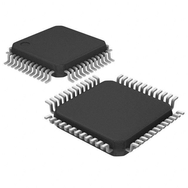
| 产品图片 |
|
| rohs | 符合RoHS无铅 / 符合限制有害物质指令(RoHS)规范要求 |
| 产品系列 | 嵌入式处理器和控制器,微控制器 - MCU,8位微控制器 -MCU,Freescale Semiconductor MC9S08LG32CLHS08 |
| 数据手册 | |
| 产品型号 | MC9S08LG32CLH |
| RAM容量 | 1.9K x 8 |
| 产品目录页面 | |
| 产品种类 | 8位微控制器 -MCU |
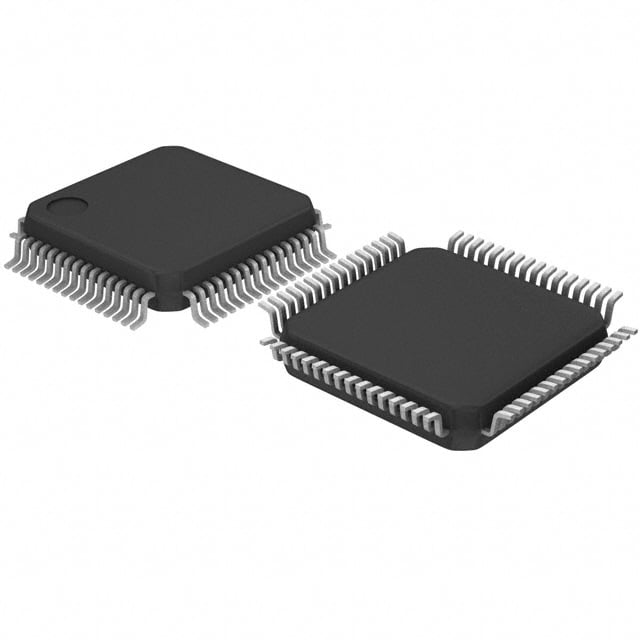
| 供应商器件封装 | 64-LQFP(10x10) |
| 包装 | 托盘 |
| 单位重量 | 346.550 mg |
| 可用A/D通道 | 12 |
| 可编程输入/输出端数量 | 53 |
| 商标 | Freescale Semiconductor |
| 处理器系列 | MC9S08 |
| 外设 | LCD,LVD,PWM |
| 安装风格 | SMD/SMT |
| 定时器数量 | 3 Timer |
| 封装 | Tray |
| 封装/外壳 | 64-LQFP |
| 封装/箱体 | LQFP-64 |
| 工作温度 | -40°C ~ 85°C |
| 工作电源电压 | 2.7 V to 5.5 V |
| 工厂包装数量 | 800 |
| 振荡器类型 | 内部 |
| 接口类型 | I2C, SCI, SPI |
| 数据RAM大小 | 1984 B |
| 数据总线宽度 | 8 bit |
| 数据转换器 | A/D 12x12b |
| 最大工作温度 | + 85 C |
| 最大时钟频率 | 40 MHz |
| 最小工作温度 | - 40 C |
| 标准包装 | 1,600 |
| 核心 | S08 |
| 核心处理器 | S08 |
| 核心尺寸 | 8-位 |
| 片上ADC | Yes |
| 电压-电源(Vcc/Vdd) | 2.7 V ~ 5.5 V |
| 电源电压-最大 | 5.5 V |
| 电源电压-最小 | 2.7 V |
| 程序存储器大小 | 32 kB |
| 程序存储器类型 | Flash |
| 程序存储容量 | 32KB(32K x 8) |
| 系列 | S08LG |
| 输入/输出端数量 | 53 I/O |
| 连接性 | I²C, SCI, SPI |
| 速度 | 40MHz |
| 配用 | /product-detail/zh/DEMO9S08LG32/DEMO9S08LG32-ND/2062872 |


- 商务部:美国ITC正式对集成电路等产品启动337调查
- 曝三星4nm工艺存在良率问题 高通将骁龙8 Gen1或转产台积电
- 太阳诱电将投资9.5亿元在常州建新厂生产MLCC 预计2023年完工
- 英特尔发布欧洲新工厂建设计划 深化IDM 2.0 战略
- 台积电先进制程称霸业界 有大客户加持明年业绩稳了
- 达到5530亿美元!SIA预计今年全球半导体销售额将创下新高
- 英特尔拟将自动驾驶子公司Mobileye上市 估值或超500亿美元
- 三星加码芯片和SET,合并消费电子和移动部门,撤换高东真等 CEO
- 三星电子宣布重大人事变动 还合并消费电子和移动部门
- 海关总署:前11个月进口集成电路产品价值2.52万亿元 增长14.8%


PDF Datasheet 数据手册内容提取
Freescale Semiconductor, Inc. Document Number: MC9S08LG32 Rev. 10, 04/2015 Data Sheet: Technical Data MC9S08LG32 Series with Addendum Covers: MC9S08LG32 and MC9S08LG16 Rev. 10 of the MC9S08LG32 Series data sheet (covering MC9S08LG32 and MC9S08LG16) has two parts: • The addendum to revision 9 of the data sheet, immediately following this cover page. • Revision 9 of the data sheet, following the addendum. The changes described in the addendum have not been implemented in the specified pages. ©2015 Freescale Semiconductor, Inc. All rights reserved.
Freescale Semiconductor, Inc. Document Number: MC9S08LG32AD Data Sheet Addendum Rev. 0, 04/2015 Addendum to Rev. 9 of the MC9S08LG32 Series Covers: MC9S08LG32 and MC9S08LG16 This addendum identifies changes to Rev. 9 of the MC9S08LG32 Series data sheet (covering MC9S08LG32 and MC9S08LG16). The changes described in this addendum have not been implemented in the specified pages. 1 Add min values for I (DC injection current) IC Location: Table 8. DC Characteristics, Page 14 In Table 8, “DC Characteristics,” add min values for I (row number 14) as follows: IC Num C Characteristic Symbol Min Typ1 Max Unit 14 D DC injection Single pin limit I -0.2 — 2 mA IC current 5, 6, 7 Total MCU limit, includes sum of -5 — 25 mA V < V (min) IN SS all stressed pins V > V (max) IN DD 2 Change the max value of t (low power oscillator LPO period) Location: Table 14. Control Timing, Page 29 In Table 14, “Control Timing,” change the max value of t (row number 2) from 1300 to 1500 µs. LPO ©2015 Freescale Semiconductor, Inc. All rights reserved.
Freescale Semiconductor Document Number: MC9S08LG32 Data Sheet: Technical Data Rev. 9 , 09/2011 MC9S08LG32 Series MC9S08LG32 Covers: MC9S08LG32 and MC9S08LG16 80-LQFP 64-LQFP Case 917A Case 840F 14 mm × 14 mm 10 mm × 10 mm Features 48-LQFP • 8-bit HCS08 Central Processor Unit (CPU) Case 932 – Up to 40 MHz CPU at 5.5 V to 2.7 V across temperature 7 mm × 7mm range of –40 °C to 85 °C and –40 °C to 105 °C – On-Chip in-circuit emulator (ICE) debug module containing – HCS08 instruction set with added BGND instruction three comparators and nine trigger modes; eight deep FIFO – Support for up to 32 interrupt/reset sources for storing change-of-flow addresses and event-only data; • On-Chip Memory debug module supports both tag and force breakpoints – 32 KB or 18 KB dual array flash; read/program/erase • Peripherals over full operating voltage and temperature – LCD — Up to 4 × 41 or 8 × 37 LCD driver with internal – 1984 byte random access memory (RAM) charge pump. – Security circuitry to prevent unauthorized access to – ADC — Up to 16-channel, 12-bit resolution, 2.5 s RAM and flash contents conversion time, automatic compare function, temperature • Power-Saving Modes sensor, internal bandgap reference channel, runs in stop3 and – Two low-power stop modes (stop2 and stop3) can wake up the system, fully functional from 5.5 V to 2.7 V – Reduced-power wait mode – SCI — Full duplex non-return to zero (NRZ), LIN master – Peripheral clock gating register can disable clocks to extended break generation, LIN slave extended break unused modules, thereby reducing currents detection, wakeup on active edge – Low power On-Chip crystal oscillator (XOSC) that can – SPI — Full-duplex or single-wire bidirectional, be used in low-power modes to provide accurate clock double-buffered transmit and receive, master or slave mode, source to real time counter and LCD controller MSB-first or LSB-first shifting – 100 s typical wakeup time from stop3 mode – IIC — With up to 100 kbps with maximum bus loading, • Clock Source Options multi-master operation, programmable slave address, – Oscillator (XOSC) — Loop-control Pierce oscillator; interrupt driven byte-by-byte data transfer, supports crystal or ceramic resonator range of 31.25 kHz to broadcast mode and 10-bit addressing 38.4kHz or 1 MHz to 16 MHz – TPMx — One 6 channel and one 2 channel, selectable input – Internal Clock Source (ICS) — Internal clock source capture, output compare, or buffered edge or center-aligned module containing a frequency-locked-loop (FLL) PWM on each channel controlled by internal or external reference; precision – MTIM — 8-bit counter with match register,, four clock trimming of internal reference allows 0.2% resolution sources with prescaler dividers, can be used for periodic and 2% deviation over temperature and voltage; supports wakeup bus frequencies from 1 MHz to 20 MHz. – RTC — 8-bit modulus counter with binary or decimal based • System Protection prescaler, three clock sources including one external source, – COP reset with option to run from dedicated 1 kHz can be used for time base, calendar, or task scheduling internal clock or bus clock functions – Low-voltage warning with interrupt – KBI — One keyboard control module capable of supporting – Low-voltage detection with reset 8 × 8 keyboard matrix – Illegal opcode detection with reset – IRQ — External pin for wakeup from low-power modes – Illegal address detection with reset • Input/Output – Flash and RAM protection – 39, 53, or 69 GPIOs • Development Support – 8 KBI and 1 IRQ interrupt with selectable polarity – Single-wire background debug interface – Hysteresis and configurable pullup device on all input pins, – Breakpoint capability to allow single breakpoint setting configurable slew rate and drive strength on all output pins. during in-circuit debugging and plus two more • Package Options breakpoints in On-Chip debug module – 48-pin LQFP, 64-pin LQFP, and 80-pin LQFP Freescale reserves the right to change the detail specifications as may be required to permit improvements in the design of its products. ©Freescale Semiconductor, Inc., 2009-2011. All rights reserved.
Table of Contents 1 Pin Assignments. . . . . . . . . . . . . . . . . . . . . . . . . . . . . . . . . . . .4 Figure17.Internal Oscillator Deviation from Trimmed Frequency 25 2 Electrical Characteristics . . . . . . . . . . . . . . . . . . . . . . . . . . . .10 Figure18.ADC Input Impedance Equivalency Diagram. . . . . . . 26 2.1 Introduction. . . . . . . . . . . . . . . . . . . . . . . . . . . . . . . . . .10 Figure19.Reset Timing . . . . . . . . . . . . . . . . . . . . . . . . . . . . . . . 29 2.2 Parameter Classification. . . . . . . . . . . . . . . . . . . . . . . .10 Figure20.IRQ/KBIPx Timing . . . . . . . . . . . . . . . . . . . . . . . . . . . 30 2.3 Absolute Maximum Ratings . . . . . . . . . . . . . . . . . . . . .10 Figure21.Timer External Clock . . . . . . . . . . . . . . . . . . . . . . . . . 30 2.4 Thermal Characteristics . . . . . . . . . . . . . . . . . . . . . . . .11 Figure22.Timer Input Capture Pulse. . . . . . . . . . . . . . . . . . . . . 30 2.5 ESD Protection and Latch-Up Immunity. . . . . . . . . . . .12 Figure23.SPI Master Timing (CPHA = 0) . . . . . . . . . . . . . . . . . 32 2.6 DC Characteristics . . . . . . . . . . . . . . . . . . . . . . . . . . . .13 Figure24.SPI Master Timing (CPHA =1). . . . . . . . . . . . . . . . . . 32 2.7 Supply Current Characteristics. . . . . . . . . . . . . . . . . . .17 Figure25.SPI Slave Timing (CPHA = 0) . . . . . . . . . . . . . . . . . . 33 2.8 External Oscillator (XOSC) Characteristics . . . . . . . . .22 Figure26.SPI Slave Timing (CPHA = 1) . . . . . . . . . . . . . . . . . . 33 2.9 Internal Clock Source (ICS) Characteristics. . . . . . . . .24 Figure27.4MHz, Positive Polarity Pins 1 – 41 . . . . . . . . . . . . . 36 2.10 ADC Characteristics . . . . . . . . . . . . . . . . . . . . . . . . . . .25 Figure28.4MHz, Positive Polarity Pins 42 – 80 . . . . . . . . . . . . 36 2.11 AC Characteristics . . . . . . . . . . . . . . . . . . . . . . . . . . . .29 Figure29.4MHz, Negative Polarity Pins 1 – 41. . . . . . . . . . . . . 37 2.11.1 Control Timing. . . . . . . . . . . . . . . . . . . . . . . . . .29 Figure30.4MHz, Negative Polarity Pins 42 – 80. . . . . . . . . . . . 37 2.11.2 TPM Module Timing . . . . . . . . . . . . . . . . . . . . .30 Figure31.Device Number Example for Auto Parts. . . . . . . . . . . 39 2.11.3 SPI Timing. . . . . . . . . . . . . . . . . . . . . . . . . . . . .31 Figure32.Device Number Example for IMM Parts. . . . . . . . . . . 39 2.12 LCD Specifications . . . . . . . . . . . . . . . . . . . . . . . . . . . .34 Figure33.80-pin LQFP Package Drawing 2.13 Flash Specifications . . . . . . . . . . . . . . . . . . . . . . . . . . .34 (Case 917A, Doc #98ASS23237W). . . . . . . . . . . . . . . . . . . . . . 42 2.14 EMC Performance. . . . . . . . . . . . . . . . . . . . . . . . . . . . .35 Figure34.64-pin LQFP Package Drawing 2.14.1 Radiated Emissions. . . . . . . . . . . . . . . . . . . . . .35 (Case 840F, Doc #98ASS23234W) . . . . . . . . . . . . . . . . . . . . . . 45 2.14.2 Conducted Transient Susceptibility . . . . . . . . . .35 Figure35.48-pin LQFP Package Drawing 3 Ordering Information. . . . . . . . . . . . . . . . . . . . . . . . . . . . . . . .38 (Case 932, Doc #98ASH00962A) . . . . . . . . . . . . . . . . . . . . . . . 47 3.1 Device Numbering System. . . . . . . . . . . . . . . . . . . . . .39 List of Tables 4 Package Information. . . . . . . . . . . . . . . . . . . . . . . . . . . . . . . .39 4.1 Mechanical Drawings . . . . . . . . . . . . . . . . . . . . . . . . . .39 Table1. MC9S08LG32 Series Features by MCU and Package . 4 4.1.1 80-pin LQFP . . . . . . . . . . . . . . . . . . . . . . . . . . .40 Table2. Pin Availability by Package Pin-Count. . . . . . . . . . . . . . 8 4.1.2 64-pin LQFP . . . . . . . . . . . . . . . . . . . . . . . . . . .43 Table3. Parameter Classifications . . . . . . . . . . . . . . . . . . . . . . 10 4.1.3 48-pin LQFP . . . . . . . . . . . . . . . . . . . . . . . . . . .46 Table4. Absolute Maximum Ratings. . . . . . . . . . . . . . . . . . . . . 11 5 Revision History . . . . . . . . . . . . . . . . . . . . . . . . . . . . . . . . . . .48 Table5. Thermal Characteristics. . . . . . . . . . . . . . . . . . . . . . . . 11 Table6. ESD and Latch-Up Test Conditions. . . . . . . . . . . . . . . 12 List of Figures Table7. ESD and Latch-Up Protection Characteristics. . . . . . . 13 Figure1.MC9S08LG32 Series Block Diagram . . . . . . . . . . . . . . 3 Table8. DC Characteristics. . . . . . . . . . . . . . . . . . . . . . . . . . . . 13 Figure2.80-Pin LQFP. . . . . . . . . . . . . . . . . . . . . . . . . . . . . . . . . 5 Table9. Supply Current Characteristics. . . . . . . . . . . . . . . . . . 17 Figure3.64-Pin LQFP. . . . . . . . . . . . . . . . . . . . . . . . . . . . . . . . . 6 Table10.Oscillator Electrical Specifications Figure4.48-Pin LQFP. . . . . . . . . . . . . . . . . . . . . . . . . . . . . . . . . 7 (Temperature Range = –40 C to 105 C Ambient) . . . . . . . . . . 22 Figure5.Typical Low-side Drive (sink) characteristics – Table11.ICS Frequency Specifications High Drive (PTxDSn = 1). . . . . . . . . . . . . . . . . . . . . . . . . . . . . . 15 (Temperature Range = –40C to 105 C Ambient) . . . . . . . . . . 24 Figure6.Typical Low-side Drive (sink) characteristics – Table12.12-bit ADC Operating Conditions . . . . . . . . . . . . . . . . 25 Low Drive (PTxDSn = 0) . . . . . . . . . . . . . . . . . . . . . . . . . . . . . . 15 Table13.12-bit ADC Characteristics Figure7.Typical High-side Drive (source) characteristics – (V = V , V = V ) . . . . . . . . . . . . . . . . . . . . . . . 27 REFH DDAD REFL SSAD High Drive (PTxDSn = 1). . . . . . . . . . . . . . . . . . . . . . . . . . . . . . 15 Table14.Control Timing. . . . . . . . . . . . . . . . . . . . . . . . . . . . . . . 29 Figure8.Typical High-side Drive (source) characteristics – Table15.TPM Input Timing . . . . . . . . . . . . . . . . . . . . . . . . . . . . 30 Low Drive (PTxDSn = 0) . . . . . . . . . . . . . . . . . . . . . . . . . . . . . . 16 Table16.SPI Timing. . . . . . . . . . . . . . . . . . . . . . . . . . . . . . . . . . 31 Figure9.Typical Run I for FBE Mode at 1 MHz. . . . . . . . . . . 19 Table17.LCD Electricals, 3 V Glass . . . . . . . . . . . . . . . . . . . . . 34 DD Figure10.Typical Run I for FBE Mode at 20 MHz. . . . . . . . . 20 Table18.Flash Characteristics. . . . . . . . . . . . . . . . . . . . . . . . . . 34 DD Figure11.Typical Run I for FEE Mode at 1 MHz. . . . . . . . . . 20 Table19.Radiated Emissions, Electric Field . . . . . . . . . . . . . . . 35 DD Figure12.Typical Run I for FEE Mode at 20 MHz. . . . . . . . . 21 Table20.Conducted Susceptibility, EFT/B. . . . . . . . . . . . . . . . . 35 DD Figure13.Typical Stop2 I . . . . . . . . . . . . . . . . . . . . . . . . . . . . 21 Table21.Susceptibility Performance Classification . . . . . . . . . . 38 DD Figure14.Typical Stop3 I . . . . . . . . . . . . . . . . . . . . . . . . . . . . 22 Table22.Device Numbering System . . . . . . . . . . . . . . . . . . . . . 38 DD Figure15.Typical Crystal or Resonator Circuit: High Range and Low Table23.Package Descriptions . . . . . . . . . . . . . . . . . . . . . . . . . 39 Range/High Gain . . . . . . . . . . . . . . . . . . . . . . . . . . . . 23 Table24.Revision History. . . . . . . . . . . . . . . . . . . . . . . . . . . . . . 48 Figure16.Typical Crystal or Resonator Circuit: Low Range/Low Power . . . . . . . . . . . . . . . . . . . . . . . . . . . . . . . . . . . . . 24 MC9S08LG32 Series Data Sheet, Rev. 9 2 Freescale Semiconductor
HCS08 CORE LCD28/ADC5/TPMCLK/PTA7 On-ChipICE (ICE) and LCD27/ADC4/TPM2CH1/KBI7/PTA6 CPU INT DEBUGMODULE(DBG) LCD26/ADC3/TPM2CH0/KBI6/PTA5 A T LCD25/ADC2/RX2/KBI5/PTA4 R LCD24/ADC1/TX2/KBI4/PTA3 BKGD/MS Real Time Counter O BKGD BKP P LCD23/ADC0/SDA/PTA2 (RTC) LCD22/SCL/PTA1 LCD21/PTA0 HCS08 SYSTEM CONTROL Modulo Timer TMRCLK B (MTIM) T LCD[40:37]/PTB[7:4] RESETS AND INTERRUPTS R LCD[32:29]/PTB[3:0] O MODES OF OPERATION KBI[7:0] P 8-BIT KEYBOARD POWER MANAGEMENT INTERRUPT (KBI) C RESET/PTC6 SS RT BKGD/MS/PTC5 COP RESET SPSCK O LCD[20:16]/PTC[4:0] SERIAL PERIPHERAL MISO P IRQ INTERFACE (SPI) IRQ LVD MOSI D SCL RT LCD[7:0]/PTD[7:0] USER FLASH A IIC MODULE (IIC) SDA PO (LG32 = 16K BYTES) (LG16 = 2K BYTES) TPM2CH[5:0] E 6-CHANNEL TIMER/PWM RT LCD[15:8]/PTE[7:0] (TPM2) TPMCLK O P USER FLASH B (LG32 = 16K BYTES) 2-CHANNEL TIMER/PWM TPM1CH[1:0] EXTAL/PTF7 (LG16 = 16K BYTES) (TPM1) TPMCLK XTAL/PTF6 TPM2CH3/KBI2/MOSI/PTF5 F TxD1 T TPM2CH4/KBI1/MISO/PTF4 SERIAL COMMUNICATIONS R USER RAM INTERFACE (SCI1) RxD1 PO TAPDMC124C/HIR5Q/K/TBPI0M/S1SC/HP1T/FS3PSCK/PTF2 1984 BYTES ADC13/TPM1CH0/RX1/PTF1 TxD2 ADC12/TPM2CH2/KBI3/TX1/PTF0 SERIAL COMMUNICATIONS RxD2 INTERFACE (SCI2) INTSEoRuNrcAeL ( CICLSO)CK RT G LLCCDD[[4346::4313]]//PPTTGG[[73::40]] XTAL O P LOW-POWER OSCILLATOR EXTAL TPM2CH4/KBI1/PTH7 V 12-BIT H ADC15/KBI0/TPM2CH5/PTH6 VVLLLLL3L_312 LIQUID CRYSTAL ACNOANLVOEGR-TTOER-D (IAGDITCA)L AD[15:0] PORT AAADDDCCC11[910://6TT]/PPKMMB11I[CC7:HH401]///PKKTBBHII32[3//TR:0XX]11//PPTTHH54 VLL2 DISPLAY DRIVER (LCD) SS/SCL/TPM2CH0/PTI5 VVCCAAPP12 RT I SMPOSSCI/KT/PSMD2AC/THP2M/P2TCI3H1/PTI4 LCD[44:0] PO MISO/TPM2CH3/PTI2 TX2/TMRCLK/PTI1 RX2/PTI0 V DD V SS VOLTAGE REGULATOR V Available only on 80-pin package SS2 Available only on 64-pin and 80-pin package VDDA/VREFH */Default function out of reset/* VSSA/VREFL Figure1. MC9S08LG32 Series Block Diagram MC9S08LG32 Series Data Sheet, Rev. 9 Freescale Semiconductor 3
Pin Assignments Table1. MC9S08LG32 Series Features by MCU and Package Feature MC9S08LG32 MC9S08LG16 Flash size (bytes) 32,768 18,432 RAM size (bytes) 1984 Pin quantity 80 64 48 64 48 ADC 16 ch 12 ch 9 ch 12 ch 9 ch LCD 8 x 37 8 x 29 8 x 21 8 x 29 8 x 21 4 x 41 4 x 33 4 x 25 4 x 33 4 x 25 ICE + DBG yes ICS yes IIC yes IRQ yes KBI 8 pin GPIOs 69 53 39 53 39 RTC yes MTIM yes SCI1 yes SCI2 yes SPI yes TPM1 channels 2 TPM2 channels 6 XOSC yes 1 Pin Assignments This section shows the pin assignments for the MC9S08LG32 series devices. The priority of functions on a pin is in ascending order from left to right and bottom to top. Another view of pinouts and function priority is given in Table2. MC9S08LG32 Series Data Sheet, Rev. 9 4 Freescale Semiconductor
Pin Assignments 0123341234 456789 891111334444 111111 DDDDDDDDDDDD DDDDDD CCCCCCCCCCCC CCCCCC LLLLLLLLLLLL LLLLLL TE0/TE1/TE2/TE3/TE4/TE5/TG0/TG1/TG4/TG5/TG6/TG7/ LL3_2 SS2TE6/TE7/TC0/TC1/TC2/TC3/ PPPPPPPPPPPPVVPPPPPP 09876543210987654321 PTD7/LCD7 1 87777777777666666666 60 PTC4/LCD20 PTD6/LCD6 2 59 PTA0/LCD21 PTD5/LCD5 3 58 PTG2/LCD35 PTD4/LCD4 4 57 PTG3/LCD36 PTD3/LCD3 5 56 PTA1/SCL/LCD22 PTD2/LCD2 6 55 PTA2/SDA/ADC0/LCD23 PTB3/LCD32 7 54 PTA3/KBI4/TX2/ADC1/LCD24 PTB2/LCD31 8 53 PTA4/KBI5/RX2/ADC2/LCD25 PTB7/LCD40 9 52 PTA5/KBI6/TPM2CH0/ADC3/LCD26 80-Pin LQFP PTB6/LCD39 10 51 PTA6/KBI7/TPM2CH1/ADC4/LCD27 PTB5/LCD38 11 50 PTA7/TPMCLK/ADC5/LCD28 PTB4/LCD37 12 49 PTC5/BKGD/MS PTB1/LCD30 13 48 PTC6/RESET PTB0/LCD29 14 47 PTH0/KBI4/ADC6 PTD1/LCD1 15 46 PTH1/KBI5/ADC7 PTD0/LCD0 16 45 PTH2KBI6/ADC8 V 17 44 PTH3/KBI7/ADC9 CAP1 V 18 43 PTH4/RX1/KBI2/TPM1CH1/ADC10 CAP2 V 19 42 PTH5/TX1/KBI3/TPM1CH0/ADC11 LL1 V 20 41 PTF3/SS/KBI0/TPM2CH5 LL2 12345678901234567890 22222222233333333334 VLL3PTF5/MOSI/KBI2/TPM2CH3PTF4/MISO/KBI1/TPM2CH4PTI5/TPM2CH0/SCL/SSPTI4/TPM2CH1/SDA/SPSCKPTI3/TPM2CH2/MOSIPTI2/TPM2CH3/MISOPTI1/TMRCLK/TX2PTI0/RX2PTH7/KBI1/TPM2CH4VSSVDDPTF7/EXTALPTF6/XTAL/VVDDAREFHV/VSSAREFLPTH6/TPM2CH5/KBI0/ADC152/SPSCK/TPM1CH1/IRQ/ADC14PTF1/RX1/TPM1CH0/ADC13TF0/TX1/KBI3/TPM2CH2/ADC12 F P T P Figure2. 80-Pin LQFP NOTE V /V are internally connected to V /V . REFH REFL DDA SSA MC9S08LG32 Series Data Sheet, Rev. 9 Freescale Semiconductor 5
Pin Assignments 012334 456789 89111133 111111 DDDDDDDD DDDDDD CCCCCCCC CCCCCC LLLLLLLL LLLLLL TE0/TE1/TE2/TE3/TE4/TE5/TG0/TG1/ LL3_2 SS2TE6/TE7/TC0/TC1/TC2/TC3/ PPPPPPPPVVPPPPPP PTD7/LCD7 16463626160595857565554535251504948 PTC4/LCD20 PTD6/LCD6 2 47 PTA0/LCD21 PTD5/LCD5 3 46 PTG2/LCD35 PTD4/LCD4 4 45 PTG3/LCD36 PTD3/LCD3 5 44 PTA1/SCL/LCD22 PTD2/LCD2 6 43 PTA2/SDA/ADC0/LCD23 PTB3/LCD32 7 42 PTA3/KBI4/TX2/ADC1/LCD24 PTB2/LCD31 8 64-Pin LQFP 41 PTA4/KBI5/RX2/ADC2/LCD25 PTB1/LCD30 9 40 PTA5/KBI6/TPM2CH0/ADC3/LCD26 PTB0/LCD29 10 39 PTA6/KBI7/TPM2CH1/ADC4/LCD27 PTD1/LCD1 11 38 PTA7/TPMCLK/ADC5/LCD28 PTD0/LCD0 12 37 PTC5/BKGD/MS V 13 36 PTC6/RESET CAP1 V 14 35 PTH4/RX1/KBI2/TPM1CH1/ADC10 CAP2 V 15 34 PTH5/TX1/KBI3/TPM1CH0/ADC11 LL1 V 16 33 PTF3/SS/KBI0/TPM2CH5 LL2 7890123456789012 1112222222222333 334SK4 S DLL H L5432 VLLPTF5/MOSI/KBI2/TPM2CHPTF4/MISO/KBI1/TPM2CHPTI5/TPM2CH0/SCL/SPTI4/TPM2CH1/SDA/SPSCPTH7/KBI1/TPM2CHVSVDPTF7/EXTAPTF6/XTA/VVDDAREFV/VSSAREFPTH6/TPM2CH5/KBI0/ADC12/SPSCK/TPM1CH1/IRQ/ADC1PTF1/RX1/TPM1CH0/ADC1TF0/TX1/KBI3/TPM2CH2/ADC1 F P T P Figure3. 64-Pin LQFP NOTE V /V are internally connected to V /V . REFH REFL DDA SSA MC9S08LG32 Series Data Sheet, Rev. 9 6 Freescale Semiconductor
Pin Assignments D8 D9 D10 D11 D12 D13 D14 D15 D16 D17 D18 D19 C C C C C C C C C C C C E0/L E1/L E2/L E3/L E4/L E5/L E6/L E7/L C0/L C1/L C2/L C3/L T T T T T T T T T T T T P P P P P P P P P P P P 48 37 47 46 45 44 43 42 41 40 39 38 PTD7/LCD7 1 36 PTC4/LCD20 PTD6/LCD6 2 35 PTA0/LCD21 PTD5/LCD5 3 34 PTA1/SCL/LCD22 PTD4/LCD4 4 33 PTA2/SDA/ADC0/LCD23 PTD3/LCD3 5 32 PTA3/KBI4/TX2/ADC1/LCD24 PTD2/LCD2 6 31 PTA4/KBI5/RX2/ADC2/LCD25 48-Pin LQFP PTD1/LCD1 7 30 PTA5/KBI6/TPM2CH0/ADC3/LCD26 PTD0/LCD0 8 29 PTA6/KBI7/TPM2CH1/ADC4/LCD27 V 9 28 PTA7/TPMCLK/ADC5/LCD28 CAP1 V 10 27 PTC5/BKGD/MS CAP2 V 11 26 PTC6/RESET LL1 VLL2 12 25 PTF3/SS/KBI0/TPM2CH5 14 15 16 17 18 19 20 21 22 23 13 24 3 3 4 S D L L H L 4 3 2 VLL KBI2/TPM2CH KBI1/TPM2CH VS VD PTF7/EXTA PTF6/XTA V/VDDAREF V/VSSAREF H1/IRQ/ADC1 M1CH0/ADC1 M2CH2/ADC1 SI/ O/ 1C TP TP O S M 1/ 3/ TF5/M TF4/MI KS/TP F1/RX X1/KBI P P SPSC PT TF0/T 2/ P F T P Figure4. 48-Pin LQFP NOTE V /V are internally connected to V /V . REFH REFL DDA SSA MC9S08LG32 Series Data Sheet, Rev. 9 Freescale Semiconductor 7
Pin Assignments Table2. Pin Availability by Package Pin-Count Packages <-- Lowest Priority --> Highest 80 64 48 Port Pin Alt 1 Alt 2 Alt 3 Alt 4 1 1 1 PTD7 LCD7 — — — 2 2 2 PTD6 LCD6 — — — 3 3 3 PTD5 LCD5 — — — 4 4 4 PTD4 LCD4 — — — 5 5 5 PTD3 LCD3 — — — 6 6 6 PTD2 LCD2 — — — 7 7 — PTB3 LCD32 — — — 8 8 — PTB2 LCD31 — — — 9 — — PTB7 LCD40 — — — 10 — — PTB6 LCD39 — — — 11 — — PTB5 LCD38 — — — 12 — — PTB4 LCD37 — — — 13 9 — PTB1 LCD30 — — — 14 10 — PTB0 LCD29 — — — 15 11 7 PTD1 LCD1 — — — 16 12 8 PTD0 LCD0 — — — 17 13 9 V — — — — CAP1 18 14 10 V — — — — CAP2 19 15 11 V — — — — LL1 20 16 12 V — — — — LL2 21 17 13 V — — — — LL3 22 18 14 PTF5 MOSI KBI2 TPM2CH3 — 23 19 15 PTF4 MISO KBI1 TPM2CH4 — 24 20 — PTI5 TPM2CH0 SCL SS — 25 21 — PTI4 TPM2CH1 SDA SPSCK — 26 — — PTI3 TPM2CH2 MOSI — — 27 — — PTI2 TPM2CH3 MISO — — 28 — — PTI1 TMRCLK TX2 — — 29 — — PTI0 RX2 — — — 30 22 — PTH7 KBI1 TPM2CH4 — — 31 23 16 V — — — — SS 32 24 17 V — — — — DD 33 25 18 PTF7 EXTAL — — — 34 26 19 PTF6 XTAL — — — 35 27 20 V V — — — DDA REFH 36 28 21 V V — — — SSA REFL 37 29 — PTH6 TPM2CH5 KBI0 ADC15 — 38 30 22 PTF2 SPSCK TPM1CH1 IRQ ADC14 MC9S08LG32 Series Data Sheet, Rev. 9 8 Freescale Semiconductor
Pin Assignments Table2. Pin Availability by Package Pin-Count (continued) Packages <-- Lowest Priority --> Highest 80 64 48 Port Pin Alt 1 Alt 2 Alt 3 Alt 4 39 31 23 PTF1 RX1 TPM1CH0 ADC13 — 40 32 24 PTF0 TX1 KBI3 TPM2CH2 ADC12 41 33 25 PTF3 SS KBI0 TPM2CH5 — 42 34 — PTH5 TX1 KBI3 TPM1CH0 ADC11 43 35 — PTH4 RX1 KBI2 TPM1CH1 ADC10 44 — — PTH3 KBI7 ADC9 — — 45 — — PTH2 KBI6 ADC8 — — 46 — — PTH1 KBI5 ADC7 — — 47 — — PTH0 KBI4 ADC6 — — 48 36 26 PTC6 RESET — — — 49 37 27 PTC5 BKGD/MS — — — 50 38 28 PTA7 TPMCLK ADC5 LCD28 — 51 39 29 PTA6 KBI7 TPM2CH1 ADC4 LCD27 52 40 30 PTA5 KBI6 TPM2CH0 ADC3 LCD26 53 41 31 PTA4 KBI5 RX2 ADC2 LCD25 54 42 32 PTA3 KBI4 TX2 ADC1 LCD24 55 43 33 PTA2 SDA ADC0 LCD23 — 56 44 34 PTA1 SCL LCD22 — — 57 45 — PTG3 LCD36 — — — 58 46 — PTG2 LCD35 — — — 59 47 35 PTA0 LCD21 — — — 60 48 36 PTC4 LCD20 — — — 61 49 37 PTC3 LCD19 — — — 62 50 38 PTC2 LCD18 — — — 63 51 39 PTC1 LCD17 — — — 64 52 40 PTC0 LCD16 — — — 65 53 41 PTE7 LCD15 — — — 66 54 42 PTE6 LCD14 — — — 67 55 — V — — — — SS2 68 56 — V — — — — LL3_2 69 — — PTG7 LCD44 — — — 70 — — PTG6 LCD43 — — — 71 — — PTG5 LCD42 — — — 72 — — PTG4 LCD41 — — — 73 57 — PTG1 LCD34 — — — 74 58 — PTG0 LCD33 — — — 75 59 43 PTE5 LCD13 — — — 76 60 44 PTE4 LCD12 — — — MC9S08LG32 Series Data Sheet, Rev. 9 Freescale Semiconductor 9
Electrical Characteristics Table2. Pin Availability by Package Pin-Count (continued) Packages <-- Lowest Priority --> Highest 80 64 48 Port Pin Alt 1 Alt 2 Alt 3 Alt 4 77 61 45 PTE3 LCD11 — — — 78 62 46 PTE2 LCD10 — — — 79 63 47 PTE1 LCD9 — — — 80 64 48 PTE0 LCD8 — — — 2 Electrical Characteristics 2.1 Introduction This section contains electrical and timing specifications for the MC9S08LG32 series of microcontrollers available at the time of publication. 2.2 Parameter Classification The electrical parameters shown in this supplement are guaranteed by various methods. To give the customer a better understanding the following classification is used and the parameters are tagged accordingly in the tables where appropriate: Table3. Parameter Classifications P Those parameters are guaranteed during production testing on each individual device. Those parameters are achieved by the design characterization by measuring a statistically relevant C sample size across process variations. Those parameters are achieved by design characterization on a small sample size from typical devices T under typical conditions unless otherwise noted. All values shown in the typical column are within this category. D Those parameters are derived mainly from simulations. NOTE The classification is shown in the column labeled “C” in the parameter tables where appropriate. 2.3 Absolute Maximum Ratings Absolute maximum ratings are stress ratings only, and functional operation at the maxima is not guaranteed. Stress beyond the limits specified in Table4 may affect device reliability or cause permanent damage to the device. For functional operating conditions, refer to the remaining tables in this section. This device contains circuitry that protects against damage due to high static voltage or electrical fields. However, it is advised that normal precautions should be taken to avoid application of any voltages higher than maximum-rated voltages to this high-impedance circuit. Reliability of operation is enhanced if unused inputs are tied to an appropriate logic voltage level (for instance, either V or V ) or the programmable pull-up resistor associated with the pin is enabled. SS DD MC9S08LG32 Series Data Sheet, Rev. 9 10 Freescale Semiconductor
Electrical Characteristics Table4. Absolute Maximum Ratings Rating Symbol Value Unit Supply voltage V –0.3 to +5.8 V DD Maximum current into V I 120 mA DD DD Digital input voltage V –0.3 to V +0.3 V In DD Instantaneous maximum current I 25 mA D Single pin limit (applies to all port pins)1,2,3 2 Storage temperature range T –55 to 150 C stg 1 Input must be current limited to the value specified. To determine the value of the required current-limiting resistor, calculate resistance values for positive (V ) and negative (V ) clamp DD SS voltages and use the largest of the two resistance values. 2 All functional non-supply pins are internally clamped to V and V . SS DD 3 Power supply must maintain regulation within operating V range during instantaneous and DD operating maximum current conditions. If positive injection current (V > V ) is greater than In DD I , the injection current may flow out of V and could result in an external power supply going DD DD out of regulation. Ensure that the external V load will shunt current greater than maximum DD injection current, this will be of greater risk when the MCU is not consuming power. For instance, if no system clock is present, or if the clock rate is very low (which would reduce overall power consumption). 2.4 Thermal Characteristics This section provides information about operating temperature range, power dissipation, and package thermal resistance. Power dissipation on I/O pins is usually small compared to the power dissipation in On-Chip logic and voltage regulator circuits, and it is user-determined rather than being controlled by the MCU design. To take P into account in power calculations, determine I/O the difference between actual pin voltage and V or V and multiply by the pin current for each I/O pin. Except in cases of SS DD unusually high pin current (heavy loads), the difference between pin voltage and V or V will be very small. SS DD Table5. Thermal Characteristics Rating Symbol Value Unit Operating temperature range T T to T C A L H (packaged) –40 to +105 Maximum junction temperature T 125 C J Thermal resistance Single-layer board 80-pin LQFP 61 C/W JA 64-pin LQFP 71 48-pin LQFP 80 Thermal resistance Four-layer board 80-pin LQFP 48 C/W JA 64-pin LQFP 52 48-pin LQFP 56 The average chip-junction temperature (T ) in C can be obtained from: J T = T + (P ) Eqn.1 J A D JA MC9S08LG32 Series Data Sheet, Rev. 9 Freescale Semiconductor 11
Electrical Characteristics where: T = Ambient temperature, C A = Package thermal resistance, junction-to-ambient, C/W JA P = P P D int I/O P = I V , Watts — chip internal power int DD DD P = Power dissipation on input and output pins — user determined I/O For most applications, P P and can be neglected. An approximate relationship between P and T (if P is neglected) I/O int D J I/O is: P = K (T + 273 C) Eqn.2 D J Solving Equation1 and Equation2 for K gives: K = P (T + 273C) + (P )2 Eqn.3 D A JA D where K is a constant pertaining to the particular part. K can be determined from equation 3 by measuring P (at equilibrium) D for a known T . Using this value of K, the values of P and T can be obtained by solving Equation1 and Equation2 iteratively A D J for any value of T . A 2.5 ESD Protection and Latch-Up Immunity Although damage from electrostatic discharge (ESD) is much less common on these devices than on early CMOS circuits, normal handling precautions should be taken to avoid exposure to static discharge. Qualification tests are performed to ensure that these devices can withstand exposure to reasonable levels of static without suffering any permanent damage. All ESD testing is in conformity with AEC-Q100 Stress Test Qualification for automotive grade integrated circuits. During the device qualification, ESD stresses were performed for the human body model (HBM), the machine model (MM) and the charge device model (CDM). A device is defined as a failure if after exposure to ESD pulses the device no longer meets the device specification. Complete DC parametric and functional testing is performed per the applicable device specification at room temperature followed by hot temperature, unless instructed otherwise in the device specification. Table6. ESD and Latch-Up Test Conditions Model Description Symbol Value Unit Human Body Series resistance R1 1500 Model Storage capacitance C 100 pF Number of pulses per pin — 3 — Latch-up Minimum input voltage limit — –2.5 V Maximum input voltage limit — 7.5 V MC9S08LG32 Series Data Sheet, Rev. 9 12 Freescale Semiconductor
Electrical Characteristics Table7. ESD and Latch-Up Protection Characteristics No. Rating1 Symbol Min Max Unit 1 Human body model (HBM) V 2500 — V HBM 2 Charge device model (CDM) V 750 — V CDM 3 Latch-up current at T = 85 C I 100 — mA A LAT 1 Parameter is achieved by design characterization on a small sample size from typical devices under typical conditions unless otherwise noted. 2.6 DC Characteristics This section includes information about power supply requirements and I/O pin characteristics. Table8. DC Characteristics Num C Characteristic Symbol Min Typ1 Max Unit 1 — Operating Voltage — 2.7 — 5.5 V 2 P Output high voltage — Low Drive (PTxDSn = 0) V V OH 5 V, ILoad = –2 mA VDD – 0.8 — — 3 V, ILoad = –0.6 mA VDD – 0.8 — — Output high voltage — High Drive (PTxDSn = 1) V 5 V, ILoad = –10 mA VDD – 0.8 — — 3 V, ILoad = –3 mA VDD – 0.8 — — 3 P Output low voltage — Low Drive (PTxDSn= 0) V — V OL 5 V, ILoad = 2 mA — 0.8 3 V, ILoad = 0.6 mA — 0.8 Output low voltage — High Drive (PTxDSn = 1) 5 V, ILoad = 10 mA — 0.8 3 V, ILoad = 3 mA — 0.8 4 P Output high current — Max total I for all ports I — — mA OH OHT 5 V 100 3 V 60 5 C Output high current — Max total I for all ports I — — mA OL OLT 5 V 100 3 V 60 6 P Bandgap voltage reference V — 1.225 — V BG 7 P Input high voltage; all digital inputs V 0.65 x V — — V IH DD 8 P Input low voltage; all digital inputs V — — 0.35 x V V IL DD 9 P Input hysteresis; all digital inputs V 0.06 x V — — mV hys DD 10 P Input leakage current; input only pins2 |I | — 0.1 1 A In V = V or V In DD SS 11 P High impedence (off-state) leakage current |I | — 0.1 1 A OZ VIn = VDD or VSS 12 P Internal pullup resistors3 R 20 45 65 k PU 13 P Internal pulldown resistors4 R 20 45 65 k PD MC9S08LG32 Series Data Sheet, Rev. 9 Freescale Semiconductor 13
Electrical Characteristics Table8. DC Characteristics (continued) Num C Characteristic Symbol Min Typ1 Max Unit 14 D DC injection Single pin limit I — — 2 mA IC current 5, 6, 7 Total MCU limit, includes sum of — — 25 mA V < V , V > IN SS IN allstressed pins V DD 15 C Input Capacitance, all non-supply pins C — — 8 pF In 16 C RAM retention voltage V 2 — — V RAM 17 P POR rearm voltage V 0.9 1.4 2.0 V POR 18 D POR rearm time t 10 — — s POR 19 P Low-voltage detection threshold — high range V V LVD1 V falling 3.9 4.0 4.1 DD V rising 4.0 4.1 4.2 DD 20 P Low-voltage detection threshold — low range V V LVD0 V falling 2.48 2.56 2.64 DD V rising 2.54 2.62 2.70 DD 21 P Low-voltage warning threshold — high range 1 V V LVW3 V falling 4.5 4.6 4.7 DD V rising 4.6 4.7 4.8 DD 22 P Low-voltage warning threshold — high range 0 V V LVW2 V falling 4.2 4.3 4.4 DD V rising 4.3 4.4 4.5 DD 23 P Low-voltage warning threshold — low range 1 V V LVW1 V falling 2.84 2.92 3.00 DD V rising 2.90 2.98 3.06 DD 24 P Low-voltage warning threshold — low range 0 V V LVW0 V falling 2.66 2.74 2.82 DD V rising 2.72 2.80 2.88 DD 25 P Low-voltage inhibit reset/recover hysteresis V — — mV hys 5 V 100 3 V 60 1 Typical values are measured at 25 C. Characterized, not tested 2 Measured with VIn = VDD or VSS. 3 Measured with VIn = VSS. 4 Measured with VIn = VDD. 5 All functional non-supply pins, except for PTC6 are internally clamped to V and V . SS DD 6 Input must be current limited to the value specified. To determine the value of the required current-limiting resistor, calculate resistance values for positive and negative clamp voltages, then use the larger of the two values. 7 Power supply must maintain regulation within operating V range during instantaneous and operating maximum current DD conditions. If the positive injection current (V > V ) is greater than I , the injection current may flow out of V and could In DD DD DD result in external power supply going out of regulation. Ensure that external V load will shunt current greater than maximum DD injection current. This will be the greatest risk when the MCU is not consuming power. For instance, if no system clock is present, or if clock rate is very low (which would reduce overall power consumption). MC9S08LG32 Series Data Sheet, Rev. 9 14 Freescale Semiconductor
Electrical Characteristics Typical VOL vs. IOL AT VDD = 5V Typical VOL vs. IOL AT VDD = 3V 0.80 1.40 Hot (105°C) Hot (105°C) 0.70 Room (25°C) 1.20 Room (25°C) 0.60 Cold (-40°C) 1.00 Cold (-40°C) 0.50 v) v) 0.80 (L 0.40 (L VO VO 0.60 0.30 0.40 0.20 0.10 0.20 0.00 0.00 0 1 2 3 4 5 6 7 8 9 10 11 12 13 14 15 0 1 2 3 4 5 6 7 8 9 10 11 12 13 IOL (mA) IOL (mA) Figure5. Typical Low-side Drive (sink) characteristics – High Drive (PTxDSn = 1) Typical VOL vs. IOL AT VDD = 5V Typical VOL vs. IOL AT VDD = 3V 0.90 0.90 Hot (105°C) Hot (105°C) 0.80 0.80 Room (25°C) Room (25°C) 0.70 Cold (-40°C) 0.70 Cold (-40°C) 0.60 0.60 v)0.50 v) 0.50 (OL 0.40 (OL 0.40 V V 0.30 0.30 0.20 0.20 0.10 0.10 0.00 0.00 0 1 2 3 4 5 0 1 2 3 IOL (mA) IOL (mA) Figure6. Typical Low-side Drive (sink) characteristics – Low Drive (PTxDSn = 0) Typical VDD - VOH vs. IOH AT VDD = 5V Typical VDD - VOH vs. IOH AT VDD=3V 1.2 0.8 Hot (105°C) Hot (105°C) 1.0 Room (25°C) Room (25°C) - V (v)DDOH 00..46 Cold (-40°C) - V (v)DOH 00..68 Cold (-40°C) V 0.2 D 0.4 V 0.2 0.0 0 -1 -2 -3 -4 -5 -6 -7 -8 -9 -10-11-12-13-14-15 0.0 IOH (mA) 0 -1 -2 -3 -4 -5I -6 (m-A7)-8 -9 -10 -11 -12 -13 OH Figure7. Typical High-side Drive (source) characteristics – High Drive (PTxDSn = 1) MC9S08LG32 Series Data Sheet, Rev. 9 Freescale Semiconductor 15
Electrical Characteristics Typical VDD - VOH vs. IOH AT VDD = 5V Typical VDD - VOH vs. IOH AT VDD=3V 1.2 1.2 Hot (105°C) Hot (105°C) 1.0 Room (25°C) 1.0 Room (25°C) Cold (-40°C) V (v)OH 00..68 Cold (-40°C) V (v)OH 00..68 V - DD 0.4 V - DD 0.4 0.2 0.2 0.0 0.0 0 -1 -2 -3 -4 -5 0 -1 -2 -3 IOH (mA) IOH (mA) Figure8. Typical High-side Drive (source) characteristics – Low Drive (PTxDSn = 0) MC9S08LG32 Series Data Sheet, Rev. 9 16 Freescale Semiconductor
Electrical Characteristics 2.7 Supply Current Characteristics This section includes information about power supply current in various operating modes. Table9. Supply Current Characteristics Num C Parameter Symbol Bus VDD Typ1 Max Unit Temp Freq (V) (C) 1 C Run supply current RI 20 MHz 3 16.38 27.85 mA –40 C to 85 C DD FEI mode, all modules on C 28.05 –40 C to105 C C 1 MHz 1.67 2.84 –40 C to 85 C C 2.87 –40 C to105 C P 20 MHz 5 16.55 28.14 mA –40 C to 85 C P 28.35 –40 C to105 C C 1 MHz 1.77 3.01 –40 C to 85 C C 3.05 –40 C to105 C 2 T Run supply current RI 20 MHz 3 11.9 20.25 mA –40 C to 85 C DD FEI mode, all modules off T 21.72 –40 C to105 C T 1 MHz 1.16 1.95 –40 C to 85 C T 1.98 –40 C to105 C T 20 MHz 5 12.68 21.56 mA –40 C to 85 C T 23.12 –40 C to105 C T 1 MHz 1.4 2.39 –40 C to 85 C T 2.41 –40 C to105 C 3 T Wait mode supply current WI 20 MHz 3 7.9 13.42 mA –40 C to 85 C DD FEI mode, all modules off T 13.59 –40 C to105 C T 1 MHz 0.88 1.49 –40 C to 85 C T 1.51 –40 C to105 C P 20 MHz 5 8.13 13.81 mA –40 C to 85 C P 13.98 –40 C to105 C T 1 MHz 1.12 1.91 –40 C to 85 C T 1.94 –40 C to105 C 4 C Stop2 mode supply current S2I n/a 3 1.1 16.0 A –40 C to 85 C DD C 39.0 –40 C to105 C P 5 1.2 18.7 A –40 C to 85 C P 46.1 –40 C to105 C 5 C Stop3 mode supply current S3I n/a 3 1.2 22.4 A –40 C to 85 C DD No clocks active C 56.2 –40 C to105 C P 5 1.32 25.5 A –40 C to 85 C P 63.9 –40 C to105 C MC9S08LG32 Series Data Sheet, Rev. 9 Freescale Semiconductor 17
Electrical Characteristics Table9. Supply Current Characteristics (continued) Num C Parameter Symbol Bus VDD Typ1 Max Unit Temp Freq (V) (C) 6 T Stop2 adders: RTC using LPO — n/a 3 210 — nA –40 C to 105 C RTC using low 4.25 — A power crystal oscillator LCD2 with rbias 1.23 — (Low Gain) LCD2 with rbias 184 — (High Gain) LCD2 with Cpump 4.053 — –40 C to 85 C RTC using LPO 5 210 — nA –40 C to 105 C RTC using low 4.22 — A power crystal oscillator LCD2 with rbias 1.53 — (Low Gain) LCD2 with rbias 324 — (High Gain) LCD2 with Cpump 7.123 — –40 C to 85 C 7 T Stop3 adders: RTC using LPO — n/a 3 210 — nA –40 C to 105 C RTC using low 4.75 — A power crystal oscillator LCD2 with rbias 1.23 — (Low Gain) LCD2 with rbias 184 — (High Gain) LCD2 with Cpump 4.353 — –40 C to 85 C RTC using LPO 5 230 — nA –40 C to 105 C RTC using low 4.74 — A power crystal oscillator LCD2 with rbias 1.53 — (Low Gain) LCD2 with rbias 324 — (High Gain) LCD2 with Cpump 7.493 — –40 C to 85 C MC9S08LG32 Series Data Sheet, Rev. 9 18 Freescale Semiconductor
Electrical Characteristics Table9. Supply Current Characteristics (continued) Num C Parameter Symbol Bus VDD Typ1 Max Unit Temp Freq (V) (C) 8 T Stop3 adders: EREFSTEN = 1 — n/a 3 4.58 — A –40 C to 105 C IREFSTEN = 1 71.7 — LVD 94.35 — EREFSTEN = 1 5 4.61 — A IREFSTEN = 1 71.69 — LVD 107.34 — 1 Typical values are measured at 25 C. Characterized, not tested. 2 LCD configured for Charge Pump Enabled V connected to V . LL3 DD 3 This does not include current required for 32 kHz oscillator. 4 This is the maximum current when all LCD inputs/outputs are used. I DD V DD Figure9. Typical Run I for FBE Mode at 1 MHz DD MC9S08LG32 Series Data Sheet, Rev. 9 Freescale Semiconductor 19
Electrical Characteristics I DD V DD Figure10. Typical Run I for FBE Mode at 20 MHz DD I DD V DD Figure11. Typical Run I for FEE Mode at 1 MHz DD MC9S08LG32 Series Data Sheet, Rev. 9 20 Freescale Semiconductor
Electrical Characteristics I DD V DD Figure12. Typical Run I for FEE Mode at 20 MHz DD I DD V DD Figure13. Typical Stop2 I DD MC9S08LG32 Series Data Sheet, Rev. 9 Freescale Semiconductor 21
Electrical Characteristics I DD V DD Figure14. Typical Stop3 I DD 2.8 External Oscillator (XOSC) Characteristics Table10. Oscillator Electrical Specifications (Temperature Range = –40 C to 105 C Ambient) Num C Characteristic Symbol Min Typ1 Max Unit 1 D Oscillator crystal or resonator (EREFS = 1, ERCLKEN = 1) (cid:129) Low range (RANGE = 0) f 32 — 38.4 kHz lo (cid:129) High range (RANGE = 1) FEE or FBE mode2 f 1 — 5 MHz hi (cid:129) High range (RANGE = 1, HGO = 1) BLPE mode f 1 — 16 MHz hi-hgo (cid:129) High range (RANGE = 1, HGO = 0) BLPE mode f 1 — 8 MHz hi-lp 2 D Load capacitors C See crystal or resonator 1 C manufacturer’s recommendation. 2 MC9S08LG32 Series Data Sheet, Rev. 9 22 Freescale Semiconductor
Electrical Characteristics Table10. Oscillator Electrical Specifications (Temperature Range = –40 C to 105 C Ambient) (continued) Num C Characteristic Symbol Min Typ1 Max Unit 3 D Feedback resistor R M F (cid:129) Low range (32 kHz to 100 kHz) — 10 — (cid:129) High range (1 MHz to 16 MHz) — 1 — 4 D Series resistor R k S (cid:129) Low range, low gain (RANGE = 0, HGO = 0) 0 (cid:129) Low range, high gain (RANGE = 0, HGO = 1) 100 5 D Series resistor R k S (cid:129) High range, low gain (RANGE = 1, HGO = 0) (cid:129) High range, high gain (RANGE = 1, HGO = 1) 8 MHz — 0 0 4 MHz — 0 10 1 MHz — 0 20 6 T Crystal start-up time3, 4 ms (cid:129) Low range (HGO = 0) t — 500 — CSTL-LP (cid:129) Low range (HGO = 1) t — 3570 — CSTL-HGO (cid:129) High range (HG0 = 0)5 t — 4 — CSTH-LP (cid:129) High range (HG0 = 1)5 t — 4 — CSTH-HGO 7 D Square wave input clock frequency (EREFS = 0, ERCLKEN = 1) f MHz extal (cid:129) FEE or FBE mode2 0.03125 — 5 (cid:129) BLPE mode 0 — 40 1 Data in Typical column was characterized at 5.0 V, 25 C or is typical recommended value. 2 When ICS is configured for FEE or FBE mode, input clock source must be divisible using RDIV to within the range of 31.25kHz to 39.0625 kHz. 3 This parameter is characterized and not tested on each device. 4 Proper PC board layout procedures must be followed to achieve specifications. 5 4 MHz crystal XOSC EXTAL XTAL R R S F Crystal or Resonator C 1 C 2 Figure15. Typical Crystal or Resonator Circuit: High Range and Low Range/High Gain MC9S08LG32 Series Data Sheet, Rev. 9 Freescale Semiconductor 23
Electrical Characteristics XOSC EXTAL XTAL Crystal or Resonator Figure16. Typical Crystal or Resonator Circuit: Low Range/Low Power 2.9 Internal Clock Source (ICS) Characteristics Table11. ICS Frequency Specifications (Temperature Range = –40 C to 105 C Ambient) Num C Characteristic Symbol Min Typ1 Max Unit 1 P Average internal reference frequency — factory trimmed f — 32.768 — kHz int_ft at VDD= 5.0 V and temperature = 25 C 2 C Average internal reference frequency — user trimmed f 31.25 — 39.0625 kHz int_t 3 C Internal reference start-up time t — 60 100 s IRST 4 P DCO output frequency range — Low range (DRS = 00) f 16 — 20 MHz dco_t trimmed2 P Mid range (DRS = 01) 32 — 40 5 P DCO output frequency2 Low range (DRS = 00) f — 19.92 — MHz dco_DMX32 Reference = 32768 Hz P Mid range (DRS = 01) — 39.85 — and DMX32 = 1 6 C Resolution of trimmed DCO output frequency at fixed f — 0.1 0.2 %f dco_res_t dco voltage and temperature (using FTRIM)3 7 C Resolution of trimmed DCO output frequency at fixed f — 0.2 0.4 %f dco_res_t dco voltage and temperature (not using FTRIM)3 8 P Total deviation of trimmed DCO output frequency over f — –1.0 2 %f dco_t dco voltage and temperature to+0.5 9 C Total deviation of trimmed DCO output frequency over f — 0.5 1 %f dco_t dco fixed voltage and temperature range of 0 C to 70 C3 10 C FLL acquisition time3, 4 t — — 1 mS Acquire 11 C Long term jitter of DCO output clock (averaged over 2 ms C — 0.02 0.2 %f Jitter dco interval)5 1 Data in Typical column was characterized at 5.0 V, 25 C or is typical recommended value. 2 The resulting bus clock frequency should not exceed the maximum specified bus clock frequency of the device. 3 This parameter is characterized and not tested on each device. 4 This specification applies to any time the FLL reference source or reference divider is changed, trim value changed or changing from FLL disabled (FBELP, FBILP) to FLL enabled (FEI, FEE, FBE, FBI). If a crystal/resonator is being used as the reference, this specification assumes it is already running. 5 Jitter is the average deviation from the programmed frequency measured over the specified interval at maximum f . Bus Measurements are made with the device powered by filtered supplies and clocked by a stable external clock signal. Noise injected into the FLL circuitry via V and V and variation in the crystal oscillator frequency increase the C percentage DD SS Jitter for a given interval. MC9S08LG32 Series Data Sheet, Rev. 9 24 Freescale Semiconductor
Electrical Characteristics 65.00 60.00 55.00 ) z 50.00 h k cy ( 45.00 n e qu 40.00 e r F S 35.00 C I 30.00 25.00 20.00 0 1 0 1 0 1 0 1 0 1 0 1 0 1 0 1 0 1 0 1 0 0 1 1 0 0 1 1 0 0 1 1 0 0 1 1 0 0 1 1 0 1 0 1 1 0 1 0 0 1 0 1 1 0 1 0 0 1 0 1 0 1 1 0 0 0 1 1 1 0 0 1 1 1 0 0 0 1 1 0 0 0 1 0 1 0 0 1 0 1 0 0 1 0 1 0 1 1 0 1 0 0 0 1 1 0 0 0 1 1 0 0 0 1 1 0 0 0 1 1 0 0 0 0 0 1 1 1 1 1 0 0 0 0 0 1 1 1 1 1 0 0 0 0 0 0 0 0 0 0 1 1 1 1 1 1 1 1 1 1 ' ' ' ' ' ' ' ' ' ' ' ' ' ' ' ' ' ' ' ' ICS Trim values -40°C 25°C 110°C Figure17. Internal Oscillator Deviation from Trimmed Frequency 2.10 ADC Characteristics Table12. 12-bit ADC Operating Conditions Characteristic Conditions Symb Min Typ1 Max Unit Comment Supply voltage Absolute V 2.7 — 5.5 V — DDAD Delta to V V –100 0 +100 mV — DD DDAD (V –V )2 DD DDAD Ground voltage Delta to V V –100 0 +100 mV — SS SSAD (V –V )2 SS SSAD Ref Voltage — V — — — V V shorted to REFH REFH High V DDAD Ref Voltage — V — — — V V shorted to REFL REFL Low V SSAD Input Voltage — V V — V V — ADIN REFL REFH Input — C — 4.5 5.5 pF — ADIN Capacitance MC9S08LG32 Series Data Sheet, Rev. 9 Freescale Semiconductor 25
Electrical Characteristics Table12. 12-bit ADC Operating Conditions (continued) Characteristic Conditions Symb Min Typ1 Max Unit Comment Input — R — 5 7 k — ADIN Resistance Analog Source 12-bit mode R k External to MCU AS Resistance f > 4MHz — — 2 ADCK f < 4MHz — — 5 ADCK 10-bit mode f > 4MHz — — 5 ADCK f < 4MHz — — 10 ADCK 8-bit mode (all valid f ) — — 10 ADCK ADC High Speed (ADLPC = 0) f 0.4 — 8.0 MHz — ADCK Conversion Low Power (ADLPC = 1) 0.4 — 4.0 Clock Freq. 1 Typical values assume V = 5.0 V, Temp = 25 C, f = 1.0 MHz unless otherwise stated. Typical values are for DDAD ADCK reference only and are not tested in production. 2 DC potential difference. SIMPLIFIED INPUT PIN EQUIVALENT CIRCUIT ZADIN SIMPLIFIED Pad ZAS leakage CHANNEL SELECT due to CIRCUIT ADC SAR R input R ENGINE AS protection ADIN + V ADIN – C VAS + AS – R ADIN INPUT PIN R ADIN INPUT PIN R ADIN INPUT PIN C ADIN Figure18. ADC Input Impedance Equivalency Diagram MC9S08LG32 Series Data Sheet, Rev. 9 26 Freescale Semiconductor
Electrical Characteristics Table13. 12-bit ADC Characteristics (V = V , V = V ) REFH DDAD REFL SSAD Num C Characteristic Conditions Symb Min Typ1 Max Unit Comment 1 T Supply Current — I — 195 — A — DDAD ADLPC = 1 ADLSMP = 1 ADCO = 1 2 T Supply Current — I — 347 — A — DDAD ADLPC = 1 ADLSMP = 0 ADCO = 1 3 T Supply Current — I — 407 — A — DDAD ADLPC = 0 ADLSMP = 1 ADCO = 1 4 P Supply Current — I — 0.755 1 mA — DDAD ADLPC = 0 ADLSMP = 0 ADCO = 1 5 — Supply Current Stop, Reset, Module Off IDDAD 0.011 1 A — 6 P ADC High Speed (ADLPC=0) f 2 3.3 5 MHz t = ADACK ADACK Asynchronous 1/f ADACK Clock Source Low Power (ADLPC=1) 1.25 2 3.3 7 C Conversion Short sample (ADLSMP=0) t — 20 — ADCK See ADC ADC Time (Including cycles chapter in the sample time) Long sample (ADLSMP=1) — 40 — LG32 Reference 8 C Sample Time Short sample (ADLSMP=0) tADS — 3.5 — ADCK Manual for cycles conversion Long sample (ADLSMP=1) — 23.5 — time variances 9 T Total 12-bit mode E — 3.0 — LSB2 Includes TUE Unadjusted quantization P Error 10-bit mode — 1 2.5 T 8-bit mode — 0.5 1 10 T Differential 12-bit mode DNL — 1.75 — LSB2 Non-Linearity P 10-bit mode3 — 0.5 1.0 T 8-bit mode3 — 0.3 0.5 11 T Integral 12-bit mode INL — 1.5 — LSB2 Non-Linearity P 10-bit mode — 0.5 1 T 8-bit mode — 0.3 0.5 12 T Zero-Scale 12-bit mode E — 1.5 — LSB2 V = V ZS ADIN SSAD Error P 10-bit mode — 0.5 1.5 T 8-bit mode — 0.5 0.5 MC9S08LG32 Series Data Sheet, Rev. 9 Freescale Semiconductor 27
Electrical Characteristics Table13. 12-bit ADC Characteristics (V = V , V = V ) (continued) REFH DDAD REFL SSAD Num C Characteristic Conditions Symb Min Typ1 Max Unit Comment 13 T Full-Scale 12-bit mode E — 1 — LSB2 V = V FS ADIN DDAD Error P 10-bit mode — 0.5 1 T 8-bit mode — 0.5 0.5 14 D Quantization 12-bit mode E — –1 to 0 — LSB2 — Q Error 10-bit mode — — 0.5 8-bit mode — — 0.5 15 D Input Leakage 12-bit mode E — 1 — LSB2 Pad leakage4 * IL Error R AS 10-bit mode — 0.2 2.5 8-bit mode — 0.1 1 16 C Temp Sensor –40 C to 25 C m — 1.646 — mV/C — Slope 25 C to 125C — 1.769 — 17 C Temp Sensor 25 C V — 701.2 — mV — TEMP25 Voltage 1 Typical values assume V = 5.0 V, Temp = 25 C, f = 1.0 MHz unless otherwise stated. Typical values are for reference only DDAD ADCK and are not tested in production. 2 1 LSB = (V – V )/2N REFH REFL 3 Monotonicity and no-missing-codes guaranteed in 10-bit and 8-bit modes 4 Based on input pad leakage current. Refer to pad electricals. MC9S08LG32 Series Data Sheet, Rev. 9 28 Freescale Semiconductor
Electrical Characteristics 2.11 AC Characteristics This section describes timing characteristics for each peripheral system. 2.11.1 Control Timing Table14. Control Timing Num C Rating Symbol Min Typ1 Max Unit 1 D Bus frequency (t = 1/f ) f dc — 20 MHz cyc Bus Bus 2 D Internal low power oscillator period t 700 — 1300 s LPO 3 D External reset pulse width2 t 100 — — ns extrst 4 D Reset low drive t 66 x t — — ns rstdrv cyc 5 D BKGD/MS setup time after issuing background debug t 500 — — ns MSSU force reset to enter user or BDM modes 6 D BKGD/MS hold time after issuing background debug t 100 — — s MSH force reset to enter user or BDM modes 3 7 D IRQ pulse width ns Asynchronous path2 t 100 — — ILIH Synchronous path4 t 1.5 x t — — IHIL cyc 8 D Keyboard interrupt pulse width ns Asynchronous path2 t 100 — — ILIH Synchronous path4 t 1.5 x t — — IHIL cyc 9 C Port rise and fall time — (load = 50 pF)5, 6 ns Slew rate control disabled (PTxSE = 0) t — 3 — Rise Slew rate control enabled (PTxSE = 1) t — 30 — Fall 1 Typical values are based on characterization data at V = 5.0 V, 25 C unless otherwise stated. DD 2 This is the shortest pulse that is guaranteed to be recognized as a reset pin request. 3 To enter BDM mode following a POR, BKGD/MS should be held low during the power-up and for a hold time of t after V MSH DD rises above V . LVD 4 This is the minimum pulse width that is guaranteed to pass through the pin synchronization circuitry. Shorter pulses may or may not be recognized. In stop mode, the synchronizer is bypassed so shorter pulses can be recognized. 5 Timing is shown with respect to 20% V and 80% V levels. Temperature range –40 C to 105C. DD DD 6 Except for LCD pins in Open Drain mode. t extrst RESET PIN Figure19. Reset Timing MC9S08LG32 Series Data Sheet, Rev. 9 Freescale Semiconductor 29
Electrical Characteristics t IHIL IRQ/KBIPx IRQ/KBIPx t ILIH Figure20. IRQ/KBIPx Timing 2.11.2 TPM Module Timing Synchronizer circuits determine the shortest input pulses that can be recognized or the fastest clock that can be used as the optional external source to the timer counter. These synchronizers operate from the current bus rate clock. Table15. TPM Input Timing No. C Function Symbol Min Max Unit 1 D External clock frequency f 0 f /4 Hz TCLK Bus 2 D External clock period t 4 — t TCLK cyc 3 D External clock high time t 1.5 — t clkh cyc 4 D External clock low time t 1.5 — t clkl cyc 5 D Input capture pulse width t 1.5 — t ICPW cyc t TCLK t clkh TPMCLK t clkl Figure21. Timer External Clock t ICPW TPMCHn TPMCHn t ICPW Figure22. Timer Input Capture Pulse MC9S08LG32 Series Data Sheet, Rev. 9 30 Freescale Semiconductor
Electrical Characteristics 2.11.3 SPI Timing Table16 and Figure23 through Figure26 describe the timing requirements for the SPI system. Table16. SPI Timing No. C Function Symbol Min Max Unit — D Operating frequency f Hz op Master f /2048 f /2 Bus Bus Slave 0 f /4 Bus D SPSCK period t 1 SPSCK Master 2 2048 t cyc Slave 4 — t cyc D Enable lead time t 2 Lead Master 12 — t SPSCK Slave 1 — t cyc D Enable lag time t 3 Lag Master 12 — t SPSCK Slave 1 — t cyc D Clock (SPSCK) high or low time t 4 WSPSCK Master t –30 1024 t ns cyc cyc Slave t – 30 — ns cyc D Data setup time (inputs) t 5 SU Master 15 — ns Slave 15 — ns D Data hold time (inputs) t 6 HI Master 0 — ns Slave 25 — ns D Slave access time t — 1 t 7 a cyc D Slave MISO disable time t — 1 t 8 dis cyc D Data valid (after SPSCK edge) t 9 v Master — 25 ns Slave — 25 ns D Data hold time (outputs) t 10 HO Master 0 — ns Slave 0 — ns D Rise time 11 Input t — t – 25 ns RI cyc Output t — 25 ns RO D Fall time 12 Input t — t – 25 ns FI cyc Output t — 25 ns FO MC9S08LG32 Series Data Sheet, Rev. 9 Freescale Semiconductor 31
Electrical Characteristics SS1 (OUTPUT) 2 1 11 3 SPSCK 4 (CPOL = 0) (OUTPUT) 4 12 SPSCK (CPOL = 1) (OUTPUT) 5 6 MISO (INPUT) MS BIN2 BIT 6 . . . 1 LSB IN 9 9 10 MOSI (OUTPUT) MSB OUT2 BIT 6 . . . 1 LSB OUT NOTES: 1. SS output mode (DDS7 = 1, SSOE = 1). 2. LSBF = 0. For LSBF = 1, bit order is LSB, bit 1, ..., bit 6, MSB. Figure23. SPI Master Timing (CPHA = 0) SS1 (OUTPUT) 1 2 12 11 3 SPSCK (CPOL = 0) (OUTPUT) 4 4 11 12 SPSCK (CPOL = 1) (OUTPUT) 5 6 MISO (INPUT) MSB IN2 BIT 6 . . . 1 LSB IN 9 10 MOSI PORT DATA MASTER MSB OUT2 BIT 6 . . . 1 MASTER LSB OUT PORT DATA (OUTPUT) NOTES: 1. SS output mode (DDS7 = 1, SSOE = 1). 2. LSBF = 0. For LSBF = 1, bit order is LSB, bit 1, ..., bit 6, MSB. Figure24. SPI Master Timing (CPHA =1) MC9S08LG32 Series Data Sheet, Rev. 9 32 Freescale Semiconductor
Electrical Characteristics SS (INPUT) 1 12 11 3 SPSCK (CPOL = 0) (INPUT) 2 4 4 11 12 SPSCK (CPOL = 1) (INPUT) 8 7 9 10 10 MISO SEE (OUTPUT) SLAVE MSB OUT BIT 6 . . . 1 SLAVE LSB OUT NOTE 1 5 6 MOSI (INPUT) MSB IN BIT 6 . . . 1 LSB IN NOTE: 1. Not defined but normally MSB of character just received. Figure25. SPI Slave Timing (CPHA = 0) SS (INPUT) 1 3 2 12 11 SPSCK (CPOL = 0) (INPUT) 4 4 11 12 SPSCK (CPOL = 1) (INPUT) 9 10 c MISO SEE (OUTPUT) NOTE 1 SLAVE MSB OUT BIT 6 . . . 1 SLAVE LSB OUT 7 o 6 MOSI (INPUT) MSB IN BIT 6 . . . 1 LSB IN NOTE: 1. Not defined but normally LSB of character just received Figure26. SPI Slave Timing (CPHA = 1) MC9S08LG32 Series Data Sheet, Rev. 9 Freescale Semiconductor 33
Electrical Characteristics 2.12 LCD Specifications Table17. LCD Electricals, 3 V Glass C Characteristic Symbol Min Typ Max Units D VLL3 Supply Voltage VLL3 2.7 — 5.5 V D LCD Frame Frequency f 28 30 64 Hz Frame D LCD Charge Pump Capacitance C — 100 100 pF LCD D LCD Bypass Capacitance C — 100 100 BYLCD D LCD Glass Capacitance C — 2000 8000 glass 2.13 Flash Specifications This section provides details about program/erase times and program-erase endurance for the flash memory. Program and erase operations do not require any special power sources other than the normal V supply. For more detailed DD information about program/erase operations, see the Memory section. Table18. Flash Characteristics C Characteristic Symbol Min Typical Max Unit Supply voltage for program/erase D –40 C to 85 C V 2.7 5.5 V prog/erase D Supply voltage for read operation V 2.7 5.5 V Read D Internal FCLK frequency1 f 150 200 kHz FCLK D Internal FCLK period (1/FCLK) t 5 6.67 s Fcyc C Byte program time (random location)2 t 9 t prog Fcyc C Byte program time (burst mode)2 t 4 t Burst Fcyc C Page erase time2 t 4000 t Page Fcyc C Mass erase time2 t 20,000 t Mass Fcyc D Byte program current3 R — 4 — mA IDDBP D Page erase current3 R — 6 — mA IDDPE Program/erase endurance4 C T to T = –40 C to + 85 C 10,000 — — cycles L H T = 25 C 100,000 — C Data retention5 t 15 100 — years D_ret 1 The frequency of this clock is controlled by a software setting. 2 These values are hardware state machine controlled. User code does not need to count cycles. This information supplied for calculating approximate time to program and erase. 3 The program and erase currents are additional to the standard run I . These values are measured at room temperatures DD with V = 5.0 V, bus frequency = 4.0 MHz. DD 4 Typical endurance for flash was evaluated for this product family on the 9S12Dx64. For additional information on how Freescale defines typical endurance, please refer to Engineering Bulletin EB619, Typical Endurance for Nonvolatile Memory. 5 Typical data retention values are based on intrinsic capability of the technology measured at high temperature and de-rated to 25 C using the Arrhenius equation. For additional information on how Freescale defines typical data retention, please refer to Engineering Bulletin EB618, Typical Data Retention for Nonvolatile Memory. MC9S08LG32 Series Data Sheet, Rev. 9 34 Freescale Semiconductor
Electrical Characteristics 2.14 EMC Performance Electromagnetic compatibility (EMC) performance is highly dependant on the environment in which the MCU resides. Board design and layout, circuit topology choices, location and characteristics of external components as well as MCU software operation all play a significant role in EMC performance. The system designer should consult Freescale applications notes such as AN2321, AN1050, AN1263, AN2764, and AN1259 for advice and guidance specifically targeted at optimizing EMC performance. 2.14.1 Radiated Emissions Microcontroller radiated RF emissions are measured from 150 kHz to 1 GHz using the TEM/GTEM cell method in accordance with the IEC 61967-2 and SAE J1752/3 standards. The measurement is performed with the microcontroller installed on a custom EMC evaluation board while running specialized EMC test software. The radiated emissions from the microcontroller are measured in a TEM cell in two package orientations (North and East). The maximum radiated RF emissions of the tested configuration in all orientations are less than or equal to the reported emissions levels. Table19. Radiated Emissions, Electric Field Level1 Parameter Symbol Conditions Frequency f /f Unit OSC BUS (Max) Radiated emissions, V V = 5.5 0.15 – 50 MHz 4 MHz crystal 10 dBV RE_TEM DD electric field T = +25 oC 16 MHz bus A 50 – 150 MHz 14 Package type = 80 LQFP 150 – 500 MHz 8 500 – 1000 MHz 5 IEC Level L — SAE Level 2 — 1 Data based on qualification test results. 2.14.2 Conducted Transient Susceptibility Microcontroller transient conducted susceptibility is measured in accordance with an internal Freescale test method. The measurement is performed with the microcontroller installed on a custom EMC evaluation board and running specialized EMC test software designed in compliance with the test method. The conducted susceptibility is determined by injecting the transient susceptibility signal on each pin of the microcontroller. The transient waveform and injection methodology is based on IEC 61000-4-4 (EFT/B). The transient voltage required to cause performance degradation on any pin in the tested configuration is greater than or equal to the reported levels unless otherwise indicated by footnotes below Table20. Table20. Conducted Susceptibility, EFT/B Amplitude1 Parameter Symbol Conditions f /f Result Unit OSC BUS (Min) Conducted susceptibility, electrical V V = 5.5 4 kHz crystal A >4.02 kV CS_EFT DD fast transient/burst (EFT/B) T = +25 oC 4 MHz bus B >4.03 A Package type = 80-pin LQFP C >4.04 D >4.0 1 Data based on qualification test results. Not tested in production. 2 Exceptions as covered in footnotes 3 and 4. MC9S08LG32 Series Data Sheet, Rev. 9 Freescale Semiconductor 35
Electrical Characteristics 3 Except pins PHT1, PTH2, PTH3, PTH4, PTH5. See figures below for values. 4 Except pins PTF3, PTH5, PTH4, PHT0, Reset, and BKGD. See figures below for values. Individual performance of each pin is shown in Figure27, Figure28, Figure29, and Figure30. Figure27. 4MHz, Positive Polarity Pins 1 – 41 Note: RESET retested with 0.1 F capacitor from pin to ground is Class A compliant as shown by 48*. Figure28. 4MHz, Positive Polarity Pins 42 – 80 MC9S08LG32 Series Data Sheet, Rev. 9 36 Freescale Semiconductor
Electrical Characteristics Figure29. 4MHz, Negative Polarity Pins 1 – 41 Note: RESET retested with 0.1 F capacitor from pin to ground is Class A compliant as shown by 48*. Figure30. 4MHz, Negative Polarity Pins 42 – 80 MC9S08LG32 Series Data Sheet, Rev. 9 Freescale Semiconductor 37
Ordering Information The susceptibility performance classification is described in Table21. Table21. Susceptibility Performance Classification Result Performance Criteria A No failure The MCU performs as designed during and after exposure. B Self-recovering The MCU does not perform as designed during exposure. The MCU returns failure automatically to normal operation after exposure is removed. C Soft failure The MCU does not perform as designed during exposure. The MCU does not return to normal operation until exposure is removed and the RESET pin is asserted. D Hard failure The MCU does not perform as designed during exposure. The MCU does not return to normal operation until exposure is removed and the power to the MCU is cycled. E Damage The MCU does not perform as designed during and after exposure. The MCU cannot be returned to proper operation due to physical damage or other permanent performance degradation. 3 Ordering Information This section contains ordering information for MC9S08LG32 and MC9S08LG16 devices. Table22. Device Numbering System Memory LCD Mode Device Number1 Temperature Range (°C) Available Packages2 Operation FLASH RAM Auto S9S08LG32J0CLK 32 KB 1984 -40 °C to +85 °C Charge Pump 80-pin LQFP S9S08LG32J0CLH 64-pinLQFP S9S08LG32J0CLF 48-pinLQFP S9S08LG32J0VLK 32 KB 1984 -40 °C to +105 °C Register Bias 80-pin LQFP S9S08LG32J0VLH 64-pinLQFP S9S08LG32J0VLF 48-pinLQFP S9S08LG16J0VLH 18 KB 1984 64-pinLQFP S9S08LG16J0VLF 48-pinLQFP IMM MC9S08LG32CLK 32 KB 1984 -40 °C to + 85 °C Charge Pump 80-pin LQFP MC9S08LG32CLH 64-pinLQFP MC9S08LG32CLF 48-pinLQFP MC9S08LG16CLH 18 KB 1984 64-pinLQFP MC9S08LG16CLF 48-pinLQFP 1 See the MC9S08LG32 Reference Manual (document MC9S08LG32RM), for a complete description of modules included on each device. 2 See Table23 for package information. MC9S08LG32 Series Data Sheet, Rev. 9 38 Freescale Semiconductor
Package Information 3.1 Device Numbering System Example of the device numbering system: S 9 S08 LG32 J0X XX Package designator (see Table23) Status/Partnumber Type (S = Maskset specific partnumber) Temperature range (C = –40 C to 85C) (V = –40 C to 105C) Memory Maskset Identifier Suffix (9 = FLASH-based) (First digit usually references wafer fab Core Second digit usually differentiates mask rev) Family Approximate Flash size in KB Figure31. Device Number Example for Auto Parts MC9 S08 LG32 C XX Status (MC = Fully Qualified) Package designator (see Table23) Temperature range Memory (C = –40 C to 85C) (9 = FLASH-based) Core Family Approximate Flash size in KB Figure32. Device Number Example for IMM Parts 4 Package Information Table23. Package Descriptions Pin Count Package Type Abbreviation Designator Case No. Document No. 80 Low Quad Flat Package LQFP LK 917A 98ASS23237W 64 Low Quad Flat Package LQFP LH 840F 98ASS23234W 48 Low Quad Flat Package LQFP LF 932 98ASH00962A 4.1 Mechanical Drawings The following pages are mechanical drawings for the packages described in Table 23. For the latest available drawings please visit our web site (http://www.freescale.com) and enter the package’s document number into the keyword search box. MC9S08LG32 Series Data Sheet, Rev. 9 Freescale Semiconductor 39
Package Information 4.1.1 80-pin LQFP MC9S08LG32 Series Data Sheet, Rev. 9 40 Freescale Semiconductor
Package Information MC9S08LG32 Series Data Sheet, Rev. 9 Freescale Semiconductor 41
Package Information Figure33. 80-pin LQFP Package Drawing (Case 917A, Doc #98ASS23237W) MC9S08LG32 Series Data Sheet, Rev. 9 42 Freescale Semiconductor
Package Information 4.1.2 64-pin LQFP MC9S08LG32 Series Data Sheet, Rev. 9 Freescale Semiconductor 43
Package Information MC9S08LG32 Series Data Sheet, Rev. 9 44 Freescale Semiconductor
Package Information Figure34. 64-pin LQFP Package Drawing (Case 840F, Doc #98ASS23234W) MC9S08LG32 Series Data Sheet, Rev. 9 Freescale Semiconductor 45
Package Information 4.1.3 48-pin LQFP MC9S08LG32 Series Data Sheet, Rev. 9 46 Freescale Semiconductor
Package Information Figure35. 48-pin LQFP Package Drawing (Case 932, Doc #98ASH00962A) MC9S08LG32 Series Data Sheet, Rev. 9 Freescale Semiconductor 47
Revision History 5 Revision History To provide the most up-to-date information, the revision of our documents on the World Wide Web are the most current. Your printed copy may be an earlier revision. To verify you have the latest information available, refer to: http://www.freescale.com The following revision history table summarizes changes contained in this document. Table24. Revision History Revision Date Description of Changes 1 8/2008 First Initial release. 2 9/2008 Second Initial Release. 3 11/2008 Alpha Customer Release. 4 2/2009 Launch Release. 5 4/2009 Added EMC Radiated Emission and Transient Susceptibility data in Table19 and Table20. 6 4/2009 Updated EMC performance data. 7 8/2009 Updated auto part numbers, changed TCLK, T0CH0, T0CH1, T1CH0, T1CH1, T1CH2, T1CH3, T1CH3, T1CH4, and T1CH5 to TPMCLK, TPM0CH0, TPM0CH1,TPM1CH0, TPM1CH1, TPM1CH2, TPM1CH3, TPM1CH4, and TPM1CH5, and changed the maximum LCD frame frequency to 64 Hz. 8 8/2011 Updated Table “ICS Frequency Specifications (Temperature Range = –40 ×C to 105 ×C Ambient)”. Changed the value of row 8 column C from C to P. 9 9/2011 Updated Table “ICS Frequency Specifications (Temperature Range = –40 ×C to 105 ×C Ambient)”. Removed Footnote from Row 8. Updated the Revision History MC9S08LG32 Series Data Sheet, Rev. 9 48 Freescale Semiconductor
THIS PAGE INTENTIONALLY BLANK MC9S08LG32 Series Data Sheet, Rev. 9 Freescale Semiconductor 49
How to Reach Us: Information in this document is provided solely to enable system and software Home Page: implementers to use Freescale products. There are no express or implied copyright freescale.com licenses granted hereunder to design or fabricate any integrated circuits based on the Web Support: information in this document. freescale.com/support Freescale reserves the right to make changes without further notice to any products herein. Freescale makes no warranty, representation, or guarantee regarding the suitability of its products for any particular purpose, nor does Freescale assume any liability arising out of the application or use of any product or circuit, and specifically disclaims any and all liability, including without limitation consequential or incidental damages. “Typical” parameters that may be provided in Freescale data sheets and/or specifications can and do vary in different applications, and actual performance may vary over time. All operating parameters, including “typicals,” must be validated for each customer application by customer’s technical experts. Freescale does not convey any license under its patent rights nor the rights of others. Freescale sells products pursuant to standard terms and conditions of sale, which can be found at the following address: freescale.com/SalesTermsandConditions. Freescale and the Freescale logo are trademarks of Freescale Semiconductor, Inc., Reg. U.S. Pat. & Tm. Off. All other product or service names are the property of their respective owners. All rights reserved. © 2009, 2011,2015 Freescale Semiconductor, Inc. Document Number: MC9S08LG32 Rev. 10 04/2015
Mouser Electronics Authorized Distributor Click to View Pricing, Inventory, Delivery & Lifecycle Information: N XP: S9S08LG16J0CLH S9S08LG32J0CLK S9S08LG32J0VLF S9S08LG32J0VLH S9S08LG32J0VLK MC9S08LG16CLH MC9S08LG32CLH MC9S08LG32CLK MC9S08LG32CLF MC9S08LG16CLF S9S08SG8E2WTG S9S08LG16J0VLF S9S08LG32J0CLH S9S08SG8E2WTGR S9S08LG32J0CLKR