ICGOO在线商城 > 集成电路(IC) > 嵌入式 - 微控制器 > MC9S08AW60MFUE

 Datasheet下载
- 型号: MC9S08AW60MFUE
- 制造商: Freescale Semiconductor
- 库位|库存: xxxx|xxxx
- 要求:
| 数量阶梯 | 香港交货 | 国内含税 |
| +xxxx | $xxxx | ¥xxxx |
查看当月历史价格
查看今年历史价格
MC9S08AW60MFUE产品简介:
ICGOO电子元器件商城为您提供MC9S08AW60MFUE由Freescale Semiconductor设计生产,在icgoo商城现货销售,并且可以通过原厂、代理商等渠道进行代购。 MC9S08AW60MFUE价格参考¥66.90-¥66.90。Freescale SemiconductorMC9S08AW60MFUE封装/规格:嵌入式 - 微控制器, S08 微控制器 IC S08 8-位 40MHz 60KB(60K x 8) 闪存 64-QFP(14x14)。您可以下载MC9S08AW60MFUE参考资料、Datasheet数据手册功能说明书,资料中有MC9S08AW60MFUE 详细功能的应用电路图电压和使用方法及教程。
型号为 MC9S08AW60MFUE 的嵌入式微控制器由 NXP USA Inc. 生产,属于高性能、低成本的8位微控制器系列。该芯片主要面向工业控制、汽车电子和智能家电等应用场景。

其典型应用场景包括:

1. 汽车电子系统:如车身控制模块(BCM)、车门控制、灯光控制、电动窗控制等。该芯片具备较强的抗干扰能力和稳定性,适合在车载环境中使用。

2. 工业自动化设备:用于传感器控制、电机控制、小型执行器管理等场景,支持多种通信接口(如SCI、SPI),便于与上位机或其他设备进行数据交互。

3. 消费类电子产品:如智能家电(洗衣机、空调、微波炉)中的主控单元,实现人机交互、状态监测与控制功能。

4. 安防与监控设备:用于门禁系统、监控摄像头或报警系统的本地控制单元,具备一定的I/O扩展能力,可连接按键、显示屏、传感器等外设。

5. 电池供电设备:由于其低功耗设计,适用于手持设备或远程监控终端,有助于延长电池使用寿命。

该芯片内置60KB Flash存储器和丰富的外设资源,适合对性能和成本都有要求的中低端控制系统应用。
| 参数 | 数值 |
| A/D位大小 | 10 bit |
| 产品目录 | 集成电路 (IC)半导体 |
| 描述 | IC MCU 8BIT 60KB FLASH 64QFP8位微控制器 -MCU 8 BIT 60K FLASH 4K RAM |
| EEPROM容量 | - |
| 产品分类 | |
| I/O数 | 54 |
| 品牌 | Freescale Semiconductor |
| 产品手册 | |
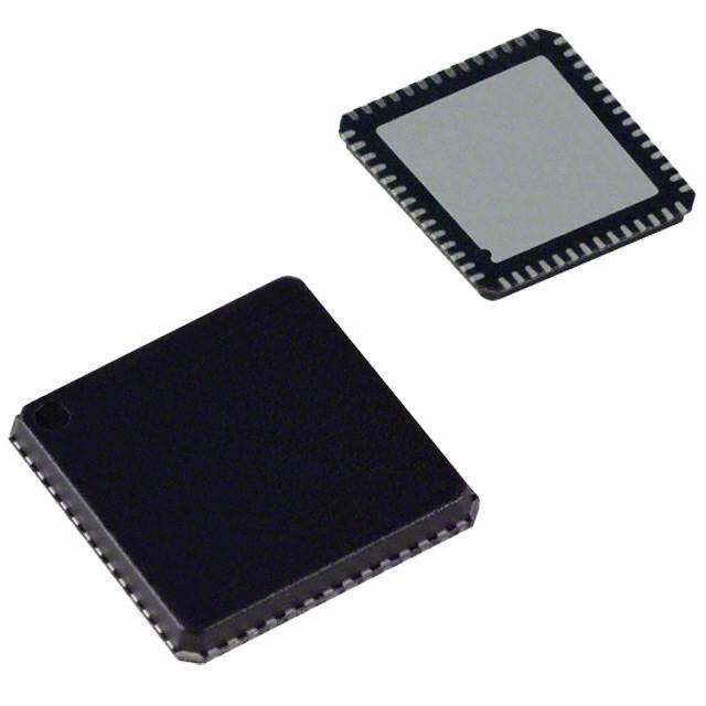
| 产品图片 |
|
| rohs | 符合RoHS无铅 / 符合限制有害物质指令(RoHS)规范要求 |
| 产品系列 | 嵌入式处理器和控制器,微控制器 - MCU,8位微控制器 -MCU,Freescale Semiconductor MC9S08AW60MFUES08 |
| 数据手册 | |
| 产品型号 | MC9S08AW60MFUE |
| PCN设计/规格 | http://cache.freescale.com/files/shared/doc/pcn/PCN15684.htm |
| RAM容量 | 2K x 8 |
| 产品目录页面 | |
| 产品种类 | 8位微控制器 -MCU |
| 供应商器件封装 | 64-QFP(14x14) |
| 包装 | 托盘 |
| 单位重量 | 1 g |
| 可用A/D通道 | 16 |
| 可编程输入/输出端数量 | 54 |
| 商标 | Freescale Semiconductor |
| 处理器系列 | MC9S08 |
| 外设 | LVD,POR,PWM,WDT |
| 安装风格 | SMD/SMT |
| 定时器数量 | 8 Timer |
| 封装 | Tray |
| 封装/外壳 | 64-QFP |
| 封装/箱体 | QFP-64 |
| 工作温度 | -40°C ~ 125°C |
| 工作电源电压 | 2.7 V to 5.5 V |
| 工厂包装数量 | 420 |
| 振荡器类型 | 内部 |
| 接口类型 | I2C, SCI, SPI |
| 数据RAM大小 | 2 kB |
| 数据Rom类型 | Flash |
| 数据总线宽度 | 8 bit |
| 数据转换器 | A/D 16x10b |
| 最大工作温度 | + 85 C |
| 最大时钟频率 | 40 MHz |
| 最小工作温度 | - 55 C |
| 标准包装 | 840 |
| 核心 | S08 |
| 核心处理器 | S08 |
| 核心尺寸 | 8-位 |
| 片上ADC | Yes |
| 电压-电源(Vcc/Vdd) | 2.7 V ~ 5.5 V |
| 电源电压-最大 | 5.5 V |
| 电源电压-最小 | 2.7 V |
| 程序存储器大小 | 60 kB |
| 程序存储器类型 | 闪存 |
| 程序存储容量 | 60KB(60K x 8) |
| 系列 | S08AW |
| 输入/输出端数量 | 54 I/O |
| 连接性 | I²C, SCI, SPI |
| 速度 | 40MHz |
| 配用 | /product-detail/zh/DEMO9S08AW60E/DEMO9S08AW60E-ND/1015057 |


PDF Datasheet 数据手册内容提取
Freescale Semiconductor Document Number: QFN_Addendum Rev. 0, 07/2014 Addendum Addendum for New QFN Package Migration This addendum provides the changes to the 98A case outline numbers for products covered in this book. Case outlines were changed because of the migration from gold wire to copper wire in some packages. See the table below for the old (gold wire) package versus the new (copper wire) package. To view the new drawing, go to Freescale.com and search on the new 98A package number for your device. For more information about QFN package use, see EB806: Electrical Connection Recommendations for the Exposed Pad on QFN and DFN Packages. ©Freescale Semiconductor, Inc., 2014. All rights reserved.
Original (gold wire) Current (copper wire) Part Number Package Description package document number package document number MC68HC908JW32 48 QFN 98ARH99048A 98ASA00466D MC9S08AC16 MC9S908AC60 MC9S08AC128 MC9S08AW60 MC9S08GB60A MC9S08GT16A MC9S08JM16 MC9S08JM60 MC9S08LL16 MC9S08QE128 MC9S08QE32 MC9S08RG60 MCF51CN128 MC9RS08LA8 48 QFN 98ARL10606D 98ASA00466D MC9S08GT16A 32 QFN 98ARH99035A 98ASA00473D MC9S908QE32 32 QFN 98ARE10566D 98ASA00473D MC9S908QE8 32 QFN 98ASA00071D 98ASA00736D MC9S08JS16 24 QFN 98ARL10608D 98ASA00734D MC9S08QB8 MC9S08QG8 24 QFN 98ARL10605D 98ASA00474D MC9S08SH8 24 QFN 98ARE10714D 98ASA00474D MC9RS08KB12 24 QFN 98ASA00087D 98ASA00602D MC9S08QG8 16 QFN 98ARE10614D 98ASA00671D MC9RS08KB12 8 DFN 98ARL10557D 98ASA00672D MC9S08QG8 MC9RS08KA2 6 DFN 98ARL10602D 98ASA00735D Addendum for New QFN Package Migration, Rev. 0 2 Freescale Semiconductor
MC9S08AW60 MC9S08AW48 MC9S08AW32 MC9S08AW16 Data Sheet HCS08 Microcontrollers MC9S08AW60 Rev 2 12/2006 freescale.com
None
MC9S08AW60 Features 8-Bit HCS08 Central Processor Unit (CPU) • IIC — Inter-integrated circuit bus module to • 40-MHz HCS08 CPU (central processor unit) operate at up to 100 kbps with maximum bus • 20-MHz internal bus frequency loading; capable of higher baud rates with reduced loading • HC08 instruction set with added BGND instruction • Timers — One 2-channel and one 6-channel 16-bit timer/pulse-width modulator (TPM) • Single-wire background debug mode interface module: Selectable input capture, output • Breakpointcapabilitytoallowsinglebreakpoint compare,andedge-alignedPWMcapabilityon setting during in-circuit debugging (plus two each channel. Each timer module may be more breakpoints in on-chip debug module) configured for buffered, centered PWM • On-chipreal-timein-circuitemulation(ICE)with (CPWM) on all channels two comparators (plus one in BDM), nine • KBI — Up to 8-pin keyboard interrupt module trigger modes, and on-chip bus capture buffer. Typically shows approximately 50 instructions Input/Output before or after the trigger point. • Up to 54 general-purpose input/output (I/O) • Support for up to 32 interrupt/reset sources pins • Software-selectable pullups on ports when Memory Options used as inputs • Upto60KBofon-chipin-circuitprogrammable • Software-selectable slew rate control on ports FLASH memory with block protection and when used as outputs security options • Software-selectable drive strength on ports • Up to 2 KB of on-chip RAM when used as outputs Clock Source Options • Master reset pin and power-on reset (POR) • Clocksourceoptionsincludecrystal,resonator, • InternalpulluponRESET,IRQ,andBKGD/MS external clock, or internally generated clock pins to reduce customer system cost with precision NVM trimming Package Options System Protection MC9S08AW60/48/32 • Optional computer operating properly (COP) • 64-pin quad flat package (QFP) reset • 64-pin low-profile quad flat package (LQFP) • Low-voltage detection with reset or interrupt • 48-pin low-profile quad flat package (QFN) • Illegalopcode detection withreset • 44-pin low-profile quad flat package (LQFP) • Illegaladdress detection withreset (some devices don’t have illegal addresses) MC9S08AW16 • 48-pin low-profile quad flat package (QFN) Power-Saving Modes • 44-pin low-profile quad flat package (LQFP) • Wait plus two stops Peripherals • ADC — Up to 16-channel, 10-bit analog-to-digital converter with automatic compare function • SCI — Two serial communications interface modules with optional 13-bit break • SPI — Serial peripheral interface module
None
MC9S08AW60 Data Sheet Covers: MC9S08AW60 MC9S08AW48 MC9S08AW32 MC9S08AW16 MC9S08AW60 Rev 2 12/2006
Revision History Toprovidethemostup-to-dateinformation,therevisionofourdocumentsontheWorldWideWebwillbe the most current. Your printed copymay beanearlier revision.To verify you have thelatest information available, refer to: http://freescale.com/ The following revision history table summarizes changes contained in this document. For your convenience, the page number designators have been linked to the appropriate location. Revision Revision Description of Changes Number Date 1 1/2006 Initial external release. Includes KBI block changes; new V / I figures; RI spec changes; SC part OL OL DD numbers with ICG trim modifications; addition of Temp Sensor to ADC. Resolved 2 12/2006 the stop IDD issues, added RTI figure, bandgap information, and incorporated electricals edits and any ProjectSync issues. ® This product incorporates SuperFlash technology licensed from SST. Freescale™ and the Freescale logo are trademarks of Freescale Semiconductor, Inc. ©Freescale Semiconductor, Inc., 2006. All rights reserved.
List of Chapters Chapter Title Page Chapter 1 Introduction......................................................................................19 Chapter 2 Pins and Connections.....................................................................23 Chapter 3 Modes of Operation.........................................................................33 Chapter 4 Memory.............................................................................................39 Chapter 5 Resets, Interrupts, and System Configuration.............................65 Chapter 6 Parallel Input/Output.......................................................................81 Chapter 7 Central Processor Unit (S08CPUV2)............................................109 Chapter 8 Internal Clock Generator (S08ICGV4)..........................................129 Chapter 9 Keyboard Interrupt (S08KBIV1)....................................................157 Chapter 10 Timer/PWM (S08TPMV2)...............................................................165 Chapter 11 Serial Communications Interface (S08SCIV2).............................181 Chapter 12 Serial Peripheral Interface (S08SPIV3)........................................199 Chapter 13 Inter-Integrated Circuit (S08IICV1)...............................................215 Chapter 14 Analog-to-Digital Converter (S08ADC10V1)................................233 Chapter 15 Development Support...................................................................261 Appendix A Electrical Characteristics and Timing Specifications................283 Appendix B Ordering Information and Mechanical Drawings........................309 MC9S08AW60 Data Sheet, Rev 2 Freescale Semiconductor 7
None
Contents Section Number Title Page Chapter 1 Introduction 1.1 Overview .........................................................................................................................................19 1.2 MCU Block Diagrams .....................................................................................................................19 1.3 System Clock Distribution ..............................................................................................................21 Chapter 2 Pins and Connections 2.1 Introduction .....................................................................................................................................23 2.2 Device Pin Assignment ...................................................................................................................24 2.3 Recommended System Connections ...............................................................................................26 2.3.1 Power (V , 2 x V , V , V ) .........................................................................28 DD SS DDAD SSAD 2.3.2 Oscillator (XTAL, EXTAL) ............................................................................................28 2.3.3 RESET Pin ......................................................................................................................29 2.3.4 Background/Mode Select (BKGD/MS) .........................................................................29 2.3.5 ADC Reference Pins (V , V ) ...........................................................................29 REFH REFL 2.3.6 External Interrupt Pin (IRQ) ...........................................................................................29 2.3.7 General-Purpose I/O and Peripheral Ports .....................................................................30 Chapter 3 Modes of Operation 3.1 Introduction .....................................................................................................................................33 3.2 Features ...........................................................................................................................................33 3.3 Run Mode ........................................................................................................................................33 3.4 Active Background Mode ................................................................................................................33 3.5 Wait Mode .......................................................................................................................................34 3.6 Stop Modes ......................................................................................................................................34 3.6.1 Stop2 Mode ....................................................................................................................35 3.6.2 Stop3 Mode ....................................................................................................................36 3.6.3 Active BDM Enabled in Stop Mode ...............................................................................36 3.6.4 LVD Enabled in Stop Mode ...........................................................................................37 3.6.5 On-Chip Peripheral Modules in Stop Modes .................................................................37 Chapter 4 Memory 4.1 MC9S08AW60 Series Memory Map ..............................................................................................39 4.1.1 Reset and Interrupt Vector Assignments ........................................................................42 4.2 Register Addresses and Bit Assignments ........................................................................................43 4.3 RAM ................................................................................................................................................49 MC9S08AW60 Data Sheet, Rev 2 Freescale Semiconductor 9
Section Number Title Page 4.4 FLASH ............................................................................................................................................50 4.4.1 Features ...........................................................................................................................51 4.4.2 Program and Erase Times ...............................................................................................51 4.4.3 Program and Erase Command Execution .......................................................................52 4.4.4 Burst Program Execution ...............................................................................................53 4.4.5 Access Errors ..................................................................................................................55 4.4.6 FLASH Block Protection ...............................................................................................55 4.4.7 Vector Redirection ..........................................................................................................56 4.5 Security ............................................................................................................................................56 4.6 FLASH Registers and Control Bits .................................................................................................58 4.6.1 FLASH Clock Divider Register (FCDIV) ......................................................................58 4.6.2 FLASH Options Register (FOPT and NVOPT) .............................................................59 4.6.3 FLASH Configuration Register (FCNFG) .....................................................................60 4.6.4 FLASH Protection Register (FPROT and NVPROT) ....................................................61 4.6.5 FLASH Status Register (FSTAT) ...................................................................................61 4.6.6 FLASH Command Register (FCMD) ............................................................................63 Chapter 5 Resets, Interrupts, and System Configuration 5.1 Introduction .....................................................................................................................................65 5.2 Features ...........................................................................................................................................65 5.3 MCU Reset ......................................................................................................................................65 5.4 Computer Operating Properly (COP) Watchdog .............................................................................66 5.5 Interrupts .........................................................................................................................................66 5.5.1 Interrupt Stack Frame .....................................................................................................67 5.5.2 External Interrupt Request (IRQ) Pin .............................................................................68 5.5.3 Interrupt Vectors, Sources, and Local Masks .................................................................69 5.6 Low-Voltage Detect (LVD) System ................................................................................................71 5.6.1 Power-On Reset Operation .............................................................................................71 5.6.2 LVD Reset Operation .....................................................................................................71 5.6.3 LVD Interrupt Operation ................................................................................................71 5.6.4 Low-Voltage Warning (LVW) ........................................................................................71 5.7 Real-Time Interrupt (RTI) ...............................................................................................................71 5.8 MCLK Output .................................................................................................................................72 5.9 Reset, Interrupt, and System Control Registers and Control Bits ...................................................72 5.9.1 Interrupt Pin Request Status and Control Register (IRQSC) .........................................73 5.9.2 System Reset Status Register (SRS) ...............................................................................74 5.9.3 System Background Debug Force Reset Register (SBDFR) ..........................................75 5.9.4 System Options Register (SOPT) ...................................................................................75 5.9.5 System MCLK Control Register (SMCLK) ...................................................................76 5.9.6 System Device Identification Register (SDIDH, SDIDL) ..............................................77 5.9.7 System Real-Time Interrupt Status and Control Register (SRTISC) .............................78 MC9S08AW60 Data Sheet, Rev 2 10 Freescale Semiconductor
Section Number Title Page 5.9.8 System Power Management Status and Control 1 Register (SPMSC1) .........................79 5.9.9 System Power Management Status and Control 2 Register (SPMSC2) .........................80 Chapter 6 Parallel Input/Output 6.1 Introduction .....................................................................................................................................81 6.2 Features ...........................................................................................................................................81 6.3 Pin Descriptions ..............................................................................................................................82 6.3.1 Port A ..............................................................................................................................82 6.3.2 Port B ..............................................................................................................................82 6.3.3 Port C ..............................................................................................................................83 6.3.4 Port D ..............................................................................................................................83 6.3.5 Port E ..............................................................................................................................84 6.3.6 Port F ..............................................................................................................................85 6.3.7 Port G ..............................................................................................................................85 6.4 Parallel I/O Control .........................................................................................................................86 6.5 Pin Control ......................................................................................................................................87 6.5.1 Internal Pullup Enable ....................................................................................................87 6.5.2 Output Slew Rate Control Enable ..................................................................................87 6.5.3 Output Drive Strength Select ..........................................................................................87 6.6 Pin Behavior in Stop Modes ............................................................................................................88 6.7 Parallel I/O and Pin Control Registers ............................................................................................88 6.7.1 Port A I/O Registers (PTAD and PTADD) .....................................................................88 6.7.2 Port A Pin Control Registers (PTAPE, PTASE, PTADS) ..............................................89 6.7.3 Port B I/O Registers (PTBD and PTBDD) .....................................................................91 6.7.4 Port B Pin Control Registers (PTBPE, PTBSE, PTBDS) ..............................................92 6.7.5 Port C I/O Registers (PTCD and PTCDD) .....................................................................94 6.7.6 Port C Pin Control Registers (PTCPE, PTCSE, PTCDS) ..............................................95 6.7.7 Port D I/O Registers (PTDD and PTDDD) ....................................................................97 6.7.8 Port D Pin Control Registers (PTDPE, PTDSE, PTDDS) .............................................98 6.7.9 Port E I/O Registers (PTED and PTEDD)....................................................................100 6.7.10 Port E Pin Control Registers (PTEPE, PTESE, PTEDS) .............................................101 6.7.11 Port F I/O Registers (PTFD and PTFDD) ....................................................................103 6.7.12 Port F Pin Control Registers (PTFPE, PTFSE, PTFDS) ..............................................104 6.7.13 Port G I/O Registers (PTGD and PTGDD) ..................................................................106 6.7.14 Port G Pin Control Registers (PTGPE, PTGSE, PTGDS) ...........................................107 Chapter 7 Central Processor Unit (S08CPUV2) 7.1 Introduction ...................................................................................................................................109 7.1.1 Features .........................................................................................................................109 7.2 Programmer’s Model and CPU Registers .....................................................................................110 MC9S08AW60 Data Sheet, Rev 2 Freescale Semiconductor 11
Section Number Title Page 7.2.1 Accumulator (A) ...........................................................................................................110 7.2.2 Index Register (H:X) ....................................................................................................110 7.2.3 Stack Pointer (SP) .........................................................................................................111 7.2.4 Program Counter (PC) ..................................................................................................111 7.2.5 Condition Code Register (CCR) ...................................................................................111 7.3 Addressing Modes .........................................................................................................................113 7.3.1 Inherent Addressing Mode (INH) ................................................................................113 7.3.2 Relative Addressing Mode (REL) ................................................................................113 7.3.3 Immediate Addressing Mode (IMM) ...........................................................................113 7.3.4 Direct Addressing Mode (DIR) ....................................................................................113 7.3.5 Extended Addressing Mode (EXT) ..............................................................................114 7.3.6 Indexed Addressing Mode ............................................................................................114 7.4 Special Operations .........................................................................................................................115 7.4.1 Reset Sequence .............................................................................................................115 7.4.2 Interrupt Sequence ........................................................................................................115 7.4.3 Wait Mode Operation ...................................................................................................116 7.4.4 Stop Mode Operation ...................................................................................................116 7.4.5 BGND Instruction ........................................................................................................117 7.5 HCS08 Instruction Set Summary ..................................................................................................118 Chapter 8 Internal Clock Generator (S08ICGV4) 8.1 Introduction ...................................................................................................................................131 8.1.1 Features .........................................................................................................................131 8.1.2 Modes of Operation ......................................................................................................132 8.1.3 Block Diagram ..............................................................................................................133 8.2 External Signal Description ..........................................................................................................133 8.2.1 EXTAL — External Reference Clock / Oscillator Input ..............................................133 8.2.2 XTAL — Oscillator Output ..........................................................................................133 8.2.3 External Clock Connections .........................................................................................134 8.2.4 External Crystal/Resonator Connections ......................................................................134 8.3 Register Definition ........................................................................................................................135 8.3.1 ICG Control Register 1 (ICGC1) .................................................................................135 8.3.2 ICG Control Register 2 (ICGC2) .................................................................................137 8.3.3 ICG Status Register 1 (ICGS1) ....................................................................................138 8.3.4 ICG Status Register 2 (ICGS2) ....................................................................................139 8.3.5 ICG Filter Registers (ICGFLTU, ICGFLTL) ...............................................................139 8.3.6 ICG Trim Register (ICGTRM) .....................................................................................140 8.4 Functional Description ..................................................................................................................140 8.4.1 Off Mode (Off) .............................................................................................................141 8.4.2 Self-Clocked Mode (SCM) ...........................................................................................141 8.4.3 FLL Engaged, Internal Clock (FEI) Mode ...................................................................142 MC9S08AW60 Data Sheet, Rev 2 12 Freescale Semiconductor
Section Number Title Page 8.4.4 FLL Engaged Internal Unlocked ..................................................................................143 8.4.5 FLL Engaged Internal Locked ......................................................................................143 8.4.6 FLL Bypassed, External Clock (FBE) Mode ...............................................................143 8.4.7 FLL Engaged, External Clock (FEE) Mode .................................................................143 8.4.8 FLL Lock and Loss-of-Lock Detection ........................................................................144 8.4.9 FLL Loss-of-Clock Detection ......................................................................................145 8.4.10 Clock Mode Requirements ...........................................................................................146 8.4.11 Fixed Frequency Clock .................................................................................................147 8.4.12 High Gain Oscillator .....................................................................................................147 8.5 Initialization/Application Information ..........................................................................................147 8.5.1 Introduction ..................................................................................................................147 8.5.2 Example #1: External Crystal = 32 kHz, Bus Frequency = 4.19MHz ........................149 8.5.3 Example #2: External Crystal = 4 MHz, Bus Frequency = 20 MHz ............................151 8.5.4 Example #3: No External Crystal Connection, 5.4 MHz Bus Frequency ....................153 8.5.5 Example #4: Internal Clock Generator Trim ................................................................155 Chapter 9 Keyboard Interrupt (S08KBIV1) 9.1 Introduction ...................................................................................................................................157 9.2 Keyboard Pin Sharing ....................................................................................................................157 9.3 Features .........................................................................................................................................158 9.3.1 KBI Block Diagram ......................................................................................................160 9.4 Register Definition ........................................................................................................................160 9.4.1 KBI Status and Control Register (KBI1SC) .................................................................161 9.4.2 KBI Pin Enable Register (KBI1PE) .............................................................................162 9.5 Functional Description ..................................................................................................................162 9.5.1 Pin Enables ...................................................................................................................162 9.5.2 Edge and Level Sensitivity ...........................................................................................162 9.5.3 KBI Interrupt Controls .................................................................................................163 Chapter 10 Timer/PWM (S08TPMV2) 10.1 Introduction ...................................................................................................................................165 10.2 Features .........................................................................................................................................165 10.2.1 Features .........................................................................................................................167 10.2.2 Block Diagram ..............................................................................................................167 10.3 External Signal Description ..........................................................................................................169 10.3.1 External TPM Clock Sources .......................................................................................169 10.3.2 TPMxCHn — TPMx Channel n I/O Pins .....................................................................169 10.4 Register Definition ........................................................................................................................169 10.4.1 Timer x Status and Control Register (TPMxSC) ..........................................................170 10.4.2 Timer x Counter Registers (TPMxCNTH:TPMxCNTL) .............................................171 MC9S08AW60 Data Sheet, Rev 2 Freescale Semiconductor 13
Section Number Title Page 10.4.3 Timer x Counter Modulo Registers (TPMxMODH:TPMxMODL) .............................172 10.4.4 Timer x Channel n Status and Control Register (TPMxCnSC) ....................................173 10.4.5 Timer x Channel Value Registers (TPMxCnVH:TPMxCnVL) ....................................174 10.5 Functional Description ..................................................................................................................175 10.5.1 Counter .........................................................................................................................175 10.5.2 Channel Mode Selection ...............................................................................................176 10.5.3 Center-Aligned PWM Mode ........................................................................................178 10.6 TPM Interrupts ..............................................................................................................................179 10.6.1 Clearing Timer Interrupt Flags .....................................................................................179 10.6.2 Timer Overflow Interrupt Description ..........................................................................179 10.6.3 Channel Event Interrupt Description ............................................................................180 10.6.4 PWM End-of-Duty-Cycle Events .................................................................................180 Chapter 11 Serial Communications Interface (S08SCIV2) 11.1 Introduction ...................................................................................................................................181 11.1.1 Features .........................................................................................................................183 11.1.2 Modes of Operation ......................................................................................................183 11.1.3 Block Diagram ..............................................................................................................183 11.2 Register Definition ........................................................................................................................185 11.2.1 SCI Baud Rate Registers (SCIxBDH, SCIxBHL) ........................................................186 11.2.2 SCI Control Register 1 (SCIxC1) .................................................................................187 11.2.3 SCI Control Register 2 (SCIxC2) .................................................................................188 11.2.4 SCI Status Register 1 (SCIxS1) ....................................................................................189 11.2.5 SCI Status Register 2 (SCIxS2) ....................................................................................191 11.2.6 SCI Control Register 3 (SCIxC3) .................................................................................191 11.2.7 SCI Data Register (SCIxD) ..........................................................................................192 11.3 Functional Description ..................................................................................................................192 11.3.1 Baud Rate Generation ...................................................................................................193 11.3.2 Transmitter Functional Description ..............................................................................193 11.3.3 Receiver Functional Description ..................................................................................194 11.3.4 Interrupts and Status Flags ...........................................................................................196 11.3.5 Additional SCI Functions .............................................................................................197 Chapter 12 Serial Peripheral Interface (S08SPIV3) 12.0.1 Features .........................................................................................................................201 12.0.2 Block Diagrams ............................................................................................................201 12.0.3 SPI Baud Rate Generation ............................................................................................203 12.1 External Signal Description ..........................................................................................................204 12.1.1 SPSCK — SPI Serial Clock .........................................................................................204 12.1.2 MOSI — Master Data Out, Slave Data In ....................................................................204 MC9S08AW60 Data Sheet, Rev 2 14 Freescale Semiconductor
Section Number Title Page 12.1.3 MISO — Master Data In, Slave Data Out ....................................................................204 12.1.4 SS — Slave Select ........................................................................................................204 12.2 Modes of Operation .......................................................................................................................205 12.2.1 SPI in Stop Modes ........................................................................................................205 12.3 Register Definition ........................................................................................................................205 12.3.1 SPI Control Register 1 (SPI1C1) ..................................................................................205 12.3.2 SPI Control Register 2 (SPI1C2) ..................................................................................206 12.3.3 SPI Baud Rate Register (SPI1BR) ...............................................................................207 12.3.4 SPI Status Register (SPI1S) ..........................................................................................208 12.3.5 SPI Data Register (SPI1D) ...........................................................................................209 12.4 Functional Description ..................................................................................................................210 12.4.1 SPI Clock Formats ........................................................................................................210 12.4.2 SPI Interrupts ................................................................................................................213 12.4.3 Mode Fault Detection ...................................................................................................213 Chapter 13 Inter-Integrated Circuit (S08IICV1) 13.1 Introduction ...................................................................................................................................215 13.1.1 Features .........................................................................................................................217 13.1.2 Modes of Operation ......................................................................................................217 13.1.3 Block Diagram ..............................................................................................................218 13.2 External Signal Description ..........................................................................................................218 13.2.1 SCL — Serial Clock Line .............................................................................................218 13.2.2 SDA — Serial Data Line ..............................................................................................218 13.3 Register Definition ........................................................................................................................218 13.3.1 IIC Address Register (IIC1A) .......................................................................................219 13.3.2 IIC Frequency Divider Register (IIC1F) ......................................................................219 13.3.3 IIC Control Register (IIC1C) ........................................................................................222 13.3.4 IIC Status Register (IIC1S) ..........................................................................................223 13.3.5 IIC Data I/O Register (IIC1D) ......................................................................................224 13.4 Functional Description ..................................................................................................................225 13.4.1 IIC Protocol ..................................................................................................................225 13.5 Resets ............................................................................................................................................228 13.6 Interrupts .......................................................................................................................................228 13.6.1 Byte Transfer Interrupt .................................................................................................229 13.6.2 Address Detect Interrupt ...............................................................................................229 13.6.3 Arbitration Lost Interrupt .............................................................................................229 13.7 Initialization/Application Information ..........................................................................................230 MC9S08AW60 Data Sheet, Rev 2 Freescale Semiconductor 15
Section Number Title Page Chapter 14 Analog-to-Digital Converter (S08ADC10V1) 14.1 Overview .......................................................................................................................................233 14.2 Channel Assignments ....................................................................................................................233 14.2.1 Alternate Clock .............................................................................................................234 14.2.2 Hardware Trigger ..........................................................................................................234 14.2.3 Temperature Sensor ......................................................................................................235 14.2.4 Features .........................................................................................................................237 14.2.5 Block Diagram ..............................................................................................................237 14.3 External Signal Description ..........................................................................................................238 14.3.1 Analog Power (V ) ................................................................................................239 DDAD 14.3.2 Analog Ground (V ) ..............................................................................................239 SSAD 14.3.3 Voltage Reference High (V ) .................................................................................239 REFH 14.3.4 Voltage Reference Low (V ) ..................................................................................239 REFL 14.3.5 Analog Channel Inputs (ADx) ......................................................................................239 14.4 Register Definition ........................................................................................................................239 14.4.1 Status and Control Register 1 (ADC1SC1) ..................................................................239 14.4.2 Status and Control Register 2 (ADC1SC2) ..................................................................241 14.4.3 Data Result High Register (ADC1RH) ........................................................................242 14.4.4 Data Result Low Register (ADC1RL) ..........................................................................242 14.4.5 Compare Value High Register (ADC1CVH) ................................................................243 14.4.6 Compare Value Low Register (ADC1CVL) .................................................................243 14.4.7 Configuration Register (ADC1CFG) ............................................................................243 14.4.8 Pin Control 1 Register (APCTL1) ................................................................................245 14.4.9 Pin Control 2 Register (APCTL2) ................................................................................246 14.4.10 Pin Control 3 Register (APCTL3) ................................................................................247 14.5 Functional Description ..................................................................................................................248 14.5.1 Clock Select and Divide Control ..................................................................................248 14.5.2 Input Select and Pin Control .........................................................................................249 14.5.3 Hardware Trigger ..........................................................................................................249 14.5.4 Conversion Control .......................................................................................................249 14.5.5 Automatic Compare Function ......................................................................................252 14.5.6 MCU Wait Mode Operation .........................................................................................252 14.5.7 MCU Stop3 Mode Operation .......................................................................................252 14.5.8 MCU Stop1 and Stop2 Mode Operation ......................................................................253 14.6 Initialization Information ..............................................................................................................253 14.6.1 ADC Module Initialization Example ...........................................................................253 14.7 Application Information ................................................................................................................255 14.7.1 External Pins and Routing ............................................................................................255 14.7.2 Sources of Error ............................................................................................................257 MC9S08AW60 Data Sheet, Rev 2 16 Freescale Semiconductor
Section Number Title Page Chapter 15 Development Support 15.1 Introduction ...................................................................................................................................261 15.1.1 Features .........................................................................................................................262 15.2 Background Debug Controller (BDC) ..........................................................................................262 15.2.1 BKGD Pin Description .................................................................................................263 15.2.2 Communication Details ................................................................................................264 15.2.3 BDC Commands ...........................................................................................................268 15.2.4 BDC Hardware Breakpoint ..........................................................................................270 15.3 On-Chip Debug System (DBG) ....................................................................................................271 15.3.1 Comparators A and B ...................................................................................................271 15.3.2 Bus Capture Information and FIFO Operation .............................................................271 15.3.3 Change-of-Flow Information ........................................................................................272 15.3.4 Tag vs. Force Breakpoints and Triggers .......................................................................272 15.3.5 Trigger Modes ..............................................................................................................273 15.3.6 Hardware Breakpoints ..................................................................................................275 15.4 Register Definition ........................................................................................................................275 15.4.1 BDC Registers and Control Bits ...................................................................................275 15.4.2 System Background Debug Force Reset Register (SBDFR) ........................................277 15.4.3 DBG Registers and Control Bits ..................................................................................278 Appendix A Electrical Characteristics and Timing Specifications A.1 Introduction....................................................................................................................................283 A.2 Parameter Classification.................................................................................................................283 A.3 Absolute Maximum Ratings...........................................................................................................283 A.4 Thermal Characteristics..................................................................................................................285 A.5 ESD Protection and Latch-Up Immunity.......................................................................................286 A.6 DC Characteristics..........................................................................................................................287 A.7 Supply Current Characteristics.......................................................................................................291 A.8 ADC Characteristics.......................................................................................................................293 A.9 Internal Clock Generation Module Characteristics........................................................................296 A.9.1 ICG Frequency Specifications.......................................................................................297 A.10 AC Characteristics..........................................................................................................................300 A.10.1 Control Timing..............................................................................................................300 A.10.2 Timer/PWM (TPM) Module Timing.............................................................................302 A.11 SPI Characteristics.........................................................................................................................303 A.12 FLASH Specifications....................................................................................................................306 A.13 EMC Performance..........................................................................................................................307 A.13.1 Radiated Emissions.......................................................................................................307 A.13.2 Conducted Transient Susceptibility...............................................................................307 MC9S08AW60 Data Sheet, Rev 2 Freescale Semiconductor 17
Section Number Title Page Appendix B Ordering Information and Mechanical Drawings B.1 Ordering Information.....................................................................................................................309 B.2 Orderable Part Numbering System................................................................................................310 B.2.1 Consumer and Industrial Orderable Part Numbering System.......................................310 B.2.2 Automotive Orderable Part Numbering System............................................................310 B.3 Mechanical Drawings.....................................................................................................................310 MC9S08AW60 Data Sheet, Rev 2 18 Freescale Semiconductor
Chapter 1 Introduction 1.1 Overview The MC9S08AW60, MC9S08AW48, MC9S08AW32, and MC9S08AW16 are members of the low-cost, high-performanceHCS08familyof8-bitmicrocontrollerunits(MCUs).AllMCUsinthefamilyusethe enhanced HCS08 core and are available with a variety of modules, memory sizes, memory types, and package types. Refer toTable 1-1 for memory sizes and package types. Table1-2 summarizes the peripheral availability per package type for the devices available in the MC9S08AW60 Series. Table1-1. Devices in the MC9S08AW60 Series Device FLASH RAM Package MC9S08AW60 63,280 64 QFP MC9S08AW48 49,152 2048 64 LQFP 48 QFN MC9S08AW32 32,768 44 LQFP 48 QFN MC9S08AW16 16,384 1024 44 LQFP Table1-2. Peripherals Available per Package Type Package Options Feature 64-pin 48-pin 44-pin ADC 16-channel 8-channel 8-channel IIC yes yes yes IRQ yes yes yes KBI1 8 7 6 SCI1 yes yes yes SCI2 yes yes yes SPI1 yes yes yes TPM1 6-channel 4-channel 4-channel TPM1CLK yes no no TPM2 2-channel 2-channel 2-channel TPM2CLK yes no no I/O pins 54 38 34 1.2 MCU Block Diagrams The block diagram shows the structure of the MC9S08AW60 Series. MC9S08AW60 Data Sheet, Rev 2 Freescale Semiconductor 19
Chapter1 Introduction HCS08 CORE DEBUG A 8 T PTA7– PTA0 MODULE (DBG) R O P BKGD/MS BDC CPU B RT 8 PTB7/AD1P7– PO PTB0/AD1P0 HCS08 SYSTEM CONTROL RESET RESETS AND INTERRUPTS PTC6 RxD2 MODES OF OPERATION SERIAL COMMUNICATIONS PTC5/RxD2 IRQ POWER MANAGEMENT INTERFACE MODULE (SCI2) TxD2 RT C PPTTCC43/TxD2 O SDA1 P PTC2/MCLK RTI COP PTC1/SDA1 IIC MODULE (IIC1) SCL1 PTC0/SCL1 IRQ LVD AD1P7–AD1P0 8 V DDAD 10-BIT 8 AD1P15–AD1P8 V SSAD ANALOG-TO-DIGITAL V REFL CONVERTER (ADC1) V PTD7/AD1P15/KBI1P7 REFH PTD6/AD1P14/TPM1CLK PTD5/AD1P13 USER FLASH T D PTD4/AD1P12/TPM2CLK (AW60 = 63,280 BYTES) R PTD3/AD1P11/KBI1P6 (AW48 = 49,152 BYTES) PO PTD2/AD1P10/KBI1P5 (AW32 = 32,768 BYTES) PTD1/AD1P9 (AW16 = 16,384 BYTES) PTD0/AD1P8 SPSCK1 PTE7/SPSCK1 MOSI1 SERIAL PERIPHERAL PTE6/MOSI1 USER RAM MISO1 AW60/48/32 = 2048 BYTES INTERFACE MODULE (SPI1) PTE5/MISO1 SS1 AW16 = 1024 BYTES PTE4/SS1 TPM1CLK E PTE3/TPM1CH1 6-CHANNEL TIMER/PWM T TPM1CH5– R PTE2/TPM1CH0 INTERNAL CLOCK MODULE (TPM1) TPM1CH0 6 PO GENERATOR (ICG) RxD1 PTE1/RxD1 SERIAL COMMUNICATIONS TxD1 PTE0/TxD1 LOW-POWER OSCILLATOR INTERFACE MODULE (SCI1) PTF7 PTF6 V TPM2CLK PTF5/TPM2CH1 VDSDS RVEOGLUTALAGTEOR 2-CHMAONDNUELLE T (ITMPEMR2/P)WM TPM2CH1–TPM2CH0 RT F PTF4/TPM2CH0 O 2 P PTF3/TPM1CH5 KBI1P7–KBI1P5 3 PTF2/TPM1CH4 8-BIT KEYBOARD PTF1/TPM1CH3 INTERRUPT MODULE (KBI1) KBI1P4–KBI1P0 5 PTF0/TPM1CH2 EXTAL PTG6/EXTAL XTAL PTG5/XTAL NOTES: G 1. Port pins are software configurable with pullup device if input port. T PTG4/KBI1P4 R 2. Pin contains software-configurable pullup/pulldown device if IRQ is enabled O PTG3/KBI1P3 (IRQPE=1). Pulldown is enabled if rising edge detect is selected (IRQEDG = 1) P PTG2/KBI1P2 3. IRQ does not have a clamp diode to V . IRQ should not be driven above V . PTG1/KBI1P1 DD DD PTG0/KBI1P0 4. Pin contains integrated pullup device. 5. Pins PTD7, PTD3, PTD2, and PTG4 contain both pullup and pulldown devices. Pulldown enabled when KBI is enabled (KBIPEn = 1) and rising edge is selected (KBEDGn = 1). Figure1-1. MC9S08AW60 Series Block Diagram MC9S08AW60 Data Sheet, Rev 2 20 Freescale Semiconductor
Chapter1 Introduction Table1-3 lists the functional versions of the on-chip modules. Table1-3. Versions of On-Chip Modules Module Version Analog-to-Digital Converter (S08ADC10) 1 Internal Clock Generator (S08ICG) 4 Inter-Integrated Circuit (S08IIC) 1 Keyboard Interrupt (S08KBI) 1 Serial Communications Interface (S08SCI) 2 Serial Peripheral Interface (S08SPI) 3 Timer Pulse-Width Modulator (S08TPM) 2 Central Processing Unit (S08CPU) 2 Debug Module (DBG) 2 1.3 System Clock Distribution SYSTEM CONTROL TPM1 TPM2 IIC1 SCI1 SCI2 SPI1 LOGIC ICGERCLK RTI FFE ÷ 2 ICG FIXED FREQ CLOCK (XCLK) ICGOUT ÷ BUSCLK 2 ICGLCLK* CPU BDC ADC1 RAM FLASH ADC has min and max FLASH has frequency * ICGLCLK is the alternate BDC clock source for the MC9S08AW60 Series. frequency requirements. requirements for program SeeChapter14, and erase operation. “Analog-to-DigitalConverter SeeAppendixA, “Electrical (S08ADC10V1) and Characteristics and Timing AppendixA, “Electrical Specifications. Characteristics and Timing Specifications Figure1-2. System Clock Distribution Diagram Some of the modules inside the MCU have clock source choices. Figure1-2 shows a simplified clock connection diagram. The ICG supplies the clock sources: • ICGOUT is an output of the ICG module. It is one of the following: — The external crystal oscillator — An external clock source MC9S08AW60 Data Sheet, Rev 2 Freescale Semiconductor 21
Chapter1 Introduction — The output of the digitally-controlled oscillator (DCO) in the frequency-locked loop sub-module — Control bits inside the ICG determine which source is connected. • FFEisacontrolsignalgeneratedinsidetheICG.IfthefrequencyofICGOUT>4×thefrequency of ICGERCLK, this signal is a logic 1 and the fixed-frequency clock will be ICGERCLK/2. Otherwise the fixed-frequency clock will be BUSCLK. • ICGLCLK — Development tools can select this internal self-clocked source (~ 8MHz) to speed up BDC communications in systems where the bus clock is slow. • ICGERCLK — External reference clock can be selected as the real-time interrupt clock source. Can also be used as the ALTCLK input to the ADC module. MC9S08AW60 Data Sheet, Rev 2 22 Freescale Semiconductor
Chapter 2 Pins and Connections 2.1 Introduction Thischapterdescribessignalsthatconnecttopackagepins.Itincludesapinoutdiagram,atableofsignal properties, and detailed discussion of signals. MC9S08AW60 Data Sheet, Rev 2 Freescale Semiconductor 23
Chapter2 Pins and Connections 2.2 Device Pin Assignment 4 2 1 1 P15 D1P D1P 1 A A PTC5/RxD2 PTC3/TxD2 PTC2/MCLK PTC1/SDA1 PTC0/SCL1 VSS PTG6/EXTAL PTG5/XTAL BKGD/MS VREFL VREFH PTD7/KBI1P7/AD PTD6/TPM1CLK/ PTD5/AD1P13 PTD4/TPM2CLK/ PTG4/KBI1P4 64 49 63 62 61 60 59 58 57 56 55 54 53 52 51 50 PTC4 1 48 PTG3/KBI1P3 IRQ 2 47 PTD3/KBI1P6/AD1P11 RESET 3 46 PTD2/KBI1P5/AD1P10 PTF0/TPM1CH2 4 45 VSSAD PTF1/TPM1CH3 5 44 V DDAD PTF2/TPM1CH4 6 43 PTD1/AD1P9 PTF3/TPM1CH5 7 42 PTD0/AD1P8 PTF4/TPM2CH0 8 41 PTB7/AD1P7 64-Pin QFP PTC6 9 64-Pin LQFP 40 PTB6/AD1P6 PTF7 10 39 PTB5/AD1P5 PTF5/TPM2CH1 11 38 PTB4/AD1P4 PTF6 12 37 PTB3/AD1P3 PTE0/TxD1 13 36 PTB2/AD1P2 PTE1/RxD1 14 35 PTB1/AD1P1 PTE2/TPM1CH0 15 34 PTB0/AD1P0 PTE3/TPM1CH1 16 33 PTA7 18 19 20 21 22 23 24 25 26 27 28 29 30 31 17 32 PTE4/SS1 E5/MISO1 E6/MOSI1 7/SPSCK1 VSS VDD G0/KBI1P0 G1/KBI1P1 G2/KBI1P2 PTA0 PTA1 PTA2 PTA3 PTA4 PTA5 PTA6 PT PT PTE PT PT PT Figure2-1. MC9S08AW60 Series in 64-Pin QFP/LQFP Package MC9S08AW60 Data Sheet, Rev 2 24 Freescale Semiconductor
Chapter2 Pins and Connections TC5/RxD2 TC3/TxD2 TC2/MCLK TC1/SDA1 TC0/SCL1 SS TG6/EXTAL TG5/XTAL KGD/MS REFL REFH TG4/KB1IP4 P P P P P V P P B V V P PTC4 1 48 47 46 45 44 43 42 41 40 39 38 3736 PTG3/KBI1P3 IRQ 2 35 PTD3/KBI1P6/AD1P11 RESET 3 34 PTD2/KBI1P5/AD1P10 PTF0/TPM1CH2 4 33 VSSAD PTF1/TPM1CH3 5 32 VDDAD PTF4/TPM2CH0 6 48-Pin QFN 31 PTD1/AD1P9 PTF5/TPM2CH1 7 30 PTD0/AD1P8 PTF6 8 29 PTB3/AD1P3 PTE0/TxD1 9 28 PTB2/AD1P2 PTE1/RxD1 10 27 PTB1/AD1P1 PTE2/TPM1CH0 11 26 PTB0/AD1P0 PTE3/TPM1CH1 12 25 PTA7 3 4 5 6 7 8 9 0 1 2 3 4 1 1 1 1 1 1 1 2 2 2 2 2 1 1 1 1 S D 0 1 2 0 1 2 PTE4/SS PTE5/MISO PTE6/MOSI PTE7/SPSCK VS VD PTG0/KBI1P PTG1/KBI1P PTG2/KBI1P PTA PTA PTA Figure2-2. MC9S08AW60 Series in 48-Pin QFN Package MC9S08AW60 Data Sheet, Rev 2 Freescale Semiconductor 25
Chapter2 Pins and Connections PTC5/RxD2 PTC3/TxD2 PTC2/MCLK PTC1/SDA1 PTC0/SCL1 VSS PTG6/EXTAL PTG5/XTAL BKGD/MS VREFL VREFH 44 34 43 42 41 40 39 38 37 36 35 PTC4 1 33 PTG3/KBI1P3 IRQ 2 32 PTD3/KBI1P6/AD1P11 RESET 3 31 PTD2/KBI1P5/AD1P10 PTF0/TPM1CH2 4 30 V SSAD PTF1/TPM1CH3 5 29 V DDAD 44-Pin LQFP PTF4/TPM2CH0 6 28 PTD1/AD1P9 PTF5/TPM2CH1 7 27 PTD0/AD1P8 PTE0/TxD1 8 26 PTB3/AD1P3 PTE1/RxD1 9 25 PTB2/AD1P2 PTE2/TPM1CH0 10 24 PTB1/AD1P1 PTE3/TPM1CH1 11 PTB0/AD1P0 23 13 14 15 16 17 18 19 20 21 12 22 1 1 1 1 S D 0 1 2 0 1 PTE4/SS PTE5/MISO PTE6/MOSI PTE7/SPSCK VS VD PTG0/KBI1P PTG1/KBI1P PTG2/KBI1P PTA PTA Figure2-3. MC9S08AW60 Series in 44-Pin LQFP Package 2.3 Recommended System Connections Figure2-4 shows pin connections that are common to almost all MC9S08AW60 Series application systems. MC9S08AW60 Data Sheet, Rev 2 26 Freescale Semiconductor
Chapter2 Pins and Connections V REFH MC9S08AW60 V DDAD C BYAD 0.1μF PTA0 PTA1 V SYSTEM VDD VSSAD PTA2 POWER REFL + VDD PORT PTA3 5 V CBLK + CBY A PTA4 10μF 0.1μF PTA5 VSS(x2) PTA6 PTA7 NOTE 1 RF R PTB0/AD1P0 S XTAL PTB1/AD1P1 NOTE 2 C1 X1 C2 PTB2/AD1P2 EXTAL PORT PTB3/AD1P3 NOTE 2 B PTB4/AD1P4 BACKGROUND HEADER PTB5/AD1P5 PTB6/AD1P6 I/O AND 1 V PTB7/AD1P7 PERIPHERAL DD BKGD/MS V PTC0/SCL1 INTERFACE TO DD PTC1/SDA1 APPLICATION 4.7 kΩ–10 kΩ PTC2/MCLK SYSTEM RESET PORT PTC3/TxD2 0.1 μF VDD NOTE 3 C PTC4 OPTIONAL 4.7 kΩ– PTC5/RxD2 MANUAL ASYNCHRONOUS 10 kΩ PTC6 RESET INTERRUPT IRQ INPUT 0.1 μF NOTE 3 PTD0/AD1P8 PTG0/KBI1P0 PTD1/AD1P9 PTG1/KBI1P1 PTD2/AD1P10/KBI1P5 PTG2/KBI1P2 PORT PORT PTD3/AD1P11/KBI1P6 PTG3/KBI1P3 G D PTD4/AD1P12/TPM2CLK PTG4/KBI1P4 PTD5/AD1P13 PTG5/XTAL PTD6/AD1P14/TPM1CLK PTG6/EXTAL PTD7/AD1P15/KBI1P7 NOTES: 1. Not required if PTF0/TPM1CH2 PTE0/TxD1 using the internal clock option. PTF1/TPM1CH3 PTE1/RxD1 2. These are the PTF2/TPM1CH4 PTE2/TPM1CH0 same pins as PTF3/TPM1CH5 PORT PORT PTE3/TPM1CH1 PTG5 and PTG6 PTF4/TPM2CH0 F E PTE4/SS1 3. RC filters on RESET and IRQ PTF5/TPM2CH1 PTE5/MISO1 arerecommended PTF6 PTE6/MOSI1 for EMC-sensitive PTF7 PTE7/SPSCK1 applications. Figure2-4. Basic System Connections MC9S08AW60 Data Sheet, Rev 2 Freescale Semiconductor 27
Chapter2 Pins and Connections 2.3.1 Power (V , 2 x V , V , V ) DD SS DDAD SSAD V and V are the primary power supply pins for the MCU. This voltage source supplies power to all DD SS I/Obuffercircuitryandtoaninternalvoltageregulator.Theinternalvoltageregulatorprovidesregulated lower-voltage source to the CPU and other internal circuitry of the MCU. Typically, application systems have two separate capacitors across the power pins. In this case, there shouldbeabulkelectrolyticcapacitor,suchasa10-μFtantalumcapacitor,toprovidebulkchargestorage for the overall system and a 0.1-μF ceramic bypass capacitor located as near to the paired V and V DD SS powerpinsaspracticaltosuppresshigh-frequencynoise.TheMC9S08AW60hasasecondV pin.This SS pin should be connected to the system ground plane or to the primary V pin through a low-impedance SS connection. V andV aretheanalogpowersupplypinsfortheMCU.Thisvoltagesourcesuppliespowerto DDAD SSAD the ADC module. A 0.1-μF ceramic bypass capacitor should be located as near to the analog power pins as practical to suppress high-frequency noise. 2.3.2 Oscillator (XTAL, EXTAL) Out of reset, the MCU uses an internally generated clock (self-clocked mode — f ) equivalent to Self_reset about 8-MHz crystal rate. This frequency source is used during reset startup and can be enabled as the clocksourceforstoprecoverytoavoidtheneedforalongcrystalstartupdelay.ThisMCUalsocontains atrimmableinternalclockgenerator(ICG)modulethatcanbeusedtoruntheMCU.Formoreinformation on the ICG, see the Chapter8, “Internal Clock Generator (S08ICGV4).” TheoscillatoramplitudeonXTALandEXTALisgainlimitedforlow-poweroscillation.Typically,these pinshavea1-Vpeak-to-peaksignal.Fornoisyenvironments,thehighgainoutput(HGO)bitcanbesetto enable rail-to-rail oscillation. The oscillator in this MCU is a Pierce oscillator that can accommodate a crystal or ceramic resonator in eitheroftwofrequencyrangesselectedbytheRANGEbitintheICGC1register.Ratherthanacrystalor ceramic resonator, an external oscillator can be connected to the EXTAL input pin. Refer to Figure2-4 for the following discussion. R (when used) and R should be low-inductance S F resistorssuchascarboncompositionresistors.Wire-woundresistors,andsomemetalfilmresistors,have toomuchinductance.C1andC2normallyshouldbehigh-qualityceramiccapacitorsthatarespecifically designed for high-frequency applications. R isusedtoprovideabiaspathtokeeptheEXTALinputinitslinearrangeduringcrystalstartupandits F valueisnotgenerallycritical.Typicalsystemsuse1MΩto10MΩ.Highervaluesaresensitivetohumidity and lower values reduce gain and (in extreme cases) could prevent startup. C1andC2aretypicallyinthe5-pFto25-pFrangeandarechosentomatchtherequirementsofaspecific crystal or resonator. Be sure to take into account printed circuit board (PCB) capacitance and MCU pin capacitancewhensizingC1andC2.Thecrystalmanufacturertypicallyspecifiesaloadcapacitancewhich is the series combination of C1 and C2 which are usually the same size. As a first-order approximation, use 10 pF as an estimate of combined pin and PCB capacitance for each oscillator pin (EXTAL and XTAL). MC9S08AW60 Data Sheet, Rev 2 28 Freescale Semiconductor
Chapter2 Pins and Connections 2.3.3 RESET Pin RESETisadedicatedpinwithapullupdevicebuiltin.Ithasinputhysteresis,ahighcurrentoutputdriver, and no output slew rate control. Internal power-on reset and low-voltage reset circuitry typically make external reset circuitry unnecessary. This pin is normally connected to the standard 6-pin background debugconnectorsoadevelopmentsystemcandirectlyresettheMCUsystem.Ifdesired,amanualexternal reset can be added by supplying a simple switch to ground (pull reset pin low to force a reset). Wheneveranyresetisinitiated(whetherfromanexternalsignalorfromaninternalsystem),theresetpin is driven low for approximately 34bus cycles, released, and sampled again approximately 38 bus cycles later.Ifresetwascausedbyaninternalsourcesuchaslow-voltageresetorwatchdogtimeout,thecircuitry expectstheresetpinsampletoreturnalogic1.Theresetcircuitrydecodesthecauseofresetandrecords it by setting a corresponding bit in the system control reset status register (SRS). InEMC-sensitiveapplications,anexternalRCfilterisrecommendedontheresetpin.SeeFigure 2-4for an example. 2.3.4 Background/Mode Select (BKGD/MS) While in reset, the BKGD/MS pin functions as a mode select pin. Immediately after reset rises the pin functionsasthebackgroundpinandcanbeusedforbackgrounddebugcommunication.Whilefunctioning as a background/mode select pin, the pin includes an internal pullup device, input hysteresis, a standard output driver, and no output slew rate control. Ifnothingisconnectedtothispin,theMCUwillenternormaloperatingmodeattherisingedgeofreset. Ifadebugsystemisconnectedtothe6-pinstandardbackgrounddebugheader,itcanholdBKGD/MSlow during the rising edge of reset which forces the MCU to active background mode. TheBKGDpinisusedprimarilyforbackgrounddebugcontroller(BDC)communicationsusingacustom protocol that uses 16 clock cycles of the target MCU’s BDC clock per bit time. The target MCU’s BDC clockcouldbeasfastasthebusclockrate,sothereshouldneverbeanysignificantcapacitanceconnected to the BKGD/MS pin that could interfere with background serial communications. Although the BKGD pin is a pseudo open-drain pin, the background debug communication protocol provides brief, actively driven, high speedup pulses to ensure fast rise times. Small capacitances from cablesandtheabsolutevalueoftheinternalpullupdeviceplayalmostnoroleindeterminingriseandfall times on the BKGD pin. 2.3.5 ADC Reference Pins (V , V ) REFH REFL The V and V pins are the voltage reference high and voltage reference low inputs respectively REFH REFL for the ADC module. 2.3.6 External Interrupt Pin (IRQ) TheIRQpinistheinputsourcefortheIRQinterruptandisalsotheinputfortheBIHandBILinstructions. If the IRQ function is not enabled, this pin does not perform any function. MC9S08AW60 Data Sheet, Rev 2 Freescale Semiconductor 29
Chapter2 Pins and Connections When IRQ is configured as the IRQ input and is set to detect rising edges, a pulldown device rather than a pullup device is enabled. In EMC-sensitive applications, an external RC filter is recommended on the IRQ pin. See Figure 2-4 for an example. 2.3.7 General-Purpose I/O and Peripheral Ports Theremainingpinsaresharedamonggeneral-purposeI/Oandon-chipperipheralfunctionssuchastimers and serial I/O systems. Immediately after reset, all of these pins are configured as high-impedance general-purpose inputs with internal pullup devices disabled. NOTE Toavoidextracurrentdrainfromfloatinginputpins,theresetinitialization routine in the application program should either enable on-chip pullup devicesorchangethedirectionofunusedpinstooutputssothepinsdonot float. For information about controlling these pins as general-purpose I/O pins, seeChapter6, “Parallel Input/Output.”Forinformationabouthowandwhenon-chipperipheralsystemsusethesepins,refertothe appropriate chapter fromTable 2-1. Table2-1. Pin Sharing Priority Lowest <- Pin Function Priority -> Highest Reference1 Port Pins Alternate Function Alternate Function PTB7–PTB0 AD1P7–AD1P0 Chapter14, “Analog-to-Digital Converter (S08ADC10V1)” PTC5, PTC3 RxD2–TxD2 Chapter11, “Serial Communications Interface (S08SCIV2)” PTC2 MCLK Chapter5, “Resets, Interrupts, and System Configuration” PTC1–PTC0 SCL1–SDA1 Chapter13, “Inter-Integrated Circuit (S08IICV1)” PTD7 KBI1P7 AD1P15 Chapter14, “Analog-to-Digital Converter (S08ADC10V1)” Chapter9, “Keyboard Interrupt (S08KBIV1)” PTD6 TPM1CLK AD1P14 Chapter14, “Analog-to-Digital Converter (S08ADC10V1)” Chapter10, “Timer/PWM (S08TPMV2)” PTD5 AD1P13 AD1P13 Chapter14, “Analog-to-Digital Converter (S08ADC10V1)” PTD4 TPM2CLK AD1P12 Chapter14, “Analog-to-Digital Converter (S08ADC10V1)” Chapter10, “Timer/PWM (S08TPMV2)” PTD3–PTD2 KBI1P6–KBI1P5 AD1P11–AD1P10 Chapter14, “Analog-to-Digital Converter (S08ADC10V1)” Chapter9, “Keyboard Interrupt (S08KBIV1)” PTD1–PTD0 AD1P9–AD1P8 Chapter14, “Analog-to-Digital Converter (S08ADC10V1)” PTE7 SPSCK1 Chapter12, “Serial Peripheral Interface (S08SPIV3)” PTE6 MOSI1 PTE5 MISO1 PTE4 SS1 PTE3–PTE2 TPM1CH1– Chapter10, “Timer/PWM (S08TPMV2)” TPM1CH0 PTE1–PTE0 RxD1–TxD1 Chapter11, “Serial Communications Interface (S08SCIV2)” PTF5–PTF4 TPM2CH1– Chapter10, “Timer/PWM (S08TPMV2)” TPM2CH0 MC9S08AW60 Data Sheet, Rev 2 30 Freescale Semiconductor
Chapter2 Pins and Connections Table2-1. Pin Sharing Priority Lowest <- Pin Function Priority -> Highest Reference1 Port Pins Alternate Function Alternate Function PTF3–PTF0 TPM1CH5– Chapter10, “Timer/PWM (S08TPMV2)” TPM1CH2 PTG4–PTG0 KBI1P4–KBI1P0 Chapter9, “Keyboard Interrupt (S08KBIV1)” PTG6–PTG5 EXTAL–XTAL Chapter8, “Internal Clock Generator (S08ICGV4)” 1 See the listed chapter for information about modules that share these pins. Whenanon-chipperipheralsystemiscontrollingapin,datadirectioncontrolbitsstilldeterminewhatis read from port data registers even though the peripheral module controls the pin direction by controlling theenableforthepin’soutputbuffer.SeetheChapter 6,“ParallelInput/Output”chapterformoredetails. Pullupenablebitsforeachinputpincontrolwhetheron-chippullupdevicesareenabledwheneverthepin isactingasaninputevenifitisbeingcontrolledbyanon-chipperipheralmodule.WhenthePTD7,PTD3, PTD2, and PTG4 pins are controlled by the KBI module and are configured for rising-edge/high-level sensitivity, the pullup enable control bits enable pulldown devices rather than pullup devices. NOTE Whenanalternativefunctionisfirstenableditispossibletogetaspurious edge to the module, user software should clear out any associated flags before interrupts are enabled. Table2-1 illustrates the priority if multiple modulesareenabled.Thehighestprioritymodulewillhavecontroloverthe pin. Selecting a higher priority pin function with a lower priority function alreadyenabledcancausespuriousedgestothelowerprioritymodule.Itis recommendedthatallmodulesthatshareapinbedisabledbeforeenabling another module. MC9S08AW60 Data Sheet, Rev 2 Freescale Semiconductor 31
Chapter2 Pins and Connections MC9S08AW60 Data Sheet, Rev 2 32 Freescale Semiconductor
Chapter 3 Modes of Operation 3.1 Introduction TheoperatingmodesoftheMC9S08AW60Seriesaredescribedinthischapter.Entryintoeachmode,exit from each mode, and functionality while in each of the modes are described. 3.2 Features • Active background mode for code development • Wait mode: — CPU shuts down to conserve power — System clocks running — Full voltage regulation maintained • Stop modes: — System clocks stopped; voltage regulator in standby — Stop2 — Partial power down of internal circuits, RAM contents retained — Stop3 — All internal circuits powered for fast recovery 3.3 Run Mode This is the normal operating mode for the MC9S08AW60 Series. This mode is selected when the BKGD/MS pin is high at the rising edge of reset. In this mode, the CPU executes code from internal memory with execution beginning at the address fetched from memory at $FFFE:$FFFF after reset. 3.4 Active Background Mode The active background mode functions are managed through the background debug controller (BDC) in the HCS08 core. The BDC, together with the on-chip debug module (DBG), provide the means for analyzing MCU operation during software development. Active background mode is entered in any of five ways: • When the BKGD/MS pin is low at the rising edge of reset • When a BACKGROUND command is received through the BKGD pin • When a BGND instruction is executed • When encountering a BDC breakpoint • When encountering a DBG breakpoint MC9S08AW60 Data Sheet, Rev 2 Freescale Semiconductor 33
Chapter3 Modes of Operation Afterenteringactivebackgroundmode,theCPUisheldinasuspendedstatewaitingforserialbackground commands rather than executing instructions from the user’s application program. Background commands are of two types: • Non-intrusive commands, defined as commands that can be issued while the user program is running. Non-intrusive commands can be issued through the BKGD pin while the MCU is in run mode; non-intrusive commands can also be executed when the MCU is in the active background mode. Non-intrusive commands include: — Memory access commands — Memory-access-with-status commands — BDC register access commands — The BACKGROUND command • Activebackgroundcommands,whichcanonlybeexecutedwhiletheMCUisinactivebackground mode. Active background commands include commands to: — Read or write CPU registers — Trace one user program instruction at a time — Leave active background mode to return to the user’s application program (GO) TheactivebackgroundmodeisusedtoprogramabootloaderoruserapplicationprogramintotheFLASH program memory before the MCU is operated in run mode for the first time. When the MC9S08AW60 Series is shipped from the Freescale Semiconductor factory, the FLASH program memory is erased by default unless specifically noted so there is no program that could be executed in run mode until the FLASH memory is initially programmed. The active background mode can also be used to erase and reprogram the FLASH memory after it has been previously programmed. For additional information about the active background mode, refer to Chapter15, “Development Support.” 3.5 Wait Mode WaitmodeisenteredbyexecutingaWAITinstruction.UponexecutionoftheWAITinstruction,theCPU enters a low-power state in which it is not clocked. The I bit in CCR is cleared when the CPU enters the wait mode, enabling interrupts. When an interrupt request occurs, the CPU exits the wait mode and resumes processing, beginning with the stacking operations leading to the interrupt service routine. While the MCU is in wait mode, there are some restrictions on which background debug commands can be used. Only the BACKGROUND command and memory-access-with-status commands are available whentheMCUisinwaitmode.Thememory-access-with-statuscommandsdonotallowmemoryaccess, but they report an error indicating that the MCU is in either stop or wait mode. The BACKGROUND command can be used to wake the MCU from wait mode and enter active background mode. 3.6 Stop Modes OneoftwostopmodesisentereduponexecutionofaSTOPinstructionwhentheSTOPEbitinthesystem option register is set. In both stop modes, all internal clocks are halted. If the STOPE bit is not set when MC9S08AW60 Data Sheet, Rev 2 34 Freescale Semiconductor
Chapter3 Modes of Operation the CPU executes a STOP instruction, the MCU will not enter either of the stop modes and an illegal opcode reset is forced. The stop modes are selected by setting the appropriate bits in SPMSC2. HCS08 devices that are designed for low voltage operation (1.8V to 3.6V) also include stop1 mode. The MC9S08AW60 Series family of devices does not include stop1 mode. Table3-1 summarizes the behavior of the MCU in each of the stop modes. Table3-1. Stop Mode Behavior CPU, Digital Mode PPDC Peripherals, RAM ICG ADC1 Regulator I/O Pins RTI FLASH Stop2 1 Off Standby Off Disabled Standby States Optionally on held Stop3 0 Standby Standby Off1 Optionally on Standby States Optionally on held 1 Crystal oscillator can be configured to run in stop3. Please see the ICG registers. 3.6.1 Stop2 Mode The stop2 mode provides very low standby power consumption and maintains the contents of RAM and thecurrentstateofalloftheI/Opins.Toenterstop2,theusermustexecuteaSTOPinstructionwithstop2 selected (PPDC = 1) and stop mode enabled (STOPE = 1). In addition, the LVD must not be enabled to operateinstop(LVDSE=0orLVDE=0).IftheLVDisenabledinstop,thentheMCUentersstop3upon the execution of the STOP instruction regardless of the state of PPDC. Beforeenteringstop2mode,theusermustsavethecontentsoftheI/Oportregisters,aswellasanyother memory-mappedregisterswhichtheywanttorestoreafterexitofstop2,tolocationsinRAM.Uponexit of stop2, these values can be restored by user software before pin latches are opened. WhentheMCUisinstop2mode,allinternalcircuitsthatarepoweredfromthevoltageregulatorareturned off,exceptfortheRAM.Thevoltageregulatorisinalow-powerstandbystate,asistheADC.Uponentry intostop2,thestatesoftheI/Opinsarelatched.Thestatesareheldwhileinstop2modeandafterexiting stop2 mode until a logic 1 is written to PPDACK in SPMSC2. Exit from stop2 is done by asserting either of the wake-up pins: RESET or IRQ, or by an RTI interrupt. IRQ is always an active low input when the MCU is in stop2, regardless of how it was configured before entering stop2. NOTE Although this IRQ pin is automatically configured as active low input, the pullupassociatedwiththeIRQpinisnotautomaticallyenabled.Therefore, if an external pullup is not used, the internal pullup must be enabled by setting IRQPE in IRQSC. Uponwake-upfromstop2mode,theMCUwillstartupasfromapower-onreset(POR)exceptpinstates remainlatched.TheCPUwilltaketheresetvector.Thesystemandallperipheralswillbeintheirdefault reset states and must be initialized. MC9S08AW60 Data Sheet, Rev 2 Freescale Semiconductor 35
Chapter3 Modes of Operation Afterwakingupfromstop2,thePPDFbitinSPMSC2isset.Thisflagmaybeusedtodirectusercodeto go to a stop2 recovery routine. PPDF remains set and the I/O pin states remain latched until a logic 1 is written to PPDACK in SPMSC2. To maintain I/O state for pins that were configured as general-purpose I/O, the user must restore the contents of the I/O port registers, which have been saved in RAM, to the port registers before writing to the PPDACK bit. If the port registers are not restored from RAM before writing to PPDACK, then the registerbitswillassumetheirresetstateswhentheI/OpinlatchesareopenedandtheI/Opinswillswitch to their reset states. For pins that were configured as peripheral I/O, the user must reconfigure the peripheral module that interfaces to the pin before writing to the PPDACK bit. If the peripheral module is not enabled before writing to PPDACK, the pins will be controlled by their associated port control registers when the I/O latches are opened. 3.6.2 Stop3 Mode Stop3 mode is entered by executing a STOP instruction under the conditions as shown in Table 3-1. The states of all of the internal registers and logic, RAM contents, and I/O pin states are maintained. Stop3canbeexitedbyassertingRESET,orbyaninterruptfromoneofthefollowingsources:thereal-time interrupt (RTI), LVD, ADC, IRQ, or the KBI. Ifstop3isexitedbymeansoftheRESETpin,thentheMCUisresetandoperationwillresumeaftertaking the reset vector. Exit by means of one of the internal interrupt sources results in the MCU taking the appropriate interrupt vector. 3.6.3 Active BDM Enabled in Stop Mode Entry into the active background mode from run mode is enabled if the ENBDM bit in BDCSCR is set. ThisregisterisdescribedinChapter15,“DevelopmentSupport”ofthisdatasheet.IfENBDMissetwhen theCPUexecutesaSTOPinstruction,thesystemclockstothebackgrounddebuglogicremainactivewhen theMCUentersstopmodesobackgrounddebugcommunicationisstillpossible.Inaddition,thevoltage regulator does not enter its low-power standby state but maintains full internal regulation. If the user attempts to enter stop2 with ENBDM set, the MCU will instead enter stop3. Most background commands are not available in stop mode. The memory-access-with-status commands do not allow memory access, but they report an error indicating that the MCU is in either stop or wait mode. The BACKGROUND command can be used to wake the MCU from stop and enter active background mode if the ENBDM bit is set. After entering background debug mode, all background commands are available. Table3-2 summarizes the behavior of the MCU in stop when entry into the background debug mode is enabled. MC9S08AW60 Data Sheet, Rev 2 36 Freescale Semiconductor
Chapter3 Modes of Operation Table3-2. BDM Enabled Stop Mode Behavior CPU, Digital Mode PPDC Peripherals, RAM ICG ADC1 Regulator I/O Pins RTI FLASH Stop3 0 Standby Standby Active Optionally on Active States Optionally on held 3.6.4 LVD Enabled in Stop Mode TheLVDsystemiscapableofgeneratingeitheraninterruptoraresetwhenthesupplyvoltagedropsbelow theLVDvoltage.IftheLVDisenabledinstopbysettingtheLVDEandtheLVDSEbits,thenthevoltage regulator remains active during stop mode. If the user attempts to enter stop2 with the LVD enabled for stop,theMCUwillinsteadenterstop3.Table 3-3summarizesthebehavioroftheMCUinstopwhenthe LVD is enabled. Table3-3. LVD Enabled Stop Mode Behavior CPU, Digital Mode PPDC Peripherals, RAM ICG ADC1 Regulator I/O Pins RTI FLASH Stop3 0 Standby Standby Off1 Optionally on Active States Optionally on held 1 Crystal oscillator can be configured to run in stop3. Please see the ICG registers. 3.6.5 On-Chip Peripheral Modules in Stop Modes WhentheMCUentersanystopmode,systemclockstotheinternalperipheralmodulesarestopped.Even in the exception case (ENBDM=1), where clocks to the background debug logic continue to operate, clocks to the peripheral systems are halted to reduce power consumption. Refer to Section3.6.1, “Stop2 Mode,” andSection3.6.2, “Stop3 Mode,” for specific information on system behavior in stop modes. Table3-4. Stop Mode Behavior Mode Peripheral Stop2 Stop3 CPU Off Standby RAM Standby Standby FLASH Off Standby Parallel Port Registers Off Standby ADC1 Off Optionally On1 ICG Off Optionally On2 IIC Off Standby MC9S08AW60 Data Sheet, Rev 2 Freescale Semiconductor 37
Chapter3 Modes of Operation Table3-4. Stop Mode Behavior (continued) Mode Peripheral Stop2 Stop3 KBI Off Optionally On3 RTI Optionally On4 Optionally On4 SCI Off Standby SPI Off Standby TPM Off Standby Voltage Regulator Standby Standby I/O Pins States Held States Held 1 Requires the asynchronous ADC clock and LVD to be enabled, else in standby. 2 OSCSTENsetinICSC1,elseinstandby.Forhighfrequencyrange(RANGE in ICSC2 set) requires the LVD to also be enabled in stop3. 3 During stop3, KBI pins that are enabled continue to function as interrupt sources that are capable of waking the MCU from stop3. 4 This RTI can be enabled to run in stop2 or stop3 with the internal RTI clock source (RTICLKS = 0, in SRTISC). The RTI also can be enabled to run in stop3 with the external clock source (RTICLKS = 1 and OSCSTEN = 1). MC9S08AW60 Data Sheet, Rev 2 38 Freescale Semiconductor
Chapter 4 Memory 4.1 MC9S08AW60 Series Memory Map Figure4-1 shows the memory map for the MC9S08AW60 and MC9S08AW48 MCUs. Figure4-2 shows the memory map for the MC9S08AW32 and MC9S08AW16 MCUs. On-chip memory in the MC9S08AW60SeriesofMCUsconsistsofRAM,FLASHprogrammemoryfornonvolatiledatastorage, plus I/O and control/status registers. The registers are divided into three groups: • Direct-page registers ($0000 through $006F) • High-page registers ($1800 through $185F) • Nonvolatile registers ($FFB0 through $FFBF) MC9S08AW60 Data Sheet, Rev 2 Freescale Semiconductor 39
Chapter4 Memory $0000 $0000 DIRECT PAGE REGISTERS DIRECT PAGE REGISTERS $006F $006F $0070 $0070 RAM RAM 2048 BYTES 2048 BYTES $086F $086F $0870 FLASH $0870 RESERVED 3984 BYTES 3984 BYTES $17FF $17FF $1800 $1800 HIGH PAGE REGISTERS HIGH PAGE REGISTERS $185F $185F $1860 $1860 RESERVED 10,144 BYTES $3FFF $4000 FLASH 59,296 BYTES FLASH 49,152 BYTES $FFFF $FFFF MC9S08AW60 MC9S08AW48 Figure4-1. MC9S08AW60 and MC9S08AW48 Memory Map MC9S08AW60 Data Sheet, Rev 2 40 Freescale Semiconductor
Chapter4 Memory $0000 $0000 DIRECT PAGE REGISTERS DIRECT PAGE REGISTERS $006F $006F $0070 $0070 RAM RAM $046F 1024 BYTES 2048 BYTES $0470 $086F RESERVED $0870 RESERVED 5008 BYTES 3984 BYTES $17FF $17FF $1800 $1800 HIGH PAGE REGISTERS HIGH PAGE REGISTERS $185F $185F $1860 $1860 RESERVED RESERVED 26,528 BYTES 42,912 BYTES $7FFF $8000 $BFFF $C000 FLASH FLASH 32,768 BYTES 16,384 BYTES $FFFF $FFFF MC9S08AW32 MC9S08AW16 Figure4-2. MC9S08AW32 and MC9S08AW16 Memory Map MC9S08AW60 Data Sheet, Rev 2 Freescale Semiconductor 41
Chapter4 Memory 4.1.1 Reset and Interrupt Vector Assignments Figure4-1showsaddressassignmentsforresetandinterruptvectors.Thevectornamesshowninthistable are the labels used in the Freescale-provided equate file for the MC9S08AW60 Series. For more details about resets, interrupts, interrupt priority, and local interrupt mask controls, refer to Chapter5, “Resets, Interrupts, and System Configuration.” Table4-1. Reset and Interrupt Vectors Address Vector Vector Name (High/Low) $FFC0:FFC1 Unused Vector Space (available for user program) $FFCA:FFCB $FFCC:FFCD RTI Vrti $FFCE:FFCF IIC1 Viic1 $FFD0:FFD1 ADC1 Conversion Vadc1 $FFD2:FFD3 KBI1 Vkeyboard1 $FFD4:FFD5 SCI2 Transmit Vsci2tx $FFD6:FFD7 SCI2 Receive Vsci2rx $FFD8:FFD9 SCI2 Error Vsci2err $FFDA:FFDB SCI1 Transmit Vsci1tx $FFDC:FFDD SCI1 Receive Vsci1rx $FFDE:FFDF SCI1 Error Vsci1err $FFE0:FFE1 SPI1 Vspi1 $FFE2:FFE3 TPM2 Overflow Vtpm2ovf $FFE4:FFE5 TPM2 Channel 1 Vtpm2ch1 $FFE6:FFE7 TPM2 Channel 0 Vtpm2ch0 $FFE8:FFE9 TPM1 Overflow Vtpm1ovf $FFEA:FFEB TPM1 Channel 5 Vtpm1ch5 $FFEC:FFED TPM1 Channel 4 Vtpm1ch4 $FFEE:FFEF TPM1 Channel 3 Vtpm1ch3 $FFF0:FFF1 TPM1 Channel 2 Vtpm1ch2 $FFF2:FFF3 TPM1 Channel 1 Vtpm1ch1 $FFF4:FFF5 TPM1 Channel 0 Vtpm1ch0 $FFF6:FFF7 ICG Vicg $FFF8:FFF9 Low Voltage Detect Vlvd $FFFA:FFFB IRQ Virq $FFFC:FFFD SWI Vswi $FFFE:FFFF Reset Vreset MC9S08AW60 Data Sheet, Rev 2 42 Freescale Semiconductor
Chapter4 Memory 4.2 Register Addresses and Bit Assignments The registers in the MC9S08AW60 Series are divided into these three groups: • Direct-page registers are located in the first 112 locations in the memory map, so they are accessible with efficient direct addressing mode instructions. • High-pageregistersareusedmuchlessoften,sotheyarelocatedabove$1800inthememorymap. This leaves more room in the direct page for more frequently used registers and variables. • The nonvolatile register area consists of a block of 16locations in FLASH memory at $FFB0–$FFBF. Nonvolatile register locations include: — Three values which are loaded into working registers at reset — An 8-byte backdoor comparison key which optionally allows a user to gain controlled access to secure memory Because the nonvolatile register locations are FLASH memory, they must be erased and programmed like other FLASH memory locations. Direct-pageregisterscanbeaccessedwithefficientdirectaddressingmodeinstructions.Bitmanipulation instructions can be used to access any bit in any direct-page register. Table4-2 is a summary of all user-accessible direct-page registers and control bits. The direct page registers in Table 4-2 can use the more efficient direct addressing mode which only requires the lower byte of the address. Because of this, the lower byte of the address in column one is shown in bold text. In Table4-3 and Table4-4 the whole address in column one is shown in bold. In Table4-2,Table4-3,andTable4-4,theregisternamesincolumntwoareshowninboldtosetthemapart fromthebitnamestotheright.Cellsthatarenotassociatedwithnamedbitsareshaded.Ashadedcellwith a0indicatesthisunusedbitalwaysreadsasa0.Shadedcellswithdashesindicateunusedorreservedbit locations that could read as 1s or 0s. MC9S08AW60 Data Sheet, Rev 2 Freescale Semiconductor 43
Chapter4 Memory Table4-2. Direct-Page Register Summary (Sheet 1 of 3) Address Register Name Bit 7 6 5 4 3 2 1 Bit 0 $0000 PTAD PTAD7 PTAD6 PTAD5 PTAD4 PTAD3 PTAD2 PTAD1 PTAD0 $0001 PTADD PTADD7 PTADD6 PTADD5 PTADD4 PTADD3 PTADD2 PTADD1 PTADD0 $0002 PTBD PTBD7 PTBD6 PTBD5 PTBD4 PTBD3 PTBD2 PTBD1 PTBD0 $0003 PTBDD PTBDD7 PTBDD6 PTBDD5 PTBDD4 PTBDD3 PTBDD2 PTBDD1 PTBDD0 $0004 PTCD 0 PTCD6 PTCD5 PTCD4 PTCD3 PTCD2 PTCD1 PTCD0 $0005 PTCDD 0 PTCDD6 PTCDD5 PTCDD4 PTCDD3 PTCDD2 PTCDD1 PTCDD0 $0006 PTDD PTDD7 PTDD6 PTDD5 PTDD4 PTDD3 PTDD2 PTDD1 PTDD0 $0007 PTDDD PTDDD7 PTDDD6 PTDDD5 PTDDD4 PTDDD3 PTDDD2 PTDDD1 PTDDD0 $0008 PTED PTED7 PTED6 PTED5 PTED4 PTED3 PTED2 PTED1 PTED0 $0009 PTEDD PTEDD7 PTEDD6 PTEDD5 PTEDD4 PTEDD3 PTEDD2 PTEDD1 PTEDD0 $000A PTFD PTFD7 PTFD6 PTFD5 PTFD4 PTFD3 PTFD2 PTFD1 PTFD0 $000B PTFDD PTFDD7 PTFDD6 PTFDD5 PTFDD4 PTFDD3 PTFDD2 PTFDD1 PTFDD0 $000C PTGD 0 PTGD6 PTGD5 PTGD4 PTGD3 PTGD2 PTGD1 PTGD0 $000D PTGDD 0 PTGDD6 PTGDD5 PTGDD4 PTGDD3 PTGDD2 PTGDD1 PTGDD0 $000E– — — — — — — — — Reserved $000F — — — — — — — — $0010 ADC1SC1 COCO AIEN ADCO ADCH $0011 ADC1SC2 ADACT ADTRG ACFE ACFGT 0 0 R R $0012 ADC1RH 0 0 0 0 0 0 ADR9 ADR8 $0013 ADC1RL ADR7 ADR6 ADR5 ADR4 ADR3 ADR2 ADR1 ADR0 $0014 ADC1CVH 0 0 0 0 0 0 ADCV9 ADCV8 $0015 ADC1CVL ADCV7 ADCV6 ADCV5 ADCV4 ADCV3 ADCV2 ADCV1 ADCV0 $0016 ADC1CFG ADLPC ADIV ADLSMP MODE ADICLK $0017 APCTL1 ADPC7 ADPC6 ADPC5 ADPC4 ADPC3 ADPC2 ADPC1 ADPC0 $0018 APCTL2 ADPC15 ADPC14 ADPC13 ADPC12 ADPC11 ADPC10 ADPC9 ADPC8 $0019 APCTL3 ADPC23 ADPC22 ADPC21 ADPC20 ADPC19 ADPC18 ADPC17 ADPC16 $001A– — — — — — — — — Reserved $001B — — — — — — — — $001C IRQSC 0 0 IRQEDG IRQPE IRQF IRQACK IRQIE IRQMOD $001D Reserved — — — — — — — — $001E KBI1SC KBEDG7 KBEDG6 KBEDG5 KBEDG4 KBF KBACK KBIE KBIMOD $001F KBI1PE KBIPE7 KBIPE6 KBIPE5 KBIPE4 KBIPE3 KBIPE2 KBIPE1 KBIPE0 $0020 TPM1SC TOF TOIE CPWMS CLKSB CLKSA PS2 PS1 PS0 $0021 TPM1CNTH Bit 15 14 13 12 11 10 9 Bit 8 $0022 TPM1CNTL Bit 7 6 5 4 3 2 1 Bit 0 $0023 TPM1MODH Bit 15 14 13 12 11 10 9 Bit 8 $0024 TPM1MODL Bit 7 6 5 4 3 2 1 Bit 0 $0025 TPM1C0SC CH0F CH0IE MS0B MS0A ELS0B ELS0A 0 0 $0026 TPM1C0VH Bit 15 14 13 12 11 10 9 Bit 8 $0027 TPM1C0VL Bit 7 6 5 4 3 2 1 Bit 0 MC9S08AW60 Data Sheet, Rev 2 44 Freescale Semiconductor
Chapter4 Memory Table4-2. Direct-Page Register Summary (Sheet 2 of 3) Address Register Name Bit 7 6 5 4 3 2 1 Bit 0 $0028 TPM1C1SC CH1F CH1IE MS1B MS1A ELS1B ELS1A 0 0 $0029 TPM1C1VH Bit 15 14 13 12 11 10 9 Bit 8 $002A TPM1C1VL Bit 7 6 5 4 3 2 1 Bit 0 $002B TPM1C2SC CH2F CH2IE MS2B MS2A ELS2B ELS2A 0 0 $002C TPM1C2VH Bit 15 14 13 12 11 10 9 Bit 8 $002D TPM1C2VL Bit 7 6 5 4 3 2 1 Bit 0 $002E TPM1C3SC CH3F CH3IE MS3B MS3A ELS3B ELS3A 0 0 $002F TPM1C3VH Bit 15 14 13 12 11 10 9 Bit 8 $0030 TPM1C3VL Bit 7 6 5 4 3 2 1 Bit 0 $0031 TPM1C4SC CH4F CH4IE MS4B MS4A ELS4B ELS4A 0 0 $0032 TPM1C4VH Bit 15 14 13 12 11 10 9 Bit 8 $0033 TPM1C4VL Bit 7 6 5 4 3 2 1 Bit 0 $0034 TPM1C5SC CH5F CH5IE MS5B MS5A ELS5B ELS5A 0 0 $0035 TPM1C5VH Bit 15 14 13 12 11 10 9 Bit 8 $0036 TPM1C5VL Bit 7 6 5 4 3 2 1 Bit 0 $0037 Reserved — — — — — — — — $0038 SCI1BDH 0 0 0 SBR12 SBR11 SBR10 SBR9 SBR8 $0039 SCI1BDL SBR7 SBR6 SBR5 SBR4 SBR3 SBR2 SBR1 SBR0 $003A SCI1C1 LOOPS SCISWAI RSRC M WAKE ILT PE PT $003B SCI1C2 TIE TCIE RIE ILIE TE RE RWU SBK $003C SCI1S1 TDRE TC RDRF IDLE OR NF FE PF $003D SCI1S2 0 0 0 0 0 BRK13 0 RAF $003E SCI1C3 R8 T8 TXDIR TXINV ORIE NEIE FEIE PEIE $003F SCI1D Bit 7 6 5 4 3 2 1 Bit 0 $0040 SCI2BDH 0 0 0 SBR12 SBR11 SBR10 SBR9 SBR8 $0041 SCI2BDL SBR7 SBR6 SBR5 SBR4 SBR3 SBR2 SBR1 SBR0 $0042 SCI2C1 LOOPS SCISWAI RSRC M WAKE ILT PE PT $0043 SCI2C2 TIE TCIE RIE ILIE TE RE RWU SBK $0044 SCI2S1 TDRE TC RDRF IDLE OR NF FE PF $0045 SCI2S2 0 0 0 0 0 BRK13 0 RAF $0046 SCI2C3 R8 T8 TXDIR TXINV ORIE NEIE FEIE PEIE $0047 SCI2D Bit 7 6 5 4 3 2 1 Bit 0 $0048 ICGC1 HGO RANGE REFS CLKS OSCSTEN LOCD 0 $0049 ICGC2 LOLRE MFD LOCRE RFD $004A ICGS1 CLKST REFST LOLS LOCK LOCS ERCS ICGIF $004B ICGS2 0 0 0 0 0 0 0 DCOS $004C ICGFLTU 0 0 0 0 FLT $004D ICGFLTL FLT $004E ICGTRM TRIM $004F Reserved — — — — — — — — MC9S08AW60 Data Sheet, Rev 2 Freescale Semiconductor 45
Chapter4 Memory Table4-2. Direct-Page Register Summary (Sheet 3 of 3) Address Register Name Bit 7 6 5 4 3 2 1 Bit 0 $0050 SPI1C1 SPIE SPE SPTIE MSTR CPOL CPHA SSOE LSBFE $0051 SPI1C2 0 0 0 MODFEN BIDIROE 0 SPISWAI SPC0 $0052 SPI1BR 0 SPPR2 SPPR1 SPPR0 0 SPR2 SPR1 SPR0 $0053 SPI1S SPRF 0 SPTEF MODF 0 0 0 0 $0054 Reserved 0 0 0 0 0 0 0 0 $0055 SPI1D Bit 7 6 5 4 3 2 1 Bit 0 $0056– — — — — — — — — Reserved $0057 — — — — — — — — $0058 IIC1A ADDR 0 $0059 IIC1F MULT ICR $005A IIC1C IICEN IICIE MST TX TXAK RSTA 0 0 $005B IIC1S TCF IAAS BUSY ARBL 0 SRW IICIF RXAK $005C IIC1D DATA $005D– — — — — — — — — Reserved $005F — — — — — — — — $0060 TPM2SC TOF TOIE CPWMS CLKSB CLKSA PS2 PS1 PS0 $0061 TPM2CNTH Bit 15 14 13 12 11 10 9 Bit 8 $0062 TPM2CNTL Bit 7 6 5 4 3 2 1 Bit 0 $0063 TPM2MODH Bit 15 14 13 12 11 10 9 Bit 8 $0064 TPM2MODL Bit 7 6 5 4 3 2 1 Bit 0 $0065 TPM2C0SC CH0F CH0IE MS0B MS0A ELS0B ELS0A 0 0 $0066 TPM2C0VH Bit 15 14 13 12 11 10 9 Bit 8 $0067 TPM2C0VL Bit 7 6 5 4 3 2 1 Bit 0 $0068 TPM2C1SC CH1F CH1IE MS1B MS1A ELS1B ELS1A 0 0 $0069 TPM2C1VH Bit 15 14 13 12 11 10 9 Bit 8 $006A TPM2C1VL Bit 7 6 5 4 3 2 1 Bit 0 $006B– — — — — — — — — Reserved $006F — — — — — — — — MC9S08AW60 Data Sheet, Rev 2 46 Freescale Semiconductor
Chapter4 Memory High-pageregisters,showninTable4-3,areaccessedmuchlessoftenthanotherI/Oandcontrolregisters so they have been located outside the direct addressable memory space, starting at $1800. Table4-3. High-Page Register Summary (Sheet 1 of 2) Address Register Name Bit 7 6 5 4 3 2 1 Bit 0 $1800 SRS POR PIN COP ILOP 0 ICG LVD 0 $1801 SBDFR 0 0 0 0 0 0 0 BDFR $1802 SOPT COPE COPT STOPE — 0 0 — — $1803 SMCLK 0 0 0 MPE 0 MCSEL $1804– — — — — — — — — Reserved $1805 — — — — — — — — $1806 SDIDH REV3 REV2 REV1 REV0 ID11 ID10 ID9 ID8 $1807 SDIDL ID7 ID6 ID5 ID4 ID3 ID2 ID1 ID0 $1808 SRTISC RTIF RTIACK RTICLKS RTIE 0 RTIS2 RTIS1 RTIS0 $1809 SPMSC1 LVDF LVDACK LVDIE LVDRE LVDSE LVDE 01 BGBE $180A SPMSC2 LVWF LVWACK LVDV LVWV PPDF PPDACK — PPDC $180B– — — — — — — — — Reserved $180F — — — — — — — — $1810 DBGCAH Bit 15 14 13 12 11 10 9 Bit 8 $1811 DBGCAL Bit 7 6 5 4 3 2 1 Bit 0 $1812 DBGCBH Bit 15 14 13 12 11 10 9 Bit 8 $1813 DBGCBL Bit 7 6 5 4 3 2 1 Bit 0 $1814 DBGFH Bit 15 14 13 12 11 10 9 Bit 8 $1815 DBGFL Bit 7 6 5 4 3 2 1 Bit 0 $1816 DBGC DBGEN ARM TAG BRKEN RWA RWAEN RWB RWBEN $1817 DBGT TRGSEL BEGIN 0 0 TRG3 TRG2 TRG1 TRG0 $1818 DBGS AF BF ARMF 0 CNT3 CNT2 CNT1 CNT0 $1819– — — — — — — — — Reserved $181F — — — — — — — — $1820 FCDIV DIVLD PRDIV8 DIV5 DIV4 DIV3 DIV2 DIV1 DIV0 $1821 FOPT KEYEN FNORED 0 0 0 0 SEC01 SEC00 $1822 Reserved — — — — — — — — $1823 FCNFG 0 0 KEYACC 0 0 0 0 0 $1824 FPROT FPS7 FPS6 FPS5 FPS4 FPS3 FPS2 FPS1 FPDIS $1825 FSTAT FCBEF FCCF FPVIOL FACCERR 0 FBLANK 0 0 $1826 FCMD FCMD7 FCMD6 FCMD5 FCMD4 FCMD3 FCMD2 FCMD1 FCMD0 $1827– — — — — — — — — Reserved $183F — — — — — — — — $1840 PTAPE PTAPE7 PTAPE6 PTAPE5 PTAPE4 PTAPE3 PTAPE2 PTAPE1 PTAPE0 $1841 PTASE PTASE7 PTASE6 PTASE5 PTASE4 PTASE3 PTASE2 PTASE1 PTASE0 $1842 PTADS PTADS7 PTADS6 PTADS5 PTADS4 PTADS3 PTADS2 PTADS1 PTADS0 $1843 Reserved — — — — — — — — $1844 PTBPE PTBPE7 PTBPE6 PTBPE5 PTBPE4 PTBPE3 PTBPE2 PTBPE1 PTBPE0 $1845 PTBSE PTBSE7 PTBSE6 PTBSE5 PTBSE4 PTBSE3 PTBSE2 PTBSE1 PTBSE0 MC9S08AW60 Data Sheet, Rev 2 Freescale Semiconductor 47
Chapter4 Memory Table4-3. High-Page Register Summary (Sheet 2 of 2) Address Register Name Bit 7 6 5 4 3 2 1 Bit 0 $1846 PTBDS PTBDS7 PTBDS6 PTBDS5 PTBDS4 PTBDS3 PTBDS2 PTBDS1 PTBDS0 $1847 Reserved — — — — — — — — $1848 PTCPE 0 PTCPE6 PTCPE5 PTCPE4 PTCPE3 PTCPE2 PTCPE1 PTCPE0 $1849 PTCSE 0 PTCSE6 PTCSE5 PTCSE4 PTCSE3 PTCSE2 PTCSE1 PTCSE0 $184A PTCDS 0 PTCDS6 PTCDS5 PTCDS4 PTCDS3 PTCDS2 PTCDS1 PTCDS0 $184B Reserved — — — — — — — — $184C PTDPE PTDPE7 PTDPE6 PTDPE5 PTDPE4 PTDPE3 PTDPE2 PTDPE1 PTDPE0 $184D PTDSE PTDSE7 PTDSE6 PTDSE5 PTDSE4 PTDSE3 PTDSE2 PTDSE1 PTDSE0 $184E PTDDS PTDDS7 PTDDS6 PTDDS5 PTDDS4 PTDDS3 PTDDS2 PTDDS1 PTDDS0 $184F Reserved — — — — — — — — $1850 PTEPE PTEPE7 PTEPE6 PTEPE5 PTEPE4 PTEPE3 PTEPE2 PTEPE1 PTEPE0 $1851 PTESE PTESE7 PTESE6 PTESE5 PTESE4 PTESE3 PTESE2 PTESE1 PTESE0 $1852 PTEDS PTEDS7 PTEDS6 PTEDS5 PTEDS4 PTEDS3 PTEDS2 PTEDS1 PTEDS0 $1853 Reserved — — — — — — — — $1854 PTFPE PTFPE7 PTFPE6 PTFPE5 PTFPE4 PTFPE3 PTFPE2 PTFPE1 PTFPE0 $1855 PTFSE PTFSE7 PTFSE6 PTFSE5 PTFSE4 PTFSE3 PTFSE2 PTFSE1 PTFSE0 $1856 PTFDS PTFDS7 PTFDS6 PTFDS5 PTFDS4 PTFDS3 PTFDS2 PTFDS1 PTFDS0 $1857 Reserved — — — — — — — — $1858 PTGPE 0 PTGPE6 PTGPE5 PTGPE4 PTGPE3 PTGPE2 PTGPE1 PTGPE0 $1859 PTGSE 0 PTGSE6 PTGSE5 PTGSE4 PTGSE3 PTGSE2 PTGSE1 PTGSE0 $185A PTGDS 0 PTGDS6 PTGDS5 PTGDS4 PTGDS3 PTGDS2 PTGDS1 PTGDS0 $185B– — — — — — — — — Reserved $185F — — — — — — — — 1 This reserved bit must always be written to 0. Nonvolatile FLASH registers, shown in Table 4-4, are located in the FLASH memory. These registers includean8-bytebackdoorkeywhichoptionallycanbeusedtogainaccesstosecurememoryresources. Duringresetevents,thecontentsofNVPROTandNVOPTinthenonvolatileregisterareaoftheFLASH memoryaretransferredintocorrespondingFPROTandFOPTworkingregistersinthehigh-pageregisters to control security and block protection options. MC9S08AW60 Data Sheet, Rev 2 48 Freescale Semiconductor
Chapter4 Memory Table4-4. Nonvolatile Register Summary Address Register Name Bit 7 6 5 4 3 2 1 Bit 0 $FFB0 – NVBACKKEY 8-Byte Comparison Key $FFB7 $FFB8 – Reserved — — — — — — — — $FFBB $FFBC Reserved for stor- age of 250 kHz — — — — — — — — ICGTRM value $FFBD NVPROT FPS7 FPS6 FPS5 FPS4 FPS3 FPS2 FPS1 FPDIS $FFBE Reserved for stor- age of 243 kHz — — — — — — — — ICGTRM value $FFBF NVOPT KEYEN FNORED 0 0 0 0 SEC01 SEC00 Provided the key enable (KEYEN) bit is 1, the 8-byte comparison key can be used to temporarily disengagememorysecurity.Thiskeymechanismcanbeaccessedonlythroughusercoderunninginsecure memory.(Asecuritykeycannotbeentereddirectlythroughbackgrounddebugcommands.)Thissecurity key can be disabled completely by programming the KEYEN bit to 0. If the security key is disabled, the onlywaytodisengagesecurityisbymasserasingtheFLASHifneeded(normallythroughthebackground debuginterface)andverifyingthatFLASHisblank.Toavoidreturningtosecuremodeafterthenextreset, program the security bits (SEC01:SEC00) to the unsecured state (1:0). 4.3 RAM The MC9S08AW60 Series includes static RAM. The locations in RAM below $0100 can be accessed usingthemoreefficientdirectaddressingmode,andanysinglebitinthisareacanbeaccessedwiththebit manipulation instructions (BCLR, BSET, BRCLR, and BRSET). Locating the most frequently accessed program variables in this area of RAM is preferred. The RAM retains data when the MCU is in low-power wait, stop2, or stop3 mode. At power-on, the contentsofRAMareuninitialized.RAMdataisunaffectedbyanyresetprovidedthatthesupplyvoltage does not drop below the minimum value for RAM retention. For compatibility with older M68HC05 MCUs, the HCS08 resets the stack pointer to $00FF. In the MC9S08AW60Series,itisusuallybesttore-initializethestackpointertothetopoftheRAMsothedirect page RAM can be used for frequently accessed RAM variables and bit-addressable program variables. Includethefollowing2-instructionsequenceinyourresetinitializationroutine(whereRamLastisequated to the highest address of the RAM in the Freescale-provided equate file). LDHX #RamLast+1 ;point one past RAM TXS ;SP<-(H:X-1) MC9S08AW60 Data Sheet, Rev 2 Freescale Semiconductor 49
Chapter4 Memory Whensecurityisenabled,theRAMisconsideredasecurememoryresourceandisnotaccessiblethrough BDM or through code executing from non-secure memory. See Section4.5, “Security” for a detailed description of the security feature. 4.4 FLASH The FLASH memory is intended primarily for program storage. In-circuit programming allows the operating program to be loaded into the FLASH memory after final assembly of the application product. Itispossibletoprogramtheentirearraythroughthesingle-wirebackgrounddebuginterface.Becauseno special voltages are needed for FLASH erase and programming operations, in-application programming isalsopossiblethroughothersoftware-controlledcommunicationpaths.Foramoredetaileddiscussionof in-circuit and in-application programming, refer to theHCS08 Family Reference Manual, Volume I, Freescale Semiconductor document order number HCS08RMv1/D. MC9S08AW60 Data Sheet, Rev 2 50 Freescale Semiconductor
Chapter4 Memory 4.4.1 Features Features of the FLASH memory include: • FLASH Size — MC9S08AW60 — 63280 bytes (124 pages of 512 bytes each) — MC9S08AW48 — 49152 bytes (96 pages of 512 bytes each) — MC9S08AW32 — 32768 bytes (64 pages of 512 bytes each) — MC9S08AW16 — 16384 bytes (32 pages of 512 bytes each) • Single power supply program and erase • Command interface for fast program and erase operation • Up to 100,000 program/erase cycles at typical voltage and temperature • Flexible block protection • Security feature for FLASH and RAM • Auto power-down for low-frequency read accesses 4.4.2 Program and Erase Times Beforeanyprogramorerasecommandcanbeaccepted,theFLASHclockdividerregister(FCDIV)must be written to set the internal clock for the FLASH module to a frequency (f ) between 150kHz and FCLK 200kHz(seeSection4.6.1,“FLASHClockDividerRegister(FCDIV)”).Thisregistercanbewrittenonly once,sonormallythiswriteisdoneduringresetinitialization.FCDIVcannotbewritteniftheaccesserror flag, FACCERR in FSTAT, is set. The user must ensure that FACCERR is not set before writing to the FCDIV register. One period of the resulting clock (1/f ) is used by the command processor to time FCLK program and erase pulses. An integer number of these timing pulses are used by the command processor to complete a program or erase command. Table4-5showsprogramanderasetimes.ThebusclockfrequencyandFCDIVdeterminethefrequency ofFCLK(f ).ThetimeforonecycleofFCLKist = 1/f .Thetimesareshownasanumber FCLK FCLK FCLK of cycles of FCLK and as an absolute time for the case where t = 5μs. Program and erase times FCLK shownincludeoverheadforthecommandstatemachineandenablinganddisablingofprogramanderase voltages. Table4-5. Program and Erase Times Parameter Cycles of FCLK Time if FCLK=200kHz Byte program 9 45μs Byte program (burst) 4 20μs1 Page erase 4000 20ms2 Mass erase 20,000 100ms2 1 Excluding start/end overhead 2 BecausethepageandmasserasetimescanbelongerthantheCOPwatchdogtimeout,the COP should be serviced during any software erase routine. MC9S08AW60 Data Sheet, Rev 2 Freescale Semiconductor 51
Chapter4 Memory 4.4.3 Program and Erase Command Execution Thestepsforexecutinganyofthecommandsarelistedbelow.TheFCDIVregistermustbeinitializedand any error flags cleared before beginning command execution. The command execution steps are: 1. Write a data value to an address in the FLASH array. The address and data information from this write is latched into the FLASH interface. This write is a required first step in any command sequence. For erase and blank check commands, the value of the data is not important. For page erasecommands,theaddressmaybeanyaddressinthe512-bytepageofFLASHtobeerased.For mass erase and blank check commands, the address can be any address in the FLASH memory. Wholepagesof512bytesarethesmallestblockofFLASHthatmaybeerased.Inthe60Kversion, therearetwoinstanceswherethesizeofablockthatisaccessibletotheuserislessthan512bytes: thefirstpagefollowingRAM,andthefirstpagefollowingthehighpageregisters.Thesepagesare overlapped by the RAM and high page registers respectively. NOTE Do not program any byte in the FLASH more than once after a successful erase operation. Reprogramming bits to a byte which is already programmedisnotallowedwithoutfirsterasingthepageinwhichthebyte resides or mass erasing the entire FLASH memory. Programming without first erasing may disturb data stored in the FLASH. 2. WritethecommandcodeforthedesiredcommandtoFCMD.Thefivevalidcommandsareblank check ($05), byte program ($20), burst program ($25), page erase ($40), and mass erase ($41). The command code is latched into the command buffer. 3. Write a 1 to the FCBEF bit in FSTAT to clear FCBEF and launch the command (including its address and data information). Apartialcommandsequencecanbeabortedmanuallybywritinga0toFCBEFanytimeafterthewriteto the memory array and before writing the 1 that clears FCBEF and launches the complete command. Aborting a command in this way sets the FACCERR access error flag which must be cleared before starting a new command. Astrictlymonitoredproceduremustbeobeyedorthecommandwillnotbeaccepted.Thisminimizesthe possibility of any unintended changes to the FLASH memory contents. The command complete flag (FCCF) indicates when a command is complete. The command sequence must be completed by clearing FCBEF to launch the command.Figure 4-3 is a flowchart for executing all of the commands except for burst programming. The FCDIV register must be initialized before using any FLASH commands. This only must be done once following a reset. MC9S08AW60 Data Sheet, Rev 2 52 Freescale Semiconductor
Chapter4 Memory WRITE TO FCDIV(Note 1) Note 1:Required only once after reset. FLASH PROGRAM AND ERASE FLOW START 0 FACCERR ? 1 CLEAR ERROR WRITE TO FLASH TO BUFFER ADDRESS AND DATA WRITE COMMAND TO FCMD WRITE 1 TO FCBEF Note 2:Wait at least four bus cycles TO LAUNCH COMMAND before checking FCBEF or FCCF. AND CLEAR FCBEF(Note 2) FPVIOL OR YES ERROR EXIT FACCERR ? NO 0 FCCF ? 1 DONE Figure4-3. FLASH Program and Erase Flowchart 4.4.4 Burst Program Execution The burst program command is used to program sequential bytes of data in less time than would be required using the standard program command. This is possible because the high voltage to the FLASH array does not need to be disabled between program operations. Ordinarily, when a program or erase command is issued, an internal charge pump associated with the FLASH memory must be enabled to supplyhighvoltagetothearray.Uponcompletionofthecommand,thechargepumpisturnedoff.When aburstprogramcommandisissued,thechargepumpisenabledandthenremainsenabledaftercompletion of the burst program operation if these two conditions are met: • The next burst program command has been queued before the current program operation has completed. • The next sequential address selects a byte on the same physical row as the current byte being programmed. A row of FLASH memory consists of 64 bytes. A byte within a row is selected by addresses A5 through A0. A new row begins when addresses A5 through A0 are all zero. MC9S08AW60 Data Sheet, Rev 2 Freescale Semiconductor 53
Chapter4 Memory The first byte of a series of sequential bytes being programmed in burst mode will take the same amount of time to program as a byte programmed in standard mode. Subsequent bytes will program in the burst program time provided that the conditions above are met. In the case the next sequential address is the beginningofanewrow,theprogramtimeforthatbytewillbethestandardtimeinsteadofthebursttime. This is because the high voltage to the array must be disabled and then enabled again. If a new burst command has not been queued before the current command completes, then the charge pump will be disabled and high voltage removed from the array. WRITE TO FCDIV(Note 1) Note 1:Required only once after reset. FLASH BURST START PROGRAM FLOW 0 FACCERR ? 1 CLEAR ERROR 0 FCBEF ? 1 WRITE TO FLASH TO BUFFER ADDRESS AND DATA WRITE COMMAND ($25) TO FCMD WRITE 1 TO FCBEF Note 2:Wait at least four bus cycles before TO LAUNCH COMMAND checking FCBEF or FCCF. AND CLEAR FCBEF(Note 2) FPVIO OR YES ERROR EXIT FACCERR ? NO YES NEW BURST COMMAND ? NO 0 FCCF ? 1 DONE Figure4-4. FLASH Burst Program Flowchart MC9S08AW60 Data Sheet, Rev 2 54 Freescale Semiconductor
Chapter4 Memory 4.4.5 Access Errors An access error occurs whenever the command execution protocol is violated. Any of the following specific actions will cause the access error flag (FACCERR) in FSTAT to be set. FACCERRmustbeclearedbywritinga1toFACCERRinFSTAT beforeanycommandcanbeprocessed. • Writing to a FLASH address before the internal FLASH clock frequency has been set by writing to the FCDIV register • WritingtoaFLASHaddresswhileFCBEFisnotset(Anewcommandcannotbestarteduntilthe command buffer is empty.) • WritingasecondtimetoaFLASHaddressbeforelaunchingthepreviouscommand(Thereisonly one write to FLASH for every command.) • WritingasecondtimetoFCMDbeforelaunchingthepreviouscommand(Thereisonlyonewrite to FCMD for every command.) • Writing to any FLASH control register other than FCMD after writing to a FLASH address • Writing any command code other than the five allowed codes ($05, $20, $25, $40, or $41) to FCMD • Accessing (read or write) any FLASH control register other than the write to FSTAT (to clear FCBEF and launch the command) after writing the command to FCMD. • The MCU enters stop mode while a program or erase command is in progress (The command is aborted.) • Writing the byte program, burst program, or page erase command code ($20, $25, or $40) with a background debug command while the MCU is secured (The background debug controller can only do blank check and mass erase commands when the MCU is secure.) • Writing 0 to FCBEF to cancel a partial command 4.4.6 FLASH Block Protection The block protection feature prevents the protected region of FLASH from program or erase changes. Block protection is controlled through the FLASH Protection Register (FPROT). When enabled, block protectionbeginsatany512byteboundarybelowthelastaddressofFLASH,$FFFF.(seeSection4.6.4, “FLASH Protection Register (FPROT and NVPROT)”). After exit from reset, FPROT is loaded with the contents of the NVPROT location which is in the nonvolatile register block of the FLASH memory. FPROT cannot be changed directly from application softwaresoarunawayprogramcannotaltertheblockprotectionsettings.SinceNVPROTiswithinthelast 512 bytes of FLASH, if any amount of memory is protected, NVPROT is itself protected and cannot be altered (intentionally or unintentionally) by the application software. FPROT can be written through background debug commands which allows a way to erase and reprogram a protected FLASH memory. The block protection mechanism is illustrated below. The FPS bits are used as the upper bits of the last addressofunprotectedmemory.ThisaddressisformedbyconcatenatingFPS7:FPS1withlogic1bitsas shown.Forexample,inordertoprotectthelast8192bytesofmemory(addresses$E000through$FFFF), the FPS bits must be set to 1101 111 which results in the value $DFFF as the last address of unprotected memory.InadditiontoprogrammingtheFPSbitstotheappropriatevalue,FPDIS(bit0ofNVPROT)must MC9S08AW60 Data Sheet, Rev 2 Freescale Semiconductor 55
Chapter4 Memory beprogrammedtologic0toenableblockprotection.Thereforethevalue$DEmustbeprogrammedinto NVPROT to protect addresses $E000 through $FFFF. FPS7 FPS6 FPS5 FPS4 FPS3 FPS2 FPS1 1 1 1 1 1 1 1 1 1 A15 A14 A13 A12 A11 A10 A9 A8 A7 A6 A5 A4 A3 A2 A1 A0 Figure4-5. Block Protection Mechanism OneuseforblockprotectionistoblockprotectanareaofFLASHmemoryforabootloaderprogram.This bootloader program then can be used to erase the rest of the FLASH memory and reprogram it. Because the bootloader is protected, it remains intact even if MCU power is lost in the middle of an erase and reprogram operation. 4.4.7 Vector Redirection Whenever any block protection is enabled, the reset and interrupt vectors will be protected. Vector redirectionallowsuserstomodifyinterruptvectorinformationwithoutunprotectingbootloaderandreset vector space. Vector redirection is enabled by programming the FNORED bit in the NVOPT register locatedataddress$FFBFtozero.Forredirectiontooccur,atleastsomeportionbutnotalloftheFLASH memorymustbeblockprotectedbyprogrammingtheNVPROTregisterlocatedataddress$FFBD.Allof the interrupt vectors (memory locations $FFC0–$FFFD) are redirected, though the reset vector ($FFFE:FFFF) is not. For example, if 512 bytes of FLASH are protected, the protected address region is from $FE00 through $FFFF.Theinterruptvectors($FFC0–$FFFD)areredirectedtothelocations$FDC0–$FDFD.Now,ifan SPIinterruptistakenforinstance,thevaluesinthelocations$FDE0:FDE1areusedforthevectorinstead of the values in the locations $FFE0:FFE1. This allows the user to reprogram the unprotected portion of theFLASHwithnewprogramcodeincludingnewinterruptvectorvalueswhileleavingtheprotectedarea, which includes the default vector locations, unchanged. 4.5 Security TheMC9S08AW60SeriesincludescircuitrytopreventunauthorizedaccesstothecontentsofFLASHand RAMmemory.Whensecurityisengaged,FLASHandRAMareconsideredsecureresources.Direct-page registers, high-page registers, and the background debug controller are considered unsecured resources. Programs executing within secure memory have normal access to any MCU memory locations and resources. Attempts to access a secure memory location with a program executing from an unsecured memoryspaceorthroughthebackgrounddebuginterfaceareblocked(writesareignoredandreadsreturn all 0s). Security is engaged or disengaged based on the state of two nonvolatile register bits (SEC01:SEC00) in theFOPTregister.Duringreset,thecontentsofthenonvolatilelocationNVOPTarecopiedfromFLASH intotheworkingFOPTregisterinhigh-pageregisterspace.Auserengagessecuritybyprogrammingthe NVOPT location which can be done at the same time the FLASH memory is programmed. The 1:0 state disengagessecurityandtheotherthreecombinationsengagesecurity.Noticetheerasedstate(1:1)makes MC9S08AW60 Data Sheet, Rev 2 56 Freescale Semiconductor
Chapter4 Memory theMCUsecure.Duringdevelopment,whenevertheFLASHiserased,itisgoodpracticetoimmediately program the SEC00 bit to 0 in NVOPT so SEC01:SEC00= 1:0. This would allow the MCU to remain unsecured after a subsequent reset. The on-chip debug module cannot be enabled while the MCU is secure. The separate background debug controller can still be used for background memory access commands, but the MCU cannot enter active background mode except by holding BKGD/MS low at the rising edge of reset. A user can choose to allow or disallow a security unlocking mechanism through an 8-byte backdoor securitykey.IfthenonvolatileKEYENbitinNVOPT/FOPTis0,thebackdoorkeyisdisabledandthere isnowaytodisengagesecuritywithoutcompletelyerasingallFLASHlocations.IfKEYENis1,asecure user program can temporarily disengage security by: 1. Writing1toKEYACCintheFCNFGregister.ThismakestheFLASHmoduleinterpretwritesto the backdoor comparison key locations (NVBACKKEY through NVBACKKEY+7) as values to be compared against the key rather than as the first step in a FLASH program or erase command. 2. Writing the user-entered key values to the NVBACKKEY through NVBACKKEY+7 locations. These writes must be done in order starting with the value for NVBACKKEY and ending with NVBACKKEY+7.STHXshouldnotbeusedforthesewritesbecausethesewritescannotbedone on adjacent bus cycles. User software normally would get the key codes from outside the MCU system through a communication interface such as a serial I/O. 3. Writing 0 to KEYACC in the FCNFG register. If the 8-byte key that was just written matches the key stored in the FLASH locations, SEC01:SEC00 are automatically changed to 1:0 and security will be disengaged until the next reset. Thesecuritykeycanbewrittenonlyfromsecurememory(eitherRAMorFLASH),soitcannotbeentered through background commands without the cooperation of a secure user program. Thebackdoorcomparisonkey(NVBACKKEYthroughNVBACKKEY+7)islocatedinFLASHmemory locations in the nonvolatile register space so users can program these locations exactly as they would programanyotherFLASHmemorylocation.Thenonvolatileregistersareinthesame512-byteblockof FLASHastheresetandinterruptvectors,soblockprotectingthatspacealsoblockprotectsthebackdoor comparisonkey.Blockprotectscannotbechangedfromuserapplicationprograms,soifthevectorspace is block protected, the backdoor security key mechanism cannot permanently change the block protect, security settings, or the backdoor key. Security can always be disengaged through the background debug interface by taking these steps: 1. Disable any block protections by writing FPROT. FPROT can be written only with background debug commands, not from application software. 2. Mass erase FLASH if necessary. 3. BlankcheckFLASH.ProvidedFLASHiscompletelyerased,securityisdisengageduntilthenext reset. To avoid returning to secure mode after the next reset, program NVOPT so SEC01:SEC00=1:0. MC9S08AW60 Data Sheet, Rev 2 Freescale Semiconductor 57
Chapter4 Memory 4.6 FLASH Registers and Control Bits The FLASH module has nine 8-bit registers in the high-page register space, three locations in the nonvolatileregisterspaceinFLASHmemorywhicharecopiedintothreecorrespondinghigh-pagecontrol registers at reset. There is also an 8-byte comparison key in FLASH memory. Refer to Table4-3 and Table4-4fortheabsoluteaddressassignmentsforallFLASHregisters.Thissectionreferstoregistersand control bits only by their names. A Freescale-provided equate or header file normally is used to translate these names into the appropriate absolute addresses. 4.6.1 FLASH Clock Divider Register (FCDIV) Bit7ofthisregisterisaread-onlystatusflag.Bits6through0maybereadatanytimebutcanbewritten only one time. Before any erase or programming operations are possible, write to this register to set the frequency of the clock for the nonvolatile memory system within acceptable limits. 7 6 5 4 3 2 1 0 R DIVLD PRDIV8 DIV5 DIV4 DIV3 DIV2 DIV1 DIV0 W Reset 0 0 0 0 0 0 0 0 = Unimplemented or Reserved Figure4-6. FLASH Clock Divider Register (FCDIV) Table4-6. FCDIV Register Field Descriptions Field Description 7 DivisorLoadedStatusFlag—Whenset,thisread-onlystatusflagindicatesthattheFCDIVregisterhasbeen DIVLD writtensincereset.Resetclearsthisbitandthefirstwritetothisregistercausesthisbittobecomesetregardless of the data written. 0 FCDIV has not been written since reset; erase and program operations disabled for FLASH. 1 FCDIV has been written since reset; erase and program operations enabled for FLASH. 6 Prescale (Divide) FLASH Clock by 8 PRDIV8 0 Clock input to the FLASH clock divider is the bus rate clock. 1 Clock input to the FLASH clock divider is the bus rate clock divided by8. 5:0 DivisorforFLASHClockDivider—TheFLASHclockdividerdividesthebusrateclock(orthebusrateclock DIV[5:0] divided by 8 if PRDIV8=1) by the value in the 6-bit DIV5:DIV0 field plus one. The resulting frequency of the internal FLASH clock must fall within the range of 200kHz to 150kHz for proper FLASH operations. Program/ErasetimingpulsesareonecycleofthisinternalFLASHclockwhichcorrespondstoarangeof5μsto 6.7μs. The automated programming logic uses an integer number of these pulses to complete an erase or program operation. SeeEquation4-1,Equation4-2, andTable4-6. if PRDIV8=0 — f = f ÷ ([DIV5:DIV0] + 1) Eqn.4-1 FCLK Bus if PRDIV8=1 — f = f ÷ (8× ([DIV5:DIV0] + 1)) Eqn.4-2 FCLK Bus Table4-7 shows the appropriate values for PRDIV8 and DIV5:DIV0 for selected bus frequencies. MC9S08AW60 Data Sheet, Rev 2 58 Freescale Semiconductor
Chapter4 Memory Table4-7. FLASH Clock Divider Settings PRDIV8 DIV5:DIV0 Program/EraseTimingPulse f f Bus (Binary) (Decimal) FCLK (5μs Min, 6.7 μs Max) 20 MHz 1 12 192.3 kHz 5.2μs 10 MHz 0 49 200 kHz 5μs 8 MHz 0 39 200 kHz 5μs 4 MHz 0 19 200 kHz 5μs 2 MHz 0 9 200 kHz 5μs 1 MHz 0 4 200 kHz 5μs 200 kHz 0 0 200 kHz 5μs 150 kHz 0 0 150 kHz 6.7μs 4.6.2 FLASH Options Register (FOPT and NVOPT) Duringreset,thecontentsofthenonvolatilelocationNVOPTarecopiedfromFLASHintoFOPT.Bits5 through2arenotusedandalwaysread0.Thisregistermaybereadatanytime,butwriteshavenomeaning oreffect.Tochangethevalueinthisregister,eraseandreprogramtheNVOPTlocationinFLASHmemory as usual and then issue a new MCU reset. 7 6 5 4 3 2 1 0 R KEYEN FNORED 0 0 0 0 SEC01 SEC00 W Reset This register is loaded from nonvolatile location NVOPT during reset. = Unimplemented or Reserved Figure4-7. FLASH Options Register (FOPT) Table4-8. FOPT Register Field Descriptions Field Description 7 Backdoor Key Mechanism Enable — When this bit is 0, the backdoor key mechanism cannot be used to KEYEN disengage security. The backdoor key mechanism is accessible only from user (secured) firmware. BDM commandscannotbeusedtowritekeycomparisonvaluesthatwouldunlockthebackdoorkey.Formoredetailed information about the backdoor key mechanism, refer toSection4.5, “Security.” 0 No backdoor key access allowed. 1 If user firmware writes an 8-byte value that matches the nonvolatile backdoor key (NVBACKKEY through NVBACKKEY+7 in that order), security is temporarily disengaged until the next MCU reset. 6 Vector Redirection Disable — When this bit is 1, then vector redirection is disabled. FNORED 0 Vector redirection enabled. 1 Vector redirection disabled. 1:0 SecurityStateCode—This2-bitfielddeterminesthesecuritystateoftheMCUasshowninTable4-9.When SEC0[1:0] the MCU is secure, the contents of RAM and FLASH memory cannot be accessed by instructions from any unsecuredsourceincludingthebackgrounddebuginterface.Formoredetailedinformationaboutsecurity,refer toSection4.5, “Security.” MC9S08AW60 Data Sheet, Rev 2 Freescale Semiconductor 59
Chapter4 Memory Table4-9. Security States SEC01:SEC00 Description 0:0 secure 0:1 secure 1:0 unsecured 1:1 secure SEC01:SEC00changesto1:0aftersuccessfulbackdoorkeyentryorasuccessfulblankcheckofFLASH. 4.6.3 FLASH Configuration Register (FCNFG) Bits7through5maybereadorwrittenatanytime.Bits4through0alwaysread0andcannotbewritten. 7 6 5 4 3 2 1 0 R 0 0 0 0 0 0 0 KEYACC W Reset 0 0 0 0 0 0 0 0 = Unimplemented or Reserved Figure4-8. FLASH Configuration Register (FCNFG) Table4-10. FCNFG Register Field Descriptions Field Description 5 Enable Writing of Access Key — This bit enables writing of the backdoor comparison key. For more detailed KEYACC information about the backdoor key mechanism, refer toSection4.5, “Security.” 0 Writes to $FFB0–$FFB7 are interpreted as the start of a FLASH programming or erase command. 1 Writes to NVBACKKEY ($FFB0–$FFB7) are interpreted as comparison key writes. MC9S08AW60 Data Sheet, Rev 2 60 Freescale Semiconductor
Chapter4 Memory 4.6.4 FLASH Protection Register (FPROT and NVPROT) Duringreset,thecontentsofthenonvolatilelocationNVPROTarecopiedfromFLASHintoFPROT.This register may be read at any time. • If FPDIS = 0, then protection can be increased (in other words, a smaller value of FPS can be written). • If FPDIS = 1, then writes do not change protection. 7 6 5 4 3 2 1 0 R FPS7 FPS6 FPS5 FPS4 FPS3 FPS2 FPS1 FPDIS W (1) (1) (1) (1) (1) (1) (1) (1) Reset This register is loaded from nonvolatile location NVPROT during reset. 1 Background commands can be used to change the contents of these bits in FPROT. Figure4-9. FLASH Protection Register (FPROT) Table4-11. FPROT Register Field Descriptions Field Description 7:1 FLASHProtectSelectBits—WhenFPDIS=0,this7-bitfielddeterminestheendingaddressofunprotected FPS[7:1] FLASH locations at the high address end of the FLASH. Protected FLASH locations cannot be erased or programmed. 0 FLASH Protection Disable FPDIS 0 FLASH block specified by FPS[7:1] is block protected (program and erase not allowed). 1 No FLASH block is protected. 4.6.5 FLASH Status Register (FSTAT) Bits3,1,and0alwaysread0andwriteshavenomeaningoreffect.Theremainingfivebitsarestatusbits that can be read at any time. Writes to these bits have special meanings that are discussed in the bit descriptions. 7 6 5 4 3 2 1 0 R FCCF 0 FBLANK 0 0 FCBEF FPVIOL FACCERR W Reset 1 1 0 0 0 0 0 0 = Unimplemented or Reserved Figure4-10. FLASH Status Register (FSTAT) MC9S08AW60 Data Sheet, Rev 2 Freescale Semiconductor 61
Chapter4 Memory Table4-12. FSTAT Register Field Descriptions Field Description 7 FLASHCommandBufferEmptyFlag—TheFCBEFbitisusedtolaunchcommands.Italsoindicatesthatthe FCBEF command buffer is empty so that a new command sequence can be executed when performing burst programming. The FCBEF bit is cleared by writing a one to it or when a burst program command is transferred to the array for programming. Only burst program commands can be buffered. 0 Command buffer is full (not ready for additional commands). 1 A new burst program command may be written to the command buffer. 6 FLASH Command Complete Flag — FCCF is set automatically when the command buffer is empty and no FCCF command is being processed. FCCF is cleared automatically when a new command is started (by writing 1 to FCBEF to register a command). Writing to FCCF has no meaning or effect. 0 Command in progress 1 All commands complete 5 Protection Violation Flag — FPVIOL is set automatically when FCBEF is cleared to register a command that FPVIOL attempts to erase or program a location in a protected block (the erroneous command is ignored). FPVIOL is cleared by writing a 1 to FPVIOL. 0 No protection violation. 1 An attempt was made to erase or program a protected location. 4 AccessErrorFlag—FACCERRissetautomaticallywhenthepropercommandsequenceisnotobeyedexactly FACCERR (theerroneouscommandisignored),ifaprogramoreraseoperationisattemptedbeforetheFCDIVregisterhas beeninitialized,oriftheMCUentersstopwhileacommandwasinprogress.Foramoredetaileddiscussionof theexactactionsthatareconsideredaccesserrors,seeSection4.4.5,“AccessErrors.”FACCERRisclearedby writing a 1 to FACCERR. Writing a 0 to FACCERR has no meaning or effect. 0 No access error. 1 An access error has occurred. 2 FLASHVerifiedasAllBlank(erased)Flag—FBLANKissetautomaticallyattheconclusionofablankcheck FBLANK commandiftheentireFLASHarraywasverifiedtobeerased.FBLANKisclearedbyclearingFCBEFtowritea new valid command. Writing to FBLANK has no meaning or effect. 0 After a blank check command is completed and FCCF=1, FBLANK=0 indicates the FLASH array is not completely erased. 1 After a blank check command is completed and FCCF=1, FBLANK=1 indicates the FLASH array is completely erased (all $FF). MC9S08AW60 Data Sheet, Rev 2 62 Freescale Semiconductor
Chapter4 Memory 4.6.6 FLASH Command Register (FCMD) Only five command codes are recognized in normal user modes as shown in Table4-14. Refer to Section4.4.3, “Program and Erase Command Execution” for a detailed discussion of FLASH programming and erase operations. 7 6 5 4 3 2 1 0 R 0 0 0 0 0 0 0 0 W FCMD7 FCMD6 FCMD5 FCMD4 FCMD3 FCMD2 FCMD1 FCMD0 Reset 0 0 0 0 0 0 0 0 Figure4-11. FLASH Command Register (FCMD) Table4-13. FCMD Register Field Descriptions Field Description FCMD[7:0] FLASH Command Bits — SeeTable4-14 Table4-14. FLASH Commands Command FCMD Equate File Label Blank check $05 mBlank Byte program $20 mByteProg Byte program — burst mode $25 mBurstProg Page erase (512 bytes/page) $40 mPageErase Mass erase (all FLASH) $41 mMassErase All other command codes are illegal and generate an access error. It is not necessary to perform a blank check command after a mass erase operation. Only blank check is required as part of the security unlocking mechanism. MC9S08AW60 Data Sheet, Rev 2 Freescale Semiconductor 63
Chapter4 Memory MC9S08AW60 Data Sheet, Rev 2 64 Freescale Semiconductor
Chapter 5 Resets, Interrupts, and System Configuration 5.1 Introduction Thischapterdiscussesbasicresetandinterruptmechanismsandthevarioussourcesofresetandinterrupts in the MC9S08AW60 Series. Some interrupt sources from peripheral modules are discussed in greater detailwithinotherchaptersofthisdatamanual.Thischaptergathersbasicinformationaboutallresetand interruptsourcesinoneplaceforeasyreference.Afewresetandinterruptsources,includingthecomputer operating properly (COP) watchdog and real-time interrupt (RTI), are not part of on-chip peripheral systems with their own sections but are part of the system control logic. 5.2 Features Reset and interrupt features include: • Multiple sources of reset for flexible system configuration and reliable operation: — Power-on detection (POR) — Low voltage detection (LVD) with enable — External RESET pin — COP watchdog with enable and two timeout choices — Illegal opcode — Serial command from a background debug host • Reset status register (SRS) to indicate source of most recent reset • Separate interrupt vectors for each module (reduces polling overhead) (see Table5-10) 5.3 MCU Reset ResettingtheMCUprovidesawaytostartprocessingfromaknownsetofinitialconditions.Duringreset, most control and status registers are forced to initial values and the program counter is loaded from the resetvector($FFFE:$FFFF).On-chipperipheralmodulesaredisabledandI/Opinsareinitiallyconfigured as general-purpose high-impedance inputs with pullup devices disabled. The I bit in the condition code register(CCR)issettoblockmaskableinterruptssotheuserprogramhasachancetoinitializethestack pointer (SP) and system control settings. SP is forced to $00FF at reset. The MC9S08AW60 Series has seven sources for reset: • Power-on reset (POR) • Low-voltage detect (LVD) • Computer operating properly (COP) timer MC9S08AW60 Data Sheet, Rev 2 Freescale Semiconductor 65
Chapter5 Resets, Interrupts, and System Configuration • Illegal opcode detect • Background debug forced reset • The reset pin (RESET) • Clock generator loss of lock and loss of clock reset Each of these sources, with the exception of the background debug forced reset, has an associated bit in thesystemresetstatusregister.WhenevertheMCUentersreset,theinternalclockgenerator(ICG)module switchestoself-clockedmodewiththefrequencyoff selected.Theresetpinisdrivenlowfor34 Self_reset bus cycles where the internal bus frequency is half the ICG frequency. After the 34 bus cycles are completed, the pin is released and will be pulled up by the internal pullup resistor, unless it is held low externally.Afterthepinisreleased,itissampledafteranother38buscyclestodeterminewhetherthereset pin is the cause of the MCU reset. 5.4 Computer Operating Properly (COP) Watchdog The COP watchdog is intended to force a system reset when the application software fails to execute as expected. To prevent a system reset from the COP timer (when it is enabled), application software must reset the COP timer periodically. If the application program gets lost and fails to reset the COP before it times out, a system reset is generated to force the system back to a known starting point. The COP watchdogisenabledbytheCOPEbitinSOPT(seeSection5.9.4,“SystemOptionsRegister(SOPT)”for additionalinformation).TheCOPtimerisresetbywritinganyvaluetotheaddressofSRS.Thiswritedoes notaffectthedataintheread-onlySRS.Instead,theactofwritingtothisaddressisdecodedandsendsa reset signal to the COP timer. Afteranyreset,theCOPtimerisenabled.Thisprovidesareliablewaytodetectcodethatisnotexecuting as intended. If the COP watchdog is not used in an application, it can be disabled by clearing the COPE bitinthewrite-onceSOPTregister.Also,theCOPTbitcanbeusedtochooseoneoftwotimeoutperiods (218or213cyclesofthebusrateclock).EveniftheapplicationwillusetheresetdefaultsettingsinCOPE andCOPT,theusershouldwritetowrite-onceSOPTduringresetinitializationtolockinthesettings.That way, they cannot be changed accidentally if the application program gets lost. ThewritetoSRSthatservices(clears)theCOPtimershouldnotbeplacedinaninterruptserviceroutine (ISR) because the ISR could continue to be executed periodically even if the main application program fails. When the MCU is in active background mode, the COP timer is temporarily disabled. 5.5 Interrupts InterruptsprovideawaytosavethecurrentCPUstatusandregisters,executeaninterruptserviceroutine (ISR), and then restore the CPU status so processing resumes where it left off before the interrupt. Other thanthesoftwareinterrupt(SWI),whichisaprograminstruction,interruptsarecausedbyhardwareevents such as an edge on the IRQ pin or a timer-overflow event. The debug module can also generate an SWI under certain circumstances. Ifaneventoccursinanenabledinterruptsource,anassociatedread-onlystatusflagwillbecomeset.The CPU will not respond until and unless the local interrupt enable is a logic 1 to enable the interrupt. The MC9S08AW60 Data Sheet, Rev 2 66 Freescale Semiconductor
Chapter5 Resets, Interrupts, and System Configuration I bit in the CCR is 0 to allow interrupts. The global interrupt mask (I bit) in the CCR is initially set after resetwhichmasks(prevents)allmaskableinterruptsources.Theuserprograminitializesthestackpointer and performs other system setup before clearing the I bit to allow the CPU to respond to interrupts. WhentheCPUreceivesaqualifiedinterruptrequest,itcompletesthecurrentinstructionbeforeresponding totheinterrupt.Theinterruptsequenceobeysthesamecycle-by-cyclesequenceastheSWIinstructionand consists of: • Saving the CPU registers on the stack • Setting the I bit in the CCR to mask further interrupts • Fetching the interrupt vector for the highest-priority interrupt that is currently pending • Filling the instruction queue with the first three bytes of program information starting from the address fetched from the interrupt vector locations WhiletheCPUisrespondingtotheinterrupt,theIbitisautomaticallysettoavoidthepossibilityofanother interruptinterruptingtheISRitself(thisiscallednestingofinterrupts).Normally,theIbitisrestoredto0 whentheCCRisrestoredfromthevaluestackedonentrytotheISR.Inrarecases,theIbitmaybecleared inside an ISR (after clearing the status flag that generated the interrupt) so that other interrupts can be servicedwithoutwaitingforthefirstserviceroutinetofinish.Thispracticeisnotrecommendedforanyone otherthanthemostexperiencedprogrammersbecauseitcanleadtosubtleprogramerrorsthataredifficult to debug. Theinterruptserviceroutineendswithareturn-from-interrupt(RTI)instructionwhichrestorestheCCR, A, X, and PC registers to their pre-interrupt values by reading the previously saved information off the stack. NOTE For compatibility with the M68HC08, the H register is not automatically savedandrestored.ItisgoodprogrammingpracticetopushHontothestack atthestartoftheinterruptserviceroutine(ISR)andrestoreitimmediately before the RTI that is used to return from the ISR. WhentwoormoreinterruptsarependingwhentheIbitiscleared,thehighestprioritysourceisserviced first (seeTable 5-1). 5.5.1 Interrupt Stack Frame Figure5-1 shows the contents and organization of a stack frame. Before the interrupt, the stack pointer (SP)pointsatthenextavailablebytelocationonthestack.ThecurrentvaluesofCPUregistersarestored onthestackstartingwiththelow-orderbyteoftheprogramcounter(PCL)andendingwiththeCCR.After stacking,theSPpointsatthenextavailablelocationonthestackwhichistheaddressthatisonelessthan theaddresswheretheCCRwassaved.ThePCvaluethatisstackedistheaddressoftheinstructioninthe main program that would have executed next if the interrupt had not occurred. MC9S08AW60 Data Sheet, Rev 2 Freescale Semiconductor 67
Chapter5 Resets, Interrupts, and System Configuration TOWARD LOWER ADDRESSES UNSTACKING ORDER 7 0 SP AFTER INTERRUPT STACKING 5 1 CONDITION CODE REGISTER 4 2 ACCUMULATOR 3 3 INDEX REGISTER (LOW BYTE X)* 2 4 PROGRAM COUNTER HIGH SP BEFORE 1 5 PROGRAM COUNTER LOW THE INTERRUPT STACKING TOWARD HIGHER ADDRESSES ORDER * High byte (H) of index register is not automatically stacked. Figure5-1. Interrupt Stack Frame WhenanRTIinstructionisexecuted,thesevaluesarerecoveredfromthestackinreverseorder.Aspartof the RTI sequence, the CPU fills the instruction pipeline by reading three bytes of program information, starting from the PC address recovered from the stack. The status flag causing the interrupt must be acknowledged (cleared) before returning from the ISR. Typically,theflagshouldbeclearedatthebeginningoftheISRsothatifanotherinterruptisgeneratedby this same source, it will be registered so it can be serviced after completion of the current ISR. 5.5.2 External Interrupt Request (IRQ) Pin External interrupts are managed by the IRQSC status and control register. When the IRQ function is enabled,synchronouslogicmonitorsthepinforedge-onlyoredge-and-levelevents.WhentheMCUisin stopmodeandsystemclocksareshutdown,aseparateasynchronouspathisusedsotheIRQ(ifenabled) can wake the MCU. 5.5.2.1 Pin Configuration Options TheIRQpinenable(IRQPE)controlbitintheIRQSCregistermustbe1inorderfortheIRQpintoactas the interrupt request (IRQ) input. As an IRQ input, the user can choose the polarity of edges or levels detected(IRQEDG),whetherthepindetectsedges-onlyoredgesandlevels(IRQMOD),andwhetheran event causes an interrupt or only sets the IRQF flag which can be polled by software. WhentheIRQpinisconfiguredtodetectrisingedges,anoptionalpulldownresistorisavailableratherthan apullupresistor.BIHandBILinstructionsmaybeusedtodetectthelevelontheIRQpinwhenthepinis configured to act as the IRQ input. MC9S08AW60 Data Sheet, Rev 2 68 Freescale Semiconductor
Chapter5 Resets, Interrupts, and System Configuration NOTE The voltage measured on the pulled up IRQ pin may be as low as V –0.7V.Theinternalgatesconnectedtothispinarepulledalltheway DD to V . All other pins with enabled pullup resistors will have an unloaded DD measurement of V . DD 5.5.2.2 Edge and Level Sensitivity The IRQMOD control bit reconfigures the detection logic so it detects edge events and pin levels. In this edge detection mode, the IRQF status flag becomes set when an edge is detected (when the IRQ pin changesfromthedeassertedtotheassertedlevel),buttheflagiscontinuouslyset(andcannotbecleared) as long as the IRQ pin remains at the asserted level. 5.5.3 Interrupt Vectors, Sources, and Local Masks Table5-1 provides a summary of all interrupt sources. Higher-priority sources are located toward the bottom of the table. The high-order byte of the address for the interrupt service routine is located at the first address in the vector address column, and the low-order byte of the address for the interrupt service routine is located at the next higher address. When an interrupt condition occurs, an associated flag bit becomes set. If the associated local interrupt enable is 1, an interrupt request is sent to the CPU. Within the CPU, if the global interrupt mask (I bit in the CCR) is 0, the CPU will finish the current instruction, stack the PCL, PCH, X, A, and CCR CPU registers, set the I bit, and then fetch the interrupt vector for the highest priority pending interrupt. Processing then continues in the interrupt service routine. MC9S08AW60 Data Sheet, Rev 2 Freescale Semiconductor 69
Chapter5 Resets, Interrupts, and System Configuration Table5-1. Vector Summary Vector Vector Address Vector Name Module Source Enable Description Priority Number (High/Low) Lower 26 $FFC0/FFC1 Unused Vector Space through through (available for user program) 31 $FFCA/FFCB 25 $FFCC/FFCD Vrti System RTIF RTIE Real-time interrupt control 24 $FFCE/FFCF Viic1 IIC1 IICIF IICIE IIC1 23 $FFD0/FFD1 Vadc1 ADC1 COCO AIEN ADC1 22 $FFD2/FFD3 Vkeyboard1 KBI1 KBF KBIE KBI1 pins 21 $FFD4/FFD5 Vsci2tx SCI2 TDRE TIE SCI2 transmit TC TCIE 20 $FFD6/FFD7 Vsci2rx SCI2 IDLE ILIE SCI2 receive RDRF RIE 19 $FFD8/FFD9 Vsci2err SCI2 OR ORIE SCI2 error NF NFIE FE FEIE PF PFIE 18 $FFDA/FFDB Vsci1tx SCI1 TDRE TIE SCI1 transmit TC TCIE 17 $FFDC/FFDD Vsci1rx SCI1 IDLE ILIE SCI1 receive RDRF RIE 16 $FFDE/FFDF Vsci1err SCI1 OR ORIE SCI1 error NF NFIE FE FEIE PF PFIE 15 $FFE0/FFE1 Vspi1 SPI1 SPIF SPIE SPI1 MODF SPIE SPTEF SPTIE 14 $FFE2/FFE3 Vtpm2ovf TPM2 TOF TOIE TPM2 overflow 13 $FFE4/FFE5 Vtpm2ch1 TPM2 CH1F CH1IE TPM2 channel 1 12 $FFE6/FFE7 Vtpm2ch0 TPM2 CH0F CH0IE TPM2 channel 0 11 $FFE8/FFE9 Vtpm1ovf TPM1 TOF TOIE TPM1 overflow 10 $FFEA/FFEB Vtpm1ch5 TPM1 CH5F CH5IE TPM1 channel 5 9 $FFEC/FFED Vtpm1ch4 TPM1 CH4F CH4IE TPM1 channel 4 8 $FFEE/FFEF Vtpm1ch3 TPM1 CH3F CH3IE TPM1 channel 3 7 $FFF0/FFF1 Vtpm1ch2 TPM1 CH2F CH2IE TPM1 channel 2 6 $FFF2/FFF3 Vtpm1ch1 TPM1 CH1F CH1IE TPM1 channel 1 5 $FFF4/FFF5 Vtpm1ch0 TPM1 CH0F CH0IE TPM1 channel 0 4 $FFF6/FFF7 Vicg ICG ICGIF LOLRE/LOCRE ICG (LOLS/LOCS) 3 $FFF8/FFF9 Vlvd System LVDF LVDIE Low-voltage detect control 2 $FFFA/FFFB Virq IRQ IRQF IRQIE IRQ pin 1 $FFFC/FFFD Vswi Core SWI — Software interrupt Instruction 0 $FFFE/FFFF Vreset System COP COPE Watchdog timer control LVD LVDRE Low-voltage detect RESET pin — External pin Higher Illegal opcode — Illegal opcode MC9S08AW60 Data Sheet, Rev 2 70 Freescale Semiconductor
Chapter5 Resets, Interrupts, and System Configuration 5.6 Low-Voltage Detect (LVD) System TheMC9S08AW60Seriesincludesasystemtoprotectagainstlowvoltageconditionsinordertoprotect memory contents and control MCU system states during supply voltage variations. The system is comprisedofapower-onreset(POR)circuitandanLVDcircuitwithauserselectabletripvoltage,either high (V ) or low (V ). The LVD circuit is enabled when LVDE in SPMSC1 is high and the trip LVDH LVDL voltageisselectedbyLVDVinSPMSC2.TheLVDisdisableduponenteringanyofthestopmodesunless theLVDSEbitisset.IfLVDSEandLVDEarebothset,thentheMCUcannotenterstop2,andthecurrent consumption in stop3 with the LVD enabled will be greater. 5.6.1 Power-On Reset Operation WhenpowerisinitiallyappliedtotheMCU,orwhenthesupplyvoltagedropsbelowtheV level,the POR PORcircuitwillcausearesetcondition.Asthesupplyvoltagerises,theLVDcircuitwillholdthechipin reset until the supply has risen above the V level. Both the POR bit and the LVD bit in SRS are set LVDL following a POR. 5.6.2 LVD Reset Operation The LVD can be configured to generate a reset upon detection of a low voltage condition by setting LVDREto1.AfteranLVDresethasoccurred,theLVDsystemwillholdtheMCUinresetuntilthesupply voltage has risen above the level determined by LVDV. The LVD bit in the SRS register is set following either an LVD reset or POR. 5.6.3 LVD Interrupt Operation WhenalowvoltageconditionisdetectedandtheLVDcircuitisconfiguredforinterruptoperation(LVDE set, LVDIE set, and LVDRE clear), then LVDF will be set and an LVD interrupt will occur. 5.6.4 Low-Voltage Warning (LVW) The LVD system has a low voltage warning flag to indicate to the user that the supply voltage is approaching,theLVDvoltage.TheLVWdoesnothaveaninterruptassociatedwithit.Therearetwouser selectabletripvoltagesfortheLVW,onehigh(V )andonelow(V ).Thetripvoltageisselected LVWH LVWL by LVWV in SPMSC2. Setting the LVW trip voltage equal to the LVD trip voltage is not recommended. Typical use of the LVW would be to select V and V . LVWH LVDL 5.7 Real-Time Interrupt (RTI) The real-time interrupt function can be used to generate periodic interrupts. The RTI can accept two sources of clocks, the 1-kHz internal clock or an external clock if available. The 1-kHz internal clock sourceiscompletelyindependentofanybusclocksourceandisusedonlybytheRTImoduleand,onsome MCUs,theCOPwatchdog.Touseanexternalclocksource,itmustbeavailableandactive.TheRTICLKS bit in SRTISC is used to select the RTI clock source. MC9S08AW60 Data Sheet, Rev 2 Freescale Semiconductor 71
Chapter5 Resets, Interrupts, and System Configuration EitherRTIclocksourcecanbeusedwhentheMCUisinrun,waitorstop3mode.Whenusingtheexternal oscillatorinstop3,itmustbeenabledinstop(OSCSTEN=1)andconfiguredforlowbandwidthoperation (RANGE = 0). Only the internal 1-kHz clock source can be selected to wake the MCU from stop2 mode. The SRTISC register includes a read-only status flag, a write-only acknowledge bit, and a 3-bit control value (RTIS2:RTIS1:RTIS0) used to disable the clock source to the real-time interrupt or select one of seven wakeup periods. The RTI has a local interrupt enable, RTIE, to allow masking of the real-time interrupt. The RTI can be disabled by writing each bit of RTIS to zeroes, and no interrupts will be generated. SeeSection5.9.7, “System Real-Time Interrupt Status and Control Register (SRTISC),” for detailed information about this register. 5.8 MCLK Output The PTC2 pin is shared with the MCLK clock output. Setting the pin enable bit, MPE, causes the PTC2 pin to output a divided version of the internal MCU bus clock. The divide ratio is determined by the MCSELbits.WhenMPEisset,thePTC2pinisforcedtooperateasanoutputpinregardlessofthestate of the port data direction control bit for the pin. If the MCSEL bits are all 0s, the pin is driven low. The slew rate and drive strength for the pin are controlled by PTCSE2 and PTCDS2, respectively. The maximum clock output frequency is limited if slew rate control is enabled, see AppendixA, “Electrical Characteristics and Timing Specifications,” for pin rise and fall times with slew rate enabled. 5.9 Reset, Interrupt, and System Control Registers and Control Bits One8-bitregisterinthedirectpageregisterspaceandeight8-bitregistersinthehigh-pageregisterspace are related to reset and interrupt systems. Refer to the direct-page register summary in Chapter4, “Memory,” of this data sheet for the absolute addressassignmentsforallregisters.Thissectionreferstoregistersandcontrolbitsonlybytheirnames. A Freescale-provided equate or header file is used to translate these names into the appropriate absolute addresses. Some control bits in the SOPT and SPMSC2registers are related to modes of operation. Although brief descriptions of these bits are provided here, the related functions are discussed in greater detail in Chapter3, “Modes of Operation.” MC9S08AW60 Data Sheet, Rev 2 72 Freescale Semiconductor
Chapter5 Resets, Interrupts, and System Configuration 5.9.1 Interrupt Pin Request Status and Control Register (IRQSC) This direct page register includes two unimplemented bits which always read 0, four read/write bits, one read-onlystatusbit,andonewrite-onlybit.ThesebitsareusedtoconfiguretheIRQfunction,reportstatus, and acknowledge IRQ events. 7 6 5 4 3 2 1 0 R 0 0 IRQF 0 IRQEDG IRQPE IRQIE IRQMOD W IRQACK Reset 0 0 0 0 0 0 0 0 = Unimplemented or Reserved Figure5-2. Interrupt Request Status and Control Register (IRQSC) Table5-2. IRQSC Register Field Descriptions Field Description 5 Interrupt Request (IRQ) Edge Select — This read/write control bit is used to select the polarity of edges or IRQEDG levels on the IRQ pin that cause IRQF to be set. The IRQMOD control bit determines whether the IRQ pin is sensitivetobothedgesandlevelsoronlyedges.WhentheIRQpinisenabledastheIRQinputandisconfigured to detect rising edges, the optional pullup resistor is re-configured as an optional pulldown resistor. 0 IRQ is falling edge or falling edge/low-level sensitive. 1 IRQ is rising edge or rising edge/high-level sensitive. 4 IRQPinEnable—Thisread/writecontrolbitenablestheIRQpinfunction.WhenthisbitissettheIRQpincan IRQPE be used as an interrupt request. Also, when this bit is set, either an internal pull-up or an internal pull-down resistor is enabled depending on the state of the IRQEDG bit. 0 IRQ pin function is disabled. 1 IRQ pin function is enabled. 3 IRQ Flag — This read-only status bit indicates when an interrupt request event has occurred. IRQF 0 No IRQ request. 1 IRQ event detected. 2 IRQAcknowledge—Thiswrite-onlybitisusedtoacknowledgeinterruptrequestevents(write1toclearIRQF). IRQACK Writing 0 has no meaning or effect. Reads always return logic 0. If edge-and-level detection is selected (IRQMOD=1), IRQF cannot be cleared while the IRQ pin remains at its asserted level. 1 IRQ Interrupt Enable — This read/write control bit determines whether IRQ events generate a hardware IRQIE interrupt request. 0 Hardware interrupt requests from IRQF disabled (use polling). 1 Hardware interrupt requested whenever IRQF=1. 0 IRQ Detection Mode — This read/write control bit selects either edge-only detection or edge-and-level IRQMOD detection. The IRQEDG control bit determines the polarity of edges and levels that are detected as interrupt request events. SeeSection5.5.2.2, “Edge and Level Sensitivity” for more details. 0 IRQ event on falling edges or rising edges only. 1 IRQ event on falling edges and low levels or on rising edges and high levels. MC9S08AW60 Data Sheet, Rev 2 Freescale Semiconductor 73
Chapter5 Resets, Interrupts, and System Configuration 5.9.2 System Reset Status Register (SRS) Thisregisterincludessevenread-onlystatusflagstoindicatethesourceofthemostrecentreset.Whena debughostforcesresetbywriting1toBDFRintheSBDFRregister,noneofthestatusbitsinSRSwillbe set.WritinganyvaluetothisregisteraddressclearstheCOPwatchdogtimerwithoutaffectingthecontents of this register. The reset state of these bits depends on what caused the MCU to reset. 7 6 5 4 3 2 1 0 R POR PIN COP ILOP 0 ICG LVD 0 W Writing any value to SIMRS address clears COP watchdog timer. POR 1 0 0 0 0 0 1 0 LVR: U 0 0 0 0 0 1 0 Any other 0 (1) (1) (1) 0 (1) 0 0 reset: U = Unaffected by reset 1 Any of these reset sources that are active at the time of reset will cause the corresponding bit(s) to be set; bits corresponding to sources that are not active at the time of reset will be cleared. Figure5-3. System Reset Status (SRS) Table5-3. SRS Register Field Descriptions Field Description 7 Power-OnReset—Resetwascausedbythepower-ondetectionlogic.Becausetheinternalsupplyvoltagewas POR rampingupatthetime,thelow-voltagereset(LVR)statusbitisalsosettoindicatethattheresetoccurredwhile the internal supply was below the LVR threshold. 0 Reset not caused by POR. 1 POR caused reset. 6 External Reset Pin — Reset was caused by an active-low level on the external reset pin. PIN 0 Reset not caused by external reset pin. 1 Reset came from external reset pin. 5 ComputerOperatingProperly(COP)Watchdog—ResetwascausedbytheCOPwatchdogtimertimingout. COP This reset source may be blocked by COPE=0. 0 Reset not caused by COP timeout. 1 Reset caused by COP timeout. 4 IllegalOpcode—Resetwascausedbyanattempttoexecuteanunimplementedorillegalopcode.TheSTOP ILOP instructionisconsideredillegalifstopisdisabledbySTOPE=0intheSOPTregister.TheBGNDinstructionis considered illegal if active background mode is disabled by ENBDM=0 in the BDCSC register. 0 Reset not caused by an illegal opcode. 1 Reset caused by an illegal opcode. MC9S08AW60 Data Sheet, Rev 2 74 Freescale Semiconductor
Chapter5 Resets, Interrupts, and System Configuration Table5-3. SRS Register Field Descriptions (continued) Field Description 2 Internal Clock Generation Module Reset — Reset was caused by an ICG module reset. ICG 0 Reset not caused by ICG module. 1 Reset caused by ICG module. 1 Low Voltage Detect — If the LVDRE and LVDSE bits are set and the supply drops below the LVD trip voltage, LVD an LVD reset will occur. This bit is also set by POR. 0 Reset not caused by LVD trip or POR. 1 Reset caused by LVD trip or POR. 5.9.3 System Background Debug Force Reset Register (SBDFR) This register contains a single write-only control bit. A serial background command such as WRITE_BYTEmustbeusedtowritetoSBDFR.Attemptstowritethisregisterfromauserprogramare ignored. Reads always return $00. 7 6 5 4 3 2 1 0 R 0 0 0 0 0 0 0 0 W BDFR1 Reset 0 0 0 0 0 0 0 0 = Unimplemented or Reserved 1 BDFR is writable only through serial background debug commands, not from user programs. Figure5-4. System Background Debug Force Reset Register (SBDFR) Table5-4. SBDFR Register Field Descriptions Field Description 0 Background Debug Force Reset — A serial background command such as WRITE_BYTE may be used to BDFR allowanexternaldebughosttoforceatargetsystemreset.Writinglogic1tothisbitforcesanMCUreset.This bit cannot be written from a user program. 5.9.4 System Options Register (SOPT) This register may be read at any time. Bits 3 and 2 are unimplemented and always read 0. This is a write-onceregistersoonlythefirstwriteafterresetishonored.AnysubsequentattempttowritetoSOPT (intentionallyorunintentionally)isignoredtoavoidaccidentalchangestothesesensitivesettings.SOPT shouldbewrittenduringtheuser’sresetinitializationprogramtosetthedesiredcontrolsevenifthedesired settings are the same as the reset settings. MC9S08AW60 Data Sheet, Rev 2 Freescale Semiconductor 75
Chapter5 Resets, Interrupts, and System Configuration 7 6 5 4 3 2 1 0 R 0 0 COPE COPT STOPE W Reset 1 1 0 1 0 0 1 1 = Unimplemented or Reserved Figure5-5. System Options Register (SOPT) Table5-5. SOPT Register Field Descriptions Field Description 7 COP Watchdog Enable— This write-once bit defaults to 1 after reset. COPE 0 COP watchdog timer disabled. 1 COP watchdog timer enabled (force reset on timeout). 6 COP Watchdog Timeout — This write-once bit defaults to 1 after reset. COPT 0 Short timeout period selected (213 cycles of BUSCLK). 1 Long timeout period selected (218 cycles of BUSCLK). 5 Stop Mode Enable — This write-once bit defaults to 0 after reset, which disables stop mode. If stop mode is STOPE disabled and a user program attempts to execute a STOP instruction, an illegal opcode reset is forced. 0 Stop mode disabled. 1 Stop mode enabled. 5.9.5 System MCLK Control Register (SMCLK) This register is used to control the MCLK clock output. 7 6 5 4 3 2 1 0 R 0 0 0 0 MPE MCSEL W Reset 0 0 0 0 0 0 0 0 = Unimplemented or Reserved Figure5-6. System MCLK Control Register (SMCLK) Table5-6. SMCLK Register Field Descriptions Field Description 4 MCLK Pin Enable — This bit is used to enable the MCLK function. MPE 0 MCLK output disabled. 1 MCLK output enabled on PTC2 pin. 2:0 MCLK Divide Select — These bits are used to select the divide ratio for the MCLK output according to the MCSEL formulabelowwhentheMCSELbitsarenotequaltoallzeroes.InthecasethattheMCSELbitsareallzeroand MPE is set, the pin is driven low. SeeEquation5-1. MCLK frequency = Bus Clock frequency÷ (2 * MCSEL) Eqn.5-1 MC9S08AW60 Data Sheet, Rev 2 76 Freescale Semiconductor
Chapter5 Resets, Interrupts, and System Configuration 5.9.6 System Device Identification Register (SDIDH, SDIDL) This read-only register is included so host development systems can identify the HCS08 derivative. This allows the development software to recognize where specific memory blocks, registers, and control bits are located in a target MCU. 7 6 5 4 3 2 1 0 R ID11 ID10 ID9 ID8 W Reset — — — — 0 0 0 0 = Unimplemented or Reserved Figure5-7. System Device Identification Register — High (SDIDH) Table5-7. SDIDH Register Field Descriptions Field Description 7:4 Bits 7:4 are reserved. Reading these bits will result in an indeterminate value; writes have no effect. Reserved 3:0 Part Identification Number — Each derivative in the HCS08 family has a unique identification number. The ID[11:8] MC9S08AW60 Series is hard coded to the value $008. See also ID bits inTable5-8. 7 6 5 4 3 2 1 0 R ID7 ID6 ID5 ID4 ID3 ID2 ID1 ID0 W Reset 0 0 0 0 1 0 0 0 = Unimplemented or Reserved Figure5-8. System Device Identification Register — Low (SDIDL) Table5-8. SDIDL Register Field Descriptions Field Description 7:0 Part Identification Number — Each derivative in the HCS08 family has a unique identification number. The ID[7:0] MC9S08AW60 Series is hard coded to the value $008. See also ID bits inTable5-7. MC9S08AW60 Data Sheet, Rev 2 Freescale Semiconductor 77
Chapter5 Resets, Interrupts, and System Configuration 5.9.7 System Real-Time Interrupt Status and Control Register (SRTISC) This register contains one read-only status flag, one write-only acknowledge bit, three read/write delay selects, and three unimplemented bits, which always read 0. 7 6 5 4 3 2 1 0 R RTIF 0 0 RTICLKS RTIE RTIS2 RTIS1 RTIS0 W RTIACK Reset 0 0 0 0 0 0 0 0 = Unimplemented or Reserved Figure5-9. System RTI Status and Control Register (SRTISC) Table5-9. SRTISC Register Field Descriptions Field Description 7 Real-Time Interrupt Flag — This read-only status bit indicates the periodic wakeup timer has timed out. RTIF 0 Periodic wakeup timer not timed out. 1 Periodic wakeup timer timed out. 6 Real-Time Interrupt Acknowledge — This write-only bit is used to acknowledge real-time interrupt request RTIACK (write 1 to clear RTIF). Writing 0 has no meaning or effect. Reads always return logic 0. 5 Real-Time Interrupt Clock Select — This read/write bit selects the clock source for the real-time interrupt. RTICLKS 0 Real-time interrupt request clock source is internal 1-kHz oscillator. 1 Real-time interrupt request clock source is external clock. 4 Real-Time Interrupt Enable — This read-write bit enables real-time interrupts. RTIE 0 Real-time interrupts disabled. 1 Real-time interrupts enabled. 2:0 Real-Time Interrupt Delay Selects — These read/write bits select the wakeup delay for the RTI. The clock RTIS[2:0] sourceforthereal-timeinterruptisaself-clockedsourcewhichoscillatesatabout1kHz,isindependentofother MCU clock sources. Using external clock source the delays will be crystal frequency divided by value in RTIS2:RTIS1:RTIS0. SeeTable5-10. Table5-10. Real-Time Interrupt Frequency Using External Clock Source Delay RTIS2:RTIS1:RTIS0 1-kHz Clock Source Delay1 (Crystal Frequency) 0:0:0 Disable periodic wakeup timer Disable periodic wakeup timer 0:0:1 8 ms divide by 256 0:1:0 32 ms divide by 1024 0:1:1 64 ms divide by 2048 1:0:0 128 ms divide by 4096 1:0:1 256 ms divide by 8192 1:1:0 512 ms divide by 16384 1:1:1 1.024 s divide by 32768 1 Normal values are shown in this column based on f =1kHz. SeeAppendixA, “Electrical Characteristics and Timing RTI Specifications,” f for the tolerance on these values. RTI MC9S08AW60 Data Sheet, Rev 2 78 Freescale Semiconductor
Chapter5 Resets, Interrupts, and System Configuration 5.9.8 System Power Management Status and Control 1 Register (SPMSC1) 1 7 6 5 4 3 2 1 0 R LVDF 0 LVDIE LVDRE(2) LVDSE(2) LVDE(2) BGBE W LVDACK Reset 0 0 0 1 1 1 0 0 = Unimplemented or Reserved 1 Bit 1 is a reserved bit that must always be written to 0. 2 This bit can be written only one time after reset. Additional writes are ignored. Figure5-10. System Power Management Status and Control 1 Register (SPMSC1) Table5-11. SPMSC1 Register Field Descriptions Field Description 7 Low-Voltage Detect Flag— Provided LVDE = 1, this read-only status bit indicates a low-voltage detect event. LVDF 6 Low-Voltage Detect Acknowledge — This write-only bit is used to acknowledge low voltage detection errors LVDACK (write 1 to clear LVDF). Reads always return 0. 5 Low-Voltage Detect Interrupt Enable — This read/write bit enables hardware interrupt requests for LVDF. LVDIE 0 Hardware interrupt disabled (use polling). 1 Request a hardware interrupt when LVDF = 1. 4 Low-Voltage Detect Reset Enable — This read/write bit enables LVDF events to generate a hardware reset LVDRE (provided LVDE = 1). 0 LVDF does not generate hardware resets. 1 Force an MCU reset when LVDF = 1. 3 Low-VoltageDetectStopEnable—ProvidedLVDE=1,thisread/writebitdetermineswhetherthelow-voltage LVDSE detect function operates when the MCU is in stop mode. 0 Low-voltage detect disabled during stop mode. 1 Low-voltage detect enabled during stop mode. 2 Low-Voltage Detect Enable — This read/write bit enables low-voltage detect logic and qualifies the operation LVDE of other bits in this register. 0 LVD logic disabled. 1 LVD logic enabled. 0 BandgapBufferEnable—TheBGBEbitisusedtoenableaninternalbufferforthebandgapvoltagereference BGBE for use by the ADC module on one of its internal channels. 0 Bandgap buffer disabled. 1 Bandgap buffer enabled. MC9S08AW60 Data Sheet, Rev 2 Freescale Semiconductor 79
Chapter5 Resets, Interrupts, and System Configuration 5.9.9 System Power Management Status and Control 2 Register (SPMSC2) Thisregisterisusedtoreportthestatusofthelowvoltagewarningfunction,andtoconfigurethestopmode behavior of the MCU. 7 6 5 4 3 2 1 0 R LVWF 0 PPDF 0 LVDV LVWV PPDC1 W LVWACK PPDACK Power-on 0(2) 0 0 0 0 0 0 0 reset: LVD 0(2) 0 U U 0 0 0 0 reset: Any other 0(2) 0 U U 0 0 0 0 reset: = Unimplemented or Reserved U = Unaffected by reset 1 This bit can be written only one time after reset. Additional writes are ignored. 2 LVWF will be set in the case when V transitions below the trip point or after reset and V is already below V . Supply Supply LVW Figure5-11. System Power Management Status and Control 2 Register (SPMSC2) Table5-12. SPMSC2 Register Field Descriptions Field Description 7 Low-Voltage Warning Flag — The LVWF bit indicates the low voltage warning status. LVWF 0 Low voltage warningnot present. 1 Low voltage warning is present or was present. 6 Low-Voltage Warning Acknowledge — The LVWACK bit is the low-voltage warning acknowledge. LVWACK Writing a 1 to LVWACK clears LVWF to a 0 if a low voltage warning is not present. 5 Low-Voltage Detect Voltage Select — The LVDV bit selects the LVD trip point voltage (V ). LVD LVDV 0 Low trip point selected (V = V ). LVD LVDL 1 High trip point selected (V = V ). LVD LVDH 4 Low-Voltage Warning Voltage Select — The LVWV bit selects the LVW trip point voltage (V ). LVW LVWV 0 Low trip point selected (V = V ). LVW LVWL 1 High trip point selected (V = V ). LVW LVWH 3 Partial Power Down Flag — The PPDF bit indicates that the MCU has exited the stop2 mode. PPDF 0 Not stop2 mode recovery. 1 Stop2 mode recovery. 2 Partial Power Down Acknowledge — Writing a 1 to PPDACK clears the PPDF bit. PPDACK 0 Partial Power Down Control — The write-once PPDC bit controls whether stop2 or stop3 mode is selected. PPDC 0 Stop3 mode enabled. 1 Stop2, partial power down, mode enabled. MC9S08AW60 Data Sheet, Rev 2 80 Freescale Semiconductor
Chapter 6 Parallel Input/Output 6.1 Introduction This chapter explains software controls related to parallel input/output (I/O). The MC9S08AW60 has seven I/O ports which include a total of 54 general-purpose I/O pins. SeeChapter2, “Pins and Connections” for more information about the logic and hardware aspects of these pins. Manyofthesepinsaresharedwithon-chipperipheralssuchastimersystems,communicationsystems,or keyboard interrupts. When these other modules are not controlling the port pins, they revert to general-purpose I/O control. Pinsthatarenotusedintheapplicationmustbeterminated.Thispreventsexcesscurrentcausedbyfloating inputs and enhances immunity during noise or transient events. Termination methods include: • Configuring unused pins as outputs driving high or low • Configuring unused pins as inputs and using internal or external pullups Never connect unused pins to V or V . DD SS Table6-1. KBI and Parallel I/O Interaction PTxPEn PTxDDn KBIPEn KBEDGn Pullup Pulldown (Pull Enable) (Data Direction) (KBI Pin Enable) (KBI Edge Select) 0 0 0 x1 disabled disabled 1 0 0 x enabled disabled x 1 0 x disabled disabled 1 x 1 0 enabled disabled 1 x 1 1 disabled enabled 0 x 1 x disabled disabled 1 x = Don’t care 6.2 Features Parallel I/O and Pin Control features, depending on package choice, include: • A total of 54 general-purpose I/O pins in seven ports • Hysteresis input buffers • Software-controlled pullups on each input pin MC9S08AW60 Data Sheet, Rev 2 Freescale Semiconductor 81
Chapter6 Parallel Input/Output • Software-controlled slew rate output buffers • Eight port A pins • Eight port B pins shared with ADC1 • Seven port C pins shared with SCI2, IIC1, and MCLK • Eight port D pins shared with ADC1, KBI1, and TPM1 and TPM2 external clock inputs • Eight port E pins shared with SCI1, TPM1, and SPI1 • Eight port F pins shared with TPM1 and TPM2 • Seven port G pins shared with XTAL, EXTAL, and KBI1 6.3 Pin Descriptions The MC9S08AW60 Series has a total of 54 parallel I/O pins in seven ports (PTA–PTG). Not all pins are bondedoutinallpackages.ConsultthepinassignmentinChapter2,“PinsandConnections,”foravailable parallel I/O pins. All of these pins are available for general-purpose I/O when they are not used by other on-chip peripheral systems. Afterreset,thesharedperipheralfunctionsaredisabledsothatthepinsarecontrolledbytheparallelI/O. All of the parallel I/O are configured as inputs (PTxDDn = 0). The pin control functions for each pin are configuredasfollows:slewratecontrolenabled(PTxSEn=1),lowdrivestrengthselected(PTxDSn=0), and internal pullups disabled (PTxPEn = 0). The following paragraphs discuss each port and the software controls that determine each pin’s use. 6.3.1 Port A Port A Bit 7 6 5 4 3 2 1 Bit 0 MCU Pin: PTA7 PTA6 PTA5 PTA4 PTA3 PTA2 PTA1 PTA0 Figure6-1. Port A Pin Names PortApinsaregeneral-purposeI/Opins.ParallelI/OfunctioniscontrolledbytheportAdata(PTAD)and datadirection(PTADD)registerswhicharelocatedinpagezeroregisterspace.Thepincontrolregisters, pullup enable (PTAPE), slew rate control (PTASE), and drive strength select (PTADS) are located in the high page registers. Refer to Section6.4, “Parallel I/O Control” for more information about general-purpose I/O control andSection6.5, “Pin Control” for more information about pin control. 6.3.2 Port B Port B Bit 7 6 5 4 3 2 1 Bit 0 PTB7/ PTB6/ PTB5/ PTB4/ PTB3/ PTB2/ PTB1/ PTB0/ MCU Pin: AD1P7 AD1P6 AD1P5 AD1P4 AD1P3 AD1P2 AD1P1 AD1P0 Figure6-2. Port B Pin Names MC9S08AW60 Data Sheet, Rev 2 82 Freescale Semiconductor
Chapter6 Parallel Input/Output PortBpinsaregeneral-purposeI/Opins.ParallelI/OfunctioniscontrolledbytheportBdata(PTBD)and datadirection(PTBDD)registerswhicharelocatedinpagezeroregisterspace.Thepincontrolregisters, pullup enable (PTBPE), slew rate control (PTBSE), and drive strength select (PTBDS) are located in the high page registers. Refer to Section6.4, “Parallel I/O Control” for more information about general-purpose I/O control andSection6.5, “Pin Control” for more information about pin control. Port B general-purpose I/O are shared with the ADC. Any pin enabled as an ADC input will have the general-purpose I/O function disabled. Refer toChapter14, “Analog-to-Digital Converter (S08ADC10V1)” for more information about using port B as analog inputs. 6.3.3 Port C Port C Bit 7 6 5 3 3 2 1 Bit 0 PTC5/ PTC3/ PTC2/ PTC1/ PTC0/ MCU Pin: PTC6 PTC4 RxD2 TxD2 MCLK SDA1 SCL1 Figure6-3. Port C Pin Names PortCpinsaregeneral-purposeI/Opins.ParallelI/OfunctioniscontrolledbytheportCdata(PTCD)and datadirection(PTCDD)registerswhicharelocatedinpagezeroregisterspace.Thepincontrolregisters, pullup enable (PTCPE), slew rate control (PTCSE), and drive strength select (PTCDS) are located in the high page registers. Refer to Section6.4, “Parallel I/O Control” for more information about general-purpose I/O control andSection6.5, “Pin Control” for more information about pin control. Port C general-purpose I/O is shared with SCI2, IIC, and MCLK. When any of these shared functions is enabled, the direction, input or output, is controlled by the shared function and not by the data direction registeroftheparallelI/Oport.Also,forpinswhichareconfiguredasoutputsbythesharedfunction,the output data is controlled by the shared function and not by the port data register. Refer to Chapter11, “Serial Communications Interface (S08SCIV2)” for more information about using port C pins as SCI pins. RefertoChapter 13,“Inter-IntegratedCircuit(S08IICV1)”formoreinformationaboutusingportCpins as IIC pins. Refer to Chapter5, “Resets, Interrupts, and System Configuration” for more information about using PTC2 as the MCLK pin. 6.3.4 Port D Port D Bit 7 6 5 4 3 2 1 Bit 0 PTD7/ PTD6/ PTD4/ PTD3/ PTD2/ PTD5/ PTD1/ PTD0/ MCU Pin: AD1P15/ AD1P14/ AD1P12/ AD1P11/ AD1P10/ AD1P13/ AD1P9 AD1P8 KBI1P7 TPM1CLK TPM2CLK KBI1P6 KBI1P5 Figure6-4. Port D Pin Names PortDpinsaregeneral-purposeI/Opins.ParallelI/OfunctioniscontrolledbytheportDdata(PTDD)and datadirection(PTDDD)registerswhicharelocatedinpagezeroregisterspace.Thepincontrolregisters, MC9S08AW60 Data Sheet, Rev 2 Freescale Semiconductor 83
Chapter6 Parallel Input/Output pullupenable(PTDPE),slewratecontrol(PTDSE),anddrivestrengthselect(PTDDS)arelocatedinthe high page registers. Refer to Section6.4, “Parallel I/O Control” for more information about general-purpose I/O control andSection6.5, “Pin Control” for more information about pin control. Port D general-purpose I/O are shared with the ADC, KBI, and TPM1 and TPM2 external clock inputs. When any of these shared functions is enabled, the direction, input or output, is controlled by the shared functionandnotbythedatadirectionregisteroftheparallelI/Oport.Whenapinissharedwithboththe ADCandadigitalperipheralfunction,theADChashigherpriority.Forexample,inthecasethatboththe ADC and the KBI are configured to use PTD7 then the pin is controlled by the ADC module. RefertoChapter10,“Timer/PWM(S08TPMV2)”formoreinformationaboutusingportDpinsasTPM external clock inputs. Refer to Chapter14, “Analog-to-Digital Converter (S08ADC10V1)” for more information about using port D pins as analog inputs. Refer to Chapter9, “Keyboard Interrupt (S08KBIV1)” for more information about using port D pins as keyboard inputs. 6.3.5 Port E Port E Bit 7 6 5 4 3 2 1 Bit 0 PTE7/ PTE6/ PTE5/ PTE4/ PTE3/ PTE2/ PTE1/ PTE0/ MCU Pin: SPSCK1 MOSI1 MISO1 SS1 TPM1CH1 TPM1CH0 RxD1 TxD1 Figure6-5. Port E Pin Names PortEpinsaregeneral-purposeI/Opins.ParallelI/OfunctioniscontrolledbytheportEdata(PTED)and datadirection(PTEDD)registerswhicharelocatedinpagezeroregisterspace.Thepincontrolregisters, pullup enable (PTEPE), slew rate control (PTESE), and drive strength select (PTEDS) are located in the high page registers. Refer to Section6.4, “Parallel I/O Control” for more information about general-purpose I/O control andSection6.5, “Pin Control” for more information about pin control. PortEgeneral-purposeI/OissharedwithSCI1,SPI,andTPM1timerchannels.Whenanyoftheseshared functionsisenabled,thedirection,inputoroutput,iscontrolledbythesharedfunctionandnotbythedata direction register of the parallel I/O port. Also, for pins which are configured as outputs by the shared function, the output data is controlled by the shared function and not by the port data register. Refer to Chapter11, “Serial Communications Interface (S08SCIV2)” for more information about using port E pins as SCI pins. Refer to Chapter12, “Serial Peripheral Interface (S08SPIV3)” for more information about using port E pins as SPI pins. Refer to Chapter10, “Timer/PWM (S08TPMV2)” for more information about using port E pins as TPM channel pins. MC9S08AW60 Data Sheet, Rev 2 84 Freescale Semiconductor
Chapter6 Parallel Input/Output 6.3.6 Port F Port F Bit 7 6 5 4 3 2 1 Bit 0 PTF5/ PTF4/ PTF3/ PTF2/ PTF1/ PTF0/ MCU Pin: PTF7 PTF6 TPM2CH1 TPM2CH0 TPM1CH5 TPM1CH4 TPM1CH3 TPM1CH2 Figure6-6. Port F Pin Names PortFpinsaregeneral-purposeI/Opins.ParallelI/OfunctioniscontrolledbytheportFdata(PTFD)and datadirection(PTFDD)registerswhicharelocatedinpagezeroregisterspace.Thepincontrolregisters, pullup enable (PTFPE), slew rate control (PTFSE), and drive strength select (PTFDS) are located in the high page registers. Refer to Section6.4, “Parallel I/O Control” for more information about general-purpose I/O control andSection6.5, “Pin Control” for more information about pin control. Port F general-purpose I/O is shared with TPM1 and TPM2 timer channels. When any of these shared functionsisenabled,thedirection,inputoroutput,iscontrolledbythesharedfunctionandnotbythedata direction register of the parallel I/O port. Also, for pins which are configured as outputs by the shared function, the output data is controlled by the shared function and not by the port data register. Refer to Chapter10, “Timer/PWM (S08TPMV2)” for more information about using port F pins as TPM channel pins. 6.3.7 Port G Port G Bit 7 6 5 4 3 2 1 Bit 0 PTG6/ PTG5/ PTG4/ PTG3/ PTG2/ PTG1/ PTG0/ MCU Pin: EXTAL XTAL KBI1P4 KBI1P3 KBI1P2 KBI1P1 KBI1P0 Figure6-7. Port G Pin Names PortGpinsaregeneral-purposeI/Opins.ParallelI/OfunctioniscontrolledbytheportGdata(PTGD)and datadirection(PTGDD)registerswhicharelocatedinpagezeroregisterspace.Thepincontrolregisters, pullupenable(PTGPE),slewratecontrol(PTGSE),anddrivestrengthselect(PTGDS)arelocatedinthe high page registers. Refer to Section6.4, “Parallel I/O Control” for more information about general-purpose I/O control andSection6.5, “Pin Control” for more information about pin control. PortGgeneral-purposeI/OissharedwithKBI,XTAL,andEXTAL.WhenapinisenabledasaKBIinput, thepinfunctionsasaninputregardlessofthestateoftheassociatedPTGdatadirectionregisterbit.When the external oscillator is enabled, PTG5 and PTG6 function as oscillator pins. In this case the associated parallel I/O and pin control registers have no control of the pins. RefertoChapter8,“InternalClockGenerator(S08ICGV4)”formoreinformationaboutusingportGpins as XTAL and EXTAL pins. Refer to Chapter9, “Keyboard Interrupt (S08KBIV1)” for more information about using port G pins as keyboard inputs. MC9S08AW60 Data Sheet, Rev 2 Freescale Semiconductor 85
Chapter6 Parallel Input/Output 6.4 Parallel I/O Control ReadingandwritingofparallelI/Oisdonethroughtheportdataregisters.Thedirection,inputoroutput, iscontrolledthroughtheportdatadirectionregisters.TheparallelI/Oportfunctionforan individualpin is illustrated in the block diagram below. PTxDDn D Q Output Enable PTxDn D Q Output Data 1 Port Read Data 0 Synchronizer Input Data BUSCLK Figure6-8. Parallel I/O Block Diagram The data direction control bits determine whether the pin output driver is enabled, and they control what isreadforportdataregisterreads.Eachportpinhasadatadirectionregisterbit.WhenPTxDDn= 0,the corresponding pin is an input and reads of PTxD return the pin value. When PTxDDn= 1, the corresponding pin is an output and reads of PTxD return the last value written to the port data register. Whenaperipheralmoduleorsystemfunctionisincontrolofaportpin,thedatadirectionregisterbitstill controls what is returned for reads of the port data register, even though the peripheral system has overriding control of the actual pin direction. Whenasharedanalogfunctionisenabledforapin,alldigitalpinfunctionsaredisabled.Areadoftheport data register returns a value of 0 for any bits which have shared analog functions enabled. In general, wheneverapinissharedwithbothanalternatedigitalfunctionandananalogfunction,theanalogfunction hasprioritysuchthatifboththedigitalandanalogfunctionsareenabled,theanalogfunctioncontrolsthe pin. Itisagoodprogrammingpracticetowritetotheportdataregisterbeforechangingthedirectionofaport pin to become an output. This ensures that the pin will not be driven momentarily with an old data value that happened to be in the port data register. MC9S08AW60 Data Sheet, Rev 2 86 Freescale Semiconductor
Chapter6 Parallel Input/Output 6.5 Pin Control Thepincontrolregistersarelocatedinthehighpageregisterblockofthememory.Theseregistersareused to control pullups, slew rate, and drive strength for the I/O pins. The pin control registers operate independently of the parallel I/O registers. 6.5.1 Internal Pullup Enable An internal pullup device can be enabled for each port pin by setting the corresponding bit in one of the pullupenableregisters(PTxPEn).Thepullupdeviceisdisabledifthepinisconfiguredasanoutputbythe parallel I/O control logic or any shared peripheral function regardless of the state of the corresponding pullupenableregisterbit.Thepullupdeviceisalsodisabledifthepiniscontrolledbyananalogfunction. 6.5.2 Output Slew Rate Control Enable Slewratecontrolcanbeenabledforeachportpinbysettingthecorrespondingbitinoneoftheslewrate controlregisters(PTxSEn).Whenenabled,slewcontrollimitstherateatwhichanoutputcantransitionin order to reduce EMC emissions. Slew rate control has no effect on pins which are configured as inputs. 6.5.3 Output Drive Strength Select Anoutputpincanbeselectedtohavehighoutputdrivestrengthbysettingthecorrespondingbitinoneof thedrivestrengthselectregisters(PTxDSn).Whenhighdriveisselectedapiniscapableofsourcingand sinkinggreatercurrent.EventhougheveryI/Opincanbeselectedashighdrive,theusermustensurethat thetotalcurrentsourceandsinklimitsforthechiparenotexceeded.Drivestrengthselectionisintended toaffecttheDCbehaviorofI/Opins.However,theACbehaviorisalsoaffected.Highdriveallowsapin to drive a greater load with the same switching speed as a low drive enabled pin into a smaller load. Because of this the EMC emissions may be affected by enabling pins as high drive. MC9S08AW60 Data Sheet, Rev 2 Freescale Semiconductor 87
Chapter6 Parallel Input/Output 6.6 Pin Behavior in Stop Modes Depending on the stop mode, I/O functions differently as the result of executing a STOP instruction. An explanation of I/O behavior for the various stop modes follows: • Stop2 mode is a partial power-down mode, whereby I/O latches are maintained in their state as beforetheSTOPinstructionwasexecuted.CPUregisterstatusandthestateofI/Oregistersshould besavedinRAMbeforetheSTOPinstructionisexecutedtoplacetheMCUinstop2mode.Upon recoveryfromstop2mode,beforeaccessinganyI/O,theusershouldexaminethestateofthePPDF bitintheSPMSC2register.IfthePPDFbitis0,I/Omustbeinitializedasifapoweronresethad occurred.IfthePPDFbitis1,I/OdatapreviouslystoredinRAM,beforetheSTOPinstructionwas executed, peripherals may require being initialized and restored to their pre-stop condition. The usermustthenwritea1tothePPDACKbitintheSPMSC2register.AccesstoI/Oisnowpermitted again in the user’s application program. • In stop3 mode, all I/O is maintained because internal logic circuity stays powered up. Upon recovery, normal I/O function is available to the user. 6.7 Parallel I/O and Pin Control Registers ThissectionprovidesinformationabouttheregistersassociatedwiththeparallelI/Oportsandpincontrol functions. These parallel I/O registers are located in page zero of the memory map and the pin control registers are located in the high page register section of memory. Refer to tables inChapter4, “Memory,” for the absolute address assignments for all parallel I/O and pin controlregisters.Thissectionreferstoregistersandcontrolbitsonlybytheirnames.AFreescale-provided equate or header file normally is used to translate these names into the appropriate absolute addresses. 6.7.1 Port A I/O Registers (PTAD and PTADD) Port A parallel I/O function is controlled by the registers listed below. 7 6 5 4 3 2 1 0 R PTAD7 PTAD6 PTAD5 PTAD4 PTAD3 PTAD2 PTAD1 PTAD0 W Reset 0 0 0 0 0 0 0 0 Figure6-9. Port A Data Register (PTAD) Table6-2. PTAD Register Field Descriptions Field Description 7:0 Port A Data Register Bits — For port A pins that are inputs, reads return the logic level on the pin. For port A PTAD[7:0] pins that are configured as outputs, reads return the last value written to this register. Writes are latched into all bits of this register. For port A pins that are configured as outputs, the logic level is driven out the corresponding MCU pin. ResetforcesPTADtoall0s,butthese0sarenotdrivenoutthecorrespondingpinsbecauseresetalsoconfigures all port pins as high-impedance inputs with pullups disabled. MC9S08AW60 Data Sheet, Rev 2 88 Freescale Semiconductor
Chapter6 Parallel Input/Output 7 6 5 4 3 2 1 0 R PTADD7 PTADD6 PTADD5 PTADD4 PTADD3 PTADD2 PTADD1 PTADD0 W Reset 0 0 0 0 0 0 0 0 Figure6-10. Data Direction for Port A Register (PTADD) Table6-3. PTADD Register Field Descriptions Field Description 7:0 DataDirectionforPortABits—Theseread/writebitscontrolthedirectionofportApinsandwhatisreadfor PTADD[7:0] PTAD reads. 0 Input (output driver disabled) and reads return the pin value. 1 Output driver enabled for port A bit n and PTAD reads return the contents of PTADn. 6.7.2 Port A Pin Control Registers (PTAPE, PTASE, PTADS) In addition to the I/O control, port A pins are controlled by the registers listed below. 7 6 5 4 3 2 1 0 R PTAPE7 PTAPE6 PTAPE5 PTAPE4 PTAPE3 PTAPE2 PTAPE1 PTAPE0 W Reset 0 0 0 0 0 0 0 0 Figure6-11. Internal Pullup Enable for Port A (PTAPE) Table6-4. PTADD Register Field Descriptions Field Description [7:0] Internal Pullup Enable for Port A Bits— Each of these control bits determines if the internal pullup device is PTAPE[7:0] enabledfortheassociatedPTApin.ForportApinsthatareconfiguredasoutputs,thesebitshavenoeffectand the internal pullup devices are disabled. 0 Internal pullup device disabled for port A bit n. 1 Internal pullup device enabled for port A bit n. MC9S08AW60 Data Sheet, Rev 2 Freescale Semiconductor 89
Chapter6 Parallel Input/Output 7 6 5 4 3 2 1 0 R PTASE7 PTASE6 PTASE5 PTASE4 PTASE3 PTASE2 PTASE1 PTASE0 W Reset 0 0 0 0 0 0 0 0 Figure6-12. Output Slew Rate Control Enable for Port A (PTASE) Table6-5. PTASE Register Field Descriptions Field Description 7:0 OutputSlewRateControlEnableforPortABits—Eachofthesecontrolbitsdeterminewhetheroutputslew PTASE[7:0] ratecontrolisenabledfortheassociatedPTApin.ForportApinsthatareconfiguredasinputs,thesebitshave no effect. 0 Output slew rate control disabled for port A bit n. 1 Output slew rate control enabled for port A bit n. 7 6 5 4 3 2 1 0 R PTADS7 PTADS6 PTADS5 PTADS4 PTADS3 PTADS2 PTADS1 PTADS0 W Reset 0 0 0 0 0 0 0 0 Figure6-13. Output Drive Strength Selection for Port A (PTASE) Table6-6. PTASE Register Field Descriptions Field Description 7:0 Output Drive Strength Selection for Port A Bits — Each of these control bits selects between low and high PTADS[7:0] output drive for the associated PTA pin. 0 Low output drive enabled for port A bit n. 1 High output drive enabled for port A bit n. MC9S08AW60 Data Sheet, Rev 2 90 Freescale Semiconductor
Chapter6 Parallel Input/Output 6.7.3 Port B I/O Registers (PTBD and PTBDD) Port B parallel I/O function is controlled by the registers listed below. 7 6 5 4 3 2 1 0 R PTBD7 PTBD6 PTBD5 PTBD4 PTBD3 PTBD2 PTBD1 PTBD0 W Reset 0 0 0 0 0 0 0 0 Figure6-14. Port B Data Register (PTBD) Table6-7. PTBD Register Field Descriptions Field Description 7:0 Port B Data Register Bits— For port B pins that are inputs, reads return the logic level on the pin. For port B PTBD[7:0] pins that are configured as outputs, reads return the last value written to this register. Writes are latched into all bits of this register. For port B pins that are configured as outputs, the logic level is driven out the corresponding MCU pin. ResetforcesPTBDtoall0s,butthese0sarenotdrivenoutthecorrespondingpinsbecauseresetalsoconfigures all port pins as high-impedance inputs with pullups disabled. 7 6 5 4 3 2 1 0 R PTBDD7 PTBDD6 PTBDD5 PTBDD4 PTBDD3 PTBDD2 PTBDD1 PTBDD0 W Reset 0 0 0 0 0 0 0 0 Figure6-15. Data Direction for Port B (PTBDD) Table6-8. PTBDD Register Field Descriptions Field Description 7:0 DataDirectionforPortBBits—Theseread/writebitscontrolthedirectionofportBpinsandwhatisreadfor PTBDD[7:0] PTBD reads. 0 Input (output driver disabled) and reads return the pin value. 1 Output driver enabled for port B bit n and PTBD reads return the contents of PTBDn. MC9S08AW60 Data Sheet, Rev 2 Freescale Semiconductor 91
Chapter6 Parallel Input/Output 6.7.4 Port B Pin Control Registers (PTBPE, PTBSE, PTBDS) In addition to the I/O control, port B pins are controlled by the registers listed below. 7 6 5 4 3 2 1 0 R PTBPE7 PTBPE6 PTBPE5 PTBPE4 PTBPE3 PTBPE2 PTBPE1 PTBPE0 W Reset 0 0 0 0 0 0 0 0 Figure6-16. Internal Pullup Enable for Port B (PTBPE) Table6-9. PTBPE Register Field Descriptions Field Description 7:0 Internal Pullup Enable for Port B Bits — Each of these control bits determines if the internal pullup device is PTBPE[7:0] enabledfortheassociatedPTBpin.ForportBpinsthatareconfiguredasoutputs,thesebitshavenoeffectand the internal pullup devices are disabled. 0 Internal pullup device disabled for port B bit n. 1 Internal pullup device enabled for port B bit n. 7 6 5 4 3 2 1 0 R PTBSE7 PTBSE6 PTBSE5 PTBSE4 PTBSE3 PTBSE2 PTBSE1 PTBSE0 W Reset 0 0 0 0 0 0 0 0 Figure6-17. Output Slew Rate Control Enable (PTBSE) Table6-10. PTBSE Register Field Descriptions Field Description 7:0 OutputSlewRateControlEnableforPortBBits—Eachofthesecontrolbitsdeterminewhetheroutputslew PTBSE[7:0] ratecontrolisenabledfortheassociatedPTBpin.ForportBpinsthatareconfiguredasinputs,thesebitshave no effect. 0 Output slew rate control disabled for port B bit n. 1 Output slew rate control enabled for port B bit n. MC9S08AW60 Data Sheet, Rev 2 92 Freescale Semiconductor
Chapter6 Parallel Input/Output 7 6 5 4 3 2 1 0 R PTBDS7 PTBDS6 PTBDS5 PTBDS4 PTBDS3 PTBDS2 PTBDS1 PTBDS0 W Reset 0 0 0 0 0 0 0 0 Figure6-18. Output Drive Strength Selection for Port B (PTBDS) Table6-11. PTBDS Register Field Descriptions Field Description 7:0 Output Drive Strength Selection for Port B Bits — Each of these control bits selects between low and high PTBDS[7:0] output drive for the associated PTB pin. 0 Low output drive enabled for port B bit n. 1 High output drive enabled for port B bit n. MC9S08AW60 Data Sheet, Rev 2 Freescale Semiconductor 93
Chapter6 Parallel Input/Output 6.7.5 Port C I/O Registers (PTCD and PTCDD) Port C parallel I/O function is controlled by the registers listed below. 7 6 5 4 3 2 1 0 R PTCD6 PTCD5 PTCD4 PTCD3 PTCD2 PTCD1 PTCD0 W Reset 0 0 0 0 0 0 0 0 Figure6-19. Port C Data Register (PTCD) Table6-12. PTCD Register Field Descriptions Field Description 6:0 Port C Data Register Bits— For port C pins that are inputs, reads return the logic level on the pin. For port C PTCD[6:0] pins that are configured as outputs, reads return the last value written to this register. Writes are latched into all bits of this register. For port C pins that are configured as outputs, the logic level is driven out the corresponding MCU pin. Reset forces PTCD to all 0s, but these 0s are not driven out the corresponding pins because reset also configures all port pins as high-impedance inputs with pullups disabled. 7 6 5 4 3 2 1 0 R PTCDD6 PTCDD5 PTCDD4 PTCDD3 PTCDD2 PTCDD1 PTCDD0 W Reset 0 0 0 0 0 0 0 0 Figure6-20. Data Direction for Port C (PTCDD) Table6-13. PTCDD Register Field Descriptions Field Description 6:0 DataDirectionforPortCBits—Theseread/writebitscontrolthedirectionofportCpinsandwhatisreadfor PTCDD[6:0] PTCD reads. 0 Input (output driver disabled) and reads return the pin value. 1 Output driver enabled for port C bit n and PTCD reads return the contents of PTCDn. MC9S08AW60 Data Sheet, Rev 2 94 Freescale Semiconductor
Chapter6 Parallel Input/Output 6.7.6 Port C Pin Control Registers (PTCPE, PTCSE, PTCDS) In addition to the I/O control, port C pins are controlled by the registers listed below. 7 6 5 4 3 2 1 0 R PTCPE6 PTCPE5 PTCPE4 PTCPE3 PTCPE2 PTCPE1 PTCPE0 W Reset 0 0 0 0 0 0 0 0 Figure6-21. Internal Pullup Enable for Port C (PTCPE) Table6-14. PTCPE Register Field Descriptions Field Description 6:0 Internal Pullup Enable for Port C Bits — Each of these control bits determines if the internal pullup device is PTCPE[6:0] enabledfortheassociatedPTCpin.ForportCpinsthatareconfiguredasoutputs,thesebitshavenoeffectand the internal pullup devices are disabled. 0 Internal pullup device disabled for port C bit n. 1 Internal pullup device enabled for port C bit n. 7 6 5 4 3 2 1 0 R PTCSE6 PTCSE5 PTCSE4 PTCSE3 PTCSE2 PTCSE1 PTCSE0 W Reset 0 0 0 0 0 0 0 0 Figure6-22. Output Slew Rate Control Enable for Port C (PTCSE) Table6-15. PTCSE Register Field Descriptions Field Description 6:0 OutputSlewRateControlEnableforPortCBits—Eachofthesecontrolbitsdeterminewhetheroutputslew PTCSE[6:0] ratecontrolisenabledfortheassociatedPTCpin.ForportCpinsthatareconfiguredasinputs,thesebitshave no effect. 0 Output slew rate control disabled for port C bit n. 1 Output slew rate control enabled for port C bit n. MC9S08AW60 Data Sheet, Rev 2 Freescale Semiconductor 95
Chapter6 Parallel Input/Output 7 6 5 4 3 2 1 0 R PTCDS6 PTCDS5 PTCDS4 PTCDS3 PTCDS2 PTCDS1 PTCDS0 W Reset 0 0 0 0 0 0 0 0 Figure6-23. Output Drive Strength Selection for Port C (PTCDS) Table6-16. PTCDS Register Field Descriptions Field Description 6:0 Output Drive Strength Selection for Port C Bits — Each of these control bits selects between low and high PTCDS[6:0] output drive for the associated PTC pin. 0 Low output drive enabled for port C bit n. 1 High output drive enabled for port C bit n. MC9S08AW60 Data Sheet, Rev 2 96 Freescale Semiconductor
Chapter6 Parallel Input/Output 6.7.7 Port D I/O Registers (PTDD and PTDDD) Port D parallel I/O function is controlled by the registers listed below. 7 6 5 4 3 2 1 0 R PTDD7 PTDD6 PTDD5 PTDD4 PTDD3 PTDD2 PTDD1 PTDD0 W Reset 0 0 0 0 0 0 0 0 Figure6-24. Port D Data Register (PTDD) Table6-17. PTDD Register Field Descriptions Field Description 7:0 Port D Data Register Bits — For port D pins that are inputs, reads return the logic level on the pin. For port D PTDD[7:0] pins that are configured as outputs, reads return the last value written to this register. Writes are latched into all bits of this register. For port D pins that are configured as outputs, the logic level is driven out the corresponding MCU pin. Reset forces PTDD to all 0s, but these 0s are not driven out the corresponding pins because reset also configures all port pins as high-impedance inputs with pullups disabled. 7 6 5 4 3 2 1 0 R PTDDD7 PTDDD6 PTDDD5 PTDDD4 PTDDD3 PTDDD2 PTDDD1 PTDDD0 W Reset 0 0 0 0 0 0 0 0 Figure6-25. Data Direction for Port D (PTDDD) Table6-18. PTDDD Register Field Descriptions Field Description 7:0 DataDirectionforPortDBits—Theseread/writebitscontrolthedirectionofportDpinsandwhatisreadfor PTDDD[7:0] PTDD reads. 0 Input (output driver disabled) and reads return the pin value. 1 Output driver enabled for port D bit n and PTDD reads return the contents of PTDDn. MC9S08AW60 Data Sheet, Rev 2 Freescale Semiconductor 97
Chapter6 Parallel Input/Output 6.7.8 Port D Pin Control Registers (PTDPE, PTDSE, PTDDS) In addition to the I/O control, port D pins are controlled by the registers listed below. 7 6 5 4 3 2 1 0 R PTDPE7 PTDPE6 PTDPE5 PTDPE4 PTDPE3 PTDPE2 PTDPE1 PTDPE0 W Reset 0 0 0 0 0 0 0 0 Figure6-26. Internal Pullup Enable for Port D (PTDPE) Table6-19. PTDPE Register Field Descriptions Field Description 7:0 Internal Pullup Enable for Port D Bits — Each of these control bits determines if the internal pullup device is PTDPE[7:0] enabledfortheassociatedPTDpin.ForportDpinsthatareconfiguredasoutputs,thesebitshavenoeffectand the internal pullup devices are disabled. 0 Internal pullup device disabled for port D bit n. 1 Internal pullup device enabled for port D bit n. 7 6 5 4 3 2 1 0 R PTDSE7 PTDSE6 PTDSE5 PTDSE4 PTDSE3 PTDSE2 PTDSE1 PTDSE0 W Reset 0 0 0 0 0 0 0 0 Figure6-27. Output Slew Rate Control Enable for Port D (PTDSE) Table6-20. PTDSE Register Field Descriptions Field Description 7:0 OutputSlewRateControlEnableforPortDBits—Eachofthesecontrolbitsdeterminewhetheroutputslew PTDSE[7:0] ratecontrolisenabledfortheassociatedPTDpin.ForportDpinsthatareconfiguredasinputs,thesebitshave no effect. 0 Output slew rate control disabled for port D bit n. 1 Output slew rate control enabled for port D bit n. MC9S08AW60 Data Sheet, Rev 2 98 Freescale Semiconductor
Chapter6 Parallel Input/Output 7 6 5 4 3 2 1 0 R PTDDS7 PTDDS6 PTDDS5 PTDDS4 PTDDS3 PTDDS2 PTDDS1 PTDDS0 W Reset 0 0 0 0 0 0 0 0 Figure6-28. Output Drive Strength Selection for Port D (PTDDS) Table6-21. PTDDS Register Field Descriptions Field Description 7:0 Output Drive Strength Selection for Port D Bits— Each of these control bits selects between low and high PTDDS[7:0] output drive for the associated PTD pin. 0 Low output drive enabled for port D bit n. 1 High output drive enabled for port D bit n. MC9S08AW60 Data Sheet, Rev 2 Freescale Semiconductor 99
Chapter6 Parallel Input/Output 6.7.9 Port E I/O Registers (PTED and PTEDD) Port E parallel I/O function is controlled by the registers listed below. 7 6 5 4 3 2 1 0 R PTED7 PTED6 PTED5 PTED4 PTED3 PTED2 PTED1 PTED0 W Reset 0 0 0 0 0 0 0 0 Figure6-29. Port E Data Register (PTED) Table6-22. PTED Register Field Descriptions Field Description 7:0 Port E Data Register Bits — For port E pins that are inputs, reads return the logic level on the pin. For port E PTED[7:0] pins that are configured as outputs, reads return the last value written to this register. Writes are latched into all bits of this register. For port E pins that are configured as outputs, the logic level is driven out the corresponding MCU pin. ResetforcesPTEDtoall0s,butthese0sarenotdrivenoutthecorrespondingpinsbecauseresetalsoconfigures all port pins as high-impedance inputs with pullups disabled. 7 6 5 4 3 2 1 0 R PTEDD7 PTEDD6 PTEDD5 PTEDD4 PTEDD3 PTEDD2 PTEDD1 PTEDD0 W Reset 0 0 0 0 0 0 0 0 Figure6-30. Data Direction for Port E (PTEDD) Table6-23. PTEDD Register Field Descriptions Field Description 7:0 DataDirectionforPortEBits—Theseread/writebitscontrolthedirectionofportEpinsandwhatisreadfor PTEDD[7:0] PTED reads. 0 Input (output driver disabled) and reads return the pin value. 1 Output driver enabled for port E bit n and PTED reads return the contents of PTEDn. MC9S08AW60 Data Sheet, Rev 2 100 Freescale Semiconductor
Chapter6 Parallel Input/Output 6.7.10 Port E Pin Control Registers (PTEPE, PTESE, PTEDS) In addition to the I/O control, port E pins are controlled by the registers listed below. 7 6 5 4 3 2 1 0 R PTEPE7 PTEPE6 PTEPE5 PTEPE4 PTEPE3 PTEPE2 PTEPE1 PTEPE0 W Reset 0 0 0 0 0 0 0 0 Figure6-31. Internal Pullup Enable for Port E (PTEPE) Table6-24. PTEPE Register Field Descriptions Field Description 7:0 Internal Pullup Enable for Port E Bits— Each of these control bits determines if the internal pullup device is PTEPE[7:0] enabledfortheassociatedPTEpin.ForportEpinsthatareconfiguredasoutputs,thesebitshavenoeffectand the internal pullup devices are disabled. 0 Internal pullup device disabled for port E bit n. 1 Internal pullup device enabled for port E bit n. 7 6 5 4 3 2 1 0 R PTESE7 PTESE6 PTESE5 PTESE4 PTESE3 PTESE2 PTESE1 PTESE0 W Reset 0 0 0 0 0 0 0 0 Figure6-32. Output Slew Rate Control Enable for Port E (PTESE) Table6-25. PTESE Register Field Descriptions Field Description 7:0 OutputSlewRateControlEnableforPortEBits—Eachofthesecontrolbitsdeterminewhetheroutputslew PTESE[7:0] ratecontrolisenabledfortheassociatedPTEpin.ForportEpinsthatareconfiguredasinputs,thesebitshave no effect. 0 Output slew rate control disabled for port E bit n. 1 Output slew rate control enabled for port E bit n. MC9S08AW60 Data Sheet, Rev 2 Freescale Semiconductor 101
Chapter6 Parallel Input/Output 7 6 5 4 3 2 1 0 R PTEDS7 PTEDS6 PTEDS5 PTEDS4 PTEDS3 PTEDS2 PTEDS1 PTEDS0 W Reset 0 0 0 0 0 0 0 0 Figure6-33. Output Drive Strength Selection for Port E (PTEDS) Table6-26. PTEDS Register Field Descriptions Field Description 7:0 Output Drive Strength Selection for Port E Bits— Each of these control bits selects between low and high PTEDS[7:0] output drive for the associated PTE pin. 0 Low output drive enabled for port E bit n. 1 High output drive enabled for port E bit n. MC9S08AW60 Data Sheet, Rev 2 102 Freescale Semiconductor
Chapter6 Parallel Input/Output 6.7.11 Port F I/O Registers (PTFD and PTFDD) Port F parallel I/O function is controlled by the registers listed below. 7 6 5 4 3 2 1 0 R PTFD7 PTFD6 PTFD5 PTFD4 PTFD3 PTFD2 PTFD1 PTFD0 W Reset 0 0 0 0 0 0 0 0 Figure6-34. Port F Data Register (PTFD) Table6-27. PTFD Register Field Descriptions Field Description 7:0 Port F Data Register Bits— For port F pins that are inputs, reads return the logic level on the pin. For port F PTFD[7:0] pins that are configured as outputs, reads return the last value written to this register. Writes are latched into all bits of this register. For port F pins that are configured as outputs, the logic level is driven out the corresponding MCU pin. ResetforcesPTFDtoall0s,butthese0sarenotdrivenoutthecorrespondingpinsbecauseresetalsoconfigures all port pins as high-impedance inputs with pullups disabled. 7 6 5 4 3 2 1 0 R PTFDD7 PTFDD6 PTFDD5 PTFDD4 PTFDD3 PTFDD2 PTFDD1 PTFDD0 W Reset 0 0 0 0 0 0 0 0 Figure6-35. Data Direction for Port F (PTFDD) Table6-28. PTFDD Register Field Descriptions Field Description 7:0 DataDirectionforPortFBits—Theseread/writebitscontrolthedirectionofportFpinsandwhatisreadfor PTFDD[7:0] PTFD reads. 0 Input (output driver disabled) and reads return the pin value. 1 Output driver enabled for port F bit n and PTFD reads return the contents of PTFDn. MC9S08AW60 Data Sheet, Rev 2 Freescale Semiconductor 103
Chapter6 Parallel Input/Output 6.7.12 Port F Pin Control Registers (PTFPE, PTFSE, PTFDS) In addition to the I/O control, port F pins are controlled by the registers listed below. 7 6 5 4 3 2 1 0 R PTFPE7 PTFPE6 PTFPE5 PTFPE4 PTFPE3 PTFPE2 PTFPE1 PTFPE0 W Reset 0 0 0 0 0 0 0 0 Figure6-36. Internal Pullup Enable for Port F (PTFPE) Table6-29. PTFPE Register Field Descriptions Field Description 7:0 Internal Pullup Enable for Port F Bits — Each of these control bits determines if the internal pullup device is PTFPE[7:0] enabledfortheassociatedPTFpin.ForportFpinsthatareconfiguredasoutputs,thesebitshavenoeffectand the internal pullup devices are disabled. 0 Internal pullup device disabled for port F bit n. 1 Internal pullup device enabled for port F bit n. 7 6 5 4 3 2 1 0 R PTFSE7 PTFSE6 PTFSE5 PTFSE4 PTFSE3 PTFSE2 PTFSE1 PTFSE0 W Reset 0 0 0 0 0 0 0 0 Figure6-37. Output Slew Rate Control Enable for Port F (PTFSE) Table6-30. PTFSE Register Field Descriptions Field Description 7:0 OutputSlewRateControlEnableforPortFBits—Eachofthesecontrolbitsdeterminewhetheroutputslew PTFSE[7:0] ratecontrolisenabledfortheassociatedPTFpin.ForportFpinsthatareconfiguredasinputs,thesebitshave no effect. 0 Output slew rate control disabled for port F bit n. 1 Output slew rate control enabled for port F bit n. MC9S08AW60 Data Sheet, Rev 2 104 Freescale Semiconductor
Chapter6 Parallel Input/Output 7 6 5 4 3 2 1 0 R PTFDS7 PTFDS6 PTFDS5 PTFDS4 PTFDS3 PTFDS2 PTFDS1 PTFDS0 W Reset 0 0 0 0 0 0 0 0 Figure6-38. Output Drive Strength Selection for Port F (PTFDS) Table6-31. PTFDS Register Field Descriptions Field Description 7:0 Output Drive Strength Selection for Port F Bits— Each of these control bits selects between low and high PTFDS[7:0] output drive for the associated PTF pin. 0 Low output drive enabled for port F bit n. 1 High output drive enabled for port F bit n. MC9S08AW60 Data Sheet, Rev 2 Freescale Semiconductor 105
Chapter6 Parallel Input/Output 6.7.13 Port G I/O Registers (PTGD and PTGDD) Port G parallel I/O function is controlled by the registers listed below. 7 6 5 4 3 2 1 0 R PTGD6 PTGD5 PTGD4 PTGD3 PTGD2 PTGD1 PTGD0 W Reset 0 0 0 0 0 0 0 0 Figure6-39. Port G Data Register (PTGD) Table6-32. PTGD Register Field Descriptions Field Description 6:0 PortGDataRegisterBits—ForportGpinsthatareinputs,readsreturnthelogiclevelonthepin.ForportG PTGD[6:0] pins that are configured as outputs, reads return the last value written to this register. Writes are latched into all bits of this register. For port G pins that are configured as outputs, the logic level is driven out the corresponding MCU pin. Reset forces PTGD to all 0s, but these 0s are not driven out the corresponding pins because reset also configures all port pins as high-impedance inputs with pullups disabled. 7 6 5 4 3 2 1 0 R PTGDD6 PTGDD5 PTGDD4 PTGDD3 PTGDD2 PTGDD1 PTGDD0 W Reset 0 0 0 0 0 0 0 0 Figure6-40. Data Direction for Port G (PTGDD) Table6-33. PTGDD Register Field Descriptions Field Description 6:0 DataDirectionforPortGBits—Theseread/writebitscontrolthedirectionofportGpinsandwhatisreadfor PTGDD[6:0] PTGD reads. 0 Input (output driver disabled) and reads return the pin value. 1 Output driver enabled for port G bit n and PTGD reads return the contents of PTGDn. MC9S08AW60 Data Sheet, Rev 2 106 Freescale Semiconductor
Chapter6 Parallel Input/Output 6.7.14 Port G Pin Control Registers (PTGPE, PTGSE, PTGDS) In addition to the I/O control, port G pins are controlled by the registers listed below. 7 6 5 4 3 2 1 0 R PTGPE6 PTGPE5 PTGPE4 PTGPE3 PTGPE2 PTGPE1 PTGPE0 W Reset 0 0 0 0 0 0 0 0 Figure6-41. Internal Pullup Enable for Port G Bits (PTGPE) Table6-34. PTGPE Register Field Descriptions Field Description 6:0 InternalPullupEnableforPortGBits—Eachofthesecontrolbitsdeterminesiftheinternalpullupdeviceis PTGPE[6:0] enabledfortheassociatedPTGpin.ForportGpinsthatareconfiguredasoutputs,thesebitshavenoeffectand the internal pullup devices are disabled. 0 Internal pullup device disabled for port G bit n. 1 Internal pullup device enabled for port G bit n. 7 6 5 4 3 2 1 0 R PTGSE6 PTGSE5 PTGSE4 PTGSE3 PTGSE2 PTGSE1 PTGSE0 W Reset 0 0 0 0 0 0 0 0 Figure6-42. Output Slew Rate Control Enable for Port G Bits (PTGSE) Table6-35. PTGSE Register Field Descriptions Field Description 6:0 OutputSlewRateControlEnableforPortGBits—Eachofthesecontrolbitsdeterminewhetheroutputslew PTGSE[6:0] ratecontrolisenabledfortheassociatedPTGpin.ForportGpinsthatareconfiguredasinputs,thesebitshave no effect. 0 Output slew rate control disabled for port G bit n. 1 Output slew rate control enabled for port G bit n. MC9S08AW60 Data Sheet, Rev 2 Freescale Semiconductor 107
Chapter6 Parallel Input/Output 7 6 5 4 3 2 1 0 R PTGDS6 PTGDS5 PTGDS4 PTGDS3 PTGDS2 PTGDS1 PTGDS0 W Reset 0 0 0 0 0 0 0 0 Figure6-43. Output Drive Strength Selection for Port G (PTGDS) Table6-36. PTGDS Register Field Descriptions Field Description 6:0 Output Drive Strength Selection for Port G Bits — Each of these control bits selects between low and high PTGDS[6:0] output drive for the associated PTG pin. 0 Low output drive enabled for port G bit n. 1 High output drive enabled for port G bit n. MC9S08AW60 Data Sheet, Rev 2 108 Freescale Semiconductor
Chapter 7 Central Processor Unit (S08CPUV2) 7.1 Introduction This section provides summary information about the registers, addressing modes, and instruction set of the CPU of the HCS08 family. For a more detailed discussion, refer to the HCS08 Family Reference Manual, volume 1, Freescale Semiconductor document order number HCS08RMV1/D. The HCS08 CPU is fully source- and object-code-compatible with the M68HC08 CPU. Several instructionsandenhancedaddressingmodeswereaddedtoimproveCcompilerefficiencyandtosupport anewbackgrounddebugsystemwhichreplacesthemonitormodeofearlierM68HC08microcontrollers (MCU). 7.1.1 Features Features of the HCS08 CPU include: • Object code fully upward-compatible with M68HC05 and M68HC08 Families • All registers and memory are mapped to a single 64-Kbyte address space • 16-bit stack pointer (any size stack anywhere in 64-Kbyte address space) • 16-bit index register (H:X) with powerful indexed addressing modes • 8-bit accumulator (A) • Many instructions treat X as a second general-purpose 8-bit register • Seven addressing modes: — Inherent — Operands in internal registers — Relative — 8-bit signed offset to branch destination — Immediate — Operand in next object code byte(s) — Direct — Operand in memory at 0x0000–0x00FF — Extended — Operand anywhere in 64-Kbyte address space — Indexed relative to H:X — Five submodes including auto increment — Indexed relative to SP — Improves C efficiency dramatically • Memory-to-memory data move instructions with four address mode combinations • Overflow, half-carry, negative, zero, and carry condition codes support conditional branching on the results of signed, unsigned, and binary-coded decimal (BCD) operations • Efficient bit manipulation instructions • Fast 8-bit by 8-bit multiply and 16-bit by 8-bit divide instructions • STOP and WAIT instructions to invoke low-power operating modes MC9S08AW60 Data Sheet, Rev 2 Freescale Semiconductor 109
Chapter7 Central Processor Unit (S08CPUV2) 7.2 Programmer’s Model and CPU Registers Figure7-1 shows the five CPU registers. CPU registers are not part of the memory map. 7 0 ACCUMULATOR A 16-BIT INDEX REGISTER H:X H INDEX REGISTER (HIGH) INDEX REGISTER (LOW) X 15 8 7 0 STACK POINTER SP 15 0 PROGRAM COUNTER PC 7 0 CONDITION CODE REGISTER V 1 1 H I N Z C CCR CARRY ZERO NEGATIVE INTERRUPT MASK HALF-CARRY (FROM BIT 3) TWO’S COMPLEMENT OVERFLOW Figure7-1. CPU Registers 7.2.1 Accumulator (A) The A accumulator is a general-purpose 8-bit register. One operand input to the arithmetic logic unit (ALU)isconnectedtotheaccumulatorandtheALUresultsareoftenstoredintotheAaccumulatorafter arithmeticandlogicaloperations.Theaccumulatorcanbeloadedfrommemoryusingvariousaddressing modes to specify the address where the loaded data comes from, or the contents of A can be stored to memory using various addressing modes to specify the address where data from A will be stored. Reset has no effect on the contents of the A accumulator. 7.2.2 Index Register (H:X) This16-bitregisterisactuallytwoseparate8-bitregisters(HandX),whichoftenworktogetherasa16-bit addresspointerwhereHholdstheupperbyteofanaddressandXholdsthelowerbyteoftheaddress.All indexed addressing mode instructions use the full 16-bit value in H:X as an index reference pointer; however, for compatibility with the earlier M68HC05 family, some instructions operate only on the low-order 8-bit half (X). Many instructions treat X as a second general-purpose 8-bit register that can be used to hold 8-bit data values.Xcanbecleared,incremented,decremented,complemented,negated,shifted,orrotated.Transfer instructionsallowdatatobetransferredfromAortransferredtoAwherearithmeticandlogicaloperations can then be performed. ForcompatibilitywiththeearlierM68HC05family,Hisforcedto0x00duringreset.Resethasnoeffect on the contents of X. MC9S08AW60 Data Sheet, Rev 2 110 Freescale Semiconductor
Chapter7 Central Processor Unit (S08CPUV2) 7.2.3 Stack Pointer (SP) This 16-bit address pointer register points at the next available location on the automatic last-in-first-out (LIFO) stack. The stack may be located anywhere in the 64-Kbyte address space that has RAM and can beanysizeuptotheamountofavailableRAM.Thestackisusedtoautomaticallysavethereturnaddress for subroutine calls, the return address and CPU registers during interrupts, and for local variables. The AIS(addimmediatetostackpointer)instructionaddsan8-bitsignedimmediatevaluetoSP.Thisismost often used to allocate or deallocate space for local variables on the stack. SP is forced to 0x00FF at reset for compatibility with the earlier M68HC05 family. HCS08 programs normally change the value in SP to the address of the last location (highest address) in on-chip RAM during reset initialization to free up direct page RAM (from the end of the on-chip registers to 0x00FF). TheRSP(resetstackpointer)instructionwasincludedforcompatibilitywiththeM68HC05familyandis seldom used in new HCS08 programs because it only affects the low-order half of the stack pointer. 7.2.4 Program Counter (PC) Theprogramcounterisa16-bitregisterthatcontainstheaddressofthenextinstructionoroperandtobe fetched. During normal program execution, the program counter automatically increments to the next sequential memory location every time an instruction or operand is fetched. Jump, branch, interrupt, and return operations load the program counter with an address other than that of the next sequential location. This is called a change-of-flow. During reset, the program counter is loaded with the reset vector that is located at 0xFFFE and 0xFFFF. The vector stored there is the address of the first instruction that will be executed after exiting the reset state. 7.2.5 Condition Code Register (CCR) The 8-bit condition code register contains the interrupt mask (I) and five flags that indicate the results of theinstructionjustexecuted.Bits6and5aresetpermanentlyto1.Thefollowingparagraphsdescribethe functions of the condition code bits in general terms. For a more detailed explanation of how each instruction sets the CCR bits, refer to the HCS08 Family Reference Manual, volume 1, Freescale Semiconductor document order number HCS08RMv1. MC9S08AW60 Data Sheet, Rev 2 Freescale Semiconductor 111
Chapter7 Central Processor Unit (S08CPUV2) 7 0 CONDITION CODE REGISTER V 1 1 H I N Z C CCR CARRY ZERO NEGATIVE INTERRUPT MASK HALF-CARRY (FROM BIT 3) TWO’S COMPLEMENT OVERFLOW Figure7-2. Condition Code Register Table7-1. CCR Register Field Descriptions Field Description 7 Two’sComplementOverflowFlag—TheCPUsetstheoverflowflagwhenatwo’scomplementoverflowoccurs. V The signed branch instructions BGT, BGE, BLE, and BLT use the overflow flag. 0 No overflow 1 Overflow 4 Half-CarryFlag—TheCPUsetsthehalf-carryflagwhenacarryoccursbetweenaccumulatorbits3and4during H an add-without-carry (ADD) or add-with-carry (ADC) operation. The half-carry flag is required for binary-coded decimal (BCD) arithmetic operations. The DAA instruction uses the states of the H and C condition code bits to automatically add a correction value to the result from a previous ADD or ADC on BCD operands to correct the result to a valid BCD value. 0 No carry between bits 3 and 4 1 Carry between bits 3 and 4 3 Interrupt Mask Bit — When the interrupt mask is set, all maskable CPU interrupts are disabled. CPU interrupts I are enabled when the interrupt mask is cleared. When a CPU interrupt occurs, the interrupt mask is set automaticallyaftertheCPUregistersaresavedonthestack,butbeforethefirstinstructionoftheinterruptservice routine is executed. Interrupts are not recognized at the instruction boundary after any instruction that clears I (CLI or TAP). This ensuresthatthenextinstructionafteraCLIorTAPwillalwaysbeexecutedwithoutthepossibilityofanintervening interrupt, provided I was set. 0 Interrupts enabled 1 Interrupts disabled 2 Negative Flag — The CPU sets the negative flag when an arithmetic operation, logic operation, or data N manipulationproducesanegativeresult,settingbit7oftheresult.Simplyloadingorstoringan8-bitor16-bitvalue causes N to be set if the most significant bit of the loaded or stored value was 1. 0 Non-negative result 1 Negative result 1 Zero Flag — The CPU sets the zero flag when an arithmetic operation, logic operation, or data manipulation Z produces a result of 0x00 or 0x0000. Simply loading or storing an 8-bit or 16-bit value causes Z to be set if the loaded or stored value was all 0s. 0 Non-zero result 1 Zero result 0 Carry/BorrowFlag—TheCPUsetsthecarry/borrowflagwhenanadditionoperationproducesacarryoutofbit C 7oftheaccumulatororwhenasubtractionoperationrequiresaborrow.Someinstructions—suchasbittestand branch, shift, and rotate — also clear or set the carry/borrow flag. 0 No carry out of bit 7 1 Carry out of bit 7 MC9S08AW60 Data Sheet, Rev 2 112 Freescale Semiconductor
Chapter7 Central Processor Unit (S08CPUV2) 7.3 Addressing Modes AddressingmodesdefinethewaytheCPUaccessesoperandsanddata.IntheHCS08,allmemory,status andcontrolregisters,andinput/output(I/O)portsshareasingle64-Kbytelinearaddressspacesoa16-bit binary address can uniquely identify any memory location. This arrangement means that the same instructionsthataccessvariablesinRAMcanalsobeusedtoaccessI/Oandcontrolregistersornonvolatile program space. Someinstructionsusemorethanoneaddressingmode.Forinstance,moveinstructionsuseoneaddressing mode to specify the source operand and a second addressing mode to specify the destination address. InstructionssuchasBRCLR,BRSET,CBEQ,andDBNZuseoneaddressingmodetospecifythelocation of an operand for a test and then use relative addressing mode to specify the branch destination address whenthetestedconditionistrue.ForBRCLR,BRSET,CBEQ,andDBNZ,theaddressingmodelistedin the instruction set tables is the addressing mode needed to access the operand to be tested, and relative addressing mode is implied for the branch destination. 7.3.1 Inherent Addressing Mode (INH) In this addressing mode, operands needed to complete the instruction (if any) are located within CPU registers so the CPU does not need to access memory to get any operands. 7.3.2 Relative Addressing Mode (REL) Relativeaddressingmodeisusedtospecifythedestinationlocationforbranchinstructions.Asigned8-bit offsetvalueislocatedinthememorylocationimmediatelyfollowingtheopcode.Duringexecution,ifthe branch condition is true, the signed offset is sign-extended to a 16-bit value and is added to the current contents of the program counter, which causes program execution to continue at the branch destination address. 7.3.3 Immediate Addressing Mode (IMM) In immediate addressing mode, the operand needed to complete the instruction is included in the object codeimmediatelyfollowingtheinstructionopcodeinmemory.Inthecaseofa16-bitimmediateoperand, the high-order byte is located in the next memory location after the opcode, and the low-order byte is located in the next memory location after that. 7.3.4 Direct Addressing Mode (DIR) Indirectaddressingmode,theinstructionincludesthelow-ordereightbitsofanaddressinthedirectpage (0x0000–0x00FF).Duringexecutiona16-bitaddressisformedbyconcatenatinganimplied0x00forthe high-order half of the address and the direct address from the instruction to get the 16-bit address where thedesiredoperandislocated.Thisisfasterandmorememoryefficientthanspecifyingacomplete16-bit address for the operand. MC9S08AW60 Data Sheet, Rev 2 Freescale Semiconductor 113
Chapter7 Central Processor Unit (S08CPUV2) 7.3.5 Extended Addressing Mode (EXT) In extended addressing mode, the full 16-bit address of the operand is located in the next two bytes of program memory after the opcode (high byte first). 7.3.6 Indexed Addressing Mode Indexedaddressingmodehassevenvariationsincludingfivethatusethe16-bitH:Xindexregisterpairand two that use the stack pointer as the base reference. 7.3.6.1 Indexed, No Offset (IX) Thisvariationofindexedaddressingusesthe16-bitvalueintheH:Xindexregisterpairastheaddressof the operand needed to complete the instruction. 7.3.6.2 Indexed, No Offset with Post Increment (IX+) Thisvariationofindexedaddressingusesthe16-bitvalueintheH:Xindexregisterpairastheaddressof the operand needed to complete the instruction. The index register pair is then incremented (H:X= H:X+ 0x0001) after the operand has been fetched. This addressing mode is only used for MOV and CBEQ instructions. 7.3.6.3 Indexed, 8-Bit Offset (IX1) Thisvariationofindexedaddressingusesthe16-bitvalueintheH:Xindexregisterpairplusanunsigned 8-bit offset included in the instruction as the address of the operand needed to complete the instruction. 7.3.6.4 Indexed, 8-Bit Offset with Post Increment (IX1+) Thisvariationofindexedaddressingusesthe16-bitvalueintheH:Xindexregisterpairplusanunsigned 8-bit offset included in the instruction as the address of the operand needed to complete the instruction. Theindexregisterpairisthenincremented(H:X= H:X +0x0001)aftertheoperandhasbeenfetched.This addressing mode is used only for the CBEQ instruction. 7.3.6.5 Indexed, 16-Bit Offset (IX2) Thisvariationofindexedaddressingusesthe16-bitvalueintheH:Xindexregisterpairplusa16-bitoffset included in the instruction as the address of the operand needed to complete the instruction. 7.3.6.6 SP-Relative, 8-Bit Offset (SP1) Thisvariationofindexedaddressingusesthe16-bitvalueinthestackpointer(SP)plusanunsigned8-bit offset included in the instruction as the address of the operand needed to complete the instruction. MC9S08AW60 Data Sheet, Rev 2 114 Freescale Semiconductor
Chapter7 Central Processor Unit (S08CPUV2) 7.3.6.7 SP-Relative, 16-Bit Offset (SP2) This variation of indexed addressing uses the 16-bit value in the stack pointer (SP) plus a 16-bit offset included in the instruction as the address of the operand needed to complete the instruction. 7.4 Special Operations The CPU performs a few special operations that are similar to instructions but do not have opcodes like otherCPUinstructions.Inaddition,afewinstructionssuchasSTOPandWAITdirectlyaffectotherMCU circuitry. This section provides additional information about these operations. 7.4.1 Reset Sequence Reset can be caused by a power-on-reset (POR) event, internal conditions such as the COP (computer operating properly) watchdog, or by assertion of an external active-low reset pin. When a reset event occurs, the CPU immediately stops whatever it is doing (the MCU does not wait for an instruction boundary before responding to a reset event). For a more detailed discussion about how the MCU recognizes resets and determines the source, refer to the Resets, Interrupts, and System Configuration chapter. Thereseteventisconsideredconcludedwhenthesequencetodeterminewhethertheresetcamefroman internalsourceisdoneandwhentheresetpinisnolongerasserted.Attheconclusionofaresetevent,the CPU performs a 6-cycle sequence to fetch the reset vector from 0xFFFE and 0xFFFF and to fill the instruction queue in preparation for execution of the first program instruction. 7.4.2 Interrupt Sequence When an interrupt is requested, the CPU completes the current instruction before responding to the interrupt.Atthispoint,theprogramcounterispointingatthestartofthenextinstruction,whichiswhere the CPU should return after servicing the interrupt. The CPU responds to an interrupt by performing the samesequenceofoperationsasforasoftwareinterrupt(SWI)instruction,excepttheaddressusedforthe vector fetch is determined by the highest priority interrupt that is pending when the interrupt sequence started. The CPU sequence for an interrupt is: 1. Store the contents of PCL, PCH, X, A, and CCR on the stack, in that order. 2. Set the I bit in the CCR. 3. Fetch the high-order half of the interrupt vector. 4. Fetch the low-order half of the interrupt vector. 5. Delay for one free bus cycle. 6. Fetch three bytes of program information starting at the address indicated by the interrupt vector to fill the instruction queue in preparation for execution of the first instruction in the interrupt service routine. After the CCR contents are pushed onto the stack, the I bit in the CCR is set to prevent other interrupts while in the interrupt service routine. Although it is possible to clear the I bit with an instruction in the MC9S08AW60 Data Sheet, Rev 2 Freescale Semiconductor 115
Chapter7 Central Processor Unit (S08CPUV2) interrupt service routine, this would allow nesting of interrupts (which is not recommended because it leads to programs that are difficult to debug and maintain). ForcompatibilitywiththeearlierM68HC05MCUs,thehigh-orderhalfoftheH:Xindexregisterpair(H) is not saved on the stack as part of the interrupt sequence. The user must use a PSHH instruction at the beginning of the service routine to save H and then use a PULH instruction just before the RTI that ends theinterruptserviceroutine.ItisnotnecessarytosaveHifyouarecertainthattheinterruptserviceroutine does not use any instructions or auto-increment addressing modes that might change the value of H. The software interrupt (SWI) instruction is like a hardware interrupt except that it is not masked by the global I bit in the CCR and it is associated with an instruction opcode within the program so it is not asynchronous to program execution. 7.4.3 Wait Mode Operation The WAIT instruction enables interrupts by clearing the I bit in the CCR. It then halts the clocks to the CPU to reduce overall power consumption while the CPU is waiting for the interrupt or reset event that willwaketheCPUfromwaitmode.Whenaninterruptorreseteventoccurs,theCPUclockswillresume and the interrupt or reset event will be processed normally. IfaserialBACKGROUNDcommandisissuedtotheMCUthroughthebackgrounddebuginterfacewhile theCPUisinwaitmode,CPUclockswillresumeandtheCPUwillenteractivebackgroundmodewhere otherserialbackgroundcommandscanbeprocessed.Thisensuresthatahostdevelopmentsystemcanstill gain access to a target MCU even if it is in wait mode. 7.4.4 Stop Mode Operation Usually, all system clocks, including the crystal oscillator (when used), are halted during stop mode to minimize power consumption. In such systems, external circuitry is needed to control the time spent in stop mode and to issue a signal to wake up the target MCU when it is time to resume processing. Unlike the earlier M68HC05 and M68HC08 MCUs, the HCS08 can be configured to keep a minimum set of clocks running in stop mode. This optionally allows an internal periodic signal to wake the target MCU from stop mode. When a host debug system is connected to the background debug pin (BKGD) and the ENBDM control bithasbeensetbyaserialcommandthroughthebackgroundinterface(orbecausetheMCUwasresetinto activebackgroundmode),theoscillatorisforcedtoremainactivewhentheMCUentersstopmode.Inthis case,ifaserialBACKGROUNDcommandisissuedtotheMCUthroughthebackgrounddebuginterface whiletheCPUisinstopmode,CPUclockswillresumeandtheCPUwillenteractivebackgroundmode whereotherserialbackgroundcommandscanbeprocessed.Thisensuresthatahostdevelopmentsystem can still gain access to a target MCU even if it is in stop mode. RecoveryfromstopmodedependsontheparticularHCS08andwhethertheoscillatorwasstoppedinstop mode. Refer to the Modes of Operationchapter for more details. MC9S08AW60 Data Sheet, Rev 2 116 Freescale Semiconductor
Chapter7 Central Processor Unit (S08CPUV2) 7.4.5 BGND Instruction The BGND instruction is new to the HCS08 compared to the M68HC08. BGND would not be used in normal user programs because it forces the CPU to stop processing user instructions and enter the active background mode. The only way to resume execution of the user program is through reset or by a host debug system issuing a GO, TRACE1, or TAGGO serial command through the background debug interface. Software-based breakpoints can be set by replacing an opcode at the desired breakpoint address with the BGNDopcode.Whentheprogramreachesthisbreakpointaddress,theCPUisforcedtoactivebackground mode rather than continuing the user program. MC9S08AW60 Data Sheet, Rev 2 Freescale Semiconductor 117
Chapter7 Central Processor Unit (S08CPUV2) 7.5 HCS08 Instruction Set Summary Instruction Set Summary Nomenclature The nomenclature listed here is used in the instruction descriptions inTable7-2. Operators ( ) = Contents of register or memory location shown inside parentheses ← = Is loaded with (read: “gets”) & = Boolean AND | = Boolean OR ⊕ = Boolean exclusive-OR × = Multiply ÷ = Divide : = Concatenate + = Add – = Negate (two’s complement) CPU registers A = Accumulator CCR = Condition code register H = Index register, higher order (most significant) 8 bits X = Index register, lower order (least significant) 8 bits PC = Program counter PCH = Program counter, higher order (most significant) 8 bits PCL = Program counter, lower order (least significant) 8 bits SP = Stack pointer Memory and addressing M = A memory location or absolute data, depending on addressing mode M:M + 0x0001= A 16-bit value in two consecutive memory locations. The higher-order (most significant) 8 bits are located at the address of M, and the lower-order (least significant) 8 bits are located at the next higher sequential address. Condition code register (CCR) bits V = Two’s complement overflow indicator, bit 7 H = Half carry, bit 4 I = Interrupt mask, bit 3 N = Negative indicator, bit 2 Z = Zero indicator, bit 1 C = Carry/borrow, bit 0 (carry out of bit 7) CCR activity notation – = Bit not affected MC9S08AW60 Data Sheet, Rev 2 118 Freescale Semiconductor
Chapter7 Central Processor Unit (S08CPUV2) 0 = Bit forced to 0 1 = Bit forced to 1 = Bit set or cleared according to results of operation U = Undefined after the operation Machine coding notation dd = Low-order 8 bits of a direct address 0x0000–0x00FF (high byte assumed to be 0x00) ee = Upper 8 bits of 16-bit offset ff = Lower 8 bits of 16-bit offset or 8-bit offset ii = One byte of immediate data jj = High-order byte of a 16-bit immediate data value kk = Low-order byte of a 16-bit immediate data value hh = High-order byte of 16-bit extended address ll = Low-order byte of 16-bit extended address rr = Relative offset Source form Everythinginthesourceformscolumns,exceptexpressionsinitaliccharacters,isliteralinformationthat must appear in the assembly source file exactly as shown. The initial 3- to 5-letter mnemonic is always a literal expression. All commas, pound signs (#), parentheses, and plus signs (+) are literal characters. n — Any label or expression that evaluates to a single integer in the range 0–7 opr8i — Any label or expression that evaluates to an 8-bit immediate value opr16i — Any label or expression that evaluates to a 16-bit immediate value opr8a — Anylabelorexpressionthatevaluatestoan8-bitvalue.Theinstructiontreatsthis8-bit value as the low order 8 bits of an address in the direct page of the 64-Kbyte address space (0x00xx). opr16a — Any label or expression that evaluates to a 16-bit value. The instruction treats this value as an address in the 64-Kbyte address space. oprx8 — Any label or expression that evaluates to an unsigned 8-bit value, used for indexed addressing oprx16 — Any label or expression that evaluates to a 16-bit value. Because the HCS08 has a 16-bit address bus, this can be either a signed or an unsigned value. rel — Any label or expression that refers to an address that is within –128 to +127 locations fromthe next addressafterthelastbyteof objectcodeforthecurrentinstruction.The assemblerwillcalculatethe8-bitsignedoffsetandincludeitintheobjectcodeforthis instruction. Address modes INH = Inherent (no operands) IMM = 8-bit or 16-bit immediate DIR = 8-bit direct EXT = 16-bit extended MC9S08AW60 Data Sheet, Rev 2 Freescale Semiconductor 119
Chapter7 Central Processor Unit (S08CPUV2) IX = 16-bit indexed no offset IX+ = 16-bit indexed no offset, post increment (CBEQ and MOV only) IX1 = 16-bit indexed with 8-bit offset from H:X IX1+ = 16-bit indexed with 8-bit offset, post increment (CBEQ only) IX2 = 16-bit indexed with 16-bit offset from H:X REL = 8-bit relative offset SP1 = Stack pointer with 8-bit offset SP2 = Stack pointer with 16-bit offset Table7-2. HCS08 Instruction Set Summary (Sheet 1 of 7) Effect 1s SFoourrmce Operation Description on CCR dressode code erand Cycle V H I N Z C AdM Op Op us B ADC #opr8i IMM A9 ii 2 ADC opr8a DIR B9 dd 3 ADC opr16a EXT C9 hh ll 4 ADC oprx16,X Add with Carry A← (A) + (M) + (C) ↕ ↕ – ↕ ↕ ↕ IX2 D9 ee ff 4 ADC oprx8,X IX1 E9 ff 3 ADC ,X IX F9 3 ADC oprx16,SP SP2 9ED9 ee ff 5 ADC oprx8,SP SP1 9EE9 ff 4 ADD #opr8i IMM AB ii 2 ADD opr8a DIR BB dd 3 ADD opr16a EXT CB hh ll 4 ADD oprx16,X Add without Carry A← (A) + (M) ↕ ↕ – ↕ ↕ ↕ IX2 DB ee ff 4 ADD oprx8,X IX1 EB ff 3 ADD ,X IX FB 3 ADD oprx16,SP SP2 9EDB ee ff 5 ADD oprx8,SP SP1 9EEB ff 4 Add Immediate Value SP← (SP) + (M) AIS #opr8i – – – – – – IMM A7 ii 2 (Signed) to Stack Pointer M is sign extended to a 16-bit value Add Immediate Value H:X← (H:X) + (M) AIX #opr8i (Signed) to Index – – – – – – IMM AF ii 2 M is sign extended to a 16-bit value Register (H:X) AND #opr8i IMM A4 ii 2 AND opr8a DIR B4 dd 3 AND opr16a EXT C4 hh ll 4 AND oprx16,X Logical AND A← (A) & (M) 0 – – ↕ ↕ – IX2 D4 ee ff 4 AND oprx8,X IX1 E4 ff 3 AND ,X IX F4 3 AND oprx16,SP SP2 9ED4 ee ff 5 AND oprx8,SP SP1 9EE4 ff 4 ASL opr8a DIR 38 dd 5 ASLA INH 48 1 AASSLLXoprx8,X A(Sriathmmee atisc LSShLif)t Left C 0 ↕ – – ↕ ↕ ↕ IINX1H 5688 ff 15 ASL ,X b7 b0 IX 78 4 ASL oprx8,SP SP1 9E68 ff 6 ASR opr8a DIR 37 dd 5 ASRA INH 47 1 ASRX Arithmetic Shift Right C ↕ – – ↕ ↕ ↕ INH 57 1 ASR oprx8,X IX1 67 ff 5 b7 b0 ASR ,X IX 77 4 ASR oprx8,SP SP1 9E67 ff 6 BCC rel Branch if Carry Bit Clear Branch if (C) = 0 – – – – – – REL 24 rr 3 MC9S08AW60 Data Sheet, Rev 2 120 Freescale Semiconductor
Chapter7 Central Processor Unit (S08CPUV2) Table7-2. HCS08 Instruction Set Summary (Sheet 2 of 7) Effect 1s SFoourrmce Operation Description on CCR dressode code erand Cycle V H I N Z C AdM Op Op us B DIR (b0) 11 dd 5 DIR (b1) 13 dd 5 DIR (b2) 15 dd 5 BCLR n,opr8a Clear Bit n in Memory Mn← 0 – – – – – – DIR (b3) 17 dd 5 DIR (b4) 19 dd 5 DIR (b5) 1B dd 5 DIR (b6) 1D dd 5 DIR (b7) 1F dd 5 Branch if Carry Bit Set BCS rel Branch if (C) = 1 – – – – – – REL 25 rr 3 (Same as BLO) BEQ rel Branch if Equal Branch if (Z) = 1 – – – – – – REL 27 rr 3 BranchifGreaterThanor BGE rel Equal To Branch if (N ⊕ V) = 0 – – – – – – REL 90 rr 3 (Signed Operands) Waits For and Processes BDM Enter Active Background BGND Commands Until GO, TRACE1, or – – – – – – INH 82 5+ if ENBDM = 1 TAGGO BGT rel Branch if Greater Than Branch if (Z)| (N ⊕ V) = 0 – – – – – – REL 92 rr 3 (Signed Operands) Branch if Half Carry Bit BHCC rel Branch if (H) = 0 – – – – – – REL 28 rr 3 Clear Branch if Half Carry Bit BHCS rel Branch if (H) = 1 – – – – – – REL 29 rr 3 Set BHI rel Branch if Higher Branch if (C) | (Z) = 0 – – – – – – REL 22 rr 3 BranchifHigherorSame BHS rel Branch if (C) = 0 – – – – – – REL 24 rr 3 (Same as BCC) BIHrel Branch if IRQ Pin High Branch if IRQ pin = 1 – – – – – – REL 2F rr 3 BIL rel Branch if IRQ Pin Low Branch if IRQ pin = 0 – – – – – – REL 2E rr 3 BIT #opr8i IMM A5 ii 2 BIT opr8a DIR B5 dd 3 BIT opr16a EXT C5 hh ll 4 (A) & (M) BIT oprx16,X Bit Test (CCR Updated but Operands 0 – – ↕ ↕ – IX2 D5 ee ff 4 BIT oprx8,X IX1 E5 ff 3 Not Changed) BIT ,X IX F5 3 BIT oprx16,SP SP2 9ED5 ee ff 5 BIT oprx8,SP SP1 9EE5 ff 4 Branch if Less Than BLE rel or Equal To Branch if (Z)| (N⊕V) = 1 – – – – – – REL 93 rr 3 (Signed Operands) Branch if Lower BLO rel Branch if (C) = 1 – – – – – – REL 25 rr 3 (Same as BCS) BLS rel Branch if Lower or Same Branch if (C) | (Z) = 1 – – – – – – REL 23 rr 3 BLTrel Branch if Less Than Branch if (N ⊕ V) =1 – – – – – – REL 91 rr 3 (Signed Operands) Branch if Interrupt Mask BMC rel Branch if (I) = 0 – – – – – – REL 2C rr 3 Clear BMI rel Branch if Minus Branch if (N) = 1 – – – – – – REL 2B rr 3 Branch if Interrupt Mask BMS rel Branch if (I) = 1 – – – – – – REL 2D rr 3 Set BNE rel Branch if Not Equal Branch if (Z) = 0 – – – – – – REL 26 rr 3 BPL rel Branch if Plus Branch if (N) = 0 – – – – – – REL 2A rr 3 BRA rel Branch Always No Test – – – – – – REL 20 rr 3 MC9S08AW60 Data Sheet, Rev 2 Freescale Semiconductor 121
Chapter7 Central Processor Unit (S08CPUV2) Table7-2. HCS08 Instruction Set Summary (Sheet 3 of 7) Effect 1s SFoourrmce Operation Description on CCR dressode code erand Cycle V H I N Z C AdM Op Op us B DIR (b0) 01 dd rr 5 DIR (b1) 03 dd rr 5 DIR (b2) 05 dd rr 5 BRCLR n,opr8a,rel BranchifBitn inMemory Branch if (Mn) = 0 – – – – – ↕ DIR (b3) 07 dd rr 5 Clear DIR (b4) 09 dd rr 5 DIR (b5) 0B dd rr 5 DIR (b6) 0D dd rr 5 DIR (b7) 0F dd rr 5 BRN rel Branch Never Uses 3 Bus Cycles – – – – – – REL 21 rr 3 DIR (b0) 00 dd rr 5 DIR (b1) 02 dd rr 5 DIR (b2) 04 dd rr 5 BRSET n,opr8a,rel BranchifBitninMemory Branch if (Mn) = 1 – – – – – ↕ DIR (b3) 06 dd rr 5 Set DIR (b4) 08 dd rr 5 DIR (b5) 0A dd rr 5 DIR (b6) 0C dd rr 5 DIR (b7) 0E dd rr 5 DIR (b0) 10 dd 5 DIR (b1) 12 dd 5 DIR (b2) 14 dd 5 BSET n,opr8a Set Bitnin Memory Mn← 1 – – – – – – DIR (b3) 16 dd 5 DIR (b4) 18 dd 5 DIR (b5) 1A dd 5 DIR (b6) 1C dd 5 DIR (b7) 1E dd 5 PC←(PC) + 0x0002 push (PCL); SP← (SP) – 0x0001 BSR rel Branch to Subroutine push (PCH); SP← (SP) – 0x0001 – – – – – – REL AD rr 5 PC← (PC) +rel CBEQ opr8a,rel Branch if (A) = (M) DIR 31 dd rr 5 CBEQA #opr8i,rel Branch if (A) = (M) IMM 41 ii rr 4 CBEQX #opr8i,rel Compare and Branch if Branch if (X) = (M) IMM 51 ii rr 4 – – – – – – CBEQ oprx8,X+,rel Equal Branch if (A) = (M) IX1+ 61 ff rr 5 CBEQ ,X+,rel Branch if (A) = (M) IX+ 71 rr 5 CBEQoprx8,SP,rel Branch if (A) = (M) SP1 9E61 ff rr 6 CLC Clear Carry Bit C← 0 – – – – – 0 INH 98 1 CLI Clear Interrupt Mask Bit I← 0 – – 0 – – – INH 9A 1 CLR opr8a M← 0x00 DIR 3F dd 5 CLRA A← 0x00 INH 4F 1 CLRX X← 0x00 INH 5F 1 CLRH Clear H← 0x00 0 – – 0 1 – INH 8C 1 CLR oprx8,X M← 0x00 IX1 6F ff 5 CLR ,X M← 0x00 IX 7F 4 CLR oprx8,SP M← 0x00 SP1 9E6F ff 6 CMP #opr8i IMM A1 ii 2 CMP opr8a DIR B1 dd 3 CMP opr16a EXT C1 hh ll 4 (A) – (M) CMP oprx16,X Compare Accumulator (CCR Updated But Operands Not ↕ – – ↕ ↕ ↕ IX2 D1 ee ff 4 CMP oprx8,X with Memory IX1 E1 ff 3 Changed) CMP ,X IX F1 3 CMP oprx16,SP SP2 9ED1 ee ff 5 CMP oprx8,SP SP1 9EE1 ff 4 COM opr8a M← (M)= 0xFF – (M) DIR 33 dd 5 COMA A← (A) = 0xFF – (A) INH 43 1 CCOOMMXoprx8,X C(Oonmep’sle Cmoemnptlement) MX←← ((MX)) == 00xxFFFF –– ((XM)) 0 – – ↕ ↕ 1 IINX1H 5633 ff 15 COM ,X M← (M) = 0xFF – (M) IX 73 4 COM oprx8,SP M← (M) = 0xFF – (M) SP1 9E63 ff 6 CPHXopr16a EXT 3E hh ll 6 (H:X) – (M:M + 0x0001) CPHX #opr16i Compare IndexRegister (CCR Updated But Operands Not ↕ – – ↕ ↕ ↕ IMM 65 jj kk 3 CPHXopr8a (H:X) withMemory DIR 75 dd 5 Changed) CPHXoprx8,SP SP1 9EF3 ff 6 MC9S08AW60 Data Sheet, Rev 2 122 Freescale Semiconductor
Chapter7 Central Processor Unit (S08CPUV2) Table7-2. HCS08 Instruction Set Summary (Sheet 4 of 7) Effect 1s SFoourrmce Operation Description on CCR dressode code erand Cycle V H I N Z C AdM Op Op us B CPX #opr8i IMM A3 ii 2 CPX opr8a DIR B3 dd 3 CPX opr16a EXT C3 hh ll 4 Compare X (Index (X) – (M) CPX oprx16,X Register Low) with (CCR Updated But Operands Not ↕ – – ↕ ↕ ↕ IX2 D3 ee ff 4 CPX oprx8,X IX1 E3 ff 3 Memory Changed) CPX ,X IX F3 3 CPX oprx16,SP SP2 9ED3 ee ff 5 CPX oprx8,SP SP1 9EE3 ff 4 Decimal Adjust DAA AccumulatorAfterADDor (A) U – – ↕ ↕ ↕ INH 72 1 10 ADC of BCD Values DBNZ opr8a,rel DIR 3B dd rr 7 DBNZA rel INH 4B rr 4 Decrement A, X, or M DBNZX rel Decrement and Branch if Branch if (result)≠0 – – – – – – INH 5B rr 4 DBNZ oprx8,X,rel Not Zero IX1 6B ff rr 7 DBNZX Affects X Not H DBNZ ,X,rel IX 7B rr 6 DBNZ oprx8,SP,rel SP1 9E6B ff rr 8 DEC opr8a M← (M) – 0x01 DIR 3A dd 5 DECA A← (A) – 0x01 INH 4A 1 DDEECCXoprx8,X Decrement MX←← ((XM)) –– 00xx0011 ↕ – – ↕ ↕ – IINX1H 56AA ff 15 DEC ,X M← (M) – 0x01 IX 7A 4 DEC oprx8,SP M← (M) – 0x01 SP1 9E6A ff 6 DIV Divide HA←← R (Hem:Aa)÷in(dXe)r – – – – ↕ ↕ INH 52 6 EOR #opr8i IMM A8 ii 2 EOR opr8a DIR B8 dd 3 EOR opr16a EXT C8 hh ll 4 Exclusive OR EOR oprx16,X Memory with A← (A⊕ M) 0 – – ↕ ↕ – IX2 D8 ee ff 4 EOR oprx8,X IX1 E8 ff 3 Accumulator EOR ,X IX F8 3 EOR oprx16,SP SP2 9ED8 ee ff 5 EOR oprx8,SP SP1 9EE8 ff 4 INC opr8a M← (M) + 0x01 DIR 3C dd 5 INCA A← (A) + 0x01 INH 4C 1 IINNCCXoprx8,X Increment MX←← ((XM)) ++ 00xx0011 ↕ – – ↕ ↕ – IINX1H 56CC ff 15 INC ,X M← (M) + 0x01 IX 7C 4 INC oprx8,SP M← (M) + 0x01 SP1 9E6C ff 6 JMP opr8a DIR BC dd 3 JMP opr16a EXT CC hh ll 4 JMP oprx16,X Jump PC← Jump Address – – – – – – IX2 DC ee ff 4 JMP oprx8,X IX1 EC ff 3 JMP ,X IX FC 3 JSR opr8a PC← (PC) +n (n = 1, 2, or 3) DIR BD dd 5 JSR opr16a Push (PCL); SP← (SP) – 0x0001 EXT CD hh ll 6 JSR oprx16,X Jump to Subroutine Push (PCH); SP← (SP) – 0x0001 – – – – – – IX2 DD ee ff 6 JSR oprx8,X PC← Unconditional Address IX1 ED ff 5 JSR ,X IX FD 5 LDA #opr8i IMM A6 ii 2 LDA opr8a DIR B6 dd 3 LDA opr16a EXT C6 hh ll 4 LDA oprx16,X Load Accumulator from A← (M) 0 – – ↕ ↕ – IX2 D6 ee ff 4 LDA oprx8,X Memory IX1 E6 ff 3 LDA ,X IX F6 3 LDA oprx16,SP SP2 9ED6 ee ff 5 LDA oprx8,SP SP1 9EE6 ff 4 LDHX #opr16i IMM 45 jj kk 3 LDHX opr8a DIR 55 dd 4 LDHX opr16a EXT 32 hh ll 5 LDHX ,X LoadIndexRegister(H:X) H:X← (M:M+ 0x0001) 0 – – ↕ ↕ – IX 9EAE 5 from Memory LDHX oprx16,X IX2 9EBE ee ff 6 LDHX oprx8,X IX1 9ECE ff 5 LDHX oprx8,SP SP1 9EFE ff 5 MC9S08AW60 Data Sheet, Rev 2 Freescale Semiconductor 123
Chapter7 Central Processor Unit (S08CPUV2) Table7-2. HCS08 Instruction Set Summary (Sheet 5 of 7) Effect 1s SFoourrmce Operation Description on CCR dressode code erand Cycle V H I N Z C AdM Op Op us B LDX #opr8i IMM AE ii 2 LDX opr8a DIR BE dd 3 LDX opr16a EXT CE hh ll 4 LDX oprx16,X Load X (Index Register X← (M) 0 – – ↕ ↕ – IX2 DE ee ff 4 LDX oprx8,X Low) from Memory IX1 EE ff 3 LDX ,X IX FE 3 LDX oprx16,SP SP2 9EDE ee ff 5 LDX oprx8,SP SP1 9EEE ff 4 LSL opr8a DIR 38 dd 5 LSLA INH 48 1 LSLX Logical Shift Left C 0 ↕ – – ↕ ↕ ↕ INH 58 1 LSL oprx8,X (Same as ASL) IX1 68 ff 5 b7 b0 LSL ,X IX 78 4 LSL oprx8,SP SP1 9E68 ff 6 LSR opr8a DIR 34 dd 5 LSRA INH 44 1 LSRX Logical Shift Right 0 C ↕ – – 0 ↕ ↕ INH 54 1 LSR oprx8,X IX1 64 ff 5 b7 b0 LSR ,X IX 74 4 LSR oprx8,SP SP1 9E64 ff 6 MOVopr8a,opr8a (M) ←(M) DIR/DIR 4E dd dd 5 destination source MMOOVV #ooppr8r8ai,,Xo+pr8a Move H:X← (H:X) + 0x0001 in 0 – – ↕ ↕ – DIMIRM//IDXI+R 56EE diid dd 54 MOV ,X+,opr8a IX+/DIR and DIR/IX+ Modes IX+/DIR 7E dd 5 MUL Unsigned multiply X:A← (X)× (A) – 0 – – – 0 INH 42 5 NEG opr8a M← – (M) = 0x00 – (M) DIR 30 dd 5 NEGA A← – (A) = 0x00 – (A) INH 40 1 NNEEGGXoprx8,X N(Tewgoa’tse Complement) MX←← –– ((MX)) == 00xx0000 –– ((XM)) – – ↕ ↕ ↕ IINX1H 5600 ff 15 NEG ,X M← – (M) = 0x00 – (M) IX 70 4 NEG oprx8,SP M← – (M) = 0x00 – (M) SP1 9E60 ff 6 NOP No Operation Uses 1 Bus Cycle – – – – – – INH 9D 1 NSA Nibble Swap A← (A[3:0]:A[7:4]) – – – – – – INH 62 1 Accumulator ORA #opr8i IMM AA ii 2 ORA opr8a DIR BA dd 3 ORA opr16a EXT CA hh ll 4 ORA oprx16,X InclusiveORAccumulator A← (A) | (M) 0 – – ↕ ↕ – IX2 DA ee ff 4 ORA oprx8,X andMemory IX1 EA ff 3 ORA ,X IX FA 3 ORA oprx16,SP SP2 9EDA ee ff 5 ORA oprx8,SP SP1 9EEA ff 4 PSHA Push Accumulator onto Push (A); SP←(SP) – 0x0001 – – – – – – INH 87 2 Stack PSHH Push H (Index Register Push (H); SP←(SP) –0x0001 – – – – – – INH 8B 2 High) onto Stack PSHX Push X (Index Register Push (X);SP←(SP) –0x0001 – – – – – – INH 89 2 Low) onto Stack PULA Pull Accumulator from SP←(SP +0x0001); Pull (A) – – – – – – INH 86 3 Stack PULH Pull H (Index Register SP←(SP +0x0001); Pull (H) – – – – – – INH 8A 3 High) from Stack PULX Pull X (Index Register SP←(SP +0x0001); Pull (X) – – – – – – INH 88 3 Low) from Stack ROL opr8a DIR 39 dd 5 ROLA INH 49 1 ROLX RotateLeftthroughCarry C ↕ – – ↕ ↕ ↕ INH 59 1 ROL oprx8,X IX1 69 ff 5 ROL ,X b7 b0 IX 79 4 ROL oprx8,SP SP1 9E69 ff 6 MC9S08AW60 Data Sheet, Rev 2 124 Freescale Semiconductor
Chapter7 Central Processor Unit (S08CPUV2) Table7-2. HCS08 Instruction Set Summary (Sheet 6 of 7) Effect 1s SFoourrmce Operation Description on CCR dressode code erand Cycle V H I N Z C AdM Op Op us B ROR opr8a DIR 36 dd 5 RORA INH 46 1 RORX Rotate Right through C ↕ – – ↕ ↕ ↕ INH 56 1 ROR oprx8,X Carry IX1 66 ff 5 ROR ,X b7 b0 IX 76 4 ROR oprx8,SP SP1 9E66 ff 6 SP← 0xFF RSP Reset Stack Pointer – – – – – – INH 9C 1 (High Byte Not Affected) SP← (SP) + 0x0001; Pull (CCR) SP← (SP) + 0x0001; Pull (A) RTI Return from Interrupt SP← (SP) + 0x0001; Pull (X) ↕ ↕ ↕ ↕ ↕ ↕ INH 80 9 SP← (SP) + 0x0001; Pull (PCH) SP← (SP) + 0x0001; Pull (PCL) SP← SP + 0x0001;Pull (PCH) RTS Return from Subroutine SP← SP + 0x0001; Pull (PCL) – – – – – – INH 81 6 SBC #opr8i IMM A2 ii 2 SBC opr8a DIR B2 dd 3 SBC opr16a EXT C2 hh ll 4 SBC oprx16,X Subtract with Carry A← (A) – (M) – (C) ↕ – – ↕ ↕ ↕ IX2 D2 ee ff 4 SBC oprx8,X IX1 E2 ff 3 SBC ,X IX F2 3 SBC oprx16,SP SP2 9ED2 ee ff 5 SBC oprx8,SP SP1 9EE2 ff 4 SEC Set Carry Bit C← 1 – – – – – 1 INH 99 1 SEI Set Interrupt Mask Bit I← 1 – – 1 – – – INH 9B 1 STA opr8a DIR B7 dd 3 STA opr16a EXT C7 hh ll 4 STA oprx16,X IX2 D7 ee ff 4 STA oprx8,X Store Accumulator in M←(A) 0 – – ↕ ↕ – IX1 E7 ff 3 Memory STA ,X IX F7 2 STA oprx16,SP SP2 9ED7 ee ff 5 STA oprx8,SP SP1 9EE7 ff 4 STHXopr8a DIR 35 dd 4 STHXopr16a Store H:X (Index Reg.) (M:M + 0x0001)← (H:X) 0 – – ↕ ↕ – EXT 96 hh ll 5 STHXoprx8,SP SP1 9EFF ff 5 Enable Interrupts: STOP Stop Processing I bit← 0; Stop Processing – – 0 – – – INH 8E 2+ Refer to MCU Documentation STX opr8a DIR BF dd 3 STX opr16a EXT CF hh ll 4 STX oprx16,X Store X (Low 8 Bits of IX2 DF ee ff 4 STX oprx8,X Index Register) M←(X) 0 – – ↕ ↕ – IX1 EF ff 3 STX ,X in Memory IX FF 2 STX oprx16,SP SP2 9EDF ee ff 5 STX oprx8,SP SP1 9EEF ff 4 SUB #opr8i IMM A0 ii 2 SUB opr8a DIR B0 dd 3 SUB opr16a EXT C0 hh ll 4 SUB oprx16,X Subtract A← (A)– (M) ↕ – – ↕ ↕ ↕ IX2 D0 ee ff 4 SUB oprx8,X IX1 E0 ff 3 SUB ,X IX F0 3 SUB oprx16,SP SP2 9ED0 ee ff 5 SUB oprx8,SP SP1 9EE0 ff 4 PC← (PC) + 0x0001 Push (PCL); SP← (SP) – 0x0001 Push (PCH); SP← (SP) – 0x0001 Push (X); SP← (SP) – 0x0001 SWI Software Interrupt Push (A); SP← (SP) – 0x0001 – – 1 – – – INH 83 11 Push (CCR); SP← (SP) – 0x0001 I← 1; PCH← Interrupt Vector High Byte PCL← Interrupt Vector Low Byte MC9S08AW60 Data Sheet, Rev 2 Freescale Semiconductor 125
Chapter7 Central Processor Unit (S08CPUV2) Table7-2. HCS08 Instruction Set Summary (Sheet 7 of 7) Effect 1s SFoourrmce Operation Description on CCR dressode code erand Cycle V H I N Z C AdM Op Op us B TAP Transfer Accumulator to CCR← (A) ↕ ↕ ↕ ↕ ↕ ↕ INH 84 1 CCR TAX Transfer Accumulator to X← (A) – – – – – – INH 97 1 X (Index Register Low) TPA Transfer CCR to A← (CCR) – – – – – – INH 85 1 Accumulator TST opr8a (M) – 0x00 DIR 3D dd 4 TSTA (A) – 0x00 INH 4D 1 TSTX Test for Negative or Zero (X) – 0x00 0 – – ↕ ↕ – INH 5D 1 TST oprx8,X (M) – 0x00 IX1 6D ff 4 TST ,X (M) – 0x00 IX 7D 3 TST oprx8,SP (M) – 0x00 SP1 9E6D ff 5 TSX TransferSPtoIndexReg. H:X← (SP) + 0x0001 – – – – – – INH 95 2 TXA Transfer X (Index Reg. A← (X) – – – – – – INH 9F 1 Low) to Accumulator TXS TransferIndexReg.toSP SP← (H:X) – 0x0001 – – – – – – INH 94 2 WAIT Enable Interrupts; Wait I bit← 0; Halt CPU – – 0 – – – INH 8F 2+ for Interrupt 1 Bus clock frequency is one-half of the CPU clock frequency. MC9S08AW60 Data Sheet, Rev 2 126 Freescale Semiconductor
Chapter7 Central Processor Unit (S08CPUV2) Table7-3. Opcode Map (Sheet 1 of 2) Bit-Manipulation Branch Read-Modify-Write Control Register/Memory 00 5 10 5 20 3 30 5 40 1 50 1 60 5 70 4 80 9 90 3 A0 2 B0 3 C0 4 D0 4 E0 3 F0 3 BRSET0 BSET0 BRA NEG NEGA NEGX NEG NEG RTI BGE SUB SUB SUB SUB SUB SUB 3 DIR 2 DIR 2 REL 2 DIR 1 INH 1 INH 2 IX1 1 IX 1 INH 2 REL 2 IMM 2 DIR 3 EXT 3 IX2 2 IX1 1 IX 01 5 11 5 21 3 31 5 41 4 51 4 61 5 71 5 81 6 91 3 A1 2 B1 3 C1 4 D1 4 E1 3 F1 3 BRCLR0 BCLR0 BRN CBEQ CBEQA CBEQX CBEQ CBEQ RTS BLT CMP CMP CMP CMP CMP CMP 3 DIR 2 DIR 2 REL 3 DIR 3 IMM 3 IMM 3 IX1+ 2 IX+ 1 INH 2 REL 2 IMM 2 DIR 3 EXT 3 IX2 2 IX1 1 IX 02 5 12 5 22 3 32 5 42 5 52 6 62 1 72 1 82 5+ 92 3 A2 2 B2 3 C2 4 D2 4 E2 3 F2 3 BRSET1 BSET1 BHI LDHX MUL DIV NSA DAA BGND BGT SBC SBC SBC SBC SBC SBC 3 DIR 2 DIR 2 REL 3 EXT 1 INH 1 INH 1 INH 1 INH 1 INH 2 REL 2 IMM 2 DIR 3 EXT 3 IX2 2 IX1 1 IX 03 5 13 5 23 3 33 5 43 1 53 1 63 5 73 4 83 11 93 3 A3 2 B3 3 C3 4 D3 4 E3 3 F3 3 BRCLR1 BCLR1 BLS COM COMA COMX COM COM SWI BLE CPX CPX CPX CPX CPX CPX 3 DIR 2 DIR 2 REL 2 DIR 1 INH 1 INH 2 IX1 1 IX 1 INH 2 REL 2 IMM 2 DIR 3 EXT 3 IX2 2 IX1 1 IX 04 5 14 5 24 3 34 5 44 1 54 1 64 5 74 4 84 1 94 2 A4 2 B4 3 C4 4 D4 4 E4 3 F4 3 BRSET2 BSET2 BCC LSR LSRA LSRX LSR LSR TAP TXS AND AND AND AND AND AND 3 DIR 2 DIR 2 REL 2 DIR 1 INH 1 INH 2 IX1 1 IX 1 INH 1 INH 2 IMM 2 DIR 3 EXT 3 IX2 2 IX1 1 IX 05 5 15 5 25 3 35 4 45 3 55 4 65 3 75 5 85 1 95 2 A5 2 B5 3 C5 4 D5 4 E5 3 F5 3 BRCLR2 BCLR2 BCS STHX LDHX LDHX CPHX CPHX TPA TSX BIT BIT BIT BIT BIT BIT 3 DIR 2 DIR 2 REL 2 DIR 3 IMM 2 DIR 3 IMM 2 DIR 1 INH 1 INH 2 IMM 2 DIR 3 EXT 3 IX2 2 IX1 1 IX 06 5 16 5 26 3 36 5 46 1 56 1 66 5 76 4 86 3 96 5 A6 2 B6 3 C6 4 D6 4 E6 3 F6 3 BRSET3 BSET3 BNE ROR RORA RORX ROR ROR PULA STHX LDA LDA LDA LDA LDA LDA 3 DIR 2 DIR 2 REL 2 DIR 1 INH 1 INH 2 IX1 1 IX 1 INH 3 EXT 2 IMM 2 DIR 3 EXT 3 IX2 2 IX1 1 IX 07 5 17 5 27 3 37 5 47 1 57 1 67 5 77 4 87 2 97 1 A7 2 B7 3 C7 4 D7 4 E7 3 F7 2 BRCLR3 BCLR3 BEQ ASR ASRA ASRX ASR ASR PSHA TAX AIS STA STA STA STA STA 3 DIR 2 DIR 2 REL 2 DIR 1 INH 1 INH 2 IX1 1 IX 1 INH 1 INH 2 IMM 2 DIR 3 EXT 3 IX2 2 IX1 1 IX 08 5 18 5 28 3 38 5 48 1 58 1 68 5 78 4 88 3 98 1 A8 2 B8 3 C8 4 D8 4 E8 3 F8 3 BRSET4 BSET4 BHCC LSL LSLA LSLX LSL LSL PULX CLC EOR EOR EOR EOR EOR EOR 3 DIR 2 DIR 2 REL 2 DIR 1 INH 1 INH 2 IX1 1 IX 1 INH 1 INH 2 IMM 2 DIR 3 EXT 3 IX2 2 IX1 1 IX 09 5 19 5 29 3 39 5 49 1 59 1 69 5 79 4 89 2 99 1 A9 2 B9 3 C9 4 D9 4 E9 3 F9 3 BRCLR4 BCLR4 BHCS ROL ROLA ROLX ROL ROL PSHX SEC ADC ADC ADC ADC ADC ADC 3 DIR 2 DIR 2 REL 2 DIR 1 INH 1 INH 2 IX1 1 IX 1 INH 1 INH 2 IMM 2 DIR 3 EXT 3 IX2 2 IX1 1 IX 0A 5 1A 5 2A 3 3A 5 4A 1 5A 1 6A 5 7A 4 8A 3 9A 1 AA 2 BA 3 CA 4 DA 4 EA 3 FA 3 BRSET5 BSET5 BPL DEC DECA DECX DEC DEC PULH CLI ORA ORA ORA ORA ORA ORA 3 DIR 2 DIR 2 REL 2 DIR 1 INH 1 INH 2 IX1 1 IX 1 INH 1 INH 2 IMM 2 DIR 3 EXT 3 IX2 2 IX1 1 IX 0B 5 1B 5 2B 3 3B 7 4B 4 5B 4 6B 7 7B 6 8B 2 9B 1 AB 2 BB 3 CB 4 DB 4 EB 3 FB 3 BRCLR5 BCLR5 BMI DBNZ DBNZA DBNZX DBNZ DBNZ PSHH SEI ADD ADD ADD ADD ADD ADD 3 DIR 2 DIR 2 REL 3 DIR 2 INH 2 INH 3 IX1 2 IX 1 INH 1 INH 2 IMM 2 DIR 3 EXT 3 IX2 2 IX1 1 IX 0C 5 1C 5 2C 3 3C 5 4C 1 5C 1 6C 5 7C 4 8C 1 9C 1 BC 3 CC 4 DC 4 EC 3 FC 3 BRSET6 BSET6 BMC INC INCA INCX INC INC CLRH RSP JMP JMP JMP JMP JMP 3 DIR 2 DIR 2 REL 2 DIR 1 INH 1 INH 2 IX1 1 IX 1 INH 1 INH 2 DIR 3 EXT 3 IX2 2 IX1 1 IX 0D 5 1D 5 2D 3 3D 4 4D 1 5D 1 6D 4 7D 3 9D 1 AD 5 BD 5 CD 6 DD 6 ED 5 FD 5 BRCLR6 BCLR6 BMS TST TSTA TSTX TST TST NOP BSR JSR JSR JSR JSR JSR 3 DIR 2 DIR 2 REL 2 DIR 1 INH 1 INH 2 IX1 1 IX 1 INH 2 REL 2 DIR 3 EXT 3 IX2 2 IX1 1 IX 0E 5 1E 5 2E 3 3E 6 4E 5 5E 5 6E 4 7E 5 8E 2+ 9E AE 2 BE 3 CE 4 DE 4 EE 3 FE 3 BRSET7 BSET7 BIL CPHX MOV MOV MOV MOV STOP Page 2 LDX LDX LDX LDX LDX LDX 3 DIR 2 DIR 2 REL 3 EXT 3 DD 2 DIX+ 3 IMD 2 IX+D 1 INH 2 IMM 2 DIR 3 EXT 3 IX2 2 IX1 1 IX 0F 5 1F 5 2F 3 3F 5 4F 1 5F 1 6F 5 7F 4 8F 2+ 9F 1 AF 2 BF 3 CF 4 DF 4 EF 3 FF 2 BRCLR7 BCLR7 BIH CLR CLRA CLRX CLR CLR WAIT TXA AIX STX STX STX STX STX 3 DIR 2 DIR 2 REL 2 DIR 1 INH 1 INH 2 IX1 1 IX 1 INH 1 INH 2 IMM 2 DIR 3 EXT 3 IX2 2 IX1 1 IX INH Inherent REL Relative SP1 Stack Pointer, 8-Bit Offset IMM Immediate IX Indexed, No Offset SP2 Stack Pointer, 16-Bit Offset DIR Direct IX1 Indexed, 8-Bit Offset IX+ Indexed, No Offset with EXT Extended IX2 Indexed, 16-Bit Offset Post Increment DD DIR to DIR IMD IMM to DIR IX1+ Indexed, 1-Byte Offset with IX+D IX+ to DIR DIX+ DIR to IX+ Post Increment Opcode in Hexadecimal F0 3 HCS08 Cycles SUB Instruction Mnemonic Number of Bytes 1 IX Addressing Mode MC9S08AW60 Data Sheet, Rev 2 Freescale Semiconductor 127
Chapter7 Central Processor Unit (S08CPUV2) Table7-3. Opcode Map (Sheet 2 of 2) Bit-Manipulation Branch Read-Modify-Write Control Register/Memory 9E60 6 9ED0 5 9EE0 4 NEG SUB SUB 3 SP1 4 SP2 3 SP1 9E61 6 9ED1 5 9EE1 4 CBEQ CMP CMP 4 SP1 4 SP2 3 SP1 9ED2 5 9EE2 4 SBC SBC 4 SP2 3 SP1 9E63 6 9ED3 5 9EE3 4 9EF3 6 COM CPX CPX CPHX 3 SP1 4 SP2 3 SP1 3 SP1 9E64 6 9ED4 5 9EE4 4 LSR AND AND 3 SP1 4 SP2 3 SP1 9ED5 5 9EE5 4 BIT BIT 4 SP2 3 SP1 9E66 6 9ED6 5 9EE6 4 ROR LDA LDA 3 SP1 4 SP2 3 SP1 9E67 6 9ED7 5 9EE7 4 ASR STA STA 3 SP1 4 SP2 3 SP1 9E68 6 9ED8 5 9EE8 4 LSL EOR EOR 3 SP1 4 SP2 3 SP1 9E69 6 9ED9 5 9EE9 4 ROL ADC ADC 3 SP1 4 SP2 3 SP1 9E6A 6 9EDA 5 9EEA 4 DEC ORA ORA 3 SP1 4 SP2 3 SP1 9E6B 8 9EDB 5 9EEB 4 DBNZ ADD ADD 4 SP1 4 SP2 3 SP1 9E6C 6 INC 3 SP1 9E6D 5 TST 3 SP1 9EAE 5 9EBE 6 9ECE 5 9EDE 5 9EEE 4 9EFE 5 LDHX LDHX LDHX LDX LDX LDHX 2 IX 4 IX2 3 IX1 4 SP2 3 SP1 3 SP1 9E6F 6 9EDF 5 9EEF 4 9EFF 5 CLR STX STX STHX 3 SP1 4 SP2 3 SP1 3 SP1 INH Inherent REL Relative SP1 Stack Pointer, 8-Bit Offset IMM Immediate IX Indexed, No Offset SP2 Stack Pointer, 16-Bit Offset DIR Direct IX1 Indexed, 8-Bit Offset IX+ Indexed, No Offset with EXT Extended IX2 Indexed, 16-Bit Offset Post Increment DD DIR to DIR IMD IMM to DIR IX1+ Indexed, 1-Byte Offset with IX+D IX+ to DIR DIX+ DIR to IX+ Post Increment Note: All Sheet 2 Opcodes are Preceded by the Page 2 Prebyte (9E) Prebyte (9E) and Opcode in Hexadecimal 9E60 6 HCS08 Cycles NEG Instruction Mnemonic Number of Bytes 3 SP1 Addressing Mode MC9S08AW60 Data Sheet, Rev 2 128 Freescale Semiconductor
Chapter 8 Internal Clock Generator (S08ICGV4) Theinternalclockgeneration(ICG)moduleisusedtogeneratethesystemclocksfortheMC9S08AW60 Series MCU. The analog supply lines V and V are internally derived from the MCU’s V and DDA SSA DD V pins.ElectricalparametricdatafortheICGmaybefoundinAppendixA,“ElectricalCharacteristics SS and Timing Specifications.” SYSTEM CONTROL TPM1 TPM2 IIC1 SCI1 SCI2 SPI1 LOGIC ICGERCLK RTI FFE ÷ 2 ICG FIXED FREQ CLOCK (XCLK) ICGOUT ÷ BUSCLK 2 ICGLCLK* CPU BDC ADC RAM FLASH ADC has min and max FLASH has frequency * ICGLCLK is the alternate BDC clock source for the MC9S08AW60 Series. frequency requirements. requirements for program SeeChapter14, and erase operation. “Analog-to-DigitalConverter SeeAppendixA, “Electrical (S08ADC10V1) and Characteristics and Timing AppendixA, “Electrical Specifications. Characteristics and Timing Specifications Figure8-1. System Clock Distribution Diagram NOTE Freescale Semiconductor recommends that FLASH location $FFBE be reserved to store a nonvolatile version of ICGTRM. This will allow debuggerandprogrammervendorstoperformamanualtrimoperationand store the resultant ICGTRM value for users to access at a later time. MC9S08AW60 Data Sheet, Rev 2 Freescale Semiconductor 129
Chapter8 Internal Clock Generator (S08ICGV4) HCS08 CORE DEBUG A 8 T PTA7– PTA0 MODULE (DBG) R O P BKGD/MS BDC CPU B RT 8 PTB7/AD1P7– PO PTB0/AD1P0 HCS08 SYSTEM CONTROL RESET RESETS AND INTERRUPTS PTC6 RxD2 MODES OF OPERATION SERIAL COMMUNICATIONS PTC5/RxD2 IRQ POWER MANAGEMENT INTERFACE MODULE (SCI2) TxD2 RT C PPTTCC43/TxD2 O SDA1 P PTC2/MCLK RTI COP PTC1/SDA1 IIC MODULE (IIC1) SCL1 PTC0/SCL1 IRQ LVD AD1P7–AD1P0 8 V DDAD 10-BIT 8 AD1P15–AD1P8 V SSAD ANALOG-TO-DIGITAL V REFL CONVERTER (ADC1) V PTD7/AD1P15/KBI1P7 REFH PTD6/AD1P14/TPM1CLK PTD5/AD1P13 USER FLASH T D PTD4/AD1P12/TPM2CLK (AW60 = 63,280 BYTES) R PTD3/AD1P11/KBI1P6 (AW48 = 49,152 BYTES) PO PTD2/AD1P10/KBI1P5 (AW32 = 32,768 BYTES) PTD1/AD1P9 (AW16 = 16,384 BYTES) PTD0/AD1P8 SPSCK1 PTE7/SPSCK1 MOSI1 SERIAL PERIPHERAL PTE6/MOSI1 USER RAM MISO1 AW60/48/32 = 2048 BYTES INTERFACE MODULE (SPI1) PTE5/MISO1 SS1 AW16 = 1024 BYTES PTE4/SS1 TPM1CLK E PTE3/TPM1CH1 6-CHANNEL TIMER/PWM T TPM1CH5– R PTE2/TPM1CH0 INTERNAL CLOCK MODULE (TPM1) TPM1CH0 6 PO GENERATOR (ICG) RxD1 PTE1/RxD1 SERIAL COMMUNICATIONS TxD1 PTE0/TxD1 LOW-POWER OSCILLATOR INTERFACE MODULE (SCI1) PTF7 PTF6 V TPM2CLK PTF5/TPM2CH1 VDSDS RVEOGLUTALAGTEOR 2-CHMAONDNUELLE T (ITMPEMR2/P)WM TPM2CH1–TPM2CH0 RT F PTF4/TPM2CH0 O 2 P PTF3/TPM1CH5 KBI1P7–KBI1P5 3 PTF2/TPM1CH4 8-BIT KEYBOARD PTF1/TPM1CH3 INTERRUPT MODULE (KBI1) KBI1P4–KBI1P0 5 PTF0/TPM1CH2 EXTAL PTG6/EXTAL XTAL PTG5/XTAL NOTES: G 1. Port pins are software configurable with pullup device if input port. T PTG4/KBI1P4 R 2. Pin contains software configurable pullup/pulldown device if IRQ is enabled O PTG3/KBI1P3 (IRQPE=1). Pulldown is enabled if rising edge detect is selected (IRQEDG = 1) P PTG2/KBI1P2 3. IRQ does not have a clamp diode to V . IRQ should not be driven above V . PTG1/KBI1P1 DD DD PTG0/KBI1P0 4. Pin contains integrated pullup device. 5. Pins PTD7, PTD3, PTD2, and PTG4 contain both pullup and pulldown devices. Pulldown enabled when KBI is enabled (KBIPEn = 1) and rising edge is selected (KBEDGn = 1). Figure8-2. Block Diagram Highlighting ICG Module MC9S08AW60 Data Sheet, Rev 2 130 Freescale Semiconductor
Chapter 8 Internal Clock Generator (S08ICGV4) 8.1 Introduction The ICG provides multiple options for clock sources. This offers a user great flexibility when making choices between cost, precision, current draw, and performance. As seen in Figure 8-3, the ICG consists offourfunctionalblocks.Eachoftheseisbrieflydescribedhereandtheninmoredetailinalatersection. • Oscillator block — The oscillator block provides means for connecting an external crystal or resonator. Two frequency ranges are software selectable to allow optimal startup and stability. Alternatively,theoscillatorblockcanbeusedtorouteanexternalsquarewavetothesystemclock. External sources can provide a very precise clock source. The oscillator is capable of being configured for low power mode or high amplitude mode as selected by HGO. • Internalreferencegenerator—Theinternalreferencegeneratorconsistsoftwocontrolledclock sources. One is designed to be approximately 8 MHz and can be selected as a local clock for the background debug controller. The other internal reference clock source is typically 243 kHz and can be trimmed for finer accuracy via software when a precise timed event is input to the MCU. This provides a highly reliable, low-cost clock source. • Frequency-locked loop — A frequency-locked loop (FLL) stage takes either the internal or externalclocksourceandmultipliesittoahigherfrequency.Statusbitsprovideinformationwhen thecircuithasachievedlockandwhenitfallsoutoflock.Additionally,thisblockcanmonitorthe external reference clock and signals whether the clock is valid or not. • Clock select block — The clock select block provides several switch options for connecting different clock sources to the system clock tree. ICGDCLK is the multiplied clock frequency out oftheFLL,ICGERCLKisthereferenceclockfrequencyfromthecrystalorexternalclocksource, and FFE (fixed frequency enable) is a control signal used to control the system fixed frequency clock (XCLK). ICGLCLK is the clock source for the background debug controller (BDC). 8.1.1 Features Themoduleisintendedtobeveryuserfriendlywithmanyofthefeaturesoccurringautomaticallywithout user intervention. To quickly configure the module, go to Section8.5, “Initialization/Application Information” and pick an example that best suits the application needs. Features of the ICG and clock distribution system: • Severaloptionsfortheprimaryclocksourceallowawiderangeofcost,frequency,andprecision choices: — 32kHz–100 kHz crystal or resonator — 1MHz–16MHz crystal or resonator — External clock — Internal reference generator • Defaults to self-clocked modeto minimize startup delays • Frequency-locked loop (FLL) generates 8MHz to 40MHz (for bus rates up to 20MHz) — Uses external or internal clock as reference frequency • Automatic lockout of non-running clock sources • Reset or interrupt on loss of clock or loss of FLL lock MC9S08AW60 Data Sheet, Rev 2 Freescale Semiconductor 131
Chapter 8 Internal Clock Generator (S08ICGV4) • Digitally-controlled oscillator (DCO) preserves previous frequency settings, allowing fast frequency lock when recovering from stop3 mode • DCO will maintain operating frequency during a loss or removal of reference clock • Post-FLL divider selects 1 of 8 bus rate divisors (/1 through /128) • Separate self-clocked source for real-time interrupt • Trimmable internal clock source supports SCI communications without additional external components • Automatic FLL engagement after lock is acquired • External oscillator selectable for low power or high gain 8.1.2 Modes of Operation This is a high-level description only. Detailed descriptions of operating modes are contained in Section8.4, “Functional Description.” • Mode 1 — Off The output clock, ICGOUT, is static. This mode may be entered when the STOP instruction is executed. • Mode 2 — Self-clocked (SCM) Defaultmodeofoperationthatisenteredimmediatelyafterreset.TheICG’sFLLisopenloopand the digitally controlled oscillator (DCO) is free running at a frequency set by the filter bits. • Mode 3 — FLL engaged internal (FEI) In this mode, the ICG’s FLL is used to create frequencies that are programmable multiples of the internal reference clock. — FLLengagedinternalunlockedisatransitionstatethatoccurswhiletheFLLisattemptingto lock. The FLL DCO frequency is off target and the FLL is adjusting the DCO to match the target frequency. — FLLengagedinternallockedisastatethatoccurswhentheFLLdetectsthattheDCOislocked to a multiple of the internal reference. • Mode 4 — FLL bypassed external (FBE) Inthismode,theICGisconfiguredtobypasstheFLLanduseanexternalclockastheclocksource. • Mode 5 — FLL engaged external (FEE) The ICG’s FLL is used to generate frequencies that are programmable multiples of the external clock reference. — FLLengagedexternalunlockedisatransitionstatethatoccurswhiletheFLLisattemptingto lock. The FLL DCO frequency is off target and the FLL is adjusting the DCO to match the target frequency. — FLL engaged external locked is a state which occurs when the FLL detects that the DCO is locked to a multiple of the internal reference. MC9S08AW60 Data Sheet, Rev 2 132 Freescale Semiconductor
Chapter 8 Internal Clock Generator (S08ICGV4) 8.1.3 Block Diagram Figure8-3 is a top-level diagram that shows the functional organization of the internal clock generation (ICG) module. This section includes a general description and a feature list. EXTAL ICG OSCILLATOR (OSC) CLOCK WITH EXTERNAL REF SELECT SELECT ICGERCLK OUTPUT XTAL ICGDCLK CLOCK /R FREQUENCY DCO SELECT ICGOUT LOCKED REF LOOP (FLL) SELECT V DDA (SEE NOTE 2) LOSS OF LOCK AND CLOCK DETECTOR V SSA FIXED (SEE NOTE 2) CLOCK SELECT FFE IRG ICGIRCLK TYP 243 kHz INTERNAL REFERENCE 8 MHz GENERATORS RG LOCAL CLOCK FOR OPTIONAL USE WITH BDC ICGLCLK NOTES: 1. SeeTable8-9 for specific use of ICGOUT, FFE, ICGLCLK, ICGERCLK 2. Not all HCS08 microcontrollers have unique supply pins for the ICG. See the device pin assignments. Figure8-3. ICG Block Diagram 8.2 External Signal Description TheoscillatorpinsareusedtoprovideanexternalclocksourcefortheMCU.Theoscillatorpinsaregain controlled in low-power mode (default). Oscillator amplitudes in low-power mode are limited to approximately 1 V, peak-to-peak. 8.2.1 EXTAL — External Reference Clock / Oscillator Input IfuponthefirstwritetoICGC1,eithertheFEEmodeorFBEmodeisselected,thispinfunctionsaseither theexternalclockinputortheinputoftheoscillatorcircuitasdeterminedbyREFS.Ifuponthefirstwrite to ICGC1, either the FEI mode or SCM mode is selected, this pin is not used by the ICG. 8.2.2 XTAL — Oscillator Output If upon the first write to ICGC1, either the FEE mode or FBE mode is selected, this pin functions as the output of the oscillator circuit. If upon the first write to ICGC1, either the FEI mode or SCM mode is MC9S08AW60 Data Sheet, Rev 2 Freescale Semiconductor 133
Chapter 8 Internal Clock Generator (S08ICGV4) selected,thispinisnotusedbytheICG.Theoscillatoriscapableofbeingconfiguredtoprovideahigher amplitude output for improved noise immunity. This mode of operation is selected by HGO = 1. 8.2.3 External Clock Connections If an external clock is used, then the pins are connected as shown Figure 8-4. ICG EXTAL V XTAL SS NOT CONNECTED CLOCK INPUT Figure8-4. External Clock Connections 8.2.4 External Crystal/Resonator Connections If an external crystal/resonator frequency reference is used, then the pins are connected as shown in Figure8-5. Recommended component values are listed in the Electrical Characteristics chapter. ICG EXTAL V XTAL SS R S C C 1 2 R F CRYSTAL OR RESONATOR Figure8-5. External Frequency Reference Connection MC9S08AW60 Data Sheet, Rev 2 134 Freescale Semiconductor
Chapter 8 Internal Clock Generator (S08ICGV4) 8.3 Register Definition Refertothedirect-pageregistersummaryintheMemorychapterofthisdatasheetfortheabsoluteaddress assignments for all ICG registers. This section refers to registers and control bits only by their names. A Freescale-provided equate or header file is used to translate these names into the appropriate absolute addresses. 8.3.1 ICG Control Register 1 (ICGC1) 7 6 5 4 3 2 1 0 R 0 HGO1 RANGE REFS CLKS OSCSTEN LOCD W Reset 0 1 0 0 0 1 0 0 = Unimplemented or Reserved Figure8-6. ICG Control Register 1 (ICGC1) 1 This bit can be written only once after reset. Additional writes are ignored. Table8-1. ICGC1 Register Field Descriptions Field Description 7 High Gain Oscillator Select — The HGO bit is used to select between low power operation and high gain HGO operation for improved noise immunity. This bit is write-once after reset. 0 Oscillator configured for low power operation. 1 Oscillator configured for high gain operation. 6 Frequency Range Select — The RANGE bit controls the oscillator, reference divider, and FLL loop prescaler RANGE multiplication factor (P). It selects one of two reference frequency ranges for the ICG. The RANGE bit is write-onceafterareset.TheRANGEbitonlyhasaneffectinFLLengagedexternalandFLLbypassedexternal modes. 0 Oscillator configured for low frequency range. FLL loop prescale factor P is 64. 1 Oscillator configured for high frequency range. FLL loop prescale factor P is 1. 5 External Reference Select — The REFS bit controls the external reference clock source for ICGERCLK. The REFS REFS bit is write-once after a reset. 0 External clock requested. 1 Oscillator using crystal or resonator requested. 4:3 Clock Mode Select — The CLKS bits control the clock mode as described below. If FLL bypassed external is CLKS requested, it will not be selected until ERCS=1. If the ICG enters off mode, the CLKS bits will remain unchanged.Writes to the CLKS bits will not take effect if a previous write is not complete. 00 Self-clocked 01 FLL engaged, internal reference 10 FLL bypassed, external reference 11 FLL engaged, external reference TheCLKSbitsarewritableatanytime,unlessthefirstwriteafteraresetwasCLKS=0X,theCLKSbitscannot be written to 1X until after the next reset (because the EXTAL pin was not reserved). MC9S08AW60 Data Sheet, Rev 2 Freescale Semiconductor 135
Chapter 8 Internal Clock Generator (S08ICGV4) Table8-1. ICGC1 Register Field Descriptions (continued) Field Description 2 Enable Oscillator in Off Mode — The OSCSTEN bit controls whether or not the oscillator circuit remains OSCSTEN enabled when the ICG enters off mode. This bit has no effect if HGO = 1 and RANGE = 1. 0 Oscillator disabled when ICG is in off mode unless ENABLE is high, CLKS=10, and REFST=1. 1 Oscillator enabled when ICG is in off mode, CLKS=1X and REFST=1. 1 Loss of Clock Disable LOCD 0 Loss of clock detection enabled. 1 Loss of clock detection disabled. MC9S08AW60 Data Sheet, Rev 2 136 Freescale Semiconductor
Chapter 8 Internal Clock Generator (S08ICGV4) 8.3.2 ICG Control Register 2 (ICGC2) 7 6 5 4 3 2 1 0 R LOLRE MFD LOCRE RFD W Reset 0 0 0 0 0 0 0 0 Figure8-7. ICG Control Register 2 (ICGC2) Table8-2. ICGC2 Register Field Descriptions Field Description 7 LossofLockResetEnable—TheLOLREbitdetermineswhattypeofrequestismadebytheICGfollowinga LOLRE loss of lock indication. The LOLRE bit only has an effect when LOLS is set. 0 Generate an interrupt request on loss of lock. 1 Generate a reset request on loss of lock. 6:4 MultiplicationFactor—TheMFDbitscontroltheprogrammablemultiplicationfactorintheFLLloop.Thevalue MFD specified by the MFD bits establishes the multiplication factor (N) applied to the reference frequency. Writes to the MFD bits will not take effect if a previous write is not complete. Select a low enough value for N such that f does not exceed its maximum specified value. ICGDCLK 000 Multiplication factor = 4 001 Multiplication factor = 6 010 Multiplication factor = 8 011 Multiplication factor = 10 100 Multiplication factor = 12 101 Multiplication factor = 14 110 Multiplication factor = 16 111 Multiplication factor = 18 3 LossofClockResetEnable—TheLOCREbitdetermineshowthesystemmanagesalossofclockcondition. LOCRE 0 Generate an interrupt request on loss of clock. 1 Generate a reset request on loss of clock. 2:0 ReducedFrequencyDivider—TheRFDbitscontrolthevalueofthedividerfollowingtheclockselectcircuitry. RFD ThevaluespecifiedbytheRFDbitsestablishesthedivisionfactor(R)appliedtotheselectedoutputclocksource. Writes to the RFD bits will not take effect if a previous write is not complete. 000 Division factor = 1 001 Division factor = 2 010 Division factor = 4 011 Division factor = 8 100 Division factor = 16 101 Division factor = 32 110 Division factor = 64 111 Division factor = 128 MC9S08AW60 Data Sheet, Rev 2 Freescale Semiconductor 137
Chapter 8 Internal Clock Generator (S08ICGV4) 8.3.3 ICG Status Register 1 (ICGS1) 7 6 5 4 3 2 1 0 R CLKST REFST LOLS LOCK LOCS ERCS ICGIF W 1 Reset 0 0 0 0 0 0 0 0 = Unimplemented or Reserved Figure8-8. ICG Status Register 1 (ICGS1) Table8-3. ICGS1 Register Field Descriptions Field Description 7:6 Clock Mode Status — The CLKST bits indicate the current clock mode. The CLKST bits don’t update CLKST immediately after a write to the CLKS bits due to internal synchronization between clock domains. 00 Self-clocked 01 FLL engaged, internal reference 10 FLL bypassed, external reference 11 FLL engaged, external reference 5 Reference Clock Status — The REFST bit indicates which clock reference is currently selected by the REFST Reference Select circuit. 0 External Clock selected. 1 Crystal/Resonator selected. 4 FLL Loss of Lock Status — The LOLS bit is an indication of FLL lock status. LOLS 0 FLL has not unexpectedly lost lock since LOLS was last cleared. 1 FLL has unexpectedly lost lock since LOLS was last cleared, LOLRE determines action taken. 3 FLLLockStatus—TheLOCKbitindicateswhethertheFLLhasacquiredlock.TheLOCKbitisclearedinoff, LOCK self-clocked, and FLL bypassed modes. 0 FLL is currently unlocked. 1 FLL is currently locked. 2 Loss Of Clock Status — The LOCS bit is an indication of ICG loss of clock status. LOCS 0 ICG has not lost clock since LOCS was last cleared. 1 ICG has lost clock since LOCS was last cleared, LOCRE determines action taken. 1 External Reference Clock Status — The ERCS bit is an indication of whether or not the external reference ERCS clock (ICGERCLK) meets the minimum frequency requirement. 0 External reference clock is not stable, frequency requirement is not met. 1 External reference clock is stable, frequency requirement is met. 0 ICGInterruptFlag—TheICGIFread/writeflagissetwhenanICGinterruptrequestispending.Itisclearedby ICGIF aresetorbyreadingtheICGstatusregisterwhenICGIFissetandthenwritingalogic1toICGIF.IfanotherICG interruptoccursbeforetheclearingsequenceiscomplete,thesequenceisresetsoICGIFwouldremainsetafter the clear sequence was completed for the earlier interrupt. Writing a logic 0 to ICGIF has no effect. 0 No ICG interrupt request is pending. 1 An ICG interrupt request is pending. MC9S08AW60 Data Sheet, Rev 2 138 Freescale Semiconductor
Chapter 8 Internal Clock Generator (S08ICGV4) 8.3.4 ICG Status Register 2 (ICGS2) 7 6 5 4 3 2 1 0 R 0 0 0 0 0 0 0 DCOS W Reset 0 0 0 0 0 0 0 0 = Unimplemented or Reserved Figure8-9. ICG Status Register 2 (ICGS2) Table8-4. ICGS2 Register Field Descriptions Field Description 0 DCOClockStable—TheDCOSbitissetwhentheDCOclock(ICG2DCLK)isstable,meaningthecounterror DCOS has not changed by more than n for two consecutive samples and the DCO clock is not static. This bit is unlock usedwhenexitingoffstateifCLKS=X1todeterminewhentoswitchtotherequestedclockmode.Itisalsoused inself-clockedmodetodeterminewhentostartmonitoringtheDCOclock.Thisbitiscleareduponenteringthe off state. 0 DCO clock is unstable. 1 DCO clock is stable. 8.3.5 ICG Filter Registers (ICGFLTU, ICGFLTL) 7 6 5 4 3 2 1 0 R 0 0 0 0 FLT W Reset 0 0 0 0 0 0 0 0 = Unimplemented or Reserved Figure8-10. ICG Upper Filter Register (ICGFLTU) Table8-5. ICGFLTU Register Field Descriptions Field Description 3:0 FilterValue—TheFLTbitsindicatethecurrentfiltervalue,whichcontrolstheDCOfrequency.TheFLTbitsare FLT readonlyexceptwhentheCLKSbitsareprogrammedtoself-clockedmode(CLKS=00).Inself-clockedmode, anywritetoICGFLTUupdatesthecurrent12-bitfiltervalue.WritestotheICGFLTUregisterwillnotaffectFLTif a previous latch sequence is not complete. MC9S08AW60 Data Sheet, Rev 2 Freescale Semiconductor 139
Chapter 8 Internal Clock Generator (S08ICGV4) 7 6 5 4 3 2 1 0 R FLT W Reset 1 1 0 0 0 0 0 0 Figure8-11. ICG Lower Filter Register (ICGFLTL) Table8-6. ICGFLTL Register Field Descriptions Field Description 7:0 FilterValue—TheFLTbitsindicatethecurrentfiltervalue,whichcontrolstheDCOfrequency.TheFLTbitsare FLT readonlyexceptwhentheCLKSbitsareprogrammedtoself-clockedmode(CLKS=00).Inself-clockedmode, anywritetoICGFLTUupdatesthecurrent12-bitfiltervalue.WritestotheICGFLTUregisterwillnotaffectFLTif a previous latch sequence is not complete. The filter registers show the filter value (FLT). 8.3.6 ICG Trim Register (ICGTRM) 7 6 5 4 3 2 1 0 R TRIM W POR 1 0 0 0 0 0 0 0 Reset: U U U U U U U U U = Unaffected by MCU reset Figure8-12. ICG Trim Register (ICGTRM) Table8-7. ICGTRM Register Field Descriptions Field Description 7 ICG Trim Setting — The TRIM bits control the internal reference generator frequency. They allow a±25% TRIM adjustmentofthenominal(POR)period.Thebit’seffectonperiodisbinaryweighted(i.e.,bit1willadjusttwice asmuchaschangingbit0).IncreasingthebinaryvalueinTRIMwillincreasetheperiodanddecreasingthevalue will decrease the period. 8.4 Functional Description This section provides a functional description of each of the five operating modes of the ICG. Also discussedarethelossofclockandlossoflockerrorsandrequirementsforentryintoeachmode.TheICG is very flexible, and in some configurations, it is possible to exceed certain clock specifications. When usingtheFLL,configuretheICGsothatthefrequencyofICGDCLKdoesnotexceeditsmaximumvalue to ensure proper MCU operation. MC9S08AW60 Data Sheet, Rev 2 140 Freescale Semiconductor
Chapter 8 Internal Clock Generator (S08ICGV4) 8.4.1 Off Mode (Off) Normally when the CPU enters stop mode, the ICG will cease all clock activity and is in the off state. However there are two cases to consider when clock activity continues while the CPU is in stop mode, 8.4.1.1 BDM Active When the BDM is enabled, the ICG continues activity as originally programmed. This allows access to memory and control registers via the BDC controller. 8.4.1.2 OSCSTEN Bit Set Whentheoscillatorisenabledinstopmode(OSCSTEN= 1),theindividualclockgeneratorsareenabled but the clock feed to the rest of the MCU is turned off. This option is provided to avoid long oscillator startup times if necessary, or to run the RTI from the oscillator during stop3. 8.4.1.3 Stop/Off Mode Recovery UpontheCPUexitingstopmodeduetoaninterrupt,thepreviouslysetcontrolbitsarevalidandthesystem clockfeedresumes.IfFEEisselected,theICGwillsourcetheinternalreferenceuntiltheexternalclock isstable.IfFBEisselected,theICGwillwaitfortheexternalclocktostabilizebeforeenablingICGOUT. Upon the CPU exiting stop mode due to a reset, the previously set ICG control bits are ignored and the default reset values applied. Therefore the ICG will exit stop in SCM mode configured for an approximately8MHzDCOoutput(4MHzbusclock)withtrimvaluemaintained.Ifusingacrystal,4096 clocks are detected prior to engaging ICGERCLK. This is incorporated in crystal start-up time. 8.4.2 Self-Clocked Mode (SCM) Self-clocked mode (SCM) is the default mode of operation and is entered when any of the following conditions occur: • After any reset. • Exiting from off mode when CLKS does not equal 10. If CLKS=X1, the ICG enters this state temporarily until the DCO is stable (DCOS=1). • CLKS bits are written from X1 to 00. • CLKS= 1X and ICGERCLK is not detected (both ERCS= 0 and LOCS= 1). Inthisstate,theFLLloopisopen.TheDCOison,andtheoutputclocksignalICGOUTfrequencyisgiven byf /R.TheICGDCLKfrequencycanbevariedfrom8MHzto40MHzbywritinganewvalue ICGDCLK into the filter registers (ICGFLTH and ICGFLTL). This is the only mode in which the filter registers can be written. Ifthismodeisenteredduetoareset,f willdefaulttof whichisnominally8MHz.Ifthis ICGDCLK Self_reset modeisenteredfromFLLengagedinternal,f willmaintainthepreviousfrequency.Ifthismode ICGDCLK isenteredfromFLLengagedexternal(eitherbyprogrammingCLKSorduetoalossofexternalreference clock),f willmaintainthepreviousfrequency,butICGOUTwilldoubleiftheFLLwasunlocked. ICGDCLK If this mode is entered from off mode, f will be equal to the frequency of ICGDCLK before ICGDCLK MC9S08AW60 Data Sheet, Rev 2 Freescale Semiconductor 141
Chapter 8 Internal Clock Generator (S08ICGV4) enteringoffmode.IfCLKSbitsaresetto01or11comingoutoftheOffstate,theICGentersthismode untilICGDCLKisstableasdeterminedbytheDCOSbit.AfterICGDCLKisconsideredstable,theICG automaticallyclosestheloopbyswitchingtoFLLengaged(internalorexternal)asselectedbytheCLKS bits. CLKST CLKS RFD REFERENCE ICGIRCLK CLOCK REDUCED ICGOUT DIVIDER (/7) SELECT FREQUENCY CIRCUIT DIVIDER (R) RANGE ICGDCLK FLT MFD DIGITAL DIGITALLY 1x SUBTRACTOR LOOP CONTROLLED FILTER OSCILLATOR 2x FLL ANALOG K CLKST L RC FREQUENCY- GE LOCKED C LOOP (FLL) I OVERFLOW PULSE ICG2DCLK COUNTER COUNTER ENABLE RANGE IRQ LOCK AND RESET AND LOSS OF CLOCK INTERRUPT RESET DETECTOR CONTROL DCOS LOCK LOLS LOCS ERCS LOCD ICGIF LOLRELOCRE Figure8-13. Detailed Frequency-Locked Loop Block Diagram 8.4.3 FLL Engaged, Internal Clock (FEI) Mode FLL engaged internal (FEI) is entered when any of the following conditions occur: • CLKS bits are written to 01 • The DCO clock stabilizes (DCOS= 1) while in SCM upon exiting the off state with CLKS= 01 In FLL engaged internal mode, the reference clock is derived from the internal reference clock ICGIRCLK, and the FLL loop will attempt to lock the ICGDCLK frequency to the desired value, as selected by the MFD bits. MC9S08AW60 Data Sheet, Rev 2 142 Freescale Semiconductor
Chapter 8 Internal Clock Generator (S08ICGV4) 8.4.4 FLL Engaged Internal Unlocked FEIunlockedisatemporarystatethatisenteredwhenFEIisenteredandthecounterror(Δn)outputfrom the subtractor is greater than the maximum n or less than the minimum n , as required by the unlock unlock lock detector to detect the unlock condition. TheICGwillremaininthisstatewhilethecounterror(Δn)isgreaterthanthemaximumn orlessthan lock the minimum n , as required by the lock detector to detect the lock condition. lock In this state the output clock signal ICGOUT frequency is given by f / R. ICGDCLK 8.4.5 FLL Engaged Internal Locked FLLengagedinternallockedisenteredfromFEIunlockedwhenthecounterror(Δn),whichcomesfrom the subtractor, is less than n (max) and greater than n (min) for a given number of samples, as lock lock required by the lock detector to detect the lock condition. The output clock signal ICGOUT frequency is givenbyf /R.InFEIlocked,thefiltervalueisupdatedonlyonceeveryfourcomparisoncycles. ICGDCLK The update made is an average of the error measurements taken in the four previous comparisons. 8.4.6 FLL Bypassed, External Clock (FBE) Mode FLL bypassed external (FBE) is entered when any of the following conditions occur: • From SCM when CLKS= 10 and ERCS is high • When CLKS= 10, ERCS= 1 upon entering off mode, and off is then exited • FromFLLengagedexternalmodeifalossofDCOclockoccursandtheexternalreferenceremains valid (both LOCS= 1 and ERCS= 1) Inthisstate,theDCOandIRGareoffandthereferenceclockisderivedfromtheexternalreferenceclock, ICGERCLK.TheoutputclocksignalICGOUTfrequencyisgivenbyf /R.Ifanexternalclock ICGERCLK source is used (REFS=0), then the input frequency on the EXTAL pin can be anywhere in the range 0MHz to 40 MHz. If a crystal or resonator is used (REFS= 1), then frequency range is either low for RANGE= 0 or high for RANGE= 1. 8.4.7 FLL Engaged, External Clock (FEE) Mode The FLL engaged external (FEE) mode is entered when any of the following conditions occur: • CLKS= 11 and ERCS and DCOS are both high. • The DCO stabilizes (DCOS=1) while in SCM upon exiting the off state with CLKS= 11. InFEEmode,thereferenceclockisderivedfromtheexternalreferenceclockICGERCLK,andtheFLL loop will attempt to lock the ICGDCLK frequency to the desired value, as selected by the MFD bits. To runinFEEmode,theremustbeaworking32kHz–100kHzor2MHz–10MHzexternalclocksource.The maximumexternalclockfrequencyislimitedto10MHzinFEEmodetopreventover-clockingtheDCO. TheminimummultiplierfortheFLL,fromTable8-12is4.Because4X10MHzis40MHz,whichisthe operational limit of the DCO, the reference clock cannot be any faster than 10 MHz. MC9S08AW60 Data Sheet, Rev 2 Freescale Semiconductor 143
Chapter 8 Internal Clock Generator (S08ICGV4) 8.4.7.1 FLL Engaged External Unlocked FEEunlockedisenteredwhenFEEisenteredandthecounterror(Δn)outputfromthesubtractorisgreater thanthemaximumn orlessthantheminimumn ,asrequiredbythelockdetectortodetectthe unlock unlock unlock condition. TheICGwillremaininthisstatewhilethecounterror(Δn)isgreaterthanthemaximumn orlessthan lock the minimum n , as required by the lock detector to detect the lock condition. lock In this state, the pulse counter, subtractor, digital loop filter, and DCO form a closed loop and attempt to lock it according to their operational descriptions later in this section. Upon entering this state and until the FLL becomes locked, the output clock signal ICGOUT frequency is given by f / (2×R) This ICGDCLK extra divide by two prevents frequency overshoots during the initial locking process from exceeding chip-level maximum frequency specifications. After the FLL has locked, if an unexpected loss of lock causes it to re-enter the unlocked state while the ICG remains in FEE mode, the output clock signal ICGOUT frequency is given by f / R. ICGDCLK 8.4.7.2 FLL Engaged External Locked FEE locked is entered from FEE unlocked when the count error (Δn) is less than n (max) and greater lock than n (min) for a given number of samples, as required by the lock detector to detect the lock lock condition.TheoutputclocksignalICGOUTfrequencyisgivenbyf /R.InFLLengagedexternal ICGDCLK locked,thefiltervalueisupdatedonlyonceeveryfourcomparisoncycles.Theupdatemadeisanaverage of the error measurements taken in the four previous comparisons. 8.4.8 FLL Lock and Loss-of-Lock Detection TodeterminetheFLLlockedandloss-of-lockconditions,thepulsecountercountsthepulsesoftheDCO foronecomparisoncycle(seeTable 8-9forexplanationofacomparisoncycle)andpassesthisnumberto thesubtractor.ThesubtractorcomparesthisvaluetothevalueinMFDandproducesacounterror,Δn.To achievelockedstatus,Δnmustbebetweenn (min)andn (max).AftertheFLLhaslocked,Δnmust lock lock staybetweenn (min)andn (max)toremainlocked.IfΔngoesoutsidethisrangeunexpectedly, unlock unlock the LOLS status bit is set and remains set until cleared by software or until the MCU is reset. LOLS is cleared by reading ICGS1 then writing 1 to ICGIF (LOLRE = 0), or by a loss-of-lock induced reset (LOLRE = 1), or by any MCU reset. If the ICG enters the off state due to stop mode when ENBDM= OSCSTEN= 0, the FLL loses locked status (LOCK is cleared), but LOLS remains unchanged because this is not an unexpected loss-of-lock condition.Thoughitwouldbeunusual,ifENBDMisclearedto0whiletheMCUisinstop,theICGenters theoffstate.Becausethisisanunexpectedstoppingofclocks,LOLSwillbesetwhentheMCUwakesup from stop. Expected loss of lock occurs when the MFD or CLKS bits are changed or in FEI mode only, when the TRIM bits are changed. In these cases, the LOCK bit will be cleared until the FLL regains lock, but the LOLS will not be set. MC9S08AW60 Data Sheet, Rev 2 144 Freescale Semiconductor
Chapter 8 Internal Clock Generator (S08ICGV4) 8.4.9 FLL Loss-of-Clock Detection ThereferenceclockandtheDCOclockaremonitoredunderdifferentconditions(seeTable8-8).Provided thereferencefrequencyisbeingmonitored,ERCS= 1indicatesthatthereferenceclockmeetsminimum frequencyrequirements.Whenthereferenceand/orDCOclock(s)arebeingmonitored,ifeitheronefalls belowacertainfrequency,f andf ,respectively,theLOCSstatusbitwillbesettoindicatetheerror. LOR LOD LOCS will remain set until it is acknowledged or until the MCU is reset. LOCS is cleared by reading ICGS1thenwriting1toICGIF(LOCRE=0),orbyaloss-of-clockinducedreset(LOCRE=1),orbyany MCU reset. IftheICGisinFEE,alossofreferenceclockcausestheICGtoenterSCM,andalossofDCOclockcauses the ICG to enter FBE mode. If the ICG is in FBE mode, a loss of reference clock will cause the ICG to enterSCM.Ineachcase,theCLKSTandCLKSbitswillbeautomaticallychangedtoreflectthenewstate. IftheICGisinFEEmodewhenalossofclockoccursandtheERCSisstillsetto1,thentheCLKSTbits are set to 10 and the ICG reverts to FBE mode. AlossofclockwillalsocausealossoflockwheninFEEorFEImodes.Becausethemethodofclearing theLOCSandLOLSbitsisthesame,thiswouldonlybeanissueintheunlikelycasethatLOLRE =1and LOCRE =0. In this case, the interrupt would be overridden by the reset for the loss of lock. Table8-8. Clock Monitoring (When LOCD = 0) ExternalReference DCO Clock Mode CLKS REFST ERCS Clock Monitored? Monitored? Off 0X or 11 X Forced Low No No 10 0 Forced Low No No 10 1 Real-Time1 Yes(1) No SCM 0X X Forced Low No Yes2 (CLKST=00) 10 0 Forced High No Yes(2) 10 1 Real-Time Yes Yes(2) 11 X Real-Time Yes Yes(2) FEI 0X X Forced Low No Yes (CLKST=01) 11 X Real-Time Yes Yes FBE 10 0 Forced High No No (CLKST=10) 10 1 Real-Time Yes No FEE 11 X Real-Time Yes Yes (CLKST=11) 1 If ENABLE is high (waiting for external crystal start-up after exiting stop). 2 DCO clock will not be monitored until DCOS=1 upon entering SCM from off or FLL bypassed external mode. MC9S08AW60 Data Sheet, Rev 2 Freescale Semiconductor 145
Chapter 8 Internal Clock Generator (S08ICGV4) 8.4.10 Clock Mode Requirements A clock mode is requested by writing to CLKS1:CLKS0 and the actual clock mode is indicated by CLKST1:CLKST0.Providedminimumconditionsaremet,thestatusshowninCLKST1:CLKST0should be the same as the requested mode in CLKS1:CLKS0. Table8-9 shows the relationship between CLKS, CLKST, and ICGOUT. It also shows the conditions for CLKS=CLKST or the reason CLKS ≠ CLKST. NOTE If a crystal will be used before the next reset, then be sure to set REFS= 1 andCLKS =1xonthefirstwritetotheICGC1register.Failuretodosowill result in “locking” REFS=0 which will prevent the oscillator amplifier from being enabled until the next reset occurs. Table8-9. ICG State Table Actual Desired Reference Reason Comparison Conditions1for Mode Mode Range Frequency ICGOUT CLKS1≠ Cycle Time CLKS = CLKST (CLKST) (CLKS) (f ) CLKST REFERENCE Off X 0 — 0 — — Off (XX) (XX) FBE X 0 — 0 — ERCS = 0 (10) Not switching SCM (00) X fICGIRCLK/72 8/fICGIRCLK ICGDCLK/R from FBE to — SCM FEI SCM (01) 0 fICGIRCLK/7(1) 8/fICGIRCLK ICGDCLK/R — DCOS=0 (00) FBE (10) X fICGIRCLK/7(1) 8/fICGIRCLK ICGDCLK/R — ERCS=0 FEE DCOS=0or (11) X fICGIRCLK/7(1) 8/fICGIRCLK ICGDCLK/R — ERCS=0 FEI FEI (01) 0 fICGIRCLK/7 8/fICGIRCLK ICGDCLK/R DCOS=1 — (01) FEE (11) X fICGIRCLK/7 8/fICGIRCLK ICGDCLK/R — ERCS=0 FBE X 0 — ICGERCLK/R ERCS=1 — FBE (10) (10) FEE LOCS=1& X 0 — ICGERCLK/R — (11) ERCS=1 ERCS=1 and FEE FEE 0 fICGERCLK 2/fICGERCLK ICGDCLK/R3 DCOS=1 — (11) (11) ERCS=1 and 1 fICGERCLK 128/fICGERCLK ICGDCLK/R(2) DCOS=1 — 1 CLKST will not update immediately after a write to CLKS. Several bus cycles are required before CLKST updates to the new value. 2 ThereferencefrequencyhasnoeffectonICGOUTinSCM,butthereferencefrequencyisstillusedinmakingthecomparisons that determine the DCOS bit 3 AfterinitialLOCK;willbeICGDCLK/2RduringinitiallockingprocessandwhileFLLisre-lockingaftertheMFDbitsarechanged. MC9S08AW60 Data Sheet, Rev 2 146 Freescale Semiconductor
Chapter 8 Internal Clock Generator (S08ICGV4) 8.4.11 Fixed Frequency Clock The ICG provides a fixed frequency clock output, XCLK, for use by on-chip peripherals. This output is equal to the internal bus clock, BUSCLK, in all modes except FEE. In FEE mode, XCLK is equal to ICGERCLK÷ 2 when the following conditions are met: • (P × N)÷R ≥ 4 where P is determined by RANGE (seeTable8-11), N and R are determined by MFD and RFD respectively (see Table8-12). • LOCK = 1. If the above conditions are not true, then XCLK is equal to BUSCLK. WhentheICGisineitherFEIorSCMmode,XCLKisturnedoff.AnyperipheralswhichcanuseXCLK as a clock source must not do so when the ICG is in FEI or SCM mode. 8.4.12 High Gain Oscillator The oscillator has the option of running in a high gain oscillator (HGO) mode, which improves the oscillator'sresistancetoEMCnoisewhenrunninginFBEorFEEmodes.Thisoptionisselectedbywriting a1totheHGObitintheICGC1register.HGOisusedwithboththehighandlowrangeoscillatorsbutis only valid when REFS = 1 in the ICGC1 register. When HGO = 0, the standard low-power oscillator is selected. This bit is writable only once after any reset. 8.5 Initialization/Application Information 8.5.1 Introduction The section is intended to give some basic direction on which configuration a user would want to select wheninitializingtheICG.Forsomeapplications,theserialcommunicationlinkmaydictatetheaccuracy of the clock reference. For other applications, lowest power consumption may be the chief clock consideration. Still others may have lowest cost as the primary goal. The ICG allows great flexibility in choosing which is best for any application. MC9S08AW60 Data Sheet, Rev 2 Freescale Semiconductor 147
Chapter 8 Internal Clock Generator (S08ICGV4) Table8-10. ICG Configuration Consideration Clock Reference Source = Internal Clock Reference Source = External FEI FEE 4 MHz < fBus< 20 MHz. 4 MHz < fBus< 20 MHz Medium power (will be less than FEE if oscillator Medium power (will be less than FEI if oscillator FLL range = high) range = low) Engaged Good clock accuracy (After IRG is trimmed) High clock accuracy Lowest system cost(no external components Medium/High system cost (crystal, resonator or required) external clock source required) IRG is on. DCO is on.1 IRG is off. DCO is on. SCM FBE This mode is mainly provided for quick and reliable f range≤8 MHz when crystal or resonator is Bus system startup. used. FLL 3 MHz < fBus< 5 MHz (default). Lowest power Bypassed 3 MHz < fBus< 20 MHz (via filter bits). Highest clock accuracy Medium power Medium/High system cost (Crystal, resonator or Poor accuracy. external clock source required) IRG is off. DCO is on and open loop. IRG is off. DCO is off. 1 TheIRGtypicallyconsumes100μA.TheFLLandDCOtypicallyconsumes0.5to2.5mA,dependinguponoutputfrequency. For minimum power consumption and minimum jitter, choose N and R to be as small as possible. The following sections contain initialization examples for various configurations. NOTE Hexadecimalvaluesdesignatedbyapreceding$,binaryvaluesdesignated by a preceding %, and decimal values have no preceding character. Important configuration information is repeated here for reference. Table8-11. ICGOUT Frequency Calculation Options Clock Scheme f 1 P Note ICGOUT SCM — self-clocked mode (FLL bypassed f / R NA Typical f = 8MHz ICGDCLK ICGOUT internal) immediately after reset FBE — FLL bypassed external f / R NA ext FEI — FLL engaged internal (f / 7)* 64 * N / R 64 Typical f = 243 kHz IRG IRG FEE — FLL engaged external f * P * N / R Range =0 ; P = 64 ext Range =1; P = 1 1 Ensure thatf , which is equal tof * R, does not exceed f . ICGDCLK ICGOUT ICGDCLKmax Table8-12. MFD and RFD Decode Table MFD Value Multiplication Factor (N) RFD Division Factor (R) 000 4 000 ÷1 001 6 001 ÷2 010 8 010 ÷4 011 10 011 ÷8 100 12 100 ÷16 MC9S08AW60 Data Sheet, Rev 2 148 Freescale Semiconductor
Chapter 8 Internal Clock Generator (S08ICGV4) Table8-12. MFD and RFD Decode Table 101 14 101 ÷32 110 16 110 ÷64 111 18 111 ÷128 8.5.2 Example #1: External Crystal = 32 kHz, Bus Frequency = 4.19 MHz In this example, the FLL will be used (in FEE mode) to multiply the external 32 kHz oscillator up to 8.38MHz to achieve 4.19 MHz bus frequency. AftertheMCUisreleasedfromreset,theICGisinself-clockedmode(SCM)andsuppliesapproximately 8 MHz on ICGOUT, which corresponds to a 4 MHz bus frequency (f ). Bus The clock scheme will be FLL engaged, external (FEE). So f = f * P * N / R ; P =64, f = 32 kHz Eqn.8-1 ICGOUT ext ext Solving for N / R gives: N / R = 8.38 MHz /(32 kHz * 64) = 4 ; we can choose N = 4 and R =1 Eqn.8-2 The values needed in each register to set up the desired operation are: ICGC1 = $38 (%00111000) Bit 7 HGO 0 Configures oscillator for low power Bit 6 RANGE 0 Configures oscillator for low-frequency range; FLL prescale factor is 64 Bit 5 REFS 1 Oscillator using crystal or resonator is requested Bits 4:3 CLKS 11 FLL engaged, external reference clock mode Bit 2 OSCSTEN 0 Oscillator disabled Bit 1 LOCD 0 Loss-of-clock detection enabled Bit 0 0 Unimplemented or reserved, always reads zero ICGC2 = $00 (%00000000) Bit 7 LOLRE 0 Generates an interrupt request on loss of lock Bits 6:4 MFD 000 Sets the MFD multiplication factor to 4 Bit 3 LOCRE 0 Generates an interrupt request on loss of clock Bits 2:0 RFD 000 Sets the RFD division factor to÷1 ICGS1 = $xx This is read only except for clearing interrupt flag ICGS2 = $xx This is read only; should read DCOS= 1 before performing any time critical tasks ICGFLTLU/L = $xx Only needed in self-clocked mode; FLT will be adjusted by loop to give 8.38 MHz DCO clock Bits 15:12 unused 0000 MC9S08AW60 Data Sheet, Rev 2 Freescale Semiconductor 149
Chapter 8 Internal Clock Generator (S08ICGV4) Bits 11:0 FLT No need for user initialization ICGTRM = $xx Bits 7:0 TRIM Only need to write when trimming internal oscillator; not used when external crystal is clock source Figure8-14 shows flow charts for three conditions requiring ICG initialization. RESET QUICK RECOVERY FROM STOP MINIMUM CURRENT DRAW IN STOP RECOVERY FROM STOP RECOVERY FROM STOP OSCSTEN =1 OSCSTEN =0 INITIALIZE ICG ICGC1 = $38 ICGC2=$00 CHECK CHECK NO NO FLL LOCK STATUS. FLL LOCK STATUS. LOCK=1? LOCK=1? YES YES CHECK NO FLL LOCK STATUS. LOCK=1? CONTINUE CONTINUE YES CONTINUE NOTE: THIS WILL REQUIRE THE OSCILLATOR TO START AND STABILIZE. ACTUAL TIME IS DEPENDENT ON CRYSTAL /RESONATOR AND EXTERNAL CIRCUITRY. Figure8-14. ICG Initialization for FEE in Example #1 MC9S08AW60 Data Sheet, Rev 2 150 Freescale Semiconductor
Chapter 8 Internal Clock Generator (S08ICGV4) 8.5.3 Example #2: External Crystal = 4 MHz, Bus Frequency = 20 MHz In this example, the FLL will be used (in FEE mode) to multiply the external 4 MHz oscillator up to 40-MHz to achieve 20 MHz bus frequency. AftertheMCUisreleasedfromreset,theICGisinself-clockedmode(SCM)andsuppliesapproximately 8 MHz on ICGOUT which corresponds to a 4 MHz bus frequency (f ). Bus During reset initialization software, the clock scheme will be set to FLL engaged, external (FEE). So f = f * P * N / R ; P =1, f = 4.00 MHz Eqn.8-3 ICGOUT ext ext Solving for N / R gives: N / R = 40 MHz /(4 MHz * 1) = 10 ; We can choose N = 10 and R =1 Eqn.8-4 The values needed in each register to set up the desired operation are: ICGC1 = $78 (%01111000) Bit 7 HGO 0 Configures oscillator for low power Bit 6 RANGE 1 Configures oscillator for high-frequency range; FLL prescale factor is 1 Bit 5 REFS 1 Requests an oscillator Bits 4:3 CLKS 11 FLL engaged, external reference clock mode Bit 2 OSCSTEN 0 Disables the oscillator Bit 1 LOCD 0 Loss-of-clock detection enabled Bit 0 0 Unimplemented or reserved, always reads zero ICGC2 = $30 (%00110000) Bit 7 LOLRE 0 Generates an interrupt request on loss of lock Bit 6:4 MFD 011 Sets the MFD multiplication factor to 10 Bit 3 LOCRE 0 Generates an interrupt request on loss of clock Bit 2:0 RFD 000 Sets the RFD division factor to÷1 ICGS1 = $xx This is read only except for clearing interrupt flag ICGS2 = $xx This is read only. Should read DCOS before performing any time critical tasks ICGFLTLU/L = $xx Not used in this example ICGTRM Not used in this example MC9S08AW60 Data Sheet, Rev 2 Freescale Semiconductor 151
Chapter 8 Internal Clock Generator (S08ICGV4) RECOVERY RESET FROM STOP INITIALIZE ICG ICGC1 = $7A SERVICE INTERRUPT ICGC2 = $30 SOURCE (f = 4 MHz) Bus CHECK NO FLL LOCK STATUS CHECK NO LOCK=1? FLL LOCK STATUS LOCK=1? YES YES CONTINUE CONTINUE Figure8-15. ICG Initialization and Stop Recovery for Example #2 MC9S08AW60 Data Sheet, Rev 2 152 Freescale Semiconductor
Chapter 8 Internal Clock Generator (S08ICGV4) 8.5.4 Example #3: No External Crystal Connection, 5.4 MHz Bus Frequency In this example, the FLL will be used (in FEI mode) to multiply the internal 243 kHz (approximate) reference clock up to 10.8 MHz to achieve 5.4 MHz bus frequency. This system will also use the trim function to fine tune the frequency based on an external reference signal. AftertheMCUisreleasedfromreset,theICGisinself-clockedmode(SCM)andsuppliesapproximately 8 MHz on ICGOUT which corresponds to a 4 MHz bus frequency (f ). Bus The clock scheme will be FLL engaged, internal (FEI). So f = (f / 7) * P * N / R ; P = 64, f = 243 kHz Eqn.8-5 ICGOUT IRG IRG Solving for N / R gives: N / R = 10.8 MHz /(243/7 kHz * 64) = 4.86 ; We can choose N = 10 and R = 2. Eqn.8-6 A trim procedure will be required to hone the frequency to exactly 5.4 MHz. An example of the trim procedure is shown in example #4. The values needed in each register to set up the desired operation are: ICGC1 = $28 (%00101000) Bit 7 HGO 0 Configures oscillator for low power Bit 6 RANGE 0 Configures oscillator for low-frequency range; FLL prescale factor is 64 Bit 5 REFS 1 Oscillator using crystal or resonator requested (bit is really a don’t care) Bits 4:3 CLKS 01 FLL engaged, internal reference clock mode Bit 2 OSCSTEN 0 Disables the oscillator Bit 1 LOCD 0 Loss-of-clock enabled Bit 0 0 Unimplemented or reserved, always reads zero ICGC2 = $31 (%00110001) Bit 7 LOLRE 0 Generates an interrupt request on loss of lock Bit 6:4 MFD 011 Sets the MFD multiplication factor to 10 Bit 3 LOCRE 0 Generates an interrupt request on loss of clock Bit 2:0 RFD 001 Sets the RFD division factor to÷2 ICGS1 = $xx This is read only except for clearing interrupt flag ICGS2 = $xx This is read only; good idea to read this before performing time critical operations ICGFLTLU/L = $xx Not used in this example MC9S08AW60 Data Sheet, Rev 2 Freescale Semiconductor 153
Chapter 8 Internal Clock Generator (S08ICGV4) ICGTRM = $xx Bit 7:0 TRIM Only need to write when trimming internal oscillator; done in separate operation (see example #4) RECOVERY RESET FROM STOP INITIALIZE ICG ICGC1 =$28 CHECK NO ICGC2 = $31 FLL LOCK STATUS. LOCK=1? YES CHECK NO FLL LOCK STATUS. LOCK=1? CONTINUE YES CONTINUE NOTE: THIS WILL REQUIRE THE INTERAL REFERENCE CLOCK TO START AND STABILIZE. Figure8-16. ICG Initialization and Stop Recovery for Example #3 MC9S08AW60 Data Sheet, Rev 2 154 Freescale Semiconductor
Chapter 8 Internal Clock Generator (S08ICGV4) 8.5.5 Example #4: Internal Clock Generator Trim Theinternallygeneratedclocksourceisguaranteedtohaveaperiod±25%ofthenominalvalue.Insome cases, this may be sufficient accuracy. For other applications that require a tight frequency tolerance, a trimmingprocedureisprovidedthatwillallowaveryaccuratesource.Thissectionoutlinesoneexample of trimming the internal oscillator. Many other possible trimming procedures are valid and can be used. Initial conditions: 1) Clock supplied from ATE has 500μsec duty period 2) ICG configured for internal reference with 4 MHz bus START TRIM PROCEDURE ICGTRM = $80, n=1 MEASURE INCOMING CLOCK WIDTH (COUNT = # OF BUS CLOCKS / 4) COUNT < EXPECTED =500 (RUNNING TOO SLOW) . COUNT = EXPECTED = 500 CASE STATEMENT COUNT > EXPECTED = 500 (RUNNING TOO FAST) ICGTRM = ICGTRM = ICGTRM - 128 / (2**n) ICGTRM + 128 / (2**n) STORE ICGTRM VALUE (DECREASING ICGTRM (INCREASING ICGTRM IN NON-VOLATILE INCREASES THE FREQUENCY) DECREASES THE FREQUENCY) MEMORY CONTINUE n = n + 1 YES IS n > 8? NO Figure8-17. Trim Procedure In this particular case, the MCU has been attached to a PCB and the entire assembly is undergoing final testwithautomatedtestequipment.AseparatesignalormessageisprovidedtotheMCUoperatingunder user provided software control. The MCU initiates a trim procedure as outlined in Figure8-17 while the tester supplies a precision reference signal. Iftheintendedbusfrequencyisnearthemaximumallowedforthedevice,itisrecommendedtotrimusing a reduction divisor (R) twice the final value. After the trim procedure is complete, the reduction divisor can be restored. This will prevent accidental overshoot of the maximum clock frequency. MC9S08AW60 Data Sheet, Rev 2 Freescale Semiconductor 155
Chapter 8 Internal Clock Generator (S08ICGV4) MC9S08AW60 Data Sheet, Rev 2 156 Freescale Semiconductor
Chapter 9 Keyboard Interrupt (S08KBIV1) 9.1 Introduction TheMC9S08AW60SerieshasoneKBImodulewitheightkeyboardinterruptinputsthataresharedwith portDandportGpins.SeeChapter2,“PinsandConnections,”formoreinformationaboutthelogicand hardware aspects of these pins. 9.2 Keyboard Pin Sharing The KBI input KBIP7 shares a common pin with PTD7 and AD15. When KBIP7 is enabled the pin is forcedtoitsinputstateregardlessofthevalueoftheassociatedportDdatadirectionbit.TheportDpullup enableisstillusedtocontrolthepullupresistorandthepinstatecanbesensedthroughareadoftheport D data register (this requires that bit 7 of the port D DDR is 0). In the case that the pin is enabled as an ADC input, both the PTD7 and KBIP7 functions are disabled, including the pullup resistor. TheKBIinputKBIP6sharesacommonpinwithPTD3andAD11,andKBIinputKBIP5sharesacommon pin with PTD2 and AD10. The sharing of each of these inputs with port and ADC functions operates in the same way as described above for KBIP7. The KBI inputs KBIP4 – KBIP0 are shared on common pins with PTG4 – PTG0. These pins all operate in the same way as described above for KBIP7 except that none are shared with an ADC input. KBIP3 – KBIP0 are always falling-edge/low-level sensitive. KBIP7 – KBIP4 can be configured for rising-edge/high-levelorforfalling-edge/low-levelsensitivity.WhenanyoftheinputsKBIP7–KBIP0are enabled and configured to detect rising edges/high levels, and the pin pullup is enabled through the correspondingportpullupenablebitforthatpin,apulldownresistorratherthanapullupresistorisenabled on the pin. Table9-1. KBI and Parallel I/O Interaction PTxPEn PTxDDn KBIPEn KBEDGn Pullup Pulldown (Pull Enable) (Data Direction) (KBI Pin Enable) (KBI Edge Select) 0 0 0 x1 disabled disabled 1 0 0 x enabled disabled x 1 0 x disabled disabled 1 x 1 0 enabled disabled 1 x 1 1 disabled enabled 0 x 1 x disabled disabled 1 x = Don’t care MC9S08AW60 Data Sheet, Rev 2 Freescale Semiconductor 157
Chapter9 Keyboard Interrupt (S08KBIV1) 9.3 Features The keyboard interrupt (KBI) module features include: • Four falling edge/low level sensitive • Four falling edge/low level or rising edge/high level sensitive • Choice of edge-only or edge-and-level sensitivity • Common interrupt flag and interrupt enable control • Capable of waking up the MCU from stop3 or wait mode MC9S08AW60 Data Sheet, Rev 2 158 Freescale Semiconductor
Chapter9 Keyboard Interrupt (S08KBIV1) HCS08 CORE DEBUG A 8 T PTA7– PTA0 MODULE (DBG) R O P BKGD/MS BDC CPU B RT 8 PTB7/AD1P7– PO PTB0/AD1P0 HCS08 SYSTEM CONTROL RESET RESETS AND INTERRUPTS PTC6 RxD2 MODES OF OPERATION SERIAL COMMUNICATIONS PTC5/RxD2 IRQ POWER MANAGEMENT INTERFACE MODULE (SCI2) TxD2 RT C PPTTCC43/TxD2 O SDA1 P PTC2/MCLK RTI COP PTC1/SDA1 IIC MODULE (IIC1) SCL1 PTC0/SCL1 IRQ LVD AD1P7–AD1P0 8 V DDAD 10-BIT 8 AD1P15–AD1P8 V SSAD ANALOG-TO-DIGITAL V REFL CONVERTER (ADC1) V PTD7/AD1P15/KBI1P7 REFH PTD6/AD1P14/TPM1CLK PTD5/AD1P13 USER FLASH T D PTD4/AD1P12/TPM2CLK (AW60 = 63,280 BYTES) R PTD3/AD1P11/KBI1P6 (AW48 = 49,152 BYTES) PO PTD2/AD1P10/KBI1P5 (AW32 = 32,768 BYTES) PTD1/AD1P9 (AW16 = 16,384 BYTES) PTD0/AD1P8 SPSCK1 PTE7/SPSCK1 MOSI1 SERIAL PERIPHERAL PTE6/MOSI1 USER RAM MISO1 AW60/48/32 = 2048 BYTES INTERFACE MODULE (SPI1) PTE5/MISO1 SS1 AW16 = 1024 BYTES PTE4/SS1 TPM1CLK E PTE3/TPM1CH1 6-CHANNEL TIMER/PWM T TPM1CH5– R PTE2/TPM1CH0 INTERNAL CLOCK MODULE (TPM1) TPM1CH0 6 PO GENERATOR (ICG) RxD1 PTE1/RxD1 SERIAL COMMUNICATIONS TxD1 PTE0/TxD1 LOW-POWER OSCILLATOR INTERFACE MODULE (SCI1) PTF7 PTF6 V TPM2CLK PTF5/TPM2CH1 VDSDS RVEOGLUTALAGTEOR 2-CHMAONDNUELLE T (ITMPEMR2/P)WM TPM2CH1–TPM2CH0 RT F PTF4/TPM2CH0 O 2 P PTF3/TPM1CH5 KBI1P7–KBI1P5 3 PTF2/TPM1CH4 8-BIT KEYBOARD PTF1/TPM1CH3 INTERRUPT MODULE (KBI1) KBI1P4–KBI1P0 5 PTF0/TPM1CH2 EXTAL PTG6/EXTAL XTAL PTG5/XTAL NOTES: G 1. Port pins are software configurable with pullup device if input port. T PTG4/KBI1P4 2. Pin contains software configurable pullup/pulldown device if IRQ is enabled OR PTG3/KBI1P3 (IRQPE=1). Pulldown is enabled if rising edge detect is selected (IRQEDG = 1) P PTG2/KBI1P2 3. IRQ does not have a clamp diode to V . IRQ should not be driven above V . PTG1/KBI1P1 DD DD PTG0/KBI1P0 4. Pin contains integrated pullup device. 5. Pins PTD7, PTD3, PTD2, and PTG4 contain both pullup and pulldown devices. Pulldown enabled when KBI is enabled (KBIPEn = 1) and rising edge is selected (KBEDGn = 1). Figure9-1. Block Diagram Highlighting KBI Module MC9S08AW60 Data Sheet, Rev 2 Freescale Semiconductor 159
Chapter 9 Keyboard Interrupt (S08KBIV1) 9.3.1 KBI Block Diagram Figure9-2 shows the block diagram for a KBI module. KBI1P0 KBIPE0 KBI1P3 KBACK BUSCLK KBIPE3 VDD RESET KBF DCLRQ 1 SYNCHRONIZER CK KBI1P4 0 S KBIPE4 KEYBOARD STOP STOP BYPASS KEYBOARD KBEDG4 INTERRUPT FF INTERRUPT REQUEST KBIMOD 1 KBIE KBI1Pn 0 S KBIPEn KBEDGn Figure9-2. KBI Block Diagram 9.4 Register Definition This section provides information about all registers and control bits associated with the KBI module. Refertothedirect-pageregistersummaryintheMemorychapterofthisdatasheetfortheabsoluteaddress assignments for all KBI registers. This section refers to registers and control bits only by their names. A Freescale-provided equate or header file is used to translate these names into the appropriate absolute addresses. MC9S08AW60 Data Sheet, Rev 2 160 Freescale Semiconductor
Chapter 9 Keyboard Interrupt (S08KBIV1) 9.4.1 KBI Status and Control Register (KBI1SC) 7 6 5 4 3 2 1 0 R KBF 0 KBEDG7 KBEDG6 KBEDG5 KBEDG4 KBIE KBIMOD W KBACK Reset 0 0 0 0 0 0 0 0 = Unimplemented or Reserved Figure9-3. KBI Status and Control Register (KBI1SC) Table9-2. KBI1SC Register Field Descriptions Field Description 7:4 KeyboardEdgeSelectforKBIPortBits—Eachoftheseread/writebitsselectsthepolarityoftheedgesand/or KBEDG[7:4] levelsthatarerecognizedastriggereventsonthecorrespondingKBIportpinwhenitisconfiguredasakeyboard interruptinput(KBIPEn=1).AlsoseetheKBIMODcontrolbit,whichdetermineswhetherthepinissensitiveto edges-only or edges and levels. 0 Falling edges/low levels 1 Rising edges/high levels 3 Keyboard Interrupt Flag — This read-only status flag is set whenever the selected edge event has been KBF detected on any of the enabled KBI port pins. This flag is cleared by writing a 1 to the KBACK control bit. The flag will remain set if KBIMOD=1 to select edge-and-level operation and any enabled KBI port pin remains at the asserted level. KBF can be used as a software pollable flag (KBIE=0) or it can generate a hardware interrupt request to the CPU (KBIE=1). 0 No KBI interrupt pending 1 KBI interrupt pending 2 KeyboardInterruptAcknowledge—Thiswrite-onlybit(readsalwaysreturn0)isusedtocleartheKBFstatus KBACK flag by writing a 1 to KBACK. When KBIMOD=1 to select edge-and-level operation and any enabled KBI port pinremains at the asserted level, KBF is being continuously set so writing 1 to KBACK does not clear the KBF flag. 1 KeyboardInterruptEnable—Thisread/writecontrolbitdetermineswhetherhardwareinterruptsaregenerated KBIE whentheKBFstatusflagequals1.WhenKBIE=0,nohardwareinterruptsaregenerated,butKBFcanstillbe used for software polling. 0 KBF does not generate hardware interrupts (use polling) 1 KBI hardware interrupt requested when KBF=1 KBIMOD Keyboard Detection Mode — This read/write control bit selects either edge-only detection or edge-and-level detection.KBIportbits3through0candetectfallingedges-onlyorfallingedgesandlowlevels.KBIportbits7 through 4 can be configured to detect either: • Rising edges-only or rising edges and high levels (KBEDGn=1) • Falling edges-only or falling edges and low levels (KBEDGn=0) 0 Edge-only detection 1 Edge-and-level detection MC9S08AW60 Data Sheet, Rev 2 Freescale Semiconductor 161
Chapter 9 Keyboard Interrupt (S08KBIV1) 9.4.2 KBI Pin Enable Register (KBI1PE) 7 6 5 4 3 2 1 0 R KBIPE7 KBIPE6 KBIPE5 KBIPE4 KBIPE3 KBIPE2 KBIPE1 KBIPE0 W Reset 0 0 0 0 0 0 0 0 = Unimplemented or Reserved Figure9-4. KBI Pin Enable Register (KBI1PE) Table9-3. KBI1PE Register Field Descriptions Field Description 7:0 Keyboard Pin Enable for KBI Port Bits — Each of these read/write bits selects whether the associated KBI KBIPE[7:0] port pin is enabled as a keyboard interrupt input or functions as a general-purpose I/O pin. 0 Bit n of KBI port is a general-purpose I/O pin not associated with the KBI 1 Bit n of KBI port enabled as a keyboard interrupt input 9.5 Functional Description 9.5.1 Pin Enables TheKBIPEncontrolbitsintheKBI1PEregisterallowausertoenable(KBIPEn= 1)anycombinationof KBI-related port pins to be connected to the KBI module. Pins corresponding to 0s in KBI1PE are general-purpose I/O pins that are not associated with the KBI module. 9.5.2 Edge and Level Sensitivity Synchronous logic is used to detect edges. Prior to detecting an edge, enabled keyboard inputs in a KBI module must be at the deasserted logic level. Afallingedgeisdetectedwhenanenabledkeyboardinputsignalisseenasalogic1(thedeassertedlevel) during one bus cycle and then a logic0 (the asserted level) during the next cycle. Arisingedgeisdetectedwhentheinputsignalisseenasalogic0duringonebuscycleandthenalogic1 during the next cycle. The KBIMOD control bit can be set to reconfigure the detection logic so that it detects edges and levels. In KBIMOD =1 mode, the KBF status flag becomes set when an edge is detected (when one or more enabled pins change from the deasserted to the asserted level while all other enabled pins remain at their deassertedlevels),buttheflagiscontinuouslyset(andcannotbecleared)aslongasanyenabledkeyboard inputpinremainsattheassertedlevel.WhentheMCUentersstop3mode,thesynchronousedge-detection logic is bypassed (because clocks are stopped). In stop3 mode, KBI inputs act as asynchronous level-sensitive inputs so they can wake the MCU from stop3 mode. MC9S08AW60 Data Sheet, Rev 2 162 Freescale Semiconductor
Chapter 9 Keyboard Interrupt (S08KBIV1) 9.5.3 KBI Interrupt Controls The KBF status flag becomes set (1) when an edge event has been detected on any KBI input pin. If KBIE =1intheKBI1SCregister,ahardwareinterruptwillberequestedwheneverKBF= 1.TheKBFflag is cleared by writing a 1 to the keyboard acknowledge (KBACK) bit. When KBIMOD=0 (selecting edge-only operation), KBF is always cleared by writing 1 to KBACK. WhenKBIMOD= 1(selectingedge-and-leveloperation),KBFcannotbeclearedaslongasanykeyboard input is at its asserted level. MC9S08AW60 Data Sheet, Rev 2 Freescale Semiconductor 163
Chapter 9 Keyboard Interrupt (S08KBIV1) MC9S08AW60 Data Sheet, Rev 2 164 Freescale Semiconductor
Chapter 10 Timer/PWM (S08TPMV2) 10.1 Introduction The MC9S08AW60 Series includes two independent timer/PWM (TPM) modules which support traditional input capture, output compare, or buffered edge-aligned pulse-width modulation (PWM) on eachchannel.AcontrolbitineachTPMconfiguresallchannelsinthattimertooperateascenter-aligned PWMfunctions.IneachofthesetwoTPMs,timingfunctionsarebasedonaseparate16-bitcounterwith prescaler and modulo features to control frequency and range (period between overflows) of the time reference. This timing system is ideally suited for a wide range of control applications, and the center-alignedPWMcapabilityonthe3-channelTPMextendsthefieldofapplicationstomotorcontrolin small appliances. The use of the fixed system clock, XCLK, as the clock source for either of the TPM modules allows the TPMprescalertorunusingtheoscillatorratedividedbytwo(ICGERCLK/2).Thisoptionisonlyavailable if the ICG is configured in FEE mode and the proper conditions are met (seeSection8.4.11, “Fixed Frequency Clock”). In all other ICG modes this selection is redundant because XCLK is the same as BUSCLK. 10.2 Features The timer system in the MC9S08AW60 Series includes a 6-channel TPM1 and a separate 2-channel TPM2. Timer system features include: • A total of eightchannels: — Each channel may be input capture, output compare, or buffered edge-aligned PWM — Rising-edge, falling-edge, or any-edge input capture trigger — Set, clear, or toggle output compare action — Selectable polarity on PWM outputs • EachTPMmaybeconfiguredforbuffered,center-alignedpulse-widthmodulation(CPWM)onall channels • Clock source to prescaler for each TPM is independently selectable as bus clock, fixed system clock, or an external pin: — Prescale taps for divide by 1, 2, 4, 8, 16, 32, 64, or 128 — External clock inputs TPM1CLK for TPM1 and TPM2CLK for TPM2 (only available in 64-pin package) • 16-bit free-running or up/down (CPWM) count operation • 16-bit modulus register to control counter range • Timer system enable • One interrupt per channel plus a terminal count interrupt for each TPM module MC9S08AW60 Data Sheet, Rev 2 Freescale Semiconductor 165
Chapter10 Timer/PWM (S08TPMV2) HCS08 CORE DEBUG A 8 T PTA7– PTA0 MODULE (DBG) R O P BKGD/MS BDC CPU B RT 8 PTB7/AD1P7– PO PTB0/AD1P0 HCS08 SYSTEM CONTROL RESET RESETS AND INTERRUPTS PTC6 RxD2 MODES OF OPERATION SERIAL COMMUNICATIONS PTC5/RxD2 IRQ POWER MANAGEMENT INTERFACE MODULE (SCI2) TxD2 RT C PPTTCC43/TxD2 O SDA1 P PTC2/MCLK RTI COP PTC1/SDA1 IIC MODULE (IIC1) SCL1 PTC0/SCL1 IRQ LVD AD1P7–AD1P0 8 V DDAD 10-BIT 8 AD1P15–AD1P8 V SSAD ANALOG-TO-DIGITAL V REFL CONVERTER (ADC1) V PTD7/AD1P15/KBI1P7 REFH PTD6/AD1P14/TPM1CLK PTD5/AD1P13 USER FLASH T D PTD4/AD1P12/TPM2CLK (AW60 = 63,280 BYTES) R PTD3/AD1P11/KBI1P6 (AW48 = 49,152 BYTES) PO PTD2/AD1P10/KBI1P5 (AW32 = 32,768 BYTES) PTD1/AD1P9 (AW16 = 16,384 BYTES) PTD0/AD1P8 SPSCK1 PTE7/SPSCK1 MOSI1 SERIAL PERIPHERAL PTE6/MOSI1 USER RAM MISO1 AW60/48/32 = 2048 BYTES INTERFACE MODULE (SPI1) PTE5/MISO1 SS1 AW16 = 1024 BYTES PTE4/SS1 TPM1CLK E PTE3/TPM1CH1 6-CHANNEL TIMER/PWM T TPM1CH5– R PTE2/TPM1CH0 INTERNAL CLOCK MODULE (TPM1) TPM1CH0 6 PO GENERATOR (ICG) RxD1 PTE1/RxD1 SERIAL COMMUNICATIONS TxD1 PTE0/TxD1 LOW-POWER OSCILLATOR INTERFACE MODULE (SCI1) PTF7 PTF6 V TPM2CLK PTF5/TPM2CH1 VDSDS RVEOGLUTALAGTEOR 2-CHMAONDNUELLE T (ITMPEMR2/P)WM TPM2CH1–TPM2CH0 RT F PTF4/TPM2CH0 O 2 P PTF3/TPM1CH5 KBI1P7–KBI1P5 3 PTF2/TPM1CH4 8-BIT KEYBOARD PTF1/TPM1CH3 INTERRUPT MODULE (KBI1) KBI1P4–KBI1P0 5 PTF0/TPM1CH2 EXTAL PTG6/EXTAL XTAL PTG5/XTAL NOTES: G 1. Port pins are software configurable with pullup device if input port. T PTG4/KBI1P4 R 2. Pin contains software configurable pullup/pulldown device if IRQ is enabled O PTG3/KBI1P3 (IRQPE=1). Pulldown is enabled if rising edge detect is selected (IRQEDG = 1) P PTG2/KBI1P2 3. IRQ does not have a clamp diode to V . IRQ should not be driven above V . PTG1/KBI1P1 DD DD PTG0/KBI1P0 4. Pin contains integrated pullup device. 5. Pins PTD7, PTD3, PTD2, and PTG4 contain both pullup and pulldown devices. Pulldown enabled when KBI is enabled (KBIPEn = 1) and rising edge is selected (KBEDGn = 1). Figure10-1. Block Diagram Highlighting the TPM Module MC9S08AW60 Data Sheet, Rev 2 166 Freescale Semiconductor
Chapter 10 Timer/Pulse-Width Modulator (S08TPMV2) 10.2.1 Features The TPM has the following features: • EachTPMmaybeconfiguredforbuffered,center-alignedpulse-widthmodulation(CPWM)onall channels • Clock sources independently selectable per TPM (multiple TPMs device) • Selectable clock sources (device dependent): bus clock, fixed system clock, external pin • Clock prescaler taps for divide by 1, 2, 4, 8, 16, 32, 64, or 128 • 16-bit free-running or up/down (CPWM) count operation • 16-bit modulus register to control counter range • Timer system enable • One interrupt per channel plus a terminal count interrupt for each TPM module (multiple TPMs device) • Channel features: — Each channel may be input capture, output compare, or buffered edge-aligned PWM — Rising-edge, falling-edge, or any-edge input capture trigger — Set, clear, or toggle output compare action — Selectable polarity on PWM outputs 10.2.2 Block Diagram Figure10-2 shows the structure of a TPM. Some MCUs include more than one TPM, with various numbers of channels. MC9S08AW60 Data Sheet, Rev 2 Freescale Semiconductor 167
Chapter 10 Timer/Pulse-Width Modulator (S08TPMV2) BUSCLK CLOCK SOURCE PRESCALE AND SELECT SELECT DIVIDE BY XCLK SYNC OFF, BUS, XCLK, EXT 1, 2, 4, 8, 16, 32, 64, or 128 TPMxCLK CLKSB CLKSA PS2 PS1 PS0 CPWMS MAIN 16-BIT COUNTER TOF COUNTER RESET INTERRUPT TOIE LOGIC 16-BIT COMPARATOR TPMxMODH:TPMxMODL ELS0B ELS0A CHANNEL 0 PORT TPMxCH0 16-BIT COMPARATOR LOGIC TPMxC0VH:TPMxC0VL CH0F 16-BIT LATCH INTERRUPT LOGIC MS0B MS0A CH0IE S CHANNEL 1 ELS1B ELS1A PORT TPMxCH1 BU 16-BIT COMPARATOR LOGIC L NA TPMxC1VH:TPMxC1VL CH1F R E T 16-BIT LATCH INTERRUPT N I LOGIC MS1B MS1A CH1IE . . . . . . . . . ELSnB ELSnA CHANNEL n PORT TPMxCHn 16-BIT COMPARATOR LOGIC TPMxCnVH:TPMxCnVL CHnF 16-BIT LATCH INTERRUPT LOGIC CHnIE MSnB MSnA Figure10-2. TPM Block Diagram The central component of the TPM is the 16-bit counter that can operate as a free-running counter, a modulocounter,oranup-/down-counterwhentheTPMisconfiguredforcenter-alignedPWM.TheTPM counter(whenoperatinginnormalup-countingmode)providesthetimingreferencefortheinputcapture, output compare, and edge-aligned PWM functions. The timer counter modulo registers, TPMxMODH:TPMxMODL, control the modulo value of the counter. (The values 0x0000 or 0xFFFF effectively make the counter free running.) Software can read the counter value at any time without affecting the counting sequence. Any write to either byte of the TPMxCNT counter resets the counter regardless of the data value written. MC9S08AW60 Data Sheet, Rev 2 168 Freescale Semiconductor
Chapter 10 Timer/Pulse-Width Modulator (S08TPMV2) All TPM channels are programmable independently as input capture, output compare, or buffered edge-aligned PWM channels. 10.3 External Signal Description When any pin associated with the timer is configured as a timer input, a passive pullup can be enabled. Afterreset,theTPMmodulesaredisabledandallpinsdefaulttogeneral-purposeinputswiththepassive pullups disabled. 10.3.1 External TPM Clock Sources WhencontrolbitsCLKSB:CLKSAinthetimerstatusandcontrolregisteraresetto1:1,theprescalerand consequentlythe16-bitcounterforTPMxaredrivenbyanexternalclocksource,TPMxCLK,connected to an I/O pin. A synchronizer is needed between the external clock and the rest of the TPM. This synchronizerisclockedbythebusclocksothefrequencyoftheexternalsourcemustbelessthanone-half thefrequencyofthebusrateclock.Theupperfrequencylimitforthisexternalclocksourceisspecifiedto beone-fourththebusfrequencytoconservativelyaccommodatedutycycleandphase-lockedloop(PLL) or frequency-locked loop (FLL) frequency jitter effects. OnsomedevicestheexternalclockinputissharedwithoneoftheTPMchannels.WhenaTPMchannel issharedastheexternalclockinput,theassociatedTPMchannelcannotusethepin.(Thechannelcanstill be used in output compare mode as a software timer.) Also, if one of the TPM channels is used as the externalclockinput,thecorrespondingELSnB:ELSnAcontrolbitsmustbesetto0:0sothechannelisnot trying to use the same pin. 10.3.2 TPMxCHn — TPMx Channel n I/O Pins Each TPM channel is associated with an I/O pin on the MCU. The function of this pin depends on the configurationofthechannel.Insomecases,nopinfunctionisneededsothepinrevertstobeingcontrolled by general-purpose I/O controls. When a timer has control of a port pin, the port data and data direction registersdonotaffecttherelatedpin(s).SeethePinsandConnectionschapterforadditionalinformation about shared pin functions. 10.4 Register Definition The TPM includes: • An 8-bit status and control register (TPMxSC) • A 16-bit counter (TPMxCNTH:TPMxCNTL) • A 16-bit modulo register (TPMxMODH:TPMxMODL) Each timer channel has: • An 8-bit status and control register (TPMxCnSC) • A 16-bit channel value register (TPMxCnVH:TPMxCnVL) Refertothedirect-pageregistersummaryintheMemorychapterofthisdatasheetfortheabsoluteaddress assignmentsforallTPMregisters.Thissectionreferstoregistersandcontrolbitsonlybytheirnames.A MC9S08AW60 Data Sheet, Rev 2 Freescale Semiconductor 169
Chapter 10 Timer/Pulse-Width Modulator (S08TPMV2) Freescale-provided equate or header file is used to translate these names into the appropriate absolute addresses. SomeMCUsystemshavemorethanoneTPM,soregisternamesincludeplaceholdercharacterstoidentify which TPM and which channel is being referenced. For example, TPMxCnSC refers to timer (TPM) x, channel n and TPM1C2SC is the status and control register for timer 1, channel 2. 10.4.1 Timer x Status and Control Register (TPMxSC) TPMxSCcontainstheoverflowstatusflagandcontrolbitsthatareusedtoconfiguretheinterruptenable, TPM configuration, clock source, and prescale divisor. These controls relate to all channels within this timer module. 7 6 5 4 3 2 1 0 R TOF TOIE CPWMS CLKSB CLKSA PS2 PS1 PS0 W Reset 0 0 0 0 0 0 0 0 = Unimplemented or Reserved Figure10-3. Timer x Status and Control Register (TPMxSC) Table10-1. TPMxSC Register Field Descriptions Field Description 7 Timer Overflow Flag — This flag is set when the TPM counter changes to 0x0000 after reaching the modulo TOF value programmed in the TPM counter modulo registers. When the TPM is configured for CPWM, TOF is set after the counter has reached the value in the modulo register, at the transition to the next lower count value. ClearTOFbyreadingtheTPMstatusandcontrolregisterwhenTOFissetandthenwritinga0toTOF.Ifanother TPMoverflowoccursbeforetheclearingsequenceiscomplete,thesequenceisresetsoTOFwouldremainset aftertheclearsequencewascompletedfortheearlierTOF.ResetclearsTOF.Writinga1toTOFhasnoeffect. 0 TPM counter has not reached modulo value or overflow 1 TPM counter has overflowed 6 Timer Overflow Interrupt Enable — This read/write bit enables TPM overflow interrupts. If TOIE is set, an TOIE interrupt is generated when TOF equals 1. Reset clears TOIE. 0 TOF interrupts inhibited (use software polling) 1 TOF interrupts enabled 5 Center-AlignedPWMSelect—Thisread/writebitselectsCPWMoperatingmode.Resetclearsthisbitsothe CPWMS TPMoperatesinup-countingmodeforinputcapture,outputcompare,andedge-alignedPWMfunctions.Setting CPWMS reconfigures the TPM to operate in up-/down-counting mode for CPWM functions. Reset clears CPWMS. 0 AllTPMxchannelsoperateasinputcapture,outputcompare,oredge-alignedPWMmodeasselectedbythe MSnB:MSnA control bits in each channel’s status and control register 1 All TPMx channels operate in center-aligned PWM mode 4:3 ClockSourceSelect—AsshowninTable10-2,this2-bitfieldisusedtodisabletheTPMsystemorselectone CLKS[B:A] ofthreeclocksourcestodrivethecounterprescaler.TheexternalsourceandtheXCLKaresynchronizedtothe bus clock by an on-chip synchronization circuit. 2:0 Prescale Divisor Select — This 3-bit field selects one of eight divisors for the TPM clock input as shown in PS[2:0] Table10-3.Thisprescalerislocatedafteranyclocksourcesynchronizationorclocksourceselection,soitaffects whatever clock source is selected to drive the TPM system. MC9S08AW60 Data Sheet, Rev 2 170 Freescale Semiconductor
Chapter 10 Timer/Pulse-Width Modulator (S08TPMV2) Table10-2. TPM Clock Source Selection CLKSB:CLKSA TPM Clock Source to Prescaler Input 0:0 No clock selected (TPMx disabled) 0:1 Bus rate clock (BUSCLK) 1:0 Fixed system clock (XCLK) 1:1 External source (TPMxCLK)1,2 1 The maximum frequency that is allowed as an external clock is one-fourth of the bus frequency. 2 If the external clock input is shared with channel n and is selected as the TPM clock source, the corresponding ELSnB:ELSnA control bits should be set to 0:0 so channel n does not try to use the same pin for a conflicting function. Table10-3. Prescale Divisor Selection PS2:PS1:PS0 TPM Clock Source Divided-By 0:0:0 1 0:0:1 2 0:1:0 4 0:1:1 8 1:0:0 16 1:0:1 32 1:1:0 64 1:1:1 128 10.4.2 Timer x Counter Registers (TPMxCNTH:TPMxCNTL) Thetworead-onlyTPMcounterregisterscontainthehighandlowbytesofthevalueintheTPMcounter. Readingeitherbyte(TPMxCNTHorTPMxCNTL)latchesthecontentsofbothbytesintoabufferwhere they remain latched until the other byte is read. This allows coherent 16-bit reads in either order. The coherencymechanismisautomaticallyrestartedbyanMCUreset,awriteofanyvaluetoTPMxCNTHor TPMxCNTL, or any write to the timer status/control register (TPMxSC). Reset clears the TPM counter registers. 7 6 5 4 3 2 1 0 R Bit 15 14 13 12 11 10 9 Bit 8 W Any write to TPMxCNTH clears the 16-bit counter. Reset 0 0 0 0 0 0 0 0 Figure10-4. Timer x Counter Register High (TPMxCNTH) MC9S08AW60 Data Sheet, Rev 2 Freescale Semiconductor 171
Chapter 10 Timer/Pulse-Width Modulator (S08TPMV2) 7 6 5 4 3 2 1 0 R Bit 7 6 5 4 3 2 1 Bit 0 W Any write to TPMxCNTL clears the 16-bit counter. Reset 0 0 0 0 0 0 0 0 Figure10-5. Timer x Counter Register Low (TPMxCNTL) Whenbackgroundmodeisactive,thetimercounterandthecoherencymechanismarefrozensuchthatthe buffer latches remain in the state they were in when the background mode became active even if one or both bytes of the counter are read while background mode is active. 10.4.3 Timer x Counter Modulo Registers (TPMxMODH:TPMxMODL) The read/write TPM modulo registers contain the modulo value for the TPM counter. After the TPM counter reaches the modulo value, the TPM counter resumes counting from 0x0000 at the next clock (CPWMS= 0)orstartscountingdown(CPWMS= 1),andtheoverflowflag(TOF)becomesset.Writing toTPMxMODHorTPMxMODLinhibitsTOFandoverflowinterruptsuntiltheotherbyteiswritten.Reset setstheTPMcountermoduloregistersto0x0000,whichresultsinafree-runningtimercounter(modulo disabled). 7 6 5 4 3 2 1 0 R Bit 15 14 13 12 11 10 9 Bit 8 W Reset 0 0 0 0 0 0 0 0 Figure10-6. Timer x Counter Modulo Register High (TPMxMODH) 7 6 5 4 3 2 1 0 R Bit 7 6 5 4 3 2 1 Bit 0 W Reset 0 0 0 0 0 0 0 0 Figure10-7. Timer x Counter Modulo Register Low (TPMxMODL) Itisgoodpracticetowaitforanoverflowinterruptsobothbytesofthemoduloregistercanbewrittenwell before a new overflow. An alternative approach is to reset the TPM counter before writing to the TPM modulo registers to avoid confusion about when the first counter overflow will occur. MC9S08AW60 Data Sheet, Rev 2 172 Freescale Semiconductor
Chapter 10 Timer/Pulse-Width Modulator (S08TPMV2) 10.4.4 Timer x Channel n Status and Control Register (TPMxCnSC) TPMxCnSC contains the channel interrupt status flag and control bits that are used to configure the interrupt enable, channel configuration, and pin function. 7 6 5 4 3 2 1 0 R 0 0 CHnF CHnIE MSnB MSnA ELSnB ELSnA W Reset 0 0 0 0 0 0 0 0 = Unimplemented or Reserved Figure10-8. Timer x Channel n Status and Control Register (TPMxCnSC) Table10-4. TPMxCnSC Register Field Descriptions Field Description 7 ChannelnFlag—Whenchannelnisconfiguredforinputcapture,thisflagbitissetwhenanactiveedgeoccurs CHnF on the channel n pin. When channel n is an output compare or edge-aligned PWM channel, CHnF is set when the value in the TPM counter registers matches the value in the TPM channel n value registers. This flag is seldom used with center-aligned PWMs because it is set every time the counter matches the channel value register, which correspond to both edges of the active duty cycle period. A corresponding interrupt is requested when CHnF is set and interrupts are enabled (CHnIE = 1). Clear CHnF byreadingTPMxCnSCwhileCHnFissetandthenwritinga0toCHnF.Ifanotherinterruptrequestoccursbefore the clearing sequence is complete, the sequence is reset so CHnF would remain set after the clear sequence was completed for the earlier CHnF. This is done so a CHnF interrupt request cannot be lost by clearing a previous CHnF. Reset clears CHnF. Writing a 1 to CHnF has no effect. 0 No input capture or output compare event occurred on channeln 1 Input capture or output compare event occurred on channeln 6 Channel n Interrupt Enable — This read/write bit enables interrupts from channel n. Reset clears CHnIE. CHnIE 0 Channel n interrupt requests disabled (use software polling) 1 Channel n interrupt requests enabled 5 Mode Select B for TPM Channel n — When CPWMS=0, MSnB=1 configures TPM channel n for MSnB edge-aligned PWM mode. For a summary of channel mode and setup controls, refer toTable10-5. 4 ModeSelectAforTPMChanneln—WhenCPWMS=0andMSnB=0,MSnAconfiguresTPMchannelnfor MSnA input capture mode or output compare mode. Refer toTable10-5 for a summary of channel mode and setup controls. 3:2 Edge/Level Select Bits — Depending on the operating mode for the timer channel as set by ELSn[B:A] CPWMS:MSnB:MSnA and shown inTable10-5, these bits select the polarity of the input edge that triggers an input capture event, select the level that will be driven in response to an output compare match, or select the polarity of the PWM output. SettingELSnB:ELSnAto0:0configurestherelatedtimerpinasageneral-purposeI/Opinunrelatedtoanytimer channelfunctions.Thisfunctionistypicallyusedtotemporarilydisableaninputcapturechannelortomakethe timerpinavailableasageneral-purposeI/Opinwhentheassociatedtimerchannelissetupasasoftwaretimer that does not require the use of a pin. MC9S08AW60 Data Sheet, Rev 2 Freescale Semiconductor 173
Chapter 10 Timer/Pulse-Width Modulator (S08TPMV2) Table10-5. Mode, Edge, and Level Selection CPWMS MSnB:MSnA ELSnB:ELSnA Mode Configuration X XX 00 PinnotusedforTPMchannel;useasanexternalclockfortheTPMor revert to general-purpose I/O 0 00 01 Input capture Capture onrising edge only 10 Capture onfalling edge only 11 Capture on rising or falling edge 01 00 Output Software compare only compare 01 Toggle output on compare 10 Clearoutput on compare 11 Setoutput on compare 1X 10 Edge-aligned High-true pulses (clearoutput on compare) PWM X1 Low-true pulses (setoutput on compare) 1 XX 10 Center-aligned High-true pulses (clearoutput on compare-up) PWM X1 Low-true pulses (setoutput on compare-up) If the associated port pin is not stable for at least two bus clock cycles before changing to input capture mode, it is possible to get an unexpected indication of an edge trigger. Typically, a program would clear status flags after changing channel configuration bits and before enabling channel interrupts or using the status flags to avoid any unexpected behavior. 10.4.5 Timer x Channel Value Registers (TPMxCnVH:TPMxCnVL) These read/write registers contain the captured TPM counter value of the input capture function or the outputcomparevaluefortheoutputcompareorPWMfunctions.Thechannelvalueregistersarecleared by reset. 7 6 5 4 3 2 1 0 R Bit 15 14 13 12 11 10 9 Bit 8 W Reset 0 0 0 0 0 0 0 0 Figure10-9. Timerx Channel Value Register High (TPMxCnVH) 7 6 5 4 3 2 1 0 R Bit 7 6 5 4 3 2 1 Bit 0 W Reset 0 0 0 0 0 0 0 0 Figure10-10. TimerChannel Value Register Low (TPMxCnVL) Ininputcapturemode,readingeitherbyte(TPMxCnVHorTPMxCnVL)latchesthecontentsofbothbytes into a buffer where they remain latched until the other byte is read. This latching mechanism also resets (becomes unlatched) when the TPMxCnSC register is written. MC9S08AW60 Data Sheet, Rev 2 174 Freescale Semiconductor
Chapter 10 Timer/Pulse-Width Modulator (S08TPMV2) InoutputcompareorPWMmodes,writingtoeitherbyte(TPMxCnVHorTPMxCnVL)latchesthevalue into a buffer. When both bytes have been written, they are transferred as a coherent 16-bit value into the timer channel value registers. This latching mechanism may be manually reset by writing to the TPMxCnSC register. This latching mechanism allows coherent 16-bit writes in either order, which is friendly to various compiler implementations. 10.5 Functional Description All TPM functions are associated with a main 16-bit counter that allows flexible selection of the clock sourceandprescaledivisor.A16-bitmoduloregisteralsoisassociatedwiththemain16-bitcounterinthe TPM. Each TPM channel is optionally associated with an MCU pin and a maskable interrupt function. TheTPMhascenter-alignedPWMcapabilitiescontrolledbytheCPWMScontrolbitinTPMxSC.When CPWMS is set to 1, timer counter TPMxCNT changes to an up-/down-counter and all channels in the associated TPM act as center-aligned PWM channels. When CPWMS=0, each channel can independentlybeconfiguredtooperateininputcapture,outputcompare,orbufferededge-alignedPWM mode. The following sections describe the main 16-bit counter and each of the timer operating modes (input capture,outputcompare,edge-alignedPWM,andcenter-alignedPWM).Becausedetailsofpinoperation and interrupt activity depend on the operating mode, these topics are covered in the associated mode sections. 10.5.1 Counter All timer functions are based on the main 16-bit counter (TPMxCNTH:TPMxCNTL). This section discusses selection of the clock source, up-counting vs. up-/down-counting, end-of-count overflow, and manual counter reset. After any MCU reset, CLKSB:CLKSA= 0:0 so no clock source is selected and the TPM is inactive. Normally,CLKSB:CLKSAwouldbesetto0:1sothebusclockdrivesthetimercounter.Theclocksource for each of the TPM can be independently selected to be off, the bus clock (BUSCLK), the fixed system clock (XCLK), or an external input. The maximum frequency allowed for the external clock option is one-fourth the bus rate. Refer toSection10.4.1, “Timer x Status and Control Register (TPMxSC)” and Table10-2 for more information about clock source selection. Whenthemicrocontrollerisinactivebackgroundmode,theTPMtemporarilysuspendsallcountinguntil themicrocontrollerreturnstonormaluseroperatingmode.Duringstopmode,allTPMclocksarestopped; therefore, the TPM is effectively disabled until clocks resume. During wait mode, the TPM continues to operate normally. Themain16-bitcounterhastwocountingmodes.Whencenter-alignedPWMisselected(CPWMS= 1), thecounteroperatesinup-/down-countingmode.Otherwise,thecounteroperatesasasimpleup-counter. As an up-counter, the main 16-bit counter counts from 0x0000 through its terminal count and then continueswith0x0000.Theterminalcountis0xFFFForamodulusvalueinTPMxMODH:TPMxMODL. MC9S08AW60 Data Sheet, Rev 2 Freescale Semiconductor 175
Chapter 10 Timer/Pulse-Width Modulator (S08TPMV2) When center-aligned PWM operation is specified, the counter counts upward from 0x0000 through its terminalcountandthencountsdownwardto0x0000whereitreturnstoup-counting.Both0x0000andthe terminal count value (value in TPMxMODH:TPMxMODL) are normal length counts (one timer clock period long). Aninterruptflagandenableareassociatedwiththemain16-bitcounter.Thetimeroverflowflag(TOF)is asoftware-accessibleindicationthatthetimercounterhasoverflowed.Theenablesignalselectsbetween software polling (TOIE= 0) where no hardware interrupt is generated, or interrupt-driven operation (TOIE= 1) where a static hardware interrupt is automatically generated whenever the TOF flag is 1. The conditions that cause TOF to become set depend on the counting mode (up or up/down). In up-countingmode,themain16-bitcountercountsfrom0x0000through0xFFFFandoverflowsto0x0000 onthenextcountingclock.TOFbecomessetatthetransitionfrom0xFFFFto0x0000.Whenamodulus limitisset,TOFbecomessetatthetransitionfromthevaluesetinthemodulusregisterto0x0000.When the main 16-bit counter is operating in up-/down-counting mode, the TOF flag gets set as the counter changesdirectionatthetransitionfromthevaluesetinthemodulusregisterandthenextlowercountvalue. This corresponds to the end of a PWM period. (The 0x0000 count value corresponds to the center of a period.) Because the HCS08 MCU is an 8-bit architecture, a coherency mechanism is built into the timer counter forreadoperations.Whenevereitherbyteofthecounterisread(TPMxCNTHorTPMxCNTL),bothbytes arecapturedintoabuffersowhentheotherbyteisread,thevaluewillrepresenttheotherbyteofthecount atthetimethefirstbytewasread.Thecountercontinuestocountnormally,butnonewvaluecanberead from either byte until both bytes of the old count have been read. Themaintimercountercanberesetmanuallyatanytimebywritinganyvaluetoeitherbyteofthetimer count TPMxCNTH or TPMxCNTL. Resetting the counter in this manner also resets the coherency mechanism in case only one byte of the counter was read before resetting the count. 10.5.2 Channel Mode Selection ProvidedCPWMS= 0(center-alignedPWMoperationisnotspecified),theMSnBandMSnAcontrolbits inthechannelnstatusandcontrol registersdeterminethebasicmodeofoperationforthecorresponding channel. Choices include input capture, output compare, and buffered edge-aligned PWM. 10.5.2.1 Input Capture Mode Withtheinputcapturefunction,theTPMcancapturethetimeatwhichanexternaleventoccurs.Whenan activeedgeoccursonthepinofaninputcapturechannel,theTPMlatchesthecontentsoftheTPMcounter intothechannelvalueregisters(TPMxCnVH:TPMxCnVL).Risingedges,fallingedges,oranyedgemay be chosen as the active edge that triggers an input capture. When either byte of the 16-bit capture register is read, both bytes are latched into a buffer to support coherent16-bitaccessesregardlessoforder.Thecoherencysequencecanbemanuallyresetbywritingto the channel status/control register (TPMxCnSC). An input capture event sets a flag bit (CHnF) that can optionally generate a CPU interrupt request. MC9S08AW60 Data Sheet, Rev 2 176 Freescale Semiconductor
Chapter 10 Timer/Pulse-Width Modulator (S08TPMV2) 10.5.2.2 Output Compare Mode With the output compare function, the TPM can generate timed pulses with programmable position, polarity,duration,andfrequency.Whenthecounterreachesthevalueinthechannelvalueregistersofan output compare channel, the TPM can set, clear, or toggle the channel pin. In output compare mode, values are transferred to the corresponding timer channel value registers only afterboth8-bitbytesofa16-bitregisterhavebeenwritten.Thiscoherencysequencecanbemanuallyreset by writing to the channel status/control register (TPMxCnSC). An output compare event sets a flag bit (CHnF) that can optionally generate a CPU interrupt request. 10.5.2.3 Edge-Aligned PWM Mode ThistypeofPWMoutputusesthenormalup-countingmodeofthetimercounter(CPWMS= 0)andcan be used when other channels in the same TPM are configured for input capture or output compare functions. The period of this PWM signal is determined by the setting in the modulus register (TPMxMODH:TPMxMODL). The duty cycle is determined by the setting in the timer channel value register (TPMxCnVH:TPMxCnVL). The polarity of this PWM signal is determined by the setting in the ELSnA control bit. Duty cycle cases of 0percent and 100 percent are possible. AsFigure 10-11shows,theoutputcomparevalueintheTPMchannelregistersdeterminesthepulsewidth (duty cycle) of the PWM signal. The time between the modulus overflow and the output compare is the pulse width. If ELSnA= 0, the counter overflow forces the PWM signal high and the output compare forcesthePWMsignallow.IfELSnA= 1,thecounteroverflowforcesthePWMsignallowandtheoutput compare forces the PWM signal high. OVERFLOW OVERFLOW OVERFLOW PERIOD PULSE WIDTH TPMxC OUTPUT OUTPUT OUTPUT COMPARE COMPARE COMPARE Figure10-11. PWM Period and Pulse Width (ELSnA=0) Whenthechannelvalueregisterissetto0x0000,thedutycycleis0percent.Bysettingthetimerchannel value register (TPMxCnVH:TPMxCnVL) to a value greater than the modulus setting, 100% duty cycle can be achieved. This implies that the modulus setting must be less than 0xFFFF to get 100% duty cycle. Because the HCS08 is a family of 8-bit MCUs, the settings in the timer channel registers are buffered to ensure coherent 16-bit updates and to avoid unexpected PWM pulse widths. Writes to either register, TPMxCnVH or TPMxCnVL, write to buffer registers. In edge-PWM mode, values are transferred to the correspondingtimerchannelregistersonlyafterboth8-bitbytesofa16-bitregisterhavebeenwrittenand the value in the TPMxCNTH:TPMxCNTL counter is 0x0000. (The new duty cycle does not take effect until the next full period.) MC9S08AW60 Data Sheet, Rev 2 Freescale Semiconductor 177
Chapter 10 Timer/Pulse-Width Modulator (S08TPMV2) 10.5.3 Center-Aligned PWM Mode This type of PWM output uses the up-/down-counting mode of the timer counter (CPWMS= 1). The output compare value in TPMxCnVH:TPMxCnVL determines the pulse width (duty cycle) of the PWM signal and the period is determined by the value in TPMxMODH:TPMxMODL. TPMxMODH:TPMxMODLshouldbekeptintherangeof0x0001to0x7FFFbecausevaluesoutsidethis range can produce ambiguous results. ELSnA will determine the polarity of the CPWM output. pulse width=2 x (TPMxCnVH:TPMxCnVL) Eqn.10-1 period = 2 x (TPMxMODH:TPMxMODL); for TPMxMODH:TPMxMODL=0x0001–0x7FFF Eqn.10-2 IfthechannelvalueregisterTPMxCnVH:TPMxCnVLiszeroornegative(bit15set),thedutycyclewill be 0%. If TPMxCnVH:TPMxCnVL is a positive value (bit 15 clear) and is greater than the (nonzero) modulus setting, the duty cycle will be 100% because the duty cycle compare will never occur. This implies the usable range of periods set by the modulus register is 0x0001 through 0x7FFE (0x7FFF if generationof100%dutycycleisnotnecessary).Thisisnotasignificantlimitationbecausetheresulting period is much longer than required for normal applications. TPMxMODH:TPMxMODL= 0x0000isaspecialcasethatshouldnotbeusedwithcenter-alignedPWM mode. When CPWMS= 0, this case corresponds to the counter running free from 0x0000 through 0xFFFF,butwhenCPWMS= 1thecounterneedsavalidmatchtothemodulusregistersomewhereother than at 0x0000 in order to change directions from up-counting to down-counting. Figure10-12 shows the output compare value in the TPM channel registers (multiplied by 2), which determines the pulse width (duty cycle) of the CPWM signal. If ELSnA= 0, the compare match while counting up forces the CPWM output signal low and a compare match while counting down forces the outputhigh.ThecountercountsupuntilitreachesthemodulosettinginTPMxMODH:TPMxMODL,then counts down until it reaches zero. This sets the period equal to two times TPMxMODH:TPMxMODL. COUNT=0 OUTPUT OUTPUT COUNT= COMPARE COMPARE COUNT= TPMxMODH:TPMx (COUNT DOWN) (COUNT UP) TPMxMODH:TPMx TPM1C PULSE WIDTH 2 x PERIOD 2 x Figure10-12. CPWM Period and Pulse Width (ELSnA=0) Center-alignedPWMoutputstypicallyproducelessnoisethanedge-alignedPWMsbecausefewerI/Opin transitionsarelinedupatthesamesystemclockedge.ThistypeofPWMisalsorequiredforsometypes of motor drives. Because the HCS08 is a family of 8-bit MCUs, the settings in the timer channel registers are buffered to ensurecoherent16-bitupdatesandtoavoidunexpectedPWMpulsewidths.Writestoanyoftheregisters, TPMxMODH,TPMxMODL,TPMxCnVH,andTPMxCnVL,actuallywritetobufferregisters.Valuesare MC9S08AW60 Data Sheet, Rev 2 178 Freescale Semiconductor
Chapter 10 Timer/Pulse-Width Modulator (S08TPMV2) transferredtothecorrespondingtimerchannelregistersonlyafterboth8-bitbytesofa16-bitregisterhave beenwrittenandthetimercounteroverflows(reversesdirectionfromup-countingtodown-countingatthe endoftheterminalcountinthemodulusregister).ThisTPMxCNToverflowrequirementonlyappliesto PWM channels, not output compares. Optionally,whenTPMxCNTH:TPMxCNTL= TPMxMODH:TPMxMODL,theTPMcangenerateaTOF interruptattheendofthiscount.TheusercanchoosetoreloadanynumberofthePWMbuffers,andthey will all update simultaneously at the start of a new period. Writing to TPMxSC cancels any values written to TPMxMODH and/or TPMxMODL and resets the coherencymechanismforthemoduloregisters.WritingtoTPMxCnSCcancelsanyvalueswrittentothe channel value registers and resets the coherency mechanism for TPMxCnVH:TPMxCnVL. 10.6 TPM Interrupts TheTPMgeneratesanoptionalinterruptforthemaincounteroverflowandaninterruptforeachchannel. The meaning of channel interrupts depends on the mode of operation for each channel. If the channel is configured for input capture, the interrupt flag is set each time the selected input capture edge is recognized.IfthechannelisconfiguredforoutputcompareorPWMmodes,theinterruptflagisseteach time the main timer counter matches the value in the 16-bit channel value register. See the Resets, Interrupts, and System Configuration chapter for absolute interrupt vector addresses, priority, and local interrupt mask control bits. ForeachinterruptsourceintheTPM,aflagbitissetonrecognitionoftheinterruptconditionsuchastimer overflow, channel input capture, or output compare events. This flag may be read (polled) by software to verify that the action has occurred, or an associated enable bit (TOIE or CHnIE) can be set to enable hardware interrupt generation. While the interrupt enable bit is set, a static interrupt will be generated whenever the associated interrupt flag equals 1. It is the responsibility of user software to perform a sequence of steps to clear the interrupt flag before returning from the interrupt service routine. 10.6.1 Clearing Timer Interrupt Flags TPM interrupt flags are cleared by a 2-step process that includes a read of the flag bit while it is set (1) followedbyawriteof0tothebit.Ifaneweventisdetectedbetweenthesetwosteps,thesequenceisreset and the interrupt flag remains set after the second step to avoid the possibility of missing the new event. 10.6.2 Timer Overflow Interrupt Description The conditions that cause TOF to become set depend on the counting mode (up or up/down). In up-countingmode,the16-bittimercountercountsfrom0x0000through0xFFFFandoverflowsto0x0000 onthenextcountingclock.TOFbecomessetatthetransitionfrom0xFFFFto0x0000.Whenamodulus limitisset,TOFbecomessetatthetransitionfromthevaluesetinthemodulusregisterto0x0000.When thecounterisoperatinginup-/down-countingmode,theTOFflaggetssetasthecounterchangesdirection atthetransitionfromthevaluesetinthemodulusregisterandthenextlowercountvalue.Thiscorresponds to the end of a PWM period. (The 0x0000 count value corresponds to the center of a period.) MC9S08AW60 Data Sheet, Rev 2 Freescale Semiconductor 179
Chapter 10 Timer/Pulse-Width Modulator (S08TPMV2) 10.6.3 Channel Event Interrupt Description The meaning of channel interrupts depends on the current mode of the channel (input capture, output compare, edge-aligned PWM, or center-aligned PWM). When a channel is configured as an input capture channel, the ELSnB:ELSnA control bits select rising edges,fallingedges,anyedge,ornoedge(off)astheedgethattriggersaninputcaptureevent.Whenthe selected edge is detected, the interrupt flag is set. The flag is cleared by the 2-step sequence described in Section10.6.1, “Clearing Timer Interrupt Flags.” When a channel is configured as an output compare channel, the interrupt flag is set each time the main timer counter matches the 16-bit value in the channel value register. The flag is cleared by the 2-step sequence described inSection10.6.1, “Clearing Timer Interrupt Flags.” 10.6.4 PWM End-of-Duty-Cycle Events For channels that are configured for PWM operation, there are two possibilities: • When the channel is configured for edge-aligned PWM, the channel flag is set when the timer counter matches the channel value register that marks the end of the active duty cycle period. • When the channel is configured for center-aligned PWM, the timer count matches the channel valueregistertwiceduringeachPWMcycle.InthisCPWMcase,thechannelflagissetatthestart and at the end of the active duty cycle, which are the times when the timer counter matches the channel value register. The flag is cleared by the 2-step sequence described inSection10.6.1, “Clearing Timer Interrupt Flags.” MC9S08AW60 Data Sheet, Rev 2 180 Freescale Semiconductor
Chapter 11 Serial Communications Interface (S08SCIV2) 11.1 Introduction The MC9S08AW60 Series includes two independent serial communications interface (SCI) modules which are sometimes called universal asynchronous receiver/transmitters (UARTs). Typically, these systems are used to connect to the RS232 serial input/output (I/O) port of a personal computer or workstation, but they can also be used to communicate with other embedded controllers. Aflexible,13-bit,modulo-basedbaudrategeneratorsupportsabroadrangeofstandardbaudratesbeyond 115.2 kbaud. Transmit and receive within the same SCI use a common baud rate, and each SCI module has a separate baud rate generator. This SCI system offers many advanced features not commonly found on other asynchronous serial I/O peripherals on other embedded controllers. The receiver employs an advanced data sampling technique that ensures reliable communication and noise detection. Hardware parity, receiver wakeup, and double buffering on transmit and receive are also included. MC9S08AW60 Data Sheet, Rev 2 Freescale Semiconductor 181
Chapter11 Serial Communications Interface (S08SCIV2) HCS08 CORE DEBUG A 8 T PTA7– PTA0 MODULE (DBG) R O P BKGD/MS BDC CPU B RT 8 PTB7/AD1P7– PO PTB0/AD1P0 HCS08 SYSTEM CONTROL RESET RESETS AND INTERRUPTS PTC6 RxD2 MODES OF OPERATION SERIAL COMMUNICATIONS PTC5/RxD2 IRQ POWER MANAGEMENT INTERFACE MODULE (SCI2) TxD2 RT C PPTTCC43/TxD2 O SDA1 P PTC2/MCLK RTI COP PTC1/SDA1 IIC MODULE (IIC1) SCL1 PTC0/SCL1 IRQ LVD AD1P7–AD1P0 8 V DDAD 10-BIT 8 AD1P15–AD1P8 V SSAD ANALOG-TO-DIGITAL V REFL CONVERTER (ADC1) V PTD7/AD1P15/KBI1P7 REFH PTD6/AD1P14/TPM1CLK PTD5/AD1P13 USER FLASH T D PTD4/AD1P12/TPM2CLK (AW60 = 63,280 BYTES) R PTD3/AD1P11/KBI1P6 (AW48 = 49,152 BYTES) PO PTD2/AD1P10/KBI1P5 (AW32 = 32,768 BYTES) PTD1/AD1P9 (AW16 = 16,384 BYTES) PTD0/AD1P8 SPSCK1 PTE7/SPSCK1 MOSI1 SERIAL PERIPHERAL PTE6/MOSI1 USER RAM MISO1 AW60/48/32 = 2048 BYTES INTERFACE MODULE (SPI1) PTE5/MISO1 SS1 AW16 = 1024 BYTES PTE4/SS1 TPM1CLK E PTE3/TPM1CH1 6-CHANNEL TIMER/PWM T TPM1CH5– R PTE2/TPM1CH0 INTERNAL CLOCK MODULE (TPM1) TPM1CH0 6 PO GENERATOR (ICG) RxD1 PTE1/RxD1 SERIAL COMMUNICATIONS TxD1 PTE0/TxD1 LOW-POWER OSCILLATOR INTERFACE MODULE (SCI1) PTF7 PTF6 V TPM2CLK PTF5/TPM2CH1 VDSDS RVEOGLUTALAGTEOR 2-CHMAONDNUELLE T (ITMPEMR2/P)WM TPM2CH1–TPM2CH0 RT F PTF4/TPM2CH0 O 2 P PTF3/TPM1CH5 KBI1P7–KBI1P5 3 PTF2/TPM1CH4 8-BIT KEYBOARD PTF1/TPM1CH3 INTERRUPT MODULE (KBI1) KBI1P4–KBI1P0 5 PTF0/TPM1CH2 EXTAL PTG6/EXTAL XTAL PTG5/XTAL NOTES: G 1. Port pins are software configurable with pullup device if input port. T PTG4/KBI1P4 R 2. Pin contains software configurable pullup/pulldown device if IRQ is enabled O PTG3/KBI1P3 (IRQPE=1). Pulldown is enabled if rising edge detect is selected (IRQEDG = 1) P PTG2/KBI1P2 3. IRQ does not have a clamp diode to V . IRQ should not be driven above V . PTG1/KBI1P1 DD DD PTG0/KBI1P0 4. Pin contains integrated pullup device. 5. Pins PTD7, PTD3, PTD2, and PTG4 contain both pullup and pulldown devices. Pulldown enabled when KBI is enabled (KBIPEn = 1) and rising edge is selected (KBEDGn = 1). Figure11-1. Block Diagram Highlighting the SCI Modules MC9S08AW60 Data Sheet, Rev 2 182 Freescale Semiconductor
Chapter 11 Serial Communications Interface (S08SCIV2) 11.1.1 Features Features of SCI module include: • Full-duplex, standard non-return-to-zero (NRZ) format • Double-buffered transmitter and receiver with separate enables • Programmable baud rates (13-bit modulo divider) • Interrupt-driven or polled operation: — Transmit data register empty and transmission complete — Receive data register full — Receive overrun, parity error, framing error, and noise error — Idle receiver detect • Hardware parity generation and checking • Programmable 8-bit or 9-bit character length • Receiver wakeup by idle-line or address-mark • Optional 13-bit break character • Selectable transmitter output polarity 11.1.2 Modes of Operation See Section11.3, “Functional Description,” for a detailed description of SCI operation in the different modes. • 8- and 9-bit data modes • Stop modes — SCI is halted during all stop modes • Loop mode • Single-wire mode 11.1.3 Block Diagram Figure11-2 shows the transmitter portion of the SCI. MC9S08AW60 Data Sheet, Rev 2 Freescale Semiconductor 183
Chapter 11 Serial Communications Interface (S08SCIV2) INTERNAL BUS (WRITE-ONLY) LOOPS SCID – Tx BUFFER RSRC LOOP TO RECEIVE M P RT CONTROL DATA IN O A ST 11-BIT TRANSMIT SHIFT REGISTER ST 1× BAUD H 8 7 6 5 4 3 2 1 0 L TO TxD PIN RATE CLOCK B SHIFT DIRECTION S L D PPET GENPTAE8RRIATTYION OAD FROM SCIx SHIFT ENABLE PREAMBLE (ALL 1s) BREAK (ALL 0s) TXINV L SCI CONTROLS TxD TE SBK TO TxD TRANSMIT CONTROL TxD DIRECTION PIN LOGIC TXDIR BRK13 TDRE TIE Tx INTERRUPT TC REQUEST TCIE Figure11-2. SCI Transmitter Block Diagram MC9S08AW60 Data Sheet, Rev 2 184 Freescale Semiconductor
Chapter 11 Serial Communications Interface (S08SCIV2) Figure11-3 shows the receiver portion of the SCI. INTERNAL BUS (READ-ONLY) SCID – Rx BUFFER 16× BAUD DIVIDE RATE CLOCK BY 16 T P R M TO 11-BIT RECEIVE SHIFT REGISTER SB TA S L S H 8 7 6 5 4 3 2 1 0 L FROM RxD PIN DATA RECOVERY s ALL 1 MSB SHIFT DIRECTION LOOPS SINGLE-WIRE WAKE WAKEUP RWU LOOP CONTROL LOGIC RSRC ILT FROM TRANSMITTER RDRF RIE Rx INTERRUPT IDLE REQUEST ILIE OR ORIE FE FEIE ERROR INTERRUPT REQUEST NF NEIE PE PARITY PF CHECKING PT PEIE Figure11-3. SCI Receiver Block Diagram 11.2 Register Definition The SCI has eight 8-bit registers to control baud rate, select SCI options, report SCI status, and for transmit/receive data. MC9S08AW60 Data Sheet, Rev 2 Freescale Semiconductor 185
Chapter 11 Serial Communications Interface (S08SCIV2) Refertothedirect-pageregistersummaryintheMemorychapterofthisdatasheetfortheabsoluteaddress assignments for all SCI registers. This section refers to registers and control bits only by their names. A Freescale-provided equate or header file is used to translate these names into the appropriate absolute addresses. 11.2.1 SCI Baud Rate Registers (SCIxBDH, SCIxBHL) ThispairofregisterscontrolstheprescaledivisorforSCIbaudrategeneration.Toupdatethe13-bitbaud ratesetting[SBR12:SBR0],firstwritetoSCIxBDHtobufferthehighhalfofthenewvalueandthenwrite to SCIxBDL. The working value in SCIxBDH does not change until SCIxBDL is written. SCIxBDLisresettoanon-zerovalue,soafterresetthebaudrategeneratorremainsdisableduntilthefirst time the receiver or transmitter is enabled (RE or TE bits in SCIxC2 are written to 1). 7 6 5 4 3 2 1 0 R 0 0 0 SBR12 SBR11 SBR10 SBR9 SBR8 W Reset 0 0 0 0 0 0 0 0 = Unimplemented or Reserved Figure11-4. SCI Baud Rate Register (SCIxBDH) Table11-1. SCIxBDH Register Field Descriptions Field Description 4:0 BaudRateModuloDivisor—These13bitsarereferredtocollectivelyasBR,andtheysetthemodulodivide SBR[12:8] rate for the SCI baud rate generator. When BR=0, the SCI baud rate generator is disabled to reduce supply current. When BR=1 to 8191, the SCI baud rate=BUSCLK/(16×BR). See also BR bits inTable11-2. 7 6 5 4 3 2 1 0 R SBR7 SBR6 SBR5 SBR4 SBR3 SBR2 SBR1 SBR0 W Reset 0 0 0 0 0 1 0 0 Figure11-5. SCI Baud Rate Register (SCIxBDL) Table11-2. SCIxBDL Register Field Descriptions Field Description 4:0 BaudRateModuloDivisor—These13bitsarereferredtocollectivelyasBR,andtheysetthemodulodivide SBR[12:8] rate for the SCI baud rate generator. When BR=0, the SCI baud rate generator is disabled to reduce supply current. When BR=1 to 8191, the SCI baud rate=BUSCLK/(16×BR). See also BR bits inTable11-1. MC9S08AW60 Data Sheet, Rev 2 186 Freescale Semiconductor
Chapter 11 Serial Communications Interface (S08SCIV2) 11.2.2 SCI Control Register 1 (SCIxC1) This read/write register is used to control various optional features of the SCI system. 7 6 5 4 3 2 1 0 R LOOPS SCISWAI RSRC M WAKE ILT PE PT W Reset 0 0 0 0 0 0 0 0 Figure11-6. SCI Control Register 1 (SCIxC1) Table11-3. SCIxC1 Register Field Descriptions Field Description 7 Loop Mode Select — Selects between loop back modes and normal 2-pin full-duplex modes. When LOOPS LOOPS=1, the transmitter output is internally connected to the receiver input. 0 Normal operation — RxD and TxD use separate pins. 1 Loop mode or single-wire mode where transmitter outputs are internally connected to receiver input. (See RSRC bit.) RxD pin is not used by SCI. 6 SCI Stops in Wait Mode SCISWAI 0 SCIclockscontinuetoruninwaitmodesotheSCIcanbethesourceofaninterruptthatwakesuptheCPU. 1 SCI clocks freeze while CPU is in wait mode. 5 Receiver Source Select — This bit has no meaning or effect unless the LOOPS bit is set to 1. When RSRC LOOPS=1, the receiver input is internally connected to the TxD pin and RSRC determines whether this connection is also connected to the transmitter output. 0 ProvidedLOOPS=1,RSRC=0selectsinternalloopbackmodeandtheSCIdoesnotusetheRxDorTxD pins. 1 Single-wire SCI mode where the TxD pin is connected to the transmitter output and receiver input. 4 9-Bit or 8-Bit Mode Select M 0 Normal — start + 8 data bits (LSB first) + stop. 1 Receiver and transmitter use 9-bit data characters start + 8 data bits (LSB first) + 9th data bit + stop. 3 Receiver Wakeup Method Select — Refer toSection11.3.3.2, “Receiver Wakeup Operation” for more WAKE information. 0 Idle-line wakeup. 1 Address-mark wakeup. 2 Idle Line Type Select — Setting this bit to 1 ensures that the stop bit and logic1 bits at the end of a character ILT do not count toward the 10 or 11 bit times of the logic high level by the idle line detection logic. Refer to Section11.3.3.2.1, “Idle-Line Wakeup” for more information. 0 Idle character bit count starts after start bit. 1 Idle character bit count starts after stop bit. 1 ParityEnable—Enableshardwareparitygenerationandchecking.Whenparityisenabled,themostsignificant PE bit (MSB) of the data character (eighth or ninth data bit) is treated as the parity bit. 0 No hardware parity generation or checking. 1 Parity enabled. 0 ParityType—Providedparityisenabled(PE=1),thisbitselectsevenoroddparity.Oddparitymeansthetotal PT number of 1s in the data character, including the parity bit, is odd. Even parity means the total number of 1s in the data character, including the parity bit, is even. 0 Even parity. 1 Odd parity. MC9S08AW60 Data Sheet, Rev 2 Freescale Semiconductor 187
Chapter 11 Serial Communications Interface (S08SCIV2) 11.2.3 SCI Control Register 2 (SCIxC2) This register can be read or written at any time. 7 6 5 4 3 2 1 0 R TIE TCIE RIE ILIE TE RE RWU SBK W Reset 0 0 0 0 0 0 0 0 Figure11-7. SCI Control Register 2 (SCIxC2) Table11-4. SCIxC2 Register Field Descriptions Field Description 7 Transmit Interrupt Enable (for TDRE) TIE 0 Hardware interrupts from TDRE disabled (use polling). 1 Hardware interrupt requested when TDRE flag is 1. 6 Transmission Complete Interrupt Enable (for TC) TCIE 0 Hardware interrupts from TC disabled (use polling). 1 Hardware interrupt requested when TC flag is 1. 5 Receiver Interrupt Enable (for RDRF) RIE 0 Hardware interrupts from RDRF disabled (use polling). 1 Hardware interrupt requested when RDRF flag is 1. 4 Idle Line Interrupt Enable (for IDLE) ILIE 0 Hardware interrupts from IDLE disabled (use polling). 1 Hardware interrupt requested when IDLE flag is 1. 3 Transmitter Enable TE 0 Transmitter off. 1 Transmitter on. TEmustbe1inordertousetheSCItransmitter.Normally,whenTE=1,theSCIforcestheTxDpintoactasan outputfortheSCIsystem.IfLOOPS=1andRSRC=0,theTxDpinrevertstobeingaportBgeneral-purpose I/O pin even if TE=1. When the SCI is configured for single-wire operation (LOOPS=RSRC=1), TXDIR controls the direction of traffic on the single SCI communication line (TxD pin). TEalsocanbeusedtoqueueanidlecharacterbywritingTE=0thenTE=1whileatransmissionisinprogress. Refer toSection11.3.2.1, “Send Break and Queued Idle” for more details. WhenTEiswrittento0,thetransmitterkeepscontroloftheportTxDpinuntilanydata,queuedidle,orqueued break character finishes transmitting before allowing the pin to revert to a general-purpose I/O pin. 2 Receiver Enable — When the SCI receiver is off, the RxD pin reverts to being a general-purpose port I/O pin. RE 0 Receiver off. 1 Receiver on. MC9S08AW60 Data Sheet, Rev 2 188 Freescale Semiconductor
Chapter 11 Serial Communications Interface (S08SCIV2) Table11-4. SCIxC2 Register Field Descriptions (continued) Field Description 1 Receiver Wakeup Control — This bit can be written to 1 to place the SCI receiver in a standby state where it RWU waits for automatic hardware detection of a selected wakeup condition. The wakeup condition is either an idle linebetweenmessages(WAKE=0,idle-linewakeup),oralogic1inthemostsignificantdatabitinacharacter (WAKE=1, address-mark wakeup). Application software sets RWU and (normally) a selected hardware condition automatically clears RWU. Refer toSection11.3.3.2, “Receiver Wakeup Operation” for more details. 0 Normal SCI receiver operation. 1 SCI receiver in standby waiting for wakeup condition. 0 SendBreak—Writinga1andthena0toSBKqueuesabreakcharacterinthetransmitdatastream.Additional SBK breakcharactersof10or11bittimesoflogic0arequeuedaslongasSBK=1.Dependingonthetimingofthe set and clear of SBK relative to the information currently being transmitted, a second break character may be queued before software clears SBK. Refer toSection11.3.2.1, “Send Break and Queued Idle” for more details. 0 Normal transmitter operation. 1 Queue break character(s) to be sent. 11.2.4 SCI Status Register 1 (SCIxS1) Thisregisterhaseightread-onlystatusflags.Writeshavenoeffect.Specialsoftwaresequences(whichdo not involve writing to this register) are used to clear these status flags. 7 6 5 4 3 2 1 0 R TDRE TC RDRF IDLE OR NF FE PF W Reset 1 1 0 0 0 0 0 0 = Unimplemented or Reserved Figure11-8. SCI Status Register 1 (SCIxS1) Table11-5. SCIxS1 Register Field Descriptions Field Description 7 TransmitDataRegisterEmptyFlag—TDREissetoutofresetandwhenatransmitdatavaluetransfersfrom TDRE thetransmitdatabuffertothetransmitshifter,leavingroomforanewcharacterinthebuffer.ToclearTDRE,read SCIxS1 with TDRE=1 and then write to the SCI data register (SCIxD). 0 Transmit data register (buffer) full. 1 Transmit data register (buffer) empty. 6 Transmission Complete Flag — TC is set out of reset and when TDRE=1 and no data, preamble, or break TC character is being transmitted. 0 Transmitter active (sending data, a preamble, or a break). 1 Transmitter idle (transmission activity complete). TC is cleared automatically by reading SCIxS1 with TC=1 and then doing one of the following three things: • Write to the SCI data register (SCIxD) to transmit new data • Queue a preamble by changing TE from 0 to 1 • Queue a break character by writing 1 to SBK in SCIxC2 MC9S08AW60 Data Sheet, Rev 2 Freescale Semiconductor 189
Chapter 11 Serial Communications Interface (S08SCIV2) Table11-5. SCIxS1 Register Field Descriptions (continued) Field Description 5 ReceiveDataRegisterFullFlag—RDRFbecomessetwhenacharactertransfersfromthereceiveshifterinto RDRF thereceivedataregister(SCIxD).In8-bitmode,toclearRDRF,readSCIxS1withRDRF=1andthenreadthe SCIdataregister(SCIxD).In9-bitmode,toclearRDRF,readSCIxS1withRDRF=1andthenreadSCIxDand theSCIcontrol3register(SCIxC3).SCIxDandSCIxC3canbereadinanyorder,buttheflagisclearedonlyafter both data registers are read. 0 Receive data register empty. 1 Receive data register full. 4 Idle Line Flag — IDLE is set when the SCI receive line becomes idle for a full character time after a period of IDLE activity. When ILT=0, the receiver starts counting idle bit times after the start bit. So if the receive character is all 1s, these bit times and the stop bit time count toward the full character time of logic high (10 or 11 bit times dependingontheMcontrolbit)neededforthereceivertodetectanidleline.WhenILT=1,thereceiverdoesn’t start counting idle bit times until after the stop bit. So the stop bit and any logic high bit times at the end of the previouscharacterdonotcounttowardthefullcharactertimeoflogichighneededforthereceivertodetectan idle line. To clear IDLE, read SCIxS1 with IDLE=1 and then read the SCI data register (SCIxD). After IDLE has been cleared,itcannotbecomesetagainuntilafteranewcharacterhasbeenreceivedandRDRFhasbeenset.IDLE will get set only once even if the receive line remains idle for an extended period. 0 No idle line detected. 1 Idle line was detected. 3 ReceiverOverrunFlag—ORissetwhenanewserialcharacterisreadytobetransferredtothereceivedata OR register (buffer), but the previously received character has not been read from SCIxD yet. In this case, the new character(andallassociatederrorinformation)islostbecausethereisnoroomtomoveitintoSCIxD.Toclear OR, read SCIxS1 with OR=1 and then read the SCI data register (SCIxD). 0 No overrun. 1 Receive overrun (new SCI data lost). 2 NoiseFlag—Theadvancedsamplingtechniqueusedinthereceivertakessevensamplesduringthestartbit NF andthreesamplesineachdatabitandthestopbit.Ifanyofthesesamplesdisagreeswiththerestofthesamples within any bit time in the frame, the flag NF will be set at the same time as the flag RDRF gets set for the character. To clear NF, read SCIxS1 and then read the SCI data register (SCIxD). 0 No noise detected. 1 Noise detected in the received character in SCIxD. 1 FramingErrorFlag—FEissetatthesametimeasRDRFwhenthereceiverdetectsalogic0wherethestop FE bit was expected. This suggests the receiver was not properly aligned to a character frame. To clear FE, read SCIxS1 with FE=1 and then read the SCI data register (SCIxD). 0 No framing error detected. This does not guarantee the framing is correct. 1 Framing error. 0 Parity Error Flag — PF is set at the same time as RDRF when parity is enabled (PE=1) and the parity bit in PF the received character does not agree with the expected parity value. To clear PF, read SCIxS1 and then read the SCI data register (SCIxD). 0 No parity error. 1 Parity error. MC9S08AW60 Data Sheet, Rev 2 190 Freescale Semiconductor
Chapter 11 Serial Communications Interface (S08SCIV2) 11.2.5 SCI Status Register 2 (SCIxS2) This register has one read-only status flag. Writes have no effect. 7 6 5 4 3 2 1 0 R 0 0 0 0 0 0 RAF BRK13 W Reset 0 0 0 0 0 0 0 0 = Unimplemented or Reserved Figure11-9. SCI Status Register 2 (SCIxS2) Table11-6. SCIxS2 Register Field Descriptions Field Description 2 Break Character Length — BRK13 is used to select a longer break character length. Detection of a framing BRK13 error is not affected by the state of this bit. 0 Break character is 10 bit times (11 if M = 1) 1 Break character is 13 bit times (14 if M = 1) 0 ReceiverActiveFlag—RAFissetwhentheSCIreceiverdetectsthebeginningofavalidstartbit,andRAFis RAF cleared automatically when the receiver detects an idle line. This status flag can be used to check whether an SCI character is being received before instructing the MCU to go to stop mode. 0 SCI receiver idle waiting for a start bit. 1 SCI receiver active (RxD input not idle). 11.2.6 SCI Control Register 3 (SCIxC3) 7 6 5 4 3 2 1 0 R R8 T8 TXDIR TXINV ORIE NEIE FEIE PEIE W Reset 0 0 0 0 0 0 0 0 = Unimplemented or Reserved Figure11-10. SCI Control Register 3 (SCIxC3) Table11-7. SCIxC3 Register Field Descriptions Field Description 7 Ninth Data Bit for Receiver — When the SCI is configured for 9-bit data (M=1), R8 can be thought of as a R8 ninthreceivedatabittotheleftoftheMSBofthebuffereddataintheSCIxDregister.Whenreading9-bitdata, both R8 and SCIxD must be read to complete the automatic RDRF clearing sequence. 6 NinthDataBitforTransmitter—WhentheSCIisconfiguredfor9-bitdata(M=1),T8maybethoughtofasa T8 ninthtransmitdatabittotheleftoftheMSBofthedataintheSCIxDregister.Whenwriting9-bitdata,theentire 9-bit value is transferred to the SCI shift register after SCIxD is written so T8 should be written (if it needs to change from its previous value) before SCIxD is written. If T8 does not need to change in the new value (such as when it is used to generate mark or space parity), it need not be written each time SCIxD is written. MC9S08AW60 Data Sheet, Rev 2 Freescale Semiconductor 191
Chapter 11 Serial Communications Interface (S08SCIV2) Table11-7. SCIxC3 Register Field Descriptions (continued) Field Description 5 TxD Pin Direction in Single-Wire Mode — When the SCI is configured for single-wire half-duplex operation TXDIR (LOOPS=RSRC=1), this bit determines the direction of data at the TxD pin. 0 TxD pin is an input in single-wire mode. 1 TxD pin is an output in single-wire mode. 4 Transmit Data Inversion — Setting this bit reverses the polarity of the transmitted data output. TXINV1 0 Transmit data not inverted 1 Transmit data inverted 3 Overrun Interrupt Enable — This bit enables the overrun flag (OR) to generate hardware interrupt requests. ORIE 0 OR interrupts disabled (use polling). 1 Hardware interrupt requested when OR=1. 2 Noise Error Interrupt Enable — This bit enables the noise flag (NF) to generate hardware interrupt requests. NEIE 0 NF interrupts disabled (use polling). 1 Hardware interrupt requested when NF=1. 1 Framing Error Interrupt Enable — This bit enables the framing error flag (FE) to generate hardware interrupt FEIE requests. 0 FE interrupts disabled (use polling). 1 Hardware interrupt requested when FE=1. 0 Parity Error Interrupt Enable — This bit enables the parity error flag (PF) to generate hardware interrupt PEIE requests. 0 PF interrupts disabled (use polling). 1 Hardware interrupt requested when PF=1. 1 Setting TXINV inverts the TxD output for all cases: data bits, start and stop bits, break, and idle. 11.2.7 SCI Data Register (SCIxD) This register is actually two separate registers. Reads return the contents of the read-only receive data buffer and writes go to the write-only transmit data buffer. Reads and writes of this register are also involved in the automatic flag clearing mechanisms for the SCI status flags. 7 6 5 4 3 2 1 0 R R7 R6 R5 R4 R3 R2 R1 R0 W T7 T6 T5 T4 T3 T2 T1 T0 Reset 0 0 0 0 0 0 0 0 Figure11-11. SCI Data Register (SCIxD) 11.3 Functional Description The SCI allows full-duplex, asynchronous, NRZ serial communication among the MCU and remote devices,includingotherMCUs.TheSCIcomprisesabaudrategenerator,transmitter,andreceiverblock. Thetransmitterandreceiveroperateindependently,althoughtheyusethesamebaudrategenerator.During normaloperation,theMCUmonitorsthestatusoftheSCI,writesthedatatobetransmitted,andprocesses received data. The following describes each of the blocks of the SCI. MC9S08AW60 Data Sheet, Rev 2 192 Freescale Semiconductor
Chapter 11 Serial Communications Interface (S08SCIV2) 11.3.1 Baud Rate Generation As shown in Figure11-12, the clock source for the SCI baud rate generator is the bus-rate clock. MODULO DIVIDE BY (1 THROUGH 8191) DIVIDE BY BUSCLK SBR12:SBR0 16 Tx BAUD RATE Rx SAMPLING CLOCK BAUD RATE GENERATOR (16× BAUD RATE) OFF IF [SBR12:SBR0] =0 BUSCLK BAUD RATE = [SBR12:SBR0]× 16 Figure11-12. SCI Baud Rate Generation SCI communications require the transmitter and receiver (which typically derive baud rates from independentclocksources)tousethesamebaudrate.Allowedtoleranceonthisbaudfrequencydepends onthedetailsofhowthereceiversynchronizestotheleadingedgeofthestartbitandhowbitsamplingis performed. TheMCUresynchronizestobitboundariesoneveryhigh-to-lowtransition,butintheworstcase,thereare no such transitions in the full 10- or 11-bit time character frame so any mismatch in baud rate is accumulated for the whole character time. For a Freescale Semiconductor SCI system whose bus frequencyisdrivenbyacrystal,theallowedbaudratemismatchisabout±4.5percentfor8-bitdataformat and about±4 percent for 9-bit data format. Although baud rate modulo divider settings do not always produce baud rates that exactly match standard rates, it is normally possible to get within a few percent, which is acceptable for reliable communications. 11.3.2 Transmitter Functional Description This section describes the overall block diagram for the SCI transmitter, as well as specialized functions for sending break and idle characters. The transmitter block diagram is shown in Figure11-2. Thetransmitteroutput(TxD)idlestatedefaultstologichigh(TXINV=0followingreset).Thetransmitter outputisinvertedbysettingTXINV=1.ThetransmitterisenabledbysettingtheTEbitinSCIxC2.This queuesapreamblecharacterthatisonefullcharacterframeoftheidlestate.Thetransmitterthenremains idleuntildataisavailableinthetransmitdatabuffer.Programsstoredataintothetransmitdatabufferby writing to the SCI data register (SCIxD). The central element of the SCI transmitter is the transmit shift register that is either 10 or 11 bits long depending on the setting in the M control bit. For the remainder of this section, we will assume M= 0, selectingthenormal8-bitdatamode.In8-bitdatamode,theshiftregisterholdsastartbit,eightdatabits, and a stop bit. When the transmit shift register is available for a new SCI character, the value waiting in thetransmitdataregisteristransferredtotheshiftregister(synchronizedwiththebaudrateclock)andthe transmit data register empty (TDRE) status flag is set to indicate another character may be written to the transmit data buffer at SCIxD. MC9S08AW60 Data Sheet, Rev 2 Freescale Semiconductor 193
Chapter 11 Serial Communications Interface (S08SCIV2) If no new character is waiting in the transmit data buffer after a stop bit is shifted out the TxD pin, the transmitter sets the transmit complete flag and enters an idle mode, with TxD high, waiting for more characters to transmit. Writing0toTEdoesnotimmediatelyreleasethepintobeageneral-purposeI/Opin.Anytransmitactivity that is in progress must first be completed. This includes data characters in progress, queued idle characters, and queued break characters. 11.3.2.1 Send Break and Queued Idle The SBK control bit in SCIxC2 is used to send break characters which were originally used to gain the attention of old teletype receivers. Break characters are a full character time of logic 0 (10 bit times including the start and stop bits). A longer break of 13 bit times can be enabled by setting BRK13 = 1. Normally, a program would wait for TDRE to become set to indicate the last character of a message has moved to the transmit shifter, then write 1 and then write 0 to the SBK bit. This action queues a break charactertobesentassoonastheshifterisavailable.IfSBKisstill1whenthequeuedbreakmovesinto theshifter(synchronizedtothebaudrateclock),anadditionalbreakcharacterisqueued.Ifthereceiving deviceisanotherFreescaleSemiconductorSCI,thebreakcharacterswillbereceivedas0sinalleightdata bits and a framing error (FE= 1) occurs. Whenidle-linewakeupisused,afullcharactertimeofidle(logic1)isneededbetweenmessagestowake up any sleeping receivers. Normally, a program would wait for TDRE to become set to indicate the last characterofamessagehasmovedtothetransmitshifter,thenwrite0andthenwrite1totheTEbit.This actionqueuesanidlecharactertobesentassoonastheshifterisavailable.Aslongasthecharacterinthe shifterdoesnotfinishwhileTE = 0,theSCItransmitterneveractuallyreleasescontroloftheTxDpin.If there is a possibility of the shifter finishing while TE =0, set the general-purpose I/O controls so the pin thatissharedwithTxDisanoutputdrivingalogic1.ThisensuresthattheTxDlinewilllooklikeanormal idle line even if the SCI loses control of the port pin between writing 0 and then 1 to TE. The length of the break character is affected by the BRK13 and M bits as shown below. Table11-8. Break Character Length BRK13 M Break Character Length 0 0 10 bit times 0 1 11 bit times 1 0 13 bit times 1 1 14 bit times 11.3.3 Receiver Functional Description In this section, the receiver block diagram (Figure11-3) is used as a guide for the overall receiver functionaldescription.Next,thedatasamplingtechniqueusedtoreconstructreceiverdataisdescribedin more detail. Finally, two variations of the receiver wakeup function are explained. ThereceiverisenabledbysettingtheREbitinSCIxC2.Characterframesconsistofastartbitoflogic0, eight(ornine)databits(LSBfirst),andastopbitoflogic1.Forinformationabout9-bitdatamode,refer MC9S08AW60 Data Sheet, Rev 2 194 Freescale Semiconductor
Chapter 11 Serial Communications Interface (S08SCIV2) toSection11.3.5.1,“8-and9-BitDataModes.”Fortheremainderofthisdiscussion,weassumetheSCI is configured for normal 8-bit data mode. Afterreceivingthestopbitintothereceiveshifter,andprovidedthereceivedataregisterisnotalreadyfull, thedatacharacteristransferredtothereceivedataregisterandthereceivedataregisterfull(RDRF)status flagisset.IfRDRFwasalreadysetindicatingthereceivedataregister(buffer)wasalreadyfull,theoverrun (OR) status flag is set and the new data is lost. Because the SCI receiver is double-buffered, the program hasonefullcharactertimeafterRDRFissetbeforethedatainthereceivedatabuffermustbereadtoavoid a receiver overrun. Whenaprogramdetectsthatthereceivedataregisterisfull(RDRF= 1),itgetsthedatafromthereceive data register by reading SCIxD. The RDRF flag is cleared automatically by a 2-step sequence which is normally satisfied in the course of the user’s program that handles receive data. Refer to Section11.3.4, “Interrupts and Status Flags” for more details about flag clearing. 11.3.3.1 Data Sampling Technique TheSCIreceiverusesa16×baudrateclockforsampling.Thereceiverstartsbytakinglogiclevelsamples at 16 times the baud rate to search for a falling edge on the RxD serial data input pin. A falling edge is defined as a logic 0 sample after three consecutive logic 1 samples. The 16× baud rate clock is used to dividethebittimeinto16segmentslabeledRT1throughRT16.Whenafallingedgeislocated,threemore samples are taken at RT3, RT5, and RT7 to make sure this was a real start bit and not merely noise. If at least two of these three samples are 0, the receiver assumes it is synchronized to a receive character. The receiver then samples each bit time, including the start and stop bits, at RT8, RT9, and RT10 to determinethelogiclevelforthatbit.Thelogiclevelisinterpretedtobethatofthemajorityofthesamples takenduringthebittime.Inthecaseofthestartbit,thebitisassumedtobe0ifatleasttwoofthesamples at RT3, RT5, and RT7 are 0 even if one or all of the samples taken at RT8, RT9, and RT10 are 1s. If any sample in any bit time (including the start and stop bits) in a character frame fails to agree with the logic level for that bit, the noise flag (NF) will be set when the received character is transferred to the receive data buffer. Thefallingedgedetectionlogiccontinuouslylooksforfallingedges,andifanedgeisdetected,thesample clock is resynchronized to bit times. This improves the reliability of the receiver in the presence of noise or mismatched baud rates. It does not improve worst case analysis because some characters do not have any extra falling edges anywhere in the character frame. Inthecaseofaframingerror,providedthereceivedcharacterwasnotabreakcharacter,thesamplinglogic that searches for a falling edge is filled with three logic 1 samples so that a new start bit can be detected almost immediately. Inthecaseofaframingerror,thereceiverisinhibitedfromreceivinganynewcharactersuntiltheframing error flag is cleared. The receive shift register continues to function, but a complete character cannot transfer to the receive data buffer if FE is still set. 11.3.3.2 Receiver Wakeup Operation Receiver wakeup is a hardware mechanism that allows an SCI receiver to ignore the characters in a message that is intended for a different SCI receiver. In such a system, all receivers evaluate the first MC9S08AW60 Data Sheet, Rev 2 Freescale Semiconductor 195
Chapter 11 Serial Communications Interface (S08SCIV2) character(s) of each message, and as soon as they determine the message is intended for a different receiver, they write logic 1 to the receiver wake up (RWU) control bit in SCIxC2. When RWU= 1, it inhibitssettingofthestatusflagsassociatedwiththereceiver,thuseliminatingthesoftwareoverheadfor handling the unimportant message characters. At the end of a message, or at the beginning of the next message, all receivers automatically force RWU to 0 so all receivers wake up in time to look at the first character(s) of the next message. 11.3.3.2.1 Idle-Line Wakeup When WAKE = 0, the receiver is configured for idle-line wakeup. In this mode, RWU is cleared automaticallywhenthereceiverdetectsafullcharactertimeoftheidle-linelevel.TheMcontrolbitselects 8-bitor9-bitdatamodethatdetermineshowmanybittimesofidleareneededtoconstituteafullcharacter time (10 or 11 bit times because of the start and stop bits). WhentheRWUbitisset,theidlecharacterthatwakesareceiverdoesnotsetthereceiveridlebit,IDLE, or the receive data register full flag, RDRF. It therefore will not generate an interrupt when this idle characteroccurs.ThereceiverwillwakeupandwaitforthenextdatatransmissionwhichwillsetRDRF and generate an interrupt if enabled. The idle-line type (ILT) control bit selects one of two ways to detect an idle line. When ILT = 0, the idle bit counter starts after the start bit so the stop bit and any logic 1s at the end of a character count toward thefullcharactertimeofidle.WhenILT=1,theidlebitcounterdoesnotstartuntilafterastopbittime, so the idle detection is not affected by the data in the last character of the previous message. 11.3.3.2.2 Address-Mark Wakeup When WAKE = 1, the receiver is configured for address-mark wakeup. In this mode, RWU is cleared automaticallywhenthereceiverdetectsalogic1inthemostsignificantbitofareceivedcharacter(eighth bit in M = 0 mode and ninth bit in M = 1 mode). Address-mark wakeup allows messages to contain idle characters but requires that the MSB be reserved for use in address frames. The logic 1 MSB of an address frame clears the receivers RWU bit before the stop bit is received and sets the RDRF flag. 11.3.4 Interrupts and Status Flags TheSCIsystemhasthreeseparateinterruptvectorstoreducetheamountofsoftwareneededtoisolatethe cause of the interrupt. One interrupt vector is associated with the transmitter for TDRE and TC events. Another interrupt vector is associated with the receiver for RDRF and IDLE events, and a third vector is used for OR, NF, FE, and PF error conditions. Each of these eight interrupt sources can be separately maskedbylocalinterruptenablemasks.Theflagscanstillbepolledbysoftwarewhenthelocalmasksare cleared to disable generation of hardware interrupt requests. TheSCItransmitterhastwostatusflagsthatoptionallycangeneratehardwareinterruptrequests.Transmit data register empty (TDRE) indicates when there is room in the transmit data buffer to write another transmit character to SCIxD. If the transmit interrupt enable (TIE) bit is set, a hardware interrupt will be requested whenever TDRE = 1. Transmit complete (TC) indicates that the transmitter is finished transmittingalldata,preamble,andbreakcharactersandisidlewithTxDhigh.Thisflagisoftenusedin MC9S08AW60 Data Sheet, Rev 2 196 Freescale Semiconductor
Chapter 11 Serial Communications Interface (S08SCIV2) systemswithmodemstodeterminewhenitissafetoturnoffthemodem.Ifthetransmitcompleteinterrupt enable (TCIE) bit is set, a hardware interrupt will be requested whenever TC= 1. Instead of hardware interrupts,softwarepollingmaybeusedtomonitortheTDREandTCstatusflagsifthecorrespondingTIE or TCIE local interrupt masks are 0s. Whenaprogramdetectsthatthereceivedataregisterisfull(RDRF= 1),itgetsthedatafromthereceive data register by reading SCIxD. The RDRF flag is cleared by reading SCIxS1 while RDRF=1 and then readingSCIxD.IftheSCIisconfiguredtooperatein9-bitmode,anadditionalreadtotheSCIxC3register is required to clear RDRF When polling is used, this sequence is naturally satisfied in the normal course of the user program. If hardwareinterruptsareused,SCIxS1mustbereadintheinterruptserviceroutine(ISR).Normally,thisis done in the ISR anyway to check for receive errors, so the sequence is automatically satisfied. TheIDLEstatusflagincludeslogicthatpreventsitfromgettingsetrepeatedlywhentheRxDlineremains idleforanextendedperiodoftime.IDLEisclearedbyreadingSCIxS1whileIDLE = 1andthenreading SCIxD.AfterIDLEhasbeencleared,itcannotbecomesetagainuntilthereceiverhasreceivedatleastone new character and has set RDRF. IftheassociatederrorwasdetectedinthereceivedcharacterthatcausedRDRFtobeset,theerrorflags— noiseflag(NF),framingerror(FE),andparityerrorflag(PF)—getsetatthesametimeasRDRF.These flags are not set in overrun cases. If RDRF was already set when a new character is ready to be transferred from the receive shifter to the receive data buffer, the overrun (OR) flag gets set instead and the data and any associated NF, FE, or PF condition is lost. 11.3.5 Additional SCI Functions The following sections describe additional SCI functions. 11.3.5.1 8- and 9-Bit Data Modes The SCI system (transmitter and receiver) can be configured to operate in 9-bit data mode by setting the M control bit in SCIxC1. In 9-bit mode, there is a ninth data bit to the left of the MSB of the SCI data register. For the transmit data buffer, this bit is stored in T8 in SCIxC3. For the receiver, the ninth bit is held in R8 in SCIxC3. Whentransmitting9-bitdata,writetotheT8bitbeforewritingtoSCIxDforcoherentwritestothetransmit data buffer. If the bit value to be transmitted as the ninth bit of a new character is the same as for the previouscharacter,itisnotnecessarytowritetoT8again.Whendataistransferredfromthetransmitdata buffertothetransmitshifter,thevalueinT8iscopiedatthesametimedataistransferredfromSCIxDto the shifter. Whenreceiving9-bitdata,cleartheRDRFbitbyreadingbothR8andSCIxD.R8andSCIxDcanberead in either order. MC9S08AW60 Data Sheet, Rev 2 Freescale Semiconductor 197
Chapter 11 Serial Communications Interface (S08SCIV2) 9-bitdatamodetypicallyisusedinconjunctionwithparitytoalloweightbitsofdataplustheparityinthe ninth bit. Or it is used with address-mark wakeup so the ninth data bit can serve as the wakeup bit. In custom protocols, the ninth bit can also serve as a software-controlled marker. 11.3.5.2 Stop Mode Operation During all stop modes, clocks to the SCI module are halted. Instop1andstop2modes,allSCIregisterdataislostandmustbere-initializeduponrecoveryfromthese two stop modes. No SCI module registers are affected in stop3 mode. Note, because the clocks are halted, the SCI module will resume operation upon exit from stop (only in stop3mode).Softwareshouldensurestopmodeisnotenteredwhilethereisacharacterbeingtransmitted out of or received into the SCI module. 11.3.5.3 Loop Mode When LOOPS= 1, the RSRC bit in the same register chooses between loop mode (RSRC= 0) or single-wire mode (RSRC= 1). Loop mode is sometimes used to check software, independent of connectionsintheexternalsystem,tohelpisolatesystemproblems.Inthismode,thetransmitteroutputis internally connected to the receiver input and the RxD pin is not used by the SCI, so it reverts to a general-purpose port I/O pin. 11.3.5.4 Single-Wire Mode When LOOPS= 1, the RSRC bit in the same register chooses between loop mode (RSRC= 0) or single-wire mode (RSRC= 1). Single-wire mode is used to implement a half-duplex serial connection. ThereceiverisinternallyconnectedtothetransmitteroutputandtotheTxDpin.TheRxDpinisnotused and reverts to a general-purpose port I/O pin. Insingle-wiremode,theTXDIRbitinSCIxC3controlsthedirectionofserialdataontheTxDpin.When TXDIR= 0, the TxD pin is an input to the SCI receiver and the transmitter is temporarily disconnected fromtheTxDpinsoanexternaldevicecansendserialdatatothereceiver.WhenTXDIR= 1,theTxDpin is an output driven by the transmitter. MC9S08AW60 Data Sheet, Rev 2 198 Freescale Semiconductor
Chapter 12 Serial Peripheral Interface (S08SPIV3) TheMC9S08AW60Serieshasoneserialperipheralinterface(SPI)module.Thefourpinsassociatedwith SPIfunctionalityaresharedwithportEpins4–7.SeeAppendixA,“ElectricalCharacteristicsandTiming Specifications,” for SPI electrical parametric information. MC9S08AW60 Data Sheet, Rev 2 Freescale Semiconductor 199
SPIChapter12 Serial Peripheral Interface (S08SPIV3) HCS08 CORE DEBUG A 8 T PTA7– PTA0 MODULE (DBG) R O P BKGD/MS BDC CPU B RT 8 PTB7/AD1P7– PO PTB0/AD1P0 HCS08 SYSTEM CONTROL RESET RESETS AND INTERRUPTS PTC6 RxD2 MODES OF OPERATION SERIAL COMMUNICATIONS PTC5/RxD2 IRQ POWER MANAGEMENT INTERFACE MODULE (SCI2) TxD2 RT C PPTTCC43/TxD2 O SDA1 P PTC2/MCLK RTI COP PTC1/SDA1 IIC MODULE (IIC1) SCL1 PTC0/SCL1 IRQ LVD AD1P7–AD1P0 8 V DDAD 10-BIT 8 AD1P15–AD1P8 V SSAD ANALOG-TO-DIGITAL V REFL CONVERTER (ADC1) V PTD7/AD1P15/KBI1P7 REFH PTD6/AD1P14/TPM1CLK PTD5/AD1P13 USER FLASH T D PTD4/AD1P12/TPM2CLK (AW60 = 63,280 BYTES) R PTD3/AD1P11/KBI1P6 (AW48 = 49,152 BYTES) PO PTD2/AD1P10/KBI1P5 (AW32 = 32,768 BYTES) PTD1/AD1P9 (AW16 = 16,384 BYTES) PTD0/AD1P8 SPSCK1 PTE7/SPSCK1 MOSI1 SERIAL PERIPHERAL PTE6/MOSI1 USER RAM MISO1 AW60/48/32 = 2048 BYTES INTERFACE MODULE (SPI1) PTE5/MISO1 SS1 AW16 = 1024 BYTES PTE4/SS1 TPM1CLK E PTE3/TPM1CH1 6-CHANNEL TIMER/PWM T TPM1CH5– R PTE2/TPM1CH0 INTERNAL CLOCK MODULE (TPM1) TPM1CH0 6 PO GENERATOR (ICG) RxD1 PTE1/RxD1 SERIAL COMMUNICATIONS TxD1 PTE0/TxD1 LOW-POWER OSCILLATOR INTERFACE MODULE (SCI1) PTF7 PTF6 V TPM2CLK PTF5/TPM2CH1 VDSDS RVEOGLUTALAGTEOR 2-CHMAONDNUELLE T (ITMPEMR2/P)WM TPM2CH1–TPM2CH0 RT F PTF4/TPM2CH0 O 2 P PTF3/TPM1CH5 KBI1P7–KBI1P5 3 PTF2/TPM1CH4 8-BIT KEYBOARD PTF1/TPM1CH3 INTERRUPT MODULE (KBI1) KBI1P4–KBI1P0 5 PTF0/TPM1CH2 EXTAL PTG6/EXTAL XTAL PTG5/XTAL NOTES: G 1. Port pins are software configurable with pullup device if input port. T PTG4/KBI1P4 R 2. Pin contains software configurable pullup/pulldown device if IRQ is enabled O PTG3/KBI1P3 (IRQPE=1). Pulldown is enabled if rising edge detect is selected (IRQEDG = 1) P PTG2/KBI1P2 3. IRQ does not have a clamp diode to V . IRQ should not be driven above V . PTG1/KBI1P1 DD DD PTG0/KBI1P0 4. Pin contains integrated pullup device. 5. Pins PTD7, PTD3, PTD2, and PTG4 contain both pullup and pulldown devices. Pulldown enabled when KBI is enabled (KBIPEn = 1) and rising edge is selected (KBEDGn = 1). Figure12-1. Block Diagram Highlighting the SPI Module MC9S08AW60 Data Sheet, Rev 2 200 Freescale Semiconductor
Chapter 12 Serial Peripheral Interface (S08SPIV3) 12.0.1 Features Features of the SPI module include: • Master or slave mode operation • Full-duplex or single-wire bidirectional option • Programmable transmit bit rate • Double-buffered transmit and receive • Serial clock phase and polarity options • Slave select output • Selectable MSB-first or LSB-first shifting 12.0.2 Block Diagrams ThissectionincludesblockdiagramsshowingSPIsystemconnections,theinternalorganizationoftheSPI module, and the SPI clock dividers that control the master mode bit rate. 12.0.2.1 SPI System Block Diagram Figure12-2 shows the SPI modules of two MCUs connected in a master-slave arrangement. The master deviceinitiatesallSPIdatatransfers.Duringatransfer,themastershiftsdataout(ontheMOSIpin)tothe slave while simultaneously shifting data in (on the MISO pin) from the slave. The transfer effectively exchangesthedatathatwasintheSPIshiftregistersofthetwoSPIsystems.TheSPSCKsignalisaclock output from the master and an input to the slave. The slave device must be selected by a low level on the slaveselectinput(SSpin).Inthissystem,themasterdevicehasconfigureditsSSpinasanoptionalslave select output. MASTER SLAVE MOSI MOSI SPI SHIFTER SPI SHIFTER 7 6 5 4 3 2 1 0 7 6 5 4 3 2 1 0 MISO MISO SPSCK SPSCK CLOCK GENERATOR SS SS Figure12-2. SPI System Connections MC9S08AW60 Data Sheet, Rev 2 Freescale Semiconductor 201
Chapter 12 Serial Peripheral Interface (S08SPIV3) The most common uses of the SPI system include connecting simple shift registers for adding input or output ports or connecting small peripheral devices such as serial A/D or D/A converters. Although Figure12-2showsasystemwheredataisexchangedbetweentwoMCUs,manypracticalsystemsinvolve simplerconnectionswheredataisunidirectionallytransferredfromthemasterMCUtoaslaveorfroma slave to the master MCU. 12.0.2.2 SPI Module Block Diagram Figure12-3isablockdiagramoftheSPImodule.ThecentralelementoftheSPIistheSPIshiftregister. Data is written to the double-buffered transmitter (write to SPI1D) and gets transferred to the SPI shift register at the start of a data transfer. After shifting in a byte of data, the data is transferred into the double-buffered receiver where it can be read (read from SPI1D). Pin multiplexing logic controls connections between MCU pins and the SPI module. WhentheSPIisconfiguredasamaster,theclockoutputisroutedtotheSPSCKpin,theshifteroutputis routed to MOSI, and the shifter input is routed from the MISO pin. When the SPI is configured as a slave, the SPSCK pin is routed to the clock input of the SPI, the shifter output is routed to MISO, and the shifter input is routed from the MOSI pin. IntheexternalSPIsystem,simplyconnectallSPSCKpinstoeachother,allMISOpinstogether,andall MOSI pins together. Peripheral devices often use slightly different names for these pins. MC9S08AW60 Data Sheet, Rev 2 202 Freescale Semiconductor
Chapter 12 Serial Peripheral Interface (S08SPIV3) PIN CONTROL M MOSI SPE S (MOMI) Tx BUFFER (WRITE SPI1D) ENABLE SPI SYSTEM M MISO SHIFT SPI SHIFT REGISTER SHIFT S (SISO) OUT IN SPC0 Rx BUFFER (READ SPI1D) BIDIROE SHIFT SHIFT Rx BUFFER Tx BUFFER LSBFE DIRECTION CLOCK FULL EMPTY MASTER CLOCK M BUS RATE SPIBR CLOCK SPSCK CLOCK CLOCK GENERATOR LOGIC SLAVE CLOCK S MASTER/SLAVE MASTER/ MSTR MODE SELECT SLAVE MODFEN SSOE MODE FAULT SS DETECTION SPRF SPTEF SPTIE SPI INTERRUPT MODF REQUEST SPIE Figure12-3. SPI Module Block Diagram 12.0.3 SPI Baud Rate Generation As shown in Figure12-4, the clock source for the SPI baud rate generator is the bus clock. The three prescale bits (SPPR2:SPPR1:SPPR0) choose a prescale divisor of 1, 2, 3, 4, 5, 6, 7, or 8. The three rate select bits (SPR2:SPR1:SPR0) divide the output of the prescaler stage by 2, 4, 8, 16, 32, 64, 128, or 256 to get the internal SPI master mode bit-rate clock. MC9S08AW60 Data Sheet, Rev 2 Freescale Semiconductor 203
Chapter 12 Serial Peripheral Interface (S08SPIV3) PRESCALER CLOCK RATE DIVIDER DIVIDE BY DIVIDE BY MASTER BUS CLOCK SPI 1, 2, 3, 4, 5, 6, 7, or 8 2, 4, 8, 16, 32, 64, 128, or 256 BIT RATE SPPR2:SPPR1:SPPR0 SPR2:SPR1:SPR0 Figure12-4. SPI Baud Rate Generation 12.1 External Signal Description TheSPIoptionallysharesfourportpins.ThefunctionofthesepinsdependsonthesettingsofSPIcontrol bits.WhentheSPIisdisabled(SPE=0),thesefourpinsreverttobeinggeneral-purposeportI/Opinsthat are not controlled by the SPI. 12.1.1 SPSCK — SPI Serial Clock WhentheSPIisenabledasaslave,thispinistheserialclockinput.WhentheSPIisenabledasamaster, this pin is the serial clock output. 12.1.2 MOSI — Master Data Out, Slave Data In When the SPI is enabled as a master and SPI pin control zero (SPC0) is 0 (not bidirectional mode), this pin is the serial data output. When the SPI is enabled as a slave and SPC0= 0, this pin is the serial data input.IfSPC0 = 1toselectsingle-wirebidirectionalmode,andmastermodeisselected,thispinbecomes thebidirectionaldataI/Opin(MOMI).Also,thebidirectionalmodeoutputenablebitdetermineswhether the pin acts as an input (BIDIROE= 0) or an output (BIDIROE = 1). If SPC0= 1 and slave mode is selected, this pin is not used by the SPI and reverts to being a general-purpose port I/O pin. 12.1.3 MISO — Master Data In, Slave Data Out When the SPI is enabled as a master and SPI pin control zero (SPC0) is 0 (not bidirectional mode), this pin is the serial data input. When the SPI is enabled as a slave and SPC0= 0, this pin is the serial data output.IfSPC0 = 1toselectsingle-wirebidirectionalmode,andslavemodeisselected,thispinbecomes thebidirectionaldataI/Opin(SISO)andthebidirectionalmodeoutputenablebitdetermineswhetherthe pinactsasaninput(BIDIROE= 0)oranoutput(BIDIROE= 1).IfSPC0 = 1andmastermodeisselected, this pin is not used by the SPI and reverts to being a general-purpose port I/O pin. 12.1.4 SS — Slave Select WhentheSPIisenabledasaslave,thispinisthelow-trueslaveselectinput.WhentheSPIisenabledas amasterandmodefaultenableisoff(MODFEN=0),thispinisnotusedbytheSPIandrevertstobeing a general-purpose port I/O pin. When the SPI is enabled as a master and MODFEN= 1, the slave select outputenablebitdetermineswhetherthispinactsasthemodefaultinput(SSOE= 0)orastheslaveselect output (SSOE= 1). MC9S08AW60 Data Sheet, Rev 2 204 Freescale Semiconductor
Chapter 12 Serial Peripheral Interface (S08SPIV3) 12.2 Modes of Operation 12.2.1 SPI in Stop Modes The SPI is disabled in all stop modes, regardless of the settings before executing the STOP instruction. Duringeitherstop1orstop2mode,theSPImodulewillbefullypowereddown.Uponwake-upfromstop1 orstop2mode,theSPImodulewillbeintheresetstate.Duringstop3mode,clockstotheSPImoduleare halted. No registers are affected. If stop3 is exited with a reset, the SPI will be put into its reset state. If stop3 is exited with an interrupt, the SPI continues from the state it was in when stop3 was entered. 12.3 Register Definition The SPI has five 8-bit registers to select SPI options, control baud rate, report SPI status, and for transmit/receive data. Refertothedirect-pageregistersummaryintheMemorychapterofthisdatasheetfortheabsoluteaddress assignmentsforallSPIregisters.Thissectionreferstoregistersandcontrolbitsonlybytheirnames,and a Freescale-provided equate or header file is used to translate these names into the appropriate absolute addresses. 12.3.1 SPI Control Register 1 (SPI1C1) This read/write register includes the SPI enable control, interrupt enables, and configuration options. 7 6 5 4 3 2 1 0 R SPIE SPE SPTIE MSTR CPOL CPHA SSOE LSBFE W Reset 0 0 0 0 0 1 0 0 Figure12-5. SPI Control Register 1 (SPI1C1) Table12-1. SPI1C1 Field Descriptions Field Description 7 SPI Interrupt Enable (for SPRF and MODF) — This is the interrupt enable for SPI receive buffer full (SPRF) SPIE and mode fault (MODF) events. 0 Interrupts from SPRF and MODF inhibited (use polling) 1 When SPRF or MODF is 1, request a hardware interrupt 6 SPISystemEnable—DisablingtheSPIhaltsanytransferthatisinprogress,clearsdatabuffers,andinitializes SPE internal state machines. SPRF is cleared and SPTEF is set to indicate the SPI transmit data buffer is empty. 0 SPI system inactive 1 SPI system enabled 5 SPI Transmit Interrupt Enable — This is the interrupt enable bit for SPI transmit buffer empty (SPTEF). SPTIE 0 Interrupts from SPTEF inhibited (use polling) 1 When SPTEF is 1, hardware interrupt requested MC9S08AW60 Data Sheet, Rev 2 Freescale Semiconductor 205
Chapter 12 Serial Peripheral Interface (S08SPIV3) Table12-1. SPI1C1 Field Descriptions (continued) Field Description 4 Master/Slave Mode Select MSTR 0 SPI module configured as a slave SPI device 1 SPI module configured as a master SPI device 3 ClockPolarity—ThisbiteffectivelyplacesaninverterinserieswiththeclocksignalfromamasterSPIortoa CPOL slave SPI device. Refer toSection12.4.1, “SPI Clock Formats” for more details. 0 Active-high SPI clock (idles low) 1 Active-low SPI clock (idles high) 2 Clock Phase — This bit selects one of two clock formats for different kinds of synchronous serial peripheral CPHA devices. Refer toSection12.4.1, “SPI Clock Formats” for more details. 0 First edge on SPSCK occurs at the middle of the first cycle of an 8-cycle data transfer 1 First edge on SPSCK occurs at the start of the first cycle of an 8-cycle data transfer 1 Slave Select Output Enable — This bit is used in combination with the mode fault enable (MODFEN) bit in SSOE SPCR2andthemaster/slave(MSTR)controlbittodeterminethefunctionoftheSSpinasshowninTable12-2. 0 LSB First (Shifter Direction) LSBFE 0 SPI serial data transfers start with most significant bit 1 SPI serial data transfers start with least significant bit Table12-2.SS Pin Function MODFEN SSOE Master Mode Slave Mode 0 0 General-purpose I/O (not SPI) Slave select input 0 1 General-purpose I/O (not SPI) Slave select input 1 0 SS input for mode fault Slave select input 1 1 AutomaticSS output Slave select input NOTE EnsurethattheSPIshouldnotbedisabled(SPE=0)atthesametimeasabitchangetotheCPHAbit.These changes should be performed as separate operations or unexpected behavior may occur. 12.3.2 SPI Control Register 2 (SPI1C2) This read/write register is used to control optional features of the SPI system. Bits 7, 6, 5, and 2 are not implemented and always read 0. 7 6 5 4 3 2 1 0 R 0 0 0 0 MODFEN BIDIROE SPISWAI SPC0 W Reset 0 0 0 0 0 0 0 0 = Unimplemented or Reserved Figure12-6. SPI Control Register 2 (SPI1C2) MC9S08AW60 Data Sheet, Rev 2 206 Freescale Semiconductor
Chapter 12 Serial Peripheral Interface (S08SPIV3) Table12-3. SPI1C2 Register Field Descriptions Field Description 4 MasterMode-FaultFunctionEnable—WhentheSPIisconfiguredforslavemode,thisbithasnomeaningor MODFEN effect. (TheSS pin is the slave select input.) In master mode, this bit determines how theSS pin is used (refer toTable12-2 for more details). 0 Mode fault function disabled, masterSS pin reverts to general-purpose I/O not controlled by SPI 1 Mode fault function enabled, masterSS pin acts as the mode fault input or the slave select output 3 Bidirectional Mode Output Enable — When bidirectional mode is enabled by SPI pin control 0 (SPC0)=1, BIDIROE BIDIROE determines whether the SPI data output driver is enabled to the single bidirectional SPI I/O pin. Depending on whether the SPI is configured as a master or a slave, it uses either the MOSI (MOMI) or MISO (SISO) pin, respectively, as the single SPI data I/O pin. When SPC0=0, BIDIROE has no meaning or effect. 0 Output driver disabled so SPI data I/O pin acts as an input 1 SPI I/O pin enabled as an output 1 SPI Stop in Wait Mode SPISWAI 0 SPI clocks continue to operate in wait mode 1 SPI clocks stop when the MCU enters wait mode 0 SPIPinControl0—TheSPC0bitchoosessingle-wirebidirectionalmode.IfMSTR=0(slavemode),theSPI SPC0 uses the MISO (SISO) pin for bidirectional SPI data transfers. If MSTR=1 (master mode), the SPI uses the MOSI(MOMI)pinforbidirectionalSPIdatatransfers.WhenSPC0=1,BIDIROEisusedtoenableordisablethe output driver for the single bidirectional SPI I/O pin. 0 SPI uses separate pins for data input and data output 1 SPI configured for single-wire bidirectional operation 12.3.3 SPI Baud Rate Register (SPI1BR) ThisregisterisusedtosettheprescalerandbitratedivisorforanSPImaster.Thisregistermaybereador written at any time. 7 6 5 4 3 2 1 0 R 0 0 SPPR2 SPPR1 SPPR0 SPR2 SPR1 SPR0 W Reset 0 0 0 0 0 0 0 0 = Unimplemented or Reserved Figure12-7. SPI Baud Rate Register (SPI1BR) Table12-4. SPI1BR Register Field Descriptions Field Description 6:4 SPIBaudRatePrescaleDivisor—This3-bitfieldselectsoneofeightdivisorsfortheSPIbaudrateprescaler SPPR[2:0] asshowninTable12-5.Theinputtothisprescaleristhebusrateclock(BUSCLK).Theoutputofthisprescaler drives the input of the SPI baud rate divider (seeFigure12-4). 2:0 SPIBaudRateDivisor—This3-bitfieldselectsoneofeightdivisorsfortheSPIbaudratedividerasshownin SPR[2:0] Table12-6.TheinputtothisdividercomesfromtheSPIbaudrateprescaler(seeFigure12-4).Theoutputofthis divider is the SPI bit rate clock for master mode. MC9S08AW60 Data Sheet, Rev 2 Freescale Semiconductor 207
Chapter 12 Serial Peripheral Interface (S08SPIV3) Table12-5. SPI Baud Rate Prescaler Divisor SPPR2:SPPR1:SPPR0 Prescaler Divisor 0:0:0 1 0:0:1 2 0:1:0 3 0:1:1 4 1:0:0 5 1:0:1 6 1:1:0 7 1:1:1 8 Table12-6. SPI Baud Rate Divisor SPR2:SPR1:SPR0 Rate Divisor 0:0:0 2 0:0:1 4 0:1:0 8 0:1:1 16 1:0:0 32 1:0:1 64 1:1:0 128 1:1:1 256 12.3.4 SPI Status Register (SPI1S) Thisregisterhasthreeread-onlystatusbits.Bits6,3,2,1,and0arenotimplementedandalwaysread0. Writes have no meaning or effect. 7 6 5 4 3 2 1 0 R SPRF 0 SPTEF MODF 0 0 0 0 W Reset 0 0 1 0 0 0 0 0 = Unimplemented or Reserved Figure12-8. SPI Status Register (SPI1S) MC9S08AW60 Data Sheet, Rev 2 208 Freescale Semiconductor
Chapter 12 Serial Peripheral Interface (S08SPIV3) Table12-7. SPI1S Register Field Descriptions Field Description 7 SPIReadBufferFullFlag—SPRFissetatthecompletionofanSPItransfertoindicatethatreceiveddatamay SPRF be read from the SPI data register (SPI1D). SPRF is cleared by reading SPRF while it is set, then reading the SPI data register. 0 No data available in the receive data buffer 1 Data available in the receive data buffer 5 SPITransmitBufferEmptyFlag—Thisbitissetwhenthereisroominthetransmitdatabuffer.Itisclearedby SPTEF readingSPI1SwithSPTEFset,followedbywritingadatavaluetothetransmitbufferatSPI1D.SPI1Smustbe read with SPTEF=1 before writing data to SPI1D or the SPI1D write will be ignored. SPTEF generates an SPTEFCPUinterruptrequestiftheSPTIEbitintheSPI1C1isalsoset.SPTEFisautomaticallysetwhenadata bytetransfersfromthetransmitbufferintothetransmitshiftregister.ForanidleSPI(nodatainthetransmitbuffer or the shift register and no transfer in progress), data written to SPI1D is transferred to the shifter almost immediately so SPTEF is set within two bus cycles allowing a second 8-bit data value to be queued into the transmit buffer. After completion of the transfer of the value in the shift register, the queued value from the transmitbufferwillautomaticallymovetotheshifterandSPTEFwillbesettoindicatethereisroomfornewdata in the transmit buffer. If no new data is waiting in the transmit buffer, SPTEF simply remains set and no data moves from the buffer to the shifter. 0 SPI transmit buffer not empty 1 SPI transmit buffer empty 4 Master Mode Fault Flag — MODF is set if the SPI is configured as a master and the slave select input goes MODF low,indicatingsomeotherSPIdeviceisalsoconfiguredasamaster.TheSSpinactsasamodefaulterrorinput only when MSTR=1, MODFEN=1, and SSOE=0; otherwise, MODF will never be set. MODF is cleared by reading MODF while it is 1, then writing to SPI control register 1 (SPI1C1). 0 No mode fault error 1 Mode fault error detected 12.3.5 SPI Data Register (SPI1D) 7 6 5 4 3 2 1 0 R Bit 7 6 5 4 3 2 1 Bit 0 W Reset 0 0 0 0 0 0 0 0 Figure12-9. SPI Data Register (SPI1D) Readsofthisregisterreturnthedatareadfromthereceivedatabuffer.Writestothisregisterwritedatato the transmit data buffer. When the SPI is configured as a master, writing data to the transmit data buffer initiates an SPI transfer. Data should not be written to the transmit data buffer unless the SPI transmit buffer empty flag (SPTEF) is set, indicating there is room in the transmit buffer to queue a new transmit byte. Data may be read from SPI1D any time after SPRF is set and before another transfer is finished. Failure toreadthedataoutofthereceivedatabufferbeforeanewtransferendscausesareceiveoverruncondition and the data from the new transfer is lost. MC9S08AW60 Data Sheet, Rev 2 Freescale Semiconductor 209
Chapter 12 Serial Peripheral Interface (S08SPIV3) 12.4 Functional Description An SPI transfer is initiated by checking for the SPI transmit buffer empty flag (SPTEF=1) and then writingabyteofdatatotheSPIdataregister(SPI1D)inthemasterSPIdevice.WhentheSPIshiftregister isavailable,thisbyteofdataismovedfromthetransmitdatabuffertotheshifter,SPTEFissettoindicate thereisroominthebuffertoqueueanothertransmitcharacterifdesired,andtheSPIserialtransferstarts. DuringtheSPItransfer,dataissampled(read)ontheMISOpinatoneSPSCKedgeandshifted,changing thebitvalueontheMOSIpin,one-halfSPSCKcyclelater.AftereightSPSCKcycles,thedatathatwasin theshiftregisterofthemasterhasbeenshiftedouttheMOSIpintotheslavewhileeightbitsofdatawere shiftedintheMISOpinintothemaster’sshiftregister.Attheendofthistransfer,thereceiveddatabyteis moved from the shifter into the receive data buffer and SPRF is set to indicate the data can be read by readingSPI1D.Ifanotherbyteofdataiswaitinginthetransmitbufferattheendofatransfer,itismoved into the shifter, SPTEF is set, and a new transfer is started. Normally, SPI data is transferred most significant bit (MSB) first. If the least significant bit first enable (LSBFE) bit is set, SPI data is shifted LSB first. When the SPI is configured as a slave, its SS pin must be driven low before a transfer starts and SS must stay low throughout the transfer. If a clock format where CPHA=0 is selected, SS must be driven to a logic1betweensuccessivetransfers.IfCPHA =1,SSmayremainlowbetweensuccessivetransfers.See Section12.4.1, “SPI Clock Formats” for more details. Because the transmitter and receiver are double buffered, a second byte, in addition to the byte currently being shifted out, can be queued into the transmit data buffer, and a previously received character can be in the receive data buffer while a new character is being shifted in. The SPTEF flag indicates when the transmit buffer has room for a new character. The SPRF flag indicates when a received character is available in the receive data buffer. The received character must be read out of the receive buffer (read SPI1D) before the next transfer is finished or a receive overrun error results. In the case of a receive overrun, the new data is lost because the receive buffer still held the previous character and was not ready to accept the new data. There is no indication for such an overrun condition so the application system designer must ensure that previous data has been read from the receive buffer before a new transfer is initiated. 12.4.1 SPI Clock Formats To accommodate a wide variety of synchronous serial peripherals from different manufacturers, the SPI system has a clock polarity (CPOL) bit and a clock phase (CPHA) control bit to select one of four clock formats for data transfers. CPOL selectively inserts an inverter in series with the clock. CPHA chooses between two different clock phase relationships between the clock and data. Figure12-10 shows the clock formats when CPHA = 1. At the top of the figure, the eight bit times are shownforreferencewithbit1startingatthefirstSPSCKedgeandbit8endingone-halfSPSCKcycleafter the sixteenth SPSCK edge. The MSB first and LSB first lines show the order of SPI data bits depending onthesettinginLSBFE.BothvariationsofSPSCKpolarityareshown,butonlyoneofthesewaveforms appliesforaspecifictransfer,dependingonthevalueinCPOL.TheSAMPLEINwaveformappliestothe MOSI input of a slave or the MISO input of a master. The MOSI waveform applies to the MOSI output MC9S08AW60 Data Sheet, Rev 2 210 Freescale Semiconductor
Chapter 12 Serial Peripheral Interface (S08SPIV3) pin from a master and the MISOwaveform applies to the MISO output from a slave. The SS OUT waveformappliestotheslaveselectoutputfromamaster(providedMODFENandSSOE= 1).Themaster SS output goes to active low one-half SPSCK cycle before the start of the transfer and goes back high at the end of the eighth bit time of the transfer. The SSIN waveform applies to the slave select input of a slave. BIT TIME # (REFERENCE) 1 2 ... 6 7 8 SPSCK (CPOL=0) SPSCK (CPOL=1) SAMPLE IN (MISO OR MOSI) MOSI (MASTER OUT) MSB FIRST BIT 7 BIT 6 ... BIT 2 BIT 1 BIT 0 LSB FIRST BIT 0 BIT 1 ... BIT 5 BIT 6 BIT 7 MISO (SLAVE OUT) SS OUT (MASTER) SS IN (SLAVE) Figure12-10. SPI Clock Formats (CPHA = 1) WhenCPHA = 1,theslavebeginstodriveitsMISOoutputwhenSSgoestoactivelow,butthedataisnot defined until the first SPSCK edge. The first SPSCK edge shifts the first bit of data from the shifter onto the MOSI output of the master and the MISO output of the slave. The next SPSCK edge causes both the master and the slave to sample the data bit values on their MISO and MOSI inputs, respectively. At the thirdSPSCKedge,theSPIshiftershiftsonebitpositionwhichshiftsinthebitvaluethatwasjustsampled, andshiftstheseconddatabitvalueouttheotherendoftheshiftertotheMOSIandMISOoutputsofthe master and slave, respectively. When CHPA= 1, the slave’s SS input is not required to go to its inactive high level between transfers. Figure12-11 shows the clock formats when CPHA = 0. At the top of the figure, the eight bit times are shownforreferencewithbit1startingastheslaveisselected(SSINgoeslow),andbit8endsatthelast SPSCKedge. TheMSB firstandLSB firstlines show theorderofSPIdatabitsdependingonthesetting MC9S08AW60 Data Sheet, Rev 2 Freescale Semiconductor 211
Chapter 12 Serial Peripheral Interface (S08SPIV3) in LSBFE. Both variations of SPSCK polarity are shown, but only one of these waveforms applies for a specifictransfer,dependingonthevalueinCPOL.TheSAMPLEINwaveformappliestotheMOSIinput of a slave or the MISO input of a master. The MOSIwaveform applies to the MOSI output pin from a masterandtheMISOwaveformappliestotheMISOoutputfromaslave.TheSSOUTwaveformapplies totheslaveselectoutputfromamaster(providedMODFENandSSOE= 1).Themaster SSoutputgoes toactivelowatthestartofthefirstbittimeofthetransferandgoesbackhighone-halfSPSCKcycleafter the end of the eighth bit time of the transfer. The SSIN waveform applies to the slave select input of a slave. BIT TIME # (REFERENCE) 1 2 ... 6 7 8 SPSCK (CPOL=0) SPSCK (CPOL=1) SAMPLE IN (MISO OR MOSI) MOSI (MASTER OUT) MSB FIRST BIT 7 BIT 6 ... BIT 2 BIT 1 BIT 0 LSB FIRST BIT 0 BIT 1 ... BIT 5 BIT 6 BIT 7 MISO (SLAVE OUT) SS OUT (MASTER) SS IN (SLAVE) Figure12-11. SPI Clock Formats (CPHA = 0) When CPHA= 0, the slave begins to drive its MISO output with the first data bit value (MSB or LSB dependingonLSBFE)whenSSgoestoactivelow.ThefirstSPSCKedgecausesboththemasterandthe slave to sample the data bit values on their MISO and MOSI inputs, respectively. At the second SPSCK edge,theSPIshiftershiftsonebitpositionwhichshiftsinthebitvaluethatwasjustsampledandshiftsthe second data bit value out the other end of the shifter to the MOSI and MISO outputs of the master and slave, respectively. When CPHA= 0, the slave’s SS input must go to its inactive high level between transfers. MC9S08AW60 Data Sheet, Rev 2 212 Freescale Semiconductor
Chapter 12 Serial Peripheral Interface (S08SPIV3) 12.4.2 SPI Interrupts Therearethreeflagbits,twointerruptmaskbits,andoneinterruptvectorassociatedwiththeSPIsystem. TheSPIinterruptenablemask(SPIE)enablesinterruptsfromtheSPIreceiverfullflag(SPRF)andmode fault flag (MODF). The SPI transmit interrupt enable mask (SPTIE) enables interrupts from the SPI transmitbufferemptyflag(SPTEF).Whenoneoftheflagbitsisset,andtheassociatedinterruptmaskbit isset,ahardwareinterruptrequestissenttotheCPU.Iftheinterruptmaskbitsarecleared,softwarecan poll the associated flag bits instead of using interrupts. The SPI interrupt service routine (ISR) should checktheflagbitstodeterminewhateventcausedtheinterrupt.Theserviceroutineshouldalsoclearthe flag bit(s) before returning from the ISR (usually near the beginning of the ISR). 12.4.3 Mode Fault Detection A mode fault occurs and the mode fault flag (MODF) becomes set when a master SPI device detects an error on theSS pin (provided theSS pin is configured as the mode fault input signal). TheSS pin is configured to be the mode fault input signal when MSTR= 1, mode fault enable is set (MODFEN= 1), and slave select output enable is clear (SSOE= 0). ThemodefaultdetectionfeaturecanbeusedinasystemwheremorethanoneSPIdevicemightbecome amasteratthesametime.Theerrorisdetectedwhenamaster’sSSpinislow,indicatingthatsomeother SPIdeviceistryingtoaddressthismasterasifitwereaslave.Thiscouldindicateaharmfuloutputdriver conflict,sothemodefaultlogicisdesignedtodisableallSPIoutputdriverswhensuchanerrorisdetected. When a mode fault is detected, MODF is set and MSTR is cleared to change the SPI configuration back to slave mode. The output drivers on the SPSCK, MOSI, and MISO (if not bidirectional mode) are disabled. MODF is cleared by reading it while it is set, then writing to the SPI control register 1 (SPI1C1). User software should verify the error condition has been corrected before changing the SPI back to master mode. MC9S08AW60 Data Sheet, Rev 2 Freescale Semiconductor 213
Chapter 12 Serial Peripheral Interface (S08SPIV3) MC9S08AW60 Data Sheet, Rev 2 214 Freescale Semiconductor
Chapter 13 Inter-Integrated Circuit (S08IICV1) 13.1 Introduction The MC9S08AW60 Series of microcontrollers has an inter-integrated circuit (IIC) module for communication with other integrated circuits. The two pins associated with this module, SCL and SDA, are open-drain outputs and are shared with port C pins 0 and 1, respectively. MC9S08AW60 Data Sheet, Rev 2 Freescale Semiconductor 215
IICChapter13 Inter-Integrated Circuit (S08IICV1) HCS08 CORE DEBUG A 8 T PTA7– PTA0 MODULE (DBG) R O P BKGD/MS BDC CPU B RT 8 PTB7/AD1P7– PO PTB0/AD1P0 HCS08 SYSTEM CONTROL RESET RESETS AND INTERRUPTS PTC6 RxD2 MODES OF OPERATION SERIAL COMMUNICATIONS PTC5/RxD2 IRQ POWER MANAGEMENT INTERFACE MODULE (SCI2) TxD2 RT C PPTTCC43/TxD2 O SDA1 P PTC2/MCLK RTI COP PTC1/SDA1 IIC MODULE (IIC1) SCL1 PTC0/SCL1 IRQ LVD AD1P7–AD1P0 8 V DDAD 10-BIT 8 AD1P15–AD1P8 V SSAD ANALOG-TO-DIGITAL V REFL CONVERTER (ADC1) V PTD7/AD1P15/KBI1P7 REFH PTD6/AD1P14/TPM1CLK PTD5/AD1P13 USER FLASH T D PTD4/AD1P12/TPM2CLK (AW60 = 63,280 BYTES) R PTD3/AD1P11/KBI1P6 (AW48 = 49,152 BYTES) PO PTD2/AD1P10/KBI1P5 (AW32 = 32,768 BYTES) PTD1/AD1P9 (AW16 = 16,384 BYTES) PTD0/AD1P8 SPSCK1 PTE7/SPSCK1 MOSI1 SERIAL PERIPHERAL PTE6/MOSI1 USER RAM MISO1 AW60/48/32 = 2048 BYTES INTERFACE MODULE (SPI1) PTE5/MISO1 SS1 AW16 = 1024 BYTES PTE4/SS1 TPM1CLK E PTE3/TPM1CH1 6-CHANNEL TIMER/PWM T TPM1CH5– R PTE2/TPM1CH0 INTERNAL CLOCK MODULE (TPM1) TPM1CH0 6 PO GENERATOR (ICG) RxD1 PTE1/RxD1 SERIAL COMMUNICATIONS TxD1 PTE0/TxD1 LOW-POWER OSCILLATOR INTERFACE MODULE (SCI1) PTF7 PTF6 V TPM2CLK PTF5/TPM2CH1 VDSDS RVEOGLUTALAGTEOR 2-CHMAONDNUELLE T (ITMPEMR2/P)WM TPM2CH1–TPM2CH0 RT F PTF4/TPM2CH0 O 2 P PTF3/TPM1CH5 KBI1P7–KBI1P5 3 PTF2/TPM1CH4 8-BIT KEYBOARD PTF1/TPM1CH3 INTERRUPT MODULE (KBI1) KBI1P4–KBI1P0 5 PTF0/TPM1CH2 EXTAL PTG6/EXTAL XTAL PTG5/XTAL NOTES: G 1. Port pins are software configurable with pullup device if input port. T PTG4/KBI1P4 R 2. Pin contains software configurable pullup/pulldown device if IRQ is enabled O PTG3/KBI1P3 (IRQPE=1). Pulldown is enabled if rising edge detect is selected (IRQEDG = 1) P PTG2/KBI1P2 3. IRQ does not have a clamp diode to V . IRQ should not be driven above V . PTG1/KBI1P1 DD DD PTG0/KBI1P0 4. Pin contains integrated pullup device. 5. Pins PTD7, PTD3, PTD2, and PTG4 contain both pullup and pulldown devices. Pulldown enabled when KBI is enabled (KBIPEn = 1) and rising edge is selected (KBEDGn = 1). Figure13-1. Block Diagram Highlighting the IIC Module MC9S08AW60 Data Sheet, Rev 2 216 Freescale Semiconductor
Chapter 13 Inter-Integrated Circuit (S08IICV1) 13.1.1 Features The IIC includes these distinctive features: • Compatible with IIC bus standard • Multi-master operation • Software programmable for one of 64 different serial clock frequencies • Software selectable acknowledge bit • Interrupt driven byte-by-byte data transfer • Arbitration lost interrupt with automatic mode switching from master to slave • Calling address identification interrupt • START and STOP signal generation/detection • Repeated START signal generation • Acknowledge bit generation/detection • Bus busy detection 13.1.2 Modes of Operation The IIC functions the same in normal and monitor modes. A brief description of the IIC in the various MCU modes is given here. • Run mode — This is the basic mode of operation. To conserve power in this mode, disable the module. • Waitmode—ThemodulewillcontinuetooperatewhiletheMCUisinwaitmodeandcanprovide a wake-up interrupt. • Stop mode — The IIC is inactive in stop3 mode for reduced power consumption. The STOP instruction does not affect IIC register states. Stop2 will reset the register contents. MC9S08AW60 Data Sheet, Rev 2 Freescale Semiconductor 217
Chapter 13 Inter-Integrated Circuit (S08IICV1) 13.1.3 Block Diagram Figure13-2 is a block diagram of the IIC. ADDRESS DATA BUS INTERRUPT ADDR_DECODE DATA_MUX CTRL_REG FREQ_REG ADDR_REG STATUS_REG DATA_REG INPUT SYNC IN/OUT START DATA STOP SHIFT ARBITRATION REGISTER CONTROL CLOCK CONTROL ADDRESS COMPARE SCL SDA Figure13-2. IIC Functional Block Diagram 13.2 External Signal Description This section describes each user-accessible pin signal. 13.2.1 SCL — Serial Clock Line The bidirectional SCL is the serial clock line of the IIC system. 13.2.2 SDA — Serial Data Line The bidirectional SDA is the serial data line of the IIC system. 13.3 Register Definition This section consists of the IIC register descriptions in address order. MC9S08AW60 Data Sheet, Rev 2 218 Freescale Semiconductor
Chapter 13 Inter-Integrated Circuit (S08IICV1) Refertothedirect-pageregistersummaryintheMemorychapterofthisdatasheetfortheabsoluteaddress assignments for all IIC registers. This section refers to registers and control bits only by their names. A Freescale-provided equate or header file is used to translate these names into the appropriate absolute addresses. 13.3.1 IIC Address Register (IIC1A) 7 6 5 4 3 2 1 0 R 0 ADDR W Reset 0 0 0 0 0 0 0 0 = Unimplemented or Reserved Figure13-3. IIC Address Register (IIC1A) Table13-1. IIC1A Register Field Descriptions Field Description 7:1 IIC Address Register — The ADDR contains the specific slave address to be used by the IIC module. This is ADDR[7:1] the address the module will respond to when addressed as a slave. 13.3.2 IIC Frequency Divider Register (IIC1F) 7 6 5 4 3 2 1 0 R MULT ICR W Reset 0 0 0 0 0 0 0 0 Figure13-4. IIC Frequency Divider Register (IIC1F) MC9S08AW60 Data Sheet, Rev 2 Freescale Semiconductor 219
Chapter 13 Inter-Integrated Circuit (S08IICV1) Table13-2. IIC1A Register Field Descriptions Field Description 7:6 IIC Multiplier Factor — The MULT bits define the multiplier factor mul. This factor is used along with the SCL MULT divider to generate the IIC baud rate. The multiplier factor mul as defined by the MULT bits is provided below. 00 mul = 01 01 mul = 02 10 mul = 04 11 Reserved 5:0 IIC Clock Rate — The ICR bits are used to prescale the bus clock for bit rate selection. These bits are used to ICR define the SCL divider and the SDA hold value. The SCL divider multiplied by the value provided by the MULT register (multiplier factor mul) is used to generate IIC baud rate. IIC baud rate = bus speed (Hz)/(mul * SCL divider) SDA hold time is the delay from the falling edge of the SCL (IIC clock) to the changing of SDA (IIC data). The ICR is used to determine the SDA hold value. SDA hold time = bus period (s) * SDA hold value Table13-3providestheSCLdividerandSDAholdvaluesforcorrespondingvaluesoftheICR.Thesevaluescan be used to set IIC baud rate and SDA hold time. For example: Bus speed = 8MHz MULT is set to 01 (mul = 2) Desired IIC baud rate = 100kbps IIC baud rate = bus speed (Hz)/(mul * SCL divider) 100000 = 8000000/(2*SCL divider) SCL divider = 40 Table13-3 shows that ICR must be set to 0B to provide an SCL divider of 40 and that this will result in an SDA hold value of 9. SDA hold time = bus period (s) * SDA hold value SDA hold time = 1/8000000 * 9 = 1.125μs IfthegeneratedSDAholdvalueisnotacceptable,theMULTbitscanbeusedtochangetheICR.Thiswillresult in a different SDA hold value. MC9S08AW60 Data Sheet, Rev 2 220 Freescale Semiconductor
Chapter 13 Inter-Integrated Circuit (S08IICV1) Table13-3. IIC Divider and Hold Values ICR SDA Hold ICR SDA Hold SCL Divider SCL Divider (hex) Value (hex) Value 00 20 7 20 160 17 01 22 7 21 192 17 02 24 8 22 224 33 03 26 8 23 256 33 04 28 9 24 288 49 05 30 9 25 320 49 06 34 10 26 384 65 07 40 10 27 480 65 08 28 7 28 320 33 09 32 7 29 384 33 0A 36 9 2A 448 65 0B 40 9 2B 512 65 0C 44 11 2C 576 97 0D 48 11 2D 640 97 0E 56 13 2E 768 129 0F 68 13 2F 960 129 10 48 9 30 640 65 11 56 9 31 768 65 12 64 13 32 896 129 13 72 13 33 1024 129 14 80 17 34 1152 193 15 88 17 35 1280 193 16 104 21 36 1536 257 17 128 21 37 1920 257 18 80 9 38 1280 129 19 96 9 39 1536 129 1A 112 17 3A 1792 257 1B 128 17 3B 2048 257 1C 144 25 3C 2304 385 1D 160 25 3D 2560 385 1E 192 33 3E 3072 513 1F 240 33 3F 3840 513 MC9S08AW60 Data Sheet, Rev 2 Freescale Semiconductor 221
Chapter 13 Inter-Integrated Circuit (S08IICV1) 13.3.3 IIC Control Register (IIC1C) 7 6 5 4 3 2 1 0 R 0 0 0 IICEN IICIE MST TX TXAK W RSTA Reset 0 0 0 0 0 0 0 0 = Unimplemented or Reserved Figure13-5. IIC Control Register (IIC1C) Table13-4. IIC1C Register Field Descriptions Field Description 7 IIC Enable — The IICEN bit determines whether the IIC module is enabled. IICEN 0 IIC is not enabled. 1 IIC is enabled. 6 IIC Interrupt Enable — The IICIE bit determines whether an IIC interrupt is requested. IICIE 0 IIC interrupt request not enabled. 1 IIC interrupt request enabled. 5 MasterModeSelect—TheMSTbitischangedfroma0toa1whenaSTARTsignalisgeneratedonthebus MST andmastermodeisselected.Whenthisbitchangesfroma1toa0aSTOPsignalisgeneratedandthemode of operation changes from master to slave. 0 Slave Mode. 1 Master Mode. 4 TransmitModeSelect—TheTXbitselectsthedirectionofmasterandslavetransfers.Inmastermodethisbit TX shouldbesetaccordingtothetypeoftransferrequired.Therefore,foraddresscycles,thisbitwillalwaysbehigh. When addressed as a slave this bit should be set by software according to the SRW bit in the status register. 0 Receive. 1 Transmit. 3 Transmit Acknowledge Enable — This bit specifies the value driven onto the SDA during data acknowledge TXAK cycles for both master and slave receivers. 0 An acknowledge signal will be sent out to the bus after receiving one data byte. 1 No acknowledge signal response is sent. 2 Repeat START — Writing a one to this bit will generate a repeated START condition provided it is the current RSTA master.Thisbitwillalwaysbereadasalow.Attemptingarepeatatthewrongtimewillresultinlossofarbitration. MC9S08AW60 Data Sheet, Rev 2 222 Freescale Semiconductor
Chapter 13 Inter-Integrated Circuit (S08IICV1) 13.3.4 IIC Status Register (IIC1S) 7 6 5 4 3 2 1 0 R TCF BUSY 0 SRW RXAK IAAS ARBL IICIF W Reset 1 0 0 0 0 0 0 0 = Unimplemented or Reserved Figure13-6. IIC Status Register (IIC1S) Table13-5. IIC1S Register Field Descriptions Field Description 7 Transfer Complete Flag — This bit is set on the completion of a byte transfer. Note that this bit is only valid TCF during or immediately following a transfer to the IIC module or from the IIC module.The TCF bit is cleared by reading the IIC1D register in receive mode or writing to the IIC1D in transmit mode. 0 Transfer in progress. 1 Transfer complete. 6 AddressedasaSlave—TheIAASbitissetwhenthecallingaddressmatchestheprogrammedslaveaddress. IAAS Writing the IIC1C register clears this bit. 0 Not addressed. 1 Addressed as a slave. 5 BusBusy—TheBUSYbitindicatesthestatusofthebusregardlessofslaveormastermode.TheBUSYbitis BUSY set when a START signal is detected and cleared when a STOP signal is detected. 0 Bus is idle. 1 Bus is busy. 4 Arbitration Lost — This bit is set by hardware when the arbitration procedure is lost. The ARBL bit must be ARBL cleared by software, by writing a one to it. 0 Standard bus operation. 1 Loss of arbitration. 2 Slave Read/Write — When addressed as a slave the SRW bit indicates the value of the R/W command bit of SRW the calling address sent to the master. 0 Slave receive, master writing to slave. 1 Slave transmit, master reading from slave. 1 IIC Interrupt Flag — The IICIF bit is set when an interrupt is pending. This bit must be cleared by software, by IICIF writing a one to it in the interrupt routine. One of the following events can set the IICIF bit: • One byte transfer completes • Match of slave address to calling address • Arbitration lost 0 No interrupt pending. 1 Interrupt pending. 0 ReceiveAcknowledge—WhentheRXAKbitislow,itindicatesanacknowledgesignalhasbeenreceivedafter RXAK thecompletionofonebyteofdatatransmissiononthebus.IftheRXAKbitishighitmeansthatnoacknowledge signal is detected. 0 Acknowledge received. 1 No acknowledge received. MC9S08AW60 Data Sheet, Rev 2 Freescale Semiconductor 223
Chapter 13 Inter-Integrated Circuit (S08IICV1) 13.3.5 IIC Data I/O Register (IIC1D) 7 6 5 4 3 2 1 0 R DATA W Reset 0 0 0 0 0 0 0 0 Figure13-7. IIC Data I/O Register (IIC1D) Table13-6. IIC1D Register Field Descriptions Field Description 7:0 Data — In master transmit mode, when data is written to the IIC1D, a data transfer is initiated. The most DATA significantbitissentfirst.Inmasterreceivemode,readingthisregisterinitiatesreceivingofthenextbyteofdata. NOTE When transmitting out of master receive mode, the IIC mode should be switched before reading the IIC1D register to prevent an inadvertent initiation of a master receive data transfer. In slave mode, the same functions are available after an address match has occurred. Note that the TX bit in IIC1C must correctly reflect the desired direction of transfer in master and slave modesforthetransmissiontobegin.Forinstance,iftheIICisconfiguredformastertransmitbutamaster receive is desired, then reading the IIC1D will not initiate the receive. ReadingtheIIC1DwillreturnthelastbytereceivedwhiletheIICisconfiguredineithermasterreceiveor slave receive modes. The IIC1D does not reflect every byte that is transmitted on the IIC bus, nor can software verify that a byte has been written to the IIC1D correctly by reading it back. Inmastertransmitmode,thefirstbyteofdatawrittentoIIC1DfollowingassertionofMSTisusedforthe addresstransferandshouldcompriseofthecallingaddress(inbit7–bit1)concatenatedwiththerequired R/W bit (in position bit 0). MC9S08AW60 Data Sheet, Rev 2 224 Freescale Semiconductor
Chapter 13 Inter-Integrated Circuit (S08IICV1) 13.4 Functional Description This section provides a complete functional description of the IIC module. 13.4.1 IIC Protocol TheIICbussystemusesaserialdataline(SDA)andaserialclockline(SCL)fordatatransfer.Alldevices connectedtoitmusthaveopendrainoropencollectoroutputs.AlogicANDfunctionisexercisedonboth lines with external pull-up resistors. The value of these resistors is system dependent. Normally, a standard communication is composed of four parts: • START signal • Slave address transmission • Data transfer • STOP signal The STOP signal should not be confused with the CPU STOP instruction. The IIC bus system communication is described briefly in the following sections and illustrated in Figure13-8. MSB LSB MSB LSB SCL 1 2 3 4 5 6 7 8 9 1 2 3 4 5 6 7 8 9 SDA AD7 AD6 AD5 AD4 AD3 AD2 AD1 R/W XXX D7 D6 D5 D4 D3 D2 D1 D0 START CALLING ADDRESS READ/ ACK DATA BYTE NO STOP SIGNAL WRITE BIT ACK SIGNAL BIT MSB LSB MSB LSB SCL 1 2 3 4 5 6 7 8 9 1 2 3 4 5 6 7 8 9 SDA AD7 AD6 AD5 AD4 AD3 AD2 AD1 R/W XX AD7 AD6 AD5 AD4 AD3 AD2 AD1 R/W START CALLING ADDRESS READ/ ACK REPEATED NEW CALLING ADDRESS READ/ NO STOP SIGNAL WRITE BIT START WRITE ACK SIGNAL SIGNAL BIT Figure13-8. IIC Bus Transmission Signals MC9S08AW60 Data Sheet, Rev 2 Freescale Semiconductor 225
Chapter 13 Inter-Integrated Circuit (S08IICV1) 13.4.1.1 START Signal When the bus is free; i.e., no master device is engaging the bus (both SCL and SDA lines are at logical high), a master may initiate communication by sending a START signal. As shown in Figure13-8, a START signal is defined as a high-to-low transition of SDA while SCL is high. This signal denotes the beginningofanewdatatransfer(eachdatatransfermaycontainseveralbytesofdata)andbringsallslaves out of their idle states. 13.4.1.2 Slave Address Transmission The first byte of data transferred immediately after the START signal is the slave address transmitted by themaster.Thisisaseven-bitcallingaddressfollowedbyaR/Wbit.TheR/Wbittellstheslavethedesired direction of data transfer. 1 = Read transfer, the slave transmits data to the master. 0 = Write transfer, the master transmits data to the slave. Only the slave with a calling address that matches the one transmitted by the master will respond by sendingbackanacknowledgebit.ThisisdonebypullingtheSDAlowatthe9thclock(seeFigure13-8). Notwoslavesinthesystemmayhavethesameaddress.IftheIICmoduleisthemaster,itmustnottransmit an address that is equal to its own slave address. The IIC cannot be master and slave at the same time. However, if arbitration is lost during an address cycle, the IIC will revert to slave mode and operate correctly even if it is being addressed by another master. 13.4.1.3 Data Transfer Before successful slave addressing is achieved, the data transfer can proceed byte-by-byte in a direction specified by the R/W bit sent by the calling master. Alltransfersthatcomeafteranaddresscyclearereferredtoasdatatransfers,eveniftheycarrysub-address information for the slave device Each data byte is 8 bits long. Data may be changed only while SCL is low and must be held stable while SCL is high as shown in Figure13-8. There is one clock pulse on SCL for each data bit, the MSB being transferred first. Each data byte is followed by a 9th (acknowledge) bit, which is signalled from the receivingdevice.AnacknowledgeissignalledbypullingtheSDAlowattheninthclock.Insummary,one complete data transfer needs nine clock pulses. If the slave receiver does not acknowledge the master in the 9th bit time, the SDA line must be left high by the slave. The master interprets the failed acknowledge as an unsuccessful data transfer. Ifthemasterreceiverdoesnotacknowledgetheslavetransmitterafteradatabytetransmission,theslave interprets this as an end of data transfer and releases the SDA line. In either case, the data transfer is aborted and the master does one of two things: • Relinquishes the bus by generating a STOP signal. • Commences a new calling by generating a repeated START signal. MC9S08AW60 Data Sheet, Rev 2 226 Freescale Semiconductor
Chapter 13 Inter-Integrated Circuit (S08IICV1) 13.4.1.4 STOP Signal The master can terminate the communication by generating a STOP signal to free the bus. However, the master may generate a START signal followed by a calling command without generating a STOP signal first. This is called repeated START. A STOP signal is defined as a low-to-high transition of SDA while SCL at logical 1 (see Figure13-8). ThemastercangenerateaSTOPeveniftheslavehasgeneratedanacknowledgeatwhichpointtheslave must release the bus. 13.4.1.5 Repeated START Signal AsshowninFigure13-8,arepeatedSTARTsignalisaSTARTsignalgeneratedwithoutfirstgeneratinga STOP signal to terminate the communication. This is used by the master to communicate with another slave or with the same slave in different mode (transmit/receive mode) without releasing the bus. 13.4.1.6 Arbitration Procedure The IIC bus is a true multi-master bus that allows more than one master to be connected on it. If two or moremasterstrytocontrolthebusatthesametime,aclocksynchronizationproceduredeterminesthebus clock,forwhichthelowperiodisequaltothelongestclocklowperiodandthehighisequaltotheshortest oneamongthemasters.Therelativepriorityofthecontendingmastersisdeterminedbyadataarbitration procedure,abusmasterlosesarbitrationifittransmitslogic1whileanothermastertransmitslogic0.The losing masters immediately switch over to slave receive mode and stop driving SDA output. In this case, the transition from master to slave mode does not generate a STOP condition. Meanwhile, a status bit is set by hardware to indicate loss of arbitration. 13.4.1.7 Clock Synchronization Becausewire-ANDlogicisperformedontheSCLline,ahigh-to-lowtransitionontheSCLlineaffectsall thedevicesconnectedonthebus.Thedevicesstartcountingtheirlowperiodandafteradevice’sclockhas gone low, it holds the SCL line low until the clock high state is reached. However, the change of low to highinthisdeviceclockmaynotchangethestateoftheSCLlineifanotherdeviceclockisstillwithinits low period. Therefore, synchronized clock SCL is held low by the device with the longest low period. Devices with shorter low periods enter a high wait state during this time (see Figure13-9). When all devices concerned have counted off their low period, the synchronized clock SCL line is released and pulledhigh.ThereisthennodifferencebetweenthedeviceclocksandthestateoftheSCLlineandallthe devices start counting their high periods. The first device to complete its high period pulls the SCL line low again. MC9S08AW60 Data Sheet, Rev 2 Freescale Semiconductor 227
Chapter 13 Inter-Integrated Circuit (S08IICV1) DELAY START COUNTING HIGH PERIOD SCL1 SCL2 SCL INTERNAL COUNTER RESET Figure13-9. IIC Clock Synchronization 13.4.1.8 Handshaking Theclocksynchronizationmechanismcanbeusedasahandshakeindatatransfer.Slavedevicesmayhold the SCL low after completion of one byte transfer (9 bits). In such case, it halts the bus clock and forces the master clock into wait states until the slave releases the SCL line. 13.4.1.9 Clock Stretching Theclocksynchronizationmechanismcanbeusedbyslavestoslowdownthebitrateofatransfer.After the master has driven SCL low the slave can drive SCL low for the required period and then release it. If theslaveSCLlowperiodisgreaterthanthemasterSCLlowperiodthentheresultingSCLbussignallow period is stretched. 13.5 Resets The IIC is disabled after reset. The IIC cannot cause an MCU reset. 13.6 Interrupts The IIC generates a single interrupt. AninterruptfromtheIIC isgeneratedwhenanyoftheeventsin Table13-7occurprovidedtheIICIEbit isset.TheinterruptisdrivenbybitIICIF(oftheIICstatusregister)andmaskedwithbitIICIE(oftheIIC controlregister).TheIICIFbitmustbeclearedbysoftwarebywritingaonetoitintheinterruptroutine. The user can determine the interrupt type by reading the status register. Table13-7. Interrupt Summary Interrupt Source Status Flag Local Enable Complete 1-byte transfer TCF IICIF IICIE Match of received calling address IAAS IICIF IICIE Arbitration Lost ARBL IICIF IICIE MC9S08AW60 Data Sheet, Rev 2 228 Freescale Semiconductor
Chapter 13 Inter-Integrated Circuit (S08IICV1) 13.6.1 Byte Transfer Interrupt TheTCF(transfercompleteflag)bitissetatthefallingedgeofthe9thclocktoindicatethecompletionof byte transfer. 13.6.2 Address Detect Interrupt When the calling address matches the programmed slave address (IIC address register), the IAAS bit in thestatusregisterisset.TheCPUisinterruptedprovidedtheIICIEisset.TheCPUmustchecktheSRW bit and set its Tx mode accordingly. 13.6.3 Arbitration Lost Interrupt TheIICisatruemulti-masterbusthatallowsmorethanonemastertobeconnectedonit.Iftwoormore masterstrytocontrolthebusatthesametime,therelativepriorityofthecontendingmastersisdetermined by a data arbitration procedure. The IIC module asserts this interrupt when it loses the data arbitration process and the ARBL bit in the status register is set. Arbitration is lost in the following circumstances: • SDA sampled as a low when the master drives a high during an address or data transmit cycle. • SDAsampledasalowwhenthemasterdrivesahighduringtheacknowledgebitofadatareceive cycle. • A START cycle is attempted when the bus is busy. • A repeated START cycle is requested in slave mode. • A STOP condition is detected when the master did not request it. This bit must be cleared by software by writing a one to it. MC9S08AW60 Data Sheet, Rev 2 Freescale Semiconductor 229
Chapter 13 Inter-Integrated Circuit (S08IICV1) 13.7 Initialization/Application Information Module Initialization (Slave) 1. Write: IICA — to set the slave address 2. Write: IICC — to enable IIC and interrupts 3. Initialize RAM variables (IICEN = 1 and IICIE = 1) for transmit data 4. Initialize RAM variables used to achieve the routine shown inFigure13-11 Module Initialization (Master) 1. Write: IICF — to set the IIC baud rate (example provided in this chapter) 2. Write: IICC — to enable IIC and interrupts 3. Initialize RAM variables (IICEN = 1 and IICIE = 1) for transmit data 4. Initialize RAM variables used to achieve the routine shown inFigure13-11 5. Write: IICC — to enable TX 6. Write: IICC — to enable MST (master mode) 7. Write: IICD — withtheaddressofthetargetslave.(TheLSBofthisbytewilldeterminewhetherthecommunicationis master receive or transmit.) Module Use TheroutineshowninFigure13-11canhandlebothmasterandslaveIICoperations.Forslaveoperation,an incomingIICmessagethatcontainstheproperaddresswillbeginIICcommunication.Formasteroperation, communication must be initiated by writing to the IICD register. Register Model IICA ADDR 0 Address to which the module will respond when addressed as a slave (in slave mode) IICF MULT ICR Baud rate = BUSCLK / (2 x MULT x (SCL DIVIDER)) IICC IICEN IICIE MST TX TXAK RSTA 0 0 Module configuration IICS TCF IAAS BUSY ARBL 0 SRW IICIF RXAK Module status flags IICD DATA Data register; Write to transmit IIC data read to read IIC data Figure13-10. IIC Module Quick Start MC9S08AW60 Data Sheet, Rev 2 230 Freescale Semiconductor
Chapter 13 Inter-Integrated Circuit (S08IICV1) Clear IICIF Y Master N Mode ? TX Tx/Rx RX Y Arbitration Lost ? ? N Last Byte Transmitted Y Clear ARBL ? N RXAK=0 N Byte tLoa Bset Read Y N IAAS=1 Y IAAS=1 ? ? ? ? Y N Y N Address Transfer Data Transfer Y Y AdEdnr dC oyfcle Y Byte2 tnod B Lea sRtead (Read) SRW=1 TX/RX RX (Mast?er Rx) ? ? ? N N N(Write) TX Write Next Generate Set TX Y ACK from Set TXACK =1 Stop Signal Receiver Byte to IICD Mode (MST = 0) ? N Read Data Write Data Tx Next from IICD to IICD Byte and Store Switch to Set RX Switch to Rx Mode Mode Rx Mode Generate Read Data Dummy Read Dummy Read Dummy Read Stop Signal from IICD from IICD from IICD from IICD (MST = 0) and Store RTI Figure13-11. Typical IIC Interrupt Routine MC9S08AW60 Data Sheet, Rev 2 Freescale Semiconductor 231
Chapter 13 Inter-Integrated Circuit (S08IICV1) MC9S08AW60 Data Sheet, Rev 2 232 Freescale Semiconductor
Chapter 14 Analog-to-Digital Converter (S08ADC10V1) 14.1 Overview The10-bitanalog-to-digitalconverter(ADC)isasuccessiveapproximationADCdesignedforoperation withinanintegratedmicrocontrollersystem-on-chip.TheADCmoduledesignsupportsupto28separate analog inputs (AD0-AD27). Only 18 (AD0-AD15, AD26, and AD27) of the possible inputs are implementedontheMC9S08AW60SeriesofMCUs.TheseinputsareselectedbytheADCHbits.Some inputs are shared with I/O pins as shown in Figure14-1. All of the channel assignments of the ADC for the MC9S08AW60 Series devices are summarized in Table14-1. 14.2 Channel Assignments The ADC channel assignments for the MC9S08AW60 Series devices are shown in the table below. Channels that are unimplemented are internally connected to V . Reserved channels convert to an REFL unknown value.Channels which are connected to an I/O pin have an associated pin control bit as shown. Table14-1. ADC Channel Assignment ADCH Channel Input Pin Control ADCH Channel Input Pin Control 00000 AD0 PTB0/ADC1P0 ADPC0 10000 AD16 V N/A REFL 00001 AD1 PTB1/ADC1P1 ADPC1 10001 AD17 V N/A REFL 00010 AD2 PTB2/ADC1P2 ADPC2 10010 AD18 V N/A REFL 00011 AD3 PTB3/ADC1P3 ADPC3 10011 AD19 V N/A REFL 00100 AD4 PTB4/ADC1P4 ADPC4 10100 AD20 V N/A REFL 00101 AD5 PTB5/ADC1P5 ADPC5 10101 AD21 V N/A REFL 00110 AD6 PTB6/ADC1P6 ADPC6 10110 AD22 Reserved N/A 00111 AD7 PTB7/ADC1P7 ADPC7 10111 AD23 Reserved N/A 01000 AD8 PTD0/ADC1P8 ADPC8 11000 AD24 Reserved N/A 01001 AD9 PTD1/ADC1P9 ADPC9 11001 AD25 Reserved N/A 01010 AD10 PTD2/ADC1P10/ ADPC10 11010 AD26 Temperature N/A KBI1P5 Sensor1 01011 AD11 PTD3/ADC1P11/ ADPC11 11011 AD27 Internal Bandgap N/A KBI1P6 01100 AD12 PTD4/ADC1P12/ ADPC12 11100 Reserved N/A — TPM2CLK 01101 AD13 PTD5/ADC1P13 ADPC13 11101 V V N/A REFH REFH MC9S08AW60 Data Sheet, Rev 2 Freescale Semiconductor 233
Chapter14 Analog-to-Digital Converter (S08ADC10V1) Table14-1. ADC Channel Assignment (continued) ADCH Channel Input Pin Control ADCH Channel Input Pin Control 01110 AD14 PTD6/ADC1P14/ ADPC14 11110 V V N/A REFL REFL TPM1CLK 01111 AD15 PTD7ADC1P15/ ADPC15 11111 Module None N/A KBI1P7 disabled 1 For more information, seeSection14.2.3, “Temperature Sensor.” NOTE Selecting the internal bandgap channel requires BGBE =1 in SPMSC1 see Section5.9.8, “System Power Management Status and Control 1 Register (SPMSC1).”ForvalueofbandgapvoltagereferenceseeSectionTableA-7., “DC Characteristics.” 14.2.1 Alternate Clock The ADC module is capable of performing conversions using the MCU bus clock, the bus clock divided bytwo,thelocalasynchronousclock(ADACK)withinthemodule,orthealternateclock,ALTCLK.The alternateclockfortheMC9S08AW60SeriesMCUdevicesistheexternalreferenceclock(ICGERCLK) from the internal clock generator (ICG) module. BecauseICGERCLKisactiveonlywhileanexternalclocksourceisenabled,theICGmustbeconfigured for either FBE or FEE mode (CLKS1 = 1). ICGERCLK must run at a frequency such that the ADC conversionclock(ADCK)runsatafrequencywithinitsspecifiedrange(f )afterbeingdivideddown ADCK fromtheALTCLKinputasdeterminedbytheADIVbits.Forexample,iftheADIVbitsaresetuptodivide by four, then the minimum frequency for ALTCLK (ICGERCLK) is four times the minimum value for f andthemaximumfrequencyisfourtimesthemaximumvalueforf .Becauseoftheminimum ADCK ADCK frequency requirement, when an oscillator circuit is used it must be configured for high range operation (RANGE = 1). ALTCLKisactivewhiletheMCUisinwaitmodeprovidedtheconditionsdescribedabovearemet.This allows ALTCLK to be used as the conversion clock source for the ADC while the MCU is in wait mode. ALTCLK cannot be used as the ADC conversion clock source while the MCU is in stop3. 14.2.2 Hardware Trigger TheADChardwaretrigger,ADHWT,isoutputfromtherealtimeinterrupt(RTI)counter.TheRTIcounter can be clocked by either ICGERCLK or a nominal 1 kHz clock source within the RTI block. The 1-kHz clocksourcecanbeusedwiththeMCUinrun,wait,orstop3.WiththeICGconfiguredforeitherFBEor FEE mode, ICGERCLK can be used with the MCU in run or wait. The period of the RTI is determined by the input clock frequency and the RTIS bits. When the ADC hardwaretriggerisenabled,aconversionisinitiateduponanRTIcounteroverflow.TheRTIcounterisa free running counter that generates an overflow at the RTI rate determined by the RTIS bits. MC9S08AW60 Data Sheet, Rev 2 234 Freescale Semiconductor
Chapter14 Analog-to-Digital Converter (S08ADC10V1) 14.2.2.1 Analog Pin Enables TheADConMC9S08AW60Seriescontainsonlytwoanalogpinenableregisters,APCTL1andAPCTL2. 14.2.2.2 Low-Power Mode Operation The ADC is capable of running in stop3 mode but requires LVDSE and LVDE in SPMSC1 to be set. 14.2.3 Temperature Sensor The ADC1 module includes a temperature sensor whose output is connected to one of the ADC analog channel inputs.Equation14-1 provides an approximate transfer function of the temperature sensor. Temp = 25-((V -V )÷ m) Eqn.14-1 TEMP TEMP25 where: — V is the voltage of the temperature sensor channel at the ambient temperature. TEMP — V is the voltage of the temperature sensor channel at 25°C. TEMP25 — m is the hot or cold voltage versus temperature slope in V/°C. For temperature calculations, use the V and m values from the ADC Electricals table. TEMP25 In application code, the user reads the temperature sensor channel, calculates V , and compares to TEMP V .IfV isgreaterthanV thecoldslopevalueisappliedinEquation14-1.IfV is TEMP25 TEMP TEMP25 TEMP less than V the hot slope value is applied in Equation14-1. TEMP25 MC9S08AW60 Data Sheet, Rev 2 Freescale Semiconductor 235
Chapter14 Analog-to-Digital Converter (S08ADC10V1) HCS08 CORE DEBUG A 8 T PTA7– PTA0 MODULE (DBG) R O P BKGD/MS BDC CPU B RT 8 PTB7/AD1P7– PO PTB0/AD1P0 HCS08 SYSTEM CONTROL RESET RESETS AND INTERRUPTS PTC6 RxD2 MODES OF OPERATION SERIAL COMMUNICATIONS PTC5/RxD2 IRQ POWER MANAGEMENT INTERFACE MODULE (SCI2) TxD2 RT C PPTTCC43/TxD2 O SDA1 P PTC2/MCLK RTI COP PTC1/SDA1 IIC MODULE (IIC1) SCL1 PTC0/SCL1 IRQ LVD AD1P7–AD1P0 8 V DDAD 10-BIT 8 AD1P15–AD1P8 V SSAD ANALOG-TO-DIGITAL V REFL CONVERTER (ADC1) V PTD7/AD1P15/KBI1P7 REFH PTD6/AD1P14/TPM1CLK PTD5/AD1P13 USER FLASH T D PTD4/AD1P12/TPM2CLK (AW60 = 63,280 BYTES) R PTD3/AD1P11/KBI1P6 (AW48 = 49,152 BYTES) PO PTD2/AD1P10/KBI1P5 (AW32 = 32,768 BYTES) PTD1/AD1P9 (AW16 = 16,384 BYTES) PTD0/AD1P8 SPSCK1 PTE7/SPSCK1 MOSI1 SERIAL PERIPHERAL PTE6/MOSI1 USER RAM MISO1 AW60/48/32 = 2048 BYTES INTERFACE MODULE (SPI1) PTE5/MISO1 SS1 AW16 = 1024 BYTES PTE4/SS1 TPM1CLK E PTE3/TPM1CH1 6-CHANNEL TIMER/PWM T TPM1CH5– R PTE2/TPM1CH0 INTERNAL CLOCK MODULE (TPM1) TPM1CH0 6 PO GENERATOR (ICG) RxD1 PTE1/RxD1 SERIAL COMMUNICATIONS TxD1 PTE0/TxD1 LOW-POWER OSCILLATOR INTERFACE MODULE (SCI1) PTF7 PTF6 V TPM2CLK PTF5/TPM2CH1 VDSDS RVEOGLUTALAGTEOR 2-CHMAONDNUELLE T (ITMPEMR2/P)WM TPM2CH1–TPM2CH0 RT F PTF4/TPM2CH0 O 2 P PTF3/TPM1CH5 KBI1P7–KBI1P5 3 PTF2/TPM1CH4 8-BIT KEYBOARD PTF1/TPM1CH3 INTERRUPT MODULE (KBI1) KBI1P4–KBI1P0 5 PTF0/TPM1CH2 EXTAL PTG6/EXTAL XTAL PTG5/XTAL NOTES: G 1. Port pins are software configurable with pullup device if input port. T PTG4/KBI1P4 R 2. Pin contains software configurable pullup/pulldown device if IRQ is enabled O PTG3/KBI1P3 (IRQPE=1). Pulldown is enabled if rising edge detect is selected (IRQEDG = 1) P PTG2/KBI1P2 3. IRQ does not have a clamp diode to V . IRQ should not be driven above V . PTG1/KBI1P1 DD DD PTG0/KBI1P0 4. Pin contains integrated pullup device. 5. Pins PTD7, PTD3, PTD2, and PTG4 contain both pullup and pulldown devices. Pulldown enabled when KBI is enabled (KBIPEn = 1) and rising edge is selected (KBEDGn = 1). Figure14-1. MC9S08AW60 Block Diagram Highlighting ADC Block and Pins MC9S08AW60 Data Sheet, Rev 2 236 Freescale Semiconductor
Chapter 14 Analog-to-Digital Converter (S08ADC10V1) 14.2.4 Features Features of the ADC module include: • Linearsuccessive approximation algorithm with 10bits resolution. • Up to 28 analog inputs. • Output formatted in 10- or 8-bit right-justified format. • Singleor continuous conversion (automatic return to idle after single conversion). • Configurable sample time and conversion speed/power. • Conversion complete flag and interrupt. • Inputclock selectable from up to four sources. • Operation in wait or stop3 modes for lower noise operation. • Asynchronous clock source for lower noise operation. • Selectable asynchronous hardware conversion trigger. • Automaticcomparewithinterruptforless-than,orgreater-thanorequal-to,programmablevalue. 14.2.5 Block Diagram Figure14-2 provides a block diagram of the ADC module MC9S08AW60 Data Sheet, Rev 2 Freescale Semiconductor 237
Chapter 14 Analog-to-Digital Converter (S08ADC10V1) 3 Compare true ADC1SC1 ADC1CFG O N C ADCH AIE1 CO2 ADCO complete ADTRG MODE ADLSMP ADLPC ADIV ADICLK CloAcsky Gncen ADACK Bus Clock MCU STOP ADCK Clock ADHWT Control Sequencer Divide ÷2 AD0 initialize sample convert transfer abort ALTCLK • AIEN 1 Interrupt • • ADVIN COCO 2 SAR Converter AD27 V REFH Data Registers V REFL m u S Compare true 3 Compare Logic Value CFGT A Compare Value Registers ADC1SC2 Figure14-2. ADC Block Diagram 14.3 External Signal Description TheADCmodulesupportsupto28separateanaloginputs.Italsorequiresfoursupply/reference/ground connections. Table14-2. Signal Properties Name Function AD27–AD0 Analog Channel inputs V High reference voltage REFH V Low reference voltage REFL V Analog power supply DDAD V Analog ground SSAD MC9S08AW60 Data Sheet, Rev 2 238 Freescale Semiconductor
Chapter 14 Analog-to-Digital Converter (S08ADC10V1) 14.3.1 Analog Power (V ) DDAD The ADC analog portion usesV as its power connection. In some packages, V is connected DDAD DDAD internally to V . If externally available, connect the V pin to the same voltage potential as V . DD DDAD DD External filtering may be necessary to ensure cleanV for good results. DDAD 14.3.2 Analog Ground (V ) SSAD The ADC analog portion usesV as its ground connection. In some packages, V is connected SSAD SSAD internally to V . If externally available, connect theV pin to the same voltage potential as V . SS SSAD SS 14.3.3 Voltage Reference High (V ) REFH V isthehighreferencevoltagefortheconverter.Insomepackages,V isconnectedinternallyto REFH REFH V . If externally available, V may be connected to the same potential as V , or may be DDAD REFH DDAD drivenbyanexternalsourcethatisbetweentheminimumV specandtheV potential(V DDAD DDAD REFH must never exceed V ). DDAD 14.3.4 Voltage Reference Low (V ) REFL V isthelowreferencevoltagefortheconverter.Insomepackages,V isconnectedinternallyto REFL REFL V .If externally available, connect the V pin to the same voltage potential asV . SSAD REFL SSAD 14.3.5 Analog Channel Inputs (ADx) TheADCmodulesupportsupto28separateanaloginputs.Aninputisselectedforconversionthroughthe ADCH channel select bits. 14.4 Register Definition These memory mapped registers control and monitor operation of the ADC: • Status and control register, ADC1SC1 • Status and control register, ADC1SC2 • Data result registers, ADC1RH and ADC1RL • Compare value registers, ADC1CVH and ADC1CVL • Configuration register, ADC1CFG • Pin enable registers, APCTL1, APCTL2, APCTL3 14.4.1 Status and Control Register 1 (ADC1SC1) ThissectiondescribesthefunctionoftheADCstatusandcontrolregister(ADC1SC1).WritingADC1SC1 aborts the current conversion and initiates a new conversion (if the ADCH bits are equal to a value other than all 1s). MC9S08AW60 Data Sheet, Rev 2 Freescale Semiconductor 239
Chapter 14 Analog-to-Digital Converter (S08ADC10V1) 7 6 5 4 3 2 1 0 R COCO AIEN ADCO ADCH W Reset: 0 0 0 1 1 1 1 1 = Unimplemented or Reserved Figure14-3. Status and Control Register (ADC1SC1) Table14-3. ADC1SC1 Register Field Descriptions Field Description 7 Conversion Complete Flag — The COCO flag is a read-only bit which is set each time a conversion is COCO completedwhenthecomparefunctionisdisabled(ACFE=0).Whenthecomparefunctionisenabled(ACFE= 1) the COCO flag is set upon completion of a conversion only if the compare result is true. This bit is cleared whenever ADC1SC1 is written or whenever ADC1RL is read. 0 Conversion not completed 1 Conversion completed 6 Interrupt Enable — AIEN is used to enable conversion complete interrupts. When COCO becomes set while AIEN AIEN is high, an interrupt is asserted. 0 Conversion complete interrupt disabled 1 Conversion complete interrupt enabled 5 Continuous Conversion Enable — ADCO is used to enable continuous conversions. ADCO 0 One conversion following a write to the ADC1SC1 when software triggered operation is selected, or one conversion following assertion of ADHWT when hardware triggered operation is selected. 1 ContinuousconversionsinitiatedfollowingawritetoADC1SC1whensoftwaretriggeredoperationisselected. Continuous conversions are initiated by an ADHWT event when hardware triggered operation is selected. 4:0 InputChannelSelect—TheADCHbitsforma5-bitfieldwhichisusedtoselectoneoftheinputchannels.The ADCH input channels are detailed inFigure14-4. The successive approximation converter subsystem is turned off when the channel select bits are all set to 1. This feature allows for explicit disabling of the ADC and isolation of the input channel from all sources. Terminatingcontinuousconversionsthiswaywillpreventanadditional,singleconversionfrombeingperformed. Itisnotnecessarytosetthechannelselectbitstoall1stoplacetheADCinalow-powerstatewhencontinuous conversions are not enabled because the module automatically enters a low-power state when a conversion completes. Figure14-4. Input Channel Select ADCH Input Select ADCH Input Select 00000 AD0 10000 AD16 00001 AD1 10001 AD17 00010 AD2 10010 AD18 00011 AD3 10011 AD19 00100 AD4 10100 AD20 00101 AD5 10101 AD21 00110 AD6 10110 AD22 00111 AD7 10111 AD23 MC9S08AW60 Data Sheet, Rev 2 240 Freescale Semiconductor
Chapter 14 Analog-to-Digital Converter (S08ADC10V1) Figure14-4. Input Channel Select (continued) ADCH Input Select ADCH Input Select 01000 AD8 11000 AD24 01001 AD9 11001 AD25 01010 AD10 11010 AD26 01011 AD11 11011 AD27 01100 AD12 11100 Reserved 01101 AD13 11101 V REFH 01110 AD14 11110 V REFL 01111 AD15 11111 Module disabled 14.4.2 Status and Control Register 2 (ADC1SC2) TheADC1SC2registerisusedtocontrolthecomparefunction,conversiontriggerandconversionactive of the ADC module. 7 6 5 4 3 2 1 0 R ADACT 0 0 ADTRG ACFE ACFGT R1 R1 W Reset: 0 0 0 0 0 0 0 0 = Unimplemented or Reserved 1 Bits 1 and 0 are reserved bits that must always be written to 0. Figure14-5.Status and Control Register 2 (ADC1SC2) Table14-4. ADC1SC2 Register Field Descriptions Field Description 7 Conversion Active — ADACT indicates that a conversion is in progress. ADACT is set when a conversion is ADACT initiated and cleared when a conversion is completed or aborted. 0 Conversion not in progress 1 Conversion in progress 6 ConversionTriggerSelect—ADTRGisusedtoselectthetypeoftriggertobeusedforinitiatingaconversion. ADTRG Two types of trigger are selectable: software trigger and hardware trigger. When software trigger is selected, a conversionisinitiatedfollowingawritetoADC1SC1.Whenhardwaretriggerisselected,aconversionisinitiated following the assertion of the ADHWT input. 0 Software trigger selected 1 Hardware trigger selected MC9S08AW60 Data Sheet, Rev 2 Freescale Semiconductor 241
Chapter 14 Analog-to-Digital Converter (S08ADC10V1) Table14-4. ADC1SC2 Register Field Descriptions (continued) Field Description 5 Compare Function Enable — ACFE is used to enable the compare function. ACFE 0 Compare function disabled 1 Compare function enabled 4 CompareFunctionGreaterThanEnable—ACFGTisusedtoconfigurethecomparefunctiontotriggerwhen ACFGT the result of the conversion of the input being monitored is greater than or equal to the compare value. The comparefunctiondefaultstotriggeringwhentheresultofthecompareoftheinputbeingmonitoredislessthan the compare value. 0 Compare triggers when input is less than compare level 1 Compare triggers when input is greater than or equal to compare level 14.4.3 Data Result High Register (ADC1RH) ADC1RH contains the upper two bits of the result of a 10-bit conversion. When configured for 8-bit conversions both ADR8 and ADR9 are equal to zero. ADC1RH is updated each time a conversion completes except when automatic compare is enabled and the compare condition is not met. In 10-bit MODE, reading ADC1RH prevents the ADC from transferring subsequent conversion results into the resultregistersuntilADC1RLisread.IfADC1RLisnotreaduntilafterthenextconversioniscompleted, thentheintermediateconversionresultwillbelost.In8-bitmodethereisnointerlockingwithADC1RL. In the case that the MODE bits are changed, any data in ADC1RH becomes invalid. 7 6 5 4 3 2 1 0 R 0 0 0 0 0 0 ADR9 ADR8 W Reset: 0 0 0 0 0 0 0 0 = Unimplemented or Reserved Figure14-6. Data Result High Register (ADC1RH) 14.4.4 Data Result Low Register (ADC1RL) ADC1RL contains the lower eight bits of the result of a 10-bit conversion, and all eight bits of an 8-bit conversion.Thisregisterisupdatedeachtimeaconversioncompletesexceptwhenautomaticcompareis enabledandthecompareconditionisnotmet.In10-bitmode,readingADC1RHpreventstheADCfrom transferring subsequent conversion results into the result registers until ADC1RL is read. If ADC1RL is notreaduntiltheafternextconversioniscompleted,thentheintermediateconversionresultswillbelost. In 8-bit mode, there is no interlocking with ADC1RH. In the case that the MODE bits are changed, any data in ADC1RL becomes invalid. MC9S08AW60 Data Sheet, Rev 2 242 Freescale Semiconductor
Chapter 14 Analog-to-Digital Converter (S08ADC10V1) 7 6 5 4 3 2 1 0 R ADR7 ADR6 ADR5 ADR4 ADR3 ADR2 ADR1 ADR0 W Reset: 0 0 0 0 0 0 0 0 = Unimplemented or Reserved Figure14-7. Data Result Low Register (ADC1RL) 14.4.5 Compare Value High Register (ADC1CVH) This register holds the upper two bits of the 10-bit compare value. These bits are compared to the upper twobitsoftheresultfollowingaconversionin10-bitmodewhenthecomparefunctionisenabled.In8-bit operation, ADC1CVH is not used during compare. 7 6 5 4 3 2 1 0 R 0 0 0 0 ADCV9 ADCV8 W Reset: 0 0 0 0 0 0 0 0 = Unimplemented or Reserved Figure14-8. Compare Value High Register (ADC1CVH) 14.4.6 Compare Value Low Register (ADC1CVL) This register holds the lower 8 bits of the 10-bit compare value, or all 8 bits of the 8-bit compare value. BitsADCV7:ADCV0arecomparedtothelower8bitsoftheresultfollowingaconversionineither10-bit or 8-bit mode. 7 6 5 4 3 2 1 0 R ADCV7 ADCV6 ADCV5 ADCV4 ADCV3 ADCV2 ADCV1 ADCV0 W Reset: 0 0 0 0 0 0 0 0 Figure14-9. Compare Value Low Register(ADC1CVL) 14.4.7 Configuration Register (ADC1CFG) ADC1CFGisusedtoselectthemodeofoperation,clocksource,clockdivide,andconfigureforlowpower or long sample time. MC9S08AW60 Data Sheet, Rev 2 Freescale Semiconductor 243
Chapter 14 Analog-to-Digital Converter (S08ADC10V1) 7 6 5 4 3 2 1 0 R ADLPC ADIV ADLSMP MODE ADICLK W Reset: 0 0 0 0 0 0 0 0 Figure14-10. Configuration Register (ADC1CFG) Table14-5. ADC1CFG Register Field Descriptions Field Description 7 Low Power Configuration — ADLPC controls the speed and power configuration of the successive ADLPC approximationconverter.Thisisusedtooptimizepowerconsumptionwhenhighersampleratesarenotrequired. 0 High speed configuration 1 Low power configuration: {FC31}The power is reduced at the expense of maximum clock speed. 6:5 Clock Divide Select — ADIV select the divide ratio used by the ADC to generate the internal clock ADCK. ADIV Table14-6 shows the available clock configurations. 4 LongSampleTimeConfiguration—ADLSMPselectsbetweenlongandshortsampletime.Thisadjuststhe ADLSMP sampleperiodtoallowhigherimpedanceinputstobeaccuratelysampledortomaximizeconversionspeedfor lower impedance inputs. Longer sample times can also be used to lower overall power consumption when continuous conversions are enabled if high conversion rates are not required. 0 Short sample time 1 Long sample time 3:2 Conversion Mode Selection — MODE bits are used to select between 10- or 8-bit operation. SeeTable14-7. MODE 1:0 Input Clock Select — ADICLK bits select the input clock source to generate the internal clock ADCK. See ADICLK Table14-8. Table14-6. Clock Divide Select ADIV Divide Ratio Clock Rate 00 1 Input clock 01 2 Input clock÷2 10 4 Input clock÷4 11 8 Input clock÷8 Table14-7. Conversion Modes MODE Mode Description 00 8-bit conversion (N=8) 01 Reserved 10 10-bit conversion (N=10) 11 Reserved MC9S08AW60 Data Sheet, Rev 2 244 Freescale Semiconductor
Chapter 14 Analog-to-Digital Converter (S08ADC10V1) Table14-8. Input Clock Select ADICLK Selected Clock Source 00 Bus clock 01 Bus clock divided by 2 10 Alternate clock (ALTCLK) 11 Asynchronous clock (ADACK) 14.4.8 Pin Control 1 Register (APCTL1) The pin control registers are used to disable the I/O port control of MCU pins used as analog inputs. APCTL1 is used to control the pins associated with channels 0–7 of the ADC module. 7 6 5 4 3 2 1 0 R ADPC7 ADPC6 ADPC5 ADPC4 ADPC3 ADPC2 ADPC1 ADPC0 W Reset: 0 0 0 0 0 0 0 0 Figure14-11. Pin Control 1 Register (APCTL1) Table14-9. APCTL1 Register Field Descriptions Field Description 7 ADC Pin Control 7 — ADPC7 is used to control the pin associated with channel AD7. ADPC7 0 AD7 pin I/O control enabled 1 AD7 pin I/O control disabled 6 ADC Pin Control 6 — ADPC6 is used to control the pin associated with channel AD6. ADPC6 0 AD6 pin I/O control enabled 1 AD6 pin I/O control disabled 5 ADC Pin Control 5 — ADPC5 is used to control the pin associated with channel AD5. ADPC5 0 AD5 pin I/O control enabled 1 AD5 pin I/O control disabled 4 ADC Pin Control 4 — ADPC4 is used to control the pin associated with channel AD4. ADPC4 0 AD4 pin I/O control enabled 1 AD4 pin I/O control disabled 3 ADC Pin Control 3 — ADPC3 is used to control the pin associated with channel AD3. ADPC3 0 AD3 pin I/O control enabled 1 AD3 pin I/O control disabled 2 ADC Pin Control 2 — ADPC2 is used to control the pin associated with channel AD2. ADPC2 0 AD2 pin I/O control enabled 1 AD2 pin I/O control disabled MC9S08AW60 Data Sheet, Rev 2 Freescale Semiconductor 245
Chapter 14 Analog-to-Digital Converter (S08ADC10V1) Table14-9. APCTL1 Register Field Descriptions (continued) Field Description 1 ADC Pin Control 1 — ADPC1 is used to control the pin associated with channel AD1. ADPC1 0 AD1 pin I/O control enabled 1 AD1 pin I/O control disabled 0 ADC Pin Control 0 — ADPC0 is used to control the pin associated with channel AD0. ADPC0 0 AD0 pin I/O control enabled 1 AD0 pin I/O control disabled 14.4.9 Pin Control 2 Register (APCTL2) APCTL2 is used to control channels 8–15 of the ADC module. 7 6 5 4 3 2 1 0 R ADPC15 ADPC14 ADPC13 ADPC12 ADPC11 ADPC10 ADPC9 ADPC8 W Reset: 0 0 0 0 0 0 0 0 Figure14-12. Pin Control 2 Register (APCTL2) Table14-10. APCTL2 Register Field Descriptions Field Description 7 ADC Pin Control 15 — ADPC15 is used to control the pin associated with channel AD15. ADPC15 0 AD15 pin I/O control enabled 1 AD15 pin I/O control disabled 6 ADC Pin Control 14 — ADPC14 is used to control the pin associated with channel AD14. ADPC14 0 AD14 pin I/O control enabled 1 AD14 pin I/O control disabled 5 ADC Pin Control 13 — ADPC13 is used to control the pin associated with channel AD13. ADPC13 0 AD13 pin I/O control enabled 1 AD13 pin I/O control disabled 4 ADC Pin Control 12 — ADPC12 is used to control the pin associated with channel AD12. ADPC12 0 AD12 pin I/O control enabled 1 AD12 pin I/O control disabled 3 ADC Pin Control 11 — ADPC11 is used to control the pin associated with channel AD11. ADPC11 0 AD11 pin I/O control enabled 1 AD11 pin I/O control disabled 2 ADC Pin Control 10 — ADPC10 is used to control the pin associated with channel AD10. ADPC10 0 AD10 pin I/O control enabled 1 AD10 pin I/O control disabled MC9S08AW60 Data Sheet, Rev 2 246 Freescale Semiconductor
Chapter 14 Analog-to-Digital Converter (S08ADC10V1) Table14-10. APCTL2 Register Field Descriptions (continued) Field Description 1 ADC Pin Control 9 — ADPC9 is used to control the pin associated with channel AD9. ADPC9 0 AD9 pin I/O control enabled 1 AD9 pin I/O control disabled 0 ADC Pin Control 8— ADPC8 is used to control the pin associated with channel AD8. ADPC8 0 AD8 pin I/O control enabled 1 AD8 pin I/O control disabled 14.4.10 Pin Control 3 Register (APCTL3) APCTL3 is used to control channels 16–23 of the ADC module. 7 6 5 4 3 2 1 0 R ADPC23 ADPC22 ADPC21 ADPC20 ADPC19 ADPC18 ADPC17 ADPC16 W Reset: 0 0 0 0 0 0 0 0 Figure14-13. Pin Control 3 Register (APCTL3) Table14-11. APCTL3 Register Field Descriptions Field Description 7 ADC Pin Control 23 — ADPC23 is used to control the pin associated with channel AD23. ADPC23 0 AD23 pin I/O control enabled 1 AD23 pin I/O control disabled 6 ADC Pin Control 22 — ADPC22 is used to control the pin associated with channel AD22. ADPC22 0 AD22 pin I/O control enabled 1 AD22 pin I/O control disabled 5 ADC Pin Control 21 — ADPC21 is used to control the pin associated with channel AD21. ADPC21 0 AD21 pin I/O control enabled 1 AD21 pin I/O control disabled 4 ADC Pin Control 20 — ADPC20 is used to control the pin associated with channel AD20. ADPC20 0 AD20 pin I/O control enabled 1 AD20 pin I/O control disabled 3 ADC Pin Control 19 — ADPC19 is used to control the pin associated with channel AD19. ADPC19 0 AD19 pin I/O control enabled 1 AD19 pin I/O control disabled 2 ADC Pin Control 18 — ADPC18 is used to control the pin associated with channel AD18. ADPC18 0 AD18 pin I/O control enabled 1 AD18 pin I/O control disabled MC9S08AW60 Data Sheet, Rev 2 Freescale Semiconductor 247
Chapter 14 Analog-to-Digital Converter (S08ADC10V1) Table14-11. APCTL3 Register Field Descriptions (continued) Field Description 1 ADC Pin Control 17 — ADPC17 is used to control the pin associated with channel AD17. ADPC17 0 AD17 pin I/O control enabled 1 AD17 pin I/O control disabled 0 ADC Pin Control 16 — ADPC16 is used to control the pin associated with channel AD16. ADPC16 0 AD16 pin I/O control enabled 1 AD16 pin I/O control disabled 14.5 Functional Description TheADCmoduleisdisabledduringresetorwhentheADCHbitsareallhigh.Themoduleisidlewhena conversion has completed and another conversion has not been initiated. When idle, the module is in its lowest power state. The ADC can perform an analog-to-digital conversion on any of the software selectable channels. The selectedchannelvoltageisconvertedbyasuccessiveapproximationalgorithmintoan11-bitdigitalresult. In 8-bit mode, the selected channel voltage is converted by a successive approximation algorithm into a 9-bit digital result. When the conversion is completed, the result is placed in the data registers (ADC1RH and ADC1RL).In 10-bit mode, the result is rounded to 10 bits and placed in ADC1RH and ADC1RL. In 8-bit mode, the resultisroundedto8bitsandplacedinADC1RL.Theconversioncompleteflag(COCO)isthensetand an interrupt is generated if the conversion complete interrupt has been enabled (AIEN = 1). The ADC module has the capability of automatically comparing the result of a conversion with the contents of its compare registers. The compare function is enabled by setting the ACFE bit and operates in conjunction with any of the conversion modes and configurations. 14.5.1 Clock Select and Divide Control One of four clock sources can be selected as the clock source for the ADC module. This clock source is then divided by a configurable value to generate the input clock to the converter (ADCK). The clock is selected from one of the following sources by means of the ADICLK bits. • The bus clock, which is equal to the frequency at which software is executed. This is the default selection following reset. • Thebusclockdividedby2.Forhigherbusclockrates,thisallowsamaximumdivideby16ofthe bus clock. • ALTCLK, as defined for this MCU (See module section introduction). • Theasynchronousclock(ADACK)–ThisclockisgeneratedfromaclocksourcewithintheADC module.WhenselectedastheclocksourcethisclockremainsactivewhiletheMCUisinwaitor stop3 mode and allows conversions in these modes for lower noise operation. Whicheverclockisselected,itsfrequencymustfallwithinthespecifiedfrequencyrangeforADCK.Ifthe availableclocksaretooslow,theADCwillnotperformaccordingtospecifications.Iftheavailableclocks MC9S08AW60 Data Sheet, Rev 2 248 Freescale Semiconductor
Chapter 14 Analog-to-Digital Converter (S08ADC10V1) are too fast, then the clock must be divided to the appropriate frequency. This divider is specified by the ADIV bits and can be divide-by 1, 2, 4, or 8. 14.5.2 Input Select and Pin Control Thepincontrolregisters(APCTL3,APCTL2,andAPCTL1)areusedtodisabletheI/Oportcontrolofthe pinsusedasanaloginputs.Whenapincontrolregisterbitisset,thefollowingconditionsareforcedforthe associated MCU pin: • The output buffer is forced to its high impedance state. • The input buffer is disabled. A read of the I/O port returns a zero for any pin with its input buffer disabled. • The pullup is disabled. 14.5.3 Hardware Trigger The ADC module has a selectable asynchronous hardware conversion trigger, ADHWT, that is enabled whentheADTRGbitisset.ThissourceisnotavailableonallMCUs.Consultthemoduleintroductionfor information on the ADHWT source specific to this MCU. WhenADHWTsourceisavailableandhardwaretriggerisenabled(ADTRG=1),aconversionisinitiated ontherisingedgeofADHWT.Ifaconversionisinprogresswhenarisingedgeoccurs,therisingedgeis ignored.Incontinuousconvertconfiguration,onlytheinitialrisingedgetolaunchcontinuousconversions isobserved.Thehardwaretriggerfunctionoperatesinconjunctionwithanyoftheconversionmodesand configurations. 14.5.4 Conversion Control Conversions can be performed in either 10-bit mode or 8-bit mode as determined by the MODE bits. Conversionscanbeinitiatedbyeitherasoftwareorhardwaretrigger.Inaddition,theADCmodulecanbe configuredforlowpoweroperation,longsampletime,continuousconversion,andautomaticcompareof the conversion result to a software determined compare value. 14.5.4.1 Initiating Conversions A conversion is initiated: • Following a write to ADC1SC1 (with ADCH bits not all 1s) if software triggered operation is selected. • Following a hardware trigger (ADHWT) event if hardware triggered operation is selected. • Following the transfer of the result to the data registers when continuous conversion is enabled. Ifcontinuousconversionsareenabledanewconversionisautomaticallyinitiatedafterthecompletionof the current conversion. In software triggered operation, continuous conversions begin after ADC1SC1 is writtenandcontinueuntilaborted.Inhardwaretriggeredoperation,continuousconversionsbeginaftera hardware trigger event and continue until aborted. MC9S08AW60 Data Sheet, Rev 2 Freescale Semiconductor 249
Chapter 14 Analog-to-Digital Converter (S08ADC10V1) 14.5.4.2 Completing Conversions A conversion is completed when the result of the conversion is transferred into the data result registers, ADC1RH and ADC1RL. This is indicated by the setting of COCO. An interrupt is generated if AIEN is high at the time that COCO is set. A blocking mechanism prevents a new result from overwriting previous data in ADC1RH and ADC1RL ifthepreviousdataisintheprocessofbeingreadwhilein10-bitMODE(theADC1RHregisterhasbeen readbuttheADC1RLregisterhasnot).Whenblockingisactive,thedatatransferisblocked,COCOisnot set,andthenewresultislost.Inthecaseofsingleconversionswiththecomparefunctionenabledandthe compare condition false, blocking has no effect and ADC operation is terminated. In all other cases of operation,whenadatatransferisblocked,anotherconversionisinitiatedregardlessofthestateofADCO (single or continuous conversions enabled). If single conversions are enabled, the blocking mechanism could result in several discarded conversions and excess power consumption. To avoid this issue, the data registers must not be read after initiating a single conversion until the conversion completes. 14.5.4.3 Aborting Conversions Any conversion in progress will be aborted when: • AwritetoADC1SC1occurs(thecurrentconversionwillbeabortedandanewconversionwillbe initiated, if ADCH are not all 1s). • A write to ADC1SC2, ADC1CFG, ADC1CVH, or ADC1CVL occurs. This indicates a mode of operation change has occurred and the current conversion is therefore invalid. • The MCU is reset. • The MCU enters stop mode with ADACK not enabled. Whenaconversionisaborted,thecontentsofthedataregisters,ADC1RHandADC1RL,arenotaltered butcontinuetobethevaluestransferredafterthecompletionofthelastsuccessfulconversion.Inthecase that the conversion was aborted by a reset, ADC1RH and ADC1RL return to their reset states. 14.5.4.4 Power Control The ADC module remains in its idle state until a conversion is initiated.If ADACK is selected as the conversion clock source, the ADACK clock generator is also enabled. PowerconsumptionwhenactivecanbereducedbysettingADLPC.Thisresultsinalowermaximumvalue for f (see the electrical specifications). ADCK 14.5.4.5 Total Conversion Time The total conversion time depends on the sample time (as determined by ADLSMP), the MCU bus frequency,theconversionmode(8-bitor10-bit),andthefrequencyoftheconversionclock(f ).After ADCK the module becomes active, sampling of the input begins. ADLSMP is used to select between short and long sample times.When sampling is complete, the converter is isolated from the input channel and a successiveapproximationalgorithmisperformedtodeterminethedigitalvalueoftheanalogsignal.The MC9S08AW60 Data Sheet, Rev 2 250 Freescale Semiconductor
Chapter 14 Analog-to-Digital Converter (S08ADC10V1) result of the conversion is transferred to ADC1RH and ADC1RL upon completion of the conversion algorithm. If the bus frequency is less than the f frequency, precise sample time for continuous conversions ADCK cannotbeguaranteedwhenshortsampleisenabled(ADLSMP=0).Ifthebusfrequencyislessthan1/11th ofthef frequency,precisesampletimeforcontinuousconversionscannotbeguaranteedwhenlong ADCK sample is enabled (ADLSMP=1). The maximum total conversion time for different conditions is summarized in Table14-12. Table14-12. Total Conversion Time vs. Control Conditions Conversion Type ADICLK ADLSMP Max Total Conversion Time Single or first continuous 8-bit 0x, 10 0 20 ADCK cycles + 5 bus clock cycles Single or first continuous 10-bit 0x, 10 0 23 ADCK cycles + 5 bus clock cycles Single or first continuous 8-bit 0x, 10 1 40 ADCK cycles + 5 bus clock cycles Single or first continuous 10-bit 0x, 10 1 43 ADCK cycles + 5 bus clock cycles Single or first continuous 8-bit 11 0 5μs + 20 ADCK + 5 bus clock cycles Single or first continuous 10-bit 11 0 5μs + 23 ADCK + 5 bus clock cycles Single or first continuous 8-bit 11 1 5μs + 40 ADCK + 5 bus clock cycles Single or first continuous 10-bit 11 1 5μs + 43 ADCK + 5 bus clock cycles Subsequent continuous 8-bit; xx 0 17 ADCK cycles f > f BUS ADCK Subsequent continuous 10-bit; xx 0 20 ADCK cycles f > f BUS ADCK Subsequent continuous 8-bit; xx 1 37 ADCK cycles f > f /11 BUS ADCK Subsequent continuous 10-bit; xx 1 40 ADCK cycles f > f /11 BUS ADCK Themaximumtotalconversiontimeisdeterminedbytheclocksourcechosenandthedivideratioselected. TheclocksourceisselectablebytheADICLKbits,andthedivideratioisspecifiedbytheADIVbits.For example,in10-bitmode,withthebusclockselectedastheinputclocksource,theinputclockdivide-by-1 ratio selected, and a bus frequency of 8 MHz, then the conversion time for a single conversion is: 23 ADCK cyc 5 bus cyc Conversion time = + = 3.5 μs 8 MHz/1 8 MHz Number of bus cycles = 3.5 μs x 8 MHz = 28 cycles NOTE The ADCK frequency must be between f minimum and f ADCK ADCK maximum to meet ADC specifications. MC9S08AW60 Data Sheet, Rev 2 Freescale Semiconductor 251
Chapter 14 Analog-to-Digital Converter (S08ADC10V1) 14.5.5 Automatic Compare Function The compare function can be configured to check for either an upper limit or lower limit. After the input issampledandconverted,theresultisaddedtothetwo’scomplementofthecomparevalue(ADC1CVH andADC1CVL).Whencomparingtoanupperlimit(ACFGT=1),iftheresultisgreater-thanorequal-to thecomparevalue,COCOisset.Whencomparingtoalowerlimit(ACFGT=0),iftheresultislessthan thecomparevalue,COCOisset.Thevaluegeneratedbytheadditionoftheconversionresultandthetwo’s complement of the compare value is transferred to ADC1RH and ADC1RL. Upon completion of a conversion while the compare function is enabled, if the compare condition is not true,COCOisnotsetandnodataistransferredtotheresultregisters.AnADCinterruptisgeneratedupon the setting of COCO if the ADC interrupt is enabled (AIEN = 1). NOTE Thecomparefunctioncanbeusedtomonitorthevoltageonachannelwhile theMCUisineitherwaitorstop3mode.TheADCinterruptwillwakethe MCU when the compare condition is met. 14.5.6 MCU Wait Mode Operation The WAIT instruction puts the MCU in a lower power-consumption standby mode from which recovery is very fast because the clock sources remain active. If a conversion is in progress when the MCU enters waitmode,itcontinuesuntilcompletion.ConversionscanbeinitiatedwhiletheMCUisinwaitmodeby means of the hardware trigger or if continuous conversions are enabled. Thebusclock,busclockdividedbytwo,andADACKareavailableasconversionclocksourceswhilein wait mode. The use of ALTCLK as the conversion clock source in wait is dependent on the definition of ALTCLK for this MCU. Consult the module introduction for information on ALTCLK specific to this MCU. AconversioncompleteeventsetstheCOCOandgeneratesanADCinterrupttowaketheMCUfromwait mode if the ADC interrupt is enabled (AIEN = 1). 14.5.7 MCU Stop3 Mode Operation The STOP instruction is used to put the MCU in a low power-consumption standby mode during which most or all clock sources on the MCU are disabled. 14.5.7.1 Stop3 Mode With ADACK Disabled Iftheasynchronousclock,ADACK,isnotselectedastheconversionclock,executingaSTOPinstruction abortsthecurrentconversionandplacestheADCinitsidlestate.ThecontentsofADC1RHandADC1RL areunaffectedbystop3mode.Afterexitingfromstop3mode,asoftwareorhardwaretriggerisrequiredto resume conversions. MC9S08AW60 Data Sheet, Rev 2 252 Freescale Semiconductor
Chapter 14 Analog-to-Digital Converter (S08ADC10V1) 14.5.7.2 Stop3 Mode With ADACK Enabled If ADACK is selected as the conversion clock, the ADC continues operation during stop3 mode. For guaranteedADCoperation,theMCU’svoltageregulatormustremainactiveduringstop3mode.Consult the module introduction for configuration information for this MCU. IfaconversionisinprogresswhentheMCUentersstop3mode,itcontinuesuntilcompletion.Conversions can be initiated while the MCU is in stop3 mode by means of the hardware trigger or if continuous conversions are enabled. AconversioncompleteeventsetstheCOCOandgeneratesanADCinterrupttowaketheMCUfromstop3 mode if the ADC interrupt is enabled (AIEN = 1). NOTE ItispossiblefortheADCmoduletowakethesystemfromlowpowerstop and cause the MCU to begin consuming run-level currents without generating a system level interrupt. To prevent this scenario, software should ensure that the data transfer blocking mechanism (discussed in Section14.5.4.2,“CompletingConversions)isclearedwhenenteringstop3 and continuing ADC conversions. 14.5.8 MCU Stop1 and Stop2 Mode Operation TheADCmoduleisautomaticallydisabledwhentheMCUenterseitherstop1orstop2mode.Allmodule registers contain their reset values following exit from stop1 or stop2. Therefore the module must be re-enabled and re-configured following exit from stop1 or stop2. 14.6 Initialization Information This section gives an example which provides some basic direction on how a user would initialize and configure the ADC module. The user has the flexibility of choosing between configuring the module for 8-bitor10-bitresolution,singleorcontinuousconversion,andapolledorinterruptapproach,amongmany other options. Refer to Table14-6,Table14-7, and Table14-8 for information used in this example. NOTE Hexadecimalvaluesdesignatedbyapreceding0x,binaryvaluesdesignated by a preceding %, and decimal values have no preceding character. 14.6.1 ADC Module Initialization Example 14.6.1.1 Initialization Sequence Before the ADC module can be used to complete conversions, an initialization procedure must be performed. A typical sequence is as follows: 1. Update the configuration register (ADCCFG) to select the input clock source and the divide ratio usedtogeneratetheinternalclock,ADCK.Thisregisterisalsousedforselectingsampletimeand low-power configuration. MC9S08AW60 Data Sheet, Rev 2 Freescale Semiconductor 253
Chapter 14 Analog-to-Digital Converter (S08ADC10V1) 2. Update status and control register 2 (ADCSC2) to select the conversion trigger (hardware or software) and compare function options, if enabled. 3. Update status and control register 1 (ADCSC1) to select whether conversions will be continuous orcompletedonlyonce,andtoenableordisableconversioncompleteinterrupts.Theinputchannel on which conversions will be performed is also selected here. 14.6.1.2 Pseudo — Code Example In this example, the ADC module will be set up with interrupts enabled to perform a single 10-bit conversionatlowpowerwithalongsampletimeoninputchannel1,wheretheinternalADCKclockwill be derived from the bus clock divided by 1. ADCCFG = 0x98 (%10011000) Bit 7 ADLPC 1 Configures for low power (lowers maximum clock speed) Bit 6:5 ADIV 00 Sets the ADCK to the input clock ÷ 1 Bit 4 ADLSMP 1 Configures for long sample time Bit 3:2 MODE 10 Sets mode at 10-bit conversions Bit 1:0 ADICLK 00 Selects bus clock as input clock source ADCSC2 = 0x00 (%00000000) Bit 7 ADACT 0 Flag indicates if a conversion is in progress Bit 6 ADTRG 0 Software trigger selected Bit 5 ACFE 0 Compare function disabled Bit 4 ACFGT 0 Not used in this example Bit 3:2 00 Unimplemented or reserved, always reads zero Bit 1:0 00 Reserved for Freescale’s internal use; always write zero ADCSC1 = 0x41 (%01000001) Bit 7 COCO 0 Read-only flag which is set when a conversion completes Bit 6 AIEN 1 Conversion complete interrupt enabled Bit 5 ADCO 0 One conversion only (continuous conversions disabled) Bit 4:0 ADCH 00001 Input channel 1 selected as ADC input channel ADCRH/L = 0xxx Holds results of conversion. Read high byte (ADCRH) before low byte (ADCRL) so that conversion data cannot be overwritten with data from the next conversion. ADCCVH/L = 0xxx Holds compare value when compare function enabled APCTL1=0x02 AD1 pin I/O control disabled. All other AD pins remain general purpose I/O pins APCTL2=0x00 All other AD pins remain general purpose I/O pins MC9S08AW60 Data Sheet, Rev 2 254 Freescale Semiconductor
Chapter 14 Analog-to-Digital Converter (S08ADC10V1) RESET INITIALIZE ADC ADCCFG = $98 ADCSC2 = $00 ADCSC1 = $41 CHECK NO COCO=1? YES READ ADCRH THEN ADCRL TO CLEAR COCO BIT CONTINUE Figure14-14. Initialization Flowchart for Example 14.7 Application Information ThissectioncontainsinformationforusingtheADCmoduleinapplications.TheADChasbeendesigned to be integrated into a microcontroller for use in embedded control applications requiring an A/D converter. 14.7.1 External Pins and Routing ThefollowingsectionsdiscusstheexternalpinsassociatedwiththeADCmoduleandhowtheyshouldbe used for best results. 14.7.1.1 Analog Supply Pins The ADC module has analog power and ground supplies (V and V ) which are available as DDAD SSAD separatepinsonsomedevices.Onotherdevices,V issharedonthesamepinastheMCUdigitalV , SSAD SS andonothers,bothV andV aresharedwiththeMCUdigitalsupplypins.Inthesecases,there SSAD DDAD are separate pads for the analog supplies which are bonded to the same pin as the corresponding digital supply so that some degree of isolation between the supplies is maintained. Whenavailableonaseparatepin,bothV andV mustbeconnectedtothesamevoltagepotential DDAD SSAD as their corresponding MCU digital supply (V and V ) and must be routed carefully for maximum DD SS noise immunity and bypass capacitors placed as near as possible to the package. MC9S08AW60 Data Sheet, Rev 2 Freescale Semiconductor 255
Chapter 14 Analog-to-Digital Converter (S08ADC10V1) In cases where separate power supplies are used for analog and digital power, the ground connection betweenthesesuppliesmustbeattheV pin.Thisshouldbetheonlygroundconnectionbetweenthese SSAD supplies if possible. The V pin makes a good single point ground location. SSAD 14.7.1.2 Analog Reference Pins Inadditiontotheanalogsupplies,theADCmodulehasconnectionsfortworeferencevoltageinputs.The high reference is V , which may be shared on the same pin as V on some devices. The low REFH DDAD reference is V , which may be shared on the same pin as V on some devices. REFL SSAD When available on a separate pin, V may be connected to the same potential as V , or may be REFH DDAD drivenbyanexternalsourcethatisbetweentheminimumV specandtheV potential(V DDAD DDAD REFH must never exceed V ). When available on a separate pin, V must be connected to the same DDAD REFL voltage potential asV . Both V and V must be routed carefully for maximum noise SSAD REFH REFL immunity and bypass capacitors placed as near as possible to the package. ACcurrentintheformofcurrentspikesrequiredtosupplychargetothecapacitorarrayateachsuccessive approximationstepisdrawnthroughtheV andV loop.Thebestexternalcomponenttomeetthis REFH REFL currentdemandisa0.1μFcapacitorwithgoodhighfrequencycharacteristics.Thiscapacitorisconnected betweenV andV andmustbeplacedasnearaspossibletothepackagepins.Resistanceinthe REFH REFL path is not recommended because the current will cause a voltage drop which could result in conversion errors. Inductance in this path must be minimum (parasitic only). 14.7.1.3 Analog Input Pins TheexternalanaloginputsaretypicallysharedwithdigitalI/OpinsonMCUdevices.ThepinI/Ocontrol is disabled by setting the appropriate control bit in one of the pin control registers. Conversions can be performed on inputs without the associated pin control register bit set. It is recommended that the pin controlregisterbitalwaysbesetwhenusingapinasananaloginput.Thisavoidsproblemswithcontention because the output buffer will be in its high impedance state and the pullup is disabled. Also, the input bufferdrawsdccurrentwhenitsinputisnotateitherV orV .Settingthepincontrolregisterbitsfor DD SS all pins used as analog inputs should be done to achieve lowest operating current. Empirical data shows that capacitors on the analog inputs improve performance in the presence of noise orwhenthesourceimpedanceishigh.Useof0.01μFcapacitorswithgoodhigh-frequencycharacteristics issufficient.Thesecapacitorsarenotnecessaryinallcases,butwhenusedtheymustbeplacedasnearas possible to the package pins and be referenced toV . SSA For proper conversion, the input voltage must fall between V and V . If the input is equal to or REFH REFL exceedsV ,theconvertercircuitconvertsthesignalto$3FF(fullscale10-bitrepresentation)or$FF REFH (fullscale8-bitrepresentation).IftheinputisequaltoorlessthanV ,theconvertercircuitconvertsit REFL to $000. Input voltages between V and V are straight-line linear conversions. There will be a REFH REFL brief current associated with V when the sampling capacitor is charging. The input is sampled for REFL 3.5cycles of the ADCK source when ADLSMP is low, or 23.5 cycles when ADLSMP is high. Forminimallossofaccuracyduetocurrentinjection,pinsadjacenttotheanaloginputpinsshouldnotbe transitioning during conversions. MC9S08AW60 Data Sheet, Rev 2 256 Freescale Semiconductor
Chapter 14 Analog-to-Digital Converter (S08ADC10V1) 14.7.2 Sources of Error Several sources of error exist for A/D conversions. These are discussed in the following sections. 14.7.2.1 Sampling Error Forproperconversions,theinputmustbesampledlongenoughtoachievetheproperaccuracy.Giventhe maximuminputresistanceofapproximately7kΩandinputcapacitanceofapproximately5.5pF,sampling towithin1/4LSB(at10-bitresolution)canbeachievedwithintheminimumsamplewindow(3.5 cycles@ 8MHz maximum ADCK frequency) provided the resistance of the external analog source (R ) is kept AS below 5 kΩ. Higher source resistances or higher-accuracy sampling is possible by setting ADLSMP (to increase the sample window to 23.5 cycles) or decreasing ADCK frequency to increase sample time. 14.7.2.2 Pin Leakage Error LeakageontheI/Opinscancauseconversionerroriftheexternalanalogsourceresistance(R )ishigh. AS Ifthiserrorcannotbetoleratedbytheapplication,keepR lowerthanV / (2N*I )forlessthan AS DDAD LEAK 1/4LSB leakage error (N = 8 in 8-bit mode or 10 in 10-bit mode). 14.7.2.3 Noise-Induced Errors System noise which occurs during the sample or conversion process can affect the accuracy of the conversion. The ADC accuracy numbers are guaranteed as specified only if the following conditions are met: • There is a 0.1 μF low-ESR capacitor from V to V . REFH REFL • There is a 0.1 μF low-ESR capacitor from V to V . DDAD SSAD • Ifinductiveisolationisusedfromtheprimarysupply,anadditional1μFcapacitorisplacedfrom V to V . DDAD SSAD • V (and V , if connected) is connected to V at a quiet point in the ground plane. SSAD REFL SS • Operate the MCU in wait or stop3 mode before initiating (hardware triggered conversions) or immediately after initiating (hardware or software triggered conversions) the ADC conversion. — For software triggered conversions, immediately follow the write to the ADC1SC1 with a WAIT instruction or STOP instruction. — Forstop3modeoperation,selectADACKastheclocksource.Operationinstop3reducesV DD noise but increases effective conversion time due to stop recovery. • There is no I/O switching, input or output, on the MCU during the conversion. Therearesomesituationswhereexternalsystemactivitycausesradiatedorconductednoiseemissionsor excessive V noise is coupled into the ADC. In these situations, or when the MCU cannot be placed in DD waitorstop3orI/Oactivitycannotbehalted,theserecommendedactionsmayreducetheeffectofnoise on the accuracy: • Place a 0.01μF capacitor (C ) on the selected input channel to V or V (this will AS REFL SSAD improve noise issues but will affect sample rate based on the external analog source resistance). MC9S08AW60 Data Sheet, Rev 2 Freescale Semiconductor 257
Chapter 14 Analog-to-Digital Converter (S08ADC10V1) • Average the result by converting the analog input many times in succession and dividing the sum of the results. Four samples are required to eliminate the effect of a 1LSB, one-time error. • Reduce the effect of synchronous noise by operating off the asynchronous clock (ADACK) and averaging. Noise that is synchronous to ADCK cannot be averaged out. 14.7.2.4 Code Width and Quantization Error The ADC quantizes the ideal straight-line transfer function into 1024 steps (in 10-bit mode). Each step ideally has the same height (1 code) and width. The width is defined as the delta between the transition pointstoonecodeandthenext.TheidealcodewidthforanNbitconverter(inthiscaseNcanbe8or10), defined as 1LSB, is: 1LSB = (VREFH - VREFL) / 2N Eqn.14-2 Thereisaninherentquantizationerrorduetothedigitizationoftheresult.For8-bitor10-bitconversions the code will transition when the voltage is at the midpoint between the points where the straight line transfer function is exactly represented by the actual transfer function. Therefore, the quantization error will be± 1/2LSB in 8- or 10-bit mode. As a consequence, however, the code width of the first ($000) conversion is only 1/2LSB and the code width of the last ($FF or $3FF) is 1.5LSB. 14.7.2.5 Linearity Errors The ADC may also exhibit non-linearity of several forms. Every effort has been made to reduce these errors but the system should be aware of them because they affect overall accuracy. These errors are: • Zero-scaleerror(E )(sometimescalledoffset)—Thiserrorisdefinedasthedifferencebetween ZS the actual code width of the first conversion and the ideal code width (1/2LSB). Note, if the first conversionis$001,thenthedifferencebetweentheactual$001codewidthanditsideal(1LSB)is used. • Full-scale error (E ) — This error is defined as the difference between the actual code width of FS thelastconversionandtheidealcodewidth(1.5LSB).Note,ifthelastconversionis$3FE,thenthe difference between the actual $3FE code width and its ideal (1LSB) is used. • Differentialnon-linearity(DNL)—Thiserrorisdefinedastheworst-casedifferencebetweenthe actual code width and the ideal code width for all conversions. • Integralnon-linearity(INL)—Thiserrorisdefinedasthehighest-valuethe(absolutevalueofthe) running sum of DNL achieves. More simply, this is the worst-case difference of the actual transition voltage to a given code and its corresponding ideal transition voltage, for all codes. • Totalunadjustederror(TUE)—Thiserrorisdefinedasthedifferencebetweentheactualtransfer function and the ideal straight-line transfer function, and therefore includes all forms of error. 14.7.2.6 Code Jitter, Non-Monotonicity and Missing Codes Analog-to-digital converters are susceptible to three special forms of error. These are code jitter, non-monotonicity, and missing codes. Code jitter is when, at certain points, a given input voltage converts to one of two values when sampled repeatedly. Ideally, when the input voltage is infinitesimally smaller than the transition voltage, the MC9S08AW60 Data Sheet, Rev 2 258 Freescale Semiconductor
Chapter 14 Analog-to-Digital Converter (S08ADC10V1) converteryieldsthelowercode(andvice-versa).However,evenverysmallamountsofsystemnoisecan cause the converter to be indeterminate (between two codes) for a range of input voltages around the transitionvoltage.Thisrangeisnormallyaround 1/2LSBandwillincreasewithnoise.Thiserrormaybe reducedbyrepeatedlysamplingtheinputandaveragingtheresult.Additionallythetechniquesdiscussed in Section14.7.2.3 will reduce this error. Non-monotonicity is defined as when, except for code jitter, the converter converts to a lower code for a higher input voltage. Missing codes are those values which are never converted for any input value. In 8-bit or 10-bit mode, the ADC is guaranteed to be monotonic and to have no missing codes. MC9S08AW60 Data Sheet, Rev 2 Freescale Semiconductor 259
Chapter 14 Analog-to-Digital Converter (S08ADC10V1) MC9S08AW60 Data Sheet, Rev 2 260 Freescale Semiconductor
Chapter 15 Development Support 15.1 Introduction Development support systems in the HCS08 include the background debug controller (BDC) and the on-chip debug module (DBG). The BDC provides a single-wire debug interface to the target MCU that providesaconvenientinterfaceforprogrammingtheon-chipFLASHandothernonvolatilememories.The BDCisalsotheprimarydebuginterfacefordevelopmentandallowsnon-intrusiveaccesstomemorydata and traditional debug features such as CPU register modify, breakpoints, and single instruction trace commands. In the HCS08 family, address and data bus signals are not available on external pins (not even in test modes).DebugisdonethroughcommandsfedintothetargetMCUviathesingle-wirebackgrounddebug interface. The debug module provides a means to selectively trigger and capture bus information so an external development system can reconstruct what happened inside the MCU on a cycle-by-cycle basis without having external access to the address and data signals. The alternate BDC clock source for MC9S08AW60 Series is the ICGLCLK. See Chapter8, “Internal Clock Generator (S08ICGV4)” for more information about ICGCLK and how to select clock sources. MC9S08AW60 Data Sheet, Rev 2 Freescale Semiconductor 261
Chapter 15 Development Support 15.1.1 Features Features of the BDC module include: • Single pin for mode selection and background communications • BDC registers are not located in the memory map • SYNC command to determine target communications rate • Non-intrusive commands for memory access • Active background mode commands for CPU register access • GO and TRACE1 commands • BACKGROUND command can wake CPU from stop or wait modes • One hardware address breakpoint built into BDC • Oscillator runs in stop mode, if BDC enabled • COP watchdog disabled while in active background mode Features of the ICE system include: • Two trigger comparators: Two address + read/write (R/W) or one full address + data + R/W • Flexible 8-word by 16-bit FIFO (first-in, first-out) buffer for capture information: — Change-of-flow addresses or — Event-only data • Two types of breakpoints: — Tag breakpoints for instruction opcodes — Force breakpoints for any address access • Nine trigger modes: — Basic: A-only, A OR B — Sequence: A then B — Full: A AND B data, A AND NOT B data — Event (store data): Event-only B, A then event-only B — Range: Inside range (A ≤ address ≤ B), outside range (address < A or address > B) 15.2 Background Debug Controller (BDC) AllMCUsintheHCS08familycontainasingle-wirebackgrounddebuginterfacethatsupportsin-circuit programming of on-chip nonvolatile memory and sophisticated non-intrusive debug capabilities. Unlike debuginterfacesonearlier8-bitMCUs,thissystemdoesnotinterferewithnormalapplicationresources. It does not use any user memory or locations in the memory map and does not share any on-chip peripherals. BDC commands are divided into two groups: • ActivebackgroundmodecommandsrequirethatthetargetMCUisinactivebackgroundmode(the user program is not running). Active background mode commands allow the CPU registers to be readorwritten,andallowtheusertotraceoneuserinstructionatatime,orGOtotheuserprogram from active background mode. MC9S08AW60 Data Sheet, Rev 2 262 Freescale Semiconductor
Chapter 15 Development Support • Non-intrusive commands can be executed at any time even while the user’s program is running. Non-intrusivecommandsallowausertoreadorwriteMCUmemorylocationsoraccessstatusand control registers within the background debug controller. Typically, a relatively simple interface pod is used to translate commands from a host computer into commandsforthecustomserialinterfacetothesingle-wirebackgrounddebugsystem.Dependingonthe developmenttoolvendor,thisinterfacepodmayuseastandardRS-232serialport,aparallelprinterport, orsomeothertypeofcommunicationssuchasauniversalserialbus(USB)tocommunicatebetweenthe hostPCandthepod.Thepodtypicallyconnectstothetargetsystemwithground,theBKGDpin,RESET, and sometimes V . An open-drain connection to reset allows the host to force a target system reset, DD which is useful to regain control of a lost target system or to control startup of a target system before the on-chip nonvolatile memory has been programmed. Sometimes V can be used to allow the pod to use DD powerfromthetargetsystemtoavoidtheneedforaseparatepowersupply.However,ifthepodispowered separately,itcanbeconnectedtoarunningtargetsystemwithoutforcingatargetsystemresetorotherwise disturbing the running application program. BKGD 1 2 GND NO CONNECT 3 4 RESET NO CONNECT 5 6 V DD Figure15-1. BDM Tool Connector 15.2.1 BKGD Pin Description BKGD is the single-wire background debug interface pin. The primary function of this pin is for bidirectionalserialcommunicationofactivebackgroundmodecommandsanddata.Duringreset,thispin is used to select between starting in active background mode or starting the user’s application program. Thispinisalsousedtorequestatimedsyncresponsepulsetoallowahostdevelopmenttooltodetermine the correct clock frequency for background debug serial communications. BDC serial communications use a custom serial protocol first introduced on the M68HC12 family of microcontrollers.Thisprotocolassumesthehostknowsthecommunicationclockratethatisdetermined by the target BDC clock rate. All communication is initiated and controlled by the host that drives a high-to-lowedgetosignalthebeginningofeachbittime.Commandsanddataaresentmostsignificantbit first (MSB first). For a detailed description of the communications protocol, refer to Section15.2.2, “Communication Details.” IfahostisattemptingtocommunicatewithatargetMCUthathasanunknownBDCclockrate,aSYNC commandmaybesenttothetargetMCUtorequestatimedsyncresponsesignalfromwhichthehostcan determine the correct communication speed. BKGDisapseudo-open-drainpinandthereisanon-chippullupsonoexternalpullupresistorisrequired. Unliketypicalopen-drainpins,theexternalRCtimeconstantonthispin,whichisinfluencedbyexternal capacitance, plays almost no role in signal rise time. The custom protocol provides for brief, actively driven speedup pulses to force rapid rise times on this pin without risking harmful drive level conflicts. Refer to Section15.2.2, “Communication Details,” for more detail. MC9S08AW60 Data Sheet, Rev 2 Freescale Semiconductor 263
Chapter 15 Development Support Whennodebuggerpodisconnectedtothe6-pinBDMinterfaceconnector,theinternalpulluponBKGD choosesnormaloperatingmode.WhenadebugpodisconnectedtoBKGDitispossibletoforcetheMCU into active background mode after reset. The specific conditions for forcing active background depend upon the HCS08 derivative (refer to the introduction to this Development Support section). It is not necessary to reset the target MCU to communicate with it through the background debug interface. 15.2.2 Communication Details The BDC serial interface requires the external controller to generate a falling edge on the BKGD pin to indicate the start of each bit time. The external controller provides this falling edge whether data is transmitted or received. BKGDisapseudo-open-drainpinthatcanbedriveneitherbyanexternalcontrollerorbytheMCU.Data is transferred MSB first at 16BDC clock cycles per bit (nominal speed). The interface times out if 512BDCclockcyclesoccurbetweenfallingedgesfromthehost.AnyBDCcommandthatwasinprogress when this timeout occurs is aborted without affecting the memory or operating mode of the target MCU system. The custom serial protocol requires the debug pod to know the target BDC communication clock speed. Theclockswitch(CLKSW)controlbitintheBDCstatusandcontrolregisterallowstheusertoselectthe BDC clock source. The BDC clock source can either be the bus or the alternate BDC clock source. The BKGD pin can receive a high or low level or transmit a high or low level. The following diagrams show timing for each of these cases. Interface timing is synchronous to clocks in the target BDC, but asynchronoustotheexternalhost.TheinternalBDCclocksignalisshownforreferenceincountingcycles. MC9S08AW60 Data Sheet, Rev 2 264 Freescale Semiconductor
Chapter 15 Development Support Figure15-2showsanexternalhosttransmittingalogic1or0totheBKGDpinofatargetHCS08MCU. Thehostisasynchronoustothetargetsothereisa0-to-1cycledelayfromthehost-generatedfallingedge to where the target perceives the beginning of the bit time. Ten target BDC clock cycles later, the target sensesthebitlevelontheBKGDpin.Typically,thehostactivelydrivesthepseudo-open-drainBKGDpin duringhost-to-targettransmissionstospeeduprisingedges.BecausethetargetdoesnotdrivetheBKGD pinduringthehost-to-targettransmissionperiod,thereisnoneedtotreatthelineasanopen-drainsignal during this period. BDC CLOCK (TARGET MCU) HOST TRANSMIT 1 HOST TRANSMIT 0 10 CYCLES EARLIEST START OF NEXT BIT SYNCHRONIZATION TARGET SENSES BIT LEVEL UNCERTAINTY PERCEIVED START OF BIT TIME Figure15-2. BDC Host-to-Target Serial Bit Timing MC9S08AW60 Data Sheet, Rev 2 Freescale Semiconductor 265
Chapter 15 Development Support Figure15-3 shows the host receiving a logic 1 from the target HCS08 MCU. Because the host is asynchronous to the target MCU, there is a 0-to-1 cycle delay from the host-generated falling edge on BKGD to the perceived start of the bit time in the target MCU. The host holds the BKGD pin low long enoughforthetargettorecognizeit(atleasttwotargetBDCcycles).Thehostmustreleasethelowdrive beforethetargetMCUdrivesabriefactive-highspeeduppulsesevencyclesaftertheperceivedstartofthe bit time. The host should sample the bit level about 10cycles after it started the bit time. BDC CLOCK (TARGET MCU) HOST DRIVE TO BKGD PIN HIGH-IMPEDANCE TARGET MCU SPEEDUP PULSE HIGH-IMPEDANCE HIGH-IMPEDANCE PERCEIVED START OF BIT TIME R-C RISE BKGD PIN 10 CYCLES EARLIEST START OF NEXT BIT 10 CYCLES HOST SAMPLES BKGD PIN Figure15-3. BDC Target-to-Host Serial Bit Timing (Logic 1) MC9S08AW60 Data Sheet, Rev 2 266 Freescale Semiconductor
Chapter 15 Development Support Figure15-4 shows the host receiving a logic 0 from the target HCS08 MCU. Because the host is asynchronous to the target MCU, there is a 0-to-1 cycle delay from the host-generated falling edge on BKGD to the start of the bit time as perceived by the target MCU. The host initiates the bit time but the targetHCS08finishesit.Becausethetargetwantsthehosttoreceivealogic0,itdrivestheBKGDpinlow for 13 BDC clock cycles, then briefly drives it high to speed up the rising edge. The host samples the bit level about 10 cycles after starting the bit time. BDC CLOCK (TARGET MCU) HOST DRIVE HIGH-IMPEDANCE TO BKGD PIN SPEEDUP TARGET MCU PULSE DRIVE AND SPEED-UP PULSE PERCEIVED START OF BIT TIME BKGD PIN 10 CYCLES EARLIEST START OF NEXT BIT 10 CYCLES HOST SAMPLES BKGD PIN Figure15-4. BDM Target-to-Host Serial Bit Timing (Logic 0) MC9S08AW60 Data Sheet, Rev 2 Freescale Semiconductor 267
Chapter 15 Development Support 15.2.3 BDC Commands BDC commands are sent serially from a host computer to the BKGD pin of the target HCS08 MCU. All commandsanddataaresentMSB-firstusingacustomBDCcommunicationsprotocol.Activebackground mode commands require that the target MCU is currently in the active background mode while non-intrusivecommandsmaybeissuedatanytimewhetherthetargetMCUisinactivebackgroundmode or running a user application program. Table15-1 shows all HCS08 BDC commands, a shorthand description of their coding structure, and the meaning of each command. Coding Structure Nomenclature This nomenclature is used in Table15-1 to describe the coding structure of the BDC commands. Commands begin with an 8-bit hexadecimal command code in the host-to-target direction (most significant bit first) / = separates parts of the command d = delay 16 target BDC clock cycles AAAA = a 16-bit address in the host-to-target direction RD = 8 bits of read data in the target-to-host direction WD = 8 bits of write data in the host-to-target direction RD16 = 16 bits of read data in the target-to-host direction WD16 = 16 bits of write data in the host-to-target direction SS = the contents of BDCSCR in the target-to-host direction (STATUS) CC = 8 bits of write data for BDCSCR in the host-to-target direction (CONTROL) RBKP = 16 bits of read data in the target-to-host direction (from BDCBKPT breakpoint register) WBKP = 16bitsofwritedatainthehost-to-targetdirection(forBDCBKPTbreakpointregister) MC9S08AW60 Data Sheet, Rev 2 268 Freescale Semiconductor
Chapter 15 Development Support Table15-1. BDC Command Summary Command Active BDM/ Coding Description Mnemonic Non-intrusive Structure Request a timed reference pulse to determine SYNC Non-intrusive n/a1 target BDC communication speed Enable acknowledge protocol. Refer to ACK_ENABLE Non-intrusive D5/d Freescale document order no. HCS08RMv1/D. Disable acknowledge protocol. Refer to ACK_DISABLE Non-intrusive D6/d Freescale document order no. HCS08RMv1/D. Enter active background mode if enabled BACKGROUND Non-intrusive 90/d (ignore if ENBDM bit equals 0) READ_STATUS Non-intrusive E4/SS Read BDC status from BDCSCR WRITE_CONTROL Non-intrusive C4/CC Write BDC controls in BDCSCR READ_BYTE Non-intrusive E0/AAAA/d/RD Read a byte from target memory READ_BYTE_WS Non-intrusive E1/AAAA/d/SS/RD Read a byte and report status Re-read byte from address just read and READ_LAST Non-intrusive E8/SS/RD report status WRITE_BYTE Non-intrusive C0/AAAA/WD/d Write a byte to target memory WRITE_BYTE_WS Non-intrusive C1/AAAA/WD/d/SS Write a byte and report status READ_BKPT Non-intrusive E2/RBKP Read BDCBKPT breakpoint register WRITE_BKPT Non-intrusive C2/WBKP Write BDCBKPT breakpoint register Go to execute the user application program GO Active BDM 08/d starting at the address currently in the PC Trace 1 user instruction at the address in the TRACE1 Active BDM 10/d PC, then return to active background mode Same as GO but enable external tagging TAGGO Active BDM 18/d (HCS08 devices have no external tagging pin) READ_A Active BDM 68/d/RD Read accumulator (A) READ_CCR Active BDM 69/d/RD Read condition code register (CCR) READ_PC Active BDM 6B/d/RD16 Read program counter (PC) READ_HX Active BDM 6C/d/RD16 Read H and X register pair (H:X) READ_SP Active BDM 6F/d/RD16 Read stack pointer (SP) Increment H:X by one then read memory byte READ_NEXT Active BDM 70/d/RD located at H:X Increment H:X by one then read memory byte READ_NEXT_WS Active BDM 71/d/SS/RD located at H:X. Report status and data. WRITE_A Active BDM 48/WD/d Write accumulator (A) WRITE_CCR Active BDM 49/WD/d Write condition code register (CCR) WRITE_PC Active BDM 4B/WD16/d Write program counter (PC) WRITE_HX Active BDM 4C/WD16/d Write H and X register pair (H:X) WRITE_SP Active BDM 4F/WD16/d Write stack pointer (SP) IncrementH:Xbyone,thenwritememorybyte WRITE_NEXT Active BDM 50/WD/d located at H:X IncrementH:Xbyone,thenwritememorybyte WRITE_NEXT_WS Active BDM 51/WD/d/SS located at H:X. Also report status. 1 The SYNC command is a special operation that does not have a command code. MC9S08AW60 Data Sheet, Rev 2 Freescale Semiconductor 269
Chapter 15 Development Support The SYNC command is unlike other BDC commands because the host does not necessarily know the correctcommunicationsspeedtouseforBDCcommunicationsuntilafterithasanalyzedtheresponseto the SYNC command. To issue a SYNC command, the host: • DrivestheBKGDpinlowforatleast128cyclesoftheslowestpossibleBDCclock(Theslowest clock is normally the reference oscillator/64 or the self-clocked rate/64.) • DrivesBKGDhighforabriefspeeduppulsetogetafastrisetime(Thisspeeduppulseistypically one cycle of the fastest clock in the system.) • Removes all drive to the BKGD pin so it reverts to high impedance • Monitors the BKGD pin for the sync response pulse Thetarget,upondetectingtheSYNCrequestfromthehost(whichisamuchlongerlowtimethanwould ever occur during normal BDC communications): • Waits for BKGD to return to a logic high • Delays 16cycles to allow the host to stop driving the high speedup pulse • Drives BKGD low for 128 BDC clock cycles • Drives a 1-cycle high speedup pulse to force a fast rise time on BKGD • Removes all drive to the BKGD pin so it reverts to high impedance Thehostmeasuresthelowtimeofthis128-cyclesyncresponsepulseanddeterminesthecorrectspeedfor subsequent BDC communications. Typically, the host can determine the correct communication speed within a few percent of the actual target speed and the communication protocol can easily tolerate speed errors of several percent. 15.2.4 BDC Hardware Breakpoint The BDC includes one relatively simple hardware breakpoint that compares the CPU address bus to a 16-bitmatchvalueintheBDCBKPTregister.Thisbreakpointcangenerateaforcedbreakpointoratagged breakpoint. A forced breakpoint causes the CPU to enter active background mode at the first instruction boundary following any access to the breakpoint address. The tagged breakpoint causes the instruction opcode at the breakpoint address to be tagged so that the CPU will enter active background mode rather than executing that instruction if and when it reaches the end of the instruction queue. This implies that taggedbreakpointscanonlybeplacedattheaddressofaninstructionopcodewhileforcedbreakpointscan be set at any address. Thebreakpointenable(BKPTEN)controlbitintheBDCstatusandcontrolregister(BDCSCR)isusedto enable the breakpoint logic (BKPTEN= 1). When BKPTEN= 0, its default value after reset, the breakpointlogicisdisabledandnoBDCbreakpointsarerequestedregardlessofthevaluesinotherBDC breakpoint registers and control bits. The force/tag select (FTS) control bit in BDCSCR is used to select forced (FTS= 1) or tagged (FTS= 0) type breakpoints. Theon-chipdebugmodule(DBG)includescircuitryfortwoadditionalhardwarebreakpointsthataremore flexible than the simple breakpoint in the BDC module. MC9S08AW60 Data Sheet, Rev 2 270 Freescale Semiconductor
Chapter 15 Development Support 15.3 On-Chip Debug System (DBG) Because HCS08 devices do not have external address and data buses, the most important functions of an in-circuitemulatorhavebeenbuiltontothechipwiththeMCU.Thedebugsystemconsistsofan8-stage FIFOthatcanstoreaddressordatabusinformation,andaflexibletriggersystemtodecidewhentocapture businformationandwhatinformationtocapture.Thesystemreliesonthesingle-wirebackgrounddebug system to access debug control registers and to read results out of the eight stage FIFO. The debug module includes control and status registers that are accessible in the user’s memory map. These registers are located in the high register space to avoid using valuable direct page memory space. Mostofthedebugmodule’sfunctionsareusedduringdevelopment,anduserprogramsrarelyaccessany of the control and status registers for the debug module. The one exception is that the debug system can provide the means to implement a form of ROM patching. This topic is discussed in greater detail in Section15.3.6, “Hardware Breakpoints.” 15.3.1 Comparators A and B Two16-bitcomparators(AandB)canoptionallybequalifiedwiththeR/Wsignalandanopcodetracking circuit.SeparatecontrolbitsallowyoutoignoreR/Wforeachcomparator.Theopcodetrackingcircuitry optionally allows you to specify that a trigger will occur only if the opcode at the specified address is actuallyexecutedasopposedtoonlybeingreadfrommemoryintotheinstructionqueue.Thecomparators are also capable of magnitude comparisons to support the inside range and outside range trigger modes. Comparators are disabled temporarily during all BDC accesses. The A comparator is always associated with the 16-bit CPU address. The B comparator compares to the CPU address or the 8-bit CPU data bus, depending on the trigger mode selected. Because the CPU data bus is separated into a read data bus and a write data bus, the RWAEN and RWA control bits have an additional purpose, in full address plus data comparisons they are used to decide which of these buses to useinthecomparatorBdatabuscomparisons.IfRWAEN= 1(enabled)andRWA = 0(write),theCPU’s write data bus is used. Otherwise, the CPU’s read data bus is used. Thecurrentlyselectedtriggermodedetermineswhatthedebuggerlogicdoeswhenacomparatordetects a qualified match condition. A match can cause: • Generation of a breakpoint to the CPU • Storage of data bus values into the FIFO • Starting to store change-of-flow addresses into the FIFO (begin type trace) • Stopping the storage of change-of-flow addresses into the FIFO (end type trace) 15.3.2 Bus Capture Information and FIFO Operation The usual way to use the FIFO is to setup the trigger mode and other control options, then arm the debugger. When the FIFO has filled or the debugger has stopped storing data into the FIFO, you would read the information out of it in the order it was stored into the FIFO. Status bits indicate the number of wordsofvalidinformationthatareintheFIFOasdataisstoredintoit.Ifatracerunismanuallyhaltedby writing0toARMbeforetheFIFOisfull(CNT=1:0:0:0),theinformationisshiftedbyonepositionand MC9S08AW60 Data Sheet, Rev 2 Freescale Semiconductor 271
Chapter 15 Development Support thehostmustperform((8–CNT)–1)dummyreadsoftheFIFOtoadvanceittothefirstsignificantentry in the FIFO. Inmosttriggermodes,theinformationstoredintheFIFOconsistsof16-bitchange-of-flowaddresses.In thesecases,readDBGFHthenDBGFLtogetonecoherentwordofinformationoutoftheFIFO.Reading DBGFL(thelow-orderbyteoftheFIFOdataport)causestheFIFOtoshiftsothenextwordofinformation isavailableattheFIFOdataport.Intheevent-onlytriggermodes(seeSection15.3.5,“TriggerModes”), 8-bitdatainformationisstoredintotheFIFO.Inthesecases,thehigh-orderhalfoftheFIFO(DBGFH)is notusedanddataisreadoutoftheFIFObysimplyreadingDBGFL.EachtimeDBGFLisread,theFIFO is shifted so the next data value is available through the FIFO data port at DBGFL. In trigger modes where the FIFO is storing change-of-flow addresses, there is a delay between CPU addressesandtheinputsideoftheFIFO.Becauseofthisdelay,ifthetriggereventitselfisachange-of-flow addressorachange-of-flowaddressappearsduringthenexttwobuscyclesafteratriggereventstartsthe FIFO,itwillnotbesavedintotheFIFO.Inthecaseofanend-trace,ifthetriggereventisachange-of-flow, it will be saved as the last change-of-flow entry for that debug run. TheFIFOcanalsobeusedtogenerateaprofileofexecutedinstructionaddresseswhenthedebuggerisnot armed. When ARM= 0, reading DBGFL causes the address of the most-recently fetched opcode to be savedintheFIFO.Tousetheprofilingfeature,ahostdebuggerwouldreadaddressesoutoftheFIFOby reading DBGFH then DBGFL at regular periodic intervals. The first eight values would be discarded because they correspond to the eight DBGFL reads needed to initially fill the FIFO. Additional periodic readsofDBGFHandDBGFLreturndelayedinformationaboutexecutedinstructionssothehostdebugger can develop a profile of executed instruction addresses. 15.3.3 Change-of-Flow Information To minimize the amount of information stored in the FIFO, only information related to instructions that causeachangetothenormalsequentialexecutionofinstructionsisstored.Withknowledgeofthesource andobjectcodeprogramstoredinthetargetsystem,anexternaldebuggersystemcanreconstructthepath of execution through many instructions from the change-of-flow information stored in the FIFO. For conditional branch instructions where the branch is taken (branch condition was true), the source addressisstored(theaddressoftheconditionalbranchopcode).BecauseBRAandBRNinstructionsare not conditional, these events do not cause change-of-flow information to be stored in the FIFO. IndirectJMPandJSRinstructionsusethecurrentcontentsoftheH:Xindexregisterpairtodeterminethe destination address, so the debug system stores the run-time destination address for any indirect JMP or JSR. For interrupts, RTI, or RTS, the destination address is stored in the FIFO as change-of-flow information. 15.3.4 Tag vs. Force Breakpoints and Triggers Taggingisatermthatreferstoidentifyinganinstructionopcodeasitisfetchedintotheinstructionqueue, but not taking any other action until and unless that instruction is actually executed by the CPU. This distinction is important because any change-of-flow from a jump, branch, subroutine call, or interrupt causessomeinstructionsthathavebeenfetchedintotheinstructionqueuetobethrownawaywithoutbeing executed. MC9S08AW60 Data Sheet, Rev 2 272 Freescale Semiconductor
Chapter 15 Development Support A force-type breakpoint waits for the current instruction to finish and then acts upon the breakpoint request. The usual action in response to a breakpoint is to go to active background mode rather than continuing to the next instruction in the user application program. Thetagvs.forceterminologyisusedintwocontextswithinthedebugmodule.Thefirstcontextrefersto breakpoint requests from the debug module to the CPU. The second refers to match signals from the comparators to the debugger control logic. When a tag-type break request is sent to the CPU, a signal is enteredintotheinstructionqueuealongwiththeopcodesothatif/whenthisopcodeeverexecutes,theCPU will effectively replace the tagged opcode with a BGND opcode so the CPU goes to active background moderatherthanexecutingthetaggedinstruction.WhentheTRGSELcontrolbitintheDBGTregisteris set to select tag-type operation, the output from comparator A or B is qualified by a block of logic in the debugmodulethattracksopcodesandonlyproducesatriggertothedebuggeriftheopcodeatthecompare addressisactuallyexecuted.Thereisseparateopcodetrackinglogicforeachcomparatorsomorethanone compare event can be tracked through the instruction queue at a time. 15.3.5 Trigger Modes Thetriggermodecontrolstheoverallbehaviorofadebugrun.The4-bitTRGfieldintheDBGTregister selectsoneofninetriggermodes.WhenTRGSEL = 1intheDBGTregister,theoutputofthecomparator must propagate through an opcode tracking circuit before triggering FIFO actions. The BEGIN bit in DBGTchooseswhethertheFIFObeginsstoringdatawhenthequalifiedtriggerisdetected(begintrace), ortheFIFOstoresdatainacircularfashionfromthetimeitisarmeduntilthequalifiedtriggerisdetected (end trigger). Adebugrunisstartedbywritinga1totheARMbitintheDBGCregister,whichsetstheARMFflagand clearstheAFandBFflagsandtheCNTbitsinDBGS.Abegin-tracedebugrunendswhentheFIFOgets full.Anend-tracerunendswhentheselectedtriggereventoccurs.Anydebugruncanbestoppedmanually by writing a 0 to ARM or DBGEN in DBGC. In all trigger modes except event-only modes, the FIFO stores change-of-flow addresses. In event-only trigger modes, the FIFO stores data in the low-order eight bits of the FIFO. The BEGIN control bit is ignored in event-only trigger modes and all such debug runs are begin type traces.WhenTRGSEL= 1toselectopcodefetchtriggers,itisnotnecessarytouseR/Wincomparisons because opcode tags would only apply to opcode fetches that are always read cycles. It would also be unusual to specify TRGSEL= 1 while using a full mode trigger because the opcode value is normally known at a particular address. Thefollowingtriggermodedescriptionsonlystatetheprimarycomparatorconditionsthatleadtoatrigger. Either comparator can usually be further qualified with R/W by setting RWAEN (RWBEN) and the corresponding RWA (RWB) value to be matched against R/W. The signal from the comparator with optional R/W qualification is used to request a CPU breakpoint if BRKEN= 1 and TAG determines whether the CPU request will be a tag request or a force request. MC9S08AW60 Data Sheet, Rev 2 Freescale Semiconductor 273
Chapter 15 Development Support A-Only — Trigger when the address matches the value in comparator A A OR B — Trigger when the address matches either the value in comparator A or the value in comparatorB A Then B — Trigger when the address matches the value in comparator B but only after the address for another cycle matched the value in comparator A. There can be any number of cycles after the A match and before the B match. A AND B Data (Full Mode) — This is called a full mode because address, data, and R/W (optionally) mustmatchwithinthesamebuscycletocauseatriggerevent.ComparatorAchecksaddress,thelowbyte of comparator B checks data, and R/W is checked against RWA if RWAEN= 1. The high-order half of comparator B is not used. Infulltriggermodesitisnotusefultospecifyatag-typeCPUbreakpoint(BRKEN = TAG= 1),butifyou do, the comparator B data match is ignored for the purpose of issuing the tag request to the CPU and the CPU breakpoint is issued when the comparator A address matches. A AND NOT B Data (Full Mode) — Address must match comparator A, data must not match the low halfofcomparatorB,andR/WmustmatchRWAifRWAEN= 1.Allthreeconditionsmustbemetwithin the same bus cycle to cause a trigger. Infulltriggermodesitisnotusefultospecifyatag-typeCPUbreakpoint(BRKEN = TAG= 1),butifyou do, the comparator B data match is ignored for the purpose of issuing the tag request to the CPU and the CPU breakpoint is issued when the comparator A address matches. Event-Only B (Store Data) — Trigger events occur each time the address matches the value in comparator B. Trigger events cause the data to be captured into the FIFO. The debug run ends when the FIFO becomes full. AThenEvent-OnlyB(StoreData)—AftertheaddresshasmatchedthevalueincomparatorA,atrigger eventoccurseachtimetheaddressmatchesthevalueincomparatorB.Triggereventscausethedatatobe captured into the FIFO. The debug run ends when the FIFO becomes full. InsideRange(A≤Address≤B)—Atriggeroccurswhentheaddressisgreaterthanorequaltothevalue in comparator A and less than or equal to the value in comparator B at the same time. Outside Range (Address < A or Address > B) — A trigger occurs when the address is either less than the value in comparator A or greater than the value in comparator B. MC9S08AW60 Data Sheet, Rev 2 274 Freescale Semiconductor
Chapter 15 Development Support 15.3.6 Hardware Breakpoints The BRKEN control bit in the DBGC register may be set to 1 to allow any of the trigger conditions describedinSection15.3.5,“TriggerModes,”tobeusedtogenerateahardwarebreakpointrequesttothe CPU.TAGinDBGCcontrolswhetherthebreakpointrequestwillbetreatedasatag-typebreakpointora force-typebreakpoint.Atagbreakpointcausesthecurrentopcodetobemarkedasitenterstheinstruction queue.Ifataggedopcodereachestheendofthepipe,theCPUexecutesaBGNDinstructiontogotoactive background mode rather than executing the tagged opcode. A force-type breakpoint causes the CPU to finish the current instruction and then go to active background mode. If the background mode has not been enabled (ENBDM= 1) by a serial WRITE_CONTROL command through the BKGD pin, the CPU will execute an SWI instruction instead of going to active background mode. 15.4 Register Definition This section contains the descriptions of the BDC and DBG registers and control bits. Refertothehigh-pageregistersummaryinthedeviceoverviewchapterofthisdatasheetfortheabsolute address assignments for all DBG registers. This section refers to registers and control bits only by their names. A Freescale-provided equate or header file is used to translate these names into the appropriate absolute addresses. 15.4.1 BDC Registers and Control Bits The BDC has two registers: • The BDC status and control register (BDCSCR) is an 8-bit register containing control and status bits for the background debug controller. • The BDC breakpoint match register (BDCBKPT) holds a 16-bit breakpoint match address. These registers are accessed with dedicated serial BDC commands and are not located in the memory space of the target MCU (so they do not have addresses and cannot be accessed by user programs). SomeofthebitsintheBDCSCRhavewritelimitations;otherwise,theseregistersmaybereadorwritten at any time. For example, the ENBDM control bit may not be written while the MCU is in active backgroundmode.(Thispreventstheambiguousconditionofthecontrolbitforbiddingactivebackground mode while the MCU is already in active background mode.) Also, the four status bits (BDMACT, WS, WSF,andDVF)areread-onlystatusindicatorsandcanneverbewrittenbytheWRITE_CONTROLserial BDC command. The clock switch (CLKSW) control bit may be read or written at any time. MC9S08AW60 Data Sheet, Rev 2 Freescale Semiconductor 275
Chapter 15 Development Support 15.4.1.1 BDC Status and Control Register (BDCSCR) ThisregistercanbereadorwrittenbyserialBDCcommands(READ_STATUSandWRITE_CONTROL) but is not accessible to user programs because it is not located in the normal memory map of the MCU. 7 6 5 4 3 2 1 0 R BDMACT WS WSF DVF ENBDM BKPTEN FTS CLKSW W Normal 0 0 0 0 0 0 0 0 Reset Reset in 1 1 0 0 1 0 0 0 Active BDM: = Unimplemented or Reserved Figure15-5. BDC Status and Control Register (BDCSCR) Table15-2. BDCSCR Register Field Descriptions Field Description 7 Enable BDM (Permit Active Background Mode)— Typically, this bit is written to 1 by the debug host shortly ENBDM afterthebeginningofadebugsessionorwheneverthedebughostresetsthetargetandremains1untilanormal reset clears it. 0 BDM cannot be made active (non-intrusive commands still allowed) 1 BDM can be made active to allow active background mode commands 6 Background Mode Active Status — This is a read-only status bit. BDMACT 0 BDM not active (user application program running) 1 BDM active and waiting for serial commands 5 BDC Breakpoint Enable — If this bit is clear, the BDC breakpoint is disabled and the FTS (force tag select) BKPTEN control bit and BDCBKPT match register are ignored. 0 BDC breakpoint disabled 1 BDC breakpoint enabled 4 Force/Tag Select — When FTS=1, a breakpoint is requested whenever the CPU address bus matches the FTS BDCBKPT match register. When FTS=0, a match between the CPU address bus and the BDCBKPT register causes the fetched opcode to be tagged. If this tagged opcode ever reaches the end of the instruction queue, the CPU enters active background mode rather than executing the tagged opcode. 0 Tag opcode at breakpoint address and enter active background mode if CPU attempts to execute that instruction 1 Breakpoint match forces active background mode at next instruction boundary (address need not be an opcode) 3 Select Source for BDC Communications Clock — CLKSW defaults to 0, which selects the alternate BDC CLKSW clock source. 0 Alternate BDC clock source 1 MCU bus clock MC9S08AW60 Data Sheet, Rev 2 276 Freescale Semiconductor
Chapter 15 Development Support Table15-2. BDCSCR Register Field Descriptions (continued) Field Description 2 Wait or Stop Status — When the target CPU is in wait or stop mode, most BDC commands cannot function. WS However,theBACKGROUNDcommandcanbeusedtoforcethetargetCPUoutofwaitorstopandintoactive background mode where all BDC commands work. Whenever the host forces the target MCU into active background mode, the host should issue a READ_STATUS command to check that BDMACT=1 before attempting other BDC commands. 0 TargetCPUisrunninguserapplicationcodeorinactivebackgroundmode(wasnotinwaitorstopmodewhen background became active) 1 TargetCPUisinwaitorstopmode,oraBACKGROUNDcommandwasusedtochangefromwaitorstopto active background mode 1 WaitorStopFailureStatus—ThisstatusbitissetifamemoryaccesscommandfailedduetothetargetCPU WSF executing a wait or stop instruction at or about the same time. The usual recovery strategy is to issue a BACKGROUND command to get out of wait or stop mode into active background mode, repeat the command thatfailed,thenreturntotheuserprogram.(Typically,thehostwouldrestoreCPUregistersandstackvaluesand re-execute the wait or stop instruction.) 0 Memory access did not conflict with a wait or stop instruction 1 Memory access command failed because the CPU entered wait or stop mode 0 Data Valid Failure Status — This status bit is not used in the MC9S08AW60 Series because it does not have DVF any slow access memory. 0 Memory access did not conflict with a slow memory access 1 Memory access command failed because CPU was not finished with a slow memory access 15.4.1.2 BDC Breakpoint Match Register (BDCBKPT) This 16-bit register holds the address for the hardware breakpoint in the BDC. The BKPTEN and FTS control bits in BDCSCR are used to enable and configure the breakpoint logic. Dedicated serial BDC commands (READ_BKPT and WRITE_BKPT) are used to read and write the BDCBKPT register but is not accessible to user programs because it is not located in the normal memory map of the MCU. BreakpointsarenormallysetwhilethetargetMCUisinactivebackgroundmodebeforerunningtheuser application program. For additional information about setup and use of the hardware breakpoint logic in the BDC, refer to Section15.2.4, “BDC Hardware Breakpoint.” 15.4.2 System Background Debug Force Reset Register (SBDFR) This register contains a single write-only control bit. A serial background mode command such as WRITE_BYTEmustbeusedtowritetoSBDFR.Attemptstowritethisregisterfromauserprogramare ignored. Reads always return 0x00. MC9S08AW60 Data Sheet, Rev 2 Freescale Semiconductor 277
Chapter 15 Development Support 7 6 5 4 3 2 1 0 R 0 0 0 0 0 0 0 0 W BDFR1 Reset 0 0 0 0 0 0 0 0 = Unimplemented or Reserved 1 BDFR is writable only through serial background mode debug commands, not from user programs. Figure15-6. System Background Debug Force Reset Register (SBDFR) Table15-3. SBDFR Register Field Description Field Description 0 BackgroundDebugForceReset—AserialactivebackgroundmodecommandsuchasWRITE_BYTEallows BDFR an external debug host to force a target system reset. Writing 1 to this bit forces an MCU reset. This bit cannot be written from a user program. 15.4.3 DBG Registers and Control Bits The debug module includes nine bytes of register space for three 16-bit registers and three 8-bit control and status registers. These registers are located in the high register space of the normal memory map so theyareaccessibleto normalapplicationprograms.These registersarerarely ifeveraccessed bynormal user application programs with the possible exception of a ROM patching mechanism that uses the breakpoint logic. 15.4.3.1 Debug Comparator A High Register (DBGCAH) This register contains compare value bits for the high-order eight bits of comparator A. This register is forced to 0x00 at reset and can be read at any time or written at any time unless ARM = 1. 15.4.3.2 Debug Comparator A Low Register (DBGCAL) This register contains compare value bits for the low-order eight bits of comparator A. This register is forced to 0x00 at reset and can be read at any time or written at any time unless ARM = 1. 15.4.3.3 Debug Comparator B High Register (DBGCBH) This register contains compare value bits for the high-order eight bits of comparator B. This register is forced to 0x00 at reset and can be read at any time or written at any time unless ARM = 1. 15.4.3.4 Debug Comparator B Low Register (DBGCBL) This register contains compare value bits for the low-order eight bits of comparator B. This register is forced to 0x00 at reset and can be read at any time or written at any time unless ARM = 1. MC9S08AW60 Data Sheet, Rev 2 278 Freescale Semiconductor
Chapter 15 Development Support 15.4.3.5 Debug FIFO High Register (DBGFH) Thisregisterprovidesread-onlyaccesstothehigh-ordereightbitsoftheFIFO.Writestothisregisterhave nomeaningoreffect.Intheevent-onlytriggermodes,theFIFOonlystoresdataintothelow-orderbyteof each FIFO word, so this register is not used and will read 0x00. ReadingDBGFHdoesnotcausetheFIFOtoshifttothenextword.Whenreading16-bitwordsoutofthe FIFO, read DBGFH before reading DBGFL because reading DBGFL causes the FIFO to advance to the next word of information. 15.4.3.6 Debug FIFO Low Register (DBGFL) Thisregisterprovidesread-onlyaccesstothelow-ordereightbitsoftheFIFO.Writestothisregisterhave no meaning or effect. Reading DBGFL causes the FIFO to shift to the next available word of information. When the debug module is operating in event-only modes, only 8-bit data is stored into the FIFO (high-order half of each FIFOwordisunused).Whenreading8-bitwordsoutoftheFIFO,simplyreadDBGFLrepeatedlytoget successive bytes of data from the FIFO. It isn’t necessary to read DBGFH in this case. DonotattempttoreaddatafromtheFIFOwhileitisstillarmed(afterarmingbutbeforetheFIFOisfilled or ARMF is cleared) because the FIFO is prevented from advancing during reads of DBGFL. This can interfere with normal sequencing of reads from the FIFO. ReadingDBGFLwhilethedebuggerisnotarmedcausestheaddressofthemost-recentlyfetchedopcode tobestoredtothelastlocationintheFIFO.ByreadingDBGFHthenDBGFLperiodically,externalhost softwarecandevelopaprofileofprogramexecution.AftereightreadsfromtheFIFO,theninthreadwill returntheinformationthatwasstoredasaresultofthefirstread.Tousetheprofilingfeature,readtheFIFO eight times without using the data to prime the sequence and then begin using the data to get a delayed pictureofwhataddresseswerebeingexecuted.TheinformationstoredintotheFIFOonreadsofDBGFL (while the FIFO is not armed) is the address of the most-recently fetched opcode. MC9S08AW60 Data Sheet, Rev 2 Freescale Semiconductor 279
Chapter 15 Development Support 15.4.3.7 Debug Control Register (DBGC) This register can be read or written at any time. 7 6 5 4 3 2 1 0 R DBGEN ARM TAG BRKEN RWA RWAEN RWB RWBEN W Reset 0 0 0 0 0 0 0 0 Figure15-7. Debug Control Register (DBGC) Table15-4. DBGC Register Field Descriptions Field Description 7 Debug Module Enable — Used to enable the debug module. DBGEN cannot be set to 1 if the MCU is secure. DBGEN 0 DBG disabled 1 DBG enabled 6 ArmControl—ControlswhetherthedebuggeriscomparingandstoringinformationintheFIFO.Awriteisused ARM tosetthisbit(andARMF)andcompletionofadebugrunautomaticallyclearsit.Anydebugruncanbemanually stopped by writing 0 to ARM or to DBGEN. 0 Debugger not armed 1 Debugger armed 5 Tag/Force Select — Controls whether break requests to the CPU will be tag or force type requests. If TAG BRKEN=0, this bit has no meaning or effect. 0 CPU breaks requested as force type requests 1 CPU breaks requested as tag type requests 4 BreakEnable—ControlswhetheratriggereventwillgenerateabreakrequesttotheCPU.Triggereventscan BRKEN causeinformationtobestoredintheFIFOwithoutgeneratingabreakrequesttotheCPU.Foranendtrace,CPU break requests are issued to the CPU when the comparator(s) and R/W meet the trigger requirements. For a begintrace,CPUbreakrequestsareissuedwhentheFIFObecomesfull.TRGSELdoesnotaffectthetimingof CPU break requests. 0 CPU break requests not enabled 1 Triggers cause a break request to the CPU 3 R/WComparisonValueforComparatorA—WhenRWAEN=1,thisbitdetermineswhetherareadorawrite RWA access qualifies comparator A. When RWAEN=0, RWA and the R/W signal do not affect comparator A. 0 Comparator A can only match on a write cycle 1 Comparator A can only match on a read cycle 2 Enable R/W for Comparator A— Controls whether the level of R/W is considered for a comparator A match. RWAEN 0 R/W is not used in comparison A 1 R/W is used in comparison A 1 R/WComparisonValueforComparatorB—WhenRWBEN=1,thisbitdetermineswhetherareadorawrite RWB access qualifies comparator B. When RWBEN=0, RWB and the R/W signal do not affect comparator B. 0 Comparator B can match only on a write cycle 1 Comparator B can match only on a read cycle 0 Enable R/W for Comparator B — Controls whether the level of R/W is considered for a comparator B match. RWBEN 0 R/W is not used in comparison B 1 R/W is used in comparison B MC9S08AW60 Data Sheet, Rev 2 280 Freescale Semiconductor
Chapter 15 Development Support 15.4.3.8 Debug Trigger Register (DBGT) Thisregistercanbereadanytime,butmaybewrittenonlyifARM= 0,exceptbits4and5arehard-wired to 0s. 7 6 5 4 3 2 1 0 R 0 0 TRGSEL BEGIN TRG3 TRG2 TRG1 TRG0 W Reset 0 0 0 0 0 0 0 0 = Unimplemented or Reserved Figure15-8. Debug Trigger Register (DBGT) Table15-5. DBGT Register Field Descriptions Field Description 7 Trigger Type — Controls whether the match outputs from comparators A and B are qualified with the opcode TRGSEL tracking logic in the debug module. If TRGSEL is set, a match signal from comparator A or B must propagate throughtheopcodetrackinglogicandatriggereventisonlysignalledtotheFIFOlogiciftheopcodeatthematch address is actually executed. 0 Trigger on access to compare address (force) 1 Trigger if opcode at compare address is executed (tag) 6 Begin/EndTriggerSelect—ControlswhethertheFIFOstartsfillingatatriggerorfillsinacircularmanneruntil BEGIN a trigger ends the capture of information. In event-only trigger modes, this bit is ignored and all debug runs are assumed to be begin traces. 0 Data stored in FIFO until trigger (end trace) 1 Trigger initiates data storage (begin trace) 3:0 Select Trigger Mode — Selects one of nine triggering modes, as described below. TRG[3:0] 0000 A-only 0001 A OR B 0010 A Then B 0011 Event-only B (store data) 0100 A then event-only B (store data) 0101 A AND B data (full mode) 0110 A AND NOT B data (full mode) 0111 Inside range: A≤ address≤ B 1000 Outside range: address < A or address > B 1001 – 1111 (No trigger) MC9S08AW60 Data Sheet, Rev 2 Freescale Semiconductor 281
Chapter 15 Development Support 15.4.3.9 Debug Status Register (DBGS) This is a read-only status register. 7 6 5 4 3 2 1 0 R AF BF ARMF 0 CNT3 CNT2 CNT1 CNT0 W Reset 0 0 0 0 0 0 0 0 = Unimplemented or Reserved Figure15-9. Debug Status Register (DBGS) Table15-6. DBGS Register Field Descriptions Field Description 7 Trigger Match A Flag — AF is cleared at the start of a debug run and indicates whether a trigger match A AF condition was met since arming. 0 Comparator A has not matched 1 Comparator A match 6 Trigger Match B Flag — BF is cleared at the start of a debug run and indicates whether a trigger match B BF condition was met since arming. 0 Comparator B has not matched 1 Comparator B match 5 ArmFlag—WhileDBGEN=1,thisstatusbitisaread-onlyimageofARMinDBGC.Thisbitissetbywriting1 ARMF to the ARM control bit in DBGC (while DBGEN=1) and is automatically cleared at the end of a debug run. A debug run is completed when the FIFO is full (begin trace) or when a trigger event is detected (end trace). A debug run can also be ended manually by writing 0 to ARM or DBGEN in DBGC. 0 Debugger not armed 1 Debugger armed 3:0 FIFOValidCount—Thesebitsareclearedatthestartofadebugrunandindicatethenumberofwordsofvalid CNT[3:0] dataintheFIFOattheendofadebugrun.ThevalueinCNTdoesnotdecrementasdataisreadoutoftheFIFO. The external debug host is responsible for keeping track of the count as information is read out of the FIFO. 0000 Number of valid words in FIFO = No valid data 0001 Number of valid words in FIFO = 1 0010 Number of valid words in FIFO = 2 0011 Number of valid words in FIFO = 3 0100 Number of valid words in FIFO = 4 0101 Number of valid words in FIFO = 5 0110 Number of valid words in FIFO = 6 0111 Number of valid words in FIFO = 7 1000 Number of valid words in FIFO = 8 MC9S08AW60 Data Sheet, Rev 2 282 Freescale Semiconductor
Appendix A Electrical Characteristics and Timing Specifications A.1 Introduction This section contains electrical and timing specifications. A.2 Parameter Classification The electrical parameters shown in this supplement are guaranteed by various methods. To give you a betterunderstanding,thefollowingclassificationisusedandtheparametersaretaggedaccordinglyinthe tables where appropriate: TableA-1. Parameter Classifications P Those parameters are guaranteed during production testing on each individual device. Those parameters are achieved by the design characterization by measuring a statistically relevant C sample size across process variations. Those parameters are achieved by design characterization on a small sample size from typical devices T under typical conditions unless otherwise noted. All values shown in the typical column are within this category. D Those parameters are derived mainly from simulations. NOTE The classification is shown in the column labeled “C” in the parameter tables where appropriate. A.3 Absolute Maximum Ratings Absolute maximum ratings are stress ratings only, and functional operation at the maxima is not guaranteed. Stress beyond the limits specified in TableA-2 may affect device reliability or cause permanentdamagetothedevice.Forfunctionaloperatingconditions,refertotheremainingtablesinthis section. This device contains circuitry protecting against damage due to high static voltage or electrical fields; however, it is advised that normal precautions be taken to avoid application of any voltages higher than maximum-rated voltages to this high-impedance circuit. Reliability of operation is enhanced if unused inputs are tied to an appropriate logic voltage level (for instance, either V or V ). SS DD MC9S08AW60 Data Sheet, Rev 2 Freescale Semiconductor 283
AppendixA Electrical Characteristics and Timing Specifications TableA-2. Absolute Maximum Ratings Rating Symbol Value Unit Supply voltage V –0.3 to + 5.8 V DD Input voltage V – 0.3 to V + 0.3 V In DD Instantaneous maximum current Single pin limit (applies to all port pins)1,2,3 ID ± 25 mA Maximum current into V I 120 mA DD DD Storage temperature Tstg –55 to +150 °C Maximum junction temperature T 150 °C J 1 Input must be current limited to the value specified. To determine the value of the required current-limitingresistor,calculateresistancevaluesforpositive(V )andnegative(V )clamp DD SS voltages, then use the larger of the two resistance values. 2 All functional non-supply pins are internally clamped to V and V . SS DD 3 Power supply must maintain regulation within operating V range during instantaneous and DD operating maximum current conditions. If positive injection current (V > V ) is greater than In DD I , the injection current may flow out of V and could result in external power supply going DD DD out of regulation. Ensure external V load will shunt current greater than maximum injection DD current.ThiswillbethegreatestriskwhentheMCUisnotconsumingpower.Examplesare:if no system clock is present, or if the clock rate is very low which would reduce overall power consumption. MC9S08AW60 Data Sheet, Rev 2 284 Freescale Semiconductor
AppendixA Electrical Characteristics and Timing Specifications A.4 Thermal Characteristics This section provides information about operating temperature range, power dissipation, and package thermal resistance. Power dissipation on I/O pins is usually small compared to the power dissipation in on-chip logic and it is user-determined rather than being controlled by the MCU design. In order to take P into account in power calculations, determine the difference between actual pin voltage and V or I/O SS V andmultiplybythepincurrentforeachI/Opin.Exceptincasesofunusuallyhighpincurrent(heavy DD loads), the difference between pin voltage and V or V will be very small. SS DD TableA-3. Thermal Characteristics Rating Symbol Value Unit Thermal resistance1,2,3,4 64-pin QFP 1s 57 2s2p 43 64-pin LQFP 2s21ps θJA 6594 °C/W 48-pin QFN 1s 84 2s2p 27 44-pin LQFP 1s 73 2s2p 56 1 Junction temperature is a function of die size, on-chip power dissipation, package thermal resistance,mountingsite(board)temperature,ambienttemperature,airflow,powerdissipation of other components on the board, and board thermal resistance. 2 Junction to Ambient Natural Convection 3 1s - Single Layer Board, one signal layer 4 2s2p - Four Layer Board, 2 signal and 2 power layers The average chip-junction temperature (T ) in°C can be obtained from: J T = T + (P ×θ ) Eqn.A-1 J A D JA where: T = Ambient temperature,°C A θ = Package thermal resistance, junction-to-ambient, °C/W JA P = P + P D int I/O P = I × V , Watts — chip internal power int DD DD P = Power dissipation on input and output pins — user determined I/O Formostapplications,P <<P andcanbeneglected.AnapproximaterelationshipbetweenP andT I/O int D J (if P is neglected) is: I/O P = K÷ (T + 273°C) Eqn.A-2 D J MC9S08AW60 Data Sheet, Rev 2 Freescale Semiconductor 285
AppendixA Electrical Characteristics and Timing Specifications Solving equations 1 and 2 for K gives: K = P × (T + 273°C) +θ × (P )2 Eqn.A-3 D A JA D whereKisaconstantpertainingtotheparticularpart.Kcanbedeterminedfromequation3bymeasuring P (at equilibrium) for a known T . Using this value of K, the values of P and T can be obtained by D A D J solving equations 1 and 2 iteratively for any value of T . A A.5 ESD Protection and Latch-Up Immunity Althoughdamagefromelectrostaticdischarge(ESD)ismuchlesscommononthesedevicesthanonearly CMOS circuits, normal handling precautions should be used to avoid exposure to static discharge. Qualificationtestsareperformedtoensurethatthesedevicescanwithstandexposuretoreasonablelevels of static without suffering any permanent damage. All ESD testing is in conformity with AEC-Q100 Stress Test Qualification for Automotive Grade Integrated Circuits. During the device qualification ESD stresses were performed for the Human Body Model (HBM), the Machine Model (MM) and the Charge Device Model (CDM). A device is defined as a failure if after exposure to ESD pulses the device no longer meets the device specification. Complete DC parametric and functional testing is performed per the applicable device specification at room temperature followed by hot temperature, unless specified otherwise in the device specification. TableA-4. ESD and Latch-up Test Conditions Model Description Symbol Value Unit Ω Series Resistance R1 1500 Human Body Storage Capacitance C 100 pF Model Number of Pulse per pin — 3 Ω Series Resistance R1 0 Machine Model Storage Capacitance C 200 pF Number of Pulse per pin — 3 Minimum input voltage limit –2.5 V Latch-Up Maximum input voltage limit 7.5 V TableA-5. ESD and Latch-Up Protection Characteristics Num C Rating Symbol Min Max Unit 1 C Human Body Model (HBM) VHBM ±2000 — V 2 C Machine Model (MM) VMM ±200 — V 3 C Charge Device Model (CDM) VCDM ±500 — V 4 C Latch-up Current at TA = 125°C ILAT ±100 — mA MC9S08AW60 Data Sheet, Rev 2 286 Freescale Semiconductor
AppendixA Electrical Characteristics and Timing Specifications A.6 DC Characteristics This section includes information about power supply requirements, I/O pin characteristics, and power supply current in various operating modes. TableA-6. MCU Operating Conditions Uni Characteristic Min Typ Max t Supply Voltage 2.7 — 5.5 V Temperature °C M –40 — 125 V –40 — 105 C -40 — 85 TableA-7. DC Characteristics Num C Parameter Symbol Min Typ1 Max Unit Output high voltage — Low Drive (PTxDSn = 0) 5 V, I = –2 mA V – 1.5 — — Load DD 3 V, I = –0.6 mA V –1.5 — — Load DD 5 V, I = –0.4 mA V – 0.8 — — Load DD 3 V, I = –0.24 mA V – 0.8 — — Load DD 1 P V V Output high voltage — High Drive (PTxDSn = 1) OH 5 V, I = –10 mA V – 1.5 — — Load DD 3 V, I = –3 mA V –1.5 — — Load DD 5 V, I = –2 mA V – 0.8 — — Load DD 3 V, I = –0.4 mA V – 0.8 — — Load DD Output low voltage — Low Drive (PTxDSn = 0) 5 V, I = 2 mA — — 1.5 Load 3 V, I = 0.6 mA — — 1.5 Load 5 V, I = 0.4 mA — — 0.8 Load 3 V, I = 0.24 mA — — 0.8 Load 2 P V V Output low voltage — High Drive (PTxDSn = 1) OL 5 V, I = 10 mA — — 1.5 Load 3 V, I = 3 mA — — 1.5 Load 5 V, I = 2 mA — — 0.8 Load 3 V, I = 0.4 mA — — 0.8 Load 3 D Output high current — Max total I for all ports OH 5V I — — 100 mA OHT 3V — — 60 4 D Output low current — Max total I for all ports OL 5V I — — 100 mA OLT 3V — — 60 5 P Input high voltage; all digital inputs V 0.65 x V — — IH DD V 6 P Input low voltage; all digital inputs V — — 0.35 x V IL DD 7 T Input hysteresis; all digital inputs V 0.06 x V mV hys DD 8 P Input leakage current; input only pins2 |I | — 0.01 1 μA In MC9S08AW60 Data Sheet, Rev 2 Freescale Semiconductor 287
AppendixA Electrical Characteristics and Timing Specifications TableA-7. DC Characteristics (continued) Num C Parameter Symbol Min Typ1 Max Unit 9 P High Impedance (off-state) leakage current2 |I | — 0.01 1 µA OZ 10 P Internal pullup resistors3 R 20 45 65 kΩ PU 11 P Internal pulldown resistors4 R 20 45 65 kΩ PD 12 C Input Capacitance; all non-supply pins C — — 8 pF In 13 P POR rearm voltage V 0.9 1.4 2.0 V POR 14 D POR rearm time t 10 — — µs POR 15 P Low-voltage detection threshold — high range V falling V 4.2 4.3 4.4 V DD LVDH V rising 4.3 4.4 4.5 DD Low-voltage detection threshold — low range 16 P V falling V 2.48 2.56 2.64 V DD LVDL V rising 2.54 2.62 2.7 DD Low-voltage warning threshold — high range 17 P V falling V 4.2 4.3 4.4 V DD LVWH V rising 4.3 4.4 4.5 DD Low-voltage warning threshold — low range 18 P V falling V 2.48 2.56 2.64 V DD LVWL V rising 2.54 2.62 2.7 DD Low-voltage inhibit reset/recover hysteresis 19 P 5V V — 100 — mV hys 3V — 60 — 20 P Bandgap Voltage Reference V 1.185 1.20 1.215 V BG Factory trimmed at V = 5.0 V DD Temp = 25 °C 21 D dc injection current 5,6,7,8 DC Injection Current Single pin limit V > V 0 - 2 mA IN DD |I | V < V IC 0 - –0.2 mA IN SS TotalMCUlimit,includessumofallstressedpins V > V 0 - 25 mA IN DD V < V 0 - –5 mA IN SS 1 Typical values are based on characterization data at 25°C unless otherwise stated. 2 Measured with V = V or V . In DD SS 3 Measured with V = V . In SS 4 Measured with V = V . In DD 5 Power supply must maintain regulation within operating V range during instantaneous and operating DD maximumcurrentconditions.Ifpositiveinjectioncurrent(V >V )isgreaterthanI ,theinjectioncurrent In DD DD mayflowoutofV andcouldresultinexternalpowersupplygoingoutofregulation.EnsureexternalV DD DD loadwillshuntcurrentgreaterthanmaximuminjectioncurrent.ThiswillbethegreatestriskwhentheMCU isnotconsumingpower.Examplesare:ifnosystemclockispresent,orifclockrateisverylowwhich(would reduce overall power consumption). 6 All functional non-supply pins are internally clamped to V and V . SS DD 7 Input must be current limited to the value specified. To determine the value of the required current-limiting resistor,calculateresistancevaluesforpositiveandnegativeclampvoltages,thenusethelargerofthetwo values. MC9S08AW60 Data Sheet, Rev 2 288 Freescale Semiconductor
AppendixA Electrical Characteristics and Timing Specifications 8 IRQ does not have a clamp diode to V . Do not drive IRQ above V . DD DD 0.7 0.8 125ºC 0.6 85ºC 0.7 IOL= 2mA 125ºC 85ºC 25ºC 0.5 25ºC 40ºC 0.6 40ºC V) 0.4 V) (L (L 0.5 VO 0.3 VO 0.4 0.2 V = 5V 0.1 DD 0.3 0 0.2 0.2 0.6 1.2 1.6 2.0 2.4 3.0 2.75 3.0 3.25 3.5 3.75 4.0 4.25 4.5 4.75 5.0 5.25 5.5 I (mA) V (V) OL DD FigureA-1. Typical Low-Side Driver (Sink) Characteristics — Low Drive (PTxDS = 0) n 0.9 1.4 0.8 125ºC 1.3 I = +10mA 125ºC 0.7 8255ººCC 1.2 OL 8255ººCC 0.6 40ºC 1.1 40ºC 1.0 V) 0.5 V) (L (L 0.9 O 0.4 O V V 0.8 0.3 0.7 0.2 0.6 V = 5V 0.1 DD 0.5 0 0.4 0.2 1.2 1.6 2.0 3.0 4.0 5.0 6.0 7.0 8.0 9.0 10.0 3.0 4.0 5.0 I (mA) V (V) OL DD FigureA-2. Typical Low-Side Driver (Sink) Characteristics — High Drive (PTxDS = 1) n MC9S08AW60 Data Sheet, Rev 2 Freescale Semiconductor 289
AppendixA Electrical Characteristics and Timing Specifications 1.2 1.4 125ºC 1.0 125ºC 1.2 85ºC 85ºC 25ºC 25ºC 1.0 V) 0.8 40ºC V) 40ºC (L (L 0.8 O O V 0.6 V – D – D 0.6 VD 0.4 VD 0.4 0.2 VDD= 5V 0.2 IOH= -2mA 0 0 0.2 0.6 1.2 1.6 2.0 2.4 3.0 2.75 3.0 3.25 3.5 3.75 4.0 4.25 4.5 4.75 5.0 5.25 5.5 I (mA) V (V) OH DD FigureA-3. Typical High-Side (Source) Characteristics — Low Drive (PTxDS = 0) n 1.2 1.5 1.4 125ºC 1.0 125ºC 85ºC 85ºC 1.3 25ºC 25ºC V) 0.8 40ºC V) 1.2 40ºC (OL (OL 1.1 V 0.6 V – – 1.0 D D VD 0.4 VD 0.9 0.8 0.2 V = 5V I = -10mA DD 0.7 OH 0 0.6 0.2 1.2 2.0 3.0 4.0 5.0 6.0 7.0 8.0 9.0 10.0 3.0 4.0 5.0 I (mA) V (V) OH DD FigureA-4. Typical High-Side (Source) Characteristics — High Drive (PTxDSn = 1) MC9S08AW60 Data Sheet, Rev 2 290 Freescale Semiconductor
AppendixA Electrical Characteristics and Timing Specifications A.7 Supply Current Characteristics TableA-8. Supply Current Characteristics Num C Parameter Symbol V(VDD) Typ1 Max Unit T(e°mC)p 2 Run supply current measured at 5 0.750 0.950 1 P (CPU clock = 2MHz, f = 1 MHz) RI mA –40to125°C Bus DD 3 0.570 0.770 Run supply current2 measured at 5 4.90 5.10 2 P (CPU clock = 16MHz, f = 8 MHz) RI mA –40to125°C Bus DD 3 3.50 3.70 Run supply current3 measured at (CPU 5 16.8 18.5 3 P clock = 40 MHz, f = 20 MHz) RI mA –40to125°C Bus DD 3 11.5 12.5 Stop2 mode supply current 18.0 –40 to 85°C 5 0.900 60 μA –40to125°C 4 P S2I 17.0 –40 to 85°C DD 3 0.720 50 μA –40to125°C Stop3 mode supply current 20.0 –40 to 85°C 5 0.975 90 μA –40to125°C 5 P S3IDD 19.0 –40 to 85°C 3 0.825 85 μA –40to125°C 500 –40 to 85°C 5 300 nA 500 –40to125°C RTI adder to stop2 or stop34 6 C S23IDDRTI 500 –40 to 85°C 3 300 nA 500 –40to125°C 5 110 180 μA –40to125°C 7 C LVD adder to stop3 (LVDE = LVDSE = 1) S3I DDLVD 3 90 160 μA –40to125°C Adder to stop3 for oscillator enabled 8 C 5,3 5 8 μA –40to125°C (OSCSTEN =1)5 S3I DDOSC 1 Typicalvaluesarebasedoncharacterizationdataat25°Cunlessotherwisestated.SeeFigureA-5throughFigureA-7for typical curves across voltage/temperature. 2 All modules except ADC enabled, but not active. ICG configured for FBE. Does not include any DC loads on port pins. 3 All modules except ADC active, ICG configured for FBE and does not include any DC loads on port pins 4 Mostcustomersareexpectedtofindthatauto-wakeupfromstop2orstop3canbeusedinsteadofthehighercurrentwait mode. Wait mode typical is 500μA at 5 V with f = 1 MHz. Bus 5 Valuesgivenunderthefollowingconditions:lowrangeoperation(RANGE=0)witha32.768kHzcrystal,lowpowermode (HGO = 0), clock monitor disabled (LOCD = 1). MC9S08AW60 Data Sheet, Rev 2 Freescale Semiconductor 291
AppendixA Electrical Characteristics and Timing Specifications 24.0 20MHz – FEI Clock Mode, ADC Module Off 22.0 20MHz – FBE Clock Mode, ADC Module Off 20.0 8MHz – FEI Clock Mode, ADC Module Off 18.0 8MHz – FBE Clock Mode, ADC Module Off 1MHz – FEI Clock Mode, ADC Module Off 16.0 1MHz – FBE Clock Mode, ADC Module Off A) 14.0 m 12.0 ( D D 10.0 I 8.0 6.0 4.0 2.0 0 2.7 2.9 3.1 3.3 3.5 3.7 3.9 4.1 4.3 4.5 4.7 4.9 5.1 5.3 5.5 V (V) DD Note:AllmodulesexceptADCactive. FigureA-5. Typical Run I for FBE and FEI Modes, I vs. V DD DD DD Stop2 I (A) DD Average of Meas I DD 4.000E–05 3.500E–05 ) A 3.000E–05 ( Temp D2.500E–05 D –40 2 I 2.000E–05 25 p o 1.500E–05 85 St 125 1.000E–05 5.000E–06 0.000E+00 1.8 2 2.5 3 3.5 4 4.5 5 V (V) DD FigureA-6. Typical Stop 2 I DD MC9S08AW60 Data Sheet, Rev 2 292 Freescale Semiconductor
AppendixA Electrical Characteristics and Timing Specifications Stop3 I (A) DD Average of Meas I DD 50.0E–6 45.0E–6 40.0E–6 35.0E–6 30.0E–6 Temp ) –40 A 25.0E–6 (D 20.0E–6 25 D 85 I 15.0E–6 125 10.0E–6 5.0E–6 000.0E+0 1.8 2 2.5 3 3.5 4 4.5 5 V (V) DD FigureA-7. Typical Stop3 I DD A.8 ADC Characteristics TableA-9. 5 Volt 10-bit ADC Operating Conditions Characteristic Conditions Symb Min Typ1 Max Unit Supply voltage Absolute V 2.7 — 5.5 V DDAD Delta to V (V –V )2 ΔV –100 0 +100 mV DD DD DDAD DDAD Ground voltage Delta to V (V –V )2 ΔV –100 0 +100 mV SS SS SSAD SSAD Ref voltage high VREFH 2.7 VDDAD VDDAD V Ref voltage low V V V V V REFL SSAD SSAD SSAD Input voltage V V — V V ADIN REFL REFH Input capacitance C — 4.5 5.5 pF ADIN Input resistance R — 3 5 kΩ ADIN Analog source resistance 10-bit mode R kΩ AS External to MCU f > 4MHz — — 5 ADCK f < 4MHz — — 10 ADCK 8-bit mode (all valid f ) — — 10 ADCK ADC conversion clock frequency High speed (ADLPC = 0) f 0.4 — 8.0 MHz ADCK Low power (ADLPC = 1) 0.4 — 4.0 1 TypicalvaluesassumeV =5.0V,Temp=25°C,f =1.0MHzunlessotherwisestated.Typicalvaluesareforreference DDAD ADCK only and are not tested in production. 2 dc potential difference. MC9S08AW60 Data Sheet, Rev 2 Freescale Semiconductor 293
AppendixA Electrical Characteristics and Timing Specifications SIMPLIFIED INPUT PIN EQUIVALENT CIRCUIT ZADIN SIMPLIFIED Pad ZAS leakage CHANNEL SELECT due to CIRCUIT ADC SAR R input R ENGINE AS protection ADIN + V ADIN – C V + AS AS – R ADIN INPUT PIN R ADIN INPUT PIN R ADIN INPUT PIN C ADIN FigureA-8. ADC Input Impedance Equivalency Diagram TableA-10. 10-bit ADC Characteristics (V = V , V = V ) REFH DDAD REFL SSAD Characteristic Conditions C Symb Min Typ1 Max Unit Supply current T I — 133 — μA DDAD ADLPC = 1 ADLSMP = 1 ADCO = 1 Supply current T I — 218 — μA DDAD ADLPC = 1 ADLSMP = 0 ADCO = 1 Supply current T I — 327 — μA DDAD ADLPC = 0 ADLSMP = 1 ADCO = 1 Supply current V < 5.5 V P I — 582 990 μA DDAD DDAD ADLPC = 0 ADLSMP = 0 ADCO = 1 Supply current Stop, reset, I — 0.011 1 μA DDAD module off MC9S08AW60 Data Sheet, Rev 2 294 Freescale Semiconductor
AppendixA Electrical Characteristics and Timing Specifications TableA-10. 10-bit ADC Characteristics (V = V , V = V ) (continued) REFH DDAD REFL SSAD Characteristic Conditions C Symb Min Typ1 Max Unit ADC asynchronous clock High speed P f 2 3.3 5 MHzS ADACK source (ADLPC = 0) t = 1/f ADACK ADACK Low power 1.25 2 3.3 (ADLPC = 1) Conversion time Short sample P t — 20 — ADCK ADC (Including sample time) (ADLSMP = 0) cycles Long sample — 40 — (ADLSMP = 1) Sample time Short sample P t — 3.5 — ADCK ADS (ADLSMP = 0) cycles Long sample — 23.5 — (ADLSMP = 1) Total unadjusted error 10-bit mode P E — ±1 ±2.5 LSB2 TUE Includesquantization 8-bit mode — ±0.5 ±1.0 Differential non-linearity 10-bit mode P DNL — ±0.5 ±1.0 LSB2 8-bit mode — ±0.3 ±0.5 Monotonicity and no-missing-codes guaranteed Integral non-linearity 10-bit mode C INL — ±0.5 ±1.0 LSB2 8-bit mode — ±0.3 ±0.5 Zero-scale error 10-bit mode P E — ±0.5 ±1.5 LSB2 ZS V = V ADIN SSA 8-bit mode — ±0.5 ±0.5 Full-scale error 10-bit mode P E — ±0.5 ±1.5 LSB2 FS V = V ADIN DDA 8-bit mode — ±0.5 ±0.5 Quantization error 10-bit mode D E — — ±0.5 LSB2 Q 8-bit mode — — ±0.5 Input leakage error 10-bit mode D E — ±0.2 ±2.5 LSB2 IL Pad leakage3 * R AS 8-bit mode — ±0.1 ±1 -40°C - 25°C — 3.266 — mV/°C Temp sensor slope T m 25°C - 125°C — 3.638 — 25°C V 1.396 — V Temp sensor voltage P TEMP25 — 1 Typical values assume V = 5.0V, Temp = 25C, f =1.0 MHz unless otherwise stated. Typical values are for DDAD ADCK reference only and are not tested in production. 2 1 LSB = (V – V )/2N REFH REFL 3 Based on input pad leakage current. Refer to pad electricals. MC9S08AW60 Data Sheet, Rev 2 Freescale Semiconductor 295
AppendixA Electrical Characteristics and Timing Specifications A.9 Internal Clock Generation Module Characteristics ICG EXTAL XTAL R R S F Crystal or Resonator C 1 C 2 TableA-11. ICG DC Electrical Specifications (Temperature Range = –40 to 125°C Ambient) Characteristic Symbol Min Typ1 Max Unit Load capacitors C 1 See Note2 C 2 Feedback resistor Low range (32k to 100 kHz) R 10 MΩ F High range (1M – 16 MHz) 1 MΩ Series resistor Low range Low Gain (HGO = 0) — 0 — High Gain (HGO = 1) — 100 — High range R kΩ Low Gain (HGO = 0) S — 0 — High Gain (HGO = 1) ≥ 8 MHz — 0 — 4 MHz — 10 — 1MHz — 20 — 1 Typical values are based on characterization data at V = 5.0V, 25°C or is typical recommended value. DD 2 See crystal or resonator manufacturer’s recommendation. MC9S08AW60 Data Sheet, Rev 2 296 Freescale Semiconductor
AppendixA Electrical Characteristics and Timing Specifications A.9.1 ICG Frequency Specifications TableA-12. ICG Frequency Specifications (V = V (min) to V (max), Temperature Range = –40 to 125°C Ambient) DDA DDA DDA Num C Characteristic Symbol Min Typ1 Max Unit Oscillator crystal or resonator (REFS = 1) (Fundamentalmodecrystalorceramicresonator) Low range flo 32 — 100 kHz High range 1 T High Gain, FBE (HGO = 1,CLKS = 10) fhi_byp 1 — 16 MHz High Gain, FEE (HGO = 1,CLKS = 11) fhi_eng 2 — 10 MHz Low Power, FBE (HGO = 0, CLKS = 10) flp_byp 1 8 MHz Low Power, FEE (HGO = 0, CLKS = 11) flp_eng 2 8 MHz Input clock frequency (CLKS=11, REFS=0) 2 T Low range flo 32 — 100 kHz High range fhi_eng 2 — 10 MHz 3 T Input clock frequency (CLKS=10, REFS=0) fExtal 0 — 40 MHz 4 P Internal reference frequency (untrimmed) fICGIRCLK 182.25 243 303.75 kHz 5 P Duty cycle of input clock (REFS=0) tdc 40 — 60 % Output clock ICGOUT frequency CLKS=10, REFS=0 f (max) 6 P All other cases fICGOUT fExtal(min) — fExtal MHz f (min) — ICGDCLKmax lo (max) 7 Minimum DCO clock (ICGDCLK) frequency fICGDCLKmin 8 — MHz 8 Maximum DCO clock (ICGDCLK) frequency fICGDCLKmax — 40 MHz 9 P Self-clock mode (ICGOUT) frequency2 fSelf fICGDCLKmin fICGDCLKmax MHz 10 P Self-clock mode reset (ICGOUT) frequency fSelf_reset 5.5 8 10.5 MHz Loss of reference frequency3 11 T Low range fLOR 5 25 kHz High range 50 500 12 T Loss of DCO frequency4 fLOD 0.5 1.5 MHz Crystalstart-uptime5,6 t CSTL 13 T Low range — 430 — t ms High range CSTH — 4 — FLL lock time 7 14 P Low range tLockl — 5 ms High range t — 5 Lockh 15 T FLL frequency unlock range nUnlock –4*N 4*N counts 16 T FLL frequency lock range nLock –2*N 2*N counts ICGOUT period jitter, 8measured at f Max 17 T Long term jitter (averaged over 2 mIsC GinOteUrTval) CJitter — 0.2 % fICG Oscillator Amplitude (peak-to-peak) 18 T HGO = 0 Voscamp — 1 — V HGO = 1 — V — DD MC9S08AW60 Data Sheet, Rev 2 Freescale Semiconductor 297
AppendixA Electrical Characteristics and Timing Specifications TableA-12. ICG Frequency Specifications (continued) (V = V (min) to V (max), Temperature Range = –40 to 125°C Ambient) DDA DDA DDA Num C Characteristic Symbol Min Typ1 Max Unit MC9S08AWxx: Internal oscillator deviation from trimmed frequency9 C VDD = 2.7 – 5.5 V, (constant temperature) ACCint — ±0.5 ±2 % P V = 5.0 V±10%, –40° C to 125°C — ±0.5 ±2 % DD 19 S9S08AWxx: Internal oscillator deviation from trimmed frequency9 C VDD = 2.7 – 5.5 V, (constant temperature) ACCint — ±0.5 ±1.5 % P V = 5.0 V±10%, –40° C to 85°C — ±0.5 ±1.5 % DD P V = 5.0 V±10%, –40° C to 125°C — ±0.5 ±2 % DD 1 Typical values are based on characterization data at V = 5.0V, 25°C unless otherwise stated. DD 2 Self-clocked mode frequency is the frequency that the DCO generates when the FLL is open-loop. 3 Lossofreferencefrequencyisthereferencefrequencydetectedinternally,whichtransitionstheICGintoself-clockedmodeifit is not in the desired range. 4 Loss of DCO frequency is the DCO frequency detected internally, which transitions the ICG into FLL bypassed external mode (if an external reference exists) if it is not in the desired range. 5 This parameter is characterized before qualification rather than 100% tested. 6 Proper PC board layout procedures must be followed to achieve specifications. 7 ThisspecificationappliestotheperiodoftimerequiredfortheFLLtolockafterenteringFLLengagedinternalorexternalmodes. If a crystal/resonator is being used as the reference, this specification assumes it is already running. 8 Jitter is the average deviation from the programmed frequency measured over the specified interval at maximum f . ICGOUT Measurements are made with the device powered by filtered supplies and clocked by a stable external clock signal. Noise injectedintotheFLLcircuitryviaV andV andvariationincrystaloscillatorfrequencyincreasetheC percentagefor DDA SSA Jitter a given interval. 9 SeeFigureA-9. MC9S08AW60 Data Sheet, Rev 2 298 Freescale Semiconductor
AppendixA Electrical Characteristics and Timing Specifications Internal Oscillator Deviation from Trimmed Frequency Variable 5 V 0.0 3 V –0.5 ) % ( nt e c –1.0 r e P –1.5 –2.0 –50 –25 0 25 50 75 100 125 Temp Device trimmed at 25°C at 3.0 V. FigureA-9. Internal Oscillator Deviation from Trimmed Frequency MC9S08AW60 Data Sheet, Rev 2 Freescale Semiconductor 299
AppendixA Electrical Characteristics and Timing Specifications A.10 AC Characteristics Thissectiondescribesactimingcharacteristicsforeachperipheralsystem.Fordetailedinformationabout how clocks for the bus are generated, see Chapter8, “Internal Clock Generator (S08ICGV4).” A.10.1 Control Timing TableA-13. Control Timing Num C Parameter Symbol Min Typ1 Max Unit 1 Bus frequency (tcyc = 1/fBus) fBus dc — 20 MHz 2 P Real-time interrupt internal oscillator period tRTI 700 1300 μs 3 External reset pulse width2 1.5 x (tcyc = 1/fSelf_reset) textrst tSelf_reset — ns 4 Reset low drive3 trstdrv 34 x tcyc — ns 5 Active background debug mode latch setup time tMSSU 25 — ns 6 Active background debug mode latch hold time tMSH 25 — ns IRQ pulse width 7 Asynchronous path2 t t 100 — — ns ILIH, IHIL Synchronous path4 1.5 x t cyc 8 KBIPx pulse width Asynchronous path2 t t 100 — — ns ILIH, IHIL Synchronous path3 1.5 x t cyc Port rise and fall time — Low output drive (PTxDS = 0) (load = 50 pF)5 Slew rate control disabled (PTxSE = 0) tRise, tFall — 40 — ns Slew rate control enabled (PTxSE = 1) — 75 — 9 T Port rise and fall time — High output drive (PTxDS = 1) (load = 50 pF) Slew rate control disabled (PTxSE = 0) tRise, tFall — 11 — ns Slew rate control enabled (PTxSE = 1) — 35 — 1 Typical values are based on characterization data at V = 5.0V, 25°C unless otherwise stated. DD 2 This is the shortest pulse that is guaranteed to be recognized as a reset pin request. Shorter pulses are not guaranteed to override reset requests from internal sources. 3 Whenanyresetisinitiated,internalcircuitrydrivestheresetpinlowforabout34buscyclesandthensamplesthelevelon the reset pin about 38bus cycles later to distinguish external reset requests from internal requests. 4 Thisistheminimumpulsewidththatisguaranteedtopassthroughthepinsynchronizationcircuitry.Shorterpulsesmayor may not be recognized. In stop mode, the synchronizer is bypassed so shorter pulses can be recognized in that case. 5 Timing is shown with respect to 20% V and 80% V levels. Temperature range –40°C to 125°C. DD DD MC9S08AW60 Data Sheet, Rev 2 300 Freescale Semiconductor
AppendixA Electrical Characteristics and Timing Specifications 1300 1250 +3 SD 1200 Mean 1150 –3 SD ec)1100 s d (1050 o eri1000 P 950 900 850 800 –40 –20 0 20 40 60 80 100 120 Temperature (ºC) FigureA-10. Typical RTI Clock Period vs. Temperature t extrst RESET PIN FigureA-11. Reset Timing BKGD/MS RESET t MSH t MSSU FigureA-12. Active Background Debug Mode Latch Timing t IHIL IRQ/KBIP7-KBIP4 IRQ/KBIPx t ILIH FigureA-13. IRQ/KBIPx Timing MC9S08AW60 Data Sheet, Rev 2 Freescale Semiconductor 301
AppendixA Electrical Characteristics and Timing Specifications A.10.2 Timer/PWM (TPM) Module Timing Synchronizer circuits determine the shortest input pulses that can be recognized or the fastest clock that can be used as the optional external source to the timer counter. These synchronizers operate from the current bus rate clock. TableA-14. TPM Input Timing Function Symbol Min Max Unit External clock frequency fTPMext dc fBus/4 Hz External clock period tTPMext 4 — tcyc External clock high time tclkh 1.5 — tcyc External clock low time tclkl 1.5 — tcyc Input capture pulse width tICPW 1.5 — tcyc t TPMext t clkh TPMxCLK t clkl FigureA-14. Timer External Clock t ICPW TPMxCHn TPMxCHn t ICPW FigureA-15. Timer Input Capture Pulse MC9S08AW60 Data Sheet, Rev 2 302 Freescale Semiconductor
AppendixA Electrical Characteristics and Timing Specifications A.11 SPI Characteristics TableA-15 and FigureA-16 through FigureA-19 describe the timing requirements for the SPI system. TableA-15. SPI Electrical Characteristic Num1 C Characteristic2 Symbol Min Max Unit Operating frequency3 Master f f /2048 f /2 Hz op Bus Bus Slave f dc f /4 op Bus 1 Cycle time Master tSCK 2 2048 tcyc Slave tSCK 4 — tcyc 2 Enablelead time Master t — 1/2 t Lead SCK Slave t 1/2 — t Lead SCK 3 Enable lag time Master t — 1/2 t Lag SCK Slave t 1/2 — t Lag SCK 4 Clock (SPSCK)high time Master and Slave t 1/2 t – 25 — ns SCKH SCK 5 Clock(SPSCK)lowtimeMaster and Slave tSCKL 1/2 tSCK – 25 — ns 6 Datasetup time (inputs) Master t 30 — ns SI(M) Slave t 30 — ns SI(S) 7 Datahold time (inputs) Master t 30 — ns HI(M) Slave t 30 — ns HI(S) 8 Accesstime, slave4 t 0 40 ns A 9 Disabletime, slave5 t — 40 ns dis 10 Datasetup time (outputs) Master t 25 — ns SO Slave t 25 — ns SO 11 Datahold time (outputs) Master t –10 — ns HO Slave t –10 — ns HO 1 Refer toFigureA-16 throughFigureA-19. 2 All timing is shown with respect to 20% V and 70% V , unless noted; 100 pF load on all SPI DD DD pins.AlltimingassumesslewratecontroldisabledandhighdrivestrengthenabledforSPIoutput pins. 3 Maximum baud rate must be limited to 5 MHz due to pad input characteristics. 4 Time to data active from high-impedance state. 5 Hold time to high-impedance state. MC9S08AW60 Data Sheet, Rev 2 Freescale Semiconductor 303
AppendixA Electrical Characteristics and Timing Specifications SS1 (OUTPUT) 2 1 3 SCK 5 (CPOL = 0) (OUTPUT) 4 SCK 5 (CPOL = 1) 4 (OUTPUT) 6 7 MISO (INPUT) MSB IN2 BIT 6 . . . 1 LSB IN 10 10 11 MOSI MSB OUT2 BIT 6 . . . 1 LSB OUT (OUTPUT) NOTES: 1.SS output mode (MODFEN = 1, SSOE = 1). 2. LSBF = 0. For LSBF = 1, bit order is LSB, bit 1, ..., bit 6, MSB. FigureA-16. SPI Master Timing (CPHA = 0) SS(1) (OUTPUT) 1 2 3 SCK 5 (CPOL = 0) (OUTPUT) 4 SCK 5 (CPOL = 1) 4 (OUTPUT) 6 7 MISO (INPUT) MSB IN(2) BIT 6 . . . 1 LSB IN 10 11 MOSI MSB OUT(2) BIT 6 . . . 1 LSB OUT (OUTPUT) NOTES: 1.SS output mode (MODFEN = 1, SSOE = 1). 2. LSBF = 0. For LSBF = 1, bit order is LSB, bit 1, ..., bit 6, MSB. FigureA-17. SPI Master Timing (CPHA = 1) MC9S08AW60 Data Sheet, Rev 2 304 Freescale Semiconductor
AppendixA Electrical Characteristics and Timing Specifications SS (INPUT) 1 3 SCK 5 (CPOL = 0) (INPUT) 4 2 SCK 5 (CPOL = 1) (INPUT) 4 9 8 10 11 MISO SEE (OUTPUT) SLAVE MSB OUT BIT 6 . . . 1 SLAVE LSB OUT NOTE 6 7 MOSI (INPUT) MSB IN BIT 6 . . . 1 LSB IN NOTE: 1. Not defined but normally MSB of character just received FigureA-18. SPI Slave Timing (CPHA = 0) SS (INPUT) 1 3 2 SCK (CPOL = 0) 5 (INPUT) 4 SCK 5 (CPOL = 1) 4 (INPUT) 10 11 9 MISO SEE (OUTPUT) NOTE SLAVE MSB OUT BIT 6 . . . 1 SLAVE LSB OUT 8 6 7 MOSI (INPUT) MSB IN BIT 6 . . . 1 LSB IN NOTE: 1. Not defined but normally LSB of character just received FigureA-19. SPI Slave Timing (CPHA = 1) MC9S08AW60 Data Sheet, Rev 2 Freescale Semiconductor 305
AppendixA Electrical Characteristics and Timing Specifications A.12 FLASH Specifications This section provides details about program/erase times and program-erase endurance for the FLASH memory. ProgramanderaseoperationsdonotrequireanyspecialpowersourcesotherthanthenormalV supply. DD For more detailed information about program/erase operations, seeChapter 4, “Memory.” TableA-16. FLASH Characteristics Num C Characteristic Symbol Min Typ1 Max Unit 1 P Supply voltage for program/erase Vprog/erase 2.7 5.5 V 2 P Supply voltage for read operation VRead 2.7 5.5 V 3 P Internal FCLK frequency2 fFCLK 150 200 kHz 4 P Internal FCLK period (1/FCLK) tFcyc 5 6.67 μs 5 P Byte program time (random location)3 tprog 9 tFcyc 6 C Byte program time (burst mode)3 tBurst 4 tFcyc 7 P Page erase time3 tPage 4000 tFcyc 8 P Mass erase time3 tMass 20,000 tFcyc Program/erase endurance4 9 C T to T = –40°C to + 125°C 10,000 — — cycles L H T = 25°C — 100,000 — 10 C Data retention5 tD_ret 15 100 — years 1 Typical values are based on characterization data at V = 5.0 V, 25°C unless otherwise stated. DD 2 The frequency of this clock is controlled by a software setting. 3 These values are hardware state machine controlled. User code does not need to count cycles. This information supplied for calculating approximate time to program and erase. 4 TypicalenduranceforFLASHwasevaluatedforthisproductfamilyonthe9S12Dx64.Foradditionalinformation onhowFreescaleSemiconductordefinestypicalendurance,pleaserefertoEngineeringBulletinEB619/D,Typical Endurance for Nonvolatile Memory. 5 Typicaldataretentionvaluesarebasedonintrinsiccapabilityofthetechnologymeasuredathightemperatureand de-ratedto25°CusingtheArrheniusequation.ForadditionalinformationonhowFreescaleSemiconductordefines typicaldataretention,pleaserefertoEngineeringBulletinEB618/D,TypicalDataRetentionforNonvolatileMemory. MC9S08AW60 Data Sheet, Rev 2 306 Freescale Semiconductor
AppendixA Electrical Characteristics and Timing Specifications A.13 EMC Performance Electromagneticcompatibility(EMC)performanceishighlydependantontheenvironmentinwhichthe MCU resides. Board design and layout, circuit topology choices, location and characteristics of external components as well as MCU software operation all play a significant role in EMC performance. The system designer should consult Freescale applications notes such as AN2321, AN1050, AN1263, AN2764, and AN1259 for advice and guidance specifically targeted at optimizing EMC performance. A.13.1 Radiated Emissions MicrocontrollerradiatedRFemissionsaremeasuredfrom150kHzto1GHzusingtheTEM/GTEMCell methodinaccordancewiththeIEC61967-2andSAEJ1752/3standards.Themeasurementisperformed withthemicrocontrollerinstalledonacustomEMCevaluationboardwhilerunningspecializedEMCtest software. The radiated emissions from the microcontroller are measured in a TEM cell in two package orientations(NorthandEast).Formoredetailedinformationconcerningtheevaluationresults,conditions and setup, please refer to the EMC Evaluation Report for this device. The maximum radiated RF emissions of the tested configuration in all orientations are less than or equal to the reported emissions levels. TableA-17. Radiated Emissions Level1 Parameter Symbol Conditions f /f Frequency Unit OSC BUS (Max) 4 MHz crystal 0.15 – 50 MHz 16 dBμV 20 MHz Bus 50 – 150 MHz 3 150 – 500 MHz 1 500 – 1000 MHz 0 IEC Level L — V = 5.5V DD Radiated emissions, T = +25oC SAE Level 2 — V A electric field RE_TEM package type 32kHzcrystal 0.15 – 50 MHz -1 dBμV 64 QFP 8 MHz Bus 50 – 150 MHz -6 150 – 500 MHz -10 500 – 1000 MHz -10 IEC Level N — SAE Level 1 — 1 Data based on qualification test results. A.13.2 Conducted Transient Susceptibility Microcontroller transient conducted susceptibility is measured in accordance with an internal Freescale test method. The measurement is performed with the microcontroller installed on a custom EMC evaluationboardandrunningspecializedEMCtestsoftwaredesignedincompliancewiththetestmethod. MC9S08AW60 Data Sheet, Rev 2 Freescale Semiconductor 307
AppendixA Electrical Characteristics and Timing Specifications The conducted susceptibility is determined by injecting the transient susceptibility signal on each pin of the microcontroller. The transient waveform and injection methodology is based on IEC 61000-4-4 (EFT/B). The transient voltage required to cause performance degradation on any pin in the tested configurationisgreaterthanorequaltothereportedlevelsunlessotherwiseindicatedbyfootnotesbelow the table. TableA-18. Conducted Susceptibility Amplitude1 Parameter Symbol Conditions fOSC/fBUS Result Unit (Min) ±0 A ±2.02 VDD = 5.5V B ±2.5 Conducted susceptibility, electrical 32768 Hz fast transient/burst (EFT/B) VCS_EFT TA= +25oC crystal kV package type 2 MHz Bus C ±3.0 64 QFP D >±3.0 1 Data based on qualification test results. Not tested in production. 2 TheRESETpinissusceptibletotheminimumappliedtransientof220V.AllotherpinshavearesultofAuptoaminimumof 2000V. The susceptibility performance classification is described inTable A-19. TableA-19. Susceptibility Performance Classification Result Performance Criteria A No failure The MCU performs as designed during and after exposure. B Self-recovering The MCU does not perform as designed during exposure. The MCU returns failure automatically to normal operation after exposure is removed. C Soft failure TheMCUdoesnotperformasdesignedduringexposure.TheMCUdoesnotreturnto normal operation until exposure is removed and the RESET pin is asserted. D Hard failure TheMCUdoesnotperformasdesignedduringexposure.TheMCUdoesnotreturnto normal operation until exposure is removed and the power to the MCU is cycled. E Damage The MCU does not perform as designed during and after exposure. The MCU cannot be returned to proper operation due to physical damage or other permanent performance degradation. MC9S08AW60 Data Sheet, Rev 2 308 Freescale Semiconductor
Appendix B Ordering Information and Mechanical Drawings B.1 Ordering Information This section contains ordering numbers for MC9S08AW60 Series devices. See below for an example of the device numbering system. TableB-1.Consumer and IndustrialDevice Numbering System Memory Available Packages2 Device Number1 FLASH RAM Type MC9S08AW60 63,280 64-pin LQFP MC9S08AW48 49,152 2048 64-pin QFP MC9S08AW32 32,768 48-pin QFN MC9S08AW16 16,384 1024 44-pin LQFP 1 SeeTable1-1 for a complete description of modules included on each device. 2 SeeTableB-3 for package information. TableB-2.Automotive Device Numbering System Memory Available Packages2 Device Number1 FLASH RAM Type S9S08AW60 63,280 64-pin LQFP S9S08AW48 49,152 2048 48-pin QFN S9S08AW32 32,768 44-pin LQFP 48-pin QFN S9S08AW16 16,384 1024 44-pin LQFP 1 SeeTable1-1 for a complete description of modules included on each device. 2 SeeTableB-3 for package information. MC9S08AW60 Data Sheet, Rev 2 Freescale Semiconductor 309
AppendixB Ordering Information and Mechanical Drawings B.2 Orderable Part Numbering System B.2.1 Consumer and Industrial Orderable Part Numbering System MC 9 S08AW 60 C XX E Status (MC =Consumer & Pb free indicator Industrial Fully Qualified) Package designator (SeeTableB-3) Memory Temperature range (9 = FLASH-based) (C = –40°C to 85°C) Core (M = –40°C to 125°C) Family Memory size designator B.2.2 Automotive Orderable Part Numbering System S 9 S08AW 60 C XX E Status (S = Automotive Pb free indicator Fully Qualified) Package designator (SeeTableB-3) Memory Temperature range (9 = FLASH-based) (C = –40°C to 85°C) Core (V = –40°C to 105°C) Family (M = –40°C to 125°C) Memory size designator B.3 Mechanical Drawings This following pages contain mechanical specifications for MC9S08AW60 Series package options. See TableB-3 for the document numbers that correspond to each package type. TableB-3. Package Information Pin Count Type Designator Document No. 44 LQFP FG 98ASS23225W 48 QFN FD 98ARH99048A 64 LQFP PU 98ASS23234W 64 QFP FU 98ASB42844B MC9S08AW60 Data Sheet, Rev 2 310 Freescale Semiconductor
None
None
None
None
None
None
None
None
None
None
None
None
None
How to Reach Us: Informationinthisdocumentisprovidedsolelytoenablesystemandsoftwareimplementerstouse Freescale Semiconductor products. There are no express or implied copyright licenses granted USA/Europe/Locations not listed: hereundertodesignorfabricateanyintegratedcircuitsorintegratedcircuitsbasedontheinformation Freescale Semiconductor Literature Distribution in this document. P.O. Box 5405, Denver, Colorado 80217 1-800-521-6274 or 480-768-2130 FreescaleSemiconductorreservestherighttomakechangeswithoutfurthernoticetoanyproducts herein. Freescale Semiconductor makes no warranty, representation or guarantee regarding the Japan: suitabilityofitsproductsforanyparticularpurpose,nordoesFreescaleSemiconductorassumeany Freescale Semiconductor Japan Ltd. SPS, Technical Information Center liability arising out of the application or use of any product or circuit, and specifically disclaims any 3-20-1, Minami-Azabu andallliability,includingwithoutlimitationconsequentialorincidentaldamages.“Typical”parameters Minato-ku which may be provided in Freescale Semiconductor data sheets and/or specifications can and do Tokyo 106-8573, Japan 81-3-3440-3569 varyindifferentapplicationsandactualperformancemayvaryovertime.Alloperatingparameters, including“Typicals”mustbevalidatedforeachcustomerapplicationbycustomer’stechnicalexperts. Asia/Pacific: FreescaleSemiconductordoesnotconveyanylicenseunderitspatentrightsnortherightsofothers. Freescale Semiconductor H.K. Ltd. 2 Dai King Street FreescaleSemiconductorproductsarenotdesigned,intended,orauthorizedforuseascomponents Tai Po Industrial Estate in systems intended for surgical implant into the body, or other applications intended to support or Tai Po, N.T. Hong Kong sustainlife,orforanyotherapplicationinwhichthefailureoftheFreescaleSemiconductorproduct 852-26668334 could create a situation where personal injury or death may occur. Should Buyer purchase or use Learn More: FreescaleSemiconductorproductsforanysuchunintendedorunauthorizedapplication,Buyershall For more information about Freescale indemnifyandholdFreescaleSemiconductoranditsofficers,employees,subsidiaries,affiliates,and Semiconductor products, please visit http://www.freescale.com distributors harmless against all claims, costs, damages, and expenses, and reasonable attorney fees arising out of, directly or indirectly, any claim of personal injury or death associated with such unintended or unauthorized use, even if such claim alleges that Freescale Semiconductor was negligent regarding the design or manufacture of the part. Freescale™ and the Freescale logo are trademarks of Freescale Semiconductor, Inc. All other MC9S08AW60, Rev 2 product or service names are the property of their respective owners. 12/2006 © Freescale Semiconductor, Inc. 2005.
Mouser Electronics Authorized Distributor Click to View Pricing, Inventory, Delivery & Lifecycle Information: N XP: MC9S08AW60CFGER MC9S08AW16CFGER MC9S08AW32MFGE MC9S08AW60CPUER MC9S08AW16MPUE MC9S08AW32CFUER S9S08AW16AE0MLC S9S08AW32E5CFUE S9S08AW60E5MFGER MC9S08AW60VFGE MC9S08AW16CFDE MC9S08AW60CFUER MC9S08AW60CFDE MC9S08AW48CFUE MC9S08AW60CPUE MC9S08AW32CFGER MC9S08AW32CFUE MC9S08AW16CPUE MC9S08AW48CFGE MC9S08AW60CFGE MC9S08AW60MFDE MC9S08AW48CFUER MC9S08AW32CPUE MC9S08AW16MFDE MC9S08AW60MFUE MC9S08AW16CFGE MC9S08AW16MFGE MC9S08AW16CFUE MC9S08AW32CFDE MC9S08AW60MFGE MC9S08AW48CPUE MC9S08AW60CFUE MC9S08AW48CFDE MC9S08AW32CFGE MC9S08AW16MFUE MC9S08AW32VFGE MC9S08AW60MPUE S9S08AW16AE0CFT S9S08AW16AE0CLD S9S08AW16AE0MLD S9S08AW32E5CFGE S9S08AW32E5CPUE S9S08AW32E5MFDE S9S08AW32E5MFGE S9S08AW32E5MFUE S9S08AW32E5MPUE S9S08AW32E5VFGE S9S08AW32E5VPUE S9S08AW60E5CFGE S9S08AW60E5MFDE S9S08AW60E5MFGE S9S08AW60E5MFUE S9S08AW60E5MPUE S9S08AW60E5VPUE MC9S08AW60MFUER S9S08AW32E5CFDE S9S08AW16AE0CFTR S9S08AW32E7CFDE S9S08AW16AE0VFT S9S08AW16AE0VFTR S9S08AW60E7VPUE MC9S08AW32CPUER MC9S08AW48CFGER MC9S08AW16VFGE MC9S08AW32CFDER S9S08AW16AE0VLDR S9S08AW16AE0CLC S9S08AW8AE0CLC S9S08AW16AE0CLDR S9S08AW16AE0MLDR S9S08AW8AE0MLC S9S08AW16AE0VLD S9S08AW48E5VFDE S9S08AW48E5VPUE S9S08AW32E5MFGER S9S08AW32E5VFGER S9S08AW32E5CFGER S9S08AW48E5CFGER S9S08AW32E7VFGER S9S08AW32E5CPUER S9S08AW32E7CFDER S9S08AW32E5MFUER S9S08AW32E7VFGE S9S08AW32E7CFGER S9S08AW32E5CFDER MC9S08AW32MFUE S9S08AW48E5CFGE S9S08AW60E5CPUER S9S08AW48E5MPUE S9S08AW48E5MPUER MC9S08AW32VFUE S9S08AW60E5MPUER S9S08AW32E7CFGE S9S08AW16E5CFDE S9S08AW16E5CFGER MC9S08AW16CPUER