ICGOO在线商城 > 集成电路(IC) > PMIC - 稳压器 - 线性 > MC79M05CDTRKG
 Datasheet下载
- 型号: MC79M05CDTRKG
- 制造商: ON Semiconductor
- 库位|库存: xxxx|xxxx
- 要求:
| 数量阶梯 | 香港交货 | 国内含税 |
| +xxxx | $xxxx | ¥xxxx |
查看当月历史价格
查看今年历史价格
MC79M05CDTRKG产品简介:
ICGOO电子元器件商城为您提供MC79M05CDTRKG由ON Semiconductor设计生产,在icgoo商城现货销售,并且可以通过原厂、代理商等渠道进行代购。 MC79M05CDTRKG价格参考¥0.93-¥1.14。ON SemiconductorMC79M05CDTRKG封装/规格:PMIC - 稳压器 - 线性, Linear Voltage Regulator IC Negative Fixed 1 Output 500mA DPAK。您可以下载MC79M05CDTRKG参考资料、Datasheet数据手册功能说明书,资料中有MC79M05CDTRKG 详细功能的应用电路图电压和使用方法及教程。
ON Semiconductor(安森美)的MC79M05CDTRKG是一款负电压线性稳压器,属于PMIC中的线性稳压器类别,输出固定-5V电压,最大输出电流可达500mA。该器件采用TO-252(D-Pak)封装,具有过热和过流保护功能,稳定性高、外围电路简单。

其主要应用场景包括:

1. 电源管理模块:常用于将较高的负输入电压(如-7V至-20V)稳定为-5V,为需要负电源的模拟或混合信号电路供电,例如运算放大器、传感器信号调理电路等。

2. 工业控制系统:在PLC、工业仪表和自动化设备中,为各类接口电路和控制芯片提供稳定的负电压源。

3. 通信设备:应用于调制解调器、路由器、交换机等通信模块中,为特定模拟电路或接口电路(如RS-232电平转换)提供负电源。

4. 消费类电子产品:用于音频设备、电视机、机顶盒等产品中,为音频放大器或其他需要负电源的部分供电。

5. 嵌入式系统与电源适配器:适用于需双电源供电(±5V)的嵌入式系统,常与正电压稳压器(如78系列)配合使用,构成对称电源。

MC79M05CDTRKG因其高可靠性、良好的负载调整率和成本效益,广泛应用于中小功率电子设备中,尤其适合空间受限且需稳定负电压输出的场合。
| 参数 | 数值 |
| 产品目录 | 集成电路 (IC)半导体 |
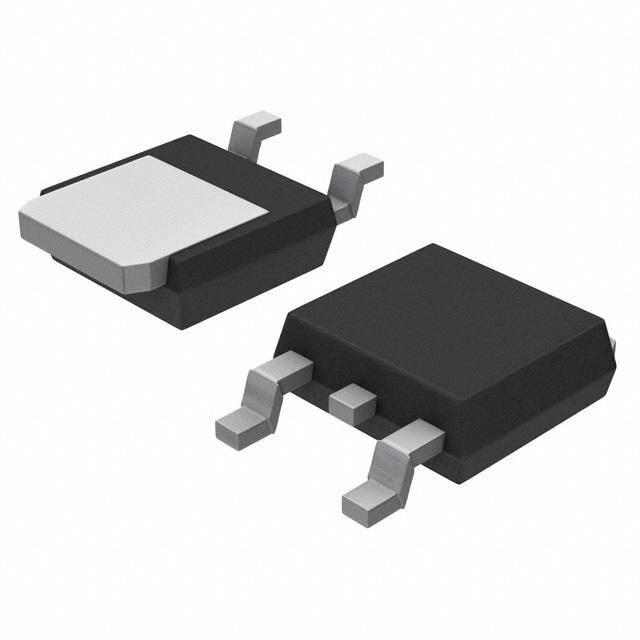
| 描述 | IC REG LDO -5V 0.5A DPAK线性稳压器 5V 500mA Negative |
| 产品分类 | |
| 品牌 | ON Semiconductor |
| 产品手册 | |
| 产品图片 |
|
| rohs | 符合RoHS无铅 / 符合限制有害物质指令(RoHS)规范要求 |
| 产品系列 | 电源管理 IC,线性稳压器,ON Semiconductor MC79M05CDTRKG- |
| 数据手册 | |
| 产品型号 | MC79M05CDTRKG |
| PSRR/纹波抑制—典型值 | 66 dB |
| 产品目录页面 | |
| 产品种类 | |
| 供应商器件封装 | DPAK-3 |
| 其它名称 | MC79M05CDTRKGOSDKR |
| 包装 | Digi-Reel® |
| 商标 | ON Semiconductor |
| 安装类型 | 表面贴装 |
| 安装风格 | SMD/SMT |
| 封装 | Reel |
| 封装/外壳 | TO-252-3,DPak(2 引线+接片),SC-63 |
| 封装/箱体 | TO-252-3 (DPAK) |
| 工作温度 | 0°C ~ 125°C |
| 工厂包装数量 | 2500 |
| 最大工作温度 | + 125 C |
| 最大输入电压 | - 35 V |
| 最小工作温度 | 0 C |
| 最小输入电压 | - 7 V |
| 极性 | Negative |
| 标准包装 | 1 |
| 电压-跌落(典型值) | 1.1V @ 500mA |
| 电压-输入 | 可下调至 -35V |
| 电压-输出 | -5V |
| 电流-输出 | 500mA |
| 电流-限制(最小值) | - |
| 稳压器拓扑 | 负,固定式 |
| 稳压器数 | 1 |
| 系列 | MC79M05 |
| 线路调整率 | 50 mV |
| 负载调节 | 100 mV |
| 输出电压 | - 5 V |
| 输出电流 | 0.5 A |
| 输出端数量 | 1 |
| 输出类型 | Fixed |


- 商务部:美国ITC正式对集成电路等产品启动337调查
- 曝三星4nm工艺存在良率问题 高通将骁龙8 Gen1或转产台积电
- 太阳诱电将投资9.5亿元在常州建新厂生产MLCC 预计2023年完工
- 英特尔发布欧洲新工厂建设计划 深化IDM 2.0 战略
- 台积电先进制程称霸业界 有大客户加持明年业绩稳了
- 达到5530亿美元!SIA预计今年全球半导体销售额将创下新高
- 英特尔拟将自动驾驶子公司Mobileye上市 估值或超500亿美元
- 三星加码芯片和SET,合并消费电子和移动部门,撤换高东真等 CEO
- 三星电子宣布重大人事变动 还合并消费电子和移动部门
- 海关总署:前11个月进口集成电路产品价值2.52万亿元 增长14.8%


PDF Datasheet 数据手册内容提取
MC79M00 Series 500 mA Negative Voltage Regulators The MC79M00 series of fixed output negative voltage regulators are intended as complements to the popular MC78M00 series devices. Available in fixed output voltage options of −5.0 V, −8.0 V, −12 V http://onsemi.com and −15 V, these regulators employ current limiting, thermal shutdown, and safe−area compensation, making them remarkably THREE−TERMINAL rugged under most operating conditions. With adequate heatsinking NEGATIVE FIXED they can deliver output currents in excess of 0.5 A. VOLTAGE REGULATORS Features • STANDARD APPLICATION No External Components Required • Internal Thermal Overload Protection Input MC79MXX Output • Internal Short Circuit Current Limiting Cin* CO** • Output Transistor Safe−Area Compensation 0.33 (cid:2)F 1.0 (cid:2)F • Also Available in Surface Mount DPAK (DT) Package • A common ground is required between the input Pb−Free Packages are Available and the output voltages. The input voltage must remain typically 1.1 V more negative even during the high point of the input ripple voltage. DEVICE TYPE/NOMINAL OUTPUT VOLTAGE XXThese two digits of the type number indicate Device Nominal Output Voltage nominal voltage. * Cin is required if regulator is located an MC79M05 −5.0 V appreciable distance from power supply filter. MC79M08 −8.0 V MC79M12 −12 V ** CO improve stability and transient response. MC79M15 −15 V MARKING DIAGRAMS GND 25 2.4 k 14.7 k 2.0 k 2.0 k 11.5 k 3.6 k 547 4.0 k R1 79MxxMyCT 1.2 k 12 k 1.0 k 4.9 k 2.0 k 12 3 Pin 123... GIOnrupotuputuntd AWLYWWG R2 TO−220−3 T SUFFIX 10 k VO CASE 221AB 4 20 pF 9MxxBG 79MxxG 10 pF 10 k 1 2 ALYWW ALYWW 3 20 k 20 k 240 2.0 k 0.3 DPAK−3 1.1 k 100 DT SUFFIX 750 CASE 369C xx = 05, 08, 12, or 15 This device contains 31 active transistors. VI y = B or C A = Assembly Location Figure 1. Representative Schematic Diagram WL, L = Wafer Lot Y = Year WW = Work Week G = Pb−Free Device ORDERING INFORMATION See detailed ordering and shipping information in the package dimensions section on page 6 of this data sheet. © Semiconductor Components Industries, LLC, 2013 1 Publication Order Number: July, 2013 − Rev. 15 MC79M00/D
MC79M00 Series MAXIMUM RATINGS (TA = 25°C, unless otherwise noted.) Rating Symbol Value Unit Input Voltage VI −35 Vdc Power Dissipation Case 221A (TO−220−3) TA = 25°C PD Internally Limited W Thermal Resistance, Junction−to−Ambient (cid:3)JA 65 °C/W Thermal Resistance, Junction−to−Case (cid:3)JC 5.0 °C/W Case 369C (DPAK−3) TA = 25°C PD Internally Limited W Thermal Resistance, Junction−to−Ambient (cid:3)JA 92 °C/W Thermal Resistance, Junction−to−Case (cid:3)JC 6.0 °C/W Storage Junction Temperature Tstg −65 to +150 °C Operating Junction Temperature Range TJ −40 to +150 °C Stresses exceeding Maximum Ratings may damage the device. Maximum Ratings are stress ratings only. Functional operation above the Recommended Operating Conditions is not implied. Extended exposure to stresses above the Recommended Operating Conditions may affect device reliability. *This device series contains ESD protection and exceeds the following tests: Human Body Model 2000 V per MIL_STD_883, Method 3015 Machine Model Method 200 V MC79M05B, C ELECTRICAL CHARACTERISTICS (VI = −10 V, IO = 350 mA, Tlow to Thigh (Note 2), unless otherwise noted.) Characteristic Symbol Min Typ Max Unit Output Voltage (TJ = 25°C) VO −4.8 −5.0 −5.2 Vdc Line Regulation, TJ = 25°C (Note 1) Regline mV −7.0 Vdc ≥ VI ≥ −25 Vdc − 7.0 50 −8.0 Vdc ≥ VI ≥ −18 Vdc − 2.0 30 Load Regulation, TJ = 25°C (Note 1) Regload mV 5.0 mA ≤ IO ≤ 500 mA − 30 100 Output Voltage VO Vdc −7.0 Vdc ≥ VI ≥ −25 Vdc, 5.0 mA ≤ IO ≤ 350 mA −4.75 − −5.25 Input Bias Current (TJ = 25°C) IIB − 4.3 8.0 mA Input Bias Current Change (cid:4)IIB mA −8.0 Vdc ≥ VI ≥ −25 Vdc, IO = 350 mA − − 0.4 5.0 mA ≤ IO ≤ 350 mA, VI = −10 V − − 0.4 Output Noise Voltage, TA = 25°C, 10 Hz ≤ f ≤ 100 kHz Vn − 40 − (cid:2)V Ripple Rejection (f = 120 Hz) RR 54 66 − dB Dropout Voltage VI−VO Vdc IO = 500 mA, TJ = 25°C − 1.1 − Average Temperature Coefficient of Output Voltage (cid:4)VO/(cid:4)T mV/°C IO = 5.0 mA, 0°C ≤ TJ ≤ 125°C − 0.2 − 1. Load and line regulation are specified at constant temperature. Change in VO due to heating effects must be taken into account separately. Pulse testing with low duty cycle is used. 2. B = Tlow to Thigh, −40°C < TJ < 125°C C = Tlow to Thigh, 0°C < TJ < 125°C. http://onsemi.com 2
MC79M00 Series MC79M08B, C ELECTRICAL CHARACTERISTICS (VI = −10 V, IO = 350 mA, Tlow to Thigh (Note 4), unless otherwise noted.) Characteristic Symbol Min Typ Max Unit Output Voltage (TJ = 25°C) VO −7.7 −8.0 −8.3 Vdc Line Regulation, TJ = 25°C (Note 3) Regline mV −10.5 Vdc ≥ VI ≥ −25 Vdc − 5.0 80 −11 Vdc ≥ VI ≥ −21 Vdc − 3.0 50 Load Regulation, TJ = 25°C (Note 3) Regload mV 5.0 mA ≤ IO ≤ 500 mA − 30 100 Output Voltage VO Vdc −10.5 Vdc ≥ VI ≥ −25 Vdc, 5.0 mA ≤ IO ≤ 350 mA −7.6 −8.0 −8.4 Input Bias Current (TJ = 25°C) IIB − − 8.0 mA Input Bias Current Change (cid:4)IIB mA −10.5 Vdc ≥ VI ≥ −25 Vdc, IO = 350 mA − − 0.4 5.0 mA ≤ IO ≤ 350 mA, VI = −10 V − − 0.4 Output Noise Voltage, TA = 25°C, 10 Hz ≤ f ≤ 100 kHz Vn − 60 − (cid:2)V Ripple Rejection (f = 120 Hz) RR 54 63 − dB Dropout Voltage VI−VO Vdc IO = 500 mA, TJ = 25°C − 1.1 − Average Temperature Coefficient of Output Voltage (cid:4)VO/(cid:4)T mV/°C IO = 5.0 mA, 0°C ≤ TJ ≤ 125°C − 0.4 − 3. Load and line regulation are specified at constant temperature. Change in VO due to heating effects must be taken into account separately. Pulse testing with low duty cycle is used. 4. B = Tlow to Thigh, −40°C < TJ < 125°C C = Tlow to Thigh, 0°C < TJ < 125°C MC79M12B, C ELECTRICAL CHARACTERISTICS (VI = −19 V, IO = 350 mA, Tlow to Thigh (Note 6), unless otherwise noted.) Characteristic Symbol Min Typ Max Unit Output Voltage (TJ = 25°C) VO −11.5 −12 −12.5 Vdc Line Regulation, TJ = 25°C (Note 5) Regline mV −14.5 Vdc ≥ VI ≥ −30 Vdc − 5.0 80 −15 Vdc ≥ VI ≥ −25 Vdc − 3.0 50 Load Regulation, TJ = 25°C (Note 5) Regload mV 5.0 mA ≤ IO ≤ 500 mA − 30 240 Output Voltage VO Vdc −14.5 Vdc ≥ VI ≥ −30 Vdc, 5.0 mA ≤ IO ≤ 350 mA −11.4 − −12.6 Input Bias Current (TJ = 25°C) IIB − 4.4 8.0 mA Input Bias Current Change (cid:4)IIB mA −14.5 Vdc ≥ VI ≥ −30 Vdc, IO = 350 mA − − 0.4 5.0 mA ≤ IO ≤ 350 mA, VI = −19 V − − 0.4 Output Noise Voltage, TA = 25°C, 10 Hz ≤ f ≤ 100 kHz Vn − 75 − (cid:2)V Ripple Rejection (f = 120 Hz) RR 54 60 − dB Dropout Voltage VI−VO Vdc IO = 500 mA, TJ = 25°C − 1.1 − Average Temperature Coefficient of Output Voltage (cid:4)VO/(cid:4)T mV/°C IO = 5.0 mA, 0°C ≤ TJ ≤ 125°C − −0.8 − 5. Load and line regulation are specified at constant temperature. Change in VO due to heating effects must be taken into account separately. Pulse testing with low duty cycle is used. 6. B = Tlow to Thigh, −40°C < TJ < 125°C C = Tlow to Thigh, 0°C < TJ < 125°C http://onsemi.com 3
MC79M00 Series MC79M15B, C ELECTRICAL CHARACTERISTICS (VI = −23 V, IO = 350 mA, Tlow to Thigh (Note 8), unless otherwise noted.) Characteristic Symbol Min Typ Max Unit Output Voltage (TJ = 25°C) VO −14.4 −15 −15.6 Vdc Line Regulation, TJ = 25°C (Note 7) Regline mV −17.5 Vdc ≥ VI ≥ −30 Vdc − 5.0 80 −18 Vdc ≥ VI ≥ −28 Vdc − 3.0 50 Load Regulation, TJ = 25°C (Note 7) Regload mV 5.0 mA ≤ IO ≤ 500 mA − 30 240 Output Voltage VO Vdc −17.5 Vdc ≥ VI ≥ −30 Vdc, 5.0 mA ≤ IO ≤ 350 mA −14.25 − −15.75 Input Bias Current (TJ = 25°C) IIB − 4.4 8.0 mA Input Bias Current Change (cid:4)IIB mA −17.5 Vdc ≥ VI ≥ −30 Vdc, IO = 350 mA − − 0.4 5.0 mA ≤ IO ≤ 350 mA, VI = −23 V − − 0.4 Output Noise Voltage, TA = 25°C, 10 Hz ≤ f ≤ 100 kHz Vn − 90 − (cid:2)V Ripple Rejection (f = 120 Hz) RR 54 60 − dB Dropout Voltage VI−VO Vdc IO = 500 mA, TJ = 25°C − 1.1 − Average Temperature Coefficient of Output Voltage (cid:4)VO/(cid:4)T mV/°C IO = 5.0 mA, 0°C ≤ TJ ≤ 125°C − −1.0 − 7. Load and line regulation are specified at constant temperature. Change in VO due to heating effects must be taken into account separately. Pulse testing with low duty cycle is used. 8. B = Tlow to Thigh, −40°C < TJ < 125°C C = Tlow to Thigh, 0°C < TJ < 125°C 100 Free Air PD(max) for TA = 50°C 2.4 N (W) ESISTANCE°R ( C/W) 8900 VMeoruticnatelldy Î2.0 oÎz. CLoÎpperÎ12..60 DISSIPATIO R AI Minimum R , THERMAL JAUNCTION‐TO‐ 6700 Size Pad ÎÎÎL ÎÎÎÎÎÎÎÎÎ01..82 XIMUM POWE θ J A R 50 0.4 M R(cid:3)JA P, D 40 0 0 5.0 10 15 20 25 30 L, LENGTH OF COPPER (mm) Figure 1. DPAK−3 Thermal Resistance and Maximum Power Dissipation versus P.C.B. Copper Length http://onsemi.com 4
MC79M00 Series Protection Diodes Diode D2 prevents output capacitor from discharging thru When external capacitors are used with MC79M00 series the MC79M15 during an input short circuit or fast switch off regulator it is sometimes necessary to add protection diodes of power supply. to prevent the capacitors from discharging through low Gnd Gnd current points into the regulator or from output polarity + + reversals. Generally, no protection diode is required for 1.0 (cid:2)F 1.0 (cid:2)F D1 MBRS140 or Equiv values of output capacitance less then 10(cid:2)F. Figure 2 shows MC79M15 the MC79M15 with the recommended protection diodes. -(cid:3)20 V -15 V • Input Output Opposite Polarity Protection Diode D1 protects the regulator from output polarity D2MBRS140 reversals during startup, power off and short-circuit or Equiv operation. Figure 2. Protection Diodes • Reverse-bias Protection http://onsemi.com 5
MC79M00 Series ORDERING INFORMATION Output Voltage Operating Device Package Shipping† Tolerance Temperature Range MC79M05BDT DPAK 75 Units / Rail DPAK MC79M05BDTG 75 Units / Rail (Pb−Free) MC79M05BDTRK DPAK 2500 Units / Reel MC79M05BDTRKG TJ = −40°C to +125°C DPAK 2500 Units / Reel (Pb−Free) MC79M05BT TO−220 50 Units / Rail TO−220 MC79M05BTG 50 Units / Rail (Pb−Free) MC79M05CDT DPAK 75 Units / Rail DPAK MC79M05CDTG 75 Units / Rail (Pb−Free) MC79M05CDTRK DPAK 2500 Units / Reel MC79M05CDTRKG TJ = 0°C to +125°C DPAK 2500 Units / Reel (Pb−Free) MC79M05CT TO−220 50 Units / Rail TO−220 MC79M05CTG 50 Units / Rail (Pb−Free) MC79M08BDT DPAK 75 Units / Rail MC79M08BDTRK DPAK 2500 Units / Reel DPAK MC79M08BDTRKG 2500 Units / Reel TJ = −40°C to +125°C (Pb−Free) MC79M08BT TO−220 50 Units / Rail TO−220 MC79M08BTG 50 Units / Rail (Pb−Free) MC79M08CDT DPAK 75 Units / Rail 4.0% DPAK MC79M08CDTG 75 Units / Rail (Pb−Free) MC79M08CDTRK DPAK 2500 Units / Reel MC79M08CDTRKG TJ = 0°C to +125°C DPAK 2500 Units / Reel (Pb−Free) MC79M08CT TO−220 50 Units / Rail TO−220 MC79M08CTG 50 Units / Rail (Pb−Free) MC79M12BDT DPAK 75 Units / Rail DPAK MC79M12BDTG 75 Units / Rail (Pb−Free) MC79M12BDTRK DPAK 2500 Units / Reel MC79M12BDTRKG TJ = −40°C to +125°C DPAK 2500 Units / Reel (Pb−Free) MC79M12BT TO−220 50 Units / Rail TO−220 MC79M12BTG 50 Units / Rail (Pb−Free) MC79M12CDT DPAK 75 Units / Rail DPAK MC79M12CDTG 75 Units / Rail (Pb−Free) MC79M12CDTRK DPAK 2500 Units / Reel MC79M12CDTRKG TJ = 0°C to +125°C DPAK 2500 Units / Reel (Pb−Free) MC79M12CT TO−220 50 Units / Rail TO−220 MC79M12CTG 50 Units / Rail (Pb−Free) †For information on tape and reel specifications, including part orientation and tape sizes, please refer to our Tape and Reel Packaging Specifications Brochure, BRD8011/D. http://onsemi.com 6
MC79M00 Series ORDERING INFORMATION Output Voltage Operating Device Package Shipping(cid:2) Tolerance Temperature Range MC79M15BDT DPAK 75 Units / Rail DPAK MC79M15BDTG 75 Units / Rail (Pb−Free) MC79M15BDTRK DPAK 2500 Units / Reel TJ = −40°C to +125°C DPAK MC79M15BDTRKG 2500 Units / Reel (Pb−Free) MC79M15BT TO−220 50 Units / Rail TO−220 MC79M15BTG 50 Units / Rail (Pb−Free) 4.0% MC79M15CDT DPAK 75 Units / Rail DPAK MC79M15CDTG 75 Units / Rail (Pb−Free) MC79M15CDTRK DPAK 2500 Units / Reel TJ = 0°C to +125°C DPAK MC79M15CDTRKG 2500 Units / Reel (Pb−Free) MC79M15CT TO−220 50 Units / Rail TO−220 MC79M15CTG 50 Units / Rail (Pb−Free) †For information on tape and reel specifications, including part orientation and tape sizes, please refer to our Tape and Reel Packaging Specifications Brochure, BRD8011/D. http://onsemi.com 7
MC79M00 Series PACKAGE DIMENSIONS TO−220, SINGLE GAUGE CASE 221AB ISSUE A NOTES: 1. DIMENSIONING AND TOLERANCING PER ANSI Y14.5M, 1982. −T− SPELAATNIENG 23.. CDOIMNETNRSOIOLLNI NZG D DEFIMINEENSS IAO ZNO: INNEC WHEHSE.RE ALL BODY AND B F C LEAD IRREGULARITIES ARE ALLOWED. 4. PRODUCT SHIPPED PRIOR TO 2008 HAD DIMENSIONS T S S = 0.045 - 0.055 INCHES (1.143 - 1.397 MM) 4 INCHES MILLIMETERS DIM MIN MAX MIN MAX A 0.570 0.620 14.48 15.75 Q A B 0.380 0.405 9.66 10.28 C 0.160 0.190 4.07 4.82 1 2 3 U D 0.025 0.035 0.64 0.88 H F 0.142 0.147 3.61 3.73 G 0.095 0.105 2.42 2.66 K H 0.110 0.155 2.80 3.93 Z J 0.018 0.025 0.46 0.64 K 0.500 0.562 12.70 14.27 L 0.045 0.060 1.15 1.52 N 0.190 0.210 4.83 5.33 L R Q 0.100 0.120 2.54 3.04 R 0.080 0.110 2.04 2.79 V J S 0.020 0.024 0.508 0.61 G T 0.235 0.255 5.97 6.47 U 0.000 0.050 0.00 1.27 D V 0.045 --- 1.15 --- N Z --- 0.080 --- 2.04 http://onsemi.com 8
MC79M00 Series PACKAGE DIMENSIONS DPAK−3 DT SUFFIX CASE 369C ISSUE D NOTES: C 1.DIMENSIONING AND TOLERANCING PER ASME A Y14.5M, 1994. E A 2.CONTROLLING DIMENSION: INCHES. 3.THERMAL PAD CONTOUR OPTIONAL WITHIN DI- MENSIONS b3, L3 and Z. b3 B c2 4.DIMENSIONS D AND E DO NOT INCLUDE MOLD FLASH, PROTRUSIONS, OR BURRS. MOLD FLASH, PROTRUSIONS, OR GATE BURRS SHALL NOT EXCEED 0.006 INCHES PER SIDE. L3 4 Z 5.DOIUMTEENRSMIOONSST DE XATNRDE ME EASR EO FD ETTHEER PMLIANSETDIC A TB OTHDEY. D H 6.DATUMS A AND B ARE DETERMINED AT DATUM 1 2 3 DETAIL A PLANE H. INCHES MILLIMETERS DIM MIN MAX MIN MAX L4 A 0.086 0.094 2.18 2.38 b2 A1 0.000 0.005 0.00 0.13 b c b 0.025 0.035 0.63 0.89 b2 0.030 0.045 0.76 1.14 e 0.005 (0.13) M C H b3 0.180 0.215 4.57 5.46 c 0.018 0.024 0.46 0.61 L2 GPLAAUNGEE C SPELAATNIENG cD2 00..203158 00..204254 50..9476 60..2621 E 0.250 0.265 6.35 6.73 e 0.090 BSC 2.29 BSC H 0.370 0.410 9.40 10.41 L A1 L 0.055 0.070 1.40 1.78 L1 L1 0.108 REF 2.74 REF L2 0.020 BSC 0.51 BSC DETAIL A L3 0.035 0.050 0.89 1.27 ROTATED 90(cid:2) CW L4 −−− 0.040 −−− 1.01 Z 0.155 −−− 3.93 −−− SOLDERING FOOTPRINT* 6.20 3.00 0.244 0.118 2.58 0.102 5.80 1.60 6.17 0.228 0.063 0.243 (cid:2) (cid:3) mm SCALE 3:1 inches *For additional information on our Pb−Free strategy and soldering details, please download the ON Semiconductor Soldering and Mounting Techniques Reference Manual, SOLDERRM/D. ON Semiconductor and are registered trademarks of Semiconductor Components Industries, LLC (SCILLC). SCILLC owns the rights to a number of patents, trademarks, copyrights, trade secrets, and other intellectual property. A listing of SCILLC’s product/patent coverage may be accessed at www.onsemi.com/site/pdf/Patent−Marking.pdf. SCILLC reserves the right to make changes without further notice to any products herein. SCILLC makes no warranty, representation or guarantee regarding the suitability of its products for any particular purpose, nor does SCILLC assume any liability arising out of the application or use of any product or circuit, and specifically disclaims any and all liability, including without limitation special, consequential or incidental damages. “Typical” parameters which may be provided in SCILLC data sheets and/or specifications can and do vary in different applications and actual performance may vary over time. All operating parameters, including “Typicals” must be validated for each customer application by customer’s technical experts. SCILLC does not convey any license under its patent rights nor the rights of others. SCILLC products are not designed, intended, or authorized for use as components in systems intended for surgical implant into the body, or other applications intended to support or sustain life, or for any other application in which the failure of the SCILLC product could create a situation where personal injury or death may occur. Should Buyer purchase or use SCILLC products for any such unintended or unauthorized application, Buyer shall indemnify and hold SCILLC and its officers, employees, subsidiaries, affiliates, and distributors harmless against all claims, costs, damages, and expenses, and reasonable attorney fees arising out of, directly or indirectly, any claim of personal injury or death associated with such unintended or unauthorized use, even if such claim alleges that SCILLC was negligent regarding the design or manufacture of the part. SCILLC is an Equal Opportunity/Affirmative Action Employer. This literature is subject to all applicable copyright laws and is not for resale in any manner. PUBLICATION ORDERING INFORMATION LITERATURE FULFILLMENT: N. American Technical Support: 800−282−9855 Toll Free ON Semiconductor Website: www.onsemi.com Literature Distribution Center for ON Semiconductor USA/Canada P.O. Box 5163, Denver, Colorado 80217 USA Europe, Middle East and Africa Technical Support: Order Literature: http://www.onsemi.com/orderlit Phone: 303−675−2175 or 800−344−3860 Toll Free USA/Canada Phone: 421 33 790 2910 Fax: 303−675−2176 or 800−344−3867 Toll Free USA/Canada Japan Customer Focus Center For additional information, please contact your local Email: orderlit@onsemi.com Phone: 81−3−5817−1050 Sales Representative http://onsemi.com MC79M00/D 9
Mouser Electronics Authorized Distributor Click to View Pricing, Inventory, Delivery & Lifecycle Information: O N Semiconductor: MC79M05BDTG MC79M05BDTRKG MC79M05BTG MC79M05CDTG MC79M05CDTRKG MC79M05CTG MC79M08BDTG MC79M08BDTRKG MC79M08BTG MC79M08CDTG MC79M08CDTRKG MC79M08CTG MC79M12BDTG MC79M12BDTRKG MC79M12BTG MC79M12CDTG MC79M12CDTRKG MC79M12CTG MC79M15BDTG MC79M15BDTRKG MC79M15BTG MC79M15CDTG MC79M15CDTRKG MC79M15CTG