ICGOO在线商城 > 集成电路(IC) > 逻辑 - 栅极和逆变器 > MC74LCX14DTR2G
 Datasheet下载
- 型号: MC74LCX14DTR2G
- 制造商: ON Semiconductor
- 库位|库存: xxxx|xxxx
- 要求:
| 数量阶梯 | 香港交货 | 国内含税 |
| +xxxx | $xxxx | ¥xxxx |
查看当月历史价格
查看今年历史价格
MC74LCX14DTR2G产品简介:
ICGOO电子元器件商城为您提供MC74LCX14DTR2G由ON Semiconductor设计生产,在icgoo商城现货销售,并且可以通过原厂、代理商等渠道进行代购。 MC74LCX14DTR2G价格参考。ON SemiconductorMC74LCX14DTR2G封装/规格:逻辑 - 栅极和逆变器, Inverter IC 6 Channel Schmitt Trigger 14-TSSOP。您可以下载MC74LCX14DTR2G参考资料、Datasheet数据手册功能说明书,资料中有MC74LCX14DTR2G 详细功能的应用电路图电压和使用方法及教程。
MC74LCX14DTR2G 是由 ON Semiconductor 生产的一款逻辑电路,具体来说是一款施密特触发六反相器(Hex Schmitt Trigger Inverter)。这款器件广泛应用于需要信号整形、噪声抑制和电平转换的数字电路中。以下是其主要应用场景:

 1. 信号整形与噪声抑制
   施密特触发器具有两个不同的阈值电压,分别用于上升沿和下降沿的检测。这种特性使得 MC74LCX14DTR2G 能够有效地消除输入信号中的噪声,确保输出信号的稳定性和可靠性。它特别适用于那些输入信号带有噪声或抖动的场景,如传感器接口、开关电路等。

 2. 脉冲展宽与延迟
   由于施密特触发器的迟滞特性,MC74LCX14DTR2G 可以用于脉冲展宽或延迟应用。通过调整输入信号的幅度和频率,可以实现对脉冲宽度的精确控制。这在定时电路、脉冲发生器和振荡器设计中非常有用。

 3. 电平转换
   该器件可以在不同电压电平之间进行转换。例如,在低速通信接口中,MC74LCX14DTR2G 可以将 TTL 或 CMOS 电平转换为适合后续电路处理的电平。这种功能在混合信号系统中尤为重要,特别是在连接不同电压标准的模块时。

 4. 振荡器电路
   MC74LCX14DTR2G 还可以用于构建简单的振荡器电路。通过外接电阻和电容,可以形成一个稳定的振荡源,适用于定时器、时钟生成和其他需要周期性信号的应用。

 5. 接口保护
   在一些应用场景中,MC74LCX14DTR2G 可以用作接口保护电路。它能够防止输入信号超出安全范围,从而保护后续的敏感电路免受损坏。

 6. 消费电子与工业控制
   在消费电子产品(如家电、手持设备)和工业控制系统中,MC74LCX14DTR2G 常用于信号调理和逻辑控制。它的低功耗和高可靠性使其成为这些应用的理想选择。

总之,MC74LCX14DTR2G 凭借其施密特触发特性,在信号处理、噪声抑制、电平转换和振荡器设计等方面表现出色,适用于广泛的电子系统和应用场景。
| 参数 | 数值 |
| 产品目录 | 集成电路 (IC)半导体 |
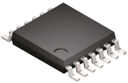
| 描述 | IC INV HEX SCHMT LV CMOS 14TSSOP变换器 2-3.6V CMOS Hex Schmitt |
| 产品分类 | |
| 品牌 | ON Semiconductor |
| 产品手册 | |
| 产品图片 |
|
| rohs | 符合RoHS无铅 / 符合限制有害物质指令(RoHS)规范要求 |
| 产品系列 | 逻辑集成电路,变换器,ON Semiconductor MC74LCX14DTR2G74LCX |
| 数据手册 | |
| 产品型号 | MC74LCX14DTR2G |
| 不同V、最大CL时的最大传播延迟 | 6.5ns @ 3.3V,50pF |
| 产品种类 | 变换器 |
| 低电平输出电流 | 24 mA |
| 供应商器件封装 | 14-TSSOP |
| 其它名称 | MC74LCX14DTR2GOS |
| 包装 | 带卷 (TR) |
| 商标 | ON Semiconductor |
| 安装类型 | 表面贴装 |
| 安装风格 | SMD/SMT |
| 封装 | Reel |
| 封装/外壳 | 14-TSSOP(0.173",4.40mm 宽) |
| 封装/箱体 | TSSOP-14 |
| 工作温度 | -40°C ~ 85°C |
| 工厂包装数量 | 2500 |
| 最大工作温度 | + 85 C |
| 标准包装 | 2,500 |
| 特性 | 施密特触发器 |
| 电压-电源 | 2 V ~ 3.6 V |
| 电流-输出高,低 | 24mA,24mA |
| 电流-静态(最大值) | 10µA |
| 电源电压-最大 | 3.6 V |
| 电源电压-最小 | 2 V |
| 电路数 | 6 |
| 电路数量 | 6 Circuit |
| 系列 | MC74LCX14 |
| 输入数 | 6 |
| 逻辑电平-低 | 0.4 V ~ 0.6 V |
| 逻辑电平-高 | 1.7 V ~ 2.2 V |
| 逻辑类型 | |
| 逻辑系列 | 74LCX |
| 高电平输出电流 | - 24 mA |


PDF Datasheet 数据手册内容提取
MC74LCX14 Low Voltage CMOS Hex Schmitt Inverter With 5 V-Tolerant Inputs The MC74LCX14 is a high performance hex inverter with http://onsemi.com Schmitt−Trigger inputs operating from a 2.3 to 3.6 V supply. High impedance TTL compatible inputs significantly reduce current MARKING loading to input drivers, while TTL compatible outputs offer improved DIAGRAMS switching noise performance. A VI specification of 5.5 V allows MC74LCX14 inputs to be safely driven from 5.0 V devices. 14 Pin configuration and function are the same as the MC74LCX04, SOIC−14 LCX14G 14 but the inputs have hysteresis and, with its Schmitt trigger function, D SUFFIX AWLYWW CASE 751A the LCX14 can be used as a line receiver which will receive slow input 1 signals. 1 Features 14 Designed for 2.3 V to 3.6 V V Operation CC TSSOP−14 LCX 5.0 V Tolerant Inputs − Interface Capability with 5.0 V TTL Logic 14 DT SUFFIX 14 LVTTL Compatible 1 CASE 948G ALY(cid:2)W(cid:2) 1 LVCMOS Compatible 24 mA Balanced Output Sink and Source Capability A = Assembly Location L, WL = Wafer Lot Near Zero Static Supply Current (10 (cid:2)A) Substantially Reduces Y, YY = Year System Power Requirements W, WW = Work Week G or (cid:2) = Pb−Free Package Latchup Performance Exceeds 500 mA (Note: Microdot may be in either location) Current Drive Capability is 24 mA at Source/Sink Pin and Function Compatible with Other Standard Logic Families ORDERING INFORMATION ESD Performance: Human Body Model >2000 V See detailed ordering and shipping information in the package Machine Model >100 V dimensions section on page 4 of this data sheet. Chip Complexity: 41 Equivalent Gates These Devices are Pb−Free, Halogen Free/BFR Free and are RoHS Compliant Semiconductor Components Industries, LLC, 2012 1 Publication Order Number: October, 2012 − Rev. 8 MC74LCX14/D
MC74LCX14 1 2 A1 Y1 3 4 A2 Y2 5 6 VCC A6 Y6 A5 Y5 A4 Y4 A3 Y3 14 13 12 11 10 9 8 Y = A 9 8 A4 Y4 11 10 A5 Y5 1 2 3 4 5 6 7 13 12 A6 Y6 A1 Y1 A2 Y2 A3 Y3 GND Figure 1. Pinout: 14−Lead (Top View) Figure 2. Logic Diagram PIN NAMES TRUTH TABLE Pins Function Inputs Outputs An Data Inputs A Y Yn Outputs L H H L MAXIMUM RATINGS Symbol Parameter Value Condition Units VCC DC Supply Voltage −0.5 to +7.0 V VI DC Input Voltage −0.5 VI +7.0 V VO DC Output Voltage −0.5 VO VCC + 0.5 Output in HIGH or LOW State. (Note 1) V IIK DC Input Diode Current −50 VI < GND mA IOK DC Output Diode Current −50 VO < GND mA +50 VO > VCC mA IO DC Output Source/Sink Current 50 mA ICC DC Supply Current Per Supply Pin 100 mA IGND DC Ground Current Per Ground Pin 100 mA TSTG Storage Temperature Range −65 to +150 C MSL Moisture Sensitivity Level 1 Maximum ratings are those values beyond which device damage can occur. Maximum ratings applied to the device are individual stress limit values (not normal operating conditions) and are not valid simultaneously. If these limits are exceeded, device functional operation is not implied, damage may occur and reliability may be affected. 1. IO absolute maximum rating must be observed. http://onsemi.com 2
MC74LCX14 RECOMMENDED OPERATING CONDITIONS Symbol Parameter Min Typ Max Units VCC Supply Voltage V Operating 2.0 2.5 to 3.3 3.6 Data Retention Only 1.5 3.6 VI Input Voltage 0 5.5 V VO Output Voltage (HIGH or LOW State) 0 VCC V IOH HIGH Level Output Current mA VCC = 3.0 V−3.6 V −24 VCC = 2.7 V−3.0 V −12 VCC = 2.3 V−2.7 V −8 IOL LOW Level Output Current mA VCC = 3.0 V−3.6 V +24 VCC = 2.7 V−3.0 V +12 VCC = 2.3 V−2.7 V +8 TA Operating Free−Air Temperature −40 +85 C ÎÎÎÎÎÎÎÎÎÎÎÎÎÎÎÎÎÎÎÎÎÎÎÎÎÎÎÎÎÎÎÎÎ DC ELECTRICAL CHARACTERISTICS ÎÎÎÎÎÎÎÎÎÎÎÎÎÎÎÎÎÎÎÎÎÎÎÎÎÎÎÎÎÎÎÎÎÎÎÎÎÎÎÎÎÎÎÎÎÎÎÎÎÎÎÎÎÎÎÎÎÎÎÎÎÎÎÎÎÎÎÎÎÎÎÎÎÎÎÎÎÎ TA = −40 to 85C ÎÎÎÎÎÎÎÎÎÎÎÎÎÎÎÎÎÎÎÎÎÎÎÎÎÎÎÎÎÎÎÎÎÎÎÎÎÎÎÎÎÎÎÎÎÎÎÎÎÎÎÎÎÎÎÎÎÎÎÎÎÎÎÎÎÎÎÎÎÎÎÎÎÎÎÎ Symbol Characteristic Condition Min Max Units ÎÎVÎT+ ÎÎPÎositivÎe InÎput TÎhreÎsholdÎ VoÎltageÎ (FigÎure ÎÎ3) ÎÎÎÎVÎCC =Î 2.5Î V ÎÎÎÎÎÎ0.Î9 ÎÎÎ1.Î7 ÎÎÎVÎ ÎÎÎÎÎÎÎÎÎÎÎÎÎÎÎÎÎÎÎÎÎÎÎÎÎÎÎÎÎÎÎÎÎÎÎÎÎÎÎÎVÎÎCC =ÎÎ 3.0ÎÎ V ÎÎÎÎÎÎÎÎÎÎÎÎ1.ÎÎ2 ÎÎÎÎÎÎ2.ÎÎ2 ÎÎÎÎÎÎÎÎ ÎÎVÎT− ÎÎNÎegatÎive IÎnputÎ ThreÎshoÎld VoÎltagÎe ÎÎÎÎÎÎÎVÎCC =Î 2.5Î V ÎÎÎÎÎÎ0.Î4 ÎÎÎ1.Î1 ÎÎÎVÎ (Figure 3) VCC = 3.0 V 0.6 1.5 ÎÎÎÎÎÎÎÎÎÎÎÎÎÎÎÎÎÎÎÎÎÎÎÎÎÎÎÎÎÎÎÎÎÎÎÎÎÎÎÎÎÎÎÎÎÎÎÎÎÎÎÎÎÎÎÎÎÎÎÎÎÎÎÎÎÎÎÎÎÎÎÎÎÎÎÎ VH Input Hysteresis Voltage (Figure 3) VCC = 2.5 V 0.3 1.0 V ÎÎÎÎÎÎÎÎÎÎÎÎÎÎÎÎÎÎÎÎÎÎÎÎÎÎÎÎÎÎÎÎÎÎÎÎÎÎÎÎVÎÎCC =ÎÎ 3.0ÎÎ V ÎÎÎÎÎÎÎÎÎÎÎÎ0.ÎÎ4 ÎÎÎÎÎÎ1.ÎÎ2 ÎÎÎÎÎÎÎÎ ÎÎVOÎH ÎÎHÎIGHÎ LevÎel OuÎtputÎ VoltÎageÎÎÎÎÎÎÎÎÎÎ2.3 ÎÎV ÎÎVCCÎÎ 3.ÎÎ6 V; ÎÎIOL =ÎÎ 100ÎÎ (cid:2)AÎÎÎÎÎÎVÎÎCC−ÎÎ0.2ÎÎÎÎÎÎÎÎÎÎÎÎVÎ ÎÎÎÎÎÎÎÎÎÎÎÎÎÎÎÎÎÎÎÎÎÎÎVCCÎÎ = 2ÎÎ.3 V;ÎÎ IOH ÎÎ= −8ÎÎ mAÎÎÎÎÎÎÎÎÎÎ1.ÎÎ8 ÎÎÎÎÎÎÎÎÎÎÎÎÎ ÎÎÎÎÎÎÎÎÎÎÎÎÎÎÎÎÎÎÎÎÎÎÎVCCÎÎ = 2.ÎÎ7 V; ÎÎIOH =ÎÎ −1ÎÎ2 mAÎÎÎÎÎÎÎÎÎÎ2.ÎÎ2 ÎÎÎÎÎÎÎÎÎÎÎÎÎ ÎÎÎÎÎÎÎÎÎÎÎÎÎÎÎÎÎÎÎÎÎÎÎVCCÎÎ = 3.ÎÎ0 V; ÎÎIOH =ÎÎ −1ÎÎ8 mAÎÎÎÎÎÎÎÎÎÎ2.ÎÎ4 ÎÎÎÎÎÎÎÎÎÎÎÎÎ ÎÎÎÎÎÎÎÎÎÎÎÎÎÎÎÎÎÎÎÎÎÎÎÎÎÎÎÎÎÎÎÎÎÎÎÎÎÎVCCÎÎ = 3.ÎÎ0 V; ÎÎIOH =ÎÎ −2ÎÎ4 mAÎÎÎÎÎÎÎÎÎÎ2.ÎÎ2 ÎÎÎÎÎÎÎÎÎÎÎÎÎÎÎÎ ÎÎVÎOL ÎÎLÎOW ÎLeveÎl OuÎtput ÎVoltÎageÎÎÎÎÎÎÎÎÎÎ2.3 ÎÎV ÎÎVCCÎÎ 3.ÎÎ6 V; ÎÎIOL =ÎÎ 100ÎÎ (cid:2)AÎÎÎÎÎÎÎÎÎÎÎÎÎÎÎÎ0.ÎÎ2 ÎÎÎÎVÎ VCC = 2.3 V; IOL = 8 mA 0.3 ÎÎÎÎÎÎÎÎÎÎÎÎÎÎÎÎÎÎÎÎÎÎÎÎÎÎÎÎÎÎÎÎÎÎÎÎÎÎÎÎÎÎÎÎÎÎÎÎÎÎÎÎÎÎÎÎÎÎ VCC = 2.7 V; IOL = 12 mA 0.4 ÎÎÎÎÎÎÎÎÎÎÎÎÎÎÎÎÎÎÎÎÎÎÎÎÎÎÎÎÎÎÎÎÎÎÎÎÎÎÎÎÎÎÎÎÎÎÎÎÎÎÎÎÎÎÎÎÎÎ VCC = 3.0 V; IOL = 16 mA 0.4 ÎÎÎÎÎÎÎÎÎÎÎÎÎÎÎÎÎÎÎÎÎÎÎÎÎÎÎÎÎÎÎÎÎÎÎÎÎÎÎÎÎÎÎÎÎÎÎÎÎÎÎÎÎÎÎÎÎÎ VCC = 3.0 V; IOL = 24 mA 0.55 ÎÎÎÎÎÎÎÎÎÎÎÎÎÎÎÎÎÎÎÎÎÎÎÎÎÎÎÎÎÎÎÎÎÎÎÎÎÎÎÎÎÎÎÎÎÎÎÎÎÎÎÎÎÎÎÎÎÎÎÎÎÎÎÎÎÎÎÎÎÎÎÎÎÎÎÎ IOFF Power Off Leakage Current VCC = 0, VIN = 5.5 V or VOUT = 5.5 V 10 (cid:2)A ÎÎÎÎIIÎÎN ÎÎÎÎInÎÎput ÎÎLeakÎÎage ÎÎCurrÎÎentÎÎÎÎÎÎÎÎÎÎÎÎÎÎÎÎVCÎÎC = 3ÎÎ.6 VÎÎ, VINÎÎ = 5ÎÎ.5 V ÎÎor GÎÎNDÎÎÎÎÎÎÎÎÎÎÎÎÎÎÎÎ5ÎÎ.0 ÎÎÎÎÎÎ(cid:2)AÎÎ ÎÎICÎC ÎÎQÎuiesÎcentÎ SupÎply CÎurreÎnt ÎÎÎÎÎÎÎVCÎC = 3Î.6 VÎ, VINÎ = 5Î.5 V Îor GÎNDÎÎÎÎÎÎÎÎ1Î0 ÎÎÎ(cid:2)AÎ (cid:3)ICC Increase in ICC per Input 2.3 VCC 3.6 V; VIH = VCC − 0.6 V 500 (cid:2)A http://onsemi.com 3
MC74LCX14 ÎÎÎÎÎÎÎÎÎÎÎÎÎÎÎÎÎÎÎÎÎÎÎÎÎÎÎÎÎÎÎÎÎ AC ELECTRICAL CHARACTERISTICS (Input tr = tf = 2.5 ns) ÎÎÎÎÎÎÎÎÎÎÎÎÎÎÎÎÎÎÎÎÎÎÎÎÎÎÎÎÎÎÎÎÎ Limits TA = −40C to +85C VCC = 3.3 V 0.3 V VCC = 2.7 V VCC = 2.5 V 0.2 V CL = 50 pF CL = 50 pF CL = 30 pF Symbol Parameter Waveform Min Max Min Max Min Max Units tPLH Propagation Delay Input to Output 1 1.5 6.5 1.5 7.5 1.5 7.8 ns tPHL 1.5 6.5 1.5 7.5 1.5 7.8 tOSHL Output−to−Output Skew (Note 2) 1.0 ns tOSLH 1.0 2. Skew is defined as the absolute value of the difference between the actual propagation delay for any two separate outputs of the same device. The specification applies to any outputs switching in the same direction, either HIGH−to−LOW (tOSHL) or LOW−to−HIGH (tOSLH); parameter guaranteed by design. DYNAMIC SWITCHING CHARACTERISTICS TA = +25C Symbol Characteristic Condition Min Typ Max Units VOLP Dynamic LOW Peak Voltage VCC = 3.3 V, CL = 50 pF, VIH = 3.3 V, VIL = 0 V 0.8 V (Note 3) VCC = 2.5 V, CL = 30 pF, VIH = 2.5 V, VIL = 0 V 0.6 VOLV Dynamic LOW Valley Voltage VCC = 3.3 V, CL = 50 pF, VIH = 3.3 V, VIL = 0 V −0.8 V (Note 3) VCC = 2.5 V, CL = 30 pF, VIH = 2.5 V, VIL = 0 V −0.6 3. Number of outputs defined as “n”. Measured with “n−1” outputs switching from HIGH−to−LOW or LOW−to−HIGH. The remaining output is measured in the LOW state. CAPACITIVE CHARACTERISTICS Symbol Parameter Condition Typical Units CIN Input Capacitance VCC = 3.3 V, VI = 0 V or VCC 7 pF COUT Output Capacitance VCC = 3.3 V, VI = 0 V or VCC 8 pF CPD Power Dissipation Capacitance 10 MHz, VCC = 3.3 V, VI = 0 V or VCC 25 pF ORDERING INFORMATION Device Package Shipping† MC74LCX14DG SOIC−14 55 Units / Rail (Pb−Free) MC74LCX14DR2G SOIC−14 2500 Tape & Reel (Pb−Free) MC74LCX14DTG TSSOP−14 96 Units / Rail (Pb−Free) MC74LCX14DTR2G TSSOP−14 2500 Tape & Reel (Pb−Free) †For information on tape and reel specifications, including part orientation and tape sizes, please refer to our Tape and Reel Packaging Specifications Brochure, BRD8011/D. http://onsemi.com 4
MC74LCX14 VCC PULSE DUT GENERATOR VCC RT CL RL A 50% GND tPLH tPHL CL=50 pF at VCC = 3.3 (cid:2)0.3 V or equivalent VOH (includes jig and probe capacitance) Y 50% VCC RL= R1 = 500 (cid:4) or equivalent VOL RT= ZOUT of pulse generator (typically 50 (cid:4)) Figure 3. Switching Waveforms Figure 4. Test Circuit TS 4 L O V E ( G A LT 3 O V D L O H ES 2 (VT+) HR VHtyp T T U NP (VT−) L I 1 A C PI Y T , T V 2 2.5 3 3.5 3.6 VCC, POWER SUPPLY VOLTAGE (VOLTS) VHtyp = (VT+ typ) − (VT− typ) Figure 5. Typical Input Threshold, V , V versus Power Supply Voltage T+ T− (a) A Schmitt−Trigger Squares Up Inputs With Slow Rise and Fall Times (b) A Schmitt−Trigger Offers Maximum Noise Immunity VCC VCC VH VH Vin VT+ Vin VT+ VT− VT− GND GND VOH VOH Vout Vout VOL VOL Figure 6. Typical Schmitt−Trigger Applications http://onsemi.com 5
MC74LCX14 INPUT Figure 7. Input Equivalent Circuit http://onsemi.com 6
MC74LCX14 PACKAGE DIMENSIONS TSSOP−14 CASE 948G ISSUE B 14X K REF NOTES: 1. DIMENSIONING AND TOLERANCING PER 0.10 (0.004) M T U S V S ANSI Y14.5M, 1982. 2. CONTROLLING DIMENSION: MILLIMETER. 0.15 (0.006) T U S 3. DIMENSION A DOES NOT INCLUDE MOLD FLASH, PROTRUSIONS OR GATE BURRS. N MOLD FLASH OR GATE BURRS SHALL NOT 0.25 (0.010) EXCEED 0.15 (0.006) PER SIDE. 14 8 4. DIMENSION B DOES NOT INCLUDE 2XL/2 INTERLEAD FLASH OR PROTRUSION. M INTERLEAD FLASH OR PROTRUSION SHALL NOT EXCEED 0.25 (0.010) PER SIDE. L B 5. DIMENSION K DOES NOT INCLUDE −U− N DAMBAR PROTRUSION. ALLOWABLE PIN 1 DAMBAR PROTRUSION SHALL BE 0.08 IDENT. F (0.003) TOTAL IN EXCESS OF THE K DIMENSION AT MAXIMUM MATERIAL 1 7 DETAIL E CONDITION. 6. TERMINAL NUMBERS ARE SHOWN FOR REFERENCE ONLY. 7. DIMENSION A AND B ARE TO BE 0.15 (0.006) T U S A K DETERMINED AT DATUM PLANE −W−. −V− K1 MILLIMETERS INCHES ÇÉÇÉÇÉ DIM MIN MAX MIN MAX A 4.90 5.10 0.193 0.200 J J1 ÇÉÇÉÇÉ B 4.30 4.50 0.169 0.177 C −−− 1.20 −−− 0.047 SECTION N−N D 0.05 0.15 0.002 0.006 F 0.50 0.75 0.020 0.030 G 0.65 BSC 0.026 BSC H 0.50 0.60 0.020 0.024 −W− J 0.09 0.20 0.004 0.008 C J1 0.09 0.16 0.004 0.006 K 0.19 0.30 0.007 0.012 0.10 (0.004) K1 0.19 0.25 0.007 0.010 L 6.40 BSC 0.252 BSC −T− SPELAATNIENG D G H DETAIL E M 0 (cid:3) 8 (cid:3) 0 (cid:3) 8 (cid:3) SOLDERING FOOTPRINT* 7.06 1 0.65 PITCH 14X 14X 0.36 1.26 DIMENSIONS: MILLIMETERS *For additional information on our Pb−Free strategy and soldering details, please download the ON Semiconductor Soldering and Mounting Techniques Reference Manual, SOLDERRM/D. http://onsemi.com 7
MC74LCX14 PACKAGE DIMENSIONS SOIC−14 NB CASE 751A−03 ISSUE K D A NOTES: B 1.DIMENSIONING AND TOLERANCING PER ASME Y14.5M, 1994. 2.CONTROLLING DIMENSION: MILLIMETERS. 14 8 3.DIMENSION b DOES NOT INCLUDE DAMBAR A3 PROTRUSION. ALLOWABLE PROTRUSION SHALL BE 0.13 TOTAL IN EXCESS OF AT MAXIMUM MATERIAL CONDITION. H E 4.DIMENSIONS D AND E DO NOT INCLUDE MOLD PROTRUSIONS. L 5.MAXIMUM MOLD PROTRUSION 0.15 PER SIDE. 1 7 DETAIL A MILLIMETERS INCHES 0.25 M B M 13Xb DIM MIN MAX MIN MAX A 1.35 1.75 0.054 0.068 0.25 M C A S B S A1 0.10 0.25 0.004 0.010 A3 0.19 0.25 0.008 0.010 DETAIL A b 0.35 0.49 0.014 0.019 h A X 45(cid:3) DE 83..5850 84..7050 00..135307 00..135474 e 1.27 BSC 0.050 BSC H 5.80 6.20 0.228 0.244 h 0.25 0.50 0.010 0.019 e A1 C SEATING M ML 0.04 0(cid:3) 1.72 5(cid:3) 0.001 6(cid:3) 0.047 9(cid:3) PLANE SOLDERING FOOTPRINT* 6.50 14X 1.18 1 1.27 PITCH 14X 0.58 DIMENSIONS: MILLIMETERS *For additional information on our Pb−Free strategy and soldering details, please download the ON Semiconductor Soldering and Mounting Techniques Reference Manual, SOLDERRM/D. ON Semiconductor and are registered trademarks of Semiconductor Components Industries, LLC (SCILLC). SCILLC owns the rights to a number of patents, trademarks, copyrights, trade secrets, and other intellectual property. A listing of SCILLC’s product/patent coverage may be accessed at www.onsemi.com/site/pdf/Patent−Marking.pdf. SCILLC reserves the right to make changes without further notice to any products herein. SCILLC makes no warranty, representation or guarantee regarding the suitability of its products for any particular purpose, nor does SCILLC assume any liability arising out of the application or use of any product or circuit, and specifically disclaims any and all liability, including without limitation special, consequential or incidental damages. “Typical” parameters which may be provided in SCILLC data sheets and/or specifications can and do vary in different applications and actual performance may vary over time. All operating parameters, including “Typicals” must be validated for each customer application by customer’s technical experts. SCILLC does not convey any license under its patent rights nor the rights of others. SCILLC products are not designed, intended, or authorized for use as components in systems intended for surgical implant into the body, or other applications intended to support or sustain life, or for any other application in which the failure of the SCILLC product could create a situation where personal injury or death may occur. Should Buyer purchase or use SCILLC products for any such unintended or unauthorized application, Buyer shall indemnify and hold SCILLC and its officers, employees, subsidiaries, affiliates, and distributors harmless against all claims, costs, damages, and expenses, and reasonable attorney fees arising out of, directly or indirectly, any claim of personal injury or death associated with such unintended or unauthorized use, even if such claim alleges that SCILLC was negligent regarding the design or manufacture of the part. SCILLC is an Equal Opportunity/Affirmative Action Employer. This literature is subject to all applicable copyright laws and is not for resale in any manner. PUBLICATION ORDERING INFORMATION LITERATURE FULFILLMENT: N. American Technical Support: 800−282−9855 Toll Free ON Semiconductor Website: www.onsemi.com Literature Distribution Center for ON Semiconductor USA/Canada P.O. Box 5163, Denver, Colorado 80217 USA Europe, Middle East and Africa Technical Support: Order Literature: http://www.onsemi.com/orderlit Phone: 303−675−2175 or 800−344−3860 Toll Free USA/Canada Phone: 421 33 790 2910 Fax: 303−675−2176 or 800−344−3867 Toll Free USA/Canada Japan Customer Focus Center For additional information, please contact your local Email: orderlit@onsemi.com Phone: 81−3−5817−1050 Sales Representative http://onsemi.com MC74LCX14/D 8
Mouser Electronics Authorized Distributor Click to View Pricing, Inventory, Delivery & Lifecycle Information: O N Semiconductor: MC74LCX14DR2G MC74LCX14DG MC74LCX14DTG MC74LCX14DTR2G