ICGOO在线商城 > 集成电路(IC) > 逻辑 - 缓冲器,驱动器,接收器,收发器 > MC74LCX125DR2G

 Datasheet下载
- 型号: MC74LCX125DR2G
- 制造商: ON Semiconductor
- 库位|库存: xxxx|xxxx
- 要求:
| 数量阶梯 | 香港交货 | 国内含税 |
| +xxxx | $xxxx | ¥xxxx |
查看当月历史价格
查看今年历史价格
MC74LCX125DR2G产品简介:
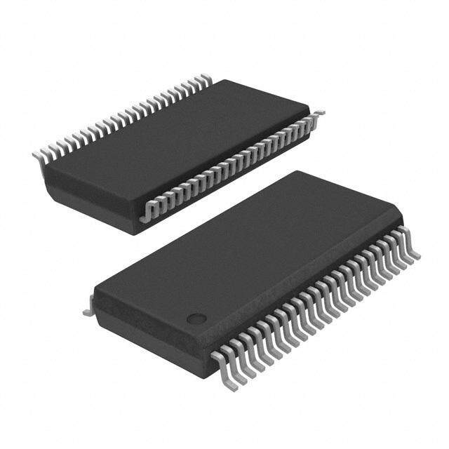
ICGOO电子元器件商城为您提供MC74LCX125DR2G由ON Semiconductor设计生产,在icgoo商城现货销售,并且可以通过原厂、代理商等渠道进行代购。 MC74LCX125DR2G价格参考。ON SemiconductorMC74LCX125DR2G封装/规格:逻辑 - 缓冲器,驱动器,接收器,收发器, 缓冲器,非反向 4 Element 1 Bit per Element 三态 Output 14-SOIC。您可以下载MC74LCX125DR2G参考资料、Datasheet数据手册功能说明书,资料中有MC74LCX125DR2G 详细功能的应用电路图电压和使用方法及教程。
ON Semiconductor的MC74LCX125DR2G是一款四路非反相三态输出缓冲器/驱动器,属于低电压CMOS逻辑器件,具有宽电压工作范围(2.3V至3.6V)和高抗噪能力。该器件集成了5V输入/输出容限,可安全地与5V逻辑系统接口,适用于混合电压系统设计。

主要应用场景包括:

1. 数字系统电平转换:在3.3V系统与5V系统之间进行信号电平转换,广泛用于微控制器、FPGA或ASIC之间的接口电路。

2. 总线驱动与隔离:作为总线缓冲器,用于增强信号驱动能力,减少负载对源电路的影响,适用于数据总线、地址总线等需要多设备共享的场合。

3. 通信接口模块:在工业控制、通信设备中用作信号调理和驱动,提升信号完整性和传输距离。

4. 消费类电子产品:应用于手机、平板、便携设备中的逻辑控制电路,实现低功耗与高性能的平衡。

5. 嵌入式系统与主板设计:用于时钟分配、状态指示信号缓冲或I/O扩展电路中,提高系统稳定性。

MC74LCX125DR2G采用SOIC-14小封装,适合高密度PCB布局,具备优良的电磁兼容性,广泛用于工业、汽车电子(非动力系统)、通信及消费类电子领域。其“G”后缀表示符合RoHS环保标准,适用于绿色电子产品制造。
| 参数 | 数值 |
| 产品目录 | 集成电路 (IC)半导体 |
| 描述 | IC BUFF TRI-ST QD LV CMOS 14SOIC缓冲器和线路驱动器 2-3.6V Quad 3-State Non-Inverting |
| 产品分类 | |
| 品牌 | ON Semiconductor |
| 产品手册 | |
| 产品图片 |
|
| rohs | 符合RoHS无铅 / 符合限制有害物质指令(RoHS)规范要求 |
| 产品系列 | 逻辑集成电路,缓冲器和线路驱动器,ON Semiconductor MC74LCX125DR2G74LCX |
| 数据手册 | |
| 产品型号 | MC74LCX125DR2G |
| 产品种类 | 缓冲器和线路驱动器 |
| 传播延迟时间 | 7.2 ns |
| 低电平输出电流 | 24 mA |
| 供应商器件封装 | 14-SOICN |
| 元件数 | 4 |
| 其它名称 | MC74LCX125DR2GOSDKR |
| 包装 | Digi-Reel® |
| 商标 | ON Semiconductor |
| 安装类型 | 表面贴装 |
| 安装风格 | SMD/SMT |
| 封装 | Reel |
| 封装/外壳 | 14-SOIC(0.154",3.90mm 宽) |
| 封装/箱体 | SOIC-14 |
| 工作温度 | -40°C ~ 85°C |
| 工厂包装数量 | 2500 |
| 最大工作温度 | + 85 C |
| 最小工作温度 | - 40 C |
| 极性 | Non-Inverting |
| 标准包装 | 1 |
| 每元件位数 | 1 |
| 每芯片的通道数量 | 4 |
| 电压-电源 | 2 V ~ 3.6 V |
| 电流-输出高,低 | 24mA,24mA |
| 电源电压-最大 | 3.6 V |
| 电源电压-最小 | 2 V |
| 电源电流 | 10 uA |
| 系列 | MC74LCX125 |
| 输入线路数量 | 4 |
| 输出类型 | 3-State |
| 输出线路数量 | 3 |
| 逻辑类型 | CMOS |
| 逻辑系列 | LCX |
| 高电平输出电流 | - 24 mA |


- 商务部:美国ITC正式对集成电路等产品启动337调查
- 曝三星4nm工艺存在良率问题 高通将骁龙8 Gen1或转产台积电
- 太阳诱电将投资9.5亿元在常州建新厂生产MLCC 预计2023年完工
- 英特尔发布欧洲新工厂建设计划 深化IDM 2.0 战略
- 台积电先进制程称霸业界 有大客户加持明年业绩稳了
- 达到5530亿美元!SIA预计今年全球半导体销售额将创下新高
- 英特尔拟将自动驾驶子公司Mobileye上市 估值或超500亿美元
- 三星加码芯片和SET,合并消费电子和移动部门,撤换高东真等 CEO
- 三星电子宣布重大人事变动 还合并消费电子和移动部门
- 海关总署:前11个月进口集成电路产品价值2.52万亿元 增长14.8%


PDF Datasheet 数据手册内容提取
MC74LCX125 Low-Voltage CMOS Quad Buffer With 5 V−Tolerant Inputs and Outputs (3−State, Non−Inverting) http://onsemi.com The MC74LCX125 is a high performance, non−inverting quad buffer operating from a 2.3 to 3.6 V supply. High impedance TTL MARKING compatible inputs significantly reduce current loading to input drivers DIAGRAMS while TTL compatible outputs offer improved switching noise performance. A VI specification of 5.5 V allows MC74LCX125 inputs to be safely driven from 5.0 V devices. The MC74LCX125 is suitable 14 for memory address driving and all TTL level bus oriented transceiver SOIC−14 14 LCX125G applications. D SUFFIX AWLYWW CASE 751A Current drive capability is 24 mA at the outputs. The Output Enable 1 (OEn) inputs, when HIGH, disable the outputs by placing them in a 1 HIGH Z condition. Features 14 Designed for 2.3 to 3.6 V V Operation LCX CC TSSOP−14 125 5.0 V Tolerant − Interface Capability With 5.0 V TTL Logic 14 DT SUFFIX ALYW(cid:2) Supports Live Insertion and Withdrawal 1 CASE 948G (cid:2) 1 I Specification Guarantees High Impedance When V = 0 V OFF CC LVTTL Compatible A = Assembly Location LVCMOS Compatible L, WL = Wafer Lot 24 mA Balanced Output Sink and Source Capability Y, YY = Year Near Zero Static Supply Current in all Three Logic States (10 (cid:2)A) W, WW = Work Week G or (cid:2) = Pb−Free Package Substantially Reduces System Power Requirements (Note: Microdot may be in either location) Latchup Performance Exceeds 500 mA ESD Performance: Human Body Model >2000 V Machine Model >200 V ORDERING INFORMATION See detailed ordering and shipping information in the package NLV Prefix for Automotive and Other Applications Requiring dimensions section on page 4 of this data sheet. Unique Site and Control Change Requirements; AEC−Q100 Qualified and PPAP Capable These Devices are Pb−Free, Halogen Free/BFR Free and are RoHS Compliant Semiconductor Components Industries, LLC, 2012 1 Publication Order Number: October, 2012 − Rev. 8 MC74LCX125/D
MC74LCX125 VCC OE3 D3 O3 OE2 D2 O2 14 13 12 11 10 9 8 1 10 OE OE 0 2 2 3 9 8 D0 O0 D2 O2 4 13 OE OE 1 3 5 6 12 11 D1 O1 D3 O3 1 2 3 4 5 6 7 OE0 D0 O0 OE1 D1 O1 GND Figure 1. Pinout: 14−Lead (Top View) Figure 2. Logic Diagram PIN NAMES TRUTH TABLE Pins Function INPUTS OUTPUTS OEn Output Enable Inputs OEn Dn On Dn Data Inputs L L L On 3−State Outputs L H H H X Z H = High Voltage Level L = Low Voltage Level Z = High Impedance State X = High or Low Voltage Level and Transitions Are Acceptable; for ICC reasons, DO NOT FLOAT Inputs MAXIMUM RATINGS Symbol Parameter Value Condition Units VCC DC Supply Voltage −0.5 to +7.0 V VI DC Input Voltage −0.5 VI +7.0 V VO DC Output Voltage −0.5 VO +7.0 Output in 3−State V −0.5 VO VCC + 0.5 Output in HIGH or LOW State. (Note 1) V IIK DC Input Diode Current −50 VI < GND mA IOK DC Output Diode Current −50 VO < GND mA +50 VO > VCC mA IO DC Output Source/Sink Current 50 mA ICC DC Supply Current Per Supply Pin 100 mA IGND DC Ground Current Per Ground Pin 100 mA TSTG Storage Temperature Range −65 to +150 C MSL Moisture Sensitivity Level 1 Maximum ratings are those values beyond which device damage can occur. Maximum ratings applied to the device are individual stress limit values (not normal operating conditions) and are not valid simultaneously. If these limits are exceeded, device functional operation is not implied, damage may occur and reliability may be affected. 1. IO absolute maximum rating must be observed. http://onsemi.com 2
MC74LCX125 RECOMMENDED OPERATING CONDITIONS Symbol Parameter Min Typ Max Units VCC Supply Voltage V Operating 2.0 2.5, 3.3 3.6 Data Retention Only 1.5 2.5, 3.3 3.6 VI Input Voltage 0 5.5 V VO Output Voltage V HIGH or LOW State 0 VCC 3−State 0 5.5 IOH HIGH Level Output Current mA VCC = 3.0 V − 3.6 V −24 VCC = 2.7 V − 3.0 V −12 VCC = 2.3 V − 2.7 V −8 IOL LOW Level Output Current mA VCC = 3.0 V − 3.6 V +24 VCC = 2.7 V − 3.0 V +12 VCC = 2.3 V − 2.7 V +8 TA Operating Free−Air Temperature −40 +85 C (cid:3)t/(cid:3)V Input Transition Rise or Fall Rate, VIN from 0.8 V to 2.0 V, 0 10 ns/V VCC = 3.0 V DC ELECTRICAL CHARACTERISTICS TA = −40C to +85C Symbol Characteristic Condition Min Max Units VIH HIGH Level Input Voltage (Note 2) 2.3 V VCC 2.7 V 1.7 V 2.7 V VCC 3.6 V 2.0 VIL LOW Level Input Voltage (Note 2) 2.3 V VCC 2.7 V 0.7 V 2.7 V VCC 3.6 V 0.8 VOH HIGH Level Output Voltage 2.3 V VCC 3.6 V; IOL = 100 (cid:2)A VCC−0.2 V VCC = 2.3 V; IOH = −8 mA 1.8 VCC = 2.7 V; IOH = −12 mA 2.2 VCC = 3.0 V; IOH = −18 mA 2.4 VCC = 3.0 V; IOH = −24 mA 2.2 VOL LOW Level Output Voltage 2.3 V VCC 3.6 V; IOL = 100 (cid:2)A 0.2 V VCC = 2.3 V; IOL= 8 mA 0.6 VCC = 2.7 V; IOL= 12 mA 0.4 VCC = 3.0 V; IOL = 16 mA 0.4 VCC = 3.0 V; IOL = 24 mA 0.55 IOZ 3−State Output Current VCC = 3.6 V, VIN = VIH or VIL, 5 (cid:2)A VOUT = 0 to 5.5 V IOFF Power Off Leakage Current VCC = 0, VIN = 5.5 V or VOUT = 5.5 V 10 (cid:2)A IIN Input Leakage Current VCC = 3.6 V, VIN = 5.5 V or GND 5 (cid:2)A ICC Quiescent Supply Current VCC = 3.6 V, VIN = 5.5 V or GND 10 (cid:2)A (cid:3)ICC Increase in ICC per Input 2.3 VCC 3.6 V; VIH = VCC − 0.6 V 500 (cid:2)A 2. These values of VI are used to test DC electrical characteristics only. http://onsemi.com 3
MC74LCX125 AC CHARACTERISTICS (tR = tF = 2.5 ns; RL = 500 (cid:4)) Limits TA = −40C to +85C VCC = 3.3 V 0.3 V VCC = 2.7 V VCC = 2.5 V 0.2 V CL = 50 pF CL = 50 pF CL = 30 pF Symbol Parameter Waveform Min Max Min Max Min Max Units tPLH Propagation Delay Time 1 1.5 6.0 1.5 6.5 1.5 7.2 ns tPHL Input to Output 1.5 6.0 1.5 6.5 1.5 7.2 tPZH Output Enable Time to 2 1.5 7.0 1.5 8.0 1.5 9.1 ns tPZL High and Low Level 1.5 7.0 1.5 8.0 1.5 9.1 tPHZ Output Disable Time From 2 1.5 6.0 1.5 7.0 1.5 7.2 ns tPLZ High and Low Level 1.5 6.0 1.5 7.0 1.5 7.2 tOSHL Output−to−Output Skew 1.0 ns tOSLH (Note 3) 1.0 3. Skew is defined as the absolute value of the difference between the actual propagation delay for any two separate outputs of the same device. The specification applies to any outputs switching in the same direction, either HIGH−to−LOW (tOSHL) or LOW−to−HIGH (tOSLH); parameter guaranteed by design. DYNAMIC SWITCHING CHARACTERISTICS TA = +25C Symbol Characteristic Condition Min Typ Max Units VOLP Dynamic LOW Peak Voltage VCC = 3.3 V, CL = 50 pF, VIH = 3.3 V, VIL = 0 V 0.8 V (Note 4) VCC = 2.5 V, CL = 30 pF, VIH = 2.5 V, VIL = 0 V 0.6 VOLV Dynamic LOW Valley Voltage VCC = 3.3 V, CL = 50 pF, VIH = 3.3 V, VIL = 0 V −0.8 V (Note 4) VCC = 2.5 V, CL = 30 pF, VIH = 2.5 V, VIL = 0 V −0.6 4. Number of outputs defined as “n”. Measured with “n−1” outputs switching from HIGH−to−LOW or LOW−to−HIGH. The remaining output is measured in the LOW state. CAPACITIVE CHARACTERISTICS Symbol Parameter Condition Typical Units CIN Input Capacitance VCC = 3.3 V, VI = 0 V or VCC 7 pF COUT Output Capacitance VCC = 3.3 V, VI = 0 V or VCC 8 pF CPD Power Dissipation Capacitance 10 MHz, VCC = 3.3 V, VI = 0 V or VCC 25 pF ORDERING INFORMATION Device Package Shipping† MC74LCX125DG SOIC−14 55 Units / Rail (Pb−Free) MC74LCX125DR2G SOIC−14 2500 Tape & Reel (Pb−Free) MC74LCX125DTG TSSOP−14 96 Units / Rail (Pb−Free) MC74LCX125DTR2G TSSOP−14 2500 Tape & Reel (Pb−Free) NLVLCX125DTR2G TSSOP−14* 2500 Tape & Reel (Pb−Free) †For information on tape and reel specifications, including part orientation and tape sizes, please refer to our Tape and Reel Packaging Specifications Brochure, BRD8011/D. *NLV Prefix for Automotive and Other Applications Requiring Unique Site and Control Change Requirements; AEC−Q100 Qualified. http://onsemi.com 4
MC74LCX125 VCC Dn Vmi Vmi 0 V tPLH tPHL VOH On Vmo Vmo VOL WAVEFORM 1 − PROPAGATION DELAYS tR = tF = 2.5 ns, 10% to 90%; f = 1 MHz; tW = 500 ns VCC OEn Vmi Vmi 0 V tPZH tPHZ VCC VOH − 0.3 V On Vmo 0 V tPZL tPLZ 3.0 V On Vmo VOL + 0.3 V GND WAVEFORM 2 − OUTPUT ENABLE AND DISABLE TIMES tR = tF = 2.5 ns, 10% to 90%; f = 1 MHz; tW = 500 ns VCC Symbol 3.3 V 0.3 V 2.7 V 2.5 V 0.2 V Vmi 1.5 V 1.5 V VCC/2 Vmo 1.5 V 1.5 V VCC/2 Figure 3. AC Waveforms VCC PULSE DUT GENERATOR RT CL RL CL= 50 pF at VCC = 3.3 0.3 V or equivalent (includes jig and probe capacitance) CL= 30 pF at VCC = 2.5 0.2 V or equivalent (includes jig and probe capacitance) RL= R1 = 500 (cid:4) or equivalent RT= ZOUT of pulse generator (typically 50 (cid:4)) Figure 4. Test Circuit http://onsemi.com 5
MC74LCX125 PACKAGE DIMENSIONS TSSOP−14 CASE 948G ISSUE B 14X K REF NOTES: 1. DIMENSIONING AND TOLERANCING PER 0.10 (0.004) M T U S V S ANSI Y14.5M, 1982. 2. CONTROLLING DIMENSION: MILLIMETER. 0.15 (0.006) T U S 3. DIMENSION A DOES NOT INCLUDE MOLD FLASH, PROTRUSIONS OR GATE BURRS. N MOLD FLASH OR GATE BURRS SHALL NOT 0.25 (0.010) EXCEED 0.15 (0.006) PER SIDE. 14 8 4. DIMENSION B DOES NOT INCLUDE 2XL/2 INTERLEAD FLASH OR PROTRUSION. M INTERLEAD FLASH OR PROTRUSION SHALL NOT EXCEED 0.25 (0.010) PER SIDE. L B 5. DIMENSION K DOES NOT INCLUDE −U− N DAMBAR PROTRUSION. ALLOWABLE PIN 1 DAMBAR PROTRUSION SHALL BE 0.08 IDENT. F (0.003) TOTAL IN EXCESS OF THE K DIMENSION AT MAXIMUM MATERIAL 1 7 DETAIL E CONDITION. 6. TERMINAL NUMBERS ARE SHOWN FOR REFERENCE ONLY. 7. DIMENSION A AND B ARE TO BE 0.15 (0.006) T U S A K DETERMINED AT DATUM PLANE −W−. −V− ÇÉÇÉK1ÇÉ MILLIMETERS INCHES DIM MIN MAX MIN MAX J J1 ÇÉÇÉÇÉ A 4.90 5.10 0.193 0.200 B 4.30 4.50 0.169 0.177 C −−− 1.20 −−− 0.047 SECTION N−N D 0.05 0.15 0.002 0.006 F 0.50 0.75 0.020 0.030 G 0.65 BSC 0.026 BSC H 0.50 0.60 0.020 0.024 −W− J 0.09 0.20 0.004 0.008 C J1 0.09 0.16 0.004 0.006 K 0.19 0.30 0.007 0.012 0.10 (0.004) K1 0.19 0.25 0.007 0.010 L 6.40 BSC 0.252 BSC −T− SPELAATNIENG D G H DETAIL E M 0 (cid:3) 8 (cid:3) 0 (cid:3) 8 (cid:3) SOLDERING FOOTPRINT* 7.06 1 0.65 PITCH 14X 14X 0.36 1.26 DIMENSIONS: MILLIMETERS *For additional information on our Pb−Free strategy and soldering details, please download the ON Semiconductor Soldering and Mounting Techniques Reference Manual, SOLDERRM/D. http://onsemi.com 6
MC74LCX125 PACKAGE DIMENSIONS SOIC−14 NB CASE 751A−03 ISSUE K D A NOTES: B 1.DIMENSIONING AND TOLERANCING PER ASME Y14.5M, 1994. 2.CONTROLLING DIMENSION: MILLIMETERS. 14 8 3.DIMENSION b DOES NOT INCLUDE DAMBAR A3 PROTRUSION. ALLOWABLE PROTRUSION SHALL BE 0.13 TOTAL IN EXCESS OF AT MAXIMUM MATERIAL CONDITION. H E 4.DIMENSIONS D AND E DO NOT INCLUDE MOLD PROTRUSIONS. L 5.MAXIMUM MOLD PROTRUSION 0.15 PER SIDE. 1 7 DETAIL A MILLIMETERS INCHES 0.25 M B M 13Xb DIM MIN MAX MIN MAX A 1.35 1.75 0.054 0.068 0.25 M C A S B S A1 0.10 0.25 0.004 0.010 A3 0.19 0.25 0.008 0.010 DETAIL A b 0.35 0.49 0.014 0.019 h A X 45(cid:3) DE 83..5850 84..7050 00..135307 00..135474 e 1.27 BSC 0.050 BSC H 5.80 6.20 0.228 0.244 h 0.25 0.50 0.010 0.019 e A1 C SEATING M ML 0.04 0(cid:3) 1.72 5(cid:3) 0.001 6(cid:3) 0.047 9(cid:3) PLANE SOLDERING FOOTPRINT* 6.50 14X 1.18 1 1.27 PITCH 14X 0.58 DIMENSIONS: MILLIMETERS *For additional information on our Pb−Free strategy and soldering details, please download the ON Semiconductor Soldering and Mounting Techniques Reference Manual, SOLDERRM/D. ON Semiconductor and are registered trademarks of Semiconductor Components Industries, LLC (SCILLC). SCILLC owns the rights to a number of patents, trademarks, copyrights, trade secrets, and other intellectual property. A listing of SCILLC’s product/patent coverage may be accessed at www.onsemi.com/site/pdf/Patent−Marking.pdf. SCILLC reserves the right to make changes without further notice to any products herein. SCILLC makes no warranty, representation or guarantee regarding the suitability of its products for any particular purpose, nor does SCILLC assume any liability arising out of the application or use of any product or circuit, and specifically disclaims any and all liability, including without limitation special, consequential or incidental damages. “Typical” parameters which may be provided in SCILLC data sheets and/or specifications can and do vary in different applications and actual performance may vary over time. All operating parameters, including “Typicals” must be validated for each customer application by customer’s technical experts. SCILLC does not convey any license under its patent rights nor the rights of others. SCILLC products are not designed, intended, or authorized for use as components in systems intended for surgical implant into the body, or other applications intended to support or sustain life, or for any other application in which the failure of the SCILLC product could create a situation where personal injury or death may occur. Should Buyer purchase or use SCILLC products for any such unintended or unauthorized application, Buyer shall indemnify and hold SCILLC and its officers, employees, subsidiaries, affiliates, and distributors harmless against all claims, costs, damages, and expenses, and reasonable attorney fees arising out of, directly or indirectly, any claim of personal injury or death associated with such unintended or unauthorized use, even if such claim alleges that SCILLC was negligent regarding the design or manufacture of the part. SCILLC is an Equal Opportunity/Affirmative Action Employer. This literature is subject to all applicable copyright laws and is not for resale in any manner. PUBLICATION ORDERING INFORMATION LITERATURE FULFILLMENT: N. American Technical Support: 800−282−9855 Toll Free ON Semiconductor Website: www.onsemi.com Literature Distribution Center for ON Semiconductor USA/Canada P.O. Box 5163, Denver, Colorado 80217 USA Europe, Middle East and Africa Technical Support: Order Literature: http://www.onsemi.com/orderlit Phone: 303−675−2175 or 800−344−3860 Toll Free USA/Canada Phone: 421 33 790 2910 Fax: 303−675−2176 or 800−344−3867 Toll Free USA/Canada Japan Customer Focus Center For additional information, please contact your local Email: orderlit@onsemi.com Phone: 81−3−5817−1050 Sales Representative http://onsemi.com MC74LCX125/D 7
Mouser Electronics Authorized Distributor Click to View Pricing, Inventory, Delivery & Lifecycle Information: O N Semiconductor: MC74LCX125DG MC74LCX125DR2G MC74LCX125DTG MC74LCX125DTR2G