ICGOO在线商城 > 集成电路(IC) > 逻辑 - 栅极和逆变器 > MC74HC86ADTR2G

 Datasheet下载
- 型号: MC74HC86ADTR2G
- 制造商: ON Semiconductor
- 库位|库存: xxxx|xxxx
- 要求:
| 数量阶梯 | 香港交货 | 国内含税 |
| +xxxx | $xxxx | ¥xxxx |
查看当月历史价格
查看今年历史价格
MC74HC86ADTR2G产品简介:
ICGOO电子元器件商城为您提供MC74HC86ADTR2G由ON Semiconductor设计生产,在icgoo商城现货销售,并且可以通过原厂、代理商等渠道进行代购。 MC74HC86ADTR2G价格参考¥2.24-¥2.24。ON SemiconductorMC74HC86ADTR2G封装/规格:逻辑 - 栅极和逆变器, XOR (Exclusive OR) IC 4 Channel 14-TSSOP。您可以下载MC74HC86ADTR2G参考资料、Datasheet数据手册功能说明书,资料中有MC74HC86ADTR2G 详细功能的应用电路图电压和使用方法及教程。
MC74HC86ADTR2G 是一款由 ON Semiconductor 提供的逻辑器件,属于“逻辑 - 栅极和逆变器”分类。具体来说,它是一个四路双输入异或门(XOR Gate)集成电路,采用先进的 CMOS 技术制造,符合 HC 系列标准。以下是其主要应用场景:

1. 数字信号处理
   MC74HC86ADTR2G 可用于数字电路中的信号处理任务,例如检测两个输入信号是否不同。这种特性使其适用于编码、解码以及数据校验等场景。

2. 加法器设计
   异或门是构建全加器和半加器的核心元件之一。在二进制加法运算中,异或门可以用来生成“和”输出,而与门则负责生成“进位”输出。

3. 时钟信号生成与修改
   在需要对时钟信号进行调整或生成新时钟信号的应用中,该芯片可以通过组合逻辑实现分频、移相等功能,从而满足特定的时序需求。

4. 数据比较与同步
   它可用于比较两组数据流并检测差异,或者在多通道系统中实现数据同步功能。当两个输入信号一致时,输出为低电平;反之,则为高电平。

5. 音频/视频设备中的应用
   在某些音频或视频切换开关中,异或门能够帮助选择不同的输入源,并确保正确的信号传递到输出端。

6. 通信领域
   该器件可应用于加密算法中的比特流操作,比如生成伪随机序列、执行奇偶校验等。此外,在无线通信系统中,它也可以参与调制解调过程。

7. 工业控制与自动化
   在工业环境中,MC74HC86ADTR2G 能够协助完成传感器信号处理、状态监测及故障诊断等工作。

总之,这款产品凭借其高性能、低功耗的特点,在消费电子、通信、工业控制等多个领域都有着广泛的应用前景。
| 参数 | 数值 |
| 产品目录 | 集成电路 (IC)半导体 |
| 描述 | IC GATE XOR 4CH 2-INP 14-TSSOP逻辑门 2-6V Quad 2-Input XOR |
| 产品分类 | |
| 品牌 | ON Semiconductor |
| 产品手册 | |
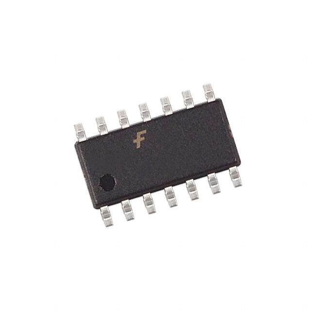
| 产品图片 |
|
| rohs | 符合RoHS无铅 / 符合限制有害物质指令(RoHS)规范要求 |
| 产品系列 | 逻辑集成电路,逻辑门,ON Semiconductor MC74HC86ADTR2G74HC |
| 数据手册 | |
| 产品型号 | MC74HC86ADTR2G |
| 不同V、最大CL时的最大传播延迟 | 17ns @ 6V,50pF |
| 产品 | XOR |
| 产品种类 | 逻辑门 |
| 传播延迟时间 | 100 ns |
| 低电平输出电流 | 5.2 mA |
| 供应商器件封装 | 14-TSSOP |
| 其它名称 | MC74HC86ADTR2GOSCT |
| 包装 | 剪切带 (CT) |
| 商标 | ON Semiconductor |
| 安装类型 | 表面贴装 |
| 安装风格 | SMD/SMT |
| 封装 | Reel |
| 封装/外壳 | 14-TSSOP(0.173",4.40mm 宽) |
| 封装/箱体 | SOIC-14 |
| 工作温度 | -55°C ~ 125°C |
| 工厂包装数量 | 2500 |
| 最大工作温度 | + 125 C |
| 最小工作温度 | - 55 C |
| 栅极数量 | 4 Gate |
| 标准包装 | 1 |
| 特性 | - |
| 电压-电源 | 2 V ~ 6 V |
| 电流-输出高,低 | 5.2mA,5.2mA |
| 电流-静态(最大值) | 1µA |
| 电源电压-最大 | 6 V |
| 电源电压-最小 | 2 V |
| 电路数 | 4 |
| 系列 | MC74HC86A |
| 输入/输出线数量 | 2 / 1 |
| 输入数 | 2 |
| 输入线路数量 | 2 |
| 输出线路数量 | 1 |
| 逻辑电平-低 | 0.5 V ~ 1.8 V |
| 逻辑电平-高 | 1.5 V ~ 4.2 V |
| 逻辑类型 | XOR(异或) |
| 逻辑系列 | 74HC |
| 高电平输出电流 | - 5.2 mA |


- 商务部:美国ITC正式对集成电路等产品启动337调查
- 曝三星4nm工艺存在良率问题 高通将骁龙8 Gen1或转产台积电
- 太阳诱电将投资9.5亿元在常州建新厂生产MLCC 预计2023年完工
- 英特尔发布欧洲新工厂建设计划 深化IDM 2.0 战略
- 台积电先进制程称霸业界 有大客户加持明年业绩稳了
- 达到5530亿美元!SIA预计今年全球半导体销售额将创下新高
- 英特尔拟将自动驾驶子公司Mobileye上市 估值或超500亿美元
- 三星加码芯片和SET,合并消费电子和移动部门,撤换高东真等 CEO
- 三星电子宣布重大人事变动 还合并消费电子和移动部门
- 海关总署:前11个月进口集成电路产品价值2.52万亿元 增长14.8%


PDF Datasheet 数据手册内容提取
MC74HC86A Quad 2-Input Exclusive OR Gate High−Performance Silicon−Gate CMOS The MC74HC86A is identical in pinout to the LS86. The device http://onsemi.com inputs are compatible with standard CMOS outputs; with pullup resistors, they are compatible with LSTTL outputs. Features • Output Drive Capability: 10 LSTTL Loads SOIC−14 NB TSSOP−14 • D SUFFIX DT SUFFIX Outputs Directly Interface to CMOS, NMOS, and TTL CASE 751A CASE 948G • Operating Voltage Range: 2.0 to 6.0 V • Low Input Current: 1 (cid:2)A PIN ASSIGNMENT • High Noise Immunity Characteristic of CMOS Devices • In Compliance with JEDEC Standard No. 7A Requirements A1 1 14 VCC • B1 2 13 B4 Chip Complexity: 56 FETs or 14 Equivalent Gates • Y1 3 12 A4 NLV Prefix for Automotive and Other Applications Requiring Unique Site and Control Change Requirements; AEC−Q100 A2 4 11 Y4 Qualified and PPAP Capable B2 5 10 B3 • These Devices are Pb−Free, Halogen Free and are RoHS Compliant Y2 6 9 A3 GND 7 8 Y3 LOGIC DIAGRAM 1 MARKING DIAGRAMS A1 3 2 Y1 B1 14 14 HC HC86AG 4 86A A2 6 AWLYWW ALYW(cid:2) 5 Y2 (cid:2) B2 1 1 9 SOIC−14 NB TSSOP−14 A3 8 10 Y3 B3 A = Assembly Location L, WL = Wafer Lot 12 Y, YY = Year A4 11 W, WW = Work Week B4 13 Y4 G or (cid:2) = Pb−Free Package Y = A ⊕ B PIN 14 = VCC (Note: Microdot may be in either location) = AB + AB PIN 7 = GND FUNCTION TABLE Inputs Output A B Y L L L L H H H L H H H L ORDERING INFORMATION See detailed ordering and shipping information in the package dimensions section on page 4 of this data sheet. © Semiconductor Components Industries, LLC, 2014 1 Publication Order Number: August, 2014 − Rev. 7 MC74HC86A/D
MC74HC86A ÎÎÎÎÎÎÎÎÎÎÎÎÎÎÎÎÎÎÎÎÎÎÎ MAXIMUM RATINGS ÎÎÎÎÎÎÎÎÎÎÎÎÎÎÎÎÎÎÎÎÎÎÎÎÎÎÎÎÎÎÎÎÎÎÎÎÎÎÎÎÎÎÎÎÎÎÎÎÎ Symbol Parameter Value Unit This device contains protection ÎÎÎÎÎÎÎÎÎÎÎÎÎÎÎÎÎÎÎÎÎÎÎÎÎÎÎÎÎÎÎÎÎÎÎÎÎÎÎÎÎÎÎÎÎÎÎÎÎÎÎÎ VCC DC Supply Voltage (Referenced to GND) –0.5 to +7.0 V circuitry to guard against damage ÎÎÎÎÎÎÎÎÎÎÎÎÎÎÎÎÎÎÎÎÎÎÎÎÎÎÎÎÎÎÎÎÎÎÎÎÎÎÎÎÎÎÎÎÎÎÎÎÎÎÎÎ due to high static voltages or electric Vin DC Input Voltage (Referenced to GND) –0.5 to VCC + 0.5 V fields. However, precautions must ÎÎÎÎÎÎÎÎÎÎÎÎÎÎÎÎÎÎÎÎÎÎÎÎÎÎÎÎÎÎÎÎÎÎÎÎÎÎÎÎÎÎÎÎÎÎÎÎÎÎÎÎÎÎÎÎÎÎÎÎÎÎÎÎÎÎÎÎÎÎÎÎÎÎÎÎÎÎ Vout DC Output Voltage (Referenced to GND) –0.5 to VCC + 0.5 V be taken to avoid applications of any ÎÎÎÎIÎÎin ÎÎÎÎDÎÎC InpÎÎut CÎÎurreÎÎnt, pÎÎer PÎÎin ÎÎÎÎÎÎÎÎÎÎÎÎÎÎÎÎÎÎÎα20ÎÎÎÎÎÎÎÎmAÎÎ voltage higher than maximum rated voltages to this high−impedance cir- ÎÎÎÎIoÎÎut ÎÎÎÎDÎÎC OuÎÎtputÎÎ CurÎÎrent,ÎÎ perÎÎ PinÎÎÎÎÎÎÎÎÎÎÎÎÎÎÎÎÎÎÎα25ÎÎÎÎÎÎÎÎmAÎÎ cuit. For proper operation, Vin and ÎÎÎÎICÎÎC ÎÎÎÎDÎÎC SuÎÎpplyÎÎ CurÎÎrentÎÎ, VCCÎÎ andÎÎ GNÎÎD PÎÎins ÎÎÎÎÎÎÎÎÎÎÎÎÎα50ÎÎÎÎÎÎÎÎmAÎÎ Vout should be constrained to the ÎÎPÎD ÎÎPoÎwerÎ DisÎsipatÎion iÎn StiÎll AirÎ, ÎÎSOICÎ PaÎckagÎe†ÎÎÎÎ500ÎÎÎÎmWÎ ranUgneu GseNdD i n(cid:2)p u(tVsi n moru sVto uat)l w(cid:2)a yVsC Cb.e TSSOP Package† 450 ÎÎÎÎÎÎÎÎÎÎÎÎÎÎÎÎÎÎÎÎÎÎÎÎÎÎÎÎÎÎÎÎÎÎÎÎÎÎÎÎÎÎÎÎÎÎÎÎÎÎÎÎÎÎÎÎÎÎÎÎÎÎÎÎÎÎÎÎÎÎÎÎÎÎÎÎÎÎ tied to an appropriate logic voltage Tstg Storage Temperature –65 to +150 (cid:3)C level (e.g., either GND or VCC). ÎÎÎÎTÎÎL ÎÎÎÎLeÎÎad TÎÎempÎÎeratÎÎure, ÎÎ1 mÎÎm froÎÎm CÎÎase ÎÎfor 1ÎÎ0 SeÎÎconÎÎds ÎÎÎÎÎÎÎÎÎÎÎÎÎÎÎÎ(cid:3)CÎÎ Unused outputs must be left open. ÎÎÎÎÎÎÎÎ(PÎlastÎic DIÎP, SÎOIC Îor TÎSSOÎP PaÎckaÎge)ÎÎÎÎ260ÎÎÎÎÎ Stresses exceeding those listed in the Maximum Ratings table may damage the device. If any of these limits are exceeded, device functionality should not be assumed, damage may occur and reliability may be affected. †Derating: SOIC Package: – 7mW/(cid:3)C from 65(cid:3) to 125(cid:3)C TSSOP Package: −6.1 mW/(cid:3)C from 65(cid:3) to 125(cid:3)C RECOMMENDED OPERATING CONDITIONS Symbol Parameter Min Max Unit VCC DC Supply Voltage (Referenced to GND) 2.0 6.0 V Vin, Vout DC Input Voltage, Output Voltage (Referenced to GND) 0 VCC V TA Operating Temperature, All Package Types – 55 + 125 (cid:3)C tr, tf Input Rise and Fall Time VCC = 2.0 V 0 1000 ns (Figure 1) VCC = 4.5 V 0 500 VCC = 6.0 V 0 400 Functional operation above the stresses listed in the Recommended Operating Ranges is not implied. Extended exposure to stresses beyond the Recommended Operating Ranges limits may affect device reliability. DC ELECTRICAL CHARACTERISTICS (Voltages Referenced to GND) Guaranteed Limit VCC –55 to Symbol Parameter Test Conditions V 25(cid:3)C (cid:2) 85(cid:3)C (cid:2) 125(cid:3)C Unit VIH Minimum High−Level Input Vout = 0.1 V or VCC – 0.1 V 2.0 1.5 1.5 1.5 V Voltage |Iout| (cid:2) 20 (cid:2)A 3.0 2.1 2.1 2.1 4.5 3.15 3.15 3.15 6.0 4.2 4.2 4.2 VIL Maximum Low−Level Input Vout = 0.1 V or VCC – 0.1 V 2.0 0.5 0.5 0.5 V Voltage |Iout| (cid:2) 20 (cid:2)A 3.0 0.9 0.9 0.9 4.5 1.35 1.35 1.35 6.0 1.8 1.8 1.8 VOH Minimum High−Level Output Vin = VIH or VIL 2.0 1.9 1.9 1.9 V Voltage |Iout| (cid:2) 20 (cid:2)A 4.5 4.4 4.4 4.4 6.0 5.9 5.9 5.9 Vin = VIH or VIL |Iout| (cid:2) 2.4 mA 3.0 2.48 2.34 2.20 |Iout| (cid:2) 4.0 mA 4.5 3.98 3.84 3.70 |Iout| (cid:2) 5.2 mA 6.0 5.48 5.34 5.20 VOL Maximum Low−Level Output Vin = VIH or VIL 2.0 0.1 0.1 0.1 V Voltage |Iout| (cid:2) 20 (cid:2)A 4.5 0.1 0.1 0.1 6.0 0.1 0.1 0.1 Vin = VIH or VIL |Iout| (cid:2) 2.4 mA 3.0 0.26 0.33 0.40 |Iout| (cid:2) 4.0 mA 4.5 0.26 0.33 0.40 |Iout| (cid:2) 5.2 mA 6.0 0.26 0.33 0.40 Iin Maximum Input Leakage Current Vin = VCC or GND 6.0 ±0.1 ±1.0 ±1.0 (cid:2)A ICC Maximum Quiescent Supply Vin = VCC or GND 6.0 1.0 10 40 (cid:2)A Current (per Package) Iout = 0 (cid:2)A http://onsemi.com 2
MC74HC86A AC ELECTRICAL CHARACTERISTICS (CL = 50 pF, Input t, = tf = 6 ns) Guaranteed Limit VCC –55 to Symbol Parameter V 25(cid:3)C (cid:2) 85(cid:3)C (cid:2) 125(cid:3)C Unit tPLH, Maximum Propagation Delay, Input A or B to Output Y 2.0 100 125 150 ns tPHL (Figures 1 and 2) 3.0 80 90 110 4.5 20 25 31 6.0 17 21 26 tTLH, Maximum Output Transition Time, Any Output 2.0 75 95 110 ns tTHL (Figures 1 and 2) 3.0 30 40 55 4.5 15 19 22 6.0 13 16 19 Cin Maximum Input Capacitance — 10 10 10 pF Typical @ 25°C, VCC = 5.0 V CPD Power Dissipation Capacitance (Per Gate)* 33 pF *Used to determine the no−load dynamic power consumption: PD = CPD VCC2f + ICC VCC. tr tf 90% VCC INPUT 50% A OR B TEST POINT 10% GND OUTPUT tPLH tPHL DEVICE 90% UNDER TEST CL* OUTPUT Y 50% 10% tTLH tTHL *Includes all probe and jig capacitance Figure 1. Switching Waveforms Figure 2. Test Circuit A Y B Figure 3. Expanded Logic Diagram (1/4 of Device) http://onsemi.com 3
MC74HC86A ORDERING INFORMATION Device Package Shipping† MC74HC86ADG SOIC−14 NB 55 Units / Rail (Pb−Free) NLV74HC86ADG* SOIC−14 NB 55 Units / Rail (Pb−Free) MC74HC86ADR2G SOIC−14 NB 2500 / Tape & Reel (Pb−Free) NLV74HC86ADR2G* SOIC−14 NB 2500 / Tape & Reel (Pb−Free) MC74HC86ADTR2G TSSOP−14 2500 / Tape & Reel (Pb−Free) NLV74HC86ADTR2G* TSSOP−14 2500 / Tape & Reel (Pb−Free) †For information on tape and reel specifications, including part orientation and tape sizes, please refer to our Tape and Reel Packaging Specifications Brochure, BRD8011/D. *NLV Prefix for Automotive and Other Applications Requiring Unique Site and Control Change Requirements; AEC−Q100 Qualified and PPAP Capable. http://onsemi.com 4
MC74HC86A PACKAGE DIMENSIONS TSSOP−14 CASE 948G ISSUE B 14X K REF NOTES: 1. DIMENSIONING AND TOLERANCING PER 0.10 (0.004) M T U S V S ANSI Y14.5M, 1982. 2. CONTROLLING DIMENSION: MILLIMETER. 0.15 (0.006) T U S 3. DIMENSION A DOES NOT INCLUDE MOLD FLASH, PROTRUSIONS OR GATE BURRS. N MOLD FLASH OR GATE BURRS SHALL NOT 0.25 (0.010) EXCEED 0.15 (0.006) PER SIDE. 2XL/2 14 8 4I.NTDEIMRLEENASDIO FNL ABS DHO OERS PNROOT TINRCULSUIODNE. M INTERLEAD FLASH OR PROTRUSION SHALL NOT EXCEED 0.25 (0.010) PER SIDE. L B 5. DIMENSION K DOES NOT INCLUDE −U− N DAMBAR PROTRUSION. ALLOWABLE PIN 1 DAMBAR PROTRUSION SHALL BE 0.08 IDENT. F (0.003) TOTAL IN EXCESS OF THE K DIMENSION AT MAXIMUM MATERIAL 1 7 DETAIL E CONDITION. 6. TERMINAL NUMBERS ARE SHOWN FOR REFERENCE ONLY. 7. DIMENSION A AND B ARE TO BE 0.15 (0.006) T U S A K DETERMINED AT DATUM PLANE −W−. −V− K1 MILLIMETERS INCHES ÇÉÇÉÇÉ DIM MIN MAX MIN MAX A 4.90 5.10 0.193 0.200 J J1 ÇÉÇÉÇÉ B 4.30 4.50 0.169 0.177 C −−− 1.20 −−− 0.047 SECTION N−N D 0.05 0.15 0.002 0.006 F 0.50 0.75 0.020 0.030 G 0.65 BSC 0.026 BSC H 0.50 0.60 0.020 0.024 −W− J 0.09 0.20 0.004 0.008 C J1 0.09 0.16 0.004 0.006 K 0.19 0.30 0.007 0.012 0.10 (0.004) K1 0.19 0.25 0.007 0.010 L 6.40 BSC 0.252 BSC −T− SEATING D G H DETAIL E M 0 (cid:3) 8 (cid:3) 0 (cid:3) 8 (cid:3) PLANE SOLDERING FOOTPRINT 7.06 1 0.65 PITCH 14X 14X 0.36 1.26 DIMENSIONS: MILLIMETERS http://onsemi.com 5
MC74HC86A PACKAGE DIMENSIONS SOIC−14 NB CASE 751A−03 ISSUE K D A NOTES: B 1.DIMENSIONING AND TOLERANCING PER ASME Y14.5M, 1994. 2.CONTROLLING DIMENSION: MILLIMETERS. 14 8 3.DIMENSION b DOES NOT INCLUDE DAMBAR A3 PROTRUSION. ALLOWABLE PROTRUSION SHALL BE 0.13 TOTAL IN EXCESS OF AT MAXIMUM MATERIAL CONDITION. H E 4.DIMENSIONS D AND E DO NOT INCLUDE MOLD PROTRUSIONS. L 5.MAXIMUM MOLD PROTRUSION 0.15 PER SIDE. 1 7 DETAIL A MILLIMETERS INCHES 0.25 M B M 13Xb DIM MIN MAX MIN MAX A 1.35 1.75 0.054 0.068 0.25 M C A S B S A1 0.10 0.25 0.004 0.010 A3 0.19 0.25 0.008 0.010 DETAIL A b 0.35 0.49 0.014 0.019 h A D 8.55 8.75 0.337 0.344 X 45(cid:3) E 3.80 4.00 0.150 0.157 e 1.27 BSC 0.050 BSC H 5.80 6.20 0.228 0.244 h 0.25 0.50 0.010 0.019 e A1 C SEATING M ML 0.04 0(cid:3) 1.72 5(cid:3) 0.001 6(cid:3) 0.074 9(cid:3) PLANE SOLDERING FOOTPRINT* 6.50 14X 1.18 1 1.27 PITCH 14X 0.58 DIMENSIONS: MILLIMETERS *For additional information on our Pb−Free strategy and soldering details, please download the ON Semiconductor Soldering and Mounting Techniques Reference Manual, SOLDERRM/D. ON Semiconductor and the are registered trademarks of Semiconductor Components Industries, LLC (SCILLC) or its subsidiaries in the United States and/or other countries. SCILLC owns the rights to a number of patents, trademarks, copyrights, trade secrets, and other intellectual property. A listing of SCILLC’s product/patent coverage may be accessed at www.onsemi.com/site/pdf/Patent−Marking.pdf. SCILLC reserves the right to make changes without further notice to any products herein. SCILLC makes no warranty, representation or guarantee regarding the suitability of its products for any particular purpose, nor does SCILLC assume any liability arising out of the application or use of any product or circuit, and specifically disclaims any and all liability, including without limitation special, consequential or incidental damages. “Typical” parameters which may be provided in SCILLC data sheets and/or specifications can and do vary in different applications and actual performance may vary over time. All operating parameters, including “Typicals” must be validated for each customer application by customer’s technical experts. SCILLC does not convey any license under its patent rights nor the rights of others. SCILLC products are not designed, intended, or authorized for use as components in systems intended for surgical implant into the body, or other applications intended to support or sustain life, or for any other application in which the failure of the SCILLC product could create a situation where personal injury or death may occur. Should Buyer purchase or use SCILLC products for any such unintended or unauthorized application, Buyer shall indemnify and hold SCILLC and its officers, employees, subsidiaries, affiliates, and distributors harmless against all claims, costs, damages, and expenses, and reasonable attorney fees arising out of, directly or indirectly, any claim of personal injury or death associated with such unintended or unauthorized use, even if such claim alleges that SCILLC was negligent regarding the design or manufacture of the part. SCILLC is an Equal Opportunity/Affirmative Action Employer. This literature is subject to all applicable copyright laws and is not for resale in any manner. PUBLICATION ORDERING INFORMATION LITERATURE FULFILLMENT: N. American Technical Support: 800−282−9855 Toll Free ON Semiconductor Website: www.onsemi.com Literature Distribution Center for ON Semiconductor USA/Canada P.O. Box 5163, Denver, Colorado 80217 USA Europe, Middle East and Africa Technical Support: Order Literature: http://www.onsemi.com/orderlit Phone: 303−675−2175 or 800−344−3860 Toll Free USA/Canada Phone: 421 33 790 2910 Fax: 303−675−2176 or 800−344−3867 Toll Free USA/Canada Japan Customer Focus Center For additional information, please contact your local Email: orderlit@onsemi.com Phone: 81−3−5817−1050 Sales Representative http://onsemi.com MC74HC86A/D 6
Mouser Electronics Authorized Distributor Click to View Pricing, Inventory, Delivery & Lifecycle Information: O N Semiconductor: MC74HC86ADG MC74HC86ADR2G MC74HC86ADTR2G 74HC86DR2G 74HC86DTR2G