 Datasheet下载
- 型号: MC74AC273DWR2G
- 制造商: ON Semiconductor
- 库位|库存: xxxx|xxxx
- 要求:
| 数量阶梯 | 香港交货 | 国内含税 |
| +xxxx | $xxxx | ¥xxxx |
查看当月历史价格
查看今年历史价格
MC74AC273DWR2G产品简介:
ICGOO电子元器件商城为您提供MC74AC273DWR2G由ON Semiconductor设计生产,在icgoo商城现货销售,并且可以通过原厂、代理商等渠道进行代购。 MC74AC273DWR2G价格参考¥1.39-¥1.74。ON SemiconductorMC74AC273DWR2G封装/规格:逻辑 - 触发器, 。您可以下载MC74AC273DWR2G参考资料、Datasheet数据手册功能说明书,资料中有MC74AC273DWR2G 详细功能的应用电路图电压和使用方法及教程。
ON Semiconductor的MC74AC273DWR2G是一款高速CMOS八进制D型触发器集成电路,广泛应用于需要数据存储和同步功能的数字电路中。其主要应用场景包括:

1. 数据寄存器:用于暂存多路并行数据,实现数据的同步读取与写入,常见于微处理器、控制器及外围接口电路中。

2. 时序控制电路:在工业自动化、仪器仪表及通信设备中,该芯片可用于生成和控制精确的时序信号,确保系统各部分协调工作。

3. 缓冲与隔离设计:在总线系统或长距离信号传输中,作为缓冲器使用,增强信号驱动能力并减少干扰。

4. 计数器与时钟分频器:通过级联多个触发器,可构建二进制或任意模数的计数器,用于频率分频或状态机控制。

5. 消费类电子产品:如电视、音响设备中的控制逻辑部分,提供稳定的数据锁存功能。

6. 汽车电子:适用于车载控制系统,如ECU模块中进行信号处理与存储。

该器件具备低功耗、高抗噪能力和宽工作温度范围(-55°C至+125°C),适合工业及汽车等严苛环境应用。采用TSSOP封装,便于PCB布局和自动化生产。
| 参数 | 数值 |
| 产品目录 | 集成电路 (IC)半导体 |
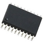
| 描述 | IC D-TYPE POS TRG SNGL 20SOIC触发器 2-6V CMOS Octal D-Type |
| 产品分类 | |
| 品牌 | ON Semiconductor |
| 产品手册 | |
| 产品图片 |
|
| rohs | 符合RoHS无铅 / 符合限制有害物质指令(RoHS)规范要求 |
| 产品系列 | 逻辑集成电路,触发器,ON Semiconductor MC74AC273DWR2G74AC |
| 数据手册 | |
| 产品型号 | MC74AC273DWR2G |
| 不同V、最大CL时的最大传播延迟 | 9ns @ 5V,50pF |
| 产品种类 | Logic- Flip Flops |
| 传播延迟时间 | 13 ns |
| 低电平输出电流 | 24 mA |
| 元件数 | 1 |
| 其它名称 | MC74AC273DWR2GOSCT |
| 功能 | 主复位 |
| 包装 | 剪切带 (CT) |
| 商标 | ON Semiconductor |
| 安装类型 | 表面贴装 |
| 安装风格 | SMD/SMT |
| 封装 | Reel |
| 封装/外壳 | 20-SOIC(0.295",7.50mm 宽) |
| 封装/箱体 | SOIC-20 WB |
| 工作温度 | -40°C ~ 85°C |
| 工厂包装数量 | 1000 |
| 最大工作温度 | + 85 C |
| 最小工作温度 | - 40 C |
| 极性 | Non-Inverting |
| 标准包装 | 1 |
| 每元件位数 | 8 |
| 电压-电源 | 2 V ~ 6 V |
| 电流-输出高,低 | 24mA,24mA |
| 电流-静态 | 8µA |
| 电源电压-最大 | 6 V |
| 电源电压-最小 | 2 V |
| 电路数量 | 8 |
| 类型 | D 型 |
| 系列 | MC74AC273 |
| 触发器类型 | 正边沿 |
| 输入电容 | 4.5pF |
| 输入类型 | Single-Ended |
| 输入线路数量 | 8 |
| 输出类型 | Single-Ended |
| 输出线路数量 | 8 |
| 逻辑类型 | D-Type Flip-Flop |
| 逻辑系列 | 74AC |
| 频率-时钟 | 175MHz |
| 高电平输出电流 | - 24 mA |


- 商务部:美国ITC正式对集成电路等产品启动337调查
- 曝三星4nm工艺存在良率问题 高通将骁龙8 Gen1或转产台积电
- 太阳诱电将投资9.5亿元在常州建新厂生产MLCC 预计2023年完工
- 英特尔发布欧洲新工厂建设计划 深化IDM 2.0 战略
- 台积电先进制程称霸业界 有大客户加持明年业绩稳了
- 达到5530亿美元!SIA预计今年全球半导体销售额将创下新高
- 英特尔拟将自动驾驶子公司Mobileye上市 估值或超500亿美元
- 三星加码芯片和SET,合并消费电子和移动部门,撤换高东真等 CEO
- 三星电子宣布重大人事变动 还合并消费电子和移动部门
- 海关总署:前11个月进口集成电路产品价值2.52万亿元 增长14.8%


PDF Datasheet 数据手册内容提取
MC74AC273, MC74ACT273 Octal D Flip-Flop The MC74AC273/74ACT273 has eight edge-triggered D−type flip−flops with individual D inputs and Q outputs. The common buffered Clock (CP) and Master Reset (MR) inputs load and reset (clear) all flip−flops simultaneously. The register is fully edge-triggered. The state of each D input, one setup time before the LOW−to−HIGH clock transition, is transferred www.onsemi.com to the corresponding flip−flop’s Q output. All outputs will be forced LOW independently of Clock or Data inputs by a LOW voltage level on the MR input. The device is useful SOIC−20WB for applications where the true output only is required and the Clock 20 SUFFIX DW CASE 751D and Master Reset are common to all storage elements. 1 Features • Ideal Buffer for MOS Microprocessor or Memory • TSSOP−20 Eight Edge-Triggered D Flip−Flops 20 SUFFIX DT • Buffered Common Clock CASE 948E • Buffered, Asynchronous Master Reset 1 • See MC74AC377 for Clock Enable Version • See MC74AC373 for Transparent Latch Version PIN ASSIGNMENT • See MC74AC374 for 3-State Version PIN FUNCTION • Outputs Source/Sink 24 mA D0−D7 Data Inputs • ′ACT273 Has TTL Compatible Inputs MR Master Reset • These are Pb−Free Devices CP Clock Pulse Input Q0−Q7 Data Outputs VCC Q7 D7 D6 Q6 Q5 D5 D4 Q4 CP 20 19 18 17 16 15 14 13 12 11 D0 D1 D2 D3 D4 D5 D6 D7 CP MR Q0 Q1 Q2 Q3 Q4 Q5 Q6 Q7 1 2 3 4 5 6 7 8 9 10 MR Q0 D0 D1 Q1 Q2 D2 D3 Q3 GND Logic Symbol (Top View) Pinout: 20−Lead Packages Conductors ORDERING INFORMATION See detailed ordering and shipping information in the package dimensions section on page 6 of this data sheet. MODE SELECT-FUNCTION TABLE Inputs Outputs Operating Mode MR CP Dn Qn DEVICE MARKING INFORMATION Reset (Clear) L X X L See general marking information in the device marking section on page 6 of this data sheet. Load ′1′ H H H Load ′0′ H L L H = HIGH Voltage Level L = LOW Voltage Level X = Immaterial = LOW-to-HIGH Clock Transition © Semiconductor Components Industries, LLC, 2016 1 Publication Order Number: December, 2016 − Rev. 8 MC74AC273/D
MC74AC273, MC74ACT273 D0 D1 D2 D3 D4 D5 D6 D7 CP D Q D Q D Q D Q D Q D Q D Q D Q CP CP CP CP CP CP CP CP RD RD RD RD RD RD RD RD MR O0 O1 O2 O3 O4 O5 O6 O7 NOTE:That this diagram is provided only for the understanding of logic operations and should not be used to estimate propagation delays. Figure 1. Logic Diagram www.onsemi.com 2
MC74AC273, MC74ACT273 MAXIMUM RATINGS Symbol Parameter Value Unit VCC DC Supply Voltage (Referenced to GND) −0.5 to +7.0 V VIN DC Input Voltage (Referenced to GND) −0.5 to VCC +0.5 V VOUT DC Output Voltage (Referenced to GND) (Note 1) −0.5 to VCC +0.5 V IIK DC Input Diode Current ±20 mA IOK DC Output Diode Current ±50 mA IOUT DC Output Sink/Source Current ±50 mA ICC DC Supply Current, per Output Pin ±50 mA IGND DC Ground Current, per Output Pin ±100 mA TSTG Storage Temperature Range (cid:2)65 to (cid:3)150 (cid:2)C TL Lead temperature, 1 mm from Case for 10 Seconds 260 (cid:2)C TJ Junction Temperature Under Bias 140 (cid:2)C (cid:2)JA Thermal Resistance (Note 2) SOIC 65.8 (cid:2)C/W TSSOP 110.7 MSL Moisture Sensitivity SOIC Level 3 TSSOP Level 1 FR Flammability Rating Oxygen Index: 30% − 35% UL 94 V−0 @ 0.125 in VESD ESD Withstand Voltage Human Body Model (Note 3) > 2000 V Machine Model (Note 4) > 200 Charged Device Model (Note 5) > 1000 ILatchup Latchup Performance Above VCC and Below GND at 85(cid:2)C (Note 6) ±100 mA Stresses exceeding those listed in the Maximum Ratings table may damage the device. If any of these limits are exceeded, device functionality should not be assumed, damage may occur and reliability may be affected. 1. IOUT absolute maximum rating must be observed. 2. The package thermal impedance is calculated in accordance with JESD 51−7. 3. Tested to EIA/JESD22−A114−A. 4. Tested to EIA/JESD22−A115−A. 5. Tested to JESD22−C101−A. 6. Tested to EIA/JESD78. RECOMMENDED OPERATING CONDITIONS Symbol Parameter Min Typ Max Unit ′AC 2.0 5.0 6.0 VCC Supply Voltage ′ACT 4.5 5.0 5.5 V Vin, Vout DC Input Voltage, Output Voltage (Ref. to GND) 0 − VCC V VCC @ 3.0 V − 150 − Input Rise and Fall Time (Note 7) tr, tf ′AC Devices except Schmitt Inputs VCC @ 4.5 V − 40 − ns/V VCC @ 5.5 V − 25 − Input Rise and Fall Time (Note 8) VCC @ 4.5 V − 10 − tr, tf ′ACT Devices except Schmitt Inputs VCC @ 5.5 V − 8.0 − ns/V TA Operating Ambient Temperature Range −40 25 85 °C IOH Output Current − High − − −24 mA IOL Output Current − Low − − 24 mA Functional operation above the stresses listed in the Recommended Operating Ranges is not implied. Extended exposure to stresses beyond the Recommended Operating Ranges limits may affect device reliability. 7. VIN from 30% to 70% VCC; see individual Data Sheets for devices that differ from the typical input rise and fall times. 8. VIN from 0.8 V to 2.0 V; see individual Data Sheets for devices that differ from the typical input rise and fall times. www.onsemi.com 3
MC74AC273, MC74ACT273 DC CHARACTERISTICS 74AC 74AC Symbol Parameter VCC TA = +25°C TA = −40°C to +85°C Unit Conditions (V) Typ Guaranteed Limits VIH Minimum High Level Input Voltage 3.0 1.5 2.1 2.1 V VOUT = 0.1 V 4.5 2.25 3.15 3.15 or VCC − 0.1 V 5.5 2.75 3.85 3.85 VIL Maximum Low Level Input Voltage 3.0 1.5 0.9 0.9 V VOUT = 0.1 V 4.5 2.25 1.35 1.35 or VCC − 0.1 V 5.5 2.75 1.65 1.65 VOH Minimum High Level Output Voltage 3.0 2.99 2.9 2.9 V IOUT = −50 (cid:3)A 4.5 4.49 4.4 4.4 5.5 5.49 5.4 5.4 *VIN = VIL or VIH 3.0 − 2.56 2.46 −12 mA V 4.5 − 3.86 3.76 IOH −24 mA 5.5 − 4.86 4.76 −24 mA VOL Maximum Low Level Output Voltage 3.0 0.002 0.1 0.1 V IOUT = 50 (cid:3)A 4.5 0.001 0.1 0.1 5.5 0.001 0.1 0.1 *VIN = VIL or VIH 3.0 − 0.36 0.44 12 mA V 4.5 − 0.36 0.44 IOL 24 mA 5.5 − 0.36 0.44 24 mA IIN Maximum Input Leakage Current 5.5 − ±0.1 ±1.0 (cid:3)A VI = VCC, GND IOLD †Minimum Dynamic Output Current 5.5 − − 75 mA VOLD = 1.65 V Max IOHD 5.5 − − −75 VOHD = 3.85 V Min ICC Maximum Quiescent Supply Current 5.5 − 8.0 80 (cid:3)A VIN = VCC or GND *All outputs loaded; thresholds on input associated with output under test. †Maximum test duration 2.0 ms, one output loaded at a time. NOTE: Note: IIN and ICC @ 3.0 V are guaranteed to be less than or equal to the respective limit @ 5.5 V VCC. AC CHARACTERISTICS (For Figures and Waveforms − See Section 3 of the ON Semiconductor FACT Data Book, DL138/D) 74AC 74AC Symbol Parameter V(CVC)* TA = +25°C CL = 50 pF TA = −40°C to +85°C CL = 50 pF Unit FiNgou.re Min Typ Max Min Max Maximum Clock 3.3 90 125 − 75 − fmax Frequency 5.0 140 175 − 125 − Mhz 3−3 Propagation Delay 3.3 4.0 7.0 12.5 3.0 14.0 tPLH Clock to Output 5.0 3.0 5.5 9.0 2.5 10.0 ns 3−6 Propagation Delay 3.3 4.0 7.0 13.0 3.5 14.5 tPHL Clock to Output 5.0 3.0 5.0 10.0 2.5 11.0 ns 3−6 Propagation Delay 3.3 4.0 7.0 13.0 3.5 14.0 tPHL MR to Output 5.0 3.0 5.0 10.0 2.5 10.5 ns 3−6 *Voltage Range 3.3 V is 3.3 V ±0.3 V. Voltage Range 5.0 V is 5.0 V ±0.5 V. AC OPERATING REQUIREMENTS 74AC 74AC Symbol Parameter V(CVC)* TA = +25°C CL = 50 pF TA = −40°C to +85°C CL = 50 pF Unit FiNgou.re Typ Guaranteed Minimum Setup Time, HIGH or LOW 3.3 3.5 5.5 6.0 ts Data to CP 5.0 2.5 4.0 4.5 ns 3−9 Hold Time, HIGH or LOW 3.3 −2.0 0 0 th Data to CP 5.0 −1.0 1.0 1.0 ns 3−9 Clock Pulse Width 3.3 3.5 5.5 6.0 tw HIGH or LOW 5.0 2.5 4.0 4.5 ns 3−6 MR Pulse Width 3.3 2.0 5.5 6.0 tw HIGH or LOW 5.0 1.5 4.0 4.5 ns 3−6 Recovery Time 3.3 1.5 3.5 4.5 trec MR to CP 5.0 1.0 2.0 3.0 ns 3−9 *Voltage Range 3.3 V is 3.3 V ±0.3 V. Voltage Range 5.0 V is 5.0 V ±0.5 V. www.onsemi.com 4
MC74AC273, MC74ACT273 DC CHARACTERISTICS 74ACT 74ACT Symbol Parameter V(VCC) TA = +25°C −40°CT tAo = +85°C Unit Conditions Typ Guaranteed Limits VIH Minimum High Level Input Voltage 4.5 1.5 2.0 2.0 V VOUT = 0.1 V 5.5 1.5 2.0 2.0 or VCC − 0.1 V VIL Maximum Low Level Input Voltage 4.5 1.5 0.8 0.8 V VOUT = 0.1 V 5.5 1.5 0.8 0.8 or VCC − 0.1 V VOH Minimum High Level Output Voltage 4.5 4.49 4.4 4.4 V IOUT = −50 (cid:3)A 5.5 5.49 5.4 5.4 *VIN = VIL or VIH 4.5 − 3.86 3.76 V IOH −24 mA 5.5 − 4.86 4.76 −24 mA VOL Maximum Low Level Output Voltage 4.5 0.001 0.1 0.1 V IOUT = 50 (cid:3)A 5.5 0.001 0.1 0.1 *VIN = VIL or VIH 4.5 − 0.36 0.44 V 24 mA 5.5 − 0.36 0.44 IOL 24 mA IIN Maximum Input Leakage Current 5.5 − ±0.1 ±1.0 (cid:3)A VI = VCC, GND (cid:4)ICCT Additional Max. ICC/Input 5.5 0.6 − 1.5 mA VI = VCC −2.1 V IOLD †Minimum Dynamic Output Current 5.5 − − 75 mA VOLD = 1.65 V Max IOHD 5.5 − − −75 VOHD = 3.85 V Min ICC Maximum Quiescent Supply Current 5.5 − 8.0 80 (cid:3)A VIN = VCC or GND *All outputs loaded; thresholds on input associated with output under test. †Maximum test duration 2.0 ms, one output loaded at a time. AC CHARACTERISTICS (For Figures and Waveforms − See Section 3 of the ON Semiconductor FACT Data Book, DL138/D) 74ACT 74ACT Symbol Parameter V(CVC)* TA = +25°C CL = 50 pF TA = C−4L0 =° C5 0to p F+85°C Unit FiNgou.re Min Typ Max Min Max fmax Maximum Clock Frequency 5.0 125 200 − 125 − MHz 3−3 tPHL Propagation Delay Clock to Output 5.0 3.0 6.0 10 2.5 11.0 ns 3−6 tPLH Propagation Delay Clock to Output 5.0 3.0 6.5 11 2.5 12.0 ns 3−6 tPHL Propagation Delay MR to Output 5.0 3.0 7.0 11 2.5 11.5 ns 3−6 *Voltage Range 5.0 V is 5.0 V ±0.5 V. AC OPERATING REQUIREMENTS 74ACT 74ACT Symbol Parameter V(CVC)* TA = +25°C CL = 50 pF TA = C−4L0 =° C5 0to p F+85°C Unit FiNgou.re Typ Guaranteed Minimum ts Setup Time, HIGH or LOW − Data to CP 5.0 3.0 4.5 5.0 ns 3−9 th Hold Time, HIGH or LOW − Data to CP 5.0 −2.5 2.0 2.0 ns 3−9 tw Clock Pulse Width − HIGH or LOW 5.0 2.5 4.0 4.5 ns 3−6 tw MR Pulse Width − HIGH or LOW 5.0 2.5 4.0 4.5 ns 3−6 trec Recovery Time − MR to CP 5.0 −1.0 2.0 3.0 ns 3−6 *Voltage Range 5.0 V is 5.0 V ±0.5 V. CAPACITANCE Symbol Parameter Value Typ Unit Test Conditions CIN Input Capacitance 4.5 pF VCC = 5.0 V CPD Power Dissipation Capacitance 50 pF VCC = 5.0 V www.onsemi.com 5
MC74AC273, MC74ACT273 ORDERING INFORMATION Device Package Shipping† MC74AC273DWG SOIC−20WB 38 Units / Rail (Pb−Free) MC74AC273DWR2G SOIC−20WB 1000 / Tape & Reel (Pb−Free) MC74AC273DTR2G TSSOP−20 2500 / Tape & Reel (Pb−Free) MC74ACT273DWG SOIC−20WB 38 Units / Rail (Pb−Free) MC74ACT273DWR2G SOIC−20WB 1000 / Tape & Reel (Pb−Free) MC74ACT273DTR2G TSSOP−20 2500 / Tape & Reel (Pb−Free) †For information on tape and reel specifications, including part orientation and tape sizes, please refer to our Tape and Reel Packaging Specifications Brochure, BRD8011/D. MARKING DIAGRAMS SOIC−20WB TSSOP−20 20 20 AC AC273 273 AWLYYWWG ALYW(cid:3) (cid:3) 1 1 20 20 ACT ACT273 273 AWLYYWWG ALYW(cid:3) (cid:3) 1 1 A = Assembly Location WL, L = Wafer Lot YY, Y = Year WW, W = Work Week G or (cid:3) = Pb−Free Package (Note: Microdot may be in either location) www.onsemi.com 6
MC74AC273, MC74ACT273 PACKAGE DIMENSIONS TSSOP−20 DT SUFFIX CASE 948E−02 ISSUE C NOTES: 20X K REF K 1. DIMENSIONING AND TOLERANCING PER ANSI Y14.5M, 1982. 0.15 (0.006) T U S 0.10 (0.004) M T U S V S ÍÍKÍ1 Í 2. CONTROLLING DIMENSION: MILLIMETER. 3. DIMENSION A DOES NOT INCLUDE ÍÍÍÍ MOLD FLASH, PROTRUSIONS OR GATE 20 11 J J1 BURRS. MOLD FLASH OR GATE BURRS 2X L/2 ÍÍÍÍ SHALL NOT EXCEED 0.15 (0.006) PER SIDE. 4. DIMENSION B DOES NOT INCLUDE B SECTION N−N INTERLEAD FLASH OR PROTRUSION. INTERLEAD FLASH OR PROTRUSION L −U− SHALL NOT EXCEED 0.25 (0.010) PER SIDE. PIN 1 5. DIMENSION K DOES NOT INCLUDE IDENT 0.25 (0.010) DAMBAR PROTRUSION. ALLOWABLE N DAMBAR PROTRUSION SHALL BE 0.08 1 10 (0.003) TOTAL IN EXCESS OF THE K DIMENSION AT MAXIMUM MATERIAL M CONDITION. 6. TERMINAL NUMBERS ARE SHOWN FOR 0.15 (0.006) T U S REFERENCE ONLY. 7. DIMENSION A AND B ARE TO BE A DETERMINED AT DATUM PLANE −W−. N MILLIMETERS INCHES −V− F DIM MIN MAX MIN MAX A 6.40 6.60 0.252 0.260 DETAIL E B 4.30 4.50 0.169 0.177 C --- 1.20 --- 0.047 D 0.05 0.15 0.002 0.006 F 0.50 0.75 0.020 0.030 −W− G 0.65 BSC 0.026 BSC C H 0.27 0.37 0.011 0.015 J 0.09 0.20 0.004 0.008 J1 0.09 0.16 0.004 0.006 D G H K 0.19 0.30 0.007 0.012 DETAIL E K1 0.19 0.25 0.007 0.010 0.100 (0.004) ML 06 (cid:2).40 BSC8 (cid:2) 00 (cid:2).252 BSC8 (cid:2) −T− SEATING SOLDERING FOOTPRINT* PLANE 7.06 1 0.65 PITCH 16X 16X 0.36 1.26 DIMENSIONS: MILLIMETERS *For additional information on our Pb−Free strategy and soldering details, please download the ON Semiconductor Soldering and Mounting Techniques Reference Manual, SOLDERRM/D. www.onsemi.com 7
MC74AC273, MC74ACT273 PACKAGE DIMENSIONS SOIC−20W DW SUFFIX CASE 751D−05 ISSUE G D NOTES: A (cid:2) 1. DIMENSIONS ARE IN MILLIMETERS. 2. INTERPRET DIMENSIONS AND TOLERANCES PER ASME Y14.5M, 1994. 3. DIMENSIONS D AND E DO NOT INCLUDE MOLD M 20 11 PROTRUSION. 4. MAXIMUM MOLD PROTRUSION 0.15 PER SIDE. B (cid:2) 5. DIMENSION B DOES NOT INCLUDE DAMBAR H M 45 PROTRUSION. ALLOWABLE PROTRUSION 10X 0.25 E hX SDCHIOMANELDNLI STBIIOEO NN0.. 1A3T TMOATXAILM IUNM E MXCATEESRSI AOLF B 1 10 MILLIMETERS DIM MIN MAX A 2.35 2.65 A1 0.10 0.25 20X B B B 0.35 0.49 C 0.23 0.32 0.25 M T A S B S D 12.65 12.95 E 7.40 7.60 e 1.27 BSC H 10.05 10.55 h 0.25 0.75 A L 0.50 0.90 (cid:2) 0 (cid:2) 7 (cid:2) L SEATING 18X e A1 TPLANE C ON Semiconductor and are trademarks of Semiconductor Components Industries, LLC dba ON Semiconductor or its subsidiaries in the United States and/or other countries. ON Semiconductor owns the rights to a number of patents, trademarks, copyrights, trade secrets, and other intellectual property. A listing of ON Semiconductor’s product/patent coverage may be accessed at www.onsemi.com/site/pdf/Patent−Marking.pdf. ON Semiconductor reserves the right to make changes without further notice to any products herein. ON Semiconductor makes no warranty, representation or guarantee regarding the suitability of its products for any particular purpose, nor does ON Semiconductor assume any liability arising out of the application or use of any product or circuit, and specifically disclaims any and all liability, including without limitation special, consequential or incidental damages. Buyer is responsible for its products and applications using ON Semiconductor products, including compliance with all laws, regulations and safety requirements or standards, regardless of any support or applications information provided by ON Semiconductor. “Typical” parameters which may be provided in ON Semiconductor data sheets and/or specifications can and do vary in different applications and actual performance may vary over time. All operating parameters, including “Typicals” must be validated for each customer application by customer’s technical experts. ON Semiconductor does not convey any license under its patent rights nor the rights of others. ON Semiconductor products are not designed, intended, or authorized for use as a critical component in life support systems or any FDA Class 3 medical devices or medical devices with a same or similar classification in a foreign jurisdiction or any devices intended for implantation in the human body. Should Buyer purchase or use ON Semiconductor products for any such unintended or unauthorized application, Buyer shall indemnify and hold ON Semiconductor and its officers, employees, subsidiaries, affiliates, and distributors harmless against all claims, costs, damages, and expenses, and reasonable attorney fees arising out of, directly or indirectly, any claim of personal injury or death associated with such unintended or unauthorized use, even if such claim alleges that ON Semiconductor was negligent regarding the design or manufacture of the part. ON Semiconductor is an Equal Opportunity/Affirmative Action Employer. This literature is subject to all applicable copyright laws and is not for resale in any manner. PUBLICATION ORDERING INFORMATION LITERATURE FULFILLMENT: N. American Technical Support: 800−282−9855 Toll Free ON Semiconductor Website: www.onsemi.com Literature Distribution Center for ON Semiconductor USA/Canada 19521 E. 32nd Pkwy, Aurora, Colorado 80011 USA Europe, Middle East and Africa Technical Support: Order Literature: http://www.onsemi.com/orderlit Phone: 303−675−2175 or 800−344−3860 Toll Free USA/Canada Phone: 421 33 790 2910 Fax: 303−675−2176 or 800−344−3867 Toll Free USA/Canada Japan Customer Focus Center For additional information, please contact your local Email: orderlit@onsemi.com Phone: 81−3−5817−1050 Sales Representative ◊ www.onsemi.com MC74AC273/D 8