ICGOO在线商城 > 集成电路(IC) > 逻辑 - 栅极和逆变器 > MC74AC132DG
 Datasheet下载
- 型号: MC74AC132DG
- 制造商: ON Semiconductor
- 库位|库存: xxxx|xxxx
- 要求:
| 数量阶梯 | 香港交货 | 国内含税 |
| +xxxx | $xxxx | ¥xxxx |
查看当月历史价格
查看今年历史价格
MC74AC132DG产品简介:
ICGOO电子元器件商城为您提供MC74AC132DG由ON Semiconductor设计生产,在icgoo商城现货销售,并且可以通过原厂、代理商等渠道进行代购。 MC74AC132DG价格参考¥2.80-¥2.80。ON SemiconductorMC74AC132DG封装/规格:逻辑 - 栅极和逆变器, 与非门 IC 4 Channel 14-SOIC。您可以下载MC74AC132DG参考资料、Datasheet数据手册功能说明书,资料中有MC74AC132DG 详细功能的应用电路图电压和使用方法及教程。
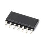
MC74AC132DG是安森美半导体(ON Semiconductor)生产的一款四路2输入端与非门(NAND Gate)集成电路,属于高速CMOS逻辑系列。该芯片内含四个独立的2输入与非门电路,具有低功耗、高噪声抑制能力和宽工作电压范围(通常为2V至6V),适用于多种数字逻辑设计场景。

其典型应用场景包括:

1. 数字逻辑控制电路:用于构建基本的逻辑判断模块,如在嵌入式系统或工业控制中实现信号判断与处理。

2. 时序控制电路:在时钟发生器、定时器或状态机设计中,作为基本逻辑单元使用。

3. 接口电路:用于电平转换或信号整形,提高系统间信号传输的稳定性。

4. 通信设备:在通信模块中实现数据编码、解码或信号切换功能。

5. 消费电子产品:如家电控制器、智能玩具、电子仪表等,作为逻辑处理单元。

6. 教育与实验开发:因其功能明确、使用简单,广泛用于电子教学实验板或原型开发中。

该器件采用14引脚TSSOP封装,适合表面贴装工艺,适用于工业级温度范围(-40℃至+85℃),具备良好的环境适应性和可靠性。
| 参数 | 数值 |
| 产品目录 | 集成电路 (IC)半导体 |
| 描述 | IC GATE NAND 4CH 2-INP 14-SOIC逻辑门 2-6V Quad 2-Input NAND Schmitt |
| 产品分类 | |
| 品牌 | ON Semiconductor |
| 产品手册 | |
| 产品图片 |
|
| rohs | 符合RoHS无铅 / 符合限制有害物质指令(RoHS)规范要求 |
| 产品系列 | 逻辑集成电路,逻辑门,ON Semiconductor MC74AC132DG74AC |
| 数据手册 | |
| 产品型号 | MC74AC132DG |
| 不同V、最大CL时的最大传播延迟 | 9ns @ 5V,50pF |
| 产品 | NAND |
| 产品目录页面 | |
| 产品种类 | Logic- Gates |
| 传播延迟时间 | 13.5 ns |
| 低电平输出电流 | 24 mA |
| 供应商器件封装 | 14-SOICN |
| 其它名称 | MC74AC132DG-ND |
| 包装 | 管件 |
| 商标 | ON Semiconductor |
| 安装类型 | 表面贴装 |
| 安装风格 | SMD/SMT |
| 封装 | Tube |
| 封装/外壳 | 14-SOIC(0.154",3.90mm 宽) |
| 封装/箱体 | SOIC-14 |
| 工作温度 | -40°C ~ 85°C |
| 工厂包装数量 | 55 |
| 最大工作温度 | + 85 C |
| 最小工作温度 | - 40 C |
| 栅极数量 | 4 |
| 标准包装 | 55 |
| 特性 | 施密特触发器 |
| 电压-电源 | 2 V ~ 6 V |
| 电流-输出高,低 | 24mA,24mA |
| 电流-静态(最大值) | 4µA |
| 电源电压-最大 | 6 V |
| 电源电压-最小 | 2 V |
| 电路数 | 4 |
| 系列 | MC74AC132 |
| 输入/输出线数量 | 2 / 1 |
| 输入数 | 2 |
| 输入线路数量 | 2 |
| 输出线路数量 | 1 |
| 逻辑电平-低 | 0.5 V ~ 1.1 V |
| 逻辑电平-高 | 2.2 V ~ 3.9 V |
| 逻辑类型 | 与非门 |
| 逻辑系列 | 74AC |
| 高电平输出电流 | - 24 mA |


.jpg)


- 商务部:美国ITC正式对集成电路等产品启动337调查
- 曝三星4nm工艺存在良率问题 高通将骁龙8 Gen1或转产台积电
- 太阳诱电将投资9.5亿元在常州建新厂生产MLCC 预计2023年完工
- 英特尔发布欧洲新工厂建设计划 深化IDM 2.0 战略
- 台积电先进制程称霸业界 有大客户加持明年业绩稳了
- 达到5530亿美元!SIA预计今年全球半导体销售额将创下新高
- 英特尔拟将自动驾驶子公司Mobileye上市 估值或超500亿美元
- 三星加码芯片和SET,合并消费电子和移动部门,撤换高东真等 CEO
- 三星电子宣布重大人事变动 还合并消费电子和移动部门
- 海关总署:前11个月进口集成电路产品价值2.52万亿元 增长14.8%


PDF Datasheet 数据手册内容提取
MC74AC132, MC74ACT132 Quad 2-Input NAND Schmitt Trigger High−Performance Silicon−Gate CMOS The MC74AC/74ACT132 contains four 2−input NAND gates www.onsemi.com which are capable of transforming slowly changing input signals into sharply defined, jitter−free output signals. In addition, they have greater noise margin than conventional NAND gates. MARKING DIAGRAM Each circuit contains a 2−input Schmitt trigger. The Schmitt trigger uses positive feedback to effectively speed−up slow input transitions, 14 and provide different input threshold voltages for positive and negative-going transitions. This hysteresis between the positive−going SOIC−14 xxx132G D SUFFIX AWLYWW and negative−going input threshold is determined by resistor ratios 14 CASE 751A and is essentially insensitive to temperature and supply voltage 1 variations. 1 Features xxx = AC or ACT A = Assembly Location • WL = Wafer Lot Schmitt Trigger Inputs Y = Year • Outputs Source/Sink 24 mA WW = Work Week • ′ACT132 Has TTL Compatible Inputs G = Pb−Free Package • These are Pb−Free Devices VCC ORDERING INFORMATION 14 13 12 11 10 9 8 See detailed ordering and shipping information in the package dimensions section on page 5 of this data sheet. 1 2 3 4 5 6 7 GND Figure 1. Pinout; 14−Lead Packages Conductors (Top View) FUNCTION TABLE Inputs Output A B Y L L H L H H H L H H H L H = HIGH Voltage Level L = LOW Voltage Level © Semiconductor Components Industries, LLC, 2015 1 Publication Order Number: January, 2015 − Rev. 8 MC74AC132/D
MC74AC132, MC74ACT132 MAXIMUM RATINGS Symbol Parameter Value Unit VCC DC Supply Voltage (cid:2)0.5 to (cid:3)7.0 V VI DC Input Voltage (cid:2)0.5 (cid:4) VI (cid:4) VCC (cid:3)0.5 V VO DC Output Voltage (Note 1) (cid:2)0.5 (cid:4) VO (cid:4) VCC (cid:3)0.5 V IIK DC Input Diode Current (cid:5)20 mA IOK DC Output Diode Current (cid:5)50 mA IO DC Output Sink/Source Current (cid:5)50 mA ICC DC Supply Current per Output Pin (cid:5)50 mA IGND DC Ground Current per Output Pin (cid:5)50 mA TSTG Storage Temperature Range (cid:2)65 to (cid:3)150 °C TL Lead temperature, 1 mm from Case for 10 Seconds 260 °C TJ Junction temperature under Bias (cid:3)150 °C (cid:2) Thermal Resistance (Note 2) 125 °C/W JA PD Power Dissipation in Still Air at 85°C 125 mW MSL Moisture Sensitivity Level 1 FR Flammability Rating Oxygen Index: 30% − 35% UL 94 V−0 @ 0.125 in VESD ESD Withstand Voltage Human Body Model (Note 3) > 2000 V Machine Model (Note 4) > 200 Charged Device Model (Note 5) > 1000 ILatch−Up Latch−Up Performance Above VCC and Below GND at 85°C (Note 6) (cid:5)100 mA Stresses exceeding those listed in the Maximum Ratings table may damage the device. If any of these limits are exceeded, device functionality should not be assumed, damage may occur and reliability may be affected. 1. IO absolute maximum rating must be observed. 2. The package thermal impedance is calculated in accordance with JESD51−7. 3. Tested to EIA/JESD22−A114−A. 4. Tested to EIA/JESD22−A115−A. 5. Tested to JESD22−C101−A. 6. Tested to EIA/JESD78. RECOMMENDED OPERATING CONDITIONS Symbol Parameter Min Typ Max Unit ′AC 2.0 5.0 6.0 VCC Supply Voltage ′ACT 4.5 5.0 5.5 V Vin, Vout DC Input Voltage, Output Voltage (Ref. to GND) 0 − VCC V VCC @ 3.0 V − 150 − Input Rise and Fall Time (Note 1) tr, tf ′AC Devices except Schmitt Inputs VCC @ 4.5 V − 40 − ns/V VCC @ 5.5 V − 25 − Input Rise and Fall Time (Note 2) VCC @ 4.5 V − 10 − tr, tf ′ACT Devices except Schmitt Inputs VCC @ 5.5 V − 8.0 − ns/V TJ Junction Temperature (PDIP) − − 140 °C TA Operating Ambient Temperature Range −40 25 85 °C IOH Output Current − High − − −24 mA IOL Output Current − Low − − 24 mA Functional operation above the stresses listed in the Recommended Operating Ranges is not implied. Extended exposure to stresses beyond the Recommended Operating Ranges limits may affect device reliability. 1. Vin from 30% to 70% VCC; see individual Data Sheets for devices that differ from the typical input rise and fall times. 2. Vin from 0.8 V to 2.0 V; see individual Data Sheets for devices that differ from the typical input rise and fall times. www.onsemi.com 2
MC74AC132, MC74ACT132 DC CHARACTERISTICS 74AC 74AC Symbol Parameter V(VCC) TA = +25°C −4T0A°C = to Unit Conditions +85°C Typ Guaranteed Limits VOH Minimum High Level 3.0 2.99 2.9 2.9 IOUT = −50 (cid:3)A Output Voltage 4.5 4.49 4.4 4.4 V 5.5 5.49 5.4 5.4 *VIN = VIL or VIH 3.0 − 2.56 2.46 −12 mA V 4.5 − 3.86 3.76 IOH −24 mA 5.5 − 4.86 4.76 −24 mA VOL Maximum Low Level 3.0 0.002 0.1 0.1 IOUT = 50 (cid:3)A Output Voltage 4.5 0.001 0.1 0.1 V 5.5 0.001 0.1 0.1 *VIN = VIL or VIH 3.0 − 0.36 0.44 12 mA V 4.5 − 0.36 0.44 IOL 24 mA 5.5 − 0.36 0.44 24 mA IIN MLeaaxkimaguem C Iunrpruetnt 5.5 − ±0.1 ±1.0 (cid:3)A VI = VCC, GND IOLD †Minimum Dynamic 5.5 − − 75 mA VOLD = 1.65 V Max Output Current IOHD 5.5 − − −75 mA VOHD = 3.85 V Min ICC MSuapxpimlyu Cmu Qrreunietscent 5.5 − 4.0 40 (cid:3)A VIN = VCC or GND Product parametric performance is indicated in the Electrical Characteristics for the listed test conditions, unless otherwise noted. Product performance may not be indicated by the Electrical Characteristics if operated under different conditions. *All outputs loaded; thresholds on input associated with output under test. †Maximum test duration 2.0 ms, one output loaded at a time. NOTE: IIN and ICC @ 3.0 V are guaranteed to be less than or equal to the respective limit @ 5.5 V VCC. AC CHARACTERISTICS 74AC 74AC Symbol Parameter VCC* TA = +25°C TtAo = + −8450°C°C Unit Fig. (V) CL = 50 pF CL = 50 pF No. Min Typ Max Min Max 3.3 2.0 − 13.0 1.5 14.0 tPLH Propagation Delay 5.0 2.0 − 9.0 1.5 10.0 ns 3−5 3.3 2.0 − 13.5 1.5 15.0 tPHL Propagation Delay 5.0 2.0 − 9.0 1.5 10.0 ns 3−5 *Voltage Range 3.3 V is 3.3 V ±0.3 V. Voltage Range 5.0 V is 5.0 V ±0.5 V. www.onsemi.com 3
MC74AC132, MC74ACT132 DC CHARACTERISTICS 74ACT 74ACT Symbol Parameter V(VCC) TA = +25°C −4T0A°C = to Unit Conditions +85°C Typ Guaranteed Limits VOH Minimum High Level 4.5 4.49 4.4 4.4 IOUT = −50 (cid:3)A V Output Voltage 5.5 5.49 5.4 5.4 *VIN = VIL or VIH 4.5 − 3.86 3.76 V −24 mA 5.5 − 4.86 4.76 IOH −24 mA VOL Maximum Low Level 4.5 0.001 0.1 0.1 IOUT = 50 (cid:3)A V Output Voltage 5.5 0.001 0.1 0.1 *VIN = VIL or VIH 4.5 − 0.36 0.44 V 24 mA 5.5 − 0.36 0.44 IOL 24 mA IIN MLeaaxkimaguem C Iunrpruetnt 5.5 − ±0.1 ±1.0 (cid:3)A VI = VCC, GND (cid:4)ICCT Additional Max. ICC/Input 5.5 0.6 − 1.5 mA VI = VCC −2.1 V IOLD †Minimum Dynamic 5.5 − − 75 mA VOLD = 1.65 V Max Output Current IOHD 5.5 − − −75 mA VOHD = 3.85 V Min ICC MSuapxpimlyu Cmu Qrreunietscent 5.5 − 4.0 40 (cid:3)A VIN = VCC or GND Product parametric performance is indicated in the Electrical Characteristics for the listed test conditions, unless otherwise noted. Product performance may not be indicated by the Electrical Characteristics if operated under different conditions. *All outputs loaded; thresholds on input associated with output under test. †Maximum test duration 2.0 ms, one output loaded at a time. AC CHARACTERISTICS 74ACT 74ACT Symbol Parameter VCC* TA = +25°C TtAo = + −8450°C°C Unit Fig. (V) CL = 50 pF CL = 50 pF No. Min Typ Max Min Max tPLH Propagation Delay 5.0 3.0 − 11.5 2.5 13.0 ns 3−6 tPHL Propagation Delay 5.0 3.0 − 11.0 2.5 12.5 ns 3−5 *Voltage Range 5.0 V is 5.0 V ±0.5 V. www.onsemi.com 4
MC74AC132, MC74ACT132 INPUT CHARACTERISTICS (unless otherwise specified) Symbol Parameter VCC 74AC 74ACT Unit Test Conditions (V) 3.0 2.2 Maximum Positive Vt + Threshold 4.5 3.2 2.0 V TA = Worst Case 5.5 3.9 3.0 0.5 Minimum Negative Vt − Threshold 4.5 0.9 0.8 V TA = Worst Case 5.5 1.1 3.0 1.2 Vh(max) Maximum Hysteresis 4.5 1.4 1.2 V TA = Worst Case 5.5 1.6 3.0 0.3 Vh(min) Minimum Hysteresis 4.5 0.4 0.4 V TA = Worst Case 5.5 0.5 CAPACITANCE Value Symbol Parameter Unit Test Conditions Typ CIN Input Capacitance 4.5 pF VCC = 5.0 V CPD Power Dissipation Capacitance 30 pF VCC = 5.0 V ORDERING INFORMATION Device Package Shipping† MC74AC132DG SOIC−14 55 Units/Rail (Pb−Free) MC74AC132DR2G SOIC−14 2500/Tape & Reel (Pb−Free) MC74ACT132DG SOIC−14 55 Units/Rail (Pb−Free) MC74ACT132DR2G SOIC−14 2500/Tape & Reel (Pb−Free) †For information on tape and reel specifications, including part orientation and tape sizes, please refer to our Tape and Reel Packaging Specifications Brochure, BRD8011/D. www.onsemi.com 5
MC74AC132, MC74ACT132 PACKAGE DIMENSIONS SOIC−14 NB CASE 751A−03 ISSUE K D A NOTES: B 1.DIMENSIONING AND TOLERANCING PER ASME Y14.5M, 1994. 2.CONTROLLING DIMENSION: MILLIMETERS. 14 8 3.DIMENSION b DOES NOT INCLUDE DAMBAR A3 PROTRUSION. ALLOWABLE PROTRUSION SHALL BE 0.13 TOTAL IN EXCESS OF AT MAXIMUM MATERIAL CONDITION. H E 4.DIMENSIONS D AND E DO NOT INCLUDE MOLD PROTRUSIONS. L 5.MAXIMUM MOLD PROTRUSION 0.15 PER SIDE. 1 7 DETAIL A MILLIMETERS INCHES 0.25 M B M 13Xb DIM MIN MAX MIN MAX A 1.35 1.75 0.054 0.068 0.25 M C A S B S A1 0.10 0.25 0.004 0.010 A3 0.19 0.25 0.008 0.010 DETAIL A b 0.35 0.49 0.014 0.019 h A D 8.55 8.75 0.337 0.344 X 45(cid:2) E 3.80 4.00 0.150 0.157 e 1.27 BSC 0.050 BSC H 5.80 6.20 0.228 0.244 h 0.25 0.50 0.010 0.019 e A1 C SEATING M ML 0.04 0(cid:2) 1.72 5(cid:2) 0.001 6(cid:2) 0.074 9(cid:2) PLANE SOLDERING FOOTPRINT* 6.50 14X 1.18 1 1.27 PITCH 14X 0.58 DIMENSIONS: MILLIMETERS *For additional information on our Pb−Free strategy and soldering details, please download the ON Semiconductor Soldering and Mounting Techniques Reference Manual, SOLDERRM/D. ON Semiconductor and the are registered trademarks of Semiconductor Components Industries, LLC (SCILLC) or its subsidiaries in the United States and/or other countries. SCILLC owns the rights to a number of patents, trademarks, copyrights, trade secrets, and other intellectual property. A listing of SCILLC’s product/patent coverage may be accessed at www.onsemi.com/site/pdf/Patent−Marking.pdf. SCILLC reserves the right to make changes without further notice to any products herein. SCILLC makes no warranty, representation or guarantee regarding the suitability of its products for any particular purpose, nor does SCILLC assume any liability arising out of the application or use of any product or circuit, and specifically disclaims any and all liability, including without limitation special, consequential or incidental damages. “Typical” parameters which may be provided in SCILLC data sheets and/or specifications can and do vary in different applications and actual performance may vary over time. All operating parameters, including “Typicals” must be validated for each customer application by customer’s technical experts. SCILLC does not convey any license under its patent rights nor the rights of others. SCILLC products are not designed, intended, or authorized for use as components in systems intended for surgical implant into the body, or other applications intended to support or sustain life, or for any other application in which the failure of the SCILLC product could create a situation where personal injury or death may occur. Should Buyer purchase or use SCILLC products for any such unintended or unauthorized application, Buyer shall indemnify and hold SCILLC and its officers, employees, subsidiaries, affiliates, and distributors harmless against all claims, costs, damages, and expenses, and reasonable attorney fees arising out of, directly or indirectly, any claim of personal injury or death associated with such unintended or unauthorized use, even if such claim alleges that SCILLC was negligent regarding the design or manufacture of the part. SCILLC is an Equal Opportunity/Affirmative Action Employer. This literature is subject to all applicable copyright laws and is not for resale in any manner. PUBLICATION ORDERING INFORMATION LITERATURE FULFILLMENT: N. American Technical Support: 800−282−9855 Toll Free ON Semiconductor Website: www.onsemi.com Literature Distribution Center for ON Semiconductor USA/Canada P.O. Box 5163, Denver, Colorado 80217 USA Europe, Middle East and Africa Technical Support: Order Literature: http://www.onsemi.com/orderlit Phone: 303−675−2175 or 800−344−3860 Toll Free USA/Canada Phone: 421 33 790 2910 Fax: 303−675−2176 or 800−344−3867 Toll Free USA/Canada Japan Customer Focus Center For additional information, please contact your local Email: orderlit@onsemi.com Phone: 81−3−5817−1050 Sales Representative www.onsemi.com MC74AC132/D 6
Mouser Electronics Authorized Distributor Click to View Pricing, Inventory, Delivery & Lifecycle Information: O N Semiconductor: MC74AC132DG MC74AC132DR2G MC74ACT132DG MC74ACT132DR2G