ICGOO在线商城 > 集成电路(IC) > PMIC - 监控器 > MC33161DMR2G
 Datasheet下载
- 型号: MC33161DMR2G
- 制造商: ON Semiconductor
- 库位|库存: xxxx|xxxx
- 要求:
| 数量阶梯 | 香港交货 | 国内含税 |
| +xxxx | $xxxx | ¥xxxx |
查看当月历史价格
查看今年历史价格
MC33161DMR2G产品简介:
ICGOO电子元器件商城为您提供MC33161DMR2G由ON Semiconductor设计生产,在icgoo商城现货销售,并且可以通过原厂、代理商等渠道进行代购。 MC33161DMR2G价格参考¥3.45-¥3.45。ON SemiconductorMC33161DMR2G封装/规格:PMIC - 监控器, 开路漏极或开路集电极 监控器 2 通道 Micro8™。您可以下载MC33161DMR2G参考资料、Datasheet数据手册功能说明书,资料中有MC33161DMR2G 详细功能的应用电路图电压和使用方法及教程。
MC33161DMR2G 是一款由 ON Semiconductor 提供的电源管理集成电路(PMIC),属于 PMIC - 监控器类别。该器件主要应用于需要高效电源管理和电压监控的场景,具体应用场景如下:

1. 汽车电子系统:MC33161DMR2G 常用于汽车电子控制单元(ECU)中,例如发动机控制模块、变速箱控制单元和车身控制模块。它能够监控电池电压,并在异常情况下提供复位或保护功能,确保系统的稳定运行。

2. 工业设备:在工业自动化领域,该芯片可用于监控和管理供电电压,确保传感器、控制器和执行器等关键组件的正常工作。其低功耗特性和高可靠性使其非常适合长时间运行的工业设备。

3. 消费类电子产品:虽然 MC33161DMR2G 更常用于工业和汽车领域,但在某些高性能消费类电子产品中,如便携式设备或智能家居控制器,也可以用作电压监控和电源管理解决方案。

4. 通信设备:在网络通信设备中,如路由器、网关或基站的子系统中,MC33161DMR2G 可以帮助监控电源状态并防止因电压波动导致的系统故障。

5. 电池管理系统(BMS):在电池供电的应用中,该器件可以监控电池电压,确保电池处于安全的工作范围内,并在必要时触发保护机制。

MC33161DMR2G 的主要功能包括欠压检测、上电复位和手动复位等功能,适用于需要高可靠性和精确电压监控的多种应用场合。其设计特别适合对环境适应性要求较高的场景,例如高温、振动或电磁干扰较强的环境。
| 参数 | 数值 |
| 产品目录 | 集成电路 (IC)半导体 |
| 描述 | IC MONITOR VOLTAGE UNIV 8MICRO监控电路 Universal Voltage Monitor |
| 产品分类 | |
| 品牌 | ON Semiconductor |
| 产品手册 | |
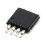
| 产品图片 |
|
| rohs | 符合RoHS无铅 / 符合限制有害物质指令(RoHS)规范要求 |
| 产品系列 | 电源管理 IC,监控电路,ON Semiconductor MC33161DMR2G- |
| NumberofInputsMonitored | 2 Input |
| 数据手册 | |
| 产品型号 | MC33161DMR2G |
| PCN设计/规格 | |
| 产品目录页面 | |
| 产品种类 | 监控电路 |
| 人工复位 | No Manual Reset |
| 供应商器件封装 | Micro8™ |
| 其它名称 | MC33161DMR2GOSDKR |
| 包装 | Digi-Reel® |
| 受监控电压数 | 2 |
| 商标 | ON Semiconductor |
| 复位 | - |
| 复位超时 | - |
| 安装类型 | 表面贴装 |
| 安装风格 | SMD/SMT |
| 封装 | Reel |
| 封装/外壳 | 8-TSSOP,8-MSOP(0.118",3.00mm 宽) |
| 封装/箱体 | MSOP-8 |
| 工作温度 | -40°C ~ 105°C |
| 工作电源电流 | 560 uA |
| 工厂包装数量 | 4000 |
| 最大工作温度 | + 105 C |
| 最小工作温度 | - 40 C |
| 标准包装 | 1 |
| 欠电压阈值 | Adjustable |
| 电压-阈值 | 可调节/可选择 |
| 电池备用开关 | No Backup |
| 电源电压-最大 | 40 V |
| 电源电压-最小 | 2 V |
| 监视器 | No Watchdog |
| 类型 | Voltage Supervisory |
| 系列 | MC33161 |
| 被监测输入数 | 2 Input |
| 输出 | 开路漏极或开路集电极 |
| 输出类型 | Open Collector / Drain |
| 过电压阈值 | Adjustable |
| 重置延迟时间 | Adjustable |
| 阈值电压 | 1.27 V |


- 商务部:美国ITC正式对集成电路等产品启动337调查
- 曝三星4nm工艺存在良率问题 高通将骁龙8 Gen1或转产台积电
- 太阳诱电将投资9.5亿元在常州建新厂生产MLCC 预计2023年完工
- 英特尔发布欧洲新工厂建设计划 深化IDM 2.0 战略
- 台积电先进制程称霸业界 有大客户加持明年业绩稳了
- 达到5530亿美元!SIA预计今年全球半导体销售额将创下新高
- 英特尔拟将自动驾驶子公司Mobileye上市 估值或超500亿美元
- 三星加码芯片和SET,合并消费电子和移动部门,撤换高东真等 CEO
- 三星电子宣布重大人事变动 还合并消费电子和移动部门
- 海关总署:前11个月进口集成电路产品价值2.52万亿元 增长14.8%


PDF Datasheet 数据手册内容提取
MC34161, MC33161, NCV33161 Universal Voltage Monitors The MC34161/MC33161 are universal voltage monitors intended for use in a wide variety of voltage sensing applications. These devices offer the circuit designer an economical solution for positive and negative voltage detection. The circuit consists of two comparator channels each with hysteresis, a unique Mode Select Input for channel programming, a pinned out 2.54 V reference, and two open collector www.onsemi.com outputs capable of sinking in excess of 10mA. Each comparator MARKING channel can be configured as either inverting or noninverting by the DIAGRAMS Mode Select Input. This allows over, under, and window detection of positive and negative voltages. The minimum supply voltage needed for these devices to be fully functional is 2.0 V for positive voltage 8 sensing and 4.0V for negative voltage sensing. PDIP−8 MC3x161P Applications include direct monitoring of positive and negative P SUFFIX AWL CASE 626 YYWWG voltages used in appliance, automotive, consumer, and industrial equipment. 1 1 Features 8 • Unique Mode Select Input Allows Channel Programming SOIC−8 3x161 • Over, Under, and Window Voltage Detection D SUFFIX ALYW • Positive and Negative Voltage Detection CASE 751 (cid:2) 1 • Fully Functional at 2.0 V for Positive Voltage Sensing and 4.0 V 1 for Negative Voltage Sensing • 8 Pinned Out 2.54 V Reference with Current Limit Protection • Low Standby Current Micro8(cid:3) x161 • DM SUFFIX AYW(cid:2) Open Collector Outputs for Enhanced Device Flexibility CASE 846A (cid:2) • NCV Prefix for Automotive and Other Applications Requiring 1 1 Unique Site and Control Change Requirements; AEC−Q100 x = 3 or 4 Qualified and PPAP Capable A = Assembly Location • These Devices are Pb−Free and are RoHS Compliant WL, L = Wafer Lot VCC YY, Y = Year WW, W = Work Week 8 G or (cid:2) = Pb−Free Package (Note: Microdot may be in either location) 1 2.54V PIN CONNECTIONS Reference VS 7 - Vref 1 8 VCC + + 6 Input 1 2 7 Mode Select 2 2.8V + Input 2 3 6 Output 1 + - GND 4 5 Output 2 1.27V - + + 5 (TOP VIEW) 3 + 0.6V + - ORDERING INFORMATION 1.27V See detailed ordering and shipping information in the package dimensions section on page 15 of this data sheet. 4 This device contains 141 transistors. Figure 1. Simplified Block Diagram (Positive Voltage Window Detector Application) © Semiconductor Components Industries, LLC, 2015 1 Publication Order Number: November, 2015 − Rev. 13 MC34161/D
MC34161, MC33161, NCV33161 MAXIMUM RATINGS (Note 1) Rating Symbol Value Unit Power Supply Input Voltage VCC 40 V Comparator Input Voltage Range Vin −1.0to+40 V Comparator Output Sink Current (Pins 5 and 6) (Note 2) ISink 20 mA Comparator Output Voltage Vout 40 V Power Dissipation and Thermal Characteristics (Note 2) P Suffix, Plastic Package, Case 626 Maximum Power Dissipation @ TA = 70°C PD 800 mW Thermal Resistance, Junction−to−Air R(cid:2)JA 100 °C/W D Suffix, Plastic Package, Case 751 Maximum Power Dissipation @ TA = 70°C PD 450 mW Thermal Resistance, Junction−to−Air R(cid:2)JA 178 °C/W DM Suffix, Plastic Package, Case 846A Thermal Resistance, Junction−to−Ambient R(cid:2)JA 240 °C/W Operating Junction Temperature TJ +150 °C Operating Ambient Temperature (Note 3) TA °C MC34161 0to+70 MC33161 −40to+105 NCV33161 −40 to +125 Storage Temperature Range Tstg −55to+150 °C Stresses exceeding those listed in the Maximum Ratings table may damage the device. If any of these limits are exceeded, device functionality should not be assumed, damage may occur and reliability may be affected. 1. This device series contains ESD protection and exceeds the following tests: Human Body Model 2000 V per MIL−STD−883, Method 3015. Machine Model Method 200 V. 2. Maximum package power dissipation must be observed. 3. Tlow = 0°C for MC34161 Thigh = +70°C for MC34161 −40°C for MC33161 +105°C for MC33161 −40°C for NCV33161 +125°C for NCV33161 www.onsemi.com 2
MC34161, MC33161, NCV33161 ELECTRICAL CHARACTERISTICS (VCC = 5.0 V, for typical values TA = 25°C, for min/max values TA is the operating ambient temperature range that applies [Notes 4 and 5], unless otherwise noted.) Characteristics Symbol Min Typ Max Unit COMPARATOR INPUTS Threshold Voltage, Vin Increasing (TA = 25°C) Vth 1.245 1.27 1.295 V (TA = Tmin to Tmax) 1.235 − 1.295 Threshold Voltage Variation (VCC = 2.0 V to 40 V) (cid:3)Vth − 7.0 15 mV Threshold Hysteresis, Vin Decreasing VH 15 25 35 mV Threshold Difference |Vth1 − Vth2| VD − 1.0 15 mV Reference to Threshold Difference (Vref − Vin1), (Vref − Vin2) VRTD 1.20 1.27 1.32 V Input Bias Current (Vin = 1.0 V) IIB − 40 200 nA (Vin = 1.5 V) − 85 400 MODE SELECT INPUT Mode Select Threshold Voltage (Figure 6) Channel 1 Vth(CH1) Vref+0.15 Vref+0.23 Vref+0.30 V Channel 2 Vth(CH2) 0.3 0.63 0.9 COMPARATOR OUTPUTS Output Sink Saturation Voltage (ISink = 2.0 mA) VOL − 0.05 0.3 V (ISink = 10 mA) − 0.22 0.6 (ISink = 0.25 mA, VCC = 1.0 V) − 0.02 0.2 Off−State Leakage Current (VOH = 40 V) IOH − 0 1.0 (cid:4)A REFERENCE OUTPUT Output Voltage (IO = 0 mA, TA = 25°C) Vref 2.48 2.54 2.60 V Load Regulation (IO = 0 mA to 2.0 mA) Regload − 0.6 15 mV Line Regulation (VCC = 4.0 V to 40 V) Regline − 5.0 15 mV Total Output Variation over Line, Load, and Temperature (cid:3)Vref 2.45 − 2.60 V Short Circuit Current ISC − 8.5 30 mA TOTAL DEVICE Power Supply Current (VMode, Vin1, Vin2 = GND) (VCC = 5.0 V) ICC − 450 700 (cid:4)A (VCC = 40 V) − 560 900 Operating Voltage Range (Positive Sensing) VCC 2.0 − 40 V (Negative Sensing) 4.0 − 40 Product parametric performance is indicated in the Electrical Characteristics for the listed test conditions, unless otherwise noted. Product performance may not be indicated by the Electrical Characteristics if operated under different conditions. 4. Low duty cycle pulse techniques are used during test to maintain junction temperature as close to ambient as possible. 5. Tlow = 0°C for MC34161 Thigh = +70°C for MC34161 −40°C for MC33161 +105°C for MC33161 −40°C for NCV33161 +125°C for NCV33161 www.onsemi.com 3
MC34161, MC33161, NCV33161 6.0 500 VCC = 5.0 V GE (V) 5.0 RTAL == 2 150°C k to VCC ENT (nA) 400 VVTACM Co=d =2e 5=5°. 0CG NVD A 4.0 R T R OL CU 300 PUT V 3.0 BIAS T T 200 V, OUout21..00 TTTAAA === 82-4550°°CC°C TTTAAA === 82-4550°°CC°C I , INPUIB 100 0 0 1.22 1.23 1.24 1.25 1.26 1.27 1.28 1.29 0 1.0 2.0 3.0 4.0 5.0 Vin, INPUT VOLTAGE (V) Vin, INPUT VOLTAGE (V) Figure 2. Comparator Input Threshold Voltage Figure 3. Comparator Input Bias Current versus Input Voltage s) n E (3600 8.0 N DELAY TIM3000 VTAC C= =2 55°.0C V 1234.... VVVVMMMMooooddddeeee ==== GGVVCCNNCCDD,, ,,OO OOuuuuttppttppuuuutt ttRF FRaisailslilinlininngggg AGE (V) 6.0 UPRRrn1Lo d==ge r11rav0.m8o k lmkt at,eo gRd eV2 t DCo=C e t4rtie.p7c atkot r4.5 V TIO2400 OLT Refer to Figure 17 A V ROPAG1800 1 UTPUT 4.0 P O UTPUT 1200 2 3 V, out 2.0 TA = -40°C , OHL 4 TTAA == --8255°°CC P 600 0 t 0 2.0 4.0 6.0 8.0 10 0 2.0 4.0 6.0 8.0 PERCENT OVERDRIVE (%) VCC, SUPPLY VOLTAGE (V) Figure 4. Output Propagation Delay Time Figure 5. Output Voltage versus Supply Voltage versus Percent Overdrive E (V) 6.0 Channel 2 Threshold Channel 1 Threshold μNT ( A) 4305 VCC = 5.0 V LTAG 5.0 URRE 30 TA = 25°C UT VO 4.0 VRCL C= =1 05 .k0 tVo VCC PUT C 25 P N UT 3.0 T I 20 O C , CHANNEL out 21..00 TTTAAA === 82-554°°0CC°C TA = -40°C TTAA == 2855°°CC , MODE SELEe511.500 V d o 0 M 0 0 0.5 1.0 1.5 2.0 2.5 3.0 3.5 I 0 1.0 2.0 3.0 4.0 5.0 VMode, MODE SELECT INPUT VOLTAGE (V) VMode, MODE SELECT INPUT VOLTAGE (V) Figure 6. Mode Select Thresholds Figure 7. Mode Select Input Current versus Input Voltage www.onsemi.com 4
MC34161, MC33161, NCV33161 2.8 V) 2.610 E ( V) 2.4 AG Vref Max = 2.60 V GE ( OLT 2.578 TA 2.0 T V E VOL 1.6 UTPU 2.546 NC E O Vref Typ = 2.54 V RE 1.2 NC 2.514 V, REFEref 00..84 VTAM o=d 2e 5=° CGND , REFEREef2.482 Vref Min = 2.48 V VVCMCod =e =5. 0G NVD Vr 0 2.450 0 10 20 30 40 -55 -25 0 25 50 75 100 125 VCC, SUPPLY VOLTAGE (V) TA, AMBIENT TEMPERATURE (°C) Figure 8. Reference Voltage Figure 9. Reference Voltage versus Supply Voltage versus Ambient Temperature GE (mV) 0 GE (V) 0.5 VVCMCod =e =5. 0G NVD RENCE VOLTAGE CHAN---246...000 VVCMCod =e =5. 0G NVD °0C °T= 85CA °T= 25CA UT SATURATION VOLTA 000...432 TA = 25°C TA = 85°CTA = -40°C EFE-8.0 = -4 UTP 0.1 R A O , ef T , ut Vr-10 Vo 0 0 1.0 2.0 3.0 4.0 5.0 6.0 7.0 8.0 0 4.0 8.0 12 16 Iref, REFERENCE SOURCE CURRENT (mA) Iout, OUTPUT SINK CURRENT (mA) Figure 10. Reference Voltage Change Figure 11. Output Saturation Voltage versus Source Current versus Output Sink Current 0.8 1.6 VMode = VCC A) T (mA) 0.6 VPMinosd 2e ,= 3 G =N 1D.5 V PGiNnsD 2, 3 = ENT (m 1.2 N R E R R U LY CUR 0.4 VPPMiinno 12de == = 1G V.N5re DVf PPLY C 0.8 P U P S , SUICC 0.2 ITCAC = m 2e5a°sCured at Pin 8 , INPUT ICC0.4 VVTACM Co=d =2e 5=5°. 0CG NVD 0 0 0 10 20 30 40 0 4.0 8.0 12 16 VCC, SUPPLY VOLTAGE (V) Iout, OUTPUT SINK CURRENT (mA) Figure 12. Supply Current versus Figure 13. Supply Current Supply Voltage versus Output Sink Current www.onsemi.com 5
MC34161, MC33161, NCV33161 VCC 8 2.54V Vref Reference 1 Mode Select - Channel 1 7 + + 2.8V Output 1 Input 1 + 6 2 + - 1.27V - Channel 2 + + Output 2 Input 2 + 0.6V 5 3 + - 1.27V GND 4 Figure 14. MC34161 Representative Block Diagram Mode Select Input 1 Output 1 Input 2 Output 2 Pin 7 Pin 2 Pin 6 Pin 3 Pin 5 Comments GND 0 0 0 0 Channels 1 & 2: Noninverting 1 1 1 1 Vref 0 0 0 1 Channel 1: Noninverting 1 1 1 0 Channel 2: Inverting VCC (>2.9V) 0 1 0 1 Channels 1 & 2: Inverting 1 0 1 0 Figure 15. Truth Table www.onsemi.com 6
MC34161, MC33161, NCV33161 FUNCTIONAL DESCRIPTION Introduction Reference To be competitive in today’s electronic equipment market, The 2.54 V reference is pinned out to provide a means for new circuits must be designed to increase system reliability the input comparators to sense negative voltages, as well as with minimal incremental cost. The circuit designer can take a means to program the Mode Select input for window a significant step toward attaining these goals by detection applications. The reference is capable of sourcing implementing economical circuitry that continuously in excess of 2.0 mA output current and has built−in short monitors critical circuit voltages and provides a fault signal circuit protection. The output voltage has a guaranteed in the event of an out−of−tolerance condition. The tolerance of ±2.4% at room temperature. MC34161, MC33161 series are universal voltage monitors The 2.54 V reference is derived by gaining up the internal intended for use in a wide variety of voltage sensing 1.27V reference by a factor of two. With a power supply applications. The main objectives of this series was to voltage of 4.0 V, the 2.54 V reference is in full regulation, configure a device that can be used in as many voltage allowing the device to accurately sense negative voltages. sensing applications as possible while minimizing cost. The Mode Select Circuit flexibility objective is achieved by the utilization of a unique The key feature that allows this device to be flexible is the Mode Select input that is used in conjunction with Mode Select input. This input allows the user to program traditional circuit building blocks. The cost objective is each of the channels for various types of voltage sensing achieved by processing the device on a standard Bipolar applications. Figure 15 shows that the Mode Select input has Analog flow, and by limiting the package to eight pins. The three defined states. These states determine whether device consists of two comparator channels each with Channel 1 and/or Channel 2 operate in the inverting or hysteresis, a mode select input for channel programming, a noninverting mode. The Mode Select thresholds are shown pinned out reference, and two open collector outputs. Each in Figure 6. The input circuitry forms a tristate switch with comparator channel can be configured as either inverting or thresholds at 0.63V and V + 0.23 V. The mode select input noninverting by the Mode Select input. This allows a single ref current is 10 (cid:4)A when connected to the reference output, and device to perform over, under, and window detection of 42 (cid:4)A when connected to a V of 5.0 V, refer to Figure 7. positive and negative voltages. A detailed description of CC each section of the device is given below with the Output Stage representative block diagram shown in Figure 14. The output stage uses a positive feedback base boost circuit for enhanced sink saturation, while maintaining a Input Comparators relatively low device standby current. Figure 11 shows that The input comparators of each channel are identical, each having an upper threshold voltage of 1.27 V ±2.0% with the sink saturation voltage is about 0.2 V at 8.0 mA over temperature. By combining the low output saturation 25 mV of hysteresis. The hysteresis is provided to enhance characteristics with low voltage comparator operation, this output switching by preventing oscillations as the device is capable of sensing positive voltages at a V of comparator thresholds are crossed. The comparators have an CC 1.0V. These characteristics are important in undervoltage input bias current of 60 nA at their threshold which approximates a 21.2M(cid:5) resistor to ground. This high sensing applications where the output must stay in a low state as V approaches ground. Figure 5 shows the Output impedance minimizes loading of the external voltage CC Voltage versus Supply Voltage in an undervoltage sensing divider for well defined trip points. For all positive voltage application. Note that as V drops below the programmed sensing applications, both comparator channels are fully CC 4.5 V trip point, the output stays in a well defined active low functional at a V of 2.0 V. In order to provide enhanced CC state until V drops below 1.0 V. device ruggedness for hostile industrial environments, CC additional circuitry was designed into the inputs to prevent device latchup as well as to suppress electrostatic discharges (ESD). APPLICATIONS The following circuit figures illustrate the flexibility of Note that many of the voltage detection circuits are shown this device. Included are voltage sensing applications for with a dashed line output connection. This connection gives over, under, and window detectors, as well as three unique the inverse function of the solid line connection. For configurations. Many of the voltage detection circuits are example, the solid line output connection of Figure 16 has shown with the open collector outputs of each channel the LED ‘ON’ when input voltage V is above trip voltage S connected together driving a light emitting diode (LED). V , for overvoltage detection. The dashed line output 2 This ‘ORed’ connection is shown for ease of explanation connection has the LED ‘ON’ when V is below trip voltage S and it is only required for window detection applications. V , for undervoltage detection. 2 www.onsemi.com 7
MC34161, MC33161, NCV33161 VCC 8 V2 2.54V Input VS VHys Reference 1 V1 VS1 - GND R2 7 + + 2.8V + 6 OVoulttpaugte VCC VS2 R1 2 + 1-.27V Pins 5, 6 GND LED `ON' - R2 + + + 0.6V 5 3 + - R1 1.27V 4 The above figure shows the MC34161 configured as a dual positive overvoltage detector. As the input voltage increases from ground, the LED will turn ‘ON’ when VS1 or VS2 exceeds V2. With the dashed line output connection, the circuit becomes a dual positive undervoltage detector. As the input voltage decreases from the peak towards ground, the LED will turn ‘ON’ when VS1 or VS2 falls below V1. For known resistor values, the voltage trip points are: For a specific trip voltage, the required resistor ratio is: (cid:4) (cid:6) (cid:4) (cid:6) R R R V R V V (cid:2)(V (cid:3)V ) 2(cid:5)1 V (cid:2)V 2(cid:5)1 2(cid:2) 1 (cid:3)1 2(cid:2) 2(cid:3)1 1 th H R 2 th R R V (cid:3)V R V 1 1 1 th H 1 th Figure 16. Dual Positive Overvoltage Detector VCC 8 V2 2.54V Reference Input VS VHys VS1 1 V1 - 7 + + R2 2.8V GND + 6 VS2 2 + - Output VCC R1 1.27V - Voltage Pins 5, 6 GND LED `ON' R2 + + 0+.6V 5 3 + - R1 1.27V 4 The above figure shows the MC34161 configured as a dual positive undervoltage detector. As the input voltage decreases towards ground, the LED will turn ‘ON’ when VS1 or VS2 falls below V1. With the dashed line output connection, the circuit becomes a dual positive overvoltage detector. As the input voltage increases from ground, the LED will turn ‘ON’ when VS1 or VS2 exceeds V2. For known resistor values, the voltage trip points are: For a specific trip voltage, the required resistor ratio is: (cid:4) (cid:6) (cid:4) (cid:6) V1(cid:2)(Vth(cid:3)VH) RR21(cid:5)1 V2(cid:2)Vth RR21(cid:5)1 RR21(cid:2)VthV(cid:3)1VH(cid:3)1 RR21(cid:2)VVt2h(cid:3)1 Figure 17. Dual Positive Undervoltage Detector www.onsemi.com 8
MC34161, MC33161, NCV33161 VCC 8 2.54V GND Reference 1 R2 - V1 7 + + R1 Input -VS VHys + 2.8V 6 V2 -VS1 2 + - 1.27V Output VCC RR12 + +- VPoinltsa 5g,e 6 GND LED `ON' -VS2 3 + +- 0.6V 5 1.27V 4 The above figure shows the MC34161 configured as a dual negative overvoltage detector. As the input voltage increases from ground, the LED will turn ‘ON’ when −VS1 or −VS2 exceeds V2. With the dashed line output connection, the circuit becomes a dual negative undervoltage detector. As the input voltage decreases from the peak towards ground, the LED will turn ‘ON’ when −VS1 or −VS2 falls below V1. For known resistor values, the voltage trip points are: For a specific trip voltage, the required resistor ratio is: R R R V (cid:3)V R V (cid:3)V (cid:5)V V (cid:2) 1(V (cid:3)V )(cid:5)V V (cid:2) 1(V (cid:3)V (cid:3)V )(cid:5)V (cid:3)V 1(cid:2) 1 th 1(cid:2) 2 th H 1 R th ref th 2 R th H ref th H R V (cid:3)V R V (cid:3)V (cid:3)V 2 2 2 th ref 2 th H ref Figure 18. Dual Negative Overvoltage Detector VCC 8 2.54V Reference 1 GND R2 - 7 + + V1 R1 + 2.8V 6 Input -VS VHys -VS1 2 + - 1.27V V2 R2 - + + R1 Output VCC -VS2 + 0.6V 5 Voltage 3 + - LED `ON' Pins 5, 6 GND 1.27V 4 The above figure shows the MC34161 configured as a dual negative undervoltage detector. As the input voltage decreases towards ground, the LED will turn ‘ON’ when −VS1 or −VS2 falls below V1. With the dashed line output connection, the circuit becomes a dual negative overvoltage detector. As the input voltage increases from ground, the LED will turn ‘ON’ when −VS1 or −VS2 exceeds V2. For known resistor values, the voltage trip points are: For a specific trip voltage, the required resistor ratio is: R R R V (cid:3)V R V (cid:3)V (cid:5)V V (cid:2) 1(V (cid:3)V )(cid:5)V V (cid:2) 1(V (cid:3)V (cid:3)V )(cid:5)V (cid:3)V 1(cid:2) 1 th 1(cid:2) 2 th H 1 R th ref th 2 R th H ref th H R V (cid:3)V R V (cid:3)V (cid:3)V 2 2 2 th ref 2 th H ref Figure 19. Dual Negative Undervoltage Detector www.onsemi.com 9
MC34161, MC33161, NCV33161 VCC 8 CH2 VV43 VHys2 VS 1 Re2f.e5r4eVnce Input VS CH1 VV21 VHys1 R3 7 + +- 2.8V + 6 2 + - GND 1.27V R2 - Output VCC + + Voltage `ON' LED `OFF' LED `ON' `OFF' LED `ON' + 0.6V 5 Pins 5, 6 GND 3 + - R1 1.27V 4 The above figure shows the MC34161 configured as a positive voltage window detector. This is accomplished by connecting channel 1 as an undervoltage detector, and channel 2 as an overvoltage detector. When the input voltage VS falls out of the window established by V1 and V4, the LED will turn ‘ON’. As the input voltage falls within the window, VS increasing from ground and exceeding V2, or VS decreasing from the peak towards ground and falling below V3, the LED will turn ‘OFF’. With the dashed line output connection, the LED will turn ‘ON’ when the input voltage VS is within the window. For known resistor values, the voltage trip points are: For a specific trip voltage, the required resistor ratio is: (cid:4) (cid:6) (cid:4) (cid:6) R R (cid:5)R R V (V (cid:3)V ) R V (V (cid:3)V (cid:5)V ) V (cid:2)(V (cid:3)V ) 3 (cid:5)1 V (cid:2)(V (cid:3)V ) 2 3(cid:5)1 2(cid:2) 3 th2 H2 (cid:3)1 3(cid:2) 3 1 th1 H1 1 th1 H1 R (cid:5)R 3 th2 H2 R R V (V (cid:3)V ) R V (V (cid:3)V ) 1 2 1 1 1 th1 H1 1 1 th2 H2 (cid:4) (cid:6) (cid:4) (cid:6) R R (cid:5)R R V x V R V (V (cid:3)V ) V (cid:2)V 3 (cid:5)1 V (cid:2)V 2 3(cid:5)1 2(cid:2) 4 th1(cid:3)1 3(cid:2) 4 2 th1 2 th1 R (cid:5)R 4 th2 R R V x V R V x V 1 2 1 1 2 th2 1 2 th2 Figure 20. Positive Voltage Window Detector VCC 8 2.54V Reference GND 1 Input -VS CH2 VV12 VHys2 R3 7 + + 2+-.8V 6 CH1 VV34 VHys1 R2 2 + 1-.27V - + + OVoulttpaugte VCC `ON' LED `OFF' LED `ON' `OFF' LED `ON' 3 + -+ 0.6V 5 Pins 5, 6 GND R1 1.27V -VS 4 The above figure shows the MC34161 configured as a negative voltage window detector. When the input voltage −VS falls out of the window established by V1 and V4, the LED will turn ‘ON’. As the input voltage falls within the window, −VS increasing from ground and exceeding V2, or −VS decreasing from the peak towards ground and falling below V3, the LED will turn ‘OFF’. With the dashed line output connection, the LED will turn ‘ON’ when the input voltage −VS is within the window. For known resistor values, the voltage trip points are: For a specific trip voltage, the required resistor ratio is: R (V (cid:3)V ) R V (cid:3)V V (cid:2) 1 th2 ref (cid:5)V 1 (cid:2) 1 th2 1 R (cid:5)R th2 R (cid:5)R V (cid:3)V 2 3 2 3 th2 ref R (V (cid:3)V (cid:3)V ) R V (cid:3)V (cid:5)V V (cid:2) 1 th2 H2 ref (cid:5)V (cid:3)V 1 (cid:2) 2 th2 H2 2 R (cid:5)R th2 H2 R (cid:5)R V (cid:3)V (cid:3)V 2 3 2 3 th2 H2 ref (R (cid:5)R )(V (cid:3)V ) R V (cid:3)V V (cid:2) 1 2 th1 ref (cid:5)V 3 (cid:2) th1 ref 3 R th1 R (cid:5)R V (cid:3)V 3 1 2 3 th1 (R (cid:5)R )(V (cid:3)V (cid:3)V ) R V (cid:3)V (cid:3)V V (cid:2) 1 2 th1 H1 ref (cid:5)V (cid:3)V 3 (cid:2) th1 H1 ref 4 R th1 H1 R (cid:5)R V (cid:5)V (cid:3)V 3 1 2 4 H1 th1 Figure 21. Negative Voltage Window Detector www.onsemi.com 10
MC34161, MC33161, NCV33161 VCC 8 Input VS2 V4 VHys2 2.54V Reference V3 1 GND - R4 7 + + Input -VS1 VV12 VHys1 -VS1 R3 2 + 1-+.27V 2.8V 6 - Output VCC R2 + + Voltage LED `ON' VS2 + 0.6V 5 Pins 5, 6 GND 3 + - R1 1.27V 4 The above figure shows the MC34161 configured as a positive and negative overvoltage detector. As the input voltage increases from ground, the LED will turn ‘ON’ when either −VS1 exceeds V2, or VS2 exceeds V4. With the dashed line output connection, the circuit becomes a positive and negative undervoltage detector. As the input voltage decreases from the peak towards ground, the LED will turn ‘ON’ when either VS2 falls below V3, or −VS1 falls below V1. For known resistor values, the voltage trip points are: For a specific trip voltage, the required resistor ratio is: (cid:4) (cid:6) V1(cid:2)RR34(Vth1(cid:3)Vref)(cid:5)Vth1 V3(cid:2)(Vth2(cid:3)VH2) RR21(cid:5)1 RR34(cid:2)((VVth11(cid:3)(cid:3)VVthr1e)f) RR21(cid:2)VVth42(cid:3)1 (cid:4) (cid:6) V2(cid:2)RR34(Vth1(cid:3)VH1(cid:3)Vref)(cid:5)Vth1(cid:3)VH1 V4(cid:2)Vth2 RR21(cid:5)1 RR34(cid:2)((VVth21(cid:3)(cid:3)VVthH11(cid:5)(cid:3)VVHr1e)f) RR21(cid:2)Vth2V(cid:3)3VH2(cid:3)1 Figure 22. Positive and Negative Overvoltage Detector VCC 8 Input VS1 VV21 VHys1 Re2f.e5r4eVnce 1 - GND 7 + + V3 R4 + 2.8V 6 Input -VS2 VHys2 VS1 2 + - V4 R3 1.27V - R2 + + Output VCC + 0.6V 5 VPoinltsa 5g,e 6 GND LED `ON' R1 3 + 1-.27V -VS2 4 The above figure shows the MC34161 configured as a positive and negative undervoltage detector. As the input voltage decreases toward ground, the LED will turn ‘ON’ when either VS1 falls below V1, or −VS2 falls below V3. With the dashed line output connection, the circuit becomes a positive and negative overvoltage detector. As the input voltage increases from the ground, the LED will turn ‘ON’ when either VS1 exceeds V2, or −VS1 exceeds V1. For known resistor values, the voltage trip points are: For a specific trip voltage, the required resistor ratio is: (cid:4) (cid:6) R R R V R V (cid:5)V (cid:3)V V (cid:2)(V (cid:3)V ) 4(cid:5)1 V (cid:2) 1(V (cid:3)V )(cid:5)V 4(cid:2) 2 (cid:3)1 1(cid:2) 4 H2 th2 1 th1 H1 R 3 R th ref th2 R V R V (cid:3)V (cid:3)V 3 2 3 th1 2 th2 H2 ref (cid:4) (cid:6) R R R V R V (cid:3)V V (cid:2)V 4(cid:5)1 V (cid:2) 1(V (cid:3)V (cid:3)V )(cid:5)V (cid:3)V 4(cid:2) 1 (cid:3)1 1(cid:2) 3 th2 2 th1 R 4 R th H2 ref th2 H2 R V (cid:3)V R V (cid:3)V 3 2 3 th1 H1 2 th2 ref Figure 23. Positive and Negative Undervoltage Detector www.onsemi.com 11
MC34161, MC33161, NCV33161 VCC 8 RA V2 2.54V Reference Piezo Input VS VHys VS 1 V1 - R2 7 + + 2.8V GND + 6 2 + - Output VCC R1 1.27V - VPoinltsa 5g,e 6 GND Osc `ON' + + + 0.6V 5 3 + - 1.27V 4 CT RB The above figure shows the MC34161 configured as an overvoltage detector with an audio alarm. Channel 1 monitors input voltage VS while channel 2 is connected as a simple RC oscillator. As the input voltage increases from ground, the output of channel 1 allows the oscillator to turn ‘ON’ when VS exceeds V2. For known resistor values, the voltage trip points are: For a specific trip voltage, the required resistor ratio is: (cid:4) (cid:6) (cid:4) (cid:6) R R R V R V V (cid:2)(V (cid:3)V ) 2(cid:5)1 V (cid:2)V 2(cid:5)1 2(cid:2) 1 (cid:3)1 2(cid:2) 2(cid:3)1 1 th H R 2 th R R V (cid:3)V R V 1 1 1 th H 1 th Figure 24. Overvoltage Detector with Audio Alarm VCC 8 2.54V Reference Input VS VV21 VHys 1 - R3 7 + + GND + 2.8V 6 OVoulttpaugte VCC VS 2 + 1-.27V - Pin 5 GND R2 + + RDLY tDLY 3 + -+ 0.6V 5 Output VCC R1 1.27V Voltage Reset LED `ON' Pin 6 GND 4 CDLY The above figure shows the MC34161 configured as a microprocessor reset with a time delay. Channel 2 monitors input voltage VS while channel 1 performs the time delay function. As the input voltage decreases towards ground, the output of channel 2 quickly discharges CDLY when VS falls below V1. As the input voltage increases from ground, the output of channel 2 allows RDLY to charge CDLY when VS exceeds V2. For known resistor values, the voltage trip points are: For a specific trip voltage, the required resistor ratio is: (cid:4) (cid:6) (cid:4) (cid:6) R R R V R V V (cid:2)(V (cid:3)V ) 2(cid:5)1 V (cid:2)V 2(cid:5)1 2(cid:2) 1 (cid:3)1 2(cid:2) 2(cid:3)1 1 th H R 2 th R R V (cid:3)V R V 1 1 1 th H 1 th 1 For known RDLY CDLY values, the reset time delay is: tDLY = RDLYCDLY In Vth 1 − VCC Figure 25. Microprocessor Reset with Time Delay www.onsemi.com 12
MC34161, MC33161, NCV33161 B+ + 220 MAC 75k 250V 228A6FP MR506 T Input 8 10k + 220 92 Vac to 75k 250V 276 Vac 3.0A 2.54V 1 Reference 1.2k RTN 10k - 7 + + 2.8V + 6 2 + - 100k 1.27V - + + 1.6M + 0.6V 5 3 + - + 1.27V 1N + 10 47 4742 4 10k 3W The above circuit shows the MC34161 configured as an automatic line voltage selector. The IC controls the triac, enabling the circuit to function as a fullwave voltage doubler or a fullwave bridge. Channel 1 senses the negative half cycles of the AC line voltage. If the line voltage is less than150V, the circuit will switch from bridge mode to voltage doubling mode after a preset time delay. The delay is controlled by the 100 k(cid:5) resistor and the 10 (cid:4)F capacitor. If the line voltage is greater than 150V, the circuit will immediately return to fullwave bridge mode. Figure 26. Automatic AC Line Voltage Selector www.onsemi.com 13
MC34161, MC33161, NCV33161 470(cid:4)H Vin MPS750 VO 12V 330 + 8 470 1N5819 + 1000 5.0V/250mA 2.54V 1 Reference 0.01 1.8k - 0.01 4.7k 7 + + 2.8V + 6 2 + - 1.6k 1.27V - + + + 0.6V 5 3 + - 1.27V 47k 4 0.005 Figure 27. Step−Down Converter Test Conditions Results Line Regulation Vin = 9.5 V to 24 V, IO = 250 mA 40 mV = ±0.1% Load Regulation Vin = 12 V, IO = 0.25 mA to 250 mA 2.0 mV = ±0.2% Output Ripple Vin = 12 V, IO = 250 mA 50 mVpp Efficiency Vin = 12 V, IO = 250 mA 87.8% The above figure shows the MC34161 configured as a step−down converter. Channel 1 monitors the output voltage while Channel 2 performs the oscillator function. Upon initial powerup, the converters output voltage will be below nominal, and the output of Channel 1 will allow the oscillator to run. The external switch transistor will eventually pump−up the output capacitor until its voltage exceeds the input threshold of Channel 1. The output of Channel 1 will then switch low and disable the oscillator. The oscillator will commence operation when the output voltage falls below the lower threshold of Channel 1. www.onsemi.com 14
MC34161, MC33161, NCV33161 ORDERING INFORMATION Device Package Shipping† MC34161PG PDIP−8 50 Units / Rail (Pb−Free) MC34161DG 98 Units / Rail SOIC−8 MC34161DR2G (Pb−Free) 2500 / Tape & Reel MC34161DMR2G Micro8 4000 / Tape & Reel (Pb−Free) MC33161PG PDIP−8 50 Units / Rail (Pb−Free) MC33161DG 98 Units / Rail SOIC−8 MC33161DR2G 2500 / Tape & Reel (Pb−Free) NCV33161DR2G* 2500 / Tape & Reel MC33161DMR2G 4000 / Tape & Reel Micro8 NCV33161DMR2G* (Pb−Free) 4000 / Tape & Reel †For information on tape and reel specifications, including part orientation and tape sizes, please refer to our Tape and Reel Packaging Specifications Brochure, BRD8011/D. *NCV: Tlow = −40°C, Thigh = +125°C. Guaranteed by design. NCV Prefix for Automotive and Other Applications Requiring Unique Site and Control Change Requirements; AEC−Q100 Qualified and PPAP Capable. www.onsemi.com 15
MC34161, MC33161, NCV33161 PACKAGE DIMENSIONS PDIP−8 CASE 626−05 ISSUE N D A NOTES: 1. DIMENSIONING AND TOLERANCING PER ASME Y14.5M, 1994. E 2. CONTROLLING DIMENSION: INCHES. H 3. DIMENSIONS A, A1 AND L ARE MEASURED WITH THE PACK- AGE SEATED IN JEDEC SEATING PLANE GAUGE GS−3. 8 5 4. DIMENSIONS D, D1 AND E1 DO NOT INCLUDE MOLD FLASH OR PROTRUSIONS. MOLD FLASH OR PROTRUSIONS ARE E1 NOT TO EXCEED 0.10 INCH. 5. DIMENSION E IS MEASURED AT A POINT 0.015 BELOW DATUM PLANE H WITH THE LEADS CONSTRAINED PERPENDICULAR 1 4 TO DATUM C. 6. DIMENSION E3 IS MEASURED AT THE LEAD TIPS WITH THE NOTE 8 c LEADS UNCONSTRAINED. b2 B 7. DATUM PLANE H IS COINCIDENT WITH THE BOTTOM OF THE END VIEW LEADS, WHERE THE LEADS EXIT THE BODY. TOP VIEW WITH LEADS CONSTRAINED 8. PACKAGE CONTOUR IS OPTIONAL (ROUNDED OR SQUARE CORNERS). NOTE 5 INCHES MILLIMETERS A2 DIM MIN MAX MIN MAX e/2 A A −−−− 0.210 −−− 5.33 NOTE 3 A1 0.015 −−−− 0.38 −−− A2 0.115 0.195 2.92 4.95 L b 0.014 0.022 0.35 0.56 b2 0.060 TYP 1.52 TYP C 0.008 0.014 0.20 0.36 D 0.355 0.400 9.02 10.16 SEATING A1 PLANE D1 0.005 −−−− 0.13 −−− E 0.300 0.325 7.62 8.26 C M E1 0.240 0.280 6.10 7.11 D1 e 0.100 BSC 2.54 BSC e eB eB −−−− 0.430 −−− 10.92 L 0.115 0.150 2.92 3.81 8Xb END VIEW M −−−− 10° −−− 10° 0.010 M C A M B M NOTE 6 SIDE VIEW www.onsemi.com 16
MC34161, MC33161, NCV33161 PACKAGE DIMENSIONS SOIC−8 NB CASE 751−07 ISSUE AK NOTES: −X− 1. DIMENSIONING AND TOLERANCING PER ANSI Y14.5M, 1982. A 2. CONTROLLING DIMENSION: MILLIMETER. 3. DIMENSION A AND B DO NOT INCLUDE MOLD PROTRUSION. 4. MAXIMUM MOLD PROTRUSION 0.15 (0.006) 8 5 PER SIDE. 5. DIMENSION D DOES NOT INCLUDE DAMBAR B S 0.25 (0.010) M Y M PROTRUSION. ALLOWABLE DAMBAR PROTRUSION SHALL BE 0.127 (0.005) TOTAL 1 IN EXCESS OF THE D DIMENSION AT −Y− 4 K 6. 7M5A1X−I0M1U TMH RMUA T7E51R−IA0L6 CAROEN DOIBTSIOONL.ETE. NEW STANDARD IS 751−07. G MILLIMETERS INCHES DIM MIN MAX MIN MAX C NX 45(cid:4) A 4.80 5.00 0.189 0.197 B 3.80 4.00 0.150 0.157 SEATING PLANE C 1.35 1.75 0.053 0.069 −Z− D 0.33 0.51 0.013 0.020 G 1.27 BSC 0.050 BSC 0.10 (0.004) H 0.10 0.25 0.004 0.010 H D M J J 0.19 0.25 0.007 0.010 K 0.40 1.27 0.016 0.050 M 0 (cid:4) 8 (cid:4) 0 (cid:4) 8 (cid:4) N 0.25 0.50 0.010 0.020 0.25 (0.010)M Z Y S X S S 5.80 6.20 0.228 0.244 SOLDERING FOOTPRINT* 1.52 0.060 7.0 4.0 0.275 0.155 0.6 1.270 0.024 0.050 (cid:4) (cid:6) mm SCALE 6:1 inches *For additional information on our Pb−Free strategy and soldering details, please download the ON Semiconductor Soldering and Mounting Techniques Reference Manual, SOLDERRM/D. www.onsemi.com 17
MC34161, MC33161, NCV33161 PACKAGE DIMENSIONS Micro8(cid:3) CASE 846A−02 ISSUE J DD NOTES: 1. DIMENSIONING AND TOLERANCING PER ANSI Y14.5M, 1982. 2. CONTROLLING DIMENSION: MILLIMETER. 3. DIMENSION A DOES NOT INCLUDE MOLD FLASH, PROTRUSIONS OR GATE BURRS. MOLD FLASH, PROTRUSIONS OR GATE BURRS SHALL NOT EXCEED HE E 0.15 (0.006) PER SIDE. 4. DIMENSION B DOES NOT INCLUDE INTERLEAD FLASH OR PROTRUSION. INTERLEAD FLASH OR PROTRUSION SHALL NOT EXCEED 0.25 (0.010) PER SIDE. 5. 846A-01 OBSOLETE, NEW STANDARD 846A-02. MILLIMETERS INCHES PIN 1 ID e DIM MIN NOM MAX MIN NOM MAX A −− −− 1.10 −− −− 0.043 b8 PL A1 0.05 0.08 0.15 0.002 0.003 0.006 0.08 (0.003) M T B S A S b 0.25 0.33 0.40 0.010 0.013 0.016 c 0.13 0.18 0.23 0.005 0.007 0.009 D 2.90 3.00 3.10 0.114 0.118 0.122 E 2.90 3.00 3.10 0.114 0.118 0.122 e 0.65 BSC 0.026 BSC SEATING −T− PLANE L 0.40 0.55 0.70 0.016 0.021 0.028 0.038 (0.0015) A HE 4.75 4.90 5.05 0.187 0.193 0.199 A1 c L RECOMMENDED SOLDERING FOOTPRINT* 8X 8X0.48 0.80 5.25 0.65 PITCH DIMENSION: MILLIMETERS *For additional information on our Pb−Free strategy and soldering details, please download the ON Semiconductor Soldering and Mounting Techniques Reference Manual, SOLDERRM/D. Micro8 is a trademark of International Rectifier. ON Semiconductor and the are registered trademarks of Semiconductor Components Industries, LLC (SCILLC) or its subsidiaries in the United States and/or other countries. SCILLC owns the rights to a number of patents, trademarks, copyrights, trade secrets, and other intellectual property. A listing of SCILLC’s product/patent coverage may be accessed at www.onsemi.com/site/pdf/Patent−Marking.pdf. SCILLC reserves the right to make changes without further notice to any products herein. SCILLC makes no warranty, representation or guarantee regarding the suitability of its products for any particular purpose, nor does SCILLC assume any liability arising out of the application or use of any product or circuit, and specifically disclaims any and all liability, including without limitation special, consequential or incidental damages. “Typical” parameters which may be provided in SCILLC data sheets and/or specifications can and do vary in different applications and actual performance may vary over time. All operating parameters, including “Typicals” must be validated for each customer application by customer’s technical experts. SCILLC does not convey any license under its patent rights nor the rights of others. SCILLC products are not designed, intended, or authorized for use as components in systems intended for surgical implant into the body, or other applications intended to support or sustain life, or for any other application in which the failure of the SCILLC product could create a situation where personal injury or death may occur. Should Buyer purchase or use SCILLC products for any such unintended or unauthorized application, Buyer shall indemnify and hold SCILLC and its officers, employees, subsidiaries, affiliates, and distributors harmless against all claims, costs, damages, and expenses, and reasonable attorney fees arising out of, directly or indirectly, any claim of personal injury or death associated with such unintended or unauthorized use, even if such claim alleges that SCILLC was negligent regarding the design or manufacture of the part. SCILLC is an Equal Opportunity/Affirmative Action Employer. This literature is subject to all applicable copyright laws and is not for resale in any manner. PUBLICATION ORDERING INFORMATION LITERATURE FULFILLMENT: N. American Technical Support: 800−282−9855 Toll Free ON Semiconductor Website: www.onsemi.com Literature Distribution Center for ON Semiconductor USA/Canada P.O. Box 5163, Denver, Colorado 80217 USA Europe, Middle East and Africa Technical Support: Order Literature: http://www.onsemi.com/orderlit Phone: 303−675−2175 or 800−344−3860 Toll Free USA/Canada Phone: 421 33 790 2910 Fax: 303−675−2176 or 800−344−3867 Toll Free USA/Canada Japan Customer Focus Center For additional information, please contact your local Email: orderlit@onsemi.com Phone: 81−3−5817−1050 Sales Representative www.onsemi.com MC34161/D 18
Mouser Electronics Authorized Distributor Click to View Pricing, Inventory, Delivery & Lifecycle Information: O N Semiconductor: MC33161DG MC33161DMR2G MC33161DR2G MC34161DG MC34161DMR2G MC34161DR2G NCV33161DR2G