ICGOO在线商城 > 集成电路(IC) > 接口 - 模拟开关,多路复用器,多路分解器 > MC14551BDR2G
 Datasheet下载
- 型号: MC14551BDR2G
- 制造商: ON Semiconductor
- 库位|库存: xxxx|xxxx
- 要求:
| 数量阶梯 | 香港交货 | 国内含税 |
| +xxxx | $xxxx | ¥xxxx |
查看当月历史价格
查看今年历史价格
MC14551BDR2G产品简介:
ICGOO电子元器件商城为您提供MC14551BDR2G由ON Semiconductor设计生产,在icgoo商城现货销售,并且可以通过原厂、代理商等渠道进行代购。 MC14551BDR2G价格参考。ON SemiconductorMC14551BDR2G封装/规格:接口 - 模拟开关,多路复用器,多路分解器, 4 Circuit IC Switch 2:1 280Ohm 16-SOIC。您可以下载MC14551BDR2G参考资料、Datasheet数据手册功能说明书,资料中有MC14551BDR2G 详细功能的应用电路图电压和使用方法及教程。
MC14551BDR2G是安森美(ON Semiconductor)生产的一款CMOS模拟多路复用器/多路分解器,属于接口类芯片中的模拟开关。该器件包含四个独立的2选1多路复用器,可实现从两路模拟或数字输入信号中选择一路进行输出,广泛应用于需要信号切换和路由控制的电子系统中。

典型应用场景包括:工业控制系统的传感器信号切换,通过单一ADC依次采集多个传感器信号,节省硬件资源;通信设备中的音频或数据通道选择,实现不同输入源之间的快速切换;测试测量仪器中用于自动切换被测信号路径,提高测试效率;消费类电子产品如音频设备中实现音源切换功能。

MC14551BDR2G支持宽电源电压范围(3V至18V),具备低导通电阻、低漏电流和高噪声抑制能力,适合处理微弱模拟信号。其TSSOP-16封装形式有助于节省PCB空间,适用于紧凑型设计。此外,该器件符合绿色环保标准,采用无铅设计(后缀“G”表示符合RoHS),适用于对环保要求较高的产品。

综上,MC14551BDR2G凭借其高可靠性、灵活性和宽电压工作能力,在工业、通信、测量及消费电子等领域中广泛用于多路模拟信号的切换与管理。
| 参数 | 数值 |
| 产品目录 | 集成电路 (IC)半导体 |
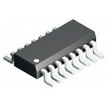
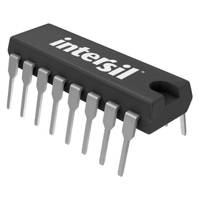
| 描述 | IC MUX/DEMUX QUAD 2X1 16SOIC多路器开关 IC 3-18V Quad 2 CHNL Mux/Demux -55 to 125 |
| 产品分类 | |
| 品牌 | ON Semiconductor |
| 产品手册 | |
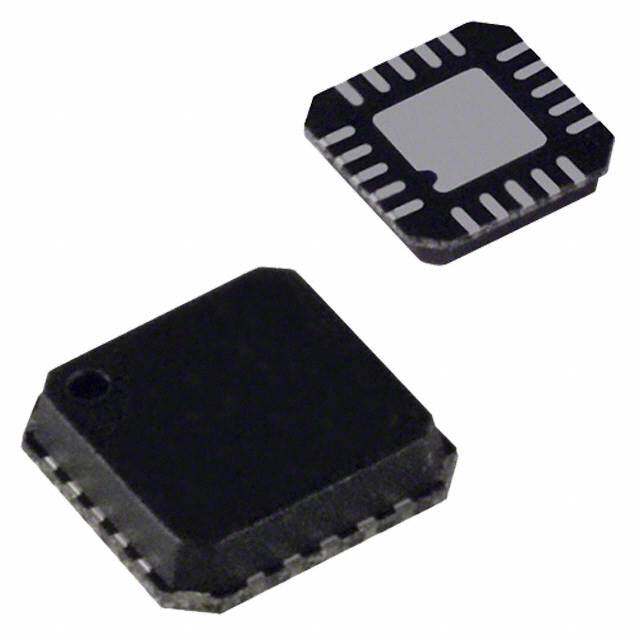
| 产品图片 |
|
| rohs | 符合RoHS无铅 / 符合限制有害物质指令(RoHS)规范要求 |
| 产品系列 | 开关 IC,多路器开关 IC,ON Semiconductor MC14551BDR2G4000B |
| 数据手册 | |
| 产品型号 | MC14551BDR2G |
| 产品种类 | 多路器开关 IC |
| 传播延迟时间 | 90 ns |
| 供应商器件封装 | 16-SOIC |
| 其它名称 | MC14551BDR2GOSDKR |
| 功能 | 多路复用器/多路分解器 |
| 包装 | Digi-Reel® |
| 商标 | ON Semiconductor |
| 安装类型 | 表面贴装 |
| 安装风格 | SMD/SMT |
| 导通电阻 | 280 欧姆 |
| 导通电阻—最大值 | 1050 Ohms |
| 封装 | Reel |
| 封装/外壳 | 16-SOIC(0.154",3.90mm 宽) |
| 封装/箱体 | SOIC-16 |
| 工作温度 | -55°C ~ 125°C |
| 工作电源电压 | 3 V to 18 V |
| 工厂包装数量 | 2500 |
| 带宽 | 17 MHz |
| 开关数量 | 4 |
| 最大功率耗散 | 500 mW |
| 最大工作温度 | + 125 C |
| 最小工作温度 | - 55 C |
| 标准包装 | 1 |
| 电压-电源,单/双 (±) | ±3 V ~ 18 V |
| 电压源 | 双电源 |
| 电流-电源 | 360nA |
| 电路 | 4 x 2:1 |
| 系列 | MC14551B |
| 通道数量 | 4 Channel |


- 商务部:美国ITC正式对集成电路等产品启动337调查
- 曝三星4nm工艺存在良率问题 高通将骁龙8 Gen1或转产台积电
- 太阳诱电将投资9.5亿元在常州建新厂生产MLCC 预计2023年完工
- 英特尔发布欧洲新工厂建设计划 深化IDM 2.0 战略
- 台积电先进制程称霸业界 有大客户加持明年业绩稳了
- 达到5530亿美元!SIA预计今年全球半导体销售额将创下新高
- 英特尔拟将自动驾驶子公司Mobileye上市 估值或超500亿美元
- 三星加码芯片和SET,合并消费电子和移动部门,撤换高东真等 CEO
- 三星电子宣布重大人事变动 还合并消费电子和移动部门
- 海关总署:前11个月进口集成电路产品价值2.52万亿元 增长14.8%


PDF Datasheet 数据手册内容提取
MC14551B Quad 2-Channel Analog Multiplexer/Demultiplexer The MC14551B is a digitally−controlled analog switch. This device implements a 4PDT solid state switch with low ON impedance and very low OFF Leakage current. Control of analog signals up to the complete supply voltage range can be achieved. http://onsemi.com Features • Triple Diode Protection on All Control Inputs • Supply Voltage Range = 3.0 Vdc to 18 Vdc 1 • Analog Voltage Range (V − V ) = 3.0 to 18 V SOIC−16 DD EE Note: V must be ≤ V D SUFFIX EE SS • CASE 751B Linearized Transfer Characteristics • Low Noise − 12 nV√Cycle, f ≥ 1.0 kHz typical PIN ASSIGNMENT • For Low R , Use The HC4051, HC4052, or HC4053 High−Speed ON CMOS Devices W1 1 16 VDD • Switch Function is Break Before Make X0 2 15 W0 • NLV Prefix for Automotive and Other Applications Requiring X1 3 14 W Unique Site and Control Change Requirements; AEC−Q100 X 4 13 Z Qualified and PPAP Capable • Y 5 12 Z1 This Device is Pb−Free and is RoHS Compliant ÎÎÎÎÎÎÎÎÎÎÎÎÎÎÎÎÎÎÎ Y0 6 11 Z0 ÎÎMAÎXIMÎUMÎ RATÎINGÎS ÎÎÎÎÎÎÎÎÎÎÎÎ VEE 7 10 Y1 Parameter Symbol Value Unit VSS 8 9 CONTROL DC Supply Voltage Range VDD – 0.5 to + 18.0 V (Referenced to VEE, VSS ≥ VEE) MARKING DIAGRAM Input or Output Voltage (DC or Transient) Vin, Vout – 0.5 to VDD V (Referenced to VSS for Control Input and + 0.5 16 VEE for Switch I/O) Input Current (DC or Transient), Iin ±10 mA 14551BG per Control Pin AWLYWW Switch Through Current Isw ±25 mA 1 Power Dissipation, per Package (Note 1) PD 500 mW A = Assembly Location Ambient Temperature Range TA – 55 to + 125 (cid:2)C WL, L = Wafer Lot YY, Y = Year Storage Temperature Range Tstg – 65 to + 150 (cid:2)C WW, W = Work Week Lead Temperature (8–Second Soldering) TL 260 (cid:2)C G = Pb−Free Package Stresses exceeding those listed in the Maximum Ratings table may damage the device. If any of these limits are exceeded, device functionality should not be ORDERING INFORMATION assumed, damage may occur and reliability may be affected. See detailed ordering and shipping information in the package 1. Temperature Derating: “D/DW” Package: −7.0 mW/(cid:2)C From 65(cid:2)C To 125(cid:2)C dimensions section on page 2 of this data sheet. This device contains protection circuitry to guard against damage due to high static voltages or electric fields. However, precautions must be taken to avoid applications of any voltage higher than maximum rated voltages to this high−impedance circuit. For proper operation, Vin and Vout should be constrained to the range VSS ≤ (Vin or Vout) ≤ VDD for control inputs and VEE ≤ (Vin or Vout) ≤ VDD for Switch I/O. Unused inputs must always be tied to an appropriate logic voltage level (e.g., either VSS, VEE or VDD). Unused outputs must be left open. © Semiconductor Components Industries, LLC, 2014 1 Publication Order Number: July, 2014 − Rev. 9 MC14551B/D
MC14551B 9 CONTROL W 14 15 W0 1 W1 X (cid:2)4 2 X0 COMMONS SWITCHES 3 X1 OUT/IN IN/OUT 6 Y0 Y (cid:2)5 10 Y1 11 Z0 Z 13 12 Z1 VDD = Pin 16 Control ON VSS = Pin 8 0 W0 X0 Y0 Z0 VEE = Pin 7 1 W1 X1 Y1 Z1 NOTE:Control Input referenced to VSS, Analog Inputs and Outputs reference to VEE. VEE must be (cid:2) VSS. ORDERING INFORMATION Device Package Shipping† MC14551BDG SOIC−16 48 Units / Rail (Pb−Free) MC14551BDR2G SOIC−16 2500 / Tape & Reel (Pb−Free) NLV14551BDR2G* SOIC−16 2500 / Tape & Reel (Pb−Free) †For information on tape and reel specifications, including part orientation and tape sizes, please refer to our Tape and Reel Packaging Specifications Brochure, BRD8011/D. *NLV Prefix for Automotive and Other Applications Requiring Unique Site and Control Change Requirements; AEC−Q100 Qualified and PPAP Capable. http://onsemi.com 2
MC14551B ELECTRICAL CHARACTERISTICS – 55(cid:2)C 25(cid:2)C 125(cid:2)C Typ Characteristic VDD Test Conditions Symbol Min Max Min (Note 2) Max Min Max Unit SUPPLY REQUIREMENTS (Voltages Referenced to VEE) Power Supply Voltage − VDD – 3.0 ≥ VSS ≥ VEE VDD 3.0 18 3.0 − 18 3.0 18 V Range Quiescent Current Per 5.0 Control Inputs: Vin = IDD − 5.0 − 0.005 5.0 − 150 (cid:3)A Package 10 VSS or VDD, − 10 − 0.010 10 − 300 15 Switch I/O: VEE (cid:2) VI/O − 20 − 0.015 20 − 600 (cid:2) VDD, and (cid:2)Vswitch (cid:2) 500 mV (Note 3 ) T(PDoetyran Pl aSamucikpcap Pglyleu C)su Qrrueinetscent, 511.050 Tnc(VhAoia tn= n in– n2c eV5lul(cid:2)o dcuCeto) dm/oR.n)polyon ,n( iTesnhte, ID(AV) Typical (((000...203076 (cid:3)(cid:3)(cid:3)AAA///kkkHHHzzz))) fff +++ IIIDDDDDD (cid:3)A CONTROL INPUT (Voltages Referenced to VSS) Low−Level Input Voltage 5.0 Ron = per spec, VIL − 1.5 − 2.25 1.5 − 1.5 V 10 Ioff = per spec − 3.0 − 4.50 3.0 − 3.0 15 − 4.0 − 6.75 4.0 − 4.0 High−Level Input Voltage 5.0 Ron = per spec, VIH 3.5 − 3.5 2.75 − 3.5 − V 10 Ioff = per spec 7.0 − 7.0 5.50 − 7.0 − 15 11 − 11 8.25 − 11 − Input Leakage Current 15 Vin = 0 or VDD Iin − ±0.1 − ±0.00001 ±0.1 − ±1.0 (cid:3)A Input Capacitance − Cin − − − 5.0 7.5 − − pF SWITCHES IN/OUT AND COMMONS OUT/IN — W, X, Y, Z (Voltages Referenced to VEE) Recommended Peak−to− − Channel On or Off VI/O 0 VDD 0 − VDD 0 VDD Vp–p Peak Voltage Into or Out of the Switch Recommended Static or − Channel On (cid:2)Vswitch 0 600 0 − 600 0 300 mV Dynamic Voltage Across the Switch (Note 3) (Figure 3) Output Offset Voltage − Vin = 0 V, No Load VOO − − − 10 − − − (cid:3)V ON Resistance 5.0 (cid:2)Vswitch (cid:2) 500 mV Ron − 800 − 250 1050 − 1200 (cid:4) 10 (Note 3), − 400 − 120 500 − 520 15 Vin = VIL or VIH 220 − 80 280 − 300 (Control), and Vin = 0 to VDD (Switch) (cid:2)ON Resistance Between 5.0 (cid:2)Ron − 70 − 25 70 − 135 (cid:4) Any Two Channels 10 − 50 − 10 50 − 95 in the Same Package 15 − 45 − 10 45 − 65 Off−Channel Leakage 15 Vin = VIL or VIH Ioff − ±100 − ±0.05 ±100 − ±1000 nA Current (Figure 8) (Control) Channel to Channel or Any One Channel Capacitance, Switch I/O − Switch Off CI/O − − − 10 − − − pF Capacitance, Common O/I − CO/I − − − 17 − − − pF Capacitance, Feedthrough − Pins Not Adjacent CI/O − − − 0.15 − − − pF (Channel Off) − Pins Adjacent − − − 0.47 − − − Product parametric performance is indicated in the Electrical Characteristics for the listed test conditions, unless otherwise noted. Product performance may not be indicated by the Electrical Characteristics if operated under different conditions. 2. Data labeled “Typ” is not to be used for design purposes, but is intended as an indication of the IC’s potential performance. 3. For voltage drops across the switch ((cid:2)Vswitch) > 600 mV ( > 300 mV at high temperature), excessive VDD current may be drawn; i.e. the current out of the switch may contain both VDD and switch input components. The reliability of the device will be unaffected unless the Maximum Ratings are exceeded. (See first page of this data sheet.) http://onsemi.com 3
MC14551B ELECTRICAL CHARACTERISTICS (CL = 50 pF, TA = 25(cid:2)C, VEE (cid:2) VSS) VDD – VEE Typ Characteristic Symbol Vdc Min (Note 4 ) Max Unit Propagation Delay Times tPLH, tPHL − ns Switch Input to Switch Output (RL = 10 k(cid:4)) tPLH, tPHL = (0.17 ns/pF) CL + 26.5 ns 5.0 35 90 tPLH, tPHL = (0.08 ns/pF) CL + 11 ns 10 15 40 tPLH, tPHL = (0.06 ns/pF) CL + 9.0 ns 15 12 30 Control Input to Output (RL = 10 k(cid:4)) tPLH, tPHL − ns VEE = VSS (Figure 4) 5.0 350 875 10 140 350 15 100 250 Second Harmonic Distortion − 10 − 0.07 − % RL = 10 k(cid:4), f = 1 kHz, Vin = 5 Vp−p Bandwidth (Figure 5) BW 10 − 17 − MHz RL = 1 k(cid:4), Vin = 1/2 (VDD − VEE) p−p, 20 Log (Vout/Vin) = − 3 dB, CL = 50 pF Off Channel Feedthrough Attenuation, Figure 5 − 10 − – 50 − dB RL = 1 k(cid:4), Vin = 1/2 (VDD − VEE) p−p, fin = 55 MHz Channel Separation (Figure 6) − 10 − – 50 − dB RL = 1 k(cid:4), Vin = 1/2 (VDD − VEE) p−p, fin = 3 MHz Crosstalk, Control Input to Common O/I, Figure 7 − 10 − 75 − mV R1 = 1 k(cid:4), RL = 10 k(cid:4), Control tr = tf = 20 ns Product parametric performance is indicated in the Electrical Characteristics for the listed test conditions, unless otherwise noted. Product performance may not be indicated by the Electrical Characteristics if operated under different conditions. 4. Data labelled “Typ” is not to be used for design purposes but is intended as an indication of the IC’s potential performance. http://onsemi.com 4
MC14551B VDD VDD VDD IN/OUT OUT/IN VEE VDD LEVEL CONVERTED IN/OUT OUT/IN CONTROL CONTROL VEE Figure 1. Switch Circuit Schematic 16 VDD CONTROL(cid:2)9 LEVEL CONTROL CONVERTER 8 VSS 7 VEE W0(cid:2)15 14(cid:2)W W1(cid:2)(cid:2)1 X0(cid:2)(cid:2)2 4(cid:2)(cid:2)X X1(cid:2)(cid:2)3 Y0(cid:2)(cid:2)6 5(cid:2)(cid:2)Y Y1(cid:2)10 Z0(cid:2)11 13(cid:2)Z Z1(cid:2)12 Figure 2. MC14551B Functional Diagram http://onsemi.com 5
MC14551B TEST CIRCUITS ON SWITCH CONTROL PULSE SECTION GENERATOR OF IC CONTROL Vout LOAD V RL CL SOURCE VDD VEE VEE VDD Figure 3. (cid:2)V Across Switch Figure 4. Propagation Delay Times, Control to Output Control input used to turn ON or OFF the switch under test. RL ON CONTROL Vout CONTROL OFF RL CL = 50 pF Vout RL CL = 50 pF Vin VDD - VEE VDD - VEE Vin 2 2 Figure 5. Bandwidth and Off−Channel Figure 6. Channel Separation Feedthrough Attenuation (Adjacent Channels Used for Setup) OFF CHANNEL UNDER TEST VDD VEE CONTROL SECTION OTHER CONTROL Vout OF IC CHANNEL(S) VEE RL CL = 50 pF VDD R1 VEE VDD Figure 7. Crosstalk, Control Input Figure 8. Off Channel Leakage to Common O/I VDD KEITHLEY 160 DIGITAL MULTIMETER 10 k 1 k(cid:4) VDD RANGE X/Y PLOTTER VEE = VSS Figure 9. Channel Resistance (R ) Test Circuit ON http://onsemi.com 6
MC14551B TYPICAL RESISTANCE CHARACTERISTICS 350 350 300 300 S) S) M M H H O 250 O 250 E ( E ( C C N 200 N 200 A A T T S S N” RESI 150 TA = 125°C N” RESI 150 TA = 125°C R, “OON 15000 -2(cid:2)555°°CC R, “OON 15000 -2(cid:2)555°°CC 0 0 -(cid:2)10 -(cid:2)8.0 -(cid:2)6.0 -(cid:2)4.0 -(cid:2)2.0 0 2.0 4.0 6.0 8.0 10 -(cid:2)10 -(cid:2)8.0 -(cid:2)6.0 -(cid:2)4.0 -(cid:2)2.0 0 2.0 4.0 6.0 8.0 10 Vin, INPUT VOLTAGE (VOLTS) Vin, INPUT VOLTAGE (VOLTS) Figure 10. V @ 7.5 V, V @ – 7.5 V Figure 11. V @ 5.0 V, V @ – 5.0 V DD EE DD EE 700 350 TA = 25°C 600 300 S) S) M M OH 500 OH 250 VDD = 2.5 V E ( E ( C C N 400 N 200 A A T T S S ESI 300 ESI 150 ON” R 200 TA = 125°C ON” R 100 5.0 V , “N 25°C , “N 7.5 V O O R 100 -(cid:2)55°C R 50 0 0 -(cid:2)10 -(cid:2)8.0 -(cid:2)6.0 -(cid:2)4.0 -(cid:2)2.0 0 2.0 4.0 6.0 8.0 10 -(cid:2)10 -(cid:2)8.0 -(cid:2)6.0 -(cid:2)4.0 -(cid:2)2.0 0 2.0 4.0 6.0 8.0 10 Vin, INPUT VOLTAGE (VOLTS) Vin, INPUT VOLTAGE (VOLTS) Figure 12. V @ 2.5 V, V @ – 2.5 V Figure 13. Comparison at 25(cid:2)C, V @ – V DD EE DD EE http://onsemi.com 7
MC14551B APPLICATIONS INFORMATION Figure A illustrates use of the on−chip level converter signal which allows a 1/2 V margin at each peak. If voltage detailed in Figure 2. The 0−to−5.0 V Digital Control signal is transients above V and/or below V are anticipated on the DD EE used to directly control a 9 V analog signal. analog channels, external diodes (D ) are recommended as p−p x The digital control logic levels are determined by V and shown in Figure B. These diodes should be small signal types DD V . The V voltage is the logic high voltage; the V able to absorb the maximum anticipated current surges during SS DD SS voltage is logic low. For the example, V = + 5.0 V = logic clipping. DD high at the control inputs; V = GND = 0 V = logic low. The absolute maximum potential difference between V SS DD The maximum analog signal level is determined by V and V is 18 V. Most parameters are specified up to 15 V DD EE and V . The V voltage determines the maximum which is the recommended maximum difference between EE DD recommended peak above V . The V voltage determines V and V . SS EE DD EE the maximum swing below V . For the example, V – V Balanced supplies are not required. However, V must be SS DD SS SS = 5.0 V maximum swing above V ; V – V = 5.0 V greater than or equal to V . For example, V = + 10 V, V SS SS EE EE DD SS maximum swing below V . The example shows a ± 4.5 V = + 5.0 V, and V = – 3.0 V is acceptable. See the table below. SS EE +5 V -5 V VDD VSS VEE +4.5 V +5 V 9 Vp-p SWITCH ANALOG SIGNAL I/O COMMON 9 Vp-p GND O/I ANALOG SIGNAL EXTERNAL MC14551B 0-TO-5 V DIGITAL CMOS CONTROL -4.5 V DIGITAL CONTROL SIGNAL CIRCUITRY Figure A. Application Example VDD VDD Dx Dx SWITCH COMMON I/O O/I Dx Dx VEE VEE Figure B. External Schottky or Germanium Clipping Diodes ÎÎÎÎÎÎÎÎÎÎÎÎÎÎÎÎÎÎÎÎÎÎÎÎÎ POSSIBLE SUPPLY CONNECTIONS ÎÎÎÎÎÎÎÎÎÎÎÎÎÎÎÎÎÎÎÎÎÎÎÎÎÎÎÎÎÎÎÎÎÎÎÎÎÎÎÎÎÎÎÎÎÎÎÎÎÎÎÎÎÎ ÎÎÎÎÎÎÎÎÎÎÎÎÎÎCÎontÎrol InÎputÎs ÎÎÎÎÎÎÎÎÎÎÎ VDD VSS VEE Logic High/Logic Low Maximum Analog Signal Range ÎÎInÎÎ VoÎÎlts ÎÎÎÎIÎÎn VoÎÎlts ÎÎÎÎÎÎIn VoÎÎltsÎÎÎÎÎÎÎÎInÎÎ VolÎÎts ÎÎÎÎÎÎÎÎÎÎÎÎÎÎIn VoÎÎltsÎÎÎÎÎÎÎÎ ÎÎ+ 8ÎÎÎÎ0ÎÎÎΖ Î8 ÎÎÎÎÎ+ 8/0ÎÎÎÎÎÎ+Î 8 toÎ – 8 Î= 16Î Vp–Îp ÎÎ ÎÎÎÎÎÎÎÎÎÎÎÎÎÎÎÎÎÎÎÎÎÎÎÎÎÎÎÎÎÎÎÎÎÎÎÎÎÎÎÎÎÎÎÎÎÎÎÎÎÎÎÎÎÎÎÎÎÎ + 5 0 – 12 + 5/0 + 5 to – 12 = 17 Vp–p ÎÎÎÎÎÎÎÎÎÎÎÎÎÎÎÎÎÎÎÎÎÎÎÎÎÎÎÎÎÎÎÎÎÎÎÎÎÎÎÎÎÎÎÎÎÎÎÎÎÎÎÎÎÎÎÎÎÎ + 5 0 0 + 5/0 + 5 to 0 = 5 Vp–p ÎÎÎÎÎÎÎÎÎÎÎÎÎÎÎÎÎÎÎÎÎÎÎÎÎÎÎÎÎÎÎÎÎÎÎÎÎÎÎÎÎÎÎÎÎÎÎÎÎÎÎÎÎÎÎÎÎÎ + 5 0 – 5 + 5/0 + 5 to – 5 = 10 Vp–p ÎÎÎÎÎÎÎÎÎÎÎÎÎÎÎÎÎÎÎÎÎÎÎÎÎÎÎÎÎÎÎÎÎÎÎÎÎÎÎÎÎÎÎÎÎÎÎÎÎÎÎÎÎÎÎÎÎÎ ÎÎ+ 10ÎÎÎÎÎÎÎΖ Î5 ÎÎÎÎ+ Î10/ +Î 5 ÎÎÎÎÎ+ Î10 toÎ – 5Î = 15Î Vp–Îp ÎÎ http://onsemi.com 8
MC14551B PACKAGE DIMENSIONS SOIC−16 D SUFFIX CASE 751B−05 ISSUE K −A− NOTES: 1. DIMENSIONING AND TOLERANCING PER ANSI Y14.5M, 1982. 2. CONTROLLING DIMENSION: MILLIMETER. 16 9 3. DIMENSIONS A AND B DO NOT INCLUDE MOLD PROTRUSION. 4. MAXIMUM MOLD PROTRUSION 0.15 (0.006) PER SIDE. −B− P8 PL 5. DIMENSION D DOES NOT INCLUDE DAMBAR PROTRUSION. ALLOWABLE DAMBAR PROTRUSION 1 8 0.25 (0.010) M B S SHALL BE 0.127 (0.005) TOTAL IN EXCESS OF THE D DIMENSION AT MAXIMUM MATERIAL CONDITION. MILLIMETERS INCHES DIM MIN MAX MIN MAX G A 9.80 10.00 0.386 0.393 B 3.80 4.00 0.150 0.157 C 1.35 1.75 0.054 0.068 F D 0.35 0.49 0.014 0.019 K R X 45(cid:2) F 0.40 1.25 0.016 0.049 G 1.27 BSC 0.050 BSC J 0.19 0.25 0.008 0.009 C K 0.10 0.25 0.004 0.009 M 0 (cid:2) 7 (cid:2) 0 (cid:2) 7 (cid:2) −T− SEATING P 5.80 6.20 0.229 0.244 PLANE M J R 0.25 0.50 0.010 0.019 D 16 PL 0.25 (0.010) M T B S A S SOLDERING FOOTPRINT 8X 6.40 16X1.12 1 16 16X 0.58 1.27 PITCH 8 9 DIMENSIONS: MILLIMETERS ON Semiconductor and the are registered trademarks of Semiconductor Components Industries, LLC (SCILLC) or its subsidiaries in the United States and/or other countries. SCILLC owns the rights to a number of patents, trademarks, copyrights, trade secrets, and other intellectual property. A listing of SCILLC’s product/patent coverage may be accessed at www.onsemi.com/site/pdf/Patent−Marking.pdf. SCILLC reserves the right to make changes without further notice to any products herein. SCILLC makes no warranty, representation or guarantee regarding the suitability of its products for any particular purpose, nor does SCILLC assume any liability arising out of the application or use of any product or circuit, and specifically disclaims any and all liability, including without limitation special, consequential or incidental damages. “Typical” parameters which may be provided in SCILLC data sheets and/or specifications can and do vary in different applications and actual performance may vary over time. All operating parameters, including “Typicals” must be validated for each customer application by customer’s technical experts. SCILLC does not convey any license under its patent rights nor the rights of others. SCILLC products are not designed, intended, or authorized for use as components in systems intended for surgical implant into the body, or other applications intended to support or sustain life, or for any other application in which the failure of the SCILLC product could create a situation where personal injury or death may occur. Should Buyer purchase or use SCILLC products for any such unintended or unauthorized application, Buyer shall indemnify and hold SCILLC and its officers, employees, subsidiaries, affiliates, and distributors harmless against all claims, costs, damages, and expenses, and reasonable attorney fees arising out of, directly or indirectly, any claim of personal injury or death associated with such unintended or unauthorized use, even if such claim alleges that SCILLC was negligent regarding the design or manufacture of the part. SCILLC is an Equal Opportunity/Affirmative Action Employer. This literature is subject to all applicable copyright laws and is not for resale in any manner. PUBLICATION ORDERING INFORMATION LITERATURE FULFILLMENT: N. American Technical Support: 800−282−9855 Toll Free ON Semiconductor Website: www.onsemi.com Literature Distribution Center for ON Semiconductor USA/Canada P.O. Box 5163, Denver, Colorado 80217 USA Europe, Middle East and Africa Technical Support: Order Literature: http://www.onsemi.com/orderlit Phone: 303−675−2175 or 800−344−3860 Toll Free USA/Canada Phone: 421 33 790 2910 Fax: 303−675−2176 or 800−344−3867 Toll Free USA/Canada Japan Customer Focus Center For additional information, please contact your local Email: orderlit@onsemi.com Phone: 81−3−5817−1050 Sales Representative http://onsemi.com MC14551B/D 9
Mouser Electronics Authorized Distributor Click to View Pricing, Inventory, Delivery & Lifecycle Information: O N Semiconductor: MC14551BDG MC14551BDR2G