ICGOO在线商城 > 集成电路(IC) > 时钟/计时 - 时钟缓冲器,驱动器 > MC100LVEP11DTG
 Datasheet下载
- 型号: MC100LVEP11DTG
- 制造商: ON Semiconductor
- 库位|库存: xxxx|xxxx
- 要求:
| 数量阶梯 | 香港交货 | 国内含税 |
| +xxxx | $xxxx | ¥xxxx |
查看当月历史价格
查看今年历史价格
MC100LVEP11DTG产品简介:
ICGOO电子元器件商城为您提供MC100LVEP11DTG由ON Semiconductor设计生产,在icgoo商城现货销售,并且可以通过原厂、代理商等渠道进行代购。 MC100LVEP11DTG价格参考¥50.87-¥103.32。ON SemiconductorMC100LVEP11DTG封装/规格:时钟/计时 - 时钟缓冲器,驱动器, Clock Fanout Buffer (Distribution) IC 1:2 3GHz 8-TSSOP, 8-MSOP (0.118", 3.00mm Width)。您可以下载MC100LVEP11DTG参考资料、Datasheet数据手册功能说明书,资料中有MC100LVEP11DTG 详细功能的应用电路图电压和使用方法及教程。
MC100LVEP11DTG 是由 ON Semiconductor 提供的一款时钟缓冲器/驱动器,属于时钟与计时系列器件。以下是其主要应用场景:

 1. 通信设备
   - 用于网络交换机、路由器和通信模块中,提供稳定的时钟信号分配。
   - 支持多路输出,能够驱动多个负载,满足通信系统对时钟同步的需求。

 2. 计算机与外设
   - 在计算机主板、显卡和其他外设中,作为时钟信号分配的核心组件。
   - 确保多个芯片或模块之间的时钟信号一致性,减少抖动和延迟。

 3. 工业自动化
   - 应用于工业控制板卡,为微控制器、FPGA 和 DSP 提供精确的时钟信号。
   - 在需要高可靠性和低功耗的环境中表现优异,例如工厂自动化和机器人控制系统。

 4. 消费电子
   - 用于音频/视频设备(如电视、音响)中,确保音视频数据传输的同步性。
   - 在家用路由器、智能家居设备中提供稳定的时钟源。

 5. 测试与测量设备
   - 为示波器、频谱分析仪等精密仪器提供高质量的时钟信号。
   - 减少信号失真,提高测量精度。

 6. 汽车电子
   - 在车载信息娱乐系统、导航系统和高级驾驶辅助系统(ADAS)中,提供可靠的时钟分配。
   - 满足汽车电子对高温、振动和电磁干扰环境的严格要求。

 核心优势
- 低抖动:适合对时钟信号质量要求较高的应用。
- 多路输出:支持多达 8 路输出,灵活分配时钟信号。
- 宽工作电压范围:适应多种电源环境。
- 小型封装:节省 PCB 空间,便于设计。

综上,MC100LVEP11DTG 广泛应用于需要稳定、低抖动时钟信号分配的场景,是高性能电子系统中的关键组件。
| 参数 | 数值 |
| 产品目录 | 集成电路 (IC)半导体 |
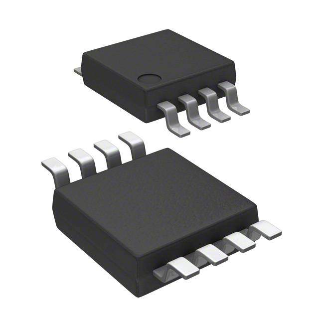
| 描述 | IC CLK BUFFER 1:2 3GHZ 8TSSOP时钟缓冲器 2.5V/3.3V ECL 1:2 Diff Fanout Buffer |
| 产品分类 | |
| 品牌 | ON Semiconductor |
| 产品手册 | |
| 产品图片 |
|
| rohs | 符合RoHS无铅 / 符合限制有害物质指令(RoHS)规范要求 |
| 产品系列 | 时钟和计时器IC,时钟缓冲器,ON Semiconductor MC100LVEP11DTG100LVEP |
| 数据手册 | |
| 产品型号 | MC100LVEP11DTG |
| 产品目录页面 | |
| 产品种类 | Amplifiers- Audio |
| 传播延迟—最大值 | 0.31 ns |
| 供应商器件封装 | 8-TSSOP |
| 其它名称 | MC100LVEP11DTGOS |
| 包装 | 管件 |
| 商标 | ON Semiconductor |
| 安装类型 | 表面贴装 |
| 安装风格 | SMD/SMT |
| 封装 | Tube |
| 封装/外壳 | 8-TSSOP,8-MSOP(0.118",3.00mm 宽) |
| 封装/箱体 | TSSOP-8 |
| 工作温度 | -40°C ~ 85°C |
| 工厂包装数量 | 100 |
| 差分-输入:输出 | 是/是 |
| 最大工作温度 | + 85 C |
| 最大输入频率 | 3000 MHz |
| 最小工作温度 | - 40 C |
| 标准包装 | 100 |
| 比率-输入:输出 | 1:2 |
| 电压-电源 | 2.375 V ~ 3.8 V |
| 电源电压-最大 | +/- 3.8 V |
| 电源电压-最小 | +/- 2.375 V |
| 电路数 | 1 |
| 类型 | 扇出缓冲器(分配) |
| 系列 | MC100LVEP11 |
| 输入 | CML,LVDS,PECL |
| 输出 | ECL,PECL |
| 输出端数量 | 4 |
| 零件号别名 | MC100LVEP11DG |
| 频率-最大值 | 3GHz |


PDF Datasheet 数据手册内容提取
MC10LVEP11, MC100LVEP11 2.5(cid:2)V / 3.3(cid:2)V ECL 1:2 Differential Fanout Buffer Description The MC10/100LVEP11 is a differential 1:2 fanout buffer. The device is pin and functionally equivalent to the EP11 device. With AC www.onsemi.com performance the same as the EP11 device, the LVEP11 is ideal for applications requiring lower voltage. Single-ended CLK input operation is limited to a V (cid:2) 3.0 V in PECL mode, or V (cid:3) CC EE 8 8 −3.0 V in NECL mode. 1 1 The 100 Series contains temperature compensation. SOIC−8NB TSSOP−8 DFN−8 Features D SUFFIX DT SUFFIX MN SUFFIX • 240 ps Typical Propagation Delay CASE CASE CASE 506AA • 751−07 948R−02 Maximum Frequency > 3.0 GHz Typical • PECL Mode Operating Range: ♦ VCC = 2.375V to 3.8V with VEE = 0V MARKING DIAGRAMS* • NECL Mode Operating Range: ♦ VCC = 0V with VEE = −2.375V to −3.8V 8 8 • (cid:2) • OQ pOenu tIpnuptu Wt Dille fDaeuflat uSltta LteOW with Inputs Open or at VEE HAVLY(cid:2)PW11 AHLYU(cid:2)W11(cid:2) 5X M(cid:2) • 1 4 LVDS Input Compatible 1 1 • These Devices are Pb-Free, Halogen Free and are RoHS Compliant 8 8 (cid:2) KAVLY(cid:2)PW11 AKLUY1W1(cid:2) 4K M(cid:2) (cid:2) 1 4 1 1 H = MC10 A = Assembly Location K = MC100 L = Wafer Lot 5X = MC10 Y= Year 4K = MC100 W= Work Week M= Date Code (cid:2) = Pb-Free Package (Note: Microdot may be in either location) *For additional marking information, refer to Application Note AND8002/D. ORDERING INFORMATION See detailed ordering and shipping information on page 9 of this data sheet. © Semiconductor Components Industries, LLC, 2016 1 Publication Order Number: August, 2016 − Rev. 14 MC10LVEP11/D
MC10LVEP11, MC100LVEP11 Table 1. PIN DESCRIPTION Q0 1 8 VCC PIN FUNCTION D*, D** ECL Data Inputs Q0, Q0, Q1, Q1 ECL Data Outputs Q0 2 7 D VCC Positive Supply VEE Negative Supply EP (DFN−8 only) Thermal exposed pad must be connected to a sufficient ther- mal conduit. Electrically connect to the Q1 3 6 D most negative supply (GND) or leave unconnected, floating open. *Pins will default to 2/3 VCC when left open. **Pins will default LOW when left open. Q1 4 5 VEE Figure 1. 8-Lead Pinout (Top View) and Logic Diagram Table 2. ATTRIBUTES Characteristics Value Internal Input Pulldown Resistor 75 k(cid:2) Internal Input Pullup Resistor 37.5 k(cid:2) ESD Protection Human Body Model > 4kV Machine Model > 200V Charged Device Model > 2kV Moisture Sensitivity, Indefinite Time Out of Drypack (Note 1) Pb-Free Pkg SOIC−8NB Level 1 TSSOP−8 Level 3 DFN−8 Level 1 Flammability Rating UL 94V−0 @ 0.125 in Oxygen Index: 28 to 34 Transistor Count 110 Devices Meets or exceeds JEDEC Spec EIA/JESD78 IC Latchup Test 1. For additional information, see Application Note AND8003/D. www.onsemi.com 2
MC10LVEP11, MC100LVEP11 Table 3. MAXIMUM RATINGS Symbol Parameter Condition 1 Condition 2 Rating Unit VCC PECL Mode Power Supply VEE = 0V 6 V VEE NECL Mode Power Supply VCC = 0V −6 V VI PECL Mode Input Voltage VEE = 0V VI (cid:3) VCC 6 V NECL Mode Input Voltage VCC = 0V VI (cid:2) VEE −6 Iout Output Current Continuous 50 mA Surge 100 TA Operating Temperature Range −40 to +85 °C Tstg Storage Temperature Range −65 to +150 °C (cid:3)JA Thermal Resistance (Junction-to-Ambient) 0lfpm SOIC−8NB 190 °C/W 500lfpm 130 (cid:3)JC Thermal Resistance (Junction-to-Case) Standard Board SOIC−8NB 41 to 44 °C/W (cid:3)JA Thermal Resistance (Junction-to-Ambient) 0lfpm TSSOP−8 185 °C/W 500lfpm 140 (cid:3)JC Thermal Resistance (Junction-to-Case) Standard Board TSSOP−8 41 to 44 °C/W (cid:3)JA Thermal Resistance (Junction-to-Ambient) 0lfpm DFN−8 129 °C/W 500lfpm 84 Tsol Wave Solder (Pb-Free) <2 to 3 sec @ 260°C 265 °C (cid:3)JC Thermal Resistance (Junction-to-Case) (Note 1) DFN−8 35 to 40 °C/W Stresses exceeding those listed in the Maximum Ratings table may damage the device. If any of these limits are exceeded, device functionality should not be assumed, damage may occur and reliability may be affected. 1. JEDEC standard multilayer board − 2S2P (2 signal, 2 power) www.onsemi.com 3
MC10LVEP11, MC100LVEP11 Table 4. 10LVEP DC CHARACTERISTICS, PECL (VCC = 2.5V, VEE = 0V (Note 1)) −40°C 25°C 85°C Symbol Characteristic Min Typ Max Min Typ Max Min Typ Max Unit IEE Power Supply Current 25 33 40 29 33 40 32 34 42 mA VOH Output HIGH Voltage (Note 2) 1365 1490 1615 1430 1555 1680 1490 1615 1740 mV VOL Output LOW Voltage (Note 2) 565 740 865 630 805 930 690 865 990 mV VIHCMR Input HIGH Voltage Common Mode 1.2 2.5 1.2 2.5 1.2 2.5 V Range (Differential Configuration) (Note 3) IIH Input HIGH Current 150 150 150 (cid:4)A IIL Input LOW Current (cid:4)A D 0.5 0.5 0.5 D −150 −150 −150 NOTE:Device will meet the specifications after thermal equilibrium has been established when mounted in a test socket or printed circuit board with maintained transverse airflow greater than 500lfpm. Electrical parameters are guaranteed only over the declared operating temperature range. Functional operation of the device exceeding these conditions is not implied. Device specification limit values are applied individually under normal operating conditions and not valid simultaneously. 1. Input and output parameters vary 1:1 with VCC. VEE can vary +0.125V to −1.3V. 2. All loading with 50(cid:2) to VCC − 2.0 V. 3. VIHCMR min varies 1:1 with VEE, VIHCMR max varies 1:1 with VCC. The VIHCMR range is referenced to the most positive side of the differential input signal. Single-Ended input CLK pin operation is limited to VCC (cid:2) 3.0 V in PECL mode. Table 5. 10LVEP DC CHARACTERISTICS, PECL (VCC = 3.3V, VEE = 0V (Note 1)) −40°C 25°C 85°C Symbol Characteristic Min Typ Max Min Typ Max Min Typ Max Unit IEE Power Supply Current 25 33 40 29 33 40 32 34 42 mA VOH Output HIGH Voltage (Note 2) 2165 2290 2415 2230 2355 2480 2290 2415 2540 mV VOL Output LOW Voltage (Note 2) 1365 1540 1665 1430 1605 1730 1490 1665 1790 mV VIH Input HIGH Voltage (Single-Ended) (Note 3) 2090 2415 2155 2480 2215 2540 mV VIL Input LOW Voltage (Single-Ended) (Note 3) 1365 1690 1430 1755 1490 1815 mV VIHCMR Input HIGH Voltage Common Mode Range 1.2 3.3 1.2 3.3 1.2 3.3 V (Differential Configuration) (Note 4) IIH Input HIGH Current 150 150 150 (cid:4)A IIL Input LOW Current (cid:4)A D 0.5 0.5 0.5 D −150 −150 −150 NOTE:Device will meet the specifications after thermal equilibrium has been established when mounted in a test socket or printed circuit board with maintained transverse airflow greater than 500lfpm. Electrical parameters are guaranteed only over the declared operating temperature range. Functional operation of the device exceeding these conditions is not implied. Device specification limit values are applied individually under normal operating conditions and not valid simultaneously. 1. Input and output parameters vary 1:1 with VCC. VEE can vary +0.925V to −0.5V. 2. All loading with 50(cid:2) to VCC − 2.0 V. 3. Single-Ended input CLK pin operation is limited to VCC (cid:2) 3.0 V in PECL mode. 4. VIHCMR min varies 1:1 with VEE, VIHCMR max varies 1:1 with VCC. The VIHCMR range is referenced to the most positive side of the differential input signal. www.onsemi.com 4
MC10LVEP11, MC100LVEP11 Table 6. 10LVEP DC CHARACTERISTICS, NECL (VCC = 0V, VEE = −3.8V to −2.375V (Note 1)) −40°C 25°C 85°C Symbol Characteristic Min Typ Max Min Typ Max Min Typ Max Unit IEE Power Supply Current 25 33 40 29 33 40 32 34 42 mA VOH Output HIGH Voltage (Note 2) −1135 −1010 −885 −1070 −945 −820 −1010 −885 −760 mV VOL Output LOW Voltage (Note 2) −1935 −1760 −1635 −1870 −1695 −1570 −1810 −1635 −1510 mV VIH Input HIGH Voltage (Single-Ended) −1210 −885 −1145 −820 −1085 −760 mV (Note 3) VIL Input LOW Voltage (Single-Ended) −1935 −1610 −1870 −1545 −1810 −1485 mV (Note 3) VIHCMR Input HIGH Voltage Common Mode VEE+1.2 0.0 VEE+1.2 0.0 VEE+1.2 0.0 V Range (Differential Configuration) (Note 4) IIH Input HIGH Current 150 150 150 (cid:4)A IIL Input LOW Current (cid:4)A D 0.5 0.5 0.5 D −150 −150 −150 NOTE:Device will meet the specifications after thermal equilibrium has been established when mounted in a test socket or printed circuit board with maintained transverse airflow greater than 500lfpm. Electrical parameters are guaranteed only over the declared operating temperature range. Functional operation of the device exceeding these conditions is not implied. Device specification limit values are applied individually under normal operating conditions and not valid simultaneously. 1. Input and output parameters vary 1:1 with VCC. 2. All loading with 50(cid:2) to VCC − 2.0 V. 3. Single-Ended input CLK pin operation is limited to VEE (cid:3) −3.0 V in NECL mode. 4. VIHCMR min varies 1:1 with VEE, VIHCMR max varies 1:1 with VCC. The VIHCMR range is referenced to the most positive side of the differential input signal. Table 7. 100LVEP DC CHARACTERISTICS, PECL (VCC = 2.5V, VEE = 0V (Note 1)) −40°C 25°C 85°C Symbol Characteristic Min Typ Max Min Typ Max Min Typ Max Unit IEE Power Supply Current 25 35 42 29 38 46 32 41 50 mA VOH Output HIGH Voltage (Note 2) 1355 1480 1605 1355 1480 1605 1355 1480 1605 mV VOL Output LOW Voltage (Note 2) 555 730 900 555 730 900 555 730 900 mV VIH Input HIGH Voltage (Single-Ended) 1335 1620 1335 1620 1335 1620 mV VIL Input LOW Voltage (Single-Ended) 555 900 555 900 555 900 mV VIHCMR Input HIGH Voltage Common Mode 1.2 2.5 1.2 2.5 1.2 2.5 V Range (Differential Configuration) (Note 3) IIH Input HIGH Current 150 150 150 (cid:4)A IIL Input LOW Current (cid:4)A D 0.5 0.5 0.5 D −150 −150 −150 NOTE:Device will meet the specifications after thermal equilibrium has been established when mounted in a test socket or printed circuit board with maintained transverse airflow greater than 500lfpm. Electrical parameters are guaranteed only over the declared operating temperature range. Functional operation of the device exceeding these conditions is not implied. Device specification limit values are applied individually under normal operating conditions and not valid simultaneously. 1. Input and output parameters vary 1:1 with VCC. VEE can vary +0.125V to −1.3V. 2. All loading with 50(cid:2) to VCC − 2.0 V. 3. VIHCMR min varies 1:1 with VEE, VIHCMR max varies 1:1 with VCC. The VIHCMR range is referenced to the most positive side of the differential input signal. Single-Ended input CLK pin operation is limited to VCC (cid:2) 3.0 V in PECL mode. www.onsemi.com 5
MC10LVEP11, MC100LVEP11 Table 8. 100LVEP DC CHARACTERISTICS, PECL (VCC = 3.3V, VEE = 0V (Note 1)) −40°C 25°C 85°C Symbol Characteristic Min Typ Max Min Typ Max Min Typ Max Unit IEE Power Supply Current 25 35 42 29 38 46 32 41 50 mA VOH Output HIGH Voltage (Note 2) 2155 2280 2405 2155 2280 2405 2155 2280 2405 mV VOL Output LOW Voltage (Note 2) 1355 1530 1700 1355 1530 1700 1355 1530 1700 mV VIH Input HIGH Voltage (Single-Ended) (Note 3) 2135 2420 2135 2420 2135 2420 mV VIL Input LOW Voltage (Single-Ended) (Note 3) 1355 1700 1355 1700 1355 1700 mV VIHCMR Input HIGH Voltage Common Mode Range 1.2 3.3 1.2 3.3 1.2 3.3 V (Differential Configuration) (Note 4) IIH Input HIGH Current 150 150 150 (cid:4)A IIL Input LOW Current (cid:4)A D 0.5 0.5 0.5 D −150 −150 −150 NOTE:Device will meet the specifications after thermal equilibrium has been established when mounted in a test socket or printed circuit board with maintained transverse airflow greater than 500lfpm. Electrical parameters are guaranteed only over the declared operating temperature range. Functional operation of the device exceeding these conditions is not implied. Device specification limit values are applied individually under normal operating conditions and not valid simultaneously. 1. Input and output parameters vary 1:1 with VCC. VEE can vary +0.925V to −0.5V. 2. All loading with 50(cid:2) to VCC − 2.0 V. 3. Single-Ended input CLK pin operation is limited to VCC (cid:2) 3.0 V in PECL mode. 4. VIHCMR min varies 1:1 with VEE, VIHCMR max varies 1:1 with VCC. The VIHCMR range is referenced to the most positive side of the differential input signal. Table 9. 100LVEP DC CHARACTERISTICS, NECL (VCC = 0V; VEE = −3.8V to −2.375V (Note 1)) −40°C 25°C 85°C Symbol Characteristic Min Typ Max Min Typ Max Min Typ Max Unit IEE Power Supply Current 25 35 42 29 38 46 32 41 50 mA VOH Output HIGH Voltage (Note 2) −1145 −1020 −895 −1145 −1020 −895 −1145 −1020 −895 mV VOL Output LOW Voltage (Note 2) −1945 −1770 −1600 −1945 −1770 −1600 −1945 −1770 −1600 mV VIH Input HIGH Voltage (Single-Ended) −1165 −880 −1165 −880 −1165 −880 mV (Note 3) VIL Input LOW Voltage (Single-Ended) −1945 −1425 −1600 −1945 −1425 −1600 −1945 −1425 −1600 mV (Note 3) VIHCMR Input HIGH Voltage Common Mode VEE+1.2 0.0 VEE+1.2 0.0 VEE+1.2 0.0 V Range (Differential Configuration) (Note 4) IIH Input HIGH Current 150 150 150 (cid:4)A IIL Input LOW Current 0.5 0.5 0.5 (cid:4)A D −150 −150 −150 D NOTE:Device will meet the specifications after thermal equilibrium has been established when mounted in a test socket or printed circuit board with maintained transverse airflow greater than 500lfpm. Electrical parameters are guaranteed only over the declared operating temperature range. Functional operation of the device exceeding these conditions is not implied. Device specification limit values are applied individually under normal operating conditions and not valid simultaneously. 1. Input and output parameters vary 1:1 with VCC. 2. All loading with 50(cid:2) to VCC − 2.0 V. 3. Single-Ended input CLK pin operation is limited to VEE ≤ −3.0 V in NECL mode. 4. VIHCMR min varies 1:1 with VEE, VIHCMR max varies 1:1 with VCC. The VIHCMR range is referenced to the most positive side of the differential input signal. www.onsemi.com 6
MC10LVEP11, MC100LVEP11 Table 10. AC CHARACTERISTICS (VCC = 0V; VEE = −3.8V to −2.375V or VCC = 2.375V to 3.8V; VEE = 0V (Note 1)) −40°C 25°C 85°C Symbol Characteristic Min Typ Max Min Typ Max Min Typ Max Unit fmax Maximum Frequency (Figure 2) 3 3 3 GHz tPLH, Propagation Delay 170 230 300 180 240 310 210 270 360 ps tPHL (Differential Configuration) CLK to Q, Q tSKEW Within Device Skew Q, Q 5.0 20 5.0 20 5.0 20 ps Device to Device Skew (Note 2) 130 130 150 tJITTER CLOCK Random Jitter (RMS) ps @ (cid:3)1.0GHz 0.126 0.3 0.142 0.4 0.209 0.3 @ (cid:3)1.5GHz 0.112 0.2 0.162 0.3 0.162 0.2 @ (cid:3)2.0GHz 0.111 0.3 0.122 0.2 0.170 0.3 @ (cid:3)2.5GHz 0.112 0.2 0.172 0.3 0.235 0.3 @ (cid:3)3.0GHz 0.155 0.2 0.217 0.3 0.368 0.6 VPP Input Voltage Swing 150 800 1200 150 800 1200 150 800 1200 mV (Differential Configuration) tr Output Rise/Fall Times Q, Q 70 110 170 80 120 180 100 140 200 ps tf (20% − 80%) NOTE:Device will meet the specifications after thermal equilibrium has been established when mounted in a test socket or printed circuit board with maintained transverse airflow greater than 500lfpm. Electrical parameters are guaranteed only over the declared operating temperature range. Functional operation of the device exceeding these conditions is not implied. Device specification limit values are applied individually under normal operating conditions and not valid simultaneously. 1. Measured using a 750mV source, 50% duty cycle clock source. All loading with 50(cid:2) to VCC − 2.0 V. 2. Skew is measured between outputs under identical transitions. 1000 3.3 V 900 2.5 V 800 V) m ( p 700 p UT 600 O V 500 400 300 200 100 0 0 1000 2000 3000 4000 FREQUENCY (MHz) Figure 2. F Typical max www.onsemi.com 7
MC10LVEP11, MC100LVEP11 Figure 3. Typical Phase Noise Plot at Figure 4. Typical Phase Noise Plot at f = 156.25MHz f = 311.04MHz carrier carrier Figure 5. Typical Phase Noise Plot at Figure 6. Typical Phase Noise Plot at f = 1.5GHz f = 2GHz carrier carrier The above phase noise plots captured using Agilent device (integrated between 12kHz and 20MHz; as shown E5052A show additive phase noise of the MC100LVEP11 in the shaded region of the plot) at each of the frequencies device at frequencies 156.25MHz, 311.04MHz, 1.5GHz is 66fs, 37fs, 14fs and 13fs respectively. The input source and 2GHz respectively at an operating voltage of 3.3V in used for the phase noise measurements is Agilent E8663B. room temperature. The RMS Phase Jitter contributed by the www.onsemi.com 8
MC10LVEP11, MC100LVEP11 Q Zo = 50 (cid:2) D Driver Receiver Device Device Q Zo = 50 (cid:2) D 50 (cid:2) 50 (cid:2) VTT VTT = VCC − 2.0 V Figure 7. Typical Termination for Output Driver and Device Evaluation (See Application Note AND8020/D − Termination of ECL Logic Devices.) ORDERING INFORMATION Device Package Shipping† MC10LVEP11DG SOIC−8NB 98 Units / Rail (Pb-Free) MC10LVEP11DR2G SOIC−8NB 2500 / Tape & Reel (Pb-Free) MC10LVEP11DTG TSSOP−8 100 Units / Rail (Pb-Free) MC10LVEP11DTR2G TSSOP−8 2500 / Tape & Reel (Pb-Free) MC100LVEP11DG SOIC−8 98 Units / Rail (Pb-Free) MC100LVEP11DR2G SOIC−8 2500 / Tape & Reel (Pb-Free) MC100LVEP11DTG TSSOP−8 100 Units / Rail (Pb-Free) MC100LVEP11DTR2G TSSOP−8 2500 / Tape & Reel (Pb-Free) MC100LVEP11MNR4G DFN−8 1000 / Tape & Reel (Pb-Free) †For information on tape and reel specifications, including part orientation and tape sizes, please refer to our Tape and Reel Packaging Specifications Brochure, BRD8011/D. www.onsemi.com 9
MC10LVEP11, MC100LVEP11 Resource Reference of Application Notes AN1405/D − ECL Clock Distribution Techniques AN1406/D − Designing with PECL (ECL at +5.0 V) AN1503/D − ECLinPS(cid:3) I/O SPiCE Modeling Kit AN1504/D − Metastability and the ECLinPS Family AN1568/D − Interfacing Between LVDS and ECL AN1672/D − The ECL Translator Guide AND8001/D − Odd Number Counters Design AND8002/D − Marking and Date Codes AND8020/D − Termination of ECL Logic Devices AND8066/D − Interfacing with ECLinPS AND8090/D − AC Characteristics of ECL Devices www.onsemi.com 10
MC10LVEP11, MC100LVEP11 PACKAGE DIMENSIONS SOIC−8NB CASE 751−07 ISSUE AK NOTES: −X− 1. DIMENSIONING AND TOLERANCING PER ANSI Y14.5M, 1982. A 2. CONTROLLING DIMENSION: MILLIMETER. 3. DIMENSION A AND B DO NOT INCLUDE MOLD PROTRUSION. 4. MAXIMUM MOLD PROTRUSION 0.15 (0.006) 8 5 PER SIDE. 5. DIMENSION D DOES NOT INCLUDE DAMBAR B S 0.25 (0.010) M Y M PROTRUSION. ALLOWABLE DAMBAR PROTRUSION SHALL BE 0.127 (0.005) TOTAL 1 IN EXCESS OF THE D DIMENSION AT −Y− 4 K 6. 7M5A1X−I0M1U TMH RMUA T7E51R−IA0L6 CAROEN DOIBTSIOONL.ETE. NEW STANDARD IS 751−07. G MILLIMETERS INCHES DIM MIN MAX MIN MAX A 4.80 5.00 0.189 0.197 C NX 45(cid:4) B 3.80 4.00 0.150 0.157 SEATING C 1.35 1.75 0.053 0.069 PLANE D 0.33 0.51 0.013 0.020 −Z− G 1.27 BSC 0.050 BSC H 0.10 0.25 0.004 0.010 0.10 (0.004) J 0.19 0.25 0.007 0.010 H D M J K 0.40 1.27 0.016 0.050 M 0 (cid:4) 8 (cid:4) 0 (cid:4) 8 (cid:4) N 0.25 0.50 0.010 0.020 0.25 (0.010)M Z Y S X S S 5.80 6.20 0.228 0.244 SOLDERING FOOTPRINT* 1.52 0.060 7.0 4.0 0.275 0.155 0.6 1.270 0.024 0.050 (cid:4) (cid:5) mm SCALE 6:1 inches *For additional information on our Pb-Free strategy and soldering details, please download the ON Semiconductor Soldering and Mounting Techniques Reference Manual, SOLDERRM/D. www.onsemi.com 11
MC10LVEP11, MC100LVEP11 PACKAGE DIMENSIONS TSSOP−8 CASE 948R−02 ISSUE A 8x K REF NOTES: 0.10 (0.004) M T U S V S 1. DIMENSIONING AND TOLERANCING PER ANSI 0.15 (0.006) T U S Y14.5M, 1982. 2. CONTROLLING DIMENSION: MILLIMETER. 3. DIMENSION A DOES NOT INCLUDE MOLD FLASH. 2XL/2 8 5 0.25 (0.010) PORRO GTARTUES BIOUNRSR SO RS HGAALTLE N BOUTR ERXSC. E MEODL 0D.1 F5LASH B L −U− 4. (D0I.M00E6N) SPIEORN SBI DDEO.ES NOT INCLUDE INTERLEAD 1 4 M FLASH OR PROTRUSION. INTERLEAD FLASH OR PIN 1 PROTRUSION SHALL NOT EXCEED 0.25 (0.010) IDENT PER SIDE. 0.15 (0.006) T U S A 5. RTEERFEMRINEANLC NEU OMNBLEYR.S ARE SHOWN FOR F −V− 6. DIMENSION A AND B ARE TO BE DETERMINED AT DATUM PLANE -W-. DETAIL E MILLIMETERS INCHES DIM MIN MAX MIN MAX A 2.90 3.10 0.114 0.122 C B 2.90 3.10 0.114 0.122 C 0.80 1.10 0.031 0.043 0.10 (0.004) D 0.05 0.15 0.002 0.006 −W− −T− SPELAATNIENG D G GF 0.04.065 BSC0.70 0.001.0626 B0S.C028 K 0.25 0.40 0.010 0.016 DETAIL E L 4.90 BSC 0.193 BSC M 0 (cid:4) 6 (cid:4) 0 (cid:4) 6 (cid:4) www.onsemi.com 12
MC10LVEP11, MC100LVEP11 PACKAGE DIMENSIONS DFN−8 2x2, 0.5P CASE 506AA ISSUE F D A NOTES: L L 1. DIMENSIONING AND TOLERANCING PER B ASME Y14.5M, 1994 . 2. CONTROLLING DIMENSION: MILLIMETERS. L1 3. DIMENSION b APPLIES TO PLATED TERMINAL AND IS MEASURED BETWEEN 0.15 AND 0.20 MM FROM TERMINAL TIP. REFEPRINE ONCNEE ÇÇ E DOEPTTIAONILA LA 4. CPAODP LAASN WAREILTLY A ASP TPHLEIE TSE TROM TINHAEL ESX.POSED 2X 0.10 C ÇÇ CONSTRUCTIONS MILLIMETERS DIM MIN MAX ÇÇ A 0.80 1.00 A3 A1 0.00 0.05 2X 0.10 C EXPOSED CuÉÉMOLD CMPD ÉÉ A3 0.20 REF TOP VIEW b 0.20 0.30 ÉÇÉÇ ÉÇÉÇ D 2.00 BSC D2 1.10 1.30 0.10 C DETAIL B A A1 E 2.00 BSC E2 0.70 0.90 DETAIL B e 0.50 BSC K 0.30 REF ALTERNATE L 0.25 0.35 0.08 C (A3) CONSTRUCTIONS L1 −−− 0.10 NOTE 4 A1 C SEATING SIDE VIEW PLANE RECOMMENDED SOLDERING FOOTPRINT* DETAIL A D2 8X 8X L 1.30 0.50 1 4 PACKAGE OUTLINE E2 0.90 2.30 K 8 5 8X b e/2 0.10 C A BB 1 e 0.05 C NOTE 3 08.X30 0.50 PITCH BOTTOM VIEW DIMENSIONS: MILLIMETERS *For additional information on our Pb-Free strategy and soldering details, please download the ON Semiconductor Soldering and Mounting Techniques Reference Manual, SOLDERRM/D. ECLinPS is a registered trademark of Semiconductor Components Industries, LLC (SCILLC) or its subsidiaries in the United States and/or other countries. ON Semiconductor and are trademarks of Semiconductor Components Industries, LLC dba ON Semiconductor or its subsidiaries in the United States and/or other countries. ON Semiconductor owns the rights to a number of patents, trademarks, copyrights, trade secrets, and other intellectual property. A listing of ON Semiconductor’s product/patent coverage may be accessed at www.onsemi.com/site/pdf/Patent-Marking.pdf. ON Semiconductor reserves the right to make changes without further notice to any products herein. ON Semiconductor makes no warranty, representation or guarantee regarding the suitability of its products for any particular purpose, nor does ON Semiconductor assume any liability arising out of the application or use of any product or circuit, and specifically disclaims any and all liability, including without limitation special, consequential or incidental damages. Buyer is responsible for its products and applications using ON Semiconductor products, including compliance with all laws, regulations and safety requirements or standards, regardless of any support or applications information provided by ON Semiconductor. “Typical” parameters which may be provided in ON Semiconductor data sheets and/or specifications can and do vary in different applications and actual performance may vary over time. All operating parameters, including “Typicals” must be validated for each customer application by customer’s technical experts. ON Semiconductor does not convey any license under its patent rights nor the rights of others. ON Semiconductor products are not designed, intended, or authorized for use as a critical component in life support systems or any FDA Class 3 medical devices or medical devices with a same or similar classification in a foreign jurisdiction or any devices intended for implantation in the human body. Should Buyer purchase or use ON Semiconductor products for any such unintended or unauthorized application, Buyer shall indemnify and hold ON Semiconductor and its officers, employees, subsidiaries, affiliates, and distributors harmless against all claims, costs, damages, and expenses, and reasonable attorney fees arising out of, directly or indirectly, any claim of personal injury or death associated with such unintended or unauthorized use, even if such claim alleges that ON Semiconductor was negligent regarding the design or manufacture of the part. ON Semiconductor is an Equal Opportunity/Affirmative Action Employer. This literature is subject to all applicable copyright laws and is not for resale in any manner. PUBLICATION ORDERING INFORMATION LITERATURE FULFILLMENT: N. American Technical Support: 800−282−9855 Toll Free ON Semiconductor Website: www.onsemi.com Literature Distribution Center for ON Semiconductor USA/Canada 19521 E. 32nd Pkwy, Aurora, Colorado 80011 USA Europe, Middle East and Africa Technical Support: Order Literature: http://www.onsemi.com/orderlit Phone: 303−675−2175 or 800−344−3860 Toll Free USA/Canada Phone: 421 33 790 2910 Fax: 303−675−2176 or 800−344−3867 Toll Free USA/Canada Japan Customer Focus Center For additional information, please contact your local Email: orderlit@onsemi.com Phone: 81−3−5817−1050 Sales Representative www.onsemi.com MC10LVEP11/D 13
Mouser Electronics Authorized Distributor Click to View Pricing, Inventory, Delivery & Lifecycle Information: O N Semiconductor: MC100LVEP11DG MC100LVEP11DR2G MC100LVEP11DTG MC100LVEP11DTR2G MC100LVEP11MNR4G MC10LVEP11DG MC10LVEP11DR2G MC10LVEP11DTG MC10LVEP11DTR2G