ICGOO在线商城 > 分立半导体产品 > 二极管 - 整流器 - 单 > MBRB1645T4G
 Datasheet下载
- 型号: MBRB1645T4G
- 制造商: ON Semiconductor
- 库位|库存: xxxx|xxxx
- 要求:
| 数量阶梯 | 香港交货 | 国内含税 |
| +xxxx | $xxxx | ¥xxxx |
查看当月历史价格
查看今年历史价格
MBRB1645T4G产品简介:
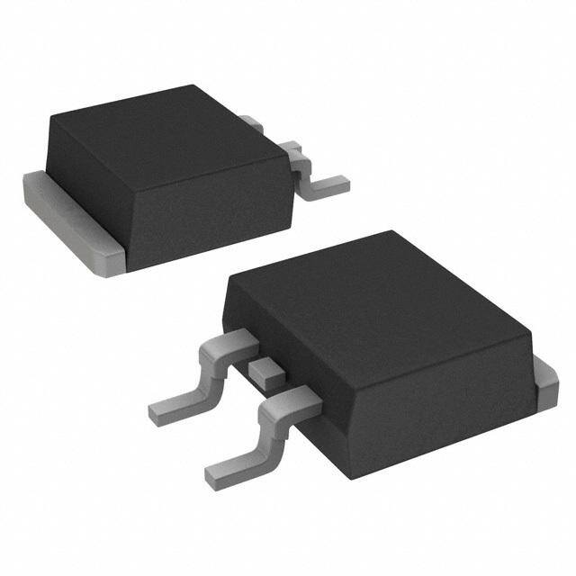
ICGOO电子元器件商城为您提供MBRB1645T4G由ON Semiconductor设计生产,在icgoo商城现货销售,并且可以通过原厂、代理商等渠道进行代购。 MBRB1645T4G价格参考。ON SemiconductorMBRB1645T4G封装/规格:二极管 - 整流器 - 单, Diode Schottky 45V 16A Surface Mount D2PAK。您可以下载MBRB1645T4G参考资料、Datasheet数据手册功能说明书,资料中有MBRB1645T4G 详细功能的应用电路图电压和使用方法及教程。
ON Semiconductor的MBRB1645T4G是一款肖特基势垒二极管,属于二极管-整流器-单类型器件。该型号具有160V反向重复电压和6.0A平均整流电流,采用TO-277封装,具备低正向压降(典型值0.57V)和高效率特性,适用于中等电压、大电流的电源转换场景。

其主要应用场景包括:开关电源(SMPS)、AC-DC和DC-DC电源转换器、消费类电子产品(如电视、机顶盒、显示器电源板)、工业控制设备电源模块以及电信设备中的次级侧整流电路。由于其低损耗和高效率,特别适合用于追求节能与小型化的电源设计。

此外,MBRB1645T4G符合RoHS环保标准,并具有无卤素版本,适用于对环保要求较高的产品。其封装形式便于表面贴装,有利于自动化生产,提升制造效率。在需要高效能、紧凑布局和稳定可靠性的低压大电流整流应用中表现优异。
| 参数 | 数值 |
| 产品目录 | |
| 描述 | DIODE SCHOTTKY 45V 16A D2PAK肖特基二极管与整流器 RECTIFIER 16A 45V |
| 产品分类 | 单二极管/整流器分离式半导体 |
| 品牌 | ON Semiconductor |
| 产品手册 | |
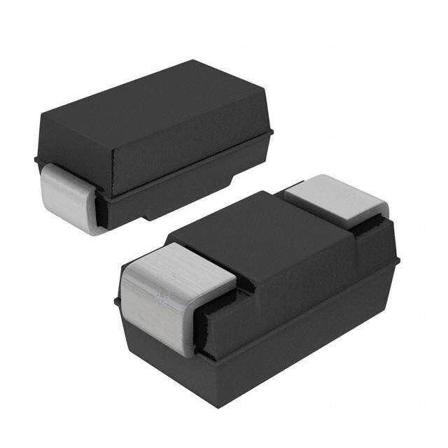
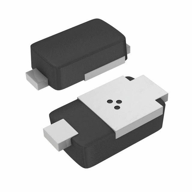
| 产品图片 |
|
| rohs | 符合RoHS无铅 / 符合限制有害物质指令(RoHS)规范要求 |
| 产品系列 | 二极管与整流器,肖特基二极管与整流器,ON Semiconductor MBRB1645T4GSWITCHMODE™ |
| 数据手册 | |
| 产品型号 | MBRB1645T4G |
| 不同If时的电压-正向(Vf) | 630mV @ 16A |
| 不同 Vr、F时的电容 | - |
| 不同 Vr时的电流-反向漏电流 | 200µA @ 45V |
| 二极管类型 | |
| 产品 | Schottky Diodes |
| 产品种类 | 肖特基二极管与整流器 |
| 供应商器件封装 | D2PAK |
| 其它名称 | MBRB1645T4GOSDKR |
| 包装 | Digi-Reel® |
| 反向恢复时间(trr) | - |
| 商标 | ON Semiconductor |
| 安装类型 | 表面贴装 |
| 安装风格 | SMD/SMT |
| 封装 | Reel |
| 封装/外壳 | TO-263-3,D²Pak(2 引线+接片),TO-263AB |
| 封装/箱体 | D2PAK |
| 峰值反向电压 | 45 V |
| 工作温度-结 | -65°C ~ 175°C |
| 工作温度范围 | - 65 C to + 175 C |
| 工厂包装数量 | 800 |
| 技术 | Silicon |
| 最大反向漏泄电流 | 200 uA |
| 最大工作温度 | + 175 C |
| 最大浪涌电流 | 150 A |
| 最小工作温度 | - 65 C |
| 标准包装 | 1 |
| 正向电压下降 | 0.63 V |
| 正向连续电流 | 16 A |
| 热阻 | 1.5°C/W Jc |
| 电压-DC反向(Vr)(最大值) | 45V |
| 电流-平均整流(Io) | 16A |
| 系列 | MBR1645 |
| 速度 | 快速恢复 =< 500 ns,> 200mA(Io) |
| 配置 | Single |


- 商务部:美国ITC正式对集成电路等产品启动337调查
- 曝三星4nm工艺存在良率问题 高通将骁龙8 Gen1或转产台积电
- 太阳诱电将投资9.5亿元在常州建新厂生产MLCC 预计2023年完工
- 英特尔发布欧洲新工厂建设计划 深化IDM 2.0 战略
- 台积电先进制程称霸业界 有大客户加持明年业绩稳了
- 达到5530亿美元!SIA预计今年全球半导体销售额将创下新高
- 英特尔拟将自动驾驶子公司Mobileye上市 估值或超500亿美元
- 三星加码芯片和SET,合并消费电子和移动部门,撤换高东真等 CEO
- 三星电子宣布重大人事变动 还合并消费电子和移动部门
- 海关总署:前11个月进口集成电路产品价值2.52万亿元 增长14.8%


PDF Datasheet 数据手册内容提取
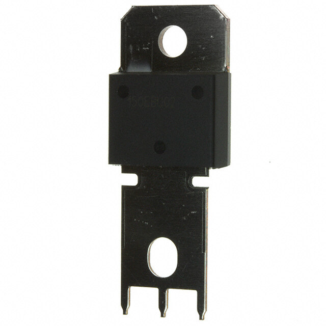
MBR1635, MBR1645, MBRB1645, NRVBB1645 Switch Mode Power Rectifiers 16 A, 35 and 45 V These state−of−the−art devices use the Schottky Barrier principle with a platinum barrier metal. http://onsemi.com Features • MARKING Guard−ring for Stress Protection • Low Forward Voltage 4 DIAGRAMS • 175°C Operating Junction Temperature • TO−220AC NRVB Prefix for Automotive and Other Applications Requiring CASE 221B Unique Site and Control Change Requirements; AEC−Q101 PLASTIC AYWWG Qualified and PPAP Capable B16x5 • KA These Devices are Pb−Free and are RoHS Compliant 1 Mechanical Characteristics: 3 1, 4 • 3 Case: Epoxy, Molded • Weight: 1.9 Grams for TO−220 A = Assembly Location 1.7 Grams for D2PAK Y = Year • WW = Work Week Finish: All External Surfaces Corrosion Resistant and Terminal B16x5 = Device Code Leads are Readily Solderable x = 3 or 4 • Lead Temperature for Soldering Purposes: KA = Diode Polarity 260°C Max. for 10 Seconds G = Pb−Free Package MAXIMUM RATINGS Rating Symbol Value Unit D2PAK B1645G 4 CASE 418B AYWW Peak Repetitive Reverse Voltage VRRM V STYLE 3 Working Peak Reverse Voltage VRWM 1 DC Blocking Voltage MBR1635 VR 35 3 1 MBR1645 45 4 MBRB1645 45 3 Average Rectified Forward Current Delay IF(AV) A B1645 = Device Code (Rated VR, TC = 163°C) Total Device 16 A = Assembly Location Peak Repetitive Forward Current, Per IFRM 32 A Y = Year Leg WW = Work Week (Rated VR, Square Wave, G = Pb−Free Package 20 kHz, TC = 157°C) Total Device ORDERING INFORMATION Non−Repetitive Peak Surge Current IFSM 150 A (Surge Applied at Rated Load Conditions Device Package Shipping Halfwave, Single Phase, 60 Hz) MBR1635G TO−220 50 Units / Rail Peak Repetitive Reverse Surge Current IRRM 1.0 A (Pb−Free) (2.0 (cid:2)s, 1.0 kHz) Storage Temperature Range Tstg −65 to +175 °C MBR1645G TO−220 50 Units / Rail (Pb−Free) Operating Junction Temperature (Note 1) TJ −65 to +175 °C MBRB1645T4G D2PAK 800 Units / Rail Voltage Rate of Change (Rated VR) dv/dt 10,000 V/(cid:2)s (Pb−Free) Stresses exceeding Maximum Ratings may damage the device. Maximum NRVBB1645T4G D2PAK 800 Units / Rail Ratings are stress ratings only. Functional operation above the Recommended (Pb−Free) Operating Conditions is not implied. Extended exposure to stresses above the Recommended Operating Conditions may affect device reliability. 1. The heat generated must be less than the thermal conductivity from Junction−to−Ambient: dPD/dTJ < 1/R(cid:3)JA. © Semiconductor Components Industries, LLC, 2014 1 Publication Order Number: April, 2014 − Rev. 12 MBR1635/D
MBR1635, MBR1645, MBRB1645, NRVBB1645 THERMAL CHARACTERISTICS Characteristic Symbol Value Unit Maximum Thermal Resistance, Junction−to−Case R(cid:3)JC 1.5 °C/W ELECTRICAL CHARACTERISTICS Characteristic Symbol Value Unit Maximum Instantaneous Forward Voltage (Note 2) vF V (iF = 16 Amps, TC = 125°C) 0.57 (iF = 16 Amps, TC = 25°C) 0.63 Maximum Instantaneous Reverse Current (Note 2) iR mA (Rated dc Voltage, TC = 125°C) 40 (Rated dc Voltage, TC = 25°C) 0.2 2. Pulse Test: Pulse Width = 300 (cid:2)s, Duty Cycle ≤2.0%. http://onsemi.com 2
MBR1635, MBR1645, MBRB1645, NRVBB1645 A) T ( 100 N 1.0E−01 RE 70 TJ = 150°C R 50 D CU 30 TJ = 125°C T (A)1.0E−02 125°C AR 20 100°C EN1.0E−03 RW 25°C RR S FO 71.00 E CU1.0E−04 U S O 5.0 R1.0E−05 NTANE 23..00 , REVER1.0E−06 25°C A I T S N 1.0 1.0E−07 , IF 0 0.2 0.4 0.6 0.8 1.0 0 10 20 30 40 50 i vF, INSTANTANEOUS FORWARD VOLTAGE (V) VR, REVERSE VOLTAGE (V) Figure 1. Typical Forward Voltage Figure 2. Typical Reverse Current 28 20 26 dc R(cid:3)JA = 16°C/W RD 2224 RD 1168 dc R(N(cid:3)oJA H =e a6t0 S°Cin/kW) A A W 20 SQUARE W 14 GE FORENT (A)111468 GE FORENT (A) 1102 RARR12 RARR 8 dc I, AVEF(AV)CU10468 I, AVEF(AV)CU 246 SQWUAARVEE 2 0 0 145 150 155 160 165 170 175 0 25 50 75 100 125 150 175 TC, CASE TEMPERATURE (°C) TA, AMBIENT TEMPERATURE (°C) Figure 3. Current Derating, Case, Per Leg Figure 4. Current Derating, Ambient W) PATION ( 1164 (RESISTIVELOAD) IIPAKV(cid:2)(cid:4) SQUARE WAVE SI 12 S I R DI 10 (CAPACITATIVE(cid:2)LOAD) IPK(cid:2)5.0 dc E AV W 8.0 O P 10 E 6.0 G A 20 R 4.0 VE TJ = 125°C A , E) 2.0 V A 0 PF( 0 2.0 4.0 6.0 8.0 10 12 14 16 18 20 IF(AV), AVERAGE FORWARD CURRENT (A) Figure 5. Forward Power Dissipation http://onsemi.com 3
MBR1635, MBR1645, MBRB1645, NRVBB1645 PACKAGE DIMENSIONS D2PAK CASE 418B−04 ISSUE J −B− C NOTES: 1. DIMENSIONING AND TOLERANCING 4 E PER ANSI Y14.5M, 1982. V 2. CONTROLLING DIMENSION: INCH. 3. 418B−01 THRU 418B−03 OBSOLETE, W NEW STANDARD 418B−04. INCHES MILLIMETERS S DIM MIN MAX MIN MAX 1 2 3 A 0.340 0.380 8.64 9.65 A B 0.380 0.405 9.65 10.29 C 0.160 0.190 4.06 4.83 −T− D 0.020 0.035 0.51 0.89 SEATING E 0.045 0.055 1.14 1.40 PLANE G F 0.310 0.350 7.87 8.89 G 0.100 BSC 2.54 BSC K H 0.080 0.110 2.03 2.79 W D3 PL J KJ 00..001980 00..011205 20..2496 20..6749 0.13 (0.005) M T B M L 0.052 0.072 1.32 1.83 H M 0.280 0.320 7.11 8.13 N 0.197 REF 5.00 REF VARIABLE P 0.079 REF 2.00 REF CONFIGURATION R 0.039 REF 0.99 REF ZONE N P S 0.575 0.625 14.60 15.88 R V 0.045 0.055 1.14 1.40 U STYLE 3: L L L PIN 1.ANODE 2.CATHODE 3.ANODE M M M 4.CATHODE F F F VIEW W−W VIEW W−W VIEW W−W 1 2 3 SOLDERING FOOTPRINT* 8.38 0.33 10.66 1.016 5.08 0.42 0.04 0.20 3.05 0.12 17.02 0.67 (cid:3) (cid:4) mm SCALE 3:1 inches *For additional information on our Pb−Free strategy and soldering details, please download the ON Semiconductor Soldering and Mounting Techniques Reference Manual, SOLDERRM/D. http://onsemi.com 4
MBR1635, MBR1645, MBRB1645, NRVBB1645 PACKAGE DIMENSIONS TO−220 CASE 221B−04 ISSUE E NOTES: C 1. DIMENSIONING AND TOLERANCING PER ANSI Y14.5M, 1982. Q B F T S 2. CONTROLLING DIMENSION: INCH. INCHES MILLIMETERS DIM MIN MAX MIN MAX 4 A 0.595 0.620 15.11 15.75 B 0.380 0.405 9.65 10.29 A C 0.160 0.190 4.06 4.82 U D 0.025 0.035 0.64 0.89 1 3 F 0.142 0.161 3.61 4.09 H G 0.190 0.210 4.83 5.33 H 0.110 0.130 2.79 3.30 K J 0.014 0.025 0.36 0.64 K 0.500 0.562 12.70 14.27 L 0.045 0.060 1.14 1.52 Q 0.100 0.120 2.54 3.04 L R 0.080 0.110 2.04 2.79 D R S 0.045 0.055 1.14 1.39 T 0.235 0.255 5.97 6.48 J G U 0.000 0.050 0.000 1.27 ON Semiconductor and are registered trademarks of Semiconductor Components Industries, LLC (SCILLC). SCILLC owns the rights to a number of patents, trademarks, copyrights, trade secrets, and other intellectual property. A listing of SCILLC’s product/patent coverage may be accessed at www.onsemi.com/site/pdf/Patent−Marking.pdf. SCILLC reserves the right to make changes without further notice to any products herein. SCILLC makes no warranty, representation or guarantee regarding the suitability of its products for any particular purpose, nor does SCILLC assume any liability arising out of the application or use of any product or circuit, and specifically disclaims any and all liability, including without limitation special, consequential or incidental damages. “Typical” parameters which may be provided in SCILLC data sheets and/or specifications can and do vary in different applications and actual performance may vary over time. All operating parameters, including “Typicals” must be validated for each customer application by customer’s technical experts. SCILLC does not convey any license under its patent rights nor the rights of others. SCILLC products are not designed, intended, or authorized for use as components in systems intended for surgical implant into the body, or other applications intended to support or sustain life, or for any other application in which the failure of the SCILLC product could create a situation where personal injury or death may occur. Should Buyer purchase or use SCILLC products for any such unintended or unauthorized application, Buyer shall indemnify and hold SCILLC and its officers, employees, subsidiaries, affiliates, and distributors harmless against all claims, costs, damages, and expenses, and reasonable attorney fees arising out of, directly or indirectly, any claim of personal injury or death associated with such unintended or unauthorized use, even if such claim alleges that SCILLC was negligent regarding the design or manufacture of the part. SCILLC is an Equal Opportunity/Affirmative Action Employer. This literature is subject to all applicable copyright laws and is not for resale in any manner. PUBLICATION ORDERING INFORMATION LITERATURE FULFILLMENT: N. American Technical Support: 800−282−9855 Toll Free ON Semiconductor Website: www.onsemi.com Literature Distribution Center for ON Semiconductor USA/Canada P.O. Box 5163, Denver, Colorado 80217 USA Europe, Middle East and Africa Technical Support: Order Literature: http://www.onsemi.com/orderlit Phone: 303−675−2175 or 800−344−3860 Toll Free USA/Canada Phone: 421 33 790 2910 Fax: 303−675−2176 or 800−344−3867 Toll Free USA/Canada Japan Customer Focus Center For additional information, please contact your local Email: orderlit@onsemi.com Phone: 81−3−5817−1050 Sales Representative http://onsemi.com MBR1635/D 5
Mouser Electronics Authorized Distributor Click to View Pricing, Inventory, Delivery & Lifecycle Information: O N Semiconductor: MBRB1645T4G MBR1635G MBR1645G NRVBB1645T4G