
 Datasheet下载
- 型号: MB85RC64PNF-G-JNE1
- 制造商: Fujitsu
- 库位|库存: xxxx|xxxx
- 要求:
| 数量阶梯 | 香港交货 | 国内含税 |
| +xxxx | $xxxx | ¥xxxx |
查看当月历史价格
查看今年历史价格
MB85RC64PNF-G-JNE1产品简介:
ICGOO电子元器件商城为您提供MB85RC64PNF-G-JNE1由Fujitsu设计生产,在icgoo商城现货销售,并且可以通过原厂、代理商等渠道进行代购。 MB85RC64PNF-G-JNE1价格参考¥14.53-¥30.88。FujitsuMB85RC64PNF-G-JNE1封装/规格:存储器, FRAM(铁电体 RAM) 存储器 IC 64Kb (8K x 8) I²C 400kHz 900ns 8-SOP。您可以下载MB85RC64PNF-G-JNE1参考资料、Datasheet数据手册功能说明书,资料中有MB85RC64PNF-G-JNE1 详细功能的应用电路图电压和使用方法及教程。
Fujitsu Electronics America, Inc. 生产的型号为 MB85RC64PNF-G-JNE1 的存储器属于铁电随机存取存储器(FeRAM,Ferroelectric RAM)系列。该型号的应用场景主要包括以下领域:

 1. 工业自动化
   - FeRAM 的高读写耐久性和低功耗特性使其非常适合工业控制设备中的数据记录和参数存储。
   - 应用于 PLC(可编程逻辑控制器)、传感器数据采集系统和实时监控设备。

 2. 医疗设备
   - 在医疗仪器中,如便携式健康监测设备、心率监测仪或血糖仪,MB85RC64PNF 可用于存储关键患者数据和校准信息。
   - 其非易失性确保断电后数据不丢失,可靠性高。

 3. 汽车电子
   - 适用于汽车电子控制单元(ECU)、导航系统和驾驶辅助系统中的日志记录和配置数据存储。
   - 高速写入能力有助于实时记录行车数据,满足安全性和性能要求。

 4. 物联网(IoT)
   - 在 IoT 设备中,如智能家居、环境监测传感器或智能仪表,FeRAM 提供快速数据写入和低功耗优势。
   - 适合频繁更新的小型数据块存储,例如状态日志或传感器采样数据。

 5. 消费类电子产品
   - 用于数码相机、打印机或其他需要临时缓存和永久存储结合的设备。
   - 支持快速启动和关机时的数据保存功能。

 6. 能源管理
   - 在智能电网、能源计量设备中,MB85RC64PNF 可存储用电数据、时间戳和其他重要信息。
   - 其非易失性和高耐久性保证了长期可靠运行。

 特性总结
- 容量:64Kb (8K x 8)
- 接口:I²C 接口,支持高速模式(最高 400kHz)
- 工作电压:1.7V 至 3.6V
- 温度范围:-40°C 至 +85°C(工业级)
- 优点:非易失性、高写入耐久性(超过 10^12 次)、低功耗、快速写入速度。

综上所述,MB85RC64PNF-G-JNE1 适合需要高可靠性、低功耗和快速数据存储的各种应用场景,尤其是在需要频繁写入且不能因断电而丢失数据的场合。
| 参数 | 数值 |
| 产品目录 | 集成电路 (IC) |
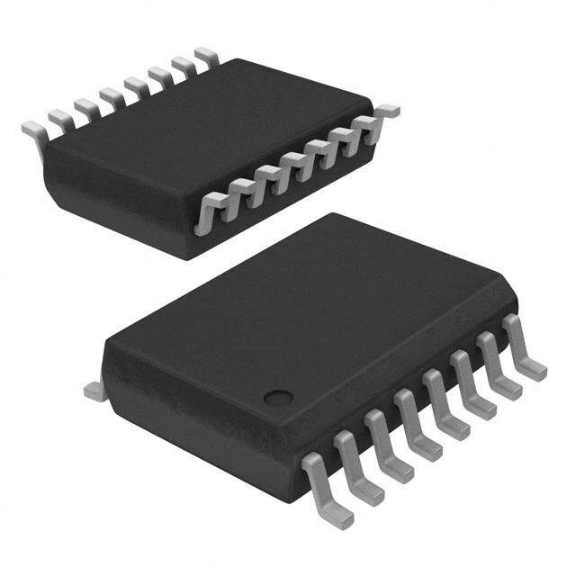
| 描述 | IC FRAM 64KBIT 400KHZ 8SOP |
| 产品分类 | |
| 品牌 | Fujitsu Semiconductor America Inc |
| 数据手册 | |
| 产品图片 |
|
| 产品型号 | MB85RC64PNF-G-JNE1 |
| rohs | 无铅 / 符合限制有害物质指令(RoHS)规范要求 |
| 产品系列 | - |
| 供应商器件封装 | 8-SOP |
| 其它名称 | 865-1175 |
| 包装 | 托盘 |
| 存储器类型 | FRAM(Ferroelectric RAM) |
| 存储容量 | 64K (8K x 8) |
| 封装/外壳 | 8-SOIC(0.154",3.90mm 宽) |
| 工作温度 | -40°C ~ 85°C |
| 接口 | I²C,2 线串口 |
| 标准包装 | 1,500 |
| 格式-存储器 | RAM |
| 特色产品 | http://www.digikey.com/product-highlights/cn/zh/fujitsu-fram/1208 |
| 电压-电源 | 2.7 V ~ 3.6 V |
| 速度 | 400kHz |


_renders/MR4A16BCYS35.jpg)

- 商务部:美国ITC正式对集成电路等产品启动337调查
- 曝三星4nm工艺存在良率问题 高通将骁龙8 Gen1或转产台积电
- 太阳诱电将投资9.5亿元在常州建新厂生产MLCC 预计2023年完工
- 英特尔发布欧洲新工厂建设计划 深化IDM 2.0 战略
- 台积电先进制程称霸业界 有大客户加持明年业绩稳了
- 达到5530亿美元!SIA预计今年全球半导体销售额将创下新高
- 英特尔拟将自动驾驶子公司Mobileye上市 估值或超500亿美元
- 三星加码芯片和SET,合并消费电子和移动部门,撤换高东真等 CEO
- 三星电子宣布重大人事变动 还合并消费电子和移动部门
- 海关总署:前11个月进口集成电路产品价值2.52万亿元 增长14.8%

_renders/IS42S32800D-6BLI.jpg)


PDF Datasheet 数据手册内容提取
FUJITSU SEMICONDUCTOR DS05–13109–3E DATA SHEET Memory FRAM × 64 K (8 K 8) Bit I2C MB85RC64 ■ DESCRIPTION The MB85RC64 is a FRAM (Ferroelectric Random Access Memory) Stand-Alone chip in a configuration of 8,192 words × 8 bits, using the ferroelectric process and silicon gate CMOS process technologies for forming the nonvolatile memory cells. The MB85RC64 adopts the two-wire serial interface. Unlike SRAM, the MB85RC64 is able to retain data without using a data backup battery. The read/write endurance of the nonvolatile memory cells used for the MB85RC64 has improved to be at least 1010 cycles, significantly out performing Flash memory and E2PROM in the number. The MB85RC64 does not need a polling sequence after writing to the memory such as the case of Flash memory nor E2PROM. ■ FEATURES • Bit configuration : 8,192 words × 8 bits (cid:129) Operating power supply voltage: 2.7 V to 3.6 V (cid:129) Operating frequency : 400 kHz (Max) (cid:129) Two-wire serial interface : I2C-bus specification ver. 2.1 compliant, supports Standard-mode/ Fast-mode. Fully controllable by two ports: serial clock (SCL) and serial data (SDA). (cid:129) Operating temperature range : − 40 °C to +85 °C (cid:129) Data retention : 10 years ( + 75 °C) (cid:129) Read/write endurance : 1010 times (cid:129) Package : Plastic / SOP, 8-pin (FPT-8P-M02) (cid:129) Low power consumption : Operating current 0.15 mA (Max: @400 kHz), Standby current 5 μA (Typ) Copyright©2010-2011 FUJITSU SEMICONDUCTOR LIMITED All rights reserved 2011.6
MB85RC64 ■ PIN ASSIGNMENT (TOP VIEW) A0 1 8 VDD A1 2 7 WP A2 3 6 SCL VSS 4 5 SDA (FPT-8P-M02) ■ PIN FUNCTIONAL DESCRIPTIONS Pin Pin Name Functional Description Number Device Address pins The MB85RC64 can be connected to the same data bus up to 8 devices. Device addresses are used in order to identify each of the devices. Connect 1 to 3 A0 to A2 these pins to VDD pin or VSS pin externally. Only if the combination of VDD and VSS pins matches a device, an address and a code inputted from the SDA pin, the device operates. In the open pin state, A0, A1, and A2 pins are pulled-down and recognized as “L”. 4 VSS Ground pin Serial Data I/O pin This is an I/O pin of serial data for performing bidirectional communication of address and writing or reading data of FRAM memory cell array. It is an open 5 SDA drain output that may be wired OR with other open drain or open collector sig- nals on the bus, so a pull-up resistance is required to be connected to the ex- ternal circuit. Serial Clock pin 6 SCL This is a clock input pin for input/output timing serial data. Data is sampled on the rising edge of the clock and output on the falling edge. Write Protect pin When the Write Protect pin is “H”, the writing operation is disabled. When the 7 WP Write Protect pin is “L”, the entire memory region can be overwritten. The read- ing operation is always enabled regardless of the Write Protect pin condition. In the open pin state, the Write Protect pin is pulled-down and recognized as “L”. 8 VDD Supply Voltage pin 2 DS05–13109–3E
MB85RC64 ■ BLOCK DIAGRAM SDA Serial/Parallel Converter r e d o c FRAM Array e er D 8,192 × 8 nt w u o o R SCL C ogic ess L r ol dd ntr A WP o C Column Decoder/Sense Amp/ Write Amp A0, A1, A2 ■ I2C (Inter-Integrated Circuit) The MB85RC64 has the two-wire serial interface; the I2C bus,and operates as a slave device. The I2C bus defines communication roles of “master” and “slave” devices, with the master side holding the authority to initiate control. Furthermore, a I2C bus connection is possible where a single master device is connected to multiple slave devices in a party-line configuration. In this case, it is necessary to assign a unique device address to the slave device. • I2C Interface System Configuration Example VDD Pull-up Resistors SCL SDA ... I2C Bus I2C Bus I2C Bus I2C Bus Master MB85RC64 MB85RC64 MB85RC64 A2 A1 A0 A2 A1 A0 A2 A1 A0 0 0 0 0 0 1 0 1 0 Device address DS05–13109–3E 3
MB85RC64 ■ I2C COMMUNICATION PROTOCOL The I2C bus is a two wire serial interface that uses a bidirectional data bus (SDA) and serial clock (SCL). A data transfer can only be initiated by the bus master, which will also provide the serial clock for synchroni- zation. The SDA signal should change while SCL is Low. However, as an exception, when starting and stopping communication sequence, SDA is allowed to change while SCL is High. (cid:129) Start Condition To start read or write operations by the I2C bus, set the SDA input from High to Low while the SCL input is in High in order to start reading and writing. (cid:129) Stop Condition Set the SDA input from Low to High while the SCL input is in High in order to terminate the I2C bus commu- nication. Because the MB85RC64 does not need the writing wait time unlike E2PROM, it goes to the standby state immediately after the stop condition input. • Start Condition, Stop Condition SCL SDA Start Stop Note : The FRAM device does not need the programming wait time like t after issuing the Stop Condition WC such as. 4 DS05–13109–3E
MB85RC64 ■ ACKNOWLEDGE (ACK) In the I2C bus, serial data including address or memory information is sent in units of 8 bits. The acknowledge signal indicates that every each 8 bits of the data is successfully sent and received. The information receiver side usually outputs “L” every time on the 9th SCL clock after each 8 bits are successfully transmitted. On the transmitter side, the bus is temporarily released to Hi-Z every time on this 9th clock to allow the acknowl- edge signal to be received and checked. During this Hi-Z-released period, the receiver side pulls the SDA line down to indicate “L” that the previous 8bits communication is successfully received. If the information receiver side detects Stop condition before driving the acknowledge “L”, the read operation ends and the I2C bus enters the standby state. If Stop condition is not sent, nor does the transmitter detect the acknowledge “L”, the bus remains in the released state “H” without doing anything. • Acknowledge timing overview diagram SCL 1 2 3 8 9 SDA ACK The transmitter side should always release SDA on the Start 9th bit. At this time, the receiver side outputs a pull-down to indicate a successful byte transfer (ACK response). DS05–13109–3E 5
MB85RC64 ■ DEVICE ADDRESS WORD (Slave address) Following the start condition, the bus master sends the 8bits device address word (Slave address) to start I2C communication. The device address word (8bits) consists of a device Type code (4bits), device address code (3bits), and a read/write code (1bit). (cid:129) Device Type Code (4bits) The upper 4 bits of the device address word are a device type code that identifies the device type, and are fixed at “1010” for the MB85RC64. (cid:129) Device Address Code (3bits) Following the device type code, the 3 bits of the device address code are input in order of A2, A1, and A0. Each MB85RC64 is given a unique 3bits code on the device address pin (external hardware pin A2, A1, and A0). When the device address code is received by the slave device, the slave only responds if the hardware device address of which is equal to its unique 3bits code. (cid:129) Read/Write Code (1bit) The 8th bit of the device address word is the R/W (read/write) code. When the R/W code is “0”, a write operation is enabled, and the R/W code is “1”, a read operation is enabled for the MB85RC64. It turns to a stand-by state if the device code is not “1010” or device address code does not equal to pins A2, A1, and A0. 6 DS05–13109–3E
MB85RC64 ■ DATA STRUCTURE In the I2C bus, the acknowledge “L” is output on the 9th bit after the 8 bits of the device and address word following the start condition. After confirming the acknowledge response at the slave, the I2C master outputs 8bits × 2 memory address to the I2C slave. When the memory address input ends, the slave again outputs the acknowledge “L”. After this operation, the I/O data follows in units of 8 bits, with the acknowledge “L” output after every 8bits. It is determined by the R/W code whether the data line is driven by the master or the slave. For a write operation the slave will accept 8bits from the master then send an acknowledge. If the master detects the acknowledge, the master will transfer the next 8bits. For a read operation the slave will place 8bits on the I2C bus, then wait for an acknowledge from the master. • Data Structure Diagram Start 1 2 3 4 5 6 7 8 9 1 2 . . SCL SDA ACK . . S 1 0 1 0 A2 A1 A0 R/W A Access from master Access from slave S Start Condition A ACK ■ FRAM ACKNOWLEDGE -- POLLING NOT REQUIRED The MB85RC64 performs write operations at the same speed as read operations, so any waiting time for an ACK polling* does not occur. The write cycle takes no additional time. *: As to E2PROM, the Acknowledge Polling is performed as a progress check in the write programming step. It places NAK condition on the bus as of “not acknowledged” during the writing programming period. The busy status for the write programming is given from 9th ACK bit. That “done” condition is placed onto I2C bus by E2PROM I2C device and your program had to poll the bus in order to sense that condition. ■ WRITE PROTECT (WP) The entire memory array can be write protected using the Write Protect pin. When the Write Protect pin is set to “H”, the entire memory map will be write protected. When the Write Protect pin is “L”, all addresses may be overwritten. Reading is allowed regardless of the WP pin's High/Low. Note : The Write Protect pin is pulled down internally to VSS pin, therefore if the Write Protect pin is open, the pin status is detected as Low (write enabled). DS05–13109–3E 7
MB85RC64 ■ COMMAND (cid:129) Byte Write If the 8th bit of the device address word (R/W = 0) is sent following the start condition, the slave responds with an ACK. After this ACK, write addresses and data are sent in the same way, and the write ends by master, generating a stop condition at the end. Address Address Write S 1 0 1 0 A2A1A0 0 A A A A P High 8bits Low 8bits Data 8bits 000XXXXX XXXXXXXX Access from master MSB LSB Access from slave S Start Condition P Stop Condition A ACK Note : In the MB85RC64, input “000” as the upper 3 bits of the MSB. (cid:129) Page Write If additional 8bits are sent after the same command as Byte Write, a page write is performed. If more bytes are sent than will fit up to the end of the address, the address rolls over to 0000 . Therefore, if more than H 8KBytes are sent, the data is overwritten in order starting from the start of the FRAM memory address that was written first. Because FRAM performs write operations at bus speed, the data will be written to FRAM after the ACK response finishes immediately. Address Address Write Write ... S 1 0 1 0 A2A1A0 0 A A A A A P High 8bits Low 8bits Data 8bits Data Access from master Access from slave S Start Condition P Stop Condition A ACK Note : It is not necessary to take a period for internal write operation cycles from the buffer to the memory after the stop condition is generated. 8 DS05–13109–3E
MB85RC64 (cid:129) Current Address Read When the previous write or read operation finishes successfully up to the stop command and if the last accessed address is taken to be “n”, then the address at “n+1” is read by sending the following command unless turning the power off. If the end of the address range is reached internally, the address counter will roll over to 0000 . The current address is undefined immediately after the power is turned on. H Access from master Access from slave S Start Condition (n+1) address Read P Stop Condition S 1 0 1 0 A2A1A0 1 A N P Data 8bits A ACK N NACK (cid:129) Random Read The one byte of data at the address as saved in the buffer can be read out synchronously to SCL by specifying the address in the same way as for a write, and then issuing another start condition and sending the Control Byte (R/W = 1). The final NACK is issued by the receiver that receives the data. In this case, this bit is issued by the master side. n address Address Address Read S 1 0 1 0 A2A1A0 0 A A A S 1 0 1 0 A2A1A0 1 A N P High 8bits Low 8bits Data 8bits Access from master Access from slave S Start Condition P Stop Condition A ACK N NACK DS05–13109–3E 9
MB85RC64 (cid:129) Sequential Read Data can be received continuously following the control byte after specifying the address the same as for Random Read. If the read reaches the end of address for the MB85RC64, the internal read address auto- matically rolls over to 0000 . H ... Read Read ... Read A A A N P Data 8bits Data Data 8bits Access from master Access from slave P Stop Condition A ACK N NACK 10 DS05–13109–3E
MB85RC64 ■ ABSOLUTE MAXIMUM RATINGS Rating Parameter Symbol Unit Min Max Power supply voltage* V − 0.5 +4.0 V CC Input pin voltage* V − 0.5 V + 0.5 ( ≤ 4.0) V IN CC Output pin voltage* V − 0.5 V + 0.5 ( ≤ 4.0) V OUT CC Ambient temperature T − 40 + 85 °C A Storage temperature Tstg − 40 + 125 °C *: These parameters are based on the condition that VSS is 0 V. WARNING: Semiconductor devices can be permanently damaged by application of stress (voltage, current, temperature, etc.) in excess of absolute maximum ratings. Do not exceed these ratings. ■ RECOMMENDED OPERATING CONDITIONS Value Parameter Symbol Unit Min Typ Max Power supply voltage* V 2.7 3.3 3.6 V CC V + 0.5 “H” level input voltage* V V × 0.8 ⎯ CC V IH CC ( ≤ 4.0) “L” level input voltage* V − 0.5 ⎯ + 0.6 V IL Ambient temperature T − 40 ⎯ + 85 °C A *: These parameters are based on the condition that VSS is 0 V. WARNING: The recommended operating conditions are required in order to ensure the normal operation of the semiconductor device. All of the device's electrical characteristics are warranted when the device is operated within these ranges. Always use semiconductor devices within their recommended operating condition ranges. Operation outside these ranges may adversely affect reliability and could result in device failure. No warranty is made with respect to uses, operating conditions, or combinations not represented on the data sheet. Users considering application outside the listed conditions are advised to contact their representatives beforehand. DS05–13109–3E 11
MB85RC64 ■ ELECTRICAL CHARACTERISTICS 1. DC Characteristics (within recommended operating conditions) Value Parameter Symbol Condition Unit Min Typ Max SCL, SDA = 0 V to V Input leakage current |I | CC ⎯ ⎯ 1 μA LI A0, A1, A2, WP = 0 V or V CC Output leakage current |I | V = 0 V to V ⎯ ⎯ 1 μA LO OUT CC Operating power supply current I SCL = 400 kHz ⎯ 100 150 μA CC SCL, SDA = V Standby current I CC ⎯ 5 20 μA SB A0, A1, A2, WP = 0 V or V CC “L” level output voltage V I = 2 mA ⎯ ⎯ 0.4 V OL OL 2. AC Characteristics Value Parameter Symbol Unit Min Max SCL clock frequency FSCL 0 400 kHz Clock high time T 600 ⎯ ns HIGH Clock low time T 1300 ⎯ ns LOW SCL/SDA rise time T ⎯ 300 ns r SCL/SDA fall time T ⎯ 300 ns f Start condition hold T 600 ⎯ ns HD:STA Start condition setup T 600 ⎯ ns SU:STA SDA input hold T 0 ⎯ ns HD:DAT SDA input setup T 100 ⎯ ns SU:DAT SDA output hold T 0 ⎯ ns DH:DAT Stop condition setup T 600 ⎯ ns SU:STO SDA output access after SCL fall T ⎯ 900 ns AA Pre-charge time T 1300 ⎯ ns BUF Pulse width ignored T ⎯ 50 ns (Input Filter on SCL and SDA) SP AC characteristics were measured under the following measurement conditions. Power supply voltage : 2.7 V to 3.6 V Operating temperature : − 40 °C to + 85 °C Input voltage magnitude : 0.3 V to 2.7 V Input rise time : 5 ns Input fall time : 5 ns Input judge level : V /2 CC Output judge level : V /2 CC 12 DS05–13109–3E
MB85RC64 3. AC Timing Definitions TSU:DAT THD:DAT SCL VIH VIH VIH VIH VIH VIL Start VIL VIL VIL VIL Stop VIH VIH VIH VIH SDA VIL VIL VIL VIL TSU:STA THD:STA TSU:STO Tr Tf THIGH TLOW SCL VIH VIH VIH VIH Stop Start VIL VIL VIL VIL VIH VIH VIH VIH SDA VIL VIL VIL VIL Tbuf TaTar TDH:DATTf Tsp VIH SCL VIL VIL VIH VIH SDA Valid VIL VIL VIL 1/FSCL 4. Pin Capacitance Value Parameter Symbol Conditions Unit Min Typ Min I/O capacitance CI/O VIN = VOUT = 0 V, ⎯ ⎯ 15 pF Input capacitance CIN f = 1 MHz, TA = + 25 °C ⎯ ⎯ 15 pF 5. AC Test Load Circuit 3.3 V Output 100 pF DS05–13109–3E 13
MB85RC64 ■ POWER ON SEQUENCE tpd tr tpu VCC VCC 2.7 V 2.7 V VIH (Min) VIH (Min) 1.0 V 1.0 V VIL (Max) VIL (Max) 0 V 0 V SDA, SCL SDA, SCL >VCC × 0.8 * SDA, SCL : Don't care SDA, SCL >VCC × 0.8 * SDA, SCL * : SDA, SCL (Max) < V + 0.5 V CC Value Parameter Symbol Unit Min Max SDA, SCL level hold time during power down tpd 85 ⎯ ns SDA, SCL level hold time during power up tpu 85 ⎯ ns Power supply rise time tr 10 ⎯ μs ■ NOTES ON USE (cid:129) Data written before performing IR reflow is not guaranteed. (cid:129) VDD pin is required to be rising from 0 V because turning the power on from an intermediate level may cause malfunctions, when the power is turned on. During the access period from the start condition to the stop condition, keep the level of WP, A0, A1, and A2 pins to “H” or “L”. 14 DS05–13109–3E
MB85RC64 ■ ORDERING INFORMATION Part number Package Remarks 8-pin, plastic SOP MB85RC64PNF-G-JNE1 (FPT-8P-M02) 8-pin, plastic SOP MB85RC64PNF-G-JNERE1 Embossed Carrier tape (FPT-8P-M02) DS05–13109–3E 15
MB85RC64 ■ PACKAGE DIMENSION 8-pin plastic SOP Lead pitch 1.27 mm Package width × 3.9 mm × 5.05 mm package length Lead shape Gullwing Sealing method Plastic mold Mounting height 1.75 mm MAX Weight 0.06 g (FPT-8P-M02) 8-pin plastic SOP Note 1)*1 : These dimensions include resin protrusion. (FPT-8P-M02) Note 2)*2 : These dimensions do not include resin protrusion. Note 3)Pins width and pins thickness include plating thickness. Note 4)Pins width do not include tie bar cutting remainder. *15.05–+00..2205 .199–+..000180 0.22–+00..0073 .009+–..000031 8 5 *23.90±0.30 6.00±0.40 (.154±.012) (.236±.016) Details of "A" part 45° 1.55±0.20 (Mounting height) (.061±.008) 0.25(.010) 0.40(.016) "A" 0~8° 1 4 1.27(.050) 0.44±0.08 (.017±.003) 0.13(.005)M 0.50±0.20 0.15±0.10 (.020±.008) (.006±.004) 0.60±0.15 (Stand off) (.024±.006) 00..1100((..000044)) Dimensions in mm (inches). C 2002-2010 FUJITSUSEMICONDUCTOR LIMITED F08004S-c-4-9 Note: The values in parentheses are reference values. Please check the latest package dimension at the following URL. http://edevice.fujitsu.com/package/en-search/ 16 DS05–13109–3E
MB85RC64 MEMO DS05–13109–3E 17
MB85RC64 MEMO 18 DS05–13109–3E
MB85RC64 MEMO DS05–13109–3E 19
MB85RC64 FUJITSU SEMICONDUCTOR LIMITED Nomura Fudosan Shin-yokohama Bldg. 10-23, Shin-yokohama 2-Chome, Kohoku-ku Yokohama Kanagawa 222-0033, Japan Tel: +81-45-415-5858 http://jp.fujitsu.com/fsl/en/ For further information please contact: North and South America Asia Pacific FUJITSU SEMICONDUCTOR AMERICA, INC. FUJITSU SEMICONDUCTOR ASIA PTE. LTD. 1250 E. Arques Avenue, M/S 333 151 Lorong Chuan, Sunnyvale, CA 94085-5401, U.S.A. #05-08 New Tech Park 556741 Singapore Tel: +1-408-737-5600 Fax: +1-408-737-5999 Tel : +65-6281-0770 Fax : +65-6281-0220 http://us.fujitsu.com/micro/ http://www.fujitsu.com/sg/services/micro/semiconductor/ Europe FUJITSU SEMICONDUCTOR SHANGHAI CO., LTD. FUJITSU SEMICONDUCTOR EUROPE GmbH Rm. 3102, Bund Center, No.222 Yan An Road (E), Pittlerstrasse 47, 63225 Langen, Germany Shanghai 200002, China Tel: +49-6103-690-0 Fax: +49-6103-690-122 Tel : +86-21-6146-3688 Fax : +86-21-6335-1605 http://emea.fujitsu.com/semiconductor/ http://cn.fujitsu.com/fss/ Korea FUJITSU SEMICONDUCTOR PACIFIC ASIA LTD. FUJITSU SEMICONDUCTOR KOREA LTD. 10/F., World Commerce Centre, 11 Canton Road, 902 Kosmo Tower Building, 1002 Daechi-Dong, Tsimshatsui, Kowloon, Hong Kong Gangnam-Gu, Seoul 135-280, Republic of Korea Tel : +852-2377-0226 Fax : +852-2376-3269 Tel: +82-2-3484-7100 Fax: +82-2-3484-7111 http://cn.fujitsu.com/fsp/ http://kr.fujitsu.com/fsk/ Specifications are subject to change without notice. For further information please contact each office. All Rights Reserved. The contents of this document are subject to change without notice. Customers are advised to consult with sales representatives before ordering. The information, such as descriptions of function and application circuit examples, in this document are presented solely for the purpose of reference to show examples of operations and uses of FUJITSU SEMICONDUCTOR device; FUJITSU SEMICONDUCTOR does not warrant proper operation of the device with respect to use based on such information. When you develop equipment incorporating the device based on such information, you must assume any responsibility arising out of such use of the information. FUJITSU SEMICONDUCTOR assumes no liability for any damages whatsoever arising out of the use of the information. Any information in this document, including descriptions of function and schematic diagrams, shall not be construed as license of the use or exercise of any intellectual property right, such as patent right or copyright, or any other right of FUJITSU SEMICONDUCTOR or any third party or does FUJITSU SEMICONDUCTOR warrant non-infringement of any third-party's intellectual property right or other right by using such information. FUJITSU SEMICONDUCTOR assumes no liability for any infringement of the intellectual property rights or other rights of third parties which would result from the use of information contained herein. The products described in this document are designed, developed and manufactured as contemplated for general use, including without limitation, ordinary industrial use, general office use, personal use, and household use, but are not designed, developed and manufactured as contemplated (1) for use accompanying fatal risks or dangers that, unless extremely high safety is secured, could have a serious effect to the public, and could lead directly to death, personal injury, severe physical damage or other loss (i.e., nuclear reaction control in nuclear facility, aircraft flight control, air traffic control, mass transport control, medical life support system, missile launch control in weapon system), or (2) for use requiring extremely high reliability (i.e., submersible repeater and artificial satellite). Please note that FUJITSU SEMICONDUCTOR will not be liable against you and/or any third party for any claims or damages aris- ing in connection with above-mentioned uses of the products. Any semiconductor devices have an inherent chance of failure. You must protect against injury, damage or loss from such failures by incorporating safety design measures into your facility and equipment such as redundancy, fire protection, and prevention of over- current levels and other abnormal operating conditions. Exportation/release of any products described in this document may require necessary procedures in accordance with the regulations of the Foreign Exchange and Foreign Trade Control Law of Japan and/or US export control laws. The company names and brand names herein are the trademarks or registered trademarks of their respective owners. Edited: Sales Promotion Department