ICGOO在线商城 > 集成电路(IC) > PMIC - 稳压器 - DC DC 切换控制器 > MAX8597ETP+

 Datasheet下载
- 型号: MAX8597ETP+
- 制造商: Maxim
- 库位|库存: xxxx|xxxx
- 要求:
| 数量阶梯 | 香港交货 | 国内含税 |
| +xxxx | $xxxx | ¥xxxx |
查看当月历史价格
查看今年历史价格
MAX8597ETP+产品简介:
ICGOO电子元器件商城为您提供MAX8597ETP+由Maxim设计生产,在icgoo商城现货销售,并且可以通过原厂、代理商等渠道进行代购。 MAX8597ETP+价格参考。MaximMAX8597ETP+封装/规格:PMIC - 稳压器 - DC DC 切换控制器, 降压 稳压器 正 输出 降压 DC-DC 控制器 IC 20-TQFN(4x4)。您可以下载MAX8597ETP+参考资料、Datasheet数据手册功能说明书,资料中有MAX8597ETP+ 详细功能的应用电路图电压和使用方法及教程。
Maxim Integrated的MAX8597ETP+是一款高效的同步整流式DC-DC降压控制器,广泛应用于需要高效、稳定电源转换的场景。其主要应用场景包括:

1. 服务器与通信设备:用于为高性能处理器、FPGA、ASIC等提供稳定的低电压高电流电源,满足数据中心和通信基础设施对高效率和高密度电源设计的需求。

2. 工业控制系统:适用于工业自动化设备中的电源管理模块,提供稳定可靠的电源转换,支持宽输入电压范围,适应复杂的工业环境。

3. 笔记本电脑与便携设备:作为主电源或辅助电源的DC-DC转换控制器,帮助实现轻薄化设计与长续航能力。

4. 汽车电子系统:用于车载信息娱乐系统、ADAS(高级驾驶辅助系统)等模块的电源管理,具备良好的热管理和过载保护功能。

该器件支持多相操作,可扩展输出电流能力,同时具备过温、过流和欠压保护功能,提高了系统稳定性和可靠性。采用TSSOP封装,便于散热与PCB布局,适用于中高功率电源设计。
| 参数 | 数值 |
| 产品目录 | 集成电路 (IC)半导体 |
| Cuk | 无 |
| 描述 | IC REG CTRLR BUCK PWM VM 20-TQFN开关控制器 Step-Down Controller |
| 产品分类 | |
| 品牌 | Maxim Integrated |
| 产品手册 | |
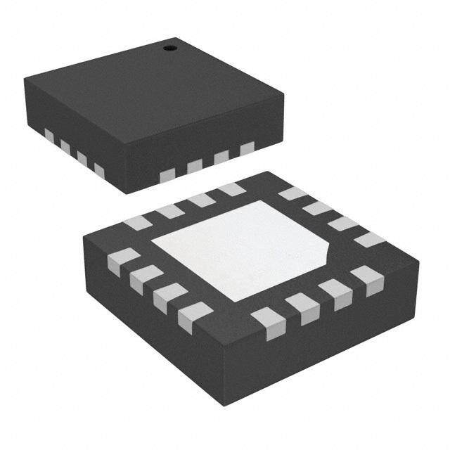
| 产品图片 |
|
| rohs | 符合RoHS无铅 / 符合限制有害物质指令(RoHS)规范要求 |
| 产品系列 | 电源管理 IC,开关控制器 ,Maxim Integrated MAX8597ETP+- |
| 数据手册 | |
| 产品型号 | MAX8597ETP+ |
| PWM类型 | 电压模式 |
| 产品培训模块 | http://www.digikey.cn/PTM/IndividualPTM.page?site=cn&lang=zhs&ptm=25703http://www.digikey.cn/PTM/IndividualPTM.page?site=cn&lang=zhs&ptm=25705 |
| 产品种类 | 开关控制器 |
| 倍增器 | 无 |
| 分频器 | 无 |
| 包装 | 管件 |
| 升压 | 无 |
| 占空比 | 99.5% |
| 占空比-最大 | 99.5 % |
| 反向 | 无 |
| 反激式 | 无 |
| 商标 | Maxim Integrated |
| 安装风格 | SMD/SMT |
| 封装 | Tube |
| 封装/外壳 | 20-WFQFN 裸露焊盘 |
| 封装/箱体 | TQFN-20 |
| 工作温度 | -40°C ~ 85°C |
| 工作电源电压 | 4.5 V to 28 V |
| 工作电源电流 | 5 mA |
| 工厂包装数量 | 75 |
| 应用说明 | |
| 开关频率 | 200 kHz to 1.4 MHz |
| 拓扑结构 | Buck |
| 最大工作温度 | + 85 C |
| 最小工作温度 | - 40 C |
| 标准包装 | 1 |
| 电压-电源 | 4.5 V ~ 28 V |
| 类型 | Voltage Mode PWM Controllers |
| 系列 | MAX8597 |
| 输出数 | 1 |
| 输出电压 | 0.6 V to 28 V |
| 输出电流 | 20 A |
| 输出端数量 | 1 |
| 降压 | 是 |
| 隔离式 | 无 |
| 零件号别名 | MAX8597 |
| 频率-最大值 | 1.4MHz |


PDF Datasheet 数据手册内容提取
19-3505; Rev 1; 6/05 EVAALVUAAILTAIOBNL EKIT Low-Dropout, Wide-Input-Voltage, Step-Down Controllers General Description Features M The MAX8597/MAX8598/MAX8599 voltage-mode PWM ♦ Low Dropout with >99.5% Duty Cycle A step-down controllers are designed to operate from a ♦ Lossless High-Side Current Limit X 4.5V to 28V input supply and generate output voltages ♦ Wide 4.5V to 28V Input Range down to 0.6V. A proprietary switching algorithm stretch- 8 ♦ Dynamic Output Voltage Adjustment with es the duty cycle to >99.5% for low-dropout design. 5 Adjustable Offset (MAX8597) Unlike conventional step-down regulators using a p- channel high-side MOSFET to achieve high duty cycle, ♦ Remote Voltage Sensing for Both Positive and 9 the MAX8597/MAX8598/MAX8599 drive n-channel Negative Rails (MAX8597) 7 MOSFETs resulting in high efficiency and high-current- ♦ Tracking Output Through REFIN (MAX8597) / M capability designs. ♦ Adjustable Switching Frequency from 200kHz to The MAX8597 is available in a 20-pin thin QFN pack- 1.4MHz A age and is designed for applications that use an analog ♦ Adjustable Soft-Start X signal to control the output voltage with an adjustable ♦ Prebias Startup 8 offset, such as DC fan-speed control. This is achieved ♦ Enable and Power-OK (MAX8598/MAX8599) for 5 with an internal uncommitted operational amplifier. The MAX8597 is also targeted for tracking output-voltage Flexible Sequencing 9 applications for chipsets, ASIC and DSP cores, and I/O ♦ 25MHz Error Amplifier 8 supplies. The MAX8598/MAX8599 are available in a 16- ♦ Adjustable Hiccup Current Limit for Output / M pin thin QFN package and do not have the uncommitted Short-Circuit Protection operational amplifier, reference input, and reference out- ♦ Output Overvoltage Protection (MAX8599) A put, but offer an open-drain, power-OK output. ♦ Small, Low-Profile Thin QFN Package X The MAX8597/MAX8598/MAX8599 allow startup with prebias voltage on the output for applications where a 8 backup supply or a tracking device may charge the Ordering Information 5 output capacitor before the MAX8597/MAX8598/ 9 MAX8599 are enabled. In addition, the MAX8599 fea- PART TEMP RANGE PIN-PACKAGE 9 tures output overvoltage protection. 20 Thin QFN 4mm x 4mm MAX8597ETP -40°C to +85°C These controllers also feature lossless high-side peak (T2044-3) inductor current sensing, adjustable current limit, and 20 Thin QFN 4mm x 4mm hiccup-mode short-circuit protection. Switching fre- MAX8597ETP+ -40°C to +85°C (T2044-3) quency is set with an external resistor from 200kHz to 1.4MHz. This wide frequency range combined with a 16 Thin QFN 4mm x 4mm MAX8598ETE -40°C to +85°C wide-bandwidth error amplifier enables the loop com- (T1644-4) pensation scheme to give the user ample flexibility to 16 Thin QFN 4mm x 4mm optimize for cost, size, and efficiency. MAX8598ETE+ -40°C to +85°C (T1644-4) 16 Thin QFN 4mm x 4mm Applications MAX8599ETE -40°C to +85°C (T1644-4) Nonisolated Power Modules 16 Thin QFN 4mm x 4mm MAX8599ETE+ -40°C to +85°C Variable-Speed DC Fan Power Supplies (T1644-4) (MAX8597) +Denotes lead-free package. Tracking Power Supplies (MAX8597) Chipset Power Supplies Pin Configurations appear at end of data sheet. ________________________________________________________________Maxim Integrated Products 1 For pricing, delivery, and ordering information,please contact Maxim/Dallas Direct!at 1-888-629-4642, or visit Maxim’s website at www.maxim-ic.com.
Low-Dropout, Wide-Input-Voltage, Step-Down Controllers 9 ABSOLUTE MAXIMUM RATINGS 9 V+, ILIM to GND.....................................................-0.3V to +30V DL to PGND.................................................-0.3V to (VVL+ 0.3V) 5 AVL, VL to GND........................................................-0.3V to +6V Continuous Power Dissipation PGND to GND.......................................................-0.3V to +0.3V 16- or 20-Pin Thin QFN 8 FB, EN, POK, AIN-, AIN+, REFIN to GND................-0.3V to +6V Up to +70°C (derate 16.9mW/°C above +70°C)........1349mW X AOUT, REFOUT, FREQ, SS, COMP to Operating Temperature Range...........................-40°C to +85°C A GND .....................................................-0.3V to (VAVL+ 0.3V) Junction Temperature......................................................+150°C BST to GND............................................................-0.3V to +36V Storage Temperature Range.............................-65°C to +150°C M DH to LX....................................................-0.3V to (VBST+ 0.3V) Lead Temperature (soldering, 10s).................................+300°C LX to GND........................-2V (-2.5V for less than 50ns) to +30V / LX to BST..................................................................-6V to +0.3V 8 9 Stresses beyond those listed under “Absolute Maximum Ratings” may cause permanent damage to the device. These are stress ratings only, and functional operation of the device at these or any other conditions beyond those indicated in the operational sections of the specifications is not implied. Exposure to 5 absolute maximum rating conditions for extended periods may affect device reliability. 8 X ELECTRICAL CHARACTERISTICS A (VV+= VVL= VAVL= VEN= VREFIN= 5V, VBST= 6V, VLX= 1V, CVL= 4.7µF, CREFOUT= 1µF, VAIN-= VAOUT, VAIN+= 2.5V, VILIM= M VLX- 0.2V, VFB= 0.65V, GND = PGND = 0V, CSS= 0.01µF, RFREQ= 20kΩ, TA= 0°C to +85°C, typical values are at TA= +25°C, unless otherwise noted.) / 7 PARAMETER CONDITIONS MIN TYP MAX UNITS 9 GENERAL 5 V+ Operating Range 5 .5 2 8.0 V 8 V+/VL Operating Range V+ = VL 4.5 5 .5 V X V+ Operating Supply Current VV+ = 12V, VL unloaded, no MOSFETs connected, VFB = 0V 3 .4 5.0 mA A V+ Standby Supply Current VV+ = 12V, VL unloaded, VFB = 0V 2 .0 m A M VL REGULATOR Output Voltage 5.5V < VV+ < 28V, 1mA < ILOAD < 35mA 4.7 5.0 5.3 V VL Undervoltage-Lockout Rising edge, typical hysteresis = 460mV 4.05 4.2 4.35 V Trip Level Thermal Shutdown Rising temperature, typical hysteresis = 10°C + 160 ° C REFERENCE (MAX8597 only) REFOUT Output Voltage IREFOUT = 150µA, VV+ = VVL = 4.5V or 5.5V 2.49 2.50 2.51 V REFOUT Load Regulation IREFOUT = 10µA to 1mA 1 0 mV REFOUT Internal Discharge During VL UVLO 15 Ω Switch On-Resistance CURRENT-LIMIT COMPARATOR (all current limits are tested at VV+ = VVL = 4.5V and 5.5V) ILIM Sink Current 1.8V < VLX < 28V, VBST = VLX + 5V 180 200 220 µA Comparator Input Offset VLX = 28V, VBST = VLX + 5V -10 + 10 mV Voltage Error SOFT-START Soft-Start Source Current VSS = 100mV 3 5 7 µA Soft-Start Sink Current VSS = (0.6V or VREFIN) 3 5 7 µA FREQUENCY RFREQ = 100kΩ 150 200 240 Frequency RFREQ = 20.0kΩ 800 1000 1200 kHz RFREQ = 14.3kΩ 1100 1400 1700 2 _______________________________________________________________________________________
Low-Dropout, Wide-Input-Voltage, Step-Down Controllers ELECTRICAL CHARACTERISTICS (continued) M (VV+= VVL= VAVL= VEN= VREFIN= 5V, VBST= 6V, VLX= 1V, CVL= 4.7µF, CREFOUT= 1µF, VAIN-= VAOUT, VAIN+= 2.5V, VILIM= A VLX- 0.2V, VFB= 0.65V, GND = PGND = 0V, CSS= 0.01µF, RFREQ= 20kΩ, TA= 0°C to +85°C, typical values are at TA= +25°C, unless otherwise noted.) X PARAMETER CONDITIONS MIN TYP MAX UNITS 8 DH Minimum Off-Time 1 80 200 220 ns 5 DH Minimum On-Time 1 15 140 ns 9 FB ERROR AMPLIFIER 7 FB Input Bias Current 1 00 nA /M FB Input Voltage Set Point Over load and line 0.594 0.600 0.606 V A FB Offset Error VREFIN = 1.25V and 2.5V, measured with respect to REFIN +10 -10 mV X Error-Amp Open-Loop Voltage VCOMP = 1.2V to 2.4V 72 90 dB 8 Gain 5 Slew Rate CLOAD = 80pF 18 V/µs 9 UNCOMMITTED OPERATIONAL AMPLIFIER (MAX8597 only) 8 RLOAD = 100kΩ 90 Open-Loop Voltage Gain (AVOL) RLOAD = 10kΩ 70 dB /M VAVL - A Output-Voltage Swing High VAIN+ = 2.5V, VAIN- = (VAIN+ - 100mV), ISOURCE = 100µA V 20mV X Output-Voltage Swing Low VAIN+ = 2.5V, VAIN- = (VAIN+ + 100mV), ISINK = 100µA 20 mV 8 Unity-Gain BW 1.5 MHz 5 Phase Margin CLOAD = 10pF, RLOAD = 10kΩ to 100kΩ +80 De gre es 9 CLOAD = 100pF, RLOAD = 10kΩ to 100kΩ +40 9 Slew Rate CLOAD = 100pF 3.5 V/µs Input Offset Voltage VCM = 1.25V and 2.5V -3 +3 mV Input Leakage Current -10 +10 nA Input Common-Mode Range VAVL - +0.50 V (CMVR) 2.0 Common-Mode Rejection Ratio 75 dB (CMRR) DRIVERS DH, DL Break-Before-Make Time CLOAD = 2000pF 2 0 n s DH On-Resistance in Low State VBST - VLX = 5V 1 .0 2.5 Ω DH On-Resistance in High State VBST - VLX = 5V 1 .5 3.3 Ω DL On-Resistance in Low State VVL = VV+ = 5V 0 .45 1.0 Ω DL On-Resistance in High State VVL = VV+ = 5V 1 .3 2.5 Ω BST Bias Current VBST = 33V, VLX = 28V, VEN = 0V 2 30 520 µA LX Bias Current VBST = 33V, VLX = 28V, VEN = 0V - 230 -520 µA BST/LX Leakage Current VBST = VLX = 28V, VEN = 0V 5 0 µA LOGIC INPUTS (EN) Input Low Level 4.5V < VVL = VV+ = VAVL < 5.5V 1 .14 0.80 V Input High Level 4.5V < VVL = VV+ = VAVL < 5.5V 2.40 1.73 V Input Bias Current VVL = VV+ = VAVL = 5.5V, VEN = 0 to 5.5V -1 + 1 µA _______________________________________________________________________________________ 3
Low-Dropout, Wide-Input-Voltage, Step-Down Controllers 9 ELECTRICAL CHARACTERISTICS (continued) 9 (VV+= VVL= VAVL= VEN= VREFIN= 5V, VBST= 6V, VLX= 1V, CVL= 4.7µF, CREFOUT= 1µF, VAIN-= VAOUT, VAIN+= 2.5V, VILIM= 5 VLX- 0.2V, VFB= 0.65V, GND = PGND = 0V, CSS= 0.01µF, RFREQ= 20kΩ, TA= 0°C to +85°C, typical values are at TA= +25°C, unless otherwise noted.) 8 X PARAMETER CONDITIONS MIN TYP MAX UNITS REFIN INPUT (MAX8597 only) A REFIN Input Voltage Range 0 2 .75 V M REFIN Dual Mode™ Threshold VAVL - VAVL - V 8/ 1.0 0.5 9 REFIN Input Bias Current VREFIN = 1.25V or 2.5V -250 + 250 nA 5 OV AND UV FAULT COMPARATORS 8 Upper FB Fault Threshold (OV) Rising edge, hysteresis = 15mV (MAX8599 only) 115 117 120 % X Lower FB Fault Threshold (UV) Falling edge, hysteresis = 15mV 67 70 73 % A POWER-OK OUTPUT (POK) (MAX8598/MAX8599 only) M Clock POK Delay For both FB rising and falling edges 8 cycles / 7 Lower FB POK Threshold FB falling, hysteresis = 20mV 85 88 90 % 9 POK Output Low Level ISINK = 2mA 0.4 V 5 POK Output High Leakage VPOK = 5.5V 5 µA 8 X ELECTRICAL CHARACTERISTICS A (VV+= VVL= VAVL= VEN= VREFIN= 5V, VBST= 6V, VLX= 1V, CVL= 4.7µF, CREFOUT= 1µF, VAIN-= VAOUT, VAIN+= 2.5V, VILIM= M VLX- 0.2V, VFB= 0.65V, GND = PGND = 0V, CSS= 0.01µF, RFREQ= 20kΩ, TA= -40°C to +85°C, typical values are at TA= +25°C, unless otherwise noted.) (Note 1) PARAMETER CONDITIONS MIN TYP MAX UNITS GENERAL V+ Operating Range 5 .5 2 8.0 V V+/VL Operating Range V+ = VL 4.5 5 .5 V V+ Operating Supply Current VV+ = 12V, VL unloaded, no MOSFETs connected, VFB = 0V 5 .0 mA VL REGULATOR Output Voltage 5.5V < VV+ < 28V, 1mA < ILOAD < 35mA 4.7 5 .3 V VL Undervoltage-Lockout Trip Rising edge, typical hysteresis = 460mV 4.05 4 .35 V Level REFERENCE (MAX8597 only) REFOUT Output Voltage IREFOUT = 150µA, VV+ = VVL = 4.5V or 5.5V 2.47 2 .51 V REFOUT Load Regulation IREFOUT = 10µA to 1mA 1 0 mV CURRENT-LIMIT COMPARATOR (all current limits are tested at VV+ = VVL = 4.5V and 5.5V) ILIM Sink Current VILIM = VLX - 0.2V, 1.8V < VLX < 28V, VBST = VLX + 5V 180 2 20 µA Comparator Input Offset Voltage - 10 + 10 mV Error SOFT-START Soft-Start Source Current VSS = 100mV 3 7 µA Soft-Start Sink Current VSS = (0.6V or VREFIN) 3 7 µA Dual Mode is a trademark of Maxim Integrated Products, Inc. 4 _______________________________________________________________________________________
Low-Dropout, Wide-Input-Voltage, Step-Down Controllers ELECTRICAL CHARACTERISTICS (continued) M (VV+= VVL= VAVL= VEN= VREFIN= 5V, VBST= 6V, VLX= 1V, CVL= 4.7µF, CREFOUT= 1µF, VAIN-= VAOUT, VAIN+= 2.5V, VILIM= A VLX- 0.2V, VFB= 0.65V, GND = PGND = 0V, CSS= 0.01µF, RFREQ= 20kΩ, TA= -40°C to +85°C, typical values are at TA= +25°C, unless otherwise noted.) (Note 1) X PARAMETER CONDITIONS MIN TYP MAX UNITS 8 5 FREQUENCY RFREQ = 100kΩ 140 2 40 9 Frequency RFREQ = 20.0kΩ 800 1 200 kHz 7 / RFREQ = 14.3kΩ 1100 1 700 M DH Minimum Off-Time 1 80 2 30 ns A DH Minimum On-Time 1 40 ns X FB ERROR AMPLIFIER 8 FB Input Bias Current 1 50 nA 5 FB Input Voltage Set Point Over load and line 0.591 0 .606 V 9 FB Offset Error VREFIN = 1.25V and 2.5V, measured with respect to REFIN +20 -20 mV 8 Error-Amp Open-Loop Voltage Gain VCOMP = 1.2V to 2.4V 72 dB /M UNCOMMITTED OPERATIONAL AMPLIFIER (MAX8597 only) A VAVL - X Output Voltage Swing High VAIN+ = 2.5V, VAIN- = (VAIN+ - 100mV), ISOURCE = 100µA V 20mV 8 Output Voltage Swing Low VAIN+ = 2.5V, VAIN- = (VAIN+ + 100mV), ISINK = 100µA 20 mV 5 Input Offset Voltage VCM = 1.25V and 2.5V -3 +3 mV 9 Input Common-Mode Range VAVL - 9 +0.50 V (CMVR) 2.0 DRIVERS DH On-Resistance in Low State VBST - VLX = 5V 2 .5 Ω DH On-Resistance in High State VBST - VLX = 5V 3 .3 Ω DL On-Resistance in Low State VVL = VV+ = 5V 1 .0 Ω DL On-Resistance in High State VVL = VV+ = 5V 3 .5 Ω BST Bias Current VBST = 33V, VLX = 28V, VEN = 0V 5 20 µA LX Bias Current VBST = 33V, VLX = 28V, VEN = 0V - 520 µA BST/LX Leakage Current VBST = VLX = 28V, VEN = 0V 5 0 µA LOGIC INPUTS (EN) Input Low Level 4.5V < VVL = VV+ = VAVL < 5.5V 0 .8 V Input High Level 4.5V < VVL = VV+ = VAVL < 5.5V 2.4 V Input Bias Current VVL = VV+ = VAVL = 5.5V, VEN = 0 to 5.5V -1 + 1 µA REFIN INPUT (MAX8597 only) REFIN Input Voltage Range 0 2 .75 V REFIN Dual-Mode Threshold VAVL - VAVL - V 1.0 0.5 REFIN Input Bias Current VREFIN = 1.25V or 2.5V -250 + 250 nA _______________________________________________________________________________________ 5
Low-Dropout, Wide-Input-Voltage, Step-Down Controllers 9 ELECTRICAL CHARACTERISTICS (continued) 9 (VV+= VVL= VAVL= VEN= VREFIN= 5V, VBST= 6V, VLX= 1V, CVL= 4.7µF, CREFOUT= 1µF, VAIN-= VAOUT, VAIN+= 2.5V, VILIM= 5 VLX- 0.2V, VFB= 0.65V, GND = PGND = 0V, CSS= 0.01µF, RFREQ= 20kΩ, TA= -40°C to +85°C, typical values are at TA= +25°C, unless otherwise noted.) (Note 1) 8 X PARAMETER CONDITIONS MIN TYP MAX UNITS A OV AND UV FAULT COMPARATORS Upper FB Fault Threshold (OV) Rising edge, hysteresis = 15mV (MAX8599 only) 115 120 % M Lower FB Fault Threshold (UV) Falling edge, hysteresis = 15mV 67 73 % / 8 POWER-OK OUTPUT (POK) (MAX8598/MAX8599 only) 9 Lower FB POK Threshold FB falling, hysteresis = 20mV 85 90 % 5 POK Output Low Level ISINK = 2mA 0.4 V 8 POK Output High Leakage VPOK = 5.5V 5 µA X Note 1: Limits to -40°C are guaranteed by design and characterization. A M Typical Operating Characteristics / (Circuit of Figure 4, TA= +25°C, 500kHz switching frequency, VIN= 12V, unless otherwise noted.) 7 9 EFFICIENCY vs. LOAD CURRENT EFFICIENCY vs. LOAD CURRENT OUTPUT VOLTAGE 5 CIRCUIT OF FIGURE 1 CIRCUIT OF FIGURE 2 vs. LOAD CURRENT AX8 1990050 VOUVTO =U T1 1=. 59VV MAX8597 toc01 19000 VOUT = 3.3V MAX8597 toc02 11..220150 MAX8597 toc03 M EFFICIENCY (%) 788505 VOUT = 6V EFFICIENCY (%) 678000 VOUTV =O U1T. 2=V 1V.O8UVT = 2.5V UTPUT VOLTAGE (V)1.200 50 O 70 1.195 65 40 60 30 1.190 0.1 1 10 1 10 100 0 2 4 6 8 10 12 14 16 18 20 LOAD CURRENT (A) LOAD CURRENT (A) ILOAD (A) OUTPUT VOLTAGE vs. INPUT VOLTAGE POWER-UP WAVEFORMS POWER-DOWN WAVEFORMS 1.210 MAX8597 toc05 MAX8597 toc06 MAX8597 toc04 VAVL 5V/div VAVL 5V/div 1.205 V) GE ( ILOAD = 0A ILX 10A/div ILX 10A/div A T L T VO 1.200 ILOAD = 20A U P UT VOUT 1V/div IOUT 1V/div O 1.195 VIN 10V/div VIN 10V/div 1.190 10.0 10.5 11.0 11.5 12.0 12.5 13.0 13.5 14.0 2ms/div 2ms/div VIN (V) 6 _______________________________________________________________________________________
Low-Dropout, Wide-Input-Voltage, Step-Down Controllers Typical Operating Characteristics (continued) M (Circuit of Figure 4, TA= +25°C, 500kHz switching frequency, VIN= 12V, unless otherwise noted.) A X STARTUP/SHUTDOWN WITH 8 OUTPUT PREBIASED STARTUP EN (ILOAD = 20A) MAX8597 toc07 MAX8597 toc08 5 5V/div 9 VPOK 7 VLX 10V/div / M 1.2V ILX 10A/div A VOUT 1.0V 5V/div X 1V/div 8 VOUT 5 VIN 5V/div 9 VDL 5V/div VEN 8 1ms/div 2ms/div / M OUTPUT VOLTAGE vs. VADJ ENTERING DROPOUT WAVEFORMS A (VIN = 12V) CIRCUIT OF FIGURE 1 13 MAX8597 toc10 X 1112 MAX8597 toc09 VLX 10V/div 85 E (V) 10 11V 9 G LTA 9 VOUT 9 O V T 8 U UTP 7 VCOMP 500mV/div O 6 5 CIRCUIT OF FIGURE 1 VIN 100mV/div RLOAD = 1.2Ω (AC-COUPLED) 4 0 1 2 3 4 5 6 2µs/div VADJ (V) HEAVY-DROPOUT WAVEFORMS CIRCUIT OF FIGURE 1 OUTPUT TRACKING REFIN MAX8597 toc11 MAX8597 toc12 VREFIN VLX 10V/div VOUT 11.9V 1ms RISE 1V/div VOUT TIME VREFIN VCOMP 500mV/div VOUT 5ms RISE TIME 1V/div VIN 500mV/div (AC-COUPLED) CIRCUIT OF FIGURE 3 10µs/div 1ms/div _______________________________________________________________________________________ 7
Low-Dropout, Wide-Input-Voltage, Step-Down Controllers 9 Typical Operating Characteristics (continued) 9 (Circuit of Figure 4, TA= +25°C, 500kHz switching frequency, VIN= 12V, unless otherwise noted.) 5 8 X 50% LOAD STEP AT 5A/µs 90% LOAD STEP AT 5A/µs A MAX8597 toc13 MAX8597 toc14 M / VOUT 100mV/div 8 (AC-COUPLED) 9 VOUT 50mV/div 5 (AC-COUPLED) 8 20A 20A X IOUT 10A IOUT A 2A M 40µs/div 40µs/div / 7 9 5 8 X A SHORT-CIRCUIT RESPONSE OUTPUT OVERVOLTAGE PROTECTION M MAX8597 toc15 MAX8597 toc16 VOUT 1V/div VFB 500mV/div IIN 2A/div VDH 10V/div ILX 10A/div 5V/div VDL 4ms/div 10µs/div 8 _______________________________________________________________________________________
Low-Dropout, Wide-Input-Voltage, Step-Down Controllers Block Diagram M A X 8 ILIM 5 MAX8597 9 MAX8598 200µA 7 MAX8599 BST / M FREQ DH A OSC CONTROL LX LOGIC X 1VP-P 8 5 PWM VL 9 1/20 8 COUNTER DL / M PGND A X REFERENCE REFOUT (MAX8597) 8 AVL BIAS 5 VREG SOFT-START EN 9 9 COMP EAMP V+ VL VL GND UVP 1.17 x VREG SS OVP REFIN (MAX8597) (MAX8599) 0.7 x VREG FB AOUT POK (MAX8597) (MAX8598/ MAX8599) N AIN+ (MAX8597) 0.88 x VREG AIN- (MAX8597) _______________________________________________________________________________________ 9
Low-Dropout, Wide-Input-Voltage, Step-Down Controllers 9 Pin Description 9 PIN 5 8 MAX8598/ NAME FUNCTION MAX8597 MAX8599 X Filtered VL Input. Connect to VL through a 10Ω resistor. Bypass to GND with a 0.22µF or larger A 1 1 AVL ceramic capacitor. M External Reference Input. FB tracks the voltage input to REFIN. Connect REFIN to AVL to use 2 — REFIN / the internal 0.6V reference. 8 9 Analog Ground. Connect to the exposed paddle and analog ground plane and then connect to 3 2 GND 5 PGND at the output ground. 8 Soft-Start Programming Input. Connect a capacitor from SS to GND to set the soft-start time. 4 3 SS X See the Selecting the Soft-Start Capacitor section for details. A Feedback Input. Connect to the center tap of an external resistor-divider to set the output 5 4 FB voltage. Regulates to 0.6V for the MAX8598/MAX8599 and MAX8597 when REFIN is connected M to AVL. Regulates to VREFIN (MAX8597) when using an external reference. / 7 Compensation Input. Connect to the required compensation network. See the Compensation 6 5 COMP 9 Design section for details. 5 7 6 EN Enable Input. Drive EN high to enable the IC. Drive low to shut down the IC. 8 Internal Reference Output. REFOUT regulates to 2.5V and can source up to 1mA. REFOUT 8 — REFOUT X discharges to GND during UVLO. A Input Supply Voltage for Internal VL Regulator. Connect to an input supply in the 4.5V to 28V 9 7 V+ M range. Bypass to GND with a 1µF or larger ceramic capacitor through a 3Ω resistor. Internal 5V Linear-Regulator Output. VL provides power for the internal MOSFET gate drivers. 10 8 VL Bypass to PGND with a 1µF or larger ceramic capacitor. VL is always enabled except in thermal shutdown. See the Internal 5V Linear Regulator section for details. Low-Side Gate-Driver Output. Connect to the gate of the synchronous rectifier. DL swings from 11 9 DL PGND to VL. DL is held low during shutdown. 12 10 PGND Power Ground. Connect to the synchronous rectifier’s source and PGND plane. Bootstrap Input Supply for the High-Side MOSFET Driver. Connect to the cathode of an external 13 11 BST diode from VL and connect a 0.1µF or larger capacitor from BST to LX. High-Side Gate-Driver Output. Connect to the gate of the high-side MOSFET. DH swings from 14 12 DH LX to BST. DH is low (connected to LX) during shutdown. External Inductor Connection. LX is the low supply for the DH gate driver as well as the sense 15 13 LX connection for the current-limit circuitry. Connect LX to the switched side of the inductor as well as the source of the high-side MOSFET and the drain of the synchronous rectifier. Current-Limit Sense Input. Connect a resistor from ILIM to the current-sense point to set the 16 14 ILIM output current limit. See the Setting the Current Limit section for details. 10 ______________________________________________________________________________________
Low-Dropout, Wide-Input-Voltage, Step-Down Controllers Pin Description (continued) M A PIN MAX8598/ NAME FUNCTION X MAX8597 MAX8599 8 5 Frequency Adjust Input. Connect a resistor from FREQ to GND to set the switching frequency. 17 15 FREQ The range of the FREQ resistor is 14.3kΩ to 100kΩ (corresponding to 1400kHz to 200kHz). 9 7 Output of the Uncommitted Operational Amplifier. AOUT is high impedance during 18 — AOUT undervoltage lockout. / M 19 — AIN- Inverting Input of the Uncommitted Operational Amplifier A 20 — AIN+ Noninverting Input of the Uncommitted Operational Amplifier X Power-OK Output. POK is an open-drain output that goes high impedance when the regulator — 16 POK output is greater than 88% of the regulation threshold. POK is low during shutdown. 8 5 — — EP Exposed Paddle. Connect to analog ground plane for improved thermal performance. 9 Detailed Description The MAX8597/MAX8598/MAX8599 allow startup with 8 prebias voltage on the output for applications where a / The MAX8597/MAX8598/MAX8599 voltage-mode PWM backup supply or a tracking device may charge the M step-down controllers are designed to operate from output capacitor before the MAX8597/MAX8598/ 4.5V to 28V input and generate output voltages down to A MAX8599 are enabled. The MAX8599 has output over- 0.6V. A proprietary switching algorithm stretches the voltage protection. X duty cycle to >99.5% for low-dropout design. Unlike conventional step-down regulators using a p-channel These controllers feature lossless high-side peak 8 high-side MOSFET to achieve high duty cycle, the inductor current sensing, adjustable current limit, and 5 MAX8597/MAX8598/MAX8599 drive n-channel hiccup-mode short-circuit protection. Switching fre- 9 MOSFETs permitting high efficiency and high-current quency is set with an external resistor from 200kHz to 9 designs. 1.4MHz. This wide frequency range combined with a wide-bandwidth error amplifier enable the loop-com- The MAX8597 is available in a 20-pin thin QFN pack- pensation scheme to give the user ample flexibility to age and is designed for applications that use an ana- optimize for cost, size, and efficiency. log signal to control the output voltage with adjustable offset, such as DC fan speed control. For example, a DC-DC Controller 12VDC fan can be driven from 6V to 12V with 12V input The MAX8597/MAX8598/MAX8599 step-down DC-DC power source depending on the system’s cooling controllers use a PWM voltage-mode control scheme. An requirement to minimize fan noise and power consump- internal high-bandwidth (25MHz) operational amplifier is tion. This is achieved with an internal uncommitted used as an error amplifier to regulate the output voltage. operational amplifier. With the addition of an external The output voltage is sensed and compared with an inter- RC filter, a PWM input can also be used to control the nal 0.6V reference or REFIN (MAX8597) to generate an output voltage. The MAX8597 also generates a tracking error signal. The error signal is then compared with a output for chipsets, ASICs, and DSP where core and fixed-frequency ramp by a PWM comparator to give the I/O supplies are split and require tracking. In applica- appropriate duty cycle to maintain output voltage regula- tions where tighter output tolerance is required, the tion. The high-side MOSFET turns on at the rising edge of MAX8597 output can be set by an external precision the internal clock 20ns after DL (the low-side MOSFET reference source feeding to REFIN. The MAX8598/ gate drive) goes low. The high-side MOSFET turns off MAX8599 are available in a 16-pin thin QFN package once the internal ramp voltage reaches the error-amplifier and do not have the uncommitted operational amplifier, output voltage. The process repeats for every clock reference input, and reference output, but offer a power- cycle. During the high-side MOSFET on-time, current OK output (POK). With the enable input and POK out- flows from the input through the inductor to the output put, the MAX8598/MAX8599 can easily be configured to capacitor and load. At the moment the high-side MOS- have power sequencing of multiple supply rails. FET turns off, the energy stored in the inductor during the on-time is released to support the load as the inductor ______________________________________________________________________________________ 11
Low-Dropout, Wide-Input-Voltage, Step-Down Controllers 9 current ramps down through the low-side MOSFET body High-Side Gate-Drive Supply (BST) diode; 20ns after DH goes low, the low-side MOSFET Gate-drive voltage for the high-side n-channel MOSFET is 9 turns on, resulting in a lower voltage drop to increase effi- generated by an external flying capacitor and diode boost 5 ciency. The low-side MOSFET turns off at the rising edge circuit (D1 and C5 in Figure 1). When the synchronous 8 of the next clock pulse, and when its gate voltage dis- rectifier is on, C5 is charged from the VL supply through X charges to zero, the high-side MOSFET turns on and the Schottky diode. When the synchronous rectifier is A another cycle starts. turned off, the Schottky is reverse biased and the voltage on C5 is stacked above LX to provide the necessary turn- These controllers also sense peak inductor current and M on voltage for the high-side MOSFET. A low-current provide hiccup-overload and short-circuit protection Schottky diode, such as Central Semiconductor’s / (see the Current Limit section). The MAX8597/ 8 CMDSH-3, works well for most applications. The capacitor MAX8598/MAX8599 operate in forced-PWM mode 9 should be large enough to prevent it from charging to where the inductor current is always continuous. The 5 controller maintains constant switching frequency excessive voltage, but small enough to adequately charge during the minimum low-side MOSFET on-time, which 8 under all loads, except under dropout conditions where occurs at minimum input voltage. A capacitor in the 0.1µF X it skips DL pulses. to 0.47µF range works well for most applications. A Current Limit Internal 5V Linear Regulator The MAX8597/MAX8598/MAX8599 DC-DC step-down M The MAX8597/MAX8598/MAX8599 contain a low- controllers sense the peak inductor current either with dropout 5V regulator that provides up to 35mA to sup- / the on-resistance of the high-side MOSFET for lossless 7 ply gate drive for the external MOSFETs, and supplies sensing, or a series resistor for more accurate sensing. 9 AVL, which powers the IC’s internal circuitry. Bypass When the voltage across the sensing element exceeds 5 the current-limit threshold set with ILIM, the controller the regulator’s output (VL) with 1µF per 10mA of VL load, or greater ceramic capacitor. The current 8 immediately turns off the high-side MOSFET. The low- required to drive the external MOSFET can be estimat- X side MOSFET is then turned on to let the inductor cur- rent ramp down. As the output load current increases ed by multiplying the total gate charge (at VGS= 5V) of A the MOSFETs by the switching frequency. above the ILIM threshold, the output voltage sags M because the truncated duty cycle is insufficient to sup- Undervoltage Lockout (UVLO) port the load current. When FB falls 30% below its nomi- When VVL drops below 3.75V (typ), the MAX8597/ nal threshold, the output undervoltage protection is MAX8598/MAX8599s’ undervoltage-lockout (UVLO) cir- triggered and the controller enters hiccup mode to limit cuitry inhibits switching, forces POK (MAX8598/ power dissipation. This current-limit method allows the MAX8599) low, and forces DH and DL low. Once VVL circuit to withstand a continuous output short circuit. rises above 4.2V (typ), the controller powers up the out- The MAX8597/MAX8598/MAX8599 current-limit thresh- put in startup mode (see the Startupsection). old is set by an external resistor that works in conjunc- tion with an internal 200µA current sink (see the Setting Startup the Current Limit section for more details). The MAX8597/MAX8598/MAX8599 start switching once all the following conditions are met: Synchronous-Rectifier Driver (DL) 1) EN is high. Synchronous rectification reduces the conduction loss in the rectifier by replacing the normal Schottky catch 2) VVL> 4.2V (typ). diode with a low-resistance MOSFET switch. The 3) Soft-start voltage VSSexceeds VFB. MAX8597/MAX8598/MAX8599 also use the synchro- 4) Thermal limit is not exceeded. nous rectifier to ensure proper startup of the boost gate-drive circuit. The third condition ensures that the MAX8597/ MAX8598/MAX8599 do not discharge a prebiased out- put. Once all of these conditions are met, the IC begins switching and the soft-start cycle is initiated. 12 ______________________________________________________________________________________
Low-Dropout, Wide-Input-Voltage, Step-Down Controllers Power-OK Signal condition still exists, the UVP process begins again. The M (POK, MAX8598/MAX8599 Only) result is“hiccup” mode, where the controller attempts to The power-OK signal (POK) is an open-drain output that restart periodically as long as the overload condition A goes high impedance when FB is above 91% of its nom- exists. In hiccup mode, the soft-start capacitor voltage X inal threshold. There is an eight clock-cycle delay before ramps up to 112% of the nominal VFB threshold and 8 POK goes high impedance. For 500kHz switching fre- then ramps down to 50mV. For the MAX8597, VREFIN quency, this delay is typically 16µs. To obtain a logic must be greater than 450mV to trigger UVP. The soft- 5 voltage output, connect a pullup resistor from POK to start capacitor voltage then ramps up to 112% of VREFIN 9 AVL. A 100kΩ resistor works well for most applications. and then down to 50mV. 7 If unused, connect POK to GND or leave it unconnected. Output Overvoltage Protection /M Enable and Soft-Start (OVP, MAX8599) The MAX8597/MAX8598/MAX8599 are enabled using The output voltage is continuously monitored for over- A the EN input. A logic high on EN enables the output of voltage (MAX8599 only). If the output voltage is more X the IC. Conversely, a logic low on EN disables the out- than 117% of its nominal set value, OVP is triggered 8 put. On the rising edge of EN, the controllers enter soft- after a 12µs (typ) delay. The MAX8599 latches DH low start. Soft-start gradually ramps up the reference to turn off the high-side MOSFET, and DL high to turn 5 voltage seen at the error amplifier to control the output on the low-side MOSFET to clamp the output to PGND. 9 rate of rise and reduce the inrush current during start- The latch is reset either by toggling EN or by cycling V+ 8 up. The soft-start period is determined by a capacitor below the UVLO threshold. Note that DL latching high / connected from SS to GND (C6 in Figure 1). A 5µA cur- causes a negative spike at the output due to the energy M rent source charges the external capacitor to the refer- stored in the output LC at the instant of OVP trip. If the A ence voltage (0.6V or VREFIN). The capacitor value is load cannot tolerate this negative spike, add a power determined as follows: Schottky diode across the output to act as a reverse X polarity clamp. 8 5µA × t C6 = SS Thermal-Overload Protection 5 V FB Thermal-overload protection limits the total power dissi- 9 pation in the MAX8597/MAX8598/MAX8599. When the 9 where tSS is the soft-start time in seconds and VFB is junction temperature exceeds +160°C, a thermal sen- 0.6V or VREFIN. The output reaches regulation when sor shuts down the device, forcing DH and DL low, soft-start is completed. allowing the IC to cool. The thermal sensor turns the part on after the junction temperature cools by 10°C, Output Undervoltage Protection (UVP) resulting in a pulsed output during continuous thermal- Output UVP begins when the controller is at its current overload conditions. During a thermal event, the switch- limit and VFB is 30% below its nominal threshold. This ing converter is turned off, the reference is turned off, condition causes the controller to drive DH and DL low the VL regulator is turned off, POK is high impedance, and discharges the soft-start capacitor with a 5µA pull- and the soft-start capacitor is discharged. down current until VSS reaches 50mV. Then the con- troller begins in soft-start mode. If the overload ______________________________________________________________________________________ 13
Low-Dropout, Wide-Input-Voltage, Step-Down Controllers 9 Design Procedure 9 5 VIN (10.8V TO 13.2V) 8 C2A X 33R.21kΩ R31Ω5 1Cµ1F VL 10µF A ON EN M OFF R4 AVL 2 7 17 9 16 CMDSHD-13 1.21kRΩ2 C0.301µF 1C02µBF 8/ VADJ (0V TO 5V) 100kΩ 19 AINR-EFIN EN FREQ V+ ILIMBST13 C15 20 9 0.01µF R5 C6 AIN+ Q1 32.4kΩ 0.033µF 14 IRF7821 85 R6 148 SS MAX8597 DH15 C0.522µF 1Lµ1H 6V TOV O1U2TV/10A 48.7kΩ AOUT LX X Q2 R8 11 IRF7821 R14 C7A C7B A R7 6.0R49kΩ 24.9kΩ5 DL12 2CΩ14 47µF 47µF M 48.7kΩ C8 FB PGND 2200pF 4.7pF COMPGND AVL REFO VL 6 3 1 8 10 C12 7/ 93.1Rk1Ω0 R11 47Rk1Ω2 82C09pF 1R01Ω3 4.7µF 9 5.1kΩ C11 0.22µF C13 5 1µF VL C10 8 100pF X A Figure 1. MAX8597 (600kHz): Live Adjustable Output Voltage from 6V to 12V at 10A M C2A VIN (10.8V TO 13.2V) 10µF R14 C2B 40R.21kΩ 3Ω 1Cµ1F VL 10µF OFF ON EN AVL CMDSHD-13 R2 C0.301µF 1C02µCF 1.65kΩ 2 7 17 9 16 R3 10kΩ REFIN EN FREQ V+ ILIM 13 19 AIN- BST Q1 Q2 R4 14 10kΩ R5 DH (Q1 = Q2 = 10kΩ 20 AIN+ C0.522µFIRF7807Z) 0.7Lµ1H 1.2VVO/U2T0A 10kRΩ6 0.0C334µF184 SS MAX8597 DLXL1115 Q3 Q4 R3Ω12 47C0µ7AF C4770BµF R127.1kΩ 12R.19kΩ 5 FABOUT PGND12 (QI3R F=7 Q8342 =) C221030pF R8 C8 COMPGND AVL REFO VL 7.2kΩ 39pF 6 3 1 8 10 C12 C8 R10 C9 1R01Ω1 4.7µF 1800pF 16kΩ 6800pF C10 C11 0.22µF 1µF VL Figure 2. 1.2V at 20A Output with Remote Sensing 14 ______________________________________________________________________________________
Low-Dropout, Wide-Input-Voltage, Step-Down Controllers Design Procedure (continued) M A VIN (10.8V TO 13.2V) X R1 ON EN 20kΩ R31Ω2 1Cµ1F VL 1C02µAF 8 OFF REFIN 5 C2B R3 C4 D1 10µF 9 70kΩ D2 1000pFR2EFIN 7EN1F7REQ 9V+ 16ILIM CMDSH-3 1.5kRΩ2 C0.301µF 7 CRM4PD914 19 AIN- BST13 /M R5 18.2kΩ 20 Q1 6.98kΩ AIN+ DH14 IRF7807Z A 22C006pF4 SS MAX8597 LX15 C0.522µF 0.5L61µH 1.8VVO/U1T0A X Q2 8 18 AOUT DL11 IRF7821 R2Ω10 10C0µ7AF C1070BµF 5 5 12 C14 FB PGND 2200pF 9 10kRΩ6 390RΩ7 56CpF8 C6OMPG3ND A1VL 1R09ΩR8EFO 10VL 4C.71µ3F 8/ C10 5.6kRΩ8 82C009pF C11 M 1000pF 0.22µF C1µ12F VL A X 8 5 Figure 3. MAX8597 1MHz Tracking Supply with Clamp (Output voltage tracks VREFINfrom 0V up to the nominal output regulation voltage.) 9 9 C2A VIN (10.8V TO 13.2V) 10µF R11 C2B 40R.21kΩ 3Ω 1Cµ1F VL 10µF OFF ON EN AVL CMDSHD-13 R2 C0.301µF 1C02µCF 2.26kΩ 6 15 7 14 R3 EN FREQ V+ ILIM POK 100kΩ 16 BST11 POK 12R.14kΩ0.0C334µF 3 SS MAX8598 DH1132 C0.522µF HATQ21168H 0.7Lµ1H 1.2VVO/U2T0A 4 LX FB MAX8599 R125.1kΩ 39Cp8F 5 COMP DL9 HATQ21265H HATQ21365H R3CΩ912 47C0µ7AF C4770BµF R7 2200pF R6 16kΩ C9 GND AVL VL PGND 1.2kΩ 6800pF 2 1 8 10 C8 AVL C11 1800pF R8 4.7µF 10Ω C10 0.22µF VL Figure 4. MAX8598/MAX8599 500kHz, 1.2V, 20A Output Power Supply ______________________________________________________________________________________ 15
Low-Dropout, Wide-Input-Voltage, Step-Down Controllers 9 Setting the Output Voltage Additionally, to minimize error, R6 and R7 should be chosen such that: 9 Fixed Output Voltage 5 The output voltage is set by a resistor-divider network R6 × R7 R4 × R5 from the output to GND with FB at the center tap (R4 = 8 and R5 in Figure 4). Select R4 between 5kΩ and 15kΩ R6 + R7 R4 + R5 X and calculate R5 by: A R5 = R4 x [( VOUT/ VFB) - 1] Inductor Selection M There are several parameters that must be examined Live Adjustable Output Voltage (see Figure 1) when determining which inductor is to be used: input 8/ Using the uncommitted operational amplifier, the voltage, output voltage, load current, switching fre- MAX8597 can be configured such that the output volt- quency, and LIR. LIR is the ratio of inductor current rip- 9 age is adjustable using a voltage source (VADJ). The ple to DC load current. A higher LIR value allows for a 5 following parameters must be defined before starting smaller inductor but results in higher losses and higher 8 the design: output ripple. A good compromise between size and X •The minimum desired output voltage, VOUT_MIN efficiency is a 30% LIR. Once all the parameters are A •The maximum desired output voltage, VOUT_MAX chosen, the inductor value is determined as follows: ( ) M •The desired input that corresponds to the minimum L = VOUT x VIN−VOUT output voltage, VADJ_MIN V x f x I x LIR / IN S LOAD(MAX) 7 •The desired input that corresponds to the maximum 9 output voltage, VADJ_MAX where fS is the switching frequency. Choose a standard 5 Select VAOUT (uncommitted operational-amplifier out- value close to the calculated value. The exact inductor 8 put) between 0.05V and 3V and VAOUT_MAX higher value is not critical and can be adjusted in order to X than VAOUT_MIN. Calculate the required AIN+ reference make trade-offs among size, cost, and efficiency. (VAIN+) as: Lower inductor values minimize size and cost, but also A increase the output ripple and reduce the efficiency M VAIN+= (VVAADOJU_TM_AMXA−XV×AVDAJ_DMJ_INM)A+X(V−AVOAUOTU_TM_MAXIN−×VVAAODUJT__MMIINN) dinudeu tcot ohrig vhaelru peesa ikn ccruerraesnets e. fOfinc itehnec oyt,h ebru ht aenvde, nhtiugahlelyr resistive losses due to extra turns of wire exceed the benefit gained from lower AC current levels. Find a low- VAIN+ is set using a resistor-divider from REFOUT to GND (R6 and R7). Select R7 to be approximately 50kΩ loss inductor having the lowest possible DC resistance that fits the allotted dimensions. Ferrite cores are often as a starting point and then calculate R6 as: the best choice, although powdered iron is inexpensive R6 = R7 x [(2.5V / VAIN+) - 1] and can work well up to 300kHz. The chosen inductor’s Select R4 to be 100kΩand calculate R5 as: saturation current rating must exceed the peak inductor current determined as: R5 = (VAIN+ − VAOUT_MIN) × R4 ⎛LIR⎞ (VADJ_MAX − VAIN+) IPEAK = ILOAD(MAX) + ⎝⎜ 2 ⎠⎟ × ILOAD(MAX) Select R9 between 5kΩ and 15kΩ, then calculate R8 and R10 as follows: Input Capacitor The input filter capacitor reduces peak currents drawn R8 = [(VOUT_MIN−VFB)(×(V(OVFUBT_−MVAAOXU−TV_FMBI)N−)(+VO(VUOTU_TM_INMA−XVF−BV)F)B×)V×F(BVAOUT_MAX−VFB)]×R9 frripompl et hoen p tohwee irn psouut rccaeu asnedd rbeyd uthcee sc nirociusiet’ sa nsdw ivtcohltaingge. The input capacitor must meet the ripple current ( ) requirement (IRMS) imposed by the switching currents R10 = (VFBR×8R×8)R+9[×(VFVBOU−TV_AMOAUXT_−MVIFNB)×R9] defined by the following equation: ( ) ILOAD × VOUT × VIN−VOUT where VFBis the feedback regulation voltage (0.6V with IRMS = REFIN connected to AVL). VIN 16 ______________________________________________________________________________________
Low-Dropout, Wide-Input-Voltage, Step-Down Controllers IRMS has a maximum value when the input voltage MOSFET Selection M equals twice the output voltage (VIN = 2 x VOUT), so The MAX8597/MAX8598/MAX8599 controllers drive IRMS(MAX) = ILOAD / 2. Ceramic capacitors are recom- external, logic-level, n-channel MOSFETs as the circuit- A mended due to their low ESR and ESL at high frequen- switch elements. The key selection parameters are: X cy, with relatively lower cost. Choose a capacitor that • On-resistance (RDS(ON)): the lower, the better. 8 exhibits less than 10°C temperature rise at the maximum operating RMS current for optimum long-term reliability. • Maximum drain-to-source voltage (VDSS): should be 5 at least 20% higher than the input supply rail at the 9 Output Capacitor high-side MOSFET’s drain. 7 The key selection parameters for the output capacitor • Gate charges (Qg, Qgd, Qgs): the lower, the better. / are the actual capacitance value, the equivalent series M resistance (ESR), the equivalent series inductance Choose MOSFETs with RDS(ON)rated at VGS= 4.5V. For (ESL), and the voltage-rating requirements, which a good compromise between efficiency and cost, A choose the high-side MOSFET that has conduction loss affect the overall stability, output ripple voltage, and X equal to the switching loss at the nominal input voltage transient response. The output ripple has three compo- and maximum output current. For the low-side MOSFET, 8 nents: variations in the charge stored in the output capacitor, voltage drop across the capacitor’s ESR, make sure it does not spuriously turn on due to dv/dt 5 caused by the high-side MOSFET turning on, resulting in and voltage drop across the capacitor’s ESL, caused 9 efficiency degrading shoot-through current. MOSFETs by the current into and out of the capacitor. The follow- 8 ing equations estimate the worst-case ripple: with a lower Qgd/Qgsratio have higher immunity to dv/dt. / For proper thermal-management design, the power dis- M sipation must be calculated at the desired maximum V = V +V +V A RIPPLE RIPPLE(ESR) RIPPLE(ESL) RIPPLE(C) operating junction temperature, maximum output current, VRIPPLE(ESR)= IP−P× ESR and worst-case input voltage (for low-side MOSFET, X V × ESL worst case is at VIN(MAX); for high-side MOSFET, it could 8 VRIPPLE(ESL)= LIN + ESL be either at VIN(MIN)or VIN(MAX)). 5 High-side and low-side MOSFETs have different loss V = IP−P components due to the circuit operation. The low-side 9 RIPPLE(C) 8 × C × f 9 OUT S MOSFET operates as a zero-voltage switch; therefore, IP−P= ⎛⎝⎜VINf − ×VO LUT⎞⎠⎟ × ⎛⎝⎜VVOUT⎞⎠⎟ t(hPeLS CmCa)j oarn dlo tshsee bso dayre-d itohdee cchoanndnuectli-ocno lnodssu c(PtiLoSnD Clo):ss S IN PLSCC= [1 - (VOUT/ VIN)] x (ILOAD)2x RDS(ON) PLSDC= 2 x ILOADx VFx tdtx fS where IP-Pis the peak-to-peak inductor current. where VF is the body-diode forward-voltage drop, tdt is The response to a load transient depends on the select- the dead-time between the high-side MOSFET and the ed output capacitor. After a load transient, the output low-side MOSFET switching transitions, and fS is the instantly changes by (ESR x ∆ILOAD) + (ESL x di/dt). switching frequency. The high-side MOSFET operates Before the controller can respond, the output deviates as a duty-cycle control switch and has the following further depending on the inductor and output capacitor major losses: the channel-conduction loss (PHSCC), the values. After a short period of time (see the Typical V-I overlapping switching loss (PHSSW), and the drive Operating Characteristics), the controller responds by loss (PHSDR). The high-side MOSFET does not have regulating the output voltage back to its nominal state. body-diode conduction loss because the diode never The controller response time depends on the closed- conducts current: loop bandwidth. With higher bandwidth, the response time is faster, preventing the output capacitor voltage PHSCC= (VOUT/ VIN) x ILOAD2x RDS(ON) from further deviation from its regulation value. Do not Use RDS(ON)at TJ(MAX): exceed the capacitor’s voltage or ripple current ratings. PHSSW= VINx ILOADx fSx [(Qgs+ Qgd) / IGATE] where IGATE is the average DH-high driver output-cur- rent capability determined by: IGATE= 2.5 / (RDH+ RGATE) ______________________________________________________________________________________ 17
Low-Dropout, Wide-Input-Voltage, Step-Down Controllers 9 where RDH is the high-side MOSFET driver’s average the LX voltage waveform can interfere with the current 9 on-resistance (1.25Ω typ) and RGATE is the internal limit. Below is the procedure for selecting the value of the gate resistance of the MOSFET (typically 0.5Ωto 2Ω): series RC snubber circuit (R14 and C14 in Figure 1): 5 8 PHSDR= Qgsx VGSx fSx RGATE/ (RGATE+ RDH) 1) Connect a scope probe to measure VLX to GND, X where VGS~ VVL= 5V. and observe the ringing frequency, fR. 2) Find the capacitor value (connected from LX to In addition to the losses above, add approximately A GND) that reduces the ringing frequency by half. 20% more for additional losses due to MOSFET output M capacitances and low-side MOSFET body-diode The circuit parasitic capacitance (CPAR) at LX is then equal to 1/3 the value of the added capaci- reverse-recovery charge dissipated in the high-side / 8 MOSFET that exists, but is not well defined in the tance above. The circuit parasitic inductance (LPAR) is calculated by: 9 MOSFET data sheet. Refer to the MOSFET data sheet 5 for thermal-resistance specification to calculate the 1 8 PmCu mb ooaprder aatrienag njuenecdteiodn tote mmpaienrtaatiunr eth ew idthe sthiree da bmoavxei-- LPAR= (2π×fR)2×CPAR X calculated power dissipation. To reduce EMI caused A by switching noise, add a 0.1µF or larger ceramic The resistor for critical dampening (R14) is equal to 2πx M capacitor from the high-side switch drain to the low- fR x LPAR. Adjust the resistor value up or down to tailor side switch source or add resistors in series with DH the desired damping and the peak voltage excursion. / and DL to slow down the switching transitions. 7 The capacitor (C14) should be at least 2 to 4 times the However, adding a series resistor increases the power 9 dissipation of the MOSFETs, so be sure this does not value of the CPAR in order to be effective. The power loss of the snubber circuit is dissipated in the resistor 5 overheat the MOSFETs. The minimum load current must (R14) and is calculated as: 8 exceed the high-side MOSFET’s maximum leakage plus the maximum LX bias current over temperature. PR14= C14 x (VIN)2x fS X where VIN is the input voltage and fS is the switching A Setting the Current-Limit frequency. Choose an R14 power rating that meets the The MAX8597/MAX8598/MAX8599 controllers sense M specific application’s derating rule for the power dissi- the peak inductor current to provide constant-current pation calculated. and hiccup current limit. The peak current-limit thresh- Additionally, there is parasitic inductance of the cur- old is set by an external resistor (R2 in Figure 1) togeth- rent-sensing element, whether the high-side MOSFET er with the internal current sink of 200µA. The voltage drop across the resistor R2 due to the 200µA current (LSENSE_FET) or the optional current-sense resistor sets the maximum peak inductor current that can flow (LRSENSE) are used, which is in series with the output filter inductor. This parasitic inductance, together with through the high-side MOSFET or the optional current- the output inductor, forms an inductive divider and sense resistor (between the high-side MOSFET source causes error in the current-sensing voltage. To com- and LX) by the equations below: pensate for this error, a series RC circuit can be added IPEAK(MAX)= 200µA x R2 / RDSON(HSFET) in parallel with the sensing element (see Figure 5). The IPEAK(MAX)= 200µA x R2 / RSENSE RC time constant should equal LRSENSE / RSENSE, or The actual corresponding maximum load current is LSENSE_FET/ RDS(ON). First, set the value of R equal to or less than R2 / 100. Then, the value of C is calculated as: lower than the IPEAK(MAX) by half of the inductor ripple current. If the RDS(ON)of the high-side MOSFET is used C = LRSENSE/ (RSENSEx R) or for current sensing, use the maximum RDS(ON) at the C = LSENSE_FET/ (RDS(ON)x R) highest operating junction temperature to avoid false Any PC board trace inductance in series with the sens- tripping of the current limit at elevated temperature. ing element and output inductor should be added to Consideration should also be given to the tolerance of the specified FET or resistor inductance per the the 200µA current sink. When the RDS(ON) of the high- respective manufacturer’s data sheet. For the case of side MOSFET is used for current sensing, ringing on 18 ______________________________________________________________________________________
Low-Dropout, Wide-Input-Voltage, Step-Down Controllers M A R2 R2 ILIM X ILIM 8 DH 5 C3 R 9 R DH RDS(ON) C3 C RSENSE 7 LX C / M LX DL A DL X 8 5 Figure 5. Adding RC for More Accurate Sensing 9 8 the MOSFET, it is the inductance from the drain to the comparing the error-amplifier output (COMP) with a source lead. fixed internal ramp to produce the required duty cycle. /M The error amplifier is an operational amplifier with Alternately, to save board space and cost, the RC net- 25MHz bandwidth to provide fast response. The output A works above can be omitted; however, the value of lowpass LC filter creates a double pole at the resonant RILIM should be raised to account for the voltage step X frequency that introduces a gain drop of 40dB per caused by the inductive divider. 8 decade and a phase shift of 180 degrees per decade. An additional switching noise filter may be needed at The error amplifier must compensate for this gain drop 5 ILIM by connecting a capacitor in parallel with R2 (in and phase shift to achieve a stable high-bandwidth 9 the case of RDS(ON) sensing) or from ILIM to LX (in the closed-loop system. The Type III compensation 9 case of resistor sensing). For the case of RDS(ON)sens- scheme (Figure 6) is used to achieve this stability. ing, the value of the capacitor should be: The basic regulator loop can be thought of as consist- C3 > 15 / (πx fSx R2) ing of a power modulator and an error amplifier. The For the case of resistor sensing: power modulator has a DC gain set by VIN / VRAMP, C3 < 25 x 10-9/ R2 with a double pole, fP_LC, and a single zero, fZ_ESR, set by the output inductor (L), the output capacitor (CO), Selecting the Soft-Start Capacitor and its equivalent series resistance (RESR). Below are An external capacitor from SS to GND is charged by an the equations that define the power modulator: internal 5µA current source, to the corresponding feed- back threshold. Therefore, the soft-start time is calculat- V G = IN , where V =1V (typ) ed as: MOD(DC) RAMP V RAMP tSS= CSSx VFB / 5µA 1 f = P_LC For example, 0.033µF from SS to GND yields approxi- 2π L×C O mately a 3.96ms soft-start period. 1 In the tracking application (see Figure 3), the output fZ_ESR = 2π×R ×C voltage is required to track REFIN during REFIN rise ESR O and fall time. CSS must be chosen so that tss is less than REFIN rise and fall time. Compensation Design where CO is the total output capacitance and RESR is The MAX8597/MAX8598/MAX8599 use a voltage-mode the total ESR of the output capacitors. control scheme that regulates the output voltage by ______________________________________________________________________________________ 19
Low-Dropout, Wide-Input-Voltage, Step-Down Controllers 9 When the output capacitor is comprised of paralleling n fP2_EA= 1 / (2 πx R3 x C1) 9 number of the same capacitors, then: fP3_EA= 1 / (2 πx R4 x (C2 x C3 / (C2 + C3))) 5 CO= n x CEACH Note that fZ2_EA and fP2_EA are chosen to have the 8 and converter closed-loop crossover frequency, fC, occur X RESR= RESR_EACH/ n when the error-amplifier gain has +1 slope, between fZ2_EA and fP2_EA. The error-amplifier gain at fC must A Thus, the resulting fZ_ESR is the same as that of a sin- meet the requirement below: gle capacitor. M GEA(FC)= 1 / GMOD(FC) The total closed-loop gain must be equal to unity at the 8/ crossover frequency, where the crossover frequency is The gain of the error amplifier between fZ1_EA and 9 less than or equal to 1/5 the switching frequency (fS): fZ2_EAis: 5 fC ≤fS/ 5 GEA(fZ1_EA - fZ2_EA)= GEA(FC)x fZ2_EA/ fC= fZ2_EA/ (fCx GMOD(FC)) This gain is set by the ratio of R4/R1 (Figure 6), where 8 So the loop-gain equation at the crossover frequency is: R1 is calculated as illustrated in the Setting the Output X GEA(FC)x GMOD(FC)= 1 Voltage section. Thus: A where GEA(FC) is the error-amplifier gain at fC, and R4 = R1 x fZ2_EA/ (fCx GMOD(FC)) M GMOD(FC)is the power-modulator gain at fC. where fZ2_EA= fP_LC. The loop compensation is affected by the choice of out- / Due to the underdamped (Q > 1) nature of the output 7 put filter capacitor due to the position of its ESR-zero LC double pole, the first error-amplifier zero frequency frequency with respect to the desired closed-loop 9 must be set less than the LC double-pole frequency in crossover frequency. Ceramic capacitors are used for 5 order to provide adequate phase boost. Set the error- higher switching frequencies and have low capaci- 8 tance and low ESR; therefore, the ESR-zero frequency amplifier first zero, fZ1_EA, at 1/4 of the LC double-pole frequency. Hence: X is higher than the closed-loop crossover frequency. A Electrolytic capacitors (e.g., tantalum, solid polymer, C2 = 2 / (πx R4 x fP_LC) and OS-CON) are needed for lower switching frequen- M Set the error amplifier fP2_EAat fZ_ESRand cies and have high capacitance (and some have high- er ESR); therefore, the ESR-zero frequency can be f at fs iff islessthanfs. p3_EA Z_ESR lower than the closed-loop crossover frequency. Thus, 2 2 the compensation design procedures are separated f If f isgreater than s, thenset into two cases: Z_ESR 2 Case 1: Crossover frequency is less than the out- f f at s andf atf . put-capacitor ESR-zero (fC< fZ_ESR). p2_EA 2 p3_EA Z_ESR The modulator gain at fCis: The error-amplifier gain between fP2_EA and fP3_EA is GMOD(FC)= GMOD(DC)x (fP_LC/ fC)2 set by the ratio of R4/RM and is equal to: Since the crossover frequency is lower than the output GEA(fZ1_EA - fZ2_EA)x (fP2_EA/ fP_LC) capacitor ESR-zero frequency and higher than the LC where RM = R1 x R3 / (R1 + R3). Then: double-pole frequency, the error-amplifier gain must have a +1 slope at fCso that, together with the -2 slope RM = R4 x fP_LC/ (GEA(fZ1_EA - fZ2_EA)x fP2_EA) of the LC double pole, the loop crosses over at the = R4 x fCx GMOD(FC)/ fP2_EA desired -1 slope. The value of R3 can then be calculated as: The error amplifier has a dominant pole at a very low R3 = R1 x RM / (R1 – RM) frequency (~0Hz), and two additional zeros and two Now we can calculate the value of C1 as: additional poles as indicated by the equations below and illustrated in Figure 7: C1 = 1 / (2 πx R3 x fp2_EA) fZ1_EA= 1 / (2 πx R4 x C2) and C3 as: fZ2_EA= 1 / (2 πx (R1 + R3) x C1) C3 = C2 / ((2 πx C2 x R4 x fP3_EA) - 1) 20 ______________________________________________________________________________________
Low-Dropout, Wide-Input-Voltage, Step-Down Controllers Case 2: Crossover frequency is greater than the Set the error-amplifier third pole, fP3_EA, at half the M output-capacitor ESR zero (fC> fZ_ESR). switching frequency, and let RM = (R1 x R3) / (R1 + The modulator gain at fCis: R3). The gain of the error amplifier between fP2_EA and A fP3_EA is set by the ratio of R4/RM and is equal to X GMOD(FC)= GMOD(DC)x (fP_LC)2/ (fZ_ESRx fC) GEA(FC)= 1 / GMOD(FC). Then: 8 Since the output-capacitor ESR-zero frequency is high- er than the LC double-pole frequency but lower than RM = R4 x GMOD(FC) 5 Similar to case 1, R3, C1, and C3 are calculated as: the closed-loop crossover frequency, where the modu- 9 lator already has -1 slope, the error-amplifier gain must R3 = R1 x RM / (R1 - RM) 7 have zero slope at fC so the loop crosses over at the C1 = 1 / (2πx R3 x fZ_ESR) / desired -1 slope. M C3 = C2 / ((2πx C2 x R4 x fP3_EA) - 1) The error-amplifier circuit configuration is the same as A case 1 above; however, the closed-loop crossover fre- X quency is now between fP2 and fP3 as illustrated in Figure 8. GAIN 8 (dB) The equations that define the error amplifier’s zeros 5 (fZ1_EA, fZ2_EA) and poles (fP2_EA, fP3_EA) are the 9 same as case 1; however, fP2_EA is now lower than the 8 closed-loop crossover frequency. Therefore, the error- / amplifier gain between fZ1_EA and fZ2_EA is now calcu- M lated as: CLOSED-LOOP GAIN EA GAIN A GEA(fZ1_EA- fZ2_EA)= GEA(FC)x fZ2_EA/ fP2_EA= fZ2_EA/ (fP2_EAx GMOD(FC)) X This gain is set by the ratio of R4/R1, where R1 is calcu- 8 lated as illustrated in the Setting the Output Voltage section. Thus: 5 9 R4 = R1 x fZ2_EA/ (fP2_EAx GMOD(FC)) 9 where fZ2_EA= fP_LCand fP2_EA= fZ_ESR. 0 fZ1 fZ2 fC fP2 fP3 FREQUENCY Similar to case 1, C2 is calculated as: Figure 7. Closed-Loop and Error-Amplifier Gain Plot for Case 1 C2 = 2 / (πx R4 x fP_LC) L GAIN (dB) CO MAX8597 MAX8598 R3 MAX8599 C2 COMP R1 C1 CLOSED-LOOP GAIN EA GAIN C3 R4 R2 FB REF 0 fZ1 fZ2 fP2 fC fP3 FREQUENCY Figure 6. Type III Compensation Network Figure 8. Closed-Loop and Error-Amplifier Gain Plot for Case 2 ______________________________________________________________________________________ 21
Low-Dropout, Wide-Input-Voltage, Step-Down Controllers 9 Applications Information 5) Keep the power ground plane (connected to the source of the low-side MOSFET, PGND pin, input 9 PC Board Layout Guide and output capacitors’ ground, VL decoupling 5 Careful PC board layout is critical to achieve low ground) and the signal ground plane (connected to 8 switching losses and clean, stable operation. The GND pin and the rest of the circuit ground returns) X switching power stage requires particular attention. separate. Connect the two ground planes together Follow these guidelines for good PC board layout: at the ground of the output capacitor(s). A 1) Place the high-side MOSFET close to the low-side 6) Place the RC snubber circuit as close to the low- M MOSFET and arrange them in such a way that the side MOSFET as possible. / drain of the high-side MOSFET and the source of 8 7) Keep the high-current paths as short as possible. the low-side MOSFET can be tightly decoupled with 9 a 10µF or larger ceramic capacitor. The MOSFETs 8) Connect the drains of the MOSFETs to a large cop- 5 should also be placed close to the controller IC, per area to help cool the devices and further 8 preferably not more than 1.5in away from the IC. improve efficiency and long-term reliability. X 2) Place the IC’s pin decoupling capacitors as close to 9) Ensure the feedback connection is short and direct. pins as possible. Place the feedback resistors as close to the IC as A possible. 3) A current-limit setting resistor must be connected from M ILIM directly to the drain of the high-side MOSFET. 10)Route high-speed switching nodes, such as LX, DH, and DL away from sensitive analog areas (FB, / 4) Try to keep the LX node connection to the IC pin 7 COMP, ILIM, AIN+, AIN-). separate from the connection to the flying boost 9 capacitor. Refer to the MAX8597/MAX8598/MAX8599 evalua- 5 tion kit for a sample board layout. 8 X Pin Configurations A M TOP VIEW D D LX DH BST PGN DL DH BST PGN DL 15 14 13 12 11 12 11 10 9 ILIM 16 10 VL LX 13 8 VL FREQ 17 9 V+ ILIM 14 7 V+ AOUT 18 MAX8597 8 REFOUT MAX8598 MAX5899 FREQ 15 6 EN AIN- 19 7 EN AIN+ 20 6 COMP POK 16 5 COMP 1 2 3 4 5 1 2 3 4 AVL EFIN GND SS FB AVL GND SS FB R THIN QFN THIN QFN 4mm x 4mm 4mm x 4mm Chip Information TRANSISTOR COUNT: 4493 PROCESS: BiCMOS 22 ______________________________________________________________________________________
Low-Dropout, Wide-Input-Voltage, Step-Down Controllers Package Information M (The package drawing(s) in this data sheet may not reflect the most current specifications. For the latest package outline information, A go to www.maxim-ic.com/packages.) X S P 8 E N. 5 HI T 9 N F 7 Q L /M 4 2 A X 8 5 9 8 / M A X 8 5 9 9 PACKAGE OUTLINE, 12, 16, 20, 24, 28L THIN QFN, 4x4x0.8mm 1 21-0139 D 2 ______________________________________________________________________________________ 23
Low-Dropout, Wide-Input-Voltage, Step-Down Controllers 9 Package Information (continued) 9 (The package drawing(s) in this data sheet may not reflect the most current specifications. For the latest package outline information, 5 go to www.maxim-ic.com/packages.) 8 X A M / 8 9 5 8 X A M / 7 9 5 8 X A M PACKAGE OUTLINE, 12, 16, 20, 24, 28L THIN QFN, 4x4x0.8mm 2 21-0139 D 2 Maxim cannot assume responsibility for use of any circuitry other than circuitry entirely embodied in a Maxim product. No circuit patent licenses are implied. Maxim reserves the right to change the circuitry and specifications without notice at any time. 24 ____________________Maxim Integrated Products, 120 San Gabriel Drive, Sunnyvale, CA 94086 408-737-7600 © 2005 Maxim Integrated Products Printed USA is a registered trademark of Maxim Integrated Products, Inc.
Mouser Electronics Authorized Distributor Click to View Pricing, Inventory, Delivery & Lifecycle Information: M axim Integrated: MAX8597ETP+ MAX8597ETP+T MAX8598ETE+ MAX8598ETE+T MAX8599ETE+ MAX8599ETE+T