ICGOO在线商城 > 集成电路(IC) > PMIC - 监控器 > MAX821TUS+T

 Datasheet下载
- 型号: MAX821TUS+T
- 制造商: Maxim
- 库位|库存: xxxx|xxxx
- 要求:
| 数量阶梯 | 香港交货 | 国内含税 |
| +xxxx | $xxxx | ¥xxxx |
查看当月历史价格
查看今年历史价格
MAX821TUS+T产品简介:
ICGOO电子元器件商城为您提供MAX821TUS+T由Maxim设计生产,在icgoo商城现货销售,并且可以通过原厂、代理商等渠道进行代购。 MAX821TUS+T价格参考。MaximMAX821TUS+T封装/规格:PMIC - 监控器, 推挽式,图腾柱 监控器 1 通道 SOT-143-4。您可以下载MAX821TUS+T参考资料、Datasheet数据手册功能说明书,资料中有MAX821TUS+T 详细功能的应用电路图电压和使用方法及教程。
MAX821TUS+T 是 Maxim Integrated 公司生产的一款 PMIC(电源管理集成电路)监控器,主要用于电池供电设备的电压和电流监测。以下是该型号的应用场景:

 1. 便携式电子设备
   - MAX821TUS+T 常用于便携式电子设备中,例如笔记本电脑、平板电脑、智能手机和可穿戴设备。它能够实时监测电池电压和系统功耗,确保设备在低功耗模式下运行稳定。
   - 在这些设备中,芯片可以提供过压、欠压保护,并支持动态电源管理,延长电池使用寿命。

 2. 电池管理系统 (BMS)
   - 该芯片适用于电池管理系统,用于监测电池状态(如电量、健康状况等)。通过精确的电压和电流检测,帮助优化充电和放电过程。
   - 它还能触发报警或关机功能,防止电池过充或过放,从而提升安全性。

 3. 工业控制设备
   - 在工业领域,MAX821TUS+T 可应用于各种需要电源监控的设备,例如 PLC(可编程逻辑控制器)、传感器节点和远程监控装置。
   - 它能够检测电源异常情况(如掉电或波动),并及时通知主控单元采取措施。

 4. 通信设备
   - 该芯片适合用在小型化、低功耗的通信设备中,如路由器、调制解调器和物联网模块。
   - 它可以帮助设备实现高效的电源管理,降低能耗,同时确保信号传输的稳定性。

 5. 医疗设备
   - 在便携式医疗设备(如血糖仪、脉搏血氧仪等)中,MAX821TUS+T 能够监测电池状态,确保设备在关键时刻正常工作。
   - 它还支持低功耗设计,延长设备续航时间。

 6. 汽车电子
   - 在汽车电子领域,MAX821TUS+T 可用于车载信息娱乐系统、后视摄像头和其他低功耗模块。
   - 它能监控电源状态,防止因电压异常导致的系统故障。

总结来说,MAX821TUS+T 的应用场景主要集中在需要高效电源管理和电池监控的领域,其高精度和低功耗特性使其成为许多现代电子设备的理想选择。
| 参数 | 数值 |
| 产品目录 | 集成电路 (IC)半导体 |
| 描述 | IC MONITOR VOLT MPU SOT143-4监控电路 4-Pin uPower Voltage Monitor |
| 产品分类 | |
| 品牌 | Maxim Integrated |
| 产品手册 | |
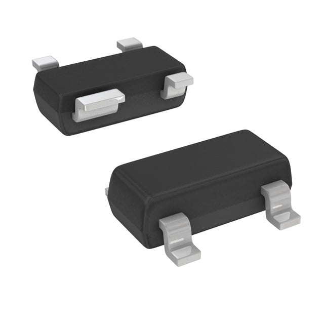
| 产品图片 |
|
| rohs | 符合RoHS无铅 / 符合限制有害物质指令(RoHS)规范要求 |
| 产品系列 | 电源管理 IC,监控电路,Maxim Integrated MAX821TUS+T- |
| NumberofInputsMonitored | 1 Input |
| 数据手册 | |
| 产品型号 | MAX821TUS+T |
| 产品培训模块 | http://www.digikey.cn/PTM/IndividualPTM.page?site=cn&lang=zhs&ptm=25703http://www.digikey.cn/PTM/IndividualPTM.page?site=cn&lang=zhs&ptm=25705 |
| 产品目录页面 | |
| 产品种类 | 监控电路 |
| 人工复位 | No Manual Reset |
| 供应商器件封装 | SOT-143-4 |
| 其它名称 | MAX821TUS+T-ND |
| 功率失效检测 | No |
| 包装 | 带卷 (TR) |
| 受监控电压数 | 1 |
| 商标 | Maxim Integrated |
| 复位 | 低有效 |
| 复位超时 | 可调节/可选择 |
| 安装类型 | 表面贴装 |
| 封装 | Reel |
| 封装/外壳 | TO-253-4,TO-253AA |
| 封装/箱体 | SOT-4 |
| 工作温度 | -40°C ~ 125°C |
| 工作电源电流 | 5.5 uA |
| 工厂包装数量 | 2500 |
| 最大功率耗散 | 320 mW |
| 最大工作温度 | + 125 C |
| 最小工作温度 | - 40 C |
| 标准包装 | 2,500 |
| 欠电压阈值 | 3.04 V |
| 电压-阈值 | 3.08V |
| 电池备用开关 | No Backup |
| 电源电压-最大 | 5.5 V |
| 电源电压-最小 | 1 V |
| 监视器 | No Watchdog |
| 类型 | Voltage Supervisory |
| 系列 | MAX821T |
| 芯片启用信号 | No Chip Enable |
| 被监测输入数 | 1 Input |
| 输出 | 推挽式,图腾柱 |
| 输出类型 | Active Low, Push-Pull |
| 过电压阈值 | 3.11 V |
| 重置延迟时间 | 200 ms |
| 阈值电压 | 3 V to 5 V |
| 零件号别名 | MAX821T |


- 商务部:美国ITC正式对集成电路等产品启动337调查
- 曝三星4nm工艺存在良率问题 高通将骁龙8 Gen1或转产台积电
- 太阳诱电将投资9.5亿元在常州建新厂生产MLCC 预计2023年完工
- 英特尔发布欧洲新工厂建设计划 深化IDM 2.0 战略
- 台积电先进制程称霸业界 有大客户加持明年业绩稳了
- 达到5530亿美元!SIA预计今年全球半导体销售额将创下新高
- 英特尔拟将自动驾驶子公司Mobileye上市 估值或超500亿美元
- 三星加码芯片和SET,合并消费电子和移动部门,撤换高东真等 CEO
- 三星电子宣布重大人事变动 还合并消费电子和移动部门
- 海关总署:前11个月进口集成电路产品价值2.52万亿元 增长14.8%


PDF Datasheet 数据手册内容提取
19-1122; Rev 3; 12/05 4-Pin µP Voltage Monitors with Pin-Selectable Power-On Reset Timeout Delay General Description Features M The MAX821/MAX822 microprocessor (µP) supervisory ♦ Pin-Selectable, Precision Power-On Reset Delay: A circuits monitor power supplies in µP and digital sys- 1ms (max), 20ms (min), or 100ms (min) X tems. They provide excellent circuit reliability and low ♦ Precision Monitoring of +3V to +5V Power-Supply cost by eliminating external components and adjust- 8 ments when used with 5V-powered or 3V-powered cir- Voltages 2 cuits. The MAX821/MAX822 also provide a power-on ♦ 2.5µA Supply Current 1 reset timeout delay that is pin selectable to 1ms (max), ♦ Guaranteed Over Temperature (-40°C to +125°C) / 20ms (min), or 100ms (min). M These devices perform a single function: they assert a ♦ Guaranteed RESETValid to VCC= 1V (MAX821) A reset signal whenever the VCC supply voltage falls ♦ Power-Supply Transient Immunity below a preset threshold, and they keep reset asserted X ♦ No External Components for the pin-selected reset timeout delay after VCC has 8 risen above the reset threshold. The only difference ♦ SOT143 Package 2 between the two devices is that the MAX821 has an active-low RESET output (which is guaranteed to be in Ordering Information 2 the correct state for VCC down to 1V), while the MAX822 has an active-high RESET output. The reset PART NOMINAL VTH(V) TOP MARK* comparator is designed to ignore fast transients on MAX821LUS-T 4.63 AZ_ _ VCC. Reset thresholds suitable for operation with a vari- MAX821MUS-T 4.38 BA_ _ ety of supply voltages are available. MAX821PUS-T 4.00 BM_ _ Low supply current makes the MAX821/MAX822 ideal MAX821TUS-T 3.08 BB_ _ for use in portable equipment. These devices come in a MAX821SUS-T 2.93 BC_ _ 4-pin SOT143 package. MAX821UUS-T 2.78 BL_ _ ________________________Applications MAX821RUS-T 2.63 BD_ _ MAX822LUS-T 4.63 BF_ _ Bar-Code Scanners MAX822MUS-T 4.38 BG_ _ Computers MAX822TUS-T 3.08 BH_ _ Controllers MAX822SUS-T 2.93 BJ_ _ Intelligent Instruments MAX822RUS-T 2.63 BK_ _ * The first two letters in the package top mark identify the part, Critical µP and µC Power Monitoring while the remaining two letters are the lot-tracking code. Portable/Battery-Powered Equipment Devices are available in both leaded and lead-free packaging. Specify lead-free by replacing “-T” with “+T” when ordering. __________Typical Operating Circuit Pin Configuration VCC VCC TOP VIEW MAX821 µP GND 1 4 VCC MAX822 MAX821 RESET MAX822 20ms RESET INPUT (RESET) 100ms SRT 1ms (RESET) RESET 2 3 SRT GND GND SOT143 ( ) ARE FOR MAX822 ( ) ARE FOR MAX822 ________________________________________________________________Maxim Integrated Products 1 For pricing, delivery, and ordering information,please contact Maxim/Dallas Direct!at 1-888-629-4642, or visit Maxim’s website at www.maxim-ic.com.
4-Pin µP Voltage Monitors with Pin-Selectable Power-On Reset Timeout Delay 2 ABSOLUTE MAXIMUM RATINGS 2 Terminal Voltage (with respect to GND) Continuous Power Dissipation (TA= +70°C) 8 VCC......................................................................-0.3V to 6.0V SOT143-4 (derate 4mW/°C above +70°C)...................320mW X All Other Inputs.......................................-0.3V to (VCC+ 0.3V) Operating Temperature Range.........................-40°C to +125°C Input Current, VCC, SRT......................................................20mA Storage Temperature Range.............................-65°C to +160°C A Output Current, RESET or RESET.......................................20mA Lead Temperature (soldering, 10sec).............................+300°C M Stresses beyond those listed under “Absolute Maximum Ratings” may cause permanent damage to the device. These are stress ratings only, and functional / operation of the device at these or any other conditions beyond those indicated in the operational sections of the specifications is not implied. Exposure to 1 absolute maximum rating conditions for extended periods may affect device reliability. 2 8 ELECTRICAL CHARACTERISTICS X (VCC= full range, TA= -40°C to +125°C, unless otherwise noted. Typical values are at TA= +25°C.) A PARAMETER SYMBOL CONDITIONS MIN TYP MAX UNITS M TA= 0°C to +70°C 1.0 5.5 VCCRange V TA= -40°C to +85°C 1.2 5.5 MAX82_L/M/P, TA= +25°C 2.5 7.0 VCC= 5.5V, IOUT= 0 TA= TMINto TMAX 12 Supply Current ICC µA MAX82_R/S/T/U, TA= +25°C 1.8 5.5 VCC= 5.5V, IOUT= 0 TA= TMINto TMAX 9 TA= +25°C 4.56 4.63 4.70 MAX82_L TA= -40°C to +125°C 4.50 4.75 TA= +25°C 4.31 4.38 4.45 MAX82_M TA= -40°C to +125°C 4.25 4.50 TA= +25°C 3.97 4.00 4.04 MAX82_P TA= -40°C to +125°C 3.91 4.09 TA= +25°C 3.04 3.08 3.11 Reset Threshold (Note 1) VTH MAX82_T V TA= -40°C to +125°C 3.00 3.15 TA= +25°C 2.89 2.93 2.96 MAX82_S TA= -40°C to +125°C 2.85 3.00 TA= +25°C 2.74 2.78 2.81 MAX82_U TA= -40°C to +125°C 2.70 2.85 TA= +25°C 2.59 2.63 2.66 MAX82_R TA= -40°C to +125°C 2.55 2.70 Reset Threshold Tempco 30 ppm/°C VCCto Reset Delay (Note 1) VCCfalling at 1mV/µs 50 µs SRT = GND 0.5 0.8 1 Reset Active Timeout Period tRP SRT = VCC 20 32 40 ms SRT = unconnected 100 160 200 SRT = GND -100 RESET= low for MAX821, SRT Input Current (Note 2) SRT = VCC 100 µA RESET = high for MAX822 SRT = unconnected -1 1 VIL 0.07VCC RESET= low for MAX821, SRT Input Threshold VIH 0.9VCC V RESET = high for MAX822 VOPEN 0.5VCC 2 _______________________________________________________________________________________
4-Pin µP Voltage Monitors with Pin-Selectable Power-On Reset Timeout Delay ELECTRICAL CHARACTERISTICS (continued) M (VCC= full range, TA= -40°C to +125°C, unless otherwise noted. Typical values are at TA= +25°C.) A PARAMETER SYMBOL CONDITIONS MIN TYP MAX UNITS X SRT Input Capacitance 8 (Note 3) (see Setting 2 Internal 20 pF the Reset Timeout Delay 1 section) / M MAX821L/M/P only, ISINK= 3.2mA, 0.4 VCC= VTH(MIN) A MAX821R/S/T/U only, ISINK= 1.2mA, 0.3 X VCC= VTH(MIN) VOL 8 TA= 0°C to +70°C, 0.3 2 RESETOutput Voltage VCC≥1V 2 ISINK= 50µA V (MAX821) TA = -40°C to +85°C, 0.3 VCC≥1.2V MVCACX8≥2V1TLH/M(M/APX o)nly, ISOURCE= 800µA, VCC-1.5 VOH MVCACX8≥2V1TRH/(SM/TA/XU) only, ISOURCE= 500µA, 0.8VCC MAX822L/M only, ISINK= 3.2mA, 0.4 VCC= VTH(MAX) RESET Output Voltage VOL (MAX822) MAX822R/S/T only, ISINK= 1.2mA, 0.3 V VCC= VTH(MAX) VOH ISOURCE= 150µA, 1.4V ≤VCC≤VTH(MIN) 0.8VCC Note 1: RESEToutput for MAX821; RESET output for MAX822. Note 2: During reset active timeout period only. Note 3: Guaranteed by design. __________________________________________Typical Operating Characteristics (TA = +25°C, unless otherwise noted.) RESET TIMEOUT PERIOD RESET TIMEOUT PERIOD RESET TIMEOUT PERIOD vs. TEMPERATURE vs. TEMPERATURE vs. TEMPERATURE 1.0 36 180 D (ms) 0.9 SRT = GND MAX 821/822 TOC-04 D (ms) 35 SRT = VCC MAX 821/822 TOC-05 D (ms) 175 SRT = UNCONNECTED MAX 821/822 TOC-06 O O 34 O 170 RI RI RI E E E P P P T 0.8 T 33 T 165 U U U O O O E E E M M M TI TI 32 TI 160 T T T SE 0.7 SE SE E E E R R 31 R 155 0.6 30 150 -40 -20 0 20 40 60 80 100 -40 -20 0 20 40 60 80 100 -40 -20 0 20 40 60 80 100 TEMPERATURE (°C) TEMPERATURE (°C) TEMPERATURE (°C) _______________________________________________________________________________________ 3
4-Pin µP Voltage Monitors with Pin-Selectable Power-On Reset Timeout Delay 2 ____________________________Typical Operating Characteristics (continued) 2 (TA = +25°C, unless otherwise noted.) 8 X MAX82_R/S/T POWER-DOWN RESET DELAY MAX82_L/M POWER-DOWN RESET DELAY A vs. TEMPERATURE vs. TEMPERATURE 45 60 21/M µDELAY (s) 433050 VCC FALLING AT 1mV/µs MAX 821/822 TOC-02 µDELAY (s) 5400 VCC FALLING AT 1mV/µs MAX 821/822 TOC-03 8 SET 25 SET RE RE 30 X N 20 N W W A R-DO 15 VCC FALLING AT 10mV/µs R-DO 20 VCC FALLING AT 10mV/µs M WE 10 WE O O 10 P 5 P 0 0 -40 -20 0 20 40 60 80 100 -40 -20 0 20 40 60 80 100 TEMPERATURE (°C) TEMPERATURE (°C) NORMALIZED SUPPLY NORMALIZED RESET THRESHOLD CURRENT vs. TEMPERATURE vs. TEMPERATURE µENT (A)11..0150 MAX 821/822 TOC-01 HOLD (V) 11..000023 MAX 821/822 TOC-07 RR ES 1.001 U R C H NORMALIZED SUPPLY 01..9050 NORMALIZED RESET T 001...990990980 0.90 0.997 -40 -20 0 20 40 60 80 100 -40 -20 0 20 40 60 80 100 TEMPERATURE (°C) TEMPERATURE (°C) ______________________________________________________________Pin Description PIN NAME FUNCTION MAX821 MAX822 1 1 GND Ground Active-Low Reset Output. RESETis low while VCCis below the reset threshold. It remains 2 – RESET low for the reset timeout period after the reset condition is terminated. The reset timeout period is determined by the SRT input. Active-High Reset Output. RESET is high while VCCis below the reset threshold. It remains – 2 RESET high for the reset timeout period after the reset condition is terminated. The reset timeout period is determined by the SRT input. 3 3 SRT Set Reset Timeout Input. Connect to GND for 1ms (max) delay; connect to VCCfor 20ms (min) delay; leave unconnected for 100ms (min) delay. 4 4 VCC Supply Voltage 4 _______________________________________________________________________________________
4-Pin µP Voltage Monitors with Pin-Selectable Power-On Reset Timeout Delay _______________Detailed Description M Reset Output A 300 Akton mopwircner voseptanrotte c.ce oTshdseoesr-’ees xµ(eµPcP us’sut)ip orener sveeisrt roionrryps uc dti rsucturaiinrtstgs atpshsoeew µretP rr -eiunsp ea,t µTION (s) 250 TA = +25°C MAX821/822 FIG-01 X8 power-down, or brownout conditions. They also provide URA 200 2 a reset timeout delay that is pin programmable to 1ms T D 1 N (flmexaixb)i,l it2y0 mins d(emsiing)n, ionrg 1 b0a0rm-cso (dmei ns)c. aTnhnise fresa, thuaren da-llhoewlds ANSIE 150 /M R devices, and other applications that require quick or T 100 M A nonstandard power-up times. U M XI 50 X The MAX821’s RESET output is guaranteed to be a A M logic low for VCC > 1V. Once VCC exceeds the reset 0 8 threshold, an internal timer keeps RESET low for the 1 10 100 1000 2 reset timeout period, as determined by the Set Reset RESET COMPARATOR OVERDRIVE, VTH-VCC (mV) 2 Timeout (SRT) input. See the Setting the Reset Timeout Delaysection. If a brownout condition occurs (VCC dips below the Figure 1. Maximum Transient Duration Without Causing a reset threshold), RESET goes low. Any time VCC goes Reset Pulse vs. Comparator Overdrive below the reset threshold, the internal timer resets to zero, and RESET goes low. The internal timer begins __________Applications Information counting after VCC returns above the reset threshold, and RESETremains low for the reset timeout period. Negative-Going VCC Transients While designed to issue a reset to the microprocessor The MAX822 has an active-high RESET output that is (µP) during power-up, power-down, and brownout con- the inverse of the MAX821’s RESEToutput. ditions, the MAX821/MAX822 are relatively immune to Setting the Reset Timeout Delay short-duration, negative-going VCCtransients (glitches). Use the three-level Set Reset Timeout (SRT) input to set Figure 1 shows the maximum transient duration vs. reset the reset timeout delay. Connect SRT to GND for a 1ms comparator overdrive for which the MAX821/MAX822 (max) delay; connect it to VCC for a 20ms (min) delay; typically do not generate a reset pulse. This graph was or leave it unconnected for a 100ms (min) delay. generated using a negative-going pulse applied to VCC, If you choose to drive the SRT pin with an external sig- starting above the actual reset threshold and ending nal, make sure the signal source can charge/discharge below it by the magnitude indicated (reset comparator the capacitance on SRT quickly enough (<500µs) to overdrive). The graph indicates the typical maximum avert an unintended reset timeout delay. pulse width a negative-going VCC transient may have without causing a reset pulse to be issued. As the mag- To ensure proper operation when selecting the 100ms nitude of the transient increases (goes farther below the timeout (SRT = unconnected), minimize capacitive reset threshold), the maximum allowable pulse width loading on the SRT pin (< 200pF). Excessive capacitive loading can select an unintended faster timeout mode. decreases. Typically, for the MAX821/MAX822, a VCC transient that goes 100mV below the reset threshold and Reset Threshold Accuracy lasts 12µs or less will not cause a reset pulse to be The MAX821/MAX822 are designed to meet their worst- issued. A 0.1µF capacitor mounted as close as possible case specifications over their entire operating tempera- to VCC can provide additional transient immunity, if ture range. Choose a reset threshold guaranteed to desired. assert at a voltage below the power supply’s regulation range and above the minimum specified operating volt- age range for the system’s ICs. _______________________________________________________________________________________ 5
4-Pin µP Voltage Monitors with Pin-Selectable Power-On Reset Timeout Delay 2 Ensuring a Valid RESETOutput 2 Down to VCC = 0V VCC VCC 8 When VCC falls below 1V, the MAX821 RESET output no longer sinks current—it becomes an open circuit. X Therefore, high-impedance CMOS logic inputs con- VCC VCC A nected to the RESET output can drift to undetermined R1 voltages. This presents no problem in most applica- M tions, since most µP and other circuitry is inoperative MAX821 MAX822 / with VCC below 1V. However, in applications where the RESET RESET 1 RESET output must be valid down to 0V, adding a pull- 2 R1 down resistor to the RESET pin will cause any stray 8 leakage currents to flow to ground, holding RESET low GND GND X (Figure 2a). R1’s value is not critical; 100kΩ is large a) b) enough not to load RESET, and small enough to pull A RESETto ground. M A 100kΩ pull-up resistor to VCC is also recommended Figure 2. RESET/RESET Valid to VCC= Ground Circuit for the MAX822 if RESET is required to remain valid for VCC< 1V (Figure 2b). Interfacing to µPs with BUFFERED RESET BUFFER TO OTHER SYSTEM Bidirectional Reset Pins COMPONENTS µPs with bidirectional reset pins (such as the Motorola 68HC11 series) can contend with the MAX821 reset output. For example, if the MAX821 RESET output is VCC VCC asserted high and the µP wants to pull it low, indetermi- nate logic levels may result. To correct such cases, MAX821 µP 4.7k connect a 4.7kΩ resistor between the MAX821 RESET RESET RESET output and the µP reset I/O (Figure 3). Buffer the reset output to other system components. GND GND ___________________Chip Information TRANSISTOR COUNT: 492 Figure 3. Interfacing to µPs with Bidirectional Reset I/O 6 _______________________________________________________________________________________
4-Pin µP Voltage Monitors with Pin-Selectable Power-On Reset Timeout Delay Package Information M (The package drawing(s) in this data sheet may not reflect the most current specifications. For the latest package outline information, A go to www.maxim-ic.com/packages.) X 8 S P L.E 2 4 43 1 1 OT- / S M A X 8 2 2 PACKAGE OUTLINE, SOT-143, 4L 1 21-0052 E 1 Maxim cannot assume responsibility for use of any circuitry other than circuitry entirely embodied in a Maxim product. No circuit patent licenses are implied. Maxim reserves the right to change the circuitry and specifications without notice at any time. 7 _____________________Maxim Integrated Products, 120 San Gabriel Drive, Sunnyvale, CA 94086 408-737-7600 © 2005 Maxim Integrated Products Printed USA is a registered trademark of Maxim Integrated Products, Inc.