ICGOO在线商城 > 集成电路(IC) > PMIC - 监控器 > MAX6804US26D3+T

 Datasheet下载
- 型号: MAX6804US26D3+T
- 制造商: Maxim
- 库位|库存: xxxx|xxxx
- 要求:
| 数量阶梯 | 香港交货 | 国内含税 |
| +xxxx | $xxxx | ¥xxxx |
查看当月历史价格
查看今年历史价格
MAX6804US26D3+T产品简介:
ICGOO电子元器件商城为您提供MAX6804US26D3+T由Maxim设计生产,在icgoo商城现货销售,并且可以通过原厂、代理商等渠道进行代购。 MAX6804US26D3+T价格参考¥11.03-¥11.03。MaximMAX6804US26D3+T封装/规格:PMIC - 监控器, 推挽式,图腾柱 监控器 1 通道 SOT-143-4。您可以下载MAX6804US26D3+T参考资料、Datasheet数据手册功能说明书,资料中有MAX6804US26D3+T 详细功能的应用电路图电压和使用方法及教程。
MAX6804US26D3+T 是由 Maxim Integrated(现为 Analog Devices 旗下)生产的一款电源管理IC,属于 PMIC 中的监控器类别。它主要用于监测系统中的电压水平,并在电压异常时提供复位信号,以确保系统的稳定性和可靠性。

该器件的典型应用场景包括:

1. 嵌入式系统与工业控制:用于监测微处理器或微控制器的供电电压,防止因电压过低导致系统运行异常或数据损坏。

2. 通信设备:在基站、路由器或交换机等设备中,用于监控电源状态,确保设备在电压异常时能及时复位,维持通信稳定。

3. 消费电子产品:如智能家电、智能仪表等,用于提供电压监控和系统复位功能,提高产品可靠性。

4. 汽车电子:用于车载控制系统中,监测电池或主电源电压,保障系统在恶劣电源环境下正常工作。

5. 医疗设备:在便携式或固定式医疗仪器中,确保设备在电压不稳时能及时响应,避免误操作或数据丢失。

该芯片具有低功耗、高精度电压检测和手动复位输入等功能,适用于多种对电源监控有较高要求的场景。
| 参数 | 数值 |
| 产品目录 | 集成电路 (IC) |
| 描述 | IC RESET MPU LOW PWR SOT143-4 |
| 产品分类 | |
| 品牌 | Maxim Integrated |
| 数据手册 | |
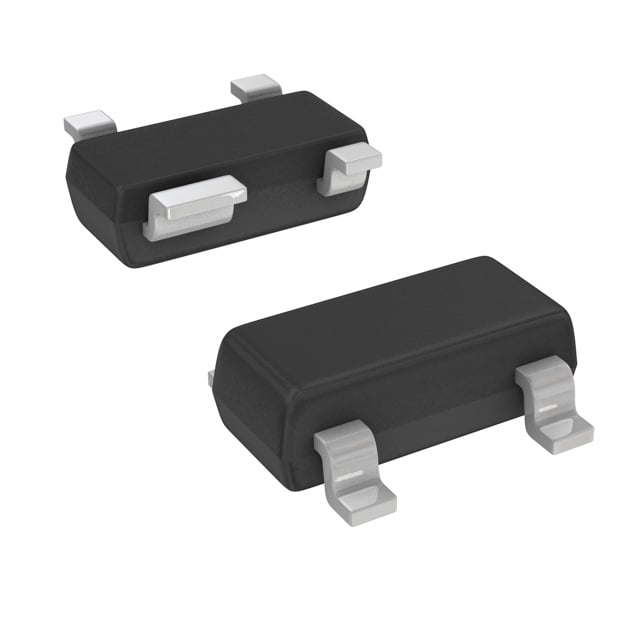
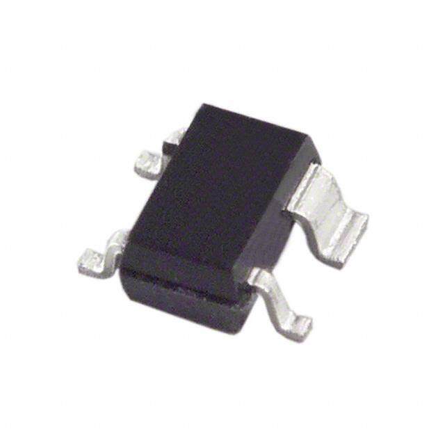
| 产品图片 |
|
| 产品型号 | MAX6804US26D3+T |
| rohs | 无铅 / 符合限制有害物质指令(RoHS)规范要求 |
| 产品系列 | - |
| 产品培训模块 | http://www.digikey.cn/PTM/IndividualPTM.page?site=cn&lang=zhs&ptm=25703http://www.digikey.cn/PTM/IndividualPTM.page?site=cn&lang=zhs&ptm=25705 |
| 产品目录页面 | |
| 供应商器件封装 | SOT-143-4 |
| 其它名称 | MAX6804US26D3+TCT |
| 包装 | 剪切带 (CT) |
| 受监控电压数 | 1 |
| 复位 | 低有效 |
| 复位超时 | 最小为 100 ms |
| 安装类型 | 表面贴装 |
| 封装/外壳 | TO-253-4,TO-253AA |
| 工作温度 | -40°C ~ 125°C |
| 标准包装 | 1 |
| 电压-阈值 | 2.63V |
| 类型 | 简单复位/加电复位 |
| 输出 | 推挽式,图腾柱 |


- 商务部:美国ITC正式对集成电路等产品启动337调查
- 曝三星4nm工艺存在良率问题 高通将骁龙8 Gen1或转产台积电
- 太阳诱电将投资9.5亿元在常州建新厂生产MLCC 预计2023年完工
- 英特尔发布欧洲新工厂建设计划 深化IDM 2.0 战略
- 台积电先进制程称霸业界 有大客户加持明年业绩稳了
- 达到5530亿美元!SIA预计今年全球半导体销售额将创下新高
- 英特尔拟将自动驾驶子公司Mobileye上市 估值或超500亿美元
- 三星加码芯片和SET,合并消费电子和移动部门,撤换高东真等 CEO
- 三星电子宣布重大人事变动 还合并消费电子和移动部门
- 海关总署:前11个月进口集成电路产品价值2.52万亿元 增长14.8%


PDF Datasheet 数据手册内容提取
MAX6803/MAX6804/ 4-Pin, Low-Power MAX6805 µP Reset Circuits with Manual Reset General Description Features The MAX6803/MAX6804/MAX6805 microprocessor (µP) ● Ultra-Low 0.7V Operating Supply Voltage supervisory circuits monitor the power supplies in 2.85V ● Low 4.0µA Supply Current to 5.0V µP and digital systems. They increase cir- ● Precision Monitoring of 2.85V to 5.0V Power-Supply cuit reliability and reduce cost by eliminating external Voltages components and adjustments. They also feature a debounced manual-reset input. ● Reset Thresholds Available from 2.63V to 4.80V, in Approximately 100mV Increments These devices perform a single function: they assert a reset signal whenever the VCC supply voltage declines ● Debounced Manual-Reset Input below a preset threshold or whenever manual reset is ● Fully Specified over Temperature asserted. Reset remains asserted for a preset timeout ● Three Power-On Reset Timeout Periods Available period after VCC has risen above the reset threshold or (1ms min, 20ms min, 100ms min) after manual reset is deasserted. The only difference among the three devices is their output. The MAX6804 ● Low Cost (push/pull) and MAX6805 (open-drain) have an active- ● Three Available Output Structures: Push/Pull low RESET output, while the MAX6803 (push/pull) has RESET, Push/Pull RESET, Open-Drain RESET an active-high RESET output. The MAX6803/MAX6804 ● Guaranteed RESET/RESET Valid to VCC = 0.7V are guaranteed to be in the correct state for VCC down (MAX6803/MAX6804) to 0.7V. The MAX6805 is guaranteed to be in the correct state for VCC down to 1.0V. ● Power-Supply Transient Immunity The reset comparator in these ICs is designed to ignore ● No External Components Required fast transients on VCC. Reset thresholds are factory- ● 4-Pin SOT143 Package trimmable between 2.63V and 4.80V, in approximately ● Pin Compatible with MAX811/MAX812 and 100mV increments. These devices are available with a MAX6314/MAX6315( 1ms min, 20ms min, or 100ms min reset timeout period. Ideal for space-critical applications, the MAX6803/ Ordering Information MAX6804/MAX6805 come packaged in a 4-pin SOT143. PART* TEMP RANGE PIN-PACKAGE For a lower threshold voltage version, see the MAX6335/ MAX6803US_ _D_-T -40°C to +125°C 4 SOT143 MAX6336/MAX6337. MAX6804US_ _D_-T -40°C to +125°C 4 SOT143 Applications MAX6805US_ _D_-T -40°C to +125°C 4 SOT143 ● Computers *These devices are available in factory-set VCC reset thresh- ● Controllers olds from 2.63V to 4.80V, in approximately 0.1V increments. ● Intelligent Instruments Choose the desired reset threshold suffix from Table 1 and insert it in the blanks following “US” in the part number. ● Critical µP/µC Power Monitoring Factory-programmed reset timeout periods are also available. ● Portable/Battery-Powered Equipment Insert the number corresponding to the desired nominal reset timeout period (1 = 1ms min, 2 = 20ms min, 3 = 100ms min) in the blank following “D” in the part number. There are 15 stan- dard versions with a required order increment of 2500 pieces. Sample stock is generally held on the standard versions only Typical Operating Circuit and Pin Configuration appear (see Selector Guide). Contact the factory for availability of non- at end of data sheet. standard versions (required order increment is 10,000 pieces). All devices available in tape-and-reel only. Devices are available in both leaded and lead-free packaging. Selector Guide appears at end of data sheet. Specify lead-free by replacing “-T” with “+T” when ordering. 19-1946; Rev 3; 7/14
MAX6803/MAX6804/ 4-Pin, Low-Power MAX6805 µP Reset Circuits with Manual Reset Absolute Maximum Ratings Terminal Voltage (with respect to GND) Continuous Power Dissipation (TA = +70°C) VCC ......................................................................-0.3V to +6V 4-Pin SOT143 (derate 4mW/°C above +70°C) ...........320mW Push/Pull RESET or RESET, MR ........-0.3V to (VCC + 0.3V) Operating Temperature Range .........................-40°C to +125°C Open-Drain RESET .............................................-0.3V to +6V Junction Temperature ......................................................+150°C Input Current (VCC) ............................................................20mA Storage Temperature Range ............................-65°C to +150°C Output Current (RESET, RESET) ......................................20mA Lead Temperature (soldering, 10s) .................................+300°C Stresses beyond those listed under “Absolute Maximum Ratings” may cause permanent damage to the device. These are stress ratings only, and functional operation of the device at these or any other conditions beyond those indicated in the operational sections of the specifications is not implied. Exposure to absolute maximum rating conditions for extended periods may affect device reliability. Electrical Characteristics (VCC = full range, TA = -40°C to +125°C, unless otherwise noted. Typical values are at VCC = +5.0V and TA = +25°C, reset not asserted.) (Note 1) PARAMETER SYMBOL CONDITIONS MIN TYP MAX UNITS MAX6803/MAX6804 0.7 5.5 TA = 0°C to +125°C Supply Voltage Range MAX6805 1.0 5.5 (Note 1) VCC MAX6803/MAX6804 0.78 5.5 V TA = -40°C to +125°C MAX6805 1.2 5.5 VCC = +3.0V 4 10 Supply Current ICC No load µA VCC = +5.0V 5 12 TA = +25°C - V1.T8H% VTH + V1T.8H% MAX680_US_ _D_-T, Reset Threshold VTH Table 1 V TA = -40°C to +125°C -V 3T%H VTH +V 3T%H VCC Falling Reset Delay VCC falling at 10V/ms 30 µs MAX680_US_ _D1-T 1 1.5 2 Reset Active Timeout Period tRP MAX680_US_ _D2-T 20 30 40 ms MAX680_US_ _D3-T 100 150 200 MR Minimum Pulse Width 1 µs MR Glitch Immunity 50 ns MR Reset Delay 0.1 µs VIL 0.3 × VCC MR Input Voltage V VIH 0.7 × VCC MR Pullup Resistance 12 20 30 kW ISINK = 50µA, VCC ≥ 1.0V 0.4 RESET Output Low Voltage Reset (MAX6804/MAX6805) VOL asserted ISINK = 1.2mA, VCC ≥ 2.5V 0.3 V ISINK = 3.2mA, VCC ≥ 4.25V 0.4 RESET Output High Voltage Reset not ISOURCE = 500µA, VCC ≥ 3.0V 0.8 × VCC (MAX6804) VOH asserted ISOURCE = 800µA, VCC ≥ 5.0V 0.8 × VCC V www.maximintegrated.com Maxim Integrated │ 2
MAX6803/MAX6804/ 4-Pin, Low-Power MAX6805 µP Reset Circuits with Manual Reset Electrical Characteristics (continued) (VCC = full range, TA = -40°C to +125°C, unless otherwise noted. Typical values are at VCC = +5.0V and TA = +25°C, reset not asserted.) (Note 1) PARAMETER SYMBOL CONDITIONS MIN TYP MAX UNITS ISOURCE = 1µA, VCC ≥ 1.0V 0.8 × VCC Reset VOH asserted ISOURCE = 200µA, VCC ≥ 1.8V 0.8 × VCC V RESET Output Voltage (MAX6803) ISOURCE = 800µA, VCC ≥ 4.25V 0.8 × VCC Reset not ISINK = 1.2mA, VCC ≥ 3.0V 0.3 VOL asserted ISINK = 3.2mA, VCC ≥ 5.0V 0.4 V RESET Output Leakage Current (MAX6805) VCC > VTH, RESET not asserted 0.5 µA Note 1: All parts are production tested at TA = +25°C. Over temperature limits are guaranteed by design and not production tested. Note 2: ISOURCE for the MAX6803 is 100nA; ISINK for the MAX6804 is 100nA; ISINK for the MAX6805 is 50µA. Typical Operating Characteristics (Reset not asserted, TA = +25°C, unless otherwise noted.) SUPPLY CURRENT NORMALIZED RESET TIMEOUT PERIOD OUTPUT-VOLTAGE LOW vs. TEMPERATURE vs. TEMPERATURE vs. SUPPLY VOLTAGE µI (A)CC 54656.....05055 VCC = +5.0V MAX6803/04/05 toc01 D RESET TIMEOUT PERIOD1011111.......090000009432150000000 MAX6803/04/05 toc02 T-VOLTAGE LOW (mV) 864000 +125°C +85°C+2IRVS5TEI°NHSCK =E = T2 - 5.490030°VµCA MAX6803/04/05 toc03 4.0 VCC = +3.3V MALIZE00..998700 OUTPU 20 3.5 OR N0.960 3.0 0.950 0 -50 -25 0 25 50 75 100 125 -50 -25 0 25 50 75 100 125 1.0 1.5 2.0 2.5 3.0 TEMPERATURE (°C) TEMPERATURE (°C) VCC (V) OUTPUT-VOLTAGE HIGH MAXIMUM TRANSIENT DURATION VCC FALLING PROPAGATION DELAY vs. SUPPLY VOLTAGE vs. RESET COMPARATOR OVERDRIVE vs. TEMPERATURE TPUT-VOLTAGE HIGH (V - V) (mV)CCOH107520505 +12+58°5C°IR(VCSMTEINAHSK+ X=E 26= T528 1°.A09C03S30)VSµEARTEDMAX6803/04/05 toc04 µAXIMUM TRANSIENT DURATION (s)124356000000000000 RNEOSTE TO C DCOUERS RESET OCCURS MAX6803/04/05 toc05 µPOROPAGATION DELAY (s)1325498760000000000 VVCCCC = = F FAALLLLININGG A ATT 1 10VV//mmss MAX6803/04/05 toc06 OU -40°C M 10 0 0 0 1.0 1.5 2.0 2.5 3.0 0.1 1 10 100 1000 -50 -25 0 25 50 75 100 125 VCC (V) RESET COMPARATOR OVERDRIVE (mV) TEMPERATURE (°C) www.maximintegrated.com Maxim Integrated │ 3
MAX6803/MAX6804/ 4-Pin, Low-Power MAX6805 µP Reset Circuits with Manual Reset Pin Description PIN MAX6804 NAME FUNCTION MAX6803 MAX6805 1 1 GND Ground Active-Low Reset Output. RESET is asserted while VCC is below the reset threshold, or while MR is asserted. RESET remains asserted for a reset — 2 RESET timeout period (tRP) after VCC rises above the reset threshold or MR is deasserted. RESET on the MAX6804 is push/pull. RESET on the MAX6805 is open-drain. Active-High Reset Output. RESET is asserted high while VCC is below the reset threshold or while MR is asserted, and RESET remains asserted for a 2 — RESET reset timeout period (tRP) after VCC rises above the reset threshold or MR is deasserted. RESET on the MAX6803 is push/pull. Manual-Reset Input. A logic low on MR asserts reset. Reset remains 3 3 MR asserted as long as MR is low, and for the reset timeout period (tRP) after MR goes high. Leave unconnected or connect to VCC if not used. 4 4 VCC Supply Voltage Input Applications Information shows the maximum pulse width that a negative-going VCC transient may typically have without issuing a reset Manual-Reset Input signal. As the amplitude of the transient increases, the Many µP-based products require manual-reset capability, maximum allowable pulse width decreases. allowing the operator, a test technician, or external logic Ensuring a Valid Reset Output Down to circuitry to initiate a reset. A logic low on MR asserts reset. Reset remains asserted while MR is low, and for the reset VCC = 0 active timeout period after MR returns high. MR has an When VCC falls below 1V and approaches the minimum internal 20kW pullup resistor, so it can be left unconnected operating voltage of 0.7V, push/pull-structured reset if not used. Connect a normally open momentary switch sinking (or sourcing) capabilities decrease drastically. from MR to GND to create a manual-reset function; High-impedance CMOS-logic inputs connected to the external debounce circuitry is not required. RESET pin can drift to indeterminate voltages. This does not present a problem in most cases, since most Interfacing to µPs with Bidirectional Reset Pins VCC Since the RESET output on the MAX6805 is open-drain, 100kΩ this device interfaces easily with µPs that have bidirec- VCC VCC tional reset pins, such as the Motorola 68HC11. µP MAX6805 MOTOROLA Connecting the µP supervisor’s RESET output directly 68HCXX to the microcontroller’s (µC’s) RESET pin with a MR RESET RESET single pullup resistor allows either device to assert reset (Figure 1). Negative-Going VCC Transients GND GND In addition to issuing a reset to the µP during power-up, power-down, and brownout conditions, these devices are relatively immune to short-duration, negative-going Figure 1. Interfacing to μPs with Bidirectional Reset Pins VCC transients (glitches). The Typical Operating Characteristics show the Maximum Transient Duration vs. Reset Comparator Overdrive graph. The graph www.maximintegrated.com Maxim Integrated │ 4
MAX6803/MAX6804/ 4-Pin, Low-Power MAX6805 µP Reset Circuits with Manual Reset µPs and circuitry do not operate when VCC drops below Since the MAX6805 has an open-drain, active-low 1V. For the MAX6804 application where RESET must out-put, it typically uses a pullup resistor. With this device, be valid down to 0, adding a pulldown resistor between RESET will most likely not maintain an active condi- RESET and GND removes stray leakage currents, tion, but will drift to a non-active level due to the pullup holding RESET low (Figure 2a). The pulldown resistor resistor and the reduced sinking capability of the open- value is not critical; 100kW is large enough not to load drain device. Therefore, this device is not recommend- RESET, and small enough to pull it low. For the MAX6803, ed for applications where the RESET pin is required to where RESET must be valid to VCC = 0, a 100kW pullup be valid down to VCC = 0. resistor between RESET and VCC will hold RESET high when VCC falls below 0.7V (Figure 2b). Pin Configuration VCC TOP VIEW MAX6804 MR RESET GND 1 4 VCC 100kΩ (a) GND MAX6803 MAX6804 MAX6805 VCC RESET(RESET) 2 3 MR 100kΩ* MAX6803 SOT143 MR RESET ( ) ARE FOR MAX6803 (b) GND Typical Operating Circuit *ASSUMES HIGH-Z RESET INPUT TO THE µP Figure 2. Ensuring Reset Valid down to VCC = 0 VCC VCC VCC MAX6804 µP MR RESET RESET GND GND PUSHBUTTON SWITCH www.maximintegrated.com Maxim Integrated │ 5
MAX6803/MAX6804/ 4-Pin, Low-Power MAX6805 µP Reset Circuits with Manual Reset Table 1. Factory-Trimmed Reset Thresholds RESET TA = +25°C TA = -40°C to +125°C THRESHOLD SUFFIX MIN TYP (VTH) MAX MIN MAX 48 4.714 4.80 4.886 4.656 4.944 47 4.615 4.70 4.785 4.559 4.841 46 4.547 4.63 4.713 4.491 4.769 45 4.419 4.50 4.581 4.365 4.635 44 4.301 4.38 4.459 4.249 4.511 43 4.223 4.30 4.377 4.171 4.429 42 4.124 4.20 4.276 4.074 4.326 41 4.026 4.10 4.174 3.977 4.223 40 3.928 4.00 4.072 3.880 4.120 39 4.830 3.90 3.970 3.783 4.017 38 3.732 3.80 3.868 3.686 3.914 37 3.633 3.70 3.767 3.589 3.811 36 3.535 3.60 3.665 3.492 3.708 35 3.437 3.50 3.563 3.395 3.605 34 3.339 3.40 3.461 3.298 3.502 33 3.241 3.30 3.359 3.201 3.399 32 3.142 3.20 3.258 3.104 3.296 31 3.025 3.08 3.135 2.988 3.172 30 2.946 3.00 3.054 2.910 3.090 29 2.877 2.93 2.983 2.842 3.018 28 2.750 2.80 2.850 2.716 2.884 27 2.651 2.70 2.749 2.619 2.781 26 2.583 2.63 2.677 2.551 2.709 www.maximintegrated.com Maxim Integrated │ 6
MAX6803/MAX6804/ 4-Pin, Low-Power MAX6805 µP Reset Circuits with Manual Reset Selector Guide (Standard Versions*) MIN RESET SOT PART OUTPUT STAGE NOMINAL VTH (V) TIMEOUT (ms) TOP MARK MAX6803US26D3-T Push/Pull RESET 2.63 100 KACH MAX6803US29D3-T Push/Pull RESET 2.93 100 KACI MAX6803US31D3-T Push/Pull RESET 3.08 100 KACJ MAX6803US44D3-T Push/Pull RESET 4.38 100 KACK MAX6803US46D3-T Push/Pull RESET 4.63 100 KACL MAX6804US26D3-T Push/Pull RESET 2.63 100 KACN MAX6804US29D3-T Push/Pull RESET 2.93 100 KACP MAX6804US31D3-T Push/Pull RESET 3.08 100 KACQ MAX6804US44D3-T Push/Pull RESET 4.38 100 KACR MAX6804US46D3-T Push/Pull RESET 4.63 100 KACS MAX6805US26D3-T Open-Drain RESET 2.63 100 KACO MAX6805US29D3-T Open-Drain RESET 2.93 100 KACU MAX6805US31D3-T Open-Drain RESET 3.08 100 KACV MAX6805US44D3-T Open-Drain RESET 4.38 100 KACW MAX6805US46D3-T Open-Drain RESET 4.63 100 KACX *Sample stock is generally held on all standard versions. Chip Information Package Information TRANSISTOR COUNT: 505 For the latest package outline information and land patterns PROCESS: BiCMOS (footprints), go to www.maximintegrated.com/packages. Note that a “+”, “#”, or “-” in the package code indicates RoHS status only. Package drawings may show a different suffix character, but the drawing pertains to the package regardless of RoHS status. PACKAGE PACKAGE OUTLINE LAND TYPE CODE NO. PATTERN NO. 4 SOT143 U4-1 21-0052 90-0183 www.maximintegrated.com Maxim Integrated │ 7
MAX6803/MAX6804/ 4-Pin, Low-Power MAX6805 µP Reset Circuits with Manual Reset Revision History REVISION REVISION PAGES DESCRIPTION NUMBER DATE CHANGED 3 7/14 No /V OPNs; removed Automotive reference from Applications section 1 For pricing, delivery, and ordering information, please contact Maxim Direct at 1-888-629-4642, or visit Maxim Integrated’s website at www.maximintegrated.com. Maxim Integrated cannot assume responsibility for use of any circuitry other than circuitry entirely embodied in a Maxim Integrated product. No circuit patent licenses are implied. Maxim Integrated reserves the right to change the circuitry and specifications without notice at any time. The parametric values (min and max limits) shown in the Electrical Characteristics table are guaranteed. Other parametric values quoted in this data sheet are provided for guidance. Maxim Integrated and the Maxim Integrated logo are trademarks of Maxim Integrated Products, Inc. © 2014 Maxim Integrated Products, Inc. │ 8
Mouser Electronics Authorized Distributor Click to View Pricing, Inventory, Delivery & Lifecycle Information: M axim Integrated: MAX6803US26D1+T MAX6803US26D2+T MAX6803US26D3+T MAX6803US27D1+T MAX6803US27D2+T MAX6803US27D3+T MAX6803US28D1+T MAX6803US28D2+T MAX6803US28D3+T MAX6803US29D1+T MAX6803US29D2+T MAX6803US29D3+T MAX6803US30D1+T MAX6803US30D2+T MAX6803US30D3+T MAX6803US31D1+T MAX6803US31D2+T MAX6803US31D3+T MAX6803US32D1+T MAX6803US32D2+T MAX6803US32D3+T MAX6803US33D1+T MAX6803US33D2+T MAX6803US33D3+T MAX6803US34D1+T MAX6803US34D2+T MAX6803US34D3+T MAX6803US35D1+T MAX6803US35D2+T MAX6803US35D3+T MAX6803US36D1+T MAX6803US36D2+T MAX6803US36D3+T MAX6803US37D1+T MAX6803US37D2+T MAX6803US37D3+T MAX6803US38D1+T MAX6803US38D2+T MAX6803US38D3+T MAX6803US39D1+T MAX6803US39D2+T MAX6803US39D3+T MAX6803US40D1+T MAX6803US40D2+T MAX6803US40D3+T MAX6803US41D1+T MAX6803US41D2+T MAX6803US41D3+T MAX6803US42D1+T MAX6803US42D2+T MAX6803US42D3+T MAX6803US43D1+T MAX6803US43D2+T MAX6803US43D3+T MAX6803US44D1+T MAX6803US44D2+T MAX6803US44D3+T MAX6803US45D1+T MAX6803US45D2+T MAX6803US45D3+T MAX6803US46D1+T MAX6803US46D2+T MAX6803US46D3+T MAX6803US47D1+T MAX6803US47D2+T MAX6803US47D3+T MAX6803US48D1+T MAX6803US48D2+T MAX6803US48D3+T MAX6804US26D1+T MAX6804US26D2+T MAX6804US26D3+T MAX6804US27D1+T MAX6804US27D2+T MAX6804US27D3+T MAX6804US28D1+T MAX6804US28D2+T MAX6804US28D3+T MAX6804US29D1+T MAX6804US29D2+T MAX6804US29D3+T MAX6804US30D1+T MAX6804US30D2+T MAX6804US30D3+T MAX6804US31D1+T MAX6804US31D2+T MAX6804US31D3+T MAX6804US32D1+T MAX6804US32D2+T MAX6804US32D3+T MAX6804US33D1+T MAX6804US33D2+T MAX6804US33D3+T MAX6804US34D1+T MAX6804US34D2+T MAX6804US34D3+T MAX6804US35D1+T MAX6804US35D2+T MAX6804US35D3+T MAX6804US36D1+T