ICGOO在线商城 > 集成电路(IC) > PMIC - 监控器 > MAX6464XR16+T

 Datasheet下载
- 型号: MAX6464XR16+T
- 制造商: Maxim
- 库位|库存: xxxx|xxxx
- 要求:
| 数量阶梯 | 香港交货 | 国内含税 |
| +xxxx | $xxxx | ¥xxxx |
查看当月历史价格
查看今年历史价格
MAX6464XR16+T产品简介:
ICGOO电子元器件商城为您提供MAX6464XR16+T由Maxim设计生产,在icgoo商城现货销售,并且可以通过原厂、代理商等渠道进行代购。 MAX6464XR16+T价格参考¥10.55-¥10.55。MaximMAX6464XR16+T封装/规格:PMIC - 监控器, 推挽式,图腾柱 监控器 1 通道 SC-70-3。您可以下载MAX6464XR16+T参考资料、Datasheet数据手册功能说明书,资料中有MAX6464XR16+T 详细功能的应用电路图电压和使用方法及教程。
MAX6464XR16+T 是由 Maxim Integrated(现为 Analog Devices 旗下品牌)生产的一款电源管理IC(PMIC),具体分类为电压监控器。该器件主要用于监测系统中的电源电压,确保其在安全范围内运行,广泛应用于需要高可靠性和稳定性的电子系统中。

其主要应用场景包括:

1. 工业控制系统:用于监测PLC、工控机等设备的供电电压,防止因电压异常导致系统崩溃或数据丢失。
2. 通信设备:如基站、路由器和交换机中,用于监控电源模块输出电压,保障通信稳定性。
3. 嵌入式系统与服务器:用于监控处理器、FPGA或DSP的核心电压,确保高性能芯片正常工作。
4. 汽车电子系统:如车载控制单元(ECU)、电池管理系统(BMS)中,用于检测电源状态,提升行车安全性。
5. 消费类电子产品:高端家电、智能终端等产品中用于电源监控,提高系统可靠性。

该器件具有多个阈值可选、低功耗、封装小巧等特点,适合多种电源监控需求。
| 参数 | 数值 |
| 产品目录 | 集成电路 (IC)半导体 |
| 描述 | IC VOLT DETECTOR LP SC70-3监控电路 Single uPower Voltage Monitor |
| 产品分类 | |
| 品牌 | Maxim Integrated |
| 产品手册 | |
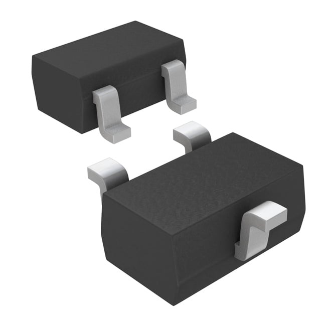
| 产品图片 |
|
| rohs | 符合RoHS无铅 / 符合限制有害物质指令(RoHS)规范要求 |
| 产品系列 | 电源管理 IC,监控电路,Maxim Integrated MAX6464XR16+T- |
| NumberofInputsMonitored | 1 Input |
| 数据手册 | |
| 产品型号 | MAX6464XR16+T |
| 产品培训模块 | http://www.digikey.cn/PTM/IndividualPTM.page?site=cn&lang=zhs&ptm=25703http://www.digikey.cn/PTM/IndividualPTM.page?site=cn&lang=zhs&ptm=25705 |
| 产品目录页面 | |
| 产品种类 | 监控电路 |
| 人工复位 | No Manual Reset |
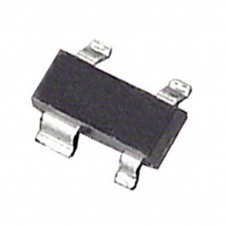
| 供应商器件封装 | SC-70-3 |
| 其它名称 | MAX6464XR16+T-ND |
| 准确性 | 2.5 % |
| 包装 | 带卷 (TR) |
| 受监控电压数 | 1 |
| 商标 | Maxim Integrated |
| 复位 | 低有效 |
| 复位超时 | 最小为 150 ms |
| 安装类型 | 表面贴装 |
| 安装风格 | SMD/SMT |
| 封装 | Reel |
| 封装/外壳 | SC-70,SOT-323 |
| 封装/箱体 | SC-70-3 |
| 工作温度 | -40°C ~ 125°C |
| 工作电源电流 | 3.5 uA |
| 工厂包装数量 | 2500 |
| 最大工作温度 | + 125 C |
| 最小工作温度 | - 40 C |
| 标准包装 | 2,500 |
| 欠电压阈值 | 1.647 V |
| 电压-阈值 | 1.6V |
| 电池备用开关 | No Backup |
| 电源电压-最大 | 6 V |
| 电源电压-最小 | 1.2 V |
| 监视器 | No Watchdog |
| 类型 | 简单复位/加电复位 |
| 系列 | MAX6464 |
| 被监测输入数 | 1 Input |
| 输出 | 推挽式,图腾柱 |
| 输出类型 | Active Low, Push-Pull |
| 过电压阈值 | 1.697 V |
| 重置延迟时间 | 260 ms |
| 阈值电压 | 1.672 V |
| 零件号别名 | MAX6464 |


- 商务部:美国ITC正式对集成电路等产品启动337调查
- 曝三星4nm工艺存在良率问题 高通将骁龙8 Gen1或转产台积电
- 太阳诱电将投资9.5亿元在常州建新厂生产MLCC 预计2023年完工
- 英特尔发布欧洲新工厂建设计划 深化IDM 2.0 战略
- 台积电先进制程称霸业界 有大客户加持明年业绩稳了
- 达到5530亿美元!SIA预计今年全球半导体销售额将创下新高
- 英特尔拟将自动驾驶子公司Mobileye上市 估值或超500亿美元
- 三星加码芯片和SET,合并消费电子和移动部门,撤换高东真等 CEO
- 三星电子宣布重大人事变动 还合并消费电子和移动部门
- 海关总署:前11个月进口集成电路产品价值2.52万亿元 增长14.8%


PDF Datasheet 数据手册内容提取
19-2533; Rev 2; 12/05 Ultra-Low-Power Voltage Detectors and µP Supervisory Circuits General Description Features M The MAX6461–MAX6466 family of ultra-low-power voltage ♦ Ultra-Low 1.0µA Supply Current A detectors and µP reset supervisory circuits monitors bat- ♦ Preset Thresholds from +1.6V to +5.5V in 100mV X tery, power-supply, and system voltages. Each circuit Increments includes a precision bandgap reference, a comparator, 6 internally trimmed resistor networks that set specified trip ♦ Internal 5% Threshold Hysteresis 4 thresholds, and an internal 5% threshold hysteresis circuit ♦ ±2.5% Threshold Accuracy Over Temperature 6 (see the Functional Diagram). Output is asserted when ♦ Internal Timeout Period Option (150ms min) 1 VCC falls below the internal VTH- and remains asserted until VCC rises above VTH+ (VTH+ = VTH- × 1.05). These ♦ Immune to Short Voltage Transients – M devices provide excellent circuit reliability and low cost ♦ No External Components by eliminating external components and adjustments when monitoring nominal system voltages from +1.6V to ♦ Available in Three Output Options: Push-Pull A +5.5V. The MAX6461/MAX6462/MAX6463 are voltage (Active Low/Active High) and Open Drain (Active X detectors with a propagation delay of 17µs. Low) 6 The MAX6464/MAX6465/MAX6466 are µP supervisory ♦ Fully Specified from -40°C to +125°C 4 circuits with a minimum reset timeout period of 150ms. All ♦ Small SC70 and SOT23 Packages 6 devices are available with thresholds from +1.6V to +5.5V Ordering Information 6 in 100mV increments. The family is available with three output stage options: PART TEMP RANGE PIN-PACKAGE push-pull with active-low output, push-pull with active- MAX6461XR_ _-T -40°C to +125°C 3 SC70-3 high output, and open drain with active-low output. These MAX6461UR_ _-T -40°C to +125°C 3 SOT23-3 devices are available in SC70 and SOT23 packages specified over the -40°C to +125°C temperature range. MAX6461UK_ _-T -40°C to +125°C 5 SOT23-5 MAX6462XR_ _-T -40°C to +125°C 3 SC70-3 Applications MAX6462UR_ _-T -40°C to +125°C 3 SOT23-3 Precision Battery Monitoring MAX6462UK_ _-T -40°C to +125°C 5 SOT23-5 The MAX6461–MAX6466 are available in factory-set thresholds Load Switching/Power Sequencing from 1.6V to 5.5V in approximately 100mV increments. Choose Power-Supply Monitoring in Digital/Analog the desired voltage threshold suffix from Table 1 and insert it in Systems the blank spaces in the part number. There are 30 standard ver- sions with a required order increment of 2500 pieces. Sample Noise-Immune µP Reset Circuits stock generally is held on the standard versions only (Table 2). Portable/Battery-Powered Equipment Nonstandard versions require a 10k-piece order increment. Contact factory for availability. All devices available in tape-and- Cellular Phones/Cordless Phones reel only. PDAs Devices are available in both leaded and lead-free packaging. Specify lead-free by replacing “-T” with “+T” when ordering. Portable Medical Devices Ordering Information continued at end of data sheet. Selector Guide appears at end of data sheet. Pin Configurations TOP VIEW GND 1 N.C. 1 5 VCC (OUT)/OUT 1 MAX6461– 3 VCC MAX6461– MAX6461– 3 VCC MAX6466 GND 2 MAX6466 MAX6466 (OUT)/OUT 2 GND 2 GND 3 4 (OUT)/OUT SC70-3 SOT23-3 ( ) ARE FOR THE MAX6462/MAX6465 ONLY SOT23-5 ________________________________________________________________Maxim Integrated Products 1 For pricing, delivery, and ordering information,please contact Maxim/Dallas Direct!at 1-888-629-4642, or visit Maxim’s website at www.maxim-ic.com.
Ultra-Low-Power Voltage Detectors and µP Supervisory Circuits 6 ABSOLUTE MAXIMUM RATINGS 6 (All voltages referenced to GND unless otherwise noted.) Operating Temperature Range.........................-40°C to +125°C 4 VCC, Open-Drain OUT..............................................-0.3V to +7V Junction Temperature......................................................+150°C 6 Push-Pull OUT/OUT....................................-0.3V to (VCC+ 0.3V) Storage Temperature Range.............................-65°C to +150°C Input/Output Current (all pins)............................................20mA Lead Temperature (soldering, 10s).................................+300°C X Output Short Circuit (VCCor GND) A Continuous Power Dissipation (TA= +70°C) 3-Pin SC70 (derate 2.9mW/°C above +70°C)...........228.6mW M 3-Pin SOT23 (derate 4.0mW/°C above +70°C)............320mW 5-Pin SOT23 (derate 7.1mW/°C above +70°C)............571mW – Stresses beyond those listed under “Absolute Maximum Ratings” may cause permanent damage to the device. These are stress ratings only, and functional 1 operation of the device at these or any other conditions beyond those indicated in the operational sections of the specifications is not implied. Exposure to 6 absolute maximum rating conditions for extended periods may affect device reliability. 4 6 ELECTRICAL CHARACTERISTICS X (VCC= +1.2V to +6V, TA= -40°C to +125°C. Typical values are at TA= +25°C, unless otherwise noted.) (Note1) A PARAMETER SYMBOL CONDITIONS MIN TYP MAX UNITS M TA = 0°C to +125°C 1 6 Operating Voltage Range VCC V TA = -40°C to 0°C 1.2 6.0 VCC = 3.6V, TA = -40°C to +125°C, 1 2 no load, output not asserted VCC = 5.0V, TA = -40°C to +85°C, VCC Supply Current ICC 1.3 2.5 µA no load, output not asserted VCC = 5.0V, TA = +85°C to +125°C, 3.5 no load, output not asserted (VTH+) (VTH+) VCC rising, TA = +25°C × 0.985 VTH+ × 1.015 VTH+ (VTH+) (VTH+) Voltage Threshold VCC rising, TA = -40°C to +125°C × 0.975 × 1.025 V (Note 2) (VTH-) (VTH-) VCC falling, TA = +25°C × 0.985 VTH- × 1.015 VTH- (VTH-) (VTH-) VCC falling, TA = -40°C to +125°C × 0.975 × 1.025 Voltage Threshold Hysteresis VHYST VHYST = [(VTH+) - (VTH-)] / (VTH-)] × 100% 3 4.5 6 % VCC falling at 10mV/µs from 17 (VTH-) + 100mV to (V TH-) - 100mV Propagation Delay tP VCC rising at 10mV/µs MAX6461/ µs from (VTH+) - 100mV to MAX6462/ 100 (VTH+) + 100mV MAX6463 only Startup Time 225 µs (MAX6461/MAX6462/MAX6463) Output Timeout Period tRP 150 260 430 ms (MAX6464/MAX6465/MAX6466) 2 _______________________________________________________________________________________
Ultra-Low-Power Voltage Detectors and µP Supervisory Circuits ELECTRICAL CHARACTERISTICS (continued) M (VCC= +1.2V to +6V, TA= -40°C to +125°C. Typical values are at TA= +25°C, unless otherwise noted.) (Note1) A PARAMETER SYMBOL CONDITIONS MIN TYP MAX UNITS X VCC ≥ 1.2V, ISINK = 1.0mA, OUT asserted 0.3 6 OUT Output Low (Open Drain or Push-Pull) VOL VCC ≥ 2.5V, ISINK = 4.0mA, OUT asserted 0.3 V 4 VCC ≥ 4.5V, ISINK = 9.0mA, OUT asserted 0.4 6 VCC ≥ 1.8V, ISOURCE = 1.5mA, 0.8 × 1 OUT not asserted VCC – VCC ≥ 2.5V, ISOURCE = 3.0mA, 0.8 × M OUT Output High (Push-Pull) VOH V OUT not asserted VCC A VCC ≥ 4.5V, ISOURCE = 8.0mA, 0.8 × X OUT not asserted VCC 6 OUT Output Open-Drain Leakage Current ILKG OUT not asserted, V OUT = +6V 100 nA 4 6 VCC ≥ 1.2V, ISOURCE = 200µA, 0.8 × 6 OUT asserted VCC VCC ≥ 1.8V, ISOURCE = 1.5mA, 0.8 × OUT asserted VCC OUT Output High (Push-Pull) VOH V VCC ≥ 2.5V, ISOURCE = 3.0mA, 0.8 × OUT asserted VCC VCC ≥ 4.5V, ISOURCE = 8.0mA, 0.8 × OUT asserted VCC VCC ≥ 2.5V, ISINK = 4.0mA, 0.3 OUT not asserted OUT Output Low (Push-Pull) VOL V VCC ≥ 4.5V, ISINK = 9.0mA, 0.4 OUT not asserted Note 1:100% production testing done at +25°C. Limits over temperature are guaranteed by design. Note 2:See Table 1 for VTH- and VTH+ values. Typical Operating Characteristics (VCC= 5V, TA= +25°C, unless otherwise noted.) PROPAGATION DELAY (RISING) PROPAGATION DELAY (FALLING) SUPPLY CURRENT vs. TEMPERATURE vs. TEMPERATURE vs. TEMPERATURE 11..4405 VCC = 5V, NO LOAD MAX6461 toc01 111200 V((CVCTH R+I)S -IN 1G0 0AmT V2)0 T0Om V((/VµTsH +F)R +O M100mV) MAX6461 toc02 3450 V((CVCTH F-A) L+L 1IN0G0m AVT) 2T0O0 m((VVT/µH-s) F-R 1O0M0mV) MAX6461 toc03 µURRENT (A) 11..3305 µON DELAY (s) 19000 µON DELAY (s) 223050 PLY C AGATI AGATI 15 UP 1.25 OP 80 OP S R R P P 10 1.20 70 5 1.15 60 0 -40-25-10 5 20 35 50 65 80 95 110125 -40-25-10 5 20 35 50 65 80 95 110125 -40-25-10 5 20 35 50 65 80 95 110125 TEMPERATURE (°C) TEMPERATURE (°C) TEMPERATURE (°C) _______________________________________________________________________________________ 3
Ultra-Low-Power Voltage Detectors and µP Supervisory Circuits 6 Typical Operating Characteristics (continued) 6 (VCC= 5V, TA= +25°C, unless otherwise noted.) 4 6 MAXIMUM VCC TRANSIENT DURATION X vs. VTH- THRESHOLD OVERDRIVE PROPAGATION DELAY VCC RISING PROPAGATION DELAY VCC FALLING 20 MAX6461 toc05a MAX6461 toc05b MA 1189 MAX6461 toc04 µs) 100mV/div VCC 100mV/div VCC – N ( 17 OUTPUT ASSERTS AC-COUPLED AC-COUPLED O 1 TI 16 ABOVE THIS LINE A R 6 DU 15 T 4 EN 14 6 RANSI 13 1V/div AOCUTTIPVUET-HIGH OUT 1V/div AOCUTTIPVUET-HIGH OUT T X 12 MAX6464_ _22 A 11 MAX6462_ _16 MAX6462_ _16 10 M 0.01 0.1 1 10µs/div 20µs/div VTH- THRESHOLD OVERDRIVE ((VTH-) - VCC) (V) OUTPUT VOLTAGE HIGH OUTPUT VOLTAGE HIGH OUTPUT VOLTAGE LOW vs. SOURCE CURRENT vs. SOURCE CURRENT vs. SINK CURRENT 6.0 MAX6461 toc06a 33..35 VVCTHC == 23..93VV MAX6461 toc06b 223570050 VVCTHC == 22..97VV MAX6461 toc07 VOLTAGE (V) 55..05 VOLTAGE (V) 3.1 OLTAGE (mV) 112257020505 PUT PUT 2.9 UT V 125 OUT OUT UTP 100 4.5 O 75 2.7 50 25 4.0 2.5 0 0 1 2 3 4 5 6 7 8 9 10 0 1 2 3 4 5 6 7 8 9 10 0 1 2 3 4 5 6 7 8 9 10 SOURCE CURRENT (mA) SOURCE CURRENT (mA) SINK CURRENT (mA) NORMALIZED THRESHOLD NORMALIZED OUTPUT TIMEOUT PERIOD vs. TEMPERATURE vs. TEMPERATURE HYSTERESIS vs. TEMPERATURE ALIZED THRESHOLD 111...000012 MAX6461 toc08 D RESET TIMEOUT PERIOD 111...000012 MAX6466 MAX6461 toc09 % OF VTH- 556...050 MAX6461 MAX6461 toc10 M E NOR 0.99 MALIZ 0.99 4.5 R O N 0.98 0.98 4.0 -40-25-10 5 20 35 50 65 80 95 110125 -40-25-10 5 20 35 50 65 80 95 110125 -40-25-10 5 20 35 50 65 80 95 110125 TEMPERATURE (°C) TEMPERATURE (°C) TEMPERATURE (°C) 4 _______________________________________________________________________________________
Ultra-Low-Power Voltage Detectors and µP Supervisory Circuits Pin Description M A PIN MAX6461–MAX6466 NAME FUNCTION X SOT23-3 SC70-3 SOT23-5 6 4 Detector Output for the MAX6461/MAX6462/MAX6463: Push-pull (active-low or active-high) and open-drain (active-low) options. OUT is asserted low when the 6 monitored input (VCC) drops below the internal VTH- threshold and remains low 1 until the monitored input exceeds the internal VTH+ threshold. OUT is asserted – OUT high when the monitored input (VCC) drops below the internal VTH- threshold and M remains high until the monitored input exceeds the internal VTH+ threshold. The open-drain output OUT requires an external pullup resistor. Output for the A 1 2 4 MAX6464/MAX6465/MAX6466: Push-pull (active-low or active-high) and open- X drain (active-low) options. 6 OUT is asserted low when the monitored input (VCC) drops below the internal 4 VTH- threshold and remains low for at least 150ms after the monitored input 6 OUT exceeds the internal VTH+ threshold. OUT is asserted high when the monitored 6 input (VCC) drops below the internal VTH- threshold and remains high for at least 150ms after the monitored input exceeds the internal VTH+ threshold. The open- drain output OUT requires an external pullup resistor. 2 1 2, 3 GND Ground. In the SOT23-5 package, both pins must be grounded. 3 3 5 VCC Supply Voltage and Monitored Voltage Input — — 1 N.C. No Connection Functional Diagram Detailed Description The MAX6461/MAX6462/MAX6463 voltage detectors VCC and the MAX6464/MAX6465/MAX6466 µP reset supervi- sory circuits monitor battery, power-supply, and system voltages from +1.6V to +5.5V. These devices consume only 1µA of supply current with a 3.6V supply voltage. R1 MAX6461– MAX6466 Whenever VCC falls below the internal VTH- threshold, the output is asserted and remains asserted until VCC rises above VTH+ (VTH+ = VTH- ×1.05). All devices have R2 ±2.5% threshold accuracy over temperature and offer RESET OUTPUT protection to short voltage transients. These devices are OUT TIMEOUT STAGE ideal for low-cost and space-critical applications because they do not require external components for proper operation. R3 1.23V _______________________________________________________________________________________ 5
Ultra-Low-Power Voltage Detectors and µP Supervisory Circuits 6 Hysteresis The MAX6461–MAX6466 feature internal hysteresis that 6 IN OUT creates two trip points: one for rising supply voltage 4 DC/DC and one for falling supply voltage. The hysteresis pre- CONVERTER 6 VCC vents the output from oscillating (chattering) when VCC X is near the voltage threshold. A Transients Immunity M 3.L6iV+ VCC µP These devices are relatively immune to short-duration MAX6463 MAX6466 and falling VCC transients (glitches). The Typical – Operating Characteristics show the Maximum Transient 1 OUT SUSPEND Duration vs. Threshold Overdrive graph, for which OUT 6 is not asserted. The graph shows the maximum pulse 4 width that a falling VCC transient typically might have 6 before the devices are asserted. As the amplitude of X the transient increases, the maximum allowable pulse width decreases. A Figure 1. Interfacing to Different Logic Voltage Components Ensuring Valid Output Down to 0V M When VCC falls below 1V, the MAX6461/MAX6464 out- put sinking capability is reduced. Therefore, high- impedance CMOS logic inputs connected to OUT can Applications Information drift to undetermined voltages. This presents no prob- Interfacing to Different Logic Voltage lem in most applications, because most circuitry is Components inoperative when VCC is below 1V. In applications The MAX6463 and MAX6466’s active-low, open-drain out- where OUT must be valid down to ground, add a pull- put versions can be used to interface with a different logic down resistor to ground so any stray leakage currents voltage than VCC, as shown in Figure 1. This output struc- flow to ground, holding OUTlow. Select a resistor large ture sinks current when OUT is asserted. Connect a enough not to load OUT and small enough to pull OUT pullup resistor from OUT to any supply from 0 to 6V. to ground. For most applications, 100kΩ does not load Select a resistor value large enough to allow a valid logic OUTand pulls OUTto ground. low (see the Electrical Characteristics) and small enough to register a logic high while supplying all input current and leakage paths connected to the OUTpin. 6 _______________________________________________________________________________________
Ultra-Low-Power Voltage Detectors and µP Supervisory Circuits Table 1a. MAX6461–MAX6466 Lower Trip Threshold (VTH-) Voltage Options M VOLTAGE THRESHOLD, VTH- A SUFFIX TA = +25°C TA = -40°C to +125°C X VTH- (min) VTH- (typ) VTH- (max) VTH- (min) VTH- (max) 6 16 1.576 1.600 1.624 1.560 1.640 4 17 1.675 1.700 1.726 1.658 1.743 6 18 1.773 1.800 1.827 1.755 1.845 1 19 1.872 1.900 1.929 1.853 1.948 – 20 1.970 2.000 2.030 1.950 2.050 M 21 2.069 2.100 2.132 2.048 2.153 A 22 2.167 2.200 2.233 2.145 2.255 X 23 2.266 2.300 2.335 2.243 2.358 24 2.364 2.400 2.436 2.340 2.460 6 25 2.463 2.500 2.538 2.438 2.563 4 26 2.561 2.600 2.639 2.535 2.665 6 27 2.660 2.700 2.741 2.633 2.768 6 28 2.758 2.800 2.842 2.730 2.870 29 2.857 2.900 2.944 2.828 2.973 30 2.955 3.000 3.045 2.925 3.075 31 3.054 3.100 3.147 3.023 3.178 32 3.152 3.200 3.248 3.120 3.280 33 3.251 3.300 3.350 3.218 3.383 34 3.349 3.400 3.451 3.315 3.485 35 3.448 3.500 3.553 3.413 3.588 36 3.546 3.600 3.654 3.510 3.690 37 3.645 3.700 3.756 3.608 3.793 38 3.743 3.800 3.857 3.705 3.895 39 3.842 3.900 3.959 3.803 3.998 40 3.940 4.000 4.060 3.900 4.100 41 4.039 4.100 4.162 3.998 4.203 42 4.137 4.200 4.263 4.095 4.305 43 4.236 4.300 4.365 4.193 4.408 44 4.334 4.400 4.466 4.290 4.510 45 4.433 4.500 4.568 4.388 4.613 46 4.531 4.600 4.669 4.485 4.715 47 4.630 4.700 4.771 4.583 4.818 48 4.728 4.800 4.872 4.680 4.920 49 4.827 4.900 4.974 4.778 5.023 50 4.925 5.000 5.075 4.875 5.125 51 5.024 5.100 5.177 4.973 5.228 52 5.122 5.200 5.278 5.070 5.330 53 5.221 5.300 5.380 5.168 5.433 54 5.319 5.400 5.481 5.265 5.535 55 5.418 5.500 5.583 5.363 5.638 _______________________________________________________________________________________ 7
Ultra-Low-Power Voltage Detectors and µP Supervisory Circuits 6 Table 1b. MAX6461–MAX6466 Upper Trip Threshold (VTH+) Voltage Options 6 4 VOLTAGE THRESHOLD, VTH+ 6 SUFFIX TA = +25°C TA = -40°C to +125°C VTH+ (min) VTH+ (typ) VTH+ (max) VTH+ (min) VTH+ (max) X 16 1.647 1.672 1.697 1.630 1.714 A 17 1.750 1.777 1.803 1.732 1.821 M 18 1.853 1.881 1.909 1.834 1.928 – 19 1.956 1.986 2.015 1.936 2.035 1 20 2.059 2.090 2.121 2.038 2.142 6 21 2.162 2.195 2.227 2.140 2.249 4 22 2.265 2.299 2.333 2.242 2.356 6 23 2.367 2.404 2.440 2.343 2.464 X 24 2.470 2.508 2.546 2.445 2.571 A 25 2.573 2.613 2.652 2.547 2.678 26 2.676 2.717 2.758 2.649 2.785 M 27 2.779 2.822 2.864 2.751 2.892 28 2.882 2.926 2.970 2.853 2.999 29 2.985 3.031 3.076 2.955 3.106 30 3.088 3.135 3.182 3.057 3.213 31 3.191 3.240 3.288 3.159 3.320 32 3.294 3.344 3.394 3.260 3.428 33 3.397 3.449 3.500 3.362 3.535 34 3.500 3.553 3.606 3.464 3.642 35 3.603 3.658 3.712 3.566 3.749 36 3.706 3.762 3.818 3.668 3.856 37 3.809 3.867 3.924 3.770 3.963 38 3.911 3.971 4.031 3.872 4.070 39 4.014 4.076 4.137 3.974 4.177 40 4.117 4.180 4.243 4.076 4.285 41 4.220 4.285 4.349 4.177 4.392 42 4.323 4.389 4.455 4.279 4.499 43 4.426 4.494 4.561 4.381 4.606 44 4.529 4.598 4.667 4.483 4.713 45 4.632 4.703 4.773 4.585 4.820 46 4.735 4.807 4.879 4.687 4.927 47 4.838 4.912 4.985 4.789 5.034 48 4.941 5.016 5.091 4.891 5.141 49 5.044 5.121 5.197 4.992 5.249 50 5.147 5.225 5.303 5.094 5.356 51 5.250 5.330 5.409 5.196 5.463 52 5.352 5.434 5.516 5.298 5.570 53 5.455 5.539 5.622 5.400 5.677 54 5.558 5.643 5.728 5.502 5.784 55 5.661 5.748 5.834 5.604 5.891 8 _______________________________________________________________________________________
Ultra-Low-Power Voltage Detectors and µP Supervisory Circuits Table 2. Standard Versions Table M TOP MARK TOP MARK A PART PART (SC70) (SC70) X MAX6461XR16-T AMB MAX6464XR16-T AMO 6 MAX6461XR22-T AMC MAX6464XR22-T AMP 4 MAX6461XR26-T AMD MAX6464XR26-T AMQ 6 MAX6461XR29-T AKV MAX6464XR29-T AMR 1 MAX6461XR46-T AME MAX6464XR46-T AMS – M MAX6462XR16-T AKW MAX6465XR16-T AMT MAX6462XR22-T AMF MAX6465XR22-T AMU A MAX6462XR26-T AMG MAX6465XR26-T AMV X MAX6462XR29-T AMH MAX6465XR29-T AMW 6 MAX6462XR46-T AMI MAX6465XR46-T AKZ 4 MAX6463XR16-T AMJ MAX6466XR16-T AMX 6 MAX6463XR22-T AMK MAX6466XR22-T AMY 6 MAX6463XR26-T AML MAX6466XR26-T AMZ MAX6463XR29-T AMM MAX6466XR29-T ALA MAX6463XR46-T AMN MAX6466XR46-T ALB Selector Guide TYPICAL PUSH-PULL PUSH-PULL OPEN-DRAIN MINIMUM TIMEOUT PART PROPAGATION OUT OUT OUT PERIOD (ms) DELAY (µs) MAX6461 ✔ — — 14 — MAX6462 — ✔ — 14 — MAX6463 — — ✔ 14 — MAX6464 ✔ — — — 150 MAX6465 — ✔ — — 150 MAX6466 — — ✔ — 150 _______________________________________________________________________________________ 9
Ultra-Low-Power Voltage Detectors and µP Supervisory Circuits 6 Ordering Information (continued) Chip Information 6 TRANSISTOR COUNT: 581 PART TEMP RANGE PIN-PACKAGE 4 PROCESS: BiCMOS MAX6463XR_ _-T -40°C to +125°C 3 SC70-3 6 MAX6463UR_ _-T -40°C to +125°C 3 SOT23-3 X MAX6463UK_ _-T -40°C to +125°C 5 SOT23-5 A MAX6464XR_ _-T -40°C to +125°C 3 SC70-3 M MAX6464UR_ _-T -40°C to +125°C 3 SOT23-3 Package Information – MAX6464UK_ _-T -40°C to +125°C 5 SOT23-5 1 For the latest package outline information, go to MAX6465XR_ _-T -40°C to +125°C 3 SC70-3 www.maxim-ic.com/packages.) 6 MAX6465UR_ _-T -40°C to +125°C 3 SOT23-3 4 MAX6465UK_ _-T -40°C to +125°C 5 SOT23-5 6 MAX6466XR_ _-T -40°C to +125°C 3 SC70-3 X MAX6466UR_ _-T -40°C to +125°C 3 SOT23-3 A MAX6466UK_ _-T -40°C to +125°C 5 SOT23-5 M The MAX6461–MAX6466 are available in factory-set thresholds from 1.6V to 5.5V in approximately 100mV increments. Choose the desired voltage threshold suffix from Table 1 and insert it in the blank spaces in the part number. There are 30 standard ver- sions with a required order increment of 2500 pieces. Sample stock generally is held on the standard versions only (Table 2). Nonstandard versions require a 10k-piece order increment. Contact factory for availability. All devices available in tape-and- reel only. Devices are available in both leaded and lead-free packaging. Specify lead-free by replacing “-T” with “+T” when ordering. Maxim cannot assume responsibility for use of any circuitry other than circuitry entirely embodied in a Maxim product. No circuit patent licenses are implied. Maxim reserves the right to change the circuitry and specifications without notice at any time. 10 ____________________Maxim Integrated Products, 120 San Gabriel Drive, Sunnyvale, CA 94086 408-737-7600 © 2005 Maxim Integrated Products Printed USA is a registered trademark of Maxim Integrated Products, Inc.
Mouser Electronics Authorized Distributor Click to View Pricing, Inventory, Delivery & Lifecycle Information: M axim Integrated: MAX6462UK23+T MAX6462UK24+T MAX6462UK25+T MAX6462UK26+T MAX6462UK27+T MAX6462UK28+T MAX6462UK29+T MAX6462UK30+T MAX6462UK31+T MAX6462UK32+T MAX6462UK33+T MAX6462UK34+T MAX6462UK35+T MAX6462UK36+T MAX6462UK37+T MAX6462UK38+T MAX6462UK39+T MAX6462UK40+T MAX6462UK41+T MAX6462UK42+T MAX6462UK43+T MAX6462UK44+T MAX6462UK45+T MAX6462UK46+T MAX6462UK47+T MAX6462UK48+T MAX6462UK49+T MAX6462UK50+T MAX6462UK51+T MAX6462UK52+T MAX6462UK53+T MAX6462UK54+T MAX6462UK55+T MAX6462UR16+T MAX6462UR17+T MAX6462UR18+T MAX6462UR19+T MAX6462UR20+T MAX6462UR21+T MAX6462UR22+T MAX6462UR23+T MAX6462UR24+T MAX6462UR25+T MAX6462UR26+T MAX6462UR27+T MAX6462UR28+T MAX6462UR29+T MAX6462UR30+T MAX6462UR31+T MAX6462UR32+T MAX6462UR33+T MAX6462UR34+T MAX6462UR35+T MAX6462UR36+T MAX6462UR37+T MAX6462UR38+T MAX6462UR39+T MAX6462UR40+T MAX6462UR41+T MAX6462UR42+T MAX6462UR43+T MAX6462UR44+T MAX6462UR45+T MAX6462UR46+T MAX6462UR47+T MAX6462UR48+T MAX6462UR49+T MAX6462UR50+T MAX6462UR51+T MAX6462UR52+T MAX6462UR53+T MAX6462UR54+T MAX6462UR55+T MAX6462XR16+T MAX6462XR17+T MAX6462XR18+T MAX6462XR19+T MAX6462XR20+T MAX6462XR21+T MAX6462XR22+T MAX6462XR23+T MAX6462XR24+T MAX6462XR25+T MAX6462XR26+T MAX6462XR27+T MAX6462XR28+T MAX6462XR29+T MAX6462XR30+T MAX6462XR31+T MAX6462XR32+T MAX6462XR33+T MAX6462XR34+T MAX6462XR35+T MAX6462XR36+T MAX6462XR37+T MAX6462XR38+T MAX6462XR39+T MAX6462XR40+T MAX6462XR41+T MAX6462XR42+T