ICGOO在线商城 > 集成电路(IC) > PMIC - 监控器 > MAX6362LUT29+T

 Datasheet下载
- 型号: MAX6362LUT29+T
- 制造商: Maxim
- 库位|库存: xxxx|xxxx
- 要求:
| 数量阶梯 | 香港交货 | 国内含税 |
| +xxxx | $xxxx | ¥xxxx |
查看当月历史价格
查看今年历史价格
MAX6362LUT29+T产品简介:
ICGOO电子元器件商城为您提供MAX6362LUT29+T由Maxim设计生产,在icgoo商城现货销售,并且可以通过原厂、代理商等渠道进行代购。 MAX6362LUT29+T价格参考¥23.06-¥23.06。MaximMAX6362LUT29+T封装/规格:PMIC - 监控器, 推挽式,图腾柱 监控器 1 通道 SOT-23-6。您可以下载MAX6362LUT29+T参考资料、Datasheet数据手册功能说明书,资料中有MAX6362LUT29+T 详细功能的应用电路图电压和使用方法及教程。
Maxim Integrated的MAX6362LUT29+T是一款电压监控器(Voltage Supervisor),属于电源管理集成电路(PMIC)中的监控器类别。该器件主要用于监测系统电源电压,确保其在安全范围内工作,并在电压异常时提供复位信号以防止系统故障。

该芯片广泛应用于需要高可靠性的嵌入式系统、工业控制设备和通信设备中。例如,在工业自动化控制系统中,MAX6362LUT29+T可用于监控主控芯片或处理器的供电电压,避免因电压过低或波动导致的数据错误或系统崩溃。在通信模块中,它可作为看门狗电路的一部分,提升系统的稳定性与可靠性。

此外,该器件也适用于电池供电设备,如便携式测量仪器、智能电表等,用于检测电池电量状态,及时提示用户更换电池或进行低功耗处理。由于其封装小巧(如SOT23-5)、功耗低,也适合空间受限和对能效要求较高的应用场合。

总结来说,MAX6362LUT29+T主要应用于工业控制、通信设备、便携式电子设备等领域,功能涵盖电压监测、系统复位控制及电源管理,有助于提高系统的稳定性和抗干扰能力。
| 参数 | 数值 |
| 产品目录 | 集成电路 (IC) |
| 描述 | IC SUPERVISOR MPU LP SOT23-6 |
| 产品分类 | |
| 品牌 | Maxim Integrated |
| 数据手册 | |
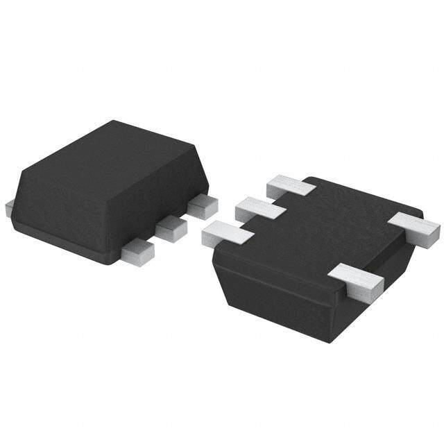
| 产品图片 |
|
| 产品型号 | MAX6362LUT29+T |
| rohs | 无铅 / 符合限制有害物质指令(RoHS)规范要求 |
| 产品系列 | - |
| 产品培训模块 | http://www.digikey.cn/PTM/IndividualPTM.page?site=cn&lang=zhs&ptm=25703http://www.digikey.cn/PTM/IndividualPTM.page?site=cn&lang=zhs&ptm=25705 |
| 供应商器件封装 | SOT-23-6 |
| 其它名称 | MAX6362LUT29+T-ND |
| 包装 | 带卷 (TR) |
| 受监控电压数 | 1 |
| 复位 | 低有效 |
| 复位超时 | 最小为 150 ms |
| 安装类型 | 表面贴装 |
| 封装/外壳 | SOT-23-6 |
| 工作温度 | -40°C ~ 85°C |
| 标准包装 | 2,500 |
| 电压-阈值 | 2.93V |
| 类型 | 备用电池电路 |
| 输出 | 推挽式,图腾柱 |


- 商务部:美国ITC正式对集成电路等产品启动337调查
- 曝三星4nm工艺存在良率问题 高通将骁龙8 Gen1或转产台积电
- 太阳诱电将投资9.5亿元在常州建新厂生产MLCC 预计2023年完工
- 英特尔发布欧洲新工厂建设计划 深化IDM 2.0 战略
- 台积电先进制程称霸业界 有大客户加持明年业绩稳了
- 达到5530亿美元!SIA预计今年全球半导体销售额将创下新高
- 英特尔拟将自动驾驶子公司Mobileye上市 估值或超500亿美元
- 三星加码芯片和SET,合并消费电子和移动部门,撤换高东真等 CEO
- 三星电子宣布重大人事变动 还合并消费电子和移动部门
- 海关总署:前11个月进口集成电路产品价值2.52万亿元 增长14.8%


PDF Datasheet 数据手册内容提取
19-1615; Rev 4; 10/11 SOT23, Low-Power µP Supervisory Circuits with Battery Backup General Description Features M The MAX6361–MAX6364 supervisory circuits reduce the (cid:1) Low +1.2V Operating Supply Voltage A complexity and number of components required for (VCCor VBATT) X power-supply monitoring and battery control functions in (cid:1) Precision Monitoring of +5.0V, +3.3V, +3.0V, and microprocessor (µP) systems. The circuits significantly 6 +2.5V Power-Supply Voltages improve system reliability and accuracy compared to that (cid:1) Debounced Manual Reset Input (MAX6361) 3 obtainable with separate ICs or discrete components. (cid:1) Watchdog Timer with 1.6s Timeout Period 6 Their functions include µP reset, backup battery switchover, and power failure warning. (MAX6362) 1 (cid:1) Battery-On Output Indicator (MAX6363) – The MAX6361–MAX6364 operate from supply voltages as low as +1.2V. The factory-preset reset threshold voltage (cid:1) Auxiliary User-Adjustable RESET IN (MAX6364) M ranges from 2.32V to 4.63V (see Ordering Information). (cid:1) Three Available Output Structures A These devices provide a manual reset input (MAX6361), Push-Pull RESET, Open-Drain RESET, X watchdog timer input (MAX6362), battery-on output Open-Drain RESET (MAX6363), and an auxiliary adjustable reset input (cid:1) RESET/RESET Valid Down to 1.2V Guaranteed 6 (MAX6364). In addition, each part type is offered in three (VCCor VBATT) 3 reset output versions: an active-low open-drain reset, an (cid:1) Power-Supply Transient Immunity 6 active-low open-drain reset, and an active-high open- (cid:1) 150ms (min) Reset Timeout Period 4 drain reset (see Selector Guide at end of data sheet). (cid:1) Small 6-Pin SOT23 Package Ordering Information Applications PART TEMP RANGE PIN-PACKAGE MAX6361LUT_ _-T -40°C to +85°C 6 SOT23 Computers Fax Machines MAX6361PUT_ _-T -40°C to +85°C 6 SOT23 Controllers Industrial Control MAX6361HUT_ _-T -40°C to +85°C 6 SOT23 Intelligent Instruments POS Equipment MAX6362LUT_ _-T -40°C to +85°C 6 SOT23 Critical µP/µC Portable/Battery-Powered MAX6362PUT_ _-T -40°C to +85°C 6 SOT23 Power Monitoring Equipment MAX6362HUT_ _-T -40°C to +85°C 6 SOT23 MAX6363LUT_ _-T -40°C to +85°C 6 SOT23 MAX6363PUT_ _-T -40°C to +85°C 6 SOT23 MAX6363HUT_ _-T -40°C to +85°C 6 SOT23 Pin Configurations MAX6364LUT_ _-T -40°C to +85°C 6 SOT23 MAX6364PUT_ _-T -40°C to +85°C 6 SOT23 TOP VIEW MAX6364HUT_ _-T -40°C to +85°C 6 SOT23 Note:These parts offer a choice of reset threshold voltages. From the table below, select the suffix corresponding to the RESET, RESET 1 6 BATT desired thresholdvoltage and insert it into the part number to complete it. When ordering from the factory, there is a 2500- MAX6361 piece minimum on the SOT package (tape-and-reel only). GND 2 5 OUT Devices are available in both leaded and lead-free packaging. Specify lead-free by replacing "-T" with "+T" when ordering. MR 3 4 VCC SUFFIX RESET THRESHOLD RANGES (V) MIN TYP MAX SOT23-6 46 4.50 4.63 4.75 44 4.25 4.38 4.50 Pin Configurations continued at end of data sheet. 31 3.00 3.08 3.15 Selector Guide appears at end of data sheet. 29 2.85 2.93 3.00 26 2.55 2.63 2.70 Typical Operating Circuit appears at end of data sheet. 23 2.25 2.32 2.38 ________________________________________________________________Maxim Integrated Products 1 For pricing, delivery, and ordering information,please contact Maxim Directat 1-888-629-4642, or visit Maxim’s website at www.maxim-ic.com.
SOT23, Low-Power µP Supervisory Circuits with Battery Backup 4 ABSOLUTE MAXIMUM RATINGS 6 Terminal Voltages (with respect to GND) Output Current 3 VCC, BATT, OUT.......................................................-0.3V to +6V OUT................................Short-Circuit Protection for up to 10s 6 RESET(open drain), RESET (open drain)................-0.3V to +6V RESET, RESET, BATT ON ..............................................20mA X BATT ON, RESET (push-pull), RESET IN, Continuous Power Dissipation (TA= +70°C) WDI.......................................................-0.3V to (VOUT+ 0.3V) 6-Pin SOT23 (derate 8.70mW/°C above +70°C) .........696mW A MR .............................................................-0.3V to (VCC+ 0.3V) Operating Temperature Range...........................-40°C to +85°C M Input Current Junction Temperature......................................................+150°C VCCPeak ............................................................................1A Storage Temperature Range.............................-65°C to +150°C – VCCContinuous............................................................250mA Lead Temperature (soldering, 10s).................................+300°C 1 BATT Peak....................................................................250mA Soldering Temperature (reflow) 6 BATT Continuous............................................................40mA Lead(Pb)-free...............................................................+260°C GND................................................................................75mA Packages containing lead(Pb).....................................+240°C 3 Stresses beyond those listed under “Absolute Maximum Ratings” may cause permanent damage to the device. These are stress ratings only, and functional 6 operation of the device at these or any other conditions beyond those indicated in the operational sections of the specifications is not implied. Exposure to X absolute maximum rating conditions for extended periods may affect device reliability. A ELECTRICAL CHARACTERISTICS M (VCC = +2.4V to +5.5V, VBATT = 3V, TA = -40°C to +85°C, reset not asserted. Typical values are at TA = +25°C, unless otherwise noted.) (Note 1) PARAMETER SYMBOL CONDITIONS MIN TYP MAX UNITS Operating Voltage Range, VCC, No load (Note 2) 0 5.5 V VCCor VBATT VBATT Supply Current No load, VCC> VTH, VCC= 2.8V 10 30 (Excluding IOUT) ICC (WMDAIX =6 3V6C2C)or GND VCC= 3.6V 11 35 µA VCC= 5.5V 15 50 IMSUodPPeL (YEixnc Bluadtitnegry I-OBUaTc)kup ISUPPLY VVBCACT=T =0V 2.8V, TTAA== +-4205°°CC to +85°C 13 µA BATT Standby Current IBATT 5(V.5BVA T>T V+C 0C.2>V) TTAA== +-4205°°CC to +85°C --01..10 00..0025 µA VCC= 4.75V, IOUT≤150mA 2.75 VCCto OUT On-Resistance RON VCC= 3.15V, IOUT≤65mA 3.0 Ω VCC= 2.38V, IOUT≤25mA 4.6 VBATT= 4.5V, IOUT≤20mA VBATT- 0.2 VOUTin Battery-Backup Mode VBATT= 3.0V, IOUT≤10mA VBATT- 0.15 V VBATT= 2.25V, IOUT≤5mA VBATT- 0.15 Battery-Switchover Threshold Power-up 20 (VCC- VBATT) VCC < VTH Power-down -20 mV MAX636_UT46 4.50 4.63 4.75 MAX636_UT44 4.25 4.38 4.50 MAX636_UT31 3.00 3.08 3.15 Reset Threshold VTH V MAX636_UT29 2.85 2.93 3.00 MAX636_UT26 2.55 2.63 2.70 MAX636_UT23 2.25 2.32 2.38 VCCFalling Reset Delay VCCfalling at 10V/ms 35 µs Reset-Active Timeout Period tRP 150 280 ms 2 _______________________________________________________________________________________
SOT23, Low-Power µP Supervisory Circuits with Battery Backup ELECTRICAL CHARACTERISTICS (continued) M (VCC = +2.4V to +5.5V, VBATT = 3V, TA = -40°C to +85°C, reset not asserted. Typical values are at TA = +25°C, unless otherwise A noted.) (Note 1) X PARAMETER SYMBOL CONDITIONS MIN TYP MAX UNITS 6 ISINK= 1.6mA, 0.3 3 Reset asserted, VCC≥2.1V RESETOutput Voltage VOL VBATT= 0V ISINK= 100µA, 0.4 V 61 VCC≥1.2V – VOH R(MeAseXt6 n3o6t_ aLs osnelryte) d IVSCOCUR≥CVETH=( M50A0Xµ)A, 0.8 (cid:2)VCC M A RESET Output Voltage VOL Reset not asserted IVSCINCK≥=V 1T.H6(mMAAX,) 0.3 V X 6 RESET, RESET Output Leakage Current ILK MAX636_P, MAX636_H only 1 µA 3 6 MANUAL RESET (MAX6361 only) 4 VIL 0.3 (cid:2)VCC MRInput Voltage V VIH 0.7 (cid:2)VCC Pull-Up Resistance 20 kΩ Minimum Pulse Width 1 µs Glitch Immunity VCC= 3.3V 100 ns MRto Reset Delay VCC= 3.3V 120 ns WATCHDOG INPUT(MAX6362 only) Watchdog Timeout Period tWD 1.00 1.60 2.25 s Minimum WDI Input Pulse Width tWDI 100 ns VIL 0.3 (cid:2)VCC Input Voltage V VIH 0.7 (cid:2)VCC BATT ON(MAX6363 only) Output Voltage VOL ISINK= 3.2mA, VBATT= 2.1V 0.4 V Sink current, VCC= 5V 60 mA Output Short-Circuit Current Source current, VBATT≥2V 10 30 100 µA RESET IN(MAX6364 only) Input Threshold 1.185 1.235 1.285 V RESET IN Leakage Current ±0.01 ±25 nA RESET IN to Reset Delay Overdrive voltage = 50mV, RESET IN falling 1.5 µs Note 1: All devices are 100% production tested at TA= +25°C. Limits over temperature are guaranteed by design. Note 2: VBATTcan be 0V anytime or VCCcan go down to 0V if VBATTis active (except at startup). _______________________________________________________________________________________ 3
SOT23, Low-Power µP Supervisory Circuits with Battery Backup 4 Typical Operating Characteristics 6 (TA= +25°C, unless otherwise noted.) 3 6 SUPPLY CURRENT vs. TEMPERATURE BATTERY SUPPLY CURRENT BATTERY TO OUT ON-RESISTANCE X (NO LOAD) (BACKUP MODE) vs. TEMPERATURE vs. TEMPERATURE 6361–MA µUPPLY CURRENT (A) 112680 MAX6361 toc01 µRY SUPPLY CURRENT (A) 00011.....64802 VVBBAATTTT = = 2 2.8.0VV VCC = 0 MAX6361 toc02 ΩO OUT ON-RESISTANCE () 43567 VBATT = 2.0V VBATT = 2.8V MAX6361 toc03 AX S 14 VVBCACT =T =5 .00VV BATTE 0.2 BATT T 12 VBATT = 5.0V IVOCUCT == 02V5mA M 12 0 0 -40 -20 0 20 40 60 80 -40 -20 0 20 40 60 80 -40 -20 0 20 40 60 80 TEMPERATURE (°C) TEMPERATURE (°C) TEMPERATURE (°C) VCC TO OUT ON-RESISTANCE RESET TIMEOUT PERIOD VCC TO RESET PROPAGATION DELAY vs. TEMPERATURE vs. TEMPERATURE vs. TEMPERATURE ΩTO OUT ON-RESISTANCE ()OUT 0001....3962 VIOCUCT == 22VIO.5C3UmCVT A== 41.550VmA VIOCUCT == 36.50mVA MAX6361 toc04 RESET TIMEOUT PERIOD (ms)122290015500 MAX6361 toc05 µPROPAGATION DELAY (s)1113764932005055050 VCC FALLING 01.2V5/mV/sms MAX6361 toc06 V 15 10V/ms 0 190 0 -40 -20 0 20 40 60 80 -40 -20 0 20 40 60 80 -40 -20 0 20 40 60 80 TEMPERATURE (°C) TEMPERATURE (°C) TEMPERATURE (°C) MAX6362 WATCHDOG TIMEOUT PERIOD RESET THRESHOLD MAXIMUM TRANSIENT DURATION vs. TEMPERATURE vs. TEMPERATURE vs. RESET THRESHOLD OVERDRIVE HDOG TIMEOUT PERIOD (s) 111112......659870 MAX6361toc06a THRESHOLD (V) 35443.....00505 MAX636_46 MAX6361 toc07 µM TRANSIENT DURATION (s) 433221005505000000 MAX636_4RA6EBSOEVTE OCCUCRUVRES MAX6361 toc08 TC 1.4 MAX636_26 MU 100 WA 2.5 AXI 1.3 M 50 MAX636_26 1.2 2.0 0 -40 -20 0 20 40 60 80 -40 -20 0 20 40 60 80 1 10 100 1k 10k TEMPERATURE (°C) TEMPERATURE (°C) RESET THRESHOLD OVERDRIVE VTH - VCC (mV) 4 _______________________________________________________________________________________
SOT23, Low-Power µP Supervisory Circuits with Battery Backup Typical Operating Characteristics (continued) M (TA= +25°C, unless otherwise noted.) A MAX6364 MAX6364 BATTERY SUPPLY CURRENT RESET IN THRESHOLD RESET IN TO RESET PROPAGATION DELAY X vs. SUPPLY VOLTAGE vs. TEMPERATURE vs. TEMPERATURE 6 µTTERY SUPPLY CURRENT (A) 134567890 VBVABTATT =T =2 .25.V8V VTH = 2.93V MAX6361 toc09 THRESHOLD (V)11..223356 MAX6361 toc10 µPROPAGATION DELAY (s) 11222.....96852 VOD = 50mV MAX6361 toc11 361–MAX BA 2 1.3 6 1 VBATT = 2.3V 3 0 1.234 1.0 6 0 1 2 3 4 -40 -20 0 20 40 60 80 -40 -20 0 20 40 60 80 VCC (V) TEMPERATURE (°C) TEMPERATURE (°C) 4 Pin Description PIN NAME FUNCTION Active-High Reset Output. RESET is continuously high when VCCis below the reset threshold (VTH), MRis low, or RESET IN is low. It asserts in pulses when the internal watchdog times out. RESET remains high RESET for the reset timeout period (tRP) after VCCrises above the reset threshold, after the manual reset input goes from low to high, after RESET IN goes high, or after the watchdog triggers a reset event. The MAX636_H is an active-high open-drain output. 1 Active-Low Reset Output. RESETis continuously low when VCCis below the reset threshold (VTH), MRis low, or RESET IN is low. It asserts in pulses when the internal watchdog times out. RESETremains low for RESET the reset timeout period (tRP) after VCCrises above the reset threshold, after the manual reset input goes from low to high, after RESET IN goes high, or after the watchdog triggers a reset event. The MAX636_L is an active-low push-pull output while the MAX636_P is an active-low open-drain output. 2 GND Ground MAX6361Manual-Reset Input. Maintaining logic low on MRasserts a reset. Reset output remains assert- MR ed for at least 150ms (tRP) after MRtransitions from low to high. Leave unconnected or connected to VCC if not used. MAX6362Watchdog Input. If WDI remains high or low for longer than the watchdog timeout period (tWD), the 3 WDI internal watchdog timer runs out and a reset pulse is triggered for the reset timeout period (tRP) (Figure 1). The internal watchdog clears whenever reset asserts or whenever WDI sees a rising or falling edge. BATT ON MAX6363Battery-On Output. BATT ON goes high in battery backup mode. MAX6364Reset Input. When RESET IN falls below 1.235V, reset is asserted. Reset output remains RESET IN asserted as long as RESET IN is low and for at least 150ms (tRP) after RESET IN goes high. 4 VCC SRuepseptl yr eVmolataingse a, s0s teor t5e.d5 Vu.n Rtile VsCetC isr isaesss earbteodv ew VheTHn aVnCdC fdorro apts l ebaeslto 1w5 t0hme sr easfetet rt hVrCeCshroisleds v aobltaogvee V(VTTHH.). 5 OUT Output. OUT sources from VCCwhen it is above the reset threshold (VTH), and from the greater of VCCor BATT when VCCis below VTH. Backup-Battery Input. When VCCfalls below the reset threshold, BATT switches to OUT if VBATTis 20mV 6 BATT greater than VCC. When VCCrises 20mV above VBATT, VCCswitches to OUT. The 40mV hysteresis prevents repeated switching if VCCfalls slowly. _______________________________________________________________________________________ 5
SOT23, Low-Power µP Supervisory Circuits with Battery Backup 4 Detailed Description (high to low or low to high) within the watchdog timeout 6 period (tWD) with a 100ns minimum pulse width clears The Typical Operating Circuitshows a typical connection the watchdog timer. If WDI remains high or low for longer 3 for the MAX6361–MAX6364 family. OUT powers the stat- than the watchdog timeout period, the internal watchdog 6 ic random-access memory (SRAM). OUT is internally timer runs out and a reset pulse is triggered for the reset X connected to VCCif VCCis greater than the reset thresh- timeout period (tRP). The internal watchdog timer clears A old, or to the greater of VCC or VBATT when VCC is less whenever reset asserts or the WDI sees a rising or falling than the reset threshold. OUT can supply up to 150mA edge within the watchdog timeout period. If WDI remains M from VCC. When VCCis higher than VBATT, the BATT ON in a high or low state for an extended period of time, a – (MAX6363) output is low. When VCCis lower than VBATT, reset pulse asserts after every watchdog timeout period an internal MOSFET connects the backup battery to 1 (tWD) (Figure 1). OUT. The on-resistance of the MOSFET is a function of 6 backup-battery voltage and is shown in the Battery to Reset In (MAX6364 Only) 3 Out On-Resistance vs. Temperature graph in the Typical RESET IN is compared to an internal 1.235V reference. 6 Operating Characteristicssection. If the voltage at RESET IN is less than 1.235V, reset is X asserted. The RESET IN comparator may be used as Backup-Battery Switchover an undervoltage detector to signal a failing power sup- A In a brownout or power failure, it may be necessary to ply. It can also be used as a secondary power-supply M preserve the contents of the RAM. With a backup bat- reset monitor. tery installed at BATT, the MAX6361–MAX6364 auto- matically switch the RAM to backup power when VCC To program the reset threshold (VRTH) of the secondary falls. The MAX6363 has a BATT ON output that goes power supply, use the following equation (see Typical high when in battery-backup mode. These devices Operating Circuit): require two conditions before switching to battery- ⎛R1 ⎞ backup mode: V =V ⎜ +1⎟ RTH REF ⎝R2 ⎠ 1) VCCmust be below the reset threshold. 2) VCCmust be below VBATT. where VREF = 1.235V. To simplify the resistor selection, Table 1 lists the status of the inputs and outputs in bat- tery-backup mode. The device will not power up if the [( ) ] only voltage source is on BATT. OUT will only power up R1 = R2 V /V −1 RTH REF from VCCat startup. choose a value for R2 and calculate R1: Manual Reset Input (MAX6361 Only) Many µP-based products require manual reset capabili- Since the input current at RESET IN is 25nA (max), large ty, allowing the operator, a test technician, or external values (up to 1MΩ) can be used for R2 with no signifi- logic circuitry to initiate a reset. For the MAX6361, a logic cant loss in accuracy. For example, in the Typical low on MR asserts reset. Reset remains asserted while MR is low, and for a minimum of 150ms (tRP) after it returns high. MR has an internal 20kΩ pull-up resistor to Table 1. Input and Output Status in VCC. This input can be driven with TTL/CMOS logic lev- Battery-Backup Mode els or with open-drain/collector outputs. Connect a nor- mally open momentary switch from MRto GND to create PIN STATUS a manual reset function; external debounce circuitry is VCC Disconnected from OUT not required. If MR is driven from long cables or the OUT Connected to BATT device is used in a noisy environment, connect a 0.1µF Connected to OUT. Current drawn from capacitor from MR to GND to provide additional noise BATT the battery is less than 1µA (at VBATT= immunity. 2.8V, excluding IOUT) when VCC= 0. Watchdog Input (MAX6362 Only) RESET/RESET Asserted The watchdog monitors µP activity through the input BATT ON High state WDI. If the µP becomes inactive, the reset output is MR, RESET IN, asserted in pulses. To use the watchdog function, con- Inputs ignored WDI nect WDI to a bus line or µP I/O line. A change of state 6 _______________________________________________________________________________________
SOT23, Low-Power µP Supervisory Circuits with Battery Backup Operating Circuit,the MAX6362 monitors two supply Replacing the Backup Battery M voltages. To monitor the secondary 5V logic or analog If BATT is decoupled with a 0.1µF capacitor to ground, A supply with a 4.60V nominal programmed reset thresh- the backup power source can be removed while VCC old, choose R2 = 100kΩ, and calculate R1 = 273kΩ. remains valid without danger of triggering a reset pulse. X The device does not enter battery-backup mode when Reset Output 6 VCCstays above the reset threshold voltage. A µP’s reset input starts the µP in a known state. The 3 MAX6361–MAX6364 µP supervisory circuits assert a Negative-Going VCCTransients 6 reset to prevent code-execution errors during power- These supervisors are relatively immune to short-dura- 1 up, power-down, and brownout conditions. RESET is tion, negative-going VCC transients. Resetting the µP – guaranteed to be a logic low or high depending on the when VCC experiences only small glitches is usually M device chosen (see Ordering Information). RESET or not desirable. RESET asserts when VCC is below the reset threshold The Typical Operating Characteristicssection shows a A and for at least 150ms (tRP) after VCC rises above the graph of Maximum Transient Duration vs. Reset X reset threshold. RESET or RESETalso asserts when MR Threshold Overdrive for which reset is not asserted. is low (MAX6361) and when RESET IN is less than 6 The graph was produced using negative-going VCC 1.235V (MAX6364). The MAX6362 watchdog function 3 pulses, starting at VCC and ending below the reset will cause RESET (or RESET) to assert in pulses follow- threshold by the magnitude indicated (reset threshold 6 ing a watchdog timeout (Figure 1). overdrive). The graph shows the maximum pulse width 4 that a negative-going VCC transient can typically have Applications Information without triggering a reset pulse. As the amplitude of the transient increases (i.e., goes further below the reset Operation Without a Backup threshold), the maximum allowable pulse width Power Source decreases. Typically, a VCC transient that goes 100mV The MAX6361–MAX6364 were designed for battery- below the reset threshold and lasts for 30µs will not backed applications. If a backup battery is not used, trigger a reset pulse. connect VCCto OUT and connect BATT to GND. A 0.1µF bypass capacitor mounted close to the VCC pin provides additional transient immunity. WDI tRP tRP tWD tWD RESET tWD = WATCHDOG TIMEOUT PERIOD tRP = RESET TIMEOUT PERIOD Figure 1. MAX6362 Watchdog Timeout Period and Reset Active Time _______________________________________________________________________________________ 7
SOT23, Low-Power µP Supervisory Circuits with Battery Backup 4 Watchdog Software Considerations 6 (MAX6362 Only) 3 To help the watchdog timer monitor software execution START more closely, set and reset the watchdog input at dif- 6 ferent points in the program, rather than “pulsing” the X watchdog input low-high-low. This technique avoids a A “stuck” loop, in which the watchdog timer would contin- ue to be reset within the loop, keeping the watchdog SET M WDI from timing out. Figure 2 shows an example of a flow LOW – diagram where the I/O driving the WDI is set low at the 1 beginning of the program, set high at the beginning of 6 every subroutine or loop, then set low again when the 3 program returns to the beginning. If the program SUBROUTINE should “hang” in any subroutine, the problem would 6 OR PROGRAM LOOP quickly be corrected, since the I/O is continually set low SET WDI X and the watchdog timer is allowed to time out, trigger- HIGH A ing a reset. M RETURN END Figure 2. Watchdog Flow Diagram 8 _______________________________________________________________________________________
SOT23, Low-Power µP Supervisory Circuits with Battery Backup Selector Guide M A MANUAL RESET RESET RESET RESET WATCHDOG BATT RESET X PART PUSH- OPEN OPEN INPUT INPUT WDI ON IN PULL DRAIN DRAIN 6 MR 3 MAX6361LUT_ _ (cid:3) (cid:3) 6 MAX6361PUT_ _ (cid:3) (cid:3) 1 MAX6361HUT_ _ (cid:3) (cid:3) – MAX6362LUT_ _ (cid:3) (cid:3) M MAX6362PUT_ _ (cid:3) (cid:3) A MAX6362HUT_ _ (cid:3) (cid:3) X MAX6363LUT_ _ (cid:3) (cid:3) 6 MAX6363PUT_ _ (cid:3) (cid:3) 3 MAX6363HUT_ _ (cid:3) (cid:3) 6 MAX6364LUT_ _ (cid:3) (cid:3) 4 MAX6364PUT_ _ (cid:3) (cid:3) MAX6364HUT_ _ (cid:3) (cid:3) Device Marking Codes TOP TOP TOP TOP PART PART PART PART MARK MARK MARK MARK MAX6361LUT23 AAEI MAX6362LUT23 AAFA MAX6363LUT23 AAFS MAX6364LUT23 AAGK MAX6361LUT26 AAEH MAX6362LUT26 AAEZ MAX6363LUT26 AAFR MAX6364LUT26 AAGJ MAX6361LUT29* AAEG MAX6362LUT29* AAEY MAX6363LUT29* AAFQ MAX6364LUT29* AAGI MAX6361LUT31 AAEF MAX6362LUT31 AAEX MAX6363LUT31 AAFP MAX6364LUT31 AAGH MAX6361LUT44 AAEE MAX6362LUT44 AAEW MAX6363LUT44 AAFO MAX6364LUT44 AAGG MAX6361LUT46* AAED MAX6362LUT46* AAEV MAX6363LUT46* AAFN MAX6364LUT46* AAGF MAX6361PUT23 AAEO MAX6362PUT23 AAFG MAX6363PUT23 AAFY MAX6364PUT23 AAGQ MAX6361PUT26 AAEN MAX6362PUT26 AAFF MAX6363PUT26 AAFX MAX6364PUT26 AAGP MAX6361PUT29* AAEM MAX6362PUT29* AAFE MAX6363PUT29* AAFW MAX6364PUT29* AAGO MAX6361PUT31 AAEL MAX6362PUT31 AAFD MAX6363PUT31 AAFV MAX6364PUT31 AAGN MAX6361PUT44 AAEK MAX6362PUT44 AAFC MAX6363PUT44 AAFU MAX6364PUT44 AAGM MAX6361PUT46* AAEJ MAX6362PUT46* AAFB MAX6363PUT46* AAFT MAX6364PUT46* AAGL MAX6361HUT23 AAEU MAX6362HUT23 AAFM MAX6363HUT23 AAGE MAX6364HUT23 AAGW MAX6361HUT26 AAET MAX6362HUT26 AAFL MAX6363HUT26 AAGD MAX6364HUT26 AAGV MAX6361HUT29 AAES MAX6362HUT29 AAFK MAX6363HUT29 AAGC MAX6364HUT29 AAGU MAX6361HUT31 AAER MAX6362HUT31 AAFJ MAX6363HUT31 AAGB MAX6364HUT31 AAGT MAX6361HUT44 AAEQ MAX6362HUT44 AAFI MAX6363HUT44 AAGA MAX6364HUT44 AAGS MAX6361HUT46* AAEP MAX6362HUT46* AAFH MAX6363HUT46* AAFZ MAX6364HUT46* AAGR *Sample stock generally held on standard versions only. Contact factory for availability of nonstandard versions. _______________________________________________________________________________________ 9
SOT23, Low-Power µP Supervisory Circuits with Battery Backup 4 Pin Configurations (continued) 6 3 TOP VIEW 6 X A RESET, RESET 1 6 BATT RESET, RESET 1 6 BATT RESET, RESET 1 6 BATT M MAX6362 MAX6363 MAX6364 – GND 2 5 OUT GND 2 5 OUT GND 2 5 OUT 1 6 3 WDI 3 4 VCC BATT ON 3 4 VCC RESET IN 3 4 VCC 6 SOT23-6(cid:0) SOT23-6 SOT23-6 X A M Typical Operating Circuit Chip Information PROCESS: BiCMOS 2.4V TO 5.5V UNREGULATED DC VOLTAGE VCC R1 0.1µF VCC Package Information RESET RESET µP For the latest package outline information and land patterns RESET IN (footprints), go to www.maxim-ic.com/packages. Note that a GND “+”, “#”, or “-” in the package code indicates RoHS status only. R2 MAX6364 Package drawings may show a different suffix character, but B the drawing pertains to the package regardless of RoHS status. U S OUT PACKAGE PACKAGE OUTLINE LAND 3.6V Li+ BATT VCC BATTERY TYPE CODE NO. PATTERN NO. GND 0.1µF SRAM GND 6 SOT23 U6-1 21-0058 90-0175 10 ______________________________________________________________________________________
SOT23, Low-Power µP Supervisory Circuits with Battery Backup Revision History M A REVISION REVISION PAGES NUMBER DATE DESCRIPTION CHANGED X 0 1/00 Initial release — 6 3 3 11/05 Added lead-free information. 1 6 4 10/11 Updated Electrical Characteristics. 2 1 – M A X 6 3 6 4 Maxim cannot assume responsibility for use of any circuitry other than circuitry entirely embodied in a Maxim product. No circuit patent licenses are implied. Maxim reserves the right to change the circuitry and specifications without notice at any time. The parametric values (min and max limits) shown in the Electrical Characteristics table are guaranteed. Other parametric values quoted in this data sheet are provided for guidance. 11 ____________________Maxim Integrated Products, 120 San Gabriel Drive, Sunnyvale, CA 94086 408-737-7600 © 2011 Maxim Integrated Products Maxim is a registered trademark of Maxim Integrated Products, Inc.
Mouser Electronics Authorized Distributor Click to View Pricing, Inventory, Delivery & Lifecycle Information: M axim Integrated: MAX6364LUT31+T MAX6361HUT23+T MAX6361HUT31+T MAX6361HUT44+T MAX6361HUT46+T MAX6361LUT23+T MAX6361LUT26+T MAX6361LUT29+T MAX6361LUT31+T MAX6361LUT44+T MAX6361LUT46+T MAX6361PUT23+T MAX6361PUT26+T MAX6361PUT29+T MAX6361PUT31+T MAX6361PUT44+T MAX6361PUT46+T MAX6362HUT23+T MAX6362HUT26+T MAX6362HUT29+T MAX6362HUT31+T MAX6362HUT46+T MAX6362LUT23+T MAX6362LUT26+T MAX6362LUT29+T MAX6362LUT31+T MAX6362LUT46+T MAX6362PUT23+T MAX6362PUT26+T MAX6362PUT29+T MAX6362PUT31+T MAX6362PUT44+T MAX6362PUT46+T MAX6363HUT23+T MAX6363HUT26+T MAX6363HUT29+T MAX6363HUT31+T MAX6363HUT44+T MAX6363HUT46+T MAX6363LUT23+T MAX6363LUT26+T MAX6363LUT29+T MAX6363LUT31+T MAX6363LUT44+T MAX6363LUT46+T MAX6363PUT23+T MAX6363PUT26+T MAX6363PUT29+T MAX6363PUT31+T MAX6363PUT44+T MAX6363PUT46+T MAX6364HUT23+T MAX6364HUT46+T MAX6364LUT23+T MAX6364LUT26+T MAX6364LUT29+T MAX6364LUT46+T MAX6364PUT23+T MAX6364PUT26+T MAX6364PUT29+T MAX6364PUT31+T MAX6364PUT44+T MAX6364PUT46+T