ICGOO在线商城 > MAX5251BCPP+

 Datasheet下载
- 型号: MAX5251BCPP+
- 制造商: Maxim
- 库位|库存: xxxx|xxxx
- 要求:
| 数量阶梯 | 香港交货 | 国内含税 |
| +xxxx | $xxxx | ¥xxxx |
查看当月历史价格
查看今年历史价格
MAX5251BCPP+产品简介:
ICGOO电子元器件商城为您提供MAX5251BCPP+由Maxim设计生产,在icgoo商城现货销售,并且可以通过原厂、代理商等渠道进行代购。 提供MAX5251BCPP+价格参考¥89.55-¥89.55以及MaximMAX5251BCPP+封装/规格参数等产品信息。 你可以下载MAX5251BCPP+参考资料、Datasheet数据手册功能说明书, 资料中有MAX5251BCPP+详细功能的应用电路图电压和使用方法及教程。
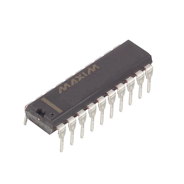
Maxim Integrated的MAX5251BCPP+是一款低功耗、四通道、12位数模转换器(DAC),采用20引脚DIP封装,具有并行接口。该器件适用于需要多通道精密模拟电压输出的应用场景。

典型应用场景包括工业控制与自动化系统,如PLC(可编程逻辑控制器)和过程控制系统,用于驱动执行器或调节模拟信号;测试与测量设备中,作为信号发生模块,为传感器校准或电路测试提供精确的参考电压;通信系统中可用于偏置控制或信道调节;此外,在医疗仪器等对精度和稳定性要求较高的设备中,也可用于生成可控的模拟激励信号。

MAX5251BCPP+支持单电源供电(+4.5V至+5.5V),输出缓冲集成在片内,可直接驱动负载,简化了外围电路设计。其低温漂、高线性度和可靠的性能使其在环境条件变化较大的工业环境中表现稳定。同时,该器件具备良好的抗干扰能力,适合在噪声较强的现场使用。

综上,MAX5251BCPP+广泛应用于需多路、高精度、稳定DAC输出的工业、通信和测量领域,是中小型控制系统中实现数字到模拟信号转换的理想选择之一。
| 参数 | 数值 |
| 产品目录 | 集成电路 (IC)半导体 |
| 描述 | IC DAC 10BIT QUAD 3V 20-DIP数模转换器- DAC 10-Bit 4Ch Precision DAC |
| 产品分类 | |
| 品牌 | Maxim Integrated |
| 产品手册 | |
| 产品图片 |
|
| rohs | 符合RoHS无铅 / 符合限制有害物质指令(RoHS)规范要求 |
| 产品系列 | 数据转换器IC,数模转换器- DAC,Maxim Integrated MAX5251BCPP+- |
| 数据手册 | |
| 产品型号 | MAX5251BCPP+ |
| 产品培训模块 | http://www.digikey.cn/PTM/IndividualPTM.page?site=cn&lang=zhs&ptm=25703http://www.digikey.cn/PTM/IndividualPTM.page?site=cn&lang=zhs&ptm=25705 |
| 产品种类 | 数模转换器- DAC |
| 位数 | 10 |
| 供应商器件封装 | 20-PDIP |
| 分辨率 | 10 bit |
| 包装 | 管件 |
| 商标 | Maxim Integrated |
| 安装类型 | 通孔 |
| 安装风格 | Through Hole |
| 封装 | Tube |
| 封装/外壳 | 20-DIP(0.300",7.62mm) |
| 封装/箱体 | PDIP-20 |
| 工作温度 | 0°C ~ 70°C |
| 工厂包装数量 | 18 |
| 应用说明 | |
| 建立时间 | 12µs |
| 接口类型 | QSPI, SPI, Serial (3-Wire, Microwire) |
| 数据接口 | MICROWIRE™,QSPI™,串行,SPI™ |
| 最大工作温度 | + 70 C |
| 最小工作温度 | 0 C |
| 标准包装 | 1 |
| 电压参考 | External |
| 电压源 | 单电源 |
| 电源电压-最大 | 3.6 V |
| 电源电压-最小 | 3 V |
| 积分非线性 | +/- 1 LSB |
| 稳定时间 | 12 us |
| 系列 | MAX5251 |
| 结构 | R-2R |
| 转换器数 | 4 |
| 转换器数量 | 4 |
| 输出数和类型 | 4 电压,单极4 电压,双极 |
| 输出类型 | Voltage |
| 采样率(每秒) | - |
| 零件号别名 | MAX5251 |






- 商务部:美国ITC正式对集成电路等产品启动337调查
- 曝三星4nm工艺存在良率问题 高通将骁龙8 Gen1或转产台积电
- 太阳诱电将投资9.5亿元在常州建新厂生产MLCC 预计2023年完工
- 英特尔发布欧洲新工厂建设计划 深化IDM 2.0 战略
- 台积电先进制程称霸业界 有大客户加持明年业绩稳了
- 达到5530亿美元!SIA预计今年全球半导体销售额将创下新高
- 英特尔拟将自动驾驶子公司Mobileye上市 估值或超500亿美元
- 三星加码芯片和SET,合并消费电子和移动部门,撤换高东真等 CEO
- 三星电子宣布重大人事变动 还合并消费电子和移动部门
- 海关总署:前11个月进口集成电路产品价值2.52万亿元 增长14.8%





PDF Datasheet 数据手册内容提取
19-1172; Rev 1; 10/02 +3V, Quad, 10-Bit Voltage-Output DAC with Serial Interface __________________General Description ______________________________Features M The +3V MAX5251 combines four low-power, voltage- (cid:2) Four 10-Bit DACs with Configurable A output, 10-bit digital-to-analog converters (DACs) and Output Amplifiers X four precision output amplifiers in a space-saving, 20- (cid:2) +3.0V to +3.6V Single-Supply Operation pin package. In addition to the four voltage outputs, (cid:2) Low Supply Current: 0.8mA Normal Operation 5 each amplifier’s negative input is also available to the 3µA Shutdown Mode 2 user. This facilitates specific gain configurations, remote sensing, and high output drive capacity, making the (cid:2) Available in 20-Pin SSOP 5 MAX5251 ideal for industrial-process-control applica- (cid:2) Power-On Reset Clears all Registers and 1 tions. Other features include software shutdown, hard- DACs to Zero ware shutdown lockout, an active-low reset that clears (cid:2) SPI/QSPI and MICROWIRECompatible all registers and DACs to zero, a user-programmable (cid:2) Simultaneous or Independent Control of DACs logic output, and a serial-data output. Through 3-Wire Serial Interface Each DAC has a double-buffered input organized as an (cid:2) User-Programmable Digital Output input register followed by a DAC register. A 16-bit serial (cid:2) Schmitt-Trigger Digital Inputs for Direct word loads data into each input/DAC register. The Optocoupler Interface 3-wire serial interface is compatible with SPI™/QSPI™ and MICROWIRE™. It allows the input and DAC regis- (cid:2) 12-Bit Upgrade Available: MAX5253 ters to be updated independently or simultaneously with a single software command. All logic inputs are _________________Ordering Information TTL/CMOS-logic compatible. INL ________________________Applications PART TEMP RANGE PIN-PACKAGE (LSB) Digital Offset and Gain Adjustment MAX5251ACPP 0°C to +70°C 20 Plastic DIP ±1/2 Microprocessor-Controlled Systems MAX5251BCPP 0°C to +70°C 20 Plastic DIP ±1 MAX5251ACAP 0°C to +70°C 20 SSOP ±1/2 Industrial Process Controls MAX5251BCAP 0°C to +70°C 20 SSOP ±1 Automatic Test Equipment Ordering Information continued on last page. Remote Industrial Controls Pin Configuration appears at end of data sheet. Motion Control _________________________________________________________________________Functional Diagram DOUT CL PDL DGND AGND VDD REFAB FBA DECODE MAX5251 CONTROL OUTA INPUT DAC DAC A REGISTER A REGISTER A FBB OUTB 16-BIT INPUT DAC DAC B SHIFT REGISTER B REGISTER B FBC REGISTER OUTC INPUT DAC DAC C REGISTER C REGISTER C FBD OUTD SR LOGIC INPUT DAC DAC D CONTROL OUTPUT REGISTER D REGISTER D CS DIN SCLK UPO REFCD SPI and QSPI are trademarks of Motorola, Inc. MICROWIREis a trademark of National Semiconductor Corp. ________________________________________________________________Maxim Integrated Products 1 For pricing delivery, and ordering informationplease contact Maxim/Dallas Direct!at 1-888-629-4642, or visit Maxim’s website at www.maxim-ic.com.
+3V, Quad, 10-Bit Voltage-Output DAC with Serial Interface 1 ABSOLUTE MAXIMUM RATINGS 5 VDDto AGND............................................................-0.3V to +6V Operating Temperature Ranges 2 VDDto DGND...........................................................-0.3V to +6V MAX5251_C_P......................................................0°C to +70°C AGND to DGND..................................................................±0.3V MAX5251_E_P...................................................-40°C to +85°C 5 REFAB, REFCD to AGND...........................-0.3V to (VDD+ 0.3V) MAX5251BMJP................................................-55°C to +125°C X OUT_, FB_ to AGND...................................-0.3V to (VDD+ 0.3V) Storage Temperature Range.............................-65°C to +150°C Digital Inputs to DGND.............................................-0.3V to +6V Lead Temperature (soldering, 10s).................................+300°C A DOUT, UPO to DGND................................-0.3V to (VDD+ 0.3V) M Continuous Current into Any Pin.......................................±20mA Continuous Power Dissipation (TA= +70°C) Plastic DIP (derate 8.00mW/°C above +70°C).................640mW SSOP (derate 8.00mW/°C above +70°C)......................640mW CERDIP (derate 11.11mW/°C above +70°C).................889mW Stresses beyond those listed under “Absolute Maximum Ratings” may cause permanent damage to the device. These are stress ratings only, and functional operation of the device at these or any other conditions beyond those indicated in the operational sections of the specifications is not implied. Exposure to absolute maximum rating conditions for extended periods may affect device reliability. ELECTRICAL CHARACTERISTICS (VDD= +3.0V to +3.6V, AGND = DGND = 0V, REFAB = REFCD = 1.25V, RL= 5kΩ, CL= 100pF, TA= TMINto TMAX, unless otherwise noted. Typical values are at TA= +25°C. Output buffer connected in unity-gain configuration (Figure 9).) PARAMETER SYMBOL CONDITIONS MIN TYP MAX UNITS STATIC PERFORMANCE—ANALOG SECTION Resolution N 10 Bits MAX5251AC/E ±0.25 ±0.5 Integral Nonlinearity INL MAX5251BC/E ±1.0 LSB (Note 1) MAX5251BMJP ±2.0 Differential Nonlinearity DNL Guaranteed monotonic ±1.0 LSB Offset Error VOS ±6.0 mV Offset-Error Tempco 6 ppm/°C Gain Error GE (Note 1) ±2.4 LSB Gain-Error Tempco 1 ppm/°C Power-Supply Rejection Ratio PSRR VDD= +3.0V to +3.6V 100 800 µV/V MREAFTECRHEINNGC EP EINRPFUOTRMANCE (TA= +25°C) Reference Input Range VREF 0 VDD - 1.4 V Reference Input Resistance RREF Code dependent, minimum at code 554 hex 8 kΩ 2 _______________________________________________________________________________________
+3V, Quad, 10-Bit Voltage-Output DAC with Serial Interface ELECTRICAL CHARACTERISTICS (continued) M (VDD= +3.0V to +3.6V, AGND = DGND = 0V, REFAB = REFCD = 1.25V, RL= 5kΩ, CL= 100pF, TA= TMINto TMAX, unless otherwise A noted. Typical values are at TA= +25°C. Output buffer connected in unity-gain configuration (Figure 9).) X PARAMETER SYMBOL CONDITIONS MIN TYP MAX UNITS 5 MULTIPLYING-MODE PERFORMANCE 2 Reference -3dB Bandwidth VREF= 0.67VP-P 650 kHz 5 Reference Feedthrough Input code = all 0s, VREF= 1.6VP-Pat 1kHz -84 dB 1 Signal-to-Noise Plus SINAD VREF= 1VP-Pat 25kHz, code = full scale 72 dB Distortion Ratio DIGITAL INPUTS Input High Voltage VIH 2.0 V Input Low Voltage VIL 0.6 V Input Leakage Current IIN VIN= 0V or VDD 0.01 ±1.0 µA Input Capacitance CIN 8 pF DIGITAL OUTPUTS Output High Voltage VOH ISOURCE= 2mA VDD- 0.5 V Output Low Voltage VOL ISINK= 2mA 0.13 0.4 V DYNAMIC PERFORMANCE Voltage Output Slew Rate SR 0.6 V/µs Output Settling Time To ±1/2LSB, VSTEP= 1.25V 12 µs Output Voltage Swing Rail-to-Rail®(Note 2) 0 to VDD V Current into FB_ 0 0.1 µA OUT_ Leakage Current RL= ∞ 0.01 ±1 µA in Shutdown Start-Up Time Exiting 20 µs Shutdown Mode Digital Feedthrough CS= VDD, DIN = 100kHz 5 nV-s Digital Crosstalk 5 nV-s POWER SUPPLIES Supply Voltage VDD (Note 3) 3.0 3.6 V Supply Current IDD (Note 4) 0.82 0.98 mA Supply Current in Shutdown (Note 4) 3 20 µA Reference Current in Shutdown 0.01 ±1 µA Rail-to-Rail is a registered trademark of Motorola Nippon Ltd. Note 1: Guaranteed from code 5 to code 1023 in unity-gain configuration. Note 2: Accuracy is better than 1LSB for VOUT= 6mV to VDD- 80mV, guaranteed by PSR test at the endpoints. Note 3: Remains operational with supply voltage as low as +2.7V. Note 4: RL= ∞, digital inputs at DGND or VDD. _______________________________________________________________________________________ 3
+3V, Quad, 10-Bit Voltage-Output DAC with Serial Interface 1 ELECTRICAL CHARACTERISTICS (continued) 5 (VDD= +3.0V to +3.6V, AGND = DGND = 0V, REFAB = REFCD = 1.25V, RL= 5kΩ, CL= 100pF, TA= TMINto TMAX, unless otherwise 2 noted. Typical values are at TA= +25°C. Output buffer connected in unity-gain configuration (Figure 9).) 5 PARAMETER SYMBOL CONDITIONS MIN TYP MAX UNITS X TSICMLIKN GC lCocHkA PReAriCodTERISTICS (Figure t6C)P 100 ns A SCLK Clock Period tCP 100 ns M SCLK Pulse Width High tCH 40 ns SCLK Pulse Width Low tCL 40 ns CSFall to SCLK Rise Setup Time tCSS 40 ns SCLK Rise to CSRise Hold Time tCSH 0 ns DIN Setup Time tDS 40 ns DIN Hold Time tDH 0 ns SCLK Rise to DOUT Valid tD01 CL= 200pF 120 ns Propagation Delay SCLK Fall to DOUT Valid tD02 CL= 200pF 120 ns Propagation Delay SCLK Rise to CSFall Delay tCS0 40 ns CSRise to SCLK Rise Hold Time tCS1 40 ns CSPulse Width High tCSW 100 ns __________________________________________Typical Operating Characteristics (VDD = +3.3V, TA = +25°C, unless otherwise noted.) SUPPLY CURRENT INTEGRAL NONLINEARITY REFERENCE VOLTAGE INPUT vs. TEMPERATURE vs. REFERENCE VOLTAGE FREQUENCY RESPONSE 0.205 MAX5251-01 B) -04 RRCELL F==A 51Bk0 ΩS0WpFEPT 0.67VP-P MAX5251-06 µA)1099805050000 MAX5251-04 INL (LSB)--00..2550 VE OUTPUT (d -1-82 LY CURRENT ( 877050000 -0.75 RELATI -16 SUPP 665000 -1.00 550 R = 5kΩ CODE = FFC HEX L 500 -1.25 -20 -55-40 -20 0 20 40 60 80 100 120 0 0.5 1.0 1.5 2.0 2.5 0 500k 1.0M 1.5M 2.0M 2.5M 3.0M REFERENCE VOLTAGE (V) FREQUENCY (Hz) TEMPERATURE (°C) 4 _______________________________________________________________________________________
+3V, Quad, 10-Bit Voltage-Output DAC with Serial Interface ____________________________Typical Operating Characteristics (continued) M (VDD = +3.3V, TA = +25°C, unless otherwise noted.) A X SUPPLY CURRENT TOTAL HARMONIC DISTORTION 5 vs. SUPPLY VOLTAGE PLUS NOISE vs. FREQUENCY OUTPUT FFT PLOT 2 µSUPPLY CURRENT (A) 1099887760505050500000000 MAX5251-05 THD + NOISE (%)00000000........5122334405050505 DRRCELAL FC==A 51CBk0 OΩ=0D p1EFV =P -FPULL SCALE MAX5251-02 SIGNAL AMPLITUDE (dB) ---4260000 VRCRLL E==F 15=0k 1Ω0kpHFz, 0.006V TO 1.6V MAX5251-10 51 -80 600 0.10 550 0.05 CODE = FFC HEX -100 500 0 2.7 2.8 2.9 3.0 3.1 3.2 3.3 3.4 3.5 3.6 0.1 1 10 100 0.5 1.6 2.7 3.8 4.9 6.0 SUPPLY VOLTAGE (V) FREQUENCY (kHz) FREQUENCY (kHz) FULL-SCALE ERROR REFERENCE FEEDTHROUGH vs. LOAD AT 1kHz 0 MAX5251-03 0 REFAB INPUT SIGNAL MAX5251-11 LE ERROR (LSB) --10..05 MPLITUDE (dB) --4200 VRCRLL E==F 15=0k 1Ω0.p6FVP-P AT 1kHz L-SCA -1.5 NAL A -60 L G FU -2.0 SI -80 OUTA FEEDTHROUGH -2.5 -100 0.01 0.1 1 10 100 0.5 1.2 1.9 2.6 3.3 4.0 LOAD (kΩ) FREQUENCY (kHz) _______________________________________________________________________________________ 5
+3V, Quad, 10-Bit Voltage-Output DAC with Serial Interface 1 ____________________________Typical Operating Characteristics (continued) 5 (VDD = +3.3V, VREF= 1.25V, RL= 5kΩ, CL= 100pF, TA = +25°C, unless otherwise noted.) 2 5 X A M MAJOR-CARRY TRANSITION DIGITAL FEEDTHROUGH (SCLK = 100kHz) MAX5251-07 MAX5251-08 CS SCLK, 5V/div 2V/div OUTB, OUTA, AC-COUPLED AC-COUPLED 50mV/div 10mV/div 10µs/div 2µs/div CS = PDL = CL = 3.3V, DIN = 0V DAC A CODE SET TO 800 HEX ANALOG CROSSTALK DYNAMIC RESPONSE MAX5251-12 MAX5251-13 OUTA, OUTA, 500mV/div 500mV/div GND OUTB, AC-COUPLED 10mV/div 10µs/div 10µs/div DAC A CODE SWITCHING FROM 00C HEX TO FFC HEX SWITCHING FROM CODE 000 hex TO FB4 HEX DAC B CODE SET TO 800 HEX OUTPUT AMPLIFIER GAIN = +2.6 6 _______________________________________________________________________________________
+3V, Quad, 10-Bit Voltage-Output DAC with Serial Interface ______________________________________________________________Pin Description M A PIN NAME FUNCTION X 1 AGND Analog Ground 5 2 FBA DAC A Output Amplifier Feedback 2 5 3 OUTA DAC A Output Voltage 1 4 OUTB DAC B Output Voltage 5 FBB DAC B Output Amplifier Feedback 6 REFAB Reference Voltage Input for DAC A and DAC B 7 CL Clears All DACs and Registers. Resets all outputs (OUT_, UPO, DOUT) to 0, active low. 8 CS Chip-Select Input. Active low. 9 DIN Serial-Data Input 10 SCLK Serial-Clock Input 11 DGND Digital Ground 12 DOUT Serial-Data Output 13 UPO User-Programmable Logic Output 14 PDL Power-Down Lockout. Active low. Locks out software shutdown if low. 15 REFCD Reference Voltage Input for DAC C and DAC D 16 FBC DAC C Output Amplifier Feedback 17 OUTC DAC C Output Voltage 18 OUTD DAC D Output Voltage 19 FBD DAC D Output Amplifier Feedback 20 VDD Positive Power Supply _______________________________________________________________________________________ 7
+3V, Quad, 10-Bit Voltage-Output DAC with Serial Interface 1 The impedance at each reference input is code depen- dent, ranging from a low value of 10kΩ when both 5 FB_ DACs connected to the reference have an input code 2 of 554 hex, to a high value exceeding several giga 5 R R R OUT_ ohms (leakage current) with an input code of 000 hex. X Because the input impedance at the reference pins is code dependent, load regulation of the reference A source is important. 2R 2R 2R 2R 2R M The REFAB and REFCD reference inputs have a 10kΩ S0 S1 D0 D9 guaranteed minimum input impedance. When the two reference inputs are driven from the same source, the effective minimum impedance is 5kΩ. Driving the REF_ REFAB and REFCD pins separately improves reference accuracy. AGND In shutdown mode, the MAX5251’s REFAB and REFCD inputs enter a high-impedance state with a typical input SHOWN FOR ALL 1s ON DAC leakage current of 0.01µA. The reference input capacitance is also code depen- dent and typically ranges from 20pF with an input code Figure 1. Simplified DAC Circuit Diagram of all 0s to 100pF at full scale. _______________Detailed Description Output Amplifiers All MAX5251 DAC outputs are internally buffered by pre- The MAX5251 contains four voltage-output digital-to- cision amplifiers with a typical slew rate of 0.6V/µs. analog converters (DACs) that are easily addressed Access to each output amplifier’s inverting input pro- using a simple 3-wire serial interface. It includes a vides the user greater flexibility in output gain setting/ 16-bit data-in/data-out shift register, and each DAC has signal conditioning (see the Applications Information a doubled-buffered input composed of an input register section). and a DAC register (see Functional Diagram). In addi- tion to the four voltage outputs, each amplifier’s nega- With a full-scale transition at the MAX5251 output, the tive input is available to the user. typical settling time to ±1/2LSB is 12µs when loaded with 5kΩ in parallel with 100pF (loads less than 2kΩ The DACs are inverted R-2R ladder networks that con- degrade performance). vert a digital input (10 data bits plus 2 sub-bits) into equivalent analog output voltages in proportion to the The MAX5251 output amplifier’s output dynamic applied reference voltage inputs. DACs A and B share responses and settling performances are shown in the the REFAB reference input, while DACs C and D share Typical Operating Characteristics. the REFCD reference input. The two reference inputs Power-Down Mode allow different full-scale output voltage ranges for each The MAX5251 features a software-programmable shut- pair of DACs. Figure 1 shows a simplified circuit dia- down that reduces supply current to a typical value of gram of one of the four DACs. 3µA. The power-down lockout pin (PDL) must be high to Reference Inputs enable shutdown mode. Writing 1100XXXXXXXXXXXX as The two reference inputs accept positive DC and AC the input-control word puts the MAX5251 in shutdown signals. The voltage at each reference input sets the mode (Table 1). full-scale output voltage for its two corresponding DACs. The reference input voltage range is 0V to (VDD - 1.4V). The output voltages (VOUT_) are repre- sented by a digitally programmable voltage source as: VOUT_= (VREFx NB / 1024 ) x Gain where NB is the numeric value of the DAC’s binary input code (0 to 1023), VREF is the reference voltage, and Gain is the externally set voltage gain. 8 _______________________________________________________________________________________
+3V, Quad, 10-Bit Voltage-Output DAC with Serial Interface In shutdown mode, the MAX5251 output amplifiers and M the reference inputs enter a high-impedance state. The serial interface remains active. Data in the input regis- SCLK SK A ters is retained in shutdown, allowing the MAX5251 to X recall the output states prior to entering shutdown. Exit DIN SO 5 shutdown mode either by recalling the previous config- uration or by updating the DACs with new data. When 2 MAX5251 powering up the device or bringing it out of shutdown, DOUT* SI* MICROWIRE 5 allow 20µs for the outputs to stabilize. PORT 1 Serial-Interface Configurations CS I/O The MAX5251’s 3-wire serial interface is compatible with both MICROWIRE (Figure 2) and SPI/QSPI (Figure 3). The serial input word consists of two address bits and two control bits followed by 10+2 data bits *THE DOUT-SI CONNECTION IS NOT REQUIRED FOR WRITING TO THE MAX5251, (MSB first), as shown in Figure 4. The 4-bit address/ BUT CAN BE USED FOR READBACK PURPOSES. control code determines the MAX5251’s response out- lined in Table 1. The connection between DOUT and Figure 2. Connections for Microwire the serial-interface port is not necessary, but may be used for data echo. Data held in the MAX5251’s shift register can be shifted out of DOUT and returned to the +3.3V microprocessor (µP) for data verification. The MAX5251’s digital inputs are double buffered. Depending on the command issued through the serial interface, the input register(s) can be loaded without DOUT* MISO* SS affecting the DAC register(s), the DAC register(s) can be loaded directly, or all four DAC registers can be updated simultaneously from the input registers DIN MOSI (Table 1). MAX5251 Serial-Interface Description SCLK SCK SPI/QSPI PORT The MAX5251 requires 16 bits of serial data. Table 1 lists the serial-interface programming commands. For certain commands, the 10+2 data bits are “don’t CS I/O cares.” Data is sent MSB first and can be sent in two 8-bit packets or one 16-bit word (CS must remain low until 16 bits are transferred). The serial data is com- CPOL = 0, CPHA = 0 posed of two DAC address bits (A1, A0) and two con- trol bits (C1, C0), followed by the 10+2 data bits *THE DOUT-MISO CONNECTION IS NOT REQUIRED FOR WRITING TO THE MAX5251, BUT CAN BE USED FOR READBACK PURPOSES. D9…D0, S1, S0 (Figure 4). Set both sub-bits (S0, S1) to zero. The 4-bit address/control code determines: Figure 3. Connections for SPI/QSPI • The register(s) to be updated • The clock edge on which data is to be clocked out through the serial-data output (DOUT) MSB..................................................................................LSB • The state of the user-programmable logic output 16 Bits of Serial Data (UPO) Address Control Data Bits • If the part is to go into shutdown mode (assuming Bits Bits MSB.................................LSB PDLis high) A1 A0 C1 C0 D9...................................D0 S1 S0 • How the part is configured when exiting shutdown 4 Address/ mode. Control Bits 10+2 Data Bits Figure 4. Serial-Data Format _______________________________________________________________________________________ 9
+3V, Quad, 10-Bit Voltage-Output DAC with Serial Interface 1 Table 1. Serial-Interface Programming Commands 5 2 16-BIT SERIAL WORD 5 D9.................D0 FUNCTION A1 A0 C1 C0 S1 S0 X MSB.............LSB A 0 0 0 1 10-bit DAC data 0 0 Load input register A; DAC registers unchanged. 0 1 0 1 10-bit DAC data 0 0 Load input register B; DAC registers unchanged. M 1 0 0 1 10-bit DAC data 0 0 Load input register C; DAC registers unchanged. 1 1 0 1 10-bit DAC data 0 0 Load input register D; DAC registers unchanged. 0 0 1 1 10-bit DAC data 0 0 Load input register A; all DAC registers updated. 0 1 1 1 10-bit DAC data 0 0 Load input register B; all DAC registers updated. 1 0 1 1 10-bit DAC data 0 0 Load input register C; all DAC registers updated. 1 1 1 1 10-bit DAC data 0 0 Load input register D; all DAC registers updated. Update all DAC registers from their respective input registers (also exit 0 1 0 0 XXXXXXXXXX X X shutdown mode). 1 0 0 0 10-bit DAC data 0 0 Load all DAC registers from shift register (also exit shutdown mode). 1 1 0 0 XXXXXXXXXX X X Enter shutdown mode (provided PDL= 1). 0 0 1 0 XXXXXXXXXX X X UPO goes low (default). 0 1 1 0 XXXXXXXXXX X X UPO goes high. 0 0 0 0 XXXXXXXXXX X X No operation (NOP) to DAC registers Mode 1, DOUT clocked out on SCLK’s rising edge. All DAC registers 1 1 1 0 XXXXXXXXXX X X updated. Mode 0, DOUT clocked out on SCLK’s falling edge. All DAC registers 1 0 1 0 XXXXXXXXXX X X updated (default). “X” = Don’t care Figure 5 shows the serial-interface timing requirements. change the clock edge on which serial data is shifted The chip-select pin (CS) must be low to enable the out of DOUT also loads data from all input registers to DAC’s serial interface. When CS is high, the interface their respective DAC registers. control circuitry is disabled. CS must go low at least Serial-Data Output (DOUT) tCSSbefore the rising serial clock (SCLK) edge to prop- The serial-data output, DOUT, is the internal shift regis- erly clock in the first bit. When CS is low, data is ter’s output. The MAX5251 can be programmed so that clocked into the internal shift register through the serial- data is clocked out of DOUT on SCLK’s rising edge data input pin (DIN) on SCLK’s rising edge. The maxi- (Mode 1) or falling edge (Mode 0). In Mode 0, output mum guaranteed clock frequency is 10MHz. Data is data at DOUT lags input data at DIN by 16.5 clock latched into the appropriate MAX5251 input/DAC regis- cycles, maintaining compatibility with MICROWIRE, ters on CS’s rising edge. SPI/QSPI, and other serial interfaces. In Mode 1, output The programming command Load-All-DACs-From-Shift- data lags input data by 16 clock cycles. On power-up, Register allows all input and DAC registers to be simul- DOUT defaults to Mode 0 timing. taneously loaded with the same digital code from the input shift register. The no operation (NOP) command User-Programmable Logic Output (UPO) leaves the register contents unaffected and is useful The user-programmable logic output, UPO, allows an when the MAX5251 is configured in a daisy chain (see external device to be controlled through the MAX5251 the Daisy Chaining Devices section). The command to serial interface (Table 1). 10 ______________________________________________________________________________________
+3V, Quad, 10-Bit Voltage-Output DAC with Serial Interface M CS A X COMMAND SCLK EXECUTED 5 1 8 9 16 2 DIN A1 A0 C1 C0 D9 D8 D7 D6 D5 D4 D3 D2 D1 D0 S1 S0 5 DATA PACKET (N) 1 DOUT A1 A0 C1 C0 D9 D8 D7 D6 D5 D4 D3 D2 D1 D0 S1 S0 A1 (MODE 0) MSB FROM PREVIOUS WRITE DATA PACKET (N-1) DATA PACKET (N) DOUT A1 A0 C1 C0 D9 D8 D7 D6 D5 D4 D3 D2 D1 D0 S1 S0 A1 (MODE 1) MSB FROM PREVIOUS WRITE DATA PACKET (N-1) DATA PACKET (N) Figure 5. Serial-Interface Timing Diagram CS tCSW tCSS tCH tCP tCSH tCSO tCL tCS1 SCLK tDS tDH DIN tDO1 tDO2 DOUT Figure 6. Detailed Serial-Interface Timing Diagram Power-Down Lockout (PDL) Since the MAX5251’s DOUT pin has an internal active The power-down lockout pin PDL disables software pull-up, the DOUT sink/source capability determines shutdown when low. When in shutdown, transitioning the time required to discharge/charge a capacitive PDL from high to low wakes up the part with the output load. Refer to the serial-data-out VOH and VOL specifi- set to the state prior to shutdown. PDL could also be cations in the Electrical Characteristics. used to wake up the device asynchronously. Figure 8 shows an alternate method of connecting sev- eral MAX5251s. In this configuration, the data bus is Daisy Chaining Devices common to all devices; data is not shifted through a Any number of MAX5251s can be daisy chained by daisy chain. More I/O lines are required in this configu- connecting the DOUT pin of one device to the DIN pin ration because a dedicated chip-select input (CS) is of the following device in the chain (Figure 7). required for each IC. ______________________________________________________________________________________ 11
+3V, Quad, 10-Bit Voltage-Output DAC with Serial Interface 1 5 2 5 X A MAX5251 MAX5251 MAX5251 M SCLK SCLK SCLK SCLK DIN DIN DOUT DIN DOUT DIN DOUT CS CS CS CS TO OTHER SERIAL DEVICES Figure 7. Daisy-Chaining MAX5251s DIN SCLK CS1 CS2 TO OTHER SERIAL DEVICES CS3 CS CS CS MAX5251 MAX5251 MAX5251 SCLK SCLK SCLK DIN DIN DIN Figure 8. Multiple MAX5251s Sharing a Common DIN Line 12 ______________________________________________________________________________________
+3V, Quad, 10-Bit Voltage-Output DAC with Serial Interface __________Applications Information Bipolar Output M The MAX5251 outputs can be configured for bipolar Unipolar Output operation using Figure 11’s circuit: A For a unipolar output, the output voltages and the refer- VOUT= VREF[(2NB / 1024) - 1] X ence inputs have the same polarity. Figure 9 shows the MAX5251 unipolar output circuit, which is also the typi- where NB is the numeric value of the DAC’s binary 5 cal operating circuit. Table 2 lists the unipolar output input code. Table 3 shows digital codes (offset binary) 2 codes. and corresponding output voltages for Figure 11’s 5 circuit. For rail-to-rail outputs, see Figure 10. This circuit shows 1 the MAX5251 with the output amplifiers configured with a closed-loop gain of +2.6 to provide 0V to 3.25V full- scale range when a 1.25V reference is used. +3.3V REFERENCE INPUTS MAX5251 Table 2. Unipolar Code Table REFAB REFCD VDD FBA DAC CONTENTS MSB LSB ANALOG OUTPUT DAC A OUTA 1111 1111 11(00) +VREF(—1—02—3 ) FBB 1024 1000 0000 01(00) +VREF(—15—0123—4 ) DAC B OUTB FBC 1000 0000 00(00) +VREF(—5—12— )=—+—VR—E—F 1024 2 DAC C 0111 1111 11(00) +VREF(—15—0121—4 ) FBDOUTC 0000 0000 01(00) +VREF(——1— ) DAC D 1024 OUTD 0000 0000 00(00) 0V AGND DGND Table 3. Bipolar Code Table Figure 9. Unipolar Output Circuit DAC CONTENTS ANALOG OUTPUT MSB LSB 1111 1111 11(00) +VREF(—5—11— ) 512 1000 0000 01(00) +VREF(——1— ) 512 1000 0000 00(00) 0V 0111 1111 11(00) -VREF(——1— ) 512 0000 0000 01(00) -VREF(—5—11— ) 512 0000 0000 00(00) -VREF(—5—12— )= -VREF 512 ( ) Sub-bits ______________________________________________________________________________________ 13
+3V, Quad, 10-Bit Voltage-Output DAC with Serial Interface 1 Using an AC Reference In applications where the reference has AC signal com- 5 REFERENCE INPUTS +3.3V ponents, the MAX5251 has multiplying capability within 2 MAX5251 the reference input range specifications. Figure 12 5 REFAB REFCD VDD FBA 10kΩ shows a technique for applying a sine-wave signal to X the reference input where the AC signal is offset before 16kΩ A DAC A being applied to REFAB/REFCD. The reference voltage OUTA must never be more negative than DGND. M FBB 10kΩ The MAX5251’s total harmonic distortion plus noise 16kΩ (THD + N) is typically less than -72dB (full-scale code), DAC B given a 1VP-P signal swing and input frequencies up to OUTB 25kHz. The typical -3dB frequency is 650kHz, as FBC 10kΩ shown in the Typical Operating Characteristics graphs. 16kΩ Digitally Programmable Current Source DAC C The circuit of Figure 13 places an NPN transistor OUTC FBD 10kΩ (2N3904 or similar) within the op-amp feedback loop to implement a digitally programmable, unidirectional cur- 16kΩ rent source. This circuit can be used to drive 4–20mA DAC D current loops, which are commonly used in industrial- OUTD control applications. The output current is calculated AGND DGND with the following equation: VREFAB = VREFCD = 1.25V IOUT= (VREF / R) x (NB / 1024) AV = 1 + 11 60 kk ΩΩ = 2.6 where NB is the numeric value of the DAC’s binary input code and R is the sense resistor shown in Figure 13. Figure 10. Unipolar Rail-to-Rail Output Circuit +3.3V AC 26kΩ REFERENCE 1/2 MAX492 R1 R2 INPUT REF_ +3.3V 500mVP-P 10kΩ REF_ VDD FB_ VOUT DAC DAC_ OUT_ OUT_ -3.3V MAX5251 R1 = R2 = 10kΩ ± 0.1% MAX5251 AGND DGND Figure 11. Bipolar Output Circuit Figure 12. AC Reference Input Circuit 14 ______________________________________________________________________________________
+3V, Quad, 10-Bit Voltage-Output DAC with Serial Interface __________________Pin Configuration M REF_ A TOP VIEW VL X MAX5251 5 IOUT DAC_ AGND 1 20 VDD 2 OUT_ 2N3904 FBA 2 19 FBD 5 OUTA 3 18 OUTD 1 FB_ OUTB 4 17 OUTC FBB 5 MAX5251 16 FBC R REFAB 6 15 REFCD CL 7 14 PDL CS 8 13 UPO DIN 9 12 DOUT Figure 13. Digitally Programmable Current Source SCLK 10 11 DGND Power-Supply Considerations DIP/SSOP On power-up, all input and DAC registers are cleared (set to zero code) and DOUT is in Mode 0 (serial data is shifted out of DOUT on the clock’s falling edge). For rated MAX5251 performance, limit REFAB/REFCD to less than 1.4V below VDD. Bypass VDD with a 4.7µF capacitor in parallel with a 0.1µF capacitor to AGND. Use short lead lengths and place the bypass capaci- tors as close to the supply pins as possible. Grounding and Layout Considerations Digital or AC transient signals between AGND and DGND can create noise at the analog outputs. Tie AGND and DGND together at the DAC, then tie this point to the highest-quality ground available. Good printed circuit board ground layout minimizes crosstalk between DAC outputs, reference inputs, and digital inputs. Reduce crosstalk by keeping analog lines away from digital lines. Wire-wrapped boards are not recommended. ______________________________________________________________________________________ 15
+3V, Quad, 10-Bit Voltage-Output DAC with Serial Interface 1 _Ordering Information (continued) ___________________Chip Information 5 TRANSISTOR COUNT: 4337 INL 2 PART TEMP RANGE PIN-PACKAGE (LSB) 5 MAX5251AEPP -40°C to +85°C 20 Plastic DIP ±1/2 X MAX5251BEPP -40°C to +85°C 20 Plastic DIP ±1 A MAX5251AEAP -40°C to +85°C 20 SSOP ±1/2 M MAX5251BEAP -40°C to +85°C 20 SSOP ±1 MAX5251BMJP -55°C to +125°C 20 CERDIP* ±2 *Contact factory for availability and processing to MIL-STD-883. Package Information (The package drawing(s) in this data sheet may not reflect the most current specifications. For the latest package outline information go to www.maxim-ic.com/packages.) INCHES MILLIMETERS DIM MIN MAX MIN MAX A 0.068 0.078 1.73 1.99 A1 0.002 0.008 0.05 0.21 B 0.010 0.015 0.25 0.38 C 0.004 0.008 0.09 0.20 D SEE VARIATIONS α E 0.205 0.209 5.20 5.38 E H e 0.0256 BSC 0.65 BSC H 0.301 0.311 7.65 7.90 L 0.025 0.037 0.63 0.95 C L α 0˚ 8˚ 0˚ 8˚ INCHES MILLIMETERS DIM PINS MIN MAX MIN MAX e D 14 0.239 0.249 6.07 6.33 SSOP D 16 0.239 0.249 6.07 6.33 SHRINK D 20 0.278 0.289 7.07 7.33 A D 24 0.317 0.328 8.07 8.33 SMALL-OUTLINE D 28 0.397 0.407 10.07 10.33 PACKAGE B A1 21-0056A D Maxim cannot assume responsibility for use of any circuitry other than circuitry entirely embodied in a Maxim product. No circuit patent licenses are implied. Maxim reserves the right to change the circuitry and specifications without notice at any time. 16 ____________________Maxim Integrated Products, 120 San Gabriel Drive, Sunnyvale, CA 94086 408-737-7600 © 2002 Maxim Integrated Products Printed USA is a registered trademark of Maxim Integrated Products.
Mouser Electronics Authorized Distributor Click to View Pricing, Inventory, Delivery & Lifecycle Information: M axim Integrated: MAX5251BCAP+ MAX5251ACAP+ MAX5251ACAP+T MAX5251ACPP+ MAX5251AEAP+ MAX5251AEAP+T MAX5251AEPP+ MAX5251BCAP+T MAX5251BCPP+ MAX5251BEAP+ MAX5251BEAP+T MAX5251BEPP+