ICGOO在线商城 > 集成电路(IC) > 数据采集 - 数模转换器 > MAX509ACWP+

 Datasheet下载
- 型号: MAX509ACWP+
- 制造商: Maxim
- 库位|库存: xxxx|xxxx
- 要求:
| 数量阶梯 | 香港交货 | 国内含税 |
| +xxxx | $xxxx | ¥xxxx |
查看当月历史价格
查看今年历史价格
MAX509ACWP+产品简介:
ICGOO电子元器件商城为您提供MAX509ACWP+由Maxim设计生产,在icgoo商城现货销售,并且可以通过原厂、代理商等渠道进行代购。 MAX509ACWP+价格参考¥155.36-¥155.36。MaximMAX509ACWP+封装/规格:数据采集 - 数模转换器, 8 位 数模转换器 4 20-SOIC。您可以下载MAX509ACWP+参考资料、Datasheet数据手册功能说明书,资料中有MAX509ACWP+ 详细功能的应用电路图电压和使用方法及教程。
Maxim Integrated的MAX509ACWP+是一款数模转换器(DAC),其主要功能是将数字信号转换为模拟信号。该型号属于数据采集类中的数模转换器,广泛应用于需要高精度模拟输出的电子系统中。

MAX509ACWP+采用12位分辨率,具有较高的转换精度,支持电压输出模式,通常用于工业控制、自动化设备、测试测量仪器、通信设备以及嵌入式系统中。例如,在工业过程控制系统中,它可以将微控制器输出的数字信号转换为标准的模拟电压,用于控制执行机构如阀门或电机的运行。在测试设备中,它可用于生成精确的参考信号或模拟传感器输出。

此外,该器件采用20引脚TSSOP封装,适用于空间受限的高密度电路设计。其工作温度范围通常为工业级(-40℃至+85℃),适合在恶劣环境中稳定工作。

总之,MAX509ACWP+凭借其高精度、小封装和工业级性能,广泛应用于工业控制、仪器仪表、通信及自动化等领域。
| 参数 | 数值 |
| 产品目录 | 集成电路 (IC)半导体 |
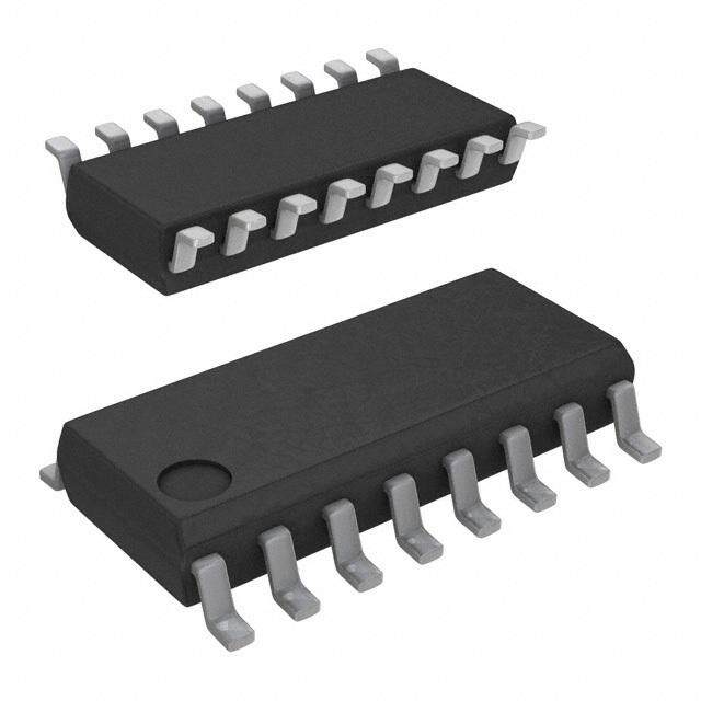
| 描述 | IC DAC 8BIT QUAD R-R 20-SOIC数模转换器- DAC 8-Bit 4Ch Precision DAC |
| 产品分类 | |
| 品牌 | Maxim Integrated |
| 产品手册 | |
| 产品图片 |
|
| rohs | 符合RoHS无铅 / 符合限制有害物质指令(RoHS)规范要求 |
| 产品系列 | 数据转换器IC,数模转换器- DAC,Maxim Integrated MAX509ACWP+- |
| 数据手册 | |
| 产品型号 | MAX509ACWP+ |
| 产品培训模块 | http://www.digikey.cn/PTM/IndividualPTM.page?site=cn&lang=zhs&ptm=25703http://www.digikey.cn/PTM/IndividualPTM.page?site=cn&lang=zhs&ptm=25705 |
| 产品种类 | 数模转换器- DAC |
| 位数 | 8 |
| 供应商器件封装 | 20-SOIC W |
| 分辨率 | 8 bit |
| 包装 | 管件 |
| 商标 | Maxim Integrated |
| 安装类型 | 表面贴装 |
| 安装风格 | SMD/SMT |
| 封装 | Tube |
| 封装/外壳 | 20-SOIC(0.295",7.50mm 宽) |
| 封装/箱体 | SOIC-20 |
| 工作温度 | 0°C ~ 70°C |
| 工厂包装数量 | 36 |
| 建立时间 | 6µs |
| 接口类型 | QSPI, SPI, Serial (3-Wire, 4-Wire, Microwire) |
| 数据接口 | 串行 |
| 最大功率耗散 | 762 mW |
| 最大工作温度 | + 70 C |
| 最小工作温度 | 0 C |
| 标准包装 | 1 |
| 电压参考 | External |
| 电压源 | 双 ± |
| 电源电压-最大 | 5.5 V |
| 电源电压-最小 | 4.5 V |
| 稳定时间 | 6 us |
| 系列 | MAX509A |
| 结构 | R-2R |
| 转换器数 | 4 |
| 转换器数量 | 4 |
| 输出数和类型 | 4 电压,单极4 电压,双极 |
| 输出类型 | Voltage |
| 采样率(每秒) | - |
| 零件号别名 | MAX509A |


- 商务部:美国ITC正式对集成电路等产品启动337调查
- 曝三星4nm工艺存在良率问题 高通将骁龙8 Gen1或转产台积电
- 太阳诱电将投资9.5亿元在常州建新厂生产MLCC 预计2023年完工
- 英特尔发布欧洲新工厂建设计划 深化IDM 2.0 战略
- 台积电先进制程称霸业界 有大客户加持明年业绩稳了
- 达到5530亿美元!SIA预计今年全球半导体销售额将创下新高
- 英特尔拟将自动驾驶子公司Mobileye上市 估值或超500亿美元
- 三星加码芯片和SET,合并消费电子和移动部门,撤换高东真等 CEO
- 三星电子宣布重大人事变动 还合并消费电子和移动部门
- 海关总署:前11个月进口集成电路产品价值2.52万亿元 增长14.8%


PDF Datasheet 数据手册内容提取
19-0155; Rev 3; 12/10 Quad, Serial 8-Bit DACs with Rail-to-Rail Outputs _______________General Description ____________________________Features M The MAX509/MAX510 are quad, serial-input, 8-bit volt- ♦♦ Single +5V or Dual ±5V Supply Operation A age-output digital-to-analog converters (DACs). They ♦♦ Output Buffer Amplifiers Swing Rail-to-Rail X operate with a single +5V supply or dual ±5V supplies. ♦♦ Reference Input Range Includes Both Supply Rails Internal, precision buffers swing rail-to-rail. The refer- 5 ence input range includes both supply rails. ♦♦ Calibrated Offset, Gain, and Linearity (1LSB TUE) 0 The MAX509 has four separate reference inputs, allow- ♦♦ 10MHz Serial Interface, Compatible with SPI, QSPI 9 (CPOL = CPHA = 0) and MICROWIRE ing each DAC's full-scale range to be set independently. / 20-pin DIP, SSOP, and SO packages are available. The ♦♦ Double-Buffered Registers for Synchronous M MAX510 is identical to the MAX509 except it has two ref- Updating A erence inputs, each shared by two DACs. The MAX510 ♦♦ Serial Data Output for Daisy-Chaining is housed in space-saving 16-pin DIP and SO packages. ♦♦ Power-On Reset Clears Serial Interface and Sets X The serial interface is double-buffered: A 12-bit input All Registers to Zero 5 shift register is followed by four 8-bit buffer registers and 1 ______________Ordering Information four 8-bit DAC registers. A 12-bit serial word is used to 0 load data into each register. Both input and DAC regis- TUE ters can be updated independently or simultaneously PART TEMP RANGE PIN-PACKAGE (LSB) with single software commands. Two additional asyn- MAX509ACPP+ 0°C to +70°C 20 PDIP ±1 chronous control pins provide simultaneous updating MAX509BCPP+ 0°C to +70°C 20 PDIP ±1.5 (LDAC)or clearing (CLR)of input and DAC registers. MAX509ACWP+ 0°C to +70°C 20 Wide SO ±1 The interface is compatible with MICROWIRETM and MAX509BCWP+ 0°C to +70°C 20 Wide SO ±1.5 SPI/QSPITM. All digital inputs and outputs are MAX509ACAP+ 0°C to +70°C 20 SSOP ±1 TTL/CMOS compatible. A buffered data output provides Ordering Information continued on last page. for readback or daisy-chaining of serial devices. **Contact factory for availability and processing to MIL-STD-883. +Denotes a lead(Pb)-free/RoHS-compliant package. _______________Functional Diagrams _________________Pin Configurations CLR DOUT LDAC AGND DGND VSS VDD REFB REFA TOP VIEW MAX509 DECODE CONTROL OUTA INPUT DAC OUTB 1 20 OUTC DAC A REG A REG A OUTA 2 19 OUTD VSS 3 18 VDD OUTB 12-BIT INPUT DAC REFB 4 MAX509 17 REFC DAC B SHIFT REG B REG B REFA 5 16 REFD REGISTER AGND 6 15 CS OUTC INPUT DAC N.C. 7 14 N.C. DAC C REG C REG C DGND 8 13 SCLK LDAC 9 12 DIN OUTD SR INPUT DAC DAC D DOUT 10 11 CLR CONTROL REG D REG D DIP/SO/SSOP CS DIN SCLK REFC REFD Functional Diagrams continued at end of data sheet. Pin Configurations continued at end of data sheet. MICROWIREis a trademark of National Semiconductor Corp. SPI and QSPI are trademarks of Motorola. ________________________________________________________________Maxim Integrated Products 1 For pricing, delivery, and ordering information,please contact Maxim Directat 1-888-629-4642, or visit Maxim’s website at www.maxim-ic.com.
Quad, Serial 8-Bit DACs with Rail-to-Rail Outputs 0 ABSOLUTE MAXIMUM RATINGS 1 VDDto DGND..............................................................-0.3V, +6V 20-Pin Plastic DIP (derate 11.11mW/°C above +70°C)....889mW 5 VDDto AGND...............................................................-0.3V, +6V 20-Pin Wide SO (derate 10.00mW/°C above +70°C).......800mW X VSSto DGND...............................................................-6V, +0.3V 20-Pin SSOP (derate 10.00mW/°C above +70°C)............800mW A VSSto AGND...............................................................-6V, +0.3V 20-Pin CERDIP (derate 11.11mW/°C above +70°C)........889mW VDDto VSS.................................................................-0.3V, +12V Operating Temperature Ranges: M Digital Input Voltage to DGND......................-0.3V, (VDD+ 0.3V) MAX5_ _ _C_ _.....................................................0°C to +70°C REF_....................................................(VSS- 0.3V), (VDD+ 0.3V) MAX5_ _ _E_ _..................................................-40°C to +85°C / 9 OUT_..............................................................................VDD, VSS MAX5_ _ _MJ_................................................-55°C to +125°C 0 Maximum Current into Any Pin............................................50mA Storage Temperature Range.............................-65°C to +150°C 5 Continuous Power Dissipation (TA= +70°C) Lead Temperature (soldering, 10s).................................+300°C 16-Pin Plastic DIP (derate 10.53mW/°C above +70°C)....842mW Soldering Temperature (reflow) X 16-Pin Wide SO (derate 9.52mW/°C above +70°C).........762mW Lead (Pb)-free packages..............................................+260°C A 16-Pin CERDIP (derate 10.00mW/°C above +70°C)........800mW Packages containing lead (Pb).....................................+260°C M Note: The outputs may be shorted to VDD, VSS, or AGND if the package power dissipation is not exceeded. Typical short-circuitcurrent to AGND is 50mA. Do not bias AGND more than +1V above DGND, or more than 2.5V below DGND. Stresses beyond those listed under “Absolute Maximum Ratings” may cause permanent damage to the device. These are stress ratings only, and functional operation of the device at these or any other conditions beyond those indicated in the operational sections of the specifications is not implied. Exposure to absolute maximum rating conditions for extended periods may affect device reliability. ELECTRICAL CHARACTERISTICS (VDD= +5V ±10%, VSS= 0V to -5.5V, VREF= 4V, AGND = DGND = 0V, RL= 10kΩ, CL= 100pF, TA= TMINto TMAX, unless other- wise noted.) PARAMETER SYMBOL CONDITIONS MIN TYP MAX UNITS STATIC ACCURACY Resolution 8 Bits VREF = +4V, MAX5_ _A ±1 VSS= 0V or -5V ±10% MAX5_ _B ±1.5 Total Unadjusted Error TUE LSB VREF = -4V, MAX5_ _A ±1 VSS= -5V ±10% MAX5_ _B ±1.5 Differential Nonlinearity DNL Guaranteed monotonic ±1 LSB MAX5_ _C 14 Code = 00 hex, MAX5_ _E 16 VSS= 0V MAX5_ _M 20 Zero-Code Error ZCE mV MAX5_ _C ±14 Code = 00 hex, MAX5_ _E ±16 VSS= -5V ±10% MAX5_ _M ±20 Zero-Code-Error Supply Rejection Code = 00 hex, VDD= 5V ±10%, 1 2 mV VSS= 0V or -5V ±10% Zero-Code Code = 00 hex ±10 µV/°C Temperature Coefficient Full-Scale Error Code = FF hex ±14 mV MAX5_ _C 1 4 Code = FF hex, Full-Scale-Error Supply Rejection VDD= +5V ±10%, MAX5_ _E 1 8 mV VSS= 0V or -5V ±10% MAX5_ _M 1 12 Full-Scale-Error Code = FF hex ±10 µV/°C Temperature Coefficient 2 _______________________________________________________________________________________
Quad, Serial 8-Bit DACs with Rail-to-Rail Outputs ELECTRICAL CHARACTERISTICS (continued) M (VDD= +5V ±10%, VSS= 0V to -5.5V, VREF= 4V, AGND = DGND = 0V, RL= 10kΩ, CL= 100pF, TA= TMINto TMAX, A unless otherwise noted.) X PARAMETER SYMBOL CONDITIONS MIN TYP MAX UNITS 5 REFERENCE INPUTS 0 Input Voltage Range VSS VDD V 9 MAX509 16 24 Input Resistance (Note 1) Code = 55 hex kΩ / MAX510 8 12 M MAX509 15 A Input Capacitance (Note 2) Code = 00 hex pF MAX510 30 X Channel-to-Channel Isolation (Note 3) -60 dB 5 ACFeedthrough (Note 4) -70 dB 1 DAC OUTPUTS 0 Full-Scale Output Voltage VSS VDD V VREF = 4V, load regulation ≤1/4LSB 2 VREF = -4V, VSS = -5V ±10%, 2 load regulation ≤1/4LSB Resistive Load VREF = VDDMAX5_ _C/E, kΩ 10 load regulation ≤1LSB VREF = VDDMAX5_ _M, 10 load regulation ≤2LSB DIGITAL INPUTS Input High Voltage VIH 2.4 V Input Low Voltage VIL 0.8 V Input Current IIN VIN= 0V or VDD 1.0 µA Input Capacitance CIN (Note 5) 10 pF DIGITAL OUTPUTS Output High Voltage VOH ISOURCE= 0.2mA VDD- 0.5 V Output Low Voltage VOL ISINK= 1.6mA 0.4 V DYNAMIC PERFORMANCE MAX5_ _C 1.0 Voltage-Output Slew Rate Positive and negative MAX5_ _E 0.7 V/µs MAX5_ _M 0.5 Output Settling Time (Note 6) To 1/2LSB, 10kΩII 100pF load 6 µs Code = 00 hex, all digital inputs Digital Feedthrough 5 nV-s from 0V to VDD Digital-to-Analog Glitch Impulse Code 128➝127 12 nV-s VREF = 4Vp-pat 1kHz, VDD= 5V, 87 Signal-to-Noise + Distortion Ratio SINAD code = FF hex dB VREF = 4Vp-pat 20kHz, VSS= -5V ±10% 74 Multiplying Bandwidth VREF = 0.5Vp-p, 3dB bandwidth 1 MHz Wideband Amplifier Noise 60 µVRMS _______________________________________________________________________________________ 3
Quad, Serial 8-Bit DACs with Rail-to-Rail Outputs 0 ELECTRICAL CHARACTERISTICS (continued) 1 (VDD= +5V ±10%, VSS= 0V to -5.5V, VREF= 4V, AGND = DGND = 0V, RL= 10kΩ, CL= 100pF, TA= TMINto TMAX, 5 unless otherwise noted.) X PARAMETER SYMBOL CONDITIONS MIN TYP MAX UNITS A POWER SUPPLIES M Positive Supply Voltage VDD For specified performance 4.5 5.5 V Negative Supply Voltage VSS For specified performance -5.5 0 V / 9 Outputs unloaded, all MAX5_ _C/E 5 10 Positive Supply Current IDD mA 0 digital inputs = 0V or VDD MAX5_ _M 5 12 5 VSS= -5V ±10%, outputs MAX5_ _C/E 5 10 X Negative Supply Current ISS unloaded, all digital mA inputs = 0V or VDD MAX5_ _M 5 12 A Note 1: Input resistance is code dependent. The lowest input resistance occurs at code = 55 hex. M Note 2: Input capacitance is code dependent. The highest input capacitance occurs at code = 00 hex. Note 3: VREF = 4Vp-p, 10kHz. Channel-to-channel isolation is measured by setting the code of one DAC to FF hex and setting the code of all other DACs to 00 hex. Note 4: VREF = 4Vp-p, 10kHz. DAC code = 00 hex. Note 5: Guaranteed by design. Note 6: Output settling time is measured by taking the code from 00 hex to FF hex, and from FF hex to 00 hex. TIMING CHARACTERISTICS (VDD= +5V ±10%, VSS= 0V to -5V, VREF= 4V, AGND = DGND = 0V, CL= 50pF, TA= TMINto TMAX, unless otherwise noted.) PARAMETER SYMBOL CONDITIONS MIN TYP MAX UNITS MAX5_ _C/E 40 20 LDACPulse Width Low tLDW ns MAX5_ _M 50 25 CSRise to LDACFall Setup Time tCLL (Notes 7, 8) 0 ns MAX5_ _C/E 40 20 CLRPulse Width Low tCLW ns MAX5_ _M 50 25 SERIAL INTERFACE TIMING MAX5_ _C/E 40 CSFall to SCLK Setup Time tCSS ns MAX5_ _M 50 SCLK Fall to CSRise Hold Time tCSH2 0 ns SCLK Rise to CSRise Hold Time tCSH1 (Note 9) 40 ns SCLK Fall to CSFall Hold Time tCSH0 (Note 7) 0 ns MAX5_ _C/E 40 DIN to SCLK Rise Setup Time tDS ns MAX5_ _M 50 DIN to SCLK Rise Hold Time tDH 0 ns MAX5_ _C/E 20 12.5 SCLK Clock Frequency fCLK MHz MAX5_ _M 20 10 MAX5_ _C/E 40 SCLK Pulse Width High tCH ns MAX5_ _M 50 MAX5_ _C/E 40 SCLK Pulse Width Low tCL ns MAX5_ _M 50 MAX5_ _C/E 10 100 SCLK to DOUT Valid tDO ns MAX5_ _M 10 100 Note 7: Guaranteed by design. Note 8: If LDACis activated prior to CS's rising edge, it must stay low for tLDWor longer after CSgoes high. Note 9: Minimum delay from 12th clock cycle to CSrise. 4 _______________________________________________________________________________________
Quad, Serial 8-Bit DACs with Rail-to-Rail Outputs __________________________________________Typical Operating Characteristics M (TA = +25°C, unless otherwise noted.) A X OUTPUT SINK CURRENT OUTPUT SOURCE CURRENT SUPPLY CURRENT 5 vs. (VOUT - VSS) vs. OUTPUT VOLTAGE vs. TEMPERATURE 1120 MAX509-FG01 --2205 VVDSSD == GVNREDF = +5V MAX509-FG10 76 MAX509-FG02 09/ DIGITAL INPUT = FF HEX A) 5 M I (mA)OUT 2648 VVDSSD == GVNRDEF = = 0 +V5V I (mA)OUT--11-505 SUPPLY CURRENT (m 2431 VVVADSRLSLDE F=D= =I-+G5 5-I.4T.55.AV7VL5 INPUTS =IS +S5VIDD AX510 ALL DIGITAL INPUTS = 00 HEX 0 0 0 0 0.2 0.4 0.6 0.8 1.0 1.2 3.6 3.8 4.0 4.2 4.4 4.6 4.8 5.0 -60 -40 -20 0 20 40 60 80 100120 140 VOUT - VSS (V) VOUT (V) TEMPERATURE (°C) SUPPLY CURRENT THD + NOISE AT DAC OUTPUT THD + NOISE AT DAC OUTPUT vs. REFERENCE VOLTAGE vs. REFERENCE AMPLITUDE vs. REFERENCE FREQUENCY 65 MAX509-FG03 --4405 VVDSSD == -+55VV MAX509-FG041% --2300 VVDSSD == -+55VV MAX509-FG0510% VSS = 0V -50 INPUT CODE = FF HEX INPUT CODE = FF HEX I (mA)DD 324 VSS = -5V THD + NOISE (dB)----67650055 FREQ = 20kHz 0.1%THD + NOISE (%) THD + NOISE (dB)---654000 FREQ = SWEPTVREF = 8Vp-p 01.1%%THD + NOISE (%) -75 -70 VREF = 1Vp-p FREQ = 1kHz 1 VADLLD L=O +G5IVC -80 0.01% -80 0.01% -85 VREF = 4Vp-p INPUTS = +5V 0 -90 -90 -5 -4 -3 -2 -1 0 1 2 3 4 5 0 2 4 6 8 10 10 100 1k 10k 100k VREF VOLTAGE (V) REFERENCE AMPLITUDE (Vp-p) REFERENCE FREQUENCY (Hz) REFERENCE VOLTAGE INPUT REFERENCE VOLTAGE INPUT REFERENCE VOLTAGE INPUT FREQUENCY RESPONSE FREQUENCY RESPONSE FREQUENCY RESPONSE 0 MAX509-FG06 0 MAX509-FG07 0 MAX509-FG08 RELATIVE OUTPUT (dB)---321000 RELATIVE OUTPUT (dB)---321000 RELATIVE OUTPUT (dB)---321000 VDD = +5V VDD = +5V VSS = AGND VSS = AGND VDD = +5V -40 VREF = 2.5VDC + 0.5Vp-p SINE WAVE -40 VREF = 2.5VDC + 0.05Vp-p SINE WAVE -40 VVSRSE F= =-5 2V.5VDC + 4Vp-p SINE WAVE 1k 10k 100k 1M 10M 1k 10k 100k 1M 10M 1k 10k 100k 1M 10M FREQUENCY (Hz) FREQUENCY (Hz) FREQUENCY (Hz) _______________________________________________________________________________________ 5
Quad, Serial 8-DACs with Rail-to-Rail Outputs 0 ____________________________Typical Operating Characteristics (continued) 1 (TA = +25°C, unless otherwise noted.) 5 X ZERO-CODE ERROR REFERENCE FEEDTHROUGH AT 40kHz A vs. NEGATIVE SUPPLY VOLTAGE WORST-CASE 1LSB DIGITAL STEP CHANGE 5.0 M 4.8 VVDRDE F= =+ 5+V4V MAX509-FG09 2V 20mV / 9 mV)4.6 A A 0 OR (4.4 5 RR X ODE E 4.2 A RO-C4.0 B ZE3.8 B M 3.6 200nS 3.4 A = REFA, 10Vp-p 0 -1 -2 -3 -4 -5 -6 A = CS, 2V/div B = OUTA, 100μV/div, UNLOADED VSS (V) B = OUTA, 20mV ˜ TIMEBASE = 10μs/div TIMEBASE = 200ns/div VDD = +5V, VSS = -5V CODE = ALL 0s REFERENCE FEEDTHROUGH AT 10kHz REFERENCE FEEDTHROUGH AT 4kHz REFERENCE FEEDTHROUGH AT 400Hz 5V 50μV A A A B 10 B B 100μS A = REFA, 10Vp-p A = REFA, 10Vp-p A = REFA, 10Vp-p B = OUTA, 50μV/div, UNLOADED B = OUTA, 50μV/div, UNLOADED B = OUTA, 50μV/div, UNLOADED TIMEBASE = 50μs/div TIMEBASE = 100μs/div TIMEBASE = 1ms/div 6 _______________________________________________________________________________________
Quad, Serial 8-Bit DACs with Rail-to-Rail Outputs ____________________________Typical Operating Characteristics (continued) M (TA = +25°C, unless otherwise noted.) A POSITIVE SETTLING TIME X CLOCK FEEDTHROUGH (VSS = AGND OR -5V) 5 0 5V 100mV 9 A / A M A B X 5 B 1 0 1μS A = SCLK, 333kHz A = DIGITAL INPUT, 5V/div B = OUT_, 10mV/div B = OUT_ , 2V/div TIMEBASE = 2μs/div TIMEBASE = 1μs/div VDD = +5V REF_ = +4V ALL BITS OFF TO ALL BITS ON RL = 10kΩ, CL = 100pF NEGATIVE SETTLING TIME NEGATIVE SETTLING TIME (VSS = AGND) (VSS = -5V) 5V 100mV 5V 100mV A A B B 1μS 1μS A = DIGITAL INPUT, 5V/div A = DIGITAL INPUT, 5V/div B = OUT_ , 2V/div B = OUT_ , 2V/div TIMEBASE = 1μs/div TIMEBASE = 1μs/div VDD = +5V VDD = +5V REF_ = +4V REF_ = +4V ALL BITS ON TO ALL BITS OFF ALL BITS ON TO ALL BITS OFF RL = 10kΩ, CL = 100pF RL = 10kΩ, CL = 100pF _______________________________________________________________________________________ 7
Quad, Serial 8-Bit DACs with Rail-to-Rail Outputs 0 ______________________________________________________________Pin Description 1 5 PIN NAME FUNCTION X MAX509 MAX510 A 1 1 OUTB DAC B Voltage Output M 2 2 OUTA DAC A Voltage Output / 9 3 3 VSS Negative Power Supply, 0V to -5V ±10%. Connect to AGND for single-supply operation. 0 5 4 – REFB Reference Voltage Input for DAC B X – 4 REFAB Reference Voltage Input for DACs A and B A 5 – REFA Reference Voltage Input for DAC A M 6 5 AGND Analog Ground 7, 14 – N.C. Not Internally Connected 8 6 DGND Digital Ground Load DAC Input (active low). Driving this asynchronous input low (level sensitive) 9 7 LDAC transfers the contents of each input latch to its respective DAC latch. Serial Data Output. Can sink and source current. Data at DOUT is adjustable to be 10 8 DOUT clocked out on rising or falling edge of SCLK. Clear DAC input (active low). Driving CLRlow causes an asynchronous clear of input 11 9 CLR and DAC registers and sets all DAC outputs to zero. Serial Data Input. TTL/CMOS-compatible input. Data is clocked into DIN on the 12 10 DIN rising edge of SCLK. CSmust be low for data to be clocked in. Serial Clock Input. Data is clocked in on the rising edge and clocked out on either the 13 11 SCLK rising (default) or the falling edge. Chip-Select Input (active low). Data is shifted in and out when CSis low. Programming 15 12 CS commands are executed when CSrises. 16 – REFD Reference Voltage Input for DAC D – 13 REFCD Reference Voltage Input for DACs C and D 17 – REFC Reference Voltage Input for DAC C 18 14 VDD Positive Power Supply, +5V ±10% 19 15 OUTD DAC D Output Voltage 20 16 OUTC DAC C Output Voltage 8 _______________________________________________________________________________________
Quad, Serial 8-Bit DACs with Rail-to-Rail Outputs _______________Detailed Description between updates. DOUT does not go into a high- M impedance state if the clock or CSis high. Serial Interface A Serial data is clocked into the data registers in MSB- At power-on, the serial interface and all DACs are first format, with the address and configuration infor- X cleared and set to code zero. The serial data output mation preceding the actual DAC data. Data is 5 (DOUT) is set to transition on SCLK's rising edge. clocked in on SCLK's rising edge while CSis low. Data 0 The MAX509/MAX510 communicate with microproces- at DOUT is clocked out 12 clock cycles later, either at 9 sors through a synchronous, full-duplex, 3-wire inter- SCLK's rising edge (default or mode 1) or falling edge face (Figure 1). Data is sent MSB first and can be (mode 0). /M transmitted in one 4-bit and one 8-bit (byte) packet or Chip select (CS) must be low to enable the DAC. If CS in one 12-bit word. If a 16-bit control word is used, the A is high, the interface is disabled and DOUT remains first four bits are ignored. A 4-wire interface adds a line unchanged. CS must go low at least 40ns before the X for LDACand allows asynchronous updating. The serial first rising edge of the clock pulse to properly clock in 5 clock (SCLK) synchronizes the data transfer. Data is the first bit. With CS low, data is clocked into the transmitted and received simultaneously. 1 MAX509/MAX510's internal shift register on the rising Figure 2 shows a detailed serial interface timing. edge of the external serial clock. SCLK can be driven 0 Please note that the clock should be low if it is stopped at rates up to 12.5MHz. INSTRUCTION EXECUTED CS • • • • • • SCLK DIN • • • A1 A0 C1 C0 D7 D6 D5 D4 D3 D2 D1 D0 A1 A1 A0 C1 C0 D7 D6 D5 D4 D3 D2 D1 D0 A1 MSB LSB MSB LSB DACA DACD DOUT MODE 1 • • • (DEFAULT) A1 A0 C1 C0 D7 D6 D5 D4 D3 D2 D1 D0 A1 A1 A0 C1 C0 D7 D6 D5 D4 D3 D2 D1 D0 A1 DATA FROM PREVIOUS DATA INPUT DATA FROM PREVIOUS DATA INPUT DOUT • • • MODE 0 A1 A0 C1 C0 D7 D6 D5 D4 D3 D2 D1 D0 A1 A1 A0 C1 C0 D7 D6 D5 D4 D3 D2 D1 D0 A1 Figure 1. MAX509/MAX510 3-Wire Interface Timing _______________________________________________________________________________________ 9
Quad, Serial 8-Bit DACs with Rail-to-Rail Outputs 0 tCLL 1 5 CS • • • tCSH2 X A tCSS tCH M tCSH0 / • • • 9 0 SCLK 5 tDS tCL tCSH1 X tDH A • • • M DIN tDO • • • DOUT • • • LDAC NOTE: TIMING SPECIFICATION tCLL IS RECOMMENDED TO MINIMIZE OUTPUT GLITCH, BUT IS NOT MANDATORY. tLDW Figure 2. Detailed Serial Interface Timing (Mode 0 Shown) Table 1. Serial-Interface Programming Commands 12-Bit Serial Word LDAC Function A1 A0 C1 C0 D7 . . . . . . . . D0 0 0 0 1 8-Bit DAC Data 1 Load DAC A input register, DAC output unchanged. 0 1 0 1 8-Bit DAC Data 1 Load DAC B input register, DAC output unchanged. 1 0 0 1 8-Bit DAC Data 1 Load DAC C input register, DAC output unchanged. 1 1 0 1 8-Bit DAC Data 1 Load DAC D input register, DAC output unchanged. 0 0 1 1 8-Bit DAC Data 1 Load input and DAC register A. 0 1 1 1 8-Bit DAC Data 1 Load input and DAC register B. 1 0 1 1 8-Bit DAC Data 1 Load input and DAC register C. 1 1 1 1 8-Bit DAC Data 1 Load input and DAC register D. X 0 0 0 8-Bit DAC Data X Update all DACs from shift register. X 1 0 0 X X X X X X X X X No Operation (NOP), shifts data in shift register. “LDAC” Command, all DACs updated from respective 0 X 1 0 X X X X X X X X X input registers. Mode 1, DOUT clocked out on rising edge of SCLK 1 1 1 0 X X X X X X X X X (default). All DACs updated from respective input registers. Mode 0, DOUT clocked out on falling edge of SCLK. 1 0 1 0 X X X X X X X X X All DACs updated from input registers. 10 ______________________________________________________________________________________
Quad, Serial 8-Bit DACs with Rail-to-Rail Outputs Serial Input Data Format and Control Codes Update All DACs from Shift Registers M The 12-bit serial input format shown in Figure 3 com- prises two DAC address bits (A1, A0), two control bits A1 A0 C1 C0 D7 D6 D5 D4 D3 D2 D1 D0 A (C1, C0) and eight bits of data (D0...D7). x 0 0 0 8-Bit DAC Data X The 4-bit address/control code configures the DAC as (LDAC= x) 5 shown in Table 1. All four DAC registers are updated with shift-register 0 data. This command allows all DACs to be set to any 9 This is the first bit shifted in MSB LSB analog value within the reference range. This command / M can be used to substitute CLR if code 00 hex is pro- DOUT A1 A0 C1 C0 D7 D6 ● ● ● D1 D0 DIN grammed, which clears all DACs. A No Operation (NOP) X Control and 8-bit DAC data Address bits A1 A0 C1 C0 D7 D6 D5 D4 D3 D2 D1 D0 5 x 1 0 0 x x x x x x x x 1 Figure 3. Serial Input Format 0 (LDAC= x) Load Input Register, DAC Registers Unchanged The NOP command (no operation) allows data to be shift- (Single Update Operation) ed through the MAX509/MAX510 shift register without affecting the input or DAC registers. This is useful in daisy A1 A0 C1 C0 D7 D6 D5 D4 D3 D2 D1 D0 chaining (also see the Daisy-Chaining Devicessection). Address 0 1 8-Bit Data For this command, the data bits are "Don't Cares." As an (LDAC= H) example, three MAX509/MAX510s are daisy-chained (A, B and C), and DAC A and DAC C need to be updated. The When performing a single update operation, A1 and A0 36-bit-wide command would consist of one 12-bit word for select the respective input register. At the rising edge device C, followed by an NOP instruction for device B and of CS, the selected input register is loaded with the cur- a third 12-bit word with data for device A. At CS's rising rent shift-register data. All DAC outputs remain edge, only device B is not updated. unchanged. This preloads individual data in the input register without changing the DAC outputs. “LDAC” Command (Software) A1 A0 C1 C0 D7 D6 D5 D4 D3 D2 D1 D0 Load Input and DAC Registers 0 x 1 0 x x x x x x x x A1 A0 C1 C0 D7 D6 D5 D4 D3 D2 D1 D0 (LDAC= x) Address 1 1 8-Bit Data (LDAC= H) All DAC registers are updated with the contents of their respective input registers at CS's rising edge. With the This command directly loads the selected DAC register exception of using CS to execute, this performs the at CS's rising edge. A1 and A0 set the DAC address. same function as the asynchronous LDAC. Current shift-register data is placed in the selected input and DAC registers. Set DOUT Phase – SCLK Rising (Mode 1, Default) For example, to load all four DAC registers simultaneously A1 A0 C1 C0 D7 D6 D5 D4 D3 D2 D1 D0 with individual settings (DAC A = 1V, DAC B = 2V, DAC 1 1 1 0 x x x x x x x x C = 3V and DAC D = 4V), five commands are required. (LDAC= x) First, perform four single input register update opera- tions. Next, perform an “LDAC” command as a fifth Mode 1 resets the serial output DOUT to transition at command. All DACs will be updated from their respec- SCLK's rising edge. This is the MAX509/MAX510’s tive input registers at the rising edge of CS. default setting after the supply voltage has been applied. The command also loads all DAC registers with the con- tents of their respective input registers, and is identical to the “LDAC” command. ______________________________________________________________________________________ 11
Quad, Serial 8-Bit DACs with Rail-to-Rail Outputs 0 Set DOUT Phase – SCLK Falling (Mode 0) 1 A1 A0 C1 C0 D7 D6 D5 D4 D3 D2 D1 D0 5 SCLK SK 1 0 1 0 x x x x x x x x X (LDAC= x) MAX509 DIN SO A MAX510 MICROWIRE PORT M This command resets DOUT to transition at SCLK's falling DOUT SI edge. Once this command is issued, the phase of DOUT is / 9 latched and will not change except on power-up or if the CS I/0 0 specific command is issued that sets the phase to rising edge. 5 THE DOUT-SI CONNECTION IS NOT REQUIRED FOR WRITING TO THE X The same command also updates all DAC registers with MAX509/MAX510, BUT MAY BE USED FOR READ-BACK PURPOSES. the contents of their respective input registers, identical to A the “LDAC” command. Figure 4. Connections for MICROWIRE M LDAC Operation (Hardware) LDAC is typically used in 4-wire interfaces (Figure 7). LDAC allows asynchronous hardware control of the DAC outputs and is level-sensitive. With LDAClow, the DAC reg- DOUT MISO isters are transparent and any time an input register is updated, the DAC output immediately follows. MAX509 DIN MOSI MAX510 SPI Clear DACs with CLR PORT SCLK SCK Strobing the CLR pin low causes an asynchronous clear of input and DAC registers and sets all DAC outputs to zero. CS I/0 Similar to the LDAC pin, CLR can be invoked at any time, typically when the device is not selected (CS = H). When the DAC data is all zeros, this function is equivalent to the CPOL = 0, CPHA = 0 "Update all DACs from Shift Registers" command. THE DOUT-MISO CONNECTION IS NOT REQUIRED FOR WRITING TO THE MAX509/MAX510, BUT MAY BE USED FOR READ-BACK PURPOSES. Digital Inputs and Outputs Digital inputs and outputs are compatible with both TTL and Figure 5. Connections for SPI 5V CMOS logic. The power-supply current (I ) depends DD on the input logic levels. Using CMOS logic to drive CS, The MAX509/MAX510 can interface with Intel's SCLK, DIN, CLRand LDACturns off the internal level trans- 80C5X/80C3X family in mode 0 if the SCLK clock polarity is lators and minimizes supply currents. inverted. More universally, if a serial port is not available, three lines from one of the parallel ports can be used for bit Serial Data Output manipulation. DOUT is the output of the internal shift register. DOUT can be Digital feedthrough at the voltage outputs is greatly mini- programmed to clock out data on SCLK's falling edge (mode mized by operating the serial clock only to update the regis- 0) or rising edge (mode 1). In mode 0, output data lags the ters. Also see the Clock Feedthrough photo in the Typical input data by 12.5 clock cycles, maintaining compatibility with Operating Characteristicssection. The clock idle state is low. Microwire, SPI, and QSPI. In mode 1, output data lags the input by 12 clock cycles. On power-up, DOUT defaults to mode 1 Daisy-Chaining Devices timing. DOUT never three-states; it always actively drives either Any number of MAX509/MAX510s can be daisy-chained by high or low and remains unchanged when CSis high. connecting the DOUT pin of one device to the DIN pin of the following device in the chain. The NOP instruction (Table 1) Interfacing to the Microprocessor allows data to be passed from DIN to DOUT without chang- The MAX509/MAX510 are Microwire, SPI, and QSPI compati- ing the input or DAC registers of the passing device. A three- ble. For SPI and QSPI, clear the CPOL and CPHA configura- wire interface updates daisy-chained or individual tion bits (CPOL = CPHA = 0). The SPI/QSPI CPOL = CPHA MAX509/MAX510s simultaneously by bringing CShigh. = 1 configuration can also be used if the DOUT output is ignored. 12 ______________________________________________________________________________________
Quad, Serial 8-Bit DACs with Rail-to-Rail Outputs M A X MAX509 MAX509 MAX509 SCLK SCLK MAX510 SCLK MAX510 SCLK MAX510 5 0 DIN DIN DOUT DIN DOUT DIN DOUT 9 / CS CS CS CS M TO OTHER SERIAL DEVICES A X 5 1 MAX509 0 SCLK SCLK MAX510 DIN DIN CS CS Figure 6. Daisy-chained or individual MAX509/MAX510s are simultaneously updated by bringing CShigh. Only three wires are required. DIN SCLK LDAC CS1 CS2 TO OTHER SERIAL CS3 DEVICES CS CS CS LDAC MAX509 LDAC MAX509 LDAC MAX509 MAX510 MAX510 MAX510 SCLK SCLK SCLK DIN DIN DIN Figure 7. Multiple MAX509/MAX510 DACs sharing one DIN line. Simultaneously update by strobing LDAC, or specifically update by enabling individual CS. ______________________________________________________________________________________ 13
Quad, Serial 8-Bit DACs with Rail-to-Rail Outputs 0 dependent: 15pF typical for the MAX509 and 30pF 1 typical for the MAX510. 5 The output voltage for any DAC can be represented by X a digitally programmable voltage source as: R R R OUT_ A VOUT = (NB x VREF) / 256 M 2R 2R 2R 2R 22RR where NB is the numerical value of the DAC's binary input code. / D0 D5 D6 D7 9 Output Buffer Amplifiers 0 All MAX509/MAX510 voltage outputs are internally 5 REF_ buffered by precision unity-gain followers that slew at X AGND up to 1V/µs. The outputs can swing from VSS to VDD. With a 0V to +4V (or +4V to 0V) output transition, the A SHOWN FOR ALL 1 ON DAC amplifier outputs will settle to 1/2LSB in typically 6µs M when loaded with 10kΩin parallel with 100pF. Figure 8. DAC Simplified Circuit Diagram The buffer amplifiers are stable with any combination of If multiple devices share a common DIN line, Figure 7's resistive loads ≥2kΩand capacitive loads ≤300pF. configuration provides simultaneous update by strob- __________Applications Information ing LDAC low. CS1, CS2, CS3... are driven separately, thus controlling which data are written to devices 1, 2, 3.... Power Supply and Analog Section Reference Operating Ranges The MAX509/MAX510 are fully specified to operate with DAC Operation VDD = 5V ±10% and VSS = 0V to -5.5V. 8-bit perfor- The MAX509/MAX510 contain four matched voltage- mance is guaranteed for both single- and dual-supply output DACs. The DACs are inverted R-2R ladder net- operation. The zero-code output error is less than 14mV works that convert 8-bit digital words into equivalent when operating from a single +5V supply. analog output voltages in proportion to the applied ref- erence voltages. Each DAC in the MAX509 has a sepa- The DACs work well with reference voltages from VSS rate reference input, while the two reference inputs in to VDD. The reference voltage is referred to AGND. the MAX510 each share a pair of DACs. The two refer- The preferred power-up sequence is to apply VSS and ence inputs permit different full-scale output voltage then VDD, but bringing up both supplies at the same ranges for each pair of DACs. A simplified diagram of time is also acceptable. In either case, the voltage one of the four DACs is shown in Figure 8. applied to REF should not exceed VDD during power- up or at any other time. If proper power sequencing is Reference Input not possible, connect an external Schottky diode The MAX509/MAX510 can be used for multiplying between VSS and AGND to ensure compliance with the applications. The reference accepts both DC and AC Absolute Maximum Ratings. Do not apply signals to signals. The voltage at each REF input sets the full- the digital inputs before the device is fully powered up. scale output voltage for its respective DAC(s). If the ref- erence voltage is positive, both the MAX509 and Power-Supply Bypassing MAX510 can be operated from a single supply. If dual and Ground Management supplies are used, the reference input can vary from In single-supply operation (AGND = DGND = VSS = VSS to VDD, but is always referred to AGND. The input 0V), AGND, DGND and VSS should be connected impedance at REF is code dependent, with the lowest together in a "star" ground at the chip. This ground value (16kΩ for the MAX509 and 8kΩ for the MAX510) should then return to the highest quality ground avail- occurring when the input code is 55 hex or 0101 0101. able. Bypass VDD with a 0.1µF capacitor, located as The maximum value, practically infinity, occurs when close to VDD and DGND as possible. In dual-supply the input code is 00 hex. Since the REF input imped- operation, bypass VSSto AGND with 0.1µF. ance is code dependent, the DAC's reference sources Careful PC board layout minimizes crosstalk among must have a low output impedance (no more than 32Ω DAC outputs, reference inputs, and digital inputs. for the MAX509 and 16Ω for the MAX510) to maintain Figures 9 and 10 show suggested circuit board layouts output linearity. The REF input capacitance is also code to minimize crosstalk. 14 ______________________________________________________________________________________
Quad, Serial 8-Bit DACs with Rail-to-Rail Outputs SYSTEM GND M SYSTEM GND A OUTC OUTB OUTC OUTB X OUTD OUTA OUTD OUTA 5 0 VDD VSS VDD VSS 9 REFC REFB REFCD REFAB / M REFD REFA AGND AGND A X 5 1 0 Figure 9. Suggested MAX509 PC Board Layout for Minimizing Figure 10. Suggested MAX510 PC Board Layout for Minimizing Crosstalk (Bottom View) Crosstalk (Bottom View) Unipolar-Output, 2-Quadrant Multiplication Bipolar-Output, 2-Quadrant Multiplication In unipolar operation, the output voltages and the refer- Bipolar-output, 2-quadrant multiplication is achieved by ence input(s) are the same polarity. Figures 11 and 12 offsetting AGND positively or negatively. Table 3 shows show the MAX509/MAX510 unipolar configurations. the bipolar code. Both devices can be operated from a single supply if AGND can be biased above DGND to provide an arbi- the reference inputs are positive. If dual supplies are trary nonzero output voltage for a 0 input code, as used, the reference input can vary from VSS to VDD. shown in Figure 13. The output voltage at OUTA is: Table 2 shows the unipolar code. VOUTA= VBIAS+ (NB/256)(VIN), Table 2. Unipolar Code Table Table 3. Bipolar Code Table DAC CONTENTS ANALOG DAC CONTENTS ANALOG MSB LSB OUTPUT MSB LSB OUTPUT 1 1 1 1 1 1 1 1 +VREF(–22–55–56–) 1 1 1 1 1 1 1 1 +VREF(11––22–78–) 1 0 0 0 0 0 0 1 +VREF (–12–25–96–) 1 0 0 0 0 0 0 1 +VREF(–1–21–8–) 1 0 0 0 0 0 0 0 +V (–1–2–8– ) = + V –R–E–F– 1 0 0 0 0 0 0 0 0V REF 256 2 ( 1 ) 0 1 1 1 1 1 1 1 -V –––– REF (127) 128 0 1 1 1 1 1 1 1 +V –––– REF 256 (127) 0 0 0 0 0 0 0 1 -V –––– REF ( 1 ) 128 0 0 0 0 0 0 0 1 +V –––– REF 256 (128 ) 0 0 0 0 0 0 0 0 -V –––– = -V REF REF 0 0 0 0 0 0 0 0 0V 128 -8 ( 1 ) Note:1LSB = (V ) (2 ) = +V –––– REF REF 256 ______________________________________________________________________________________ 15
Quad, Serial 8-Bit DACs with Rail-to-Rail Outputs 0 1 REFERENCE INPUTS (VSS TO VDD) +5V +5V 5 4 17 16 18 5 REFA REFB REFC REFD VDD 5 18 X REFA VDD 2 A DAC A OUTA M 2 OUTA DAC A / VIN 9 0 DAC B 1 OUTB 6 AGND SERIAL MAX509 5 INTERFACE VBIAS VSS DGND X NOT SHOWN 3 8 20 A DAC C OUTC -5V (OR GND) M +5V 4 14 19 REFAB VDD DAC D OUTD VSS AGND DGND 2 OUTA 3 6 8 DAC A VIN -5V (OR GND) MAX509 5 AGND MAX510 Figure 11. MAX509 Unipolar Output Circuit VBIAS VSS DGND 3 6 -5V (OR GND) REFERENCE INPUTS (VSS TO VDD) +5V 4 14 SERIAL INTERFACE NOT SHOWN REFAB VDD Figure 13. MAX509/MAX510 AGND Bias Circuits (Positive 2 Offset) DAC A OUTA where NB represents the digital input word. Since AGND is common to all four DACs, all outputs will be 1 offset by V in the same manner. Do not bias AGND BIAS DAC B OUTB more than +1V above DGND, or more than 2.5V below SERIAL DGND. INTERFACE NOT SHOWN Figures 14 and 15 illustrate the generation of negative 16 offsets with bipolar outputs. In these circuits, AGND is DAC C OUTC biased negatively (up to -2.5V with respect to DGND) to provide an arbitrary negative output voltage for a 0 input code. The output voltage at OUTA is: 15 OUTA = -(R2/R1)(2.5V) + (NB/256)(2.5V)(R2/R1+1) DAC D OUTD where NB represents the digital input word. Since VSS REFCD AGND DGND AGND is common to all four DACs, all outputs will be 3 13 5 6 offset by VBIAS in the same manner. Table 3, with V = 2.5V, shows the digital code vs. output voltage -5V (OR GND) REF MAX510 for Figure 14 and 15's circuits with R1 = R2. The ICL7612 op amp is chosen because its common-mode Figure 12. MAX510 Unipolar Output Circuit range extends to both supply rails. 16 ______________________________________________________________________________________
Quad, Serial 8-Bit DACs with Rail-to-Rail Outputs M REFERENCE INPUTS +5V A X 5 4 17 16 18 0.1μF 5 +5V SERIAL VDD 0 INTERFACE 9 NOT SHOWN MAX509 / 0.1μF M 2 DAC A OUTA A R1 R2 X 330k 330k 0.1% 0.1% MAX873 1 5 +2.5V DAC B OUTB 1 +5V 0 0.1μF 20 2 7 DAC C OUTC 6 3 8 19 ICL7611A 1 DAC D OUTD 0.1μF VSS AGND DGND 3 6 8 -5V 0.1μF -5V Figure 14. MAX509 AGND Bias Circuit (Negative Offset) 4-Quadrant Multiplication Each DAC output may be configured for 4-quadrant multiplication using Figure 16 and 17's circuit. One op amp and two resistors are required per channel. With R1 = R2: VOUT= VREF[2(NB/256)-1] where NB represents the digital word in DAC register A. The recommended value for resistors R1 and R2 is 330kΩ(±0.1%). Table 3 shows the digital code vs. out- put voltage for Figure 16 and 17's circuit. ______________________________________________________________________________________ 17
Quad, Serial 8-Bit DACs with Rail-to-Rail Outputs 0 1 REFERENCE INPUTS +5V 5 4 13 14 +5V X VDD 0.1μF A SERIAL MAX510 0.1μF INTERFACE M NOT SHOWN DAC A 2 OUTA / 2 R1 R2 9 330k 330k 0 MAX873 6 0.1% 0.1% 1 DAC B OUTB 5 +2.5V 4 +5V X A 0.1μF 16 2 7 DAC C OUTC M 6 3 8 15 ICL7611A 1 DAC D OUTD 0.1μF VSS AGND DGND 3 5 6 -5V 0.1μF -5V Figure 15. MAX510 AGND Bias Circuit (Negative Offset) REFERENCE INPUTS (VSS TO VDD) +5V +5V 0.1μF 5 4 17 16 18 VDD 0.1μF R1 R2 MAX509 2 ICL7612A* VOUT DAC A OUTA 0.1μF SERIAL 1 +5V -5V DAC B INTERFACE OUTB NOT SHOWN 0.1μF 20 DAC C R1 R2 OUTC 19 ICL7612A* VOUT DAC D OUTD VSS AGND DGND 0.1μF -5V 3 6 8 0.1μF *CONNECT ICL7612A PIN 8 TO AGND AGND OR -5V Figure 16. MAX509 Bipolar Output Circuit 18 ______________________________________________________________________________________
Quad, Serial 8-Bit DACs with Rail-to-Rail Outputs M REFERENCE INPUTS A +5V +5V X 4 13 14 0.1μF VDD 0.1μF 5 R1 0 MAX510 R2 9 2 ICL7612A* VOUT DAC A /M OUTA 0.1μF A -5V 1 SERIAL DAC B X INTERFACE OUTB +5V NOT SHOWN 5 0.1μF 1 16 DAC C R1 0 OUTC R2 15 ICL7612A* VOUT DAC D OUTD VSS AGND DGND 0.1μF -5V 3 5 6 0.1μF *CONNECT ICL7612A PIN 8 TO AGND AGND OR -5V Figure 17. MAX510 Bipolar Output Circuit __Functional Diagrams (continued) ____Pin Configurations (continued) CLR DOUT LDAC AGND DGND VSS VDD REFAB TOP VIEW DECODE MAX510 CONTROL OUTA INPUT DAC REG A REG A DAC A OUTB(cid:1)1 16 OUTC OUTA(cid:1)2 15 OUTD OUTB VSS(cid:1)3 14 VDD 12-BIT INPUT DAC SHIFT REG B REG B DAC B REFAB(cid:1)4 MAX510 13 REFCD(cid:1) REGISTER AGND(cid:1)5 12 CS(cid:1) OUTC DGND(cid:1)6 11 SCLK(cid:1) INPUT DAC REG C REG C DAC C LDAC 7 10 DIN(cid:1) DOUT 8 9 CLR(cid:1) OUTD SR INPUT DAC DAC D DIP/Wide SO CONTROL REG D REG D CS DIN SCLK REFCD ______________________________________________________________________________________ 19
Quad, Serial 8-Bit DACs with Rail-to-Rail Outputs 0 _Ordering Information (continued) Package Information 1 For the latest package outline information and land patterns, go 5 TUE to www.maxim-ic.com/packages. Note that a “+”, “#”, or “-” in PART TEMP RANGE PIN-PACKAGE X (LSB) the package code indicates RoHS status only. Package draw- MAX509BCAP+ 0°C to +70°C 20 SSOP ±1.5 ings may show a different suffix character, but the drawing per- A MAX509AEPP+ -40°C to +85°C 20 PDIP ±1 tains to the package regardless of RoHS status. M MAX509BEPP+ -40°C to +85°C 20 PDIP ±1.5 PACKAGE PACKAGE OUTLINE LAND MAX509AEWP+ -40°C to +85°C 20 Wide SO ±1 / TYPE CODE NO. PATTERN NO. 9 MAX509BEWP+ -40°C to +85°C 20 Wide SO ±1.5 MAX509AEAP+ -40°C to +85°C 20 SSOP ±1 20 PDIP P20+3 21-0043 — 0 MAX509BEAP+ -40°C to +85°C 20 SSOP ±1.5 20 Wide SO W20+3 21-0042 90-0108 5 MAX509AMJP -55°C to +125°C 20 CERDIP** ±1 20 SSOP A20A+1 21-0056 90-0094 X MAX509BMJP -55°C to +125°C 20 CERDIP** ±1.5 20 CERDIP J20-2 21-0045 — MAX510ACPE+ 0°C to +70°C 16 PDIP ±1 A MAX510BCPE+ 0°C to +70°C 16 PDIP ±1.5 16 PDIP P16+2 21-0043 — M MAX510ACWE+ 0°C to +70°C 16 Wide SO ±1 16 Wide SO W16+3 21-0042 90-0107 MAX510BCWE+ 0°C to +70°C 16 Wide SO ±1.5 16 CERDIP J16-3 21-0045 — MAX510AEPE+ -40°C to +85°C 16 PDIP ±1 MAX510BEPE+ -40°C to +85°C 16 PDIP ±1.5 MAX510AEWE+ -40°C to +85°C 16 Wide SO ±1 MAX510BEWE+ -40°C to +85°C 16 Wide SO ±1.5 MAX510AMJE -55°C to +125°C 16 CERDIP** ±1 MAX510BMJE -55°C to +125°C 16 CERDIP** ±1.5 **Contact factory for availability and processing to MIL-STD-883. +Denotes a lead(Pb)-free/RoHS-compliant package. 20 ______________________________________________________________________________________
Quad, Serial 8-Bit DACs with Rail-to-Rail Outputs Revision History M A REVISION REVISION PAGES DESCRIPTION X NUMBER DATE CHANGED 5 Updated Ordering Information, added soldering temperature to Absolute 0 3 12/10 1, 2, 19, 20 Maximum Ratings, updated Figure 17 and Functional Diagrams 9 / M A X 5 1 0 Maxim cannot assume responsibility for use of any circuitry other than circuitry entirely embodied in a Maxim product. No circuit patent licenses are implied. Maxim reserves the right to change the circuitry and specifications without notice at any time. Maxim Integrated Products, 120 San Gabriel Drive, Sunnyvale, CA 94086 408-737-7600 ____________________21 © 2010 Maxim Integrated Products Maxim is a registered trademark of Maxim Integrated Products, Inc.
Quad, Serial 8-Bit DACs with Rail-to-Rail Outputs 0 _Ordering Information (continued) Package Information 1 For the latest package outline information and land patterns, go 5 TUE to www.maxim-ic.com/packages. Note that a “+”, “#”, or “-” in PART TEMP RANGE PIN-PACKAGE X (LSB) the package code indicates RoHS status only. Package draw- MAX509BCAP+ 0°C to +70°C 20 SSOP ±1.5 ings may show a different suffix character, but the drawing per- A MAX509AEPP+ -40°C to +85°C 20 PDIP ±1 tains to the package regardless of RoHS status. M MAX509BEPP+ -40°C to +85°C 20 PDIP ±1.5 PACKAGE PACKAGE OUTLINE LAND MAX509AEWP+ -40°C to +85°C 20 Wide SO ±1 / TYPE CODE NO. PATTERN NO. 9 MAX509BEWP+ -40°C to +85°C 20 Wide SO ±1.5 MAX509AEAP+ -40°C to +85°C 20 SSOP ±1 20 PDIP P20+3 21-0043 — 0 MAX509BEAP+ -40°C to +85°C 20 SSOP ±1.5 20 Wide SO W20+3 21-0042 90-0108 5 MAX509AMJP -55°C to +125°C 20 CERDIP** ±1 20 SSOP A20A+1 21-0056 90-0094 X MAX509BMJP -55°C to +125°C 20 CERDIP** ±1.5 20 CERDIP J20-2 21-0045 — MAX510ACPE+ 0°C to +70°C 16 PDIP ±1 A MAX510BCPE+ 0°C to +70°C 16 PDIP ±1.5 16 PDIP P16+2 21-0043 — M MAX510ACWE+ 0°C to +70°C 16 Wide SO ±1 16 Wide SO W16+3 21-0042 90-0107 MAX510BCWE+ 0°C to +70°C 16 Wide SO ±1.5 16 CERDIP J16-3 21-0045 — MAX510AEPE+ -40°C to +85°C 16 PDIP ±1 MAX510BEPE+ -40°C to +85°C 16 PDIP ±1.5 MAX510AEWE+ -40°C to +85°C 16 Wide SO ±1 MAX510BEWE+ -40°C to +85°C 16 Wide SO ±1.5 MAX510AMJE -55°C to +125°C 16 CERDIP** ±1 MAX510BMJE -55°C to +125°C 16 CERDIP** ±1.5 **Contact factory for availability and processing to MIL-STD-883. +Denotes a lead(Pb)-free/RoHS-compliant package. 20 ______________________________________________________________________________________