ICGOO在线商城 > 集成电路(IC) > PMIC - 稳流/电流管理 > MAX4788EXS+T

 Datasheet下载
- 型号: MAX4788EXS+T
- 制造商: Maxim
- 库位|库存: xxxx|xxxx
- 要求:
| 数量阶梯 | 香港交货 | 国内含税 |
| +xxxx | $xxxx | ¥xxxx |
查看当月历史价格
查看今年历史价格
MAX4788EXS+T产品简介:
ICGOO电子元器件商城为您提供MAX4788EXS+T由Maxim设计生产,在icgoo商城现货销售,并且可以通过原厂、代理商等渠道进行代购。 MAX4788EXS+T价格参考。MaximMAX4788EXS+T封装/规格:PMIC - 稳流/电流管理, 限流 Regulator 100mA SC-70-4。您可以下载MAX4788EXS+T参考资料、Datasheet数据手册功能说明书,资料中有MAX4788EXS+T 详细功能的应用电路图电压和使用方法及教程。
MAX4788EXS+T是Maxim Integrated生产的一款PMIC(电源管理集成电路),属于稳流/电流管理类器件。该芯片主要设计用于高精度、低噪声的电流调节应用,特别适用于对电源稳定性要求较高的便携式设备和精密电子系统。

其典型应用场景包括:
1. 便携式医疗设备:如血糖仪、便携式监护仪等,需要稳定电流驱动传感器或显示模块,确保测量精度和系统可靠性。
2. 工业传感器供电:为各类电流环路(如4-20mA)传感器提供精确的电流源,保障信号传输的准确性。
3. 测试与测量仪器:在精密仪表中用作参考电流源,提升系统整体测量精度。
4. 电池供电设备:如手持终端、智能穿戴设备,利用其低功耗特性延长电池寿命。
5. LED背光驱动:为小型LCD屏幕提供均匀稳定的背光电流,避免亮度波动。

MAX4788EXS+T采用小尺寸封装(如SOT23),适合空间受限的应用;具备良好的温度稳定性和低静态电流,可在宽温范围内可靠工作。此外,其集成度高,外围元件少,有助于简化电路设计,提高系统可靠性。

综上,MAX4788EXS+T广泛应用于需高精度电流控制的小型化、低功耗电子设备中,尤其适合医疗、工业和便携式消费类电子产品。
| 参数 | 数值 |
| 产品目录 | 集成电路 (IC)半导体 |
| 描述 | IC ANALOG SWITCH 1X1 SC70-4电源开关 IC - 配电 50mA/100mA Current Limit Switch |
| 产品分类 | |
| 品牌 | Maxim Integrated |
| 产品手册 | |
| 产品图片 |
|
| rohs | 符合RoHS无铅 / 符合限制有害物质指令(RoHS)规范要求 |
| 产品系列 | 开关 IC,电源开关 IC - 配电,Maxim Integrated MAX4788EXS+T- |
| 数据手册 | |
| 产品型号 | MAX4788EXS+T |
| 产品培训模块 | http://www.digikey.cn/PTM/IndividualPTM.page?site=cn&lang=zhs&ptm=25703http://www.digikey.cn/PTM/IndividualPTM.page?site=cn&lang=zhs&ptm=25705 |
| 产品目录页面 | |
| 产品种类 | 电源开关 IC - 配电 |
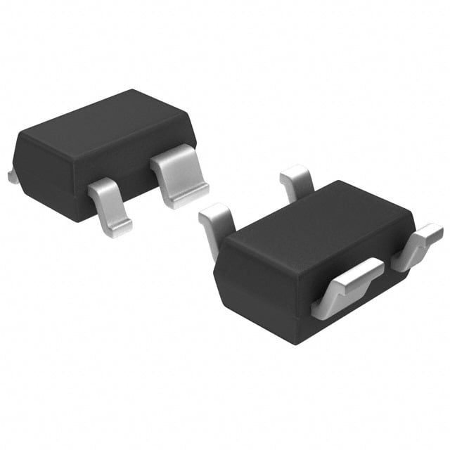
| 供应商器件封装 | SC-70-4 |
| 其它名称 | MAX4788EXS+TDKR |
| 功能 | |
| 包装 | Digi-Reel® |
| 商标 | Maxim Integrated |
| 安装类型 | 表面贴装 |
| 安装风格 | SMD/SMT |
| 导通电阻 | 1 欧姆 |
| 导通电阻—最大值 | 1 Ohms |
| 封装 | Reel |
| 封装/外壳 | SC-82A,SOT-343 |
| 封装/箱体 | SC-70-4 |
| 工作温度 | -40°C ~ 85°C |
| 工作电源电压 | 2.3 V to 5.5 V |
| 工厂包装数量 | 2500 |
| 最大功率耗散 | 245 mW |
| 最大工作温度 | + 85 C |
| 最大输入电压 | 5.5 V |
| 最小工作温度 | - 40 C |
| 最小输入电压 | 2.3 V |
| 标准包装 | 1 |
| 电压-电源,单/双 (±) | 2.3 V ~ 5.5 V |
| 电压源 | 单电源 |
| 电流-电源 | 65µA |
| 电路 | 1 x 1:1 |
| 空闲时间—最大值 | 50 us |
| 系列 | MAX4788 |
| 输出端数量 | 1 Output |
| 运行时间—最大值 | 30 ns |
| 零件号别名 | MAX4788 |


- 商务部:美国ITC正式对集成电路等产品启动337调查
- 曝三星4nm工艺存在良率问题 高通将骁龙8 Gen1或转产台积电
- 太阳诱电将投资9.5亿元在常州建新厂生产MLCC 预计2023年完工
- 英特尔发布欧洲新工厂建设计划 深化IDM 2.0 战略
- 台积电先进制程称霸业界 有大客户加持明年业绩稳了
- 达到5530亿美元!SIA预计今年全球半导体销售额将创下新高
- 英特尔拟将自动驾驶子公司Mobileye上市 估值或超500亿美元
- 三星加码芯片和SET,合并消费电子和移动部门,撤换高东真等 CEO
- 三星电子宣布重大人事变动 还合并消费电子和移动部门
- 海关总署:前11个月进口集成电路产品价值2.52万亿元 增长14.8%


PDF Datasheet 数据手册内容提取
19-2664; Rev 1; 4/03 50mA/100mA Current-Limit Switches General Description Features M The MAX4785–MAX4788 family of switches feature inter- ♦ Guaranteed Current Limit: 50mA, 100mA A nal current limiting to prevent host devices from being ♦ Thermal-Shutdown Protection X damaged due to faulty load conditions. These analog switches have a low 0.7Ω on-resistance and operate ♦ Reverse-Current Protection 4 from a 2.3V to 5.5V input voltage range. They are avail- ♦ 0.7ΩOn-Resistance 7 able with guaranteed 50mA and 100mA current limits, making them ideal for load-switching applications. ♦ 14ms Guaranteed Blanking Time 8 5 When the switch is on and a load is connected to the ♦ FLAGFunction (MAX4785/MAX4787) – port, a guaranteed blanking time of 14ms ensures that ♦ 65µA Supply Current M the transient voltages settle down. If after this blanking time the load current is greater than the current limit, ♦ 8µA Latch-Off Current (MAX4785/MAX4787) A the MAX4785 and MAX4787 enter a latch-off state ♦ 0.01µA Shutdown Current X where the switch is turned off and FLAGis issued to the microprocessor. The switch can be turned on again by ♦ 2.3V to 5.5V Supply Range 4 cycling the power or the ON pin. ♦ Undervoltage Lockout 7 The MAX4786 and MAX4788 have an autoretry feature ♦ Fast Current-Limit Response Time 8 where the switch turns off after the blanking time and 8 then continuously checks to see if the overload condi- ♦ Tiny SC70 Package tion is present. The switch remains on after the overload condition disappears. Ordering Information The MAX4785 and MAX4787 are available in a tiny space-saving 4-pin or 5-pin SC70 package. The PIN- TOP MAX4786 and MAX4788 are available only in the 4-pin PART TEMP RANGE PACKAGE MARK SC70 package. For higher current current-limiting MAX4785EXS-T -40°C to +85°C 4 SC70-4 AGE switches, refer to the MAX4789–MAX4794 and MAX1693 data sheets. MAX4785EXK-T -40°C to +85°C 5 SC70-5 ADL MAX4786EXS-T -40°C to +85°C 4 SC70-4 AGF MAX4787EXS-T -40°C to +85°C 4 SC70-4 AGG Applications MAX4787EXK-T -40°C to +85°C 5 SC70-5 AND MAX4788EXS-T -40°C to +85°C 4 SC70-4 AGH PDAs and Palmtop Devices Cell Phones Selector Guide appears at end of data sheet. GPS Systems Typical Operating Circuit Hand-Held Devices 2.3V TO 5.5V Pin Configurations TOP VIEW IN ON OUT 1 5 IN OUT 1 4 IN MAX4785 FLAG µP MAX4787 GND 2 MAX4785 MAX4785– MAX4787 MAX4788 TO EXTERNAL PORT OUT FLAG 3 4 ON GND 2 3 ON GND SC70 SC70 ________________________________________________________________Maxim Integrated Products 1 For pricing, delivery, and ordering information,please contact Maxim/Dallas Direct!at 1-888-629-4642, or visit Maxim’s website at www.maxim-ic.com.
50mA/100mA Current-Limit Switches 8 ABSOLUTE MAXIMUM RATINGS 8 IN, ON, FLAG, OUT to GND.....................................-0.3V to +6V Operating Temperature Range...........................-40°C to +85°C 7 OUT Short Circuit to GND.................................Internally Limited Junction Temperature......................................................+150°C 4 Continuous Power Dissipation (TA= +70°C) Storage Temperature Range.............................-65°C to +150°C 4-Pin SC70 (derate 3.1mW/°C above +70°C)..............245mW Lead Temperature (soldering, 10s).................................+300°C X 5-Pin SC70 (derate 3.1mW/°C above +70°C)..............247mW A Stresses beyond those listed under “Absolute Maximum Ratings” may cause permanent damage to the device. These are stress ratings only, and functional M operation of the device at these or any other conditions beyond those indicated in the operational sections of the specifications is not implied. Exposure to absolute maximum rating conditions for extended periods may affect device reliability. – 5 ELECTRICAL CHARACTERISTICS 8 7 (VIN= 2.3V to 5.5V, TA= -40°C to +85°C, unless otherwise noted. Typical values are at VIN= 3.3V, TA= +25°C.) (Note 1) 4 PARAMETER SYMBOL CONDITIONS MIN TYP MAX UNITS X Operating Voltage VIN 2.3 5.5 V A VON = VIN, IOUT = 0, VIN = 2.3V to 5.0V 65 100 M Quiescent Current IQ switch on VIN = 5.0V to 5.5V 120 µA VON = VIN, after an overcurrent fault Latch-Off Current (Note 2) ILATCH 8 15 µA (MAX4785/MAX4787) Shutdown Current ISHDN VON = 0V 0.01 1 µA MAX4785/MAX4786 50 120 Forward Current Limit IFWD mA MAX4787/MAX4788 100 240 MAX4785/MAX4786 120 Reverse Current Limit IREV mA MAX4787/MAX4788 240 ON Input Leakage VON = VIN or GND -1 +1 µA Off Switch Leakage VON = 0V, VOUT = 0V 0.01 1 µA Undervoltage Lockout UVLO Rising edge 1.8 2.2 V Undervoltage Lockout Hysteresis 100 mV On-Resistance RON TA = +25°C, IOUT = 20mA 0.7 1 Ω TA = -40°C to +85°C, IOUT = 20mA 1.3 ON Input Logic High Voltage VIH 2.0 V ON Input Logic Low Voltage VIL 0.8 V FLAG Output Logic Low Voltage ISINK = 1mA (MAX4785/MAX4787) 0.4 V FLAG Output High Leakage VIN = V F LAG = 5.5V (MAX4785/MAX4787) 1 µA Current Thermal Shutdown 150 °C Thermal-Shutdown Hysteresis 15 °C DYNAMIC ON from low to high; IOUT = 10mA, Turn-On Time (Note 3) 50 µs CL = 0.1µF ON from high to low; IOUT = 10mA, Turn-Off Time (Note 3) 30 ns CL = 0.1µF 2 _______________________________________________________________________________________
50mA/100mA Current-Limit Switches ELECTRICAL CHARACTERISTICS (continued) M (VIN= 2.3V to 5.5V, TA= -40°C to +85°C, unless otherwise noted. Typical values are at VIN= 3.3V, TA= +25°C.) (Note 1) A PARAMETER SYMBOL CONDITIONS MIN TYP MAX UNITS X Blanking Time tBLANK Overcurrent fault, Figures 2, 3 14 60 ms 4 Short-Circuit Current-Limit VON = VIN = 3.3V, short circuit applied to 7 5 µs Response Time OUT 8 MAX4786/MAX4788: overcurrent fault, 5 Retry Time (Note 4) tRETRY 98 420 ms Figure 2 – M Note 1: All parts are 100% tested at +25°C. Limits across the full temperature range are guaranteed by design and correlation. Note 2: Latch-off current does not include the current flowing into FLAG. A Note 3: The on-time is defined as the time taken for the current through the switch to go from 0mA to full load. The off-time is defined as the time taken for the current through the switch to go from full load to 0mA. X Note 4: Retry time is typically 7x the blanking time. 4 7 Typical Operating Characteristics 8 8 (VIN= 3.3V, TA= +25°C, unless otherwise noted.) QUIESCENT SUPPLY CURRENT SUPPLY CURRENT LATCH-OFF CURRENT vs. SUPPLY VOLTAGE vs. TEMPERATURE vs. TEMPERATURE 789000 VON = VIN MAX4785-01 789000 VON = VIN VIN = 5V MAX4785-02 11112354 VON = VIN MAX4785 toc03 µSUPPLY CURRENT (A) 34560000 µSUPPLY CURRENT (A) 34560000 VIN = 3.3V µLATCH-OFF (A) 1145678901 VVIINN == 35.V3V 20 20 3 2 10 10 1 0 0 0 2.0 2.5 3.0 3.5 4.0 4.5 5.0 5.5 6.0 -40 -15 10 35 60 85 -40 -15 10 35 60 85 SUPPLY VOLTAGE (V) TEMPERATURE (°C) TEMPERATURE (°C) SHUTDOWN SUPPLY CURRENT SHUTDOWN LEAKAGE CURRENT LATCH-OFF LEAKAGE CURRENT vs. TEMPERATURE vs. TEMPERATURE vs. TEMPERATURE NT (nA) 110 MAX4785-04 NT (nA) 101 VIN = 5V MAX4785-05 NT (nA) 11000 MAX4785 toc06 URRE URRE URRE 1 SHUTDOWN SUPPLY C 0.00.11 SHUTDOWN LEAKAGE C00.00.00.111 VIN = 3.3V LATCH-OFF LEAKAGE C0.00.000.111 VIN = 5V VIN = 3.3V 0.001 0.0001 0.0001 -40 -15 10 35 60 85 -40 -15 10 35 60 85 -40 -15 10 35 60 85 TEMPERATURE (°C) TEMPERATURE (°C) TEMPERATURE (°C) _______________________________________________________________________________________ 3
50mA/100mA Current-Limit Switches 8 Typical Operating Characteristics (continued) 8 (VIN= 3.3V, TA= +25°C, unless otherwise noted.) 7 4 NORMALIZED ON-RESISTANCE OUTPUT CURRENT vs. TEMPERATURE vs. OUTPUT VOLTAGE X MA 11..24 VCC = 3.3V MAX4785-07 235000 MAX4785 toc08 1.0 A) 4785– NORMALIZED RON 000...468 OUTPUT CURRENT (m 112050000 MMAAXX44778875//MMAAXX44778886 X 0.2 50 A 0 0 M -40 -15 10 35 60 85 0 0.3 0.6 0.9 1.2 1.5 1.8 2.1 2.4 2.7 3.0 3.3 TEMPERATURE (°C) VIN - VOUT (V) SWITCH TURN-ON/OFF TIMES FLAG-BLANKING TIMEOUT vs. TEMPERATURE vs. TEMPERATURE µs) 11000 ILOAD = 10mAON MAX4785 toc09 ms) 4550 MAX4785 toc10 TURN-ON/OFF TIMES ( 0.11 VCC = 3.3V OFF VCC = 5V LAG-BLANKING TIME ( 334050 0.01 F 25 0.001 20 -40 -15 10 35 60 85 -40 -15 10 35 60 85 TEMPERATURE (°C) TEMPERATURE (°C) CURRENT-LIMIT RESPONSE CURRENT-LIMIT RESPONSE MAX4785 toc11 MAX4785 toc12 COUT = 1µF VIN = 3.3V CIN = 1µF VIN 2V/div VIN = VON VON 1V/div 2V/div I1O0U0TmA/div VIN = VON I1O0U0TmA/div CIN = 1µF COUT = 1µF 40µs/div 20µs/div 4 _______________________________________________________________________________________
50mA/100mA Current-Limit Switches Typical Operating Characteristics (continued) M (VIN= 3.3V, TA= +25°C, unless otherwise noted.) A X CURRENT-LIMIT RESPONSE (OUT SHORTED TO GND) SWITCH TURN-ON TIME RESPONSE 4 MAX4785 toc13 MAX4785 toc14 COCUITN == 11µµFF VIN VIN = 3.3V 78 2V/div VON 5 – VOUT M 2V/div IOUT A 10mA/div X 4 IOUT 2A/div 7 8 40µs/div 100µs/div 8 SWITCH TURN-OFF TIME RESPONSE FLAG-BLANKING RESPONSE MAX4785 toc15 MAX4785 toc16 VIN VIN = 3.3V 2V/div V2VO/Ndiv VON 2V/div IOUT FLAG 10mA/div 2V/div IOUT 100mA/div 100ns/div 4ms/div Pin Description PIN NAME FUNCTION SC70 SC70 1 1 OUT Switch Output. Bypass with a 0.1µF capacitor to ground. 2 2 GND Ground Fault Output. This open-drain output goes low when the device stays in forward or reverse — 3 FLAG current limit for more than the blanking time period. FLAG is high impedance when a fault is not present or when ON is low. 3 4 ON Active-High Switch-On Input. A logic high turns the switch on. 4 5 IN Input. Bypass with a 0.1µF ceramic capacitor to ground. _______________________________________________________________________________________ 5
50mA/100mA Current-Limit Switches 8 8 7 REVERSE-CURRENT MAX4785/MAX4787 DETECTOR 4 ONLY FLAG X BLANKING TIME A CIRCUITRY N M – FORWARD CURRENT 5 DETECTOR N 8 IN OUT 7 4 X A ON UNDERVOLTAGE +2.0V LOCKOUT M LOGIC GND AUTO- MAX4785–MAX4788 RETRY Figure 1. MAX4785–MAX4788 Functional Diagram Detailed Description Reverse-Current Protection The MAX4785–MAX4788 limit the reverse current (VOUT The MAX4785–MAX4788 are forward/reverse current- to VIN) from exceeding the maximum IREV value. The limited switches that operate from a 2.3V to 5.5V input switch is shut off and FLAG is asserted (MAX4785/ voltage range and guarantee a 50mA and 100mA mini- MAX4787) if the reverse current-limit condition persists mum current-limit threshold for different options. The for more than the blanking time. This feature prevents voltage drop across an internal sense resistor is com- excessive reverse currents from flowing through the pared to two reference voltages to indicate a forward or device. reverse current-limit fault. When the load current exceeds the preset current limit for greater than the Switch-On/Off Control fault-blanking time, the switch opens. Toggle ON high to enable the current-limited switches. The MAX4786 and MAX4788 have an autoretry function The switches are continuously on, only if VIN exceeds that turns on the switch again after an internal retry time the UVLO threshold (typically 2V) and there is no fault. expires. If the faulty load condition is still present after When a forward/reverse current fault is preset or the die the blanking time, the switch turns off again and the exceeds the thermal-shutdown temperature of +150°C, cycle is repeated. If the faulty load condition is not pre- OUT is internally disconnected from IN and the supply sent, the switch remains on. current decreases to 8µA (latch off). The switch is now operating in one of its off states. The switch off-state The MAX4785 and MAX4787 do not have the autoretry also occurs when driving ON low, thus reducing the option and the switch remains in latch-off mode until supply current (shutdown) to 0.01µA. Table 1 illustrates the ON pin or the input power is cycled from high to low the ON/OFF state of the MAX4785–MAX4788 current- and then high again. limit switches. The undervoltage lockout (UVLO) circuit prevents erro- neous switch operation when the input voltage goes too low during startup conditions. 6 _______________________________________________________________________________________
50mA/100mA Current-Limit Switches Table 1. MAX4785–MAX4788 Switch Truth Table M ON FAULT SWITCH ON/OFF SUPPLY CURRENT MODE A Low X OFF Shutdown X High Undervoltage lockout OFF Shutdown 4 High Thermal OFF immediately (tBLANK period does not apply) Latch off 7 OFF after tBLANK period has elapsed Latch off 8 High Current limit ON during tBLANK period, OFF during tRETRY period for the 5 See the Autoretry section MAX4786 and MAX4788; cycle repeats until fault is removed – M FLAGIndicator A The MAX4785 and MAX4787 feature a latched fault out- tBLANK tRETRY tBLANK tBLANK put, FLAG. Whenever a fault is activated, it latches CURRENT X FLAG output low and also turns the switch off. FLAG is LIMIT 4 an open-drain output transistor and requires an exter- LOAD SHORT nal pullup resistor from FLAG to IN. During shutdown CURRENT CONDITION 7 REMOVED 8 (ON is low), the pulldown on FLAGoutput is released in order to limit power dissipation. FLAG goes low when ON 8 any of the following conditions occur: SWITCH • The die temperature exceeds the thermal-shutdown STATUS temperature limit of +150°C. OFF • The device is in current limit for more than the fault- blanking period. Figure 2. MAX4786/MAX4788 Autoretry Fault Blanking Diagram • VINis below UVLO threshold. resets if the overcurrent condition disappears before Autoretry (MAX4786/MAX4788) tBLANK has elapsed. The switch is shut off if the over- When the forward or reverse current-limit threshold is current condition continues up to the end of the blank- exceeded, tBLANK timer begins counting (Figure 2). ing time. Reset the switch by either toggling ON (Figure The timer resets if the overcurrent condition disappears 3a) or cycling the input voltage below UVLO, typically before tBLANK has elapsed. A retry time delay, tRETRY, 2V (Figure 3b). is started immediately after tBLANK has elapsed and Fault Blanking during that time, the switch is latched off. At the end of The MAX4785–MAX4788 feature 14ms (min) fault tRETRY, the switch is turned on again. If the fault still blanking. Fault blanking allows current-limit faults, exists, the cycle is repeated. If the fault has been including momentary short-circuit faults that occur removed, the switch stays on. when hot swapping a capacitive load, and also ensures The autoretry feature saves system power in the case that no fault is issued during power-up. When a load of an overcurrent or short-circuit condition. During transient causes the device to enter current limit, an tBLANK, when the switch is on, the supply current is at internal counter starts. If the load-transient fault persists the current limit. During tRETRY, when the switch is off, beyond the fault-blanking timeout, the MAX4785 and the current through the switch is zero. Instead of MAX4787s’ FLAGasserts low. Load-transient faults less observing the full load current, the switch sees the than tBLANK do not cause a FLAG output assertion. equivalent load current times duty cycle or ISUPPLY = Only current-limit faults are blanked. ILOAD ✕ tBLANK/(tBLANK + tRETRY). With a typical A thermal fault and input voltage drops below the tBLANK = 37ms and typical tRETRY = 259ms, the duty UVLO threshold cause FLAGto assert immediately and cycle is 12%, which results in an 88% power savings do not wait for the blanking time. over the switch being on the entire time. The duty cycle is consistent across the process and devices. Thermal Shutdown The MAX4785–MAX4788 have a thermal shutdown fea- Latch Off (MAX4785/MAX4787) ture to protect the devices from overheating. The switch When the forward or reverse current-limit threshold is turns off and FLAGgoes low immediately (no fault blank- exceeded, tBLANK timer begins counting. The timer ing) when the junction temperature exceeds +150°C. _______________________________________________________________________________________ 7
50mA/100mA Current-Limit Switches 8 the MAX4785–MAX4788 from tripping erroneously. If the load capacitance is too large, then current may not 8 tBLANK tBLANK have enough time to charge the capacitance and the 7 device assumes that there is a faulty load condition. 4 LOAD The maximum capacitive load value that can be driven CURRENT X from OUT is obtained by the following formula: A ON I × t M SSWTAITTCUHS CMAX < FWD_MIN BLANK_MIN V OFF IN – 5 ON PIN VOLTAGE Layout and Thermal Dissipation 8 To optimize the switch response time to output short- 7 circuit conditions, it is very important to keep all traces 4 FLAG as short as possible to reduce the effect of undesirable PIN STATUS parasitic inductance. Place input and output capacitors X (a) as close as possible to the device (no more than 5mm). A IN and OUT pins must be connected with short traces M tBLANK tBLANK to the power bus. During normal operation, the power dissipation is small and the package temperature change is minimal. If the LOAD output is continuously shorted to ground at the maxi- CURRENT mum supply voltage, the operation of the switches with ON the autoretry option does not cause problems because SWITCH the total power dissipated during the short is scaled by STATUS OFF the duty cycle: IN PIN UVLO V × I × t VOLTAGE P = IN_MAX OUT_MAX BLANK =161mW MAX t + t RETRY BLANK FLAG PIN STATUS where VIN = 5.5V, IOUT = 240mA, tBLANK = 14ms, and (b) tRETRY= 98ms. Attention must be given to the MAX4785 and MAX4787 Figure 3. MAX4785/MAX4787 Latch Off Fault Blanking where the latch-off condition must be manually reset by toggling ON from high to low. If the latch-off time dura- The switches with autoretry feature turn back on when tion is not sufficiently high, it is possible for the device the device temperature drops approximately 15°C. The to reach the thermal-shutdown threshold and never be switches with latchoff feature require ON cycling. able to turn the device on until it cools down. Applications Information Selector Guide Input Capacitor To limit the input voltage drop during momentary output short-circuit conditions, connect a capacitor from IN to PART CURRENT FLAG AUTO- GND. A 0.1µF ceramic capacitor is adequate for most LIMIT (mA) FUNCTION RETRY applications; however, higher capacitor values further MAX4785EXS 50 No No reduce the voltage drop at the input and are recom- MAX4785EXK 50 Yes No mended for lower voltage applications. MAX4786EXS 50 No Yes Output Capacitance MAX4787EXS 100 No No Connect a 0.1µF capacitor from OUT to GND. This MAX4787EXK 100 Yes No capacitor helps prevent inductive parasitics from MAX4788EXS 100 No Yes pulling OUT negative during turn-off, thus preventing 8 _______________________________________________________________________________________
50mA/100mA Current-Limit Switches Package Information M (The package drawing(s) in this data sheet may not reflect the most current specifications. For the latest package outline information, A go to www.maxim-ic.com/packages.) X PS 4 E 4L. 7 0, C7 8 S 5 – M A X 4 7 8 8 PACKAGE OUTLINE, 4L SC70 1 21-0098 C 1 Chip Information TRANSISTOR COUNT: 1659 PROCESS: BiCMOS _______________________________________________________________________________________ 9
50mA/100mA Current-Limit Switches 8 Package Information (continued) 8 (The package drawing(s) in this data sheet may not reflect the most current specifications. For the latest package outline information, 7 go to www.maxim-ic.com/packages.) 4 S P X L.E 5 A 70, C S M – 5 8 7 4 X A M PACKAGE OUTLINE, 5L SC70 1 21-0076 C 1 Maxim cannot assume responsibility for use of any circuitry other than circuitry entirely embodied in a Maxim product. No circuit patent licenses are implied. Maxim reserves the right to change the circuitry and specifications without notice at any time. 10 ____________________Maxim Integrated Products, 120 San Gabriel Drive, Sunnyvale, CA 94086 408-737-7600 © 2005 Maxim Integrated Products Printed USA is a registered trademark of Maxim Integrated Products, Inc.
Mouser Electronics Authorized Distributor Click to View Pricing, Inventory, Delivery & Lifecycle Information: M axim Integrated: MAX4785EXK+T MAX4786EXS+T MAX4787EXK+T MAX4787EXK+TC7Q MAX4788EXS+T MAX4787EXK-T MAX4786EXS+